Embed Size (px)
Citation preview

TUTORIAL ON USING XILINX ISE DESIGN SUITE 10.1:
Design Entry of HalfAdder
Using Schematic Capture for Spartan-II E (Digilent D2E Board)
Shawki Areibi
September 28, 2009
1 Introduction
The objective of this tutorial is to familiarize the student with the Xilinx ISE Design Suite 10.1. Thissoftware package provides the digital designer with a wide variety of software tools. These allow digitalcircuits to be designed and simulated before they are implemented in hardware. CAD tools such as theseare essential for designing complex digital circuits. They remove much of the drudgery from the designprocess and allow the designer to concentrate on the creative part of the design.
2 Xilinx ISE Design Suite 10.1
Before designing a schematic, you must derive Boolean equations for your circuit. Once you have derivedthese equation, you may verify and implement them using the Xilinx software.
3 Half Adder
Binary adder circuits are present in every microprocessor as well as in other circuits. They are used to takethe arithmetic sum of two binary numbers. They are also the building blocks for other arithmetic circuitssuch as subtractors and multipliers. We will first look at the simplest type of adder, the half-adder.
Specifications
The half adder will take in two binary digits in order to produce a sum bit and carry bit.
Define inputs and outputs
Inputs: two bits (A and B).Outputs: a sum bit (S) and a carry bit (C).
Create a truth table
1

Inputs Outputs
A B C S
0 0 0 00 1 0 11 0 0 11 1 1 0
Derive Boolean equations
As we can see from the truth table, the carry bit is only set when both A and B are set. This is and ANDoperation. The sum is set when only one of the two inputs are set This is an Exclusive-OR operation.
Therefore,C = AB
S = AB + AB = A ⊕ B
We are now ready to enter our design into software.
4 Starting a new project
To enter a new design we must first start a new project in the Project Navigator; the main interface for theXilinx ISE Suite.
1. Load the Project Navigator from the → All Programs → Development → Xilinx ISEDesign Suite 10.1 → ISE → Project Navigator.
2. The Project Navigator window will appear. Select File → New Project
3. The New Project Wizard dialog box will appear. Specify the directory in which you want to store theproject in and name the project “half adder sch”. In the Top-Level Source Type section selectSchematic and click Next.
4. Another New Project Wizard dialog box will appear prompting you for device, synthesis and simulationsettings for the project.
2

In this dialog box verify the following settings:
• Device Family → Spartan2E.
• Device → xc2s200e.
• Package → pq208.
• Speed Grade → -6.
• Synthesis Tool → XST (VHDL/Verilog).
• Simulator → ISE Simulator (VHDL/Verilog).
• Generated Simulation Language → VHDL.
If the information is correct click Next.
5. The next dialog box will allow you to create a new source file and add it to the project. Click onthe New Source... button. In the dialog box that appears, select Schematic from the list of filetypes and enter “half adder” as the file name. The default location is the current project directoryand can be left as it is. Ensure the Add to Project box is selected and click the Next button.
Verify the information in the next dialog box and click Finish. When you are returned to the Createa New Source dialog box click Next.
6. If you wish to add an existing source file to the project the Add Existing Sources dialog allows you todo this. Since we are only using new source files in this project click the Next button to proceed tothe final dialog box.
7. The New Project Wizard - Project Summary dialog box allows you to verify the information about theproject you have entered up to this point. Check the information in the window and click Finish tocontinue to the Schematic Editor in the Project Navigator software package.
8. Notice that on the left half of the screen you have two sub screens (i) Sources in Project (ii) Processfor Source. If you do not see both then you can use view at top of the pane and check the views youwish to see on the project navigator.
5 Using the Schematic Editor in the Project Navigator
We are now ready to start working with the schematic editor.
1. The Schematic Editor window will have appeared within the project navigator interface at the com-pletion of the last step in the previous section. Select Tools → Create I/O Markers in the menubar. In the Create I/O Markers dialog box that appears enter “A,B” as inputs and “S,C” as outputs.The circuit we are designing does not have any bidirectional signals so this section of the form canbe left blank. Click the OK button. There should now be four I/O markers in the drawing area.
3
2. We will now insert logic gates into our schematic. Select the Symbols tab in the Options toolbarand a list of symbol categories will appear on the left hand side of the Project Navigator window.
Select Logic from this list and a list of simple logic gates will be shown in the lower Symbols scrollbox. For the half adder, we will require a 2 input XOR gate and a 2 input AND gate. Click onAND2 then drag your cursor onto the drawing area. You will see the symbol for the AND gateappear. Put it in the desired location and left click the mouse. This will drop it. Do the same forthe XOR gate (XOR2).
3. Next we need to switch to Wire mode to add wires to our circuit. This can be accomplished in oneof several ways:
• Click on the button in the Tools toolbar.
• Select Add → Wire in the menu bar.
• Control-W key pair.
• Press the right mouse button while in the drawing area and select Add→Wire from the floatingmenus.
Once in Wire mode connect the gates.
Hints:
• To delete a wire or a gate, click on it while in the Select mode and press [DELETE].
• The Edit menu contains standard editor functions (undo, select, cut, paste, copy, etc . . . )
• You will find that you cannot connect two or more wire to an input or output of a gate. Connectthe first wire to the gate’s connection, then connect additional wires to the first wire.
4

• You may also find that the wires will refuse to connect if there are too many wires or gatescluttered together. To solve this, make room for the new wire. Use the Select mode to movethe wires and the gates around. Click and hold on them then drag them to a new location.
4. NOTE If you inserted the logic gates and forgot to add the I/O markers at the beginning you canstill add them by using the following steps: Use the Add I/O Marker to each input and output ofthe circuit. Following this step, the input and output nets (wires) can be renamed. Click the rightmouse button and use the Rename Port option. For other ISE version you can rename the nets
(wires) by using the following steps. Select in the Tools toolbar and enter the name you wishto assign to a net in the Options tab. Move the cursor into the schematic area and you will see acrosshair symbol with the name next to it. Center the crosshairs over the net you wish to name andpress the left mouse button. Repeat this for the remaining input and output nets.
5. Your circuit should look like this:
6. In the Symbols tab select General in the Catagories pane. In the Symbols pane below selectTitle. Place this symbols in the lower right hand corner of the schematic. To add a title, your name
and the date switch to Select mode by clicking the icon in the Tools toolbar and double leftclick on the title block symbol in the drawing area. In the Object Properties dialog box change theValue field of TitleFieldText to “Half Adder” and change NameFieldText to an appropriatevalues. Click OK.
7. We will now check the design for connection errors. Select Tools → Check Schematic in the menubar. A dialog box will appear showing error numbers and messages or if all is well a “No errors orwarning is detected” message. If the test indicates that there are no errors, save your schematic.
We now should have a view as shown below:
5
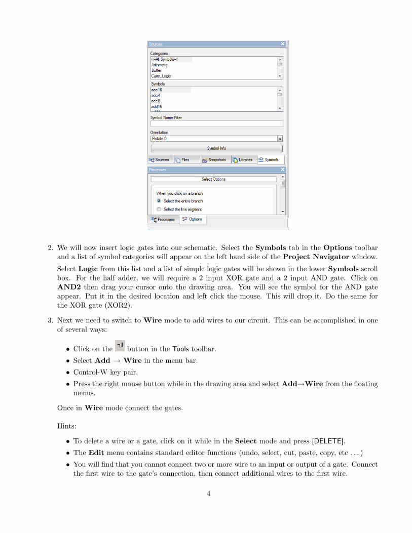
We are now ready to test the design for logical correctness in the simulator .
6 Using the Simulator
The simulator is a tool that allows us to test a circuits using software. Traditionally, a digital circuithad to be built on a breadboard using TTL chips in order to test for logical correctness. This had manydrawbacks. It was costly to equip a lab with enough hardware for a class full of students. The cost wasaugmented further because many chips where hooked up incorrectly and destroyed. Hookup errors oftenoccurred which were hard to detect on a breadboard. Software design solves these problems and allowsdesigns to be re-used and built upon.
1. Select the device (xc2s200e) in the Sources in Project pane in the Project Navigator, right clickand select New Source...
2. Select Test Bench Waveform from the list of file types and enter “halfadder tb” as the file name.Click the Next button. The next dialog box will shows which source file to associate the test benchwavform with, which is halfadder. Click the Next button. Verify the information in the last dialogbox and click the Finish button.
6
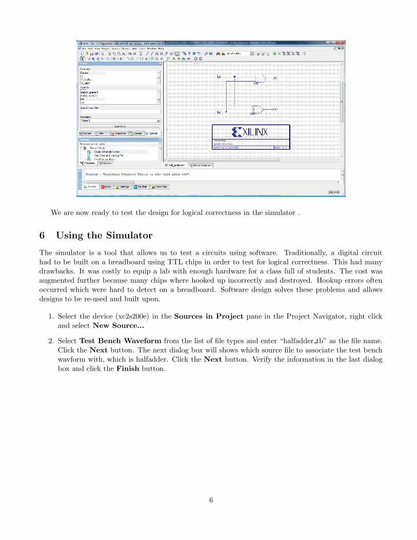
3. The Initialize Timing dialog box will appear. Ensure that the Combinatorial Design radio buttonis selected, the Check outputs and Assign inputs are set to “50” and the Time Scale is in “ns”.Click the Finish button.
4. The HDL Bencher window will appear in the main pane of the Project Navigator.
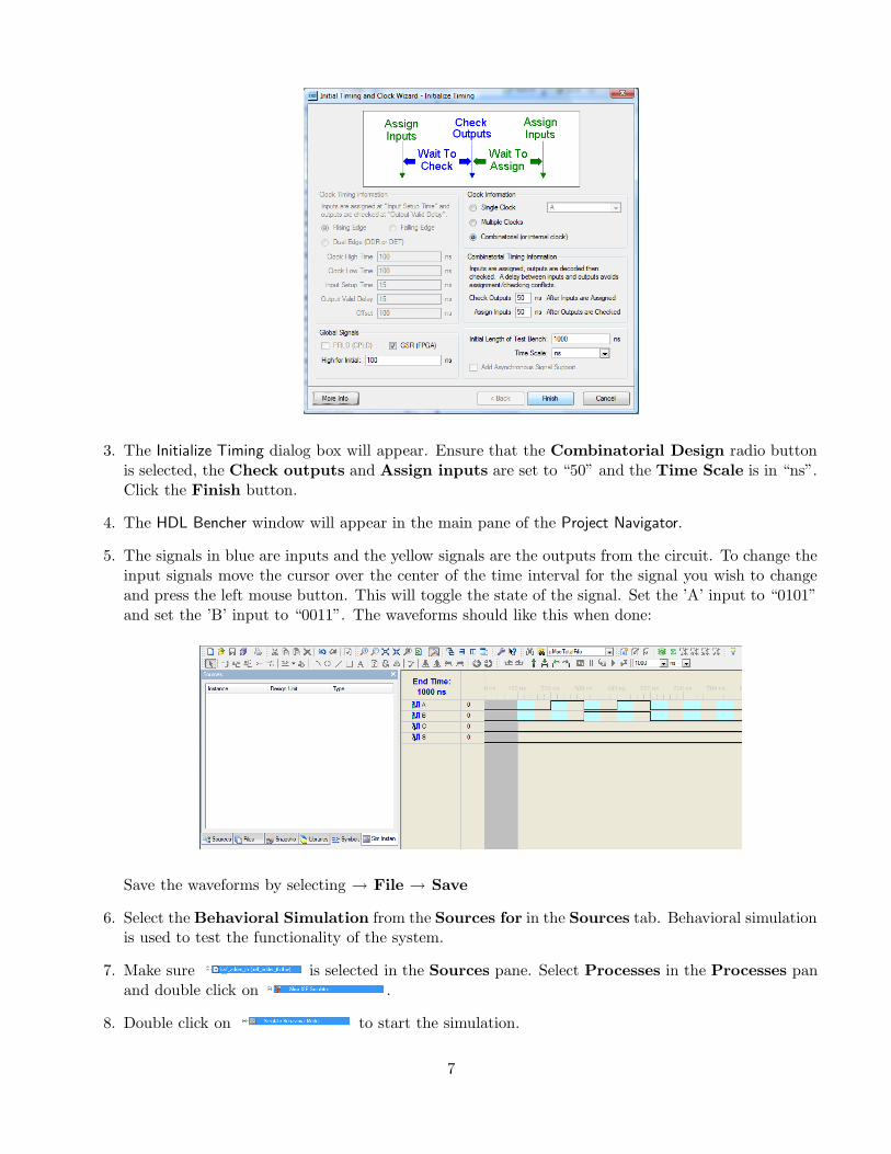
5. The signals in blue are inputs and the yellow signals are the outputs from the circuit. To change theinput signals move the cursor over the center of the time interval for the signal you wish to changeand press the left mouse button. This will toggle the state of the signal. Set the ’A’ input to “0101”and set the ’B’ input to “0011”. The waveforms should like this when done:
Save the waveforms by selecting → File → Save
6. Select the Behavioral Simulation from the Sources for in the Sources tab. Behavioral simulationis used to test the functionality of the system.
7. Make sure is selected in the Sources pane. Select Processes in the Processes panand double click on .
8. Double click on to start the simulation.
7

9. A message box will should pop-up and ask you if you would like to reload “halfadderi tb.tbw”. ClickYes.
10. A new waveform window will appear showing the simulation results. Your waveform should look likethis:
7 Creating a UCF file
A User Constraint File (UCF) is used to assign I/O pins in a design to the actual pins on the FPGA.Please refer to Appendix B for more information.
1. Highlight and right-click on the schematic source in the Sources in Project pane of the ProjectNavigator and select New Source... from the floating menu.
2. From the list of file types select Implementation Constraints File. Name the file “halfadder cf”and click Next.
3. The next dialog box is used to associate the UCF file with a specific source file. Choose the sourcefile in the project, “half adder.sch”, and click Next.
4. The final dialog box is for confirming the information input in the previous dialog boxes. ClickFinish if the information is correct.
5. In the Sources in Project pane ensure “halfadder cf.ucf” is highlighted and in the Processesfor Source pane click on the “+” in to expand the section and double click EditConstraints (Text) in the list.
6. The UCF file has the following format:
NET <pin name in Schematic design> LOC=P<pin number on FPGA>
NOTE: Make sure to use upper case letters for the pin names.
7. Let us assign the inputs to the dip switches on the FPGA and the outputs to the LEDs. Please referto the DIO1 board schematic for more information about pin connections. We will make A switch1, B switch 2, S LED 1 and C LED 2.
8

—Design pin —FPGA pin —Description
A P126 SW1B P129 SW2S P154 LED1C P161 LED2
8. Enter the following code:NET A LOC=P126;NET B LOC=P129;NET S LOC=P154;NET C LOC=P161;
You can get a better idea of our setup by looking at the Digilent DIO1 Programmer’s model in Ap-pendix B. We will look at this setup in more detail in the following sections.
8 Compiling a Logic Design
Hitherto, we have examined how to design and simulate a digital circuit using the Xilinx ISE Design Suite10.1 Software. We will now look at how to compile and download the design to the Digilent D2E board.Connected to the D2E is a DIO1 board that contains switches and LEDs.
1. Now go back to the Project Navigator window. Highlight in the Sources in Projectpane and double click in the Processes for Source pane to synthesize the design.
2. When the synthesis stage has completed, double click to implement the design.
3. Finally, double click to generate the programming file that will be downloaded tothe FPGA. It is possible to go straight to generating the programming file, and the Project Navigatorwill determine which of the previous step need to be run to produce an up to date programming file.
9 Downloading the design to the FPGA
Downloading a file to the FPGA is accomplished through the iMPACT tool.Please check Appendix A for setting up the DE2 and DIO1 boards before downloading the desing on
the FPGA board.
1. Select
2. Double click in the Processes pane to start the iIMPACT tool.
3. In the Configure Devices dialog box that appears verify the Boundary-Scan Mode radio buttonis selected and click Next.
4. In the next dialog box ensure the Automatically connect to cable and identify Boundary-Scanchain radio button is selected and click Finish.
9

5. A message window titled Boundary-Scan Chain Contents Summary will appear stating iMPACT willask for the desired programming file. Click OK.
6. In the Assign New Configuration File dialog box select “half adder.bit” and click Open.
7. A message box will appear with a warning that the BIT file is for a different device than was foundin the boundary scan. This can be safely ignored. Click Yes.
8. Another warning will appear stating that the Startup Clock has been changed to ’JtagClk’ in thebitstream. Click OK.
9. Move the cursor over the device that appears in the Boundary-Scan tab and press the left mousebutton and select Program....
10. In the Program Options dialog box that appears verify none of the options are selected and click OK.
10 Testing the design
Depending on the state of the inputs, you may or may not see some of the LEDs on the bargraph displayglowing. We have assigned our Sum bit to LEDs LD1. The carry-out bit (C) is displayed on LED LD2.
We are using the slide switches for our A and B inputs. The A inputs is assigned to SW switch 1. TheB input is assigned to SW switch 2 Moving a switch to the ON position puts a 1 on the input. Movinga switch to the OFF position puts a 0 on the input.Try different combinations of inputs and verify that the circuit is working correctly.
10

11 Appendix A - Setting up the D2E and DIO1 boards
This is intended to allow the student to quickly set up the D2E board with the DIO1 board for this tutorial.It does not attempt to explain the configuration and is in no way a substitute for the documentationprovided with the two boards. It will allow you to use the slide switches as input and the LEDs as outputs.
1. Ensure that the slide switch located next to the DB25 connector is in the JTAG position.
2. Connect the parallel cable to the D2E board.
3. Ask your lab instructor to verify your jumper settings before applying power to the board.
4. Plug the 9V DC center positive adapter into the D2E board. A small red LED labeled LED2 shouldglow.
11

12 Appendix B - LEDs, 7-Segments and Switches
The following sections explain the connection and location of the DIP switches and LEDs of the DigilentIO1 Board.
12.1 LEDs
The Digilent DIO1 Board provides a series of eight LEDs (LD1–LD8) and four multiplexed 7-segmentdisplays (DSP1) for use by a Digilent 2E FPGA Board. All of these LEDs are Large active highmeaning that an LED segment will glow when a logic-high is applied to it. The following tables show theconnection from the Digilent 2E Board to the LEDs on the DIO1 Board expressed as UCF constraints.
—Description —Location
NET SEGA LOC=P127NET SEGB LOC=P132NET SEGC LOC=P134NET SEGD LOC=P136NET SEGE LOC=P139NET SEGF LOC=P141NET SEGG LOC=P146NET SEGDP LOC=P148
Table 1: Connections between DIO1 7-Segment display and Digilent 2E
12.2 Switches
The DIO1 has bank of eight slide switches and five pushbuttons (labeled BTN1 through BTN5) that areaccessible from an Digilent 2E Board.
When closed or ON, each DIP switch pulls the connected pin of the XS Board to ground. When theDIP switch is open or OFF, the pin is pulled high through a 10KΩ resistor.
When pressed, each pushbutton pulls the connected pin of the XS Board to ground. Otherwise, thepin is pulled high through a 10KΩ resistor. The table below show the connections from the Digilent D2EBoard to the switches on the Digilent IO1 Board expressed as UCF constraints.
—Description —Location
NET LD < 1 > LOC=P154NET LD < 2 > LOC=P161NET LD < 3 > LOC=P163NET LD < 4 > LOC=P165NET LD < 5 > LOC=P167NET LD < 6 > LOC=P169NET LD < 7 > LOC=P174NET LD < 8 > LOC=P176
Table 2: Connections between the DIO1 LEDs and Digilent 2E
12

—Description —Location
NET SW < 1 > LOC=P126NET SW < 2 > LOC=P129NET SW < 3 > LOC=P133NET SW < 4 > LOC=P135NET SW < 5 > LOC=P138NET SW < 6 > LOC=P140NET SW < 7 > LOC=P145NET SW < 8 > LOC=P147
Table 3: Connections between the DIO1 slide switches and Digilent 2E
—Description —Location
NET BTN < 1 > LOC=P149NET BTN < 2 > LOC=P150NET BTN < 3 > LOC=P151NET BTN < 4 > LOC=P152NET BTN < 5 > LOC=P178
Table 4: Connections between the DIO1 pushbuttons and Digilent 2E
13