Embed Size (px)
Citation preview
UNITED STATES DISTRICT COURT EASTERN DISTRICT OF TEXAS
TYLER DIVISION SUPER INTERCONNECT TECHNOLOGIES LLC, Plaintiff,
v. Civil Action No. 6:13-cv-740 ZTE CORPORATION AND ZTE USA, JURY TRIAL DEMANDED INC., Defendants.
COMPLAINT
1. Plaintiff Super Interconnect Technologies LLC (“Super Interconnect
Technologies”), for its Complaint against defendants ZTE Corporation and ZTE USA, Inc.
(collectively “ZTE” or “Defendants”), hereby alleges as follows:
PARTIES
2. Super Interconnect Technologies is a Texas company with its principal place of
business in the Eastern District of Texas at 2400 Dallas Parkway, Suite 200, Plano, Texas 75093.
3. On information and belief, ZTE Corporation is a corporation organized under the
laws of the People’s Republic of China, and has its principal place of business located at No. 55,
Hi-Tech Road South, ShenZhen, P.R. China 518057, where it can be served with process in
accordance with the terms of the Hague Convention.
4. On information and belief, ZTE USA, Inc. is a New Jersey corporation with its
principal place of business at 2425 North Central Expressway, Suite 323, Richardson, Texas
Case 6:13-cv-00740 Document 1 Filed 10/01/13 Page 1 of 5 PageID #: 1
2
75080. ZTE USA Inc.’s registered agent for service of process in Texas is Jing Li, 2425 North
Central Expressway, Suite 323, Richardson, Texas 75080.
NATURE OF THE ACTION
5. This is a civil action for infringement of United States Patent No. 6,560,290 (the
“’290 patent”) under the patent laws of the United States, 35 U.S.C. § 1 et seq.
JURISDICTION AND VENUE
6. This Court has subject matter jurisdiction pursuant to 28 U.S.C. §§ 1331 and
1338(a).
7. On information and belief, each Defendant is subject to this Court’s specific and
general personal jurisdiction pursuant to due process and the Texas Long Arm Statute, due at
least to its substantial business in this forum, including: (A) at least part of its infringing
activities alleged herein, and (B) regularly doing or soliciting business, engaging in other
persistent causes of conduct, or deriving substantial revenue from goods and services provided to
persons and other entities in Texas and this judicial district.
8. Venue is proper in this judicial district pursuant to 28 U.S.C. § 1391(b), (c) and
(d) and § 1400(b). On information and belief, each Defendant has purposely transacted
substantial business in this judicial district, and has committed acts of direct infringement in this
judicial district.
THE PATENT-IN-SUIT
9. United States Patent No. 6,560,290, entitled “CMOS Driver and On-Chip
Termination for Gigabaud Speed Data Communication,” was duly and legally issued by the
United States Patent and Trademark Office on May 6, 2003. A copy of the ‘290 patent is
attached hereto as Exhibit A.
Case 6:13-cv-00740 Document 1 Filed 10/01/13 Page 2 of 5 PageID #: 2
3
10. Super Interconnect Technologies is the exclusive licensee of the ‘290 patent and
has the right to sue and recover damages for any current or past infringement.
COUNT I
(INFRINGEMENT OF U.S. PATENT NO. 6,560,290)
11. Paragraphs 1 through 10 are incorporated by reference as if fully stated herein.
12. This cause of action arises under the patent laws of the United States, and in
particular, 35 U.S.C. § 271 et seq.
13. ZTE has infringed, and continues to infringe, at least claim 9 of the ‘290 patent
under 35 U.S.C. § 271, either literally or under the doctrine of equivalents, by making, using,
offering to sell, selling or importing into the United States mobile electronic products that
include on-chip termination, for example and without limitation, ZTE Fury.
14. Super Interconnect Technologies has been and continues to be damaged by ZTE’s
infringement of the ‘290 patent.
PRAYER FOR RELIEF
Wherefore, Super Interconnect Technologies respectfully requests that this Court enter:
A. Judgment in favor of Super Interconnect Technologies that ZTE has infringed the
‘290 patent;
B. An order requiring ZTE to pay Super Interconnect Technologies damages
adequate to compensate for ZTE’s past infringement and any continuing or future infringement
up until the date such judgment is entered, including pre- and post-judgment interest, costs and
disbursements as justified under 35 U.S.C. § 284 and, if necessary to adequately compensate
Super Interconnect Technologies for ZTE’s infringement, an accounting;
Case 6:13-cv-00740 Document 1 Filed 10/01/13 Page 3 of 5 PageID #: 3
4
C. A determination that this case is exceptional within the meaning of 35 U.S.C. §
285;
D. A preliminary and permanent injunction preventing ZTE, and those in active
concert or participation with ZTE, from directly or indirectly infringing the ‘290 patent;
E. A judgment requiring that, in the event a permanent injunction preventing future
acts of infringement is not granted, Super Interconnect Technologies be awarded a compulsory
ongoing licensing fee; and
F. Any and all further relief which this Court deems just and proper.
DEMAND FOR JURY TRIAL
Super Interconnect Technologies requests a trial by jury on all issues so triable by right
pursuant to Fed. R. Civ. P. 38.
Case 6:13-cv-00740 Document 1 Filed 10/01/13 Page 4 of 5 PageID #: 4
5
Dated: October 1, 2013 Respectfully submitted,
By: /s/ Craig Tadlock__________________ Craig Tadlock
Texas State Bar No. 00791766 Keith Smiley Texas State Bar No. 24067869
TADLOCK LAW FIRM PLLC 2701 Dallas Parkway, Suite 360 Plano, Texas 75093 Tel: (903) 730-6789 Email: [email protected] Email: [email protected] Paul J. Hayes Robert R. Gilman
Christopher E. Millikin Jonathan R. DeBlois
HAYES MESSINA GILMAN & HAYES LLC 250 Northern Ave., Suite 410 Boston, Massachusetts 02110 Tel: (978) 809-3850 Fax: (978) 809-3869 Email: [email protected] Email: [email protected] Email: [email protected] Email: [email protected] ATTORNEYS FOR PLAINTIFF SUPER INTERCONNECT TECHNOLOGIES LLC
Case 6:13-cv-00740 Document 1 Filed 10/01/13 Page 5 of 5 PageID #: 5
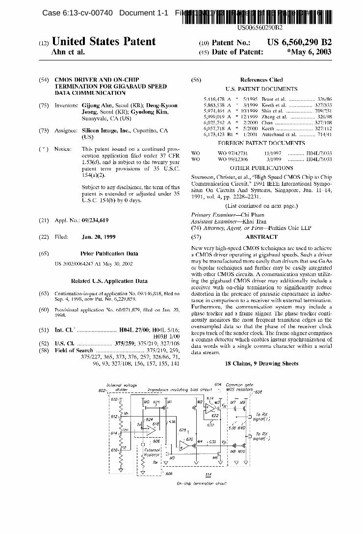
(12) United States Patent
US006560290B2
(10) Patent N0.: US 6,560,290 B2 Ahn et al. (45) Date 0f Patent: *May 6, 2003
(54) CMOS DRIVER AND ON-CHIP (56) References Cited TERMINATION FOR GIGABAUD SPEED U.S. PATENT DOCUMENTS DATA COMMUNICATION
5,418,478 A * 5/1995 Brunt et a1. ................ .. 326/86
(75) Inventors: Gijung Ahn, Seoul Deog-Kyoon 5,883,538 A * 3/1999 Keeth et a1. .............. .. 327/333 Jeong, Seoul Gyudong Kim, 5,974,464 A * 10/1999 CI 8.1. 709/231 Sunnyvale CAWS) 5,999,019 A * 12/1999 Zheng et a1. ..... .. 326/98
’ 6,025,742 A * 2/2000 Chan . . . . . . . . . . . . . . .. 327/108
(73) Assignee: Silicon Image, Inc., Cupertino, CA 6,057,718 A * 5/2000 Keeth 327/112 (Us) 6,173,423 B1 * 1/2001 Autechaud et a1. ......... .. 714/41
FOREIGN PATENT DOCUMENTS
(*) Notice: This patent issued on a continued pros- W0 WO 97/42731 11/1997 H04L/7/033 ecution application ?led under 37 CFR " 15361), and is Subject to the twenty year W0 WO 99/12306 3/1999 ......... .. HO4L/7/O33
patent term provisions of 35 U.S.C. OTHER PUBLICATIONS
154(aX2)‘ Svensson, Christer, et al., “High Speed CMOS Chip to Chip . . . . Communication Circuit,” 1991 IEEE International Sympo
sutbletct.m artly (iilsglalmecrifthf fiermgf “g1; sium On Circuits And Systems, Singapore, Jun. 11—14, {gasenc 1i5f1’Eb‘3nb; 0212551“ 6 “n er 1991, vol. 4, pp. 2228—2231.
(List continued on neXt page.)
Primary Examiner—Chi Pham (21) APPL NOJ 090343619 Assistant Examiner—Khai Tran
[tome , em, or zrm er ns o1e 74A yAg F'—Pki C'LLP
1 e : an. , 22 F1 d J 20 1999 57 ABSTRACT
eW ver 1 -s ee tec n1 ues are use to ac 1eve _ _ _ N yh'gh p d CMOS h 'q d h' (65) Prlor Pubhcatlon Data a CMOS driver operating at gigabaud speeds. Such a driver
Us 2OO2/OO64247 A1 May 30 2002 may be manufactured more easily than drivers that use GaAs 7 or bipolar techniques and further may be easily integrated
With other CMOS circuits. A communication system utiliz Related US. Application Data ing the gigabaud CMOS driver may additionally include a
receiver With on-chip termination to signi?cantly reduce (63) Continuation-in-part of application No. 09/146,818, ?led on distortion in the presence of parasitic capacitance in induc
SeP- 4, 1998, HOW Pat- N°~ 672297859 tance in comparison to a receiver With external termination. . . . . Furthermore, the communication system may include a
(60) lgg‘gslonal apphcanon NO' 60/071’879’ ?led on Jan' 20’ phase tracker and a frame aligner. The phase tracker conti nously monitors the most frequent transition edges in the
7 _ _ oversampled data so that the phase of the receiver clock (51) Int‘ Cl‘ """"""""""""" " H04L 27/00’ keeps track of the sender clock. The frame aligner comprises
_ _ a comma detector Which enables instant synchronization of (52) US. Cl. ...................... .. 375/259, 375/219, 327/108 data Words With a Single Comma Character Within a Serial (58) Field of Search ............................... .. 375/219, 259, data Stream
375/227, 365, 373, 376, 257, 326/86, 71, 96,93; 327/108, 156, 157, 155, 141
in terno/ voltage divider
7
1m edance matchin bios circuit \ ""1 eeeeeeee "g 444444444 *4‘ T 4444 441/7608
18 Claims, 9 Drawing Sheets
5104 Common gate M05 resistors
(
l 1 l 1 1 To RX 1 11 [524 signal(+) 1 1 101 618 1 Vm 11 “w 15" 11 To RX ' 1 TTTTTFT556T1 $/gnal(—) : W 1 r : 516 1 1 External l1 1 1 1 Resistor11 1 1 l ‘l 1
I l : Re 1L sssssssssssssssss H31 2222 ,4
u 22222 1,1 1 1 ,506 M4
On-chip termination circuit
Case 6:13-cv-00740 Document 1-1 Filed 10/01/13 Page 1 of 16 PageID #: 6

US 6,560,290 B2 Page 2
OTHER PUBLICATIONS
Gogaert, S., et al., “622 Mbit/s board—to—board link in 0.5 urn CMOS technology,” Proceedings of the IEEE 1995 Custom Integrated Circuits Conference, Santa Clara, Cali fornia, May 1—4, 1995, pp. 447—450. Gogaert, S., et al., “A 1 Gbit/s full—dupleX CMOS driver/ receiver for tWisted—pair data—cornrnunication,” 1998 Syrn posiurn On VLSI Circuits Digest of Technical Papers, Hono lulu, HaWaii, Jun. 11—13, 1998, pp. 192—195. Kim, S. et al.; An 800Mbps Mulit—Channel CMOS Serial Link with 3x Oversampling; pp. 451—454; IEEE 1995 Cus torn Integrated Circuits Conference.
Gotoh, K. et al.; All—Digital Multi—Phase Delay Locked Loop for Internal Timing Generation in Embedded and/or High—Speed DRAMs; pp. 107—108;1997 Symposium on VLSI Circuits Digest of Technical Papers. Shin, H. et al.; A250—Mbit/s CMOS Crosspoint SWitch; pp. 478—486; IEEE Journal of Solid—State Circuits, vol. 24, No. 2, Apr. 1989. Keiser, Bernhard E.; Sources of Radiated Interference and its Characteristics; pp. 25—34; Principles of Electronrnag netic Cornpatibility; 1996; 3rd Edition. Spread Spectrum Modulation; Pseudo—Noise Sequences; pp. 578—611 (Chapter 9). * cited by eXarniner
Case 6:13-cv-00740 Document 1-1 Filed 10/01/13 Page 2 of 16 PageID #: 7
Case 6:13-cv-00740 Document 1-1 Filed 10/01/13 Page 3 of 16 PageID #: 8
Case 6:13-cv-00740 Document 1-1 Filed 10/01/13 Page 4 of 16 PageID #: 9
U.S. Patent May 6, 2003 Sheet 3 0f 9 US 6,560,290 B2
1 M7 __ MI
5060 | | [3080 306111 | f308b
From _ _D To From [I To Seria/izer Cab/e Seria/izer Cab/e
(—) 3040 (+) (+) 304b (—)
I _J_|_ M2 J_J_ M2 1 3020 l 1 30gb
F 3 Differential voi/tage driver 1Q?
Circuitl configurations of current mode driver (a) and voltage mode driver (b) (L=4nH,C7=2pF and C2=4pF)
I -
L | 408 - ' ~
\ | _| l- C; l _L C2 _L C2
3; l I @623? i
_______________________ FIG. 4A
_ _ _ _ M g _ _ _ _ _ _ _ _ _ _ _ _ _ _ _ _ _ ___‘ V
TX 702 %/;T 708\ H 7
Case 6:13-cv-00740 Document 1-1 Filed 10/01/13 Page 5 of 16 PageID #: 10
Case 6:13-cv-00740 Document 1-1 Filed 10/01/13 Page 6 of 16 PageID #: 11
Case 6:13-cv-00740 Document 1-1 Filed 10/01/13 Page 7 of 16 PageID #: 12
Case 6:13-cv-00740 Document 1-1 Filed 10/01/13 Page 8 of 16 PageID #: 13
U.S. Patent May 6, 2003 Sheet 7 0f 9 US 6,560,290 B2
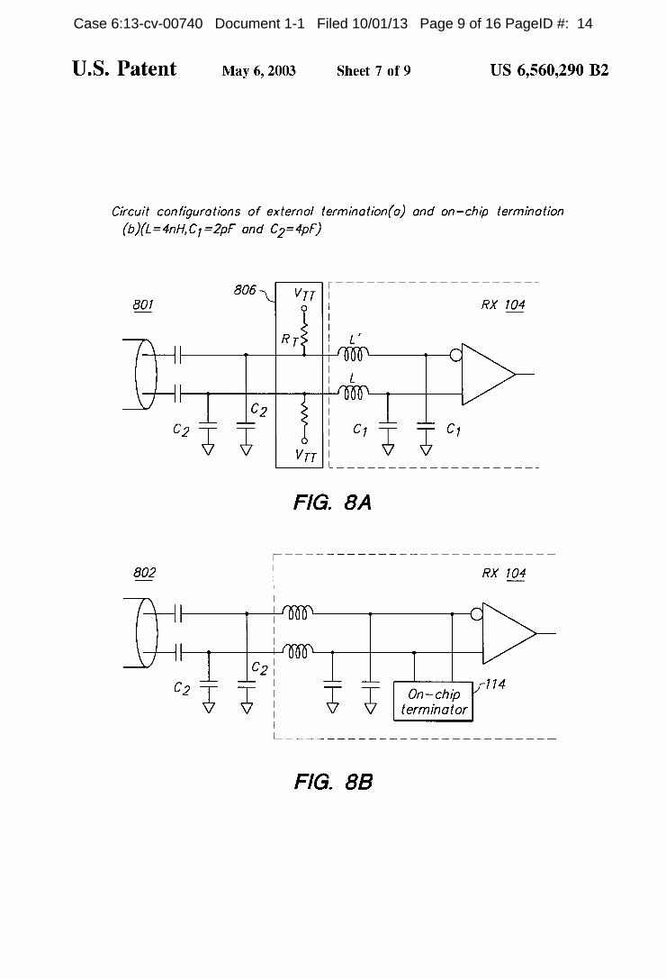
Circuit con?gurations of external termination(a) and on-chip termination (b)(L=4nH,C;=2pF and C2=4pF)
g 806\ V” I: my,
RT; I: L' ) H {/6102
| L
H . lfm . II |
62L “C2 i : C1l “ 61 |
1; g VUL g Q; FIG. 8A
L2 F _________________ "£55" I
) n i000 |
:: - i600“ -
C24]~ __C2i l '__ _ f774 Q; Q i E E 1
Case 6:13-cv-00740 Document 1-1 Filed 10/01/13 Page 9 of 16 PageID #: 14
Case 6:13-cv-00740 Document 1-1 Filed 10/01/13 Page 10 of 16 PageID #: 15
Case 6:13-cv-00740 Document 1-1 Filed 10/01/13 Page 11 of 16 PageID #: 16
US 6,560,290 B2 1
CM OS DRIVER AND ON-CHIP TERMINATION FOR GIGABAUD SPEED
DATA COMMUNICATION
CROSS-REFERENCE TO RELATED APPLICATIONS
The present application claims the bene?t of US. provi sional application serial No. 60/071,879, titled “1.25 GBaud CMOS Driver and On-Chip Termination for Gigabit Ether net PHY Chip,” invented by Gijung Ahn, Deog-Kyoon Jeong, and Gyudong Kim, and ?led on Jan. 20, 1998. The present application is also a continuation-in-part of US. patent application Ser. No. 09/146,818, titled “System and Method for High-Speed, Synchronized Data Communication,” invented by Deog-Kyoon Jeong and Gijung Ahn, and ?led on Sep. 4, 1998 now US. Pat. No. 6,229,809.
BACKGROUND OF THE INVENTION
1. Technical Field This invention relates to data communication systems.
More particularly, this invention relates high-speed commu nications systems including high-speed transmitters and receivers.
2. Description of Related Art As electronic and computer technology continues to
evolve, communication of information among different devices, either situated near by or at a distance becomes increasingly important. For example, it is noW more desir able than ever to provide for high speed communications among different chips on a circuit board, different circuit boards in a system, and different systems With each other. It is also increasingly desirable to provide such communica tions at very high speeds, especially in vieW of the large amount of data required for data communications in inten sive data consuming systems using graphical or video information, multiple input-output channels, local area netWorks, and the like.
It is particularly desirable to enable individual personal computers, Workstations, or other computing devices, Within Which data is normally internally transferred using parallel data buses, to communicate With each other over relatively simple transmission lines. Such transmission lines typically include only one or tWo conductors, in contrast With the 64-bit and Wider data paths Within computing systems noW commonly available. A communication system that includes oversampling is
often utiliZed to recover transmitted data. Such a system includes a receiver Which samples the incoming serial data stream at a rate greater than the rate at Which symbols (bits) are being transmitted. For example, in a three-times (3x) oversampling receiver, the incoming data stream is sampled at a rate approximately three times the symbol rate. HoWever, there are various problems to overcome in order to effectively implement such a receiver When the rate of data transmission is very high. For example, parasitic capacitance and inductance typically introduce substantial distortion into the received signal.
The physical layer of the Gigabit Ethernet standard (IEEE 802.32) requires a so-called PHY chip Which operates at gigabaud speeds. Traditionally, either GaAs or bipolar tech niques have been used to implement such PHY chips. HoWever, GaAs and bipolar circuits cannot be easily inte grated With other CMOS (complementary metal-oxide semiconductor) circuits and are typically more costly to manufacture than CMOS circuits.
10
15
20
25
30
35
40
45
55
60
65
2 SUMMARY OF THE INVENTION
The above described needs are met and problems are solved by the present invention. NeW very high-speed CMOS techniques are used to achieve a CMOS driver operating at gigabaud speeds. Such a driver may be manu factured more easily than drivers that use GaAs or bipolar techniques and further may be easily integrated With other CMOS circuits. A communication system utiliZing the gigabaud CMOS driver may additionally include a receiver With on-chip termination to signi?cantly reduce distortion in the presence of parasitic capacitance in inductance in com parison to a receiver With external termination. Furthermore, the communication system may include a phase tracker and a frame aligner. The phase tracker continously monitors the most frequent transition edges in the oversampled data so that the phase of the receiver clock keeps track of the sender clock. The frame aligner comprises a comma detector Which enables instant synchroniZation of data Words With a single comma character Within a serial data stream.
BRIEF DESCRIPTION OF THE DRAWINGS
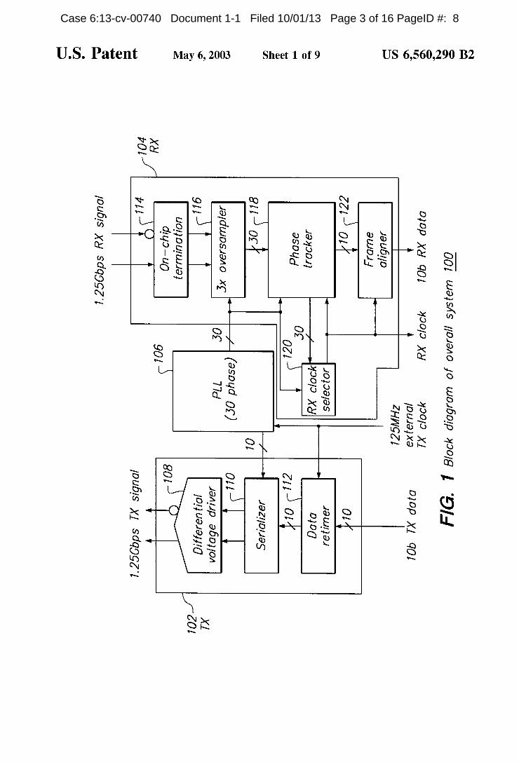
FIG. 1 shoWs a block diagram of a communication system utiliZing a gigabaud CMOS driver in accordance With a preferred embodiment of the present invention.
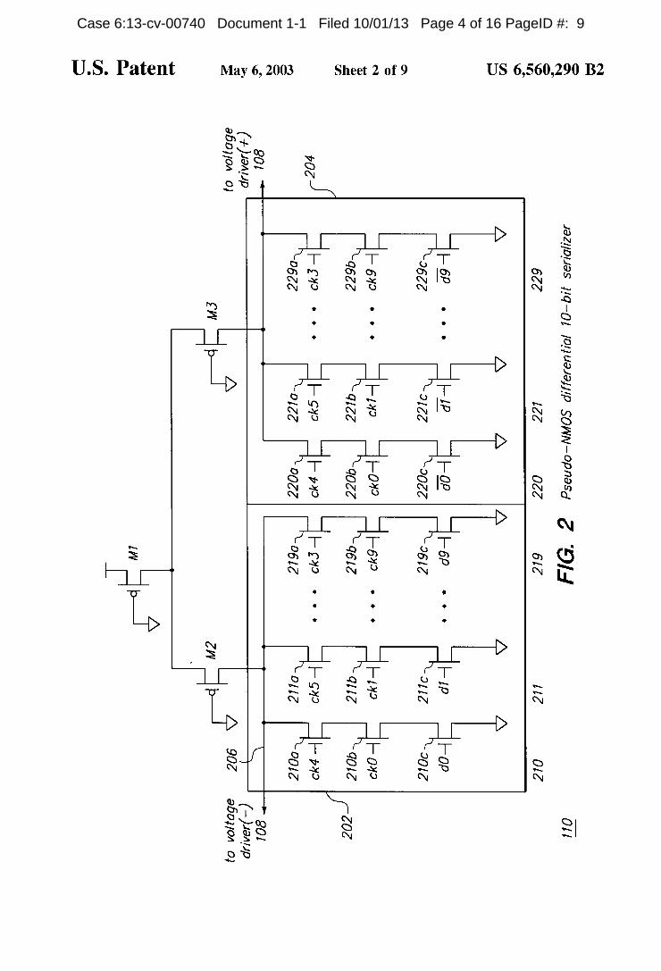
FIG. 2 shoWs a circuit diagram of a high-speed serialiZer in accordance With a preferred embodiment of the present invention.
FIG. 3 shoWs a circuit diagram of a differential voltage driver in accordance With a preferred embodiment of the present invention.
FIG. 4 shoWs typical circuit con?gurations of (a) a current mode driver and (b) a voltage mode driver in accordance With a preferred embodiment of the present invention.
FIG. 5 shoWs simulated Waveforms under the con?gura tions shoWn in FIG. 4 in accordance With a preferred embodiment of the present invention.
FIG. 6 shoWs a circuit diagram of an on-chip termination circuit in accordance With a preferred embodiment of the present invention.
FIG. 7 shoWs the characteristics of the on-chip termina tion circuit shoWn in FIG. 6 for a 75 ohm transmission line in accordance With a preferred embodiment of the present invention.
FIG. 8 contrasts (a) a conventional receiver con?guration using external termination outside the conventional receiver With (b) the receiver con?guration Which utiliZes on-chip termination Within the receiver in accordance With a pre ferred embodiment of the present invention.
FIG. 9 contrasts (a) a simulated Waveform in a receiver using external termination in accordance With FIG. 8(a) With (b) a simulated Waveform in a receiver utiliZing on-chip termination in accordance With FIG. 8(b).
FIG. 10 shoWs a block diagram of (a) a phase tracker and (b) a frame aligner in accordance With a preferred embodi ment of the present invention.
DESCRIPTION OF THE PREFERRED EMBODIMENTS
FIG. 1 shoWs a block diagram of a communication system 100 utiliZing a gigabaud CMOS driver 108 in accordance With a preferred embodiment of the present invention. The system 100 includes a transmitter 102, a receiver (RX) 104, and a phase-locked loop (PLL) 106. As shoWn in FIG. 1, the transmitter 102 outputs a 1.25
gigabit per second (Gbps) signal to a transmission medium.
Case 6:13-cv-00740 Document 1-1 Filed 10/01/13 Page 12 of 16 PageID #: 17
US 6,560,290 B2 3
Of course, the particular speed of the signal may vary Within the scope of the present invention. The transmitter 102 includes a differential voltage driver (the gigabaud CMOS driver) 108, a serialiZer 110, and a data retimer 112.
In accordance With a preferred embodiment, the data retimer 112 receives a 125 MHZ external clock and a DC-balanced and limited run-length 10-bit parallel data stream from an encoder. The data retimer 112 utiliZes the external clock to adjust the timing of the data stream.
The serialiZer 110 receives the adjusted 10-bit parallel data stream from the data retimer 112. The serialiZer 110 also receives 10 phase clocks from the PLL 106. The serialiZer 110 utiliZes the 10 phase clocks to transform the 10-bit parallel data stream into a serial bit stream.
The differential voltage driver 108 receives the serial bit stream from the serialiZer 110. The differential voltage driver 108 drives the serial bit stream onto the medium at 1.25 Gbps, 10 times the 125 MHZ speed of the external clock.
The transmission medium Which carries the 1.25 Gbps signal is not terminated With a conventional external resistor. Instead, the transmission medium is terminated by an on-chip termination circuit 114 Within the receiver 104. Use of the on-chip termination circuit 114 reduces signal distor tion in comparison With external termination. The receiver 104 includes, in addition to the on-chip termination 114, a 3-times (3x) oversampler 116, a phase tracker 118, a RX clock selector 120, and a frame aligner 122.
The oversampler 116 receives the data signal from the on-chip termination 114. The oversampler 116 utiliZes 30 phase clocks supplied by the PLL 106 to oversample the data signal and generate 30 sampled bits in parallel. The 3x oversampler 116 provides the 30 sampled bits in parallel to the phase tracker 118. The phase tracker 118 and the RX clock selector 120 operate to recover the clock and the data from the oversampled data and provides the recovered data stream to the frame aligner 122. In a preferred embodiment, the frame aligner 122 searches for a comma character in the recovered data stream and makes a near instant alignment of the boundary betWeen Words When such a comma character is found.
In accordance With a preferred embodiment of the system 100, a clock frequency difference betWeen the TX 102 and the RX 104 of less than 0.1% is to be tolerated. The PLL 106 operates to keep the clock frequency difference Within that tolerance.
FIG. 2 shoWs a circuit diagram of a high-speed serialiZer 110 in accordance With a preferred embodiment of the present invention. The serialiZer 110 comprises NMOS (n-type metal-oxide-semiconductor) transistors used as sWitching elements, and PMOS (p-type metal-oxide semiconductor) transistors (M1, M2, M3) used as loads. These transistors are used to form differential pseudo NMOS logic.
Regarding the PMOS transistors, M1 has its source coupled to a supply voltage, its gate coupled to an electrical ground, and its drain coupled to the sources of M2 and M3. Operationally, M1 pulls doWn the common mode voltage so that the output voltage moves around one-half the supply voltage (Vdd/2) With a small sWing. M2 has its gate coupled to an electrical ground, and its drain coupled to a ?rst NMOS transistor netWork 202. M3 has its gate coupled to an electrical ground, and its drain coupled to a second NMOS transistor netWork 204.
The ?rst netWork 202 includes a ?rst node 206 coupled to the drain of M2. The ?rst node 206 is also coupled to the
10
15
20
25
30
35
40
45
55
60
65
4 negative input terminal of the differential voltage driver 108. In addition, the ?rst node 206 is coupled to ten columns (210, 211, . . . , 219) of NMOS transistors. Each column 210—219 includes three NMOS transistors in series betWeen the ?rst node 206 and electrical ground. For example, the ?rst column 210 includes a ?rst NMOS transistor 210a Whose source is coupled to the ?rst node 206, a second NMOS transistor 210b Whose source is coupled to the drain of the ?rst NMOS transistor 210a, and a third NMOS transistor 210c Whose source is coupled to the drain of the second NMOS transistor 210b and Whose drain is coupled to an electrical ground. The gate of the ?rst NMOS transistor 210a is coupled to receive a ?fth phase clock signal (ck4) from the PLL 106. The gate of the second NMOS transistor 210b is coupled to receive a ?rst phase clock signal (ck0) from the PLL 106. Finally, the gate of the third NMOS transistor 210c is coupled to receive a ?rst data signal (d0) from the data retimer 112.
Similarly, the second column 211 includes three NMOS transistors (211a—211c) coupled in series betWeen the ?rst node 206 and an electrical ground. The gate of the ?rst NMOS transistor 211a is coupled to receive a sixth phase clock signal (ck5) from the PLL 106. The gate of the second NMOS transistor 211b is coupled to receive a second phase clock signal (ck1) from the PLL 106. Finally, the gate of the third NMOS transistor 211c is coupled to receive a second data signal (d1) from the data retimer 112. And so on for the other columns 212—219, incrementing
the signals on the gates appropriately. For example, regard ing the tenth column 219, the gate of the ?rst NMOS transistor 219a is coupled to receive a fourth phase clock signal (ck3) from the PLL 106. The gate of the second NMOS transistor 219b is coupled to receive a tenth phase clock signal (ck9) from the PLL 106. Finally, the gate of the third NMOS transistor 2196 is coupled to receive a tenth data signal (d9) from the data retimer 112. The second netWork 204 includes a second node 208
coupled to the drain of M3. The second node 208 is also coupled to the positive input terminal of the differential voltage driver 108. In addition, the second node 208 is coupled to ten columns (220, 221, . . . , 229) of NMOS transistors. Each column 220—229 includes three NMOS transistors in series betWeen the second node 208 and electrical ground. For example, the ?rst column 220 includes a ?rst NMOS transistor 220a Whose source is coupled to the second node 208, a second NMOS transistor 220b Whose source is coupled to the drain of the ?rst NMOS transistor 220a, and a third NMOS transistor 2206 whose source is coupled to the drain of the second NMOS transistor 220b and Whose drain is coupled to an electrical ground. The gate of the ?rst NMOS transistor 220a is coupled to receive a ?fth phase clock signal (ck4) from the PLL 106. The gate of the second NMOS transistor 220b is coupled to receive the ?rst phase clock signal (ck0) from the PLL 106. Finally, the gate of the third NMOS transistor 2206 is coupled to receive an inverted version of the ?rst data signal (inverted d0) from the data retimer 112.
Similarly, the second column 221 includes three NMOS transistors (221a—221c) coupled in series betWeen the sec ond node 208 and an electrical ground. The gate of the ?rst NMOS transistor 221a is coupled to receive a sixth phase clock signal (ck5) from the PLL 106. The gate of the second NMOS transistor 221b is coupled to receive a second phase clock signal (ck1) from the PLL 106. Finally, the gate of the third NMOS transistor 2216 is coupled to receive an inverted version of the second data signal (inverted d1) from the data retimer 112.
Case 6:13-cv-00740 Document 1-1 Filed 10/01/13 Page 13 of 16 PageID #: 18
US 6,560,290 B2 5
And so on for the other columns 222—229, incrementing the signals on the gates appropriately. For example, regard ing the tenth column 229, the gate of the ?rst NMOS transistor 229a is coupled to receive a fourth phase clock signal (ck3) from the PLL 106. The gate of the second NMOS transistor 229b is coupled to receive a tenth phase clock signal (ck9) from the PLL 106. Finally, the gate of the third NMOS transistor 2296 is coupled to receive an inverted version of the tenth data signal (d9) from the data retimer 112.
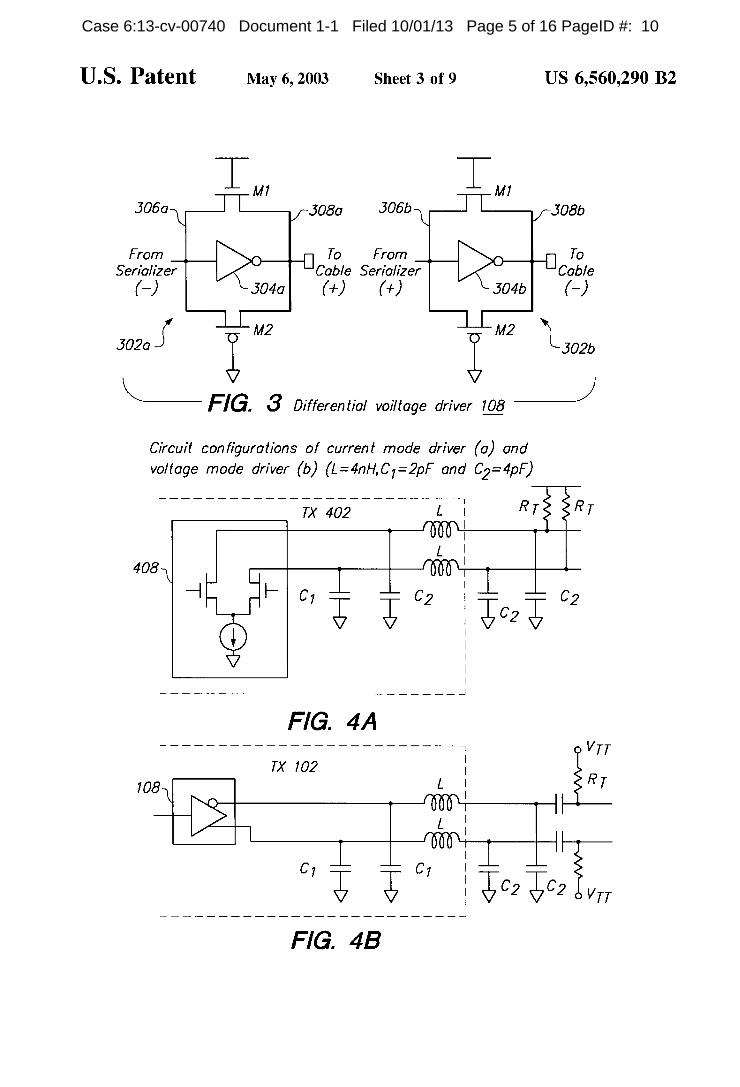
FIG. 3 shoWs a circuit diagram of a differential voltage driver 108 in accordance With a preferred embodiment of the present invention. The communication system 100 uses such a differential voltage driver 108 instead of a current mode driver, because a current mode driver is not appropriate to drive a high speed signal onto a transmission line in the presence of large parasitic capacitance and inductance due to bonding Wires and pads. The differential voltage driver 108 comprises a ?rst inverter circuit 302a and a second inverter circuit 302b.
The ?rst inverter circuit 302a comprises a NMOS tran sistor M1, a PMOS transistor M2, and an inverter 304a. The NMOS transistor M1 has its gate coupled to a supply voltage, its drain coupled to a ?rst node 306a, and its source coupled to a second node 308a. The PMOS transistor M2 has its gate coupled to an electrical ground, its drain coupled to the ?rst node 306a, and its source coupled to the second node 308a. The inverter 304a has its input coupled to the ?rst node 306a and its output coupled to the second node 308a. The ?rst node 306a is also coupled to receive the negative polarity (—) output from the serialiZer 110. The second node 308a is also coupled to output a positive polarity (+) output to the transmission medium (for example, a cable). Thus, the circuitry of the ?rst inverter circuit 302a operates to receive the negative polarity data signal from the serialiZer 110, invert the signal, and output a positive polar ity data signal to the transmission medium. M1 and M2 are used as feedback resistors Which reduce the voltage sWing of the inverter 304a as Well as reducing the output impedance.
The second inverter circuit 302b comprises a NMOS transistor M1, a PMOS transistor M2, and an inverter 304b. The NMOS transistor M1 has its gate coupled to a supply voltage, its drain coupled to a ?rst node 306b, and its source coupled to a second node 308b. The PMOS transistor M2 has its gate coupled to an electrical ground, its drain coupled to the ?rst node 306b, and its source coupled to the second node 308b. The inverter 304b has its input coupled to the ?rst node 306b and its output coupled to the second node 308b. The ?rst node 306b is also coupled to receive the positive polarity (+) output from the serialiZer 110. The second node 308b is also coupled to output a negative polarity (—) output to the transmission medium (for example, a cable). Thus, the circuitry of the second inverter circuit 302b operates to receive the positive polarity data signal from the serialiZer 110, invert the signal, and output a negative polarity data signal to the transmission medium. M1 and M2 are used as feedback resistors Which reduce the voltage sWing of the inverter 304b as Well as reducing the output impedance.
FIG. 4 shoWs typical circuit con?gurations of (a) a current mode driver 408 and (b) a voltage mode driver 108. The voltage mode driver 108 Would be in accordance With a preferred embodiment of the present invention.
In both cases, the driver (408 or 108) is coupled to a transmission medium via a connection typically including bonding and Wire pads. The transmission medium and connection thereto are modeled by tWo capacitors C1 and C2 and an inductor L for each of tWo lines. C2 represents the capacitance of each transmission line, and each of the capacitors C2 is coupled betWeen a transmission line and an
10
15
25
35
45
65
6 electrical ground. Each LC circuit (comprising inductor L and capacitor C1) represents the parasitic inductance and capacitance due to the bonding Wires and pads. The other end of the transmission medium is coupled to a receiver via an appropriate connection (including termination). The appropriate connection varies depending upon Whether the driver is a current mode driver 408 or a voltage mode driver 108.
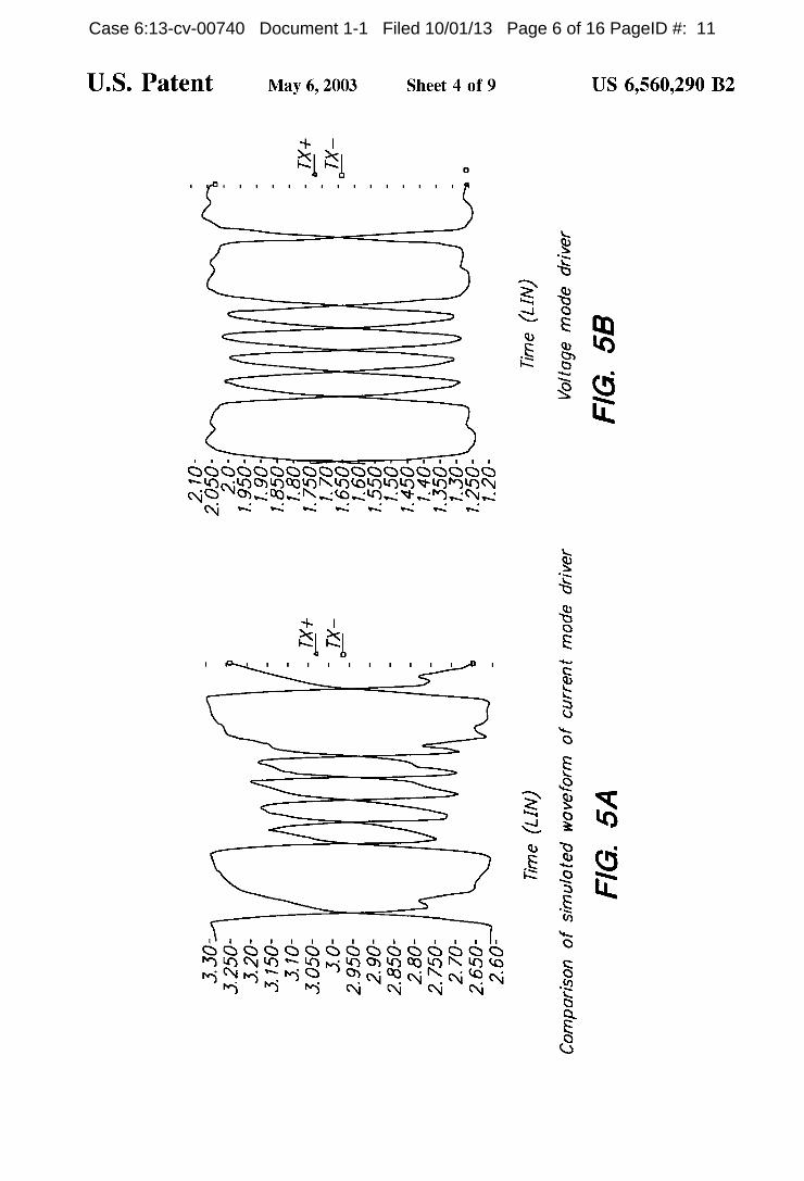
FIG. 5 shoWs simulated Waveforms under the con?gura tions shoWn in FIG. 4 in accordance With a preferred embodiment of the present invention. For purposes of the simulation, in order to model parasitic effects of the trans mission medium and the connection thereto, the inductance L Was set to be 4nH, and the tWo capacitors C1 and C2 Were set to be 2 pF and 4 pF, respectively. As shoWn in FIG. 5(a), signi?cant inter-symbol interfer
ence occurs in the current mode driver 408 con?guration. This inter-symbol interference may be attributed to sloW, passive pull-up and constant current pull-doWn. In contrast, as shoWn in FIG. 5(b), only an insigni?cant amount of distortion occurs in the voltage mode driver 108 con?gura tion. This is because the voltage mode driver 108 drives the signal actively in both directions (up and doWn).
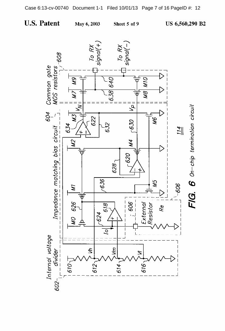
FIG. 6 shoWs a circuit diagram of an on-chip termination circuit 114 in accordance With a preferred embodiment of the present invention. As shoWn in FIG. 6, the on-chip termination circuit is based on a common gate CMOS con?guration. In particular, the on-chip termination circuit 114 includes an internal voltage divider 602, an impedance matching bias circuit 604, an external resistor 606, and a con?guration of common gate MOS transistors 608.
In accordance With a preferred embodiment, the internal voltage divider 602 includes four resistors (610, 612, 614, 616) and three nodes (Vh, Vm, and VI). The four resistors are coupled in series betWeen a supply voltage and an electrical ground. The three nodes exist betWeen the four resistors. The ?rst resistor 610 couples the supply voltage to the ?rst node Vh. The second resistor 612 couples the ?rst node V,1 to the second node Vm. The third resistor 614 couples the second node Vm to the third node VI. The fourth resistor 616 couples the third node V, to an electrical ground. The voltage at V,1 is relatively high, the voltage at V, is relatively loW, and the voltage at Vm is in betWeen. Finally, each of the three nodes is coupled to the bias circuit 604. Thus, the internal voltage divider 602 generates three reference voltages.
In a preferred embodiment, the bias circuit 604 includes three operational ampli?ers (opamps) 618, 620, and 622 and 7 transistors (M0—M6). The ?rst opamp 618 has its negative terminal coupled to Vm of the voltage divider 602, its positive terminal coupled to a ?rst node 624, and its output terminal coupled to a second node 626. The second opamp 620 has its positive terminal coupled to of the voltage divider 602, its negative terminal coupled to a third node 628, and its output terminal coupled to a fourth node 630. The fourth node 630 is also labeled as voltage VP. The third opamp 622 has its positive terminal coupled to V1, its negative terminal coupled to a ?fth node 632, and its output terminal coupled to a sixth node 634. The sixth node 634 is also labeled as voltage VN. The ?rst transistor MO comprises a PMOS transistor
having its source coupled to a supply voltage, its drain coupled to the ?rst node 624, and its gate coupled to the second node 626. The second transistor M1 comprises a PMOS transistor having its source coupled to a supply voltage, its drain coupled to a seventh node 636, and its gate coupled to the second node 626. The third transistor M2 comprises a PMOS transistor having its source coupled to a supply voltage, its drain coupled to the third node 628, and its gate coupled to the second node 626. Thus, each of the ?rst three transistors M0—M2 comprise PMOS transistor having their gates controlled by the output of the ?rst opamp 618.
Case 6:13-cv-00740 Document 1-1 Filed 10/01/13 Page 14 of 16 PageID #: 19
US 6,560,290 B2 7
The fourth transistor M3 comprises a NMOS transistor having its source coupled to a supply voltage, its drain coupled to the ?fth node 632, and its gate coupled to the siXth node 634 (VN). The ?fth transistor M4 comprises a PMOS transistor having its source coupled to the third node 628, its drain coupled to an electrical ground, and its gate coupled to the fourth node 630 (VP). The siXth transistor M5 comprises a NMOS transistor having its source and its gate both coupled to the seventh node 636, and its drain coupled to an electrical ground. Finally, the seventh transistor M6 comprises a NMOS transistor having its source coupled to the ?fth node 632, its drain coupled to an electrical ground, and its gate coupled to the seventh node 636.
The external resistor 606 includes a resistor, denoted as having a resistance value of Re, coupled betWeen the ?rst node 624 of the bias circuit 604 and an electrical ground. The eXternal resistor 606 is used as a reference impedance.
The common gate MOS transistors 608 include tWo NMOS transistors M7 and M9, and tWo PMOS transistors M8 and M0. The ?rst NMOS transistor M7 has its source coupled to a supply voltage, its drain coupled to a ?rst output node 638, and its gate coupled to the siXth node 634 of the bias circuit 604. The ?rst PMOS transistor M8 has its source coupled to the ?rst output node 638, its drain coupled to an electrical ground, and its gate coupled to the fourth node 630 of the bias circuit 604. The ?rst output node 638 is coupled to the positive polarity line from the transmission medium for termination purposes. The second NMOS transistor M9 has its source coupled to a supply voltage, its drain coupled to a second output node 640, and its gate coupled to the siXth node 634 of the bias circuit 604. The second PMOS tran sistor M10 has its source coupled to the second output node 640, its drain coupled to an electrical ground, and its gate coupled to the fourth node 630 of the bias circuit 604. The second output node 640 is coupled to the negative polarity line of the transmission medium for termination purposes.
Operationally, the bias circuit 604 controls the termina tion voltage and impedance by providing bias voltages VP and VN to the gates of the common gate MOS transistors 608. Within the bias circuit 604, transistors M0, M1, M2, M5 and M6 are connected as current mirrors. All currents in the current mirrors are set as Vm/Re. Transistors M7 and M9 are replicas of M3. Transistors M8 and M10 are replicas of M4. M3 generates current Io at V1. M4 generates current Io at Vh.
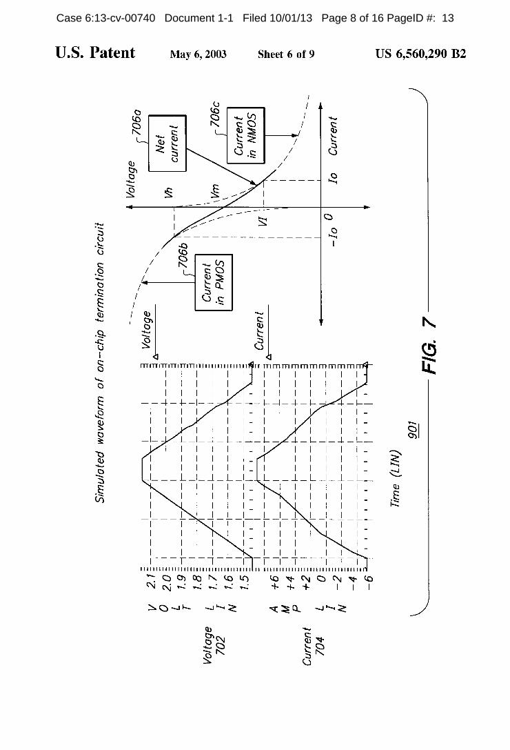
FIG. 7 shoWs the characteristics of the on-chip termina tion circuit 114 shoWn in FIG. 6 for a 75 ohm transmission line in accordance With a preferred embodiment of the present invention. Both voltage 702 and current 704 char acteristics are shoWn. In addition, a voltage versus current graph 706 is also shoWn.
The voltage vs. current graph 706 shoWs net current 706a, PMOS transistor current 706b, and NMOS transistor current 706c. The graph 706 shoWs that although the impedance of either the PMOS transistor or the NMOS transistor is not linear, the combined effect of the PMOS and NMOS tran sistors is almost linear When the voltage is around Vdd/2. In particular, When the resistor values in the voltage divider are such that (Vh—Vm)=(Vm—Vl), then the relation betWeen termination resistance RT and external resistance Re is as folloWs:
The above equation shoWs that impedance is independent of supply voltage because both (Vh—Vm) and Vm are pro portional to Vdd. There is a trade-off betWeen poWer con sumption and termination resistance range.
FIG. 8 contrasts (a) a conventional receiver con?guration 801 using eXternal termination 806 outside the conventional
10
15
25
35
45
55
65
8 receiver 804 With (b) the receiver con?guration 802 Which utiliZes on-chip termination 114 Within the receiver 104 in accordance With a preferred embodiment of the present invention. As shoWn in FIG. 8, the conventional receiver con?guration 801 has the eXternal termination 806 placed in betWeen the capacitance C2 of the transmission medium and the LC circuit (L and C1) on the conventional receiver 804. In contrast, the receiver con?guration 802 has the on-chip termination 114 betWeen the LC circuit (L and C1) on the conventional receiver 804 and the rest of the conventional receiver 804.
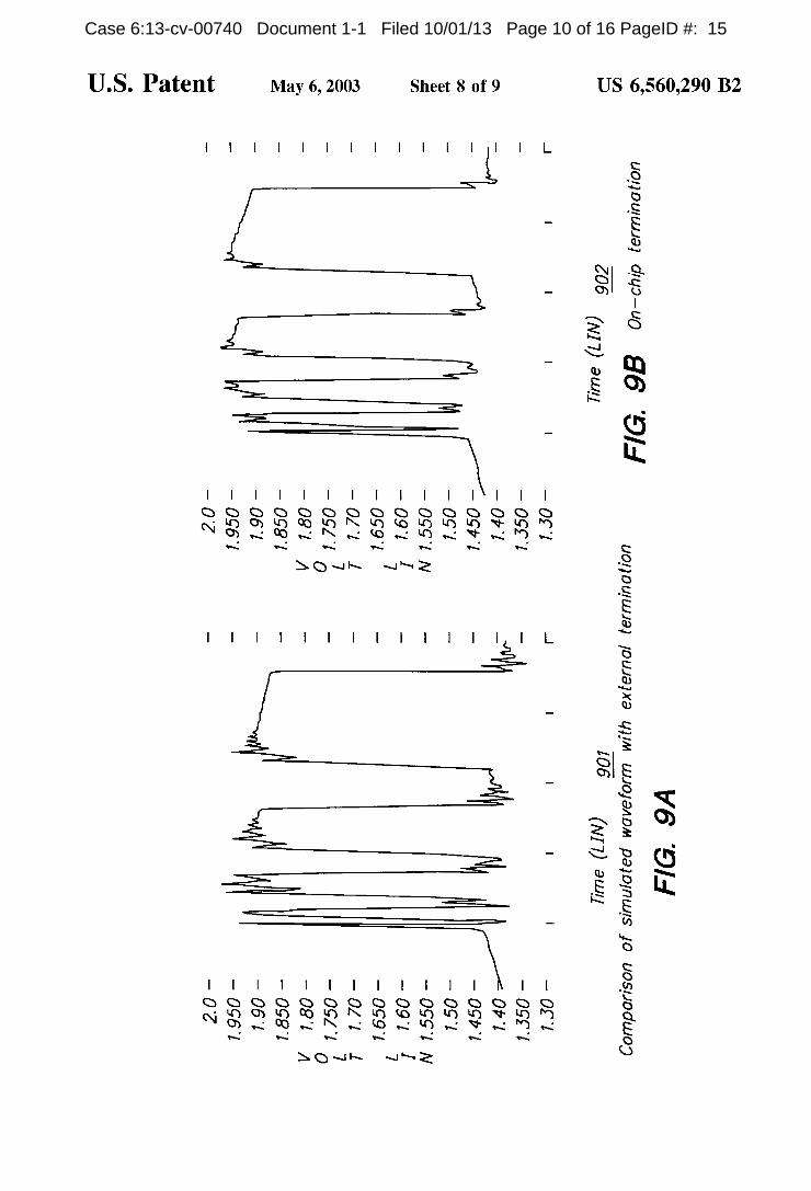
FIG. 9 contrasts (a) a ?rst simulated Waveform 901 in a receiver using eXternal termination in accordance With FIG. 8(a) With (b) a second simulated Waveform 902 in a receiver utiliZing on-chip termination in accordance With FIG. 8(b). The simulations Were run assuming the folloWing values: L=4 nH, C1=2 pF, and C2=4 pF. The simulations also assumed an ideal rectangular pulse train driven through a 75 ohm medium. As shoWn in FIG. 9, signi?cantly reduced distortion can be seen in the second simulated Waveform 902 in comparison to the ?rst simulated Waveform 901. Thus, using the on-chip termination 114 reduces distortion of the received signal.
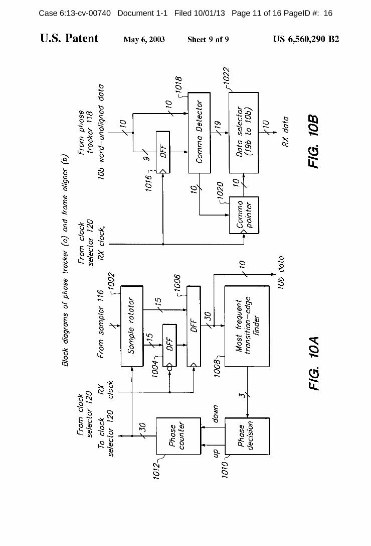
FIG. 10 shoWs a block diagram of (a) a phase tracker 118 and (b) a frame aligner 122 in accordance With a preferred embodiment of the present invention. In the preferred embodiment shoWn in FIG. 10(a), the phase tracker 118 includes a sample rotator 1002, a ?rst D-type ?ip ?op (DFF) array 1004, a second D-type ?ip ?op (DFF) array 1006, a most frequent transition-edge ?nder 1008, a phase decision circuit 1010, and a phase counter 1012.
In a preferred embodiment, the rotator 1002 receives thirty samples in parallel from the sampler 116. The rotator 1002 applies a signal from the phase counter 1012 to shuffle the samples and to the timing of the samples into a RX clock domain. The rotated samples are provided by the rotator 1002 to the DFF arrays 1004 and 1006. Both the tWo DFF arrays 1004 and 1006 also receives the RX clock signal from the RX clock selector 120 for control purposes. In particular, the ?rst 15 samples are provided to the ?rst DFF array 1004, and the second 15 samples are provided to a second half of the second DFF array 1006. The ?rst DFF array 1004 provides its contents to a ?rst half of the second DFF array 1006. The second DFF array 1006 outputs 10 bits of data in parallel to the frame aligner 122, and also outputs its contents to the ?nder 1008.
In a preferred embodiment, the ?nder 1008 determines the most frequent transition-edge in the contents provided by the second DFF 1006. The most frequent edge information is passed from the ?nder to the phase decision circuit 1010. By continuously monitoring the most frequent transition-edge in the oversampled data, the phase of the RX clock keeps track of the sender’s clock. In a preferred embodiment, the phase decision circuit 1010 uses the most frequent transition-edge information to determine Whether an up signal or a doWn signal should be sent to the phase counter 1012. The phase counter 1012 applies any up or doWn signal received from the phase decision circuit 1010 and provides a 10-bit phase pointer to the rotator 1002 and to the clock selector 120. The phase pointer indicates Which clock among the 30 PLL clocks is closest to the clock of the transmitter 102.
In the preferred embodiment shoWn in FIG. 10(b), the frame aligner 122 includes a D-type ?ip ?op (DFF) array 1016, a comma detector 1018, a comma pointer 1020, and a data selector 1022. The DFF array 1016 stores the previous 9 bits of Word-unaligned data from the phase tracker 118 and provides them to a comma detector 1018. The comma detector 1018 also receives the current 10 bits of Word unaligned data from the phase tracker 118. The comma detector 1018 searches across the 19 bit data sequence to
Case 6:13-cv-00740 Document 1-1 Filed 10/01/13 Page 15 of 16 PageID #: 20
US 6,560,290 B2
detect any comma Which Would comprise the sequence of bits 0011111010. The detected position of a comma is stored using a comma pointer 1020. The comma pointer 1020 is used by the data selector 1022 to extract the Word aligned 10 bits of data until a neW comma is detected.
What is claimed is: 1. A system for high speed communication of digital data
comprising: a transmission medium including a ?rst end and a second
end; a transmitter coupled to the ?rst end of the transmission medium for converting the digital data to a data signal and for driving the digital signal onto the transmission medium, the transmitter including a complementary metal-oxide-semiconductor (CMOS) voltage driver; and
a receiver coupled to the second end of the transmission medium for receiving the data signal from the trans mission medium and for recovering the digital data from the data signal, the receiver including on-chip termination for substantially reducing distortion in the data signal.
2. The system of claim 1, Wherein the data signal com prises a serial data signal, and the transmitter further includes a high speed serialiZer.
3. The system of claim 1, Wherein the CMOS voltage driver drives the data signal onto the transmission medium at least at gigabaud speed.
4. The system of claim 1, further comprising: a phase-locked loop coupled to the transmitter and to the
receiver, the phase-locked loop receiving a clock signal from the transmitter, generating a plurality of clock signals With different phases based on the clock signal, and providing the plurality of clock signals With dif ferent phases to the receiver.
5. The system of claim 4, Wherein the phase-locked loop further provides a subset of the plurality of clock signals With different phases to the transmitter.
6. The system of claim 5, Wherein the reveiver further includes an oversampler for receiving the plurality of clock signals With different phases and applying the plurality of clock signals With different phases to oversample the data signal and so generate an oversampled data signal.
7. The system of claim 6, Wherein the receiver further includes phase tracking circuitry for receiving the over sampled data signal and for monitoring a most frequent transition edge in the oversampled data in order to keep track of the clock signal from the transmitter.
8. The system of claim 7, the receiver further comprises: a clock selector coupled to the phase tracking circuitry
and to the phase-locked loop, the clock selector and the phase tracker operative to recover the clock and the data from the oversampled data.
9. A receiver for receiving a data signal from a transmis sion medium and for recovering digital data from the data signal, the receiver comprising:
an on-chip termination circuit for substantially reducing distortion in the data signal the on-chip termination circuit comprising an internal voltage divider for generating reference
voltages; an impedance matching bias circuit coupled to the
internal voltage divider; and common gate MOS resistors coupled to the impedance
matching bias circuit, the impedance matching cir cuit controlling a termination voltage and impedance by providing bias voltages to gates of the common gate MOS transistors.
10
15
25
30
50
55
60
65
10 10. The receiver of claim 9, further comprising: an oversampler for applying a plurality of clock signals
With different phases to oversample the data signal and so generate an oversampled data signal.
11. The receiver of claim 10, Wherein the receiver further includes phase tracking circuitry for monitoring a most frequent transition edge in the oversampled data in order to keep track of a clock signal from a transmitter Which drove the data signal onto the transmission medium.
12. The receiver of claim 9, further comprising: a comma detector for ?nding comma characters in the
data signal for purposes of data Word synchroniZation. 13. The receiver of claim 9, Wherein the common gate
MOS resistors comprise: common-gate PMOS and NMOS transistors, the PMOS and NMOS transistors being opera tive to increase the linearity of the current and voltage relations and to increase the alloWable voltage- current range for high-speed signal termination.
14. The receiver of claim 9, Wherein the on-chip termi nation circuit further comprises:
an external resistor coupled betWeen a ?rst node of the impedance matching bias circuit and an electrical ground, the external resistor operative to act as a reference impedance.
15. The receiver of claim 9, Wherein the internal voltage divider comprises:
three nodes providing three reference voltages Vh, Vm, V1, to the impedance matching bias circuit.
16. The receiver of claim 11, Wherein the phase tracking circuitry comprises
a sample rotator coupled to the oversampler, the sample rotator operative to rotate the samples and to provide the rotated samples as output.
17. A transmitter for converting digital data to a data signal and for driving the data signal onto a communication medium, the transmitter comprising:
a CMOS voltage driver for driving the data signal onto the transmission medium at least at gigabaud speed, the driver comprising a ?rst inverter circuit and a second inverter circuit, the ?rst inverter circuit comprising: a NMOS transistor Ml having a gate coupled to a
supply voltage, a drain coupled to a ?rst node and a source coupled to a second node;
a PMOS transistor M2 having a gate coupled to an electrical ground, a drain coupled to the ?rst node and a source coupled to the second node; and
an inverter having an input coupled to the ?rst node and an output coupled to the second node, the ?rst node being adapted to receive a negative polarity output, the second node being adapted to output a positive polarity output onto the communication medium, the second inverter circuit comprising: a NMOS transistor Ml having a gate coupled to a
supply voltage, a drain coupled to a ?rst node and a source coupled to a second node;
a PMOS transistor M2 having a gate coupled to an electrical ground, a drain coupled to the ?rst node and a source coupled to the second node; and
an inverter having an input coupled to the ?rst node and an output coupled to the second node, the ?rst node being adapted to receive a positive polarity output, the second node being adapted to output a negative polarity output onto the communication medium.
18. The transmitter of claim 17, Where the data signal comprises a serial data signal, and the transmitter further includes a high speed serialiZer.
* * * * *
Case 6:13-cv-00740 Document 1-1 Filed 10/01/13 Page 16 of 16 PageID #: 21
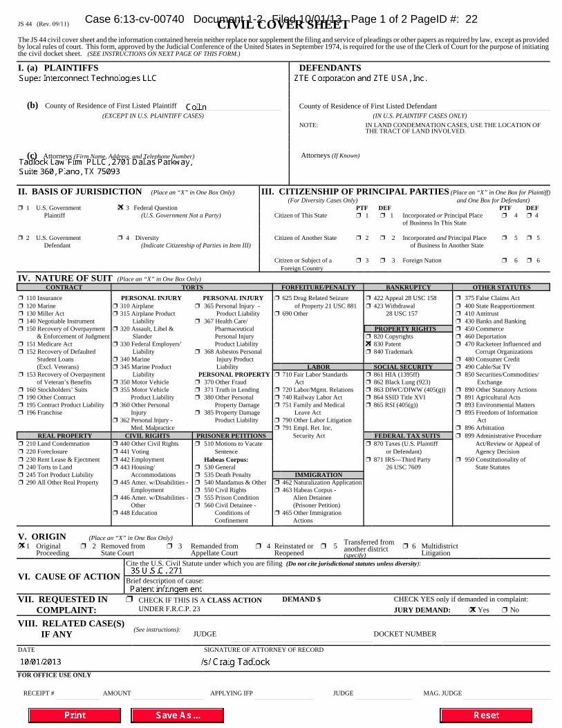
JS 44 (Rev. 09/11) CIVIL COVER SHEETThe JS 44 civil cover sheet and the information contained herein neither replace nor supplement the filing and service of pleadings or other papers as required by law, except as providedby local rules of court. This form, approved by the Judicial Conference of the United States in September 1974, is required for the use of the Clerk of Court for the purpose of initiatingthe civil docket sheet. (SEE INSTRUCTIONS ON NEXT PAGE OF THIS FORM.)
I. (a) PLAINTIFFS DEFENDANTS
(b) County of Residence of First Listed Plaintiff County of Residence of First Listed Defendant(EXCEPT IN U.S. PLAINTIFF CASES) (IN U.S. PLAINTIFF CASES ONLY)
NOTE: IN LAND CONDEMNATION CASES, USE THE LOCATION OF THE TRACT OF LAND INVOLVED.
(c) Attorneys (Firm Name, Address, and Telephone Number) Attorneys (If Known)
II. BASIS OF JURISDICTION (Place an “X” in One Box Only) III. CITIZENSHIP OF PRINCIPAL PARTIES (Place an “X” in One Box for Plaintiff)(For Diversity Cases Only) and One Box for Defendant)
’ 1 U.S. Government ’ 3 Federal Question PTF DEF PTF DEFPlaintiff (U.S. Government Not a Party) Citizen of This State ’ 1 ’ 1 Incorporated or Principal Place ’ 4 ’ 4
of Business In This State
’ 2 U.S. Government ’ 4 Diversity Citizen of Another State ’ 2 ’ 2 Incorporated and Principal Place ’ 5 ’ 5Defendant (Indicate Citizenship of Parties in Item III) of Business In Another State
Citizen or Subject of a ’ 3 ’ 3 Foreign Nation ’ 6 ’ 6 Foreign Country
IV. NATURE OF SUIT (Place an “X” in One Box Only)CONTRACT TORTS FORFEITURE/PENALTY BANKRUPTCY OTHER STATUTES
’ 110 Insurance PERSONAL INJURY PERSONAL INJURY ’ 625 Drug Related Seizure ’ 422 Appeal 28 USC 158 ’ 375 False Claims Act’ 120 Marine ’ 310 Airplane ’ 365 Personal Injury - of Property 21 USC 881 ’ 423 Withdrawal ’ 400 State Reapportionment’ 130 Miller Act ’ 315 Airplane Product Product Liability ’ 690 Other 28 USC 157 ’ 410 Antitrust’ 140 Negotiable Instrument Liability ’ 367 Health Care/ ’ 430 Banks and Banking’ 150 Recovery of Overpayment ’ 320 Assault, Libel & Pharmaceutical PROPERTY RIGHTS ’ 450 Commerce
& Enforcement of Judgment Slander Personal Injury ’ 820 Copyrights ’ 460 Deportation’ 151 Medicare Act ’ 330 Federal Employers’ Product Liability ’ 830 Patent ’ 470 Racketeer Influenced and’ 152 Recovery of Defaulted Liability ’ 368 Asbestos Personal ’ 840 Trademark Corrupt Organizations
Student Loans ’ 340 Marine Injury Product ’ 480 Consumer Credit (Excl. Veterans) ’ 345 Marine Product Liability LABOR SOCIAL SECURITY ’ 490 Cable/Sat TV
’ 153 Recovery of Overpayment Liability PERSONAL PROPERTY ’ 710 Fair Labor Standards ’ 861 HIA (1395ff) ’ 850 Securities/Commodities/ of Veteran’s Benefits ’ 350 Motor Vehicle ’ 370 Other Fraud Act ’ 862 Black Lung (923) Exchange
’ 160 Stockholders’ Suits ’ 355 Motor Vehicle ’ 371 Truth in Lending ’ 720 Labor/Mgmt. Relations ’ 863 DIWC/DIWW (405(g)) ’ 890 Other Statutory Actions’ 190 Other Contract Product Liability ’ 380 Other Personal ’ 740 Railway Labor Act ’ 864 SSID Title XVI ’ 891 Agricultural Acts’ 195 Contract Product Liability ’ 360 Other Personal Property Damage ’ 751 Family and Medical ’ 865 RSI (405(g)) ’ 893 Environmental Matters’ 196 Franchise Injury ’ 385 Property Damage Leave Act ’ 895 Freedom of Information
’ 362 Personal Injury - Product Liability ’ 790 Other Labor Litigation Act Med. Malpractice ’ 791 Empl. Ret. Inc. ’ 896 Arbitration
REAL PROPERTY CIVIL RIGHTS PRISONER PETITIONS Security Act FEDERAL TAX SUITS ’ 899 Administrative Procedure’ 210 Land Condemnation ’ 440 Other Civil Rights ’ 510 Motions to Vacate ’ 870 Taxes (U.S. Plaintiff Act/Review or Appeal of ’ 220 Foreclosure ’ 441 Voting Sentence or Defendant) Agency Decision’ 230 Rent Lease & Ejectment ’ 442 Employment Habeas Corpus: ’ 871 IRS—Third Party ’ 950 Constitutionality of’ 240 Torts to Land ’ 443 Housing/ ’ 530 General 26 USC 7609 State Statutes’ 245 Tort Product Liability Accommodations ’ 535 Death Penalty IMMIGRATION’ 290 All Other Real Property ’ 445 Amer. w/Disabilities - ’ 540 Mandamus & Other ’ 462 Naturalization Application
Employment ’ 550 Civil Rights ’ 463 Habeas Corpus -’ 446 Amer. w/Disabilities - ’ 555 Prison Condition Alien Detainee
Other ’ 560 Civil Detainee - (Prisoner Petition)’ 448 Education Conditions of ’ 465 Other Immigration
Confinement Actions
V. ORIGINTransferred fromanother district(specify)
(Place an “X” in One Box Only)’ 1 Original
Proceeding’ 2 Removed from
State Court’ 3 Remanded from
Appellate Court’ 4 Reinstated or
Reopened’ 5 ’ 6 Multidistrict
Litigation
VI. CAUSE OF ACTIONCite the U.S. Civil Statute under which you are filing (Do not cite jurisdictional statutes unless diversity): Brief description of cause:
VII. REQUESTED IN COMPLAINT:
’ CHECK IF THIS IS A CLASS ACTIONUNDER F.R.C.P. 23
DEMAND $ CHECK YES only if demanded in complaint:JURY DEMAND: ’ Yes ’ No
VIII. RELATED CASE(S) IF ANY (See instructions): JUDGE DOCKET NUMBER
DATE SIGNATURE OF ATTORNEY OF RECORD
FOR OFFICE USE ONLY
RECEIPT # AMOUNT APPLYING IFP JUDGE MAG. JUDGE
Case 6:13-cv-00740 Document 1-2 Filed 10/01/13 Page 1 of 2 PageID #: 22

JS 44 Reverse (Rev. 09/11)
INSTRUCTIONS FOR ATTORNEYS COMPLETING CIVIL COVER SHEET FORM JS 44
Authority For Civil Cover Sheet
The JS 44 civil cover sheet and the information contained herein neither replaces nor supplements the filings and service of pleading or other papers as requiredby law, except as provided by local rules of court. This form, approved by the Judicial Conference of the United States in September 1974, is required for theuse of the Clerk of Court for the purpose of initiating the civil docket sheet. Consequently, a civil cover sheet is submitted to the Clerk of Court for each civilcomplaint filed. The attorney filing a case should complete the form as follows:
I. (a) Plaintiffs-Defendants. Enter names (last, first, middle initial) of plaintiff and defendant. If the plaintiff or defendant is a government agency, use onlythe full name or standard abbreviations. If the plaintiff or defendant is an official within a government agency, identify first the agency and then the official, givingboth name and title.
(b) County of Residence. For each civil case filed, except U.S. plaintiff cases, enter the name of the county where the first listed plaintiff resides at thetime of filing. In U.S. plaintiff cases, enter the name of the county in which the first listed defendant resides at the time of filing. (NOTE: In land condemnationcases, the county of residence of the “defendant” is the location of the tract of land involved.)
(c) Attorneys. Enter the firm name, address, telephone number, and attorney of record. If there are several attorneys, list them on an attachment, notingin this section “(see attachment)”.
II. Jurisdiction. The basis of jurisdiction is set forth under Rule 8(a), F.R.C.P., which requires that jurisdictions be shown in pleadings. Place an “X” in oneof the boxes. If there is more than one basis of jurisdiction, precedence is given in the order shown below.
United States plaintiff. (1) Jurisdiction based on 28 U.S.C. 1345 and 1348. Suits by agencies and officers of the United States are included here.
United States defendant. (2) When the plaintiff is suing the United States, its officers or agencies, place an “X” in this box.
Federal question. (3) This refers to suits under 28 U.S.C. 1331, where jurisdiction arises under the Constitution of the United States, an amendment to theConstitution, an act of Congress or a treaty of the United States. In cases where the U.S. is a party, the U.S. plaintiff or defendant code takes precedence, and box1 or 2 should be marked.
Diversity of citizenship. (4) This refers to suits under 28 U.S.C. 1332, where parties are citizens of different states. When Box 4 is checked, the citizenship ofthe different parties must be checked. (See Section III below; federal question actions take precedence over diversity cases.)
III. Residence (citizenship) of Principal Parties. This section of the JS 44 is to be completed if diversity of citizenship was indicated above. Mark this sectionfor each principal party.
IV. Nature of Suit. Place an “X” in the appropriate box. If the nature of suit cannot be determined, be sure the cause of action, in Section VI below, issufficient to enable the deputy clerk or the statistical clerks in the Administrative Office to determine the nature of suit. If the cause fits more than one nature ofsuit, select the most definitive.
V. Origin. Place an “X” in one of the seven boxes.Original Proceedings. (1) Cases which originate in the United States district courts.
Removed from State Court. (2) Proceedings initiated in state courts may be removed to the district courts under Title 28 U.S.C., Section 1441. When the petitionfor removal is granted, check this box.
Remanded from Appellate Court. (3) Check this box for cases remanded to the district court for further action. Use the date of remand as the filing date.
Reinstated or Reopened. (4) Check this box for cases reinstated or reopened in the district court. Use the reopening date as the filing date.
Transferred from Another District. (5) For cases transferred under Title 28 U.S.C. Section 1404(a). Do not use this for within district transfers or multidistrictlitigation transfers.
Multidistrict Litigation. (6) Check this box when a multidistrict case is transferred into the district under authority of Title 28 U.S.C. Section 1407. When thisbox is checked, do not check (5) above.
Appeal to District Judge from Magistrate Judgment. (7) Check this box for an appeal from a magistrate judge’s decision.
VI. Cause of Action. Report the civil statute directly related to the cause of action and give a brief description of the cause. Do not cite jurisdictional statutesunless diversity. Example: U.S. Civil Statute: 47 USC 553
Brief Description: Unauthorized reception of cable service
VII. Requested in Complaint. Class Action. Place an “X” in this box if you are filing a class action under Rule 23, F.R.Cv.P.Demand. In this space enter the dollar amount (in thousands of dollars) being demanded or indicate other demand such as a preliminary injunction.
Jury Demand. Check the appropriate box to indicate whether or not a jury is being demanded.
VIII. Related Cases. This section of the JS 44 is used to reference related pending cases if any. If there are related pending cases, insert the docket numbersand the corresponding judge names for such cases.
Date and Attorney Signature. Date and sign the civil cover sheet.
Case 6:13-cv-00740 Document 1-2 Filed 10/01/13 Page 2 of 2 PageID #: 23