Embed Size (px)
Citation preview
3-1
Topi
c 3
Under the Hood of a DC/DC Boost Converter
Brian T. Lynch
AbstrAct
Despite having the same number of significant power components as the well-understood buck converter, the boost converter has the reputation of being low-performance and complicated to design. This topic discusses continuous-conduction-mode (CCM) and discontinuous-conduction-mode (DCM) operation of the boost converter in practical terms and presents a mathematical model for analysis of voltage-mode and current-mode feedback control.
I. IntroductIon
Necessitated by the proliferation of devices requiring unique voltage rails, the single-voltage, intermediate-bus architecture has gained in popularity over using a centralized, multivoltage source. Localized point-of-load converters optimized for specific loads remove from the system the overhead of multiple-voltage distribution. While stepping the intermediate-bus voltage down to a lower voltage with buck converters is the most common requirement, there is the occasional need for a boost converter to step the bus voltage up.
This topic discusses a few basics of the boost topology, going into some detailed discussion regarding modes of operation, and then discusses design trade-offs in the control options and their effect on overall converter per-formance. Mathematical models aid in the analysis.
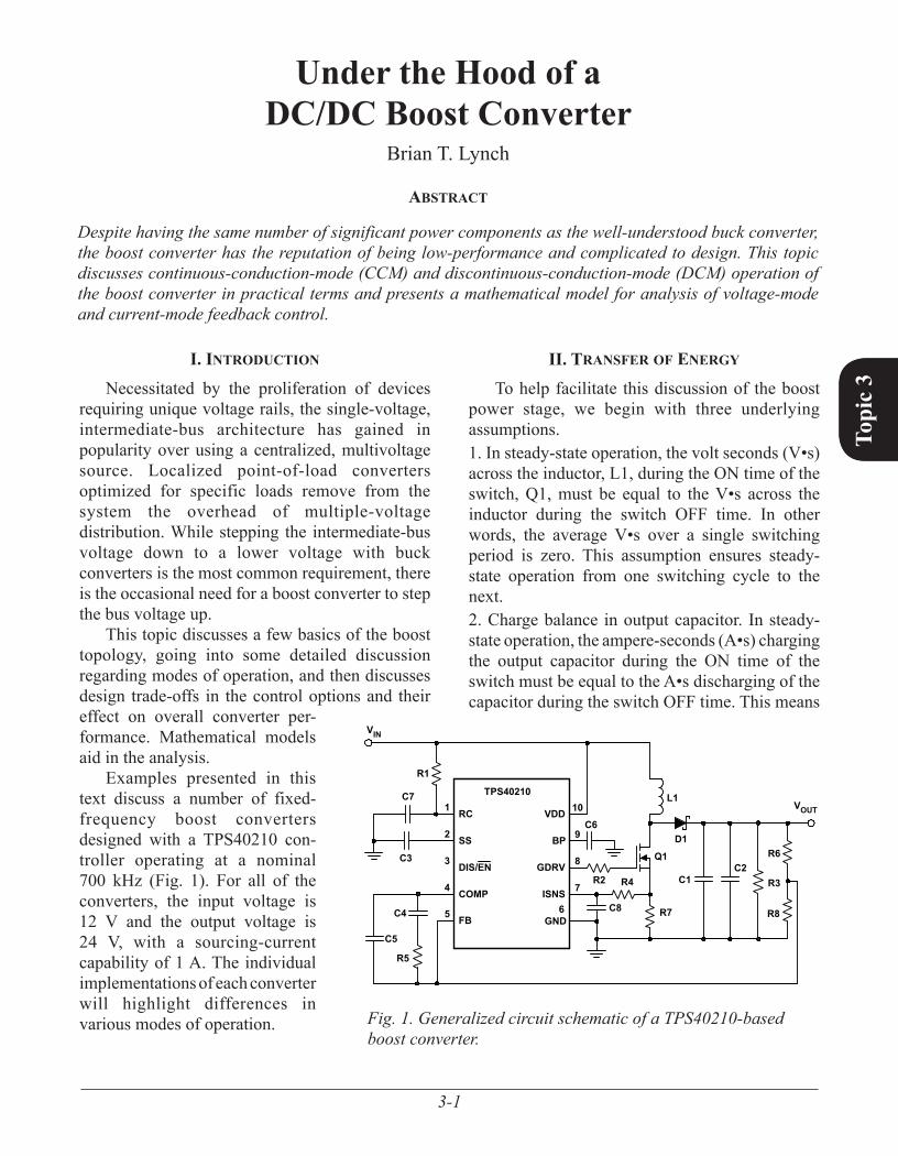
Examples presented in this text discuss a number of fixed-frequency boost converters designed with a TPS40210 con-troller operating at a nominal 700 kHz (Fig. 1). For all of the converters, the input voltage is 12 V and the output voltage is 24 V, with a sourcing-current capability of 1 A. The individual implementations of each converter will highlight differences in various modes of operation.
II. trAnsfer of energy
To help facilitate this discussion of the boost power stage, we begin with three underlying assumptions.1. In steady-state operation, the volt seconds (V•s) across the inductor, L1, during the ON time of the switch, Q1, must be equal to the V•s across the inductor during the switch OFF time. In other words, the average V•s over a single switching period is zero. This assumption ensures steady-state operation from one switching cycle to the next.2. Charge balance in output capacitor. In steady-state operation, the ampere-seconds (A•s) charging the output capacitor during the ON time of the switch must be equal to the A•s discharging of the capacitor during the switch OFF time. This means
1
2
3
5 FB
4
10
9
8
7
RC
DIS/EN
COMP
SS
VDD
ISNS
GDRV
GND
TPS40210VOUT
VIN
6
BP
R7
L1
R4R2
R5
R1
R3
R6
R8
D1
C2
C6
C7
C3
C4 C8
C1
C5
Q1
Fig. 1. Generalized circuit schematic of a TPS40210-based boost converter.
3-2
Topi
c 3
that the average A•s over a single switch period is zero. This assumption ensures steady-state operation from one switching cycle to the next.3. The ripple voltage across the output capacitor is small compared to the DC voltage generated by the converter. This assumption simplifies the analysis somewhat when we look at the V•s balance across the inductor.
The nonsynchronous boost topology is one of the few topologies where, even if the converter is off, there is an output voltage. Unfortunately, the voltage is unregulated and is subject to every change of the input. Under this steady-state condition, load current—if there is any—flows continuously through the inductor and diode and into the load. With the exception of the drop across the inductor due to the DC resistance, there is no voltage across the inductor.
To generate a regulated output voltage, the switch must begin switching. When switch Q1 turns ON, the voltage across the inductor increases to approximately the input voltage, and energy is stored in the inductor. The amount of energy stored is a function of the input voltage, the inductance, and the duration of the ON pulse. The diode rectifier, D1, is reverse-biased during this time interval. When the switch turns OFF, the stored energy releases to the output through the rectifier. The output capacitor filters the pulsating current, allowing DC current to flow into the load.
There are two fundamentally different operating modes for the converter. The first, continuous-conduction mode (CCM), is where energy in the inductor flows continuously during the operation of the converter. The increase of stored energy in the inductor during the ON time of the switch is equal to the energy discharged into the output during the OFF time of the switch, ensuring steady-state operation. At the end of the discharge interval, residual energy remains in the inductor. During the next ON interval of the switch, energy builds from that residual level to that required by the load for the next switching cycle.
In the other mode, discontinuous-conduction mode (DCM), the energy stored in the inductor during the ON interval of the switch is equal only to the energy required by the load for one switching
cycle, plus an amount for converter losses. The energy in the inductor depletes to zero before the end of each switching cycle, resulting in a period of no energy flow, or discontinuous operation.
These two operating modes have significant influence on the performance of the converter. One of the first decisions to make in designing a boost converter is to select in which of these two modes the converter is to operate.
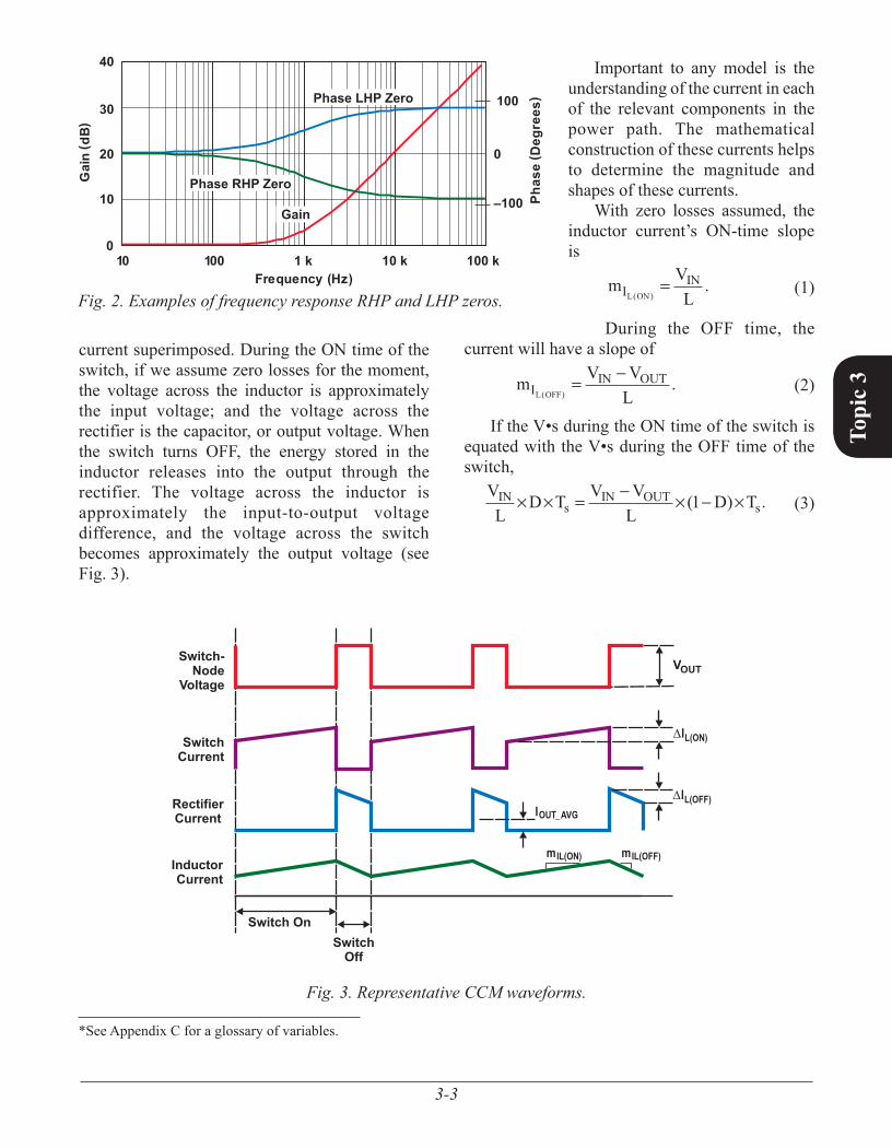
Unlike a buck-derived topology, energy flows to the load during the OFF time of the control switch. The effect of any control action during the ON time of the switch is delayed until the switch is turned OFF. For example, during a load-step increase, the output voltage drops due to insufficient stored energy in the inductor. The lower output voltage in turn creates a demand for a longer pulse width in order to store additional energy in the inductor. In a fixed-frequency converter, a longer ON-time pulse means a shorter OFF-time pulse, which means the output will droop even further. It is not until the release of the energy in the inductor from the longer ON-time pulse that the output voltage will reverse towards regulation. From the standpoint of small-signal feedback control, the phenomenon of the output response initially going in the opposite direction of the desired correction creates a right-half-plane (RHP) zero, so named because of the placement of the zeros in the right-half plane of a complex s-plane. The frequency-response curve in Fig. 2 shows that with a left-half-plane (LHP) zero (as from the ESR of a capacitor), the phase increases with increasing gain; and with an RHP zero, the phase decreases with increasing gain. This condition makes compensating the control loop a difficult task if a feedback loop is to have adequate phase margin. This discussion later shows that design decisions regarding mode of operation and the choice of control method largely alleviate the RHP-zero effect.
A. Continuous-Conduction Mode (CCM)
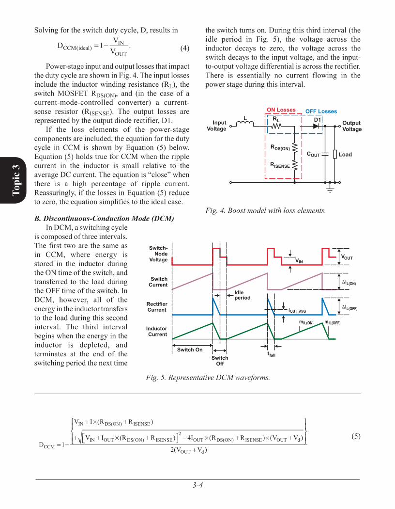
In CCM, power transfer is a two-step process. When the switch is ON, stored energy builds in the inductor. When the switch is OFF, energy transfers to the output through the diode. The switch current is a stepped sawtooth with a fixed steady-state ON time with some amount of ripple
3-3
Topi
c 3
current superimposed. During the ON time of the switch, if we assume zero losses for the moment, the voltage across the inductor is approximately the input voltage; and the voltage across the rectifier is the capacitor, or output voltage. When the switch turns OFF, the energy stored in the inductor releases into the output through the rectifier. The voltage across the inductor is approximately the input-to-output voltage difference, and the voltage across the switch becomes approximately the output voltage (see Fig. 3).
Important to any model is the understanding of the current in each of the relevant components in the power path. The mathematical construction of these currents helps to determine the magnitude and shapes of these currents.
With zero losses assumed, the inductor current’s ON-time slope is
m V
LIIN
L ON( ).=
(1)
During the OFF time, the current will have a slope of
m V V
LIIN OUT
L OFF( ).= −
(2)
If the V•s during the ON time of the switch is equated with the V•s during the OFF time of the switch,
VL
D T V VL
D TINs
IN OUTs× × × ×= − −( ) .1
(3)
InductorCurrent
RectifierCurrent
SwitchCurrent
Switch-Node
Voltage
Switch OnSwitch
Off
IL(OFF)
IL(ON)
IOUT_AVG
mIL(ON) mIL(OFF)
VOUT
Fig. 3. Representative CCM waveforms.
*See Appendix C for a glossary of variables.
1 k 100 k10 k0
10 –100
20 0
30 100
40
Frequency (Hz)
Gain( dB)
Phase( Deg
rees)
10010
Gain
Phase LHP Zero
Phase RHP Zero
Fig. 2. Examples of frequency response RHP and LHP zeros.
3-4
Topi
c 3
Solving for the switch duty cycle, D, results in
D V
VCCM idealIN
OUT( ) .= −1
(4)
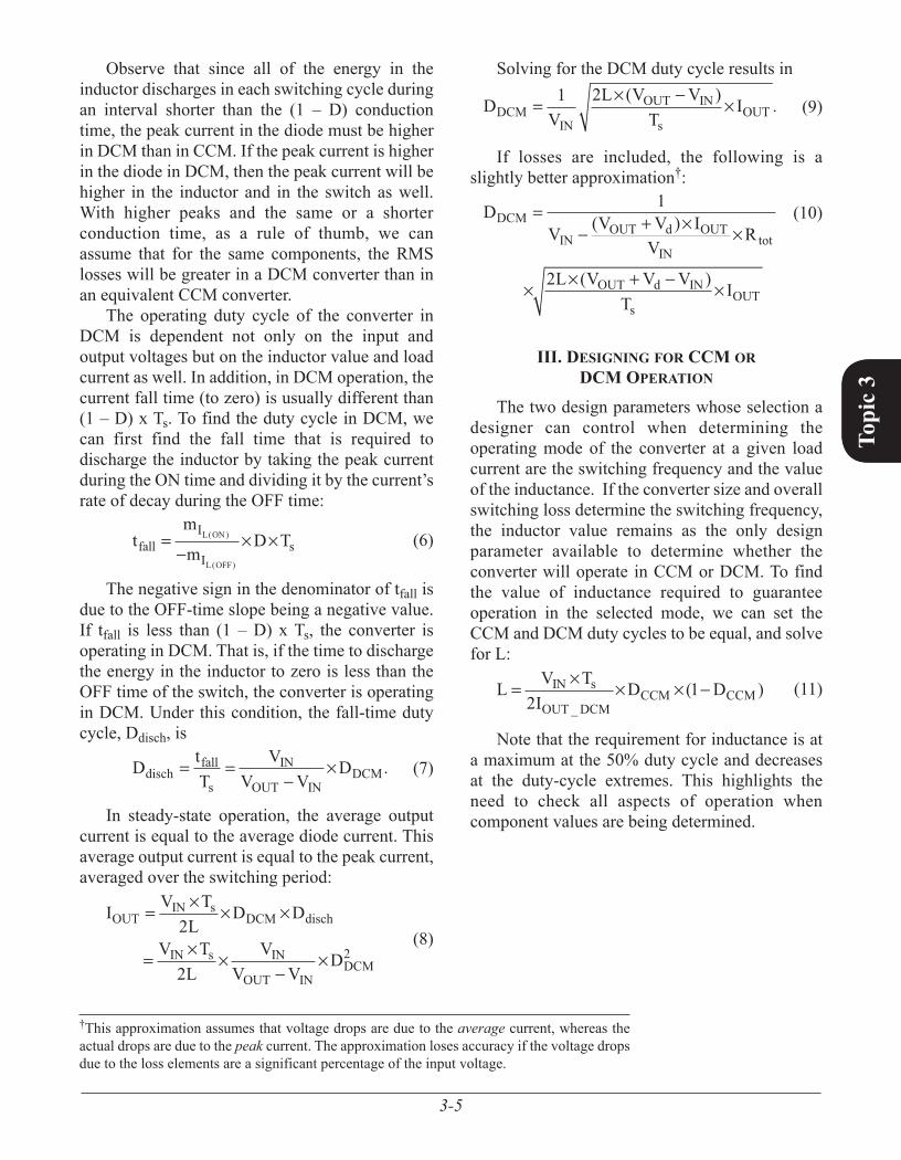
Power-stage input and output losses that impact the duty cycle are shown in Fig. 4. The input losses include the inductor winding resistance (RL), the switch MOSFET RDS(ON), and (in the case of a current-mode-controlled converter) a current-sense resistor (RISENSE). The output losses are represented by the output diode rectifier, D1.
If the loss elements of the power-stage components are included, the equation for the duty cycle in CCM is shown by Equation (5) below. Equation (5) holds true for CCM when the ripple current in the inductor is small relative to the average DC current. The equation is “close” when there is a high percentage of ripple current. Reassuringly, if the losses in Equation (5) reduce to zero, the equation simplifies to the ideal case.
B. Discontinuous-Conduction Mode (DCM)In DCM, a switching cycle
is composed of three intervals. The first two are the same as in CCM, where energy is stored in the inductor during the ON time of the switch, and transferred to the load during the OFF time of the switch. In DCM, however, all of the energy in the inductor transfers to the load during this second interval. The third interval begins when the energy in the inductor is depleted, and terminates at the end of the switching period the next time
the switch turns on. During this third interval (the idle period in Fig. 5), the voltage across the inductor decays to zero, the voltage across the switch decays to the input voltage, and the input-to-output voltage differential is across the rectifier. There is essentially no current flowing in the power stage during this interval.
InductorCurrent
RectifierCurrent
SwitchCurrent
Switch-Node
Voltage
Switch OnSwitch
Off
Idleperiod
VOUT
IOUT_AVG
VIN
tfall
IL(OFF)
IL(ON)
mIL(ON) mIL(OFF)
COUT Load
OutputVoltage
LInput
Voltage
RL
ON Losses OFF LossesD1
RISENSE
RDS(ON)
Fig. 4. Boost model with loss elements.
Fig. 5. Representative DCM waveforms.
D
V I R R
V I R RCCM
IN DS ON ISENSE
IN OUT DS ON ISENSE= −
+ +
+ + +1
×
×
( )
( )
( )
( ) − + +
+
24
2
I R R V V
V VOUT DS ON ISENSE OUT d
OUT d
× ×( ) ( )
(( )
))
(5)
3-5
Topi
c 3
Observe that since all of the energy in the inductor discharges in each switching cycle during an interval shorter than the (1 – D) conduction time, the peak current in the diode must be higher in DCM than in CCM. If the peak current is higher in the diode in DCM, then the peak current will be higher in the inductor and in the switch as well. With higher peaks and the same or a shorter conduction time, as a rule of thumb, we can assume that for the same components, the RMS losses will be greater in a DCM converter than in an equivalent CCM converter.
The operating duty cycle of the converter in DCM is dependent not only on the input and output voltages but on the inductor value and load current as well. In addition, in DCM operation, the current fall time (to zero) is usually different than (1 – D) x Ts. To find the duty cycle in DCM, we can first find the fall time that is required to discharge the inductor by taking the peak current during the ON time and dividing it by the current’s rate of decay during the OFF time:
t
m
mD Tfall
I
Is
L ON
L OFF
=−
( )
( )
× ×
(6)
The negative sign in the denominator of tfall is due to the OFF-time slope being a negative value. If tfall is less than (1 – D) x Ts, the converter is operating in DCM. That is, if the time to discharge the energy in the inductor to zero is less than the OFF time of the switch, the converter is operating in DCM. Under this condition, the fall-time duty cycle, Ddisch, is
D t
TV
V VDdisch
fall
s
IN
OUT INDCM= =
−× .
(7)
In steady-state operation, the average output current is equal to the average diode current. This average output current is equal to the peak current, averaged over the switching period:
I V TL
D D
V TL
VV V
D
OUTIN s
DCM disch
IN s IN
OUT INDCM
=
=−
× × ×
× × ×
2
22
(8)
Solving for the DCM duty cycle results in
D
VL V V
TIDCM
IN
OUT IN
sOUT= −1 2 × ×( ) .
(9)
If losses are included, the following is a slightly better approximation†:
DV V V I
VR
L V V VT
I
DCM
INOUT d OUT
INtot
OUT d IN
sOUT
=− +
+ −
1
2
( )
( )
× ×
× × ×
(10)
III. desIgnIng for ccM or dcM operAtIon
The two design parameters whose selection a designer can control when determining the operating mode of the converter at a given load current are the switching frequency and the value of the inductance. If the converter size and overall switching loss determine the switching frequency, the inductor value remains as the only design parameter available to determine whether the converter will operate in CCM or DCM. To find the value of inductance required to guarantee operation in the selected mode, we can set the CCM and DCM duty cycles to be equal, and solve for L:
L V T
ID DIN s
OUT DCMCCM CCM= −× × ×
21
_( )
(11)
Note that the requirement for inductance is at a maximum at the 50% duty cycle and decreases at the duty-cycle extremes. This highlights the need to check all aspects of operation when component values are being determined.
†This approximation assumes that voltage drops are due to the average current, whereas the actual drops are due to the peak current. The approximation loses accuracy if the voltage drops due to the loss elements are a significant percentage of the input voltage.
3-6
Topi
c 3
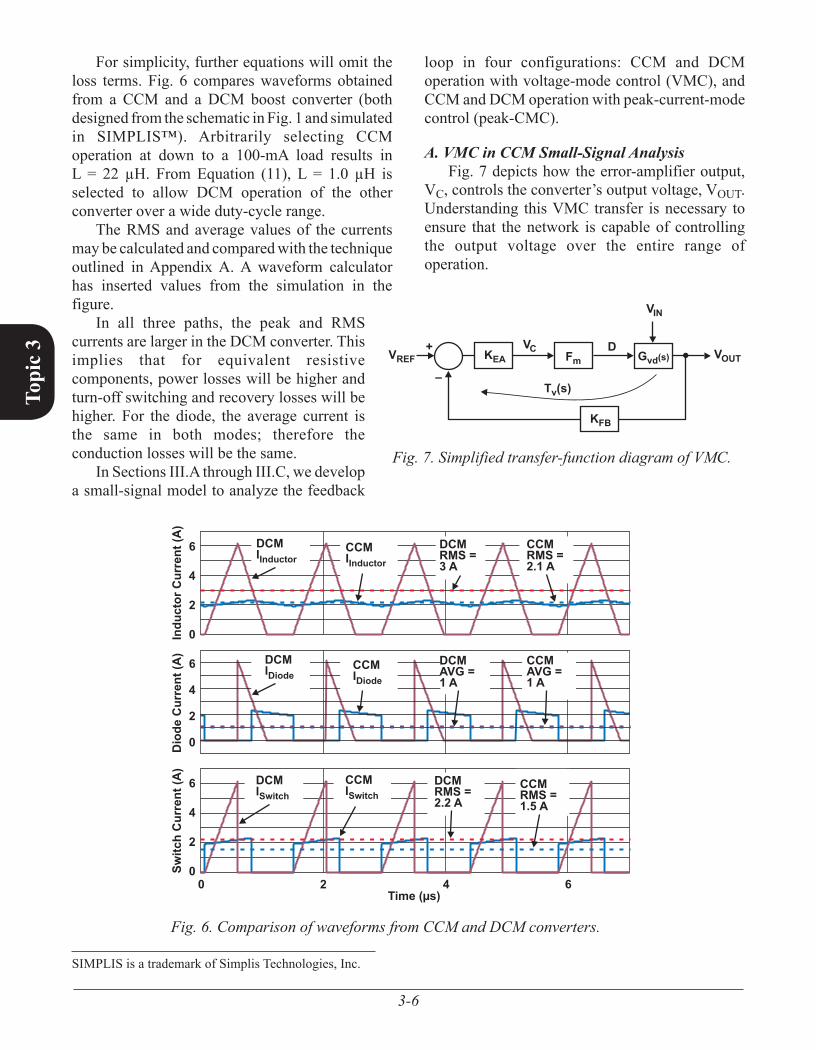
For simplicity, further equations will omit the loss terms. Fig. 6 compares waveforms obtained from a CCM and a DCM boost converter (both designed from the schematic in Fig. 1 and simulated in SIMPLIS™). Arbitrarily selecting CCM operation at down to a 100-mA load results in L = 22 µH. From Equation (11), L = 1.0 µH is selected to allow DCM operation of the other converter over a wide duty-cycle range.
The RMS and average values of the currents may be calculated and compared with the technique outlined in Appendix A. A waveform calculator has inserted values from the simulation in the figure.
In all three paths, the peak and RMS currents are larger in the DCM converter. This implies that for equivalent resistive components, power losses will be higher and turn-off switching and recovery losses will be higher. For the diode, the average current is the same in both modes; therefore the conduction losses will be the same.
In Sections III.A through III.C, we develop a small-signal model to analyze the feedback
loop in four configurations: CCM and DCM operation with voltage-mode control (VMC), and CCM and DCM operation with peak-current-mode control (peak-CMC).
A. VMC in CCM Small-Signal AnalysisFig. 7 depicts how the error-amplifier output,
VC, controls the converter’s output voltage, VOUT. Understanding this VMC transfer is necessary to ensure that the network is capable of controlling the output voltage over the entire range of operation.
Time (µs)0
6
4
2
0
6
4
2
0
6
4
2
02
SwitchCurrent(A)
Diode
Current(A)
InductorCurrent(A)
4 6
CCMIInductor
CCMIDiode
CCMISwitch
DCMIInductor
DCMIDiode
DCMISwitch
DCMRMS =3 A
DCMAVG =1 A
DCMRMS =2.2 A
CCMRMS =2.1 A
CCMAVG =1 A
CCMRMS =1.5 A
Fig. 6. Comparison of waveforms from CCM and DCM converters.
Fm Gvd(s) VOUTVC D
VIN
KEAVREF+
–
KFB
T (s)v
Fig. 7. Simplified transfer-function diagram of VMC.
SIMPLIS is a trademark of Simplis Technologies, Inc.
3-7
Topi
c 3
The modulator gain, Fm, is the transfer function that generates the duty cycle based on the VC control voltage. That is, for a given change in VC, the duty cycle will change by an amount proportional to the modulator gain. For VMC, Fm is simply
F
m Tma s
= 1×
,
(12)
where ma is the slope of a sawtooth ramp waveform (Fig. 8). The controller’s internal clock oscillator usually generates this sawtooth waveform. As a side note, the TPS40210 is configurable so that ma is fixed or is a function of the input voltage. This provides an option for including voltage feedforward to the transfer function. The impact of increasing the slope, ma, is a decreasing Fm, the result of which is described later in this section.
The small-signal duty-cycle-to-output-voltage transfer function, Gvd_CCM(s), is determined from the boost circuit’s impedances (Fig. 9). ZON is the impedance of the inductor as a function of frequency, plus the RDS(ON) of the MOSFET switch and any other series impedances:
Z Z R RON L DS ON ISENSE= + +( )
(13)
ZOFF is the parallel combination of the output capacitors and the load resistance:
Z Z R
Z ROFFC load
C load=
+×
(14)
0VC
Vramp
OscillatorSawtooth
ResultingPWM
ma
ControlVoltage
PWM
Oscillator Sawtooth
Control Voltage +
–
Fig. 8. Pulse-width modulation (PWM).
ZON ZOFF
COUT COUT
RESR RESR
Load
OutputVoltage
L
RISENSE
RDS(ON)
InputVoltage
RL
Fig. 9. Circuit highlighting ON- and OFF-time impedances.
Note that if the output capacitors are of mixed types (i.e., aluminum electrolytic and ceramic), their impedances may be included in this parallel combination, allowing characterization of converters with a variety of mixed component types.
The derivation of Gvd_CCM(s) is developed in detail in Reference [1]. Without re-creating that work here, it is sufficient to give that function for CCM in terms of circuit impedances as
G s V M
Z MR
Z MZ
vd CCM IN
ON CCM
load
ON CCM
OFF
CCM_ ( ) =−
+× ×
×
×2
2
2
1
1
(15)
3-8
Topi
c 3
where MCCM is the conversion ratio in CCM,
M V
V DCCMOUT
IN= =
−1
1.
(16)
It is in Gvd(s) that the RHP zero comes into play. As the numerator of Equation (15) indicates, the zero is a function of the converter’s ON impedance (determined from the inductor value, the frequency, and parasitic imped ances) load, and duty cycle. In Fig. 10, the span of movement of the RHP zero is from about 23 kHz to 96 kHz over the input-voltage range. At lighter load (Fig. 11), the RHP zero moves to a much higher frequency, likely beyond any frequency of interest. Note again that the ESR-zero frequency of the output capacitor is just over 11 kHz. The interaction of the two zeros (the RHP zero from the converter and the LHP zero from the capacitor's ESR) tends to flatten the phase response while providing a double-zero correction to the L-C filter double pole.
Notice also that the lower gain occurs at higher input voltages (smaller MCCM, Equation (16)). This is in contrast to a buck-derived converter where the gain increases with increasing input voltage. In this example, adding input-voltage feedforward increases the gain spread for the 9- to 18-V input-voltage change from –5.5 dB (see Figs. 10 and 11) to –11.5 dB. This further decrease in gain with increasing input voltage is due to the decrease in Fm with input voltage (see Equation (12)).
Putting the blocks together yields the control-to-output transfer function of the converter:
G s F G svc m vd( ) ( )= × (17)
The dominant pole in CCM is generated from the ratio of the network impedance when the switch is on (basically, the inductor impedance) to the output-network impedance when the switch is off (when the output capacitance is in parallel with
the load resistance), scaled by the CCM duty cycle.
With VMC used in CCM, the three dominant characteristics of the curves are observable (see Fig. 10):
A relatively low-frequency double pole due to • the inductor and output capacitorAn RHP zero due to the inductor, the load, and • the duty cycleAn LHP zero due to the output capacitor and • ESR
The complexities in compen sating this path are numerous (Figs. 10 and 11): The RHP zero shifts in frequency with varying duty cycle and load, and the gain changes inversely with input voltage. The zero occurs with a control-to-output gain above 0 dB, and the phase shifts dramatically
1 k 100 k 1 M10 k–30 –180
–10–20
–90
–135
100
20
0
30 9045
–45
50
40
180
135
Frequency (Hz)
Gain( dB)
Phase( Degrees)
10010
18 VIN12 VIN9 VIN
Phase
Gain
18 VIN 12 VIN
9 VIN
L-C Double Pole
Two Zeros inClose Proximity
Fig. 10. Control-to-output Bode plot for VMC CCM operation at 1-A load.
1 k 100 k 1 M10 k–30 –180
–10–20
–90
–135
100
20
0
30 9045
–45
50
40
180
135
Frequency (Hz)
Gain( dB)
Phase( Degrees)
10010
18 VIN12 VIN9 VIN
Phase
Gain
18 VIN 12 VIN
9 VIN
Fig. 11. Control-to-output Bode plot for VMC CCM operation at 150-mA load.
3-9
Topi
c 3
in the 1- to 5-kHz range. The output capacitor’s ESR provides an additional phase boost (at 11 kHz in these plots), lessening the available margin. To compensate this control loop, a feedback network must be designed so that the closed-loop response has a crossover frequency in the low 100s of hertz, perhaps an octive below the minimum worst-case L-C pole frequency and the dramatic phase shift.
B. VMC in DCM Small-Signal AnalysisIn DCM, the energy stored in the inductor in
each switching cycle is equal to the output energy and is a function of the input voltage, the inductance, and the output power. Equating the energy over a switching cycle gives us the conversion ratio:
M
V V D TI L
DCM
OUT d s
OUT=+ + +1 1 2
2
2× × ×
×( )
(18)
The control-to-output transfer characteristic in DCM is
G s VD
MMs D
FM R
vd DCMOUT DCM
DCM
s
DCM load
_ ( )
( )(
= −−
−
+ −
2 12 1
12
1 12
×
×
×
×MM ZDCM C−1)
.
×
(19)
In DCM, and because of the relatively smaller inductor, the RHP-zero frequency extends to beyond the switching frequency with negligible inpact at typical loop crossover frequencies [2]. See Figs. 12 and 13.
The low-frequency pole is a function of the output capacitance and load resistance, and is lower in frequency than in the CCM example.
The gain change over an input voltage range is +4.7 dB. This is because Gvd(s) now increases
–30 –180
–10–20
–90
–135
100
20
0
30 9045
–45
50
40
180
135
Frequency (Hz)
Phase( Degrees)
10010
18 VIN12 VIN9 VIN
Phase
Gain
12 VIN9 VIN
R -C Single Poleload
ESR Zero
18 VIN
1 k 100 k 1 M10 k
Gain( dB)
Fig. 12. Control-to-output Bode plot for VMC DCM operation at 1-A load.
–30 –180
–10–20
–90
–135
100
20
0
30 9045
–45
50
40
180
135
Frequency (Hz)
Phas
e( D
egre
es)
10010
Gain
9 VIN
18 VIN
18 VIN12 VIN9 VIN
Phase
12 VIN
1 k 100 k 1 M10 k
Gai
n( d
B)
Fig. 13. Control-to-output Bode plot for VMC DCM operation at 150-mA load.
3-10
Topi
c 3
with increasing VIN. Adding voltage feedforward reduces Fm with increasing input voltage and reduces the gain variation to –1.3 dB.
To compensate this converter, a network with a zero at a few hundred hertz and a pole at about 10 kHz will yield a stable system with a crossover frequency in the low 10s of kilohertz.
C. Peak-Current-Mode Control Incorporating peak-CMC is a matter of
monitoring the switch current during the ON time of the switch and summing a current signal into the modulator (see Fig. 14). The modulator gain then becomes
F
m Tmn s
= 1×
,
(20)
where mn is a slope proportional to the inductor’s current slope during the ON time of the switch,
m R An IL ON ISENSE CS= m ,( )× ×
(21)
and ACS is the gain of the current-sense amplifier. Notice that the current slope is a function of the input voltage (Equation (1)), and that a shift in gain will occur from that changing slope. The effect is similar to that of voltage feedforward in the VMC converter.
The current feedback path has a transfer function in CCM, but not in DCM. This is because
there is no output information in the current signal in DCM.
G s I M
RZ
Z MZ
id CCM OUT CCM
load
C
ON CCM
OFF
_ ( ) ,=+
+2
12
1
22× ×
×
(22)
where MCCM is defined by Equation (16).As shown in Fig. 15, the inner current loop is
T s F A R G H sI m CS ISENSE id e( ) ( ),= × × × ( ×s)
(23)
where He(s) is the sampling gain‡[3]. The sense resistor, RISENSE, used in this example is 50 mΩ, and the current-sense gain (ACS) of the TPS40210 is about 6.
SwitchCurrent
ResultingPWM
Ts
mn
PWM
SwitchCurrent
ErrorAmplifier
RISENSE
ACS
Control Voltage
++
––
ControlVoltage
Fm Gvd(s) VOUTVCVREF
D++
––
VIN VIN
KEA
TI(s)
Tv(s)
A RCS ISENSE
KFB
He(s)
Gid(s)
Fig. 14 Current Mode PWM.
Fig. 15. Simplified block diagram of CMC converter.
‡The sampling gain is a modeling tool that allows the zero-order sample-and-hold effects of peak-CMC to be included in this simple frequency-domain model.
3-11
Topi
c 3The control-to-output transfer function,
including the inner current loop, is
G s F G s
T sevc
m vd
I
s td( ) ( )( )
,=+
− ×× ×1
(24)
where e–s×td is the delay time from the PWM comparator input to the transition of the converter switch node. This delay introduces a phase lag at higher frequencies.
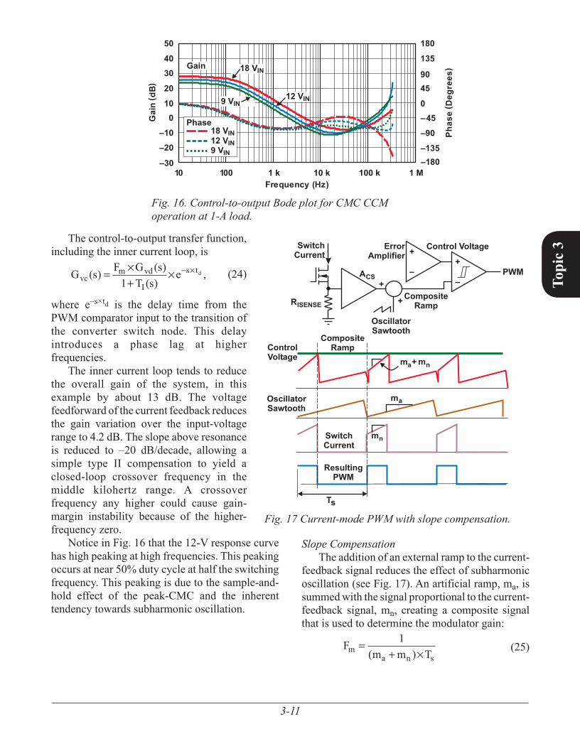
The inner current loop tends to reduce the overall gain of the system, in this example by about 13 dB. The voltage feedforward of the current feedback reduces the gain variation over the input-voltage range to 4.2 dB. The slope above resonance is reduced to –20 dB/decade, allowing a simple type II compensation to yield a closed-loop crossover frequency in the middle kilohertz range. A crossover frequency any higher could cause gain-margin instability because of the higher-frequency zero.
Notice in Fig. 16 that the 12-V response curve has high peaking at high frequencies. This peaking occurs at near 50% duty cycle at half the switching frequency. This peaking is due to the sample-and-hold effect of the peak-CMC and the inherent tendency towards subharmonic oscillation.
1 k 100 k 1 M10 k–30 –180
–10–20
–90
–135
100
20
0
30 9045
–45
50
40
180
135
Frequency (Hz)
Gain( dB)
Phase( Degrees)
10010
18 VIN12 VIN9 VIN
Phase
Gain 18 VIN
9 VIN12 VIN
OscillatorSawtooth
SwitchCurrent
ResultingPWM
Ts
ma
m + ma n
mn
CompositeRampControl
Voltage
PWM
OscillatorSawtooth
SwitchCurrent
ErrorAmplifier
RISENSE
ACS
CompositeRamp
Control Voltage
++
+
+
––
Fig. 16. Control-to-output Bode plot for CMC CCM operation at 1-A load.
Fig. 17 Current-mode PWM with slope compensation.
Slope CompensationThe addition of an external ramp to the current-
feedback signal reduces the effect of subharmonic oscillation (see Fig. 17). An artificial ramp, ma, is summed with the signal proportional to the current-feedback signal, mn, creating a composite signal that is used to determine the modulator gain:
F
m m Tma n s
=+
1( )×
(25)
3-12
Topi
c 3
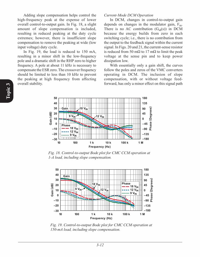
Adding slope compensation helps control the high-frequency peak at the expense of lower overall control-to-output gain. In Fig. 18, a slight amount of slope compensation is included, resulting in reduced peaking at the duty cycle extremes; however, there is insufficient slope compensation to remove the peaking at wide (low input voltage) duty cycle.
In Fig. 19, the load is reduced to 150 mA, resulting in a minor shift in the low-frequency pole and a dramatic shift in the RHP zero to higher frequency. A pole at about 11 kHz is necessary to compensate the ESR zero. The crossover frequency should be limited to less than 10 kHz to prevent the peaking at high frequency from affecting overall stability.
1 k 100 k 1 M10 k–30 –180
–10–20
–90
–135
100
20
0
30 9045
–45
50
40
180
135
Frequency (Hz)
Gain( dB)
Phase( Degrees)
10010
18 VIN12 VIN9 VIN
Phase
Gain 18 VIN
9 VIN 12 VIN
–30 –180
–10–20
–90
–135
100
20
0
30 9045
–45
50
40
180
135
Phas
e( Deg
rees
)Gain
18 VIN9 VIN 12 VIN
18 VIN12 VIN9 VIN
Phase
1 k 100 k 1 M10 kFrequency (Hz)
Gain( dB)
10010
Fig. 18. Control-to-output Bode plot for CMC CCM operation at 1-A load, including slope compensation.
Fig. 19. Control-to-output Bode plot for CMC CCM operation at 150-mA load, including slope compensation.
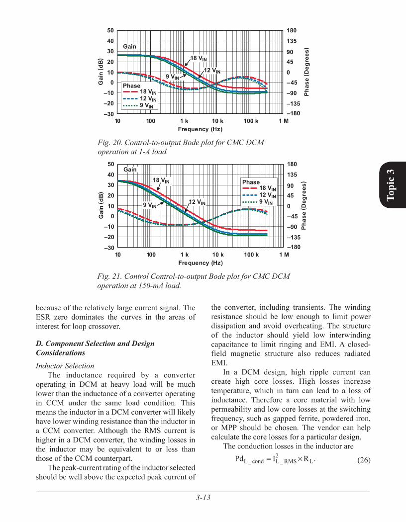
Current-Mode DCM OperationIn DCM, changes in control-to-output gain
depends on changes in the modulator gain, Fm. There is no AC contribution (Gid(s)) in DCM because the energy builds from zero in each switching cycle; i.e., there is no contribution from the output to the feedback signal within the current signal. In Figs. 20 and 21, the current-sense resistor is reduced from 50 mΩ to 17 mΩ to limit the peak voltage at the sense pin and to keep power dissipation low.
With essentially only a gain shift, the curves follow the poles and zeros of the VMC converters operating in DCM. The inclusion of slope compensation, with or without voltage feed-forward, has only a minor effect on this signal path
3-13
Topi
c 3
because of the relatively large current signal. The ESR zero dominates the curves in the areas of interest for loop crossover.
D. Component Selection and Design ConsiderationsInductor Selection
The inductance required by a converter operating in DCM at heavy load will be much lower than the inductance of a converter operating in CCM under the same load condition. This means the inductor in a DCM converter will likely have lower winding resistance than the inductor in a CCM converter. Although the RMS current is higher in a DCM converter, the winding losses in the inductor may be equivalent to or less than those of the CCM counterpart.
The peak-current rating of the inductor selected should be well above the expected peak current of
–30 –180
–10–20
–90
–135
100
20
0
30 9045
–45
50
40
180
135
Phas
e( Deg
rees
)
Gain
18 VIN
9 VIN
18 VIN12 VIN9 VIN
Phase
12 VIN
1 k 100 k 1 M10 kFrequency (Hz)
Gain( dB)
10010
Fig. 21. Control Control-to-output Bode plot for CMC DCM operation at 150-mA load.
the converter, including transients. The winding resistance should be low enough to limit power dissipation and avoid overheating. The structure of the inductor should yield low interwinding capacitance to limit ringing and EMI. A closed-field magnetic structure also reduces radiated EMI.
In a DCM design, high ripple current can create high core losses. High losses increase temperature, which in turn can lead to a loss of inductance. Therefore a core material with low permeability and low core losses at the switching frequency, such as gapped ferrite, powdered iron, or MPP should be chosen. The vendor can help calculate the core losses for a partic ular design.
The conduction losses in the inductor are
Pd I RL cond L RMS L_ _ .= 2 ×
(26)
–30 –180
–10–20
–90
–135
100
20
0
30 9045
–45
50
40
180
135
Phas
e( Deg
rees
)
18 VIN12 VIN9 VIN
Phase
Gain
18 VIN
9 VIN12 VIN
1 k 100 k 1 M10 kFrequency (Hz)
Gain( dB)
10010
Fig. 20. Control-to-output Bode plot for CMC DCM operation at 1-A load.
3-14
Topi
c 3
MOSFET SelectionMOSFET selection focuses primarily on
breakdown voltage and power dissipation. A MOSFET with a breakdown voltage of about 1.5 times the output voltage is preferable. Once the converter is running, the designer should ensure that all drain voltage spikes are well below this value.
Power dissipation in the switch is composed of three elements—conduction loss, switching loss, and gate loss. The conduction losses in the MOSFET are approximated as
Pd I RSW cond SW RMS DS ON_ _ ( ).= 2 ×
(27)
The switching losses are approximated as shown by Equation (28) below are comprised of the losses incurred in driving the node capacitance (MOSFET Coss and the rectifier capacitance or Qrr) and the device itself. The gate losses are approximated as
Pd Q V FSW gate GATE GATE s_ .= × ×
(29)
An RDS(ON) should be selected for the MOSFET so that the conduction power dissipation is limited to 1% or so of the total output power. With this selection, the maximum allowable drain current of the MOSFET will be much greater than what will occur in the application. A MOSFET with low capacitance will minimize switching losses. A good rule of thumb is to select a MOSFET with switching losses equal to conduction losses with the converter operating at maximum load. Obviously, selecting a MOSFET to meet these criteria is a somewhat iterative endeavor.
Diode Rectifier SelectionThe rectifier must be capable of handling the
capacitor’s peak input current and of dissipating the rectifier’s average power—the rectifier voltage drop times the load current. The voltage breakdown of the device must be greater than the output voltage plus some margin. The typical choice for a rectifier in applications with low output voltage is a low-capacitance Schottky diode. If the output
voltage is high, a fast-recovery diode is an alternate possibility. For converters operating in CCM, a diode with a “soft” recovery characteristic will minimize EMI and the need for a snubber. This characteristic is not necessary in a DCM application because there is no current flowing in the diode when the switch is turned on.
A simple approximation of conduction losses in the diode is
Pd I VRECT cond OUT d_ .= ×
(30)
Switching losses associated with a Schottky rectifier are dissipated by the switch. In this case, the results of Equation (31) are added to those of Equation (28).
Pd C V V
TSW SCH RECTOUT d
s_
( ) ,= +12 2
2× ×
(31)
and for a fast-recovery device, as shown by
Pd V t I
TRECT QrrOUT rr OFFSET
s_ .= × ×
2
(32)
Synchronous RectificationIf the RDS(ON) is low and the output current is
high, a MOSFET may replace the diode. The benefits of the increased efficiency must be weighed against the additional complexity of driving the MOSFET. Using a MOSFET allows a “discontinuous” design to be run in CCM. If the gate-driver timing allows the synchronous rectifier’s MOSFET to be on for the full (1 – D) interval, then when the inductor current decays to zero during the OFF period, it then reverses and conducts energy back into the input. However, during such CCM operation, power dissipation increases significantly due to the recirculation of energy.
Selection of an Output CapacitorTo provide relatively smooth DC voltage to
the load, the output capacitor in a boost converter must absorb pulsating ripple current. For this to occur, the impedance of the capacitor at the
(28)PdT
C V V V V ID
Q RSW switch
sOSS OUT d OUT d
OUT GD GA_ = +( ) + +( )
−1
2 12× × × × × TTE
GATE thV V−
3-15
Topi
c 3
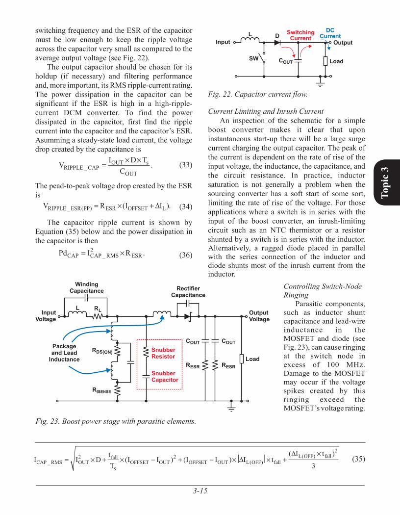
switching frequency and the ESR of the capacitor must be low enough to keep the ripple voltage across the capacitor very small as compared to the average output voltage (see Fig. 22).
The output capacitor should be chosen for its holdup (if necessary) and filtering performance and, more important, its RMS ripple-current rating. The power dissipation in the capacitor can be significant if the ESR is high in a high-ripple-current DCM converter. To find the power dissipated in the capacitor, first find the ripple current into the capacitor and the capacitor’s ESR. Asumming a steady-state load current, the voltage drop created by the capacitance is
V I D T
CRIPPLE CAPOUT s
OUT_ .= × ×
(33)
The pead-to-peak voltage drop created by the ESR is
V R I IRIPPLE ESR PP ESR OFFSET L_ ( ) ( ).= +× ∆
(34)
The capacitor ripple current is shown by Equation (35) below and the power dissipation in the capacitor is then
Pd I RCAP CAP RMS ESR= _ .2 ×
(36)
Current Limiting and Inrush Current An inspection of the schematic for a simple
boost converter makes it clear that upon instantaneous start-up there will be a large surge current charging the output capacitor. The peak of the current is dependent on the rate of rise of the input voltage, the inductance, the capacitance, and the circuit resistance. In practice, inductor saturation is not generally a problem when the sourcing converter has a soft start of some sort, limiting the rate of rise of the voltage. For those applications where a switch is in series with the input of the boost converter, an inrush-limiting circuit such as an NTC thermistor or a resistor shunted by a switch is in series with the inductor. Alternatively, a rugged diode placed in parallel with the series connection of the inductor and diode shunts most of the inrush current from the inductor.
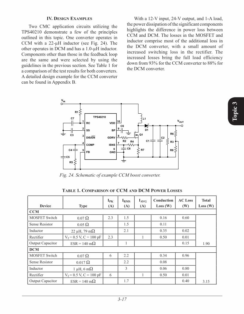
Controlling Switch-Node Ringing
Parasitic components, such as inductor shunt capacitance and lead-wire inductance in the MOSFET and diode (see Fig. 23), can cause ringing at the switch node in excess of 100 MHz. Damage to the MOSFET may occur if the voltage spikes created by this ringing exceed the MOSFET’s voltage rating.
I I DtT
I I I ICAP RMS OUTfall
OFFSET OUT OFFSET OUTs
_ ( ) ( )= + − + −2 2× × ×∆II tI t
L OFF fallL OFF fall
( )( )( )
××
+∆ 2
3(35)
COUT Load
OutputL
InputD Switching
CurrentDC
Current
SW
Fig. 22. Capacitor current flow.
WindingCapacitance Rectifier
Capacitance
Packageand Lead
Inductance
COUT COUT
RESR RESRLoad
OutputVoltage
SnubberResistor
SnubberCapacitor
L
RISENSE
RDS(ON)
InputVoltage
RL
Fig. 23. Boost power stage with parasitic elements.

3-16
Topi
c 3
In addition to more power loss, conducted and radiated EMI are by-products of this ringing.
Good PCB layout practices minimize some of this ringing. The physical trace loop areas of the switch node must be as small as possible to minimize stray inductance. Tying the source of the MOSFET at the return path of the output capacitor can help, or a high-frequency capacitor can be connected from the cathode of the diode directly to the source of the MOSFET.
An additional technique is to place a small (2- to 10-Ω) resistor in series with the gate of the MOSFET. This will serve to slow the turn-on and turn-off of the MOSFET and will further reduce the ringing. However, a resistor that is too large will increase switching times and power dissipation.
Another technique is to add a series R-C snubber across the MOSFET to dampen the
parasitic energy. The snubber capacitor controls the maximum peak voltage at the switch node:
C
I tV
C PK r= ( )
max
×
(37)
The snubber resistor ensures that the capacitor is discharged when the switch is turned on.
R
tC
ON= _ min
3 (38)
The power dissipation in the resistor will be approximately
Pd C V Fs= 1
22× × .
(39)
Reference [4] contains a technique for finding the R and C values based on bench measurements of the ringing.
3-17
Topi
c 3
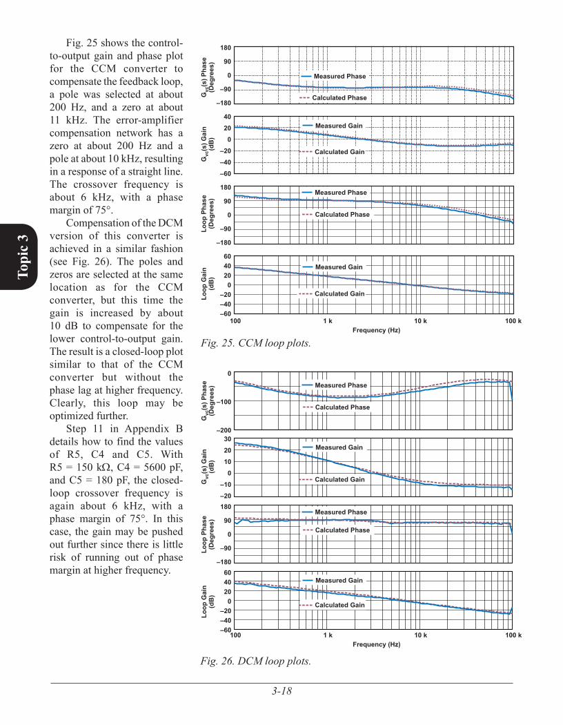
IV. desIgn exAMples
Two CMC application circuits utilizing the TPS40210 demonstrate a few of the principles outlined in this topic. One converter operates in CCM with a 22-µH inductor (see Fig. 24). The other operates in DCM and has a 1.0-µH inductor. Components other than those in the feedback loop are the same and were selected by using the guidelines in the previous section. See Table 1 for a comparison of the test results for both converters. A detailed design example for the CCM converter can be found in Appendix B.
With a 12-V input, 24-V output, and 1-A load, the power dissipation of the significant components highlights the difference in power loss between CCM and DCM. The losses in the MOSFET and inductor comprise most of the additional loss in the DCM converter, with a small amount of increased switching loss in the rectifier. The increased losses bring the full load efficiency down from 93% for the CCM converter to 88% for the DCM converter.
1
2
3
5 FB
4
10
9
8
7
RC
DIS/EN
COMP
SS
VDD
ISNS
GDRV
GND
TPS40210VOUT
VIN
6
BP
R7
L1
R4R2
R5
R1
R3
R6
R8
D1
C2
C6
C7
C3
C4 C8
C1
C5
Q1
Fig. 24. Schematic of example CCM boost converter.
Device TypeIPK (A)
IRMS (A)
IAVG (A)
Conduction Loss (W)
AC Loss (W)
Total Loss (W)
CCMMOSFET Switch 0.07 Ω 2.3 1.5 0.16 0.60
1.90
Sense Resistor 0.05 Ω 1.5 0.11Inductor 22 µH, 79 mΩ 2.1 0.35 0.02Rectifier Vf = 0.5 V, C = 100 pF 2.3 1 0.50 0.01Output Capacitor ESR = 140 mΩ 1 0.15DCMMOSFET Switch 0.07 Ω 6 2.2 0.34 0.96
3.15
Sense Resistor 0.017 Ω 2.2 0.08Inductor 1 µH, 6 mΩ 3 0.06 0.80Rectifier Vf = 0.5 V, C = 100 pF 6 1 0.50 0.01Output Capacitor ESR = 140 mΩ 1.7 0.40
tAble 1. coMpArIson of ccM And dcM power losses
3-18
Topi
c 3
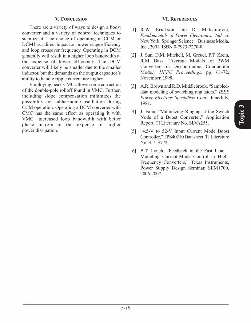
Fig. 25 shows the control-to-output gain and phase plot for the CCM converter to compensate the feedback loop, a pole was selected at about 200 Hz, and a zero at about 11 kHz. The error-amplifier compensation network has a zero at about 200 Hz and a pole at about 10 kHz, resulting in a response of a straight line. The crossover frequency is about 6 kHz, with a phase margin of 75°.
Compensation of the DCM version of this converter is achieved in a similar fashion (see Fig. 26). The poles and zeros are selected at the same location as for the CCM converter, but this time the gain is increased by about 10 dB to compensate for the lower control-to-output gain. The result is a closed-loop plot similar to that of the CCM converter but without the phase lag at higher frequency. Clearly, this loop may be optimized further.
Step 11 in Appendix B details how to find the values of R5, C4 and C5. With R5 = 150 kΩ, C4 = 5600 pF, and C5 = 180 pF, the closed-loop crossover frequency is again about 6 kHz, with a phase margin of 75°. In this case, the gain may be pushed out further since there is little risk of running out of phase margin at higher frequency.
G(s) P
hase
(Deg
rees
)vc
Loop
Phas
e(D
egrees
)G
(s)G
ain
(dB)
vcLo
opGain
(dB)
180
90
0
–90
–180
Frequency (Hz)100 1 k 10 k 100 k
180
90
0
–90
–180
6040200
–20–40–60
40200
–20–40–60
Measured Gain
Measured Gain
Measured Phase
Measured Phase
Calculated Gain
Calculated Gain
Calculated Phase
Calculated Phase
Fig. 25. CCM loop plots.
G(s) P
hase
(Deg
rees
)vc
Loop
Phas
e(Deg
rees
)G
(s)G
ain
(dB)
vcLo
opGain
(dB)
0
–100
–200
Frequency (Hz)100 1 k 10 k 100 k
180
90
0
–90
–1806040200
–20–40–60
3020100
–10–20
Measured Gain
Measured Gain
Measured Phase
Measured Phase
Calculated Gain
Calculated Gain
Calculated Phase
Calculated Phase
Fig. 26. DCM loop plots.
3-19
Topi
c 3
V. conclusIon
There are a variety of ways to design a boost converter and a variety of control techniques to stabilize it. The choice of operating in CCM or DCM has a direct impact on power-stage efficiency and loop crossover frequency. Operating in DCM generally will result in a higher loop bandwidth at the expense of lower efficiency. The DCM converter will likely be smaller due to the smaller inductor, but the demands on the output capacitor’s ability to handle ripple current are higher.
Employing peak-CMC allows some correction of the double-pole rolloff found in VMC. Further, including slope compensation minimizes the possibility for subharmonic oscillation during CCM operation. Operating a DCM converter with CMC has the same effect as operating it with VMC—increased loop bandwidth with better phase margin at the expense of higher power dissipation.
VI. references
[1] R.W. Erickson and D. Maksimovic, Fundamentals of Power Electronics, 2nd ed. New York: Springer Science + Business Media, Inc., 2001. ISBN 0-7923-7270-0
[2] J. Sun, D.M. Mitchell, M. Greuel, P.T. Krein, R.M. Bass, “Average Models for PWM Converters in Discontinuous Conduction Mode,” HFPC Proceedings, pp. 61-72, November, 1998.
[3] A.R. Brown and R.D. Middlebrook, “Sampled-data modeling of switching regulators,” IEEE Power Electrons Specialists Conf., June/July, 1981.
[4] J. Falin, “Minimizing Ringing at the Switch Node of a Boost Converter,” Application Report, TI Literature No. SLVA255.
[5] “4.5-V to 52-V Input Current Mode Boost Controller,” TPS40210 Datasheet, TI Literature No. SLUS772.
[6] B.T. Lynch, “Feedback in the Fast Lane—Modeling Current-Mode Control in High-Frequency Converters,” Texas Instruments, Power Supply Design Seminar, SEM1700, 2006-2007.

3-20
Topi
c 3
One of the most common waveforms in a switching power supply is the stepped sawtooth. Fig. 27 shows the switch current in the boost converter.
Pedestal IOFFSET is the level from which the current begins to rise at the start of a switching cycle. The level corresponds to the average input current, less one-half the peak current value:
I I
DI
OFFSETout L=−
−1 2
| |∆
The RMS switch current is
I I I I I tTRMS OFFSET OFFSET L
L
s= + +
22
31× ×∆ ∆ .
The average value is
I I I t
TAVG OFFSETL
s= +
∆2
1× .
In the case of DCM operation, IOFFSET goes to zero, and the calculations simplify to
I I t TRMS PK
s= × 13
and
I I t TAVG PK
s= × 12
.
In the rectifier, similar calculations hold true (see Fig. 28).
In CCM,
I I I I I tTRMS OFFSET OFFSET L
L
s= + +
22
32× ×∆ ∆
and
I I I t
TAVG OFFSETL
s= +
∆2
2× .
In DCM,
I I t TRMS PK
s= × 23
and
I I t TAVG PK
s= × 22
.
t1
IPKIOFFSET
IL
Ts
Fig. 27. Switch current in boost converter.
t2
Ts
IPKIOFFSET
IL
Fig. 28. Rectifier switch current.
AppendIx A. cAlculAtIon of rMs And AVerAge VAlues for coMMon swItchIng wAVeforMs
IL(ON) IL(OFF)
Fig. 29. Inductor current.
The average and RMS values of the inductor current are calculated from the switch and rectifier currents.
I
II IL AVG
L ONOFFSET RECT AVG_
( )_= +
+
∆2
I I IL RMS SW RMS RECT RMS_ _ _= +2 2
For CCM cases, an alternative is
I I
DL AVGOUT
_ .=−1
3-21
Topi
c 3
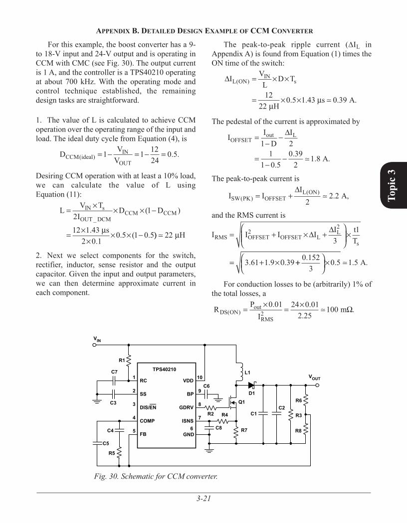
For this example, the boost converter has a 9- to 18-V input and 24-V output and is operating in CCM with CMC (see Fig. 30). The output current is 1 A, and the controller is a TPS40210 operating at about 700 kHz. With the operating mode and control technique established, the remaining design tasks are straightforward.
1. The value of L is calculated to achieve CCM operation over the operating range of the input and load. The ideal duty cycle from Equation (4), is
D V
VCCM idealIN
OUT( ) . .= − = − =1 1 12
240 5
Desiring CCM operation with at least a 10% load, we can calculate the value of L using Equation (11):
L V TI
D DIN s
OUT DCMCCM CCM= −
= −
× × ×
××
× ×
21
12 1 432 0 1
0 5 1 0 5
_( )
..
. ( . sµ )) 22 µH
2. Next we select components for the switch, rectifier, inductor, sense resistor and the output capacitor. Given the input and output parameters, we can then determine approximate current in each component.
The peak-to-peak ripple current (∆IL in Appendix A) is found from Equation (1) times the ON time of the switch:
∆I VL
D T
Hs A
L ONIN
s( )
. . . .
=
=
× ×
× ×1222
0 5 1 43 0 39
µ
µ
The pedestal of the current is approximated by
I ID
IOFFSET
out L=−
−
=−
−
1 21
1 0 50 39
21 8
∆
.. . A.
The peak-to-peak current is
I II
SW PK OFFSETL ON
( )( ) .= +
∆2
2 2 A,
and the RMS current is
I I I I I tTRMS OFFSET OFFSET L
L
s= + +
= +
22
31
3 61 1 9 39
× ×
×0
∆ ∆
. . . ++
0 1523
0 5 1 5. . .× A.
For conduction losses to be (arbitrarily) 1% of the total losses, a
R PI
mDS ONout
RMS( )
. ..
.= =× ×0 01 24 0 012 25
1002 Ω
1
2
3
5 FB
4
10
9
8
7
RC
DIS/EN
COMP
SS
VDD
ISNS
GDRV
GND
TPS40210VOUT
VIN
6
BP
R7
L1
R4R2
R5
R1
R3
R6
R8
D1
C2
C6
C7
C3
C4 C8
C1
C5
Q1
Fig. 30. Schematic for CCM converter.
AppendIx b. detAIled desIgn exAMple of ccM conVerter

3-22
Topi
c 3
The MOSFET should have a maximum voltage rating of at least 24 V. For this converter, an Si4446DY has a maximum RDS(ON) of 72 mΩ with a typical value of 43 mΩ, and a breakdown voltage rating of 40 V.
For the rectifier, the average rectifier current will be the same as the load current: 1 A. An MBRS340 has 3-A capability and a breakdown voltage of 40 V.
The inductor is a Pulse P1169.273NL. This device has a 20-µH inductance at 2.4 A and 27-µH inductance at 0 A.
To suppress the tendency towards subharmonic oscillation, the current-sense resistor is selected so that the slope of the current signal (at the input of the PWM) is half that of the compensating ramp. Refer to the TSP40210 datasheet [4] for further detail.
The slope of the compensating ramp is the peak-to-peak value of the sawtooth waveform divided by the period of oscillation:
m
sa = 0 61 43
420..
V/msµ
The sense-resistor value is
R mI A
kk
m
ISENSEa
L OFF CS=
= ≈
∆
Ω
( )
.
× ×
×× × ×
2
420 1545 1 6 2
64
A 50-mΩ resistor is used.The remaining component in the power stage
is the output capacitor. From earlier, the peak-to-peak ripple current was determined to be 2.2 A.
For a 2% peak-to-peak ripple voltage, a capacitor with an ESR of less than 218 mΩ should be used. In this example, a Panasonic 100-µF FK series capacitor is used. The ESR for this capacitor is measured to be about 140 mΩ.
Using Equation (35), the RMS ripple current in the capacitor is about 1 A. The rating of the capacitor is just under 400 mA at 105°C. Although dissipation is low, about 140 mW, a more robust solution should be found for a production converter.
3. With the major components selected, calculate the CCM duty cycle, DCCM, from Equation (5) as shown at bottom of this page, this time including losses.Note: If the converter was operating in DCM, this is where the DCM duty cycle would be calculated using Equation (10) for use in subsequent calculations.
4. For CCM, peak CMC operation, we calculate the slope of the current in the switch during the ON interval. Equation (1) is modified to include the voltage drop across the loss elements of the MOSFET and the current-sense resistor:
mV I
DR R
LIIN
OUTISENSE DS ON
L ON( )
( )
.( . .
( )=
−−
+
=−
−+
1
12 11 0 52
0 05 0
×
× 007
22529
)
A ms
µH
D
V I R R
V I R RCCM
IN DS ON ISENSE
IN OUT DS ON ISENSE= −
+ +
+ + +1
×
×
( )
( )
( )
( ) − + +
+
24
2
I R R V V
V VOUT DS ON ISENSE OUT d
OUT d
× ×( ) ( )
(( )
))
DCCM = −
+ +
+ + + − +1
12 1 0 07 0 05
12 1 0 07 0 05 4 1 0 07 0 052
×
× × ×
( . . )
[ ( . . )] ( . . )) ( . )( . )
%×
×24 0 5
2 24 0 552
+
+
3-23
Topi
c 3
5. From Equation (25), calculate the modulator gain, Fm:
Fm m T
s
ma n s
=+
=+
=
1
1417000 529000 6 0 05 1 43
1 2
( )
( . ) ..
×
× × × µ
Notice that mn from Equation (21) is the inductor-current ON slope times the sense resistor amplified by the current-sense amplifier gain, ACS, of 6.
6. The conversion ratio from Equation (16) is
M
DCCM =−
=−
11
11 0 52
2 1.
. .
7. To find Gvd(s), the duty-cycle to output-voltage transfer function, the frequency dependent parameters, ZON and ZOFF must first be calculated.§
Solving Equation (15):
G s V M
Z MR
Z MZ
vd CCM IN
ON CCM
load
ON CCM
OFF
CCM_ ( )
.
=−
+
=
× ×
×
×
×
2
2
2
1
1
12 4 3341 4 34
24
1 4 34×
×
×
−
+
Z
ZZ
ON
ON
OFF
.
.
8. The inner current-loop transfer function, TI(s), is determined from Equation (23) as shown at the
bottom of this page:
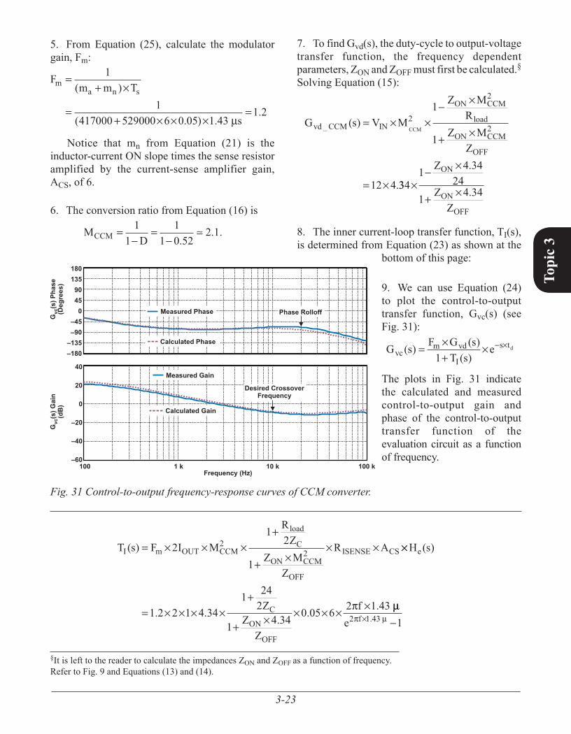
9. We can use Equation (24) to plot the control-to-output transfer function, Gvc(s) (see Fig. 31):
G s F G sT s
evcm vd
I
s td( ) ( )( )
=+
−× × ×
1
The plots in Fig. 31 indicate the calculated and measured control-to-output gain and phase of the control-to-output transfer function of the evaluation circuit as a function of frequency.
§It is left to the reader to calculate the impedances ZON and ZOFF as a function of frequency. Refer to Fig. 9 and Equations (13) and (14).
T s F I M
RZ
Z MZ
R AI m OUT CCM
load
C
ON CCM
OFF
ISENSE CS( ) =+
+× × ×
×× ×2
12
1
22 ××
× × × × × × × × ×
H s
ZZ
Z
f
e
C
ON
OFF
( )
. . . . .=+
+1 2 2 1 4 34
1 242
1 4 34 0 05 6 2 1 43π µµπ µe f2 1 43 1× . −
G(s) P
hase
(Deg
rees
)vc
G(s) G
ain
(dB)
vc
18013590450
–45–90
–135–180
Frequency (Hz)100 1 k 10 k 100 k
40
20
0
–20
–40
–60
Measured Gain
Phase Rolloff
Desired CrossoverFrequency
Calculated Gain
Calculated Phase
Measured Phase
Fig. 31 Control-to-output frequency-response curves of CCM converter.
3-24
Topi
c 3 10. Find the poles and zeros of the circuit. There is
a pole at about 200 Hz, and a zero at about 11 kHz. The error-amplifier compensation network should then have a zero at about 200 Hz and a pole at about 11 kHz. The resulting desired response will be a straight line with a –20-dB/decade slope.
11. Referring to the Bode plot, the phase begins to roll off at about 20 kHz. The loop crossover frequency should then be below 10 kHz to give some margin of safety. The error-amplifier gain therefore needs to be about +9 dB to bring the gain curve to 0 dB in the region of 10 kHz at the nominal 12-V input.
The voltage divider, R6 and R8 in this example, determines the output voltage. Arbitrarily setting R8 to 1.5 kΩ, the remaining components to find
are R6, R5, C4, and C5 (see Fig. 32).
R VV
R kOUT
REF6 8 24
0 71500 49 9= =× ×
.. , Ω
R R k kAV CA
5 6 10 49 9 10 13820920= =× ×
_
. , Ω Ω
where AV_CA is the desired gain (9 dB) of the compensated amplifier at the crossover frequency. To set the zero at about 200 Hz,
Cf R k
nFz EA
4 12 5
12 200 138
5 8= =π π_
. ,× × ×
Ω
and to set the pole at about 11 kHz,
C
f Rf C
k
p CAp CA
5 1
2 5 12 4
1
2 11000 138 12 11
=
+
=+
ππ
ππ
__
××
× ××
Ω0000 5 8
100
× .
.
nF
pF
The calculation for R5 assumes that the C4 impedance at the desired crossover frequency is small compared to R5. If not, then the overall gain is greater than originally desired. Also, if the impedance of C5 at the crossover frequency is near the value of R5, the compensated amplifier gain will be lower than calculated. After some iteration of values, Fig. 33 shows a gain/phase plot with R5 = 138 kΩ, C4 = 5800 pF, and C5 = 100 pF.
The crossover frequency, which is about 6 kHz with a phase margin of 75°, is lower than originally desired. As mentioned, the gain is also lower than
originally desired due to the process of selecting R5, C4, and C5.
The measured and predicted results compare fairly well (see Fig. 25). The low-frequency differ-ences are accounted for by the omission of losses in the MCCM conversion-ratio calculation on page 3-23. The high-frequency differences likely result from the parasitic elements of the output capacitor being different than those assumed.
R5 C4
C5
R6
VOUT
R8
Error-AmplifierOutput(COMP Pin)FB Pin +
–
Fig. 32. Error amplifier with type II compensation.
3020100
–1020304050
––––
1 k 100 k 1 M10 k–180
–90
–135
0
9045
–45
180
135
Frequency (Hz)
Gain( dB)
Phas
e( Deg
rees
)
10010
Gain
Phase
Fig. 33. Error-amplifier gain/phase plot.
3-25
Topi
c 3
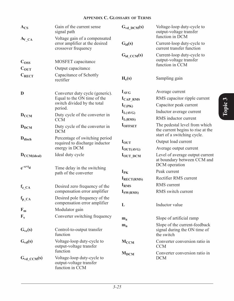
AppendIx c. glossAry of terMs
ACS Gain of the current sense signal path
AV_CA Voltage gain of a compensated error amplifier at the desired crossover frequency
COSS MOSFET capacitanceCOUT Output capacitanceCRECT Capacitance of Schottly
rectifier
D Converter duty cycle (generic). Equal to the ON time of the switch divided by the total period.
DCCM Duty cycle of the converter in CCM
DDCM Duty cycle of the converter in DCM
Ddisch Percentage of switching period required to discharge inductor energy in DCM
DCCM(ideal) Ideal duty cycle
e–s×td Time delay in the switching path of the converter
fz_CA Desired zero frequency of the compensation error amplifier
fp_CA Desired pole frequency of the compensation error amplifier
Fm Modulator gainFs Converter switching frequency
Gvc(s) Control-to-output transfer function
Gvd(s) Voltage-loop duty-cycle to output-voltage transfer function
Gvd_CCM(s) Voltage-loop duty-cycle to output-voltage transfer function in CCM
Gvd_DCM(s) Voltage-loop duty-cycle to output-voltage transfer function in DCM
Gid(s) Current-loop duty-cycle to current transfer function
Gid_CCM(s) Current-loop duty-cycle to output-voltage transfer function in CCM
He(s) Sampling gain
IAVG Average currentICAP_RMS RMS capacitor ripple currentIC(PK) Capacitor peak currentIL(AVG) Inductor average currentIL(RMS) RMS inductor currentIOFFSET The pedestal level from which
the current begins to rise at the start of a switching cycle.
IOUT Output load currentIOUT(AVG) Average output currentIOUT_DCM Level of average output current
at boundary between CCM and DCM operation
IPK Peak currentIRECT(RMS) Rectifier RMS currentIRMS RMS currentISW(RMS) RMS switch current
L Inductor value
ma Slope of artificial rampmn Slope of the current-feedback
signal during the ON time of the switch
MCCM Converter conversion ratio in CCM
MDCM Converter conversion ratio in DCM
3-26
Topi
c 3
mIL(ON) Slope of the inductor current during ON time of the switch
mIL(OFF) Slope of the inductor current during OFF time of the switch
Pd Power dissipatedPdCAP Power dissipated by output
capacitorPdL_cond Inductor winding power lossPdRECT_cond Rectifier conduction power
lossPdRECT_FR Rectifier switching power lossPdRECT_Qrr Schottky rectifier switching
lossPdSW_cond MOSFET conduction power
lossPdSW_switch MOSFET switching power
lossPdSW_gate MOSFET gate power lossPout Converter output power
QGD MOSFET gate-drain chargeQGATE MOSFET total gate charge RDS(ON) Switch ON resistanceRESR Capacitor ESRRGATE MOSFET gate resistanceRL Inductor winding resistanceRload Converter load resistanceRISENSE Current-sense resistorRtot Sum of DC loss elements when
the switch is on
s Frequency in radians/s
tDISCHG Discharge time of sawtoothtOFF Turn-OFF timetON_min Switch ON time under
minimum duty-cycle conditions
TI(s) Inner current-loop transfer function
tr Desired SW-node rise timeTs Converter switching periodtfall Time for the inductor current
to decay to zero in DCM operation
Vd Rectifier diode forward voltageVf Rectifier forward voltageVGATE MOSFET gate-drive voltageVIN Converter input voltageVmax Maximum voltage across the
snubber capacitorVOUT Converter output voltageVramp Sawtooth waveform peak-to-
peak voltageVRIPPLE_CAP Voltage ripple across the
output capacitor VRIPPLE_ESR(PP) Peak-to-peak voltage ripple
across the output capacitor’s ESR
Vth MOSFET gate-threshold voltage
ZC Parallel impedances of output capacitors
ZON Total impedance of the network when the switch is on
ZOFF Total impedance of the network when the switch is off
AppendIx c. glossAry of terMs (contInued)