Embed Size (px)
Citation preview
S.K.P. Engineering College, Tiruvannamalai V SEM
Department of ECE 1 EC6504 Microprocessor and Microcontroller
Unit I THE 8086 MICROPROCESSOR
Part - A Questions & Answers
1. Define stack. (April-May-16)
The stack is a part of read/write memory that is used for temporary storage of
binary information during execution of program
When the information is written on the stack, the operation is called ‘PUSH’.
When the information is read from the stack, the operation is called ‘POP’.
Stack is a top-down data structure, whose elements are accessed using a pointer
that is implemented using the SS (stack segment register) & SP (stack pointer
registers).
It is a LIFO data segment. .
2. (i)Define stack register. (April-May-17)
(ii) Define stack pointer. (April-May-18)
Stack register also called as stack pointer, it is a register which holds the 16 bit
offset from the start of the segment to the top of the stack.
Stack is a top-down data structure, whose elements are accessed using a pointer
that is implemented using the SS (stack segment register) & SP (stack pointer
registers).
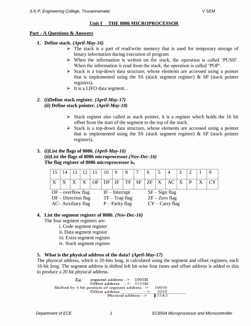
3. (i)List the flags of 8086. (April-May-16)
(ii)List the flags of 8086 microprocessor.(Nov-Dec-16)
The flag register of 8086 microprocessor is,
15 14 13 12 11 10 9 8 7 6 5 4 3 2 1 0
X X X X OF DF IF TF SF ZF X AC X P X CY
OF – overflow flag IF – Interrupt SF – Sign flag
DF – Direction flag TF – Trap flag ZF – Zero flag
AC– Auxiliary flag P – Parity flag CY – Carry flag
4. List the segment register of 8086. (Nov-Dec-16)
The four segment registers are:
i. Code segment register
ii. Data segment register
iii. Extra segment register
iv. Stack segment register
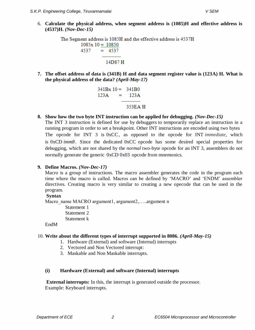
5. What is the physical address of the data? (April-May-17)
The physical address, which is 20-bits long, is calculated using the segment and offset registers, each
16-bit long. The segment address is shifted left bit-wise four times and offset address is added to this
to produce a 20 bit physical address.
S.K.P. Engineering College, Tiruvannamalai V SEM
Department of ECE 2 EC6504 Microprocessor and Microcontroller
6. Calculate the physical address, when segment address is (1085)H and effective address is
(4537)H. (Nov-Dec-15)
7. The offset address of data is (341B) H and data segment register value is (123A) H. What is
the physical address of the data? (April-May-17)
8. Show how the two byte INT instruction can be applied for debugging. (Nov-Dec-15)
The INT 3 instruction is defined for use by debuggers to temporarily replace an instruction in a
running program in order to set a breakpoint. Other INT instructions are encoded using two bytes
The opcode for INT 3 is 0xCC , as opposed to the opcode for INT immediate, which
is 0xCD imm8 . Since the dedicated 0xCC opcode has some desired special properties for
debugging, which are not shared by the normal two-byte opcode for an INT 3, assemblers do not
normally generate the generic 0xCD 0x03 opcode from mnemonics.
9. Define Macros. (Nov-Dec-17)
Macro is a group of instructions. The macro assembler generates the code in the program each
time where the macro is called. Macros can be defined by ‘MACRO’ and ‘ENDM’ assembler
directives. Creating macro is very similar to creating a new opecode that can be used in the
program.
Syntax
Macro_name MACRO argument1, argument2,…..argument n
Statement 1
Statement 2
Statement k
EndM
10. Write about the different types of interrupt supported in 8086. (April-May-15)
1. Hardware (External) and software (Internal) interrupts
2. Vectored and Non Vectored interrupt:
3. Maskable and Non Maskable interrupts.
(i) Hardware (External) and software (Internal) interrupts
External interrupts: In this, the interrupt is generated outside the processor.
Example: Keyboard interrupts.
S.K.P. Engineering College, Tiruvannamalai V SEM
Department of ECE 3 EC6504 Microprocessor and Microcontroller
Internal interrupts: It is generated internally by the processor circuit or by the execution of an
interrupt instruction. Example: Zero interrupt, overflow interrupt.
(ii) Vectored and Non Vectored interrupt:
When an interrupt signal is accepted by the processor, if the program control automatically
branches to a specific address (called vector address) then the interrupt is called vectored
interrupt.
In non-vectored interrupts the interrupting device should supply the address of the ISR to be
executed in response to the interrupt.
(iii) Maskable and Non Maskable interrupts
The interrupts whose request can be either accepted or rejected by the processor are called
maskable interrupts.
The interrupts whose request has to be definitely accepted (or cannot be rejected) by the
processor are called non-maskable interrupts.
11. List the modes of operation in 8086. (Nov-Dec-17)
The two operating Modes of 8086 are
1. Minimum Mode
2. Maximum Mode
12. List the addressing modes of 8086.
. Register addressing mode
Immediate addressing mode
Direct memory addressing mode
Indirect addressing in register
o Register indirect addressing mode
o Base plus index register addressing mode
o Register relative addressing mode
o Base plus index register relative addressing mode
String addressing mode
Direct I/O port Addressing Mode
Relative Addressing
Implied Addressing
Part – B Questions
1. (i) Explain briefly about internal hardware architecture of 8086 microprocessor with a neat
diagram. (10) (April-May’15)
(ii)Explain the architecture of Intel 8086 with the help of block diagram. (08) (Nov-Dec’15)
(iii)Explain the internal hardware architecture of 8086 microprocessor with neat diagram. (12)
(Nov-Dec’16)
(iv)Draw and explain the architecture of 8086 with neat diagram. (13) (April-May’17)
(v)Draw the architecture and explain the functional units of 8086. (13) (Nov-Dec’17)
(vi)Draw and explain the architecture of 8086 with neat diagram. (13) (April-May’18)
2. (i)Explain briefly about addressing modes of 8086. (08) (Nov-Dec’15)
S.K.P. Engineering College, Tiruvannamalai V SEM
Department of ECE 4 EC6504 Microprocessor and Microcontroller
(ii)Explain the various addressing modes of 8086 microprocessor with suitable examples. (16)
(Nov-Dec’16)
3. Explain the data transfer and arithmetic and branch instruction with example. (09) (April-May’16)
4. (i)Explain about ASSUME, EQU, DD assembler directives. (08) (April-May’15)
(ii)Write a short note about assembler directives. (4) (Nov-Dec’16)
5. (i) Write an 8086 Assembly Language Program to convert BCD data – Binary Data. (6) (April-
May’15)
(ii)Write an 8086 assembly language program to check whether given string is PALINDROME or
not. (8) (April-May-15)
(iii)Write an ALP to find sum of numbers in an array of 10 elements. (07) (April-May’16)
6. (i)Explain briefly about interrupt handling process in 8086. (08) (April-May’15)
(ii) Explain in details about Interrupt and Interrupt Service Routine of 8086. (16) (Nov-Dec’15)
(iii)Define Interrupts and their types. Write in details about interrupt service routine. (16) (April-
May’16)
(iv)Describe the interrupts of 8086 and its types with service routine. (13) (April-May’17)
(v)Describe the interrupts of 8086 and its types with service routine. (13) (Nov-Dec’17)
(vi)Explain in details about Interrupt and Interrupt Service Routine of 8086. (April-May’18) (13)
Unit II 8086 SYSTEM BUS STRUCTURE
Part - A Questions & Answers
1. Define bus. Why bus request and cycle stealing required? (April-May-15)
A set of wires used for transferring information between the components in a computer
stem is called a Bus. Taking control of the bus for a bus cycle is called cycle stealing.
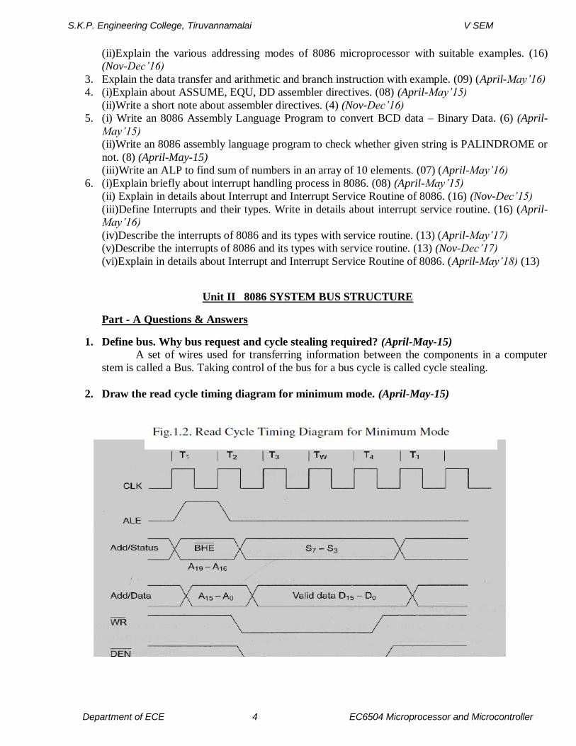
2. Draw the read cycle timing diagram for minimum mode. (April-May-15)
S.K.P. Engineering College, Tiruvannamalai V SEM
Department of ECE 5 EC6504 Microprocessor and Microcontroller
3. What is multiprogramming? (Nov-Dec-15)
If more than one process is carried out at the same time, then it is known as
multiprogramming. Another definition is the interleaving of CPU and IO operations among
several program is called multiprogramming.
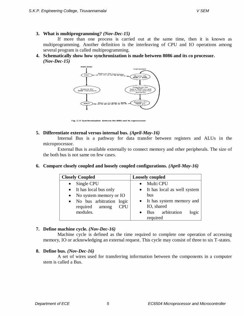
4. Schematically show how synchronization is made between 8086 and its co processor.
(Nov-Dec-15)
5. Differentiate external versus internal bus. (April-May-16)
Internal Bus is a pathway for data transfer between registers and ALUs in the
microprocessor.
External Bus is available externally to connect memory and other peripherals. The size of
the both bus is not same on few cases.
6. Compare closely coupled and loosely coupled configurations. (April-May-16)
Closely Coupled Loosely coupled
Single CPU
It has local bus only
No system memory or IO
No bus arbitration logic
required among CPU
modules.
Multi CPU
It has local as well system
bus
It has system memory and
IO, shared
Bus arbitration logic
required
7. Define machine cycle. (Nov-Dec-16)
Machine cycle is defined as the time required to complete one operation of accessing
memory, IO or acknowledging an external request. This cycle may consist of three to six T-states.
8. Define bus. (Nov-Dec-16)
A set of wires used for transferring information between the components in a computer
stem is called a Bus.
S.K.P. Engineering College, Tiruvannamalai V SEM
Department of ECE 6 EC6504 Microprocessor and Microcontroller
9. What is meant by multiprogramming? (April-May-17)
If more than one process is carried out at the same time, then it is known as
multiprogramming. Another definition is the interleaving of CPU and IO operations among
several program is called multiprogramming.
10. Write some examples for advanced processors. (April-May-17)
80286
80386
Pentium 1 2 3
11. What is the need of LOCK signal? (Nov-Dec’17)
This Output pin indicates that other system bus master will be prevented from gaining the
system bus, while LOCK signal is low. This signal is activated by LOCK prefix instruction.
12. Write some example for advanced processors. (Nov-Dec’17)
80286
80386
Pentium 1 2 3
Part – B Questions
1. (i)Discuss the maximum mode configuration of 8086 by with neat diagram. Mention the functions
of the various signals. (16) (April-May’15)
(ii)With neat diagram ,explain the minimum mode of operation of 8086 (16) (Nov-Dec-15)
(iii)Discuss the maximum mode configuration of 8086 by with neat diagram. Mention the
functions of the various signals. (13) (April-May’18)
2. (i)Explain in details about the system bus timing of 8086 .(16) (April-May-16)
(ii)Explain in detail about system bus timing of 8086. (16) (Nov-Dec-16)
(iii)Explain system bus structure of 8086 .Draw the timing diagram for Interrupt
Acknowledgement cycle. (13) (April-May-17)
(iv)Explain the system bus structure of 8086. Draw the timing diagram for interrupt
acknowledgment cycle. (13) (Nov-Dec’17)
3. (i)Compare closely coupled configuration with loosely coupled configuration. (8)(April-May-15)
(ii) Define loosely coupled system. Explain the scheme used for establishing priority. (16) (Nov-
Dec-15)
(iii)Explain the following
(i)Multiprocessor system (4)
(ii)Coprocessor (4)
(iii)Multiprogramming (4)
(iv)Semaphore (4) (April-May-16)
(iv)Discuss about multiprocessor configuration of 8086. (16) (Nov-Dec-16)
(v)Explain closely coupled configuration with neat diagram, (13) (April-May-17)
(vi)Explain the loosely looped configuration with neat diagram. (13) (Nov-Dec’17)
(vii)Discuss about multiprocessor configuration of 8086. (13) (April-May-18)
S.K.P. Engineering College, Tiruvannamalai V SEM
Department of ECE 7 EC6504 Microprocessor and Microcontroller
Unit III -I/O INTERFACING
Part - A Questions & Answers
1. What is the drawback of memory mapped I/O? (Nov-Dec-16)
In such scenarios the devices (I/O) are treated as a part of the memory only. Complete 1MB of memory
cannot be used as they are a part of the memory. In case of memory mapped I/O operations
no external separate instructions are required.
There is data transfer restriction in case of memory mapped instructions.
It is suitable for small system only.
Decoding circuit is complex since there are 20 address lines.
2. List the operating modes of 8255A and 8237A. (Nov-Dec-15)
8255 operating modes:-
a) I/O mode
i. Mode0 – simple input/output
ii. Mode1 – strobed input/output (Handshake mode)
iii. Mode2 – strobed bidirectional mode
b) Bit Set/Reset mode.
8237 operating modes:-
a) Single transfer mode (cycle stealing mode)
b) Block transfer mode (Burst mode)
3. What is the handshake signals used in Mode – 2 configurations of 8255? (Nov-Dec-16)
8255-based devices that perform handshaking support four handshaking signals:
Strobe Input (STB)
Input Buffer Full (IBF)
Output Buffer Full (OBF)
Acknowledge Input (ACK)
Use the STB and IBF signals for digital input operations and the OBF and ACK signals for digital output
operations.
4. List the advantages and disadvantages of parallel communication over serial
communication. (April-May-16)
Most of the microprocessor is designed for parallel communication. In parallel communication, number
of lines required to transfer data depend on the number of bits to be transferred. For
transmitting data over a long distance, using parallel communication is impractical due to the
increase in cost of cabling. Parallel communication is also not practical for devices such as
cassette tapes or a CRT terminal. In such situations, serial communication is used. In serial
communication, one bit is transferred at a time over a single line.
S.K.P. Engineering College, Tiruvannamalai V SEM
Department of ECE 8 EC6504 Microprocessor and Microcontroller
5. Give the various modes and applications of 8254 timer. (April-May-15) (ii)Give the various
modes of 8254 (Nov-Dec -18)
MODES & APPLICATIONS: 1.Mode 0:Clock generator
2. Mode 1:Pulse generator
3. Mode 2:Square wave generator
4. Mode 3:Programmable timer
5. Mode 4:Programmable counter
6. Mode 0:Rate generator5
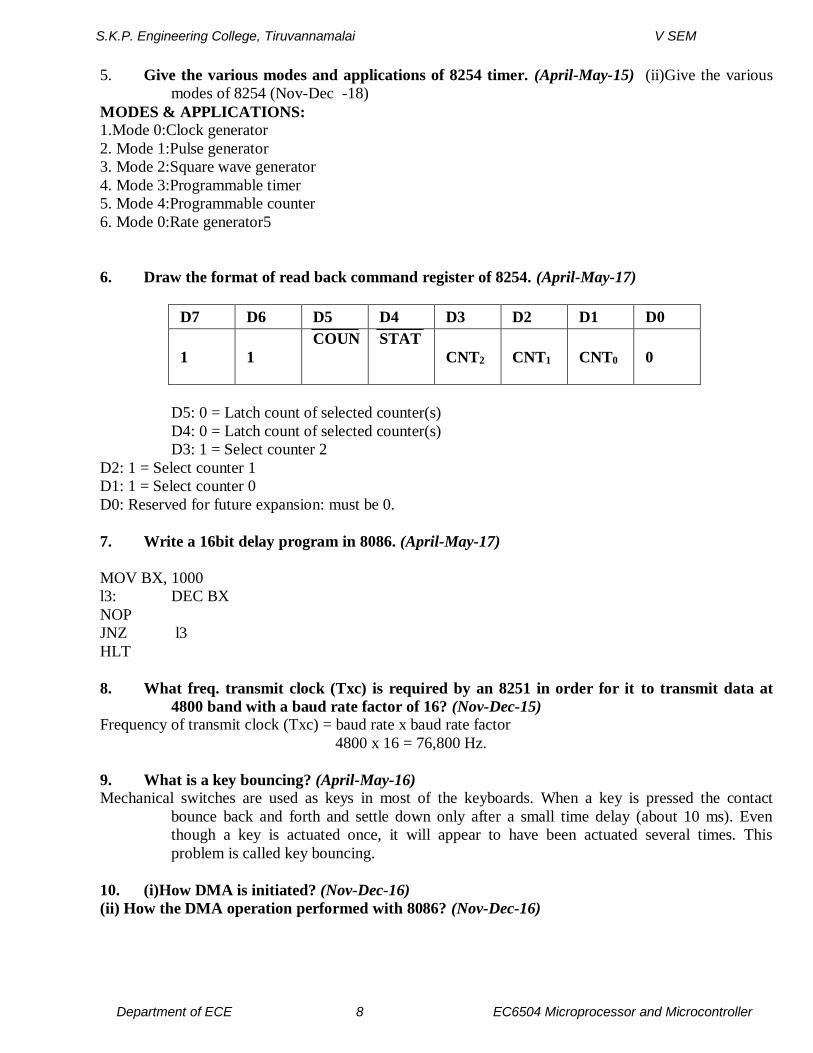
6. Draw the format of read back command register of 8254. (April-May-17)
D7 D6 D5 D4 D3 D2 D1 D0
1 1
COUN
T
STAT
U
S
CNT2 CNT1 CNT0 0
D5: 0 = Latch count of selected counter(s)
D4: 0 = Latch count of selected counter(s)
D3: 1 = Select counter 2
D2: 1 = Select counter 1
D1: 1 = Select counter 0
D0: Reserved for future expansion: must be 0.
7. Write a 16bit delay program in 8086. (April-May-17)
MOV BX, 1000
l3: DEC BX
NOP
JNZ l3
HLT
8. What freq. transmit clock (Txc) is required by an 8251 in order for it to transmit data at
4800 band with a baud rate factor of 16? (Nov-Dec-15)
Frequency of transmit clock (Txc) = baud rate x baud rate factor
4800 x 16 = 76,800 Hz.
9. What is a key bouncing? (April-May-16)
Mechanical switches are used as keys in most of the keyboards. When a key is pressed the contact
bounce back and forth and settle down only after a small time delay (about 10 ms). Even
though a key is actuated once, it will appear to have been actuated several times. This
problem is called key bouncing.
10. (i)How DMA is initiated? (Nov-Dec-16)
(ii) How the DMA operation performed with 8086? (Nov-Dec-16)
S.K.P. Engineering College, Tiruvannamalai V SEM
Department of ECE 9 EC6504 Microprocessor and Microcontroller
A special control unit may be provided to enable transfer a block of data directly between an external
peripheral devices and memory without contiguous intervention by the CPU. This approach is
called DMA. The data transfer using such approach is called DMA operation. Two control
signals are used to request and acknowledge a DMA transfer in the microprocessor-based
system
The two main advantages of DMA operations are,
1. The data transfer is fast.
2. Processor is not involved in the data transfer operation and hence it is free to execute other tasks.
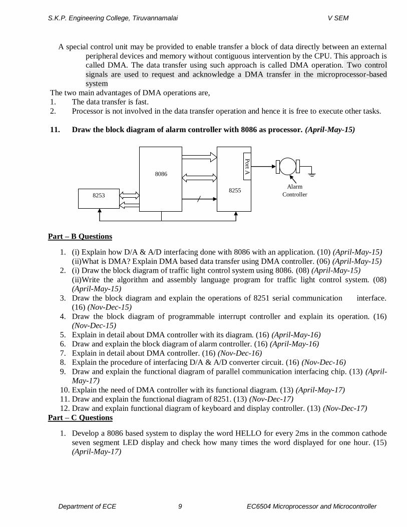
11. Draw the block diagram of alarm controller with 8086 as processor. (April-May-15)
Part – B Questions
1. (i) Explain how D/A & A/D interfacing done with 8086 with an application. (10) (April-May-15)
(ii)What is DMA? Explain DMA based data transfer using DMA controller. (06) (April-May-15)
2. (i) Draw the block diagram of traffic light control system using 8086. (08) (April-May-15)
(ii)Write the algorithm and assembly language program for traffic light control system. (08)
(April-May-15)
3. Draw the block diagram and explain the operations of 8251 serial communication interface.
(16) (Nov-Dec-15)
4. Draw the block diagram of programmable interrupt controller and explain its operation. (16)
(Nov-Dec-15)
5. Explain in detail about DMA controller with its diagram. (16) (April-May-16)
6. Draw and explain the block diagram of alarm controller. (16) (April-May-16)
7. Explain in detail about DMA controller. (16) (Nov-Dec-16)
8. Explain the procedure of interfacing D/A & A/D converter circuit. (16) (Nov-Dec-16)
9. Draw and explain the functional diagram of parallel communication interfacing chip. (13) (April-
May-17)
10. Explain the need of DMA controller with its functional diagram. (13) (April-May-17)
11. Draw and explain the functional diagram of 8251. (13) (Nov-Dec-17)
12. Draw and explain functional diagram of keyboard and display controller. (13) (Nov-Dec-17)
Part – C Questions
1. Develop a 8086 based system to display the word HELLO for every 2ms in the common cathode
seven segment LED display and check how many times the word displayed for one hour. (15)
(April-May-17)
8253
Timer
8086
Microprocessor 8255
PPI
Alarm
Controller
Port A
S.K.P. Engineering College, Tiruvannamalai V SEM
Department of ECE 10 EC6504 Microprocessor and Microcontroller
2. Develop an 8086 based system with 128 Ram and 4K ROM, to display the word HAPPY for
every 2ms in the common anode seven segment LED display. Explain the delay timings. (15)
(Nov-Dec-17)
Unit IV -MICROCONTROLLER
Part – A Questions and Answers
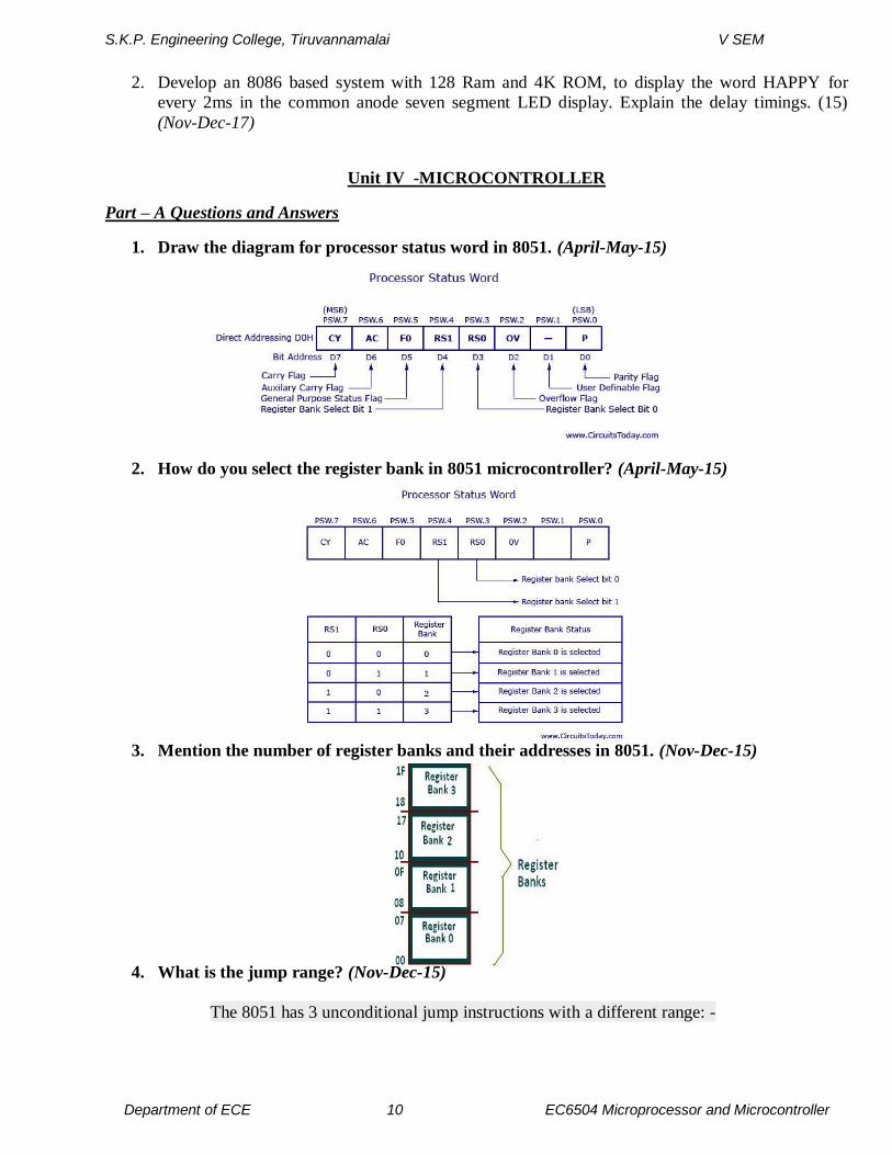
1. Draw the diagram for processor status word in 8051. (April-May-15)
2. How do you select the register bank in 8051 microcontroller? (April-May-15)
3. Mention the number of register banks and their addresses in 8051. (Nov-Dec-15)
4. What is the jump range? (Nov-Dec-15)
The 8051 has 3 unconditional jump instructions with a different range: -
S.K.P. Engineering College, Tiruvannamalai V SEM
Department of ECE 11 EC6504 Microprocessor and Microcontroller
• SJMP (Short Jump)
– Allows a jump of –128 to +127 bytes relative to the current PC value
– Instruction is 2 bytes long.
• AJMP (Absolute Jump)
– Allows a jump with the same 2KByte page that the PC is currently located in
– Instruction is 2 bytes long.
• LJMP (Long Jump)
– Allows a jump anywhere within the 64KByte program memory range of the 8051.
• If unsure which of the 3 instructions to use, simply use the JMP instruction and let the
assembler decide which instruction to use.
5. What are the different ways of operand addressing in 8051? (April-May-16)
o Immediate Addressing Mode
o Direct Addressing Mode
o Register Direct Addressing Mode
o Register Indirect Addressing Mode
o Indexed Addressing Mode
6. Write an 8051 ALP to toggle P1 a total of 200 times. Use RAM location 32H to hold your
counter value instead of register R0-R7. (April-May-16)
MOV P1, #55H
MOV 32, #200
LOP: CPL P1
ACALL DELAY
DJNZ 32, LOP
DELAY: MOV R0, #FF
LO: DJNZ R0, LO
RET
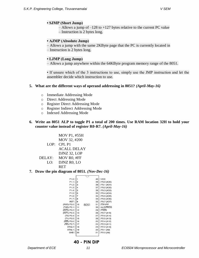
7. Draw the pin diagram of 8051. (Nov-Dec-16)
S.K.P. Engineering College, Tiruvannamalai V SEM
Department of ECE 12 EC6504 Microprocessor and Microcontroller
8. What is the significance of EA’ pin? (Nov-Dec-16)
It stands for external access. When the EA pin is connected to Vcc, program fetched to
address 0000H through 0FFFH are directed to the internal ROM and program fetches to address
1000H through FFFFH are directed to external ROM/EPROM. When the EA’ pin is grounded, all
the address fetched by program are directed to the external ROM/EPROM.
9. Which port used as multifunctional port? List the signals. (April-May-17)
Refer Q.No 7
10. Illustrate the CJNE instruction. (April-May-17)
The CJNE instruction compares the first two operands and branches to the specified
destination if their values are not equal. If the values are the same, execution continues with the
next instruction.
Operation: CJNE
Function: Compare and Jump If Not Equal
Syntax: CJNE operand1, operand2, reladdr
Examples
CJNE A, #data, reladdr
CJNE A, iram addr, reladdr
CJNE @Rn, #data, reladdr
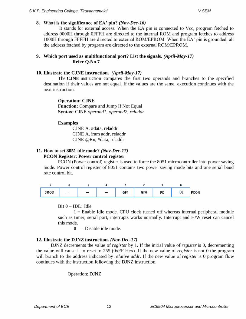
11. How to set 8051 idle mode? (Nov-Dec-17)
PCON Register: Power control register PCON (Power control) register is used to force the 8051 microcontroller into power saving
mode. Power control register of 8051 contains two power saving mode bits and one serial baud
rate control bit.
Bit 0 – IDL: Idle
1 = Enable Idle mode. CPU clock turned off whereas internal peripheral module
such as timer, serial port, interrupts works normally. Interrupt and H/W reset can cancel
this mode.
0 = Disable idle mode.
12. Illustrate the DJNZ instruction. (Nov-Dec-17)
DJNZ decrements the value of register by 1. If the initial value of register is 0, decrementing
the value will cause it to reset to 255 (0xFF Hex). If the new value of register is not 0 the program
will branch to the address indicated by relative addr. If the new value of register is 0 program flow
continues with the instruction following the DJNZ instruction.
Operation: DJNZ
S.K.P. Engineering College, Tiruvannamalai V SEM
Department of ECE 13 EC6504 Microprocessor and Microcontroller
Function: Decrement and Jump if Not Zero
Syntax: DJNZ register,reladdr
Examples:
DJNZ iram addr,reladdr
DJNZ Rn,reladdr
Part – B Questions
1. (i) Explain the architecture of 8051 microcontroller with neat diagram. (08) (April-May-15)
(ii) Explain the TMOD function register and its timer modes of operation. (08) (April-May-15)
2. (i) Explain about architecture and control instruction set in 8051. (10) (April-May-15)
(ii) Write a program to bring in data in serial form and send it out in parallel form using 8051.
(06) (April-May-15)
3. (i) Explain detail about the special function registers in 8051. (08) (Nov-Dec-15)
(ii) Briefly explain about addressing modes of 8051. (08) (Nov-Dec-15)
4. (i) Give PSW of 8051 and describe the use of each bit in PSW. (08) (Nov-Dec-15)
(ii) Describe the functions of the following signals in 8051. (08) (Nov-Dec-15)
RST, EA, PSEN and ALE
5. Explain the architecture of 8051 with its diagram. (16) (April-May-16)
6. Write an 8051 ALP to create a square wave of 66% duty cycle on bit 3 of port 1. (16) (April-May-
16)
7. Explain in detail about the architecture of 8051 microcontroller with a neat diagram. (16) (Nov-
Dec-16)
8. Write an ALP using 8051 instructions to receive bytes of data serially and put them in P1.set
the baud rate at 4800,8-bit data and 1 stop bit. (16) (Nov-Dec-16)
9. Write the available special function registers in 8051.Explain each register with its format and
functions. (13) (April-May-17)
10. (i) Discuss the types of addressing modes with suitable example in 8051.(08) (April-May-17)
(ii) Write an 8051 assembly language program to multiply the given number 48H and 30H. (05)
(April-May-17)
11. Describe the architecture of 8051 with neat diagram. (13) (Nov-Dec-17)
12. Discuss the ports and its circuits of 8051. (13) (Nov-Dec-17)
Unit V -INTERFACING MICROCONTROLLER
Part – A Questions and Answers
1. Differentiate between timers and counters. Draw the diagram of TCON in 8051. (April-May-
15)
A counter is a device that records the number of occurrences of a particular event. In
modern applications, counters are based on electronic devices and the counters are sequential
logic circuit designed to record the number of electric pulses fed into the counter.
A timer is an application of the counters where a certain signal with a fixed frequency
(hence period) is counted to record the time.
S.K.P. Engineering College, Tiruvannamalai V SEM
Department of ECE 14 EC6504 Microprocessor and Microcontroller
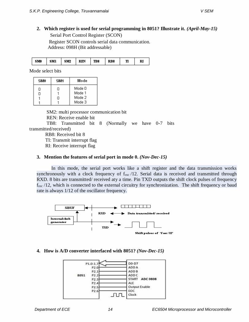
2. Which register is used for serial programming in 8051? Illustrate it. (April-May-15)
Serial Port Control Register (SCON)
Register SCON controls serial data communication.
Address: 098H (Bit addressable)
Mode select bits
SM2: multi processor communication bit
REN: Receive enable bit
TB8: Transmitted bit 8 (Normally we have 0-7 bits
transmitted/received)
RB8: Received bit 8
TI: Transmit interrupt flag
RI: Receive interrupt flag
3. Mention the features of serial port in mode 0. (Nov-Dec-15)
In this mode, the serial port works like a shift register and the data transmission works
synchronously with a clock frequency of fosc /12. Serial data is received and transmitted through
RXD. 8 bits are transmitted/ received aty a time. Pin TXD outputs the shift clock pulses of frequency
fosc /12, which is connected to the external circuitry for synchronization. The shift frequency or baud
rate is always 1/12 of the oscillator frequency.
4. How is A/D converter interfaced with 8051? (Nov-Dec-15)
S.K.P. Engineering College, Tiruvannamalai V SEM
Department of ECE 15 EC6504 Microprocessor and Microcontroller
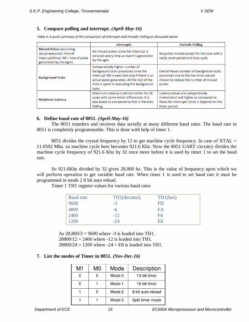
5. Compare polling and interrupt. (April-May-16)
6. Define baud rate of 8051. (April-May-16)
The 8051 transfers and receives data serially at many different baud rates. The baud rate in
8051 is completely programmable. This is done with help of timer 1.
8051 divides the crystal frequency by 12 to get machine cycle frequency. In case of XTAL =
11.0592 Mhz. so machine cycle here becomes 921.6 Khz. Now the 8051 UART circuitry divides the
machine cycle frequency of 921.6 Khz by 32 once more before it is used by timer 1 to set the baud
rate.
So 921.6Khz divided by 32 gives 28,800 hz. This is the value of frequency upon which we
will perform operation to get variable baud rate. When timer 1 is used to set baud rate it must be
programmed in mode 2 8 bit auto reload.
Timer 1 TH1 register values for various baud rates
Baud rate TH1(decimal) TH1(hex)
9600 -3 FD
4800 -6 FA
2400 -12 F4
1200 -24 E8
As 28,800/3 = 9600 where -3 is loaded into TH1.
28800/12 = 2400 where -12 is loaded into TH1.
28800/24 = 1200 where -24 = E8 is loaded into TH1.
7. List the modes of Timer in 8051. (Nov-Dec-16)
S.K.P. Engineering College, Tiruvannamalai V SEM
Department of ECE 16 EC6504 Microprocessor and Microcontroller
8. State how baud rate is calculated for serial data transfer in mode 1. (Nov-Dec-16)
Steps to calculate Baud Rate:
1. The 8051 microcontroller transfers and receives data serially at many different baud
rates. The baud rate in the 8051 is programmable and can be set through Timer 1 or by changing
the external crystal oscillator.
2. The 8051 has external clock of frequency 11.0592 MHz, which gets divided by 12 to
get machine cycle frequency is 921.6 kHz.
3. The 8051 microcontroller serial communication UART circuitry divides the machine
cycle frequency of 921.6 kHz by 32, before it is used by Timer 1 to set the baud rate. Therefore,
921.6 kHz divided by 32 gives out 28,800 Hz.
4. When Timer 1 is used to set the baud rate it must be programmed in mode 2, that is 8-
bit auto reload. To get baud rates compatible with PC, we must load TH1 with values: -3, -6, -12,
-24. These values are fixed to find out suitable baud rate compatible with PC's COM port. PC
baud rates values are set by the vendors and are fixed. Some of the baud rates values supported by
Pentium IBM PC are as 110, 150, 300, 600, 1200, 2400, 4800, 9600, 19200. So, one has to
generate 8051 microcontroller baud rate accordingly.
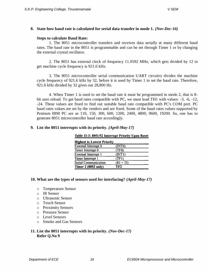
9. List the 8051 interrupts with its priority. (April-May-17)
10. What are the types of sensors used for interfacing? (April-May-17)
o Temperature Sensor
o IR Sensor
o Ultrasonic Sensor
o Touch Sensor
o Proximity Sensors
o Pressure Sensor
o Level Sensors
o Smoke and Gas Sensors
11. List the 8051 interrupts with its priority. (Nov-Dec-17)
Refer Q.No 9
S.K.P. Engineering College, Tiruvannamalai V SEM
Department of ECE 17 EC6504 Microprocessor and Microcontroller
Part – B Questions
1. (i) Describe the different modes of operation of timers/counters in 8051 with its associated
register. (10) (April-May-15)
(ii)How does one interface a 16x2 LCD display using 8051 microprocessor? (06) (April-May-15)
2. Draw the diagram to interface a stepper motor with 8051 microcontroller and explain. Write an
8051 assembly language program to run the stepper motor in both forward and reverse direction
with delay. (16) (April-May-15)
3. With a neat circuit diagram explain how a 4x4 keypad is interfaced with 8051 microcontroller and
write 8051 ALP for keypad scanning. (16) (Nov-Dec-15)
4. Draw the schematic for interfacing a stepper motor with 8051 microcontroller and write 8051
ALP for changing speed and direction of motor. (16) (Nov-Dec-15)
5. Draw the diagram to interface a stepper motor with 8051 microcontroller and explain Write an
8051 assembly language program to run the stepper motor in both forward and reverse direction
with delay. (16) (April-May-16)
6. Explain 8051 serial port programming with example. (16) (April-May-16)
7. Describe the different modes of operation of timers /counters in 8051 microcontroller. (16) (Nov-
Dec-16)
8. Draw a diagram to interface a stepper motor with 8051 microcontroller also writ an 8051 ALP to
run the stepper motor in both forward and reversed direction with delay. (16) (Nov-Dec-16)
9. Write a program for generation of unipolar square waveform of 1KHZ frequency using Timer 0 of
8051 in mode 0.consider the system frequency as 12MHZ. (13) (April-May-17)
10. Demonstrate the interfacing of the stepper motor with 8051 and explain its interfacing diagram
and develop program to rotate the motor in clock wise direction. (13) (April-May-17)
11. Illustrate the serial communication in 8051, with its special function register. (13) (Nov-Dec-17)
12. (i) Interface the ADC converter with 8051, with its special function register. (13) (Nov-Dec-17)
(ii) Write the assembly language program to execute the ADC conversion. (13) (Nov-Dec-17)
Part – C Questions
1. Develop 8051 based system design having 8Kbyte RAM generate the triangular wave using DAC.
(April-May-17)
2. Design a circuit to generate 12 MHz frequency for a system. Write a program for generation of
unipolar square waveform of 1 KHz frequency using Timer0 of 8051 in moce0. (Nov-Dec-17)