Embed Size (px)
Citation preview
1
UV Photodetector Based on Graphene−−−−ZnO Nanowire Hybrid: 1
Fabrication, Photoresponse and Photoluminescence Studies 2
Ravi K. Biroju1, P. K. Giri1, 2* 3
1Centre for Nanotechnology, Indian Institute of Technology Guwahati, Guwahati-781039, India 4
2Department of Physics, Indian Institute of Technology Guwahati, Guwahati-781039, India. 5
6
Abstract 7
Herein, we demonstrate a graphene based efficient UV photodetector by using vertically aligned ZnO 8
NWs on chemical vapor deposited graphene with and without a ZnO buffer layer. The effect of rapid 9
thermal annealing (RTA) on grapheneZnO thin film hybrid prior to the growth of ZnO NWs by physical 10
vapor deposition technique is investigated from the µRaman spectroscopy and high resolution 11
transmission electron microscopy. The change in the relative intensities of 2D and D band Raman modes 12
and a red shift in 2D band (~ 13 cm-1) after RTA treatment in ZnO coated graphene substrate reveals the 13
strong interaction between graphene and ZnO hexagonal lattice, covalent sp2 carbon lattice. The vertical 14
ZnO NWs with high aspect ratio on the grapheneZnO thin film hybrid exhibit enhanced UV absorption, 15
strong UV and visible photoluminescence and improved UV photoresponse. There is a 6 fold 16
enhancement in the photocurrent in ZnO NWs grown on graphene as compared to the ZnO NWs grown 17
on bare ZnO seed layer. The improved performance of these graphene based 2D1D integrated hybrid ZnO 18
nanostructures is an important step towards the fabrication of hybrid photodetectors and phototransistors 19
with enhanced UV response. 20
Keywords: CVD graphene; Graphene−ZnO NWs, UV photodetector, Rapid Thermal Annealing 21
22
23
1. INTRODUCTION 24
*Email of corresponding author: [email protected]
2
A tremendous research interest has grown recently on the fabrication and optoelectronic properties of 1
graphene based semiconducting nanowire (NW) hybrid structures for applications in various 2
optoelectronic devices, such as ultrafast photodetectors (PDs) and light emitting diodes (LEDs) etc.1-3 On 3
the other hand, investigating the photo physical properties from 2D single layer (SLG) and few layer 4
graphene or boron nitride (h-BN) with high quality, wide band gap semiconductor (ZnO, GaN, GaAs etc.) 5
epitaxial layers is a very important aspect in multi−quantum−well hetero structures for light emission 6
devises such as LEDs and ultrafast PDs.4-7 Further, incorporating the pre−treated epitaxial 7
graphene−semiconductor thin film substrates for the growth of catalyst free, vertically aligned 8
semiconducting nanowires (NWs) for the enhanced photoluminescence (PL) and photoconductivity (PC) 9
properties is a challenging task. Among all, fabrication of ZnO thin film using RF magnetron sputtering 10
followed by ZnO NW growth on graphene−ZnO layer substrates by low temperature physical vapor 11
deposition (PVD) technique is very simple technique and controlled fabrication of 2D−1D integrated 12
hybrid nanostructures with improved PD device characteristics are challenging. Understanding the 13
epitaxial relation between sp2 hybridized single crystalline graphene layer and hexagonal wurtzite phase 14
ZnO is very important for the growth of catalyst free ZnO NW hetero structures on graphene.1 Further 15
these 2D−1D integrated graphene−ZnO hybrids will improve the optical properties such as UV−vis 16
absorption, PL and photoconductivity (PC) as compared the ZnO NWs only.1,8,9 The advantage of 17
combining ZnO over the graphene, that can catalyze the growth of ZnO NW for the vertical alignment in 18
the presence of ZnO seed layer and due to its very high carrier mobility, very low optical absorption and 19
high thermal conductivity can enhance the optical property of the resultant integrated hybrid 20
nanostructure which is suitable for the improved photosensitivity and ultrafast UV light response.10,11 21
There are no reports on the effect of RTA treatment of the ZnO seed layer on the fabrication of 22
ZnO NWs on graphene-ZnO hybrid layer and the role of graphene layer in the vertical alignment of ZnO 23
NWs on these substrates. In the present work, we have grown the vertical ZnO NWs on graphene 24
substrate with sputter deposited ultra-thin ZnO seed layer and achieved enhanced optical properties from 25
3
these hybrids, such as, optical absorption, photoconductivity and PL. The mechanism of catalyst free 1
growth of ZnO NWs over the graphene layer with and without ZnO seed layer was systematically studied 2
from the µ−Raman spectroscopy and high resolution transmission electron microscopy (HRTEM). 3
Characteristic Raman features of graphene−ZnO thin film hybrid, such as change in the relative 4
intensities and full width at half maxima (FWHM) of 2D, D Raman bands with respect to the G band 5
reveals the epitaxial relation between graphene and ZnO that originates the growth of vertically aligned 6
ZnO NWs. The structural and optical properties of these graphene−ZnO NWs hybrid nanostructures were 7
studied by high resolution FESEM, HRTEM and optical absorption and µ−Raman spectroscopy. Further 8
enhanced UV PL was achieved in case of ZnO NWs grown on graphene−ZnO seed layer substrate. These 9
PL results are compared with the bare ZnO seed layer substrates. Photoresponse studies are carried out on 10
the hybrid nanostructures. 11
2. EXPERIMENTAL DETAILS 12
2.1. Synthesis of Graphene by Chemical Vapor Deposition 13
Large area single layer graphene was synthesized on a Cu foil (Alfa Aesar, 99.999% pure, 1×1 14
inch area) by a thermal CVD technique. As grown graphene on the Cu foil was transferred on to 15
Si/SiO2 and quartz substrates by standard wet transfer method. Initially, the Cu foil was inserted 16
in a quartz boat, which was kept at the center of a tubular quartz chamber (diameter 1 inch, 17
length ∼1 meter) placed inside a muffle furnace. The base vacuum of 4.0 ×10⁻⁴ mbar inside the 18
tube was created using a turbo molecular pump. Subsequently, Ar gas (300 standard cubic 19
centimeters per minute (SCCM)) was purged into the quartz tube for 15 min. The ratio of 20
precursor gas sources Ar: CH4: H2 was 300:10:50 SCCM during the graphene growth and the 21
duration of growth was 30 min. The growth temperature and pressure were maintained at 1045°C 22
and 2.2 mbar, respectively. 23
4
As−grown graphene on the Cu foil was transferred onto various substrates by standard 1
wet transfer process, which involved spin coating of a layer of Poly methyl methacrylate 2
(PMMA)/Toluene on one side of the Cu foil and then etching away the other side by keeping it 3
floating on Fe(NO3)3 solution (etchant solution) overnight. The Fe(NO3)3 solution was then 4
repeatedly diluted with millipore water by using a syringe in such a way that it turns orange color 5
to complete transparent, i.e. in the end only water remained. The layer of PMMA with graphene 6
attached to it was scooped out using various substrates. The substrates were then rinsed with DI 7
water and dried in the oven at 180°C for 15 min. The PMMA layer was removed by repeated 8
rinsing of graphene substrates with Acetone for several times. In order to remove the PMMA and 9
residual Cu catalyst particles adhered on graphene layer, hydrogen (H2) annealing was 10
performed. Further details of the H2 annealing of GR were reported in our earlier work.12 11
2.2. Deposition of ZnO Thin Films on Graphene 12
High quality ZnO film with two different thicknesses: ~300 nm (sample code−Z1), ~10 nm 13
(sample code−Z2) were deposited by RF magnetron sputtering on various graphene substrates 14
for the growth of ZnO NWs. Initially, a base pressure of 6.7x10⁻⁶ mbar was created inside the 15
chamber and during the RF plasma induced sputtering, it was maintained at 1x10⁻² mbar. The RF 16
power and substrate temperature were kept at 100 W and 200°C, respectively. Further, the ZnO 17
thin films were subjected to rapid thermal annealing (RTA) treatment at 600°C in Ar gas ambient 18
(flow rate of 200 SCCM) atmosphere for 3 minutes using a commercial RTA system 19
(MILA3000, Ulvac, Japan) in order to further improve the crystalline quality as well as to 20
remove the excess oxygen defects in the ZnO films on various substrates. Improvements in the 21
crystallinity of ZnO grains and their phases were confirmed from XRD and HRTEM analyses. 22
Note that the results and discussions are made only for the ZnO NWs grown on the RTA treated 23
5
GRZ2 substrate (10nm thick ZnO seed layer on graphene/SiO2), Z2 substrate (10nm thick ZnO 1
seed layer on SiO2) and GR (pristine single layer CVD graphene) substrates only. 2
2.3. Growth of ZnO NWs on Graphene Substrates 3
Commercial nanosized activated Zn powder (purity ~ 99%, Aldrich) was taken as a source 4
material in an alumina boat and placed at the center of a horizontal quartz tube kept inside a 5
muffle furnace. The above prepared substrates were placed downstream ~ 5 cm away from the 6
source material. Initially the quartz tube was pumped down to a pressure of ~ 10-3 mbar. In order 7
to prevent the oxidation of the graphene layer, 300 SCCM of Ar gas was flushed into the 8
chamber until it reached the set point with a ramp rate of 18°C /min. When the furnace reached 9
the source temperature, 20 SCCM of O2 gas was introduced and gas pressure inside the chamber 10
was maintained at 1.6 mbar for the growth time 50 min. The temperature of the source material 11
was maintained at ~ 600°C, while the substrate temperature was at ~ 580°C. After the 12
completion of the reaction, the furnace was cooled down to room temperature. RTA is performed 13
at 600°C in Ar atmosphere (300 SCCM) for 3 minutes to improve the crystalline quality of the 14
as−grown ZnO NWs. Note that the sample codes used in the main text is as follows Z2W(ZnO 15
NWs grown on Z2 substrate); GRZ2W (ZnO NWs grown GRZ2 substrate) and GRW (ZnO NWs 16
grown on GR substrate). 17
3. CHARACTERIZATION TECHNIQUES 18
The morphology and crystal structure of the as−grown samples were studied using electron 19
microscopy tools such as field emission scanning electron microscope (FESEM, Sigma, Zeiss) 20
and high resolution transmission electron microscope (HRTEM, JEM2100 operated at 200kV, 21
JEOL). µ-Raman measurements were performed using a high resolution Raman spectrometer 22
6
(LAB RAM HR, Horiba, Spectra Physics)with the excitation source 488 and 514.5 nm (Ar+ 1
laser) and monochromator using 1800 gr.mm-1 lines with a thermoelectric cooled CCD detector 2
in the backscattering configuration to examine the crystalline quality and number of layers in the 3
graphene and the ZnO seed layer crystalline quality. PL measurement was carried out at room 4
temperature using a 355 nm diode laser excitation in a commercial fluorimeter (AB2, Thermo 5
Spectronic). The UV–vis–NIR absorption spectroscopy measurements were recorded using a 6
commercial spectrophotometer (PerkinElmer UV WinLab, UV−3101PC). PC measurements 7
were performed with a micro probe station (ECOPIA EPS−500) connected to a source measure 8
unit (Keithely 2400, USA) for current−voltage characteristics and 300 W Xenon lamp (Newport, 9
USA) as a light source to excite the sample. Note that the excitation wavelength was selected 10
using a monochromator (Oriel Instruments, USA). The I−V setup was interfaced with a 11
computer to collect the data using Lab Tracer 2.0 software. 12
3. RESULTS AND DISCUSSION 13
3.1 Micro−Raman and HRTEM studies of GRZ2 and Z2 Substrates 14
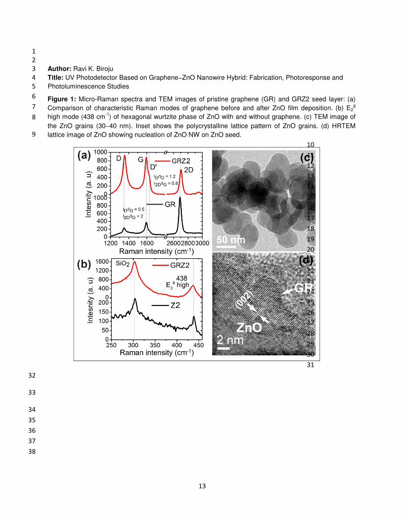
The quality, number of layers and uniformity of as−grown graphene was evaluated from the characteristic 15
Raman line shapes of graphene before and after sputter deposited ZnO layer. Figure 1 (a−b) represents 16
the typical Raman spectra of graphene and graphene−ZnO thin film hybrid before and after ZnO film 17
deposition. Raman signatures of SLG (see the lower curve in the Fig. 1(a)) with peaks at 1350 cm-1 (D 18
band- significant for layer disorder due to intrinsic defects), 1593 cm-1 (G band− originating from 19
in−plane symmetric (E2g) vibrations from the sp2 hybridized carbon atoms), 1620 cm-1 (D’ band− 20
significant for the edge defects such as arm chair and zig−zag edge reconstruction etc.) and 2689 cm-1 (a 21
sharp 2D band determining the number of graphene layers). The ratio of integrated intensities of 2D and 22
G band i.e. I2D/IG= 2.0 signifies the dominance of single layer graphene (SLG) in the as-grown layer. 23
7
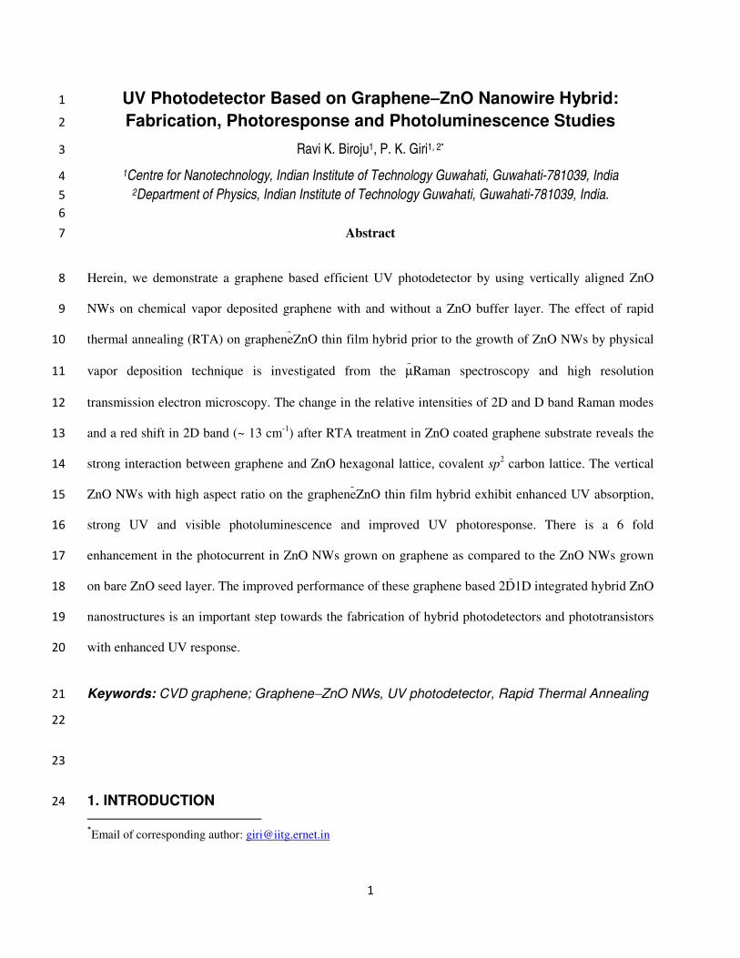
Based on the spatial mapping of the Raman finger prints of graphene it was found that the SLG is covered 1
over the large area on the substrate. In GRZ2, the ratio of relative integrated intensity of ID/IG is increased 2
by a factor of 2.4 and I2D/IG is reduced by a factor of 2.5 with respect to the pristine graphene, which 3
signifies the disorder and compressible strain in graphene induced by the ZnO layer. Note that the line 4
shape of 2D band without any asymmetry is identical to the few layer graphene that denotes the uniform 5
coverage of ultrathin ZnO seed layer over the SLG in GRZ2, which behaves like a few layer graphene. 6
An important observation for the epitaxial relation and covalent interaction between graphene and ZnO 7
was evidenced from the redshift (13 cm-1) of 2D band in GRZ2. Confirmation of wurtzite phase for the 8
ZnO seed layer was clear from the appearance of the E2g high mode at ~ 438 cm-1.The FWHM of the E2
g 9
high mode was increased in the GRZ2 as compared to the Z2 substrate due to the covalent interaction of 10
the ZnO seed layer with the graphene. Further, the size distribution of ZnO seed layer was estimated from 11
the HRTEM. Figure 1(c) denotes the TEM image of the ZnO grains with uniform size (30-40 nm) 12
distribution. These ZnO grains on graphene play an important role for the vertical alignment of ZnO NWs 13
in the PVD growth. In order to support the Raman results, we have performed the HRTEM imaging for 14
the GRZ2 hybrid thin film. Figure 1(d) illustrates the graphene and ZnO (002) plane interface. SLG (GR) 15
lattice pattern can be clearly seen at the outer edge of the thin film that was shown by the white color 16
arrow. The (002) plane of ZnO on GR layer was clearly seen at the inner part of the HRTEM image. 17
3.2 FESEM and HRTEM Studies 18
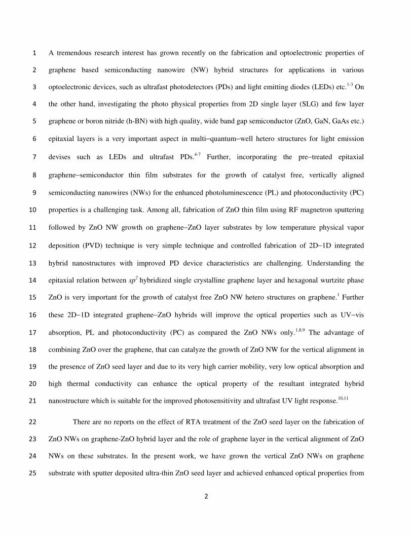
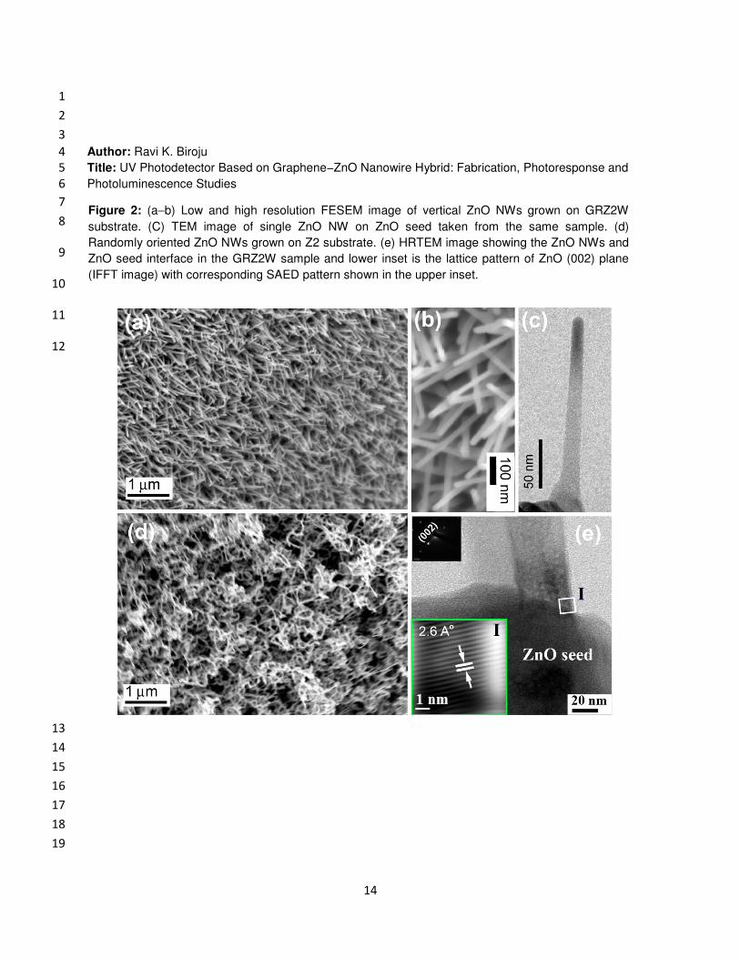
Further, morphological features and growth initiation of ZnO NWs on GRZ2 and Z2 substrates were 19
elucidated using high resolution FESEM and HRTEM imaging. Figure 2(a) shows the array of vertically 20
grown ZnO NWs on GRZ2 substrate, which have high aspect ratio and large surface area. We have not 21
observed any hexagonal facets on the top face of the ZnO NWs, as shown in the FESEM image Fig. 2(b). 22
Note that the growth of ZnO NWs on graphene−Au catalyst results in a vertically aligned hexagonal 23
faceted ZnO NWs as discussed in our earlier report.1 However, in the present case we have not observed 24
any hexagonal facets on the tip of ZnO NWs though the ZnO seed layer was used on the graphene 25
8
substrate. Figure 1(c) is a HRTEM image of a single ZnO NW grown vertically on the ZnO grain. On the 1
other hand, in absence of graphene layer, a dense array of randomly oriented ZnO NWs is grown on the 2
Z2 substrate. Direct growth of ZnO NWs on GR substrate also yields randomly oriented sparse ZnO NWs 3
(data not shown). FESEM image in Fig. 2(d) clearly reveals that random alignment of the ZnO NWs is 4
due to the absence of the graphene layer over the ZnO grains. This is occurring probably due to the non- 5
uniform surface energy and excess oxygen on the Z2 layer that lead to the dense and random alignment 6
for the ZnO NWs. Furthermore, the crystallinity and c−axis orientation of the ZnO NWs was investigated 7
from the HRTEM, as shown in the Fig. 2(e). It shows the ZnO NW nucleates on the ZnO seed. The inset 8
shows the IFFT image corresponding to the region I, which shows the lattice fringes of the (002) plane 9
with d spacing of 2.6Å that matches with the SAED pattern. Note that the upper left inset in Fig. 2(e) is 10
the SAED pattern taken at the region I. 11
3.3 Optical Absorption & Micro−Raman studies of ZnO NWs 12
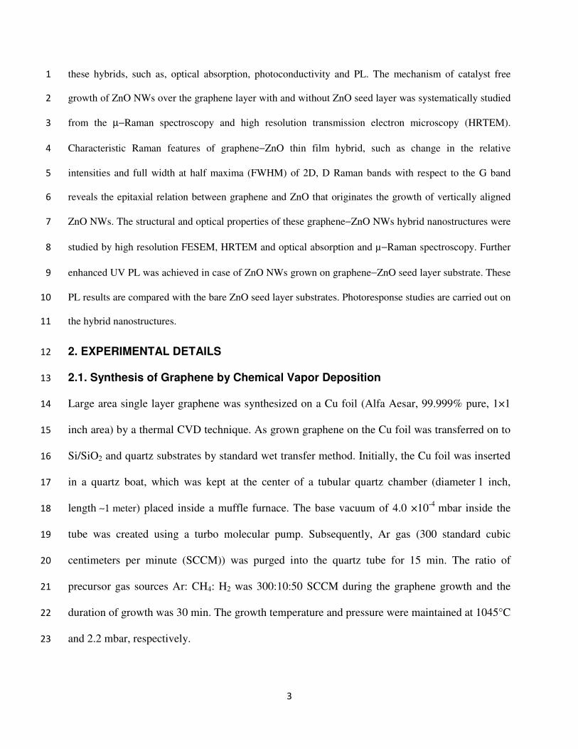
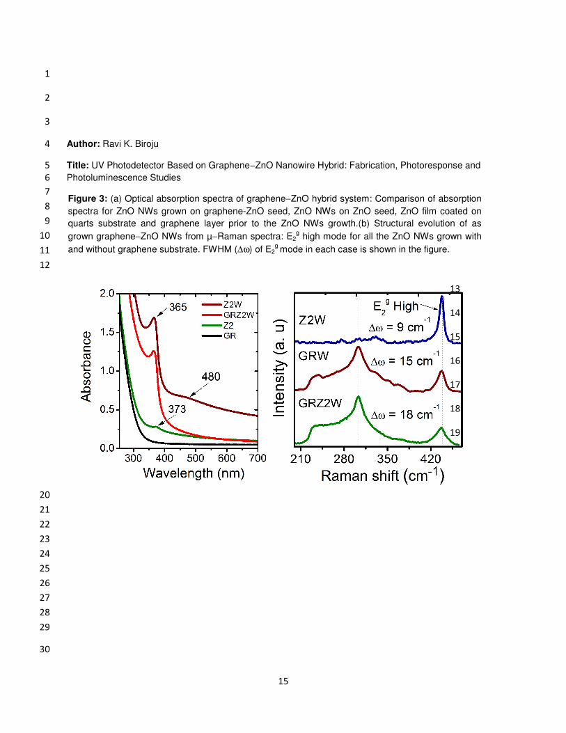
The UV-vis absorption characteristics of graphene−ZnO hybrid system was done individually for the 13
graphene transferred on to the quartz substrate before and after ZnO seed layer and ZnO NWs growth, 14
respectively. Figure 3(a) describes the comparison of UV−vis absorption from GR (black), Z2 (green), 15
GRZ2W (Red) and Z2W (brown). Graphene layer on quartz substrate (GR) shows the complete optical 16
transparency from UV to visible absorption wavelength whereas in case of Z2 there is a weak UV 17
absorption band found to be 373 nm. ZnO NWs grown on the graphene−ZnO substrates show the 18
enhanced UV band edge absorption at 365 nm due to their high aspect ratio and large surface area as 19
discussed in the earlier section (see Fig. 2). The UV absorption was increased by a factor of 5 and 6.5 for 20
GRZ2W and Z2W, respectively as shown in the Fig. 3(a). Note that in case of Z2W there is a broad 21
absorption band cantered at 480 nm originating from oxygen related trap states (oxygen vacancies (Vo) 22
and oxygen interstitials (Oi)) which are formed on the ZnO NWs. This absorption band reveals that the 23
ZnO NWs grown Z2 substrate are oxygen rich, which is further augmented by the PL results. 24
9
The typical Raman spectra for comparison among Z2W, GRW and GRZ2W samples are shown 1
in the Fig. 3(b). The E2ghigh mode at ~438 cm-1 was fitted with the Lorentzian line shape for the 2
calculation of FWHM (∆ω) to compare the crystalline quality of ZnO NWs grown on different substrates. 3
The FWHM of GRZ2W is typically higher (18 cm-1) than that of the Z2W (9 cm-1), though it shows the 4
strong UV near band edge (NBE) emission in the PL spectra (discussed later). That may be due to the 5
contribution of the substrate ZnO layer on the Raman spectrum. 6
7
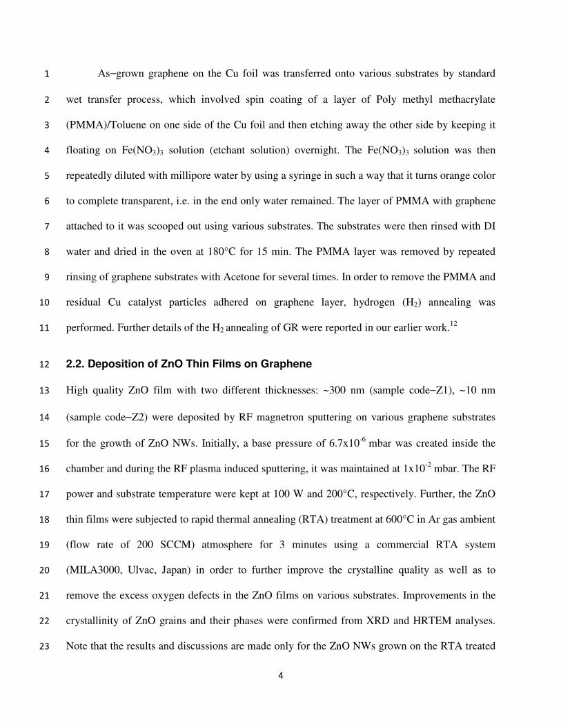
3.4 Photoluminescence Studies 8
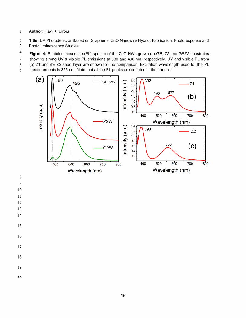
The PL characteristics of the graphene−ZnO hybrid system before and after ZnO NWs growth was 9
carried out using 355 nm laser excitation. Figure 4(a) illustrates the UV−vis PL from the ZnO NWs 10
grown on GRZ2, Z2 and GR substrates, respectively. A sharp UV NBE emission is found to be at 380 nm 11
and a broad visible absorption band peaked at 496 nm originating various oxygenated defect state 12
emissions (Vo or Oi).1 The integrated intensity ratio of UV to visible PL emission is higher in case of 13
ZnO NWs grown on GRZ2 substrate, while it is lower for the NWs grown on GR substrate. The PL 14
emission from the ZnO seed layer substrate was also studied for comparison. Figures 4 (b) and (c) show 15
the PL spectra for the Z1 and Z2 substrates, respectively. Here, the NBE emission was observed at ~ 390 16
nm for both the samples. There are two visible emission bands: 490 and 577 nm in case of Z1, while a 17
broad visible emission band centered at 558 nm in case of Z2. The PL emission at 490 nm is attributed to 18
the Vo related defects on the surface of the ZnO thin film and 577nm, 558 nm emissions are attributed to 19
the Oi related defects. Here we have discussed PL emissions from the ZnO NWs grown on Z2 substrate 20
because it shows relatively lower defect density as compared to the Z1 substrate. Both high UV and 21
visible PL from these hybrid nanostructures are beneficial for display applications. 22
23
3.5 Photoconductivity Studies 24
10
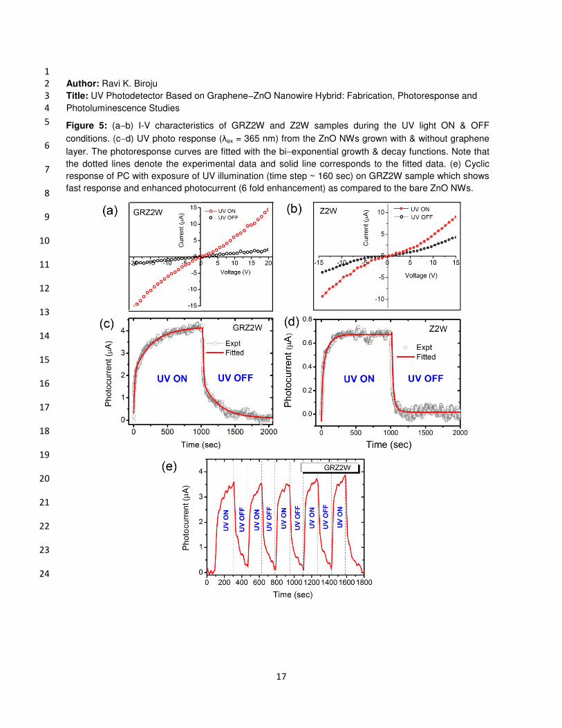
The photocurrent and photoresponse behavior of the ZnO NWs grown on GRZ2 and Z2 are 1
investigated by exciting with the UV light on these graphene−ZnO hybrids. For conductivity 2
measurements, the silver (Ag) contacts are deposited at high vacuum (~ 10-6 mbar) using a 3
thermal evaporation system. The channel length as well as width of the Ag contacts is 0.2 mm 4
and thickness of the Ag contact is ~ 100 nm. Figure 5(a−b) represents the photocurrent and dark 5
current characteristics measured for the GRZ2W and Z2W samples, respectively. Further time 6
response measurement was conducted by exciting with UV light (365 nm) for each cycle of 1000 7
sec for ON and OFF conditions with fixed bias voltage (Vb= 2 V). Figure 5(c−d) represent the 8
photoresponse curves for the both GRZ2W and Z2W samples, which show the exponential 9
growth and decay of current for UV ON and UV OFF conditions. Note that the PC curves are 10
fitted with the bi−exponential growth and decay functions as reported by the Dhara et al.13 11
Dotted lines represent the experimental data and solid red lines correspond to the fitted data. PC 12
growth characteristics are fitted by the equation (1). 13
------------- (1) 14
Here I1, A1 and A2 are the constants. τ1 and τ2 are characteristic the time constants, which are 15
obtained from the fitting. For GRZ2W and Z2W, the time constants of PC growth are found to 16
be τ1 = 14.8s, τ2 =266.9s and τ1 = 14.2s, τ2 = 84.2s, respectively. PC decay is represented by 17
equation (2). 18
-------------- (2) 19
Here A3 and A4 are the constants. These two time constants physically signify the fast and slow 20
photoresponse from the UV NBE emission and oxygenated defect states from the ZnO NWs, 21
respectively. This is applicable to both the cases UV ON and UV OFF conditions as shown in the 22
11
Figures 5(c, d). τ1and τ2 are calculated as 241.8s, 9.9s in the case of GRZ2W and 52.2s, 15.5s in 1
Z2W, respectively. Note that the represent the photocurrent after long time, which is 2
equal to the dark current. The photocurrent is enhanced by a factor of 6 in case of ZnO NWs 3
grown on GRZ2 as compared to the Z2 substrate. This enhancement might be due to the 4
Schottky contact between the bunch of ZnO NWs and underlying graphene layer which leads to 5
the multiple exciton formation in the graphene−ZnO NWs hybrid photodetector.8,9 Figure 5(e) 6
illustrates the consecutive time response curves with 160 sec interval measured for the 5 cycles 7
of UV ON and OFF in case of GRZ2W sample. It shows enhanced current values as compared to 8
the bare ZnO NWs without any degradation in photocurrent with respect to time. Further 9
optimization of the growth parameters is need for faster photoresponse of graphene based PD 10
device. 11
12
4. CONCLUSION: 13
Vertically aligned ZnO NWs have been grown on CVD graphene substrates with and without the RTA 14
treated ZnO seed layer. The important role of graphene buffer layer on growth of well aligned ZnO NWs 15
in presence of ZnO seed layers was established. The strong interaction between graphene and ZnO layer 16
was shown from the characteristic line shape features (D, G and 2D bands) of graphene. Vertically 17
aligned growth of ZnO NWs take place in case of graphene−ZnO thin film substrate, while randomly 18
oriented ZnO NWs are grown in case of ZnO seed layer without the graphene layer. Enhanced 19
photocurrent response was achieved from these graphene−ZnO NWs hybrid structures. The photodetector 20
based on graphene−ZnO NWs hybrid shows 6 fold higher photocurrent response than that of the bare 21
ZnO NWs based photodetector. Our results are promising for further optimization of the growth and 22
processing parameters of the graphene based UV photodetectors using ZnO NWs. 23
12
ACKNOWELEDGEMENT: 1
We thank Central Instruments Facility (CIF) for providing FESEM and micro Raman facilities. 2
We acknowledge the financial support from CSIR (Grant No. 03(1270)/13/EMR-II), DEITY 3
(Grant No. 5(9)/2012-NANO) and BRNS (Grant No. 2012/37P/1/BRNS) for carrying out part of 4
this work. 5
6
References 7
1 R. K. Biroju, P. K. Giri, S. Dhara, K. Imakita, and M. Fujii, ACS Appl. Mater. Interfaces 6, 377 8
(2013). 9 2 R. K. Biroju and P. K. Giri, J. Nanosci. Lett. 4, 34 (2013). 10 3 A. Mazid Munshi and H. Weman, physica status solidi (RRL) – Rapid Research Letters 7, 713 11
(2013). 12 4 S. Jeong Woo, O. Jitsuo, U. Kohei, K. Atsushi, and F. Hiroshi, Applied Physics Express 7, 13
085502 (2014). 14 5 K. Chung, C.-H. Lee, and G.-C. Yi, Science 330, 655 (2010). 15 6 Y. J. Hong, W. H. Lee, Y. Wu, R. S. Ruoff, and T. Fukui, Nano Lett. 12, 1431 (2012). 16 7 H. Oh, Y. J. Hong, K.-S. Kim, S. Yoon, H. Baek, S.-H. Kang, Y.-K. Kwon, M. Kim, and G.-C. 17
Yi, NPG Asia Mater 6, e145 (2014). 18 8 B. D. Boruah, D. B. Ferry, A. Mukherjee, A. Misra, Nanotechnology 26, 235703 (2015). 19 9 R. K. Biroju, N. Tilak, R. Gone, S. Dhara, and P. K. Giri, Nanotechnology 26, 145601 (2015). 20 10 Y. Kim, J.-H. Lee, and G. Yi, Appl. Phys. Lett. 95, 213101 (2010). 21 11 S. G. Zhang, X. W. Zhang, F. T. Si, J. J. Dong, and J. X. W. e. al., Appl. Phys. Lett. 101, 121104 22
(2012). 23 12 R. K. Biroju and P. K. Giri, J. Phys. Chem. C 118, 13833 (2014). 24 13 S. Dhara and P. K. Giri, Nanoscale Res Lett. 6, 504 (2011). 25
26
27
28
29
30
31
32
33
34
35
36
37
38
13
1
2
Author: Ravi K. Biroju 3
Title: UV Photodetector Based on Graphene−ZnO Nanowire Hybrid: Fabrication, Photoresponse and 4
Photoluminescence Studies 5
6
7
8
9
10
11
12
13
14
15
16
17
18
19
20
21
22
23
24
25
26
27
28
29
30
31
32
33
34
35
36
37
38
Figure 1: Micro-Raman spectra and TEM images of pristine graphene (GR) and GRZ2 seed layer: (a)
Comparison of characteristic Raman modes of graphene before and after ZnO film deposition. (b) E2g
high mode (438 cm-1
) of hexagonal wurtzite phase of ZnO with and without graphene. (c) TEM image of
the ZnO grains (30−40 nm). Inset shows the polycrystalline lattice pattern of ZnO grains. (d) HRTEM
lattice image of ZnO showing nucleation of ZnO NW on ZnO seed.
14
1
2
3
Author: Ravi K. Biroju 4
Title: UV Photodetector Based on Graphene−ZnO Nanowire Hybrid: Fabrication, Photoresponse and 5
Photoluminescence Studies 6
7
8
9
10
11
12
13
14
15
16
17
18
19
Figure 2: (a−b) Low and high resolution FESEM image of vertical ZnO NWs grown on GRZ2W
substrate. (C) TEM image of single ZnO NW on ZnO seed taken from the same sample. (d)
Randomly oriented ZnO NWs grown on Z2 substrate. (e) HRTEM image showing the ZnO NWs and
ZnO seed interface in the GRZ2W sample and lower inset is the lattice pattern of ZnO (002) plane
(IFFT image) with corresponding SAED pattern shown in the upper inset.
15
1
2
3
Author: Ravi K. Biroju 4
Title: UV Photodetector Based on Graphene−ZnO Nanowire Hybrid: Fabrication, Photoresponse and 5
Photoluminescence Studies 6
7
8
9
10
11
12
13
14
15
16
17
18
19
20
21
22
23
24
25
26
27
28
29
30
Figure 3: (a) Optical absorption spectra of graphene−ZnO hybrid system: Comparison of absorption
spectra for ZnO NWs grown on graphene-ZnO seed, ZnO NWs on ZnO seed, ZnO film coated on
quarts substrate and graphene layer prior to the ZnO NWs growth.(b) Structural evolution of as
grown graphene−ZnO NWs from µ−Raman spectra: E2g high mode for all the ZnO NWs grown with
and without graphene substrate. FWHM (∆ω) of E2g mode in each case is shown in the figure.
16
Author: Ravi K. Biroju 1
Title: UV Photodetector Based on Graphene−ZnO Nanowire Hybrid: Fabrication, Photoresponse and 2
Photoluminescence Studies 3
4
5
6
7
8
9
10
11
12
13
14
15
16
17
18
19
20
Figure 4: Photoluminescence (PL) spectra of the ZnO NWs grown (a) GR, Z2 and GRZ2 substrates
showing strong UV & visible PL emissions at 380 and 496 nm, respectively. UV and visible PL from
(b) Z1 and (b) Z2 seed layer are shown for the comparison. Excitation wavelength used for the PL
measurements is 355 nm. Note that all the PL peaks are denoted in the nm unit.
17
1
Author: Ravi K. Biroju 2
Title: UV Photodetector Based on Graphene−ZnO Nanowire Hybrid: Fabrication, Photoresponse and 3
Photoluminescence Studies 4
5
6
7
8
9
10
11
12
13
14
15
16
17
18
19
20
21
22
23
24
Figure 5: (a−b) I-V characteristics of GRZ2W and Z2W samples during the UV light ON & OFF
conditions. (c−d) UV photo response (λex = 365 nm) from the ZnO NWs grown with & without graphene
layer. The photoresponse curves are fitted with the bi−exponential growth & decay functions. Note that
the dotted lines denote the experimental data and solid line corresponds to the fitted data. (e) Cyclic
response of PC with exposure of UV illumination (time step ~ 160 sec) on GRZ2W sample which shows
fast response and enhanced photocurrent (6 fold enhancement) as compared to the bare ZnO NWs.