Embed Size (px)
Citation preview
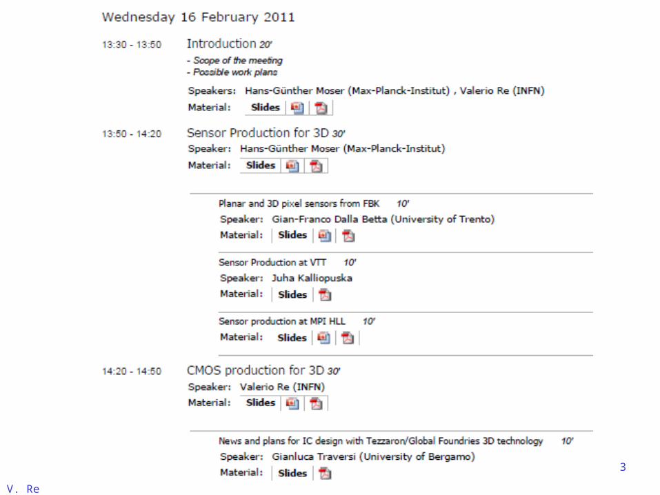
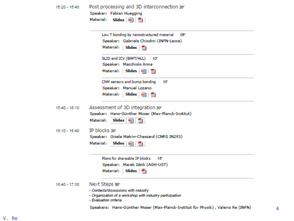
V. Re
1
WP3
Microelectronics and interconnection technology
AIDA kick-off meeting, February 18, 2011
Hans-Günther Moser - MPI
Valerio Re - INFN
V. Re
2
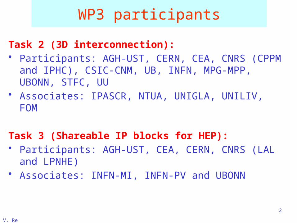
WP3 participants
Task 2 (3D interconnection):• Participants: AGH-UST, CERN, CEA, CNRS (CPPM and
IPHC), CSIC-CNM, UB, INFN, MPG-MPP, UBONN, STFC, UU
• Associates: IPASCR, NTUA, UNIGLA, UNILIV, FOM
Task 3 (Shareable IP blocks for HEP):• Participants: AGH-UST, CEA, CERN, CNRS (LAL and
LPNHE)• Associates: INFN-MI, INFN-PV and UBONN
V. Re
3
V. Re
4
H.-G. MoserMPI Munich
Valerio ReINFN
Aim of the WP3 kick-off meeting
The aim of this first meeting was to define a coherent program, and to start a selection process among the many options that are available for both 3D integration and IP blocks, obviously taking into account manpower and funding limitations.
Some decisions have to be taken in a relatively early stage of the project (e.g., how to procure CMOS chips for 3D integration), others require to establish contacts with industry (for 3D interconnection steps), which is an important part of WP3.5
H.-G. MoserMPI Munich
Valerio ReINFN
WP3.2:3D interconnection
The aim is to build a demonstrator of a 3D vertically integrated pixel sensor, which provides a tool to qualify the technologies that are involved in 3D integration and makes them accessible to the community.
WP3 plans to follow a “via last ” approach to 3D integration to build a 2-layer device in heterogeneous technologies, where the two layers are fabricated independently, and TSVs (Through Silicon Vias) and interconnections are made as the last steps of the process.
6
H.-G. MoserMPI Munich
Valerio ReINFN
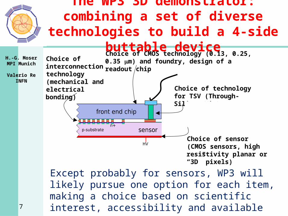
The WP3 3D demonstrator: combining a set of diverse technologies to build a
4-side buttable deviceChoice of interconnectiontechnology(mechanical and electrical bonding) Choice of technology for
TSV (Through-Silicon-Via)
Choice of CMOS technology (0.13, 0.25, 0.35 mm) and foundry, design of a readout chip
Choice of sensor(CMOS sensors, high resistivity planar or “3D” pixels)
Except probably for sensors, WP3 will likely pursue one option for each item, making a choice based on scientific interest, accessibility and available resources 7
H.-G. MoserMPI Munich
Valerio ReINFN
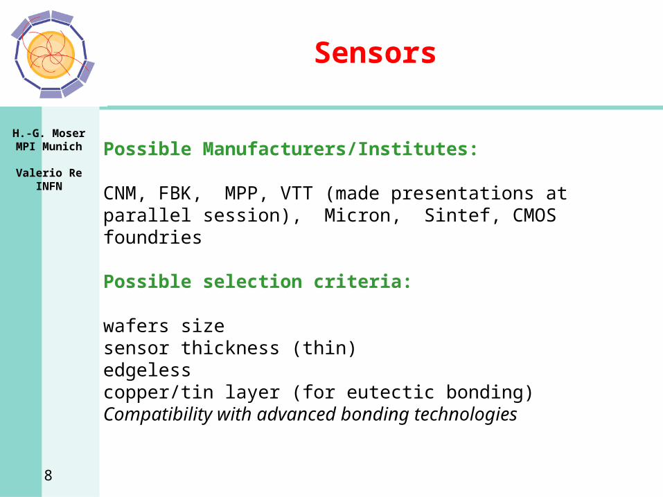
Sensors
Possible Manufacturers/Institutes:
CNM, FBK, MPP, VTT (made presentations at parallel session), Micron, Sintef, CMOS foundries
Possible selection criteria:
wafers size sensor thickness (thin)edgelesscopper/tin layer (for eutectic bonding)Compatibility with advanced bonding technologies
8
H.-G. MoserMPI Munich
Valerio ReINFN
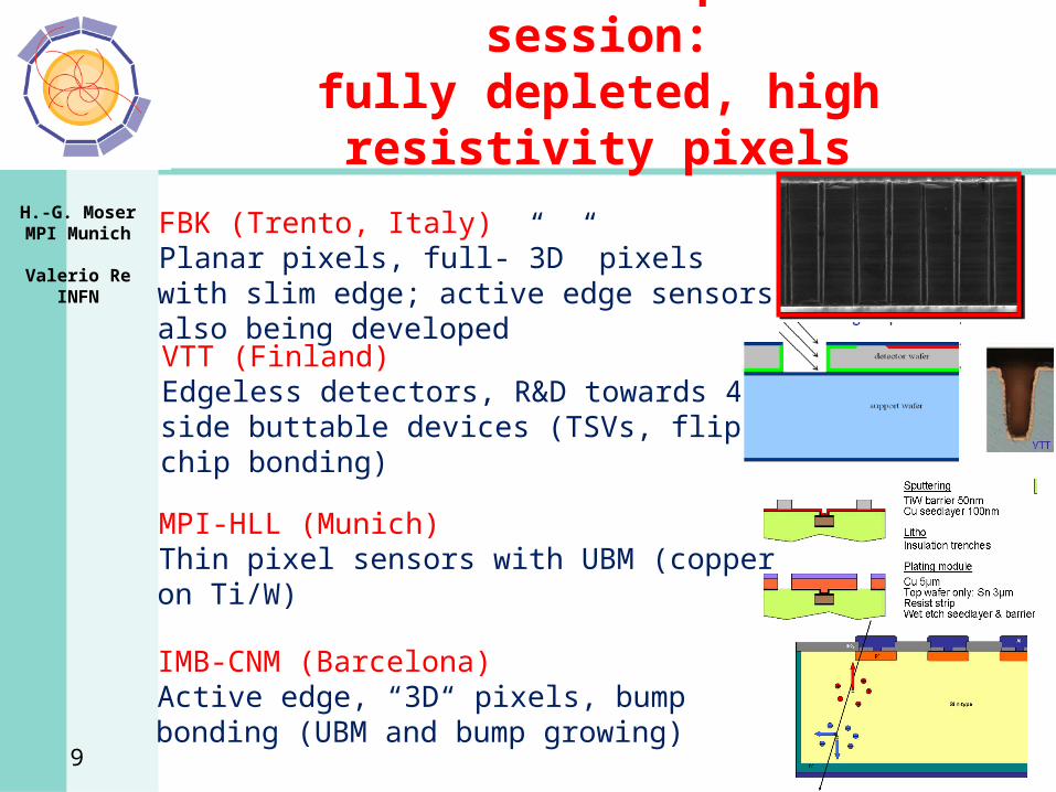
Sensors at WP3 parallel session:fully depleted, high resistivity pixels
FBK (Trento, Italy)Planar pixels, full-”3D” pixels with slim edge; active edge sensors also being developedVTT (Finland)Edgeless detectors, R&D towards 4-side buttable devices (TSVs, flip-chip bonding)
MPI-HLL (Munich)Thin pixel sensors with UBM (copper on Ti/W)
IMB-CNM (Barcelona)Active edge, “3D“ pixels, bump bonding (UBM and bump growing)
9
H.-G. MoserMPI Munich
Valerio ReINFN
CMOS readout circuits for 3D integration
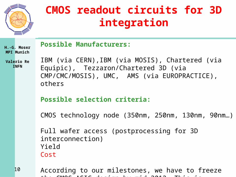
Possible Manufacturers:
IBM (via CERN),IBM (via MOSIS), Chartered (via Equipic), Tezzaron/Chartered 3D (via CMP/CMC/MOSIS), UMC, AMS (via EUROPRACTICE), others
Possible selection criteria:
CMOS technology node (350nm, 250nm, 130nm, 90nm…)
Full wafer access (postprocessing for 3D interconnection)YieldCost
According to our milestones, we have to freeze the CMOS ASIC design by mid 2012. This is necessary to complete the program on 3D integration with a full qualification of the demonstrator and of the relevant technologies.
10
H.-G. MoserMPI Munich
Valerio ReINFN
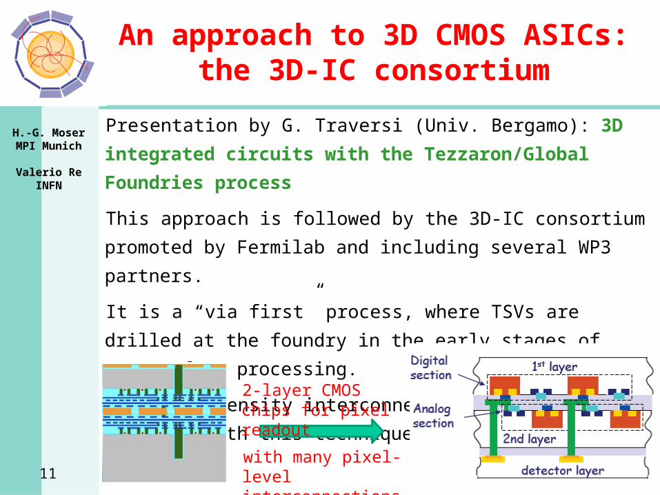
An approach to 3D CMOS ASICs:the 3D-IC consortium
11
Presentation by G. Traversi (Univ. Bergamo): 3D
integrated circuits with the Tezzaron/Global
Foundries process
This approach is followed by the 3D-IC consortium
promoted by Fermilab and including several WP3 partners.
It is a “via first” process, where TSVs are drilled at the
foundry in the early stages of CMOS wafers processing.
Very high density interconnections (< 10 mm) are possible
with this technique.2-layer CMOS chips for pixel readout
with many pixel-level interconnections
H.-G. MoserMPI Munich
Valerio ReINFN
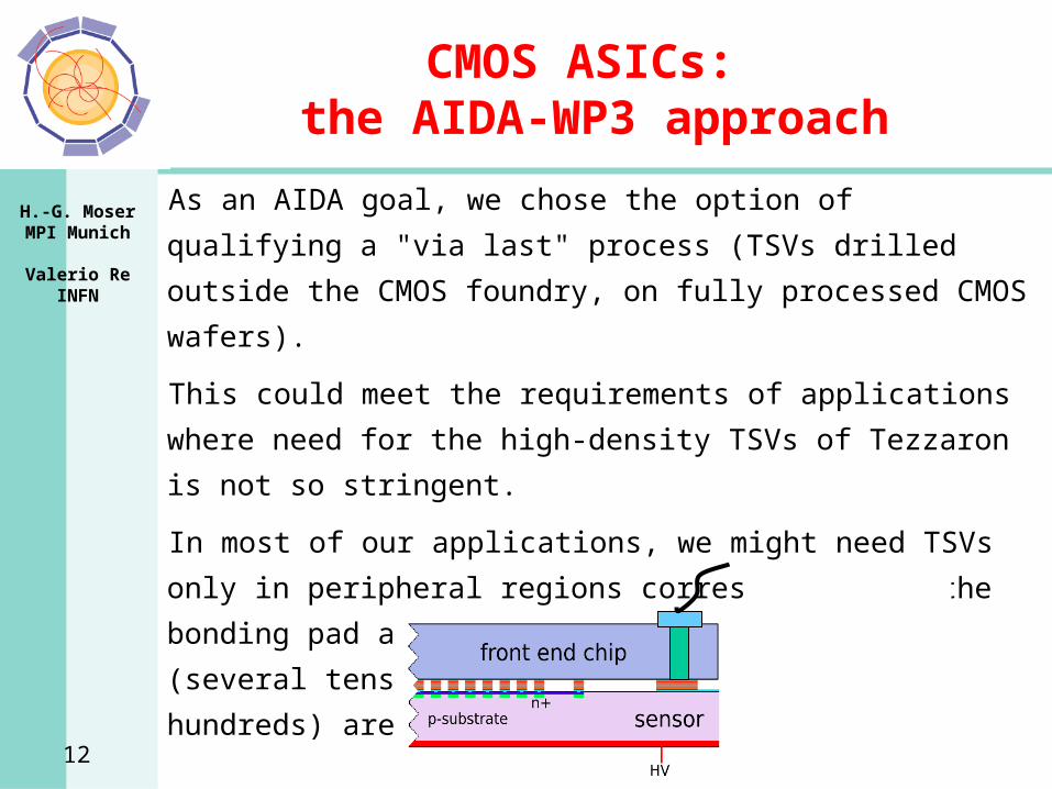
CMOS ASICs: the AIDA-WP3 approach
As an AIDA goal, we chose the option of qualifying a "via
last" process (TSVs drilled outside the CMOS foundry, on
fully processed CMOS wafers).
This could meet the requirements of applications where
need for the high-density TSVs of Tezzaron is not so
stringent.
In most of our applications, we might need TSVs only in
peripheral regions corresponding to the bonding pad area.
In this case, TSV pitch (several tens of mm) and number
(several hundreds) are relatively low.
12
H.-G. MoserMPI Munich
Valerio ReINFN
How WP3 may get CMOS ASICs
13
This is a key issue, and was the focus of most of the
discussion in the parallel session.
Considering funding limitations, two strategies are
possible:
1) Choose CMOS 130 nm (most pixel readout designs are
presently done in this node) and share the costs of an
engineering run (necessary to get full wafers) with other
partners and/or projects. This could be organized by
CERN.
2) Choose a less scaled technology, such as 350 nm.
It would be nice to build a dedicated chip that is optimized
for 3D integration; most likely, this should be an
adaptation of an existing chip (restricting the choices of
130 nm foundries).
H.-G. MoserMPI Munich
Valerio ReINFN
Post processing and 3D interconnection
Possible manufacturers:
IZM Berlin, EMFT (ex IZM Munich), IMEC, LETI, VTT, T-Micro, Tezzaron, Ziptronix, others(with a large diversity of approaches)
Possible Selection Criteria:
post processing possibilities (via last)thinningvia densityAccessibilityCost
14
H.-G. MoserMPI Munich
Valerio ReINFN
15
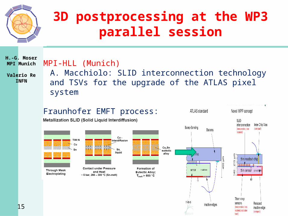
3D postprocessing at the WP3 parallel session
MPI-HLL (Munich) A. Macchiolo: SLID interconnection technology and TSVs for the upgrade of the ATLAS pixel system
Fraunhofer EMFT process:
H.-G. MoserMPI Munich
Valerio ReINFN
WP3 interaction with industry for 3D integration
We agreed to concentrate on one supplier for the 3D processing, which is quite expensive.
WP3 will organize a 1-day workshop with industries and research institutes which may provide 3D technology to our network.
This will be an opportunity to discuss with them and understand how they can meet our needs.
This will be the first step towards the choice of the 3D technology we will use for our demonstrator.
16
16 february 2011Gisèle Martin-Chassard - AIDA Kick off meeting 17
WP3-3 task (I)
Shareable IP blocks for HEP• Goal : provide 2 lots of IP blocks for the HEP needs with full
documentation and laboratory tests
• Lead institutions : CERN + LAL• Choose the best techno at best price (MPW center)• Gather the different designs • Send them to MPW center• Provide efficient interface between designers and MPW center• Centralize the documentation of blocks and test results• Organize users meeting
• Other participant labs : AGHT-UST, IRFU, LPNHE
• Associated labs : INFN-Mi, INFN-Pv, U Bonn, others ?
16 february 2011Gisèle Martin-Chassard - AIDA Kick off meeting 18
WP3-3 task (II)
• 1srt set of IP blocks (November 2012):– managed by CERN– Technology : DSM CMOS (mostly 130nm, 65nm could be supported
also); presentation by Marek Idzik (AGH-UST) on IBM 130nm blocks– electronics for trackers– Radiation hardness
• 2nd set of IP blocks (September 2014):– Managed by LAL – Technology : SiGe 130nm, 180nm or 350 nm ? (IBM, AMS …)– MPW center : depend on techno (CMP, MOSIS …)– Electronics for calorimeters and TPCs : high dynamic range, need of
precise capacitors and resistors, …
– Blocks (for both sets): low noise and fast amplifiers, fast ADCs, TDC (100ps), Bandgap, Rad-tol memory, PLL, SEU resistant flipflop, high speed LVDS, DC-DC …
H.-G. MoserMPI Munich
Valerio ReINFN
Conclusions
In this WP3 meeting, we made the first steps towards the technology choices that are needed to build our 3D demonstrator and to design IP blocks.
The 3D integration of devices in heterogeneous technology may open up various solutions (e.g. CMOSreadout + high res. sensor, analogCMOS + digitalCMOS, CMOSsensor + digitalCMOS).
We moved forward to create an effective network that will provide the community with know-how and access to 3D integration technologies for advanced pixel sensors, and to IP blocks for readout integrated circuits in a variety of detectors and applications.
19
Backup slides
V. Re
20
V. Re
21
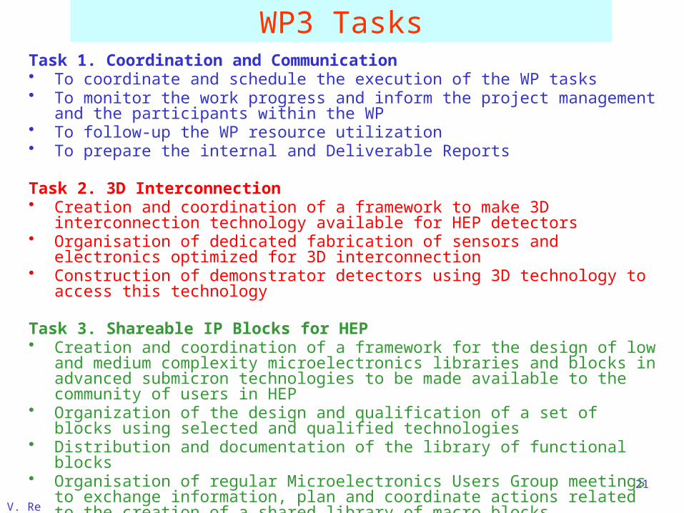
WP3 TasksTask 1. Coordination and Communication • To coordinate and schedule the execution of the WP tasks• To monitor the work progress and inform the project management and the
participants within the WP• To follow-up the WP resource utilization • To prepare the internal and Deliverable Reports
Task 2. 3D Interconnection • Creation and coordination of a framework to make 3D interconnection
technology available for HEP detectors• Organisation of dedicated fabrication of sensors and electronics optimized
for 3D interconnection• Construction of demonstrator detectors using 3D technology to access
this technology
Task 3. Shareable IP Blocks for HEP• Creation and coordination of a framework for the design of low and
medium complexity microelectronics libraries and blocks in advanced submicron technologies to be made available to the community of users in HEP
• Organization of the design and qualification of a set of blocks using selected and qualified technologies
• Distribution and documentation of the library of functional blocks• Organisation of regular Microelectronics Users Group meetings to
exchange information, plan and coordinate actions related to the creation of a shared library of macro blocks.