Embed Size (px)
Citation preview
1
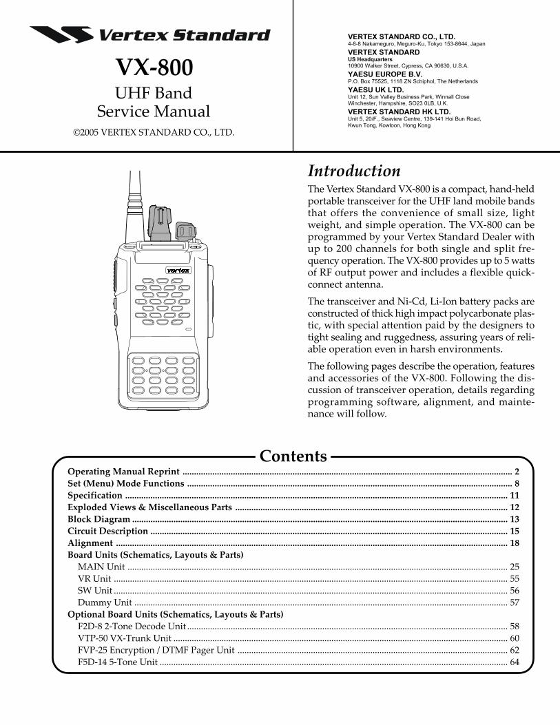
©2005 VERTEX STANDARD CO., LTD.
UHF BandService Manual
VX-800
IntroductionThe Vertex Standard VX-800 is a compact, hand-heldportable transceiver for the UHF land mobile bandsthat offers the convenience of small size, lightweight, and simple operation. The VX-800 can beprogrammed by your Vertex Standard Dealer withup to 200 channels for both single and split fre-quency operation. The VX-800 provides up to 5 wattsof RF output power and includes a flexible quick-connect antenna.
The transceiver and Ni-Cd, Li-Ion battery packs areconstructed of thick high impact polycarbonate plas-tic, with special attention paid by the designers totight sealing and ruggedness, assuring years of reli-able operation even in harsh environments.
The following pages describe the operation, featuresand accessories of the VX-800. Following the dis-cussion of transceiver operation, details regardingprogramming software, alignment, and mainte-nance will follow.
VERTEX STANDARD CO., LTD.4-8-8 Nakameguro, Meguro-Ku, Tokyo 153-8644, Japan
VERTEX STANDARDUS Headquarters10900 Walker Street, Cypress, CA 90630, U.S.A.
YAESU EUROPE B.V.P.O. Box 75525, 1118 ZN Schiphol, The Netherlands
YAESU UK LTD.Unit 12, Sun Valley Business Park, Winnall CloseWinchester, Hampshire, SO23 0LB, U.K.
VERTEX STANDARD HK LTD.Unit 5, 20/F., Seaview Centre, 139-141 Hoi Bun Road,Kwun Tong, Kowloon, Hong Kong
ContentsOperating Manual Reprint ................................................................................................................................................ 2Set (Menu) Mode Functions .............................................................................................................................................. 8Specification ....................................................................................................................................................................... 11Exploded Views & Miscellaneous Parts ....................................................................................................................... 12Block Diagram .................................................................................................................................................................... 13Circuit Description ............................................................................................................................................................ 15Alignment ........................................................................................................................................................................... 18Board Units (Schematics, Layouts & Parts)
MAIN Unit ...................................................................................................................................................................... 25VR Unit ............................................................................................................................................................................ 55SW Unit ............................................................................................................................................................................ 56Dummy Unit ................................................................................................................................................................... 57
Optional Board Units (Schematics, Layouts & Parts)F2D-8 2-Tone Decode Unit ............................................................................................................................................ 58VTP-50 VX-Trunk Unit .................................................................................................................................................. 60FVP-25 Encryption / DTMF Pager Unit ...................................................................................................................... 62F5D-14 5-Tone Unit ........................................................................................................................................................ 64
2
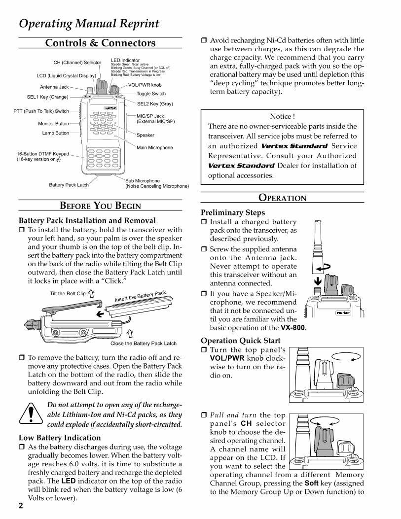
Operating Manual ReprintControls & Connectors
BEFORE YOU BEGIN
Battery Pack Installation and RemovalTo install the battery, hold the transceiver withyour left hand, so your palm is over the speakerand your thumb is on the top of the belt clip. In-sert the battery pack into the battery compartmenton the back of the radio while tilting the Belt Clipoutward, then close the Battery Pack Latch untilit locks in place with a “Click.”
To remove the battery, turn the radio off and re-move any protective cases. Open the Battery PackLatch on the bottom of the radio, then slide thebattery downward and out from the radio whileunfolding the Belt Clip.
Do not attempt to open any of the recharge-able Lithium-Ion and Ni-Cd packs, as theycould explode if accidentally short-circuited.
Low Battery IndicationAs the battery discharges during use, the voltagegradually becomes lower. When the battery volt-age reaches 6.0 volts, it is time to substitute afreshly charged battery and recharge the depletedpack. The LED indicator on the top of the radiowill blink red when the battery voltage is low (6Volts or lower).
OPERATION
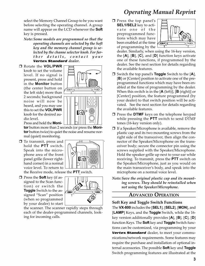
Preliminary StepsInstall a charged batterypack onto the transceiver, asdescribed previously.Screw the supplied antennaonto the Antenna jack.Never attempt to operatethis transceiver without anantenna connected.If you have a Speaker/Mi-crophone, we recommendthat it not be connected un-til you are familiar with thebasic operation of the VX-800.
Operation Quick StartTurn the top panel’sVOL/PWR knob clock-wise to turn on the ra-dio on.
Pull and turn the toppanel 's CH selectorknob to choose the de-sired operating channel.A channel name willappear on the LCD. Ifyou want to select theoperating channel from a different MemoryChannel Group, pressing the Soft key (assignedto the Memory Group Up or Down function) to
Avoid recharging Ni-Cd batteries often with littleuse between charges, as this can degrade thecharge capacity. We recommend that you carryan extra, fully-charged pack with you so the op-erational battery may be used until depletion (this“deep cycling” technique promotes better long-term battery capacity).
Notice !There are no owner-serviceable parts inside thetransceiver. All service jobs must be referred toan authorized ServiceRepresentative. Consult your Authorized
Dealer for installation ofoptional accessories.
3
Operating Manual Reprintselect the Memory Channel Group to be you wantbefore selecting the operating channel. A groupname will appear on the LCD whenever the Softkey is pressed.Note: Some models are programmed so that the
operating channels are selected by the Softkey and the memory channel group is se-lected by the channe selector knob. For fur-t h e r d e t a i l s , c o n t a c t y o u r
dealer.Rotate the VOL/PWRknob to set the volumelevel. If no signal ispresent, press and holdin the Monitor button(the center button onthe left side) more than2 seconds; backgroundnoise wi l l now beheard, and you may usethis to set the VOL/PWRknob for the desired au-dio level.Press and hold the Moni-tor button more than 2 seconds (or press the Moni-tor button twice) to quiet the noise and resume nor-mal (quiet) monitoring.To transmit, press andhold the PTT switch.Speak into the micro-phone area of the frontpanel grille (lower right-hand corner) in a normalvoice level. To return tothe Receive mode, release the PTT switch.Press the Soft key (if as-signed to the Scan func-t ion) or switch theToggle Switch to the as-signed “Scan” position(when so programmedby your dealer) to startthe scanner. The scanner rapidly steps througheach of the dealer-programmed channels, look-ing for incoming calls.
Press the top panel’sSEL1/SEL2 key to acti-v a t e o n e o f t h epreprogrammed func-tions which may havebeen enabled at the timeof programming by thedealer. Similarly, when using the 16-key version,the [A], [B], [C], and [D] function keys activateone of these functions, if programmed by thedealer. See the next section for details regardingthe available features.Switch the top panel’s Toggle Switch to the [A],[B] or [Center] position to activate one of the pre-programmed functions which may have been en-abled at the time of programming by the dealer.When this switch is in the [A (left)], [B (right)] or[Center] position, the feature programmed (byyour dealer) to that switch position will be acti-vated. See the next section for details regardingthe available features.Press the DTMF keys on the telephone keypadwhile pressing the PTT switch to send DTMFtones (16-key version only).If a Speaker/Microphone is available, remove theplastic cap and its two mounting screws from theright side of the transceiver, then align the con-nector of the Speaker/Microphone on the trans-ceiver body; secure the connector pin using thescrews supplied with the Speaker/Microphone.Hold the speaker grille up next to your ear whilereceiving. To transmit, press the PTT switch onthe Speaker/Microphone, just as you would onthe main transceiver’s body, and speak into themicrophone on a normal voice level.
Note: Save the original plastic cap and its mount-ing screws. They should be reinstalled whennot using the Speaker/Microphone.
ADVANCED OPERATION
Soft Key and Toggle Switch FunctionsThe VX-800 includes the [SEL1], [SEL2], [MON], and[LAMP] Keys, and the Toggle Switch, while the 16-key version additionally provides [A], [B], [C], [D]function Keys. The Soft key and Toggle Switch func-tions can be customized, via programming by your
dealer, to meet your commu-nications/network requirements. Some features mayrequire the purchase and installation of optional in-ternal accessories. The possible Soft key and ToggleSwitch programming features are illustrated at the
4
Operating Manual Reprintright, and their functions are explained on page 8.F o r f u r t h e r d e t a i l s , c o n t a c t y o u r
dealer. For future reference,check the box next to each function that has beenassigned to the Soft key and Toggle Switch on yourparticular radio, and keep it handy.
Description of Operating Functions
Channel ScanThe Scanning feature is used to monitor multiple signalsprogrammed into the transceiver. While scanning, the trans-ceiver will check each channel for the presence of a signal,and will stop on a channel if a signal is present.
One key or switch may be assigned to the Scan function, asfollows:
One of the Soft keys may be assigned for Scan opera-tion; orThe Toggle switch may have one position assigned tothe Scan function.
To activate scanning:Press the assigned Soft key, or set the Toggle switch tothe assigned position.The scanner will search the channels, looking for activeones; it will pause each time it finds a channel on whichsomeone is speaking.
To stop scanning:Press the assigned Soft key, or set the Toggle switch toa different position.Operation will revert to the channel to which the CHknob is set.
* requires DTMF/Encryption Unit
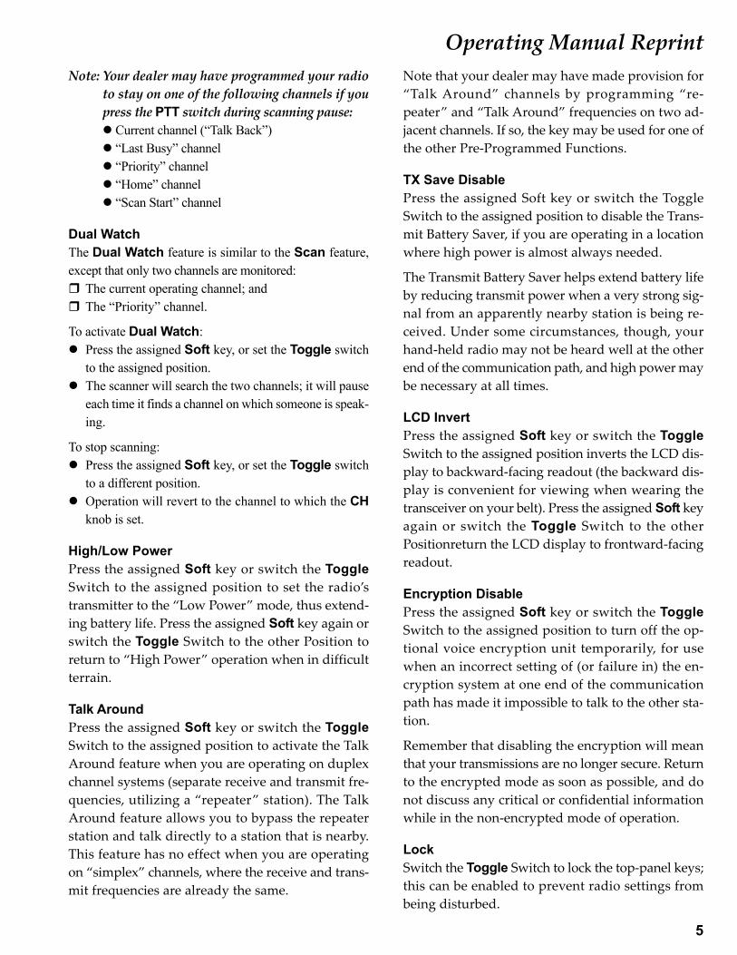
NoneChannel ScanDual WatchHigh/Low PowerTalk AroundTX Save DisableLCD InvertEncryption Disable*Follow-Me DWCall/Reset*Speed Dial*Emergency*Group UpGroup DownChannel UpChannel DownMonitorLamp
A B C DSoft Key
Functions
NoneChannel ScanDual WatchHigh/Low PowerTalk AroundTX Save DisableLCD InvertEncryption Disable*Follow-Me DWCall/Reset*Speed Dial*Emergency*Group UpGroup DownChannel UpChannel DownMonitorLamp
SEL2 MON LAMPSEL1Soft Key
Functions
Toggle Switch (Position)A B
NoneChannel ScanDual WatchHigh/Low PowerTalk AroundTX Save DisableLCD InvertEncryption Disable*LockFollow-Me Scan
Group recall Shortcut
Functions center
Group 1Group 2Group 3
Group 1Group 2Group 3
Group 1Group 2Group 3 * requires DTMF/Encryption Unit
* requires DTMF/Encryption Unit
5
Operating Manual ReprintNote: Your dealer may have programmed your radio
to stay on one of the following channels if youpress the PTT switch during scanning pause:
Current channel (“Talk Back”) “Last Busy” channel “Priority” channel “Home” channel “Scan Start” channel
Dual WatchThe Dual Watch feature is similar to the Scan feature,except that only two channels are monitored:
The current operating channel; andThe “Priority” channel.
To activate Dual Watch:Press the assigned Soft key, or set the Toggle switchto the assigned position.The scanner will search the two channels; it will pauseeach time it finds a channel on which someone is speak-ing.
To stop scanning:Press the assigned Soft key, or set the Toggle switchto a different position.Operation will revert to the channel to which the CHknob is set.
High/Low PowerPress the assigned Soft key or switch the ToggleSwitch to the assigned position to set the radio’stransmitter to the “Low Power” mode, thus extend-ing battery life. Press the assigned Soft key again orswitch the Toggle Switch to the other Position toreturn to “High Power” operation when in difficultterrain.
Talk AroundPress the assigned Soft key or switch the ToggleSwitch to the assigned position to activate the TalkAround feature when you are operating on duplexchannel systems (separate receive and transmit fre-quencies, utilizing a “repeater” station). The TalkAround feature allows you to bypass the repeaterstation and talk directly to a station that is nearby.This feature has no effect when you are operatingon “simplex” channels, where the receive and trans-mit frequencies are already the same.
Note that your dealer may have made provision for“Talk Around” channels by programming “re-peater” and “Talk Around” frequencies on two ad-jacent channels. If so, the key may be used for one ofthe other Pre-Programmed Functions.
TX Save DisablePress the assigned Soft key or switch the ToggleSwitch to the assigned position to disable the Trans-mit Battery Saver, if you are operating in a locationwhere high power is almost always needed.
The Transmit Battery Saver helps extend battery lifeby reducing transmit power when a very strong sig-nal from an apparently nearby station is being re-ceived. Under some circumstances, though, yourhand-held radio may not be heard well at the otherend of the communication path, and high power maybe necessary at all times.
LCD InvertPress the assigned Soft key or switch the ToggleSwitch to the assigned position inverts the LCD dis-play to backward-facing readout (the backward dis-play is convenient for viewing when wearing thetransceiver on your belt). Press the assigned Soft keyagain or switch the Toggle Switch to the otherPositionreturn the LCD display to frontward-facingreadout.
Encryption DisablePress the assigned Soft key or switch the ToggleSwitch to the assigned position to turn off the op-tional voice encryption unit temporarily, for usewhen an incorrect setting of (or failure in) the en-cryption system at one end of the communicationpath has made it impossible to talk to the other sta-tion.
Remember that disabling the encryption will meanthat your transmissions are no longer secure. Returnto the encrypted mode as soon as possible, and donot discuss any critical or confidential informationwhile in the non-encrypted mode of operation.
LockSwitch the Toggle Switch to lock the top-panel keys;this can be enabled to prevent radio settings frombeing disturbed.
6
Follow-Me Scan“Follow-Me” Scan feature checks a User-assignedPriority Channel regularly as you scan the otherchannels. Thus, if only Channels 1, 3, and 5 (of the 8available channels) are designated for “Scanning,”the user may nonetheless assign Channel 2 as the“User-assigned” Priority Channel via the “Follow-Me” feature.
To activate “Follow-Me” scanning, first select thechannel you want to designate as the “User-As-signed Priority Channel” and Switch the ToggleSwitch to the assigned position. Then turn the CHselector knob to the “Scanning Start” channel whichhas been programmed by your dealer to activate thescanner. When the scanner stops on an “Active”channel, the User-assigned Priority Channel willautomatically be checked every few seconds; if ac-tivity is found on the User-assigned Priority Chan-nel, the radio will switch between it and the Dealer-Assigned Priority Channel, if any.
Follow-Me DWTo set up a “Dual Watch” frequency pair using the“Follow-Me” feature, select a channel using the CHselector knob. Now press the assigned Soft key;pressing the assigned Soft key locks the currentchannel as the User-assigned Priority Channel. Nowrotate the CH selector knob to another channel (notthe “Scanning Start” channel). Your radio will nowswitch back-and-forth between the currently-se-lected channel (shown on the CH selector knob) andthe User-assigned Priority Channel.
During “Follow-Me” scanning (after you havepressed the key), you can set up the “Dual Watch”feature by rotating the CH selector knob to anotherchannel. The radio will then scan back and forthbetween the original User-assigned Priority Chan-nel and the newly-selected channel.
The Priority Channel you have assigned (beforepressing the key) will be retained in memory untilyou change it.
Channel Group SelectionThe VX-800 is capable of separating its 200 memorychannels into any of ten Groups. There is no limitas to the number of channels which may be assigned
Operating Manual Reprintto each Group. The Dealer will have made the Groupassignment at the time of channel programming. Atthe same time, one of the Soft Keys will be assignedas the Channel Group Selection key.
To change Channel Groups, press the assigned softkey to step through the available Groups. Once thedesired Group is reached, rotate the CH selectorknob to select the desired channel within the selectedGroup.
You may wish to have the Scanner (described previ-ously) pass through more than one Group duringthe scanning process (normally, scanning is per-formed within the current group only). To includethe current Group in the scanning loop, press andhold in the assigned Soft key for one second.
To remove a Group from Group Scan, press and holdin the assigned Soft key again for one second.
Multi-Group Scanning is only possible if you areusing the “User Scan” list.
The VX-800 has two scanning “lists:” the “DealerScan” list and the “User Scan” list. The “Dealer Scan”list is a fixed group of stations which will be includedwhen scanning is activated. The “User Scan” list is adifferent list, initially arranged by the Dealer, whichmay be modified by the User (if, for example, youwant to delete one or more of these channels fromthe scanning list).
To edit the User Scan list, press and hold the Softkey (assigned to the Group Up/Down function) todelete the current Memory Group from the Scan-ning. Alternatively, press and hold the “Scan” Softkey for one second to delete the Current Memorychannel from the Scanning.
When you delete a Group or channel, “-SKIP-” willappear on the LCD for one second after pressing theSoft key. To restore a particular channel to your scan-ning list, press and hold in the Soft key again forone second; “-STOP-” will appear on the LCD forone second after pressing the Soft key.
7
Operating Manual ReprintCall/ResetThis feature, if enabled, allows the user to changethe 3-digit Page Call code, used to call other simi-larly-equipped stations. Press the Dealer-assignedSoft key, followed by the three digits representingthe Page Call code of the station you wish to call.Three tones will be heard after the last key is pressed(the new code will now be transmitted).
The receiver squelch of the other station will beopened, and you can begin communication.
Speed DialYour Dealer may have pre-programmed Auto-Dialtelephone number memories into your radio.
To dial a number, press the numbered key corre-sponding to the Auto-Dial memory number list pro-vided by your Dealer while pressing the PTT switch.Once the telephone number has begun (you will hearthe tones in the speaker), you can release the PTTswitch.
EmergencyThe VX-800 includes an “Emergency” feature whichmay be useful if you have someone monitoring onthe same frequency as your transceiver’s channel.For further details contact your nearest dealer.
ARTS(AUTO RANGE TRANSPOND SYSTEM)
This system is designed to inform you when you andanother ARTS-equipped station are within commu-nication range.
During ARTS operation, your radio automaticallytransmits for about 1 second every 25 seconds (theinterval is programmed by the Dealer) in an attemptto shake hands with the other station.
If you move out of range for more than two min-utes, your radio senses that no signal has been re-ceived, a ringing beeper will sound, and "OUT OFSERVICE" will scroll on the LCD. If you subse-quently move back into range, as soon as the otherstation transmits, your beeper will sound, and "INSERVICE" will scroll on the LCD.
DTMF PAGING SYSTEM
This system allows paging and selective calling, us-ing DTMF tone sequences.
When your radio is paged by a station bearing a tonesequence which matches yours, your radio’s squelchwill open and the alert ringer will sound (unless youhave disabled it, as described previously).
The three-digit code of the station which paged youwill be displayed on your radio’s LCD.
ACCESSORIES & OPTIONS
FVP-25 Encryption/DTMF Pager UnitF2D-8 2-Tone Decode UnitFNB-V57 7.2 V 1100 mAh Ni-Cd BatteryFNB-V57IS Intrinsically-Safe 7.2 V 1100 mAh Ni-
Cd BatteryFNB-V62LI 7.4 V 1600 mAh Lithium-Ion BatteryFBA-25A Battery CaseVAC-800 Rapid Desktop Charger (for FNB-V57,
FNB-V57IS, FNB-V62LI)NC-77B 120 VAC Compact Wall Charger for
FNB-V57/-V57ISNC-77C 230-240 VAC Compact Wall Charger
for FNB-V57/-V57ISNC-77F 220 VAC Compact Wall Charger for
FNB-V57/-V57ISNC-77U 230 VAC Compact Wall Charger for
FNB-V57/-V57ISVTP-50 VX-Trunk UnitMH-50A7A Speaker/MicrophoneCT-70 CT-29 to Radio Programming CableCT-71 PC Programming CableCT-72 Radio to Radio Programming CableATU-6C 440~470 MHz AntennaATU-6D 450-485 MHz Antenna
Availability of accessories may vary; some accessories aresupplied as standard per local requirements, others maybe unavailable in some reqions. Check with your VertexStandard Dealer for changes to the above list.
8
One or more of the radio’s "Soft Keys" may be en-abled for a function associated with the "Set" (Menu)mode. This feature, when activated, allows the userto customize certain performance aspects of the VX-800. Note that some of these items may also appearas available "Soft Keys," described below.
The operating procedure for the Menu mode is quitesimple, requiring only a few easily- rememberedactions on the user’s part.
The VX-800 Soft Keys include the [SEL1], [SEL2],[MON], and [LAMP] Keys, plus the [A], [B], [C], and[D] keys on the 16-key version. The Soft Key func-tions can be assigned either as a "Menu" function oran "operating" function at the time of programming.
Basic Menu Mode Operation1. Press the appropriate Soft Key to activate a Menu
function. The available keys include the [SEL1],[SEL2], [MON], and [LAMP] Keys, plus the [A],[B], [C], and [D] keys on the 16-key version.
2. Rotate the top panel’s CH selector knob to selectthe feature you wish to view and/or modify.
3. Press the [SEL1] and/or [SEL2] keys to modify oradjust the current setting of this Menu item ("On"to "Off," etc.)
4. Rotate the CH selector to save the new setting.5. Press the PTT switch to exit the Set (Menu) mode.
Available Soft Key Menu FunctionsNo.1 SQL (Squelch Level)After selecting this Menu, press the [SEL1] or[SEL2] key to find the point where the backgroundnoise is just silenced. This is the point of best re-ceiver sensitivity consistent with quiet monitoring.The scale for the Squelch Level adjustment is 0 ~ 11and 12 (RSSI SQL), The default value is 8.When the Squelch Level set to "12" activates the RSSI(Received Signal Strength Indicator) Squelch feature,which allows you to set the squelch so that only sig-nals exceeding a prescribed RX signal input levelwill open the squelch. The RX signal input level isdetermined via the Alignment Program SVC31. Seepage 20 for details regarding the RSSI level setting.
No.2 LIST (Scanning List)The VX-800 has two scanning "list:" the "Dealer Scan"list and the "User Scan" list. The "Dealer scan" list isa fixed group of stations which will be includedwhen scanning is activated. The "User Scan" list is adifferent list, initially arranged by the dealer, by theUser.
This Menu Item allows you to select the scanninglist "Dealer Scan" or "User Scan".
After selecting this Menu, press the [SEL1] or [SEL2]key to select the Scan List in which you wish to scan("LIST DLR: Dealer List" or "LIST USR: User List").Rotate the CH selector knob to save the new setting,then press the PTT switch to exit the Set (Menu)mode.
No.3 BEEP (Keypad Beeper On/Off)After selecting this Menu, press the [SEL1] or [SEL2]key to enable (ON) or disable (OFF) the keypad beeptones. Rotate the CH selector knob to save the newsetting, then press the PTT switch to exit the Set(Menu) mode.
No.4 BELL (CTCSS/DCS/Paging Alert Bell On/Off)After selecting this Menu, press the [SEL1] or [SEL2]key to enable (ON) or disable (OFF) the alert bellwhich sounds when your radio is called using ei-ther CTCSS or DCS calling tones. Rotate the CH se-lector knob to save the new setting, then press thePTT switch to exit the Set (Menu) mode.
No.5 LGT (TX/BUSY LED On/Off)After selecting this Menu, press the [SEL1] or [SEL2]key to enable (ON) or disable (OFF) the LED whichserves as the Busy Channel and Transmitter On in-dicator. Turning this LED off will extend battery lifesomewhat. Rotate the CH selector knob to save thenew setting, then press the PTT switch to exit theSet (Menu) mode.
No.6 LOCK (Keypad, PTT, or Knob Disabling)In some situations, you may wish to disable the key-pad's keys, the CH selector knob, and/or the PTTswitch (so as to prevent transmission by unautho-rized users of the radio). LOCK Menu determineswhich features will be disabled when the LOCKfunction is engaged.
Set (Menu) Mode Functions
9
After selecting this Menu, press the [SEL1] or [SEL2]key to select "P" (PTT Lock), "D" (Dial-Knob-Lock),"K" (Keypad Lock), or various combinations of these.Rotate the CH selector knob to save the new setting,then press the PTT switch to exit the Set (Menu)mode.
No.7 GROUP (Group Select)This Menu Item allows you to change ChannelGroups, in the event that a Soft Key has not beendesignated for this purpose. After selecting thisMenu, press the [SEL1] or [SEL2] key to select theChannel Group in which you wish to operate. Ro-tate the CH selector knob to save the new setting,then press the PTT switch to exit the Set (Menu)mode.
No.8 SCAN (Scan Mode On/Off)This Menu Item allows you to start the scanner, inthe event that a Soft Key has not been designatedfor this purpose.After selecting this Menu, press the [SEL1] or [SEL2]key to start ("SCAN ON") or stop ("SCAN OFF") thescanner. Rotate the CH selector knob to save the newsetting, then press the PTT switch to exit the Set(Menu) mode.
No.9 DW (Dual Watch On/Off)This Menu Item allows you to activate the DualWatch feature, in the event that a Soft Key has notbeen designated for this purpose.After selecting this Menu, press the [SEL1] or [SEL2]key to enable ("DW ON") or disable ("DW OFF") theDual Watch feature. Rotate the CH selector knob tosave the new setting, then press the PTT switch toexit the Set (Menu) mode.
No.10 TA (Talk Around)This Menu Item allows you to activate the TalkAround feature, in the event that a Soft Key has notbeen designated for this purpose.After selecting this Menu, press the [SEL1] or [SEL2]key to enable ("TA ON") or disable ("TA OFF") theTalk Around feature. Rotate the CH selector knob tosave the new setting, then press the PTT switch toexit the Set (Menu) mode.
No.11 ENCR (Encryption)On channels where scrambling is used, an incorrectsetting of (or failure in) the encryption system at oneend of the communication path will make it impos-sible to talk to the other station. To change the cur-rent status of encryption on your radio, after select-ing this Menu, press the [SEL1] or [SEL2] key toenable (ENCR EN) or disable (ENCR DI) encryption.Rotate the CH selector knob to save the new setting,then press the PTT switch to exit the Set (Menu)mode.Remember that disabling encryption will mean thatyour transmissions are no longer secure.
Return to the encrypted mode as soon as possible, and donot discuss any critical or confidential information whilein the non- encrypted mode of operation.
No.12 AF VRThis Menu Item determine the audio volume levelwhere the top panel's VOL knob is set to fully coun-terclockwise position (but not into the click stop).
After selecting this Menu, press the [SEL1] or [SEL2]key to select the desired volume level. Rotate theCH selector knob to save the new setting, then pressthe PTT switch to exit the Set (Menu) mode.
No.13 BP VR (Beep VR)This Menu Item determine the beep volume level.
After selecting this Menu, press the [SEL1] or [SEL2]key to select the desired level. Rotate the CH selec-tor knob to save the new setting, then press the PTTswitch to exit the Set (Menu) mode.
Set (Menu) Mode Functions

10
Set (Menu) Mode FunctionsNote:
11
SpecificationsGENERALFrequency Range: 400-430 MHz (Ver A), 440-470 MHz (Ver CS), 450-490 MHz (Ver D)Number of Channels: 200 channelsChannel Spacing: 12.5/25 kHzBattery Voltage: 7.4 VDCTemperature Range: –22 °F to 140 °F (–30 °C to +60 °C)Frequency Stability: better than ±2.5 ppmCase Size (WHD): 2.3" x 4.3" x 1.1" (58 x 110 x 28.9 mm) w/FNB-V62LIWeight (approx.): 10.6 oz (300 grams) with FNB-V62LI, antenna, belt clip
RECEIVERCircuit Type: Double-conversion superheterodyneIFs: 44.25 MHz & 450 kHz12-dB SINAD Sensitivity: < 0.25 µVSquelch Sensitivity: < 0.25 µVSelectivity: > 75 dB (25 kHz)/> 68 dB (12.5 kHz)Intermodulation: > 75 dB (25 kHz)/> 65 dB (12.5 kHz)Spurious Rejection: > 75 dBAF Output: 0.5 W @ 16 Ω, 3% THD (BTL output)
TRANSMITTERPower Output: 5.0/2.5/1.0/0.25 W (Selectable)Modulation System: Direct FMMaximum Deviation: ±5 kHz (25 kHz)/±2.5 kHz (12.5 kHz)FM Noise: > 45 dB (25 kHz)/> 40 dB (12.5 kHz)Spurious Emission: > 70 dB below carrierAF Distortion (@ 1 kHz): < 3 %Microphone Type: 2-k Ω condenser
Specifications are subject to change without notice or obligation.
12
Exploded View & Miscellaneous Parts
MAIN UNIT
RA0123500LATCH NAIL
RA0215000EXT CAP
M4090141SPEAKER
RA010300A (Lot. 1-19)RA010300B (Lot. 20-)KNOB
RA0228800KNOB
RA0206300 (Lot. 1-3)RA0229300 (Lot. 4-)RUBBER PACKING
CS1674001REAR CASE ASS'Y(with ANT CONNECTOR (SMA))
RA008920A (Lot. 1-16)RA008920B (Lot. 17, 20-)RA0389100 (Lot. 18-19)O RING
RA0111500SPECIAL NUT
RA0112300COIL SPRING
RA0111400RING NUT
CP6570001BELT CLIP ASS'Y
RA0207100 (Lot. 1-7)RA020710A (Lot. 8-)TERMINAL PLATE (+)
RA0207200TERMINAL PLATE (−)
RA0205800 (Lot. 1-5)RA020580A (Lot. 6-15)RA020580B (Lot. 16-)FRONT CASE ASS'Y
Non-designated parts are available only aspart of a designated assembly.
RA0205600 (Lot. 1-4)RA020560A (Lot. 5-15)RA020560B (Lot. 16-)FRONT CASE ASS'Y(16KEY)
VR UNIT
RA0206600KNOB (Orange:Antenna side)
RA0206900O RING
RA0207400INTER CONNECTOR
RA0207500INTER CONNECTORRA0207600INTER CONNECTOR
RA0207900 (Lot. 1-7)RA020790A (Lot. 8-)HOLDER RUBBER
RA0206400LCD HOLDER
RA0206800HOLDER PLATE
G6090136LCD
RA0206200LIGHT GUIDE
RA0088900 (Lot. 1-5)RA008890A (Lot. 6-)O RING
DUMMY UNIT
RA0207000COIL SPRING
RA0215400SHEET
RA0217300MYLAR SHEETRA0217400
REFLECTOR SHEET
RA0228300KNOB (Gray:Toggle Switch side)
RA0173700RUBBER KNOB (16KEY)
1212
U9900094 TAPTITE SCREW M2X5NI#2 2U9900069 TAPTITE SCREW M2X9.5NI#2 3U9900092 PAN HEAD SCREW M1.7X14AU#2 1
U9900093 TAPTITE SCREW M1.7X5NI#2 (Lot. 1) 3TAPTITE SCREW M1.7X4NI#2GUIDE (Lot. 2-)U9900084 BINDING HEAD SCREW M2X7.5B 1U9900063 TAPTITE SCREW 2X3.3NI 2U20305007 BINDING HEAD SCREW M3X5B 2U9900068 TAPTITE SCREW M2X4NI#3 3U9900086 TAPTITE SCREW M1.7X2.5B 2U07230107 PAN HEAD SCREW M2X3B #1 3U07225102 PAN HEAD SCREW M2X2.5NI #1 1U02206007 SEMS SCREW SM2.6X6B 2
11
12
REF. VXSTD P/N Description Qty.
RA0229000 (Lot. 1)RA0239100 (Lot. 2-)INTER CONNECTOR
P1091084 (Lot. 1-4)P1091084A (Lot. 5-)CONNECTOR
RA020830ADOUBLE FACE
RA0236000 (Lot. 1-4)SPACER (EXT)
RA0210300RUBBER KNOBRA0207800HOLDER RUBBER
11
13
Block Diagram

14
Note:
Block Diagram
15
Circuit DescriptionOverviewThe VX-800U is a UHF/FM hand-held transceiverdesigned to operate in the frequency range of 400 to512MHz.
Circuit Configuration by FrequencyThe receiver is a double-conversion superhetero-dyne with a first intermediate frequency (IF) of 44.25MHz and a second IF of 450 kHz.
Incoming signals from the antenna are mixed withthe local signal from the PLL to produce the first IFof 44.25 MHz. The first IF signal is subsequentlymixed with the 43.8 MHz second local oscillatoroutput (from the 14.6MHz reference crystal) to pro-duce the 450 kHz second IF. The second IF is thendemodulated to produce audio output.
The transmit signal frequency is generated by thePLL VCO, and is modulated by the signal from themicrophone. It is then amplified and sent to the an-tenna.
Receive Signal PathFront-end RF amplifierIncoming RF energy from the antenna jack is deliv-ered to the RF Unit and passes through a low-passfilter and high-pass filter consisting of coils L1004,L1005, L1006, L1030, L1001, L1028, L1029, L1002, andL1003, capacitors C1013, C1014, C1015, C1017, C1019,C1020, C1282, C1001, C1005, C1006, C1283, C1007,C1008, and C1009, and antenna switching diodeD1020 (HVU131).
Signals within the frequency range of the transceiverare then amplified by Q1001 (2SC5226) and enter avaractor-tuned band-pass filter consisting of coilsL1008, L1010, and L1011, capacitors C1041, C1042,C1044, C1045, C1046, C1047, C1068, C1069, C1070,C1071, C1072, C1073, C1074, and C1174, and diodesD1018, D1023, and D1024 (all HVC350) before de-livery to the first mixer.
First MixerBuffered output from the VCO is amplified by Q1030(2SC5226) to provide a pure first local signal be-tween 355.75 and 467 MHz for injection to the firstmixer D1030 (GN2011-Q:Lot. 1~50, SPM5001:Lot.51~). The 44.25 MHz first IF product then passesthrough monolithic crystal filters XF1001 and XF1002
(44-11BF-P2, ±5.5 kHz BW) to strip away unwantedmixer products.
IF amplifierThe first IF signal is amplified by Q1037(2SC4215Y:Lot. 1~3, 2SC5226:Lot. 4~).
The amplified first IF signal is then applied to FM IFsubsystem IC Q1046 (TA31136FN) which containsthe second mixer, second local oscillator, limiter am-plifier, noise amplifier, and S-meter amplifier.
A second local signal is generated by Q1022(NJM2902V) using the 14.6 MHz crystal (X1002) asa reference, producing a 43.8 MHz signal; this yieldsa 450 kHz second IF when mixed with the first IFsignal within Q1046.
The second IF then passes through the ceramic fil-t e r C F 1 0 0 1 ( P B F C 4 5 0 R 1 5 D : L o t . 1 ~ 3 9 ,E L F Y 4 5 0 E : L o t . 4 0 ~ ) o r C F 1 0 0 2(SFPCA450KG1A:Lot. 1~50, ELFC450G:Lot. 51~:“Narrow” channels) to strip away all but the desiredsignal, and is applied to the limiter amplifier inQ1046, which removes amplitude variations in the450 kHz IF, before detection of the speech by the ce-r a m i c d i s c r i m i n a t o r C D 1 0 0 1(CDBCB450KCAY24:Lot. 1~50, ECDA450C24:Lot.51~).
Audio amplifierDetected audio from Q1046 is applied to Q1028(AK2345) and an audio low-pass filter, and then fedpast the volume control (Q1025: M62364FP) to theaudio amplifier Q1017 (TDA2822D : externalspeaker) or Q1063 (TDA2822D: internal speaker),providing up to 0.5 Watts of audio to the optionalheadphone jack or 16-Ohm loudspeaker.
Attention: Audio output is BTL output.
Squelch ControlThe squelch circuitry consists of a noise amplifierand band-pass filter within Q1046, and noise detec-tor D1053 (DA221).
When no carrier received, noise at the output of thedetector stage in Q1046 is amplified and band-passfiltered by the noise amplifier section of Q1046 andthe network between pins 7 and 8, and then recti-fied by D1053.
16
Circuit DescriptionThe resulting DC squelch control voltage is passedto pin 19 of the microprocessor Q1048. If no carrieris received, this signal causes pin 32 of Q1048 to golow and pin 89 to go high. Pin 32 signals Q1008(CPH6102), Q1064 and Q1065 (both UMC5N) to dis-able the supply voltage to the audio amplifier Q1017and Q1063, while pin 89 makes Q1014 (UMG2N) holdthe green (Busy) half of the LED off.
Thus, the microprocessor blocks output from theaudio amplifier, and silences the receiver while nosignal is being received, and during transmission.
When a carrier appears at the discriminator, noiseis removed from the output, causing pin 19 of Q1048to go low and the microprocessor to activate the BusyLED via Q1048.
The microprocessor then checks for DTMF or CTCSSor CDCSS code squelch information, if enabled, re-spectively. If not transmitting and CTCSS or CDCSSis not activated, or if the received tone or codematches that programmed, the microprocessor stopsscanning, if active, and allows audio to pass throughthe audio amplifier (Q1017 or Q1063) to the loud-speaker by enabling the supply voltage to it viaQ1008, Q1064, and Q1065.
Transmit Signal PathMicrophone amplifierSpeech input from the microphone is amplified inQ1022 (NJM2902V), then filtered and sent to Q1025(M62364FP), then on to the Dummy Unit (or anOptional Unit). The audio which is returned fromthe Dummy Unit passes through Q1028 (AK2345)to be pre-emphasized.
The processed audio is then mixed with a CTCSStone generated by Q1028 (AK2345) and deliveredto D1035 (HVU350) for frequency modulating thePLL carrier up to ±5kHz from the unmodulated car-rier at the transmitting frequency.
If an external microphone is used, PTT switching iscontrolled by Q1007 (UMZ2N), which signals themicroprocessor when the impedance at the micro-phone jack drops.
If a CDCSS code is enabled for transmission, the codeis generated by microprocessor Q1048 and deliveredto D1055 (HVC350) for CDCSS modulating.
If DTMF is enabled for transmission, the tone is gen-erated by the microprocessor Q1048 and applied tothe splatter filter section in place of speech audio.Also, the tone is amplified for monitoring in theloudspeaker.
Noise canceling microphone circuitThe two signals from internal microphone (main andsub) are injected to the positive input (sub) and tothe negative input (main) of Q1022 (NJM2902V). Ifthe same signal is injected to both the main and subports, the main signal is canceled at the output (pin7 of Q1022). In other words, noise from nearbysources not directly connected to the transceiver en-ters the main and sub input at the same signal leveland is therefore canceled out.
When a signal is only injected to the “main” portand there is no signal at sub, the main signal is al-lowed to flow, as is, from Q1022.
Driver and Final AmplifiersThe modulated signal from the VCO Q1039(2SC4227) is buffered by Q1034 (2SC5226-4/5) andamplified by Q1030 (2SC5226-4/5) and Q1060(2SC3356-R25). The low-level transmit signal is thenapplied to the Power Module Q1019 (M68732HA-22) for final amplification up to 5 watts output power.
The transmit signal then passes through the antennaswitch D1020 (HVU131) and is low-pass filtered tosuppress away harmonic spurious radiation beforedelivery to the antenna.
Automatic Transmit Power ControlRF power output from the final amplifier is sampledby C1016 and C1018, and is rectified by D1019(RB715F). The resulting DC voltage is fed backthrough Q1018 (NJM2902V) to the Power Module,providing control of the power output.
The microprocessor selects either “High” or one ofthree “Low” power levels.
Transmit InhibitWhen the transmit PLL is unlocked, pin 18 of PLLchip Q1054 goes to a logic low. The resulting DCunlock control voltage is passed to pin 20 of the mi-croprocessor Q1048. While the transmit PLL is un-locked, pin 85 of Q1048 remains low, which thenturns off the Automatic Power Controller Q1010
17
(UMC5N) and Q1018 to disable the supply voltageto the Power Module Q1019, thus disabling the trans-mitter.
Spurious SuppressionGeneration of spurious products by the transmitteris minimized by the fundamental carrier frequencybeing equal to final transmitting frequency, modu-lated directly in the transmit VCO. Additional har-monic suppression is provided by a low-pass filterconsisting of L1004, L1005, and, L1006 and C1013,C1014, C1015, C1017, C1019, and C1020, resultingin more than 60 dB of harmonic suppression priorto delivery of the RF signal to the antenna.
PLL Frequency SynthesizerThe PLL frequency synthesizer consists of the VCO(Q1033 2SK508-K52: RX and Q1039 2SC4227: TX),VCO buffers Q1034 (2SC5226-4/5), Q1041(2SC5226-4/5), Q1030 (2SC5226-4/5), PLL sub-system IC Q1054 (SA7025DK) and 14.6MHz refer-ence crystal X1002.
The frequency stability is ±2.5 ppm within the tem-perature range of –22°F to +140°F (–30°C to +60°C).
The output of the 14.6 MHz reference is applied topin 8 of the PLL IC. While receiving, VCO Q1033oscillates between 355.75 and 467.75 MHz accord-ing to the transceiver version and the programmedreceiving frequency. The VCO generates this 355.75to 467.75 MHz frequency for provision of the firstlocal signal. While transmitting, the VCO generatesa signal at 400 to 512 MHz.
The output of the VCO is amplified by Q1041 androuted to the pin 5 of the PLL IC. The output of theVCO is also amplified by Q1030 and routed to thefirst local or Power Module according to D1031.
The PLL IC consists of a prescaler, fractional divider,reference divider, phase comparator, and chargepump. This PLL IC is a fractional-N type synthesizerand operates using a 40, 50, or 60 kHz reference sig-nal which is the eighth harmonic of the channel step(5, 6.25 or 7.5 kHz). The input signal from pins 5 and8 of the PLL IC is divided down to 40/50/60 kHz andcompared at the phase comparator. The pulsed out-put signal of the phase comparator is applied to thecharge pump and transformed into a DC signal inthe loop filter. The DC signal is applied to the pin 1of the VCO and locked to keep the VCO frequencyconstant.
PLL data is put out from “DTA” (pin 100), “CLK”(pin 2) and “PSTB” (pin 98) of the microprocessorQ1048. The data are passed to the PLL IC when thechannel is changed or when transmission is switchedto reception (and vice versa). The “PLL lock” condi-tion is always monitored by pin 20 of Q1048. Whenthe PLL is unlocked, the “UL” line goes low.
Miscellaneous CircuitsPush-To-Talk Transmit ActivationThe PTT switch on the microphone is connected topin 36 of microprocessor Q1048, so that when thePTT switch is closed, pin 85 of Q1048 goes high. Thissignals the microprocessor to activate the TX/RX con-troller Q1004 (UMG2N), which then disables the re-ceiver by disabling the 5V supply bus at Q1011(UN911F) to the front-end, FM IF subsystem ICQ1046, and receiver VCO circuitry.
At the same time, Q1003 (XP1501) and Q1002(CPH6102) activate the TX 5V supply line to enablethe transmitter.
Circuit Description
18
AlignmentIntroductionThe VX-800 is carefully aligned at the factory for thespecified performance across the frequency rangespecified for each version. Realignment shouldtherefore not be necessary except in the event of acomponent failure, or when altering the versiontype. All component replacement and service shouldbe performed only by an authorized Vertex Stan-dard representative, or the warranty policy may bevoid.
The following procedures cover the sometimes criti-cal and tedious adjustments that are not normallyrequired once the transceiver has left the factory.However, if damage occurs and some parts subse-quently are placed, realignment may be required. Ifa sudden problem occurs during normal operation,it is likely due to component failure; realignmentshould not be done until after the faulty componenthas been replaced.
We recommend that servicing be performed onlyby authorized Vertex Standard service technicianswho are experienced with the circuitry and fullyequipped for repair and alignment. Those who doundertake any of the following alignments are cau-tioned to proceed at their own risk. Problems causedby unauthorized attempts at realignment are notcovered by the warranty policy. Also, Vertex Stan-dard reserves the right to change circuits and align-ment procedures, in the interest of improved per-formance, without notifying owners.
Under no circumstances should any alignment beattempted unless the normal function and opera-tion of the transceiver are clearly understood, thecause of the malfunction has been clearly pinpointedand any faulty components replaced, and realign-ment determined to be absolutely necessary.
Do not attempt to perform only a single step unlessit is clearly isolated electrically from all other steps.Have all test equipment ready before beginning, andfollow all of the steps in a section in the order pre-sented.
The following test equipment (and thorough famil-iarity with its correct use) is necessary for completerealignment. Correction of problems caused by mis-alignment resulting from use of improper test equip-
ment is not covered under the warranty policy. Whilemost steps do not require all of the equipment listed,the interactions of some adjustments may requirethat more complex adjustments be performed after-wards.
Required Test EquipmentRF Signal Generator with calibrated output levelat 1000 MHzDeviation Meter (linear detector)In-line Wattmeter with 5% accuracy at 1000 MHz50-Ω RF Dummy Load with power rating 10W at1000 MHz16-Ω AF Dummy Load(Attention : Audio output is BTL output; do not
short "shield" to ground!)Regulated DC Power Supply (standard 7.5V DC,3A)Frequency Counter with 0.2 ppm accuracy at 1000MHzAC VoltmeterDC VoltmeterVHF Sampling CouplerIBM PC / compatible Computer with MicrosoftDOS v3.0 or later operating systemVertex Standard CT-71 Connection Cable andSVC31 Alignment program
Alignment Preparation and PrecautionsA 50-Ω RF Dummy Load and in-line wattmeter mustbe connected to the main antenna jack in all proce-dures that call for transmission, except where speci-fied otherwise. Correct alignment is not possiblewith an antenna.
After completing one step, read the following stepto determine whether the same test equipment willbe required. If not, remove the test equipment (ex-cept dummy load and wattmeter, in connected) be-fore proceeding.
Correct alignment requires that the ambient tem-perature be the same as that of the transceiver andtest equipment, and that this temperature be heldconstant between 68 °F ~ 86 °F (20°C and 30°C).When the transceiver is brought into the shop fromhot or cold air, it should be allowed time to come toroom temperature before alignment.
19
AlignmentWhenever possible, alignments should be made withoscillator shields and circuit boards firmly affixedin place. Also, the test equipment must be thor-oughly warmed up before beginning.
Note: Signal levels in dB referred to in the alignmentprocedure are based on 0 dBµ EMF = 0.5 µV (closed cir-cuit).
When connecting the CT-71 plug into the MIC/SP jack of the VX-800, you must remove theplastic cap and its mounting screws prior toprogramming. Please remember to re-attachthe cap and screws when the programming iscomplete.
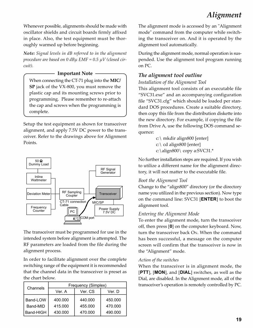
Setup the test equipment as shown for transceiveralignment, and apply 7.5V DC power to the trans-ceiver. Refer to the drawings above for AlignmentPoints.
The alignment mode is accessed by an "Alignmentmode" command from the computer while switch-ing the transceiver on. And it is operated by thealignment tool automatically.
During the alignment mode, normal operation is sus-pended. Use the alignment tool program runningon PC.
The alignment tool outlineInstallation of the Alignment ToolThis alignment tool consists of an executable file“SVC31.exe” and an accompanying configurationfile “SVC31.cfg” which should be loaded per stan-dard DOS procedures. Create a suitable directory,then copy this file from the distribution diskette intothe new directory. For example, if copying the filefrom Drive A, use the following DOS command se-quence:
c:\ mkdir align800 [enter]c:\ cd align800 [enter]c:\align800\ copy a:SVC31.*
No further installation steps are required. If you wishto utilize a different name for the alignment direc-tory, it will not matter to the executable file.
Boot the Alignment ToolChange to the “align800” directory (or the directoryname you utilized in the previous section). Now typeon the command line: SVC31 [ENTER] to boot thealignment tool.
Entering the Alignment ModeTo enter the alignment mode, turn the transceiveroff, then press [0] on the computer keyboard. Now,turn the transceiver back ON. When the commandhas been successful, a message on the computerscreen will confirm that the transceiver is now inthe “Alignment” mode.
Action of the switchesWhen the transceiver is in alignment mode, the[PTT], [MON], and [DIAL] switches, as well as theDial, are disabled. In the Alignment mode, all of thetransceiver’s operation is remotely controlled by PC.
Important Note
The transceiver must be programmed for use in theintended system before alignment is attempted. TheRF parameters are loaded from the file during thealignment process.
In order to facilitate alignment over the completeswitching range of the equipment it is recommendedthat the channel data in the transceiver is preset asthe chart below.
50 ΩΩΩΩΩDummy Load
InlineWattmeter
Deviation Meter
FrequencyCounter
RF SamplingCoupler
RF SignalGenerator
Transceiver
Power Supply7.5V DC
CT-71 connectionCable
PC
MIC/SP
COM port
ChannelsFrequency (Simplex)
Ver. A Ver. CS Ver. D
Band-LOWBand-MID
Band-HIGH
400.000 440.000 450.000415.000 455.000 470.000430.000 470.000 490.000
20
AlignmentAlignment SequenceAlthough the data displayed on the computer’sscreen during alignment is temporary data, it is im-portant that you follow the basic alignment sequenceprecisely, so that the displayed data and the dataloaded into the transceiver are identical.
Basic Alignment Sequence1. Enter the alignment mode2. Upload data from transceiver3. Align data4. Download data to transceiver
Alignment Tool MenuCommon DataThe parameters in this section represent "common"data for all channels. Once these "Common Data"parameters are correctly aligned, the "TX POWER,""MAX DEV," and "SUB AUDIO DEV," can be trimmed foreach channel, if needed.
During alignment, each parameter is adjusted for ahigher or lower value via the computer’s [ ] and[ ] keys. When the desired value is reached, type[ENTER] to lock in the new value.
(0) Common Tx :The first alignment section adjusts transmit-modeparameters which are common to all channels.
- [0] FREQUENCY
This parameter is used to adjust the PLL refer-ence frequency. From the "(0) Common Tx" sec-tion, press [0] to activate this alignment section.
• Press the [space] key on the keyboard to acti-vate the transmitter.
• Press the [ ] or [ ] key, as need, so the counterfrequency is with in 100 Hz of the channel cen-ter frequency for the MID channel.
• When the frequency is attained, press [ENTER]to lock in the new data.
• Now verify that the HIGH and LOW channelsare also with in tolerance.
- [1] HIGH
This parameter is used to align Tx High power(5W). From the "(0) Common Tx" section, press[1] to activate this alignment section.
• Use the [ ] or [ ] key to select the "MID" fre-
quency channel in the alignment range.• Press the [space] key on the keyboard to acti-
vate the transmitter.• Press the [ ] or [ ] key, as need, to set the
power output to 5.1 W ±0.1 W, as indicated onthe external wattmeter.
• When the 5 Watt level is attained, press [EN-TER] to lock in the new data.
- [2] L3This parameter aligns the L3 power (2.5 W) lev-el. From the "(0) Common Tx" section, press [4]to activate this alignment section.
• Press the [space] key on the keyboard to acti-vate the transmitter.
• Press the [ ] or [ ] key, as needed, to set thepower output to 2.5 W ± 0.2 W, as indicated onthe external wattmeter.
• When the 2.5 W level is attained, press [EN-TER] to lock in the new data.
- [3] L2This parameter aligns the L2 power (1 W) level.From the "(0) Common Tx" section, press [3] toactivate this alignment section.
• Press the [space] key on the keyboard to acti-vate the transmitter.
• Press the [ ] or [ ] key, as needed, to set thepower output to 1 W ± 0.2 W, as indicated onthe external wattmeter.
• When the 1 Watt level is attained, press [EN-TER] to lock in the new data.
- [4] L1This parameter aligns the L1 power (0.25 W) lev-el. From the "(0) Common Tx" section, press [2]to activate this alignment section.
• Press the [space] key on the keyboard to acti-vate the transmitter.
• Press the [ ] or [ ] key, as needed, to set thepower output to 0.25 W ± 0.04 W, as indicatedon the external wattmeter.
• When the 0.25 W level is attained, press [EN-TER] to lock in the new data.
21
Alignment- [5] MAXIMUM DEVIATION
This section adjusts the transmitter’s voice devi-ation level. From the “(0) Common Tx” section,select [5] to enter this section.
• Use the [ ] or [ ] key to select the "MID" fre-quency channel in the alignment range.
• Disable any subaudible tone signalling on thischannel, if present.
• Press the [space] key on the computer key-board to start alignment. This activates the trans-mitter, and injects a 1 kHz test tone.
• Press the [ ] or [ ] key, as needed, to set thedeviation to the desired value (typically 3.9 ~4.2 kHz, or 2.0 ~ 2.3 kHz for “narrow band”channels).
• When the desired deviation level is attained,press [ENTER] to lock in the new value.
- [6] MIC GAIN
This parameter is used to align MIC Gain level.From the "(0) Common Tx" section, press [6] toactivate this alignment section.
• Use the [ ] or [ ] key to select the channel onwhich you wish to adjust the MIC Gain.
• Press the [space] key on the computer key-board to start alignment. This activates the trans-mitter, and injects a subaudible test tone.
• Use the [ ] or [ ] key to find the desired MICGain level is achieved.
• Press the [ENTER] key on the computer key-board to lock in the new MIC Gain level.
- [7] SUB AUDIO DEVIATION
This section adjusts the transmitter’s subaudibletone deviation level. From the "(0) Common Tx"section, select [7] to enter this section.
• After setting the Maximum Deviation in theprevious section, it is now time to align the sub-audible signaling deviation level.
• Use the [ ] or [ ] key to select the channel onwhich you wish to adjust the Subaudible Devia-tion (select DCS code number 627, CTCSS 250.3Hz).
• Press the [space] key on the computer key-board to start alignment. This activates the trans-mitter, and injects a subaudible test tone.
• Press the [ ] or [ ] key, as needed, to set thedeviation to the desired value (typically 0.6±0.2kHz, or 0.4±0.2 kHz for “narrow band” chan-nels).
• When the desired deviation level is attained,press [ENTER] to lock in the new value.
(1) Common RX :
- [0] TIGHT N SQUELCH
This parameter is used to align the "Tight NoiseSquelch" level. From the "(1) Common Rx" sec-tion, select [0] to enter this section.
• Set the signal generator output level to –0dBµEMF (0.5 µV).
• Press the [ENTER] key on your computer key-board to set the “Tight” squelch level.
- [1] THRESHOLD N SQUELCH
This parameter is used to align the squelch thresh-old level. From the “(1) Common Rx” select [1]to enter this section.
• Set the signal generator output level to –10 dBµEMF (0.16 µV).
• Press the [ENTER] key on your computer key-board to set the squelch “Threshold” level.
- [2] RSSI (RECEIVED SIGNAL STRENGTH INDICATOR)SQUELCH
This section allows adjustment of the RSSI level.From the “(1) Common Rx” section, press [2] toenter this section.
• Set the signal generator output level to +3.0 dBµEMF ( 0.7 µV ).
• Press the [ENTER] key on the computer key-board to set the RSSI squelch level.
- [3] TX SAVE
This section allows adjustment of the Tx Save ac-tivation threshold (reducing the transmitter pow-er in strong-signal environments). From the “(1)Common Rx” section, press [3] to enter this sec-tion.
• Set the Signal Generator output level to +15 dBµEMF ( 2.8 µV).
• Press the [ENTER] key on the computer key-board to lock in the TX Battery Saver thresholdlevel.
22
AlignmentChannelsThe following parameters may be adjusted individu-ally for each channel. For example, minor variationsin the power output across the operating band maybe equalized by following this section’s instructions.
(2) Channels TX :- [0] TX HI POWER TRIM
This parameter is used to trim Tx power on thedisplayed channel. From the “(2) Channels Tx”section, select [0] to adjust the “TX Hi Power Trim”setting(s).
• Use the [ ] or [ ] key to select the channel tobe adjusted.
• Press the [space] key on the keyboard to acti-vate the transmitter.
• Press the [ ] or [ ] key, as needed, to trim thepower output to the power that is programmedby CE31 channel editor, as indicated on the ex-ternal wattmeter.
• Press [ENTER] to lock in the new data.
- [1] TX LOW POWER TRIM (L1, L2 or L3)This parameter is used to trim Tx power on the
displayed channel. From the “(2) Channels Tx”section, select [1] to adjust the “TX Low PowerTrim” setting(s).
• Use the [ ] or [ ] key to select the channel tobe adjusted.
• Press the [space] key on the keyboard to acti-vate the transmitter.
• Press the [ ] or [ ] key, as needed, to trim thepower output to the power that is programmedby CE31 channel editor, as indicated on the ex-ternal wattmeter.
• Press [ENTER] to lock in the new data.
- [2] MAXIMUM DEVIATION TRIM
This parameter is to trim maximum deviation onthe displayed channel. From the "(2) Channels Tx"section, select [2] to adjust the deviation level.
• Use the [ ] or [ ] key to select the channel onwhich you wish to adjust the deviation.
• Press the [space] key on the computer keyboardto start alignment. This activates the transmit-ter, and injects a 1 kHz test tone.
• Press the [ ] or [ ] key, as needed, to set the
deviation to the desired value (typically 3.9~4.2kHz, or 2.0~2.3 kHz for "narrow band" channels).
• When the desired deviation level is attained,press [ENTER] to lock in the new value.
- [2] SUB AUDIO DEVIATION TRIM
This parameter used to is to trim Subaudible de-viation on the displayed Sub-audio channel. Fromthe "(2) Channels Tx" section, select [2] to adjustthe Subaudible Deviation level.
• Use the [ ] or [ ] key to select the channel onwhich you wish to adjust the Subaudible Devia-tion.
• Press the [space] key on the computer keyboardto start alignment. This activates the transmit-ter, and injects a subaudible test tone.
• Press the [ ] or [ ] key, as needed, to set thedeviation to the desired value (typically 0.6±0.2kHz, or 0.4±0.2 kHz for "narrow band" channels).
• When the desired deviation level is attained,press [ENTER] to lock in the new value.
(3) Channels Rx :- [0] MANUAL TUNING
This parameter is used to tune the RF front-endcomponents for the current channel manually.From the "(3) Channels Rx" section, select [0] topeak the receiver performance.
• Use the [ ] or [ ] key to select the channel onwhich you wish to adjust the front end alignment.
• Connect the signal generator to the Antennajack, and set its level to +20 dBµ EMF (5 µV).
• Press [ENTER] to lock in the new data.
(4) Other :- [0] BATTERY WARNING LEVEL
This parameter sets the battery warning level.From the "(4) Other" section, select [0] to alignthe battery warning voltage sensor.
• Set the DC supply voltage to 6.5 Volts.• Press [ENTER] to lock in the new data.
23
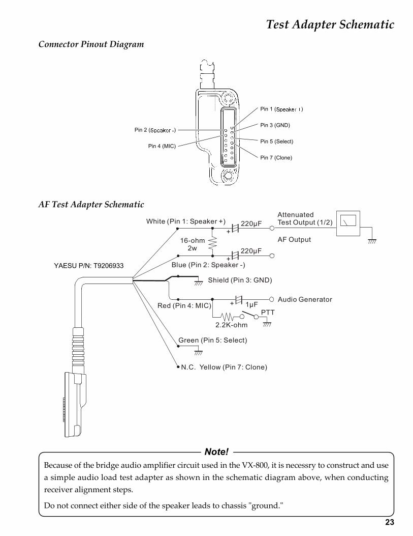
Test Adapter SchematicConnector Pinout Diagram
AF Test Adapter Schematic
Note!Because of the bridge audio amplifier circuit used in the VX-800, it is necessry to construct and usea simple audio load test adapter as shown in the schematic diagram above, when conductingreceiver alignment steps.
Do not connect either side of the speaker leads to chassis "ground."
Pin 2 ( )
Pin 4 (MIC)
Pin 1 ( )
Pin 3 (GND)
Pin 5 (Select)
Pin 7 (Clone)
YAESU P/N: T9206933
White (Pin 1: Speaker +)
Blue (Pin 2: Speaker -)
Red (Pin 4: MIC)
Green (Pin 5: Select)
N.C. Yellow (Pin 7: Clone)
Shield (Pin 3: GND)
16-ohm2w
220µF+
+220µF
+ 1µF
2.2K-ohm
PTT
AF Output
Audio Generator
AttenuatedTest Output (1/2)

24
Note:
25
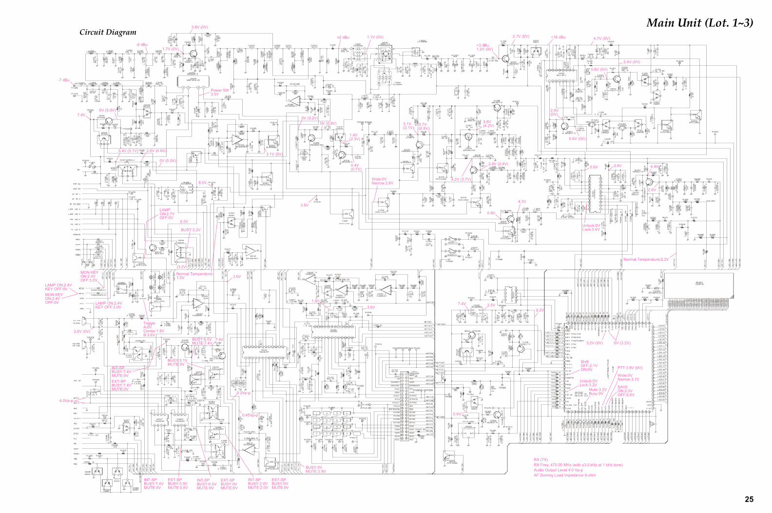
BUSY:3.1VMUTE:0V
Main Unit (Lot. 1~3)Circuit Diagram
4.7V (0V)
2.4V (0V)
0.6V (0V)
0.6V (0V)
2.8V(0V)
5.0V 3.4V 4.4V
2.6V
Normal Temperature:2.2V
Unlock:0VLock:3.4V
4.3V
0.8V
2.8V (2.4V)
4.2V (3.7V)
3.8V(4.2V)0.7V
(0.8V)3.1V(3.1V)
+16 dBu2.7V (0V)
+3 dBu1.2V (0V)
7.4V 3.5V3.2V
5.6V
3.2V (0V) 0V (3.2V)
ShiftOFF:2.1VON:0V
Unlock:0VLock:3.2V SAVE
ON:2.5VOFF:0.6V
Wide:0VNarrow:3.1V
PTT:3.5V (0V)
Mute:3.2VBusy:0V
RX (TX)RX Freq. 470.00 MHz (with ±3.0 kHz at 1 kHz tone)Audio Output Level 4.0 Vp-pAF Dummy Load Impedance 8-ohm
1.1V (0V)+2 dBu
1.4V(2.3V)
0.4V(0.7V)
0V (0.8V)0V (3.2V)
3.5V
3.1V (0V)
5.0V
5.0V
BUSY:3.2V
Normal Temperature1.5V
0V (5.0V)
2.6V (0.6V)5.4V (0.1V)
0V (5.0V)7.4V
-7 dBu
-8 dBu1.7V (0V)
3.8V (0V)
Power 5W3.0V
Wide:0VNarrow:2.6V
(3.2V)
3.6V
LAMPON:2.7VOFF:0V
LAMP ON:2.4VKEY OFF:3.0V
ToggleA:0VCenter:1.8VB:3.6V
MON KEYON:2.4VOFF:3.0V
3.5V (0V)
LAMP ON:2.4VKEY OFF:0VMON KEYON:2.4VOFF:0V
7.4VBUSY:6.5VMUTE:7.4V
3.6V1.8V
BUSY:0VMUTE:2.9V
0.45Vp-p
0.2Vp-p
4.0Vp-p
INT-SP EXT-SPBUSY:7.4V BUSY:0.5VMUTE:0V MUTE:0.6V
INT-SP EXT-SPBUSY:2.0V BUSY:0VMUTE:2.0V MUTE:0V
INT-SPBUSY:7.4VMUTE:0VEXT-SPBUSY:7.4VMUTE:0V
INT-SP EXT-SPBUSY:0.5V BUSY:0VMUTE:0V MUTE:0V

26
Main Unit (Lot. 1~3)Note:
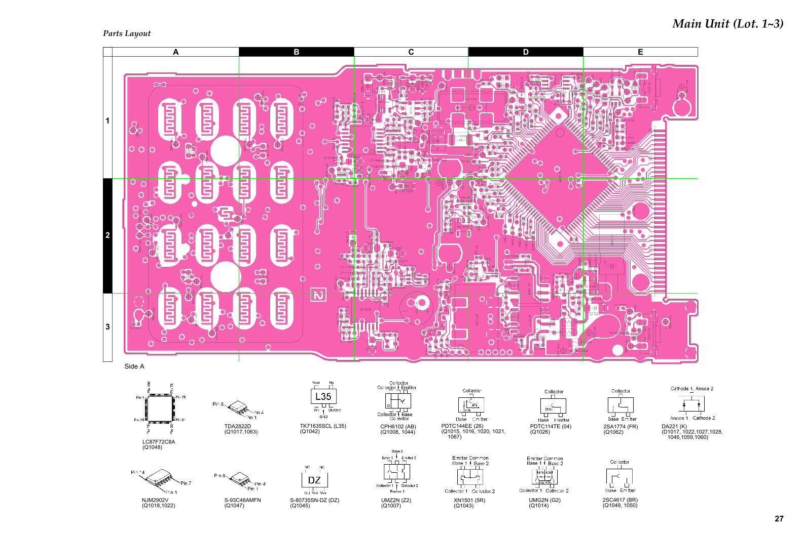
27
LC87F72C8A(Q1048)
TDA2822D(Q1017,1063)
NJM2902V(Q1018,1022)
S-93C46AMFN(Q1047)
S-80735SN-DZ (DZ)(Q1045)
XN1501 (5R)(Q1043)
DA221 (K)(D1017, 1022,1027,1028,
1046,1059,1060)
PDTC144EE (26)(Q1015, 1016, 1020, 1021,
1067)
PDTC114TE (04)(Q1026)
2SC4617 (BR)(Q1049, 1050)
2SA1774 (FR)(Q1062)
CPH6102 (AB)(Q1008, 1044)
TK71635SCL (L35)(Q1042)
UMG2N (G2)(Q1014)
Main Unit (Lot. 1~3)
Side A
Parts Layout
EA B C D
1
2
3
UMZ2N (Z2)(Q1007)
28
TA31136FN(Q1046)
SA7025DK(Q1054)
XP1501 (5R)(Q1003)
2SC4617 (BR)(Q1038, 1051, 1053, 1061)2SC5226 (R22)(Q1001, 1030, 1034, 1041)2SC4215Y (QY)(Q1037)2SC4227 (R32)(Q1039)2SC3356 (R24)(Q1060)
PDTC114TE(Q1006, 1031, 1032,
1058)
PDTC144EE (26)(Q1035, 1036, 1040, 1055,
1056, 1066)
M68732HA-22(Q1019) BR715F (3D)
(D1019)MA132WK (MU)(D1031, 1050, 1051)
DA221 (K)(D1026, 1047, 1053, 1054)
CPH6102 (AB)(Q1002)
UN911F (60)(Q1011, 1023)
M62364FP(Q1025)AK2345(Q1028)
GN2011-Q (4W)(D1030)
TK71650SCL (L50)(Q1005)
2SD1767 (DC)(Q1012)
2SK508 (K52)(Q1033)
UMC5N (C5)(Q1064, 1065)
UMG2N (G2)(Q1004)
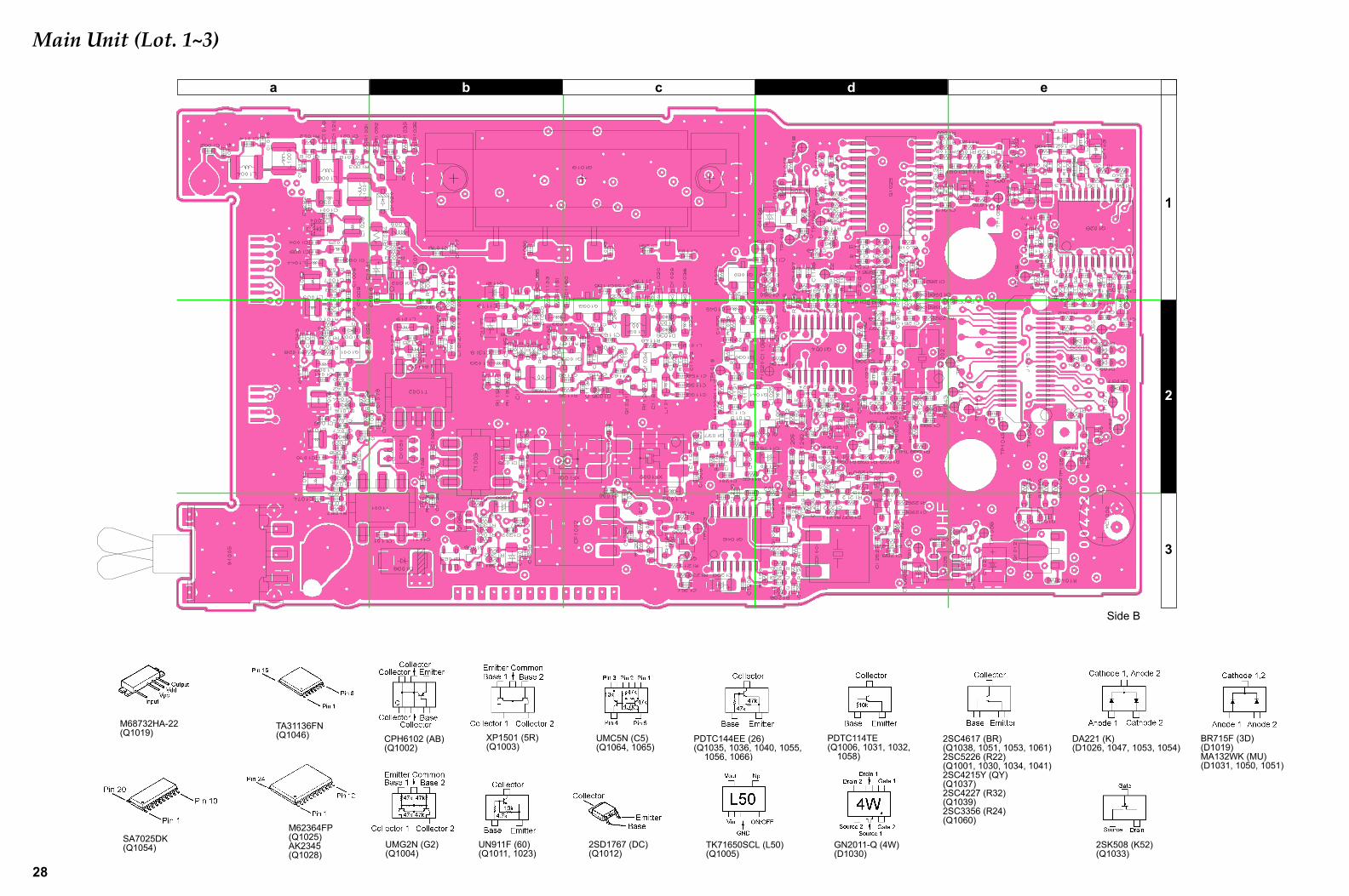
Main Unit (Lot. 1~3)
Side B
1
2
3
a b c d e
29
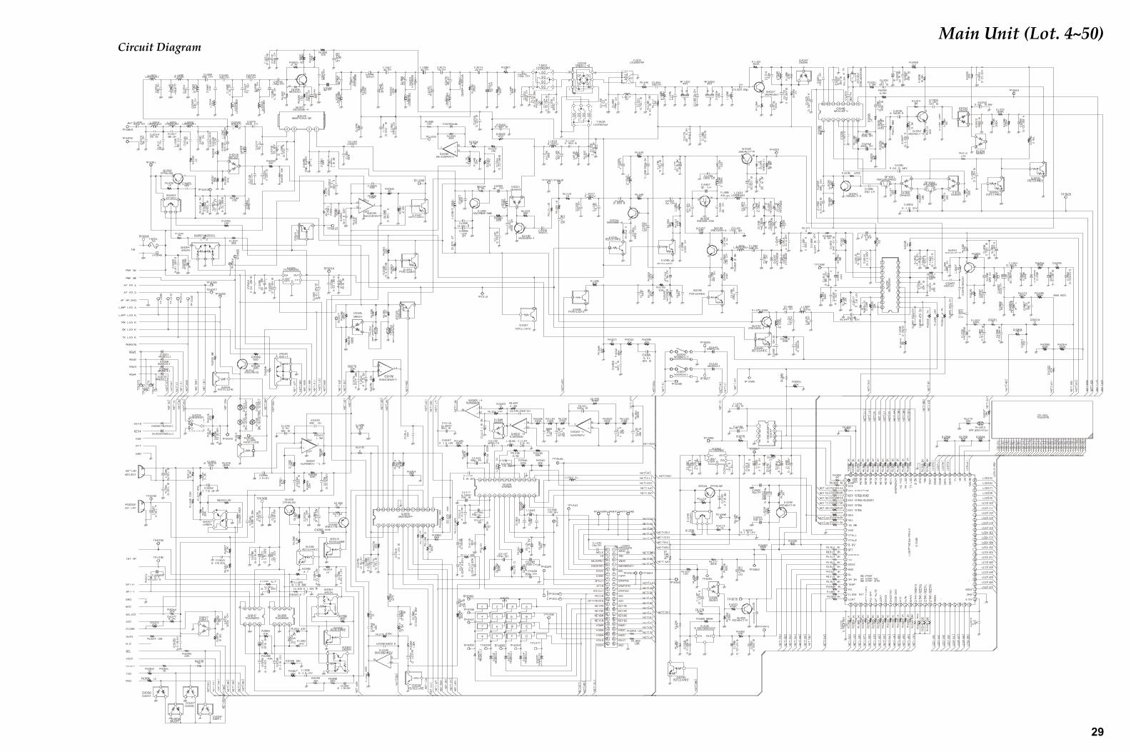
Main Unit (Lot. 4~50)Circuit Diagram

30
Main Unit (Lot. 4~50)Note:
31
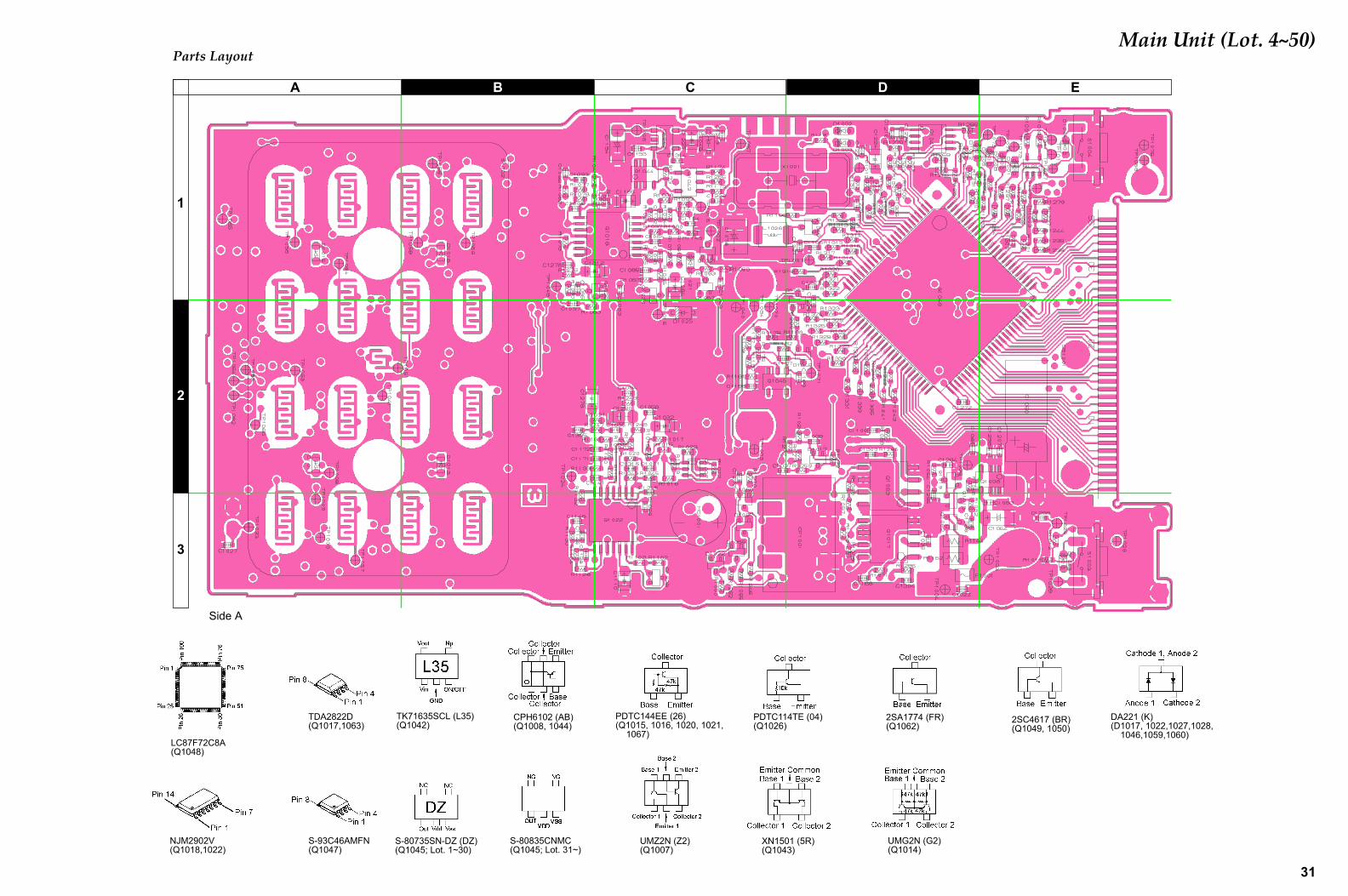
Main Unit (Lot. 4~50)
Side A
Parts Layout
1
2
3
EA B C D
LC87F72C8A(Q1048)
TDA2822D(Q1017,1063)
NJM2902V(Q1018,1022)
S-93C46AMFN(Q1047)
S-80735SN-DZ (DZ)(Q1045; Lot. 1~30)
XN1501 (5R)(Q1043)
DA221 (K)(D1017, 1022,1027,1028,
1046,1059,1060)
PDTC144EE (26)(Q1015, 1016, 1020, 1021,
1067)
PDTC114TE (04)(Q1026)
2SC4617 (BR)(Q1049, 1050)
2SA1774 (FR)(Q1062)
CPH6102 (AB)(Q1008, 1044)
TK71635SCL (L35)(Q1042)
UMG2N (G2)(Q1014)
UMZ2N (Z2)(Q1007)
S-80835CNMC(Q1045; Lot. 31~)
32
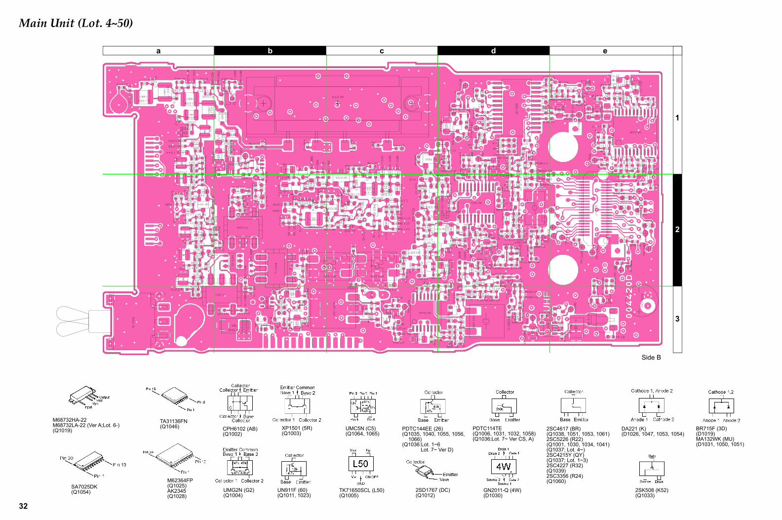
Main Unit (Lot. 4~50)
Side B
1
2
3
a b c d e
TA31136FN(Q1046)
SA7025DK(Q1054)
XP1501 (5R)(Q1003)
2SC4617 (BR)(Q1038, 1051, 1053, 1061)2SC5226 (R22)(Q1001, 1030, 1034, 1041)(Q1037; Lot. 4~)2SC4215Y (QY)(Q1037; Lot. 1~3)2SC4227 (R32)(Q1039)2SC3356 (R24)(Q1060)
PDTC114TE(Q1006, 1031, 1032, 1058)(Q1036;Lot. 7~ Ver CS, A)
M68732HA-22M68732LA-22 (Ver A;Lot. 6-)(Q1019) BR715F (3D)
(D1019)MA132WK (MU)(D1031, 1050, 1051)
DA221 (K)(D1026, 1047, 1053, 1054)
CPH6102 (AB)(Q1002)
UN911F (60)(Q1011, 1023)
M62364FP(Q1025)AK2345(Q1028)
GN2011-Q (4W)(D1030)
TK71650SCL (L50)(Q1005)
2SD1767 (DC)(Q1012)
2SK508 (K52)(Q1033)
UMC5N (C5)(Q1064, 1065)
UMG2N (G2)(Q1004)
PDTC144EE (26)(Q1035, 1040, 1055, 1056,
1066)(Q1036:Lot. 1~6
Lot. 7~ Ver D)
33
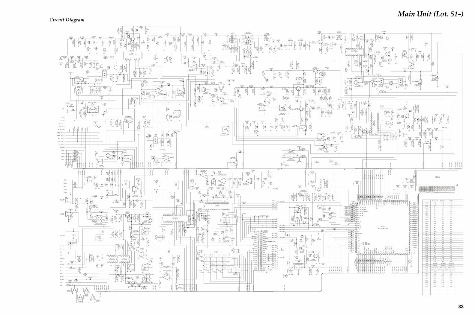
Main Unit (Lot. 51~)Circuit Diagram

34
Main Unit (Lot. 51~)Note:
35
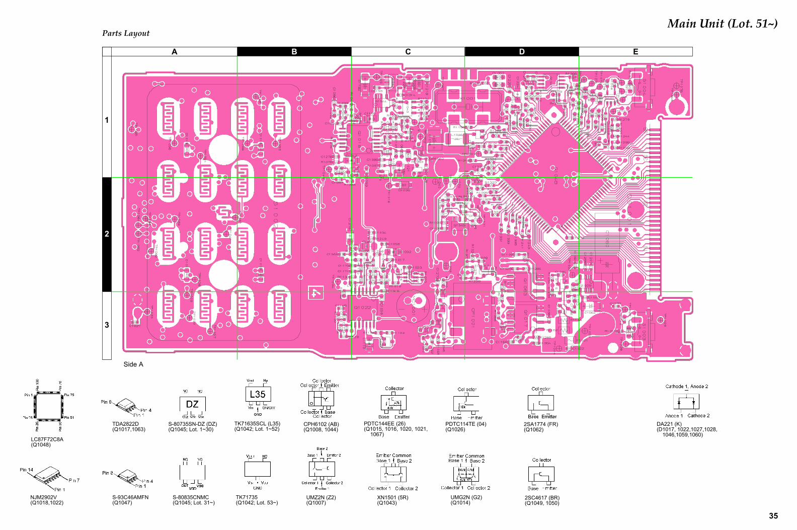
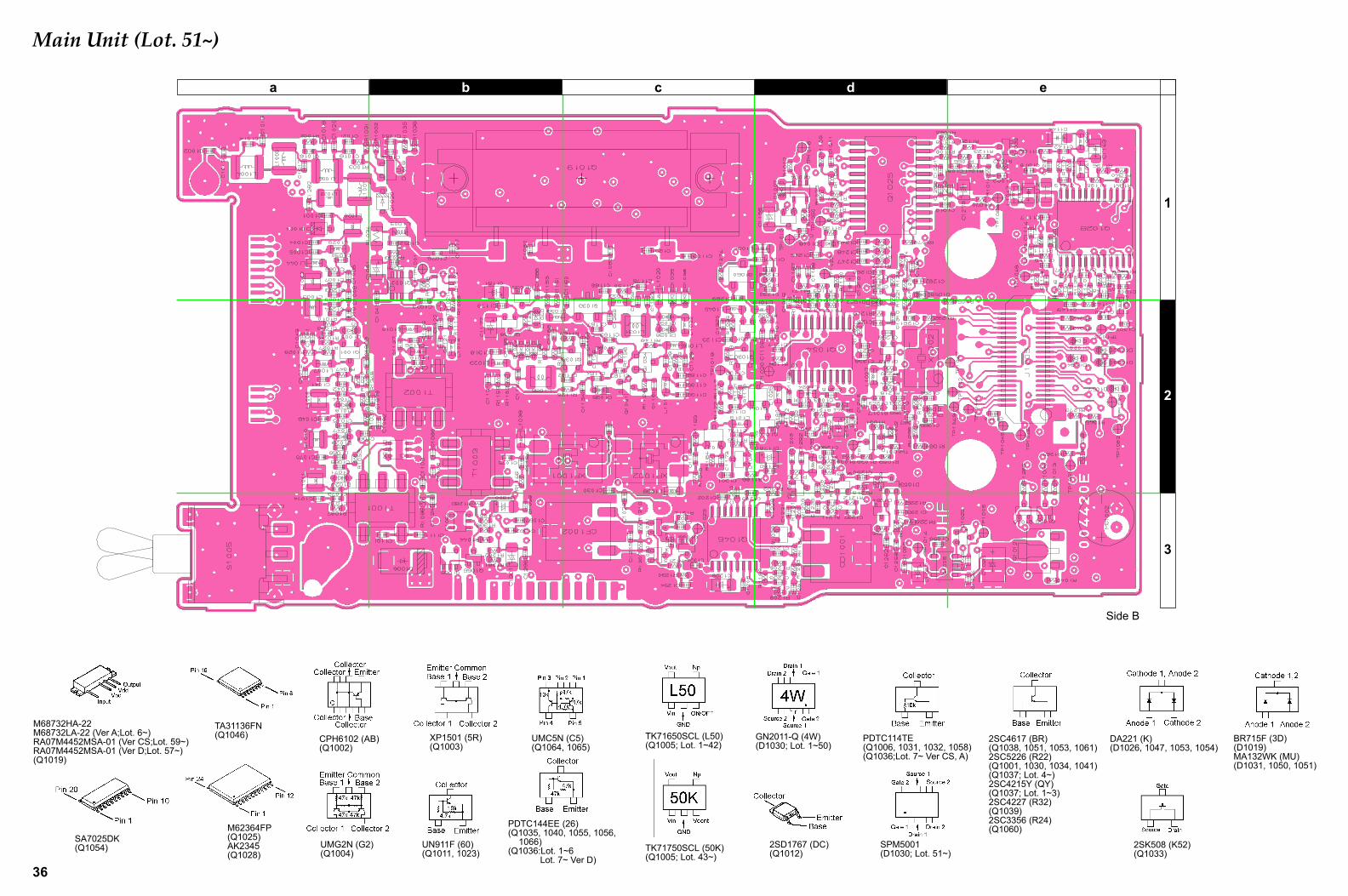
Main Unit (Lot. 51~)
Side A
Parts Layout
1
2
3
EA B C D
LC87F72C8A(Q1048)
TDA2822D(Q1017,1063)
NJM2902V(Q1018,1022)
S-93C46AMFN(Q1047)
S-80735SN-DZ (DZ)(Q1045; Lot. 1~30)
XN1501 (5R)(Q1043)
DA221 (K)(D1017, 1022,1027,1028,
1046,1059,1060)
PDTC144EE (26)(Q1015, 1016, 1020, 1021,
1067)
PDTC114TE (04)(Q1026)
2SC4617 (BR)(Q1049, 1050)
2SA1774 (FR)(Q1062)
CPH6102 (AB)(Q1008, 1044)
TK71635SCL (L35)(Q1042; Lot. 1~52)
UMG2N (G2)(Q1014)
UMZ2N (Z2)(Q1007)
S-80835CNMC(Q1045; Lot. 31~)
TK71735(Q1042; Lot. 53~)
36
Main Unit (Lot. 51~)
Side B
1
2
3
a b c d e
TA31136FN(Q1046)
SA7025DK(Q1054)
XP1501 (5R)(Q1003)
2SC4617 (BR)(Q1038, 1051, 1053, 1061)2SC5226 (R22)(Q1001, 1030, 1034, 1041)(Q1037; Lot. 4~)2SC4215Y (QY)(Q1037; Lot. 1~3)2SC4227 (R32)(Q1039)2SC3356 (R24)(Q1060)
PDTC114TE(Q1006, 1031, 1032, 1058)(Q1036;Lot. 7~ Ver CS, A)
M68732HA-22M68732LA-22 (Ver A;Lot. 6~)RA07M4452MSA-01 (Ver CS;Lot. 59~)RA07M4452MSA-01 (Ver D;Lot. 57~)(Q1019)
BR715F (3D)(D1019)MA132WK (MU)(D1031, 1050, 1051)
DA221 (K)(D1026, 1047, 1053, 1054)
CPH6102 (AB)(Q1002)
UN911F (60)(Q1011, 1023)
M62364FP(Q1025)AK2345(Q1028)
GN2011-Q (4W)(D1030; Lot. 1~50)
TK71650SCL (L50)(Q1005; Lot. 1~42)
2SD1767 (DC)(Q1012)
2SK508 (K52)(Q1033)
UMC5N (C5)(Q1064, 1065)
UMG2N (G2)(Q1004)
PDTC144EE (26)(Q1035, 1040, 1055, 1056,
1066)(Q1036:Lot. 1~6
Lot. 7~ Ver D)
SPM5001(D1030; Lot. 51~)TK71750SCL (50K)
(Q1005; Lot. 43~)
37
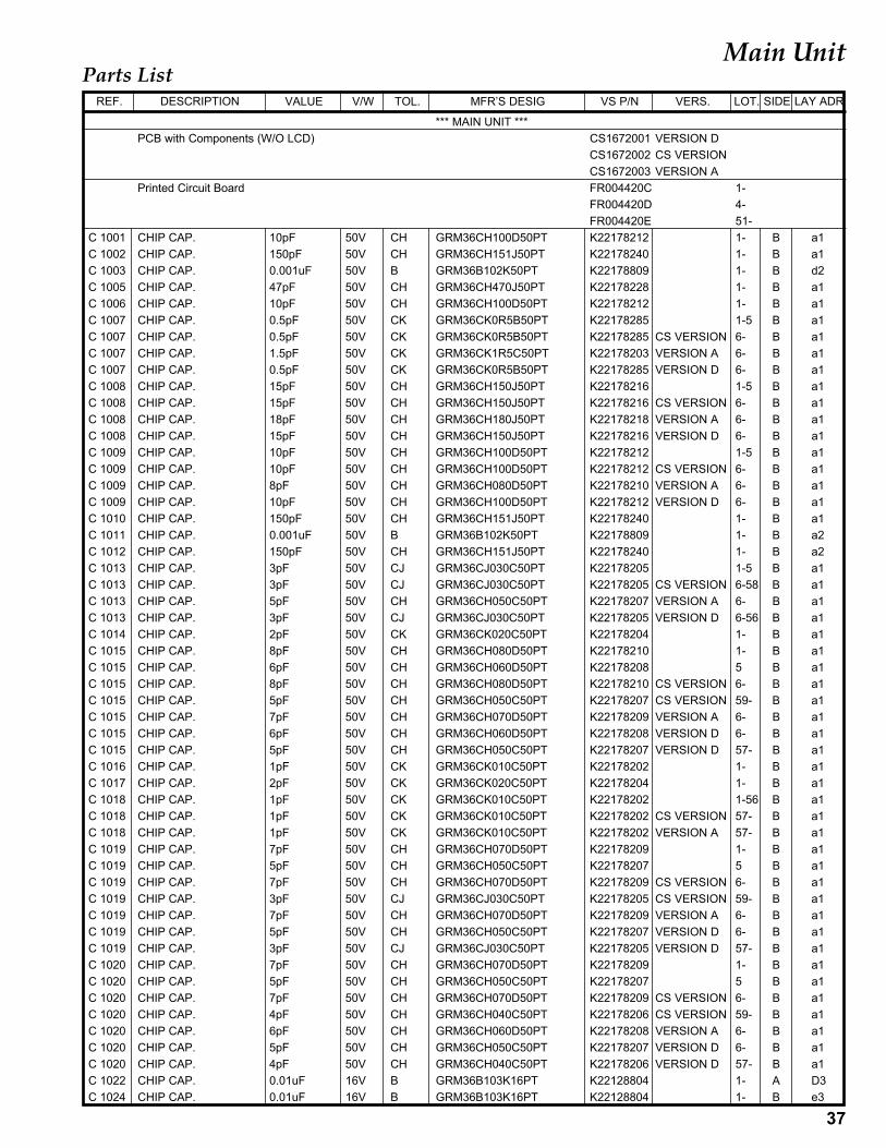
Main UnitParts List
*** MAIN UNIT ***PCB with Components (W/O LCD) CS1672001 VERSION D
CS1672002 CS VERSIONCS1672003 VERSION A
Printed Circuit Board FR004420C 1-FR004420D 4-FR004420E 51-
C 1001 CHIP CAP. 10pF 50V CH GRM36CH100D50PT K22178212 1- B a1C 1002 CHIP CAP. 150pF 50V CH GRM36CH151J50PT K22178240 1- B a1C 1003 CHIP CAP. 0.001uF 50V B GRM36B102K50PT K22178809 1- B d2C 1005 CHIP CAP. 47pF 50V CH GRM36CH470J50PT K22178228 1- B a1C 1006 CHIP CAP. 10pF 50V CH GRM36CH100D50PT K22178212 1- B a1C 1007 CHIP CAP. 0.5pF 50V CK GRM36CK0R5B50PT K22178285 1-5 B a1C 1007 CHIP CAP. 0.5pF 50V CK GRM36CK0R5B50PT K22178285 CS VERSION 6- B a1C 1007 CHIP CAP. 1.5pF 50V CK GRM36CK1R5C50PT K22178203 VERSION A 6- B a1C 1007 CHIP CAP. 0.5pF 50V CK GRM36CK0R5B50PT K22178285 VERSION D 6- B a1C 1008 CHIP CAP. 15pF 50V CH GRM36CH150J50PT K22178216 1-5 B a1C 1008 CHIP CAP. 15pF 50V CH GRM36CH150J50PT K22178216 CS VERSION 6- B a1C 1008 CHIP CAP. 18pF 50V CH GRM36CH180J50PT K22178218 VERSION A 6- B a1C 1008 CHIP CAP. 15pF 50V CH GRM36CH150J50PT K22178216 VERSION D 6- B a1C 1009 CHIP CAP. 10pF 50V CH GRM36CH100D50PT K22178212 1-5 B a1C 1009 CHIP CAP. 10pF 50V CH GRM36CH100D50PT K22178212 CS VERSION 6- B a1C 1009 CHIP CAP. 8pF 50V CH GRM36CH080D50PT K22178210 VERSION A 6- B a1C 1009 CHIP CAP. 10pF 50V CH GRM36CH100D50PT K22178212 VERSION D 6- B a1C 1010 CHIP CAP. 150pF 50V CH GRM36CH151J50PT K22178240 1- B a1C 1011 CHIP CAP. 0.001uF 50V B GRM36B102K50PT K22178809 1- B a2C 1012 CHIP CAP. 150pF 50V CH GRM36CH151J50PT K22178240 1- B a2C 1013 CHIP CAP. 3pF 50V CJ GRM36CJ030C50PT K22178205 1-5 B a1C 1013 CHIP CAP. 3pF 50V CJ GRM36CJ030C50PT K22178205 CS VERSION 6-58 B a1C 1013 CHIP CAP. 5pF 50V CH GRM36CH050C50PT K22178207 VERSION A 6- B a1C 1013 CHIP CAP. 3pF 50V CJ GRM36CJ030C50PT K22178205 VERSION D 6-56 B a1C 1014 CHIP CAP. 2pF 50V CK GRM36CK020C50PT K22178204 1- B a1C 1015 CHIP CAP. 8pF 50V CH GRM36CH080D50PT K22178210 1- B a1C 1015 CHIP CAP. 6pF 50V CH GRM36CH060D50PT K22178208 5 B a1C 1015 CHIP CAP. 8pF 50V CH GRM36CH080D50PT K22178210 CS VERSION 6- B a1C 1015 CHIP CAP. 5pF 50V CH GRM36CH050C50PT K22178207 CS VERSION 59- B a1C 1015 CHIP CAP. 7pF 50V CH GRM36CH070D50PT K22178209 VERSION A 6- B a1C 1015 CHIP CAP. 6pF 50V CH GRM36CH060D50PT K22178208 VERSION D 6- B a1C 1015 CHIP CAP. 5pF 50V CH GRM36CH050C50PT K22178207 VERSION D 57- B a1C 1016 CHIP CAP. 1pF 50V CK GRM36CK010C50PT K22178202 1- B a1C 1017 CHIP CAP. 2pF 50V CK GRM36CK020C50PT K22178204 1- B a1C 1018 CHIP CAP. 1pF 50V CK GRM36CK010C50PT K22178202 1-56 B a1C 1018 CHIP CAP. 1pF 50V CK GRM36CK010C50PT K22178202 CS VERSION 57- B a1C 1018 CHIP CAP. 1pF 50V CK GRM36CK010C50PT K22178202 VERSION A 57- B a1C 1019 CHIP CAP. 7pF 50V CH GRM36CH070D50PT K22178209 1- B a1C 1019 CHIP CAP. 5pF 50V CH GRM36CH050C50PT K22178207 5 B a1C 1019 CHIP CAP. 7pF 50V CH GRM36CH070D50PT K22178209 CS VERSION 6- B a1C 1019 CHIP CAP. 3pF 50V CJ GRM36CJ030C50PT K22178205 CS VERSION 59- B a1C 1019 CHIP CAP. 7pF 50V CH GRM36CH070D50PT K22178209 VERSION A 6- B a1C 1019 CHIP CAP. 5pF 50V CH GRM36CH050C50PT K22178207 VERSION D 6- B a1C 1019 CHIP CAP. 3pF 50V CJ GRM36CJ030C50PT K22178205 VERSION D 57- B a1C 1020 CHIP CAP. 7pF 50V CH GRM36CH070D50PT K22178209 1- B a1C 1020 CHIP CAP. 5pF 50V CH GRM36CH050C50PT K22178207 5 B a1C 1020 CHIP CAP. 7pF 50V CH GRM36CH070D50PT K22178209 CS VERSION 6- B a1C 1020 CHIP CAP. 4pF 50V CH GRM36CH040C50PT K22178206 CS VERSION 59- B a1C 1020 CHIP CAP. 6pF 50V CH GRM36CH060D50PT K22178208 VERSION A 6- B a1C 1020 CHIP CAP. 5pF 50V CH GRM36CH050C50PT K22178207 VERSION D 6- B a1C 1020 CHIP CAP. 4pF 50V CH GRM36CH040C50PT K22178206 VERSION D 57- B a1C 1022 CHIP CAP. 0.01uF 16V B GRM36B103K16PT K22128804 1- A D3C 1024 CHIP CAP. 0.01uF 16V B GRM36B103K16PT K22128804 1- B e3
DESCRIPTION VALUE V/W TOL. VS P/NMFR’S DESIG VERS.REF. LOT. SIDE LAY ADR
38
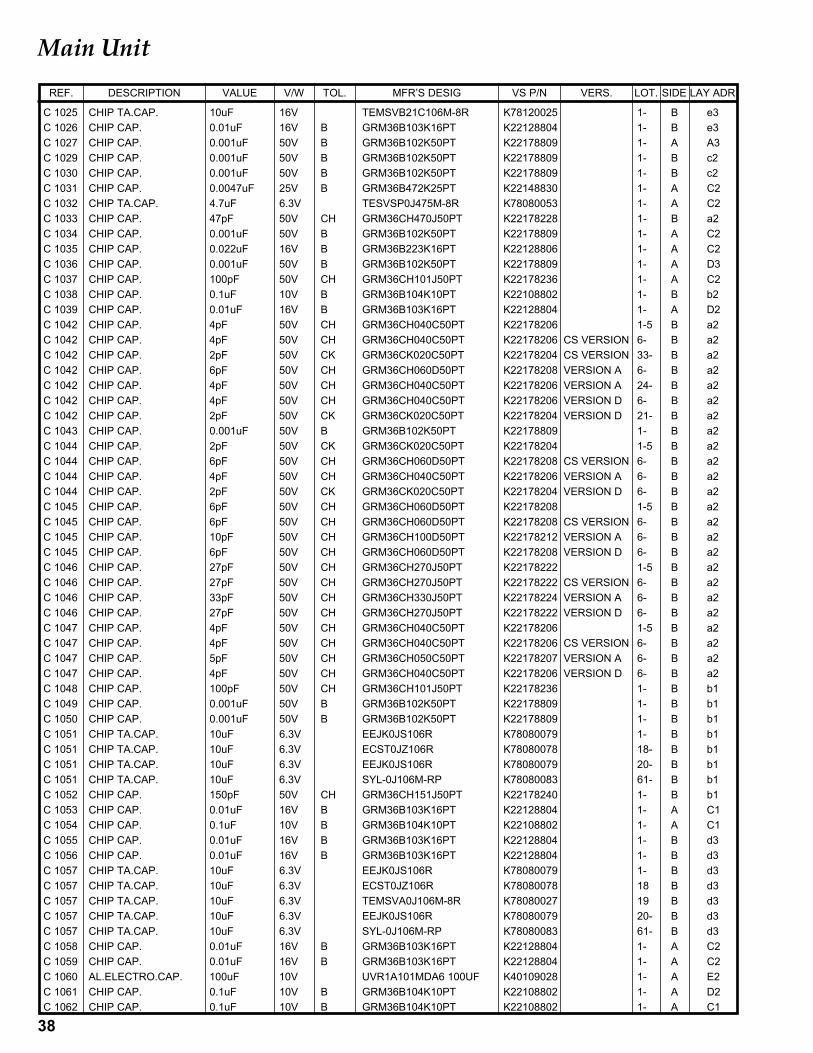
Main Unit
C 1025 CHIP TA.CAP. 10uF 16V TEMSVB21C106M-8R K78120025 1- B e3C 1026 CHIP CAP. 0.01uF 16V B GRM36B103K16PT K22128804 1- B e3C 1027 CHIP CAP. 0.001uF 50V B GRM36B102K50PT K22178809 1- A A3C 1029 CHIP CAP. 0.001uF 50V B GRM36B102K50PT K22178809 1- B c2C 1030 CHIP CAP. 0.001uF 50V B GRM36B102K50PT K22178809 1- B c2C 1031 CHIP CAP. 0.0047uF 25V B GRM36B472K25PT K22148830 1- A C2C 1032 CHIP TA.CAP. 4.7uF 6.3V TESVSP0J475M-8R K78080053 1- A C2C 1033 CHIP CAP. 47pF 50V CH GRM36CH470J50PT K22178228 1- B a2C 1034 CHIP CAP. 0.001uF 50V B GRM36B102K50PT K22178809 1- A C2C 1035 CHIP CAP. 0.022uF 16V B GRM36B223K16PT K22128806 1- A C2C 1036 CHIP CAP. 0.001uF 50V B GRM36B102K50PT K22178809 1- A D3C 1037 CHIP CAP. 100pF 50V CH GRM36CH101J50PT K22178236 1- A C2C 1038 CHIP CAP. 0.1uF 10V B GRM36B104K10PT K22108802 1- B b2C 1039 CHIP CAP. 0.01uF 16V B GRM36B103K16PT K22128804 1- A D2C 1042 CHIP CAP. 4pF 50V CH GRM36CH040C50PT K22178206 1-5 B a2C 1042 CHIP CAP. 4pF 50V CH GRM36CH040C50PT K22178206 CS VERSION 6- B a2C 1042 CHIP CAP. 2pF 50V CK GRM36CK020C50PT K22178204 CS VERSION 33- B a2C 1042 CHIP CAP. 6pF 50V CH GRM36CH060D50PT K22178208 VERSION A 6- B a2C 1042 CHIP CAP. 4pF 50V CH GRM36CH040C50PT K22178206 VERSION A 24- B a2C 1042 CHIP CAP. 4pF 50V CH GRM36CH040C50PT K22178206 VERSION D 6- B a2C 1042 CHIP CAP. 2pF 50V CK GRM36CK020C50PT K22178204 VERSION D 21- B a2C 1043 CHIP CAP. 0.001uF 50V B GRM36B102K50PT K22178809 1- B a2C 1044 CHIP CAP. 2pF 50V CK GRM36CK020C50PT K22178204 1-5 B a2C 1044 CHIP CAP. 6pF 50V CH GRM36CH060D50PT K22178208 CS VERSION 6- B a2C 1044 CHIP CAP. 4pF 50V CH GRM36CH040C50PT K22178206 VERSION A 6- B a2C 1044 CHIP CAP. 2pF 50V CK GRM36CK020C50PT K22178204 VERSION D 6- B a2C 1045 CHIP CAP. 6pF 50V CH GRM36CH060D50PT K22178208 1-5 B a2C 1045 CHIP CAP. 6pF 50V CH GRM36CH060D50PT K22178208 CS VERSION 6- B a2C 1045 CHIP CAP. 10pF 50V CH GRM36CH100D50PT K22178212 VERSION A 6- B a2C 1045 CHIP CAP. 6pF 50V CH GRM36CH060D50PT K22178208 VERSION D 6- B a2C 1046 CHIP CAP. 27pF 50V CH GRM36CH270J50PT K22178222 1-5 B a2C 1046 CHIP CAP. 27pF 50V CH GRM36CH270J50PT K22178222 CS VERSION 6- B a2C 1046 CHIP CAP. 33pF 50V CH GRM36CH330J50PT K22178224 VERSION A 6- B a2C 1046 CHIP CAP. 27pF 50V CH GRM36CH270J50PT K22178222 VERSION D 6- B a2C 1047 CHIP CAP. 4pF 50V CH GRM36CH040C50PT K22178206 1-5 B a2C 1047 CHIP CAP. 4pF 50V CH GRM36CH040C50PT K22178206 CS VERSION 6- B a2C 1047 CHIP CAP. 5pF 50V CH GRM36CH050C50PT K22178207 VERSION A 6- B a2C 1047 CHIP CAP. 4pF 50V CH GRM36CH040C50PT K22178206 VERSION D 6- B a2C 1048 CHIP CAP. 100pF 50V CH GRM36CH101J50PT K22178236 1- B b1C 1049 CHIP CAP. 0.001uF 50V B GRM36B102K50PT K22178809 1- B b1C 1050 CHIP CAP. 0.001uF 50V B GRM36B102K50PT K22178809 1- B b1C 1051 CHIP TA.CAP. 10uF 6.3V EEJK0JS106R K78080079 1- B b1C 1051 CHIP TA.CAP. 10uF 6.3V ECST0JZ106R K78080078 18- B b1C 1051 CHIP TA.CAP. 10uF 6.3V EEJK0JS106R K78080079 20- B b1C 1051 CHIP TA.CAP. 10uF 6.3V SYL-0J106M-RP K78080083 61- B b1C 1052 CHIP CAP. 150pF 50V CH GRM36CH151J50PT K22178240 1- B b1C 1053 CHIP CAP. 0.01uF 16V B GRM36B103K16PT K22128804 1- A C1C 1054 CHIP CAP. 0.1uF 10V B GRM36B104K10PT K22108802 1- A C1C 1055 CHIP CAP. 0.01uF 16V B GRM36B103K16PT K22128804 1- B d3C 1056 CHIP CAP. 0.01uF 16V B GRM36B103K16PT K22128804 1- B d3C 1057 CHIP TA.CAP. 10uF 6.3V EEJK0JS106R K78080079 1- B d3C 1057 CHIP TA.CAP. 10uF 6.3V ECST0JZ106R K78080078 18 B d3C 1057 CHIP TA.CAP. 10uF 6.3V TEMSVA0J106M-8R K78080027 19 B d3C 1057 CHIP TA.CAP. 10uF 6.3V EEJK0JS106R K78080079 20- B d3C 1057 CHIP TA.CAP. 10uF 6.3V SYL-0J106M-RP K78080083 61- B d3C 1058 CHIP CAP. 0.01uF 16V B GRM36B103K16PT K22128804 1- A C2C 1059 CHIP CAP. 0.01uF 16V B GRM36B103K16PT K22128804 1- A C2C 1060 AL.ELECTRO.CAP. 100uF 10V UVR1A101MDA6 100UF K40109028 1- A E2C 1061 CHIP CAP. 0.1uF 10V B GRM36B104K10PT K22108802 1- A D2C 1062 CHIP CAP. 0.1uF 10V B GRM36B104K10PT K22108802 1- A C1
DESCRIPTION VALUE V/W TOL. VS P/NMFR’S DESIG VERS.REF. LOT. SIDE LAY ADR
39
Main Unit
C 1063 CHIP CAP. 0.1uF 10V B GRM36B104K10PT K22108802 1- A E2C 1063 CHIP CAP. 0.01uF 16V B GRM36B103K16PT K22128804 59- A E2C 1064 CHIP TA.CAP. 10uF 10V TEMSVA1A106M-8R K78100028 1- A E3C 1064 CHIP TA.CAP. 6.8uF 16V TEMSVA1C685M-8R K78120056 59- A E3C 1067 CHIP CAP. 0.1uF 10V B GRM36B104K10PT K22108802 1- B b3C 1068 CHIP CAP. 2pF 50V CK GRM36CK020C50PT K22178204 1-5 B a2C 1068 CHIP CAP. 6pF 50V CH GRM36CH060D50PT K22178208 CS VERSION 6- B a2C 1068 CHIP CAP. 4pF 50V CH GRM36CH040C50PT K22178206 VERSION A 6- B a2C 1068 CHIP CAP. 2pF 50V CK GRM36CK020C50PT K22178204 VERSION D 6- B a2C 1069 CHIP CAP. 4pF 50V CH GRM36CH040C50PT K22178206 1-5 B a2C 1069 CHIP CAP. 4pF 50V CH GRM36CH040C50PT K22178206 CS VERSION 6- B a2C 1069 CHIP CAP. 6pF 50V CH GRM36CH060D50PT K22178208 VERSION A 6- B a2C 1069 CHIP CAP. 4pF 50V CH GRM36CH040C50PT K22178206 VERSION D 6- B a2C 1070 CHIP CAP. 18pF 50V CH GRM36CH180J50PT K22178218 1-5 B a2C 1070 CHIP CAP. 18pF 50V CH GRM36CH180J50PT K22178218 CS VERSION 6- B a2C 1070 CHIP CAP. 33pF 50V CH GRM36CH330J50PT K22178224 VERSION A 6- B a2C 1070 CHIP CAP. 18pF 50V CH GRM36CH180J50PT K22178218 VERSION D 6- B a2C 1071 CHIP CAP. 6pF 50V CH GRM36CH060D50PT K22178208 1-5 B a2C 1071 CHIP CAP. 6pF 50V CH GRM36CH060D50PT K22178208 CS VERSION 6- B a2C 1071 CHIP CAP. 8pF 50V CH GRM36CH080D50PT K22178210 VERSION A 6- B a2C 1071 CHIP CAP. 6pF 50V CH GRM36CH060D50PT K22178208 VERSION D 6- B a2C 1072 CHIP CAP. 2pF 50V CK GRM36CK020C50PT K22178204 1-5 B a2C 1072 CHIP CAP. 6pF 50V CH GRM36CH060D50PT K22178208 CS VERSION 6- B a2C 1072 CHIP CAP. 4pF 50V CH GRM36CH040C50PT K22178206 VERSION A 6- B a2C 1072 CHIP CAP. 2pF 50V CK GRM36CK020C50PT K22178204 VERSION D 6- B a2C 1073 CHIP CAP. 4pF 50V CH GRM36CH040C50PT K22178206 1-20 B a2C 1073 CHIP CAP. 4pF 50V CH GRM36CH040C50PT K22178206 CS VERSION 21- B a2C 1073 CHIP CAP. 2pF 50V CK GRM36CK020C50PT K22178204 VERSION A 21- B a2C 1073 CHIP CAP. 2pF 50V CK GRM36CK020C50PT K22178204 VERSION D 21- B a2C 1074 CHIP CAP. 5pF 50V CH GRM36CH050C50PT K22178207 1- B a2C 1076 CHIP CAP. 150pF 50V CH GRM36CH151J50PT K22178240 1- B b1C 1077 CHIP CAP. 3pF 50V CJ GRM36CJ030C50PT K22178205 1-1 B b1C 1077 CHIP CAP. 3pF 50V CJ GRM36CJ030C50PT K22178205 5 B b1C 1077 CHIP CAP. 3pF 50V CJ GRM36CJ030C50PT K22178205 CS VERSION 6- B b1C 1077 CHIP CAP. 2pF 50V CK GRM36CK020C50PT K22178204 CS VERSION 59- B b1C 1077 CHIP CAP. 2pF 50V CK GRM36CK020C50PT K22178204 VERSION A 6- B b1C 1077 CHIP CAP. 3pF 50V CJ GRM36CJ030C50PT K22178205 VERSION D 6-20 B b1C 1077 CHIP CAP. 1pF 50V CK GRM36CK010C50PT K22178202 VERSION D 57- B b1C 1078 CHIP TA.CAP. 10uF 16V TEMSVB21C106M-8R K78120025 1- A C1C 1079 CHIP CAP. 0.01uF 16V B GRM36B103K16PT K22128804 1- B b2C 1080 CHIP CAP. 0.001uF 50V B GRM36B102K50PT K22178809 1- B b1C 1081 CHIP CAP. 150pF 50V CH GRM36CH151J50PT K22178240 1- B a2C 1082 CHIP CAP. 0.001uF 50V B GRM36B102K50PT K22178809 1- B b2C 1084 CHIP TA.CAP. 1uF 6.3V TMCP0J105MTR K78080071 1- A C1C 1086 CHIP CAP. 0.001uF 50V B GRM36B102K50PT K22178809 1- A C1C 1088 CHIP CAP. 0.1uF 10V B GRM36B104K10PT K22108802 1- A C1C 1089 CHIP CAP. 150pF 50V CH GRM36CH151J50PT K22178240 1- B b2C 1090 CHIP CAP. 150pF 50V CH GRM36CH151J50PT K22178240 1- B a1C 1091 CHIP CAP. 0.047uF 10V B GRM36B473K10PT K22108801 1- B e1C 1092 CHIP CAP. 0.047uF 10V B GRM36B473K10PT K22108801 1- B e1C 1093 CHIP CAP. 0.0027uF 50V B GRM36B272K50PT K22178814 1- A B1C 1094 CHIP CAP. 680pF 50V B GRM36B681K50PT K22178807 1- A B1C 1095 CHIP CAP. 0.1uF 10V B GRM36B104K10PT K22108802 1- A B1C 1096 CHIP CAP. 0.0047uF 25V B GRM36B472K25PT K22148830 1- A B1C 1097 CHIP CAP. 0.1uF 10V B GRM36B104K10PT K22108802 1- A B1C 1100 CHIP CAP. 0.1uF 10V B GRM36B104K10PT K22108802 1- A D2C 1101 CHIP CAP. 150pF 50V CH GRM36CH151J50PT K22178240 1- B b3C 1103 CHIP CAP. 150pF 50V CH GRM36CH151J50PT K22178240 1- B c1C 1104 CHIP CAP. 0.01uF 16V B GRM36B103K16PT K22128804 1- A C1C 1105 CHIP CAP. 0.001uF 50V B GRM36B102K50PT K22178809 1- B d1
DESCRIPTION VALUE V/W TOL. VS P/NMFR’S DESIG VERS.REF. LOT. SIDE LAY ADR
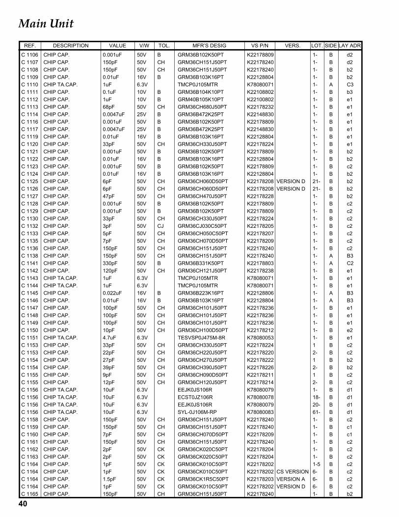
40
Main Unit
C 1106 CHIP CAP. 0.001uF 50V B GRM36B102K50PT K22178809 1- B d2C 1107 CHIP CAP. 150pF 50V CH GRM36CH151J50PT K22178240 1- B d2C 1108 CHIP CAP. 150pF 50V CH GRM36CH151J50PT K22178240 1- B b2C 1109 CHIP CAP. 0.01uF 16V B GRM36B103K16PT K22128804 1- B b2C 1110 CHIP TA.CAP. 1uF 6.3V TMCP0J105MTR K78080071 1- A C3C 1111 CHIP CAP. 0.1uF 10V B GRM36B104K10PT K22108802 1- B b3C 1112 CHIP CAP. 1uF 10V B GRM40B105K10PT K22100802 1- B e1C 1113 CHIP CAP. 68pF 50V CH GRM36CH680J50PT K22178232 1- B e1C 1114 CHIP CAP. 0.0047uF 25V B GRM36B472K25PT K22148830 1- B e1C 1116 CHIP CAP. 0.001uF 50V B GRM36B102K50PT K22178809 1- B e1C 1117 CHIP CAP. 0.0047uF 25V B GRM36B472K25PT K22148830 1- B e1C 1119 CHIP CAP. 0.01uF 16V B GRM36B103K16PT K22128804 1- B e1C 1120 CHIP CAP. 33pF 50V CH GRM36CH330J50PT K22178224 1- B e1C 1121 CHIP CAP. 0.001uF 50V B GRM36B102K50PT K22178809 1- B b2C 1122 CHIP CAP. 0.01uF 16V B GRM36B103K16PT K22128804 1- B b2C 1123 CHIP CAP. 0.001uF 50V B GRM36B102K50PT K22178809 1- B c2C 1124 CHIP CAP. 0.01uF 16V B GRM36B103K16PT K22128804 1- B b2C 1125 CHIP CAP. 6pF 50V CH GRM36CH060D50PT K22178208 VERSION D 21- B b2C 1126 CHIP CAP. 6pF 50V CH GRM36CH060D50PT K22178208 VERSION D 21- B b2C 1127 CHIP CAP. 47pF 50V CH GRM36CH470J50PT K22178228 1- B b2C 1128 CHIP CAP. 0.001uF 50V B GRM36B102K50PT K22178809 1- B c2C 1129 CHIP CAP. 0.001uF 50V B GRM36B102K50PT K22178809 1- B c2C 1130 CHIP CAP. 33pF 50V CH GRM36CH330J50PT K22178224 1- B c2C 1132 CHIP CAP. 3pF 50V CJ GRM36CJ030C50PT K22178205 1- B c2C 1133 CHIP CAP. 5pF 50V CH GRM36CH050C50PT K22178207 1- B c2C 1135 CHIP CAP. 7pF 50V CH GRM36CH070D50PT K22178209 1- B c2C 1136 CHIP CAP. 150pF 50V CH GRM36CH151J50PT K22178240 1- B c2C 1138 CHIP CAP. 150pF 50V CH GRM36CH151J50PT K22178240 1- A B3C 1141 CHIP CAP. 330pF 50V B GRM36B331K50PT K22178803 1- A C2C 1142 CHIP CAP. 120pF 50V CH GRM36CH121J50PT K22178238 1- B e1C 1143 CHIP TA.CAP. 1uF 6.3V TMCP0J105MTR K78080071 1- B e1C 1144 CHIP TA.CAP. 1uF 6.3V TMCP0J105MTR K78080071 1- B e1C 1145 CHIP CAP. 0.022uF 16V B GRM36B223K16PT K22128806 1- A B3C 1146 CHIP CAP. 0.01uF 16V B GRM36B103K16PT K22128804 1- A B3C 1147 CHIP CAP. 100pF 50V CH GRM36CH101J50PT K22178236 1- B e1C 1148 CHIP CAP. 100pF 50V CH GRM36CH101J50PT K22178236 1- B e1C 1149 CHIP CAP. 100pF 50V CH GRM36CH101J50PT K22178236 1- B e1C 1150 CHIP CAP. 10pF 50V CH GRM36CH100D50PT K22178212 1- B e2C 1151 CHIP TA.CAP. 4.7uF 6.3V TESVSP0J475M-8R K78080053 1- B e1C 1153 CHIP CAP. 33pF 50V CH GRM36CH330J50PT K22178224 1 B c2C 1153 CHIP CAP. 22pF 50V CH GRM36CH220J50PT K22178220 2- B c2C 1154 CHIP CAP. 27pF 50V CH GRM36CH270J50PT K22178222 1 B b2C 1154 CHIP CAP. 39pF 50V CH GRM36CH390J50PT K22178226 2- B b2C 1155 CHIP CAP. 9pF 50V CH GRM36CH090D50PT K22178211 1 B c2C 1155 CHIP CAP. 12pF 50V CH GRM36CH120J50PT K22178214 2- B c2C 1156 CHIP TA.CAP. 10uF 6.3V EEJK0JS106R K78080079 1- B d1C 1156 CHIP TA.CAP. 10uF 6.3V ECST0JZ106R K78080078 18- B d1C 1156 CHIP TA.CAP. 10uF 6.3V EEJK0JS106R K78080079 20- B d1C 1156 CHIP TA.CAP. 10uF 6.3V SYL-0J106M-RP K78080083 61- B d1C 1158 CHIP CAP. 150pF 50V CH GRM36CH151J50PT K22178240 1- B c2C 1159 CHIP CAP. 150pF 50V CH GRM36CH151J50PT K22178240 1- B c1C 1160 CHIP CAP. 7pF 50V CH GRM36CH070D50PT K22178209 1- B c1C 1161 CHIP CAP. 150pF 50V CH GRM36CH151J50PT K22178240 1- B c2C 1162 CHIP CAP. 2pF 50V CK GRM36CK020C50PT K22178204 1- B c2C 1163 CHIP CAP. 2pF 50V CK GRM36CK020C50PT K22178204 1- B c2C 1164 CHIP CAP. 1pF 50V CK GRM36CK010C50PT K22178202 1-5 B c2C 1164 CHIP CAP. 1pF 50V CK GRM36CK010C50PT K22178202 CS VERSION 6- B c2C 1164 CHIP CAP. 1.5pF 50V CK GRM36CK1R5C50PT K22178203 VERSION A 6- B c2C 1164 CHIP CAP. 1pF 50V CK GRM36CK010C50PT K22178202 VERSION D 6- B c2C 1165 CHIP CAP. 150pF 50V CH GRM36CH151J50PT K22178240 1- B b2
DESCRIPTION VALUE V/W TOL. VS P/NMFR’S DESIG VERS.REF. LOT. SIDE LAY ADR
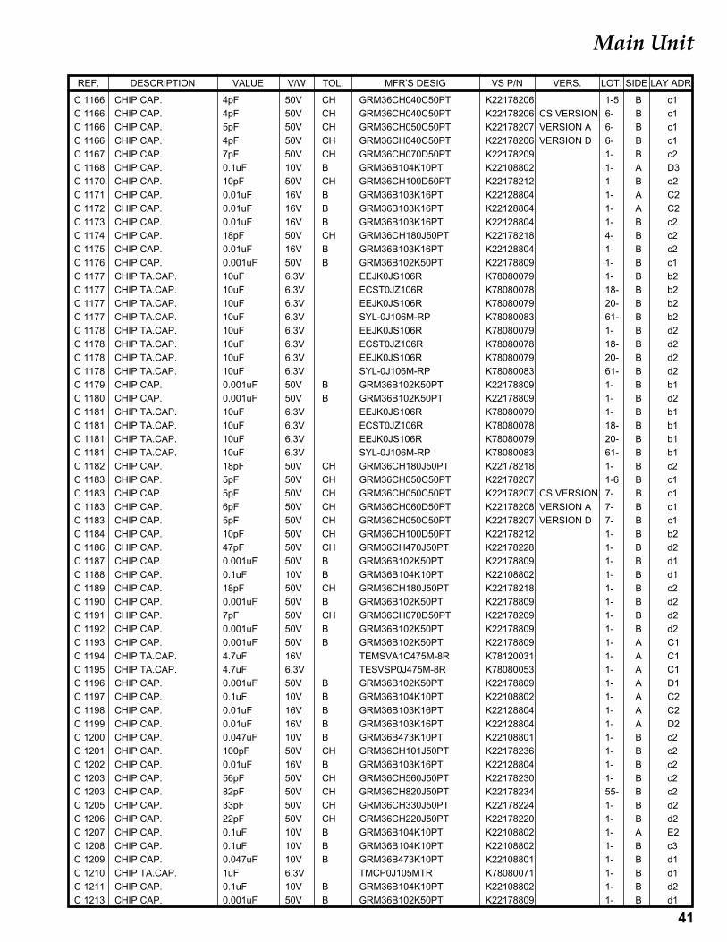
41
Main Unit
C 1166 CHIP CAP. 4pF 50V CH GRM36CH040C50PT K22178206 1-5 B c1C 1166 CHIP CAP. 4pF 50V CH GRM36CH040C50PT K22178206 CS VERSION 6- B c1C 1166 CHIP CAP. 5pF 50V CH GRM36CH050C50PT K22178207 VERSION A 6- B c1C 1166 CHIP CAP. 4pF 50V CH GRM36CH040C50PT K22178206 VERSION D 6- B c1C 1167 CHIP CAP. 7pF 50V CH GRM36CH070D50PT K22178209 1- B c2C 1168 CHIP CAP. 0.1uF 10V B GRM36B104K10PT K22108802 1- A D3C 1170 CHIP CAP. 10pF 50V CH GRM36CH100D50PT K22178212 1- B e2C 1171 CHIP CAP. 0.01uF 16V B GRM36B103K16PT K22128804 1- A C2C 1172 CHIP CAP. 0.01uF 16V B GRM36B103K16PT K22128804 1- A C2C 1173 CHIP CAP. 0.01uF 16V B GRM36B103K16PT K22128804 1- B c2C 1174 CHIP CAP. 18pF 50V CH GRM36CH180J50PT K22178218 4- B c2C 1175 CHIP CAP. 0.01uF 16V B GRM36B103K16PT K22128804 1- B c2C 1176 CHIP CAP. 0.001uF 50V B GRM36B102K50PT K22178809 1- B c1C 1177 CHIP TA.CAP. 10uF 6.3V EEJK0JS106R K78080079 1- B b2C 1177 CHIP TA.CAP. 10uF 6.3V ECST0JZ106R K78080078 18- B b2C 1177 CHIP TA.CAP. 10uF 6.3V EEJK0JS106R K78080079 20- B b2C 1177 CHIP TA.CAP. 10uF 6.3V SYL-0J106M-RP K78080083 61- B b2C 1178 CHIP TA.CAP. 10uF 6.3V EEJK0JS106R K78080079 1- B d2C 1178 CHIP TA.CAP. 10uF 6.3V ECST0JZ106R K78080078 18- B d2C 1178 CHIP TA.CAP. 10uF 6.3V EEJK0JS106R K78080079 20- B d2C 1178 CHIP TA.CAP. 10uF 6.3V SYL-0J106M-RP K78080083 61- B d2C 1179 CHIP CAP. 0.001uF 50V B GRM36B102K50PT K22178809 1- B b1C 1180 CHIP CAP. 0.001uF 50V B GRM36B102K50PT K22178809 1- B d2C 1181 CHIP TA.CAP. 10uF 6.3V EEJK0JS106R K78080079 1- B b1C 1181 CHIP TA.CAP. 10uF 6.3V ECST0JZ106R K78080078 18- B b1C 1181 CHIP TA.CAP. 10uF 6.3V EEJK0JS106R K78080079 20- B b1C 1181 CHIP TA.CAP. 10uF 6.3V SYL-0J106M-RP K78080083 61- B b1C 1182 CHIP CAP. 18pF 50V CH GRM36CH180J50PT K22178218 1- B c2C 1183 CHIP CAP. 5pF 50V CH GRM36CH050C50PT K22178207 1-6 B c1C 1183 CHIP CAP. 5pF 50V CH GRM36CH050C50PT K22178207 CS VERSION 7- B c1C 1183 CHIP CAP. 6pF 50V CH GRM36CH060D50PT K22178208 VERSION A 7- B c1C 1183 CHIP CAP. 5pF 50V CH GRM36CH050C50PT K22178207 VERSION D 7- B c1C 1184 CHIP CAP. 10pF 50V CH GRM36CH100D50PT K22178212 1- B b2C 1186 CHIP CAP. 47pF 50V CH GRM36CH470J50PT K22178228 1- B d2C 1187 CHIP CAP. 0.001uF 50V B GRM36B102K50PT K22178809 1- B d1C 1188 CHIP CAP. 0.1uF 10V B GRM36B104K10PT K22108802 1- B d1C 1189 CHIP CAP. 18pF 50V CH GRM36CH180J50PT K22178218 1- B c2C 1190 CHIP CAP. 0.001uF 50V B GRM36B102K50PT K22178809 1- B d2C 1191 CHIP CAP. 7pF 50V CH GRM36CH070D50PT K22178209 1- B d2C 1192 CHIP CAP. 0.001uF 50V B GRM36B102K50PT K22178809 1- B d2C 1193 CHIP CAP. 0.001uF 50V B GRM36B102K50PT K22178809 1- A C1C 1194 CHIP TA.CAP. 4.7uF 16V TEMSVA1C475M-8R K78120031 1- A C1C 1195 CHIP TA.CAP. 4.7uF 6.3V TESVSP0J475M-8R K78080053 1- A C1C 1196 CHIP CAP. 0.001uF 50V B GRM36B102K50PT K22178809 1- A D1C 1197 CHIP CAP. 0.1uF 10V B GRM36B104K10PT K22108802 1- A C2C 1198 CHIP CAP. 0.01uF 16V B GRM36B103K16PT K22128804 1- A C2C 1199 CHIP CAP. 0.01uF 16V B GRM36B103K16PT K22128804 1- A D2C 1200 CHIP CAP. 0.047uF 10V B GRM36B473K10PT K22108801 1- B c2C 1201 CHIP CAP. 100pF 50V CH GRM36CH101J50PT K22178236 1- B c2C 1202 CHIP CAP. 0.01uF 16V B GRM36B103K16PT K22128804 1- B c2C 1203 CHIP CAP. 56pF 50V CH GRM36CH560J50PT K22178230 1- B c2C 1203 CHIP CAP. 82pF 50V CH GRM36CH820J50PT K22178234 55- B c2C 1205 CHIP CAP. 33pF 50V CH GRM36CH330J50PT K22178224 1- B d2C 1206 CHIP CAP. 22pF 50V CH GRM36CH220J50PT K22178220 1- B d2C 1207 CHIP CAP. 0.1uF 10V B GRM36B104K10PT K22108802 1- A E2C 1208 CHIP CAP. 0.1uF 10V B GRM36B104K10PT K22108802 1- B c3C 1209 CHIP CAP. 0.047uF 10V B GRM36B473K10PT K22108801 1- B d1C 1210 CHIP TA.CAP. 1uF 6.3V TMCP0J105MTR K78080071 1- B d1C 1211 CHIP CAP. 0.1uF 10V B GRM36B104K10PT K22108802 1- B d2C 1213 CHIP CAP. 0.001uF 50V B GRM36B102K50PT K22178809 1- B d1
DESCRIPTION VALUE V/W TOL. VS P/NMFR’S DESIG VERS.REF. LOT. SIDE LAY ADR
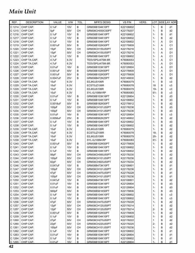
42
Main Unit
C 1214 CHIP CAP. 0.1uF 10V B GRM36B104K10PT K22108802 1- B d1C 1215 CHIP CAP. 5pF 50V CH GRM36CH050C50PT K22178207 1- B d2C 1216 CHIP CAP. 0.1uF 10V B GRM36B104K10PT K22108802 1- B d1C 1217 CHIP CAP. 0.1uF 10V B GRM36B104K10PT K22108802 1- B d2C 1218 CHIP CAP. 0.1uF 10V B GRM36B104K10PT K22108802 1- A D1C 1219 CHIP CAP. 0.001uF 50V B GRM36B102K50PT K22178809 1- A C1C 1220 CHIP CAP. 15pF 50V CH GRM36CH150J50PT K22178216 1- A D1C 1221 CHIP CAP. 15pF 50V CH GRM36CH150J50PT K22178216 1- A D1C 1222 CHIP CAP. 0.1uF 10V B GRM36B104K10PT K22108802 1- A C1C 1223 CHIP TA.CAP. 4.7uF 6.3V TESVSP0J475M-8R K78080053 1- A C1C 1224 CHIP TA.CAP. 4.7uF 6.3V TESVSP0J475M-8R K78080053 1- A D1C 1225 CHIP CAP. 0.01uF 16V B GRM36B103K16PT K22128804 1- A D1C 1226 CHIP CAP. 0.001uF 50V B GRM36B102K50PT K22178809 1- A D1C 1227 CHIP CAP. 0.001uF 50V B GRM36B102K50PT K22178809 1- A D1C 1228 CHIP CAP. 0.0047uF 25V B GRM36B472K25PT K22148830 1- B d2C 1229 CHIP TA.CAP. 10uF 6.3V EEJK0JS106R K78080079 1- B c3C 1229 CHIP TA.CAP. 10uF 6.3V ECST0JZ106R K78080078 18 B c3C 1229 CHIP TA.CAP. 10uF 6.3V EEJK0JS106R K78080079 19- B c3C 1229 CHIP TA.CAP. 10uF 6.3V SYL-0J106M-RP K78080083 61- B c3C 1230 CHIP CAP. 0.01uF 16V B GRM36B103K16PT K22128804 1- B d3C 1231 CHIP CAP. 0.1uF 10V B GRM36B104K10PT K22108802 1- B d3C 1232 CHIP CAP. 0.0018uF 50V B GRM36B182K50PT K22178812 1- B d2C 1233 CHIP CAP. 100pF 50V CH GRM36CH101J50PT K22178236 1- B d3C 1234 CHIP CAP. 100pF 50V CH GRM36CH101J50PT K22178236 1- B d3C 1235 CHIP CAP. 0.01uF 16V B GRM36B103K16PT K22128804 1- B c3C 1236 CHIP CAP. 0.0056uF 25V B GRM36B562K25PT K22148802 1- B d2C 1237 CHIP CAP. 0.1uF 10V B GRM36B104K10PT K22108802 1- B d3C 1238 CHIP CAP. 0.1uF 10V B GRM36B104K10PT K22108802 1- B d2C 1239 CHIP TA.CAP. 10uF 6.3V EEJK0JS106R K78080079 1- B d2C 1239 CHIP TA.CAP. 10uF 6.3V ECST0JZ106R K78080078 18- B d2C 1239 CHIP TA.CAP. 10uF 6.3V EEJK0JS106R K78080079 20- B d2C 1239 CHIP TA.CAP. 10uF 6.3V SYL-0J106M-RP K78080083 61- B d2C 1240 CHIP CAP. 0.001uF 50V B GRM36B102K50PT K22178809 1- B d2C 1241 CHIP CAP. 0.1uF 10V B GRM36B104K10PT K22108802 1- B d2C 1242 CHIP CAP. 0.1uF 10V B GRM36B104K10PT K22108802 1- B d2C 1243 CHIP CAP. 56pF 50V CH GRM36CH560J50PT K22178230 1- B d2C 1244 CHIP CAP. 100pF 50V CH GRM36CH101J50PT K22178236 1- B d2C 1245 CHIP CAP. 82pF 50V CH GRM36CH820J50PT K22178234 1- B d2C 1246 CHIP CAP. 0.047uF 10V B GRM36B473K10PT K22108801 1- B d1C 1247 CHIP CAP. 100pF 50V CH GRM36CH101J50PT K22178236 1- B d1C 1248 CHIP CAP. 47pF 50V CH GRM36CH470J50PT K22178228 1- B d1C 1249 CHIP CAP. 100pF 50V CH GRM36CH101J50PT K22178236 1- B d1C 1250 CHIP CAP. 0.047uF 10V B GRM36B473K10PT K22108801 1- B d2C 1251 CHIP CAP. 0.01uF 16V B GRM36B103K16PT K22128804 1- B d3C 1252 CHIP CAP. 0.01uF 16V B GRM36B103K16PT K22128804 1- B d3C 1253 CHIP CAP. 560pF 50V B GRM36B561K50PT K22178806 1- B d3C 1254 CHIP CAP. 0.1uF 10V B GRM36B104K10PT K22108802 1- B c3C 1255 CHIP CAP. 0.1uF 10V B GRM36B104K10PT K22108802 1- B c3C 1256 CHIP CAP. 47pF 50V CH GRM36CH470J50PT K22178228 1- B d2C 1257 CHIP CAP. 12pF 50V CH GRM36CH120J50PT K22178214 1 B d2C 1257 CHIP CAP. 12pF 50V CH GRM36CH120J50PT K22178214 2- B d2C 1258 CHIP CAP. 0.001uF 50V B GRM36B102K50PT K22178809 1- B d2C 1259 CHIP CAP. 0.1uF 10V B GRM36B104K10PT K22108802 1- B d2C 1260 CHIP CAP. 27pF 50V CH GRM36CH270J50PT K22178222 1 B d2C 1260 CHIP CAP. 22pF 50V CH GRM36CH220J50PT K22178220 2- B d2C 1261 CHIP CAP. 100pF 50V CH GRM36CH101J50PT K22178236 1- B d2C 1262 CHIP CAP. 0.1uF 10V B GRM36B104K10PT K22108802 1- B d1C 1263 CHIP CAP. 0.01uF 16V B GRM36B103K16PT K22128804 1- B d1C 1264 CHIP CAP. 0.1uF 10V B GRM36B104K10PT K22108802 1- B d1C 1265 CHIP CAP. 0.01uF 16V B GRM36B103K16PT K22128804 1- B d1
DESCRIPTION VALUE V/W TOL. VS P/NMFR’S DESIG VERS.REF. LOT. SIDE LAY ADR
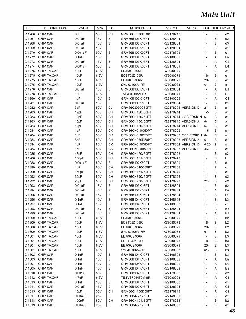
43
Main Unit
C 1266 CHIP CAP. 8pF 50V CH GRM36CH080D50PT K22178210 1- B d2C 1267 CHIP CAP. 0.01uF 16V B GRM36B103K16PT K22128804 1- B d2C 1268 CHIP CAP. 0.01uF 16V B GRM36B103K16PT K22128804 1- B d3C 1269 CHIP CAP. 0.01uF 16V B GRM36B103K16PT K22128804 1- B d1C 1270 CHIP CAP. 0.001uF 50V B GRM36B102K50PT K22178809 1- B e1C 1272 CHIP CAP. 0.1uF 10V B GRM36B104K10PT K22108802 1- A D2C 1273 CHIP CAP. 0.01uF 16V B GRM36B103K16PT K22128804 1- A C2C 1274 CHIP CAP. 0.001uF 50V B GRM36B102K50PT K22178809 1- A D1C 1275 CHIP TA.CAP. 10uF 6.3V EEJK0JS106R K78080079 1- B e1C 1275 CHIP TA.CAP. 10uF 6.3V ECST0JZ106R K78080078 18- B e1C 1275 CHIP TA.CAP. 10uF 6.3V EEJK0JS106R K78080079 20- B e1C 1275 CHIP TA.CAP. 10uF 6.3V SYL-0J106M-RP K78080083 61- B e1C 1276 CHIP CAP. 0.01uF 16V B GRM36B103K16PT K22128804 1- A B1C 1278 CHIP TA.CAP. 1uF 6.3V TMCP0J105MTR K78080071 1- A B2C 1280 CHIP CAP. 1uF 10V B GRM40B105K10PT K22100802 1- A C2C 1281 CHIP CAP. 0.01uF 16V B GRM36B103K16PT K22128804 1- B b1C 1282 CHIP CAP. 3pF 50V CJ GRM36CJ030C50PT K22178205 VERSION D 21- B a1C 1283 CHIP CAP. 12pF 50V CH GRM36CH120J50PT K22178214 1-5 B a1C 1283 CHIP CAP. 12pF 50V CH GRM36CH120J50PT K22178214 CS VERSION 6- B a1C 1283 CHIP CAP. 15pF 50V CH GRM36CH150J50PT K22178216 VERSION A 6- B a1C 1283 CHIP CAP. 12pF 50V CH GRM36CH120J50PT K22178214 VERSION D 6- B a1C 1284 CHIP CAP. 1pF 50V CK GRM36CK010C50PT K22178202 1-5 B a1C 1284 CHIP CAP. 1pF 50V CK GRM36CK010C50PT K22178202 CS VERSION 6- B a1C 1284 CHIP CAP. 6pF 50V CH GRM36CH060D50PT K22178208 VERSION A 6- B a1C 1284 CHIP CAP. 1pF 50V CK GRM36CK010C50PT K22178202 VERSION D 6-20 B a1C 1284 CHIP CAP. 1pF 50V CK GRM36CK010B50PT K22178287 VERSION D 36- B a1C 1285 CHIP CAP. 47pF 50V CH GRM36CH470J50PT K22178228 1- B c2C 1286 CHIP CAP. 150pF 50V CH GRM36CH151J50PT K22178240 1- B b1C 1288 CHIP CAP. 0.001uF 50V B GRM36B102K50PT K22178809 1- B d1C 1289 CHIP CAP. 4pF 50V CH GRM36CH040C50PT K22178206 1- B c1C 1290 CHIP CAP. 150pF 50V CH GRM36CH151J50PT K22178240 1- B d1C 1292 CHIP CAP. 39pF 50V CH GRM36CH390J50PT K22178226 1- B d2C 1292 CHIP CAP. 22pF 50V CH GRM36CH220J50PT K22178220 21- B d2C 1293 CHIP CAP. 0.01uF 16V B GRM36B103K16PT K22128804 1- B d2C 1294 CHIP CAP. 0.01uF 16V B GRM36B103K16PT K22128804 1- A D2C 1295 CHIP CAP. 0.01uF 16V B GRM36B103K16PT K22128804 1- A D2C 1296 CHIP CAP. 0.1uF 10V B GRM36B104K10PT K22108802 1- B b3C 1297 CHIP CAP. 0.1uF 10V B GRM36B104K10PT K22108802 1- B e1C 1298 CHIP CAP. 0.01uF 16V B GRM36B103K16PT K22128804 1- A E2C 1299 CHIP CAP. 0.01uF 16V B GRM36B103K16PT K22128804 1- A E3C 1300 CHIP TA.CAP. 10uF 6.3V EEJK0JS106R K78080079 1- B b2C 1300 CHIP TA.CAP. 10uF 6.3V ECST0JZ106R K78080078 18- B b2C 1300 CHIP TA.CAP. 10uF 6.3V EEJK0JS106R K78080079 20- B b2C 1300 CHIP TA.CAP. 10uF 6.3V SYL-0J106M-RP K78080083 61- B b2C 1301 CHIP TA.CAP. 10uF 6.3V EEJK0JS106R K78080079 1- B b3C 1301 CHIP TA.CAP. 10uF 6.3V ECST0JZ106R K78080078 18- B b3C 1301 CHIP TA.CAP. 10uF 6.3V EEJK0JS106R K78080079 20- B b3C 1301 CHIP TA.CAP. 10uF 6.3V SYL-0J106M-RP K78080083 61- B b3C 1302 CHIP CAP. 0.1uF 10V B GRM36B104K10PT K22108802 1- B b3C 1303 CHIP CAP. 0.1uF 10V B GRM36B104K10PT K22108802 1- A D2C 1304 CHIP CAP. 0.1uF 10V B GRM36B104K10PT K22108802 1- A D3C 1305 CHIP CAP. 0.1uF 10V B GRM36B104K10PT K22108802 1- A B2C 1310 CHIP CAP. 0.001uF 50V B GRM36B102K50PT K22178809 1- B d2C 1312 CHIP TA.CAP. 4.7uF 6.3V TESVSP0J475M-8R K78080053 1- A C1C 1313 CHIP CAP. 0.1uF 10V B GRM36B104K10PT K22108802 1- B d1C 1314 CHIP CAP. 0.01uF 16V B GRM36B103K16PT K22128804 1- A C1C 1315 CHIP CAP. 10pF 50V CH GRM36CH100D50PT K22178212 1- A C2C 1317 CHIP CAP. 0.0047uF 25V B GRM36B472K25PT K22148830 1- B e1C 1318 CHIP CAP. 100pF 50V CH GRM36CH101J50PT K22178236 1- B b2C 1319 CHIP CAP. 0.0047uF 25V B GRM36B472K25PT K22148830 1- B e1
DESCRIPTION VALUE V/W TOL. VS P/NMFR’S DESIG VERS.REF. LOT. SIDE LAY ADR
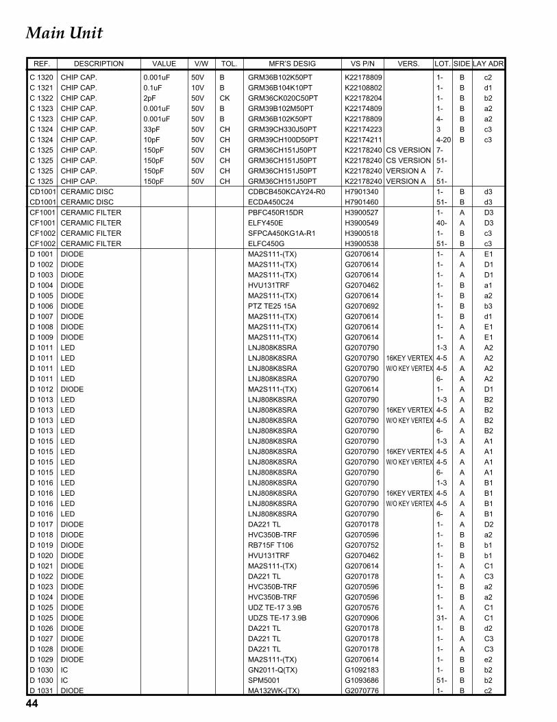
44
Main Unit
C 1320 CHIP CAP. 0.001uF 50V B GRM36B102K50PT K22178809 1- B c2C 1321 CHIP CAP. 0.1uF 10V B GRM36B104K10PT K22108802 1- B d1C 1322 CHIP CAP. 2pF 50V CK GRM36CK020C50PT K22178204 1- B b2C 1323 CHIP CAP. 0.001uF 50V B GRM39B102M50PT K22174809 1- B a2C 1323 CHIP CAP. 0.001uF 50V B GRM36B102K50PT K22178809 4- B a2C 1324 CHIP CAP. 33pF 50V CH GRM39CH330J50PT K22174223 3 B c3C 1324 CHIP CAP. 10pF 50V CH GRM39CH100D50PT K22174211 4-20 B c3C 1325 CHIP CAP. 150pF 50V CH GRM36CH151J50PT K22178240 CS VERSION 7-C 1325 CHIP CAP. 150pF 50V CH GRM36CH151J50PT K22178240 CS VERSION 51-C 1325 CHIP CAP. 150pF 50V CH GRM36CH151J50PT K22178240 VERSION A 7-C 1325 CHIP CAP. 150pF 50V CH GRM36CH151J50PT K22178240 VERSION A 51-CD1001 CERAMIC DISC CDBCB450KCAY24-R0 H7901340 1- B d3CD1001 CERAMIC DISC ECDA450C24 H7901460 51- B d3CF1001 CERAMIC FILTER PBFC450R15DR H3900527 1- A D3CF1001 CERAMIC FILTER ELFY450E H3900549 40- A D3CF1002 CERAMIC FILTER SFPCA450KG1A-R1 H3900518 1- B c3CF1002 CERAMIC FILTER ELFC450G H3900538 51- B c3D 1001 DIODE MA2S111-(TX) G2070614 1- A E1D 1002 DIODE MA2S111-(TX) G2070614 1- A D1D 1003 DIODE MA2S111-(TX) G2070614 1- A D1D 1004 DIODE HVU131TRF G2070462 1- B a1D 1005 DIODE MA2S111-(TX) G2070614 1- B a2D 1006 DIODE PTZ TE25 15A G2070692 1- B b3D 1007 DIODE MA2S111-(TX) G2070614 1- B d1D 1008 DIODE MA2S111-(TX) G2070614 1- A E1D 1009 DIODE MA2S111-(TX) G2070614 1- A E1D 1011 LED LNJ808K8SRA G2070790 1-3 A A2D 1011 LED LNJ808K8SRA G2070790 16KEY VERTEX 4-5 A A2D 1011 LED LNJ808K8SRA G2070790 W/O KEY VERTEX 4-5 A A2D 1011 LED LNJ808K8SRA G2070790 6- A A2D 1012 DIODE MA2S111-(TX) G2070614 1- A D1D 1013 LED LNJ808K8SRA G2070790 1-3 A B2D 1013 LED LNJ808K8SRA G2070790 16KEY VERTEX 4-5 A B2D 1013 LED LNJ808K8SRA G2070790 W/O KEY VERTEX 4-5 A B2D 1013 LED LNJ808K8SRA G2070790 6- A B2D 1015 LED LNJ808K8SRA G2070790 1-3 A A1D 1015 LED LNJ808K8SRA G2070790 16KEY VERTEX 4-5 A A1D 1015 LED LNJ808K8SRA G2070790 W/O KEY VERTEX 4-5 A A1D 1015 LED LNJ808K8SRA G2070790 6- A A1D 1016 LED LNJ808K8SRA G2070790 1-3 A B1D 1016 LED LNJ808K8SRA G2070790 16KEY VERTEX 4-5 A B1D 1016 LED LNJ808K8SRA G2070790 W/O KEY VERTEX 4-5 A B1D 1016 LED LNJ808K8SRA G2070790 6- A B1D 1017 DIODE DA221 TL G2070178 1- A D2D 1018 DIODE HVC350B-TRF G2070596 1- B a2D 1019 DIODE RB715F T106 G2070752 1- B b1D 1020 DIODE HVU131TRF G2070462 1- B b1D 1021 DIODE MA2S111-(TX) G2070614 1- A C1D 1022 DIODE DA221 TL G2070178 1- A C3D 1023 DIODE HVC350B-TRF G2070596 1- B a2D 1024 DIODE HVC350B-TRF G2070596 1- B a2D 1025 DIODE UDZ TE-17 3.9B G2070576 1- A C1D 1025 DIODE UDZS TE-17 3.9B G2070906 31- A C1D 1026 DIODE DA221 TL G2070178 1- B d2D 1027 DIODE DA221 TL G2070178 1- A C3D 1028 DIODE DA221 TL G2070178 1- A C3D 1029 DIODE MA2S111-(TX) G2070614 1- B e2D 1030 IC GN2011-Q(TX) G1092183 1- B b2D 1030 IC SPM5001 G1093686 51- B b2D 1031 DIODE MA132WK-(TX) G2070776 1- B c2
DESCRIPTION VALUE V/W TOL. VS P/NMFR’S DESIG VERS.REF. LOT. SIDE LAY ADR
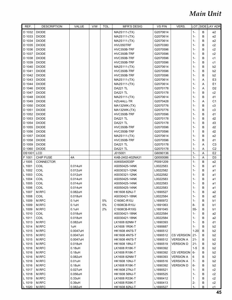
45
Main Unit
D 1032 DIODE MA2S111-(TX) G2070614 1- B e2D 1033 DIODE MA2S111-(TX) G2070614 1- B e2D 1034 DIODE MA2S111-(TX) G2070614 1- B e2D 1035 DIODE HVU350TRF G2070380 1- B c2D 1036 DIODE HVC350B-TRF G2070596 1- B c2D 1037 DIODE HVC350B-TRF G2070596 1- B c2D 1038 DIODE HVC350B-TRF G2070596 1- B c1D 1039 DIODE HVC350B-TRF G2070596 1- B c1D 1040 DIODE MA2S111-(TX) G2070614 1- B b2D 1041 DIODE HVC350B-TRF G2070596 1- B b2D 1042 DIODE HVC350B-TRF G2070596 1- B b2D 1043 DIODE MA2S111-(TX) G2070614 1- A E3D 1044 DIODE MA2S111-(TX) G2070614 1- A E1D 1046 DIODE DA221 TL G2070178 1- A D2D 1047 DIODE DA221 TL G2070178 1- B c2D 1048 DIODE MA2S111-(TX) G2070614 1- B d1D 1049 DIODE HZU4ALL-TR G2070428 1- A C1D 1050 DIODE MA132WK-(TX) G2070776 1- B c3D 1051 DIODE MA132WK-(TX) G2070776 1- B c3D 1052 DIODE HVC350B-TRF G2070596 1- B d1D 1053 DIODE DA221 TL G2070178 1- B d2D 1054 DIODE DA221 TL G2070178 1- B d3D 1055 DIODE HVC350B-TRF G2070596 1- B d2D 1056 DIODE HVC350B-TRF G2070596 1 B d2D 1057 DIODE MA2S111-(TX) G2070614 1- B e2D 1058 DIODE HVC350B-TRF G2070596 1- B d1D 1059 DIODE DA221 TL G2070178 1- A C3D 1060 DIODE DA221 TL G2070178 1- A C2DS1001 LCD J015001 G6090136 1- A E2F 1001 CHIP FUSE 4A KAB-2402-402NA31 Q0000086 1- A D3J 1005 CONNECTOR AXK6S40535P P0091209 1- B e2L 1001 COIL 0.014uH AS050425-14NK L0022583 1- B a1L 1002 COIL 0.012uH AS030321-12NK L0022582 1- B a1L 1003 COIL 0.012uH AS030321-12NK L0022582 1- B a1L 1004 COIL 0.014uH AS050425-14NK L0022583 1- B a1L 1005 COIL 0.014uH AS050425-14NK L0022583 1- B a1L 1006 COIL 0.014uH AS050425-14NK L0022583 1- B a1L 1007 M.RFC 0.082uH HK1608 82NJ-T L1690527 1- B a2L 1008 COIL 0.018uH AS030421-18NK L0022584 1- B a2L 1009 M.RFC 0.1uH 5% C1608C-R10J L1690972 1- B b1L 1009 M.RFC 0.1uH 5% C1608CB-R10J L1691063 8- B b1L 1009 M.RFC 0.1uH 2% C1608CB-R10G L1691045 55- B b1L 1010 COIL 0.018uH AS030421-18NK L0022584 1- B a2L 1011 COIL 0.018uH AS030421-18NK L0022584 1- B a2L 1013 M.RFC 0.082uH LK1608 82NM-T L1690393 1- B d1L 1014 M.RFC 1uH LK1608 1R0K-T L1690687 1- B b2L 1015 M.RFC 0.0047uH HK1608 4N7S-T L1690512 1-20 B b2L 1015 M.RFC 0.0047uH HK1608 4N7S-T L1690512 CS VERSION 21- B b2L 1015 M.RFC 0.0047uH HK1608 4N7S-T L1690512 VERSION A 21- B b2L 1015 M.RFC 0.018uH HK1608 18NJ-T L1690519 VERSION D 21- B b2L 1016 M.RFC 0.18uH LK1608 R18K-T L1690392 1-5 B b2L 1016 M.RFC 0.18uH LK1608 R18K-T L1690392 CS VERSION 6- B b2L 1016 M.RFC 0.082uH LK1608 82NM-T L1690393 VERSION A 6 B b2L 1016 M.RFC 0.01uH HK1608 10NJ-T L1690516 VERSION A 7- B b2L 1016 M.RFC 0.18uH LK1608 R18K-T L1690392 VERSION D 6- B b2L 1017 M.RFC 0.027uH HK1608 27NJ-T L1690521 1- B c2L 1018 M.RFC 0.056uH HK1608 56NJ-T L1690525 1- B c2L 1019 M.RFC 0.33uH LK1608 R33K-T L1690412 1 B c2L 1019 M.RFC 0.39uH LK1608 R39K-T L1690413 2- B c2L 1020 M.RFC 0.082uH HK1608 82NJ-T L1690527 1- B c1
DESCRIPTION VALUE V/W TOL. VS P/NMFR’S DESIG VERS.REF. LOT. SIDE LAY ADR
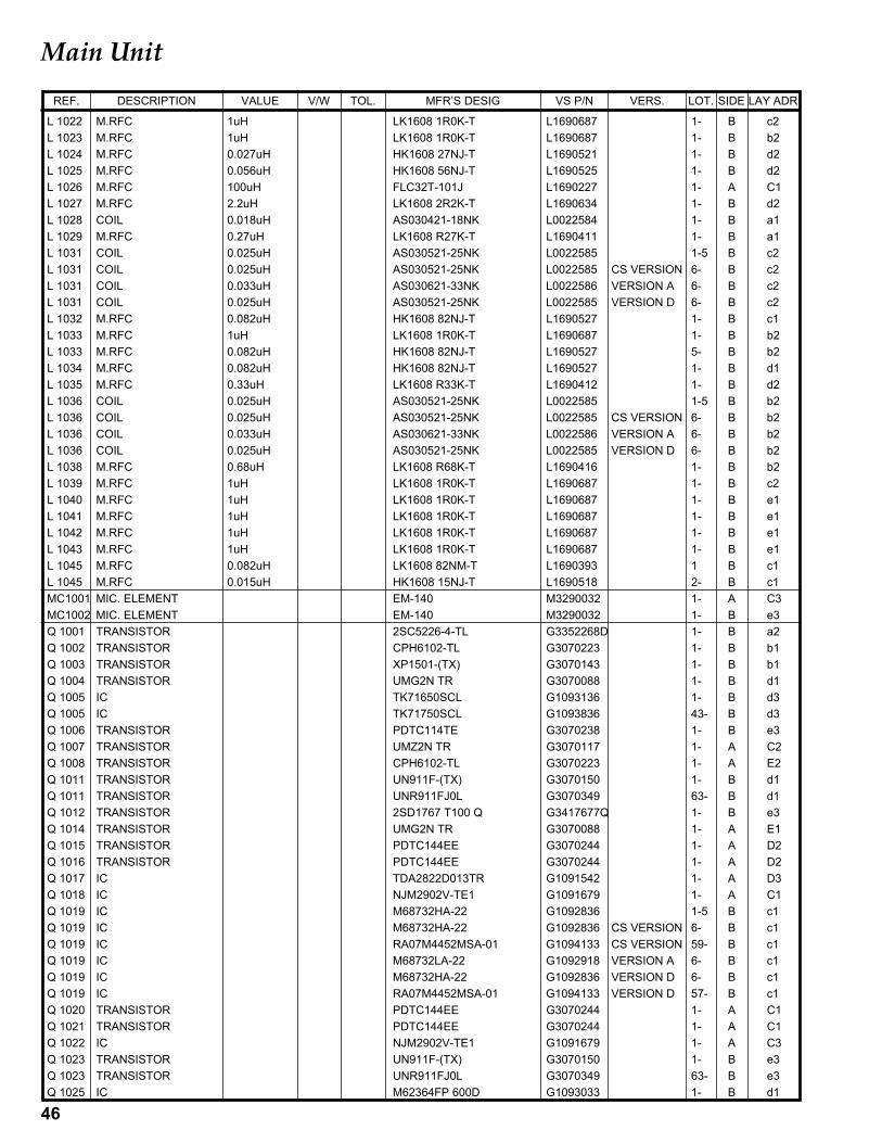
46
Main Unit
L 1022 M.RFC 1uH LK1608 1R0K-T L1690687 1- B c2L 1023 M.RFC 1uH LK1608 1R0K-T L1690687 1- B b2L 1024 M.RFC 0.027uH HK1608 27NJ-T L1690521 1- B d2L 1025 M.RFC 0.056uH HK1608 56NJ-T L1690525 1- B d2L 1026 M.RFC 100uH FLC32T-101J L1690227 1- A C1L 1027 M.RFC 2.2uH LK1608 2R2K-T L1690634 1- B d2L 1028 COIL 0.018uH AS030421-18NK L0022584 1- B a1L 1029 M.RFC 0.27uH LK1608 R27K-T L1690411 1- B a1L 1031 COIL 0.025uH AS030521-25NK L0022585 1-5 B c2L 1031 COIL 0.025uH AS030521-25NK L0022585 CS VERSION 6- B c2L 1031 COIL 0.033uH AS030621-33NK L0022586 VERSION A 6- B c2L 1031 COIL 0.025uH AS030521-25NK L0022585 VERSION D 6- B c2L 1032 M.RFC 0.082uH HK1608 82NJ-T L1690527 1- B c1L 1033 M.RFC 1uH LK1608 1R0K-T L1690687 1- B b2L 1033 M.RFC 0.082uH HK1608 82NJ-T L1690527 5- B b2L 1034 M.RFC 0.082uH HK1608 82NJ-T L1690527 1- B d1L 1035 M.RFC 0.33uH LK1608 R33K-T L1690412 1- B d2L 1036 COIL 0.025uH AS030521-25NK L0022585 1-5 B b2L 1036 COIL 0.025uH AS030521-25NK L0022585 CS VERSION 6- B b2L 1036 COIL 0.033uH AS030621-33NK L0022586 VERSION A 6- B b2L 1036 COIL 0.025uH AS030521-25NK L0022585 VERSION D 6- B b2L 1038 M.RFC 0.68uH LK1608 R68K-T L1690416 1- B b2L 1039 M.RFC 1uH LK1608 1R0K-T L1690687 1- B c2L 1040 M.RFC 1uH LK1608 1R0K-T L1690687 1- B e1L 1041 M.RFC 1uH LK1608 1R0K-T L1690687 1- B e1L 1042 M.RFC 1uH LK1608 1R0K-T L1690687 1- B e1L 1043 M.RFC 1uH LK1608 1R0K-T L1690687 1- B e1L 1045 M.RFC 0.082uH LK1608 82NM-T L1690393 1 B c1L 1045 M.RFC 0.015uH HK1608 15NJ-T L1690518 2- B c1MC1001 MIC. ELEMENT EM-140 M3290032 1- A C3MC1002 MIC. ELEMENT EM-140 M3290032 1- B e3Q 1001 TRANSISTOR 2SC5226-4-TL G3352268D 1- B a2Q 1002 TRANSISTOR CPH6102-TL G3070223 1- B b1Q 1003 TRANSISTOR XP1501-(TX) G3070143 1- B b1Q 1004 TRANSISTOR UMG2N TR G3070088 1- B d1Q 1005 IC TK71650SCL G1093136 1- B d3Q 1005 IC TK71750SCL G1093836 43- B d3Q 1006 TRANSISTOR PDTC114TE G3070238 1- B e3Q 1007 TRANSISTOR UMZ2N TR G3070117 1- A C2Q 1008 TRANSISTOR CPH6102-TL G3070223 1- A E2Q 1011 TRANSISTOR UN911F-(TX) G3070150 1- B d1Q 1011 TRANSISTOR UNR911FJ0L G3070349 63- B d1Q 1012 TRANSISTOR 2SD1767 T100 Q G3417677Q 1- B e3Q 1014 TRANSISTOR UMG2N TR G3070088 1- A E1Q 1015 TRANSISTOR PDTC144EE G3070244 1- A D2Q 1016 TRANSISTOR PDTC144EE G3070244 1- A D2Q 1017 IC TDA2822D013TR G1091542 1- A D3Q 1018 IC NJM2902V-TE1 G1091679 1- A C1Q 1019 IC M68732HA-22 G1092836 1-5 B c1Q 1019 IC M68732HA-22 G1092836 CS VERSION 6- B c1Q 1019 IC RA07M4452MSA-01 G1094133 CS VERSION 59- B c1Q 1019 IC M68732LA-22 G1092918 VERSION A 6- B c1Q 1019 IC M68732HA-22 G1092836 VERSION D 6- B c1Q 1019 IC RA07M4452MSA-01 G1094133 VERSION D 57- B c1Q 1020 TRANSISTOR PDTC144EE G3070244 1- A C1Q 1021 TRANSISTOR PDTC144EE G3070244 1- A C1Q 1022 IC NJM2902V-TE1 G1091679 1- A C3Q 1023 TRANSISTOR UN911F-(TX) G3070150 1- B e3Q 1023 TRANSISTOR UNR911FJ0L G3070349 63- B e3Q 1025 IC M62364FP 600D G1093033 1- B d1
DESCRIPTION VALUE V/W TOL. VS P/NMFR’S DESIG VERS.REF. LOT. SIDE LAY ADR
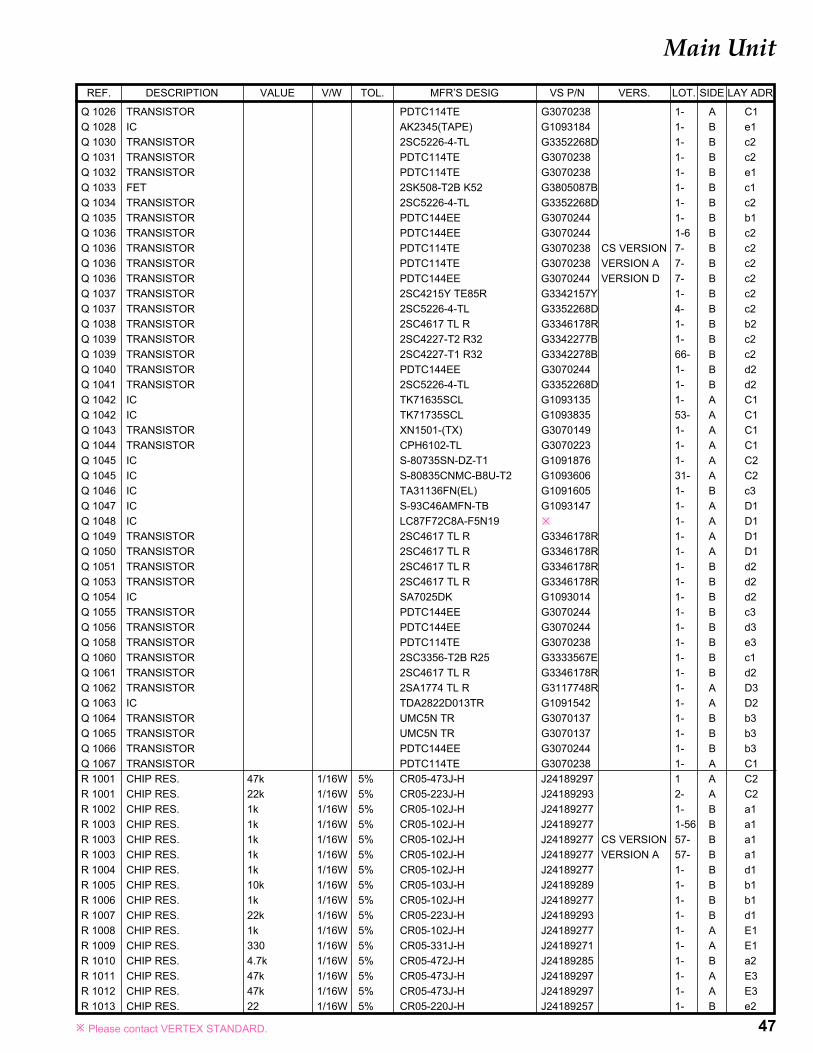
47
Main Unit
Q 1026 TRANSISTOR PDTC114TE G3070238 1- A C1Q 1028 IC AK2345(TAPE) G1093184 1- B e1Q 1030 TRANSISTOR 2SC5226-4-TL G3352268D 1- B c2Q 1031 TRANSISTOR PDTC114TE G3070238 1- B c2Q 1032 TRANSISTOR PDTC114TE G3070238 1- B e1Q 1033 FET 2SK508-T2B K52 G3805087B 1- B c1Q 1034 TRANSISTOR 2SC5226-4-TL G3352268D 1- B c2Q 1035 TRANSISTOR PDTC144EE G3070244 1- B b1Q 1036 TRANSISTOR PDTC144EE G3070244 1-6 B c2Q 1036 TRANSISTOR PDTC114TE G3070238 CS VERSION 7- B c2Q 1036 TRANSISTOR PDTC114TE G3070238 VERSION A 7- B c2Q 1036 TRANSISTOR PDTC144EE G3070244 VERSION D 7- B c2Q 1037 TRANSISTOR 2SC4215Y TE85R G3342157Y 1- B c2Q 1037 TRANSISTOR 2SC5226-4-TL G3352268D 4- B c2Q 1038 TRANSISTOR 2SC4617 TL R G3346178R 1- B b2Q 1039 TRANSISTOR 2SC4227-T2 R32 G3342277B 1- B c2Q 1039 TRANSISTOR 2SC4227-T1 R32 G3342278B 66- B c2Q 1040 TRANSISTOR PDTC144EE G3070244 1- B d2Q 1041 TRANSISTOR 2SC5226-4-TL G3352268D 1- B d2Q 1042 IC TK71635SCL G1093135 1- A C1Q 1042 IC TK71735SCL G1093835 53- A C1Q 1043 TRANSISTOR XN1501-(TX) G3070149 1- A C1Q 1044 TRANSISTOR CPH6102-TL G3070223 1- A C1Q 1045 IC S-80735SN-DZ-T1 G1091876 1- A C2Q 1045 IC S-80835CNMC-B8U-T2 G1093606 31- A C2Q 1046 IC TA31136FN(EL) G1091605 1- B c3Q 1047 IC S-93C46AMFN-TB G1093147 1- A D1Q 1048 IC LC87F72C8A-F5N19 1- A D1Q 1049 TRANSISTOR 2SC4617 TL R G3346178R 1- A D1Q 1050 TRANSISTOR 2SC4617 TL R G3346178R 1- A D1Q 1051 TRANSISTOR 2SC4617 TL R G3346178R 1- B d2Q 1053 TRANSISTOR 2SC4617 TL R G3346178R 1- B d2Q 1054 IC SA7025DK G1093014 1- B d2Q 1055 TRANSISTOR PDTC144EE G3070244 1- B c3Q 1056 TRANSISTOR PDTC144EE G3070244 1- B d3Q 1058 TRANSISTOR PDTC114TE G3070238 1- B e3Q 1060 TRANSISTOR 2SC3356-T2B R25 G3333567E 1- B c1Q 1061 TRANSISTOR 2SC4617 TL R G3346178R 1- B d2Q 1062 TRANSISTOR 2SA1774 TL R G3117748R 1- A D3Q 1063 IC TDA2822D013TR G1091542 1- A D2Q 1064 TRANSISTOR UMC5N TR G3070137 1- B b3Q 1065 TRANSISTOR UMC5N TR G3070137 1- B b3Q 1066 TRANSISTOR PDTC144EE G3070244 1- B b3Q 1067 TRANSISTOR PDTC114TE G3070238 1- A C1R 1001 CHIP RES. 47k 1/16W 5% CR05-473J-H J24189297 1 A C2R 1001 CHIP RES. 22k 1/16W 5% CR05-223J-H J24189293 2- A C2R 1002 CHIP RES. 1k 1/16W 5% CR05-102J-H J24189277 1- B a1R 1003 CHIP RES. 1k 1/16W 5% CR05-102J-H J24189277 1-56 B a1R 1003 CHIP RES. 1k 1/16W 5% CR05-102J-H J24189277 CS VERSION 57- B a1R 1003 CHIP RES. 1k 1/16W 5% CR05-102J-H J24189277 VERSION A 57- B a1R 1004 CHIP RES. 1k 1/16W 5% CR05-102J-H J24189277 1- B d1R 1005 CHIP RES. 10k 1/16W 5% CR05-103J-H J24189289 1- B b1R 1006 CHIP RES. 1k 1/16W 5% CR05-102J-H J24189277 1- B b1R 1007 CHIP RES. 22k 1/16W 5% CR05-223J-H J24189293 1- B d1R 1008 CHIP RES. 1k 1/16W 5% CR05-102J-H J24189277 1- A E1R 1009 CHIP RES. 330 1/16W 5% CR05-331J-H J24189271 1- A E1R 1010 CHIP RES. 4.7k 1/16W 5% CR05-472J-H J24189285 1- B a2R 1011 CHIP RES. 47k 1/16W 5% CR05-473J-H J24189297 1- A E3R 1012 CHIP RES. 47k 1/16W 5% CR05-473J-H J24189297 1- A E3R 1013 CHIP RES. 22 1/16W 5% CR05-220J-H J24189257 1- B e2
Please contact VERTEX STANDARD.
DESCRIPTION VALUE V/W TOL. VS P/NMFR’S DESIG VERS.REF. LOT. SIDE LAY ADR
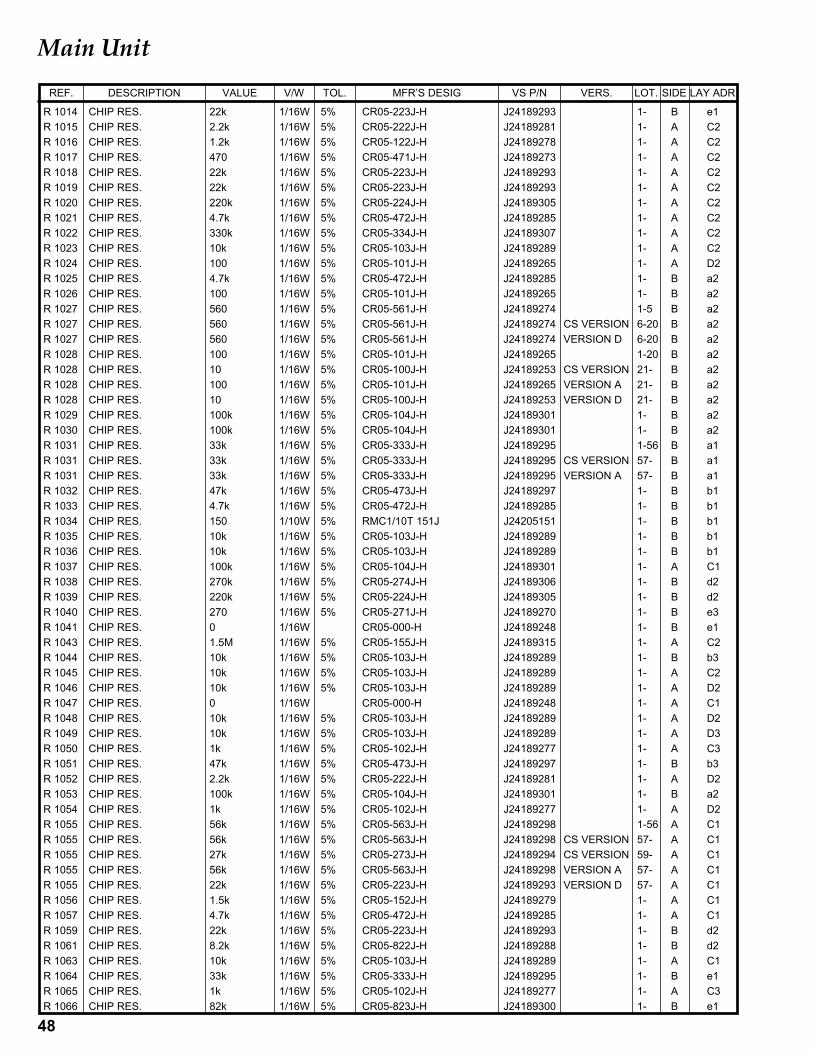
48
Main Unit
R 1014 CHIP RES. 22k 1/16W 5% CR05-223J-H J24189293 1- B e1R 1015 CHIP RES. 2.2k 1/16W 5% CR05-222J-H J24189281 1- A C2R 1016 CHIP RES. 1.2k 1/16W 5% CR05-122J-H J24189278 1- A C2R 1017 CHIP RES. 470 1/16W 5% CR05-471J-H J24189273 1- A C2R 1018 CHIP RES. 22k 1/16W 5% CR05-223J-H J24189293 1- A C2R 1019 CHIP RES. 22k 1/16W 5% CR05-223J-H J24189293 1- A C2R 1020 CHIP RES. 220k 1/16W 5% CR05-224J-H J24189305 1- A C2R 1021 CHIP RES. 4.7k 1/16W 5% CR05-472J-H J24189285 1- A C2R 1022 CHIP RES. 330k 1/16W 5% CR05-334J-H J24189307 1- A C2R 1023 CHIP RES. 10k 1/16W 5% CR05-103J-H J24189289 1- A C2R 1024 CHIP RES. 100 1/16W 5% CR05-101J-H J24189265 1- A D2R 1025 CHIP RES. 4.7k 1/16W 5% CR05-472J-H J24189285 1- B a2R 1026 CHIP RES. 100 1/16W 5% CR05-101J-H J24189265 1- B a2R 1027 CHIP RES. 560 1/16W 5% CR05-561J-H J24189274 1-5 B a2R 1027 CHIP RES. 560 1/16W 5% CR05-561J-H J24189274 CS VERSION 6-20 B a2R 1027 CHIP RES. 560 1/16W 5% CR05-561J-H J24189274 VERSION D 6-20 B a2R 1028 CHIP RES. 100 1/16W 5% CR05-101J-H J24189265 1-20 B a2R 1028 CHIP RES. 10 1/16W 5% CR05-100J-H J24189253 CS VERSION 21- B a2R 1028 CHIP RES. 100 1/16W 5% CR05-101J-H J24189265 VERSION A 21- B a2R 1028 CHIP RES. 10 1/16W 5% CR05-100J-H J24189253 VERSION D 21- B a2R 1029 CHIP RES. 100k 1/16W 5% CR05-104J-H J24189301 1- B a2R 1030 CHIP RES. 100k 1/16W 5% CR05-104J-H J24189301 1- B a2R 1031 CHIP RES. 33k 1/16W 5% CR05-333J-H J24189295 1-56 B a1R 1031 CHIP RES. 33k 1/16W 5% CR05-333J-H J24189295 CS VERSION 57- B a1R 1031 CHIP RES. 33k 1/16W 5% CR05-333J-H J24189295 VERSION A 57- B a1R 1032 CHIP RES. 47k 1/16W 5% CR05-473J-H J24189297 1- B b1R 1033 CHIP RES. 4.7k 1/16W 5% CR05-472J-H J24189285 1- B b1R 1034 CHIP RES. 150 1/10W 5% RMC1/10T 151J J24205151 1- B b1R 1035 CHIP RES. 10k 1/16W 5% CR05-103J-H J24189289 1- B b1R 1036 CHIP RES. 10k 1/16W 5% CR05-103J-H J24189289 1- B b1R 1037 CHIP RES. 100k 1/16W 5% CR05-104J-H J24189301 1- A C1R 1038 CHIP RES. 270k 1/16W 5% CR05-274J-H J24189306 1- B d2R 1039 CHIP RES. 220k 1/16W 5% CR05-224J-H J24189305 1- B d2R 1040 CHIP RES. 270 1/16W 5% CR05-271J-H J24189270 1- B e3R 1041 CHIP RES. 0 1/16W CR05-000-H J24189248 1- B e1R 1043 CHIP RES. 1.5M 1/16W 5% CR05-155J-H J24189315 1- A C2R 1044 CHIP RES. 10k 1/16W 5% CR05-103J-H J24189289 1- B b3R 1045 CHIP RES. 10k 1/16W 5% CR05-103J-H J24189289 1- A C2R 1046 CHIP RES. 10k 1/16W 5% CR05-103J-H J24189289 1- A D2R 1047 CHIP RES. 0 1/16W CR05-000-H J24189248 1- A C1R 1048 CHIP RES. 10k 1/16W 5% CR05-103J-H J24189289 1- A D2R 1049 CHIP RES. 10k 1/16W 5% CR05-103J-H J24189289 1- A D3R 1050 CHIP RES. 1k 1/16W 5% CR05-102J-H J24189277 1- A C3R 1051 CHIP RES. 47k 1/16W 5% CR05-473J-H J24189297 1- B b3R 1052 CHIP RES. 2.2k 1/16W 5% CR05-222J-H J24189281 1- A D2R 1053 CHIP RES. 100k 1/16W 5% CR05-104J-H J24189301 1- B a2R 1054 CHIP RES. 1k 1/16W 5% CR05-102J-H J24189277 1- A D2R 1055 CHIP RES. 56k 1/16W 5% CR05-563J-H J24189298 1-56 A C1R 1055 CHIP RES. 56k 1/16W 5% CR05-563J-H J24189298 CS VERSION 57- A C1R 1055 CHIP RES. 27k 1/16W 5% CR05-273J-H J24189294 CS VERSION 59- A C1R 1055 CHIP RES. 56k 1/16W 5% CR05-563J-H J24189298 VERSION A 57- A C1R 1055 CHIP RES. 22k 1/16W 5% CR05-223J-H J24189293 VERSION D 57- A C1R 1056 CHIP RES. 1.5k 1/16W 5% CR05-152J-H J24189279 1- A C1R 1057 CHIP RES. 4.7k 1/16W 5% CR05-472J-H J24189285 1- A C1R 1059 CHIP RES. 22k 1/16W 5% CR05-223J-H J24189293 1- B d2R 1061 CHIP RES. 8.2k 1/16W 5% CR05-822J-H J24189288 1- B d2R 1063 CHIP RES. 10k 1/16W 5% CR05-103J-H J24189289 1- A C1R 1064 CHIP RES. 33k 1/16W 5% CR05-333J-H J24189295 1- B e1R 1065 CHIP RES. 1k 1/16W 5% CR05-102J-H J24189277 1- A C3R 1066 CHIP RES. 82k 1/16W 5% CR05-823J-H J24189300 1- B e1
DESCRIPTION VALUE V/W TOL. VS P/NMFR’S DESIG VERS.REF. LOT. SIDE LAY ADR
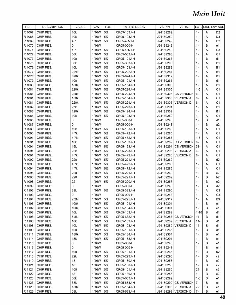
49
Main Unit
R 1067 CHIP RES. 10k 1/16W 5% CR05-103J-H J24189289 1- A D2R 1068 CHIP RES. 10k 1/16W 5% CR05-103J-H J24189289 1- A D3R 1069 CHIP RES. 4.7 1/16W 5% CR05-4R7J-H J24189249 1- A D2R 1070 CHIP RES. 0 1/16W CR05-000-H J24189248 1- B e1R 1071 CHIP RES. 4.7 1/16W 5% CR05-4R7J-H J24189249 1- A D3R 1072 CHIP RES. 56k 1/16W 5% CR05-563J-H J24189298 1- A C1R 1073 CHIP RES. 100 1/16W 5% CR05-101J-H J24189265 1- B d1R 1075 CHIP RES. 33k 1/16W 5% CR05-333J-H J24189295 1- A B1R 1076 CHIP RES. 10k 1/16W 5% CR05-103J-H J24189289 1- A B1R 1077 CHIP RES. 2.2k 1/16W 5% CR05-222J-H J24189281 1- A B1R 1078 CHIP RES. 820k 1/16W 5% CR05-824J-H J24189312 1- A B1R 1079 CHIP RES. 100 1/16W 5% CR05-101J-H J24189265 1- B d1R 1080 CHIP RES. 150k 1/16W 5% CR05-154J-H J24189303 1- A B1R 1081 CHIP RES. 220k 1/16W 5% CR05-224J-H J24189305 1-5 A C1R 1081 CHIP RES. 220k 1/16W 5% CR05-224J-H J24189305 CS VERSION 6- A C1R 1081 CHIP RES. 150k 1/16W 5% CR05-154J-H J24189303 VERSION A 6- A C1R 1081 CHIP RES. 220k 1/16W 5% CR05-224J-H J24189305 VERSION D 6- A C1R 1082 CHIP RES. 27k 1/16W 5% CR05-273J-H J24189294 1- A B1R 1083 CHIP RES. 120k 1/16W 5% CR05-124J-H J24189302 1- A B1R 1084 CHIP RES. 10k 1/16W 5% CR05-103J-H J24189289 1- A C1R 1085 CHIP RES. 0 1/16W CR05-000-H J24189248 1- B d1R 1087 CHIP RES. 0 1/16W CR05-000-H J24189248 1- B a2R 1089 CHIP RES. 10k 1/16W 5% CR05-103J-H J24189289 1- A C1R 1090 CHIP RES. 4.7k 1/16W 5% CR05-472J-H J24189285 1- A C1R 1091 CHIP RES. 4.7k 1/16W 5% CR05-472J-H J24189285 1-5 A C1R 1091 CHIP RES. 10k 1/16W 5% CR05-103J-H J24189289 CS VERSION 6- A C1R 1091 CHIP RES. 15k 1/16W 5% CR05-153J-H J24189291 CS VERSION 33- A C1R 1091 CHIP RES. 22k 1/16W 5% CR05-223J-H J24189293 VERSION A 6- A C1R 1091 CHIP RES. 4.7k 1/16W 5% CR05-472J-H J24189285 VERSION D 6- A C1R 1092 CHIP RES. 220 1/16W 5% CR05-221J-H J24189269 1- B d2R 1093 CHIP RES. 4.7k 1/16W 5% CR05-472J-H J24189285 1- A C1R 1094 CHIP RES. 4.7k 1/16W 5% CR05-472J-H J24189285 1- A C1R 1095 CHIP RES. 220 1/16W 5% CR05-221J-H J24189269 1- B c2R 1096 CHIP RES. 220 1/16W 5% CR05-221J-H J24189269 1- B b2R 1098 CHIP RES. 22 1/16W 5% CR05-220J-H J24189257 1- B e2R 1099 CHIP RES. 0 1/16W CR05-000-H J24189248 1- B d2R 1102 CHIP RES. 33k 1/16W 5% CR05-333J-H J24189295 1- A C3R 1103 CHIP RES. 0 1/16W CR05-000-H J24189248 1- A C3R 1104 CHIP RES. 2.2M 1/16W 5% CR05-225J-H J24189317 1- A B3R 1106 CHIP RES. 100k 1/16W 5% CR05-104J-H J24189301 1- B e1R 1107 CHIP RES. 100k 1/16W 5% CR05-104J-H J24189301 1- B e1R 1108 CHIP RES. 10k 1/16W 5% CR05-103J-H J24189289 1-10 B d1R 1108 CHIP RES. 6.8k 1/16W 5% CR05-682J-H J24189287 CS VERSION 11- B d1R 1108 CHIP RES. 10k 1/16W 5% CR05-103J-H J24189289 VERSION A 11- B d1R 1108 CHIP RES. 10k 1/16W 5% CR05-103J-H J24189289 VERSION D 11- B d1R 1109 CHIP RES. 100 1/16W 5% CR05-101J-H J24189265 1- B d1R 1111 CHIP RES. 180k 1/16W 5% CR05-184J-H J24189304 1- B e1R 1114 CHIP RES. 15k 1/16W 5% CR05-153J-H J24189291 1- B e1R 1115 CHIP RES. 0 1/16W CR05-000-H J24189248 1- B e1R 1116 CHIP RES. 0 1/16W CR05-000-H J24189248 1- B e1R 1117 CHIP RES. 100 1/16W 5% CR05-101J-H J24189265 1- B b2R 1118 CHIP RES. 22k 1/16W 5% CR05-223J-H J24189293 1- B c2R 1119 CHIP RES. 18 1/16W 5% CR05-180J-H J24189256 1- B c2R 1121 CHIP RES. 18 1/16W 5% CR05-180J-H J24189256 1- B c2R 1121 CHIP RES. 100 1/16W 5% CR05-101J-H J24189265 21- B c2R 1122 CHIP RES. 18 1/16W 5% CR05-180J-H J24189256 1- B c2R 1123 CHIP RES. 68k 1/16W 5% CR05-683J-H J24189299 1-6 B e1R 1123 CHIP RES. 68k 1/16W 5% CR05-683J-H J24189299 CS VERSION 7- B e1R 1123 CHIP RES. 150k 1/16W 5% CR05-154J-H J24189303 VERSION A 7- B e1R 1123 CHIP RES. 68k 1/16W 5% CR05-683J-H J24189299 VERSION D 7- B e1
DESCRIPTION VALUE V/W TOL. VS P/NMFR’S DESIG VERS.REF. LOT. SIDE LAY ADR
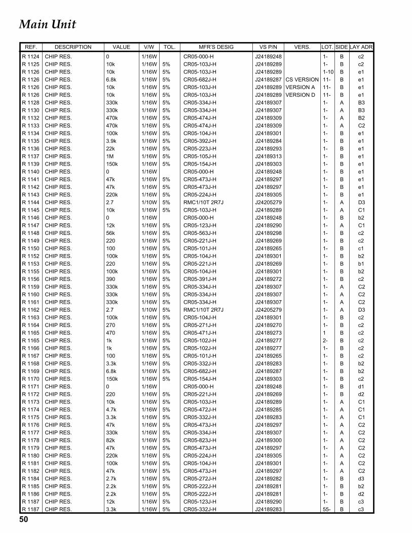
50
Main Unit
R 1124 CHIP RES. 0 1/16W CR05-000-H J24189248 1- B c2R 1125 CHIP RES. 10k 1/16W 5% CR05-103J-H J24189289 1- B c2R 1126 CHIP RES. 10k 1/16W 5% CR05-103J-H J24189289 1-10 B e1R 1126 CHIP RES. 6.8k 1/16W 5% CR05-682J-H J24189287 CS VERSION 11- B e1R 1126 CHIP RES. 10k 1/16W 5% CR05-103J-H J24189289 VERSION A 11- B e1R 1126 CHIP RES. 10k 1/16W 5% CR05-103J-H J24189289 VERSION D 11- B e1R 1128 CHIP RES. 330k 1/16W 5% CR05-334J-H J24189307 1- A B3R 1130 CHIP RES. 330k 1/16W 5% CR05-334J-H J24189307 1- A B3R 1132 CHIP RES. 470k 1/16W 5% CR05-474J-H J24189309 1- A B2R 1133 CHIP RES. 470k 1/16W 5% CR05-474J-H J24189309 1- A C2R 1134 CHIP RES. 100k 1/16W 5% CR05-104J-H J24189301 1- B e1R 1135 CHIP RES. 3.9k 1/16W 5% CR05-392J-H J24189284 1- B e1R 1136 CHIP RES. 22k 1/16W 5% CR05-223J-H J24189293 1- B e1R 1137 CHIP RES. 1M 1/16W 5% CR05-105J-H J24189313 1- B e1R 1139 CHIP RES. 150k 1/16W 5% CR05-154J-H J24189303 1- B e1R 1140 CHIP RES. 0 1/16W CR05-000-H J24189248 1- B e1R 1141 CHIP RES. 47k 1/16W 5% CR05-473J-H J24189297 1- B e1R 1142 CHIP RES. 47k 1/16W 5% CR05-473J-H J24189297 1- B e1R 1143 CHIP RES. 220k 1/16W 5% CR05-224J-H J24189305 1- B e1R 1144 CHIP RES. 2.7 1/10W 5% RMC1/10T 2R7J J24205279 1- A D3R 1145 CHIP RES. 10k 1/16W 5% CR05-103J-H J24189289 1- A C1R 1146 CHIP RES. 0 1/16W CR05-000-H J24189248 1- B b2R 1147 CHIP RES. 12k 1/16W 5% CR05-123J-H J24189290 1- A C1R 1148 CHIP RES. 56k 1/16W 5% CR05-563J-H J24189298 1- B c2R 1149 CHIP RES. 220 1/16W 5% CR05-221J-H J24189269 1- B c2R 1150 CHIP RES. 100 1/16W 5% CR05-101J-H J24189265 1- B c1R 1152 CHIP RES. 100k 1/16W 5% CR05-104J-H J24189301 1- B b2R 1153 CHIP RES. 220 1/16W 5% CR05-221J-H J24189269 1- B b1R 1155 CHIP RES. 100k 1/16W 5% CR05-104J-H J24189301 1- B b2R 1156 CHIP RES. 390 1/16W 5% CR05-391J-H J24189272 1- B c2R 1159 CHIP RES. 330k 1/16W 5% CR05-334J-H J24189307 1- A C2R 1160 CHIP RES. 330k 1/16W 5% CR05-334J-H J24189307 1- A C2R 1161 CHIP RES. 330k 1/16W 5% CR05-334J-H J24189307 1- A C2R 1162 CHIP RES. 2.7 1/10W 5% RMC1/10T 2R7J J24205279 1- A D3R 1163 CHIP RES. 100k 1/16W 5% CR05-104J-H J24189301 1- B c2R 1164 CHIP RES. 270 1/16W 5% CR05-271J-H J24189270 1- B c2R 1165 CHIP RES. 470 1/16W 5% CR05-471J-H J24189273 1 B c2R 1165 CHIP RES. 1k 1/16W 5% CR05-102J-H J24189277 2- B c2R 1166 CHIP RES. 1k 1/16W 5% CR05-102J-H J24189277 1- B c2R 1167 CHIP RES. 100 1/16W 5% CR05-101J-H J24189265 1- B c2R 1168 CHIP RES. 3.3k 1/16W 5% CR05-332J-H J24189283 1- B b2R 1169 CHIP RES. 6.8k 1/16W 5% CR05-682J-H J24189287 1- B b2R 1170 CHIP RES. 150k 1/16W 5% CR05-154J-H J24189303 1- B c2R 1171 CHIP RES. 0 1/16W CR05-000-H J24189248 1- B d1R 1172 CHIP RES. 220 1/16W 5% CR05-221J-H J24189269 1- B d2R 1173 CHIP RES. 10k 1/16W 5% CR05-103J-H J24189289 1- A C1R 1174 CHIP RES. 4.7k 1/16W 5% CR05-472J-H J24189285 1- A C1R 1175 CHIP RES. 3.3k 1/16W 5% CR05-332J-H J24189283 1- A C1R 1176 CHIP RES. 47k 1/16W 5% CR05-473J-H J24189297 1- A C2R 1177 CHIP RES. 330k 1/16W 5% CR05-334J-H J24189307 1- A C2R 1178 CHIP RES. 82k 1/16W 5% CR05-823J-H J24189300 1- A C2R 1179 CHIP RES. 47k 1/16W 5% CR05-473J-H J24189297 1- A C2R 1180 CHIP RES. 220k 1/16W 5% CR05-224J-H J24189305 1- A C2R 1181 CHIP RES. 100k 1/16W 5% CR05-104J-H J24189301 1- A C2R 1182 CHIP RES. 47k 1/16W 5% CR05-473J-H J24189297 1- A C2R 1184 CHIP RES. 2.7k 1/16W 5% CR05-272J-H J24189282 1- B d3R 1185 CHIP RES. 2.2k 1/16W 5% CR05-222J-H J24189281 1- B b2R 1186 CHIP RES. 2.2k 1/16W 5% CR05-222J-H J24189281 1- B d2R 1187 CHIP RES. 12k 1/16W 5% CR05-123J-H J24189290 1- B c3R 1187 CHIP RES. 3.3k 1/16W 5% CR05-332J-H J24189283 55- B c3
DESCRIPTION VALUE V/W TOL. VS P/NMFR’S DESIG VERS.REF. LOT. SIDE LAY ADR
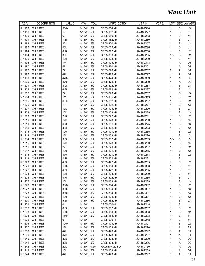
51
Main Unit
R 1188 CHIP RES. 560k 1/16W 5% CR05-564J-H J24189310 1- B d3R 1189 CHIP RES. 1k 1/16W 5% CR05-102J-H J24189277 1- B d1R 1190 CHIP RES. 68 1/16W 5% CR05-680J-H J24189263 1- B d1R 1191 CHIP RES. 1.8k 1/16W 5% CR05-182J-H J24189280 1- B d1R 1192 CHIP RES. 22 1/16W 5% CR05-220J-H J24189257 1- B d2R 1193 CHIP RES. 56k 1/16W 5% CR05-563J-H J24189298 1- B d1R 1194 CHIP RES. 8.2k 1/16W 5% CR05-822J-H J24189288 1- B d2R 1194 CHIP RES. 33k 1/16W 5% CR05-333J-H J24189295 19- B d2R 1195 CHIP RES. 12k 1/16W 5% CR05-123J-H J24189290 1- B d1R 1196 CHIP RES. 1M 1/16W 5% CR05-105J-H J24189313 1- A D1R 1197 CHIP RES. 47 1/16W 5% CR05-470J-H J24189261 1 A D1R 1197 CHIP RES. 22 1/16W 5% CR05-220J-H J24189257 2- A D1R 1198 CHIP RES. 47k 1/16W 5% CR05-473J-H J24189297 1- A D1R 1199 CHIP RES. 470k 1/16W 5% CR05-474J-H J24189309 1- A D2R 1200 CHIP RES. 470k 1/16W 5% CR05-474J-H J24189309 1- A D2R 1201 CHIP RES. 3.9k 1/16W 5% CR05-392J-H J24189284 1- B d3R 1202 CHIP RES. 6.8k 1/16W 5% CR05-682J-H J24189287 1- B d2R 1203 CHIP RES. 22 1/16W 5% CR05-220J-H J24189257 1- B d3R 1204 CHIP RES. 1M 1/16W 5% CR05-105J-H J24189313 1- B d2R 1205 CHIP RES. 6.8k 1/16W 5% CR05-682J-H J24189287 1- B d2R 1206 CHIP RES. 1k 1/16W 5% CR05-102J-H J24189277 1- B d3R 1207 CHIP RES. 12k 1/16W 5% CR05-123J-H J24189290 1- B c3R 1208 CHIP RES. 10k 1/16W 5% CR05-103J-H J24189289 1- B d3R 1209 CHIP RES. 2.2k 1/16W 5% CR05-222J-H J24189281 1- B d2R 1210 CHIP RES. 12k 1/16W 5% CR05-123J-H J24189290 1- B c3R 1211 CHIP RES. 680 1/16W 5% CR05-681J-H J24189275 1- B d3R 1212 CHIP RES. 3.3k 1/16W 5% CR05-332J-H J24189283 1- B d2R 1213 CHIP RES. 100 1/16W 5% CR05-101J-H J24189265 1- B d2R 1214 CHIP RES. 12k 1/16W 5% CR05-123J-H J24189290 1- B c3R 1214 CHIP RES. 3.3k 1/16W 5% CR05-332J-H J24189283 55- B c3R 1215 CHIP RES. 12k 1/16W 5% CR05-123J-H J24189290 1- B c3R 1216 CHIP RES. 22 1/16W 5% CR05-220J-H J24189257 1- B d2R 1217 CHIP RES. 100 1/16W 5% CR05-101J-H J24189265 1- B d2R 1218 CHIP RES. 470 1/16W 5% CR05-471J-H J24189273 1- B d2R 1219 CHIP RES. 2.2k 1/16W 5% CR05-222J-H J24189281 1- B d1R 1220 CHIP RES. 4.7k 1/16W 5% CR05-472J-H J24189285 1- B d2R 1221 CHIP RES. 150k 1/16W 5% CR05-154J-H J24189303 1- B d1R 1222 CHIP RES. 4.7k 1/16W 5% CR05-472J-H J24189285 1- B d1R 1223 CHIP RES. 10k 1/16W 5% CR05-103J-H J24189289 1- B d1R 1224 CHIP RES. 4.7k 1/16W 5% CR05-472J-H J24189285 1- B d1R 1225 CHIP RES. 10k 1/16W 5% CR05-103J-H J24189289 1- B d3R 1226 CHIP RES. 330k 1/16W 5% CR05-334J-H J24189307 1- B d2R 1227 CHIP RES. 330k 1/16W 5% CR05-334J-H J24189307 1- B d3R 1228 CHIP RES. 330k 1/16W 5% CR05-334J-H J24189307 1- B d3R 1229 CHIP RES. 100k 1/16W 5% CR05-104J-H J24189301 1- B d2R 1230 CHIP RES. 5.6k 1/16W 5% CR05-562J-H J24189286 1- B c3R 1231 CHIP RES. 0 1/16W CR05-000-H J24189248 1- B d1R 1232 CHIP RES. 6.8k 1/16W 5% CR05-682J-H J24189287 1- B d2R 1233 CHIP RES. 150k 1/16W 5% CR05-154J-H J24189303 1- B d2R 1234 CHIP RES. 150k 1/16W 5% CR05-154J-H J24189303 1- B d1R 1235 CHIP RES. 0 1/16W CR05-000-H J24189248 1- B d1R 1236 CHIP RES. 100k 1/16W 5% CR05-104J-H J24189301 1- B d2R 1237 CHIP RES. 12k 1/16W 5% CR05-123J-H J24189290 1- A E1R 1238 CHIP RES. 47k 1/16W 5% CR05-473J-H J24189297 1- A E1R 1239 CHIP RES. 47k 1/16W 5% CR05-473J-H J24189297 1- A E1R 1240 CHIP RES. 82k 1/16W 5% CR05-823J-H J24189300 1- A D2R 1241 CHIP RES. 39k 1/16W 5% CR05-393J-H J24189296 1- A D2R 1242 CHIP RES. 20k 1/16W 0.5% RR0510R-203-D J24189150 1- A D2R 1243 CHIP RES. 10k 1/16W 5% CR05-103J-H J24189289 1- A D2R 1244 CHIP RES. 47k 1/16W 5% CR05-473J-H J24189297 1- A E1
DESCRIPTION VALUE V/W TOL. VS P/NMFR’S DESIG VERS.REF. LOT. SIDE LAY ADR
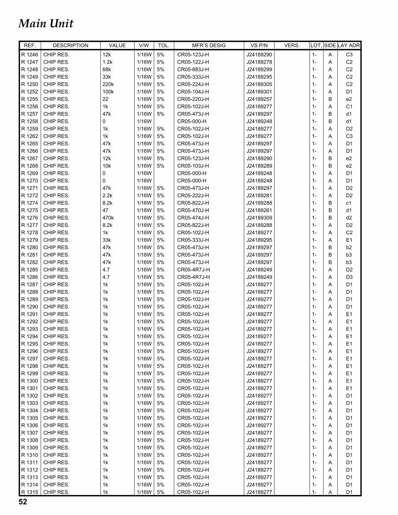
52
Main Unit
R 1246 CHIP RES. 12k 1/16W 5% CR05-123J-H J24189290 1- A C3R 1247 CHIP RES. 1.2k 1/16W 5% CR05-122J-H J24189278 1- A C2R 1248 CHIP RES. 68k 1/16W 5% CR05-683J-H J24189299 1- A C2R 1249 CHIP RES. 33k 1/16W 5% CR05-333J-H J24189295 1- A C2R 1250 CHIP RES. 220k 1/16W 5% CR05-224J-H J24189305 1- A C2R 1252 CHIP RES. 100k 1/16W 5% CR05-104J-H J24189301 1- A D1R 1255 CHIP RES. 22 1/16W 5% CR05-220J-H J24189257 1- B e2R 1256 CHIP RES. 1k 1/16W 5% CR05-102J-H J24189277 1- A C1R 1257 CHIP RES. 47k 1/16W 5% CR05-473J-H J24189297 1- B d1R 1258 CHIP RES. 0 1/16W CR05-000-H J24189248 1- B d1R 1259 CHIP RES. 1k 1/16W 5% CR05-102J-H J24189277 1- A D2R 1262 CHIP RES. 1k 1/16W 5% CR05-102J-H J24189277 1- A C3R 1265 CHIP RES. 47k 1/16W 5% CR05-473J-H J24189297 1- A D1R 1266 CHIP RES. 47k 1/16W 5% CR05-473J-H J24189297 1- A D1R 1267 CHIP RES. 12k 1/16W 5% CR05-123J-H J24189290 1- B e2R 1268 CHIP RES. 10k 1/16W 5% CR05-103J-H J24189289 1- B e2R 1269 CHIP RES. 0 1/16W CR05-000-H J24189248 1- A D1R 1270 CHIP RES. 0 1/16W CR05-000-H J24189248 1- A D1R 1271 CHIP RES. 47k 1/16W 5% CR05-473J-H J24189297 1- A D2R 1272 CHIP RES. 2.2k 1/16W 5% CR05-222J-H J24189281 1- A D2R 1274 CHIP RES. 8.2k 1/16W 5% CR05-822J-H J24189288 1- B c1R 1275 CHIP RES. 47 1/16W 5% CR05-470J-H J24189261 1- B d1R 1276 CHIP RES. 470k 1/16W 5% CR05-474J-H J24189309 1- B d2R 1277 CHIP RES. 8.2k 1/16W 5% CR05-822J-H J24189288 1- A D2R 1278 CHIP RES. 1k 1/16W 5% CR05-102J-H J24189277 1- A C2R 1279 CHIP RES. 33k 1/16W 5% CR05-333J-H J24189295 1- A E1R 1280 CHIP RES. 47k 1/16W 5% CR05-473J-H J24189297 1- B b2R 1281 CHIP RES. 47k 1/16W 5% CR05-473J-H J24189297 1- B b3R 1282 CHIP RES. 47k 1/16W 5% CR05-473J-H J24189297 1- B b3R 1285 CHIP RES. 4.7 1/16W 5% CR05-4R7J-H J24189249 1- A D2R 1286 CHIP RES. 4.7 1/16W 5% CR05-4R7J-H J24189249 1- A D3R 1287 CHIP RES. 1k 1/16W 5% CR05-102J-H J24189277 1- A D1R 1288 CHIP RES. 1k 1/16W 5% CR05-102J-H J24189277 1- A D1R 1289 CHIP RES. 1k 1/16W 5% CR05-102J-H J24189277 1- A D1R 1290 CHIP RES. 1k 1/16W 5% CR05-102J-H J24189277 1- A D1R 1291 CHIP RES. 1k 1/16W 5% CR05-102J-H J24189277 1- A E1R 1292 CHIP RES. 1k 1/16W 5% CR05-102J-H J24189277 1- A E1R 1293 CHIP RES. 1k 1/16W 5% CR05-102J-H J24189277 1- A E1R 1294 CHIP RES. 1k 1/16W 5% CR05-102J-H J24189277 1- A E1R 1295 CHIP RES. 1k 1/16W 5% CR05-102J-H J24189277 1- A E1R 1296 CHIP RES. 1k 1/16W 5% CR05-102J-H J24189277 1- A E1R 1297 CHIP RES. 1k 1/16W 5% CR05-102J-H J24189277 1- A E1R 1298 CHIP RES. 1k 1/16W 5% CR05-102J-H J24189277 1- A E1R 1299 CHIP RES. 1k 1/16W 5% CR05-102J-H J24189277 1- A E1R 1300 CHIP RES. 1k 1/16W 5% CR05-102J-H J24189277 1- A E1R 1301 CHIP RES. 1k 1/16W 5% CR05-102J-H J24189277 1- A E1R 1302 CHIP RES. 1k 1/16W 5% CR05-102J-H J24189277 1- A D1R 1303 CHIP RES. 1k 1/16W 5% CR05-102J-H J24189277 1- A D1R 1304 CHIP RES. 1k 1/16W 5% CR05-102J-H J24189277 1- A D1R 1305 CHIP RES. 1k 1/16W 5% CR05-102J-H J24189277 1- A D1R 1306 CHIP RES. 1k 1/16W 5% CR05-102J-H J24189277 1- A D1R 1307 CHIP RES. 1k 1/16W 5% CR05-102J-H J24189277 1- A D1R 1308 CHIP RES. 1k 1/16W 5% CR05-102J-H J24189277 1- A D1R 1309 CHIP RES. 1k 1/16W 5% CR05-102J-H J24189277 1- A D1R 1310 CHIP RES. 1k 1/16W 5% CR05-102J-H J24189277 1- A D1R 1311 CHIP RES. 1k 1/16W 5% CR05-102J-H J24189277 1- A D1R 1312 CHIP RES. 1k 1/16W 5% CR05-102J-H J24189277 1- A D1R 1313 CHIP RES. 1k 1/16W 5% CR05-102J-H J24189277 1- A D1R 1314 CHIP RES. 1k 1/16W 5% CR05-102J-H J24189277 1- A D1R 1315 CHIP RES. 1k 1/16W 5% CR05-102J-H J24189277 1- A D1
DESCRIPTION VALUE V/W TOL. VS P/NMFR’S DESIG VERS.REF. LOT. SIDE LAY ADR
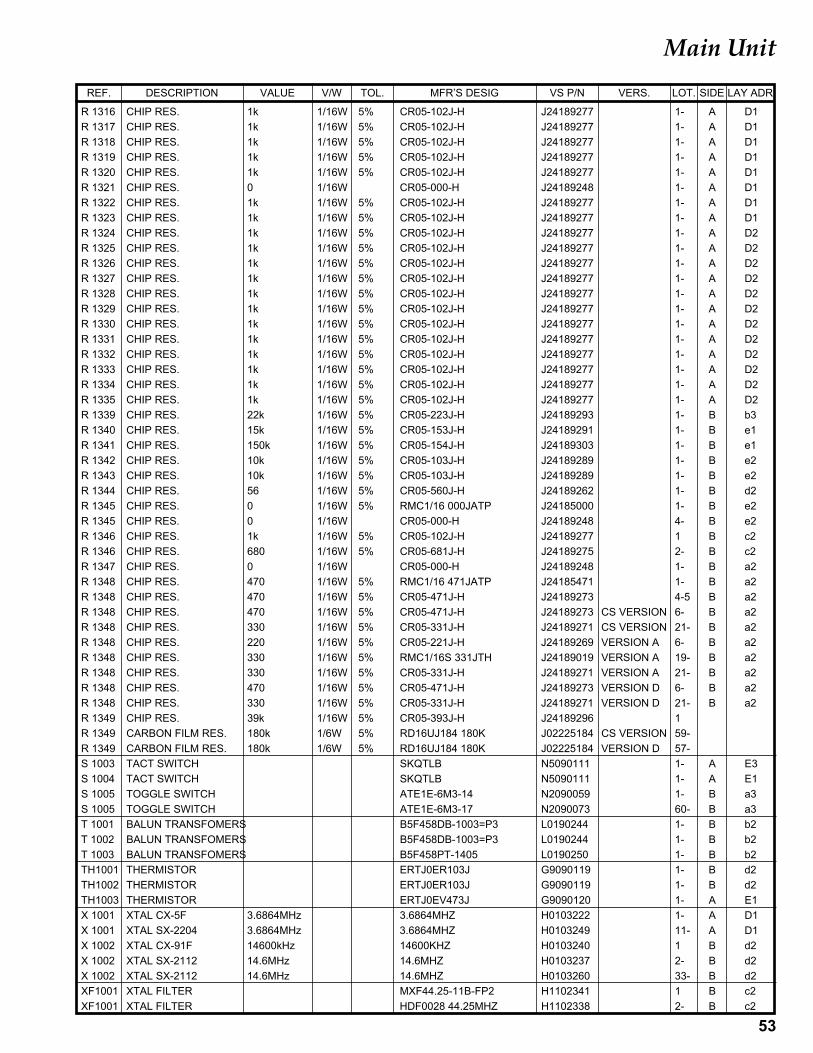
53
Main Unit
R 1316 CHIP RES. 1k 1/16W 5% CR05-102J-H J24189277 1- A D1R 1317 CHIP RES. 1k 1/16W 5% CR05-102J-H J24189277 1- A D1R 1318 CHIP RES. 1k 1/16W 5% CR05-102J-H J24189277 1- A D1R 1319 CHIP RES. 1k 1/16W 5% CR05-102J-H J24189277 1- A D1R 1320 CHIP RES. 1k 1/16W 5% CR05-102J-H J24189277 1- A D1R 1321 CHIP RES. 0 1/16W CR05-000-H J24189248 1- A D1R 1322 CHIP RES. 1k 1/16W 5% CR05-102J-H J24189277 1- A D1R 1323 CHIP RES. 1k 1/16W 5% CR05-102J-H J24189277 1- A D1R 1324 CHIP RES. 1k 1/16W 5% CR05-102J-H J24189277 1- A D2R 1325 CHIP RES. 1k 1/16W 5% CR05-102J-H J24189277 1- A D2R 1326 CHIP RES. 1k 1/16W 5% CR05-102J-H J24189277 1- A D2R 1327 CHIP RES. 1k 1/16W 5% CR05-102J-H J24189277 1- A D2R 1328 CHIP RES. 1k 1/16W 5% CR05-102J-H J24189277 1- A D2R 1329 CHIP RES. 1k 1/16W 5% CR05-102J-H J24189277 1- A D2R 1330 CHIP RES. 1k 1/16W 5% CR05-102J-H J24189277 1- A D2R 1331 CHIP RES. 1k 1/16W 5% CR05-102J-H J24189277 1- A D2R 1332 CHIP RES. 1k 1/16W 5% CR05-102J-H J24189277 1- A D2R 1333 CHIP RES. 1k 1/16W 5% CR05-102J-H J24189277 1- A D2R 1334 CHIP RES. 1k 1/16W 5% CR05-102J-H J24189277 1- A D2R 1335 CHIP RES. 1k 1/16W 5% CR05-102J-H J24189277 1- A D2R 1339 CHIP RES. 22k 1/16W 5% CR05-223J-H J24189293 1- B b3R 1340 CHIP RES. 15k 1/16W 5% CR05-153J-H J24189291 1- B e1R 1341 CHIP RES. 150k 1/16W 5% CR05-154J-H J24189303 1- B e1R 1342 CHIP RES. 10k 1/16W 5% CR05-103J-H J24189289 1- B e2R 1343 CHIP RES. 10k 1/16W 5% CR05-103J-H J24189289 1- B e2R 1344 CHIP RES. 56 1/16W 5% CR05-560J-H J24189262 1- B d2R 1345 CHIP RES. 0 1/16W 5% RMC1/16 000JATP J24185000 1- B e2R 1345 CHIP RES. 0 1/16W CR05-000-H J24189248 4- B e2R 1346 CHIP RES. 1k 1/16W 5% CR05-102J-H J24189277 1 B c2R 1346 CHIP RES. 680 1/16W 5% CR05-681J-H J24189275 2- B c2R 1347 CHIP RES. 0 1/16W CR05-000-H J24189248 1- B a2R 1348 CHIP RES. 470 1/16W 5% RMC1/16 471JATP J24185471 1- B a2R 1348 CHIP RES. 470 1/16W 5% CR05-471J-H J24189273 4-5 B a2R 1348 CHIP RES. 470 1/16W 5% CR05-471J-H J24189273 CS VERSION 6- B a2R 1348 CHIP RES. 330 1/16W 5% CR05-331J-H J24189271 CS VERSION 21- B a2R 1348 CHIP RES. 220 1/16W 5% CR05-221J-H J24189269 VERSION A 6- B a2R 1348 CHIP RES. 330 1/16W 5% RMC1/16S 331JTH J24189019 VERSION A 19- B a2R 1348 CHIP RES. 330 1/16W 5% CR05-331J-H J24189271 VERSION A 21- B a2R 1348 CHIP RES. 470 1/16W 5% CR05-471J-H J24189273 VERSION D 6- B a2R 1348 CHIP RES. 330 1/16W 5% CR05-331J-H J24189271 VERSION D 21- B a2R 1349 CHIP RES. 39k 1/16W 5% CR05-393J-H J24189296 1R 1349 CARBON FILM RES. 180k 1/6W 5% RD16UJ184 180K J02225184 CS VERSION 59-R 1349 CARBON FILM RES. 180k 1/6W 5% RD16UJ184 180K J02225184 VERSION D 57-S 1003 TACT SWITCH SKQTLB N5090111 1- A E3S 1004 TACT SWITCH SKQTLB N5090111 1- A E1S 1005 TOGGLE SWITCH ATE1E-6M3-14 N2090059 1- B a3S 1005 TOGGLE SWITCH ATE1E-6M3-17 N2090073 60- B a3T 1001 BALUN TRANSFOMERS B5F458DB-1003=P3 L0190244 1- B b2T 1002 BALUN TRANSFOMERS B5F458DB-1003=P3 L0190244 1- B b2T 1003 BALUN TRANSFOMERS B5F458PT-1405 L0190250 1- B b2TH1001 THERMISTOR ERTJ0ER103J G9090119 1- B d2TH1002 THERMISTOR ERTJ0ER103J G9090119 1- B d2TH1003 THERMISTOR ERTJ0EV473J G9090120 1- A E1X 1001 XTAL CX-5F 3.6864MHz 3.6864MHZ H0103222 1- A D1X 1001 XTAL SX-2204 3.6864MHz 3.6864MHZ H0103249 11- A D1X 1002 XTAL CX-91F 14600kHz 14600KHZ H0103240 1 B d2X 1002 XTAL SX-2112 14.6MHz 14.6MHZ H0103237 2- B d2X 1002 XTAL SX-2112 14.6MHz 14.6MHZ H0103260 33- B d2XF1001 XTAL FILTER MXF44.25-11B-FP2 H1102341 1 B c2XF1001 XTAL FILTER HDF0028 44.25MHZ H1102338 2- B c2
DESCRIPTION VALUE V/W TOL. VS P/NMFR’S DESIG VERS.REF. LOT. SIDE LAY ADR
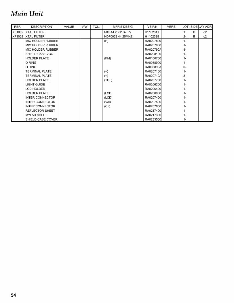
54
Main Unit
DESCRIPTION VALUE V/W TOL. VS P/NMFR’S DESIG VERS.REF. LOT. SIDE LAY ADR
XF1002 XTAL FILTER MXF44.25-11B-FP2 H1102341 1 B c2XF1002 XTAL FILTER HDF0028 44.25MHZ H1102338 2- B c2
MIC HOLDER RUBBER (F) RA0207800 1-MIC HOLDER RUBBER RA0207900 1-MIC HOLDER RUBBER RA020790A 8-SHIELD CASE VCO RA0208100 1-HOLDER PLATE (PM) RA0106700 1-O RING RA0088900 1-O RING RA008890A 6-TERMINAL PLATE (+) RA0207100 1-TERMINAL PLATE (+) RA020710A 8-HOLDER PLATE (TGL) RA0207700 1-LIGHT GUIDE RA0206200 1-LCD HOLDER RA0206400 1-HOLDER PLATE (LCD) RA0206800 1-INTER CONNECTOR (LCD) RA0207400 1-INTER CONNECTOR (Vol) RA0207500 1-INTER CONNECTOR (Ch) RA0207600 1-REFLECTOR SHEET RA0217400 1-MYLAR SHEET RA0217300 1-SHIELD CASE COVER RA0233500 1-
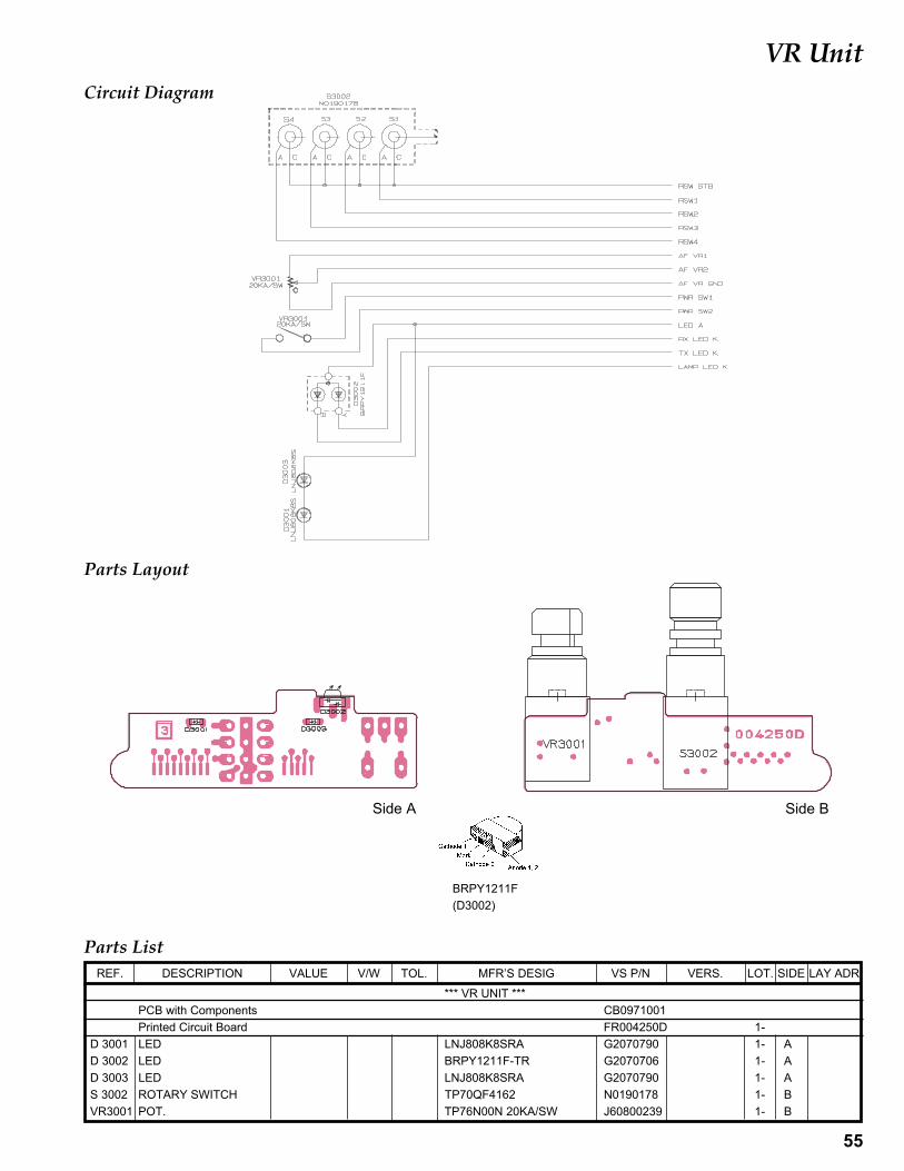
55
VR UnitCircuit Diagram
Side A Side B
Parts Layout
Parts List
*** VR UNIT ***PCB with Components CB0971001Printed Circuit Board FR004250D 1-
D 3001 LED LNJ808K8SRA G2070790 1- AD 3002 LED BRPY1211F-TR G2070706 1- AD 3003 LED LNJ808K8SRA G2070790 1- AS 3002 ROTARY SWITCH TP70QF4162 N0190178 1- BVR3001 POT. TP76N00N 20KA/SW J60800239 1- B
BRPY1211F(D3002)
DESCRIPTION VALUE V/W TOL. VS P/NMFR’S DESIG VERS.REF. LOT. SIDE LAY ADR
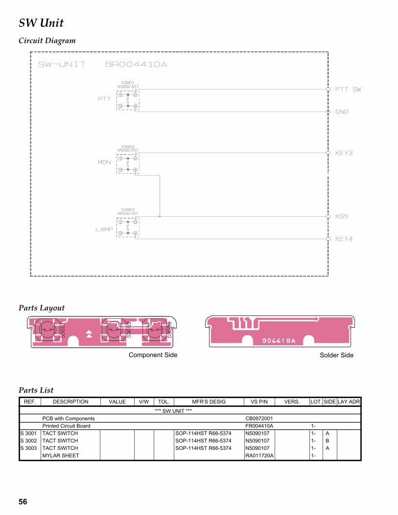
56
SW UnitCircuit Diagram
Component Side Solder Side
Parts Layout
Parts List
*** SW UNIT ***PCB with Components CB0972001Printed Circuit Board FR004410A 1-
S 3001 TACT SWITCH SOP-114HST R66-5374 N5090107 1- AS 3002 TACT SWITCH SOP-114HST R66-5374 N5090107 1- BS 3003 TACT SWITCH SOP-114HST R66-5374 N5090107 1- A
MYLAR SHEET RA011720A 1-
DESCRIPTION VALUE V/W TOL. VS P/NMFR’S DESIG VERS.REF. LOT. SIDE LAY ADR
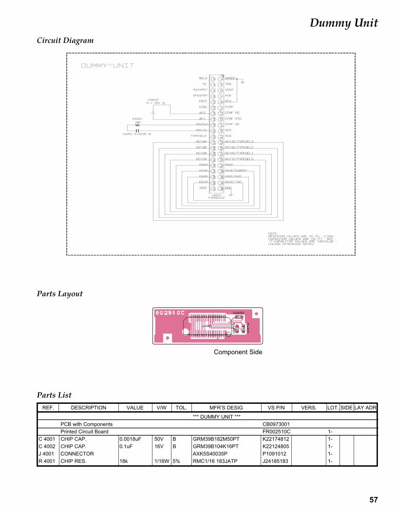
57
Circuit Diagram
Parts Layout
Parts List
Component Side
Dummy Unit
*** DUMMY UNIT ***PCB with Components CB0973001Printed Circuit Board FR002510C 1-
C 4001 CHIP CAP. 0.0018uF 50V B GRM39B182M50PT K22174812 1-C 4002 CHIP CAP. 0.1uF 16V B GRM39B104K16PT K22124805 1-J 4001 CONNECTOR AXK5S40035P P1091012 1-R 4001 CHIP RES. 18k 1/16W 5% RMC1/16 183JATP J24185183 1-
DESCRIPTION VALUE V/W TOL. VS P/NMFR’S DESIG VERS.REF. LOT. SIDE LAY ADR
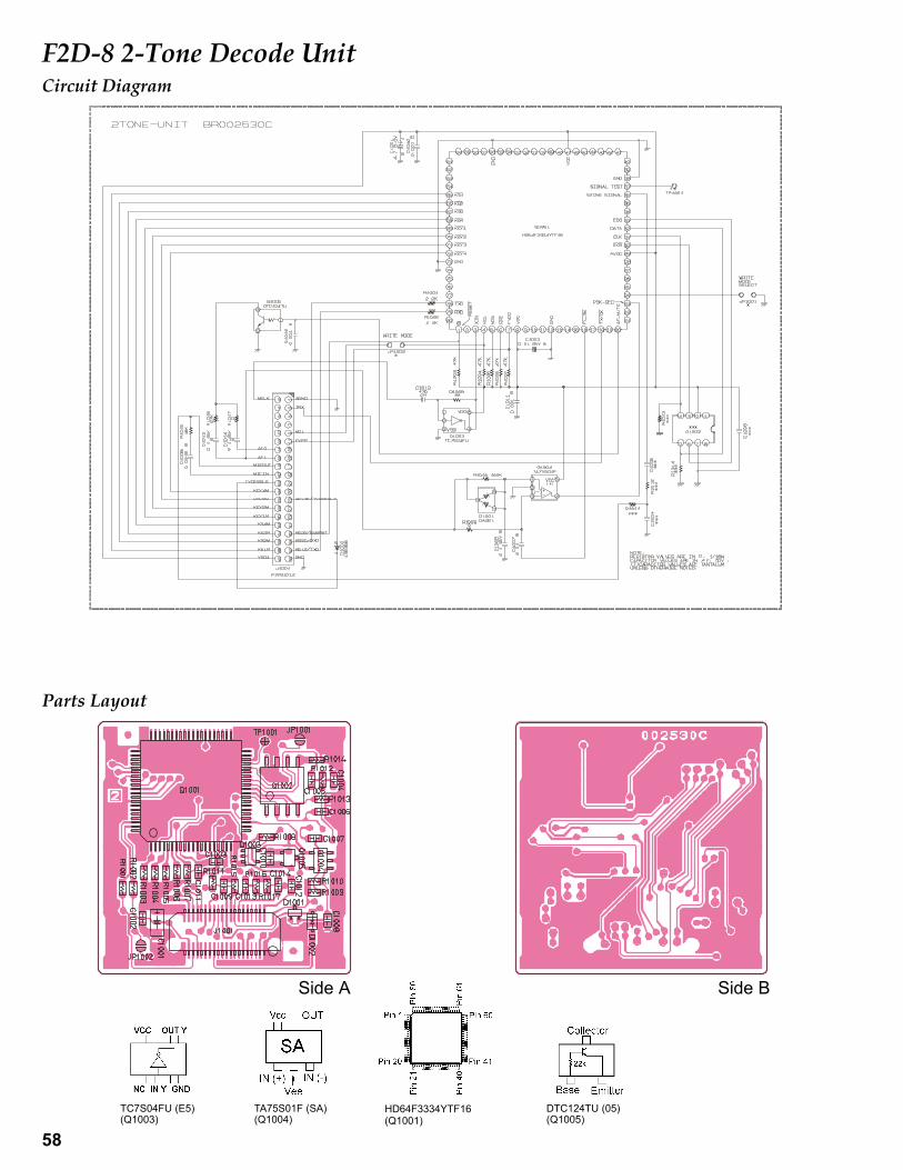
58
F2D-8 2-Tone Decode Unit
HD64F3334YTF16(Q1001)
Circuit Diagram
Parts Layout
TC7S04FU (E5)(Q1003)
DTC124TU (05)(Q1005)
TA75S01F (SA)(Q1004)
Side BSide A
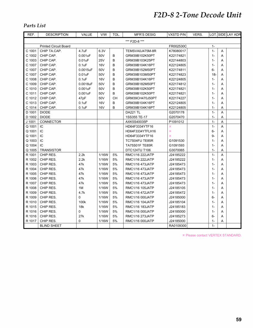
59
F2D-8 2-Tone Decode Unit
*** F2D-8 ***Printed Circuit Board FR002530C 1-
C 1001 CHIP TA.CAP. 4.7uF 6.3V TEMSVA0J475M-8R K78080017 1- AC 1002 CHIP CAP. 0.001uF 50V B GRM39B102K50PT K22174821 1- AC 1003 CHIP CAP. 0.01uF 25V B GRM39B103K25PT K22144803 1- AC 1007 CHIP CAP. 0.1uF 16V B GRM39B104K16PT K22124805 1- AC 1007 CHIP CAP. 0.0015uF 50V B GRM39B152M50PT K22174811 6- AC 1007 CHIP CAP. 0.01uF 50V B GRM39B103M50PT K22174823 18- AC 1008 CHIP CAP. 0.1uF 16V B GRM39B104K16PT K22124805 1- AC 1009 CHIP CAP. 0.0018uF 50V B GRM39B182M50PT K22174812 1- AC 1010 CHIP CAP. 0.001uF 50V B GRM39B102K50PT K22174821 1- AC 1011 CHIP CAP. 0.001uF 50V B GRM39B102K50PT K22174821 1- AC 1012 CHIP CAP. 47pF 50V CH GRM39CH470J50PT K22174227 1- AC 1013 CHIP CAP. 0.1uF 16V B GRM39B104K16PT K22124805 1- AC 1014 CHIP CAP. 0.1uF 16V B GRM39B104K16PT K22124805 1- AD 1001 DIODE DA221 TL G2070178 1- AD 1002 DIODE 1SS355 TE-17 G2070470 1- AJ 1001 CONNECTOR AXK5S40035P P1091012 1- AQ 1001 IC HD64F3334YTF16 1- AQ 1001 IC HD64F3334YTFLH16 6- AQ 1001 IC HD64F3334YTF16 9- AQ 1003 IC TC7S04FU TE85R G1091530 1- AQ 1004 IC TA75S01F TE85R G1091593 1- AQ 1005 TRANSISTOR DTC124TU T106 G3070065 1- AR 1001 CHIP RES. 2.2k 1/16W 5% RMC1/16 222JATP J24185222 1- AR 1002 CHIP RES. 2.2k 1/16W 5% RMC1/16 222JATP J24185222 1- AR 1003 CHIP RES. 47k 1/16W 5% RMC1/16 473JATP J24185473 1- AR 1004 CHIP RES. 47k 1/16W 5% RMC1/16 473JATP J24185473 1- AR 1005 CHIP RES. 47k 1/16W 5% RMC1/16 473JATP J24185473 1- AR 1006 CHIP RES. 47k 1/16W 5% RMC1/16 473JATP J24185473 1- AR 1007 CHIP RES. 47k 1/16W 5% RMC1/16 473JATP J24185473 1- AR 1008 CHIP RES. 1M 1/16W 5% RMC1/16 105JATP J24185105 1- AR 1009 CHIP RES. 4.7k 1/16W 5% RMC1/16 472JATP J24185472 1- AR 1009 CHIP RES. 0 1/16W 5% RMC1/16 000JATP J24185000 6- AR 1010 CHIP RES. 100k 1/16W 5% RMC1/16 104JATP J24185104 1- AR 1015 CHIP RES. 18k 1/16W 5% RMC1/16 183JATP J24185183 1- AR 1016 CHIP RES. 0 1/16W 5% RMC1/16 000JATP J24185000 1- AR 1016 CHIP RES. 27k 1/16W 5% RMC1/16 273JATP J24185273 6- AR 1017 CHIP RES. 0 1/16W 5% RMC1/16 000JATP J24185000 1- A
BLIND SHEET RA0109300 1-
Parts List
DESCRIPTION VALUE V/W TOL. VXSTD P/NMFR’S DESIG VERS.REF. LOT. SIDE LAY ADR
Please contact VERTEX STANDARD.
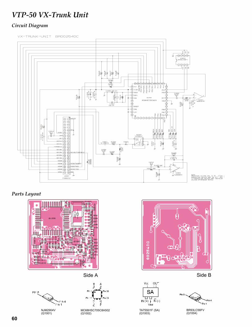
60
VTP-50 VX-Trunk Unit
NJM2904V(Q1001)
Circuit Diagram
Parts Layout
MC68HSC705C8A502(Q1002)
TA75S01F (SA)(Q1003)
Side BSide A
BR93LC56FV(Q1004)
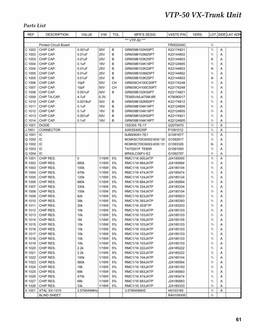
61
VTP-50 VX-Trunk UnitParts List
*** VTP-50 ***Printed Circuit Board FR002540C 1-
C 1002 CHIP CAP. 0.001uF 50V B GRM39B102K50PT K22174821 1- AC 1003 CHIP CAP. 0.01uF 25V B GRM39B103M25PT K22144802 1- AC 1003 CHIP CAP. 0.01uF 25V B GRM39B103K25PT K22144803 9- AC 1004 CHIP CAP. 0.1uF 16V B GRM39B104K16PT K22124805 1- AC 1004 CHIP CAP. 0.01uF 25V B GRM39B103K25PT K22144803 9- AC 1005 CHIP CAP. 0.01uF 25V B GRM39B103M25PT K22144802 1- AC 1005 CHIP CAP. 0.01uF 25V B GRM39B103K25PT K22144803 9- AC 1006 CHIP CAP. 10pF 50V CH GRM39CH100C50PT K22174248 1- AC 1007 CHIP CAP. 10pF 50V CH GRM39CH100C50PT K22174248 1- AC 1008 CHIP CAP. 0.001uF 50V B GRM39B102K50PT K22174821 1- AC 1009 CHIP TA.CAP. 4.7uF 6.3V TEMSVA0J475M-8R K78080017 1- AC 1010 CHIP CAP. 0.0018uF 50V B GRM39B182M50PT K22174812 1- AC 1011 CHIP CAP. 0.1uF 16V B GRM39B104K16PT K22124805 1- AC 1012 CHIP CAP. 0.1uF 16V B GRM39B104K16PT K22124805 1- AC 1013 CHIP CAP. 0.001uF 50V B GRM39B102K50PT K22174821 1- AC 1014 CHIP CAP. 0.1uF 16V B GRM39B104K16PT K22124805 1- AD 1001 DIODE 1SS355 TE-17 G2070470 1- AJ 1001 CONNECTOR AXK5S40035P P1091012 1- AQ 1001 IC NJM2904V-TE1 G1091677 1- AQ 1002 IC MC68HSC705C8A502-6030 130 G1092917 1- AQ 1002 IC MC68HSC705C8A502-6030 131 G1093326 6- AQ 1003 IC TA75S01F TE85R G1091593 1- AQ 1004 IC BR93LC56FV-E2 G1092787 1- AR 1001 CHIP RES. 0 1/16W 5% RMC1/16 000JATP J24185000 1- AR 1002 CHIP RES. 680k 1/16W 5% RMC1/16 684JATP J24185684 1- AR 1003 CHIP RES. 100k 1/16W 5% RMC1/16 104JATP J24185104 1- AR 1004 CHIP RES. 470k 1/16W 5% RMC1/16 474JATP J24185474 1- AR 1005 CHIP RES. 120k 1/16W 5% RMC1/16 124JATP J24185124 1- AR 1006 CHIP RES. 680k 1/16W 5% RMC1/16 684JATP J24185684 1- AR 1007 CHIP RES. 330k 1/16W 5% RMC1/16 334JATP J24185334 1- AR 1008 CHIP RES. 150k 1/16W 5% RMC1/16 154JATP J24185154 1- AR 1009 CHIP RES. 82k 1/16W 5% RMC1/16 823JATP J24185823 1- AR 1010 CHIP RES. 39k 1/16W 5% RMC1/16 393JATP J24185393 1- AR 1011 CHIP RES. 20k 1/16W 1% RMC1/16 203FTP J24183203 1- AR 1012 CHIP RES. 10k 1/16W 5% RMC1/16 103JATP J24185103 1- AR 1013 CHIP RES. 10k 1/16W 5% RMC1/16 103JATP J24185103 1- AR 1014 CHIP RES. 1M 1/16W 5% RMC1/16 105JATP J24185105 1- AR 1015 CHIP RES. 10k 1/16W 5% RMC1/16 103JATP J24185103 1- AR 1016 CHIP RES. 10k 1/16W 5% RMC1/16 103JATP J24185103 1- AR 1017 CHIP RES. 10k 1/16W 5% RMC1/16 103JATP J24185103 1- AR 1018 CHIP RES. 10k 1/16W 5% RMC1/16 103JATP J24185103 1- AR 1019 CHIP RES. 10k 1/16W 5% RMC1/16 103JATP J24185103 1- AR 1020 CHIP RES. 2.2k 1/16W 5% RMC1/16 222JATP J24185222 1- AR 1021 CHIP RES. 2.2k 1/16W 5% RMC1/16 222JATP J24185222 1- AR 1022 CHIP RES. 100k 1/16W 5% RMC1/16 104JATP J24185104 1- AR 1023 CHIP RES. 560k 1/16W 5% RMC1/16 564JATP J24185564 1- AR 1024 CHIP RES. 18k 1/16W 5% RMC1/16 183JATP J24185183 1- AR 1025 CHIP RES. 68k 1/16W 5% RMC1/16 683JATP J24185683 1- AR 1026 CHIP RES. 470k 1/16W 5% RMC1/16 474JATP J24185474 1- AR 1027 CHIP RES. 68k 1/16W 5% RMC1/16 683JATP J24185683 1- AR 1028 CHIP RES. 33k 1/16W 5% RMC1/16 333JATP J24185333 1- AX 1001 XTAL SX-1315 3.579545MHz 3.579545MHZ H0103185 1- A
BLIND SHEET RA0109300 1-
DESCRIPTION VALUE V/W TOL. VXSTD P/NMFR’S DESIG VERS.REF. LOT. SIDE LAY ADR
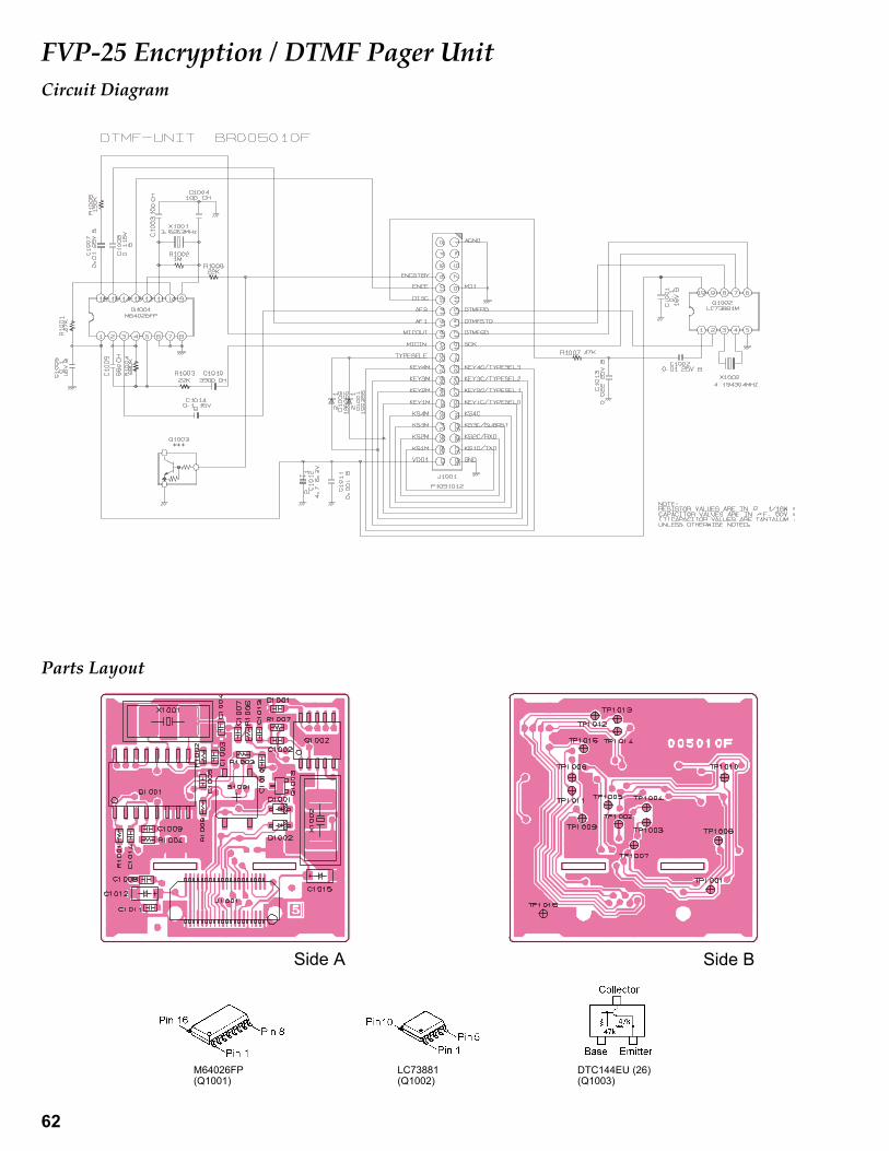
62
FVP-25 Encryption / DTMF Pager Unit
M64026FP(Q1001)
Circuit Diagram
Parts Layout
LC73881(Q1002)
DTC144EU (26)(Q1003)
Side BSide A
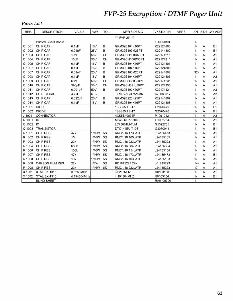
63
FVP-25 Encryption / DTMF Pager Unit
*** FVP-25 ***Printed Circuit Board FR005010F 1-
C 1001 CHIP CAP. 0.1uF 16V B GRM39B104K16PT K22124805 1- A B1C 1002 CHIP CAP. 0.01uF 25V B GRM39B103M25PT K22144802 1- A B1C 1003 CHIP CAP. 10pF 50V CH GRM39CH100D50PT K22174211 1- A A1C 1004 CHIP CAP. 10pF 50V CH GRM39CH100D50PT K22174211 1- A A1C 1005 CHIP CAP. 0.1uF 16V B GRM39B104K16PT K22124805 1- A A1C 1007 CHIP CAP. 0.1uF 16V B GRM39B104K16PT K22124805 1- A A1C 1007 CHIP CAP. 0.01uF 25V B GRM39B103M25PT K22144802 32- A A1C 1008 CHIP CAP. 0.1uF 16V B GRM39B104K16PT K22124805 1- A A2C 1009 CHIP CAP. 68pF 50V CH GRM39CH680J50PT K22174231 1- A A1C 1010 CHIP CAP. 390pF 50V CH GRM39CH391J50PT K22174255 1- A A1C 1011 CHIP CAP. 0.001uF 50V B GRM39B102K50PT K22174821 1- A A2C 1012 CHIP TA.CAP. 4.7uF 6.3V TEMSVA0J475M-8R K78080017 1- A A2C 1013 CHIP CAP. 0.022uF 25V B GRM39B223K25PT K22144807 1- A A1C 1014 CHIP CAP. 0.1uF 16V B GRM39B104K16PT K22124805 1- A A1D 1001 DIODE 1SS355 TE-17 G2070470 1- A B1D 1002 DIODE 1SS355 TE-17 G2070470 1- A B1J 1001 CONNECTOR AXK5S40035P P1091012 1- A A2Q 1001 IC M64026FP-650C G1092754 1- A A1Q 1002 IC LC73881M-TLM G1092755 1- A B1Q 1003 TRANSISTOR DTC144EU T106 G3070041 1- A B1R 1001 CHIP RES. 47k 1/16W 5% RMC1/16 473JATP J24185473 1- A A1R 1002 CHIP RES. 1M 1/16W 5% RMC1/16 105JATP J24185105 1- A A1R 1003 CHIP RES. 22k 1/16W 5% RMC1/16 223JATP J24185223 1- A A1R 1004 CHIP RES. 680k 1/16W 5% RMC1/16 684JATP J24185684 1- A A1R 1006 CHIP RES. 150k 1/16W 5% RMC1/16 154JATP J24185154 1- A A1R 1007 CHIP RES. 47k 1/16W 5% RMC1/16 473JATP J24185473 1- A B1R 1008 CHIP RES. 10k 1/16W 5% RMC1/16 103JATP J24185103 1- A A1R 1008 CARBON FILM RES. 22k 1/8W 5% RD18TJ223 22K J01215223 14- A A1R 1008 CHIP RES. 22k 1/16W 5% RMC1/16 223JATP J24185223 17- A A1X 1001 XTAL SX-1315 3.6263MHz 3.6263MHZ H0103183 1- A A1X 1002 XTAL SX-1315 4.194304MHz 4.194304MHZ H0103184 1- A B1
BLIND SHEET RA0109300 1-
Parts List
DESCRIPTION VALUE V/W TOL. VXSTD P/NMFR’S DESIG VERS.REF. LOT. SIDE LAY ADR
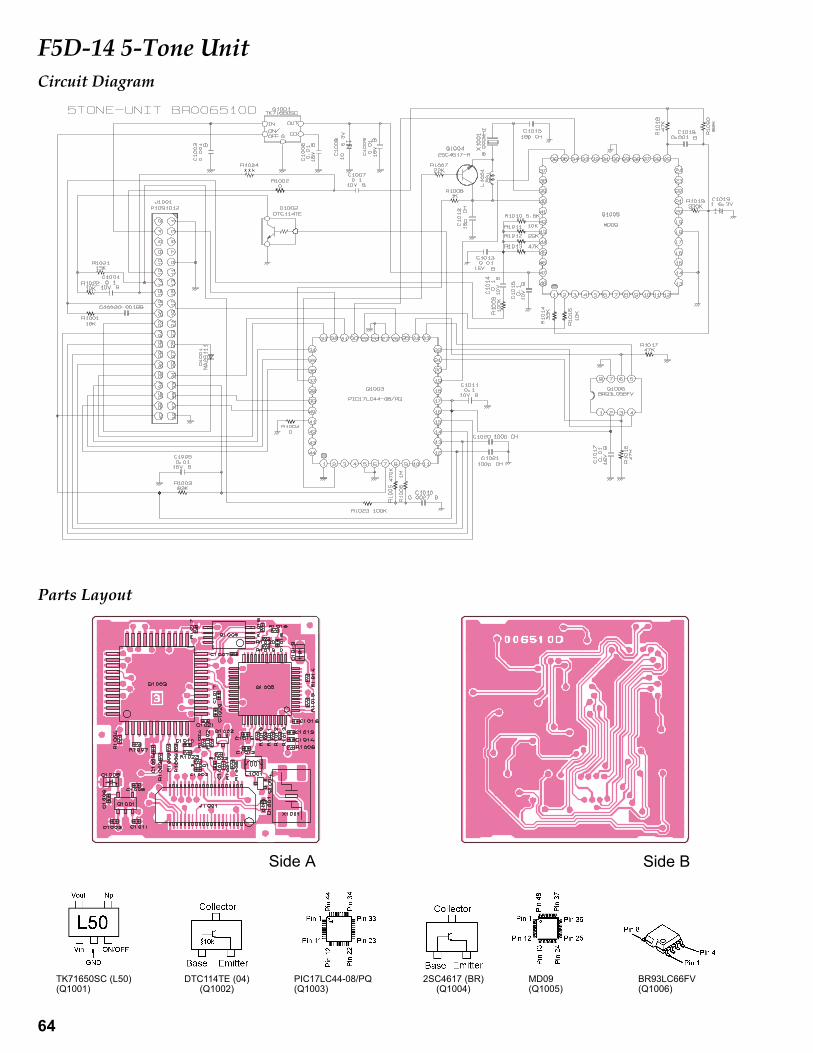
64
F5D-14 5-Tone UnitCircuit Diagram
Parts Layout
Side BSide A
2SC4617 (BR)(Q1004)
DTC114TE (04)(Q1002)
BR93LC66FV(Q1006)
TK71650SC (L50)(Q1001)
MD09(Q1005)
PIC17LC44-08/PQ(Q1003)
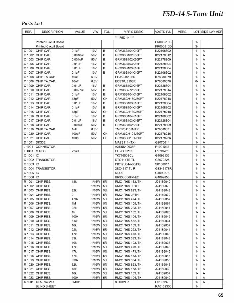
65
F5D-14 5-Tone Unit
*** F5D-14 ***Printed Circuit Board FR006510B 1-Printed Circuit Board FR006510D 3-
C 1001 CHIP CAP. 0.1uF 10V B GRM36B104K10PT K22108802 1- AC 1002 CHIP CAP. 0.0018uF 50V B GRM36B182K50PT K22178812 1- AC 1003 CHIP CAP. 0.001uF 50V B GRM36B102K50PT K22178809 1- AC 1005 CHIP CAP. 0.01uF 16V B GRM36B103K16PT K22128804 1- AC 1006 CHIP CAP. 0.01uF 16V B GRM36B103K16PT K22128804 1- AC 1007 CHIP CAP. 0.1uF 10V B GRM36B104K10PT K22108802 1- AC 1008 CHIP TA.CAP. 10uF 6.3V EEJK0JS106R K78080079 1- AC 1008 CHIP TA.CAP. 10uF 6.3V ECST0JZ106R K78080078 8- AC 1009 CHIP CAP. 0.01uF 16V B GRM36B103K16PT K22128804 1- AC 1010 CHIP CAP. 0.0027uF 50V B GRM36B272K50PT K22178814 1- AC 1011 CHIP CAP. 0.1uF 10V B GRM36B104K10PT K22108802 1- AC 1012 CHIP CAP. 18pF 50V CH GRM36CH180J50PT K22178218 1- AC 1013 CHIP CAP. 0.01uF 16V B GRM36B103K16PT K22128804 1- AC 1014 CHIP CAP. 0.1uF 10V B GRM36B104K10PT K22108802 1- AC 1015 CHIP CAP. 18pF 50V CH GRM36CH180J50PT K22178218 1- AC 1016 CHIP CAP. 0.1uF 10V B GRM36B104K10PT K22108802 1- AC 1017 CHIP CAP. 0.01uF 16V B GRM36B103K16PT K22128804 1- AC 1018 CHIP CAP. 0.001uF 50V B GRM36B102K50PT K22178809 1- AC 1019 CHIP TA.CAP. 1uF 6.3V TMCP0J105MTR K78080071 1- AC 1020 CHIP CAP. 100pF 50V CH GRM36CH101J50PT K22178236 1- AC 1021 CHIP CAP. 100pF 50V CH GRM36CH101J50PT K22178236 1- AD 1001 DIODE MA2S111-(TX) G2070614 1- AJ 1001 CONNECTOR AXK5S40035P P1091012 1- AL 1001 M.RFC 22uH ELJ-FC220K L1690201 1- AQ 1001 IC TK71650SCL G1093136 1- AQ 1002 TRANSISTOR DTC114TE TL G3070225 1- AQ 1003 IC PIC17LC44-08/PQ S8100917 1- AQ 1004 TRANSISTOR 2SC4617 TL R G3346178R 1- AQ 1005 IC MD09 G1093276 1- AQ 1006 IC BR93LC66FV-E2 G1092853 1- AR 1001 CHIP RES. 18k 1/16W 5% RMC1/16S 183JTH J24189040 1- AR 1002 CHIP RES. 0 1/16W 5% RMC1/16S JPTH J24189070 1- AR 1003 CHIP RES. 82k 1/16W 5% RMC1/16S 823JTH J24189048 1- AR 1004 CHIP RES. 0 1/16W 5% RMC1/16S JPTH J24189070 1- AR 1005 CHIP RES. 470k 1/16W 5% RMC1/16S 474JTH J24189057 1- AR 1006 CHIP RES. 1M 1/16W 5% RMC1/16S 105JTH J24189061 1- AR 1007 CHIP RES. 22k 1/16W 5% RMC1/16S 223JTH J24189041 1- AR 1008 CHIP RES. 1k 1/16W 5% RMC1/16S 102JTH J24189025 1- AR 1009 CHIP RES. 100k 1/16W 5% RMC1/16S 104JTH J24189049 1- AR 1010 CHIP RES. 5.6k 1/16W 5% RMC1/16S 562JTH J24189034 1- AR 1011 CHIP RES. 10k 1/16W 5% RMC1/16S 103JTH J24189037 1- AR 1012 CHIP RES. 22k 1/16W 5% RMC1/16S 223JTH J24189041 1- AR 1013 CHIP RES. 47k 1/16W 5% RMC1/16S 473JTH J24189045 1- AR 1014 CHIP RES. 33k 1/16W 5% RMC1/16S 333JTH J24189043 1- AR 1015 CHIP RES. 10k 1/16W 5% RMC1/16S 103JTH J24189037 1- AR 1016 CHIP RES. 47k 1/16W 5% RMC1/16S 473JTH J24189045 1- AR 1017 CHIP RES. 47k 1/16W 5% RMC1/16S 473JTH J24189045 1- AR 1018 CHIP RES. 47k 1/16W 5% RMC1/16S 473JTH J24189045 1- AR 1019 CHIP RES. 330k 1/16W 5% RMC1/16S 334JTH J24189055 1- AR 1020 CHIP RES. 82k 1/16W 5% RMC1/16S 823JTH J24189048 1- AR 1021 CHIP RES. 15k 1/16W 5% RMC1/16S 153JTH J24189039 1- AR 1022 CHIP RES. 10k 1/16W 5% RMC1/16S 103JTH J24189037 1- AR 1023 CHIP RES. 100k 1/16W 5% RMC1/16S 104JTH J24189049 1- AX 1001 XTAL 94SMX 8MHz 8.000MHZ H0103248 1- A
BLIND SHEET RA0109300 1-
Parts List
DESCRIPTION VALUE V/W TOL. VXSTD P/NMFR’S DESIG VERS.REF. LOT. SIDE LAY ADR

58
Copyright 2005VERTEX STANDARD CO., LTD.All rights reserved
No portion of this manualmay be reproduced withoutthe permission ofVERTEX STANDARD CO., LTD.