Embed Size (px)
Citation preview

Vivado Design Suite Tutorial
High-Level Synthesis
UG871 (v2012.2) August 20, 2012
High-Level Synthesis www.xilinx.com 2UG871 (v2012.2) August 20, 2012
Notice of DisclaimerThe information disclosed to you hereunder (the “Materials”) is provided solely for the selection and use of Xilinx products. To the maximum extent permitted by applicable law: (1) Materials are made available "AS IS" and with all faults, Xilinx hereby DISCLAIMS ALL WARRANTIES AND CONDITIONS, EXPRESS, IMPLIED, OR STATUTORY, INCLUDING BUT NOT LIMITED TO WARRANTIES OF MERCHANTABILITY, NON-INFRINGEMENT, OR FITNESS FOR ANY PARTICULAR PURPOSE; and (2) Xilinx shall not be liable (whether in contract or tort, including negligence, or under any other theory of liability) for any loss or damage of any kind or nature related to, arising under, or in connection with, the Materials (including your use of the Materials), including for any direct, indirect, special, incidental, or consequential loss or damage (including loss of data, profits, goodwill, or any type of loss or damage suffered as a result of any action brought by a third party) even if such damage or loss was reasonably foreseeable or Xilinx had been advised of the possibility of the same. Xilinx assumes no obligation to correct any errors contained in the Materials or to notify you of updates to the Materials or to product specifications. You may not reproduce, modify, distribute, or publicly display the Materials without prior written consent. Certain products are subject to the terms and conditions of the Limited Warranties which can be viewed at http://www.xilinx.com/warranty.htm; IP cores may be subject to warranty and support terms contained in a license issued to you by Xilinx. Xilinx products are not designed or intended to be fail-safe or for use in any application requiring fail-safe performance; you assume sole risk and liability for use of Xilinx products in Critical Applications: http://www.xilinx.com/warranty.htm#critapps.[© Copyright 2012 Xilinx, Inc. Xilinx, the Xilinx logo, Artix, ISE, Kintex, Spartan, Virtex, Vivado, and other designated brands included herein are trademarks of Xilinx in the United States and other countries. All other trademarks are the property of their respective owners.
Revision HistoryThe following table shows the revision history for this document.
Date Version Revision
8/20/12 1.0 Initial Xilinx release of the Vivado Design Suite Tutorial: High-Level Synthesis.
High-Level Synthesis www.xilinx.com 3UG902 (2012.2) August 20, 2012
Table of ContentsChapter 1: Vivado HLS: Introduction Tutorial
Introduction . . . . . . . . . . . . . . . . . . . . . . . . . . . . . . . . . . . . . . . . . . . . . . . . . . . . . . . . . . . . . . . . . . . . . . 4Licensing and Installation . . . . . . . . . . . . . . . . . . . . . . . . . . . . . . . . . . . . . . . . . . . . . . . . . . . . . . . . . . . 4Overview. . . . . . . . . . . . . . . . . . . . . . . . . . . . . . . . . . . . . . . . . . . . . . . . . . . . . . . . . . . . . . . . . . . . . . . . . 5Starting Your Project . . . . . . . . . . . . . . . . . . . . . . . . . . . . . . . . . . . . . . . . . . . . . . . . . . . . . . . . . . . . . . . 6C Validation . . . . . . . . . . . . . . . . . . . . . . . . . . . . . . . . . . . . . . . . . . . . . . . . . . . . . . . . . . . . . . . . . . . . . 13Synthesizing and Analyzing the Design . . . . . . . . . . . . . . . . . . . . . . . . . . . . . . . . . . . . . . . . . . . . . . . 20Bit-Accurate Design . . . . . . . . . . . . . . . . . . . . . . . . . . . . . . . . . . . . . . . . . . . . . . . . . . . . . . . . . . . . . . . 32Design Optimization . . . . . . . . . . . . . . . . . . . . . . . . . . . . . . . . . . . . . . . . . . . . . . . . . . . . . . . . . . . . . . 40RTL Verification and Export. . . . . . . . . . . . . . . . . . . . . . . . . . . . . . . . . . . . . . . . . . . . . . . . . . . . . . . . . 52The Shell and Scripts . . . . . . . . . . . . . . . . . . . . . . . . . . . . . . . . . . . . . . . . . . . . . . . . . . . . . . . . . . . . . . 57
Chapter 2: Vivado HLS: Integrating EDKIntroduction . . . . . . . . . . . . . . . . . . . . . . . . . . . . . . . . . . . . . . . . . . . . . . . . . . . . . . . . . . . . . . . . . . . . . 60Reference Design . . . . . . . . . . . . . . . . . . . . . . . . . . . . . . . . . . . . . . . . . . . . . . . . . . . . . . . . . . . . . . . . . 61
Chapter 3: Vivado HLS: Integrating System GeneratorIntroduction . . . . . . . . . . . . . . . . . . . . . . . . . . . . . . . . . . . . . . . . . . . . . . . . . . . . . . . . . . . . . . . . . . . . . 93Software Application for Vivado HLS . . . . . . . . . . . . . . . . . . . . . . . . . . . . . . . . . . . . . . . . . . . . . . . . . 93Create a Project in Vivado HLS for the FIR Application . . . . . . . . . . . . . . . . . . . . . . . . . . . . . . . . . . . 96Create an RTL design . . . . . . . . . . . . . . . . . . . . . . . . . . . . . . . . . . . . . . . . . . . . . . . . . . . . . . . . . . . . . 103Import the Design into System Generator . . . . . . . . . . . . . . . . . . . . . . . . . . . . . . . . . . . . . . . . . . . . 108
Appendix A: Additional ResourcesXilinx Resources . . . . . . . . . . . . . . . . . . . . . . . . . . . . . . . . . . . . . . . . . . . . . . . . . . . . . . . . . . . . . . . . . 113Solution Centers. . . . . . . . . . . . . . . . . . . . . . . . . . . . . . . . . . . . . . . . . . . . . . . . . . . . . . . . . . . . . . . . . 113References . . . . . . . . . . . . . . . . . . . . . . . . . . . . . . . . . . . . . . . . . . . . . . . . . . . . . . . . . . . . . . . . . . . . . 113
Chapter 1
Vivado HLS: Introduction Tutorial
IntroductionThis guide provides an introduction to the Xilinx® Vivado High-Level Synthesis (HLS) tool for transforming a C, C++, or SystemC design specification into a Register Transfer Level (RTL) implementation, which can be synthesized into a Xilinx FPGA.
This document is designed to be used with the FIR design example included with this tutorial.
This tutorial explains how to perform the following tasks using the Vivado HLS tool:
• Create an Vivado HLS project
• Validate the C design
• Perform synthesis and design analysis
• Create and synthesize a bit-accurate design
• Perform design optimization
• Understand how to perform RTL verif ication and export
• Review using the Vivado HLS tool with Tcl scripts
Licensing and InstallationThe f irst steps in using the Vivado HLS tool are to install the software, obtain a license and configure it. See the Xilinx Design Tools: Installation and Licensing Guide (UG978).
Contact your local Xilinx representative to obtain a license for the Vivado HLS tool.
High-Level Synthesis www.xilinx.com 4UG902 (v2012.2) August 20, 2012
Overview
OverviewThis document uses a FIR design example to explain how the Vivado HLS tool is used to synthesize a C design to RTL that meets specif ic hardware design goals.
Design GoalsThe hardware design goals for this FIR design project are to:
• Create a version of the design with the smallest area
• Create a version of this design with the highest throughput
The f inal design should be able to process 8-bit data supplied with an input valid signal and produce 8-bit output data accompanied by an output valid signal. The filter coefficients are to be stored externally to the FIR design, in a single port RAM.
Tutorial SetupBegin by copying the fir directory to a local work area.
Note: PC users: The path name to the local work area should not contain any spaces. For example, C:\Documents and Settings\My Name\Examples\fir is not a valid work area because of the spaces in the path name.
Table 1-1: Lab 1 File Summary
Filename Description
fir.c C code to be synthesized into RTL.
fir_test.c C test bench for the FIR design. It is used to validate that the C algorithm is functioning correctly and is reused by the Vivado HLS tool to verify the RTL.
fir.h Header f ile for the f ilter and test bench.
in.dat Input data f ile used by the test bench.
out.gold.dat
out.gold.8.dat
Data that is expected from the FIR function after normal operation.
High-Level Synthesis www.xilinx.com 5UG902 (v2012.2) August 20, 2012
Starting Your Project
Learning GoalsThis design example describes how to:
• Use the Vivado HLS Graphical User Interface (GUI) to create an Vivado HLS design project.
• Validate the C code within the Vivado HLS tool.
• Analyze the results of synthesis, understand the Vivado HLS reports, and be able to use the Design Viewer analysis capability.
• Apply optimizations to improve the design.
• Verify that the functionality of the RTL implementation matches that of the original C design.
• Export the design as an IP block to other Xilinx tools.
Optionally execute logic synthesis during the RTL Export process to evaluate the timing and area results after logic synthesis.
Starting Your ProjectThe Vivado HLS Graphical User Interface (GUI) is used to perform all operations in this design tutorial. The Tcl based interactive and batch modes are discussed at the end of the tutorial.
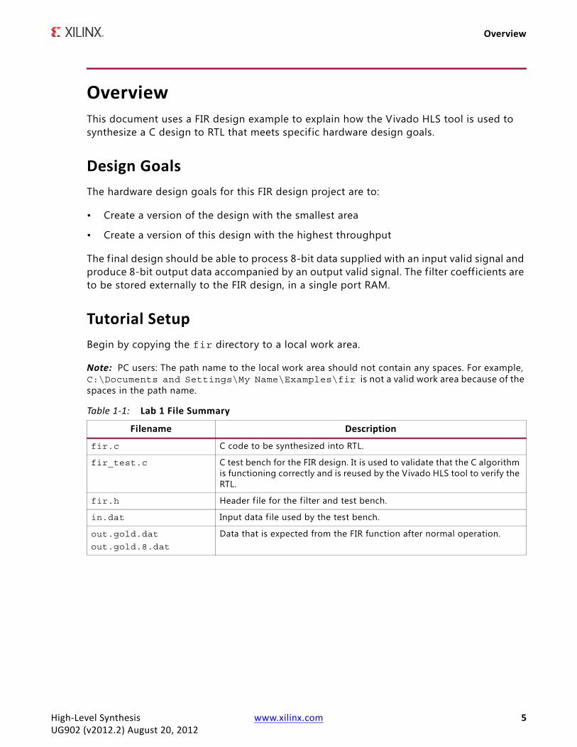
Opening the Vivado HLS GUITo open the GUI, double-click on the Vivado HLS GUI desktop icon.
Note: You can also open the GUI using the Windows menu by selecting Start > All Programs > Vivado <version> > Vivado HLS GUI. The Vivado HLS group is shown in Figure 3-1.X-Ref Target - Figure 1-1
Figure 1-1: Launching the Vivado HLS GUI
High-Level Synthesis www.xilinx.com 6UG902 (v2012.2) August 20, 2012
Starting Your Project
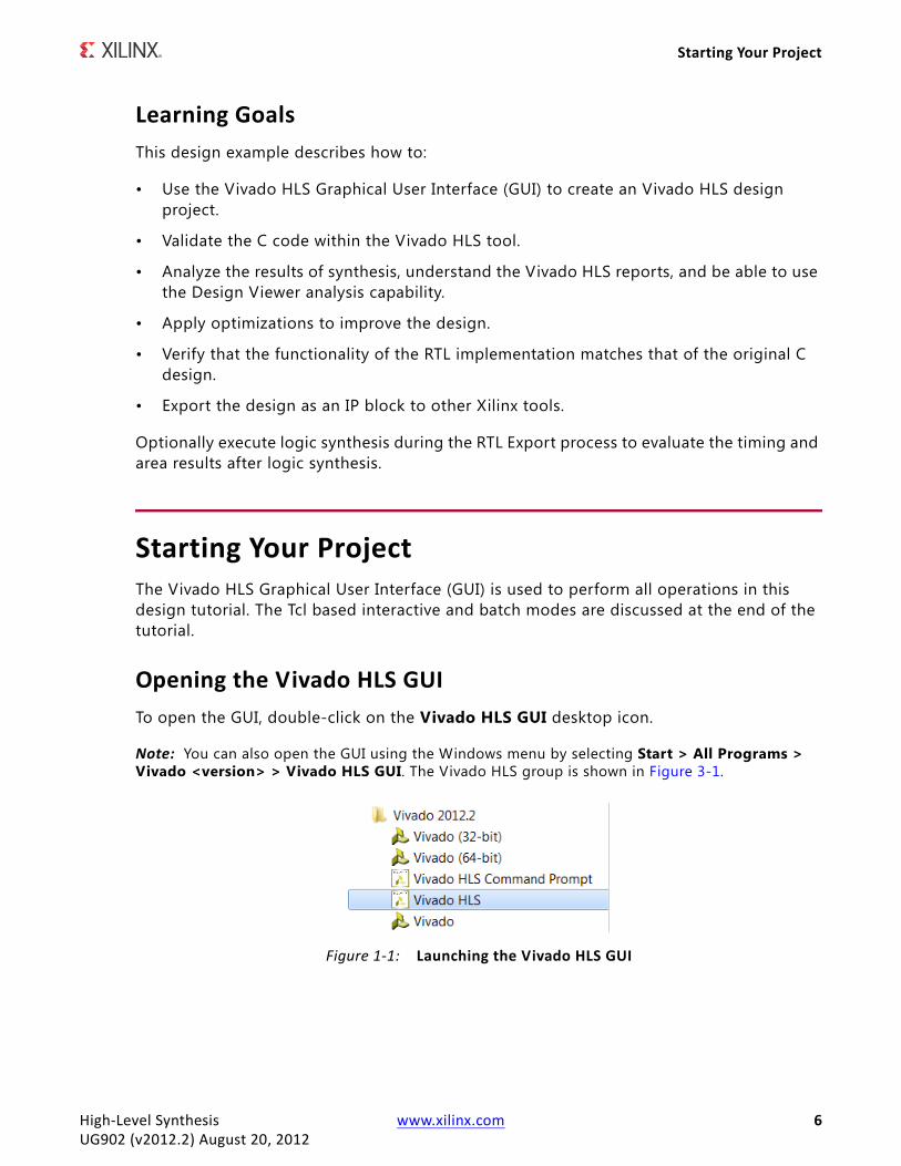
Vivado HLS opens. The Welcome Page shows the primary starting points for Vivado HLS.
The Getting Started options are:
• Create New Project: Launches the project setup wizard.
• Open Project: Opens a window for you to navigate to an existing project.
• Open Recent Project: Gives you a list of recent projects, from which you can select one to open.
• Browse Examples: Open Vivado HLS examples. These can also be found in the examples directory in the Vivado HLS installation area.
The Documentation options are:
• Release Notes Guide: Opens the Release Notes for this version of software.
• User Guide: Opens the Vivado HLS User Guide.
• Vivado HLS Tutorial: Opens the Vivado HLS Tutorials.
X-Ref Target - Figure 1-2
Figure 1-2: Vivado HLS Welcome Page
High-Level Synthesis www.xilinx.com 7UG902 (v2012.2) August 20, 2012
Starting Your Project
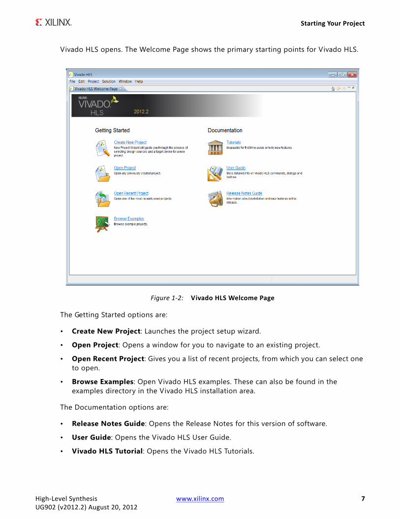
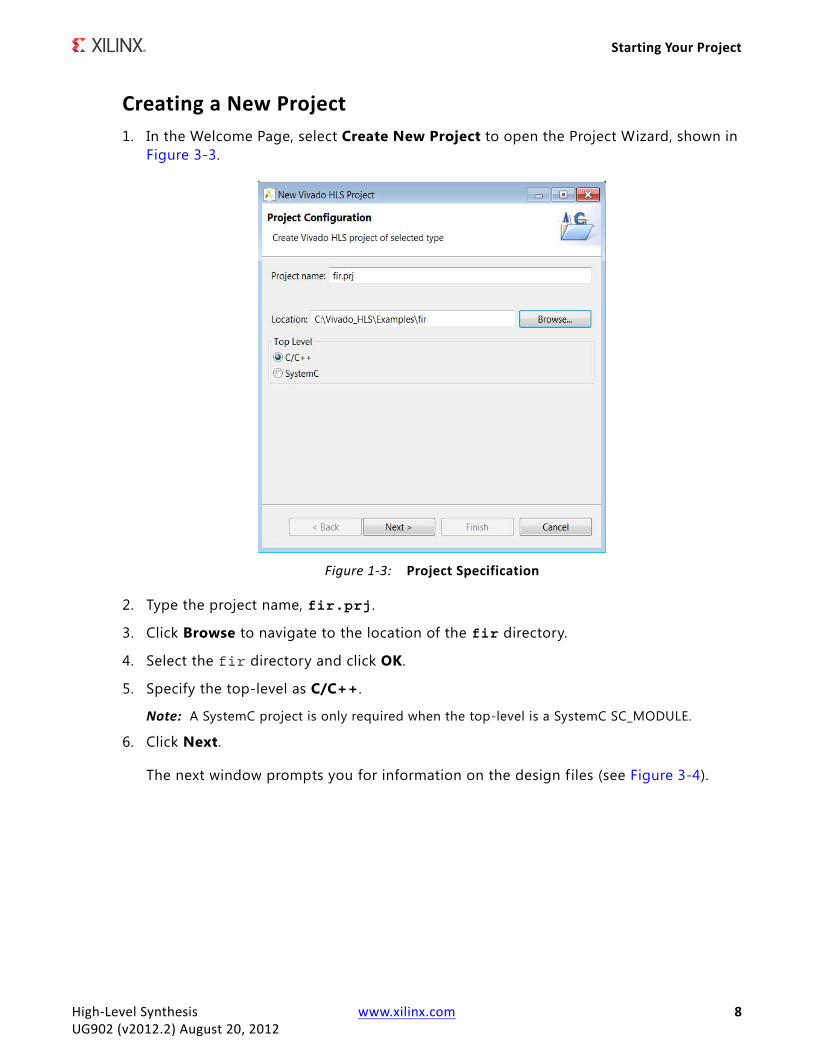
Creating a New Project1. In the Welcome Page, select Create New Project to open the Project Wizard, shown in
Figure 3-3.
2. Type the project name, fir.prj.
3. Click Browse to navigate to the location of the fir directory.
4. Select the fir directory and click OK.
5. Specify the top-level as C/C++.
Note: A SystemC project is only required when the top-level is a SystemC SC_MODULE.
6. Click Next.
The next window prompts you for information on the design files (see Figure 3-4).
X-Ref Target - Figure 1-3
Figure 1-3: Project Specification
High-Level Synthesis www.xilinx.com 8UG902 (v2012.2) August 20, 2012
Starting Your Project
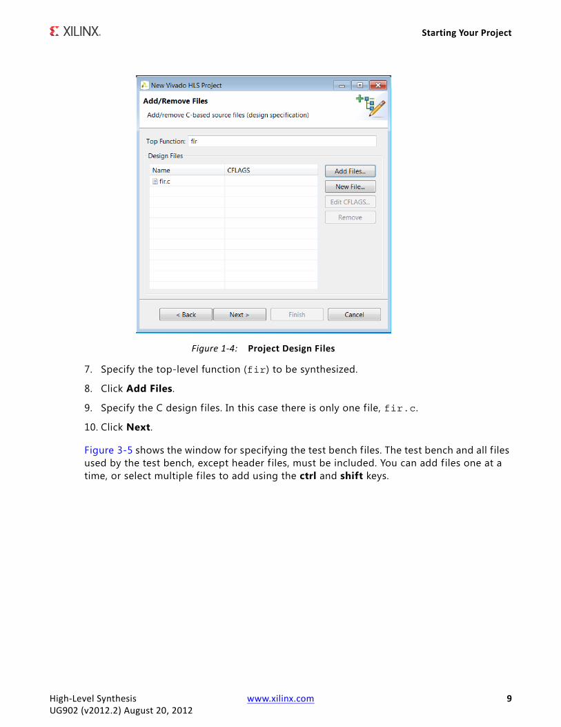
7. Specify the top-level function (fir) to be synthesized.
8. Click Add Files.
9. Specify the C design files. In this case there is only one file, fir.c.
10. Click Next.
Figure 3-5 shows the window for specifying the test bench f iles. The test bench and all f iles used by the test bench, except header f iles, must be included. You can add f iles one at a time, or select multiple files to add using the ctrl and shift keys.
X-Ref Target - Figure 1-4
Figure 1-4: Project Design Files
High-Level Synthesis www.xilinx.com 9UG902 (v2012.2) August 20, 2012
Starting Your Project
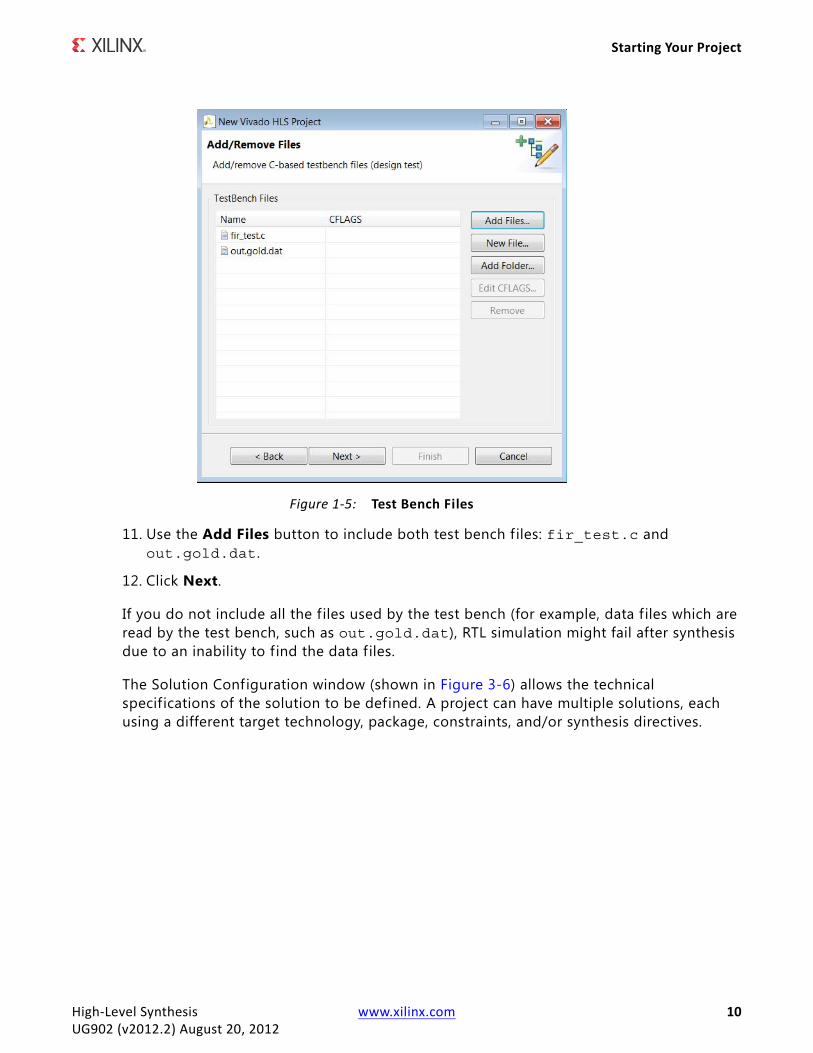
11. Use the Add Files button to include both test bench f iles: fir_test.c and out.gold.dat.
12. Click Next.
If you do not include all the files used by the test bench (for example, data files which are read by the test bench, such as out.gold.dat), RTL simulation might fail after synthesis due to an inability to f ind the data f iles.
The Solution Configuration window (shown in Figure 3-6) allows the technical specifications of the solution to be defined. A project can have multiple solutions, each using a different target technology, package, constraints, and/or synthesis directives.
X-Ref Target - Figure 1-5
Figure 1-5: Test Bench Files
High-Level Synthesis www.xilinx.com 10UG902 (v2012.2) August 20, 2012
Starting Your Project
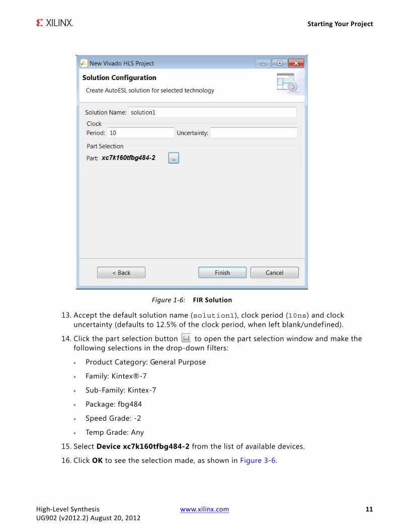
13. Accept the default solution name (solution1), clock period (10ns) and clock uncertainty (defaults to 12.5% of the clock period, when left blank/undefined).
14. Click the part selection button to open the part selection window and make the following selections in the drop-down filters:
° Product Category: General Purpose
° Family: Kintex®-7
° Sub-Family: Kintex-7
° Package: fbg484
° Speed Grade: -2
° Temp Grade: Any
15. Select Device xc7k160tfbg484-2 from the list of available devices.
16. Click OK to see the selection made, as shown in Figure 3-6.
X-Ref Target - Figure 1-6
Figure 1-6: FIR Solution
High-Level Synthesis www.xilinx.com 11UG902 (v2012.2) August 20, 2012
Starting Your Project
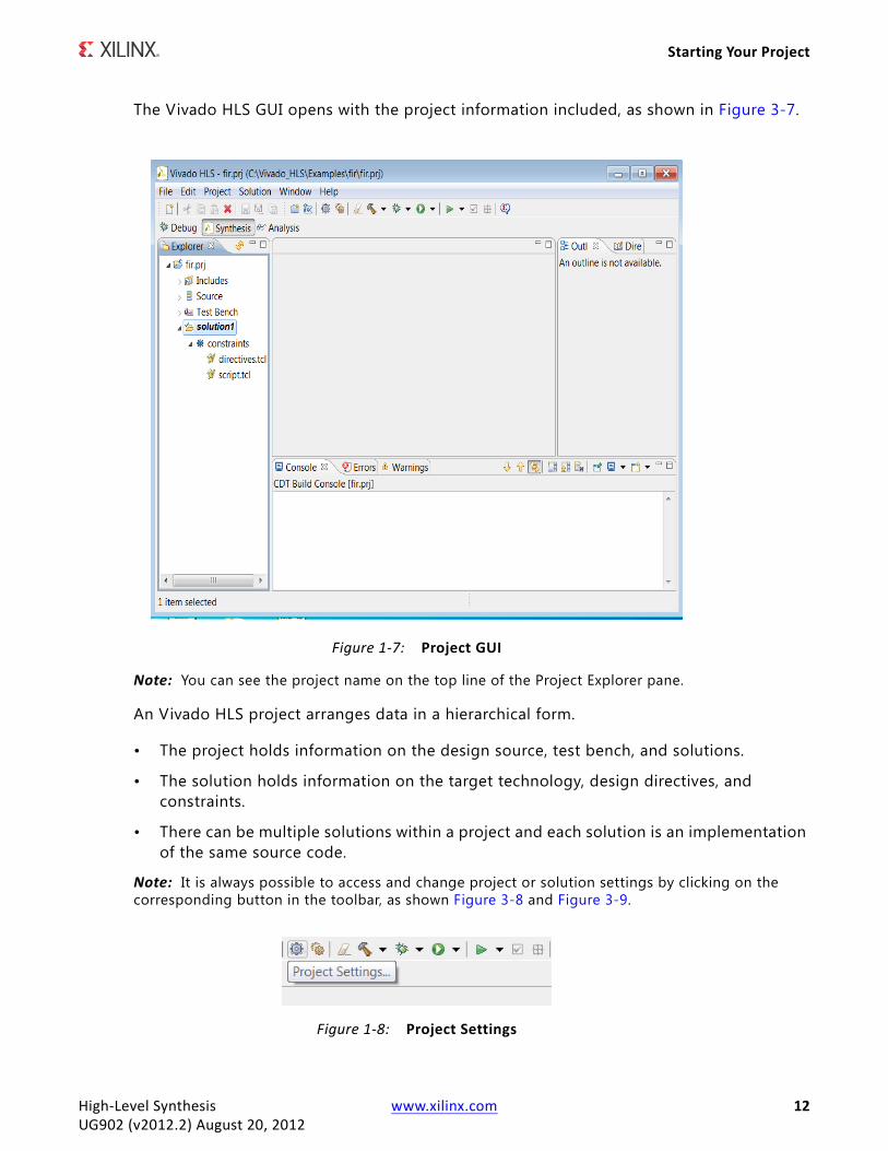
The Vivado HLS GUI opens with the project information included, as shown in Figure 3-7.
Note: You can see the project name on the top line of the Project Explorer pane.
An Vivado HLS project arranges data in a hierarchical form.
• The project holds information on the design source, test bench, and solutions.
• The solution holds information on the target technology, design directives, and constraints.
• There can be multiple solutions within a project and each solution is an implementation of the same source code.
Note: It is always possible to access and change project or solution settings by clicking on the corresponding button in the toolbar, as shown Figure 3-8 and Figure 3-9.
X-Ref Target - Figure 1-7
Figure 1-7: Project GUI
X-Ref Target - Figure 1-8
Figure 1-8: Project Settings
High-Level Synthesis www.xilinx.com 12UG902 (v2012.2) August 20, 2012
C Validation
Summary• You can use the Project wizard to set up an Vivado HLS project.
• Each project is based on the same source code and test bench.
• A project can contain multiple solutions and each solution can use a different clock rate, target technology, package, speed grade, and more typically, different optimization directives.
C ValidationYou must validate the C design prior to synthesis to ensure that it is performing correctly. You can perform this validation using the Vivado HLS tool.
Test BenchThe test bench f ile, fir_test.c, contains the top-level C function main(), which in turn calls the function to be synthesized (fir). A useful characteristic of this test bench is that it is self-checking and returns a value of 0 (zero) to confirm that the results are correct. Some other characteristics of this test bench are:
• The test bench saves the output from function fir into output file out.dat.
• The output file is compared with the golden results, stored in f ile out.gold.dat.
• If the output matches the golden data, a message confirms that the results are correct and the return value of the test bench main() function is set to 0.
• If the output is different from the golden results, a message indicates this and the return value of main() is set to 1 (one).
The Vivado HLS tool can reuse the C test bench to perform verif ication of the RTL. It confirms the successful verif ication of the RTL if the test bench returns a value of 0. If any other value is returned by main(), including no return value, it indicates that the RTL verif ication failed.
If the test bench has the self-checking characteristics mentioned above, the RTL results are automatically checked against the golden data. There is no requirement to create RTL in a test bench. This provides a robust and productive verif ication methodology.
X-Ref Target - Figure 1-9
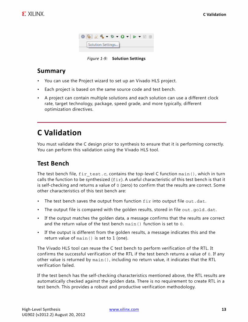
Figure 1-9: Solution Settings
High-Level Synthesis www.xilinx.com 13UG902 (v2012.2) August 20, 2012
C Validation
Types of C CompilationThe Vivado HLS tool provides two types of C compilation: Debug and Release.
• Code compiled for Debug can be used in the Vivado HLS debug environment.
• Code compiled for Release executes faster, because it has no debug information. However, it cannot be used in the debug environment.
This tutorial demonstrates both types of C compilation.
C ValidationYou can perform C simulation to validate the C algorithm by compiling the C function/design and executing it. This f irst example also opens the compiled C code in the Vivado HLS debug environment.
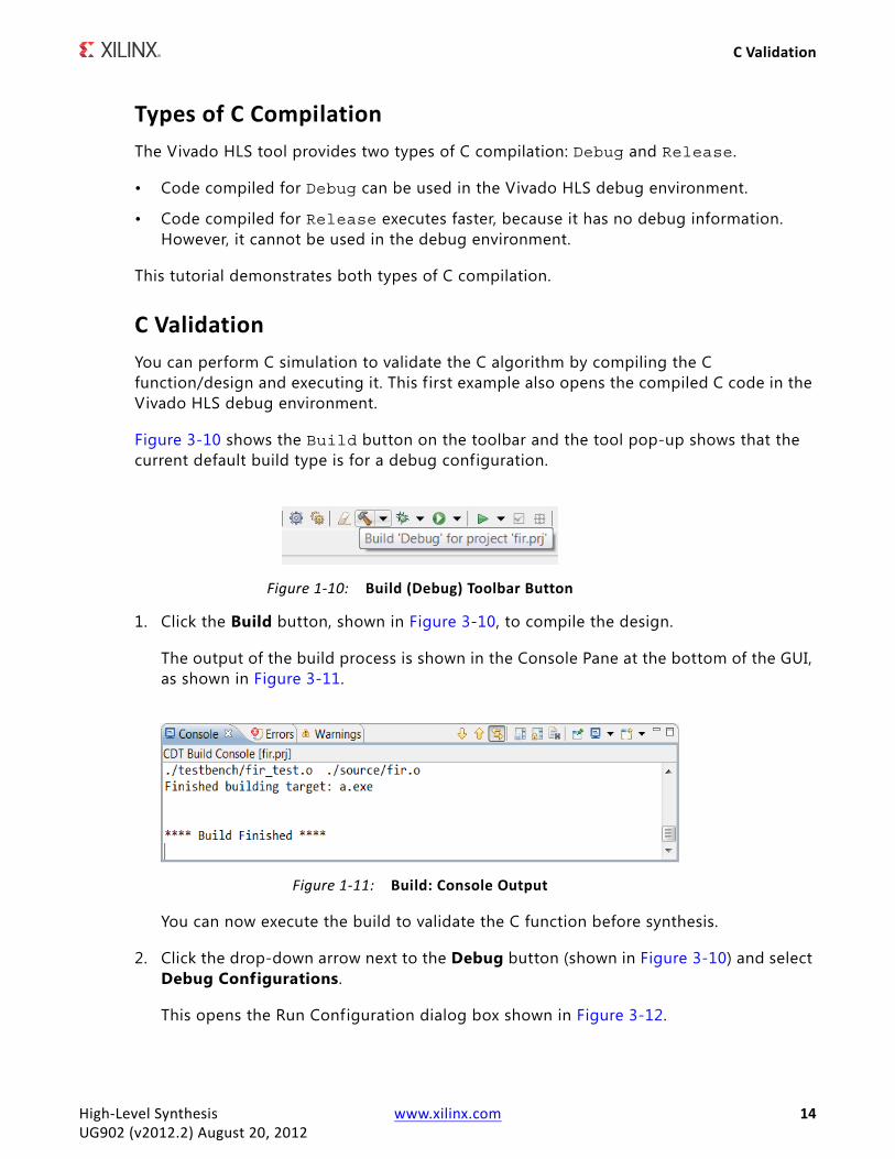
Figure 3-10 shows the Build button on the toolbar and the tool pop-up shows that the current default build type is for a debug configuration.
1. Click the Build button, shown in Figure 3-10, to compile the design.
The output of the build process is shown in the Console Pane at the bottom of the GUI, as shown in Figure 3-11.
You can now execute the build to validate the C function before synthesis.
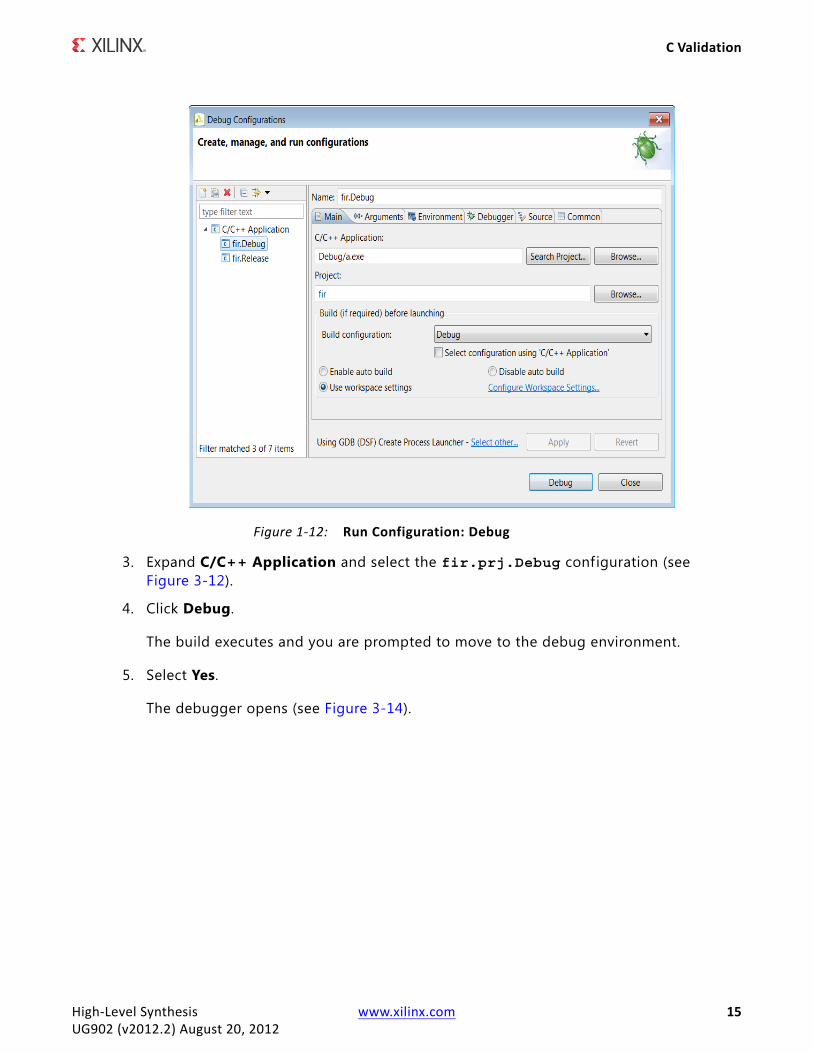
2. Click the drop-down arrow next to the Debug button (shown in Figure 3-10) and select Debug Configurations.
This opens the Run Configuration dialog box shown in Figure 3-12.
X-Ref Target - Figure 1-10
Figure 1-10: Build (Debug) Toolbar Button
X-Ref Target - Figure 1-11
Figure 1-11: Build: Console Output
High-Level Synthesis www.xilinx.com 14UG902 (v2012.2) August 20, 2012
C Validation
3. Expand C/C++ Application and select the fir.prj.Debug configuration (see Figure 3-12).
4. Click Debug.
The build executes and you are prompted to move to the debug environment.
5. Select Yes.
The debugger opens (see Figure 3-14).
X-Ref Target - Figure 1-12
Figure 1-12: Run Configuration: Debug
High-Level Synthesis www.xilinx.com 15UG902 (v2012.2) August 20, 2012
C Validation
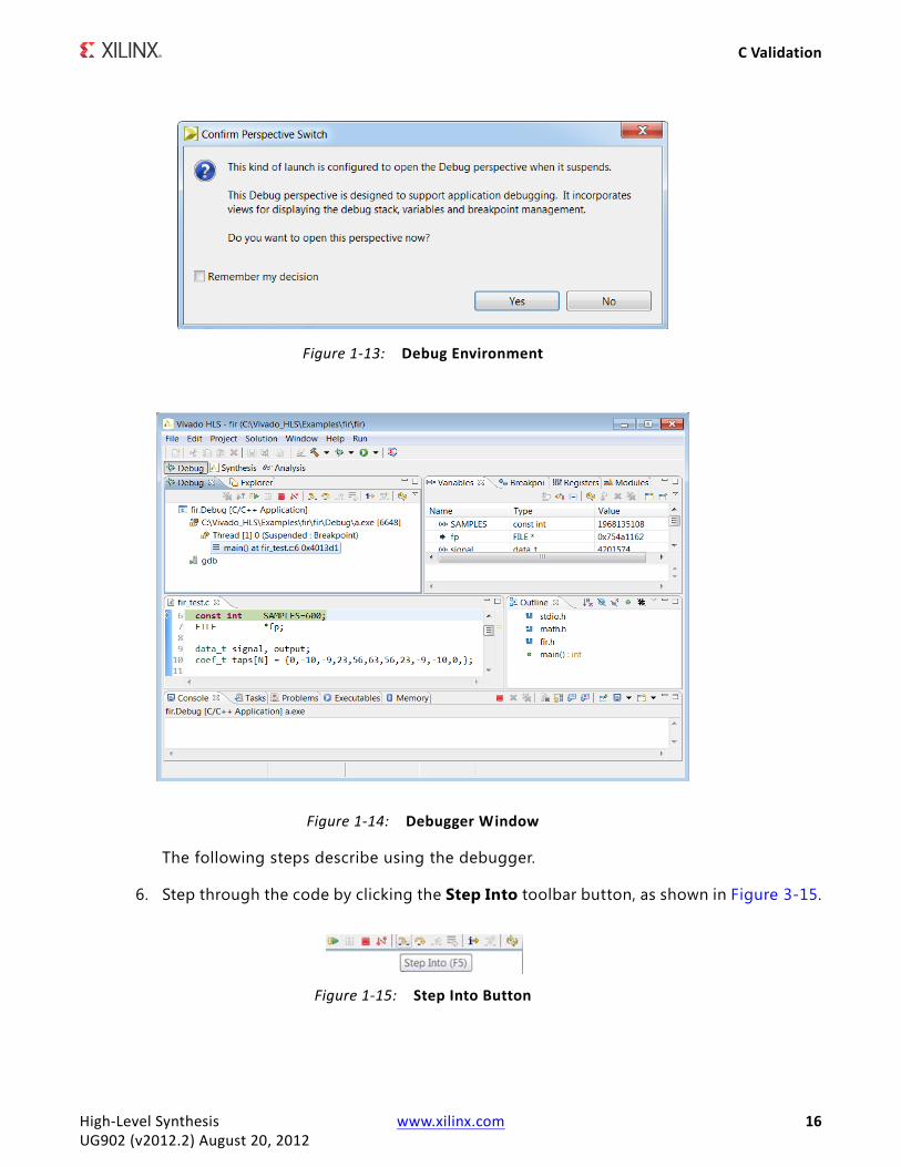
The following steps describe using the debugger.
6. Step through the code by clicking the Step Into toolbar button, as shown in Figure 3-15.
X-Ref Target - Figure 1-13
Figure 1-13: Debug Environment
X-Ref Target - Figure 1-14
Figure 1-14: Debugger Window
X-Ref Target - Figure 1-15
Figure 1-15: Step Into Button
High-Level Synthesis www.xilinx.com 16UG902 (v2012.2) August 20, 2012
C Validation
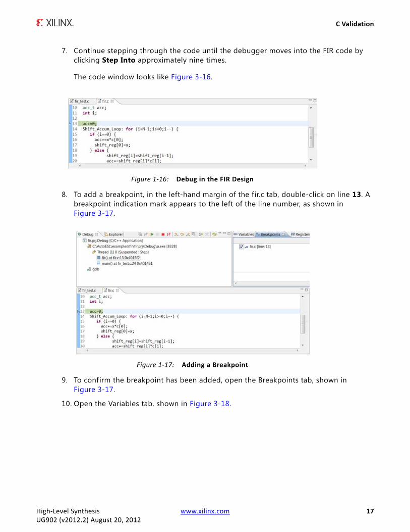
7. Continue stepping through the code until the debugger moves into the FIR code by clicking Step Into approximately nine times.
The code window looks like Figure 3-16.
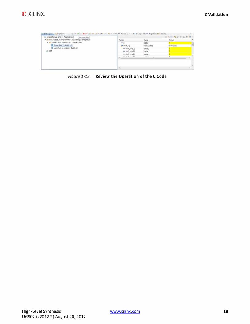
8. To add a breakpoint, in the left-hand margin of the f ir.c tab, double-click on line 13. A breakpoint indication mark appears to the left of the line number, as shown in Figure 3-17.
9. To confirm the breakpoint has been added, open the Breakpoints tab, shown in Figure 3-17.
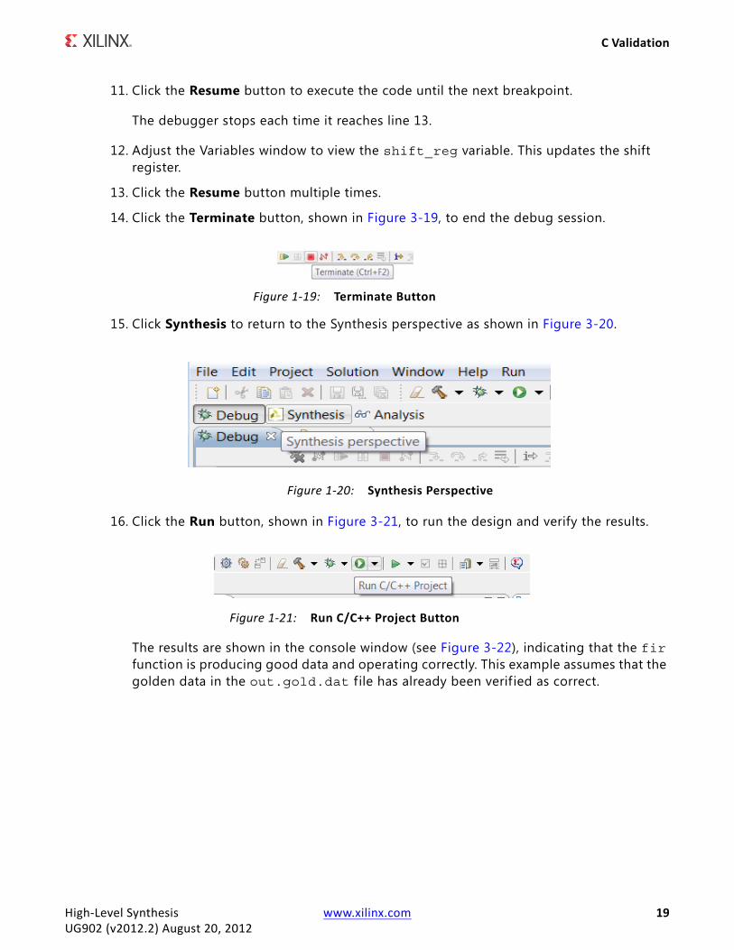
10. Open the Variables tab, shown in Figure 3-18.
X-Ref Target - Figure 1-16
Figure 1-16: Debug in the FIR Design
X-Ref Target - Figure 1-17
Figure 1-17: Adding a Breakpoint
High-Level Synthesis www.xilinx.com 17UG902 (v2012.2) August 20, 2012
C Validation
X-Ref Target - Figure 1-18
Figure 1-18: Review the Operation of the C Code
High-Level Synthesis www.xilinx.com 18UG902 (v2012.2) August 20, 2012
C Validation
11. Click the Resume button to execute the code until the next breakpoint.
The debugger stops each time it reaches line 13.
12. Adjust the Variables window to view the shift_reg variable. This updates the shift register.
13. Click the Resume button multiple times.
14. Click the Terminate button, shown in Figure 3-19, to end the debug session.
15. Click Synthesis to return to the Synthesis perspective as shown in Figure 3-20.
16. Click the Run button, shown in Figure 3-21, to run the design and verify the results.
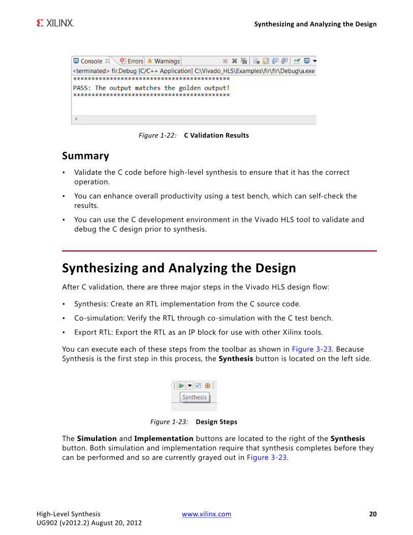
The results are shown in the console window (see Figure 3-22), indicating that the fir function is producing good data and operating correctly. This example assumes that the golden data in the out.gold.dat f ile has already been verif ied as correct.
X-Ref Target - Figure 1-19
Figure 1-19: Terminate Button
X-Ref Target - Figure 1-20
Figure 1-20: Synthesis Perspective
X-Ref Target - Figure 1-21
Figure 1-21: Run C/C++ Project Button
High-Level Synthesis www.xilinx.com 19UG902 (v2012.2) August 20, 2012
Synthesizing and Analyzing the Design
Summary• Validate the C code before high-level synthesis to ensure that it has the correct
operation.
• You can enhance overall productivity using a test bench, which can self-check the results.
• You can use the C development environment in the Vivado HLS tool to validate and debug the C design prior to synthesis.
Synthesizing and Analyzing the DesignAfter C validation, there are three major steps in the Vivado HLS design flow:
• Synthesis: Create an RTL implementation from the C source code.
• Co-simulation: Verify the RTL through co-simulation with the C test bench.
• Export RTL: Export the RTL as an IP block for use with other Xilinx tools.
You can execute each of these steps from the toolbar as shown in Figure 3-23. Because Synthesis is the f irst step in this process, the Synthesis button is located on the left side.
The Simulation and Implementation buttons are located to the right of the Synthesis button. Both simulation and implementation require that synthesis completes before they can be performed and so are currently grayed out in Figure 3-23.
X-Ref Target - Figure 1-22
Figure 1-22: C Validation Results
X-Ref Target - Figure 1-23
Figure 1-23: Design Steps
High-Level Synthesis www.xilinx.com 20UG902 (v2012.2) August 20, 2012
Synthesizing and Analyzing the Design
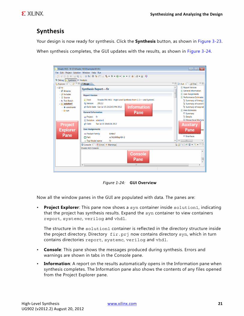
SynthesisYour design is now ready for synthesis. Click the Synthesis button, as shown in Figure 3-23.
When synthesis completes, the GUI updates with the results, as shown in Figure 3-24.
Now all the window panes in the GUI are populated with data. The panes are:
• Project Explorer : This pane now shows a syn container inside solution1, indicating that the project has synthesis results. Expand the syn container to view containers report, systemc, verilog and vhdl.
The structure in the solution1 container is reflected in the directory structure inside the project directory. Directory fir.prj now contains directory syn, which in turn contains directories report, systemc, verilog and vhdl.
• Console: This pane shows the messages produced during synthesis. Errors and warnings are shown in tabs in the Console pane.
• Information: A report on the results automatically opens in the Information pane when synthesis completes. The Information pane also shows the contents of any f iles opened from the Project Explorer pane.
X-Ref Target - Figure 1-24
Figure 1-24: GUI Overview
High-Level Synthesis www.xilinx.com 21UG902 (v2012.2) August 20, 2012
Synthesizing and Analyzing the Design
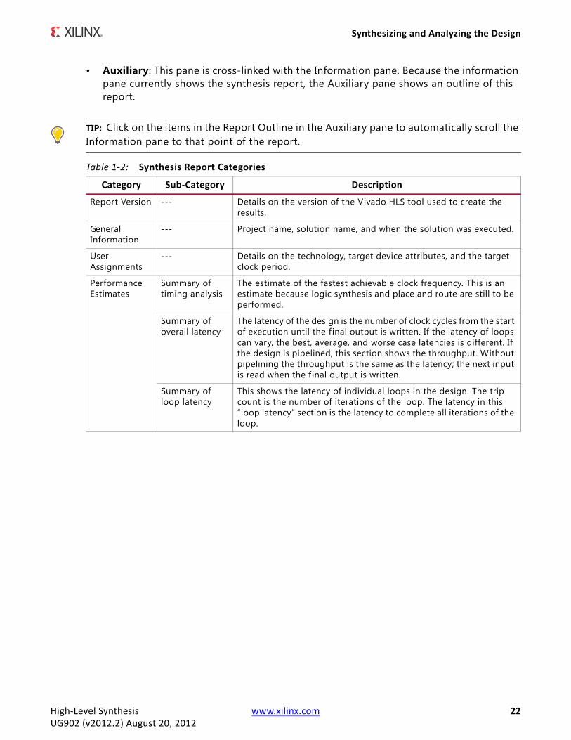
• Auxiliary: This pane is cross-linked with the Information pane. Because the information pane currently shows the synthesis report, the Auxiliary pane shows an outline of this report.
TIP: Click on the items in the Report Outline in the Auxiliary pane to automatically scroll the Information pane to that point of the report.
Table 1-2: Synthesis Report Categories
Category Sub-Category Description
Report Version --- Details on the version of the Vivado HLS tool used to create the results.
General Information
--- Project name, solution name, and when the solution was executed.
User Assignments
--- Details on the technology, target device attributes, and the target clock period.
Performance Estimates
Summary of timing analysis
The estimate of the fastest achievable clock frequency. This is an estimate because logic synthesis and place and route are still to be performed.
Summary of overall latency
The latency of the design is the number of clock cycles from the start of execution until the f inal output is written. If the latency of loops can vary, the best, average, and worse case latencies is different. If the design is pipelined, this section shows the throughput. Without pipelining the throughput is the same as the latency; the next input is read when the final output is written.
Summary of loop latency
This shows the latency of individual loops in the design. The trip count is the number of iterations of the loop. The latency in this “loop latency” section is the latency to complete all iterations of the loop.
High-Level Synthesis www.xilinx.com 22UG902 (v2012.2) August 20, 2012
Synthesizing and Analyzing the Design
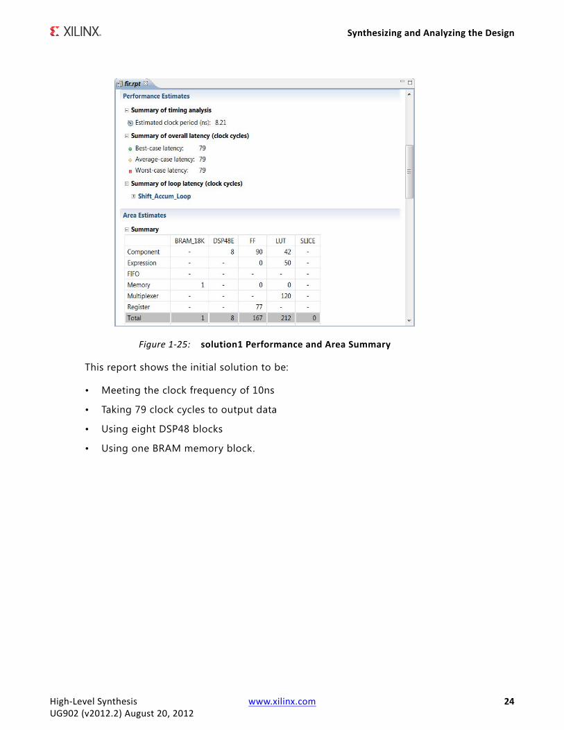
A section of the report is shown in Figure 3-25.
Area Estimates Summary This shows the resources (such as LUTS, Flip-Flops, and DSP48s) used to implement the design.The sub-categories are explained in the Details section of this table.
Details: Component
The resources specif ied here are used by the components (sub-blocks) within the top-level design. Components are created by sub-functions in the design. Unless inclined, each function becomes it’s own level of hierarchy. In this example there are no sub-blocks, the design has one level of hierarchy.
Details: Expression
This category shows the area used by any expressions such as multipliers, adders, and comparators at the current level of hierarchy.
Details: FIFO The resources listed here are those used in the implementation of FIFOs at this level of the hierarchy.
Details: Memory The resources listed here are those used in the implementation of memories at this level of the hierarchy.
Details: Multiplexors
All the resources used to implement multiplexors at this level of hierarchy are shown here.
Details: Registers
This category shows the register resources used at this level of hierarchy.
Hierarchical Multiplexor Count
A summary of the multiplexors throughput the hierarchy.
Power Estimate
Summary The expected power used by the device. At this level of abstraction the power is an estimate and should be used for comparing the efficiently of different solutions.
Hierarchical Register Count
The estimated power used by resisters throughput the design hierarchy.
Interface Summary
Interface This section shows the details on type of interfaces used for the function and the ports, such as port names, directions, and bit-widths.
Table 1-2: Synthesis Report Categories (Cont’d)
Category Sub-Category Description
High-Level Synthesis www.xilinx.com 23UG902 (v2012.2) August 20, 2012
Synthesizing and Analyzing the Design
This report shows the initial solution to be:
• Meeting the clock frequency of 10ns
• Taking 79 clock cycles to output data
• Using eight DSP48 blocks
• Using one BRAM memory block.
X-Ref Target - Figure 1-25
Figure 1-25: solution1 Performance and Area Summary
High-Level Synthesis www.xilinx.com 24UG902 (v2012.2) August 20, 2012
Synthesizing and Analyzing the Design
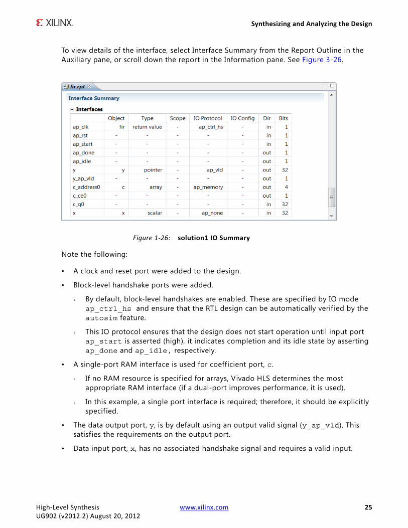
To view details of the interface, select Interface Summary from the Report Outline in the Auxiliary pane, or scroll down the report in the Information pane. See Figure 3-26.
Note the following:
• A clock and reset port were added to the design.
• Block-level handshake ports were added.
° By default, block-level handshakes are enabled. These are specif ied by IO mode ap_ctrl_hs and ensure that the RTL design can be automatically verif ied by the autosim feature.
° This IO protocol ensures that the design does not start operation until input port ap_start is asserted (high), it indicates completion and its idle state by asserting ap_done and ap_idle, respectively.
• A single-port RAM interface is used for coefficient port, c.
° If no RAM resource is specif ied for arrays, Vivado HLS determines the most appropriate RAM interface (if a dual-port improves performance, it is used).
° In this example, a single port interface is required; therefore, it should be explicitly specified.
• The data output port, y, is by default using an output valid signal (y_ap_vld). This satisfies the requirements on the output port.
• Data input port, x, has no associated handshake signal and requires a valid input.
X-Ref Target - Figure 1-26
Figure 1-26: solution1 IO Summary
High-Level Synthesis www.xilinx.com 25UG902 (v2012.2) August 20, 2012
Synthesizing and Analyzing the Design
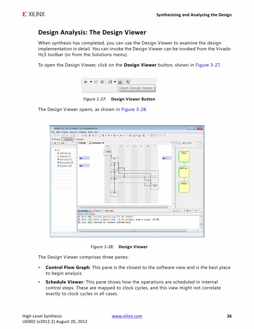
Design Analysis: The Design ViewerWhen synthesis has completed, you can use the Design Viewer to examine the design implementation in detail. You can invoke the Design Viewer can be invoked from the Vivado HLS toolbar (or from the Solutions menu).
To open the Design Viewer, click on the Design Viewer button, shown in Figure 3-27.
The Design Viewer opens, as shown in Figure 3-28.
The Design Viewer comprises three panes:
• Control Flow Graph: This pane is the closest to the software view and is the best place to begin analysis.
• Schedule Viewer: This pane shows how the operations are scheduled in internal control steps. These are mapped to clock cycles, and this view might not correlate exactly to clock cycles in all cases.
X-Ref Target - Figure 1-27
Figure 1-27: Design Viewer Button
X-Ref Target - Figure 1-28
Figure 1-28: Design Viewer
High-Level Synthesis www.xilinx.com 26UG902 (v2012.2) August 20, 2012
Synthesizing and Analyzing the Design
• Resource Viewer : This view shows how the operations in the Schedule Viewer are mapped to specif ic hardware resources.
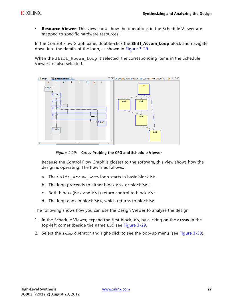
In the Control Flow Graph pane, double-click the Shift_Accum_Loop block and navigate down into the details of the loop, as shown in Figure 3-29.
When the Shift_Accum_Loop is selected, the corresponding items in the Schedule Viewer are also selected.
Because the Control Flow Graph is closest to the software, this view shows how the design is operating. The flow is as follows:
a. The Shift_Accum_Loop loop starts in basic block bb.
b. The loop proceeds to either block bb2 or block bb1.
c. Both blocks (bb2 and bb1) return control to block bb3.
d. The loop ends in block bb4, which returns to block bb.
The following shows how you can use the Design Viewer to analyze the design:
1. In the Schedule Viewer, expand the f irst block, bb, by clicking on the arrow in the top-left corner (beside the name bb); see Figure 3-29.
2. Select the icmp operator and right-click to see the pop-up menu (see Figure 3-30).
X-Ref Target - Figure 1-29
Figure 1-29: Cross-Probing the CFG and Schedule Viewer
High-Level Synthesis www.xilinx.com 27UG902 (v2012.2) August 20, 2012
Synthesizing and Analyzing the Design
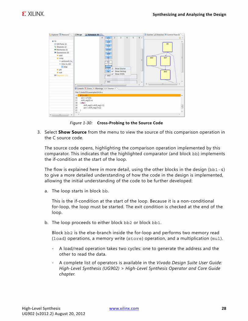
3. Select Show Source from the menu to view the source of this comparison operation in the C source code.
The source code opens, highlighting the comparison operation implemented by this comparator. This indicates that the highlighted comparator (and block bb) implements the if-condition at the start of the loop.
The flow is explained here in more detail, using the other blocks in the design (bb1-4) to give a more detailed understanding of how the code in the design is implemented, allowing the initial understanding of the code to be further developed:
a. The loop starts in block bb.
This is the if-condition at the start of the loop. Because it is a non-conditional for-loop, the loop must be started. The exit condition is checked at the end of the loop.
b. The loop proceeds to either block bb2 or block bb1.
Block bb2 is the else-branch inside the for-loop and performs two memory read (load) operations, a memory write (store) operation, and a multiplication (mul).
- A load/read operation takes two cycles: one to generate the address and the other to read the data.
- A complete list of operators is available in the Vivado Design Suite User Guide: High-Level Synthesis (UG902) > High-Level Synthesis Operator and Core Guide chapter.
X-Ref Target - Figure 1-30
Figure 1-30: Cross-Probing to the Source Code
High-Level Synthesis www.xilinx.com 28UG902 (v2012.2) August 20, 2012
Synthesizing and Analyzing the Design
Block bb1 is the if-branch inside the for-loop and performs a single memory read, write and multiplication. Both blocks (bb2 and bb1) return control to block bb3.
This block performs the accumulation common to both branches of the if-else statement.
c. The loop ends in block bb4, which returns to block bb.
Block bb4 is the loop-header, which checks the exit condition and increases the loop iteration count.
The Resource Viewer shows more details on the implementation and lists the hardware resources in the design using the following top-level categories:
• Ports
• Modules
• Memories
• Expressions
• Registers
The items under each category represent specif ic instances of this resource type in the design; for example, a RAM, multiplier, or adder.
The items under each resource instance show the number of unique operations in the C code implemented using this hardware resource. If multiple operations are shown on the same resource, the resource is being shared for multiple operations.
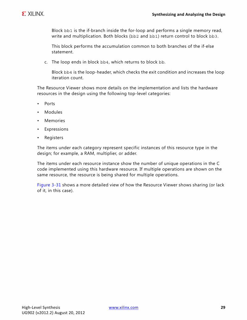
Figure 3-31 shows a more detailed view of how the Resource Viewer shows sharing (or lack of it, in this case).
High-Level Synthesis www.xilinx.com 29UG902 (v2012.2) August 20, 2012
Synthesizing and Analyzing the Design
All the multipliers in this design are listed under mul in the Modules category. Each item in the mul category represents a physical multiplier in the design (the name given is the instance name of the multiplier in the RTL design).
In this example, there are two multipliers (grp_fu_*) in the design. You can do the following actions:
• Select a multiplier in the Schedule Viewer to highlight which multiplier instance is used to implement it. If a register is also highlighted, it indicates the output is registered.
• Expand each multiplier in the Resource Viewer to show how many unique multiplication operations in the code (shown as blue squares) are mapped onto each hardware resource.
• Click on the operations (blue squares) to show that the mul operation in block bb1 is implemented on one multiplier and the mul operation in block bb2 is implemented on a different multiplier.
In this example, both multiplier resources are being used to implement a single multiplication (mul) operation and there is no sharing of the multipliers.
X-Ref Target - Figure 1-31
Figure 1-31: View Sharing in the Design Viewer
High-Level Synthesis www.xilinx.com 30UG902 (v2012.2) August 20, 2012
Synthesizing and Analyzing the Design
By contrast, examining the memory operations (load and store) in the Schedule Viewer shows that multiple read (load) and write (store) operations are implemented on the same memory resource. This also shows that array shift_reg has been implemented as a memory.
Design Analysis SummarySelecting the operations in the Schedule Viewer and correlating them with the associated elements in the Resource Viewer to show this design and the required optimizations/changes can be summarized as follows:
• The implementation, like the C code, is iterating around loop Shift_Accum_Loop and using the same hardware resources for each iteration.
° The main operation is six clock cycles through blocks bb, bb1/b2, bb3, etc. repeated 11 times.
° This keeps the resource count low, because the same resources are used in every iteration of the loop, but it costs cycles because the iterations are executed one after the other.
° To produce a design with less latency, this loop should be unrolled. Unrolling a loop allows the operations in the loop to occur in parallel, if timing and sequential dependencies (read and writes to registers and memories) allow.
• In this design, the shift_reg array is being implemented in an internal RAM.
° Even if the loop is unrolled, each iteration of the loop requires a read and write operation to this RAM.
° By default, arrays are implemented as RAMs. The shift_reg array can, however, be partitioned into individual elements. Each element is implemented by a register, allowing a shift register to be used for the implementation.
° Once the loop is unrolled, the Vivado HLS tool can perform this step automatically because it is a small RAM. All optimizations performed on the design are reported in the Console. However, because this is required, it is always better to explicitly specify it.
• The coefficient port c is using a single-port RAM interface.
° This is correct; however, because this is required, it is always better to explicitly specify it.
• Input port x is required to have an input valid signal associated with it.
° This port requires an IO protocol, which uses an input valid signal.
• There are two multipliers being used, but in the C code they are both in mutually exclusive branches.
° The Vivado HLS tool might not share components if the cost of the multiplexors could mean violating timing.
High-Level Synthesis www.xilinx.com 31UG902 (v2012.2) August 20, 2012
Bit-Accurate Design
° The timing is close in this example: 10ns minus 1.25ns, the default clock uncertainty. However, the only real way to be sure if they could be shared is to view the results after place and route.
° For this example, sharing is forced. This demonstrates a useful technique for minimizing area.
• Most importantly, The multipliers are taking four cycles each to complete! Additionally, only two multipliers are shown in the Resource Viewer, but the earlier report (Figure 3-25) gave an estimate that six DSP48s are required.
The multiplication operations are using standard C integer types (32-bit) and it requires three DSP48s to implement a 32-bit multiplication. However, this design is only required to accept 8-bit input data.
IMPORTANT: Ensure that the C code is using the correct bit-accurate types before proceeding to synthesis or it can result in larger and slower hardware.
Before performing any optimizations on this design, you must modify the source code to the required 8-bit data types.
Summary• When synthesis completes a report on the design, it automatically opens.
• More detailed and in-depth analysis of the implementation can be performed using the Design Viewer.
• In the Design Viewer, start with the Control Flow Graph and work towards the Resource Viewer for a complete understanding of how the C was implemented. The Schedule Viewer allows operations to be correlated with the C source and output HDL code.
Bit-Accurate DesignThe first step in bit-accurate design is to introduce the bit-accurate types (also called arbitrary precision types), into the source code.
When arbitrary precision types are added to a C function, it is important to validate the design and ensure that it does what it is supposed to do (rounding and truncation are of critical importance) and validates the results at the C level.
The information to make the source code bit-accurate is already included in the example f iles.
High-Level Synthesis www.xilinx.com 32UG902 (v2012.2) August 20, 2012
Bit-Accurate Design
Update the C Code
Creating a New Solution
To preserve the existing results so they can be compared against the new results, create a new solution.
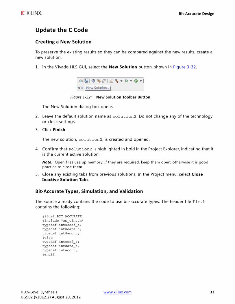
1. In the Vivado HLS GUI, select the New Solution button, shown in Figure 3-32.
The New Solution dialog box opens.
2. Leave the default solution name as solution2. Do not change any of the technology or clock settings.
3. Click Finish.
The new solution, solution2, is created and opened.
4. Confirm that solution2 is highlighted in bold in the Project Explorer, indicating that it is the current active solution.
Note: Open files use up memory. If they are required, keep them open; otherwise it is good practice to close them.
5. Close any existing tabs from previous solutions. In the Project menu, select Close Inactive Solution Tabs.
Bit-Accurate Types, Simulation, and Validation
The source already contains the code to use bit-accurate types. The header f ile fir.h contains the following:
#ifdef BIT_ACCURATE#include "ap_cint.h"typedef int8coef_t;typedef int8data_t;typedef int8acc_t;#elsetypedef intcoef_t;typedef intdata_t;typedef intacc_t;#endif
X-Ref Target - Figure 1-32
Figure 1-32: New Solution Toolbar Button
High-Level Synthesis www.xilinx.com 33UG902 (v2012.2) August 20, 2012
Bit-Accurate Design
This code ensures that if the macro BIT_ACCURATE is defined during compile or synthesis, the Vivado HLS header f ile (ap_cint.h), which defines bit-accurate C types, is included and 8-bit integer types (int8) are used instead of the standard 32-bit integer types.
In addition, new 8-bit data types result in different output data from the fir function. The test bench (fir_test.c) is also written to ensure that the output data can be easily compared with a different set of golden results, which is done if the macro BIT_ACCURATE is defined.
#ifdef BIT_ACCURATEprintf ("Comparing against bit-accurate data \n");if (system("diff -w out.dat out.gold.8.dat")) {
#elseprintf ("Comparing against output data \n");if (system("diff -w out.dat out.gold.dat")) {
#endif
IMPORTANT: In general, changing the project setting is not a good idea as the project settings affect every solution in the design. If solution1 is re-executed, it uses these new project settings and gives different results. This technique is shown here for two reasons: to show it is a possible way to compare solutions, and to highlight that the results for solution1 changes if it is re-executed and the project settings have been changed.
To ensure that the macro BIT_ACCURATE is defined for the C simulation and synthesis, the project setting must be updated.
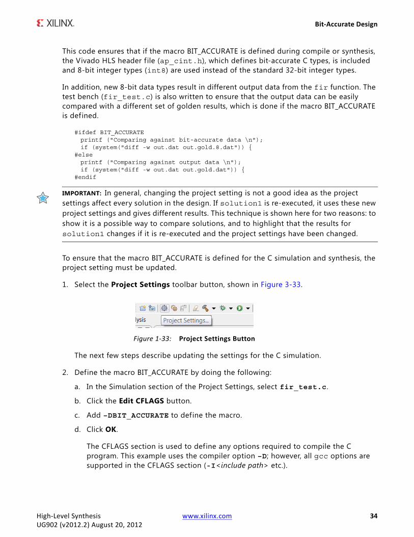
1. Select the Project Settings toolbar button, shown in Figure 3-33.
The next few steps describe updating the settings for the C simulation.
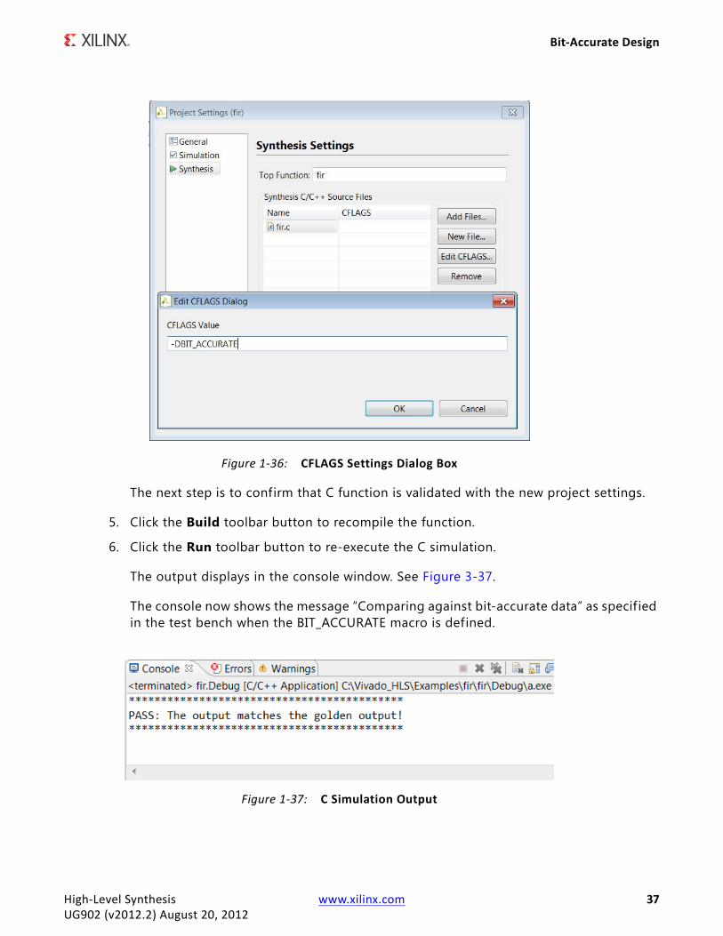
2. Define the macro BIT_ACCURATE by doing the following:
a. In the Simulation section of the Project Settings, select fir_test.c.
b. Click the Edit CFLAGS button.
c. Add –DBIT_ACCURATE to define the macro.
d. Click OK.
The CFLAGS section is used to define any options required to compile the C program. This example uses the compiler option –D; however, all gcc options are supported in the CFLAGS section (-I<include path> etc.).
X-Ref Target - Figure 1-33
Figure 1-33: Project Settings Button
High-Level Synthesis www.xilinx.com 34UG902 (v2012.2) August 20, 2012
Bit-Accurate Design
Note: There is no need to include any Vivado HLS header f iles, such as ap_cint.h, using the include flag. The Vivado HLS include directory is automatically searched.
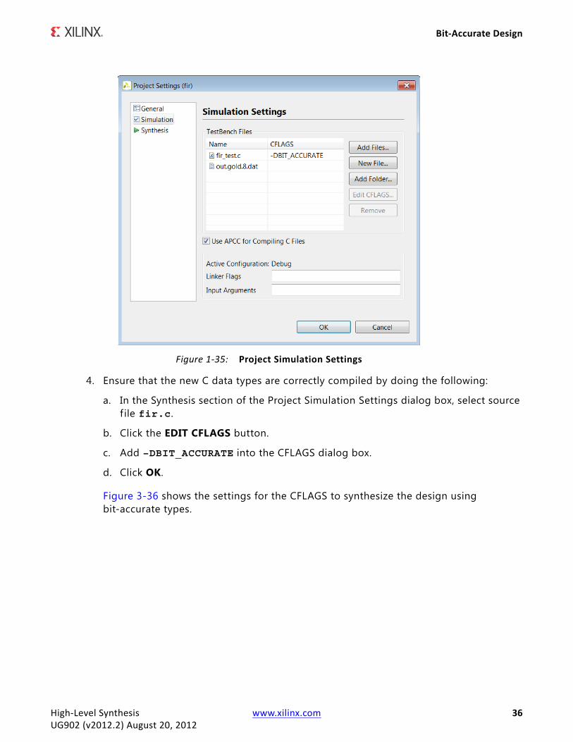
3. Update the data f ile used by the test bench by doing the following:
a. In the Simulation section, select the out.gold.dat f ile.
b. Click the Remove button to remove the f ile from the project.
If macro BIT_ACCURATE is defined, this f ile is no longer used by the test bench and is not required in the project.
c. Click the Add Files button.
d. Add the out.gold.8.dat f ile to the project.
e. Select the Use AutoCC Compiler check box.
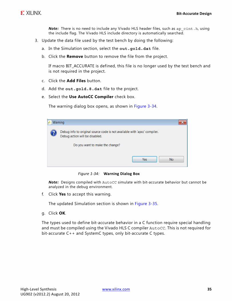
The warning dialog box opens, as shown in Figure 3-34.
Note: Designs compiled with AutoCC simulate with bit-accurate behavior but cannot be analyzed in the debug environment.
f. Click Yes to accept this warning.
The updated Simulation section is shown in Figure 3-35.
g. Click OK.
The types used to define bit-accurate behavior in a C function require special handling and must be compiled using the Vivado HLS C compiler AutoCC. This is not required for bit-accurate C++ and SystemC types, only bit-accurate C types.
X-Ref Target - Figure 1-34
Figure 1-34: Warning Dialog Box
High-Level Synthesis www.xilinx.com 35UG902 (v2012.2) August 20, 2012
Bit-Accurate Design
4. Ensure that the new C data types are correctly compiled by doing the following:
a. In the Synthesis section of the Project Simulation Settings dialog box, select source f ile fir.c.
b. Click the EDIT CFLAGS button.
c. Add –DBIT_ACCURATE into the CFLAGS dialog box.
d. Click OK.
Figure 3-36 shows the settings for the CFLAGS to synthesize the design using bit-accurate types.
X-Ref Target - Figure 1-35
Figure 1-35: Project Simulation Settings
High-Level Synthesis www.xilinx.com 36UG902 (v2012.2) August 20, 2012
Bit-Accurate Design
The next step is to confirm that C function is validated with the new project settings.
5. Click the Build toolbar button to recompile the function.
6. Click the Run toolbar button to re-execute the C simulation.
The output displays in the console window. See Figure 3-37.
The console now shows the message “Comparing against bit-accurate data” as specif ied in the test bench when the BIT_ACCURATE macro is defined.
X-Ref Target - Figure 1-36
Figure 1-36: CFLAGS Settings Dialog Box
X-Ref Target - Figure 1-37
Figure 1-37: C Simulation Output
High-Level Synthesis www.xilinx.com 37UG902 (v2012.2) August 20, 2012
Bit-Accurate Design
Synthesis and Comparison
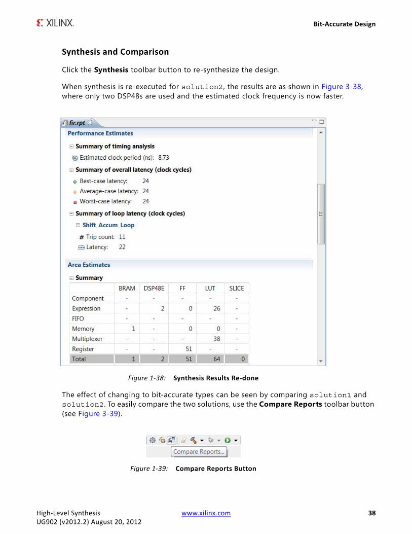
Click the Synthesis toolbar button to re-synthesize the design.
When synthesis is re-executed for solution2, the results are as shown in Figure 3-38, where only two DSP48s are used and the estimated clock frequency is now faster.
The effect of changing to bit-accurate types can be seen by comparing solution1 and solution2. To easily compare the two solutions, use the Compare Reports toolbar button (see Figure 3-39).
X-Ref Target - Figure 1-38
Figure 1-38: Synthesis Results Re-done
X-Ref Target - Figure 1-39
Figure 1-39: Compare Reports Button
High-Level Synthesis www.xilinx.com 38UG902 (v2012.2) August 20, 2012
Bit-Accurate Design
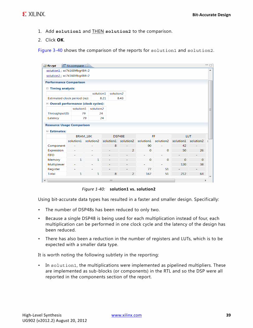
1. Add solution1 and THEN solution2 to the comparison.
2. Click OK.
Figure 3-40 shows the comparison of the reports for solution1 and solution2.
Using bit-accurate data types has resulted in a faster and smaller design. Specif ically:
• The number of DSP48s has been reduced to only two.
• Because a single DSP48 is being used for each multiplication instead of four, each multiplication can be performed in one clock cycle and the latency of the design has been reduced.
• There has also been a reduction in the number of registers and LUTs, which is to be expected with a smaller data type.
It is worth noting the following subtlety in the reporting:
• In solution1, the multiplications were implemented as pipelined multipliers. These are implemented as sub-blocks (or components) in the RTL and so the DSP were all reported in the components section of the report.
X-Ref Target - Figure 1-40
Figure 1-40: solution1 vs. solution2
High-Level Synthesis www.xilinx.com 39UG902 (v2012.2) August 20, 2012
Design Optimization
• In solution2, the multiplications are single cycle and implemented in the RTL with a multiplication operator (“*”) and are therefore listed as expressions; operations at this level of the hierarchy.
SummaryThe act of rewriting the design to be bit-accurate was deliberately introduced into this tutorial to show the steps for performing it. They are:
1. Update the code to use bit-accurate types.
2. Include the appropriate header f ile to define the types.
° For C designs, ap_cint.h
Be aware bit-accurate types in C must have the AutoCC option enabled and cannot be analyzed in the debug environment (C++ and SystemC types can).
° For C++ design, ap_int.h
° For SystemC designs, systemc.h
3. Simulate the design and validate the results before synthesis.
Design OptimizationThe following optimizations, discussed earlier, can now be implemented:
• Unroll the Shift_Accum_Loop loop to reduce latency.
• Partition the array shift_reg to prevent a BRAM being used, and allow a shift register to be used.
• Specify the input array c as a single-port RAM in order to guarantee a single-port RAM interface.
• Ensure that the input port x uses a valid handshake.
• Force sharing of the multipliers.
The first sets of optimizations to perform are those which must be performed: those associated with the interface. No matter what other optimizations are performed, the RTL interface must match the requirements.
Optimization: IO InterfaceThe following optimizations must be performed in solution3:
High-Level Synthesis www.xilinx.com 40UG902 (v2012.2) August 20, 2012
Design Optimization
• Specify the input array c as a single-port RAM in order to create a single-port RAM interface.
• Ensure that the input port x uses a valid handshake.
Step 1: Creating a New Solution
To preserve the existing results, create a new solution, solution3, by doing the following.
1. Click the New Solution button to create a new solution.
2. Leave the default solution name as solution3. Do not change any of the technology or clock settings.
3. Click Finish.
solution3 is created and automatically opens.
When solution3 opens, confirm that solution3 is highlighted in bold in the Project Explorer pane, indicating that it is the current active solution.
Note: Open files use up memory. If they are required, keep them open; otherwise it is good practice to close them.
4. Close any existing tabs from previous solutions. In the Project menu, select Close Inactive Solution Tabs.
Step 2: Adding Optimization Directives
To add optimization directives to define the desired IO interfaces to the solution, perform the following steps.
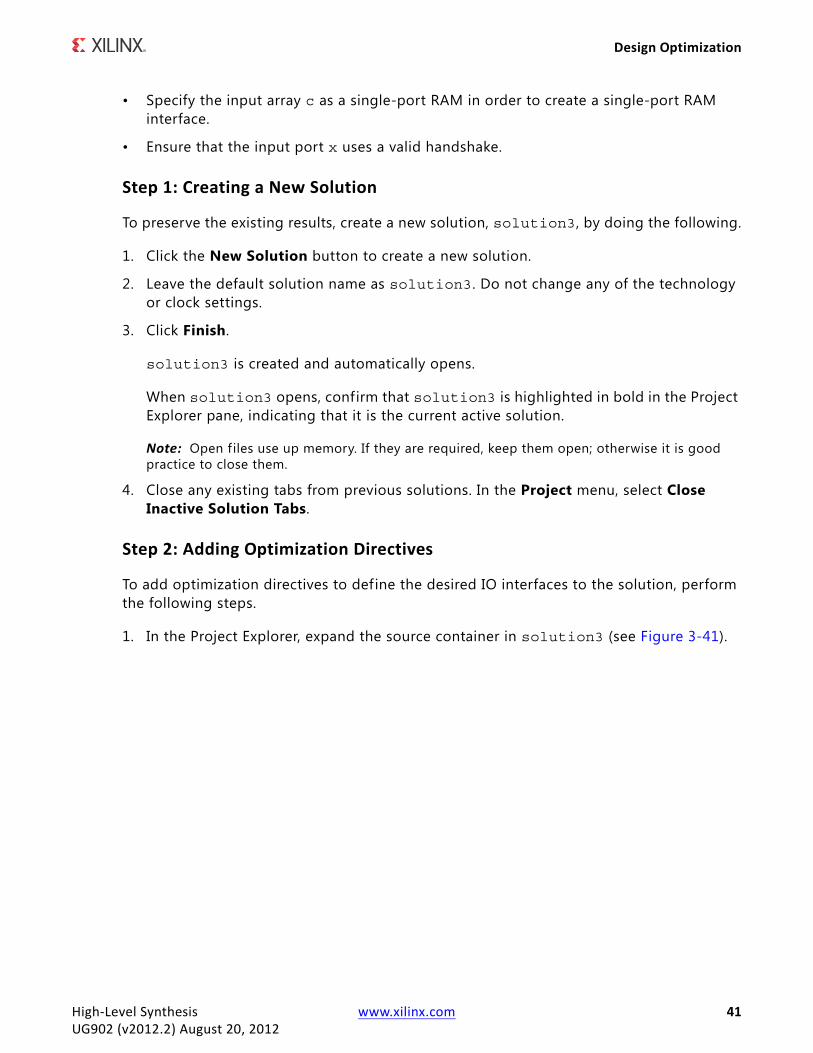
1. In the Project Explorer, expand the source container in solution3 (see Figure 3-41).
High-Level Synthesis www.xilinx.com 41UG902 (v2012.2) August 20, 2012
Design Optimization
2. Double-click fir.c to open the file in the Information pane.
3. Click the Directive Tab (see Figure 3-41).
You can now apply the optimization directives to the design.
4. In the Directive tab, select the c argument/port (green dot) or the array c.
5. Right-click and select Insert Directives.
6. Implement the array by doing the following:
a. Select RESOURCE from the Directive drop-down menu.
b. Click the core box.
X-Ref Target - Figure 1-41
Figure 1-41: Adding Optimization Directives
High-Level Synthesis www.xilinx.com 42UG902 (v2012.2) August 20, 2012
Design Optimization
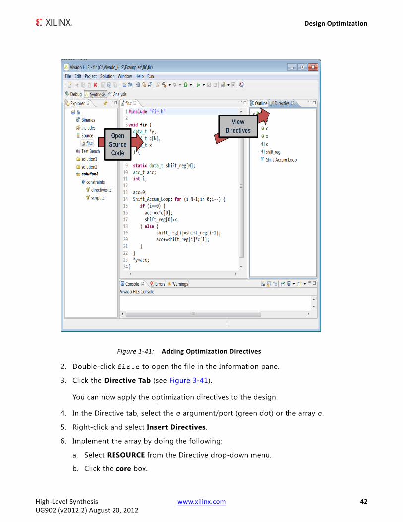
c. Select RAM_1P_BRAM, as shown in Figure 3-42.
This ensures that the array is implemented using a single port BRAM.
7. To apply the directive, click OK.
This directive informs the Vivado HLS tool that array c is implemented as a single-port RAM. Because the array is on the function interface, this is equivalent to the RAM being “off-chip.” In this case, the Vivado HLS tool creates the appropriate interface ports to access it.
The interface ports created (the number of address ports) are determined by pins on the RAM_1P_BRAM core. A complete description of the cores in the Vivado HLS library is provided in the Vivado Design Suite User Guide: High-Level Synthesis (UG902) > High-Level Synthesis Operator and Core Guide chapter.
Next, specify port x to have an associated valid signal/port.
1. In the Directive tab, select input port x (green dot).
2. Right-click and select Insert Directives.
3. Select Interface from the Directive drop-down menu.
X-Ref Target - Figure 1-42
Figure 1-42: Adding a Resource Directive
High-Level Synthesis www.xilinx.com 43UG902 (v2012.2) August 20, 2012
Design Optimization
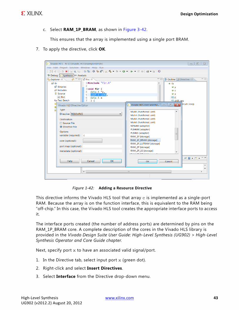
4. Select ap_vld for the mode.
5. Click OK to apply the directive.
When complete, the Directive pane looks like Figure 3-43. Select any incorrect directive and use the mouse right-click to modify it.
Step 3: Synthesis
Now that the optimization directives have been applied, run synthesis on solution3. Click the Synthesis toolbar button to synthesize the design.
When synthesis completes, the synthesis report automatically opens. Scroll down, or use the outline pane to jump to the interface section. Figure 3-44 shows the interfaces are now correctly defined.
X-Ref Target - Figure 1-43
Figure 1-43: Directive Tab solution3
High-Level Synthesis www.xilinx.com 44UG902 (v2012.2) August 20, 2012
Design Optimization
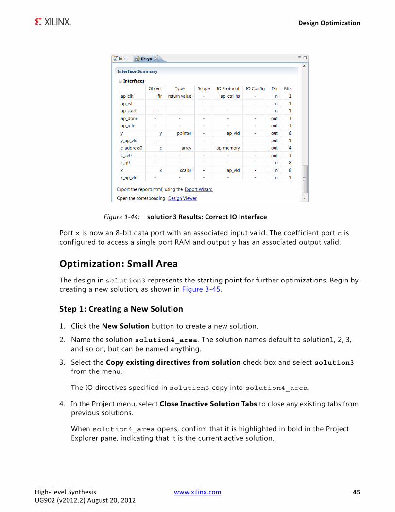
Port x is now an 8-bit data port with an associated input valid. The coefficient port c is configured to access a single port RAM and output y has an associated output valid.
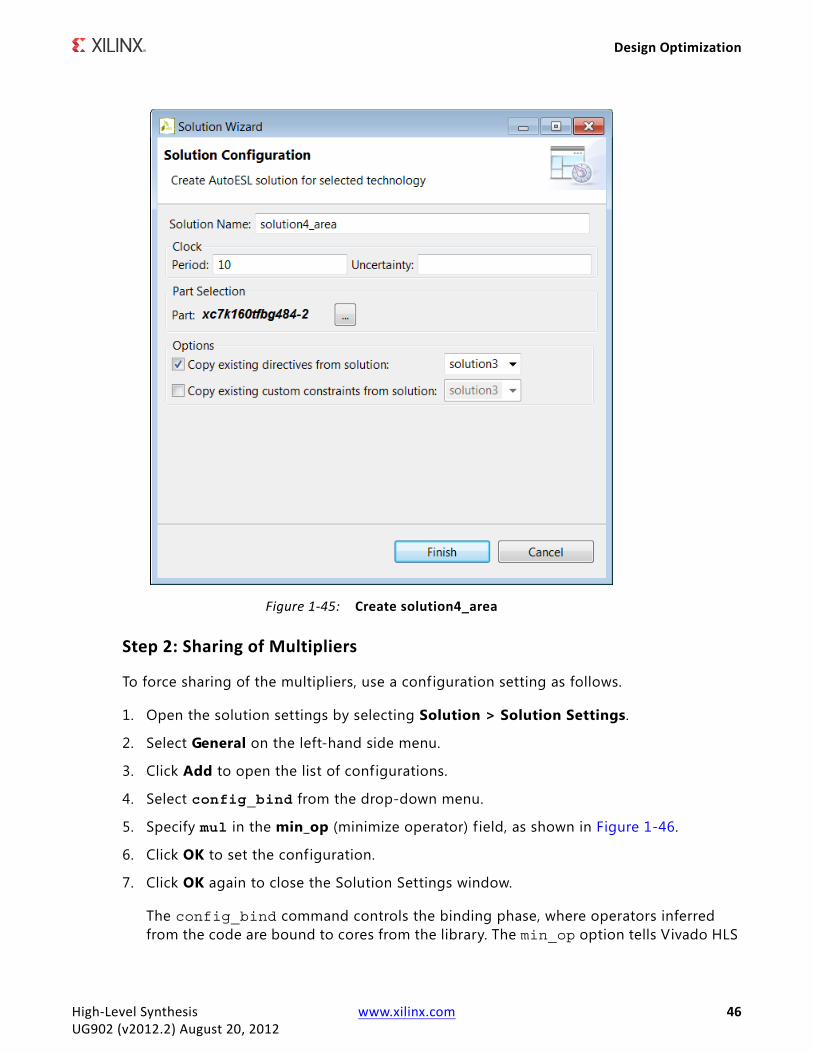
Optimization: Small AreaThe design in solution3 represents the starting point for further optimizations. Begin by creating a new solution, as shown in Figure 3-45.
Step 1: Creating a New Solution
1. Click the New Solution button to create a new solution.
2. Name the solution solution4_area. The solution names default to solution1, 2, 3, and so on, but can be named anything.
3. Select the Copy existing directives from solution check box and select solution3 from the menu.
The IO directives specified in solution3 copy into solution4_area.
4. In the Project menu, select Close Inactive Solution Tabs to close any existing tabs from previous solutions.
When solution4_area opens, confirm that it is highlighted in bold in the Project Explorer pane, indicating that it is the current active solution.
X-Ref Target - Figure 1-44
Figure 1-44: solution3 Results: Correct IO Interface
High-Level Synthesis www.xilinx.com 45UG902 (v2012.2) August 20, 2012
Design Optimization
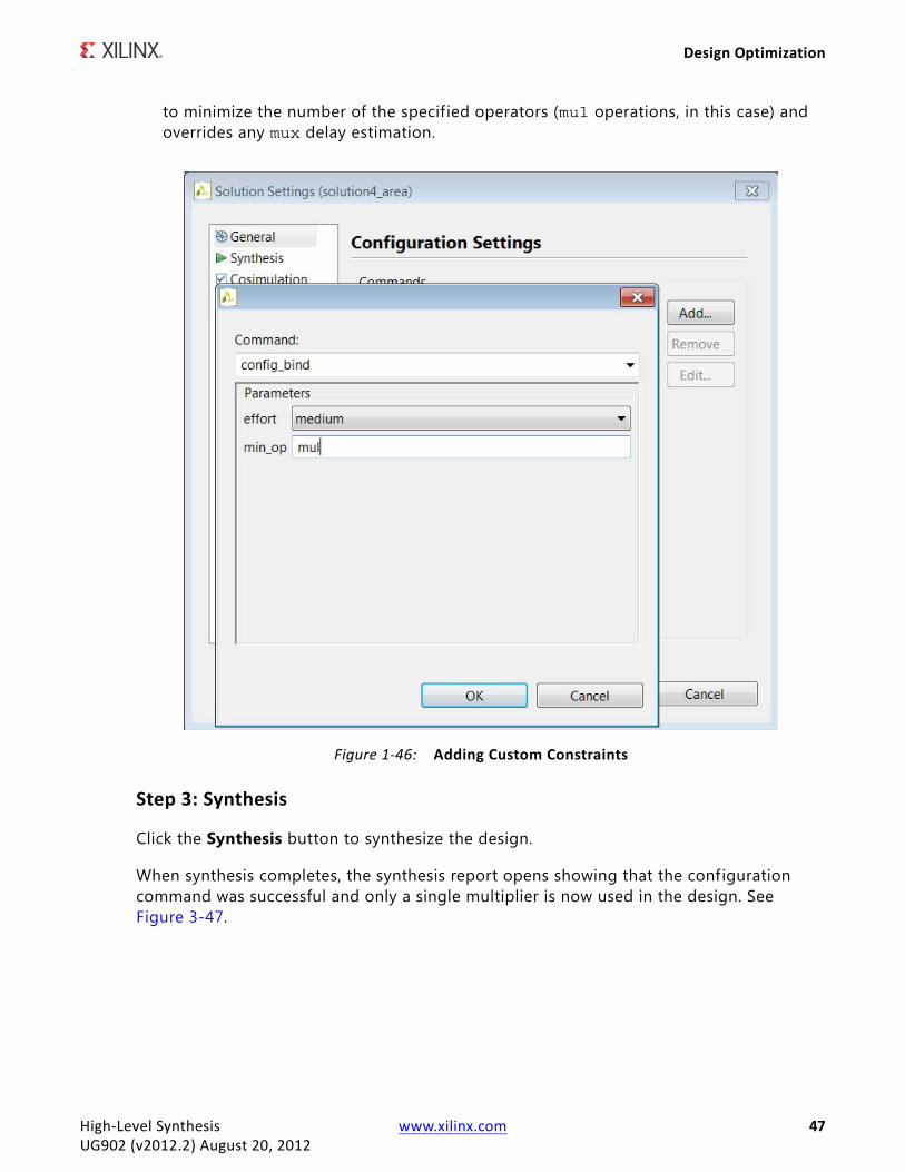
Step 2: Sharing of Multipliers
To force sharing of the multipliers, use a configuration setting as follows.
1. Open the solution settings by selecting Solution > Solution Settings.
2. Select General on the left-hand side menu.
3. Click Add to open the list of configurations.
4. Select config_bind from the drop-down menu.
5. Specify mul in the min_op (minimize operator) f ield, as shown in Figure 1-46.
6. Click OK to set the configuration.
7. Click OK again to close the Solution Settings window.
The config_bind command controls the binding phase, where operators inferred from the code are bound to cores from the library. The min_op option tells Vivado HLS
X-Ref Target - Figure 1-45
Figure 1-45: Create solution4_area
High-Level Synthesis www.xilinx.com 46UG902 (v2012.2) August 20, 2012
Design Optimization
to minimize the number of the specified operators (mul operations, in this case) and overrides any mux delay estimation.
Step 3: Synthesis
Click the Synthesis button to synthesize the design.
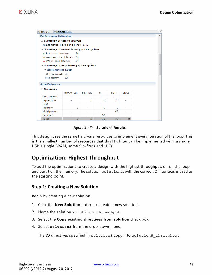
When synthesis completes, the synthesis report opens showing that the configuration command was successful and only a single multiplier is now used in the design. See Figure 3-47.
X-Ref Target - Figure 1-46
Figure 1-46: Adding Custom Constraints
High-Level Synthesis www.xilinx.com 47UG902 (v2012.2) August 20, 2012
Design Optimization
This design uses the same hardware resources to implement every iteration of the loop. This is the smallest number of resources that this FIR filter can be implemented with: a single DSP, a single BRAM, some flip-flops and LUTs.
Optimization: Highest ThroughputTo add the optimizations to create a design with the highest throughput, unroll the loop and partition the memory. The solution solution3, with the correct IO interface, is used as the starting point.
Step 1: Creating a New Solution
Begin by creating a new solution.
1. Click the New Solution button to create a new solution.
2. Name the solution solution5_throughput.
3. Select the Copy existing directives from solution check box.
4. Select solution3 from the drop-down menu.
The IO directives specified in solution3 copy into solution5_throughput.
X-Ref Target - Figure 1-47
Figure 1-47: Solution4 Results
High-Level Synthesis www.xilinx.com 48UG902 (v2012.2) August 20, 2012
Design Optimization
5. In the Project menu, select Close Inactive Solution Tabs to close any existing tabs from previous solutions.
Step 2: Unrolling the Loop
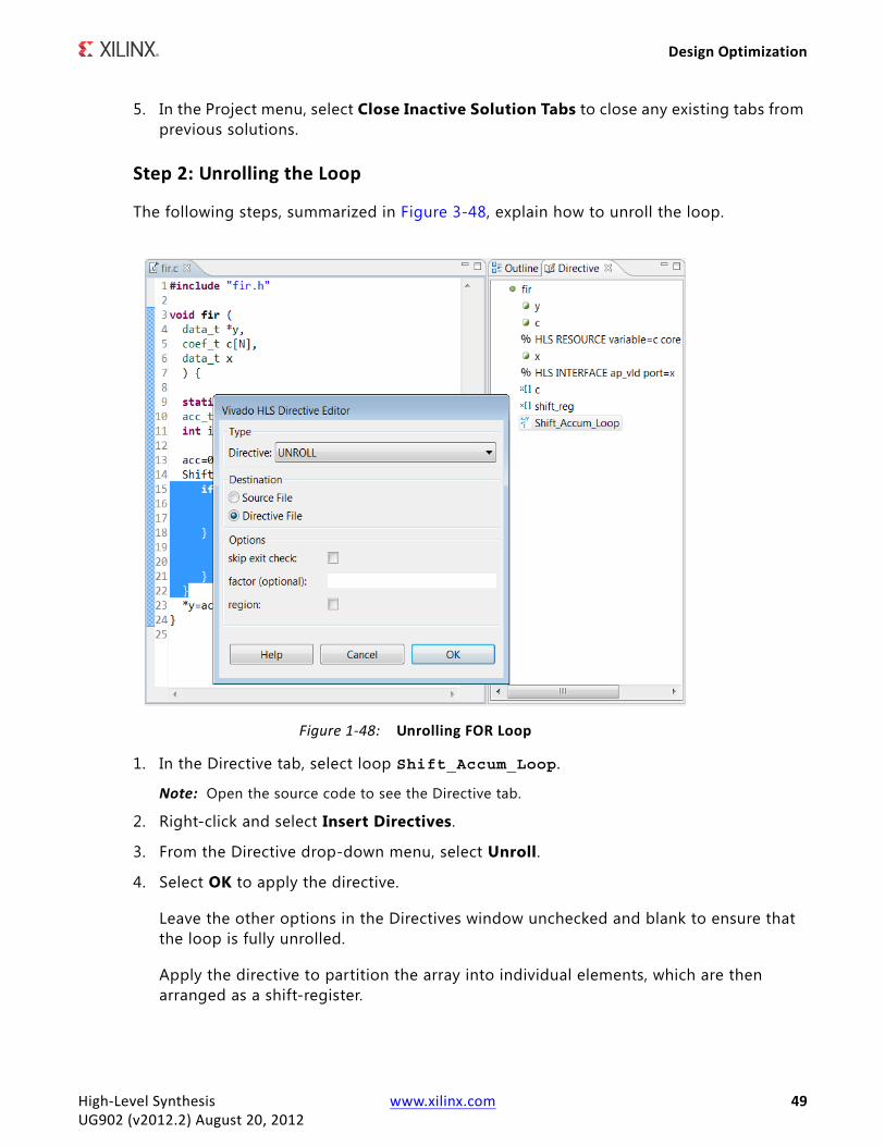
The following steps, summarized in Figure 3-48, explain how to unroll the loop.
1. In the Directive tab, select loop Shift_Accum_Loop.
Note: Open the source code to see the Directive tab.
2. Right-click and select Insert Directives.
3. From the Directive drop-down menu, select Unroll.
4. Select OK to apply the directive.
Leave the other options in the Directives window unchecked and blank to ensure that the loop is fully unrolled.
Apply the directive to partition the array into individual elements, which are then arranged as a shift-register.
X-Ref Target - Figure 1-48
Figure 1-48: Unrolling FOR Loop
High-Level Synthesis www.xilinx.com 49UG902 (v2012.2) August 20, 2012
Design Optimization
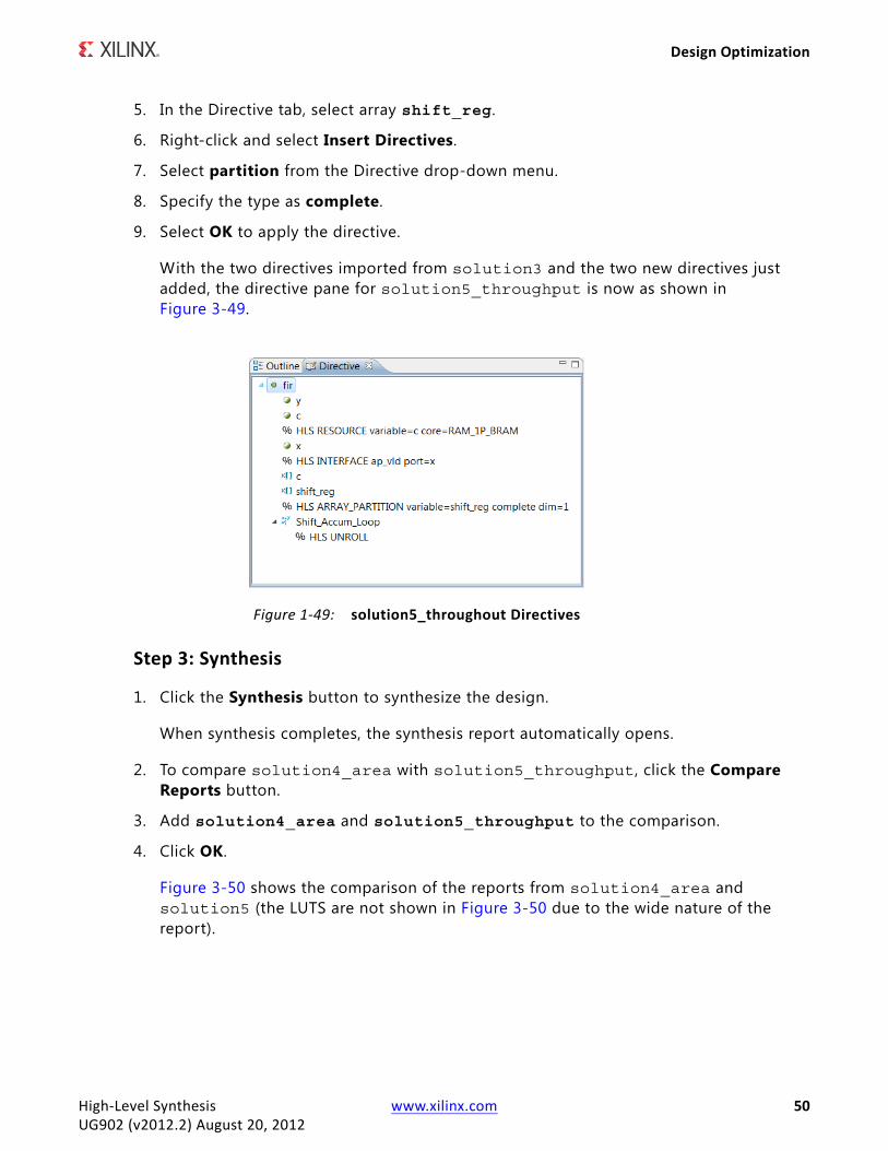
5. In the Directive tab, select array shift_reg.
6. Right-click and select Insert Directives.
7. Select partition from the Directive drop-down menu.
8. Specify the type as complete.
9. Select OK to apply the directive.
With the two directives imported from solution3 and the two new directives just added, the directive pane for solution5_throughput is now as shown in Figure 3-49.
Step 3: Synthesis
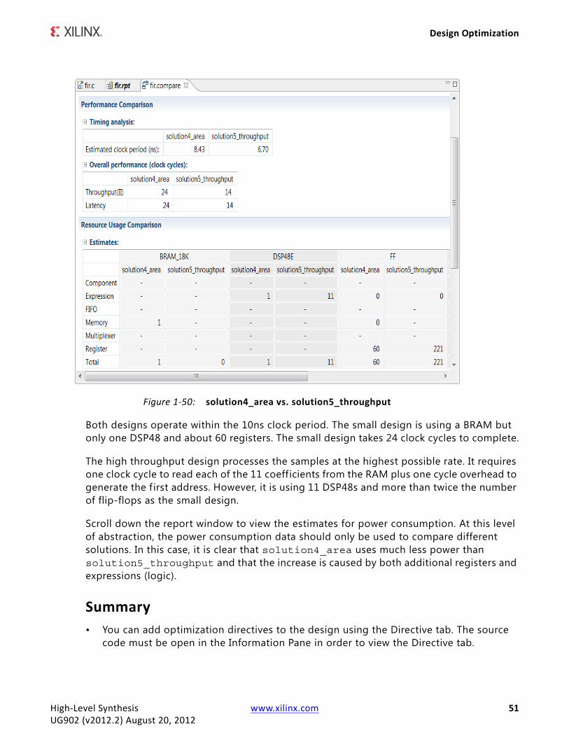
1. Click the Synthesis button to synthesize the design.
When synthesis completes, the synthesis report automatically opens.
2. To compare solution4_area with solution5_throughput, click the Compare Reports button.
3. Add solution4_area and solution5_throughput to the comparison.
4. Click OK.
Figure 3-50 shows the comparison of the reports from solution4_area and solution5 (the LUTS are not shown in Figure 3-50 due to the wide nature of the report).
X-Ref Target - Figure 1-49
Figure 1-49: solution5_throughout Directives
High-Level Synthesis www.xilinx.com 50UG902 (v2012.2) August 20, 2012
Design Optimization
Both designs operate within the 10ns clock period. The small design is using a BRAM but only one DSP48 and about 60 registers. The small design takes 24 clock cycles to complete.
The high throughput design processes the samples at the highest possible rate. It requires one clock cycle to read each of the 11 coefficients from the RAM plus one cycle overhead to generate the f irst address. However, it is using 11 DSP48s and more than twice the number of flip-flops as the small design.
Scroll down the report window to view the estimates for power consumption. At this level of abstraction, the power consumption data should only be used to compare different solutions. In this case, it is clear that solution4_area uses much less power than solution5_throughput and that the increase is caused by both additional registers and expressions (logic).
Summary• You can add optimization directives to the design using the Directive tab. The source
code must be open in the Information Pane in order to view the Directive tab.
X-Ref Target - Figure 1-50
Figure 1-50: solution4_area vs. solution5_throughput
High-Level Synthesis www.xilinx.com 51UG902 (v2012.2) August 20, 2012
RTL Verification and Export
• Creating different solutions for each new set of directives allows for the solutions to be easily compared inside the GUI.
RTL Verification and ExportThe Vivado HLS tool allows both RTL verif ication and RTL export to be performed from the GUI. The RTL verif ication and RTL export menus in the GUI are also supported at the Tcl command level (discussed later).
Details on the various options are not discussed in this tutorial but can be found by reviewing the associated Tcl command, available from the GUI help menu. The Tcl commands for RTL verif ication and RTL export are cosim_design and export_design, respectively.
RTL VerificationThe generated RTL can now be verif ied with the original C test bench. A new RTL test bench is NOT required with the Vivado HLS tool.
For RTL simulation, the Vivado HLS tool supports industry standard VHDL and Verilog RTL simulators and includes a SystemC simulation kernel allowing the SystemC RTL output to be verif ied.
The RTL can always be verif ied using the SystemC kernel and no 3rd party RTL simulator license is required for this.
To use the other supported simulators, a license for the simulator is required, and the simulator executable should be available in the search path.
In this example, the SystemC RTL will be verif ied. Start with the solution5_throughput solution. Make sure solution5_throughput is highlighted in bold in the Project Explorer, indicating it is the currently active solution.
1. Click the Simulation button in the toolbar, as shown in Figure 3-51.
The co-simulation dialog opens, as shown in Figure 3-52.
X-Ref Target - Figure 1-51
Figure 1-51: Simulation Toolbar Button
High-Level Synthesis www.xilinx.com 52UG902 (v2012.2) August 20, 2012
RTL Verification and Export
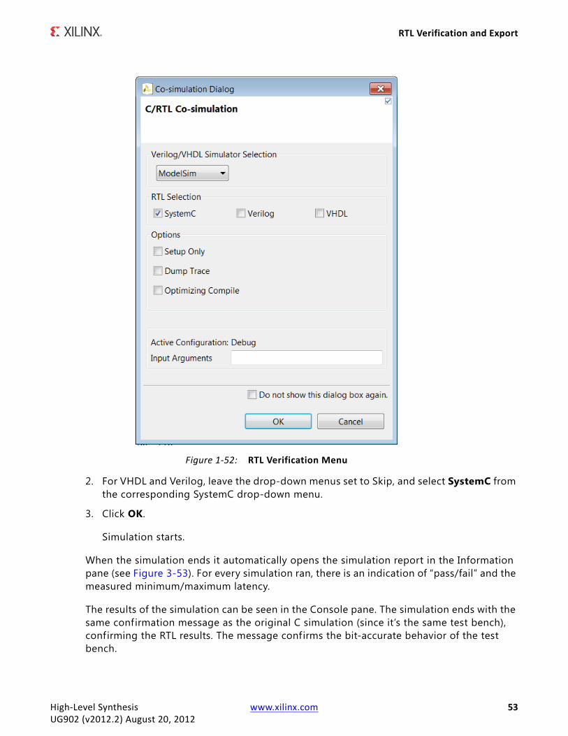
2. For VHDL and Verilog, leave the drop-down menus set to Skip, and select SystemC from the corresponding SystemC drop-down menu.
3. Click OK.
Simulation starts.
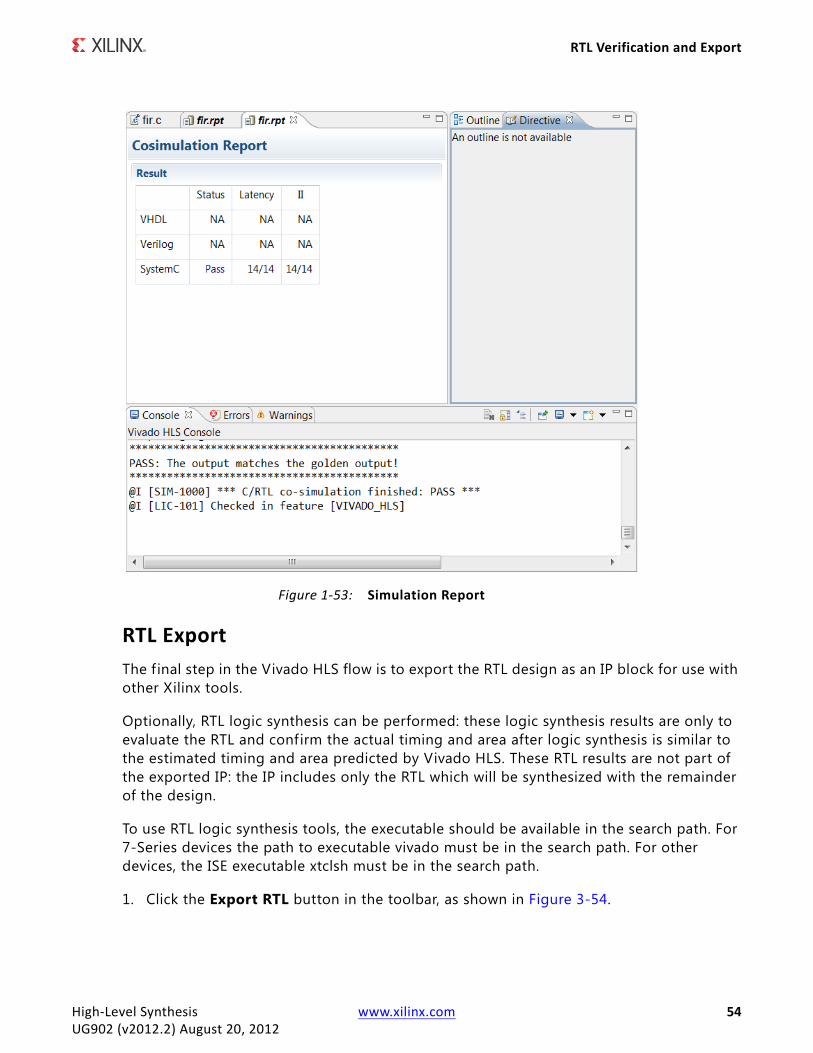
When the simulation ends it automatically opens the simulation report in the Information pane (see Figure 3-53). For every simulation ran, there is an indication of “pass/fail” and the measured minimum/maximum latency.
The results of the simulation can be seen in the Console pane. The simulation ends with the same confirmation message as the original C simulation (since it’s the same test bench), confirming the RTL results. The message confirms the bit-accurate behavior of the test bench.
X-Ref Target - Figure 1-52
Figure 1-52: RTL Verification Menu
High-Level Synthesis www.xilinx.com 53UG902 (v2012.2) August 20, 2012
RTL Verification and Export
RTL ExportThe f inal step in the Vivado HLS flow is to export the RTL design as an IP block for use with other Xilinx tools.
Optionally, RTL logic synthesis can be performed: these logic synthesis results are only to evaluate the RTL and confirm the actual timing and area after logic synthesis is similar to the estimated timing and area predicted by Vivado HLS. These RTL results are not part of the exported IP: the IP includes only the RTL which will be synthesized with the remainder of the design.
To use RTL logic synthesis tools, the executable should be available in the search path. For 7-Series devices the path to executable vivado must be in the search path. For other devices, the ISE executable xtclsh must be in the search path.
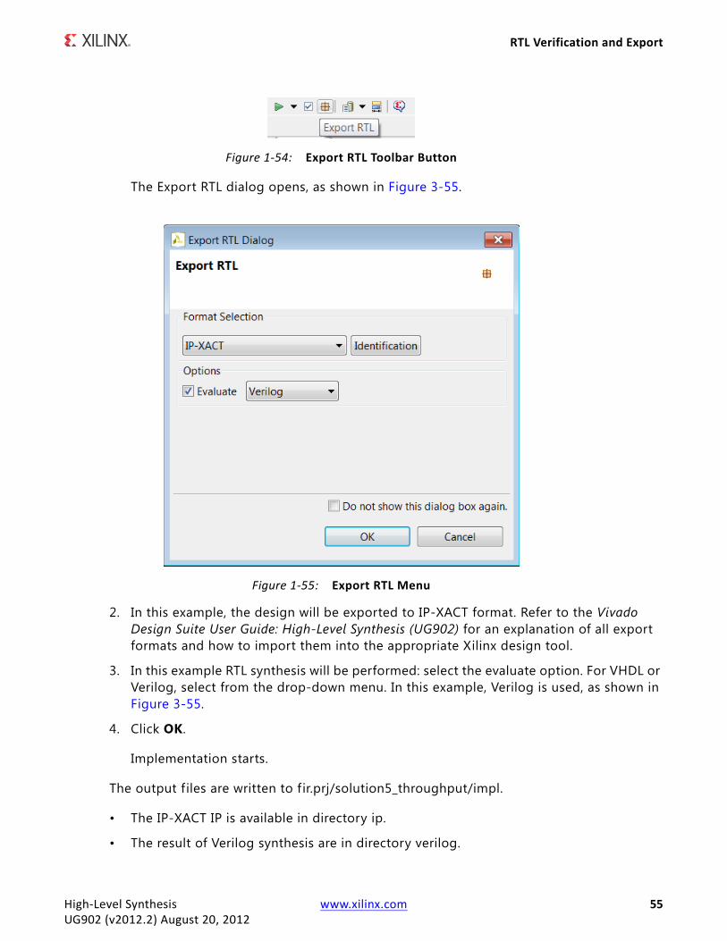
1. Click the Export RTL button in the toolbar, as shown in Figure 3-54.
X-Ref Target - Figure 1-53
Figure 1-53: Simulation Report
High-Level Synthesis www.xilinx.com 54UG902 (v2012.2) August 20, 2012
RTL Verification and Export
The Export RTL dialog opens, as shown in Figure 3-55.
2. In this example, the design will be exported to IP-XACT format. Refer to the Vivado Design Suite User Guide: High-Level Synthesis (UG902) for an explanation of all export formats and how to import them into the appropriate Xilinx design tool.
3. In this example RTL synthesis will be performed: select the evaluate option. For VHDL or Verilog, select from the drop-down menu. In this example, Verilog is used, as shown in Figure 3-55.
4. Click OK.
Implementation starts.
The output files are written to f ir.prj/solution5_throughput/impl.
• The IP-XACT IP is available in directory ip.
• The result of Verilog synthesis are in directory verilog.
X-Ref Target - Figure 1-54
Figure 1-54: Export RTL Toolbar Button
X-Ref Target - Figure 1-55
Figure 1-55: Export RTL Menu
High-Level Synthesis www.xilinx.com 55UG902 (v2012.2) August 20, 2012
RTL Verification and Export
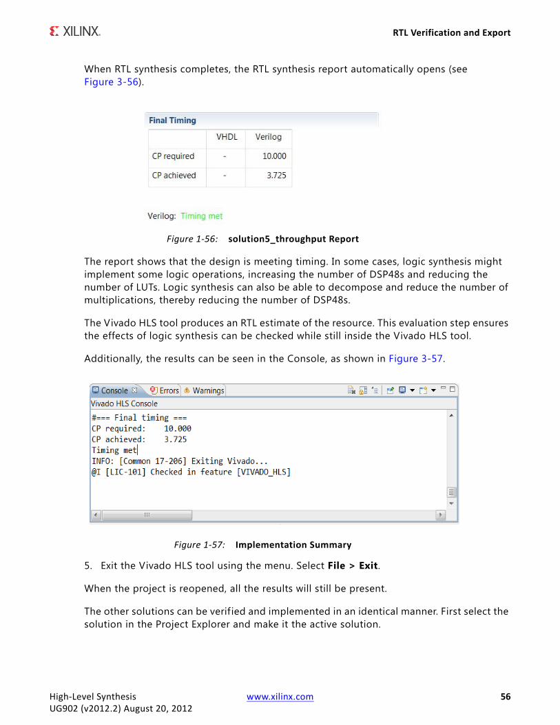
When RTL synthesis completes, the RTL synthesis report automatically opens (see Figure 3-56).
The report shows that the design is meeting timing. In some cases, logic synthesis might implement some logic operations, increasing the number of DSP48s and reducing the number of LUTs. Logic synthesis can also be able to decompose and reduce the number of multiplications, thereby reducing the number of DSP48s.
The Vivado HLS tool produces an RTL estimate of the resource. This evaluation step ensures the effects of logic synthesis can be checked while still inside the Vivado HLS tool.
Additionally, the results can be seen in the Console, as shown in Figure 3-57.
5. Exit the Vivado HLS tool using the menu. Select File > Exit.
When the project is reopened, all the results will still be present.
The other solutions can be verif ied and implemented in an identical manner. First select the solution in the Project Explorer and make it the active solution.
X-Ref Target - Figure 1-56
Figure 1-56: solution5_throughput Report
X-Ref Target - Figure 1-57
Figure 1-57: Implementation Summary
High-Level Synthesis www.xilinx.com 56UG902 (v2012.2) August 20, 2012
The Shell and Scripts
Summary• The path to verif ication and implementation tool executables must be in the search
path prior to execution from within the Vivado HLS tool. See the Xilinx Design Tools: Installation and Licensing Guide (UG978) for details.
° This is not required for RTL SystemC verif ication.
• RTL verif ication does not require an RTL test bench be created.
• The RTL can be verif ied from within the Vivado HLS tool using the existing C test bench.
• The design can be can be exported as IP and the implementation evaluated using logic synthesis tools from within the Vivado HLS tool.
The Shell and ScriptsEverything which can be performed using the Vivado HLS GUI can also be implemented using Tcl scripts at the command prompt. This section gives an overview of using the Vivado HLS tool at the command prompt and how the GUI generated scripts can be copied and used.
Vivado HLS at the ShellYou can be invoked at the Linux or DOS shell prompt.
1. Invoke a DOS shell from the menu by selecting Start > All Programs > Xilinx Design Tool > Vivado 2012.2 > Vivado HLS Command Prompt.
This ensures that the search paths for the Vivado HLS tool are already defined in the shell.
2. Type $ vivado_hls to invoke the GUI.
It can also be invoked in interactive mode, and the exit command can be used to return to the shell.
$ vivado_hls –i
Vivado Hls> exit
$
The Vivado HLS tool can be run in batch mode using a Tcl script. When the script completes the Vivado HLS tool will remain in interactive mode and if the script has an exit command, it will exit and return to the shell.
$ vivado_hls -f fir.tcl
High-Level Synthesis www.xilinx.com 57UG902 (v2012.2) August 20, 2012
The Shell and Scripts
Additionally, once a project has been created it can be opened directly from the command line. In this example, project fir.prj is opened in the GUI:
$ vivado_hls -p fir.prj
This f inal option allows scripts to be run in batch mode and then the analysis to be performed using the GUI.
Creating a ScriptWhen a project is created in the GUI, all the commands to re-create the project are provided in the scripts.tcl f ile in the solution directory.
To use the script.tcl f ile, copy it to a new location outside the project directory.
Example script.tcl f ile:
############################################################## This file is generated automatically by vivado_hls.## Please DO NOT edit it.## Copyright (C) 2012 Xilinx Inc. All rights reserved.############################################################open_project fir.prjset_top firadd_file fir.c -cflags "-DBIT_ACCURATE"add_file -tb out.gold.8.datadd_file -tb fir_test.c -cflags " -DBIT_ACCURATE"open_solution "solution5_throughput"set_part {xc6vlx240tff1156-2}create_clock -period 10
source "./fir.prj/solution5_throughput/directives.tcl"elaborateautosyn
If any directives where used in the solution, copy the directives.tcl f ile to a location outside the project directory and update the script.tcl f ile as shown, to use the local copy of directives.tcl.
############################################################## This file is generated automatically by vivado_hls.## Please DO NOT edit it.## Copyright (C) 2012 Xilinx Inc. All rights reserved.############################################################open_project fir.prjset_top firadd_file fir.c -cflags "-DBIT_ACCURATE"add_file -tb out.gold.8.datadd_file -tb fir_test.c -cflags " -DBIT_ACCURATE"open_solution "solution5_throughput"set_part {xc6vlx240tff1156-2}create_clock -period 10
source "./directives.tcl"elaborate
High-Level Synthesis www.xilinx.com 58UG902 (v2012.2) August 20, 2012
The Shell and Scripts
autosyn
Example Scripts DirectoryThe FIR directory contains a scripts directory that has f ive scripts, used to create each of the f ive solutions in this tutorial.
You can run these scripts to reproduce all the solutions in this tutorial. You can then open and analyze the project and solutions in the GUI.
Table 1-3: Summary of Scripts
Filename Solution Description
run1_hls.tcl solution1 Creates the first solution, using standard implementation types.
run2_hls.tcl solution2 Sets the macro to use Vivado HLS bit-accurate types.
run3_hls.tcl solution3 The IO interfaces are defined.
run4_hls.tcl solution4_area Uses the directives from solution3 plus the config_bind command to force sharing of the multipliers.
run5_hls.tcl solution5_throughput Optimizations are applied to create a high-throughput version.
High-Level Synthesis www.xilinx.com 59UG902 (v2012.2) August 20, 2012
Chapter 2
Vivado HLS: Integrating EDK
IntroductionThis document describes how to create an Embedded Developer Kit (EDK) Pcore with an AXI-LITE interface from the Vivado HLS high-level synthesis tool. It describes the necessary steps for integrating the generated Pcore with the MicroBlaze™ processor using the Xilinx® Platform Studio (XPS) Tool Suite.
The reference design has been verif ied on the Avnet Spartan®-6 LX9 MicroBoard, shown in Figure 3-1.
Software RequirementsThe following software is required to test this reference design:
• Xilinx ISE® WebPACK with the EDK add-on, or ISE version 14.1 Embedded or System Edition
• Installed Silicon Labs CP210x USB-to-UART Bridge Driver (see Silicon Labs CP210x USB-to-UART Setup Guide, listed at http://em.avnet.com/s6microboard)
• Vivado™ Design Suite High-Level Synthesis (HLS) version 2011.4.2
X-Ref Target - Figure 2-1
Figure 2-1: Avnet Spartan-6 LX9 MicroBoard
High-Level Synthesis www.xilinx.com 60UG871 (v2012.2) August 20, 2012
Reference Design
Reference DesignThe reference design consists of an EDK MicroBlaze processor with a custom Pcore generated from the Vivado HLS tool.
You can copy the reference design, AXI_Lite_Interface, from the examples/tutorial directory in the Vivado HLS installation area.
The MicroBlaze processor based design was created using the XPS Base System Builder (BSB). Figure 3-2, page 61 shows the f inal design created and provided with this document.
For information about using the XPS Base System Builder, refer to http://www.xilinx.com/support/documentation/sw_manuals/xilinx14_2/platform_studio/ps_c_bsb_using_bsb.htm.
The reference design with the MicroBlaze processor runs the standalone board support package software with a simple C application that prompts you to enter values for each input variable and outputs the result.
Vivado HLS Pcore FunctionalityThe Vivado HLS Pcore functionality is an 8 bit adder. The focus of this document is the interface of the pcore to the MicroBlaze processor through the AXI-Lite interface, not the functionality of the pcore.
The Vivado HLS module has three variables: A, B and C. Of these, A and B are input variables, and C is an output variable. These three variables are mapped to three registers in the generated Pcore.
A Vivado HLS module has at least three control signals: AP_START, AP_IDLE, and AP_DONE. These signals are mapped to register in the generated Pcore.
The AP_START register is used to control the start of the Pcore and AP_DONE indicates when the module operation is done. A signal diagram (waveform of all three involved control signals) should be used to explain the handshaking mechanism.
Additional registers are present in the Pcore to support interrupts.
High-Level Synthesis www.xilinx.com 61UG871 (v2012.2) August 20, 2012
Reference Design
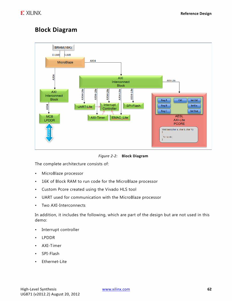
Block Diagram
The complete architecture consists of:
• MicroBlaze processor
• 16K of Block RAM to run code for the MicroBlaze processor
• Custom Pcore created using the Vivado HLS tool
• UART used for communication with the MicroBlaze processor
• Two AXI-Interconnects
In addition, it includes the following, which are part of the design but are not used in this demo:
• Interrupt controller
• LPDDR
• AXI-Timer
• SPI-Flash
• Ethernet-Lite
X-Ref Target - Figure 2-2
Figure 2-2: Block Diagram
High-Level Synthesis www.xilinx.com 62UG871 (v2012.2) August 20, 2012
Reference Design
Creating EDK Pcore with AXI-LITE
Opening the Vivado HLS Project File
To create the AXI-Lite interface Pcore, the f irst step is to open the Vivado HLS Project basic.prj.
1. Start Vivado HLS.
2. Select Open Project.
3. Select basic.prj.
Refer to Chapter 3, Vivado HLS: Introduction Tutorial for details about how to create an Vivado HLS project.
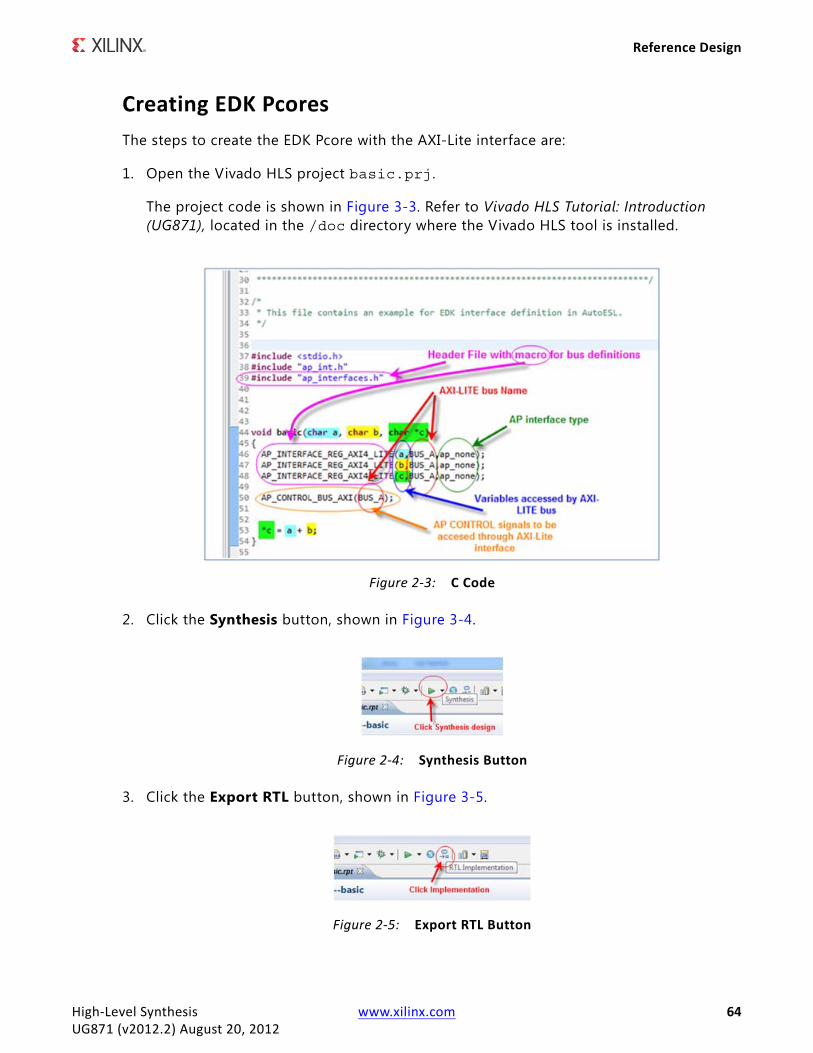
Note: Figure 3-3, page 63 shows the C code with explanation.
Generating Pcores Using Vivado HLS
To generate Pcores using Vivado HLS, the header f ile ap_interfaces.h must be included. This header f ile is a convenient way to define macros that apply standard Vivado HLS directives as pragmas.
The example makes use of the AP_INTERFACE_REG_AXI4_LITE and the AP_CONTROL_BUS_AXI macros.
The AP_INTERFACE_REG_AXI4_LITE macro defines that the three function arguments (a, b, and c) be implemented as registers that are accessed through an AXI4-Lite interface.
• Each port is specif ied as being in group BUS_A. This means they are all grouped into the same AXI4 Lite interface called BUS_A.
• The RTL interface is set to type ap_none. This means that the RTL implementation only has data ports; there are no associated acknowledge or valid signals with each data port and therefore no associated register in the interface.
The AP_CONTROL_BUS_AXI macro adds the block level IO protocol signals to an AXI4-Lite interface.
• The control signals AP_START, AP_DONE, and AP_IDLE are created by default when Vivado HLS synthesizes the top-level function. The default function interface is ap_ctrl_hs.
• Specifying the name BUS_A ensures that these signals are grouped into the same AXI4 Lite interface as the other ports.
Table 3-1, page 66 describes all the registers created by Vivado HLS for the generated Pcore.
High-Level Synthesis www.xilinx.com 63UG871 (v2012.2) August 20, 2012
Reference Design
Creating EDK PcoresThe steps to create the EDK Pcore with the AXI-Lite interface are:
1. Open the Vivado HLS project basic.prj.
The project code is shown in Figure 3-3. Refer to Vivado HLS Tutorial: Introduction (UG871), located in the /doc directory where the Vivado HLS tool is installed.
2. Click the Synthesis button, shown in Figure 3-4.
3. Click the Export RTL button, shown in Figure 3-5.
X-Ref Target - Figure 2-3
Figure 2-3: C Code
X-Ref Target - Figure 2-4
Figure 2-4: Synthesis Button
X-Ref Target - Figure 2-5
Figure 2-5: Export RTL Button
High-Level Synthesis www.xilinx.com 64UG871 (v2012.2) August 20, 2012
Reference Design
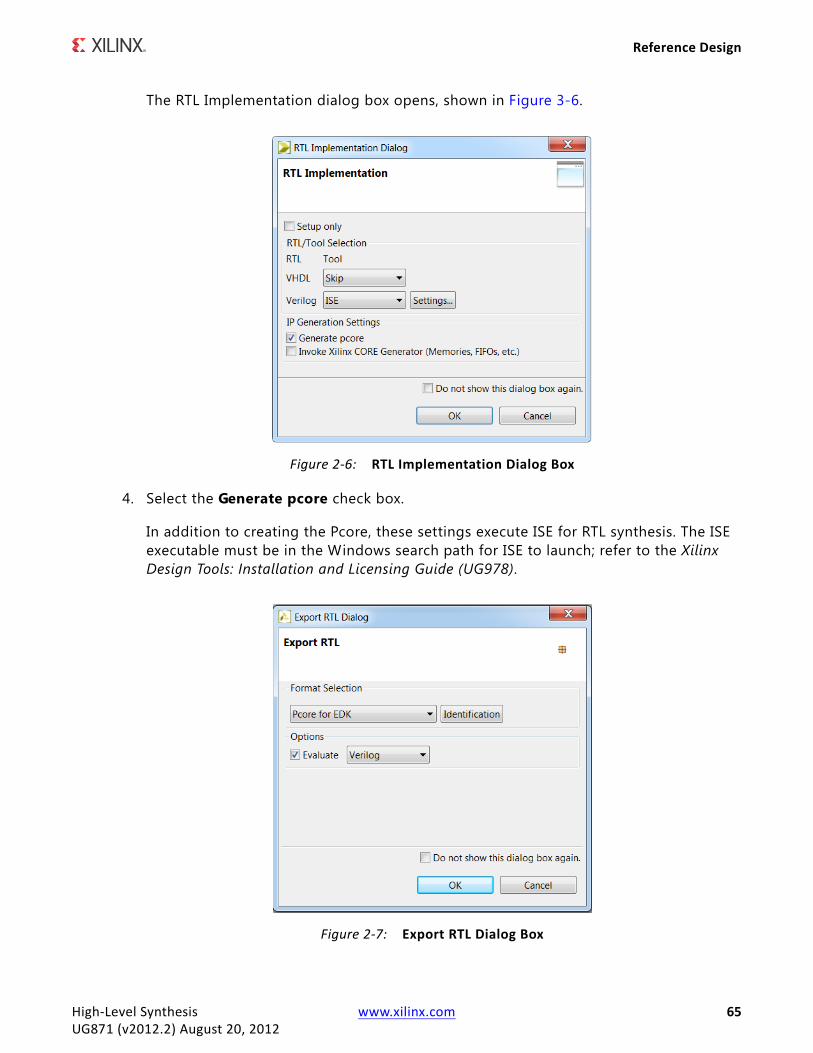
The RTL Implementation dialog box opens, shown in Figure 3-6.
4. Select the Generate pcore check box.
In addition to creating the Pcore, these settings execute ISE for RTL synthesis. The ISE executable must be in the Windows search path for ISE to launch; refer to the Xilinx Design Tools: Installation and Licensing Guide (UG978).
X-Ref Target - Figure 2-6
Figure 2-6: RTL Implementation Dialog Box
X-Ref Target - Figure 2-7
Figure 2-7: Export RTL Dialog Box
High-Level Synthesis www.xilinx.com 65UG871 (v2012.2) August 20, 2012
Reference Design
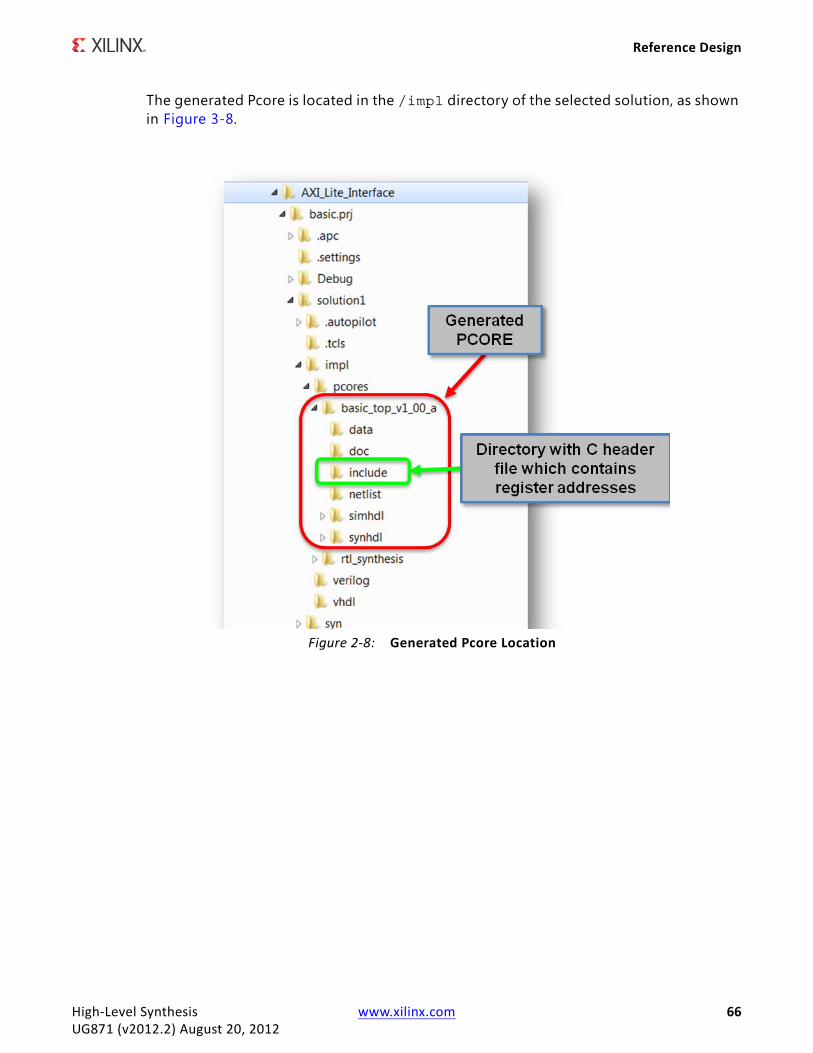
The generated Pcore is located in the /impl directory of the selected solution, as shown in Figure 3-8.
X-Ref Target - Figure 2-8
Figure 2-8: Generated Pcore Location
High-Level Synthesis www.xilinx.com 66UG871 (v2012.2) August 20, 2012
Reference Design
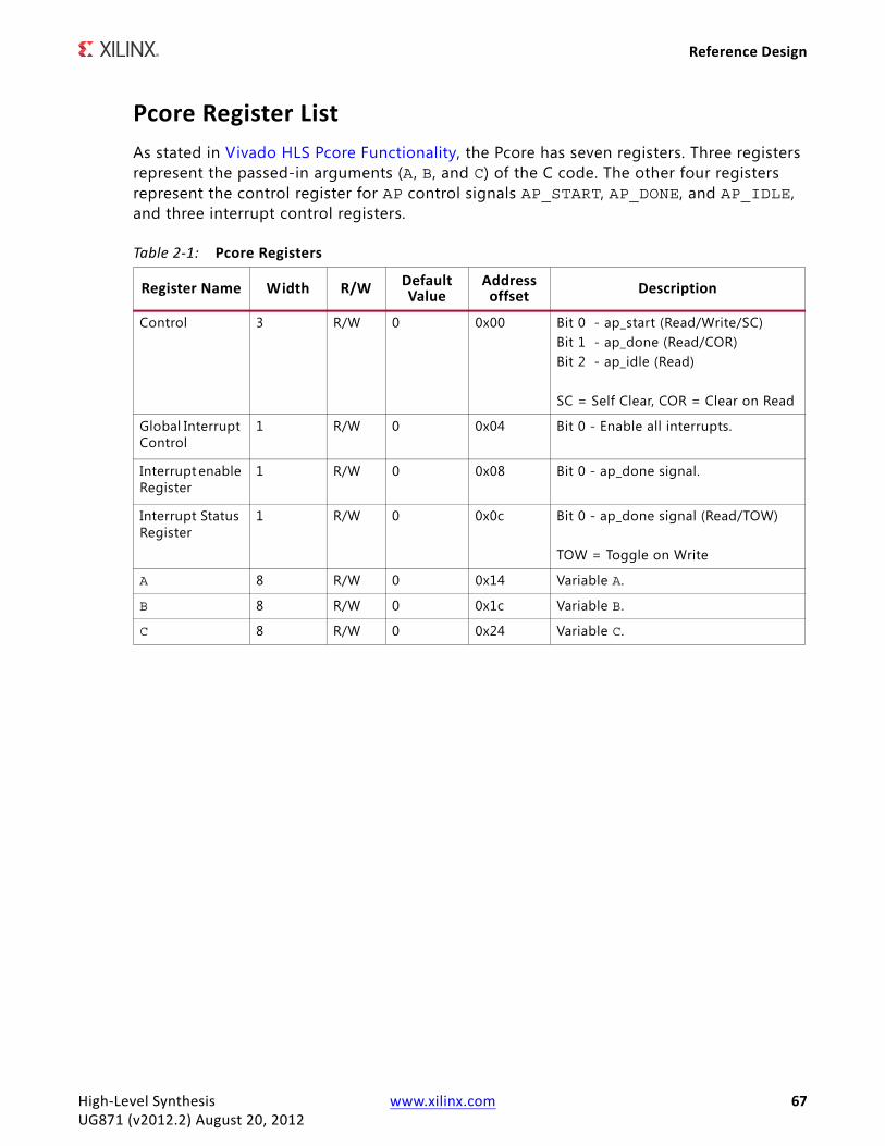
Pcore Register ListAs stated in Vivado HLS Pcore Functionality, the Pcore has seven registers. Three registers represent the passed-in arguments (A, B, and C) of the C code. The other four registers represent the control register for AP control signals AP_START, AP_DONE, and AP_IDLE, and three interrupt control registers.
Table 2-1: Pcore Registers
Register Name Width R/W Default Value
Address offset Description
Control 3 R/W 0 0x00 Bit 0 - ap_start (Read/Write/SC)Bit 1 - ap_done (Read/COR)Bit 2 - ap_idle (Read)
SC = Self Clear, COR = Clear on Read
Global Interrupt Control
1 R/W 0 0x04 Bit 0 - Enable all interrupts.
Interrupt enable Register
1 R/W 0 0x08 Bit 0 - ap_done signal.
Interrupt Status Register
1 R/W 0 0x0c Bit 0 - ap_done signal (Read/TOW)
TOW = Toggle on Write
A 8 R/W 0 0x14 Variable A.
B 8 R/W 0 0x1c Variable B.
C 8 R/W 0 0x24 Variable C.
High-Level Synthesis www.xilinx.com 67UG871 (v2012.2) August 20, 2012
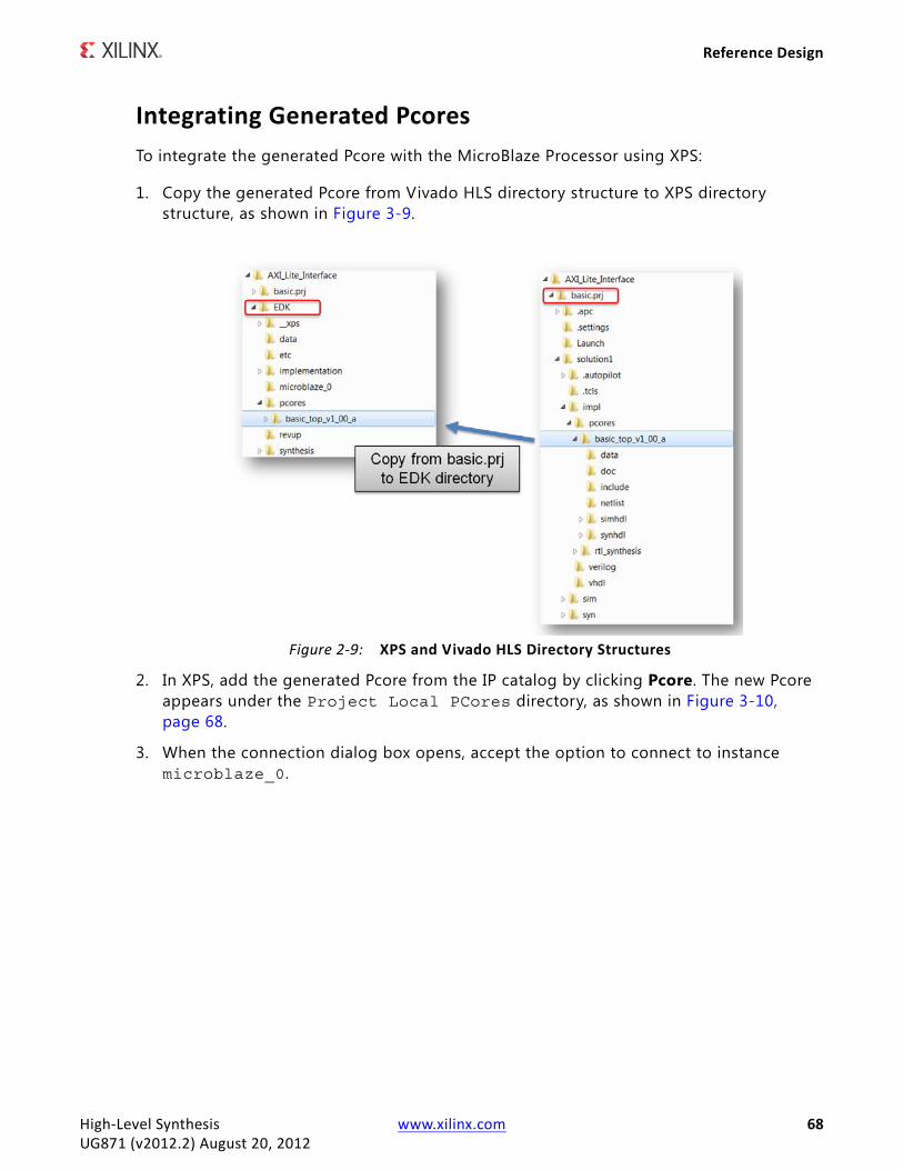
Reference Design
Integrating Generated PcoresTo integrate the generated Pcore with the MicroBlaze Processor using XPS:
1. Copy the generated Pcore from Vivado HLS directory structure to XPS directory structure, as shown in Figure 3-9.
2. In XPS, add the generated Pcore from the IP catalog by clicking Pcore. The new Pcore appears under the Project Local PCores directory, as shown in Figure 3-10, page 68.
3. When the connection dialog box opens, accept the option to connect to instance microblaze_0.
X-Ref Target - Figure 2-9
Figure 2-9: XPS and Vivado HLS Directory Structures
High-Level Synthesis www.xilinx.com 68UG871 (v2012.2) August 20, 2012
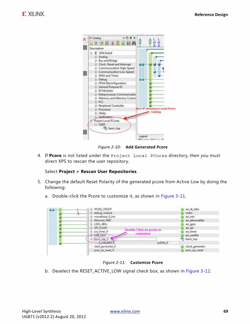
Reference Design
4. If Pcore is not listed under the Project Local PCores directory, then you must direct XPS to rescan the user repository.
Select Project > Rescan User Repositories.
5. Change the default Reset Polarity of the generated pcore from Active Low by doing the following:
a. Double-click the Pcore to customize it, as shown in Figure 3-11.
b. Deselect the RESET_ACTIVE_LOW signal check box, as shown in Figure 3-12.
X-Ref Target - Figure 2-10
Figure 2-10: Add Generated Pcore
X-Ref Target - Figure 2-11
Figure 2-11: Customize Pcore
High-Level Synthesis www.xilinx.com 69UG871 (v2012.2) August 20, 2012
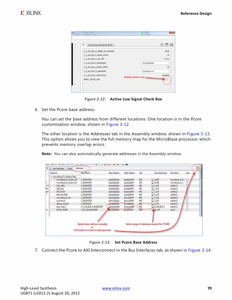
Reference Design
6. Set the Pcore base address.
You can set the base address from different locations. One location is in the Pcore customization window, shown in Figure 3-12.
The other location is the Addresses tab in the Assembly window, shown in Figure 3-13. This option allows you to view the full memory map for the MicroBlaze processor, which prevents memory overlap errors.
Note: You can also automatically generate addresses in the Assembly window.
7. Connect the Pcore to AXI Interconnect in the Bus Interfaces tab, as shown in Figure 3-14.
X-Ref Target - Figure 2-12
Figure 2-12: Active Low Signal Check Box
X-Ref Target - Figure 2-13
Figure 2-13: Set Pcore Base Address
High-Level Synthesis www.xilinx.com 70UG871 (v2012.2) August 20, 2012
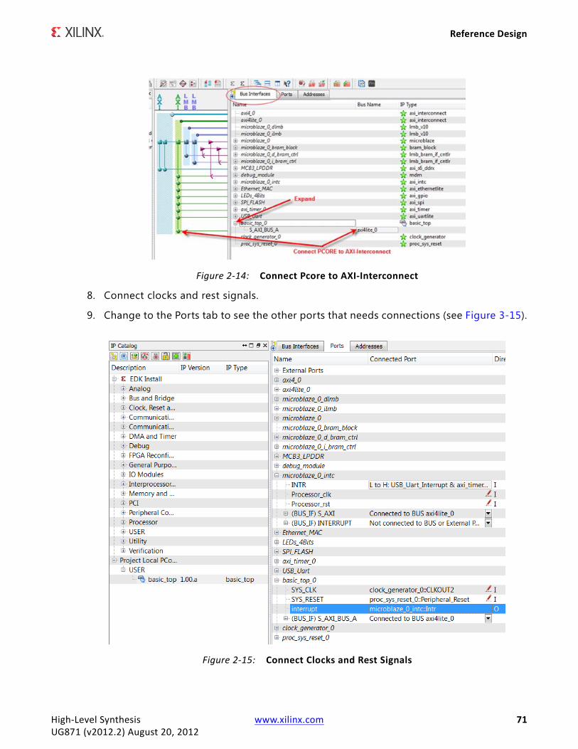
Reference Design
8. Connect clocks and rest signals.
9. Change to the Ports tab to see the other ports that needs connections (see Figure 3-15).
X-Ref Target - Figure 2-14
Figure 2-14: Connect Pcore to AXI-Interconnect
X-Ref Target - Figure 2-15
Figure 2-15: Connect Clocks and Rest Signals
High-Level Synthesis www.xilinx.com 71UG871 (v2012.2) August 20, 2012
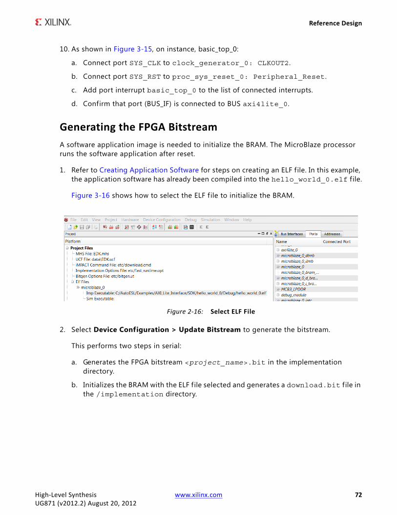
Reference Design
10. As shown in Figure 3-15, on instance, basic_top_0:
a. Connect port SYS_CLK to clock_generator_0: CLKOUT2.
b. Connect port SYS_RST to proc_sys_reset_0: Peripheral_Reset.
c. Add port interrupt basic_top_0 to the list of connected interrupts.
d. Confirm that port (BUS_IF) is connected to BUS axi4lite_0.
Generating the FPGA BitstreamA software application image is needed to initialize the BRAM. The MicroBlaze processor runs the software application after reset.
1. Refer to Creating Application Software for steps on creating an ELF f ile. In this example, the application software has already been compiled into the hello_world_0.elf f ile.
Figure 3-16 shows how to select the ELF f ile to initialize the BRAM.
2. Select Device Configuration > Update Bitstream to generate the bitstream.
This performs two steps in serial:
a. Generates the FPGA bitstream <project_name>.bit in the implementation directory.
b. Initializes the BRAM with the ELF f ile selected and generates a download.bit f ile in the /implementation directory.
X-Ref Target - Figure 2-16
Figure 2-16: Select ELF File
High-Level Synthesis www.xilinx.com 72UG871 (v2012.2) August 20, 2012
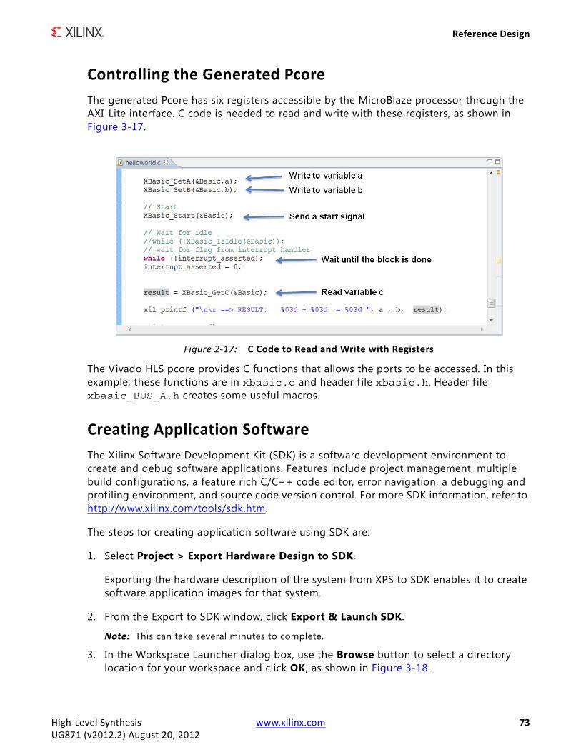
Reference Design
Controlling the Generated PcoreThe generated Pcore has six registers accessible by the MicroBlaze processor through the AXI-Lite interface. C code is needed to read and write with these registers, as shown in Figure 3-17.
The Vivado HLS pcore provides C functions that allows the ports to be accessed. In this example, these functions are in xbasic.c and header f ile xbasic.h. Header f ile xbasic_BUS_A.h creates some useful macros.
Creating Application SoftwareThe Xilinx Software Development Kit (SDK) is a software development environment to create and debug software applications. Features include project management, multiple build configurations, a feature rich C/C++ code editor, error navigation, a debugging and profiling environment, and source code version control. For more SDK information, refer to http://www.xilinx.com/tools/sdk.htm.
The steps for creating application software using SDK are:
1. Select Project > Export Hardware Design to SDK.
Exporting the hardware description of the system from XPS to SDK enables it to create software application images for that system.
2. From the Export to SDK window, click Export & Launch SDK.
Note: This can take several minutes to complete.
3. In the Workspace Launcher dialog box, use the Browse button to select a directory location for your workspace and click OK, as shown in Figure 3-18.
X-Ref Target - Figure 2-17
Figure 2-17: C Code to Read and Write with Registers
High-Level Synthesis www.xilinx.com 73UG871 (v2012.2) August 20, 2012
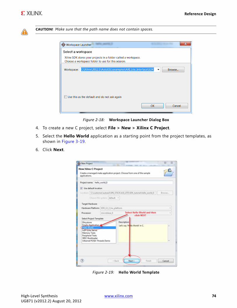
Reference Design
CAUTION! Make sure that the path name does not contain spaces.
4. To create a new C project, select File > New > Xilinx C Project.
5. Select the Hello World application as a starting point from the project templates, as shown in Figure 3-19.
6. Click Next.
X-Ref Target - Figure 2-18
Figure 2-18: Workspace Launcher Dialog Box
X-Ref Target - Figure 2-19
Figure 2-19: Hello World Template
High-Level Synthesis www.xilinx.com 74UG871 (v2012.2) August 20, 2012
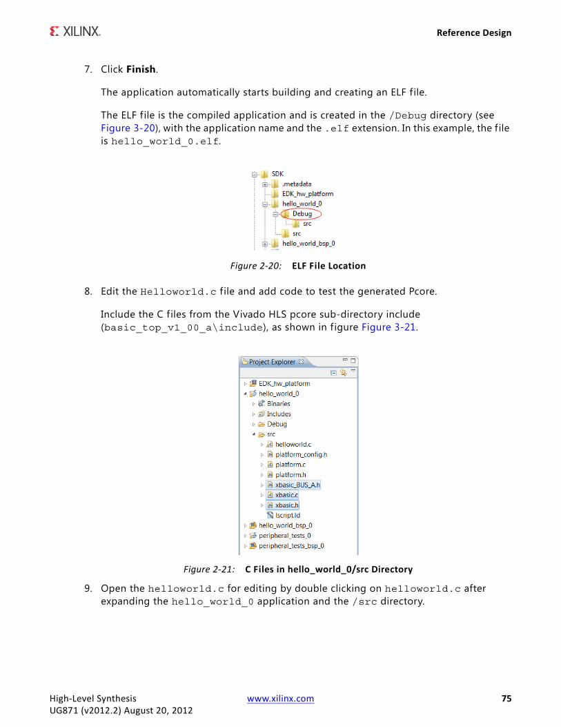
Reference Design
7. Click Finish.
The application automatically starts building and creating an ELF f ile.
The ELF f ile is the compiled application and is created in the /Debug directory (see Figure 3-20), with the application name and the .elf extension. In this example, the f ile is hello_world_0.elf.
8. Edit the Helloworld.c f ile and add code to test the generated Pcore.
Include the C f iles from the Vivado HLS pcore sub-directory include (basic_top_v1_00_a\include), as shown in f igure Figure 3-21.
9. Open the helloworld.c for editing by double clicking on helloworld.c after expanding the hello_world_0 application and the /src directory.
X-Ref Target - Figure 2-20
Figure 2-20: ELF File Location
X-Ref Target - Figure 2-21
Figure 2-21: C Files in hello_world_0/src Directory
High-Level Synthesis www.xilinx.com 75UG871 (v2012.2) August 20, 2012
Reference Design
10. In the editor, change the code in helloworld.c to match the code below. Refer to the C code SDK\hello_world_0\src\helloword.c in the tutorial directory.
#include <stdio.h>#include "platform.h"#include "xparameters.h"#include "xil_io.h"#include "xstatus.h"#include "xbasic.h" // DM added#include "xintc.h"#include "xil_exception.h"#include "xuartlite_l.h"
#define pritnf xil_printfvoid print(char *str);
// BASIC Pcore SETUPXBasic Basic;XBasic_Config Basic_Config ={ 0, XPAR_BASIC_TOP_0_S_AXI_BUS_A_BASEADDR};
int SetupBasic(void){ return XBasic_Initialize(&Basic, &Basic_Config);}
//-------------- Setup Interrupt control -----------------------------//#define INTC_DEVICE_ID XPAR_INTC_0_DEVICE_ID#define XBASIC_INTERRUPT_ID XPAR_MICROBLAZE_0_INTC_BASIC_TOP_0_INTERRUPT_INTRXIntc InterruptController; /* The instance of the Interrupt Controller */
int interrupt_count = 0; // just for statiscsint interrupt_asserted = 0;
void XBasic_InterruptHandler(void *InstancePtr){
interrupt_count++; // clear the interrupt XBasic_InterruptClear(&Basic, 1); // poor man semaphore interrupt_asserted = 1;
}
//----------------------------------------------------int SetupInterrupt(void){ int Status;
// Initialize the interrupt controller driver so that it is ready to use.
High-Level Synthesis www.xilinx.com 76UG871 (v2012.2) August 20, 2012
Reference Design
Status = XIntc_Initialize(&InterruptController, INTC_DEVICE_ID); if (Status != XST_SUCCESS) { return XST_FAILURE; }
// Connect a device driver handler that is called when an interrupt // for the device occurs, the device driver handler performs the specific // interrupt processing for the device Status = XIntc_Connect ( &InterruptController, XBASIC_INTERRUPT_ID, (XInterruptHandler)XBasic_InterruptHandler, NULL ); if (Status != XST_SUCCESS) { return XST_FAILURE; }
// Start the interrupt controller such that interrupts are enabled for // all devices that cause interrupts, specific real mode so that // the timer counter can cause interrupts thru the interrupt controller. // Status = XIntc_Start(&InterruptController, XIN_REAL_MODE); if (Status != XST_SUCCESS) { return XST_FAILURE; }
// Enable the interrupt for the AESL BASIC CORE XIntc_Enable(&InterruptController, XBASIC_INTERRUPT_ID);
// Initialize the exception table. Xil_ExceptionInit();
// Register the interrupt controller handler with the exception table. Xil_ExceptionRegisterHandler( XIL_EXCEPTION_ID_INT, (Xil_ExceptionHandler) XIntc_InterruptHandler, &InterruptController );
// Enable non-critical exceptions. Xil_ExceptionEnable();
XBasic_InterruptEnable(&Basic, 1); XBasic_InterruptGlobalEnable(&Basic);
return XST_SUCCESS;}
void print_core_regs(void ){
xil_printf ("\n\r A reg [0x%08x] ", XBasic_GetA(&Basic ) ); xil_printf ("\n\r B reg [0x%08x] ", XBasic_GetB(&Basic )); xil_printf ("\n\r C reg [0x%08x] ", XBasic_GetC(&Basic ) ); xil_printf ("\n\r DONE reg [0x%08x] ", XBasic_IsDone(&Basic) );
High-Level Synthesis www.xilinx.com 77UG871 (v2012.2) August 20, 2012
Reference Design
xil_printf ("\n\r IDLE reg [0x%08x] ", XBasic_IsIdle(&Basic) );
xil_printf ("\n\r INT STATS [%d] ", interrupt_count );
}
int ReadInt(int size){ int value=0; char c ='0'; int i; for (i=0; i <size; i++) { c=inbyte(); if (c==' ' ) { c='0'; outbyte(c); } else if (c=='\n') { break; return value; } else if (c=='\r') { break; return value; } else { outbyte(c); value=value*10+c-'0'; } }
return value;}
int main(){ //init_platform();
int a = 1000; int b = 1000; u32 result;
// initialize AESL Pcore
int status; status = XBasic_Initialize(&Basic, &Basic_Config); if (status != XST_SUCCESS) { xil_printf("\n\r ==> Basic failed.\n\r"); } else { xil_printf("\n\r ==> Basic succeeded.\n\r"); }
High-Level Synthesis www.xilinx.com 78UG871 (v2012.2) August 20, 2012
Reference Design
// Initialize the interrupts (local then global) status = SetupInterrupt(); if (status != XST_SUCCESS) { xil_printf("\n\r ==> SetupInterrupt failed.\n\r\n\r"); } else { xil_printf("\n\r ==> SetupInterrupt succeeded.\n\r\n\r"); }
// Get and setup the data while (1) { print("\n\r ==========================================================="); print("\n\r =========== START OF AESL BASIC CORE TEST ================="); print("\n\r ================ RESULT = A + B ==================\n\r");
while (a > 255) { print("\n\r --> Please enter number between (0-255) for variable A : "); a = ReadInt(3); }
while (b > 255) { print("\n\r --> Please enter number between (0-255) for variable B : "); b = ReadInt(3); }
XBasic_SetA(&Basic,a); XBasic_SetB(&Basic,b);
// Start XBasic_Start(&Basic);
// Wait for idle //while (!XBasic_IsIdle(&Basic)); // wait for flag from interrupt handler while (!interrupt_asserted); interrupt_asserted = 0;
result = XBasic_GetC(&Basic);
xil_printf ("\n\r ==> RESULT: %03d + %03d = %03d ", a , b, result);
print_core_regs();
print("\n\r ==========================================================="); print("\n\r ===========================================================\n\r"); // reset variable to value bigger then 255 to prompt user for new input a =1000; b =1000;
}
//cleanup_platform();
return 0;}
High-Level Synthesis www.xilinx.com 79UG871 (v2012.2) August 20, 2012
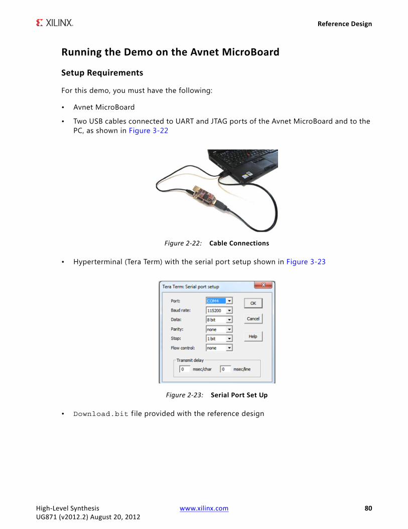
Reference Design
Running the Demo on the Avnet MicroBoard
Setup Requirements
For this demo, you must have the following:
• Avnet MicroBoard
• Two USB cables connected to UART and JTAG ports of the Avnet MicroBoard and to the PC, as shown in Figure 3-22
• Hyperterminal (Tera Term) with the serial port setup shown in Figure 3-23
• Download.bit f ile provided with the reference design
X-Ref Target - Figure 2-22
Figure 2-22: Cable Connections
X-Ref Target - Figure 2-23
Figure 2-23: Serial Port Set Up
High-Level Synthesis www.xilinx.com 80UG871 (v2012.2) August 20, 2012
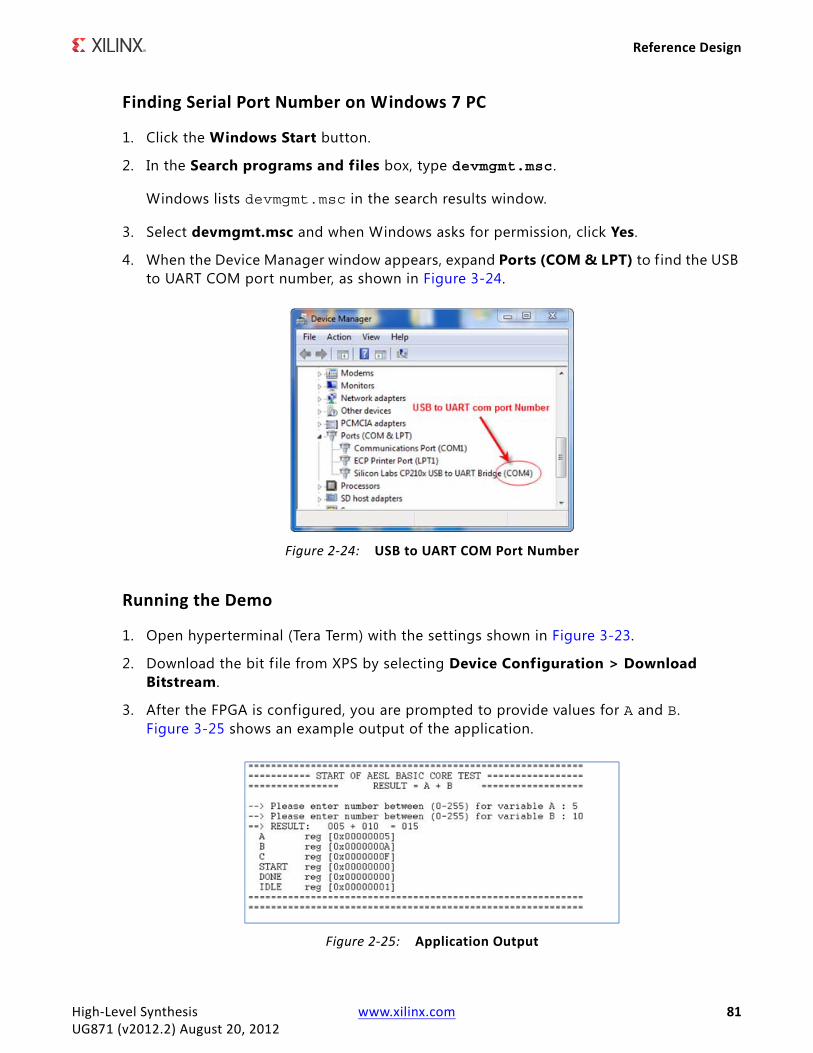
Reference Design
Finding Serial Port Number on Windows 7 PC
1. Click the Windows Start button.
2. In the Search programs and files box, type devmgmt.msc.
Windows lists devmgmt.msc in the search results window.
3. Select devmgmt.msc and when Windows asks for permission, click Yes.
4. When the Device Manager window appears, expand Ports (COM & LPT) to f ind the USB to UART COM port number, as shown in Figure 3-24.
Running the Demo
1. Open hyperterminal (Tera Term) with the settings shown in Figure 3-23.
2. Download the bit f ile from XPS by selecting Device Configuration > Download Bitstream.
3. After the FPGA is configured, you are prompted to provide values for A and B. Figure 3-25 shows an example output of the application.
X-Ref Target - Figure 2-24
Figure 2-24: USB to UART COM Port Number
X-Ref Target - Figure 2-25
Figure 2-25: Application Output
High-Level Synthesis www.xilinx.com 81UG871 (v2012.2) August 20, 2012
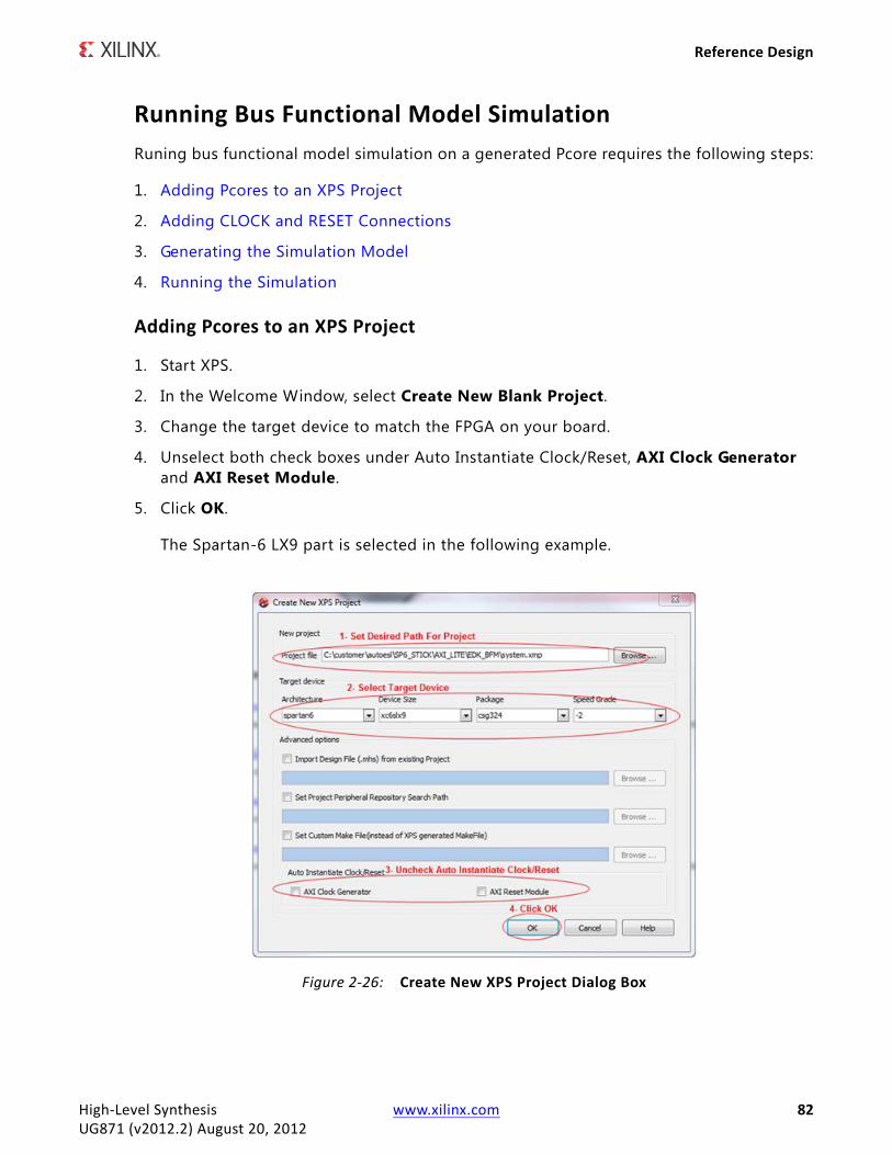
Reference Design
Running Bus Functional Model SimulationRuning bus functional model simulation on a generated Pcore requires the following steps:
1. Adding Pcores to an XPS Project
2. Adding CLOCK and RESET Connections
3. Generating the Simulation Model
4. Running the Simulation
Adding Pcores to an XPS Project
1. Start XPS.
2. In the Welcome Window, select Create New Blank Project.
3. Change the target device to match the FPGA on your board.
4. Unselect both check boxes under Auto Instantiate Clock/Reset, AXI Clock Generator and AXI Reset Module.
5. Click OK.
The Spartan-6 LX9 part is selected in the following example.
X-Ref Target - Figure 2-26
Figure 2-26: Create New XPS Project Dialog Box
High-Level Synthesis www.xilinx.com 82UG871 (v2012.2) August 20, 2012
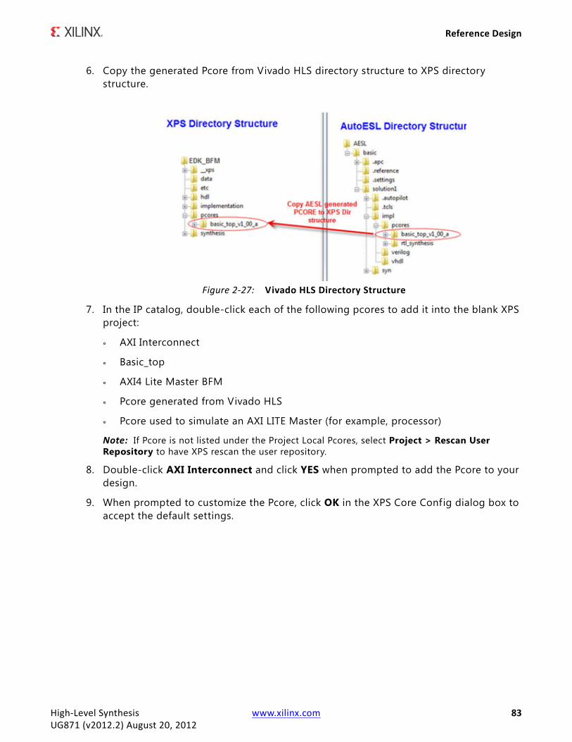
Reference Design
6. Copy the generated Pcore from Vivado HLS directory structure to XPS directory structure.
7. In the IP catalog, double-click each of the following pcores to add it into the blank XPS project:
° AXI Interconnect
° Basic_top
° AXI4 Lite Master BFM
° Pcore generated from Vivado HLS
° Pcore used to simulate an AXI LITE Master (for example, processor)
Note: If Pcore is not listed under the Project Local Pcores, select Project > Rescan User Repository to have XPS rescan the user repository.
8. Double-click AXI Interconnect and click YES when prompted to add the Pcore to your design.
9. When prompted to customize the Pcore, click OK in the XPS Core Config dialog box to accept the default settings.
X-Ref Target - Figure 2-27
Figure 2-27: Vivado HLS Directory Structure
High-Level Synthesis www.xilinx.com 83UG871 (v2012.2) August 20, 2012
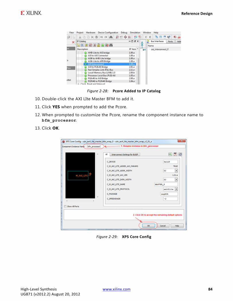
Reference Design
10. Double-click the AXI LIte Master BFM to add it.
11. Click YES when prompted to add the Pcore.
12. When prompted to customize the Pcore, rename the component instance name to bfm_processor.
13. Click OK.
X-Ref Target - Figure 2-28
Figure 2-28: Pcore Added to IP Catalog
X-Ref Target - Figure 2-29
Figure 2-29: XPS Core Config
High-Level Synthesis www.xilinx.com 84UG871 (v2012.2) August 20, 2012
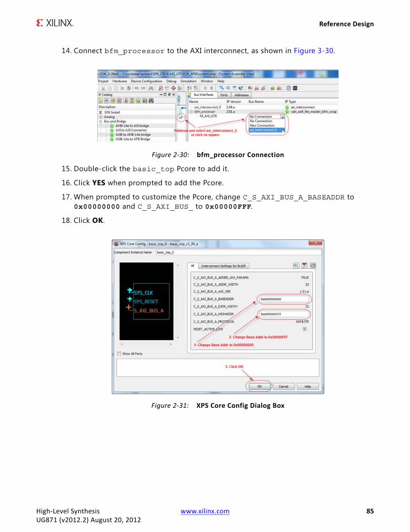
Reference Design
14. Connect bfm_processor to the AXI interconnect, as shown in Figure 3-30.
15. Double-click the basic_top Pcore to add it.
16. Click YES when prompted to add the Pcore.
17. When prompted to customize the Pcore, change C_S_AXI_BUS_A_BASEADDR to 0x00000000 and C_S_AXI_BUS_ to 0x00000FFF.
18. Click OK.
X-Ref Target - Figure 2-30
Figure 2-30: bfm_processor Connection
X-Ref Target - Figure 2-31
Figure 2-31: XPS Core Config Dialog Box
High-Level Synthesis www.xilinx.com 85UG871 (v2012.2) August 20, 2012
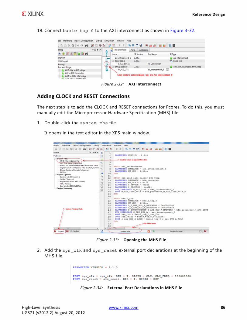
Reference Design
19. Connect basic_top_0 to the AXI interconnect as shown in Figure 3-32.
Adding CLOCK and RESET Connections
The next step is to add the CLOCK and RESET connections for Pcores. To do this, you must manually edit the Microprocessor Hardware Specif ication (MHS) f ile.
1. Double-click the system.mhs f ile.
It opens in the text editor in the XPS main window.
2. Add the sys_clk and sys_reset external port declarations at the beginning of the MHS file.
X-Ref Target - Figure 2-32
Figure 2-32: AXI Interconnect
X-Ref Target - Figure 2-33
Figure 2-33: Opening the MHS File
X-Ref Target - Figure 2-34
Figure 2-34: External Port Declarations in MHS File
High-Level Synthesis www.xilinx.com 86UG871 (v2012.2) August 20, 2012
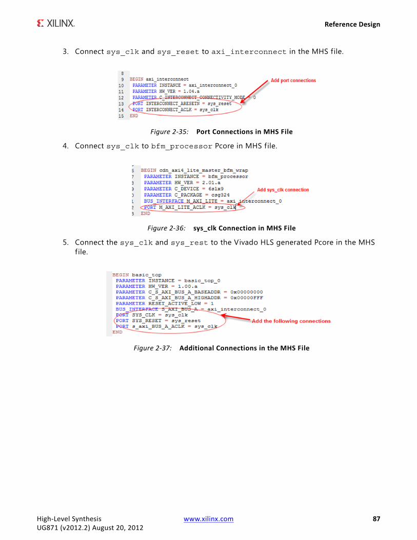
Reference Design
3. Connect sys_clk and sys_reset to axi_interconnect in the MHS file.
4. Connect sys_clk to bfm_processor Pcore in MHS file.
5. Connect the sys_clk and sys_rest to the Vivado HLS generated Pcore in the MHS file.
X-Ref Target - Figure 2-35
Figure 2-35: Port Connections in MHS File
X-Ref Target - Figure 2-36
Figure 2-36: sys_clk Connection in MHS File
X-Ref Target - Figure 2-37
Figure 2-37: Additional Connections in the MHS File
High-Level Synthesis www.xilinx.com 87UG871 (v2012.2) August 20, 2012
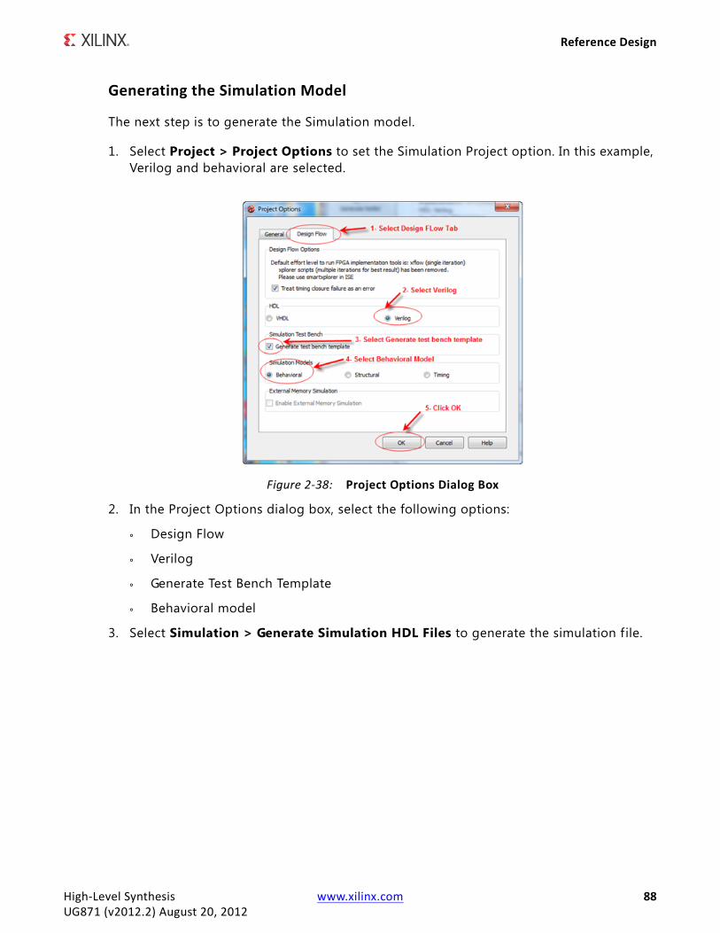
Reference Design
Generating the Simulation Model
The next step is to generate the Simulation model.
1. Select Project > Project Options to set the Simulation Project option. In this example, Verilog and behavioral are selected.
2. In the Project Options dialog box, select the following options:
° Design Flow
° Verilog
° Generate Test Bench Template
° Behavioral model
3. Select Simulation > Generate Simulation HDL Files to generate the simulation file.
X-Ref Target - Figure 2-38
Figure 2-38: Project Options Dialog Box
High-Level Synthesis www.xilinx.com 88UG871 (v2012.2) August 20, 2012
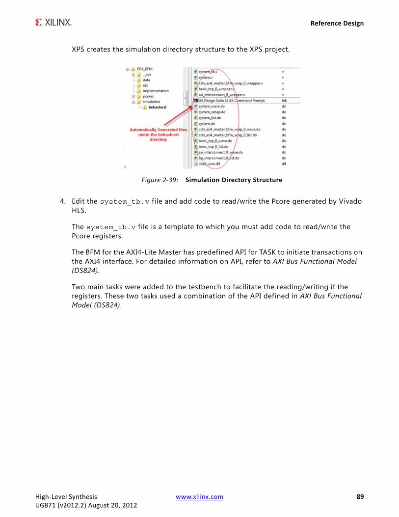
Reference Design
XPS creates the simulation directory structure to the XPS project.
4. Edit the system_tb.v f ile and add code to read/write the Pcore generated by Vivado HLS.
The system_tb.v f ile is a template to which you must add code to read/write the Pcore registers.
The BFM for the AXI4-Lite Master has predefined API for TASK to initiate transactions on the AXI4 interface. For detailed information on API, refer to AXI Bus Functional Model (DS824).
Two main tasks were added to the testbench to facilitate the reading/writing if the registers. These two tasks used a combination of the API defined in AXI Bus Functional Model (DS824).
X-Ref Target - Figure 2-39
Figure 2-39: Simulation Directory Structure
High-Level Synthesis www.xilinx.com 89UG871 (v2012.2) August 20, 2012
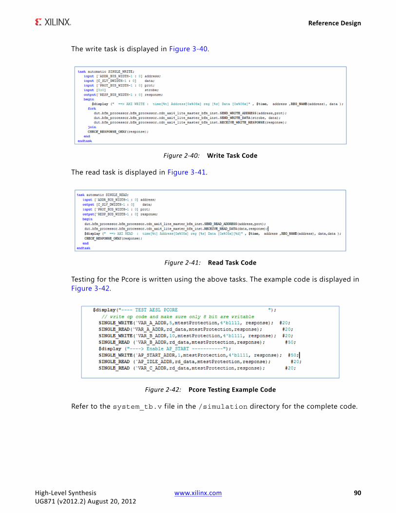
Reference Design
The write task is displayed in Figure 3-40.
The read task is displayed in Figure 3-41.
Testing for the Pcore is written using the above tasks. The example code is displayed in Figure 3-42.
Refer to the system_tb.v f ile in the /simulation directory for the complete code.
X-Ref Target - Figure 2-40
Figure 2-40: Write Task Code
X-Ref Target - Figure 2-41
Figure 2-41: Read Task Code
X-Ref Target - Figure 2-42
Figure 2-42: Pcore Testing Example Code
High-Level Synthesis www.xilinx.com 90UG871 (v2012.2) August 20, 2012
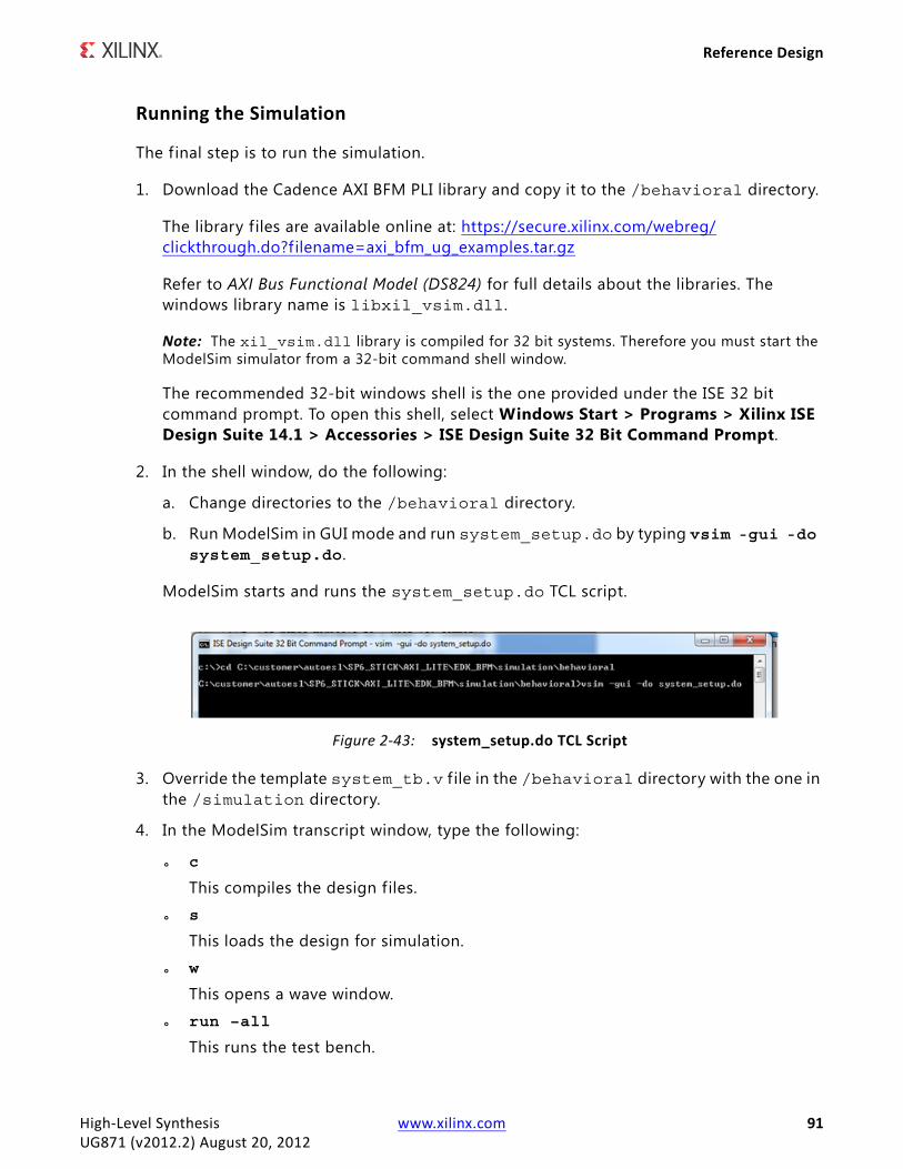
Reference Design
Running the Simulation
The final step is to run the simulation.
1. Download the Cadence AXI BFM PLI library and copy it to the /behavioral directory.
The library files are available online at: https://secure.xilinx.com/webreg/clickthrough.do?filename=axi_bfm_ug_examples.tar.gz
Refer to AXI Bus Functional Model (DS824) for full details about the libraries. The windows library name is libxil_vsim.dll.
Note: The xil_vsim.dll library is compiled for 32 bit systems. Therefore you must start the ModelSim simulator from a 32-bit command shell window.
The recommended 32-bit windows shell is the one provided under the ISE 32 bit command prompt. To open this shell, select Windows Start > Programs > Xilinx ISE Design Suite 14.1 > Accessories > ISE Design Suite 32 Bit Command Prompt.
2. In the shell window, do the following:
a. Change directories to the /behavioral directory.
b. Run ModelSim in GUI mode and run system_setup.do by typing vsim -gui -do system_setup.do.
ModelSim starts and runs the system_setup.do TCL script.
3. Override the template system_tb.v f ile in the /behavioral directory with the one in the /simulation directory.
4. In the ModelSim transcript window, type the following:
° c
This compiles the design files.
° s
This loads the design for simulation.
° w
This opens a wave window.
° run –all
This runs the test bench.
X-Ref Target - Figure 2-43
Figure 2-43: system_setup.do TCL Script
High-Level Synthesis www.xilinx.com 91UG871 (v2012.2) August 20, 2012
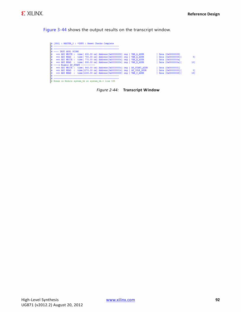
Reference Design
Figure 3-44 shows the output results on the transcript window.
X-Ref Target - Figure 2-44
Figure 2-44: Transcript Window
High-Level Synthesis www.xilinx.com 92UG871 (v2012.2) August 20, 2012
Chapter 3
Vivado HLS: Integrating System Generator
IntroductionOne of the features in Vivado HLS 2012.2 is the ability to export RTL designs targeted to 7-series devices into Xilinx System Generator environment. This tutorial describes the steps in taking a design from Vivado HLS into System Generator.
Software Application for Vivado HLSA Vivado HLS design project is made of 2 software components: a testbench and the code which will be transformed into hardware by the tool. The software directory included with this tutorial contains the software files for the example:
• Test bench f ile fir_test.cpp
• Design File fir.cpp
• A header f ile fir.h used with the test bench and the design f iles.
The header file filter.h is shown in Example 1.1.
#include <stdio.h>#include <stdlib.h>#include <hls_stream.h>
#define TAPS 21#define RUN_LENGTH 100
int fir_hw(hls::stream<int> &input_val, hls::stream<int> &output_val);
Example 1.1 FIR Header File
The testbench f ile fir_test.cpp is shown in Example 1.2. This f ile follows the recommended Vivado HLS approach of separating the testbench code from the code
High-Level Synthesis www.xilinx.com 93UG871 (v2012.2) August 20, 2012
Software Application for Vivado HLS
targeted for hardware implementation. This allows a simple way of exercising the same hardware function with different testbenches and code reuse in other hardware projects.
The testbench file is self-checking f ile. Vivado HLS requires the testbench to issue a return value of 0 if the functionality is correct and any non-zero value if there is an error. In this test bench, a version of the f ilter called fir_sw is executed in the test bench and it’s results compared to those of function fir_hw. Function fir_hw will be synthesized to RTL: the test bench will confirm both functions produce the same results before and after synthesis.
By checking the output of the software implementation against the hardware implementation of function FIR, you can be certain that the generated hardware is correct. Another approach to generating self-checking testbenches is to have known good data files containing the expected result of the hardware function.
#include “fir.h”
int fir_sw(hls::stream<int> &input_val, hls::stream<int> &output_val){int I;static short shift_reg[TAPS] = {0};const short coeff[TAPS] = {6,0,-4,-3,5,6,-6,-13,7,44,64,44,7,-13,
-6,6,5,-3,-4,0,6};
for(i=0; i < RUN_LENGTH; i++){int sample;sample = input_val.read();
//Shift Registerfor(int j=0; j < TAPS-1; j++){shift_reg[j] = shift_reg[j+1];
}shift_reg[TAPS-1] = sample;
//Filter Operationint acc = 0;for(int k=0; k < TAPS; k++){acc += shift_reg[k] * coeff[k];
}output_val.write(acc);
}}
int main(){hls::stream<int> input_sw;hls::stream<int> input_hw;hls::stream<int> output_hw;hls::stream<int> output_sw;
//Write the input valuesfor(int i = 0; i < RUN_LENGTH; i++){input_sw.write(i);input_hw.write(i);
}
High-Level Synthesis www.xilinx.com 94UG871 (v2012.2) August 20, 2012
Software Application for Vivado HLS
//Call to software model of FIR fir_sw(input_sw, output_sw);//Call to hardware model of FIRfir_hw(input_hw, output_hw);
for(int k=0; k < RUN_LENGTH; k++){int sw, hw;sw = output_sw.read();hw = output_hw.read();if(sw != hw){printf(“ERROR: k = %d sw = %d hw = %d\n”,k,sw,hw);
return 1;}
}printf(“Success! both SW and HW models match.\n”);return 0;
}
Example 1.2 FIR Testbench Code
The version of the FIR function, fir_hw, which will be exported to a System Generator design, is shown in Example 1.3. This code is the same code as the software version of FIR. This design uses the hls::stream class to implement a streaming data type. See the Vivado Design Suite User Guide: High-Level Synthesis (UG902) for more details on using steaming interfaces.
An optimization directive for the fir_hw function is embedded into the source code as a pragma: HLS PIPELINE II=1 rewind. This optimization will ensure that in the RTL implementation, each iteration of the for-loop will be implemented to operate in a pipelined manner with 1 clock cycle (II=1) between iterations: iteration 1 will start, and one clock cycle later iteration 2 will start (even though iteration 1 has not f inished). The rewind option ensures this iteration rate can be performed by the entire function.
#include “fir.h”
int fir_hw(hls::stream<int> &input_val, hls::stream<int> &output_val){int I;static short shift_reg[TAPS] = {0};const short coeff[TAPS] = {6,0,-4,-3,5,6,-6,-13,7,44,64,44,7,-13,
-6,6,5,-3,-4,0,6};
for(i=0; i < RUN_LENGTH; i++){#pragma HLS PIPELINE II=1 rewind
int sample;sample = input_val.read();
//Shift Registerfor(int j=0; j < TAPS-1; j++){shift_reg[j] = shift_reg[j+1];
}shift_reg[TAPS-1] = sample;
//Filter Operation
High-Level Synthesis www.xilinx.com 95UG871 (v2012.2) August 20, 2012
Create a Project in Vivado HLS for the FIR Application
int acc = 0;for(int k=0; k < TAPS; k++){acc += shift_reg[k] * coeff[k];
}output_val.write(acc);
}}
Example 1.3 FIR Code for Hardware Generation
Create a Project in Vivado HLS for the FIR ApplicationThe following steps will demonstrate how to run Vivado HLS and create the FIR application as a hardware block for a System Generator based design.
To invoke Vivado HLS, through the Windows menu: Start > All Programs > Xilinx Design Tools > Vivado > Vivado HLS.
High-Level Synthesis www.xilinx.com 96UG871 (v2012.2) August 20, 2012
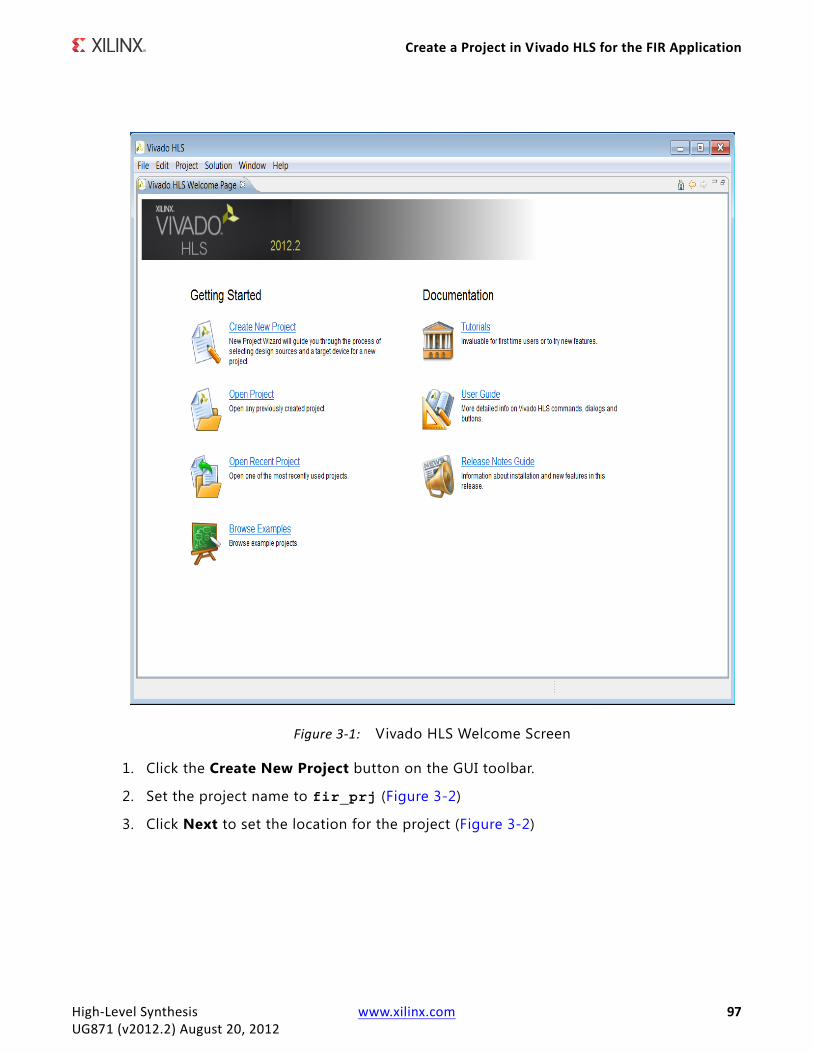
Create a Project in Vivado HLS for the FIR Application
1. Click the Create New Project button on the GUI toolbar.
2. Set the project name to fir_prj (Figure 3-2)
3. Click Next to set the location for the project (Figure 3-2)
X-Ref Target - Figure 3-1
Figure 3-1: Vivado HLS Welcome Screen
High-Level Synthesis www.xilinx.com 97UG871 (v2012.2) August 20, 2012
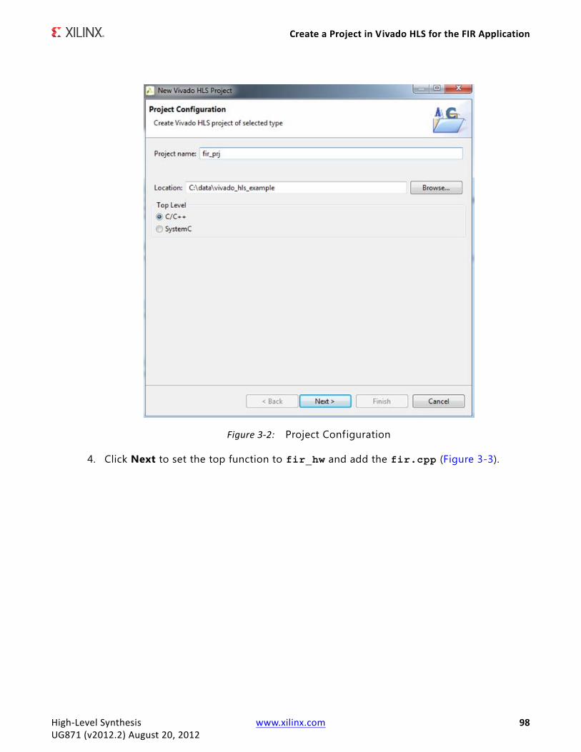
Create a Project in Vivado HLS for the FIR Application
4. Click Next to set the top function to fir_hw and add the fir.cpp (Figure 3-3).
X-Ref Target - Figure 3-2
Figure 3-2: Project Configuration
High-Level Synthesis www.xilinx.com 98UG871 (v2012.2) August 20, 2012
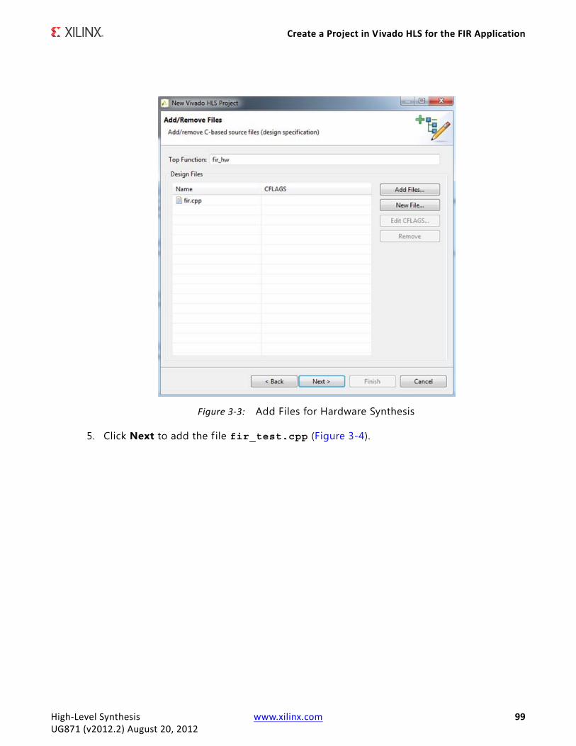
Create a Project in Vivado HLS for the FIR Application
5. Click Next to add the f ile fir_test.cpp (Figure 3-4).
X-Ref Target - Figure 3-3
Figure 3-3: Add Files for Hardware Synthesis
High-Level Synthesis www.xilinx.com 99UG871 (v2012.2) August 20, 2012
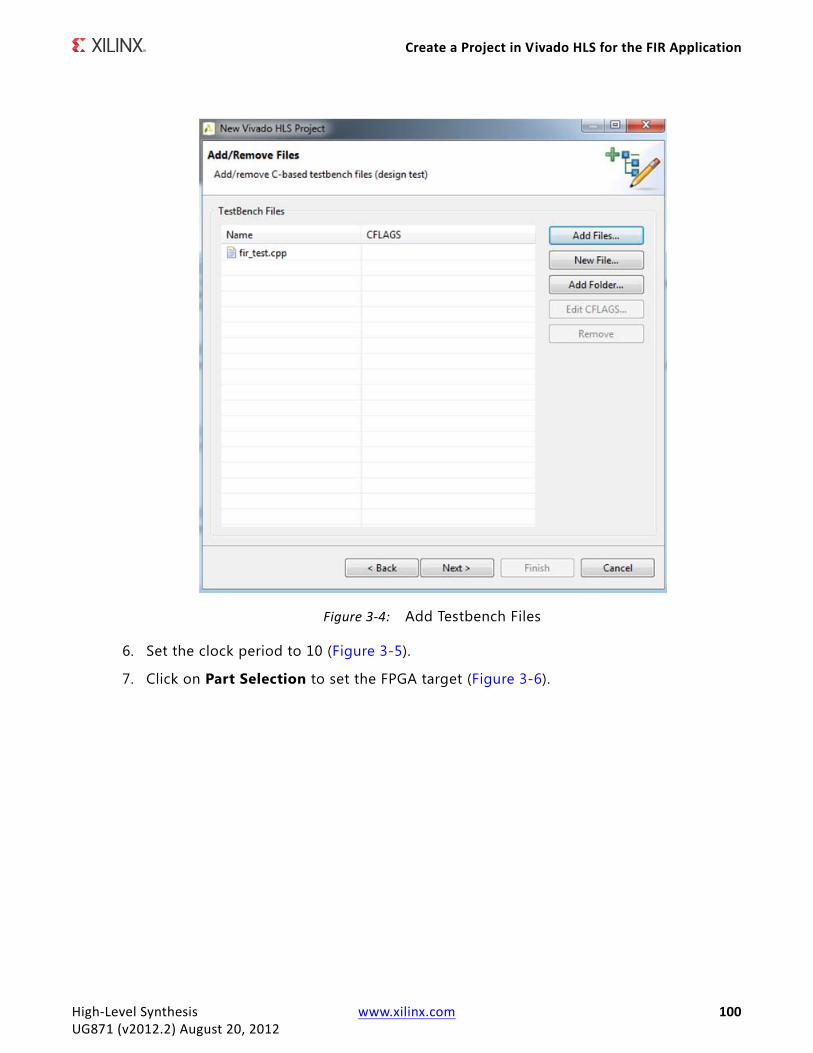
Create a Project in Vivado HLS for the FIR Application
6. Set the clock period to 10 (Figure 3-5).
7. Click on Part Selection to set the FPGA target (Figure 3-6).
X-Ref Target - Figure 3-4
Figure 3-4: Add Testbench Files
High-Level Synthesis www.xilinx.com 100UG871 (v2012.2) August 20, 2012
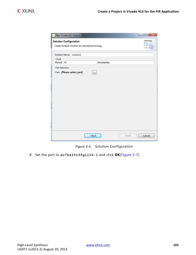
Create a Project in Vivado HLS for the FIR Application
8. Set the part to xc7k420tffg1156-1 and click OK(Figure 3-7).
X-Ref Target - Figure 3-5
Figure 3-5: Solution Configuration
High-Level Synthesis www.xilinx.com 101UG871 (v2012.2) August 20, 2012
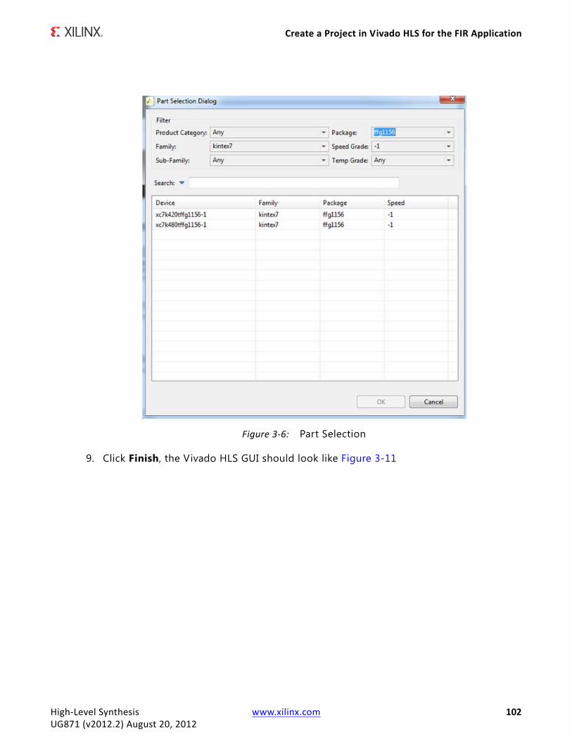
Create a Project in Vivado HLS for the FIR Application
9. Click Finish, the Vivado HLS GUI should look like Figure 3-11
X-Ref Target - Figure 3-6
Figure 3-6: Part Selection
High-Level Synthesis www.xilinx.com 102UG871 (v2012.2) August 20, 2012
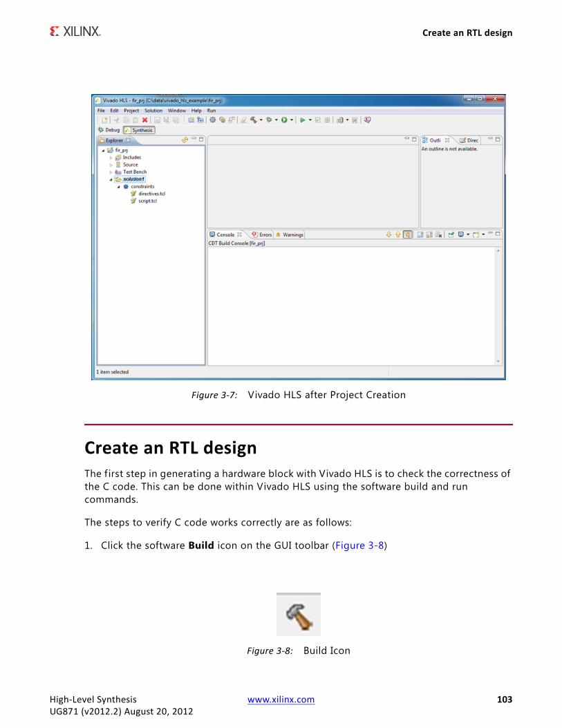
Create an RTL design
Create an RTL designThe f irst step in generating a hardware block with Vivado HLS is to check the correctness of the C code. This can be done within Vivado HLS using the software build and run commands.
The steps to verify C code works correctly are as follows:
1. Click the software Build icon on the GUI toolbar (Figure 3-8)
X-Ref Target - Figure 3-7
Figure 3-7: Vivado HLS after Project Creation
X-Ref Target - Figure 3-8
Figure 3-8: Build Icon
High-Level Synthesis www.xilinx.com 103UG871 (v2012.2) August 20, 2012
Create an RTL design
2. Click the software Run icon on the GUI toolbar (Figure 3-9)
3. Select f ir_prj.Debug and click ok. Console should look like Figure 3-10.
Once the C code is known to be correct, it is time to generate the module for System Generator. The following steps describe how to accomplish this task.
Note: All designs exported to the System Generator environment must have a global clock-enable signal. If the design does not have this implemented in the RTL, the Export RTL will process with halt with an error.
4. Click Solution > Solution Settings (Figure 3-11).
X-Ref Target - Figure 3-9
Figure 3-9: Run Icon
X-Ref Target - Figure 3-10
Figure 3-10: Expected Console Output
High-Level Synthesis www.xilinx.com 104UG871 (v2012.2) August 20, 2012
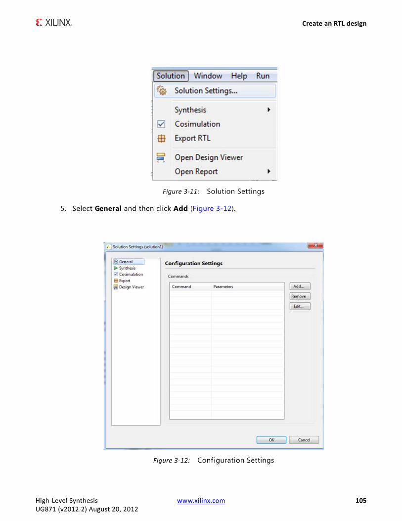
Create an RTL design
5. Select General and then click Add (Figure 3-12).
X-Ref Target - Figure 3-11
Figure 3-11: Solution Settings
X-Ref Target - Figure 3-12
Figure 3-12: Configuration Settings
High-Level Synthesis www.xilinx.com 105UG871 (v2012.2) August 20, 2012
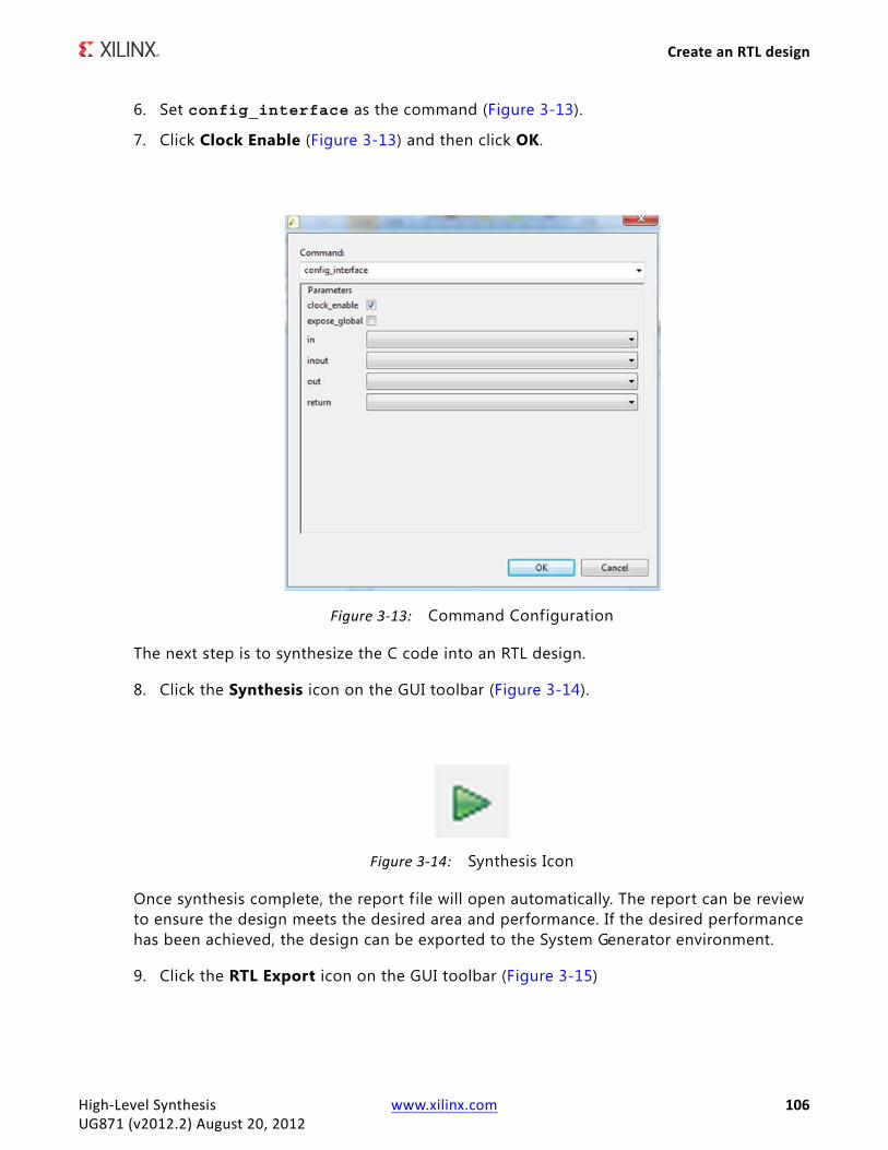
Create an RTL design
6. Set config_interface as the command (Figure 3-13).
7. Click Clock Enable (Figure 3-13) and then click OK.
The next step is to synthesize the C code into an RTL design.
8. Click the Synthesis icon on the GUI toolbar (Figure 3-14).
Once synthesis complete, the report f ile will open automatically. The report can be review to ensure the design meets the desired area and performance. If the desired performance has been achieved, the design can be exported to the System Generator environment.
9. Click the RTL Export icon on the GUI toolbar (Figure 3-15)
X-Ref Target - Figure 3-13
Figure 3-13: Command Configuration
X-Ref Target - Figure 3-14
Figure 3-14: Synthesis Icon
High-Level Synthesis www.xilinx.com 106UG871 (v2012.2) August 20, 2012
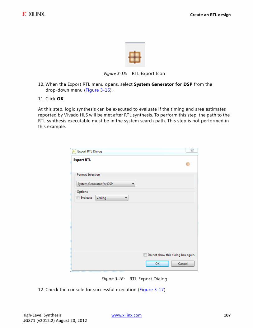
Create an RTL design
10. When the Export RTL menu opens, select System Generator for DSP from the drop-down menu (Figure 3-16).
11. Click OK.
At this step, logic synthesis can be executed to evaluate if the timing and area estimates reported by Vivado HLS will be met after RTL synthesis. To perform this step, the path to the RTL synthesis executable must be in the system search path. This step is not performed in this example.
12. Check the console for successful execution (Figure 3-17).
X-Ref Target - Figure 3-15
Figure 3-15: RTL Export Icon
X-Ref Target - Figure 3-16
Figure 3-16: RTL Export Dialog
High-Level Synthesis www.xilinx.com 107UG871 (v2012.2) August 20, 2012
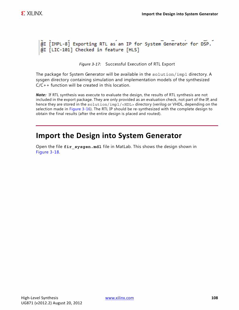
Import the Design into System Generator
The package for System Generator will be available in the solution/impl directory. A sysgen directory containing simulation and implementation models of the synthesized C/C++ function will be created in this location.
Note: If RTL synthesis was execute to evaluate the design, the results of RTL synthesis are not included in the export package. They are only provided as an evaluation check, not part of the IP, and hence they are stored in the solution/impl/<HDL> directory (verilog or VHDL, depending on the selection made in Figure 3-16). The RTL IP should be re-synthesized with the complete design to obtain the f inal results (after the entire design is placed and routed).
Import the Design into System GeneratorOpen the file fir_sysgen.mdl f ile in MatLab. This shows the design shown in Figure 3-18.
X-Ref Target - Figure 3-17
Figure 3-17: Successful Execution of RTL Export
High-Level Synthesis www.xilinx.com 108UG871 (v2012.2) August 20, 2012
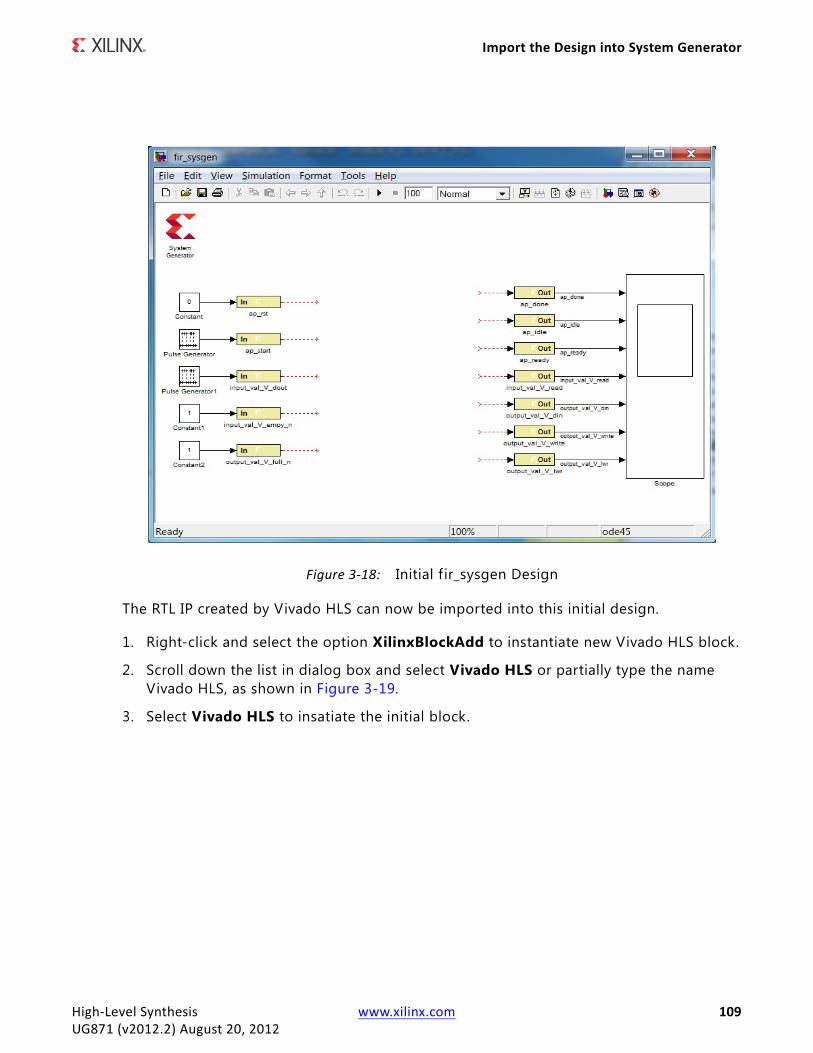
Import the Design into System Generator
The RTL IP created by Vivado HLS can now be imported into this initial design.
1. Right-click and select the option XilinxBlockAdd to instantiate new Vivado HLS block.
2. Scroll down the list in dialog box and select Vivado HLS or partially type the name Vivado HLS, as shown in Figure 3-19.
3. Select Vivado HLS to insatiate the initial block.
X-Ref Target - Figure 3-18
Figure 3-18: Initial f ir_sysgen Design
High-Level Synthesis www.xilinx.com 109UG871 (v2012.2) August 20, 2012
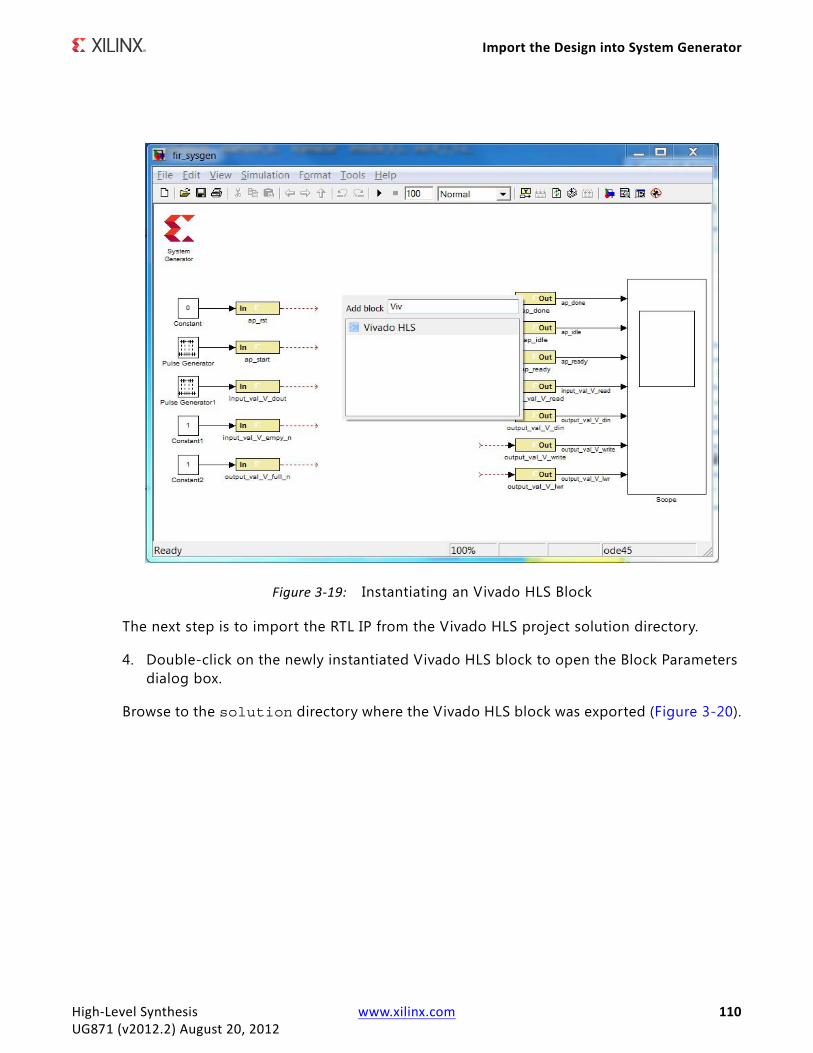
Import the Design into System Generator
The next step is to import the RTL IP from the Vivado HLS project solution directory.
4. Double-click on the newly instantiated Vivado HLS block to open the Block Parameters dialog box.
Browse to the solution directory where the Vivado HLS block was exported (Figure 3-20).
X-Ref Target - Figure 3-19
Figure 3-19: Instantiating an Vivado HLS Block
High-Level Synthesis www.xilinx.com 110UG871 (v2012.2) August 20, 2012
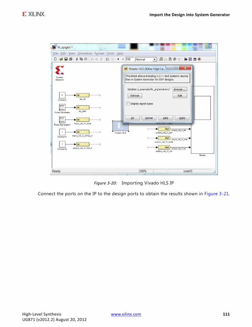
Import the Design into System Generator
Connect the ports on the IP to the design ports to obtain the results shown in Figure 3-21.
X-Ref Target - Figure 3-20
Figure 3-20: Importing Vivado HLS IP
High-Level Synthesis www.xilinx.com 111UG871 (v2012.2) August 20, 2012
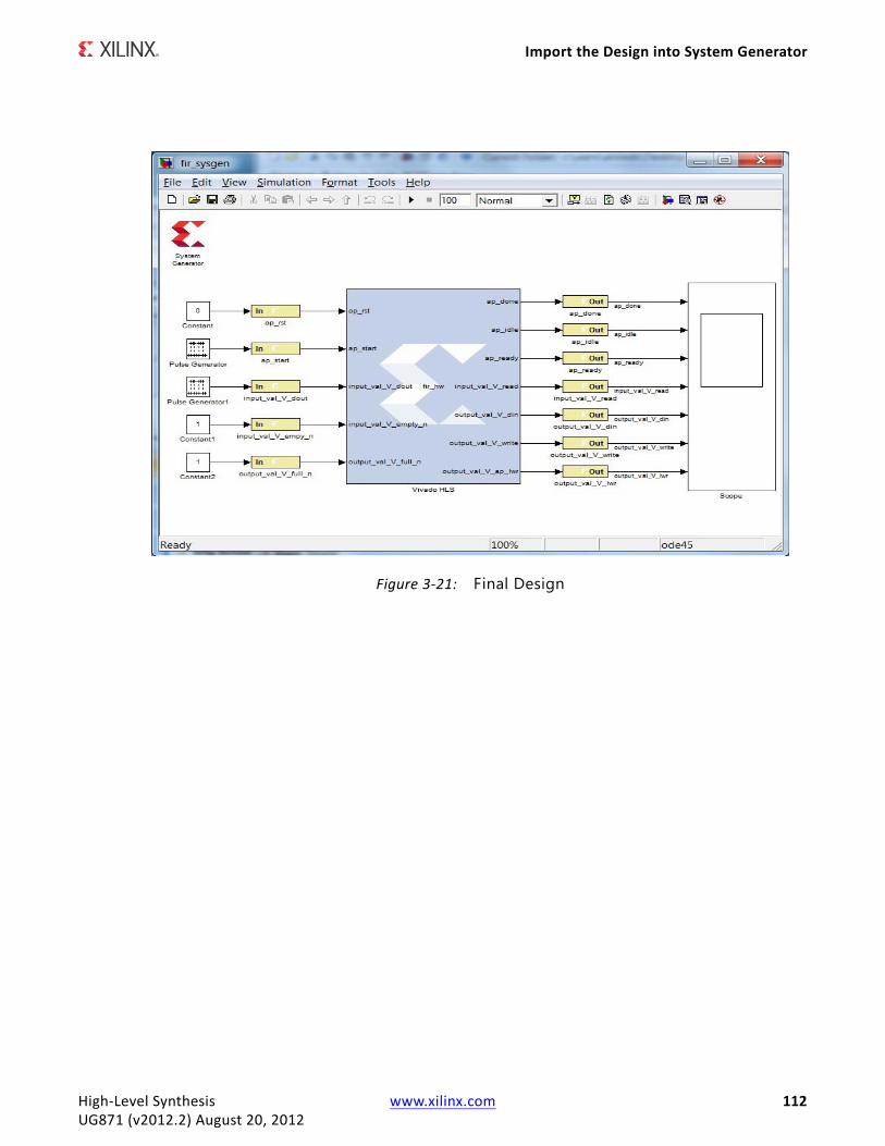
Import the Design into System Generator
X-Ref Target - Figure 3-21
Figure 3-21: Final Design
High-Level Synthesis www.xilinx.com 112UG871 (v2012.2) August 20, 2012
High-Level Synthesis www.xilinx.com 113UG871 (v2012.2) August 20, 2012
Appendix A
Additional Resources
Xilinx ResourcesFor support resources such as Answers, Documentation, Downloads, and Forums, see the Xilinx Support website at:
www.xilinx.com/support.
For a glossary of technical terms used in Xilinx documentation, see:
www.xilinx.com/company/terms.htm.
Solution CentersSee the Xilinx Solution Centers for support on devices, software tools, and intellectual property at all stages of the design cycle. Topics include design assistance, advisories, and troubleshooting tips.
References• Vivado Design Suite 2012.2 Documentation
(http://www.xilinx.com/support/documentation/dt_vivado_vivado2012-2.htm)