Embed Size (px)
Citation preview

Vivado Design Suite
Tutorial
Logic Simulation
UG937 (v2016.1) April 6, 2016

Logic Simulation www.xilinx.com 2 UG937 (v2016.1) April 6, 2016
Revision History
Date Version Revision
04/06/2016 2016.1 Updated the content and screenshots to reflect the current version.
Send Feedback
Logic Simulation www.xilinx.com 3 UG937 (v2016.1) April 6, 2016
Table of Contents
Revision History ........................................................................................................................................................... 2
Vivado Simulator Overview ......................................................................................................................................... 5
Introduction ................................................................................................................................................................... 5
Tutorial Description ..................................................................................................................................................... 6
Locating Tutorial Design Files .................................................................................................................................... 7
Software and Hardware Requirements .................................................................................................................. 8
Lab 1: Running the Simulator in Vivado IDE ......................................................................................................... 9
Introduction ................................................................................................................................................................... 9
Step 1: Creating a New Project ................................................................................................................................. 9
Step 2: Adding IP from the IP Catalog ................................................................................................................... 14
Step 3: Running Behavioral Simulation ................................................................................................................ 19
Conclusion .................................................................................................................................................................... 21
Lab 2: Debugging the Design ................................................................................................................................... 22
Introduction ................................................................................................................................................................. 22
Step 1: Opening the Project ..................................................................................................................................... 22
Step 2: Displaying Signal Waveforms .................................................................................................................... 23
Step 3: Using the Analog Wave Viewer ................................................................................................................ 24
Step 4: Working with the Waveform Window ................................................................................................... 26
Step 5: Changing Signal Properties ........................................................................................................................ 30
Step 6: Saving the Waveform Configuration ....................................................................................................... 31
Step 7: Re-Simulating the Design ........................................................................................................................... 34
Step 8: Using Cursors, Markers, and Measuring Time ...................................................................................... 34
Step 9: Debugging with Breakpoints ..................................................................................................................... 38
Step 10: Relaunch Simulation ................................................................................................................................. 43
Conclusion .................................................................................................................................................................... 45
Lab 3: Running Simulation in Batch Mode .......................................................................................................... 46
Introduction ................................................................................................................................................................. 46
Send Feedback

Revision History
Logic Simulation www.xilinx.com 4 UG937 (v2016.1) April 6, 2016
Step 1: Preparing the Simulation ........................................................................................................................... 46
Step 2: Building the Simulation Snapshot ............................................................................................................ 48
Step 3: Manually Simulating the Design .............................................................................................................. 50
Conclusion .................................................................................................................................................................... 51
Legal Notices .................................................................................................................................................................. 52
Please Read: Important Legal Notices .............................................................................................................. 52
Send Feedback
Logic Simulation www.xilinx.com 5 UG937 (v2016.1) April 6, 2016
Vivado Simulator Overview
IMPORTANT: This tutorial requires the use of the Kintex®-7 family of devices. If you do not
have this device family installed, you must update your Vivado® tools installation. Refer to
the Vivado Design Suite User Guide: Release Notes, Installation, and Licensing (UG973) for
more information on Adding Design Tools or Devices to your installation.
Introduction This Xilinx® Vivado® Design Suite tutorial provides designers with an in-depth introduction to the
Vivado simulator.
VIDEO: You can also learn more about the Vivado simulator by viewing the quick take
video at Vivado Logic Simulation.
TRAINING: Xilinx provides training courses that can help you learn more about the concepts
presented in this document. Use these links to explore related courses:
Vivado Design Suite Tool Flow Training Course
The Vivado simulator is a Hardware Description Language (HDL) simulator that lets you perform
behavioral, functional, and timing simulations for VHDL, Verilog, and mixed-language designs. The
Vivado simulator environment includes the following key elements:
1. xvhdl and xvlog: Parsers for VHDL and Verilog files, respectively, that store the parsed files into
an HDL library on disk.
2. xelab: HDL elaborator and linker command. For a given top-level unit, xelab loads up all sub-
design units, translates the design units into executable code, and links the generated executable
code with the simulation kernel to create an executable simulation snapshot.
3. xsim: Vivado simulation command that loads a simulation snapshot to effect a batch mode
simulation, or a GUI or Tcl-based interactive simulation environment.
4. Vivado Integrated Design Environment (IDE): An interactive design-editing environment that
provides the simulator user-interface.
Send Feedback
Vivado Simulator Overview
Logic Simulation www.xilinx.com 6 UG937 (v2016.1) April 6, 2016
Tutorial Description This tutorial demonstrates a design flow in which you can use the Vivado simulator for performing
behavioral, functional, or timing simulation from the Vivado Integrated Design Environment (IDE).
IMPORTANT: Tutorial files are configured to run the Vivado simulator in a Windows
environment. To run elements of this tutorial under the Linux operating system, some
file modifications may be necessary.
You can run the Vivado simulator in both Project Mode (using a Vivado design project to manage
design sources and the design flow) and in Non-Project mode (managing the design more directly). For
more information about Project Mode and Non-Project Mode, refer to the Vivado Design Suite User
Guide: Design Flows Overview (UG892).
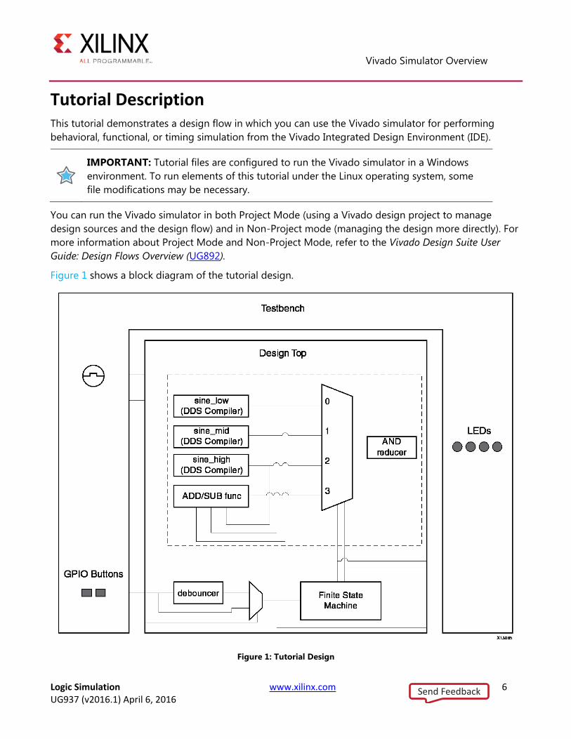
Figure 1 shows a block diagram of the tutorial design.
Figure 1: Tutorial Design
Send Feedback

Vivado Simulator Overview
Logic Simulation www.xilinx.com 7 UG937 (v2016.1) April 6, 2016
The tutorial design consists of the following blocks:
A sine wave generator that generates high, medium, and low frequency sine waves; plus an
amplitude sine wave (sinegen.vhd).
DDS compilers that generate low, middle, and high frequency waves: (sine_low.vhd,
sine_mid.vhd, and sine_high.vhd).
A Finite State Machine (FSM) to select one of the four sine waves (fsm.vhd).
A debouncer that enables switch-selection between the raw and the debounced version of the
sine wave selector (debounce.vhd).
A design top module that resets FSM and the sine wave generator, and then multiplexes the
sine select results to the LED output (sinegen_demo.vhd).
A simple testbench (testbench.v) to initiate the sine wave generator design that:
o Generates a 200 MHz input clock for the design system clock, sys_clk_p.
o Generates GPIO button selections.
o Controls raw and debounced sine wave select.
Note: For more information about testbenches, see Writing Efficient Testbenches (XAPP199).
Locating Tutorial Design Files There are separate project files and sources for each of the labs in this tutorial. You can find these at the
link provided below or under Support > Documentation > Development Tools (Product Type) >
Hardware Development (Product Category) > Vivado Design Suite – HLx Editions (Product) >
Tutorials (Doc Type) on the Xilinx.com website.
1. Download the reference design files.
2. Extract the zip file contents into any write-accessible location.
This tutorial refers to the extracted file contents of ug937-design-files directory as
<Extract_Dir>.
RECOMMENDED: You modify the tutorial design data while working through this tutorial.
Use a new copy of the design files each time you start this tutorial.
Send Feedback
Vivado Simulator Overview
Logic Simulation www.xilinx.com 8 UG937 (v2016.1) April 6, 2016
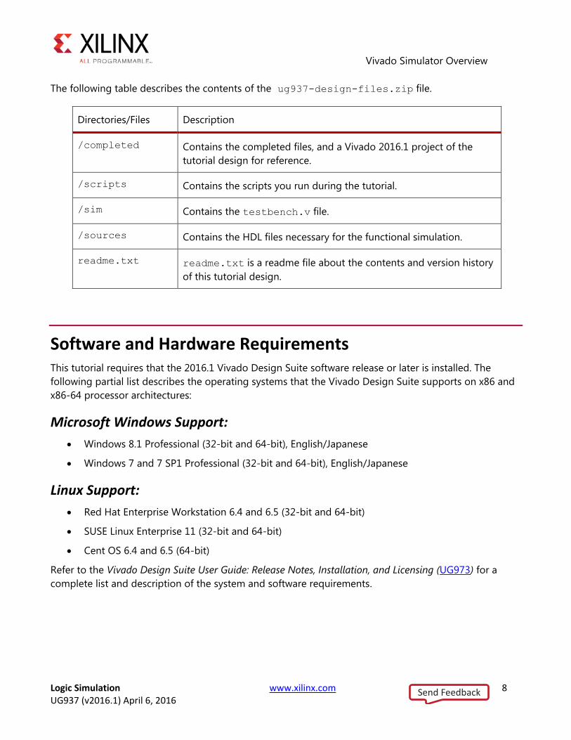
The following table describes the contents of the ug937-design-files.zip file.
Directories/Files Description
/completed Contains the completed files, and a Vivado 2016.1 project of the
tutorial design for reference.
/scripts Contains the scripts you run during the tutorial.
/sim Contains the testbench.v file.
/sources Contains the HDL files necessary for the functional simulation.
readme.txt readme.txt is a readme file about the contents and version history
of this tutorial design.
Software and Hardware Requirements This tutorial requires that the 2016.1 Vivado Design Suite software release or later is installed. The
following partial list describes the operating systems that the Vivado Design Suite supports on x86 and
x86-64 processor architectures:
Microsoft Windows Support:
Windows 8.1 Professional (32-bit and 64-bit), English/Japanese
Windows 7 and 7 SP1 Professional (32-bit and 64-bit), English/Japanese
Linux Support:
Red Hat Enterprise Workstation 6.4 and 6.5 (32-bit and 64-bit)
SUSE Linux Enterprise 11 (32-bit and 64-bit)
Cent OS 6.4 and 6.5 (64-bit)
Refer to the Vivado Design Suite User Guide: Release Notes, Installation, and Licensing (UG973) for a
complete list and description of the system and software requirements.
Send Feedback

Logic Simulation www.xilinx.com 9 UG937 (v2016.1) April 6, 2016
Lab 1: Running the Simulator in Vivado IDE
Introduction In this lab, you create a new Vivado Design Suite project, add HDL design sources, add IP from the
Xilinx IP catalog, and generate IP outputs needed for simulation. Then you run a behavioral simulation
on an elaborated RTL design.
Step 1: Creating a New Project The Vivado Integrated Design Environment (IDE) (Figure 2) lets you launch simulation from within
design projects, automatically generating the necessary simulation commands and files.
Figure 2: Vivado IDE - Getting Started Page
Create a new project for managing source files, add IP to the design, and run behavioral simulation.
Send Feedback
Lab 1: Running the Simulator in Vivado IDE
Logic Simulation www.xilinx.com 10 UG937 (v2016.1) April 6, 2016
1. On Windows, launch the Vivado IDE:
Start > All Programs > Xilinx Design Tools > Vivado 2016.x > Vivado 2016.x
(x denotes the latest version of Vivado 2016 IDE)
Note: Your Vivado Design Suite installation might be called something other than Xilinx Design
Tools on the Start menu.
2. In the Vivado IDE Getting started page, click Create New Project.
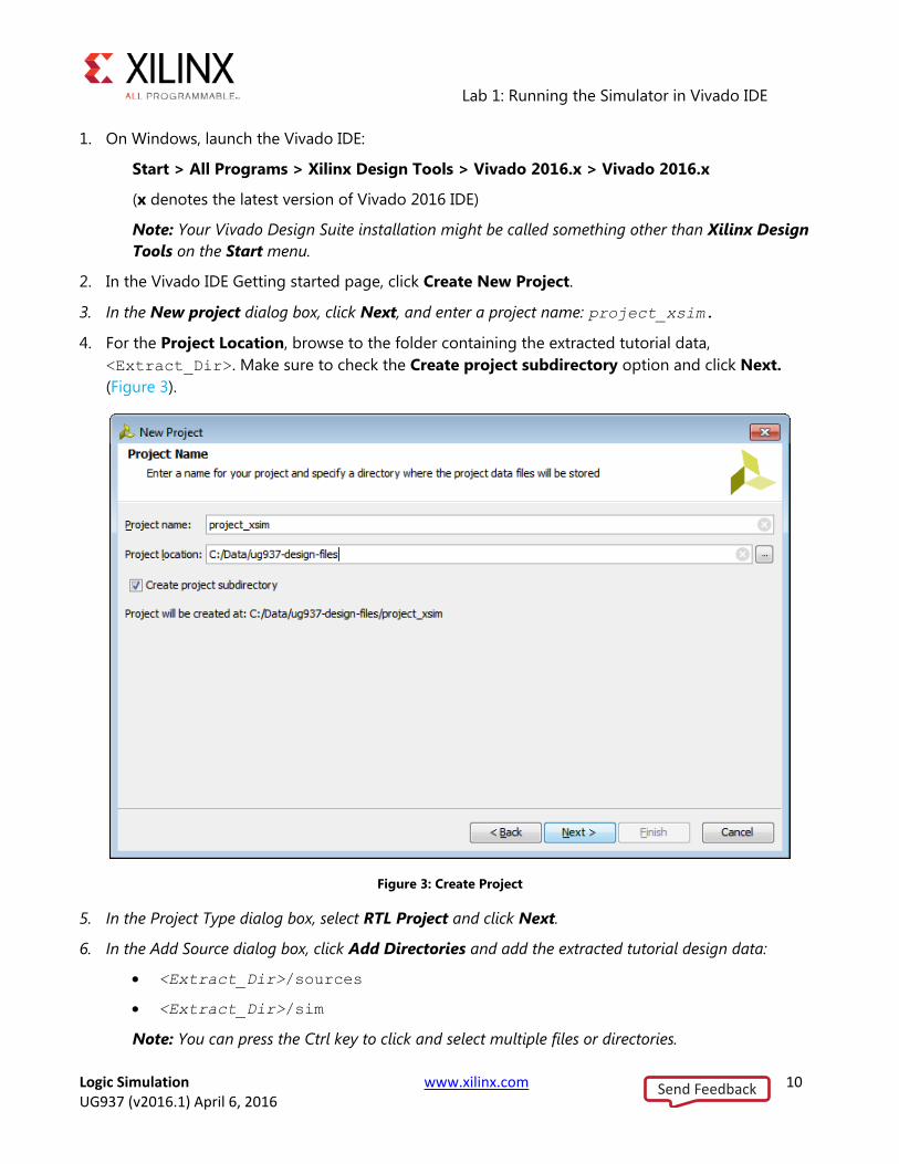
3. In the New project dialog box, click Next, and enter a project name: project_xsim.
4. For the Project Location, browse to the folder containing the extracted tutorial data,
<Extract_Dir>. Make sure to check the Create project subdirectory option and click Next.
(Figure 3).
Figure 3: Create Project
5. In the Project Type dialog box, select RTL Project and click Next.
6. In the Add Source dialog box, click Add Directories and add the extracted tutorial design data:
<Extract_Dir>/sources
<Extract_Dir>/sim
Note: You can press the Ctrl key to click and select multiple files or directories.
Send Feedback
Lab 1: Running the Simulator in Vivado IDE
Logic Simulation www.xilinx.com 11 UG937 (v2016.1) April 6, 2016
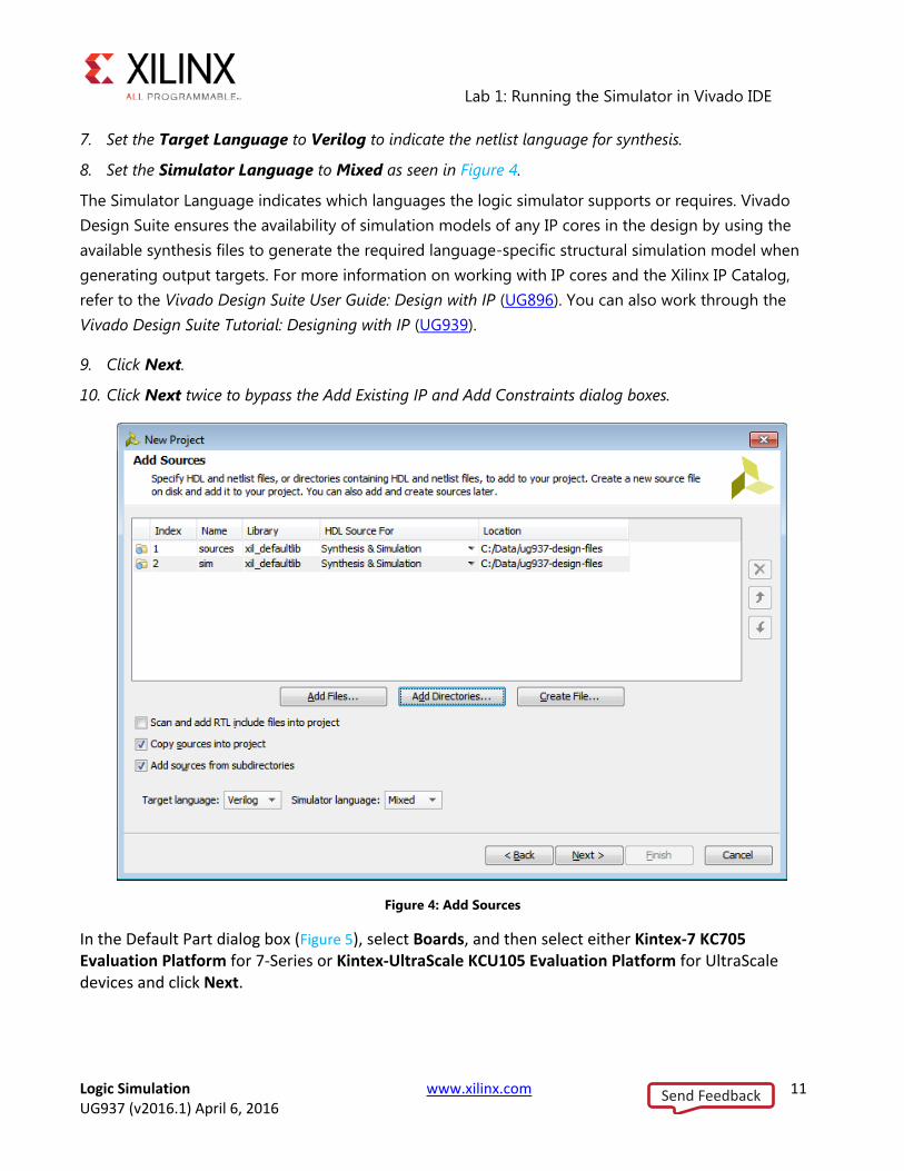
7. Set the Target Language to Verilog to indicate the netlist language for synthesis.
8. Set the Simulator Language to Mixed as seen in Figure 4.
The Simulator Language indicates which languages the logic simulator supports or requires. Vivado
Design Suite ensures the availability of simulation models of any IP cores in the design by using the
available synthesis files to generate the required language-specific structural simulation model when
generating output targets. For more information on working with IP cores and the Xilinx IP Catalog,
refer to the Vivado Design Suite User Guide: Design with IP (UG896). You can also work through the
Vivado Design Suite Tutorial: Designing with IP (UG939).
9. Click Next.
10. Click Next twice to bypass the Add Existing IP and Add Constraints dialog boxes.
Figure 4: Add Sources
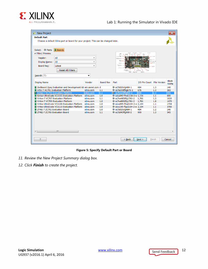
In the Default Part dialog box (Figure 5), select Boards, and then select either Kintex-7 KC705 Evaluation Platform for 7-Series or Kintex-UltraScale KCU105 Evaluation Platform for UltraScale devices and click Next.
Send Feedback
Lab 1: Running the Simulator in Vivado IDE
Logic Simulation www.xilinx.com 12 UG937 (v2016.1) April 6, 2016
Figure 5: Specify Default Part or Board
11. Review the New Project Summary dialog box.
12. Click Finish to create the project.
Send Feedback
Lab 1: Running the Simulator in Vivado IDE
Logic Simulation www.xilinx.com 13 UG937 (v2016.1) April 6, 2016
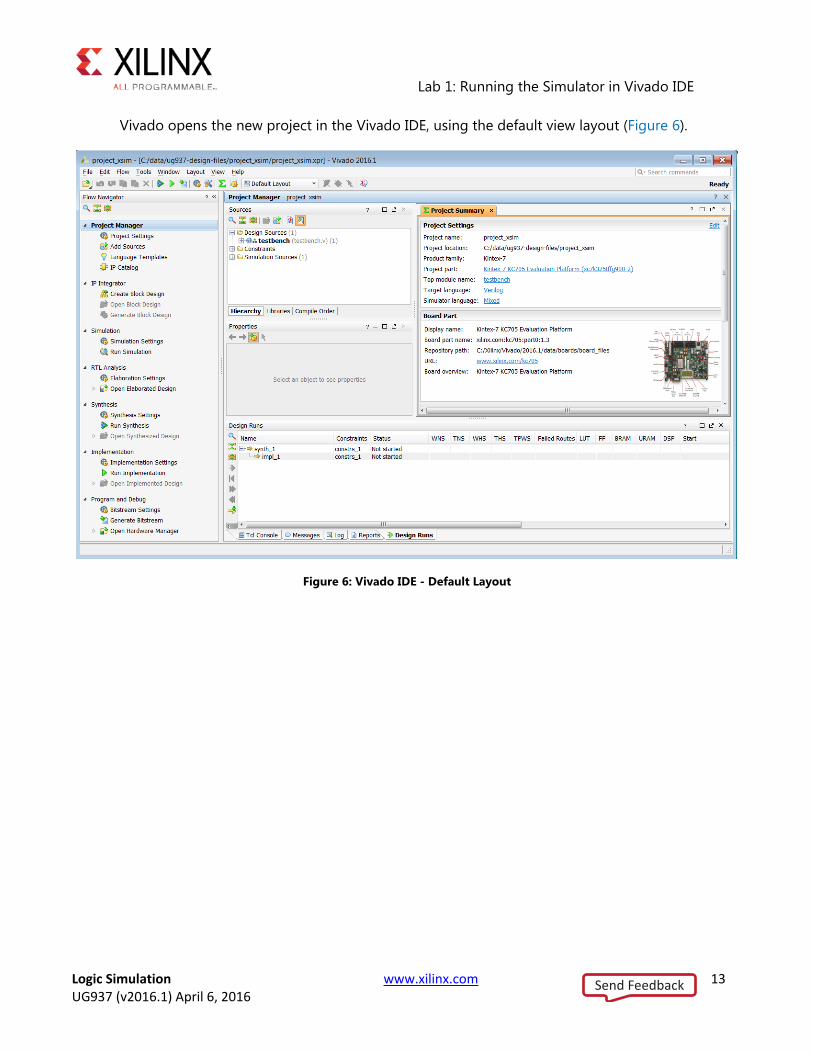
Vivado opens the new project in the Vivado IDE, using the default view layout (Figure 6).
Figure 6: Vivado IDE - Default Layout
Send Feedback

Lab 1: Running the Simulator in Vivado IDE
Logic Simulation www.xilinx.com 14 UG937 (v2016.1) April 6, 2016
Step 2: Adding IP from the IP Catalog The Sources window displays the source files that you have added during project creation. The
Hierarchy tab displays the hierarchical view of the source files.
1. Click the ‘+’ character in the Sources window to expand the folders as shown in Figure 7.
Figure 7: Sources window
2. Notice that the Sine wave generator (sinegen.vhd) references cells that are not found in the
current design sources. In the Sources window, the missing design sources are marked by the
missing source icon .
Next, you add the sine_high, sine_mid, and sine_low modules to the project from the Xilinx IP
Catalog.
Adding Sine High
1. In the Flow Navigator, select the IP Catalog button.
The IP Catalog opens in the graphical windows area. For more information on the specifics of
the Vivado IDE, refer to the Vivado Design Suite User Guide: Using the Vivado IDE (UG893).
2. In the search field of the IP Catalog, type DDS.
The Vivado IDE highlights the DDS Compilers in the IP catalog.
3. Under any category, double-click the DDS Compiler.
Send Feedback
Lab 1: Running the Simulator in Vivado IDE
Logic Simulation www.xilinx.com 15 UG937 (v2016.1) April 6, 2016
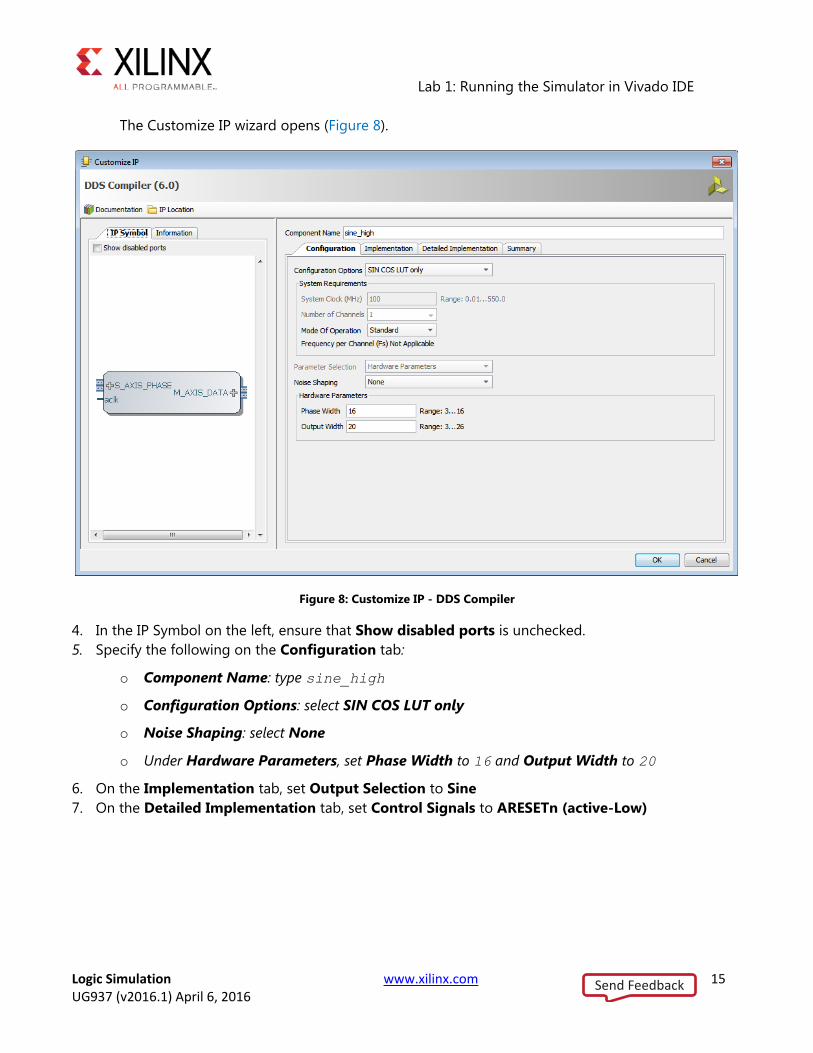
The Customize IP wizard opens (Figure 8).
Figure 8: Customize IP - DDS Compiler
4. In the IP Symbol on the left, ensure that Show disabled ports is unchecked.
5. Specify the following on the Configuration tab:
o Component Name: type sine_high
o Configuration Options: select SIN COS LUT only
o Noise Shaping: select None
o Under Hardware Parameters, set Phase Width to 16 and Output Width to 20
6. On the Implementation tab, set Output Selection to Sine
7. On the Detailed Implementation tab, set Control Signals to ARESETn (active-Low)
Send Feedback
Lab 1: Running the Simulator in Vivado IDE
Logic Simulation www.xilinx.com 16 UG937 (v2016.1) April 6, 2016
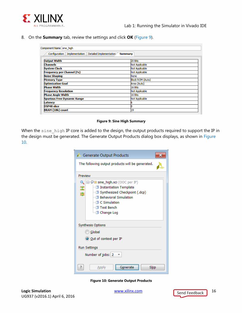
8. On the Summary tab, review the settings and click OK (Figure 9).
Figure 9: Sine High Summary
When the sine_high IP core is added to the design, the output products required to support the IP in
the design must be generated. The Generate Output Products dialog box displays, as shown in Figure
10.
Figure 10: Generate Output Products
Send Feedback
Lab 1: Running the Simulator in Vivado IDE
Logic Simulation www.xilinx.com 17 UG937 (v2016.1) April 6, 2016
The output products allow the IP to be synthesized, simulated, and implemented as part of the design.
For more information on working with IP cores and the Xilinx IP Catalog, refer to the Vivado Design
Suite User Guide: Design with IP (UG896). You can also work through the Vivado Design Suite Tutorial:
Designing with IP (UG939).
9. Click Generate to generate the default output products for sine_high.
Adding Sine Mid
1. In the IP catalog, double-click the DDS Compiler IP a second time.
2. Specify the following on the Configuration tab:
o Component Name: type sine_mid
o Configuration Options: select SIN COS LUT only
o Noise Shaping: select None
o Under Hardware Parameters, set the Phase Width to 8, and the Output Width to 18
3. On the Implementation tab, set the Output Selection to Sine
4. On the Detailed Implementation tab, set Control Signals to ARESETn (active-Low)
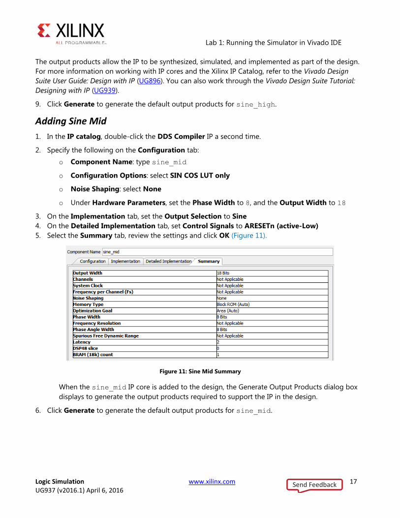
5. Select the Summary tab, review the settings and click OK (Figure 11).
Figure 11: Sine Mid Summary
When the sine_mid IP core is added to the design, the Generate Output Products dialog box
displays to generate the output products required to support the IP in the design.
6. Click Generate to generate the default output products for sine_mid.
Send Feedback
Lab 1: Running the Simulator in Vivado IDE
Logic Simulation www.xilinx.com 18 UG937 (v2016.1) April 6, 2016
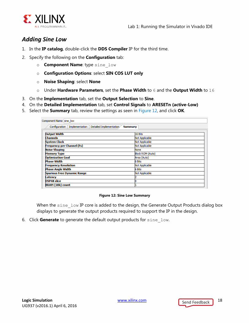
Adding Sine Low
1. In the IP catalog, double-click the DDS Compiler IP for the third time.
2. Specify the following on the Configuration tab:
o Component Name: type sine_low
o Configuration Options: select SIN COS LUT only
o Noise Shaping: select None
o Under Hardware Parameters, set the Phase Width to 6 and the Output Width to 16
3. On the Implementation tab, set the Output Selection to Sine.
4. On the Detailed Implementation tab, set Control Signals to ARESETn (active-Low)
5. Select the Summary tab, review the settings as seen in Figure 12, and click OK.
Figure 12: Sine Low Summary
When the sine_low IP core is added to the design, the Generate Output Products dialog box
displays to generate the output products required to support the IP in the design.
6. Click Generate to generate the default output products for sine_low.
Send Feedback

Lab 1: Running the Simulator in Vivado IDE
Logic Simulation www.xilinx.com 19 UG937 (v2016.1) April 6, 2016
Step 3: Running Behavioral Simulation After you have created a Vivado project for the tutorial design, you set up and launch Vivado simulator
to run behavioral simulation. Set the behavioral simulation properties in Vivado tools:
1. In the Flow Navigator, click Simulation Settings. The following defaults are automatically set:
o Simulation set: select sim_1
o Simulation top-module name: set testbench
2. In the Elaboration tab (Figure 13), ensure that the debug level is set to typical, which is the default
value.
Figure 13: Simulation Settings: Compilation
3. In the Simulation tab, observe that the Simulation Run Time is 1000ns.
4. Click OK.
Send Feedback
Lab 1: Running the Simulator in Vivado IDE
Logic Simulation www.xilinx.com 20 UG937 (v2016.1) April 6, 2016
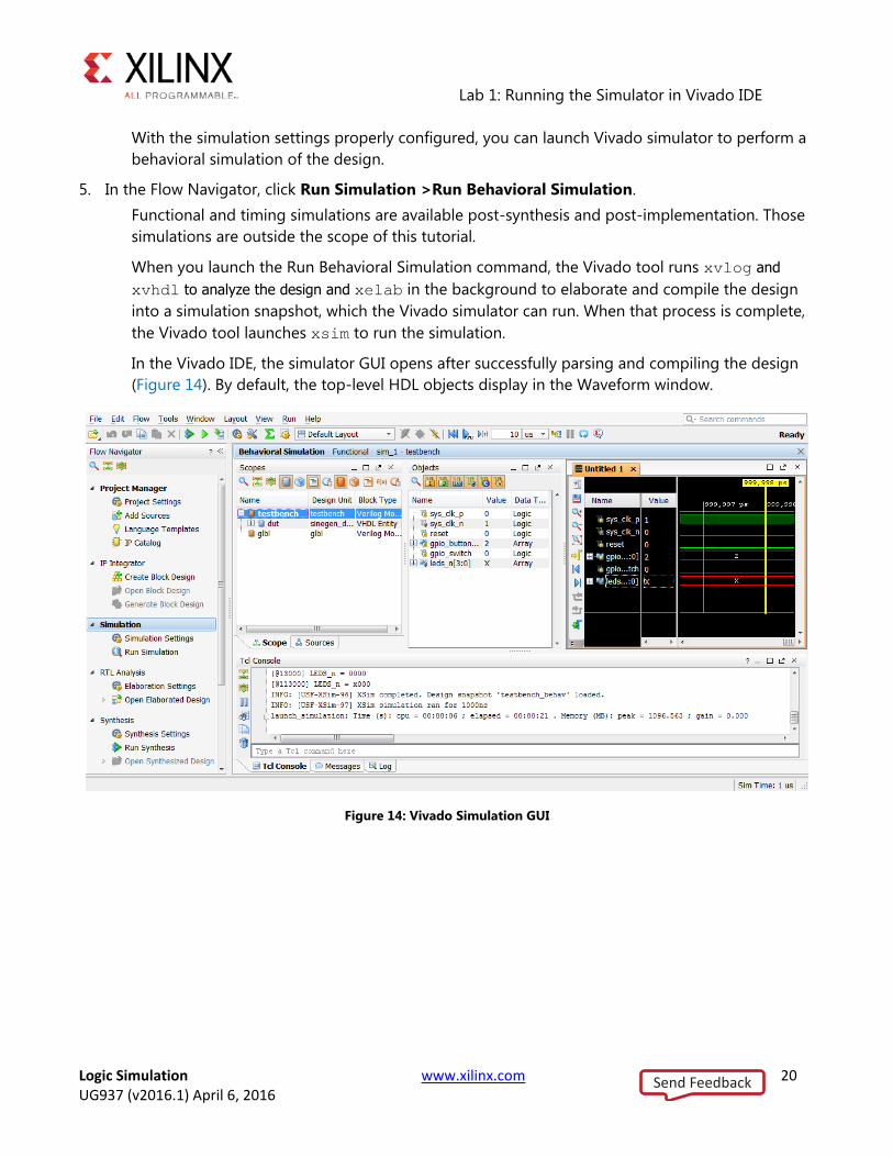
With the simulation settings properly configured, you can launch Vivado simulator to perform a
behavioral simulation of the design.
5. In the Flow Navigator, click Run Simulation >Run Behavioral Simulation.
Functional and timing simulations are available post-synthesis and post-implementation. Those
simulations are outside the scope of this tutorial.
When you launch the Run Behavioral Simulation command, the Vivado tool runs xvlog and
xvhdl to analyze the design and xelab in the background to elaborate and compile the design
into a simulation snapshot, which the Vivado simulator can run. When that process is complete,
the Vivado tool launches xsim to run the simulation.
In the Vivado IDE, the simulator GUI opens after successfully parsing and compiling the design
(Figure 14). By default, the top-level HDL objects display in the Waveform window.
Figure 14: Vivado Simulation GUI
Send Feedback
Lab 1: Running the Simulator in Vivado IDE
Logic Simulation www.xilinx.com 21 UG937 (v2016.1) April 6, 2016
Conclusion In this lab, you have created a new Vivado Design Suite project, added HDL design sources, added IP
from the Xilinx IP catalog and generated IP outputs needed for simulation, and then run behavioral
simulation on the elaborated RTL design.
This concludes Lab #1. You can continue Lab #2 at this time by starting at Step 2: Displaying Signal
Waveforms.
You can also close the simulation, project, and the Vivado IDE to start Lab #2 at a later time.
1. Click File > Close Simulation to close the open simulation.
2. Select OK if prompted to confirm closing the simulation.
3. Click File > Close Project to close the open project.
4. Click File > Exit to exit the Vivado tool.
Send Feedback
Logic Simulation www.xilinx.com 22 UG937 (v2016.1) April 6, 2016
Lab 2: Debugging the Design
Introduction The Vivado simulator GUI contains the Waveform window, and Object and Scope Windows. It
provides a set of debugging capabilities to quickly examine, debug, and fix design problems. See the
Vivado Design Suite User Guide: Logic Simulation (UG900) for more information about the GUI
components.
In this lab, you:
Enable debug capabilities
Examine a design bug
Use debug features to find the root cause of the bug
Make changes to the code
Re-compile and re-launch the simulation
Step 1: Opening the Project This lab continues from the end of Lab #1 in this tutorial. You must complete Lab #1 prior to
beginning Lab #2. If you closed the Vivado IDE, or the tutorial project, or the simulation at the end of
Lab #1, you must reopen them.
Start by loading the Vivado Integrated Design Environment (IDE).
Start > All Programs > Xilinx Design Tools > Vivado 2016.x > Vivado 2016.x
Note: Your Vivado Design Suite installation might be called something other than Xilinx Design
Tools on the Start menu.
Note: As an alternative, click the Vivado 2016.x Desktop icon to start the Vivado IDE.
The Vivado IDE opens. Now, open the project from Lab #1, and run behavioral simulation.
1. From the main menu, click File > Open Recent Project and select project_xsim, which you
saved in Lab #1.
2. After the project has opened, from the Flow Navigator click Run Simulation > Run Behavioral
Simulation.
The Vivado simulator compiles your design and loads the simulation snapshot.
Send Feedback
Lab 2: Debugging the Design
Logic Simulation www.xilinx.com 23 UG937 (v2016.1) April 6, 2016
Step 2: Displaying Signal Waveforms In this section, you examine features of the Vivado simulator GUI that help you monitor signals and
analyze simulation results, including:
Running and restarting the simulation to review the design functionality, using signals in the
Waveform window and messages from the testbench shown in the Tcl console.
Adding signals from the testbench and other design units to the Waveform window so you
can monitor their status.
Adding groups and dividers to better identify signals in the Waveform window.
Changing signal and wave properties to better interpret and review the signals in the
Waveform window.
Using markers and cursors to highlight key events in the simulation and to perform zoom and
time measurement features.
Using multiple waveform configurations.
Add and Monitor Signals
The focus of the tutorial design is to generate sine waves with different frequencies. To observe the
function of the circuit, you monitor a few signals from the design. Before running simulation for a
specified time, you can add signals to the wave window to observe the signals as they transition to
different states over the course of the simulation.
By default, the Vivado simulator adds simulation objects from the testbench to the Waveform
window. In the case of this tutorial, the following testbench signals load automatically:
Differential clock signals (sys_clk_p and sys_clk_n). This is a 200 MHz clock generated
by the testbench and is the input clock for the complete design.
Reset signal (reset). Provides control to reset the circuit.
GPIO buttons (gpio_buttons[1:0]). Provides control signals to select different frequency
sine waves.
GPIO switch (gpio_switch). Provides a control switch to enable or disable debouncer logic.
LEDs (leds_n[3:0]). A placeholder bus to display the results of the simulation.
You add some new signals to this list to monitor those signals as well.
1. If necessary, in the Scopes window, click the ‘+’ sign to expand the testbench. (It might be
exapanded by default.)
An HDL scope, or scope, is defined by a declarative region in the HDL code, such as a module,
function, task, process, or named blocks in Verilog. VHDL scopes include entity/architecture
definitions, blocks, functions, procedures, and processes.
Send Feedback
Lab 2: Debugging the Design
Logic Simulation www.xilinx.com 24 UG937 (v2016.1) April 6, 2016
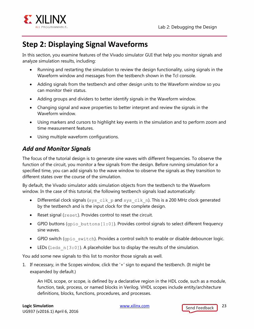
2. In the Scopes window, click to select the dut object.
The current scope of the simulation changes from the whole testbench to the selected object.
The Objects window updates with all the signals and constants of the selected scope, as
shown in Figure 15.
3. From the Objects window, select signals sine[19:0] and sineSel[1:0] and add them into
Wave Configuration window using one of the following methods:
o Drag and drop the selected signals into the Waveform window.
o Right-click on the signal to open the popup menu, and select Add to Wave Window.
Note: You can select multiple signals by holding down the CTRL key during selection.
Figure 15: Add signals to Wave Window
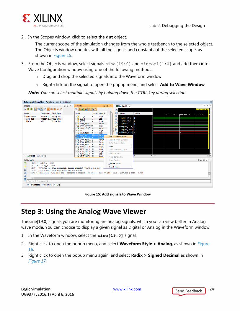
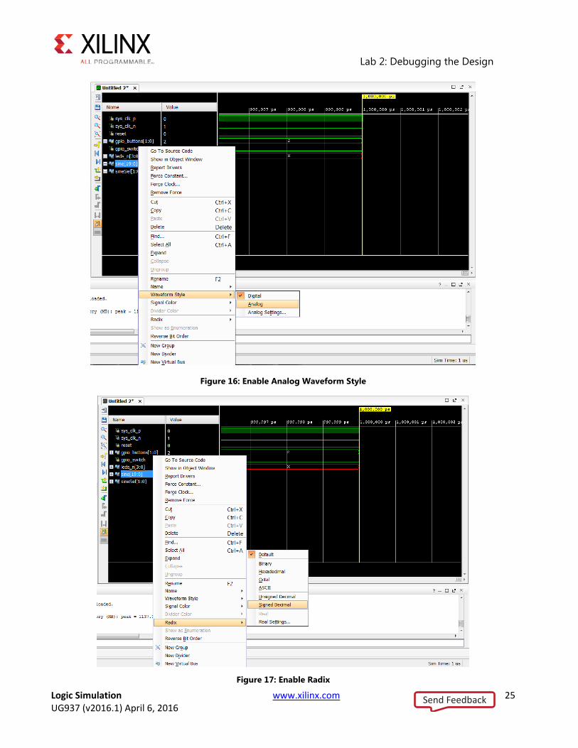
Step 3: Using the Analog Wave Viewer The sine[19:0] signals you are monitoring are analog signals, which you can view better in Analog
wave mode. You can choose to display a given signal as Digital or Analog in the Waveform window.
1. In the Waveform window, select the sine[19:0] signal.
2. Right click to open the popup menu, and select Waveform Style > Analog, as shown in Figure
16.
3. Right click to open the popup menu again, and select Radix > Signed Decimal as shown in
Figure 17.
Send Feedback
Lab 2: Debugging the Design
Logic Simulation www.xilinx.com 25 UG937 (v2016.1) April 6, 2016
Figure 16: Enable Analog Waveform Style
Figure 17: Enable Radix
Send Feedback
Lab 2: Debugging the Design
Logic Simulation www.xilinx.com 26 UG937 (v2016.1) April 6, 2016
Logging Waveforms for Debugging
The Waveform window lets you review the state of multiple signals as the simulation runs. However,
due to its limited size, the number of signals you can effectively monitor in the Waveform window is
limited. To identify design failures during debugging, you might need to trace more signals and
objects than can be practically displayed in the Waveform window. You can log the waveforms for
signals that are not displayed in the Waveform window, by writing them to the simulation waveform
database (WDB). After simulation, you can review the transitions on all signals captured in the
waveform database file.
Enable logging of the waveform for the specified HDL objects by entering the following command in
the Tcl console:
log_wave [get_objects /testbench/dut/*] [get_objects
/testbench/dut/U_SINEGEN/*]
Note: There is no GUI equivalent for this Tcl command. Refer to the Vivado Design Suite Tcl
Command Reference Guide (UG835) for more information on the log_wave command.
This command enables signal dumping for the specified HDL objects, /testbench/dut/* and
/testbench/dut/U_SINEGEN/*.
Note: * Symbol specifies all the HDL objects in a scope.
The log_wave command writes the specified signals to a waveform database, which is written to the
simulation folder of the current project:
<project_name>/<project_name>.sim/sim_1/behav
Step 4: Working with the Waveform Window Now that you have configured the simulator to display and log signals of interest into the waveform
database, you are ready to run the simulator again.
1. Run the simulation by clicking the Run All button .
Observe the sine signal output in the waveform. The Wave window can be undocked from
Main window layout to view it as standalone.
2. Click the Float button in the top right corner of the Waveform Configuration window.
3. Display the whole time spectrum in the Waveform window by clicking the Zoom Fit button
Notice that the low frequency sine output is incorrect. You can view the waveform in detail by
zooming into the Waveform window . When you zoom into the waveform, you can use the
horizontal and vertical scroll bars to pan down the full waveform.
Send Feedback
Lab 2: Debugging the Design
Logic Simulation www.xilinx.com 27 UG937 (v2016.1) April 6, 2016
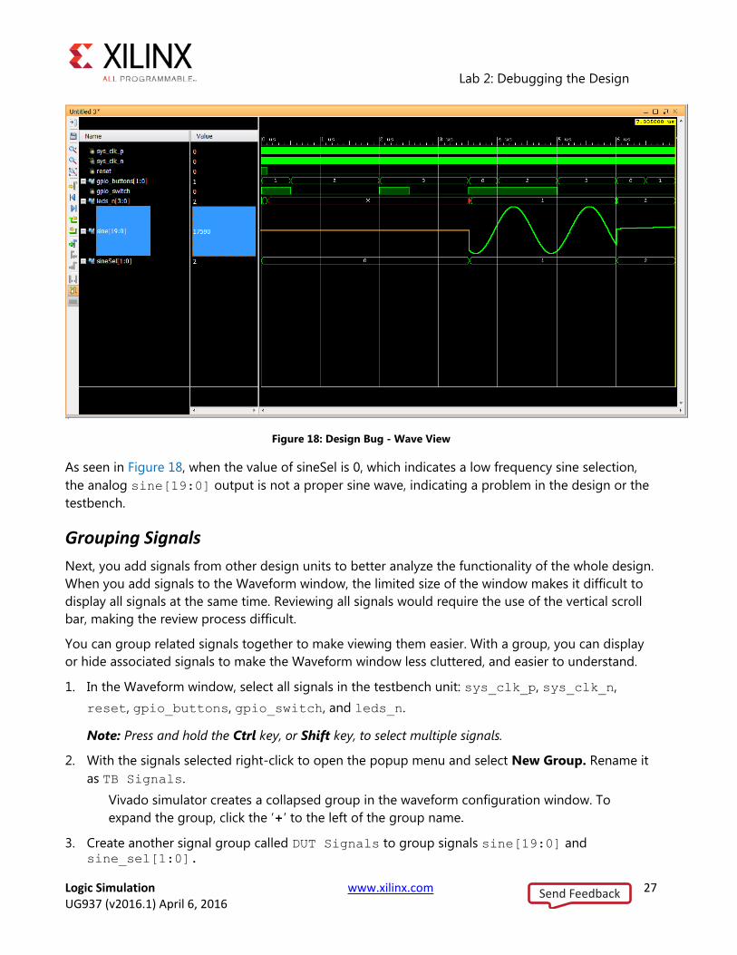
Figure 18: Design Bug - Wave View
As seen in Figure 18, when the value of sineSel is 0, which indicates a low frequency sine selection,
the analog sine[19:0] output is not a proper sine wave, indicating a problem in the design or the
testbench.
Grouping Signals
Next, you add signals from other design units to better analyze the functionality of the whole design.
When you add signals to the Waveform window, the limited size of the window makes it difficult to
display all signals at the same time. Reviewing all signals would require the use of the vertical scroll
bar, making the review process difficult.
You can group related signals together to make viewing them easier. With a group, you can display
or hide associated signals to make the Waveform window less cluttered, and easier to understand.
1. In the Waveform window, select all signals in the testbench unit: sys_clk_p, sys_clk_n,
reset, gpio_buttons, gpio_switch, and leds_n.
Note: Press and hold the Ctrl key, or Shift key, to select multiple signals.
2. With the signals selected right-click to open the popup menu and select New Group. Rename it
as TB Signals.
Vivado simulator creates a collapsed group in the waveform configuration window. To
expand the group, click the ‘+’ to the left of the group name
3. Create another signal group called DUT Signals to group signals sine[19:0] and sine_sel[1:0].
Send Feedback
Lab 2: Debugging the Design
Logic Simulation www.xilinx.com 28 UG937 (v2016.1) April 6, 2016
You can add or remove signals from a group as needed. Cut and paste signals from the list of
signals in the Waveform window, or drag and drop a signal from one group into another.
You can also drag and drop a signal from the Objects window into the Waveform window, or
into a group.
You can ungroup all signals, thereby eliminating the group. Select a group, right-click to open
the popup menu and select Ungroup.
To better visualize which signals belong to which design units, add dividers to separate the
signals by design unit.
Adding Dividers
Dividers let you create visual breaks between signals or groups of signals to more easily identify
related objects.
1. In the Waveform window, right-click to open the popup menu and select New Divider. The
Name dialog box opens to let you name the divider you are adding to the Waveform window.
2. Add two dividers named:
o Testbench
o SineGen
3. Move the SineGen divider above the DUT Signals group.
TIP: You can change divider names at any time by highlighting the divider name and
selecting the Rename command from the popup menu, or change the color with
Divider Color.
Adding Signals from Sub-modules
You can also add signals from different levels of the design hierarchy to study the interactions
between these modules and the testbench. The easiest way to add signals from a sub-module is to
filter objects and then select the signals to add to the Waveform view.
Add signals from the instantiated sine_gen_demo module (DUT) and the sinegen module
(U_SINEGEN).
1. In the Scopes window, select and expand the Testbench, then select and expand DUT.
Simulation objects associated with the currently selected scope display in the Objects
window.
By default, all types of simulation objects display in the Objects window. However, you can
limit the types of objects displayed by selecting the object filters at the top of the Objects
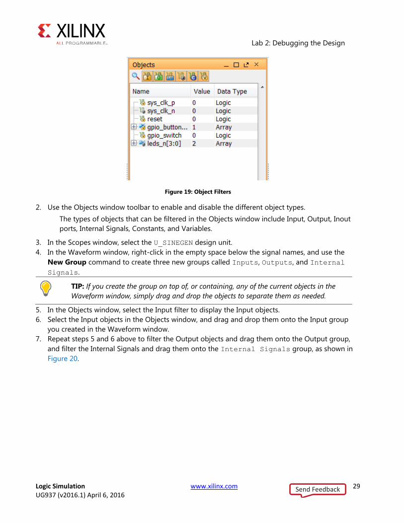
window. Figure 19 shows the Objects window with the Input and Output port objects
enabled, and the other object types are disabled. Move the cursor to hover over a button to
see the tooltip for the object type.
Send Feedback
Lab 2: Debugging the Design
Logic Simulation www.xilinx.com 29 UG937 (v2016.1) April 6, 2016
Figure 19: Object Filters
2. Use the Objects window toolbar to enable and disable the different object types.
The types of objects that can be filtered in the Objects window include Input, Output, Inout
ports, Internal Signals, Constants, and Variables.
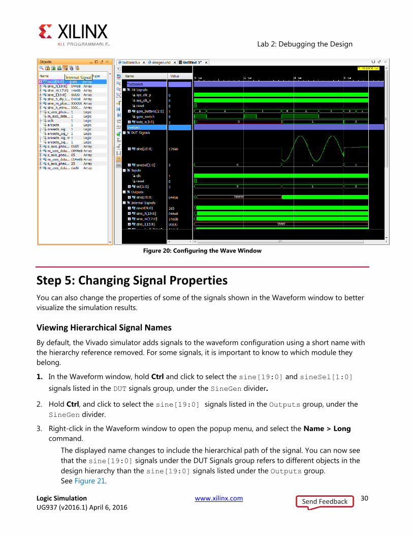
3. In the Scopes window, select the U_SINEGEN design unit.
4. In the Waveform window, right-click in the empty space below the signal names, and use the
New Group command to create three new groups called Inputs, Outputs, and Internal
Signals.
TIP: If you create the group on top of, or containing, any of the current objects in the
Waveform window, simply drag and drop the objects to separate them as needed.
5. In the Objects window, select the Input filter to display the Input objects.
6. Select the Input objects in the Objects window, and drag and drop them onto the Input group
you created in the Waveform window.
7. Repeat steps 5 and 6 above to filter the Output objects and drag them onto the Output group,
and filter the Internal Signals and drag them onto the Internal Signals group, as shown in
Figure 20.
Send Feedback
Lab 2: Debugging the Design
Logic Simulation www.xilinx.com 30 UG937 (v2016.1) April 6, 2016
Figure 20: Configuring the Wave Window
Step 5: Changing Signal Properties You can also change the properties of some of the signals shown in the Waveform window to better
visualize the simulation results.
Viewing Hierarchical Signal Names
By default, the Vivado simulator adds signals to the waveform configuration using a short name with
the hierarchy reference removed. For some signals, it is important to know to which module they
belong.
1. In the Waveform window, hold Ctrl and click to select the sine[19:0] and sineSel[1:0]
signals listed in the DUT signals group, under the SineGen divider.
2. Hold Ctrl, and click to select the sine[19:0] signals listed in the Outputs group, under the
SineGen divider.
3. Right-click in the Waveform window to open the popup menu, and select the Name > Long
command.
The displayed name changes to include the hierarchical path of the signal. You can now see
that the sine[19:0] signals under the DUT Signals group refers to different objects in the
design hierarchy than the sine[19:0] signals listed under the Outputs group.
See Figure 21.
Send Feedback

Lab 2: Debugging the Design
Logic Simulation www.xilinx.com 31 UG937 (v2016.1) April 6, 2016
Figure 21: Long Signal Names
Viewing Signal Values
You can better understand some signal values if they display in a different radix format than the
default, for instance, binary values instead of hexadecimal values. The default radix is Hexadecimal
unless you override the radix for a specific object.
Supported radix values are Binary, Hexadecimal, Octal, ASCII, Signed and Unsigned decimal. You can
set any of the above values as Default using Default Radix option.
1. In the Waveform window, select the following signals:
s_axis_phase_tdata_sine_high, s_axis_phase_tdata_sine_mid and s_axis_phase_tdata_sine_low.
2. Right-click to open the popup menu, and select Radix > Binary.
The values on these signals now display using the specified radix.
Step 6: Saving the Waveform Configuration You can customize the look and feel of the Waveform window, and then save the Waveform
configuration to reuse in future simulation runs. The Waveform configuration file defines the
displayed signals, and the display characteristics of those signals.
1. In the Waveform window, click the Options button on the sidebar menu.
Send Feedback
Lab 2: Debugging the Design
Logic Simulation www.xilinx.com 32 UG937 (v2016.1) April 6, 2016
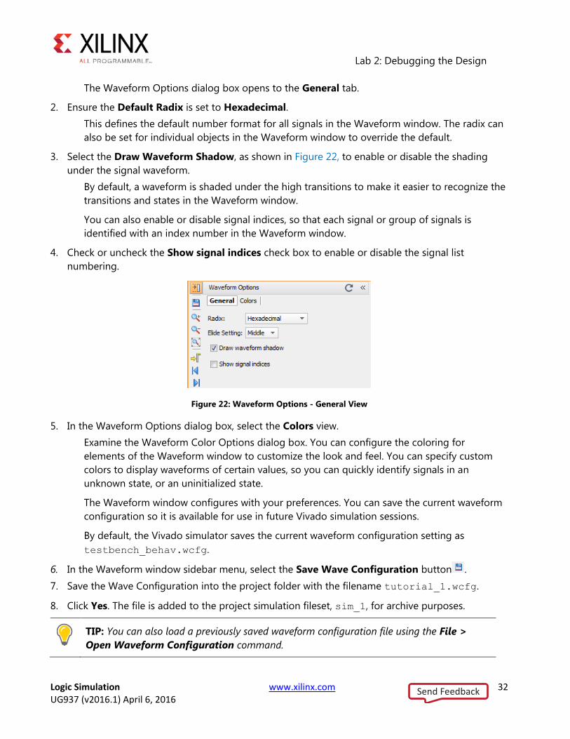
The Waveform Options dialog box opens to the General tab.
2. Ensure the Default Radix is set to Hexadecimal.
This defines the default number format for all signals in the Waveform window. The radix can
also be set for individual objects in the Waveform window to override the default.
3. Select the Draw Waveform Shadow, as shown in Figure 22, to enable or disable the shading
under the signal waveform.
By default, a waveform is shaded under the high transitions to make it easier to recognize the
transitions and states in the Waveform window.
You can also enable or disable signal indices, so that each signal or group of signals is
identified with an index number in the Waveform window.
4. Check or uncheck the Show signal indices check box to enable or disable the signal list
numbering.
Figure 22: Waveform Options - General View
5. In the Waveform Options dialog box, select the Colors view.
Examine the Waveform Color Options dialog box. You can configure the coloring for
elements of the Waveform window to customize the look and feel. You can specify custom
colors to display waveforms of certain values, so you can quickly identify signals in an
unknown state, or an uninitialized state.
The Waveform window configures with your preferences. You can save the current waveform
configuration so it is available for use in future Vivado simulation sessions.
By default, the Vivado simulator saves the current waveform configuration setting as
testbench_behav.wcfg.
6. In the Waveform window sidebar menu, select the Save Wave Configuration button .
7. Save the Wave Configuration into the project folder with the filename tutorial_1.wcfg.
8. Click Yes. The file is added to the project simulation fileset, sim_1, for archive purposes.
TIP: You can also load a previously saved waveform configuration file using the File >
Open Waveform Configuration command.
Send Feedback
Lab 2: Debugging the Design
Logic Simulation www.xilinx.com 33 UG937 (v2016.1) April 6, 2016
Working with Multiple Waveform Configurations
You can also have multiple Waveform windows, and waveform configuration files open at one time.
This is useful when the number of signals you want to display exceeds the ability to display them in a
single window. Depending on the resolution of the screen, a single Waveform window might not
display all the signals of interest at the same time. You can open multiple Waveform windows, each
with their own set of signals and signal properties, and copy and paste between them.
1. To add a new Waveform window, select File>New Waveform Configuration.
An untitled Waveform window opens with a default name. You can add signals, define
groups, add dividers, set properties and colors that are unique to this Waveform window.
2. Select signal groups in the first Waveform window by pressing and holding the Ctrl key, and
selecting the following groups: Inputs, Outputs, and Internal Signals.
3. Right-click to open the popup menu, and select Copy, or use the shortcut Ctrl+C on the selected
groups to copy them from the current Waveform window.
4. Select the new Waveform window to make it active.
5. Right-click in the Waveform window and select Paste, or use the shortcut Ctrl+V to paste the
signal groups into the prior Waveform window.
6. Select File >Save Waveform Configuration or click the Save Wave Configuration button, and
save the waveform configuration to a file called tutorial_2.wcfg.
7. When prompted to add the waveform configuration to the project, select No.
8. Close the new Waveform window by clicking the ‘X’ icon.
Send Feedback
Lab 2: Debugging the Design
Logic Simulation www.xilinx.com 34 UG937 (v2016.1) April 6, 2016
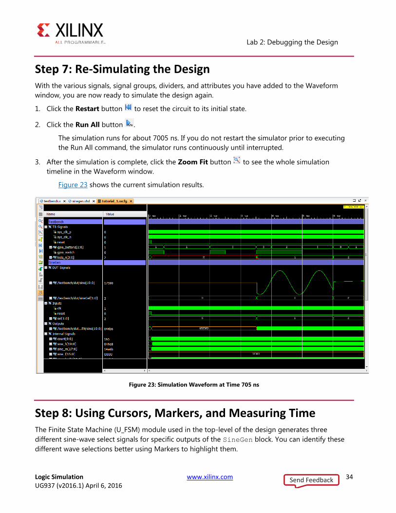
Step 7: Re-Simulating the Design With the various signals, signal groups, dividers, and attributes you have added to the Waveform
window, you are now ready to simulate the design again.
1. Click the Restart button to reset the circuit to its initial state.
2. Click the Run All button .
The simulation runs for about 7005 ns. If you do not restart the simulator prior to executing
the Run All command, the simulator runs continuously until interrupted.
3. After the simulation is complete, click the Zoom Fit button to see the whole simulation
timeline in the Waveform window.
Figure 23 shows the current simulation results.
Figure 23: Simulation Waveform at Time 705 ns
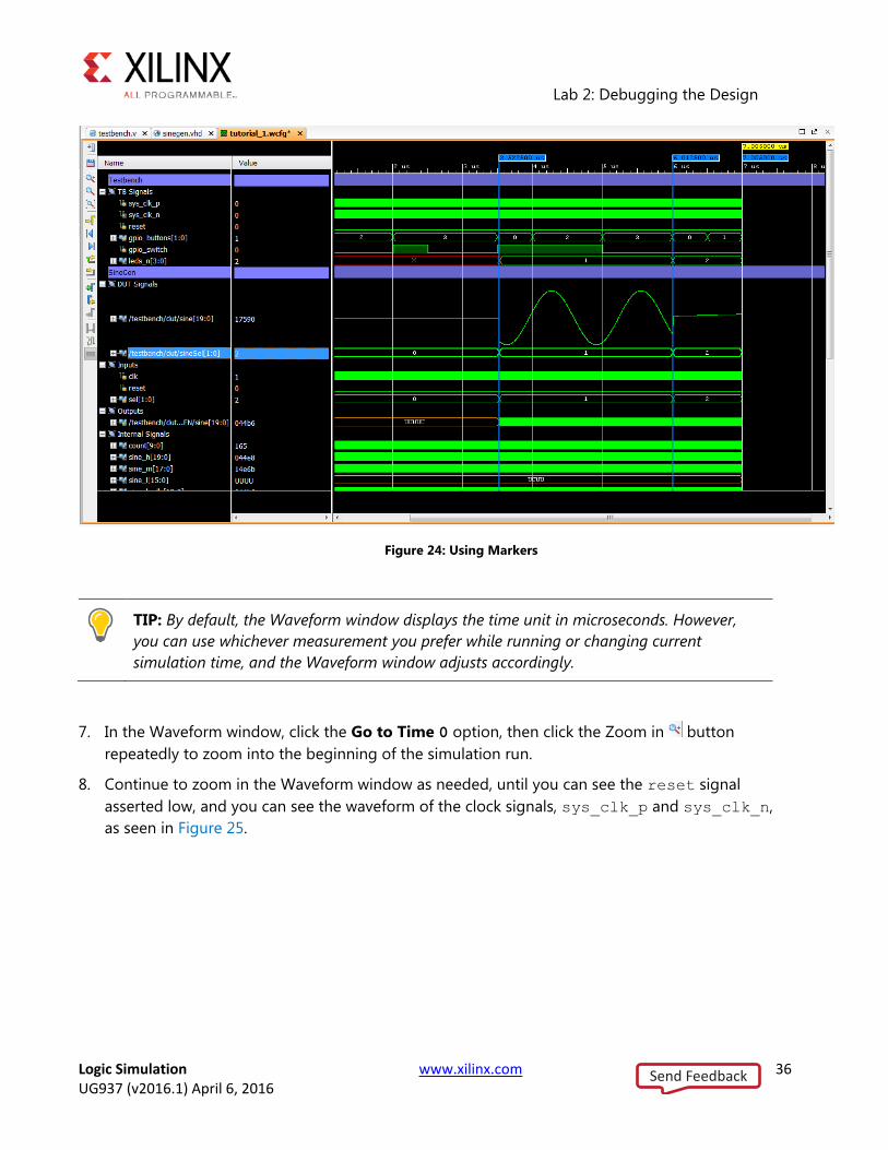
Step 8: Using Cursors, Markers, and Measuring Time The Finite State Machine (U_FSM) module used in the top-level of the design generates three
different sine-wave select signals for specific outputs of the SineGen block. You can identify these
different wave selections better using Markers to highlight them.
Send Feedback

Lab 2: Debugging the Design
Logic Simulation www.xilinx.com 35 UG937 (v2016.1) April 6, 2016
1. In the Waveform window select the /testbench/dut/sineSel[1:0] signal, as shown in
Figure 24.
2. In the waveform sidebar menu, click the Go to Time 0 button .
The current marker moves to the start of the simulation run.
3. Enable the Snap to Transition button to snap the cursor to transition edges.
4. From the waveform sidebar menu, click the Next Transition button .
The current marker moves to the first value change of the selected sineSel[1:0] signal, at
3.5225 microseconds.
5. Click the Add Marker button .
6. Search for all transitions on the sineSel signal, and add markers at each one.
With markers identifying the transitions on sineSel, the Waveform window should look
similar to Figure 24. As previously observed, the low frequency signals are incorrect when the
sinSel signal value is 0.
You can also use the main Waveform window cursor to navigate to different simulation times,
or locate value changes. In the next steps, you use this cursor to zoom into the Waveform
window when the sineSel is 0 to review the status of the output signal, sine[19:0], and
identify where the incorrect behavior initiates. You also use the cursor to measure the period
of low frequency wave control.
Send Feedback
Lab 2: Debugging the Design
Logic Simulation www.xilinx.com 36 UG937 (v2016.1) April 6, 2016
Figure 24: Using Markers
TIP: By default, the Waveform window displays the time unit in microseconds. However,
you can use whichever measurement you prefer while running or changing current
simulation time, and the Waveform window adjusts accordingly.
7. In the Waveform window, click the Go to Time 0 option, then click the Zoom in button
repeatedly to zoom into the beginning of the simulation run.
8. Continue to zoom in the Waveform window as needed, until you can see the reset signal
asserted low, and you can see the waveform of the clock signals, sys_clk_p and sys_clk_n,
as seen in Figure 25.
Send Feedback

Lab 2: Debugging the Design
Logic Simulation www.xilinx.com 37 UG937 (v2016.1) April 6, 2016
Figure 25: Viewing Reset and Clock Signals
The Waveform window zooms in or out around the area centered on the cursor.
9. Place the main Waveform window cursor on the area by clicking at a specific time or point in the
waveform.
You can also click on the main cursor, and drag it to the desired time.
10. Because 0 is the initial or default FSM output, move the cursor to the first posedge of
sys_clk_p after reset is asserted low, at time 102.5 ns, as seen in Figure 26.
You can use the Waveform window to measure time between two points on the timeline.
11. Place a marker at the time of interest, 102.5 ns, by clicking the Add Marker button .
12. Click to select the marker.
The Floating Ruler button displays a ruler at the bottom of the Waveform window useful
for measuring time between two points. Use the floating ruler to measure the sineSel control
signal period, and the corresponding output_sine[19:0] values during this time frame.
When you select the marker, a floating ruler opens at the bottom of the Waveform window,
with time 0 on the ruler positioned at the selected marker. As you move the cursor along the
timeline, the ruler measures the time difference between the cursor and the marker.
TIP: Enable the Floating Ruler button from the Waveform window sidebar menu, if
the ruler does not appear when you select the marker.
Send Feedback
Lab 2: Debugging the Design
Logic Simulation www.xilinx.com 38 UG937 (v2016.1) April 6, 2016
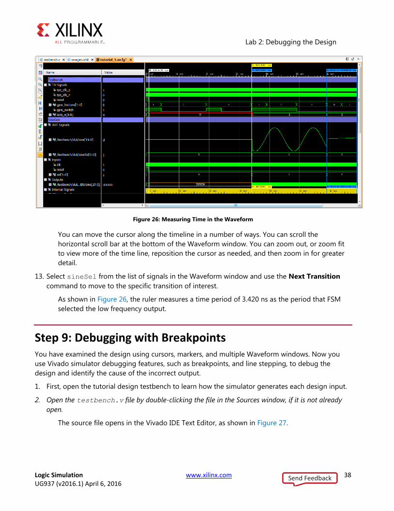
Figure 26: Measuring Time in the Waveform
You can move the cursor along the timeline in a number of ways. You can scroll the
horizontal scroll bar at the bottom of the Waveform window. You can zoom out, or zoom fit
to view more of the time line, reposition the cursor as needed, and then zoom in for greater
detail.
13. Select sineSel from the list of signals in the Waveform window and use the Next Transition
command to move to the specific transition of interest.
As shown in Figure 26, the ruler measures a time period of 3.420 ns as the period that FSM
selected the low frequency output.
Step 9: Debugging with Breakpoints You have examined the design using cursors, markers, and multiple Waveform windows. Now you
use Vivado simulator debugging features, such as breakpoints, and line stepping, to debug the
design and identify the cause of the incorrect output.
1. First, open the tutorial design testbench to learn how the simulator generates each design input.
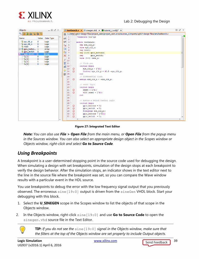
2. Open the testbench.v file by double-clicking the file in the Sources window, if it is not already
open.
The source file opens in the Vivado IDE Text Editor, as shown in Figure 27.
Send Feedback
Lab 2: Debugging the Design
Logic Simulation www.xilinx.com 39 UG937 (v2016.1) April 6, 2016
Figure 27: Integrated Text Editor
Note: You can also use File > Open File from the main menu, or Open File from the popup menu
in the Sources window. You can also select an appropriate design object in the Scopes window or
Objects window, right-click and select Go to Source Code.
Using Breakpoints
A breakpoint is a user-determined stopping point in the source code used for debugging the design.
When simulating a design with set breakpoints, simulation of the design stops at each breakpoint to
verify the design behavior. After the simulation stops, an indicator shows in the text editor next to
the line in the source file where the breakpoint was set, so you can compare the Wave window
results with a particular event in the HDL source.
You use breakpoints to debug the error with the low frequency signal output that you previously
observed. The erroneous sine[19:0] output is driven from the sineGen VHDL block. Start your
debugging with this block.
1. Select the U_SINEGEN scope in the Scopes window to list the objects of that scope in the
Objects window.
2. In the Objects window, right-click sine[19:0] and use Go to Source Code to open the
sinegen.vhd source file in the Text Editor.
TIP: If you do not see the sine[19:0] signal in the Objects window, make sure that
the filters at the top of the Objects window are set properly to include Output objects.
Send Feedback
Lab 2: Debugging the Design
Logic Simulation www.xilinx.com 40 UG937 (v2016.1) April 6, 2016
Looking through the HDL code, the clk, reset, and sel inputs are correct as expected. Set
your first breakpoint after the reset asserts low at line 137.
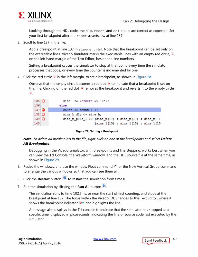
3. Scroll to line 137 in the file.
Add a breakpoint at line 137 in sinegen.vhd. Note that the breakpoint can be set only on
the executable lines. Vivado simulator marks the executable lines with an empty red circle, ,
on the left hand margin of the Text Editor, beside the line numbers.
Setting a breakpoint causes the simulator to stop at that point, every time the simulator
processes that code, or every time the counter is incremented by one.
4. Click the red circle in the left margin, to set a breakpoint, as shown in Figure 28.
Observe that the empty circle becomes a red dot to indicate that a breakpoint is set on
this line. Clicking on the red dot removes the breakpoint and reverts it to the empty circle
.
Figure 28: Setting a Breakpoint
Note: To delete all breakpoints in the file, right-click on one of the breakpoints and select Delete
All Breakpoints.
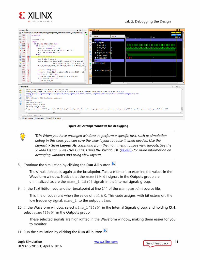
Debugging in the Vivado simulator, with breakpoints and line stepping, works best when you
can view the Tcl Console, the Waveform window, and the HDL source file at the same time, as
shown in Figure 29.
5. Resize the windows, and use the window Float command or the New Vertical Group command
to arrange the various windows so that you can see them all.
6. Click the Restart button to restart the simulation from time 0.
7. Run the simulation by clicking the Run All button .
The simulation runs to time 102.5 ns, or near the start of first counting, and stops at the
breakpoint at line 137. The focus within the Vivado IDE changes to the Text Editor, where it
shows the breakpoint indicator and highlights the line.
A message also displays in the Tcl console to indicate that the simulator has stopped at a
specific time, displayed in picoseconds, indicating the line of source code last executed by the
simulator.
Send Feedback
Lab 2: Debugging the Design
Logic Simulation www.xilinx.com 41 UG937 (v2016.1) April 6, 2016
Figure 29: Arrange Windows for Debugging
TIP: When you have arranged windows to perform a specific task, such as simulation
debug in this case, you can save the view layout to reuse it when needed. Use the
Layout > Save Layout As command from the main menu to save view layouts. See the
Vivado Design Suite User Guide: Using the Vivado IDE (UG893) for more information on
arranging windows and using view layouts.
8. Continue the simulation by clicking the Run All button .
The simulation stops again at the breakpoint. Take a moment to examine the values in the
Waveform window. Notice that the sine[19:0] signals in the Outputs group are
uninitialized, as are the sine_l[15:0] signals in the Internal signals group.
9. In the Text Editor, add another breakpoint at line 144 of the sinegen.vhd source file.
This line of code runs when the value of sel is 0. This code assigns, with bit extension, the
low frequency signal, sine_l, to the output, sine.
10. In the Waveform window, select sine_l[15:0] in the Internal Signals group, and holding Ctrl,
select sine[19:0] in the Outputs group.
These selected signals are highlighted in the Waveform window, making them easier for you
to monitor.
11. Run the simulation by clicking the Run All button .
Send Feedback

Lab 2: Debugging the Design
Logic Simulation www.xilinx.com 42 UG937 (v2016.1) April 6, 2016
Once again, the simulation stops at the breakpoint, this time at line 144.
Stepping Through Source Code
Another useful Vivado simulator debug tool is the Line Stepping feature. With line stepping, you can
run the simulator one-simulation unit (line, process, task) at a time. This is helpful if you are
interested in learning how each line of your source code affects the results in simulation.
Step through the source code line-by-line and examine how the low frequency wave is selected, and
whether the DDS compiler output is correct.
1. On the Vivado simulator toolbar menu, click the Step button .
The simulation steps forward to the next executable line, in this case in another source file.
The fsm.vdh file is opened in the Text Editor. You may need to relocate the Text Editor to let
you see all the windows as previously arranged.
Note: You can also type the step command at the Tcl prompt.
2. Continue to Step through the design, until the code returns to line 144 of sinegen.vhd.
You have stepped through one complete cycle of the circuit. Notice in the Waveform window
that while sel is 0, signal sine_l is assigned as a low frequency sine wave to the output
sine. Also, notice that sine_l remains uninitialized.
3. For debug purposes, initialize the value of sine_l by entering the following add_force
command in the Tcl console:
add_force /testbench/dut/U_SINEGEN/sine_l 0110011011001010
This command forces the value of sine_l into a specific known condition, and can provide a
repeating set of values to exercise the signal more vigorously, if needed. Refer to the Vivado
Design Suite User Guide: Logic Simulation (UG900) for more information on using
add_force.
4. Continue the simulation by clicking the Run All button a few more times.
In the Waveform window, notice that the value of sine_l[15:0] is now set to the value
specified by the add_force command, and this value is assigned to the output signal
sine[19:0] since the value of sel is still 0.
Trace the sine_l signal in the HDL source files, and identify the input for sine_l.
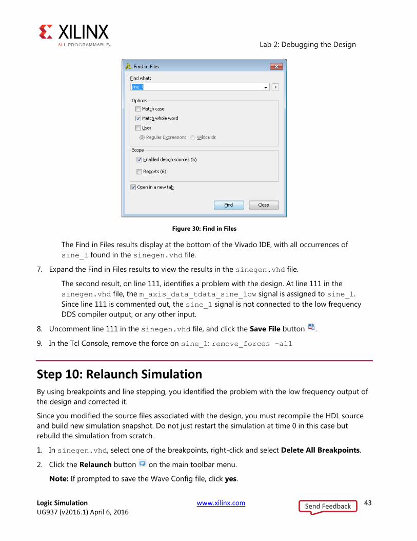
5. In the Text Editor, right-click to open the popup menu, and select the Find in files button to
search for sine_l.
6. Select the Match whole word and Enabled design sources checkboxes, as shown in Figure 30,
and click Find.
Send Feedback
Lab 2: Debugging the Design
Logic Simulation www.xilinx.com 43 UG937 (v2016.1) April 6, 2016
Figure 30: Find in Files
The Find in Files results display at the bottom of the Vivado IDE, with all occurrences of
sine_l found in the sinegen.vhd file.
7. Expand the Find in Files results to view the results in the sinegen.vhd file.
The second result, on line 111, identifies a problem with the design. At line 111 in the
sinegen.vhd file, the m_axis_data_tdata_sine_low signal is assigned to sine_l.
Since line 111 is commented out, the sine_l signal is not connected to the low frequency
DDS compiler output, or any other input.
8. Uncomment line 111 in the sinegen.vhd file, and click the Save File button .
9. In the Tcl Console, remove the force on sine_l: remove_forces -all
Step 10: Relaunch Simulation By using breakpoints and line stepping, you identified the problem with the low frequency output of
the design and corrected it.
Since you modified the source files associated with the design, you must recompile the HDL source
and build new simulation snapshot. Do not just restart the simulation at time 0 in this case but
rebuild the simulation from scratch.
1. In sinegen.vhd, select one of the breakpoints, right-click and select Delete All Breakpoints.
2. Click the Relaunch button on the main toolbar menu.
Note: If prompted to save the Wave Config file, click yes.
Send Feedback
Lab 2: Debugging the Design
Logic Simulation www.xilinx.com 44 UG937 (v2016.1) April 6, 2016
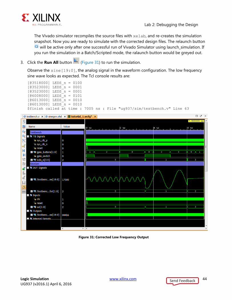
The Vivado simulator recompiles the source files with xelab, and re-creates the simulation
snapshot. Now you are ready to simulate with the corrected design files. The relaunch button
will be active only after one successful run of Vivado Simulator using launch_simulation. If
you run the simulation in a Batch/Scripted mode, the ralaunch button would be greyed out.
3. Click the Run All button (Figure 31) to run the simulation.
Observe the sine[19:0], the analog signal in the waveform configuration. The low frequency
sine wave looks as expected. The Tcl console results are:
[@3518000] LEDS_n = 0100
[@3523000] LEDS_n = 0001
[@3523000] LEDS_n = 0001
[@6008000] LEDS_n = 0101
[@6013000] LEDS_n = 0010
[@6013000] LEDS_n = 0010
$finish called at time : 7005 ns : File "ug937/sim/testbench.v" Line 63
Figure 31: Corrected Low Frequency Output
Send Feedback

Lab 2: Debugging the Design
Logic Simulation www.xilinx.com 45 UG937 (v2016.1) April 6, 2016
Conclusion After reviewing the simulation results, you may close the simulation, and close the project. This
completes Lab #2. Up to this point in the tutorial, between Lab #1 and Lab #2, you have:
Run the Vivado simulator using the Project Mode flow in Vivado IDE
Created a project, added source files, and added IP
Added a simulation-only file (testbench.v)
Set simulation properties and launched behavioral simulation
Added signals to the Waveform window
Configured and saved the Waveform Configuration file
Debugged the design bug using breakpoints and line stepping.
Corrected an error, re-launched simulation, and verified the design
In Lab # 3 you will examine the Vivado simulator batch mode.
Send Feedback
Logic Simulation www.xilinx.com 46 UG937 (v2016.1) April 6, 2016
Lab 3: Running Simulation in Batch Mode
Introduction You can use the Vivado simulator Non-Project Mode flow to simulate your design without setting up a
project in Vivado Integrated Design Environment (IDE).
In this flow, you:
Prepare the simulation project manually by creating a Vivado simulator project script.
Create a simulation snapshot file using the Vivado simulator xelab utility.
Start the Vivado simulator GUI by running the xsim command with the resulting snapshot.
Step 1: Preparing the Simulation The Vivado simulator Non-Project Mode flow lets you simulate your design without setting up a project
in the Vivado IDE.
You can compile the HDL files in a design, and create a simulation snapshot by either:
Creating a Vivado simulator project script, specifying all HDL files to be compiled, and using the
xelab command to create a simulation snapshot, or
Using specific Vivado simulator parser commands, xvlog and xvhdl, to parse individual source
files and write the parsed files into an HDL library on disk, and then using xelab to create a
simulation snapshot from the parsed files
Send Feedback
Lab 3: Running Simulation in Batch Mode
Logic Simulation www.xilinx.com 47 UG937 (v2016.1) April 6, 2016
Creating the Vivado Simulator Project File
A Vivado simulator project script specifies design source files and libraries to parse and compile for
simulation. This method is useful to create a simulation project script that can be run repeatedly over
the course of project development.
The format for a Vivado simulator project script (prj file) is as follows:
verilog | vhdl| sv <library_name> {<file_name>.v|.vhd}
Where:
o verilog | vhdl | sv specifies whether the design source is a Verilog, VHDL, or SV file.
o <library_name>: Specifies the library into which you may compile the source file. If
unspecified, the default library for compilation is work.
o <file_name>.v|.vhd: Specifies the name of the design source file to compile.
IMPORTANT: While you can specify one or more Verilog source files on a single
command line, you can only specify one VHDL source on a single command line.
In this step, you build a Vivado simulator project script by editing an existing project script to add
missing source files. The command lines for the project script should be constructed using the syntax
described above.
1. Browse to the <Extract_Dir>/scripts folder.
2. Open the simulate_xsim.prj project script with a text editor.
3. Add the following commands to the project script:
vhdl xil_defaultlib "../sources/sinegen.vhd"
vhdl xil_defaultlib "../sources/debounce.vhd"
vhdl xil_defaultlib "../sources/fsm.vhd"
vhdl xil_defaultlib "../sources/sinegen_demo.vhd"
verilog xil_defaultlib "../sim/testbench.v"
4. Save and close the file.
You do not need to list the sources based on any specific order of dependency. The xelab command
resolves the order of dependencies, and automatically processes the files accordingly.
TIP: For your reference, a completed version of the tutorial files can be found in the
ug937-design-files/completed folder.
Manually Parsing Design Files
As an alternative to creating a Vivado simulator project script, you can compile individual design source
files directly from the command line using the xvlog or xvhdl commands to parse the design sources
and write them to an HDL library. You could use this method for simple simulation runs, or to define a
shell script and makefile compilation flow.
Send Feedback
Lab 3: Running Simulation in Batch Mode
Logic Simulation www.xilinx.com 48 UG937 (v2016.1) April 6, 2016
Parse individual or multiple Verilog files using the xvlog command with the following syntax format:
xvlog [options] <verilog_file | list_of_files>
Parse individual VHDL files using the xvhdl command with the following syntax format:
xvhdl [options] <VHDL_file>
For a complete list of available xvlog and xvhdl command options, see the Vivado Design Suite User
Guide: Logic Simulation (UG900). The parse_standalone.bat file in <Extract_Dir>/scripts or
<Extract_Dir>/completed provide examples of running xvlog and xvhdl directly.
Step 2: Building the Simulation Snapshot In this step, you use the xelab command on the project script you previously edited
(simulate_xsim.prj) to elaborate, compile, and link all the sources for the design. The xelab utility
creates a simulation snapshot that lets you to simulate the design in the Vivado simulator.
The typical xelab command syntax is:
xelab -prj <project_file> -s <simulation snapshot> <library>.<top_unit>
Where:
o -prj <project_file>: Specifies a Vivado simulation project script to use for input.
o -s <simulation_snapshot>: Specifies the name of the output simulation snapshot.
o <library>.<top_unit>: Specifies the library and top-level module of the design.
Running xelab
In this step, you use the xelab command with the project file completed in Step 1 to elaborate,
compile, and link all the design sources to create the simulation snapshot. To run the xelab command,
must open and configure a command window.
1. On Windows, open a Command Prompt window. On Linux, simply skip to the next step.
2. Change directory to the Xilinx installation area, and run settings64.bat as needed to setup the
Xilinx tool paths for your computer:
cd <Vivado_install_area>\Vivado\2016.x\settings64
Note: The settings64.bat file configures the path on your computer to run the Vivado Design
Suite.
Send Feedback
Lab 3: Running Simulation in Batch Mode
Logic Simulation www.xilinx.com 49 UG937 (v2016.1) April 6, 2016
TIP: When running the xelab, xsc, xsim, xvhdl, or xvlog commands in batch files
or scripts, it may also be necessary to define the XILINX_VIVADO environment variable
to point to the installation hierarchy of the Vivado Design Suite. To set the
XILINX_VIVADO variable, you can add one of the following to your script or batch file:
On Windows -
set XILINX_VIVADO=<Vivado_install_area>/Vivado/2016.x
On Linux -
setenv XILINX_VIVADO <Vivado_install_area>/Vivado/2016.x
3. Change directory to the <Extract_Dir>/scripts folder.
The provided xelab batch file, xelab_batch.bat, is incomplete, and you must modify it
using the xelab syntax as previously described to produce the correct simulation snapshot.
4. Edit the xelab_batch.bat file to add the following options:
o Specify the project file: -prj simulate_xsim.prj
o Specify the output simulation snapshot: -s run_sineGen
o Specify the library and top-level design unit: xil_defaultlib.testbench
For a complete list of available xelab command options, see the Vivado Design Suite User
Guide: Logic Simulation (UG900).
5. Save and close the batch file.
6. In the command window, run the xelab_batch.bat file to compile and create the simulation
snapshot.
xelab_batch.bat
7. Examine the xelab output as it is transcribed to the Command Prompt window.
Note: The xelab command also writes xelab.log file in the directory from which it was run. The
log file contains all of the messages and results of the xelab command for you to review.
TIP: You can also use the xelab command after the xvlog and xvhdl commands
have parsed the HDL design sources to read the specified simulation libraries. The
xelab command would be the same as described here, except that it would not require
the -prj option since there would be no simulation project file.
Send Feedback
Lab 3: Running Simulation in Batch Mode
Logic Simulation www.xilinx.com 50 UG937 (v2016.1) April 6, 2016
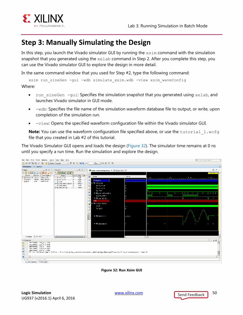
Step 3: Manually Simulating the Design In this step, you launch the Vivado simulator GUI by running the xsim command with the simulation
snapshot that you generated using the xelab command in Step 2. After you complete this step, you
can use the Vivado simulator GUI to explore the design in more detail.
In the same command window that you used for Step #2, type the following command:
xsim run_sineGen -gui -wdb simulate_xsim.wdb -view xsim_waveConfig
Where:
run_sineGen -gui: Specifies the simulation snapshot that you generated using xelab, and
launches Vivado simulator in GUI mode.
-wdb: Specifies the file name of the simulation waveform database file to output, or write, upon
completion of the simulation run.
-view: Opens the specified waveform configuration file within the Vivado simulator GUI.
Note: You can use the waveform configuration file specified above, or use the tutorial_1.wcfg
file that you created in Lab #2 of this tutorial.
The Vivado Simulator GUI opens and loads the design (Figure 32). The simulator time remains at 0 ns
until you specify a run time. Run the simulation and explore the design.
Figure 32: Run Xsim GUI
Send Feedback
Lab 3: Running Simulation in Batch Mode
Logic Simulation www.xilinx.com 51 UG937 (v2016.1) April 6, 2016
Conclusion In this tutorial, you:
Created a Vivado IDE project
Downloaded source files and ran Vivado simulation
Examined the simulation customization features
Debugged and fixed a known issue within the source files
Ran a Vivado simulation in batch mode using the Vivado simulation executable and switch options
Send Feedback

Logic Simulation www.xilinx.com 52 UG937 (v2016.1) April 6, 2016
Legal Notices
Please Read: Important Legal Notices The information disclosed to you hereunder (the “Materials”) is provided solely for the selection and use of Xilinx products. To the
maximum extent permitted by applicable law: (1) Materials are made available "AS IS" and with all faults, Xilinx hereby DISCLAIMS
ALL WARRANTIES AND CONDITIONS, EXPRESS, IMPLIED, OR STATUTORY, INCLUDING BUT NOT LIMITED TO
WARRANTIES OF MERCHANTABILITY, NON-INFRINGEMENT, OR FITNESS FOR ANY PARTICULAR PURPOSE; and (2) Xilinx
shall not be liable (whether in contract or tort, including negligence, or under any other theory of liability) for any loss or damage of
any kind or nature related to, arising under, or in connection with, the Materials (including your use of the Materials), including for
any direct, indirect, special, incidental, or consequential loss or damage (including loss of data, profits, goodwill, or any type of loss
or damage suffered as a result of any action brought by a third party) even if such damage or loss was reasonably foreseeable or
Xilinx had been advised of the possibility of the same. Xilinx assumes no obligation to correct any errors contained in the Materials
or to notify you of updates to the Materials or to product specifications. You may not reproduce, modify, distribute, or publicly display
the Materials without prior written consent. Certain products are subject to the terms and conditions of Xilinx’s limited warranty,
please refer to Xilinx’s Terms of Sale which can be viewed at http://www.xilinx.com/legal.htm#tos; IP cores may be subject to
warranty and support terms contained in a license issued to you by Xilinx. Xilinx products are not designed or intended to be fail-
safe or for use in any application requiring fail-safe performance; you assume sole risk and liability for use of Xilinx products in such
critical applications, please refer to Xilinx’s Terms of Sale which can be viewed at http://www.xilinx.com/legal.htm#tos.
© Copyright 2012-2016 Xilinx, Inc. Xilinx, the Xilinx logo, Artix, ISE, Kintex, Spartan, Virtex, Zynq, and other designated brands
included herein are trademarks of Xilinx in the United States and other countries. All other trademarks are the property of their
respective owners.
Send Feedback