Embed Size (px)
Citation preview
VLSI Physical Design: From Graph Partitioning to Timing Closure Paper Presentation
© K
LMH
Lie
nig1
EECS 527 Paper Presentation
Topological Design of Clock Distribution Networks Based on
Non-Zero Clock Skew Specifications- by Jose Luis Neves and Eby G.
Friedman
Presented by Shaobo Liu
Department Electrical Engineering and Computer Science
University of Michigan, Ann Arbor
04/2013
VLSI Physical Design: From Graph Partitioning to Timing Closure Paper Presentation
© K
LMH
Lie
nig
EECS 527 Paper Presentation
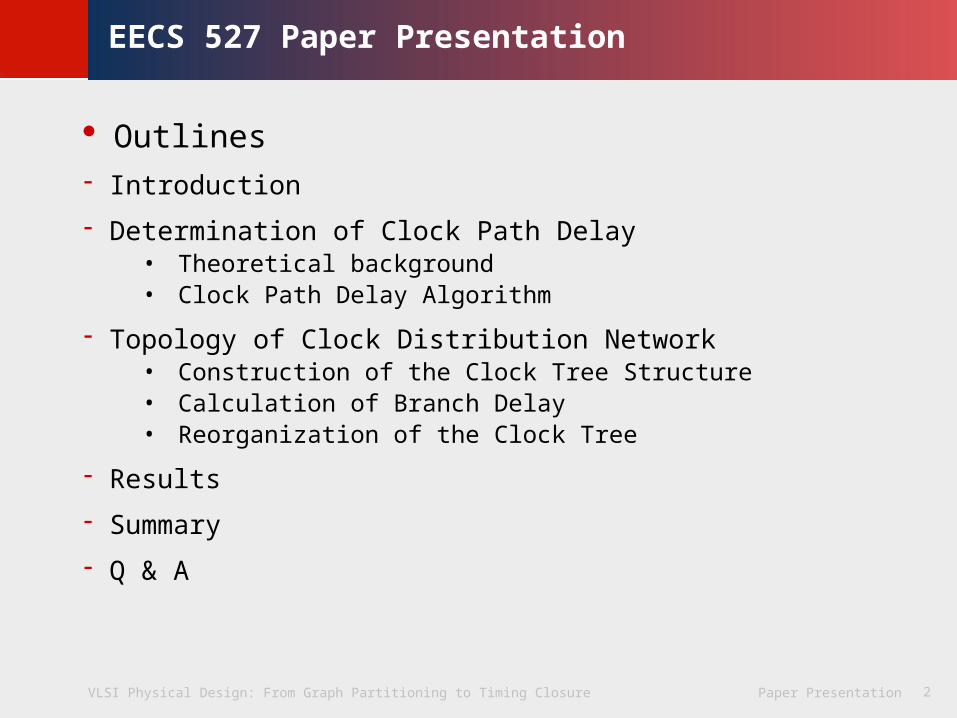
· Outlines- Introduction
- Determination of Clock Path Delay• Theoretical background• Clock Path Delay Algorithm
- Topology of Clock Distribution Network• Construction of the Clock Tree Structure• Calculation of Branch Delay• Reorganization of the Clock Tree
- Results
- Summary
- Q & A
2
VLSI Physical Design: From Graph Partitioning to Timing Closure Paper Presentation
© K
LMH
Lie
nig
Introduction
3
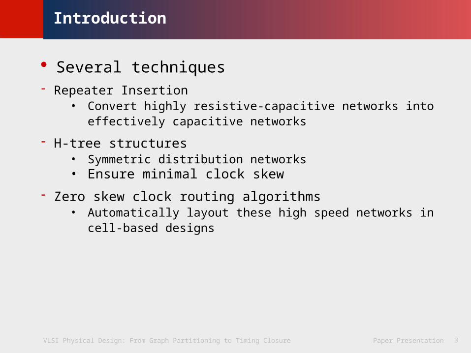
· Several techniques - Repeater Insertion
• Convert highly resistive-capacitive networks into effectively capacitive networks
- H-tree structures• Symmetric distribution networks• Ensure minimal clock skew
- Zero skew clock routing algorithms• Automatically layout these high speed networks in cell-based designs
VLSI Physical Design: From Graph Partitioning to Timing Closure Paper Presentation
© K
LMH
Lie
nig
Introduction
4
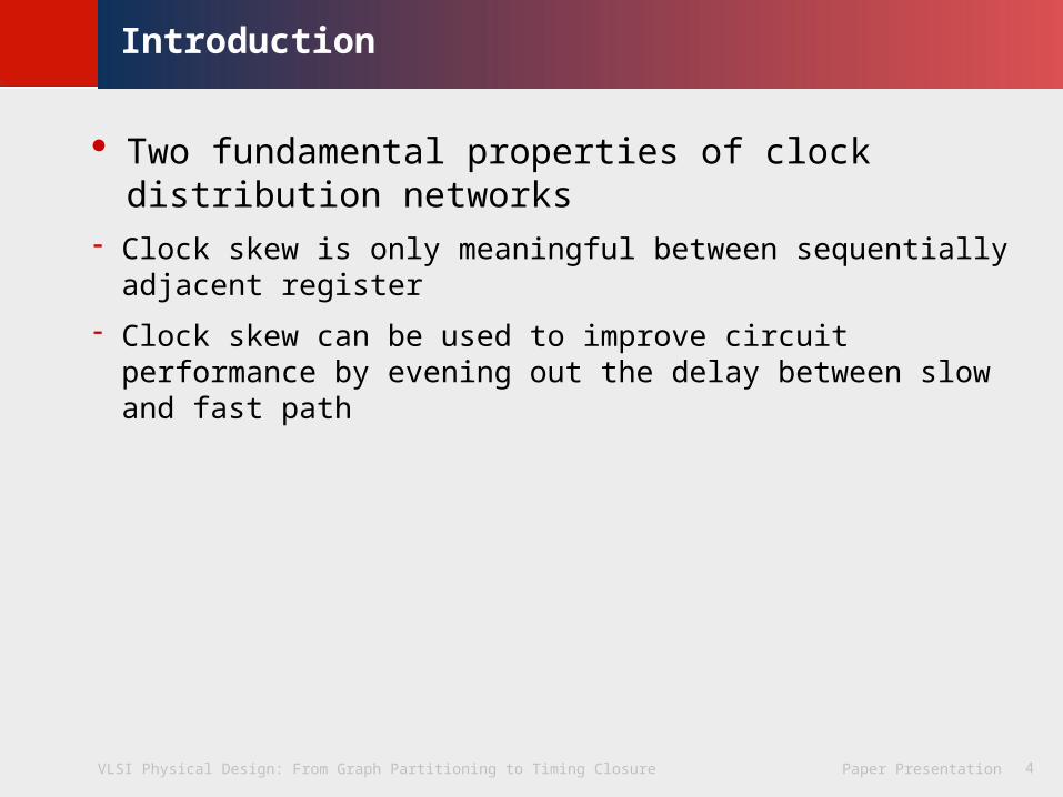
· Two fundamental properties of clock distribution networks
- Clock skew is only meaningful between sequentially adjacent register
- Clock skew can be used to improve circuit performance by evening out the delay between slow and fast path
VLSI Physical Design: From Graph Partitioning to Timing Closure Paper Presentation
© K
LMH
Lie
nig
Introduction
5
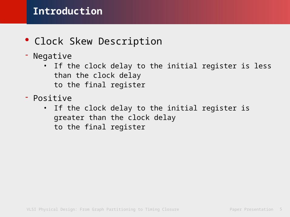
· Clock Skew Description - Negative
• If the clock delay to the initial register is less than the clock delay to the final register
- Positive• If the clock delay to the initial register is greater than the clock delay
to the final register
VLSI Physical Design: From Graph Partitioning to Timing Closure Paper Presentation
© K
LMH
Lie
nig
Determination of Clock Path Delay
6
· Theoretical Background
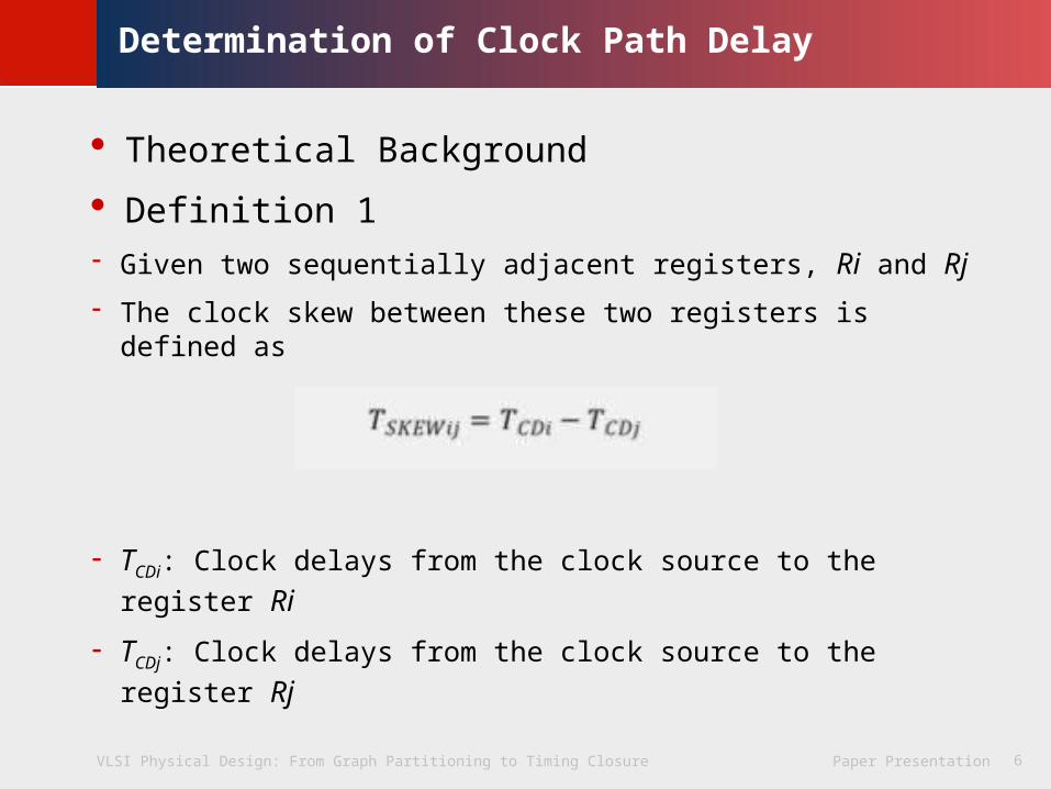
· Definition 1- Given two sequentially adjacent registers, Ri and Rj
- The clock skew between these two registers is defined as
- TCDi: Clock delays from the clock source to the register Ri
- TCDj: Clock delays from the clock source to the register Rj

VLSI Physical Design: From Graph Partitioning to Timing Closure Paper Presentation
© K
LMH
Lie
nig
Determination of Clock Path Delay
7
· Theoretical Background
· More Definition - Local data path
• The path between two sequentially adjacent registers
- Global data path• Consist of one or more local data path
VLSI Physical Design: From Graph Partitioning to Timing Closure Paper Presentation
© K
LMH
Lie
nig
Determination of Clock Path Delay
8
· Theoretical Background
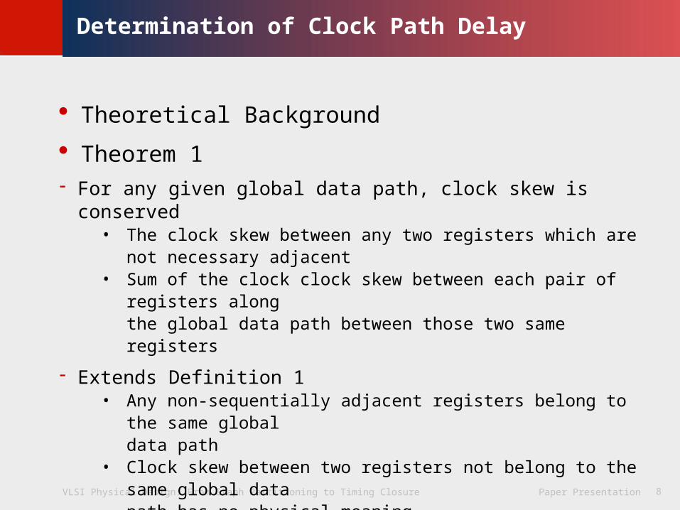
· Theorem 1 - For any given global data path, clock skew is conserved
• The clock skew between any two registers which are not necessary adjacent
• Sum of the clock clock skew between each pair of registers along the global data path between those two same registers
- Extends Definition 1 • Any non-sequentially adjacent registers belong to the same global
data path• Clock skew between two registers not belong to the same global data
path has no physical meaning
VLSI Physical Design: From Graph Partitioning to Timing Closure Paper Presentation
© K
LMH
Lie
nig
Determination of Clock Path Delay
9
· Theoretical Background
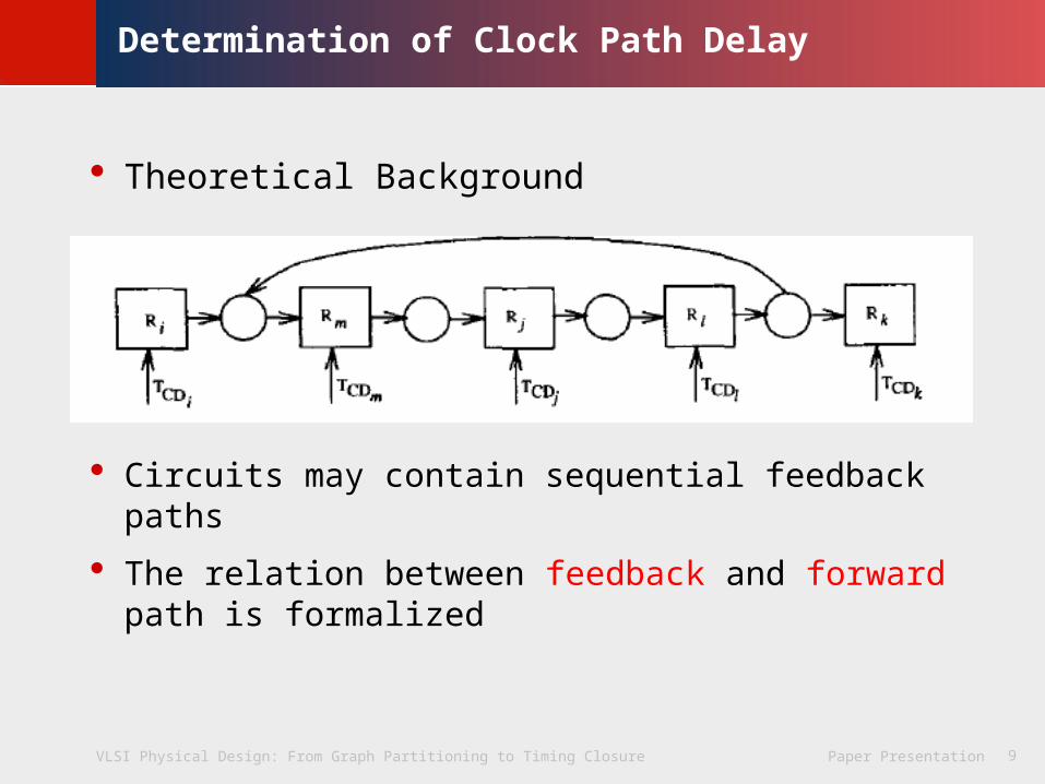
· Circuits may contain sequential feedback paths
· The relation between feedback and forward path is formalized
VLSI Physical Design: From Graph Partitioning to Timing Closure Paper Presentation
© K
LMH
Lie
nig
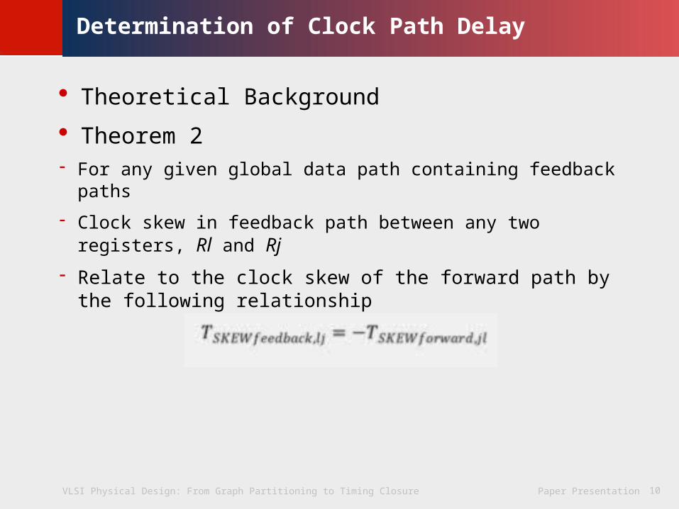
Determination of Clock Path Delay
10
· Theoretical Background
· Theorem 2- For any given global data path containing feedback paths
- Clock skew in feedback path between any two registers, Rl and Rj
- Relate to the clock skew of the forward path by the following relationship
VLSI Physical Design: From Graph Partitioning to Timing Closure Paper Presentation
© K
LMH
Lie
nig
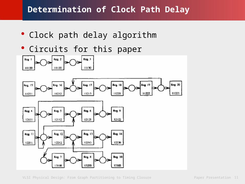
Determination of Clock Path Delay
11
· Clock path delay algorithm
· Circuits for this paper
VLSI Physical Design: From Graph Partitioning to Timing Closure Paper Presentation
© K
LMH
Lie
nig
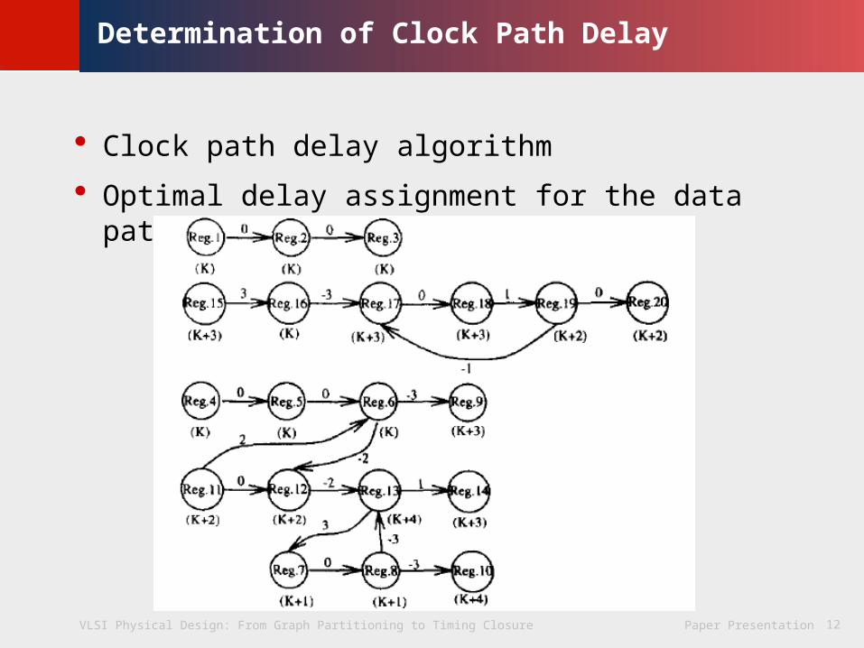
Determination of Clock Path Delay
12
· Clock path delay algorithm
· Optimal delay assignment for the data path example
VLSI Physical Design: From Graph Partitioning to Timing Closure Paper Presentation
© K
LMH
Lie
nig
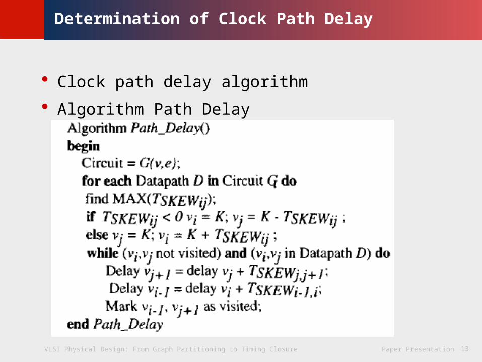
Determination of Clock Path Delay
13
· Clock path delay algorithm
· Algorithm Path Delay
VLSI Physical Design: From Graph Partitioning to Timing Closure Paper Presentation
© K
LMH
Lie
nig
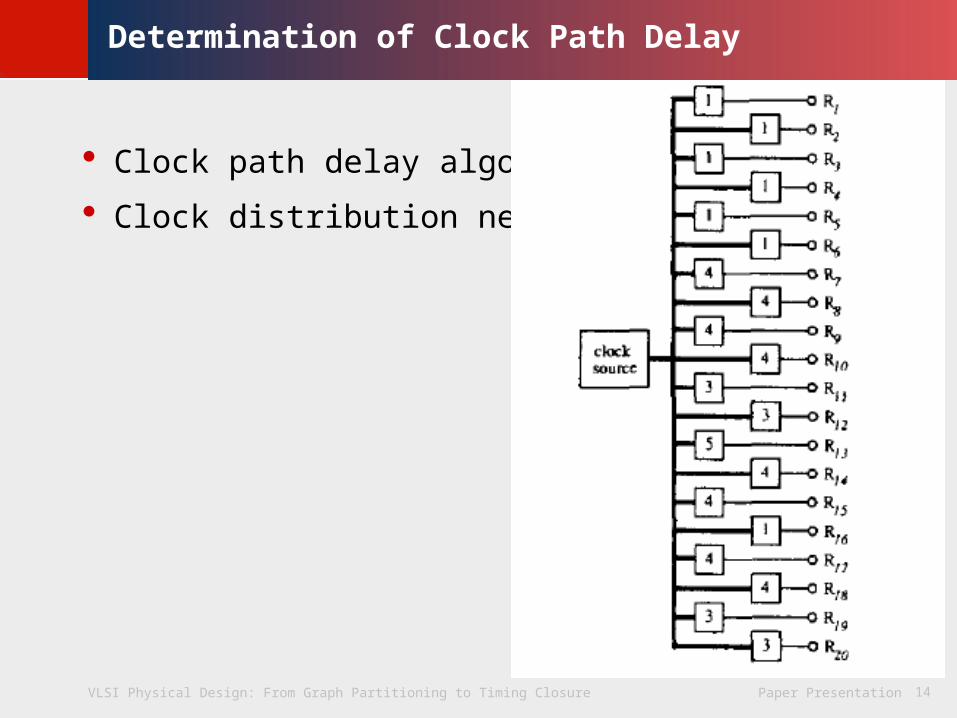
Determination of Clock Path Delay
14
· Clock path delay algorithm
· Clock distribution network
VLSI Physical Design: From Graph Partitioning to Timing Closure Paper Presentation
© K
LMH
Lie
nig
Topology of Clock Distribution Network
15
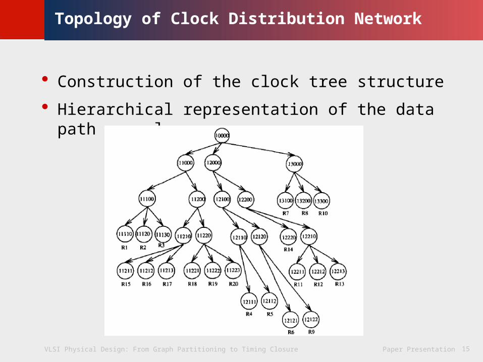
· Construction of the clock tree structure
· Hierarchical representation of the data path example
VLSI Physical Design: From Graph Partitioning to Timing Closure Paper Presentation
© K
LMH
Lie
nig
Topology of Clock Distribution Network
16
· Calculation of branch delay
· Two characteristics of the hierarchical representation
- The clock skew between sequentially adjacent registers may not depend on the delay of the internal branches
- The clock skew specifications may be satisfied if the delay of some of the internal branches is known
VLSI Physical Design: From Graph Partitioning to Timing Closure Paper Presentation
© K
LMH
Lie
nig
Topology of Clock Distribution Network
17
· Calculation of branch delay
· Three steps to determine the individual branch delays- Delay of External Branches
- Delay of Internal Branches
- Delay Shifting
VLSI Physical Design: From Graph Partitioning to Timing Closure Paper Presentation
© K
LMH
Lie
nig
Topology of Clock Distribution Network
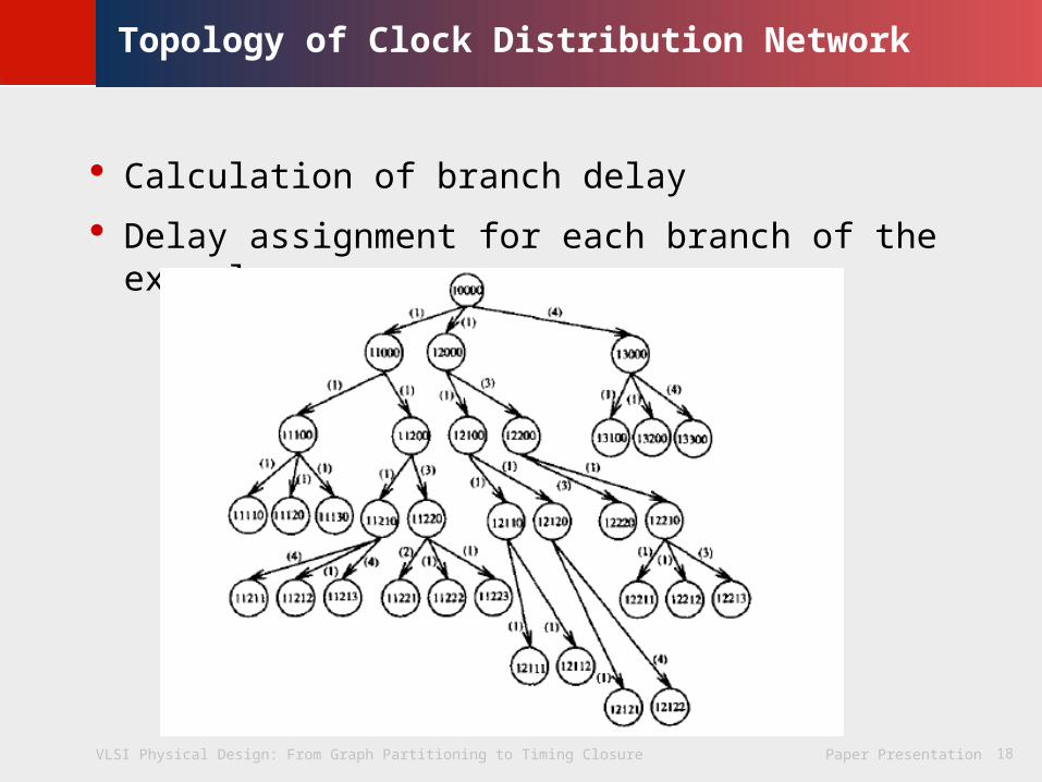
18
· Calculation of branch delay
· Delay assignment for each branch of the example
VLSI Physical Design: From Graph Partitioning to Timing Closure Paper Presentation
© K
LMH
Lie
nig
Topology of Clock Distribution Network
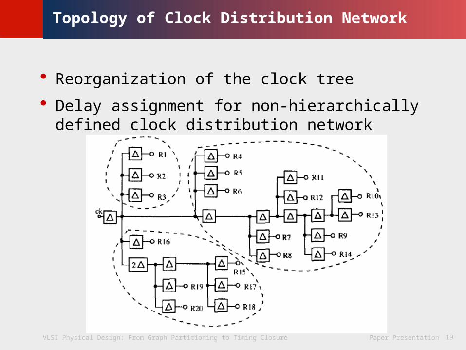
19
· Reorganization of the clock tree
· Delay assignment for non-hierarchically defined clock distribution network

VLSI Physical Design: From Graph Partitioning to Timing Closure Paper Presentation
© K
LMH
Lie
nig
Results
20
· Minimum clock delay and total number of delay units for several example circuits
VLSI Physical Design: From Graph Partitioning to Timing Closure Paper Presentation
© K
LMH
Lie
nig
Summary
21
· Determination of Clock Path Delay
- Theoretical Background
- Clock Path Delay Algorithm
· Topology of Clock Distribution Network
- Construction of the Clock Tree Network
- Calculation of Branch Delay
- Reorganization of the Clock Tree
· Future Research- Determine the Optimal Non-zero Clocking Characteristics
- Design of Circuits Structure to Emulate Delay values of the Network Branches

VLSI Physical Design: From Graph Partitioning to Timing Closure Paper Presentation
© K
LMH
Lie
nig
EECS 527 Paper Presentation
Thanks!
Q & A
22


![[XLS]eci.nic.ineci.nic.in/delim/paper1to7/TamilNadu.xls · Web viewRev. Dharmapuri & Kanniyakumari Paper 7 Paper 6 Paper 5 Paper 4 Paper 3 Paper 2 Paper 1 Index Tirunelveli (M.Corp.)](https://img.pdfslide.net/doc/110x75/5ad236e17f8b9a86158ce167/xlsecinicinecinicindelimpaper1to7-viewrev-dharmapuri-kanniyakumari-paper.jpg)


![LMMQM08M X 385 · iqT2aC?\^\] ]]]\ ab`c_hmghmgjhin spteterqpekoluusfk @DL yzz{zpqzo} _OeT]OJu Vo,opzo|qoO[}|u ^}|u KLMH ^4nODR5Z2eWr,bY-DOo2Ej+D.4xQ}D_OeT]D>0F\ eWr,bo`Y-DG+J?N\>p](https://img.pdfslide.net/doc/110x75/5f1040927e708231d44830f6/lmmqm08m-x-385-iqt2ac-abchmghmgjhin-spteterqpekoluusfk-dl-yzzzpqzo.jpg)