Embed Size (px)
Citation preview
VLSI System DesignPart I : Introduction
Oct.2006 - Feb.2007
Lecturer : Tsuyoshi IsshikiDept. Communications and Integrated Systems,
Tokyo Institute of Technology
[email protected]://www.vlsi.ss.titech.ac.jp/~isshiki/VLSISystemDesign/top.html
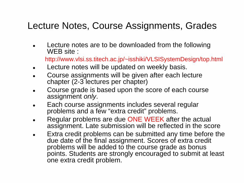
Lecture Notes, Course Assignments, Grades
Lecture notes are to be downloaded from the following WEB site :
http://www.vlsi.ss.titech.ac.jp/~isshiki/VLSISystemDesign/top.htmlLecture notes will be updated on weekly basis.Course assignments will be given after each lecture chapter (2-3 lectures per chapter)Course grade is based upon the score of each course assignment only.Each course assignments includes several regular problems and a few “extra credit” problems.Regular problems are due ONE WEEK after the actual assignment. Late submission will be reflected in the scoreExtra credit problems can be submitted any time before the due date of the final assignment. Scores of extra credit problems will be added to the course grade as bonus points. Students are strongly encouraged to submit at least one extra credit problem.
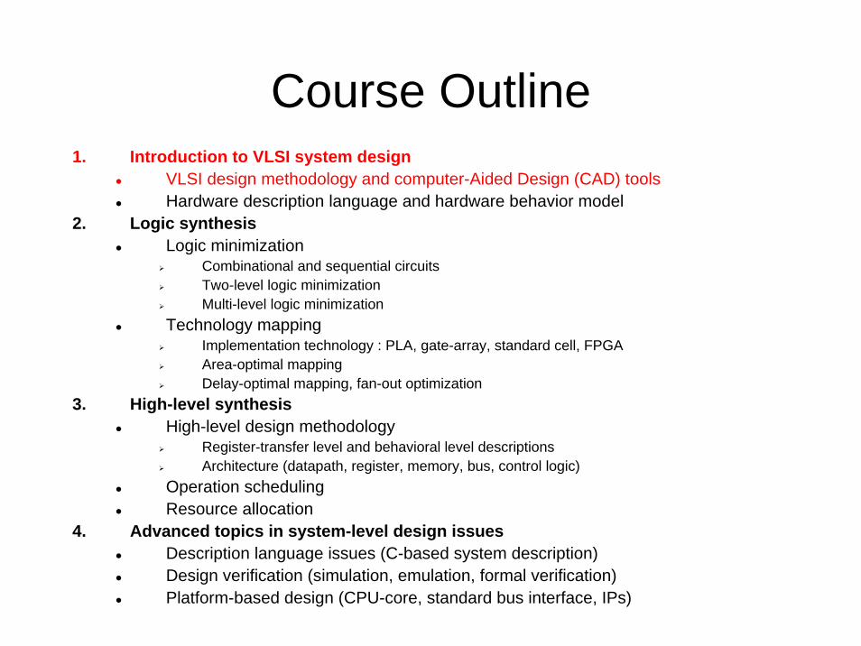
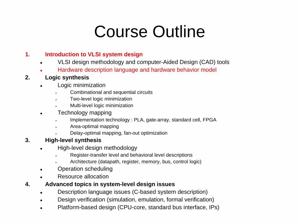
Course Outline1. Introduction to VLSI system design
VLSI design methodology and computer-Aided Design (CAD) toolsHardware description language and hardware behavior model
2. Logic synthesisLogic minimization
Combinational and sequential circuitsTwo-level logic minimizationMulti-level logic minimization
Technology mappingImplementation technology : PLA, gate-array, standard cell, FPGA Area-optimal mapping Delay-optimal mapping, fan-out optimization
3. High-level synthesis High-level design methodology
Register-transfer level and behavioral level descriptions Architecture (datapath, register, memory, bus, control logic)
Operation scheduling Resource allocation
4. Advanced topics in system-level design issues Description language issues (C-based system description)Design verification (simulation, emulation, formal verification)Platform-based design (CPU-core, standard bus interface, IPs)
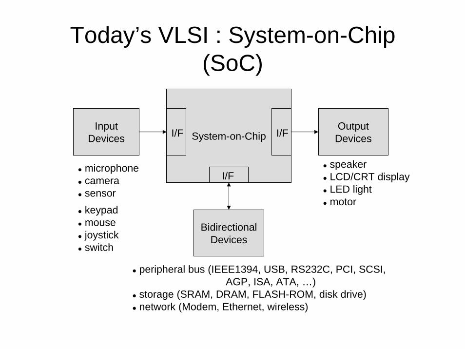
Today’s VLSI : System-on-Chip (SoC)
Bidirectional Devices
System-on-ChipInput
Devices Output Devices I/F
I/F
I/F
microphonecamerasensorkeypadmousejoystickswitch
speakerLCD/CRT displayLED lightmotor
peripheral bus (IEEE1394, USB, RS232C, PCI, SCSI, AGP, ISA, ATA, …)
storage (SRAM, DRAM, FLASH-ROM, disk drive)network (Modem, Ethernet, wireless)
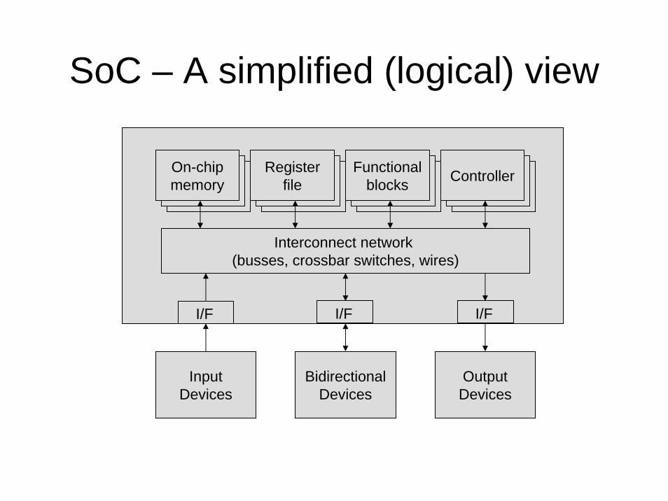
SoC – A simplified (logical) view
On-chip memory
On-chip memory
On-chip memory
Interconnect network (busses, crossbar switches, wires)
I/F
Output Devices
Bidirectional Devices
Input Devices
On-chip memory
On-chip memory
Register file On-chip
memoryOn-chip memory
Functional blocks On-chip
memoryOn-chip memory
Controller
I/F I/F
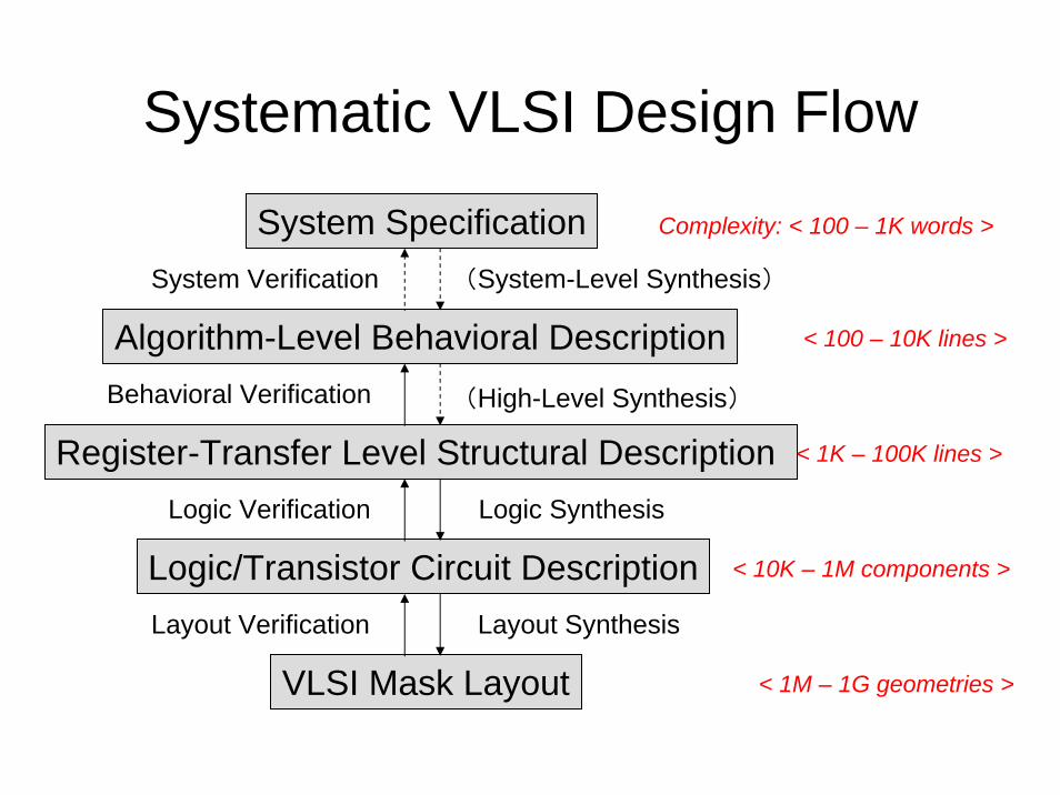
Algorithm-Level Behavioral Description
Register-Transfer Level Structural Description
Logic/Transistor Circuit Description
VLSI Mask Layout
Logic Synthesis
Layout Synthesis
(High-Level Synthesis)
System Specification(System-Level Synthesis)
Layout Verification
Logic Verification
Behavioral Verification
System Verification
Systematic VLSI Design Flow
Complexity: < 100 – 1K words >
< 100 – 10K lines >
< 1K – 100K lines >
< 10K – 1M components >
< 1M – 1G geometries >
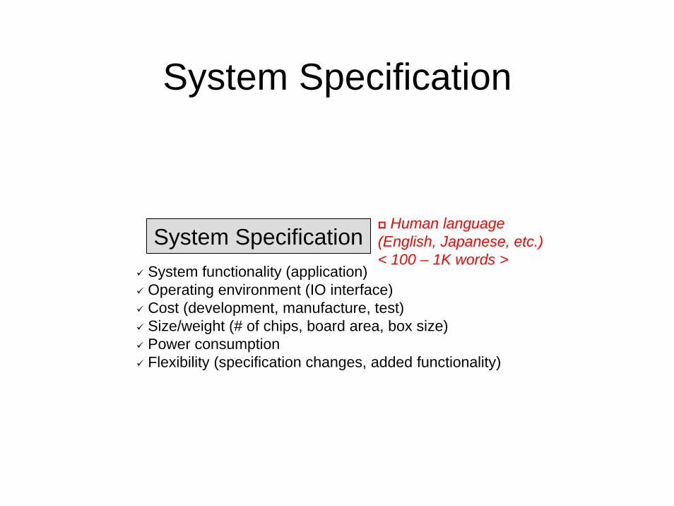
System Specification
System SpecificationSystem functionality (application)Operating environment (IO interface)Cost (development, manufacture, test)Size/weight (# of chips, board area, box size)Power consumptionFlexibility (specification changes, added functionality)
Human language (English, Japanese, etc.)< 100 – 1K words >
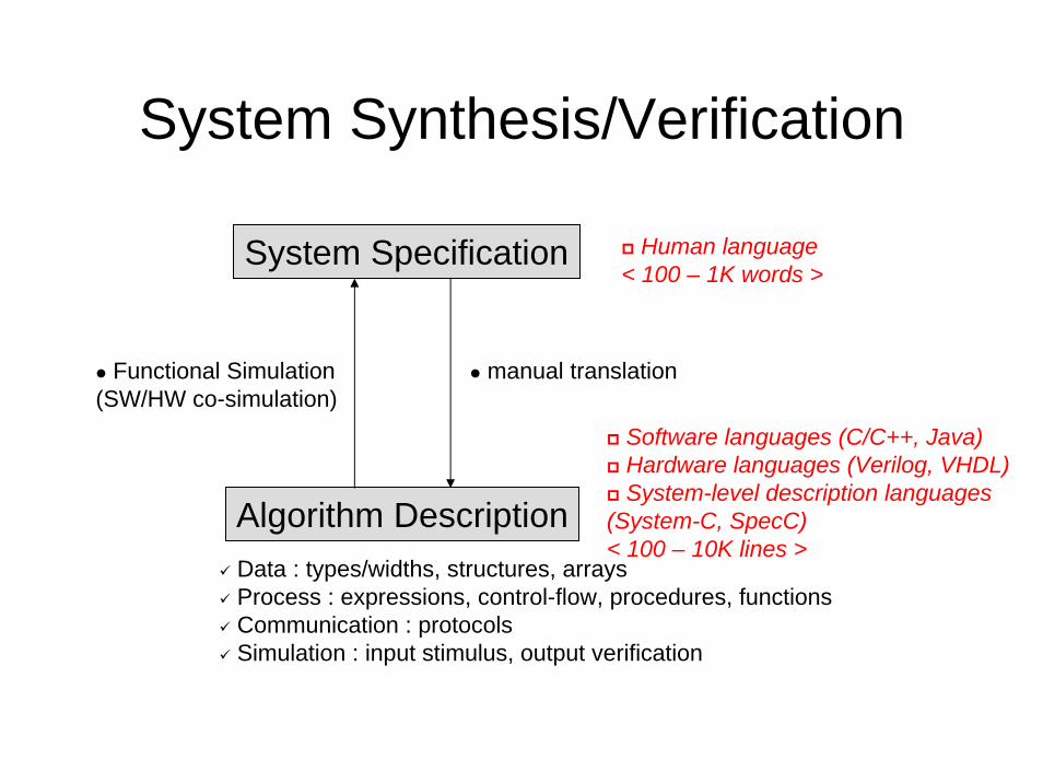
System Synthesis/Verification
Algorithm Description
System Specification
Software languages (C/C++, Java)Hardware languages (Verilog, VHDL)System-level description languages
(System-C, SpecC)< 100 – 10K lines >
Functional Simulation(SW/HW co-simulation)
Data : types/widths, structures, arraysProcess : expressions, control-flow, procedures, functionsCommunication : protocolsSimulation : input stimulus, output verification
manual translation
Human language < 100 – 1K words >
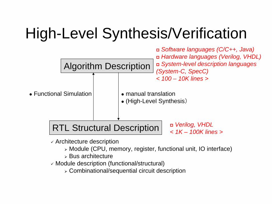
High-Level Synthesis/Verification
Algorithm Description
Functional Simulation
RTL Structural Description Verilog, VHDL< 1K – 100K lines >
Architecture descriptionModule (CPU, memory, register, functional unit, IO interface) Bus architecture
Module description (functional/structural)Combinational/sequential circuit description
manual translation(High-Level Synthesis)
Software languages (C/C++, Java)Hardware languages (Verilog, VHDL)System-level description languages
(System-C, SpecC)< 100 – 10K lines >
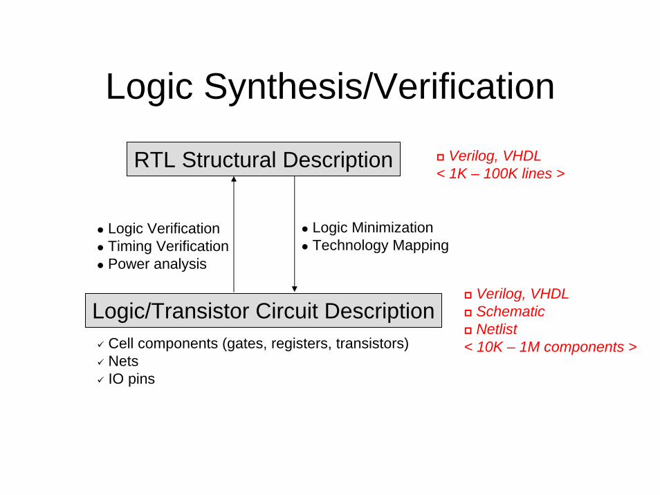
Logic Synthesis/Verification
Logic VerificationTiming VerificationPower analysis
RTL Structural Description
Logic/Transistor Circuit DescriptionVerilog, VHDLSchematicNetlist
< 10K – 1M components >
Verilog, VHDL< 1K – 100K lines >
Logic MinimizationTechnology Mapping
Cell components (gates, registers, transistors)NetsIO pins
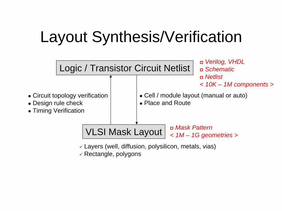
Layout Synthesis/Verification
Circuit topology verificationDesign rule checkTiming Verification
Logic / Transistor Circuit NetlistVerilog, VHDLSchematicNetlist
< 10K – 1M components >
VLSI Mask Layout Mask Pattern< 1M – 1G geometries >
Cell / module layout (manual or auto)Place and Route
Layers (well, diffusion, polysilicon, metals, vias)Rectangle, polygons
Algorithm-Level Description
RTL Structural Description
Logic/Transistor Circuit Description
VLSI Mask Layout
Logic Synthesis
Layout Synthesis
(High-Level Synthesis)
System Specification
(System-Level Synthesis)
Layout Verification
Logic Verification
Behavioral Verification
System Verification
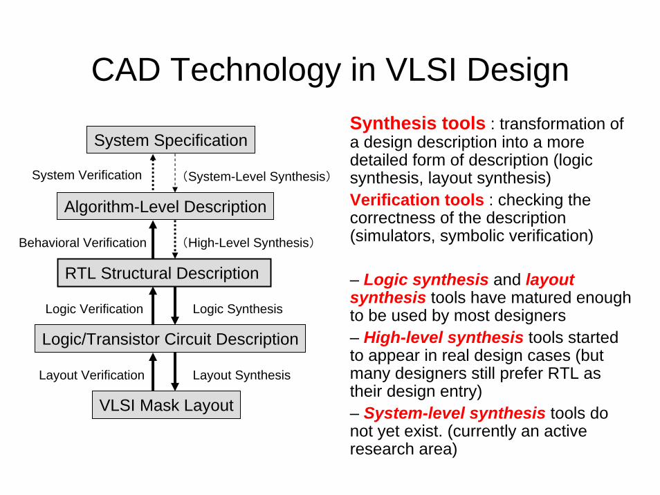
CAD Technology in VLSI DesignSynthesis tools : transformation of a design description into a more detailed form of description (logic synthesis, layout synthesis)Verification tools : checking the correctness of the description (simulators, symbolic verification)
– Logic synthesis and layout synthesis tools have matured enough to be used by most designers– High-level synthesis tools started to appear in real design cases (but many designers still prefer RTL as their design entry)– System-level synthesis tools do not yet exist. (currently an active research area)
Course Outline1. Introduction to VLSI system design
VLSI design methodology and computer-Aided Design (CAD) toolsHardware description language and hardware behavior model
2. Logic synthesisLogic minimization
Combinational and sequential circuitsTwo-level logic minimizationMulti-level logic minimization
Technology mappingImplementation technology : PLA, gate-array, standard cell, FPGA Area-optimal mapping Delay-optimal mapping, fan-out optimization
3. High-level synthesis High-level design methodology
Register-transfer level and behavioral level descriptions Architecture (datapath, register, memory, bus, control logic)
Operation scheduling Resource allocation
4. Advanced topics in system-level design issues Description language issues (C-based system description)Design verification (simulation, emulation, formal verification)Platform-based design (CPU-core, standard bus interface, IPs)
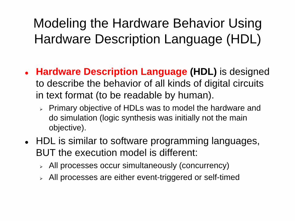
Modeling the Hardware Behavior Using Hardware Description Language (HDL)
Hardware Description Language (HDL) is designed to describe the behavior of all kinds of digital circuits in text format (to be readable by human).
Primary objective of HDLs was to model the hardware and do simulation (logic synthesis was initially not the main objective).
HDL is similar to software programming languages, BUT the execution model is different:
All processes occur simultaneously (concurrency)All processes are either event-triggered or self-timed
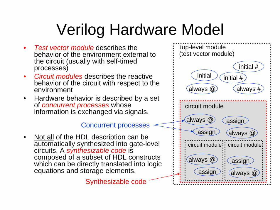
Verilog Hardware Model
initial initial #
always @
always @
assign
assign
always @
always @
assign
assign
always @
always #
top-level module(test vector module)
circuit module
initial #
• Test vector module describes the behavior of the environment external to the circuit (usually with self-timed processes)
• Circuit modules describes the reactive behavior of the circuit with respect to the environment
• Hardware behavior is described by a set of concurrent processes whose information is exchanged via signals.
• Not all of the HDL description can be automatically synthesized into gate-level circuits. A synthesizable code is composed of a subset of HDL constructs which can be directly translated into logic equations and storage elements.
circuit module circuit module
Concurrent processes
Synthesizable code
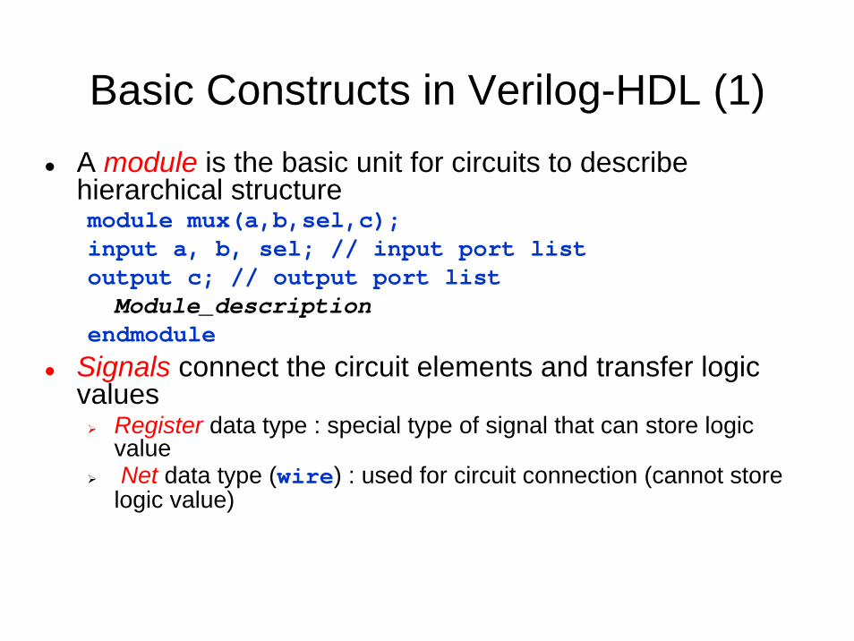
Basic Constructs in Verilog-HDL (1)A module is the basic unit for circuits to describe hierarchical structuremodule mux(a,b,sel,c);input a, b, sel; // input port listoutput c; // output port listModule_description
endmoduleSignals connect the circuit elements and transfer logic values
Register data type : special type of signal that can store logic valueNet data type (wire) : used for circuit connection (cannot store
logic value)
Basic Constructs in Verilog-HDL (2)
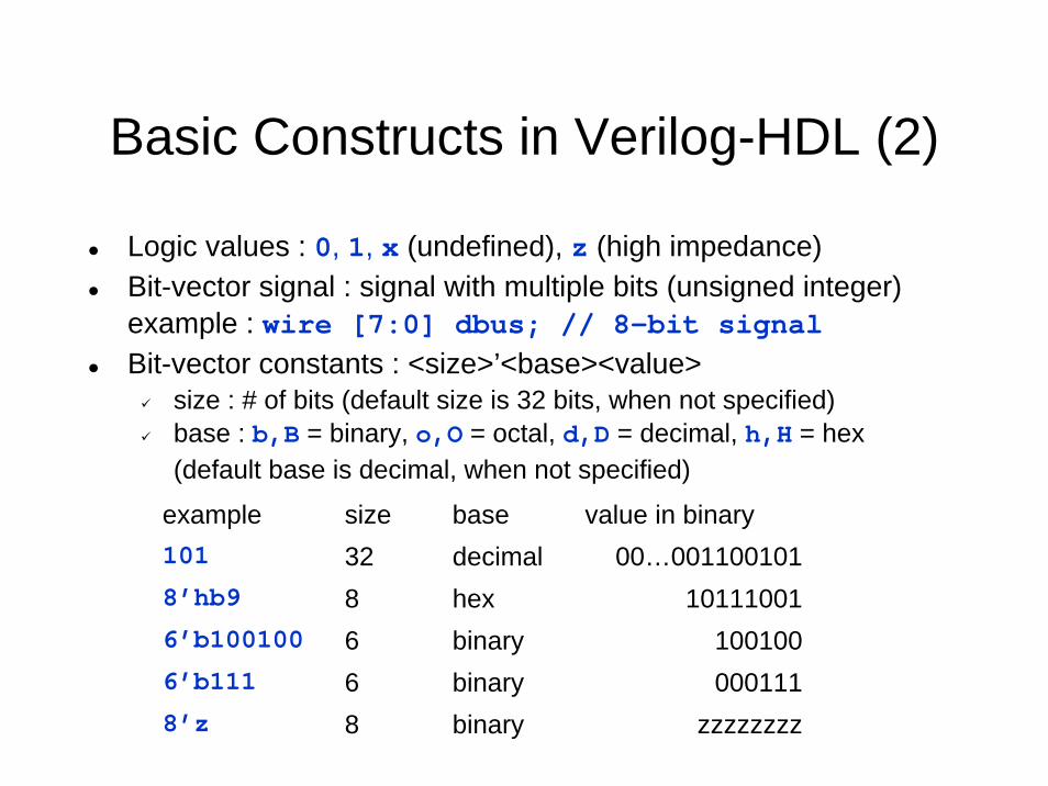
Logic values : 0, 1, x (undefined), z (high impedance)Bit-vector signal : signal with multiple bits (unsigned integer)example : wire [7:0] dbus; // 8-bit signalBit-vector constants : <size>’<base><value>
size : # of bits (default size is 32 bits, when not specified)base : b,B = binary, o,O = octal, d,D = decimal, h,H = hex(default base is decimal, when not specified)
example size base value in binary1018’hb9 8 hex 101110016’b100100 6 binary 1001006’b111 6 binary 0001118’z 8 binary
32
zzzzzzzz
00…001100101decimal
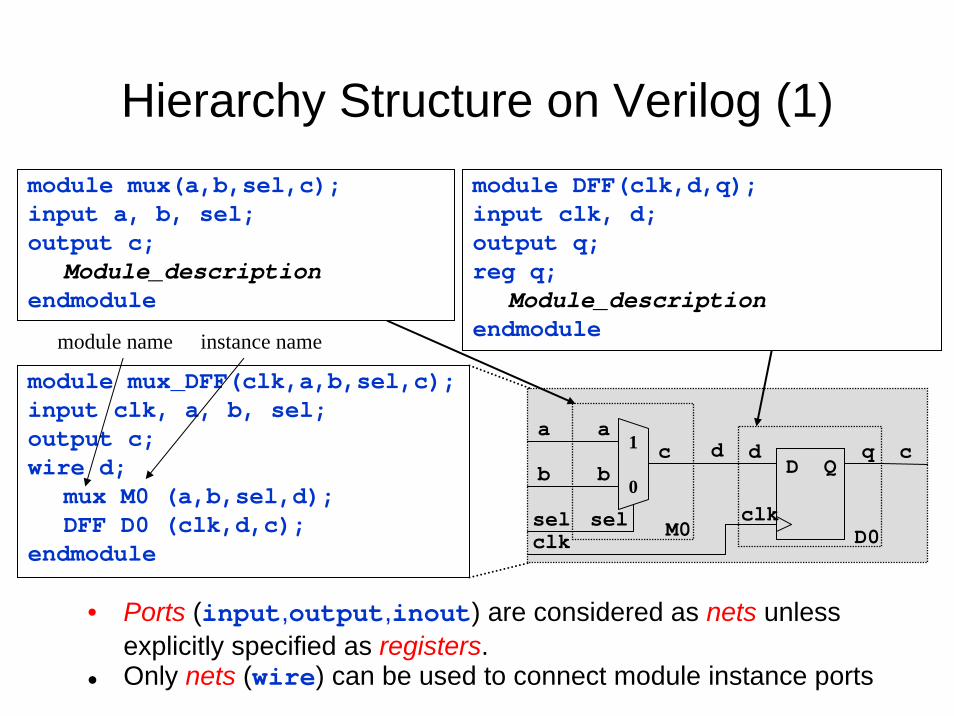
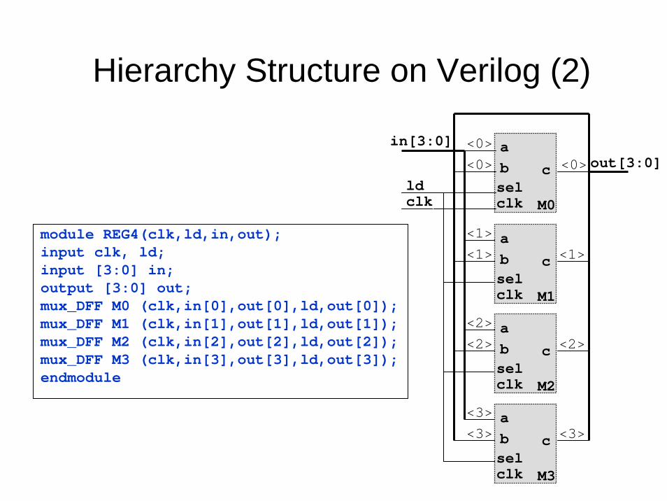
Hierarchy Structure on Verilog (1)
clk
d qD Qclk
1
0
absel
c dab
c
sel M0 D0
module DFF(clk,d,q);input clk, d;output q;reg q;
Module_descriptionendmodule
module mux(a,b,sel,c);input a, b, sel;output c;
Module_descriptionendmodule
module mux_DFF(clk,a,b,sel,c);input clk, a, b, sel;output c;wire d;
mux M0 (a,b,sel,d);DFF D0 (clk,d,c);
endmodule
module name
• Ports (input,output,inout) are considered as nets unless explicitly specified as registers.Only nets (wire) can be used to connect module instance ports
instance name
Hierarchy Structure on Verilog (2)
module REG4(clk,ld,in,out);input clk, ld;input [3:0] in;output [3:0] out;mux_DFF M0 (clk,in[0],out[0],ld,out[0]);mux_DFF M1 (clk,in[1],out[1],ld,out[1]);mux_DFF M2 (clk,in[2],out[2],ld,out[2]);mux_DFF M3 (clk,in[3],out[3],ld,out[3]);endmodule
clk
ab csel
<0><0>
<1><1>
<2><2>
<3><3> <3>
<2>
<1>
<0>in[3:0]
out[3:0]
M0
clk
ab csel
clk
ab csel
clk
ab csel
M1
M2
M3
ldclk
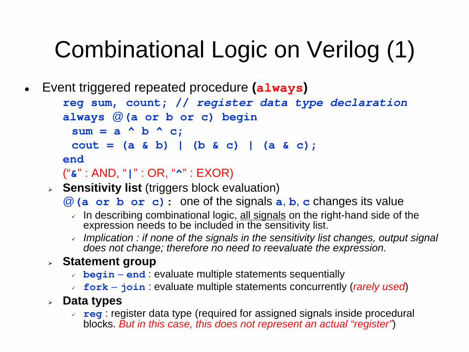
Combinational Logic on Verilog (1)Event triggered repeated procedure (always)
reg sum, count; // register data type declarationalways @(a or b or c) beginsum = a ^ b ^ c;cout = (a & b) | (b & c) | (a & c);
end(“&” : AND, “|” : OR, “^” : EXOR)Sensitivity list (triggers block evaluation)@(a or b or c): one of the signals a, b, c changes its value
In describing combinational logic, all signals on the right-hand side of the expression needs to be included in the sensitivity list.Implication : if none of the signals in the sensitivity list changes, output signal does not change; therefore no need to reevaluate the expression.
Statement groupbegin – end : evaluate multiple statements sequentiallyfork – join : evaluate multiple statements concurrently (rarely used)
Data typesreg : register data type (required for assigned signals inside procedural blocks. But in this case, this does not represent an actual “register”)
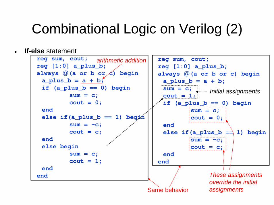
Combinational Logic on Verilog (2)If-else statement
reg sum, cout;reg [1:0] a_plus_b;always @(a or b or c) begina_plus_b = a + b;if (a_plus_b == 0) begin
sum = c;cout = 0;
endelse if(a_plus_b == 1) begin
sum = ~c;cout = c;
endelse begin
sum = c;cout = 1;
endend
reg sum, cout;reg [1:0] a_plus_b;always @(a or b or c) begina_plus_b = a + b;sum = c;cout = 1;if (a_plus_b == 0) begin
sum = c;cout = 0;
endelse if(a_plus_b == 1) begin
sum = ~c;cout = c;
endend
Same behavior
arithmetic addition
These assignments override the initial assignments
Initial assignments
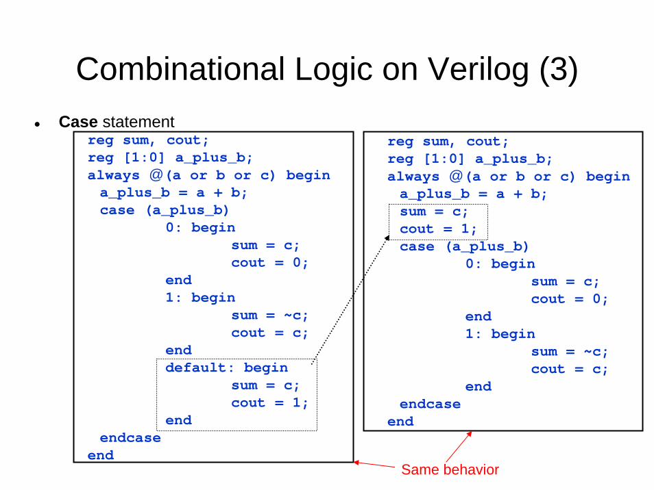
Combinational Logic on Verilog (3)Case statement
reg sum, cout;reg [1:0] a_plus_b;always @(a or b or c) begina_plus_b = a + b;case (a_plus_b)
0: beginsum = c;cout = 0;
end1: begin
sum = ~c;cout = c;
enddefault: begin
sum = c;cout = 1;
endendcase
end
reg sum, cout;reg [1:0] a_plus_b;always @(a or b or c) begina_plus_b = a + b;sum = c;cout = 1;case (a_plus_b)
0: beginsum = c;cout = 0;
end1: begin
sum = ~c;cout = c;
endendcase
end
Same behavior
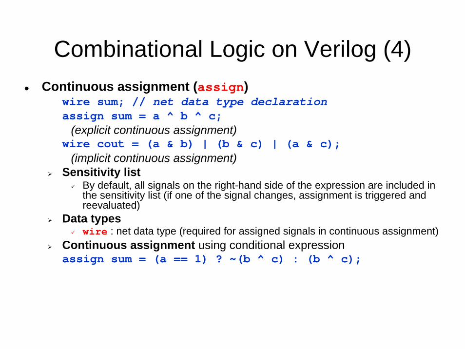
Combinational Logic on Verilog (4)Continuous assignment (assign)
wire sum; // net data type declarationassign sum = a ^ b ^ c;
(explicit continuous assignment)wire cout = (a & b) | (b & c) | (a & c);
(implicit continuous assignment)Sensitivity list
By default, all signals on the right-hand side of the expression are included in the sensitivity list (if one of the signal changes, assignment is triggered and reevaluated)
Data typeswire : net data type (required for assigned signals in continuous assignment)
Continuous assignment using conditional expression assign sum = (a == 1) ? ~(b ^ c) : (b ^ c);
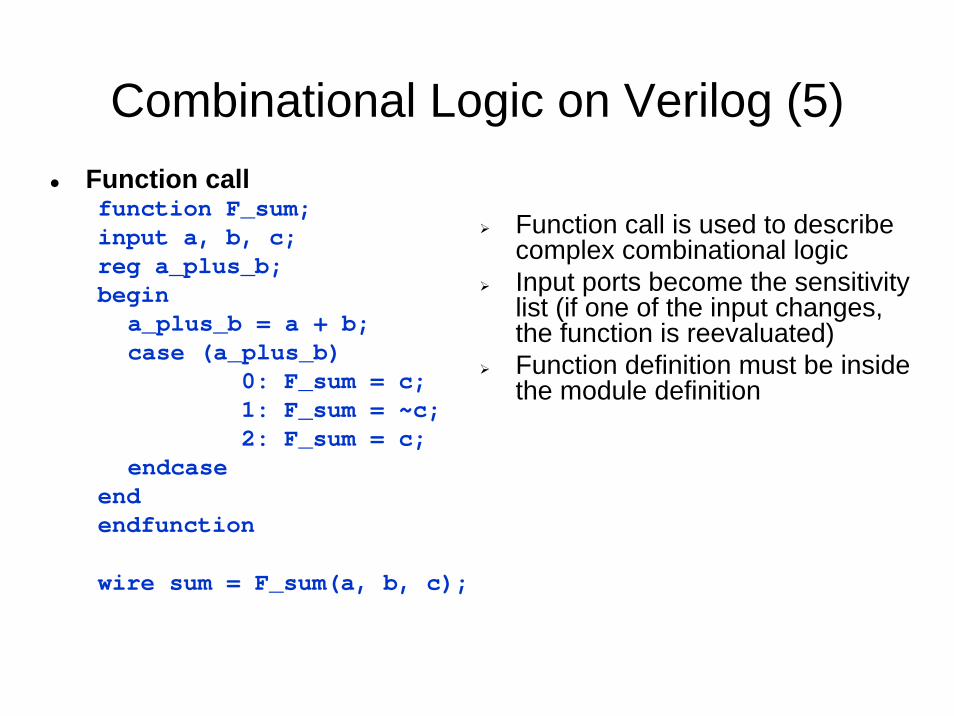
Combinational Logic on Verilog (5)Function callfunction F_sum;input a, b, c;reg a_plus_b;begin
a_plus_b = a + b;case (a_plus_b)
0: F_sum = c;1: F_sum = ~c;2: F_sum = c;
endcaseendendfunction
wire sum = F_sum(a, b, c);
Function call is used to describe complex combinational logicInput ports become the sensitivity list (if one of the input changes, the function is reevaluated)Function definition must be inside the module definition
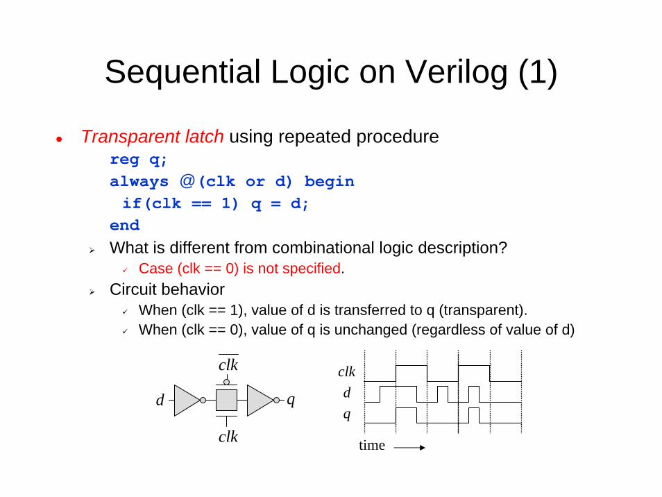
Sequential Logic on Verilog (1)
Transparent latch using repeated procedurereg q;always @(clk or d) beginif(clk == 1) q = d;
endWhat is different from combinational logic description?
Case (clk == 0) is not specified. Circuit behavior
When (clk == 1), value of d is transferred to q (transparent). When (clk == 0), value of q is unchanged (regardless of value of d)
time
clkdq
clk
clk
d q
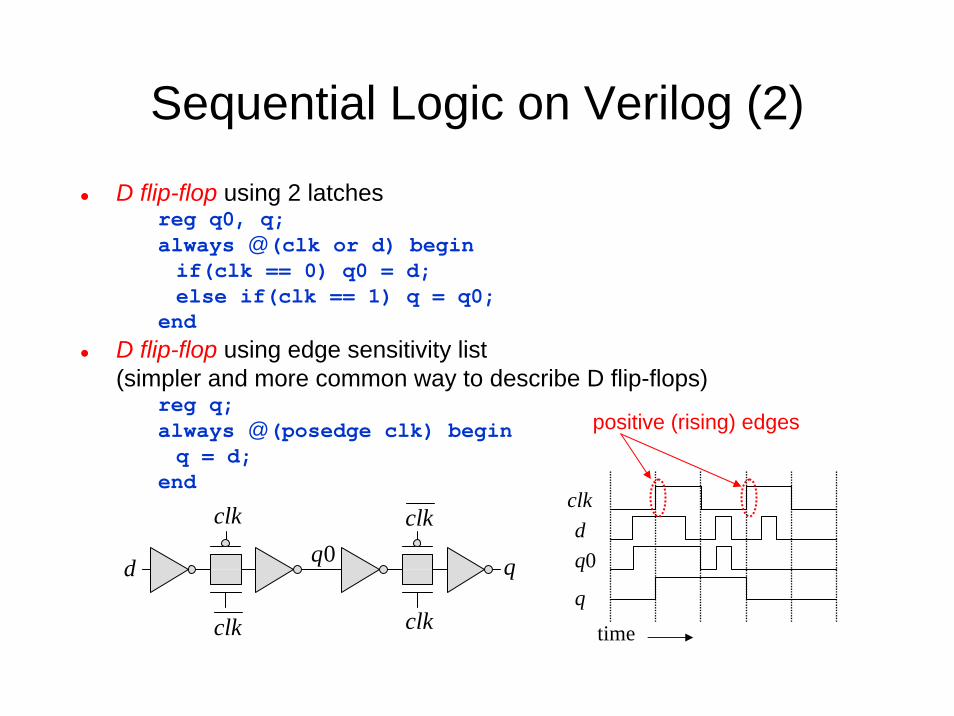
Sequential Logic on Verilog (2)
D flip-flop using 2 latchesreg q0, q;always @(clk or d) beginif(clk == 0) q0 = d;else if(clk == 1) q = q0;
endD flip-flop using edge sensitivity list(simpler and more common way to describe D flip-flops)
reg q;always @(posedge clk) beginq = d;
end
time
clkdq0
clk
clk
clk
clk
d 0q
positive (rising) edges
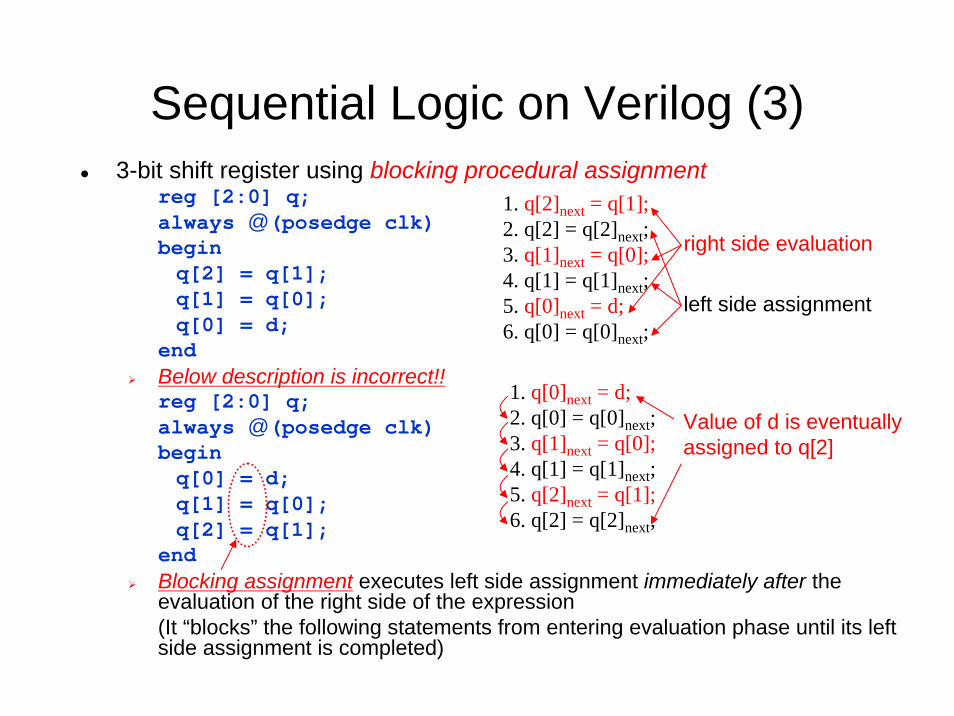
Sequential Logic on Verilog (3)3-bit shift register using blocking procedural assignment
reg [2:0] q;always @(posedge clk)beginq[2] = q[1];q[1] = q[0];q[0] = d;
endBelow description is incorrect!!reg [2:0] q;always @(posedge clk)beginq[0] = d;q[1] = q[0];q[2] = q[1];
endBlocking assignment executes left side assignment immediately after the evaluation of the right side of the expression(It “blocks” the following statements from entering evaluation phase until its left side assignment is completed)
1. q[0]next = d;2. q[0] = q[0]next;3. q[1]next = q[0];4. q[1] = q[1]next;5. q[2]next = q[1];6. q[2] = q[2]next;
1. q[2]next = q[1];2. q[2] = q[2]next;3. q[1]next = q[0];4. q[1] = q[1]next;5. q[0]next = d;6. q[0] = q[0]next;
Value of d is eventuallyassigned to q[2]
right side evaluation
left side assignment
Sequential Logic on Verilog (4)
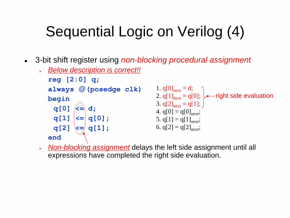
3-bit shift register using non-blocking procedural assignmentBelow description is correct!!reg [2:0] q;always @(posedge clk)beginq[0] <= d;q[1] <= q[0];q[2] <= q[1];
endNon-blocking assignment delays the left side assignment until all expressions have completed the right side evaluation.
1. q[0]next = d;2. q[1]next = q[0];3. q[2]next = q[1];4. q[0] = q[0]next;5. q[1] = q[1]next;6. q[2] = q[2]next;
right side evaluation
left side assignment
Sequential Logic on Verilog (5)
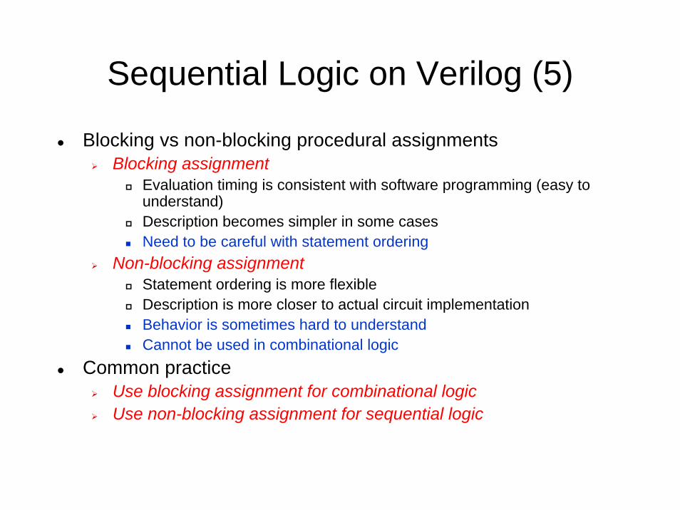
Blocking vs non-blocking procedural assignmentsBlocking assignment
Evaluation timing is consistent with software programming (easy to understand)Description becomes simpler in some casesNeed to be careful with statement ordering
Non-blocking assignmentStatement ordering is more flexibleDescription is more closer to actual circuit implementationBehavior is sometimes hard to understandCannot be used in combinational logic
Common practiceUse blocking assignment for combinational logicUse non-blocking assignment for sequential logic
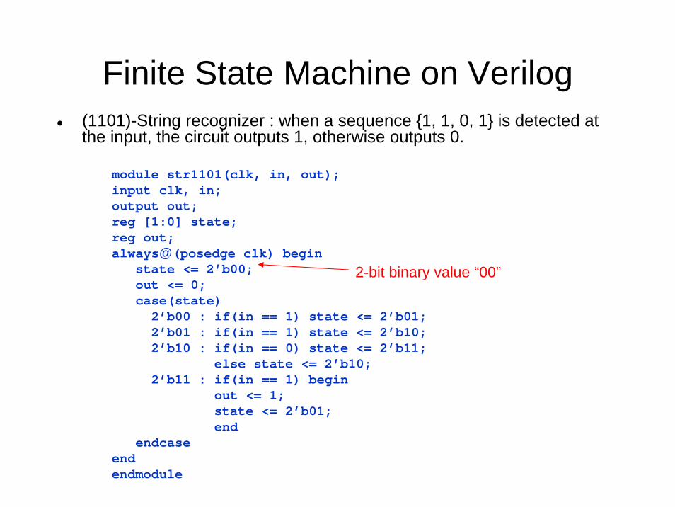
Finite State Machine on Verilog(1101)-String recognizer : when a sequence {1, 1, 0, 1} is detected at the input, the circuit outputs 1, otherwise outputs 0.
module str1101(clk, in, out);input clk, in;output out;reg [1:0] state;reg out;always@(posedge clk) begin
state <= 2’b00;out <= 0;case(state)
2’b00 : if(in == 1) state <= 2’b01;2’b01 : if(in == 1) state <= 2’b10;2’b10 : if(in == 0) state <= 2’b11;
else state <= 2’b10;2’b11 : if(in == 1) begin
out <= 1;state <= 2’b01;end
endcaseendendmodule
2-bit binary value “00”
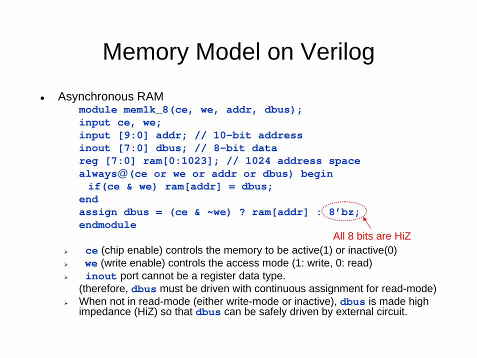
Memory Model on Verilog
Asynchronous RAMmodule mem1k_8(ce, we, addr, dbus);input ce, we;input [9:0] addr; // 10-bit addressinout [7:0] dbus; // 8-bit datareg [7:0] ram[0:1023]; // 1024 address spacealways@(ce or we or addr or dbus) beginif(ce & we) ram[addr] = dbus;
endassign dbus = (ce & ~we) ? ram[addr] : 8’bz;endmodule
ce (chip enable) controls the memory to be active(1) or inactive(0)we (write enable) controls the access mode (1: write, 0: read)inout port cannot be a register data type.
(therefore, dbus must be driven with continuous assignment for read-mode)When not in read-mode (either write-mode or inactive), dbus is made high impedance (HiZ) so that dbus can be safely driven by external circuit.
All 8 bits are HiZ
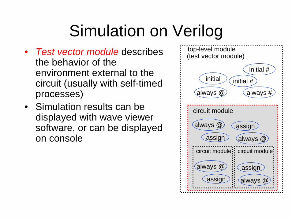
Simulation on Verilog• Test vector module describes
the behavior of the environment external to the circuit (usually with self-timed processes)
• Simulation results can be displayed with wave viewer software, or can be displayed on console
initial initial #
always @
always @
assign
assign
always @
always @
assign
assign
always @
always #
top-level module(test vector module)
circuit module
initial #
circuit module circuit module
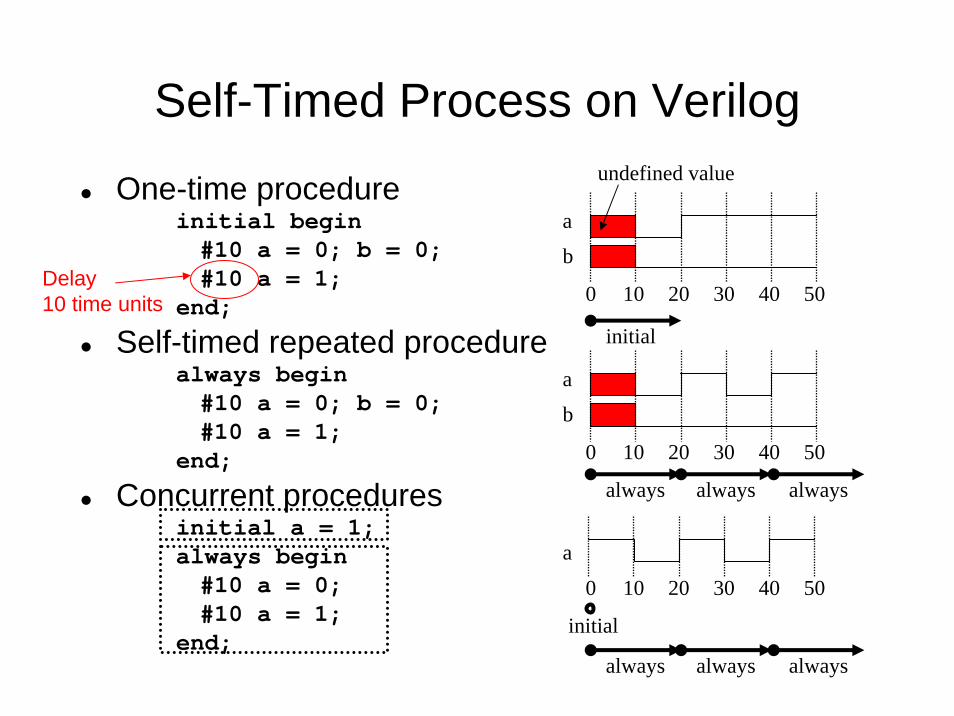
Self-Timed Process on Verilog
One-time procedureinitial begin#10 a = 0; b = 0; #10 a = 1;
end; Self-timed repeated procedure
always begin#10 a = 0; b = 0; #10 a = 1;
end;Concurrent procedures
initial a = 1;always begin#10 a = 0;#10 a = 1;
end;
0 10 20 30 40 50
a
b
0 10 20 30 40 50
a
b
undefined value
initial
always always always
Delay 10 time units
0 10 20 30 40 50
a
always always always
initial
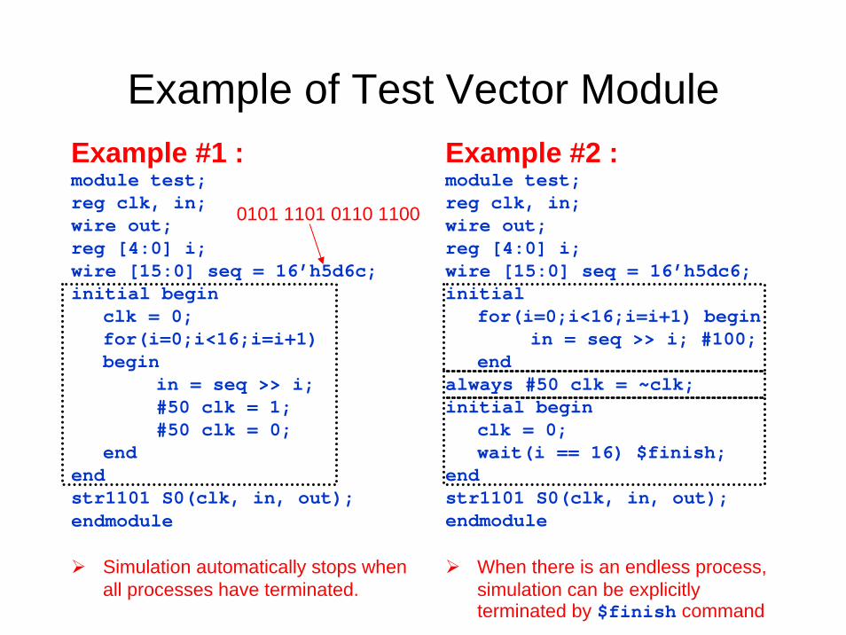
Example of Test Vector Module
0101 1101 0110 1100
Example #1 :module test;reg clk, in;wire out;reg [4:0] i;wire [15:0] seq = 16’h5d6c;initial begin
clk = 0; for(i=0;i<16;i=i+1)begin
in = seq >> i;#50 clk = 1;#50 clk = 0;
endendstr1101 S0(clk, in, out);endmodule
Simulation automatically stops when all processes have terminated.
Example #2 :module test;reg clk, in;wire out;reg [4:0] i;wire [15:0] seq = 16’h5dc6;initial
for(i=0;i<16;i=i+1) beginin = seq >> i; #100;
endalways #50 clk = ~clk;initial begin
clk = 0;wait(i == 16) $finish;
endstr1101 S0(clk, in, out);endmodule
When there is an endless process, simulation can be explicitly terminated by $finish command
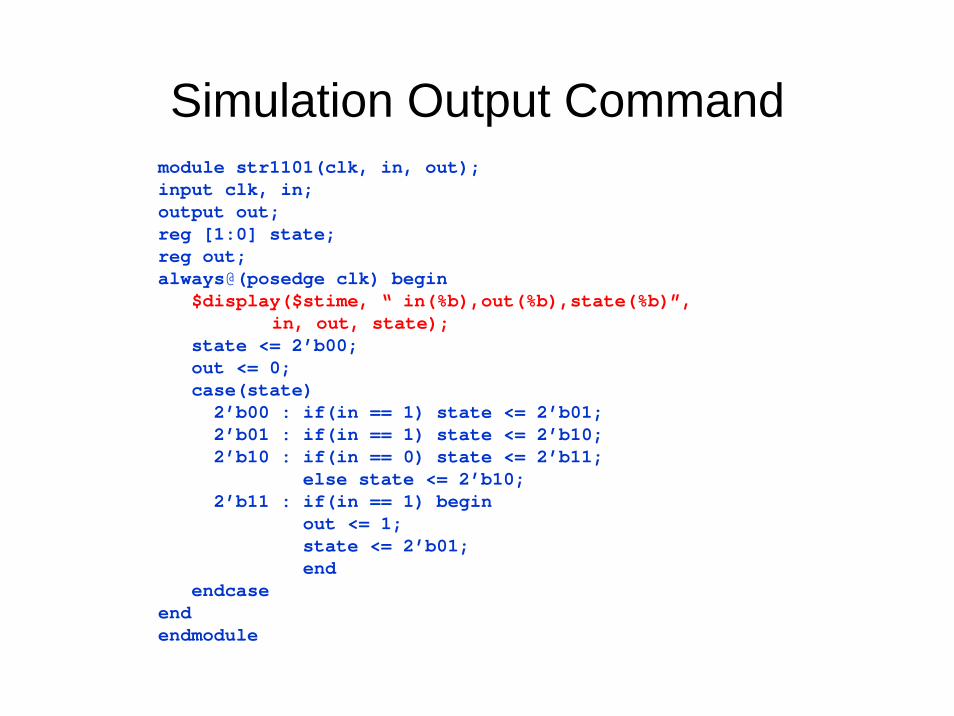
Simulation Output Commandmodule str1101(clk, in, out);input clk, in;output out;reg [1:0] state;reg out;always@(posedge clk) begin
$display($stime, “ in(%b),out(%b),state(%b)”,in, out, state);
state <= 2’b00;out <= 0;case(state)
2’b00 : if(in == 1) state <= 2’b01;2’b01 : if(in == 1) state <= 2’b10;2’b10 : if(in == 0) state <= 2’b11;
else state <= 2’b10;2’b11 : if(in == 1) begin
out <= 1;state <= 2’b01;end
endcaseendendmodule
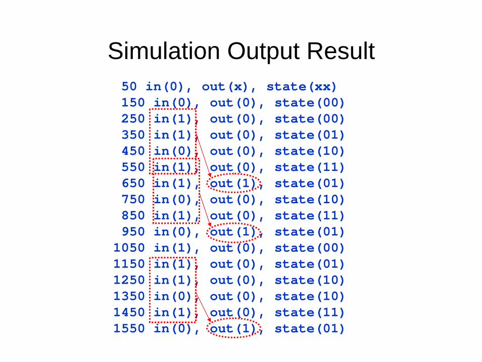
Simulation Output Result50 in(0), out(x), state(xx)150 in(0), out(0), state(00)250 in(1), out(0), state(00)350 in(1), out(0), state(01)450 in(0), out(0), state(10)550 in(1), out(0), state(11)650 in(1), out(1), state(01)750 in(0), out(0), state(10)850 in(1), out(0), state(11)950 in(0), out(1), state(01)
1050 in(1), out(0), state(00)1150 in(1), out(0), state(01)1250 in(1), out(0), state(10)1350 in(0), out(0), state(10)1450 in(1), out(0), state(11)1550 in(0), out(1), state(01)
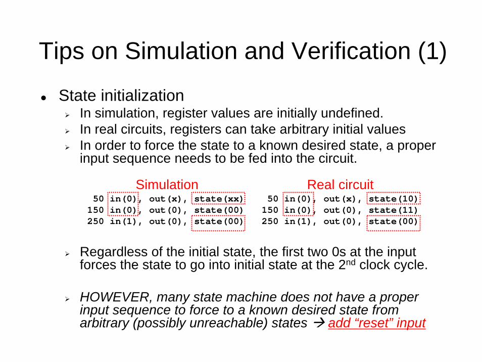
Tips on Simulation and Verification (1)
State initializationIn simulation, register values are initially undefined.In real circuits, registers can take arbitrary initial valuesIn order to force the state to a known desired state, a proper input sequence needs to be fed into the circuit.
50 in(0), out(x), state(xx) 50 in(0), out(x), state(10)150 in(0), out(0), state(00) 150 in(0), out(0), state(11)250 in(1), out(0), state(00) 250 in(1), out(0), state(00)
Regardless of the initial state, the first two 0s at the input forces the state to go into initial state at the 2nd clock cycle.
HOWEVER, many state machine does not have a proper input sequence to force to a known desired state from arbitrary (possibly unreachable) states add “reset” input
Simulation Real circuit
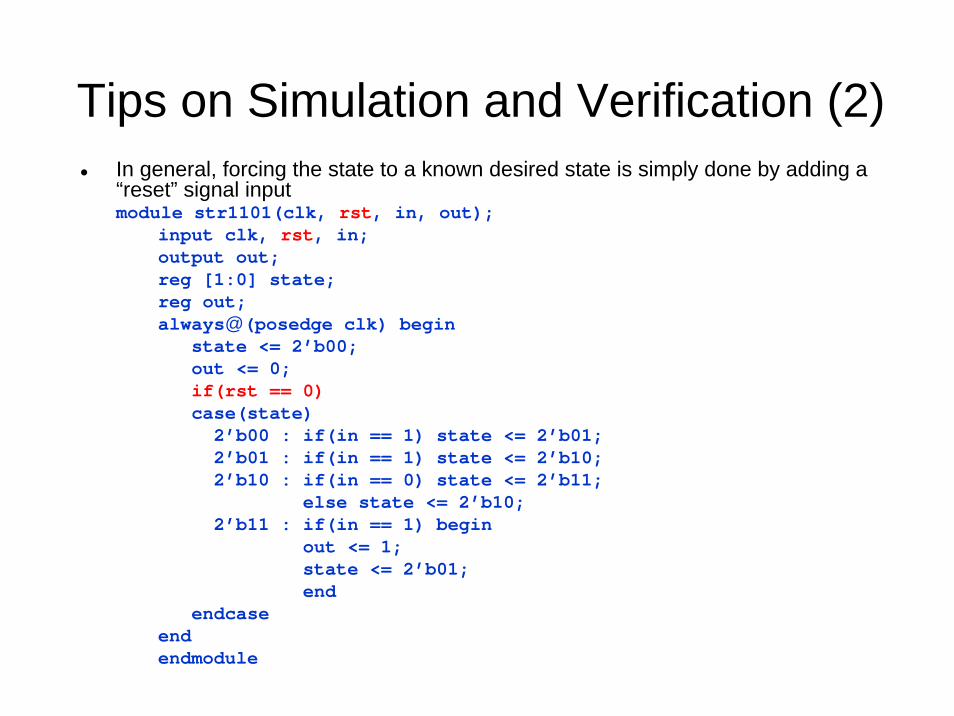
Tips on Simulation and Verification (2)In general, forcing the state to a known desired state is simply done by adding a “reset” signal input module str1101(clk, rst, in, out);
input clk, rst, in;output out;reg [1:0] state;reg out;always@(posedge clk) begin
state <= 2’b00;out <= 0;if(rst == 0)case(state)
2’b00 : if(in == 1) state <= 2’b01;2’b01 : if(in == 1) state <= 2’b10;2’b10 : if(in == 0) state <= 2’b11;
else state <= 2’b10;2’b11 : if(in == 1) begin
out <= 1;state <= 2’b01;end
endcaseendendmodule
Tips on Simulation and Verification (3)
In any system, coding the appropriate test vectors is not easy (probably harder than coding the actual circuit)
The designer needs to take account all the possible input patterns so as to cover the complete behavior of the circuitFor a large system, test vector covering only a small portion of the complete behavior takes very long time to simulate. This results in very low design productivity, and also leaves a large number of “bugs” left undetected.To verify a large system, Circuit Emulation technique is often used (the system is implemented on a set of programmable logic devices and run on actual environment).
Verilog Reference on the WEB
On-line Verilog HDL Quick Reference Guideby Stuart Sutherland of Sutherland HDL, Inc. -Portland, Oregon, USAhttp://www.sutherland-hdl.com/on-line_ref_guide/vlog_ref_top.html
Verilog FAQ (textbooks, tools, etc)http://www.angelfire.com/in/verilogfaq/
HDL Summary
Hardware Description Languages (HDLs) are designed to describe the behavior of all kinds of digital circuits in text format (to be readable by human). A subset of HDL description can be automatically transformed to gate-level circuit by logic synthesis tools ( “synthesizable” RTL code).With the current increase in design complexity, doing designs on RTL is becoming too time consuming
Although the description is in text format, concurrent behavior of HDL is still hard to track by human, giving more opportunities for errors and making debugging even harder.Software languages are far more easy to track, since everything occurs sequentially.Population of HDL programmers is much smaller than that of software programmers.Strong need for high-level synthesis tools
Problem 1.1Design the following circuits in Verilog.
Give complete module description for each circuitExplain the behavior(If you have access to Verilog simulator) create simple test vector module and confirm the behavior on simulation
A) 4-bit ripple-carry adder using full-adder modulesB) 4-bit counter with enable/reset inputs in register-transter
level description (use arithmetic operators directly on the 4-bit signals)
increment only when “enable” is 1set the counter to 0 when “reset” is 1
C) Describe the 4-bit counter in B) using 4-bit ripple-carry adder in A)
D) Unsigned multiplier (4-bit inputs, 8-bit output) (use whatever architecture such as “shift-and-add”, “array”, “Booth”)
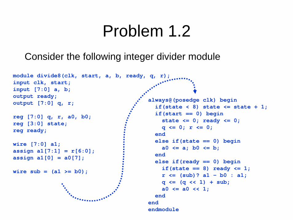
Problem 1.2Consider the following integer divider module
module divide8(clk, start, a, b, ready, q, r);input clk, start;input [7:0] a, b;output ready;output [7:0] q, r;reg [7:0] q, r, a0, b0;reg [3:0] state;reg ready;wire [7:0] a1;assign a1[7:1] = r[6:0];assign a1[0] = a0[7];wire sub = (a1 >= b0);
always@(posedge clk) beginif(state < 8) state <= state + 1;if(start == 0) beginstate <= 0; ready <= 0;q <= 0; r <= 0;
endelse if(state == 0) begina0 <= a; b0 <= b;
endelse if(ready == 0) beginif(state == 8) ready <= 1;r <= (sub)? a1 - b0 : a1;q <= (q << 1) + sub;a0 <= a0 << 1;
endendendmodule
Problem 1.2A) Explain the algorithm of this divider.
How is the division computed?What are the roles for each variable?
B) Assume :a = 8’b01100100 (=100), b = 8’b00001001 (=9)start = 0 for the first clock cycle, and start = 1after that.
Explain the behavior of the circuit at each clock cycle (explain the values of each variable at each clock cycle).
C) Modify this divider module so that it can handle 16-bit inputs.
D) Using the above 16-bit divider module, design a circuit which converts 16-bit binary value into 5-digit decimal value (each decimal digit consumes 4-bit)
Problem 1.3 (extra credit)
Design a simple calculator on Verilog with the following specificationThere are 14 keys (‘0’, ‘1’, …, ‘9’, ‘+’, ‘=’, ‘C’). When a key is pushed, a 4-bit signal associated with the key is generated with a proper control signal.There is a 4-digit decimal number display which can display 12 types of characters (‘0’, ‘1’, …, ‘9’, ‘E’, ‘ ’). To control the 4-digit display, the calculator circuit outputs 16-bit signal, each 4-bit group controlling each digit position.Entering ‘C’ resets the calculator. [‘ ’, ‘ ’, ‘ ’, ‘0’] is displayed.If the result is greater than 9999, [‘ ’, ‘ ’, ‘ ’, ‘E’] is displayed to indicate error.For other specifications, follow the conventions of actual calculator.


![Network and Hardware Co-Design - RLE at MIT · Network and Hardware Co-Design MICRO Tutorial ... deep learning inference.” ... [Moons et al., VLSI 2016]](https://img.pdfslide.net/doc/110x75/5ac7918c7f8b9acb688bc18f/network-and-hardware-co-design-rle-at-and-hardware-co-design-micro-tutorial-.jpg)