Embed Size (px)
Citation preview
What are Electron Microscopes?Electron Microscopes are scientific instruments that use a beam of highly energetic electrons to examine objects on a very fine scale. This examination can yield the following information:
Topography The surface features of an object or "how it looks", its texture; direct relation between these features and materials properties (hardness, reflectivity...etc.)
Morphology The shape and size of the particles making up the object; direct relation between these structures and materials properties (ductility, strength, reactivity...etc.)
Composition The elements and compounds that the object is composed of and the relative amounts of them; direct relationship between composition and materials properties (melting point, reactivity, hardness...etc.)
Crystallographic Information How the atoms are arranged in the object; direct relation between these arrangements and materials properties (conductivity, electrical properties, strength...etc.)

Where did Electron Microscopes Come From?Electron Microscopes were developed due to the limitations of Light Microscopes which are limited by the physics of light to 500x or 1000x magnification and a resolution of 0.2 micrometers. In the early 1930's this theoretical limit had been reached and there was a scientific desire to see the fine details of the interior structures of organic cells (nucleus, mitochondria...etc.). This required 10,000x plus magnification which was just not possible using Light Microscopes.The Transmission Electron Microscope (TEM) was the first type of Electron Microscope to be developed and is patterned exactly on the Light Transmission Microscope except that a focused beam of electrons is used instead of light to "see through" the specimen. It was developed by Max Knoll and Ernst Ruska in Germany in 1931.The first Scanning Electron Microscope (SEM) debuted in 1942 with the first commercial instruments around 1965. Its late development was due to the electronics involved in "scanning" the beam of electrons across the sample
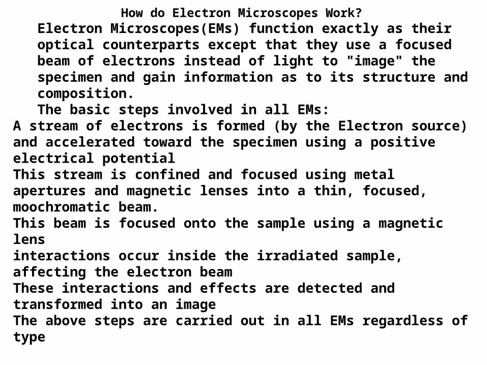
How do Electron Microscopes Work?Electron Microscopes(EMs) function exactly as their optical counterparts except that they use a focused beam of electrons instead of light to "image" the specimen and gain information as to its structure and composition.The basic steps involved in all EMs:
A stream of electrons is formed (by the Electron source) and accelerated toward the specimen using a positive electrical potential This stream is confined and focused using metal apertures and magnetic lenses into a thin, focused, moochromatic beam. This beam is focused onto the sample using a magnetic lens interactions occur inside the irradiated sample, affecting the electron beam These interactions and effects are detected and transformed into an imageThe above steps are carried out in all EMs regardless of type
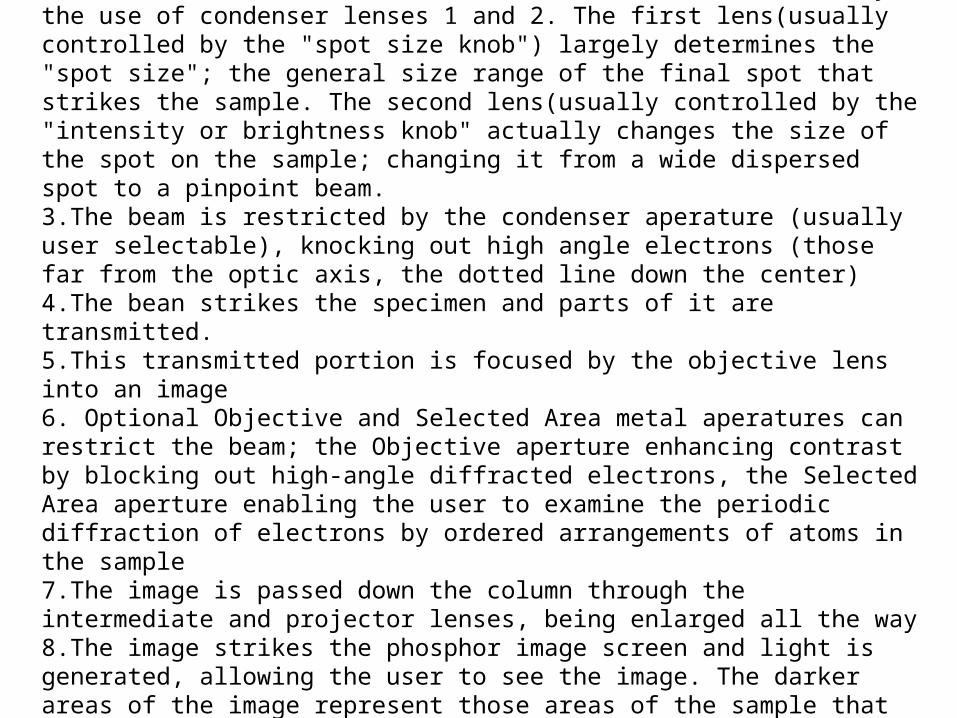
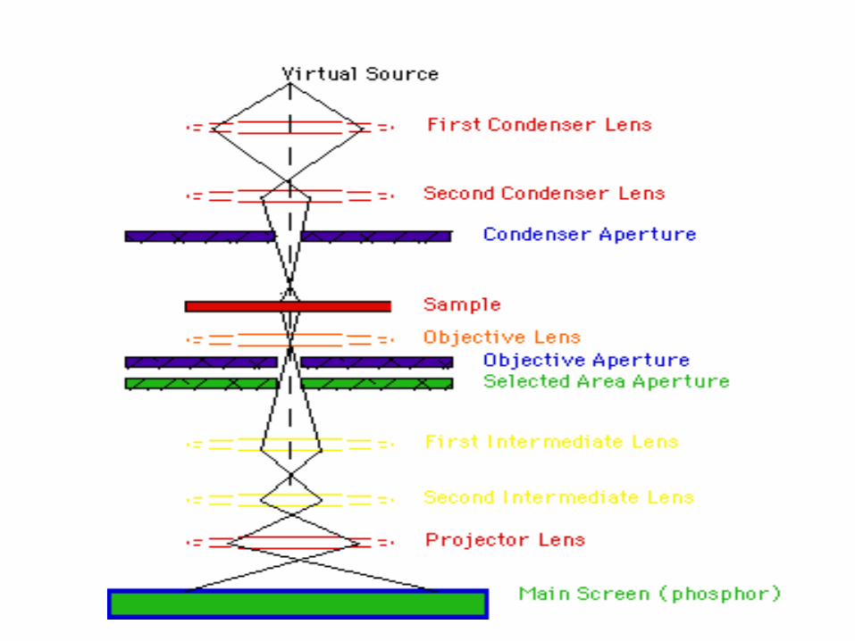
1.The "Virtual Source" at the top represents the electron gun, producing a stream of monochromatic electrons. 2.This stream is focused to a small, thin, coherent beam by the use of condenser lenses 1 and 2. The first lens(usually controlled by the "spot size knob") largely determines the "spot size"; the general size range of the final spot that strikes the sample. The second lens(usually controlled by the "intensity or brightness knob" actually changes the size of the spot on the sample; changing it from a wide dispersed spot to a pinpoint beam. 3.The beam is restricted by the condenser aperature (usually user selectable), knocking out high angle electrons (those far from the optic axis, the dotted line down the center) 4.The bean strikes the specimen and parts of it are transmitted.5.This transmitted portion is focused by the objective lens into an image 6. Optional Objective and Selected Area metal aperatures can restrict the beam; the Objective aperture enhancing contrast by blocking out high-angle diffracted electrons, the Selected Area aperture enabling the user to examine the periodic diffraction of electrons by ordered arrangements of atoms in the sample 7.The image is passed down the column through the intermediate and projector lenses, being enlarged all the way 8.The image strikes the phosphor image screen and light is generated, allowing the user to see the image. The darker areas of the image represent those areas of the sample that fewer electrons were transmitted through (they are thicker or denser). The lighter areas of the image represent those areas of the sample that more electrons were transmitted through (they are thinner or less dense)
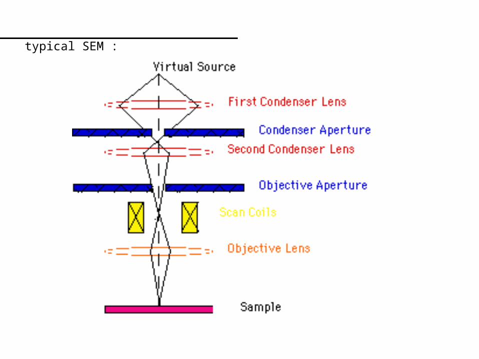
typical SEM :
1.The "Virtual Source" at the top represents the electron gun, producing a stream of monochromatic electrons.
2.The stream is condensed by the first condenser lens (usually controlled by the "coarse probe current knob"). This lens is used to both form the beam and limit the amount of current in the beam. It works in conjunction with the condenser aperture to eliminate the high-angle electrons from the beam
3.The beam is then constricted by the condenser aperture (usually not user selectable), eliminating some high-angle electrons
4.The second condenser lens forms the electrons into a thin, tight, coherent beam and is usually controlled by the "fine probe current knob"
5.A user selectable objective aperture further eliminates high-angle electrons from the beam 6.A set of coils then "scan" or "sweep" the beam in a grid fashion (like a television),
dwelling on points for a period of time determined by the scan speed (usually in the microsecond range)
7.The final lens, the Objective, focuses the scanning beam onto the part of the specimen desired.
8. When the beam strikes the sample (and dwells for a few microseconds) interactions occur inside the sample and are detected with various instruments
9.Before the beam moves to its next dwell point these instruments count the number of interactions and display a pixel on a CRT whose intensity is determined by this number (the more reactions the brighter the pixel).
10. This process is repeated until the grid scan is finished and then repeated, the entire pattern can be scanned 30 times per second

Iron oxide

Brittle fractured steel
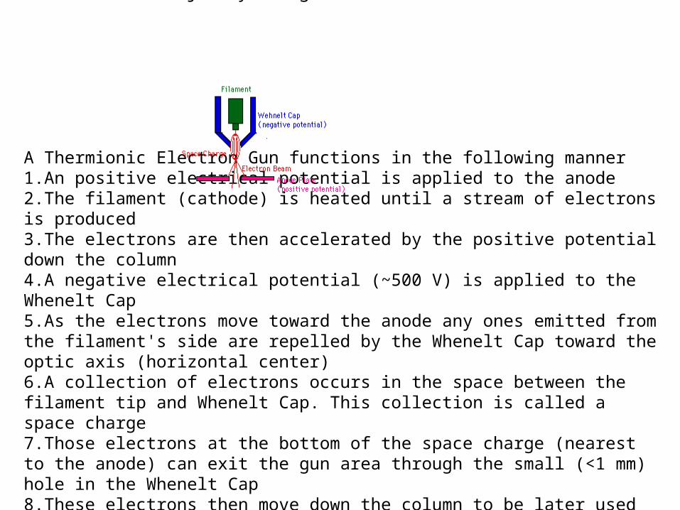
All Electron Microscopes utilize an electron source of some kind with the majority using a Themionic Gun as shown below:
A Thermionic Electron Gun functions in the following manner 1.An positive electrical potential is applied to the anode 2.The filament (cathode) is heated until a stream of electrons is produced 3.The electrons are then accelerated by the positive potential down the column 4.A negative electrical potential (~500 V) is applied to the Whenelt Cap 5.As the electrons move toward the anode any ones emitted from the filament's side are repelled by the Whenelt Cap toward the optic axis (horizontal center) 6.A collection of electrons occurs in the space between the filament tip and Whenelt Cap. This collection is called a space charge 7.Those electrons at the bottom of the space charge (nearest to the anode) can exit the gun area through the small (<1 mm) hole in the Whenelt Cap 8.These electrons then move down the column to be later used in imaging
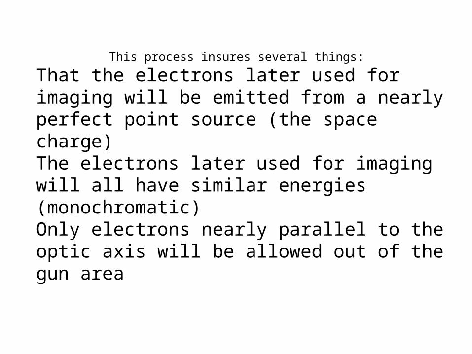
This process insures several things:
That the electrons later used for imaging will be emitted from a nearly perfect point source (the space charge) The electrons later used for imaging will all have similar energies (monochromatic) Only electrons nearly parallel to the optic axis will be allowed out of the gun area
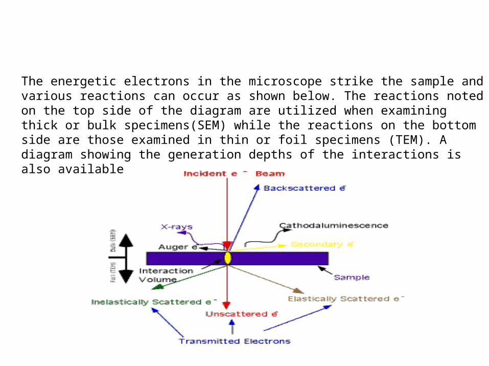
The energetic electrons in the microscope strike the sample and various reactions can occur as shown below. The reactions noted on the top side of the diagram are utilized when examining thick or bulk specimens(SEM) while the reactions on the bottom side are those examined in thin or foil specimens (TEM). A diagram showing the generation depths of the interactions is also available
Bulk Specimen InteractionsBackscattered Electrons:
Formation Caused by an incident electron colliding with an atom in the specimen which is nearly normal to the incident's path. The incident electron is then scattered "backward" 180 degrees.
Utilization The production of backscattered electrons varies directly with the specimen's atomic number. This differing production rates causes higher atomic number elements to appear brighter than lower atomic number elements. This interaction is utilized to differentiate parts of the specimen that have different average atomic number. An example is shown in the SEM output section, specifically the mechanically alloyed specimen micrograph.
Secondary Electrons: Source
Caused by an incident electron passing "near" an atom in the specimen, near enough to impart some of its energy to a lower energy electron (usually in the K-shell). This causes a slight energy loss and path change in the incident electron and the ionization of the electron in the specimen atom. This ionized electron then leaves the atom with a very small kinetic energy (5eV) and is then termed a "secondary electron". Each incident electron can produce several secondary electrons.
Utilization Production of secondary electrons is very topography related. Due to their low energy, 5eV, only secondaries that are very near the surface (<10nm,) can exit the sample and be examined. Any changes in topography in the sample that are larger than this sampling depth will change the yield of secondaries due to collection efficiencies. Collection of these electrons is aided by using a "collector" in conjunction with the secondary electron detector. The collector is a grid or mesh with a +100V potential applied to it which is placed in front of the detector, attracting the negatively charged secondary electrons to it which then pass through the grid-holes and into the detector to be counted.
Auger Electrons Source
Caused by the de-energization of the specimen atom after a secondary electron is produced. Since a lower (usually K-shell) electron was emitted from the atom during the secondary electron process an inner (lower energy) shell now has a vacancy. A higher energy electron from the same atom can "fall" to a lower energy, filling the vacancy. This creates and energy surplus in the atom which can be corrected by emitting an outer (lower energy) electron; an Auger Electron.
Utilization Auger Electrons have a characteristic energy, unique to each element from which it was emitted from. These electrons are collected and sorted according to energy to give compositional information about the specimen. Since Auger Electrons have relatively low energy they are only emitted from the bulk specimen from a depth of <3).
X-rays Source
Caused by the de-energization of the specimen atom after a secondary electron is produced. Since a lower (usually K-shell) electron was emitted from the atom during the secondary electron process an inner (lower energy) shell now has a vacancy. A higher energy electron can "fall" into the lower energy shell, filling the vacancy. As the electron "falls" it emits energy, usually X-rays to balance the total energy of the atom so it .
Utilization X-rays or Light emitted from the atom will have a characteristic energy which is unique to the element from which it originated. These signals are collected and sorted according to energy to yield micrometer diameter) of bulk specimens limiting the point-to-point comparisons available
Thin Specimen InteractionsUnscattered Electrons Source
Incident electrons which are transmitted through the thin specimen without any interaction occurring inside the specimen.
Utilization The transmission of unscattered electrons is inversely proportional to the specimen thickness. Areas of the specimen that are thicker will have fewer transmitted unscattered electrons and so will appear darker, conversely the thinner areas will have more transmitted and thus will appear lighter.
Elasticity Scattered electrons Source
Incident electrons that are scattered (deflected from their original path) by atoms in the specimen in an elastic fashion (no loss of energy). These scattered electrons are then transmitted through the remaining portions of the specimen.
Utilization All electrons follow Bragg's Law and thus are scattered according to Wavelength=2*Space between the atoms in the specimen*sin(angle of scattering). All incident electrons have the same energy(thus wavelength) and enter the specimen normal to its surface. All incidents that are scattered by the same atomic spacing will be scattered by the same angle. These "similar angle" scattered electrons can be collated using magnetic lenses to form a pattern of spots; each spot corresponding to a specific atomic spacing (a plane). This pattern can then yield information about the orientation, atomic arrangements and phases present in the area being examined
Inelastically Scattered Electrons
Source Incident electrons that interact with specimen atoms in a inelastic fashion, loosing energy during the interaction. These electrons are then transmitted trough the rest of the specimen
Utilization Inelasticaly scattered electrons can be utilized two ways
Electron Energy Loss Spectroscopy: The inelastic loss of energy by the incident electrons is characteristic of the elements that were interacted with. These energies are unique to each bonding state of each element and thus can be used to extract both compositional and bonding (i.e. oxidation state) information on the specimen region being examined. Kakuchi Bands: Bands of alternating light and dark lines that are formed by inelastic scattering interactions that are related to atomic spacings in the specimen. These bands can be either measured (their width is inversely proportional to atomic spacing) or "followed" like a roadmap to the "real" elasticity scattered electron pattern.
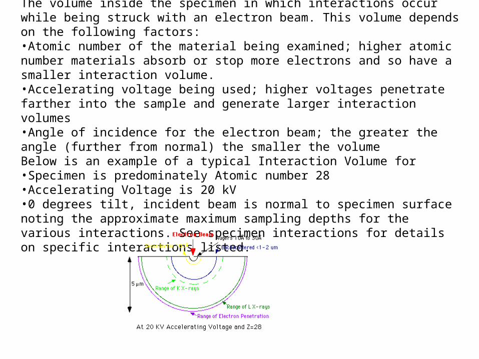
The volume inside the specimen in which interactions occur while being struck with an electron beam. This volume depends on the following factors: •Atomic number of the material being examined; higher atomic number materials absorb or stop more electrons and so have a smaller interaction volume. •Accelerating voltage being used; higher voltages penetrate farther into the sample and generate larger interaction volumes •Angle of incidence for the electron beam; the greater the angle (further from normal) the smaller the volume Below is an example of a typical Interaction Volume for •Specimen is predominately Atomic number 28 •Accelerating Voltage is 20 kV •0 degrees tilt, incident beam is normal to specimen surface noting the approximate maximum sampling depths for the various interactions. See specimen interactions for details on specific interactions listed.
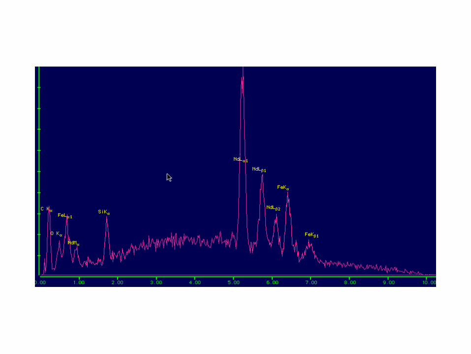
This technique is used in conjunction with SEM and is not a surface science technique. An electron beam strikes the surface of a conducting sample. The energy of the beam is typically in the range 10-20keV. This causes X-rays to be emitted from the point the material. The energy of the X-rays emitted depend on the material under examination. The X-rays are generated in a region about 2 microns in depth, and thus EDX is not a surface science technique. By moving the electron beam across the material an image of each element in the sample can be acquired in a manner similar to SAM. Due to the low X-ray intensity, images usually take a number of hours to acquire. Elements of low atomic number are difficult to detect by EDX. The SiLi detector (see below) is often protected by a Beryllium window. The absorbtion of the soft X-rays by the Be precludes the detection of elements below an atomic number of 11 (Na). In windowless systems, elements with as low atomic number as 4 (Be) have been detected, but the problems involved get progressively worse as the atomic number is reduced.