Embed Size (px)
Citation preview
Wide Band Gap Compound Semiconductor
Detectors for X-ray Spectroscopy in Harsh
Environments
Thesis submitted for the degree of
Doctor of Philosophy
at the University of Leicester
by
Anna Megan Barnett
Space Research Centre
Department of Physics and Astronomy
December 2011
Wide Band Gap Compound Semiconductor Detectors for X-ray Spectroscopy in Harsh Environments
1
Wide Band Gap Compound Semiconductor
Detectors for X-ray Spectroscopy in Harsh
Environments
Anna Megan Barnett
Abstract
Novel photon counting Al0.8Ga0.2As, GaAs and SiC X-ray photodiodes were
investigated through experiments and Monte Carlo computer simulations for their
suitability as spectroscopic soft (≤ 25 keV) X-ray detectors in high temperature (up to
90 °C) environments.
Photon counting Al0.8Ga0.2As and GaAs non-avalanche p+-i-n
+ mesa X-ray photodiodes
were shown to operate at temperatures as high as 90 °C. The temperature dependences
of their spectral resolutions (FWHM at 5.9 keV) are reported. Analyses of the noise
sources contributing to the devices‟ measured performances are presented which
suggest that efforts to improve the spectral resolutions would be well targeted at
reducing the noise contributions from the packaging of the detectors. For the GaAs
diodes, the X-ray characterisation of the devices was extended to higher energies
(25 keV). Internal detector X-ray fluorescence was demonstrated and Monte Carlo
computer simulations were compared with the experimental results.
Prior to the research presented in this thesis, the only Al0.8Ga0.2As photon counting
X-ray avalanche photodiodes reported in the literature (Lees et al., 2008, Nucl. Instr.
and Meth. A, Vol. 594, pp. 202-205) had shown anomalies in the obtained spectra.
Through new experimental measurements and computer simulations, the anomaly is
explained. A new method was developed which uses the phenomenon to extract
measurements of the electron and hole ionisation coefficients of Al0.8Ga0.2As at a
typical operating field and the first report of their temperature dependence is made.
Measurements characterising the X-ray spectroscopic performance of Semi-Transparent
SiC Schottky Diodes over an energy range ~6 keV to 25 keV at temperatures up to
80 °C are presented and discussed, along with relative efficiency measurements and
data showing the temperature dependence of the leakage current in such devices.
The research presented in this thesis shows that Al0.8Ga0.2As, GaAs and SiC X-ray
detectors are promising devices for high temperature soft X-ray spectroscopy.
Wide Band Gap Compound Semiconductor Detectors for X-ray Spectroscopy in Harsh Environments
2
Acknowledgements
My most heartfelt thanks are extended to all who made the completion of this thesis
possible, most notably Dr John Lees and David Bassford. The time, patience and
encouragement they have both shown in guiding me through three years of research
have been vital. I have benefited enormously from their experience, clarity of thought
and friendship and I feel extremely fortunate to have had such good luck as to work
with them.
I am grateful to Prof George Fraser for accepting me onto the PhD programme at the
Space Research Centre at University of Leicester, and for his advice, support and
expertise, which have ensured I retain a suitable perspective on my work. I am also
grateful to Dr Darren Wright for providing a refreshing and lucid independent view, and
to Dr Jo Shien Ng, Dr Chee Hing Tan and Dr Alton Horsfall who provided the devices
used in this work, along with much valuable advice and semiconductor engineering
expertise.
I am appreciative, too, of my friends and colleagues throughout the SRC, particularly
Dr Dean Talboys, Oliver Blake, Dr Adrian Martindale and Dr Graeme Hansford who
warmly welcomed me and called by my office each day at coffee time, and to Dr Nigel
Bannister for the music.
The financial support received from the Science and Technology Facilities Council in
the form of a studentship is also gratefully acknowledged.
Finally, but by no means least, I am so very thankful to Mum and Dad for their love and
support, and to Sarah for making life worthwhile.
Wide Band Gap Compound Semiconductor Detectors for X-ray Spectroscopy in Harsh Environments
3
Contents
Abstract 1
Acknowledgements 2
Contents 3
Publications 8
Chapter 1 Introduction 9
1.1 Background 9
1.2 Motivation 10
1.3 Applications and requirements for high temperature tolerant soft
X-ray detectors 10
1.3.1 Extraterrestrial Planetary Analysis 10
1.3.1.1 In situ planetary analysis 10
1.3.1.2 Planetary remote sensing 11
1.3.2 Terrestrial applications 13
1.4 Compound semiconductors for X-ray spectroscopy 14
1.5 Thesis organisation 18
Chapter 2 Detector physics 20
2.1 Introduction 20
2.2 X-ray attenuation 20
2.2.1 Beer-Lambert law 20
2.2.2 Photoelectric absorption 21
Wide Band Gap Compound Semiconductor Detectors for X-ray Spectroscopy in Harsh Environments
4
2.2.3 Absorption edges 21
2.3 Diode structure 22
2.4 Charge generation 25
2.5 Charge transport 27
2.6 Energy resolution and noise sources 28
2.6.1 Introduction 28
2.6.2 The energy resolution of a semiconductor detector 29
2.6.3 Parallel white noise 29
2.6.4 Series white noise 30
2.6.5 1/f series noise 31
2.6.6 Dielectric noise 31
2.6.7 Induced gate current noise 31
2.6.8 Electronic noise sources in combination 32
2.7 Impact ionisation 32
2.7.1 Introduction 32
2.7.2 Background theory 34
2.7.3 Multiplication factors 35
2.7.4 Excess noise factor 36
Chapter 3 Monte Carlo model 39
3.1 Introduction 39
3.2 Detector properties definition 40
3.3 X-ray source properties definition 41
3.4 X-ray attenuation and photoelectric absorption 41
Wide Band Gap Compound Semiconductor Detectors for X-ray Spectroscopy in Harsh Environments
5
3.5 Electron-hole pair creation 42
3.6 X-ray fluorescence 42
3.7 Avalanche multiplication 46
3.8 Spectrum generation 47
Chapter 4 The temperature dependence of Al0.8Ga0.2As
non-avalanche photodiodes 48
4.1 Introduction 48
4.2 Background 48
4.3 Diode fabrication and design 49
4.4 Leakage current measurements 52
4.5 55
Fe X-ray spectral measurements 55
4.6 Noise analysis 58
4.6.1 Initial measurements 58
4.6.2 Shaping time measurements 59
4.7 Conclusions and discussion 64
Chapter 5 High temperature GaAs non-avalanche photodiodes 66
5.1 Introduction 66
5.2 Diode design and fabrication 66
5.3 Leakage current measurements 68
5.4 55
Fe X-ray spectral measurements 70
5.5 Noise analysis 73
5.5.1 Initial measurements 73
5.5.2 Shaping time measurements 74
Wide Band Gap Compound Semiconductor Detectors for X-ray Spectroscopy in Harsh Environments
6
5.6 109
Cd spectra and GaAs diode internal X-ray fluorescence 78
5.7 Conclusions and discussion 83
Chapter 6 Photon counting Al0.8Ga0.2As avalanche photodiodes 85
6.1 Introduction 85
6.2 Diode fabrication, design and selection 86
6.3 Initial computer simulations 87
6.3.1 X-ray source definition 87
6.3.2 Detector properties definition 87
6.3.3 Initial simulation results 87
6.4 Experimentally observed spectra 90
6.5 Interpretation of experimental results and model adaptation 92
6.6 Adapted model results 93
6.7 Reduced p+ layer thickness simulations 95
6.8 Temperature dependence of the impact ionisation coefficients in
Al0.8Ga0.2As 97
6.8.1 Experimental measurements 97
6.8.2 Computer modelling and the determination of α and β 98
6.9 Conclusions and discussion 101
Chapter 7 High temperature semi-transparent 4H-SiC
Schottky photodiodes 103
7.1 Introduction 103
7.2 Diode fabrication and design 104
7.3 Leakage current measurements 106
Wide Band Gap Compound Semiconductor Detectors for X-ray Spectroscopy in Harsh Environments
7
7.4 X-ray spectral resolution measurements 107
7.5 Noise analysis 110
7.6 Detector quantum efficiency 112
7.7 Conclusions and discussion 115
Chapter 8 Summary, conclusions and further work 116
8.1 Summary and conclusions 116
8.2 Further work 119
Bibliography 122
Wide Band Gap Compound Semiconductor Detectors for X-ray Spectroscopy in Harsh Environments
8
Publications
A.M. Barnett, D.J. Bassford, J.E. Lees, J.S. Ng, C.H. Tan, J.P.R. David, 2010,
Temperature dependence of AlGaAs soft X-ray detectors, Nucl. Inst. and Meth. A,
Vol. 621, Iss. 1-3, pp. 453-455.
A.M. Barnett, J.E. Lees, D.J. Bassford, J.S. Ng, C.H. Tan, R.B. Gomes, 2011,
Modelling results of avalanche multiplication in AlGaAs soft X-ray APDs, Nucl. Inst.
and Meth. A, Vol. 626-627, pp. 25-30.
A.M. Barnett, J.E. Lees, D.J. Bassford, J.S. Ng, C.H. Tan, R.B. Gomes, 2011,
Temperature dependence of the avalanche multiplication process and impact ionization
coefficients in Al0.8Ga0.2As, Nucl. Inst. and Meth, Vol. 629, Iss. 1, pp. 154-156.
J.E. Lees, A.M. Barnett, D.J. Bassford, R.C. Stevens, A.B. Horsfall, 2011, SiC X-ray
detectors for harsh environments, J. Inst, Vol. 6, C01032.
C.H. Tan, R.B. Gomes, J.P.R. David, A.M. Barnett, D.J. Bassford, J.E. Lees, J.S. Ng,
2011, Avalanche Gain and Energy Resolution of Semiconductor X-ray Detectors, IEEE
Trans. Elect. Dev., Vol. 58, No. 9, pp. 1696-1701.
A.M. Barnett, J.E. Lees, D.J. Bassford, J.S. Ng, C.H. Tan, N. Babazadeh, R.B. Gomes,
2011, The spectral resolution of high temperature GaAs photon counting soft X-ray
photodiodes, Nucl. Instr. and Meth. A., Vol. 654, pp. 336-339.
J.E. Lees, A.M. Barnett, D.J. Bassford, J.S. Ng, C.H. Tan, N. Babazadeh, R.B. Gomes,
P. Vines, R.D. McKeag, and D. Boe, 2011, Development of high temperature AlGaAs
soft X-ray photon counting detectors, J. Inst. Vol. 6, C12007.
J.E. Lees, A.M. Barnett, D.J. Bassford, J.S. Ng, C.H. Tan, N. Babazadeh, R.B. Gomes,
P. Vines, R.D. McKeag and D. Boe, 2011, Development of AlGaAs avalanche diodes
for soft X-ray photon counting, IEEE conference on Room Temperature Semiconductor
Detectors, Valencia Spain, 2011.
A.M. Barnett, J.E. Lees, D.J. Bassford, J.S. Ng, 2012, A varied shaping time noise
analysis of Al0.8Ga0.2As and GaAs X-ray photodiodes, Nucl. Instr. and Meth. A.,
Vol. 673, pp. 10-15.
Wide Band Gap Compound Semiconductor Detectors for X-ray Spectroscopy in Harsh Environments
9
Chapter 1 Introduction
1.1 Background
In 1913, Henry Moseley published research concerning the X-ray spectra of chemical
elements (Moseley, 1913) with a view to testing a hypothesis made by Antonius van der
Broek, stating that the chemical and optical properties (including X-ray properties) of
the elements were determined by each element‟s atomic number, Z, rather than its
atomic mass, A (Heilbron, 1966). Moseley‟s work, which confirmed a link between
X-ray frequency and atomic number, Z, set the stage for X-ray spectroscopy to become
the indispensable tool it is today, used in disciplines as varied as the analysis of works
of art and the in situ investigation of the soils of other planets. In the years that have
passed since Moseley published his findings, scientists and engineers have produced
ever more sensitive and user-friendly instruments for the detection of X-rays and the
characterisation of the elements and their abundances in samples of unknown
composition.
In the 1960s, the first detectors based upon semiconducting material became available.
Today, semiconductor soft X-ray (≤ 20 keV) detectors are most often silicon based and
take one of several broad structural forms, including charge coupled devices (CCDs)
(Miyaguchi et al., 1999), silicon drift detectors (SDDs) (Gatti & Rehak, 1984),
DEPFETs (Kemmer & Lutz, 1987) (Kemmer et al., 1990) and photodiodes (Kataoka et
al., 2005). Semiconductor X-ray detectors have many advantages compared to other
detector types. Their improving spectral resolution, availability in imaging array format
and lower cost, along with their smaller size, have led to the present high popularity of
semiconductor detectors among a wide variety of X-ray spectroscopists (Knoll, 2000)
(Potts & West, 2008). However, silicon semiconductor detectors do have limitations.
They are often prone to radiation damage that can degrade their performance (Hall and
Holland, 2010) (Cappelletti, Cédola, & Blancá, 2008), and in order to achieve their
optimum performance and spectral resolution they usually need to be operated at low
(≤ 20 °C) (Lechner et al., 1996) or sometimes near-cryogenic (~ -120 °C) temperatures
(Abbey et al., 2003). The systems required to support a silicon semiconductor detector
Wide Band Gap Compound Semiconductor Detectors for X-ray Spectroscopy in Harsh Environments
10
needing to operate in a non-ideal (high temperature, intense radiation) environment are,
therefore, not insignificant: protection against radiation damage must be designed into
the system, as must facilities for cooling.
A review of the most important methods and detector types, including semiconductor
detectors, developed for space related X-ray spectroscopy in the latter half of the
twentieth century, can be found in Fraser (1989). A review of their use and applications
in a wide variety of fields, where X-ray spectroscopy use flourishes particularly because
of the miniaturisation of instrumentation brought by the semiconductor revolution, can
be found in Potts and West (2008).
1.2 Motivation
The development of semiconductor X-ray detectors that can operate at high temperature
without any (or only minimal) cooling would enable X-ray spectroscopy to be used in
many applications that are currently unable, through financial cost or energy, mass,
volume or other technical restrictions, to accommodate the cooling apparatus (such as
Peltier or cryogenic coolers) that may be required for silicon detectors in such
environments. Even in applications that are able to accommodate the cooling needs of
existing detectors, reducing the requirements for cooling would enable costs to be
reduced and X-ray spectroscopy to be deployed more widely. If high temperature
tolerant semiconductor detectors could be developed, they would be very attractive
candidates for X-ray spectrometers for future space missions to hot environments such
as the surface of Venus.
1.3 Applications and requirements for high temperature tolerant
soft X-ray detectors
1.3.1 Extraterrestrial Planetary Analysis
1.3.1.1 In situ planetary analysis
The driving factors for X-ray spectrometers designed to be landed on the surface of
planetary bodies, are mass, power, volume and performance. Instrument mass, power
requirements and volume must all be minimised due to technological limitations and the
financial restrictions inherent in, and imposed upon, space missions. Typically, for
X-ray spectrometers to be deployed on landers or rovers, mass, power and volume
Wide Band Gap Compound Semiconductor Detectors for X-ray Spectroscopy in Harsh Environments
11
budgets are of the order of 1 kg, 10 W and 103 cm
3, with the requirement that the
instrument must survive mechanical vibrations > 10 g and be tolerant of high levels
(> 10 Gy) of ionising radiation (Fraser, 2008). The environment in which the
instrument is required to operate can also be extreme and vary dramatically: Martian
surface temperatures reported by the Mars Exploration Rover Opportunity have varied
between 295 K and 175 K (Spanovich et al., 2006) at surface pressures of 610 Pa ±
110 Pa (Withers & Smith, 2006) and if one wished to perform X-ray spectroscopy on
the surface on Venus, where the environment is even more extreme, the instrument
would have to survive temperatures ≈ 735 K and pressures at the surface ≈ 9 MPa
(Moroz, 2002). Instruments can, of course, be designed so that the detector is exposed
to less extreme environments, but using a detector that is able to cope with less
protection may reward the designer with a lighter, smaller and simpler instrument.
In situ X-ray fluorescence analysis of planetary surfaces is typically concerned with
determining the elemental composition of a rocky surface with a view to elucidating its
history and formation. Thus it is necessary that detectors for this purpose be capable of
resolving X-ray lines that will enable the identification of the major rock forming
elements. A low energy limit to include magnesium (Kα = 1.25 keV), aluminium
(Kα = 1.49 keV) and silicon (Kα = 1.74 keV), and an upper limit to include at least iron
(Kα = 6.4 keV) is required along with a spectral resolution sufficient to separate those
close, low energy lines (ideally ~ 150 eV FWHM at 1.5 keV). However, detectors with
slightly lower spectral resolution (e.g. ~ 300 eV FWHM at 5.9 keV) may still prove
attractive options if their high temperature tolerance is essential for the mission (e.g. as
might be found for a surface mission to Venus or Mercury). For in situ planetary X-ray
spectroscopy, as for many other applications, it is desirable for the detector have high
quantum efficiency (see §2.2.1) throughout the X-ray energy range of interest (~ 1 keV
– 7 keV) in order to detect as large a proportion of the radiated flux as possible to
minimise spectrum accumulation time; a thick (500 µm) silicon detector has a quantum
efficiency ≈ 0.99 at 6.4 keV.
1.3.1.2 Planetary remote sensing
For remote sensing X-ray spectroscopy, unlike for in situ analysis, the source used to
fluoresce the sample is not a radioisotope X-ray source or X-ray tube carried with the
spectrometer, but instead a source external to the instrument, such as the Sun. For
Wide Band Gap Compound Semiconductor Detectors for X-ray Spectroscopy in Harsh Environments
12
airless bodies near the sun (e.g. Mercury, Earth‟s Moon and near earth objects) the solar
X-rays can fluoresce the surface of the body. However, at distances further from the
sun, the solar flux is not great enough to produce sufficient, detectable fluorescence.
However, X-rays have been detected from Jupiter and its moons (Gladstone et al., 2002)
(Elsner et al., 2002) and Saturn (Ness, 2004). Here the X-rays are thought to be
generated through energetic ion interactions (Gladstone et al., 2002) (Elsner et al.,
2002) (Ness, 2004) rather than solar induced fluorescence.
As is the case for in situ planetary analysis, the constraints for remote sensing detectors
are challenging. Low mass, low power and small volume must be coupled with
excellent spectral resolution and good performance at very soft X-ray energies with a
~ 1 keV low energy cut off. The MUSES-C/Hayabusa X-ray Spectrometer, which used
a silicon CCD cooled to -60 °C as its detector (Miyaguchi, 1999) and was designed for,
and used in, a remote sensing X-ray spectroscopy mission to asteroid Itokawa, is an
example of one such instrument. In ideal conditions the detector could achieve a
FWHM = 160 eV at 5.9 keV and its 0.7 keV low energy cut off allowed the detection of
the K shell lines of the lighter rock forming elements such as magnesium
(Kα = 1.25 keV), aluminium (Kα = 1.49 keV) and silicon (Kα = 1.74 keV) along with
the L shell lines of elements such as nickel (Lα = 0.85 keV) and copper
(Lα = 0.93 keV). Whilst the instrument was capable of sensing energies up to 10 keV,
it was found that the heavier elements were only detected during solar flares when the
solar X-ray emissions became more intense at higher energy, enabling the heavier
elements with larger electron binding energies to be fluoresced (Okada et al., 2006). At
those times of increased solar activity, however, the lower detection limit became
sulphur (Kα = 2.37 keV) due to increases in instrument noise and a low signal to noise
ratio (Okada et al., 2006).
It has also been shown that X-ray detectors with more modest spectral resolution (e.g.
~ 380 eV FWHM @ argon Kα (2.96 keV)) can be scientifically useful for spectroscopic
X-ray remote sensing missions (Grande et al., 2007) (Swinyard et al., 2009). A
radiation hard detector that could achieve these performance characteristics would be of
interest for future missions to rocky planets, moons and asteroids, and a detector with an
even lower energy cut off would be useful for missions to Jupiter and its moons since
X-ray emissions from Jupiter have been detected in the range 0.25 keV to 2 keV
(Elsner, 2002). As for in situ X-ray spectroscopy, it is desirable to maximise the
Wide Band Gap Compound Semiconductor Detectors for X-ray Spectroscopy in Harsh Environments
13
quantum efficiency of the detector in order to reduce accumulation time. This can be
particularly important for remote sensing X-ray fluorescence spectroscopy where
typically the instrument is moving relative to the sample of interest. However, at such
soft X-ray energies as would be of interest in a mission to Jupiter or Saturn, the
quantum efficiency (§2.2.1) of some detectors can be poor due to a non-sensitive region
at the front of the detector absorbing low energy photons before they can reach the
active region of the device (see §6.7). Furthermore, for many detectors there are
discontinuities in the dependence of quantum efficiency on photon energy in this region
(0.25 keV to 2 keV) due to X-ray absorption edges (see §2.2.3).
1.3.2 Terrestrial applications
Terrestrial laboratories do not have the same degree of constraint on energy use, mass
and volume that spacecraft do, and the laboratory environment can be more easily
controlled for the benefit of the instruments than can the operating environment of an
instrument orbiting another planet. Consequently, terrestrial applications for a high
temperature detector are in situations where X-ray spectroscopy is needed outside of a
laboratory environment and where energy, mass, volume or cost are driving factors. Oil
condition monitoring using X-ray fluorescence for mechanical apparatus is one such
application.
Much time and money is invested by the owners of high value, oil lubricated equipment
(e.g. engines of railway locomotives, aircraft, military vehicles and Formula 1 racing
cars) to ensure that their engines and oils are performing optimally. As part of this
process, oils are monitored offline to detect increases in the concentration of the
products of engine wear (e.g. lead (Lα1 = 10.55 keV), iron (Kα1 = 6.40 keV), aluminium
(Kα1 =1.49 keV) and silicon (Kα1 = 1.74 keV)), and decreases in the oil additives which
improve oil function e.g. molybdenum (Kα1 = 17.48 keV) and sulphur (Ka1 =
2.31 keV) (Yang, Hou & Jones, 2003), (Bently Tribology Services, N.D.). At present,
in the case of railway locomotives, oil samples are taken from the engine by hand and
sent to a laboratory where the oil is analysed and the results returned to the customer.
The process is continually repeated, typically on a weekly basis (Harrison, 2009).
Much importance is placed by the operators of railway locomotives on ensuring their
engines and oils are functioning optimally because engine damage is very costly and
disruptive to business. Being able to monitor the engine oil in situ, in near real time,
Wide Band Gap Compound Semiconductor Detectors for X-ray Spectroscopy in Harsh Environments
14
would eliminate the need to send oil samples to laboratories and enable detection of
problematic engine wear sooner than would otherwise occur. The instruments could
report their information to displays in the driver‟s cab and/or via telecommunication
networks to control rooms. Integration of X-ray spectrometers into engines for such
applications requires that the detectors can function without bulky cooling systems
because of volume and complexity of servicing restrictions. This need for
miniaturisation is even more evident in the very mass and volume sensitive cases of
aircraft and Formula 1 engines, where operating environments can be even harsher and
the penalties for failure more severe than in railway locomotive engines.
Instruments for in situ engine oil monitoring need to be small enough (≤ 103 cm
3) and
sufficiently low mass (≤ 1 kg) to be integrated into the engine and to be able to operate
at engine oil temperature (~ 100 °C) to enable continuous monitoring. For oil condition
monitoring, the instrument does not need to be imaging but it should have good enough
spectral resolution to resolve the spectral lines of interest. As for planetary X-ray
fluorescence spectroscopy, the quantum efficiency of the detector should be maximised
in order to minimise spectrum accumulation time. In the case of engine oil monitoring,
a shorter spectrum accumulation time enables monitoring with better time resolution,
and consequently provides the ability to detect changes in oil and engine condition more
quickly.
1.4 Compound semiconductors for X-ray spectroscopy
Compound semiconductors provide the opportunity to engineer detectors with material
properties that are specifically suitable for the environment in which they are required to
operate. Wide band gap compounds offer the potential for use in high temperature,
extreme radiation environments that cannot be matched by silicon. An introduction to
modern compound semiconductor radiation detector research can be found in Owens &
Peacock (2004). Another, earlier, review was by McGregor and Hermon (1997).
In a compound semiconductor, it is possible to engineer the band gap, Eg, (the energy
gap between valence and conduction bands) by modifying its average lattice constant
(Owens & Peacock, 2004) by changing alloy composition, see Fig. 1.1. In some
materials such as AlxGa1-xAs, the band gap changes rapidly with x and the lattice
constant is relatively insensitive, making lattice matching of AlxGa1-xAs to GaAs
substrates possible. Through the ability to select the preferred band gap, the device
Wide Band Gap Compound Semiconductor Detectors for X-ray Spectroscopy in Harsh Environments
15
designer can balance the improvements in the intrinsic resolution of the detector that
derive from a narrower band gap (narrower band gaps give rise to improved charge
carrier statistics) with the reduction of temperature dependent noise associated with a
wider band gap (wider band gaps reduce leakage currents thus leading to reduced noise
– see §2.6.3) for a particular temperature regime.
Fig. 1.1. The relationship between lattice constant and band gap for some common
semiconductor compounds (Molhave, 2006). The lines connecting GaP and AlP, and
GaAs and AlAs illustrate the values the band gap takes when varying the x fraction of
AlxGa1-xP and AlxGa1-xAs compounds, respectively.
The canny device designer can also select materials with a view to the intended
application, as well as the intended environment. Sometimes materials can be selected
so that the main absorption edges and fluorescence lines of the constituent elements of
the semiconductor material are outside the X-ray energy region of interest. The K edges
and fluorescence lines of gallium (Tables 1.1a & 1.1b) and arsenic (Tables 1.2a &
1.2b) are outside the main region of interest for planetary X-ray fluorescence
spectroscopy (~ 1 keV – ~ 7 keV). Consequently, when using a GaAs detector to obtain
spectra for this application, correction of the spectra to take account of the internal
Wide Band Gap Compound Semiconductor Detectors for X-ray Spectroscopy in Harsh Environments
16
detector fluorescence from these lines is not required since they are outside the region
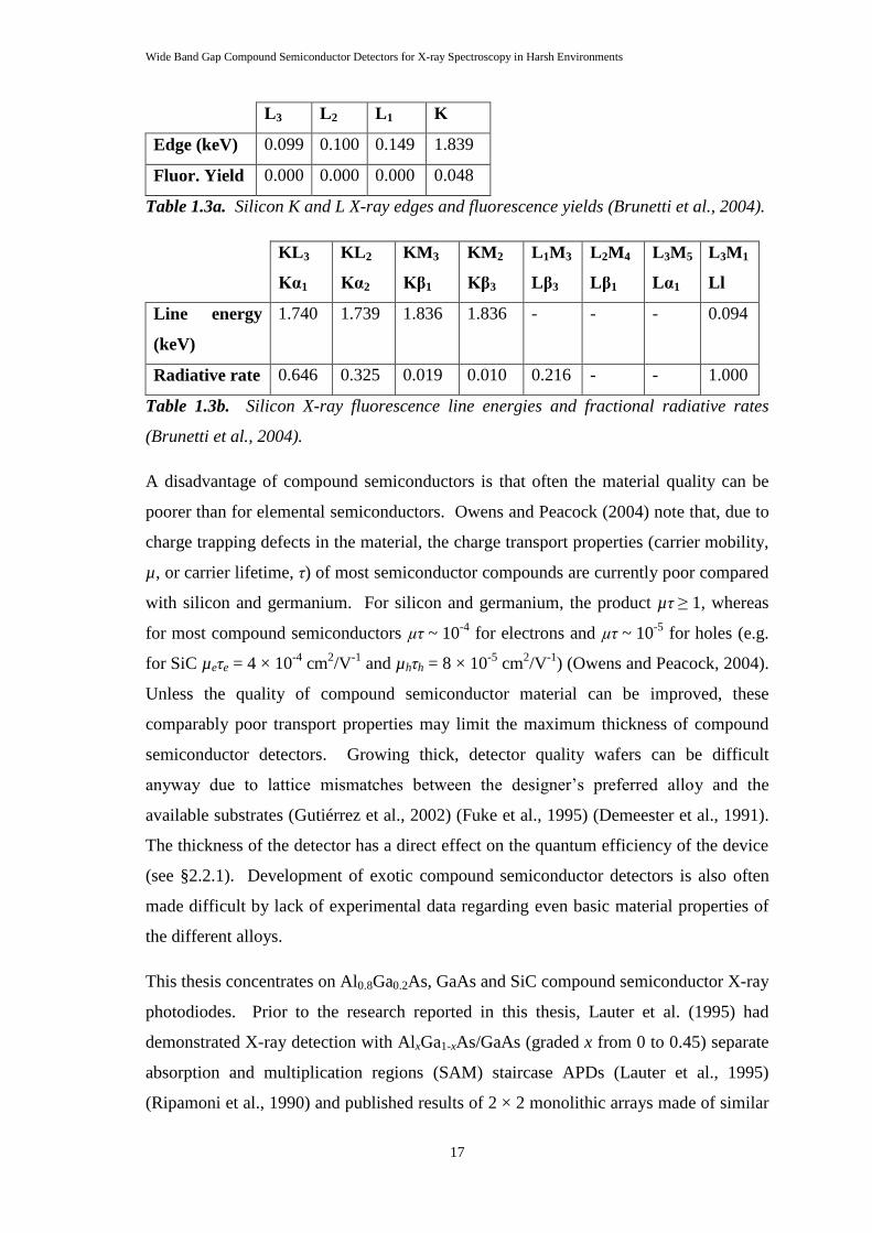
of interest, unlike in the silicon K lines for silicon detectors (Tables 1.3a & 1.3b). At
first glance it may appear as if no corrections for emission lines would be required in
the region 1 keV to 7 keV, if a GaAs detector was used. However, the L edges and
lines of gallium and arsenic are still within the spectral region of interest for planetary
XRF and have significant fluorescence yields (Tables 1.1a, 1.1b, 1.2a, 1.2b, 1.3a &
1.3b), so spectra covering this region must still be corrected for these edges and lines.
L3 L2 L1 K
Edge (keV) 1.115 1.142 1.298 10.367
Fluor. Yield 0.013 0.012 0.002 0.543
Table 1.1a. Gallium K and L X-ray edges and fluoresce yields (Brunetti et al., 2004).
KL3
Kα1
KL2
Kα2
KM3
Kβ1
KM2
Kβ3
L1M3
Lβ3
L2M4
Lβ1
L3M5
Lα1
L3M1
Ll
Line energy
(keV)
9.252 9.225 10.264 10.260 1.197 1.125 1.098 0.957
Radiative rate 0.577 0.294 0.083 0.043 0.626 0.954 0.854 0.046
Table 1.1b. Gallium X-ray fluorescence line energies and fractional radiative rates
(Brunetti et al., 2004).
L3 L2 L1 K
Edge (keV) 1.323 1.359 1.526 11.867
Fluor. Yield 0.016 0.014 0.003 0.581
Table 1.2a. Arsenic K and L X-ray edges and fluorescence yields (Brunetti et al.,
2004).
KL3
Kα1
KL2
Kα2
KM3
Kβ1
KM2
Kβ3
L1M3
Lβ3
L2M4
Lβ1
L3M5
Lα1
L3M1
Ll
Line energy
(keV)
10.543 10.507 11.726 11.720 1.389 1.317 1.282 1.120
Radiative rate 0.571 0.294 0.086 0.044 0.607 0.957 0.857 0.042
Table 1.2b. Arsenic X-ray fluorescence line energies and fractional radiative rates
(Brunetti et al., 2004).
Wide Band Gap Compound Semiconductor Detectors for X-ray Spectroscopy in Harsh Environments
17
L3 L2 L1 K
Edge (keV) 0.099 0.100 0.149 1.839
Fluor. Yield 0.000 0.000 0.000 0.048
Table 1.3a. Silicon K and L X-ray edges and fluorescence yields (Brunetti et al., 2004).
KL3
Kα1
KL2
Kα2
KM3
Kβ1
KM2
Kβ3
L1M3
Lβ3
L2M4
Lβ1
L3M5
Lα1
L3M1
Ll
Line energy
(keV)
1.740 1.739 1.836 1.836 - - - 0.094
Radiative rate 0.646 0.325 0.019 0.010 0.216 - - 1.000
Table 1.3b. Silicon X-ray fluorescence line energies and fractional radiative rates
(Brunetti et al., 2004).
A disadvantage of compound semiconductors is that often the material quality can be
poorer than for elemental semiconductors. Owens and Peacock (2004) note that, due to
charge trapping defects in the material, the charge transport properties (carrier mobility,
µ, or carrier lifetime, τ) of most semiconductor compounds are currently poor compared
with silicon and germanium. For silicon and germanium, the product µτ ≥ 1, whereas
for most compound semiconductors µτ ~ 10-4
for electrons and µτ ~ 10-5
for holes (e.g.
for SiC µeτe = 4 × 10⁻⁴
cm2/V
-1 and µhτh = 8 × 10
-5 cm
2/V
-1) (Owens and Peacock, 2004).
Unless the quality of compound semiconductor material can be improved, these
comparably poor transport properties may limit the maximum thickness of compound
semiconductor detectors. Growing thick, detector quality wafers can be difficult
anyway due to lattice mismatches between the designer‟s preferred alloy and the
available substrates (Gutiérrez et al., 2002) (Fuke et al., 1995) (Demeester et al., 1991).
The thickness of the detector has a direct effect on the quantum efficiency of the device
(see §2.2.1). Development of exotic compound semiconductor detectors is also often
made difficult by lack of experimental data regarding even basic material properties of
the different alloys.
This thesis concentrates on Al0.8Ga0.2As, GaAs and SiC compound semiconductor X-ray
photodiodes. Prior to the research reported in this thesis, Lauter et al. (1995) had
demonstrated X-ray detection with AlxGa1-xAs/GaAs (graded x from 0 to 0.45) separate
absorption and multiplication regions (SAM) staircase APDs (Lauter et al., 1995)
(Ripamoni et al., 1990) and published results of 2 × 2 monolithic arrays made of similar
Wide Band Gap Compound Semiconductor Detectors for X-ray Spectroscopy in Harsh Environments
18
devices (Lauter et al., 1996). Silenas (2004), Silenas et al. (2002, 2003, 2005, 2006)
and Dapkus et al. (2007) had reported results from graded-gap non-photon counting,
non-spectroscopic AlxGa1-xAs/GaAs detectors that can detect changes in X-ray flux
when operated in current mode, but had not demonstrated X-ray spectroscopy or photon
counting with their devices. Al0.8Ga0.2As p+-p
--n
+ photodiodes, originally intended for
use in telecommunications and grown and fabricated at the University of Sheffield had
been shown to function as room temperature photon counting X-ray spectroscopic
detectors in experiments at University of Leicester by Lees et al. (2008), but an artefact
was present in the spectrum (see Chapter 6).
GaAs photon counting X-ray photodiodes have been reported operating at temperatures
between +21 °C and -16 °C by Owens et al. (2001, 2002a) and Erd et al. (2002), but
surprisingly no report has been made of the temperature dependence of the spectral
resolution of GaAs photon counting X-ray photodiodes at higher temperatures.
The potential for SiC Schottky photodiodes to be used as high temperature photon
counting spectroscopic X-ray detectors had also been previously recognised, most
notably by Bertuccio, Casiraghi and Nava (2001) who were the first to report X-ray
detection with SiC Schottky photodiodes. Subsequent work by Bertuccio (2005),
Bertuccio & Casiraghi (2003), and Bertuccio et al. (2004a, 2004b, 2006, 2011), review
by Nava et al. (2008), dominates the SiC X-ray photon counting spectroscopic detector
literature. At University of Leicester, a novel type of SiC Schottky diode (the semi-
transparent SiC Schottky diode – STSSD), fabricated at University of Newcastle, had
also been shown to function as a photon counting spectroscopic X-ray detector in
experiments at room temperature (Lees et al., 2007) (Lees et al., 2009).
1.5 Thesis organisation
Chapter 2 reviews the physics of X-ray detection with photodiodes and provides
background on the theory of impact ionisation in X-ray photodiodes. Chapter 3
describes the Monte Carlo model developed to model X-ray detection in Al0.8Ga0.2As
and GaAs p+-p
--n
+ and p
+-i-n
+ avalanche and non-avalanche photodiodes. Chapter 4
presents measurements and analysis characterising the performance of non-avalanche
Al0.8Ga0.2As X-ray photodiodes at temperatures from +90 °C to -30 °C. Chapter 5
presents measurements and analysis of the performance of GaAs X-ray photodiodes at
temperatures between +80 °C and -30 °C. Chapter 6 presents experimental and
Wide Band Gap Compound Semiconductor Detectors for X-ray Spectroscopy in Harsh Environments
19
computer modelling results which explain the origin of the additional peak anomaly
reported by Lees et al. (2008) in their X-ray spectra taken with a p+-p
--n
+ X-ray
avalanche photodiode, and derives the temperature dependence of the impact ionisation
coefficients in Al0.8Ga0.2As at a typical operating field. Chapter 7 reports high
temperature X-ray spectrum measurements taken with semi-transparent SiC Schottky
diodes. Chapter 8 offers overarching conclusions on the work and considers future
directions for subsequent research.
Wide Band Gap Compound Semiconductor Detectors for X-ray Spectroscopy in Harsh Environments
20
Chapter 2 Detector physics
2.1 Introduction
This chapter describes the physical principles of X-ray detection with photon counting
non-avalanche photodiodes and photon counting avalanche photodiodes (APDs). The
physics of soft X-ray attenuation and photoelectric X-ray absorption are reviewed,
along with the basics of charge generation and transport in semiconductor detectors.
The factors affecting the energy resolution of semiconductor detectors are discussed,
and for avalanche photodiodes the impact ionisation process is reviewed with reference
to the local model (McIntyre, 1966).
For further detail, various comprehensive introductions to X-ray detection with
semiconductor devices exist, including Fraser (1989), Knoll (2000) and Owens &
Peacock (2004).
2.2 X-ray attenuation
2.2.1 Beer-Lambert law
Monochromatic X-rays incident on a material are attenuated through it (absorbed or
scattered by it) according to the Beer-Lambert law (Potts, 1987):
(2.1)
where I is the intensity of the beam transmitted through the material, I0 is the original
intensity of the beam, µ is the linear attenuation coefficient for the material at the
particular X-ray energy being investigated and x is the thickness of the material. It
should be noted that the linear attenuation coefficient varies with the density of the
material, even when the material stays the same. An absorber‟s linear attenuation
coefficient, µ, can be calculated from its mass attenuation coefficient, Μ, and density, ρ
(µ = Μρ). If one wishes to detect a large fraction of the incident flux, it is desirable to
maximise the absorption, I0(1-e-µx
), by maximising µ and x. The linear attenuation
coefficient, µ, is material dependent and can be maximised by selecting high Z (atomic
number) detector materials. The thickness, x, can also be increased, but it cannot be
Wide Band Gap Compound Semiconductor Detectors for X-ray Spectroscopy in Harsh Environments
21
usefully increased indefinitely: it is limited by charge carrier mobility in the detector
and the quality and thickness of the detector material that can be grown (Owens &
Peacock, 2004).
For the soft X-ray energies (~ 1 keV – ~ 25 keV) of interest in this thesis, the dominant
form of attenuation of the incident beam is photoelectric absorption (§2.2.2). For a
consideration of Compton scattering and pair-production see Knoll (2000).
2.2.2 Photoelectric absorption
In photoelectric absorption, an incident X-ray photon interacts with one of the detector‟s
atoms. The photon ionizes the atom, liberating an electron. The incident photon‟s
energy is transferred to the atom‟s electron, less the binding energy of that electron in
its original shell. The vacancy is filled by the capture of a free electron from the
material or by rearrangement of the atom‟s electronic structure. This rearrangement can
occur either by fluorescence, the Auger effect or both, since vacancies can cascade
through the shells.
When an atom rearranges by emitting a fluorescence photon, this photon is either
absorbed by the detector or escapes. When a fluorescence photon of energy, Eflu,
escapes, this gives rise to an escape peak of energy,
Eesc = E – Eflu (2.2)
in the spectrum, where E is the initial X-ray photon‟s energy. If only the fluorescence
photon is absorbed (e.g. if the original X-ray photon was absorbed in a non-active
region of the detector), an elemental characteristic fluorescence peak can be visible in
the spectrum. Photoelectrons and Auger electrons have a sufficiently short range that
they can be considered to be localised to the point of X-ray absorption for the detectors
in this thesis.
2.2.3 Absorption edges
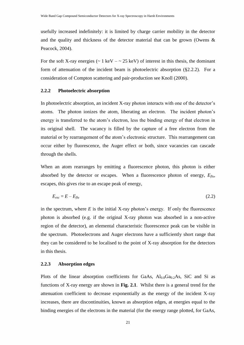
Plots of the linear absorption coefficients for GaAs, Al0.8Ga0.2As, SiC and Si as
functions of X-ray energy are shown in Fig. 2.1. Whilst there is a general trend for the
attenuation coefficient to decrease exponentially as the energy of the incident X-ray
increases, there are discontinuities, known as absorption edges, at energies equal to the
binding energies of the electrons in the material (for the energy range plotted, for GaAs,
Wide Band Gap Compound Semiconductor Detectors for X-ray Spectroscopy in Harsh Environments
22
these are the elements‟ K and L edges). Absorption edges have the effect that a photon
of energy just more than an edge has a higher probability of being absorbed than a
photon with an energy just below the absorption edge. The absorption edges result from
the different binding energies of the electrons in different shells; when a photon has an
energy greater than the binding energy of an electron in a given shell, the photon is
more likely to be absorbed by the atom because the photon has sufficient energy to
liberate electrons in that shell as well as the lower energy shells.
Fig. 2.1. The energy dependence of the linear attenuation coefficients for GaAs (blue
line), Al0.8Ga0.2As (red line), SiC (green line), and Si (dashed purple line). The
discontinuities are the absorption edges (see Tables 1.1a, 1.2a & 1.3a).
2.3 Diode structure
In order to collect efficiently the charge carriers generated by the absorption of an X-ray
photon, it is necessary to apply an electric field across the semiconductor detector
(§2.5). In order to minimise the device leakage current (§2.6.2) resulting from this
electric field, reverse biased semiconductor junctions are used rather than simple
crystals of intrinsic semiconductor material. A diode is reverse biased when a negative
voltage is applied to the diode‟s p layer, with respect to its n layer (see below). This
reverse biasing has the effect of increasing the natural potential difference between the p
and n layers, and causes electrons to be attracted to the n layer and holes to the p layer.
Wide Band Gap Compound Semiconductor Detectors for X-ray Spectroscopy in Harsh Environments
23
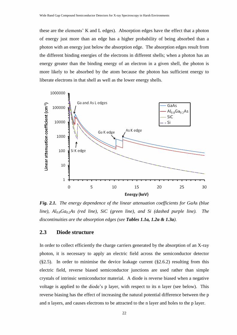
The GaAs and Al0.8Ga0.2As diodes described in this thesis are based on circular
(diameter = 200 µm) mesa p+-i-n
+ and p
+-p-n
+ junctions, which have highly doped p
+
and n+ layers (see Tables 4.1, 5.1 & 6.1 for layer properties) either side of an intrinsic
(or near intrinsic) layer; see Fig. 2.2 for a simplified schematic diagram, Fig. 2.3 for a
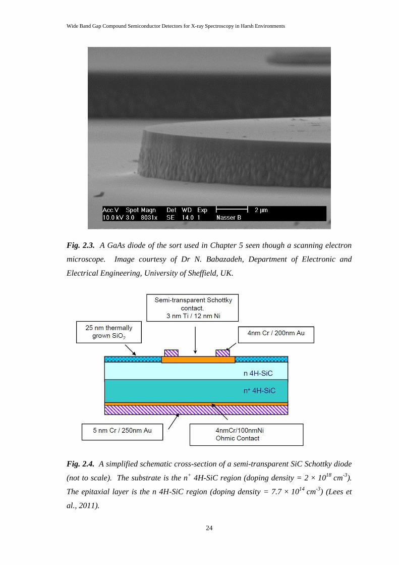
scanning electron microscope photograph, and Chapters 4, 5 and 6. The SiC devices are
square (250 µm × 250 µm) 4H-SiC semi-transparent Schottky diodes, with an epitaxial
n layer and a semi-transparent Schottky contact grown on a 4H-SiC n+ substrate (see
Fig. 2.4 and Chapter 7). Schottky diodes consist of a Schottky barrier metal-
semiconductor junction rather than semiconductor-semiconductor junctions, as in p-n,
p+-p
--n
+ or p
+-i-n
+ diodes.
The areas of the GaAs, Al0.8Ga0.2As and SiC diodes reported in this thesis are small
compared with some silicon photodiodes (e.g. diameter > 3 mm, (Kataoka et al., 2005))
but diodes of comparable area to those reported in this thesis may find use in pixel array
detectors and larger GaAs, Al0.8Ga0.2As and SiC devices are planned to be fabricated in
future (see Chapter 8).
Fig. 2.2. A simplified schematic cross-section diagram depicting the Al0.8Ga0.2As
p+-i-n
+ diodes used in Chapter 4 (not to scale).
Wide Band Gap Compound Semiconductor Detectors for X-ray Spectroscopy in Harsh Environments
24
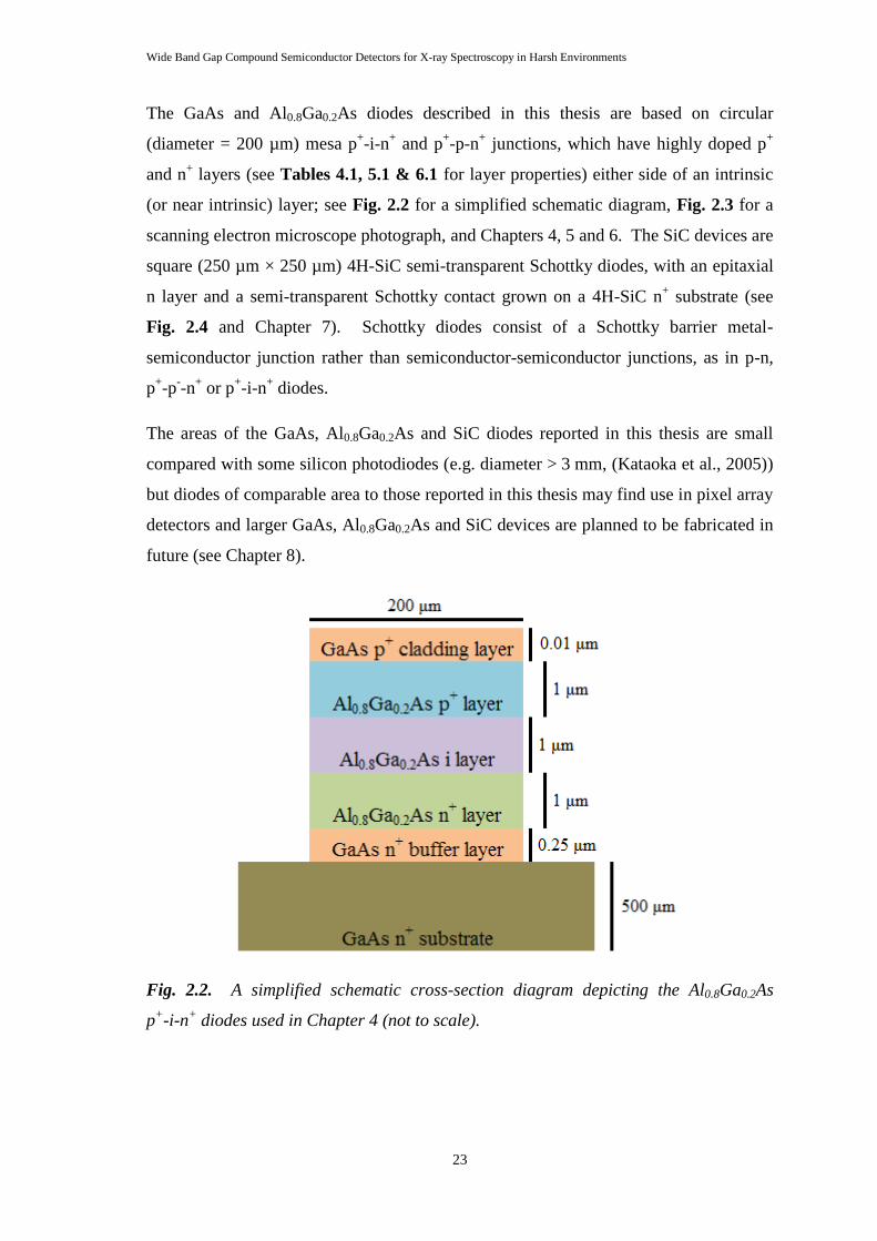
Fig. 2.3. A GaAs diode of the sort used in Chapter 5 seen though a scanning electron
microscope. Image courtesy of Dr N. Babazadeh, Department of Electronic and
Electrical Engineering, University of Sheffield, UK.
Fig. 2.4. A simplified schematic cross-section of a semi-transparent SiC Schottky diode
(not to scale). The substrate is the n+ 4H-SiC region (doping density = 2 × 10
18 cm
-3).
The epitaxial layer is the n 4H-SiC region (doping density = 7.7 × 10¹⁴
cm-3
) (Lees et
al., 2011).
Wide Band Gap Compound Semiconductor Detectors for X-ray Spectroscopy in Harsh Environments
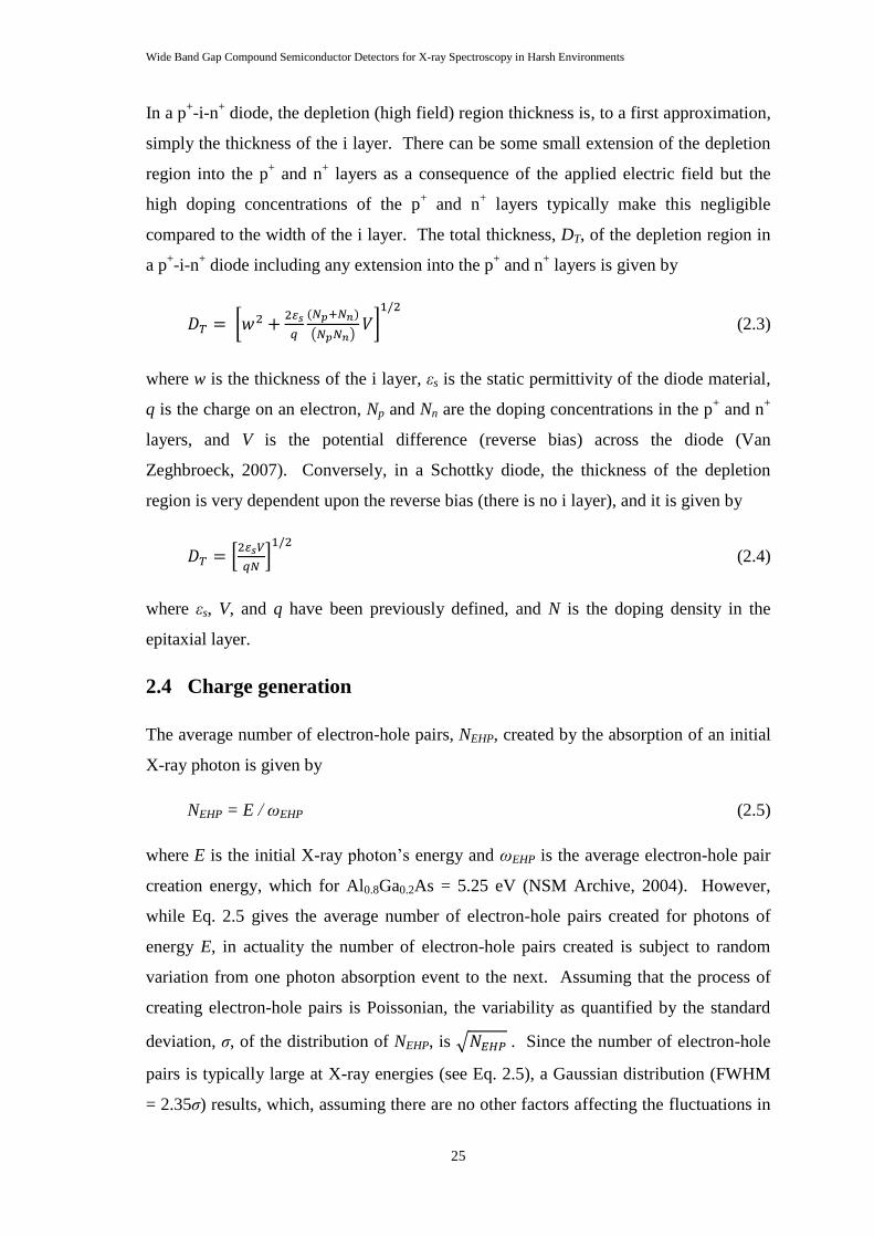
25
In a p+-i-n
+ diode, the depletion (high field) region thickness is, to a first approximation,
simply the thickness of the i layer. There can be some small extension of the depletion
region into the p+ and n
+ layers as a consequence of the applied electric field but the
high doping concentrations of the p+ and n
+ layers typically make this negligible
compared to the width of the i layer. The total thickness, DT, of the depletion region in
a p+-i-n
+ diode including any extension into the p
+ and n
+ layers is given by
[
( ) ]
(2.3)
where w is the thickness of the i layer, εs is the static permittivity of the diode material,
q is the charge on an electron, Np and Nn are the doping concentrations in the p+ and n
+
layers, and V is the potential difference (reverse bias) across the diode (Van
Zeghbroeck, 2007). Conversely, in a Schottky diode, the thickness of the depletion
region is very dependent upon the reverse bias (there is no i layer), and it is given by
*
+
(2.4)
where εs, V, and q have been previously defined, and N is the doping density in the
epitaxial layer.
2.4 Charge generation
The average number of electron-hole pairs, NEHP, created by the absorption of an initial
X-ray photon is given by
NEHP = E / ωEHP (2.5)
where E is the initial X-ray photon‟s energy and ωEHP is the average electron-hole pair
creation energy, which for Al0.8Ga0.2As = 5.25 eV (NSM Archive, 2004). However,
while Eq. 2.5 gives the average number of electron-hole pairs created for photons of
energy E, in actuality the number of electron-hole pairs created is subject to random
variation from one photon absorption event to the next. Assuming that the process of
creating electron-hole pairs is Poissonian, the variability as quantified by the standard
deviation, σ, of the distribution of NEHP, is √ . Since the number of electron-hole
pairs is typically large at X-ray energies (see Eq. 2.5), a Gaussian distribution (FWHM
= 2.35σ) results, which, assuming there are no other factors affecting the fluctuations in
Wide Band Gap Compound Semiconductor Detectors for X-ray Spectroscopy in Harsh Environments
26
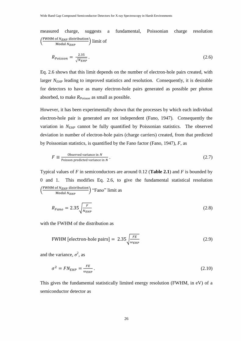
measured charge, suggests a fundamental, Poissonian charge resolution
(
) limit of
√ . (2.6)
Eq. 2.6 shows that this limit depends on the number of electron-hole pairs created, with
larger NEHP leading to improved statistics and resolution. Consequently, it is desirable
for detectors to have as many electron-hole pairs generated as possible per photon
absorbed, to make RPoisson as small as possible.
However, it has been experimentally shown that the processes by which each individual
electron-hole pair is generated are not independent (Fano, 1947). Consequently the
variation in NEHP cannot be fully quantified by Poissonian statistics. The observed
deviation in number of electron-hole pairs (charge carriers) created, from that predicted
by Poissonian statistics, is quantified by the Fano factor (Fano, 1947), F, as
. (2.7)
Typical values of F in semiconductors are around 0.12 (Table 2.1) and F is bounded by
0 and 1. This modifies Eq. 2.6, to give the fundamental statistical resolution
(
) “Fano” limit as
√
(2.8)
with the FWHM of the distribution as
- √
(2.9)
and the variance, σ2, as
. (2.10)
This gives the fundamental statistically limited energy resolution (FWHM, in eV) of a
semiconductor detector as
Wide Band Gap Compound Semiconductor Detectors for X-ray Spectroscopy in Harsh Environments
27
√
. (2.11)
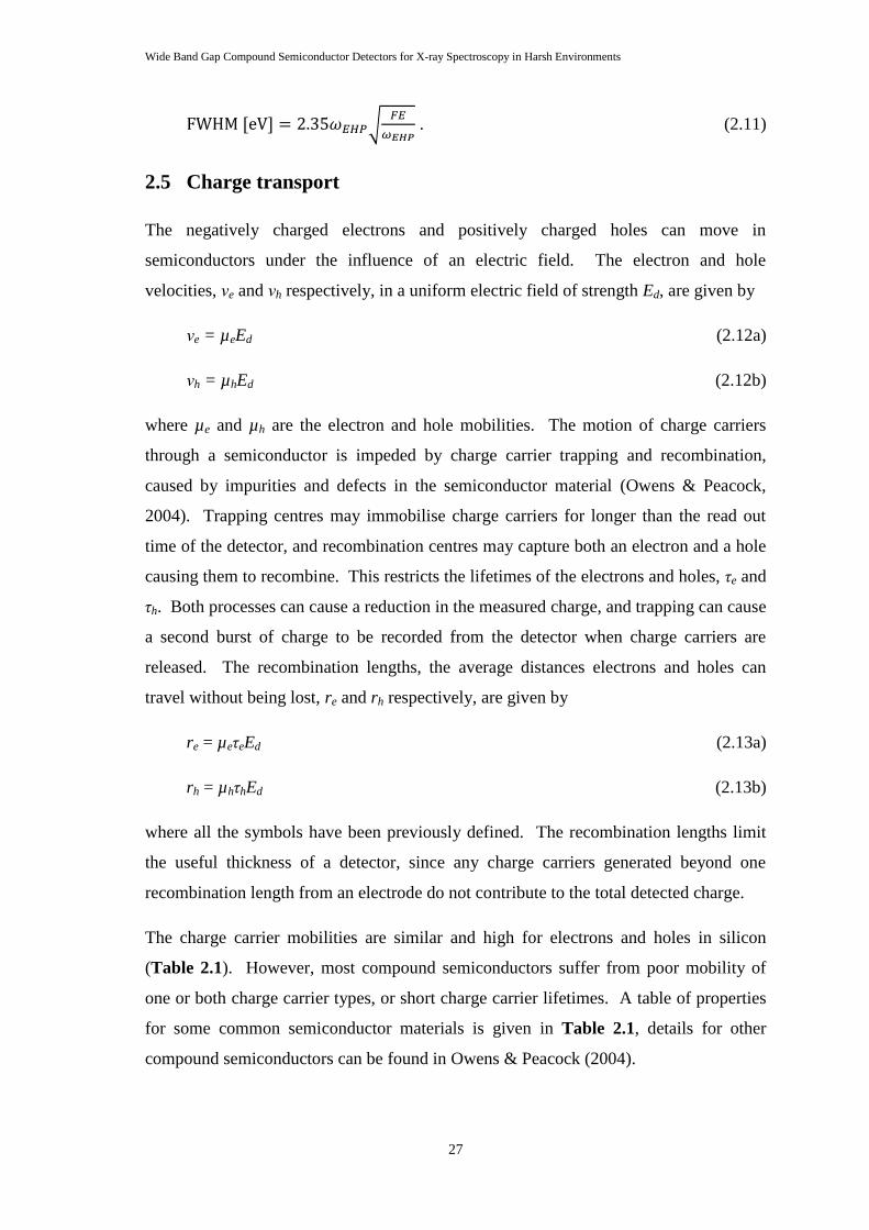
2.5 Charge transport
The negatively charged electrons and positively charged holes can move in
semiconductors under the influence of an electric field. The electron and hole
velocities, νe and νh respectively, in a uniform electric field of strength Ed, are given by
νe = µeEd (2.12a)
νh = µhEd (2.12b)
where µe and µh are the electron and hole mobilities. The motion of charge carriers
through a semiconductor is impeded by charge carrier trapping and recombination,
caused by impurities and defects in the semiconductor material (Owens & Peacock,
2004). Trapping centres may immobilise charge carriers for longer than the read out
time of the detector, and recombination centres may capture both an electron and a hole
causing them to recombine. This restricts the lifetimes of the electrons and holes, τe and
τh. Both processes can cause a reduction in the measured charge, and trapping can cause
a second burst of charge to be recorded from the detector when charge carriers are
released. The recombination lengths, the average distances electrons and holes can
travel without being lost, re and rh respectively, are given by
re = µeτeEd (2.13a)
rh = µhτhEd (2.13b)
where all the symbols have been previously defined. The recombination lengths limit
the useful thickness of a detector, since any charge carriers generated beyond one
recombination length from an electrode do not contribute to the total detected charge.
The charge carrier mobilities are similar and high for electrons and holes in silicon
(Table 2.1). However, most compound semiconductors suffer from poor mobility of
one or both charge carrier types, or short charge carrier lifetimes. A table of properties
for some common semiconductor materials is given in Table 2.1, details for other
compound semiconductors can be found in Owens & Peacock (2004).
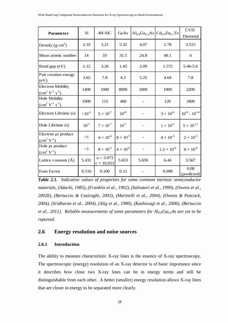
Wide Band Gap Compound Semiconductor Detectors for X-ray Spectroscopy in Harsh Environments
28
CVD
Diamond
Pair creation energy
(eV)
Electron Mobility
(cm2 V
-1 s
-1)
Hole Mobility
(cm2 V
-1 s
-1)
Electron µτ product
(cm2 V
-1)
Hole µτ product
(cm2 V
-1)
a = 3.073
c = 10.053
0.08
(predicted)
Cd0.9Zn0.1TeParameter Si 4H-SiC GaAs Al0.8Ga0.2As
0.099Fano Factor 0.116 0.100 0.12 -
3.567Lattice constant (Å) 5.431 5.653 5.659 6.44
Density (g cm3) 2.33 3.21 5.32 4.07 5.78 3.515
14 10 31.5 24.8 49.1 6Mean atomic number
Band gap (eV) 1.12 3.26 1.43 2.09 1.572 5.46-5.6
3.62 7.8 4.2 5.25 4.64 7.8
220010001000800010001400
1900 115 400 120 1800
3 × 10⁻⁶
-
10-9
- 10-10-10
-85 × 10
-7>10
-3
10-3
Electron Lifetime (s)
Hole Lifetime (s) 7 × 10⁻⁷
10-7
5 × 10-11
2 × 10⁻⁵
8 × 10⁻⁸~1 8 × 10
-54 × 10
-61.2 × 10
-4
-
-
-
1 × 10⁻⁶
4 × 10⁻³
8 × 10⁻⁵
4 × 10⁻⁴>1
Table 2.1. Indicative values of properties for some common intrinsic semiconductor
materials, (Adachi, 1985), (Franklin et al., 1992), (Salvatori et al., 1999), (Owens et al.,
2002b), (Bertuccio & Casiraghi, 2003), (Marinelli et al., 2004), (Owens & Peacock,
2004), (Sridharan et al., 2004), (Alig et al., 1980), (Kashiwagi et al., 2006), (Bertuccio
et al., 2011). Reliable measurements of some parameters for Al0.8Ga0.2As are yet to be
reported.
2.6 Energy resolution and noise sources
2.6.1 Introduction
The ability to measure characteristic X-ray lines is the essence of X-ray spectroscopy.
The spectroscopic (energy) resolution of an X-ray detector is of basic importance since
it describes how close two X-ray lines can be in energy terms and still be
distinguishable from each other. A better (smaller) energy resolution allows X-ray lines
that are closer in energy to be separated more clearly.
Wide Band Gap Compound Semiconductor Detectors for X-ray Spectroscopy in Harsh Environments
29
2.6.2 The energy resolution of a semiconductor detector
The fundamental (statistically limited) FWHM energy resolution of a semiconductor
X-ray detector (Eq. 2.11) is degraded by noise terms, R & A, defined below, which
cause the detector‟s FWHM, expressed in eV, to become
√
. (2.14)
The factor R is the equivalent noise charge (in r.m.s. e-) introduced by the detector
during the movement of the charge to the contacts (e.g. by charge trapping), and A is the
equivalent noise charge (in r.m.s. e-) introduced by the detector‟s leakage current and
pre-amplifier (Fraser, 1989). It is desirable to minimise R and A, in order to improve
the resolution of the detector; when R and A are negligible, the spectral resolution is
said to be Fano limited.
Where charge trapping is the primary source of noise contributing to charge read out
noise, R has the form
(2.15)
where k1 and k2 are empirically derived constants. However, R is small compared with
A for most modern semiconductor crystals (Owens & Peacock, 2004).
A comprehensive introduction to the various electronic noise sources contributing to A
in photon counting X-ray photodiodes coupled to charge sensitive preamplifiers can be
found in Bertuccio, Pullia & DeGeronimo (1996), the salient points of which are
summarised below to give expressions for the parallel white noise (§2.6.3), series white
noise (§2.6.4), 1/f series noise (§2.6.5), dielectric noise (§2.6.6) and induced gate
current noise (§2.6.7) contributions.
2.6.3 Parallel white noise
Parallel white noise stems from the shot noise of the currents flowing through the input
node of the preamplifier. It is primarily dependent on the leakage currents of the
detector, ILD, and the preamplifier input field effect transistor (JFET), ILT (Bertuccio,
Pullia, DeGeronimo, 1996).
The parallel white noise power spectral density, SPW, can be expressed as
Wide Band Gap Compound Semiconductor Detectors for X-ray Spectroscopy in Harsh Environments
30
(2.16)
where q is the charge on an electron (1.602 × 10⁻¹⁹
C), k is the Boltzmann constant, T is
the temperature (in K) and r is the resistance of the preamplifier feedback resistor if the
preamplifier has one (Bertuccio, Pullia, DeGeronimo, 1996). The preamplifier used for
the measurements reported in this thesis does not have a feedback resistor so the
term is omitted. The contribution (measured in r.m.s. e-) of SPW to the equivalent noise
charge A (Eq. 2.14), is
√ (2.17)
where A3 is a constant dependent on signal shaping function (Gatti et al. 1990), and τ is
the shaping time. The leakage currents of the detector and JFET are therefore important
in determining the limits of spectral resolution of the detector.
Whilst NPW is not directly dependent on the capacitance of the preamplifier input JFET,
it can be beneficial to reduce the JFET capacitance as this reduces the optimum shaping
time, τ, which does reduce NPW (Bertuccio, Pullia & DeGeronimo, 1996).
2.6.4 Series white noise
The series white noise primarily arises from the effect of thermal noise on the drain
current of the input JFET (Bertuccio, Pullia & DeGeronimo, 1996). When secondary
sources (e.g. stray resistance in series with the input JFET‟s gate) are negligible, the
series white noise power spectral density, SSW, can be approximated to the thermal noise
of the JFET drain current:
(2.18)
where 0.7 ≤ γ ≤ 1 depending on JFET characteristics, and gm is the transconductance of
the JFET. The contribution (measured in r.m.s. e-) of SSW to the equivalent noise charge
(Eq. 2.14) is
√
(2.19)
where A1 is a constant depending on signal shaping function (Gatti et al., 1990) and CT
is the total capacitance at the preamplifier input (= Cd + Ci + Cf + Cs, where Cd is the
Wide Band Gap Compound Semiconductor Detectors for X-ray Spectroscopy in Harsh Environments
31
detector capacitance, Ci is the input transistor capacitance, Cf is the feedback
capacitance and Cs is the stray capacitance) (Bertuccio, Pullia & DeGeronimo, 1996).
The equivalent noise charge contribution NSW becomes increasingly significant at
shorter shaping times because of the 1/τ dependence.
2.6.5 1/f series noise
The noise from the drain current of the preamplifier input JFET is also the main
constituent of 1/f series noise. The 1/f noise contribution to the equivalent noise charge
A (Eq. 2.14) is
√
(2.20)
where Af is a characteristic constant dependent on the JFET and A2 is a constant ranging
from 0.64 to 2 depending on signal shaping function (Gatti et al., 1990) (Bertuccio,
Pullia & DeGeronimo, 1996).
2.6.6 Dielectric noise
Dielectrics in close proximity to the preamplifier, such as the packaging of the JFET
and detector contribute
√ (2.21)
to the total electronics equivalent noise charge, A, where Cdie is the capacitance of the
dielectrics, D is the dielectrics dissipation factor (Bertuccio, Pullia & DeGeronimo,
1996) and q, A2, k and T have all been previously defined. It is therefore desirable to
design the input JFET and detector packaging to minimise exposure to dielectrics, for
example by reducing the capacitance of the JFET and detector assembly by integrating
the JFET onto the detector.
2.6.7 Induced gate current noise
Drain current noise (§2.6.4) causes charge fluctuations in the JFET gate current giving
rise to the induced gate current noise. The contribution from this to A is dependent on
SSW (Eq. 2.18). Like the series white noise, the induced gate current noise becomes
important at short shaping times because of the 1/τ dependence. Experimental
Wide Band Gap Compound Semiconductor Detectors for X-ray Spectroscopy in Harsh Environments
32
investigation has shown that Eq. 2.18 can be modified by a factor, Gc, (√Gc ≈ 0.8) to
take account of the noise in the JFET‟s gate (Bertuccio, Pullia & DeGeronimo, 1996):
. (2.22)
Consequently the ENC contribution to A becomes
√
√ . (2.23)
2.6.8 Electronic noise sources in combination
When considered together, the parallel white (§2.6.3) and series (§2.6.4) noise
contributions‟ dependences on τ and 1/τ respectively, can give rise to an optimum
shaping time which minimises the combined noise from these sources (Pullia &
Bertuccio, 1996). In §4.6.2 and §5.5.2, it is shown how the parallel white, series white,
1/f and dielectric noises combine to produce the overall measurement ENC of a
preamplifier and how this is effected by varying the shaping time, τ.
2.7 Impact ionisation
2.7.1 Introduction
Avalanche photodiodes (APDs) – photodiodes in which impact ionisation occurs – are
widely used in photonic detection systems (for compound semiconductors most notably
in telecommunications (Campbell, 2007) (David & Tan, 2008)) to increase the system‟s
signal to noise ratio, with the charge from each detected event being multiplied by the
multiplication factor, M, of the APD. The multiplication factor depends on the position,
x, at which the initial electron-hole pairs are created within (or injected to) the
avalanche region, the charge carrier ionisation coefficients which are material specific,
the electric field, E, and the temperature, T, of the diode.
Avalanche multiplication occurs when charge carriers created by a photon absorption
event gain sufficient kinetic energy from being accelerated by the electric field in a
diode to cause the generation of additional charge carriers upon their interaction with a
lattice atom.
In the case of a conduction band electron which was generated by the absorption of a
photon in the device, the electron is accelerated toward the n+ contact, gaining kinetic
Wide Band Gap Compound Semiconductor Detectors for X-ray Spectroscopy in Harsh Environments
33
energy as it travels. When this energetic electron interacts with a lattice atom, some of
the electron‟s energy is transferred to that atom, promoting one of the atom‟s higher
energy valence band electrons into the conduction band. This newly promoted
conduction electron necessarily creates a hole upon leaving its valence band position.
The electron of the electron-hole pair created by the absorption of the photon, together
with the newly created (by impact ionisation) electrons and holes are then accelerated
through the device by the electric field in the same manner as before (electrons toward
the n+ contact and holes toward p
+ contact). Both the charge carriers of the
electron-hole pairs liberated by the absorption of the photon, and the charge carriers
created by impact ionisation of those initial charge carriers, are free to impact ionise
with lattice atoms and generate more charge carriers once they have gained sufficient
energy. This chain of events is avalanche multiplication (avalanche gain) and can be
repeated many times with many impact ionisation events taking place before the charge
carriers reach their respective destination boundaries.
There are various structural forms of APD, including simple p+-i-n
+ (or p
+-p-n
+) devices
(Lees et al., 2008) (the APD structure considered in this thesis, see Chapter 6), and
separate absorption and multiplication region (SAM) or „reach-through‟ devices, which
have their depletion regions separated into two regions: a low-field drift region
(typically of low doping) for the absorption of photons and one or more high-field
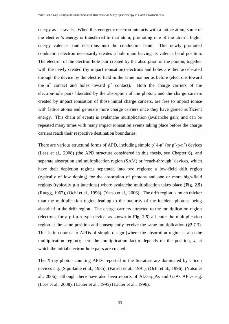
regions (typically p-n junctions) where avalanche multiplication takes place (Fig. 2.5)
(Ruegg, 1967), (Ochi et al., 1996), (Yatsu et al., 2006). The drift region is much thicker
than the multiplication region leading to the majority of the incident photons being
absorbed in the drift region. The charge carriers attracted to the multiplication region
(electrons for a p-i-p-n type device, as shown in Fig. 2.5) all enter the multiplication
region at the same position and consequently receive the same multiplication (§2.7.3).
This is in contrast to APDs of simple design (where the absorption region is also the
multiplication region); here the multiplication factor depends on the position, x, at
which the initial electron-hole pairs are created.
The X-ray photon counting APDs reported in the literature are dominated by silicon
devices e.g. (Squillante et al., 1985), (Farrell et al., 1991), (Ochi et al., 1996), (Yatsu et
al., 2006), although there have also been reports of AlxGa1-xAs and GaAs APDs e.g.
(Lees et al., 2008), (Lauter et al., 1995) (Lauter et al., 1996).
Wide Band Gap Compound Semiconductor Detectors for X-ray Spectroscopy in Harsh Environments
34
Fig. 2.5. An illustrative field profile in a p+-i-p-n
+ SAM diode (see text).
2.7.2 Background theory
The number of charge carriers generated through impact ionisation is dependent upon
the number of times that impact ionisation can occur before all charge carriers reach the
end of the high field region. The number of charge carriers generated by impact
ionisation can be different for electron and hole initiated avalanches. Stronger electric
fields within the device result in charge carriers obtaining the necessary energy to
impact ionise over a shorter distance and consequently more charge carriers can be
generated in devices operated at high electric field. The distance that charge carriers
must travel between impact ionisation events (the ionisation path length) is not constant
because the impact ionisation process is stochastic (i.e. random within the bounds of the
probability distributions) (see §2.7.4). The electron, α, and hole, β, ionisation
coefficients are the reciprocal of the average distance each charge carrier type must
travel between impact ionisation events. At sufficiently high fields, the number of
impact ionisation generated electrons and holes can increase very rapidly causing the
device to suffer avalanche breakdown.
The ionisation coefficients of a material are assumed in the local model (McIntyre,
1966), to be dependent only upon the electric field and temperature in the device.
Conventionally, it is assumed that the ionisation coefficients are constant throughout the
material, and that differences in the multiplication experienced by charge carriers of the
same type are solely due to their starting position and not the charge carrier‟s history
(McIntyre, 1966). This local model assumption is generally assumed to be valid when
Wide Band Gap Compound Semiconductor Detectors for X-ray Spectroscopy in Harsh Environments
35
the width, w, of the avalanche region is significantly larger than the electron, de, and
hole, dh, dead spaces (Plimmer, 1996) (Tan et al., 2001) (Ng et al., 2002). The electron
and hole dead spaces are the minimum distance that each type of charge carrier must
travel to gain the minimum (threshold) energy (EThe and EThh, for electrons and holes
respectively) required to impact ionise. The values of de and dh are dependent on the
electric field in the avalanche region and scattering processes associated with the
movement of the charge carriers (Childs & Leung, 1991). The time it takes each type of
charge carrier to travel the dead space for each carrier type is termed the dead time (τde
and τdh, for electrons and holes respectively).
Since the impact ionisation process is dependent upon the electric field, and the field
profile in a diode can be engineered by doping controls and layering, the region in
which charge carriers can impact ionize can be restricted by suitable layer doping
arrangements. In a reverse biased, idealised p+-i-n
+ APD, the central i layer is the
avalanche region, since it is the high field layer and consequently charge carriers within
it are subject to avalanche multiplication if the electric field generated by the applied
reverse bias is sufficiently large.
2.7.3 Multiplication factors
Assuming a local model (McIntyre, 1966), for a given temperature, the multiplication
factor, M, as a function of photon absorption position, x, in the i layer, in an ideal p+-i-n
+
diode of i layer width, w, and where the p+-i boundary is defined as x = 0 (Fig. 2.6), is
. (2.24)
For pure (maximum) electron initiated multiplication, which occurs when photons are
absorbed at the p+-i boundary, x = 0, Eq. 2.24 becomes
. (2.25)
For pure (maximum) hole initiated multiplication, which occurs when photons are
absorbed at the n+-i boundary, x = w, Eq. 2.24 becomes
. (2.26)

Wide Band Gap Compound Semiconductor Detectors for X-ray Spectroscopy in Harsh Environments
36
When photon absorption is not confined to an i layer boundary, avalanche
multiplication is a mixture of electron and hole initiated avalanche. The mixed
multiplication factor (Mmix) is given by
∫
∫
(2.27)
where G(x) is the distribution of photon absorption through the i layer.
Fig. 2.6. Schematic cross-sectional diagram of a p+-i-n
+ diode with the position of
photon absorption, x, width of i layer, w, and the p+-i and i-n
+ boundaries marked.
Just as the electron, α, and hole, β, impact ionisation coefficients can be used to derive
the multiplication factors, measurements of the multiplication factors can also be used
to derive the ionisation coefficients:
(
) (
) (2.28)
(
) (
) . (2.29)
2.7.4 Excess noise factor
Variation in the ionisation path length leads to variation in the multiplication factor
achieved for the charge carriers of each electron-hole pair for a given photon absorption
position. The excess noise factor, NXS, quantifies the variation that arises in
multiplication factor due to the stochastic nature of the impact ionisation process. The
excess noise factor is defined by
⟨ ⟩
⟨ ⟩
⟨ ⟩
(2.30)
Wide Band Gap Compound Semiconductor Detectors for X-ray Spectroscopy in Harsh Environments
37
where m is the multiplication factor of a given electron-hole pair of a set of
electron-hole pairs (Eq. 2.5) for a given photon absorption event, and M is the mean
multiplication factor over all electron-hole pairs in the same circumstance. When no
multiplication is experienced by the charge carriers (i.e. m = M = 1), the excess noise
factor is at its minimum, NXS = 1.
The excess noise factor modifies Eq. 2.14 to make it
√
. (2.31)
The excess noise factors for pure electron and pure hole initiated avalanche were
thought until recently to be well described (McIntyre, 1966) as:
(
) (2.32)
and
(
) (
) (2.33)
where k = β/α.
These relations suggest that to prevent broadening of the spectral resolution when the
avalanche multiplication is appreciable, it is necessary to have electron and hole
ionisation coefficients such that k is small. However, for most semiconductors k ranges
from 0.3 to 1.0; consequently Eqs. 2.32 & 2.33 suggest large excess noise factors and
therefore poor spectral resolution when the gain is appreciable. Another way to limit
NXS is to have a very thin (< 0.3 µm) avalanche region; in this case dead space effects
are exploited to restrict the range of probable multiplications achievable, thus limiting
NXS (Ng et al., 2002) (David & Tan, 2008).
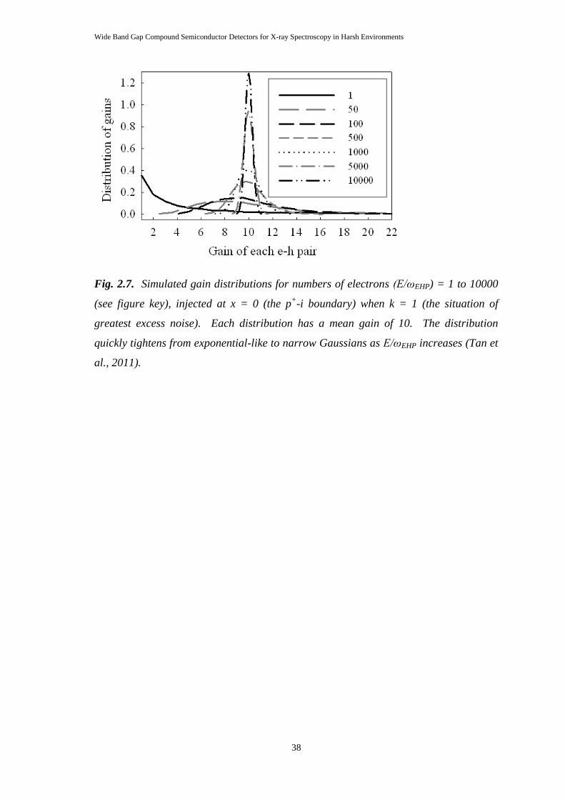
However, recent theoretical work (Tan et al., 2011) has shown that for a photon of
energy, E, where E/ωEHP >> 1, the distribution of avalanche gains achieved by the
charge carriers generated by the absorption of that photon is dependent on E/ωEHP, with
larger values of E/ωEHP leading to lower (improved) values of NXS. Fig. 2.7 shows how
as E/ωEHP increases, the distribution of gains tightens.
Wide Band Gap Compound Semiconductor Detectors for X-ray Spectroscopy in Harsh Environments
38
Fig. 2.7. Simulated gain distributions for numbers of electrons (E/ωEHP) = 1 to 10000
(see figure key), injected at x = 0 (the p+-i boundary) when k = 1 (the situation of
greatest excess noise). Each distribution has a mean gain of 10. The distribution
quickly tightens from exponential-like to narrow Gaussians as E/ωEHP increases (Tan et
al., 2011).
Wide Band Gap Compound Semiconductor Detectors for X-ray Spectroscopy in Harsh Environments
39
Chapter 3 Monte Carlo model
3.1 Introduction
This chapter describes a new Monte Carlo computer model that has been developed to
simulate X-ray detection with three layer (e.g. p+-i-n
+) non-avalanche and avalanche
mesa photodiodes, the results of which are presented in later chapters. Monte Carlo
modelling is a numerical simulation technique that can be used to model systems in
which there are stochastic (probabilistic) processes that cannot be well modelled with
deterministic methods. Many of the processes that occur in semiconductor X-ray
detectors are probabilistic and the use of Monte Carlo techniques in the simulation of
such devices is well established e.g. Lees (2010), Keister et al. (2010), Campbell et al.
(2001), McCarthy et al. (1995) and Fraser et al. (1994). The aim of developing the
model was to understand better the processes at work in X-ray semiconductor detectors,
as well as predict detector behaviour and inform future detector development.
The model was developed in The Mathworks Inc. Matlab® 7.10.0 and run on a
Microsoft® Windows® XP desktop PC with an Intel® Core 2 duo CPU. For a user
defined three-dimensional, three layer compound semiconductor detector (e.g. an
Al0.8Ga0.2As p+-i-n
+ diode) (§3.2) and X-ray source (§3.3), the relatively simple model
simulates X-ray attenuation and photoelectric absorption (§3.4), electron-hole pair
creation (§3.5), X-ray fluorescence (§3.6) and local model avalanche multiplication
(§3.7), to produce a spectrum (§3.8). A flowchart giving an overview of the model is
shown in Fig. 3.1. The processes shown in this overview are described in more detail in
the sub-sections of this chapter.
Wide Band Gap Compound Semiconductor Detectors for X-ray Spectroscopy in Harsh Environments
40
Start
Emit photons from source & determine
which photons are absorbed and
where (x, y, z) (stochastic process)
For each absorbed photon determine
what type of atom it hit (e.g. Al, Ga or
As) (stochastic process)
For each absorbed photon determine
if it fluoresces (stochastic process)
Determine which fluorescence
photons are absorbed & where (x, y,
z) (stochastic process)
For each fluorescence event
determine whether:
a) only photoelectron is absorbed in
active region
b) only fluorescence photon is
absorbed in active region
c) both photoelectron & fluorescence
photon are absorbed in active region
Calculate post-avalanche charge
created for each event (original
photons & fluorescence events)
Calculate pre-avalanche charge
carrier numbers for each event
(original photons & fluorescence
events)
Generate spectrum with noise,
including read out electronics and
Fano statistics
Finish
Detector properties defined
Source properties defined
Fig. 3.1. Flow diagram of the Monte Carlo model.
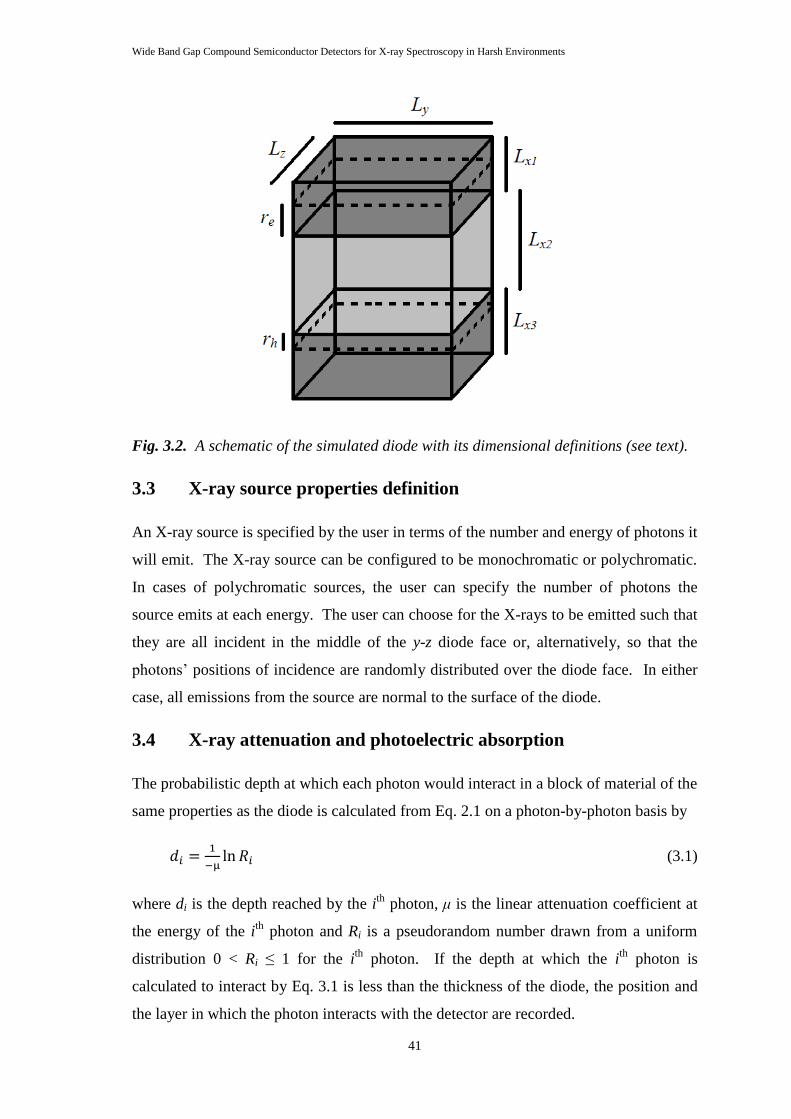
3.2 Detector properties definition
A three-dimensional square single pixel mesa photodiode consisting of three layers is
specified by the user. A schematic of the diode showing the definable dimensional
parameters is given in Fig. 3.2. The detector sizes in the y and z dimensions (Ly and Lz
respectively) are defined along with the x-dimension thickness of each layer (Lx1, Lx2
and Lx3). The material from which each layer is made is input by the user in terms of its
elemental composition and the X-ray fluorescence probabilities (yields) of each shell of
those elements along with the elemental X-ray emission lines, fractional radiative rates
and electron binding energies. The electron, α, and hole, β, impact ionisation
coefficients of the diode material as functions of electric field, along with the electric
field strength to simulate, are also input by the user. The Fano factor, electron-hole pair
creation energy for the material and the total noise in r.m.s. e- to be simulated are
specified. For layers 1 and 3 the electron, re, and hole, rh, recombination lengths are
also specified. The path to a pre-generated text file (using data from Cromer &
Liberman (1970)) containing X-ray linear attenuation coefficients for the energy range
of interest is provided by the user.
Wide Band Gap Compound Semiconductor Detectors for X-ray Spectroscopy in Harsh Environments
41
Fig. 3.2. A schematic of the simulated diode with its dimensional definitions (see text).
3.3 X-ray source properties definition
An X-ray source is specified by the user in terms of the number and energy of photons it
will emit. The X-ray source can be configured to be monochromatic or polychromatic.
In cases of polychromatic sources, the user can specify the number of photons the
source emits at each energy. The user can choose for the X-rays to be emitted such that
they are all incident in the middle of the y-z diode face or, alternatively, so that the
photons‟ positions of incidence are randomly distributed over the diode face. In either
case, all emissions from the source are normal to the surface of the diode.
3.4 X-ray attenuation and photoelectric absorption
The probabilistic depth at which each photon would interact in a block of material of the
same properties as the diode is calculated from Eq. 2.1 on a photon-by-photon basis by
(3.1)
where di is the depth reached by the ith
photon, μ is the linear attenuation coefficient at
the energy of the ith
photon and Ri is a pseudorandom number drawn from a uniform
distribution 0 < Ri ≤ 1 for the ith
photon. If the depth at which the ith
photon is
calculated to interact by Eq. 3.1 is less than the thickness of the diode, the position and
the layer in which the photon interacts with the detector are recorded.
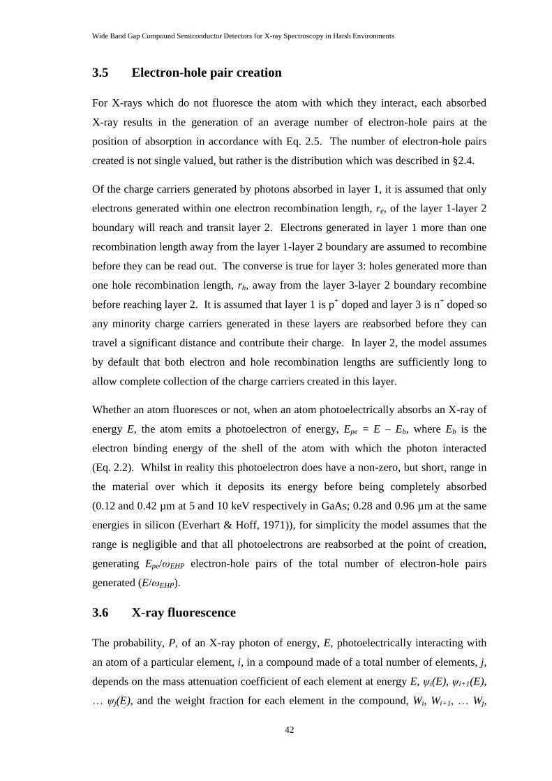
Wide Band Gap Compound Semiconductor Detectors for X-ray Spectroscopy in Harsh Environments
42
3.5 Electron-hole pair creation
For X-rays which do not fluoresce the atom with which they interact, each absorbed
X-ray results in the generation of an average number of electron-hole pairs at the
position of absorption in accordance with Eq. 2.5. The number of electron-hole pairs
created is not single valued, but rather is the distribution which was described in §2.4.
Of the charge carriers generated by photons absorbed in layer 1, it is assumed that only
electrons generated within one electron recombination length, re, of the layer 1-layer 2
boundary will reach and transit layer 2. Electrons generated in layer 1 more than one
recombination length away from the layer 1-layer 2 boundary are assumed to recombine
before they can be read out. The converse is true for layer 3: holes generated more than
one hole recombination length, rh, away from the layer 3-layer 2 boundary recombine
before reaching layer 2. It is assumed that layer 1 is p+ doped and layer 3 is n
+ doped so
any minority charge carriers generated in these layers are reabsorbed before they can
travel a significant distance and contribute their charge. In layer 2, the model assumes
by default that both electron and hole recombination lengths are sufficiently long to
allow complete collection of the charge carriers created in this layer.
Whether an atom fluoresces or not, when an atom photoelectrically absorbs an X-ray of
energy E, the atom emits a photoelectron of energy, Epe = E – Eb, where Eb is the
electron binding energy of the shell of the atom with which the photon interacted
(Eq. 2.2). Whilst in reality this photoelectron does have a non-zero, but short, range in
the material over which it deposits its energy before being completely absorbed
(0.12 and 0.42 µm at 5 and 10 keV respectively in GaAs; 0.28 and 0.96 µm at the same
energies in silicon (Everhart & Hoff, 1971)), for simplicity the model assumes that the
range is negligible and that all photoelectrons are reabsorbed at the point of creation,
generating Epe/ωEHP electron-hole pairs of the total number of electron-hole pairs
generated (E/ωEHP).
3.6 X-ray fluorescence
The probability, P, of an X-ray photon of energy, E, photoelectrically interacting with
an atom of a particular element, i, in a compound made of a total number of elements, j,
depends on the mass attenuation coefficient of each element at energy E, ψi(E), ψi+1(E),
… ψj(E), and the weight fraction for each element in the compound, Wi, Wi+1, … Wj,
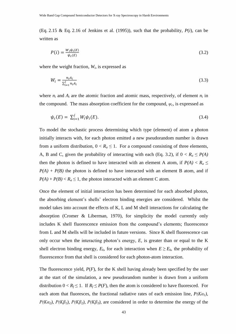
Wide Band Gap Compound Semiconductor Detectors for X-ray Spectroscopy in Harsh Environments
43
(Eq. 2.15 & Eq. 2.16 of Jenkins et al. (1995)), such that the probability, P(i), can be
written as
(3.2)
where the weight fraction, Wi, is expressed as
∑
(3.3)
where ni and Ai are the atomic fraction and atomic mass, respectively, of element ni in
the compound. The mass absorption coefficient for the compound, ψc, is expressed as
∑ . (3.4)
To model the stochastic process determining which type (element) of atom a photon
initially interacts with, for each photon emitted a new pseudorandom number is drawn
from a uniform distribution, 0 < Ra ≤ 1. For a compound consisting of three elements,
A, B and C, given the probability of interacting with each (Eq. 3.2), if 0 < Ra ≤ P(A)
then the photon is defined to have interacted with an element A atom, if P(A) < Ra ≤
P(A) + P(B) the photon is defined to have interacted with an element B atom, and if
P(A) + P(B) < Ra ≤ 1, the photon interacted with an element C atom.
Once the element of initial interaction has been determined for each absorbed photon,
the absorbing element‟s shells‟ electron binding energies are considered. Whilst the
model takes into account the effects of K, L and M shell interactions for calculating the
absorption (Cromer & Liberman, 1970), for simplicity the model currently only
includes K shell fluorescence emission from the compound‟s elements; fluorescence
from L and M shells will be included in future versions. Since K shell fluorescence can
only occur when the interacting photon‟s energy, E, is greater than or equal to the K
shell electron binding energy, Ek, for each interaction when E ≥ Ek, the probability of
fluorescence from that shell is considered for each photon-atom interaction.
The fluorescence yield, P(F), for the K shell having already been specified by the user
at the start of the simulation, a new pseudorandom number is drawn from a uniform
distribution 0 < Rf ≤ 1. If Rf ≤ P(F), then the atom is considered to have fluoresced. For
each atom that fluoresces, the fractional radiative rates of each emission line, P(Kα1),
P(Kα2), P(Kβ1), P(Kβ2), P(Kβ3), are considered in order to determine the energy of the
Wide Band Gap Compound Semiconductor Detectors for X-ray Spectroscopy in Harsh Environments
44
fluorescence photon emitted in this instance. To do this, a new pseudorandom number
is draw from a uniform distribution 0 < Rr ≤ 1 and, given the fractional radiative rates,
Table 3.1 lists the ranges of Rr that result in emission of each fluorescence photon.
Range of Rr Fluorescence
photon emitted
0 < Rr ≤ P(Kα1) Kα1
P(Kα1) < Rr ≤ P(Kα1) + P(Kα2) Kα2
P(Kα1) + P(Kα2) < Rr
≤ P(Kα1) + P(Kα2) + P(Kβ1)
Kβ1
P(Kα1) + P(Kα2) + P(Kβ1) < Rr
≤ P(Kα1) + P(Kα2) + P(Kβ1) + P(Kβ2)
Kβ2
P(Kα1) + P(Kα2) + P(Kβ1) + P(Kβ2) < Rr
≤ P(Kα1) + P(Kα2) + P(Kβ1) + P(Kβ2) + P(Kβ3)
Kβ3
Table 3.1. Ranges of pseudorandom number, Rr, that result in the emission of each K
shell fluorescence photon.
The fluorescence photon emitted from the absorbing atom is subject to attenuation and
absorption in the same way as photons emitted from the X-ray source. The distance,
dflu, that the fluorescence photon travels from its point of creation is calculated by the
same stochastic process as the original photons emitted from the source (§3.3).
However, unlike the photons emitted from the source (which are all travelling
perpendicular to the diode‟s y-z plane), the direction in which each fluorescence photon
travels is randomised. Two new pseudorandom angles, θ and υ, drawn from a uniform
distribution, 0 < D ≤ 2π, are generated for each fluorescence photon and these are used
to randomise the vector describing the fluorescence photon‟s direction of travel
(Fig. 3.3). The x, y, z components of distance that the fluorescence photon travels are
thus calculated by:
(3.5a)
(3.5b)
. (3.5c)
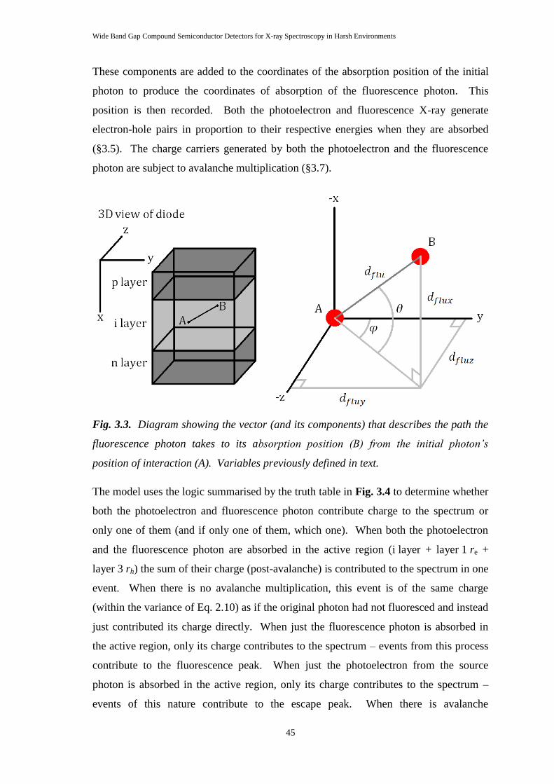
Wide Band Gap Compound Semiconductor Detectors for X-ray Spectroscopy in Harsh Environments
45
These components are added to the coordinates of the absorption position of the initial
photon to produce the coordinates of absorption of the fluorescence photon. This
position is then recorded. Both the photoelectron and fluorescence X-ray generate
electron-hole pairs in proportion to their respective energies when they are absorbed
(§3.5). The charge carriers generated by both the photoelectron and the fluorescence
photon are subject to avalanche multiplication (§3.7).
Fig. 3.3. Diagram showing the vector (and its components) that describes the path the
fluorescence photon takes to its absorption position (B) from the initial photon’s
position of interaction (A). Variables previously defined in text.
The model uses the logic summarised by the truth table in Fig. 3.4 to determine whether
both the photoelectron and fluorescence photon contribute charge to the spectrum or
only one of them (and if only one of them, which one). When both the photoelectron
and the fluorescence photon are absorbed in the active region (i layer + layer 1 re +
layer 3 rh) the sum of their charge (post-avalanche) is contributed to the spectrum in one
event. When there is no avalanche multiplication, this event is of the same charge
(within the variance of Eq. 2.10) as if the original photon had not fluoresced and instead
just contributed its charge directly. When just the fluorescence photon is absorbed in
the active region, only its charge contributes to the spectrum – events from this process
contribute to the fluorescence peak. When just the photoelectron from the source
photon is absorbed in the active region, only its charge contributes to the spectrum –
events of this nature contribute to the escape peak. When there is avalanche
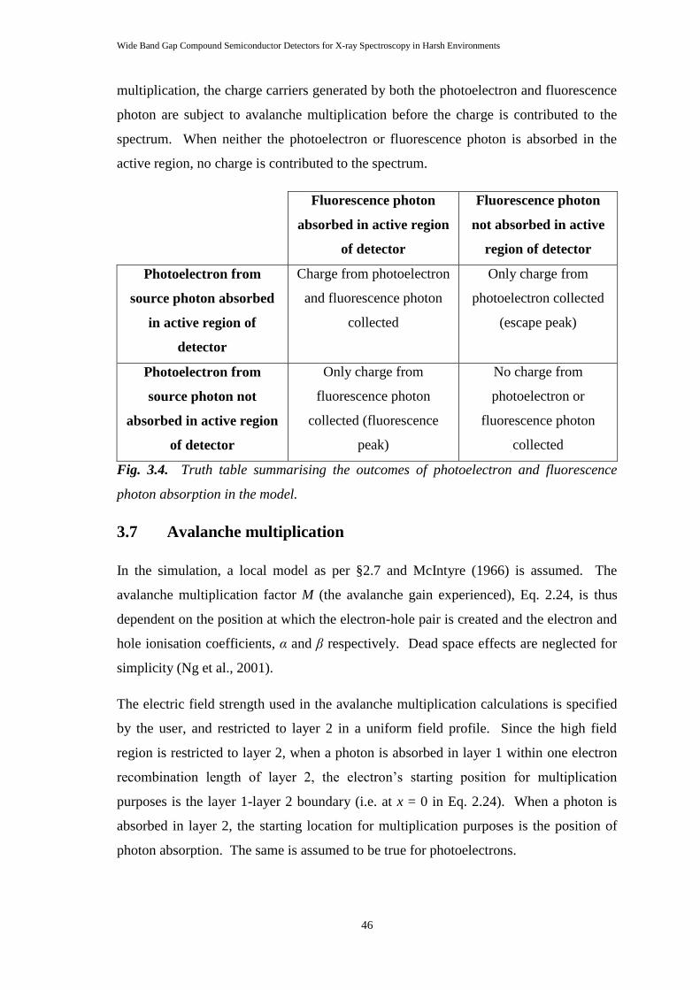
Wide Band Gap Compound Semiconductor Detectors for X-ray Spectroscopy in Harsh Environments
46
multiplication, the charge carriers generated by both the photoelectron and fluorescence
photon are subject to avalanche multiplication before the charge is contributed to the
spectrum. When neither the photoelectron or fluorescence photon is absorbed in the
active region, no charge is contributed to the spectrum.
Fluorescence photon
absorbed in active region
of detector
Fluorescence photon
not absorbed in active
region of detector
Photoelectron from
source photon absorbed
in active region of
detector
Charge from photoelectron
and fluorescence photon
collected
Only charge from
photoelectron collected
(escape peak)
Photoelectron from
source photon not
absorbed in active region
of detector
Only charge from
fluorescence photon
collected (fluorescence
peak)
No charge from
photoelectron or
fluorescence photon
collected
Fig. 3.4. Truth table summarising the outcomes of photoelectron and fluorescence
photon absorption in the model.
3.7 Avalanche multiplication
In the simulation, a local model as per §2.7 and McIntyre (1966) is assumed. The
avalanche multiplication factor M (the avalanche gain experienced), Eq. 2.24, is thus
dependent on the position at which the electron-hole pair is created and the electron and
hole ionisation coefficients, α and β respectively. Dead space effects are neglected for
simplicity (Ng et al., 2001).
The electric field strength used in the avalanche multiplication calculations is specified
by the user, and restricted to layer 2 in a uniform field profile. Since the high field
region is restricted to layer 2, when a photon is absorbed in layer 1 within one electron
recombination length of layer 2, the electron‟s starting position for multiplication
purposes is the layer 1-layer 2 boundary (i.e. at x = 0 in Eq. 2.24). When a photon is
absorbed in layer 2, the starting location for multiplication purposes is the position of
photon absorption. The same is assumed to be true for photoelectrons.
Wide Band Gap Compound Semiconductor Detectors for X-ray Spectroscopy in Harsh Environments
47
The electron, α, and hole, β, ionisation coefficients are calculated by the model from the
electric field parameterised versions input by the user. For Al0.8Ga0.2As the
parameterised forms of the ionisation coefficients have been reported by Ng et al.
(2001) as:
[ (
)
] (3.6a)
[ (
)
] (3.6b)
where E is the electric field in V/cm. The position dependent multiplication factor is
then used on a photon-by-photon basis to calculate the total charge contribution to the
spectrum from each photon absorption event.
The noise contribution to the final spectrum from the variation in the multiplication
factor between sibling electron-hole pairs created from the same photon absorption
event, i.e. the excess noise (§2.7.4), is assumed to be negligible because E/ωEHP >> 1 for
X-ray energies (Tan et al., 2011).
3.8 Spectrum generation
The charge generated in the detector for each photon emitted from the source (taking
account of fluorescence, avalanche multiplication and all other processes) is subjected
to random Gaussian noise (using pseudorandom numbers drawn from a Gaussian
distribution in Matlab) to simulate the noise (see §2.6) specified by the user. Finally,
the charge is calibrated into its energy equivalent and binned into energy bins of width
specified by the user.
Wide Band Gap Compound Semiconductor Detectors for X-ray Spectroscopy in Harsh Environments
48
Chapter 4 The temperature dependence of
Al0.8Ga0.2As non-avalanche
photodiodes
4.1 Introduction
This chapter describes work characterising the temperature dependence of the X-ray
spectroscopic performance of Al0.8Ga0.2As non-avalanche photodiodes with a view to
establishing their performance at high temperatures. The experimental methods and
techniques used to characterise the devices are presented, along with the findings of the
experimental work performed.
4.2 Background
Previous investigation of Al0.8Ga0.2As photodiodes for soft X-ray photon counting
spectroscopy has shown that they can operate with promising spectral resolution
(~1.5 keV FWHM at 5.9 keV) at room temperature (Lees et al., 2008). However, there
has been no report of their operation at any other temperature and no report of the
temperature dependence of their spectral performance. The reports in the literature
regarding AlxGa1-xAs photon counting X-ray detectors are very few. Ripamoni et al.
(1990) and Lauter et al. (1995, 1996) reported graded x AlxGa1-xAs/GaAs separate
absorption and multiplication (SAM) staircase photodiodes, and Silenas (2004), Silenas
et al. (2002, 2003, 2005, 2006, 2011) and Dapkus et al. (2007) have reported non-
photon counting AlxGa1-xAs/GaAs X-ray detectors. Lees et al. (2008) was the only
report of AlxGa1-xAs p+-p
--n
+ (or p
+-i-n
+) spectroscopic X-ray photon counting
photodiodes in the literature at the start of the research reported in this thesis. However,
work on Al0.8Ga0.2As p+-i-n
+ photodiodes for telecommunications had been reported,
concentrating on the characterisation of avalanche multiplication in the material at room
temperature (Ng et al., 2000, 2001, 2002) (Saleh et al., 2000), as had similar work for
AlxGa1-xAs x < 0.8, e.g. Plimmer et al. (2000) and Tan et al. (2001).
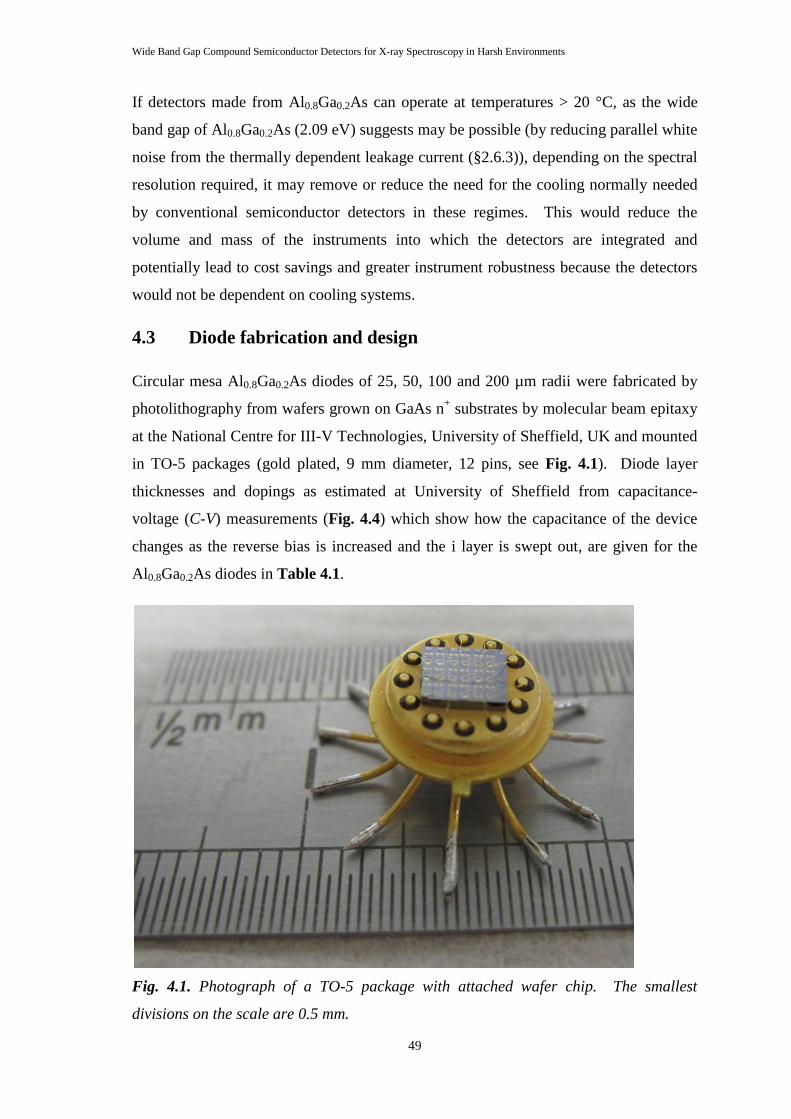
Wide Band Gap Compound Semiconductor Detectors for X-ray Spectroscopy in Harsh Environments
49
If detectors made from Al0.8Ga0.2As can operate at temperatures > 20 °C, as the wide
band gap of Al0.8Ga0.2As (2.09 eV) suggests may be possible (by reducing parallel white
noise from the thermally dependent leakage current (§2.6.3)), depending on the spectral
resolution required, it may remove or reduce the need for the cooling normally needed
by conventional semiconductor detectors in these regimes. This would reduce the
volume and mass of the instruments into which the detectors are integrated and
potentially lead to cost savings and greater instrument robustness because the detectors
would not be dependent on cooling systems.
4.3 Diode fabrication and design
Circular mesa Al0.8Ga0.2As diodes of 25, 50, 100 and 200 µm radii were fabricated by
photolithography from wafers grown on GaAs n+ substrates by molecular beam epitaxy
at the National Centre for III-V Technologies, University of Sheffield, UK and mounted
in TO-5 packages (gold plated, 9 mm diameter, 12 pins, see Fig. 4.1). Diode layer
thicknesses and dopings as estimated at University of Sheffield from capacitance-
voltage (C-V) measurements (Fig. 4.4) which show how the capacitance of the device
changes as the reverse bias is increased and the i layer is swept out, are given for the
Al0.8Ga0.2As diodes in Table 4.1.
Fig. 4.1. Photograph of a TO-5 package with attached wafer chip. The smallest
divisions on the scale are 0.5 mm.
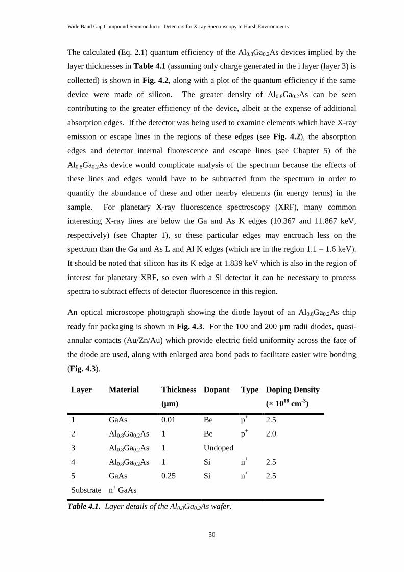
Wide Band Gap Compound Semiconductor Detectors for X-ray Spectroscopy in Harsh Environments
50
The calculated (Eq. 2.1) quantum efficiency of the Al0.8Ga0.2As devices implied by the
layer thicknesses in Table 4.1 (assuming only charge generated in the i layer (layer 3) is
collected) is shown in Fig. 4.2, along with a plot of the quantum efficiency if the same
device were made of silicon. The greater density of Al0.8Ga0.2As can be seen
contributing to the greater efficiency of the device, albeit at the expense of additional
absorption edges. If the detector was being used to examine elements which have X-ray
emission or escape lines in the regions of these edges (see Fig. 4.2), the absorption
edges and detector internal fluorescence and escape lines (see Chapter 5) of the
Al0.8Ga0.2As device would complicate analysis of the spectrum because the effects of
these lines and edges would have to be subtracted from the spectrum in order to
quantify the abundance of these and other nearby elements (in energy terms) in the
sample. For planetary X-ray fluorescence spectroscopy (XRF), many common
interesting X-ray lines are below the Ga and As K edges (10.367 and 11.867 keV,
respectively) (see Chapter 1), so these particular edges may encroach less on the
spectrum than the Ga and As L and Al K edges (which are in the region 1.1 – 1.6 keV).
It should be noted that silicon has its K edge at 1.839 keV which is also in the region of
interest for planetary XRF, so even with a Si detector it can be necessary to process
spectra to subtract effects of detector fluorescence in this region.
An optical microscope photograph showing the diode layout of an Al0.8Ga0.2As chip
ready for packaging is shown in Fig. 4.3. For the 100 and 200 µm radii diodes, quasi-
annular contacts (Au/Zn/Au) which provide electric field uniformity across the face of
the diode are used, along with enlarged area bond pads to facilitate easier wire bonding
(Fig. 4.3).
Layer Material Thickness
(µm)
Dopant Type Doping Density
(× 1018
cm-3
)
1 GaAs 0.01 Be p+ 2.5
2 Al0.8Ga0.2As 1 Be p+ 2.0
3 Al0.8Ga0.2As 1 Undoped
4 Al0.8Ga0.2As 1 Si n+ 2.5
5 GaAs 0.25 Si n+ 2.5
Substrate n+ GaAs
Table 4.1. Layer details of the Al0.8Ga0.2As wafer.
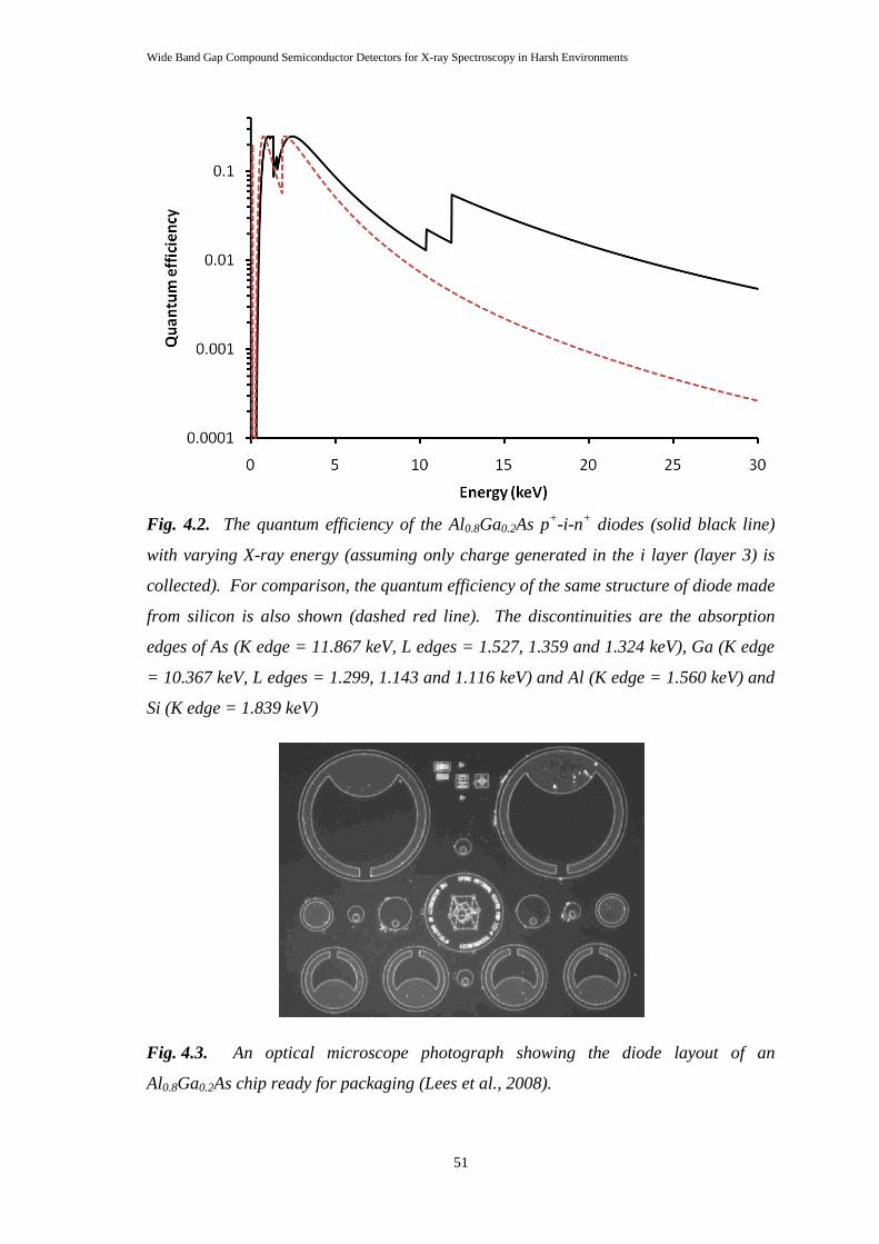
Wide Band Gap Compound Semiconductor Detectors for X-ray Spectroscopy in Harsh Environments
51
Fig. 4.2. The quantum efficiency of the Al0.8Ga0.2As p+-i-n
+ diodes (solid black line)
with varying X-ray energy (assuming only charge generated in the i layer (layer 3) is
collected). For comparison, the quantum efficiency of the same structure of diode made
from silicon is also shown (dashed red line). The discontinuities are the absorption
edges of As (K edge = 11.867 keV, L edges = 1.527, 1.359 and 1.324 keV), Ga (K edge
= 10.367 keV, L edges = 1.299, 1.143 and 1.116 keV) and Al (K edge = 1.560 keV) and
Si (K edge = 1.839 keV)
Fig. 4.3. An optical microscope photograph showing the diode layout of an
Al0.8Ga0.2As chip ready for packaging (Lees et al., 2008).
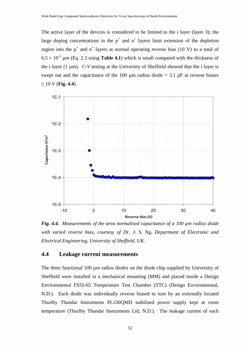
Wide Band Gap Compound Semiconductor Detectors for X-ray Spectroscopy in Harsh Environments
52
The active layer of the devices is considered to be limited to the i layer (layer 3); the
large doping concentrations in the p+ and n
+ layers limit extension of the depletion
region into the p+ and n
+ layers at normal operating reverse bias (10 V) to a total of
6.5 × 10⁻³
µm (Eq. 2.3 using Table 4.1) which is small compared with the thickness of
the i layer (1 µm). C-V testing at the University of Sheffield showed that the i layer is
swept out and the capacitance of the 100 µm radius diode = 3.1 pF at reverse biases
≥ 10 V (Fig. 4.4).
Fig. 4.4. Measurements of the area normalised capacitance of a 100 µm radius diode
with varied reverse bias, courtesy of Dr. J. S. Ng, Department of Electronic and
Electrical Engineering, University of Sheffield, UK.
4.4 Leakage current measurements
The three functional 100 µm radius diodes on the diode chip supplied by University of
Sheffield were installed in a mechanical mounting (MM) and placed inside a Design
Environmental FS55-65 Temperature Test Chamber (TTC) (Design Environmental,
N.D.). Each diode was individually reverse biased in turn by an externally located
Thurlby Thandar Instruments PL330QMD stabilised power supply kept at room
temperature (Thurlby Thandar Instruments Ltd, N.D.). The leakage current of each
Wide Band Gap Compound Semiconductor Detectors for X-ray Spectroscopy in Harsh Environments
53
diode was amplified by a Keithley Instruments 427 current amplifier (Keithley
Instruments Inc., 1975) and measured by an Iso-Tech IDM 105 digital multimeter, both
located outside the TTC. Room temperature (20 °C) current-voltage measurements (up
to 28 V reverse bias) were taken for each diode and are plotted in Fig. 4.5. At 10 V (the
operating reverse bias of these diodes used for the spectroscopic X-ray measurements,
see §4.5), diodes 1, 2 and 3 were found to have leakage currents of 4.3, 5.6 and 11.9 pA,
respectively. The variation in the leakage currents between diodes may be attributable
to variations in wafer quality and/or diode fabrication.
The two diodes with the lowest leakage current at 10 V, D1 and D2, (4.3 and 5.6 pA,
respectively) were selected on this basis for temperature dependence testing of their
leakage current and X-ray spectroscopic performance. The measurements were taken at
temperatures between +90 °C and -30 °C, in 10 °C steps. The temperature inside the
MM was monitored by thermocouple and Fluke 50D digital thermometer to ensure that
the temperature had equalised between the MM and chamber after each temperature
change. The diode and the MM were assumed to be in thermal equilibrium. Fig. 4.6
shows how the leakage currents of the diodes vary as a function of temperature. At
temperatures > 60 °C, the leakage currents of the devices diverge from each other. The
exact cause of the difference between the leakage currents is currently unknown but is
attributed to small variations in wafer quality and diode fabrication, as for the room
temperature I-V testing leakage current variations (Fig. 4.5). Even at the highest
measured temperature (90 °C), the difference is less than a factor of two and the leakage
current is still < 200 pA in each case.
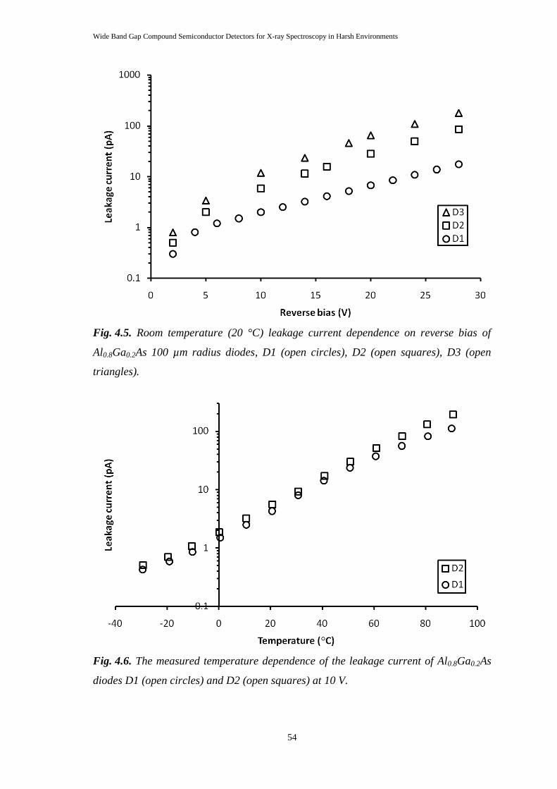
Wide Band Gap Compound Semiconductor Detectors for X-ray Spectroscopy in Harsh Environments
54
Fig. 4.5. Room temperature (20 °C) leakage current dependence on reverse bias of
Al0.8Ga0.2As 100 µm radius diodes, D1 (open circles), D2 (open squares), D3 (open
triangles).
Fig. 4.6. The measured temperature dependence of the leakage current of Al0.8Ga0.2As
diodes D1 (open circles) and D2 (open squares) at 10 V.
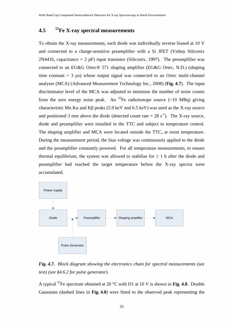
Wide Band Gap Compound Semiconductor Detectors for X-ray Spectroscopy in Harsh Environments
55
4.5 55
Fe X-ray spectral measurements
To obtain the X-ray measurements, each diode was individually reverse biased at 10 V
and connected to a charge-sensitive preamplifier with a Si JFET (Vishay Siliconix
2N4416, capacitance = 2 pF) input transistor (Siliconix, 1997). The preamplifier was
connected to an EG&G Ortec® 571 shaping amplifier (EG&G Ortec, N.D.) (shaping
time constant = 3 µs) whose output signal was connected to an Ortec multi-channel
analyser (MCA) (Advanced Measurement Technology Inc., 2008) (Fig. 4.7). The input
discriminator level of the MCA was adjusted to minimise the number of noise counts
from the zero energy noise peak. An 55
Fe radioisotope source (~10 MBq) giving
characteristic Mn Kα and Kβ peaks (5.9 keV and 6.5 keV) was used as the X-ray source
and positioned 3 mm above the diode (detected count rate = 28 s-1
). The X-ray source,
diode and preamplifier were installed in the TTC and subject to temperature control.
The shaping amplifier and MCA were located outside the TTC, at room temperature.
During the measurement period, the bias voltage was continuously applied to the diode
and the preamplifier constantly powered. For all temperature measurements, to ensure
thermal equilibrium, the system was allowed to stabilise for ≥ 1 h after the diode and
preamplifier had reached the target temperature before the X-ray spectra were
accumulated.
Diode Preamplifier Shaping amplifier MCA
Pulse Generator
Power supply
Fig. 4.7. Block diagram showing the electronics chain for spectral measurements (see
text) (see §4.6.2 for pulse generator).
A typical 55
Fe spectrum obtained at 20 °C with D1 at 10 V is shown in Fig. 4.8. Double
Gaussians (dashed lines in Fig. 4.8) were fitted to the observed peak representing the
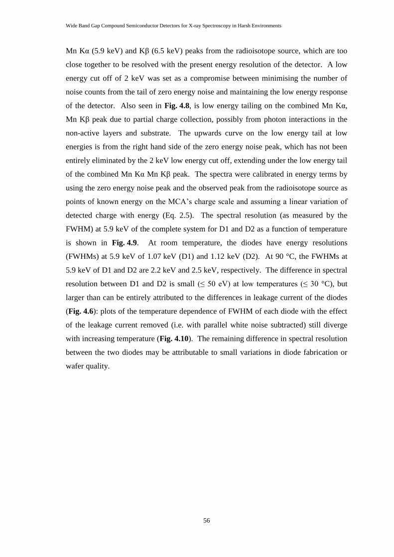
Wide Band Gap Compound Semiconductor Detectors for X-ray Spectroscopy in Harsh Environments
56
Mn Kα (5.9 keV) and Kβ (6.5 keV) peaks from the radioisotope source, which are too
close together to be resolved with the present energy resolution of the detector. A low
energy cut off of 2 keV was set as a compromise between minimising the number of
noise counts from the tail of zero energy noise and maintaining the low energy response
of the detector. Also seen in Fig. 4.8, is low energy tailing on the combined Mn Kα,
Mn Kβ peak due to partial charge collection, possibly from photon interactions in the
non-active layers and substrate. The upwards curve on the low energy tail at low
energies is from the right hand side of the zero energy noise peak, which has not been
entirely eliminated by the 2 keV low energy cut off, extending under the low energy tail
of the combined Mn Kα Mn Kβ peak. The spectra were calibrated in energy terms by
using the zero energy noise peak and the observed peak from the radioisotope source as
points of known energy on the MCA‟s charge scale and assuming a linear variation of
detected charge with energy (Eq. 2.5). The spectral resolution (as measured by the
FWHM) at 5.9 keV of the complete system for D1 and D2 as a function of temperature
is shown in Fig. 4.9. At room temperature, the diodes have energy resolutions
(FWHMs) at 5.9 keV of 1.07 keV (D1) and 1.12 keV (D2). At 90 °C, the FWHMs at
5.9 keV of D1 and D2 are 2.2 keV and 2.5 keV, respectively. The difference in spectral
resolution between D1 and D2 is small (≤ 50 eV) at low temperatures (≤ 30 °C), but
larger than can be entirely attributed to the differences in leakage current of the diodes
(Fig. 4.6): plots of the temperature dependence of FWHM of each diode with the effect
of the leakage current removed (i.e. with parallel white noise subtracted) still diverge
with increasing temperature (Fig. 4.10). The remaining difference in spectral resolution
between the two diodes may be attributable to small variations in diode fabrication or
wafer quality.
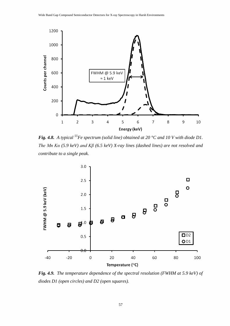
Wide Band Gap Compound Semiconductor Detectors for X-ray Spectroscopy in Harsh Environments
57
Fig. 4.8. A typical 55
Fe spectrum (solid line) obtained at 20 °C and 10 V with diode D1.
The Mn Kα (5.9 keV) and Kβ (6.5 keV) X-ray lines (dashed lines) are not resolved and
contribute to a single peak.
Fig. 4.9. The temperature dependence of the spectral resolution (FWHM at 5.9 keV) of
diodes D1 (open circles) and D2 (open squares).
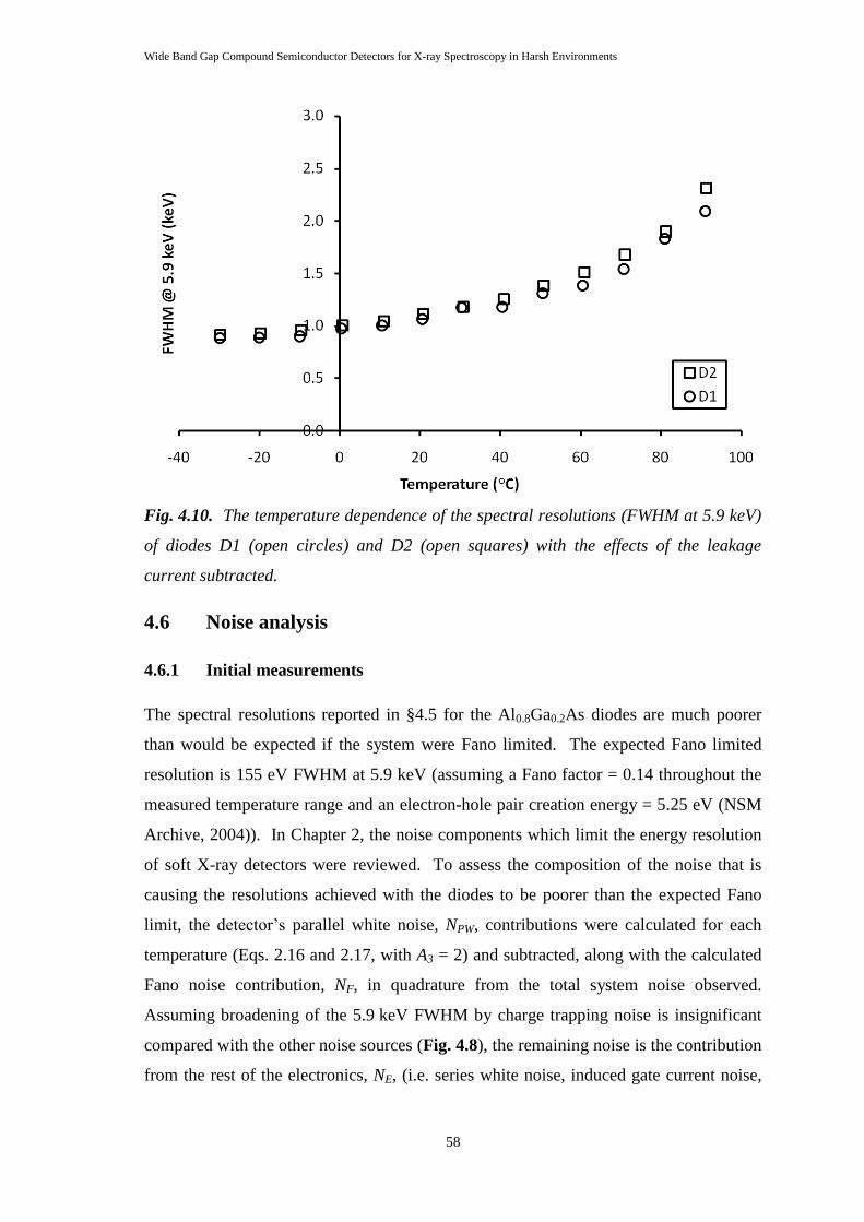
Wide Band Gap Compound Semiconductor Detectors for X-ray Spectroscopy in Harsh Environments
58
Fig. 4.10. The temperature dependence of the spectral resolutions (FWHM at 5.9 keV)
of diodes D1 (open circles) and D2 (open squares) with the effects of the leakage
current subtracted.
4.6 Noise analysis
4.6.1 Initial measurements
The spectral resolutions reported in §4.5 for the Al0.8Ga0.2As diodes are much poorer
than would be expected if the system were Fano limited. The expected Fano limited
resolution is 155 eV FWHM at 5.9 keV (assuming a Fano factor = 0.14 throughout the
measured temperature range and an electron-hole pair creation energy = 5.25 eV (NSM
Archive, 2004)). In Chapter 2, the noise components which limit the energy resolution
of soft X-ray detectors were reviewed. To assess the composition of the noise that is
causing the resolutions achieved with the diodes to be poorer than the expected Fano
limit, the detector‟s parallel white noise, NPW, contributions were calculated for each
temperature (Eqs. 2.16 and 2.17, with A3 = 2) and subtracted, along with the calculated
Fano noise contribution, NF, in quadrature from the total system noise observed.
Assuming broadening of the 5.9 keV FWHM by charge trapping noise is insignificant
compared with the other noise sources (Fig. 4.8), the remaining noise is the contribution
from the rest of the electronics, NE, (i.e. series white noise, induced gate current noise,
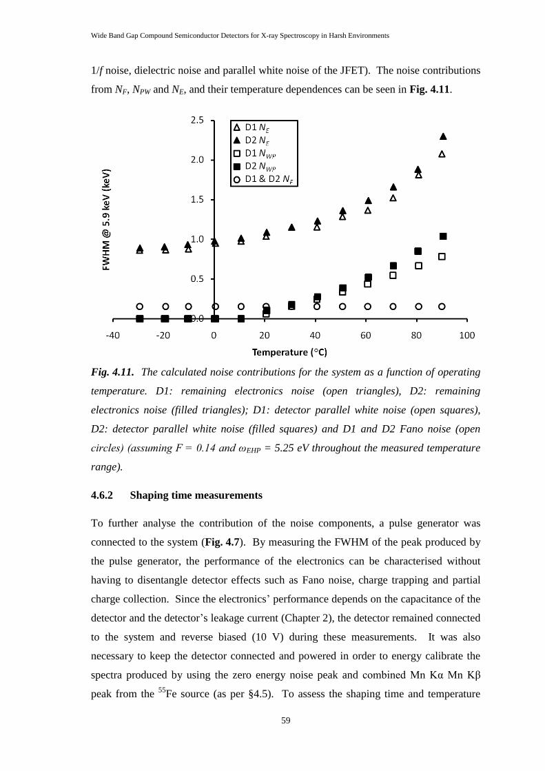
Wide Band Gap Compound Semiconductor Detectors for X-ray Spectroscopy in Harsh Environments
59
1/f noise, dielectric noise and parallel white noise of the JFET). The noise contributions
from NF, NPW and NE, and their temperature dependences can be seen in Fig. 4.11.
Fig. 4.11. The calculated noise contributions for the system as a function of operating
temperature. D1: remaining electronics noise (open triangles), D2: remaining
electronics noise (filled triangles); D1: detector parallel white noise (open squares),
D2: detector parallel white noise (filled squares) and D1 and D2 Fano noise (open
circles) (assuming F = 0.14 and ωEHP = 5.25 eV throughout the measured temperature
range).
4.6.2 Shaping time measurements
To further analyse the contribution of the noise components, a pulse generator was
connected to the system (Fig. 4.7). By measuring the FWHM of the peak produced by
the pulse generator, the performance of the electronics can be characterised without
having to disentangle detector effects such as Fano noise, charge trapping and partial
charge collection. Since the electronics‟ performance depends on the capacitance of the
detector and the detector‟s leakage current (Chapter 2), the detector remained connected
to the system and reverse biased (10 V) during these measurements. It was also
necessary to keep the detector connected and powered in order to energy calibrate the
spectra produced by using the zero energy noise peak and combined Mn Kα Mn Kβ
peak from the 55
Fe source (as per §4.5). To assess the shaping time and temperature
Wide Band Gap Compound Semiconductor Detectors for X-ray Spectroscopy in Harsh Environments
60
dependence of the electronics noise, spectra were accumulated with shaping times of
0.5, 1, 2, 3, 6 and 10 µs at temperatures of +50, +20 and -10 °C.
Unlike the parallel white noise (NPW), the series white noise including induced gate
current noise (NSWC) and 1/f noise (N1/f) contributions (see §2.6), the dielectric noise
(ND) is not readily calculable because the stray capacitances are not easily measured.
However, by calculating the noise contributions from detector and JFET parallel white
noise (§2.6.3), series white noise including induced gate current noise (§2.6.4 and
§2.6.7), and 1/f noise (§2.6.5), and subtracting these in quadrature from the total noise,
NT, shown by the FWHM of the pulser peak, it is possible to obtain an estimate for the
dielectric noise, ND, assuming any noise sources other than those mentioned are
insignificant.
The total (detector and JFET) parallel white noise contribution for each shaping time
and temperature was calculated from Eqs. 2.16 and 2.17 with signal shaping function
constant A3 = 2 (Gatti et al., 1990) (EG&G Ortec, N.D.). The JFET‟s parallel white
noise contribution was estimated to be 0.10, 0.11 and 0.50 keV at -10, 20 and 50 °C,
respectively (Siliconix, 1997). The series white noise contribution was calculated from
Eqs. 2.18 and 2.19 assuming γ = 0.85 (Bertuccio, Pullia & DeGeronimo, 1996),
transconductance of the JFET gm = 5 mS (Siliconix, 1997), and that the total capacitance
at the preamplifier input, CT, is dominated by the capacitances of the detector (3.1 pF)
and JFET (2 pF). The series white noise contribution was adjusted for induced gate
current noise (§2.6.7) by assuming √ ≈ 0.8 (Bertuccio, Pullia & DeGeronimo, 1996).
The 1/f noise contribution was calculated from Eq. 2.20 with the above assumptions and
also that A2 = 1.2 and Af = 3 × 10-15
V2 (Gatti et al., 1990).
The calculated total (detector and JFET) parallel white, series white (including induced
gate current noise) and 1/f noise components together with the measured pulser peak
FWHM and estimated dielectric noise contribution (ND2 = NT
2– NPW
2 – NSWC
2 – N1/f
2) at
each shaping time for temperatures of +50, +20 and -10 °C are shown in Fig. 4.12. The
contribution from the parallel white noise decreases and the series white contribution
increases as the shaping time is increased at all three temperatures. The increase in
parallel white noise with increased shaping time is more significant at higher
temperature because of the positive temperature dependence of the leakage current of
the detector (Fig. 4.5) and JFET. The series white noise contribution can be seen
Wide Band Gap Compound Semiconductor Detectors for X-ray Spectroscopy in Harsh Environments
61
decreasing with increasing shaping time, as expected from its 1/τ dependence (Eq.
2.19). The 1/f noise contribution is not shaping time dependent and is, therefore,
constant (Eq. 2.20). The shaping time at which the functions representing the parallel
white and series white contributions intersect lengthens with decreasing temperature (τ
= 2 µs at 50 °C, τ = 5.25 µs at 20 °C, τ = 8.45 µs at -10 °C). The optimum shaping time
lengthens with decreasing temperature (τ = 2, 3 and 6 µs at 50, 20 and -10 °C,
respectively). The data shown in Fig. 4.12 suggest that dielectric noise is a significant
noise source; indeed for the temperature range shown, the analysis suggests that the
dielectric noise is the most significant noise source.
The estimated dielectric noise is broadly similar across the measured shaping times as
would be expected from a shaping time independent contribution (Eq. 2.21). However,
slight increases in the calculated dielectric contribution are apparent, primarily at a
shaping time of 0.5 µs for temperatures of 50 °C and -10 °C, and to a lesser extent, at
long shaping times (6 µs, 10 µs) for 50 °C and 20 °C. The apparent increase in
dielectric noise at short shaping times may be attributable to an underestimate of NSWC
(Eq. 2.19), probably as a consequence of underestimating the total capacitance at the
preamplifier input (i.e. the stray capacitance is not insignificant compared with those of
the diode (3.1 pF) and JFET (2 pF)). However, if the apparent increase in dielectric
noise is attributable to underestimating the significance of the stray capacitance, it is not
clear why measurements at short shaping times at 20 °C do not show a comparable rise.
The slight rise shown in calculated dielectric noise at long shaping times at 20 °C could
be attributed to an underestimate of the parallel white noise as a consequence of
underestimating the leakage current of the JFET (the JFET‟s parameters were taken
from its data sheet rather than being measured directly in the lab). The leakage currents
of the JFET and detector are greater and more significant at higher temperature,
explaining why little increase is observed in the parallel white noise at long shaping
times in the -10 °C data.
A computer model of the noise which varies parameters such as the additional stray
capacitances (capacitances in addition to those of the detector and JFET), to fit the
experimental data, may produce better estimates for the individual noise contributions
of the system, but the analysis presented here is sufficient to show that the dielectrics
around the detector and JFET may be a very significant source of noise in the system
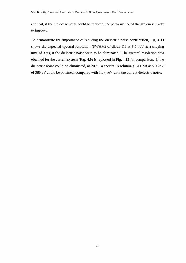
Wide Band Gap Compound Semiconductor Detectors for X-ray Spectroscopy in Harsh Environments
62
and that, if the dielectric noise could be reduced, the performance of the system is likely
to improve.
To demonstrate the importance of reducing the dielectric noise contribution, Fig. 4.13
shows the expected spectral resolution (FWHM) of diode D1 at 5.9 keV at a shaping
time of 3 µs, if the dielectric noise were to be eliminated. The spectral resolution data
obtained for the current system (Fig. 4.9) is replotted in Fig. 4.13 for comparison. If the
dielectric noise could be eliminated, at 20 °C a spectral resolution (FWHM) at 5.9 keV
of 380 eV could be obtained, compared with 1.07 keV with the current dielectric noise.
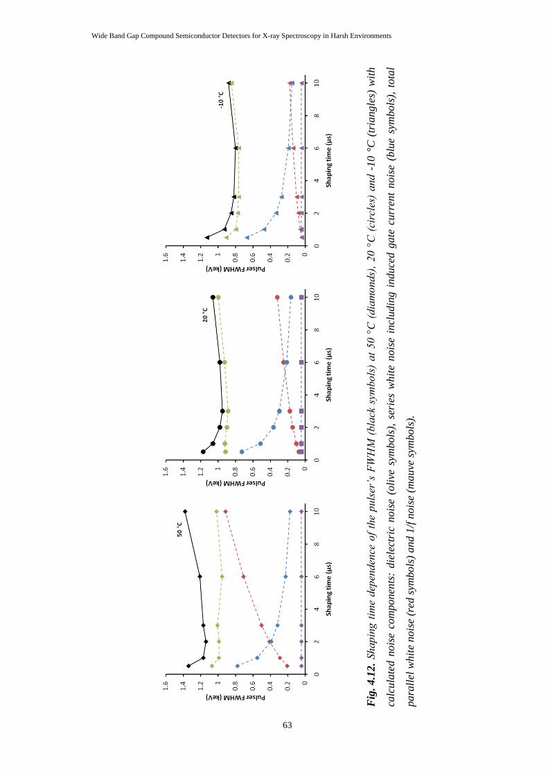
Wide Band Gap Compound Semiconductor Detectors for X-ray Spectroscopy in Harsh Environments
63
Fig
. 4.1
2.
Shapin
g t
ime
dep
enden
ce o
f th
e puls
er’s
FW
HM
(bla
ck s
ymbols
) at
50 °
C (
dia
monds)
, 20 °
C (
circ
les)
and -
10 °
C (
tria
ngle
s) w
ith
calc
ula
ted n
ois
e co
mponen
ts:
die
lect
ric
nois
e (o
live
sym
bols
), s
erie
s w
hit
e nois
e in
cludin
g i
nduce
d g
ate
curr
ent
nois
e (b
lue
sym
bols
), t
ota
l
para
llel
wh
ite
nois
e (r
ed s
ymbols
) and 1
/f n
ois
e (m
auve
sym
bols
).
Wide Band Gap Compound Semiconductor Detectors for X-ray Spectroscopy in Harsh Environments
64
Fig. 4.13. The calculated spectral resolution (FWHM) of diode D1 if the dielectric
noise was eliminated (filled circles). Also shown is the measured temperature
dependence of the spectral resolution of diode D1 including dielectric noise (open
circles).
4.7 Conclusions and discussion
Al0.8Ga0.2As p+-i-n
+ diodes have been shown to operate as photon counting
spectroscopic X-ray detectors in non-avalanche mode at temperatures from -30 °C to
+90 °C with promising spectral resolution (FWHM) of the full system (0.9 – 2.5 keV).
Room temperature spectral measurements have shown spectral resolutions at 5.9 keV of
1.07 keV and 1.12 keV FWHM for the diodes studied. This is better than that of the
previously reported Al0.8Ga0.2As devices when operated in non-avalanche mode
(~1.5 keV FWHM at 5.9 keV) using the same preamplifier electronics as here (Lees et
al., 2008).
Investigations of the noise sources contributing to the 1.07 keV spectral resolution of
diode D1 have indicated that dielectric noise, thought to arise primarily from the diode
and JFET packaging, is the most significant factor in limiting the spectral resolution of
the current system. If the dielectric noise could be eliminated through improvements to
the diode and JFET packaging (e.g. custom designed packaging, perhaps using ceramic
Wide Band Gap Compound Semiconductor Detectors for X-ray Spectroscopy in Harsh Environments
65
or Teflon mountings), spectral resolutions (FWHM at 5.9 keV) of 380 eV at 20 °C and
~500 eV at 50 °C are predicted (Fig. 4.13).
The spectral resolution of the diodes and system is currently modest compared with that
achievable with a Si CCD cooled to -90 °C (130 eV FWHM at 5.9 keV) (Nakajima et
al., 2005) and a silicon drift detector (SDD) operated at 20 °C (300 eV FWHM at
5.9 keV) (Lechner et al., 2001). SDDs may achieve good spectral performance at lower
temperatures (≤ 20 °C) but their spectral performance rapidly degrades at higher
temperatures (≥ 20 °C) (PNSensor GmbH, N.D.). Furthermore, avalanche
multiplication in Al0.8Ga0.2As is increasingly well understood (Chapter 6) and recently it
has been found that appreciable avalanche multiplication can be achieved at X-ray
energies without introducing significant avalanche excess noise (§2.7.4) (Tan et al.,
2011) (Lees et al., 2008). This may provide potential to exploit avalanche
multiplication in Al0.8Ga0.2As APDs to achieve better resolutions than could be achieved
with non-avalanche devices (Tan et al., 2011).
The uncooled Al0.8Ga0.2As detectors reported in this chapter show promise for X-ray
spectroscopy at temperatures as high as +90 °C. An X-ray spectrometer based on
Al0.8Ga0.2As detectors similar to those reported here, may find use in monitoring e.g.
iron or molybdenum content in oils as a consequence of engine and oil wear, and in
other applications where uncooled operation at high temperature is required, especially
if the dielectric noise could be reduced.
Refinements to the design of the preamplifier and reduction of the diode leakage current
through improved diode material quality, fabrication experience and mesa side wall
passivation will all enable improvement upon the currently achieved resolutions,
facilitating further progress towards the expected Fano limit of 155 eV at 5.9 keV
(assuming F = 0.14).
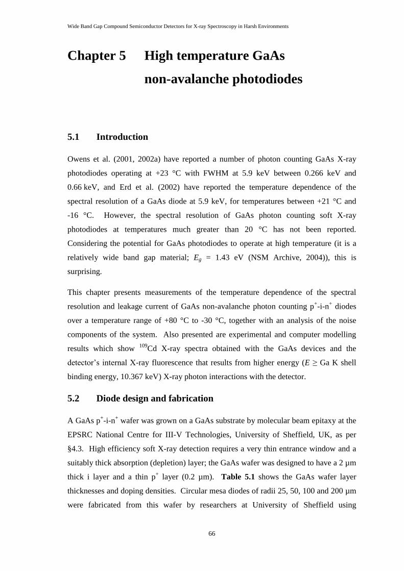
Wide Band Gap Compound Semiconductor Detectors for X-ray Spectroscopy in Harsh Environments
66
Chapter 5 High temperature GaAs
non-avalanche photodiodes
5.1 Introduction
Owens et al. (2001, 2002a) have reported a number of photon counting GaAs X-ray
photodiodes operating at +23 °C with FWHM at 5.9 keV between 0.266 keV and
0.66 keV, and Erd et al. (2002) have reported the temperature dependence of the
spectral resolution of a GaAs diode at 5.9 keV, for temperatures between +21 °C and
-16 °C. However, the spectral resolution of GaAs photon counting soft X-ray
photodiodes at temperatures much greater than 20 °C has not been reported.
Considering the potential for GaAs photodiodes to operate at high temperature (it is a
relatively wide band gap material; Eg = 1.43 eV (NSM Archive, 2004)), this is
surprising.
This chapter presents measurements of the temperature dependence of the spectral
resolution and leakage current of GaAs non-avalanche photon counting p+-i-n
+ diodes
over a temperature range of +80 °C to -30 °C, together with an analysis of the noise
components of the system. Also presented are experimental and computer modelling
results which show 109
Cd X-ray spectra obtained with the GaAs devices and the
detector‟s internal X-ray fluorescence that results from higher energy (E ≥ Ga K shell
binding energy, 10.367 keV) X-ray photon interactions with the detector.
5.2 Diode design and fabrication
A GaAs p+-i-n
+ wafer was grown on a GaAs substrate by molecular beam epitaxy at the
EPSRC National Centre for III-V Technologies, University of Sheffield, UK, as per
§4.3. High efficiency soft X-ray detection requires a very thin entrance window and a
suitably thick absorption (depletion) layer; the GaAs wafer was designed to have a 2 µm
thick i layer and a thin p+ layer (0.2 µm). Table 5.1 shows the GaAs wafer layer
thicknesses and doping densities. Circular mesa diodes of radii 25, 50, 100 and 200 µm
were fabricated from this wafer by researchers at University of Sheffield using
Wide Band Gap Compound Semiconductor Detectors for X-ray Spectroscopy in Harsh Environments
67
photolithography. The diode layout was the same as the Al0.8Ga0.2As diode layout
(Fig. 4.3). The GaAs wafers were passivated with SU-8 (an epoxy-based material
commonly used for passivation and photoresist applications) (Chollet, 2009) to
minimise surface leakage current.
Layer Material Thickness
(µm)
Dopant Type Doping Density
(×1018
cm-3
)
1 GaAs 0.01 Be p++
10
2 GaAs 0.2 Be p+ 2.0
3 GaAs 2 Undoped < 0.01
4 GaAs 0.1 Si n+ 2.0
5 GaAs 0.2 Si n+ 2.0
Substrate n+ GaAs 500
Table 5.1. Layer details of the GaAs wafer used in this work.
A graph showing the quantum efficiency of the devices, assuming only charge
generated in the i layer (layer 3) is collected, is shown in Fig. 5.1, along with the
calculated quantum efficiency if the same structure of diode were made from silicon, for
comparison. The calculated efficiencies of the GaAs diodes at 5.9 keV (Mn Kα) and
22.16 keV (Ag Kα1) are calculated to be 0.152 and 0.034, respectively. These are much
better than for the same structure made from silicon (0.067 at 5.9 keV, 0.001 at
22.16 keV). However, the efficiency of the GaAs diodes is lower than may be
achievable with a thicker (40 µm, ~0.95 efficiency at 5.9 keV) GaAs diode, perhaps
grown by CVD or LPE, or a very thick (500 µm) silicon device (~0.99 efficiency at
5.9 keV). At very soft X-ray energies, it is the thickness of the p+ layer (0.21 µm) rather
than the thinness of the i layer that reduces the quantum efficiency of the GaAs devices.
At an X-ray energy of 2 keV, an efficiency of 0.7 is predicted for GaAs diodes of the
current design, but if the thickness of the p+ layer were halved, this would increase to
0.81.
The high field region is considered to be restricted to the i layer at normal operating
bias; the high doping concentrations in the p+ and n
+ layers limit the extension of the
depletion region into these layers to a total of 3.6 × 10⁻³
µm at 10 V (Eq. 2.3 using
Table 5.1), which is small compared with the thickness of the i layer (2 µm). The
diodes were mounted in a TO-5 package (gold plated, 9 mm diameter, 12 pins,
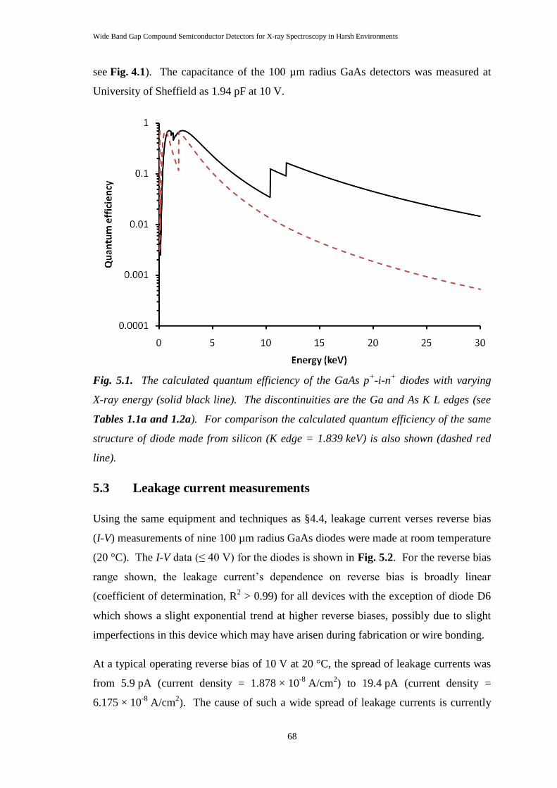
Wide Band Gap Compound Semiconductor Detectors for X-ray Spectroscopy in Harsh Environments
68
see Fig. 4.1). The capacitance of the 100 µm radius GaAs detectors was measured at
University of Sheffield as 1.94 pF at 10 V.
Fig. 5.1. The calculated quantum efficiency of the GaAs p+-i-n
+ diodes with varying
X-ray energy (solid black line). The discontinuities are the Ga and As K L edges (see
Tables 1.1a and 1.2a). For comparison the calculated quantum efficiency of the same
structure of diode made from silicon (K edge = 1.839 keV) is also shown (dashed red
line).
5.3 Leakage current measurements
Using the same equipment and techniques as §4.4, leakage current verses reverse bias
(I-V) measurements of nine 100 µm radius GaAs diodes were made at room temperature
(20 °C). The I-V data (≤ 40 V) for the diodes is shown in Fig. 5.2. For the reverse bias
range shown, the leakage current‟s dependence on reverse bias is broadly linear
(coefficient of determination, R2 > 0.99) for all devices with the exception of diode D6
which shows a slight exponential trend at higher reverse biases, possibly due to slight
imperfections in this device which may have arisen during fabrication or wire bonding.
At a typical operating reverse bias of 10 V at 20 °C, the spread of leakage currents was
from 5.9 pA (current density = 1.878 × 10⁻⁸
A/cm2) to 19.4 pA (current density =
6.175 × 10⁻⁸
A/cm2). The cause of such a wide spread of leakage currents is currently
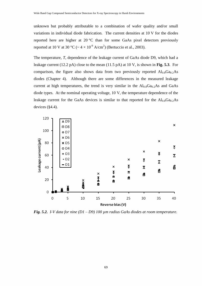
Wide Band Gap Compound Semiconductor Detectors for X-ray Spectroscopy in Harsh Environments
69
unknown but probably attributable to a combination of wafer quality and/or small
variations in individual diode fabrication. The current densities at 10 V for the diodes
reported here are higher at 20 °C than for some GaAs pixel detectors previously
reported at 10 V at 30 °C (~ 4 × 10⁻⁹
A/cm2) (Bertuccio et al., 2003).
The temperature, T, dependence of the leakage current of GaAs diode D9, which had a
leakage current (12.2 pA) close to the mean (11.5 pA) at 10 V, is shown in Fig. 5.3. For
comparison, the figure also shows data from two previously reported Al0.8Ga0.2As
diodes (Chapter 4). Although there are some differences in the measured leakage
current at high temperatures, the trend is very similar in the Al0.8Ga0.2As and GaAs
diode types. At the nominal operating voltage, 10 V, the temperature dependence of the
leakage current for the GaAs devices is similar to that reported for the Al0.8Ga0.2As
devices (§4.4).
Fig. 5.2. I-V data for nine (D1 – D9) 100 µm radius GaAs diodes at room temperature.
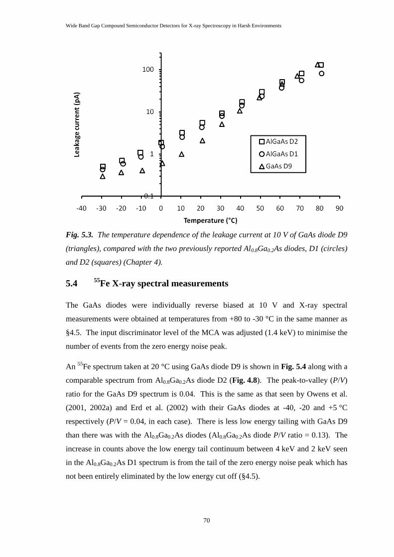
Wide Band Gap Compound Semiconductor Detectors for X-ray Spectroscopy in Harsh Environments
70
Fig. 5.3. The temperature dependence of the leakage current at 10 V of GaAs diode D9
(triangles), compared with the two previously reported Al0.8Ga0.2As diodes, D1 (circles)
and D2 (squares) (Chapter 4).
5.4 55
Fe X-ray spectral measurements
The GaAs diodes were individually reverse biased at 10 V and X-ray spectral
measurements were obtained at temperatures from +80 to -30 °C in the same manner as
§4.5. The input discriminator level of the MCA was adjusted (1.4 keV) to minimise the
number of events from the zero energy noise peak.
An 55
Fe spectrum taken at 20 °C using GaAs diode D9 is shown in Fig. 5.4 along with a
comparable spectrum from Al0.8Ga0.2As diode D2 (Fig. 4.8). The peak-to-valley (P/V)
ratio for the GaAs D9 spectrum is 0.04. This is the same as that seen by Owens et al.
(2001, 2002a) and Erd et al. (2002) with their GaAs diodes at -40, -20 and +5 °C
respectively (P/V = 0.04, in each case). There is less low energy tailing with GaAs D9
than there was with the Al0.8Ga0.2As diodes (Al0.8Ga0.2As diode P/V ratio = 0.13). The
increase in counts above the low energy tail continuum between 4 keV and 2 keV seen
in the Al0.8Ga0.2As D1 spectrum is from the tail of the zero energy noise peak which has
not been entirely eliminated by the low energy cut off (§4.5).
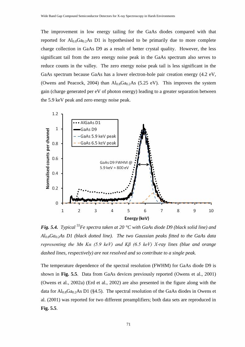
Wide Band Gap Compound Semiconductor Detectors for X-ray Spectroscopy in Harsh Environments
71
The improvement in low energy tailing for the GaAs diodes compared with that
reported for Al0.8Ga0.2As D1 is hypothesised to be primarily due to more complete
charge collection in GaAs D9 as a result of better crystal quality. However, the less
significant tail from the zero energy noise peak in the GaAs spectrum also serves to
reduce counts in the valley. The zero energy noise peak tail is less significant in the
GaAs spectrum because GaAs has a lower electron-hole pair creation energy (4.2 eV,
(Owens and Peacock, 2004) than Al0.8Ga0.2As (5.25 eV). This improves the system
gain (charge generated per eV of photon energy) leading to a greater separation between
the 5.9 keV peak and zero energy noise peak.
Fig. 5.4. Typical 55
Fe spectra taken at 20 °C with GaAs diode D9 (black solid line) and
Al0.8Ga0.2As D1 (black dotted line). The two Gaussian peaks fitted to the GaAs data
representing the Mn Kα (5.9 keV) and Kβ (6.5 keV) X-ray lines (blue and orange
dashed lines, respectively) are not resolved and so contribute to a single peak.
The temperature dependence of the spectral resolution (FWHM) for GaAs diode D9 is
shown in Fig. 5.5. Data from GaAs devices previously reported (Owens et al., 2001)
(Owens et al., 2002a) (Erd et al., 2002) are also presented in the figure along with the
data for Al0.8Ga0.2As D1 (§4.5). The spectral resolution of the GaAs diodes in Owens et
al. (2001) was reported for two different preamplifiers; both data sets are reproduced in
Fig. 5.5.
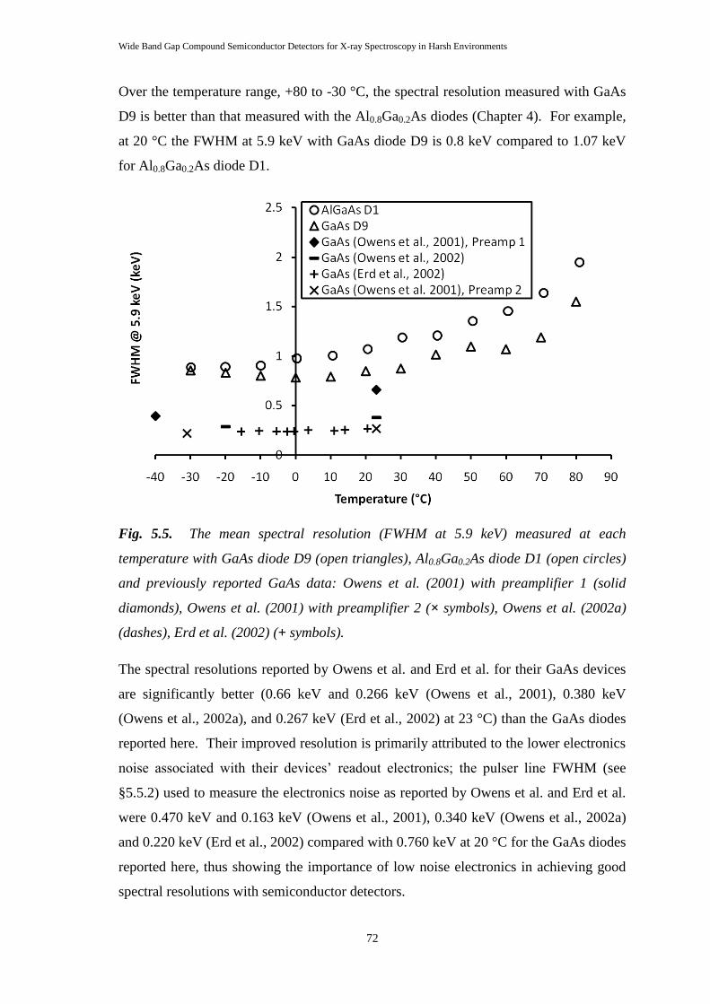
Wide Band Gap Compound Semiconductor Detectors for X-ray Spectroscopy in Harsh Environments
72
Over the temperature range, +80 to -30 °C, the spectral resolution measured with GaAs
D9 is better than that measured with the Al0.8Ga0.2As diodes (Chapter 4). For example,
at 20 °C the FWHM at 5.9 keV with GaAs diode D9 is 0.8 keV compared to 1.07 keV
for Al0.8Ga0.2As diode D1.
Fig. 5.5. The mean spectral resolution (FWHM at 5.9 keV) measured at each
temperature with GaAs diode D9 (open triangles), Al0.8Ga0.2As diode D1 (open circles)
and previously reported GaAs data: Owens et al. (2001) with preamplifier 1 (solid
diamonds), Owens et al. (2001) with preamplifier 2 (× symbols), Owens et al. (2002a)
(dashes), Erd et al. (2002) (+ symbols).
The spectral resolutions reported by Owens et al. and Erd et al. for their GaAs devices
are significantly better (0.66 keV and 0.266 keV (Owens et al., 2001), 0.380 keV
(Owens et al., 2002a), and 0.267 keV (Erd et al., 2002) at 23 °C) than the GaAs diodes
reported here. Their improved resolution is primarily attributed to the lower electronics
noise associated with their devices‟ readout electronics; the pulser line FWHM (see
§5.5.2) used to measure the electronics noise as reported by Owens et al. and Erd et al.
were 0.470 keV and 0.163 keV (Owens et al., 2001), 0.340 keV (Owens et al., 2002a)
and 0.220 keV (Erd et al., 2002) compared with 0.760 keV at 20 °C for the GaAs diodes
reported here, thus showing the importance of low noise electronics in achieving good
spectral resolutions with semiconductor detectors.
Wide Band Gap Compound Semiconductor Detectors for X-ray Spectroscopy in Harsh Environments
73
The improvement in spectral resolution of GaAs D9 compared with Al0.8Ga0.2As D1 can
be attributed primarily to the increased gain of the GaAs system; GaAs has a lower
electron-hole pair creation energy (4.2 eV) than Al0.8Ga0.2As (5.25 eV) which leads to
larger numbers of charge carriers generated for the same input X-ray photon energy.
This improves the gain of the system and, consequently, the spectral resolution. As is
the case for the Al0.8Ga0.2As diodes, the spectral resolution achieved with the GaAs
diodes is much poorer than would be expected if the system were Fano limited. For
GaAs, given a Fano factor of 0.12 (Bertuccio et al., 2003), the Fano limited resolution at
5.9 keV would be 129 eV FWHM, which is better than Al0.8Ga0.2As (155 eV FWHM at
5.9 keV, assuming F = 0.14).
5.5 Noise analysis
5.5.1 Initial measurements
The noise contributions to the GaAs diode spectra FWHM total noise, NT, were assessed
similarly to those for the Al0.8Ga0.2As spectra (§4.6): the detector‟s parallel white noise
contribution, NPW, was calculated for each temperature (Eqs. 2.16 and 2.17, with A3 = 2)
and subtracted in quadrature. The expected Fano noise contribution, NF, was similarly
subtracted. Assuming broadening of the FWHM due to charge trapping noise is
insignificant (Fig. 5.4), the remainder can be attributed to the rest of the electronics
noise contribution, NE. The contributions and total for GaAs D1 are shown in Fig. 5.6
together with the data for Al0.8Ga0.2As D2 for comparison. The noise contribution from
the Fano noise is small compared with NE, as is the detector‟s parallel white noise,
which is even less significant at lower temperatures (< 40 °C) than the Fano noise.
From the relative insignificance of the detector‟s parallel white noise, we can see that
the detector‟s leakage current (which contributes to the parallel white noise) is not
presently a limiting factor in the spectral resolution achievable with the detectors in this
temperature range. Rather, it appears that it is one or more of the noise sources
remaining in NE which is limiting the spectral resolution.
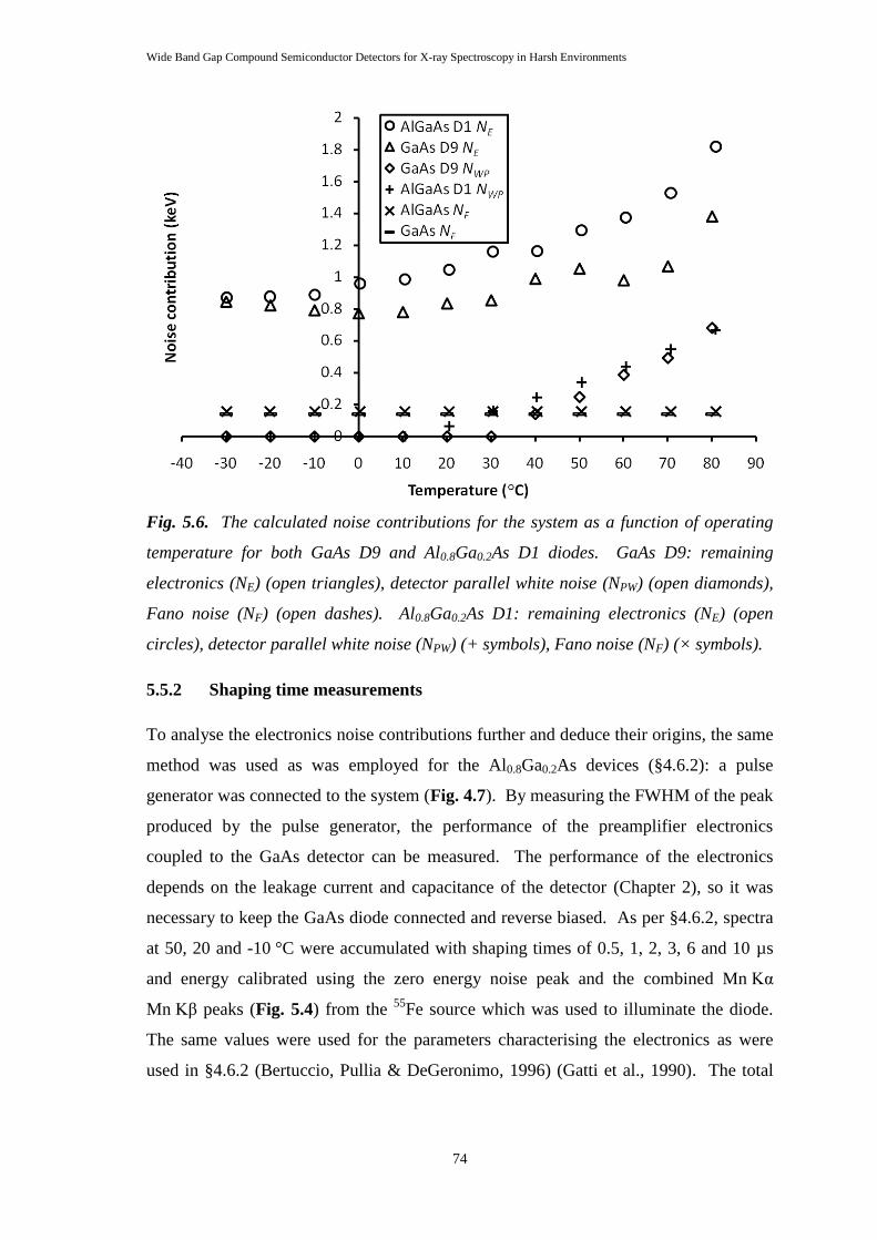
Wide Band Gap Compound Semiconductor Detectors for X-ray Spectroscopy in Harsh Environments
74
Fig. 5.6. The calculated noise contributions for the system as a function of operating
temperature for both GaAs D9 and Al0.8Ga0.2As D1 diodes. GaAs D9: remaining
electronics (NE) (open triangles), detector parallel white noise (NPW) (open diamonds),
Fano noise (NF) (open dashes). Al0.8Ga0.2As D1: remaining electronics (NE) (open
circles), detector parallel white noise (NPW) (+ symbols), Fano noise (NF) (× symbols).
5.5.2 Shaping time measurements
To analyse the electronics noise contributions further and deduce their origins, the same
method was used as was employed for the Al0.8Ga0.2As devices (§4.6.2): a pulse
generator was connected to the system (Fig. 4.7). By measuring the FWHM of the peak
produced by the pulse generator, the performance of the preamplifier electronics
coupled to the GaAs detector can be measured. The performance of the electronics
depends on the leakage current and capacitance of the detector (Chapter 2), so it was
necessary to keep the GaAs diode connected and reverse biased. As per §4.6.2, spectra
at 50, 20 and -10 °C were accumulated with shaping times of 0.5, 1, 2, 3, 6 and 10 µs
and energy calibrated using the zero energy noise peak and the combined Mn Kα
Mn Kβ peaks (Fig. 5.4) from the 55
Fe source which was used to illuminate the diode.
The same values were used for the parameters characterising the electronics as were
used in §4.6.2 (Bertuccio, Pullia & DeGeronimo, 1996) (Gatti et al., 1990). The total
Wide Band Gap Compound Semiconductor Detectors for X-ray Spectroscopy in Harsh Environments
75
capacitance at the preamplifier input, CT, was assumed to be dominated by the
capacitance of the detector (Cd = 1.94 pF) and JFET (Ci = 2 pF).
The FWHM of the pulser peak, NT, along with the calculated contributions to this
overall noise, arising from total (detector and JFET) parallel white noise, NPW (§2.6.3),
series white noise including induced gate current noise, NSWC (§2.6.4 and §2.6.7), 1/f
noise, N1/f (§2.6.5) and dielectric noise (ND2 = NT
2 – NPW
2 – NSWC
2 – N1/f
2) components
can be seen in Fig. 5.7. The JFET‟s white parallel noise contribution was estimated to
be 0.10, 0.11 and 0.50 keV at -10, 20 and 50 °C, respectively (Siliconix, 1997). Even
though the preamplifier electronics are the same as were used in Chapter 4, their
measured performance is different with the GaAs detector because of the diode‟s
different properties (compare Fig. 5.7 and Fig. 4.12). As expected from their τ
dependences, the parallel white contribution (Eqs. 2.16 and 2.17) still reduces with
increasing shaping time, the series white contribution (Eqs. 2.18 and 2.19) increases and
the 1/f contribution (Eq. 2.20) remains constant. The shaping time at which the parallel
white and series white noise contributions intersect lengthens with decreasing
temperature (τ = 2 µs at 50 °C, τ = 5.4 µs at 20 °C, τ = 7.8 µs at -10 °C) similarly to that
found with the Al0.8Ga0.2As detector, but the GaAs system‟s optimum shaping time
dependence on temperature is less clear because the minima representing the optimum
shaping time at 20 °C and -10 °C are not so well defined. However, the parallel white
and series white data suggest a lengthening of optimum shaping time with decreasing
temperature similarly to the Al0.8Ga0.2As data (Fig. 4.12).
The calculated dielectric noise contribution is broadly constant with varied shaping time
as expected (Eq. 2.21 and §4.6.2), although there are slight increases in the calculated
component at short shaping times. This trend is consistent with an underestimate of the
series white noise and 1/f noise contributions as a consequence of an underestimate of
CT. That CT is underestimated in this way (it had been assumed that CT = Cd + Ci) is not
surprising given the significance of the estimated dielectric noise contribution and the
stray capacitance that such a contribution presupposes. As was the case for the
Al0.8Ga0.2As diode system, a computer model which varies parameters such as the stray
capacitance to fit the experimental data, may enable the dielectric noise contribution to
be better calculated. Nevertheless, the analysis presented here is sufficient to show that
the dielectric noise contribution is significant and that future work to improve the
spectral resolution would be well targeted by improving the diode and JFET packaging.
Wide Band Gap Compound Semiconductor Detectors for X-ray Spectroscopy in Harsh Environments
76
A graph showing the expected spectral resolution (FWHM) at 5.9 keV (with τ = 3 µs), if
the dielectric noise could be eliminated, is shown in Fig. 5.8 and compared with the
same data for Al0.8Ga0.2As D1 (Fig. 4.11) and those presented in Fig. 5.5.
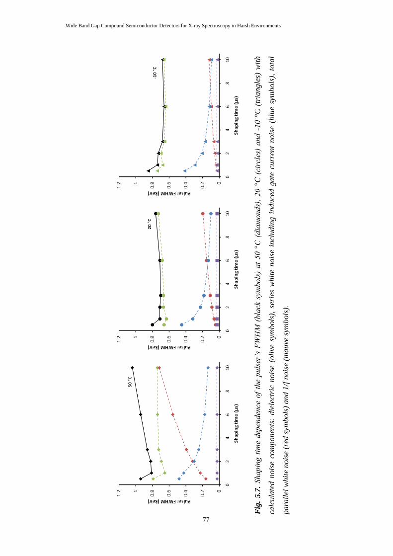
Wide Band Gap Compound Semiconductor Detectors for X-ray Spectroscopy in Harsh Environments
77
Fig
. 5.7
. Shap
ing t
ime
dep
enden
ce o
f th
e puls
er’s
FW
HM
(bla
ck s
ymbols
) at
50 °
C (
dia
mo
nds)
, 20 °
C (
circ
les)
and -
10 °
C (
tria
ngle
s) w
ith
calc
ula
ted n
ois
e co
mponen
ts:
die
lect
ric
nois
e (o
live
sym
bols
), s
erie
s w
hit
e nois
e in
cludin
g i
nduce
d g
ate
curr
ent
nois
e (b
lue
sym
bols
), t
ota
l
para
llel
wh
ite
nois
e (r
ed s
ymbols
) and 1
/f n
ois
e (m
auve
sym
bols
).
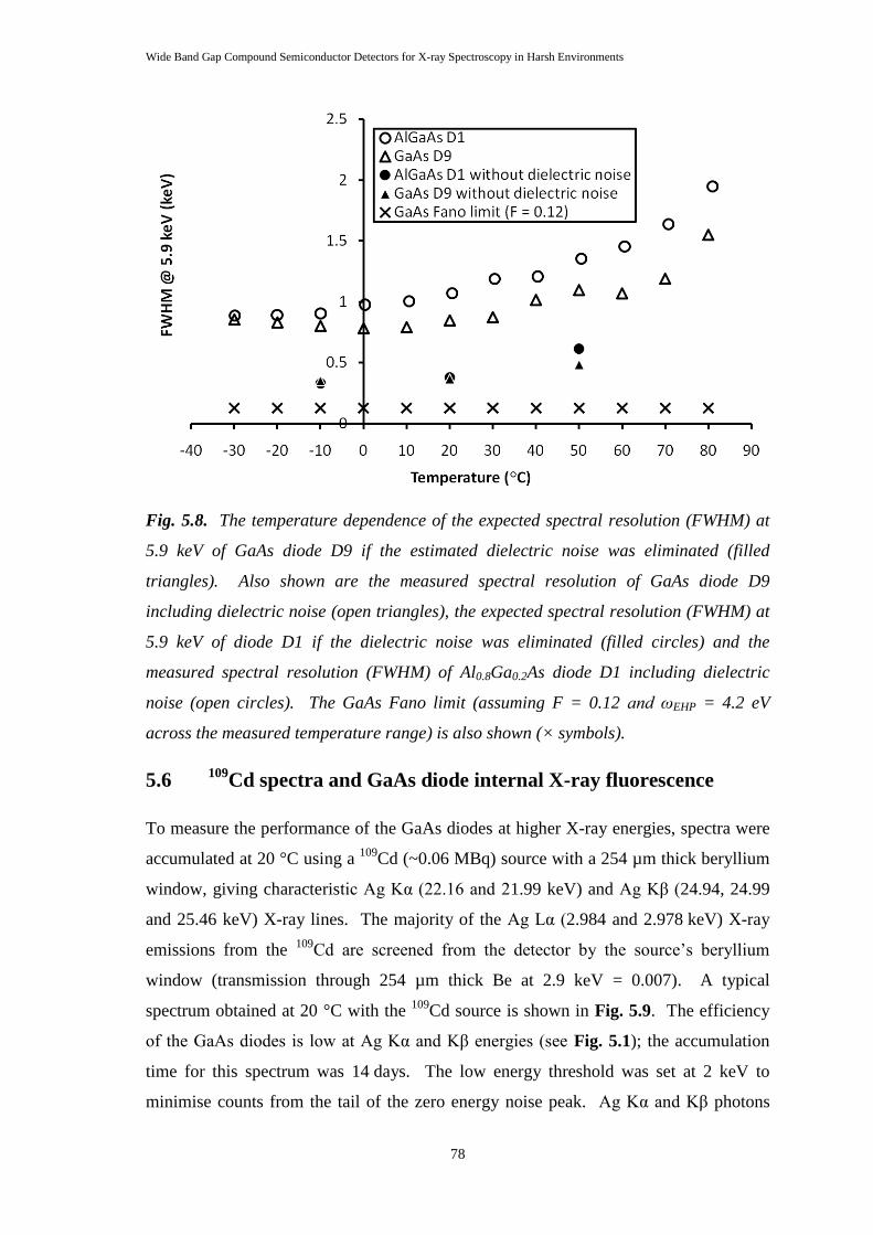
Wide Band Gap Compound Semiconductor Detectors for X-ray Spectroscopy in Harsh Environments
78
Fig. 5.8. The temperature dependence of the expected spectral resolution (FWHM) at
5.9 keV of GaAs diode D9 if the estimated dielectric noise was eliminated (filled
triangles). Also shown are the measured spectral resolution of GaAs diode D9
including dielectric noise (open triangles), the expected spectral resolution (FWHM) at
5.9 keV of diode D1 if the dielectric noise was eliminated (filled circles) and the
measured spectral resolution (FWHM) of Al0.8Ga0.2As diode D1 including dielectric
noise (open circles). The GaAs Fano limit (assuming F = 0.12 and ωEHP = 4.2 eV
across the measured temperature range) is also shown (× symbols).
5.6 109
Cd spectra and GaAs diode internal X-ray fluorescence
To measure the performance of the GaAs diodes at higher X-ray energies, spectra were
accumulated at 20 °C using a 109
Cd (~0.06 MBq) source with a 254 µm thick beryllium
window, giving characteristic Ag Kα (22.16 and 21.99 keV) and Ag Kβ (24.94, 24.99
and 25.46 keV) X-ray lines. The majority of the Ag Lα (2.984 and 2.978 keV) X-ray
emissions from the 109
Cd are screened from the detector by the source‟s beryllium
window (transmission through 254 µm thick Be at 2.9 keV = 0.007). A typical
spectrum obtained at 20 °C with the 109
Cd source is shown in Fig. 5.9. The efficiency
of the GaAs diodes is low at Ag Kα and Kβ energies (see Fig. 5.1); the accumulation
time for this spectrum was 14 days. The low energy threshold was set at 2 keV to
minimise counts from the tail of the zero energy noise peak. Ag Kα and Kβ photons
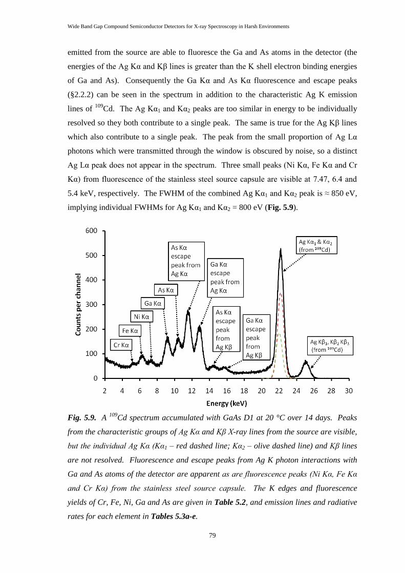
Wide Band Gap Compound Semiconductor Detectors for X-ray Spectroscopy in Harsh Environments
79
emitted from the source are able to fluoresce the Ga and As atoms in the detector (the
energies of the Ag Kα and Kβ lines is greater than the K shell electron binding energies
of Ga and As). Consequently the Ga Kα and As Kα fluorescence and escape peaks
(§2.2.2) can be seen in the spectrum in addition to the characteristic Ag K emission
lines of 109
Cd. The Ag Kα1 and Kα2 peaks are too similar in energy to be individually
resolved so they both contribute to a single peak. The same is true for the Ag Kβ lines
which also contribute to a single peak. The peak from the small proportion of Ag Lα
photons which were transmitted through the window is obscured by noise, so a distinct
Ag Lα peak does not appear in the spectrum. Three small peaks (Ni Kα, Fe Kα and Cr
Kα) from fluorescence of the stainless steel source capsule are visible at 7.47, 6.4 and
5.4 keV, respectively. The FWHM of the combined Ag Kα1 and Kα2 peak is ≈ 850 eV,
implying individual FWHMs for Ag Kα1 and Kα2 = 800 eV (Fig. 5.9).
Fig. 5.9. A 109
Cd spectrum accumulated with GaAs D1 at 20 °C over 14 days. Peaks
from the characteristic groups of Ag Kα and Kβ X-ray lines from the source are visible,
but the individual Ag Kα (Kα1 – red dashed line; Kα2 – olive dashed line) and Kβ lines
are not resolved. Fluorescence and escape peaks from Ag K photon interactions with
Ga and As atoms of the detector are apparent as are fluorescence peaks (Ni Kα, Fe Kα
and Cr Kα) from the stainless steel source capsule. The K edges and fluorescence
yields of Cr, Fe, Ni, Ga and As are given in Table 5.2, and emission lines and radiative
rates for each element in Tables 5.3a-e.
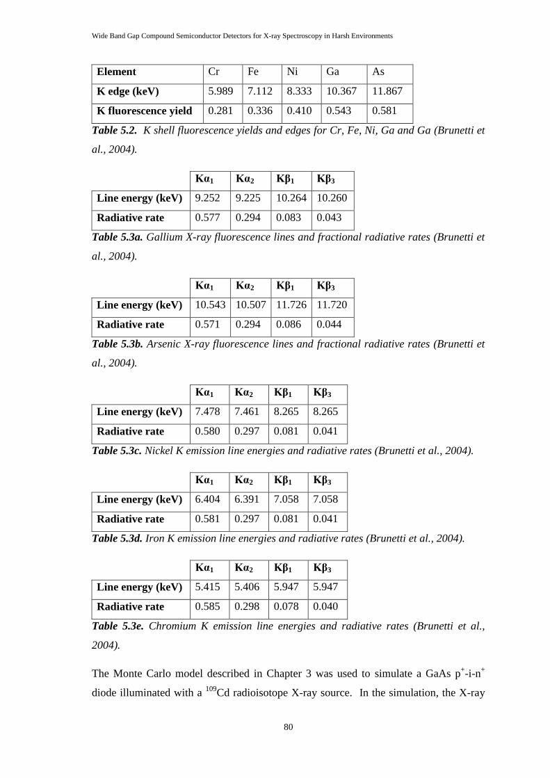
Wide Band Gap Compound Semiconductor Detectors for X-ray Spectroscopy in Harsh Environments
80
Element Cr Fe Ni Ga As
K edge (keV) 5.989 7.112 8.333 10.367 11.867
K fluorescence yield 0.281 0.336 0.410 0.543 0.581
Table 5.2. K shell fluorescence yields and edges for Cr, Fe, Ni, Ga and Ga (Brunetti et
al., 2004).
Kα1 Kα2 Kβ1 Kβ3
Line energy (keV) 9.252 9.225 10.264 10.260
Radiative rate 0.577 0.294 0.083 0.043
Table 5.3a. Gallium X-ray fluorescence lines and fractional radiative rates (Brunetti et
al., 2004).
Kα1 Kα2 Kβ1 Kβ3
Line energy (keV) 10.543 10.507 11.726 11.720
Radiative rate 0.571 0.294 0.086 0.044
Table 5.3b. Arsenic X-ray fluorescence lines and fractional radiative rates (Brunetti et
al., 2004).
Kα1 Kα2 Kβ1 Kβ3
Line energy (keV) 7.478 7.461 8.265 8.265
Radiative rate 0.580 0.297 0.081 0.041
Table 5.3c. Nickel K emission line energies and radiative rates (Brunetti et al., 2004).
Kα1 Kα2 Kβ1 Kβ3
Line energy (keV) 6.404 6.391 7.058 7.058
Radiative rate 0.581 0.297 0.081 0.041
Table 5.3d. Iron K emission line energies and radiative rates (Brunetti et al., 2004).
Kα1 Kα2 Kβ1 Kβ3
Line energy (keV) 5.415 5.406 5.947 5.947
Radiative rate 0.585 0.298 0.078 0.040
Table 5.3e. Chromium K emission line energies and radiative rates (Brunetti et al.,
2004).
The Monte Carlo model described in Chapter 3 was used to simulate a GaAs p+-i-n
+
diode illuminated with a 109
Cd radioisotope X-ray source. In the simulation, the X-ray
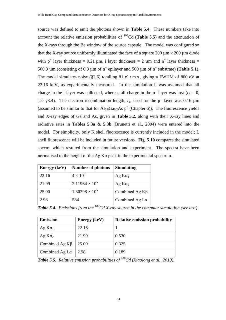
Wide Band Gap Compound Semiconductor Detectors for X-ray Spectroscopy in Harsh Environments
81
source was defined to emit the photons shown in Table 5.4. These numbers take into
account the relative emission probabilities of 109
Cd (Table 5.5) and the attenuation of
the X-rays through the Be window of the source capsule. The model was configured so
that the X-ray source uniformly illuminated the face of a square 200 µm × 200 µm diode
with p+ layer thickness = 0.21 µm, i layer thickness = 2 µm and n
+ layer thickness =
500.3 µm (consisting of 0.3 µm of n+ epilayer and 500 µm of n
+ substrate) (Table 5.1).
The model simulates noise (§2.6) totalling 81 e- r.m.s., giving a FWHM of 800 eV at
22.16 keV, as experimentally measured. In the simulation it was assumed that all
charge in the i layer was collected, whereas all charge in the n+ layer was lost (rh = 0,
see §3.4). The electron recombination length, re, used for the p+ layer was 0.16 µm
(assumed to be similar to that for Al0.8Ga0.2As p+ (Chapter 6)). The fluorescence yields
and X-ray edges of Ga and As, given in Table 5.2, along with their X-ray lines and
radiative rates in Tables 5.3a & 5.3b (Brunetti et al., 2004) were entered into the
model. For simplicity, only K shell fluorescence is currently included in the model; L
shell fluorescence will be included in future versions. Fig. 5.10 compares the simulated
spectra which resulted from the simulation and experiment. The spectra have been
normalised to the height of the Ag Kα peak in the experimental spectrum.
Energy (keV) Number of photons Simulating
22.16 4 × 10⁵ Ag Kα1
21.99 2.11964 × 10⁵ Ag Kα2
25.00 1.30298 × 10⁵ Combined Ag Kβ
2.98 584 Combined Ag Lα
Table 5.4. Emissions from the 109
Cd X-ray source in the computer simulation (see text).
Emission Energy (keV) Relative emission probability
Ag Kα1 22.16 1
Ag Kα2 21.99 0.530
Combined Ag Kβ 25.00 0.325
Combined Ag Lα 2.98 0.189
Table 5.5. Relative emission probabilities of 109
Cd (Xiaolong et al., 2010).
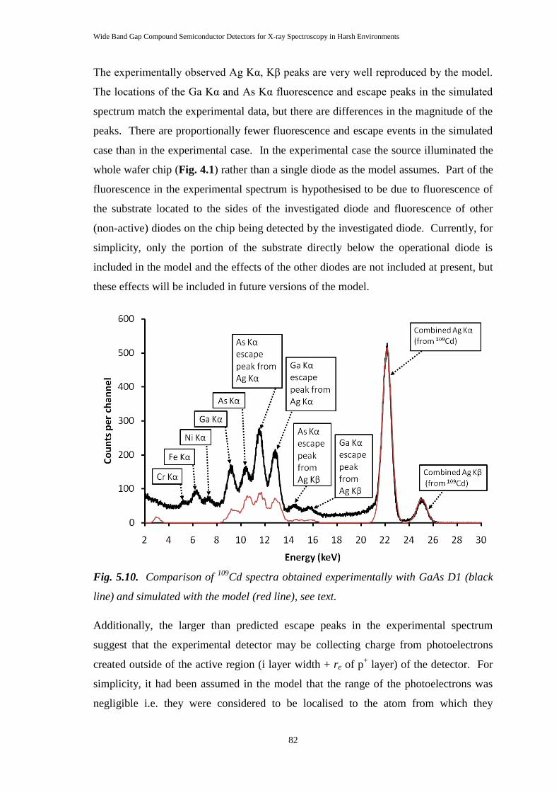
Wide Band Gap Compound Semiconductor Detectors for X-ray Spectroscopy in Harsh Environments
82
The experimentally observed Ag Kα, Kβ peaks are very well reproduced by the model.
The locations of the Ga Kα and As Kα fluorescence and escape peaks in the simulated
spectrum match the experimental data, but there are differences in the magnitude of the
peaks. There are proportionally fewer fluorescence and escape events in the simulated
case than in the experimental case. In the experimental case the source illuminated the
whole wafer chip (Fig. 4.1) rather than a single diode as the model assumes. Part of the
fluorescence in the experimental spectrum is hypothesised to be due to fluorescence of
the substrate located to the sides of the investigated diode and fluorescence of other
(non-active) diodes on the chip being detected by the investigated diode. Currently, for
simplicity, only the portion of the substrate directly below the operational diode is
included in the model and the effects of the other diodes are not included at present, but
these effects will be included in future versions of the model.
Fig. 5.10. Comparison of 109
Cd spectra obtained experimentally with GaAs D1 (black
line) and simulated with the model (red line), see text.
Additionally, the larger than predicted escape peaks in the experimental spectrum
suggest that the experimental detector may be collecting charge from photoelectrons
created outside of the active region (i layer width + re of p+ layer) of the detector. For
simplicity, it had been assumed in the model that the range of the photoelectrons was
negligible i.e. they were considered to be localised to the atom from which they
Wide Band Gap Compound Semiconductor Detectors for X-ray Spectroscopy in Harsh Environments
83
originated. However, the actual range of photoelectrons at 10 keV in GaAs is
~ 0.42 µm (Everhart & Hoff, 1971). Photoelectrons that do reach the active region of
the detector will contribute to the escape peaks, but their contribution is expected to be
small and may not entirely explain the difference between the experimental and
simulated spectra. The effect of non-localised photoelectrons, along with the effect of
fluorescence from the substrate and other diodes will be explored and quantified in
future modelling work. This may help achieve better agreement between the
experimental and modelled spectrum in the region of the Ga and As fluorescence and
escape peaks. Tailing on the low energy sides of the peaks is also visible in the
experimental spectrum but not present in the simulated spectrum. This is consistent
with the tailing being due to partial charge collection which is not presently included in
the simple model, but will be included in future work.
5.7 Conclusions and discussion
Circular mesa GaAs p+-i-n
+ diodes for photon counting X-ray spectroscopy have been
fabricated and their performance characterised at temperatures from +80 °C to -30 °C.
The performance of these diodes has been compared to Al0.8Ga0.2As devices of similar
geometry using identical signal electronics (§4.3) and GaAs diodes previously reported
at ≤ 24 °C (Owens et al., 2001) (Owens et al., 2002a) (Erd et al., 2002).
The investigations reported in this chapter have extended the high temperature range at
which GaAs diodes have been characterised beyond that previously reported and have
shown that GaAs diodes can work as photon counting X-ray detectors at temperatures
between +80 °C and -30 °C with modest spectral resolution (FWHM at 5.9 keV: 780 eV
at 0 °C, 1.55 keV at +80 °C).
Examination of the noise contributions has shown that the spectral resolution (FWHM)
at 5.9 keV of the detectors is primarily limited by dielectric noise, which is thought to
arise primarily from the diode and JFET packaging, as was the case for the Al0.8Ga0.2As
detectors (Chapter 4). The contribution from dielectric noise is significant; if it could be
reduced to negligible levels, the data suggest that spectral resolutions (FWHM) at
5.9 keV of 480, 370 and 350 eV at 50, 20 and -10 °C respectively, may be possible
(Fig. 5.8).
Wide Band Gap Compound Semiconductor Detectors for X-ray Spectroscopy in Harsh Environments
84
Higher energy X-ray spectra have been obtained experimentally using a 109
Cd
radioisotope X-ray source (providing Ag Kα1 = 22.16 keV, Ag Kα2 = 21.99 keV and Ag
Kβ ≈ 25 keV X-ray emission lines). These spectra demonstrate that although the
quantum efficiency is low at higher energies (0.034 at 22.16 keV) the diodes are still
able to operate as photon counting spectroscopic devices at low count rates (~ 0.3
counts/sec for Fig. 5.9) without the signal being swamped by noise. The spectra also
demonstrate the X-ray fluorescence of the diode itself which occurs when X-rays of
energy greater than the binding energies of the Ga and As K shell electrons illuminate
the detector. If the detector was to be used for X-ray fluorescence analysis of samples
containing elements with emission lines between ~ 9 keV and ~ 13.5 keV (the region
covered by the detector‟s Ga and As Kα and Kβ lines and associated escape peaks,
assuming a 109
Cd source was used to excite the sample), such as gold (Au Lα1 = 9.713
keV, Lα2 = 9.628 keV) or lead (Pb Lα1 = 10.552 keV, Lα2 = 10.450 keV), this internal
fluoresce may obscure the fluorescence from the sample and would have to be
subtracted from the spectra in order to reveal counts from emission lines in this region.
Simulated 109
Cd radioisotope X-ray spectra have been produced using the Monte Carlo
model detailed in Chapter 3. Good agreement between the model and experiment was
achieved with regard to the positions and sizes of the Ag Kα and Kβ emission peaks
from the X-ray source, and the positions of the fluorescence peaks (and associated
escape peaks) from the GaAs detector itself. However, the sizes of the Ga and As
fluorescence and escape peaks predicted by the model are smaller than those measured
experimentally. This is possibly a result of the model not currently including
fluorescence of the non-active diodes and substrate located to the sides of the
investigated diode, and assuming that all photoelectrons generated in the non-active
portions of the detector are reabsorbed before reaching the diode‟s active region. These
assumptions, which were included for simplicity in the present model, will be re-
examined, their effects quantified and the simulations extended to include the
phenomena they represent, in future versions of the model.
Whilst the currently achieved spectral resolutions are modest, the new measurements
reported here hint that further development of GaAs X-ray p+-i-n
+ photodiodes will lead
to devices that can operate in spectroscopic photon counting mode at temperatures
(> 50 °C) where silicon detectors cannot operate without cooling.
Wide Band Gap Compound Semiconductor Detectors for X-ray Spectroscopy in Harsh Environments
85
Chapter 6 Photon counting Al0.8Ga0.2As
avalanche photodiodes
6.1 Introduction
Room temperature AlxGa1-xAs avalanche photodiodes (APDs), which use impact
ionisation (see §2.7) to multiply the charge created when a photon is absorbed in the
device to increase the signal to noise ratio achieved, have been of interest to researchers
investigating devices suitable for telecommunications for some years. Particular
research emphasis has been placed on understanding AlxGa1-xAs‟s impact ionisation
properties (Ng et al., 2001, 2002) (Plimmer et al., 2000) (Tan et al., 2001) in order to
exploit the charge multiplication effect fully. However, those devices have always been
operated in current mode, rather than photon counting mode, and not at X-ray energies.
Silicon X-ray photon counting APDs have been reported in the literature, and
commercial reach-through devices (see §2.7.1) are available which can achieve a
spectral resolution at 5.9 keV of 380 eV FWHM at -20 °C with an electron avalanche
multiplication factor of 14, and that have a 130 µm thick absorption layer giving a
quantum efficiency of ~0.99 at 5.9 keV (Yatsu et al., 2006) (Kataoka et al., 2005).
Prior to the work reported in this thesis, there had been some limited reports of X-ray
detection with AlxGa1-xAs avalanche devices, both photon counting (Lauter et al., 1995,
1996) (Lees et al., 2008) and not photon counting (Silenas et al., 2002, 2003) (Dapkus
et al., 2007). Of the two X-ray photon counting AlxGa1-xAs APDs reported in the
literature, Lees et al.‟s detector was an Al0.8Ga0.2As p+-p
--n
+ diode (Table 6.1) and
Lauter et al.‟s detector was a separate absorption and multiplication region (SAM) diode
which had a 4.5 µm GaAs absorber region with 12 very thin (0.045 µm) x-graded (x =
0.01 to x = 0.45) AlxGa1-xAs multiplication regions beneath it. Lauter et al.‟s detector
was reported to have spectral resolutions (FWHM) at 13.96 keV and 17.8 keV of
0.95 keV and 1.4 keV, respectively, when operated at room temperature.
Lees et al.‟s device was reported as having a spectral resolution (FWHM) at 5.9 keV
of 1.5 keV in non-avalanche mode which improved to 1.2 keV in avalanche mode
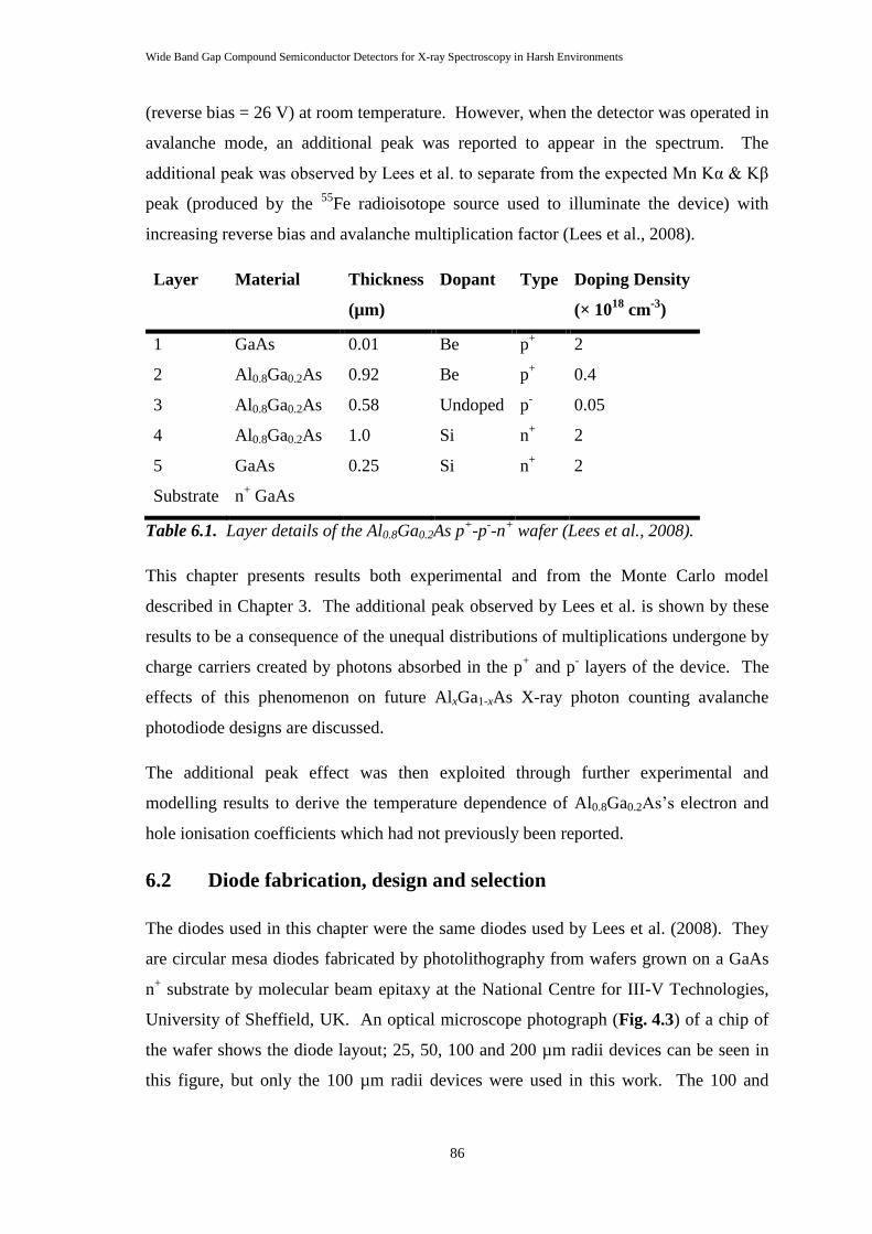
Wide Band Gap Compound Semiconductor Detectors for X-ray Spectroscopy in Harsh Environments
86
(reverse bias = 26 V) at room temperature. However, when the detector was operated in
avalanche mode, an additional peak was reported to appear in the spectrum. The
additional peak was observed by Lees et al. to separate from the expected Mn Kα & Kβ
peak (produced by the 55
Fe radioisotope source used to illuminate the device) with
increasing reverse bias and avalanche multiplication factor (Lees et al., 2008).
Layer Material Thickness
(µm)
Dopant Type Doping Density
(× 1018
cm-3
)
1 GaAs 0.01 Be p+ 2
2 Al0.8Ga0.2As 0.92 Be p+ 0.4
3 Al0.8Ga0.2As 0.58 Undoped p- 0.05
4 Al0.8Ga0.2As 1.0 Si n+ 2
5 GaAs 0.25 Si n+ 2
Substrate n+ GaAs
Table 6.1. Layer details of the Al0.8Ga0.2As p+-p
--n
+ wafer (Lees et al., 2008).
This chapter presents results both experimental and from the Monte Carlo model
described in Chapter 3. The additional peak observed by Lees et al. is shown by these
results to be a consequence of the unequal distributions of multiplications undergone by
charge carriers created by photons absorbed in the p+ and p
- layers of the device. The
effects of this phenomenon on future AlxGa1-xAs X-ray photon counting avalanche
photodiode designs are discussed.
The additional peak effect was then exploited through further experimental and
modelling results to derive the temperature dependence of Al0.8Ga0.2As‟s electron and
hole ionisation coefficients which had not previously been reported.
6.2 Diode fabrication, design and selection
The diodes used in this chapter were the same diodes used by Lees et al. (2008). They
are circular mesa diodes fabricated by photolithography from wafers grown on a GaAs
n+ substrate by molecular beam epitaxy at the National Centre for III-V Technologies,
University of Sheffield, UK. An optical microscope photograph (Fig. 4.3) of a chip of
the wafer shows the diode layout; 25, 50, 100 and 200 µm radii devices can be seen in
this figure, but only the 100 µm radii devices were used in this work. The 100 and
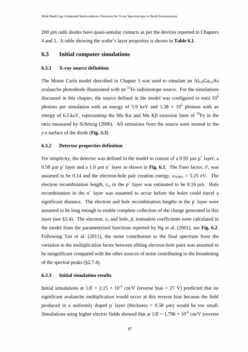
Wide Band Gap Compound Semiconductor Detectors for X-ray Spectroscopy in Harsh Environments
87
200 µm radii diodes have quasi-annular contacts as per the devices reported in Chapters
4 and 5. A table showing the wafer‟s layer properties is shown in Table 6.1.
6.3 Initial computer simulations
6.3.1 X-ray source definition
The Monte Carlo model described in Chapter 3 was used to simulate an Al0.8Ga0.2As
avalanche photodiode illuminated with an 55
Fe radioisotope source. For the simulations
discussed in this chapter, the source defined in the model was configured to emit 106
photons per simulation with an energy of 5.9 keV and 1.38 × 10⁵ photons with an
energy of 6.5 keV, representing the Mn Kα and Mn Kβ emission lines of 55
Fe in the
ratio measured by Schötzig (2000). All emissions from the source were normal to the
y-z surface of the diode (Fig. 3.3).
6.3.2 Detector properties definition
For simplicity, the detector was defined in the model to consist of a 0.92 µm p+ layer, a
0.58 µm p- layer and a 1.0 µm n
+ layer as shown in Fig. 6.1. The Fano factor, F, was
assumed to be 0.14 and the electron-hole pair creation energy, ωEHP, = 5.25 eV. The
electron recombination length, re, in the p+ layer was estimated to be 0.16 µm. Hole
recombination in the n+ layer was assumed to occur before the holes could travel a
significant distance. The electron and hole recombination lengths in the p- layer were
assumed to be long enough to enable complete collection of the charge generated in this
layer (see §3.4). The electron, α, and hole, β, ionisation coefficients were calculated in
the model from the parameterised functions reported by Ng et al. (2001), see Fig. 6.2.
Following Tan et al. (2011), the noise contribution to the final spectrum from the
variation in the multiplication factor between sibling electron-hole pairs was assumed to
be insignificant compared with the other sources of noise contributing to the broadening
of the spectral peaks (§2.7.4).
6.3.3 Initial simulation results
Initial simulations at 1/E = 2.15 × 10⁻⁶
cm/V (reverse bias = 27 V) predicted that no
significant avalanche multiplication would occur at this reverse bias because the field
produced in a uniformly doped p- layer (thickness = 0.58 µm) would be too small.
Simulations using higher electric fields showed that at 1/E = 1.796 × 10⁻⁶
cm/V (reverse
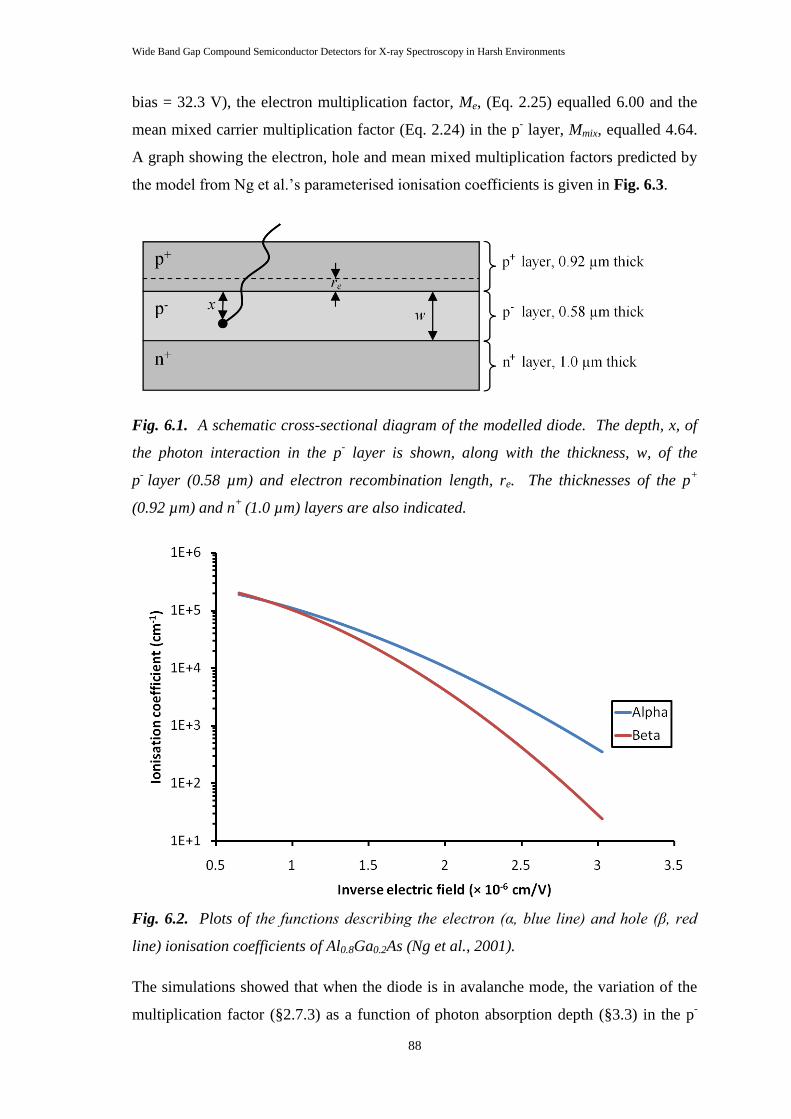
Wide Band Gap Compound Semiconductor Detectors for X-ray Spectroscopy in Harsh Environments
88
bias = 32.3 V), the electron multiplication factor, Me, (Eq. 2.25) equalled 6.00 and the
mean mixed carrier multiplication factor (Eq. 2.24) in the p- layer, Mmix, equalled 4.64.
A graph showing the electron, hole and mean mixed multiplication factors predicted by
the model from Ng et al.‟s parameterised ionisation coefficients is given in Fig. 6.3.
Fig. 6.1. A schematic cross-sectional diagram of the modelled diode. The depth, x, of
the photon interaction in the p- layer is shown, along with the thickness, w, of the
p- layer (0.58 µm) and electron recombination length, re. The thicknesses of the p
+
(0.92 µm) and n+
(1.0 µm) layers are also indicated.
Fig. 6.2. Plots of the functions describing the electron (α, blue line) and hole (β, red
line) ionisation coefficients of Al0.8Ga0.2As (Ng et al., 2001).
The simulations showed that when the diode is in avalanche mode, the variation of the
multiplication factor (§2.7.3) as a function of photon absorption depth (§3.3) in the p-
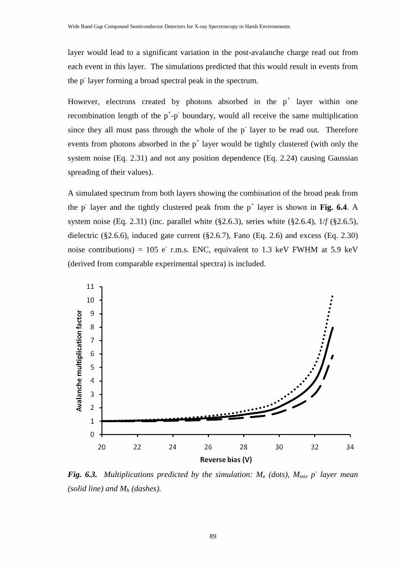
Wide Band Gap Compound Semiconductor Detectors for X-ray Spectroscopy in Harsh Environments
89
layer would lead to a significant variation in the post-avalanche charge read out from
each event in this layer. The simulations predicted that this would result in events from
the p- layer forming a broad spectral peak in the spectrum.
However, electrons created by photons absorbed in the p+ layer within one
recombination length of the p+-p
- boundary, would all receive the same multiplication
since they all must pass through the whole of the p- layer to be read out. Therefore
events from photons absorbed in the p+ layer would be tightly clustered (with only the
system noise (Eq. 2.31) and not any position dependence (Eq. 2.24) causing Gaussian
spreading of their values).
A simulated spectrum from both layers showing the combination of the broad peak from
the p- layer and the tightly clustered peak from the p
+ layer is shown in Fig. 6.4. A
system noise (Eq. 2.31) (inc. parallel white (§2.6.3), series white (§2.6.4), 1/f (§2.6.5),
dielectric (§2.6.6), induced gate current (§2.6.7), Fano (Eq. 2.6) and excess (Eq. 2.30)
noise contributions) = 105 e- r.m.s. ENC, equivalent to 1.3 keV FWHM at 5.9 keV
(derived from comparable experimental spectra) is included.
Fig. 6.3. Multiplications predicted by the simulation: Me (dots), Mmix p- layer mean
(solid line) and Mh (dashes).
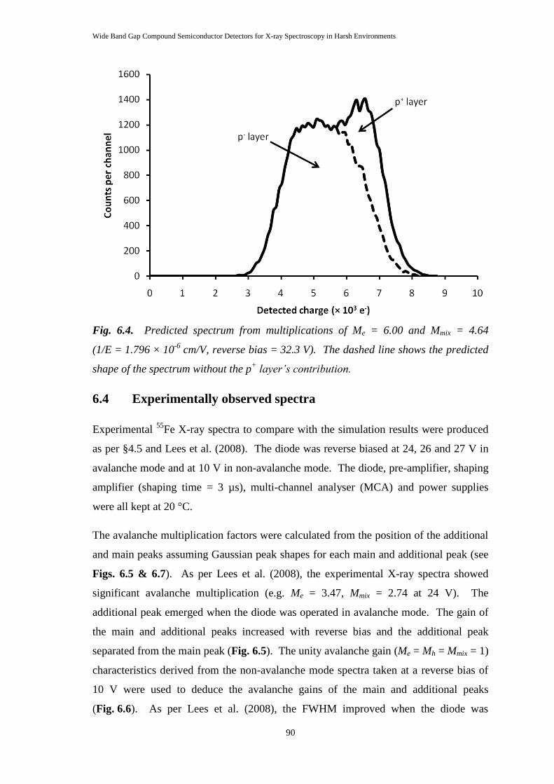
Wide Band Gap Compound Semiconductor Detectors for X-ray Spectroscopy in Harsh Environments
90
Fig. 6.4. Predicted spectrum from multiplications of Me = 6.00 and Mmix = 4.64
(1/E = 1.796 × 10⁻⁶
cm/V, reverse bias = 32.3 V). The dashed line shows the predicted
shape of the spectrum without the p+ layer’s contribution.
6.4 Experimentally observed spectra
Experimental 55
Fe X-ray spectra to compare with the simulation results were produced
as per §4.5 and Lees et al. (2008). The diode was reverse biased at 24, 26 and 27 V in
avalanche mode and at 10 V in non-avalanche mode. The diode, pre-amplifier, shaping
amplifier (shaping time = 3 µs), multi-channel analyser (MCA) and power supplies
were all kept at 20 °C.
The avalanche multiplication factors were calculated from the position of the additional
and main peaks assuming Gaussian peak shapes for each main and additional peak (see
Figs. 6.5 & 6.7). As per Lees et al. (2008), the experimental X-ray spectra showed
significant avalanche multiplication (e.g. Me = 3.47, Mmix = 2.74 at 24 V). The
additional peak emerged when the diode was operated in avalanche mode. The gain of
the main and additional peaks increased with reverse bias and the additional peak
separated from the main peak (Fig. 6.5). The unity avalanche gain (Me = Mh = Mmix = 1)
characteristics derived from the non-avalanche mode spectra taken at a reverse bias of
10 V were used to deduce the avalanche gains of the main and additional peaks
(Fig. 6.6). As per Lees et al. (2008), the FWHM improved when the diode was
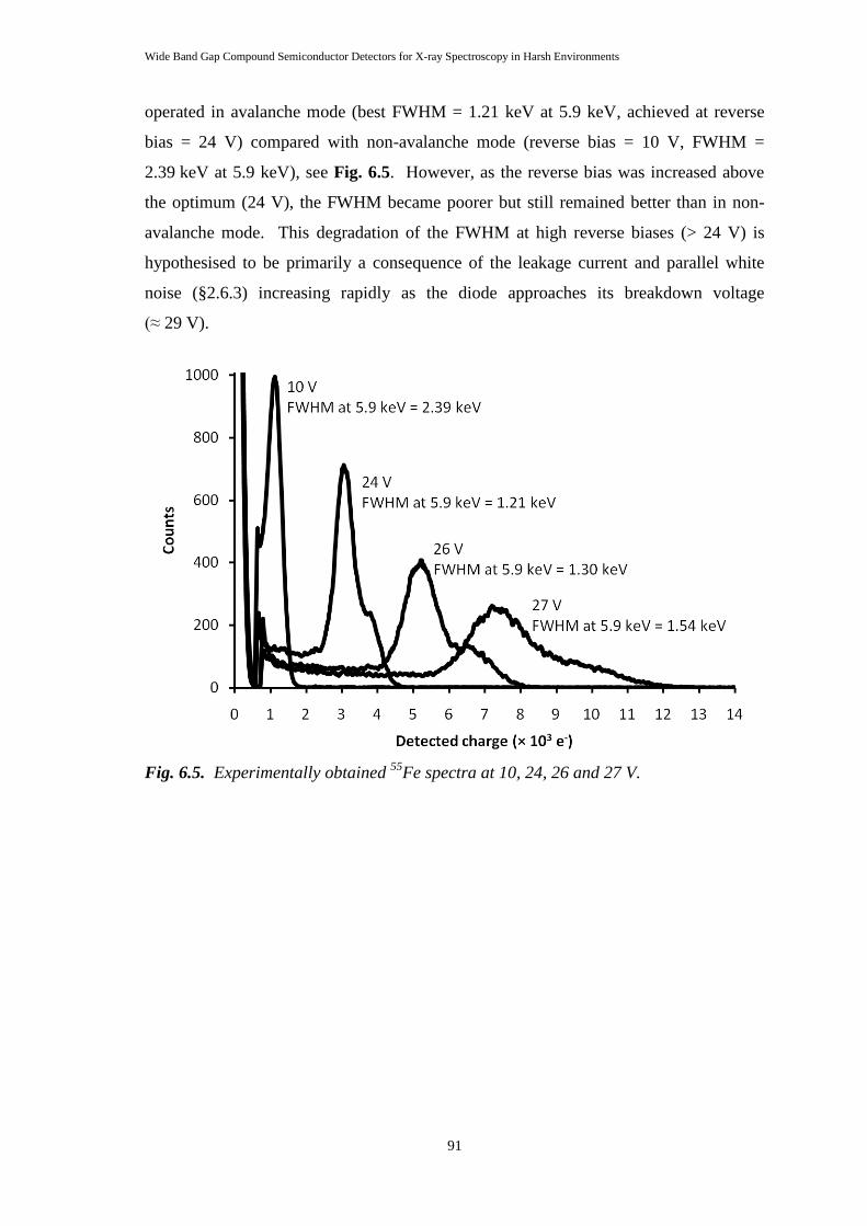
Wide Band Gap Compound Semiconductor Detectors for X-ray Spectroscopy in Harsh Environments
91
operated in avalanche mode (best FWHM = 1.21 keV at 5.9 keV, achieved at reverse
bias = 24 V) compared with non-avalanche mode (reverse bias = 10 V, FWHM =
2.39 keV at 5.9 keV), see Fig. 6.5. However, as the reverse bias was increased above
the optimum (24 V), the FWHM became poorer but still remained better than in non-
avalanche mode. This degradation of the FWHM at high reverse biases (> 24 V) is
hypothesised to be primarily a consequence of the leakage current and parallel white
noise (§2.6.3) increasing rapidly as the diode approaches its breakdown voltage
(≈ 29 V).
Fig. 6.5. Experimentally obtained 55
Fe spectra at 10, 24, 26 and 27 V.
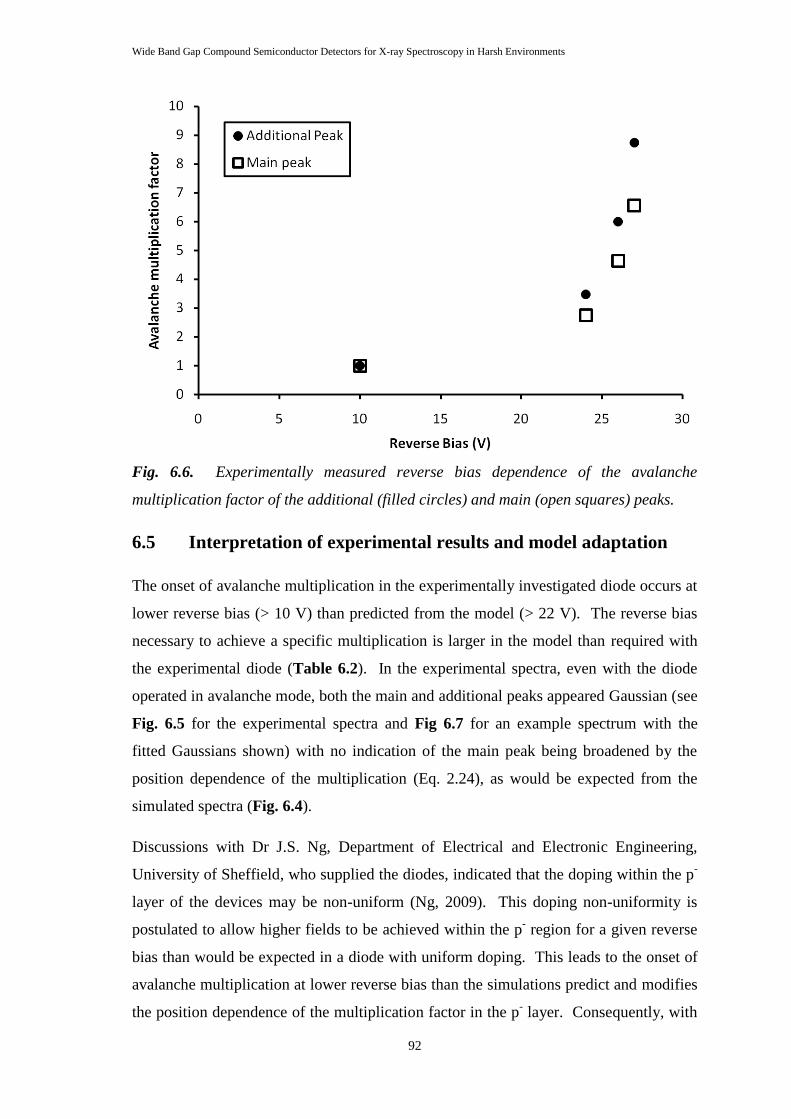
Wide Band Gap Compound Semiconductor Detectors for X-ray Spectroscopy in Harsh Environments
92
Fig. 6.6. Experimentally measured reverse bias dependence of the avalanche
multiplication factor of the additional (filled circles) and main (open squares) peaks.
6.5 Interpretation of experimental results and model adaptation
The onset of avalanche multiplication in the experimentally investigated diode occurs at
lower reverse bias (> 10 V) than predicted from the model (> 22 V). The reverse bias
necessary to achieve a specific multiplication is larger in the model than required with
the experimental diode (Table 6.2). In the experimental spectra, even with the diode
operated in avalanche mode, both the main and additional peaks appeared Gaussian (see
Fig. 6.5 for the experimental spectra and Fig 6.7 for an example spectrum with the
fitted Gaussians shown) with no indication of the main peak being broadened by the
position dependence of the multiplication (Eq. 2.24), as would be expected from the
simulated spectra (Fig. 6.4).
Discussions with Dr J.S. Ng, Department of Electrical and Electronic Engineering,
University of Sheffield, who supplied the diodes, indicated that the doping within the p-
layer of the devices may be non-uniform (Ng, 2009). This doping non-uniformity is
postulated to allow higher fields to be achieved within the p- region for a given reverse
bias than would be expected in a diode with uniform doping. This leads to the onset of
avalanche multiplication at lower reverse bias than the simulations predict and modifies
the position dependence of the multiplication factor in the p- layer. Consequently, with
Wide Band Gap Compound Semiconductor Detectors for X-ray Spectroscopy in Harsh Environments
93
the assumption that the ionisation coefficients (Ng et al., 2001) were correct, the simple
model for an ideal p-i-n diode (§6.3.3) was extended to account for the doping non-
uniformity.
The electric field required to match the multiplications seen experimentally (Fig. 6.6)
was used in the model, see Table 6.2. The position variance (Eq. 2.24) of the
multiplication factor in the p- layer was restricted by applying the mean multiplication
to all charge carriers from the p- layer. The mean multiplication was calculated from
the multiplications predicted by the model (using Eqs. 2.24 and 3.6a-b) for each
individual charge carrier.
Me Mmix Experimental
reverse bias (V)
Equivalent
simulated
reverse bias (V)
Simulated inverse electric
field (× 10-6
cm/V)
3.47 2.74 24 31.1 1.865
6.00 4.64 26 32.3 1.796
8.74 6.56 27 32.8 1.770
Table 6.2. Reverse biases required to achieve specific multiplications in the
experimentally measured diode and the simulated diode (see §6.3.3 and §6.5).
6.6 Adapted model results
The simple modifications to the model produced simulated spectra that are in good
agreement with the experimentally obtained spectra (see Fig. 6.7, and compare Fig. 6.8
with Fig. 6.5). The tail on the left of the experimental spectrum (Fig. 6.7) is due to
partial charge collection in the device (for simplicity, this is not included in the model at
present). For comparison, the simulated spectra were normalised in counts to the
experimental spectra by normalising to the height of the main peak.
Fig. 6.8 shows how, as the avalanche gain increases, the additional peak separates from
the main peak in agreement with the separation that is observed in the experimental
spectra (Fig. 6.5). The increasing separation of the main and additional peaks in the
simulations is a result of increasing electric field (reverse bias) across the high field
region.
Wide Band Gap Compound Semiconductor Detectors for X-ray Spectroscopy in Harsh Environments
94
Fig. 6.7. Comparison between the experimentally obtained 55
Fe spectrum (dotted line)
and simulated 55
Fe spectrum (dashed line) at Me = 8.74, Mmix = 6.56 (Table 6.2). Two
Gaussian peaks are shown which have been fitted to the experimental data representing
the peaks from the p- (red line) and p
+ (blue line) layers (FWHM at 5.9 keV = 1.5 keV).
Fig. 6.8. Simulated 55
Fe spectra at inverse electric fields of 5.8 × 10⁻⁶
, 1.865 × 10⁻⁶
,
1.796 × 10⁻⁶
and 1.770 × 10⁻⁶
cm/V (Table 6.2). Compare with the experimental
spectra in Fig. 6.5.
Wide Band Gap Compound Semiconductor Detectors for X-ray Spectroscopy in Harsh Environments
95
6.7 Reduced p+ layer thickness simulations
For many applications, such as X-ray fluorescence spectroscopy (XRF) of planetary
surfaces, the low energy X-ray performance of the device is critical (Fraser, 2008).
Three major rock forming elements (Mg, Al and Si) have Kα lines below 2 keV
(Table 6.3). Sensitivity to X-rays at energies 0.4 – 1 keV makes the O Kα1 line
(0.525 keV) detectable and allows the investigation of L shell emission from elements
such as Ti (0.45 keV) and Fe (0.705 keV). Since the attenuation coefficients at these
energies are high, it is essential to minimise the thickness of the p+ layer to ensure the
photons interact in the active region of the device. The relatively simple modification to
the existing design of reducing the thickness of the p+ layer to re will ensure all photons
absorbed in the p+ layer are counted. Relative device efficiencies at reduced p
+ layer
thicknesses were calculated from Eq. 2.1 and are shown in Fig. 6.9.
Element Kα (keV) Lα (keV)
O 0.525 -
Mg 1.25 -
Al 1.49 -
Si 1.74 -
Ti 4.5 0.45
Fe 6.4 0.705
Table 6.3. Important low energy X-ray emission lines.
Reducing the thickness of the p+ layer is also necessary to minimize the degradation of
the spectrum caused by the additional peak. To show this effect, the simulations were
repeated with the thickness of the p+ layer reduced to 0.08 µm (half the recombination
length in the p+ layer) as well as 0.04 and 0.01 µm. In the spectra resulting from these
simulations, the number of counts in the additional peak is reduced (Fig. 6.10). The
additional peak is reduced in size because thinning the p+ layer to less than one
recombination length reduces the number of electrons generated in the p+ layer that can
contribute to the spectrum.
Wide Band Gap Compound Semiconductor Detectors for X-ray Spectroscopy in Harsh Environments
96
Fig. 6.9. Effect of p+ layer thickness on quantum efficiency of the device (p
- layer
thickness = 0.58 µm) at 0.5 keV (solid line) and 2 keV (dashed line) with varying p+
layer thickness.
Fig. 6.10. Simulations of 55
Fe spectra with p+ layer thickness of 1 µm (solid black line)
(Table 6.1), 0.08 µm (long red dashes), 0.04 µm (short blue dashes) and 0.01 µm (olive
dots). For clarity, only simulations for 1/E = 1.796 × 10⁻⁶
cm/V (Me = 6.00, Mmix =
4.64) are shown.
Wide Band Gap Compound Semiconductor Detectors for X-ray Spectroscopy in Harsh Environments
97
6.8 Temperature dependence of the impact ionisation coefficients in
Al0.8Ga0.2As
The electric field dependence of the electron and hole impact ionisation coefficients had
previously been reported for AlxGa1-xAs with x = 0.15, 0.3, 0.6 (Plimmer et al., 2000), x
= 0.2, 0.4 (Zheng et al., 2000) and x = 0.8 (Ng et al., 2000, 2001). However, the
temperature dependence of the impact ionisation coefficients had only been reported for
x = 0.2, 0.4 (Zheng et al., 2000) and x = 0.6 (Harrison et al., 2002). Knowing how the
ionisation coefficients vary with temperature is essential to understanding how APDs
operate at high, and varied, temperature.
6.8.1 Experimental measurements
To obtain the measurements necessary to determine the temperature dependence of the
ionisation coefficients in Al0.8Ga0.2As, the diode was housed with, and connected to, a
Si charge sensitive preamplifier with a Si JFET (Vishay Siliconix 2N4416) front end
transistor, as per §6.4 and Chapter 4. The APD, Si JFET and preamplifier electronics
were all placed inside a Design Environmental FS55-65 temperature test chamber
(TTC) (Design Environmental, N.D.) and subject to temperature control. The
temperature of the APD, Si JFET and preamplifier was monitored by thermocouple
(positioned adjacent to the diode) to ensure temperature equalisation between APD
environment and TTC environments. The temperature dependent performance of the
system was investigated from +80 °C to -20 °C. The preamplifier was connected to an
EG&G Ortec® 571 shaping amplifier (EG&G Ortec, N.D.) (shaping time = 3 µs)
located outside of the TTC. The shaping amplifier was connected to an Ortec MCA
(Advanced Measurement Technology, Inc., 2008). The diode was reverse biased and
the preamplifier powered by externally located power supplies.
A 10 MBq 55
Fe radioisotope X-ray source was positioned 3 mm above the diode.
Spectra were taken from high temperature to low temperature in 10 °C steps. The
system was allowed to stabilise at each temperature before spectrum accumulation was
started and multiple spectra were accumulated at each temperature. Spectra were
accumulated at each temperature with the diode reverse biased at 26 V (avalanche
mode) and 10 V (non-avalanche mode) to obtain unity avalanche gain spectra to enable
calculation of multiplication factors as per §6.4.
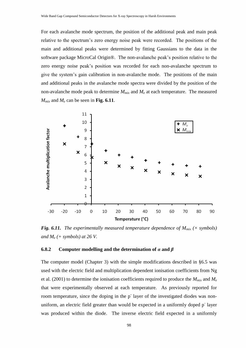
Wide Band Gap Compound Semiconductor Detectors for X-ray Spectroscopy in Harsh Environments
98
For each avalanche mode spectrum, the position of the additional peak and main peak
relative to the spectrum‟s zero energy noise peak were recorded. The positions of the
main and additional peaks were determined by fitting Gaussians to the data in the
software package MicroCal Origin®. The non-avalanche peak‟s position relative to the
zero energy noise peak‟s position was recorded for each non-avalanche spectrum to
give the system‟s gain calibration in non-avalanche mode. The positions of the main
and additional peaks in the avalanche mode spectra were divided by the position of the
non-avalanche mode peak to determine Mmix and Me at each temperature. The measured
Mmix and Me can be seen in Fig. 6.11.
Fig. 6.11. The experimentally measured temperature dependence of Mmix (× symbols)
and Me (+ symbols) at 26 V.
6.8.2 Computer modelling and the determination of α and β
The computer model (Chapter 3) with the simple modifications described in §6.5 was
used with the electric field and multiplication dependent ionisation coefficients from Ng
et al. (2001) to determine the ionisation coefficients required to produce the Mmix and Me
that were experimentally observed at each temperature. As previously reported for
room temperature, since the doping in the p- layer of the investigated diodes was non-
uniform, an electric field greater than would be expected in a uniformly doped p- layer
was produced within the diode. The inverse electric field expected in a uniformly
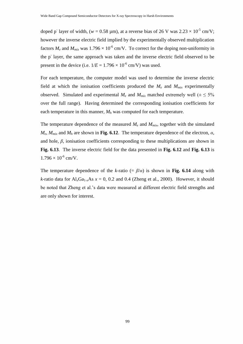
Wide Band Gap Compound Semiconductor Detectors for X-ray Spectroscopy in Harsh Environments
99
doped p- layer of width, (w = 0.58 µm), at a reverse bias of 26 V was 2.23 × 10
-5 cm/V;
however the inverse electric field implied by the experimentally observed multiplication
factors Me and Mmix was 1.796 × 10⁻⁶
cm/V. To correct for the doping non-uniformity in
the p- layer, the same approach was taken and the inverse electric field observed to be
present in the device (i.e. 1/E = 1.796 × 10⁻⁶
cm/V) was used.
For each temperature, the computer model was used to determine the inverse electric
field at which the ionisation coefficients produced the Me and Mmix experimentally
observed. Simulated and experimental Me and Mmix matched extremely well (± ≤ 5%
over the full range). Having determined the corresponding ionisation coefficients for
each temperature in this manner, Mh was computed for each temperature.
The temperature dependence of the measured Me and Mmix, together with the simulated
Me, Mmix and Mh are shown in Fig. 6.12. The temperature dependence of the electron, α,
and hole, β, ionisation coefficients corresponding to these multiplications are shown in
Fig. 6.13. The inverse electric field for the data presented in Fig. 6.12 and Fig. 6.13 is
1.796 × 10⁻⁶
cm/V.
The temperature dependence of the k-ratio (= β/α) is shown in Fig. 6.14 along with
k-ratio data for AlxGa1-xAs x = 0, 0.2 and 0.4 (Zheng et al., 2000). However, it should
be noted that Zheng et al.‟s data were measured at different electric field strengths and
are only shown for interest.
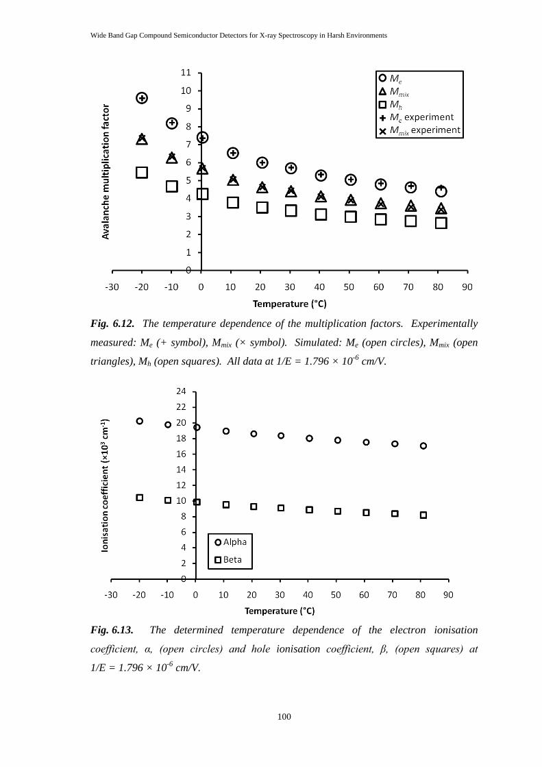
Wide Band Gap Compound Semiconductor Detectors for X-ray Spectroscopy in Harsh Environments
100
Fig. 6.12. The temperature dependence of the multiplication factors. Experimentally
measured: Me (+ symbol), Mmix (× symbol). Simulated: Me (open circles), Mmix (open
triangles), Mh (open squares). All data at 1/E = 1.796 × 10⁻⁶
cm/V.
Fig. 6.13. The determined temperature dependence of the electron ionisation
coefficient, α, (open circles) and hole ionisation coefficient, β, (open squares) at
1/E = 1.796 × 10⁻⁶
cm/V.
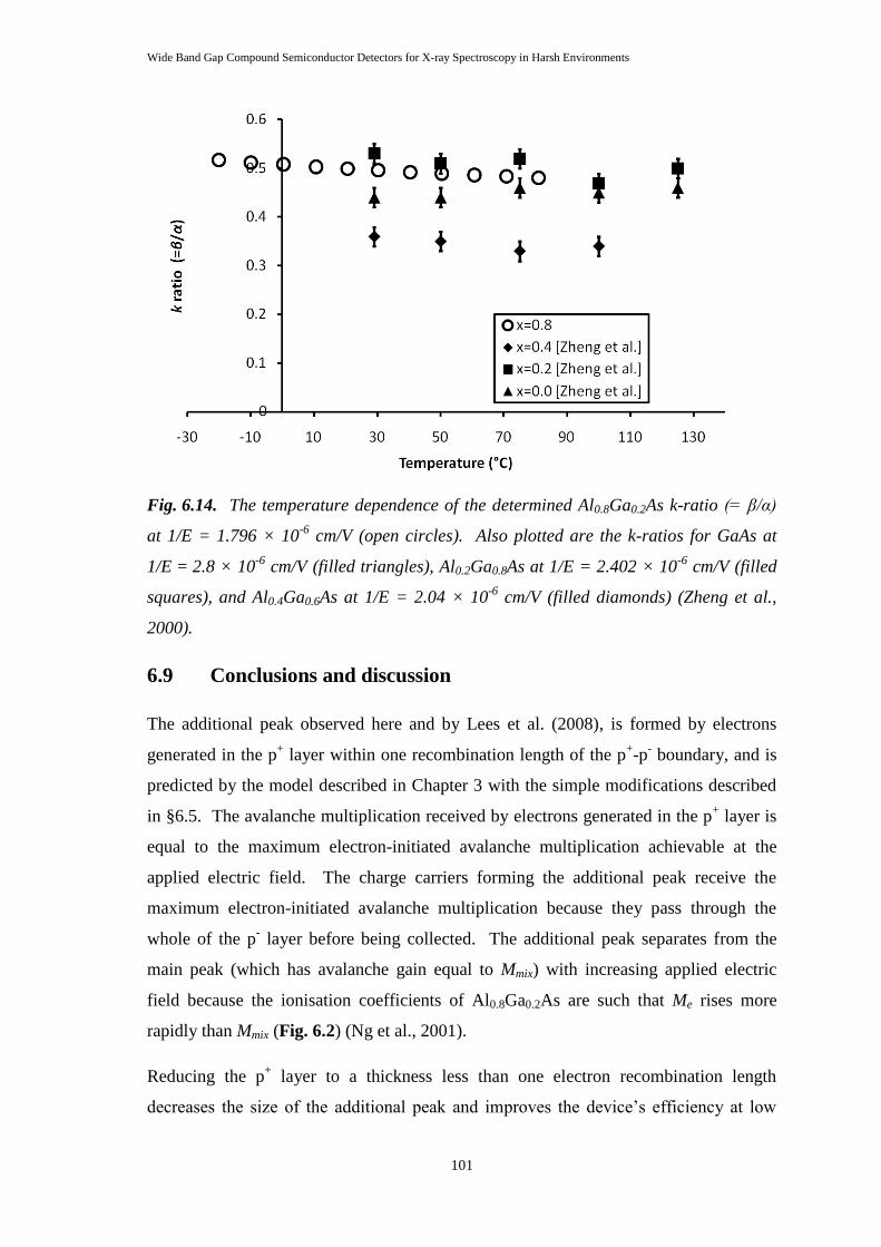
Wide Band Gap Compound Semiconductor Detectors for X-ray Spectroscopy in Harsh Environments
101
Fig. 6.14. The temperature dependence of the determined Al0.8Ga0.2As k-ratio (= β/α)
at 1/E = 1.796 × 10⁻⁶
cm/V (open circles). Also plotted are the k-ratios for GaAs at
1/E = 2.8 × 10⁻⁶
cm/V (filled triangles), Al0.2Ga0.8As at 1/E = 2.402 × 10⁻⁶
cm/V (filled
squares), and Al0.4Ga0.6As at 1/E = 2.04 × 10⁻⁶
cm/V (filled diamonds) (Zheng et al.,
2000).
6.9 Conclusions and discussion
The additional peak observed here and by Lees et al. (2008), is formed by electrons
generated in the p+ layer within one recombination length of the p
+-p
- boundary, and is
predicted by the model described in Chapter 3 with the simple modifications described
in §6.5. The avalanche multiplication received by electrons generated in the p+ layer is
equal to the maximum electron-initiated avalanche multiplication achievable at the
applied electric field. The charge carriers forming the additional peak receive the
maximum electron-initiated avalanche multiplication because they pass through the
whole of the p- layer before being collected. The additional peak separates from the
main peak (which has avalanche gain equal to Mmix) with increasing applied electric
field because the ionisation coefficients of Al0.8Ga0.2As are such that Me rises more
rapidly than Mmix (Fig. 6.2) (Ng et al., 2001).
Reducing the p+ layer to a thickness less than one electron recombination length
decreases the size of the additional peak and improves the device‟s efficiency at low
Wide Band Gap Compound Semiconductor Detectors for X-ray Spectroscopy in Harsh Environments
102
(< 2 keV) energies. Practicalities of wafer growth may limit the p+ layer thickness to
values larger than 0.01 µm. With such a thin p+ layer, impurities from the ohmic
contact may penetrate through the layer and into the low doping, high field region. This
would adversely affect the doping and field characteristics.
Increasing the efficiency of an abrupt p+-p
--n
+ or p
+-i-n
+ type diode to be operated in
avalanche mode by growing a thicker p- (or i) layer will lead to degraded spectral
resolution in avalanche mode because the mixed avalanche gain is a function of photon
interaction depth, x, (Eqs. 2.24 – 2.26 and Fig. 6.4), except in the special case when
Me(x) balances with Mh(x) to give constant Mmix(x). To operate in avalanche mode and
maintain the spectral resolution, it is necessary to use a graded doping profile across the
region or adopt a reach-through/SAM APD design.
The temperature, T, dependence of the electron and hole ionisation coefficients in
Al0.8Ga0.2As were determined using soft energy X-ray measurements on Al0.8Ga0.2As
p+-p
--n
+ APDs operated at 1/E = 1.796 × 10
-6 cm/V for +80 °C ≤ T ≤ -20 °C. For the
full temperature range, Me and Mmix, were measured from experimental X-ray spectra
and Mh was predicted from the model. The change in avalanche multiplication factors
within that temperature range was found to be significant (Me, Mmix and Mh at -20 °C are
approximately a factor of two larger than at +80 °C). The variation of multiplication
factor with temperature suggests that whilst Al0.8G0.2As p+-p
--n
+ APDs can successfully
operate uncooled for photon counting X-ray detection at temperatures between +80 °C
and -20 °C, it is important to maintain a constant temperature during spectrum
accumulation to prevent variation of the multiplication factors and degradation of the
spectrum.
Wide Band Gap Compound Semiconductor Detectors for X-ray Spectroscopy in Harsh Environments
103
Chapter 7 High temperature semi-transparent
4H-SiC Schottky photodiodes
7.1 Introduction
Previously, silicon carbide diodes have been investigated as detectors for applications in
many sensing fields including UV (Hu et al., 2008), α-particle detection (Nava et al.,
1999) (Ruddy et al., 2006) and X-ray spectroscopy (Lees et al., 2007) (Bertuccio, 2005)
(Bertuccio et al., 2001, 2003, 2004a, 2004b, 2011) (Nava et al., 2008). There has been
much interest in SiC for radiation detectors in recent years because its wide band gap
(3.23 eV for 4H-SiC) (Goldberg et al., 2001), radiation hardness (Lees et al., 2009)
(Ruddy & Siedel, 2006) and commercial availability make it attractive for the
manufacture of sensors for extreme (high temperature, intense radiation) environments.
It is also suitable as a material for capacitive gas sensors (see the review by Wright &
Horsfall (2007)) for the detection of rapidly varying concentrations of gases at
temperatures of hundreds of degrees Celsius in, for example, vehicle exhausts, and for
the monitoring of volcanoes (Weng et al., 2007). There are also efforts to manufacture
SiC JFETs (Neudeck et al., 2009), (Bhatnagar et al., 2007), (Wright and Horsfall,
2007); if JFETs suitable for use in ultra-low noise charge sensitive preamplifiers could
be produced so that signal amplification could be integrated on chip with SiC detectors,
this would potentially reduce electronic noise (by reducing the parallel white noise
component (§2.6.3) from the JFET‟s leakage current) and eliminate the temperature
sensitive silicon preamplifier electronics currently used, improving detector
performance. SiC exists in many different polytypes, including 4H and 6H, which are
the two polytypes most commonly researched because they are available commercially.
All the SiC diodes in this thesis are 4H-SiC; 4H-SiC has a wider band gap (3.23 eV)
than 6H-SiC (3.0 eV (Goldberg et al., 2001)) so this should result in lower leakage
current at high temperatures.
At the University of Leicester, the SiC detector development programme in
collaboration with Newcastle University has produced X-ray sensitive semi-transparent
silicon carbide Schottky photodiodes, see §2.3 and Lees et al. (2007). X-ray photon
Wide Band Gap Compound Semiconductor Detectors for X-ray Spectroscopy in Harsh Environments
104
counting SiC photodiodes from this programme have already been reported operating at
room temperature and have been shown to function as photon counting X-ray
spectrometers after proton irradiation (total dose = 1013
cm-2
at 50 MeV) (Lees et al.,
2009).
In this chapter, reports are made of experiments with semi-transparent silicon carbide
Schottky photodiodes illuminated by 55
Fe and 109
Cd radioisotope X-ray sources
investigating the suitability of these diodes as detectors for X-ray photon counting
spectroscopy in high temperature environments. The detectors are shown to operate as
X-ray spectrometers at energies between 5.9 keV and 25 keV at temperatures from
-30 °C to +80 °C with spectral resolutions (FWHM) between 1.6 keV and 2.5 keV.
7.2 Diode fabrication and design
Square (250 µm × 250 µm) semi-transparent silicon carbide Schottky diodes in 2 × 2
and 3 × 3 arrays of varying pixel separation (10 – 50 µm) were fabricated at Newcastle
University from commercial wafers from Cree Inc. (Cree Inc., 2011) as per Lees et al.
(2007). The devices were fabricated in array form to enable future research into pixel
arrays. The layout of the diodes fabricated is shown in Fig. 7.1. The wafers had a
45 µm 4H-SiC epitaxial layer (n type doping (nitrogen), density = 7.7 × 10¹⁴
cm-3
) on
top of a 370 µm 4H-SiC n+ substrate (doping density = 2 × 10
18 cm
-3). A 25 nm thick
thermal oxide passivation layer was grown on the epitaxial layer. Ti/Ni ohmic contacts
were deposited on the opposite side of the substrate and annealed at 1100 °C for 800
seconds to form the rear contact of each diode. Windows were etched in the front side
passivation layer and 3 nm of titanium and 12 nm of nickel were deposited by e-beam
evaporation and annealed at 600 °C to form 18 nm thick NiSi Schottky contacts. A gold
bond pad and square annular contact (200 nm thick) were deposited on top of a 4 nm
chromium adhesion layer for each pixel.
When a reverse bias is applied to a Schottky diode, the epitaxial layer depletes from the
Schottky contact to form the active detection region of the device. The depletion depth
is dependent on the applied reverse bias (Eq. 2.4). A graph showing the calculated
thickness of depletion layer with reverse bias for the devices reported in this chapter is
given in Fig. 7.2. The quantum efficiency of the devices is discussed in §7.6.
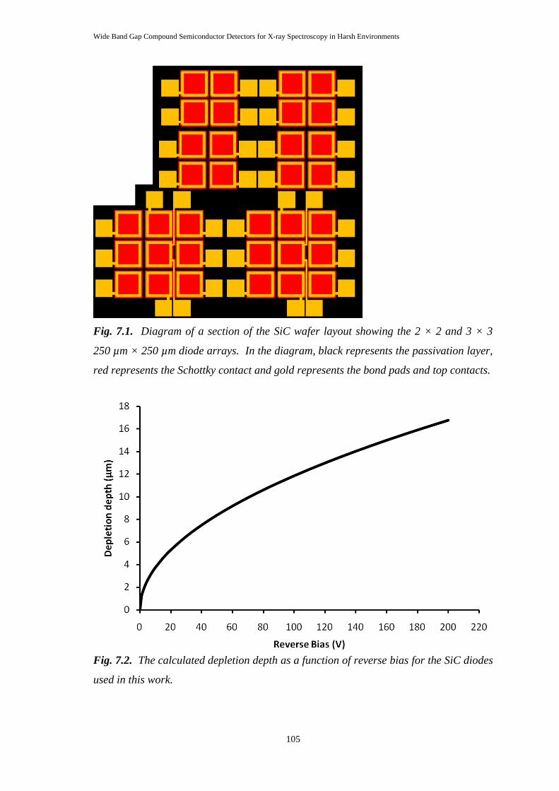
Wide Band Gap Compound Semiconductor Detectors for X-ray Spectroscopy in Harsh Environments
105
Fig. 7.1. Diagram of a section of the SiC wafer layout showing the 2 × 2 and 3 × 3
250 µm × 250 µm diode arrays. In the diagram, black represents the passivation layer,
red represents the Schottky contact and gold represents the bond pads and top contacts.
Fig. 7.2. The calculated depletion depth as a function of reverse bias for the SiC diodes
used in this work.
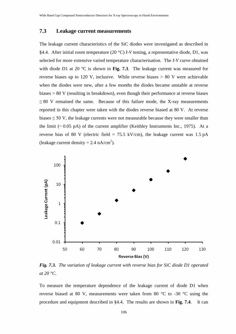
Wide Band Gap Compound Semiconductor Detectors for X-ray Spectroscopy in Harsh Environments
106
7.3 Leakage current measurements
The leakage current characteristics of the SiC diodes were investigated as described in
§4.4. After initial room temperature (20 °C) I-V testing, a representative diode, D1, was
selected for more extensive varied temperature characterisation. The I-V curve obtained
with diode D1 at 20 °C is shown in Fig. 7.3. The leakage current was measured for
reverse biases up to 120 V, inclusive. While reverse biases > 80 V were achievable
when the diodes were new, after a few months the diodes became unstable at reverse
biases > 80 V (resulting in breakdown), even though their performance at reverse biases
≤ 80 V remained the same. Because of this failure mode, the X-ray measurements
reported in this chapter were taken with the diodes reverse biased at 80 V. At reverse
biases ≤ 50 V, the leakage currents were not measurable because they were smaller than
the limit (~ 0.05 pA) of the current amplifier (Keithley Instruments Inc., 1975). At a
reverse bias of 80 V (electric field = 75.5 kV/cm), the leakage current was 1.5 pA
(leakage current density = 2.4 nA/cm2).
Fig. 7.3. The variation of leakage current with reverse bias for SiC diode D1 operated
at 20 °C.
To measure the temperature dependence of the leakage current of diode D1 when
reverse biased at 80 V, measurements were taken from 80 °C to -30 °C using the
procedure and equipment described in §4.4. The results are shown in Fig. 7.4. It can
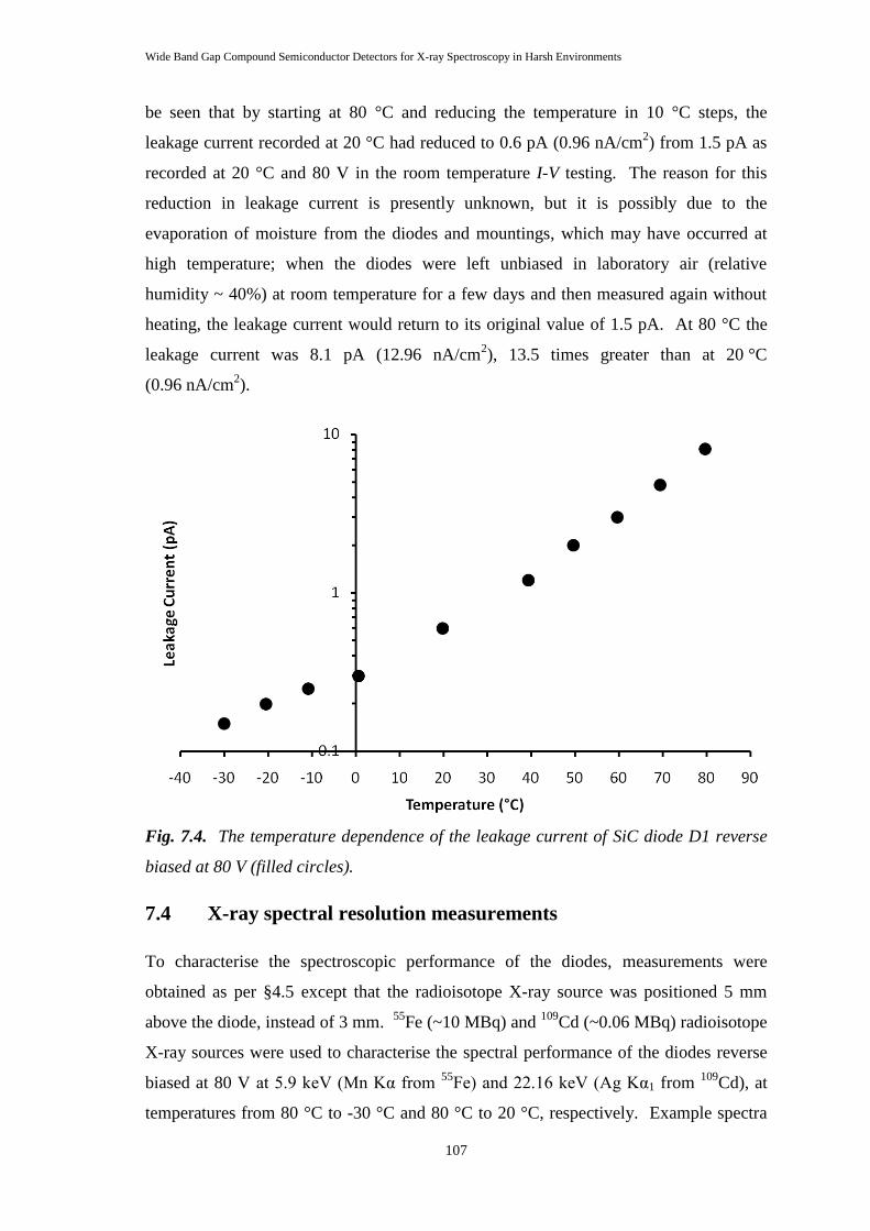
Wide Band Gap Compound Semiconductor Detectors for X-ray Spectroscopy in Harsh Environments
107
be seen that by starting at 80 °C and reducing the temperature in 10 °C steps, the
leakage current recorded at 20 °C had reduced to 0.6 pA (0.96 nA/cm2) from 1.5 pA as
recorded at 20 °C and 80 V in the room temperature I-V testing. The reason for this
reduction in leakage current is presently unknown, but it is possibly due to the
evaporation of moisture from the diodes and mountings, which may have occurred at
high temperature; when the diodes were left unbiased in laboratory air (relative
humidity ~ 40%) at room temperature for a few days and then measured again without
heating, the leakage current would return to its original value of 1.5 pA. At 80 °C the
leakage current was 8.1 pA (12.96 nA/cm2), 13.5 times greater than at 20 °C
(0.96 nA/cm2).
Fig. 7.4. The temperature dependence of the leakage current of SiC diode D1 reverse
biased at 80 V (filled circles).
7.4 X-ray spectral resolution measurements
To characterise the spectroscopic performance of the diodes, measurements were
obtained as per §4.5 except that the radioisotope X-ray source was positioned 5 mm
above the diode, instead of 3 mm. 55
Fe (~10 MBq) and 109
Cd (~0.06 MBq) radioisotope
X-ray sources were used to characterise the spectral performance of the diodes reverse
biased at 80 V at 5.9 keV (Mn Kα from 55
Fe) and 22.16 keV (Ag Kα1 from 109
Cd), at
temperatures from 80 °C to -30 °C and 80 °C to 20 °C, respectively. Example spectra
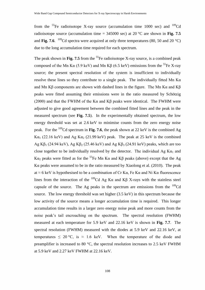
Wide Band Gap Compound Semiconductor Detectors for X-ray Spectroscopy in Harsh Environments
108
from the 55
Fe radioisotope X-ray source (accumulation time 1000 sec) and 109
Cd
radioisotope source (accumulation time = 345000 sec) at 20 °C are shown in Fig. 7.5
and Fig. 7.6. 109
Cd spectra were acquired at only three temperatures (80, 50 and 20 °C)
due to the long accumulation time required for each spectrum.
The peak shown in Fig. 7.5 from the 55
Fe radioisotope X-ray source, is a combined peak
composed of the Mn Kα (5.9 keV) and Mn Kβ (6.5 keV) emissions from the 55
Fe X-ray
source; the present spectral resolution of the system is insufficient to individually
resolve these lines so they contribute to a single peak. The individually fitted Mn Kα
and Mn Kβ components are shown with dashed lines in the figure. The Mn Kα and Kβ
peaks were fitted assuming their emissions were in the ratio measured by Schötzig
(2000) and that the FWHM of the Kα and Kβ peaks were identical. The FWHM were
adjusted to give good agreement between the combined fitted lines and the peak in the
measured spectrum (see Fig. 7.5). In the experimentally obtained spectrum, the low
energy threshold was set at 2.6 keV to minimise counts from the zero energy noise
peak. For the 109
Cd spectrum in Fig. 7.6, the peak shown at 22 keV is the combined Ag
Kα1 (22.16 keV) and Ag Kα2 (21.99 keV) peak. The peak at 25 keV is the combined
Ag Kβ1 (24.94 keV), Ag Kβ2 (25.46 keV) and Ag Kβ3 (24.91 keV) peaks, which are too
close together to be individually resolved by the detector. The individual Ag Kα1 and
Kα2 peaks were fitted as for the 55
Fe Mn Kα and Kβ peaks (above) except that the Ag
Kα peaks were assumed to be in the ratio measured by Xiaolong et al. (2010). The peak
at ≈ 6 keV is hypothesised to be a combination of Cr Kα, Fe Kα and Ni Kα fluorescence
lines from the interaction of the 109
Cd Ag Kα and Kβ X-rays with the stainless steel
capsule of the source. The Ag peaks in the spectrum are emissions from the 109
Cd
source. The low energy threshold was set higher (3.5 keV) in this spectrum because the
low activity of the source means a longer accumulation time is required. This longer
accumulation time results in a larger zero energy noise peak and more counts from the
noise peak‟s tail encroaching on the spectrum. The spectral resolution (FWHM)
measured at each temperature for 5.9 keV and 22.16 keV is shown in Fig. 7.7. The
spectral resolution (FWHM) measured with the diodes at 5.9 keV and 22.16 keV, at
temperatures ≤ 20 °C, is ≈ 1.6 keV. When the temperature of the diode and
preamplifier is increased to 80 °C, the spectral resolution increases to 2.5 keV FWHM
at 5.9 keV and 2.27 keV FWHM at 22.16 keV.
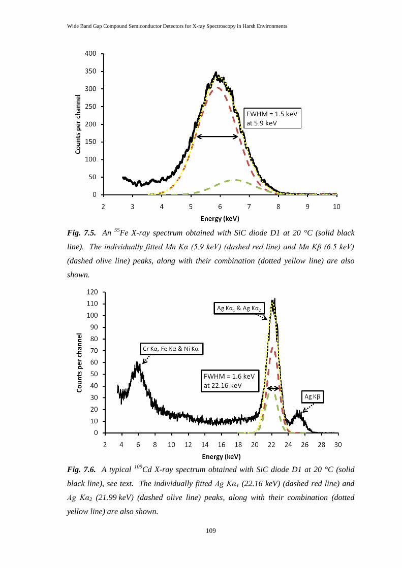
Wide Band Gap Compound Semiconductor Detectors for X-ray Spectroscopy in Harsh Environments
109
Fig. 7.5. An 55
Fe X-ray spectrum obtained with SiC diode D1 at 20 °C (solid black
line). The individually fitted Mn Kα (5.9 keV) (dashed red line) and Mn Kβ (6.5 keV)
(dashed olive line) peaks, along with their combination (dotted yellow line) are also
shown.
Fig. 7.6. A typical 109
Cd X-ray spectrum obtained with SiC diode D1 at 20 °C (solid
black line), see text. The individually fitted Ag Kα1 (22.16 keV) (dashed red line) and
Ag Kα2 (21.99 keV) (dashed olive line) peaks, along with their combination (dotted
yellow line) are also shown.
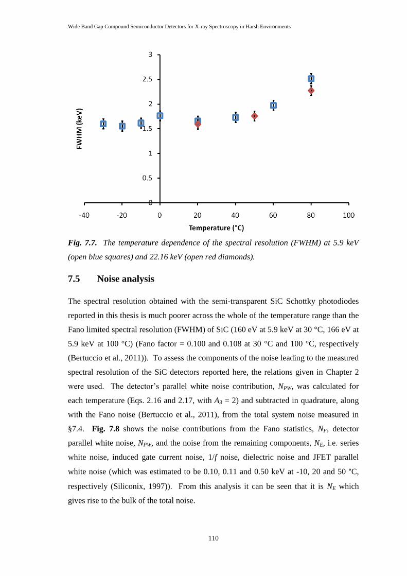
Wide Band Gap Compound Semiconductor Detectors for X-ray Spectroscopy in Harsh Environments
110
Fig. 7.7. The temperature dependence of the spectral resolution (FWHM) at 5.9 keV
(open blue squares) and 22.16 keV (open red diamonds).
7.5 Noise analysis
The spectral resolution obtained with the semi-transparent SiC Schottky photodiodes
reported in this thesis is much poorer across the whole of the temperature range than the
Fano limited spectral resolution (FWHM) of SiC (160 eV at 5.9 keV at 30 °C, 166 eV at
5.9 keV at 100 °C) (Fano factor = 0.100 and 0.108 at 30 °C and 100 °C, respectively
(Bertuccio et al., 2011)). To assess the components of the noise leading to the measured
spectral resolution of the SiC detectors reported here, the relations given in Chapter 2
were used. The detector‟s parallel white noise contribution, NPW, was calculated for
each temperature (Eqs. 2.16 and 2.17, with A3 = 2) and subtracted in quadrature, along
with the Fano noise (Bertuccio et al., 2011), from the total system noise measured in
§7.4. Fig. 7.8 shows the noise contributions from the Fano statistics, NF, detector
parallel white noise, NPW, and the noise from the remaining components, NE, i.e. series
white noise, induced gate current noise, 1/f noise, dielectric noise and JFET parallel
white noise (which was estimated to be 0.10, 0.11 and 0.50 keV at -10, 20 and 50 °C,
respectively (Siliconix, 1997)). From this analysis it can be seen that it is NE which
gives rise to the bulk of the total noise.
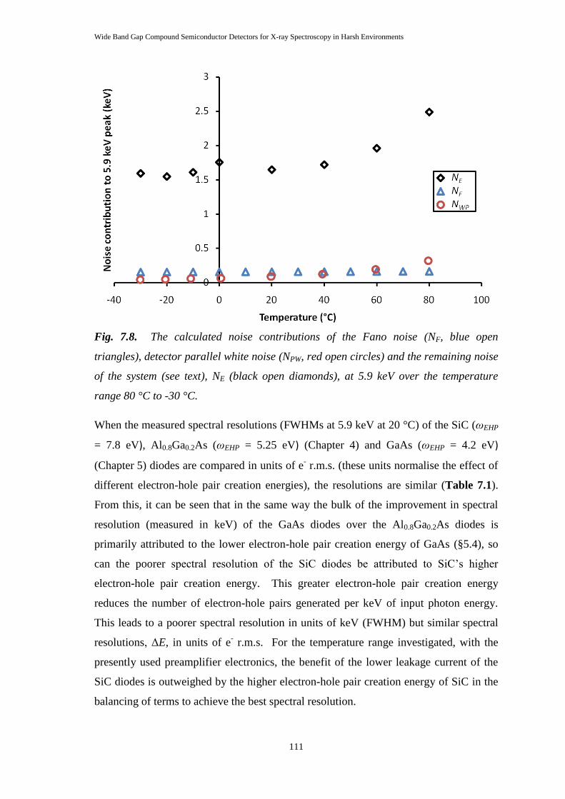
Wide Band Gap Compound Semiconductor Detectors for X-ray Spectroscopy in Harsh Environments
111
Fig. 7.8. The calculated noise contributions of the Fano noise (NF, blue open
triangles), detector parallel white noise (NPW, red open circles) and the remaining noise
of the system (see text), NE (black open diamonds), at 5.9 keV over the temperature
range 80 °C to -30 °C.
When the measured spectral resolutions (FWHMs at 5.9 keV at 20 °C) of the SiC (ωEHP
= 7.8 eV), Al0.8Ga0.2As (ωEHP = 5.25 eV) (Chapter 4) and GaAs (ωEHP = 4.2 eV)
(Chapter 5) diodes are compared in units of e- r.m.s. (these units normalise the effect of
different electron-hole pair creation energies), the resolutions are similar (Table 7.1).
From this, it can be seen that in the same way the bulk of the improvement in spectral
resolution (measured in keV) of the GaAs diodes over the Al0.8Ga0.2As diodes is
primarily attributed to the lower electron-hole pair creation energy of GaAs (§5.4), so
can the poorer spectral resolution of the SiC diodes be attributed to SiC‟s higher
electron-hole pair creation energy. This greater electron-hole pair creation energy
reduces the number of electron-hole pairs generated per keV of input photon energy.
This leads to a poorer spectral resolution in units of keV (FWHM) but similar spectral
resolutions, ΔE, in units of e- r.m.s. For the temperature range investigated, with the
presently used preamplifier electronics, the benefit of the lower leakage current of the
SiC diodes is outweighed by the higher electron-hole pair creation energy of SiC in the
balancing of terms to achieve the best spectral resolution.
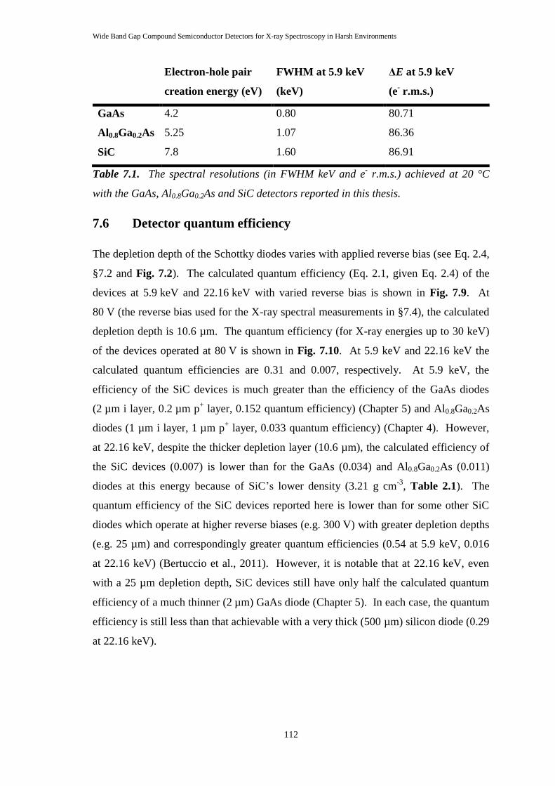
Wide Band Gap Compound Semiconductor Detectors for X-ray Spectroscopy in Harsh Environments
112
Electron-hole pair
creation energy (eV)
FWHM at 5.9 keV
(keV)
ΔE at 5.9 keV
(e- r.m.s.)
GaAs 4.2 0.80 80.71
Al0.8Ga0.2As 5.25 1.07 86.36
SiC 7.8 1.60 86.91
Table 7.1. The spectral resolutions (in FWHM keV and e- r.m.s.) achieved at 20 °C
with the GaAs, Al0.8Ga0.2As and SiC detectors reported in this thesis.
7.6 Detector quantum efficiency
The depletion depth of the Schottky diodes varies with applied reverse bias (see Eq. 2.4,
§7.2 and Fig. 7.2). The calculated quantum efficiency (Eq. 2.1, given Eq. 2.4) of the
devices at 5.9 keV and 22.16 keV with varied reverse bias is shown in Fig. 7.9. At
80 V (the reverse bias used for the X-ray spectral measurements in §7.4), the calculated
depletion depth is 10.6 µm. The quantum efficiency (for X-ray energies up to 30 keV)
of the devices operated at 80 V is shown in Fig. 7.10. At 5.9 keV and 22.16 keV the
calculated quantum efficiencies are 0.31 and 0.007, respectively. At 5.9 keV, the
efficiency of the SiC devices is much greater than the efficiency of the GaAs diodes
(2 µm i layer, 0.2 µm p+ layer, 0.152 quantum efficiency) (Chapter 5) and Al0.8Ga0.2As
diodes (1 µm i layer, 1 µm p+ layer, 0.033 quantum efficiency) (Chapter 4). However,
at 22.16 keV, despite the thicker depletion layer (10.6 µm), the calculated efficiency of
the SiC devices (0.007) is lower than for the GaAs (0.034) and Al0.8Ga0.2As (0.011)
diodes at this energy because of SiC‟s lower density (3.21 g cm-3
, Table 2.1). The
quantum efficiency of the SiC devices reported here is lower than for some other SiC
diodes which operate at higher reverse biases (e.g. 300 V) with greater depletion depths
(e.g. 25 µm) and correspondingly greater quantum efficiencies (0.54 at 5.9 keV, 0.016
at 22.16 keV) (Bertuccio et al., 2011). However, it is notable that at 22.16 keV, even
with a 25 µm depletion depth, SiC devices still have only half the calculated quantum
efficiency of a much thinner (2 µm) GaAs diode (Chapter 5). In each case, the quantum
efficiency is still less than that achievable with a very thick (500 µm) silicon diode (0.29
at 22.16 keV).
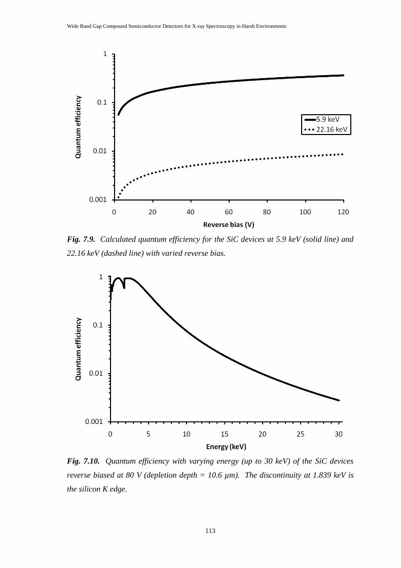
Wide Band Gap Compound Semiconductor Detectors for X-ray Spectroscopy in Harsh Environments
113
Fig. 7.9. Calculated quantum efficiency for the SiC devices at 5.9 keV (solid line) and
22.16 keV (dashed line) with varied reverse bias.
Fig. 7.10. Quantum efficiency with varying energy (up to 30 keV) of the SiC devices
reverse biased at 80 V (depletion depth = 10.6 µm). The discontinuity at 1.839 keV is
the silicon K edge.
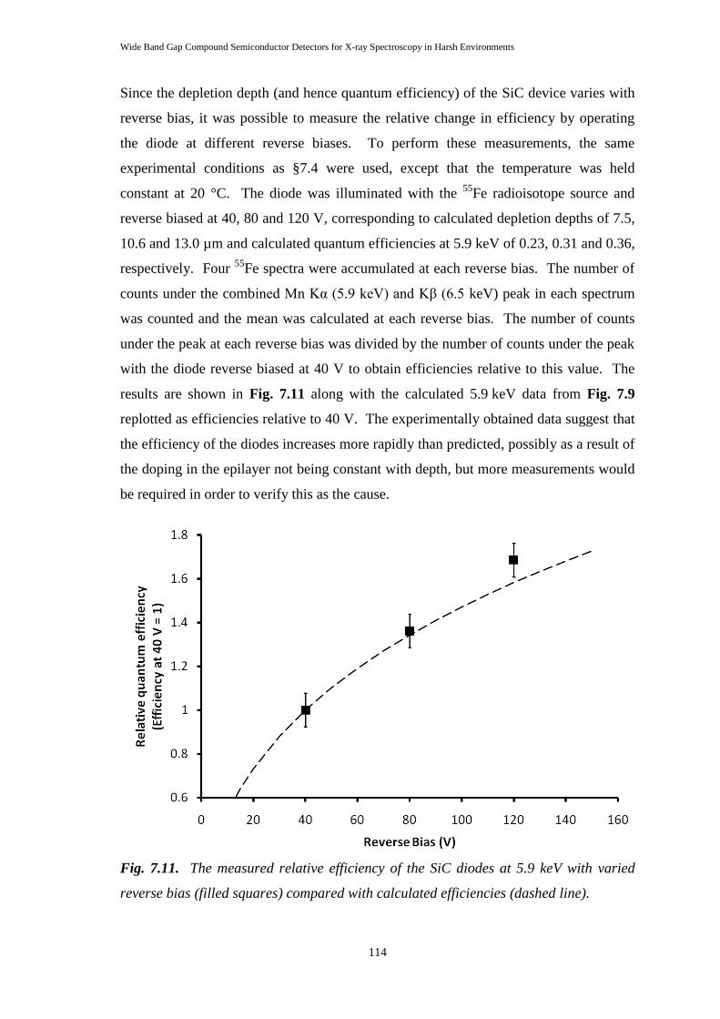
Wide Band Gap Compound Semiconductor Detectors for X-ray Spectroscopy in Harsh Environments
114
Since the depletion depth (and hence quantum efficiency) of the SiC device varies with
reverse bias, it was possible to measure the relative change in efficiency by operating
the diode at different reverse biases. To perform these measurements, the same
experimental conditions as §7.4 were used, except that the temperature was held
constant at 20 °C. The diode was illuminated with the 55
Fe radioisotope source and
reverse biased at 40, 80 and 120 V, corresponding to calculated depletion depths of 7.5,
10.6 and 13.0 µm and calculated quantum efficiencies at 5.9 keV of 0.23, 0.31 and 0.36,
respectively. Four 55
Fe spectra were accumulated at each reverse bias. The number of
counts under the combined Mn Kα (5.9 keV) and Kβ (6.5 keV) peak in each spectrum
was counted and the mean was calculated at each reverse bias. The number of counts
under the peak at each reverse bias was divided by the number of counts under the peak
with the diode reverse biased at 40 V to obtain efficiencies relative to this value. The
results are shown in Fig. 7.11 along with the calculated 5.9 keV data from Fig. 7.9
replotted as efficiencies relative to 40 V. The experimentally obtained data suggest that
the efficiency of the diodes increases more rapidly than predicted, possibly as a result of
the doping in the epilayer not being constant with depth, but more measurements would
be required in order to verify this as the cause.
Fig. 7.11. The measured relative efficiency of the SiC diodes at 5.9 keV with varied
reverse bias (filled squares) compared with calculated efficiencies (dashed line).
Wide Band Gap Compound Semiconductor Detectors for X-ray Spectroscopy in Harsh Environments
115
7.7 Conclusions and discussion
The spectroscopic X-ray performance of semi-transparent silicon carbide Schottky
photodiodes as measured by the FWHM of peaks from 55
Fe and 109
Cd radioisotope
X-ray sources has been investigated at temperatures from +80 °C to -30 °C. The diodes
have been shown to operate at high temperature (up to 80 °C) with low leakage current
(8.1 pA at 80 °C) and to operate as photon counting spectrometers sensitive to X-ray
radiation in the range 5.9 keV to 25 keV, with promising spectral resolution (1.6 –
2.5 keV FWHM) over the measured temperature range.
The larger band gap and higher electron-hole pair creation energy of SiC (compared to
Al0.8Ga0.2As and GaAs) reduces the leakage current of the devices, but also makes the
energy resolution obtained using the detector with the current preamplifier electronics
poorer than that achieved with the other devices reported in this thesis; Al0.8Ga0.2As
(Chapter 4), 1.07 keV FWHM at 5.9 keV at 20 °C; GaAs (Chapter 5), 0.8 keV FWHM
at 5.9 keV at 20 °C). However, Bertuccio et al. (2011) have shown that with ultra-low
noise preamplifier electronics, SiC X-ray detectors are able to achieve excellent spectral
resolution even at high temperature (FWHM at 5.9 keV: 233 eV at 100 °C, 196 eV at
30 °C). These results, along with those reported in this thesis, suggest that SiC Schottky
diodes are promising devices for X-ray detection in high temperature environments.
The benefit of SiC‟s larger electron-hole pair creation energy over materials with lower
electron-hole pair creation energy (such as Al0.8Ga0.2As or GaAs) may become
increasingly significant at even higher temperatures where the spectral resolution may
be limited by device leakage current rather than preamplifier noise. Advancements in
SiC JFET technology (Neudeck et al., 2009) (Bhatnagar et al., 2007) (Wright &
Horsfall, 2007) may also open the possibility of integrating the front end JFET of the
preamplifier with the detector, potentially reducing noise and the temperature sensitivity
of preamplifier by removing the highly temperature sensitive silicon based preamplifier
components. The potential for high temperature operation of SiC detectors together
with their radiation tolerance (Lees et al., 2009) and the possibility of SiC based
preamplifiers are likely to make SiC detectors attractive options in future for sensors
that need to survive in extreme environments.
Wide Band Gap Compound Semiconductor Detectors for X-ray Spectroscopy in Harsh Environments
116
Chapter 8 Summary, conclusions and further
work
8.1 Summary and conclusions
Al0.8Ga0.2As, GaAs and SiC photodiodes have been investigated for their suitability as
spectroscopic soft X-ray (< 25 keV) detectors at high temperature.
Al0.8Ga0.2As non-avalanche mesa p+-i-n
+ photodiodes have been shown to function as
X-ray photon counting detectors over a temperature, T, range, -30 °C ≤ T ≤ 90 °C, with
promising energy resolution of the full system (0.9 – 2.5 keV, FWHM at 5.9 keV). At
20 °C, the measured spectral resolution was ~1.1 keV FWHM at 5.9 keV. The main
source of noise contributing to the measured spectral resolution has been determined, by
amplifier shaping time noise analysis, to be dielectric noise. This is suspected to be
from the packaging material surrounding the detector and input JFET of the
preamplifier. It has been predicted that if this noise could be eliminated, the spectral
resolutions (FWHM at 5.9 keV) achievable at -10, +20 and +50 °C would improve to
332, 380 and 615 eV from the currently achievable 0.90, 1.07 and 1.35 keV, at a
shaping amplifier time constant of 3 µs (Fig. 4.13).
GaAs non-avalanche mesa p+-i-n
+ diodes of similar design have also been investigated.
They have been shown to have better spectral resolution (0.80 – 1.55 keV, FWHM at
5.9 keV) than the Al0.8Ga0.2As devices over the measured temperature range, -30 °C ≤ T
≤ 80 °C. At 20 °C, the measured spectral resolution was ~0.8 keV FWHM at 5.9 keV.
The GaAs detectors were also shown to have a lower low energy threshold (1.4 keV)
than the Al0.8Ga0.2As detectors (~2 keV). These better characteristics are primarily
attributed to the lower electron-hole pair creation energy of GaAs (4.2 eV (Owens &
Peacock, 2004)) compared with Al0.8Ga0.2As (5.25 eV (NSM Archive, 2004)) resulting
in the production of larger numbers of charge carriers in GaAs for a given X-ray photon
energy. The characterisation of the GaAs devices was extended to higher energies
(< 25 keV) with experiments using a 109
Cd radioisotope X-ray source and simulations
from the Monte Carlo model (Chapter 3). This higher energy work demonstrated the
Wide Band Gap Compound Semiconductor Detectors for X-ray Spectroscopy in Harsh Environments
117
internal detector K shell fluorescence that results when the incident X-ray photon‟s
energy is greater than the Ga and As K shell electron binding energies. The primary
noise source contributing to the spectral resolution achievable with the GaAs detectors
is, as for the Al0.8Ga0.2As detectors, the dielectric noise which can be attributed to the
packaging of the diode and preamplifier input JFET. At -10, +20 and +50 °C if the
dielectric noise was eliminated, the spectral resolutions achievable with the GaAs
detectors have been estimated to be 351, 367 and 484 eV FWHM at 5.9 keV,
respectively (Fig. 5.8).
The research conducted with the p+-i-n
+ non-avalanche photodiodes has advanced the
state of the art for both Al0.8Ga0.2As and GaAs high temperature X-ray detectors.
Devices of both materials have been shown to have potential for soft X-ray
spectroscopy at high temperatures. If the quantum efficiency of the detectors can be
increased by growing thicker devices and the electronic noise sources reduced (the
spectral resolution improved) through redesign of the packaging of diode and
preamplifier input JFET, as well as through improvements to the diode design and
fabrication to reduce leakage currents, Al0.8Ga0.2As and GaAs based spectrometers are
likely to find rapid adoption in both space based and terrestrial applications, where their
tolerance of high temperatures will result in cost savings and simpler, more robust
instrument design.
Al0.8Ga0.2As soft X-ray photon counting avalanche photodiodes (APDs) were
investigated experimentally and using the Monte Carlo model. A spectral anomaly
which had previously been reported in X-ray spectra obtained with Al0.8Ga0.2As X-ray
APDs (Lees et al., 2008) was predicted using the model and explained. Through new
experimental and computer modelling results, it was shown that the additional peak
reported by Lees et al., that emerged from the expected Mn Kα and Kβ peak from an
55Fe radioisotope source, when the Al0.8Ga0.2As APDs devices were operated in
avalanche mode, was a consequence of the diode structure and the different
multiplication factors achieved by charge carriers generated by X-ray photons absorbed
at different positions in the diode. Understanding this phenomenon allowed a new
method to be developed for determining the impact ionisation coefficients in
semiconductor devices. This enabled the electron and hole impact ionisation
coefficients of Al0.8Ga0.2As to be determined at X-ray energies, and their temperature
dependence to be reported for the first time.
Wide Band Gap Compound Semiconductor Detectors for X-ray Spectroscopy in Harsh Environments
118
The derivation of the temperature dependence of the impact ionisation coefficients in
Al0.8Ga0.2As has led to a better understanding of the properties of Al0.8Ga0.2As APDs in
environments of high or fluctuating temperature, and prompted the discovery (Tan et
al., 2011) that the established understanding of impact ionisation was incomplete and
that the avalanche excess noise factor is inversely proportional to the number of charge
carriers generated (Fig. 2.7). Determination of the temperature dependence of the
ionisation coefficients of Al0.8Ga0.2As has shown that whilst APDs made of this material
can operate at high temperature, and avalanche multiplication can be used to improve
the signal to noise ratio at X-ray energies, it is essential that the temperature of the
detector remains stable throughout the spectrum accumulation period in order to prevent
the ionisation coefficients from varying and smearing the spectrum.
As part of an on-going SiC photodiode development programme, the high temperature
X-ray spectral properties of Semi-Transparent SiC Schottky Diodes (STSSDs) were
characterised. The temperature dependence of the X-ray spectral performance was
investigated at energies from 5.9 keV to 25 keV. Over a temperature range -30 °C ≤ T
≤ 80 °C, it was found that the FWHM varied from 1.6 keV to 2.5 keV. At 20 °C, the
measured spectral resolution was ~1.5 keV FWHM at 5.9 keV. The poorer resolutions
achieved (compared with the Al0.8Ga0.2As and GaAs devices) were attributed to the
greater electron-hole pair creation energy of SiC (7.8 eV) reducing the number of
charge carriers generated. The relative increase in efficiency brought by increasing the
reverse bias of the devices was investigated theoretically and experimentally. It was
found that the relative efficiency increased more rapidly than theoretically predicted,
possibly because of a non-uniform doping in the epilayer of the devices, although more
measurements would be required to confirm this.
The work presented in this thesis has shown that compound semiconductor X-ray
photodiodes made from Al0.8Ga0.2As, GaAs and SiC are all promising detectors for high
temperature X-ray spectroscopy. The spectral resolutions reported here for these
materials with the present preamplifier electronics are currently poorer at room
temperature than have been reported with silicon drift detectors at 20 °C (~0.3 keV
FWHM at 5.9 keV) (Lechner et al., 2001) and silicon CCDs cooled to -90 °C (130 eV
FWHM at 5.9 keV) (Nakajima et al., 2005). However, the majority of the noise present
with the Al0.8Ga0.2As, GaAs and SiC detectors appears to be from the packaging of the
devices and the preamplifer electronics (see Figs. 4.12, 5.7 & 7.8) and improvements to
Wide Band Gap Compound Semiconductor Detectors for X-ray Spectroscopy in Harsh Environments
119
these aspects will result in much better spectral resolution (see Figs. 5.8 & 4.13). When
coupled to ultra-low noise electronics (pulser line FWHM = 113 eV at 30 °C, 163 eV at
100 °C), Bertuccio et al. (2011) have demonstrated SiC Schottky detectors with spectral
resolutions (FWHM at 5.9 keV) of 196 eV at 30 °C and 233 eV at 100 °C, reinforcing a
conclusion of this thesis that wide band gap compound semiconductor photon counting
X-ray detectors are able to function at high temperature and with useful energy
resolution.
Each material has advantages and disadvantages which must be must be balanced in
order to select the most appropriate material for a specific application. The most
notable example of such a trade-off is the balance that must be struck between selecting
a material with a larger band gap to reduce thermally generated parallel white noise, and
selecting a material with a low electron-hole pair creation energy to increase the number
of charge carriers generated per keV of incoming photon energy. The trade-offs
involved must be informed by the environment in which the instrument is intended to
operate, as well the X-ray energy range of interest and preamplifier electronics and
semiconductor material available.
With refinements to the diode packaging and preamplifier electronics to improve the
spectral resolution, along with improvements in the quantum efficiencies of the
detectors by the production of thicker devices, detectors made from Al0.8Ga0.2As, GaAs
and SiC, will likely find use in applications where operation at high temperature is
required. Real time in situ X-ray fluorescence condition monitoring of engine oil to
detect signs of oil and engine wear in high value and high performance vehicles is one
such potential terrestrial application. Space applications for wide band gap compound
semiconductor detectors include X-ray fluorescence spectrometers for future planetary
geology missions to high temperature environments such as Mercury, Venus and
hydrothermal vents in the Europan Ocean (Thomson & Delaney, 2001), (Lowell &
DuBose, 2005).
8.2 Further work
Possibilities for continued work on Al0.8Ga0.2As, GaAs and SiC detectors abound. One
area of research predicted to have an immediate payoff would be the development of
low noise packaging for the detector and preamplifier input JFET. Custom packaging
for the detector and JFET, perhaps using ceramic or Teflon, may reduce the noise
Wide Band Gap Compound Semiconductor Detectors for X-ray Spectroscopy in Harsh Environments
120
contribution from this area and improve the spectral resolution achievable with the
detectors to such an extent that they become serious contenders for soft X-ray
spectroscopy at room temperature and above, with comparable spectral resolution to a
Silicon Drift Detector cooled to +20 °C (~300 eV FWHM at 5.9 keV) (Lechner et al.,
2001). Development of FETs with lower leakage currents, ideally fabricated from the
same material as the detector so that they can be integrated easily with the detector,
would also be very beneficial as at higher temperatures the JFET leakage becomes
increasingly significant.
In addition to obvious areas of future development such as thicker, more efficient
devices, systematic studies of the processes used to manufacture the devices should be
carried out to optimise the growth and quality of the wafers and the fabrication of the
devices. The leakage currents of the GaAs and AlxGa1-xAs devices should be explored
in more detail to reveal the relative importance of contributions from bulk and surface
leakage. Trials investigating the suitability of various passivation materials (such as
SU-8, SiN and SiO) (Hwang et al., 2001) for reducing surface leakage current should
also be conducted.
Linear and two dimensional detector arrays should be fabricated and characterised to
understand the pixel-to-pixel charge sharing and crosstalk effects that may be present in
AlxGa1-xAs, GaAs and SiC detector arrays; this work will hopefully lead to the
development of high temperature tolerant soft X-ray imaging devices. The model
described in Chapter 3 could be extended to simulate these multi-pixel effects, and also
include single-pixel partial charge collection and charge spreading. Larger area diodes
should also be fabricated and characterised.
Synchrotron measurements, using very small spot size X-ray beams to measure the
uniformity of response across the face of individual diodes and diodes in arrays would
be useful to develop a better understanding of the material quality, electric field
uniformity and charge collection in both avalanche and non-avalanche devices. The
radiation hardness of photon counting Al0.8Ga0.2As and GaAs X-ray photodiodes should
also be characterised, and the characterisation of semi-transparent silicon carbide (SiC)
Schottky spectroscopic X-ray photon counting photodiodes extended beyond 1013
protons/cm2 at 50 MeV (Lees et al., 2009).
Wide Band Gap Compound Semiconductor Detectors for X-ray Spectroscopy in Harsh Environments
121
Through further laboratory experiments on the existing Al0.8Ga0.2As APDs, the
temperature dependence of the ionisation coefficients at different electric fields could be
measured using the method described in Chapter 6. This would enable the production
of equations that parameterise ionisation coefficients in Al0.8Ga0.2As as a function of
electric field and temperature. This technique could be extended to other AlxGa1-xAs
alloys to characterise the temperature dependence of the ionisation coefficients with x,
or even to different materials, subject to wafer and device availability. Further research
into APDs could investigate more advanced device designs, such as separate absorption
and multiplication region (SAM) Al0.8Ga0.2As APDs or even GaAs/Al0.8Ga0.2As SAM
APDs which use GaAs for the absorber region (to take advantage of the lower electron-
hole pair creation energy of GaAs) and Al0.8Ga0.2As in the avalanche region similarly to
those of Lauter et al. (1995).
Wide Band Gap Compound Semiconductor Detectors for X-ray Spectroscopy in Harsh Environments
122
Bibliography
Abbey, A.F., Bennie, P.J., Turner, M.J.L., Altieri, B., Rives, S., 2003, Cooling out
the radiation damage on the XMM-Newton EPIC MOS CCDs, Nuclear Instruments and
Methods in Physics Research A, Vol. 513, Iss. 1-2, pp. 136-142.
Adachi, S., 1985, GaAs, AlAs, AlxGa1-xAs: Material parameters for use in research and
device applications, Journal of Applied Physics, Vol. 53, No. 3, pp. R1-R29.
Advanced Measurement Technology Inc., 2008, Ortec Easy-MCA-8k Digital
Gamma-Ray Spectrometer Hardware User‟s Manual, Manual Revision A, Ortec Part
No. 931044, Oak Ridge, TN, USA.
Alig, R.C., Bloom, S., Struck, C.W., 1980, Scattering by ionization and phonon
emission in semiconductors, Physical Review B, Vol. 22, No. 12, pp. 5565-5582.
Bently Tribology Services, N.D., Sources of wear metals in oils analysis,
http://www.bentlytribology.com/publications/appnotes/app31.php, last retrieved 28th
April 2011.
Bertuccio, G., 2005, Prospect for energy resolving X-ray imaging with compound
semiconductor pixel detectors, Nuclear Instruments and Methods A, Vol. 546, Iss. 1-2,
pp. 232-241.
Bertuccio, G. and Casiraghi, R., 2003, Study of silicon carbide for X-ray detection
and spectroscopy, IEEE Transactions on Nuclear Science, Vol. 50, No. 1, pp. 175-185.
Bertuccio, G., Pullia, A., De Geronimo, G., 1996, Criteria of choice of the front-end
transistor for low noise preamplification of detector signals at sub-microsecond shaping
times for X- and γ-ray spectroscopy, Nuclear Instruments and Methods A, Vol. 380,
Iss. 1-2, pp. 301-307.
Bertuccio, G., Casiraghi, R., and Nava, F., 2001, Epitaxial Silicon Carbide for X-ray
detection, IEEE Transactions on Nuclear Science, Vol. 48, No. 2, pp. 232-233.
Wide Band Gap Compound Semiconductor Detectors for X-ray Spectroscopy in Harsh Environments
123
Bertuccio, G., Casiraghi, R., Maiocchi, D., Owens, A., Bavdaz, M., Peacock, A.,
Andersson, H., Nenonen, S., 2003, Noise analysis of gallium arsenide pixel X-ray
detectors coupled to ultra-low noise electronics, IEEE Transactions on Nuclear Science,
Vol. 50, No. 3, pp. 723-728.
Bertuccio, G., Casiraghi, R., Centronio, A., Lanzieri, C., Nava, F., 2004a, A new
generation of X-ray detectors based on silicon carbide, Nuclear Instruments and
Methods A, Vol. 518, Iss. 1-2, pp. 433-435.
Bertuccio, G., Casiraghi, R., Centronio, A., Lanzieri, C., Nava, F., 2004b, Silicon
carbide for high resolution X-ray detectors operating up to 100 °C, Nuclear Instruments
and Methods A, Vol. 552, Iss. 3, pp. 413-419.
Berticcio, G., Caccia, S., Casiraghi, R., Lanzieri, C., 2006, Possibility of Subelectron
noise with room-temperature silicon carbide pixel detectors, IEEE Transactions on
Nuclear Science, Vol. 53, No. 4, pp. 2421-2427.
Bertuccio, G., Caccia, S., Puglisi, D., Macera, D., 2011, Advances in silicon carbide
X-ray detectors, Nuclear Instruments and Methods A, Vol. 652, Iss. 1, pp. 193-196.
Bhatnagar, P., Wright, N.G., Horsfall, A.B., Vassilevski, K., Johnson, C.M., Uren,
M.J., Hilton, K.P., Munday, A.G., Hydes, A.J., 2007, High temperature
characterisation of 4H-SiC VJFET, Materials Science Forum, Vol. 556-557,
pp. 799-802.
Brunetti, A., Sanchez del Rio, M., Golosio, B., Simionovici, A., Somogyi, A., 2004,
A library for X-ray matter interaction cross sections for X-ray fluorescence applications,
Spectrochimica Acta B, Vol. 59, Iss. 10-11, pp. 1725-1731.
Campbell, J.C., 2007, Recent Advances in Telecommunications Avalanche
Photodiodes, Journal of Lightwave Technology, Vol. 25, No. 1, pp. 109-121.
Campbell, J.L., McDonald, L., Hopman, T., Papp, T., 2001, Simulations of Si(Li)
X‑ray detector response, X-ray Spectrometry, Vol. 30, Iss. 4, pp. 230-241.
Cappelletti, M.A., Cédola, A.P., Blancá, P., 2008, Simulation of silicon PIN
photodiodes for use in space-radiation environments, Semiconductor Science and
Technology, Vol. 23, No. 2, 025007.
Wide Band Gap Compound Semiconductor Detectors for X-ray Spectroscopy in Harsh Environments
124
Childs, P.A. and Leung, C.C.C., 1991, An analysis of „dead space‟ in semiconductors,
Journal of Physics: Condensed Matter, Vol. 3, No. 41, pp. 8053-8057.
Chollet, F., 2009, SU-8: Thick photo-resist for MEMS, Memscylopedia,
http://memscyclopedia.org/su8.html, last retrieved 4th May 2011.
Cree Inc., 2011, Silicon carbide substrates and epitaxy, MAT-CATALOG.00P,
Durham, North Carolina, USA.
Cromer, D.T., and Liberman, D., 1970, Relativistic calculation of anomalous
scattering factors for X-rays, LASL Report LA-4403.
Dapkus, L., Jasutis, C., Jucienė, V., Požela, J., Požela, K., Šilėnas, A., 2007, A
graded-gap X-ray detector with charge avalanche multiplication, Lithuanian Journal of
Physics, Vol. 47, No. 1, pp. 37-40.
David, J.P.R., and Tan, C.H., 2008, Material Considerations for Avalanche
Photodiodes, IEEE Journal of Selected Topics in Quantum Electronics, Vol. 14, No. 4,
pp. 998-1009.
Demeester, P., Ackaert, A., Coudenys, G., Moerman, I., Buydens, L., Pollentier,
Van Daele, P., 1991, Progress in Crystal Growth and Characterization of Materials,
Vol. 22, Iss. 1-2, pp. 53-141.
Design Environmental, N.D., Instruction Manual For Model FS55-65, Ebbw Vale,
Gwent, UK.
EG&G Ortec, N.D., Model 571 Spectroscopy Amplifier Operating and Service
Manual, Rev. A, Part No. 733490, Oak Ridge, Tennessee, USA.
Elsner, R.F., 2002, Discovery of soft X-ray emission from Io, Europa, and the Io
plasma torus, The Astrophysical Journal, Vol. 572, pp. 1077-1082.
Erd, C., Owens, A., Brammertz, G., Bavdaz, M., Peacock, A., Lämsä, V., Nenonen,
S., Andersson, H., Haack, N., 2002, Hard X-ray test and evaluation of a prototype
32×32 pixel gallium-arsenide array, Nuclear Instruments and Methods A, Vol. 487,
Iss. 1-2, pp. 78-89.
Wide Band Gap Compound Semiconductor Detectors for X-ray Spectroscopy in Harsh Environments
125
Everhart, T.E., and Hoff, P.H., 1971, Determination of kilovolt electron dissipation vs
penetration distance in solid materials, Journal of Applied Physics, Vol. 42, No. 13,
pp. 5837-5846.
Fano, U., 1947, Ionization Yield of Radiations. II. The Fluctuation of the Number of
Ions, Physical Review, Vol. 72, No. 1, pp. 26-29.
Farrell, R., Vanderpuye, K., Entine, G., Squillante, M.R., 1991, High resolution low
energy avalanche photodiode X-ray detectors, IEEE Transactions on Nuclear Science,
Vol. 38, No. 2, pp. 144-147.
Franklin, M., Fry, A., Gan, K.K., Han, S., Kagan, H., Kanda, S., Kania, D., Kass,
R., Kin, S.K., Malchow, R., Morrow, F., Olsen, S., Palmer, W.F., Pan, L.S., Sannes,
F., Schnetzer, S., Stone, R., Sugimoto, Y., Thomson, G.B., White, C., Zhao, S.,
1992, Development of diamond radiation detectors for SSC and LHC, Nuclear
Instruments and Methods A, Vol. 315, Iss. 1-3, pp. 39-42.
Fraser, G.W., 1989, X-ray detectors in Astronomy, Cambridge University Press,
Cambridge, UK, ISBN: 978-0-521-10603-0.
Fraser, G.W., 2008, Extraterrestrial Analysis: Planetary X-Ray Fluorescence from
Orbiting Spacecraft and Landers, in Potts, P.J. & West, M., 2008, Portable X-ray
fluorescence spectroscopy: capabilities for in situ analysis, RSC publishing, Cambridge,
UK, ISBN: 978-0-854-04552-5.
Fraser, G.W., Abbey, A.F. Holland, A., McCarthy, K., Owens, A., Wells, A., 1994,
The X-ray energy response of silicon Part A. Theory, Nuclear Instruments and Methods
A., Vol. 350, Iss. 1-2, pp. 368-378.
Fuke, S., Sano, K., Kuwahara, K., Takano, Y., Sato, M., Imai, T., 1995, Lattice
relaxation of AlGaAs layers grown on GaAs(100) substrate plane by organometallic
vapour phase epitaxy, Journal of Applied Physics, Vol. 77, Iss. 1, pp. 420-422.
Gatti, E., Rehak, P., 1984, Semiconductor drift chamber – an application of a novel
charge transport scheme, Nuclear Instruments and Methods in Physics Research A,
Vol. 225, Iss. 3, pp. 608-614.
Wide Band Gap Compound Semiconductor Detectors for X-ray Spectroscopy in Harsh Environments
126
Gatti, E., Manfredi, P.F., Sampietro, M., Speziali, V., 1990, Suboptimal filtering of
1/f-noise in detector charge measurements, Nuclear Instruments and Methods A,
Vol. 297, Iss. 3, pp. 467-478.
Gladstone, G.R., Waite, J.H., Grodent, D., Lewis, W.S., Crary, F.J., Elsner, R.F.,
Weisskopf, M.C., Majeed, T., Jahn, J.-M., Bhardwaj, A., Clarke, J.T., Young,
D.T., Dougherty, M.K., Espinosa, S.A., Cravens, T.E., 2002, A pulsating auroral
X-ray hot spot on Jupiter, Nature, Vol. 415, pp. 1000-1003.
Goldberg, Yu., Levinshtein, M.E., Rumyantsev, S.L., 2001, in Levinshtein, M.E.,
Rumyantsev, S.L., Shur, M.S., 2001, Properties of Advanced Semiconductor Materials:
GaN, AlN, SiC, BN, SiC, SiGe, John Wiley & Sons, New York, USA, ISBN: 978-0-
471-35827-5.
Grande, M., Kellett, B.J., Howe, C., Perry, C.H., Swinyard, B., Dunkin, S.,
Huovelin, J., Alha, L., D’Uston, L.C., Maurice, S., Gasnault, O., Couturier-Doux,
S., Barabash, S., Joy, K.H., Crawford, I.A., Lawrence, D., Fernandes, V.,
Casanova, I., Wieczorek, M., Thomas, N., Mall, U., Foing, B., Hughes, D., Alleyne,
H., Russell, S., Grady, M., Lundin, R., Baker, D., Murray, C.D., Guest, J.,
Christou, A., 2007, The D-CIXS X-ray spectrometer on the SMART-1 mission to the
Moon – First results, Planetary and Space Science, Vol. 55, Iss. 4, pp. 494-502.
Gutiérrez, M., Herrera, M., González, D., Aragón, G., Sánchez, J.J., Hopkinson,
M., García, R., 2002, Relaxation study of AlGaAs cladding layers in InGaAs/GaAs
(111)B lasers designed for 1.0-1.1 µm operation, Microelectronics Journal, Vol. 33,
Iss. 7, pp. 553-557.
Hall, D.J., & Holland, A., 2010, Space radiation environment effects of X-ray CCD
background, Nuclear Instruments and Methods A, Vol. 612, Iss. 2, pp. 320-327.
Harrison, C., 2009, Railway Locomotive Oil Analysis, Scientifics Ltd., Derby, UK,
[Conversation] (Personal communication, 17th February 2009).
Harrison, C.N., David, J.P.R., Hopkinson, M., Rees, G.J., 2002, Temperature
dependence of avalanche multiplication in submicron Al0.6Ga0.4As diodes, Journal of
Applied Physics Vol. 92, Iss. 12, pp. 7684-7686.
Heilbron, J. L., 1966, The works of H. G. J. Moseley, Isis, Vol. 57, No. 3, pp. 336-364.
Wide Band Gap Compound Semiconductor Detectors for X-ray Spectroscopy in Harsh Environments
127
Hu, J., Xin, X., Joseph, C.L., Li, X., Zhao, J.H., 2008, 1 × 16 Pt/4H-SiC Schottky
photodiode array for low-level EUV and UV spectroscopic detection, IEEE Photonics
Technology Letters, Vol. 20, No. 24, pp. 2030-20-32.
Hwang, H.-P., Cheng, Y.-S., Shieh, J.-L., Chyi, J.-I., 2001, A comparative study of
the passivation films on AlGaAs/GaAs hetrojunction diodes and bipolar transistors,
IEEE Transactions on Electron Devices, Vol. 48, No. 2, pp. 185-189.
Jenkins, R., Gould, R.W., Gedcke, D., 1995, Quantitative X-ray Spectrometry, Marcel
Dekker, Inc., New York, USA, ISBN: 978-0-824-79554-2.
Kashiwagi, T., Hibino, K., Kitamura, H., Mori, K., Okuno, S., Takashima, T.,
Uchihori, Y., Yajima, K., Yokota, M., Yoshida, K., 2006, Investigation of Basic
Characteristics of Synthetic Diamond Radiation Detectors, IEEE Transactions on
Nuclear Science, Vol. 53, No. 2, pp. 630-635.
Kataoka, J., Saito, T., Kuramoto, Y., Ikagawa, T., Yatsu, Y., Kotoku, J., Arimoto,
M., Kawai, N., Ishikawa, Y., Kawabata, N., 2005, Recent progress of avalanche
photodiodes in high-resolution X-rays and γ-rays detection, Nuclear Instruments and
Methods A, Vol. 541, Iss. 1-2, pp. 398-404.
Keister, J.W., Smedley, J., Dimitrov, D., Busby, R., 2010, Charge Collection and
Propagation in Diamond X-ray Detectors, IEEE Transactions on Nuclear Science,
Vol. 57, Iss. 4, pp. 2400-2404.
Keithley Instruments Inc, 1975, Instruction Manual Model 427 Current Amplifier,
Document Number 29103, Cleveland, Ohio, USA.
Kemmer, J., Lutz, G., 1987, New detector concepts, Nuclear Instruments and Methods
A, Vol. 253, Iss. 3, pp. 365-377.
Kemmer, J., Lutz, G., Prechtel, U., Schuster, K., Sterzik, M., Strüder, L., Ziemann,
T., 1990, Experimental confirmation of a new semiconductor detector principle,
Nuclear Instruments and Methods A, Vol. 288, Iss. 1, pp. 92-98.
Knoll, G., 2000, Radiation Detection and Measurement, 3rd ed., John Wiley & Sons,
Inc., New York, USA. ISBN: 978-0-471-07338-3.
Wide Band Gap Compound Semiconductor Detectors for X-ray Spectroscopy in Harsh Environments
128
Lauter, J., Protić, D., Förster, A., Lüth, H., 1995, AlGaAs/GaAs SAM-avalanche
photodiode: An X-ray detector for low energy photons, Nuclear Instruments and
Methods A, Vol. 356, Iss. 2-3, pp. 324-329.
Lauter, J., Förster, A., Lüth, H., Müller, K.D., Reinartz, R., 1996, AlGaAs/GaAs
Avalanche Detector Array 1GBit/s X-ray receiver for timing measurements, IEEE
Transactions on Nuclear Science, Vol. 43, No. 3, pp. 1446-1451.
Lechner, P., Eckbauer, S., Hartmann, R., Krisch, S., Hauff, D., Richter, R., Soltau,
H., Strüder, L., Fiorini, C., Gatti, E., Longoni, A., Sampietro, M., 1996, Silicon drift
detectors for high resolution room temperature X-ray spectroscopy, Nuclear Instruments
and Methods A, Vol. 377, Iss. 2-3, pp. 346-351.
Lechner, P., Fiorini, C., Hartmann, R., Kemmer, J., Krause, N., Leutenegger, P.,
Longoni, A., Soltau, H., Stötter, D., Stötter, R., Strüder, L., Weber, U., 2001,
Silicon drift detectors for high count rate X-ray spectroscopy at room temperature,
Nuclear Instruments and Methods in Physics Research A, Vol. 458, Iss. 1-2,
pp. 281-287.
Lees, J.E., 2010, Spectroscopic model for SiC X-ray detectors, Nuclear Instruments and
Methods A, Vol. 613, Iss. 1, pp. 98-105.
Lees, J.E., Bassford, D.J., Fraser, G.W., Horsfall, A.B., Vassilevski, K.V., Wright,
N.G., Owens, A., 2007, Semi-transparent SiC Schottky diodes for X-ray spectroscopy,
Nuclear Instruments and Methods A, Vol. 578, Iss. 1, pp. 226-234.
Lees, J.E., Bassford, D.J., Ng, J.S., Tan, C.H., David, J.P.R., 2008, AlGaAs diodes
for X-ray spectroscopy, Nuclear Instruments and Methods A, Vol. 594, Iss. 2,
pp. 202-205.
Lees, J.E., Bassford, D.J., Bunce, E.J., Sims, M.R., Horsfall, A.B., 2009, Silicon
Carbide X-ray detectors for planetary exploration, Nuclear Instruments and Methods A,
Vol. 604, Iss. 1-2, pp. 174-176.
Lees, J.E., Barnett, A.M., Bassford, D.J., Stevens, R.C., Horsfall, A.B., 2011, SiC
X-ray detectors for harsh environments, J. Inst, Vol. 6, C01032.
Wide Band Gap Compound Semiconductor Detectors for X-ray Spectroscopy in Harsh Environments
129
Lowell, R.P., and Myesha DuBose, 2005, Hydrothermal systems on Europa,
Geophysical Research Letters, Vol. 32, Iss. 5, L05202.
Marinelli, M., Milani, E., Morgada, M.E., Pucella, G., Rodriguez, G., Tucciarone,
A., Verona-Rinati, G., Angelone, M., Pillon, M., 2004, Separate measurement of
electron and hole mean drift distance in CVD diamond, Diamond and Related
Materials, Vol. 13, Iss. 4-8, pp. 929-933.
McCarthy, K.J., Owens, A., Holland, A.D., Wells, A.A., 1995, Modelling the X-ray
response of charge coupled devices, Nuclear Instruments and Methods A, Vol. 362,
Iss. 2-3, pp. 538-546.
McGregor, D.S. and Hermon, H., 1997, Room-temperature compound semiconductor
radiation detectors, Nuclear Instruments and Methods A, Vol. 395, Iss. 1, pp. 101-124.
McIntyre, R.J., 1966, Multiplication noise in uniform avalanche photodiodes, IEEE
Transactions on Electron Devices, Vol. ED-13, No. 1, pp. 164-168.
Miyaguchi, K., 1999, CCD developed for scientific application by Hamamatsu,
Nuclear Instruments and Methods A, Vol. 436, Iss. 1-2, pp. 24-31.
Miyaguchi, K., Suzuki, H., Dezaki, J., Yamamoto, K., 1999, CCD developed for
scientific application by Hamamatsu, Nuclear Instruments and Methods A, Vol. 436,
Iss. 1-2, pp. 24-31.
Molhave, K., 2006, in “The Opensource Handbook of Nanoscience and
Nanotechnology”,
http://en.wikibooks.org/wiki/File:Bandgap_vs_Lattice_Const_for_Semiconductors_5.25
‑6.74_Angstrom.jpg, last retrieved 18th January 2011.
Moroz, V. I., 2002, Studies of the atmosphere of Venus by means of spacecraft: solved
and unsolved problems, Advances in Space Research, Vol. 29, Iss. 2, pp. 215-225.
Moseley, H., 1913, The high-frequency spectra of the elements, Philosophical
Magazine, Vol. 26, Iss. 156, pp. 1024-1034.
Wide Band Gap Compound Semiconductor Detectors for X-ray Spectroscopy in Harsh Environments
130
Nakajima, H., Yamaguchi, H., Matsumoto, H., Tsuru, T.G., Koyama, K., Kissel, S.,
LaMarr, B., Bautz, M., 2005, The ground calibration of X-ray CCD cameras (XIS)
with front-illuminated chips onboard Astro-E2, Nuclear Instruments and Methods A,
Vol. 541, Iss. 1-2, pp. 365-371.
Nava, F., Bertuccio, G., Cavallini, A., Vittone, E., 2008, Silicon carbide and its use as
a radiation detector material, Measurement Science and Technology, Vol. 19, Iss. 10,
pp. 102001-102026.
Nava, F., Vanni, P., Lanzieri, C., Canali, C., 1999, Epitaxial silicon carbide charge
particle detectors, Nuclear Instruments and Methods A, Vol. 437, Iss. 2-3, pp. 354-358.
Ness, J.-U., 2004, X-ray emission from Saturn, Astronomy and Astrophysics, Vol. 418,
pp. 337-345.
Neudeck, P.G., Garverick, S.L., Spry, D.J., Chen, L.-Y., Beheim, G.M., Krasowski,
M.J., Mehregany, M., 2009, Extreme temperature 6H-SiC JFET integrated circuit
technology, Physica Status Solidi A, Vol. 206, No. 10, pp. 2329-2345.
Ng, B.K., David, J.P.R., Plimmer, S.A., Hopkinson, M., Tozer, R.C., Rees, G.J.,
2000, Impact ionization coefficients of Al0.8Ga0.2As, Applied Physics Letters, Vol. 77,
No. 26, pp. 4374-4376.
Ng, B. K., David, J.P.R., Plimmer, S.A., Rees, G.J., Tozer, R.C., Hopkinson, M.,
Hill, G., 2001, Avalanche Multiplication Characteristics of Al0.8Ga0.2As Diodes, IEEE
Transactions on Electronic Devices, Vol. 48, No. 10, pp. 2198-2204.
Ng, B.K., David, J.P.R., Tozer, R.C., Hopkinson, M., Hill, G., Rees, G.J., 2002,
excess noise characteristics of Al0.8Ga0.2As Avalanche photodiodes, IEEE Photonics
Technology Letters Vol. 14, No. 4, pp. 522-524.
Ng, J.S., 2009, Discussion of electric field profile, University of Sheffield, Sheffield,
UK, (personal communication, 10th September 2009).
NSM Archive, 2004, Physical properties of semiconductors, NSM Archive, Ioffe,
Russia, http://www.ioffe.rssi.ru/SVA/NSM/Semicond/, last retrieved 21st April 2011.
Wide Band Gap Compound Semiconductor Detectors for X-ray Spectroscopy in Harsh Environments
131
Ochi, A., Nishi, Y., Tanimori, T., 1996, Study of a large area avalanche photodiode as
a fast photodiode and a soft X-ray detector, Nuclear Instruments and Methods A,
Vol. 378, Iss. 1-2, pp. 267-274.
Okada, T., Shirai, K., Yamamoto, Y., Arai, R., Ogawa, K., Hosono, K., Kato, M.,
2006, X-ray Fluorescence Spectrometry of Asteroid Itokawa by Hayabusa, Science,
Vol. 312, No. 5778, pp. 1338-1341.
Owens, A., and Peacock, A., 2004, Compound semiconductor radiation detectors,
Nuclear Instruments and Methods A, Vol. 531, Iss. 1-2, pp. 18-37.
Owens, A., Bavdaz, M., Peacock, A., Poelaert, A., Anderson, H., Nenonen, S.,
Tröger, L., Bertuccio, G., 2001, Hard X-ray spectroscopy using small format GaAs
arrays, Nuclear Instruments and Methods A, Vol. 466, Iss. 1, pp. 168-173.
Owens, A., Bavdaz, M., Peacock, A., Andersson, H., Nenonen, S., Krumrey, M.,
Puig, A., 2002a, High resolution X-ray spectroscopy using a GaAs pixel detector,
Nuclear Instruments and Methods A, Vol. 479, Iss. 2-3, pp. 531-534.
Owens, A., Bavdaz, M., Andersson, H., Gagliardi, T., Krumrey, M., Nenonen, S.,
Peacock, A., Taylor, I., and Tröger, L., 2002b, The X-ray response of CdZnTe,
Nuclear Instruments and Methods A, Vol. 484, Iss. 1-3, pp. 242-250.
Plimmer, S.A., David, J.P.R., Herbert, D.C., Lee, T.-W., Rees, G.J., Houston, P.A.,
Grey, R., Robson, P.N., Higgs, A.W., Wright, D.R., 1996, Investigation of Impact
Ionization in Thin GaAs Diodes, IEEE Transactions on Electron Devices, Vol. 43,
No. 7, pp. 1066-1072.
Plimmer, S.A., David, J.P.R., Rees, G.J., Robson, P.N., 2000, Ionization coefficients
in AlxGa1-xAs (x = 0-0.60), Semiconductor Science and Technology, Vol. 15 No. 7,
pp. 692-699.
PNSensor GmbH, N.D., Silicon Drift Detector Development,
http://www.pnsensor.de/Welcome/Detector/SDD/index.html, last retrieved 23rd March
2011.
Potts, P.J. & West, M., 2008, Portable X-ray fluorescence spectroscopy: Capabilities
for in Situ Analysis, RSC publishing, Cambridge, UK, ISBN: 978-0-854-04552-5.
Wide Band Gap Compound Semiconductor Detectors for X-ray Spectroscopy in Harsh Environments
132
Potts, P.J., 1987, A handbook of silicate rock analysis, Blackie, Glasgow, Scotland,
ISBN: 978-0-412-00881-8.
Pullia, A., and Bertuccio, G., 1996, Resolution limits of silicon detectors and
electronics for soft X-ray spectroscopy at non cryogenic temperatures, Nuclear
Instruments and Methods A, Vol. 380, Iss. 1-2, pp. 1-5.
Ripamoni, G., Capasso, F., Hutchinson, A.L., Muehlner, D.J., Walker, J.F., Malik,
R.J., 1990, Realization of a staircase photodiode: Towards a solid-state photomultiplier,
Nuclear Instruments and Methods A, Vol. 288, Iss. 1, pp. 99-103.
Ruddy, F.H. and Siedel, J.G., 2006, Effects of gamma irradiation on silicon carbide
semiconductor radiation detectors, 2006 IEEE Nuclear Science Symposium Conference
Record, pp. 583-587.
Ruddy, F.H., Seidel, J.G., Chen, H., Dulloo, A.R., Ryu, S.-H., 2006, High-resolution
alpha-particle spectrometry using 4H silicon carbide semiconductor detectors, IEEE
Transactions on Nuclear Science, Vol. 53, No. 3, pp. 1713-1718.
Ruegg, H.W., 1967, An optimized avalanche photodiode, IEEE Transactions on
Electron Devices, Vol. 14, No. 5, pp. 239-251.
Saleh, M.A., Hayat, M.M., Saleh, B.E.A., Teich, M.C., 2000, Dead-space-based
theory correctly predicts excess noise factor for thin GaAs and AlGaAs avalanche
photodiodes, IEEE Transactions on Electron Devices, Vol. 47, No. 3, pp. 625-633.
Salvatori, S., Rossi, M.C., Galluzzi, F., 1999, Minority-carrier transport parameters in
CVD diamond, Carbon, Vol. 37, Iss. 5, pp. 811-816.
Schötzig, U., 2000, Half-life and X-ray emission probabilities of 55Fe, Applied
Radiation and Isotopes, Vol. 53, Iss. 3, pp. 469-472.
Silenas, A., 2004, Graded-gap AlxGa1-xAs analyzer of X-ray and alpha-particle spectra,
Nuclear Instruments and Methods A, Vol. 531, Iss. 1-2, pp. 92-96.
Silenas, A., Pozela, J., Smith, K.M., Pozela, K., Jasutis, V., Dapkus, L., Juciene, V.,
2002, Non-uniformly doped graded-gap AlxGa1-xAs X-ray detectors with high
photovoltaic response, Nuclear Instruments and Methods A., Vol. 487, Iss. 1-2,
pp. 54-59.
Wide Band Gap Compound Semiconductor Detectors for X-ray Spectroscopy in Harsh Environments
133
Silenas, A., Pozela, K., Dapkus, L., Jasutis, V., Juciene, V., Pozela, J., Smith, K.M.,
2003, Graded-gap AlxGa1-xAs X-ray detector with collected charge multiplication,
Nuclear Instruments and Methods A, Vol. 509, Iss. 1-3, pp. 30-33.
Silenas, A., Dapkus, L., Pozela, K., Pozela, J., Juciene, V., Jasutis, V., 2005,
Radiation hardness of graded-gap AlxGa1-xAs X-ray detectors, Nuclear Instruments and
Methods A, Vol. 546, Iss. 1-2, pp. 228-231.
Silenas, A., Pozela, J., Pozela, K., Dapkus, L., Juciene, V., 2006, High spatial
resolution graded-gap AlxGa1-xAs X-ray detector, Nuclear Instruments and Methods A,
Vol. 563, Iss. 1, pp. 21-23.
Silenas, A., Miller, A., Pozela, J., Pozela, K., Dapkus, L., Juciene, V., 2011,
Graded-gap AlxGa1-xAs detector for high-energy electron beam dosimetry, Nuclear
Instruments and Methods A, Vol. 633, Suppl. 1, pp. S62-S64.
Siliconix, 1997, 2N4416/2N4416A/SST4416 N-Channel JFETs, Data Sheet, S-52424,
Rev. E, 14-Apr-97, Vishay Electronic GmbH, Selb, Germany.
Spanovich, N., Smith, M.D., Smith, P.H., Wolff, M.J., Christensen, P.R., Squires,
S.W., 2006, Surface and near-surface atmospheric temperatures for the Mars
Exploration Rover landing sites, Icarus, Vol. 180, Iss. 2, pp. 314-320.
Squillante, M.R., Reiff, G., Entine, G., 1985, Recent advances in large area avalanche
photodiodes, IEEE Transactions on Nuclear Science, Vol. 32, No. 1, pp. 863-566.
Sridharan, M.G., Mekaladevi, M., Rodriguez-Viejo, J., Narayandass, Sa.K.,
Mangalaraj, D., Lee, H.C, 2004, Spectroscopic ellipsometry studies on polycrystalline
Cd0.9Zn0.1Te thin films, Physica Status Solidi (a), Vol. 201, No. 4, pp. 782-790.
Swinyard, B.M., Joy, K.H., Kellett, B.J., Crawford, I.A., Grande, M., Howe, C.J.,
Fernandes, V.A., Gasnault, O., Lawrence, D.J., Russell, S.S., Wieczorek, M.A.,
Foring, B.H., The SMART-1 team, 2009, X-ray fluorescence observations of the
moon by SMART-1/D-CIXS and the first detection of Ti Kα from the lunar surface,
Planetary and Space Science, Vol. 57, Iss. 7, pp. 744-750.
Wide Band Gap Compound Semiconductor Detectors for X-ray Spectroscopy in Harsh Environments
134
Tan, C.H., David, J.P.R., Plimmer, S.A., Rees, G.J., Tozer, R.C., Grey, R., 2001,
Low Multiplication Noise in Thin Al0.6Ga0.4As Avalanche Photodiodes, IEEE
Transactions on Electron Devices Vol. 48, No. 7, pp. 1310-1317.
Tan, C.H., Gomes, R.B., David, J.P.R., Barnett, A.M., Bassford, D.J., Lees, J.E.,
Ng, J.S., 2011, Avalanche Gain and Energy Resolution of Semiconductor X-ray
Detectors, IEEE Trans. Elect. Dev., Vol. 58, No. 6, pp. 1696-1701.
Thurlby Thandar Instruments Ltd, N.D., PL Series Instruction Manual, Book Part
No. 45811-0170, Iss. 12, Huntingdon, Cambridgeshire, UK.
Thomson, R.E., and Delaney, J.R., 2001, Evidence for a weakly stratified Europan
ocean sustained by seafloor heat flux, Vol. 106, No. E6, pp. 12355-12365.
Van Zeghbroeck, B., 2007, Principles of Semiconductor Devices, University of
Colorado, Boulder, USA, http://ece-www.colorado.edu/~bart/book/, last retrieved 23rd
June 2011.
Weng, M.H., Mahapatra, R., Horsfall, A.B., Wright, N.G., 2007, Hydrogen sulphide
detection in extreme environments, Journal of Physics: Conference Series, Vol. 76,
No. 1, 012005.
Withers, P., and Smith, M. D., 2006, Atmospheric entry profiles from the Mars
Exploration Rovers Spirit and Opportunity, Icarus, Vol. 198, Iss. 1, pp. 133-142.
Wright, N.G., and Horsfall, A.B., 2007, SiC sensors: a review, Journal of Physics D:
Applied Physics, Vol. 40, No. 20, pp. 6345-6354.
Xiaolong, H., Shenggui, Y., Chunsheng, D., 2010, Evaluation of the decay data of
109Cd, Nuclear Instruments and Methods A, Vol. 621, Iss. 1-3, pp. 443-446.
Yang, Z., Hou, X., Jones, B.T., 2003, Determination of wear metals in engine oil by
mild acid digestion and energy dispersive X-ray fluorescence spectrometry using solid
phase extraction disks, Talanta, Vol. 59, Iss. 4, pp. 673-680.
Yatsu, Y., Kuramoto, Y., Kataoka, J., Kotoku, J., Saito, T., Ikagawa, T., Sato, R.,
Kawai, N., Kishimoto, S., Mori, K., Kamae, T., Ishikawa, Y., Kawabata, N., 2006,
Study of avalanche photodiodes for soft X-ray detection below 20 keV, Vol. 564, Iss. 1,
pp. 134-143.
Wide Band Gap Compound Semiconductor Detectors for X-ray Spectroscopy in Harsh Environments
135
Zheng, X.G., Yaun, P., Kinsey, G.S., Holmes, A.L., Streetman, G.G., Campbell,
J.C., 2000, IEEE Journal of Quantum Electronics, Vol. 36, No. 10, pp. 1168-1173.