Embed Size (px)
Citation preview
William Stallings William Stallings Computer Organization and Architectureand Architecture8th Edition
Chapter 5pInternal Memory
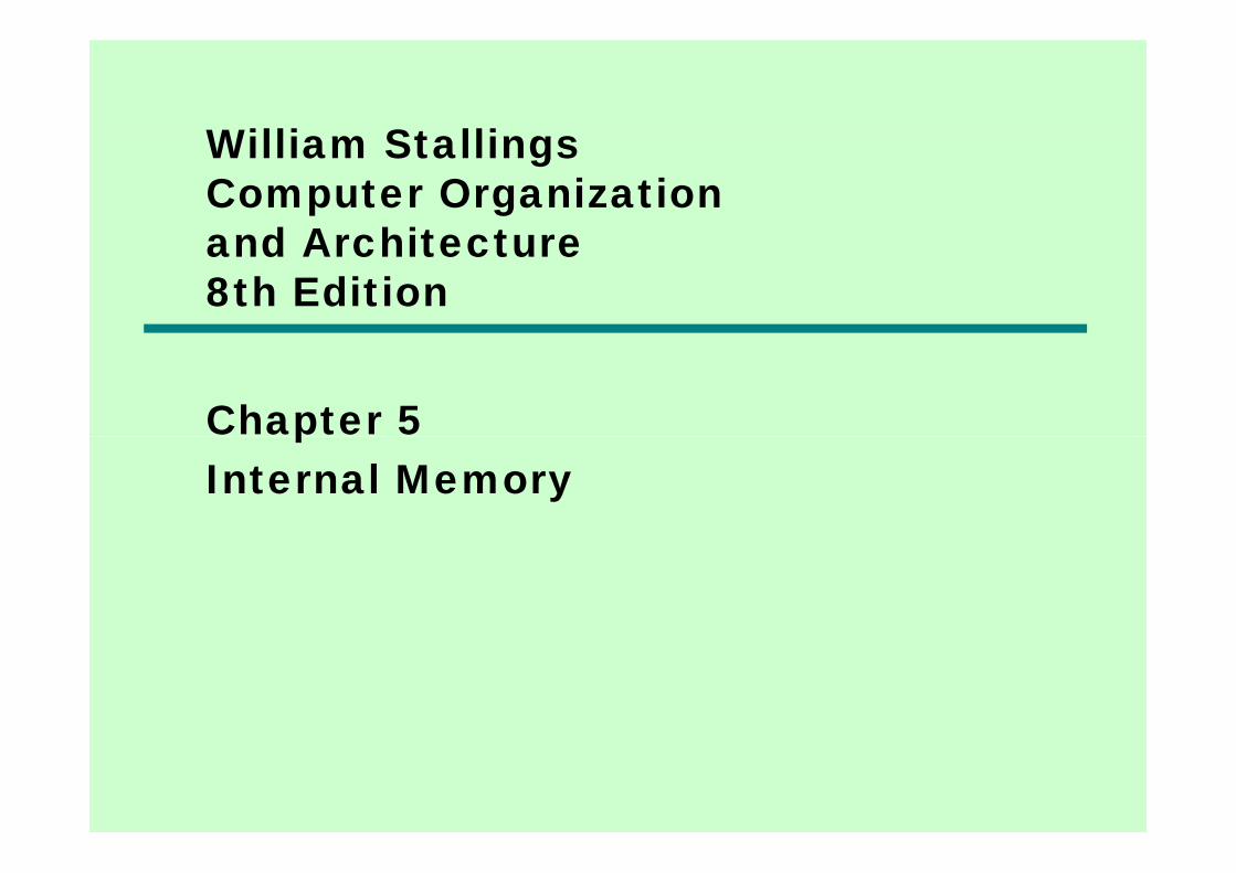
Semiconductor Memory Typesy yp
Memory Type Category Erasure Write Mechanism Volatility
Random-access memory (RAM) Read-write memory Electrically, byte-level Electrically Volatile
Read-only memory (ROM)
Read-only memory Not possible
Masks
Programmable ROM (PROM)
Nonvolatile
Electrically
Erasable PROM (EPROM) UV light, chip-level
Read-mostly memoryElectrically Erasable PROM (EEPROM) Electrically, byte-level
Flash memory Electrically, block-level
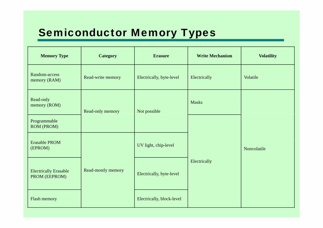
Semiconductor Memoryy• RAM
Mi d ll i d t i —Misnamed as all semiconductor memory is random accessRead/Write—Read/Write
—VolatileTempo a sto age—Temporary storage
—Static or dynamic
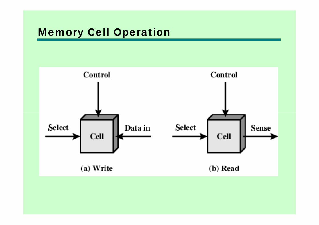
Memory Cell Operationy p
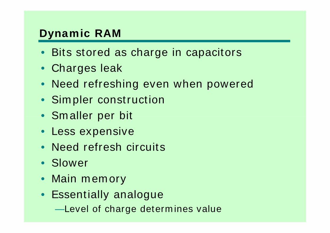
Dynamic RAMy• Bits stored as charge in capacitors
Ch l k• Charges leak• Need refreshing even when powered• Simpler construction• Smaller per bit• Smaller per bit• Less expensive
N d f h i i• Need refresh circuits• Slower• Main memory• Essentially analogue• Essentially analogue
—Level of charge determines value
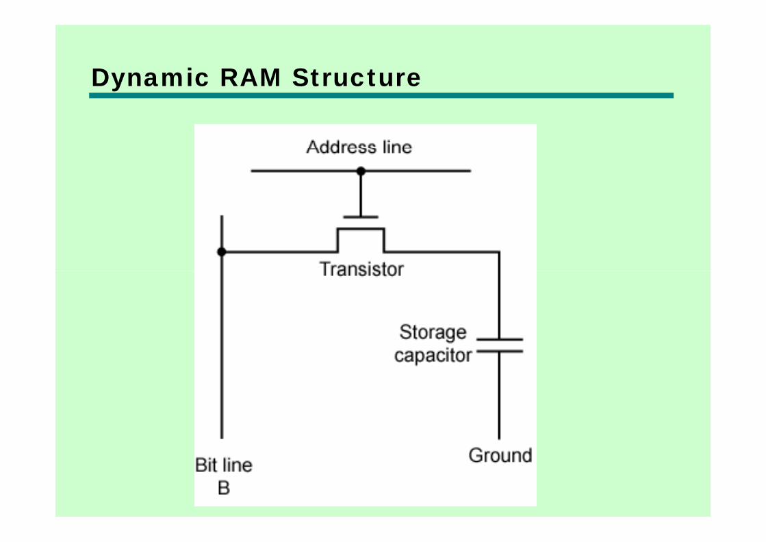
Dynamic RAM Structurey
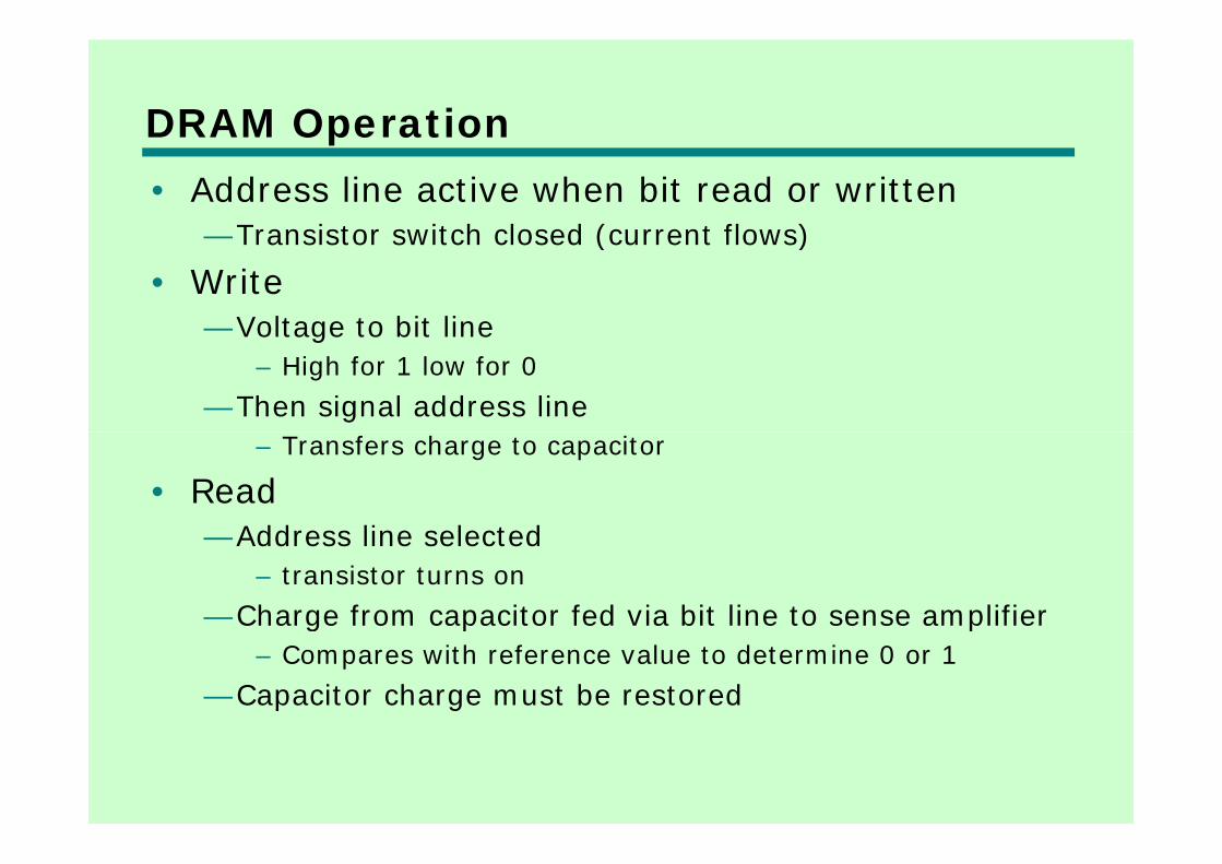
DRAM Operationp• Address line active when bit read or written
—Transistor switch closed (current flows)—Transistor switch closed (current flows)• Write
—Voltage to bit lineVoltage to bit line– High for 1 low for 0
—Then signal address line– Transfers charge to capacitor
• ReadAdd ess line selected—Address line selected
– transistor turns on—Charge from capacitor fed via bit line to sense amplifierg p p
– Compares with reference value to determine 0 or 1—Capacitor charge must be restored
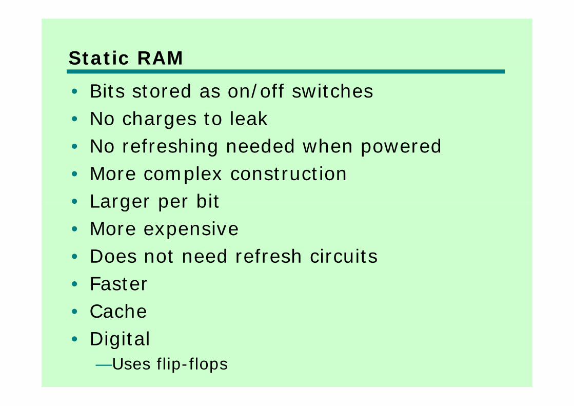
Static RAM• Bits stored as on/off switches
h l k• No charges to leak• No refreshing needed when powered• More complex construction• Larger per bit• Larger per bit• More expensive
D d f h i i• Does not need refresh circuits• Faster• Cache• Digital• Digital
—Uses flip-flops
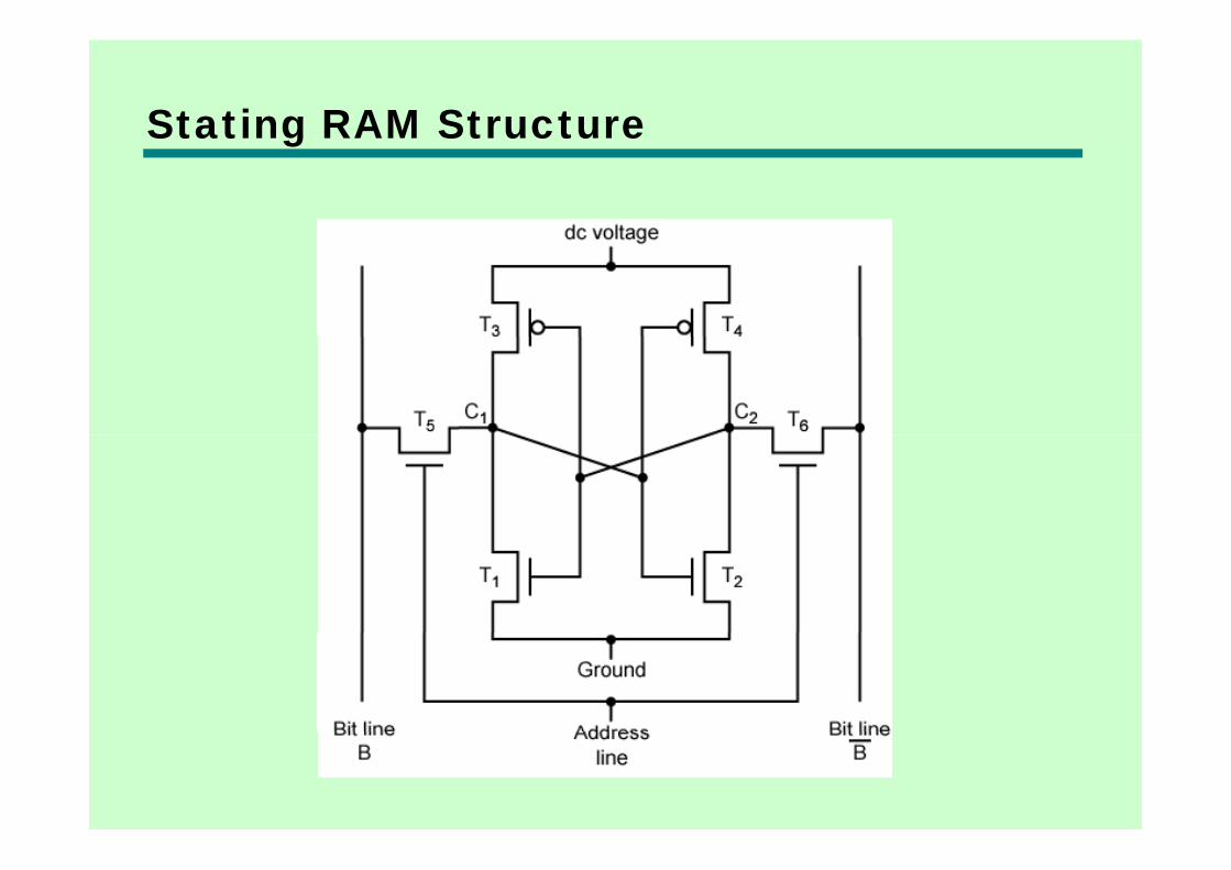
Stating RAM Structureg
Static RAM Operationp• Transistor arrangement gives stable logic
statestate• State 1
C high C low—C1 high, C2 low—T1 T4 off, T2 T3 on
• State 0• State 0—C2 high, C1 low—T T off T T onT2 T3 off, T1 T4 on
• Address line transistors T5 T6 is switch• Write apply value to B & compliment to • Write – apply value to B & compliment to
B• Read value is on line B• Read – value is on line B
SRAM v DRAM• Both volatile
P d d t d t—Power needed to preserve data• Dynamic cell
—Simpler to build, smaller—More dense—Less expensive—Needs refresh—Larger memory units
• Static—Faster—CacheCache
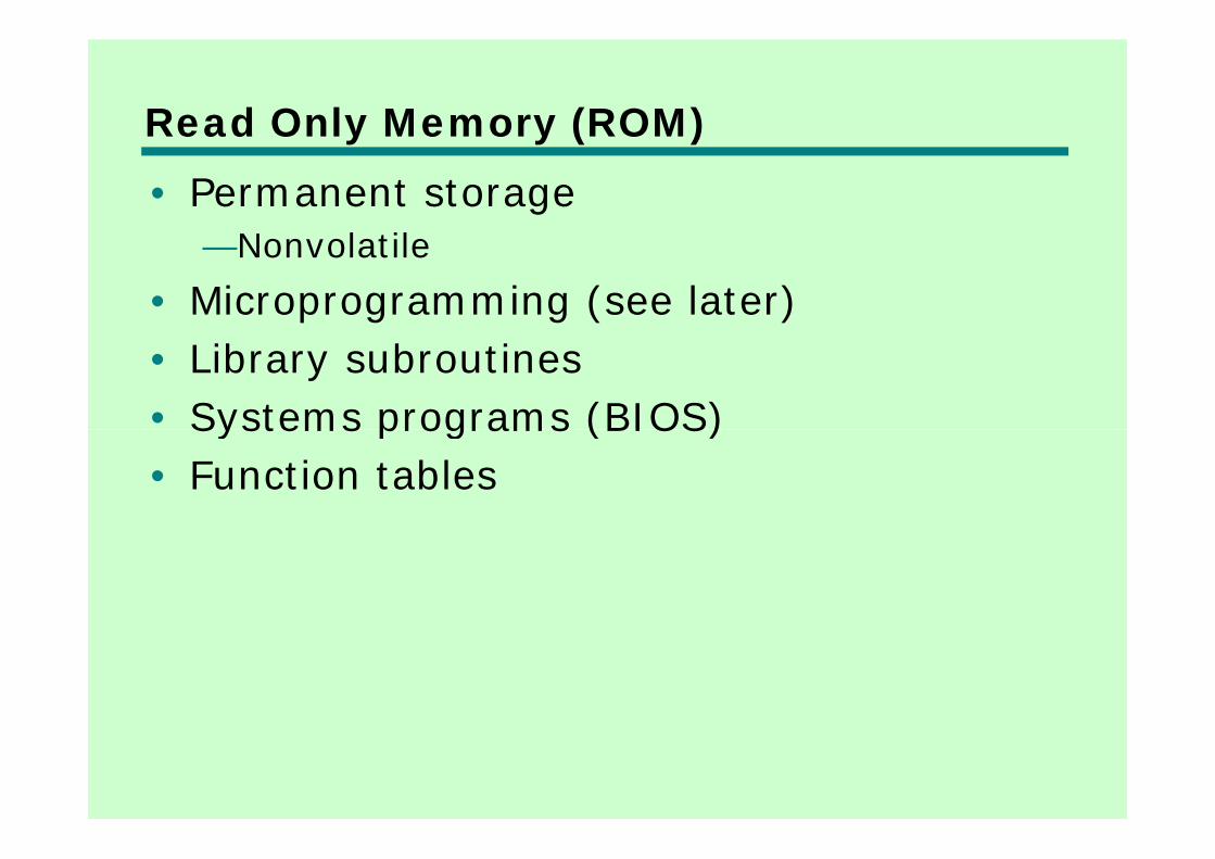
Read Only Memory (ROM)y y ( )• Permanent storage
N l til—Nonvolatile• Microprogramming (see later)• Library subroutines• Systems programs (BIOS)Systems programs (BIOS)• Function tables
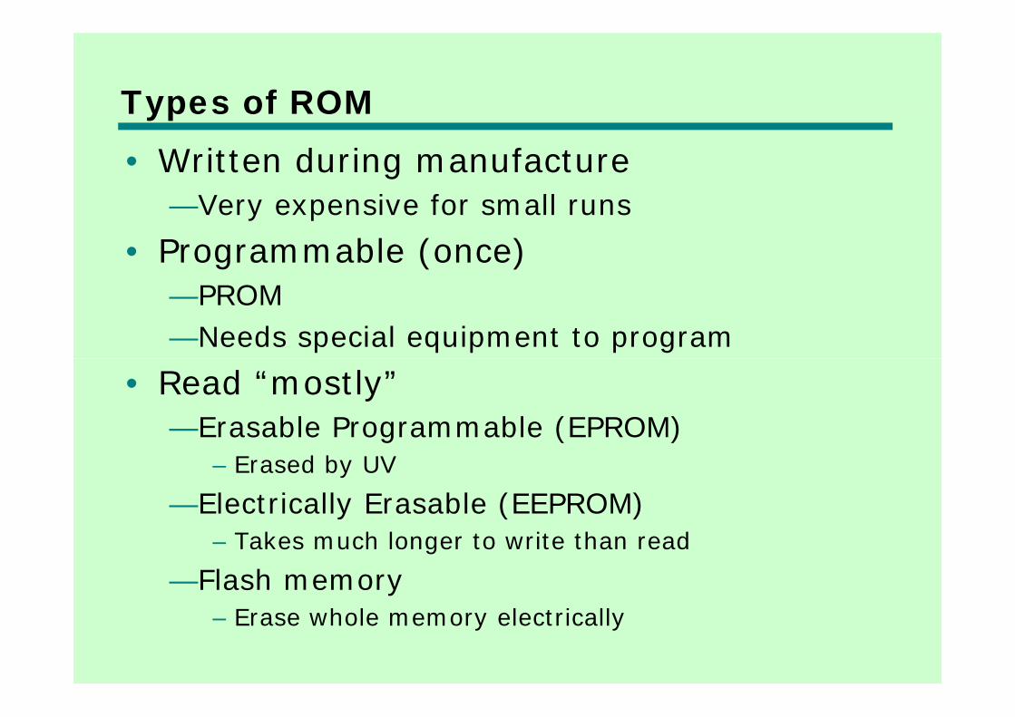
Types of ROMyp• Written during manufacture
V i f ll —Very expensive for small runs• Programmable (once)
—PROM—Needs special equipment to program
• Read “mostly”—Erasable Programmable (EPROM)g ( )
– Erased by UV—Electrically Erasable (EEPROM)
– Takes much longer to write than read—Flash memory
– Erase whole memory electrically
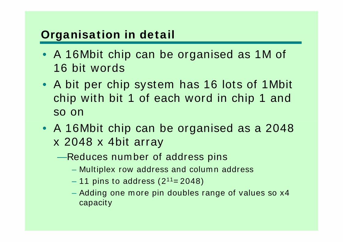
Organisation in detailg• A 16Mbit chip can be organised as 1M of
16 bit words16 bit words• A bit per chip system has 16 lots of 1Mbit
hi i h bi 1 f h d i hi 1 dchip with bit 1 of each word in chip 1 and so on
• A 16Mbit chip can be organised as a 2048 x 2048 x 4bit array—Reduces number of address pins
– Multiplex row address and column address– 11 pins to address (211=2048)– Adding one more pin doubles range of values so x4
capacitycapacity
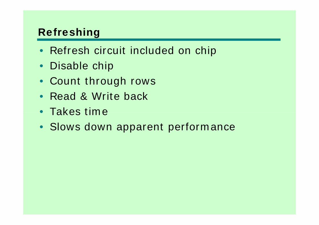
Refreshingg• Refresh circuit included on chip
bl h• Disable chip• Count through rows• Read & Write back• Takes time• Takes time• Slows down apparent performance
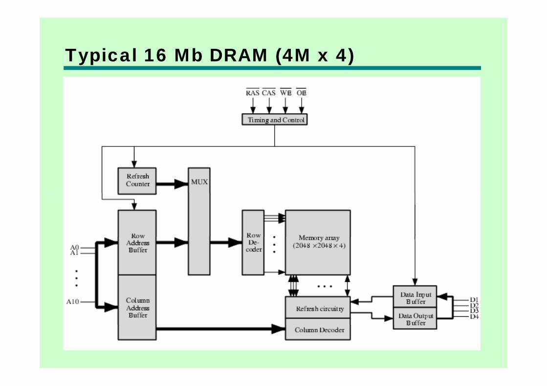
Typical 16 Mb DRAM (4M x 4)yp ( )
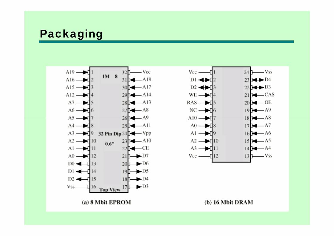
Packagingg g
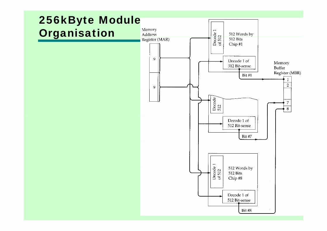
256kByte Module Organisationg
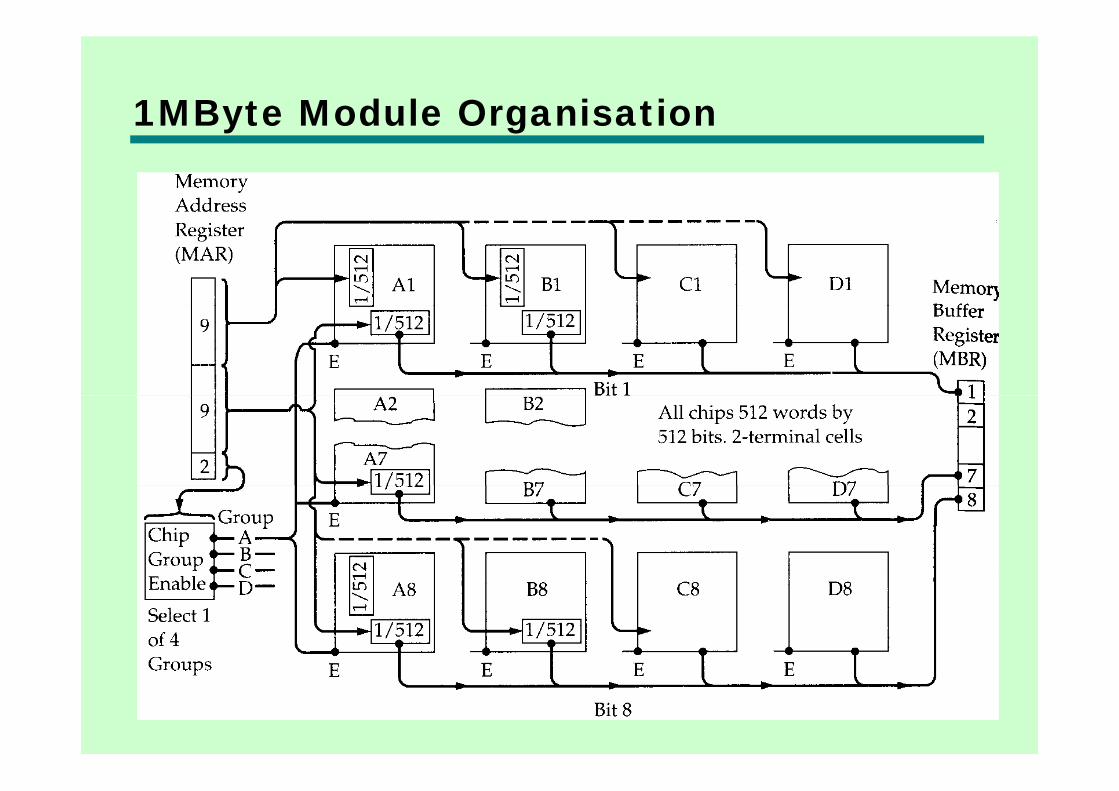
1MByte Module Organisationy g
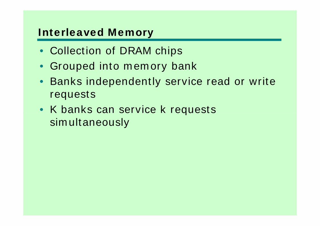
Interleaved Memoryy• Collection of DRAM chips
G d b k• Grouped into memory bank• Banks independently service read or write
requests• K banks can service k requests ba s ca se ce equests
simultaneously
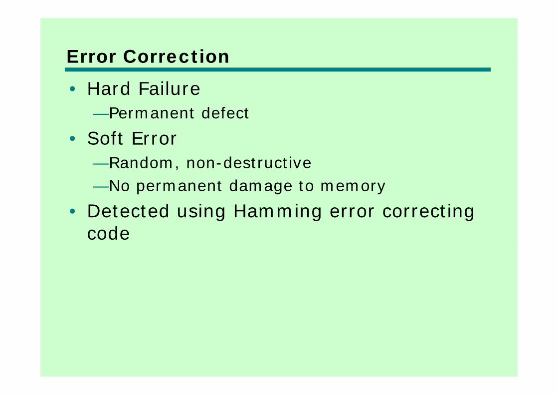
Error Correction• Hard Failure
P t d f t—Permanent defect• Soft Error
—Random, non-destructive—No permanent damage to memory
• Detected using Hamming error correcting code
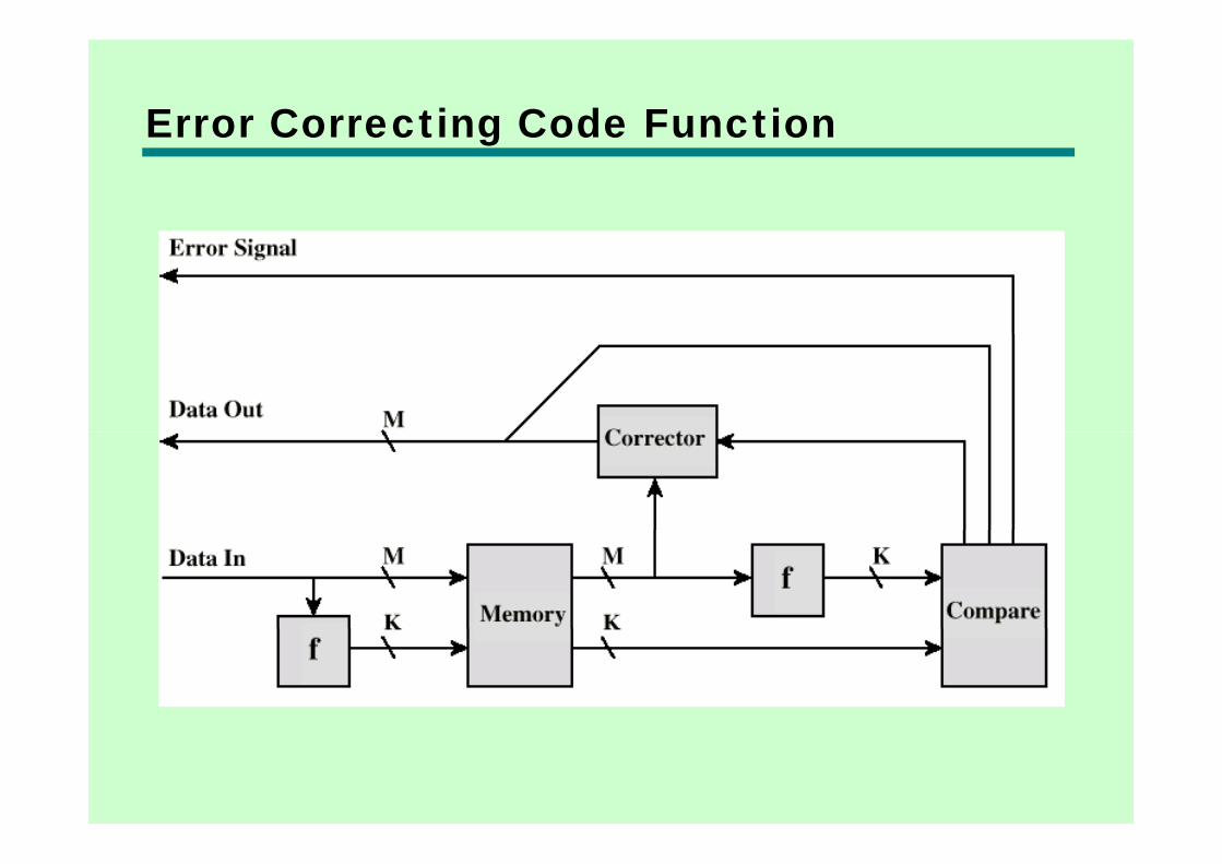
Error Correcting Code Functiong
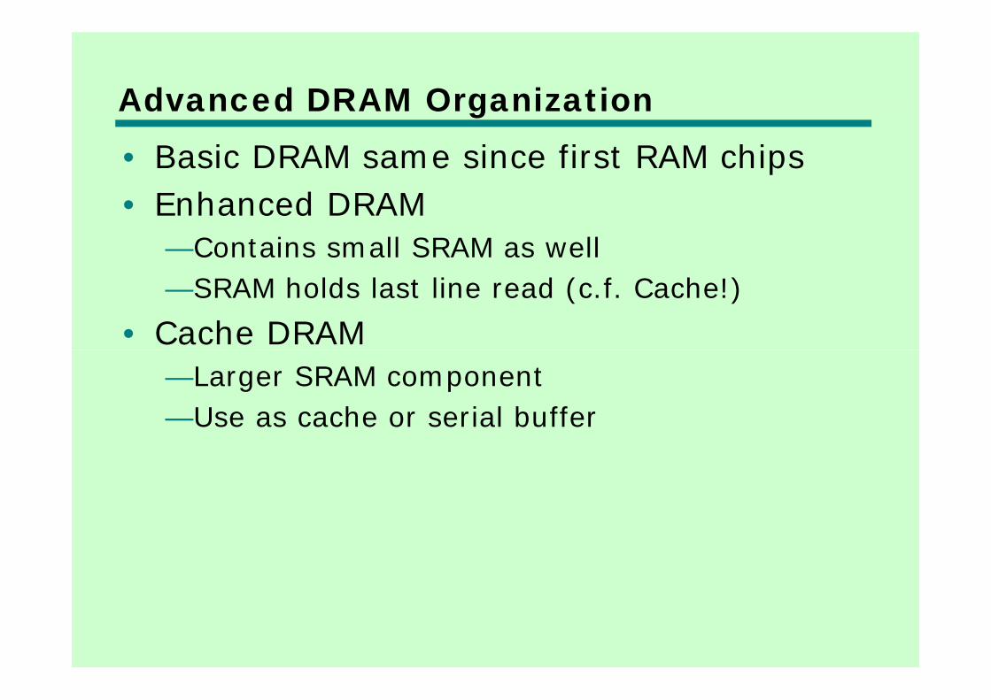
Advanced DRAM Organizationg• Basic DRAM same since first RAM chips
h d• Enhanced DRAM—Contains small SRAM as well—SRAM holds last line read (c.f. Cache!)
• Cache DRAM—Larger SRAM component—Use as cache or serial buffer
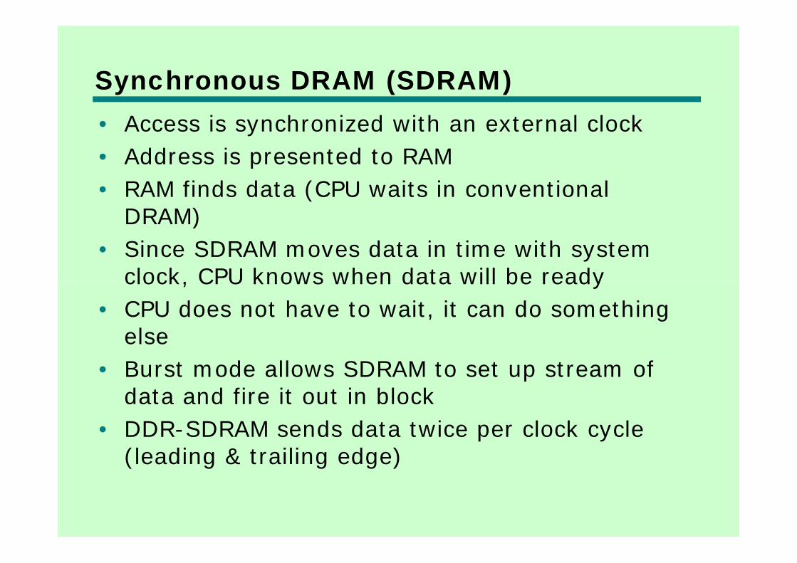
Synchronous DRAM (SDRAM)y ( )• Access is synchronized with an external clock• Address is presented to RAM• Address is presented to RAM• RAM finds data (CPU waits in conventional
DRAM)DRAM)• Since SDRAM moves data in time with system
clock, CPU knows when data will be readyclock, CPU knows when data will be ready• CPU does not have to wait, it can do something
else• Burst mode allows SDRAM to set up stream of
data and fire it out in block• DDR-SDRAM sends data twice per clock cycle
(leading & trailing edge)
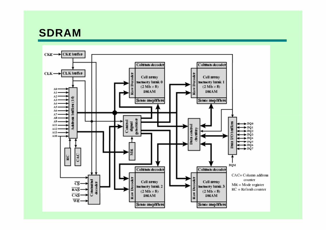
SDRAM
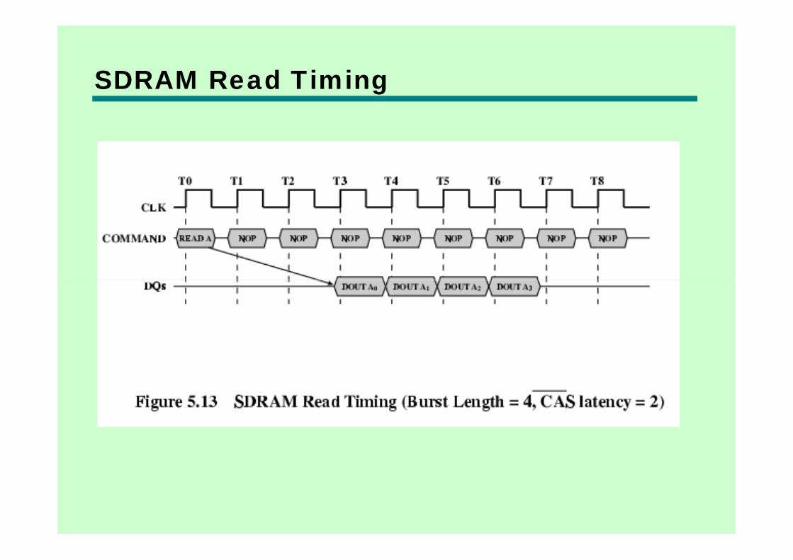
SDRAM Read Timingg
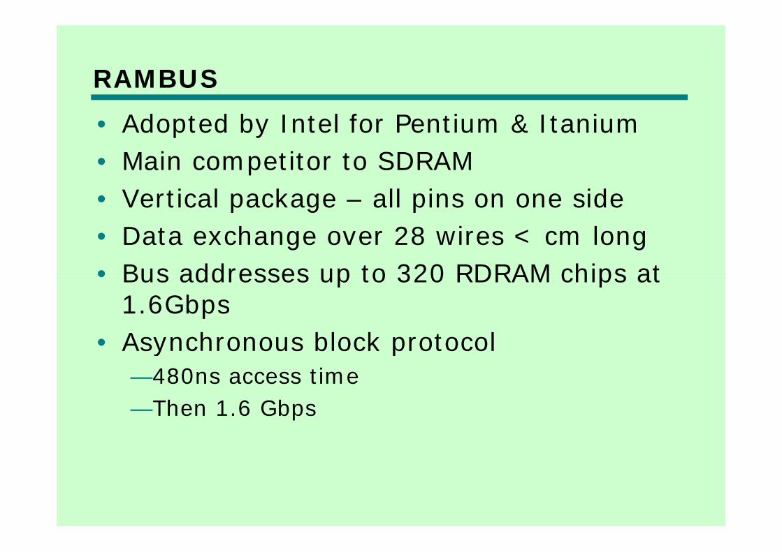
RAMBUS• Adopted by Intel for Pentium & Itanium
S• Main competitor to SDRAM• Vertical package – all pins on one side• Data exchange over 28 wires < cm long• Bus addresses up to 320 RDRAM chips at • Bus addresses up to 320 RDRAM chips at
1.6Gbps• Asynchronous block protocol• Asynchronous block protocol
—480ns access timeTh 1 6 Gb—Then 1.6 Gbps
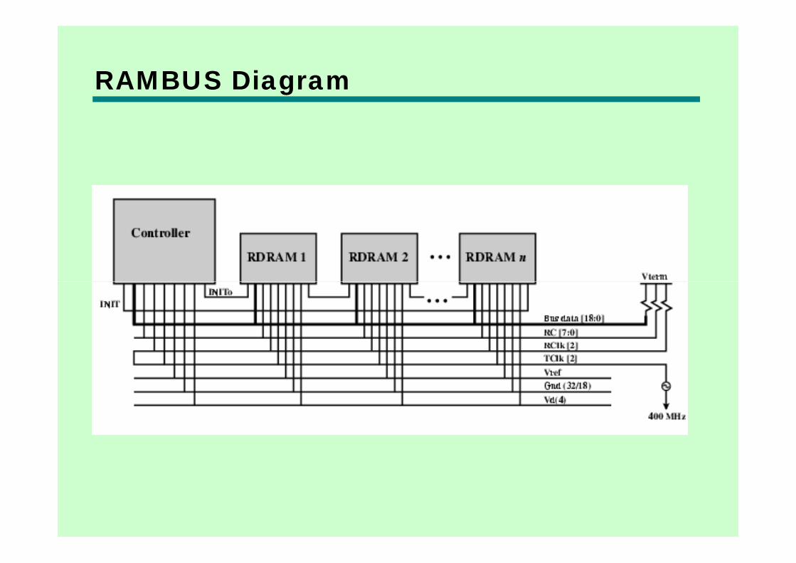
RAMBUS Diagramg
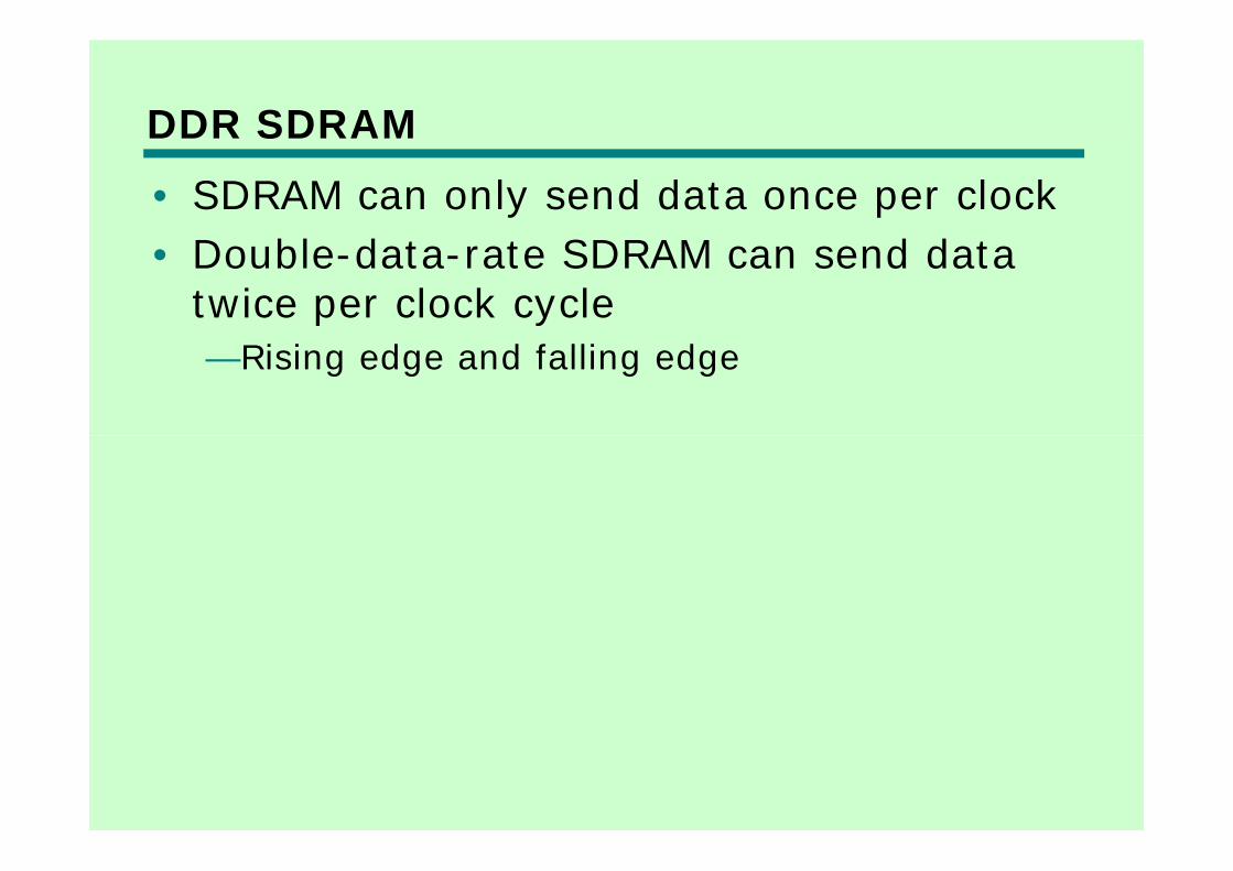
DDR SDRAM• SDRAM can only send data once per clock
bl d S d d• Double-data-rate SDRAM can send data twice per clock cycle—Rising edge and falling edge
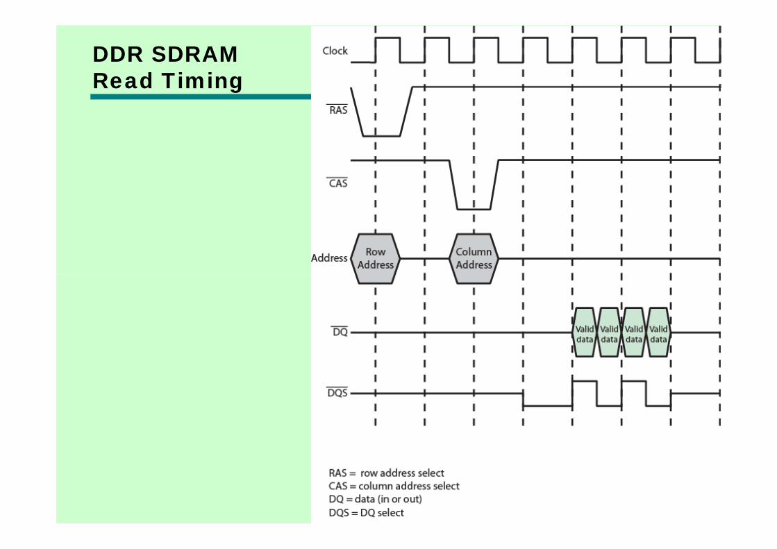
DDR SDRAM Read TimingRead Timing
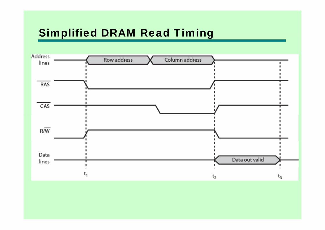
Simplified DRAM Read Timingp g
Cache DRAM• Mitsubishi
ll S h ( 6 kb)• Integrates small SRAM cache (16 kb) onto generic DRAM chip
• Used as true cache—64-bit lines—Effective for ordinary random access
• To support serial access of block of dataTo support serial access of block of data—E.g. refresh bit-mapped screen
– CDRAM can prefetch data from DRAM into SRAM pbuffer
– Subsequent accesses solely to SRAM
Readingg• The RAM Guide• RDRAM