Embed Size (px)
Citation preview

General DescriptionThe MAX2838 direct-conversion, zero-IF, RF transceiv-er is designed specifically for 3.3GHz to 3.9GHz wire-less broadband systems. The MAX2838 completelyintegrates all circuitry required to implement the RFtransceiver function, providing RF-to-baseband receivepath, baseband-to-RF transmit path, VCO, frequencysynthesizer, and baseband/control interface. Thedevice includes a fast-settling sigma-delta RF synthe-sizer with smaller than 29Hz frequency steps. TheMAX2838 supports 2Tx, 2Rx MIMO applications with amaster device providing coherent LO to the slavedevice. The transceiver IC also integrates circuits foron-chip DC-offset cancellation, I/Q error, and carrier-leakage detection circuits. Only an RF bandpass filter(BPF), TCXO, RF switch, PA, and a small number ofpassive components are needed to form a completewireless broadband RF radio solution.
The MAX2838 completely eliminates the need for anexternal SAW filter by implementing on-chip monolithicfilters for both the receiver and transmitter. The base-band filters along with the Rx and Tx signal paths areoptimized to meet the stringent noise figure and lineari-ty specifications. The device supports up to 2048-FFTOFDM and implements programmable channel filtersfor 1.5MHz to 28MHz RF channel bandwidths. Thetransceiver requires only 2µs Tx-Rx switching time. TheIC is available in a small 48-pin thin QFN package mea-suring only 6mm x 6mm x 0.8mm.
Applications802.16-2004/802.16d Fixed WiMAX™
802.16e MIMO Mobile WiMAX
WiMAX Pico and Femto Basestations
NLOS Wireless Broadband Systems
Features♦ 3.3GHz to 3.9GHz Wide-Band Operation♦ Master-Slave Modes with Coherent LO for MIMO♦ Complete RF Transceiver, and PA Driver
0dBm Linear OFDM Transmit Power-70dBr Tx Spectral Emission Mask2.8dB Rx Noise FigureTx/Rx I/Q Error and LO Leakage Detection and
AdjustmentAutomatic Rx DC Offset Correction Monolithic Low-Noise VCO with -39dBc Integrated
Phase NoiseProgrammable Rx I/Q Lowpass Channel FiltersProgrammable Tx I/Q Lowpass Anti-Aliasing FilterSigma-Delta Fractional-N PLL with 29Hz Step Size60dB Tx Gain Control Range with 1dB Step Size,
Digitally Controlled94dB Rx Gain Control Range with 2dB Step Size,
Digitally Controlled60dB Analog RSSI Instantaneous Dynamic Range4-Wire SPI™ Digital InterfaceI/Q Analog Baseband InterfaceDigital Tx/Rx/Shutdown Mode ControlLow-Power CLOCKOUT ModeOn-Chip Digital Temperature Sensor Readout
♦ +2.7V to +3.6V Transceiver Supply♦ Low-Power Shutdown Mode♦ Small 48-Pin Thin QFN Package (6mm x 6mm x 0.8mm)
MA
X2
83
8
3.3GHz to 3.9GHzWireless Broadband RF Transceiver
________________________________________________________________ Maxim Integrated Products 1
48 47 46 45 44 43 42 41 40 39 38 37
13 14 15 16 17 18 19 20 21 22 23 24
36
35
34
33
32
31
30
29
28
27
26
25
1
2
3
4
5
48 THIN QFN
+
6
7
8
9
10
11
12
MAX2838
GNDV
CO
GNDC
P
CPOU
T+
CPOU
T-
VCCC
P
REFC
LK
VCCD
IG
CLKO
UT
SCLKCS
VCCT
MX
PABI
AS
RXBBQ+
RXBBQ-
B6
B7
RSSI
DIN
DOUT
EXTVCO+
EXTVCO-
VCCLO
VCCVCO
VCOBYP
RXBB
I-
RXHP
VCCR
XVGA
RXBB
I+
VCCR
XFL
TXBB
I-
TXBB
I+
TXBB
Q+
TXBB
Q-
VCCR
XMX
RXTX
ENAB
LE
VCCRXLNA
GNDRXLNA
B5
RXRF+
RXRF-
B4
VCCTXPAD
B3
B2
TXRF+
TXRF-
B1
Pin Configuration
Ordering Information
19-1049; Rev 1; 8/08
For pricing, delivery, and ordering information, please contact Maxim Direct at 1-888-629-4642,or visit Maxim’s website at www.maxim-ic.com.
*EP = Exposed paddle.+Denotes a lead-free package.T = Tape and reel.
PART TEMP RANGE PIN-PACKAGE
M AX 2838E TM + T - 40°C to + 85°C 48 TQ FN - E P *
WiMAX is a trademark of the WiMAX Forum.SPI is a trademark of Motorola, Inc.
MA
X2
83
8
3.3GHz to 3.9GHzWireless Broadband RF Transceiver
2 _______________________________________________________________________________________
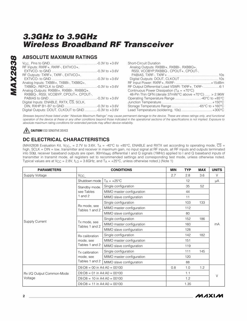
ABSOLUTE MAXIMUM RATINGS
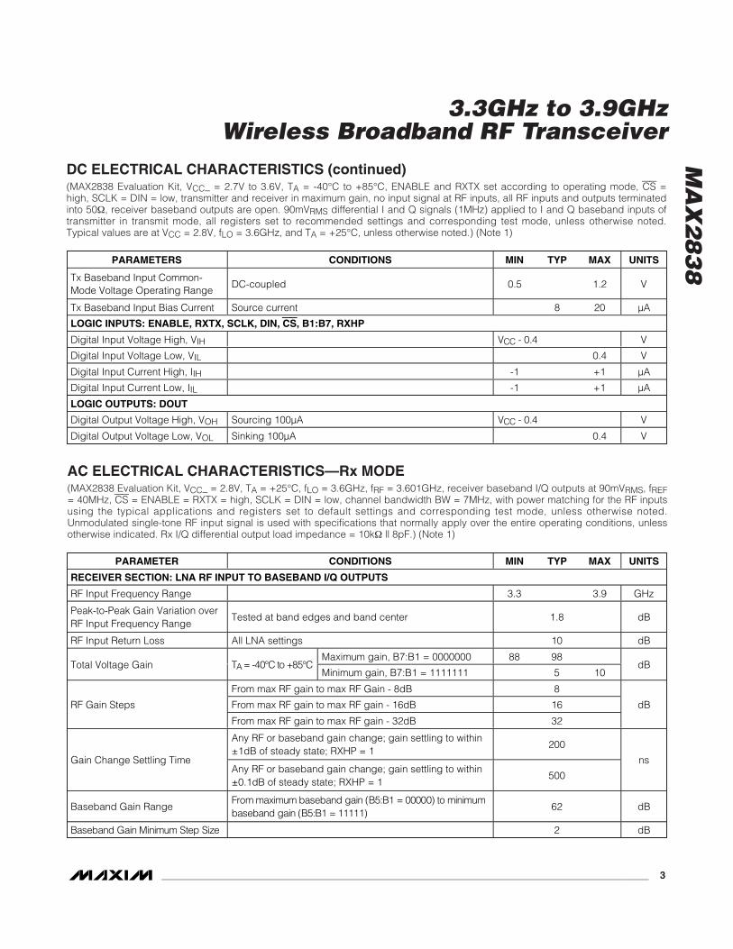
DC ELECTRICAL CHARACTERISTICS(MAX2838 Evaluation Kit, VCC_ = 2.7V to 3.6V, TA = -40°C to +85°C, ENABLE and RXTX set according to operating mode, CS =high, SCLK = DIN = low, transmitter and receiver in maximum gain, no input signal at RF inputs, all RF inputs and outputs terminatedinto 50Ω, receiver baseband outputs are open. 90mVRMS differential I and Q signals (1MHz) applied to I and Q baseband inputs oftransmitter in transmit mode, all registers set to recommended settings and corresponding test mode, unless otherwise noted.Typical values are at VCC = 2.8V, fLO = 3.6GHz, and TA = +25°C, unless otherwise noted.) (Note 1)
Stresses beyond those listed under “Absolute Maximum Ratings” may cause permanent damage to the device. These are stress ratings only, and functionaloperation of the device at these or any other conditions beyond those indicated in the operational sections of the specifications is not implied. Exposure toabsolute maximum rating conditions for extended periods may affect device reliability.
VCC_ Pins to GND..................................................-0.3V to +3.6VRF Inputs: RXRF+, RXRF-, EXTVCO+,EXTVCO- to GND ................................................-0.3V to +3.6V
RF Outputs: TXRF+, TXRF-, EXTVCO+,EXTVCO- to GND ................................................-0.3V to +3.6V
Analog Inputs: TXBBI+, TXBBI-, TXBBQ+,TXBBQ-, REFCLK to GND...................................-0.3V to +3.6V
Analog Outputs: RXBBI+, RXBBI-, RXBBQ+,RXBBQ-, RSSI, VCOBYP, CPOUT+, CPOUT-,PABIAS to GND...................................................-0.3V to +3.6V
Digital Inputs: ENABLE, RXTX, CS, SCLK,DIN, RXHP B1–B7 to GND ..................................-0.3V to +3.6V
Digital Outputs: DOUT, CLKOUT to GND .............-0.3V to +3.6V
Short-Circuit Duration Analog Outputs: RXBBI+, RXBBI-, RXBBQ+,RSSI, VCOBYP,RXBBQ-, CPOUT+, CPOUT-,PABIAS, TXRF-, TXRF+ ......................................................10s
Digital Outputs: DOUT, CLKOUT .........................................10sRF Input Power: RXRF+, RXRF- .....................................+15dBmRF Output Differential Load VSWR: TXRF+, TXRF- .................6:1Continuous Power Dissipation (TA = +70°C)48-Pin Thin QFN (derate 37mW/°C above +70°C) ...... > 2.96W
Operating Temperature Range ...........................-40°C to +85°CJunction Temperature ......................................................+150°CStorage Temperature Range .............................-65°C to +160°CLead Temperature (soldering, 10s) .................................+300°C
PARAMETERS CONDITIONS MIN TYP MAX UNITS
Supply Voltage VCC_ 2.7 2.8 3.6 V
S hutd ow n m ode TA = +25°C 12 µA
Single configuration 35 52
MIMO master configuration 44Standby mode,see Tables1 and 2 MIMO slave configuration 11
Single configuration 103 133
MIMO master configuration 112Rx mode, seeTables 1 and 2
MIMO slave configuration 80
Single configuration 152 186
MIMO master configuration 160Tx mode, seeTables 1 and 2
MIMO slave configuration 128
Single configuration 142 182
MIMO master configuration 151Rx calibrationmode, seeTables 1 and 2 MIMO slave configuration 119
Single configuration 111 145
MIMO master configuration 120
Supply Current
Tx calibrationmode, seeTables 1 and 2 MIMO slave configuration 88
mA
D9:D8 = 00 in A4:A0 = 00100 0.8 1.0 1.2
D9:D8 = 01 in A4:A0 = 00100 1.1
D9:D8 = 10 in A4:A0 = 00100 1.2Rx I/Q Output Common-ModeVoltage
D9:D8 = 11 in A4:A0 = 00100 1.35
V
CAUTION! ESD SENSITIVE DEVICE
MA
X2
83
8
3.3GHz to 3.9GHzWireless Broadband RF Transceiver
_______________________________________________________________________________________ 3
AC ELECTRICAL CHARACTERISTICS—Rx MODE(MAX2838 Evaluation Kit, VCC_ = 2.8V, TA = +25°C, fLO = 3.6GHz, fRF = 3.601GHz, receiver baseband I/Q outputs at 90mVRMS, fREF= 40MHz, CS = ENABLE = RXTX = high, SCLK = DIN = low, channel bandwidth BW = 7MHz, with power matching for the RF inputsusing the typical applications and registers set to default settings and corresponding test mode, unless otherwise noted.Unmodulated single-tone RF input signal is used with specifications that normally apply over the entire operating conditions, unlessotherwise indicated. Rx I/Q differential output load impedance = 10kΩ || 8pF.) (Note 1)
PARAMETERS CONDITIONS MIN TYP MAX UNITS
Tx Baseband Input Common-Mode Voltage Operating Range
DC-coupled 0.5 1.2 V
Tx Baseband Input Bias Current Source current 8 20 µA
LOGIC INPUTS: ENABLE, RXTX, SCLK, DIN, CS, B1:B7, RXHP
Digital Input Voltage High, VIH V C C - 0.4 V
Digital Input Voltage Low, VIL 0.4 V
Digital Input Current High, IIH -1 +1 µA
Digital Input Current Low, IIL -1 +1 µA
LOGIC OUTPUTS: DOUT
Digital Output Voltage High, VOH Sourcing 100µA V C C - 0.4 V
Digital Output Voltage Low, VOL Sinking 100µA 0.4 V
PARAMETER CONDITIONS MIN TYP MAX UNITS
RECEIVER SECTION: LNA RF INPUT TO BASEBAND I/Q OUTPUTS
RF Input Frequency Range 3.3 3.9 GHz
Peak-to-Peak Gain Variation overRF Input Frequency Range
Tested at band edges and band center 1.8 dB
RF Input Return Loss All LNA settings 10 dB
Maximum gain, B7:B1 = 0000000 88 98Total Voltage Gain TA = -40°C to +85°C
Minimum gain, B7:B1 = 1111111 5 10dB
From max RF gain to max RF Gain - 8dB 8
From max RF gain to max RF gain - 16dB 16RF Gain Steps
From max RF gain to max RF gain - 32dB 32
dB
Any RF or baseband gain change; gain settling to within±1dB of steady state; RXHP = 1
200
Gain Change Settling TimeAny RF or baseband gain change; gain settling to within±0.1dB of steady state; RXHP = 1
500
ns
Baseband Gain RangeFr om m axi m um b aseb and g ai n ( B5:B1 = 00000) to m i ni m um b aseb and g ai n ( B5:B1 = 11111)
62 dB
Baseb and Gai n M i ni m um S tep S i ze 2 dB
DC ELECTRICAL CHARACTERISTICS (continued)(MAX2838 Evaluation Kit, VCC_ = 2.7V to 3.6V, TA = -40°C to +85°C, ENABLE and RXTX set according to operating mode, CS =high, SCLK = DIN = low, transmitter and receiver in maximum gain, no input signal at RF inputs, all RF inputs and outputs terminatedinto 50Ω, receiver baseband outputs are open. 90mVRMS differential I and Q signals (1MHz) applied to I and Q baseband inputs oftransmitter in transmit mode, all registers set to recommended settings and corresponding test mode, unless otherwise noted.Typical values are at VCC = 2.8V, fLO = 3.6GHz, and TA = +25°C, unless otherwise noted.) (Note 1)
MA
X2
83
8
3.3GHz to 3.9GHzWireless Broadband RF Transceiver
4 _______________________________________________________________________________________
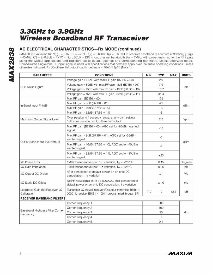
AC ELECTRICAL CHARACTERISTICS—Rx MODE (continued)(MAX2838 Evaluation Kit, VCC_ = 2.8V, TA = +25°C, fLO = 3.6GHz, fRF = 3.601GHz, receiver baseband I/Q outputs at 90mVRMS, fREF= 40MHz, CS = ENABLE = RXTX = high, SCLK = DIN = low, channel bandwidth BW = 7MHz, with power matching for the RF inputsusing the typical applications and registers set to default settings and corresponding test mode, unless otherwise noted.Unmodulated single-tone RF input signal is used with specifications that normally apply over the entire operating conditions, unlessotherwise indicated. Rx I/Q differential output load impedance = 10kΩ || 8pF.) (Note 1)
PARAMETER CONDITIONS MIN TYP MAX UNITS
Voltage gain ≥ 65dB with max RF gain (B7:B6 = 00) 2.9
V ol tag e g ai n = 50d B w i th m ax RF g ai n - 8d B ( B7:B6 = 01) 7.9
V ol tag e g ai n = 45d B w i th m ax RF g ai n - 16d B ( B7:B6 = 10) 13.7DSB Noise Figure
V ol tag e g ai n = 15d B w i th m ax RF g ai n - 32d B ( B7:B6 = 11) 31.4
dB
Max RF gain (B7:B6 = 00) -35
Max RF gain - 8dB (B7:B6 = 01) -27
Max RF gain - 16dB (B7:B6 = 10) -19In-Band Input P-1dB
Max RF gain - 32dB (B7:B6 = 11) -3
dBm
Maximum Output Signal LevelOver passband frequency range; at any gain setting;1dB compression point, differential output
2.5 VP-P
Max RF gain (B7:B6 = 00), AGC set for -65dBm wantedsignal
-10
Max RF gain - 8dB (B7:B6 = 01), AGC set for -55dBmwanted signal
-5
Max RF gain - 16dB (B7:B6 = 10), AGC set for -40dBmwanted signal
-4
Out-of-Band Input IP3 (Note 2)
Max RF gain - 32dB (B7:B6 = 11), AGC set for -30dBmwanted signal
+23
dBm
I/Q Phase Error 1MHz baseband output; 1 σ variation, TA = +25°C 0.15 D eg r ees
I/Q Gain Imbalance 1MHz baseband output; 1 σ variation, TA = +25°C 0.05 dB
I/Q Output DC DroopAfter completion of default power-on on-chip DCcancellation, 1 σ variation
±1 V/s
I/Q Static DC OffsetN o RF i np ut si g nal ; B7:B1 = 0000000, after com p l eti on ofd efaul t p ow er - on on- chi p D C cancel l ati on, 1 σ var i ati on
±1.0 mV
Loopback Gain (for Receiver I/QCalibration)
Tr ansm itter I/Q i nput to r ecei ver I/Q outp ut; tr ansm i tter B6:B1 = 000011, r ecei ver B5:B1 = 10011 p r og r am m ed thr oug h S P I
-7.0 -2 +2.5 dB
RECEIVER BASEBAND FILTERS
Corner frequency 1 600
Corner frequency 2 100
Corner frequency 3 30
Corner frequency 4 1
Baseband Highpass Filter CornerFrequency
Corner frequency 5 0.1
kHz
MA
X2
83
8
3.3GHz to 3.9GHzWireless Broadband RF Transceiver
_______________________________________________________________________________________ 5
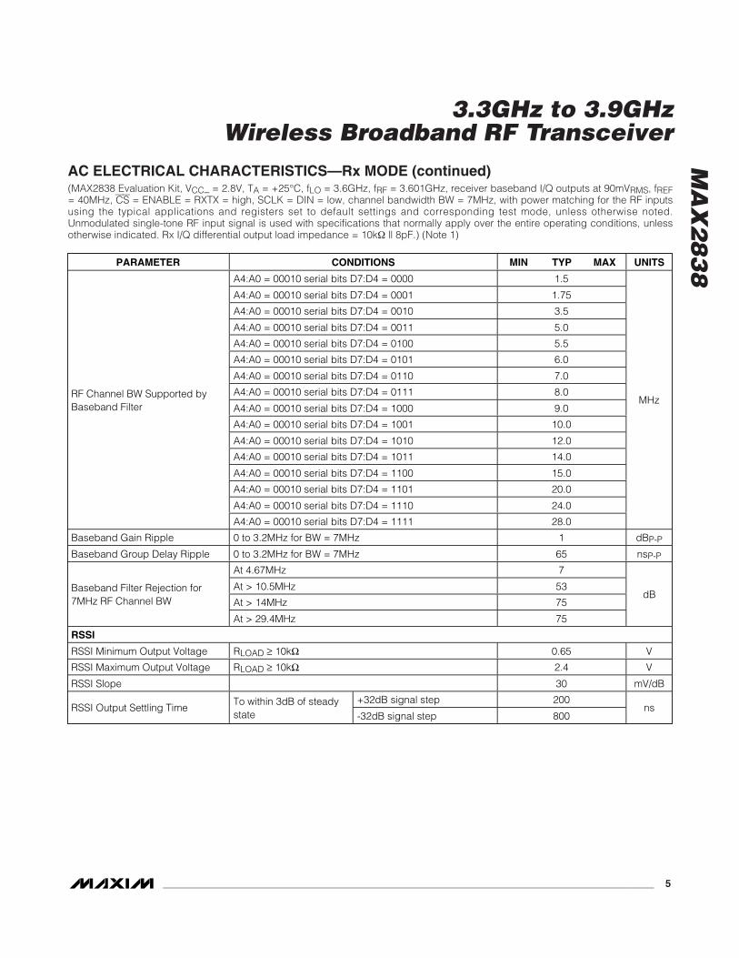
AC ELECTRICAL CHARACTERISTICS—Rx MODE (continued)(MAX2838 Evaluation Kit, VCC_ = 2.8V, TA = +25°C, fLO = 3.6GHz, fRF = 3.601GHz, receiver baseband I/Q outputs at 90mVRMS, fREF= 40MHz, CS = ENABLE = RXTX = high, SCLK = DIN = low, channel bandwidth BW = 7MHz, with power matching for the RF inputsusing the typical applications and registers set to default settings and corresponding test mode, unless otherwise noted.Unmodulated single-tone RF input signal is used with specifications that normally apply over the entire operating conditions, unlessotherwise indicated. Rx I/Q differential output load impedance = 10kΩ || 8pF.) (Note 1)
PARAMETER CONDITIONS MIN TYP MAX UNITS
A4:A0 = 00010 serial bits D7:D4 = 0000 1.5
A4:A0 = 00010 serial bits D7:D4 = 0001 1.75
A4:A0 = 00010 serial bits D7:D4 = 0010 3.5
A4:A0 = 00010 serial bits D7:D4 = 0011 5.0
A4:A0 = 00010 serial bits D7:D4 = 0100 5.5
A4:A0 = 00010 serial bits D7:D4 = 0101 6.0
A4:A0 = 00010 serial bits D7:D4 = 0110 7.0
A4:A0 = 00010 serial bits D7:D4 = 0111 8.0
A4:A0 = 00010 serial bits D7:D4 = 1000 9.0
A4:A0 = 00010 serial bits D7:D4 = 1001 10.0
A4:A0 = 00010 serial bits D7:D4 = 1010 12.0
A4:A0 = 00010 serial bits D7:D4 = 1011 14.0
A4:A0 = 00010 serial bits D7:D4 = 1100 15.0
A4:A0 = 00010 serial bits D7:D4 = 1101 20.0
A4:A0 = 00010 serial bits D7:D4 = 1110 24.0
RF Channel BW Supported byBaseband Filter
A4:A0 = 00010 serial bits D7:D4 = 1111 28.0
MHz
Baseband Gain Ripple 0 to 3.2MHz for BW = 7MHz 1 dBP-P
Baseband Group Delay Ripple 0 to 3.2MHz for BW = 7MHz 65 nsP-P
At 4.67MHz 7
At > 10.5MHz 53
At > 14MHz 75Baseband Filter Rejection for7MHz RF Channel BW
At > 29.4MHz 75
dB
RSSI
RSSI Minimum Output Voltage RLOAD ≥ 10kΩ 0.65 V
RSSI Maximum Output Voltage RLOAD ≥ 10kΩ 2.4 V
RSSI Slope 30 mV/dB
+32dB signal step 200RSSI Output Settling Time
To within 3dB of steadystate -32dB signal step 800
ns
MA
X2
83
8
3.3GHz to 3.9GHzWireless Broadband RF Transceiver
6 _______________________________________________________________________________________
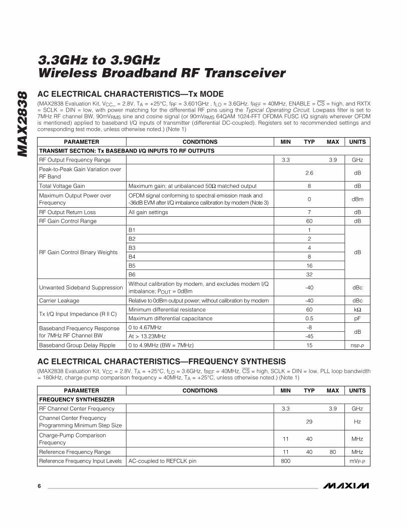
AC ELECTRICAL CHARACTERISTICS—Tx MODE(MAX2838 Evaluation Kit, VCC_ = 2.8V, TA = +25°C, fRF = 3.601GHz , fLO = 3.6GHz. fREF = 40MHz, ENABLE = CS = high, and RXTX= SCLK = DIN = low, with power matching for the differential RF pins using the Typical Operating Circuit. Lowpass filter is set to7MHz RF channel BW, 90mVRMS sine and cosine signal (or 90mVRMS 64QAM 1024-FFT OFDMA FUSC I/Q signals wherever OFDMis mentioned) applied to baseband I/Q inputs of transmitter (differential DC-coupled). Registers set to recommended settings andcorresponding test mode, unless otherwise noted.) (Note 1)
PARAMETER CONDITIONS MIN TYP MAX UNITS
TRANSMIT SECTION: Tx BASEBAND I/Q INPUTS TO RF OUTPUTS
RF Output Frequency Range 3.3 3.9 GHz
Peak-to-Peak Gain Variation overRF Band
2.6 dB
Total Voltage Gain Maximum gain; at unbalanced 50Ω matched output 8 dB
Maximum Output Power overFrequency
O FD M si g nal confor m i ng to sp ectr al em i ssi on m ask and - 36d B EV M after I/Q i m bal ance cal i br ation by m od em ( N ote 3)
0 dBm
RF Output Return Loss All gain settings 7 dB
RF Gain Control Range 60 dB
B1 1
B2 2
B3 4
B4 8
B5 16
RF Gain Control Binary Weights
B6 32
dB
Unwanted Sideband SuppressionWithout calibration by modem, and excludes modem I/Qimbalance; POUT = 0dBm
-40 dBc
Carrier Leakage Rel ati ve to 0d Bm outp ut p ow er ; w i thout cal i b r ati on b y m od em -40 dBc
Minimum differential resistance 60 kΩTx I/Q Input Impedance (R || C)
Maximum differential capacitance 0.5 pF
0 to 4.67MHz -8Baseband Frequency Responsefor 7MHz RF Channel BW At > 13.23MHz -45
dB
Baseband Group Delay Ripple 0 to 4.9MHz (BW = 7MHz) 15 nsP-P
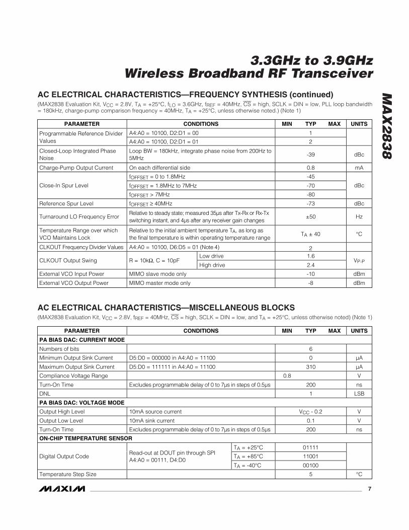
AC ELECTRICAL CHARACTERISTICS—FREQUENCY SYNTHESIS(MAX2838 Evaluation Kit, VCC = 2.8V, TA = +25°C, fLO = 3.6GHz, fREF = 40MHz, CS = high, SCLK = DIN = low, PLL loop bandwidth= 180kHz, charge-pump comparison frequency = 40MHz, TA = +25°C, unless otherwise noted.) (Note 1)
PARAMETER CONDITIONS MIN TYP MAX UNITS
FREQUENCY SYNTHESIZER
RF Channel Center Frequency 3.3 3.9 GHz
Channel Center FrequencyProgramming Minimum Step Size
29 Hz
Charge-Pump ComparisonFrequency
11 40 MHz
Reference Frequency Range 11 40 80 MHz
Refer ence Fr eq uency Inp ut Level s AC-coupled to REFCLK pin 800 mVP-P
MA
X2
83
8
3.3GHz to 3.9GHzWireless Broadband RF Transceiver
_______________________________________________________________________________________ 7
AC ELECTRICAL CHARACTERISTICS—FREQUENCY SYNTHESIS (continued)(MAX2838 Evaluation Kit, VCC = 2.8V, TA = +25°C, fLO = 3.6GHz, fREF = 40MHz, CS = high, SCLK = DIN = low, PLL loop bandwidth= 180kHz, charge-pump comparison frequency = 40MHz, TA = +25°C, unless otherwise noted.) (Note 1)
PARAMETER CONDITIONS MIN TYP MAX UNITS
A4:A0 = 10100, D2:D1 = 00 1Programmable Reference DividerValues A4:A0 = 10100, D2:D1 = 01 2
Closed-Loop Integrated PhaseNoise
Loop BW = 180kHz, integrate phase noise from 200Hz to5MHz
-39 dBc
Charge-Pump Output Current On each differential side 0.8 mA
fOFFSET = 0 to 1.8MHz -45
fOFFSET = 1.8MHz to 7MHz -70Close-In Spur Level
fOFFSET > 7MHz -80
dBc
Reference Spur Level fOFFSET ≥ 40MHz -73 dBc
Turnaround LO Frequency ErrorRel ati ve to stead y state; m easur ed 35µs after Tx- Rx or Rx- Txsw i tchi ng i nstant, and 4µs after any r ecei ver g ai n chang es
±50 Hz
Temperature Range over whichVCO Maintains Lock
Rel ati ve to the i ni ti al am b i ent tem p er atur e TA , as l ong asthe fi nal tem p er atur e i s w i thi n op er ati ng tem p er atur e r ang e
TA ± 40 °C
C LKO U T Fr eq uency D i vi d er V al ues A4:A0 = 10100, D6:D5 = 01 ( N ote 4) 2Low drive 1.6
CLKOUT Output Swing R = 10kΩ, C = 10pFHigh drive 2.4
VP-P
External VCO Input Power MIMO slave mode only -10 dBm
External VCO Output Power MIMO master mode only -8 dBm
AC ELECTRICAL CHARACTERISTICS—MISCELLANEOUS BLOCKS(MAX2838 Evaluation Kit, VCC = 2.8V, fREF = 40MHz, CS = high, SCLK = DIN = low, and TA = +25°C, unless otherwise noted) (Note 1)
PARAMETER CONDITIONS MIN TYP MAX UNITS
PA BIAS DAC: CURRENT MODE
Numbers of bits 6
Minimum Output Sink Current D5:D0 = 000000 in A4:A0 = 11100 0 µA
Maximum Output Sink Current D5:D0 = 111111 in A4:A0 = 11100 310 µA
Compliance Voltage Range 0.8 V
Turn-On Time E xcl ud es p r og r am m ab l e d el ay of 0 to 7µs i n step s of 0.5µs 200 ns
DNL 1 LSB
PA BIAS DAC: VOLTAGE MODE
Output High Level 10mA source current VCC - 0.2 V
Output Low Level 10mA sink current 0.1 V
Turn-On Time E xcl ud es p r og r am m ab l e d el ay of 0 to 7µs i n step s of 0.5µs 200 ns
ON-CHIP TEMPERATURE SENSOR
TA = +25°C 01111
TA = +85°C 11001Digital Output CodeRead-out at DOUT pin through SPIA4:A0 = 00111, D4:D0
TA = -40°C 00100
Temperature Step Size 5 °C
MA
X2
83
8
3.3GHz to 3.9GHzWireless Broadband RF Transceiver
8 _______________________________________________________________________________________
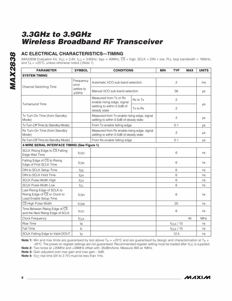
Note 1: Min and max limits are guaranteed by test above TA = +25°C and are guaranteed by design and characterization at TA =-40°C. The power-on register settings are not guaranteed. Recommended register setting must be loaded after VCC is supplied.
Note 2: Two tones at +20MHz and +39MHz offset with -35dBm/tone. Measure IM3 at 1MHz.Note 3: Gain adjusted over max gain and max gain - 3dB.Note 4: VCC rise time (0V to 2.7V) must be less than 1ms.
AC ELECTRICAL CHARACTERISTICS—TIMING(MAX2838 Evaluation Kit, VCC = 2.8V, fLO = 3.6GHz, fREF = 40MHz, CS = high, SCLK = DIN = low, PLL loop bandwidth = 180kHz,and TA = +25°C, unless otherwise noted.) (Note 1)
PARAMETER SYMBOL CONDITIONS MIN TYP MAX UNITS
SYSTEM TIMING
Automatic VCO sub-band selection 2 msChannel Switching Time
Frequencyerrorsettles to±50Hz Manual VCO sub-band selection 56 µs
Rx to Tx 2Turnaround Time
Measured from Tx or Rxenable rising edge, signalsettling to within 0.5dB ofsteady state
Tx to Rx 2µs
Tx Turn-On Time (from StandbyMode)
M easur ed fr om Tx enab l e r i si ng ed g e, si g nal settl i ng to w i thi n 0.5d B of stead y state
2 µs
Tx Tur n- Off Ti m e ( to S tand b y M od e) From Tx-enable falling edge 0.1 µs
Rx Turn-On Time (from StandbyMode)
M easur ed fr om Rx enab l e r i si ng ed g e, si g nal settl i ng to w i thi n 0.5d B of stead y state
2 µs
Rx Tur n- Off Ti m e ( to S tand b y M od e) From Rx-enable falling edge 0.1 µs
4-WIRE SERIAL INTERFACE TIMING (See Figure 1)
SCLK Rising Edge to CS FallingEdge Wait Time
tCSO 6 ns
Falling Edge of CS to RisingEdge of First SCLK Time
tCSS 6 ns
DIN to SCLK Setup Time tDS 6 ns
DIN to SCLK Hold Time tDH 6 ns
SCLK Pulse-Width High tCH 6 ns
SCLK Pulse-Width Low tCL 6 ns
Last Rising Edge of SCLK toRising Edge of CS or Clock toLoad Enable Setup Time
tCSH 6 ns
CS High Pulse Width tCSW 20 ns
Ti m e Betw een Ri si ng E d g e of C Sand the N ext Ri si ng E d g e of S C LK
tCS1 6 ns
Clock Frequency fCLK 45 MHz
Rise Time tR fCLK / 10 ns
Fall Time tF fCLK / 10 ns
SCLK Falling Edge to Valid DOUT tD 12.5 ns
MA
X2
83
8
3.3GHz to 3.9GHzWireless Broadband RF Transceiver
_______________________________________________________________________________________ 9
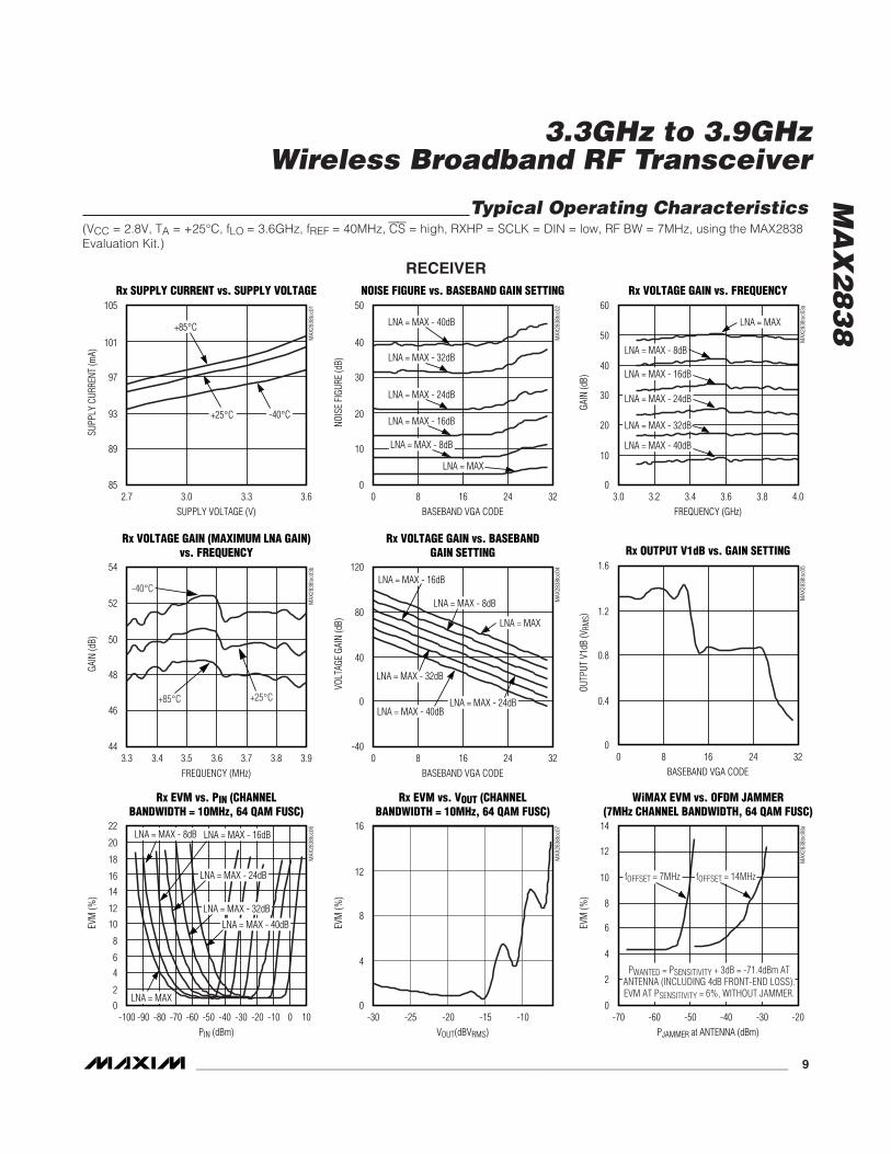
Rx SUPPLY CURRENT vs. SUPPLY VOLTAGEM
AX28
38to
c01
SUPPLY VOLTAGE (V)
SUPP
LY C
URRE
NT (m
A)
3.0
89
93
97
101
105
852.7 3.3 3.6
+85°C
-40°C+25°C
NOISE FIGURE vs. BASEBAND GAIN SETTING
MAX
2838
toc0
2
BASEBAND VGA CODE
NOIS
E FI
GURE
(dB)
8 24
10
20
30
40
50
00 16 32
LNA = MAX - 40dB
LNA = MAX - 32dB
LNA = MAX - 24dB
LNA = MAX - 16dB
LNA = MAX - 8dB
LNA = MAX
Rx VOLTAGE GAIN vs. FREQUENCY
MAX
2838
toc0
3a
FREQUENCY (GHz)
GAIN
(dB)
3.63.2
20
10
30
40
50
60
03.0 3.83.4 4.0
LNA = MAX - 40dB
LNA = MAX - 32dB
LNA = MAX - 24dB
LNA = MAX - 16dB
LNA = MAX - 8dB
LNA = MAX
Rx VOLTAGE GAIN (MAXIMUM LNA GAIN)vs. FREQUENCY
MAX
2838
toc0
3b
FREQUENCY (MHz)
GAIN
(dB)
3.63.4 3.8
46
48
50
52
54
443.3 3.73.5 3.9
-40°C
+85°C +25°C
Rx VOLTAGE GAIN vs. BASEBANDGAIN SETTING
MAX
2838
toc0
4
BASEBAND VGA CODE
VOLT
AGE
GAIN
(dB)
8
40
0
80
120
-400 16 24 32
LNA = MAX - 40dB
LNA = MAX - 32dB
LNA = MAX - 24dB
LNA = MAX - 16dB
LNA = MAX - 8dB
LNA = MAX
Rx OUTPUT V1dB vs. GAIN SETTING
MAX
2838
toc0
5
BASEBAND VGA CODE
OUTP
UT V
1dB
(VRM
S)
8 16
0.4
0.8
1.2
1.6
00 24 32
Rx EVM vs. PIN (CHANNELBANDWIDTH = 10MHz, 64 QAM FUSC)
MAX
2838
toc0
6
PIN (dBm)
EVM
(%)
-80 -60
4
2
6
8
10
14
12
16
18
20
22
0-100 -90 -70 -40 -20-50 0-10-30 10
LNA = MAX - 40dB
LNA = MAX - 32dB
LNA = MAX - 24dB
LNA = MAX - 16dBLNA = MAX - 8dB
LNA = MAX
Rx EVM vs. VOUT (CHANNELBANDWIDTH = 10MHz, 64 QAM FUSC)
MAX
2838
toc0
7
VOUT(dBVRMS)
EVM
(%)
-10-25
4
8
12
16
0-30 -15-20
WiMAX EVM vs. OFDM JAMMER(7MHz CHANNEL BANDWIDTH, 64 QAM FUSC)
MAX
2838
toc0
8a
PJAMMER at ANTENNA (dBm)
EVM
(%)
-30-50-60
8
10
12
2
4
6
14
0-70 -40 -20
fOFFSET = 7MHz fOFFSET = 14MHz
PWANTED = PSENSITIVITY + 3dB = -71.4dBm ATANTENNA (INCLUDING 4dB FRONT-END LOSS).EVM AT PSENSITIVITY = 6%, WITHOUT JAMMER.
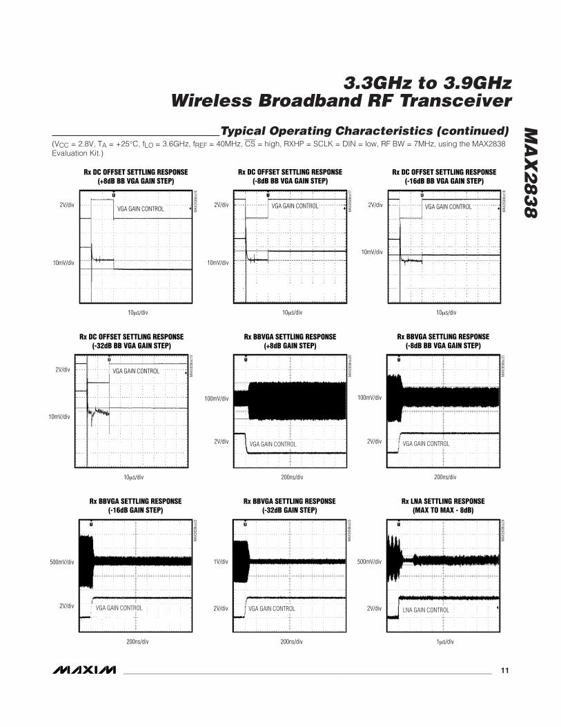
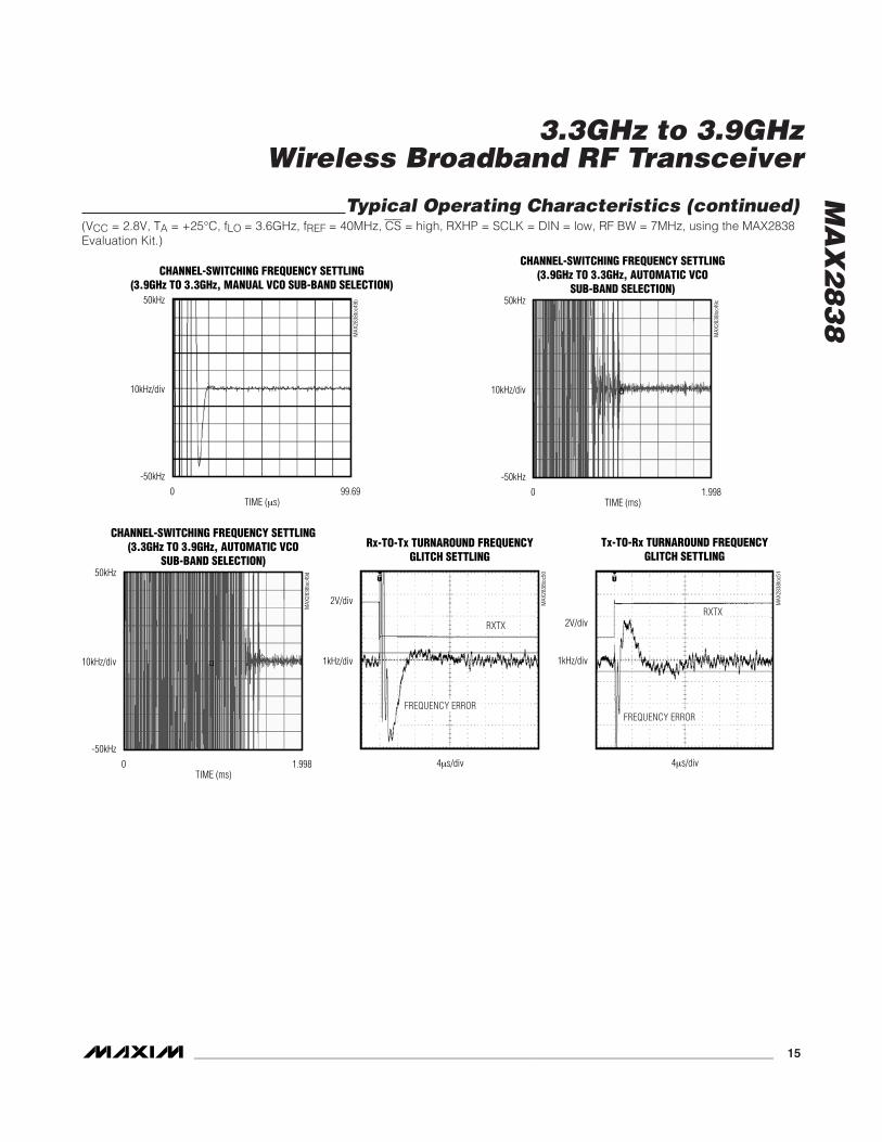
Typical Operating Characteristics(VCC = 2.8V, TA = +25°C, fLO = 3.6GHz, fREF = 40MHz, CS = high, RXHP = SCLK = DIN = low, RF BW = 7MHz, using the MAX2838Evaluation Kit.)
RECEIVER
MA
X2
83
8
3.3GHz to 3.9GHzWireless Broadband RF Transceiver
10 ______________________________________________________________________________________
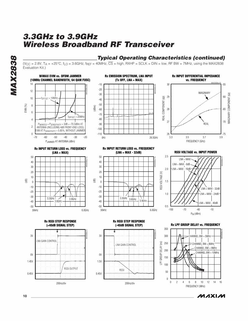
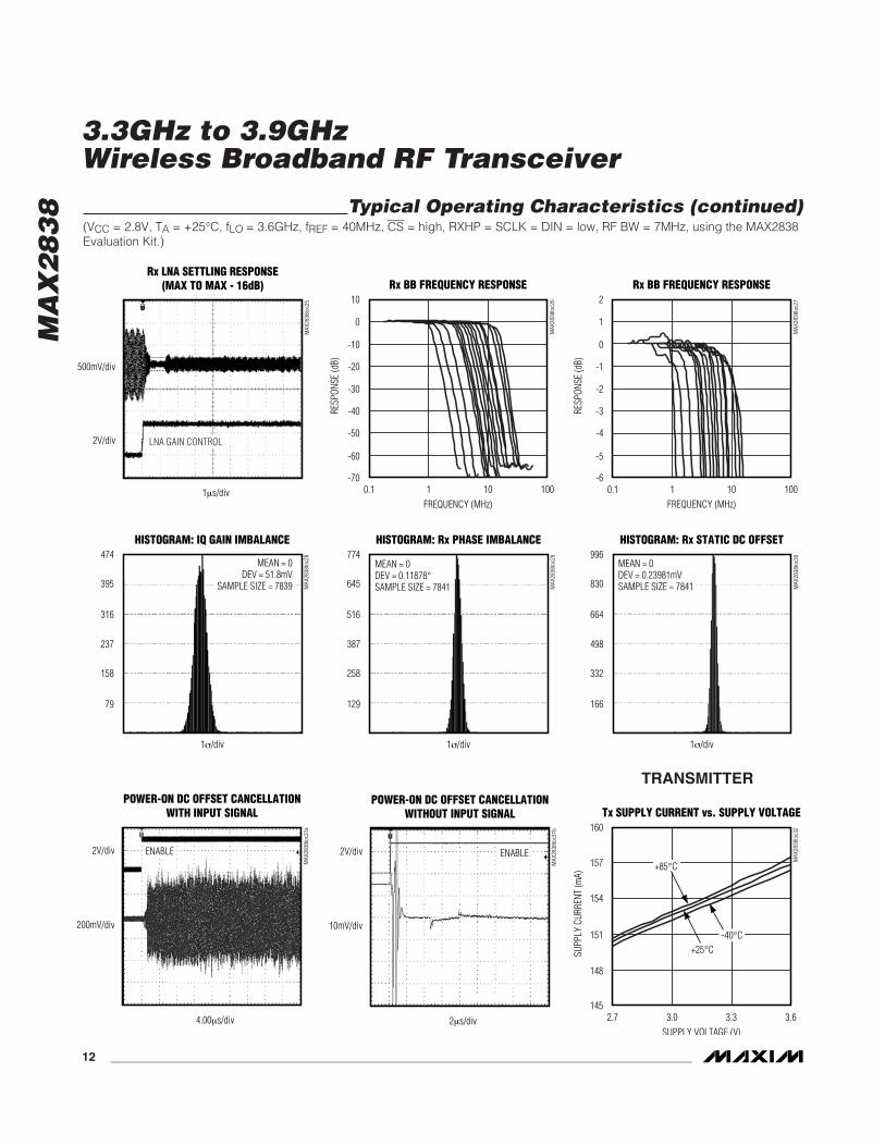
Typical Operating Characteristics (continued)(VCC = 2.8V, TA = +25°C, fLO = 3.6GHz, fREF = 40MHz, CS = high, RXHP = SCLK = DIN = low, RF BW = 7MHz, using the MAX2838Evaluation Kit.)
WiMAX EVM vs. OFDM JAMMER(10MHz CHANNEL BANDWIDTH, 64 QAM FUSC)
MAX
2838
toc0
8b
PJAMMER AT ANTENNA (dBm)
EVM
(%)
-30-50-60
8
10
12
2
4
6
14
0-70 -40 -20
fOFFSET = 10MHz
fOFFSET = 20MHz
PWANTED = PSENSITIVITY + 3dB = -70.3dBm ATANTENNA (INCLUDING 4dB FRONT-END LOSS).
EVM AT PSENSITIVITY = 5.85%, WITHOUT JAMMER.
Rx EMISSION SPECTRUM, LNA INPUT(Tx OFF, LNA = MAX)
MAX
2838
toc0
9
0Hz 26.5GHz
(dBm
)
-110
-100
-90
-80
-70
-60
-50
-40
-30
-20
-10
Rx INPUT DIFFERENTIAL IMPEDANCEvs. FREQUENCY
MAX2838toc10
3.3 3.5 3.7FREQUENCY (GHz)
3.9
REAL
COM
PONE
NT (Ω
)
IMAG
INAR
Y CO
MPO
NENT
(Ω)
26
30
29
28
27
-75
-55
-60
-65
-70
IMAGINARY
REAL
Rx INPUT RETURN LOSS vs. FREQUENCY(LNA = MAX)
MAX
2838
toc1
1a
30kHz 6.0GHz
(dB)
-50
-40
-30
-20
-10
0
10
20
30
40
50
3.9GHz3.6GHz
3.3GHz
RSSI VOLTAGE vs. INPUT POWER
MAX
2838
toc1
2
PIN (dBm)
RSSI
VOL
TAGE
(V)
1.5
1.0
2.0
2.5
0.5-100 -40 -10-70
LNA = MAX - 40dB
LNA = MAX - 32dB
LNA = MAX - 24dB
LNA = MAX - 16dB
LNA = MAX - 8dB
LNA = MAX
Rx RSSI STEP RESPONSE(+40dB SIGNAL STEP)
MAX
2838
toc1
3
200ns/div
3V
0V
1.45V
0.45V
LNA GAIN CONTROL
RSSI OUTPUT
Rx RSSI STEP RESPONSE(-40dB SIGNAL STEP)
MAX
2838
toc1
4
200ns/div
3V
0V
1.5V
0.45V
LNA GAIN CONTROL
RSSI
Rx LPF GROUP DELAY vs. FREQUENCYM
AX28
38to
c15
FREQUENCY (MHz)
LPF
GROU
P DE
LAY
(ns)
200
300
250
50
150
100
350
00 6 12 1610 142 4 8
CHANNEL BW = 5MHz
CHANNEL BW = 8MHzCHANNEL BW = 9MHz
CHANNEL BW = 10MHz
Rx INPUT RETURN LOSS vs. FREQUENCY(LNA = MAX - 32dB)
MAX
2838
toc1
1b
30kHz 6.0GHz
(dB)
-50
-40
-30
-20
-10
0
10
20
30
40
50
3.9GHz3.6GHz3.3GHz
MA
X2
83
8
3.3GHz to 3.9GHzWireless Broadband RF Transceiver
______________________________________________________________________________________ 11
Typical Operating Characteristics (continued)(VCC = 2.8V, TA = +25°C, fLO = 3.6GHz, fREF = 40MHz, CS = high, RXHP = SCLK = DIN = low, RF BW = 7MHz, using the MAX2838Evaluation Kit.)
Rx DC OFFSET SETTLING RESPONSE(+8dB BB VGA GAIN STEP)
MAX
2838
toc1
6
10μs/div
2V/div
10mV/div
VGA GAIN CONTROL
Rx DC OFFSET SETTLING RESPONSE(-8dB BB VGA GAIN STEP)
MAX
2838
toc1
7
10μs/div
2V/div
10mV/div
VGA GAIN CONTROL
Rx DC OFFSET SETTLING RESPONSE(-16dB BB VGA GAIN STEP)
MAX
2838
toc1
8
10μs/div
2V/div
10mV/div
VGA GAIN CONTROL
Rx DC OFFSET SETTLING RESPONSE(-32dB BB VGA GAIN STEP)
MAX
2838
toc1
9
10μs/div
2V/div
10mV/div
VGA GAIN CONTROL
Rx BBVGA SETTLING RESPONSE(+8dB GAIN STEP)
MAX
2838
toc2
0
200ns/div
100mV/div
2V/div VGA GAIN CONTROL
Rx BBVGA SETTLING RESPONSE(-8dB BB VGA GAIN STEP)
MAX
2838
toc2
1
200ns/div
100mV/div
2V/div VGA GAIN CONTROL
Rx BBVGA SETTLING RESPONSE(-16dB GAIN STEP)
MAX
2838
toc2
2
200ns/div
500mV/div
2V/div VGA GAIN CONTROL
Rx BBVGA SETTLING RESPONSE(-32dB GAIN STEP)
MAX
2838
toc2
3
200ns/div
1V/div
2V/div VGA GAIN CONTROL
Rx LNA SETTLING RESPONSE(MAX TO MAX - 8dB)
MAX
2838
toc2
4
1μs/div
500mV/div
2V/div LNA GAIN CONTROL
MA
X2
83
8
3.3GHz to 3.9GHzWireless Broadband RF Transceiver
12 ______________________________________________________________________________________
Rx LNA SETTLING RESPONSE(MAX TO MAX - 16dB)
MAX
2838
toc2
5
1μs/div
500mV/div
2V/div LNA GAIN CONTROL
Rx BB FREQUENCY RESPONSE
MAX
2838
toc2
6
FREQUENCY (MHz)
RESP
ONSE
(dB) -20
0
-10
-50
-60
-30
-40
10
-7010 1000.1 1
Rx BB FREQUENCY RESPONSE
MAX
2838
toc2
7
FREQUENCY (MHz)
RESP
ONSE
(dB) -1
1
0
-4
-5
-2
-3
2
-610 1000.1 1
HISTOGRAM: IQ GAIN IMBALANCE
MAX
2838
toc2
8
1σ/div
316
395
79
237
158
474MEAN = 0
DEV = 51.8mVSAMPLE SIZE = 7839
HISTOGRAM: Rx PHASE IMBALANCEM
AX28
38to
c29
1σ/div
516
645
129
387
258
774MEAN = 0DEV = 0.11878°SAMPLE SIZE = 7841
HISTOGRAM: Rx STATIC DC OFFSET
MAX
2838
toc3
0
1σ/div
664
830
166
498
332
996MEAN = 0DEV = 0.23981mVSAMPLE SIZE = 7841
POWER-ON DC OFFSET CANCELLATIONWITH INPUT SIGNAL
MAX
2838
toc3
1a
4.00μs/div
2V/div
200mV/div
ENABLE
Tx SUPPLY CURRENT vs. SUPPLY VOLTAGE
MAX
2838
toc3
2
SUPPLY VOLTAGE (V)
SUPP
LY C
URRE
NT (m
A)
157
151
148
154
160
1453.3 3.62.7 3.0
+85°C
-40°C+25°C
POWER-ON DC OFFSET CANCELLATIONWITHOUT INPUT SIGNAL
MAX
2838
toc3
1b
2μs/div
2V/div
10mV/div
ENABLE
Typical Operating Characteristics (continued)(VCC = 2.8V, TA = +25°C, fLO = 3.6GHz, fREF = 40MHz, CS = high, RXHP = SCLK = DIN = low, RF BW = 7MHz, using the MAX2838Evaluation Kit.)
TRANSMITTER
MA
X2
83
8
3.3GHz to 3.9GHzWireless Broadband RF Transceiver
______________________________________________________________________________________ 13
Tx BASEBAND FREQUENCY RESPONSE
MAX
2838
toc3
3a
FREQUENCY (MHz)
RESP
ONSE
(dB) -1
1
0
-4
-5
-2
-3
2
-60.1 10 1001
Tx OUTPUT POWER vs. FREQUENCY
MAX
2838
toc3
4
FREQUENCY (MHz)
P OUT
(dBm
)
2
-4
-6
0
-2
4
-83300 3700 39003400 36003500 3800
-40°C
+85°C
TX GAIN SET TO MAX - 3dB
+25°C
Tx OUTPUT POWER vs. GAIN SETTING
MAX
2838
toc3
5
TX GAIN CODE
P OUT
(dBm
)
-10
-30
-50
10
-700 643216 48
-40°C
+85°C
+25°C
Tx OUTPUT SPECTRUMM
AX28
38to
c36
3.625GHz3.583GHz
10dB/div
POUT = 0dBm
MASK
Tx CARRIER SUPPRESSION vs. FREQUENCY
MAX
2838
toc3
7
FREQUENCY (MHz)
CS (d
Bc)
-45
-60
-65
-50
-40
-55
-35
-703300 3700 39003400 36003500 3800
-40°C+85°C
TX GAIN SET TO MAX - 3dB
+25°C
Tx CARRIER SUPPRESSION vs.GAIN SETTING
MAX
2838
toc3
8
TX GAIN CODE
CS (d
Bc)
-30
-45
-50
-35
-25
-40
-60
-65
-55
-20
-700 6432 4816
-40°C
+85°C
+25°C
Tx SIDEBAND SUPPRESSION vs. FREQUENCY
MAX
2838
toc3
9
FREQUENCY (MHz)
SS (d
Bc)
-40
-70
-80
-50
-60
-30
-903300 3700 39003400 36003500 3800
-40°C
+85°C
TX GAIN SET TO MAX - 3dB
+25°C
Tx SIDEBAND SUPPRESSION vs.GAIN SETTING
MAX
2838
toc4
0
TX GAIN CODE
SS (d
Bc)
-40
-60
-50
-70
-30
-800 705030 6010 4020
-40°C
+85°C
+25°C
Tx BASEBAND FREQUENCY RESPONSE
MAX
2838
toc3
3
FREQUENCY (MHz)
RESP
ONSE
(dB) -20
0
-10
-50
-60
-30
-40
10
-700.1 10 1001
CHANNEL BW = 5MHz
CHANNEL BW = 1.5MHz
CHANNEL BW = 28MHz
CHANNEL BW = 20MHz
CHANNEL BW = 12MHz
CHANNEL BW = 1.75MHz
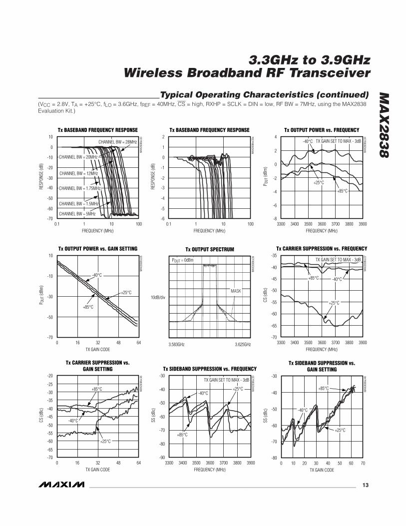
Typical Operating Characteristics (continued)(VCC = 2.8V, TA = +25°C, fLO = 3.6GHz, fREF = 40MHz, CS = high, RXHP = SCLK = DIN = low, RF BW = 7MHz, using the MAX2838Evaluation Kit.)
MA
X2
83
8
3.3GHz to 3.9GHzWireless Broadband RF Transceiver
14 ______________________________________________________________________________________
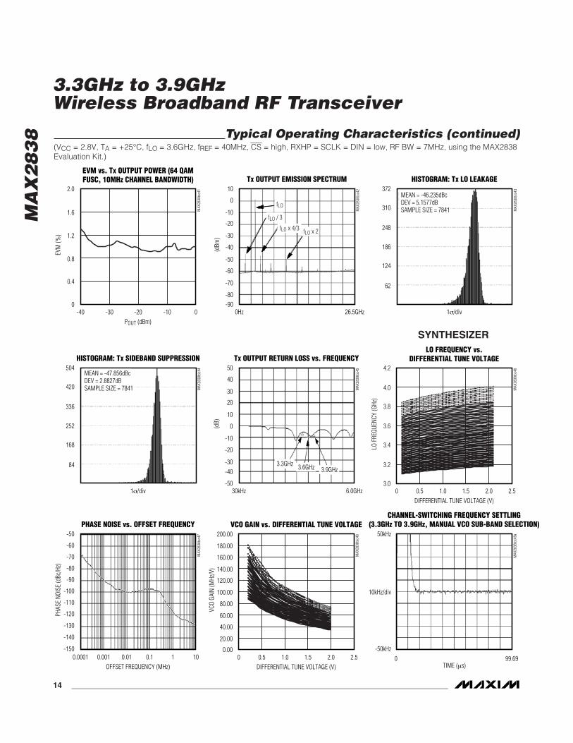
Typical Operating Characteristics (continued)(VCC = 2.8V, TA = +25°C, fLO = 3.6GHz, fREF = 40MHz, CS = high, RXHP = SCLK = DIN = low, RF BW = 7MHz, using the MAX2838Evaluation Kit.)
EVM vs. Tx OUTPUT POWER (64 QAMFUSC, 10MHz CHANNEL BANDWIDTH)
MAX
2838
toc4
1
POUT (dBm)
EVM
(%)
1.6
0.8
1.2
0.4
2.0
0-40 -10 0-30 -20
Tx OUTPUT EMISSION SPECTRUM
MAX
2838
toc4
2
(dBm
)-10
-50
-30
-70
10
-90
0
-40
-20
-60
-80
0Hz 26.5GHz
fLO
fLO / 3
fLO x 4/3 fLO x 2
HISTOGRAM: Tx LO LEAKAGE
MAX
2838
toc4
3
1σ/div
248
310
62
186
124
372MEAN = -46.235dBcDEV = 5.1577dBSAMPLE SIZE = 7841
HISTOGRAM: Tx SIDEBAND SUPPRESSION
MAX
2838
toc4
4
1σ/div
336
420
84
252
168
504MEAN = -47.856dBcDEV = 2.8827dBSAMPLE SIZE = 7841
Tx OUTPUT RETURN LOSS vs. FREQUENCYM
AX28
38to
c45
(dB)
30
-10
10
-30
50
-50
40
0
20
-20
-40
30kHz 6.0GHz
3.9GHz3.6GHz3.3GHz
LO FREQUENCY vs.DIFFERENTIAL TUNE VOLTAGE
MAX
2838
toc4
6
DIFFERENTIAL TUNE VOLTAGE (V)
LO F
REQU
ENCY
(GHz
)
4.0
3.6
3.8
3.4
3.2
4.2
3.00 1.51.0 2.52.00.5
PHASE NOISE vs. OFFSET FREQUENCY
MAX
2838
toc4
7
OFFSET FREQUENCY (MHz)
PHAS
E NO
ISE
(dBc
/Hz)
-50
-60
-70
-80
-90
-100
-110
-120
-130
-140
-1500.0001 0.10.01 1010.001
VCO GAIN vs. DIFFERENTIAL TUNE VOLTAGE
MAX
2838
toc4
8
DIFFERENTIAL TUNE VOLTAGE (V)
VCO
GAIN
(MHz
/V)
200.00
180.00
160.00
140.00
120.00
100.00
80.00
60.00
40.00
20.00
0.000 1.51.0 2.52.00.5
CHANNEL-SWITCHING FREQUENCY SETTLING(3.3GHz TO 3.9GHz, MANUAL VCO SUB-BAND SELECTION)
MAX
2838
toc4
9a
99.69TIME (μs)
0
10kHz/div
-50kHz
50kHz
SYNTHESIZER
MA
X2
83
8
3.3GHz to 3.9GHzWireless Broadband RF Transceiver
______________________________________________________________________________________ 15
CHANNEL-SWITCHING FREQUENCY SETTLING(3.9GHz TO 3.3GHz, AUTOMATIC VCO
SUB-BAND SELECTION)
MAX
2838
toc4
9c
1.998TIME (ms)
0
10kHz/div
-50kHz
50kHz
CHANNEL-SWITCHING FREQUENCY SETTLING(3.3GHz TO 3.9GHz, AUTOMATIC VCO
SUB-BAND SELECTION)
MAX
2838
toc4
9d
1.998TIME (ms)
0
10kHz/div
-50kHz
50kHz
Rx-TO-Tx TURNAROUND FREQUENCYGLITCH SETTLING
MAX
2838
toc5
0
4μs/div
1kHz/div
2V/div
FREQUENCY ERROR
RXTX
Tx-TO-Rx TURNAROUND FREQUENCYGLITCH SETTLING
MAX
2838
toc5
1
4μs/div
1kHz/div
2V/div
FREQUENCY ERROR
RXTX
Typical Operating Characteristics (continued)(VCC = 2.8V, TA = +25°C, fLO = 3.6GHz, fREF = 40MHz, CS = high, RXHP = SCLK = DIN = low, RF BW = 7MHz, using the MAX2838Evaluation Kit.)
CHANNEL-SWITCHING FREQUENCY SETTLING(3.9GHz TO 3.3GHz, MANUAL VCO SUB-BAND SELECTION)
MAX
2838
toc4
9b
99.69TIME (μs)
0
10kHz/div
-50kHz
50kHz
MA
X2
83
8
3.3GHz to 3.9GHzWireless Broadband RF Transceiver
16 ______________________________________________________________________________________
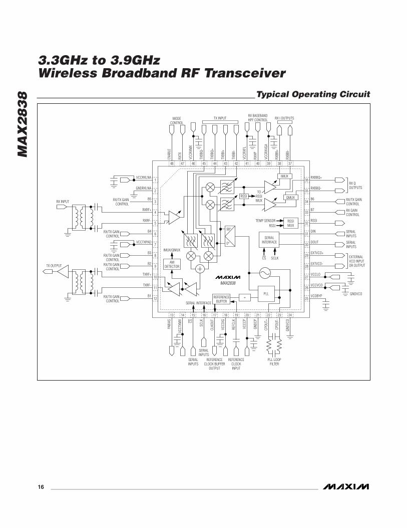
48 47 46 45 44 43 42 41 40 39 38
IMUX
37
13 14 15 16 17 18 19 20 21 22 23 24
36
35
34
33
32
31
30
29
28
27
26
25
1
2
3
4
5
6
7
8
9
10
11
12
RX I OUTPUTSTX INPUT
RSSIMUX
AMDETECTOR
SERIAL INTERFACE
REFERENCEBUFFER
÷
SERIALINTERFACE
PLL
PLL LOOPFILTER
REFERENCECLOCKINPUT
SERIALINPUTS
SERIALINPUTS
REFERENCECLOCK BUFFER
OUTPUT
RSSITO
RSSIMUX
QMUX
MAX2838
IMUX/QMUX
90°
0°
TEMP SENSORRSSI
CS SCLK
GNDV
CO
GNDC
P
CPOU
T+
CPOU
T-
VCCC
P
REFC
LK
VCCD
IG
CLKO
UT
SCLKCS
VCCT
XMX
PABI
AS
RXBBQ+
RXBBQ-
B6
B7
RSSI
DIN
DOUT
EXTVCO+
EXTVCO-
VCCLO
VCCVCO
GNDVCO
EXTERNALVCO INPUTOR OUTPUT
VCOBYP
RX QOUTPUTS
SERIALINPUTS
SERIALINPUTS
RX GAINCONTROL
RX/TX GAINCONTROL
RXBB
I-
RXHP
VCCR
XVGA
RXBB
I+
VCCR
XFL
TXBB
I-
TXBB
I+
TXBB
Q+
TXBB
Q-
VCCR
XMX
RXTX
ENAB
LE
RX BASEBANDHPF CONTROLMODE
CONTROL
VCCRXLNA
GNDRXLNA
B5
RXRF+
RXRF-
B4
VCCTXPAD
B3
B2
TXRF+
TXRF-
B1RX/TX GAINCONTROL
RX/TX GAINCONTROL
RX/TX GAINCONTROL
RX/TX GAINCONTROL
TX OUTPUT
RX INPUT RX/TX GAINCONTROL
Typical Operating Circuit
MA
X2
83
8
3.3GHz to 3.9GHzWireless Broadband RF Transceiver
______________________________________________________________________________________ 17
PIN NAME FUNCTION
1 VCCRXLNA LNA Supply Voltage. Bypass with a capacitor as close as possible to the pin.
2 GNDRXLNA LNA Ground
3 B5 Receiver and Transmitter Gain-Control Logic Input Bit 5
4 RXRF+
5 RXRF-LNA Differential Inputs. Inputs are internally DC-coupled. Two external series capacitors and oneshunt inductor match the inputs to 100Ω differential.
6 B4 Receiver and Transmitter Gain-Control Logic Input Bit 4
7 VCCTXPAD Supply Voltage for Power-Amplifier Driver. Bypass with a capacitor as close as possible to the pin.
8 B3 Receiver and Transmitter Gain-Control Logic Input Bit 3
9 B2 Receiver and Transmitter Gain-Control Logic Input Bit 2
10 TXRF+
11 TXRF-Power-Amplifier Driver Differential Output. Outputs are internally DC-coupled. Two external seriescapacitors and one shunt inductor match the outputs to 100Ω differential.
12 B1 Receiver and Transmitter Gain-Control Logic Input Bit 1
13 PABIAS Transmit PA Bias DAC Output
14 VCCTXMX Transmitter Upconverter Supply Voltage. Bypass with a capacitor as close as possible to the pin.
15 CS Chip-Select Logic Input of 4-Wire Serial Interface (See Figure 1)
16 SCLK Serial-Clock Logic Input of 4-Wire Serial Interface (See Figure 1)
17 CLKOUT Reference Clock Divided Output
18 VCCDIG Digital Circuit Supply Voltage. Bypass with a capacitor as close as possible to the pin.
19 REFCLK Reference Clock Input
20 VCCCP PLL Charge-Pump Supply Voltage. Bypass with a capacitor as close as possible to the pin.
21 GNDCP Charge-Pump Circuit Ground
22 CPOUT+
23 CPOUT-Differential Charge-Pump Output. Connect the frequency synthesizer’s loop filter between CPOUT+and CPOUT- (see the Typical Operating Circuit).
24 GNDVCO VCO Ground
25 VCOBYPOn-Chip VCO Regulator Output Bypass. Bypass with a 1µF capacitor to GND. Do not connect othercircuitry to this point.
26 VCCVCO VCO Supply Voltage. Bypass with a capacitor as close as possible to the pin.
27 VCCLO LO Generation Supply Voltage. Bypass with a capacitor as close as possible to the pin.
28 EXTVCO-
29 EXTVCO+External VCO Differential Input or Output. Input for slave configuration and output for masterconfiguration. Leave unconnected for single configuration.
30 DOUT Data Logic Output of 4-Wire Serial Interface (See Figure 1)
31 DIN Data Logic Input of 4-Wire Serial Interface (See Figure 1)
32 RSSI RSSI or Temperature Sensor Multiplexed Analog Output
33 B7 Receiver Gain-Control Logic Input Bit 7
34 B6 Receiver and Transmitter Gain-Control Logic Input Bit 6
35 RXBBQ-
36 RXBBQ+Receiver Baseband Q-Channel Differential Outputs. In Tx calibration mode, these pins are the LOleakage and sideband detector outputs.
37 RXBBI-
38 RXBBI+Receiver Baseband I-Channel Differential Outputs. In Tx calibration mode, these pins are the LOleakage and sideband detector outputs.
39 VCCRXVGA Receiver VGA Supply Voltage. Bypass with a capacitor as close as possible to the pin.
Pin Description
MA
X2
83
8
3.3GHz to 3.9GHzWireless Broadband RF Transceiver
18 ______________________________________________________________________________________
PIN NAME FUNCTION
40 RXHPReceiver Baseband AC-Coupling Highpass Corner Frequency Control Logic Input. Connect toground if not being used.
41 VCCRXFL Receiver Baseband Filter Supply Voltage. Bypass with a capacitor as close as possible to the pin.
42 TXBBI-
43 TXBBI+Transmitter Baseband I-Channel Differential Inputs
44 TXBBQ+
45 TXBBQ-Transmitter Baseband Q-Channel Differential Inputs
46 VCCRXMX Receiver Downconverters Supply Voltage. Bypass with a capacitor as close as possible to the pin.
47 RXTX Mode Control Logic Input. See Table 1 for operating modes.
48 ENABLE Mode Control Logic Input. See Table 1 for operating modes.
— EPExposed Paddle. Connect to the ground plane with multiple vias for proper operation and heatdissipation. Do not share with any other pin grounds and bypass capacitors’ ground.
Pin Description (continued)
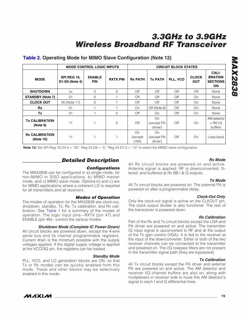
MODE CONTROL LOGIC INPUTS CIRCUIT BLOCK STATES
MODESPI REG 16,
D1:D0 (Note 6)ENABLE
PINRXTX PIN Rx PATH Tx PATH PLL, VCO
CLOCKOUT
CALI-BRATIONSEC T I O N S
ON
SHUTDOWN xx 0 0 Off Off Off Off None
STANDBY (Note 7) 01 0 1 Off Off On On None
CLOCK OUT 00 (Note 11) 0 1 Off Off Off On None
Rx 01 1 1 On Off ( N ote 8) On On None
Tx 01 1 0 Off On On On None
Tx CALIBRATION(Note 9)
11 1 0 OffOn
(except PAdriver)
On OnAM d etector
+ RX I,Qb uffer s
Rx CALIBRATION(Note 10)
11 1 1On
(exceptLNA)
On(except PA
driver)On On Loopback
Table 1. Operating Mode for MIMO Master and Single Configuration (Note 5)
Note 5: Set SPI Reg 24 D1:D0 = “00” for single-transceiver mode of operation. Set SPI Reg 16 D4:D3 = “11,” Reg 24 D8 = “1,” Reg24 D1:D0 = “01” for MIMO master configuration.
Note 6: Unused states of SPI Reg 16, D1:D0 above are not tested, and therefore, should not be used.Note 7: Parts of transceiver may be selectively enabled.Note 8: PA bias DAC may be kept active in these non-transmit mode(s) by SPI programming.Note 9: Set SPI Reg 5 D5 = “1” to mux AM detector output to RXBB pins.Note 10: Set SPI Reg 26 D3 = “1.”Note 11: CLKOUT signal is active independent of the states of SPI Reg 16, D1:D0, and is only dependent on the states of ENABLE
and RXTX pins. However, to ensure that the rest of the chip is off when the CLKOUT is active in the clock-out mode, set SPIReg 16, D1:D0 to “00” as shown above.
MA
X2
83
8
3.3GHz to 3.9GHzWireless Broadband RF Transceiver
______________________________________________________________________________________ 19
Detailed DescriptionConfigurations
The MAX2838 can be configured in a) single mode, fornon-MIMO or SISO applications, b) MIMO mastermode, and c) MIMO slave mode. Options b) and c) arefor MIMO applications where a coherent LO is requiredfor all transmitters and all receivers.
Modes of OperationThe modes of operation for the MAX2838 are clock-out,shutdown, standby, Tx, Rx, Tx calibration, and Rx cali-bration. See Table 1 for a summary of the modes ofoperation. The logic input pins—RXTX (pin 47) andENABLE (pin 48)—control the various modes.
Shutdown Mode (Complete IC Power-Down)All circuit blocks are powered down, except the 4-wireserial bus and its internal programmable registers.Current drain is the minimum possible with the supplyvoltages applied. If the digital supply voltage is appliedat the VCCDIG pin, the registers can be loaded.
Standby ModePLL, VCO, and LO generation blocks are ON, so thatTx or Rx modes can be quickly enabled from thismode. These and other blocks may be selectivelyenabled in this mode.
Rx ModeAll Rx circuit blocks are powered on and active.Antenna signal is applied; RF is downconverted, fil-tered, and buffered at Rx BB I & Q outputs.
Tx ModeAll Tx circuit blocks are powered on. The external PA ispowered on after a programmable delay.
Clock-Out OnlyOnly the clock-out signal is active on the CLKOUT pin.The clock output divider is also functional. The rest ofthe transceiver is powered down.
Rx CalibrationPart of the Rx and Tx circuit blocks except the LNA andPA driver are powered on and active. The transmitterIQ input signal is upconverted to RF and at the outputof the Tx gain control (VGA). It is fed to the receiver atthe input of the downconverter. Either or both of the tworeceiver channels can be connected to the transmitterand powered on. The I/Q lowpass filters are not presentin the transmitter signal path (they are bypassed).
Tx CalibrationAll Tx circuit blocks except the PA driver and externalPA are powered on and active. The AM detector andreceiver I/Q channel buffers are also on, along withmultiplexers in receiver side to route this AM detector’ssignal to each I and Q differential lines.
MODE CONTROL LOGIC INPUTS CIRCUIT BLOCK STATES
MODESPI REG 16,
D1:D0 (Note 4)ENABLE
PINRXTX PIN Rx PATH Tx PATH PLL, VCO
CLOCKOUT
C A L I- B R A T I O N SEC T I O N S
O N
SHUTDOWN xx 0 0 Off Off Off Off None
STANDBY (Note 7) 01 0 1 Off Off Off On None
CLOCK OUT 00 (Note 11) 0 1 Off Off Off On None
Rx 01 1 1 On Off ( N ote 8) Off On None
Tx 01 1 0 Off On Off On None
Tx CALIBRATION(Note 9)
11 1 0 OffOn
(except PAdriver)
Off OnAM d etector
+ RX I,Qb uffer s
Rx CALIBRATION(Note 10)
11 1 1On
(exceptLNA)
On(except PA
driver)Off On Loop-back
Table 2. Operating Mode for MIMO Slave Configuration (Note 12)
Note 12: Set SPI Reg 16 D4:3 = “00,” Reg 24 D8 = “0,” Reg 24 D1:0 = “10” to select the MIMO slave configuration.
MA
X2
83
8
3.3GHz to 3.9GHzWireless Broadband RF Transceiver
20 ______________________________________________________________________________________
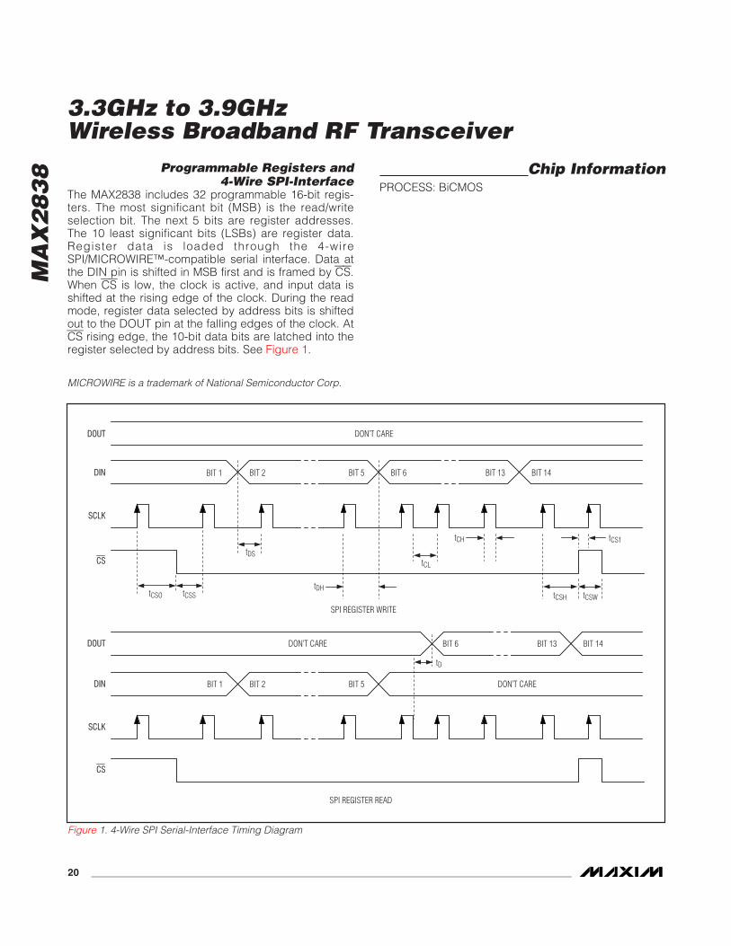
Programmable Registers and4-Wire SPI-Interface
The MAX2838 includes 32 programmable 16-bit regis-ters. The most significant bit (MSB) is the read/writeselection bit. The next 5 bits are register addresses.The 10 least significant bits (LSBs) are register data.Register data is loaded through the 4-wireSPI/MICROWIRE™-compatible serial interface. Data atthe DIN pin is shifted in MSB first and is framed by CS.When CS is low, the clock is active, and input data isshifted at the rising edge of the clock. During the readmode, register data selected by address bits is shiftedout to the DOUT pin at the falling edges of the clock. AtCS rising edge, the 10-bit data bits are latched into theregister selected by address bits. See Figure 1.
MICROWIRE is a trademark of National Semiconductor Corp.
Chip InformationPROCESS: BiCMOS
DIN
SCLK
BIT 6BIT 2BIT 1
tDS
tDH
BIT 14BIT 13BIT 5
tCH
tCL
tCSH
CS
tCSO tCSS tCSW
tCS1
DOUT DON’T CARE
SPI REGISTER WRITE
DIN
SCLK
BIT 2BIT 1
tD
BIT 5
CS
DOUT
DON’T CARE
SPI REGISTER READ
BIT 6 BIT 14BIT 13DON’T CARE
Figure 1. 4-Wire SPI Serial-Interface Timing Diagram
MA
X2
83
8
3.3GHz to 3.9GHzWireless Broadband RF Transceiver
______________________________________________________________________________________ 21
Package InformationFor the latest package outline information and land patterns, go to www.maxim-ic.com/packages.
PACKAGE TYPE PACKAGE CODE DOCUMENT NO.
48 TQFN-EP T4866+2 21-0141
MA
X2
83
8
3.3GHz to 3.9GHzWireless Broadband RF Transceiver
Maxim cannot assume responsibility for use of any circuitry other than circuitry entirely embodied in a Maxim product. No circuit patent licenses areimplied. Maxim reserves the right to change the circuitry and specifications without notice at any time.
22 ____________________Maxim Integrated Products, 120 San Gabriel Drive, Sunnyvale, CA 94086 408-737-7600
© 2008 Maxim Integrated Products is a registered trademark of Maxim Integrated Products, Inc.
Revision History
REVISION NUMBER
REVISION DATE
DESCRIPTIONPAGES
CHANGED
0 10/07 Initial release —
1 8/08 Removed CLKOUT frequency divide-by-1 ratio in AC Electrical Characteristics—Frequency Synthesis table
7