Embed Size (px)
Citation preview
Write Endurance in Flash Drives: Measurements and Analysis
Simona BoboilaNortheastern University
360 Huntington Ave.Boston, MA 02115
Peter DesnoyersNortheastern University
360 Huntington Ave.Boston, MA [email protected]
AbstractWe examine the write endurance of USB flash drives
using a range of approaches: chip-level measurements,reverse engineering, timing analysis, whole-device en-durance testing, and simulation. The focus of our inves-tigation is not only measured endurance, but underlyingfactors at the level of chips and algorithms—both typicaland ideal—which determine the endurance of a device.
Our chip-level measurements show endurance far inexcess of nominal values quoted by manufacturers, bya factor of as much as 100. We reverse engineerspecifics of the Flash Translation Layers (FTLs) usedby several devices, and find a close correlation betweenmeasured whole-device endurance and predictions fromreverse-engineered FTL parameters and measured chipendurance values. We present methods based on anal-ysis of operation latency which provide a non-intrusivemechanism for determining FTL parameters. Finally wepresent Monte Carlo simulation results giving numeri-cal bounds on endurance achievable by any on-line algo-rithm in the face of arbitrary or malicious access patterns.
1 Introduction
In recent years flash memory has entered widespreaduse, in embedded media players, photography, portabledrives, and solid-state disks (SSDs) for traditional com-puting storage. Flash has become the first competitor tomagnetic disk storage to gain significant commercial ac-ceptance, with estimated shipments of 5 × 10¹⁹ bytesin 2009 [10], or more than the amount of disk storageshipped in 2005 [31].
Flash memory differs from disk in many characteris-tics; however, one which has particular importance forthe design of storage systems is its limited write en-durance. While disk drive reliability is mostly unaffectedby usage, bits in a flash chip will fail after a limited num-ber of writes, typical quoted at 104 to 105 depending on
the specific device. When used with applications expect-ing a disk-like storage interface, e.g. to implement a FATor other traditional file system, this results in over-useof a small number of blocks and early failure. Almostall flash devices on the market—USB drives, SD drives,SSDs, and a number of others—thus implement internalwear-leveling algorithms, which map application blockaddresses to physical block addresses, and vary this map-ping to spread writes uniformly across the device.
The endurance of a flash-based storage system such asa USB drive or SSD is thus a function of both the parame-ters of the chip itself, and the details of the wear-levelingalgorithm (or Flash Translation Layer, FTL) used. Sincemeasured endurance data is closely guarded by semi-conductor manufacturers, and FTL details are typicallyproprietary and hidden within the storage device, thebroader community has little insight into the endurancecharacteristics of these systems. Even empirical testingmay be of limited utility without insight into which ac-cess patterns represent worst-case behavior.
To investigate flash drive endurance, we make use ofan array of techniques: chip-level testing, reverse engi-neering and timing analysis, whole device testing, andanalytic approaches. Intrusive tests include chip-leveltesting—where the flash chip is removed from the driveand tested without any wear-leveling—and reverse en-gineering of FTL algorithms using logic analyzer prob-ing. Analysis of operation timing and endurance testingconducted on the entire flash drive provides additionalinformation; this is augmented by analysis and simula-tion providing insight into achievable performance of thewear-leveling algorithms used in conjunction with typi-cal flash devices.
The remainder of the paper is structured as follows.Section 2 presents the basic information about flashmemory technology, FTL algorithms, and related work.Section 3 discusses our experimental results, includ-ing chip-level testing (Section 3.1), details of reverse-engineered FTLs (3.2), and device-level testing (3.3).
Bit line (in)
Bit line (out)
Word 0
Word 1
Word 2
cell
(a) NOR Flash
Word 0
Word 1
Word 2
Word 3
Bit line (in)
Bit line (out)
cell
(b) NAND Flash
Figure 1: Flash circuit structure. NAND flash is distin-guished by the series connection of cells along the bit line,while NOR flash (and most other memory technologies) ar-range cells in parallel between two bit lines.
Section 4 presents a theoretical analysis of wear-levelingalgorithms, and we conclude in Section 5.
2 Background
NAND flash is a form of electrically erasable pro-grammable read-only memory based on a particularlyspace-efficient basic cell, optimized for mass storage ap-plications. Unlike most memory technologies, NANDflash is organized in pages of typically 2K or 4K byteswhich are read and written as a unit. Unlike block-oriented disk drives, however, pages must be erasedin units of erase blocks comprising multiple pages—typically 32 to 128—before being re-written.
Devices such as USB drives and SSDs implement are-writable block abstraction, using a Flash TranslationLayer to translate logical requests to physical read, pro-gram, and erase operations. FTL algorithms aim to max-imize endurance and speed, typically a trade-off due tothe extra operations needed for wear-leveling. In addi-tion, an FTL must be implementable on the flash con-troller; while SSDs may contain 32-bit processors andmegabytes of RAM, allowing sophisticated algorithms,some of the USB drives analyzed below use 8-bit con-trollers with as little as 5KB of RAM.
2.1 Physical Characteristics
We first describe in more detail the circuit and electri-cal aspects of flash technology which are relevant to sys-tem software performance; a deeper discussion of theseand other issues may be found in the survey by San-vido et al [29]. The basic cell in a NAND flash is aMOSFET transistor with a floating (i.e. oxide-isolated)gate. Charge is tunnelled onto this gate during write op-erations, and removed (via the same tunnelling mecha-nism) during erasure. This stored charge causes changes
Erase block
pages
Independent Flash
planes (typ. 1 or 2)
Data page Spare area
Col. decode
Ro
w d
eco
de
Data register
Control
and
address
logic
I/O
NAND
flash
array
8 or
16 bits
1 page
Flash package
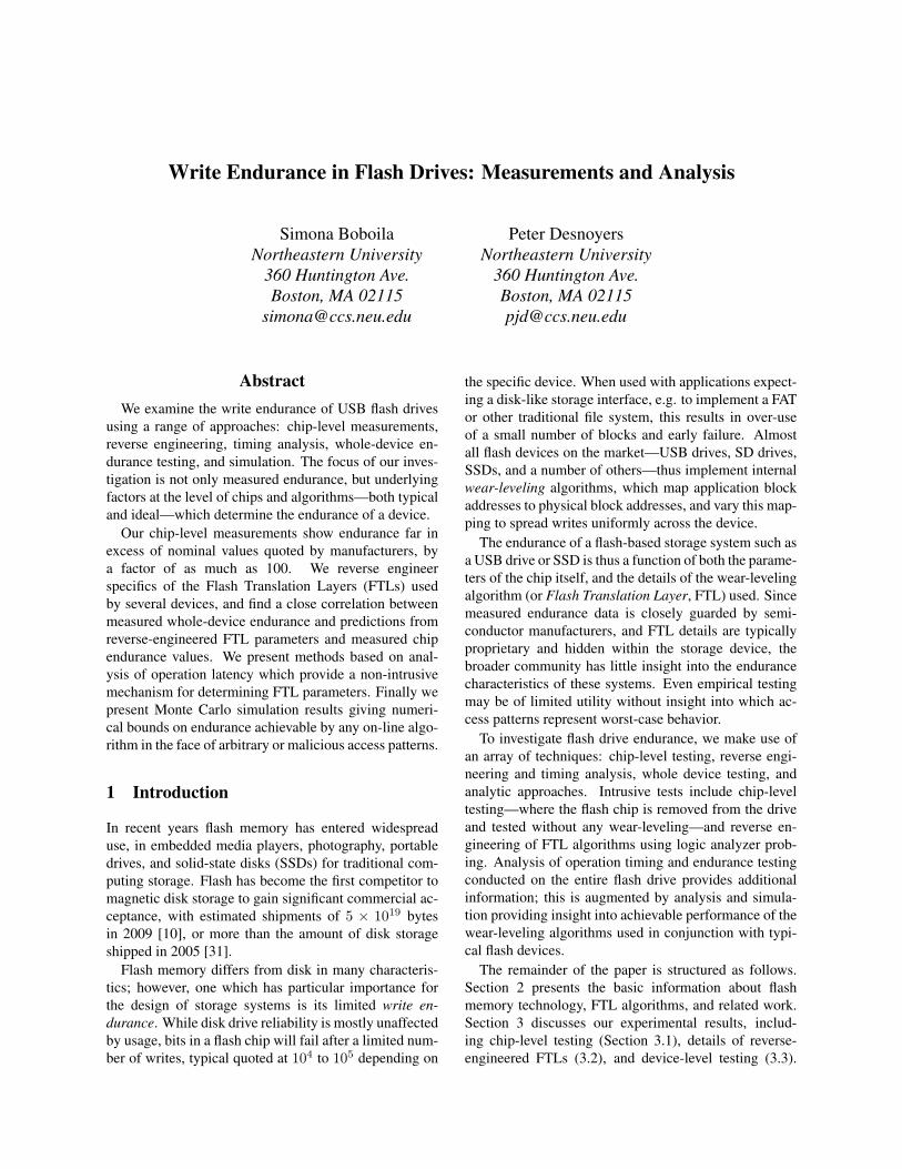
Figure 2: Typical flash device architecture. Read and writeare both performed in two steps, consisting of the transfer ofdata over the external bus to or from the data register, and theinternal transfer between the data register and the flash array.
in VT , the threshold or turn-on voltage of the cell tran-sistor, which may then be sensed by the read circuitry.NAND flash is distinguished from other flash technolo-gies (e.g. NOR flash, E2PROM) by the tunnelling mech-anism (Fowler-Nordheim or FN tunnelling) used for bothprogramming and erasure, and the series cell organiza-tion shown in Figure 1(b).
Many of the more problematic characteristics ofNAND flash are due to this organization, which elim-inates much of the decoding overhead found in othermemory technologies. In particular, in NAND flash theonly way to access an individual cell for either reading orwriting is through the other cells in its bit line. This addsnoise to the read process, and also requires care duringwriting to ensure that adjacent cells in the string are notdisturbed. (In fact, stray voltage from writing and read-ing may induce errors in other bits on the string, knownas program disturbs and read disturbs.) During erasure,in contrast, all cells on the same bit string are erased.
Individual NAND cells store an analog voltage; inpractice this may be used to store one of two voltage lev-els (Single-Level Cell or SLC technology) or between 4and 16 voltage levels—encoding 2 to 4 bits—in what isknown as Multi-Level Cell (MLC) technology. Thesecells are typically organized as shown in the block di-agram in Figure 2. Cells are arranged in pages, typi-cally containing 2K or 4K bytes plus a spare area of 64to 256 bytes for system overhead. Between 16 and 128pages make up an erase block, or block for short, whichare then grouped into a flash plane. Devices may con-tain independent flash planes, allowing simultaneous op-erations for higher performance. Finally, a static RAMbuffer holds data before writing or after reading, and datais transferred to and from this buffer via an 8- or 16-bitwide bus.
2.2 Flash Translation Layer
As described above, NAND flash is typically used with aflash translation layer implementing a disk-like interfaceof addressable, re-writable 512-byte blocks, e.g. overan interface such as SATA or SCSI-over-USB. The FTLmaps logical addresses received over this interface (Log-ical Page Numbers or LPNs) to physical addresses in theflash chip (Physical Page Numbers, PPNs) and managesthe details of erasure, wear-leveling, and garbage collec-tion [2, 3, 17].
Mapping schemes: A flash translation layer could intheory maintain a map with an entry for each 512-bytelogical page containing its corresponding location; theoverhead of doing so would be high, however, as the mapfor a 1GB device would then require 2M entries, con-suming about 8MB; maps for larger drives would scaleproportionally. FTL resource requirements are typicallyreduced by two methods: zoning and larger-granularitymapping.
Zoning refers to the division of the logical addressspace into regions or zones, each of which is assigned itsown region of physical pages. In other words, rather thanusing a single translation layer across the entire device,multiple instances of the FTL are used, one per zone.The map for the current zone is maintained in memory,and when an operation refers to a different zone, the mapfor that zone must be loaded from the flash device. Thisapproach performs well when there is a high degree of lo-cality in access patterns; however it results in high over-head for random operation. Nonetheless it is widely usedin small devices (e.g. USB drives) due to its reducedmemory requirements.
By mapping larger units, and in particular entire eraseblocks, it is possible to reduce the size of the mapping ta-bles even further [8]. On a typical flash device (64-pageerase blocks, 2KB pages) this reduces the map for a 1GBchip to 8K entries, or even fewer if divided into zones.This reduction carries a cost in performance: to modifya single 512-byte logical block, this block-mapped FTLwould need to copy an entire 128K block, for an over-head of 256×.
Hybrid mapping schemes [19, 20, 21, 25] augment ablock map with a small number of reserved blocks (log orupdate blocks) which are page mapped. This approach istargeted to usage patterns that exhibit block-level tempo-ral locality: the pages in the same logical block are likelyto be updated again in the near future. Therefore, a com-pact fine-grained mapping policy for log blocks ensuresa more efficient space utilization in case of frequent up-dates.
Garbage collection: Whenever units smaller than anerase block are mapped, there can be stale data: datawhich has been replaced by writes to the same logical
address (and stored in a different physical location) butwhich has not yet been erased. In the general case re-covering these pages efficiently is a difficult problem.However in the limited case of hybrid FTLs, this processconsists of merging log blocks with blocks containingstale data, and programming the result into one or morefree blocks. These operations are of the following types:switch merges, partial merges, and full merge [13].
A switch merge occurs during sequential writing; thelog block contains a sequence of pages exactly replacingan existing data block, and may replace it without anyfurther operation; the old block may then be erased. Apartial merge copies valid pages from a data block tothe log block, after which the two may be switched. Afull merge is needed when data in the log block is out oforder; valid pages from the log block and the associateddata block are copied together into a new free block, afterwhich the old data block and log block are both erased.
Wear-leveling: Many applications concentrate theirwrites on a small region of storage, such as the file alloca-tion table (FAT) in MSDOS-derived file systems. Naı̈vemechanisms might map these logical regions to similar-sized regions of physical storage, resulting in prema-ture device failure. To prevent this, wear-leveling algo-rithms are used to ensure that writes are spread acrossthe entire device, regardless of application write behav-ior; these algorithms [11] are classified as either dynamicor static. Dynamic wear-leveling operates only on over-written blocks, rotating writes between blocks on a freelist; thus if there are m blocks on the free list, repeatedwrites to the same logical address will cause m + 1physical blocks to be repeatedly programmed and erased.Static wear-leveling spreads the wear over both static anddynamic memory regions, by periodically swapping ac-tive blocks from the free list with static randomly-chosenblocks. This movement incurs additional overhead, butincreases overall endurance by spreading wear over theentire device.
2.3 Related Work
There is a large body of existing experimental workexamining flash memory performance and endurance;these studies may be broadly classified as either circuit-oriented or system-oriented. Circuit-level studies haveexamined the effect of program/erase stress on internalelectrical characteristics, often using custom-fabricateddevices to remove the internal control logic and allowmeasurements of the effects of single program or erasesteps. A representative study is by Lee et al. at Sam-sung [24], examining both program/erase cycling and hotstorage effects across a range of process technologies.Similar studies include those by Park et al. [28] and Yanget al. [32], both also at Samsung. The most recent work
Device Size Cell Nominal Process(bits) endurance
NAND128W3A2BN 128M SLC 105 90nmHY27US08121A 512M SLC 105 90nmMT29F2G08AAD 2G SLC 105 50nmMT29F4G08AAC 4G SLC 105 72nmNAND08GW3B2C 8G SLC 105 60nmMT29F8G08MAAWC 8G MLC 104 72nm29F16G08CANC1 16G SLC 105 50nmMT29F32G08QAA 32G MLC 104 50nm
Table 1: Devices tested
in this area includes a workshop report of our results [9]and an empirical characterization of flash memory car-ried out by Grupp et at. [12], analyzing performance ofbasic operations, power consumption, and reliability.
System-level studies have instead examined charac-teristics of entire flash-based storage systems, such asUSB drives and SSDs. The most recent of these presentsuFLIP [7], a benchmark for such storage systems, withmeasurements of a wide range of devices; this workquantifies the degraded performance observed for ran-dom writes in many such devices. Additional work inthis area includes [14],[27], and [1]
Ben-Aroyo and Toledo [5] have presented detailedtheoretical analyses of bounds on wear-leveling perfor-mance; however for realistic flash devices (i.e. with eraseblock size > 1 page) their results show the existence of abound but not its value.
3 Experimental Results
3.1 Chip-level EnduranceChip-level endurance was tested across a range of de-vices; more detailed results have been published in a pre-vious workshop paper [9] and are summarized below.
Methodology: Flash chips were acquired boththrough distributors and by purchasing and disassem-bling mass-market devices. A programmable flash con-troller was constructed using software control of general-purpose I/O pins on a micro-controller to implement theflash interface protocol for 8-bit devices. Devices testedranged from older 128Mbit (16MB) SLC devices to morerecent 16Gbit and 32Gbit MLC chips; a complete list ofdevices tested may be seen in Table 1. Unless otherwisespecified, all tests were performed at 25◦ C.
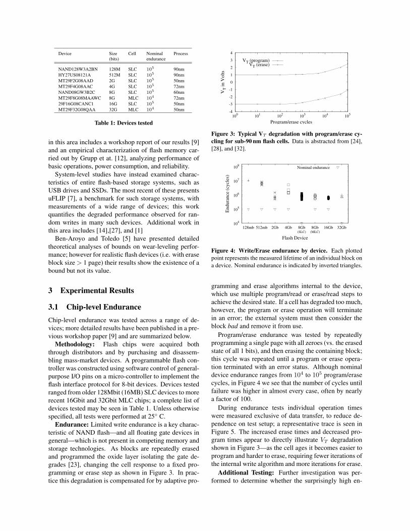
Endurance: Limited write endurance is a key charac-teristic of NAND flash—and all floating gate devices ingeneral—which is not present in competing memory andstorage technologies. As blocks are repeatedly erasedand programmed the oxide layer isolating the gate de-grades [23], changing the cell response to a fixed pro-gramming or erase step as shown in Figure 3. In prac-tice this degradation is compensated for by adaptive pro-
-4
-3
-2
-1
0
1
2
3
4
100
101
102
103
104
105
VT i
n V
olt
s
Program/erase cycles
VT (program)VT (erase)
Figure 3: Typical VT degradation with program/erase cy-cling for sub-90 nm flash cells. Data is abstracted from [24],[28], and [32].
104
105
106
107
108
128mb 512mb 2Gb 4Gb 8Gb(SLC)
8Gb(MLC)
16Gb 32GbE
nd
ura
nce
(cy
cles
)
Flash Device
Nominal endurance
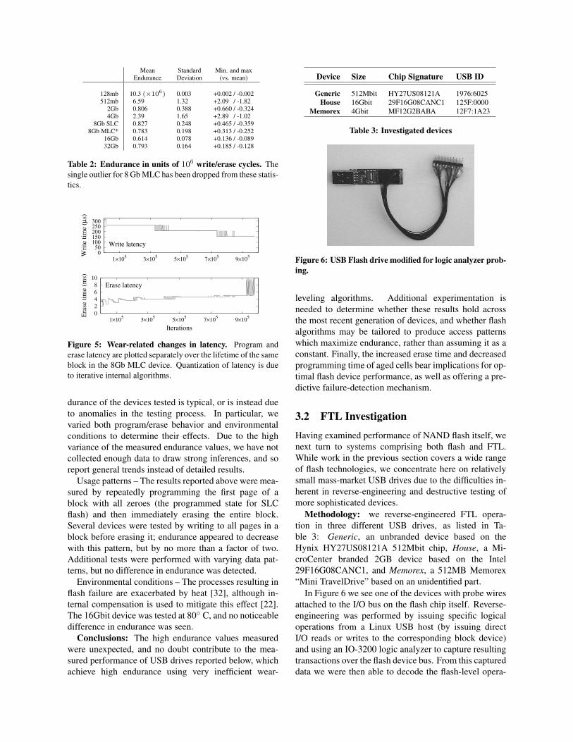
Figure 4: Write/Erase endurance by device. Each plottedpoint represents the measured lifetime of an individual block ona device. Nominal endurance is indicated by inverted triangles.
gramming and erase algorithms internal to the device,which use multiple program/read or erase/read steps toachieve the desired state. If a cell has degraded too much,however, the program or erase operation will terminatein an error; the external system must then consider theblock bad and remove it from use.
Program/erase endurance was tested by repeatedlyprogramming a single page with all zeroes (vs. the erasedstate of all 1 bits), and then erasing the containing block;this cycle was repeated until a program or erase opera-tion terminated with an error status. Although nominaldevice endurance ranges from 104 to 105 program/erasecycles, in Figure 4 we see that the number of cycles untilfailure was higher in almost every case, often by nearlya factor of 100.
During endurance tests individual operation timeswere measured exclusive of data transfer, to reduce de-pendence on test setup; a representative trace is seen inFigure 5. The increased erase times and decreased pro-gram times appear to directly illustrate VT degradationshown in Figure 3—as the cell ages it becomes easier toprogram and harder to erase, requiring fewer iterations ofthe internal write algorithm and more iterations for erase.
Additional Testing: Further investigation was per-formed to determine whether the surprisingly high en-
Mean Standard Min. and maxEndurance Deviation (vs. mean)
128mb 10.3 (×106) 0.003 +0.002 / -0.002512mb 6.59 1.32 +2.09 / -1.82
2Gb 0.806 0.388 +0.660 / -0.3244Gb 2.39 1.65 +2.89 / -1.02
8Gb SLC 0.827 0.248 +0.465 / -0.3598Gb MLC* 0.783 0.198 +0.313 / -0.252
16Gb 0.614 0.078 +0.136 / -0.08932Gb 0.793 0.164 +0.185 / -0.128
Table 2: Endurance in units of 106 write/erase cycles. Thesingle outlier for 8 Gb MLC has been dropped from these statis-tics.
0 50
100 150 200 250 300
1×10⁵
3×10⁵
5×10⁵
7×10⁵
9×10⁵W
rite
tim
e (µ
s)
Write latency
0
2
4
6
8
10
1×10⁵
3×10⁵
5×10⁵
7×10⁵
9×10⁵E
rase
tim
e (m
s)
Iterations
Erase latency
Figure 5: Wear-related changes in latency. Program anderase latency are plotted separately over the lifetime of the sameblock in the 8Gb MLC device. Quantization of latency is dueto iterative internal algorithms.
durance of the devices tested is typical, or is instead dueto anomalies in the testing process. In particular, wevaried both program/erase behavior and environmentalconditions to determine their effects. Due to the highvariance of the measured endurance values, we have notcollected enough data to draw strong inferences, and soreport general trends instead of detailed results.
Usage patterns – The results reported above were mea-sured by repeatedly programming the first page of ablock with all zeroes (the programmed state for SLCflash) and then immediately erasing the entire block.Several devices were tested by writing to all pages in ablock before erasing it; endurance appeared to decreasewith this pattern, but by no more than a factor of two.Additional tests were performed with varying data pat-terns, but no difference in endurance was detected.
Environmental conditions – The processes resulting inflash failure are exacerbated by heat [32], although in-ternal compensation is used to mitigate this effect [22].The 16Gbit device was tested at 80◦ C, and no noticeabledifference in endurance was seen.
Conclusions: The high endurance values measuredwere unexpected, and no doubt contribute to the mea-sured performance of USB drives reported below, whichachieve high endurance using very inefficient wear-
Device Size Chip Signature USB ID
Generic 512Mbit HY27US08121A 1976:6025House 16Gbit 29F16G08CANC1 125F:0000
Memorex 4Gbit MF12G2BABA 12F7:1A23
Table 3: Investigated devices
Figure 6: USB Flash drive modified for logic analyzer prob-ing.
leveling algorithms. Additional experimentation isneeded to determine whether these results hold acrossthe most recent generation of devices, and whether flashalgorithms may be tailored to produce access patternswhich maximize endurance, rather than assuming it as aconstant. Finally, the increased erase time and decreasedprogramming time of aged cells bear implications for op-timal flash device performance, as well as offering a pre-dictive failure-detection mechanism.
3.2 FTL Investigation
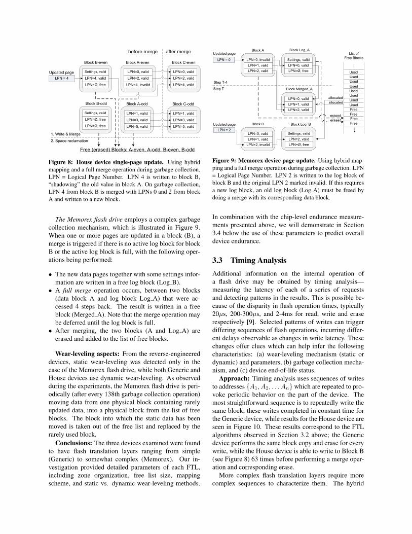
Having examined performance of NAND flash itself, wenext turn to systems comprising both flash and FTL.While work in the previous section covers a wide rangeof flash technologies, we concentrate here on relativelysmall mass-market USB drives due to the difficulties in-herent in reverse-engineering and destructive testing ofmore sophisticated devices.
Methodology: we reverse-engineered FTL opera-tion in three different USB drives, as listed in Ta-ble 3: Generic, an unbranded device based on theHynix HY27US08121A 512Mbit chip, House, a Mi-croCenter branded 2GB device based on the Intel29F16G08CANC1, and Memorex, a 512MB Memorex“Mini TravelDrive” based on an unidentified part.
In Figure 6 we see one of the devices with probe wiresattached to the I/O bus on the flash chip itself. Reverse-engineering was performed by issuing specific logicaloperations from a Linux USB host (by issuing directI/O reads or writes to the corresponding block device)and using an IO-3200 logic analyzer to capture resultingtransactions over the flash device bus. From this captureddata we were then able to decode the flash-level opera-
Generic House Memorex
Structure 16 zones 4 zones 4 zonesZone size 256 physical blocks 2048 physical blocks 1024 physical blocks
Free blocks list size 6 physical blocks per zone 30-40 physical blocks per zone 4 physical blocks per zoneMapping scheme Block-level Block-level / Hybrid Hybrid
Merge operations Partial merge Partial merge / Full merge Full mergeGarbage collection frequency At every data update At every data update Variable
Wear-leveling algorithm Dynamic Dynamic Static
Table 4: Characteristics of reverse-engineered devices
tions (read, write, erase, copy) and physical addressescorresponding to a particular logical read or write.
We characterize the flash devices based on the fol-lowing parameters: zone organization (number of zones,zone size, number of free blocks), mapping schemes,merge operations, garbage collection frequency, andwear-leveling algorithms. Investigation of these specificattributes is motivated by their importance; they are fun-damental in the design of any FTL [2, 3, 17, 19, 20,21, 25], determining space requirements, i.e. the size ofthe mapping tables to keep in RAM (zone organization,mapping schemes), overhead/performance (merge oper-ations, garbage collection frequency), device endurance(wear-leveling algorithms). The results are summarizedin Table 4, and discussed in the next sections.
Zone organization: The flash devices are divided inzones, which represent contiguous regions of flash mem-ory, with disjoint logical-to-physical mappings: a logicalblock pertaining to a zone can be mapped only in a phys-ical block from the same zone. Since the zones functionindependently from each other, when one of the zonesbecomes unusable, other zones on the same device canstill be accessed. We report actual values of zone sizesand free list sizes for the investigated devices in Table 4.
Mapping schemes: Block-mapped FTLs requiresmaller mapping tables to be stored in RAM, comparedto page-mapped FTLs (Section 2.2). For this reason,the block-level mapping scheme is more practical andwas identified in both Generic and multi-page updates ofHouse flash drives. For single-page updates, House usesthe simplified hybrid mapping scheme (which we willdescribe next), similar to Ban’s NFTL [3]. The Memo-rex flash drive uses hybrid mapping: the data blocks areblock-mapped and the log blocks are page-mapped.
Garbage collection: For the Generic drive, garbagecollection is handled immediately after each write, elim-inating the overhead of managing stale data. For Houseand Memorex, the hybrid mapping allows for several se-quential updates to be placed in the same log block. De-pending on specific writing patterns, garbage collectioncan have a variable frequency. The number of sequentialupdates that can be placed in a 64-page log block (beforea new free log block is allocated to hold updated pages of
LPN=0, valid
LPN=1, valid
LPN=2, invalid
Block A
LPN=0, valid
LPN=1, valid
LPN=2, valid
Block B
1. Write & Merge
2. Space reclamation
LPN = 2
Free (erased) Block A
Updated page
before merge after merge
Figure 7: Generic device page update. Using block-levelmapping and a partial merge operation during garbage collec-tion. LPN = Logical Page Number. New data is merged withblock A and an entire new block (B) is written.
the same logical block) ranges from 1 to 55 for Memorexand 1 to 63 for House.
We illustrate how garbage collection works after beingtriggered by a page update operation.
The Generic flash drive implements a simple page up-date mechanism (Figure 7). When a page is overwritten,a block is selected from the free block list, and the datato be written is merged with the original data block andwritten to this new block in a partial merge, resulting inthe erasure of the original data block.
The House drive allows multiple updates to occur be-fore garbage collection, using an approach illustrated inFigure 8. Flash is divided into two planes, even and odd(blocks B-even and B-odd in the figure); one log blockcan represent updates to a single block in the data area.When a single page is written, meta-data is written to thefirst page in the log block and the new data is written tothe second page; a total of 63 pages may be written tothe same block before the log must be merged. If a pageis written to another block in the plane, however, the logmust be merged immediately (via a full merge) and a newlog started.
We observe that the House flash drive implements anoptimized mechanism for multi-page updates, requiring2 erasures rather than 4. This is done by eliminating theintermediary storage step in log blocks B-even and B-odd, and writing the updated pages directly to blocks C-even and C-odd.
Block B-even
LPN = 4
Block C-oddBlock B-odd
Block C-evenBlock A-even
Block A-odd
1. Write & Merge
2. Space reclamation
LPN=1, valid
LPN=3, valid
LPN=5, valid
LPN=0, valid
LPN=2, valid
LPN=4, invalid
Settings, valid
LPN=Ø, free
LPN=Ø, free
Settings, valid
LPN=4, valid
LPN=Ø, free
LPN=1, valid
LPN=3, valid
LPN=5, valid
LPN=0, valid
LPN=2, valid
LPN=4, valid
Free (erased) Blocks: A-even, A-odd, B-even, B-odd
Updated page
before merge after merge
Figure 8: House device single-page update. Using hybridmapping and a full merge operation during garbage collection.LPN = Logical Page Number. LPN 4 is written to block B,“shadowing” the old value in block A. On garbage collection,LPN 4 from block B is merged with LPNs 0 and 2 from blockA and written to a new block.
The Memorex flash drive employs a complex garbagecollection mechanism, which is illustrated in Figure 9.When one or more pages are updated in a block (B), amerge is triggered if there is no active log block for blockB or the active log block is full, with the following oper-ations being performed:
• The new data pages together with some settings infor-mation are written in a free log block (Log B).
• A full merge operation occurs, between two blocks(data block A and log block Log A) that were ac-cessed 4 steps back. The result is written in a freeblock (Merged A). Note that the merge operation maybe deferred until the log block is full.
• After merging, the two blocks (A and Log A) areerased and added to the list of free blocks.
Wear-leveling aspects: From the reverse-engineereddevices, static wear-leveling was detected only in thecase of the Memorex flash drive, while both Generic andHouse devices use dynamic wear-leveling. As observedduring the experiments, the Memorex flash drive is peri-odically (after every 138th garbage collection operation)moving data from one physical block containing rarelyupdated data, into a physical block from the list of freeblocks. The block into which the static data has beenmoved is taken out of the free list and replaced by therarely used block.
Conclusions: The three devices examined were foundto have flash translation layers ranging from simple(Generic) to somewhat complex (Memorex). Our in-vestigation provided detailed parameters of each FTL,including zone organization, free list size, mappingscheme, and static vs. dynamic wear-leveling methods.
LPN=0, invalid
LPN=1, valid
LPN=2, valid
Block A
LPN=0, valid
LPN=1, valid
LPN=2, valid
Block Merged_A
Block Log_A
...
Used
Used
Used
Used
Free
List of
Free BlocksSettings, valid
LPN=0, valid
LPN=Ø, free
Used
Used
Used
Used
Free
Free
Free
LPN=0, valid
LPN=1, valid
LPN=2, invalid
Block B Block Log_B
Settings, valid
LPN=2, valid
LPN=Ø, free
Step T-4
Step T
allocated
allocated
erased
erased
Updated page
LPN = 0
Updated page
LPN = 2
Figure 9: Memorex device page update. Using hybrid map-ping and a full merge operation during garbage collection. LPN= Logical Page Number. LPN 2 is written to the log block ofblock B and the original LPN 2 marked invalid. If this requiresa new log block, an old log block (Log A) must be freed bydoing a merge with its corresponding data block.
In combination with the chip-level endurance measure-ments presented above, we will demonstrate in Section3.4 below the use of these parameters to predict overalldevice endurance.
3.3 Timing AnalysisAdditional information on the internal operation ofa flash drive may be obtained by timing analysis—measuring the latency of each of a series of requestsand detecting patterns in the results. This is possible be-cause of the disparity in flash operation times, typically20µs, 200-300µs, and 2-4ms for read, write and eraserespectively [9]. Selected patterns of writes can triggerdiffering sequences of flash operations, incurring differ-ent delays observable as changes in write latency. Thesechanges offer clues which can help infer the followingcharacteristics: (a) wear-leveling mechanism (static ordynamic) and parameters, (b) garbage collection mecha-nism, and (c) device end-of-life status.
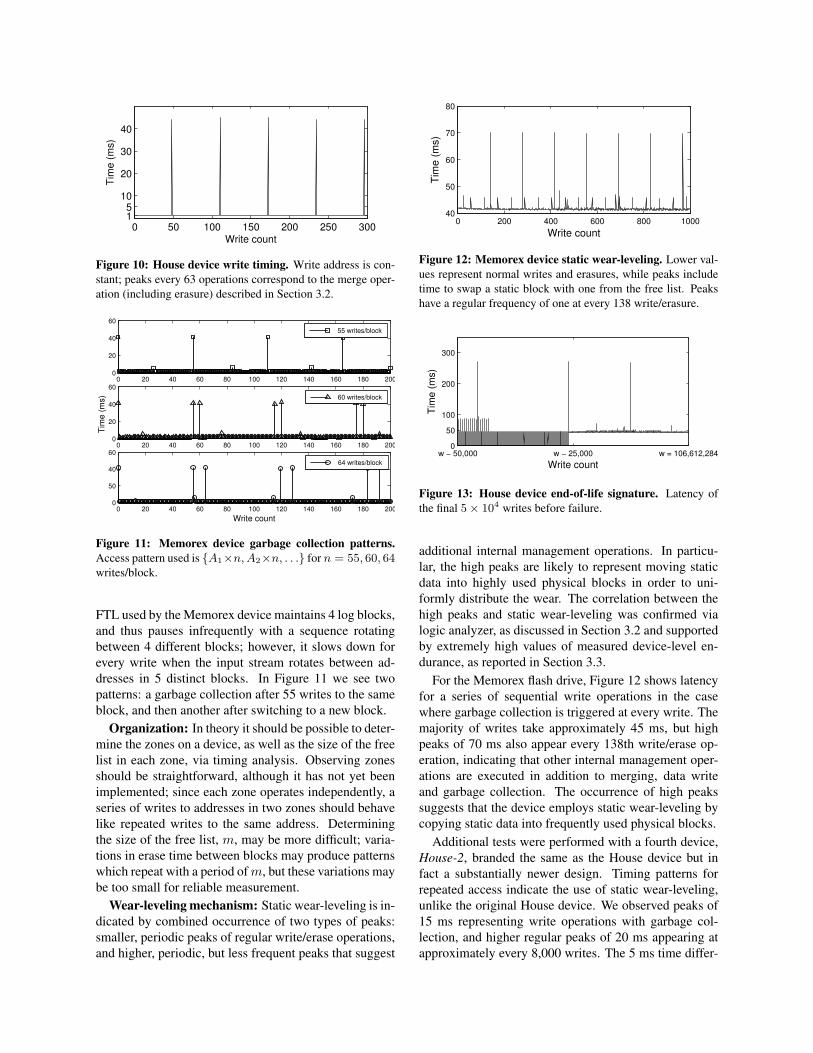
Approach: Timing analysis uses sequences of writesto addresses {A1, A2, . . . An} which are repeated to pro-voke periodic behavior on the part of the device. Themost straightforward sequence is to repeatedly write thesame block; these writes completed in constant time forthe Generic device, while results for the House device areseen in Figure 10. These results correspond to the FTLalgorithms observed in Section 3.2 above; the Genericdevice performs the same block copy and erase for everywrite, while the House device is able to write to Block B(see Figure 8) 63 times before performing a merge oper-ation and corresponding erase.
More complex flash translation layers require morecomplex sequences to characterize them. The hybrid
0 50 100 150 200 250 30015
10
20
30
40
Write count
Tim
e (
ms)
Figure 10: House device write timing. Write address is con-stant; peaks every 63 operations correspond to the merge oper-ation (including erasure) described in Section 3.2.
0 20 40 60 80 100 120 140 160 180 2000
20
40
60
55 writes/block
0 20 40 60 80 100 120 140 160 180 2000
20
40
60
60 writes/block
0 20 40 60 80 100 120 140 160 180 2000
50
40
60
Write count
Tim
e (
ms)
64 writes/block
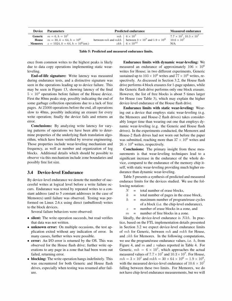
Figure 11: Memorex device garbage collection patterns.Access pattern used is {A1×n, A2×n, . . .} for n = 55, 60, 64writes/block.
FTL used by the Memorex device maintains 4 log blocks,and thus pauses infrequently with a sequence rotatingbetween 4 different blocks; however, it slows down forevery write when the input stream rotates between ad-dresses in 5 distinct blocks. In Figure 11 we see twopatterns: a garbage collection after 55 writes to the sameblock, and then another after switching to a new block.
Organization: In theory it should be possible to deter-mine the zones on a device, as well as the size of the freelist in each zone, via timing analysis. Observing zonesshould be straightforward, although it has not yet beenimplemented; since each zone operates independently, aseries of writes to addresses in two zones should behavelike repeated writes to the same address. Determiningthe size of the free list, m, may be more difficult; varia-tions in erase time between blocks may produce patternswhich repeat with a period ofm, but these variations maybe too small for reliable measurement.
Wear-leveling mechanism: Static wear-leveling is in-dicated by combined occurrence of two types of peaks:smaller, periodic peaks of regular write/erase operations,and higher, periodic, but less frequent peaks that suggest
0 200 400 600 800 100040
50
60
70
80
Write count
Tim
e (
ms)
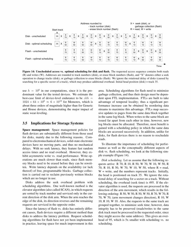
Figure 12: Memorex device static wear-leveling. Lower val-ues represent normal writes and erasures, while peaks includetime to swap a static block with one from the free list. Peakshave a regular frequency of one at every 138 write/erasure.
w − 50,000 w − 25,000 w = 106,612,2840
50
100
200
300
Write count
Tim
e (
ms)
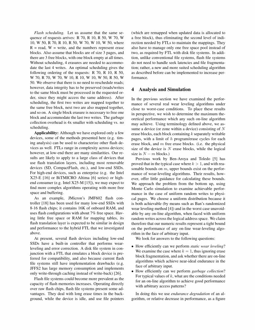
Figure 13: House device end-of-life signature. Latency ofthe final 5× 10⁴ writes before failure.
additional internal management operations. In particu-lar, the high peaks are likely to represent moving staticdata into highly used physical blocks in order to uni-formly distribute the wear. The correlation between thehigh peaks and static wear-leveling was confirmed vialogic analyzer, as discussed in Section 3.2 and supportedby extremely high values of measured device-level en-durance, as reported in Section 3.3.
For the Memorex flash drive, Figure 12 shows latencyfor a series of sequential write operations in the casewhere garbage collection is triggered at every write. Themajority of writes take approximately 45 ms, but highpeaks of 70 ms also appear every 138th write/erase op-eration, indicating that other internal management oper-ations are executed in addition to merging, data writeand garbage collection. The occurrence of high peakssuggests that the device employs static wear-leveling bycopying static data into frequently used physical blocks.
Additional tests were performed with a fourth device,House-2, branded the same as the House device but infact a substantially newer design. Timing patterns forrepeated access indicate the use of static wear-leveling,unlike the original House device. We observed peaks of15 ms representing write operations with garbage col-lection, and higher regular peaks of 20 ms appearing atapproximately every 8,000 writes. The 5 ms time differ-
Device Parameters Predicted endurance Measured enduranceGeneric m = 6, h = 107 mh 6× 10⁷ 7.7× 10⁷, 10.3× 10⁷
House m = 30, k = 64, h = 106 between mh and mkh between 3× 10⁷ and 1.9× 10⁹ 10.6× 10⁷
Memorex z = 1024, k = 64, h = 106(est.) zkh 6× 10¹⁰ N/A
Table 5: Predicted and measured endurance limits.
ence from common writes to the highest peaks is likelydue to data copy operations implementing static wear-leveling.
End-of-life signature: Write latency was measuredduring endurance tests, and a distinctive signature wasseen in the operations leading up to device failure. Thismay be seen in Figure 13, showing latency of the final5 × 104 operations before failure of the House device.First the 80ms peaks stop, possibly indicating the end ofsome garbage collection operations due to a lack of freepages. At 25000 operations before the end, all operationsslow to 40ms, possibly indicating an erasure for everywrite operation; finally the device fails and returns anerror.
Conclusions: By analyzing write latency for vary-ing patterns of operations we have been able to deter-mine properties of the underlying flash translation algo-rithm, which have been verified by reverse engineering.Those properties include wear-leveling mechanism andfrequency, as well as number and organization of logblocks. Additional details which should be possible toobserve via this mechanism include zone boundaries andpossibly free list size.
3.4 Device-level EnduranceBy device-level endurance we denote the number of suc-cessful writes at logical level before a write failure oc-curs. Endurance was tested by repeated writes to a con-stant address (and to 5 constant addresses in the case ofMemorex) until failure was observed. Testing was per-formed on Linux 2.6.x using direct (unbuffered) writesto the block devices.
Several failure behaviors were observed:
• silent: The write operation succeeds, but read verifiesthat data was not written.
• unknown error: On multiple occasions, the test ap-plication exited without any indication of error. Inmany casses, further writes were possible.
• error: An I/O error is returned by the OS. This wasobserved for the House flash drive; further write op-erations to any page in a zone that had been worn outfailed, returning error.
• blocking: The write operation hangs indefinitely. Thiswas encountered for both Generic and House flashdrives, especially when testing was resumed after fail-ure.
Endurance limits with dynamic wear-leveling: Wemeasured an endurance of approximately 106 × 106
writes for House; in two different experiments, Genericsustained up to 103×106 writes and 77×106 writes, re-spectively. As discussed in Section 3.2, the House flashdrive performs 4 block erasures for 1-page updates, whilethe Generic flash drive performs only one block erasure.However, the list of free blocks is about 5 times largerfor House (see Table 3), which may explain the higherdevice-level endurance of the House flash drive.
Endurance limits with static wear-leveling: Wear-ing out a device that employs static wear-leveling (e.g.the Memorex and House-2 flash drives) takes consider-ably longer time than wearing out one that employs dy-namic wear-leveling (e.g. the Generic and House flashdrives). In the experiments conducted, the Memorex andHouse-2 flash drives had not worn out before the paperwas submitted, reaching more than 37 × 106 writes and26× 108 writes, respectively.
Conclusions: The primary insight from these mea-surements is that wear-leveling techniques lead to asignificant increase in the endurance of the whole de-vice, compared to the endurance of the memory chip it-self, with static wear-leveling providing much higher en-durance than dynamic wear-leveling.
Table 5 presents a synthesis of predicted and measuredendurace limits for the devices studied. We use the fol-lowing notation:
N = total number of erase blocks,k = total number of pages in the erase block,h = maximum number of program/erase cycles
of a block (i.e. the chip-level endurance),z = number of erase blocks in a zone, andm = number of free blocks in a zone.
Ideally, the device-level endurance is Nkh. In prac-tice, based on the FTL implementation details presentedin Section 3.2 we expect device-level endurance limitsof mh for Generic, between mh and mkh for House,and zkh for Memorex. In the following computations,we use the program/erase endurance values, i.e. h, fromFigure 4, and m and z values reported in Table 4. ForGeneric, mh = 6 × 10⁷, which approaches the actualmeasured values of 7.7×10⁷ and 10.3×10⁷. For House,mh = 3× 10⁷ and mkh = 30× 64× 106 = 1.9× 10⁹,with the measured device-level endurance of 10.6× 10⁷
falling between these two limits. For Memorex, we donot have chip-level endurance measurements, but we will
R
70
R
10
R
50
W
70
W
10
W
5035
R
70
R
10
R
50
W
70
W
10
W
50Disk - unscheduled X X X X X X X X X X X X
R
50
W
50
R
50
W
50
R
70
W
7035
R
70
W
70
R
10
W
10
R
10
W
10Disk - optimal scheduling X X X
Flash - unscheduledR
70
R
10
R
50
W
70
W
10
W
50
R
70
R
10
R
50
W
70
W
10
W
50X X X X
Flash - optimal schedulingR
70
R
10
R
50
W
70
R
70
W
70
W
10
R
10
W
10
W
50
R
50
W
50X
Time
Start track
X = seek (disk), or
garbage collection (flash)
R = read, W = write
Address rounded to:
- track number (disk)
- erase block number (flash)
Figure 14: Unscheduled access vs. optimal scheduling for disk and flash. The requested access sequence contains both reads(R) and writes (W). Addresses are rounded to track numbers (disk), or erase block numbers (flash), and “X” denotes either a seekoperation to change tracks (disk), or garbage collection to erase blocks (flash). We ignore the rotational delay of disks (caused bysearching for a specific sector of a track), which may produce additional overhead. Initial head position (disk) = track 35.
use h = 106 in our computations, since it is the pre-dominant value for the tested devices. We estimate thebest-case limit of device-level endurance to be zkh =1024 × 64 × 106 ≈ 6 × 10¹⁰ for Memorex, which isabout three orders of magnitude higher than for Genericand House devices, demonstrating the major impact ofstatic wear-leveling.
3.5 Implications for Storage Systems
Space management: Space management policies forflash devices are substantially different from those usedfor disks, mainly due to the following reasons. Com-pared to electromechanical devices, solid-state electronicdevices have no moving parts, and thus no mechanicaldelays. With no seek latency, they feature fast randomaccess times and no read overhead. However, they ex-hibit asymmetric write vs. read performance. Write op-erations are much slower than reads, since flash mem-ory blocks need to be erased before they can be rewrit-ten. Write latency depends on the availability (or lackthereof) of free, programmable blocks. Garbage collec-tion is carried out to reclaim previously written blockswhich are no longer in use.
Disks address the seek overhead problem withscheduling algorithms. One well-known method is theelevator algorithm (also called SCAN), in which requestsare sorted by track number and serviced only in the cur-rent direction of the disk arm. When the arm reaches theedge of the disk, its direction reverses and the remainingrequests are serviced in the opposite order.
Since the latency of flash vs. disks has entirely differ-ent causes, flash devices require a different method thandisks to address the latency problem. Request schedul-ing algorithms for flash have not yet been implementedin practice, leaving space for much improvement in this
area. Scheduling algorithms for flash need to minimizegarbage collection, and thus their design must be depen-dent upon FTL implementation. FTLs are built to takeadvantage of temporal locality; thus a significant per-formance increase can be obtained by reordering datastreams to maximize this advantage. FTLs map succes-sive updates to pages from the same data block togetherin the same log block. When writes to the same block areissued far apart from each other in time, however, newlog blocks must be allocated. Therefore, most benefit isgained with a scheduling policy in which the same datablocks are accessed successively. In addition, unlike fordisks, for flash devices there is no reason to reschedulereads.
To illustrate the importance of scheduling for perfor-mance as well as the conceptually different aspects ofdisk vs. flash scheduling, we look at the following sim-ple example (Figure 14).
Disk scheduling. Let us assume that the following re-quests arrive: R 70, R 10, R 50, W 70, W 10, W 50, R70, R 10, R 50, W 70, W 10, W 50, where R = read,W = write, and the numbers represent tracks. Initially,the head is positioned on track 35. We ignore the rota-tional delay of searching for a sector on a track. Withoutscheduling, the overhead (seek time) is 495. If the ele-vator algorithm is used, the requests are processed in thedirection of the arm movement, which results in the fol-lowing ordering: R 50, W 50, R 50, W 50, R 70, W 70, R70, W 70, (arm movement changes direction), R 10, W10, R 10, W 10. Also, the requests to the same track aregrouped together, to minimize seek time; however, dataintegrity has to be preserved (reads/writes to the samedisk track must be processed in the requested order, sincethey might access the same address). This gives an over-head of 95, which is 5x smaller with scheduling vs. noscheduling.
Flash scheduling. Let us assume that the same se-quence of requests arrives: R 70, R 10, R 50, W 70, W10, W 50, R 70, R 10, R 50, W 70, W 10, W 50, whereR = read, W = write, and the numbers represent eraseblocks. Also assume that blocks are of size 3 pages, andthere are 3 free blocks, with one block empty at all times.Without scheduling, 4 erasures are needed to accommo-date the last 4 writes. An optimal scheduling gives thefollowing ordering of the requests: R 70, R 10, R 50,W 70, R 70, W 70, W 10, R 10, W 10, W 50, R 50, W50. We observe that there is no need to reschedule reads;however, data integrity has to be preserved (reads/writesto the same block must be processed in the requested or-der, since they might access the same address). Afterscheduling, the first two writes are mapped together tothe same free block, next two are also mapped together,and so on. A single block erasure is necessary to free oneblock and accommodate the last two writes. The garbagecollection overhead is 4x smaller with scheduling vs. noscheduling.
Applicability: Although we have explored only a fewdevices, some of the methods presented here (e.g. tim-ing analysis) can be used to characterize other flash de-vices as well. FTLs range in complexity across devices;however, at low-end there are many similarities. Our re-sults are likely to apply to a large class of devices thatuse flash translation layers, including most removabledevices (SD, CompactFlash, etc.), and low-end SSDs.For high-end devices, such as enterprise (e.g. the IntelX25-E [16] or BiTMICRO Altima [6] series) or high-end consumer (e.g. Intel X25-M [15]), we may expect tofind more complex algorithms operating with more freespace and buffering.
As an example, JMicron’s JMF602 flash con-troller [18] has been used for many low-end SSDs with8-16 flash chips; it contains 16K of onboard RAM, anduses flash configurations with about 7% free space. Hav-ing little free space or RAM for mapping tables, itsflash translation layer is expected to be similar in designand performance to the hybrid FTL that we investigatedabove.
At present, several flash devices including low-endSSDs have a built-in controller that performs wear-leveling and error correction. A disk file system in con-junction with a FTL that emulates a block device is pre-ferred for compatibility, and also because current flashfile systems still have implementation drawbacks (e.g.JFFS2 has large memory consumption and implementsonly write-through caching instead of write-back) [26].
Flash file systems could become more prevalent as thecapacity of flash memories increases. Operating directlyover raw flash chips, flash file systems present some ad-vantages. They deal with long erase times in the back-ground, while the device is idle, and use file pointers
(which are remapped when updated data is allocated toa free block), thus eliminating the second level of indi-rection needed by FTLs to maintain the mappings. Theyalso have to manage only one free space pool instead oftwo, as required by FTL with disk file systems. In addi-tion, unlike conventional file systems, flash file systemsdo not need to handle seek latencies and file fragmenta-tion; rather, a new and more suited scheduling algorithmas described before can be implemented to increase per-formance.
4 Analysis and Simulation
In the previous section we have examined the perfor-mance of several real wear leveling algorithms underclose to worst-case conditions. To place these resultsin perspective, we wish to determine the maximum the-oretical performance which any such on-line algorithmmay achieve. Using terminology defined above, we as-sume a device (or zone within a device) consisting of Nerase blocks, each block containing k separately writablepages, with a limit of h program/erase cycles for eacherase block, and m free erase blocks. (i.e. the physicalsize of the device is N erase blocks, while the logicalsize is N −m blocks.)
Previous work by Ben-Aroya and Toledo [5] hasproved that in the typical case where k > 1, and with rea-sonable bounds on m, upper bounds exist on the perfor-mance of wear-leveling algorithms. Their results, how-ever, offer little guidance for calculating these bounds.We approach the problem from the bottom up, usingMonte Carlo simulation to examine achievable perfor-mance in the case of uniform random writes to physi-cal pages. We choose a uniform distribution because itis both achievable (by means such as Ban’s randomizedwear leveling method [4]) and in the worst case unavoid-able by any on-line algorithm, when faced with uniformrandom writes across the logical address space. We claimtherefore that our numeric results represent a tight boundon the performance of any on-line wear-leveling algo-rithm in the face of arbitrary input.
We look for answers to the following questions:
• How efficiently can we perform static wear leveling?We examine the case where k = 1, thus ignoring eraseblock fragmentation, and ask whether there are on-linealgorithms which achieve near-ideal endurance in theface of arbitrary input.
• How efficiently can we perform garbage collection?For typical values of k, what are the conditions neededfor an on-line algorithm to achieve good performancewith arbitrary access patterns?
In doing this we use endurance degradation of an al-gorithm, or relative decrease in performance, as a figure
0
2
4
6
8
10
0 5 10 15 20
Num
ber
of
Pro
gra
m/E
rase
Cycl
es
Page Number
Worn-out blocks
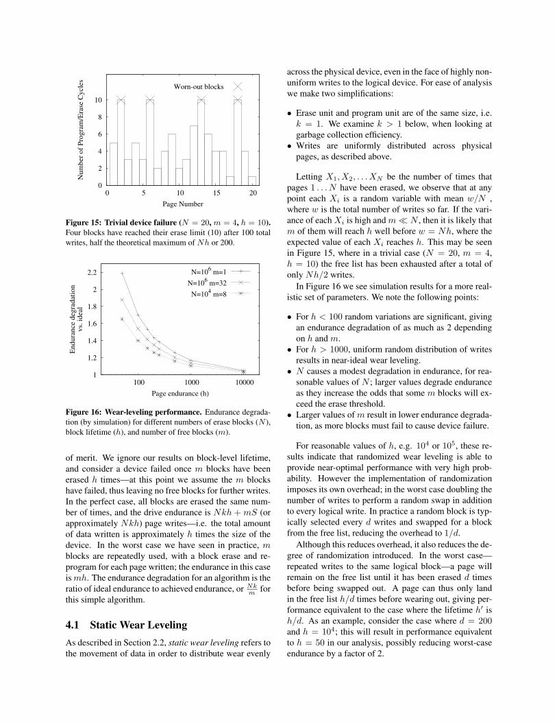
Figure 15: Trivial device failure (N = 20, m = 4, h = 10).Four blocks have reached their erase limit (10) after 100 totalwrites, half the theoretical maximum of Nh or 200.
1
1.2
1.4
1.6
1.8
2
2.2
100 1000 10000
Endura
nce
deg
radat
ion
vs.
idea
l
Page endurance (h)
N=106 m=1
N=106 m=32
N=104 m=8
Figure 16: Wear-leveling performance. Endurance degrada-tion (by simulation) for different numbers of erase blocks (N ),block lifetime (h), and number of free blocks (m).
of merit. We ignore our results on block-level lifetime,and consider a device failed once m blocks have beenerased h times—at this point we assume the m blockshave failed, thus leaving no free blocks for further writes.In the perfect case, all blocks are erased the same num-ber of times, and the drive endurance is Nkh + mS (orapproximately Nkh) page writes—i.e. the total amountof data written is approximately h times the size of thedevice. In the worst case we have seen in practice, mblocks are repeatedly used, with a block erase and re-program for each page written; the endurance in this caseismh. The endurance degradation for an algorithm is theratio of ideal endurance to achieved endurance, or Nk
m forthis simple algorithm.
4.1 Static Wear LevelingAs described in Section 2.2, static wear leveling refers tothe movement of data in order to distribute wear evenly
across the physical device, even in the face of highly non-uniform writes to the logical device. For ease of analysiswe make two simplifications:
• Erase unit and program unit are of the same size, i.e.k = 1. We examine k > 1 below, when looking atgarbage collection efficiency.
• Writes are uniformly distributed across physicalpages, as described above.
Letting X1, X2, . . . XN be the number of times thatpages 1 . . . N have been erased, we observe that at anypoint each Xi is a random variable with mean w/N ,where w is the total number of writes so far. If the vari-ance of each Xi is high and m� N , then it is likely thatm of them will reach h well before w = Nh, where theexpected value of each Xi reaches h. This may be seenin Figure 15, where in a trivial case (N = 20, m = 4,h = 10) the free list has been exhausted after a total ofonly Nh/2 writes.
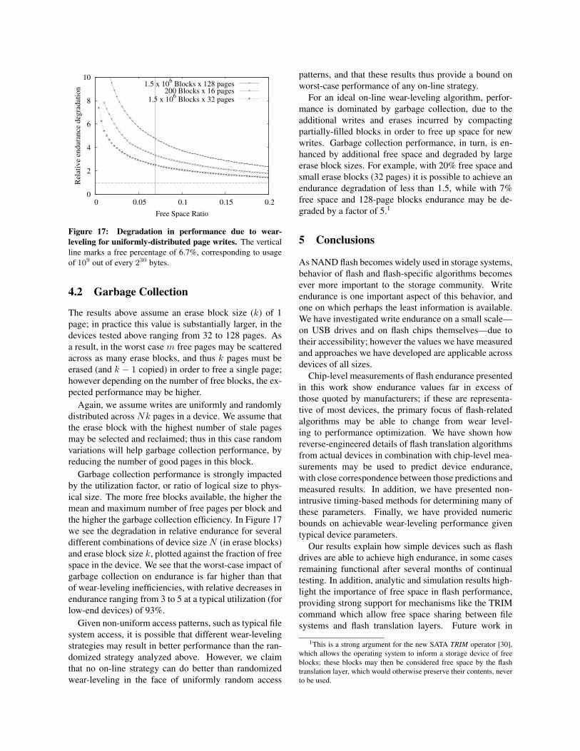
In Figure 16 we see simulation results for a more real-istic set of parameters. We note the following points:
• For h < 100 random variations are significant, givingan endurance degradation of as much as 2 dependingon h and m.
• For h > 1000, uniform random distribution of writesresults in near-ideal wear leveling.
• N causes a modest degradation in endurance, for rea-sonable values of N ; larger values degrade enduranceas they increase the odds that some m blocks will ex-ceed the erase threshold.
• Larger values of m result in lower endurance degrada-tion, as more blocks must fail to cause device failure.
For reasonable values of h, e.g. 104 or 105, these re-sults indicate that randomized wear leveling is able toprovide near-optimal performance with very high prob-ability. However the implementation of randomizationimposes its own overhead; in the worst case doubling thenumber of writes to perform a random swap in additionto every logical write. In practice a random block is typ-ically selected every d writes and swapped for a blockfrom the free list, reducing the overhead to 1/d.
Although this reduces overhead, it also reduces the de-gree of randomization introduced. In the worst case—repeated writes to the same logical block—a page willremain on the free list until it has been erased d timesbefore being swapped out. A page can thus only landin the free list h/d times before wearing out, giving per-formance equivalent to the case where the lifetime h′ ish/d. As an example, consider the case where d = 200and h = 104; this will result in performance equivalentto h = 50 in our analysis, possibly reducing worst-caseendurance by a factor of 2.
0
2
4
6
8
10
0 0.05 0.1 0.15 0.2
Rel
ativ
e en
dura
nce
deg
radat
ion
Free Space Ratio
1.5 x 10⁶ Blocks x 128 pages
200 Blocks x 16 pages1.5 x 10
6 Blocks x 32 pages
Figure 17: Degradation in performance due to wear-leveling for uniformly-distributed page writes. The verticalline marks a free percentage of 6.7%, corresponding to usageof 109 out of every 230 bytes.
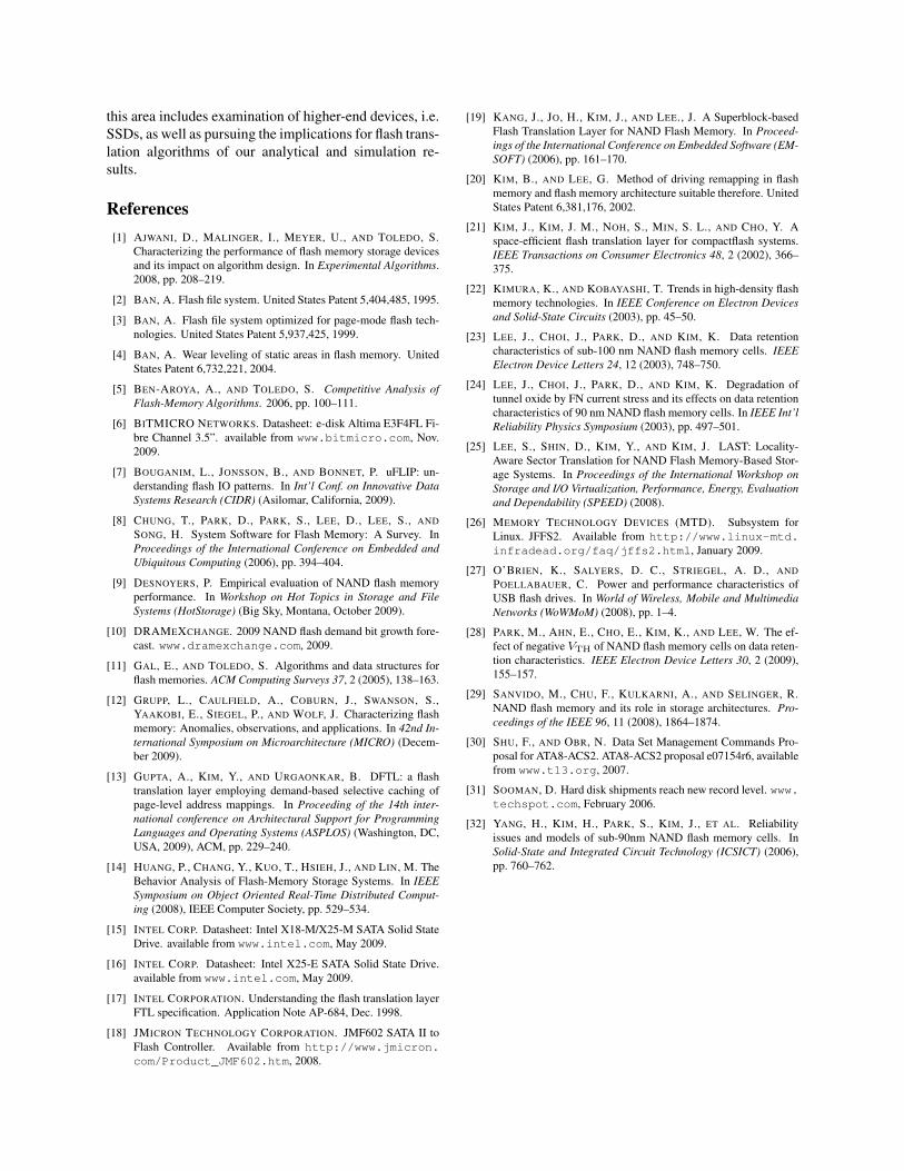
4.2 Garbage Collection
The results above assume an erase block size (k) of 1page; in practice this value is substantially larger, in thedevices tested above ranging from 32 to 128 pages. Asa result, in the worst case m free pages may be scatteredacross as many erase blocks, and thus k pages must beerased (and k − 1 copied) in order to free a single page;however depending on the number of free blocks, the ex-pected performance may be higher.
Again, we assume writes are uniformly and randomlydistributed across Nk pages in a device. We assume thatthe erase block with the highest number of stale pagesmay be selected and reclaimed; thus in this case randomvariations will help garbage collection performance, byreducing the number of good pages in this block.
Garbage collection performance is strongly impactedby the utilization factor, or ratio of logical size to phys-ical size. The more free blocks available, the higher themean and maximum number of free pages per block andthe higher the garbage collection efficiency. In Figure 17we see the degradation in relative endurance for severaldifferent combinations of device sizeN (in erase blocks)and erase block size k, plotted against the fraction of freespace in the device. We see that the worst-case impact ofgarbage collection on endurance is far higher than thatof wear-leveling inefficiencies, with relative decreases inendurance ranging from 3 to 5 at a typical utilization (forlow-end devices) of 93%.
Given non-uniform access patterns, such as typical filesystem access, it is possible that different wear-levelingstrategies may result in better performance than the ran-domized strategy analyzed above. However, we claimthat no on-line strategy can do better than randomizedwear-leveling in the face of uniformly random access
patterns, and that these results thus provide a bound onworst-case performance of any on-line strategy.
For an ideal on-line wear-leveling algorithm, perfor-mance is dominated by garbage collection, due to theadditional writes and erases incurred by compactingpartially-filled blocks in order to free up space for newwrites. Garbage collection performance, in turn, is en-hanced by additional free space and degraded by largeerase block sizes. For example, with 20% free space andsmall erase blocks (32 pages) it is possible to achieve anendurance degradation of less than 1.5, while with 7%free space and 128-page blocks endurance may be de-graded by a factor of 5.1
5 Conclusions
As NAND flash becomes widely used in storage systems,behavior of flash and flash-specific algorithms becomesever more important to the storage community. Writeendurance is one important aspect of this behavior, andone on which perhaps the least information is available.We have investigated write endurance on a small scale—on USB drives and on flash chips themselves—due totheir accessibility; however the values we have measuredand approaches we have developed are applicable acrossdevices of all sizes.
Chip-level measurements of flash endurance presentedin this work show endurance values far in excess ofthose quoted by manufacturers; if these are representa-tive of most devices, the primary focus of flash-relatedalgorithms may be able to change from wear level-ing to performance optimization. We have shown howreverse-engineered details of flash translation algorithmsfrom actual devices in combination with chip-level mea-surements may be used to predict device endurance,with close correspondence between those predictions andmeasured results. In addition, we have presented non-intrusive timing-based methods for determining many ofthese parameters. Finally, we have provided numericbounds on achievable wear-leveling performance giventypical device parameters.
Our results explain how simple devices such as flashdrives are able to achieve high endurance, in some casesremaining functional after several months of continualtesting. In addition, analytic and simulation results high-light the importance of free space in flash performance,providing strong support for mechanisms like the TRIMcommand which allow free space sharing between filesystems and flash translation layers. Future work in
1This is a strong argument for the new SATA TRIM operator [30],which allows the operating system to inform a storage device of freeblocks; these blocks may then be considered free space by the flashtranslation layer, which would otherwise preserve their contents, neverto be used.
this area includes examination of higher-end devices, i.e.SSDs, as well as pursuing the implications for flash trans-lation algorithms of our analytical and simulation re-sults.
References[1] AJWANI, D., MALINGER, I., MEYER, U., AND TOLEDO, S.
Characterizing the performance of flash memory storage devicesand its impact on algorithm design. In Experimental Algorithms.2008, pp. 208–219.
[2] BAN, A. Flash file system. United States Patent 5,404,485, 1995.
[3] BAN, A. Flash file system optimized for page-mode flash tech-nologies. United States Patent 5,937,425, 1999.
[4] BAN, A. Wear leveling of static areas in flash memory. UnitedStates Patent 6,732,221, 2004.
[5] BEN-AROYA, A., AND TOLEDO, S. Competitive Analysis ofFlash-Memory Algorithms. 2006, pp. 100–111.
[6] BITMICRO NETWORKS. Datasheet: e-disk Altima E3F4FL Fi-bre Channel 3.5”. available from www.bitmicro.com, Nov.2009.
[7] BOUGANIM, L., JONSSON, B., AND BONNET, P. uFLIP: un-derstanding flash IO patterns. In Int’l Conf. on Innovative DataSystems Research (CIDR) (Asilomar, California, 2009).
[8] CHUNG, T., PARK, D., PARK, S., LEE, D., LEE, S., ANDSONG, H. System Software for Flash Memory: A Survey. InProceedings of the International Conference on Embedded andUbiquitous Computing (2006), pp. 394–404.
[9] DESNOYERS, P. Empirical evaluation of NAND flash memoryperformance. In Workshop on Hot Topics in Storage and FileSystems (HotStorage) (Big Sky, Montana, October 2009).
[10] DRAMEXCHANGE. 2009 NAND flash demand bit growth fore-cast. www.dramexchange.com, 2009.
[11] GAL, E., AND TOLEDO, S. Algorithms and data structures forflash memories. ACM Computing Surveys 37, 2 (2005), 138–163.
[12] GRUPP, L., CAULFIELD, A., COBURN, J., SWANSON, S.,YAAKOBI, E., SIEGEL, P., AND WOLF, J. Characterizing flashmemory: Anomalies, observations, and applications. In 42nd In-ternational Symposium on Microarchitecture (MICRO) (Decem-ber 2009).
[13] GUPTA, A., KIM, Y., AND URGAONKAR, B. DFTL: a flashtranslation layer employing demand-based selective caching ofpage-level address mappings. In Proceeding of the 14th inter-national conference on Architectural Support for ProgrammingLanguages and Operating Systems (ASPLOS) (Washington, DC,USA, 2009), ACM, pp. 229–240.
[14] HUANG, P., CHANG, Y., KUO, T., HSIEH, J., AND LIN, M. TheBehavior Analysis of Flash-Memory Storage Systems. In IEEESymposium on Object Oriented Real-Time Distributed Comput-ing (2008), IEEE Computer Society, pp. 529–534.
[15] INTEL CORP. Datasheet: Intel X18-M/X25-M SATA Solid StateDrive. available from www.intel.com, May 2009.
[16] INTEL CORP. Datasheet: Intel X25-E SATA Solid State Drive.available from www.intel.com, May 2009.
[17] INTEL CORPORATION. Understanding the flash translation layerFTL specification. Application Note AP-684, Dec. 1998.
[18] JMICRON TECHNOLOGY CORPORATION. JMF602 SATA II toFlash Controller. Available from http://www.jmicron.com/Product_JMF602.htm, 2008.
[19] KANG, J., JO, H., KIM, J., AND LEE., J. A Superblock-basedFlash Translation Layer for NAND Flash Memory. In Proceed-ings of the International Conference on Embedded Software (EM-SOFT) (2006), pp. 161–170.
[20] KIM, B., AND LEE, G. Method of driving remapping in flashmemory and flash memory architecture suitable therefore. UnitedStates Patent 6,381,176, 2002.
[21] KIM, J., KIM, J. M., NOH, S., MIN, S. L., AND CHO, Y. Aspace-efficient flash translation layer for compactflash systems.IEEE Transactions on Consumer Electronics 48, 2 (2002), 366–375.
[22] KIMURA, K., AND KOBAYASHI, T. Trends in high-density flashmemory technologies. In IEEE Conference on Electron Devicesand Solid-State Circuits (2003), pp. 45–50.
[23] LEE, J., CHOI, J., PARK, D., AND KIM, K. Data retentioncharacteristics of sub-100 nm NAND flash memory cells. IEEEElectron Device Letters 24, 12 (2003), 748–750.
[24] LEE, J., CHOI, J., PARK, D., AND KIM, K. Degradation oftunnel oxide by FN current stress and its effects on data retentioncharacteristics of 90 nm NAND flash memory cells. In IEEE Int’lReliability Physics Symposium (2003), pp. 497–501.
[25] LEE, S., SHIN, D., KIM, Y., AND KIM, J. LAST: Locality-Aware Sector Translation for NAND Flash Memory-Based Stor-age Systems. In Proceedings of the International Workshop onStorage and I/O Virtualization, Performance, Energy, Evaluationand Dependability (SPEED) (2008).
[26] MEMORY TECHNOLOGY DEVICES (MTD). Subsystem forLinux. JFFS2. Available from http://www.linux-mtd.infradead.org/faq/jffs2.html, January 2009.
[27] O’BRIEN, K., SALYERS, D. C., STRIEGEL, A. D., ANDPOELLABAUER, C. Power and performance characteristics ofUSB flash drives. In World of Wireless, Mobile and MultimediaNetworks (WoWMoM) (2008), pp. 1–4.
[28] PARK, M., AHN, E., CHO, E., KIM, K., AND LEE, W. The ef-fect of negative VTH of NAND flash memory cells on data reten-tion characteristics. IEEE Electron Device Letters 30, 2 (2009),155–157.
[29] SANVIDO, M., CHU, F., KULKARNI, A., AND SELINGER, R.NAND flash memory and its role in storage architectures. Pro-ceedings of the IEEE 96, 11 (2008), 1864–1874.
[30] SHU, F., AND OBR, N. Data Set Management Commands Pro-posal for ATA8-ACS2. ATA8-ACS2 proposal e07154r6, availablefrom www.t13.org, 2007.
[31] SOOMAN, D. Hard disk shipments reach new record level. www.techspot.com, February 2006.
[32] YANG, H., KIM, H., PARK, S., KIM, J., ET AL. Reliabilityissues and models of sub-90nm NAND flash memory cells. InSolid-State and Integrated Circuit Technology (ICSICT) (2006),pp. 760–762.