Embed Size (px)
Citation preview
X-ray Diffraction Analysis of InAs Nanowires
Faculty of Science and Engineers Of Physics
University of Siegen Germany
For the PhD degree
by
Anton Davydok Solid State Physics Group
University of Siegen 57072, Walter-Flex-Str, 3
Siegen, Germany

X-ray Diffraction Analysis of InAs Nanowires
DISSERTATION
zur Erlangung des Grades eines Doktors
der Naturwissenschaften
vorgelegt von
M. Sc. Anton Davydok
eingereicht bei der Naturwissenschaftlich-Technischen Fakultät
der Universität Siegen
Siegen 2013

Referees:
Prof. Dr. Ullrich Pietsch
Prof. Dr. Vaclav Holy
Date of examination: 08.04.2013
Contents
List of abbreviations . . . . . . I
Abstracts . . . . . . . . II
Zusammenfassung . . . . . . III
Chapter 1 Introduction . . . . . . . 1
Chapter 2 VLS/VSS growth . . . . . . 3
2.1 Why InAs nanowires . . . . . . 4
2.2 Vapor-Liquid-Solid Growth . . . . . 6
2.3 Crystal phases of InAs. . . . . . 11
Chapter 3 X-ray Diffraction: Kinematical Scattering Theory. . 16
3.1 Crystal structure . . . . . . 17
3.2 Reciprocal space . . . . . . 18
3.3 X-ray diffraction on crystal . . . . . 20
3.4 The Laue equations and Bragg interpretation
of diffraction conditions . . . . . 22
3.5 Lattice sum and Laue conditions . . . 23
3.6 Atomic form factor and structure factor . . . 24
3.7 Crystal truncation rod . . . . . 25
3.8 X-ray diffraction from zinc-blende and wurtzite structures . 27
3.9 Coherence of X-ray beam . . . . . 30
3.10 Reciprocal space coordinates . . . . . 32
Chapter 4 MOVPE Au-assisted growth of InAs nanowires on
GaAs[111]B substrate. . . . . . . 33
4.1 Introduction . . . . . . . 34
4.2 Experimental technique . . . . . 35
4.3 Results and discussion . . . . . 37
4.4 Growth model . . . . . . . 40
4.5 Summery . . . . . . . 41
Chapter 5 Growth parameters influence on phase composition and defect
structure of InAs nanowires grown by self-assisted molecular beam
epitaxy onto Si (111) . . . . . . 42
5.1 As-/In/rich conditions . . . . . . 47
5.2 Substrate coverage . . . . . . 49
5.3 Substrate temperature . . . . . 51
5.4 Growth rate . . . . . . . 54
5.5 Conclusions . . . . . . . 57
Chapter 6 Structural Phase composition of InAs nanowires grown by
self-assisted molecular beam epitaxy onto Si(111) . 58
6.1 Introduction . . . . . . . 59
6.2 MBE growth . . . . . . . 60
6.3 Experimental technique and results. . . . 61
6.3.1 Ensemble measurements . . . . 62
6.3.2 Grazing incident diffraction . . . . 67
6.3.3 Single wire resolved measurements . . . 68
6.4 Simulations . . . . . . . 72
6.5 Discussion. . . . . . . . 75
6.6 Conclusions . . . . . . . 76

Conclusions . . . . . . . . . 77
References . . . . . . . . . 79
Acknowledgments . . . . . . . . 82
Appendix - MATLAB scripts . . . . . . 83

I
List of abbreviations
AFM . . . Atomic Force Microscopy
Au . . . Chemical symbol denote gold
bcc . . . body centered cell
CTR . . . Crystal Truncation Rod
EDX . . . Energy Dispersive X-ray
ESF . . . Extrinsic Stacking Faults
ESRF . . . European Synchrotron Radiation Facility
fcc . . . face centered cell
FET . . . Field-Effect Transistor
FWHM . . Full Width Half Maxima
FZP . . . Fresnel Zone Plate
GaAs . . . Galliumarsenid
GID . . . Grazing Incident Diffraction
GR . . . Growth Rate
HSQ . . . Hydrogen Silsesquioxane
InAs . . . Indiumarsenid
ISF . . . Intrinsic Stacking Faults
LED . . . Light-Emitting Diode
MBE . . . Molecular Beam Epitaxy
ML . . . Monolayer
MOCVD . . Metal-Organic Chemical Vapour Deposition
MOVPE . . Metal-Organic Vapour Phase Epitaxy

I
NW . . . Nanowire
PL . . . Photoluminescence
RHEED . . Reflection High-Energy Electron Diffraction
RSM . . . Reciprocal Space Map
SEM . . . Scanning Electron Microscopy
SET . . . Single-Electron Transistors
SF . . . Stacking Fault
Si . . . Silicon
SiOx . . . Silicon Oxide
TEM . . . Transmission Electron Microscopy
TMI . . . Trimethylindium
TPL . . . Triple Phase Line
TW . . . Twin defects
VLS . . . Vapor-Liquid-Solid
VS . . . Vapor-Solid
WZ . . . Wurtzite
XRD . . . X-ray Diffraction
ZB . . . Zincblende
II
Abstracts
Semiconductor nanowires have attracted great interest as building blocks
for future electronic and optoelectronic devices. The variability of the growth
process opens the opportunity to control and combine the various properties
tailoring for specific application. It was shown that the electrical and optical
characteristics of the nanowires are strongly connected with their structure.
Despite intensive research in this field, the growth process is still not fully
understood. In particular, extensive real structure investigations are required.
Most of the reports dedicated on the structural researches are based on the
results of scanning electron microscopy (SEM) or transmission electron
microscopy (TEM). SEM provides an image of the surface with nanostructures
and is mainly used to describe the morphology of the sample, but it does not
bring information about the internal structure, phase composition and defect
structure. At the same time, the internal structure can be examined by TEM
down to atomic scale. TEM image of good quality are very expensive due to the
efforts in sample preparation and in localisation of a single object. All these
aspects make the statistical structural analysis difficult.
In the present work, X-ray diffraction analysis has been applied for
structural investigation of InAs nanowires grown by different techniques. Using
various X-ray diffraction geometries, the nanowire systems were investigated in
terms of the lattice parameters, phase composition, strains and displacement
fields and stacking defects.
In particular, realizing grazing incidence diffraction and controlling the
penetration depth of X-ray beam, we characterized sample series grown by Au-
assisted metal organic phase epitaxy on GaAs [111]B substrate with different
growth time. According to the results of SEM and X-ray investigations, a model of
the growth process has been proposed.
A more detailed analysis was performed on InAs nanowires grown by
molecular beam epitaxy (MBE) on Si substrate. MBE provides the opportunity to
combine a group III-V material with nearly any semiconductor substrate
independent from lattice mismatch. Vertically aligned nanowire ensembles were
studied performing X-ray diffraction experiments in different scattering
geometries. Considering the nanowires are composed by structural units of zinc-
blende and wurtzite the latter one was found to be affected by a high density of

II
stacking faults already at nanowires with short growth time. The stacking faults
density was estimated by Monte-Carlo simulations based on model of ensemble
average. A strong signal of unique zinc-blende reflection was observed as well.
Coherent X-ray diffraction experiments with the use of a nano-focus setup have
shown ‘bar-code’ patterning due to stacking fault arrangement within the
nanowire. The found highly defective structure cannot be attributed to wurtzite
or zinc-blende phases alone. Also parasitic islands were found on the samples
surfaces and characterized as pure zinc-blende objects.
III
Zusammenfassung
Halbleiter-Nanodrähte sind von großem Interesse als Bausteine für
zukünftige elektronische und optoelektronische Bauelemente. Die Variabilität
des Wachstumsprozesses eröffnet die Möglichkeit, spezifische Eigenschaften
unterschiedlicher Materialien für spezifische Anwendungen zu spezifizieren. Es
wurde gezeigt, dass die elektrischen und optischen Eigenschaften der
Nanodrähte stark mit ihrer Struktur verbunden sind. Ungeachtet unfangreicher
Untersuchungen in diesem Feld, ist der Wachstumsprozess noch nicht
vollständig verstanden. Insbesondere sind umfangreiche
Realstrukturuntersuchungen erforderlich. Viele Untersuchungen zur
Realstruktur basieren auf Ergebnissen der Rasterelektronenmikroskopie (SEM)
oder Transmissionselektronenmikroskopie (TEM). SEM bietet ein Bild der
Oberfläche der Nanostrukturen, aber es liefert keine Informationen über die
innere Struktur. Andererseits kann man mit TEM die interne Struktur auf
atomarer Längenskala untersuchen. Aber eine TEM-Aufnahme von guter
Qualität ist wegen des großen Aufwandes bei der Probenpräparation und
insbesondere bei Lokalisierung einzelner Objekte sehr teuer. Alle diese Aspekte
machen die statistische Strukturanalyse schwierig.
In dieser Arbeit werden verschiedene Verfahren der Röntgenbeugung für
strukturelle Untersuchungen an InAs-Nanodrähte verwendet, die durch
verschiedene Techniken gewachsen wurden. Bei Verwendung verschiedener
Streugeometrien werden die Nanodrähte in Bezug auf ihren Gitterparameter,
Phasenzusammensetzung und Stapelfehler untersucht.
Bei Verwendung der Geometrie, wurde eine Probenserie,die mittels von
Au-assistierter MOVPE auf GaAs [111] B Substrat mit unterschiedlichen
Wachstumszeit gewachsen wurden, charakterisiert. Unter Verwendung von
Ergebnissen von SEM- und Röntgen-Untersuchungen wurde ein Modell des
Wachstumsprozesses vorgeschlagen worden.
Eine genauere Analyse wurde an InAs-Nanodrähten vorgenommen, die
mittels MBE auf Si Substrat aufgewachsen wurden. MBE bietet dabei die
Möglichkeit, AIIIBV Halbleiter mit nahezu jedem anderen Halbleitersubstrat zu
kombinieren, ungeachtet der Gitterfehlanpassung. Vertikal ausgerichtete
Nanodraht-Ensembles wurden mittels Röntgenbeugung in verschiedenen
Streugeometrien untersucht. Die Nanodrähte enthielten sowohl Zinkblende als
auch Wurzit Struktureinheiten erwiesen und wiesen bereits nach kurzer

III
Wachstumzeit eine hohe Dichte von Stapelfehlern auf. Die Stapelfehlerdichte des
Ensemble Mittelwertes wurde mittels Monte-Carlo-Simulationen aus der
Kurvenform spezifischen Beugungsreflexen abgeschätzt. Ein starkes Signal der
einzigartigen Zinkblende-Reflexion wurde ebenfalls beobachtet. Kohärente
Röntgenbeugungsexperimente mit kohärenter Röntgenstrahlung wurden unter
Verwendung eines Nano-Fokus Setups durchgeführt und lieferten ein "Bar-Code"
Strukturierung der Beugungsreflexe, die aus der konkreten Anordnung von
Stapelfehlern innerhalb des Nanodrahtes resultieren. Die gefundene Struktur
des Braggreflexes kann nicht mehr mit reinen Wurtzit und Zinkblende Phasen
beschrieben werden. Auch parasitäre Inseln wurden auf der Substratoberfläche
gefunden, die als reine Zinkblende-Objekte charakterisiert wurden.
Introduction
1
Chapter 1
Introduction
X-ray diffraction is one of the standard tools for crystal structure analysis
which was developed 100 years ago. The use of synchrotron radiation opened new
opportunities for structural investigations. Modern sources produce a flux of
photons being high enough to investigate small scale objects. In combination with
novel two-dimensional detectors, one is able to run fast measurement, producing
three-dimensional information of the structure under investigation. X-ray
diffraction opens the possibilities to examine ensembles of nano-structures and,
with the use of focusing setups, individual objects on the micro- and nano-scale.
The tendency of electronics to decrease in size opens new opportunity for
applications. Considerable reduction in object size of semiconductor materials
had a crucial effect on well known physical properties. The geometry of
nanowires offers the capability to form heterostructures between highly lattice-
mismatched materials, because the strain energy can be released at the free-
standing nanowires sidewalls. In particular, this allows for the combination of
groups III-V materials with the Si technology. Nanowires growth is typically
realized using the vapour-liquid-solid mode onto [111] planes of a zinc-blende or
diamond type of semiconductor. The knowledge about new nanostructure
properties constantly increases with an increasing number of fields of future
applications. However, the journey from a new scientific field to practical
application requires deeper understanding.
The development of new growth modes expands the range of the materials
used in nanowires growth. An increasing number of reports, dedicated to the
properties of nanostructures, is being published. X-ray diffraction methods
occupy an important place in this field. Compared to standard methods of
structural analysis as transition electron microscopy, X-ray diffraction
experiments are easier to perform and enable ensemble analysis. Also during last
Introduction
2
years huge success has been achieved in focusing the X-ray beam down to
nanometers size, with stability high enough to perform X-ray measurements at
surface nano-objects.
The thesis is arranged as follows: in Chapter 2 we introduce the growth
mechanisms of nanowires and describe technical aspects of growth realization.
Also we introduce crystal structure types, phase descriptions and structural
relations. Chapter 3 is dedicated to the basics of kinematical X-ray diffraction
theory, specifications of experimental geometries and calculations of reciprocal
space maps. Chapter 4 presents the X-ray structure analysis of Au-catalysed
InAs nanowires grown by metal-organic-phase-epitaxy on GaAs [111]B substrate.
The results obtained in symmetric out-of-plane and grazing incident geometries
describe the time evolution of a growing nanowire system. As main outcome, a
growth model is suggested. Chapter 5 introduces the influence of growth
parameters on the structure of nanowires in terms of stacking faults density and
phase composition. Chapter 6 contains our findings from self-assisted InAs
nanowires grown by molecular beam epitaxy on Si substrate. The results are
obtained from samples series produced by different growth time. Observations
made with nano-focus setups and Monte Carlo simulations are also presented in
the chapter. Chapter 4 and chapter 6 are based on following articles:
1. J. Brauer, U. Pietsch, A. Davydok, A. Biermanns, J. Grenzer, V.
Gottschalch, G. Wagner, “X-ray investigation of the interface structure
of free standing InAs nanowires grown on GaAs [ ]B”, Appl. Phys.
A, 96, 851, 2009
2. A. Davydok, E. Dimakis, A. Biermanns, L. Geelhaar, U. Pietsch
„Structural Phase composition of InAs nanowires grown by self-assisted
molecular beam epitaxy onto Si(111)“, in preparation

Chapter 2. NW growth
3
Chapter 2
Nanowires growth: thermodynamics, models, structures
The peculiarities of nanowire growth are subject of scientific debate. In
recent years, great progress in the study of the growth process has been achieved.
However, there are still open questions that need to be solved prior to a
productive application of nanostructures in industry. Nanoscale structures are
characterized by new properties and new prospects, especially in the creation of
new semiconductor heterostructures. These properties are connected to their
structure. Description of the growth process is an important step in the study of
new materials. That's why information about the internal structural order is
required.
Chapter 2. NW growth
4
2.1 InAs is material for nanowires
The main motivation behind the development in nanoscience is future
applications of those semiconductor materials with novel properties not
attainable on the macroscale. Semiconductors are materials with a narrow
energy gap between valence and conduction bands. Their electrical properties can
be tuned, for example, by adding doping carriers. This characteristic makes
semiconductors indispensable to microelectronics applications. However,
electrical properties are associated also with the crystal structure of the material.
The functionality of novel nanomaterials and their impact on society will be
ultimately dictated by increasing understanding and ability for precise control of
structural properties, size uniformity, and dopant distribution in atomic level.
Nanostructured materials exhibit interesting size- and morphology-dependent
properties and offer unique opportunities for fundamental studies and
applications. In particular, semiconductor nanowires and nanowire
heterostructures became an important class of nanomaterials for applications in
nanophotonics and optoelectronics. Nanowire device functionalities, such as
emission wavelength and efficiency, are sensitive to miniscule changes in
interface quality and interdiffusion between nanowire segments or surface
passivation layers.
For device materials, the important characteristics are lattice parameter,
band gap and density of states. The lattice parameter is defined by the size of the
crystal unit cell and plays a crucial role in the creation of heterostuctures via
integration of one material onto another. Lattice mismatches of the materials
become a reason of structural defects creation at the hetero interface. The band
gap characterizes the forbidden electron energies in the crystal band structure.
This characteristic is strongly connected with light absorption wavelength and
carrier concentration. The density of states (DOS) describes how many available
electrons states can be found within a specific energy range [1].
Semiconductor materials are compounds by groups IV elements or binary
compounds formed by elements of groups III-V, II-VI or IV-VI. In this work we
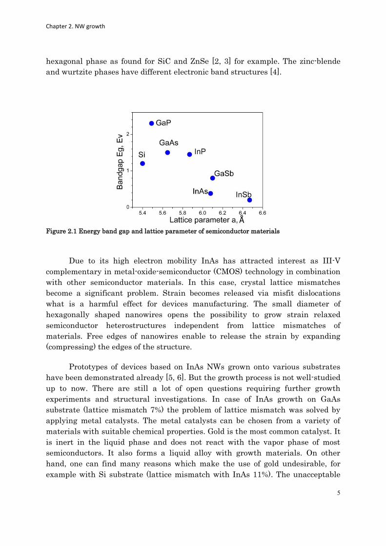
concentrate on InAs. This material is characterised by a narrow band gap
(0.36eV) compared to other semiconductors (Fig. 2.1). Together with its high
electron mobility and small electron effective mass, InAs is extremely promising
for applications in high-speed electronics. In addition, surface passivation has a
lower effect on the conductivity. Most of the bulk semiconductors exist in a cubic
zinc-blende crystal structure. In nanoscale the material can be grown in the
Chapter 2. NW growth
5
hexagonal phase as found for SiC and ZnSe [2, 3] for example. The zinc-blende
and wurtzite phases have different electronic band structures [4].
Figure 2.1 Energy band gap and lattice parameter of semiconductor materials
Due to its high electron mobility InAs has attracted interest as III-V
complementary in metal-oxide-semiconductor (CMOS) technology in combination
with other semiconductor materials. In this case, crystal lattice mismatches
become a significant problem. Strain becomes released via misfit dislocations
what is a harmful effect for devices manufacturing. The small diameter of
hexagonally shaped nanowires opens the possibility to grow strain relaxed
semiconductor heterostructures independent from lattice mismatches of
materials. Free edges of nanowires enable to release the strain by expanding
(compressing) the edges of the structure.
Prototypes of devices based on InAs NWs grown onto various substrates
have been demonstrated already [5, 6]. But the growth process is not well-studied
up to now. There are still a lot of open questions requiring further growth
experiments and structural investigations. In case of InAs growth on GaAs
substrate (lattice mismatch 7%) the problem of lattice mismatch was solved by
applying metal catalysts. The metal catalysts can be chosen from a variety of
materials with suitable chemical properties. Gold is the most common catalyst. It
is inert in the liquid phase and does not react with the vapor phase of most
semiconductors. It also forms a liquid alloy with growth materials. On other
hand, one can find many reasons which make the use of gold undesirable, for
example with Si substrate (lattice mismatch with InAs 11%). The unacceptable
Chapter 2. NW growth
6
contamination and the large diffusion length of Au in Si are accompanied with
the formation of deep-level electronic traps [7].
2.2 Vapor-Liquid-Solid growth
The most common way to grow semiconductor NWs is the Vapor-Liquid-
Solid mechanism. In 1964 Wagner and Elis suggested an explanation of the
formation of Si whiskers from vapor phase with the existence of liquid gold on the
top of the substrate surface [8]. The development of the so called free-standing
nanowhiskers was described by the Vapor-Liquid-Solid model. The name of the
growth mechanism came from the three phases appearing simultaneously –
vapor-phase precursor (SiCl4), liquid mixture of gold and silicon under growth
temperature and solid whiskers.
Considering the thermodynamic of the process, the phase transition
reaction requires supersaturation of one of the diluted growing components. The
growth takes place because of the chemical potential difference. The reaction rate
is defined by kinetic factors like the amount of supplying source material.
For two-compound systems like InAs, the growth depends on the reaction
of two elements: indium and arsenic. The two materials are introduced
separately into the growth chamber. As shown in many publications, the ratio of
both fluxes directly influences the growth process [9, 10]. Also, the difference of
chemical potentials between the vapor and solid phases of the two materials is an
important factor. NW growth is initiated by the use of a metallic catalyst. At
growth temperature, the catalyst is liquid and cooperates with the source
materials. In case of supersaturation of source materials within the catalyst
growth takes place the bottom interface. However, the composition of alloy
catalyst was unknown for long time. In addition, it is not fully clear which kind of
reaction takes place at the growing interface. Many compound semiconductor
materials produce an unstable composition with metals which can be used as
catalysts (commonly Au). Usually, the catalyst droplet contains only one of the
growing elements in considerable amount to catalyze the growth. From III-V
materials it is the group III element. Here, we come with the question how the
element of group V behaves during the growth of wire? This problem could be
solved considering that the material of group V moves along the growing surface
in the particles. High diffusion rate of arsenic along Au-grain has been shown
[11]. The group III element forms many different alloys with Au. Some of these
Chapter 2. NW growth
7
alloys have melting points in the range of the growth temperatures of NWs.
Current models still do not fully explain the development of binary compound
NWs. Prior to growth experiment one should study the phase diagrams of the
growing components [12].
It is reported that growth occurs from a supersaturated alloy with a rate
higher than it is expected from supply of vapor phase. One possible explanation
suggests that the source particle decomposes at the growth surface. Here, the
required growth rate depends on the catalyst and the source materials [13, 14].
Also, the substrate influences the decomposition process of the source material
[15]. The choice of materials defines the success of the future growth. A list of
source materials and possible catalysts has been published in [16].
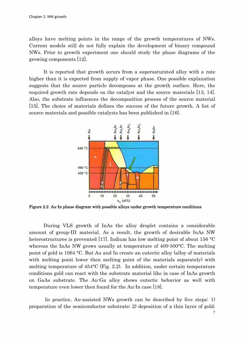
Figure 2.2 Au-In phase diagram with possible alloys under growth temperature conditions
During VLS growth of InAs the alloy droplet contains a considerable
amount of group-III material. As a result, the growth of desirable InAs NW
heterostructures is prevented [17]. Indium has low melting point of about 156 °C
whereas the InAs NW grows usually at temperature of 400-500°C. The melting
point of gold is 1064 °C. But Au and In create an eutectic alloy (alloy of materials
with melting point lower then melting point of the materials separately) with
melting temperature of 454°C (Fig. 2.2). In addition, under certain temperature
conditions gold can react with the substrate material like in case of InAs growth
on GaAs substrate. The Au-Ga alloy shows eutectic behavior as well with
temperature even lower then found for the Au-In case [18].
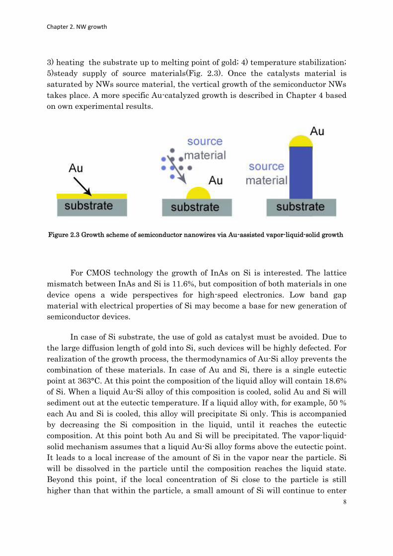
In practice, Au-assisted NWs growth can be described by five steps: 1)
preparation of the semiconductor substrate; 2) deposition of a thin layer of gold;
Chapter 2. NW growth
8
3) heating the substrate up to melting point of gold; 4) temperature stabilization;
5)steady supply of source materials(Fig. 2.3). Once the catalysts material is
saturated by NWs source material, the vertical growth of the semiconductor NWs
takes place. A more specific Au-catalyzed growth is described in Chapter 4 based
on own experimental results.
Figure 2.3 Growth scheme of semiconductor nanowires via Au-assisted vapor-liquid-solid growth
For CMOS technology the growth of InAs on Si is interested. The lattice
mismatch between InAs and Si is 11.6%, but composition of both materials in one
device opens a wide perspectives for high-speed electronics. Low band gap
material with electrical properties of Si may become a base for new generation of
semiconductor devices.
In case of Si substrate, the use of gold as catalyst must be avoided. Due to
the large diffusion length of gold into Si, such devices will be highly defected. For
realization of the growth process, the thermodynamics of Au-Si alloy prevents the
combination of these materials. In case of Au and Si, there is a single eutectic
point at 363°C. At this point the composition of the liquid alloy will contain 18.6%
of Si. When a liquid Au-Si alloy of this composition is cooled, solid Au and Si will
sediment out at the eutectic temperature. If a liquid alloy with, for example, 50 %
each Au and Si is cooled, this alloy will precipitate Si only. This is accompanied
by decreasing the Si composition in the liquid, until it reaches the eutectic
composition. At this point both Au and Si will be precipitated. The vapor-liquid-
solid mechanism assumes that a liquid Au-Si alloy forms above the eutectic point.
It leads to a local increase of the amount of Si in the vapor near the particle. Si
will be dissolved in the particle until the composition reaches the liquid state.
Beyond this point, if the local concentration of Si close to the particle is still
higher than that within the particle, a small amount of Si will continue to enter
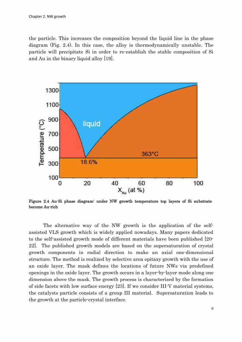
Chapter 2. NW growth
9
the particle. This increases the composition beyond the liquid line in the phase
diagram (Fig. 2.4). In this case, the alloy is thermodynamically unstable. The
particle will precipitate Si in order to re-establish the stable composition of Si
and Au in the binary liquid alloy [19].
Figure 2.4 Au-Si phase diagram: under NW growth temperature top layers of Si substrate
become Au-rich
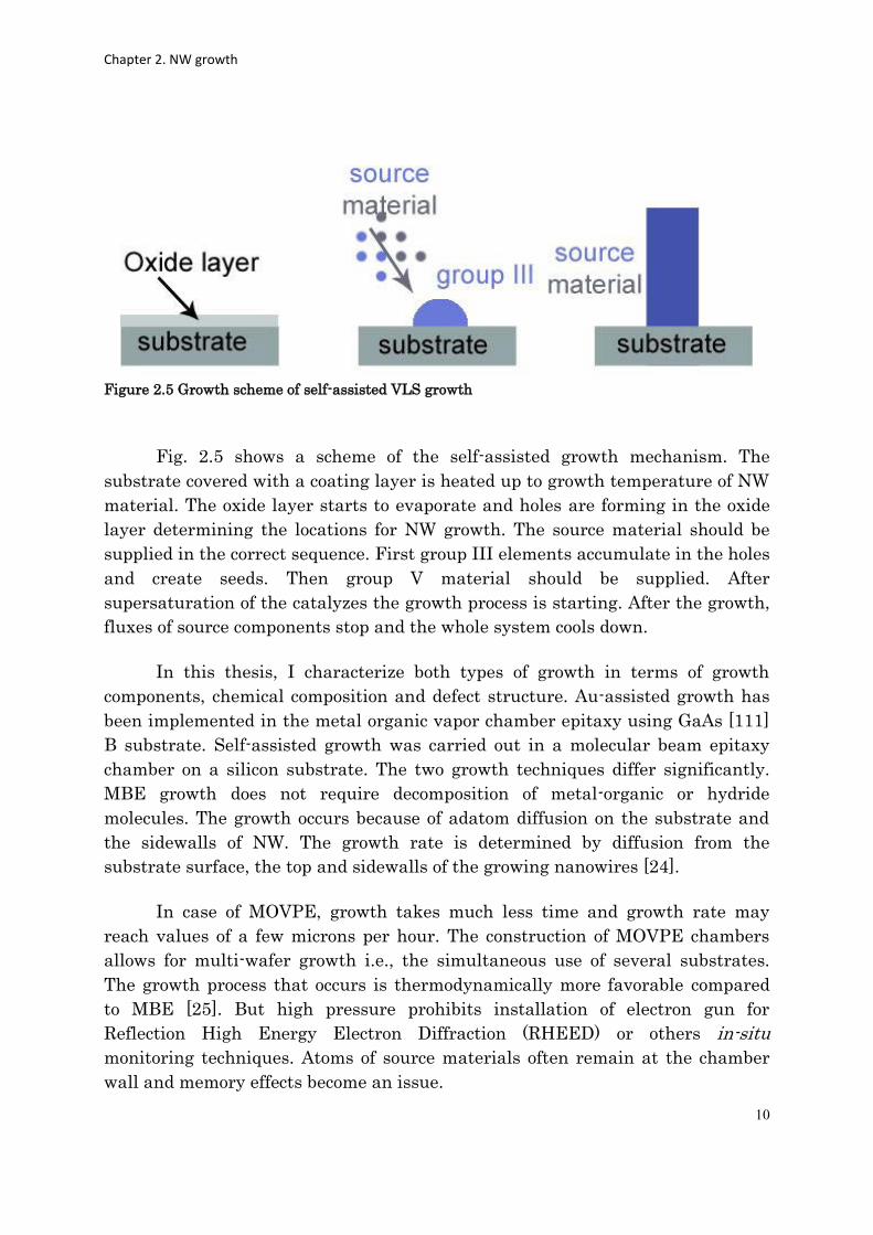
The alternative way of the NW growth is the application of the self-
assisted VLS growth which is widely applied nowadays. Many papers dedicated
to the self-assisted growth mode of different materials have been published [20-
22]. The published growth models are based on the supersaturation of crystal
growth components in radial direction to make an axial one-dimensional
structure. The method is realized by selective area epitaxy growth with the use of
an oxide layer. The mask defines the locations of future NWs via predefined
openings in the oxide layer. The growth occurs in a layer-by-layer mode along one
dimension above the mask. The growth process is characterized by the formation
of side facets with low surface energy [23]. If we consider III-V material systems,
the catalysts particle consists of a group III material. Supersaturation leads to
the growth at the particle-crystal interface.
Chapter 2. NW growth
10
Fig. 2.5 shows a scheme of the self-assisted growth mechanism. The
substrate covered with a coating layer is heated up to growth temperature of NW
material. The oxide layer starts to evaporate and holes are forming in the oxide
layer determining the locations for NW growth. The source material should be
supplied in the correct sequence. First group III elements accumulate in the holes
and create seeds. Then group V material should be supplied. After
supersaturation of the catalyzes the growth process is starting. After the growth,
fluxes of source components stop and the whole system cools down.
In this thesis, I characterize both types of growth in terms of growth
components, chemical composition and defect structure. Au-assisted growth has
been implemented in the metal organic vapor chamber epitaxy using GaAs [111]
B substrate. Self-assisted growth was carried out in a molecular beam epitaxy
chamber on a silicon substrate. The two growth techniques differ significantly.
MBE growth does not require decomposition of metal-organic or hydride
molecules. The growth occurs because of adatom diffusion on the substrate and
the sidewalls of NW. The growth rate is determined by diffusion from the
substrate surface, the top and sidewalls of the growing nanowires [24].
In case of MOVPE, growth takes much less time and growth rate may
reach values of a few microns per hour. The construction of MOVPE chambers
allows for multi-wafer growth i.e., the simultaneous use of several substrates.
The growth process that occurs is thermodynamically more favorable compared
to MBE [25]. But high pressure prohibits installation of electron gun for
Reflection High Energy Electron Diffraction (RHEED) or others in-situ
monitoring techniques. Atoms of source materials often remain at the chamber
wall and memory effects become an issue.
Figure 2.5 Growth scheme of self-assisted VLS growth
Chapter 2. NW growth
11
2.3 Crystal phases of InAs
It was found that the properties of InAs may change on the nanoscale. In
1966 scientists from Tokyo Institute of Technology reported on the growth of
InAs whiskers in wurtzite structures [26]. Bulk InAs exists in the cubic zinc-
blende phase, but on the nanoscale the wurtzite phase becomes possible as well.
A small number of reports is available today on structurally perfect NWs with
only one structure phase [27, 28]. The structure of grown NWs strongly depends
on the growth parameters, which opens the opportunity to develop NWs with
zinc-blende, wurtzite or mixed phases. The dependence of the electronic band
structure on the lattice structure allows for the formation of heterostructures
formed by the same material, but different phases [29].
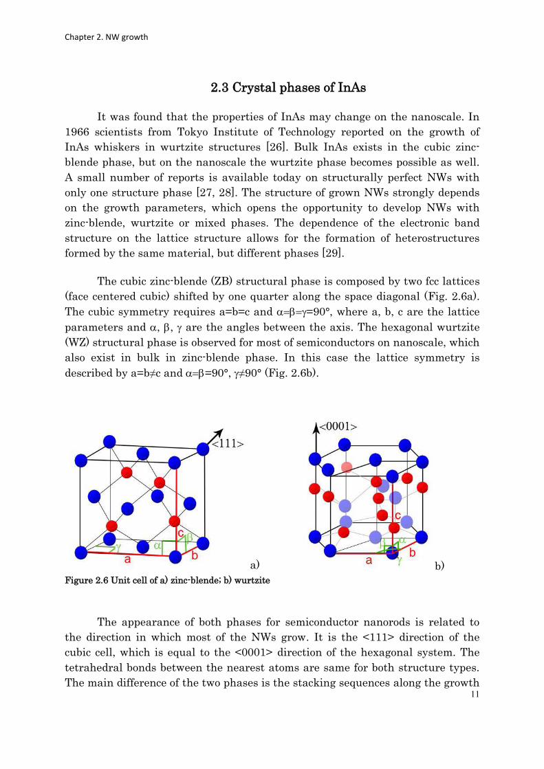
The cubic zinc-blende (ZB) structural phase is composed by two fcc lattices
(face centered cubic) shifted by one quarter along the space diagonal (Fig. 2.6a).
The cubic symmetry requires a=b=c and =90°, where a, b, c are the lattice
parameters and , , are the angles between the axis. The hexagonal wurtzite
(WZ) structural phase is observed for most of semiconductors on nanoscale, which
also exist in bulk in zinc-blende phase. In this case the lattice symmetry is
described by a=b≠c and =90°, ≠90° (Fig. 2.6b).
a) b)
Figure 2.6 Unit cell of a) zinc-blende; b) wurtzite
The appearance of both phases for semiconductor nanorods is related to
the direction in which most of the NWs grow. It is the <111> direction of the
cubic cell, which is equal to the <0001> direction of the hexagonal system. The
tetrahedral bonds between the nearest atoms are same for both structure types.
The main difference of the two phases is the stacking sequences along the growth
Chapter 2. NW growth
12
direction. For ZB sequences three distinct layers of III-V pairs are repeated. The
WZ phase is described by sequences of two layers of III-V pairs. The energetic
difference is attributed to the difference in the third-nearest-neighbor spacing,
which is shorter in the WZ structure compared to ZB one [30].
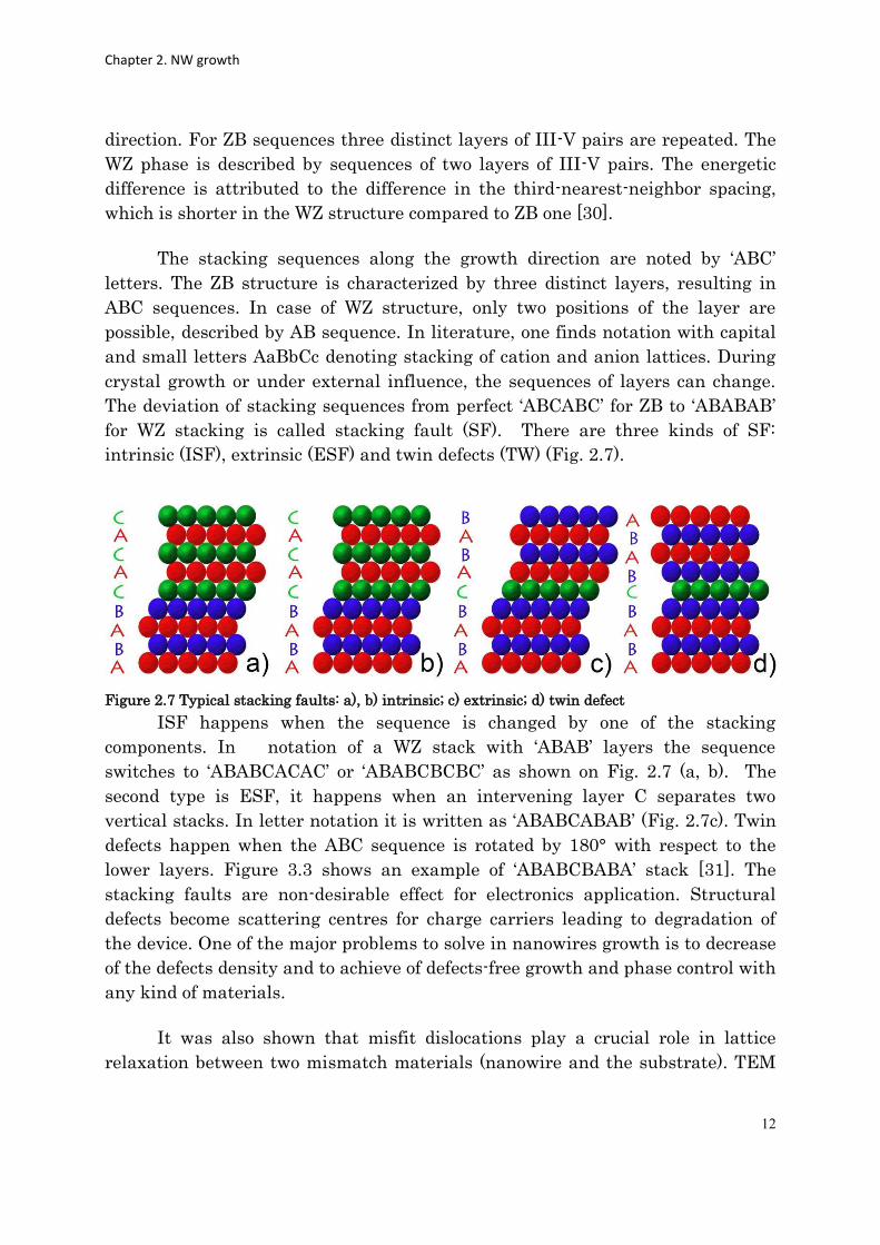
The stacking sequences along the growth direction are noted by ‘ABC’
letters. The ZB structure is characterized by three distinct layers, resulting in
ABC sequences. In case of WZ structure, only two positions of the layer are
possible, described by AB sequence. In literature, one finds notation with capital
and small letters AaBbCc denoting stacking of cation and anion lattices. During
crystal growth or under external influence, the sequences of layers can change.
The deviation of stacking sequences from perfect ‘ABCABC’ for ZB to ‘ABABAB’
for WZ stacking is called stacking fault (SF). There are three kinds of SF:
intrinsic (ISF), extrinsic (ESF) and twin defects (TW) (Fig. 2.7).
Figure 2.7 Typical stacking faults: a), b) intrinsic; c) extrinsic; d) twin defect
ISF happens when the sequence is changed by one of the stacking
components. In notation of a WZ stack with ‘ABAB’ layers the sequence
switches to ‘ABABCACAC’ or ‘ABABCBCBC’ as shown on Fig. 2.7 (a, b). The
second type is ESF, it happens when an intervening layer C separates two
vertical stacks. In letter notation it is written as ‘ABABCABAB’ (Fig. 2.7c). Twin
defects happen when the ABC sequence is rotated by 180° with respect to the
lower layers. Figure 3.3 shows an example of ‘ABABCBABA’ stack [31]. The
stacking faults are non-desirable effect for electronics application. Structural
defects become scattering centres for charge carriers leading to degradation of
the device. One of the major problems to solve in nanowires growth is to decrease
of the defects density and to achieve of defects-free growth and phase control with
any kind of materials.
It was also shown that misfit dislocations play a crucial role in lattice
relaxation between two mismatch materials (nanowire and the substrate). TEM
Chapter 2. NW growth
13
and XRD were used to characterize the realization of growth of GaAs nanowires
on Si substrate (lattice mismatch 4%) [32].
As far as electrical and optical properties of NWs are crucially dependent
on structural composition, phase purity, defect density etc. [33], investigation of
growth process and growth parameters influence become a key for understanding
and improvement of future devices. Most reports on structure and morphology of
nanowires are based on SEM and TEM techniques results. SEM provides an
images of the structure and can be used for morphology description. The internal
structure can be inspected with TEM even on atomic scale, but the technique
requires a complicated preparation procedure using focus ion beam, or other
methods for localisation of single nano-object.
Alternatively, X-ray diffraction was successful in determination of shape,
chemical composition and defect structure [32, 34, 35]. The technique allows
ensemble as well as single nanostructure characterization (with the use of special
focusing setups). The basic problem of X-ray scattering from nanostructures was
in low scattering intensity from objects with a small amount of material. The
problem was solved by opening new high-flux sources of synchrotron radiation
and upgrading of existing X-ray sources. Using a nano-focused beam of such
sources, the scattering signal is strong enough for detection and further
evaluation for the NW structure. Using X-ray diffraction technique, one is able to
detect and characterize the defect structure of the NWs system. The
concentration of defects and the defect types can be investigated and described
numerically.
Here, I demonstrate results of investigations of InAs NWs growth obtained
by X-ray diffraction. Following questions that raise from preparation and growth
modes will be solved in this thesis:
composition and structural phase of growing system?
temporal evolution of growing system during Au-catalysed growth?
temporal evolution of growing system during self-assisted growth?
investigation of defect structure of the MBE grown NWs?
parasitic growth accompanying NWs growth?
In addition, we present a technique for description and numerical
characterization of SF density in NWs. The methods are based on measurements
of one particular sensitive to SF reflection and its simulation. Improvement of
grown NWs will be achieved by understanding of a number of processes occurring
during the growth.
Chapter 2. NW growth
14
References
[1] M. Passlack, OFF-state current limits of narrow bandgap MOSFETs, Electron Devices, IEEE
Transactions, 53, 11, 2773-2778 (2006)
[2] P. Gaiduk, F. Komarov, V.Tishkov, W. Wesch, E. Wendler, Physical Review B, 61, 15785
(2000)
[3] V. Narayanan, S. Mahajan, N. Sukidi, K. J. Bachmann, V. Woods, N. Dietz, Philasophical
Magazine A, 80, 555, (2000)
[4] S. Q. Wang, H. Q. Ye, Journal of Physics of Condensed Matter, 14, 9579 (2002)
[5] L. Chuang, F. Sedgwick, R. Chen, W. Ko, M. Moewe, K.Ng, T. Tran, C. Chang-Hasnain, Nano
Lett. 11, 385, (2011)
[6] K. Tomioka, T. Fukui, Appl. Phys. Lett., 98, 083114 (2011)
[7] M.Stiles,D. Hamann, Phys Rev..B 38 , 2021-37 (1988)
[8] R. Wagner, W. Ellis, Applied Physics Letters,4(5): 89 (1964)
[9] H. J. Joyce, J.Wong-Leung,Q.Gao, H. Tan,C.Jagadish, Nano Letters., 10 , 908 (2010)
[10] S. Hertenberger,D. Rudolph,S. Bolte,M. Döblinger,M. Bichler,D. Spirkoska,J. Finley,G.
Abstreiter,G. Koblmüller ,Applied Physics Letters 98, 123114 (2011)
11] V.G. Weizer, N.S. Fatemi, Journal of Applied Physics, 64, 4618 (1988)
[12] J. Bauer PhD thesis „Metallorganische Gasphasenepitaxie von GaAs- und InAs-
Nanodrahtstrukturen über den „vapor-liquid-solid“ - Wachstumsmechanismus“, Fakultät für
Physik und Geowissenschaften der Universität Leipzig (2009)
[13] S. Kodambaka, J. Tersoff, M.C. Reuter, F.M. Ross, Physical Review Letters, 96, 096105
(2006)
[14] M.A. Verheijen, G. Immink, T. Desmet, M.T. Borgstro¨m, E.P.A.M. Bakkers, Journalof the
American ChemicalSociety, 128, 1353 (2006)
[15] A.I. Persson, L.E. Fröberg, S. Jeppesen, M.T. Björk, L. Samuelson, Journal of Applied
Physics, 101, 034313 (2007)
[16] H. Tuan, D. Lee, B.Korgel, Angewandte Chemie International Edition, 45, 5184 (2006)
[17] J. Bauer, V. Gottschalch, G. Wagner, Journal of Applied Physics 104, 114315 (2008)
Chapter 2. NW growth
15
[18] A. Lugstein,M. Steinmair,Y. J. Hyun,E. Bertagnolli, P. Pongratz, Applied Physics Letters 90,
023109 (2007)
[19] J. Lin, C. Chen, E. Diau, T. Liu, Journal of Materials Processing Technology, 206, 425
(2008)
[20] L. Gao, R. Woo, B. Liang, M. Pozuelo, S. Prikhodko, M. Jackson, N. Goel, M. Hudait, D.
Huffaker, M. Goorsky, S. Kodambaka, R. Hicks, Nano Letters, 9 (6), 2223 (2009)
[21] W. Wei, X. Bao, C. Soci, Y. Ding, Z. Wang, D. Wang, Nano Letters, 9 (8), 2926–2934 (2009)
[22] K. Ikejiri, J. Noborisaka, S. Hara, J. Motohisa, T. Fukui, Journal of Crystal Growth, 298, 616
(2007)
[23] B. Mandl, J.Stangl, E. Hilner, A. Zakharov, K. Hillerich, A. Dey, L. Samuelson, G. Bauer, K.
Deppert, A. Mikkelsen, Nano Letters, 10 (11), 4443 (2010)
[24] M. Tchernycheva, L. Travers, G. Patriarche, F. Glas, J.-C. Harmand G. Cirlin, V. Dubrovskii,
Journal of Applied Physics, 102, 094313 (2007)
[25] P. Dapkus, Journal of Crystal Growth, 68, 345, (1984)
[26] K. Takahashi, T. Morizumi, Japanese Journal of Applied Physics, 5, 8, 657-662 (1966)
[27] Y. Kitauchi, Y. Kobayashi, K. Tomioka, S. Hara, K. Hiruma, T. Fukui, J. Motohisa, Nano Letters, 10, 1699 (2010)
[28] K. Dick, C. Thelander, L. Samuelson, P. Caroff, Nano Letters, 10, 3494 (2010)
[29] L. Zhang, W-J. Luo, A. Zunger, N. Akopian, V. Zwiller, J.-C. Harmand, Nano Letters, 10,
4055 (2010)
[30] K. Dick, P. Caroff, J. Bolinsson, M. Messing, J. Johansson, K. Deppert, R. Wallenberg, L.
Samuelson, Semicon Sci technol, 25, 024009 (2010)
[31] M.Stiles, Phys Rev..B 38, 2021-37 (1988)
[32] A. Biermanns, S. Breuer, A. Trampert, A. Davydok, L. Geelhaar, U. Pietsch,
Nanotechnology, 23 (30), 305703 (2012)
[33] C. Thelander, K . Dick, M. Borgström, L. Fröberg, P. Caroff, H. Nilsson, L. Samuelson,
Nanotechnology, 21, 205703 (2010)
[34] A. Davydok, S. Breuer, A. Biermanns, L. Geelhaar, U. Pietsch, Nanoscale Research Letters,
7,109 (2012)
[35] D. Kriegner, C. Panse, B. Mandl, K. Dick, M. Keplinger, J. Persson , P. Caroff, D. Ercolani, L.
Sorba, F. Bechstedt, J. Stangl, G. Bauer, Nano Lett., 11 , 1483, (2011)
Chapter 3. X-ray Diffraction
16
Chapter 3
X-ray Diffraction: Kinematical Scattering Theory
X-ray diffraction methods were used to analyse the structure of InAs NWs.
The basic principal of scattering methods will be presented. The brief overview
includes the elements of kinematic theory of X-ray diffraction, description of
structural representation in X-ray diffraction experiments and overview of the X-
ray coherence. We give a short explanation of the methodology and the
fundamental concept of data evaluation used in this thesis. Based on this
knowledge a computer software was developed for data simulations.
.
Chapter 3. X-ray Diffraction
17
X-ray diffraction is a non-destructive method of crystal structure analysis,
sensitive to sizes, composition and strain acting at the lattice. As visible light
diffracts at a diffraction grating, X-rays diffract at a crystal lattice. The
wavelength of X-ray is in the same order of magnitude as interatomic distance in
a crystal (in order of angstroms). We focus on classical treatment of elastic
Thomson scattering which is realized by placing the detector at a distance from
the scattering object much larger then crystal lattice parameter. Inelastic
Compton scattering was not taken to account. We also neglected multi-scattering
effects and follow the kinematical approach of X-ray scattering theory. In order to
describe scattering mathematically, we will discuss the key points of crystal
representation and reciprocal space.
3.1 Crystal structure
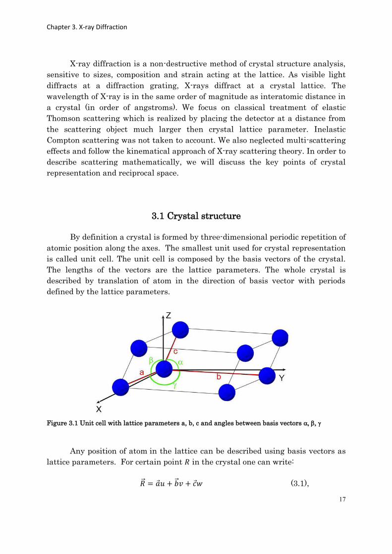
By definition a crystal is formed by three-dimensional periodic repetition of
atomic position along the axes. The smallest unit used for crystal representation
is called unit cell. The unit cell is composed by the basis vectors of the crystal.
The lengths of the vectors are the lattice parameters. The whole crystal is
described by translation of atom in the direction of basis vector with periods
defined by the lattice parameters.
Figure 3.1 Unit cell with lattice parameters a, b, c and angles between basis vectors
Any position of atom in the lattice can be described using basis vectors as
lattice parameters. For certain point in the crystal one can write:
(3.1),

Chapter 3. X-ray Diffraction
18
where a, b, c are three linear independent primitive vectors and are integer
numbers. Lattices described by equation (3.1) we called Bravias lattice. All
possible variation of the atom arrangement two-dimensions were defined by five
Bravias lattices, in three dimensions there are fourteen Bravias lattices.
3.2 Reciprocal space
In 1921 P. P. Ewald introduced the reciprocal lattice – a mathematical
construction useful for crystal planes indexing and further description of
scattering. One of the definitions for reciprocal lattice is the following: consider a
plane wave . It will only have the periodicity if the following condition is
fulfilled for all vectors
with (3.2),
The set of all wavevectors in three dimensions, which gives a plane wave
with periodicity is called the reciprocal lattice. We label the reciprocal lattice
vectors by [1].
The basis vectors of the reciprocal lattice can be written as:
(3.3)
Solutions of the system of equations are:
(3.4),
where defines the volume of unit cell. As far the crystal is a periodic
system of the atoms, the reciprocal lattice can be obtained by Fourier
transformation of the real crystal lattice. In this case the vector of a certain
lattice plane is normalized

Chapter 3. X-ray Diffraction
19
(3.5)
and the distance of the lattice plane from origin is defined by:
(3.6)
where is formed by equation (3.1). If a lattice plane crosses the coordinates
axis in the points a0, b0, c0 equation (3.6) can be rewritten by
(3.7)
Based on equations (3.5) and (3.6) we can write the lattice plane equation:
(3.8)
where are integer. With certain suitable values of define as:
Using these equations, we can write the reciprocal lattice vector, which is
along perpendicular to the real lattice by:
(3.9)
where are called Miller’s indices.
With the help of the equation (3.9), we can define the angle between two
lattice planes as the angle between corresponding normal’s to these planes by:
(3.10)
Moreover, we may calculate the distance between two neighboured lattice
planes of the same orientation by:
| |
(3.11)
In such a way, the real space distances are connected with reciprocal space
interpretation. If we consider a denominator of the right part of the equation:
( ) ( ) ( )
Chapter 3. X-ray Diffraction
20
The interplanar distance can be evaluated through the parameters of the
direct lattice by substituting for the magnitudes , and and for ,
and in these two equations. Considering the specifics of crystal system we
can calculate interplanar distance for cubic and hexagonal structure. In case of
cubic lattice and
, we obtain:
.
For hexagonal one: ;
√
, which gives
.
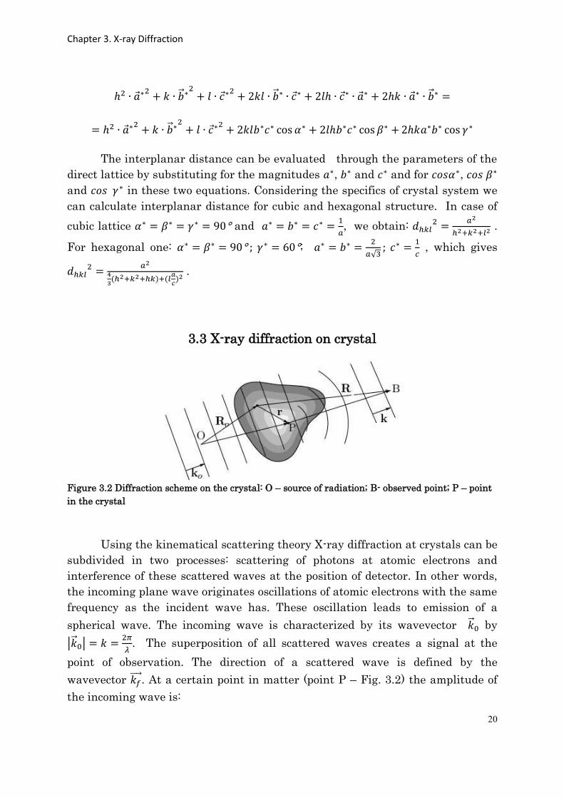
3.3 X-ray diffraction on crystal
Figure 3.2 Diffraction scheme on the crystal: O – source of radiation; B- observed point; P – point
in the crystal
Using the kinematical scattering theory X-ray diffraction at crystals can be
subdivided in two processes: scattering of photons at atomic electrons and
interference of these scattered waves at the position of detector. In other words,
the incoming plane wave originates oscillations of atomic electrons with the same
frequency as the incident wave has. These oscillation leads to emission of a
spherical wave. The incoming wave is characterized by its wavevector by
| |
. The superposition of all scattered waves creates a signal at the
point of observation. The direction of a scattered wave is defined by the
wavevector . At a certain point in matter (point P – Fig. 3.2) the amplitude of
the incoming wave is:
Chapter 3. X-ray Diffraction
21
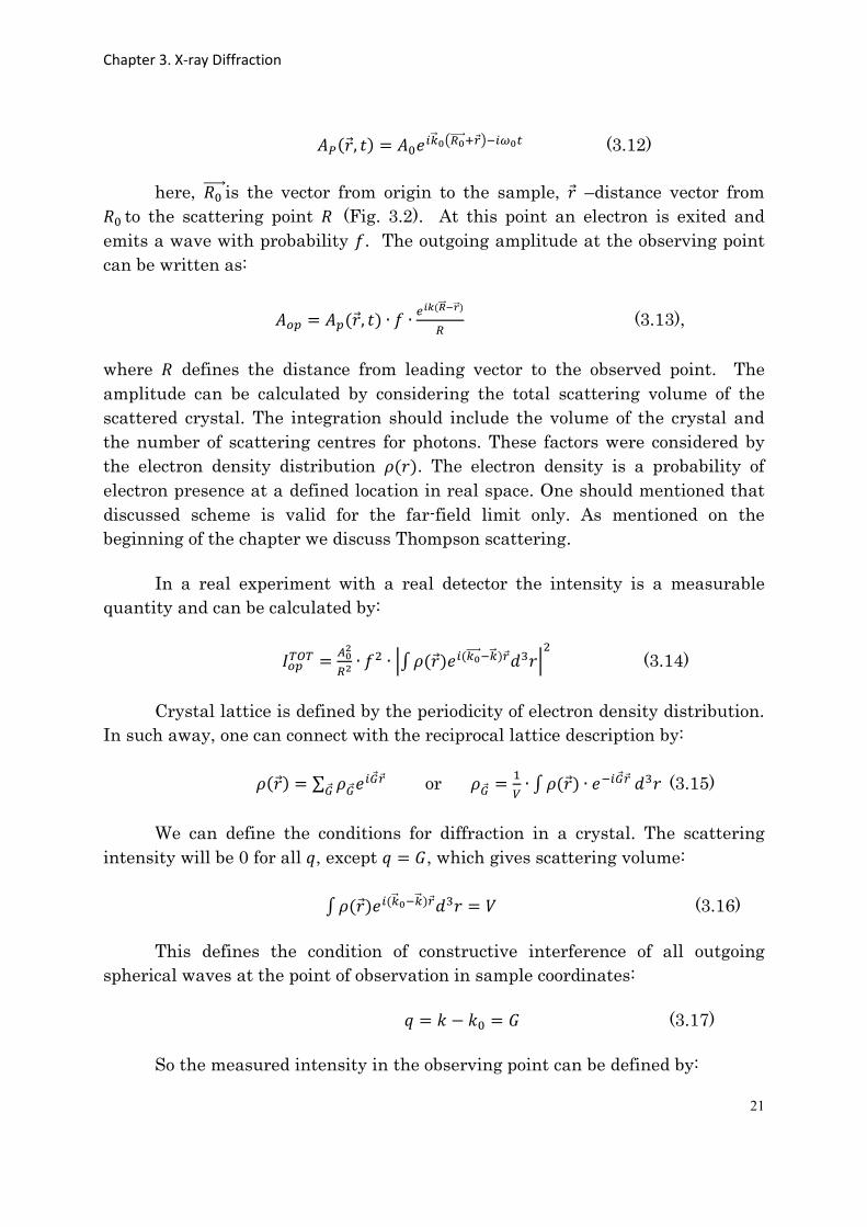
( ) (3.12)
here, is the vector from origin to the sample, –distance vector from
to the scattering point (Fig. 3.2). At this point an electron is exited and
emits a wave with probability . The outgoing amplitude at the observing point
can be written as:
(3.13),
where defines the distance from leading vector to the observed point. The
amplitude can be calculated by considering the total scattering volume of the
scattered crystal. The integration should include the volume of the crystal and
the number of scattering centres for photons. These factors were considered by
the electron density distribution . The electron density is a probability of
electron presence at a defined location in real space. One should mentioned that
discussed scheme is valid for the far-field limit only. As mentioned on the
beginning of the chapter we discuss Thompson scattering.
In a real experiment with a real detector the intensity is a measurable
quantity and can be calculated by:
|∫ |
(3.14)
Crystal lattice is defined by the periodicity of electron density distribution.
In such away, one can connect with the reciprocal lattice description by:
∑
or
∫ (3.15)
We can define the conditions for diffraction in a crystal. The scattering
intensity will be 0 for all , except , which gives scattering volume:
∫ (3.16)
This defines the condition of constructive interference of all outgoing
spherical waves at the point of observation in sample coordinates:
(3.17)
So the measured intensity in the observing point can be defined by:
Chapter 3. X-ray Diffraction
22
| | (3.18)
3.4 The Laue equations and Bragg interpretation of diffraction
conditions
Considering equation (3.17) for the three basic vectors a, b, c, one obtains the
Laue equations:
(3.19)
Since the wavevector depends on wavelength of the radiation and the
equations contain three indexes of certain reflection we obtain three equations
with three unknown values. The are integer numbers and are connected by:
and
. With this information one is able to determine the
reflection indexes and wavelength of radiation used in the experiment.
The conditions shown in equation (3.17) are interpreted as lattice planes.
In crystal the X-ray behaves like an optic beam in atmosphere. So it obeys optical
laws, in this case the process of diffraction can be described by the difference in
optical path lengths through the crystal. It should be equal to an integer number
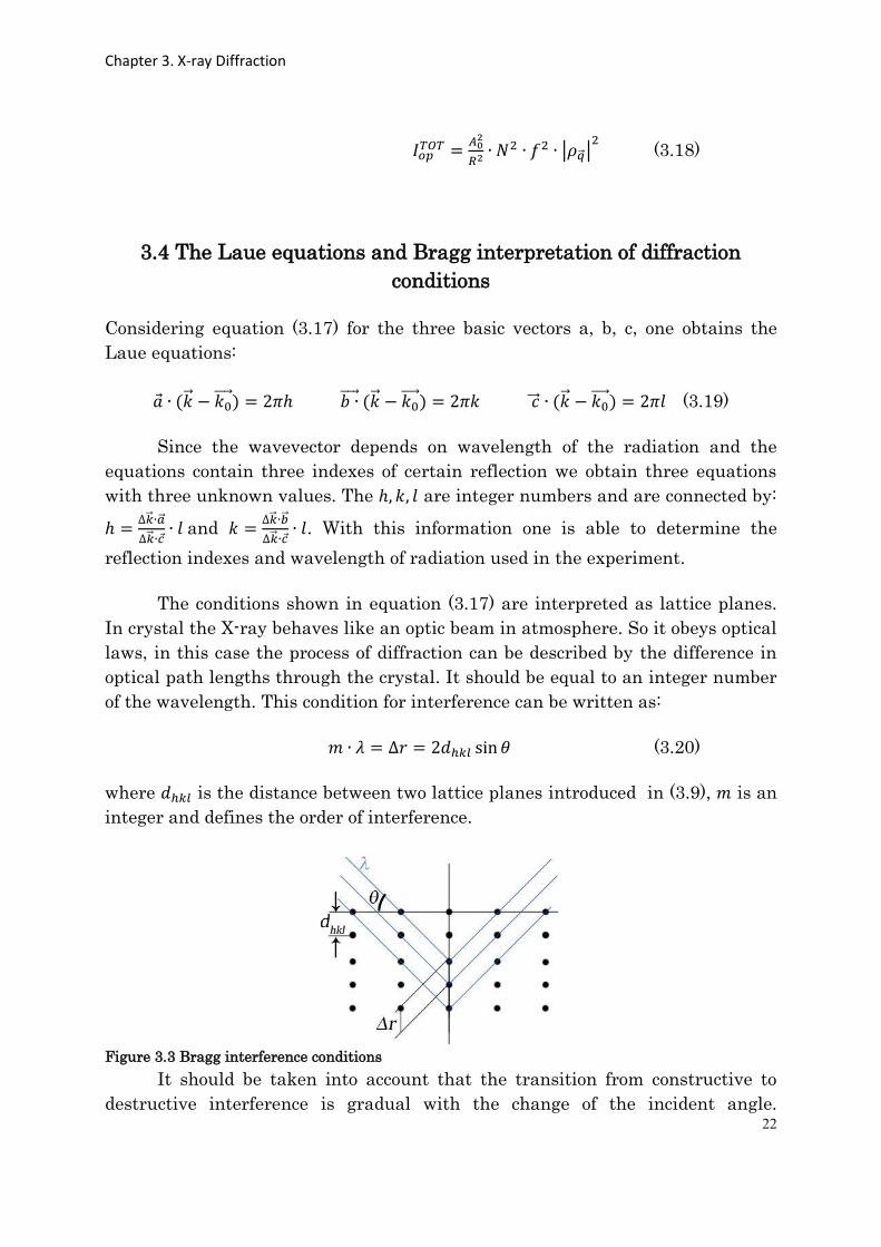
of the wavelength. This condition for interference can be written as:
(3.20)
where is the distance between two lattice planes introduced in (3.9), is an
integer and defines the order of interference.
Figure 3.3 Bragg interference conditions
It should be taken into account that the transition from constructive to
destructive interference is gradual with the change of the incident angle.
Chapter 3. X-ray Diffraction
23
Combining angular conditions with reciprocal space, we consider that the
scanning parameter can be the incident or exit wave vectors depending on setups
(angular- or energy-dispersive). The simple relationship between diffraction
angle and reciprocal space is:
| |
(3.21)
3.5 Lattice sum and Laue conditions
For calculation of scattered intensity we use the term lattice sum. It is a
sum of complex terms corresponding to the points located on the unit circle. The
lattice sum is the sum of a large amount of terms (in case of cubic crystal with
size 1x1x1m3, number of terms equals to 1012). From statistics we know when
one adds a large number of random terms, the sum will be equal to zero. The
atoms not in phase produce destructive interference. When for all , the
sum is N, a large number. This holds that if is a reciprocal lattice vector :
(3.22)
The Laue conditions for scattering from a crystal are equivalent to Bragg’s
law.
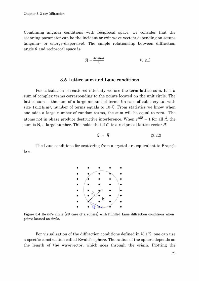
For visualisation of the diffraction conditions defined in (3.17), one can use
a specific construction called Ewald’s sphere. The radius of the sphere depends on
the length of the wavevector, which goes through the origin. Plotting the
Figure 3.4 Ewald’s circle (2D case of a sphere) with fulfilled Laue diffraction conditions when
points located on circle.
Chapter 3. X-ray Diffraction
24
wavevectors for the case of elastic scattering the following condition should be
fulfilled: . In other words, respective reciprocal lattice points lie on
Ewald’s sphere. Example on Ewald’s circle is shown in fig. 3.4. It is useful to
calculate the lattice sum explicitly and we write
and use definition of delta-function:
( ) ∑
∑
∑
∑
(3.23)
For the calculation of the lattice sum, we use equation (3.1) and (3.9). The
finite size of the crystal can be described with presentation of the crystal as
parallelepiped with basis vectors. Consider sums in (3.23) as geometric
progression using values from 0 to N-1 unit cells, it becomes:
∑
(3.24)
The measured intensity is proportional to the square of the lattice sum. In
other words, we can rewrite the measured intensity as:
| |
(3.25)
where is the total number of unit cells in the crystal.
3.6 Atomic form factor and structure factor
The scattering intensity calculated in (3.18) is defined by the square of
Fourier transformation of components of electron density distribution . In this
case, constructive interference is observed only at reciprocal lattice vectors . The
electron density calculation for the unit cell is shown in (3.15). The total density
can be represented by the sum of electron density of all atoms within the unit cell
located at the relative coordinates :
∫∑
(3.26)
=
∑
∫
Chapter 3. X-ray Diffraction
25
where defines the distance from origin of the atomic coordinates to a
certain point. The integral ∫ is the atomic scattering factor.
It depends on chemical composition and reciprocal lattice vector . The atomic
form factor can be calculated for an angle between and :
∫
∫ ∫
∫
(3.27)
Using this, one can write an equation for the structural factor:
∫
(3.28)
The measured intensity is proportional to square of scattering amplitude,
when the amplitude is defined by phase sum of atomic scattering factor. The
presented calculations define the extinction rules for any structure type. The
rules describe conditions to find a Bragg-reflection with non-zero intensity for a
certain lattice.
3.7 Crystal truncation rods
Our experiments are dedicated to structure investigation of nano-size
wires grown on the millimetre-size substrate. Here an important role plays the
surface effects and high surface/bulk ratio. The scattering of X-rays is also
sensitive to such influence. As shown in [2] integral across all crystal equals:
( ) ∫ (3.29)
where is the structure factor of the unit cell, is the shape function to
be zero outside the crystal and ∑ . Using inside the convolution
theorem:
Chapter 3. X-ray Diffraction
26
( )
∫ ( ) (3.30)
The shape function is defined as Fourier transform:
( ) ∫ (3.31)
and
∫ ∑ ∑ (3.32)
Using presented ratios we rewrite
( )
∑ (3.33)
At the position of Bragg reflection and with we can
write:
∫ (3.34)
Here, we received the lattice part of the structure factor at the Bragg point.
The shape of the crystal is represented by the shape function . Using the
Gaussian divergence theorem and consider the structure factor as volume
integral, we get:
∫
(3.35)
where is normal to surface element . The structure factor equation shows
that strongest scattering will be observed for reciprocal vectors parallel to surface
normal . In case of samples with facets, strong scattering occur towards a
direction perpendicular to facets of the crystal. The streaks appearing from Bragg
reflections along the crystal surface normal are known as crystal truncation rods
(CTRs) because the signal appears from truncation of three dimension periodicity
of the crystal by the surface. The CTRs concept is widely used for surface
investigations or for small size crystals grown on substrate. In (3.35) intensity
decays by
from Bragg reflection. The example of small crystal measurements is
shown in [3].

Chapter 3. X-ray Diffraction
27
3.8 X-ray diffraction from zinc-blende and wurtzite structures
As was mentioned in Chapter 2, semiconductor NWs may grow in two
structure phases – zinc-blende and wurtzite. In most cases NW growths is
realized along <111> direction of semiconductor ZB substrate which equal to
<0001> of WZ phase. During the X-ray diffraction experiment, one often faces the
problem that a Bragg reflection is measured from a mixed phases of ZB and WZ
phases. To overcome the problem a specific coordinate system is used to describe
the X-ray diffraction experiment, the surface coordinate system.
We consider (111) surface of a ZB crystal. Most of the semiconductor
materials exhibit zinc-blende structure in bulk. The ZB unit cell consists of two
fcc lattices and one of both is shifted by one quarter along the space diagonal of
the ZB cell. As far as NWs grow in [111] direction, it is useful to chose one
coordinate axis along the [111] direction and two in-plane vectors perpendicular.
This coordinate system is often used in surface physics [4], with cubic lattice
parameter , are given by
(
)
(
) (3.36)
For hexoganl system one can write these values as
√ √ with the
angles
( ) (
)
The corresponding reciprocal vectors are:
( )
(3.37)
These vectors used for a hexagonal system with
√
;
√ and
with the angles ( ) ( ) ( ) . For surface system, we mark
the coordinates with bottom index s. In surface coordinate the basis vectors of fcc
lattice are:
[ ] [
] [
] (3.38)
Chapter 3. X-ray Diffraction
28
Follow equation (3.38) structure factor of fcc unit cell defines as:
( ) ∑ (
) (
) =
=
0
This is an example of extinction rules mentioned before in subchapter 3.6.
It shows conditions that the measured intensity is non-zero and Bragg reflection
can be observed. Also, we would like to stress on a case of twins defects (Chapter
2), following an ABC stack is rotated around [111] direction by 60 . For this case,
extinction rule contains the indices and
For InAs the atoms occupy the follow positions of fcc lattice:
[ ] [
]
The structure factor of InAs in surface coordinates is:
( ) ( )
(3.39)
Here, we express the structure factor by atomic form factors of In and As
with certain values of 2, 6, 10…. Now we can estimate which reflections are
forbidden. The reflections with low value of in structure factor is zero or very
small.
The zinc-blende structure can be represented also as stacking of
hexagonally closed packed bilayers. Zinc-blende is characterized by stacking
sequence ABC. Twin defects rotated for 60 degrees around [111] direction are
described by ACB stacking. Using this notation, different structures can be
described. In addition to ZB structure phase, in semiconductor nanowires the
wurtzite structure is observed with stacking sequence AB. For this phase, the
basis in with cubic lattice parameter is described by (3.36).
In surface coordinates, we rewrite the out-of-plane vector [111]c to [
] .
It does not change along in-plane reciprocal vectors but has an effect for out-of-
Chapter 3. X-ray Diffraction
29
plane vector c*:
[
] . Following this logic, any stacking sequence can be
described and explained including sequences with stacking faults. For example,
the basis of a wurtzite configuration is represented by and the out-of-
plane lattice parameter is written as
[5]. Often structures are described by a
ratio of out-of-plane and in-plane parameters c/a. For ideal hexagonal close
packed lattice this ratio equal to
√
and refer to the optimum packing factor
0.74. In this case the basis is described by:
Using this basis, one can calculate structure factor of hexagonal close pack
structure:
( ) ∑ (
) (3.40)
0 for odd and
where
. From here we can define forbidden reflections of WZ phase. The
conditions are fulfilled when 4, 12, 20… Many papers have shown that the
c/a ratio in a real case of InAs nanowires is different from the ideal value [6, 7].
For real experiments it is much more comfortable to use one coordinate system
for measured reflections for both types of crystal phases. For this case we use
transformation matrices from cubic system to hexagonal one, with the notations
ac for cubic lattice parameters and ah and ch for hexagonal lattice parameters
√
√
√
= √
√
√
c
√
√
√ h
Chapter 3. X-ray Diffraction
30
and in reciprocal space will be:
√
√
=
√
√
c
√
√
√ h
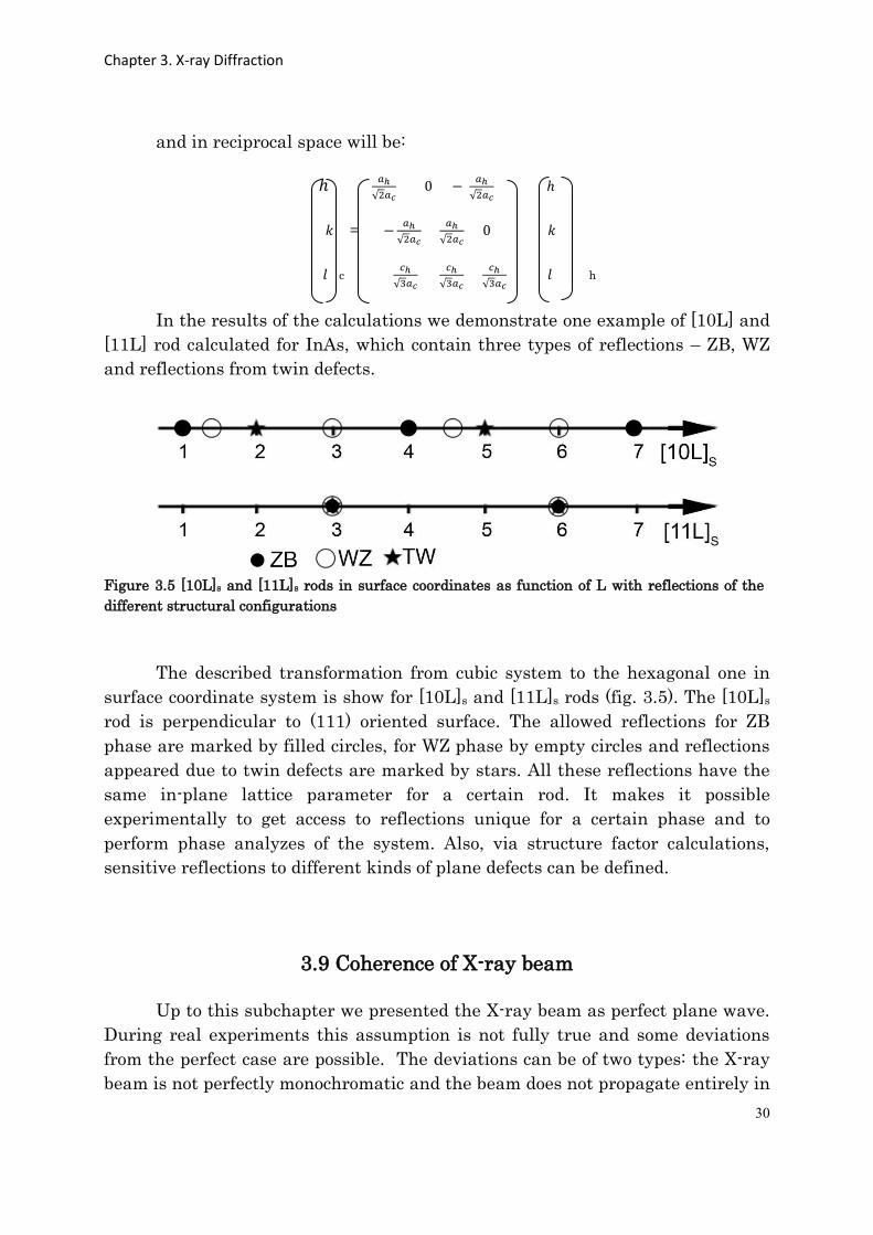
In the results of the calculations we demonstrate one example of [10L] and
[11L] rod calculated for InAs, which contain three types of reflections – ZB, WZ
and reflections from twin defects.
Figure 3.5 [10L]s and [11L]s rods in surface coordinates as function of L with reflections of the
different structural configurations
The described transformation from cubic system to the hexagonal one in
surface coordinate system is show for [10L]s and [11L]s rods (fig. 3.5). The [10L]s
rod is perpendicular to (111) oriented surface. The allowed reflections for ZB
phase are marked by filled circles, for WZ phase by empty circles and reflections
appeared due to twin defects are marked by stars. All these reflections have the
same in-plane lattice parameter for a certain rod. It makes it possible
experimentally to get access to reflections unique for a certain phase and to
perform phase analyzes of the system. Also, via structure factor calculations,
sensitive reflections to different kinds of plane defects can be defined.
3.9 Coherence of X-ray beam
Up to this subchapter we presented the X-ray beam as perfect plane wave.
During real experiments this assumption is not fully true and some deviations
from the perfect case are possible. The deviations can be of two types: the X-ray
beam is not perfectly monochromatic and the beam does not propagate entirely in
Chapter 3. X-ray Diffraction
31
the defined direction. Consider this, the X-ray beam can be characterized in
terms of the coherence length concept.
Let’s imagine two waves are exactly in phase at certain point, propagating
in the same direction but with slightly different wavelengths ( and ). The
longitudinal coherence length defines the distance where the waves become out of
phase. We denote this distance LL. After passing LL the waves are out of phase,
they come again in phase after travelling 2LL. If we define this distance equal to
or equal , it because:
(3.41)
Replacing . We can rewrite the equation as:
(3.42)
Now we consider two waves with equal wavelengths but a bit different
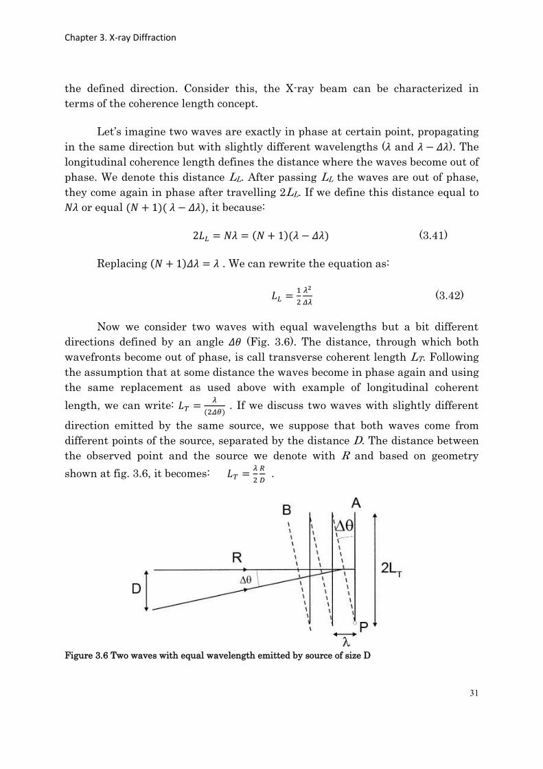
directions defined by an angle (Fig. 3.6). The distance, through which both
wavefronts become out of phase, is call transverse coherent length LT. Following
the assumption that at some distance the waves become in phase again and using
the same replacement as used above with example of longitudinal coherent
length, we can write:
. If we discuss two waves with slightly different
direction emitted by the same source, we suppose that both waves come from
different points of the source, separated by the distance D. The distance between
the observed point and the source we denote with R and based on geometry
shown at fig. 3.6, it becomes:
.
Figure 3.6 Two waves with equal wavelength emitted by source of size D
Chapter 3. X-ray Diffraction
32
For real experiments the coherence lengths of beam are important
parameters. For example, if we consider two electrons separated by a distance
larger than the coherence length then the total scattered intensity is defined by
sum of scattering intensities from the individual objects. The coherence length of
the beams is also defined by experimental setups. The type of synchrotron
radiation source and monochromator are key point in optimization of beam
quality. Also the geometry of the experiment plays an important role for the
value of coherent length of the beam.
3.10 Reciprocal space coordinates
In the next chapters experimental results and its interpretation are
described. For sake of comparison of the experiments all angular coordinates
were transformed into wavelength independent reciprocal space coordinates
using the relations:
( ( ) )
(3.43)
( ( ) )
where i,f are the incidence and exit angle with respect to (111) lattice planes,
respectively - scattering angle in the detector plane perpendicular to
f.
Chapter 3. X-ray Diffraction
33
References
[1] Ashcroft and Mermin, Solid State Physics, Stratford Books, 1976
[2] A. Vartanyants and I. K. Robinson. Partial coherence effects on the imaging of small crystals
using coherent x-ray diffraction. J. Phys.-Condes. Matter, 13:10593–10611, 2001.
[3] I. A. Vartanyants, A. V. Zozulya, K. Mundboth, O. M. Yefanov, M.-I. Richard, E.
Wintersberger, J. Stangl, A. Diaz, C. Mocuta, T. H. Metzger, G. Bauer, T. Boeck, and M.
Schmidbauer. Crystal truncation planes revealed by three-dimensional reconstruction of
reciprocal space. Phys. Rev. B, 77:115317, 2008.
[4] V. Vonk, J. Huijben, D. Kukuruznyak, A. Stierle, H. Hilgenkamp, A. Brinkman, and S.
Harkema, Phys. Rev. B 85 045401 (2012)
[5] S. Mariager, PhD thesis „Structure and dynamics of crystalline nano-systems“,University of
Copenhagen, 2010
[6] H.Shu, X, Chen, H. Zhao, H. Zhou, W.Lu J. Phys. Chem. C, 2010, 114 (41), pp 17514–17518
[7] D. Kriegner, C. Panse, B. Mandl, K. Dick, M. Keplinger, J. Persson , P. Caroff, D. Ercolani, L.
Sorba, F. Bechstedt, J. Stangl, G. Bauer, Nano Lett., 11 , 1483, (2011)
[8] W.L., Bragg, Proceedings of the Cambridge Philosophical Society 17, (1913)
[9] J. Als-Nielsen, “Elements of Modern X-ray Physics”, Wiley,1st edition, 2001
[10] B. Warren, “X-ray diffraction”, Dover Publications, 1990
[11] U. Pietsch, V. Holy, T. Baumbach, ” High-Resolution X-Ray Scattering: From Thin Films to
Lateral Nanostructures”, Springer; 2nd edition, 2004
Chapter 4 MOVPE Au-assisted growth
33
Chapter 4
MOVPE Au-assisted growth of InAs NWs on GaAs[111]B substrate
The results of investigations of InAs nanowires grown by a vapour-liquid-
solid mechanism with Au-catalyser by X-ray diffraction methods realized in out-
of-plane and in-plane geometry of diffraction using synchrotron radiation are
presented. InAs NWs on GaAs B substrate are received in the results of
heteroepitaxial growth in MOVPE chamber. The characterization of the growth
process based on the inspection of the samples with different growth time
performed by scanning electron microscopy and X-ray diffraction techniques. The
growth occurs via graduated alloy layer nucleated at early stage of growth. The
vertical growth is taking place after supersaturation of catalyst particles by
source material.
Chapter is based on paper: J. Brauer, U. Pietsch, A. Davydok, A. Biermanns, J.
Grenzer, V. Gottschalch, G. Wagner, “X-ray investigation of the interface
structure of free standing InAs nanowires grown on GaAs [ ]B”, Appl. Phys.
A, 96, 851, 2009
Chapter 4 MOVPE Au-assisted growth
34
4.1 Introduction
Semiconductor nanowires (NWs) raise an interest due to the ability to
produce single-crystalline 1D epitaxial structures and heterostructures in the
nanometer range. The superior electrical and optoelectronic properties of
semiconductor nanowires make it highly attractive for future manufacturing of
nanoscale devices. Nowadays nanowires have already found application as single-
electron transistors (SET) [1], resonant tunnelling diodes, light emitting diodes
(LED) [2], photo detectors, lasers and nano-sensors for detection [3] of biological
and chemical specimen [4]. In this chapter we present results of structural
investigation of the NWs growth process using X-ray diffraction techniques and
SEM imaging.
VLS growth of semiconductor NW is mostly realized on [111] oriented
substrates for nearly any materials of group AIIIBV [5]. Important place in growth
theory is dedicated to defects structure of the grown objects. Novel properties of
well-studied materials are crucially dependents from the local atomic distribution
and ordering. One of the advantages of MOVPE growth is opportunity to control
of defect structure of grown heterostructures [6, 7]. Semiconductor NWs nucleate
in the result of supersaturation of metal catalyses (in most common cases – gold)
by one of source material components. Vertical growth occurs after alloy
formation with the presence of liquid metal droplets and vapour semiconductor
elements (see Chapter 2). The size and position of catalysts defines the size and
position of future NW. The VLS growth process itself is not fully studied and for
the moment is under debates. Results of different groups are contributing to
general model applying various experimental techniques. For example, Dick et
al. proposed that growth is initiated by a solid seed particles (vapor-solid
mechanism) during InAs NW growth [8]. However, Dayeh et al. [9] are not in
agreement with the conclusions of [8]. Such question can be solved by detail
analysis of surface/interface characterization on different growth stages.
Real space structure information of certain NW can be obtained by TEM,
but a statistical analysis of many wires is an utopian task because of expensive
preparation procedure. In other hand, SEM can provide images of NWs arrays
but without information about the internal structure. In contrast to TEM, X-ray
diffraction is unrestrictive technique and can provide structure information from
NWs ensembles without special preparation procedures. This method is sensitive
to size, material composition and internal strain. In particular, grazing incident
diffraction is a tool dedicated to surface/interface investigations due to possible
control of X-ray penetration depth [10].
Chapter 4 MOVPE Au-assisted growth
35
Prior reported investigation the first steps of the structural analysis of the
grown system have been done. Single wire inspection performed by TEM and X-
ray diffraction experiments demonstrated the presence of two structural types in
NWs – zinc-blende and wurtzite [11]. Also the existence of a close transition layer
between substrate and NWs has been shown. The formation of the transition
layer and the appearance of alloy of metal seeds with source material are
important questions for further design of future devices.
In this chapter I report on results received by use of different geometries of
X-ray diffraction applied for structural characterization of the InAs NW growth
process by the VLS mechanism via gold seeds on GaAs B substrate. The
investigation of growth procedure was performed on sample series with different
growth time corresponding to certain stages of growth procedure, starting from
very first seconds and up to NWs with length of micron. The results became a
basis for the creation of model of the growth process.
4.2 Experimental technique
A detailed overview on preparation and growth is published in [12, 13].
NWs were grown on GaAs B substrate. The growth process was catalysed by
gold particle formed from 1nm gold layer deposited on the substrate. The NWs
were grown in LP-MOVPE chamber, a commercial system (AIX200) with
pressure of 5 kPa and 7000 sccm total gas flow and hydrogen atmosphere.
Trimethylindium (TMI, p = 0.36 Pa) and arsane (AsH3) served as precursor
materials. The investigated samples were grown at 450°C with V/III ratios of 10
without additional pre-annealing. The growth time was varied between 20s and
300s. For further structural analysis X-ray out-of-plane diffraction and GID were
performed.
Prior to X-ray experiments the NW samples were examined by SEM (Fig.
4.1). The SEM study was realized at a FEI Nova 200 NanoLab system with a
field-emission cathode. X-ray measurements have been performed at ID01
beamline of ESRF (Grenoble, France) and at X-ray lab of University of Siegen.
First step of investigation was out-of-plane X-ray diffraction measurements,
performed at the high-resolution diffractometer GE HR-XRD 3003 at Siegen
University using a coplanar Bragg reflection and Cu K1 radiation. Line profiles
of have been recorded close to the InAs (111) and GaAs(111) Bragg
reflections by a Cyber-star point detector. After recording of diffraction patterns,
Chapter 4 MOVPE Au-assisted growth
36
the angular values were recalculated into energy-independent coordinates of
reciprocal space using equations shown in subchapter 3.10.
The GID experiments for different growth time were accomplished with λ =
1.41 Å at the ID01 beamline of ESRF (Grenoble, France). Phase sensitive scan
and evolution of the transition layer were characterized by studying of in-plane
lattice compounds of the samples. During GID measurements the incident angle
of X-ray beam is keeping constant with respect to the surface and fixed in range
of critical angle (angle of total internal reflection) of substrate (with discussed
energy for GaAs 0.3°). In order to determine the composition of buffer layer and
NWs corresponding WZ and ZB sensitive reflections were chosen. We fixed the
detector at the calculated 2 position for a certain Bragg reflection and rotated
the sample around out-of-plane (111) direction. By tuning the incident angle of
the beam to the sample i, one is able to control the penetration depth of the
beam. For incident angle smaller then critical angle, refracted wave cannot
propagate into the material. Instead there will be an evanescent wave travelling
parallel to the surface, with an exponentially decaying amplitude away toward
the interior of the material. This is important, if the diffuse background from
defect scattering in the bulk is an issue, in particular for scattering from a
nanostructures on the surface. Described geometry allows to distinguish signal of
substrate and structures on the surface. Even above the critical angle the
penetration of the wave is reduced enough, in order to reduce bulk scattering. For
scattering for single crystalline substrates often an incident angle of tens of
degree is chosen. The intensity of substrate reflection is increasing with increase
of incident angle. Passing through interface, the wetting layer contributes to the
scattering signal in addition to that of the substrate. Due to specific of
experimental geometry, the GID measurements are presented in surface
coordinates described in Chapter 3.8.
Chapter 4 MOVPE Au-assisted growth
37
4.3 Results and discussion
First step of the research has been realised at home X-ray lab of University
of Siegen. A submillimetre sized X-ray beam has been used for illumination of
macroscopic samples. The diffraction signal produced by all types of structures
existing in the investigated systems visible on SEM images (Figure 4.1). SEM
images of the samples series with variation of growth time from 20sec to 300sec
demonstrate temporal evolution of the growth.
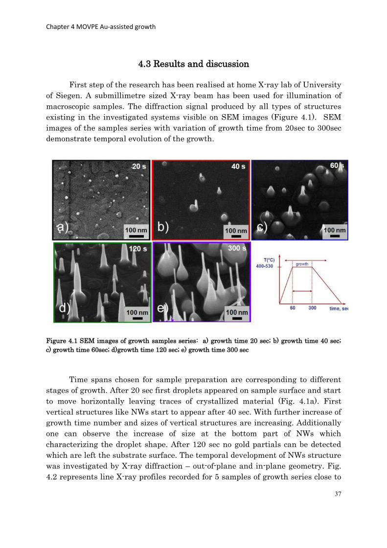
Figure 4.1 SEM images of growth samples series: a) growth time 20 sec; b) growth time 40 sec;
c) growth time 60sec; d)growth time 120 sec; e) growth time 300 sec
Time spans chosen for sample preparation are corresponding to different
stages of growth. After 20 sec first droplets appeared on sample surface and start
to move horizontally leaving traces of crystallized material (Fig. 4.1a). First
vertical structures like NWs start to appear after 40 sec. With further increase of
growth time number and sizes of vertical structures are increasing. Additionally
one can observe the increase of size at the bottom part of NWs which
characterizing the droplet shape. After 120 sec no gold partials can be detected
which are left the substrate surface. The temporal development of NWs structure
was investigated by X-ray diffraction – out-of-plane and in-plane geometry. Fig.
4.2 represents line X-ray profiles recorded for 5 samples of growth series close to
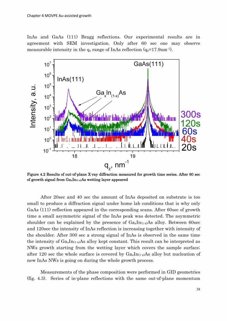
Chapter 4 MOVPE Au-assisted growth
38
InAs and GaAs (111) Bragg reflections. Our experimental results are in
agreement with SEM investigation. Only after 60 sec one may observe
measurable intensity in the qz range of InAs reflection (qz=17.9nm-1).
Figure 4.2 Results of out-of-plane X-ray diffraction measured for growth time series. After 60 sec
of growth signal from GaxIn(1-x)As wetting layer appeared
After 20sec and 40 sec the amount of InAs deposited on substrate is too
small to produce a diffraction signal under home lab conditions that is why only
GaAs (111) reflection appeared in the corresponding scans. After 60sec of growth
time a small asymmetric signal of the InAs peak was detected. The asymmetric
shoulder can be explained by the presence of GaxIn(1-x)As alloy. Between 60sec
and 120sec the intensity of InAs reflection is increasing together with intensity of
the shoulder. After 300 sec a strong signal of InAs is observed in the same time
the intensity of GaxIn(1-x)As alloy kept constant. This result can be interpreted as
NWs growth starting from the wetting layer which covers the sample surface;
after 120 sec the whole surface is covered by GaxIn(1-x)As alloy but nucleation of
new InAs NWs is going on during the whole growth process.
Measurements of the phase composition were performed in GID geometries
(fig. 4.3). Series of in-plane reflections with the same out-of-plane momentum
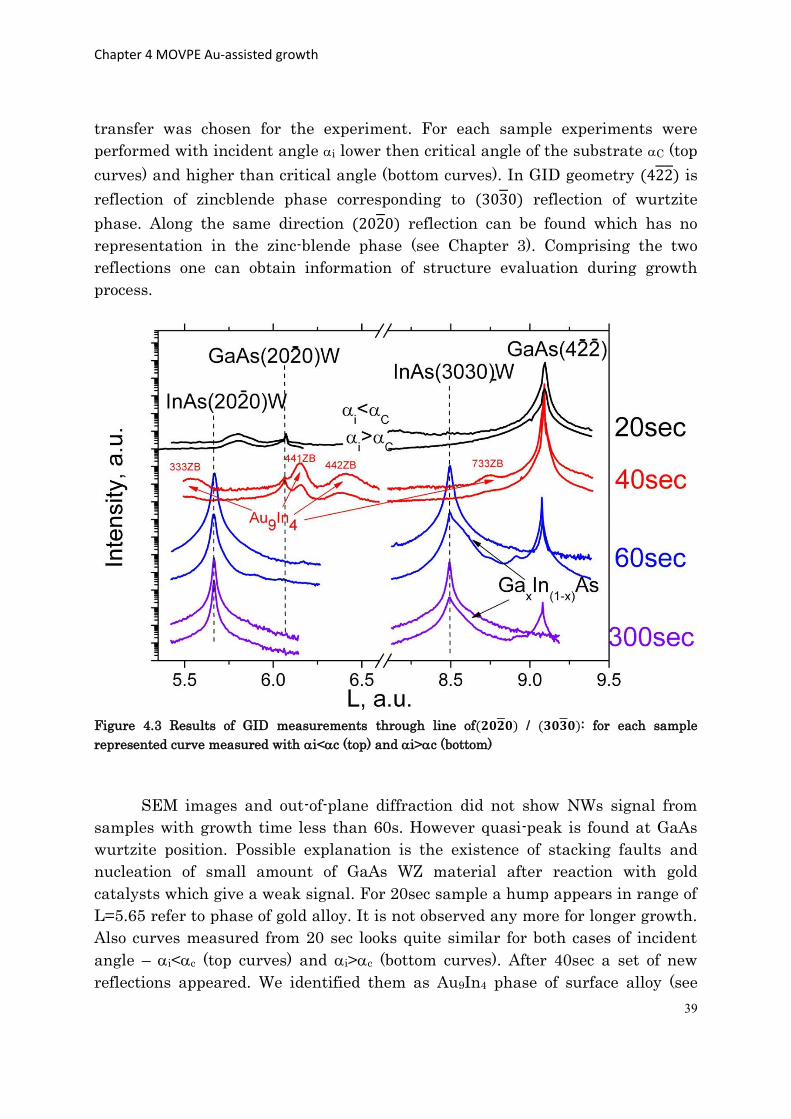
Chapter 4 MOVPE Au-assisted growth
39
transfer was chosen for the experiment. For each sample experiments were
performed with incident angle i lower then critical angle of the substrate C (top
curves) and higher than critical angle (bottom curves). In GID geometry is
reflection of zincblende phase corresponding to reflection of wurtzite
phase. Along the same direction reflection can be found which has no
representation in the zinc-blende phase (see Chapter 3). Comprising the two
reflections one can obtain information of structure evaluation during growth
process.
Figure 4.3 Results of GID measurements through line of / : for each sample
represented curve measured with i<c (top) and i>c (bottom)
SEM images and out-of-plane diffraction did not show NWs signal from
samples with growth time less than 60s. However quasi-peak is found at GaAs
wurtzite position. Possible explanation is the existence of stacking faults and
nucleation of small amount of GaAs WZ material after reaction with gold
catalysts which give a weak signal. For 20sec sample a hump appears in range of
L=5.65 refer to phase of gold alloy. It is not observed any more for longer growth.
Also curves measured from 20 sec looks quite similar for both cases of incident
angle – i<c (top curves) and i>c (bottom curves). After 40sec a set of new
reflections appeared. We identified them as Au9In4 phase of surface alloy (see
Chapter 4 MOVPE Au-assisted growth
40
Chapter 2, Fig. 2.2). Structures belong to the surface because the intensity of
discussed peaks is higher in case of penetration the substrate by the beam
(i<c). In figure 4.3 we marked reflections of different orientation of Au9In4.
According to growth details explained in [12] wurtzite GaAs layer is a result of
preparation procedure of InAs NWs growth. Growth was performed at
temperature 450°C but already at 420°C the interface between gold particles and
substrate material become liquid and creates the alloy. Under influence of
external As-flux the alloy decomposes into solid Au-droplets (with content of Ga)
and GaAs. Deposition of such GaAs is characterized by the creation of many of
twin defects what in result gave a signal at GaAs wurtzite L position. After 60sec
of growth signals from InAs NWs appeared for first time. The NWs have a
wurtzite structure because peaks of increasing intensity are found at and
wurtzite position. In the same time the shoulder corresponds to wetting
layer because it at only and only for case of higher incident angle. The
findings of GaxIn(1-x)As layer in zinc-blende structure agrees with [10]. Growth of
InAs NWs can be described in two steps: growth of GaxIn(1-x)As layer followed by
gold-rich layer formation in condition of external In- and As-fluxes. After
horizontal alloy growth (growth time below 60sec) the vertical growth of InAs
NWs is starting from a Au9In4 solid solution. During the growth, deposited gases
of indium and arsenic are collaborating with liquid Au-Ga solution, created from
liquid gold and diffuse from substrate gallium. It leads to not promotional
increasing of the radial size of bottom part of NWs (fig. 4.1).
4.4 Growth Model
Based on experimental results after inspection with SEM and XRD, a
growth model was proposed. Solid gold particles are reacting with GaAs
substrate under conditions of external pressure created by As-flow. With
beginning of In-flow, the VLS process is starting. First indium collaborates with
Au-Ga alloy creating GaxIn(1-x)As solid solution. The crystal growth is going on in
form of traces on substrate surface (fig .4.1a). A model of such a trace is shown in
fig. 4.4.
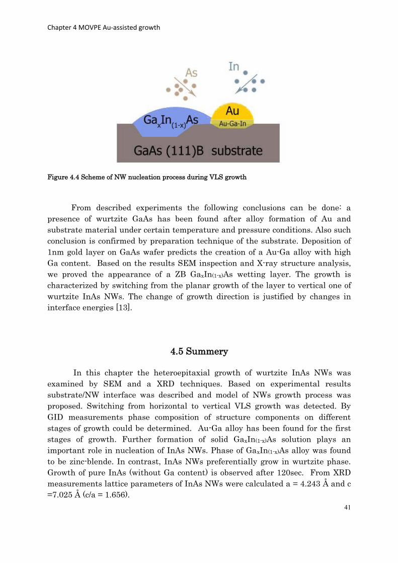
Chapter 4 MOVPE Au-assisted growth
41
Figure 4.4 Scheme of NW nucleation process during VLS growth
From described experiments the following conclusions can be done: a
presence of wurtzite GaAs has been found after alloy formation of Au and
substrate material under certain temperature and pressure conditions. Also such
conclusion is confirmed by preparation technique of the substrate. Deposition of
1nm gold layer on GaAs wafer predicts the creation of a Au-Ga alloy with high
Ga content. Based on the results SEM inspection and X-ray structure analysis,
we proved the appearance of a ZB GaxIn(1-x)As wetting layer. The growth is
characterized by switching from the planar growth of the layer to vertical one of
wurtzite InAs NWs. The change of growth direction is justified by changes in
interface energies [13].
4.5 Summery
In this chapter the heteroepitaxial growth of wurtzite InAs NWs was
examined by SEM and a XRD techniques. Based on experimental results
substrate/NW interface was described and model of NWs growth process was
proposed. Switching from horizontal to vertical VLS growth was detected. By
GID measurements phase composition of structure components on different
stages of growth could be determined. Au-Ga alloy has been found for the first
stages of growth. Further formation of solid GaxIn(1-x)As solution plays an
important role in nucleation of InAs NWs. Phase of GaxIn(1-x)As alloy was found
to be zinc-blende. In contrast, InAs NWs preferentially grow in wurtzite phase.
Growth of pure InAs (without Ga content) is observed after 120sec. From XRD
measurements lattice parameters of InAs NWs were calculated a = 4.243 Å and c
=7.025 Å (c/a = 1.656).
Chapter 5.The influence of the growth parameters
42
Chapter 5
The influence of growth parameters on
the phase composition and defect structure
of InAs nanowires grown by self-assisted
molecular beam epitaxy onto Si(111)
In this chapter, I discuss the results of structure investigations of InAs
NWs grown by MBE on Si substrate. The preferentially nanowire structure is
wurtzite but our findings demonstrate that the grown nanoobjects are highly
defective. Evidence for the high density of SF has been found by probing Bragg
reflections being particular sensitive to SF inclusions. Numerical estimations of
SFs density were done by calculation of X-ray diffraction pattern based on the
model of a statistical average over many nanowires. Also, growth of parasitic
zinc-blende islands has been observed. To improve the quality of growing
structures and to find key parameters of growth, I demonstrate the results of the
investigation of a sample series grown under different growth conditions and
probed the SF density and the ZB phase contribution.
Chapter 5.The influence of the growth parameters
43
In 2010 K. Dick et al. reported about the possibility to control the nanowire
crystal structure by variation of growth temperature and pressure, the molar
pressure fraction and the V/III ratio. These growth experiments have been
performed for six materials of III-V group. For Au catalyzed growth of InAs NWs
it was demonstrated that it is possible to control the structural phases by
changing the growth temperature within the range from 400 to 480 °C. The
increase of growth temperature has an effect on the morphology of the NWs. The
NW diameter is observed to be larger for ZB NWs then for WZ NWs. In addition,
a narrow temperature window slightly lower than 400°C was found where the
stacking fault density dramatically has decreased and a change of structural
phases took place [15]. The authors explained this fast change of structure by
thermodynamic effects but not by the growth kinetics. As we discussed earlier,
the use of metal catalysts leads to undesirable effects during the growth. For
example, at typical growth temperature (400-500°C) gold particles diffuse into
the substrate creating deep level defects and destroying the surface layers [16].
An alternative way to eliminate the use of metal catalyst is the self-
assisted growth of NWs (see Chapter 2), which successfully has been obtained
and reported in 2007 [17]. The structure was analyzed by TEM demonstrating a
high density of SFs and twin defects in the grown nano-objects. The growth of
highly defected structures can be explained by phase mixture of the two possible
structure types – wurtzite and zinc-blende (Chapter 3). The growth usually
realizes along substrate cubic direction [111] independent from substrate
orientation [18]. Despite the difference in stacking sequences, [111] axis of ZB
phase is [0001] direction of hexagonal phase, which makes in-situ phase control
complicated. Nevertheless for Au-assisted growth strong dependence of crystal
structure from growth parameters and growth preparation methods has been
shown. Phase-controlled growth was achieved and demonstrated for InAs NWs
grown on InAs [111] substrate. NWs grow usually in wurtzite phase, when the
substrate is bulk InAs. Out-of-plane lattice parameters of wurtzite and
zincblende phases differ by 0.4% only [19]. In case of InAs and Si the lattice
mismatch is 11.6%. Despite the lattice mismatch, MBE growth provides an
opportunity to grow strain relaxed InAs NWs on Si substrate [20].
S. Hertenberger et al. [21] demonstrated self-induced growth of InAs NWs
on Si (111) by solid-source molecular beam epitaxy. The growth is characterized
by spontaneous nucleation followed by VLS growth. The growth was performed
with different V/III-ratios. The structure was investigated by in-situ RHEED,
SEM and TEM techniques. TEM images were obtained for NWs grown under As-
rich and under In-rich growth conditions. The images exhibit highly defective
structures with an approximate periodicity of SF of 1 nm for both types of
Chapter 5.The influence of the growth parameters
44
growth. Tomioka et al. used Raman spectroscopy and TEM for the structure
characterization of self-induced InAs NWs grown on Si substrate by selective-
area metal-organic vapor epitaxy. The growth was performed on InAs and Si
substrates. High density of twin defects was observed with periodicity of 1-3
bilayer distances for both substrates. The grown structures exhibited a mixture
of zincblende and wurtzite phases [22]. A tendency of high SF density of InAs
NWs grown on Si was also reported in [23]. InAs nanowires were grown on Si
substrate in a MOCVD chamber. The morphology of InAs nanowires were
inspected by SEM. The images show vertically standing nanowires with a small
amount of parasitic islands. TEM investigations demonstrated that the
nanowires are highly uniform in diameter. No metal droplet was observed on top
of the nanowires. High-density of twin defects and stacking faults were found
along the whole wire length.
Explanation of NWs polytypism has been developed in recent years. The
classical nucleation theory is used to describe the growth temperature
dependence of twin planes density. Glas et al. suggested a theoretical description
of the dependence of both structural types from the position of solid/liquid
interface. Growth initiates after the supersaturation of droplet by the source
material atoms [24].
Another undesirable effect is the parasitic growth of islands. The presence
of parasitic islands was observed usually in SEM images together with InAs
nanowire. Authors of [25] described those phenomena for catalysts-free growth of
InAs by the influence of the oxide layer. The growth is initiated by desorption of
indium atoms from the Si/III surface. The thick SiOx-mask prohibits wetting of
the substrate by the highly mismatched NWs material. The nucleation process
fully depends on indium adsorption and desorption kinetics. Free island growth
appears due to a large energy barrier between surface and volume free energies
[26]. It leads to a reduction of the stacking variety in the very beginning of the
growth process. When the island size is smaller than the critical size, the growth
continues with a reduction in total free energy. The number of adatom
incorporation into the island increases constantly. Such growth continues while
desorption is decreasing with time up to the indium desorption saturates. Such
explanation was proposed for low temperature growth process (450-520°C). For
higher temperatures (560°C), the growth is limited by the number of nucleation
events and the larger re-evaporation of diffused indium adatoms compare to
lower temperature.
The understanding of parasitic growth helps to improve the growth
procedure. Tuning the growth conditions can improve a structural perfection of
the grown wires and reduce a parasitic contribution. Most of the reports
dedicated to structural investigations are based on the results of TEM
Chapter 5.The influence of the growth parameters
45
inspections providing real space images of the NW structure. Information on the
defect structure of selected NWs can be obtained by HRTEM. Only a small
number of objects can be examed by this technique due to the complicated
preparation. It makes it difficult to obtain statistic information about structural
properties.
In case of XRD experiment, from intensity and FWHM of Bragg peak one
can judge the amount of material and the defect density. A small amount of
material produces broad reflections, but with low intensity. In our experiments
we observe a broad peaks with high intensity at reflections particular sensitive to
stacking faults. That can be explained by the high density of SFs.
For interpretation of X-ray data I used a numerical description of the
defect structure of the NWs. In particular I performed a simulation of unique WZ
reflection being sensitive to inclusions of SF such as (10i5) reflection for WZ
phase. Numerical simulations are based on a Monte Carlo approach [27]
assuming statistical distribution of certain numbers of different types of SFs and
the distances between two neighboured fault planes. For application at NWs the
undisturbed basis function is the shape function of a NW described by a SINC
function.
For a quantitative analysis I used the approach published recently [28]
developed for considering the influence of SFs on the diffraction patterns taken
from thin films. It neglects effects of dynamical X-ray scattering and describes
the kinematical diffuse. The simulation considers the following simplifications:
the main structure of NW is wurtzite; the incident and exit angles of the X-ray
are much larger than the critical angle of total external reflection; the position of
SFs is random and the density of fault planes is high enough to assume a
statistical ensemble average for the X-ray signal. X-ray scattering intensity
originated by a set of randomly stacked SFs. The numerical simulations are
based on a Monte Carlo approach assuming a statistical distribution of SFs and
the distances between two neighboured fault planes. It has been shown that
different types of stacking faults (e.g. changes from ABAB to BCBC or ACAC type
of stacking) lead to slight differences in the broadening of the affected Bragg
reflections [29], which can be accessed for particularly high ordered materials.
However, in the present case no distinction between the different types is
possible due to the very large broadening of the reflections, and I considered a
random sequence of intrinsic SFs only.
For all samples, simulations were performed for the wurtzite reflection
only with average height as obtained by the SEM images. The broadening of the
reflections was then simulated by the inclusion of stacking faults with mean
distance MF (indicated in Figures), assuming a geometrical distribution of the
distance between subsequent fault planes. For growth series sample described in
Chapter 5.The influence of the growth parameters
46
Chapter 6, in each simulation step, the results from the preceding step for
shorter NWs have been considered, as these segments are maintained at the
bottom of the NWs.
Parasitic islands exhibit ZB phase (see chapter 6). We suppose that the
main contribution to ZB reflections intensity measured in experiments comes
from islands. We use this approach for the characterization of NWs systems
grown under different growth conditions. In such way, we investigate the effect of
growth parameters on the NWs parasitic islands density. Choosing WZ and ZB
reflection with the same in-plane momentum transfer, one get an opportunity to
perform phase sensitive measurements by a single scan experiment. The SF
density and number of islands crucially depend on growth parameters as the
growth temperature, the V/III ratio etc. and/or the method of substrate
preparation. Although the number of investigated samples is small, but they can
be use to demonstrate structural differences provided by the tuning of the growth
parameters.
Presented data were measured at two synchrotron radiation source
facilities. One set of samples were measured at DELTA Synchrotron in
Dortmund (Germany) at BL9 beamline dedicated to high resolution diffraction
experiments. The measurements were done at 11 keV energy with submillimeter
beam size. Diffracted intensity has been recorded with a two-dimensional
PILATUS detector. The second set of data was obtained at the P08 beamline of
PETRA III Synchrotron in DESY (Hamburg, Germany) with energy of 9keV and
submillimeter beam size (500x200 m2 – horizontal and vertical size
respectively). To record the scattered intensity, an one-dimensional MYTHEN
detector was used. For sake of comparison of the experiments all angular
coordinates were transformed into wavelength independent reciprocal space
coordinates using the relations described in subchapter 3.10.
For data analysis and fitting procedure, the line profiles were extracted
from RSMs integrating a qx range of 0.4 nm-1 along qz (the integration range is
shown in Fig. 5.3a by black rectangle). Estimation of NWs/islands volumes ratio
was done by normalizing the intensity and calculating the intensity ratio of
WZ/ZB reflections. The integration of the intensity of WZ reflection has been done
between qz=42.7nm-1 and qz=46.5nm-1. The island contribution was estimated
from the sum of integrated intensity of the two ZB reflections.
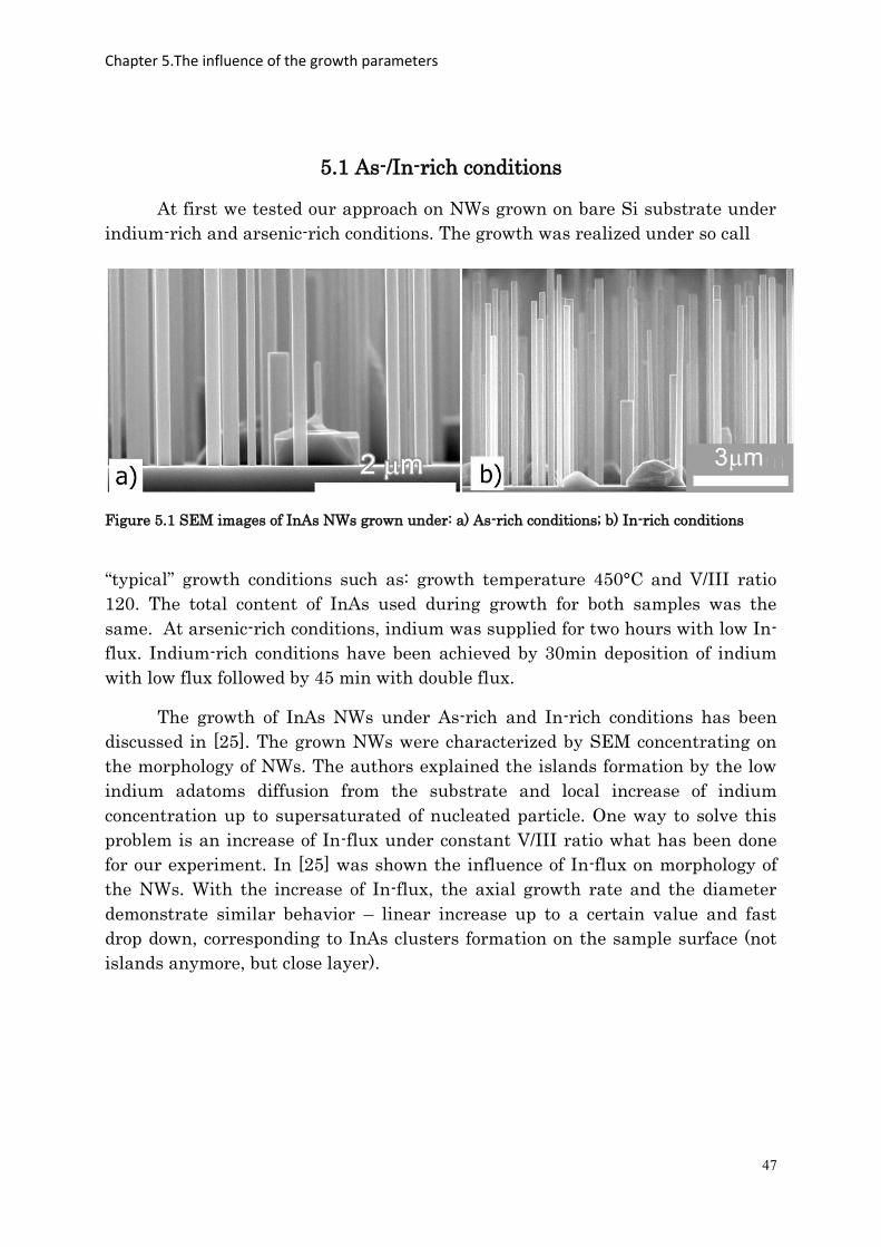
Chapter 5.The influence of the growth parameters
47
5.1 As-/In-rich conditions
At first we tested our approach on NWs grown on bare Si substrate under
indium-rich and arsenic-rich conditions. The growth was realized under so call
“typical” growth conditions such as: growth temperature 450°C and V/III ratio
120. The total content of InAs used during growth for both samples was the
same. At arsenic-rich conditions, indium was supplied for two hours with low In-
flux. Indium-rich conditions have been achieved by 30min deposition of indium
with low flux followed by 45 min with double flux.
The growth of InAs NWs under As-rich and In-rich conditions has been
discussed in [25]. The grown NWs were characterized by SEM concentrating on
the morphology of NWs. The authors explained the islands formation by the low
indium adatoms diffusion from the substrate and local increase of indium
concentration up to supersaturated of nucleated particle. One way to solve this
problem is an increase of In-flux under constant V/III ratio what has been done
for our experiment. In [25] was shown the influence of In-flux on morphology of
the NWs. With the increase of In-flux, the axial growth rate and the diameter
demonstrate similar behavior – linear increase up to a certain value and fast
drop down, corresponding to InAs clusters formation on the sample surface (not
islands anymore, but close layer).
Figure 5.1 SEM images of InAs NWs grown under: a) As-rich conditions; b) In-rich conditions
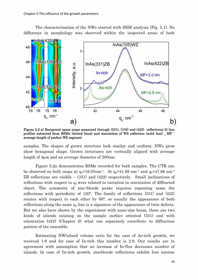
Chapter 5.The influence of the growth parameters
48
The characterization of the NWs started with SEM analysis (Fig. 5.1). No
difference in morphology was observed within the inspected areas of both
samples. The shapes of grown structure look similar and uniform. NWs grow
show hexagonal shape. Grown structures are vertically aligned with average
length of 4m and an average diameter of 200nm.
Figure 5.2a demonstrates RSMs recorded for both samples. The CTR can
be observed on both maps at qx=16.05nm-1. At qz=41.89 nm-1 and qz=47.86 nm-1
ZB reflections are visible – (331) and (422) respectively. Small inclinations of
reflections with respect to qz were related to variation in orientation of diffracted
object. The symmetry of zinc-blende peaks requires repeating same the
reflections with periodicity of 120°. The family of reflections {331} and {422}
rotates with respect to each other by 60°, so usually the appearance of both
reflections along the same qz line is a signature of the appearance of twin defects.
But we also have shown by the experiment with nano-size beam, there are two
kinds of islands existing on the sample surface oriented (331) and with
orientation (422) (Chapter 6) what can separately contribute to diffraction
pattern of the ensemble.
Estimating NW/island volume ratio for the case of As-rich growth, we
received 1.6 and for case of In-rich this number is 2.9. Our results are in
agreement with assumption that an increase of In-flux decreases number of
islands. In case of In-rich growth, zincblende reflections exhibit less intense
Figure 5.2 a) Reciprocal space maps measured through (331), (105) and (422) reflections; b) line
profiles extracted from RSMs (dotted lines) and simulation of WZ reflection (solid line) , MF -
average length of perfect WZ segment
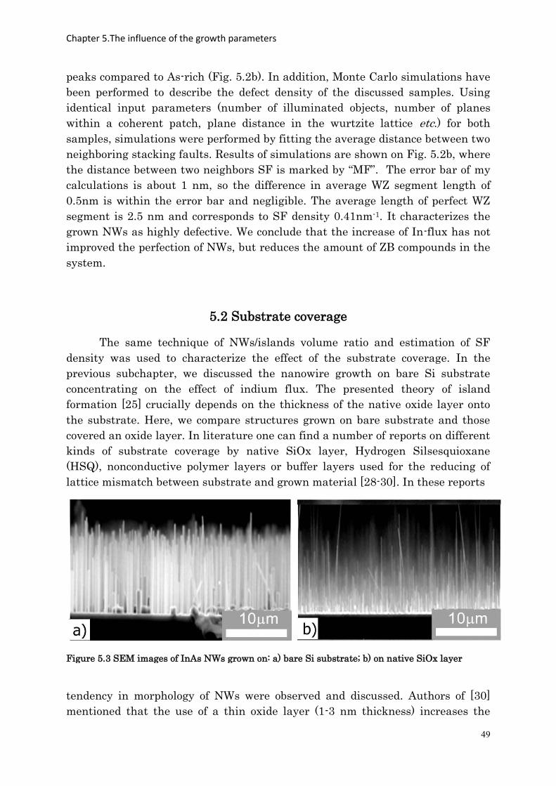
Chapter 5.The influence of the growth parameters
49
peaks compared to As-rich (Fig. 5.2b). In addition, Monte Carlo simulations have
been performed to describe the defect density of the discussed samples. Using
identical input parameters (number of illuminated objects, number of planes
within a coherent patch, plane distance in the wurtzite lattice etc.) for both
samples, simulations were performed by fitting the average distance between two
neighboring stacking faults. Results of simulations are shown on Fig. 5.2b, where
the distance between two neighbors SF is marked by “MF”. The error bar of my
calculations is about 1 nm, so the difference in average WZ segment length of
0.5nm is within the error bar and negligible. The average length of perfect WZ
segment is 2.5 nm and corresponds to SF density 0.41nm-1. It characterizes the
grown NWs as highly defective. We conclude that the increase of In-flux has not
improved the perfection of NWs, but reduces the amount of ZB compounds in the
system.
5.2 Substrate coverage
The same technique of NWs/islands volume ratio and estimation of SF
density was used to characterize the effect of the substrate coverage. In the
previous subchapter, we discussed the nanowire growth on bare Si substrate
concentrating on the effect of indium flux. The presented theory of island
formation [25] crucially depends on the thickness of the native oxide layer onto
the substrate. Here, we compare structures grown on bare substrate and those
covered an oxide layer. In literature one can find a number of reports on different
kinds of substrate coverage by native SiOx layer, Hydrogen Silsesquioxane
(HSQ), nonconductive polymer layers or buffer layers used for the reducing of
lattice mismatch between substrate and grown material [28-30]. In these reports
Figure 5.3 SEM images of InAs NWs grown on: a) bare Si substrate; b) on native SiOx layer
tendency in morphology of NWs were observed and discussed. Authors of [30]
mentioned that the use of a thin oxide layer (1-3 nm thickness) increases the
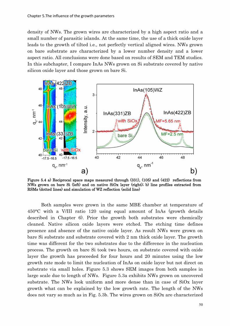
Chapter 5.The influence of the growth parameters
50
density of NWs. The grown wires are characterized by a high aspect ratio and a
small number of parasitic islands. At the same time, the use of a thick oxide layer
leads to the growth of tilted i.e., not perfectly vertical aligned wires. NWs grown
on bare substrate are characterized by a lower number density and a lower
aspect ratio. All conclusions were done based on results of SEM and TEM studies.
In this subchapter, I compare InAs NWs grown on Si substrate covered by native
silicon oxide layer and those grown on bare Si.
Both samples were grown in the same MBE chamber at temperature of
450°C with a V/III ratio 120 using equal amount of InAs (growth details
described in Chapter 6). Prior the growth both substrates were chemically
cleaned. Native silicon oxide layers were etched. The etching time defines
presence and absence of the native oxide layer. As result NWs were grown on
bare Si substrate and substrate covered with 2 nm thick oxide layer. The growth
time was different for the two substrates due to the difference in the nucleation
process. The growth on bare Si took two hours, on substrate covered with oxide
layer the growth has proceeded for four hours and 20 minutes using the low
growth rate mode to limit the nucleation of InAs on oxide layer but not direct on
substrate via small holes. Figure 5.3 shows SEM images from both samples in
large scale due to length of NWs. Figure 5.3a exhibits NWs grown on uncovered
substrate. The NWs look uniform and more dense than in case of SiOx layer
growth what can be explained by the low growth rate. The length of the NWs
does not vary so much as in Fig. 5.3b. The wires grown on SiOx are characterized
Figure 5.4 a) Reciprocal space maps measured through (331), (105) and (422) reflections from
NWs grown on bare Si (left) and on native SiOx layer (right); b) line profiles extracted from
RSMs (dotted lines) and simulation of WZ reflection (solid line)
Chapter 5.The influence of the growth parameters
51
by a lower density of parasitic structures (from top view SEM image – not shown)
and NWs aspect ratio does not change so significantly.
Measured RSMs are shown on Fig. 5.4a, where one can identify the
reflections (331) and (422) of ZB and (105) reflection of WZ phases of InAs. From
the sample grown without SiOx layer, an intense line (CTR) through all three
reflections can be observed. In contrast, in the second map one can see more
intense spots at the Bragg peak positions, but no intense line along the whole qz
range. These findings can be attributed to two factors. NWs on the second sample
are well-ordered and show a lower SFs density compared to the first case. The
results of the fitting procedure are shown on fig. 5.4b by a solid line. Following
our assumption that the NWs are forming in WZ phase, again I concentrated on
WZ (105) reflections and use the same approach as in pervious subchapter. The
structure perfection can be estimated from FWHM, which obviously is smaller for
the case of SiOx surface. Simulations gave an average size of perfect WZ domain
between two neighbor SFs. As mentioned in previous subchapter, the size of
perfect domain for NWs grown onto bare silicon is 2.5 nm. In case of SiOx layer,
this number is more then in two times larger and equals to 5.65 nm. For the
ratio between WZ and ZB reflections for NWs grown on bare Si we received 1.6,
for the second sample this ratio equals to 2.4. This is explained by the dominance
of WZ structure in the system and the lower number of parasitic islands found
onto the oxide layer compared to the case of bare Si. This observation is in
agreement with [30].
In the introduction part I already mentioned the reasons of parasitic
structures formation. More detail explanation can be found in [25]. The presence
of the oxide layer is necessary for the immobilization of indium droplets on the
surface restricting the particle size making NW nucleation possible [31]. From
our findings, one can conclude that the use of the thin SiOx layer leads to a
reduced number of parasitic grown structures and a lower SFs density.
5.3 Substrate temperature
One of the most significant parameter of growth is the substrate
temperature. Tuning the temperature and the V/III ratio one is able to control
the phase composition of the growing system. This has been demonstrated in
several publications for different growth modes. In resent a paper H. Joyce et al.
have shown that the NWs structure perfection depends on the interplay between
various parameters. The authors found out empirically that for InAs NWs grown
by Au-assisted metal-organic chemical vapour deposition at low temperature
(400°C) and high V/III ratio, it is energetically favourable to form the zinc-blende
phase. At higher temperature and lower V/III ratio, one is able to achieve a
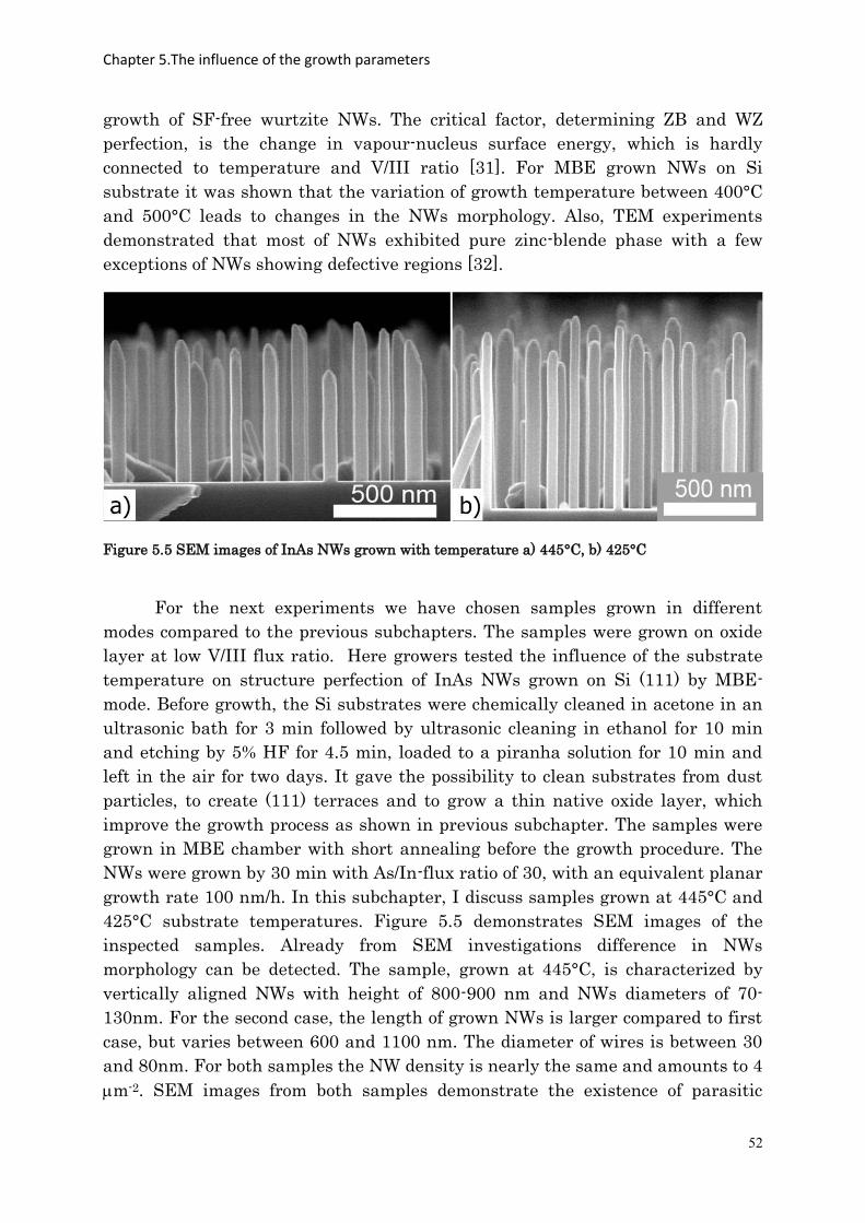
Chapter 5.The influence of the growth parameters
52
growth of SF-free wurtzite NWs. The critical factor, determining ZB and WZ
perfection, is the change in vapour-nucleus surface energy, which is hardly
connected to temperature and V/III ratio [31]. For MBE grown NWs on Si
substrate it was shown that the variation of growth temperature between 400°C
and 500°C leads to changes in the NWs morphology. Also, TEM experiments
demonstrated that most of NWs exhibited pure zinc-blende phase with a few
exceptions of NWs showing defective regions [32].
Figure 5.5 SEM images of InAs NWs grown with temperature a) 445°C, b) 425°C
For the next experiments we have chosen samples grown in different
modes compared to the previous subchapters. The samples were grown on oxide
layer at low V/III flux ratio. Here growers tested the influence of the substrate
temperature on structure perfection of InAs NWs grown on Si (111) by MBE-
mode. Before growth, the Si substrates were chemically cleaned in acetone in an
ultrasonic bath for 3 min followed by ultrasonic cleaning in ethanol for 10 min
and etching by 5% HF for 4.5 min, loaded to a piranha solution for 10 min and
left in the air for two days. It gave the possibility to clean substrates from dust
particles, to create (111) terraces and to grow a thin native oxide layer, which
improve the growth process as shown in previous subchapter. The samples were
grown in MBE chamber with short annealing before the growth procedure. The
NWs were grown by 30 min with As/In-flux ratio of 30, with an equivalent planar
growth rate 100 nm/h. In this subchapter, I discuss samples grown at 445°C and
425°C substrate temperatures. Figure 5.5 demonstrates SEM images of the
inspected samples. Already from SEM investigations difference in NWs
morphology can be detected. The sample, grown at 445°C, is characterized by
vertically aligned NWs with height of 800-900 nm and NWs diameters of 70-
130nm. For the second case, the length of grown NWs is larger compared to first
case, but varies between 600 and 1100 nm. The diameter of wires is between 30
and 80nm. For both samples the NW density is nearly the same and amounts to 4
m-2. SEM images from both samples demonstrate the existence of parasitic
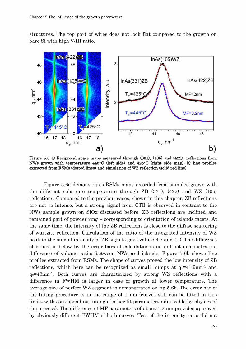
Chapter 5.The influence of the growth parameters
53
structures. The top part of wires does not look flat compared to the growth on
bare Si with high V/III ratio.
Figure 5.6 a) Reciprocal space maps measured through (331), (105) and (422) reflections from
NWs grown with temperature 445°C (left side) and 425°C (right side map); b) line profiles
extracted from RSMs (dotted lines) and simulation of WZ reflection (solid red line)
Figure 5.6a demonstrates RSMs maps recorded from samples grown with
the different substrate temperature through ZB (331), (422) and WZ (105)
reflections. Compared to the previous cases, shown in this chapter, ZB reflections
are not so intense, but a strong signal from CTR is observed in contrast to the
NWs sample grown on SiOx discussed before. ZB reflections are inclined and
remained part of powder ring – corresponding to orientation of islands facets. At
the same time, the intensity of the ZB reflections is close to the diffuse scattering
of wurtzite reflection. Calculation of the ratio of the integrated intensity of WZ
peak to the sum of intensity of ZB signals gave values 4.7 and 4.2. The difference
of values is below by the error bars of calculations and did not demonstrate a
difference of volume ratios between NWs and islands. Figure 5.6b shows line
profiles extracted from RSMs. The shape of curves proved the low intensity of ZB
reflections, which here can be recognized as small humps at qz=41.9nm-1 and
qz=48nm-1. Both curves are characterized by strong WZ reflections with a
difference in FWHM is larger in case of growth at lower temperature. The
average size of perfect WZ segment is demonstrated on fig 5.6b. The error bar of
the fitting procedure is in the range of 1 nm (curves still can be fitted in this
limits with corresponding tuning of other fit parameters admissible by physics of
the process). The difference of MF parameters of about 1.2 nm provides approved
by obviously different FWHM of both curves. Test of the intensity ratio did not
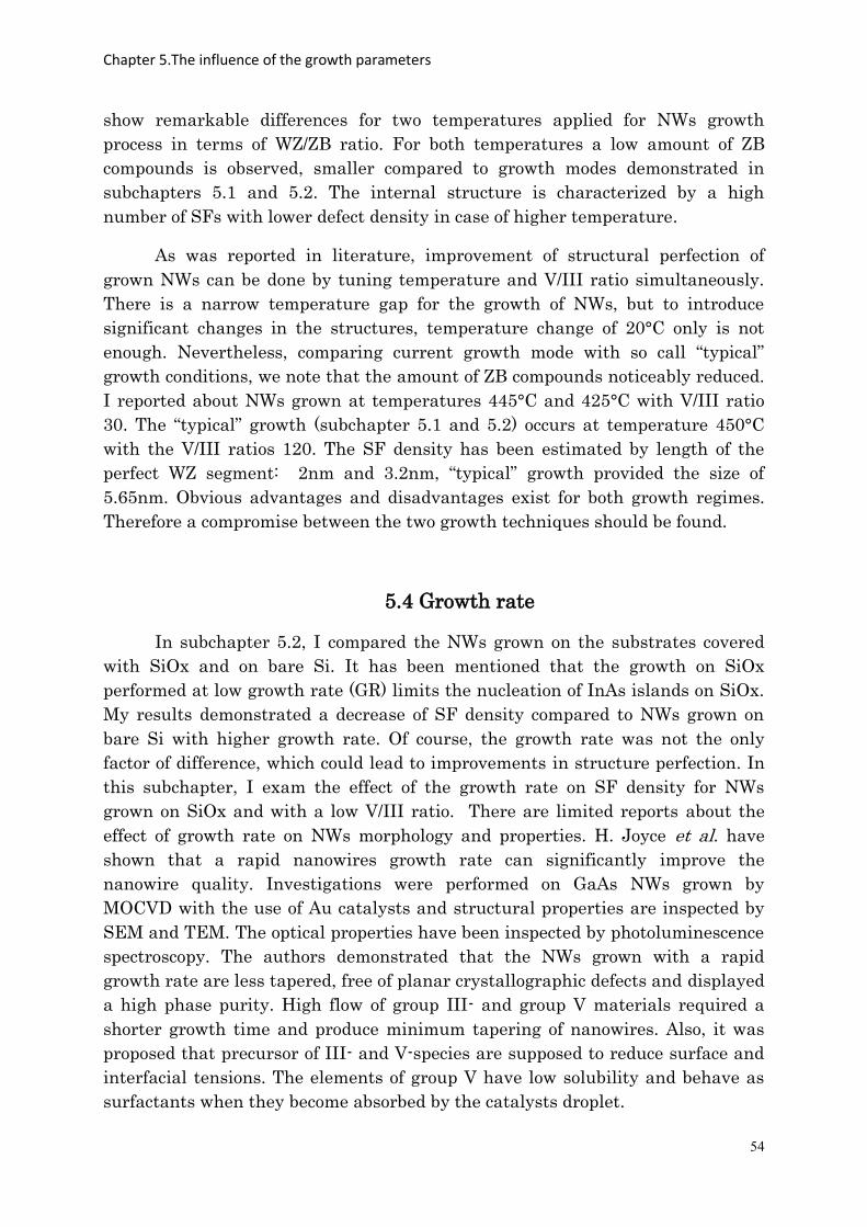
Chapter 5.The influence of the growth parameters
54
show remarkable differences for two temperatures applied for NWs growth
process in terms of WZ/ZB ratio. For both temperatures a low amount of ZB
compounds is observed, smaller compared to growth modes demonstrated in
subchapters 5.1 and 5.2. The internal structure is characterized by a high
number of SFs with lower defect density in case of higher temperature.
As was reported in literature, improvement of structural perfection of
grown NWs can be done by tuning temperature and V/III ratio simultaneously.
There is a narrow temperature gap for the growth of NWs, but to introduce
significant changes in the structures, temperature change of 20°C only is not
enough. Nevertheless, comparing current growth mode with so call “typical”
growth conditions, we note that the amount of ZB compounds noticeably reduced.
I reported about NWs grown at temperatures 445°C and 425°C with V/III ratio
30. The “typical” growth (subchapter 5.1 and 5.2) occurs at temperature 450°C
with the V/III ratios 120. The SF density has been estimated by length of the
perfect WZ segment: 2nm and 3.2nm, “typical” growth provided the size of
5.65nm. Obvious advantages and disadvantages exist for both growth regimes.
Therefore a compromise between the two growth techniques should be found.
5.4 Growth rate
In subchapter 5.2, I compared the NWs grown on the substrates covered
with SiOx and on bare Si. It has been mentioned that the growth on SiOx
performed at low growth rate (GR) limits the nucleation of InAs islands on SiOx.
My results demonstrated a decrease of SF density compared to NWs grown on
bare Si with higher growth rate. Of course, the growth rate was not the only
factor of difference, which could lead to improvements in structure perfection. In
this subchapter, I exam the effect of the growth rate on SF density for NWs
grown on SiOx and with a low V/III ratio. There are limited reports about the
effect of growth rate on NWs morphology and properties. H. Joyce et al. have
shown that a rapid nanowires growth rate can significantly improve the
nanowire quality. Investigations were performed on GaAs NWs grown by
MOCVD with the use of Au catalysts and structural properties are inspected by
SEM and TEM. The optical properties have been inspected by photoluminescence
spectroscopy. The authors demonstrated that the NWs grown with a rapid
growth rate are less tapered, free of planar crystallographic defects and displayed
a high phase purity. High flow of group III- and group V materials required a
shorter growth time and produce minimum tapering of nanowires. Also, it was
proposed that precursor of III- and V-species are supposed to reduce surface and
interfacial tensions. The elements of group V have low solubility and behave as
surfactants when they become absorbed by the catalysts droplet.
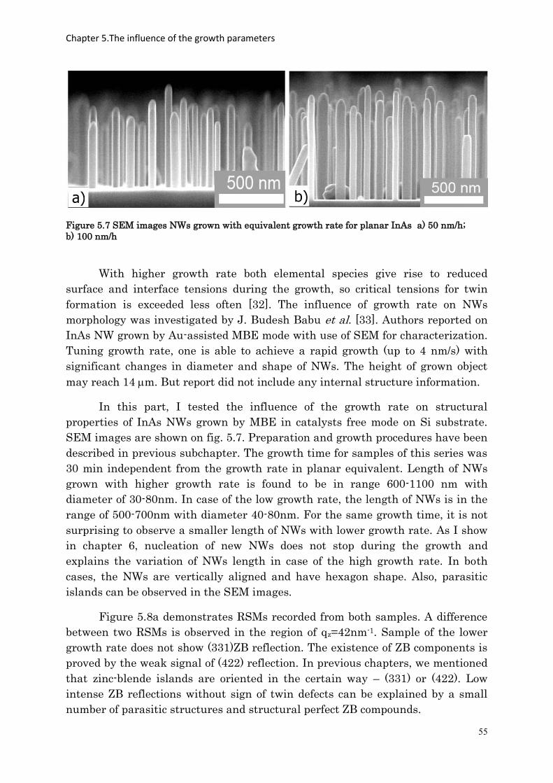
Chapter 5.The influence of the growth parameters
55
With higher growth rate both elemental species give rise to reduced
surface and interface tensions during the growth, so critical tensions for twin
formation is exceeded less often [32]. The influence of growth rate on NWs
morphology was investigated by J. Budesh Babu et al. [33]. Authors reported on
InAs NW grown by Au-assisted MBE mode with use of SEM for characterization.
Tuning growth rate, one is able to achieve a rapid growth (up to 4 nm/s) with
significant changes in diameter and shape of NWs. The height of grown object
may reach 14 m. But report did not include any internal structure information.
In this part, I tested the influence of the growth rate on structural
properties of InAs NWs grown by MBE in catalysts free mode on Si substrate.
SEM images are shown on fig. 5.7. Preparation and growth procedures have been
described in previous subchapter. The growth time for samples of this series was
30 min independent from the growth rate in planar equivalent. Length of NWs
grown with higher growth rate is found to be in range 600-1100 nm with
diameter of 30-80nm. In case of the low growth rate, the length of NWs is in the
range of 500-700nm with diameter 40-80nm. For the same growth time, it is not
surprising to observe a smaller length of NWs with lower growth rate. As I show
in chapter 6, nucleation of new NWs does not stop during the growth and
explains the variation of NWs length in case of the high growth rate. In both
cases, the NWs are vertically aligned and have hexagon shape. Also, parasitic
islands can be observed in the SEM images.
Figure 5.8a demonstrates RSMs recorded from both samples. A difference
between two RSMs is observed in the region of qz=42nm-1. Sample of the lower
growth rate does not show (331)ZB reflection. The existence of ZB components is
proved by the weak signal of (422) reflection. In previous chapters, we mentioned
that zinc-blende islands are oriented in the certain way – (331) or (422). Low
intense ZB reflections without sign of twin defects can be explained by a small
number of parasitic structures and structural perfect ZB compounds.
Figure 5.7 SEM images NWs grown with equivalent growth rate for planar InAs a) 50 nm/h;
b) 100 nm/h
Chapter 5.The influence of the growth parameters
56
Figure 5.8 a) Reciprocal space maps measured through (331), (105) and (422) reflections from
NWs grown with GR=50nm/h (left side) and GR=100nm/h (right side map); b) line profiles
extracted from RSMs (dotted lines) and simulation of WZ reflection (solid red line)
The ratio of integrated WZ intensity to the sum of integrated ZB reflections is
larger for case of lower growth rate and equal to 4.7, while for the second sample
this value equals to 4.2. For the demonstrated growth conditions, the low growth
rate reduces a number density of parasitic islands.
At integrated profiles ZB reflections are hardly observed at the top curve
(fig. 5.8b) corresponding to the case of high growth rate (GR) and not visible at all
for the bottom curve. The FWHM of wurtzite reflection is larger for GR=100nm/h
is a sign of the higher SFs density. From simulations we received the lengths of
perfect WZ segments to be 5nm for low growth rate and 2nm for high growth
rate. In contradiction to [34] we demonstrated that lower growth rate leads to
improvements of the structural perfection in terms of a lower islands number and
better structural perfection of NWs.
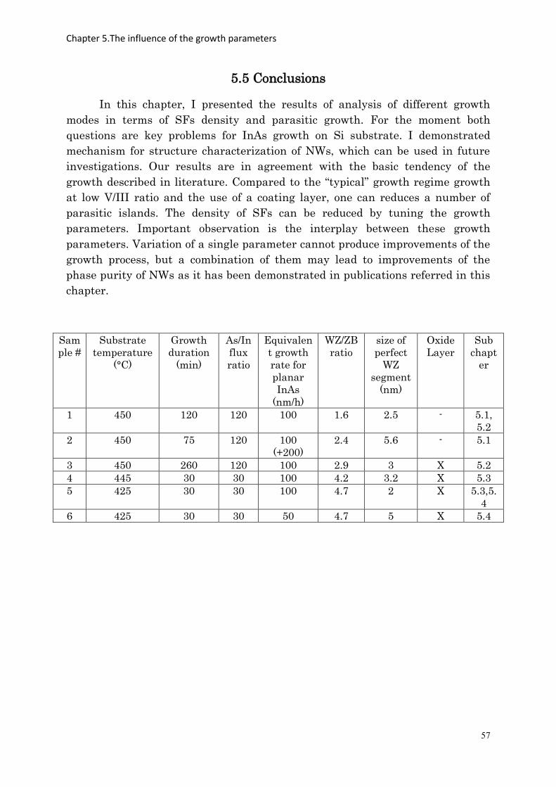
Chapter 5.The influence of the growth parameters
57
5.5 Conclusions
In this chapter, I presented the results of analysis of different growth
modes in terms of SFs density and parasitic growth. For the moment both
questions are key problems for InAs growth on Si substrate. I demonstrated
mechanism for structure characterization of NWs, which can be used in future
investigations. Our results are in agreement with the basic tendency of the
growth described in literature. Compared to the “typical” growth regime growth
at low V/III ratio and the use of a coating layer, one can reduces a number of
parasitic islands. The density of SFs can be reduced by tuning the growth
parameters. Important observation is the interplay between these growth
parameters. Variation of a single parameter cannot produce improvements of the
growth process, but a combination of them may lead to improvements of the
phase purity of NWs as it has been demonstrated in publications referred in this
chapter.
Sam
ple #
Substrate
temperature
(°C)
Growth
duration
(min)
As/In
flux
ratio
Equivalen
t growth
rate for
planar
InAs
(nm/h)
WZ/ZB
ratio
size of
perfect
WZ
segment
(nm)
Oxide
Layer
Sub
chapt
er
1 450 120 120 100 1.6 2.5 - 5.1,
5.2
2 450 75 120 100
(+200)
2.4 5.6 - 5.1
3 450 260 120 100 2.9 3 X 5.2
4 445 3020 30 100 4.2 3.2 X 5.3
5 425 30 30 100 4.7 2 X 5.3,5.
4
6 425 30 30 50 4.7 5 X 5.4
Chapter 6. MBE self-assisted growth
58
Chapter 6
Structural Phase composition of InAs
nanowires grown by self-assisted molecular
beam epitaxy onto Si(111)
InAs nanowires grown by self-assisted molecular beam epitaxy onto a Si
(111) substrate show a transition from a more droplet like to a columnar shape as
function of growth time, accompanied by the transition from an In-rich vapour-
liquid-solid to an As-rich vapour-solid growth mode. Using sample integrating
and single NW resolved X-ray diffraction techniques we studied the phase
composition of InAs NWs for both growth conditions. Already after 10 sec of
growth the NWs exhibit a high density of stacking faults. For further growth
time, the number of defects increases. After 40sec of growth the structure
displays a random stacking of InAs bilayers. I show that the stacking fault
density increases with increasing growth time. Single NW resolved XRD reveals
that the stacking sequence varies random between different NWs. However, in
most of the NWs the distances between neighboured SFs show a rather narrow
distribution. The transition from In-rich to As-rich MBE growth mode is
described in terms of structural defects. The transition of growth modes is
accompanied by the increase of SF density.
Chapter is based on paper: A. Davydok, E. Dimakis, A. Biermanns, L. Geelhaar,
U. Pietsch, „Structural Phase composition of InAs nanowires grown by self-
assisted molecular beam epitaxy onto Si(111)“, in preparation
Chapter 6. MBE self-assisted growth
59
6.1 Introduction.
Combination of the high-speed electrical properties of III-V semiconductors
with the optoelectrical properties of Si is of high interest for future electronic
devices. That’s why in this chapter I will concentrate exactly on such system.
Despite the huge lattice mismatch combination of these materials is achievable
by nanowire growth onto [111] oriented substrates, e.g. by means of molecular
beam epitaxy. NW growth of even highly mismatched systems like InAs onto
silicon, showing a lattice mismatch of 11.6% in the bulk phase, has been
successfully demonstrated [18]. However, for electrical applications planar
defects like stacking faults and twin planes play an important role as scattering
centres for charge carriers, leading to degradation of the devices [36]. The
crystallographic structure of InAs NWs shows predominantly the hexagonal WZ
phase independent from the fact that bulk material and two-dimensional
structures are grown in the cubic zinc-blende phase [37]. The NW growth
typically takes place along the [0001] hexagonal direction which is parallel to the
cubic [111] direction of the substrate. Both zinc-blende and wurtzite phases differ
in the sequence of bilayers stacking along the growth direction. Because of the
very small difference of formation energies [38], a switching between the two
phases during the growth process is hardly to control and leads to the creation of
planar defects that can already be monitored by in-situ reflection high energy
electron diffraction during NW growth. More detailed structural analysis can be
performed by High-resolution Transition Electron Microscopy [39-41] and High-
resolution- X-ray diffractometry as shown on previous chapter.
However phase control growth of InAs NWs was achieved by different
growth technique, like Au-assisted metal-organic chemical vapour deposition and
Au-assisted metal-organic vapour phase epitaxy, mainly by tuning the growth
parameters in the particular temperature range and the V/III ratio [42]. Krieger
et al [43] have shown the appearance of other stacking sequences in InAs NWs,
grown by MOVPE substrate, such as the 4H phase which is known from SiC [44].
In all cases growth were realized on InAs substrate. In the same time in case of
self-assisted InAs NWs grown on silicon substrate independent from growth
technique, most of reports are complying about high density of SFs and twin
defects [22, 46].
In recent paper [37] authors have reported on InAs NW self-catalytic MBE
growth under initially In-rich conditions. It was found that the NW growth rate
changes from high (30 µm/h) during the initial time of growth to low (2.5 µm/h)
for further growth. This change is explained by the transition from In-rich to As-
Chapter 6. MBE self-assisted growth
60
rich conditions at the NW growth interface due to the decreasing arrival of
Indium adatoms at the growth front caused by the formation of additional
nucleation centres. Whereas wurtzite was identified as predominant phase in
the initial growth time, the appearance of “streaky” features in RHEED pattern
while growing in the As-rich phase was interpreted by an increasing defect
density within the hexagonal NWs. A detailed real structure analysis of the
grown NW could not be performed.
Most of the papers report on morphology and internal structural analysis
of the grown NWs were preformed with SEM and TEM. Instead of TEM, X-ray
technique is a non-destructive method, which does not require complicated
sample preparation procedure. X-ray diffraction can provide structure
information from an ensemble of NWs, but also from a single object with the use
of specific nano-focus setup.
In following chapter I will discuss investigation of the phase structure of
InAs NWs by means of high-resolution X-ray diffraction techniques. Using
sample integrating XRD we show that under As-rich conditions the NW grow
with inclusion of a high number of stacking faults. Spatially resolved NW
inspection using a focussed X-ray beam reveals that the SF arrangement varies
randomly between the NWs but shows a rather sharp distribution of SF
distances.
6.2 MBE –Growth
The samples series was grown at 450°C with indium flux FIn=100nm/h and
ratio V/III=120. Growth was stopped after 10 sec (sample A), 43 sec (sample B),
86 sec (sample C) and 2 hours (sample D). Growth of all samples started with
opening of As-cell shutter and after a while - the Indium cell. In the end of
growth both shutters were closed simultaneously. The growth time of each
sample is defined by the opening time of the In-shutter. To remove the native
oxide layer the substrates were etched in 5% HF for 1 min, organic residuals
were etched out in H2SO4 /H2O2 (3:1) for 10 min, for creation atomic flat terraces
– in 40% NH4F for 10 min, and etched in 5% HF for 10s passivate the surface
with hydrogen. After each step substrates were rinsed by deionized H2O.
Substrates were dried with N2 and loaded to the MBE system. Prior to growth
the substrates were annealed at temperature more than 500°C. More detail about
growth process in [46]- growth series D.
After unload samples from growth chamber all of them were examined
with SEM (Fig. 6.1). For short NWs (sample A) SEM cannot distinguish between
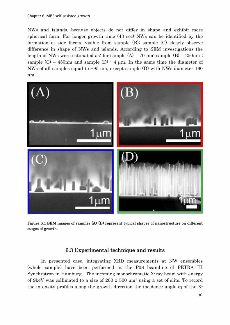
Chapter 6. MBE self-assisted growth
61
NWs and islands, because objects do not differ in shape and exhibit more
spherical form. For longer growth time (43 sec) NWs can be identified by the
formation of side facets, visible from sample (B); sample (C) clearly observe
difference in shape of NWs and islands. According to SEM investigations the
length of NWs were estimated as: for sample (A) – 70 nm; sample (B) – 250nm ;
sample (C) – 450nm and sample (D) - 4 m. In the same time the diameter of
NWs of all samples equal to ~95 nm, except sample (D) with NWs diameter 160
nm.
Figure 6.1 SEM images of samples (A)-(D) represent typical shapes of nanostructure on different
stages of growth.
6.3 Experimental technique and results
In presented case, integrating XRD measurements at NW ensembles
(whole sample) have been performed at the P08 beamline of PETRA III
Synchrotron in Hamburg. The incoming monochromatic X-ray beam with energy
of 9keV was collimated to a size of 200 x 500 µm² using a set of slits. To record
the intensity profiles along the growth direction the incidence angle i of the X-
Chapter 6. MBE self-assisted growth
62
ray beam with respect to the (111) lattice planes of the sample was rocked
through the exact Bragg condition with a step of Δi =0.01°, simultaneously
moving detector through the diffraction position with double steps. The
diffraction intensities were recorded using a 1D pixel detector, MYTHEN, with
pixel size of 50 μm along the f direction [47].
X-ray diffraction is a non-destructive tool to characterize crystalline
materials. For inspection of NWs various scattering geometries can be employed
to probe the phase composition, the lattice parameters and the strain variation
along the growth direction. Symmetric X-ray diffraction (sXRD) is applied to
inspect lattice parameter and strain along the hexagonal [0001] growth direction.
The same Bragg reflection holds for the (111) Bragg peak of zinc-blende
structure. In this geometry the ZB and WZ phases can be separated already due
to their different out-of-plane lattice parameter which is for InAs d(111)=
0.605nm/sqrt(3)=0.349nm and d(0002)= 0.351nm. In reciprocal space it leads to
appearance of two reflections with slightly different qz position (the
transformations form incident and reflected angles to q-coordinates are described
in Chapter 3). The larger d-value corresponds to a smaller qz. Symmetric
geometry is realized by simultaneous scan of incident and exit angles through the
equal angular range. This measurement in symmetrical geometry, already
provide indication of wurtzite and zinc-blende phases. More detail phase analysis
can be done in asymmetric out-of-plane geometry (aXRD). Considering bulk
lattice parameters and [111] orientation of substrate we identified the (331)
reflection to be particular sensitive for zinc-blende but (10i5) reflection as
wurtzite sensitive only. Along the same zone the (422) reflection is allowed for
zinc-blende structure only. These asymmetric reflections are accessible either in
grazing- incidence (grazing incidence angle) or grazing exit (grazing exit angle)
geometry. Due to larger incidence angle the later one provides a much smaller
foot print. In addition, the positions of these reflections are defined by both in-
plane and out-of-plane lattice parameters. From literature the InAs wurtzite in-
plane and out-of-plane lattice parameters are a=0.427nm and c=0.702nm [43].
6.3.1 Ensemble measurements
For all samples reciprocal space maps were recorded in vicinity of the (111)
Bragg reflection of silicon (Fig. 6.2a). From RSMs one can observe an increase of
InAs peak intensity with growth time i.e. an increase of InAs amount. As see in
sample (D) the InAs reflex splits in two well resolve peaks. Following observation
provoked us to perform measurements in qx-qy plane (Fig. 6.2b). We received a
pictures with six-strikes around InAs the reflection for sample (A) ; for other
Chapter 6. MBE self-assisted growth
63
samples the cross-sections are rotated by 30° with respect to each other
corresponding to transition from {1 -1 0} side-facets towards {1 1 -2} facets.
Considering the time evolution of this feature we attribute the {1 -1 0} appearing
first to wurtzite (larger c- lattice parameter) and the second one with {1 1 -2} to
zinc-blende appearing at later stage of NW growth. In real space such image can
be explained by hexagons but in reciprocal space by strikes pointing to the
hexagons facets (Fig. 6.2b). Prior the measurements we aligned samples
according Si (422) reflection. It gave us possibility to define orientations of both
hexagons (Fig. 6.2b left side).
Extracted line scans along qz in range of qx=0.1nm-1are shown in Fig.6.3.
Both the InAs and Si peaks are clearly separated without major intensity in
between. The fact that one of the peaks appears at position close to table value of
(111) position of bulk InAs already for sample A, tells us that the large lattice
mismatch of 11.6% between InAs and silicon has been already released in this
initial state of growth. In so highly mismatched systems the strain is released at
the very beginning of growth process after certain critical diameter of InAs NWs
through formation of misfit dislocations. This is in agreement with previous
studies taken for GaAs NWs grown onto silicon [48]. For the present samples the
InAs peak does not appear at the qz position expected for cubic material at
qZB=17.96nm-1 (dotted line). In fact the peak maximum is shifting towards
smaller qz measuring larger out-of-plane lattice parameter of WZ phase
(qWZ=17.90nm-1). However, zooming in the InAs peak we identify an asymmetric
peak shape which can be decomposed into a less intense ZB peak and a higher
intense WZ peak (Fig. 6.3b). The decomposition shows that the relative ZB
content decreases from 36% for sample (A) down to 8% for sample (D) (Fig. 6.3b).
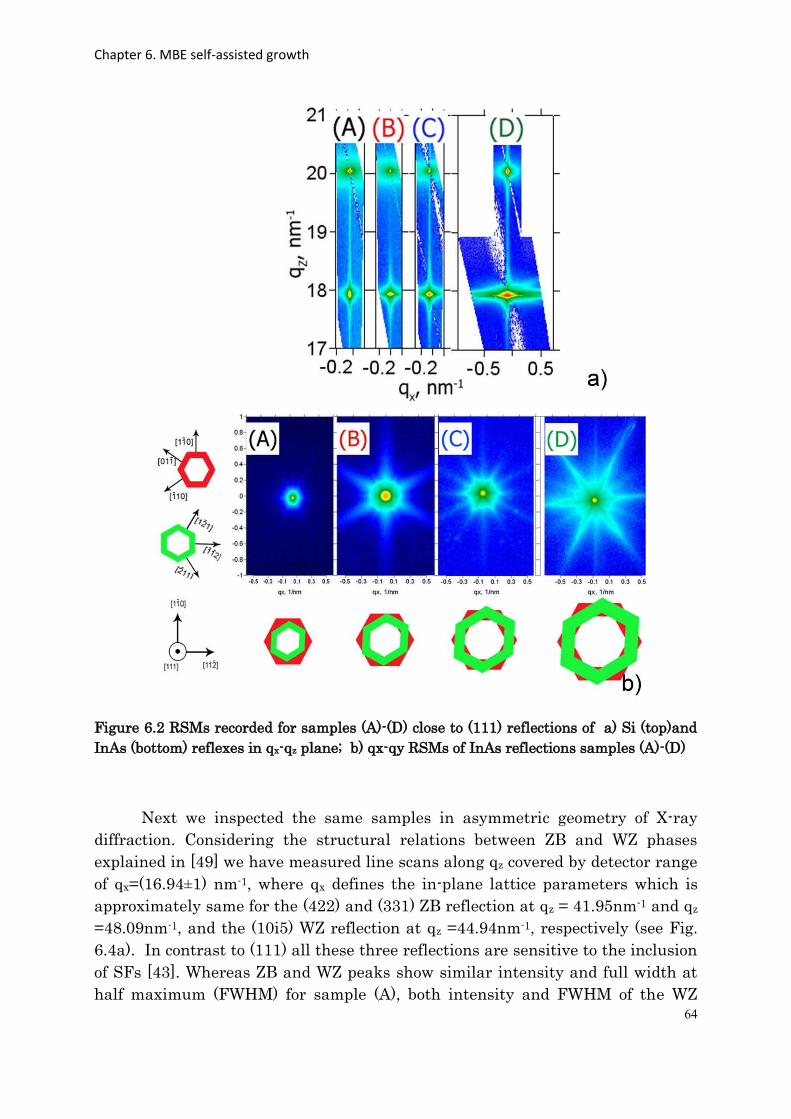
Chapter 6. MBE self-assisted growth
64
Figure 6.2 RSMs recorded for samples (A)-(D) close to (111) reflections of a) Si (top)and
InAs (bottom) reflexes in qx-qz plane; b) qx-qy RSMs of InAs reflections samples (A)-(D)
Next we inspected the same samples in asymmetric geometry of X-ray
diffraction. Considering the structural relations between ZB and WZ phases
explained in [49] we have measured line scans along qz covered by detector range
of qx=(16.94±1) nm-1, where qx defines the in-plane lattice parameters which is
approximately same for the (422) and (331) ZB reflection at qz = 41.95nm-1 and qz
=48.09nm-1, and the (10i5) WZ reflection at qz =44.94nm-1, respectively (see Fig.
6.4a). In contrast to (111) all these three reflections are sensitive to the inclusion
of SFs [43]. Whereas ZB and WZ peaks show similar intensity and full width at
half maximum (FWHM) for sample (A), both intensity and FWHM of the WZ
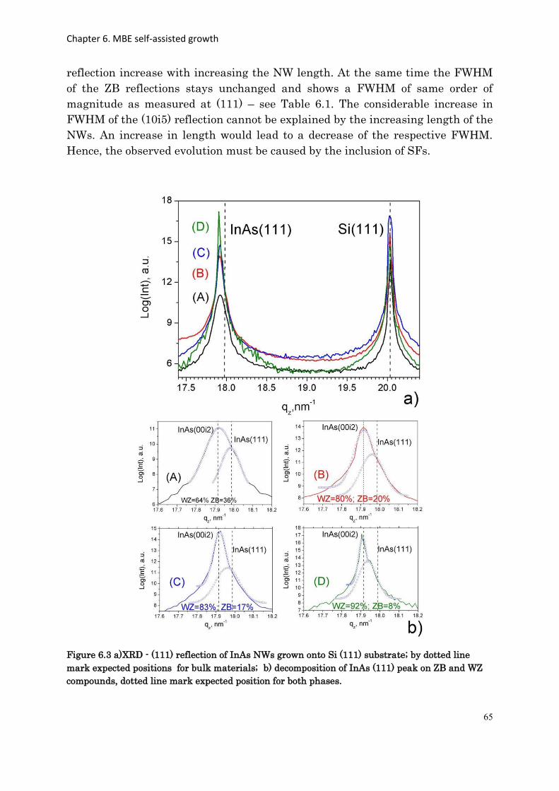
Chapter 6. MBE self-assisted growth
65
reflection increase with increasing the NW length. At the same time the FWHM
of the ZB reflections stays unchanged and shows a FWHM of same order of
magnitude as measured at (111) – see Table 6.1. The considerable increase in
FWHM of the (10i5) reflection cannot be explained by the increasing length of the
NWs. An increase in length would lead to a decrease of the respective FWHM.
Hence, the observed evolution must be caused by the inclusion of SFs.
Figure 6.3 a)XRD - (111) reflection of InAs NWs grown onto Si (111) substrate; by dotted line
mark expected positions for bulk materials; b) decomposition of InAs (111) peak on ZB and WZ
compounds, dotted line mark expected position for both phases.
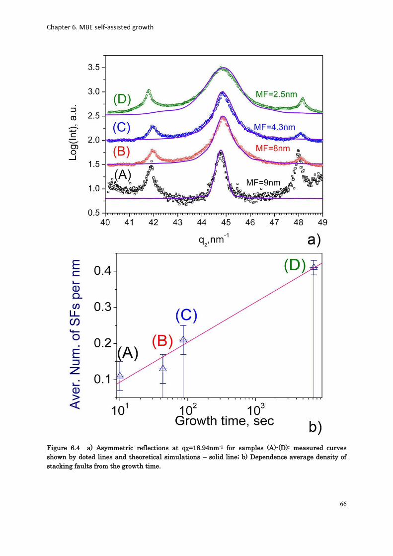
Chapter 6. MBE self-assisted growth
66
Figure 6.4 a) Asymmetric reflections at qX=16.94nm-1 for samples (A)-(D): measured curves
shown by doted lines and theoretical simulations – solid line; b) Dependence average density of
stacking faults from the growth time.
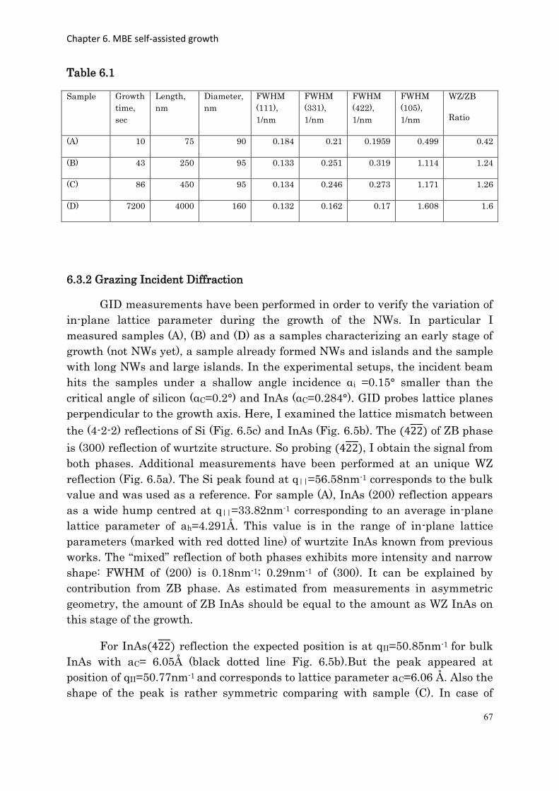
Chapter 6. MBE self-assisted growth
67
Table 6.1
Sample Growth
time,
sec
Length,
nm
Diameter,
nm
FWHM
(111),
1/nm
FWHM
(331),
1/nm
FWHM
(422),
1/nm
FWHM
(105),
1/nm
WZ/ZB
Ratio
(A) 10 75 90 0.184 0.21 0.1959 0.499 0.42
(B) 43 250 95 0.133 0.251 0.319 1.114 1.24
(C) 86 450 95 0.134 0.246 0.273 1.171 1.26
(D) 7200 4000 160 0.132 0.162 0.17 1.608 1.6
6.3.2 Grazing Incident Diffraction
GID measurements have been performed in order to verify the variation of
in-plane lattice parameter during the growth of the NWs. In particular I
measured samples (A), (B) and (D) as a samples characterizing an early stage of
growth (not NWs yet), a sample already formed NWs and islands and the sample
with long NWs and large islands. In the experimental setups, the incident beam
hits the samples under a shallow angle incidence αi =0.15° smaller than the
critical angle of silicon (αC=0.2°) and InAs (αC=0.284°). GID probes lattice planes
perpendicular to the growth axis. Here, I examined the lattice mismatch between
the (4-2-2) reflections of Si (Fig. 6.5c) and InAs (Fig. 6.5b). The of ZB phase
is (300) reflection of wurtzite structure. So probing , I obtain the signal from
both phases. Additional measurements have been performed at an unique WZ
reflection (Fig. 6.5a). The Si peak found at q||=56.58nm-1 corresponds to the bulk
value and was used as a reference. For sample (A), InAs (200) reflection appears
as a wide hump centred at q||=33.82nm-1 corresponding to an average in-plane
lattice parameter of ah=4.291Å. This value is in the range of in-plane lattice
parameters (marked with red dotted line) of wurtzite InAs known from previous
works. The “mixed” reflection of both phases exhibits more intensity and narrow
shape: FWHM of (200) is 0.18nm-1; 0.29nm-1 of (300). It can be explained by
contribution from ZB phase. As estimated from measurements in asymmetric
geometry, the amount of ZB InAs should be equal to the amount as WZ InAs on
this stage of the growth.
For InAs reflection the expected position is at qII=50.85nm-1 for bulk
InAs with aC= 6.05Å (black dotted line Fig. 6.5b).But the peak appeared at
position of qII=50.77nm-1 and corresponds to lattice parameter aC=6.06 Å. Also the
shape of the peak is rather symmetric comparing with sample (C). In case of
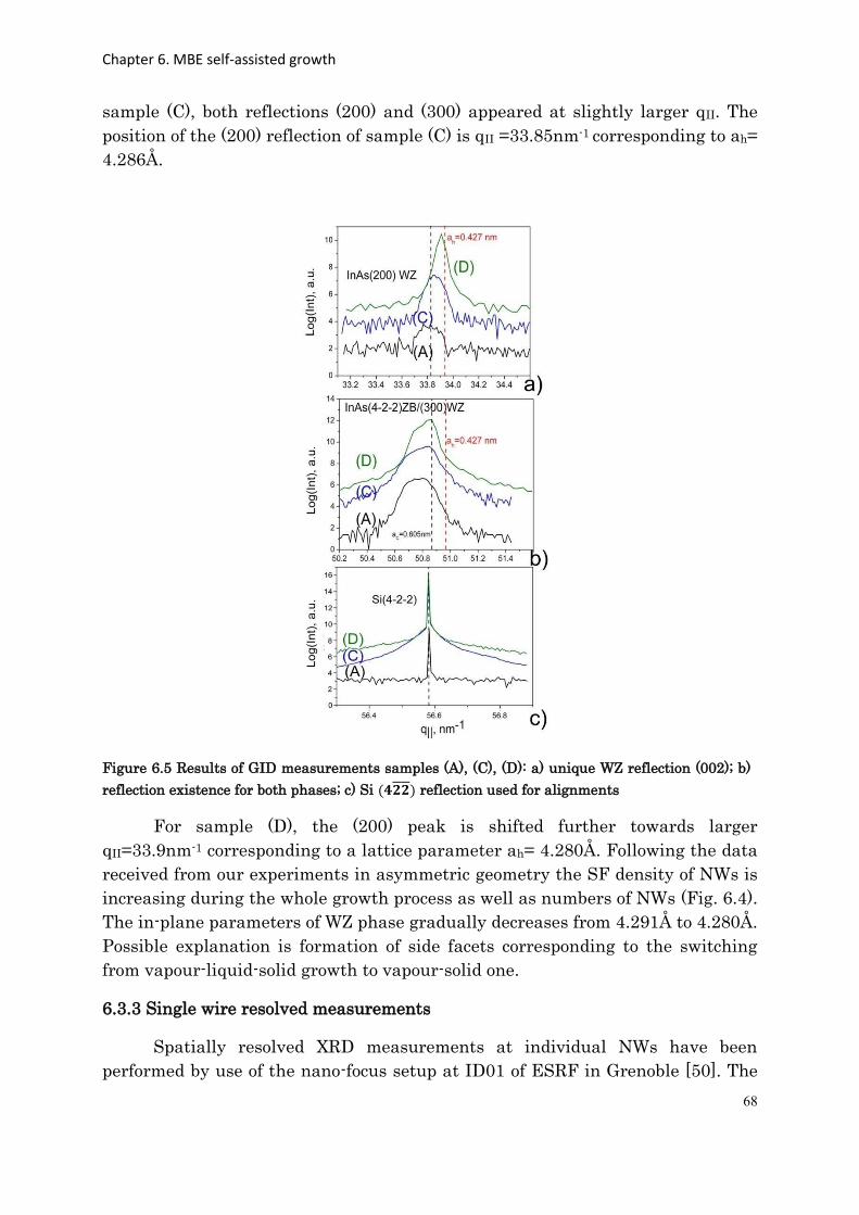
Chapter 6. MBE self-assisted growth
68
sample (C), both reflections (200) and (300) appeared at slightly larger qII. The
position of the (200) reflection of sample (C) is qII =33.85nm-1 corresponding to ah=
4.286Å.
Figure 6.5 Results of GID measurements samples (A), (C), (D): a) unique WZ reflection (002); b)
reflection existence for both phases; c) Si reflection used for alignments
For sample (D), the (200) peak is shifted further towards larger
qII=33.9nm-1 corresponding to a lattice parameter ah= 4.280Å. Following the data
received from our experiments in asymmetric geometry the SF density of NWs is
increasing during the whole growth process as well as numbers of NWs (Fig. 6.4).
The in-plane parameters of WZ phase gradually decreases from 4.291Å to 4.280Å.
Possible explanation is formation of side facets corresponding to the switching
from vapour-liquid-solid growth to vapour-solid one.
6.3.3 Single wire resolved measurements
Spatially resolved XRD measurements at individual NWs have been
performed by use of the nano-focus setup at ID01 of ESRF in Grenoble [50]. The
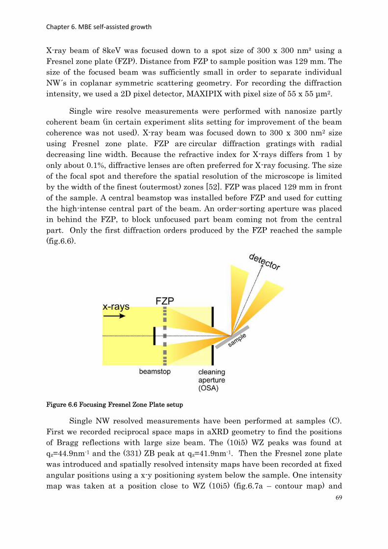
Chapter 6. MBE self-assisted growth
69
X-ray beam of 8keV was focused down to a spot size of 300 x 300 nm² using a
Fresnel zone plate (FZP). Distance from FZP to sample position was 129 mm. The
size of the focused beam was sufficiently small in order to separate individual
NW´s in coplanar symmetric scattering geometry. For recording the diffraction
intensity, we used a 2D pixel detector, MAXIPIX with pixel size of 55 x 55 μm2.
Single wire resolve measurements were performed with nanosize partly
coherent beam (in certain experiment slits setting for improvement of the beam
coherence was not used). X-ray beam was focused down to 300 x 300 nm2 size
using Fresnel zone plate. FZP are circular diffraction gratings with radial
decreasing line width. Because the refractive index for X-rays differs from 1 by
only about 0.1%, diffractive lenses are often preferred for X-ray focusing. The size
of the focal spot and therefore the spatial resolution of the microscope is limited
by the width of the finest (outermost) zones [52]. FZP was placed 129 mm in front
of the sample. A central beamstop was installed before FZP and used for cutting
the high-intense central part of the beam. An order-sorting aperture was placed
in behind the FZP, to block unfocused part beam coming not from the central
part. Only the first diffraction orders produced by the FZP reached the sample
(fig.6.6).
Figure 6.6 Focusing Fresnel Zone Plate setup
Single NW resolved measurements have been performed at samples (C).
First we recorded reciprocal space maps in aXRD geometry to find the positions
of Bragg reflections with large size beam. The (10i5) WZ peaks was found at
qz=44.9nm-1 and the (331) ZB peak at qz=41.9nm-1. Then the Fresnel zone plate
was introduced and spatially resolved intensity maps have been recorded at fixed
angular positions using a x-y positioning system below the sample. One intensity
map was taken at a position close to WZ (10i5) (fig.6.7a – contour map) and
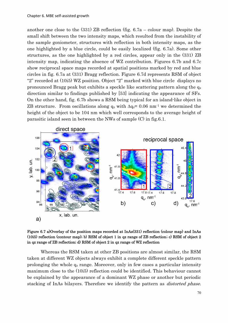
Chapter 6. MBE self-assisted growth
70
another one close to the (331) ZB reflection (fig. 6.7a – colour map). Despite the
small shift between the two intensity maps, which resulted from the instability of
the sample goniometer, structures with reflection in both intensity maps, as the
one highlighted by a blue circle, could be easily localized (fig. 6.7a). Some other
structures, as the one highlighted by a red circles, appear only in the (331) ZB
intensity map, indicating the absence of WZ contribution. Figures 6.7b and 6.7c
show reciprocal space maps recorded at spatial positions marked by red and blue
circles in fig. 6.7a at (331) Bragg reflection. Figure 6.7d represents RSM of object
“2” recorded at (10i5) WZ position. Object “2” marked with blue circle displays no
pronounced Bragg peak but exhibits a speckle like scattering pattern along the qz
direction similar to findings published by [53] indicating the appearance of SFs.
On the other hand, fig. 6.7b shows a RSM being typical for an island-like object in
ZB structure. From oscillations along qz with qz= 0.06 nm-1 we determined the
height of the object to be 104 nm which well corresponds to the average height of
parasitic island seen in between the NWs of sample (C) in fig.6.1.
Figure 6.7 a)Overlay of the position maps recorded at InAs(331) reflection (colour map) and InAs
(10i5) reflection (contour map); b) RSM of object 1 in qz range of ZB reflection; c) RSM of object 2
in qz range of ZB reflection; d) RSM of object 2 in qz range of WZ reflection
Whereas the RSM taken at other ZB positions are almost similar, the RSM
taken at different WZ objects always exhibit a complete different speckle pattern
prolonging the whole qz range. Moreover, only in few cases a particular intensity
maximum close to the (10i5) reflection could be identified. This behaviour cannot
be explained by the appearance of a dominant WZ phase or another but periodic
stacking of InAs bilayers. Therefore we identify the pattern as distorted phase.
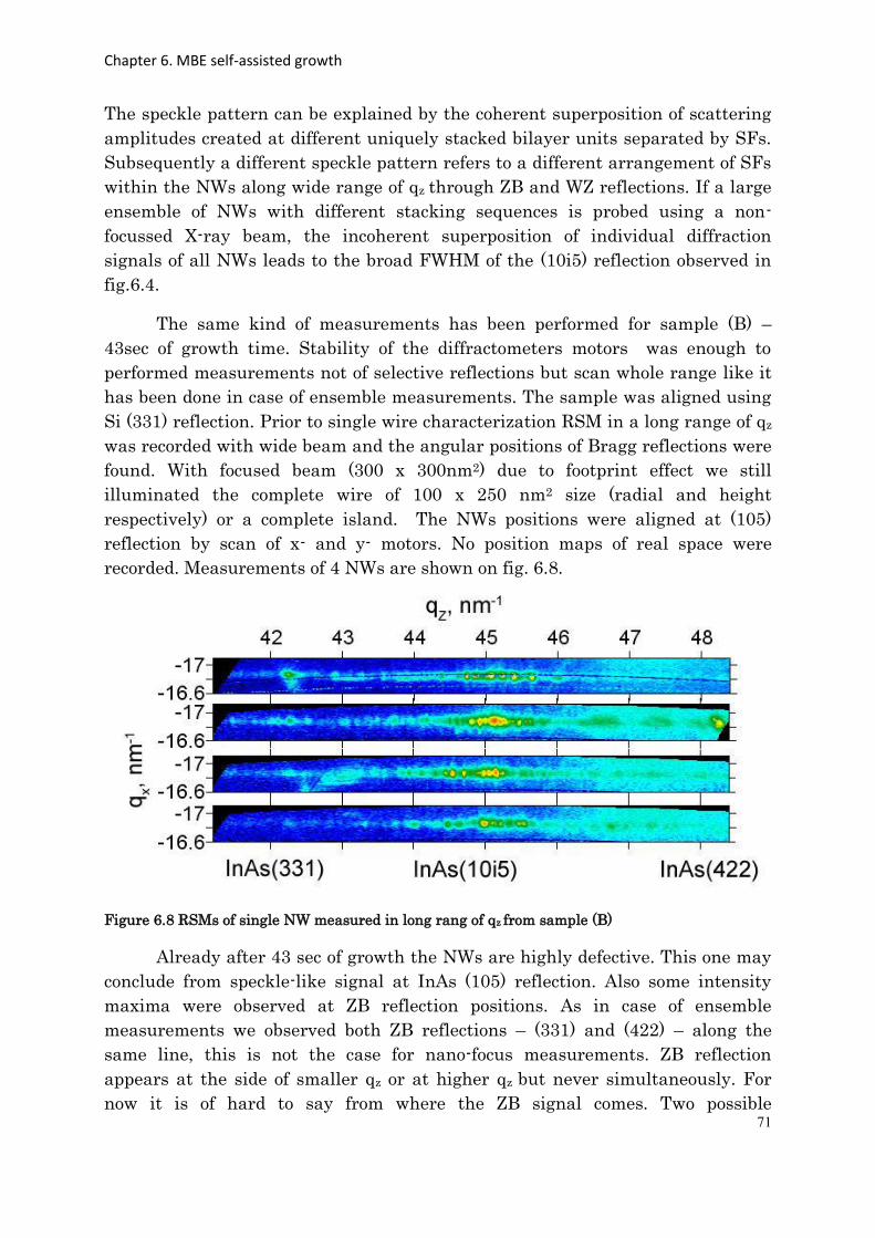
Chapter 6. MBE self-assisted growth
71
The speckle pattern can be explained by the coherent superposition of scattering
amplitudes created at different uniquely stacked bilayer units separated by SFs.
Subsequently a different speckle pattern refers to a different arrangement of SFs
within the NWs along wide range of qz through ZB and WZ reflections. If a large
ensemble of NWs with different stacking sequences is probed using a non-
focussed X-ray beam, the incoherent superposition of individual diffraction
signals of all NWs leads to the broad FWHM of the (10i5) reflection observed in
fig.6.4.
The same kind of measurements has been performed for sample (B) –
43sec of growth time. Stability of the diffractometers motors was enough to
performed measurements not of selective reflections but scan whole range like it
has been done in case of ensemble measurements. The sample was aligned using
Si (331) reflection. Prior to single wire characterization RSM in a long range of qz
was recorded with wide beam and the angular positions of Bragg reflections were
found. With focused beam (300 x 300nm2) due to footprint effect we still
illuminated the complete wire of 100 x 250 nm2 size (radial and height
respectively) or a complete island. The NWs positions were aligned at (105)
reflection by scan of x- and y- motors. No position maps of real space were
recorded. Measurements of 4 NWs are shown on fig. 6.8.
Figure 6.8 RSMs of single NW measured in long rang of qz from sample (B)
Already after 43 sec of growth the NWs are highly defective. This one may
conclude from speckle-like signal at InAs (105) reflection. Also some intensity
maxima were observed at ZB reflection positions. As in case of ensemble
measurements we observed both ZB reflections – (331) and (422) – along the
same line, this is not the case for nano-focus measurements. ZB reflection
appears at the side of smaller qz or at higher qz but never simultaneously. For
now it is of hard to say from where the ZB signal comes. Two possible
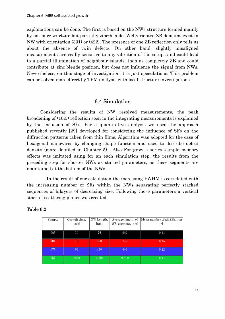
Chapter 6. MBE self-assisted growth
72
explanations can be done. The first is based on the NWs structure formed mainly
by not pure wurtzite but partially zinc-blende. Well-oriented ZB domains exist in
NW with orientation (331) or (422). The presence of one ZB reflection only tells us
about the absence of twin defects. On other hand, slightly misaligned
measurements are really sensitive to any vibration of the setups and could lead
to a partial illumination of neighbour islands, then as completely ZB and could
contribute at zinc-blende position, but does not influence the signal from NWs.
Nevertheless, on this stage of investigation it is just speculations. This problem
can be solved more direct by TEM analysis with local structure investigations.
6.4 Simulation
Considering the results of NW resolved measurements, the peak
broadening of (10i5) reflection seen in the integrating measurements is explained
by the inclusion of SFs. For a quantitative analysis we used the approach
published recently [29] developed for considering the influence of SFs on the
diffraction patterns taken from thin films. Algorithm was adopted for the case of
hexagonal nanowires by changing shape function and used to describe defect
density (more detailed in Chapter 5). Also For growth series sample memory
effects was imitated using for an each simulation step, the results from the
preceding step for shorter NWs as started parameters, as these segments are
maintained at the bottom of the NWs.
In the result of our calculation the increasing FWHM is correlated with
the increasing number of SFs within the NWs separating perfectly stacked
sequences of bilayers of decreasing size. Following these parameters a vertical
stack of scattering planes was created.
Table 6.2
Sample Growth time,
[sec]
NW Length,
[nm]
Average length of
WZ segment, [nm]
Mean number of all SFs, [nm-
1]
(A) 10 75 9±2 0.11
(B) 43 250 7±2 0.15
(C) 86 450 6±2 0.22
(D) 7200 4000 2.5±2 0.41
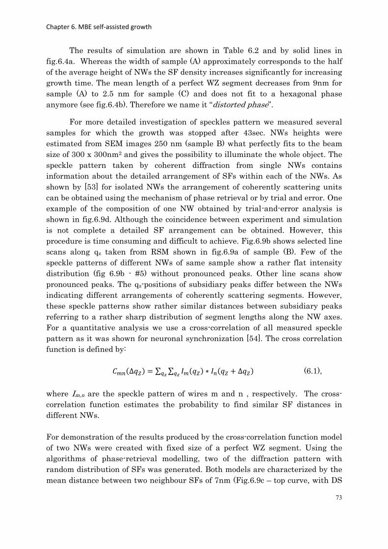
Chapter 6. MBE self-assisted growth
73
The results of simulation are shown in Table 6.2 and by solid lines in
fig.6.4a. Whereas the width of sample (A) approximately corresponds to the half
of the average height of NWs the SF density increases significantly for increasing
growth time. The mean length of a perfect WZ segment decreases from 9nm for
sample (A) to 2.5 nm for sample (C) and does not fit to a hexagonal phase
anymore (see fig.6.4b). Therefore we name it “distorted phase”.
For more detailed investigation of speckles pattern we measured several
samples for which the growth was stopped after 43sec. NWs heights were
estimated from SEM images 250 nm (sample B) what perfectly fits to the beam
size of 300 x 300nm2 and gives the possibility to illuminate the whole object. The
speckle pattern taken by coherent diffraction from single NWs contains
information about the detailed arrangement of SFs within each of the NWs. As
shown by [53] for isolated NWs the arrangement of coherently scattering units
can be obtained using the mechanism of phase retrieval or by trial and error. One
example of the composition of one NW obtained by trial-and-error analysis is
shown in fig.6.9d. Although the coincidence between experiment and simulation
is not complete a detailed SF arrangement can be obtained. However, this
procedure is time consuming and difficult to achieve. Fig.6.9b shows selected line
scans along qz taken from RSM shown in fig.6.9a of sample (B). Few of the
speckle patterns of different NWs of same sample show a rather flat intensity
distribution (fig 6.9b - #5) without pronounced peaks. Other line scans show
pronounced peaks. The qz-positions of subsidiary peaks differ between the NWs
indicating different arrangements of coherently scattering segments. However,
these speckle patterns show rather similar distances between subsidiary peaks
referring to a rather sharp distribution of segment lengths along the NW axes.
For a quantitative analysis we use a cross-correlation of all measured speckle
pattern as it was shown for neuronal synchronization [54]. The cross correlation
function is defined by:
∑ ∑ (6.1),
where Im,n are the speckle pattern of wires m and n , respectively. The cross-
correlation function estimates the probability to find similar SF distances in
different NWs.
For demonstration of the results produced by the cross-correlation function model
of two NWs were created with fixed size of a perfect WZ segment. Using the
algorithms of phase-retrieval modelling, two of the diffraction pattern with
random distribution of SFs was generated. Both models are characterized by the
mean distance between two neighbour SFs of 7nm (Fig.6.9c – top curve, with DS
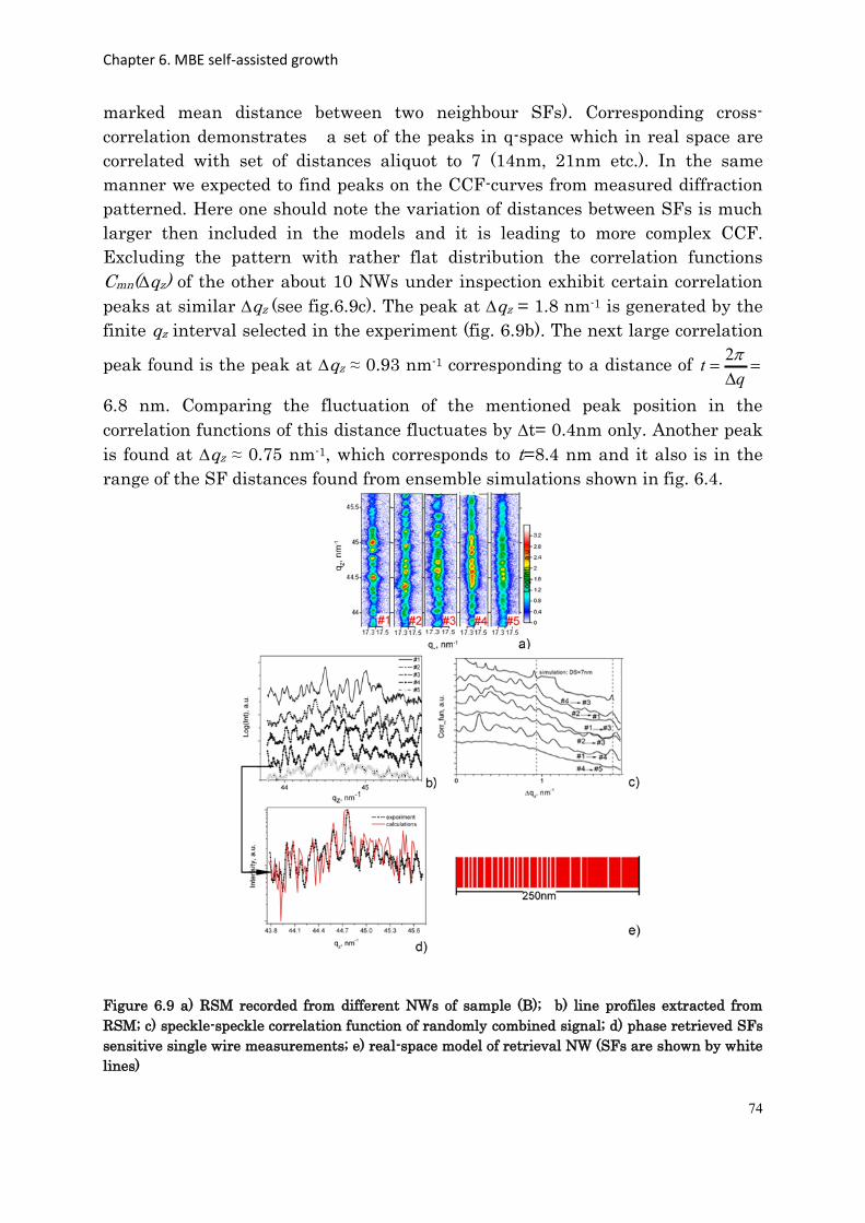
Chapter 6. MBE self-assisted growth
74
marked mean distance between two neighbour SFs). Corresponding cross-
correlation demonstrates a set of the peaks in q-space which in real space are
correlated with set of distances aliquot to 7 (14nm, 21nm etc.). In the same
manner we expected to find peaks on the CCF-curves from measured diffraction
patterned. Here one should note the variation of distances between SFs is much
larger then included in the models and it is leading to more complex CCF.
Excluding the pattern with rather flat distribution the correlation functions
Cmn(qz) of the other about 10 NWs under inspection exhibit certain correlation
peaks at similar qz (see fig.6.9c). The peak at qz = 1.8 nm-1 is generated by the
finite qz interval selected in the experiment (fig. 6.9b). The next large correlation
peak found is the peak at qz ≈ 0.93 nm-1 corresponding to a distance of
q
t 2
6.8 nm. Comparing the fluctuation of the mentioned peak position in the
correlation functions of this distance fluctuates by t= 0.4nm only. Another peak
is found at qz ≈ 0.75 nm-1, which corresponds to t=8.4 nm and it also is in the
range of the SF distances found from ensemble simulations shown in fig. 6.4.
Figure 6.9 a) RSM recorded from different NWs of sample (B); b) line profiles extracted from
RSM; c) speckle-speckle correlation function of randomly combined signal; d) phase retrieved SFs
sensitive single wire measurements; e) real-space model of retrieval NW (SFs are shown by white
lines)
Chapter 6. MBE self-assisted growth
75
6.5 Discussion
Our measurements show that the MBE grown InAs NWs on Si substrate
preferentially show up in the WZ phase, whereas parasitic InAs islands exhibit
ZB structure. However, the main outcome of our work is the investigation of the
SF probability as function of NW growth. Using sample integrated X-ray
diffraction we always find SFs in all NWs independent from growth time and the
indicated growth mechanism. Using a statistical method to SF distribution
within NWs we could quantify the mean SF density as function of growth time.
In detail, we find an increasing number density of stacking faults for increasing
the growth time. Whereas in the early stage of growth the mean distance
between neighboured SF is in the order of 9nm for 70 nm long NWs, and
decreases to 6nm for 500nm long NWs and reduces further to about 3nm for NWs
of microns length. The increase in SF density is non-linear, i.e. is seems to
saturate after few minutes of growth. Investigating single NWs we find a low SF
density for the very small NWs, so we cannot exclude that SF free structures may
exist in the early stage of NW growth. That means that the SF formation can be
related to the transition from VLS to VS mechanism as discussed in a previous
paper where the higher SF density is explained by the influence of the higher
adatom diffusion via the NWs side wall which is less dominating in the VLS
mode.
Single NW resolved inspection reveals that the SF distribution varies
drastically among the NWs grown onto the same sample. Due to the high degree
of spatial coherence of the nano-beam, the superposition of scattering amplitudes
of different perfectly stacked units within the NW being separated by SFs results
in the appearance of speckles. These speckles were measured within a wide qz
range of ± 0.7nm-1 in vicinity of the expected (10i5) WZ peak position. Form
crystallographic point of view this phase cannot be described by WZ or ZB
anymore, therefore we name it “distorted phase”. NWs exhibit a random
arrangement of stacking faults differing from NW to NW.
The appearance of SFs in InAs has been identified by V. Chamard et al.
using coherent X-ray imaging. However, the authors could not separate single
NWs and therefore the SF analysis kept rather qualitative [25]. The detailed SF
arrangement can be retrieved from the speckle pattern. This can be done by
phase retrieval [22] or by trail and error assuming a certain stacking sequence
within the NW [29]. Both methods are very time consuming but less informative
with respect of understanding the NW growth. Therefore we applied the cross –
correlation analysis to compare the diffraction patterns taken from different NWs
and find that most of NWs of one sample show indeed similar distances between
neighboured SFs. These distances are in rather good agreement with the results
Chapter 6. MBE self-assisted growth
76
of the statistical analysis over the whole NW ensemble. In consequence detailed
analysis of SF composition is necessary only if physical properties at single NWs
will be measured and interpreted.
Stacking faults are hardly connected with diameter of NWs. As shown by
[38] the NW free energy is lower for WZ phase then for ZB phase if the NW
diameter is below a critical diameter. For InAs the critical diameter is in the
order of 10 to 20nm. This is explained by the fact that the number of dangling
bonds at the clean non-saturated surface is larger for ZB then for WZ [56]. The
surface energy is in competition with the volume cohesive energy which is lower
for ZB compared to WZ. The creation of WZ phase strongly depends on the
nucleation mechanism [57] and WZ is more energetically favourable for VLS
growth. Therefore for NWs with diameter close to the critical one SF formation is
likely. Under this growth conditions, the critical diameter is close to 100nm. For
an increase of NW diameter, the WZ phase formation becomes instable during
fast axial growth. Whereas initially the In- and As- moieties are supplied
throughout the top facet only diffusion along the side facets becomes dominant
for increasing the growth time. The slightly increasing diameter for increasing
the growth time and the supply of material via diffusion along the side facets are
associated with the increasing number of SFs. Nevertheless macroscopic
fluctuation of growth conditions can be ruled out as origin of SF formation as
shown in work of Joyce et al [43].
6.6 Conclusions
In summary, our results support the assumption of a changing growth
mode from VLS towards VS in InAs MBE growth suggested in [47]. Both modes
results in rather defective WZ NWs. Already after 10 sec of growth a high density
of SF has been detected. NW growth in the VS mode, on the other hand, is
accompanied by faster increase of number of SFs inclusion where the SF density
increases with increasing growth time with nucleation of new NWs during
growth.
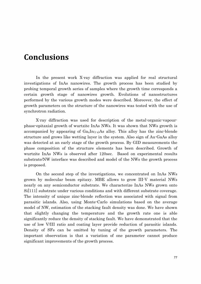
77
Conclusions
In the present work X-ray diffraction was applied for real structural
investigations of InAs nanowires. The growth process has been studied by
probing temporal growth series of samples where the growth time corresponds a
certain growth stage of nanowires growth. Evolutions of nanostructures
performed by the various growth modes were described. Moreover, the effect of
growth parameters on the structure of the nanowires was tested with the use of
synchrotron radiation.
X-ray diffraction was used for description of the metal-organic-vapour-
phase-epitaxial growth of wurtzite InAs NWs. It was shown that NWs growth is
accompanied by appearing of GaxIn(1-x)As alloy. This alloy has the zinc-blende
structure and grows like wetting layer in the system. Also sign of Au-GaAs alloy
was detected at an early stage of the growth process. By GID measurements the
phase composition of the structure elements has been described. Growth of
wurtzite InAs NWs is observed after 120sec. Based on experimental results
substrate/NW interface was described and model of the NWs the growth process
is proposed.
On the second step of the investigations, we concentrated on InAs NWs
grown by molecular beam epitaxy. MBE allows to grow III-V material NWs
nearly on any semiconductor substrate. We characterize InAs NWs grown onto
Si[111] substrate under various conditions and with different substrate coverage.
The intensity of unique zinc-blende reflection was associated with signal from
parasitic islands. Also, using Monte-Carlo simulations based on the average
model of NW, estimation of the stacking fault density was done. We have shown
that slightly changing the temperature and the growth rate one is able
significantly reduce the density of stacking fault. We have demonstrated that the
use of low V/III ratio and coating layer provide reduction of parasitic islands.
Density of SFs can be omitted by tuning of the growth parameters. The
important observation is that a variation of one parameter cannot produce
significant improvements of the growth process.
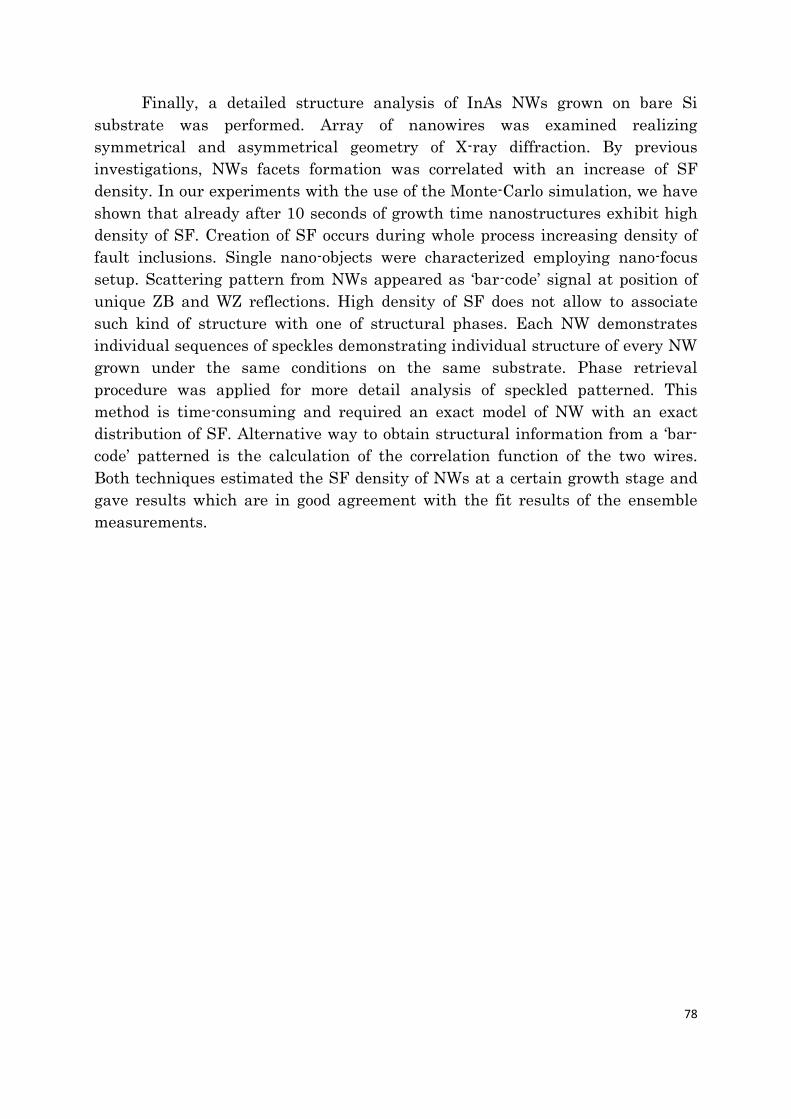
78
Finally, a detailed structure analysis of InAs NWs grown on bare Si
substrate was performed. Array of nanowires was examined realizing
symmetrical and asymmetrical geometry of X-ray diffraction. By previous
investigations, NWs facets formation was correlated with an increase of SF
density. In our experiments with the use of the Monte-Carlo simulation, we have
shown that already after 10 seconds of growth time nanostructures exhibit high
density of SF. Creation of SF occurs during whole process increasing density of
fault inclusions. Single nano-objects were characterized employing nano-focus
setup. Scattering pattern from NWs appeared as ‘bar-code’ signal at position of
unique ZB and WZ reflections. High density of SF does not allow to associate
such kind of structure with one of structural phases. Each NW demonstrates
individual sequences of speckles demonstrating individual structure of every NW
grown under the same conditions on the same substrate. Phase retrieval
procedure was applied for more detail analysis of speckled patterned. This
method is time-consuming and required an exact model of NW with an exact
distribution of SF. Alternative way to obtain structural information from a ‘bar-
code’ patterned is the calculation of the correlation function of the two wires.
Both techniques estimated the SF density of NWs at a certain growth stage and
gave results which are in good agreement with the fit results of the ensemble
measurements.
79
References
[1] C. Thelander, T. Mårtensson, M. T. Björk, B. J. Ohlsson, M. W. Larsson, L. R. Wallenberg, and L. Samuelson Appl. Phys. Lett. 83, 2052 (2003)
[2] E. Lai, W. Kim, P. Yang, Nano Res, 1: 123, 128, 2008
[3] H. Kind, H. Yan, B. Messer, M. Law, P. Yang, Adv. Mater., 14, 2, 2002
[4] Jr H. He,Yi Y. Zhang, J. Liu, D. Moore, G. Bao, Z. L. Wang, J. Phys. Chem. C, Vol. 111, No. 33, 2007
[5] K. Hiruma, M. Yazawa, T. Katsuyama, K. Ogawa, K. Haraguchi, M. Koguchi, H. Kakibayashi, J. Appl. Phys. 77, 447, 1995
[6] M. Björk, B. Ohlsson, T. Sass, A. Persson, C. Thelander, M. Magnusson, K. Deppert, L. Wallenberg, L. Samuelson, Appl. Phys. Lett. 80, 1058–1160, 2001
[7] B.J. Ohlsson, M.T. Björk, A.I. Persson, C. Thelander, L.R. Wallenberg, M.H. Magnusson, K. Deppert, L. Samuelson, Physica E 13, 1126–1130, 2002
[8] K. Dick, K. Deppert, T. Mårtensson, B. Mandl, L. Samuelson, W. Seifert, Nano Lett. 5, 761–764, 2005
[9] S. Dayeh, E. Yu, D. Wang, Nano Lett. 7, 2486–2490, 2007
[10] U. Pietsch, V. Holy, T. Baumbach, High-Resolution X-Ray Scattering. From Thin Films to Lateral Nanostructures. Advanced Texts in Physics, Springer, Berlin, 2005
[11] J. Bauer, V. Gottschalch, G. Wagner, J. Appl. Phys. 104, 114315, 2008
[12] J. Bauer, U. Pietsch, A. Davydok, A. Biermanns, J. Grenzer, V. Gottschalch, G. Wagner, Appl Phys A, 96, 851, 2009
[13] J. Bauer PhD thesis „Metallorganische Gasphasenepitaxie von GaAs- und InAs-Nanodrahtstrukturen über den „vapor-liquid-solid“ - Wachstumsmechanismus“, Fakultät für Physik und Geowissenschaften der Universität Leipzig , 2009
[14] X. Zhang, J. Zou, M. Paladugu, Y. Guo, Y. Wang, Y. Kim, H.J. Joyce, Q. Gao, H.H. Tan, C. Jagadish, Small 5, 366–369, 2009
[15] K. Dick, P. Caroff, J. Bolinsson, M. Messing, J. Johansson, K. Deppert, L. Wallenberg, L. Samuelson, Semiconductor Sci. Technology 25, 024009, 2010
[16] A. Motayed,S.Krylyuk, A. Davydov,Applied Physics Letters 99, 113107, 2011
[17] S.-G. Ihn, J.-I. Song, Nanotechnology, 18, 355603, 2007
80
[18] H.Shtrikman, R.Popovitz-Biro, A. Kretinin, P.Kacman, IEEE Journal of selected topics in quantum electronics, 17, 4, 2011
[19] D. Kriegner, C. Panse, B. Mandl, K. Dick, M. Keplinger, J. Persson, P. Caroff, D. Ercolani, L. Sorba, F. Bechstedt, J. Stangl, G. Bauer, Nano Letters, 11, 1483–1489, 2011
[20] E.Dimakis, J. Lahnemann, U. Jahn, S. Breuer, M. Hilse, L. Geelhaar, H. Riechert, Crystal Growth Designe, 11, 4001,2011
[21] S. Hertenberger, D. Rudolph, S. Bolte, M. Döblinger, M. Bichler, D. Spirkoska, J. J. Finley, G. Abstreiter, G. Koblmüller, Applied Physics Letters 98, 123114, (2011)
[22] K. Tomioka, J. Motohisa, S. Hara, T. Fukui, Nano Letter, 8, 10, (2008)
[23] W. Wei, X. Bao, C. Soci, Y. Ding, Z. Wang, D. Wang Nano Letters, 9, 8, 2926 (2009)
[24] F. Glas, J. Harmand, G. Patriarch, Physical Review Letters, 99, 146101 (2007)
[25] S. Hertenrberger, D. Udolph, J. Becker, M. Bichler, J. Finley, G. Abstrier, G. Koblmüller, Nanotechnology, 23, 235602 (2012)
[26] B. Lewis, J. Anderson, “Nucliation and growth of Thin films”, New York: Academic (1979)
[27]V. K. Kabra, D. Pandey, ActaCryst., A, 51 , 329-335 (1995)
[28] M. Barchuk, V. Holý D. Kriegner, J. Stangl S. Schwaiger, F. Scholz ,Physical Review B, 84 , 094113 (2011)
[29] Warren, B., New York: Dover Publication Inc. (1990)
[30] M. Madsen, M. Aagesen, P. Krogstrup, C. Sørensen, J. Nygard, Nanoscale Research Letters, 6, 516, (2011)
[31] T. Rieger, S. Heiderich, S. Lenk, M. I. Lepsa, D. Grützmacher, Journal of Crystal Growth, 353, 39–46, (2012)
[32] B. Mandl, J. Stangle, E. Hilner, A. Zakharov, K. Hillerich, A. Dey, L. Samuelson, G. Bauer, K. Deppert, A. Mikkelsen, Nano Letters, 10, 11, 4443 (2010)
[33] H. Joyce, J. Wong-Leung, Q. Gao, H. Tan, C. Jagadish, Nano Letters 10, 908 (2010)
[34] G. Koblmüller, S. Hertenberger, K.Vizbaras, M. Bichler, F. Bao, J. Zang, G. Abstriter, Nanotechnology, 21, 365602 (2010)
[35] M.Stiles,D. Hamann, Physical Review B, 38 , 2021-37 (1988)
[36] P. Caroff, K. A. Dick, J. Johansson, M. E. Messing, K. Deppert, L. Samuelson, Nature Nanothechnology 4 , 50 (2009)
[37]H.Shtrikman,R. Popovitziro, A.Kretinin, L. Houben, M. Heiblum,Bukała, M. Galicka, R. Buczko, Perła Kacman,Nano Letters, 9,4, 1506 (2009)
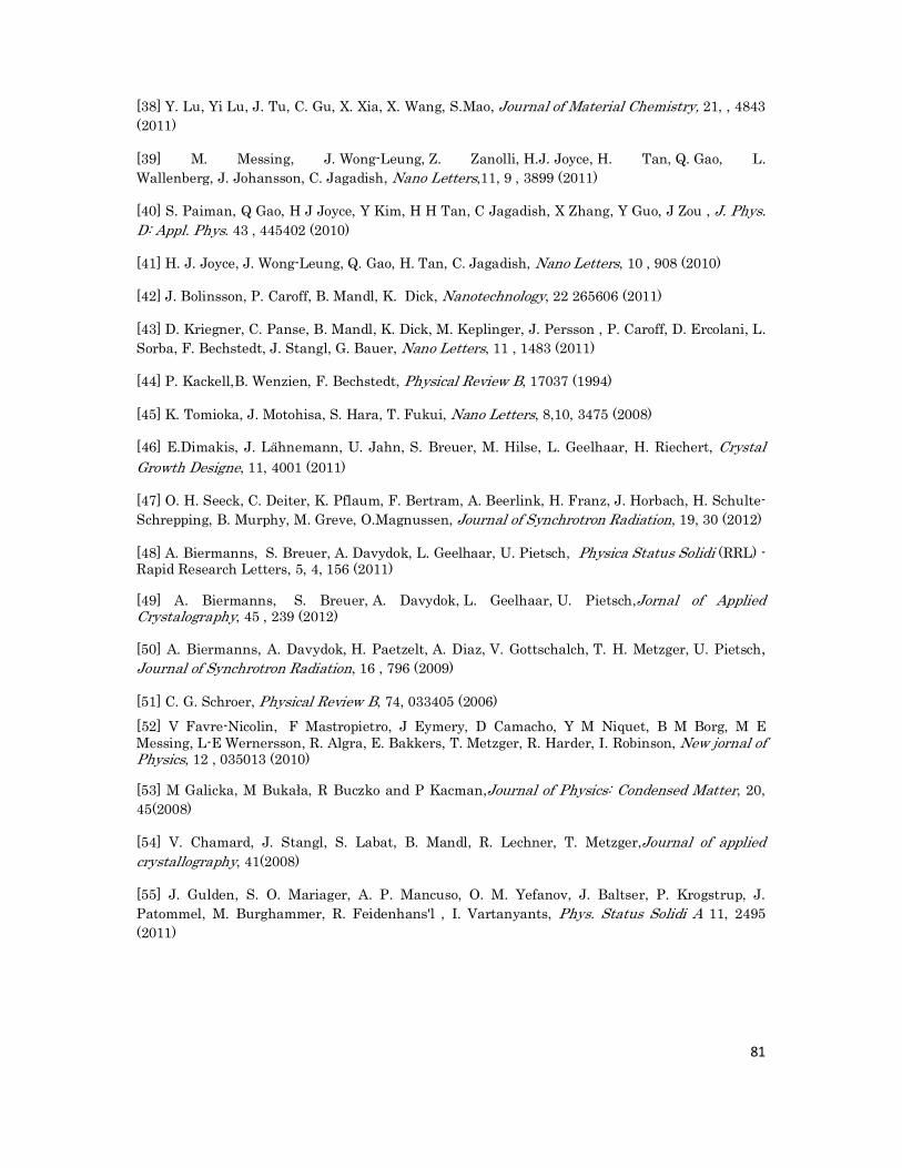
81
[38] Y. Lu, Yi Lu, J. Tu, C. Gu, X. Xia, X. Wang, S.Mao, Journal of Material Chemistry, 21, , 4843 (2011)
[39] M. Messing, J. Wong-Leung, Z. Zanolli, H.J. Joyce, H. Tan, Q. Gao, L. Wallenberg, J. Johansson, C. Jagadish, Nano Letters,11, 9 , 3899 (2011)
[40] S. Paiman, Q Gao, H J Joyce, Y Kim, H H Tan, C Jagadish, X Zhang, Y Guo, J Zou , J. Phys. D: Appl. Phys. 43 , 445402 (2010)
[41] H. J. Joyce, J. Wong-Leung, Q. Gao, H. Tan, C. Jagadish, Nano Letters, 10 , 908 (2010)
[42] J. Bolinsson, P. Caroff, B. Mandl, K. Dick, Nanotechnology, 22 265606 (2011)
[43] D. Kriegner, C. Panse, B. Mandl, K. Dick, M. Keplinger, J. Persson , P. Caroff, D. Ercolani, L. Sorba, F. Bechstedt, J. Stangl, G. Bauer, Nano Letters, 11 , 1483 (2011)
[44] P. Kackell,B. Wenzien, F. Bechstedt, Physical Review B, 17037 (1994)
[45] K. Tomioka, J. Motohisa, S. Hara, T. Fukui, Nano Letters, 8,10, 3475 (2008)
[46] E.Dimakis, J. Lahnemann, U. Jahn, S. Breuer, M. Hilse, L. Geelhaar, H. Riechert, Crystal Growth Designe, 11, 4001 (2011)
[47] O. H. Seeck, C. Deiter, K. Pflaum, F. Bertram, A. Beerlink, H. Franz, J. Horbach, H. Schulte-Schrepping, B. Murphy, M. Greve, O.Magnussen, Journal of Synchrotron Radiation, 19, 30 (2012)
[48] A. Biermanns, S. Breuer, A. Davydok, L. Geelhaar, U. Pietsch, Physica Status Solidi (RRL) - Rapid Research Letters, 5, 4, 156 (2011)
[49] A. Biermanns, S. Breuer, A. Davydok, L. Geelhaar, U. Pietsch,Jornal of Applied Crystalography, 45 , 239 (2012)
[50] A. Biermanns, A. Davydok, H. Paetzelt, A. Diaz, V. Gottschalch, T. H. Metzger, U. Pietsch, Journal of Synchrotron Radiation, 16 , 796 (2009)
[51] C. G. Schroer, Physical Review B, 74, 033405 (2006) [52] V Favre-Nicolin, F Mastropietro, J Eymery, D Camacho, Y M Niquet, B M Borg, M E Messing, L-E Wernersson, R. Algra, E. Bakkers, T. Metzger, R. Harder, I. Robinson, New jornal of Physics, 12 , 035013 (2010)
[53] M Galicka, M Bukała, R Buczko and P Kacman,Journal of Physics: Condensed Matter, 20, 45(2008)
[54] V. Chamard, J. Stangl, S. Labat, B. Mandl, R. Lechner, T. Metzger,Journal of applied crystallography, 41(2008)
[55] J. Gulden, S. O. Mariager, A. P. Mancuso, O. M. Yefanov, J. Baltser, P. Krogstrup, J. Patommel, M. Burghammer, R. Feidenhans'l , I. Vartanyants, Phys. Status Solidi A 11, 2495 (2011)
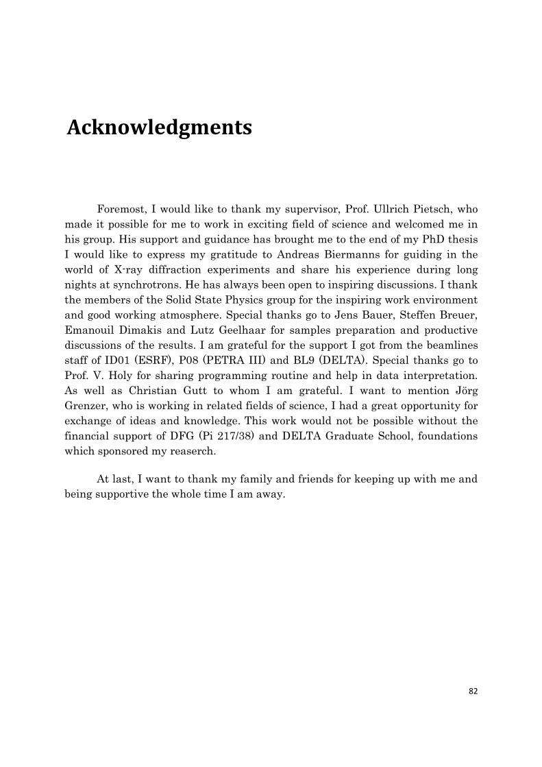
82
Acknowledgments
Foremost, I would like to thank my supervisor, Prof. Ullrich Pietsch, who
made it possible for me to work in exciting field of science and welcomed me in
his group. His support and guidance has brought me to the end of my PhD thesis
I would like to express my gratitude to Andreas Biermanns for guiding in the
world of X-ray diffraction experiments and share his experience during long
nights at synchrotrons. He has always been open to inspiring discussions. I thank
the members of the Solid State Physics group for the inspiring work environment
and good working atmosphere. Special thanks go to Jens Bauer, Steffen Breuer,
Emanouil Dimakis and Lutz Geelhaar for samples preparation and productive
discussions of the results. I am grateful for the support I got from the beamlines
staff of ID01 (ESRF), P08 (PETRA III) and BL9 (DELTA). Special thanks go to
Prof. V. Holy for sharing programming routine and help in data interpretation.
As well as Christian Gutt to whom I am grateful. I want to mention Jörg
Grenzer, who is working in related fields of science, I had a great opportunity for
exchange of ideas and knowledge. This work would not be possible without the
financial support of DFG (Pi 217/38) and DELTA Graduate School, foundations
which sponsored my reaserch.
At last, I want to thank my family and friends for keeping up with me and
being supportive the whole time I am away.
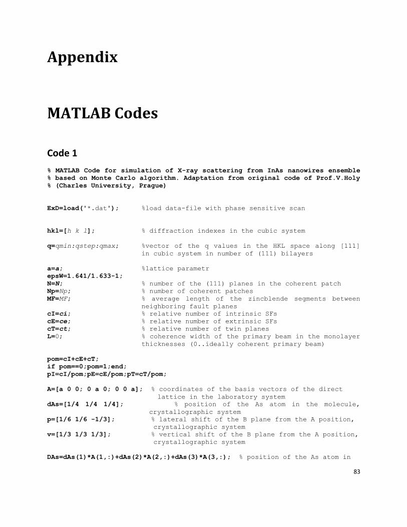
83
Appendix
MATLAB Codes
Code 1
% MATLAB Code for simulation of X-ray scattering from InAs nanowires ensemble
% based on Monte Carlo algorithm. Adaptation from original code of Prof.V.Holy
% (Charles University, Prague)
ExD=load('*.dat'); %load data-file with phase sensitive scan
hkl=[h k l]; % diffraction indexes in the cubic system
q=qmin:qstep:qmax; %vector of the q values in the HKL space along [111]
in cubic system in number of (111) bilayers
a=a; %lattice parametr
epsW=1.641/1.633-1;
N=N; % number of the (111) planes in the coherent patch
Np=Np; % number of coherent patches
MF=MF; % average length of the zincblende segments between
neighboring fault planes
cI=ci; % relative number of intrinsic SFs
cE=ce; % relative number of extrinsic SFs
cT=ct; % relative number of twin planes
L=0; % coherence width of the primary beam in the monolayer
thicknesses (0..ideally coherent primary beam)
pom=cI+cE+cT;
if pom==0;pom=1;end;
pI=cI/pom;pE=cE/pom;pT=cT/pom;
A=[a 0 0; 0 a 0; 0 0 a]; % coordinates of the basis vectors of the direct
lattice in the laboratory system
dAs=[1/4 1/4 1/4]; % position of the As atom in the molecule,
crystallographic system
p=[1/6 1/6 -1/3]; % lateral shift of the B plane from the A position,
crystallographic system
v=[1/3 1/3 1/3]; % vertical shift of the B plane from the A position,
crystallographic system
DAs=dAs(1)*A(1,:)+dAs(2)*A(2,:)+dAs(3)*A(3,:); % position of the As atom in
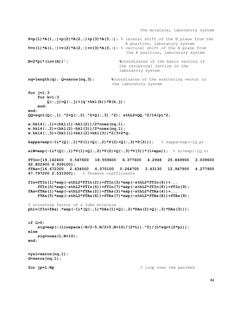
84
the molecule, laboratory system
P=p(1)*A(1,:)+p(2)*A(2,:)+p(3)*A(3,:); % lateral shift of the B plane from the
A position, laboratory system
V=v(1)*A(1,:)+v(2)*A(2,:)+v(3)*A(3,:); % vertical shift of the B plane from
the A position, laboratory system
B=2*pi*(inv(A))'; %coordinates of the basis vectors of
the reciprocal lattice in the
laboratory system
nq=length(q); Q=zeros(nq,3); %coordinates of the scattering vector in
the laboratory system
for j=1:3
for k=1:3
Q(:,j)=Q(:,j)+(q'+hkl(k))*B(k,j);
end;
end;
QQ=sqrt(Q(:,1).^2+Q(:,2).^2+Q(:,3).^2); sthL2=QQ.^2/16/pi^2;
w.hkl4(:,1)=(hkl(1)-hkl(2))/2*ones(nq,1);
w.hkl4(:,2)=(hkl(2)-hkl(3))/2*ones(nq,1);
w.hkl4(:,3)=(hkl(1)+hkl(2)+hkl(3))*2/3+2*q;
kappa=exp(-1i*(Q(:,1)*P(1)+Q(:,2)*P(2)+Q(:,3)*P(3))); % kappa=exp(-iQ.p)
xiW=exp(-1i*(Q(:,1)*V(1)+Q(:,2)*V(2)+Q(:,3)*V(3))*(1+eps)); % xi=exp(-iQ.v)
fTIn=[19.162400 0.547600 18.559600 6.377600 4.2948 25.849900 2.039600
92.802900 4.939100];
fTAs=[16.672300 2.634500 6.070100 0.264700 3.43130 12.947900 4.277900
47.797200 2.531000]; % Thomson coefficients
fIn=fTIn(1)*exp(-sthL2*fTIn(2))+fTIn(3)*exp(-sthL2*fTIn(4))+...
fTIn(5)*exp(-sthL2*fTIn(6))+fTIn(7)*exp(-sthL2*fTIn(8))+fTIn(9);
fAs=fTAs(1)*exp(-sthL2*fTAs(2))+fTAs(3)*exp(-sthL2*fTAs(4))+...
fTAs(5)*exp(-sthL2*fTAs(6))+fTAs(7)*exp(-sthL2*fTAs(8))+fTAs(9);
% structure factor of a InAs molecule
phi=(fIn+fAs).*exp(-1i*(Q(:,1)*DAs(1)+Q(:,2)*DAs(2)+Q(:,3)*DAs(3)));
if L>0;
sig=exp(-(linspace(-N/2-5,N/2+5,N+10)/(2*L)).^2)/(L*sqrt(2*pi));
else
sig=ones(1,N+10);
end;
vysl=zeros(nq,1);
d=zeros(nq,1);
for jp=1:Np % loop over the patches

85
Ms=0; % generation of the positions of the
fault planes, geometric distribution
of the distances
k=1;
while Ms<N;
dist=randraw('geom',1/(1+MF),1);
if dist>3;
wtyp=rand(1);
ityp(k)=0;
if wtyp<pI;
ityp(k)=1;
end;
if wtyp>=pI && wtyp<pI+pE;
ityp(k)=2;
end;
if wtyp>=pI+pE && wtyp<pI+pE+pT;
ityp(k)=3;
end;
Ms=Ms+dist;
M(k)=Ms;
k=k+1;
end;
end;
ampl=zeros(nq,1); % calculation of the amplitude
xic=ones(nq,1);
kappac=ones(nq,1);
isigs=1;
k=1;
j=1;
while j<=N; % loop over the basal planes
if j<M(k);
isig=isigs;
xic=xic.*(xiW.^isig);
kappac=kappac.*(kappa.^isig);
ampl=ampl+phi.*kappac.*xic*sig(j);
j=j+1;
end;
if j==M(k);
switch ityp(k);
case 0;
isig=isigs;
xic=xic.*(xiW.^isig);
kappac=kappac.*(kappa.^isig);
ampl=ampl+phi.*kappac.*xic;
j=j+1;
case 1;
isig=-isigs;
xic=xic.*xiW;
kappac=kappac.*(kappa.^isig);
ampl=ampl+phi.*kappac.*xic*sig(j);
86
j=j+1;
isigs=isig;
isig=-isigs;
xic=xic.*xiW;
kappac=kappac.*(kappa.^isig);
ampl=ampl+phi.*kappac.*xic*sig(j);
j=j+1;
isigs=isig;
if jp==1;
w.sig(j)=isig;
end;
j=j+1;
isigs=isig;
case 2;
isig=-isigs;
xic=xic.*xiW;
kappac=kappac.*(kappa.^isig);
ampl=ampl+phi.*kappac.*xic*sig(j);
j=j+1;
xic=xic.*(xiW.^isig);
kappac=kappac.*(kappa.^isig);
ampl=ampl+phi.*kappac.*xic*sig(j);
j=j+1;
xic=xic.*xiW;
ampl=ampl+phi.*kappac.*xic*sig(j);
j=j+1;
case 3;
isig=-isigs;
xic=xic.*xiW;
kappac=kappac.*(kappa.^isig);
ampl=ampl+phi.*kappac.*xic*sig(j);
j=j+1;
end;
k=k+1;
end;
end;
amplS=abs(ampl).^2;
vysl=vysl+abs(ampl).^2;
end;
w.q=q;w.int=vysl/Np;
w.int=w.int;
M1=max(w.int);
NormInt=w.int/M1;
ExD2=ExDInt;
M2=max(ExD2);
NormIntEx=ExDInt/M2;
plot(q,NormIntEx,'black')
hold on;
plot(q,NormInt,'o-');
87
Code 2 % MATLAB Code for simulation of X-ray scattering from single InAs nanowire
% with compound phase structure
wlength=lambda; %length of wire in nm
ac=a; % lattice parameter of matereal in nm
aw=ac*sqrt(2)/2;
natom=3*round(wlength/ac); % numbers of layers
zbatom=zb; % number of ZB layers
wzatom=natom-zbatom; % number of WZ layers
qz=qmin:qstep:qmax; % range of qz
qx=qx;
qy=qy;
count=1;
%In Thomson coefficients
a1=[19.162,18.560,4.295,2.040]; b1=[0.548,6.378,25.850,92.803]; c1=4.939;
%As
a2=[16.672,6.070,3.431,4.278]; b2=[2.635,0.265,12.948,47.797]; c2=2.531;
x=0;y=0;
for k=1:zbatom %creation of Zb stack
type(k)=mod(k,3)+1;
end;
for k=1:wzatom %creation of WZ stack
type2(k)=mod(k,2)+1;
end;
m=length(qz);
A1=0;
A2=0;
while count<=length(qz) % loop over qz range
88
fIn=0;
fAs=0;
fIn=fIn+sum(a1.*exp(-b1.*(qz(count)/10/(4*pi))^2))+c1;
fAs=fAs+sum(a2.*exp(-b2.*(qz(count)/10/(4*pi))^2))+c2;
F(count)=0;
for j=1:zbatom
if type(j)==2
dx(j)=0; dy(j)=0;
end;
if type(j)==1
dx(j)=aw/2; dy(j)=aw/(2*sqrt(3));
end;
if type(j)==3
dx(j)=0; dy(j)=aw/sqrt(3);
end;
z1(j)=j*(sqrt(3)/3)*ac;
z2(j)=j*(sqrt(3)/3)*ac+0.25*sqrt(3)*ac;
F(count)=F(count)+fIn*exp(i*qz(count)*z1(j))*exp(i*qx*(x+dx(j)))*exp(i*qy*(y+d
y(j)));
F(count)=F(count)+fAs*exp(i*qz(count)*(z2(j)))*exp(i*qx*(x+dx(j)))*exp(i*qy*(y
+dy(j)));
end;
A1(count)=abs(F(count))^2;
for j=1:wzatom
if type2(j)==1
dx(j)=0; dy(j)=aw/sqrt(3);
end;
if type2(j)==3
dx(j)=aw/2; dy(j)=aw/(2*sqrt(3));
end;
if type2(j)==2
dx(j)=0; dy(j)=0;
end;
z1(j)=j*(sqrt(4/3))*ac/2;
z2(j)=j*(sqrt(4/3)/2)*ac+0.25*sqrt(4/3)*ac;
F(count)=F(count)+fIn*exp(i*qz(count)*z1(j))*exp(i*qx*(x+dx(j)))*exp(i*qy*(y+d
y(j)));
F(count)=F(count)+fAs*exp(i*qz(count)*(z2(j)))*exp(i*qx*(x+dx(j)))*exp(i*qy*(y
+dy(j)));
end;

89
A2(count)=abs(F(count))^2;
count=count+1;
end;
semilogy(qz,A);


![1.3.6 Semiconductor nanowires: VLS growth and quantum ... · Ruda. [22] Charge pumping in InAs nanowires by surface acoustic waves, Semicond. Sci. Technol. 25, 024013 (2010). S. Roddaro,](https://img.pdfslide.net/doc/110x75/5f7fd5cb2f64ee521b603247/136-semiconductor-nanowires-vls-growth-and-quantum-ruda-22-charge-pumping.jpg)