Embed Size (px)
DESCRIPTION
This quarter’s issue of Xilinx’s award winning magazine, Xcell Journal, features a cover story on how Xilinx® halved power consumption in 7 Series devices by using an FPGA-optimized silicon process technology and by making smart architectural decisions. Feature stories include, “Archiving FPGA Designs for Easy Updates,” “How do I reset my FPGA?,” and “Bottling a Star Using ARM’s AXI4 in an FPGA,” to name a few.
Citation preview

www.xilinx.com/xcell/
S O L U T I O N S F O R A P R O G R A M M A B L E W O R L D
Bottling a Star UsingARM AXI4 in a Virtex-6 FPGA
Xcell journalXcell journalI S SUE 76 , TH IRD QUAR TER 2011
FPGAs Enable Real-Time Optical Biopsies
Archiving FPGA Designs for Easy Updates
MIT Taps ESL Tools, FPGAs forSystem Architecture Course
FPGAs Enable Real-Time Optical Biopsies
Archiving FPGA Designs for Easy Updates
MIT Taps ESL Tools, FPGAs forSystem Architecture Course
page22
How Xilinx HalvedPower Draw in 7 Series FPGAs
How Xilinx HalvedPower Draw in 7 Series FPGAs
©Avnet, Inc. 2011. All rights reserved. AVNET is a registered trademark of Avnet, Inc.
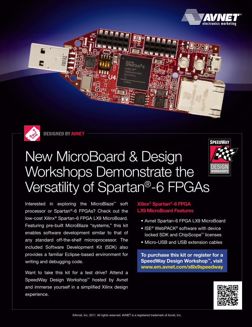
New MicroBoard & DesignWorkshops Demonstrate theVersatility of Spartan®-6 FPGAsInterested in exploring the MicroBlaze™ soft
processor or Spartan®-6 FPGAs? Check out the
low-cost Xilinx® Spartan-6 FPGA LX9 MicroBoard.
Featuring pre-built MicroBlaze “systems,” this kit
enables software development similar to that of
any standard off-the-shelf microprocessor. The
included Software Development Kit (SDK) also
provides a familiar Eclipse-based environment for
writing and debugging code.
Want to take this kit for a test drive? Attend a
SpeedWay Design Workshop™ hosted by Avnet
and immerse yourself in a simplified Xilinx design
experience.
Xilinx® Spartan®-6 FPGA
LX9 MicroBoard Features
Avnet Spartan-6 FPGA LX9 MicroBoard
ISE® WebPACK® software with device locked SDK and ChipScope™ licenses
Micro-USB and USB extension cables
To purchase this kit or register for a
SpeedWay Design Workshop™, visit
www.em.avnet.com/s6lx9speedway
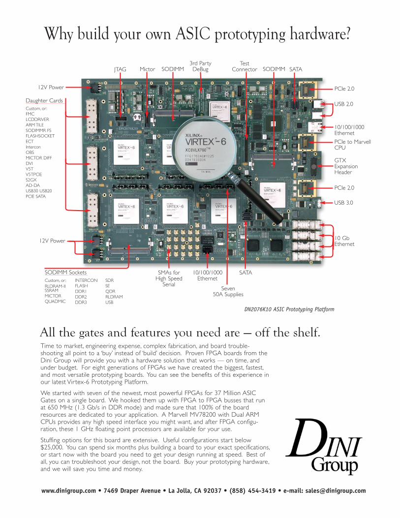
Time to market, engineering expense, complex fabrication, and board trouble-shooting all point to a ‘buy’ instead of ‘build’ decision. Proven FPGA boards from theDini Group will provide you with a hardware solution that works — on time, andunder budget. For eight generations of FPGAs we have created the biggest, fastest,and most versatile prototyping boards. You can see the benefits of this experience inour latest Vir tex-6 Prototyping Platform.
We started with seven of the newest, most powerful FPGAs for 37 Million ASICGates on a single board. We hooked them up with FPGA to FPGA busses that runat 650 MHz (1.3 Gb/s in DDR mode) and made sure that 100% of the boardresources are dedicated to your application. A Marvell MV78200 with Dual ARMCPUs provides any high speed interface you might want, and after FPGA configu-ration, these 1 GHz floating point processors are available for your use.
Stuffing options for this board are extensive. Useful configurations start below$25,000. You can spend six months plus building a board to your exact specifications,or start now with the board you need to get your design running at speed. Best ofall, you can troubleshoot your design, not the board. Buy your prototyping hardware,and we will save you time and money.
www.dinigroup.com • 7469 Draper Avenue • La Jolla, CA 92037 • (858) 454-3419 • e-mail: [email protected]
DN2076K10 ASIC Prototyping Platform
Why build your own ASIC prototyping hardware?
Daughter Cards
Custom, or:
FMC
LCDDRIVER
ARM TILE
SODIMMR FS
FLASHSOCKET
ECT
Intercon
OBS
MICTOR DIFF
DVI
V5T
V5TPCIE
S2GX
AD-DA
USB30 USB20
PCIE SATA
Custom, or:
RLDRAM-IISSRAM
MICTOR
QUADMIC
INTERCON
FLASH
DDR1
DDR2
DDR3
SDR
SE
QDR
RLDRAM
USB
12V Power
JTAG Mictor SATA
SATA
Seven50A Supplies
10/100/1000Ethernet
SMAs forHigh Speed
Serial
SODIMM Sockets
PCIe 2.0
PCIe to MarvellCPU
PCIe 2.0
USB 2.0
USB 3.0
10/100/1000Ethernet
10 GbEthernet
GTXExpansionHeader
3rd PartyDeBug
TestConnector
12V Power
All the gates and features you need are — off the shelf.
SODIMM SODIMM
L E T T E R F R O M T H E P U B L I S H E R
Xilinx, Inc.2100 Logic DriveSan Jose, CA 95124-3400Phone: 408-559-7778FAX: 408-879-4780www.xilinx.com/xcell/
© 2011 Xilinx, Inc. All rights reserved. XILINX, the Xilinx Logo, and other designated brands includedherein are trademarks of Xilinx, Inc. All other trade-marks are the property of their respective owners.
The articles, information, and other materials includedin this issue are provided solely for the convenience ofour readers. Xilinx makes no warranties, express,implied, statutory, or otherwise, and accepts no liabilitywith respect to any such articles, information, or othermaterials or their use, and any use thereof is solely atthe risk of the user. Any person or entity using suchinformation in any way releases and waives any claim itmight have against Xilinx for any loss, damage, orexpense caused thereby.
PUBLISHER Mike [email protected]
EDITOR Jacqueline Damian
ART DIRECTOR Scott Blair
DESIGN/PRODUCTION Teie, Gelwicks & Associates1-800-493-5551
ADVERTISING SALES Dan [email protected]
INTERNATIONAL Melissa Zhang, Asia [email protected]
Christelle Moraga, Europe/Middle East/[email protected]
Miyuki Takegoshi, [email protected]
REPRINT ORDERS 1-800-493-5551
Xcell journal
www.xilinx.com/xcell/
Xilinx Veteran Named ACM Fellow
“I became an engineer to build things, and that’s what FPGAs allow you to do.” So saysXilinx Fellow Steve Trimberger, the newly named Fellow of the Association forComputer Machinery, whom the ACM honored in June for his contributions to the
design of programmable logic and reconfigurable architec-tures, and for the development of design automation tools thatenable their use.
Trimberger has been pivotal in the creation of many gener-ations of FPGA architectures and EDA software since joiningXilinx in 1988. He currently holds more than 175 patents forXilinx and has dozens more pending.
He began tinkering with EDA software as a student at theCalifornia Institute of Technology, from which he earned aBS degree in engineering and, in 1983, a PhD in computerscience (gaining his MS from the University of California,Irvine, in between). “At Caltech, I wanted to design chips,but my chips didn’t always work. So then I’d go create a toolso I’d be able to catch that problem if it ever happenedagain,” said Trimberger. “After a few chips and a few debug-ging sessions, I started developing tools full time.”
He did the same thing when he went to work at VLSITechnology Inc., a pioneering ASIC company. “Back then, every tool you developed wasgood because there weren’t tools for pretty much anything,” Trimberger said. “I guesseveryone else’s chips had problems, too.”
Then, a few years later, Trimberger interviewed for a job at a pre-IPO chip company calledXilinx that had invented a new device called a field-programmable gate array.
“I heard about a company selling a logic chip that could be reprogrammed,” he said. “I real-ly wanted to use that chip, but I knew I had to move fast, because I didn’t think they wouldbe around that long.” But it turned out that “FPGAs excelled at something ASICs could neverdo—give you unlimited do-overs.” They had staying power.
At first, Trimberger mainly concentrated on software innovations to program FPGAs, butwith the mentoring of then-VP of engineering Bill Carter, he soon began creating inventionsfor next-generation silicon architectures. “The tight linking of FPGAs and tools to programthem has proved to be a key to success and is vitally important to the FPGA business,” he said.
Trimberger’s 175 patents span a wide range of design disciplines, from tools to circuits tofull IC architectures. An early patent is for a “backwards simulator” that allowed engineers toessentially run a simulation in reverse to quickly pinpoint the origins of an error. Another putsthe phenomenon of memory decay, in which a memory device loses its data when power isremoved, to good use—Trimberger describes a way of using memory decay rates to tell howlong a device has been powered off.
Trimberger has published three books: Automated Performance Optimization of Custom
Integrated Circuits, An Introduction to CAD for VLSI and Field Programmable Gate Array
Technology. He has also taught EDA software design to graduate students at Santa ClaraUniversity. In his spare time he coaches and supports high school teams in the FIRSTRobotics competition (one of his teams won first place in 2011).
The ACM is the world’s largest educational and scientific computing society. We join themin congratulating Steve Trimberger for a career spent advancing the state of the art in FPGAs,which you, our customers, in turn use to create remarkable innovations.
Mike SantariniPublisher
Xilinx’s Steve Trimberger, at theACM awards event in June.

C O N T E N T S
VIEWPOINTS XCELLENCE BY DESIGN APPLICATION FEATURES 2828
Cover StoryHow Xilinx Halved PowerDraw in 7 Series FPGAs
88
2222
Xcellence in ScientificApplications
Bottling a Star Using
ARM’s AXI4 in an FPGA… 22
Xcellence in Medical
FPGAs Drive Real-Time
Optical Biopsy System… 28
Letter From the PublisherXilinx Veteran
Named ACM Fellow… 4
XPERT OPINIONMIT Prof Uses ESL Tools,
FPGAs to Teach System Design… 16
T H I R D Q U A R T E R 2 0 1 1 , I S S U E 7 6
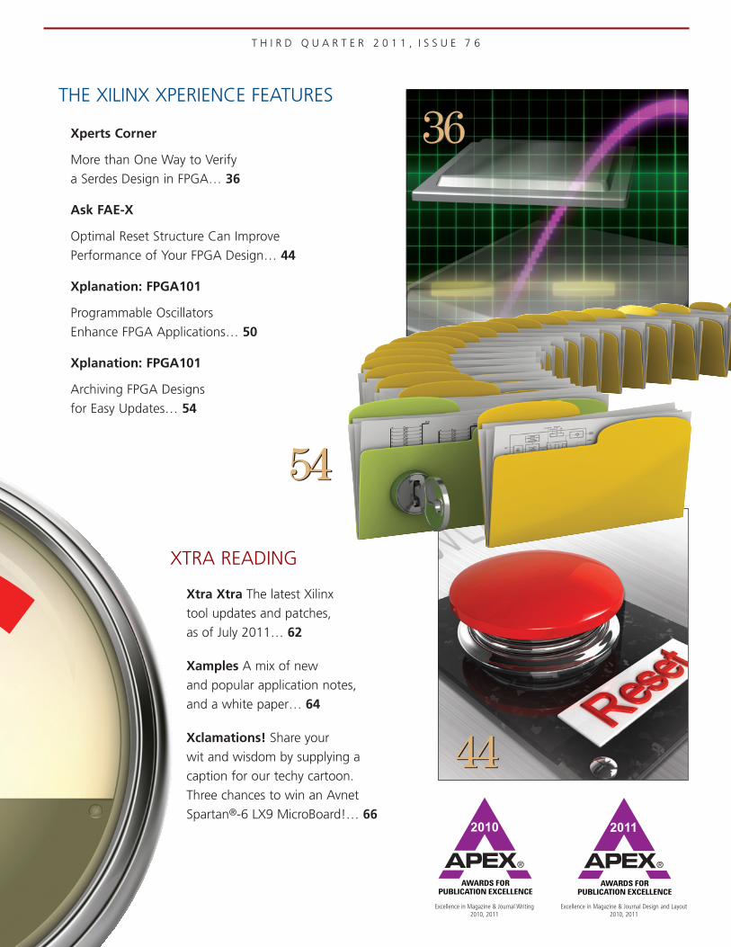
Xperts Corner
More than One Way to Verify
a Serdes Design in FPGA… 36
Ask FAE-X
Optimal Reset Structure Can Improve
Performance of Your FPGA Design… 44
Xplanation: FPGA101
Programmable Oscillators
Enhance FPGA Applications… 50
Xplanation: FPGA101
Archiving FPGA Designs
for Easy Updates… 54
THE XILINX XPERIENCE FEATURES
44442011
3636
5454
XTRA READING
Xtra Xtra The latest Xilinx
tool updates and patches,
as of July 2011… 62
Xamples A mix of new
and popular application notes,
and a white paper… 64
Xclamations! Share your
wit and wisdom by supplying a
caption for our techy cartoon.
Three chances to win an Avnet
Spartan®-6 LX9 MicroBoard!… 66
Excellence in Magazine & Journal Writing2010, 2011
Excellence in Magazine & Journal Design and Layout2010, 2011

8 Xcell Journal Third Quarter 2011
COVER STORY
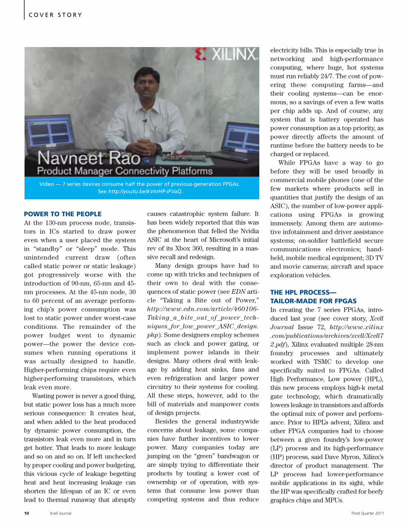
How Xilinx Halved PowerDraw in 7 Series FPGAsby Mike SantariniPublisher, Xcell JournalXilinx, [email protected]

Third Quarter 2011 Xcell Journal 9
In interviewing several hundred customers in the processof defining the 7 series FPGA line, Xilinx chip architectsfound over and over again that one topic dominated the
conversation: power. With such a clear customer mandate,Xilinx made power reduction and power management top pri-orities in its latest, 28-nanometer FPGAs, which began ship-ping to customers in March. In fact, 7 series FPGAs consumehalf the power of Xilinx’s previous-generation devices, whilestill increasing logic performance, I/O performance and trans-ceiver performance up to 28 Gbits/second and achievingrecord logic capacity (see Video).
A key enabler for this power reduction was Xilinx’s choice toimplement its series 7 FPGAs on TSMC’s 28-nm HPL process,which Xilinx and TSMC developed specifically for FPGAs.Besides offering a slew of intrinsic advantages in terms ofpower, the process had ample headroom to enable power bin-ning and voltage scaling, techniques that aren’t available forFPGAs implemented in other processes. In addition to choosinga process ideally suited for FPGAs, Xilinx also refined devicearchitectures to further cut power consumption.
This month, Xilinx will release revised power analysis tools tohelp designers evaluate the power profiles of Xilinx FPGAs.
TOP OF THE LISTIt’s no secret why power management has moved to the top ofthe must-have list for most, if not all, FPGA users. The old ruleof thumb held that if you were designing a system that your endcustomers would plug into a wall socket, you really didn’t needto care too much about the power consumption of the FPGA youwere using—you went for high performance and capacity whenchoosing one. How things have changed.
Over the last decade the industry has moved to new, fastersemiconductor manufacturing processes that have a nasty sideeffect of leaky transistors. At the same time, system makersstrive to differentiate their offerings by lowering the total cost ofownership or operating expenditures with lower-power prod-ucts, and have created newer, innovative gadgets that require DCpower (battery-based systems). Thus, lowering power andinvesting in system power management are something most cus-tomers have to do, even if they aren’t targeting handheld devices.Whether you want it to or not, power demands your attention.
A silicon manufacturing process tailored for FPGAsand an innovative unified architecture allowed Xilinxto reduce power consumption by more than 50 percentover its previous-generation devices.
C O V E R S T O R Y
POWER TO THE PEOPLEAt the 130-nm process node, transis-tors in ICs started to draw powereven when a user placed the systemin “standby” or “sleep” mode. Thisunintended current draw (oftencalled static power or static leakage)got progressively worse with theintroduction of 90-nm, 65-nm and 45-nm processes. At the 45-nm node, 30to 60 percent of an average perform-ing chip’s power consumption waslost to static power under worst-caseconditions. The remainder of thepower budget went to dynamicpower—the power the device con-sumes when running operations itwas actually designed to handle.Higher-performing chips require evenhigher-performing transistors, whichleak even more.
Wasting power is never a good thing,but static power loss has a much moreserious consequence: It creates heat,and when added to the heat producedby dynamic power consumption, thetransistors leak even more and in turnget hotter. That leads to more leakageand so on and so on. If left uncheckedby proper cooling and power budgeting,this vicious cycle of leakage begettingheat and heat increasing leakage canshorten the lifespan of an IC or evenlead to thermal runaway that abruptly
causes catastrophic system failure. Ithas been widely reported that this wasthe phenomenon that felled the NvidiaASIC at the heart of Microsoft’s initialrev of its Xbox 360, resulting in a mas-sive recall and redesign.
Many design groups have had tocome up with tricks and techniques oftheir own to deal with the conse-quences of static power (see EDN arti-cle “Taking a Bite out of Power,”http://www.edn.com/article/460106-
Taking_a_bite_out_of_power_tech-
niques_for_low_power_ASIC_design.
php). Some designers employ schemessuch as clock and power gating, orimplement power islands in theirdesigns. Many others deal with leak-age by adding heat sinks, fans andeven refrigeration and larger powercircuitry to their systems for cooling.All these steps, however, add to thebill of materials and manpower costsof design projects.
Besides the general industrywideconcerns about leakage, some compa-nies have further incentives to lowerpower. Many companies today arejumping on the “green” bandwagon orare simply trying to differentiate theirproducts by touting a lower cost ofownership or of operation, with sys-tems that consume less power thancompeting systems and thus reduce
electricity bills. This is especially true innetworking and high-performancecomputing, where huge, hot systemsmust run reliably 24/7. The cost of pow-ering these computing farms—andtheir cooling systems—can be enor-mous, so a savings of even a few wattsper chip adds up. And of course, anysystem that is battery operated haspower consumption as a top priority, aspower directly affects the amount ofruntime before the battery needs to becharged or replaced.
While FPGAs have a way to gobefore they will be used broadly incommercial mobile phones (one of thefew markets where products sell inquantities that justify the design of anASIC), the number of low-power appli-cations using FPGAs is growingimmensely. Among them are automo-tive infotainment and driver assistancesystems; on-soldier battlefield securecommunications electronics; hand-held, mobile medical equipment; 3D TVand movie cameras; aircraft and spaceexploration vehicles.
THE HPL PROCESS—TAILOR-MADE FOR FPGASIn creating the 7 series FPGAs, intro-duced last year (see cover story, Xcell
Journal Issue 72, http://www.xilinx
.com/publications/archives/xcell/Xcell7
2.pdf), Xilinx evaluated multiple 28-nmfoundry processes and ultimatelyworked with TSMC to develop onespecifically suited to FPGAs. CalledHigh Performance, Low power (HPL),this new process employs high-k metalgate technology, which dramaticallylowers leakage in transistors and affordsthe optimal mix of power and perform-ance. Prior to HPL’s advent, Xilinx andother FPGA companies had to choosebetween a given foundry’s low-power(LP) process and its high-performance(HP) process, said Dave Myron, Xilinx’sdirector of product management. TheLP process had lower-performancemobile applications in its sight, whilethe HP was specifically crafted for beefygraphics chips and MPUs.
10 Xcell Journal Third Quarter 2011
C O V E R S T O R Y
Video — 7 series devices consume half the power of previous-generation FPGAs.See http://youtu.be/kVmHP-IFVaQ.
“Neither type of process has beenthe optimal fit for FPGAs,” said Myron.“If you went with an LP process, wewere leaving performance on the table,and if we went with an HP process, ourdevices consumed more power thanwe would have liked. We had a littlewiggle room to tweak the process, butnot as much as we would have liked.”
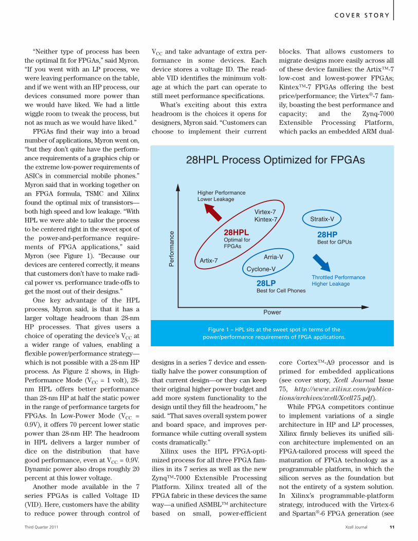
FPGAs find their way into a broadnumber of applications, Myron went on,“but they don’t quite have the perform-ance requirements of a graphics chip orthe extreme low-power requirements ofASICs in commercial mobile phones.”Myron said that in working together onan FPGA formula, TSMC and Xilinxfound the optimal mix of transistors—both high speed and low leakage. “WithHPL we were able to tailor the processto be centered right in the sweet spot ofthe power-and-performance require-ments of FPGA applications,” saidMyron (see Figure 1). “Because ourdevices are centered correctly, it meansthat customers don’t have to make radi-cal power vs. performance trade-offs toget the most out of their designs.”
One key advantage of the HPLprocess, Myron said, is that it has alarger voltage headroom than 28-nmHP processes. That gives users achoice of operating the device’s VCC ata wider range of values, enabling aflexible power/performance strategy—which is not possible with a 28-nm HPprocess. As Figure 2 shows, in High-Performance Mode (VCC = 1 volt), 28-nm HPL offers better performancethan 28-nm HP at half the static powerin the range of performance targets forFPGAs. In Low-Power Mode (VCC =0.9V), it offers 70 percent lower staticpower than 28-nm HP. The headroomin HPL delivers a larger number ofdice on the distribution that havegood performance, even at VCC = 0.9V.Dynamic power also drops roughly 20percent at this lower voltage.
Another mode available in the 7series FPGAs is called Voltage ID(VID). Here, customers have the abilityto reduce power through control of
VCC and take advantage of extra per-formance in some devices. Eachdevice stores a voltage ID. The read-able VID identifies the minimum volt-age at which the part can operate tostill meet performance specifications.
What’s exciting about this extraheadroom is the choices it opens fordesigners, Myron said. “Customers canchoose to implement their current
designs in a series 7 device and essen-tially halve the power consumption ofthat current design—or they can keeptheir original higher power budget andadd more system functionality to thedesign until they fill the headroom,” hesaid. “That saves overall system powerand board space, and improves per-formance while cutting overall systemcosts dramatically.”
Xilinx uses the HPL FPGA-opti-mized process for all three FPGA fam-ilies in its 7 series as well as the newZynq™-7000 Extensible ProcessingPlatform. Xilinx treated all of theFPGA fabric in these devices the sameway—a unified ASMBL™ architecturebased on small, power-efficient
blocks. That allows customers tomigrate designs more easily across allof these device families: the Artix™-7low-cost and lowest-power FPGAs;Kintex™-7 FPGAs offering the bestprice/performance; the Virtex®-7 fam-ily, boasting the best performance andcapacity; and the Zynq-7000Extensible Processing Platform,which packs an embedded ARM dual-
core Cortex™-A9 processor and isprimed for embedded applications(see cover story, Xcell Journal Issue75, http://www.xilinx.com/publica-
tions/archives/xcell/Xcell75.pdf). While FPGA competitors continue
to implement variations of a singlearchitecture in HP and LP processes,Xilinx firmly believes its unified sili-con architecture implemented on anFPGA-tailored process will speed thematuration of FPGA technology as aprogrammable platform, in which thesilicon serves as the foundation butnot the entirety of a system solution.In Xilinx’s programmable-platformstrategy, introduced with the Virtex-6and Spartan®-6 FPGA generation (see
Third Quarter 2011 Xcell Journal 11
C O V E R S T O R Y
Higher PerformanceLower Leakage
Throttled PerformanceHigher Leakage
Per
form
ance
Power
28HPLOptimal forFPGAs
28LPBest for Cell Phones
28HPBest for GPUs
Virtex-7Kintex-7
Artix-7 Arria-V
Cyclone-V
Stratix-V
28HPL Process Optimized for FPGAs
Figure 1 – HPL sits at the sweet spot in terms of the power/performance requirements of FPGA applications.
cover story, Xcell Journal Issue 68,h t t p : / / w w w . x i l i n x
.com/publications/archives/xcell/Xcell6
8.pdf), Xilinx not only provides cutting-edge silicon but also market- and appli-cation-specific development boards, IP,tools and documentation to help cus-tomers create innovations quickly.
Myron notes that the move to an opti-mized process and unified architectureisn’t unprecedented or radical in thesemiconductor industry—it adapts toFPGAs a strategy Intel Corp. pioneeredand has successfully implemented overthe last five years (see the white paper“Inside Intel Core Microarchitecture,”http://software.intel.com/file/18374/).
“In 2006, Intel stopped using multi-ple microprocessor architectures andimplemented its single strongest hard-ware architecture—the Intel Coremicroarchitecture—on a single siliconprocess and across multiple productlines, from high-computing serverproducts down to the mobile notebookproducts,” said Myron, who formerlyworked at Intel. “Why does a companylike Intel, with seemingly unlimitedresources at its disposal, focus on justone hardware architecture? The
answer is, they want to do one thing anddo it very well by focusing theirresources behind a single architecturethat can be scaled to fit different appli-cation needs and to make it easier fortheir customers to utilize this samearchitecture in multiple applicationswith a minimum of redesign.”
The same is certainly true forXilinx, said Myron. “By selecting acommon architecture for the 7 seriesFPGAs, we can focus our software-engineering teams on optimizing quali-ty of results without dividing theirefforts over multiple product families.In a similar fashion, our customershave expressed a strong desire to opti-mize IP reuse,” he said. “Maintaining asingle architecture facilitates IP reusewith a minimum of engineering effortcompared to doing so across multiple,different architectures.”
The high-k metal gate HPL processwas just the first stage in reducing stat-ic power. Xilinx took the effort a stepfurther by making adjustments to the 7series device architecture. In priorXilinx FPGA releases, Xilinx added theability for users to employ power gatingto shut off unused transceivers, phase-
locked loops (PLLs), digital clock man-agers and I/O. In series 7, designers cannow do the same with unused blockRAM. Since block RAM could accountfor as much as 30 percent of a givendevice’s leakage current, power gatingcan make a huge difference.
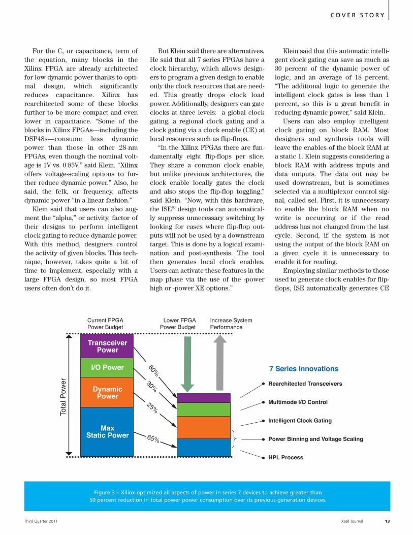
TOTAL SYSTEM POWER REDUCTIONMyron said that while the choice of thehigh-k metal gate HPL silicon processreduced static power and dynamicpower usage greatly, Xilinx took addi-tional steps to reduce the total systempower of the 7 series devices. That is, ifone were to look at total system power,it consists of static leakage, dynamicpower, I/O power and transceiverpower (Figure 3).
Dynamic power reductionXilinx power guru Matt Klein, aDistinguished Engineer who has beeninvolved in driving power reductioninto Xilinx FPGAs, said dynamicpower in the FPGA’s logic is based onthe standard “C V squared f” equation:
Dynamic power = µ xfclk x CL x VDD2
C O V E R S T O R Y
12 Xcell Journal Third Quarter 2011
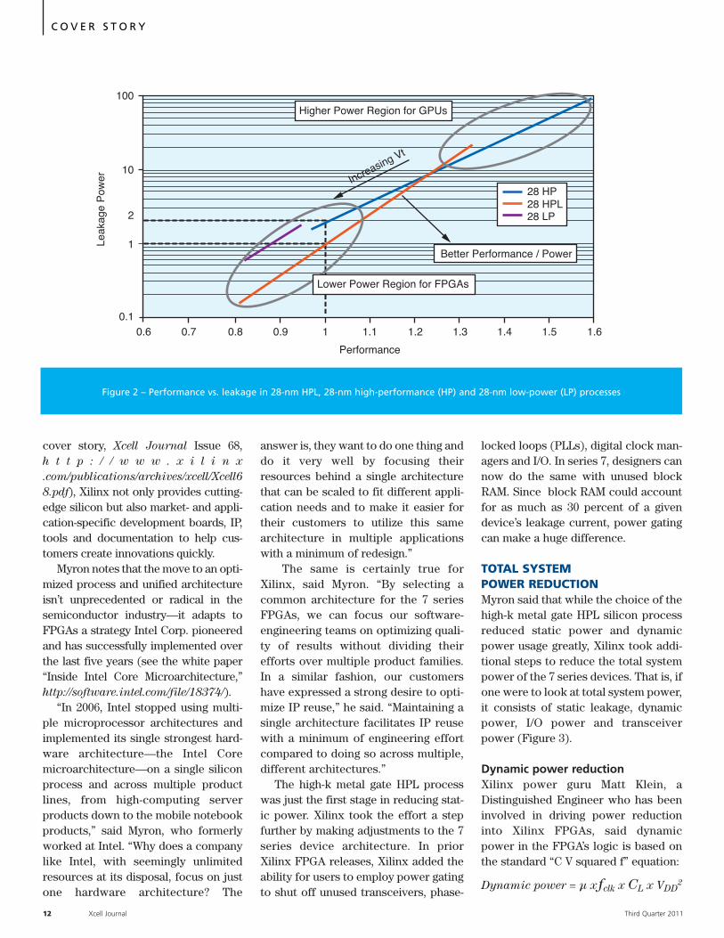
Higher Power Region for GPUs
Better Performance / Power
28 HP28 HPL28 LP
Increasing Vt
0.6 0.7 0.8 0.9 1 1.1 1.2 1.3 1.4 1.5 1.6
100
10
2
1
0.1
Leak
age
Pow
er
Performance
Lower Power Region for FPGAs
Figure 2 – Performance vs. leakage in 28-nm HPL, 28-nm high-performance (HP) and 28-nm low-power (LP) processes
For the C, or capacitance, term ofthe equation, many blocks in theXilinx FPGA are already architectedfor low dynamic power thanks to opti-mal design, which significantlyreduces capacitance. Xilinx hasrearchitected some of these blocksfurther to be more compact and evenlower in capacitance. “Some of theblocks in Xilinx FPGAs—including theDSP48s—consume less dynamicpower than those in other 28-nmFPGAs, even though the nominal volt-age is 1V vs. 0.85V,” said Klein. “Xilinxoffers voltage-scaling options to fur-ther reduce dynamic power.” Also, hesaid, the fclk, or frequency, affectsdynamic power “in a linear fashion.”
Klein said that users can also aug-ment the “alpha,” or activity, factor oftheir designs to perform intelligentclock gating to reduce dynamic power.With this method, designers controlthe activity of given blocks. This tech-nique, however, takes quite a bit oftime to implement, especially with alarge FPGA design, so most FPGAusers often don’t do it.
But Klein said there are alternatives.He said that all 7 series FPGAs have aclock hierarchy, which allows design-ers to program a given design to enableonly the clock resources that are need-ed. This greatly drops clock loadpower. Additionally, designers can gateclocks at three levels: a global clockgating, a regional clock gating and aclock gating via a clock enable (CE) atlocal resources such as flip-flops.
“In the Xilinx FPGAs there are fun-damentally eight flip-flops per slice.They share a common clock enable,but unlike previous architectures, theclock enable locally gates the clockand also stops the flip-flop toggling,”said Klein. “Now, with this hardware,the ISE® design tools can automatical-ly suppress unnecessary switching bylooking for cases where flip-flop out-puts will not be used by a downstreamtarget. This is done by a logical exami-nation and post-synthesis. The toolthen generates local clock enables.Users can activate these features in themap phase via the use of the -powerhigh or -power XE options.”
Klein said that this automatic intelli-gent clock gating can save as much as30 percent of the dynamic power oflogic, and an average of 18 percent.“The additional logic to generate theintelligent clock gates is less than 1percent, so this is a great benefit inreducing dynamic power,” said Klein.
Users can also employ intelligentclock gating on block RAM. Mostdesigners and synthesis tools willleave the enables of the block RAM ata static 1. Klein suggests considering ablock RAM with address inputs anddata outputs. The data out may beused downstream, but is sometimesselected via a multiplexor control sig-nal, called sel. First, it is unnecessaryto enable the block RAM when nowrite is occurring or if the readaddress has not changed from the lastcycle. Second, if the system is notusing the output of the block RAM ona given cycle it is unnecessary toenable it for reading.
Employing similar methods to thoseused to generate clock enables for flip-flops, ISE automatically generates CE
Third Quarter 2011 Xcell Journal 13
C O V E R S T O R Y
Current FPGAPower Budget
Lower FPGAPower Budget
Increase SystemPerformance
Tota
l Pow
er Rearchitected Transceivers
Multimode I/O Control
Intelligent Clock Gating
Power Binning and Voltage Scaling
HPL Process
7 Series Innovations
TransceiverPower
I/O Power
DynamicPower
MaxStatic Power
60%30%
25%
65%
Figure 3 – Xilinx optimized all aspects of power in series 7 devices to achieve greater than 50 percent reduction in total power power consumption over its previous-generation devices.
(or clock enable) signals on a cycle-by-cycle basis. “For block RAM the sav-ings are even greater and we find up to70 percent lower block RAM powerwith an average of 30 percent reduc-tion, again with very little logic over-head,” said Klein. “Xilinx also offersboth CORE Generator™ and XSToptions to construct power-efficientblock RAM arrays, which can save upto 75 percent of the dynamic power ofthose block RAMs in an array.”
I/O power reductionOf course, there’s more to the powerpicture than static and dynamic power.Total system power consists of twoother types as well: I/O power andtransceiver power.
To lower the power consumed byhigh-speed I/O, Xilinx added multi-mode I/O control and rearchitected itstransceivers. Klein said that multimodeI/O control delivers significant I/Opower savings, particularly for memoryinterfaces: up to 50 percent for memo-ry writes and as much as 75 percentpower savings for memory idle state.
The first of these new power reduc-tion features is valuable during a memo-ry write: The I/O hardware automatical-ly disables the IBUF (input buffer) dur-ing a write to external memory devicessuch as DDR2 and DDR3. “Since theinput buffer is a referenced receiver, itburns DC power, independent of togglerate, so now during a memory write thisDC power is removed and the saving isproportional to the percent of write,”said Klein. “During a memory write thisfeature saves an additional 50 percent ofthe total power compared with only dis-abling the termination.”
The second power reduction fea-ture added to the I/O of all 7 seriesFPGAs is the ability for the user to dis-able IBUF and the termination duringtimes when the memory bus is idle.“Normally, during a bus idle period youneed to get off the bus, but this wouldlook like a memory read and withoutthis [disabling] feature, both the termi-nation and IBUF will burn power,” said
Klein. “By disabling them, the 7 seriesI/O will consume 75 percent less powercompared to leaving the terminationand input receiver on.”
Xilinx also lowered the VCCAUX volt-age from 2.5V to 1.8V. This saves roughly30 percent on power consumption forall blocks powered by VCCAUX, includingthe PLL, IDELAY, input and outputbuffers, and configuration logic.
These new features are big benefitsvs. Virtex-6 and other FPGAs for high-performance memory interfaces.
Transceiver power reductionTransceiver power is another key con-tributor to a device’s total power.Myron said Xilinx initially providedpretty conservative transceiver powerfigures when first announcing the 7series power estimates in its XPowerEstimator (XPE) tool. Xilinx has sincefurther refined GTP and GTH transceiv-er power and correlated its tools to sil-icon results. The latest XPE release(version 13.2) reflects these new num-bers more accurately.
“For the Artix-7 GTP, which offers upto 6.75-Gbps performance, the completetransceiver power is 60 percent lowercompared to the Spartan-6 GTP at equiv-alent performance,” said Myron. “We didthis to satisfy the low-end market’s needfor absolute lowest power and cost. Wealso significantly lowered the Virtex-7GTH power.” That device, which canhave as many as 96 transceivers, is usedin high-bandwidth applications “wheretransceiver power can be a major contri-bution to total power,” he said. “This putus on par in transceiver power with thecompeting 28-nm offering.”
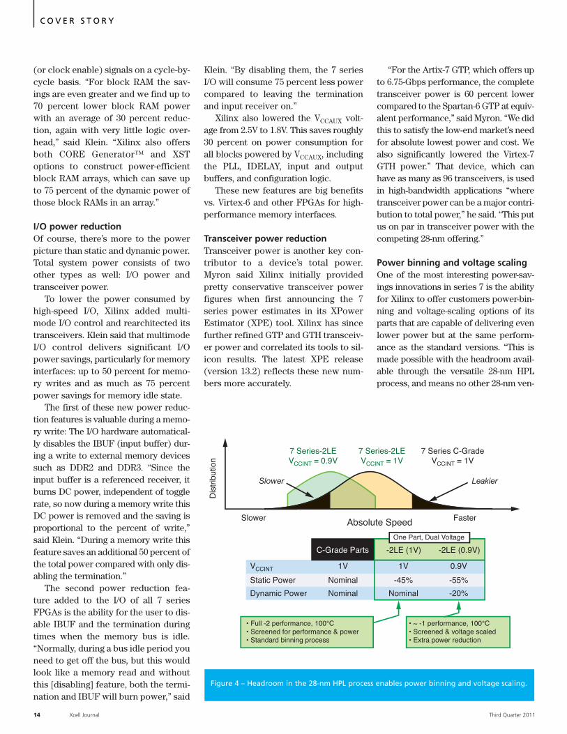
Power binning and voltage scalingOne of the most interesting power-sav-ings innovations in series 7 is the abilityfor Xilinx to offer customers power-bin-ning and voltage-scaling options of itsparts that are capable of delivering evenlower power but at the same perform-ance as the standard versions. “This ismade possible with the headroom avail-able through the versatile 28-nm HPLprocess, and means no other 28-nm ven-
C O V E R S T O R Y
Dis
trib
utio
n
Slower Faster
7 Series-2LEVCCINT = 0.9V
7 Series-2LEVCCINT = 1V
7 Series C-GradeVCCINT = 1V
Slower Leakier
Absolute Speed
C-Grade Parts -2LE (1V) -2LE (0.9V)
VCCINT
Static Power
Dynamic Power
1V
Nominal
Nominal
1V
-45%
Nominal
0.9V
-55%
-20%
One Part, Dual Voltage
• Full -2 performance, 100°C• Screened for performance & power• Standard binning process
• ~ -1 performance, 100°C• Screened & voltage scaled• Extra power reduction
Figure 4 – Headroom in the 28-nm HPL process enables power binning and voltage scaling.
14 Xcell Journal Third Quarter 2011
dor can provide you such a power-opti-mized option,” said Myron. “How wasXilinx able to achieve this? If we firstlook at the standard part distribution[Figure 4], all parts in this curve run at1V and have nominal static and dynam-ic power. We then remove the parts ofdistribution that are too slow or tooleaky to give us the distribution for the -2L devices. The -2L devices operate atthe same 1V core voltage, and there-fore deliver the same -2 performanceas the commercial or industrial coun-terparts, and can function at up to100°C. The -2LE devices offer 45 per-cent static power saving, and are partof the standard binning process, andtherefore there is no issue with avail-ability of these devices. We then takethe -2LE part and screen it to makesure that it’s capable of running at 0.9V.By lowering core voltage to 0.9V, thepower-optimized -2LE part can provideup to 55 percent static power reduc-
tion and 20 percent dynamic powerreduction compared to the standardcommercial devices.”
AND THE BENCHMARK SAYS?While competitors are apt to arguethat Xilinx is fielding a one-size-fits-allapproach at the 28-nm node, the com-pany that invented the FPGA is quiteconfident that the 7 series is yetanother innovation milestone. Xilinxhas put together comprehensivebenchmarks that show the 7 series isthe optimal mix for the entire range ofapplications you target with FPGAs.Customers can view a number ofbenchmarks Xilinx has published athttp://www.xilinx.com/publications/
technology/power-advantage/7-series-
power-benchmark-summary.pdf andview a TechOnline webinar at http://
s e m i n a r 2 . t e c h o n l i n e . c o m /
registration/wcIndex.cgi?sessionID=
xilinx_jun1411.
EMPOWER YOURSELF The latest version of the XPE powerestimator tool, release version 13.2(Figure 5), offers updated data on 7series devices reflecting the recentproduct changes. It also provides thelower power data for the rearchitect-ed GTP and GTH transceivers. Bypopular demand, this version of thetool also provides customers withnecessary max-power data for theirworst-case power supply and ther-mal planning.
For more details on power man-agement of 7 series devices andbenchmark information, read the 7series white paper entitled “LoweringPower at 28 nm with Xilinx 7 SeriesFPGAs,” which can be found atwww.xilinx.com/power.
For further details on the 7 seriespower advantage, visit http://www.
xilinx.com/products/technology/
power/index.htm.
Third Quarter 2011 Xcell Journal 15
C O V E R S T O R Y
6
Actual HardwareBenchmark Results
Kintex-7 FPGA PowerEstimator Results
vs.
Using the same reference design.First 28nm silicon demonstrates
>50% power savings.
Close correlation withestimator tool results
Static Power: 3.6 WTotal Power: 6.5 W
Static Power: 0.9 WTotal Power: 3.1 W
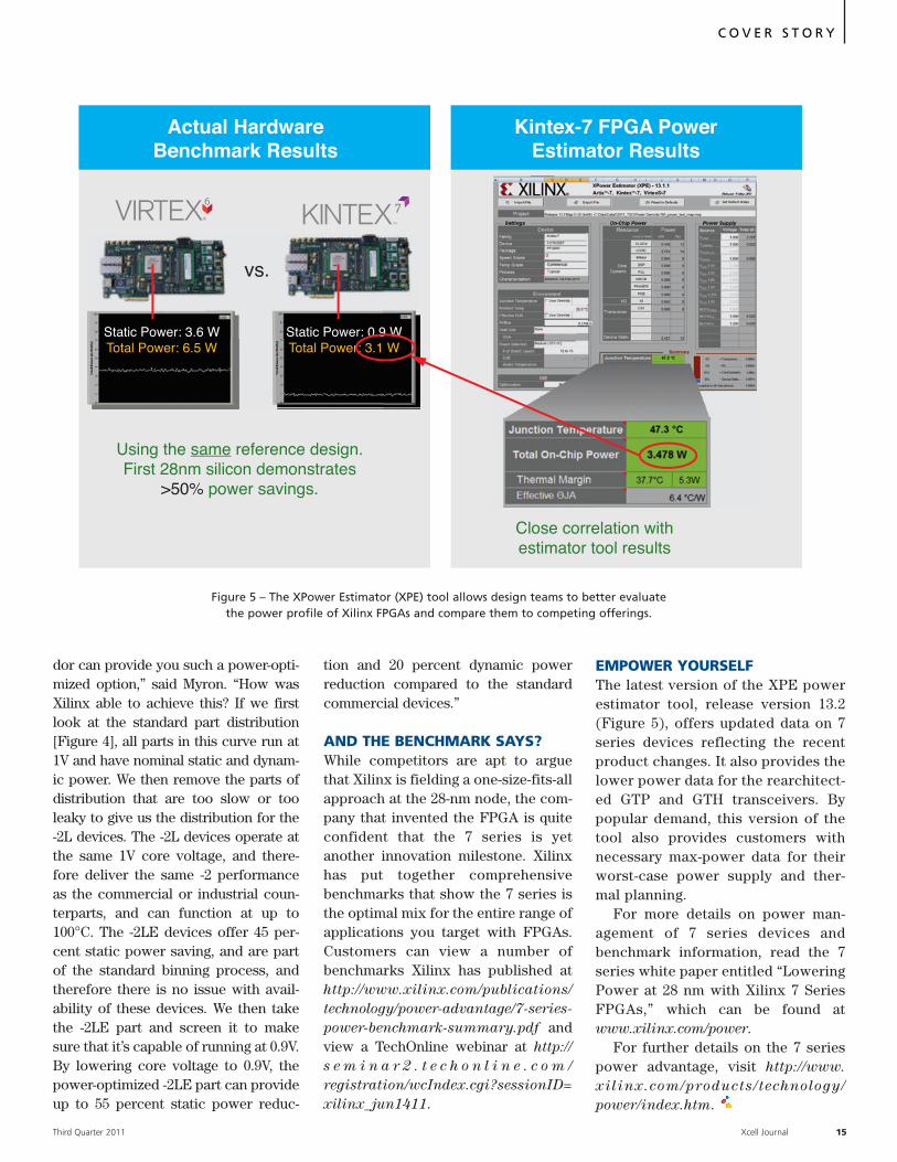
Figure 5 – The XPower Estimator (XPE) tool allows design teams to better evaluate the power profile of Xilinx FPGAs and compare them to competing offerings.
16 Xcell Journal Third Quarter 2011
MIT Prof Uses ESLTools, FPGAs to TeachSystem Architecture
MIT Prof Uses ESL Tools, FPGAs to Teach System Architecture
XPERT OPINION
By Clive (Max) MaxfieldPresidentMaxfield High-Tech [email protected]
Third Quarter 2011 Xcell Journal 17
The last time I was on the receiv-ing end of formal educationwas deep in the mists of time
(circa the end of the 1970s). My finalproject for my control engineeringdegree was a digital controller thatcould display color text and “chunkygraphics” on a cathode-ray tube. Theentire design was implemented usingcheap-and-cheerful 74-series TTLchips, each of which contained only afew simple logic gates or registers.
We didn’t have computer-aidedtools like schematic-capture systemsor logic simulators (the programs Iwrote for my computer class wereentered on a teleprinter and stored onpunched cards). So my design wascaptured as a gate-level schematicusing pencil and paper; any proof-of-concept, testing and debug took placeafter I’d soldered everything together.
Not surprisingly, I didn’t have theluxury of evaluating different architec-tural scenarios to see which wouldgive me the best results. I just optedfor an architecture I thought could “dothe job” and I remember breathing adeep sigh of relief when my controllerfinally displayed a “Hello Max” mes-sage on the screen.
Today’s chips, by contrast, offerdesigners mind-boggling logic capaci-ties and resources to solve their prob-lems. Along with design size, however,comes complexity, which is making itharder and harder to meet cost goalsand performance, power and areaspecifications.
Decisions made early in the designcycle have the most impact with regardto all aspects of the final chip. Forexample, industry analyst Gary Smithestimates that 80 percent of a product’scost is determined during the first 20percent of its development cycle. Thismeans that it is absolutely imperativeto select the optimum hardware archi-tecture as early as possible in the devel-opment process.
But how can you teach this sort ofthing to engineering students? With somuch groundwork to be laid in the foun-dations of electrical engineering, andwith limited time, universities historical-ly haven’t been able to focus on teachingarchitecture to the depth that is nowrequired. A master’s-level complex digi-tal design course at MIT is trying tochange all that. By leveraging the combi-nation of FPGAs (through the XilinxUniversity Program) and real-world elec-tronic system-level (ESL) design, whichsupports architectural exploration athigher levels of hardware abstraction,students are accomplishing in weekswhat would have required an entireschool year, or more, of study in the past.
WELCOME TO 6.375I recently heard about a course called6.375 at the Massachusetts Institute ofTechnology (MIT). It seems this courseis changing the playing field when itcomes to teaching digital design. Inparticular, a key focus of 6.375 is theuse of architectural exploration tohome in on optimal designs. The thingthat really intrigued me is that thecourse is a mere 13 weeks long, ofwhich the students have only sixweeks to design, implement and verifytheir final projects. But these projectsare of a complexity that would bringgrizzled, practicing engineers to theirknees, so how can this be possible?
First I bounced over to the MIT web-site (http://csg.csail.mit.edu/6.375/
6_375_2011_www/index.html),where I read: “6.375 is a project-orient-ed subject teaching a new method fordesigning multimillion-gate hardware
designs using high-level synthesistools in conjunction with standardcommercial EDA tools. The emphasisis on modular and robust designs;reusable modules; correctness by con-struction; architectural exploration;meeting area and timing constraints;and developing functional FPGA pro-totypes. This subject relies on high-level architectural knowledge and pro-gramming expertise rather thanknowledge of low-level circuit design.”
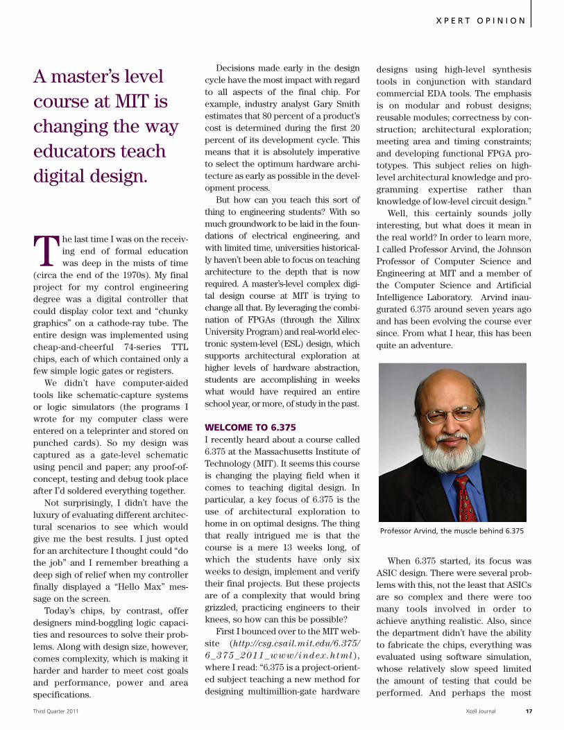
Well, this certainly sounds jollyinteresting, but what does it mean inthe real world? In order to learn more,I called Professor Arvind, the JohnsonProfessor of Computer Science andEngineering at MIT and a member ofthe Computer Science and ArtificialIntelligence Laboratory. Arvind inau-gurated 6.375 around seven years agoand has been evolving the course eversince. From what I hear, this has beenquite an adventure.
When 6.375 started, its focus wasASIC design. There were several prob-lems with this, not the least that ASICsare so complex and there were toomany tools involved in order toachieve anything realistic. Also, sincethe department didn’t have the abilityto fabricate the chips, everything wasevaluated using software simulation,whose relatively slow speed limitedthe amount of testing that could beperformed. And perhaps the most
Professor Arvind, the muscle behind 6.375
A master’s levelcourse at MIT ischanging the wayeducators teachdigital design.
X P E R T O P I N I O N
important thing was that the lack ofphysical chips to play with meant thatthe class was not as stimulating for thestudents as Arvind had wished.
A few years into the course it wasdecided to switch to FPGAs (the cur-riculum largely ignores the specialproperties of FPGAs and concentrateson straightforward RTL design), in thebelief that having physical realizationsof their designs would be significantlymore exciting for the students. Anotherbig consideration was that softwaresimulation takes so long and runs outof steam when it comes to the tremen-dous amount of vectors required tofully test today’s complex projects.Many designs don’t even start to exhib-it interesting or corner-case behavioruntil a long sequence (perhaps tens or
hundreds of millions) of test vectorshas been processed.
Today, the course—which draws amix of computer science and electricalengineering majors—features thecombination of an ESL design and ver-ification environment coupled with astate-of-the-art FPGA developmentsystem from Xilinx that was designedwith universities in mind.
THE FIRST SIX WEEKSThe first half of the course uses exam-ples of increasing complexity to intro-duce the Bluespec hardware descrip-tion language (HDL) and associateddesign and verification environment.The second half is devoted to the stu-dents’ projects. The students knowhardly anything about Bluespec or hard-
ware design before they start (this year,none of the students knew Bluespecand only three had rudimentary hard-ware design experience). Nevertheless,they tackle complex projects.
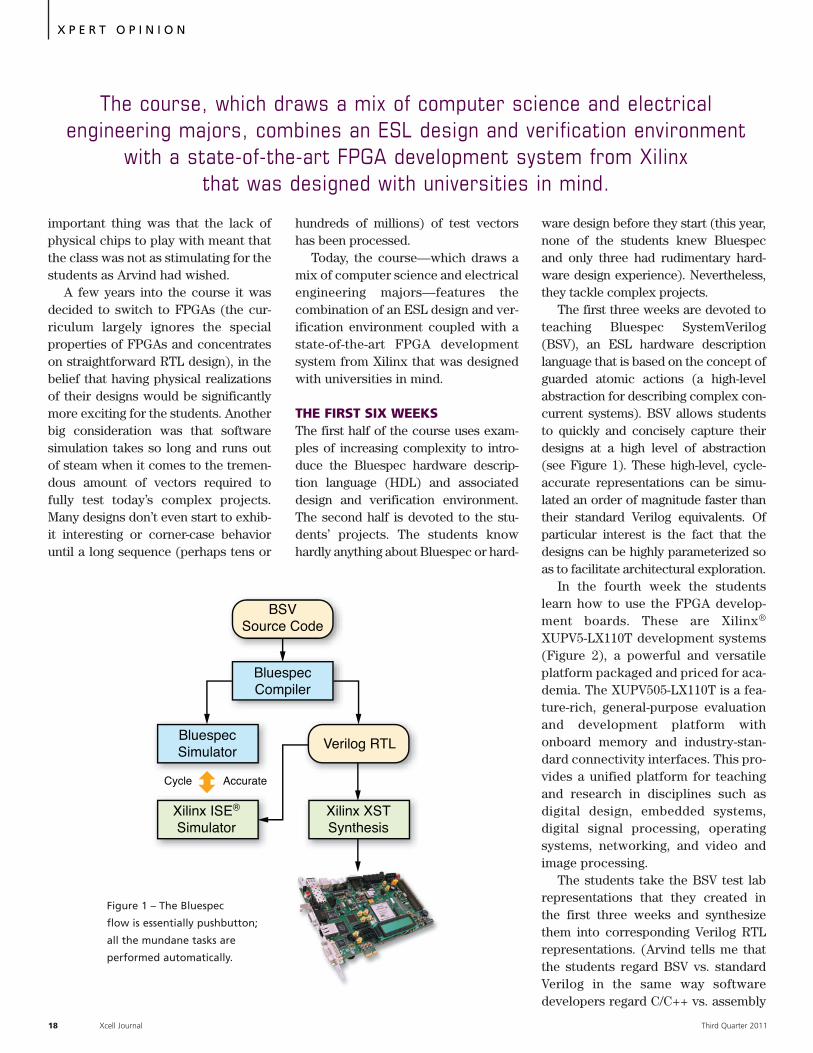
The first three weeks are devoted toteaching Bluespec SystemVerilog(BSV), an ESL hardware descriptionlanguage that is based on the concept ofguarded atomic actions (a high-levelabstraction for describing complex con-current systems). BSV allows studentsto quickly and concisely capture theirdesigns at a high level of abstraction(see Figure 1). These high-level, cycle-accurate representations can be simu-lated an order of magnitude faster thantheir standard Verilog equivalents. Ofparticular interest is the fact that thedesigns can be highly parameterized soas to facilitate architectural exploration.
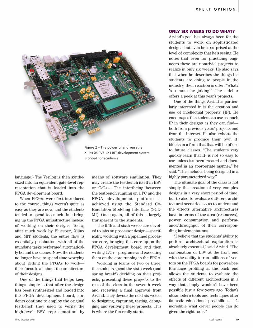
In the fourth week the studentslearn how to use the FPGA develop-ment boards. These are Xilinx®
XUPV5-LX110T development systems(Figure 2), a powerful and versatileplatform packaged and priced for aca-demia. The XUPV505-LX110T is a fea-ture-rich, general-purpose evaluationand development platform withonboard memory and industry-stan-dard connectivity interfaces. This pro-vides a unified platform for teachingand research in disciplines such asdigital design, embedded systems,digital signal processing, operatingsystems, networking, and video andimage processing.
The students take the BSV test labrepresentations that they created inthe first three weeks and synthesizethem into corresponding Verilog RTLrepresentations. (Arvind tells me thatthe students regard BSV vs. standardVerilog in the same way softwaredevelopers regard C/C++ vs. assembly
18 Xcell Journal Third Quarter 2011
X P E R T O P I N I O N
BSVSource Code
BluespecCompiler
BluespecSimulator
Verilog RTL
Xilinx ISE®
SimulatorXilinx XSTSynthesis
Cycle Accurate
Figure 1 – The Bluespec
flow is essentially pushbutton;
all the mundane tasks are
performed automatically.
The course, which draws a mix of computer science and electrical engineering majors, combines an ESL design and verification environment
with a state-of-the-art FPGA development system from Xilinx that was designed with universities in mind.
language.) The Verilog is then synthe-sized into an equivalent gate-level rep-resentation that is loaded into theFPGA development board.
When FPGAs were first introducedto the course, things weren’t quite aseasy as they are now, and the studentstended to spend too much time bring-ing up the FPGA infrastructure insteadof working on their designs. Today,after much work by Bluespec, Xilinxand MIT students, the entire flow isessentially pushbutton, with all of themundane tasks performed automatical-ly behind the scenes. Now, the studentsno longer have to spend time worryingabout getting the FPGAs to work—their focus is all about the architectureof their designs.
One of the things that helps keepthings simple is that after the designhas been synthesized and loaded intothe FPGA development board, stu-dents continue to employ the originaltestbench they used to verify thehigh-level BSV representation by
means of software simulation. Theymay create the testbench itself in BSVor C/C++. The interfacing betweenthe testbench running on a PC and theFPGA development platform isachieved using the Standard Co-Emulation Modeling Interface (SCE-MI). Once again, all of this is largelytransparent to the students.
The fifth and sixth weeks are devot-ed to labs on processor design—specif-ically, working with a pipelined proces-sor core, bringing this core up on theFPGA development board and thenwriting C/C++ programs and executingthem on the core running in the FPGA.
Working in teams of two or three,the students spend the sixth week (andspring break!) deciding on their proj-ects, presenting these projects to therest of the class in the seventh weekand receiving a final approval fromArvind. They devote the next six weeksto designing, capturing, testing, debug-ging and verifying these projects. Thisis where the fun really starts.
ONLY SIX WEEKS TO DO WHAT?Arvind’s goal has always been for thestudents to work on sophisticateddesigns, but even he is surprised at thelevel of complexity that he’s seeing. Henotes that even for practicing engi-neers these are nontrivial projects torealize in only six weeks. He also saysthat when he describes the things hisstudents are doing to people in theindustry, their reaction is often “What?You must be joking!” The sidebaroffers a peek at this year’s projects.
One of the things Arvind is particu-larly interested in is the creation anduse of intellectual property (IP). Heencourages the students to use as muchIP in their designs as they can find—both from previous years’ projects andfrom the Internet. He also exhorts thestudents to produce their own IPblocks in a form that that will be of useto future classes. “The students veryquickly learn that IP is not so easy touse unless it’s been created and docu-mented in an appropriate manner,” hesaid. “This includes being designed in ahighly parameterized way.”
The ultimate goal of the class is notsimply the creation of very complexdesigns in a very short period of time,but to also to evaluate different archi-tectural scenarios so as to understandthe effects alternative architectureshave in terms of the area (resources),power consumption and perform-ance/throughput of their correspon-ding implementations.
“I believe that the students’ ability toperform architectural exploration isabsolutely essential,” said Arvind. “Thecombination of BSV at the front endwith the ability to run millions of vec-tors on the FPGA boards for power/per-formance profiling at the back endallows the students to evaluate theeffects of different architectures in away that simply wouldn’t have beenpossible just a few years ago. Today’sultramodern tools and techniques offerfantastic educational possibilities—it’sincredible what clever people can dogiven the right tools.”
Third Quarter 2011 Xcell Journal 19
X P E R T O P I N I O N
Figure 2 – The powerful and versatile
Xilinx XUPV5-LX110T development system
is priced for academia.
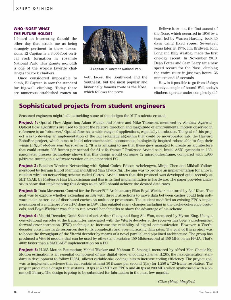
WHO ‘NOSE’ WHAT THE FUTURE HOLDS?I heard an interesting factoid theother day that struck me as beingstrangely pertinent to these discus-sions. El Capitan is a 3,000-foot verti-cal rock formation in YosemiteNational Park. This granite monolithis one of the world’s favorite chal-lenges for rock climbers.
Once considered impossible toclimb, El Capitan is now the standardfor big-wall climbing. Today there are numerous established routes on
both faces, the Southwest and theSoutheast, but the most popular andhistorically famous route is the Nose,which follows the prow.
Believe it or not, the first ascent ofthe Nose, which occurred in 1958 by ateam led by Warren Harding, took 45days using fixed ropes. Seventeenyears later, in 1975, Jim Bridwell, JohnLong and Billy Westbay made the firstone-day ascent. In November 2010,Dean Potter and Sean Leary set a newspeed record for the Nose, climbingthe entire route in just two hours, 36minutes and 45 seconds.
How is it possible to go from 45 daysto only a couple of hours? Well, today’sclimbers operate under completely dif-
20 Xcell Journal Third Quarter 2011
X P E R T O P I N I O N
Sophisticated projects from student engineersSeasoned engineers might balk at tackling some of the designs the MIT students created.
Project 1: Optical Flow Algorithm; Adam Wahab, Jud Porter and Mike Thomson, mentored by Abhinav Agarwal.Optical flow algorithms are used to detect the relative direction and magnitude of environmental motion observed inreference to an “observer.” Optical flow has a wide range of applications, especially in robotics. The goal of this proj-ect was to develop an implementation of the Lucas-Kanade algorithm that could be incorporated into the HarvardRoboBee project, which aims to build micromechanical, autonomous, biologically inspired robots able to flap theirwings (http://robobees.seas.harvard.edu). “It was amazing to me that these guys managed to create an architecturethat could sustain 205 frames per second for 64 x 64 frames,” Professor Arvind said. Initial ASIC synthesis in 130-nanometer process technology shows that this design would consume 42 microjoules/frame, compared with 1,960µJ/frame running in a software version on an embedded PC.
Project 2: Rateless Wireless Networking with Spinal Codes; Edison Achelengwa, Minjie Chen and Mikhail Volkov,mentored by Kermin Elliott Fleming and Alfred Man Cheuk Ng. The aim was to provide an implementation for a novelrateless wireless networking scheme called Cortex. Arvind notes that this protocol was developed quite recently atMIT CSAIL by Professor Hari Balakrishnan and this is its first implementation in hardware. The paper provides analy-sis to show that implementing this design as an ASIC should achieve the desired data rates.
Project 3: Data Movement Control for the PowerPC® Architecture; Silas Boyd-Wickizer, mentored by Asif Khan. Thegoal was to explore whether extending an ISA with three instructions to move data between caches could help soft-ware make better use of distributed caches on multicore processors. The student modified an existing FPGA imple-mentation of a multicore PowerPC done in BSV. This entailed many changes including in the cache-coherence proto-cols, and Boyd-Wickizer was able to run several benchmarks to show the advantage of his scheme.
Project 4: Viterbi Decoder; Omid Salehi-Abari, Arthur Chang and Sung Sik Woo, mentored by Myron King. Using aconvolutional encoder at the transmitter associated with the Viterbi decoder at the receiver has been a predominantforward-error-correction (FEC) technique to increase the reliability of digital communication. However, a Viterbidecoder consumes large resources due to its complexity and ever-increasing data rates. The goal of this project wasto boost the throughput of the Viterbi decoder by means of a novel parallel and pipelined architecture. The group hasproduced a Viterbi module that can be used by others and sustains 150 Mbits/second at 150 MHz on an FPGA. That’s400x faster than a MATLAB® implementation on a PC.
Project 5: H.265 Motion Estimation; Mehul Tikekar and Mahmut E. Sinangil, mentored by Alfred Man Cheuk Ng.Motion estimation is an essential component of any digital video encoding scheme. H.265, the next-generation stan-dard in development to follow H.264, allows variable-size coding units to increase coding efficiency. The project goalwas to implement a scheme that can sustain at least 30 frames per second (fps) for 1,280 x 720-frame resolution. Theproject produced a design that sustains 10 fps at 50 MHz on FPGA and 40 fps at 200 MHz when synthesized with a 65-nm cell library. The design is going to be submitted for fabrication in the next few months.
– Clive (Max) Maxfield
El Capitan in Yosemite National Park
ferent assumptions to the earlyclimbers and use a completely differentapproach. They carry no packs or shirtsor food or water. All they take betweenthem—in addition to minimalistichomemade climbing harnesses—is asingle 200-foot length of 9mm rope, afew carabiners and a handful of spring-loaded camming devices.
If you start with the idea that you’regoing to have to camp out to climb themountain, you are going to have tocarry a lot more gear, which will slowyou down and take longer. But whathappens if you change your initialassumptions? If you plan to climb themountain in less than a day you cancut down on the amount of gear youhave to carry. If you plan on climbing itin a couple of hours you can also dis-pense with food and water.
In much the same way, chip designteams typically start with their ownset of assumptions. They assume thatlearning a new approach comes at acost. They assume that incrementalchange is all that’s possible. Theyassume they have to painstakinglyplan out the microarchitecture with(overly) detailed specifications. Andthey assume that they have only oneshot at the architecture.
The experience of MIT’s 6.375Digital Design course is turningthese assumptions on their head.With the right approach—using mod-ern design tools and developmentplatforms—it is possible for the stu-dents (and real-world designers) toquickly express and evaluate alterna-tive architectures so as to come upwith optimal implementations.
About the Author
Clive “Max” Maxfield is
president of Maxfield
High-Tech Consulting
and editor of the EETimes Programmable
Logic DesignLine.
After receiving his BSc in control engi-
neering in 1980 from Sheffield Hallam
University, Sheffield, England, Max began
his career as a designer of central process-
ing units for mainframe computers.
Over the years, he has designed and
built all sorts of interesting “stuff,” from
silicon chips to circuit boards and brain-
wave amplifiers to Steampunk “Display-
O-Meters.” Max has also been at the fore-
front of electronic design automation
(EDA) for more than 20 years.
Max is the author and co-author of a
number of books, including Bebop to theBoolean Boogie (An Unconventional Guideto Electronics), FPGAs: Instant Access and
How Computers Do Math.
Third Quarter 2011 Xcell Journal 21
X P E R T O P I N I O N
Versatile FPGA Platform
www.techway.eu
The Versatile FPGA Platform provides a cost-effective
way of undertaking intensive calculations
and high speedcommunications in an
industrial environment.
PCI Express 4x Short CardXilinx Virtex FamiliesI/0 enabled through an FMC site (VITA 57)Development kit and drivers optimized for Windows and Linux
Optical-Mez

22 Xcell Journal Third Quarter 2011
Bottling a StarUsing ARM’s AXI4in an FPGA
XCELLENCE IN SCIENTIFIC APPLICATIONS
by Billy HuangPhD ResearcherDurham University / [email protected]
Dr. Roddy VannAssistant ProfessorUniversity of [email protected]
Dr. Graham NaylorHead of MAST Plasma Diagnostics and Control Culham Centre for Fusion Energy (CCFE)[email protected]
Dr. Vladimir ShevchenkoSenior PhysicistCulham Centre for Fusion Energy (CCFE)[email protected]
Simon FreethyPhD ResearcherUniversity of York / [email protected]
FThird Quarter 2011 Xcell Journal 23
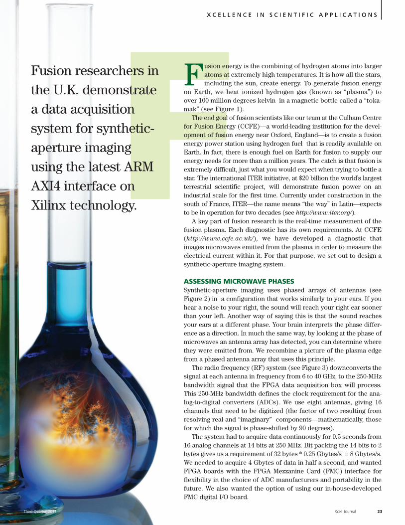
Fusion energy is the combining of hydrogen atoms into largeratoms at extremely high temperatures. It is how all the stars,including the sun, create energy. To generate fusion energy
on Earth, we heat ionized hydrogen gas (known as “plasma”) toover 100 million degrees kelvin in a magnetic bottle called a “toka-mak” (see Figure 1).
The end goal of fusion scientists like our team at the Culham Centrefor Fusion Energy (CCFE)—a world-leading institution for the devel-opment of fusion energy near Oxford, England—is to create a fusionenergy power station using hydrogen fuel that is readily available onEarth. In fact, there is enough fuel on Earth for fusion to supply ourenergy needs for more than a million years. The catch is that fusion isextremely difficult, just what you would expect when trying to bottle astar. The international ITER initiative, at $20 billion the world’s largestterrestrial scientific project, will demonstrate fusion power on anindustrial scale for the first time. Currently under construction in thesouth of France, ITER—the name means “the way” in Latin—expectsto be in operation for two decades (see http://www.iter.org/).
A key part of fusion research is the real-time measurement of thefusion plasma. Each diagnostic has its own requirements. At CCFE(http://www.ccfe.ac.uk/), we have developed a diagnostic thatimages microwaves emitted from the plasma in order to measure theelectrical current within it. For that purpose, we set out to design asynthetic-aperture imaging system.
ASSESSING MICROWAVE PHASESSynthetic-aperture imaging uses phased arrays of antennas (seeFigure 2) in a configuration that works similarly to your ears. If youhear a noise to your right, the sound will reach your right ear soonerthan your left. Another way of saying this is that the sound reachesyour ears at a different phase. Your brain interprets the phase differ-ence as a direction. In much the same way, by looking at the phase ofmicrowaves an antenna array has detected, you can determine wherethey were emitted from. We recombine a picture of the plasma edgefrom a phased antenna array that uses this principle.
The radio frequency (RF) system (see Figure 3) downconverts thesignal at each antenna in frequency from 6 to 40 GHz, to the 250-MHzbandwidth signal that the FPGA data acquisition box will process.This 250-MHz bandwidth defines the clock requirement for the ana-log-to-digital converters (ADCs). We use eight antennas, giving 16channels that need to be digitized (the factor of two resulting fromresolving real and “imaginary” components—mathematically, thosefor which the signal is phase-shifted by 90 degrees).
The system had to acquire data continuously for 0.5 seconds from16 analog channels at 14 bits at 250 MHz. Bit packing the 14 bits to 2bytes gives us a requirement of 32 bytes * 0.25 Gbytes/s = 8 Gbytes/s.We needed to acquire 4 Gbytes of data in half a second, and wantedFPGA boards with the FPGA Mezzanine Card (FMC) interface forflexibility in the choice of ADC manufacturers and portability in thefuture. We also wanted the option of using our in-house-developedFMC digital I/O board.
Fusion researchers inthe U.K. demonstratea data acquisitionsystem for synthetic-aperture imagingusing the latest ARMAXI4 interface onXilinx technology.
X C E L L E N C E I N S C I E N T I F I C A P P L I C A T I O N S
We decided during the summer of2010 that an ideal solution would usetwo Xilinx® Virtex®-6 LX240T ML605boards combined with two FMC108(eight-channel) ADC boards from 4DSP.At that time, 8 Gbytes/s was a giganticdata rate; in fact, it still is. We couldhave taken the approach of divide andconquer by using more FPGA boardsand having fewer channels on each.However, that would have increasedthe cost and size of the system.
In fact, the technology to make thisaspect of our design happen arrivedaround January 2011, when Xilinxreleased a revision of its ISE® designsoftware supporting ARM’s AMBA®
AXI4 interface protocol. Before thisthe hardware existed, but not themeans to exploit it to its full potential.
LIFE BEFORE AXI4For our system needs, the DDR3SDRAM memory must be accessible tothe MicroBlaze™ processor that resideson the Virtex-6, so that Linux can alsohave access to the real-time data we arecapturing. This requirement constrainsus to using a memory controller jointlyaccessible to the MicroBlaze bus andour real-time streaming IP. Initially wetried using the PLB bus, but found thatlimitations in the PLB-based memorycontroller meant we could not connecta 64-bit-wide interface at our requiredfrequency. Instead, only 32 bits wereavailable. We learned this the hard way,after writing a core that communicatedvia the low-level NPI protocol directlyto the memory controller, but couldachieve only 2 Gbytes/s. Even thoughthis was still an impressive rate andsmashed any speed records we couldfind, it still was not enough.
Thankfully, Xilinx then pushed outthe AXI4 interconnect and memorycontroller, giving full access to thewhole 64 bits at 400 MHz double datarate (800 million transactions per sec-ond). That effectively gave a through-put of 6.4 Gbytes/s—a truly blisteringspeed that exceeded our requirementof 4 Gbytes/s on each board. This wasexactly what we needed.
We actually found two ways toachieve this speed: one is a modifica-tion of the axi_v6_ddrx memory con-troller (hidden under the AXI intercon-nect layer), and the other is an AXIMaster PCore made in SystemGenerator. The PCore can attach to theMicroBlaze system in Xilinx PlatformStudio (XPS) as an AXI External Master.
Both solutions stream data into theDDR3 memory at 5 Gbytes/s. AXI iseasy to program, and allows very highmemory speeds with separate readand write channels. The XPS tool givesa lot of flexibility for AXI design. Weused that flexibility to our advantage,
such as choosing only a write channel ifthat was what we needed, thereby sim-plifying the logic design and freeingmore resources.
A SOFT-PROCESSOR INTERFACEA unique capability of the Xilinx tool setis the soft processor known as theMicroBlaze. It is “soft” in that it isenabled using FPGA logic. This proces-sor is well-supported in the mainbranch of the Linux kernel thanks tothe efforts of Xilinx and its partners. Weare encouraged by these efforts and areworking to extend the development inthe Linux community.
This capability has meant that wecan have a PC-like interface to theFPGA system. This is invaluable as itenables, for example, Web and SSHservers on the FPGA. We are able tomount the System ACE™ flash underLinux (when formatted as typemsdos), which allows us to updatethe firmware remotely.
NETWORK STREAMINGGiven that we could acquire 2 Gbyteson each FPGA board in half a second,the question we found ourselves facingwas how to get this data off the boardover a standard interface in a reason-able amount of time? Typical networkspeeds using the MicroBlaze processorover Gigabit Ethernet under Linux anda simple protocol such as UDP provedtoo slow, achieving only around 0.5Mbyte/s. At that rate we would have towait over an hour to download data thathad taken only half a second to acquire!
Clearly, we needed to go to a lowerlevel in the design. Our solution tookthe form of a homegrown protocol wehave dubbed FireStark, a UDP-basedprotocol that sits inside the AXIEthernet DMA driver. By modifying theMicroBlaze Linux kernel drivers andhaving the FPGAs on a dedicated pri-vate network, we are now able to down-load the entire 2 Gbytes in under 60 sec-onds, a factor-of-70 speed-up. Testingwith jumbo frames of sizes up to 6kbytes has doubled this speed—that is,
24 Xcell Journal Third Quarter 2011
X C E L L E N C E I N S C I E N T I F I C A P P L I C A T I O N S
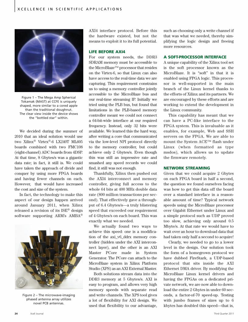
Figure 1 – The Mega Amp SphericalTokamak (MAST) at CCFE is uniquely
shaped, more similar to a cored apple than the traditional doughnut.
The clear view inside the device shows the “bottled star” within.
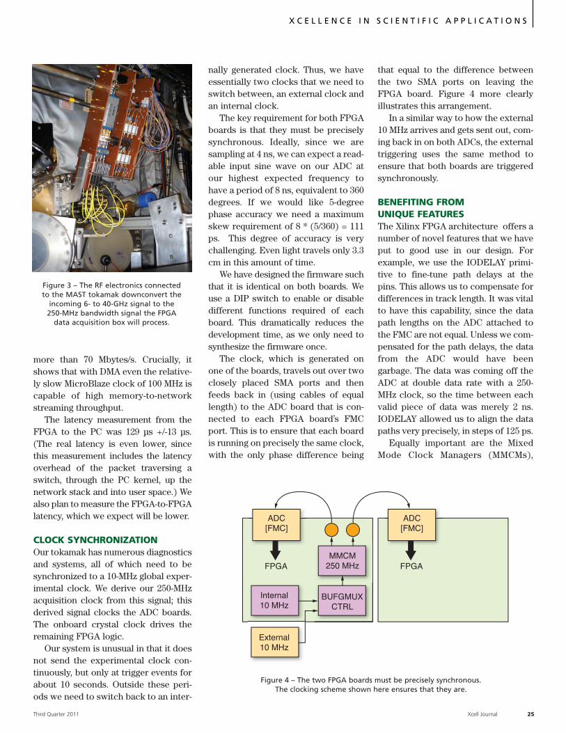
Figure 2 – The microwave-imaging phased antenna array utilizes
novel PCB antennas.
more than 70 Mbytes/s. Crucially, itshows that with DMA even the relative-ly slow MicroBlaze clock of 100 MHz iscapable of high memory-to-networkstreaming throughput.
The latency measurement from theFPGA to the PC was 129 µs +/-13 µs.(The real latency is even lower, sincethis measurement includes the latencyoverhead of the packet traversing aswitch, through the PC kernel, up thenetwork stack and into user space.) Wealso plan to measure the FPGA-to-FPGAlatency, which we expect will be lower.
CLOCK SYNCHRONIZATIONOur tokamak has numerous diagnosticsand systems, all of which need to besynchronized to a 10-MHz global exper-imental clock. We derive our 250-MHzacquisition clock from this signal; thisderived signal clocks the ADC boards.The onboard crystal clock drives theremaining FPGA logic.
Our system is unusual in that it doesnot send the experimental clock con-tinuously, but only at trigger events forabout 10 seconds. Outside these peri-ods we need to switch back to an inter-
nally generated clock. Thus, we haveessentially two clocks that we need toswitch between, an external clock andan internal clock.
The key requirement for both FPGAboards is that they must be preciselysynchronous. Ideally, since we aresampling at 4 ns, we can expect a read-able input sine wave on our ADC atour highest expected frequency tohave a period of 8 ns, equivalent to 360degrees. If we would like 5-degreephase accuracy we need a maximumskew requirement of 8 * (5/360) = 111ps. This degree of accuracy is verychallenging. Even light travels only 3.3cm in this amount of time.
We have designed the firmware suchthat it is identical on both boards. Weuse a DIP switch to enable or disabledifferent functions required of eachboard. This dramatically reduces thedevelopment time, as we only need tosynthesize the firmware once.
The clock, which is generated onone of the boards, travels out over twoclosely placed SMA ports and thenfeeds back in (using cables of equallength) to the ADC board that is con-nected to each FPGA board’s FMCport. This is to ensure that each boardis running on precisely the same clock,with the only phase difference being
that equal to the difference betweenthe two SMA ports on leaving theFPGA board. Figure 4 more clearlyillustrates this arrangement.
In a similar way to how the external10 MHz arrives and gets sent out, com-ing back in on both ADCs, the externaltriggering uses the same method toensure that both boards are triggeredsynchronously.
BENEFITING FROM UNIQUE FEATURESThe Xilinx FPGA architecture offers anumber of novel features that we haveput to good use in our design. Forexample, we use the IODELAY primi-tive to fine-tune path delays at thepins. This allows us to compensate fordifferences in track length. It was vitalto have this capability, since the datapath lengths on the ADC attached tothe FMC are not equal. Unless we com-pensated for the path delays, the datafrom the ADC would have beengarbage. The data was coming off theADC at double data rate with a 250-MHz clock, so the time between eachvalid piece of data was merely 2 ns.IODELAY allowed us to align the datapaths very precisely, in steps of 125 ps.
Equally important are the MixedMode Clock Managers (MMCMs),
Third Quarter 2011 Xcell Journal 25
X C E L L E N C E I N S C I E N T I F I C A P P L I C A T I O N S
Figure 3 – The RF electronics connected to the MAST tokamak downconvert the
incoming 6- to 40-GHz signal to the 250-MHz bandwidth signal the FPGA
data acquisition box will process.
FPGA
ADC[FMC]
FPGA
ADC[FMC]
MMCM250 MHz
BUFGMUXCTRL
Internal10 MHz
External10 MHz
Figure 4 – The two FPGA boards must be precisely synchronous. The clocking scheme shown here ensures that they are.
which perform clock managementtasks such as multiplication and phaseshifting. In cascaded mode wherebyone MMCM connects to another, wewere able to generate a wide range ofclocks from the original 10 MHz. Thisincludes the 250-MHz ADC samplingclock, as well as additional clocks thatwe used for other purposes.
We likewise made good use of theBUFGMUX_CTRL and IDDR primi-tives. Since our system switchedbetween internal and external 10-MHzclocks, it is crucial that switchingbetween the two be glitch-free. TheBUFGMUX_CTRL primitive allowedus to make sure it was. You can alsouse this primitive for standard logicsuch as triggers (not only for clock-ing); however, you need to ensure thatthe attributes IGNORE0, IGNORE1 areset to 1 to bypass the deglitching cir-cuitry, which would otherwise notallow the logic to pass through.
The ADC, meanwhile, provides datain a DDR format; that is, the data is
valid on both the rising and fallingclock edges. To recover this data intosingle data rate (SDR), we use theIDDR primitive, which is hardwired onthe I/O pads. This has a single data pininput, and two data pin outputs. Weused the SAME_EDGE_PIPELINEDattribute, which ensured the data wasvalid on both pins at the same time,thus reducing other logic. This doescome at the cost of an additional cycleof latency, but for us the latency didnot matter.
Another feature of the Xilinxarchitecture that helped in ourdesign was the FPGA MezzanineConnector (FMC). Strictly speakingthis is not a unique feature of anFPGA, but of an FPGA board. Evenso, it has proven very useful and hasworked well with the Virtex-6. FMCconnectors include high-frequencyclock pins, which are wired to clock-capable pins on the Virtex-6 on theML605 board. As such, it is possibleto send a clock via the FMC and into
the FPGA. This is advantageous sinceit means that we need only one entrypoint for the clock.
USING THE XILINX TOOL SUITEXilinx provides a number of tools to aidin the development of an FPGA system.We used a good number of them.
We used Project Navigator for man-ually coding VHDL and Verilog code.Additionally there is a graphical inter-face whereby you can make a“schematic” that allows the creation oflogic visually. However, we foundProject Navigator to be a low-level toolin that while we could operate easilyon flip-flops (single bits), expanding tooperations on larger bit numbers wasmore complicated. We found ProjectNavigator most useful for low-levelclock design. It enabled us to have pre-cise control over which clock was driv-ing specific logic.
For high-level logic design, weturned to System Generator. It is partic-ularly suited to designs where logic isdriven by a single clock frequency(although isn’t restricted to this case).System Generator is simple to use andhas access to large range of IP, such asFFTs, divide generators and filters, toname a few. Additionally, you can tielogic easily into the MicroBlaze proces-sor as read/write registers and sharedmemory. The tool automatically createsa peripheral core (PCore) and adds itinto your XPS project.
We used CORE Generator™ for fine-tuning the parameters of the ADC FIFO.This FIFO had to be 256 bits wide with awrite clock of 125 MHz and a read clockof 200 MHz. We imported the resultinggenerated NGC file into XPS as a PCore.We did this manually by creating the nec-essary .mpd, .pao and .bbd files.
The Impact tool helped us to programthe FPGA, and also to generate theSystemACE™ file for permanently plac-ing the firmware onto the CompactFlash.The CompactFlash worked very reliably,however it should be noted that thisadded an extra requirement (see underSDK, below) to our system.
26 Xcell Journal Third Quarter 2011
X C E L L E N C E I N S C I E N T I F I C A P P L I C A T I O N S
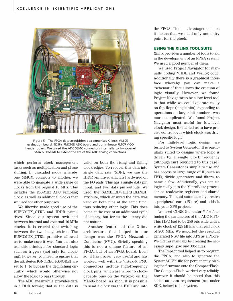
Figure 5 – The FPGA data acquisition box comprises Xilinx’s ML605 evaluation board, 4DSP’s FMC108 ADC board and our in-house FMC/PMOD
header board. We wired the ADC SSMC connectors internally to front-panel SMA bulkheads to extend the life of the ADC analog connections.
Since we wanted our system toinclude the MicroBlaze processor, weneeded the tool that creates the proces-sor system: Xilinx Platform Studio. XPSis a comprehensive tool suite thatallows you to build processor-centricsystems. It allows you to set up therequired links through a wizard. You canalso include IP from CORE Generatorby using the Create IP Wizard. It nowincludes the high-performance AXI4 on-chip interconnect.
Finally, we used the Xilinx SoftwareDevelopment Kit (SDK) to develop pro-grams that run on the processor. Infact, we have only one program to runinitially, and that is the SREC boot-loader. Due to the CompactFlash hav-ing a FAT file system, the librariesrequired to access the SREC program(also on the flash) inflated the size ofthe resulting executable. We reducedits size by turning off debugging, turn-ing on optimization and including “mb-
strip –g <elf_file_name>” as the post-compilation command. Even after allthese steps, the result was a large, 91-kbyte executable. Therefore, we had toincrease the internal BRAM so that wecould initialize the bitstream with thissize of executable.
One problem we faced was the largecompilation time with the Virtex-6. TheXilinx software PlanAhead™ can signifi-cantly help with this challenge. Weintend to utilize PlanAhead to its fullpotential to reduce the compilation time.
We are excited by the possibilitiesthat the new Zynq™-7000 extensibleprocessing platform will provide (seecover story, Xcell Journal Issue 75).However, it remains to be seen whetherZynq will make the MicroBlaze obsolete,or if the MicroBlaze will hold its ownthanks to its soft nature and the 10-plusyears of development effort behind it.Could a future cache-coherent multi-processor MicroBlaze system outper-
form the ARM® dual-core Cortex™-A9MPCore™? Could the Physical AddressExtension in the Zynq or MicroBlazelead to more powerful systems that pro-vide more than 32 bits of address space,thus allowing more than 4 Gbytes ofRAM? It will be interesting to watch andsee how time answers those questions.
A CUTTING-EDGE SYSTEMUltimately, we developed a fully func-tional data acquisition system (seeFigure 5) that is cutting edge in theworld of FPGAs, making use of thelatest Xilinx technology. It is capableof real-time acquisition at 10 Gbytes/s(or 80 Gbits/s). The end cost was lessthan $15,000. We have demonstratedtechnology that we hope will find itsway onto the largest fusion experi-ments in the world, such as the ITERproject (Figure 6).
Fusion energy is one of the biggesttechnological challenges ever attempt-ed. FPGAs are helping us to crack thistough nut in different ways by leverag-ing their unique advantages. Ourfusion research device, which incorpo-rates Virtex-6 FPGAs using the latestAXI4 interconnect and the Xilinx toolflow, achieves extremely high datarates on a small, compact system.
A new website (http://fusion.phys.
tue.nl/fpga/doku.php) promises to be ameeting place for people to communi-cate ideas and material for developingFPGA technology on fusion devices.
Acknowledgements
CCFE is associated with Durham
University’s Centre for Advanced
Instrumentation and the University
of York’s Plasma Institute.
This work was funded partly by EPSRC
under grant EP/H016732, by the
University of York, by the RCUK Energy
Programme under grant EP/I501045
and by the European Communities
under a contract of association between
EURATOM and CCFE.
The authors wish to thank John Linn,
open-source Linux engineer
at Xilinx, and the other Xilinx employ-
ees and Xilinx partners who have con-
tributed to Linux support for the
MicroBlaze processor.
Third Quarter 2011 Xcell Journal 27
X C E L L E N C E I N S C I E N T I F I C A P P L I C A T I O N S
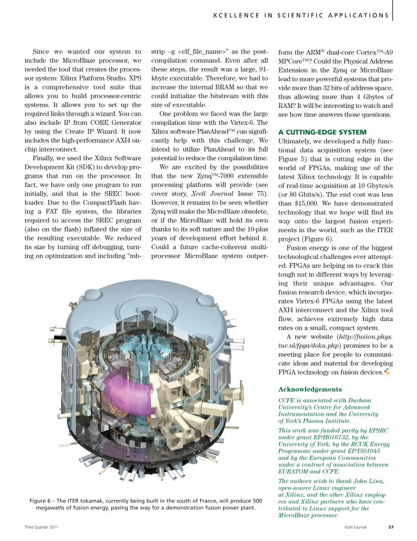
Figure 6 – The ITER tokamak, currently being built in the south of France, will produce 500megawatts of fusion energy, paving the way for a demonstration fusion power plant.

28 Xcell Journal Third Quarter 2011
FPGAs Drive Real-Time OpticalBiopsy System
FPGAs Drive Real-Time OpticalBiopsy System
XCELLENCE IN MEDICAL
by Jamie BrettleProduct Manager for Embedded SoftwareNational [email protected]
Third Quarter 2011 Xcell Journal 29
Thanks to the availability ofever-increasing processingpower, scientists in the field of
medical-device research are rapidlyfinding innovative ways to more effec-tively treat patients suffering from avariety of ailments. Commercial off-the-shelf (COTS) hardware coupledwith FPGA technologies and flexibleintegration platforms help theseresearchers to develop prototypeimaging systems more quickly, whilecontinuing to deliver new productsto the market.
Among them are researchers atKitasato University in Japan, whorecently set out to create an instru-ment that can detect cancer duringmedical screenings using a method-ology that would not require thepatient to undergo the stress of abiopsy. The data acquisition systemthey developed utilizes opticalcoherence tomography (OCT) to cre-ate real-time 3D imaging.
OCT is a noninvasive imaging tech-nique that provides subsurface, cross-sectional images. The medical com-munity has a keen interest in OCTbecause it provides much greater res-olution than other imaging technolo-gies such as magnetic resonanceimaging (MRI) or positron emissiontomography (PET). Additionally, themethod does not require muchpreparation and is extremely safefor the patient, because it uses lowlaser outputs and does not requireionizing radiation.
STATEMENT OF THE PROBLEMOCT uses a low-power light sourceand the corresponding light reflec-tions to create images—a methodsimilar to ultrasound, but it measureslight instead of sound. When the lightbeam is projected into a sample,much of the light scatters, but a smallamount reflects as a collimated beam,which the system can detect and useto create an image.
This methodology presents apromising diagnostic tool for opticalbiopsies, useful in many medicalexaminations and of particular inter-est in oncology. In most OCT applica-tions, high-speed imaging is crucialfor rapid inspection and for imagequality without motion artifacts. Forexample, to inspect the human eye,which can be held relatively motion-less using a chin rest, an A-scan ultra-sound is necessary to eliminate allmotion artifacts. However, wheninspecting the digestive or respirato-ry systems, the tissue being imagedcannot be fixed in place, making anultrahigh-speed OCT methodologynecessary to eliminate motion arti-facts of the tissue.
When performing a noninvasive,real-time optical biopsy, the imagingspeed must be fast enough to displaythe 3D image for immediate diagno-sis, just like a conventional endo-scope. A few previous methods havebeen proposed for ultrahigh-speedOCT, but none have succeeded in thereal-time display of 3D OCT movies.
INITIAL PROTOTYPEInitially, the Kitasato University teamdeveloped a first-generation systemaround 32 National Instruments (NI)high-density eight-channel digitizers.The key element of the OCT methodwas using optical demultiplexers toseparate 256 narrow spectral bandsfrom a broadband incident-lightsource. This allowed simultaneous,parallel detection of an interferencefringe signal (a critical requirementfor OCT imaging) at all wavelengths inthe measured spectrum. The systemcaptured all 256 spectral bands simul-taneously at 60 Msamples/second,using the digitizer’s onboard memory,and then transferred the data to a PCfor processing and visualization.
While it was possible to capture vol-umetric OCT videos with the system,the massive amount of data acquiredby all channels simultaneously madethe onboard memory of the digitizersthe limiting factor. Overall, the design-ers restricted the duration of an OCTvideo to about 2.5 seconds. After trans-ferring the data to the PC, they stillrequired about three hours to fullyprocess and render the 3D video data.
Performing a real-time optical biop-sy (a primary goal for endoscopic OCT)was not possible with this system. Theteam vowed to create a new prototypewith an upgraded data acquisition sub-system and enough performance tomake real-time processing possible.
HIGH-LEVEL ARCHITECTURE OFTHE SYSTEM DESCRIPTIONThe new system uses a broadbandsuperluminescent diode as the lightsource, combined with a filter thatselects the wavelength range to matchthe optical demultiplexers. A semi-conductor optical amplifier amplifiesthe output light from the diode, whilea collimator lens and an objective lensdirect the light. A resonant scannerand a galvano mirror scan the lightbeam. The system collects back-scat-
Researchers in Japan are using the Virtex-5 and National Instruments LabVIEW to developnext-generation 3D OCT imaging.
X C E L L E N C E I N M E D I C A L
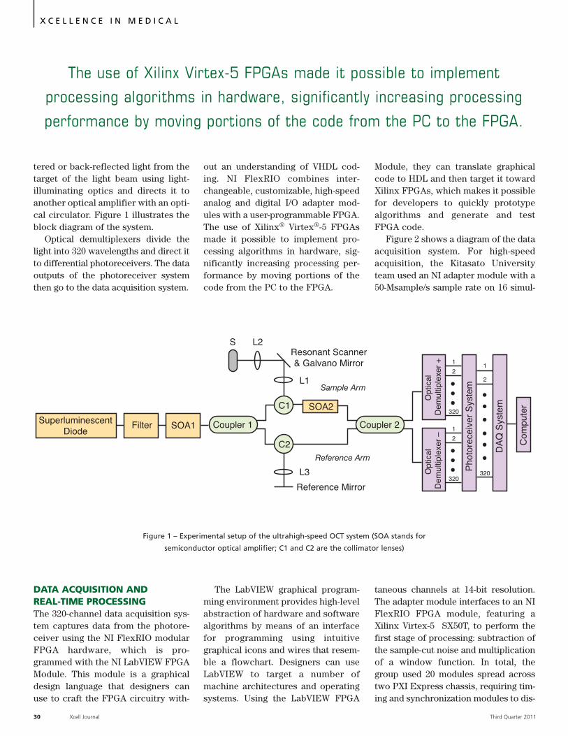
tered or back-reflected light from thetarget of the light beam using light-illuminating optics and directs it toanother optical amplifier with an opti-cal circulator. Figure 1 illustrates theblock diagram of the system.
Optical demultiplexers divide thelight into 320 wavelengths and direct itto differential photoreceivers. The dataoutputs of the photoreceiver systemthen go to the data acquisition system.
DATA ACQUISITION AND REAL-TIME PROCESSINGThe 320-channel data acquisition sys-tem captures data from the photore-ceiver using the NI FlexRIO modularFPGA hardware, which is pro-grammed with the NI LabVIEW FPGAModule. This module is a graphicaldesign language that designers canuse to craft the FPGA circuitry with-
out an understanding of VHDL cod-ing. NI FlexRIO combines inter-changeable, customizable, high-speedanalog and digital I/O adapter mod-ules with a user-programmable FPGA.The use of Xilinx® Virtex®-5 FPGAsmade it possible to implement pro-cessing algorithms in hardware, sig-nificantly increasing processing per-formance by moving portions of thecode from the PC to the FPGA.
The LabVIEW graphical program-ming environment provides high-levelabstraction of hardware and softwarealgorithms by means of an interfacefor programming using intuitivegraphical icons and wires that resem-ble a flowchart. Designers can useLabVIEW to target a number ofmachine architectures and operatingsystems. Using the LabVIEW FPGA
Module, they can translate graphicalcode to HDL and then target it towardXilinx FPGAs, which makes it possiblefor developers to quickly prototypealgorithms and generate and testFPGA code.
Figure 2 shows a diagram of the dataacquisition system. For high-speedacquisition, the Kitasato Universityteam used an NI adapter module with a50-Msample/s sample rate on 16 simul-
taneous channels at 14-bit resolution.The adapter module interfaces to an NIFlexRIO FPGA module, featuring aXilinx Virtex-5 SX50T, to perform thefirst stage of processing: subtraction ofthe sample-cut noise and multiplicationof a window function. In total, thegroup used 20 modules spread acrosstwo PXI Express chassis, requiring tim-ing and synchronization modules to dis-
30 Xcell Journal Third Quarter 2011
X C E L L E N C E I N M E D I C A L
SuperluminescentDiode
Filter SOA1 Coupler 1 Coupler 2
C1
C2
S L2
L1
L3
Reference Mirror
Resonant Scanner& Galvano Mirror
SOA2
Opt
ical
D
emul
tiple
xer
+O
ptic
al
Dem
ultip
lexe
r –
Pho
tore
ceiv
er S
yste
m
DA
Q S
yste
m
Com
pute
r
1
2
320
1
2
320
1
2
320
Sample Arm
Reference Arm
Figure 1 – Experimental setup of the ultrahigh-speed OCT system (SOA stands for
semiconductor optical amplifier; C1 and C2 are the collimator lenses)
The use of Xilinx Virtex-5 FPGAs made it possible to implement
processing algorithms in hardware, significantly increasing processing
performance by moving portions of the code from the PC to the FPGA.
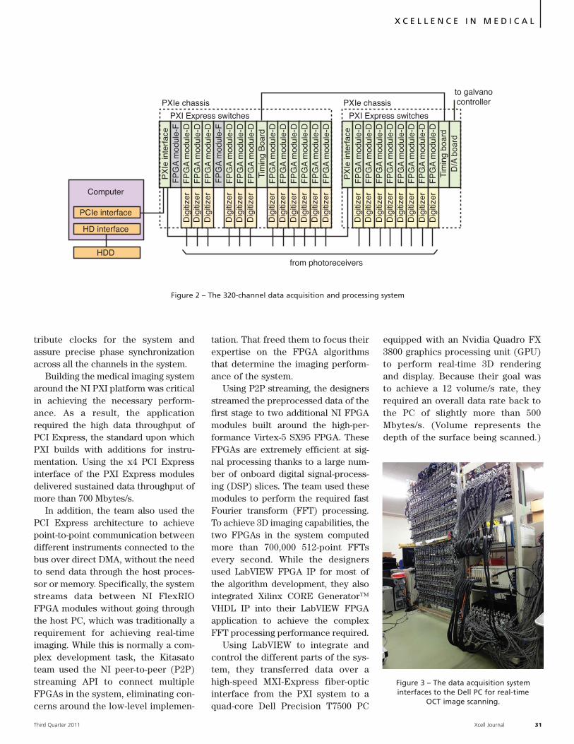
tribute clocks for the system andassure precise phase synchronizationacross all the channels in the system.
Building the medical imaging systemaround the NI PXI platform was criticalin achieving the necessary perform-ance. As a result, the applicationrequired the high data throughput ofPCI Express, the standard upon whichPXI builds with additions for instru-mentation. Using the x4 PCI Expressinterface of the PXI Express modulesdelivered sustained data throughput ofmore than 700 Mbytes/s.
In addition, the team also used thePCI Express architecture to achievepoint-to-point communication betweendifferent instruments connected to thebus over direct DMA, without the needto send data through the host proces-sor or memory. Specifically, the systemstreams data between NI FlexRIOFPGA modules without going throughthe host PC, which was traditionally arequirement for achieving real-timeimaging. While this is normally a com-plex development task, the Kitasatoteam used the NI peer-to-peer (P2P)streaming API to connect multipleFPGAs in the system, eliminating con-cerns around the low-level implemen-
tation. That freed them to focus theirexpertise on the FPGA algorithmsthat determine the imaging perform-ance of the system.
Using P2P streaming, the designersstreamed the preprocessed data of thefirst stage to two additional NI FPGAmodules built around the high-per-formance Virtex-5 SX95 FPGA. TheseFPGAs are extremely efficient at sig-nal processing thanks to a large num-ber of onboard digital signal-process-ing (DSP) slices. The team used thesemodules to perform the required fastFourier transform (FFT) processing.To achieve 3D imaging capabilities, thetwo FPGAs in the system computedmore than 700,000 512-point FFTsevery second. While the designersused LabVIEW FPGA IP for most ofthe algorithm development, they alsointegrated Xilinx CORE Generator™VHDL IP into their LabVIEW FPGAapplication to achieve the complexFFT processing performance required.
Using LabVIEW to integrate andcontrol the different parts of the sys-tem, they transferred data over ahigh-speed MXI-Express fiber-opticinterface from the PXI system to aquad-core Dell Precision T7500 PC
equipped with an Nvidia Quadro FX3800 graphics processing unit (GPU)to perform real-time 3D renderingand display. Because their goal wasto achieve a 12 volume/s rate, theyrequired an overall data rate back tothe PC of slightly more than 500Mbytes/s. (Volume represents thedepth of the surface being scanned.)
Third Quarter 2011 Xcell Journal 31
X C E L L E N C E I N M E D I C A L
PX
Ie in
terf
ace
Computer
PCIe interface
HD interface
HDD
PX
Ie in
terf
ace
FP
GA
mod
ule-
FF
PG
A m
odul
e-D
Dig
itize
rD
igiti
zer
Dig
itize
r
Dig
itize
rD
igiti
zer
Dig
itize
r
Dig
itize
rD
igiti
zer
Dig
itize
rD
igiti
zer
Dig
itize
rD
igiti
zer
Dig
itize
rD
igiti
zer
Dig
itize
rD
igiti
zer
Dig
itize
rD
igiti
zer
Dig
itize
rD
igiti
zer
FP
GA
mod
ule-
DF
PG
A m
odul
e-D
FP
GA
mod
ule-
FF
PG
A m
odul
e-D
FP
GA
mod
ule-
DF
PG
A m
odul
e-D
FP
GA
mod
ule-
DF
PG
A m
odul
e-D
FP
GA
mod
ule-
DF
PG
A m
odul
e-D
FP
GA
mod
ule-
D
FP
GA
mod
ule-
DF
PG
A m
odul
e-D
FP
GA
mod
ule-
DF
PG
A m
odul
e-D
FP
GA
mod
ule-
DF
PG
A m
odul
e-D
FP
GA
mod
ule-
DF
PG
A m
odul
e-D
Tim
ing
boar
dD
/A b
oard
FP
GA
mod
ule-
D
Tim
ing
Boa
rd
PXIe chassis
PXI Express switches
from photoreceivers
PXIe chassisto galvanocontroller
PXI Express switches
Figure 2 – The 320-channel data acquisition and processing system
Figure 3 – The data acquisition system interfaces to the Dell PC for real-time
OCT image scanning.
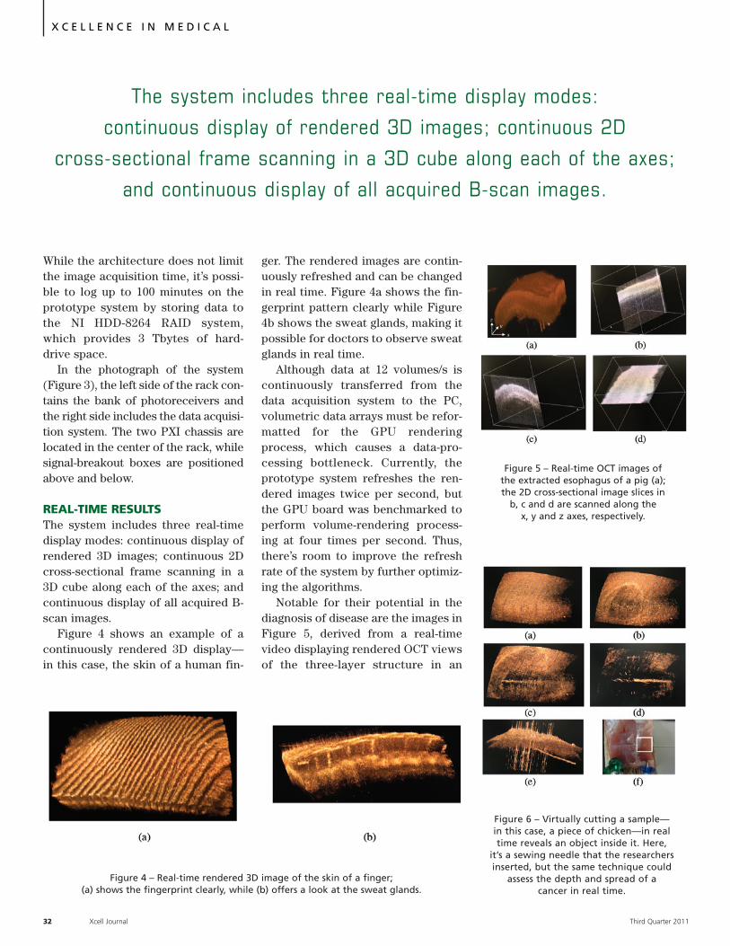
While the architecture does not limitthe image acquisition time, it’s possi-ble to log up to 100 minutes on theprototype system by storing data tothe NI HDD-8264 RAID system,which provides 3 Tbytes of hard-drive space.
In the photograph of the system(Figure 3), the left side of the rack con-tains the bank of photoreceivers andthe right side includes the data acquisi-tion system. The two PXI chassis arelocated in the center of the rack, whilesignal-breakout boxes are positionedabove and below.
REAL-TIME RESULTSThe system includes three real-timedisplay modes: continuous display ofrendered 3D images; continuous 2Dcross-sectional frame scanning in a3D cube along each of the axes; andcontinuous display of all acquired B-scan images.
Figure 4 shows an example of acontinuously rendered 3D display—in this case, the skin of a human fin-
ger. The rendered images are contin-uously refreshed and can be changedin real time. Figure 4a shows the fin-gerprint pattern clearly while Figure4b shows the sweat glands, making itpossible for doctors to observe sweatglands in real time.
Although data at 12 volumes/s iscontinuously transferred from thedata acquisition system to the PC,volumetric data arrays must be refor-matted for the GPU renderingprocess, which causes a data-pro-cessing bottleneck. Currently, theprototype system refreshes the ren-dered images twice per second, butthe GPU board was benchmarked toperform volume-rendering process-ing at four times per second. Thus,there’s room to improve the refreshrate of the system by further optimiz-ing the algorithms.
Notable for their potential in thediagnosis of disease are the images inFigure 5, derived from a real-timevideo displaying rendered OCT viewsof the three-layer structure in an
32 Xcell Journal Third Quarter 2011
X C E L L E N C E I N M E D I C A L
Figure 4 – Real-time rendered 3D image of the skin of a finger; (a) shows the fingerprint clearly, while (b) offers a look at the sweat glands.
Figure 5 – Real-time OCT images of the extracted esophagus of a pig (a); the 2D cross-sectional image slices in
b, c and d are scanned along the x, y and z axes, respectively.
Figure 6 – Virtually cutting a sample—in this case, a piece of chicken—in real time reveals an object inside it. Here,
it’s a sewing needle that the researchersinserted, but the same technique could
assess the depth and spread of a cancer in real time.
The system includes three real-time display modes:
continuous display of rendered 3D images; continuous 2D
cross-sectional frame scanning in a 3D cube along each of the axes;
and continuous display of all acquired B-scan images.
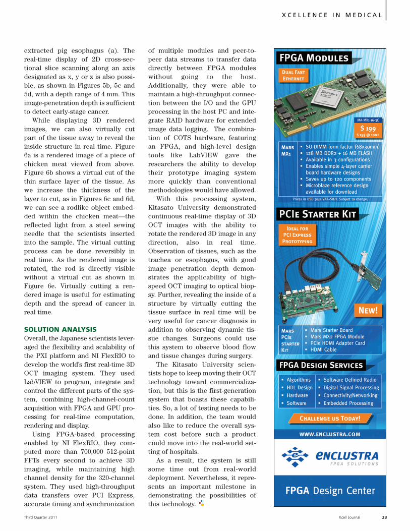
extracted pig esophagus (a). Thereal-time display of 2D cross-sec-tional slice scanning along an axisdesignated as x, y or z is also possi-ble, as shown in Figures 5b, 5c and5d, with a depth range of 4 mm. Thisimage-penetration depth is sufficientto detect early-stage cancer.
While displaying 3D renderedimages, we can also virtually cutpart of the tissue away to reveal theinside structure in real time. Figure6a is a rendered image of a piece ofchicken meat viewed from above.Figure 6b shows a virtual cut of thethin surface layer of the tissue. Aswe increase the thickness of thelayer to cut, as in Figures 6c and 6d,we can see a rodlike object embed-ded within the chicken meat—thereflected light from a steel sewingneedle that the scientists insertedinto the sample. The virtual cuttingprocess can be done reversibly inreal time. As the rendered image isrotated, the rod is directly visiblewithout a virtual cut as shown inFigure 6e. Virtually cutting a ren-dered image is useful for estimatingdepth and the spread of cancer inreal time.
SOLUTION ANALYSISOverall, the Japanese scientists lever-aged the flexibility and scalability ofthe PXI platform and NI FlexRIO todevelop the world’s first real-time 3DOCT imaging system. They usedLabVIEW to program, integrate andcontrol the different parts of the sys-tem, combining high-channel-countacquisition with FPGA and GPU pro-cessing for real-time computation,rendering and display.
Using FPGA-based processingenabled by NI FlexRIO, they com-puted more than 700,000 512-pointFFTs every second to achieve 3Dimaging, while maintaining highchannel density for the 320-channelsystem. They used high-throughputdata transfers over PCI Express,accurate timing and synchronization
of multiple modules and peer-to-peer data streams to transfer datadirectly between FPGA moduleswithout going to the host.Additionally, they were able tomaintain a high-throughput connec-tion between the I/O and the GPUprocessing in the host PC and inte-grate RAID hardware for extendedimage data logging. The combina-tion of COTS hardware, featuringan FPGA, and high-level designtools like LabVIEW gave theresearchers the ability to developtheir prototype imaging systemmore quickly than conventionalmethodologies would have allowed.
With this processing system,Kitasato University demonstratedcontinuous real-time display of 3DOCT images with the ability torotate the rendered 3D image in anydirection, also in real time.Observation of tissues, such as thetrachea or esophagus, with goodimage penetration depth demon-strates the applicability of high-speed OCT imaging to optical biop-sy. Further, revealing the inside of astructure by virtually cutting thetissue surface in real time will bevery useful for cancer diagnosis inaddition to observing dynamic tis-sue changes. Surgeons could usethis system to observe blood flowand tissue changes during surgery.
The Kitasato University scien-tists hope to keep moving their OCTtechnology toward commercializa-tion, but this is the first-generationsystem that boasts these capabili-ties. So, a lot of testing needs to bedone. In addition, the team wouldalso like to reduce the overall sys-tem cost before such a productcould move into the real-world set-ting of hospitals.
As a result, the system is stillsome time out from real-worlddeployment. Nevertheless, it repre-sents an important milestone indemonstrating the possibilities ofthis technology.
Third Quarter 2011 Xcell Journal 33
X C E L L E N C E I N M E D I C A L
36 Xcell Journal Third Quarter 2011
More Than One Way to Verify a Serdes Design in FPGA
XPERTS CORNER
The choice of strategy will depend on the complexity of your application and trade-offs indevelopment time, simulation time and accuracy.
By Chris SchalickVice President of Engineering and CTOGateRocket, [email protected]
Third Quarter 2011 Xcell Journal 37
As FPGAs increase in performanceand capacity, developers are usingthem more widely for connectivity in abroad range of media, signal-process-ing and communications applications.At the same time, developers haveturned to higher-speed serial connec-tions for on-chip and chip-to-chip com-munications, replacing parallel busesto achieve significantly higher datarates. Serdes (serializer-deserializer)technology is the key enabler for thistype of interface, as protocols basedon a serdes approach allow higherdata rates with fewer device pins.
The multigigahertz line rates thatserdes enable introduce new designchallenges in FPGAs, notably signal-integrity issues. Equally as demanding,if not more so, is the functional-verifi-cation challenge associated with thiscomplex technology. FPGA designersfind that logic simulation of serdes-based designs can bog down in longserial test sequences that can extendsimulation times by one or two ordersof magnitude. In addition, serdes tech-nology employs complex, hierarchicalprotocols, making it harder to thor-oughly exercise internal logic. Andbecause serdes are often incorporatedin a design by means of unfamiliarthird-party IP blocks, debugging theresulting system is problematic.
Designers may use a variety of func-tional-verification strategies toaddress the serdes simulation bottle-neck. Each method will affect verifica-tion performance, accuracy and engi-neering productivity, so the choice willinvolve trade-offs between develop-
ment time, simulation time and simu-lation accuracy. Among the approach-es to consider are:
• Removing the serdes from thesimulations and verifying the restof the chip using parallel commu-nications;
• Placing a second serdes in thetestbench and connecting the twoback-to-back;
• Verifying the serdes portion of thedesign on the board in the lab, in-system;
• Executing the entire device innative FPGA hardware using anemulation-like approach;
• Writing custom behavioral modelsof serdes.
SIMULATION COMPLEXITYModern FPGA devices use config-urable, high-performance serdes ele-ments to provide access to serdestechnology for a broad range of appli-cations, ranging from simple pin-reducing chip-to-chip data transferprotocols to standards-based high-per-formance buses that connect to mod-ern computer motherboards. Theseserdes elements are generally deliv-ered to end users as hard IP blocks.Commonly available FPGA serdestechnology has advanced to bit ratesbeyond 10 Gbits/second.
The Xilinx® Virtex®-5 GTP_DUALcell is representative of modern serdes.It has eight serial I/O signals that oper-ate from 100 Mbits/s to 3.75 Gbits/s,along with 342 core-side signals, someof which are optionally active.Completing the feature set are 184 con-figurable parameters, along with nineinput clocks and five output clocks.
Without any further information,designing or verifying a design withthose characteristics suggests a sub-stantial endeavor. The transceiverdocumentation [1] lists 17 communi-cations standards that the serdesmodule supports. These standardsuse 15 different reference clock fre-
quencies and a unique selection of theconfigured parameters.
Homegrown protocols can makeuse of any FPGA serdes settings andclock frequencies, whether overlap-ping standards-based protocols ornot. Of the configurable parameters,68 have two possible values, 70 arenumerical with a total of 730 variablebits and eight are non-numerical, mul-tivalue. The span of available configu-rations by parameter settings alonefor this simulation model is greaterthan 2730, an astonishingly large num-ber. The serdes transceiver can clear-ly operate in a wide variety of modesand support an additionally wide vari-ety of user designs.
To accurately model the behavior ofthis serdes design element entails avery complex simulation model. Theapparent load on a logic simulator ofdesigns that use the simulation modelis an indicator of this complexity.Indeed, FPGA serdes models can dom-inate simulation time for any designsthat use them.
TROUBLE WITH TRANSACTORSIn any design, the standard verifica-tion practice to test an interface is touse transactors, or models that coupleto pins of the interface and deliver andconsume the data protocol of theinterfaces. These transactors typicallyabstract cycle-accurate, pin-level func-tions to less granular, more easilyunderstood and manipulated func-tions. Developing complete transac-tors to model FPGA serdes systemconnections requires a great deal offlexibility and functionality.
Modeling external interfaces forFPGA serdes means trading offdevelopment time, simulation timeand accuracy. The simplest imple-mentation uses another serdes simu-lation model in the transactor. Thisapproach requires little developmenttime, but doubles the effective loadon the logic simulator of the serdessimulation model. Alternatively, youcan write a “quick and dirty” behav-
X P E R T S C O R N E R
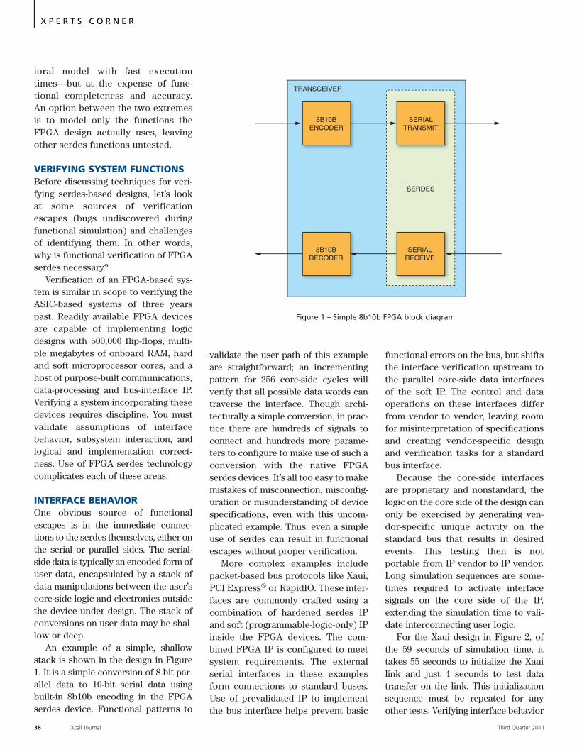
ioral model with fast executiontimes—but at the expense of func-tional completeness and accuracy.An option between the two extremesis to model only the functions theFPGA design actually uses, leavingother serdes functions untested.
VERIFYING SYSTEM FUNCTIONSBefore discussing techniques for veri-fying serdes-based designs, let’s lookat some sources of verificationescapes (bugs undiscovered duringfunctional simulation) and challengesof identifying them. In other words,why is functional verification of FPGAserdes necessary?
Verification of an FPGA-based sys-tem is similar in scope to verifying theASIC-based systems of three yearspast. Readily available FPGA devicesare capable of implementing logicdesigns with 500,000 flip-flops, multi-ple megabytes of onboard RAM, hardand soft microprocessor cores, and ahost of purpose-built communications,data-processing and bus-interface IP.Verifying a system incorporating thesedevices requires discipline. You mustvalidate assumptions of interfacebehavior, subsystem interaction, andlogical and implementation correct-ness. Use of FPGA serdes technologycomplicates each of these areas.
INTERFACE BEHAVIOROne obvious source of functionalescapes is in the immediate connec-tions to the serdes themselves, either onthe serial or parallel sides. The serial-side data is typically an encoded form ofuser data, encapsulated by a stack ofdata manipulations between the user’score-side logic and electronics outsidethe device under design. The stack ofconversions on user data may be shal-low or deep.
An example of a simple, shallowstack is shown in the design in Figure1. It is a simple conversion of 8-bit par-allel data to 10-bit serial data usingbuilt-in 8b10b encoding in the FPGAserdes device. Functional patterns to
validate the user path of this exampleare straightforward; an incrementingpattern for 256 core-side cycles willverify that all possible data words cantraverse the interface. Though archi-tecturally a simple conversion, in prac-tice there are hundreds of signals toconnect and hundreds more parame-ters to configure to make use of such aconversion with the native FPGAserdes devices. It’s all too easy to makemistakes of misconnection, misconfig-uration or misunderstanding of devicespecifications, even with this uncom-plicated example. Thus, even a simpleuse of serdes can result in functionalescapes without proper verification.
More complex examples includepacket-based bus protocols like Xaui,PCI Express® or RapidIO. These inter-faces are commonly crafted using acombination of hardened serdes IPand soft (programmable-logic-only) IPinside the FPGA devices. The com-bined FPGA IP is configured to meetsystem requirements. The externalserial interfaces in these examplesform connections to standard buses.Use of prevalidated IP to implementthe bus interface helps prevent basic
functional errors on the bus, but shiftsthe interface verification upstream tothe parallel core-side data interfacesof the soft IP. The control and dataoperations on these interfaces differfrom vendor to vendor, leaving roomfor misinterpretation of specificationsand creating vendor-specific designand verification tasks for a standardbus interface.
Because the core-side interfacesare proprietary and nonstandard, thelogic on the core side of the design canonly be exercised by generating ven-dor-specific unique activity on thestandard bus that results in desiredevents. This testing then is notportable from IP vendor to IP vendor.Long simulation sequences are some-times required to activate interfacesignals on the core side of the IP,extending the simulation time to vali-date interconnecting user logic.
For the Xaui design in Figure 2, ofthe 59 seconds of simulation time, ittakes 55 seconds to initialize the Xauilink and just 4 seconds to test datatransfer on the link. This initializationsequence must be repeated for anyother tests. Verifying interface behavior
38 Xcell Journal Third Quarter 2011
X P E R T S C O R N E R
TRANSCEIVER
8B10BENCODER
SERIALTRANSMIT
SERDES
8B10BDECODER
SERIALRECEIVE
Figure 1 – Simple 8b10b FPGA block diagram
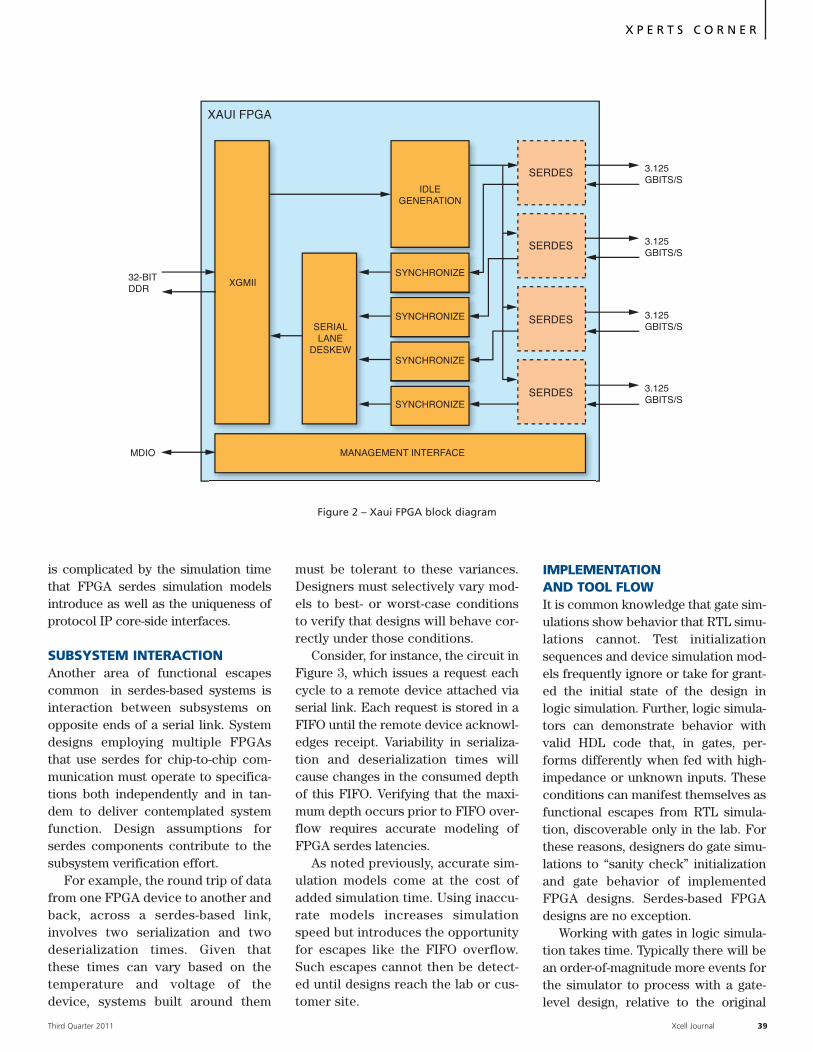
is complicated by the simulation timethat FPGA serdes simulation modelsintroduce as well as the uniqueness ofprotocol IP core-side interfaces.
SUBSYSTEM INTERACTION Another area of functional escapescommon in serdes-based systems isinteraction between subsystems onopposite ends of a serial link. Systemdesigns employing multiple FPGAsthat use serdes for chip-to-chip com-munication must operate to specifica-tions both independently and in tan-dem to deliver contemplated systemfunction. Design assumptions forserdes components contribute to thesubsystem verification effort.
For example, the round trip of datafrom one FPGA device to another andback, across a serdes-based link,involves two serialization and twodeserialization times. Given thatthese times can vary based on thetemperature and voltage of thedevice, systems built around them
must be tolerant to these variances.Designers must selectively vary mod-els to best- or worst-case conditionsto verify that designs will behave cor-rectly under those conditions.
Consider, for instance, the circuit inFigure 3, which issues a request eachcycle to a remote device attached viaserial link. Each request is stored in aFIFO until the remote device acknowl-edges receipt. Variability in serializa-tion and deserialization times willcause changes in the consumed depthof this FIFO. Verifying that the maxi-mum depth occurs prior to FIFO over-flow requires accurate modeling ofFPGA serdes latencies.
As noted previously, accurate sim-ulation models come at the cost ofadded simulation time. Using inaccu-rate models increases simulationspeed but introduces the opportunityfor escapes like the FIFO overflow.Such escapes cannot then be detect-ed until designs reach the lab or cus-tomer site.
IMPLEMENTATION AND TOOL FLOWIt is common knowledge that gate sim-ulations show behavior that RTL simu-lations cannot. Test initializationsequences and device simulation mod-els frequently ignore or take for grant-ed the initial state of the design inlogic simulation. Further, logic simula-tors can demonstrate behavior withvalid HDL code that, in gates, per-forms differently when fed with high-impedance or unknown inputs. Theseconditions can manifest themselves asfunctional escapes from RTL simula-tion, discoverable only in the lab. Forthese reasons, designers do gate simu-lations to “sanity check” initializationand gate behavior of implementedFPGA designs. Serdes-based FPGAdesigns are no exception.
Working with gates in logic simula-tion takes time. Typically there will bean order-of-magnitude more events forthe simulator to process with a gate-level design, relative to the original
Third Quarter 2011 Xcell Journal 39
X P E R T S C O R N E R
SERDES 3.125GBITS/S
SERDES 3.125GBITS/S
SERDES 3.125GBITS/S
SERDES 3.125GBITS/S
IDLEGENERATION
SYNCHRONIZE
SYNCHRONIZE
SYNCHRONIZE
SYNCHRONIZE
SERIALLANE
DESKEW
XGMII32-BITDDR
MDIO
XAUI FPGA
MANAGEMENT INTERFACE
Figure 2 – Xaui FPGA block diagram
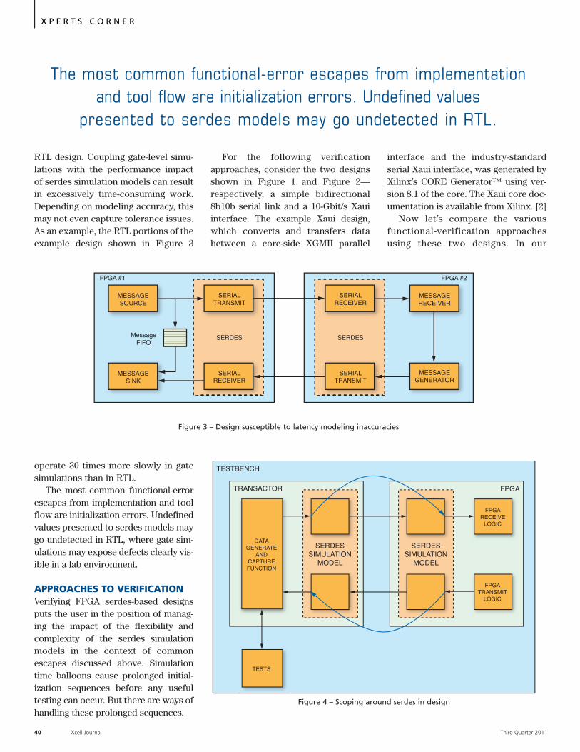
RTL design. Coupling gate-level simu-lations with the performance impactof serdes simulation models can resultin excessively time-consuming work.Depending on modeling accuracy, thismay not even capture tolerance issues.As an example, the RTL portions of theexample design shown in Figure 3
operate 30 times more slowly in gatesimulations than in RTL.
The most common functional-errorescapes from implementation and toolflow are initialization errors. Undefinedvalues presented to serdes models maygo undetected in RTL, where gate sim-ulations may expose defects clearly vis-ible in a lab environment.
APPROACHES TO VERIFICATIONVerifying FPGA serdes-based designsputs the user in the position of manag-ing the impact of the flexibility andcomplexity of the serdes simulationmodels in the context of commonescapes discussed above. Simulationtime balloons cause prolonged initial-ization sequences before any usefultesting can occur. But there are ways ofhandling these prolonged sequences.
For the following verificationapproaches, consider the two designsshown in Figure 1 and Figure 2—respectively, a simple bidirectional8b10b serial link and a 10-Gbit/s Xauiinterface. The example Xaui design,which converts and transfers databetween a core-side XGMII parallel
interface and the industry-standardserial Xaui interface, was generated byXilinx’s CORE Generator™ using ver-sion 8.1 of the core. The Xaui core doc-umentation is available from Xilinx. [2]
Now let’s compare the variousfunctional-verification approachesusing these two designs. In our
40 Xcell Journal Third Quarter 2011
X P E R T S C O R N E R
MESSAGESOURCE
MESSAGESINK
MESSAGERECEIVER
MESSAGEGENERATOR
SERIALTRANSMIT
SERIALRECEIVER
SERDES
SERIALRECEIVER
SERIALTRANSMIT
SERDESMessageFIFO
FPGA #1 FPGA #2
TESTBENCH
TRANSACTOR FPGA
DATAGENERATE
ANDCAPTUREFUNCTION
TESTS
FPGARECEIVE
LOGIC
FPGATRANSMIT
LOGIC
SERDESSIMULATION
MODEL
SERDESSIMULATION
MODEL
Figure 3 – Design susceptible to latency modeling inaccuracies
Figure 4 – Scoping around serdes in design
The most common functional-error escapes from implementation and tool flow are initialization errors. Undefined values
presented to serdes models may go undetected in RTL.
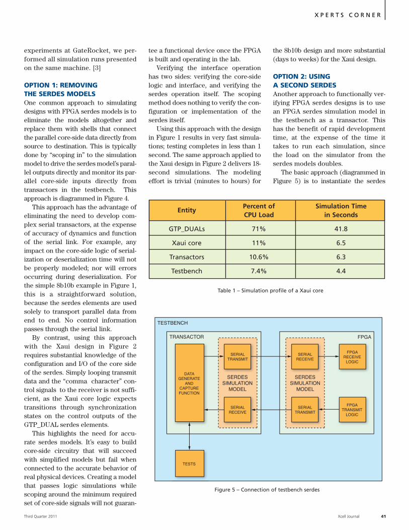
experiments at GateRocket, we per-formed all simulation runs presentedon the same machine. [3]
OPTION 1: REMOVING THE SERDES MODELSOne common approach to simulatingdesigns with FPGA serdes models is toeliminate the models altogether andreplace them with shells that connectthe parallel core-side data directly fromsource to destination. This is typicallydone by “scoping in” to the simulationmodel to drive the serdes model’s paral-lel outputs directly and monitor its par-allel core-side inputs directly fromtransactors in the testbench. Thisapproach is diagrammed in Figure 4.
This approach has the advantage ofeliminating the need to develop com-plex serial transactors, at the expenseof accuracy of dynamics and functionof the serial link. For example, anyimpact on the core-side logic of serial-ization or deserialization time will notbe properly modeled; nor will errorsoccurring during deserialization. Forthe simple 8b10b example in Figure 1,this is a straightforward solution,because the serdes elements are usedsolely to transport parallel data fromend to end. No control informationpasses through the serial link.
By contrast, using this approachwith the Xaui design in Figure 2requires substantial knowledge of theconfiguration and I/O of the core sideof the serdes. Simply looping transmitdata and the “comma character” con-trol signals to the receiver is not suffi-cient, as the Xaui core logic expectstransitions through synchronizationstates on the control outputs of theGTP_DUAL serdes elements.
This highlights the need for accu-rate serdes models. It’s easy to buildcore-side circuitry that will succeedwith simplified models but fail whenconnected to the accurate behavior ofreal physical devices. Creating a modelthat passes logic simulations whilescoping around the minimum requiredset of core-side signals will not guaran-
tee a functional device once the FPGAis built and operating in the lab.
Verifying the interface operationhas two sides: verifying the core-sidelogic and interface, and verifying theserdes operation itself. The scopingmethod does nothing to verify the con-figuration or implementation of theserdes itself.
Using this approach with the designin Figure 1 results in very fast simula-tions; testing completes in less than 1second. The same approach applied tothe Xaui design in Figure 2 delivers 18-second simulations. The modelingeffort is trivial (minutes to hours) for
the 8b10b design and more substantial(days to weeks) for the Xaui design.
OPTION 2: USING A SECOND SERDESAnother approach to functionally ver-ifying FPGA serdes designs is to usean FPGA serdes simulation model inthe testbench as a transactor. Thishas the benefit of rapid developmenttime, at the expense of the time ittakes to run each simulation, sincethe load on the simulator from theserdes models doubles.
The basic approach (diagrammed inFigure 5) is to instantiate the serdes
Third Quarter 2011 Xcell Journal 41
X P E R T S C O R N E R
EntityPercent of Simulation Time CPU Load in Seconds
GTP_DUALs 71% 41.8
Xaui core 11% 6.5
Transactors 10.6% 6.3
Testbench 7.4% 4.4
TESTBENCH
TRANSACTOR FPGA
DATAGENERATE
ANDCAPTUREFUNCTION
TESTS
FPGARECEIVE
LOGIC
SERIALRECEIVE
SERIALTRANSMIT
SERIALTRANSMIT
SERIALRECEIVE
FPGATRANSMIT
LOGIC
SERDESSIMULATION
MODEL
SERDESSIMULATION
MODEL
Table 1 – Simulation profile of a Xaui core
Figure 5 – Connection of testbench serdes
model in the transactor exactly as it isinstantiated in the design being tested.This preserves all configurationoptions. The serial-transmit outputs ofthe transactor are wired to the serial-receive inputs of the design being test-ed—and vice versa—in the testbench.
Table 1 shows the simulator profileof the design in Figure 2 running insimulation. This testbench uses behav-ioral transactors for serial-side stimu-lus and captured response. The serdesin the Xaui design dominates the 59-second simulation. Converting thetestbench to use serdes simulationmodels instead of behavioral transac-tors in the testbench doubles the loadon the simulator. In this case, it nearlydoubles the entire simulation time foreach simulation run; runtimesincrease from 59 to 101 seconds. For
the 8b10b design in Figure 1, the pro-file is more dramatic; the simulatorreports 100 percent of the time in theserdes simulation models. Using a sec-ond serdes in the testbench doublessimulation time from 32 to 64 seconds.
OPTION 3: VERIFYING SERDES IN THE LABOne solution to verifying FPGA serdesdesigns is to skip verification of theserdes’ serial and core-side connec-tions in logic simulation and advancedirectly to the lab for validation ofthose parts of the design.
One benefit of this approach is thevolume of data that you can transferthrough the serdes interfaces in a real-time system. Simulation clock fre-quencies are commonly five to sevenorders of magnitude slower than free-
running physical FPGA devices.Verifying with silicon in the lab thusprovides many-orders-of-magnitudemore test cycles than software simula-tion. It’s much harder to debug in thelab environment, however, due to thelack of visibility of the high-frequencyserial signals and the opaque contentsof the core-side logic.
OPTION 4: VERIFYING WITH NATIVE HARDWAREA different solution to the verificationchallenge is to build an emulation plat-form that incorporates the FPGAdesign and surrounding electronics tostimulate and respond to it. You canconnect a purpose-built hardware plat-form containing the FPGA being test-ed to a logic simulator or software todeliver patterns and check responsesof the FPGA design.
With this technique, you must eitherdefine and produce a seamless inter-face to the simulator for existing RTLtests, or discard existing RTL test-benches in lieu of decoupling the FPGAdesign from the tests and transactors.
Circuits operating within a soft-ware simulator maintain a strictnotion of synchronicity. Rigorouslydefined rules of hardware descrip-tion language (HDL) behavior andscheduling make software-onlydesign and simulation predictableand productive. Coupling a logic sim-ulator with a hardware platform andmaintaining setup-and-hold relation-ships between hardware and simulat-ed HDL are not trivial tasks.
Designing for verification of adecoupled design is likewise a com-plex task. Typical FPGA verificationflows build up from simple block-levelfunctions to test full-chip functionali-ty. Decoupling the design from thetestbench is a step beyond commonFPGA verification environments.
In either case, you must construct acustom hardware platform to emulatethe behavior of the serdes design. Anydesign changes quickly make such aplatform obsolete, because a different
42 Xcell Journal Third Quarter 2011
X P E R T S C O R N E R
ApproachDevelopment
AccuracySimulation
Time Performance
Remove serdes Trivial Low 1 second
Use serdes in testbench Short Medium 64 seconds
Verify in the lab Medium High n/a
Native hardware emulation
Long High 1 second
Write custom behavioral models
Medium Low 1 second
ApproachDevelopment
AccuracySimulation
Time Performance
Remove serdes Medium Low 18 seconds
Use serdes in testbench Short Medium 101 seconds
Verify in the lab Long High n/a
Native hardware emulation
Long High 18 seconds
Write custom behavioral models
Medium Low 59 seconds
Table 2 – Comparison of approaches for 8b10b
Table 3 – Comparison of Approaches for Xaui
device, device vendor or changes tothe pinout will require rewiring of theprinted-circuit board. A hardware plat-form built for the design shown inFigure 1 would not be usable for thedesign shown in Figure 2, since manyof the serdes serial connections in onedo not exist in the other.
Running the Xaui design in Figure 2in an FPGA emulation system resultsin silicon-accurate serdes behaviorand reduces the 59-second simulationto 18 seconds. However, crafting aflexible, purpose-built hardware emu-lation solution that is tightly coupledwith a logic simulator is a substantialundertaking for an FPGA design-spe-cific project. The commercial EDAcommunity has responded, however,and GateRocket now offers a well-proven and design-independent solu-tion called a RocketDrive, which pro-vides that capability. The data in thispaper is derived from this solution.
OPTION 5: CUSTOM BEHAVIORAL MODELSAs we saw in Option 1, replacing aserdes simulation model with a simpli-fied model can result in incorrectbehavior. It is common practice towrite behavioral models for a specificmode used in a design. Rather thanimplementing all possible functions ofa serdes in a simulation model, youcan implement only the selectedparameter settings and port connec-tions. This reduces the overall scopeof model development.
You can reuse models produced inthis way when your new design usesthe same parameters and port connec-tions. For example, you could modelthe simple 8b10b design in Figure 1with a simple 8b10b encoder/decoder.Any use of a serdes with this simpleoperation can then reuse this simula-tion model.
The usefulness of these models islimited to designs of the specifiedfunction. When new designs or serdesfunctions are desired, you must writenew models.
A good example of this approach isseen in the testbench the Xilinx COREGenerator tool wrote for the Xauidesign in Figure 2. The testbenchimplements behavioral serial transac-tors specific to the Xaui protocol.However, other designs—includingthe very simple 8b10b design shown inFigure 1—cannot reuse them.
This simulation runs in 59 secondswith accurate, vendor-provided mod-els for serdes in the design and pur-pose-built behavioral serdes models inthe transactors in the testbench.
COMPARING THE APPROACHESTables 2 and 3 compare the presentedapproaches for both the 8b10b andXaui designs shown in Figures 1 and 2.The measurements suggest someobservations and recommendations.
For example, using a secondserdes is appropriate only if theserdes models represent a small por-tion of the overall simulation time orif there are very few tests. If the sim-ulation profile shows a large per-centage of time spent in the serdesmodels, the resulting impact on sim-ulation time is dramatic.
The presented verification approach-es are sometimes used in conjunction.For example, design teams mightremove serdes models in simulation andalso verify the serdes function in the lab.
The native hardware emulationapproach gives the performance ofcustom behavioral models with theaccuracy of the silicon behavior.
Accuracy of software simulationmodels generally comes at theexpense of simulation performance.Hardware solutions provide higherperformance and accuracy at theexpense of development time.
Extending simulation times createspressure to reduce the number of testsin verification cycles, which naturallyleads to functional-defect escapes.
Using evaluation boards or targetsystems to verify serdes designs canput a schedule at risk while waiting forthe final article.
RECOMMENDATIONSVerifying serdes-based FPGAs is acomplex process, as our examplesshow. Among the many challengesare debugging the core logic in thedesign and ensuring that the serdesare properly configured, decidingwhich set of the 2730 configurationsimplement your desired functionalityand addressing the slow simulationtime of serdes models or the gate-level simulation to accurately verifythe design.
GateRocket recommends thought-ful planning and rigorous executionof verification projects, but if thetools you have at your disposal resultin very long simulations or cause youto skip tests to meet project sched-ules, then the project risks increasesignificantly. We believe there is nosuch thing as “too much verification,”but there certainly can be too little.When planning verification projects,ask yourself if you have the time to doit right—or to do it twice. Having theright tools to verify your serdes-baseddesign is important. Just as the ASICdesign team employs hardware-assisted verification to ensure thedesign is done right the first time, sotoo can a hardware emulation verifi-cation method benefit advancedserdes-based FPGA designs.
Visit http://www.GateRocket.com tolearn more about our implementationof this technology.
REFERENCES
[1] Xilinx Inc., Virtex-5 FPGA RocketIO™
GTP Transceiver User Guide, December
2008. www.xilinx.com/support/
documentation/user_guides/ug196.pdf
[2] Xilinx Inc., Xaui User Guide, April
2010. www.xilinx.com/support/
documentation/ip_documentation/
xaui_ug150.pdf
[3] System specifications, Intel Xeon CPU
X3363 @ 2.83GHz, 6-MB cache, 16-GB
DDR3 main memory, PC2-5300 / 667 MHz
Third Quarter 2011 Xcell Journal 43
X P E R T S C O R N E R
44 Xcell Journal Third Quarter 2011
How Do I Reset My FPGA?Devising the best reset structure canimprove the density, performance andpower of your design.
ASK FAE-X
by E. SrikanthSolutions Development EngineerXilinx, [email protected]
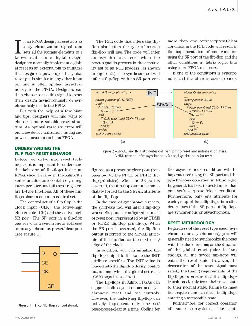
Third Quarter 2011 Xcell Journal 45
I n an FPGA design, a reset acts asa synchronization signal thatsets all the storage elements to a
known state. In a digital design,designers normally implement a glob-al reset as an external pin to initializethe design on power-up. The globalreset pin is similar to any other inputpin and is often applied asynchro-nously to the FPGA. Designers canthen choose to use this signal to resettheir design asynchronously or syn-chronously inside the FPGA.
But with the help of a few hintsand tips, designers will find ways tochoose a more suitable reset struc-ture. An optimal reset structure willenhance device utilization, timing andpower consumption in an FPGA.
UNDERSTANDING THE FLIP-FLOP RESET BEHAVIORBefore we delve into reset tech-niques, it is important to understandthe behavior of flip-flops inside anFPGA slice. Devices in the Xilinx® 7series architecture contain eight reg-isters per slice, and all these registersare D-type flip-flops. All of these flip-flops share a common control set.
The control set of a flip-flop is theclock input (CLK), the active-highchip enable (CE) and the active-highSR port. The SR port in a flip-flopcan serve as a synchronous set/resetor an asynchronous preset/clear port(see Figure 1).
The RTL code that infers the flip-flop also infers the type of reset aflip-flop will use. The code will inferan asynchronous reset when thereset signal is present in the sensitiv-ity list of an RTL process (as shownin Figure 2a). The synthesis tool willinfer a flip-flop with an SR port con-
figured as a preset or clear port (rep-resented by the FDCE or FDPE flip-flop primitive). When the SR port isasserted, the flip-flop output is imme-diately forced to the SRVAL attributeof the flip-flop.
In the case of synchronous resets,the synthesis tool will infer a flip-flopwhose SR port is configured as a setor reset port (represented by an FDSEor FDRE flip-flop primitive). Whenthe SR port is asserted, the flip-flopoutput is forced to the SRVAL attrib-ute of the flip-flop on the next risingedge of the clock.
In addition, you can initialize theflip-flop output to the value the INITattribute specifies. The INIT value isloaded into the flip-flop during config-uration and when the global set reset(GSR) signal is asserted.
The flip-flops in Xilinx FPGAs cansupport both asynchronous and syn-chronous reset and set controls.However, the underlying flip-flop cannatively implement only one set/reset/preset/clear at a time. Coding for
more than one set/reset/preset/clearcondition in the RTL code will result inthe implementation of one conditionusing the SR port of the flip-flop and theother conditions in fabric logic, thususing more FPGA resources.
If one of the conditions is synchro-nous and the other is asynchronous,
the asynchronous condition will beimplemented using the SR port and thesynchronous condition in fabric logic.In general, it’s best to avoid more thanone set/reset/preset/clear condition.Furthermore, only one attribute foreach group of four flip-flops in a slicedetermines if the SR ports of flip-flopsare synchronous or asynchronous.
RESET METHODOLOGYRegardless of the reset type used (syn-chronous or asynchronous), you willgenerally need to synchronize the resetwith the clock. As long as the durationof the global reset pulse is longenough, all the device flip-flops willenter the reset state. However, thedeassertion of the reset signal mustsatisfy the timing requirements of theflip-flops to ensure that the flip-flopstransition cleanly from their reset stateto their normal state. Failure to meetthis requirement can result in flip-flopsentering a metastable state.
Furthermore, for correct operationof some subsystems, like state
A S K F A E - X
D
CE
Q
CK
CR
Figure 1 – Slice flip-flop control signals
(a) (b)
INIT
SRVAL
signal Q:std_logic:=‘1’;....async: process (CLK, RST)begin if (RST='1')then Q <= '0'; else if (CLK’event and CLK='1') then Q <= D; end if; end if;end process async;
signal Q:std_logic:=‘1’;....sync: process (CLK)begin if (CLK’event and CLK='1') then if (RST='1') then Q <= '0'; else Q <= D; end if; end if;end process sync;
Figure 2 – SRVAL and INIT attributes define flip-flop reset and initialization: here, VHDL code to infer asynchronous (a) and synchronous (b) reset.
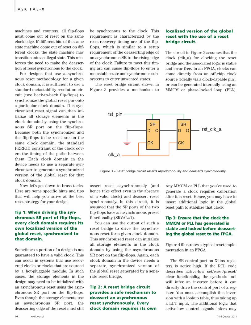
machines and counters, all flip-flopsmust come out of reset on the sameclock edge. If different bits of the samestate machine come out of reset on dif-ferent clocks, the state machine maytransition into an illegal state. This rein-forces the need to make the deasser-tion of reset synchronous to the clock.
For designs that use a synchro-nous reset methodology for a givenclock domain, it is sufficient to use astandard metastability resolution cir-cuit (two back-to-back flip-flops) tosynchronize the global reset pin ontoa particular clock domain. This syn-chronized reset signal can then ini-tialize all storage elements in theclock domain by using the synchro-nous SR port on the flip-flops.Because both the synchronizer andthe flip-flops to be reset are on thesame clock domain, the standardPERIOD constraint of the clock cov-ers the timing of the paths betweenthem. Each clock domain in thedevice needs to use a separate syn-chronizer to generate a synchronizedversion of the global reset for thatclock domain.
Now let’s get down to brass tacks.Here are some specific hints and tipsthat will help you arrive at the bestreset strategy for your design.
Tip 1: When driving the syn-chronous SR port of flip-flops,every clock domain requires itsown localized version of theglobal reset, synchronized tothat domain.
Sometimes a portion of a design is notguaranteed to have a valid clock. Thiscan occur in systems that use recov-ered clocks or clocks that are sourcedby a hot-pluggable module. In suchcases, the storage elements in thedesign may need to be initialized withan asynchronous reset using the asyn-chronous SR port on the flip-flops.Even though the storage elements usean asynchronous SR port, thedeasserting edge of the reset must still
be synchronous to the clock. Thisrequirement is characterized by thereset-recovery timing arc of the flip-flops, which is similar to a setuprequirement of the deasserting edge ofan asynchronous SR to the rising edgeof the clock. Failure to meet this tim-ing arc can cause flip-flops to enter ametastable state and synchronous sub-systems to enter unwanted states.
The reset bridge circuit shown inFigure 3 provides a mechanism to
assert reset asynchronously (andhence take effect even in the absenceof a valid clock) and deassert resetsynchronously. In this circuit, it isassumed that the SR ports of the twoflip-flops have an asynchronous presetfunctionality (SRVAL=1).
You can use the output of such areset bridge to drive the asynchro-nous reset for a given clock domain.This synchronized reset can initializeall storage elements in the clockdomain by using the asynchronousSR port on the flip-flops. Again, eachclock domain in the device needs aseparate, synchronized version ofthe global reset generated by a sepa-rate reset bridge.
Tip 2: A reset bridge circuitprovides a safe mechanism todeassert an asynchronousreset synchronously. Everyclock domain requires its own
localized version of the globalreset with the use of a resetbridge circuit.
The circuit in Figure 3 assumes that theclock (clk_a) for clocking the resetbridge and the associated logic is stableand error free. In an FPGA, clocks cancome directly from an off-chip clocksource (ideally via a clock-capable pin),or can be generated internally using anMMCM or phase-locked loop (PLL).
Any MMCM or PLL that you’ve used togenerate a clock requires calibrationafter it is reset. Hence, you may have toinsert additional logic in the globalreset path to stabilize that clock.
Tip 3: Ensure that the clock theMMCM or PLL has generated isstable and locked before deassert-ing the global reset to the FPGA.
Figure 4 illustrates a typical reset imple-mentation in an FPGA.
The SR control port on Xilinx regis-ters is active high. If the RTL codedescribes active-low set/reset/preset/clear functionality, the synthesis toolwill infer an inverter before it candirectly drive the control port of a reg-ister. You must accomplish this inver-sion with a lookup table, thus taking upa LUT input. The additional logic thatactive-low control signals infers may
46 Xcell Journal Third Quarter 2011
A S K F A E - X
D Q
CK
SR
rst_pin
rst_clk_aSR
D Q
CK
clk_a
Figure 3 – Reset bridge circuit asserts asynchronously and deasserts synchronously.
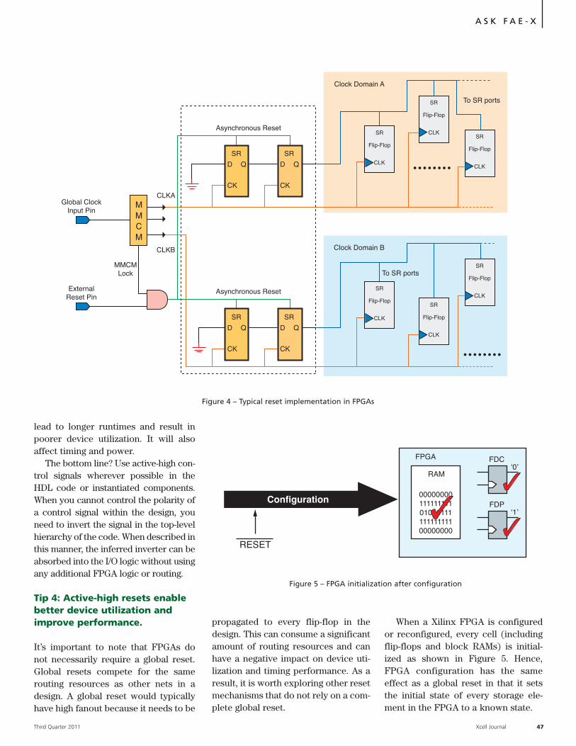
lead to longer runtimes and result inpoorer device utilization. It will alsoaffect timing and power.
The bottom line? Use active-high con-trol signals wherever possible in theHDL code or instantiated components.When you cannot control the polarity ofa control signal within the design, youneed to invert the signal in the top-levelhierarchy of the code. When described inthis manner, the inferred inverter can beabsorbed into the I/O logic without usingany additional FPGA logic or routing.
Tip 4: Active-high resets enablebetter device utilization andimprove performance.
It’s important to note that FPGAs donot necessarily require a global reset.Global resets compete for the samerouting resources as other nets in adesign. A global reset would typicallyhave high fanout because it needs to be
propagated to every flip-flop in thedesign. This can consume a significantamount of routing resources and canhave a negative impact on device uti-lization and timing performance. As aresult, it is worth exploring other resetmechanisms that do not rely on a com-plete global reset.
When a Xilinx FPGA is configuredor reconfigured, every cell (includingflip-flops and block RAMs) is initial-ized as shown in Figure 5. Hence,FPGA configuration has the sameeffect as a global reset in that it setsthe initial state of every storage ele-ment in the FPGA to a known state.
Third Quarter 2011 Xcell Journal 47
A S K F A E - X
D Q
CK
SR SR
D Q
CK
SR
Flip-Flop
CLK
SR
Flip-Flop
CLKSR
Flip-Flop
CLK
MMCM
Asynchronous Reset
Clock Domain A
To SR ports
D Q
CK
SR SR
D Q
CK
SR
Flip-Flop
CLK
SR
Flip-Flop
CLK
SR
Flip-Flop
CLKAsynchronous Reset
CLKB
CLKA
Clock Domain B
To SR ports
ExternalReset Pin
Global ClockInput Pin
MMCMLock
Figure 4 – Typical reset implementation in FPGAs
FDC‘0’
FDP‘1’
FPGA
RAM
000000001111111110101011111111111100000000
Configuration
RESET
Figure 5 – FPGA initialization after configuration
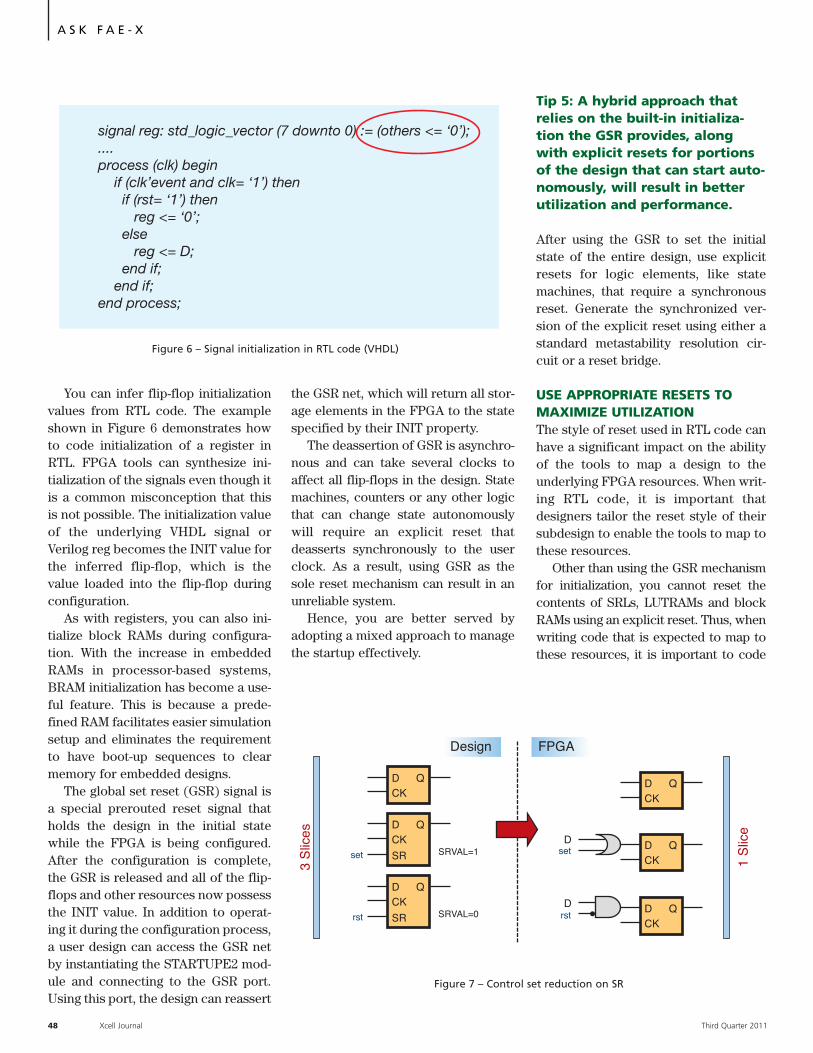
You can infer flip-flop initializationvalues from RTL code. The exampleshown in Figure 6 demonstrates howto code initialization of a register inRTL. FPGA tools can synthesize ini-tialization of the signals even though itis a common misconception that thisis not possible. The initialization valueof the underlying VHDL signal orVerilog reg becomes the INIT value forthe inferred flip-flop, which is thevalue loaded into the flip-flop duringconfiguration.
As with registers, you can also ini-tialize block RAMs during configura-tion. With the increase in embeddedRAMs in processor-based systems,BRAM initialization has become a use-ful feature. This is because a prede-fined RAM facilitates easier simulationsetup and eliminates the requirementto have boot-up sequences to clearmemory for embedded designs.
The global set reset (GSR) signal isa special prerouted reset signal thatholds the design in the initial statewhile the FPGA is being configured.After the configuration is complete,the GSR is released and all of the flip-flops and other resources now possessthe INIT value. In addition to operat-ing it during the configuration process,a user design can access the GSR netby instantiating the STARTUPE2 mod-ule and connecting to the GSR port.Using this port, the design can reassert
the GSR net, which will return all stor-age elements in the FPGA to the statespecified by their INIT property.
The deassertion of GSR is asynchro-nous and can take several clocks toaffect all flip-flops in the design. Statemachines, counters or any other logicthat can change state autonomouslywill require an explicit reset thatdeasserts synchronously to the userclock. As a result, using GSR as thesole reset mechanism can result in anunreliable system.
Hence, you are better served byadopting a mixed approach to managethe startup effectively.
Tip 5: A hybrid approach thatrelies on the built-in initializa-tion the GSR provides, alongwith explicit resets for portionsof the design that can start auto-nomously, will result in betterutilization and performance.
After using the GSR to set the initialstate of the entire design, use explicitresets for logic elements, like statemachines, that require a synchronousreset. Generate the synchronized ver-sion of the explicit reset using either astandard metastability resolution cir-cuit or a reset bridge.
USE APPROPRIATE RESETS TOMAXIMIZE UTILIZATION The style of reset used in RTL code canhave a significant impact on the abilityof the tools to map a design to theunderlying FPGA resources. When writ-ing RTL code, it is important thatdesigners tailor the reset style of theirsubdesign to enable the tools to map tothese resources.
Other than using the GSR mechanismfor initialization, you cannot reset thecontents of SRLs, LUTRAMs and blockRAMs using an explicit reset. Thus, whenwriting code that is expected to map tothese resources, it is important to code
48 Xcell Journal Third Quarter 2011
A S K F A E - X
signal reg: std_logic_vector (7 downto 0) := (others <= ‘0’); ....process (clk) begin if (clk’event and clk= ‘1’) then if (rst= ‘1’) then reg <= ‘0’; else reg <= D; end if; end if;end process;
Figure 6 – Signal initialization in RTL code (VHDL)
D QCK
D QCK
D QCK
DD
D
QCK
D QCK
SRset SRVAL=1
D QCK
SRrst
set
rstSRVAL=0
Design
3 S
lices
1 S
lice
FPGA
Figure 7 – Control set reduction on SR
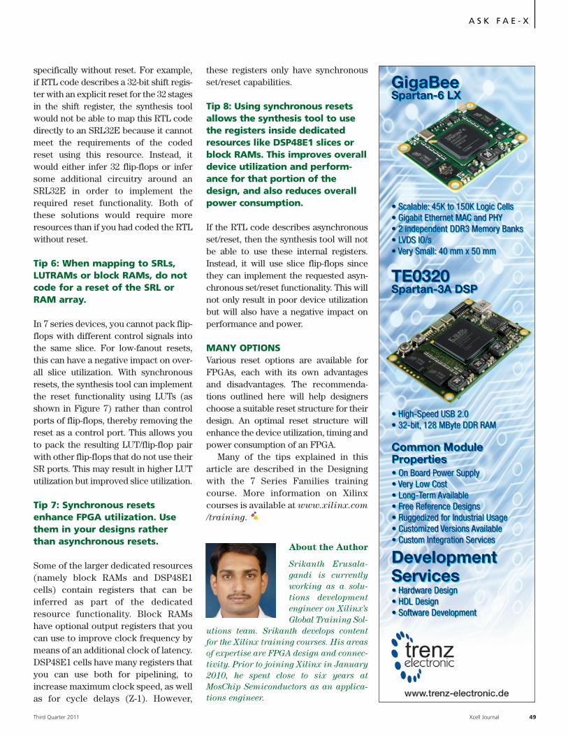
specifically without reset. For example,if RTL code describes a 32-bit shift regis-ter with an explicit reset for the 32 stagesin the shift register, the synthesis toolwould not be able to map this RTL codedirectly to an SRL32E because it cannotmeet the requirements of the codedreset using this resource. Instead, itwould either infer 32 flip-flops or infersome additional circuitry around anSRL32E in order to implement therequired reset functionality. Both ofthese solutions would require moreresources than if you had coded the RTLwithout reset.
Tip 6: When mapping to SRLs,LUTRAMs or block RAMs, do notcode for a reset of the SRL orRAM array.
In 7 series devices, you cannot pack flip-flops with different control signals intothe same slice. For low-fanout resets,this can have a negative impact on over-all slice utilization. With synchronousresets, the synthesis tool can implementthe reset functionality using LUTs (asshown in Figure 7) rather than controlports of flip-flops, thereby removing thereset as a control port. This allows youto pack the resulting LUT/flip-flop pairwith other flip-flops that do not use theirSR ports. This may result in higher LUTutilization but improved slice utilization.
Tip 7: Synchronous resetsenhance FPGA utilization. Usethem in your designs ratherthan asynchronous resets.
Some of the larger dedicated resources(namely block RAMs and DSP48E1cells) contain registers that can beinferred as part of the dedicatedresource functionality. Block RAMshave optional output registers that youcan use to improve clock frequency bymeans of an additional clock of latency.DSP48E1 cells have many registers thatyou can use both for pipelining, toincrease maximum clock speed, as wellas for cycle delays (Z-1). However,
these registers only have synchronousset/reset capabilities.
Tip 8: Using synchronous resetsallows the synthesis tool to usethe registers inside dedicatedresources like DSP48E1 slices orblock RAMs. This improves overalldevice utilization and perform-ance for that portion of thedesign, and also reduces overallpower consumption.
If the RTL code describes asynchronousset/reset, then the synthesis tool will notbe able to use these internal registers.Instead, it will use slice flip-flops sincethey can implement the requested asyn-chronous set/reset functionality. This willnot only result in poor device utilizationbut will also have a negative impact onperformance and power.
MANY OPTIONSVarious reset options are available forFPGAs, each with its own advantagesand disadvantages. The recommenda-tions outlined here will help designerschoose a suitable reset structure for theirdesign. An optimal reset structure willenhance the device utilization, timing andpower consumption of an FPGA.
Many of the tips explained in thisarticle are described in the Designingwith the 7 Series Families trainingcourse. More information on Xilinxcourses is available at www.xilinx.com
/training.
About the Author
Srikanth Erusala-
gandi is currently
working as a solu-
tions development
engineer on Xilinx’s
Global Training Sol-
utions team. Srikanth develops content
for the Xilinx training courses. His areas
of expertise are FPGA design and connec-
tivity. Prior to joining Xilinx in January
2010, he spent close to six years at
MosChip Semiconductors as an applica-
tions engineer.
Third Quarter 2011 Xcell Journal 49
A S K F A E - X
50 Xcell Journal Third Quarter 2011
T oday’s complex FPGAs contain large arrays offunctional blocks for implementing a wide vari-ety of circuits and systems. Examples of such
blocks are logic arrays, memory, DSP blocks, proces-sors, phase-locked loops (PLLs) and delay-locked loops(DLLs) for timing generation, standard I/O, high-speeddigital transceivers and parallel interfaces (PCI, DDR,etc.). Often, these FPGAs use multiple clocks to drivedifferent blocks, typically generating them using a com-
bination of external oscillators and internal PLLsand DLLs. The system designer has to
decide how to combine external and inter-nal resources for optimal clock tree design. Programmable clock oscillators offer a
number of advantages when used as timing refer-ences for FPGA-based systems. Chief among them
is the design flexibility that arises from high-resolu-tion frequency selection for clock tree optimization.
Another big benefit is spread-spectrum modulation forreducing electromagnetic interference (EMI).
A silicon MEMS clock oscillator architecture that isinherently programmable solves many problems forsystem designers who use FPGAs. The architecture ofthis type of microelectromechanical system can easilyincorporate additional features such as spread-spec-trum clocking for EMI reduction and a digitally control-lable oscillator for jitter cleaning and fail-safe functionsin high-speed applications.
XPLANATION: FPGA101
ProgrammableOscillators EnhanceFPGA ApplicationsClock oscillators offer unique advantages in highly customizable FPGA-based systems, including flexibility and EMI reduction.
by Sassan TabatabaeiDirector, Strategic ApplicationsSiTime [email protected]
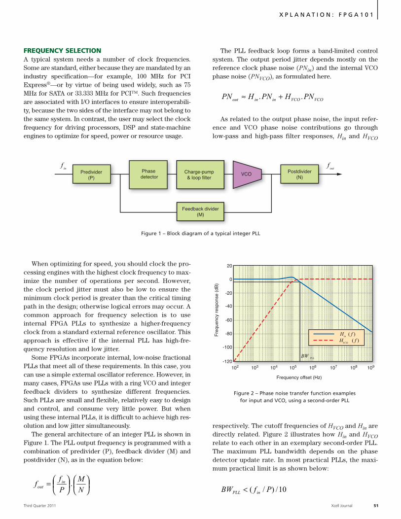
FREQUENCY SELECTION A typical system needs a number of clock frequencies.Some are standard, either because they are mandated by anindustry specification—for example, 100 MHz for PCIExpress®—or by virtue of being used widely, such as 75MHz for SATA or 33.333 MHz for PCI™. Such frequenciesare associated with I/O interfaces to ensure interoperabili-ty, because the two sides of the interface may not belong tothe same system. In contrast, the user may select the clockfrequency for driving processors, DSP and state-machineengines to optimize for speed, power or resource usage.
When optimizing for speed, you should clock the pro-cessing engines with the highest clock frequency to max-imize the number of operations per second. However,the clock period jitter must also be low to ensure theminimum clock period is greater than the critical timingpath in the design; otherwise logical errors may occur. Acommon approach for frequency selection is to useinternal FPGA PLLs to synthesize a higher-frequencyclock from a standard external reference oscillator. Thisapproach is effective if the internal PLL has high-fre-quency resolution and low jitter.
Some FPGAs incorporate internal, low-noise fractionalPLLs that meet all of these requirements. In this case, youcan use a simple external oscillator reference. However, inmany cases, FPGAs use PLLs with a ring VCO and integerfeedback dividers to synthesize different frequencies.Such PLLs are small and flexible, relatively easy to designand control, and consume very little power. But whenusing these internal PLLs, it is difficult to achieve high res-olution and low jitter simultaneously.
The general architecture of an integer PLL is shown inFigure 1. The PLL output frequency is programmed with acombination of predivider (P), feedback divider (M) andpostdivider (N), as in the equation below:
The PLL feedback loop forms a band-limited controlsystem. The output period jitter depends mostly on thereference clock phase noise (PNin) and the internal VCOphase noise (PNVCO), as formulated here.
As related to the output phase noise, the input refer-ence and VCO phase noise contributions go throughlow-pass and high-pass filter responses, Hin and HVCO
respectively. The cutoff frequencies of HVCO and Hin aredirectly related. Figure 2 illustrates how Hin and HVCOrelate to each other in an exemplary second-order PLL.The maximum PLL bandwidth depends on the phasedetector update rate. In most practical PLLs, the maxi-mum practical limit is as shown below:
Third Quarter 2011 Xcell Journal 51
X P L A N A T I O N : F P G A 1 0 1
Predivider(P)
Phase detector
Charge-pump& loop filter
VCO Postdivider(N)
Feedback divider(M)
inf
outf
)( fHin
)( fHVCO
20
0
-20
-40
-60
-80
-100
-120102 103 104 105 106 107 108 109
Frequency offset (Hz)
Fre
quen
cy r
espo
nse
(dB
)
PLLBW
Figure 1 – Block diagram of a typical integer PLL
Figure 2 – Phase noise transfer function examples for input and VCO, using a second-order PLL
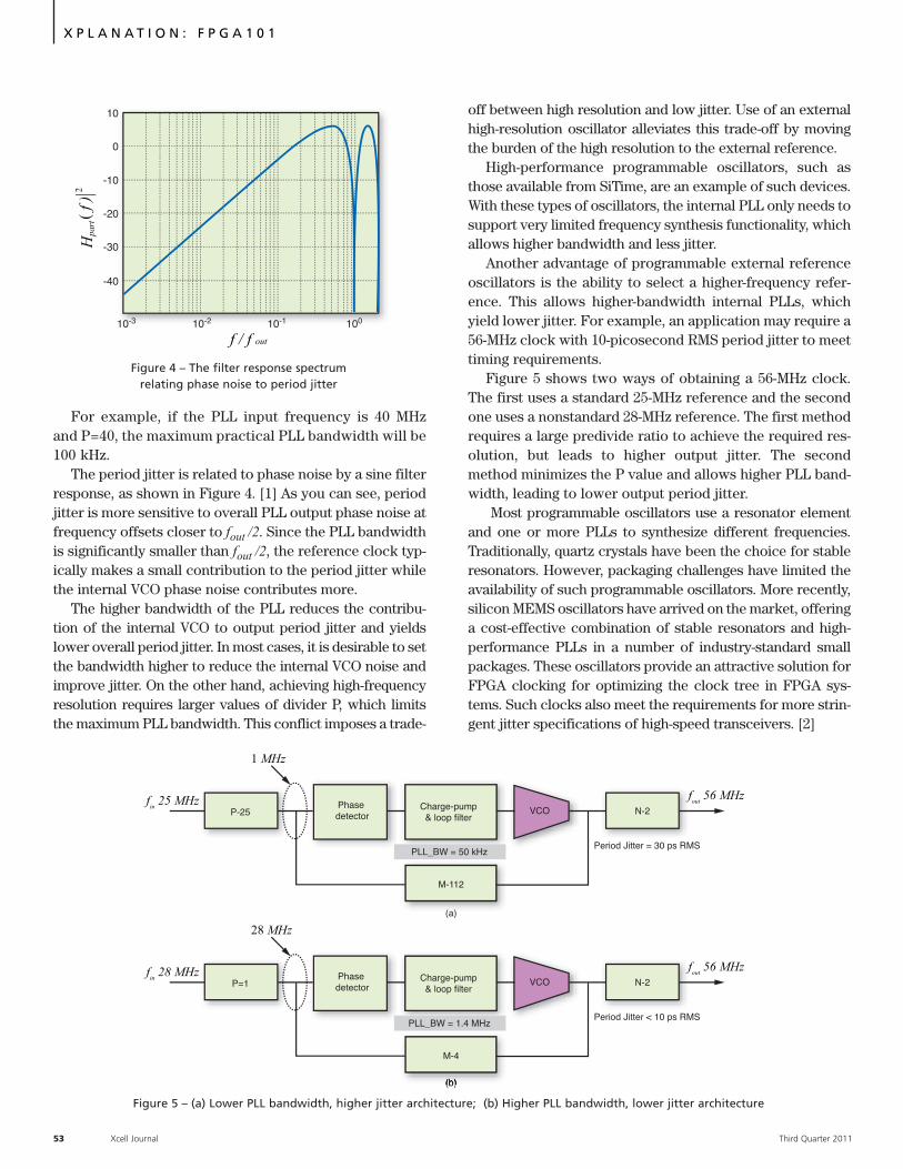
For example, if the PLL input frequency is 40 MHzand P=40, the maximum practical PLL bandwidth will be100 kHz.
The period jitter is related to phase noise by a sine filterresponse, as shown in Figure 4. [1] As you can see, periodjitter is more sensitive to overall PLL output phase noise atfrequency offsets closer to fout /2. Since the PLL bandwidthis significantly smaller than fout /2, the reference clock typ-ically makes a small contribution to the period jitter whilethe internal VCO phase noise contributes more.
The higher bandwidth of the PLL reduces the contribu-tion of the internal VCO to output period jitter and yieldslower overall period jitter. In most cases, it is desirable to setthe bandwidth higher to reduce the internal VCO noise andimprove jitter. On the other hand, achieving high-frequencyresolution requires larger values of divider P, which limitsthe maximum PLL bandwidth. This conflict imposes a trade-
53 Xcell Journal Third Quarter 2011
X P L A N A T I O N : F P G A 1 0 1
off between high resolution and low jitter. Use of an externalhigh-resolution oscillator alleviates this trade-off by movingthe burden of the high resolution to the external reference.
High-performance programmable oscillators, such asthose available from SiTime, are an example of such devices.With these types of oscillators, the internal PLL only needs tosupport very limited frequency synthesis functionality, whichallows higher bandwidth and less jitter.
Another advantage of programmable external referenceoscillators is the ability to select a higher-frequency refer-ence. This allows higher-bandwidth internal PLLs, whichyield lower jitter. For example, an application may require a56-MHz clock with 10-picosecond RMS period jitter to meettiming requirements.
Figure 5 shows two ways of obtaining a 56-MHz clock.The first uses a standard 25-MHz reference and the secondone uses a nonstandard 28-MHz reference. The first methodrequires a large predivide ratio to achieve the required res-olution, but leads to higher output jitter. The secondmethod minimizes the P value and allows higher PLL band-width, leading to lower output period jitter.
Most programmable oscillators use a resonator elementand one or more PLLs to synthesize different frequencies.Traditionally, quartz crystals have been the choice for stableresonators. However, packaging challenges have limited theavailability of such programmable oscillators. More recently,silicon MEMS oscillators have arrived on the market, offeringa cost-effective combination of stable resonators and high-performance PLLs in a number of industry-standard smallpackages. These oscillators provide an attractive solution forFPGA clocking for optimizing the clock tree in FPGA sys-tems. Such clocks also meet the requirements for more strin-gent jitter specifications of high-speed transceivers. [2]
10
0
-10
-20
-30
-40
10-3 10-2 10-1 100
( f )
Hpa
rt
f / f out
2
Figure 4 – The filter response spectrum relating phase noise to period jitter
P-25Phase detector
Charge-pump& loop filter
VCO N-2
M-112
(a)
(b)
fin
25 MHz fout
56 MHz
PLL_BW = 50 kHzPeriod Jitter = 30 ps RMS
1 MHz
P=1Phase detector
Charge-pump& loop filter
VCO N-2
M-4
fin
28 MHz fout
56 MHz
PLL_BW = 1.4 MHzPeriod Jitter < 10 ps RMS
28 MHz
Figure 5 – (a) Lower PLL bandwidth, higher jitter architecture; (b) Higher PLL bandwidth, lower jitter architecture
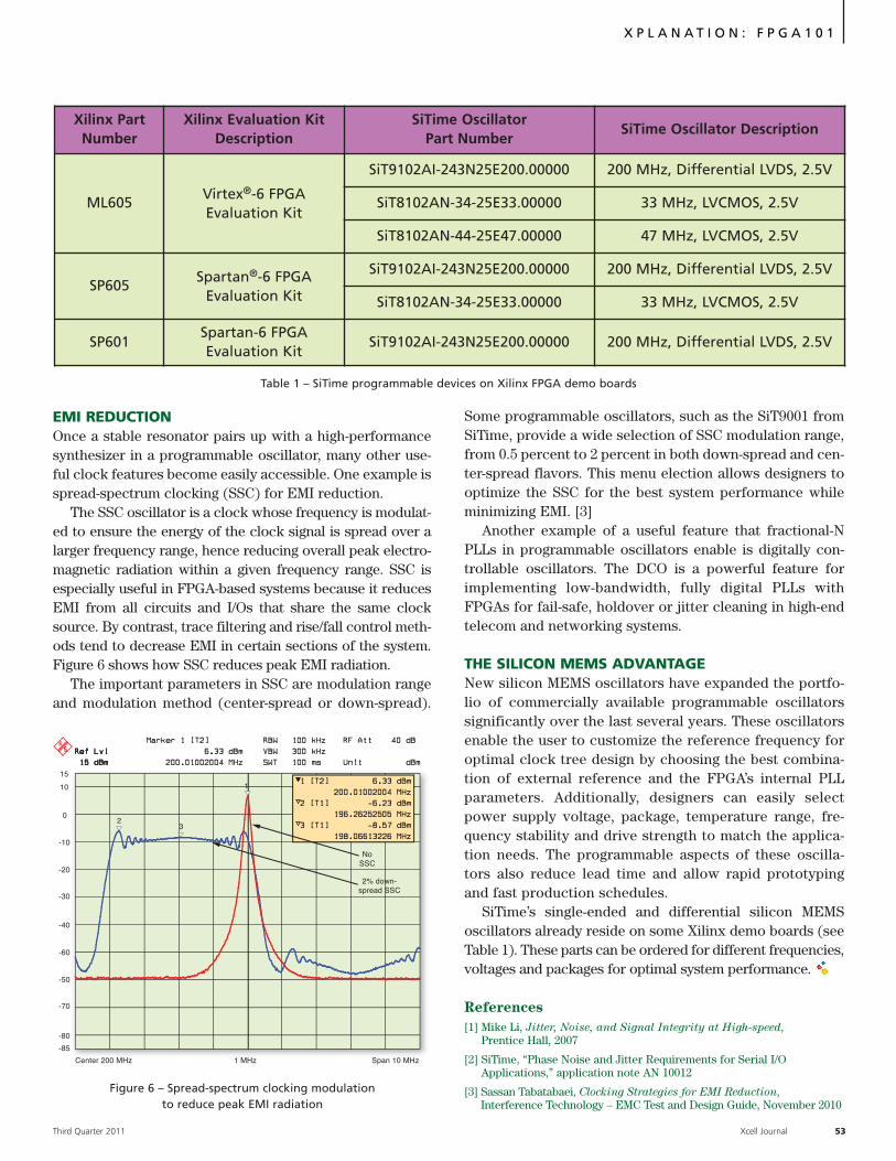
EMI REDUCTIONOnce a stable resonator pairs up with a high-performancesynthesizer in a programmable oscillator, many other use-ful clock features become easily accessible. One example isspread-spectrum clocking (SSC) for EMI reduction.
The SSC oscillator is a clock whose frequency is modulat-ed to ensure the energy of the clock signal is spread over alarger frequency range, hence reducing overall peak electro-magnetic radiation within a given frequency range. SSC isespecially useful in FPGA-based systems because it reducesEMI from all circuits and I/Os that share the same clocksource. By contrast, trace filtering and rise/fall control meth-ods tend to decrease EMI in certain sections of the system.Figure 6 shows how SSC reduces peak EMI radiation.
The important parameters in SSC are modulation rangeand modulation method (center-spread or down-spread).
X P L A N A T I O N : F P G A 1 0 1
Third Quarter 2011 Xcell Journal 53
Some programmable oscillators, such as the SiT9001 fromSiTime, provide a wide selection of SSC modulation range,from 0.5 percent to 2 percent in both down-spread and cen-ter-spread flavors. This menu election allows designers tooptimize the SSC for the best system performance whileminimizing EMI. [3]
Another example of a useful feature that fractional-NPLLs in programmable oscillators enable is digitally con-trollable oscillators. The DCO is a powerful feature forimplementing low-bandwidth, fully digital PLLs withFPGAs for fail-safe, holdover or jitter cleaning in high-endtelecom and networking systems.
THE SILICON MEMS ADVANTAGENew silicon MEMS oscillators have expanded the portfo-lio of commercially available programmable oscillatorssignificantly over the last several years. These oscillatorsenable the user to customize the reference frequency foroptimal clock tree design by choosing the best combina-tion of external reference and the FPGA’s internal PLLparameters. Additionally, designers can easily selectpower supply voltage, package, temperature range, fre-quency stability and drive strength to match the applica-tion needs. The programmable aspects of these oscilla-tors also reduce lead time and allow rapid prototypingand fast production schedules.
SiTime’s single-ended and differential silicon MEMSoscillators already reside on some Xilinx demo boards (seeTable 1). These parts can be ordered for different frequencies,voltages and packages for optimal system performance.
References
[1] Mike Li, Jitter, Noise, and Signal Integrity at High-speed, Prentice Hall, 2007
[2] SiTime, “Phase Noise and Jitter Requirements for Serial I/OApplications,” application note AN 10012
[3] Sassan Tabatabaei, Clocking Strategies for EMI Reduction,Interference Technology – EMC Test and Design Guide, November 2010
Xilinx PartNumber
Xilinx Evaluation KitDescription
SiTime Oscillator Part Number
SiTime Oscillator Description
ML605Virtex®-6 FPGAEvaluation Kit
SiT9102AI-243N25E200.00000 200 MHz, Differential LVDS, 2.5V
SiT8102AN-34-25E33.00000 33 MHz, LVCMOS, 2.5V
SiT8102AN-44-25E47.00000 47 MHz, LVCMOS, 2.5V
SP605Spartan®-6 FPGA
Evaluation Kit
SiT9102AI-243N25E200.00000 200 MHz, Differential LVDS, 2.5V
SiT8102AN-34-25E33.00000 33 MHz, LVCMOS, 2.5V
SP601Spartan-6 FPGAEvaluation Kit
SiT9102AI-243N25E200.00000 200 MHz, Differential LVDS, 2.5V
Table 1 – SiTime programmable devices on Xilinx FPGA demo boards
-80
-85
Center 200 MHz
NoSSC
2% down-spread SSC
1 MHz Span 10 MHz
-70
-60
-50
-40
-30
-10
-20
02
1
3
10
15
Figure 6 – Spread-spectrum clocking modulation to reduce peak EMI radiation

54 Xcell Journal Third Quarter 2011
XPLANATION: FPGA101
Archiving FPGA Designsfor Easy Updatesby Bruce EricksonDesign EngineerAgilent [email protected]
D evelopers that embrace the “latest and greatest” FPGA technology to get thehighest performance and provide the best functionality to customers arealways upgrading their FPGA tools, since older versions don’t support newer
families of parts. However, this does not mean that we can ignore the older FPGAs—sometimes we want to add functionality to a previous product, or we are taking newtechnology and putting it into a whole family of instruments, which means that weneed to upgrade older families of FPGAs.
Over the years our team at Agilent Technologies has struggled with how best toarchive FPGA designs for this purpose. We have always kept HDL source code andtool settings in configuration management systems (CMS) that allow us to trackchanges, and that let anybody on the team edit the code (or leverage from it). But asinnovation accelerated in the FPGA world, we started having difficulties when itcame to actually updating the older designs:
• Sometimes the effort to upgrade an older design to work with the new designenvironment outweighed the actual work on the FPGA itself.
• Often the effort to re-create the older design environment was more than thework to upgrade the FPGA (see sidebar, next page).
Over the years we have tried various strategies, as outlined in Table 1. Severalyears ago we tried using virtual machines (VMs), but discarded the technologybecause the performance of place-and-route inside a VM was terrible. But now hard-ware and software have evolved so that performance is no longer significantly worseinside a VM than outside it, and we are returning to the idea of archiving the entiredesign—including the design environment—within a virtual machine, so that it iseasy to make changes to an FPGA after initial development is finished.
At the end of an FPGA project, we copy the design tools and design to a VM’s virtu-al hard drive (VHD). Then we check the VHD into the CMS. Because the VHD is bina-ry, there is no usable “change record” for the HDL (Verilog or VHDL) sources. So we
Virtual machines can store your entire design, fromdesign environment to FPGA code, making it easy to
change an FPGA after you’ve completed development.
Third Quarter 2011 Xcell Journal 55
X P L A N A T I O N : F P G A 1 0 1
also check the HDL sources into a CMS to make it easy totrack the logical changes to the FPGA design. When weneed to make a quick change, we simply check out theVHD to our current machine and run the VM using it. Theresult is a window on our screen that looks like our olddesign environment—the old tools and even the operatingsystem are all there. There is no need to upgrade thedesign to make a simple change.
WHAT ARE VIRTUAL MACHINES?Virtual machines consist of a program, often called a “hyper-visor,” that intercepts I/O from programs running under it.The hypervisor provides emulated hard drives (also knownas virtual hard drives, or VHDs), along with emulated or,more commonly, “pass-through” LANs, DVD drives, USBports and even RS232 peripherals. A BIOS or hardwareabstraction layer (HAL) is also part of the VM program. Thecombination of these functions is a virtual machine, in justthe same way that the marriage of a CPU, peripherals andBIOS is commonly called a personal computer.
When the VM starts from power-up you see a BIOSboot display; then you can load an operating system froma CD or boot from an OS already loaded on the VHD. Thismeans that you can, for example, run a full version ofLinux under a VM running on a host Windows machine, afull version of Windows on a Linux machine—or even afull version of Windows on a Windows machine. Why domost people find this useful? Because they can changephysical hardware without making any changes to an exe-cution environment. Many companies run several VMs ona single computer, allowing them to consolidate severalsmaller servers without having to change anything aboutthe servers as far as their software—and the softwarethat uses the server—is concerned.
Around 2006 both Intel and AMD started making hard-ware support for virtual machines more widespread; basi-cally, they added methods for swapping entire sets of reg-isters and redirecting I/O on a per-process basis. Thismeans that software in a VM runs at almost the samespeed as it would run under the real hardware. In fact,compute-intensive programs (such as place-and-route)run at almost the same speed under a VM as they do onthe main OS, because the VM doesn’t need to get involvedin a lot of I/O redirection.
VMware and Sun/Oracle make excellent VMs. VMwarehas, in my opinion, the widest and most stable VM environ-ment (and the priciest). Sun’s (now Oracle’s) VM, known asVirtualBox, is also pretty good, and is licensed under GPLversion 2; download it from www.virtualbox.org.Microsoft provides a VM for Windows XP known as VirtualPC 2007. Another VM, called Windows Virtual PC, is avail-able with Windows 7 Enterprise and Professional editions;it’s free, but you need to download it from Microsoft.
56 Xcell Journal Third Quarter 2011
X P L A N A T I O N : F P G A 1 0 1
CREATING A VM WITH AN FPGA DESIGNAt this point, let’s walk through the process of creating andusing a VM. We’ll focus on VirtualBox under a Windows 7system, emulating a Windows XP system with Xilinx® ISE®
10.1. However, the general steps are applicable to otherVMs as well.
The first step is to verify that hardware support for virtu-al machines is enabled. I don’t know why, but the last fourPCs (from various vendors) I have looked at do not have theCPU’s virtualization technology enabled; I’ve had to go intothe BIOS to enable it. It exists under various names, like “vir-tualization acceleration,” “virtualization technology,” “VMT”and, in one case, “VT.” Microsoft provides a program to
Challenges in upgrading designs to new tools
■ If the design is too old, it may not be possible to read the project-definition file into the new tools.
■ If you can’t read in the old project, it can bechallenging to figure out what are the correctfiles (or versions of files), as well as languageand processing settings.
■ IP that you used in the design may not be available for the new tools—or may require new licensing fees for the upgrade.
■ It could take a lot of effort to upgrade certain parts of the design, such as soft-microprocessor cores.
Challenges in restoring old design environments
■ Old and new versions of tools may not coexist easily. If you have to remove your current tools,your current project is going to suffer.
■ It may take a long time to find and install old versions of tools.
■ It may not be clear what version of the toolswere used with the project; you may end up trying several versions before you find one that works.
■ Even if the version is documented, it might notbe clear what patches are necessary.
■ Settings defined by environment variables maynot be documented, and finding the right values might take a long time.
■ Old tools may not even run on newer operating systems.
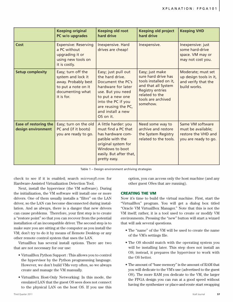
check to see if it is enabled; search microsoft.com forHardware-Assisted Virtualization Detection Tool.
Next, install the hypervisor (the VM software). Duringthe initialization, the VM software will install one or moredrivers. One of them usually installs a “filter” on the LANdriver, so the LAN can become disconnected during instal-lation. And as always, there is a danger that new driverscan cause problems. Therefore, your first step is to createa “restore point” so that you can recover from the potentialinstallation of an incompatible driver. The second step is tomake sure you are sitting at the computer as you install theVM; don’t try to do it by means of Remote Desktop or anyother remote control system that uses the LAN.
VirtualBox has several install options. There are twothat are not necessary for our use:
• VirtualBox Python Support : This allows you to controlthe hypervisor by the Python programming language.However, we don’t build VMs very often, so we alwayscreate and manage the VM manually.
• VirtualBox Host-Only Networking: In this mode, theemulated LAN that the guest OS sees does not connectto the physical LAN on the host OS. If you use this
X P L A N A T I O N : F P G A 1 0 1
Third Quarter 2011 Xcell Journal 57
option, you can access only the host machine (and anyother guest OSes that are running).
CREATING THE VMNow it’s time to build the virtual machine. First, start the“VirtualBox” program. You will get a dialog box titled“Oracle VM VirtualBox Manager.” Note that this is not theVM itself; rather, it is a tool used to create or modify VMenvironments. Pressing the “new” button will start a wizardthat will ask several questions.
• The “name” of the VM will be used to create the nameof the VM’s settings file.
• The OS should match with the operating system youwill be installing later. This step does not install anOS; instead, it prepares the hypervisor to work withthe OS better.
• The amount of “base memory” is the amount of RAM thatyou will dedicate to the VM’s use (advertised to the guestOS). The more RAM you dedicate to the VM, the largerthe FPGA design you can run at a good speed withouthaving the synthesizer or place-and-route start swapping
Keeping original PC w/o upgrades
Keeping old roothard drive
Keeping old projecthard drive
Keeping VHD
Cost Expensive: Reservinga PC withoutupgrading it orusing new tools onit is costly.
Inexpensive. Harddrives are cheap!
Inexpensive. Inexpensive: justsome hard-drivespace. VM may ormay not cost you.
Setup complexity Easy; turn off thesystem and lock itaway. Probably bestto put a note on itdocumenting whatit is for.
Easy; just pull outthe hard drive.Document the PC’shardware for lateruse. But you needto put a new oneinto the PC if youare reusing the PC,and install a newOS on it.
Easy; just make sure hard drive hastools installed on it,and that all SystemRegistry entriesrelated to the tools are archivedsomehow.
Moderate; must setup design tools in it,and verify that thebuild works.
Ease of restoring thedesign environment
Easy; turn on the oldPC and (if it boots)you are ready to go.
A little harder: youmust find a PC thathas hardware com-patible with theoriginal system forWindows to booteasily. But after that,pretty easy.
Need some way toarchive and restorethe System Registryrelated to the tools.
Same VM softwaremust be available;restore the VHD andyou are ready to go.
Table 1 – Design environment archiving strategies
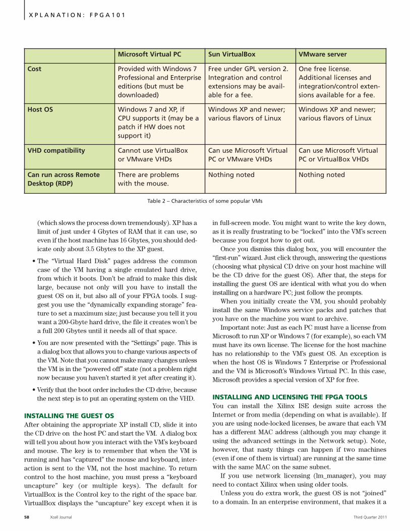
(which slows the process down tremendously). XP has alimit of just under 4 Gbytes of RAM that it can use, soeven if the host machine has 16 Gbytes, you should ded-icate only about 3.5 Gbytes to the XP guest.
• The “Virtual Hard Disk” pages address the commoncase of the VM having a single emulated hard drive,from which it boots. Don’t be afraid to make this disklarge, because not only will you have to install theguest OS on it, but also all of your FPGA tools. I sug-gest you use the “dynamically expanding storage” fea-ture to set a maximum size; just because you tell it youwant a 200-Gbyte hard drive, the file it creates won’t bea full 200 Gbytes until it needs all of that space.
• You are now presented with the “Settings” page. This isa dialog box that allows you to change various aspects ofthe VM. Note that you cannot make many changes unlessthe VM is in the “powered off” state (not a problem rightnow because you haven’t started it yet after creating it).
• Verify that the boot order includes the CD drive, becausethe next step is to put an operating system on the VHD.
INSTALLING THE GUEST OSAfter obtaining the appropriate XP install CD, slide it intothe CD drive on the host PC and start the VM. A dialog boxwill tell you about how you interact with the VM’s keyboardand mouse. The key is to remember that when the VM isrunning and has “captured” the mouse and keyboard, inter-action is sent to the VM, not the host machine. To returncontrol to the host machine, you must press a “keyboarduncapture” key (or multiple keys). The default forVirtualBox is the Control key to the right of the space bar.VirtualBox displays the “uncapture” key except when it is
X P L A N A T I O N : F P G A 1 0 1
in full-screen mode. You might want to write the key down,as it is really frustrating to be “locked” into the VM’s screenbecause you forgot how to get out.
Once you dismiss this dialog box, you will encounter the“first-run” wizard. Just click through, answering the questions(choosing what physical CD drive on your host machine willbe the CD drive for the guest OS). After that, the steps forinstalling the guest OS are identical with what you do wheninstalling on a hardware PC; just follow the prompts.
When you initially create the VM, you should probablyinstall the same Windows service packs and patches thatyou have on the machine you want to archive.
Important note: Just as each PC must have a license fromMicrosoft to run XP or Windows 7 (for example), so each VMmust have its own license. The license for the host machinehas no relationship to the VM’s guest OS. An exception iswhen the host OS is Windows 7 Enterprise or Professionaland the VM is Microsoft’s Windows Virtual PC. In this case,Microsoft provides a special version of XP for free.
INSTALLING AND LICENSING THE FPGA TOOLS You can install the Xilinx ISE design suite across theInternet or from media (depending on what is available). Ifyou are using node-locked licenses, be aware that each VMhas a different MAC address (although you may change itusing the advanced settings in the Network setup). Note,however, that nasty things can happen if two machines(even if one of them is virtual) are running at the same timewith the same MAC on the same subnet.
If you use network licensing (lm_manager), you mayneed to contact Xilinx when using older tools.
Unless you do extra work, the guest OS is not “joined”to a domain. In an enterprise environment, that makes it a
58 Xcell Journal Third Quarter 2011
Microsoft Virtual PC Sun VirtualBox VMware server
Cost Provided with Windows 7Professional and Enterpriseeditions (but must bedownloaded)
Free under GPL version 2.Integration and controlextensions may be avail-able for a fee.
One free license.Additional licenses andintegration/control exten-sions available for a fee.
Host OS Windows 7 and XP, if CPU supports it (may be apatch if HW does not support it)
Windows XP and newer;various flavors of Linux
Windows XP and newer;various flavors of Linux
VHD compatibility Cannot use VirtualBox or VMware VHDs
Can use Microsoft VirtualPC or VMware VHDs
Can use Microsoft VirtualPC or VirtualBox VHDs
Can run across RemoteDesktop (RDP)
There are problems with the mouse.
Nothing noted Nothing noted
Table 2 – Characteristics of some popular VMs
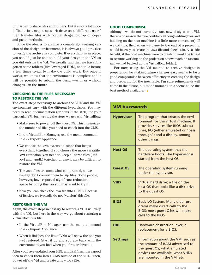
bit harder to share files and folders. But it’s not a lot moredifficult; just map a network drive as a “different user,”then transfer files with normal drag-and-drop or copy-and-paste methods.
Since the idea is to archive a completely working ver-sion of the design environment, it is always good practiceto verify the archive is complete. If everything is in place,you should just be able to build your design in the VM asyou did outside the VM. We usually find that we have for-gotten some folders (like leveraged HDL), and thus iteratea few times trying to make the build work. But once itworks, we know that the environment is complete and itwill be possible to rebuild the design—with or withoutchanges—in the future.
CHECKING IN THE FILES NECESSARY TO RESTORE THE VMThe exact steps necessary to archive the VHD and the VMenvironment vary with the different hypervisors. You mayneed to read documentation (or consult the Web) for yourparticular VM, but here are the steps we use with VirtualBox:
• Make sure to power off the guest OS. This minimizesthe number of files you need to check into the CMS.
• In the VirtualBox Manager, use the menu commandFile -> Export Appliance.
• We choose the .ova extension, since that keepseverything together. If you choose the more versatile.ovf extension, you need to keep all three files (.mf,.ovf and .vmdk) together, or else it may be difficult torestore the VM.
• The .ova files are somewhat compressed, so we usually don’t convert them to .zip files. Some people,however, have reported significant reduction inspace by doing this, so you may want to try it.
• Now you can check the .ova file into a CMS. Becauseof its size, we typically do not “version” this file.
RESTORING THE VM Again, the exact steps necessary to restore a VHD will varywith the VM, but here is the way we go about restoring aVirtualBox .ova file:
• In the VirtualBox Manager, use the menu commandFile -> Import Appliance.
• When it finishes, the list of VMs will show the one youjust restored. Start it up and you are back with theenvironment you had when you first archived it.
After you have updated your HDL and ISE files, it is a goodidea to check them into a CMS outside of the VHD. Then,power off the VM and create a new .ova file.
X P L A N A T I O N : F P G A 1 0 1
GOOD COMPROMISEAlthough we do not currently start new designs in a VM,there is no reason that we couldn’t (although editing files andbuilding on the host machine is a little more convenient). Ifwe did this, then when we came to the end of a project, itwould be easy to create the .ova file and check it in. As a sidebenefit, if the host machine were to crash, it would be trivialto resume working on the project on a new machine (assum-ing we had backed up the VirtualBox folder).
For now, using the VM method to archive designs inpreparation for making future changes easy seems to be agood compromise between efficiency in creating the designand preparing for the inevitable. I’m sure refinements willcome in the future, but at the moment, this seems to be thebest method available.
VM buzzwords
Hypervisor The program that creates the envi-ronment for the virtual machine. Itprovides services like BIOS subrou-tines, I/O (either emulated or “passthrough”) and a display, amongother things.
Host OS The operating system that thehardware boots. The hypervisor isstarted from the host OS.
Guest OS The operating system runningunder the hypervisor.
VHD Virtual hard drive; a file on thehost OS that looks like a disk driveto the guest OS.
BIOS Basic I/O System. Many older pro-grams make direct calls to theBIOS; most guest OSes will makecalls to the BIOS.
HAL Hardware abstraction layer; areplacement for a BIOS.
Settings Information about the VM, such asthe amount of RAM advertised tothe guest OS, what emulateddevices are available, what VHDsare mounted in the VM, etc.
Third Quarter 2011 Xcell Journal 59

NEW NAVIGATORA new application called Docu-
mentation Navigator allows users toview and manage Xilinx design docu-mentation (software, hardware , IP andmore) from one place, with easy-to-usedownload, search and notification fea-tures. To try out the new XilinxDocumentation Navigator, now inopen beta release, go to the downloadlink at www.xilinx.com/support.
ISE DESIGN SUITE:LOGIC EDITION
Front-to-Back FPGA Logic DesignLatest version number: 13.2Date of latest release: July 2011Previous release: 13.1URL to download the latest patch:www.xilinx.com/download
Revision highlights:A newly redesigned user interfacefor PlanAhead™ and the IP suiteimproves productivity across SoCdesign teams in a progression
toward true plug-and-play IP thattargets Spartan®-6, Virtex®-6 and 7series FPGAs. In addition, the latestISE Design Suite provides up to 25percent better performance on theindustry-leading 2 million-logic-cellVirtex-7 2000T device.
PlanAhead design analysis tool:Xilinx has further enhanced thegraphical user interface (GUI) toprovide an intuitive environmentfor both new and advanced users. Anew clock domain interactionreport analyzes timing pathsbetween clock domains. PlanAhead13.2 also offers the ability to invokeTRACE on post-implementationsand localization of tool tips forJapanese and Chinese languages.
Team design: A team designmethodology using PlanAheadaddresses the challenge of multipleengineers working on a single proj-ect by providing a methodology forgroups to work in parallel. Buildingon the design preservation capabilitymade available in ISE Design Suite
12, the team design flow providesadditional functionality and lets youlock down early implementationresults on completed portions of thedesign without having to wait for therest of the design team. This newcapability facilitates faster timingclosure and timing preservation forthe remainder of the design, increas-ing overall productivity and reducingdesign iterations.
Xilinx Power Estimator (XPE) andPower Analyzer (XPA): These toolsnow offer improved power estima-tion, and XPA features vectorlessalgorithms for activity propagation.
ISE DESIGN SUITE:EMBEDDED EDITION
Integrated Embedded Design SolutionLatest version number: 13.2Date of latest release: July 2011Previous release: 13.1URL to download the latest patch:www.xilinx.com/download
Revision highlights:All ISE Design Suite editions includethe enhancements listed above forthe Logic Edition. The followingenhancements are specific to theEmbedded Edition.
Xilinx Platform Studio (XPS): Thissoftware boasts a number of enhance-ments, including support for theKintex™ KC705 platform and for sin-gle or dual AXI4-based MicroBlaze™designs. Base System Builder uses anew two-page setup for easier config-uration. The Create/Import IP wizardnow supports AXI4, AXI-Lite andAXI4-Stream IP.
62 Xcell Journal Third Quarter 2011
Xilinx Tool & IP UpdatesXilinx is continually improving its products, IP and design tools
as it strives to help designers work more effectively. Here, we
report on the most current updates to the flagship FPGA develop-
ment environment, the ISE® Design Suite, as well as to Xilinx®
IP, as of July 2011. Product updates offer significant enhance-
ments and new features to three versions of the ISE Design
Suite: the Logic, Embedded and DSP editions. Keeping your
installation of ISE up to date is an easy way to ensure the best
results for your design. Updates to the ISE Design Suite are
available from the Xilinx Download Center at www.xilinx.com/download. For more information or to download a free 30-day
evaluation of ISE, visit www.xilinx.com/ise.
XTRA, XTRA
SDK enhancements: Xilinx hasupdated the Software DevelopmentKit to Eclipse 3.6.2 and CDT 7.0.2releases to provide stability andenhancements in this open-sourceplatform. MicroBlaze v8.20a sup-port now features a 512-bit datawidth for AXI cache interconnects.
IP enhancements: The releaseincludes new AXI PCIe™ andQuadSPI IP, along with improved AXIV6 DDRx read /write arbitration.
EDK overall enhancements: TheEmbedded Development Kit nowoffers consistent SDK workspaceselection behavior across ProjectNavigator, Xilinx Platform Studio(XPS) and the SDK.
ISE DESIGN SUITE:DSP EDITION
For High-Performance DSP Systems Latest version number: 13.2Date of latest release: July 2011Previous release: 13.1URL to download the latest patch:www.xilinx.com/download
Revision highlights:All ISE Design Suite editions includethe enhancements listed above forthe Logic Edition. Specific to theDSP Edition, version 13.2 offershardware co-simulation support forthe Kintex KC-705 platform.
In addition, the CIC Compileroffers an input width of 24 bits andthe new Divider Generator featuresoperand support to 64 bits.
XILINX IP UPDATES Name of IP: ISE IP Update 13.2Type of IP: All
Targeted application: Xilinxdevelops IP cores and partnerswith third-party IP providers to
ment a DDR2 or DDR3 SDRAMmultiport memory controllerusing MIG and AXI interconnectIP from CORE Generator.
• AXI Bus Functional Model(BFM) v1.9, created for Xilinxby Cadence Design Systems,enables Xilinx customers to veri-fy and simulate communicationwith AXI-based IP they aredeveloping. The AXI BFM IP inCORE Generator delivers test-bench and script examples thatdemonstrate the use of the BFMtest-writing APIs for AXI3, AXI4,AXI4-Lite and AXI4-Stream mas-ters and slaves.
• AXI Direct Memory Access(DMA) LogiCORE IP v4.00 pro-vides a flexible interface fortransferring packet data betweensystem memory (AXI4) andAXI4-Stream target IP. The AXIDMA provides optional supportof scatter/gather for offloadingprocessor management of DMAtransfers and descriptor queuingfor prefetching transfer descrip-tors to enable uninterruptedtransfer requests by the primaryDMA controllers.
Audio, video and image processingIP: The Video Timing Controller v3.0now supports the AXI4-Lite interfaceand Virtex-7 and Kintex-7 device fam-ilies. The Triple-Rate SDI IP hasadded Spartan-6 support.
Additional IP supporting AXI4 inter-faces: Xilinx has updated the latestversions of CORE Generator IP withproduction AXI4 interface support.For more detailed support informa-tion, see www.xilinx.com/ipcenter/
axi4_ip.htm.
For general information on XilinxAXI4 support see www.xilinx.com/
axi4.htm.
decrease customer time-to-market.The powerful combination of XilinxFPGAs with IP cores provides func-tionality and performance similar toASSPs, but with flexibility not possi-ble with ASSPs.
Latest version number: 13.2Date of latest release: July 2011URL to access the latest version:www.xilinx.com/download
Informational URL: www.xilinx.com/ipcenter/coregen/
updates_13_2.htm
Installation instructions:www.xilinx.com/ipcenter/coregen/ip_
update_install_instructions.htm
Listing of all IP in this release:www.xilinx.com/ipcenter/core-
gen/13_2_datasheets.htm
Revision highlights: In general, any IP core for Virtex-7,Kintex-7, Virtex-6 and Spartan-6device families will now support theAXI4 interface. Older production ver-sions of IP will continue to supportthe legacy interface for the respectivecore on Virtex-6, Virtex-5 and Virtex-4,and Spartan-6 and Spartan-3, devicefamilies only. Starting with release13.1, all ISE CORE Generator™ IPsupports Kintex-7 and Virtex-7devices. The 13.2 release adds the fol-lowing new IP cores.
AXI infrastructure IP: Several newcores make it easy to create designsusing AXI4, AXI4-Lite or AXI4-Streaminterfaces.
• AXI Interconnect LogiCORE™IP v1.03 connects one or moreAXI4 memory-mapped masterdevices to one AXI4 slavedevice. The AXI interconnectsupports address widths from 12to 64 bits with interface datawidths of 32, 64, 128, 256, 512 or1,024 bits. Users can now imple-
Third Quarter 2011 Xcell Journal 63
64 Xcell Journal Third Quarter 2011
FEATURED WHITE PAPER – WP392: XILINX AGILEMIXED-SIGNAL SOLUTIONShttp://www.xilinx.com/support/documentation/
white_papers/wp392_Agile_Mixed_Signal.pdf
The industry-leading 28-nanometer 7 series of advancedFPGAs has greatly expanded the capabilities of the inte-grated analog subsystem over previous generations ofFPGA families. The analog subsystem in the Xilinx® 7series is called the XADC and includes dual, independent,1-Megasample/second (MSPS), 12-bit analog-to-digitalconverters (ADCs), along with a 17-channel analog multi-plexer front end. By closely integrating the XADC withFPGA logic, Xilinx has delivered the industry’s most flexi-ble analog subsystem. This novel combination of analogand programmable logic is called Agile Mixed Signal.
Pairing the XADC together with the programmable logicenables system designers to easily eliminate a wide range ofmixed-signal devices from their products, including “house-keeping” analog functions such as power monitoring andmanagement; supervisors, voltage monitors and sequencers;thermal management; system monitors and control; singleand multichannel ADCs; and touch sensors. The savings incost, board space and I/O pins can be significant—especiallyfor designs with area and cost constraints or those that shipin high volumes. Additional benefits of the integrated solu-tion include improvements in failure-in-time (FIT) rates, sim-plified inventory management and elimination of potentialend-of-life issues for mature mixed-signal devices.
This white paper by Anthony Collins and Robert Bielbyprovides an introduction to the benefits and features of theXADC and Agile Mixed Signal solutions implemented withArtix™-7, Kintex™-7 and Virtex®-7 FPGAs, and the Zynq™-7000 Extensible Processing Platform (EPP).
XAPP875: DYNAMICALLY PROGRAMMABLE DRU FOR HIGH-SPEED SERIAL I/Ohttp://www.xilinx.com/support/documentation/
application_notes/xapp875.pdf
Multiservice optical networks today require transceivers thatcan operate over a wide range of input data rates. High-speedserial I/O has a native lower limit for operating data rates,preventing easy interfacing to low-speed client signals. Thenoninteger data recovery unit (NI-DRU) that Paolo Novelliniand Giovanni Guasti present in this application note is specif-ically designed for RocketIO™ GTP and GTX transceivers inVirtex-5 LXT, SXT, TXT and FXT platforms and consists oflookup tables (LUTs) and flip-flops. The NI-DRU extends thelower data rate limit to 0 Mbits/second and the upper limit to1,250 Mbps, making embedded high-speed transceivers theideal solution for true multirate serial interfaces.
The NI-DRU’s operational settings (data rate, jitter band-width, input ppm range and jitter peaking) are dynamicallyprogrammable, thus avoiding the need for bitstream reloador partial reconfiguration. Operating on a synchronousexternal reference clock, the NI-DRU supports fractionaloversampling ratios. Thus, only one BUFG is needed, inde-pendent of the number of channels being set up, even if allchannels are operating at different data rates.
Given the absence of a relationship between the referenceclock and incoming data rate, two optional barrel shiftersease the interfacing of the NI-DRU with an external FIFO orwith any required decoder. The first barrel shifter has a 10-bitoutput that can be easily coupled to an 8b10b or 4b5bdecoder (neither of which is included in the accompanyingreference design). The second barrel shifter has a 16-bit out-put and is specifically designed for 8-bit protocols, such asSonet/SDH. The user can design other barrel shifters.
XAMPLES. . .
Application NotesIf you want to do a bit more reading about how our FPGAs lend themselves to a broad number of applications,we recommend these application notes and a white paper.
Third Quarter 2011 Xcell Journal 65
XAPP459: ELIMINATING I/O COUPLING EFFECTS WHEN INTERFACING LARGE-SWING SINGLE-ENDED SIGNALS TO USER I/O PINS ONSPARTAN-3 FAMILIEShttp://www.xilinx.com/support/documentation/
application_notes/xapp459.pdf
The Spartan®-3 families, consisting of Spartan-3, Spartan-3E and Extended Spartan-3A devices, support an excep-tionally robust and flexible I/O feature set, such that theycan easily meet the signaling requirements of most applica-tions. You can program user I/O pins of these families tohandle many different single-ended signal standards.
The standard single-ended signaling voltage levels are 1.2V,1.5V, 1.8V, 2.5V and 3.3V. But in a number of applications, it isdesirable to receive signals with a greater voltage swing thanuser I/O pins ordinarily permit. The most common use case isreceiving 5V signals on user I/O pins that are powered for usewith one of the standard single-ended signaling levels. Thistype of large-swing signal might be received by design ormight be applied to the user I/O unintentionally from severepositive or negative overshoot, which can occur regardless ofthe programmed “direction” of a user I/O pin.
This application note by Eric Crabill describes ways toreceive large-swing signals by design. In one solution (and inthe general case of severe positive or negative overshoot), par-asitic leakage current between user I/O in differential pin pairsmight occur, even though the user I/O pins are configured withsingle-ended I/O standards. The application note addresses theparasitic leakage current behavior that occurs outside the rec-ommended operating conditions.
XAPP486: 7:1 SERIALIZATION IN SPARTAN-3E/3AFPGAS AT SPEEDS UP TO 666 MBPShttp://www.xilinx.com/support/documentation/
application_notes/xapp486.pdf
Spartan-3E and Extended Spartan-3A devices are used in awide variety of applications requiring 7:1 serialization atspeeds up to 666 Mbits/second. This application note targetsSpartan-3E/3A devices in applications that require 4-bit or 5-bit transmit data bus widths and operate at rates up to 666Mbps per line with a forwarded clock at one seventh the bitrate. This type of interface is commonly used in flat-panel dis-plays and automotive applications. (Associated receiverdesigns are discussed in XAPP485, “1:7 Deserialization inSpartan-3E/3A FPGAs at Speeds Up to 666 Mbps,”http://www.xilinx.com/support/documentation/application_
notes/xapp485.pdf.)
These designs are applicable to Spartan-3E/3A FPGAsand not to the original Spartan-3 device. The design filesfor this application note target the Spartan-3E family, butthe Extended Spartan-3A family also supports the samedesign approach.
Two versions of the serializer design are available. Inthe Logic version, the lower-speed system clock and thehigher-speed transmitter clock are phase-aligned. TheFIFO version, for its part, uses a block RAM-basedFIFO memory to ensure there is no phase relationshiprequirement between the two clocks. Both versions usea transmission clock that is 3.5 times the system clockalong with double-data-rate (DDR) techniques to arriveat a serialization factor of seven. This is done both tokeep the internal logic to a reasonable speed and toensure that the clock generation falls into the range ofthe digital frequency synthesizer (DFS) block of theSpartan-3E FPGA.
The maximum data rate for the Spartan-3E FPGA is622 Mbps for the -4 speed grade and 666 Mbps for the -5speed grade. The maximum data rate for the Spartan-3AFPGA is 640 Mbps for the -4 speed grade and 700 Mbpsfor the -5 speed grade.
The limitation in both devices is the maximum speedof the DFS block in Stepping 1 silicon.
XAPP1026 (UPDATED FOR AXI4): LIGHTWEIGHT IP (LWIP) APPLICATION EXAMPLEShttp://www.xilinx.com/support/documentation/
application_notes/xapp1026.pdf
This application note explains how to use lightweight IP(lwIP), an open-source TCP/IP networking stack forembedded systems, to develop applications on XilinxFPGAs. The Xilinx Software Development Kit (SDK) sup-plies lwIP software customized to run on Xilinx embed-ded systems containing either a PowerPC® or aMicroBlaze™ processor.
Focusing solely on the MicroBlaze, authors StephenMacMahon, Nan Zang and Anirudha Sarangi describehow to utilize the lwIP library to add networking capa-bility to an embedded system. In particular, they takeyou through the steps for developing four applications:echo server, Web server, TFTP server and receive-and-transmit throughput tests. The authors have updatedthis application note for the AX14 interface. The docu-ment includes PLB- and AXI4-based reference systemsfor the Xilinx ML605, SP605 and SP601 FPGA StarterKit boards.
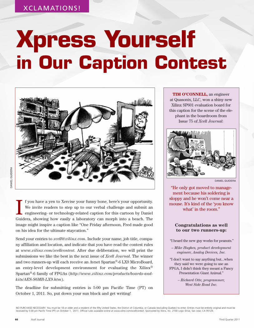
66 Xcell Journal Third Quarter 2011
Xpress Yourself in Our Caption Contest
NO PURCHASE NECESSARY. You must be 18 or older and a resident of the fifty United States, the District of Columbia, or Canada (excluding Quebec) to enter. Entries must be entirely original and must bereceived by 5:00 pm Pacific Time (PT) on October 1, 2011. Official rules available online at www.xilinx.com/xcellcontest. Sponsored by Xilinx, Inc. 2100 Logic Drive, San Jose, CA 95124.
I f you have a yen to Xercise your funny bone, here’s your opportunity.We invite readers to step up to our verbal challenge and submit anengineering- or technology-related caption for this cartoon by Daniel
Guidera, showing how easily a laboratory can morph into a beach. Theimage might inspire a caption like “One Friday afternoon, Fred made goodon his idea for the ultimate staycation.”
Send your entries to [email protected]. Include your name, job title, compa-ny affiliation and location, and indicate that you have read the contest rulesat www.xilinx.com/xcellcontest. After due deliberation, we will print thesubmissions we like the best in the next issue of Xcell Journal. The winnerand two runners-up will each receive an Avnet Spartan®-6 LX9 MicroBoard,an entry-level development environment for evaluating the Xilinx®
Spartan®-6 family of FPGAs (http://www.xilinx.com/products/boards-and-
kits/AES-S6MB-LX9.htm).
The deadline for submitting entries is 5:00 pm Pacific Time (PT) onOctober 1, 2011. So, put down your sun block and get writing!
TIM O’CONNELL, an engineer at Quasonix, LLC, won a shiny newXilinx SP601 evaluation board for
this caption for the scene of the ele-phant in the boardroom from
Issue 75 of Xcell Journal:
Congratulations as well
to our two runners-up:
“I heard the new guy works for peanuts.”
– Mike Hughes, product development
engineer, Analog Devices, Inc.
“I don’t want to say anything but...whenthey said we were going to use an
FPGA, I didn’t think they meant a FancyPresentation Giant Animal.”
– Richard Otte, programmer,
West Side Road Inc.
“He only got moved to manage-ment because his soldering is
sloppy and he won’t come near amouse. It’s kind of the ‘you know
what’ in the room.”
DANIEL GUIDERA
DA
NIE
LG
UID
ER
AXCLAMATIONS!

www.xilinx.com/7
© Copyright 2011. Xilinx, Inc. XILINX, the Xilinx logo, Artix, ISE, Kintex, Virtex, and other designated brands included herein are trademarks of Xilinx in the United States and other countries.
All other trademarks are the property of their respective owners.
Twice the performance. Half the power.Innovate without compromise with the Xilinx 7 series FPGAs.
The new 7 series devices are built on the only unified architecture
to give you a full range of options for making your concepts
a reality. Meet your needs for higher performance and lower
power. Speed up your development time with next-generation
ISE® Design Suite. And innovate with the performance and
flexibility you need to move the world forward.
HIGHEST SYSTEM PERFORMANCEBEST PRICE / PERFORMANCELOWEST SYSTEM COST
2011WINNER
PN 2487