Embed Size (px)
Citation preview
R
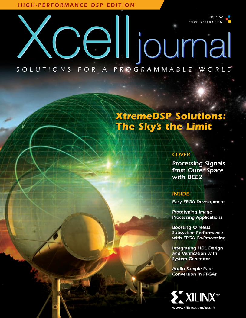
Issue 62Fourth Quarter 2007
Xcell journalXcell journalS O L U T I O N S F O R A P R O G R A M M A B L E W O R L DS O L U T I O N S F O R A P R O G R A M M A B L E W O R L D
COVER
Processing Signalsfrom Outer Spacewith BEE2
INSIDE
Easy FPGA Development
Prototyping Image Processing Applications
Boosting Wireless Subsystem Performance with FPGA Co-Processing
Integrating HDL Design and Verification with System Generator
Audio Sample RateConversion in FPGAs
COVER
Processing Signalsfrom Outer Spacewith BEE2
INSIDE
Easy FPGA Development
Prototyping Image Processing Applications
Boosting Wireless Subsystem Performance with FPGA Co-Processing
Integrating HDL Design and Verification with System Generator
Audio Sample RateConversion in FPGAs
www.xilinx.com/xcell/
XtremeDSP Solutions:The Sky’s the LimitXtremeDSP Solutions:The Sky’s the Limit
H I G H - P E R F O R M A N C E D S P E D I T I O N
Support Across The Board.™
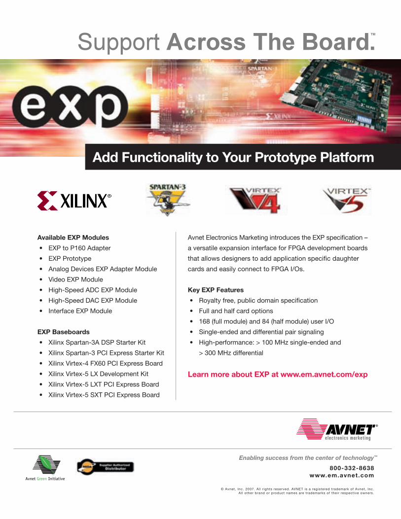
Add Functionality to Your Prototype Platform
Available EXP Modules
• EXP to P160 Adapter
• EXP Prototype
• Analog Devices EXP Adapter Module
• Video EXP Module
• High-Speed ADC EXP Module
• High-Speed DAC EXP Module
• Interface EXP Module
EXP Baseboards
• Xilinx Spartan-3A DSP Starter Kit
• Xilinx Spartan-3 PCI Express Starter Kit
• Xilinx Virtex-4 FX60 PCI Express Board
• Xilinx Virtex-5 LX Development Kit
• Xilinx Virtex-5 LXT PCI Express Board
• Xilinx Virtex-5 SXT PCI Express Board
Avnet Electronics Marketing introduces the EXP specification –
a versatile expansion interface for FPGA development boards
that allows designers to add application specific daughter
cards and easily connect to FPGA I/Os.
Key EXP Features
• Royalty free, public domain specification
• Full and half card options
• 168 (full module) and 84 (half module) user I/O
• Single-ended and differential pair signaling
• High-performance: > 100 MHz single-ended and
> 300 MHz differential
Learn more about EXP at www.em.avnet.com/exp
Enabling success from the center of technology™
800-332-8638www.em.avnet.com
© Avnet, Inc. 2007. Al l r ights reserved. AVNET is a registered trademark of Avnet, Inc.Al l other brand or product names are trademarks of their respect ive owners.
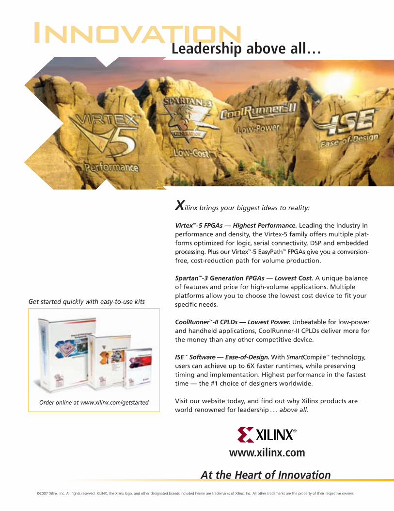
InnovationLeadership above all…
Xilinx brings your biggest ideas to reality:
Virtex™-5 FPGAs — Highest Performance. Leading the industry inperformance and density, the Virtex-5 family offers multiple plat-forms optimized for logic, serial connectivity, DSP and embeddedprocessing. Plus our Virtex™-5 EasyPath™ FPGAs give you a conversion-free, cost-reduction path for volume production.
Spartan™-3 Generation FPGAs — Lowest Cost. A unique balanceof features and price for high-volume applications. Multipleplatforms allow you to choose the lowest cost device to fit yourspecific needs.
CoolRunner™-II CPLDs — Lowest Power. Unbeatable for low-powerand handheld applications, CoolRunner-II CPLDs deliver more forthe money than any other competitive device.
ISE™ Software — Ease-of-Design. With SmartCompile™ technology,users can achieve up to 6X faster runtimes, while preserving timing and implementation. Highest performance in the fastesttime — the #1 choice of designers worldwide.
Visit our website today, and find out why Xilinx products areworld renowned for leadership . . . above all.
www.xilinx.com
At the Heart of Innovation©2007 Xilinx, Inc. All rights reserved. XILINX, the Xilinx logo, and other designated brands included herein are trademarks of Xilinx, Inc. All other trademarks are the property of their respective owners.
Get started quickly with easy-to-use kits
Order online at www.xilinx.com/getstarted
IL E T T E R F R O M T H E P U B L I S H E R
Xilinx, Inc.2100 Logic DriveSan Jose, CA 95124-3400Phone: 408-559-7778FAX: 408-879-4780www.xilinx.com/xcell/
© 2007 Xilinx, Inc. All rights reserved. XILINX, the Xilinx Logo, and other designated brands includedherein are trademarks of Xilinx, Inc. All other trade-marks are the property of their respective owners.
The articles, information, and other materials includedin this issue are provided solely for the convenience ofour readers. Xilinx makes no warranties, express,implied, statutory, or otherwise, and accepts no liabilitywith respect to any such articles, information, or othermaterials or their use, and any use thereof is solely atthe risk of the user. Any person or entity using suchinformation in any way releases and waives any claim itmight have against Xilinx for any loss, damage, orexpense caused thereby. Forrest Couch
Publisher
PUBLISHER Forrest [email protected]
EDITOR Charmaine Cooper Hussain
ART DIRECTOR Scott Blair
DESIGN/PRODUCTION Teie, Gelwicks & Associates1-800-493-5551
ADVERTISING SALES Dan Teie1-800-493-5551
TECHNICAL COORDINATOR Larry Caputo
INTERNATIONAL Piera Or, Asia [email protected]
Christelle Moraga, Europe/Middle East/[email protected]
Yumi Homura, [email protected]
SUBSCRIPTIONS All Inquirieswww.xcellpublications.com
REPRINT ORDERS 1-800-493-5551
Xcell journal
www.xilinx.com/xcell/
A New Era of Signal ProcessingIt is no accident that Xilinx® FPGAs serve an increasingly vital role in the design and developmentof today’s most demanding digital signal processing (DSP) systems. Superior performance, system-level cost, power efficiency, faster time to market, and unrivaled flexibility are the hallmarks ofFPGA-based DSP designs – value propositions that have found increasingly appreciative receptionamong leaders in markets like the communications industry.
Driven by the global demand for higher quality, higher bandwidth, and inexpensive wired andwireless communications of voice, computer, and video data, the number and complexity of newcommunications standards has grown exponentially. This is in large part because of the need forinteroperability and data exchange across myriad layers of legacy and next-generation networks.Keeping pace with these standards and the extremely critical price/performance/power ratios theypose has been anything but trivial for system vendors. Nonetheless, the flux continues to produceopportunities for industrious innovators willing to tackle the challenge.
In the dynamic markets served by high-performance DSP solutions, the inherent flexibility of theFPGA equates to:
• Faster time to market with leading-edge algorithmic solutions and standards implementations
• Lowered operational costs with easy-to-perform remote adaptation to unforeseen environmentaland functional changes
• Reduced capital expenditures due to extended life cycles for existing designs
• Easy migration to keep pace with changing customer demands and market requirements
In This IssueThis high-performance DSP edition of Xcell Journal offers several interesting – and in some casesout of this world – applications of high-performance FPGA-based DSPs. For example, the coverstory shows how several UC Berkeley astronomers programmed the BEE2 platform using aprogramming environment that leverages Linux, Xilinx System Generator, and Xilinx EDK foradvanced radio telescope applications. Other articles discuss the growing ease of programmingan FPGA-based DSP design, interesting system-design challenges using development platformsfor FPGA-based image processing applications, analyzing different hardware/software partitioningschemes to boost wireless subsystem performance, designing and verifying the CABAC functionalityof an H.264 video encoder with System Generator for DSP, and an efficient implementation ofaudio algorithms in programmable logic.
As Jeff Bier, president of BDTI, notes, “Today, FPGAs play an increasing role in a wide range ofDSP applications. We expect this trend to continue over the next several years.” Xilinx sees an ever-broadening horizon for high-performance DSP processing solutions in the demanding digital com-munications, multimedia video and imaging, and defense systems markets. And XilinxXtremeDSP™ solutions offer support every step of the way, with advanced DSP-optimized FPGAdevices, hardware and software development tools, development kits, and evaluation platforms, aswell as comprehensive training and support to ensure your success.
We hope you enjoy this issue.
O N T H E C O V E R
3131F E A T U R E
3838
F E A T U R E
99V I E W P O I N T
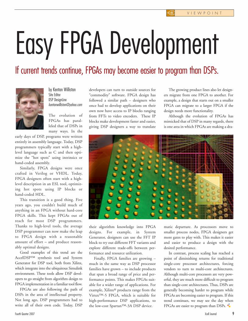
Easy FPGA DevelopmentIf current trends continue, FPGAs may become easier to program than DSPs.
4444F E A T U R E
Integrating HDL Design and Verification with System GeneratorDesigning and verifying the CABAC functionality of an H.264 video encoder is easy with System Generator for DSP.
5050F E A T U R E
Audio Sample Rate Conversion in FPGAsAn efficient implementation of audio algorithms in programmable logic.
Prototyping Image Processing ApplicationsDevelopment platforms for FPGA-based image processing applica-tions present some interesting system-design challenges.
Boosting Wireless Subsystem Performance with FPGA Co-ProcessingAnalyzing different hardware/software partitioning schemes.
Processing Signals from Outer Space with BEE2 UC Berkeley astronomers programmedthe BEE2 platform using a programmingenvironment that leverages Linux, XilinxSystem Generator, and Xilinx EDK.
1313 Cover
F O U R T H Q U A R T E R 2 0 0 7, I S S U E 6 2 Xcell journalXcell journal
VIEWPOINTS
Letter from the Publisher. . . . . . . . . . . . . . . . . . . . . . . . . . . . . . . . . . . . . . . . . . . . . . . . . . . 5
Vin Ratford: Savoring the Highs and Lows . . . . . . . . . . . . . . . . . . . . . . . . . . . . . . . . . . . . . . . 8
Kenton Williston: Easy FPGA Develpoment. . . . . . . . . . . . . . . . . . . . . . . . . . . . . . . . . . . . . . . 9
Jeff Bier: DSP Performance of FPGAs Revealed . . . . . . . . . . . . . . . . . . . . . . . . . . . . . . . . . . 10
Ivo Bolsens: Virtual Worlds . . . . . . . . . . . . . . . . . . . . . . . . . . . . . . . . . . . . . . . . . . . . . . . . 66
FEATURES
Processing Signals from Outer Space with BEE2. . . . . . . . . . . . . . . . . . . . . . . . . . . . . . . . . . 13
Prototyping Applications with the Spartan-3A DSP Starter Platform . . . . . . . . . . . . . . . . . . . . . 18
Future-Proofing Military Applications Using FPGAs . . . . . . . . . . . . . . . . . . . . . . . . . . . . . . . . . 21
Using MATLAB to Create IP for System Generator for DSP . . . . . . . . . . . . . . . . . . . . . . . . . . . 24
Automatic IP Block Selection with IP-Explorer Technology. . . . . . . . . . . . . . . . . . . . . . . . . . . . 28
Prototyping Image Processing Applications. . . . . . . . . . . . . . . . . . . . . . . . . . . . . . . . . . . . . . 31
The Virtex-5 SXT Option for High-Performance Digital Signal Processing. . . . . . . . . . . . . . . . . . 34
Boosting Wireless Subsystem Performance with FPGA Co-Processing . . . . . . . . . . . . . . . . . . . . 38
Selecting the Right Memory Controller for Real-Time Applications . . . . . . . . . . . . . . . . . . . . . . 41
Integrating HDL Design and Verification with System Generator . . . . . . . . . . . . . . . . . . . . . . . 44
Accelerating System Development Cycles with the Radar Blockset Library . . . . . . . . . . . . . . . . 47
Audio Sample Rate Conversion in FPGAs . . . . . . . . . . . . . . . . . . . . . . . . . . . . . . . . . . . . . . . 50
RESOURCES
Technical Papers and Literature . . . . . . . . . . . . . . . . . . . . . . . . . . . . . . . . . . . . . . . . . . . . . 57
Development Boards and Kits . . . . . . . . . . . . . . . . . . . . . . . . . . . . . . . . . . . . . . . . . . . . . . 58
Education and Services . . . . . . . . . . . . . . . . . . . . . . . . . . . . . . . . . . . . . . . . . . . . . . . . . . . 59
Software Tools and IP. . . . . . . . . . . . . . . . . . . . . . . . . . . . . . . . . . . . . . . . . . . . . . . . . . . . 60
Technical Support. . . . . . . . . . . . . . . . . . . . . . . . . . . . . . . . . . . . . . . . . . . . . . . . . . . . . . . 62
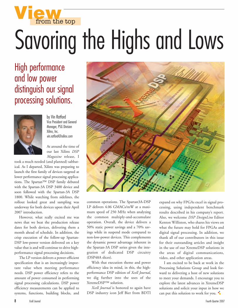
by Vin RatfordVice President and GeneralManager, PSG DivisionXilinx, [email protected]
At around the time ofour last Xilinx DSPMagazine release, I
took a much needed (and planned) sabbat-ical. As I departed, Xilinx was preparing tolaunch the first family of devices targeted atlower performance signal processing applica-tions. The Spartan™ DSP family debutedwith the Spartan-3A DSP 3400 device andsoon followed with the Spartan-3A DSP1800. While watching from sidelines, therollout looked great and sampling wasunderway for both devices upon their April2007 introduction.
However, what really excited me wasnews that we beat the production releasedates for both devices, delivering them amonth ahead of schedule. In addition, thecrisp execution of the follow-up Spartan-DSP low-power version delivered on a keyvalue that is and will continue to drive high-performance signal processing decisions.
The LP version delivers a power-efficientspecification that is an increasingly impor-tant value when meeting performanceneeds. DSP power efficiency refers to theamount of power consumed in performingsignal processing calculations. DSP powerefficiency measurements can be applied tosystems, functions, building blocks, and
common operations. The Spartan3A-DSPLP delivers 4.06 GMACs/mW at a maxi-mum speed of 250 MHz when analyzingthe common multiply-and-accumulateoperation. Overall, the device delivers a50% static power savings and a 70% sav-ings while in suspend mode compared tonon-low-power devices. This complementsthe dynamic power advantage inherent inthe Spartan-3A DSP series given the inte-gration of dedicated DSP circuitry(DSP48A slices).
With that execution theme and powerefficiency idea in mind, in this, the high-performance DSP edition of Xcell Journal,we dig further into the uses of theXtremeDSP™ solution.
Xcell Journal is honored to again haveDSP industry icon Jeff Bier from BDTI
expand on why FPGAs excel in signal pro-cessing, using independent benchmarkresults described in his company’s report.Also, we welcome DSP DesignLine EditorKenton Williston, who shares his views onwhat the future may hold for FPGAs anddigital signal processing. In addition, wethank all of our contributors in this issuefor their outstanding articles and insightin the use of our XtremeDSP solutions inthe areas of digital communications,video, and other application areas.
I am excited to be back at work in theProcessing Solutions Group and look for-ward to delivering a host of new solutionsto meet your demands. I encourage you toexplore the latest advances in XtremeDSPsolutions and solicit your input in how wecan put this solution to work for you.
8 Xcell Journal Fourth Quarter 2007
Savoring the Highs and LowsHigh performance and low power distinguish our signal processing solutions.
Viewfrom the top
by Kenton WillistonSite EditorDSP [email protected]
The evolution ofFPGAs has paral-leled that of DSPs inmany ways. In the
early days of DSP, programs were writtenentirely in assembly language. Today, DSPprogrammers typically start with a high-level language such as C and then opti-mize the “hot spots” using intrinsics orhand-coded assembly.
Similarly, FPGA designs were oncecrafted in Verilog or VHDL. Today,FPGA designers often start with a high-level description in an ESL tool, optimiz-ing hot spots using IP blocks orhand-coded HDL.
This transition is a good thing. Fiveyears ago, you couldn’t build much ofanything in an FPGA without hard-coreFPGA skills. This kept FPGAs out ofreach for most DSP programmers.Thanks to high-level tools, the averageDSP programmer can now make the leapto FPGA design with a reasonableamount of effort – and produce reason-ably optimal designs.
Good examples of this trend are theAccelDSP™ synthesis tool and SystemGenerator for DSP tool, both from Xilinx,which integrate into the ubiquitous Simulinkenvironment. These tools allow DSP devel-opers to go straight from algorithm design toFPGA implementation in a familiar tool flow.
FPGAs are also following the path ofDSPs in the area of intellectual property.Not long ago, DSP programmers had towrite all of their own code. Today, DSP
developers can turn to outside sources for“commodity” software. FPGA design hasfollowed a similar path – designers whoonce had to develop applications on theirown now have access to IP blocks rangingfrom FFTs to video encoders. These IPblocks make development faster and easier,giving DSP designers a way to translate
their algorithm knowledge into FPGAdesigns. For example, in SystemGenerator, designers can use the FFT IPblock to try out different FFT variants andexplore different trade-offs between per-formance and resource utilization.
Finally, FPGA families are growing –much in the same way as DSP processorfamilies have grown – to include productsthat span a broad range of price and per-formance points. This makes FPGAs suit-able for a wider range of applications. Forexample, Xilinx® products range from theVirtex™-5 FPGA, which is suitable forhigh-performance DSP applications, tothe low-cost Spartan™-3A DSP device.
The growing product lines also let design-ers migrate from one FPGA to another. Forexample, a design that starts out on a smallerFPGA can migrate to a larger FPGA if thedesign needs more functionality.
Although the evolution of FPGAs hasmimicked that of DSP in many regards, thereis one area in which FPGAs are making a dra-
matic departure. As processors move tosmaller process nodes, FPGA designers getmore gates to play with. This makes it easierand easier to produce a design with thedesired performance.
In contrast, process scaling has reached apoint of diminishing returns for traditionalsingle-core processor architectures, forcingvendors to turn to multi-core architectures.Although multi-core processors are very pow-erful, they are much more difficult to programthan single-core architectures. Thus, DSPs aregenerally becoming harder to program whileFPGAs are becoming easier to program. If thistrend continues, we may see the day whenFPGAs are easier to program than DSPs.
Fourth Quarter 2007 Xcell Journal 9
Easy FPGA DevelopmentIf current trends continue, FPGAs may become easier to program than DSPs.
V I E W P O I N T
by Jeff BierPresidentBDTI – Berkeley Design Technology, [email protected]
FPGAs are increasingly considered for useas processing engines in high-performanceDSP applications such as wireless base sta-tions. In these applications, they may com-pete with DSP processors or workside-by-side with them.
With more choices, system designersneed a clear picture of the signal processingperformance of high-end FPGAs, both rel-ative to each other and to high-end DSPprocessors. Unfortunately, the most com-monly used performance figures are unreli-able, confusing, and often contradictory.
For example, because DSP applicationsoften rely heavily on multiply accumulate(MAC) operations, DSP processor andFPGA vendors sometimes use peak MACsper second as a simple metric for compar-ing digital signal processing performance.But MAC throughput is a lousy predictorof performance for FPGAs and DSPs alike.Let’s examine a few reasons why.
Simple Metrics Fall ShortThe MAC performance numbers forFPGAs often assume that the hard-wiredDSP elements are operating at their highestpossible clock rate. In practice, typicalFPGA designs will operate at lower speeds.Plus, using hard-wired elements is not theonly way to implement MACs on FPGAs;you can achieve additional MAC through-put using programmable logic resourcesand distributed arithmetic. This approachcan yield higher MAC throughput thanusing hard-wired elements alone.
Yet another consideration is that typicalDSP applications rely on many operationsother than MACs. Viterbi decoding, forexample, is a key DSP algorithm used intelecommunications applications thatmakes no use of MACs at all.
Another approach for assessing signalprocessing performance is to use commonDSP functions like FIR filters. But thisapproach can have drawbacks too. Oneproblem is that each vendor typically usesa different implementation of these func-tions – perhaps using different datawidths, a different algorithm, or differentimplementation parameters such as laten-
cy. This means that results from differentvendors are generally not comparable.
Furthermore, small kernel functions typi-cally aren’t effective for FPGA benchmarkingbecause the way you would implement afunction within a full FPGA application isoften quite different from the way you wouldimplement the function alone. (For proces-sors, in contrast, these little benchmarks areusually pretty good at predicting overall DSPapplication performance.) Benchmarksimplemented by processor or FPGA vendorsoften lack independent verification, makingit difficult for engineers to make confidentcomparisons between devices.
10 Xcell Journal Fourth Quarter 2007
DSP Performance of FPGAs RevealedPopular report provides independent DSP benchmark results for FPGAs.
V I E W P O I N T
Independent Benchmarks Fill the GapBDTI is the most respected source for sig-nal processing benchmarks. Our bench-marks are used by dozens of semiconductorvendors and thousands of chip users toevaluate, compare, and select signal pro-cessing engines. BDTI has benchmarkedthe signal processing performance ofprocessors for nearly 15 years, and hasexpanded its benchmarking activities toinclude FPGAs, multi-core chips, andother technologies.
Several years ago BDTI recognized theneed for independent, accurate, apples-to-apples performance comparisonsbetween FPGAs and processors targetingDSP applications. To address this need,BDTI developed a new application-ori-ented benchmark, the BDTICommunications Benchmark (OFDM),based on an orthogonal frequency divi-sion multiplexing (OFDM) receiver. Thisbenchmark is designed to be representa-tive of the “baseband” signal processingworkloads increasingly found in commu-nications equipment for applications suchas DSL, cable modems, and wireless sys-tems. It is suitable for implementation onFPGAs, DSP processors, multi-core
have suspected that FPGAs could providebetter chip-level cost/performance thanDSPs in some applications but were notsure how much better. In the report, BDTIalso compares cost/performance results forFPGAs from competing vendors.
Of course, benchmark results alone arenot enough to answer the question ofwhether to use an FPGA in a new systemdesign, or which FPGA to choose.Designers need to understand how theirchoice of processing engine will affectdevelopment flow, implementation effort,and system design. For this reason,BDTI’s report explores the qualitative fac-tors that influence the decision of whetherto use an FPGA, a DSP, or both, and pro-vides guidance on how to make aninformed choice. The report also high-lights the key questions that will affect thelong-term success of FPGAs in high-endDSP applications, such as FPGA energyefficiency and the effectiveness of newhigh-level synthesis tools for FPGAs.
ConclusionBDTI plans to conduct further analysis inthese areas and we will continue to evaluatethe signal processing capabilities of newFPGAs, DSPs, and massively parallel proces-sors. The competition among signal process-ing engines is heating up, and BDTI willcontinue to provide the data and analysisneeded to make confident choices.
chips, and many other signal processingengines, yielding apples-to-apples bench-mark results.
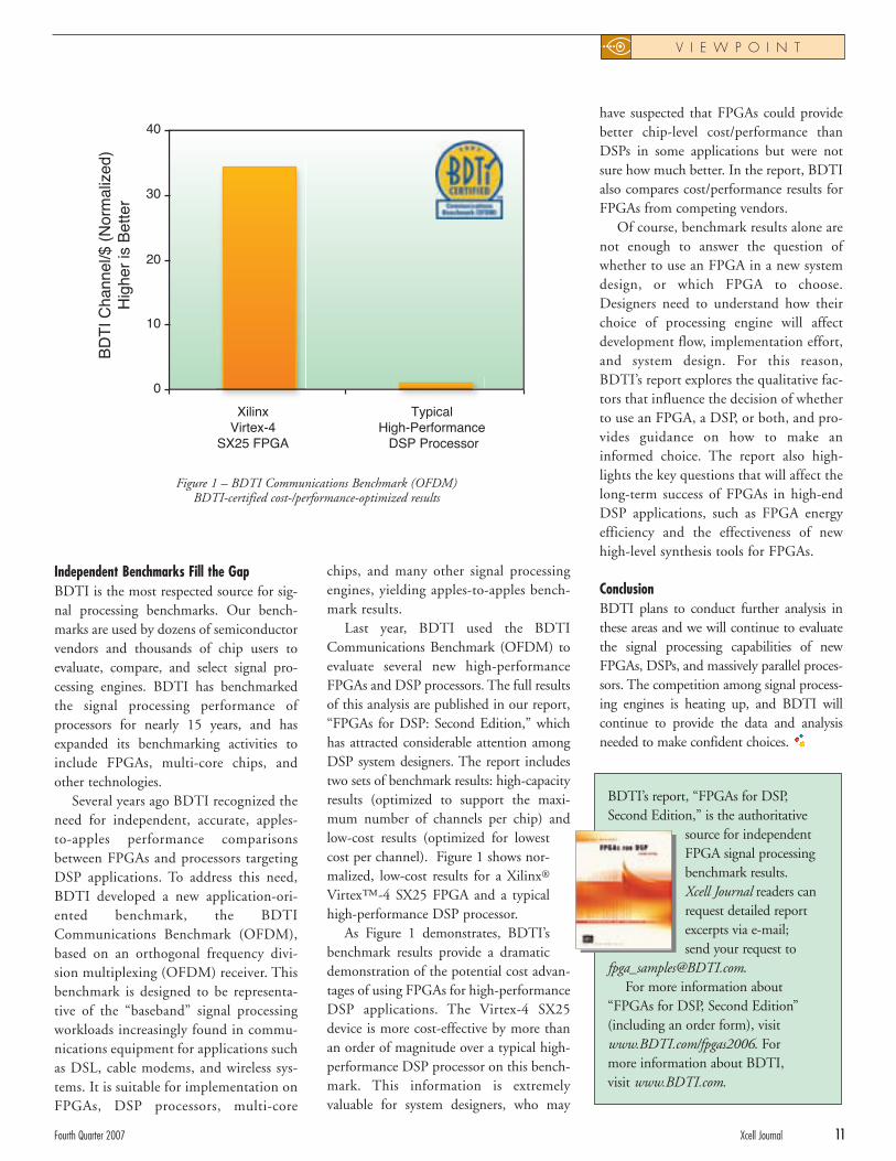
Last year, BDTI used the BDTICommunications Benchmark (OFDM) toevaluate several new high-performanceFPGAs and DSP processors. The full resultsof this analysis are published in our report,“FPGAs for DSP: Second Edition,” whichhas attracted considerable attention amongDSP system designers. The report includestwo sets of benchmark results: high-capacityresults (optimized to support the maxi-mum number of channels per chip) andlow-cost results (optimized for lowestcost per channel). Figure 1 shows nor-malized, low-cost results for a Xilinx®
Virtex™-4 SX25 FPGA and a typicalhigh-performance DSP processor.
As Figure 1 demonstrates, BDTI’sbenchmark results provide a dramaticdemonstration of the potential cost advan-tages of using FPGAs for high-performanceDSP applications. The Virtex-4 SX25device is more cost-effective by more thanan order of magnitude over a typical high-performance DSP processor on this bench-mark. This information is extremelyvaluable for system designers, who may
Fourth Quarter 2007 Xcell Journal 11
XilinxVirtex-4
SX25 FPGA
Typical High-Performance
DSP Processor
0
10
20
30
40
BD
TI C
hann
el/$
(N
orm
aliz
ed)
Hig
her
is B
ette
r
Figure 1 – BDTI Communications Benchmark (OFDM) BDTI-certified cost-/performance-optimized results
BDTI’s report, “FPGAs for DSP,Second Edition,” is the authoritative
source for independentFPGA signal processingbenchmark results. Xcell Journal readers canrequest detailed reportexcerpts via e-mail; send your request to
[email protected]. For more information about
“FPGAs for DSP, Second Edition”(including an order form), visitwww.BDTI.com/fpgas2006. For more information about BDTI, visit www.BDTI.com.
V I E W P O I N T
Why use FPGAs for signal processing?
Why use FPGAs for signal processing?
Explore the many benefits of usingXilinx high-performance DSPs in your digital communications,multimedia video and imaging,and defense systems applications.
Xilinx offers a complete DSP processing solution, including devices, hardware and software development tools, reference designs, boards and kits,parameterizable algorithms (IP cores), training, and support.
Download our XtremeDSP™ Solutions Selection Guide now and see how quickly you can get started.
www.xilinx.com/publications/prod_mktg/pn0010944-3.pdf
Download our XtremeDSP™ Solutions Selection Guide now and see how quickly you can get started.
www.xilinx.com/publications/prod_mktg/pn0010944-3.pdf
by Chen Chang CTOBEEcube [email protected]
Bob BrodersenProfessor EmeritusUC [email protected]
John WawrzynekProfessorUC [email protected]
Dan WerthimerSETI@home Chief ScientistDirector, Center for Astronomy Signal ProcessingUC [email protected]
Kees VissersPrincipal EngineerXilinx, [email protected]
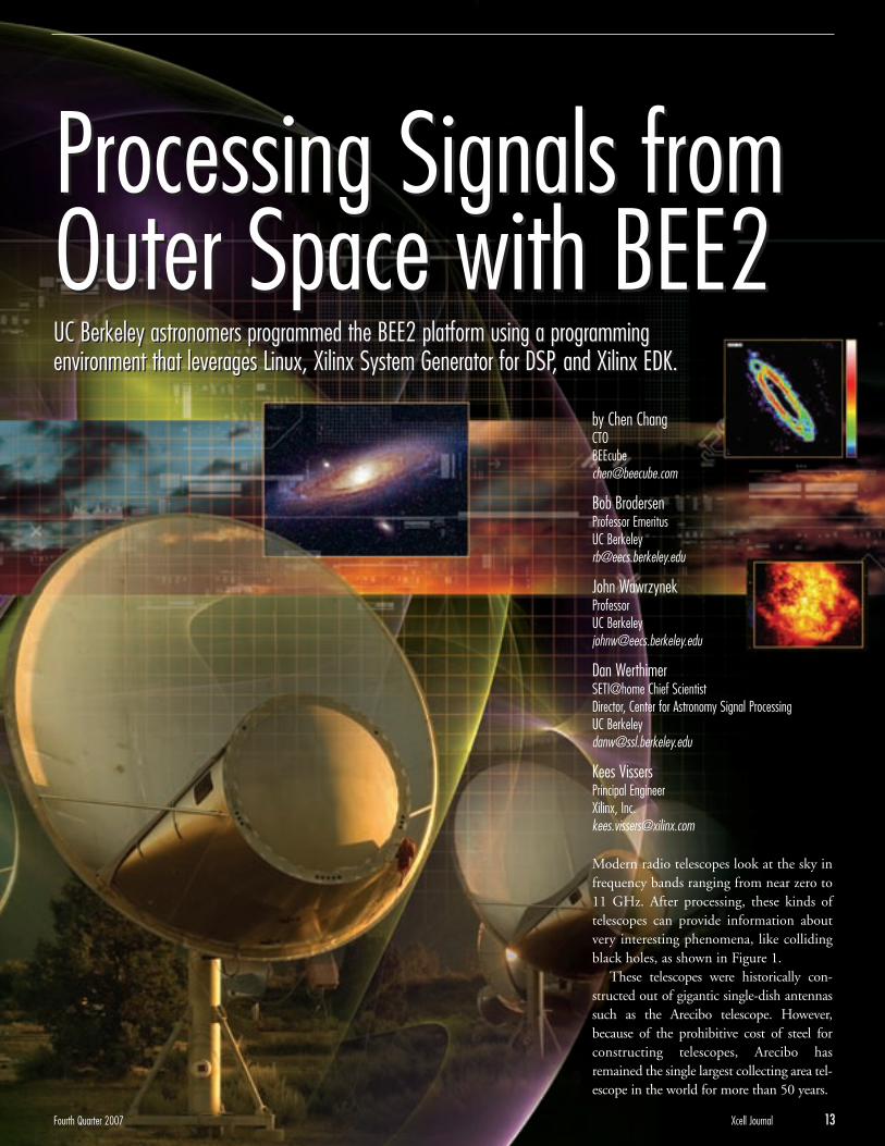
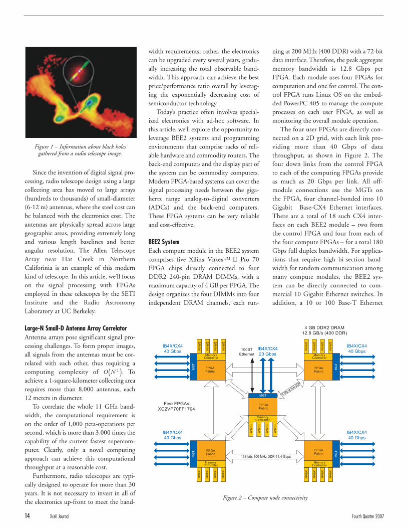
Modern radio telescopes look at the sky infrequency bands ranging from near zero to11 GHz. After processing, these kinds oftelescopes can provide information aboutvery interesting phenomena, like collidingblack holes, as shown in Figure 1.
These telescopes were historically con-structed out of gigantic single-dish antennassuch as the Arecibo telescope. However,because of the prohibitive cost of steel forconstructing telescopes, Arecibo hasremained the single largest collecting area tel-escope in the world for more than 50 years.
Fourth Quarter 2007 Xcell Journal 13
Processing Signals from Outer Space with BEE2 Processing Signals from Outer Space with BEE2 UC Berkeley astronomers programmed the BEE2 platform using a programming environment that leverages Linux, Xilinx System Generator for DSP, and Xilinx EDK.UC Berkeley astronomers programmed the BEE2 platform using a programming environment that leverages Linux, Xilinx System Generator for DSP, and Xilinx EDK.
Since the invention of digital signal pro-cessing, radio telescope design using a largecollecting area has moved to large arrays(hundreds to thousands) of small-diameter(6-12 m) antennas, where the steel cost canbe balanced with the electronics cost. Theantennas are physically spread across largegeographic areas, providing extremely longand various length baselines and betterangular resolution. The Allen TelescopeArray near Hat Creek in NorthernCaliforinia is an example of this modernkind of telescope. In this article, we’ll focuson the signal processing with FPGAsemployed in these telescopes by the SETIInstitute and the Radio AstronomyLaboratory at UC Berkeley.
Large-N Small-D Antenna Array CorrelatorAntenna arrays pose significant signal pro-cessing challenges. To form proper images,all signals from the antennas must be cor-related with each other, thus requiring acomputing complexity of O (N 2 ). Toachieve a 1-square-kilometer collecting arearequires more than 8,000 antennas, each12 meters in diameter.
To correlate the whole 11 GHz band-width, the computational requirement ison the order of 1,000 peta-operations persecond, which is more than 3,000 times thecapability of the current fastest supercom-puter. Clearly, only a novel computingapproach can achieve this computationalthroughput at a reasonable cost.
Furthermore, radio telescopes are typi-cally designed to operate for more than 30years. It is not necessary to invest in all ofthe electronics up-front to meet the band-
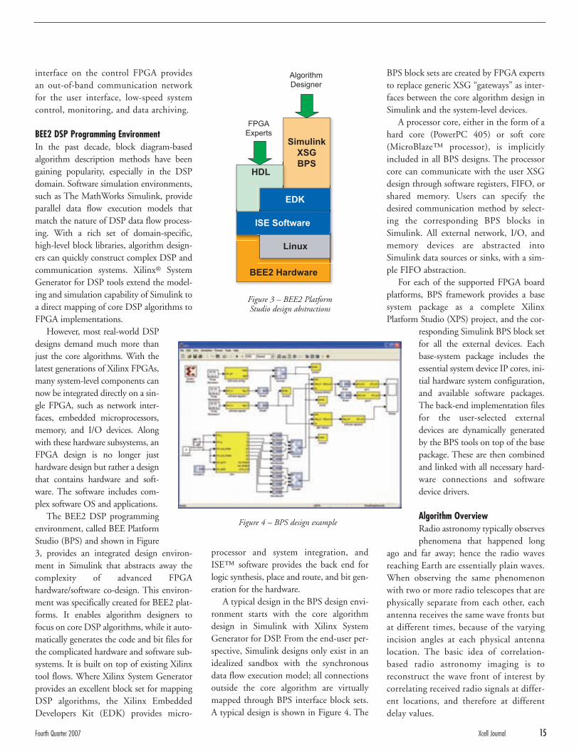
ning at 200 MHz (400 DDR) with a 72-bitdata interface. Therefore, the peak aggregatememory bandwidth is 12.8 Gbps perFPGA. Each module uses four FPGAs forcomputation and one for control. The con-trol FPGA runs Linux OS on the embed-ded PowerPC 405 to manage the computeprocesses on each user FPGA, as well asmonitoring the overall module operation.
The four user FPGAs are directly con-nected on a 2D grid, with each link pro-viding more than 40 Gbps of datathroughput, as shown in Figure 2. Thefour down links from the control FPGAto each of the computing FPGAs provideas much as 20 Gbps per link. All off-module connections use the MGTs onthe FPGA, four channel-bonded into 10Gigabit Base-CX4 Ethernet interfaces.There are a total of 18 such CX4 inter-faces on each BEE2 module – two fromthe control FPGA and four from each ofthe four compute FPGAs – for a total 180Gbps full duplex bandwidth. For applica-tions that require high bi-section band-width for random communication amongmany compute modules, the BEE2 sys-tem can be directly connected to com-mercial 10 Gigabit Ethernet switches. Inaddition, a 10 or 100 Base-T Ethernet
width requirements; rather, the electronicscan be upgraded every several years, gradu-ally increasing the total observable band-width. This approach can achieve the bestprice/performance ratio overall by leverag-ing the exponentially decreasing cost ofsemiconductor technology.
Today’s practice often involves special-ized electronics with ad-hoc software. Inthis article, we’ll explore the opportunity toleverage BEE2 systems and programmingenvironments that comprise racks of reli-able hardware and commodity routers. Theback-end computers and the display part ofthe system can be commodity computers.Modern FPGA-based systems can cover thesignal processing needs between the giga-hertz range analog-to-digital converters(ADCs) and the back-end computers.These FPGA systems can be very reliableand cost-effective.
BEE2 SystemEach compute module in the BEE2 systemcomprises five Xilinx Virtex™-II Pro 70FPGA chips directly connected to fourDDR2 240-pin DRAM DIMMs, with amaximum capacity of 4 GB per FPGA. Thedesign organizes the four DIMMs into fourindependent DRAM channels, each run-
138 bits 300 MHz DDR 41.4 Gbps
64 bits at 300 DDR
100BTEthernet
Five FPGAsXC2VP70FF1704
4 GB DDR2 DRAM12.8 GB/s (400 DDR)
MG
T
DR
AM
DR
AM
DR
AM
DR
AM
DR
AM
DR
AM
DR
AM
DR
AM
MG
TM
GT
MG
T
MemoryController
FPGAFabric
FPGAFabric
FPGAFabric
FPGAFabric
MemoryController
MemoryController
MemoryController
MGT
IB4X/CX440 Gbps
IB4X/CX440 Gbps
IB4X/CX440 Gbps
IB4X/CX420 Gbps
IB4X/CX440 Gbps
DR
AM
DR
AM
DR
AM
DR
AM
DR
AM
DR
AM
DR
AM
DR
AM
DR
AM
DR
AM
DR
AM
DR
AM
MemoryController
FPGAFabric
Figure 1 – Information about black holes gathered from a radio telescope image.
Figure 2 – Compute node connectivity
14 Xcell Journal Fourth Quarter 2007
Fourth Quarter 2007 Xcell Journal 15
interface on the control FPGA providesan out-of-band communication networkfor the user interface, low-speed systemcontrol, monitoring, and data archiving.
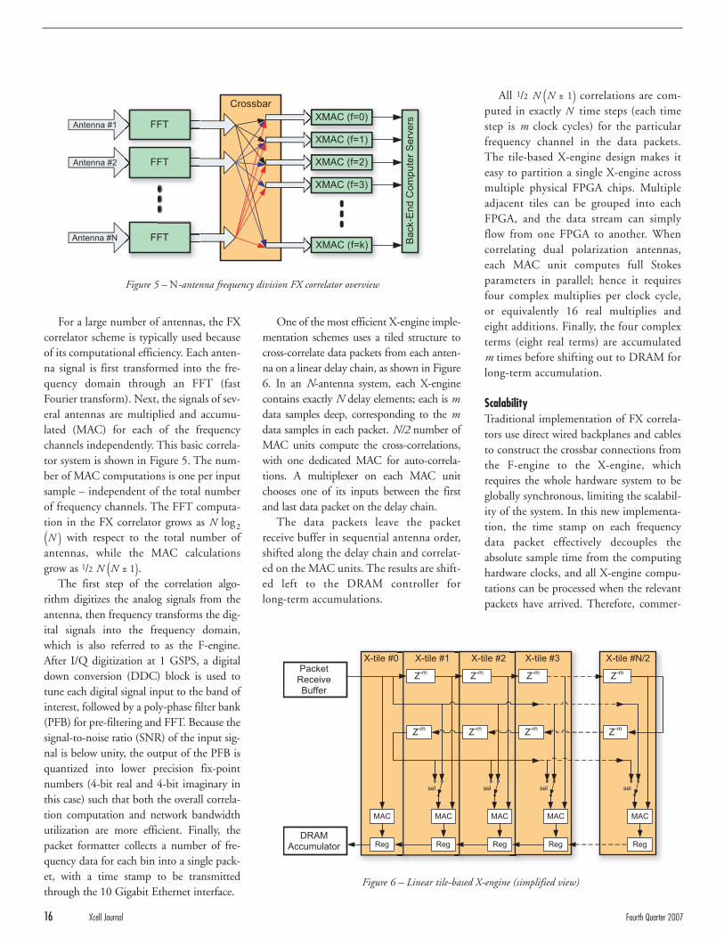
BEE2 DSP Programming EnvironmentIn the past decade, block diagram-basedalgorithm description methods have beengaining popularity, especially in the DSPdomain. Software simulation environments,such as The MathWorks Simulink, provideparallel data flow execution models thatmatch the nature of DSP data flow process-ing. With a rich set of domain-specific,high-level block libraries, algorithm design-ers can quickly construct complex DSP andcommunication systems. Xilinx® SystemGenerator for DSP tools extend the model-ing and simulation capability of Simulink toa direct mapping of core DSP algorithms toFPGA implementations.
However, most real-world DSPdesigns demand much more thanjust the core algorithms. With thelatest generations of Xilinx FPGAs,many system-level components cannow be integrated directly on a sin-gle FPGA, such as network inter-faces, embedded microprocessors,memory, and I/O devices. Alongwith these hardware subsystems, anFPGA design is no longer justhardware design but rather a designthat contains hardware and soft-ware. The software includes com-plex software OS and applications.
The BEE2 DSP programmingenvironment, called BEE PlatformStudio (BPS) and shown in Figure3, provides an integrated design environ-ment in Simulink that abstracts away thecomplexity of advanced FPGAhardware/software co-design. This environ-ment was specifically created for BEE2 plat-forms. It enables algorithm designers tofocus on core DSP algorithms, while it auto-matically generates the code and bit files forthe complicated hardware and software sub-systems. It is built on top of existing Xilinxtool flows. Where Xilinx System Generatorprovides an excellent block set for mappingDSP algorithms, the Xilinx EmbeddedDevelopers Kit (EDK) provides micro-
processor and system integration, andISE™ software provides the back end forlogic synthesis, place and route, and bit gen-eration for the hardware.
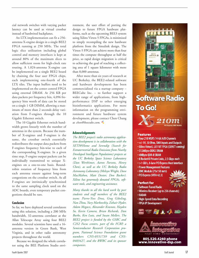
A typical design in the BPS design envi-ronment starts with the core algorithmdesign in Simulink with Xilinx SystemGenerator for DSP. From the end-user per-spective, Simulink designs only exist in anidealized sandbox with the synchronousdata flow execution model; all connectionsoutside the core algorithm are virtuallymapped through BPS interface block sets.A typical design is shown in Figure 4. The
BPS block sets are created by FPGA expertsto replace generic XSG “gateways” as inter-faces between the core algorithm design inSimulink and the system-level devices.
A processor core, either in the form of ahard core (PowerPC 405) or soft core(MicroBlaze™ processor), is implicitlyincluded in all BPS designs. The processorcore can communicate with the user XSGdesign through software registers, FIFO, orshared memory. Users can specify thedesired communication method by select-ing the corresponding BPS blocks inSimulink. All external network, I/O, andmemory devices are abstracted intoSimulink data sources or sinks, with a sim-ple FIFO abstraction.
For each of the supported FPGA boardplatforms, BPS framework provides a basesystem package as a complete XilinxPlatform Studio (XPS) project, and the cor-
responding Simulink BPS block setfor all the external devices. Eachbase-system package includes theessential system device IP cores, ini-tial hardware system configuration,and available software packages.The back-end implementation filesfor the user-selected externaldevices are dynamically generatedby the BPS tools on top of the basepackage. These are then combinedand linked with all necessary hard-ware connections and softwaredevice drivers.
Algorithm OverviewRadio astronomy typically observesphenomena that happened long
ago and far away; hence the radio wavesreaching Earth are essentially plain waves.When observing the same phenomenonwith two or more radio telescopes that arephysically separate from each other, eachantenna receives the same wave fronts butat different times, because of the varyingincision angles at each physical antennalocation. The basic idea of correlation-based radio astronomy imaging is toreconstruct the wave front of interest bycorrelating received radio signals at differ-ent locations, and therefore at differentdelay values.
Simulink
XSG
BPS
EDK
ISE Software
FPGA
Experts
Algorithm
Designer
HDL
Linux
BEE2 Hardware
Figure 3 – BEE2 Platform Studio design abstractions
Figure 4 – BPS design example
For a large number of antennas, the FXcorrelator scheme is typically used becauseof its computational efficiency. Each anten-na signal is first transformed into the fre-quency domain through an FFT (fastFourier transform). Next, the signals of sev-eral antennas are multiplied and accumu-lated (MAC) for each of the frequencychannels independently. This basic correla-tor system is shown in Figure 5. The num-ber of MAC computations is one per inputsample – independent of the total numberof frequency channels. The FFT computa-tion in the FX correlator grows as N log2
(N ) with respect to the total number ofantennas, while the MAC calculationsgrow as 1/2 N (N ± 1).
The first step of the correlation algo-rithm digitizes the analog signals from theantenna, then frequency transforms the dig-ital signals into the frequency domain,which is also referred to as the F-engine.After I/Q digitization at 1 GSPS, a digitaldown conversion (DDC) block is used totune each digital signal input to the band ofinterest, followed by a poly-phase filter bank(PFB) for pre-filtering and FFT. Because thesignal-to-noise ratio (SNR) of the input sig-nal is below unity, the output of the PFB isquantized into lower precision fix-pointnumbers (4-bit real and 4-bit imaginary inthis case) such that both the overall correla-tion computation and network bandwidthutilization are more efficient. Finally, thepacket formatter collects a number of fre-quency data for each bin into a single pack-et, with a time stamp to be transmittedthrough the 10 Gigabit Ethernet interface.
One of the most efficient X-engine imple-mentation schemes uses a tiled structure tocross-correlate data packets from each anten-na on a linear delay chain, as shown in Figure6. In an N-antenna system, each X-enginecontains exactly N delay elements; each is mdata samples deep, corresponding to the mdata samples in each packet. N/2 number ofMAC units compute the cross-correlations,with one dedicated MAC for auto-correla-tions. A multiplexer on each MAC unitchooses one of its inputs between the firstand last data packet on the delay chain.
The data packets leave the packetreceive buffer in sequential antenna order,shifted along the delay chain and correlat-ed on the MAC units. The results are shift-ed left to the DRAM controller forlong-term accumulations.
All 1/2 N (N ± 1) correlations are com-puted in exactly N time steps (each timestep is m clock cycles) for the particularfrequency channel in the data packets.The tile-based X-engine design makes iteasy to partition a single X-engine acrossmultiple physical FPGA chips. Multipleadjacent tiles can be grouped into eachFPGA, and the data stream can simplyflow from one FPGA to another. Whencorrelating dual polarization antennas,each MAC unit computes full Stokesparameters in parallel; hence it requiresfour complex multiplies per clock cycle,or equivalently 16 real multiplies andeight additions. Finally, the four complexterms (eight real terms) are accumulatedm times before shifting out to DRAM forlong-term accumulation.
ScalabilityTraditional implementation of FX correla-tors use direct wired backplanes and cablesto construct the crossbar connections fromthe F-engine to the X-engine, whichrequires the whole hardware system to beglobally synchronous, limiting the scalabil-ity of the system. In this new implementa-tion, the time stamp on each frequencydata packet effectively decouples theabsolute sample time from the computinghardware clocks, and all X-engine compu-tations can be processed when the relevantpackets have arrived. Therefore, commer-
Crossbar
Antenna #1
Ba
ck-E
nd
Co
mp
ute
r S
erv
ersFFT
Antenna #N FFT
XMAC (f=0)
Antenna #2 FFT
XMAC (f=1)
XMAC (f=2)
XMAC (f=3)
XMAC (f=k)
Z-m
MAC
Z-m
Z-m
Z-m
Z-m
Z-m
Z-m
Z-m
selsel sel sel
MAC MAC MAC
PacketReceiveBuffer
X-tile #0 X-tile #1 X-tile #2 X-tile #3 X-tile #N/2
DRAMAccumulator
MAC
Reg Reg Reg Reg Reg
Figure 5 – N-antenna frequency division FX correlator overview
Figure 6 – Linear tile-based X-engine (simplified view)
16 Xcell Journal Fourth Quarter 2007
Fourth Quarter 2007 Xcell Journal 17
cial network switches with varying packetlatency can be used as virtual crossbarinstead of hardwired backplanes.
An LTX implementation can fit a 256-antenna X-engine design in a single BEE2FPGA running at 250 MHz. The totallogic slice utilization including globalcontrol and memory interfaces is kept ataround 80% of the maximum slices toallow sufficient room for high-clock raterouting. A 1,024-antenna X-engine canbe implemented on a single BEE2 boardby chaining the four user FPGA chips,each implementing one-fourth of theLTX tiles. The input buffers need to beimplemented on the center control FPGAusing external DRAM. At 256 KB perdata packets per frequency bin, 4,096 fre-quency bins worth of data can be storedon a single 1 GB DIMM, allowing a max-imum of more than 2 seconds delay vari-ation from F-engines through the 10Gigabit Ethernet switch.
The 10 Gigabit Ethernet switch band-width grows linearly with the number ofantennas in the system. Because the num-ber of X-engines and F-engines is thesame, the crossbar switch essentiallyredistributes the output data packets fromF-engines frequency bin-wise to each ofthe corresponding X-engines. In a giventime step, F-engine output packets can beindividually transmitted to unique X-engines on a one-to-one basis. Round-robin rotation of frequency bins fromeach antenna ensure against long-termcongestions on the crossbar switch. As allF-engines are intrinsically synchronizedto the same sampling clock used on theADC boards, even temporary packet con-gestions should be rare.
ConclusionSo far, we have deployed several correlatorsusing this solution, including a 200 MHzbandwidth, 32-anternna correlator at theAllan Telescope Array using four BEE2modules. Several scientists have used a 16-antenna version in Green Bank, WestVirginia, and in other radio astronomyprojects throughout the world.
Because we designed the whole correla-tor using the BEE Platform Studio envi-
ronment, the user effort of porting thedesign to future FPGA hardware plat-forms, such as the upcoming BEE3 systemusing Xilinx Virtex-5 FPGAs, is minimizedto simply recompiling the new hardwareplatform from the Simulink design. TheVirtex-5 FPGA can achieve more than fourtimes the compute throughput at half theprice, so rapid design migration is criticalto achieving the goal of reaching a collect-ing area of 1 square kilometer with morethan 8,000 antennas.
After more than six years of research atUC Berkeley, the BEE2-related softwareand hardware development has beencommercialized via a startup company –BEECube Inc. – to further support awider range of applications, from high-performance DSP to other emergingbioinformatics applications. For moreinformation on the programming envi-ronment and future hardware systemdevelopment, please contact Chen Changat [email protected].
AcknowledgementsThe BEE2 project’s radio astronomy applica-tion development is in collaboration with theSETI@Home and Serendip (Search forExtraterrestrial Radio Emissions from NearbyDeveloped Intelligent Populations) projects atthe UC Berkeley Space Science Laboratory(Dan Werthimer, Aaron Parsons, HenryChen), as well as the UC Berkeley RadioAstronomy Laboratory (Melvyn Wright, DaveMacMahon, Matt Dexter, Don Backer).Xilinx has generously donated FPGAs, soft-ware tools, and engineering assistance.
Many thanks to all the hard work by peerstudents and staff members of the BEE2team: Pierre-Yves Droz, Greg Gibeling,Nan Zhou, Yury Markovskiy, Zohair Hyder,Adam Megacz, Alexander Krasnov, HaydenSo, Kevin Camera, Brian Richards, DanBurke, Ken Lutz, and Susan Mellers. TheBEE2 project is funded by the GSRC andC2S2 Focus centers, part of the FCRP, aSemiconductor Research Corporation pro-gram, National Science Foundation grantnumbers CNS-0551739 and CNS-0403427, and the BWRC and its sponsorcompanies.
by Jim BenekeVice President, Global Technical [email protected]
Have you ever had a great idea for the nextkiller FPGA application but struggled tofind the right prototyping hardware thatwould allow you to prove out your con-cept? You’re not alone. Finding the perfectdevelopment platform is not easy. Boardsare often designed more for demonstra-tion than development, leaving designerswith little flexibility and limited access toFPGA I/O pins.
With the recent introduction of theXilinx® Spartan™-3A DSP FPGA family,Xilinx has created a unique, low-cost, pro-totype-friendly starter platform to easeyour application development. Throughthe EXP expansion interface included onthe board, you can add application-specificdaughtercards to customize the board’s fea-ture set for your prototype needs.
In this article, I’ll review the EXP stan-dard, showing you why it’s FPGA-friendlyand able to meet your most demandingexpansion needs. We’ll look at several of theEXP modules currently available and seehow they can be used to easily create video,embedded, and communications processingapplications around the Spartan-3A DSP.You’ll see how the EXP specification, theSpartan-3A DSP Starter Platform, and theEXP add-on modules can combine toquickly and cost-effectively provide youwith a useful prototype system.
The EXP Expansion StandardThe new Spartan-3A DSP StarterPlatform (www.xilinx.com/s3adspstarter)includes a standard set of features asshown in Figure 1. Parallel flash and SPImemory are provided for configuration,while DDR2 memory is available forhigh-performance mass storage. AGigabit Ethernet PHY and serial portsupport standard communications links,while clocks, switches, LEDs, and somegeneral-purpose user I/O round out theboard interfaces. The remaining FPGAuser I/O pins – 168 in total – route totwo connectors. These connectors areconfigured to meet the EXP expansionslot standard, which was designed specif-ically for FPGA development boards.
Most industry-standard buses, such asPCI, PMC, PCMCIA, or PC-104, imple-ment an address and data bus structure,which is ideal for processor-based systemsbut limiting for the wide range of FPGA
applications. Instead, FPGA developmentboards require a more generic, universal I/Ostructure where you can define I/Os as theyare needed. Therefore, the EXP specificationprovides a great deal of flexibility by limitingthe number of fixed signal definitions,allowing a more free-form I/O assignmentas determined by your end application.
The EXP specification defines a 120-pinconnector, with 84 user I/Os and a mix ofpower and grounds. The standard EXP con-figuration uses two connectors in a full EXPmodule configuration for a total of 168 userI/Os. Half EXP module formats are alsoavailable, using just a single EXP connector.Two half EXP modules can be connected toa full EXP-configured baseboard.
The Spartan-3A DSP FPGA SelectIO™interface supports many popular single-ended and differential standards. Table 1shows the number of pins available at eachEXP connector, along with a breakdown ofthe single-ended and differential pairs sup-
18 Xcell Journal Fourth Quarter 2007
Prototyping Applications with theSpartan-3A DSP Starter PlatformThe new Spartan-3A DSP Starter Platform includes expansion capabilities for low-cost and easy-to-use application development.
ported. Each EXP connector can support upto 84 single-ended I/O signals or a mix ofsingle-ended and differential pairs.Providing as many as 24 differential pairsper EXP connector, 48 pairs total, is essen-tial for certain high-bandwidth LVDS inter-faces used in video and communicationsapplications. The Spartan-3A DSP StarterPlatform board provides a user-selectableI/O voltage jumper for each EXP connector.This allows each EXP connector to be con-figured for either 2.5V or 3.3V signaling.
As you can see, the EXP slot included onthe Spartan-3A DSP Starter Platform opensthe door to a wide range of add-on applica-tion modules and custom user interfaces.Avnet has created a set of off-the-shelf EXPmodules that are interchangeable betweenany EXP-enabled baseboard, including theSpartan-3A DSP Starter Platform. Let’sexplore some of these modules to see howthey customize the starter platform and cre-ate powerful prototype systems that leverageSpartan-3A DSP features.
Video ApplicationsThe Spartan-3A DSP FPGA is ideal for cost-sensitive DSP algorithmic and co-processingapplications. Video and image processing,especially the video surveillance and videosecurity markets, are good fits for this FPGAfamily. To help jump-start applications inthis area, Avnet has created the Video EXP
and larger enhanced block RAM enable theDSP-intensive image processing pipe.Functions such as the Bayer filter, color-space conversion, chroma sub-sampling,and MPEG-4 video compression can all beimplemented and run in real time insidethe FPGA. A 32-bit MicroBlaze™ proces-sor helps manage the processing pipe aswell as the Ethernet interface.
Wireless Communications SystemsThe increasing demand for Internet accesshas lead to the explosive growth of wirelesscommunication systems that provide a con-tinuous Internet connection. WiMAX is onewireless access technology that is gaining inpopularity and has significant market poten-tial. Based on the IEEE 802.16e-2005 stan-dard, WiMAX supports high-speed Internet
module. The Video EXP offers a full compli-ment of professional/consumer (or “pro-sumer”)-level front-end video functions.With support for DVI, component, com-posite, S-video, image sensor, and VGAinputs, plus DVI, VGA, and LCD panelvideo outputs, the Video EXP addresses abroad range of video processing applications.
Figure 2 shows an example video overEthernet application that can be built fromthe combined Video EXP and Spartan-3ADSP baseboard. The Spartan-3A DSPSelectIO interface can handle the LVDSinterfaces to the image sensors and LCDflat panel. The 250 MHz DSP48A slices
Fourth Quarter 2007 Xcell Journal 19
RS232
User I/O
EXP
Switches
Spartan-3A DSP
XC3SD1800A
Clocks
10/100/1000
PHY
User LEDs
VGA Port
DDR2
(32M x 32)
System ACE
Connector
Parallel Flash
(16M x 8)
SPI Flash
(64 Mb)
Image Sensor
Input
Image
Sensor
LCD Panel
Microphone
Headset
Image
Sensor
Video EXP
Module
Spartan-3 DSP
Starter Platform Baseboard
Audio
Codec
EMACRAM
Image Sensor
Input
EXP
Interface
Image Sensor
Interface
MicroBlaze
MPEG-4
Encoder
Image
Processing
LCD
Controller
Memory
Controller
DDR2
Memory
Ethernet
Interface
Ethernet
PHY
Audio
Interface
LCD Panel
Spartan-3 DSP FPGA
Signal CategoryPins Per Pins Per
Connector Dual EXP Slot
Single-Ended I/O 34 68Single-Ended Clocks 2 4Differential I/O Pairs (22) 44 88Differential Clock Input Pair (1) 2 4Differential Clock Output Pair (1) 2 42.5V pins (333 mA per pin) 12 243.3V pins (333 mA per pin) 12 24Grounds 12 24Total 120 240
Figure 1 – Spartan-3A DSP Starter Platform block diagram
Table 1 – EXP connector I/O assignments
Figure 2 – Video over Ethernet application example
access using advanced signal processingschemes such as orthogonal frequency-divi-sion multiple access (OFDMA) and multipleinput multiple output (MIMO) technology.The Spartan-3A DSP is a perfect solution forsupporting these high-bandwidth, process-ing-intensive applications that require flexi-bility and fast time to market.
To support wireless communicationsprototyping, Avnet and Texas Instrumentshave developed two EXP modules thatcomplement the digital IF processingcapabilities of the Spartan-3A DSP StarterPlatform. A High Speed ADC EXP mod-ule and a High Speed DAC EXP modulesupport 12-bit, 500 MSPS analog-to-digital conversion and 16-bit, 1 GSPSdigital-to-analog conversion. As halfmodules, each EXP requires just oneEXP connector; thus any combination oftwo half EXP modules is supported by
the starter platform baseboard.Figure 3 is an example direct conver-
sion wireless communications system thatyou can prototype with the Spartan-3ADSP Starter Platform, the High-SpeedDAC EXP and the High-Speed ADCEXP. The enhanced DSP48A slices insidethe Spartan-3A DSP make it ideal forimplementing digital front-end process-ing. Digital up conversion (DUC), com-prising two polyphase interpolating FIRfilters, a CIC filter, and a crest factorreduction block, can be implementedinside the Spartan-3A DSP FPGA. Theoutput drives the high-speed interpolat-ing DACs on the EXP module, which inturn drives the RF power amplifier fortransmission. On the receive side, the IFsignal can be directly sampled with the500 MSPS ADC and passed to the FPGAfor digital down conversion (DDC).
Embedded Processing PlatformsAlthough the Spartan-3A DSPFPGA family has features thatmake it well suited for high-per-formance DSP applications, it isalso a capable choice for embed-ded processing solutions. Theenhanced on-chip block RAMmakes the Spartan-3A DSP anespecially good fit for the soft-coreMicroBlaze embedded processor.To better address MicroBlazeprocessor-based embedded appli-cations, you can add the Interface
EXP half module as defined in Figure 4.The Interface EXP supports many of thecommon embedded processing interfacesfound in processor-based systems.Because the Interface EXP is a half-mod-ule format, you still have the option ofadding a second half EXP module. Whencombined with soft cores inside theSpartan-3A DSP FPGA, you have ulti-mate flexibility and control over yourdesign. Xilinx provides IP cores for all ofthe interfaces, including USB, CAN,Ethernet, SPI, I2C, and UART.
ConclusionThe Xilinx Spartan-3A DSP StarterPlatform is a great way to explore applica-tions around the Spartan-3A DSP FPGAfamily. The EXP slot included on theboard sets this kit apart, enabling cus-tomization that addresses video process-ing, communications, embedded systems,and a wide range of other applications.The available EXP add-on modules allowyou to quickly build up real-world proto-types and turn your concepts into reality.
Should a specific function not exist in anoff-the-shelf form, you can easily create yourown with a custom-designed EXP card.Avnet also provides a prototype EXPmodule that is great for accessing all ofthe I/O signals on standard .1” headers.
Avnet will continue to introduce newEXP modules that will further the reachand capability of this starter platform aswell as other EXP-enabled baseboards. Fora complete listing of EXP modules and theEXP specification (available for download-ing), visit www.em.avnet.com/exp.
20 Xcell Journal Fourth Quarter 2007
Power
Amp
EXP RF
Receiver
Interpolating
FIR FiltersCIC
Mixer
DDS
Filter
Spartan-3 DSP Starter Platform High-Speed ADC EXP Module
High-Speed DAC EXP Module
Crest
Factor
Reduction
DAC
I/F
ADC
I/F
FractionalRe-sampler
Spartan-3 DSP
FPGA
Decimating
FIR Filters
Baseband
Processing
User Clock(SMA)
RS232/485(Selectable)
10/100Ethernet PHY
USB PHY(ULPI)
CANTransceiver
CANTransceiver
User I/O(8)
1/2 EXP
Slot
DIPSwitches
RotaryEncoder
LED
I2C Port
SPI Port
Figure 3 – Example wireless communication system
Figure 4 – Interface EXP module block diagram
by Mark Littlefield Product Marketing ManagerCurtiss-Wright Controls Embedded Computing [email protected]
Manuel UhmSenior Marketing Manager, DSPXilinx, [email protected]
Over the past decade, the concept of “tech-nology insertion” (the incrementalupgrade of key technology components ina deployed or soon-to-be deployed system)has become a sort of mantra for the aero-space and defense (A&D) community,providing fielded systems with the latest,most advanced technology and the leastdelay. The rapid pace of technologicalinnovation – and subsequent obsolescence– has made technology insertion criticalfor the success of multiyear A&D develop-ment, test, and deployment projects.
Unmanned aerial vehicles (UAVs),radar, and signals intelligence (SIGINT)are examples of sophisticated platformsthat have benefited from technologyinsertion. To fully understand the chal-
lenges of technology insertion, includingcomplexity and cost, it’s useful to con-sider what is involved in successfullyusing this approach for upgrading legacysystems. Using FPGAs in a reconfig-urable computing application provides agood example of the benefits and chal-lenges entailed in making technologyinsertion work. This example alsoenables us to examine some commonissues associated with technology inser-tion, how COTS vendors can best helptheir customers address those problems,and how the overall technology insertionproblem can be significantly eased byproper planning.
Using FPGAs in Technology InsertionThe basic problem domains involved intechnology insertion can be roughly cate-gorized as:
• How the equipment physically connects (hardware)
• How the operating environment, sys-tem libraries and utilities, drivers, andmiddleware provide an infrastructurefor applications (system software)
Using FPGA technology in an embed-ded multicomputing system provides aninteresting case example because it strad-dles both the hardware and system softwaredomains. FPGAs fall into the hardwaredomain because they are physically inte-grated to hardware elements; developersmust work very closely with these elementswhen designing an application.
FPGAs present a software challenge aswell, because they must be programmedand often incorporate vendor or third-party supplied blocks or IP. In addition, ageneral-purpose processor using systemlibrary calls typically configures theFPGAs and issues the commands they useto communicate with other processorsand devices in the system. Such systemsare often complex and heterogeneous, asshown in Figure 1.
For technology insertion, the ideal sce-nario is a plug replacement module thatrequires no hardware or software changes.Although this is uncommon for FPGA-based computing products, this scenariocan also often be undesirable, as state-of-the-art computing platforms have new,more advanced features that system inte-
Fourth Quarter 2007 Xcell Journal 21
Future-Proofing Military Applications Using FPGAsFuture-Proofing Military Applications Using FPGAsTechnology insertion using COTS FPGA-basedproducts promises to deliver significant benefits but requires adequate planning.
Technology insertion using COTS FPGA-basedproducts promises to deliver significant benefits but requires adequate planning.
This article first appeared in Military Embedded Systemsmagazine, July 2007 (www.mil-embedded.com). Copyright OpenSystems Publishing. Used with permission.
grators can use to their advantage. Thus,the goal for system integrators must be tomaximize the benefits of technology inser-tion while minimizing impact on the exist-ing system. The degree of flexibility in thehardware and software domains can bedirectly affected by early design choices andproducts offered by COTS vendors.
The simplest approach for a COTSvendor to ease technology insertion hard-ware problems is to follow a commonhardware model from platform generationto platform generation and to minimizeconnector pin changes. Industry boardand module standards such as VME,VPX-REDI (VITA 46/48), PMC (VITA32), and XMC (VITA 42) address a largepart of this problem by specifying fixedform factors and pin definitions for boardI/O such as buses or switched fabric inter-connects. Vendors can extend this modelby maintaining pin footprints acrossproduct generations for such commoninterfaces as serial ports and Ethernet. Thesame also holds true for FPGAs. A com-mon, or at least similar, I/O footprintminimizes the need for radical redesignsduring a technology insertion project.
The Importance of SoftwareAlthough FPGA development is very tight-ly linked to the target component and plat-form hardware design, there is a lack of
project is the integration of the FPGA-basedapplication into a larger multicomputer sys-tem. General-purpose computing elementsare often closely tied to the system’s FPGAsby performing various command and con-trol functions such as DMA engine control.Subsequently, the ease of technology inser-tion can be directly affected by how well avendor can maintain APIs from one productgeneration to the next, which in turn isoften linked to the level of abstraction in theAPI. The more abstraction, the less likely itis that the API will change between productgenerations. One of the key tasks of anexternal processor is the command and con-trol of data movement, both within theFPGA and between the FPGA and othergeneral-purpose processing nodes.
Making Technology Insertion RealSeveral COTS vendors offer commonhardware strategies to aid technology inser-tion. One example is Curtiss-Wright’s latestgeneration of VPX-based board products.The three primary computing platforms inthis product line – a dual 8641-based SBC,a quad 8641-based DSP engine, and thedual Xilinx® Virtex™-5 FPGA-basedCHAMP-FX2 board – all share a set ofcommon hardware design elements andwere specifically designed with commonpin footprints for common I/O elements.(See Figures 2 and 3.) For instance, the
standardized or industry-accepted toolsand frameworks to abstract this linkage.The result is that software can typicallyhave an even greater effect on a technologyinsertion program than hardware.
The software challenges can be some-what mitigated on general-purpose proces-sors by using off-the-shelf operating systemssuch as VxWorks or Linux, supported withfull-featured BSPs, communications mid-dleware, and application frameworks. ForCOTS vendors of FPGA products, thechallenge is to provide development tools tointegrators to ease technology insertionwhile maintaining the performancedemanded by application developers.
A common approach is for COTS ven-dors to develop a standard “wrapper” orgasket that essentially represents the staticinfrastructure, such as interfaces to ADCs,memories, Ethernet, and so on. The blocksand infrastructure should be designed tosupport a set of commonly implementeduse cases in the most efficient manner pos-sible so as to minimize the size of the wrap-per. Ideally, such an infrastructure wouldrepresent only 5 to 10 percent of the totaldie size of the FPGA.
Software SupportNo less important than the ease of integrat-ing existing application code into a newFPGA platform for a technology insertion
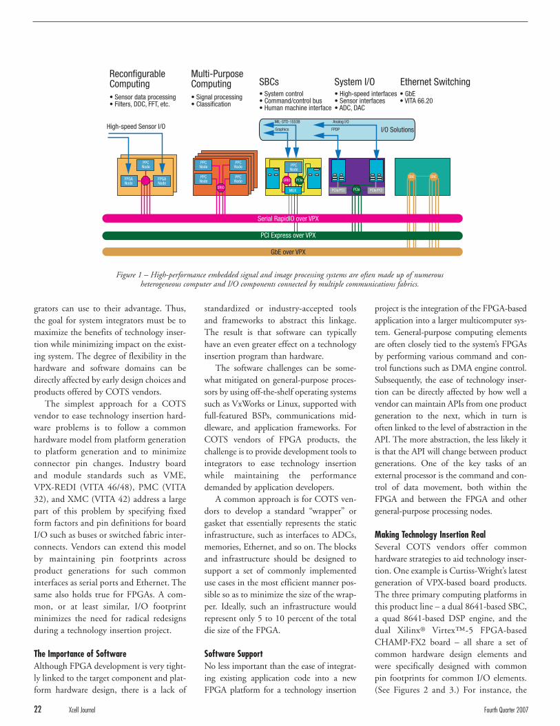
ReconfigurableComputing
Multi-PurposeComputing SBCs System I/O
I/O Solutions
Ethernet Switching
PPCNode
SRIO
SRIO
• Signal processing• Classification
• Sensor data processing• Filters, DDC, FFT, etc.
• System control• Command/control bus• Human machine interface
• High-speed interfaces• Sensor interfaces• ADC, DAC
• GbE• VITA 66.20
High-speed Sensor I/O
PCIe
PCIePCIe/PCI PCIe/PCI
GbE GbE
MUX
MIL-STD-1553B
Graphics
Analog I/O
FPDP
PPCNode
PPCNode
PPCNode
PPCNodeFPGA
NodeFPGANode
PPCNode
Serial RapidIO over VPX
PCI Express over VPX
GbE over VPX
Figure 1 – High-performance embedded signal and image processing systems are often made up of numerous heterogeneous computer and I/O components connected by multiple communications fabrics.
22 Xcell Journal Fourth Quarter 2007
Fourth Quarter 2007 Xcell Journal 23
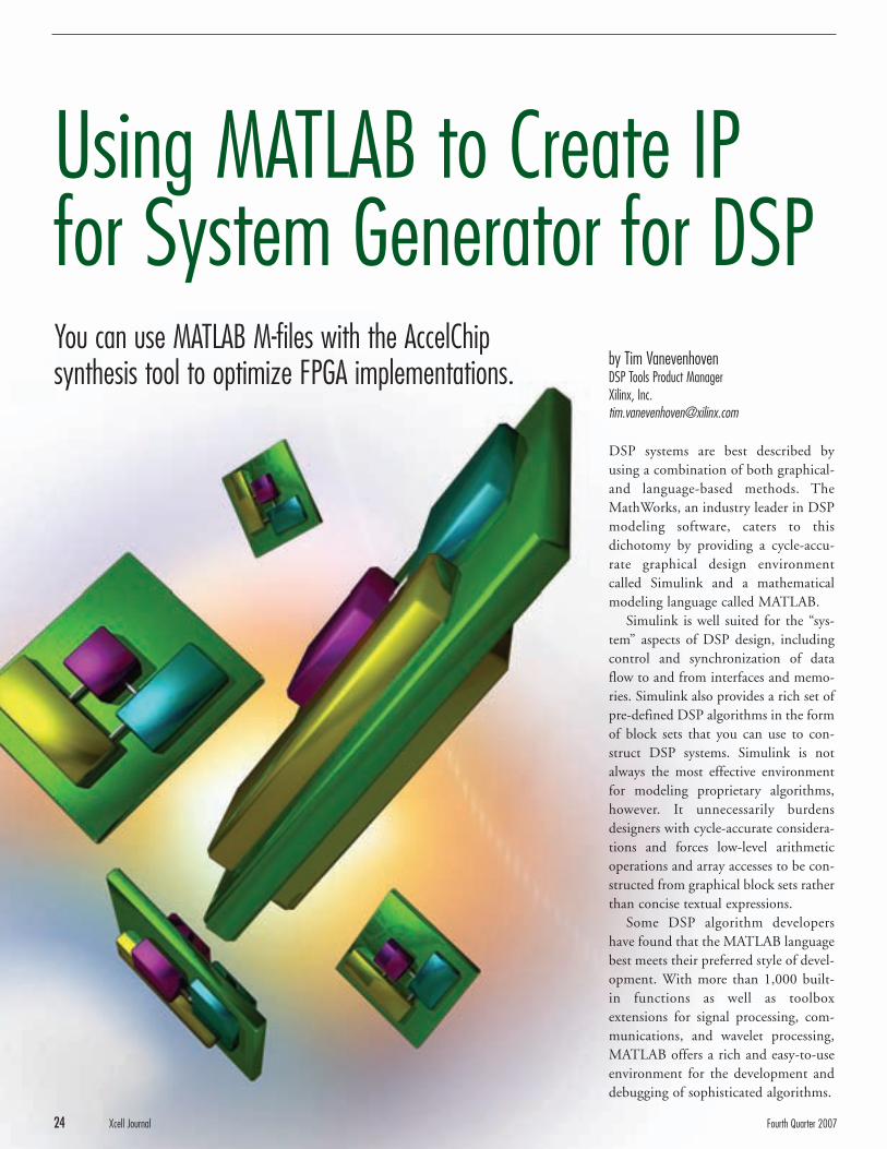
FPGA board not only shares thePowerPC node design elements with thetwo other VPX boards, but closely resem-bles its preceding VME version in its I/Oand memory configuration.
The design of the VPX FPGA boardand its VME predecessor took a balancedapproach between the twin goals of maxi-mum technology insertion value and mini-mum insertion effort. Curtiss-Wright’sContinuum FXtools design kit provides ahighly optimized set of IP blocks focusedon peripheral I/O and memories, with onlya lightweight, scalable switching block anda few additional utility blocks to ease appli-cation integration. By providing a minimalbut highly optimized infrastructure,FXtools abstracts those common I/O andmemory objects without sacrificing per-formance. Designing with these IP blocksand adopting basic use cases can help easefuture technology insertion.
To ease both the integration and technol-ogy insertion of FPGA-based computingelements, the board’s Continuum IPC com-munications middleware was extended todirectly control DMA-based data-transfersinvolving the FPGA node. The IPC soft-ware enables application developers to cre-ate named buffer and data transfer objectsthat are globally visible to the system.Thus, any processor in the IPC system cancreate named buffers, attach to already cre-ated named buffers, and create data trans-fer objects between buffers without havingto resort to code-manipulating, complexmemory map translations or DMA com-mand packet creation.
Avoiding Technology Insertion HeadachesAlthough hardware and system softwarecommonality across product generations isan important element in planning a suc-cessful technology insertion project, theapplication developer and system integra-tor can themselves play an important rolein defining how difficult a future technolo-gy insertion project may be. For example, ifthe application developer bypasses vendoror OS APIs to directly manipulate hard-ware, the resulting code will be significant-ly less portable to future hardwareplatforms. However, application developersor system integrators can structure theirapplication/system in a number of ways tominimize technology insertion headaches.
The first rule of designing for latertechnology insertion should be, “Don’tfight the system software or OS.” Most
software frameworks, such as a BSP, utili-ty library, or communications middlewarelike Continuum IPC are designed withone or more basic use cases or design pat-terns in mind. One of the easiest ways fordevelopers to introduce problems in alater technology insertion project is tobend the software framework to matchtheir favorite design pattern. Doing so vir-tually ensures that later developers willhave to bend things in a different waysimply to make it work.
The same holds true for FPGA IP devel-opers. Although implementation detailsand interfaces may shift from one productgeneration to the next, the basic design pat-terns usually do not. Using vendor-suppliedIP blocks and data flows in the manner thatthe vendor originally intended helps mini-mize the amount of recoding needed for atechnology insertion project.
Another beneficial technique that can beemployed both for software and FPGA IP isto analyze the vendor-supplied APIs andblock interfaces, identifying those interfacesthat are likely to shift in future productsand creating an abstraction layer or “shim”between the interfaces and the applicationcode. A helpful clue is that if an API orblock interface closely mirrors the underly-ing hardware, it is likely to shift betweenproduct generations.
Although such layers can add unnecessarycode and performance delays to a system, theperformance impact is often minimal, whilethe benefits for a later technology insertionproject can be enormous. Changing a shim ismuch easier than changing multiple instancesof an API call or IP block instantiation. It’simportant not to overuse this approach, how-ever, as adding shims or abstraction layerscomplicates designs and can sometimes makedebugging more difficult.
ConclusionTechnology insertion can live up to itspromise of future-proofing, but only if it isadequately planned for up front. MostCOTS vendors have developed successivegenerations of products with this in mind.To capture this value, system integratorsneed to work closely with such vendorsearly in the design cycle.
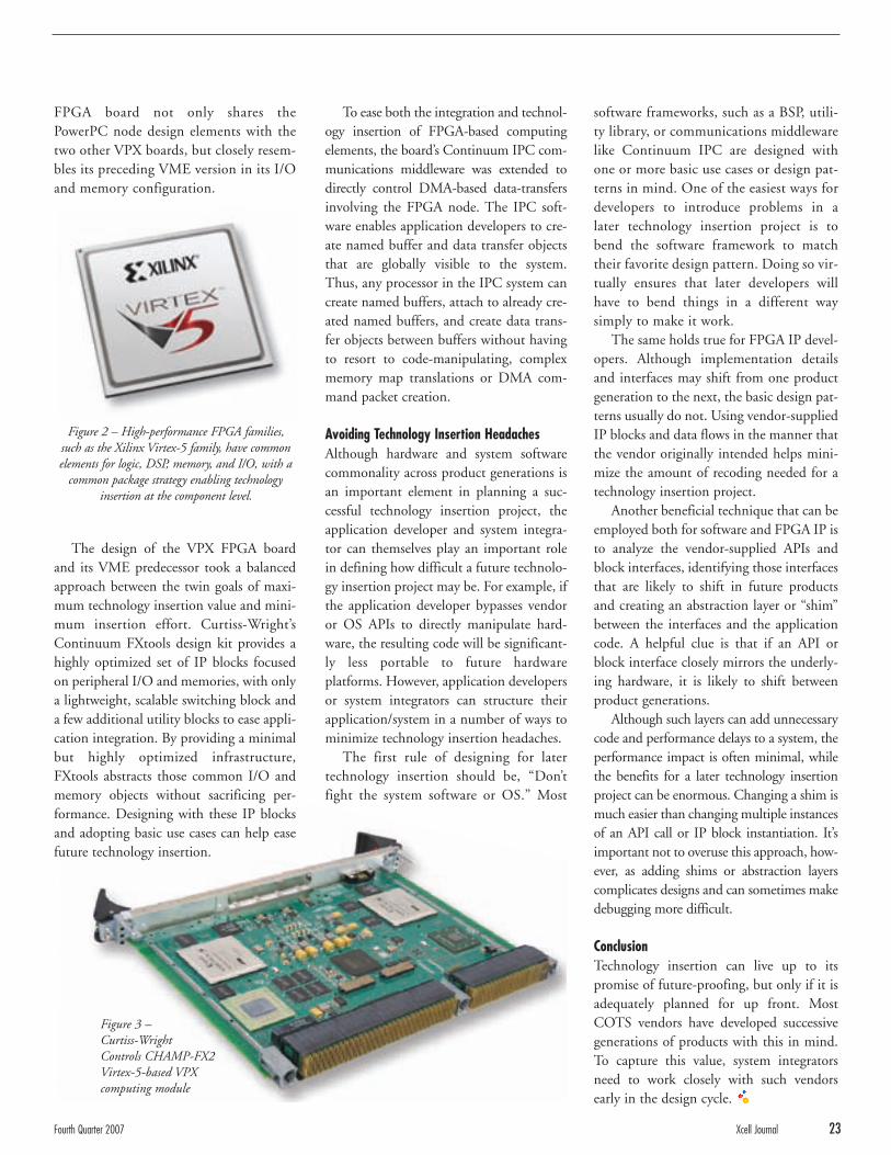
Figure 2 – High-performance FPGA families, such as the Xilinx Virtex-5 family, have common elements for logic, DSP, memory, and I/O, with a
common package strategy enabling technology insertion at the component level.
Figure 3 – Curtiss-Wright Controls CHAMP-FX2 Virtex-5-based VPX computing module
by Tim VanevenhovenDSP Tools Product ManagerXilinx, [email protected]
DSP systems are best described byusing a combination of both graphical-and language-based methods. TheMathWorks, an industry leader in DSPmodeling software, caters to thisdichotomy by providing a cycle-accu-rate graphical design environmentcalled Simulink and a mathematicalmodeling language called MATLAB.
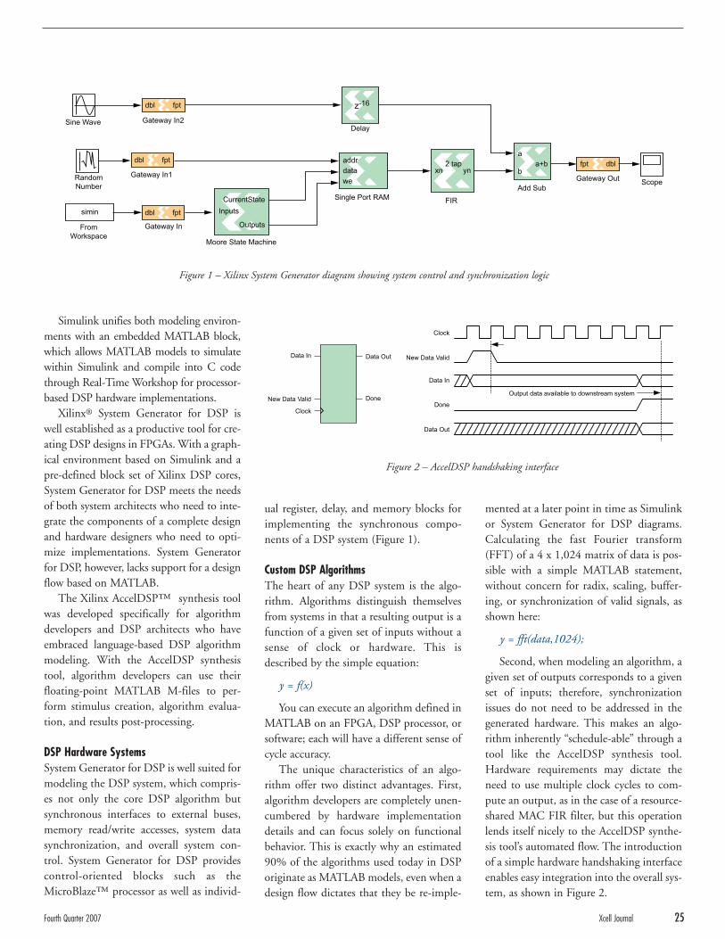
Simulink is well suited for the “sys-tem” aspects of DSP design, includingcontrol and synchronization of dataflow to and from interfaces and memo-ries. Simulink also provides a rich set ofpre-defined DSP algorithms in the formof block sets that you can use to con-struct DSP systems. Simulink is notalways the most effective environmentfor modeling proprietary algorithms,however. It unnecessarily burdensdesigners with cycle-accurate considera-tions and forces low-level arithmeticoperations and array accesses to be con-structed from graphical block sets ratherthan concise textual expressions.
Some DSP algorithm developershave found that the MATLAB languagebest meets their preferred style of devel-opment. With more than 1,000 built-in functions as well as toolboxextensions for signal processing, com-munications, and wavelet processing,MATLAB offers a rich and easy-to-useenvironment for the development anddebugging of sophisticated algorithms.
24 Xcell Journal Fourth Quarter 2007
Using MATLAB to Create IP for System Generator for DSP You can use MATLAB M-files with the AccelChip synthesis tool to optimize FPGA implementations.
Simulink unifies both modeling environ-ments with an embedded MATLAB block,which allows MATLAB models to simulatewithin Simulink and compile into C codethrough Real-Time Workshop for processor-based DSP hardware implementations.
Xilinx® System Generator for DSP iswell established as a productive tool for cre-ating DSP designs in FPGAs. With a graph-ical environment based on Simulink and apre-defined block set of Xilinx DSP cores,System Generator for DSP meets the needsof both system architects who need to inte-grate the components of a complete designand hardware designers who need to opti-mize implementations. System Generatorfor DSP, however, lacks support for a designflow based on MATLAB.
The Xilinx AccelDSP™ synthesis toolwas developed specifically for algorithmdevelopers and DSP architects who haveembraced language-based DSP algorithmmodeling. With the AccelDSP synthesistool, algorithm developers can use theirfloating-point MATLAB M-files to per-form stimulus creation, algorithm evalua-tion, and results post-processing.
DSP Hardware SystemsSystem Generator for DSP is well suited formodeling the DSP system, which compris-es not only the core DSP algorithm butsynchronous interfaces to external buses,memory read/write accesses, system datasynchronization, and overall system con-trol. System Generator for DSP providescontrol-oriented blocks such as theMicroBlaze™ processor as well as individ-
mented at a later point in time as Simulinkor System Generator for DSP diagrams.Calculating the fast Fourier transform(FFT) of a 4 x 1,024 matrix of data is pos-sible with a simple MATLAB statement,without concern for radix, scaling, buffer-ing, or synchronization of valid signals, asshown here:
y = fft(data,1024);
Second, when modeling an algorithm, agiven set of outputs corresponds to a givenset of inputs; therefore, synchronizationissues do not need to be addressed in thegenerated hardware. This makes an algo-rithm inherently “schedule-able” through atool like the AccelDSP synthesis tool.Hardware requirements may dictate theneed to use multiple clock cycles to com-pute an output, as in the case of a resource-shared MAC FIR filter, but this operationlends itself nicely to the AccelDSP synthe-sis tool’s automated flow. The introductionof a simple hardware handshaking interfaceenables easy integration into the overall sys-tem, as shown in Figure 2.
ual register, delay, and memory blocks forimplementing the synchronous compo-nents of a DSP system (Figure 1).
Custom DSP AlgorithmsThe heart of any DSP system is the algo-rithm. Algorithms distinguish themselvesfrom systems in that a resulting output is afunction of a given set of inputs without asense of clock or hardware. This isdescribed by the simple equation:
y = f(x)
You can execute an algorithm defined inMATLAB on an FPGA, DSP processor, orsoftware; each will have a different sense ofcycle accuracy.
The unique characteristics of an algo-rithm offer two distinct advantages. First,algorithm developers are completely unen-cumbered by hardware implementationdetails and can focus solely on functionalbehavior. This is exactly why an estimated90% of the algorithms used today in DSPoriginate as MATLAB models, even when adesign flow dictates that they be re-imple-
Fourth Quarter 2007 Xcell Journal 25
z-16
addrdatawe
xn yn2 tap
Inputs
Outputs
CurrentState
b
aa+b fpt dbl
dblsimin
FromWorkspace
RandomNumber
Sine Wave Gateway In2
Gateway In1
Gateway In
Moore State Machine
Single Port RAM FIR
Add SubGateway Out Scope
Delay
fpt
dbl fpt
dbl fpt
Data In
Clock
Output data available to downstream system
New Data Valid
Data In
Done
Data Out
Data Out
DoneNew Data Valid
Clock
Figure 1 – Xilinx System Generator diagram showing system control and synchronization logic
Figure 2 – AccelDSP handshaking interface
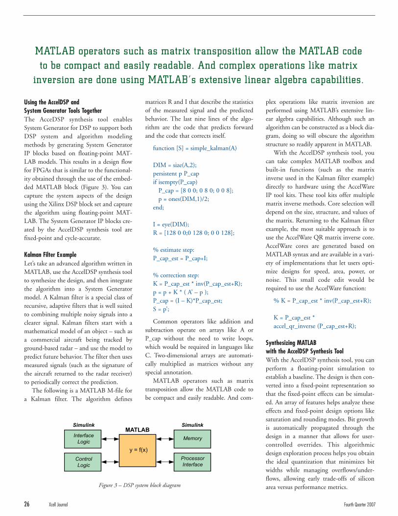
Using the AccelDSP and System Generator Tools TogetherThe AcceDSP synthesis tool enablesSystem Generator for DSP to support bothDSP system and algorithm modelingmethods by generating System GeneratorIP blocks based on floating-point MAT-LAB models. This results in a design flowfor FPGAs that is similar to the functional-ity obtained through the use of the embed-ded MATLAB block (Figure 3). You cancapture the system aspects of the designusing the Xilinx DSP block set and capturethe algorithm using floating-point MAT-LAB. The System Generator IP blocks cre-ated by the AccelDSP synthesis tool arefixed-point and cycle-accurate.
Kalman Filter ExampleLet’s take an advanced algorithm written inMATLAB, use the AccelDSP synthesis toolto synthesize the design, and then integratethe algorithm into a System Generatormodel. A Kalman filter is a special class ofrecursive, adaptive filters that is well suitedto combining multiple noisy signals into aclearer signal. Kalman filters start with amathematical model of an object – such asa commercial aircraft being tracked byground-based radar – and use the model topredict future behavior. The filter then usesmeasured signals (such as the signature ofthe aircraft returned to the radar receiver)to periodically correct the prediction.
The following is a MATLAB M-file fora Kalman filter. The algorithm defines
matrices R and I that describe the statisticsof the measured signal and the predictedbehavior. The last nine lines of the algo-rithm are the code that predicts forwardand the code that corrects itself.
function [S] = simple_kalman(A)
DIM = size(A,2);persistent p P_capif isempty(P_cap)
P_cap = [8 0 0; 0 8 0; 0 0 8];p = ones(DIM,1)/2;
end;
I = eye(DIM);R = [128 0 0;0 128 0; 0 0 128];
% estimate step:P_cap_est = P_cap+I;
% correction step:K = P_cap_est * inv(P_cap_est+R);p = p + K * ( A’ – p );P_cap = (I – K)*P_cap_est;S = p’;
Common operators like addition andsubtraction operate on arrays like A orP_cap without the need to write loops,which would be required in languages likeC. Two-dimensional arrays are automati-cally multiplied as matrices without anyspecial annotation.
MATLAB operators such as matrixtransposition allow the MATLAB code tobe compact and easily readable. And com-
plex operations like matrix inversion areperformed using MATLAB’s extensive lin-ear algebra capabilities. Although such analgorithm can be constructed as a block dia-gram, doing so will obscure the algorithmstructure so readily apparent in MATLAB.
With the AccelDSP synthesis tool, youcan take complex MATLAB toolbox andbuilt-in functions (such as the matrixinverse used in the Kalman filter example)directly to hardware using the AccelWareIP tool kits. These tool kits offer multiplematrix inverse methods. Core selection willdepend on the size, structure, and values ofthe matrix. Returning to the Kalman filterexample, the most suitable approach is touse the AccelWare QR matrix inverse core.AccelWare cores are generated based onMATLAB syntax and are available in a vari-ety of implementations that let users opti-mize designs for speed, area, power, ornoise. This small code edit would berequired to use the AccelWare function:
% K = P_cap_est * inv(P_cap_est+R);
K = P_cap_est * accel_qr_inverse (P_cap_est+R);
Synthesizing MATLAB with the AccelDSP Synthesis ToolWith the AccelDSP synthesis tool, you canperform a floating-point simulation toestablish a baseline. The design is then con-verted into a fixed-point representation sothat the fixed-point effects can be simulat-ed. An array of features helps analyze theseeffects and fixed-point design options likesaturation and rounding modes. Bit growthis automatically propagated through thedesign in a manner that allows for user-controlled overrides. This algorithmicdesign exploration process helps you obtainthe ideal quantization that minimizes bitwidths while managing overflows/under-flows, allowing early trade-offs of siliconarea versus performance metrics.
26 Xcell Journal Fourth Quarter 2007
Simulink
Memory
ProcessorInterface
y = f(x)
ControlLogic
InterfaceLogic
MATLABSimulink
Figure 3 – DSP system block diagram
MATLAB operators such as matrix transposition allow the MATLAB code to be compact and easily readable. And complex operations like matrix
inversion are done using MATLAB’s extensive linear algebra capabilities.
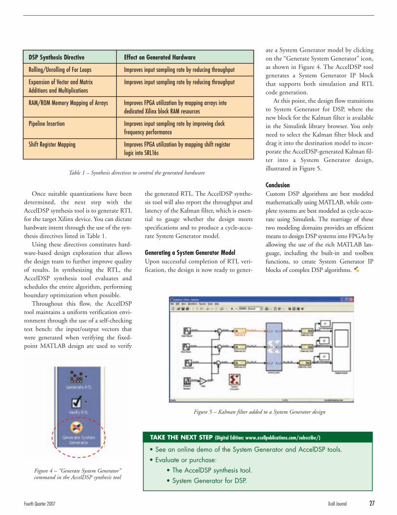
Fourth Quarter 2007 Xcell Journal 27
Once suitable quantizations have beendetermined, the next step with theAccelDSP synthesis tool is to generate RTLfor the target Xilinx device. You can dictatehardware intent through the use of the syn-thesis directives listed in Table 1.
Using these directives constitutes hard-ware-based design exploration that allowsthe design team to further improve qualityof results. In synthesizing the RTL, theAccelDSP synthesis tool evaluates andschedules the entire algorithm, performingboundary optimization when possible.
Throughout this flow, the AccelDSPtool maintains a uniform verification envi-ronment through the use of a self-checkingtest bench: the input/output vectors thatwere generated when verifying the fixed-point MATLAB design are used to verify
the generated RTL. The AccelDSP synthe-sis tool will also report the throughput andlatency of the Kalman filter, which is essen-tial to gauge whether the design meetsspecifications and to produce a cycle-accu-rate System Generator model.
Generating a System Generator ModelUpon successful completion of RTL veri-fication, the design is now ready to gener-
ate a System Generator model by clickingon the “Generate System Generator” icon,as shown in Figure 4. The AccelDSP toolgenerates a System Generator IP blockthat supports both simulation and RTLcode generation.
At this point, the design flow transitionsto System Generator for DSP, where thenew block for the Kalman filter is availablein the Simulink library browser. You onlyneed to select the Kalman filter block anddrag it into the destination model to incor-porate the AccelDSP-generated Kalman fil-ter into a System Generator design,illustrated in Figure 5.
ConclusionCustom DSP algorithms are best modeledmathematically using MATLAB, while com-plete systems are best modeled as cycle-accu-rate using Simulink. The marriage of thesetwo modeling domains provides an efficientmeans to design DSP systems into FPGAs byallowing the use of the rich MATLAB lan-guage, including the built-in and toolboxfunctions, to create System Generator IPblocks of complex DSP algorithms.
DSP Synthesis Directive Effect on Generated Hardware
Rolling/Unrolling of For Loops Improves input sampling rate by reducing throughput
Expansion of Vector and Matrix Improves input sampling rate by reducing throughputAdditions and Multiplications
RAM/ROM Memory Mapping of Arrays Improves FPGA utilization by mapping arrays into dedicated Xilinx block RAM resources
Pipeline Insertion Improves input sampling rate by improving clock frequency performance
Shift Register Mapping Improves FPGA utilization by mapping shift register logic into SRL16s
• See an online demo of the System Generator and AccelDSP tools.• Evaluate or purchase:
• The AccelDSP synthesis tool.• System Generator for DSP.
TAKE THE NEXT STEP (Digital Edition: www.xcellpublications.com/subscribe/)
Figure 4 – “Generate System Generator” command in the AccelDSP synthesis tool
Figure 5 – Kalman filter added to a System Generator design
Table 1 – Synthesis directives to control the generated hardware
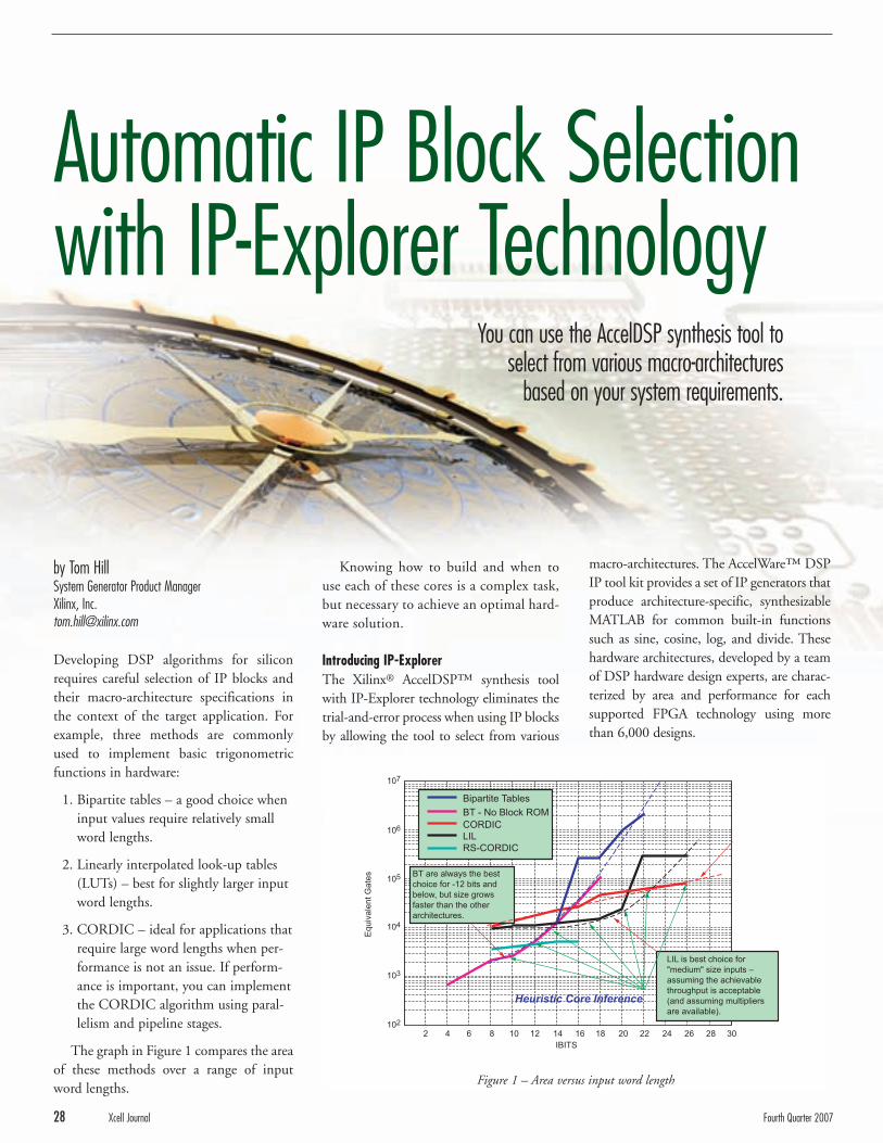
by Tom HillSystem Generator Product ManagerXilinx, [email protected]
Developing DSP algorithms for siliconrequires careful selection of IP blocks andtheir macro-architecture specifications inthe context of the target application. Forexample, three methods are commonlyused to implement basic trigonometricfunctions in hardware:
1. Bipartite tables – a good choice wheninput values require relatively smallword lengths.
2. Linearly interpolated look-up tables(LUTs) – best for slightly larger inputword lengths.
3. CORDIC – ideal for applications thatrequire large word lengths when per-formance is not an issue. If perform-ance is important, you can implementthe CORDIC algorithm using paral-lelism and pipeline stages.
The graph in Figure 1 compares the areaof these methods over a range of inputword lengths.
Knowing how to build and when touse each of these cores is a complex task,but necessary to achieve an optimal hard-ware solution.
Introducing IP-ExplorerThe Xilinx® AccelDSP™ synthesis toolwith IP-Explorer technology eliminates thetrial-and-error process when using IP blocksby allowing the tool to select from various
macro-architectures. The AccelWare™ DSPIP tool kit provides a set of IP generators thatproduce architecture-specific, synthesizableMATLAB for common built-in functionssuch as sine, cosine, log, and divide. Thesehardware architectures, developed by a teamof DSP hardware design experts, are charac-terized by area and performance for eachsupported FPGA technology using morethan 6,000 designs.
28 Xcell Journal Fourth Quarter 2007
Automatic IP Block Selection with IP-Explorer Technology
You can use the AccelDSP synthesis tool to select from various macro-architectures
based on your system requirements.
Bipartite Tables
LIL is best choice for
"medium" size inputs –
assuming the achievable
throughput is acceptable
(and assuming multipliers
are available).
BT - No Block ROM
CORDIC
LIL
RS-CORDIC
BT are always the best
choice for -12 bits and
below, but size grows
faster than the other
architectures.
Heuristic Core Inference
Eq
uiv
ale
nt
Ga
tes
IBITS
107
106
105
104
103
102
2 4 6 8 10 12 14 16 18 20 22 24 26 28 30
Figure 1 – Area versus input word length
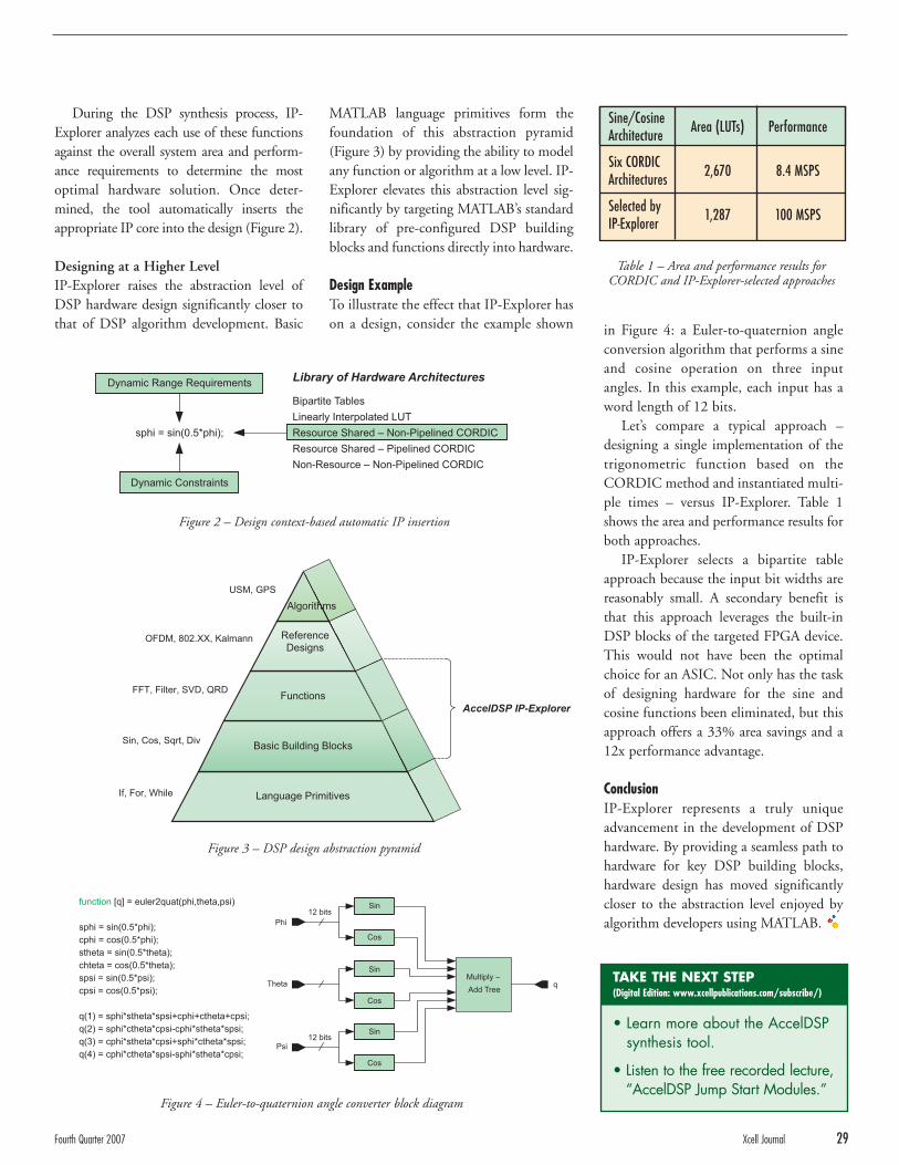
During the DSP synthesis process, IP-Explorer analyzes each use of these functionsagainst the overall system area and perform-ance requirements to determine the mostoptimal hardware solution. Once deter-mined, the tool automatically inserts theappropriate IP core into the design (Figure 2).
Designing at a Higher LevelIP-Explorer raises the abstraction level ofDSP hardware design significantly closer tothat of DSP algorithm development. Basic in Figure 4: a Euler-to-quaternion angle
conversion algorithm that performs a sineand cosine operation on three inputangles. In this example, each input has aword length of 12 bits.
Let’s compare a typical approach –designing a single implementation of thetrigonometric function based on theCORDIC method and instantiated multi-ple times – versus IP-Explorer. Table 1shows the area and performance results forboth approaches.
IP-Explorer selects a bipartite tableapproach because the input bit widths arereasonably small. A secondary benefit isthat this approach leverages the built-inDSP blocks of the targeted FPGA device.This would not have been the optimalchoice for an ASIC. Not only has the taskof designing hardware for the sine andcosine functions been eliminated, but thisapproach offers a 33% area savings and a12x performance advantage.
ConclusionIP-Explorer represents a truly uniqueadvancement in the development of DSPhardware. By providing a seamless path tohardware for key DSP building blocks,hardware design has moved significantlycloser to the abstraction level enjoyed byalgorithm developers using MATLAB.
MATLAB language primitives form thefoundation of this abstraction pyramid(Figure 3) by providing the ability to modelany function or algorithm at a low level. IP-Explorer elevates this abstraction level sig-nificantly by targeting MATLAB’s standardlibrary of pre-configured DSP buildingblocks and functions directly into hardware.
Design ExampleTo illustrate the effect that IP-Explorer hason a design, consider the example shown
Fourth Quarter 2007 Xcell Journal 29
Sine/Cosine Architecture Area (LUTs) Performance
Six CORDIC Architectures 2,670 8.4 MSPS
Selected by IP-Explorer 1,287 100 MSPS
Language Primitives
Basic Building Blocks
Functions
Algorithms
Reference
Designs
USM, GPS
OFDM, 802.XX, Kalmann
FFT, Filter, SVD, QRD
Sin, Cos, Sqrt, Div
If, For, While
AccelDSP IP-Explorer
Theta
Psi
Phi
12 bits
function [q] = euler2quat(phi,theta,psi)
sphi = sin(0.5*phi);
cphi = cos(0.5*phi);
stheta = sin(0.5*theta);
chteta = cos(0.5*theta);
spsi = sin(0.5*psi);
cpsi = cos(0.5*psi);
q(1) = sphi*stheta*spsi+cphi+ctheta+cpsi;
q(2) = sphi*ctheta*cpsi-cphi*stheta*spsi;
q(3) = cphi*stheta*cpsi+sphi*ctheta*spsi;
q(4) = cphi*ctheta*spsi-sphi*stheta*cpsi;
Cos
Sin
Cos
Sin
Cos
Sin
Multiply –
Add Treeq
12 bits
• Learn more about the AccelDSPsynthesis tool.
• Listen to the free recorded lecture,“AccelDSP Jump Start Modules.”
TAKE THE NEXT STEP (Digital Edition: www.xcellpublications.com/subscribe/)
Dynamic Range Requirements
sphi = sin(0.5*phi);
Dynamic Constraints
Bipartite Tables
Linearly Interpolated LUT
Resource Shared – Non-Pipelined CORDIC
Resource Shared – Pipelined CORDIC
Non-Resource – Non-Pipelined CORDIC
Library of Hardware Architectures
Figure 2 – Design context-based automatic IP insertion
Figure 3 – DSP design abstraction pyramid
Figure 4 – Euler-to-quaternion angle converter block diagram
Table 1 – Area and performance results forCORDIC and IP-Explorer-selected approaches
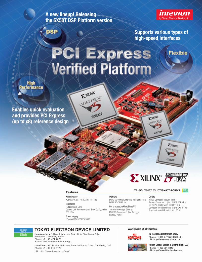
by Mike HodsonManaging DirectorImage Processing Techniques [email protected]
FPGA devices have been used for manyyears in the design of professional videosystems. The consumer electronics market-place, however, has traditionally been anarea where FPGAs have not made much ofan impact, primarily because of device cost.
Recently, goods such as high-resolutionflat-panel displays, MPEG-2/MPEG-4encoders and decoders, portable video play-ers, and digital cameras have grown in pop-ularity. Such items require significant imageprocessing functionality. A few years ago,custom silicon would have been the onlysensible choice, but with the introduction ofnext-generation devices such as the Xilinx®
Spartan™-3A DSP and Virtex™-5 fami-lies, the price/performance balance ofFPGAs versus ASIC or ASSP devices has
shifted, leading to significant growth in theuse of FPGAs for such applications.
Using FPGAs for image processing appli-cations presents system designers with someinteresting problems. The analysis andmanipulation of video images is inherently ahigh-bandwidth process, while softwaresimulations do not always provide engineerswith enough information to establish theperformance of their algorithms becausethey are not in real time. For this reason,there is a growing demand for FPGA hard-ware prototyping systems targeted specifical-ly at the requirements of image processingengineers – development platforms that pro-vide the real-time I/O and memory interfacecapabilities necessary to prototype today’smost demanding signal processing applica-tions, as illustrated in Figure 1.
In this article, I’ll look at the require-ments and availability of FPGA develop-ment platforms for image processingapplications.
Required ElementsWhen considering the design of an FPGAplatform for image processing algorithmdevelopment, it is useful to review the prin-cipal elements that are common to themost popular image analysis techniques,and what hardware resources are needed tosupport these elements.
High-Speed I/OGetting real-time video signals into andout of an image processor is obviously crit-ical to the performance of the system.Typically, image data is input and outputsynchronously through a proprietary orindustry-standard interface such as DVI,HDMI, SDI, analog component, S-video,or composite. The images may alternative-ly be transferred asynchronously through aprocessor or backplane bus (PCI, VME)directly into frame stores.
The latest generation of serial bus inter-faces, such as PCI Express, have sufficient
Fourth Quarter 2007 Xcell Journal 31
Prototyping Image Processing Applications
Prototyping Image Processing Applications
Development platforms for FPGA-based image processing applications present some interesting system-design challenges.
Development platforms for FPGA-based image processing applications present some interesting system-design challenges.
bandwidth for multiple streams of uncom-pressed high-definition video to be trans-ferred in real-time, while Virtex-5 devices,with their on-chip PCI Express interface andmultiple MGTs, provide an excellent rangeof I/O capabilities for video interfacing.
Frame StoresThe frame stores used for temporary storageof image data are at the core of many imageprocessing functions. They serve many pur-poses, such as synchronizing multiple imagesources, image re-sizing and manipulation,motion or object detection and tracking,noise reduction, and de-interlacing.
The storage of multiple video framestypically requires a large quantity of memo-ry that is accessed sequentially. For this rea-son, single- or double-data-rate SDRAM isnormally employed. However, in applica-tions where image transformations includeperspective, rotation, or non-linear “warps”of the source image, the frame store archi-tecture is typically based on very high speedsynchronous static RAMs to give low-laten-cy random access operation (rather than lin-ear data bursts from SDRAM).
Filtering and InterpolationApplications that involve re-sampling ofthe source image data also need to interpo-late or filter the image to avoid aliasingproblems. Efficient implementation of fil-ters is therefore important. Spartan-3ADSP and Virtex-5 devices are useful here,as the architecture of their DSP blocks isideally suited to the efficient implementa-tion of all kinds of filters.
overlaid on top of another using a “key”or alpha channel as a guide. It is quitepossible to perform these operationsusing a simple switch between sources;however, this does not allow for variabletransparency and may also result in out-of-band components in the output image.For this reason, professional mixers andkeyers use proper cross-fader logic builtfrom multiplier pairs and key signals with“soft” low-pass filtered edges. Ideally,FPGA-based systems should implementsimilar logic.
Software Control and AnalysisVirtually all image processing systemsrequire some form of software-pro-grammed control system, either to con-figure the system correctly or to analyzethe data and present the results in an effi-cient manner. These control systems mayrange from a simple soft- or hard-IP coreprocessor embedded in the FPGA (suchas the PowerPC embedded in VirtexFPGAs) all the way up to the latest IntelCore 2 Quad systems running MicrosoftWindows Vista, which have tremendousprocessing capability. With such high-performance processors, system designersnow have the choice to split the imageprocessing tasks between hardware andsoftware; hence the importance of imple-menting a high-bandwidth data pipebetween the two.
Resulting Platform ArchitectureThe ideal platform for image processingalgorithm development will provide most(if not all) of these processing elements.
Although many of the required ele-ments are already supported by theVirtex-5 family of FPGAs, some items(such as large frame stores and dedicatedvideo I/O) require external components.Hosting the whole system in a PC-basedenvironment is also an ideal way to inte-grate Xilinx ISE™ software with any pro-prietary user application.
Figure 2 shows the block diagram of anew FPGA prototyping system that hasbeen developed by Image ProcessingTechniques (IPT) in conjunction withXilinx. Called the Advanced Video
Delay ElementsImage processing algorithms typicallyrequire a wide range of delay elements. Fordelays of a few pixels – to equalize pipelineprocessing latency or for polyphase filtertaps – the SRL16 blocks in Xilinx FPGAsare highly efficient. Block RAMs, withtheir dual-port architecture, are ideal forline delays, which are needed where thevertical columns of data within 2D raster-scan images are processed.
Look-Up TablesAdjustments to the dynamic range ofimage data and non-linear transfer func-tions can be efficiently implemented usinglook-up tables. How such tables are imple-mented – and how they are referred to –depends on the number of inputs theyhave. Look-up tables (LUTs) are said to be“1D” where the table output value dependson only one input value, “2D” where theoutput depends on two inputs, and “3D”where it depends on three inputs.
The 1D and 2D cases can usually beimplemented in block RAM (dependingon the size of the input vectors).However, to obtain sufficient precision in3D LUTs, it is often necessary to useexternal memories such as high-speedsynchronous static RAMs. DRAMs arenot usually suitable because LUT opera-tions are rarely burst-oriented. Instead,look-up address values tend to be ran-dom in nature, which makes DRAMusage inefficient.
Color-Space ConversionA very common image processing opera-tion is the conversion of image databetween different color spaces. RGB,YCbCr, XYZ, and xvYCC are all in wide-spread use at the moment, so there is fre-quently a need to convert between thesedifferent formats. Conversion typicallyuses a 3 x 3 matrix multiplier array. Sucharrays can be implemented very easilyusing Xilinx DSP blocks.
Video Mixing and KeyingMany image processing applicationsrequire multiple image sources to bemixed or cross-faded, or one image to be
Figure 1 – Real-time 3D image manipulationusing FPGA technology
32 Xcell Journal Fourth Quarter 2007
Fourth Quarter 2007 Xcell Journal 33
Development Platform (AVDP), the systemhas been specifically designed to assist engi-neers with the development of a wide rangeof image processing algorithms.
The top of the AVDP is shown inFigure 3. It is designed around a XilinxVirtex-5 FPGA, leveraging its advantagesof multiple MGTs for high-speed I/O andan architecture that is well suited to theimplementation of filters and color-spaceconversion arrays. The board also featuresa PCI Express x4 connector, providing anefficient interface to a PC for softwarecontrol and analysis; up to 1 GB of high-speed DDR2 SDRAM for bulk video stor-age; and up to 4 x 36 MB of high-speedQDR II SRAM.
The AVDP system is available with arange of Virtex-5 devices installed, from theLX50T all the way up to the DSP-intensiveSX95T, and is provided together with arange of specialist video IP in VHDL sourcecode, software API, device drivers, and adebugging application to help designersdevelop their image processing applications.
ConclusionThe AVDP board, developed by IPT inconjunction with Xilinx, represents thestate-of-the-art in FPGA development sys-tems and addresses the requirements ofplatforms for image processing algorithmdevelopment: flexible video I/O, high-speed memory, and high-performance dataacquisition and control.
The key applications that the system isdesigned to accelerate include:
• Codec design and development:MPEG-2, MPEG-4, JPEG-2000
• Video standards conversion
• Video de-interlacing and resizing algo-rithms for flat-panel displays
• Broadcast graphics: character genera-tors, still-stores, keyers, and mixers
• Real-time image manipulation forvideo special effects
• Robotic vision processing and algo-rithm development
For more information, please visitwww.imageproc.com.
Housekeeping
Function
Mo
nito
r O
utp
ut
DDR2 SDRAM
Video Processing
Power
MG
Ts
Virtex-5 FPGA
Spartan-3
FPGA
C2 Bus
V5
Control
Bus
V5S3
Video
Bus
I/O Module
Parallel Bus
I2C Bus
From
Spartan
FPGA
I2C Bus
Analog
Reference
Input
Analog
Video
Output
I/O Module
MGT
Reference
Clocks
Sync
Clock Crosspoint
Clock Drivers
VXCOs
Sync Separator
CoolRunner-II
CPLD
Flash PROM +
Associated
Switch Block
Genlock
Flash
Interface
Monitor
Connector
I/O Module
Parallel Port
I/O Module
Parallel Port
Expansion
Module
Serial Ports
I/O Module
Serial Port
QDR II SRAM
PCIe x4
Connector
Video Filter
Video Encoder
Figure 2 – AVDP block diagram
Figure 3 – The Advanced Video Development Platform
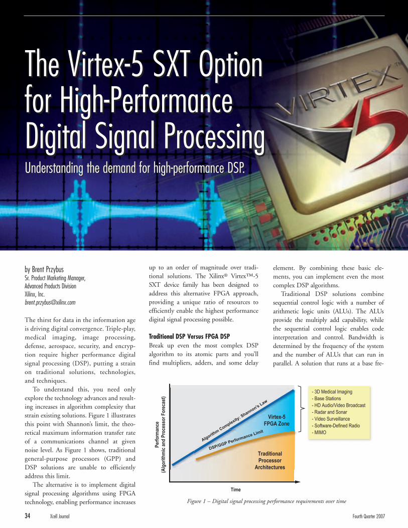
by Brent Przybus Sr. Product Marketing Manager, Advanced Products Division Xilinx, [email protected]
The thirst for data in the information ageis driving digital convergence. Triple-play,medical imaging, image processing,defense, aerospace, security, and encryp-tion require higher performance digitalsignal processing (DSP), putting a strainon traditional solutions, technologies,and techniques.
To understand this, you need onlyexplore the technology advances and result-ing increases in algorithm complexity thatstrain existing solutions. Figure 1 illustratesthis point with Shannon’s limit, the theo-retical maximum information transfer rateof a communications channel at givennoise level. As Figure 1 shows, traditionalgeneral-purpose processors (GPP) andDSP solutions are unable to efficientlyaddress this limit.
The alternative is to implement digitalsignal processing algorithms using FPGAtechnology, enabling performance increases
up to an order of magnitude over tradi-tional solutions. The Xilinx® Virtex™-5SXT device family has been designed toaddress this alternative FPGA approach,providing a unique ratio of resources toefficiently enable the highest performancedigital signal processing possible.
Traditional DSP Versus FPGA DSPBreak up even the most complex DSPalgorithm to its atomic parts and you’llfind multipliers, adders, and some delay
element. By combining these basic ele-ments, you can implement even the mostcomplex DSP algorithms.
Traditional DSP solutions combinesequential control logic with a number ofarithmetic logic units (ALUs). The ALUsprovide the multiply add capability, whilethe sequential control logic enables codeinterpretation and control. Bandwidth isdetermined by the frequency of the systemand the number of ALUs that can run inparallel. A solution that runs at a base fre-
34 Xcell Journal Fourth Quarter 2007
The Virtex-5 SXT Option for High-Performance Digital Signal Processing
The Virtex-5 SXT Option for High-Performance Digital Signal Processing Understanding the demand for high-performance DSP.Understanding the demand for high-performance DSP.
Alg
orithm
Com
plexity
: Shannon's
Law
DSP/GGP Perform
ance Limit
Virtex-5
FPGA Zone
Traditional
Processor
Architectures
Time
Per
form
ance
(Alg
ori
thm
ic a
nd
Pro
cess
or
Fo
reca
st)
- 3D Medical Imaging
- Base Stations
- HD Audio/Video Broadcast
- Radar and Sonar
- Video Surveillance
- Software-Defined Radio
- MIMO
Figure 1 – Digital signal processing performance requirements over time
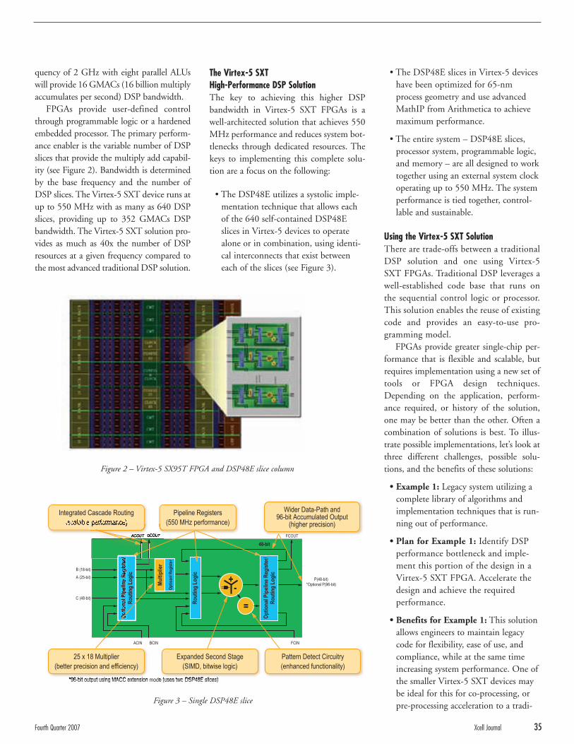
quency of 2 GHz with eight parallel ALUswill provide 16 GMACs (16 billion multiplyaccumulates per second) DSP bandwidth.
FPGAs provide user-defined controlthrough programmable logic or a hardenedembedded processor. The primary perform-ance enabler is the variable number of DSPslices that provide the multiply add capabil-ity (see Figure 2). Bandwidth is determinedby the base frequency and the number ofDSP slices. The Virtex-5 SXT device runs atup to 550 MHz with as many as 640 DSPslices, providing up to 352 GMACs DSPbandwidth. The Virtex-5 SXT solution pro-vides as much as 40x the number of DSPresources at a given frequency compared tothe most advanced traditional DSP solution.
• The DSP48E slices in Virtex-5 deviceshave been optimized for 65-nmprocess geometry and use advancedMathIP from Arithmetica to achievemaximum performance.
• The entire system – DSP48E slices,processor system, programmable logic,and memory – are all designed to worktogether using an external system clockoperating up to 550 MHz. The systemperformance is tied together, control-lable and sustainable.
Using the Virtex-5 SXT SolutionThere are trade-offs between a traditionalDSP solution and one using Virtex-5SXT FPGAs. Traditional DSP leverages awell-established code base that runs onthe sequential control logic or processor.This solution enables the reuse of existingcode and provides an easy-to-use pro-gramming model.
FPGAs provide greater single-chip per-formance that is flexible and scalable, butrequires implementation using a new set oftools or FPGA design techniques.Depending on the application, perform-ance required, or history of the solution,one may be better than the other. Often acombination of solutions is best. To illus-trate possible implementations, let’s look atthree different challenges, possible solu-tions, and the benefits of these solutions:
• Example 1: Legacy system utilizing acomplete library of algorithms andimplementation techniques that is run-ning out of performance.
• Plan for Example 1: Identify DSPperformance bottleneck and imple-ment this portion of the design in aVirtex-5 SXT FPGA. Accelerate thedesign and achieve the required performance.
• Benefits for Example 1: This solutionallows engineers to maintain legacycode for flexibility, ease of use, andcompliance, while at the same timeincreasing system performance. One ofthe smaller Virtex-5 SXT devices maybe ideal for this for co-processing, orpre-processing acceleration to a tradi-
The Virtex-5 SXT High-Performance DSP SolutionThe key to achieving this higher DSPbandwidth in Virtex-5 SXT FPGAs is awell-architected solution that achieves 550MHz performance and reduces system bot-tlenecks through dedicated resources. Thekeys to implementing this complete solu-tion are a focus on the following:
• The DSP48E utilizes a systolic imple-mentation technique that allows eachof the 640 self-contained DSP48Eslices in Virtex-5 devices to operatealone or in combination, using identi-cal interconnects that exist betweeneach of the slices (see Figure 3).
Fourth Quarter 2007 Xcell Journal 35
Integrated Cascade Routing
25 x 18 Multiplier
(better precision and efficiency)
*96-bit output using MACC extension mode (uses two DSP48E slices)
Pattern Detect Circuitry
(enhanced functionality)
Expanded Second Stage
(SIMD, bitwise logic)
Wider Data-Path and96-bit Accumulated Output
(higher precision)
Pipeline Registers
(550 MHz performance)
=
+-
Mu
ltip
lier
Ro
uti
ng
Lo
gic
Op
tio
nal
Pip
elin
e R
egis
ter/
Ro
uti
ng
Lo
gic
Ro
uti
ng
Lo
gic
Op
tio
anl R
egis
ter
B (18-bit)
A (25-bit)
C (48-bit)
ACIN BCIN FCIN
FCOUT
P(48-bit)
*Optional P(96-bit)
48-bit
Figure 3 – Single DSP48E slice
Figure 2 – Virtex-5 SX95T FPGA and DSP48E slice column
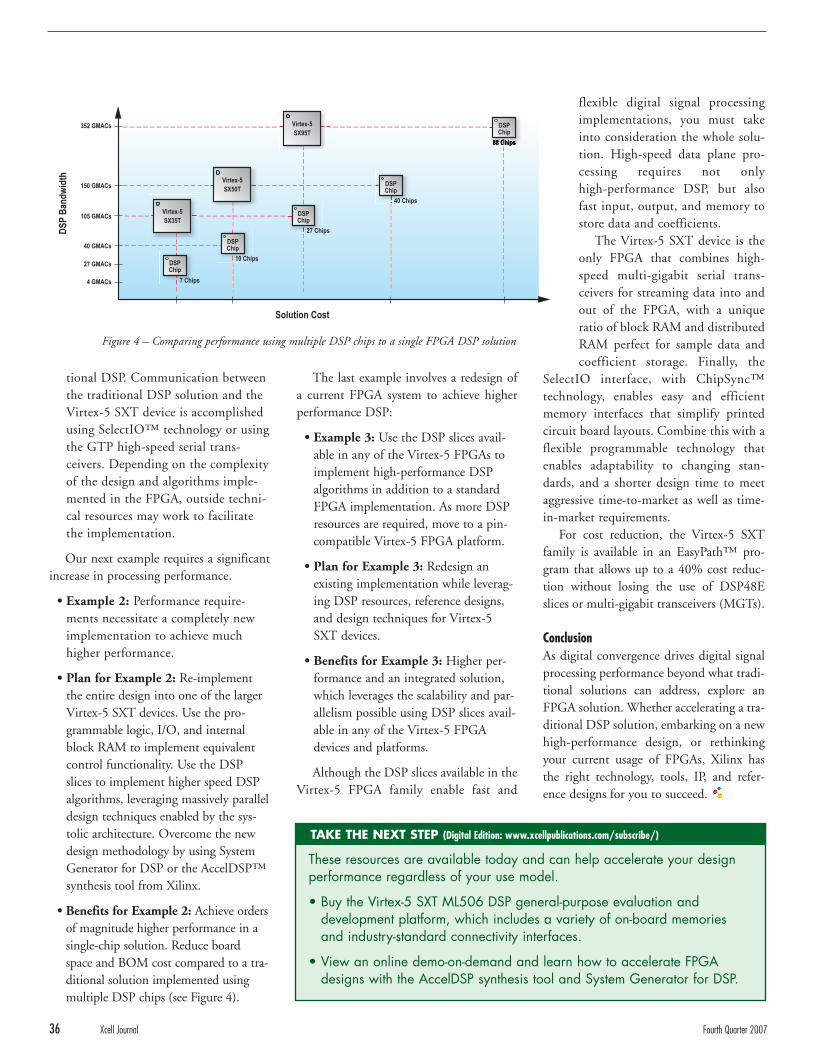
tional DSP. Communication betweenthe traditional DSP solution and theVirtex-5 SXT device is accomplishedusing SelectIO™ technology or usingthe GTP high-speed serial trans-ceivers. Depending on the complexityof the design and algorithms imple-mented in the FPGA, outside techni-cal resources may work to facilitatethe implementation.
Our next example requires a significantincrease in processing performance.
• Example 2: Performance require-ments necessitate a completely newimplementation to achieve muchhigher performance.
• Plan for Example 2: Re-implementthe entire design into one of the largerVirtex-5 SXT devices. Use the pro-grammable logic, I/O, and internalblock RAM to implement equivalentcontrol functionality. Use the DSPslices to implement higher speed DSPalgorithms, leveraging massively paralleldesign techniques enabled by the sys-tolic architecture. Overcome the newdesign methodology by using SystemGenerator for DSP or the AccelDSP™synthesis tool from Xilinx.
• Benefits for Example 2: Achieve ordersof magnitude higher performance in asingle-chip solution. Reduce boardspace and BOM cost compared to a tra-ditional solution implemented usingmultiple DSP chips (see Figure 4).
The last example involves a redesign ofa current FPGA system to achieve higherperformance DSP:
• Example 3: Use the DSP slices avail-able in any of the Virtex-5 FPGAs toimplement high-performance DSPalgorithms in addition to a standardFPGA implementation. As more DSPresources are required, move to a pin-compatible Virtex-5 FPGA platform.
• Plan for Example 3: Redesign anexisting implementation while leverag-ing DSP resources, reference designs,and design techniques for Virtex-5SXT devices.
• Benefits for Example 3: Higher per-formance and an integrated solution,which leverages the scalability and par-allelism possible using DSP slices avail-able in any of the Virtex-5 FPGAdevices and platforms.
Although the DSP slices available in theVirtex-5 FPGA family enable fast and
flexible digital signal processingimplementations, you must takeinto consideration the whole solu-tion. High-speed data plane pro-cessing requires not onlyhigh-performance DSP, but alsofast input, output, and memory tostore data and coefficients.
The Virtex-5 SXT device is theonly FPGA that combines high-speed multi-gigabit serial trans-ceivers for streaming data into andout of the FPGA, with a uniqueratio of block RAM and distributedRAM perfect for sample data andcoefficient storage. Finally, the
SelectIO interface, with ChipSync™technology, enables easy and efficientmemory interfaces that simplify printedcircuit board layouts. Combine this with aflexible programmable technology thatenables adaptability to changing stan-dards, and a shorter design time to meetaggressive time-to-market as well as time-in-market requirements.
For cost reduction, the Virtex-5 SXTfamily is available in an EasyPath™ pro-gram that allows up to a 40% cost reduc-tion without losing the use of DSP48Eslices or multi-gigabit transceivers (MGTs).
Conclusion As digital convergence drives digital signalprocessing performance beyond what tradi-tional solutions can address, explore anFPGA solution. Whether accelerating a tra-ditional DSP solution, embarking on a newhigh-performance design, or rethinkingyour current usage of FPGAs, Xilinx hasthe right technology, tools, IP, and refer-ence designs for you to succeed.
36 Xcell Journal Fourth Quarter 2007
These resources are available today and can help accelerate your design performance regardless of your use model.
• Buy the Virtex-5 SXT ML506 DSP general-purpose evaluation and development platform, which includes a variety of on-board memoriesand industry-standard connectivity interfaces.
• View an online demo-on-demand and learn how to accelerate FPGAdesigns with the AccelDSP synthesis tool and System Generator for DSP.
TAKE THE NEXT STEP (Digital Edition: www.xcellpublications.com/subscribe/)
Solution Cost
DS
P B
and
wid
th
352 GMACs
105 GMACs
4 GMACs
27 GMACs
40 GMACs
150 GMACs
DSPChip
DSPChip
27 Chips
DSPChip
40 Chips
Virtex-5
SX50T
Virtex-5
SX95T
Virtex-5
SX35T
DSPChip
7 Chips
DSPChip
10 Chips
Figure 4 – Comparing performance using multiple DSP chips to a single FPGA DSP solution
SystemBIST™ enables FPGA Configuration that is less filling for your PCB area, less filling for your BOM budget and less filling for your prototypeschedule. All the things you want less of and more of the things you do want for your PCB – like embedded JTAG tests and CPLD reconfiguration.
Typical FPGA configuration devices blindly “throw bits” at your FPGAs at power-up. SystemBIST is different – so different it has three US patentsgranted and more pending. SystemBIST’s associated software tools enable you to develop a complex power-up FPGA strategy and validate it.Using an interactive GUI, you determine what SystemBIST does in the event of a failure, what to program into the FPGA when that daughterboardis missing, or which FPGA bitstreams should be locked from further updates. You can easily add PCB 1149.1/JTAG tests to lower your down-stream production costs and enable in-the-field self-test. Some capabilities:
� User defined FPGA configuration/CPLD re-configuration
� Run Anytime-Anywhere embedded JTAG tests
� Add new FPGA designs to your products in the field
� “Failsafe” configuration – in the field FPGA updates without risk
� Small memory footprint offers lowest cost per bit FPGA configuration
� Smaller PCB real-estate, lower parts cost compared to other methods
� Industry proven software tools enable you to get-it-right before you embed
� FLASH memory locking and fast re-programming
� New: At-speed DDR and RocketIO™ MGT tests for V4/V2
If your design team is using PROMS, CPLD & FLASH or CPU and in-house software to configure FPGAs please visit our website at http://www.intellitech.com/xcell.asp to learn more.
Copyright © 2006 Intellitech Corp. All rights reserved. SystemBIST™ is a trademark of Intellitech Corporation. RocketIO™ is a registered trademark of Xilinx Corporation.
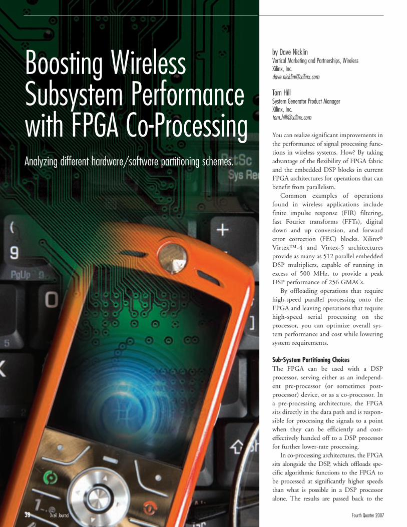
by Dave NicklinVertical Marketing and Partnerships, Wireless Xilinx, Inc. [email protected]
Tom HillSystem Generator Product ManagerXilinx, [email protected]
You can realize significant improvements inthe performance of signal processing func-tions in wireless systems. How? By takingadvantage of the flexibility of FPGA fabricand the embedded DSP blocks in currentFPGA architectures for operations that canbenefit from parallelism.
Common examples of operationsfound in wireless applications includefinite impulse response (FIR) filtering,fast Fourier transforms (FFTs), digitaldown and up conversion, and forwarderror correction (FEC) blocks. Xilinx®
Virtex™-4 and Virtex-5 architecturesprovide as many as 512 parallel embeddedDSP multipliers, capable of running inexcess of 500 MHz, to provide a peakDSP performance of 256 GMACs.
By offloading operations that requirehigh-speed parallel processing onto theFPGA and leaving operations that requirehigh-speed serial processing on theprocessor, you can optimize overall sys-tem performance and cost while loweringsystem requirements.
Sub-System Partitioning ChoicesThe FPGA can be used with a DSPprocessor, serving either as an independ-ent pre-processor (or sometimes post-processor) device, or as a co-processor. Ina pre-processing architecture, the FPGAsits directly in the data path and is respon-sible for processing the signals to a pointwhen they can be efficiently and cost-effectively handed off to a DSP processorfor further lower-rate processing.
In co-processing architectures, the FPGAsits alongside the DSP, which offloads spe-cific algorithmic functions to the FPGA tobe processed at significantly higher speedsthan what is possible in a DSP processoralone. The results are passed back to the
38 Xcell Journal Fourth Quarter 2007
Boosting Wireless Subsystem Performance with FPGA Co-ProcessingAnalyzing different hardware/software partitioning schemes.
DSP or sent to other devices for further pro-cessing, transmission, or storage (Figure 1).
The choice of pre-processing, post-processing, or co-processing is often gov-erned by the timing margins needed tomove data between the processor andFPGA and how that impinges on theoverall latency. Although a co-processingsolution is the topology most often con-sidered by designers – primarily becausethe DSP is in more direct control of thedata hand-off process – this may notalways be the best overall strategy.
Consider, for example, the latest specifi-cations for 3G LTE, in which the transmis-sion time interval (TTI) has been reducedto 1 ms, down from 2 ms for HSDPA and10 ms for WCDMA. This essentiallyrequires that data be processed from thereceiver and through to the output of theMAC layer in less than 1,000 µsec.
Figure 2 shows that using an SRIO porton the DSP running at 3.125 Gbps, with8b/10b encoding and a 200-bit overhead forthe Turbo decode function, results in a DSP-to-FPGA transfer delay of 230 µsec (that is,nearly a quarter of the TTI period just totransfer the data). Taking into account otherexpected delays, the Turbo codec perform-ance required to meet these system timingsis a very demanding 75.8 Mbps for 50 users.
Using an FPGA to process the Turbocodecs as a largely independent post-processor not only removes DSP latencybut saves time because there’s no need totransfer the data at a high bandwidthbetween the DSP and FPGA. This reducesthe throughput rate of the Turbo decoderdown to 47 Mbps, a decrease that allowsyou to use more cost-effective devices andhave reduced system power dissipation.
Another consideration is whether to usesoft- or hard-embedded processor IP on theXilinx FPGA to offload some of the systemprocessing tasks, which in turn offers thepossibility of additional cost, power, andfootprint reduction benefits. Given such awide range of signal processing resources,complex functions such as those found inbaseband processing can be more optimal-ly partitioned between the DSP processor,the FPGA-configurable logic blocks(CLBs), embedded FPGA DSP blocks, and
you to produce efficient FPGA implemen-tations from a higher level of abstractionthan what HDL tools such as MATLABmodels and C code can provide. Withdevelopment tools like Xilinx SystemGenerator for DSP and the AccelDSP™synthesis tool, you can go from algorithm
to silicon as seamlessly as possible.There is also an increasingly important
ecosystem of tool providers whose productstake development up to the electronic sys-tem level (ESL) through C/C++-to-gatedesign flows. ESL design tools are aimed atproviding an integrated system-levelapproach to the production and integra-tion of hardware-accelerated functions andthe control code for processors controllingthese functions.
No single high-level language or soft-ware tool is suitable for all of the differentelements found in today’s complex systems.The choice of language and design flow is
FPGA embedded processor. Xilinx offerstwo types of embedded processors: theMicroBlaze™ soft-core processor – oftenused for system control – and the higherperformance PowerPC hard-core embed-ded processor for more complex tasks.
FPGA-embedded processors provide an
opportunity to consolidate all non-criticaloperations into software running on theembedded processors, minimizing the totalamount of hardware resources required forthe overall system.
The Importance of Software and IPA critical issue is how to unlock all of thispotential capability. You need to considerboth the software needed to abstract thecomplexity of the problem and the avail-ability of IP, focused on key areas whereFPGAs can provide an optimal solution.
Xilinx is dedicated to developing indus-try-leading tools and ecosystems that allow
Fourth Quarter 2007 Xcell Journal 39
C6416Texas Instruments
C6416Texas Instruments
100 MHz 100 kHz100 kHz
FPGA as Pre-Processor FPGA as Co-Processor
500 MHz 500 MHz
decode1 decode2 decode50
T
DSP Data Transfer Latency (230 µs)*
TTI = 1 ms
Antenna to Turbo
Latency (100 µs)
Implications for Turbo Decode (50-user example):
Processing bandwidth available for Turbo Decode = 380 µs
Throughput rate necessary = (576 bits × 50 users) / 380 µs = 75.8 Mbps
Throughput rate without DSP transfer latency = (576 bits × 50 users) / 610 µs = 47 Mbps
Data-transfer latency directly impacts cost and power dissipation.
MAC Latency (290 µs)
Figure 1 – FPGA as a pre-processor and co-processor solution
Figure 2 – LTE example of co-processing data-transfer latency issues
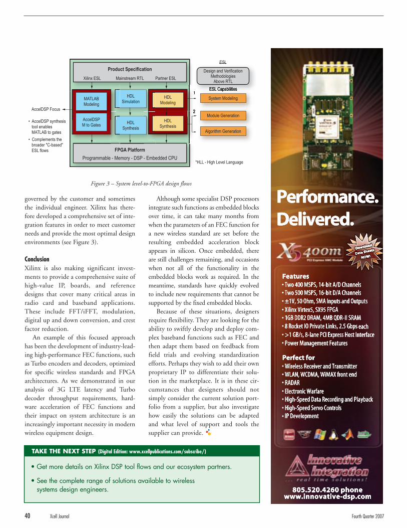
governed by the customer and sometimesthe individual engineer. Xilinx has there-fore developed a comprehensive set of inte-gration features in order to meet customerneeds and provide the most optimal designenvironments (see Figure 3).
ConclusionXilinx is also making significant invest-ments to provide a comprehensive suite ofhigh-value IP, boards, and referencedesigns that cover many critical areas inradio card and baseband applications.These include FFT/iFFT, modulation,digital up and down conversion, and crestfactor reduction.
An example of this focused approachhas been the development of industry-lead-ing high-performance FEC functions, suchas Turbo encoders and decoders, optimizedfor specific wireless standards and FPGAarchitectures. As we demonstrated in ouranalysis of 3G LTE latency and Turbodecoder throughput requirements, hard-ware acceleration of FEC functions andtheir impact on system architecture is anincreasingly important necessity in modernwireless equipment design.
Although some specialist DSP processorsintegrate such functions as embedded blocksover time, it can take many months fromwhen the parameters of an FEC function fora new wireless standard are set before theresulting embedded acceleration blockappears in silicon. Once embedded, thereare still challenges remaining, and occasionswhen not all of the functionality in theembedded blocks work as required. In themeantime, standards have quickly evolvedto include new requirements that cannot besupported by the fixed embedded blocks.
Because of these situations, designersrequire flexibility. They are looking for theability to swiftly develop and deploy com-plex baseband functions such as FEC andthen adapt them based on feedback fromfield trials and evolving standardizationefforts. Perhaps they wish to add their ownproprietary IP to differentiate their solu-tion in the marketplace. It is in these cir-cumstances that designers should notsimply consider the current solution port-folio from a supplier, but also investigatehow easily the solutions can be adaptedand what level of support and tools thesupplier can provide.
40 Xcell Journal Fourth Quarter 2007
ESL
AccelDSP Focus
*HLL - High Level Language
• AccelDSP synthesis
tool enables
MATLAB to gates
• Complements the
broader "C-based"
ESL flows
Product Specification
Programmable - Memory - DSP - Embedded CPU
Mainstream RTL Partner ESL
System Modeling
Module Generation
Algorithm Generation
Design and VerificationMethodologies
Above RTLXilinx ESL
FPGA Platform
HDL
Modeling
HDL
Synthesis
HDL
Simulation
HDL
Synthesis
MATLAB
Modeling
AccelDSP
M to Gates
• Get more details on Xilinx DSP tool flows and our ecosystem partners.
• See the complete range of solutions available to wireless systems design engineers.
TAKE THE NEXT STEP (Digital Edition: www.xcellpublications.com/subscribe/)
Figure 3 – System level-to-FPGA design flows
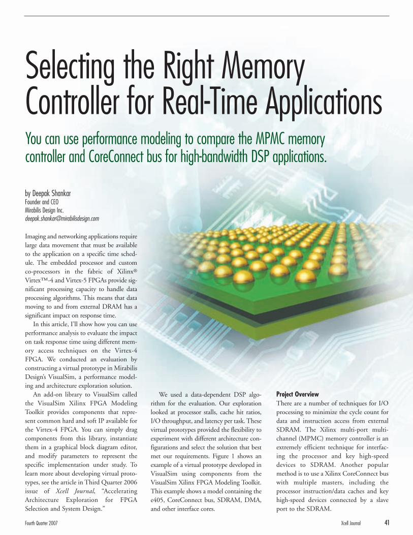
by Deepak ShankarFounder and CEOMirabilis Design [email protected]
Imaging and networking applications requirelarge data movement that must be availableto the application on a specific time sched-ule. The embedded processor and customco-processors in the fabric of Xilinx®
Virtex™-4 and Virtex-5 FPGAs provide sig-nificant processing capacity to handle dataprocessing algorithms. This means that datamoving to and from external DRAM has asignificant impact on response time.
In this article, I’ll show how you can useperformance analysis to evaluate the impacton task response time using different mem-ory access techniques on the Virtex-4FPGA. We conducted an evaluation byconstructing a virtual prototype in MirabilisDesign’s VisualSim, a performance model-ing and architecture exploration solution.
An add-on library to VisualSim calledthe VisualSim Xilinx FPGA ModelingToolkit provides components that repre-sent common hard and soft IP available forthe Virtex-4 FPGA. You can simply dragcomponents from this library, instantiatethem in a graphical block diagram editor,and modify parameters to represent thespecific implementation under study. Tolearn more about developing virtual proto-types, see the article in Third Quarter 2006issue of Xcell Journal, “AcceleratingArchitecture Exploration for FPGASelection and System Design.”
We used a data-dependent DSP algo-rithm for the evaluation. Our explorationlooked at processor stalls, cache hit ratios,I/O throughput, and latency per task. Thesevirtual prototypes provided the flexibility toexperiment with different architecture con-figurations and select the solution that bestmet our requirements. Figure 1 shows anexample of a virtual prototype developed inVisualSim using components from theVisualSim Xilinx FPGA Modeling Toolkit.This example shows a model containing thee405, CoreConnect bus, SDRAM, DMA,and other interface cores.
Project OverviewThere are a number of techniques for I/Oprocessing to minimize the cycle count fordata and instruction access from externalSDRAM. The Xilinx multi-port multi-channel (MPMC) memory controller is anextremely efficient technique for interfac-ing the processor and key high-speeddevices to SDRAM. Another popularmethod is to use a Xilinx CoreConnect buswith multiple masters, including theprocessor instruction/data caches and keyhigh-speed devices connected by a slaveport to the SDRAM.
Fourth Quarter 2007 Xcell Journal 41
Selecting the Right Memory Controller for Real-Time Applications You can use performance modeling to compare the MPMC memory controller and CoreConnect bus for high-bandwidth DSP applications.
To investigate the similarities and differ-ences between the two approaches, we con-structed models of both configurationsusing the VisualSim Xilinx FPGAModeling Toolkit. Figure 1 shows the vir-tual prototype and Figure 2 is the timingdiagram for request, acknowledge, read,and write access on the CoreConnect bus.
Design Considerations We used the same configuration to explorethe Xilinx MPMC memory controller andCoreConnect bus. The instruction and datachannels of the PowerPC e405, Ethernet,and PCI interface were connected as mas-ters; the SDRAM is a slave. The Ethernetand PCI data are burst to SDRAM usingdedicated CDMAC engines. The mastersand slaves were maintained at constantspeed and size in both virtual prototypes.Table 1 shows the instruction and datacache statistics for the virtual prototypemodel in Figure 1.
The design considerations were:
• What is driving the design – overallperformance or a combination ofpower and performance?
• Do I need one or two e405 PowerPCsfor my core tasks?
• If the e405 PowerPC is running at 400MHz, what might be the best MPMCor CoreConnect bus clock ratio?
• Does my design have equal read andwrite memory activity, multiple readsfor one write, or multiple writes forone read?
• What is the effect of SDRAM speedon the processor/memorycontroller/bus clock ratio?
• What is the effect of SDRAM speedon added application access to memory?
AnalysisWe ran the simulation on a 1.6-GHzMicrosoft Windows XP (SP2 and StandardEdition) with 512 Mb of cache. We simulat-ed 3.0 ms of real time and the VisualSimsimulation took 28 seconds of wall clocktime to finish. The model was constructed
Statistic Name CoreConnect MPMC
Instruction Data Instruction Data Cache Cache Cache Cache
Hit_Ratio_Max 95.05 96.23 94.98 97.37
Hit_Ratio_Mean 90.51 90.62 94.98 97.37
Throughput_MIPs_Max 74.45 1.69 7.44 0.16
Throughput_MIPs_Mean 7.44 0.17 7.44 0.16
Utilization_Pct_Max 18.61 0.42 1.86 0.04
Utilization_Pct_Mean 1.86 0.04 1.86 0.04
Table 1 – Instruction and data cache statistics
Figure 1 – VisualSim model of the Xilinx Virtex-4 platform: e405 with CoreConnect bus model
Figure 2 – CoreConnect bus activity with SDRAM at bottom
42 Xcell Journal Fourth Quarter 2007
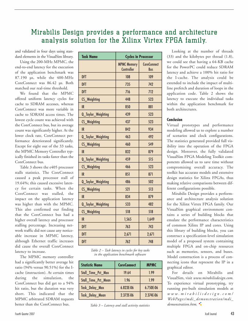
and validated in four days using stan-dard elements in the VisualSim library.
Using the 200-MHz MPMC, theend-to-end latency for the executionof the application benchmark was87.190 µs, while the 400-MHzCoreConnect was 86.42 µs. Bothmatched our real-time threshold.
We found that the MPMCoffered uniform latency cycles forcache to SDRAM accesses, whereasCoreConnect was more variable incache to SDRAM access times. Thelowest cycle count was achieved withthe CoreConnect bus, but its averagecount was significantly higher. At thelower clock rate, CoreConnect per-formance deteriorated significantly.Except for eight out of the 33 tasks,the MPMC Memory Controller typ-ically finished its tasks faster than theCoreConnect bus.
Table 3 shows the e405 processorstalls statistics. The CoreConnectcaused a peak processor stall of19.64%; this caused excessive laten-cy for certain tasks. When theCoreConnect was stalled, theimpact on the application latencywas higher than with the MPMC.This also confirmed our findingthat the CoreConnect bus had ahigher overall latency and processorstalling percentage. Increasing net-work traffic did not cause any notice-able increase in MPMC latency,although Ethernet traffic increasesdid cause the overall CoreConnectlatency to increase.
The MPMC memory controllerhad a significantly better average hitratio (94% versus 90.51%) for the I-cache (instruction). At certain timesduring the simulation, theCoreConnect bus did get to a 94%hit ratio, but the duration was veryshort. This indicated that theMPMC arbitrated SDRAM requestsbetter than the CoreConnect bus.
Looking at the number of threads(33) and the kilobytes per thread (1.8),we could see that having a 64-KB cachefor the PowerPC could reduce SDRAMlatency and achieve a 100% hit ratio forthe I-cache. The analysis could beextended to include the impact of multi-line prefetch and duration of loops in theapplication code. Table 2 shows thelatency to execute the individual taskswithin the application benchmark forboth architectures.
ConclusionVirtual prototypes and performancemodeling allowed us to explore a numberof scenarios and clock configurations.The statistics generated provided full vis-ibility into the operation of the FPGAdesign. Moreover, the fully validatedVisualSim FPGA Modeling Toolkit com-ponents allowed us to save time withoutcompromising overall accuracy. Thetoolkit has accurate models and extensivedesign statistics for Xilinx FPGAs, thusmaking relative comparisons between dif-ferent configurations possible.
Mirabilis Design provides a perform-ance and architecture analysis solutionfor the Xilinx Virtex FPGA family. OurVisualSim graphical environment con-tains a series of building blocks thatemulate the performance characteristicsof common Xilinx IP and cores. Usingthis library of building blocks, you canconstruct a specification-level simulationmodel of a proposed system containingmultiple FPGA and on-chip resourcessuch as memories, sensors, and buses.Model construction is a process of con-necting icons that represent the IP in agraphical editor.
For details on Mirabilis andVisualSim, visit www.mirabilisdesign.com.To experience virtual prototyping, tryrunning pre-built simulation models atw w w . m i r a b i l i s d e s i g n . c o m /WebPage s /mdi_demons t ra t ion /mdi_demonstration.htm.
Task Name Cycles in Processor
MPMC Memory CoreConnectController Bus
DFT 108 109
DFT 735 742
DFT 716 712
CS_Weighting 448 523
IR 850 881
Q_Taylor_Weighting 439 523
CS_Weighting 437 523
IR 842 934
Q_Taylor_Weighting 463 492
CS_Weighting 460 549
IR 832 879
Q_Taylor_Weighting 459 515
CS_Weighting 466 523
IR 851 871
Q_Taylor_Weighting 486 502
CS_Weighting 521 513
IR 834 879
Q_Taylor_Weighting 533 482
CS_Weighting 518 518
IR 1,565 1,649
DFT 763 743
DFT 2,671 2,671
DFT 762 748
Statistic Name CoreConnect MPMC
Stall_Time_Pct_Max 19.64 1.99
Stall_Time_Pct_Mean 1.96 1.99
Task_Delay_Max 6.823E-06 6.750E-06
Task_Delay_Mean 2.372E-06 2.374E-06
Table 2 – Task latency in cycles for key tasks in the application benchmark software
Table 3 – Latency and stall activity statistics
Mirabilis Design provides a performance and architecture analysis solution for the Xilinx Virtex FPGA family.
Fourth Quarter 2007 Xcell Journal 43
by Justin Delva Staff DSP Engineer Xilinx, [email protected]
Ben ChanSenior Software EngineerXilinx, [email protected]
Shay SengEngineering ManagerXilinx, [email protected]
Xilinx® System Generator for DSP is aMATLAB Simulink block set that facil-itates system design. Targeting XilinxFPGAs within the familiar MATLABenvironment, System Generator forDSP gives you the ability to functional-ly simulate a design and use the MAT-LAB environment to verify bit- andcycle-true models against the goldenreference results. These reference resultscan be produced either externally orinside the MATLAB environment, andyou can target a Xilinx FPGA hardwareplatform all from within MATLAB.
System Generator complementsHDL design tasks by providing an easi-ly configured test bench for both func-tional simulation and hardwareverification. You can simulate yourHDL code within MATLAB by usingthe built-in interface to HDL simulatorslike ModelSim. A System Generator forDSP test bench platform built aroundthe HDL code provides a powerful yetfast simulation environment that inter-acts seamlessly with ModelSim. Settingup this environment is easy.
44 Xcell Journal Fourth Quarter 2007
Integrating HDL Design andVerification with System GeneratorDesigning and verifying the CABAC functionality of an H.264video encoder is easy with System Generator for DSP.
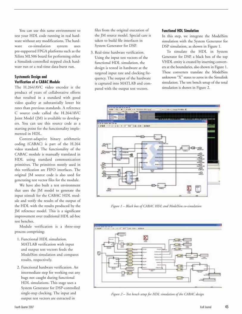
You can use this same environment totest your HDL code running in real hard-ware without any modifications. The hard-ware co-simulation system usespre-supported FPGA platforms such as theXilinx ML506 board for performing eithera Simulink-controlled stepped clock hard-ware run or a real-time data-burst run.
Systematic Design and Verification of a CABAC Module The H.264/AVC video encoder is theproduct of years of collaborative effortsthat resulted in a standard with goodvideo quality at substantially lower bitrates than previous standards. A referenceC source code called the H.264/AVCJoint Model (JM) is available to develop-ers. You can use this source code as astarting point for the functionality imple-mented in HDL.
Context-adaptive binary arithmeticcoding (CABAC) is part of the H.264video standard. The functionality of theCABAC module is manually translated inHDL using standard communicationprimitives. The primitives mostly used inthis verification are FIFO interfaces. Theoriginal JM source code is also used forgenerating test vector files for the module.
We have also built a test environmentthat uses the JM model to generate theinput stimuli for the CABAC HDL mod-ule and verify the results of the output ofthe HDL with the results produced by theJM reference model. This is a significantimprovement over traditional HDL ad-hoctest benches.
Module verification is a three-stepprocess comprising:
1. Functional HDL simulation. MATLAB verification with inputand output test vectors feeds theModelSim simulation and comparesresults, respectively.
2. Functional hardware verification. Anintermediate step for working out anybugs not caught during functionalHDL simulations. This stage uses aSystem Generator for DSP-controlledsingle-step clocking. The input andoutput test vectors are extracted in
Functional HDL Simulation In this step, we integrate the ModelSimsimulation with the System Generator forDSP simulation, as shown in Figure 1.
To simulate the HDL in SystemGenerator for DSP, a black box of the topVHDL entity is created by inserting convert-ers at the boundaries, also shown in Figure 1.These converters translate the ModelSimunknown “X” states to zeros in the Simulinksimulation. The test bench setup of the totalsimulation is shown in Figure 2.
files from the original execution ofthe JM source model. Special care istaken to build file interfaces inSystem Generator for DSP.
3. Real-time hardware verification.Using the input test vectors of thefunctional HDL simulation, thedesign is tested in hardware at thetargeted input rate and clocking fre-quency. The output of the hardwareis captured into MATLAB and com-pared with the output test vectors.
Fourth Quarter 2007 Xcell Journal 45
Figure 2 – Test bench setup for HDL simulation of the CABAC design
Figure 1 – Black box of CABAC HDL and ModelSim co-simulation
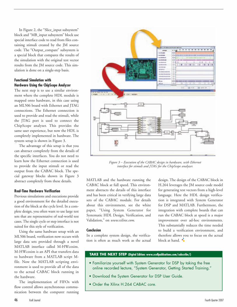
In Figure 2, the “Slice_input subsystem”block and “MB_input subsystem” block usespecial interface code to read from files con-taining stimuli created by the JM sourcecode. The “Output_compare” subsystem isa special block that compares the results ofthe simulation with the original test vectorresults from the JM source code. This sim-ulation is done on a single-step basis.
Functional Simulation with Hardware Using the ChipScope AnalyzerThe next step is to use a similar environ-ment where the complete HDL module ismapped onto hardware, in this case usingan ML506 board with Ethernet and JTAGconnections. The Ethernet connection isused to provide and read the stimuli, whilethe JTAG port is used to connect theChipScope analyzer. This provides thesame user experience, but now the HDL iscompletely implemented in hardware. Thesystem setup is shown in Figure 3.
The advantage of this setup is that youcan abstract completely from the details ofthe specific interfaces. You do not need tolearn how the Ethernet connection is usedto provide the input stimuli or read theoutput from the CABAC block. The spe-cial gateway blocks shown in Figure 3abstract completely from these details.
Real-Time Hardware VerificationPrevious simulations and executions providea good environment for the detailed execu-tion of the block at the cycle level. In a com-plete design, you often want to use large testsets that are representative of real-world testcases. The single cycle or step interface is notsuited for this style of verification.
Using the same hardware setup with anML506 board, verification now occurs withlarge data sets provided through a novelMATLAB interface called M-HWcosim.M-HWcosim is an API that transfers datato hardware from a MATLAB script M-file. Now the MATLAB scripting envi-ronment is used to provide all of the datato the actual CABAC block running inthe hardware.
The implementation of FIFOs withflow control allows asynchronous commu-nication between the computer running
MATLAB and the hardware running theCABAC block at full speed. This environ-ment abstracts the details of this interfaceand has been critical in verifying large datasets of the CABAC module. For detailsabout this environment, see the whitepaper, “Using System Generator forSystematic HDL Design, Verification, andValidation,” on www.xilinx.com.
ConclusionIn a complete system design, the verifica-tion is often as much work as the actual
design. The design of the CABAC block inH.264 leverages the JM source code modelfor generating test vectors from a high-levellanguage. Here the HDL design verifica-tion is integrated with System Generatorfor DSP and MATLAB. Furthermore, theintegration with complete boards that canrun the CABAC block at speed is a majorimprovement over ad-hoc environments.This substantially reduces the time neededto build a verification environment, andtherefore allows you to focus on the actualblock at hand.
46 Xcell Journal Fourth Quarter 2007
• Familiarize yourself with System Generator for DSP by taking the freeonline recorded lecture, “System Generator, Getting Started Training.”
• Download the System Generator for DSP User Guide.
• Order the Xilinx H.264 CABAC core.
TAKE THE NEXT STEP (Digital Edition: www.xcellpublications.com/subscribe/)
Figure 3 – Execution of the CABAC design in hardware, with Ethernet interface for stimuli and JTAG for the ChipScope analyzer.
by Meena Das Contract EngineerElectronics and Radar Development Establishment (LRDE), [email protected]
Karthik Kabbinahitlu Subrahmanya Contract EngineerElectronics and Radar Development Establishment (LRDE), [email protected]
Taniza Roy Scientist “C”Electronics and Radar Development Establishment (LRDE), [email protected]
Gnana Michael Prakasam Scientist “F”Electronics and Radar Development Establishment (LRDE), [email protected]
Designers often struggle with time-con-suming development cycles during com-plex system realization using FPGAs. Wehave designed a radar blockset library inThe MathWorks Simulink environmentthat addresses this challenge by providingpre-synthesized components.
Our radar blockset library componentsdirectly generate programming code forXilinx® FPGAs on a target board. Thus,the blocks lead to a single design solutionrather than having to use multiple blocksfor dedicated functions.
For applications such as complexradar systems, a single design solutionspeeds up development activity andkeeps designers from having to designfrom scratch. To highlight this feature,we’ll describe how a typical radar block-set library component works in a radarreceiver design.
Fourth Quarter 2007 Xcell Journal 47
Accelerating System DevelopmentCycles with the Radar Blockset LibraryA radar blockset library offers components selectable from the genericSimulink environment for complex system designs using FPGAs.
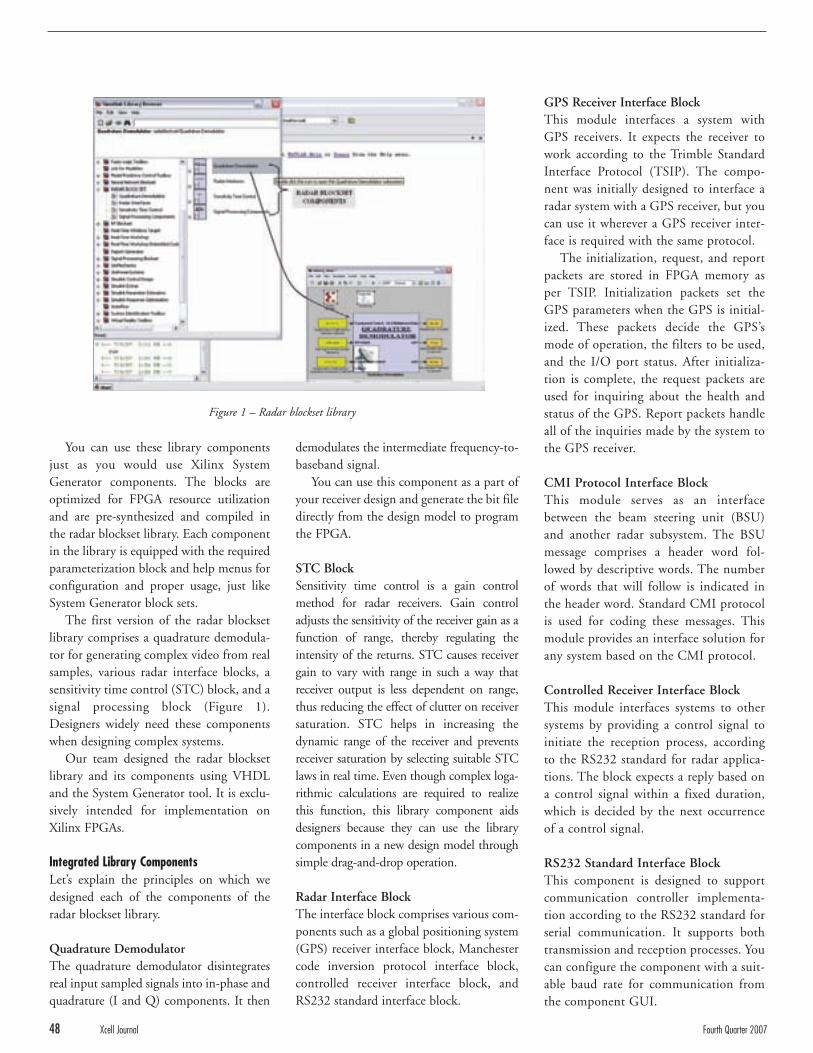
You can use these library componentsjust as you would use Xilinx SystemGenerator components. The blocks areoptimized for FPGA resource utilizationand are pre-synthesized and compiled inthe radar blockset library. Each componentin the library is equipped with the requiredparameterization block and help menus forconfiguration and proper usage, just likeSystem Generator block sets.
The first version of the radar blocksetlibrary comprises a quadrature demodula-tor for generating complex video from realsamples, various radar interface blocks, asensitivity time control (STC) block, and asignal processing block (Figure 1).Designers widely need these componentswhen designing complex systems.
Our team designed the radar blocksetlibrary and its components using VHDLand the System Generator tool. It is exclu-sively intended for implementation onXilinx FPGAs.
Integrated Library ComponentsLet’s explain the principles on which wedesigned each of the components of theradar blockset library.
Quadrature DemodulatorThe quadrature demodulator disintegratesreal input sampled signals into in-phase andquadrature (I and Q) components. It then
GPS Receiver Interface BlockThis module interfaces a system withGPS receivers. It expects the receiver towork according to the Trimble StandardInterface Protocol (TSIP). The compo-nent was initially designed to interface aradar system with a GPS receiver, but youcan use it wherever a GPS receiver inter-face is required with the same protocol.
The initialization, request, and reportpackets are stored in FPGA memory asper TSIP. Initialization packets set theGPS parameters when the GPS is initial-ized. These packets decide the GPS’smode of operation, the filters to be used,and the I/O port status. After initializa-tion is complete, the request packets areused for inquiring about the health andstatus of the GPS. Report packets handleall of the inquiries made by the system tothe GPS receiver.
CMI Protocol Interface BlockThis module serves as an interfacebetween the beam steering unit (BSU)and another radar subsystem. The BSUmessage comprises a header word fol-lowed by descriptive words. The numberof words that will follow is indicated inthe header word. Standard CMI protocolis used for coding these messages. Thismodule provides an interface solution forany system based on the CMI protocol.
Controlled Receiver Interface BlockThis module interfaces systems to othersystems by providing a control signal toinitiate the reception process, accordingto the RS232 standard for radar applica-tions. The block expects a reply based ona control signal within a fixed duration,which is decided by the next occurrenceof a control signal.
RS232 Standard Interface Block This component is designed to supportcommunication controller implementa-tion according to the RS232 standard forserial communication. It supports bothtransmission and reception processes. Youcan configure the component with a suit-able baud rate for communication fromthe component GUI.
demodulates the intermediate frequency-to-baseband signal.
You can use this component as a part ofyour receiver design and generate the bit filedirectly from the design model to programthe FPGA.
STC BlockSensitivity time control is a gain controlmethod for radar receivers. Gain controladjusts the sensitivity of the receiver gain as afunction of range, thereby regulating theintensity of the returns. STC causes receivergain to vary with range in such a way thatreceiver output is less dependent on range,thus reducing the effect of clutter on receiversaturation. STC helps in increasing thedynamic range of the receiver and preventsreceiver saturation by selecting suitable STClaws in real time. Even though complex loga-rithmic calculations are required to realizethis function, this library component aidsdesigners because they can use the librarycomponents in a new design model throughsimple drag-and-drop operation.
Radar Interface BlockThe interface block comprises various com-ponents such as a global positioning system(GPS) receiver interface block, Manchestercode inversion protocol interface block,controlled receiver interface block, andRS232 standard interface block.
Figure 1 – Radar blockset library
48 Xcell Journal Fourth Quarter 2007
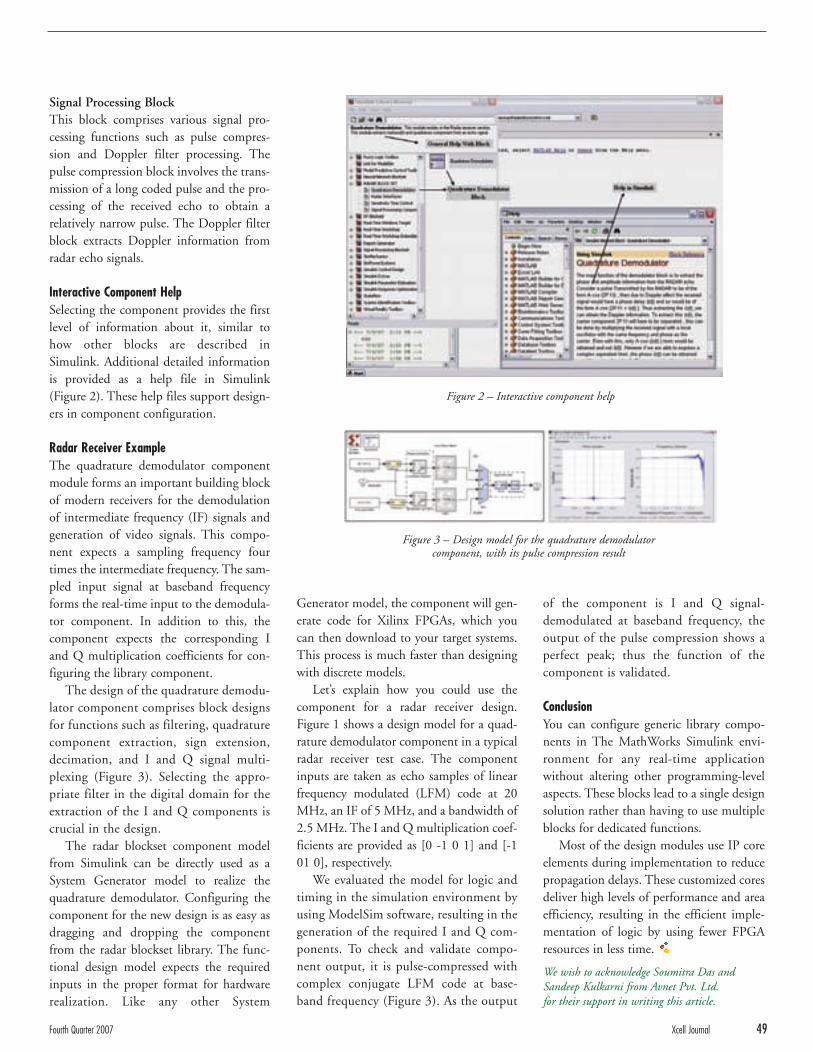
Fourth Quarter 2007 Xcell Journal 49
Signal Processing BlockThis block comprises various signal pro-cessing functions such as pulse compres-sion and Doppler filter processing. Thepulse compression block involves the trans-mission of a long coded pulse and the pro-cessing of the received echo to obtain arelatively narrow pulse. The Doppler filterblock extracts Doppler information fromradar echo signals.
Interactive Component HelpSelecting the component provides the firstlevel of information about it, similar tohow other blocks are described inSimulink. Additional detailed informationis provided as a help file in Simulink(Figure 2). These help files support design-ers in component configuration.
Radar Receiver ExampleThe quadrature demodulator componentmodule forms an important building blockof modern receivers for the demodulationof intermediate frequency (IF) signals andgeneration of video signals. This compo-nent expects a sampling frequency fourtimes the intermediate frequency. The sam-pled input signal at baseband frequencyforms the real-time input to the demodula-tor component. In addition to this, thecomponent expects the corresponding Iand Q multiplication coefficients for con-figuring the library component.
The design of the quadrature demodu-lator component comprises block designsfor functions such as filtering, quadraturecomponent extraction, sign extension,decimation, and I and Q signal multi-plexing (Figure 3). Selecting the appro-priate filter in the digital domain for theextraction of the I and Q components iscrucial in the design.
The radar blockset component modelfrom Simulink can be directly used as aSystem Generator model to realize thequadrature demodulator. Configuring thecomponent for the new design is as easy asdragging and dropping the componentfrom the radar blockset library. The func-tional design model expects the requiredinputs in the proper format for hardwarerealization. Like any other System
Generator model, the component will gen-erate code for Xilinx FPGAs, which youcan then download to your target systems.This process is much faster than designingwith discrete models.
Let’s explain how you could use thecomponent for a radar receiver design.Figure 1 shows a design model for a quad-rature demodulator component in a typicalradar receiver test case. The componentinputs are taken as echo samples of linearfrequency modulated (LFM) code at 20MHz, an IF of 5 MHz, and a bandwidth of2.5 MHz. The I and Q multiplication coef-ficients are provided as [0 -1 0 1] and [-101 0], respectively.
We evaluated the model for logic andtiming in the simulation environment byusing ModelSim software, resulting in thegeneration of the required I and Q com-ponents. To check and validate compo-nent output, it is pulse-compressed withcomplex conjugate LFM code at base-band frequency (Figure 3). As the output
of the component is I and Q signal-demodulated at baseband frequency, theoutput of the pulse compression shows aperfect peak; thus the function of thecomponent is validated.
ConclusionYou can configure generic library compo-nents in The MathWorks Simulink envi-ronment for any real-time applicationwithout altering other programming-levelaspects. These blocks lead to a single designsolution rather than having to use multipleblocks for dedicated functions.
Most of the design modules use IP coreelements during implementation to reducepropagation delays. These customized coresdeliver high levels of performance and areaefficiency, resulting in the efficient imple-mentation of logic by using fewer FPGAresources in less time.
We wish to acknowledge Soumitra Das and Sandeep Kulkarni from Avnet Pvt. Ltd. for their support in writing this article.
Figure 2 – Interactive component help
Figure 3 – Design model for the quadrature demodulator component, with its pulse compression result
by Philipp JacobsohnField Applications EngineerSynplicity Deutschland [email protected]
Derek PalmerDSP Marketing ManagerXilinx, [email protected]
Today, even low-cost FPGAs provide farmore computing power than DSPs.Current FPGAs have dedicated multipliersand even DSP multiply/accumulate (MAC)blocks that enable signals to be processedwith clock speeds in excess of 550 MHz.
Until now, however, these capabilitieswere rarely needed in audio signal process-ing. A serial implementation of an audioalgorithm working in the kilohertz rangeuses exactly the same resources required forprocessing signals in the three-digit mega-hertz range.
Consequently, programmable logiccomponents such as PLDs or FPGAs arerarely used for processing low-frequencysignals. After all, the parallel processing ofmathematical operations in hardware is ofno benefit when compared to an imple-mentation based on classical DSPs; thesampling rates are so low that most serialDSP implementations are more than ade-quate. In fact, audio applications are char-acterized by such a high number ofmultiplications that they previously could
50 Xcell Journal Fourth Quarter 2007
Audio Sample Rate Conversion in FPGAsAn efficient implementation of audio algorithms in programmable logic.
only be implemented using very largeFPGAs. So audio applications with lowsampling frequencies were implementedmore efficiently using a DSP than a largeFPGA – at a lower cost and with provensoftware support.
More recently, Synplify DSP, a synthe-sis tool from Synplicity, allows you to effi-ciently map even algorithms with largenumbers of multiplications and a lowsampling rate onto specialized DSP blocksin FPGAs. The tool is based on the popu-lar MATLAB and Simulink tools fromThe MathWorks.
Algorithms are defined using a specialblock set or description in the proprietary“M” scripting language and are later trans-lated into an RTL hardware descriptionlanguage. The block set allows both single-rate and multi-rate implementations. It notonly generates VHDL and Verilog code butalso handles tasks such as fixed-point quan-tization, pipelining, loop unrolling, andconnects to block sets from the Simulinkdevelopment environment for simulation(see Figure 1).
Application Example: Sampling Rate Conversion Let’s use a sampling rate converter foraudio frequencies as a practical example.This converter can convert a signal fromone sampling rate to another with minimalimpact on the signal. Such converters arerequired to process signals with differingsampling rates.
For example, compact discs are sampledat 44.1 kHz, while digital audio tape isusually sampled at 48 kHz. But with dataformat conversion, playing the source datawith the new sampling rate is not suffi-cient. Playing compact disc material at thesampling rates used for digital audio tapewould cause distortions. Thus, the sam-pling rate must be converted.
When processing audio signals, manysampling frequencies are used: 44.1 kHz,48 kHz, 96 kHz, and 192 kHz are com-mon. During conversion, you must takecare to maintain signal integrity in the audi-ble range between 0 and 20 kHz. Changingthe information contained in the signalshould be kept to a minimum to limitdegradation in audio quality (Figure 2).
2. The implementation issue:
a. Logically correct implementation ofthe algorithm
b. FPGA resource constraints
c. Speed-optimized implementations
d. Latency
The conversion requires a high clockspeed because the implementation dependson adequate oversampling of the signalbeing converted. The difference betweenthe FPGA system clock frequency and thesignal frequencies being converted must becorrespondingly high.
Not surprisingly, the implementation ofa sampling rate converter for audio fre-quencies raises two issues in the FPGA:
1. The algorithm issue:
a. Highest possible signal-to-noise ratio
b. Minimum possible change in theinformation carried by the originalsignal
c. Efficient description of the algorithm,as the resources consumed in theFPGA are highly dependent on thequality of the description
d. Quantization
Fourth Quarter 2007 Xcell Journal 51
1 Design
Algorithm
Floating-Point
Model
2
MATLAB/Simulink
Fixed-Point
Conversion
Synplify DSP and FPGA/ASIC Synthesis
Fixed-Point
Model
SystemEngineering
Quanti-zation
4 Design
Implementation
Folding / Retiming /
Multi-Channelization
3 Generate RTL
(VHDL, Verilog)
FPGA/ASIC Specific
RTL Code
SynthesisTarget
Architecture
Figure 1 – The model is implemented, quantified, and verified in MATLAB/Simulink. The Synplify DSP tool converts the model
into RTL code. The code can be optimized for space or speed.
Figure 2 – Modules from the Synplify DSP block set and Simulink FDA tool implement the sampling rate converter.
Simulink block set elements perform verification.
For CD-quality audio signals, the signal-to-noise ratio must also be at least 100 dB.Professional applications even require audiosignals of >120 dB. Other low-frequencysignals (such as control electronics algo-rithms) are far less demanding than audiosignals when it comes to signal quality.
The AlgorithmA polyphase FIR filter structure convertsthe sample rates (asynchronous resam-pling). The algorithm comprises two steps.In the first step, frequencies are oversam-pled. The second step – linear interpolation– is required to generate a different fre-quency from a given frequency. The twofrequencies are asynchronous to each other.
Resampling the signal in a single stepwould require far more resources becausethe filter would be far more complex. Thistype of implementation would result inseveral million multiplications. Such adescription is inefficient and should beavoided. If a linear interpolation is imple-mented for the second step, the resultingstructures are far simpler (Figure 3).
Efficiently described oversampling (thefirst step) is the only way to achieve aresource-saving FPGA implementation.The number of computations required willdrop dramatically if this part of the circuitis implemented in several cascaded stagesrather than in a single computing step.
When implementing the algorithm, youmust decide on the target architecture thatwill perform the computation (DSP orFPGA). Unlike digital signal processorsthat have a fixed architecture, FPGAs canimplement any architecture. They are ulti-mately limited, however, by the size of thedevice when implementing large numbersof individual multiplications.
The number of multipliers requiredincreases with the tap of the filter. Each tapresults in the use of a DSP block or multi-plier. When cascading resampling stages,each filter must perform functions that are
far less complex. In theory, an optimal fil-ter implementation would result from asmany individual stages as possible.
The mathematical deduction of how toreduce computing operations has beendescribed extensively in technical litera-ture. Practical results show that while it isnecessary to cascade filter stages, the num-ber of cascades must be limited. If youintroduce too many cascaded stages, youcould exceed the available resources toimplement the design. If an FPGA is used
as the target architecture, two stages hasproved to be optimal.
The entire circuit comprises two rela-tively simple filters for oversampling and asimple linear interpolator. This structurecan be efficiently mapped onto an FPGA.
The ImplementationYou can implement the circuit in Simulinkusing the Synplify DSP block set andSimulink’s filter design and analysis (FDA)tool. The FDA tool helps generate and ver-ify FIR and IIR filters of any kind. It is partof Simulink’s signal processing toolbox,which Synplify DSP uses to implement fil-ter structures.
All circuit components from theSynplify DSP block set or the FDA tool,which are defined between a PortIN and aPortOUT description, generate VHDL or
Verilog code. FFT and SCOPE elementsfrom Simulink block sets conduct spectrumanalysis and verification of the dynamicresponse. These blocks are exclusively usedfor functional verification, including float-ing-point to fixed-point conversion effects(quantization). The blocks are not imple-mented in hardware.
The first part of the algorithm imple-mentation comprises two FIR filters: thefirst has 512 taps and the second has 64taps. The RTL code resulting from over-
sampling therefore contains a total of 576multiplications, which is why using anFPGA does not appear to be commerciallyviable. Such a large FPGA would be cost-prohibitive, requiring the largest Xilinx®
Virtex™-5 XC5VSX95T device with its640 DSP48 blocks.
All multiplications that are not mappedonto dedicated hardware structures (DSPblocks) must be built from generic logicresources (LUTs or registers). This results inhigher resource requirements as well as alower maximum clock speed. DedicatedDSP48 blocks are far more efficient multi-pliers than generic logic cells (Figure 4).
OptimizationSynplify DSP’s folding option allows you tominimize the number of multipliers used.Those circuits operating at low sampling
52 Xcell Journal Fourth Quarter 2007
Sample Frequency fin[KSPS] Sample Frequency fout[KSPS]
Audio
Re-Sampling
44.1 kHz
96.0 kHz
192.0 kHz
48.0 kHz
44.1 kHz
49.0 kHz
Sample Frequency fin[KSPS] Sample Frequency fout[KSPS]
Over-Sampling
kHz MHz
Simple
Re-Sampling
MHz kHz
Figure 3 – The sample-rate converter is implemented in two steps (one, oversampling; two, linear interpolation) to improve efficiency.
The FDA too l he lps generate and ver i fy FIR and I IR f i l ters o f any k ind. I t is par t o f S imul ink’s s ignal processing too lbox,
which Synpl i fy DSP uses to implement f i l ter s truc tures.
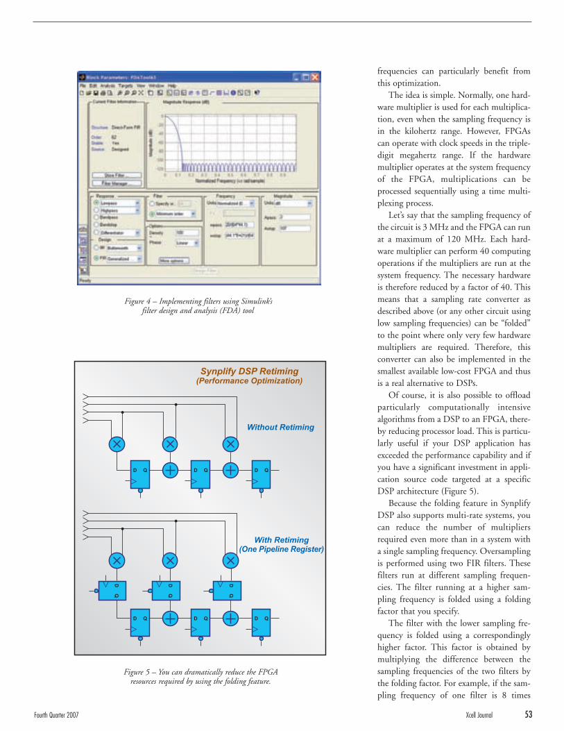
Fourth Quarter 2007 Xcell Journal 53
frequencies can particularly benefit fromthis optimization.
The idea is simple. Normally, one hard-ware multiplier is used for each multiplica-tion, even when the sampling frequency isin the kilohertz range. However, FPGAscan operate with clock speeds in the triple-digit megahertz range. If the hardwaremultiplier operates at the system frequencyof the FPGA, multiplications can beprocessed sequentially using a time multi-plexing process.
Let’s say that the sampling frequency ofthe circuit is 3 MHz and the FPGA can runat a maximum of 120 MHz. Each hard-ware multiplier can perform 40 computingoperations if the multipliers are run at thesystem frequency. The necessary hardwareis therefore reduced by a factor of 40. Thismeans that a sampling rate converter asdescribed above (or any other circuit usinglow sampling frequencies) can be “folded”to the point where only very few hardwaremultipliers are required. Therefore, thisconverter can also be implemented in thesmallest available low-cost FPGA and thusis a real alternative to DSPs.
Of course, it is also possible to offloadparticularly computationally intensivealgorithms from a DSP to an FPGA, there-by reducing processor load. This is particu-larly useful if your DSP application hasexceeded the performance capability and ifyou have a significant investment in appli-cation source code targeted at a specificDSP architecture (Figure 5).
Because the folding feature in SynplifyDSP also supports multi-rate systems, youcan reduce the number of multipliersrequired even more than in a system witha single sampling frequency. Oversamplingis performed using two FIR filters. Thesefilters run at different sampling frequen-cies. The filter running at a higher sam-pling frequency is folded using a foldingfactor that you specify.
The filter with the lower sampling fre-quency is folded using a correspondinglyhigher factor. This factor is obtained bymultiplying the difference between thesampling frequencies of the two filters bythe folding factor. For example, if the sam-pling frequency of one filter is 8 times
D QD
Without Retiming
With Retiming(One Pipeline Register)
Synplify DSP Retiming(Performance Optimization)
QD Q
D QD QD Q
DQ
DQ
DQ
Figure 4 – Implementing filters using Simulink’s filter design and analysis (FDA) tool
Figure 5 – You can dramatically reduce the FPGA resources required by using the folding feature.
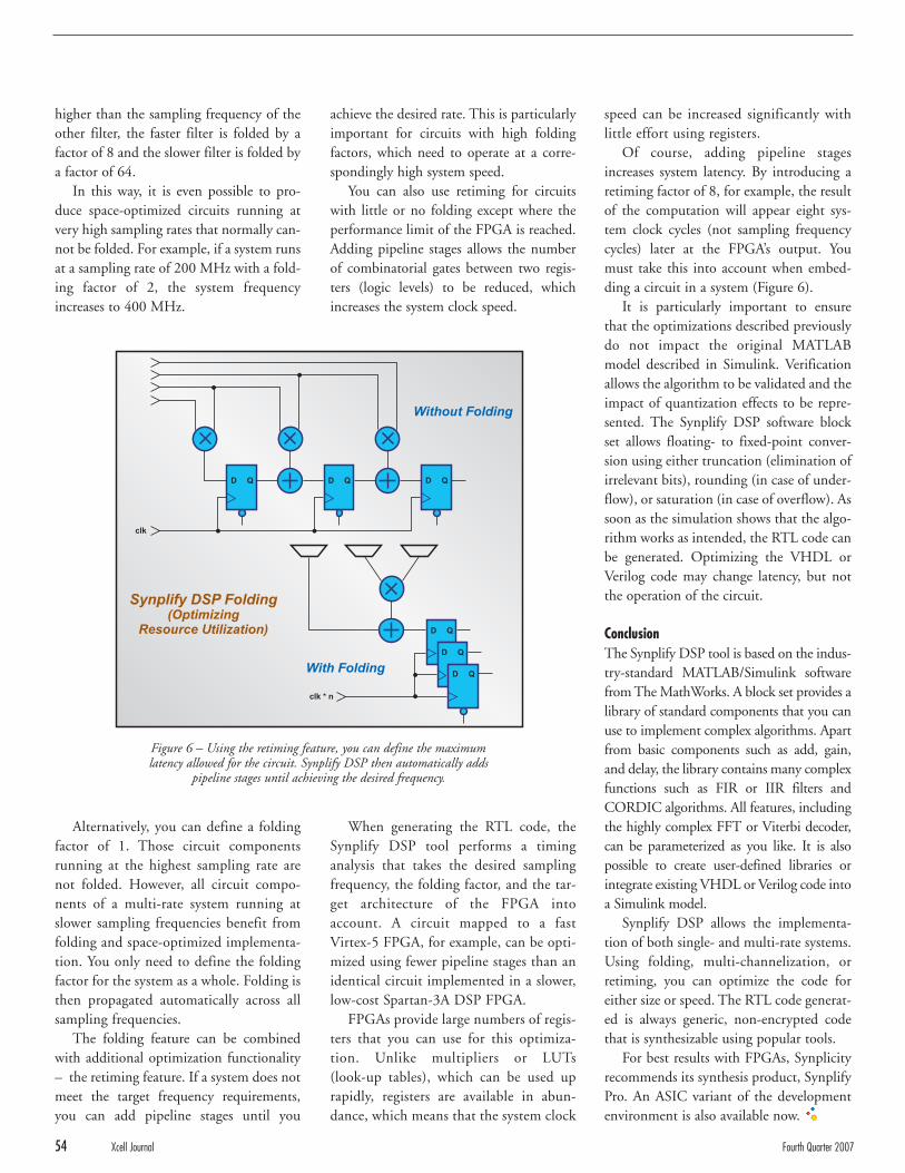
higher than the sampling frequency of theother filter, the faster filter is folded by afactor of 8 and the slower filter is folded bya factor of 64.
In this way, it is even possible to pro-duce space-optimized circuits running atvery high sampling rates that normally can-not be folded. For example, if a system runsat a sampling rate of 200 MHz with a fold-ing factor of 2, the system frequencyincreases to 400 MHz.
Alternatively, you can define a foldingfactor of 1. Those circuit componentsrunning at the highest sampling rate arenot folded. However, all circuit compo-nents of a multi-rate system running atslower sampling frequencies benefit fromfolding and space-optimized implementa-tion. You only need to define the foldingfactor for the system as a whole. Folding isthen propagated automatically across allsampling frequencies.
The folding feature can be combinedwith additional optimization functionality– the retiming feature. If a system does notmeet the target frequency requirements,you can add pipeline stages until you
achieve the desired rate. This is particularlyimportant for circuits with high foldingfactors, which need to operate at a corre-spondingly high system speed.
You can also use retiming for circuitswith little or no folding except where theperformance limit of the FPGA is reached.Adding pipeline stages allows the numberof combinatorial gates between two regis-ters (logic levels) to be reduced, whichincreases the system clock speed.
When generating the RTL code, theSynplify DSP tool performs a timinganalysis that takes the desired samplingfrequency, the folding factor, and the tar-get architecture of the FPGA intoaccount. A circuit mapped to a fastVirtex-5 FPGA, for example, can be opti-mized using fewer pipeline stages than anidentical circuit implemented in a slower,low-cost Spartan-3A DSP FPGA.
FPGAs provide large numbers of regis-ters that you can use for this optimiza-tion. Unlike multipliers or LUTs(look-up tables), which can be used uprapidly, registers are available in abun-dance, which means that the system clock
speed can be increased significantly withlittle effort using registers.
Of course, adding pipeline stagesincreases system latency. By introducing aretiming factor of 8, for example, the resultof the computation will appear eight sys-tem clock cycles (not sampling frequencycycles) later at the FPGA’s output. Youmust take this into account when embed-ding a circuit in a system (Figure 6).
It is particularly important to ensurethat the optimizations described previouslydo not impact the original MATLABmodel described in Simulink. Verificationallows the algorithm to be validated and theimpact of quantization effects to be repre-sented. The Synplify DSP software blockset allows floating- to fixed-point conver-sion using either truncation (elimination ofirrelevant bits), rounding (in case of under-flow), or saturation (in case of overflow). Assoon as the simulation shows that the algo-rithm works as intended, the RTL code canbe generated. Optimizing the VHDL orVerilog code may change latency, but notthe operation of the circuit.
ConclusionThe Synplify DSP tool is based on the indus-try-standard MATLAB/Simulink softwarefrom The MathWorks. A block set provides alibrary of standard components that you canuse to implement complex algorithms. Apartfrom basic components such as add, gain,and delay, the library contains many complexfunctions such as FIR or IIR filters andCORDIC algorithms. All features, includingthe highly complex FFT or Viterbi decoder,can be parameterized as you like. It is alsopossible to create user-defined libraries orintegrate existing VHDL or Verilog code intoa Simulink model.
Synplify DSP allows the implementa-tion of both single- and multi-rate systems.Using folding, multi-channelization, orretiming, you can optimize the code foreither size or speed. The RTL code generat-ed is always generic, non-encrypted codethat is synthesizable using popular tools.
For best results with FPGAs, Synplicityrecommends its synthesis product, SynplifyPro. An ASIC variant of the developmentenvironment is also available now.
54 Xcell Journal Fourth Quarter 2007
D Q
D Q
D Q
D QD
Without Folding
With Folding
Synplify DSP Folding(Optimizing
Resource Utilization)
QD
clk
clk * n
Q
Figure 6 – Using the retiming feature, you can define the maximum latency allowed for the circuit. Synplify DSP then automatically adds
pipeline stages until achieving the desired frequency.
Prove yourdesign with highspeed FPGA hard-ware logic emulation,that plugs directly intoyour PC. This 12+ milliongate, 8-lane PCIe board, isready to go: fixed PCIe core,extensive on board memory andeight independent clock networks willget your design running — fast! TheDN9000K10PCIe-8T features six Virtex-5,LX330 chips with 100% of FPGA resourcesuser-available.
There are no unreliable cables or stacks of overheatingboards. The price, with the biggest and baddest FPGAs, isless than $70,000. Why pay more for a “some assemblyrequired” toy? Visit www.dinigroup.com to see our completeselection of real high-speed prototyping solutions.
1010 Pearl Street, Suite 6 • La Jolla, CA 92037 • (858) 454-3419 • e-mail: [email protected]
Fourth Quarter 2007 Xcell Journal 57
Featured DSP Application NotesJumpstart your DSP design with Xilinx application notes describing
specific design examples and methodologies.
T E C H N I C A L L I T E R A T U R E
Part Number Title URL
Design Methodology Application Notes
XAPP547 PowerPC Processor with Floating Point Unit for Virtex™-4 FX Devices www.xilinx.com/bvdocs/appnotes/xapp547.pdf
Error Correction Application Notes
XAPP222 Designing Convolutional Interleavers with Virtex Devices www.xilinx.com/bvdocs/appnotes/xapp222.pdf
XAPP383 Single Error Correction and Double Error Detection (SECDED) with CoolRunner™-II CPLDs www.xilinx.com/bvdocs/appnotes/xapp383.pdf
XAPP551 Viterbi Decoder Block Decoding – Trellis Termination and Tail Biting www.xilinx.com/bvdocs/appnotes/xapp551.pdf
XAPP715 Multiple Bit Error Correction www.xilinx.com/bvdocs/appnotes/xapp715.pdf
XAPP948 Hardware Acceleration of 3GPP Turbo Encoder/Decoder BER Measurement Using System Generator www.xilinx.com/bvdocs/appnotes/xapp948.pdf
DSP Processor Application Notes
XAPP634 Analog Devices TigerSHARC Link www.xilinx.com/bvdocs/appnotes/xapp634.pdf
XAPP635 Interfacing Virtex-II FPGAs with Analog Devices TigerSHARC TS20x DSPs via LVDS Link Ports www.xilinx.com/bvdocs/appnotes/xapp635.pdf
XAPP706 Alpha Blending Two Data Streams Using a DSP48 DDR Technique www.xilinx.com/bvdocs/appnotes/xapp706.pdf
XAPP753 Interfacing Xilinx FPGAs to TI DSP Platforms Using the EMIF www.xilinx.com/bvdocs/appnotes/xapp753.pdf
XAPP919 Video Virtual Socket Architecture www.xilinx.com/bvdocs/appnotes/xapp919.pdf
Transform Application Notes
XAPP610 Video Compression Using DCT www.xilinx.com/bvdocs/appnotes/xapp610.pdf
XAPP611 Video Compression Using IDCT www.xilinx.com/bvdocs/appnotes/xapp611.pdf
Filter Application Notes
XAPP212 CDMA Matched Filter Implementation in Virtex Devices www.xilinx.com/bvdocs/appnotes/xapp212.pdf
XAPP219 Transposed Form FIR Filters www.xilinx.com/bvdocs/appnotes/xapp219.pdf
Application notes illustrate how to use a Xilinx® product in a specialized way. Xilinx maintains a large database of application notes onnumerous topics, including design files, to assist you in your next design. The main Application Notes search page, www.xilinx.com/apps,includes different sections on specific market applications.
For application notes on digital communication, multimedia video and imaging, and defense systems, see our “XtremeDSP™Selection Guide,” www.xilinx.com/publications/prod_mktg/pn0010944-3.pdf.
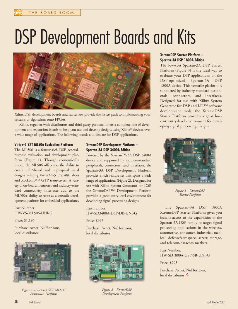
Virtex-5 SXT ML506 Evaluation PlatformThe ML506 is a feature-rich DSP general-purpose evaluation and development plat-form (Figure 1). Though economicallypriced, the ML506 offers you the ability tocreate DSP-based and high-speed serialdesigns utilizing Virtex™-5 DSP48E slicesand RocketIO™ GTP transceivers. A vari-ety of on-board memories and industry-stan-dard connectivity interfaces add to theML506’s ability to serve as a versatile devel-opment platform for embedded applications.
Part Number: HW-V5-ML506-UNI-G
Price: $1,195
Purchase: Avnet, NuHorizons, local distributor
XtremeDSP Development Platform – Spartan-3A DSP 3400A EditionPowered by the Spartan™-3A DSP 3400Adevice and supported by industry-standardperipherals, connectors, and interfaces, theSpartan-3A DSP Development Platformprovides a rich feature set that spans a widerange of applications (Figure 2). Designed foruse with Xilinx System Generator for DSP,the XtremeDSP™ Development Platformprovides a great entry-level environment fordeveloping signal processing designs.
Part number: HW-SD3400A-DSP-DB-UNI-G
Price: $995
Purchase: Avnet, NuHorizons, local distributor
XtremeDSP Starter Platform – Spartan-3A DSP 1800A EditionThe low-cost Spartan-3A DSP StarterPlatform (Figure 3) is the ideal way toevaluate your DSP applications on theDSP-optimized Spartan-3A DSP1800A device. This versatile platform issupported by industry-standard periph-erals, connectors, and interfaces.Designed for use with Xilinx SystemGenerator for DSP and ISE™ softwaredevelopment tools, the XtremeDSPStarter Platform provides a great low-cost, entry-level environment for devel-oping signal processing designs.
The Spartan-3A DSP 1800AXtremeDSP Starter Platform gives youinstant access to the capabilities of theSpartan-3A DSP family to target signalprocessing applications in the wireless,automotive, consumer, industrial, med-ical, defense/aerospace, server, storage,and telecom/datacom markets.
Part Number: HW-SD1800A-DSP-SB-UNI-G
Price: $295
Purchase: Avnet, NuHorizons, local distributor
58 Xcell Journal Fourth Quarter 2007
DSP Development Boards and Kits
Xilinx DSP development boards and starter kits provide the fastest path to implementing yoursystems or algorithms onto FPGAs.
Xilinx, together with distributors and third party partners, offers a complete line of devel-opment and expansion boards to help you test and develop designs using Xilinx® devices overa wide range of applications. The following boards and kits are for DSP applications.
T H E B O A R D R O O M
Figure 1 – Virtex-5 SXT ML506Evaluation Platform
Figure 2 – XtremeDSP Development Platform
Figure 3 – XtremeDSP Starter Platform
By Jannis McReynoldsSr. Manager, Services MarketingXilinx, [email protected]
Xilinx® Education Services (XES) pro-grams provide targeted, high-quality edu-cation products and services that aredesigned by experts in programmable logicdesign and delivered by Xilinx-qualifiedtrainers. XES offers targeted courses at alllevels of programmable logic design andcreates an engaging learning environmentby blending lecture, hands-on labs, inter-active discussions, tips, and best practices.By leveraging our global network ofAuthorized Training Providers (ATP) andonline learning systems, we can offercourses in 26 languages at 110 locationsaround the world.
By becoming proficient with advancedprogrammable logic design techniques andmethodologies, you will be able to take fulladvantage of all of the DSP capabilitiesavailable from today’s leading FPGAs. Theknowledge you gain will reduce yourR&D costs through greater efficiency inthe design process, and reduce productioncosts through the use of smaller devices ina slower speed grade. This expertise cangreatly improve your organization’s time tomarket, driving greater market success.
The Xilinx DSP Design CurriculumPath provides a recommended coursesequence. You should meet the prerequi-sites of each class to gain the full benefit ofeach course. The curriculum path includescourses delivered by Xilinx and additionalcourses offered by The MathWorks. Toview the DSP Design Curriculum Path inits entirety, visit www.xilinx.com/support/training/cur_paths/atp-dsp.htm.
The DSP Curriculum Path comprisesthese courses:
• DSP Design Using System Generator
• Introduction to AccelDSP™Synthesis Tool
• The MathWorks Simulink for Xilinx
• DSP Implementation Techniques
DSP Design Using System GeneratorThis course allows you to explore theSystem Generator for DSP tool and gainthe expertise required to develop advanced,low-cost DSP designs. This intermediatecourse focuses on using System Generatorfor DSP, design implementation tools, andhardware-in-the-loop verification. Throughhands-on exercises, you will implement adesign from algorithm concept to hardwareverification with Xilinx FPGAs.
Introduction to AccelDSP Synthesis ToolThis course will teach you how to syn-thesize an algorithm written in the lan-guage of MATLAB software into a designthat is optimized for a Xilinx FPGA.You’ll learn how to make coding changesin MATLAB to improve area and per-
formance, and how to use the floating- tofixed-point and design exploration fea-tures of the AccelDSP synthesis tool toachieve maximum results.
The MathWorks Simulink for XilinxThis course covers the basics of usingSimulink, an interactive, graphical envi-ronment for modeling and simulatingdynamic systems. This course covers allaspects of system modeling withSimulink, including creating a model,simulating the system, and analyzing theresults. Advanced simulation conceptsand simulations from the command lineare also explained. The final section dis-cusses refining models by providing addi-tional functionality with S-functions,block masks, and GUIs for interactionwith your system.
DSP Implementation TechniquesThis course will show you how to takeadvantage of Xilinx FPGA architecturesto effectively implement DSP algorithms.The techniques also demonstrate whichsystem-level decisions have the greatestimpact on the implementation processand product costs.
Fourth Quarter 2007 Xcell Journal 59
The DSP Design Curriculum PathXilinx Education Services is ready to help you use DSP solutions in your next design.
• Register today for any of these courses.
• View the full DSPDesign Curriculum Path.
• Contact your Xilinx sales representative.
TAKE THE NEXT STEP (Digital Edition: www.xcellpublications.com/subscribe/)
E D U C A T I O N
Xilinx DSP IntellectualProperty OfferingsThe Xilinx XtremeDSP Initiative helps you developtailored, high-performance DSP solutions.
Xilinx® DSP intellectual property (IP)offerings implement simple algorithms (fil-ters and transforms, for example) withvarying implementations that allow you totrade-off algorithmic performance for areaand speed. Thus, you can achieve fastertime to market by focusing on the algo-rithms and implementations that differen-tiate your designs from the competition.Xilinx DSP IP includes both free and for-purchase cores.
Table 1 lists the broad categories ofXilinx DSP IP cores.
What’s New
Fast Fourier Transform (FFT)The FFT v5.0 provides four differentarchitectures, along with system-levelfixed-point C-models, and reduces typicalimplementation times from three to sixmonths to the push of a button.
FFT v5.0 expands the focus on orthog-onal frequency-division multiplexing(OFDM) systems, providing reduced areafor OFDM multi-channel systems likeWiMAX and 3GPP-LTE throughincreased coverage of the multi-channelarchitecture and cyclic-prefix insertion.
A typical FFT used in a 2 x 2, three-sec-tor modem has 42% and 54% fewer logicresources in memory usage when compar-ing version 5.0 to version 4.1. ThisLogiCORE™ IP was released in ISE™software 9.2i, CORE Generator softwareIP update 2.
www.xilinx.com/xlnx/xebiz/designResources/ip_product_details.jsp?key=FFT
FIR Compiler The FIR filter is one of the most ubiqui-tous and fundamental building blocks inDSP systems. Version 3.2 of the FIRCompiler expands device support to thelowest cost Spartan™-3A/3E device fami-lies. This LogiCORE IP was released inISE software 9.2i, CORE Generator soft-ware IP update 2.
www.xilinx.com/xlnx/xebiz/designResources/ip_product_details.jsp?key=FIR_Compiler
Cascaded Integrator Comb (CIC) Compiler The CIC Compiler version 1.0 reducesfilter implementation time to the push ofa button, while also providing you withthe ability to make trade-offs betweendiffering hardware implementations ofyour CIC filter specification.
Along with greater than 50% area sav-ings versus older CIC filter IP offeringsfrom Xilinx, the version 1.0 of the CICCompiler also comes close to the 450MHz (-1) and 250 MHz (-4) achievable inVirtex™-5 and Spartan-3A DSP devices.This high-performance capability enablessupport for the highest performance ADCand DAC technology available, or alterna-tively supports more channels in a singlestructure to save area. This LogiCORE IPwas released in ISE software 9.2i, COREGenerator software IP update 2.
www.xilinx.com/xlnx/xebiz/designResources/ip_product_details.jsp?key=CIC
Xilinx Wireless IntellectualProperty Offerings Xilinx offers high-performance, cost-effective solu-tions for wireless networking equipment.
Xilinx wireless intellectual property (IP)offerings are suitable for RF digital front-end (DFE) signal processing, baseband pro-cessing (including forward error correction[FEC], FFTs, and adaptive modulation),and advanced interfacing, connectivity, andbridging solutions.
60 Xcell Journal Fourth Quarter 2007
Intellectual Property Offerings
Xilinx DSP IP
Filters Error Correction
Transforms Basic Math
Waveform Synthesis Floating Point
Linear Algebra Trigonometric Functions
Table 1 – Categories of Xilinx DSP IP cores
INTE L LECTUAL PROPERTY
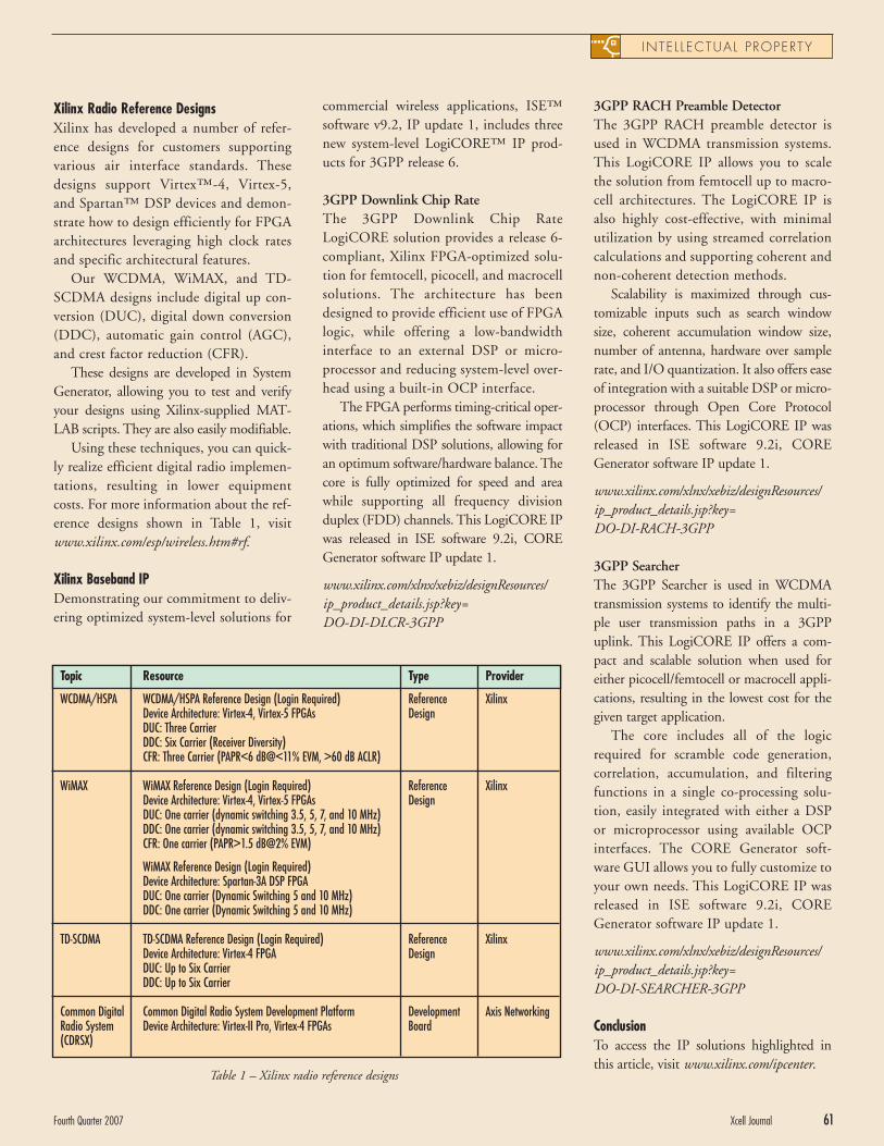
Xilinx Radio Reference DesignsXilinx has developed a number of refer-ence designs for customers supportingvarious air interface standards. Thesedesigns support Virtex™-4, Virtex-5,and Spartan™ DSP devices and demon-strate how to design efficiently for FPGAarchitectures leveraging high clock ratesand specific architectural features.
Our WCDMA, WiMAX, and TD-SCDMA designs include digital up con-version (DUC), digital down conversion(DDC), automatic gain control (AGC),and crest factor reduction (CFR).
These designs are developed in SystemGenerator, allowing you to test and verifyyour designs using Xilinx-supplied MAT-LAB scripts. They are also easily modifiable.
Using these techniques, you can quick-ly realize efficient digital radio implemen-tations, resulting in lower equipmentcosts. For more information about the ref-erence designs shown in Table 1, visitwww.xilinx.com/esp/wireless.htm#rf.
Xilinx Baseband IPDemonstrating our commitment to deliv-ering optimized system-level solutions for
3GPP RACH Preamble DetectorThe 3GPP RACH preamble detector isused in WCDMA transmission systems.This LogiCORE IP allows you to scalethe solution from femtocell up to macro-cell architectures. The LogiCORE IP isalso highly cost-effective, with minimalutilization by using streamed correlationcalculations and supporting coherent andnon-coherent detection methods.
Scalability is maximized through cus-tomizable inputs such as search windowsize, coherent accumulation window size,number of antenna, hardware over samplerate, and I/O quantization. It also offers easeof integration with a suitable DSP or micro-processor through Open Core Protocol(OCP) interfaces. This LogiCORE IP wasreleased in ISE software 9.2i, COREGenerator software IP update 1.
www.xilinx.com/xlnx/xebiz/designResources/ip_product_details.jsp?key=DO-DI-RACH-3GPP
3GPP SearcherThe 3GPP Searcher is used in WCDMAtransmission systems to identify the multi-ple user transmission paths in a 3GPPuplink. This LogiCORE IP offers a com-pact and scalable solution when used foreither picocell/femtocell or macrocell appli-cations, resulting in the lowest cost for thegiven target application.
The core includes all of the logicrequired for scramble code generation,correlation, accumulation, and filteringfunctions in a single co-processing solu-tion, easily integrated with either a DSPor microprocessor using available OCPinterfaces. The CORE Generator soft-ware GUI allows you to fully customize toyour own needs. This LogiCORE IP wasreleased in ISE software 9.2i, COREGenerator software IP update 1.
www.xilinx.com/xlnx/xebiz/designResources/ip_product_details.jsp?key=DO-DI-SEARCHER-3GPP
ConclusionTo access the IP solutions highlighted inthis article, visit www.xilinx.com/ipcenter.
commercial wireless applications, ISE™software v9.2, IP update 1, includes threenew system-level LogiCORE™ IP prod-ucts for 3GPP release 6.
3GPP Downlink Chip Rate The 3GPP Downlink Chip RateLogiCORE solution provides a release 6-compliant, Xilinx FPGA-optimized solu-tion for femtocell, picocell, and macrocellsolutions. The architecture has beendesigned to provide efficient use of FPGAlogic, while offering a low-bandwidthinterface to an external DSP or micro-processor and reducing system-level over-head using a built-in OCP interface.
The FPGA performs timing-critical oper-ations, which simplifies the software impactwith traditional DSP solutions, allowing foran optimum software/hardware balance. Thecore is fully optimized for speed and areawhile supporting all frequency divisionduplex (FDD) channels. This LogiCORE IPwas released in ISE software 9.2i, COREGenerator software IP update 1.
www.xilinx.com/xlnx/xebiz/designResources/ip_product_details.jsp?key=DO-DI-DLCR-3GPP
Fourth Quarter 2007 Xcell Journal 61
Topic Resource Type Provider
WCDMA/HSPA WCDMA/HSPA Reference Design (Login Required) Reference XilinxDevice Architecture: Virtex-4, Virtex-5 FPGAs DesignDUC: Three CarrierDDC: Six Carrier (Receiver Diversity) CFR: Three Carrier (PAPR<6 dB@<11% EVM, >60 dB ACLR)
WiMAX WiMAX Reference Design (Login Required) Reference XilinxDevice Architecture: Virtex-4, Virtex-5 FPGAs DesignDUC: One carrier (dynamic switching 3.5, 5, 7, and 10 MHz)DDC: One carrier (dynamic switching 3.5, 5, 7, and 10 MHz)CFR: One carrier (PAPR>1.5 dB@2% EVM)
WiMAX Reference Design (Login Required) Device Architecture: Spartan-3A DSP FPGADUC: One carrier (Dynamic Switching 5 and 10 MHz)DDC: One carrier (Dynamic Switching 5 and 10 MHz)
TD-SCDMA TD-SCDMA Reference Design (Login Required) Reference XilinxDevice Architecture: Virtex-4 FPGA DesignDUC: Up to Six CarrierDDC: Up to Six Carrier
Common Digital Common Digital Radio System Development Platform Development Axis NetworkingRadio System Device Architecture: Virtex-II Pro, Virtex-4 FPGAs Board(CDRSX)
Table 1 – Xilinx radio reference designs
INTE L LECTUAL PROPERTY
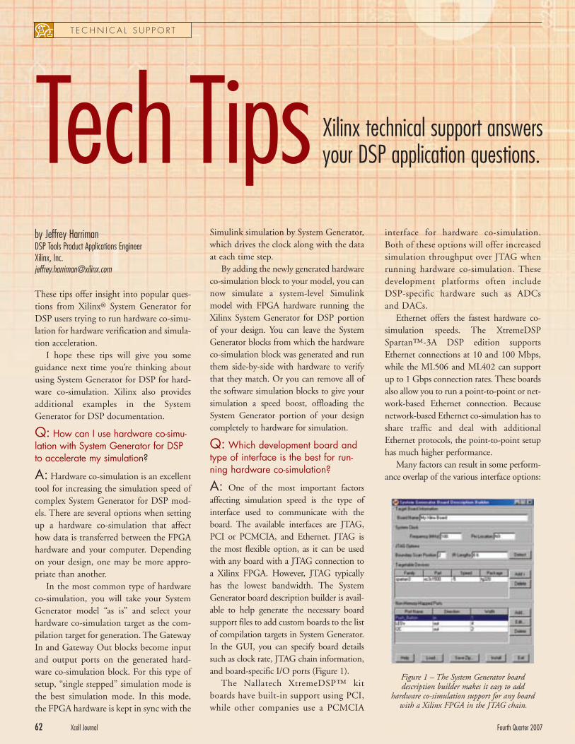
by Jeffrey HarrimanDSP Tools Product Applications EngineerXilinx, [email protected]
These tips offer insight into popular ques-tions from Xilinx® System Generator forDSP users trying to run hardware co-simu-lation for hardware verification and simula-tion acceleration.
I hope these tips will give you someguidance next time you’re thinking aboutusing System Generator for DSP for hard-ware co-simulation. Xilinx also providesadditional examples in the SystemGenerator for DSP documentation.
Q: How can I use hardware co-simu-lation with System Generator for DSPto accelerate my simulation?
A: Hardware co-simulation is an excellenttool for increasing the simulation speed ofcomplex System Generator for DSP mod-els. There are several options when settingup a hardware co-simulation that affecthow data is transferred between the FPGAhardware and your computer. Dependingon your design, one may be more appro-priate than another.
In the most common type of hardwareco-simulation, you will take your SystemGenerator model “as is” and select yourhardware co-simulation target as the com-pilation target for generation. The GatewayIn and Gateway Out blocks become inputand output ports on the generated hard-ware co-simulation block. For this type ofsetup, “single stepped” simulation mode isthe best simulation mode. In this mode,the FPGA hardware is kept in sync with the
Simulink simulation by System Generator,which drives the clock along with the dataat each time step.
By adding the newly generated hardwareco-simulation block to your model, you cannow simulate a system-level Simulinkmodel with FPGA hardware running theXilinx System Generator for DSP portionof your design. You can leave the SystemGenerator blocks from which the hardwareco-simulation block was generated and runthem side-by-side with hardware to verifythat they match. Or you can remove all ofthe software simulation blocks to give yoursimulation a speed boost, offloading theSystem Generator portion of your designcompletely to hardware for simulation.
Q: Which development board andtype of interface is the best for run-ning hardware co-simulation?
A: One of the most important factorsaffecting simulation speed is the type ofinterface used to communicate with theboard. The available interfaces are JTAG,PCI or PCMCIA, and Ethernet. JTAG isthe most flexible option, as it can be usedwith any board with a JTAG connection toa Xilinx FPGA. However, JTAG typicallyhas the lowest bandwidth. The SystemGenerator board description builder is avail-able to help generate the necessary boardsupport files to add custom boards to the listof compilation targets in System Generator.In the GUI, you can specify board detailssuch as clock rate, JTAG chain information,and board-specific I/O ports (Figure 1).
The Nallatech XtremeDSP™ kitboards have built-in support using PCI,while other companies use a PCMCIA
interface for hardware co-simulation.Both of these options will offer increasedsimulation throughput over JTAG whenrunning hardware co-simulation. Thesedevelopment platforms often includeDSP-specific hardware such as ADCsand DACs.
Ethernet offers the fastest hardware co-simulation speeds. The XtremeDSPSpartan™-3A DSP edition supportsEthernet connections at 10 and 100 Mbps,while the ML506 and ML402 can supportup to 1 Gbps connection rates. These boardsalso allow you to run a point-to-point or net-work-based Ethernet connection. Becausenetwork-based Ethernet co-simulation has toshare traffic and deal with additionalEthernet protocols, the point-to-point setuphas much higher performance.
Many factors can result in some perform-ance overlap of the various interface options:
62 Xcell Journal Fourth Quarter 2007
Tech Tips Xilinx technical support answers your DSP application questions.
Figure 1 – The System Generator board description builder makes it easy to add
hardware co-simulation support for any boardwith a Xilinx FPGA in the JTAG chain.
T E C H N I C A L S U P P O R T
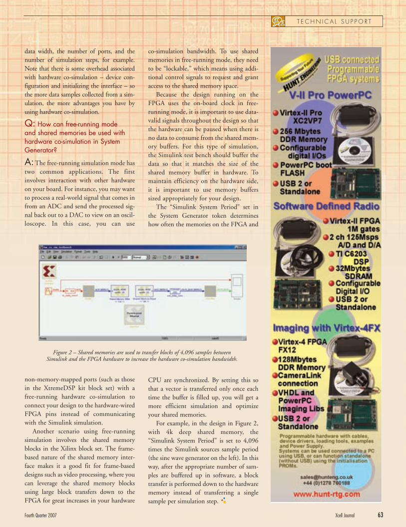
data width, the number of ports, and thenumber of simulation steps, for example.Note that there is some overhead associatedwith hardware co-simulation – device con-figuration and initializing the interface – sothe more data samples collected from a sim-ulation, the more advantages you have byusing hardware co-simulation.
Q: How can free-running mode and shared memories be used withhardware co-simulation in SystemGenerator?
A:The free-running simulation mode hastwo common applications. The firstinvolves interaction with other hardwareon your board. For instance, you may wantto process a real-world signal that comes infrom an ADC and send the processed sig-nal back out to a DAC to view on an oscil-loscope. In this case, you can use
non-memory-mapped ports (such as thosein the XtremeDSP kit block set) with afree-running hardware co-simulation toconnect your design to the hardware-wiredFPGA pins instead of communicatingwith the Simulink simulation.
Another scenario using free-runningsimulation involves the shared memoryblocks in the Xilinx block set. The frame-based nature of the shared memory inter-face makes it a good fit for frame-baseddesigns such as video processing, where youcan leverage the shared memory blocksusing large block transfers down to theFPGA for great increases in your hardware
co-simulation bandwidth. To use sharedmemories in free-running mode, they needto be “lockable,” which means using addi-tional control signals to request and grantaccess to the shared memory space.
Because the design running on theFPGA uses the on-board clock in free-running mode, it is important to use data-valid signals throughout the design so thatthe hardware can be paused when there isno data to consume from the shared mem-ory buffers. For this type of simulation,the Simulink test bench should buffer thedata so that it matches the size of theshared memory buffer in hardware. Tomaintain efficiency on the hardware side,it is important to use memory bufferssized appropriately for your design.
The “Simulink System Period” set inthe System Generator token determineshow often the memories on the FPGA and
CPU are synchronized. By setting this sothat a vector is transferred only once eachtime the buffer is filled up, you will get amore efficient simulation and optimizeyour shared memories.
For example, in the design in Figure 2,with 4k deep shared memory, the“Simulink System Period” is set to 4,096times the Simulink sources sample period(the sine wave generator on the left). In thisway, after the appropriate number of sam-ples are buffered up in software, a blocktransfer is performed down to the hardwarememory instead of transferring a singlesample per simulation step.
Fourth Quarter 2007 Xcell Journal 63
Figure 2 – Shared memories are used to transfer blocks of 4,096 samples between Simulink and the FPGA hardware to increase the hardware co-simulation bandwidth.
T E C H N I C A L S U P P O R T

Get Published
www.xilinx.com/xcell
It's easier than you think!
Submit an article draft for our Web-based or printed publications and we will assign an editor and a
graphic artist to work with you to make your work look as good as possible.
For more information on this exciting and highly rewarding program, please contact:
Forrest CouchPublisher, Xcell Publications
Would you like to write for Xcell Publications?

www.agilent.com/find/logic-offer
© Agilent Technologies, Inc. 2006 Windows is a U.S. registered trademark of Microsoft Corporation
Logic analyzers up to 50% offLogic analyzers up to 50% offA special limited-time offer from Agilent.
Now you can see inside your FPGA designs in a way that will save weeks of development time.
The FPGA dynamic probe, when combined with an AgilentWindows®-based logic analyzer, allows you to access differentgroups of signals inside your FPGA for debug—without requiringdesign changes. You’ll increase visibility into internal FPGA activityby gaining access up to 128 internal signals with each debug pin.
Our 16800 Series logic analyzers offer you unprecedented price-performance in a portable family, with up to 204 channels, 32 M memory depth and a pattern generator available.
And now for a limited time, you can receive up to 50% off ournewest 16901A modular logic analyzer mainframe when youpurchase eligible measurement modules. Offer valid February 1,2007 through August 15, 2007. Reference promotion 5.564.
• Increased visibility with FPGA dynamic probe • Customized protocol analysis with
Agilent's exclusive packet viewer software• Low-cost embedded PCI Express
packet analysis• Pricing starts at $9,450
Agilent portable and modularlogic analyzers
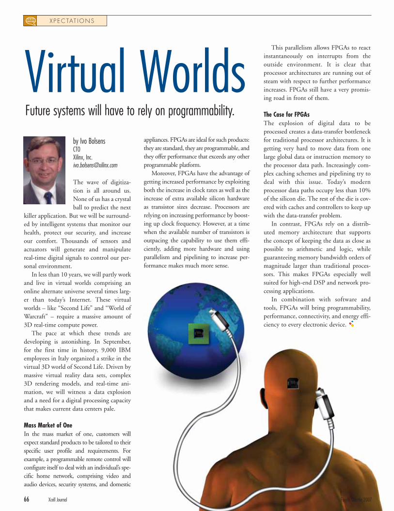
by Ivo BolsensCTOXilinx, [email protected]
The wave of digitiza-tion is all around us.None of us has a crystalball to predict the next
killer application. But we will be surround-ed by intelligent systems that monitor ourhealth, protect our security, and increaseour comfort. Thousands of sensors andactuators will generate and manipulatereal-time digital signals to control our per-sonal environment.
In less than 10 years, we will partly workand live in virtual worlds comprising anonline alternate universe several times larg-er than today’s Internet. These virtualworlds – like “Second Life” and “World ofWarcraft” – require a massive amount of3D real-time compute power.
The pace at which these trends aredeveloping is astonishing. In September,for the first time in history, 9,000 IBMemployees in Italy organized a strike in thevirtual 3D world of Second Life. Driven bymassive virtual reality data sets, complex3D rendering models, and real-time ani-mation, we will witness a data explosionand a need for a digital processing capacitythat makes current data centers pale.
Mass Market of OneIn the mass market of one, customers willexpect standard products to be tailored to theirspecific user profile and requirements. Forexample, a programmable remote control willconfigure itself to deal with an individual’s spe-cific home network, comprising video andaudio devices, security systems, and domestic
appliances. FPGAs are ideal for such products:they are standard, they are programmable, andthey offer performance that exceeds any otherprogrammable platform.
Moreover, FPGAs have the advantage ofgetting increased performance by exploitingboth the increase in clock rates as well as theincrease of extra available silicon hardwareas transistor sizes decrease. Processors arerelying on increasing performance by boost-ing up clock frequency. However, at a timewhen the available number of transistors isoutpacing the capability to use them effi-ciently, adding more hardware and usingparallelism and pipelining to increase per-formance makes much more sense.
This parallelism allows FPGAs to reactinstantaneously on interrupts from theoutside environment. It is clear thatprocessor architectures are running out ofsteam with respect to further performanceincreases. FPGAs still have a very promis-ing road in front of them.
The Case for FPGAsThe explosion of digital data to beprocessed creates a data-transfer bottleneckfor traditional processor architectures. It isgetting very hard to move data from onelarge global data or instruction memory tothe processor data path. Increasingly com-plex caching schemes and pipelining try todeal with this issue. Today’s modernprocessor data paths occupy less than 10%of the silicon die. The rest of the die is cov-ered with caches and controllers to keep upwith the data-transfer problem.
In contrast, FPGAs rely on a distrib-uted memory architecture that supportsthe concept of keeping the data as close aspossible to arithmetic and logic, whileguaranteeing memory bandwidth orders ofmagnitude larger than traditional proces-sors. This makes FPGAs especially wellsuited for high-end DSP and network pro-cessing applications.
In combination with software andtools, FPGAs will bring programmability,performance, connectivity, and energy effi-ciency to every electronic device.
66 Xcell Journal Fourth Quarter 2007
Virtual WorldsFuture systems will have to rely on programmability.
101010101001001 X P E C TAT I O N S
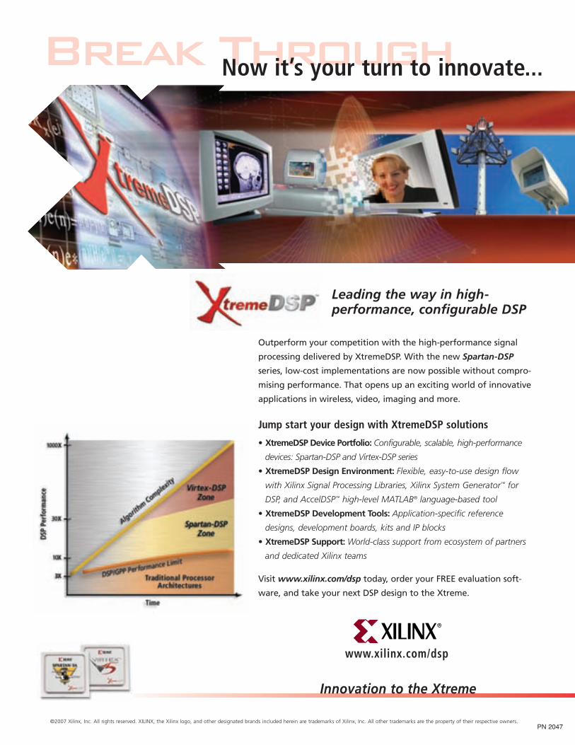
Break Through
Leading the way in high-performance, configurable DSP
Outperform your competition with the high-performance signal
processing delivered by XtremeDSP. With the new Spartan-DSP
series, low-cost implementations are now possible without compro-
mising performance. That opens up an exciting world of innovative
applications in wireless, video, imaging and more.
Jump start your design with XtremeDSP solutions
• XtremeDSP Device Portfolio: Configurable, scalable, high-performance
devices: Spartan-DSP and Virtex-DSP series
• XtremeDSP Design Environment: Flexible, easy-to-use design flow
with Xilinx Signal Processing Libraries, Xilinx System Generator™ for
DSP, and AccelDSP™ high-level MATLAB® language-based tool
• XtremeDSP Development Tools: Application-specific reference
designs, development boards, kits and IP blocks
• XtremeDSP Support: World-class support from ecosystem of partners
and dedicated Xilinx teams
Visit www.xilinx.com/dsp today, order your FREE evaluation soft-
ware, and take your next DSP design to the Xtreme.
www.xilinx.com/dsp
Innovation to the Xtreme
©2007 Xilinx, Inc. All rights reserved. XILINX, the Xilinx logo, and other designated brands included herein are trademarks of Xilinx, Inc. All other trademarks are the property of their respective owners.
Now it’s your turn to innovate...
PN 2047