Embed Size (px)
Citation preview
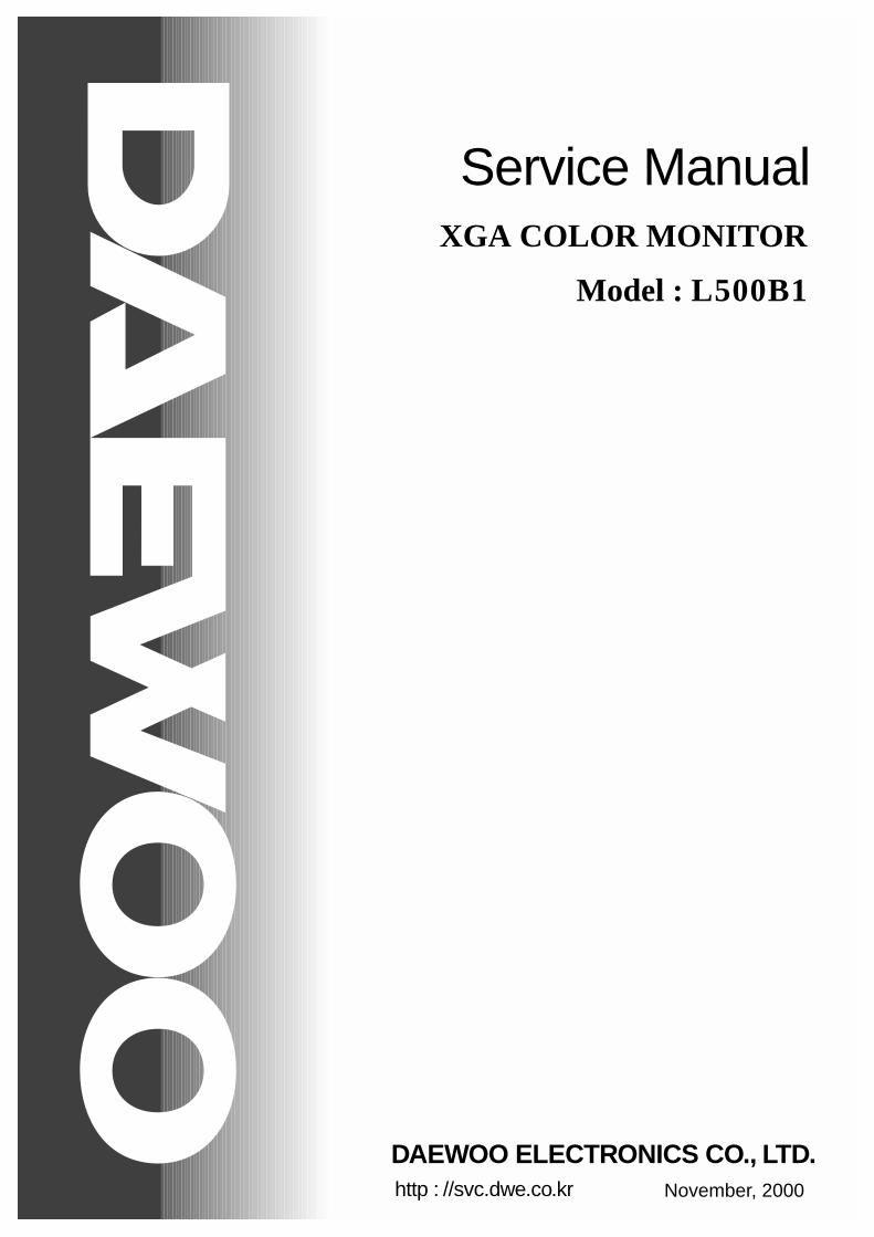
DAEWOO ELECTRONICS CO., LTD.http : //svc.dwe.co.kr
Service ManualXGA COLOR MONITOR
Model : L500B1
November, 2000
CONTENTS
SAFETY PRECAUTIONS 1
GENERAL SAFETY INFORMATION 2
SERVICING PRECAUTIONS 3
TECHNICAL INFORMATION 6
GENERAL INFORMATION 7
PIN CONNECTOR 8
CAUTIONS FOR ADJUSTMENT AND REPAIR 8
OPERATION & ADJUSTMENT 9
ALIGNMENT PROCEDURE 14
TROUBLESHOOTING HINTS 15
BLOCK DIAGRAM 22
PCB LAYOUT 23
SCHEMATIC DIAGRAM 27
EXPLODED VIEW & MECHANICAL PARTS LIST 28
INFORMATION OF PART DESCRIPTION 29
ELECTRICAL PARTS LIST 30
SAFETY PRECAUTIONS
1
Safety Check
Care should be taken while servicing this analog color display because of the high voltages used in thedeflection circuits. These voltages are exposed in such areas as the associated flyback and yoke circuits.
Fire & Shock Hazard
• Insert an isolation transformer between the analog color display and AC power line before servicing thechassis.
• When servicing, pay close attention to the original lead dress especially in the high voltage circuit area;if a short circuit is found, replace all parts which have been overheated as a result of the short circuit.
• All the protective devices must be reinstalled per original design.• Soldering must be inspected for possible cold solder points, frayed leads, damaged insulation, solder
splashes or sharp solder points. Be certain to remove all foreign materials.
Implosion Protection
Picture tube in this monitor employs intergral implosion protection system, but care should be taken toavoid damage and scratching during installation.Only use same type replacement picture tubes.
X-Ray
IMPORTANT SAFETY NOTICE: There are special components used in this analog color display,which are important for safety. These parts are shaded on theschematic diagram and on the replacement parts list. It is essentialthat these critical parts should be replaced with manufacturer’sspecified parts to prevent X-Ray, shock, fire or other hazards. Donot modify the original design without getting written permissionfrom DAEWOO ELECTRONICS CO. or this will void the originalparts and labor warranty.
CAUTION: No modifications of any circuits should be attempted. Service work should be performedonly after you are thoroughly familiar with all of the following safety checks and servicingguidelines.
WARNING: The only potential source of X-Ray is the picture tube. However when the high voltagecircuitry is operating properly, there is no possibility of an X-Ray problem. The basicprecaution which must be exercised is to keep the high voltage at the following factoryrecommended level.
NOTE: It is important to use an accurate, periodically, calibrated high voltage meter.• To measure the high voltage, use a high-impedance high-voltage meter.
Connect(-) to chassis and (+) to the CRT anode button.• Turn the Contrast & Brightness Control fully counterclockwise.• Measure the high voltage. The high voltage meter should indicate the following factory
recommended levels.• If the upper meter indication exceeds the maximum level, immediate service is required to
prevent the possibility of premature component failure.• To prevent X-Ray possibility, it is essential to use the specified picture tube.• The normal high voltage is 25.5KV or below and must not exceed 29KV at zero beam current
at rated voltage.
GENERAL SAFETY INFORMATION
2
Warning: This product includes critical mechanical and electrical parts which are essential for x rayprotection. For continued safety, replace critical components that are indicated in the servicemanual with exact replacement parts given in the parts list.Operating high voltage with this product is 29Kv at minimum brightness. Refer to servicemanual for measurement procedures and proper service adjustments.
Terms in the manual
CAUTION Statements identify conditions or practices that could result in damage to the equipment orother property.
WARNING Statements identify conditions or practices that could result in personal injury or loss oflife.
Terms as marked on equipment
CAUTION Statements indicate a personal injury hazard not immediately accessible as one reads themarking or a hazard which is properly included on the equipment itself.
WARNING Statements are clearly concerning indicated personal injury hazards.
Symbols in the manual
The symbols indicate where applicable cautionary or other information is to be found.
Symbols as marked on equipment
Protective GROUND terminal
High Voltage Warning And Critical Component Warning Label
The following warning label is on the CRT PWB shield case inside the unit.
SERVICING PRECAUTIONS
3
General Servicing Precautions
1. Always unplug the AC power cord from the AC power source before:a. Removing or reinstalling any component, circuit board, module, or any other instrument assembly.
b. Disconnecting or reconnecting any electrical plug or other electrical connection.c. Connecting a test substitute in parallel with an electrolytic capacitor in the instrument.
d. Discharging the picture tube anode.
2. Test high voltage only by measuring it with an appropriate high voltage meter or other voltagemeasuring device (DVM, FETVOM. etc.) equipped with a suitable high voltage probe. Do not test highvoltage by “drawing an arc”.
3. Discharge the picture tube anode only by: (a) first connecting one end of an insulated clip lead to thedegaussing or line grounding system shield at the point where the picture tube socket ground lead isconnected, and then (b) touching the other end of the insulated clip lead to the picture tube anodebutton, using an insulating handle to avoid personal contact with high voltage.
4. Do not any spray chemicals on or near this instrument, or any of its assemblies.
5. Unless otherwise specified in this service manual, only clean electrical contacts by applying thefollowing mixture to the contacts with a pipe cleaner, cotton-tipped stick, or comparable nonabrasiveapplicator: 10% (by volume) Aceton and 90% (by volume) isopropyl alchohol (90%-99% strength).
6. Do not damage any plug/socket B+ voltage interlocks with which instruments covered by this servicemanual might be equipped.
7. Do not apply AC power to this instrument and/or any other of its electrical assemblies unless all thesolid-state device heat sinks are correctly installed.
8. Always connect the test instrument ground lead to the appropriate instrument chassis ground beforeconnecting the test instrument positive lead. Always remove the test instrument ground lead last.
9. Only use the test fixtures specified in this service manual with this instrument.
CAUTION: Before servicing instruments covered by this service manual, its supplements, andaddendum, please read and follow the SAFETY PRECAUTIONS of this manual.
NOTE: If unforeseen circumstances create conflict between the following servicing precautions and anyof the safety precautions on page 1 of this manual, always follow the safety precautions.Remember: Safety First.
CAUTION: A wrong part substitution or incorrect polarity installation of electrolytic capacitorsmay result in a explosion.
CAUTION: This is a flammable mixture. Unless specified in this service manual, lubrication ofcontacts is not required.
CAUTION: Do not connect the test fixture ground strap to any heatsink in this instrument.
4
Electrostatically Sensitive (ES) Devices
Some semiconductor (solid state) devices can be damaged easily by static electricity.Such components are commonly called Electrostatically Sensitive (ES) Devices.The typical examples of ES devices are integrated circuits, some field-effect transistors, andsemiconductor “chip” components. The following techniques should be used to help reduce the incidenceof component damage caused by static electricity.
1. Immediately before handling any semiconductor component or semiconductor-equipped assembly,wipe off any electrostatic charge on your body by touching any known earth ground. Alternatively,obtain and wear a commercially available discharging wrist strap device which should be removed forpotential shock reasons prior to applying power to the unit under testing conditions.
2. After removing the electrical assembly equipped with ES devices, place the assembly on a conductivesurface such as aluminum foil to prevent electrostatic charge buildup or exposure to the assembly.
3. Only use a grounded-tip soldering iron to solder or unsolder ES devices.
4. Only use an anti-static type solder removal device. Some solder removal devices not classified as “anti-static” can generate enough electrical charges to damage ES devices.
5. Do not use freon-propelled chemicals. These can generate enough electrical charges to damage ESdevices.
6. Do not remove a replacement ES device from its protective package until immediately before you areready to install it. (Most replacement ES devices are packaged with leads electrically shorted togetherby conductive foam, aluminum foil, or comparable conductive material).
7. Immediately before removing the protective material from the leads of replacement ES devices, touchthe protective material to the chassis or circuit assembly into which the device will be installed.
8. Minimize bodily movements when handling unpackaged replacement ES devices. (Otherwise harmfulmotion such as the brushing together clothes fabric or the lifting your foot from a carpeted floor cangenerate enough static electricity to damage ES devices).
General Soldering Guidelines
1. Use a grounded-tip, low-wattage soldering iron with appropriate tip size and shape that will maintaintip temperature between a 550°F-660°F (288°C-316°C) range.
2. Use an appropriate gauge of RMA resin-core solder composed of 60 parts tin/40 parts lead.
3. Keep the soldering iron tip clean.
4. Throughly clean the surface to be soldered. Use a small wire-bristle (0.5 inch or 1.25cm) brush with ametal handle. Do not use freon-propelled spray-on cleaners.
5. Use the following soldering technique:a. Allow the soldering iron tip to reach normal temperature (550°F to 660°F or 288°C to 316°C)b. Hold the soldering iron tip and solder strand against the component lead until the solder melts.c. Quickly move the soldering iron tip to the junction of the component lead and the printed circuit foil,
and hold it there until the solder flows onto and around both the component lead and the foil.d. Closely inspect the solder area and remove any excess or splashed solder with a small wire-bristle
brush.
CAUTION: Be sure that no power is applied to the chassis or circuit, and observe all other safetyprecautions.
5
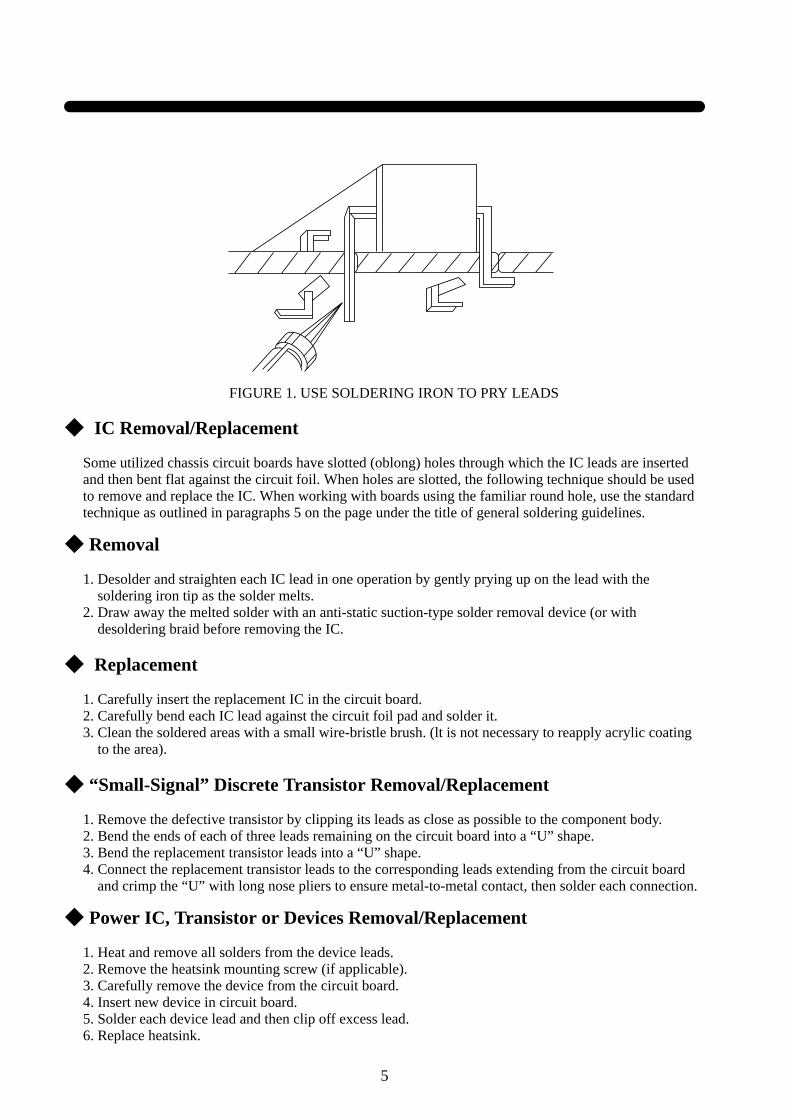
FIGURE 1. USE SOLDERING IRON TO PRY LEADS
IC Removal/Replacement
Some utilized chassis circuit boards have slotted (oblong) holes through which the IC leads are insertedand then bent flat against the circuit foil. When holes are slotted, the following technique should be usedto remove and replace the IC. When working with boards using the familiar round hole, use the standardtechnique as outlined in paragraphs 5 on the page under the title of general soldering guidelines.
Removal
1. Desolder and straighten each IC lead in one operation by gently prying up on the lead with thesoldering iron tip as the solder melts.
2. Draw away the melted solder with an anti-static suction-type solder removal device (or withdesoldering braid before removing the IC.
Replacement
1. Carefully insert the replacement IC in the circuit board.2. Carefully bend each IC lead against the circuit foil pad and solder it.3. Clean the soldered areas with a small wire-bristle brush. (lt is not necessary to reapply acrylic coating
to the area).
“Small-Signal” Discrete Transistor Removal/Replacement
1. Remove the defective transistor by clipping its leads as close as possible to the component body.2. Bend the ends of each of three leads remaining on the circuit board into a “U” shape.3. Bend the replacement transistor leads into a “U” shape.4. Connect the replacement transistor leads to the corresponding leads extending from the circuit board
and crimp the “U” with long nose pliers to ensure metal-to-metal contact, then solder each connection.
Power IC, Transistor or Devices Removal/Replacement
1. Heat and remove all solders from the device leads.2. Remove the heatsink mounting screw (if applicable).3. Carefully remove the device from the circuit board.4. Insert new device in circuit board.5. Solder each device lead and then clip off excess lead.6. Replace heatsink.
6
Diode Removal/Replacement
1. Remove defective diode by clipping its leads as close as possible to diode body.2. Bend the two remaining leads perpendicularly to the circuit board.3. Observing diode polarity, wrap each lead out of the new diode around the corresponding lead on the
circuit board.4. Securely crimp each connection and solder it.5. Inspect the solder joints of the two “original” leads on the circuit board copper side. If they are not
shiny, reheat them and apply additional solder if necessary.
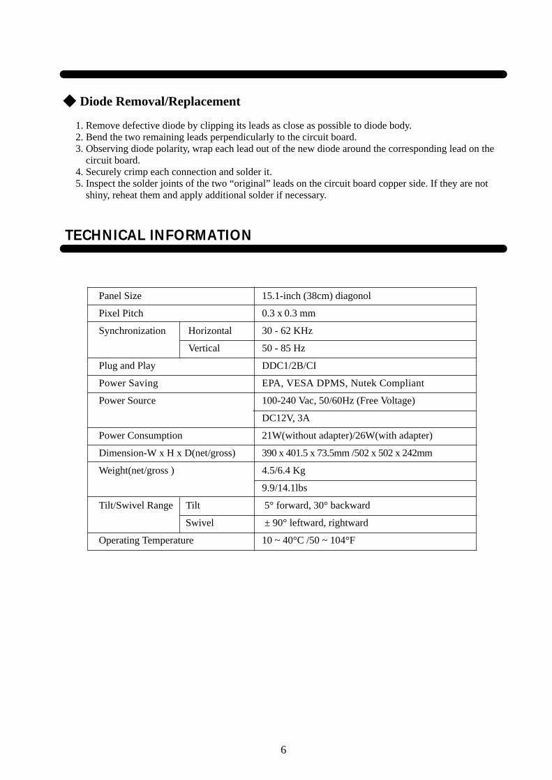
TECHNICAL INFORMATION
Panel Size 15.1-inch (38cm) diagonol
Pixel Pitch 0.3 x 0.3 mm
Synchronization Horizontal 30 - 62 KHz
Vertical 50 - 85 Hz
Plug and Play DDC1/2B/CI
Power Saving EPA, VESA DPMS, Nutek Compliant
Power Source 100-240 Vac, 50/60Hz (Free Voltage)
DC12V, 3A
Power Consumption 21W(without adapter)/26W(with adapter)
Dimension-W x H x D(net/gross) 390 x 401.5 x 73.5mm /502 x 502 x 242mm
Weight(net/gross ) 4.5/6.4 Kg
9.9/14.1lbs
Tilt/Swivel Range Tilt 5° forward, 30° backward
Swivel ± 90° leftward, rightward
Operating Temperature 10 ~ 40°C /50 ~ 104°F
GENERAL INFORMATION
7
This TFT LCD monitor automatically scans all horizontal frequencies from 30KHz to 62KHz, and allvertical frequencies from 50Hz to 85Hz. This TFT LCD monitor supports IBM PC, PC/XT, PC/AT, personalSystem/2 (PS/2), Apple Macintosh, and compatible users crisp text and vivid color graphics display whenusing the following graphics adapters : (VGA, Super VGA, VESA and XGA and Apple Macintosh VideoCard). And so, this TFT LCD monitor has a maximum horizontal resolution of 1024 dots and a maximumvertical resolution of 768 lines for superior clarity of display.
By accepting analog signal inputs which level is zero to 0.7 Volts. This TFT LCD monitor can display and262, 144 colors depending on the graphics adapter and software being used. (available used to 8 bit panel is16.7M colors)
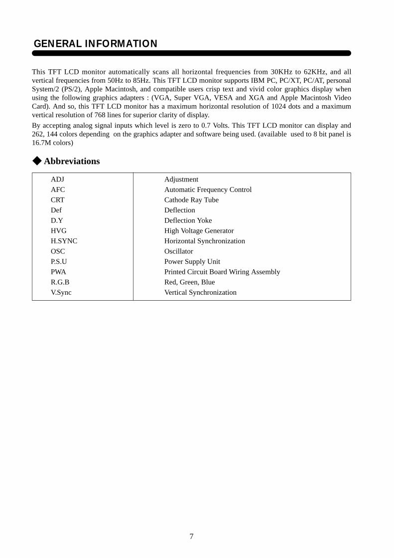
Abbreviations
ADJ Adjustment
AFC Automatic Frequency Control
CRT Cathode Ray Tube
Def Deflection
D.Y Deflection Yoke
HVG High Voltage Generator
H.SYNC Horizontal Synchronization
OSC Oscillator
P.S.U Power Supply Unit
PWA Printed Circuit Board Wiring Assembly
R.G.B Red, Green, Blue
V.Sync Vertical Synchronization
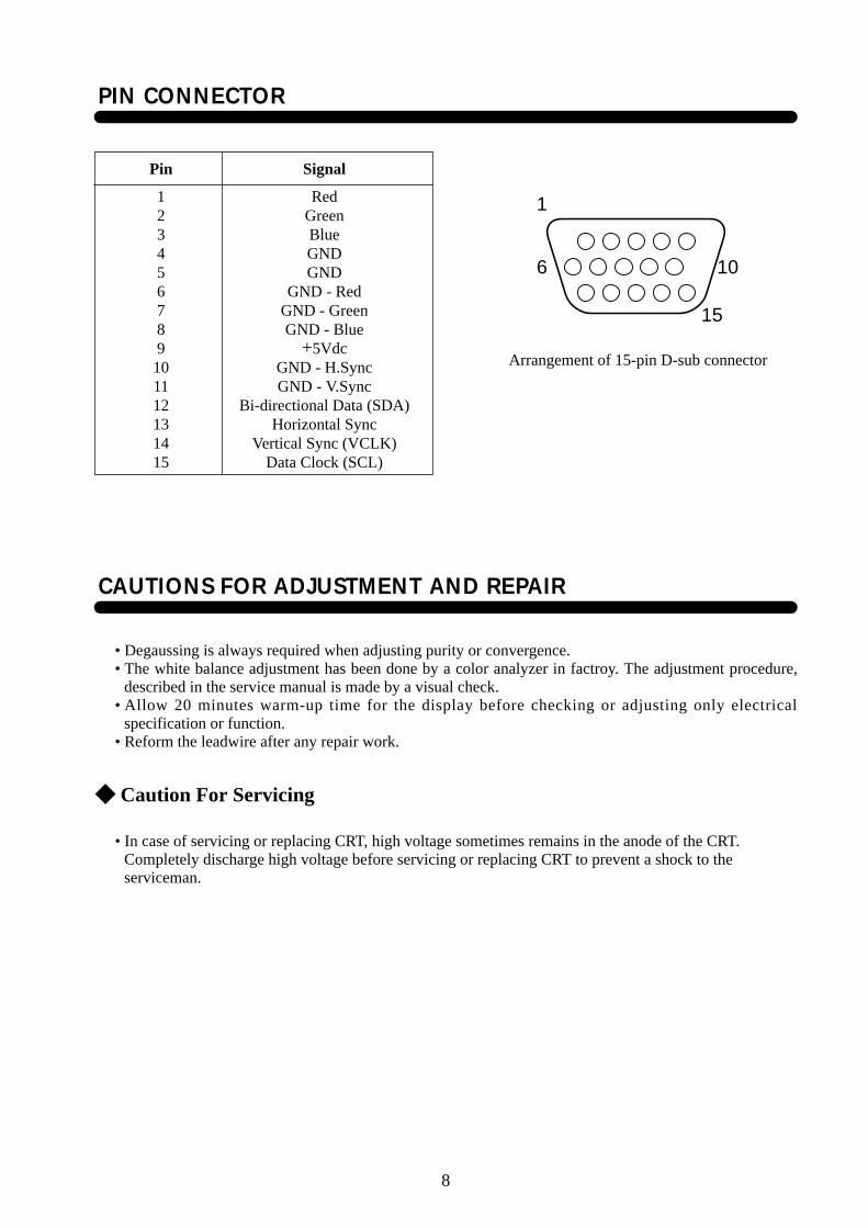
PIN CONNECTOR
CAUTIONS FOR ADJUSTMENT AND REPAIR
• Degaussing is always required when adjusting purity or convergence.• The white balance adjustment has been done by a color analyzer in factroy. The adjustment procedure,
described in the service manual is made by a visual check.• Allow 20 minutes warm-up time for the display before checking or adjusting only electrical
specification or function.• Reform the leadwire after any repair work.
Caution For Servicing
• In case of servicing or replacing CRT, high voltage sometimes remains in the anode of the CRT.Completely discharge high voltage before servicing or replacing CRT to prevent a shock to theserviceman.
Arrangement of 15-pin D-sub connector
8
Pin Signal
1 Red2 Green3 Blue4 GND5 GND6 GND - Red7 GND - Green8 GND - Blue9 +5Vdc10 GND - H.Sync11 GND - V.Sync12 Bi-directional Data (SDA)13 Horizontal Sync14 Vertical Sync (VCLK)15 Data Clock (SCL)
1
6 10
15
OPERATION & ADJUSTMENT
9
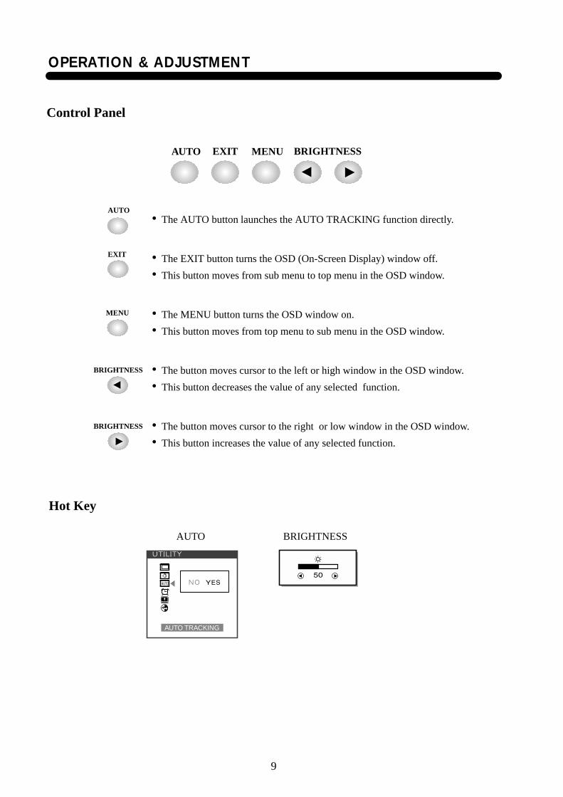
Control Panel
Hot Key
EXITAUTO MENU BRIGHTNESS
• The AUTO button launches the AUTO TRACKING function directly.
• The EXIT button turns the OSD (On-Screen Display) window off.
• This button moves from sub menu to top menu in the OSD window.
• The MENU button turns the OSD window on.
• This button moves from top menu to sub menu in the OSD window.
• The button moves cursor to the left or high window in the OSD window.
• This button decreases the value of any selected function.
• The button moves cursor to the right or low window in the OSD window.
• This button increases the value of any selected function.
AUTO
EXIT
MENU
BRIGHTNESS
BRIGHTNESS
AUTO TRACKING
AUTO BRIGHTNESS
10
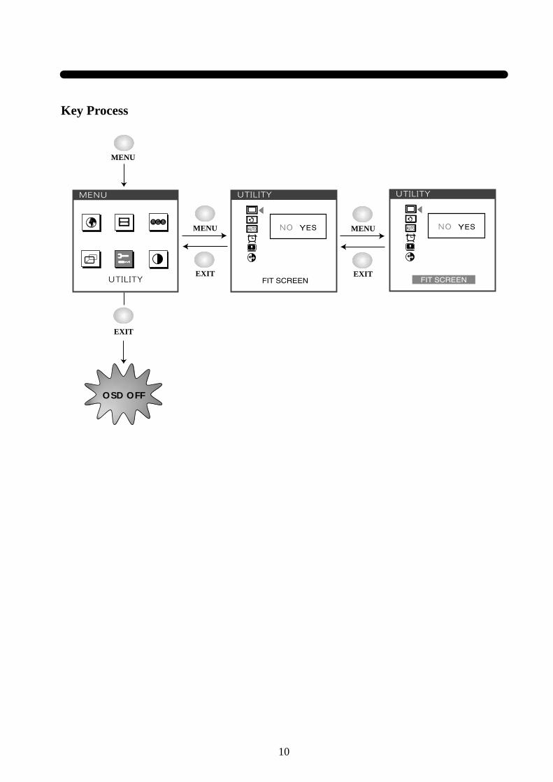
Key Process
OSD OFF
MENU
EXIT
EXIT
MENU
EXIT
MENU
11
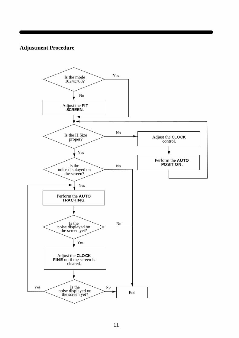
Adjustment Procedure
Is the mode1024x768?
Adjust the FITSCREEN.
Adjust the CLOCKcontrol.
Perform the AUTOPOSITION.
Is the H.Sizeproper?
Is thenoise displayed on
the screen?
Perform the AUTOTRACKING.
Is thenoise displayed on
the screen yet?
Is thenoise displayed on
the screen yet?
Adjust the CLOCKFINE until the screen is
cleared.
Yes
Yes
Yes
Yes
Yes
No
No
No
No
NoEnd
12
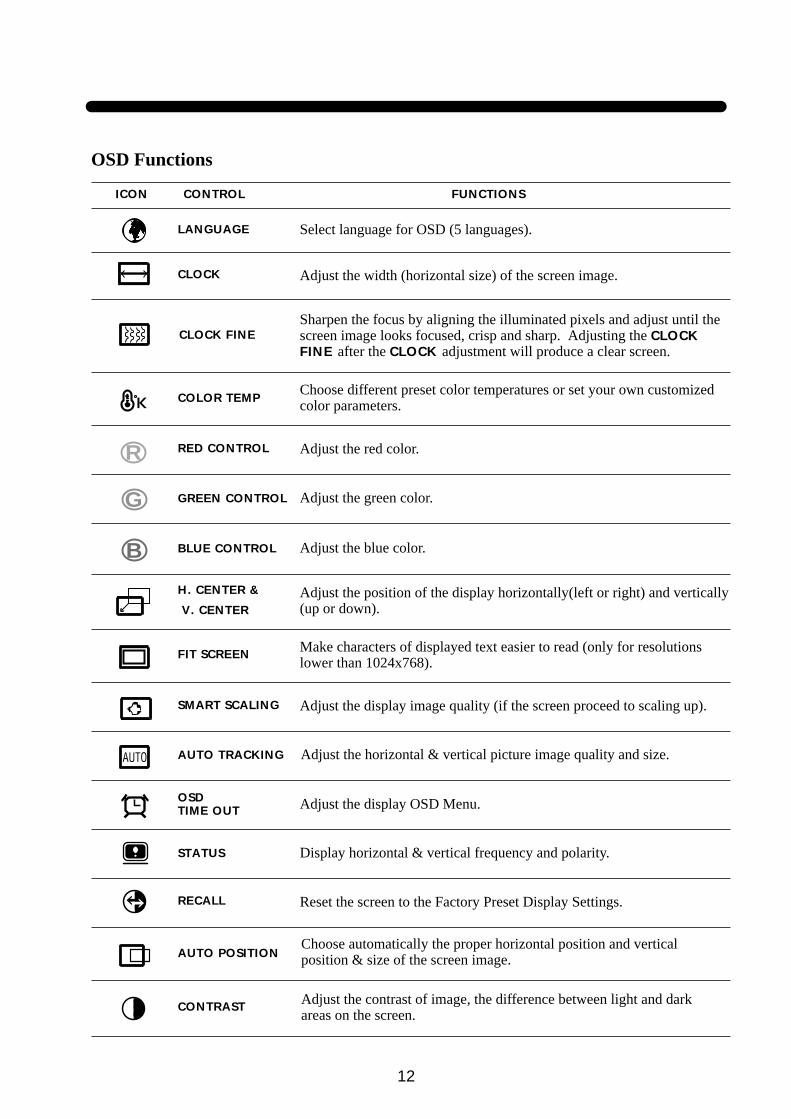
Display horizontal & vertical frequency and polarity.STATUS
Reset the screen to the Factory Preset Display Settings.RECALL
AUTO POSITIONChoose automatically the proper horizontal position and verticalposition & size of the screen image.
CONTRAST Adjust the contrast of image, the difference between light and darkareas on the screen.
Make characters of displayed text easier to read (only for resolutionslower than 1024x768).
FIT SCREEN
Adjust the display OSD Menu.OSDTIME OUT
SMART SCALING
AUTO TRACKING
Adjust the display image quality (if the screen proceed to scaling up).
Adjust the horizontal & vertical picture image quality and size.
Select language for OSD (5 languages).LANGUAGE
Adjust the position of the display horizontally(left or right) and vertically(up or down).
H. CENTER &
V. CENTER
Choose different preset color temperatures or set your own customizedcolor parameters.
Adjust the width (horizontal size) of the screen image.
Sharpen the focus by aligning the illuminated pixels and adjust until thescreen image looks focused, crisp and sharp. Adjusting the CLOCKFINE after the CLOCK adjustment will produce a clear screen.
Adjust the red color.
COLOR TEMP
CLOCK
CLOCK FINE
RED CONTROL
Adjust the green color.
Adjust the blue color.
GREEN CONTROL
BLUE CONTROL
ICON CONTROL FUNCTIONS
OSD Functions
R
G
B
13
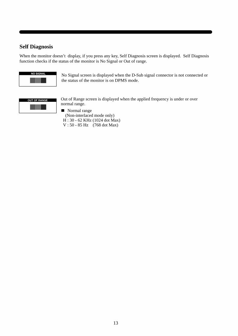
Self Diagnosis
When the monitor doesn’t display, if you press any key, Self Diagnosis screen is displayed. Self Diagnosisfunction checks if the status of the monitor is No Signal or Out of range.
No Signal screen is displayed when the D-Sub signal connector is not connected orthe status of the monitor is on DPMS mode.
Out of Range screen is displayed when the applied frequency is under or overnormal range.
Normal range(Non-interlaced mode only)
H : 30 - 62 KHz (1024 dot Max)V : 50 - 85 Hz (768 dot Max)
Standard Check point
1. Power source : 100 - 240Vac, 50/60Hz.2. Aging : Take at least 20 minutes warm-up time.3. Signal
Video input : Analog 0.7Vpp 75Ω terminal positive polaritySynchronizing : acceptable negative or positive at TTL levelResolution
Horizontal : 1024 max.Vertical : 768 max.
FrequencyHorizontal : 30KHz - 62KHzVertical : 50Hz - 85Hz (available only non interlace mode)
Adjustment
1. Smart scaling set to 69%.
2. Contrast set to 100%
3. Brightness set to 50%
4. Switching to factory alignment mode
Press power key with Auto key at the power off status.
5. Video level adjustment
Receive stair pattern of 16 step (doesn’t care any mode).
Readjust coarse R, G, B in TDA8752 menu before saturaton point.
6. Set up the tracking
See the user’s manual at page 8th.
7. Switching to user’s mode
If turn-off and turn-on then switched to user’s mode.
* All of adjusted data stores by fade out of OSD.
14
ALIGNMENT PROCEDURE
15
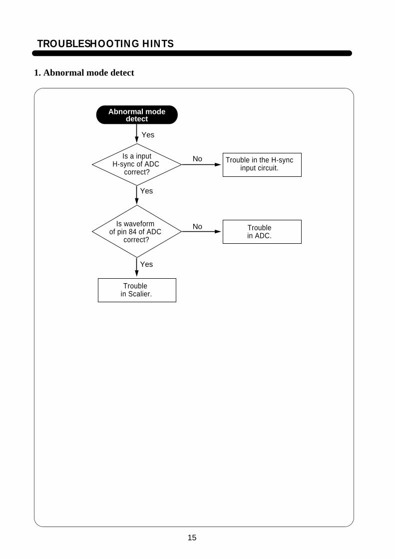
TROUBLESHOOTING HINTS
1. Abnormal mode detect
Is a inputH-sync of ADC
correct?
Abnormal modedetect
No
No
Yes
Yes
Is waveform of pin 84 of ADC
correct?
Trouble in the H-syncinput circuit.
Troublein ADC.
Trouble in Scalier.
Yes
16
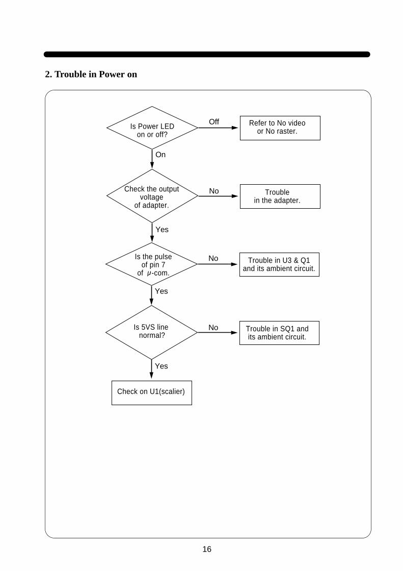
2. Trouble in Power on
No
No
Yes
Yes
Is 5VS line normal?
Trouble in U3 & Q1and its ambient circuit.
Trouble in SQ1 and its ambient circuit.
Check on U1(scalier)
Is Power LEDon or off?
Off
No
Yes
On
Check the outputvoltage
of adapter.
Refer to No videoor No raster.
Troublein the adapter.
Is the pulseof pin 7
of -com.
17
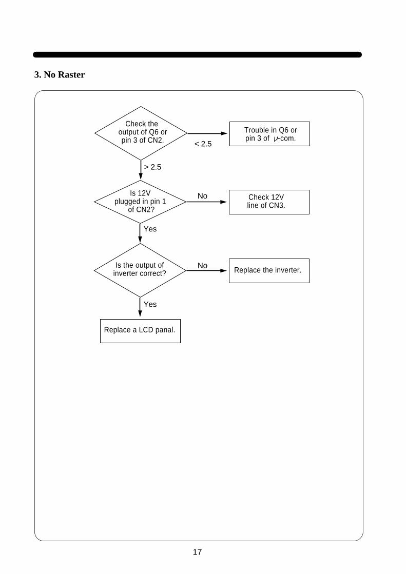
3. No Raster
Is 12Vplugged in pin 1
of CN2?
No
No
Yes
Yes
Is the output ofinverter correct?
Check 12Vline of CN3.
Replace the inverter.
Replace a LCD panal.
< 2.5
> 2.5
Check the output of Q6 orpin 3 of CN2.
Trouble in Q6 orpin 3 of -com.
18
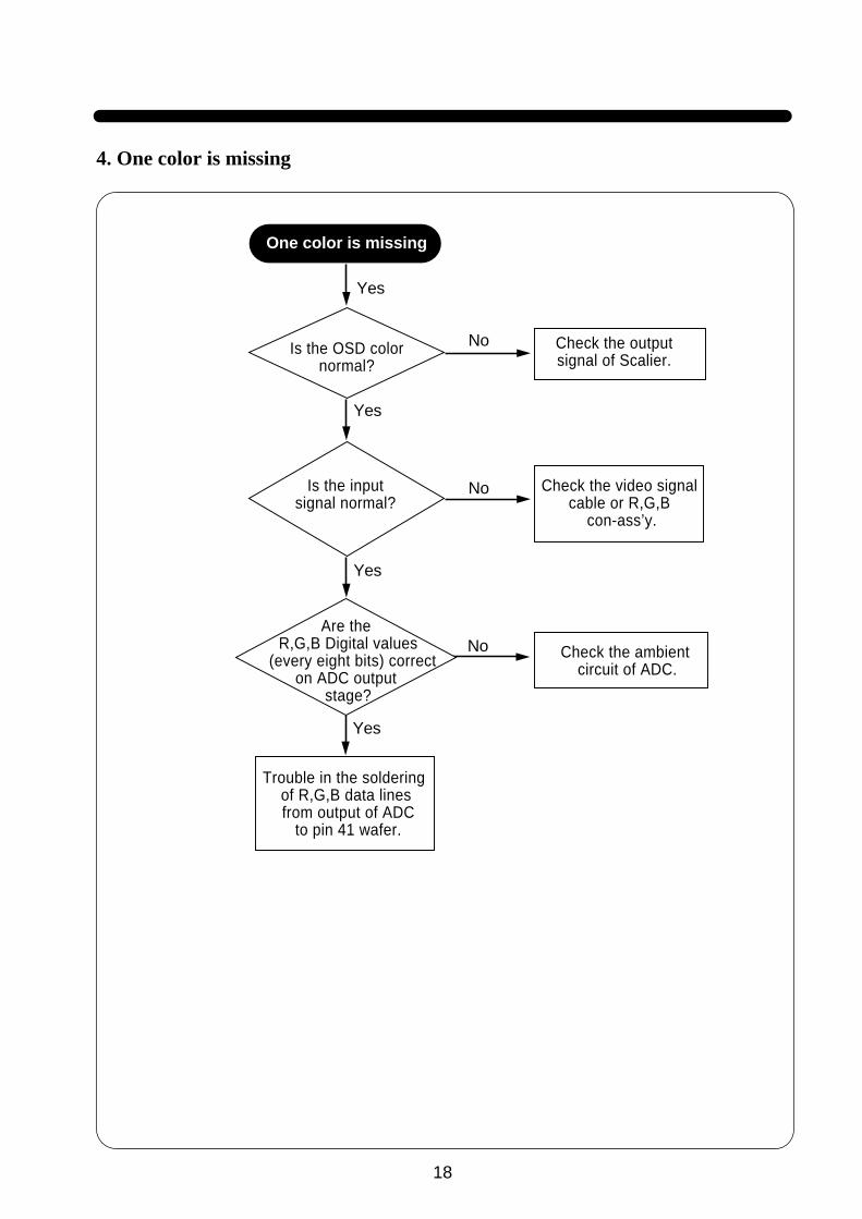
4. One color is missing
Is the OSD colornormal?
One color is missing
No
Yes
Check the outputsignal of Scalier.
No
Yes
Is the inputsignal normal?
Check the video signalcable or R,G,B
con-ass’y.
Trouble in the soldering of R,G,B data lines from output of ADC
to pin 41 wafer.
Yes
No
Yes
Are the R,G,B Digital values
(every eight bits) correcton ADC output
stage?
Check the ambient circuit of ADC.
19
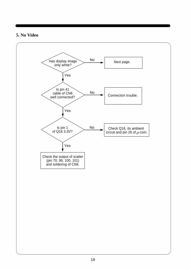
5. No Video
Has display imageonly white?
No
Yes
Next page.
No
Yes
Is pin 41cable of CN6
well connected? Connection trouble.
Check the output of scalier(pin 70, 99, 100, 101)and soldering of CN6.
No
Yes
Is pin 1of Q16 3.3V?
Check Q16, its ambient circuit and pin 26 of -com.
20
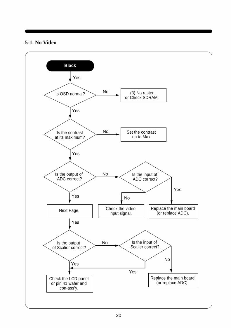
Is OSD normal?
Black
No
No
Yes
Yes
Is the contrastat its maximum?
(3) No rasteror Check SDRAM.
Set the contrast up to Max.
Next Page.
Yes
No
Yes
Is the output of ADC correct?
No
Yes
Is the input of ADC correct?
Check the videoinput signal.
Replace the main board(or replace ADC).
Yes
Check the LCD panelor pin 41 wafer and
con-ass’y.
No
Yes
Is the output of Scalier correct?
No
Yes
Is the input of Scalier correct?
Replace the main board(or replace ADC).
5-1. No Video
21
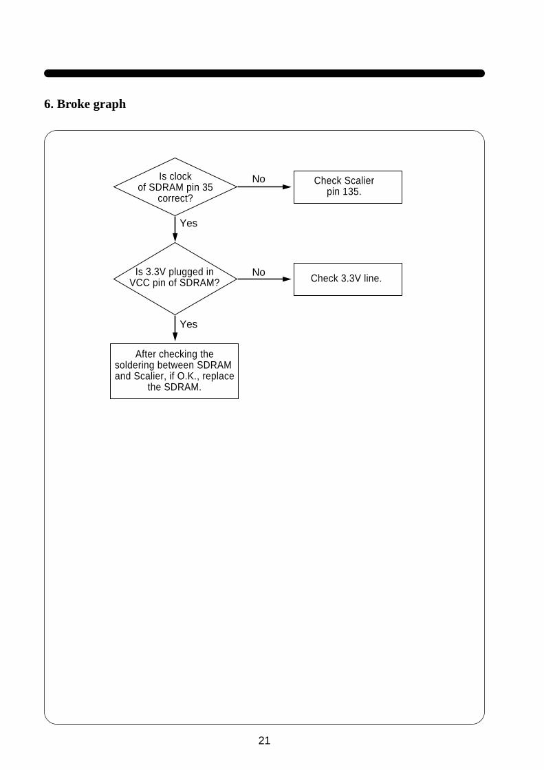
Is clockof SDRAM pin 35
correct?
No
No
Yes
Yes
Is 3.3V plugged inVCC pin of SDRAM?
Check Scalierpin 135.
Check 3.3V line.
After checking thesoldering between SDRAM and Scalier, if O.K., replace
the SDRAM.
6. Broke graph
22
BLO
CK
DIA
GR
AM
15pin DSUB -Connector
Buffer74ACT14
PRE-AMP
Controller
ADC
PLL
Scaling
MIU
OSD Mux
Dithering
CPU I/F
Odd/EvenMUX
SDRAM (16Mbit*2)
Micom
DC-DC converter&on-off control12V(3A)AdapterAC IN(100 ~ 230V)
DC-AC Inverter
Panel S,G Driver
Back light
panel
From PC
H/Vsync
RGB signal
RED (8)
Green(8)
Blue(8)
I2C
address/data line
EEPROM24C08D
ata
line/
Add
ress
line/
cont
orl l
ine
Dot clk
Red(6)Green(6)Blue(6)
Hs,Vs,DE,LCLK
630VAC/ 62khz
Hs,Vs
Hsync,Vsync
clk
Offset/Corse
-Clock timing&phase
-Current &resistance
3.3V/5V/12V
Main Borad
TDA8752
Mx88LC284FC
12V/ On-OffDDC I2C
12V
Dimming
Control Board
L500B1 BLOCK DIAGRAM
I2C
23
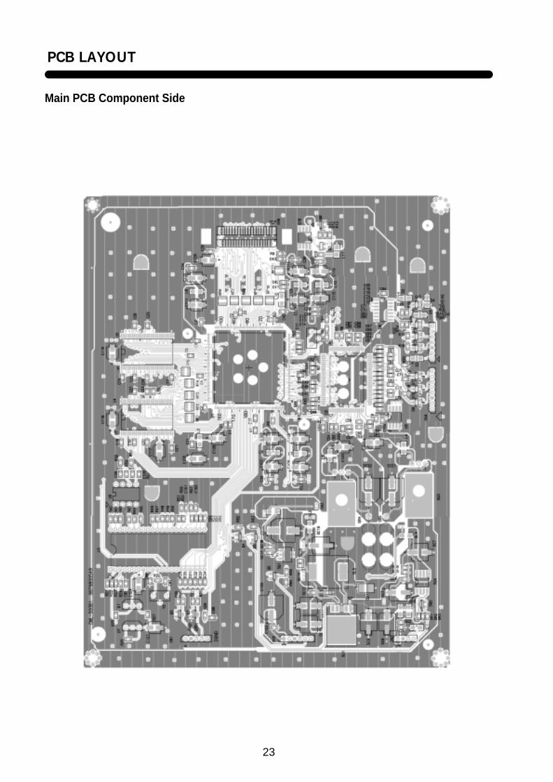
Main PCB Component Side
PCB LAYOUT
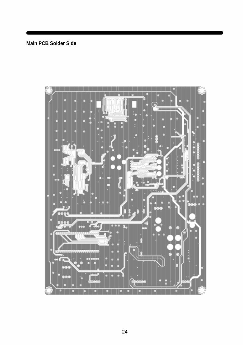
Main PCB Solder Side
24
25
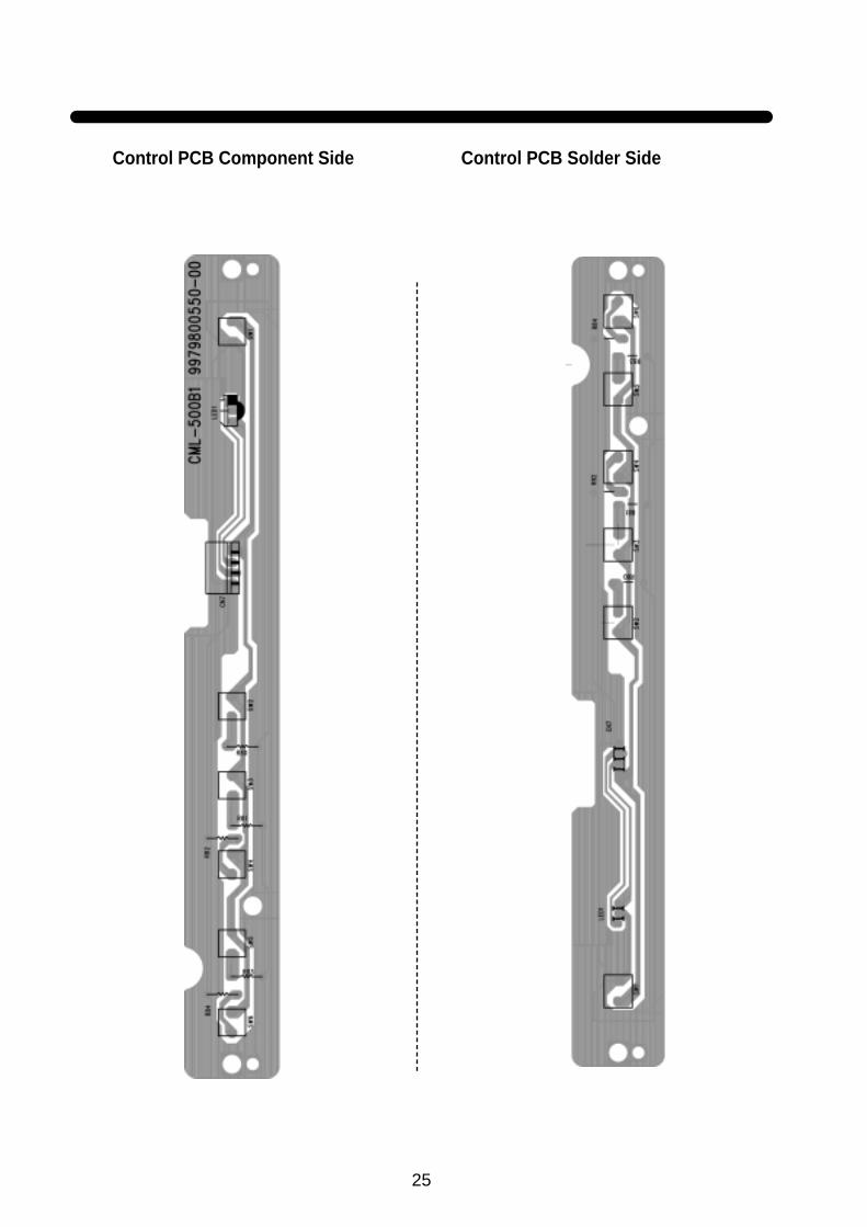
Control PCB Component Side Control PCB Solder Side
26
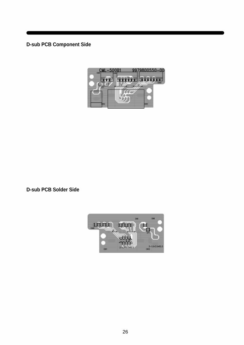
D-sub PCB Component Side
D-sub PCB Solder Side
27
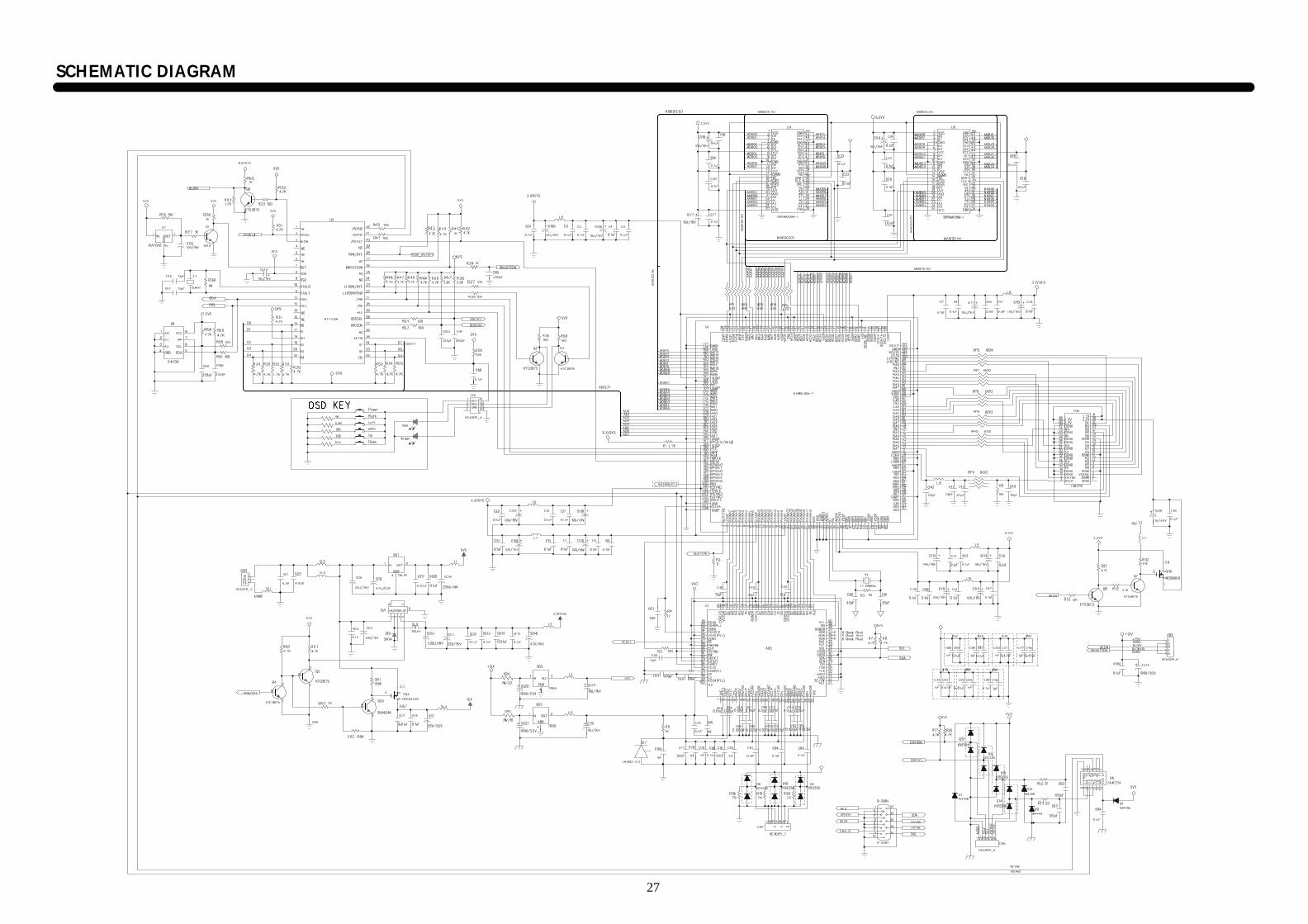
SCHEMATIC DIAGRAM
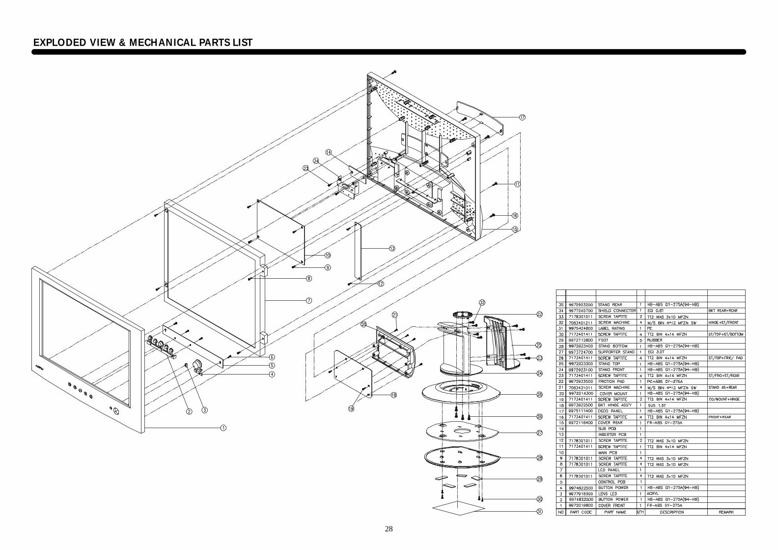
EXPLODED VIEW & MECHANICAL PARTS LIST
28
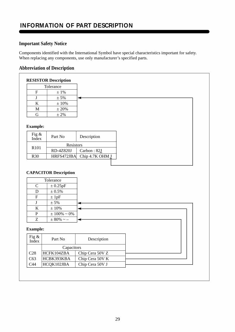
INFORMATION OF PART DESCRIPTION
29
RESISTOR Description
Example:
CAPACITOR Description
Example:
Fig & Part No DescriptionIndex
CapacitorsC28 HCFK104ZBA Chip Cera 50V ZC63 HCBK393KBA Chip Cera 50V KC44 HCQK102JBA Chip Cera 50V J
ToleranceC ± 0.25pFD ± 0.5%F ± 1pFJ ± 5%K ± 10%P ± 100% ~ 0%Z ± 80% ~ –
Fig & Part No DescriptionIndex
R101Resistors
RD-4Z820J Carbon : 82JR30 HRFS472JBA Chip 4.7K OHM J
ToleranceF ± 1%J ± 5%K ± 10%M ± 20%G ± 2%
Important Safety Notice
Components identified with the International Symbol have special characteristics important for safety.When replacing any components, use only manufacturer’s specified parts.
Abbreviation of Description
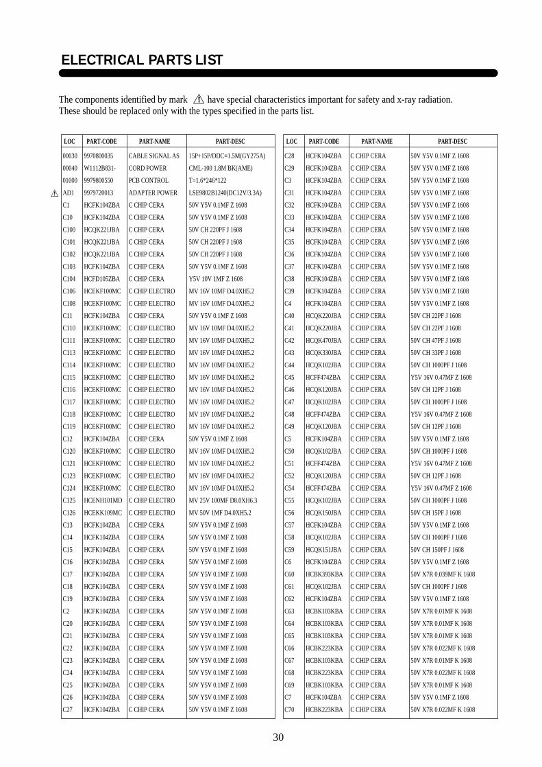
00030 9970800035 CABLE SIGNAL AS 15P+15P/DDC=1.5M(GY275A)
00040 W1112B831- CORD POWER CML-100 1.8M BK(AME)
01000 9979800550 PCB CONTROL T=1.6*246*122
AD1 9979720013 ADAPTER POWER LSE9802B1240(DC12V/3.3A)
C1 HCFK104ZBA C CHIP CERA 50V Y5V 0.1MF Z 1608
C10 HCFK104ZBA C CHIP CERA 50V Y5V 0.1MF Z 1608
C100 HCQK221JBA C CHIP CERA 50V CH 220PF J 1608
C101 HCQK221JBA C CHIP CERA 50V CH 220PF J 1608
C102 HCQK221JBA C CHIP CERA 50V CH 220PF J 1608
C103 HCFK104ZBA C CHIP CERA 50V Y5V 0.1MF Z 1608
C104 HCFD105ZBA C CHIP CERA Y5V 10V 1MF Z 1608
C106 HCEKF100MC C CHIP ELECTRO MV 16V 10MF D4.0XH5.2
C108 HCEKF100MC C CHIP ELECTRO MV 16V 10MF D4.0XH5.2
C11 HCFK104ZBA C CHIP CERA 50V Y5V 0.1MF Z 1608
C110 HCEKF100MC C CHIP ELECTRO MV 16V 10MF D4.0XH5.2
C111 HCEKF100MC C CHIP ELECTRO MV 16V 10MF D4.0XH5.2
C113 HCEKF100MC C CHIP ELECTRO MV 16V 10MF D4.0XH5.2
C114 HCEKF100MC C CHIP ELECTRO MV 16V 10MF D4.0XH5.2
C115 HCEKF100MC C CHIP ELECTRO MV 16V 10MF D4.0XH5.2
C116 HCEKF100MC C CHIP ELECTRO MV 16V 10MF D4.0XH5.2
C117 HCEKF100MC C CHIP ELECTRO MV 16V 10MF D4.0XH5.2
C118 HCEKF100MC C CHIP ELECTRO MV 16V 10MF D4.0XH5.2
C119 HCEKF100MC C CHIP ELECTRO MV 16V 10MF D4.0XH5.2
C12 HCFK104ZBA C CHIP CERA 50V Y5V 0.1MF Z 1608
C120 HCEKF100MC C CHIP ELECTRO MV 16V 10MF D4.0XH5.2
C121 HCEKF100MC C CHIP ELECTRO MV 16V 10MF D4.0XH5.2
C123 HCEKF100MC C CHIP ELECTRO MV 16V 10MF D4.0XH5.2
C124 HCEKF100MC C CHIP ELECTRO MV 16V 10MF D4.0XH5.2
C125 HCENH101MD C CHIP ELECTRO MV 25V 100MF D8.0XH6.3
C126 HCEKK109MC C CHIP ELECTRO MV 50V 1MF D4.0XH5.2
C13 HCFK104ZBA C CHIP CERA 50V Y5V 0.1MF Z 1608
C14 HCFK104ZBA C CHIP CERA 50V Y5V 0.1MF Z 1608
C15 HCFK104ZBA C CHIP CERA 50V Y5V 0.1MF Z 1608
C16 HCFK104ZBA C CHIP CERA 50V Y5V 0.1MF Z 1608
C17 HCFK104ZBA C CHIP CERA 50V Y5V 0.1MF Z 1608
C18 HCFK104ZBA C CHIP CERA 50V Y5V 0.1MF Z 1608
C19 HCFK104ZBA C CHIP CERA 50V Y5V 0.1MF Z 1608
C2 HCFK104ZBA C CHIP CERA 50V Y5V 0.1MF Z 1608
C20 HCFK104ZBA C CHIP CERA 50V Y5V 0.1MF Z 1608
C21 HCFK104ZBA C CHIP CERA 50V Y5V 0.1MF Z 1608
C22 HCFK104ZBA C CHIP CERA 50V Y5V 0.1MF Z 1608
C23 HCFK104ZBA C CHIP CERA 50V Y5V 0.1MF Z 1608
C24 HCFK104ZBA C CHIP CERA 50V Y5V 0.1MF Z 1608
C25 HCFK104ZBA C CHIP CERA 50V Y5V 0.1MF Z 1608
C26 HCFK104ZBA C CHIP CERA 50V Y5V 0.1MF Z 1608
C27 HCFK104ZBA C CHIP CERA 50V Y5V 0.1MF Z 1608
ELECTRICAL PARTS LIST
30
The components identified by mark have special characteristics important for safety and x-ray radiation.These should be replaced only with the types specified in the parts list.
LOC PART-CODE PART-NAME PART-DESC
!
C28 HCFK104ZBA C CHIP CERA 50V Y5V 0.1MF Z 1608
C29 HCFK104ZBA C CHIP CERA 50V Y5V 0.1MF Z 1608
C3 HCFK104ZBA C CHIP CERA 50V Y5V 0.1MF Z 1608
C31 HCFK104ZBA C CHIP CERA 50V Y5V 0.1MF Z 1608
C32 HCFK104ZBA C CHIP CERA 50V Y5V 0.1MF Z 1608
C33 HCFK104ZBA C CHIP CERA 50V Y5V 0.1MF Z 1608
C34 HCFK104ZBA C CHIP CERA 50V Y5V 0.1MF Z 1608
C35 HCFK104ZBA C CHIP CERA 50V Y5V 0.1MF Z 1608
C36 HCFK104ZBA C CHIP CERA 50V Y5V 0.1MF Z 1608
C37 HCFK104ZBA C CHIP CERA 50V Y5V 0.1MF Z 1608
C38 HCFK104ZBA C CHIP CERA 50V Y5V 0.1MF Z 1608
C39 HCFK104ZBA C CHIP CERA 50V Y5V 0.1MF Z 1608
C4 HCFK104ZBA C CHIP CERA 50V Y5V 0.1MF Z 1608
C40 HCQK220JBA C CHIP CERA 50V CH 22PF J 1608
C41 HCQK220JBA C CHIP CERA 50V CH 22PF J 1608
C42 HCQK470JBA C CHIP CERA 50V CH 47PF J 1608
C43 HCQK330JBA C CHIP CERA 50V CH 33PF J 1608
C44 HCQK102JBA C CHIP CERA 50V CH 1000PF J 1608
C45 HCFF474ZBA C CHIP CERA Y5V 16V 0.47MF Z 1608
C46 HCQK120JBA C CHIP CERA 50V CH 12PF J 1608
C47 HCQK102JBA C CHIP CERA 50V CH 1000PF J 1608
C48 HCFF474ZBA C CHIP CERA Y5V 16V 0.47MF Z 1608
C49 HCQK120JBA C CHIP CERA 50V CH 12PF J 1608
C5 HCFK104ZBA C CHIP CERA 50V Y5V 0.1MF Z 1608
C50 HCQK102JBA C CHIP CERA 50V CH 1000PF J 1608
C51 HCFF474ZBA C CHIP CERA Y5V 16V 0.47MF Z 1608
C52 HCQK120JBA C CHIP CERA 50V CH 12PF J 1608
C54 HCFF474ZBA C CHIP CERA Y5V 16V 0.47MF Z 1608
C55 HCQK102JBA C CHIP CERA 50V CH 1000PF J 1608
C56 HCQK150JBA C CHIP CERA 50V CH 15PF J 1608
C57 HCFK104ZBA C CHIP CERA 50V Y5V 0.1MF Z 1608
C58 HCQK102JBA C CHIP CERA 50V CH 1000PF J 1608
C59 HCQK151JBA C CHIP CERA 50V CH 150PF J 1608
C6 HCFK104ZBA C CHIP CERA 50V Y5V 0.1MF Z 1608
C60 HCBK393KBA C CHIP CERA 50V X7R 0.039MF K 1608
C61 HCQK102JBA C CHIP CERA 50V CH 1000PF J 1608
C62 HCFK104ZBA C CHIP CERA 50V Y5V 0.1MF Z 1608
C63 HCBK103KBA C CHIP CERA 50V X7R 0.01MF K 1608
C64 HCBK103KBA C CHIP CERA 50V X7R 0.01MF K 1608
C65 HCBK103KBA C CHIP CERA 50V X7R 0.01MF K 1608
C66 HCBK223KBA C CHIP CERA 50V X7R 0.022MF K 1608
C67 HCBK103KBA C CHIP CERA 50V X7R 0.01MF K 1608
C68 HCBK223KBA C CHIP CERA 50V X7R 0.022MF K 1608
C69 HCBK103KBA C CHIP CERA 50V X7R 0.01MF K 1608
C7 HCFK104ZBA C CHIP CERA 50V Y5V 0.1MF Z 1608
C70 HCBK223KBA C CHIP CERA 50V X7R 0.022MF K 1608
LOC PART-CODE PART-NAME PART-DESC
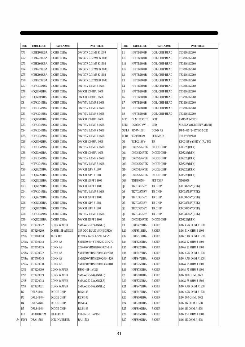
31
C71 HCBK103KBA C CHIP CERA 50V X7R 0.01MF K 1608
C72 HCBK223KBA C CHIP CERA 50V X7R 0.022MF K 1608
C73 HCBK103KBA C CHIP CERA 50V X7R 0.01MF K 1608
C74 HCBK223KBA C CHIP CERA 50V X7R 0.022MF K 1608
C75 HCBK103KBA C CHIP CERA 50V X7R 0.01MF K 1608
C76 HCBK223KBA C CHIP CERA 50V X7R 0.022MF K 1608
C77 HCFK104ZBA C CHIP CERA 50V Y5V 0.1MF Z 1608
C78 HCQK102JBA C CHIP CERA 50V CH 1000PF J 1608
C79 HCQK102JBA C CHIP CERA 50V CH 1000PF J 1608
C8 HCFK104ZBA C CHIP CERA 50V Y5V 0.1MF Z 1608
C80 HCFK104ZBA C CHIP CERA 50V Y5V 0.1MF Z 1608
C81 HCFK104ZBA C CHIP CERA 50V Y5V 0.1MF Z 1608
C82 HCQK102JBA C CHIP CERA 50V CH 1000PF J 1608
C83 HCFK104ZBA C CHIP CERA 50V Y5V 0.1MF Z 1608
C84 HCFK104ZBA C CHIP CERA 50V Y5V 0.1MF Z 1608
C85 HCFK104ZBA C CHIP CERA 50V Y5V 0.1MF Z 1608
C86 HCQK102JBA C CHIP CERA 50V CH 1000PF J 1608
C87 HCFK104ZBA C CHIP CERA 50V Y5V 0.1MF Z 1608
C88 HCQK102JBA C CHIP CERA 50V CH 1000PF J 1608
C89 HCFK104ZBA C CHIP CERA 50V Y5V 0.1MF Z 1608
C9 HCFK104ZBA C CHIP CERA 50V Y5V 0.1MF Z 1608
C90 HCQK220JBA C CHIP CERA 50V CH 22PF J 1608
C91 HCQK220JBA C CHIP CERA 50V CH 22PF J 1608
C92 HCQK121JBA C CHIP CERA 50V CH 120PF J 1608
C93 HCQK121JBA C CHIP CERA 50V CH 120PF J 1608
C94 HCFK104ZBA C CHIP CERA 50V Y5V 0.1MF Z 1608
C95 HCQK221JBA C CHIP CERA 50V CH 220PF J 1608
C96 HCQK120JBA C CHIP CERA 50V CH 12PF J 1608
C97 HCQK120JBA C CHIP CERA 50V CH 12PF J 1608
C98 HCFK104ZBA C CHIP CERA 50V Y5V 0.1MF Z 1608
C99 HCQK221JBA C CHIP CERA 50V CH 220PF J 1608
CN10 9979220022 CONN WAFER SMAW250-07 (ANGLE)
CN11 9979200209 D-SUB 15P ANGLE 15P DDC BLUE W/IN SCREW
CN12 9979100010 JACK DC POWER JACK 6.5PIE 14.5*9
CN1A 9970740044 CONN AS SMH250-04+YBNH200-05=270
CN2A 9970750035 CONN AS 5264-05+YBNH200+1007=110
CN3A 9970730072 CONN AS SMH250+YBNH200+1354=250
CN4A 9970760045 CONN AS SMH250+YBNH200+2464=120
CN5A 9970770030 CONN AS SMH250+YBNH200+1354=180
CN6 9979220080 CONN WAFER DF9B-41P-1V(22)
CN7 9979220019 CONN WAFER SMAW250-04 (ANGLE)
CN8 9979220018 CONN WAFER SMAW250-03 (ANGLE)
CN9 9979220021 CONN WAFER SMAW250-06 (ANGLE)
D2 DRLS4148-- DIODE CHIP RLS4148
D3 DRLS4148-- DIODE CHIP RLS4148
D4 DRLS4148-- DIODE CHIP RLS4148
D5 DRLS4148-- DIODE CHIP RLS4148
EF1 5PF1BH471M FILTER LC CFI-06-B-1H-471M
INV1 DBA11502-- LCD INVERTER BAI-1502
LOC PART-CODE PART-NAME PART-DESC
L1 HFFTB2601B COIL CHIP BEAD TB321611Z260
L10 HFFTB2601B COIL CHIP BEAD TB321611Z260
L11 HFFTB2601B COIL CHIP BEAD TB321611Z260
L12 HFFTB2601B COIL CHIP BEAD TB321611Z260
L2 HFFTB2601B COIL CHIP BEAD TB321611Z260
L3 HFFTB2601B COIL CHIP BEAD TB321611Z260
L4 HFFTB2601B COIL CHIP BEAD TB321611Z260
L5 HFFTB2601B COIL CHIP BEAD TB321611Z260
L6 HFFTB2601B COIL CHIP BEAD TB321611Z260
L7 HFFTB2601B COIL CHIP BEAD TB321611Z260
L8 HFFTB2601B COIL CHIP BEAD TB321611Z260
L9 HFFTB2601B COIL CHIP BEAD TB321611Z260
LCD DLM151X2C2 LCD LM151X2-C2TH
LED1 DSD50GYW-- LED SD50GYW(GREEN/AMBER)
OUTA 9970741001 CONN AS DF-9-41S*2+1571#32=220
PCB1 9979800549 PCB MAIN T=1.6*180*140
Q1 TZTC3198Y- TR KTC3198Y-(1815Y) (AUTO)
Q10 DKDS226RTK DIODE CHIP KDS226(RTK)
Q11 DKDS226RTK DIODE CHIP KDS226(RTK)
Q12 DKDS226RTK DIODE CHIP KDS226(RTK)
Q13 DKDS226RTK DIODE CHIP KDS226(RTK)
Q14 DKDS226RTK DIODE CHIP KDS226(RTK)
Q15 DKDS226RTK DIODE CHIP KDS226(RTK)
Q16 TNDS9958-- FET CHIP NDS9958
Q2 TKTC3875SY TR CHIP KTC3875SY(RTK)
Q3 TKTC3875SY TR CHIP KTC3875SY(RTK)
Q4 TKTC3875SY TR CHIP KTC3875SY(RTK)
Q5 TKTC3875SY TR CHIP KTC3875SY(RTK)
Q6 TKTC3875SY TR CHIP KTC3875SY(RTK)
Q7 TKTC3875SY TR CHIP KTC3875SY(RTK)
Q9 DKDS226RTK DIODE CHIP KDS226(RTK)
R1 HRFS472JBA R CHIP 1/16 4.7K OHM J 1608
R10 HRFS513JBA R CHIP 1/16 51K OHM J 1608
R12 HRFS512JBA R CHIP 1/16 5.1K OHM J 1608
R14 HRFS220JBA R CHIP 1/16W 22 OHM J 1608
R15 HRFS220JBA R CHIP 1/16W 22 OHM J 1608
R16 HRFS472JBA R CHIP 1/16 4.7K OHM J 1608
R17 HRFS472JBA R CHIP 1/16 4.7K OHM J 1608
R18 HRFS750JBA R CHIP 1/16W 75 OHM J 1608
R19 HRFS750JBA R CHIP 1/16W 75 OHM J 1608
R2 HRFS101JBA R CHIP 1/16 100 OHM J 1608
R20 HRFS750JBA R CHIP 1/16W 75 OHM J 1608
R21 HRFS472JBA R CHIP 1/16 4.7K OHM J 1608
R22 HRFS472JBA R CHIP 1/16 4.7K OHM J 1608
R23 HRFS101JBA R CHIP 1/16 100 OHM J 1608
R24 HRFS102JBA R CHIP 1/16 1K OHM J 1608
R25 HRFS102JBA R CHIP 1/16 1K OHM J 1608
R26 HRFS153JBA R CHIP 1/16 15K OHM J 1608
R27 HRFS102JBA R CHIP 1/16 1K OHM J 1608
LOC PART-CODE PART-NAME PART-DESC
!
32
R28 HRFS105JBA R CHIP 1/16 1M OHM J 1608
R29 HRFS472JBA R CHIP 1/16 4.7K OHM J 1608
R3 HRFS000JBA R CHIP 1/16 0 OHM J 1608
R30 HRFS472JBA R CHIP 1/16 4.7K OHM J 1608
R31 HRFS472JBA R CHIP 1/16 4.7K OHM J 1608
R32 HRFS472JBA R CHIP 1/16 4.7K OHM J 1608
R33 HRFS472JBA R CHIP 1/16 4.7K OHM J 1608
R34 HRFS472JBA R CHIP 1/16 4.7K OHM J 1608
R35 HRFS101JBA R CHIP 1/16 100 OHM J 1608
R36 HRFS221JBA R CHIP 1/16 220 OHM J 1608
R37 HRFS101JBA R CHIP 1/16 100 OHM J 1608
R38 HRFS221JBA R CHIP 1/16 220 OHM J 1608
R39 HRFS223JBA R CHIP 1/16 22K OHM J 1608
R40 HRFS101JBA R CHIP 1/16 100 OHM J 1608
R41 HRFS101JBA R CHIP 1/16 100 OHM J 1608
R42 HRFS472JBA R CHIP 1/16 4.7K OHM J 1608
R43 HRFS472JBA R CHIP 1/16 4.7K OHM J 1608
R44 HRFS472JBA R CHIP 1/16 4.7K OHM J 1608
R45 HRFS102JBA R CHIP 1/16 1K OHM J 1608
R46 HRFS472JBA R CHIP 1/16 4.7K OHM J 1608
R47 HRFS472JBA R CHIP 1/16 4.7K OHM J 1608
R48 HRFS472JBA R CHIP 1/16 4.7K OHM J 1608
R49 HRFS472JBA R CHIP 1/16 4.7K OHM J 1608
R5 HRFS105JBA R CHIP 1/16 1M OHM J 1608
R50 HRFS472JBA R CHIP 1/16 4.7K OHM J 1608
R51 HRFS101JBA R CHIP 1/16 100 OHM J 1608
R52 HRFS101JBA R CHIP 1/16 100 OHM J 1608
R53 HRFS472JBA R CHIP 1/16 4.7K OHM J 1608
R54 HRFS472JBA R CHIP 1/16 4.7K OHM J 1608
R55 HRFS472JBA R CHIP 1/16 4.7K OHM J 1608
R56 HRFS222JBA R CHIP 1/16 2.2K OHM J 1608
R57 HRFS222JBA R CHIP 1/16 2.2K OHM J 1608
R58 HRFS472JBA R CHIP 1/16 4.7K OHM J 1608
R59 HRFS101JBA R CHIP 1/16 100 OHM J 1608
R6 HRFS102JBA R CHIP 1/16 1K OHM J 1608
R60 HRFS472JBA R CHIP 1/16 4.7K OHM J 1608
R61 HRFS101JBA R CHIP 1/16 100 OHM J 1608
R62 HRFS472JBA R CHIP 1/16 4.7K OHM J 1608
R63 HRFS472JBA R CHIP 1/16 4.7K OHM J 1608
R64 HRFS473JBA R CHIP 1/16 47K OHM J 1608
R65 HRFS102JBA R CHIP 1/16 1K OHM J 1608
R66 HRFS472JBA R CHIP 1/16 4.7K OHM J 1608
R7 HRFS472JBA R CHIP 1/16 4.7K OHM J 1608
R8 HRFS472JBA R CHIP 1/16 4.7K OHM J 1608
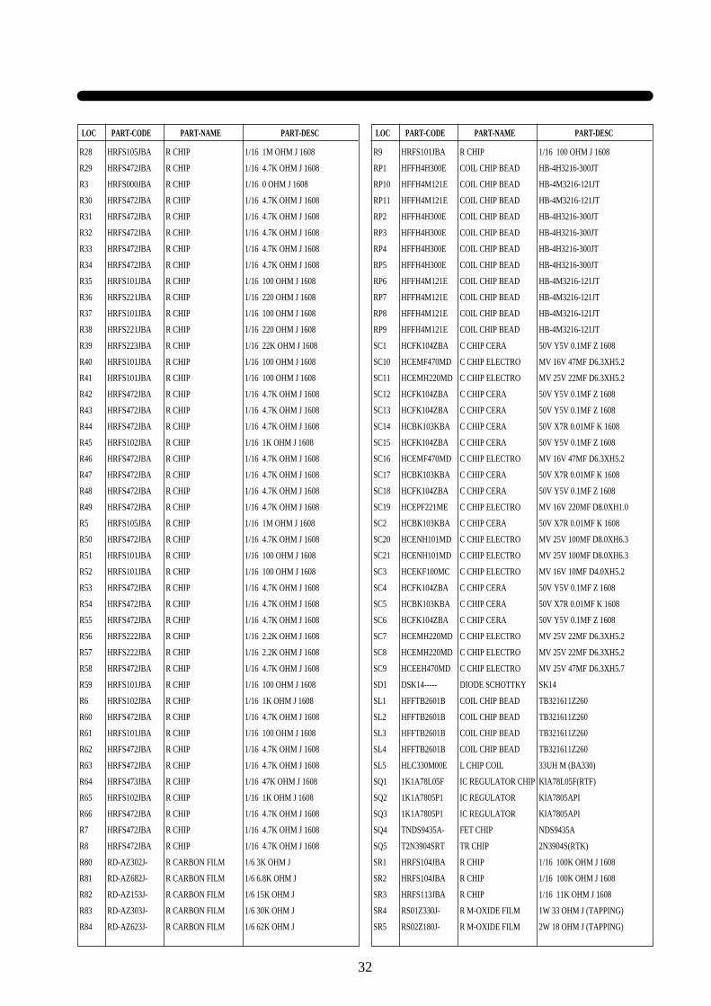
R80 RD-AZ302J- R CARBON FILM 1/6 3K OHM J
R81 RD-AZ682J- R CARBON FILM 1/6 6.8K OHM J
R82 RD-AZ153J- R CARBON FILM 1/6 15K OHM J
R83 RD-AZ303J- R CARBON FILM 1/6 30K OHM J
R84 RD-AZ623J- R CARBON FILM 1/6 62K OHM J
LOC PART-CODE PART-NAME PART-DESC
R9 HRFS101JBA R CHIP 1/16 100 OHM J 1608
RP1 HFFH4H300E COIL CHIP BEAD HB-4H3216-300JT
RP10 HFFH4M121E COIL CHIP BEAD HB-4M3216-121JT
RP11 HFFH4M121E COIL CHIP BEAD HB-4M3216-121JT
RP2 HFFH4H300E COIL CHIP BEAD HB-4H3216-300JT
RP3 HFFH4H300E COIL CHIP BEAD HB-4H3216-300JT
RP4 HFFH4H300E COIL CHIP BEAD HB-4H3216-300JT
RP5 HFFH4H300E COIL CHIP BEAD HB-4H3216-300JT
RP6 HFFH4M121E COIL CHIP BEAD HB-4M3216-121JT
RP7 HFFH4M121E COIL CHIP BEAD HB-4M3216-121JT
RP8 HFFH4M121E COIL CHIP BEAD HB-4M3216-121JT
RP9 HFFH4M121E COIL CHIP BEAD HB-4M3216-121JT
SC1 HCFK104ZBA C CHIP CERA 50V Y5V 0.1MF Z 1608
SC10 HCEMF470MD C CHIP ELECTRO MV 16V 47MF D6.3XH5.2
SC11 HCEMH220MD C CHIP ELECTRO MV 25V 22MF D6.3XH5.2
SC12 HCFK104ZBA C CHIP CERA 50V Y5V 0.1MF Z 1608
SC13 HCFK104ZBA C CHIP CERA 50V Y5V 0.1MF Z 1608
SC14 HCBK103KBA C CHIP CERA 50V X7R 0.01MF K 1608
SC15 HCFK104ZBA C CHIP CERA 50V Y5V 0.1MF Z 1608
SC16 HCEMF470MD C CHIP ELECTRO MV 16V 47MF D6.3XH5.2
SC17 HCBK103KBA C CHIP CERA 50V X7R 0.01MF K 1608
SC18 HCFK104ZBA C CHIP CERA 50V Y5V 0.1MF Z 1608
SC19 HCEPF221ME C CHIP ELECTRO MV 16V 220MF D8.0XH1.0
SC2 HCBK103KBA C CHIP CERA 50V X7R 0.01MF K 1608
SC20 HCENH101MD C CHIP ELECTRO MV 25V 100MF D8.0XH6.3
SC21 HCENH101MD C CHIP ELECTRO MV 25V 100MF D8.0XH6.3
SC3 HCEKF100MC C CHIP ELECTRO MV 16V 10MF D4.0XH5.2
SC4 HCFK104ZBA C CHIP CERA 50V Y5V 0.1MF Z 1608
SC5 HCBK103KBA C CHIP CERA 50V X7R 0.01MF K 1608
SC6 HCFK104ZBA C CHIP CERA 50V Y5V 0.1MF Z 1608
SC7 HCEMH220MD C CHIP ELECTRO MV 25V 22MF D6.3XH5.2
SC8 HCEMH220MD C CHIP ELECTRO MV 25V 22MF D6.3XH5.2
SC9 HCEEH470MD C CHIP ELECTRO MV 25V 47MF D6.3XH5.7
SD1 DSK14----- DIODE SCHOTTKY SK14
SL1 HFFTB2601B COIL CHIP BEAD TB321611Z260
SL2 HFFTB2601B COIL CHIP BEAD TB321611Z260
SL3 HFFTB2601B COIL CHIP BEAD TB321611Z260
SL4 HFFTB2601B COIL CHIP BEAD TB321611Z260
SL5 HLC330M00E L CHIP COIL 33UH M (BA330)
SQ1 1K1A78L05F IC REGULATOR CHIP KIA78L05F(RTF)
SQ2 1K1A7805P1 IC REGULATOR KIA7805API
SQ3 1K1A7805P1 IC REGULATOR KIA7805API
SQ4 TNDS9435A- FET CHIP NDS9435A
SQ5 T2N3904SRT TR CHIP 2N3904S(RTK)
SR1 HRFS104JBA R CHIP 1/16 100K OHM J 1608
SR2 HRFS104JBA R CHIP 1/16 100K OHM J 1608
SR3 HRFS113JBA R CHIP 1/16 11K OHM J 1608
SR4 RS01Z330J- R M-OXIDE FILM 1W 33 OHM J (TAPPING)
SR5 RS02Z180J- R M-OXIDE FILM 2W 18 OHM J (TAPPING)
LOC PART-CODE PART-NAME PART-DESC
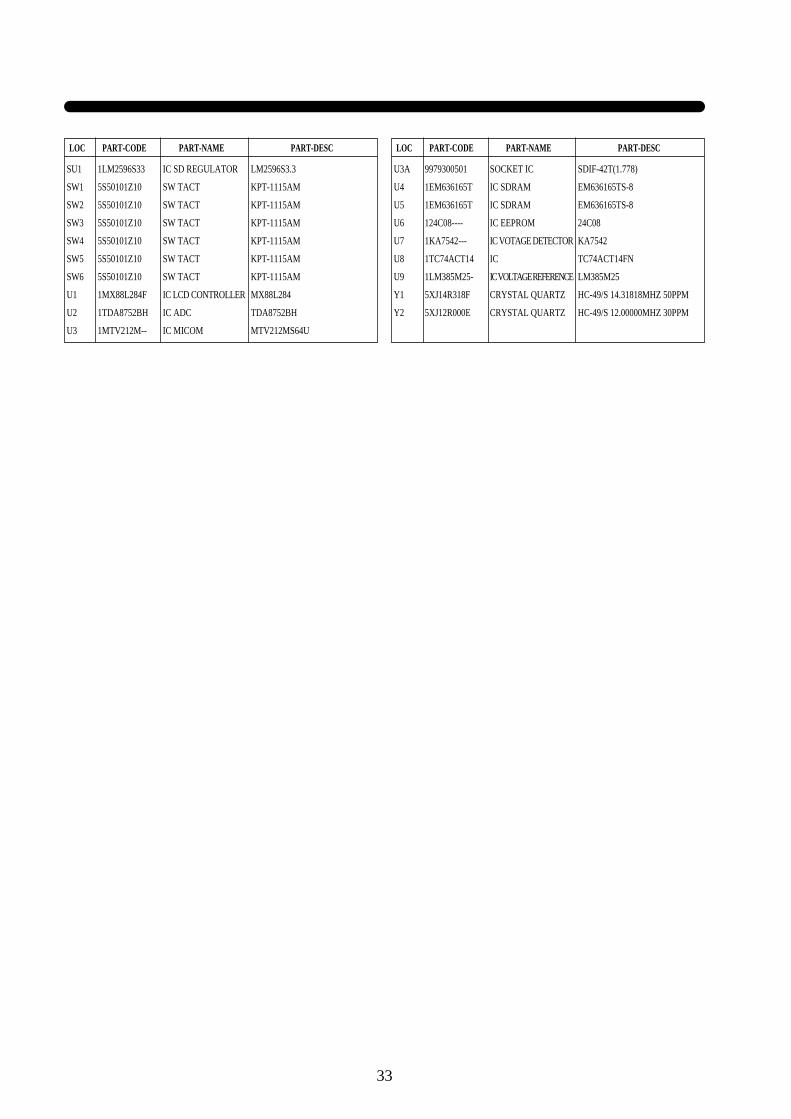
33
SU1 1LM2596S33 IC SD REGULATOR LM2596S3.3
SW1 5S50101Z10 SW TACT KPT-1115AM
SW2 5S50101Z10 SW TACT KPT-1115AM
SW3 5S50101Z10 SW TACT KPT-1115AM
SW4 5S50101Z10 SW TACT KPT-1115AM
SW5 5S50101Z10 SW TACT KPT-1115AM
SW6 5S50101Z10 SW TACT KPT-1115AM
U1 1MX88L284F IC LCD CONTROLLER MX88L284
U2 1TDA8752BH IC ADC TDA8752BH
U3 1MTV212M-- IC MICOM MTV212MS64U
LOC PART-CODE PART-NAME PART-DESC
U3A 9979300501 SOCKET IC SDIF-42T(1.778)
U4 1EM636165T IC SDRAM EM636165TS-8
U5 1EM636165T IC SDRAM EM636165TS-8
U6 124C08---- IC EEPROM 24C08
U7 1KA7542--- IC VOTAGE DETECTOR KA7542
U8 1TC74ACT14 IC TC74ACT14FN
U9 1LM385M25- IC VOLTAGE REFERENCE LM385M25
Y1 5XJ14R318F CRYSTAL QUARTZ HC-49/S 14.31818MHZ 50PPM
Y2 5XJ12R000E CRYSTAL QUARTZ HC-49/S 12.00000MHZ 30PPM
LOC PART-CODE PART-NAME PART-DESC

DAEWOO ELECTRONICS CO., LTD686, AHYEON-DONG MAPO-GUSEOUL, KOREAC.P.O. BOX 8003 SEOUL, KOREATELEX : DWELEC K28177-8CABLE : "DAEWOOELEC"E-mail : [email protected] : 82-32-510-7620FAX : 82-32-510-7630