Embed Size (px)
Citation preview

Xilinx 7 Technology
Xilinx Serie 7Zynq Technology
BTE5380 - Embedded SystemsOctober 2015
Prof. A. HabeggerBern University of Applied Sciences
Serie 7
Prof. A. Habegger
Introduction
Logic Resources
I/O Resources
MemoryResources
DSP Resources
ADC Resources
Conclusion
Rev. 1.0 – 2
Introduction
all Xilinx FPGAs contain the same basic resources:I logic resources:
I slices: grouped into configurable logic blocks (CLB),containing combinatorial logic and register resources
I memoryI multipliers
I interconnect resources
I programmable interconnectI IOBs, interface between the FPGA and the outside world
I other resources
I global clock buffersI boundary scan logic
The slides are based on Xilinx Tutorials
Serie 7
Prof. A. Habegger
Introduction
Logic Resources
I/O Resources
MemoryResources
DSP Resources
ADC Resources
Conclusion
Rev. 1.0 – 3
Configurable Logic Block (CLB) in 7-Series FPGA
I primary resource fordesign
I combinatorialfunctions
I flip-flops
I CLB contains two slices
I SLICEM: LUT canbe used for logicand memory
I SLICEL: LUT canonly be used forlogic
I connected to switchmatrix for routing to otherFPGA resources
I carry chain runsvertically in acolumn from oneslice to the oneabove
Notes
Notes
Notes
Serie 7
Prof. A. Habegger
Introduction
Logic Resources
I/O Resources
MemoryResources
DSP Resources
ADC Resources
Conclusion
Rev. 1.0 – 4
Slice Resource
I 4 six-input look-uptables (LUT)
I multiplexers
I carry chains
I SRL
I 4 flip-flops
I 4 latches
Serie 7
Prof. A. Habegger
Introduction
Logic Resources
I/O Resources
MemoryResources
DSP Resources
ADC Resources
Conclusion
Rev. 1.0 – 5
6-Input LUT with Dual Output
I LUTs can be two 5-inputLUTs with common input
I minimal speedimpact to a 6-inputLUT
I one or two outputs
I any function of sixvariables or twofunctions of five variables
Serie 7
Prof. A. Habegger
Introduction
Logic Resources
I/O Resources
MemoryResources
DSP Resources
ADC Resources
Conclusion
Rev. 1.0 – 6
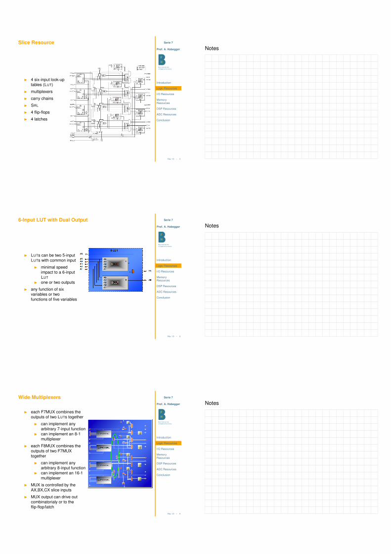
Wide Multiplexers
I each F7MUX combines theoutputs of two LUTs together
I can implement anyarbitrary 7-input function
I can implement an 8-1multiplexer
I each F8MUX combines theoutputs of two F7MUXtogether
I can implement anyarbitrary 8-input function
I can implement an 16-1multiplexer
I MUX is controlled by theAX,BX,CX slice inputs
I MUX output can drive outcombinatorialy or to theflip-flop/latch
Notes
Notes
Notes
Serie 7
Prof. A. Habegger
Introduction
Logic Resources
I/O Resources
MemoryResources
DSP Resources
ADC Resources
Conclusion
Rev. 1.0 – 7
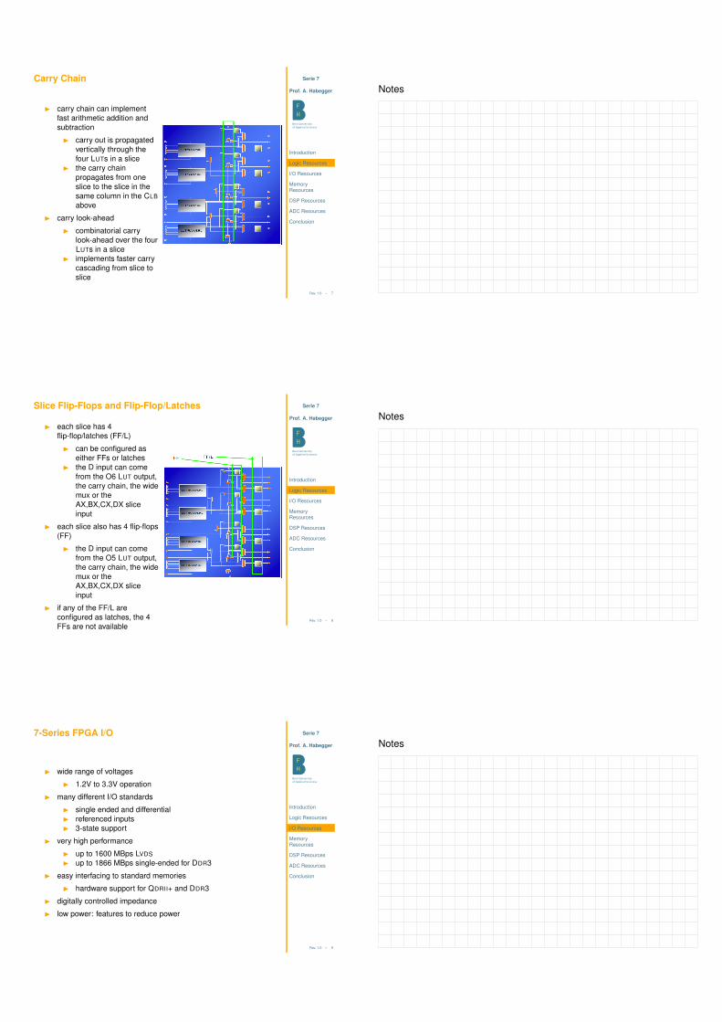
Carry Chain
I carry chain can implementfast arithmetic addition andsubtraction
I carry out is propagatedvertically through thefour LUTs in a slice
I the carry chainpropagates from oneslice to the slice in thesame column in the CLBabove
I carry look-ahead
I combinatorial carrylook-ahead over the fourLUTs in a slice
I implements faster carrycascading from slice toslice
Serie 7
Prof. A. Habegger
Introduction
Logic Resources
I/O Resources
MemoryResources
DSP Resources
ADC Resources
Conclusion
Rev. 1.0 – 8
Slice Flip-Flops and Flip-Flop/Latches
I each slice has 4flip-flop/latches (FF/L)
I can be configured aseither FFs or latches
I the D input can comefrom the O6 LUT output,the carry chain, the widemux or theAX,BX,CX,DX sliceinput
I each slice also has 4 flip-flops(FF)
I the D input can comefrom the O5 LUT output,the carry chain, the widemux or theAX,BX,CX,DX sliceinput
I if any of the FF/L areconfigured as latches, the 4FFs are not available
Serie 7
Prof. A. Habegger
Introduction
Logic Resources
I/O Resources
MemoryResources
DSP Resources
ADC Resources
Conclusion
Rev. 1.0 – 9
7-Series FPGA I/O
I wide range of voltages
I 1.2V to 3.3V operation
I many different I/O standards
I single ended and differentialI referenced inputsI 3-state support
I very high performance
I up to 1600 MBps LVDSI up to 1866 MBps single-ended for DDR3
I easy interfacing to standard memories
I hardware support for QDRII+ and DDR3
I digitally controlled impedance
I low power: features to reduce power
Notes
Notes
Notes
Serie 7
Prof. A. Habegger
Introduction
Logic Resources
I/O Resources
MemoryResources
DSP Resources
ADC Resources
Conclusion
Rev. 1.0 – 10
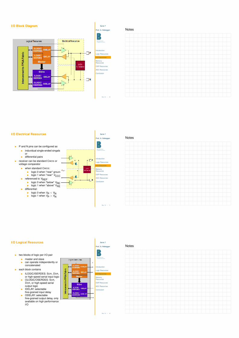
I/O Block Diagram
Serie 7
Prof. A. Habegger
Introduction
Logic Resources
I/O Resources
MemoryResources
DSP Resources
ADC Resources
Conclusion
Rev. 1.0 – 11
I/O Electrical Resources
I P and N pins can be configured as
I induvidual single-ended singalsor
I differential pairs
I receiver can be standard CMOS orvoltage comparator
I when standard CMOS:I logic 0 when "near" groundI logic 1 when "near" VCCO
I referenced to VREF:I logic 0 when "below" VREFI logic 1 when "above" VREF
I differential:I logic 0 when VP < VNI logic 1 when VP > VN
Serie 7
Prof. A. Habegger
Introduction
Logic Resources
I/O Resources
MemoryResources
DSP Resources
ADC Resources
Conclusion
Rev. 1.0 – 12
I/O Logical Resources
I two blocks of logic per I/O pair
I master and slaveI can operate independently or
concatenated
I each block contains
I ILOGIC/ISERDES: SDR, DDR,or high-speed serial input logic
I OLOGIC/OSERDES: SDR,DDR, or high-speed serialoutput logic
I IDELAY: selectablefine-grained input delay
I ODELAY: selectablefine-grained output delay, onlyavailable on high performanceI/O
Notes
Notes
Notes
Serie 7
Prof. A. Habegger
Introduction
Logic Resources
I/O Resources
MemoryResources
DSP Resources
ADC Resources
Conclusion
Rev. 1.0 – 13
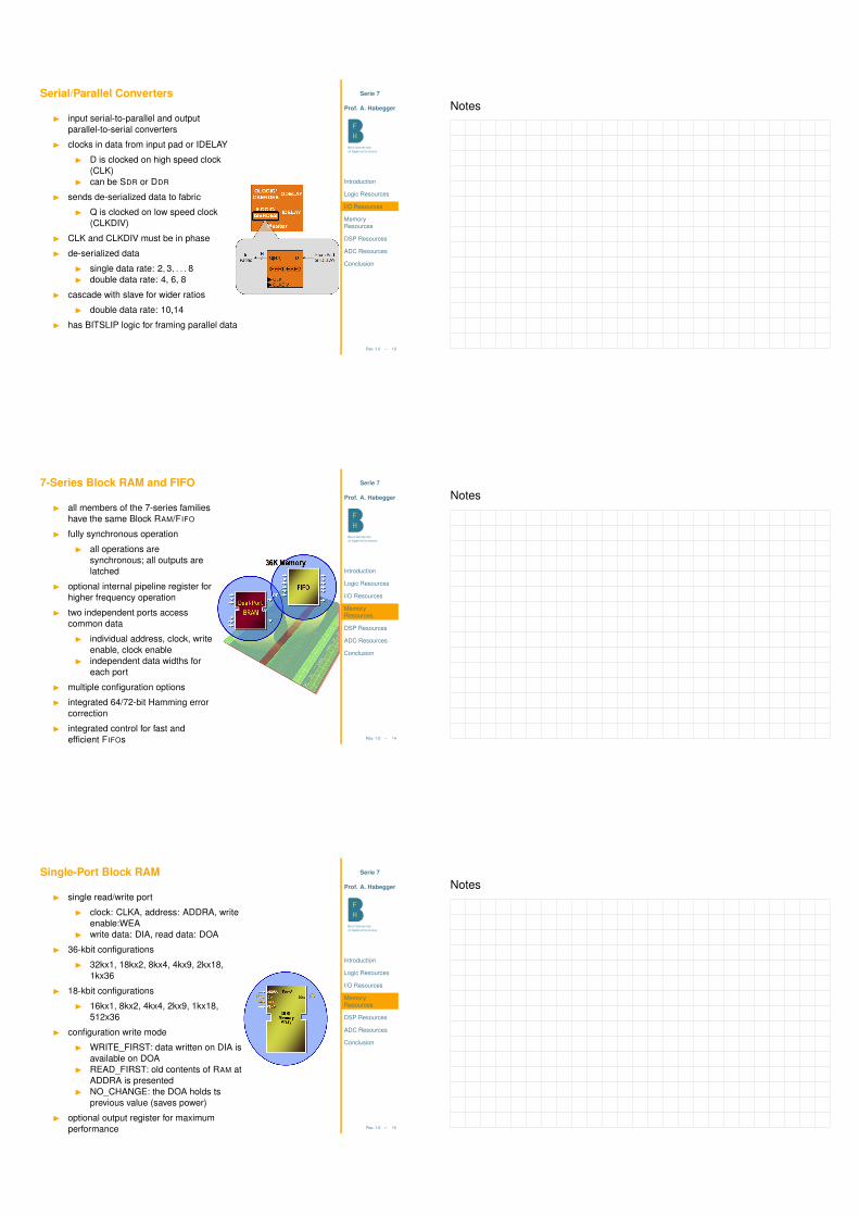
Serial/Parallel Converters
I input serial-to-parallel and outputparallel-to-serial converters
I clocks in data from input pad or IDELAY
I D is clocked on high speed clock(CLK)
I can be SDR or DDR
I sends de-serialized data to fabric
I Q is clocked on low speed clock(CLKDIV)
I CLK and CLKDIV must be in phase
I de-serialized data
I single data rate: 2, 3, . . . 8I double data rate: 4, 6, 8
I cascade with slave for wider ratios
I double data rate: 10,14
I has BITSLIP logic for framing parallel data
Serie 7
Prof. A. Habegger
Introduction
Logic Resources
I/O Resources
MemoryResources
DSP Resources
ADC Resources
Conclusion
Rev. 1.0 – 14
7-Series Block RAM and FIFO
I all members of the 7-series familieshave the same Block RAM/FIFO
I fully synchronous operation
I all operations aresynchronous; all outputs arelatched
I optional internal pipeline register forhigher frequency operation
I two independent ports accesscommon data
I individual address, clock, writeenable, clock enable
I independent data widths foreach port
I multiple configuration options
I integrated 64/72-bit Hamming errorcorrection
I integrated control for fast andefficient FIFOs
Serie 7
Prof. A. Habegger
Introduction
Logic Resources
I/O Resources
MemoryResources
DSP Resources
ADC Resources
Conclusion
Rev. 1.0 – 15
Single-Port Block RAM
I single read/write port
I clock: CLKA, address: ADDRA, writeenable:WEA
I write data: DIA, read data: DOA
I 36-kbit configurations
I 32kx1, 18kx2, 8kx4, 4kx9, 2kx18,1kx36
I 18-kbit configurations
I 16kx1, 8kx2, 4kx4, 2kx9, 1kx18,512x36
I configuration write mode
I WRITE_FIRST: data written on DIA isavailable on DOA
I READ_FIRST: old contents of RAM atADDRA is presented
I NO_CHANGE: the DOA holds tsprevious value (saves power)
I optional output register for maximumperformance
Notes
Notes
Notes
Serie 7
Prof. A. Habegger
Introduction
Logic Resources
I/O Resources
MemoryResources
DSP Resources
ADC Resources
Conclusion
Rev. 1.0 – 16
Dual-Port Block RAM
I two seperate read/write ports
I ports have seperate clock,address, data in, data out, writeenable, . . .
I clocks can be asynchronous toeach other
I the two ports can have differentwidths and modes
I no contention avoidance when bothports access the same address,except
I if clocked by the same clock,and write port is READ_FIRST
I simple dual-port block RAM
I each port has seperate clockand address
I block RAM cascading
I 128Kb, 256Kb, 512Kb, 1 Mb, . . .
Serie 7
Prof. A. Habegger
Introduction
Logic Resources
I/O Resources
MemoryResources
DSP Resources
ADC Resources
Conclusion
Rev. 1.0 – 17
FIFOI full featured
I synchronous or asynchronous read and write clocksI flags: fully, empty, programmable almost-full/empty
I FIFO configurationsI and 36Kb block RAM: 8K4x, 4Kx9, . . . 512x72I and 18Kb block RAM: 4Kx4, 2Kx9, . . . 512x72I write and read width must be equal
I can use the integrated error correction when used in the x72width
Serie 7
Prof. A. Habegger
Introduction
Logic Resources
I/O Resources
MemoryResources
DSP Resources
ADC Resources
Conclusion
Rev. 1.0 – 18
7-Series DSP48 Slice
Notes
Notes
Notes
Serie 7
Prof. A. Habegger
Introduction
Logic Resources
I/O Resources
MemoryResources
DSP Resources
ADC Resources
Conclusion
Rev. 1.0 – 19
Using DSP48 for Non-DSO Function
Serie 7
Prof. A. Habegger
Introduction
Logic Resources
I/O Resources
MemoryResources
DSP Resources
ADC Resources
Conclusion
Rev. 1.0 – 20
7-Series DSP48 Slice
I XADC is a high quality and flexible analog interface
I dual 12-bit ADCs, on-chip sensors, 17 flexible analoginputs, and track & holds with programmable signalconditioning
I 1V input rangeI 16-bit resolutionI built in digital gain and offset calibration
I analog mixed signal (AMS)
I using the FPGA programmable logic to customize theXADC and replace other external analog functions; forexample, linearization, calibration, filtering, and DCbalancing to improve data conversion resolution
Serie 7
Prof. A. Habegger
Introduction
Logic Resources
I/O Resources
MemoryResources
DSP Resources
ADC Resources
Conclusion
Rev. 1.0 – 21
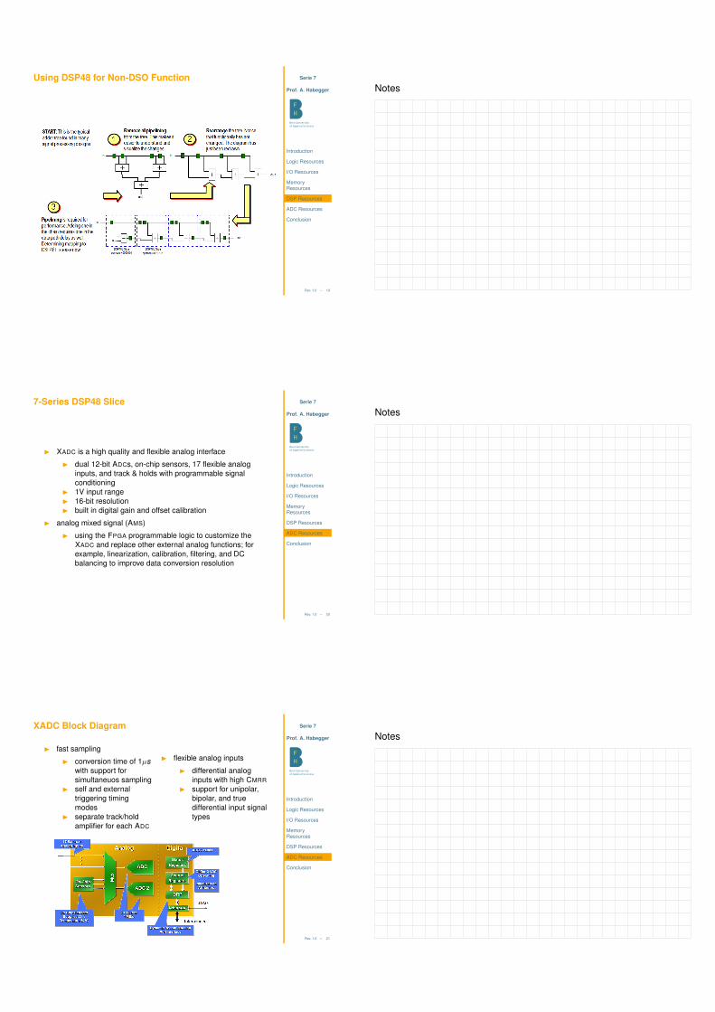
XADC Block Diagram
I fast sampling
I conversion time of 1µswith support forsimultaneuos sampling
I self and externaltriggering timingmodes
I separate track/holdamplifier for each ADC
I flexible analog inputs
I differential analoginputs with high CMRR
I support for unipolar,bipolar, and truedifferential input signaltypes
Notes
Notes
Notes
Serie 7
Prof. A. Habegger
Introduction
Logic Resources
I/O Resources
MemoryResources
DSP Resources
ADC Resources
Conclusion
Rev. 1.0 – 22
Clock Networks
I FPGA has clock management tile (CMT)
I one mixed-mode clock manager (MMCMs) and one CMT ineach clock
I performs frequency synthesis, clock de-skewing, andjitter-filtering
I FPGA has four clock-capable inputs in each bank
I these inputs are regular I/O pins with dedicatedconnections to internal clock resources
I clock inputs can be used single-ended or differental
I FPGA is a regular array of resources
I many of these resources require clocksI clock must be distributed to these resources
I for synchronous operation, clocks must arrive at the clockedelements with
I extremely low clock skew: ensures minimal hold-timeI low clock jitter: allows highest performanceI duty cycle preservation: important for double data rate
Serie 7
Prof. A. Habegger
Introduction
Logic Resources
I/O Resources
MemoryResources
DSP Resources
ADC Resources
Conclusion
Rev. 1.0 – 23
Conclusion
I the FPGA slices contain LUTs, multiplexers, carry logic forcombinatorial logic as well as registers
I the FPGA IOBs contain DDR registers as well as serial/parallelresources
I multiple I/O standards are supported
I the FPGA contains dedicated block RAM and DSP resources
I the FPGA contains dedicated MMCMs, PLLs, and clock routingresources
I the Zynq-7000 processing platform is a system-on-chip (SOC)processor with embedded programmable logic fabric of eitherArtix or Kintex 7-series FPGA
Notes
Notes
Notes