Embed Size (px)
Citation preview
DS099 June 27, 2013 www.xilinx.comProduct Specification 1
© Copyright 2003–2013 Xilinx, Inc. XILINX, the Xilinx logo, Virtex, Spartan, ISE, Artix, Kintex, Zynq, Vivado, and other designated brands included herein are trademarks of Xilinx in the United States and other countries. PCI and PCI-X are trademarks of PCI-SIG and used under license. All other trademarks are the property of their respective owners.
Module 1: Introduction and Ordering InformationDS099 (v3.1) June 27, 2013
• Introduction
• Features
• Architectural Overview
• Array Sizes and Resources
• User I/O Chart
• Ordering Information
Module 2: Functional DescriptionDS099 (v3.1) June 27, 2013
• Input/Output Blocks (IOBs)
• IOB Overview
• SelectIO™ Interface I/O Standards
• Configurable Logic Blocks (CLBs)
• Block RAM
• Dedicated Multipliers
• Digital Clock Manager (DCM)
• Clock Network
• Configuration
Module 3: DC and Switching CharacteristicsDS099 (v3.1) June 27, 2013
• DC Electrical Characteristics
• Absolute Maximum Ratings
• Supply Voltage Specifications
• Recommended Operating Conditions
• DC Characteristics
• Switching Characteristics
• I/O Timing
• Internal Logic Timing
• DCM Timing
• Configuration and JTAG Timing
Module 4: Pinout DescriptionsDS099 (v3.1) June 27, 2013
• Pin Descriptions
• Pin Behavior During Configuration
• Package Overview
• Pinout Tables
• Footprints
1Spartan-3 FPGA Family
Data Sheet
DS099 June 27, 2013 Product Specification
DS099 (v3.1) June 27, 2013 www.xilinx.comProduct Specification 2
© Copyright 2003–2013 Xilinx, Inc. XILINX, the Xilinx logo, Virtex, Spartan, ISE, Artix, Kintex, Zynq, Vivado, and other designated brands included herein are trademarks of Xilinx in the United States and other countries. PCI and PCI-X are trademarks of PCI-SIG and used under license. All other trademarks are the property of their respective owners.
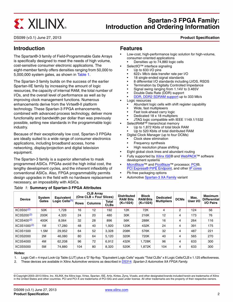
IntroductionThe Spartan®-3 family of Field-Programmable Gate Arrays is specifically designed to meet the needs of high volume, cost-sensitive consumer electronic applications. The eight-member family offers densities ranging from 50,000 to 5,000,000 system gates, as shown in Table 1.
The Spartan-3 family builds on the success of the earlier Spartan-IIE family by increasing the amount of logic resources, the capacity of internal RAM, the total number of I/Os, and the overall level of performance as well as by improving clock management functions. Numerous enhancements derive from the Virtex®-II platform technology. These Spartan-3 FPGA enhancements, combined with advanced process technology, deliver more functionality and bandwidth per dollar than was previously possible, setting new standards in the programmable logic industry.
Because of their exceptionally low cost, Spartan-3 FPGAs are ideally suited to a wide range of consumer electronics applications, including broadband access, home networking, display/projection and digital television equipment.
The Spartan-3 family is a superior alternative to mask programmed ASICs. FPGAs avoid the high initial cost, the lengthy development cycles, and the inherent inflexibility of conventional ASICs. Also, FPGA programmability permits design upgrades in the field with no hardware replacement necessary, an impossibility with ASICs.
Features• Low-cost, high-performance logic solution for high-volume,
consumer-oriented applications• Densities up to 74,880 logic cells
• SelectIO™ interface signaling• Up to 633 I/O pins• 622+ Mb/s data transfer rate per I/O• 18 single-ended signal standards • 8 differential I/O standards including LVDS, RSDS• Termination by Digitally Controlled Impedance• Signal swing ranging from 1.14V to 3.465V• Double Data Rate (DDR) support• DDR, DDR2 SDRAM support up to 333 Mb/s
• Logic resources• Abundant logic cells with shift register capability• Wide, fast multiplexers• Fast look-ahead carry logic• Dedicated 18 x 18 multipliers• JTAG logic compatible with IEEE 1149.1/1532
• SelectRAM™ hierarchical memory• Up to 1,872 Kbits of total block RAM • Up to 520 Kbits of total distributed RAM
• Digital Clock Manager (up to four DCMs)• Clock skew elimination• Frequency synthesis• High resolution phase shifting
• Eight global clock lines and abundant routing• Fully supported by Xilinx ISE® and WebPACK™ software
development systems• MicroBlaze™ and PicoBlaze™ processor, PCI®,
PCI Express® PIPE Endpoint, and other IP cores• Pb-free packaging options• Automotive Spartan-3 XA Family variant
8Spartan-3 FPGA Family:
Introduction and Ordering Information
DS099 (v3.1) June 27, 2013 Product Specification
Table 1: Summary of Spartan-3 FPGA Attributes
Device System Gates
Equivalent Logic Cells(1)
CLB Array (One CLB = Four Slices) Distributed
RAM Bits (K=1024)
Block RAM Bits (K=1024)
Dedicated Multipliers DCMs Max.
User I/O
Maximum Differential
I/O PairsRows Columns Total CLBs
XC3S50(2) 50K 1,728 16 12 192 12K 72K 4 2 124 56
XC3S200(2) 200K 4,320 24 20 480 30K 216K 12 4 173 76
XC3S400(2) 400K 8,064 32 28 896 56K 288K 16 4 264 116
XC3S1000(2) 1M 17,280 48 40 1,920 120K 432K 24 4 391 175
XC3S1500 1.5M 29,952 64 52 3,328 208K 576K 32 4 487 221
XC3S2000 2M 46,080 80 64 5,120 320K 720K 40 4 565 270
XC3S4000 4M 62,208 96 72 6,912 432K 1,728K 96 4 633 300
XC3S5000 5M 74,880 104 80 8,320 520K 1,872K 104 4 633 300
Notes: 1. Logic Cell = 4-input Look-Up Table (LUT) plus a ‘D’ flip-flop. "Equivalent Logic Cells" equals "Total CLBs" x 8 Logic Cells/CLB x 1.125 effectiveness.2. These devices are available in Xilinx Automotive versions as described in DS314: Spartan-3 Automotive XA FPGA Family.
Spartan-3 FPGA Family: Introduction and Ordering Information
DS099 (v3.1) June 27, 2013 www.xilinx.comProduct Specification 3
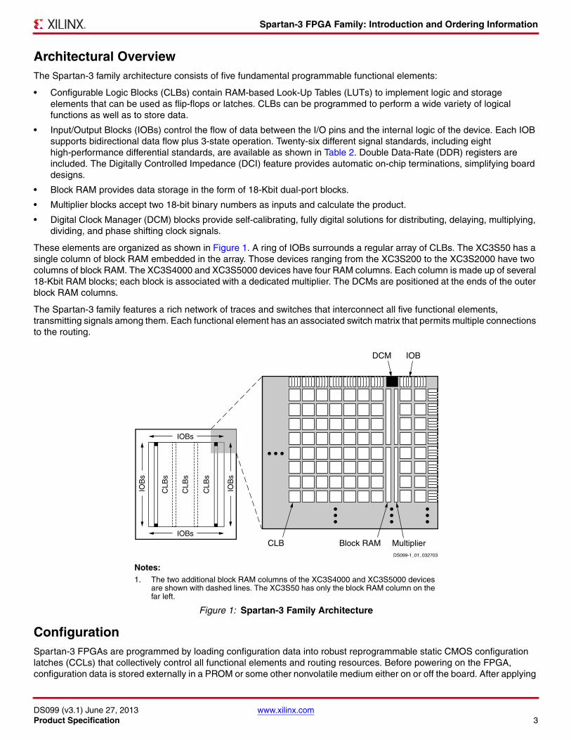
Architectural OverviewThe Spartan-3 family architecture consists of five fundamental programmable functional elements:
• Configurable Logic Blocks (CLBs) contain RAM-based Look-Up Tables (LUTs) to implement logic and storage elements that can be used as flip-flops or latches. CLBs can be programmed to perform a wide variety of logical functions as well as to store data.
• Input/Output Blocks (IOBs) control the flow of data between the I/O pins and the internal logic of the device. Each IOB supports bidirectional data flow plus 3-state operation. Twenty-six different signal standards, including eight high-performance differential standards, are available as shown in Table 2. Double Data-Rate (DDR) registers are included. The Digitally Controlled Impedance (DCI) feature provides automatic on-chip terminations, simplifying board designs.
• Block RAM provides data storage in the form of 18-Kbit dual-port blocks.
• Multiplier blocks accept two 18-bit binary numbers as inputs and calculate the product.
• Digital Clock Manager (DCM) blocks provide self-calibrating, fully digital solutions for distributing, delaying, multiplying, dividing, and phase shifting clock signals.
These elements are organized as shown in Figure 1. A ring of IOBs surrounds a regular array of CLBs. The XC3S50 has a single column of block RAM embedded in the array. Those devices ranging from the XC3S200 to the XC3S2000 have two columns of block RAM. The XC3S4000 and XC3S5000 devices have four RAM columns. Each column is made up of several 18-Kbit RAM blocks; each block is associated with a dedicated multiplier. The DCMs are positioned at the ends of the outer block RAM columns.
The Spartan-3 family features a rich network of traces and switches that interconnect all five functional elements, transmitting signals among them. Each functional element has an associated switch matrix that permits multiple connections to the routing.
ConfigurationSpartan-3 FPGAs are programmed by loading configuration data into robust reprogrammable static CMOS configuration latches (CCLs) that collectively control all functional elements and routing resources. Before powering on the FPGA, configuration data is stored externally in a PROM or some other nonvolatile medium either on or off the board. After applying
X-Ref Target - Figure 1
Figure 1: Spartan-3 Family Architecture
DS099-1_01_032703
Notes: 1. The two additional block RAM columns of the XC3S4000 and XC3S5000 devices
are shown with dashed lines. The XC3S50 has only the block RAM column on the far left.
Spartan-3 FPGA Family: Introduction and Ordering Information
DS099 (v3.1) June 27, 2013 www.xilinx.comProduct Specification 4
power, the configuration data is written to the FPGA using any of five different modes: Master Parallel, Slave Parallel, Master Serial, Slave Serial, and Boundary Scan (JTAG). The Master and Slave Parallel modes use an 8-bit-wide SelectMAP port.
The recommended memory for storing the configuration data is the low-cost Xilinx Platform Flash PROM family, which includes the XCF00S PROMs for serial configuration and the higher density XCF00P PROMs for parallel or serial configuration.
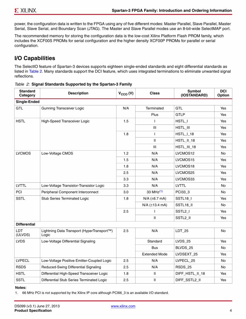
I/O CapabilitiesThe SelectIO feature of Spartan-3 devices supports eighteen single-ended standards and eight differential standards as listed in Table 2. Many standards support the DCI feature, which uses integrated terminations to eliminate unwanted signal reflections.
Table 2: Signal Standards Supported by the Spartan-3 Family
Standard Category Description VCCO (V) Class Symbol
(IOSTANDARD)DCI
Option
Single-Ended
GTL Gunning Transceiver Logic N/A Terminated GTL Yes
Plus GTLP Yes
HSTL High-Speed Transceiver Logic 1.5 I HSTL_I Yes
III HSTL_III Yes
1.8 I HSTL_I_18 Yes
II HSTL_II_18 Yes
III HSTL_III_18 Yes
LVCMOS Low-Voltage CMOS 1.2 N/A LVCMOS12 No
1.5 N/A LVCMOS15 Yes
1.8 N/A LVCMOS18 Yes
2.5 N/A LVCMOS25 Yes
3.3 N/A LVCMOS33 Yes
LVTTL Low-Voltage Transistor-Transistor Logic 3.3 N/A LVTTL No
PCI Peripheral Component Interconnect 3.0 33 MHz(1) PCI33_3 No
SSTL Stub Series Terminated Logic 1.8 N/A (±6.7 mA) SSTL18_I Yes
N/A (±13.4 mA) SSTL18_II No
2.5 I SSTL2_I Yes
II SSTL2_II Yes
Differential
LDT(ULVDS)
Lightning Data Transport (HyperTransport™) Logic
2.5 N/A LDT_25 No
LVDS Low-Voltage Differential Signaling Standard LVDS_25 Yes
Bus BLVDS_25 No
Extended Mode LVDSEXT_25 Yes
LVPECL Low-Voltage Positive Emitter-Coupled Logic 2.5 N/A LVPECL_25 No
RSDS Reduced-Swing Differential Signaling 2.5 N/A RSDS_25 No
HSTL Differential High-Speed Transceiver Logic 1.8 II DIFF_HSTL_II_18 Yes
SSTL Differential Stub Series Terminated Logic 2.5 II DIFF_SSTL2_II Yes
Notes: 1. 66 MHz PCI is not supported by the Xilinx IP core although PCI66_3 is an available I/O standard.
Spartan-3 FPGA Family: Introduction and Ordering Information
DS099 (v3.1) June 27, 2013 www.xilinx.comProduct Specification 5
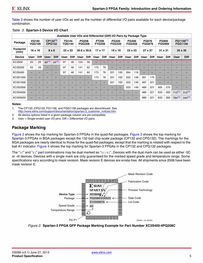
Table 3 shows the number of user I/Os as well as the number of differential I/O pairs available for each device/package combination.
Package Marking
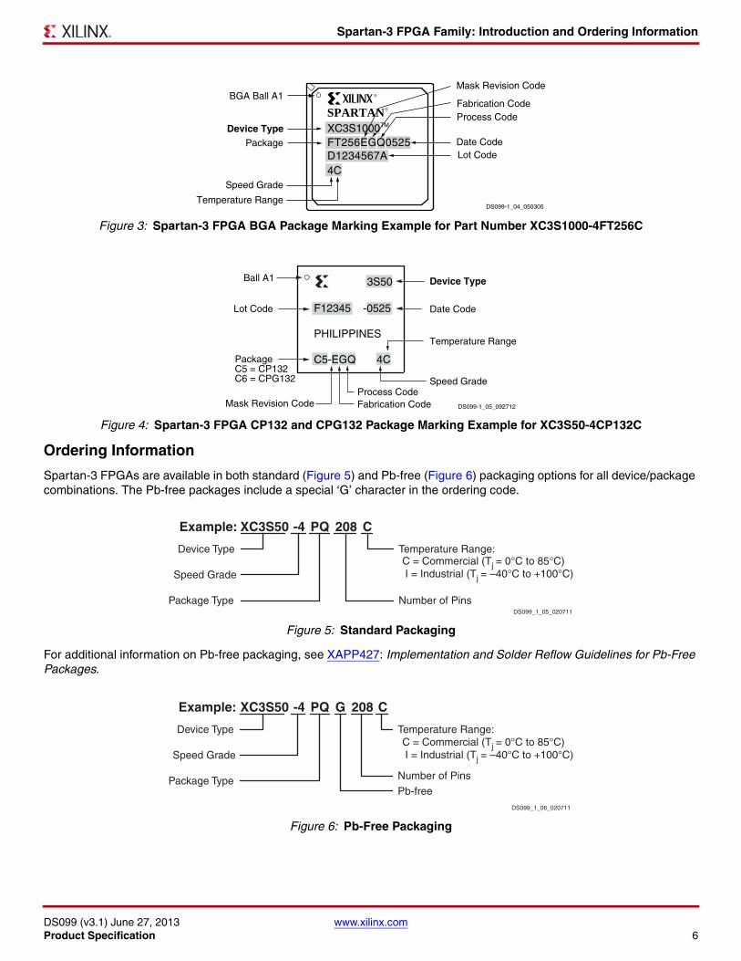
Figure 2 shows the top marking for Spartan-3 FPGAs in the quad-flat packages. Figure 3 shows the top marking for Spartan-3 FPGAs in BGA packages except the 132-ball chip-scale package (CP132 and CPG132). The markings for the BGA packages are nearly identical to those for the quad-flat packages, except that the marking is rotated with respect to the ball A1 indicator. Figure 4 shows the top marking for Spartan-3 FPGAs in the CP132 and CPG132 packages.
The “5C” and “4I” part combinations may be dual marked as “5C/4I”. Devices with the dual mark can be used as either -5C or -4I devices. Devices with a single mark are only guaranteed for the marked speed grade and temperature range. Some specifications vary according to mask revision. Mask revision E devices are errata-free. All shipments since 2006 have been mask revision E.
Table 3: Spartan-3 Device I/O Chart
Available User I/Os and Differential (Diff) I/O Pairs by Package Type
Package VQ100VQG100
CP132(1)
CPG132TQ144
TQG144PQ208
PQG208FT256
FTG256FG320
FGG320FG456
FGG456FG676
FGG676FG900
FGG900FG1156(1)
FGG1156
Footprint(mm) 16 x 16 8 x 8 22 x 22 30.6 x 30.6 17 x 17 19 x 19 23 x 23 27 x 27 31 x 31 35 x 35
Device User Diff User Diff User Diff User Diff User Diff User Diff User Diff User Diff User Diff User Diff
XC3S50 63 29 89(1) 44(1) 97 46 124 56 – – – – – – – – – – – –
XC3S200 63 29 – – 97 46 141 62 173 76 – – – – – – – – – –
XC3S400 – – – – 97 46 141 62 173 76 221 100 264 116 – – – – – –
XC3S1000 – – – – – – – – 173 76 221 100 333 149 391 175 – – – –
XC3S1500 – – – – – – – – – – 221 100 333 149 487 221 – – – –
XC3S2000 – – – – – – – – – – – – 333 149 489 221 565 270 – –
XC3S4000 – – – – – – – – – – – – – – 489 221 633 300 712(1) 312(1)
XC3S5000 – – – – – – – – – – – – – – 489 221 633 300 784(1) 344(1)
Notes: 1. The CP132, CPG132, FG1156, and FGG1156 packages are discontinued. See
http://www.xilinx.com/support/documentation/spartan-3_customer_notices.htm.2. All device options listed in a given package column are pin-compatible.3. User = Single-ended user I/O pins. Diff = Differential I/O pairs.
X-Ref Target - Figure 2
Figure 2: Spartan-3 FPGA QFP Package Marking Example for Part Number XC3S400-4PQ208C
DS099-1_03_050305
Lot Code
Date Code
Mask Revision Code
Process Technology
XC3S400 TM
PQ208EGQ0525D1234567A
4C
SPARTANDevice Type
Package
Speed Grade
Temperature Range
Fabrication Code
Pin P1
R
R
Spartan-3 FPGA Family: Introduction and Ordering Information
DS099 (v3.1) June 27, 2013 www.xilinx.comProduct Specification 6
Ordering Information
Spartan-3 FPGAs are available in both standard (Figure 5) and Pb-free (Figure 6) packaging options for all device/package combinations. The Pb-free packages include a special ‘G’ character in the ordering code.
For additional information on Pb-free packaging, see XAPP427: Implementation and Solder Reflow Guidelines for Pb-Free Packages.
X-Ref Target - Figure 3
Figure 3: Spartan-3 FPGA BGA Package Marking Example for Part Number XC3S1000-4FT256C
X-Ref Target - Figure 4
Figure 4: Spartan-3 FPGA CP132 and CPG132 Package Marking Example for XC3S50-4CP132C
X-Ref Target - Figure 5
Figure 5: Standard Packaging
X-Ref Target - Figure 6
Figure 6: Pb-Free Packaging
DS099-1_04_050305
Lot CodeDate Code
XC3S1000TM
4C
SPARTANDevice Type
BGA Ball A1
Package
Speed Grade
Temperature Range
R
R
FT256EGQ0525D1234567A
Mask Revision Code
Process CodeFabrication Code
DS099-1_05_092712
Date Code
Temperature Range
Speed Grade
3S50
C5-EGQ 4C
Device TypeBall A1
Lot Code
PackageC5 = CP132C6 = CPG132
Mask Revision Code Fabrication Code
F12345 -0525
PHILIPPINES
Process Code
XC3S50 -4 PQ 208 C
Device Type
Speed Grade
Temperature Range:C = Commercial (Tj = 0°C to 85°C) I = Industrial (Tj = –40°C to +100°C)
Package Type Number of Pins
Example:
DS099_1_05_020711
XC3S50 -4 PQ G 208 C
Device Type
Speed Grade
Temperature Range:
Package Type Number of Pins
Pb-free
Example:
C = Commercial (Tj = 0°C to 85°C) I = Industrial (Tj = –40°C to +100°C)
DS099_1_06_020711
Spartan-3 FPGA Family: Introduction and Ordering Information
DS099 (v3.1) June 27, 2013 www.xilinx.comProduct Specification 7
Revision History
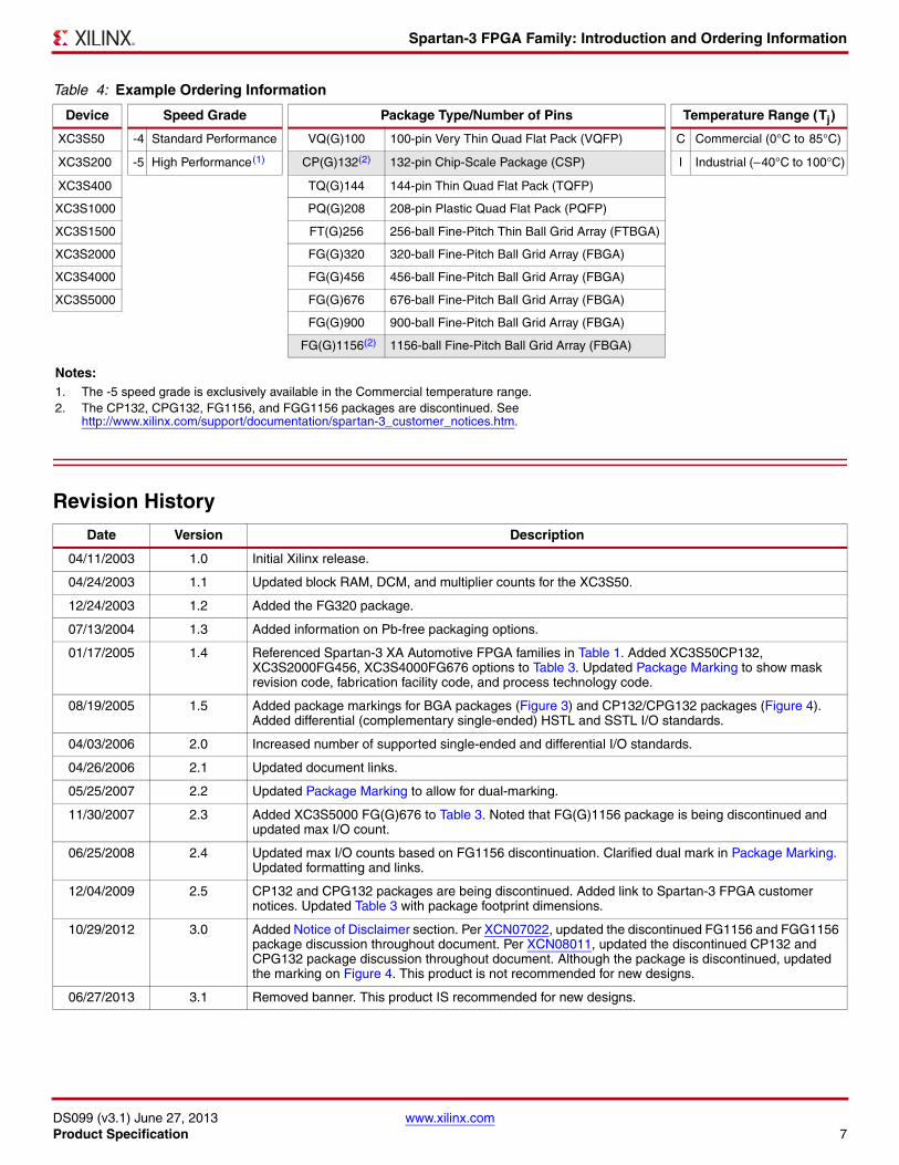
Table 4: Example Ordering Information
Device Speed Grade Package Type/Number of Pins Temperature Range (Tj)
XC3S50 -4 Standard Performance VQ(G)100 100-pin Very Thin Quad Flat Pack (VQFP) C Commercial (0°C to 85°C)
XC3S200 -5 High Performance(1) CP(G)132(2) 132-pin Chip-Scale Package (CSP) I Industrial (–40°C to 100°C)
XC3S400 TQ(G)144 144-pin Thin Quad Flat Pack (TQFP)
XC3S1000 PQ(G)208 208-pin Plastic Quad Flat Pack (PQFP)
XC3S1500 FT(G)256 256-ball Fine-Pitch Thin Ball Grid Array (FTBGA)
XC3S2000 FG(G)320 320-ball Fine-Pitch Ball Grid Array (FBGA)
XC3S4000 FG(G)456 456-ball Fine-Pitch Ball Grid Array (FBGA)
XC3S5000 FG(G)676 676-ball Fine-Pitch Ball Grid Array (FBGA)
FG(G)900 900-ball Fine-Pitch Ball Grid Array (FBGA)
FG(G)1156(2) 1156-ball Fine-Pitch Ball Grid Array (FBGA)
Notes: 1. The -5 speed grade is exclusively available in the Commercial temperature range.2. The CP132, CPG132, FG1156, and FGG1156 packages are discontinued. See
http://www.xilinx.com/support/documentation/spartan-3_customer_notices.htm.
Date Version Description
04/11/2003 1.0 Initial Xilinx release.
04/24/2003 1.1 Updated block RAM, DCM, and multiplier counts for the XC3S50.
12/24/2003 1.2 Added the FG320 package.
07/13/2004 1.3 Added information on Pb-free packaging options.
01/17/2005 1.4 Referenced Spartan-3 XA Automotive FPGA families in Table 1. Added XC3S50CP132, XC3S2000FG456, XC3S4000FG676 options to Table 3. Updated Package Marking to show mask revision code, fabrication facility code, and process technology code.
08/19/2005 1.5 Added package markings for BGA packages (Figure 3) and CP132/CPG132 packages (Figure 4). Added differential (complementary single-ended) HSTL and SSTL I/O standards.
04/03/2006 2.0 Increased number of supported single-ended and differential I/O standards.
04/26/2006 2.1 Updated document links.
05/25/2007 2.2 Updated Package Marking to allow for dual-marking.
11/30/2007 2.3 Added XC3S5000 FG(G)676 to Table 3. Noted that FG(G)1156 package is being discontinued and updated max I/O count.
06/25/2008 2.4 Updated max I/O counts based on FG1156 discontinuation. Clarified dual mark in Package Marking. Updated formatting and links.
12/04/2009 2.5 CP132 and CPG132 packages are being discontinued. Added link to Spartan-3 FPGA customer notices. Updated Table 3 with package footprint dimensions.
10/29/2012 3.0 Added Notice of Disclaimer section. Per XCN07022, updated the discontinued FG1156 and FGG1156 package discussion throughout document. Per XCN08011, updated the discontinued CP132 and CPG132 package discussion throughout document. Although the package is discontinued, updated the marking on Figure 4. This product is not recommended for new designs.
06/27/2013 3.1 Removed banner. This product IS recommended for new designs.
Spartan-3 FPGA Family: Introduction and Ordering Information
DS099 (v3.1) June 27, 2013 www.xilinx.comProduct Specification 8
Notice of DisclaimerTHE XILINX HARDWARE FPGA AND CPLD DEVICES REFERRED TO HEREIN (“PRODUCTS”) ARE SUBJECT TO THE TERMS ANDCONDITIONS OF THE XILINX LIMITED WARRANTY WHICH CAN BE VIEWED AT http://www.xilinx.com/warranty.htm. THIS LIMITEDWARRANTY DOES NOT EXTEND TO ANY USE OF PRODUCTS IN AN APPLICATION OR ENVIRONMENT THAT IS NOT WITHIN THESPECIFICATIONS STATED IN THE XILINX DATA SHEET. ALL SPECIFICATIONS ARE SUBJECT TO CHANGE WITHOUT NOTICE.PRODUCTS ARE NOT DESIGNED OR INTENDED TO BE FAIL-SAFE OR FOR USE IN ANY APPLICATION REQUIRING FAIL-SAFEPERFORMANCE, SUCH AS LIFE-SUPPORT OR SAFETY DEVICES OR SYSTEMS, OR ANY OTHER APPLICATION THAT INVOKESTHE POTENTIAL RISKS OF DEATH, PERSONAL INJURY, OR PROPERTY OR ENVIRONMENTAL DAMAGE (“CRITICALAPPLICATIONS”). USE OF PRODUCTS IN CRITICAL APPLICATIONS IS AT THE SOLE RISK OF CUSTOMER, SUBJECT TOAPPLICABLE LAWS AND REGULATIONS.
CRITICAL APPLICATIONS DISCLAIMERXILINX PRODUCTS (INCLUDING HARDWARE, SOFTWARE AND/OR IP CORES) ARE NOT DESIGNED OR INTENDED TO BEFAIL-SAFE, OR FOR USE IN ANY APPLICATION REQUIRING FAIL-SAFE PERFORMANCE, SUCH AS IN LIFE-SUPPORT ORSAFETY DEVICES OR SYSTEMS, CLASS III MEDICAL DEVICES, NUCLEAR FACILITIES, APPLICATIONS RELATED TO THEDEPLOYMENT OF AIRBAGS, OR ANY OTHER APPLICATIONS THAT COULD LEAD TO DEATH, PERSONAL INJURY OR SEVEREPROPERTY OR ENVIRONMENTAL DAMAGE (INDIVIDUALLY AND COLLECTIVELY, “CRITICAL APPLICATIONS”). FURTHERMORE,XILINX PRODUCTS ARE NOT DESIGNED OR INTENDED FOR USE IN ANY APPLICATIONS THAT AFFECT CONTROL OF AVEHICLE OR AIRCRAFT, UNLESS THERE IS A FAIL-SAFE OR REDUNDANCY FEATURE (WHICH DOES NOT INCLUDE USE OFSOFTWARE IN THE XILINX DEVICE TO IMPLEMENT THE REDUNDANCY) AND A WARNING SIGNAL UPON FAILURE TO THEOPERATOR. CUSTOMER AGREES, PRIOR TO USING OR DISTRIBUTING ANY SYSTEMS THAT INCORPORATE XILINXPRODUCTS, TO THOROUGHLY TEST THE SAME FOR SAFETY PURPOSES. TO THE MAXIMUM EXTENT PERMITTED BYAPPLICABLE LAW, CUSTOMER ASSUMES THE SOLE RISK AND LIABILITY OF ANY USE OF XILINX PRODUCTS IN CRITICALAPPLICATIONS.
AUTOMOTIVE APPLICATIONS DISCLAIMERXILINX PRODUCTS ARE NOT DESIGNED OR INTENDED TO BE FAIL-SAFE, OR FOR USE IN ANY APPLICATION REQUIRING FAIL-SAFE PERFORMANCE, SUCH AS APPLICATIONS RELATED TO: (I) THE DEPLOYMENT OF AIRBAGS, (II) CONTROL OF A VEHICLE, UNLESS THERE IS A FAIL-SAFE OR REDUNDANCY FEATURE (WHICH DOES NOT INCLUDE USE OF SOFTWARE IN THE XILINX DEVICE TO IMPLEMENT THE REDUNDANCY) AND A WARNING SIGNAL UPON FAILURE TO THE OPERATOR, OR (III) USES THAT COULD LEAD TO DEATH OR PERSONAL INJURY. CUSTOMER ASSUMES THE SOLE RISK AND LIABILITY OF ANY USE OF XILINX PRODUCTS IN SUCH APPLICATIONS.
DS099 (v3.1) June 27, 2013 www.xilinx.comProduct Specification 9
© Copyright 2003–2013 Xilinx, Inc. XILINX, the Xilinx logo, Virtex, Spartan, ISE, Artix, Kintex, Zynq, Vivado, and other designated brands included herein are trademarks of Xilinx in the United States and other countries. PCI and PCI-X are trademarks of PCI-SIG and used under license. All other trademarks are the property of their respective owners.
Spartan-3 FPGA Design DocumentationThe functionality of the Spartan®-3 FPGA family is described in the following documents. The topics covered in each guide are listed.
• UG331: Spartan-3 Generation FPGA User Guide
• Clocking Resources
• Digital Clock Managers (DCMs)
• Block RAM
• Configurable Logic Blocks (CLBs)
- Distributed RAM
- SRL16 Shift Registers
- Carry and Arithmetic Logic
• I/O Resources
• Embedded Multiplier Blocks
• Programmable Interconnect
• ISE® Software Design Tools
• IP Cores
• Embedded Processing and Control Solutions
• Pin Types and Package Overview
• Package Drawings
• Powering FPGAs
• UG332: Spartan-3 Generation Configuration User Guide
• Configuration Overview
- Configuration Pins and Behavior
- Bitstream Sizes
• Detailed Descriptions by Mode
- Master Serial Mode using Xilinx Platform Flash PROM
- Slave Parallel (SelectMAP) using a Processor
- Slave Serial using a Processor
- JTAG Mode
• ISE iMPACT Programming Examples
Create a Xilinx user account and sign up to receive automatic e-mail notification whenever this data sheet or the associated user guides are updated.
• Sign Up for Alerts on Xilinx.comhttps://secure.xilinx.com/webreg/register.do?group=myprofile&languageID=1
For specific hardware examples, see the Spartan-3 FPGA Starter Kit board web page, which has links to various design examples and the user guide.
• Spartan-3 FPGA Starter Kit Board pagehttp://www.xilinx.com/s3starter
• UG130: Spartan-3 FPGA Starter Kit User Guide
57Spartan-3 FPGA Family:
Functional Description
DS099 (v3.1) June 27, 2013 Product Specification
Spartan-3 FPGA Family: Functional Description
DS099 (v3.1) June 27, 2013 www.xilinx.comProduct Specification 10
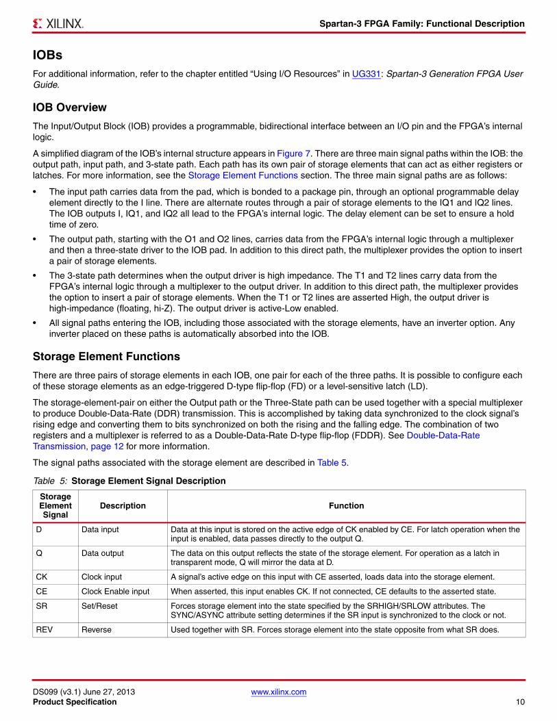
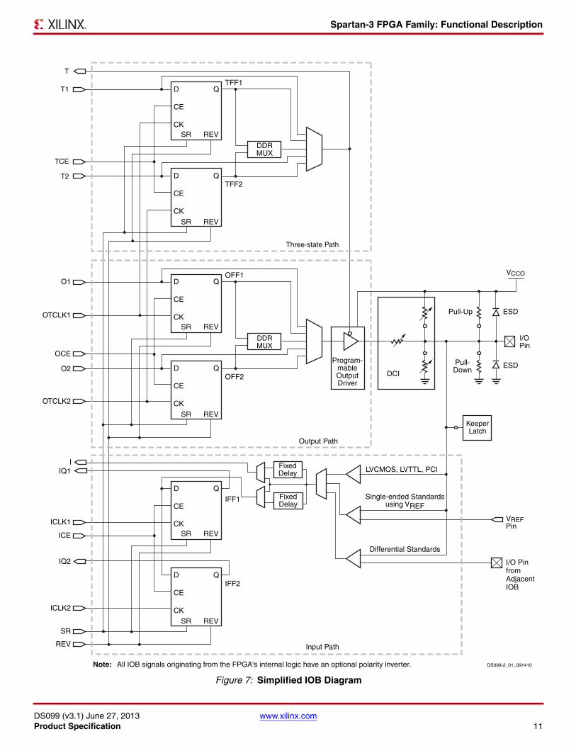
IOBsFor additional information, refer to the chapter entitled “Using I/O Resources” in UG331: Spartan-3 Generation FPGA User Guide.
IOB Overview
The Input/Output Block (IOB) provides a programmable, bidirectional interface between an I/O pin and the FPGA’s internal logic.
A simplified diagram of the IOB’s internal structure appears in Figure 7. There are three main signal paths within the IOB: the output path, input path, and 3-state path. Each path has its own pair of storage elements that can act as either registers or latches. For more information, see the Storage Element Functions section. The three main signal paths are as follows:
• The input path carries data from the pad, which is bonded to a package pin, through an optional programmable delay element directly to the I line. There are alternate routes through a pair of storage elements to the IQ1 and IQ2 lines. The IOB outputs I, IQ1, and IQ2 all lead to the FPGA’s internal logic. The delay element can be set to ensure a hold time of zero.
• The output path, starting with the O1 and O2 lines, carries data from the FPGA’s internal logic through a multiplexer and then a three-state driver to the IOB pad. In addition to this direct path, the multiplexer provides the option to insert a pair of storage elements.
• The 3-state path determines when the output driver is high impedance. The T1 and T2 lines carry data from the FPGA’s internal logic through a multiplexer to the output driver. In addition to this direct path, the multiplexer provides the option to insert a pair of storage elements. When the T1 or T2 lines are asserted High, the output driver is high-impedance (floating, hi-Z). The output driver is active-Low enabled.
• All signal paths entering the IOB, including those associated with the storage elements, have an inverter option. Any inverter placed on these paths is automatically absorbed into the IOB.
Storage Element Functions
There are three pairs of storage elements in each IOB, one pair for each of the three paths. It is possible to configure each of these storage elements as an edge-triggered D-type flip-flop (FD) or a level-sensitive latch (LD).
The storage-element-pair on either the Output path or the Three-State path can be used together with a special multiplexer to produce Double-Data-Rate (DDR) transmission. This is accomplished by taking data synchronized to the clock signal’s rising edge and converting them to bits synchronized on both the rising and the falling edge. The combination of two registers and a multiplexer is referred to as a Double-Data-Rate D-type flip-flop (FDDR). See Double-Data-Rate Transmission, page 12 for more information.
The signal paths associated with the storage element are described in Table 5.
Table 5: Storage Element Signal Description
Storage Element Signal
Description Function
D Data input Data at this input is stored on the active edge of CK enabled by CE. For latch operation when the input is enabled, data passes directly to the output Q.
Q Data output The data on this output reflects the state of the storage element. For operation as a latch in transparent mode, Q will mirror the data at D.
CK Clock input A signal’s active edge on this input with CE asserted, loads data into the storage element.
CE Clock Enable input When asserted, this input enables CK. If not connected, CE defaults to the asserted state.
SR Set/Reset Forces storage element into the state specified by the SRHIGH/SRLOW attributes. The SYNC/ASYNC attribute setting determines if the SR input is synchronized to the clock or not.
REV Reverse Used together with SR. Forces storage element into the state opposite from what SR does.
Spartan-3 FPGA Family: Functional Description
DS099 (v3.1) June 27, 2013 www.xilinx.comProduct Specification 11
X-Ref Target - Figure 7
Figure 7: Simplified IOB Diagram
D
CE
CK
TFF1
Three-state Path
T
T1
TCE
T2TFF2
Q
SR
DDRMUX
REV
D
CE
CK
Q
SR REV
D
CE
CK
OFF1
Output Path
O1
OCE
O2OFF2
Q
SR
DDRMUX
KeeperLatch
VCCO
VREFPin
I/O Pin fromAdjacentIOB
DS099-2_01_091410
I/OPin
Program-mableOutputDriver
DCI
ESDPull-Up
Pull-Down
ESD
REV
D
CE
CK
Q
SR REV
OTCLK1
OTCLK2
D
CE
CK
IFF1
Input Path
I
ICE
IFF2
Q
SR
LVCMOS, LVTTL, PCI
Single-ended Standardsusing VREF
Differential Standards
REV
D
CE
CK
Q
SR REV
ICLK1
ICLK2
SR
REV
Note: All IOB signals originating from the FPGA's internal logic have an optional polarity inverter.
IQ1
IQ2
FixedDelay
FixedDelay
Spartan-3 FPGA Family: Functional Description
DS099 (v3.1) June 27, 2013 www.xilinx.comProduct Specification 12
According to Figure 7, the clock line OTCLK1 connects the CK inputs of the upper registers on the output and three-state paths. Similarly, OTCLK2 connects the CK inputs for the lower registers on the output and three-state paths. The upper and lower registers on the input path have independent clock lines: ICLK1 and ICLK2. The enable line OCE connects the CE inputs of the upper and lower registers on the output path. Similarly, TCE connects the CE inputs for the register pair on the three-state path and ICE does the same for the register pair on the input path. The Set/Reset (SR) line entering the IOB is common to all six registers, as is the Reverse (REV) line.
Each storage element supports numerous options in addition to the control over signal polarity described in the IOB Overview section. These are described in Table 6.
Double-Data-Rate Transmission
Double-Data-Rate (DDR) transmission describes the technique of synchronizing signals to both the rising and falling edges of the clock signal. Spartan-3 devices use register-pairs in all three IOB paths to perform DDR operations.
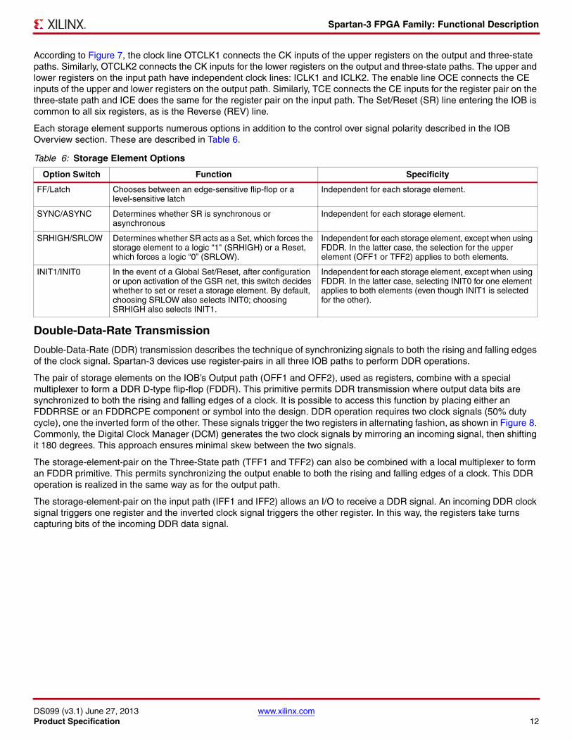
The pair of storage elements on the IOB’s Output path (OFF1 and OFF2), used as registers, combine with a special multiplexer to form a DDR D-type flip-flop (FDDR). This primitive permits DDR transmission where output data bits are synchronized to both the rising and falling edges of a clock. It is possible to access this function by placing either an FDDRRSE or an FDDRCPE component or symbol into the design. DDR operation requires two clock signals (50% duty cycle), one the inverted form of the other. These signals trigger the two registers in alternating fashion, as shown in Figure 8. Commonly, the Digital Clock Manager (DCM) generates the two clock signals by mirroring an incoming signal, then shifting it 180 degrees. This approach ensures minimal skew between the two signals.
The storage-element-pair on the Three-State path (TFF1 and TFF2) can also be combined with a local multiplexer to form an FDDR primitive. This permits synchronizing the output enable to both the rising and falling edges of a clock. This DDR operation is realized in the same way as for the output path.
The storage-element-pair on the input path (IFF1 and IFF2) allows an I/O to receive a DDR signal. An incoming DDR clock signal triggers one register and the inverted clock signal triggers the other register. In this way, the registers take turns capturing bits of the incoming DDR data signal.
Table 6: Storage Element Options
Option Switch Function Specificity
FF/Latch Chooses between an edge-sensitive flip-flop or a level-sensitive latch
Independent for each storage element.
SYNC/ASYNC Determines whether SR is synchronous or asynchronous
Independent for each storage element.
SRHIGH/SRLOW Determines whether SR acts as a Set, which forces the storage element to a logic “1" (SRHIGH) or a Reset, which forces a logic “0” (SRLOW).
Independent for each storage element, except when using FDDR. In the latter case, the selection for the upper element (OFF1 or TFF2) applies to both elements.
INIT1/INIT0 In the event of a Global Set/Reset, after configuration or upon activation of the GSR net, this switch decides whether to set or reset a storage element. By default, choosing SRLOW also selects INIT0; choosing SRHIGH also selects INIT1.
Independent for each storage element, except when using FDDR. In the latter case, selecting INIT0 for one element applies to both elements (even though INIT1 is selected for the other).
Spartan-3 FPGA Family: Functional Description
DS099 (v3.1) June 27, 2013 www.xilinx.comProduct Specification 13
Aside from high bandwidth data transfers, DDR can also be used to reproduce, or “mirror”, a clock signal on the output. This approach is used to transmit clock and data signals together. A similar approach is used to reproduce a clock signal at multiple outputs. The advantage for both approaches is that skew across the outputs will be minimal.
Some adjacent I/O blocks (IOBs) share common routing connecting the ICLK1, ICLK2, OTCLK1, and OTCLK2 clock inputs of both IOBs. These IOB pairs are identified by their differential pair names IO_LxxN_# and IO_LxxP_#, where "xx" is an I/O pair number and ‘#’ is an I/O bank number. Two adjacent IOBs containing DDR registers must share common clock inputs, otherwise one or more of the clock signals will be unroutable.
Pull-Up and Pull-Down Resistors
The optional pull-up and pull-down resistors are intended to establish High and Low levels, respectively, at unused I/Os. The pull-up resistor optionally connects each IOB pad to VCCO. A pull-down resistor optionally connects each pad to GND. These resistors are placed in a design using the PULLUP and PULLDOWN symbols in a schematic, respectively. They can also be instantiated as components, set as constraints or passed as attributes in HDL code. These resistors can also be selected for all unused I/O using the Bitstream Generator (BitGen) option UnusedPin. A Low logic level on HSWAP_EN activates the pull-up resistors on all I/Os during configuration (see The I/Os During Power-On, Configuration, and User Mode, page 21).
The Spartan-3 FPGAs I/O pull-up and pull-down resistors are significantly stronger than the "weak" pull-up/pull-down resistors used in previous Xilinx FPGA families. See Table 33, page 61 for equivalent resistor strengths.
Keeper Circuit
Each I/O has an optional keeper circuit that retains the last logic level on a line after all drivers have been turned off. This is useful to keep bus lines from floating when all connected drivers are in a high-impedance state. This function is placed in a design using the KEEPER symbol. Pull-up and pull-down resistors override the keeper circuit.
X-Ref Target - Figure 8
Figure 8: Clocking the DDR Register
D1
CLK1
DDR MUX
DCM
Q1
FDDR
D2
CLK2
Q2
180˚ 0˚
DS099-2_02_070303
Q
Spartan-3 FPGA Family: Functional Description
DS099 (v3.1) June 27, 2013 www.xilinx.comProduct Specification 14
ESD Protection
Clamp diodes protect all device pads against damage from Electro-Static Discharge (ESD) as well as excessive voltage transients. Each I/O has two clamp diodes: One diode extends P-to-N from the pad to VCCO and a second diode extends N-to-P from the pad to GND. During operation, these diodes are normally biased in the off state. These clamp diodes are always connected to the pad, regardless of the signal standard selected. The presence of diodes limits the ability of Spartan-3 FPGA I/Os to tolerate high signal voltages. The VIN absolute maximum rating in Table 28, page 58 specifies the voltage range that I/Os can tolerate.
Slew Rate Control and Drive Strength
Two options, FAST and SLOW, control the output slew rate. The FAST option supports output switching at a high rate. The SLOW option reduces bus transients. These options are only available when using one of the LVCMOS or LVTTL standards, which also provide up to seven different levels of current drive strength: 2, 4, 6, 8, 12, 16, and 24 mA. Choosing the appropriate drive strength level is yet another means to minimize bus transients.
Table 7 shows the drive strengths that the LVCMOS and LVTTL standards support.
Boundary-Scan Capability
All Spartan-3 FPGA IOBs support boundary-scan testing compatible with IEEE 1149.1 standards. During boundary- scan operations such as EXTEST and HIGHZ the I/O pull-down resistor is active. For more information, see Boundary-Scan (JTAG) Mode, page 50, and refer to the “Using Boundary-Scan and BSDL Files” chapter in UG331.
SelectIO Interface Signal Standards
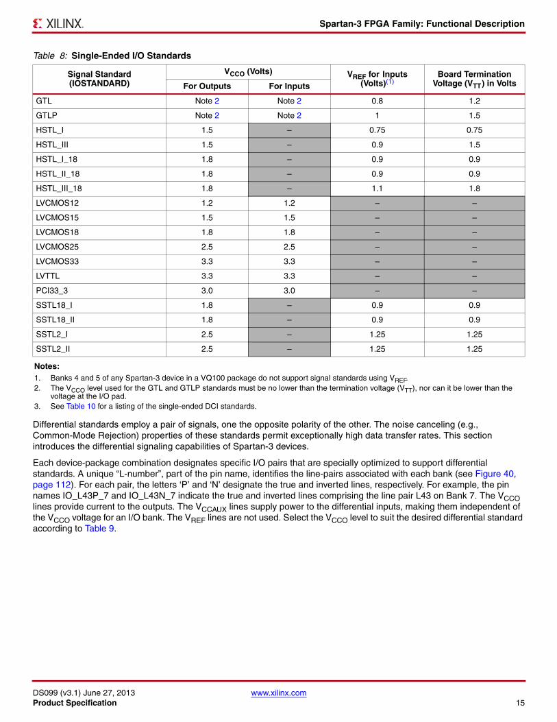
The IOBs support 18 different single-ended signal standards, as listed in Table 8. Furthermore, the majority of IOBs can be used in specific pairs supporting any of eight differential signal standards, as shown in Table 9.
To define the SelectIO™ interface signaling standard in a design, set the IOSTANDARD attribute to the appropriate setting. Xilinx provides a variety of different methods for applying the IOSTANDARD for maximum flexibility. For a full description of different methods of applying attributes to control IOSTANDARD, refer to the “Using I/O Resources” chapter in UG331.
Together with placing the appropriate I/O symbol, two externally applied voltage levels, VCCO and VREF, select the desired signal standard. The VCCO lines provide current to the output driver. The voltage on these lines determines the output voltage swing for all standards except GTL and GTLP.
All single-ended standards except the LVCMOS, LVTTL, and PCI varieties require a Reference Voltage (VREF) to bias the input-switching threshold. Once a configuration data file is loaded into the FPGA that calls for the I/Os of a given bank to use such a signal standard, a few specifically reserved I/O pins on the same bank automatically convert to VREF inputs. When using one of the LVCMOS standards, these pins remain I/Os because the VCCO voltage biases the input-switching threshold, so there is no need for VREF. Select the VCCO and VREF levels to suit the desired single-ended standard according to Table 8.
Table 7: Programmable Output Drive Current
Signal Standard(IOSTANDARD)
Current Drive (mA)
2 4 6 8 12 16 24
LVTTL ✓ ✓ ✓ ✓ ✓ ✓ ✓
LVCMOS33 ✓ ✓ ✓ ✓ ✓ ✓ ✓
LVCMOS25 ✓ ✓ ✓ ✓ ✓ ✓ ✓
LVCMOS18 ✓ ✓ ✓ ✓ ✓ ✓ –
LVCMOS15 ✓ ✓ ✓ ✓ ✓ – –
LVCMOS12 ✓ ✓ ✓ – – – –
Spartan-3 FPGA Family: Functional Description
DS099 (v3.1) June 27, 2013 www.xilinx.comProduct Specification 15
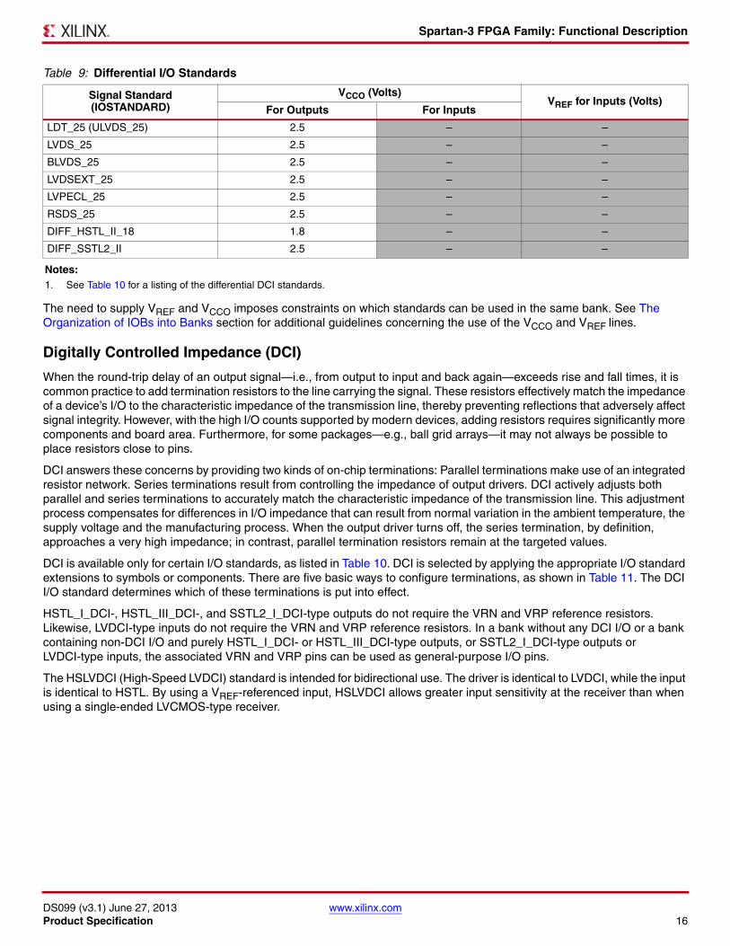
Differential standards employ a pair of signals, one the opposite polarity of the other. The noise canceling (e.g., Common-Mode Rejection) properties of these standards permit exceptionally high data transfer rates. This section introduces the differential signaling capabilities of Spartan-3 devices.
Each device-package combination designates specific I/O pairs that are specially optimized to support differential standards. A unique “L-number”, part of the pin name, identifies the line-pairs associated with each bank (see Figure 40, page 112). For each pair, the letters ‘P’ and ‘N’ designate the true and inverted lines, respectively. For example, the pin names IO_L43P_7 and IO_L43N_7 indicate the true and inverted lines comprising the line pair L43 on Bank 7. The VCCO lines provide current to the outputs. The VCCAUX lines supply power to the differential inputs, making them independent of the VCCO voltage for an I/O bank. The VREF lines are not used. Select the VCCO level to suit the desired differential standard according to Table 9.
Table 8: Single-Ended I/O Standards
Signal Standard(IOSTANDARD)
VCCO (Volts) VREF for Inputs (Volts)(1)
Board Termination Voltage (VTT) in VoltsFor Outputs For Inputs
GTL Note 2 Note 2 0.8 1.2
GTLP Note 2 Note 2 1 1.5
HSTL_I 1.5 – 0.75 0.75
HSTL_III 1.5 – 0.9 1.5
HSTL_I_18 1.8 – 0.9 0.9
HSTL_II_18 1.8 – 0.9 0.9
HSTL_III_18 1.8 – 1.1 1.8
LVCMOS12 1.2 1.2 – –
LVCMOS15 1.5 1.5 – –
LVCMOS18 1.8 1.8 – –
LVCMOS25 2.5 2.5 – –
LVCMOS33 3.3 3.3 – –
LVTTL 3.3 3.3 – –
PCI33_3 3.0 3.0 – –
SSTL18_I 1.8 – 0.9 0.9
SSTL18_II 1.8 – 0.9 0.9
SSTL2_I 2.5 – 1.25 1.25
SSTL2_II 2.5 – 1.25 1.25
Notes: 1. Banks 4 and 5 of any Spartan-3 device in a VQ100 package do not support signal standards using VREF.2. The VCCO level used for the GTL and GTLP standards must be no lower than the termination voltage (VTT), nor can it be lower than the
voltage at the I/O pad.3. See Table 10 for a listing of the single-ended DCI standards.
Spartan-3 FPGA Family: Functional Description
DS099 (v3.1) June 27, 2013 www.xilinx.comProduct Specification 16
The need to supply VREF and VCCO imposes constraints on which standards can be used in the same bank. See The Organization of IOBs into Banks section for additional guidelines concerning the use of the VCCO and VREF lines.
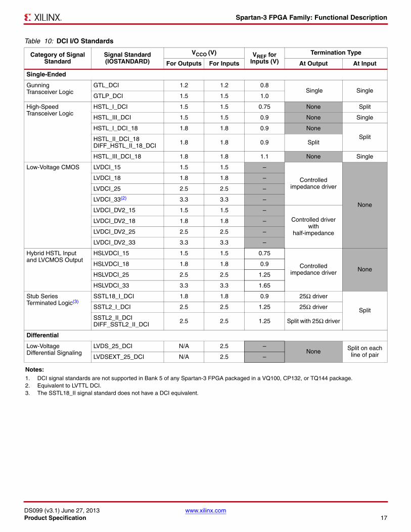
Digitally Controlled Impedance (DCI)
When the round-trip delay of an output signal—i.e., from output to input and back again—exceeds rise and fall times, it is common practice to add termination resistors to the line carrying the signal. These resistors effectively match the impedance of a device’s I/O to the characteristic impedance of the transmission line, thereby preventing reflections that adversely affect signal integrity. However, with the high I/O counts supported by modern devices, adding resistors requires significantly more components and board area. Furthermore, for some packages—e.g., ball grid arrays—it may not always be possible to place resistors close to pins.
DCI answers these concerns by providing two kinds of on-chip terminations: Parallel terminations make use of an integrated resistor network. Series terminations result from controlling the impedance of output drivers. DCI actively adjusts both parallel and series terminations to accurately match the characteristic impedance of the transmission line. This adjustment process compensates for differences in I/O impedance that can result from normal variation in the ambient temperature, the supply voltage and the manufacturing process. When the output driver turns off, the series termination, by definition, approaches a very high impedance; in contrast, parallel termination resistors remain at the targeted values.
DCI is available only for certain I/O standards, as listed in Table 10. DCI is selected by applying the appropriate I/O standard extensions to symbols or components. There are five basic ways to configure terminations, as shown in Table 11. The DCI I/O standard determines which of these terminations is put into effect.
HSTL_I_DCI-, HSTL_III_DCI-, and SSTL2_I_DCI-type outputs do not require the VRN and VRP reference resistors. Likewise, LVDCI-type inputs do not require the VRN and VRP reference resistors. In a bank without any DCI I/O or a bank containing non-DCI I/O and purely HSTL_I_DCI- or HSTL_III_DCI-type outputs, or SSTL2_I_DCI-type outputs or LVDCI-type inputs, the associated VRN and VRP pins can be used as general-purpose I/O pins.
The HSLVDCI (High-Speed LVDCI) standard is intended for bidirectional use. The driver is identical to LVDCI, while the input is identical to HSTL. By using a VREF-referenced input, HSLVDCI allows greater input sensitivity at the receiver than when using a single-ended LVCMOS-type receiver.
Table 9: Differential I/O Standards
Signal Standard(IOSTANDARD)
VCCO (Volts)VREF for Inputs (Volts)
For Outputs For Inputs
LDT_25 (ULVDS_25) 2.5 – –
LVDS_25 2.5 – –
BLVDS_25 2.5 – –
LVDSEXT_25 2.5 – –
LVPECL_25 2.5 – –
RSDS_25 2.5 – –
DIFF_HSTL_II_18 1.8 – –
DIFF_SSTL2_II 2.5 – –
Notes: 1. See Table 10 for a listing of the differential DCI standards.
Spartan-3 FPGA Family: Functional Description
DS099 (v3.1) June 27, 2013 www.xilinx.comProduct Specification 17
Table 10: DCI I/O Standards
Category of Signal Standard
Signal Standard(IOSTANDARD)
VCCO (V) VREF for Inputs (V)
Termination Type
For Outputs For Inputs At Output At Input
Single-Ended
Gunning Transceiver Logic
GTL_DCI 1.2 1.2 0.8 Single Single
GTLP_DCI 1.5 1.5 1.0
High-Speed Transceiver Logic
HSTL_I_DCI 1.5 1.5 0.75 None Split
HSTL_III_DCI 1.5 1.5 0.9 None Single
HSTL_I_DCI_18 1.8 1.8 0.9 None
SplitHSTL_II_DCI_18DIFF_HSTL_II_18_DCI 1.8 1.8 0.9 Split
HSTL_III_DCI_18 1.8 1.8 1.1 None Single
Low-Voltage CMOS LVDCI_15 1.5 1.5 –
Controlled impedance driver
None
LVDCI_18 1.8 1.8 –
LVDCI_25 2.5 2.5 –
LVDCI_33(2) 3.3 3.3 –
LVDCI_DV2_15 1.5 1.5 –
Controlled driver with
half-impedance
LVDCI_DV2_18 1.8 1.8 –
LVDCI_DV2_25 2.5 2.5 –
LVDCI_DV2_33 3.3 3.3 –
Hybrid HSTL Input and LVCMOS Output
HSLVDCI_15 1.5 1.5 0.75
Controlled impedance driver None
HSLVDCI_18 1.8 1.8 0.9
HSLVDCI_25 2.5 2.5 1.25
HSLVDCI_33 3.3 3.3 1.65
Stub Series Terminated Logic(3)
SSTL18_I_DCI 1.8 1.8 0.9 25Ω driver
SplitSSTL2_I_DCI 2.5 2.5 1.25 25Ω driver
SSTL2_II_DCIDIFF_SSTL2_II_DCI 2.5 2.5 1.25 Split with 25Ω driver
Differential
Low-Voltage Differential Signaling
LVDS_25_DCI N/A 2.5 –None Split on each
line of pairLVDSEXT_25_DCI N/A 2.5 –
Notes: 1. DCI signal standards are not supported in Bank 5 of any Spartan-3 FPGA packaged in a VQ100, CP132, or TQ144 package.2. Equivalent to LVTTL DCI.3. The SSTL18_II signal standard does not have a DCI equivalent.
Spartan-3 FPGA Family: Functional Description
DS099 (v3.1) June 27, 2013 www.xilinx.comProduct Specification 18
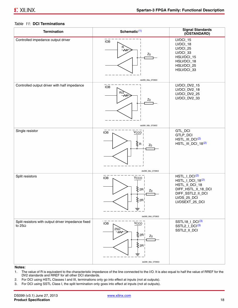
Table 11: DCI Terminations
Termination Schematic(1) Signal Standards(IOSTANDARD)
Controlled impedance output driver LVDCI_15LVDCI_18LVDCI_25LVDCI_33HSLVDCI_15HSLVDCI_18HSLVDCI_25HSLVDCI_33
Controlled output driver with half impedance LVDCI_DV2_15LVDCI_DV2_18LVDCI_DV2_25LVDCI_DV2_33
Single resistor GTL_DCIGTLP_DCIHSTL_III_DCI(2)
HSTL_III_DCI_18(2)
Split resistors HSTL_I_DCI(2)
HSTL_I_DCI_18(2)
HSTL_II_DCI_18DIFF_HSTL_II_18_DCIDIFF_SSTL2_II_DCILVDS_25_DCILVDSEXT_25_DCI
Split resistors with output driver impedance fixed to 25Ω
SSTL18_I_DCI(3)
SSTL2_I_DCI(3)
SSTL2_II_DCI
Notes: 1. The value of R is equivalent to the characteristic impedance of the line connected to the I/O. It is also equal to half the value of RREF for the
DV2 standards and RREF for all other DCI standards.2. For DCI using HSTL Classes I and III, terminations only go into effect at inputs (not at outputs).3. For DCI using SSTL Class I, the split termination only goes into effect at inputs (not at outputs).
Z0
IOB
ds099_06a_070903
R
Z0
IOB
ds099_06b_070903
R/2
R Z0
VCCOIOB
ds099_06c_070903
2R
2R Z0
VCCOIOB
ds099_06d_070903
25Ω
2R
2R Z0
VCCOIOB
ds099_06e_070903
Spartan-3 FPGA Family: Functional Description
DS099 (v3.1) June 27, 2013 www.xilinx.comProduct Specification 19
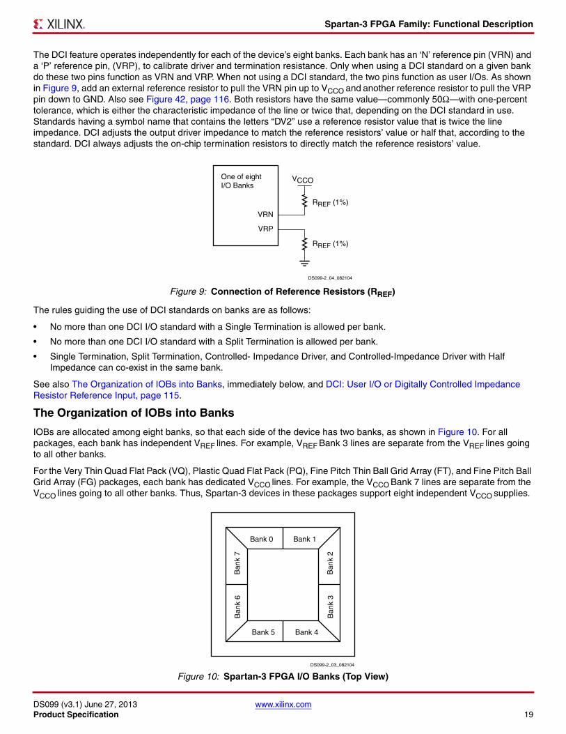
The DCI feature operates independently for each of the device’s eight banks. Each bank has an ‘N’ reference pin (VRN) and a ‘P’ reference pin, (VRP), to calibrate driver and termination resistance. Only when using a DCI standard on a given bank do these two pins function as VRN and VRP. When not using a DCI standard, the two pins function as user I/Os. As shown in Figure 9, add an external reference resistor to pull the VRN pin up to VCCO and another reference resistor to pull the VRP pin down to GND. Also see Figure 42, page 116. Both resistors have the same value—commonly 50Ω—with one-percent tolerance, which is either the characteristic impedance of the line or twice that, depending on the DCI standard in use. Standards having a symbol name that contains the letters “DV2” use a reference resistor value that is twice the line impedance. DCI adjusts the output driver impedance to match the reference resistors’ value or half that, according to the standard. DCI always adjusts the on-chip termination resistors to directly match the reference resistors’ value.
The rules guiding the use of DCI standards on banks are as follows:
• No more than one DCI I/O standard with a Single Termination is allowed per bank.
• No more than one DCI I/O standard with a Split Termination is allowed per bank.
• Single Termination, Split Termination, Controlled- Impedance Driver, and Controlled-Impedance Driver with Half Impedance can co-exist in the same bank.
See also The Organization of IOBs into Banks, immediately below, and DCI: User I/O or Digitally Controlled Impedance Resistor Reference Input, page 115.
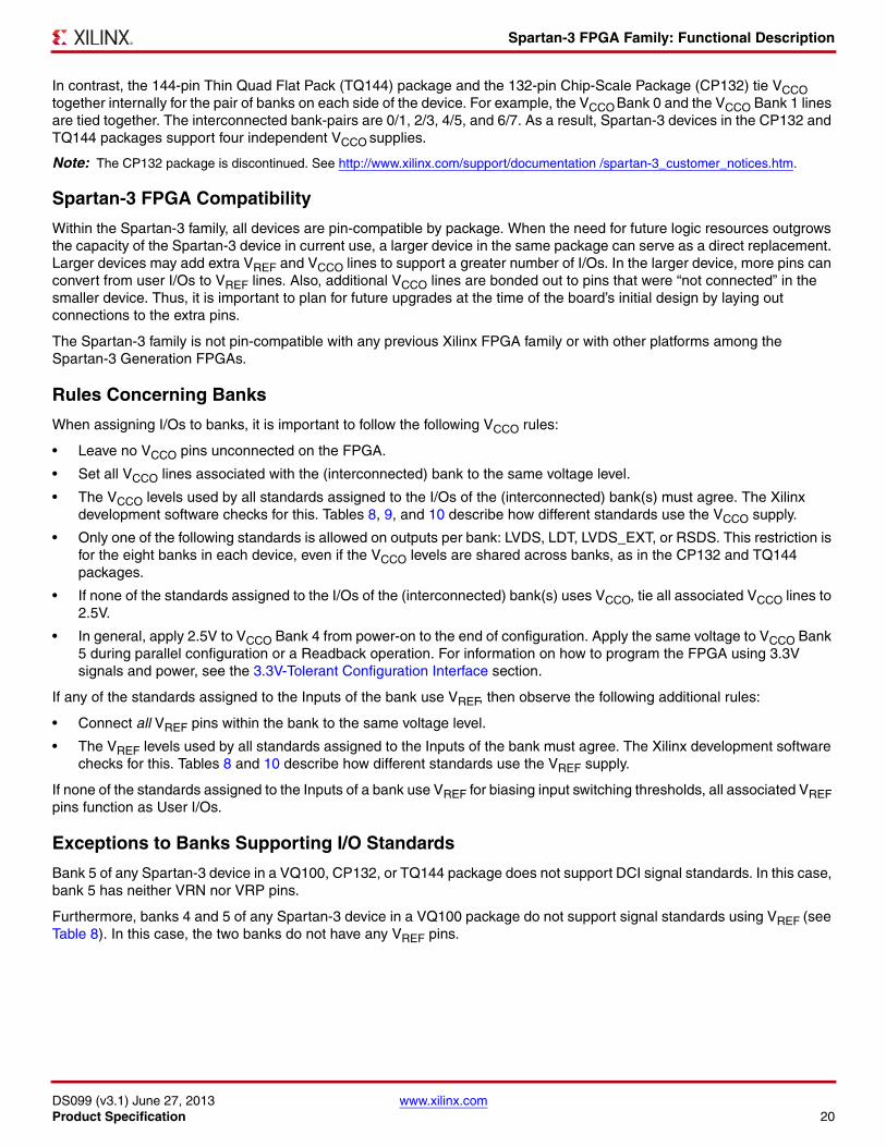
The Organization of IOBs into Banks
IOBs are allocated among eight banks, so that each side of the device has two banks, as shown in Figure 10. For all packages, each bank has independent VREF lines. For example, VREF Bank 3 lines are separate from the VREF lines going to all other banks.
For the Very Thin Quad Flat Pack (VQ), Plastic Quad Flat Pack (PQ), Fine Pitch Thin Ball Grid Array (FT), and Fine Pitch Ball Grid Array (FG) packages, each bank has dedicated VCCO lines. For example, the VCCO Bank 7 lines are separate from the VCCO lines going to all other banks. Thus, Spartan-3 devices in these packages support eight independent VCCO supplies.
X-Ref Target - Figure 9
Figure 9: Connection of Reference Resistors (RREF)
X-Ref Target - Figure 10
Figure 10: Spartan-3 FPGA I/O Banks (Top View)
DS099-2_04_082104
VCCO
VRN
VRP
One of eightI/O Banks
RREF (1%)
RREF (1%)
DS099-2_03_082104
Bank 0 Bank 1
Bank 5 Bank 4
Ban
k 7
Ban
k 6
Ban
k 2
Ban
k 3
Spartan-3 FPGA Family: Functional Description
DS099 (v3.1) June 27, 2013 www.xilinx.comProduct Specification 20
In contrast, the 144-pin Thin Quad Flat Pack (TQ144) package and the 132-pin Chip-Scale Package (CP132) tie VCCO
together internally for the pair of banks on each side of the device. For example, the VCCO Bank 0 and the VCCO Bank 1 lines are tied together. The interconnected bank-pairs are 0/1, 2/3, 4/5, and 6/7. As a result, Spartan-3 devices in the CP132 and TQ144 packages support four independent VCCO supplies.
Note: The CP132 package is discontinued. See http://www.xilinx.com/support/documentation /spartan-3_customer_notices.htm.
Spartan-3 FPGA Compatibility
Within the Spartan-3 family, all devices are pin-compatible by package. When the need for future logic resources outgrows the capacity of the Spartan-3 device in current use, a larger device in the same package can serve as a direct replacement. Larger devices may add extra VREF and VCCO lines to support a greater number of I/Os. In the larger device, more pins can convert from user I/Os to VREF lines. Also, additional VCCO lines are bonded out to pins that were “not connected” in the smaller device. Thus, it is important to plan for future upgrades at the time of the board’s initial design by laying out connections to the extra pins.
The Spartan-3 family is not pin-compatible with any previous Xilinx FPGA family or with other platforms among the Spartan-3 Generation FPGAs.
Rules Concerning Banks
When assigning I/Os to banks, it is important to follow the following VCCO rules:
• Leave no VCCO pins unconnected on the FPGA.
• Set all VCCO lines associated with the (interconnected) bank to the same voltage level.
• The VCCO levels used by all standards assigned to the I/Os of the (interconnected) bank(s) must agree. The Xilinx development software checks for this. Tables 8, 9, and 10 describe how different standards use the VCCO supply.
• Only one of the following standards is allowed on outputs per bank: LVDS, LDT, LVDS_EXT, or RSDS. This restriction is for the eight banks in each device, even if the VCCO levels are shared across banks, as in the CP132 and TQ144 packages.
• If none of the standards assigned to the I/Os of the (interconnected) bank(s) uses VCCO, tie all associated VCCO lines to 2.5V.
• In general, apply 2.5V to VCCO Bank 4 from power-on to the end of configuration. Apply the same voltage to VCCO Bank 5 during parallel configuration or a Readback operation. For information on how to program the FPGA using 3.3V signals and power, see the 3.3V-Tolerant Configuration Interface section.
If any of the standards assigned to the Inputs of the bank use VREF, then observe the following additional rules:
• Connect all VREF pins within the bank to the same voltage level.
• The VREF levels used by all standards assigned to the Inputs of the bank must agree. The Xilinx development software checks for this. Tables 8 and 10 describe how different standards use the VREF supply.
If none of the standards assigned to the Inputs of a bank use VREF for biasing input switching thresholds, all associated VREF pins function as User I/Os.
Exceptions to Banks Supporting I/O Standards
Bank 5 of any Spartan-3 device in a VQ100, CP132, or TQ144 package does not support DCI signal standards. In this case, bank 5 has neither VRN nor VRP pins.
Furthermore, banks 4 and 5 of any Spartan-3 device in a VQ100 package do not support signal standards using VREF (see Table 8). In this case, the two banks do not have any VREF pins.
Spartan-3 FPGA Family: Functional Description
DS099 (v3.1) June 27, 2013 www.xilinx.comProduct Specification 21
Supply Voltages for the IOBs
Three different supplies power the IOBs:
• The VCCO supplies, one for each of the FPGA’s I/O banks, power the output drivers, except when using the GTL and GTLP signal standards. The voltage on the VCCO pins determines the voltage swing of the output signal.
• VCCINT is the main power supply for the FPGA’s internal logic.
• The VCCAUX is an auxiliary source of power, primarily to optimize the performance of various FPGA functions such as I/O switching.
The I/Os During Power-On, Configuration, and User Mode
With no power applied to the FPGA, all I/Os are in a high-impedance state. The VCCINT (1.2V), VCCAUX (2.5V), and VCCO supplies may be applied in any order. Before power-on can finish, VCCINT, VCCO Bank 4, and VCCAUX must have reached their respective minimum recommended operating levels (see Table 29, page 59). At this time, all I/O drivers also will be in a high-impedance state. VCCO Bank 4, VCCINT, and VCCAUX serve as inputs to the internal Power-On Reset circuit (POR).
A Low level applied to the HSWAP_EN input enables pull-up resistors on User I/Os from power-on throughout configuration. A High level on HSWAP_EN disables the pull-up resistors, allowing the I/Os to float. If the HSWAP_EN pin is floating, then an internal pull-up resistor pulls HSWAP_EN High. As soon as power is applied, the FPGA begins initializing its configuration memory. At the same time, the FPGA internally asserts the Global Set-Reset (GSR), which asynchronously resets all IOB storage elements to a Low state.
Upon the completion of initialization, INIT_B goes High, sampling the M0, M1, and M2 inputs to determine the configuration mode. At this point, the configuration data is loaded into the FPGA. The I/O drivers remain in a high-impedance state (with or without pull-up resistors, as determined by the HSWAP_EN input) throughout configuration.
The Global Three State (GTS) net is released during Start-Up, marking the end of configuration and the beginning of design operation in the User mode. At this point, those I/Os to which signals have been assigned go active while all unused I/Os remain in a high-impedance state. The release of the GSR net, also part of Start-up, leaves the IOB registers in a Low state by default, unless the loaded design reverses the polarity of their respective RS inputs.
In User mode, all internal pull-up resistors on the I/Os are disabled and HSWAP_EN becomes a “don’t care” input. If it is desirable to have pull-up or pull-down resistors on I/Os carrying signals, the appropriate symbol—e.g., PULLUP, PULLDOWN—must be placed at the appropriate pads in the design. The Bitstream Generator (Bitgen) option UnusedPin available in the Xilinx development software determines whether unused I/Os collectively have pull-up resistors, pull-down resistors, or no resistors in User mode.
CLB OverviewFor more details on the CLBs, refer to the chapter entitled “Using Configurable Logic Blocks” in UG331.
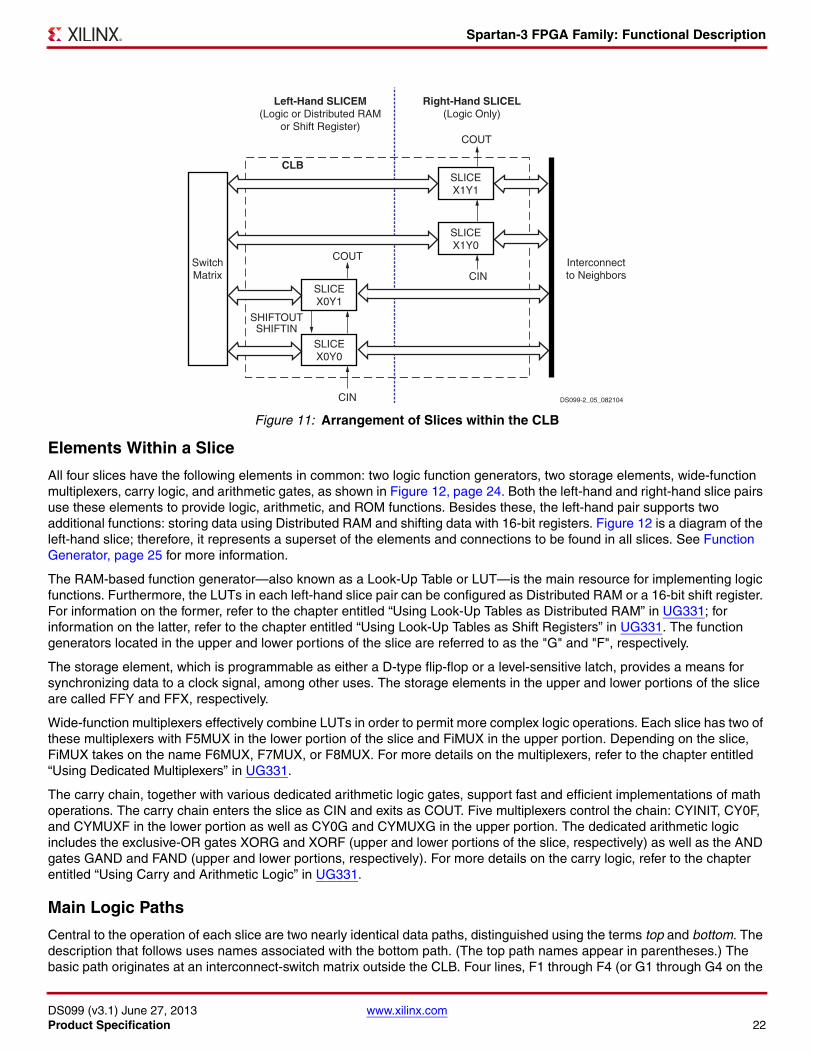
The Configurable Logic Blocks (CLBs) constitute the main logic resource for implementing synchronous as well as combinatorial circuits. Each CLB comprises four interconnected slices, as shown in Figure 11. These slices are grouped in pairs. Each pair is organized as a column with an independent carry chain.
The nomenclature that the FPGA Editor—part of the Xilinx development software—uses to designate slices is as follows: The letter ‘X’ followed by a number identifies columns of slices. The ‘X’ number counts up in sequence from the left side of the die to the right. The letter ‘Y’ followed by a number identifies the position of each slice in a pair as well as indicating the CLB row. The ‘Y’ number counts slices starting from the bottom of the die according to the sequence: 0, 1, 0, 1 (the first CLB row); 2, 3, 2, 3 (the second CLB row); etc. Figure 11 shows the CLB located in the lower left-hand corner of the die. Slices X0Y0 and X0Y1 make up the column-pair on the left where as slices X1Y0 and X1Y1 make up the column-pair on the right. For each CLB, the term “left-hand” (or SLICEM) indicates the pair of slices labeled with an even ‘X’ number, such as X0, and the term “right-hand” (or SLICEL) designates the pair of slices with an odd ‘X’ number, e.g., X1.
Spartan-3 FPGA Family: Functional Description
DS099 (v3.1) June 27, 2013 www.xilinx.comProduct Specification 22
Elements Within a Slice
All four slices have the following elements in common: two logic function generators, two storage elements, wide-function multiplexers, carry logic, and arithmetic gates, as shown in Figure 12, page 24. Both the left-hand and right-hand slice pairs use these elements to provide logic, arithmetic, and ROM functions. Besides these, the left-hand pair supports two additional functions: storing data using Distributed RAM and shifting data with 16-bit registers. Figure 12 is a diagram of the left-hand slice; therefore, it represents a superset of the elements and connections to be found in all slices. See Function Generator, page 25 for more information.
The RAM-based function generator—also known as a Look-Up Table or LUT—is the main resource for implementing logic functions. Furthermore, the LUTs in each left-hand slice pair can be configured as Distributed RAM or a 16-bit shift register. For information on the former, refer to the chapter entitled “Using Look-Up Tables as Distributed RAM” in UG331; for information on the latter, refer to the chapter entitled “Using Look-Up Tables as Shift Registers” in UG331. The function generators located in the upper and lower portions of the slice are referred to as the "G" and "F", respectively.
The storage element, which is programmable as either a D-type flip-flop or a level-sensitive latch, provides a means for synchronizing data to a clock signal, among other uses. The storage elements in the upper and lower portions of the slice are called FFY and FFX, respectively.
Wide-function multiplexers effectively combine LUTs in order to permit more complex logic operations. Each slice has two of these multiplexers with F5MUX in the lower portion of the slice and FiMUX in the upper portion. Depending on the slice, FiMUX takes on the name F6MUX, F7MUX, or F8MUX. For more details on the multiplexers, refer to the chapter entitled “Using Dedicated Multiplexers” in UG331.
The carry chain, together with various dedicated arithmetic logic gates, support fast and efficient implementations of math operations. The carry chain enters the slice as CIN and exits as COUT. Five multiplexers control the chain: CYINIT, CY0F, and CYMUXF in the lower portion as well as CY0G and CYMUXG in the upper portion. The dedicated arithmetic logic includes the exclusive-OR gates XORG and XORF (upper and lower portions of the slice, respectively) as well as the AND gates GAND and FAND (upper and lower portions, respectively). For more details on the carry logic, refer to the chapter entitled “Using Carry and Arithmetic Logic” in UG331.
Main Logic Paths
Central to the operation of each slice are two nearly identical data paths, distinguished using the terms top and bottom. The description that follows uses names associated with the bottom path. (The top path names appear in parentheses.) The basic path originates at an interconnect-switch matrix outside the CLB. Four lines, F1 through F4 (or G1 through G4 on the
X-Ref Target - Figure 11
Figure 11: Arrangement of Slices within the CLB
DS099-2_05_082104
Interconnectto Neighbors
Left-Hand SLICEM(Logic or Distributed RAM
or Shift Register)
Right-Hand SLICEL(Logic Only)
CIN
SLICEX0Y1
SLICEX0Y0
SwitchMatrix
COUT
CLB
COUT
SHIFTOUTSHIFTIN
CIN
SLICEX1Y1
SLICEX1Y0
Spartan-3 FPGA Family: Functional Description
DS099 (v3.1) June 27, 2013 www.xilinx.comProduct Specification 23
upper path), enter the slice and connect directly to the LUT. Once inside the slice, the lower 4-bit path passes through a function generator ‘F’ (or ‘G’) that performs logic operations. The function generator’s Data output, ‘D’, offers five possible paths:
• Exit the slice via line ‘X’ (or ‘Y’) and return to interconnect.
• Inside the slice, ‘X’ (or ‘Y’) serves as an input to the DXMUX (DYMUX) which feeds the data input, ‘D’, of the FFX (FFY) storage element. The ‘Q’ output of the storage element drives the line XQ (or YQ) which exits the slice.
• Control the CYMUXF (or CYMUXG) multiplexer on the carry chain.
• With the carry chain, serve as an input to the XORF (or XORG) exclusive-OR gate that performs arithmetic operations, producing a result on ‘X’ (or ‘Y’).
• Drive the multiplexer F5MUX to implement logic functions wider than four bits. The ‘D’ outputs of both the F-LUT and G-LUT serve as data inputs to this multiplexer.
In addition to the main logic paths described above, there are two bypass paths that enter the slice as BX and BY. Once inside the FPGA, BX in the bottom half of the slice (or BY in the top half) can take any of several possible branches:
• Bypass both the LUT and the storage element, then exit the slice as BXOUT (or BYOUT) and return to interconnect.
• Bypass the LUT, then pass through a storage element via the D input before exiting as XQ (or YQ).
• Control the wide function multiplexer F5MUX (or F6MUX).
• Via multiplexers, serve as an input to the carry chain.
• Drives the DI input of the LUT.
• BY can control the REV inputs of both the FFY and FFX storage elements.
• Finally, the DIG_MUX multiplexer can switch BY onto the DIG line, which exits the slice.
Other slice signals shown in Figure 12 are discussed in the sections that follow.
Spartan-3 FPGA Family: Functional Description
DS099 (v3.1) June 27, 2013 www.xilinx.comProduct Specification 24
X-Ref Target - Figure 12
Figure 12: Simplified Diagram of the Left-Hand SLICEM
WF[4:1]
DS312-2_32_042007
D
DI
DIWS
Notes: 1. Options to invert signal polarity as well as other options that enable lines for various functions are not shown.2. The index i can be 6, 7, or 8, depending on the slice. In this position, the upper right-hand slice has an F8MUX, and the
upper left-hand slice has an F7MUX. The lower right-hand and left-hand slices both have an F6MUX.
Spartan-3 FPGA Family: Functional Description
DS099 (v3.1) June 27, 2013 www.xilinx.comProduct Specification 25
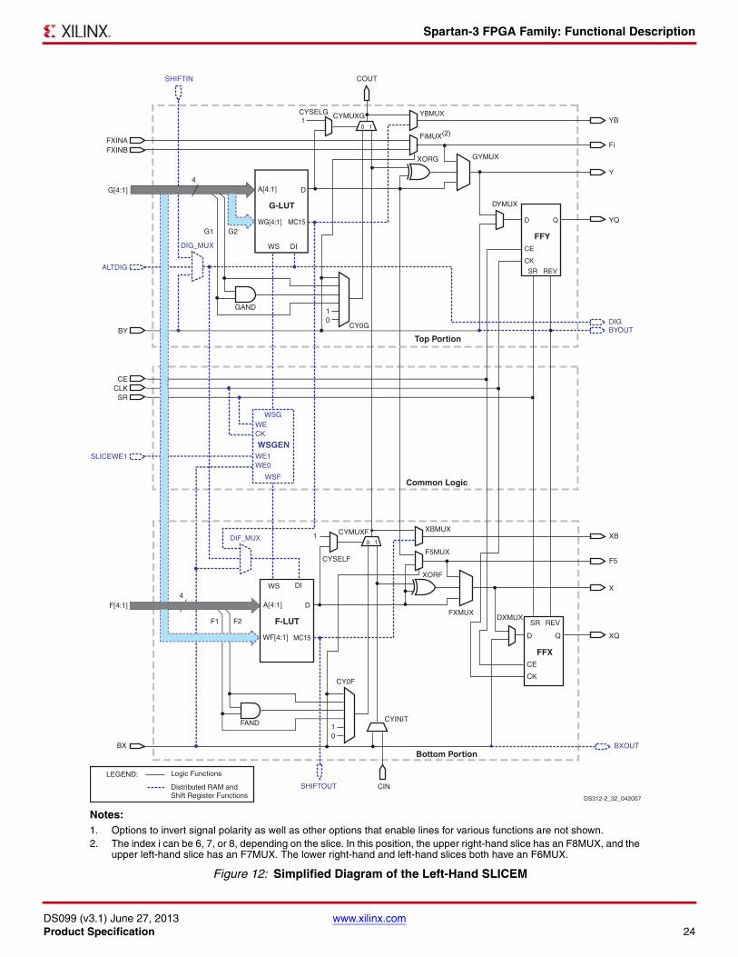
Function Generator
Each of the two LUTs (F and G) in a slice have four logic inputs (A1-A4) and a single output (D). This permits any four-variable Boolean logic operation to be programmed into them. Furthermore, wide function multiplexers can be used to effectively combine LUTs within the same CLB or across different CLBs, making logic functions with still more input variables possible.
The LUTs in both the right-hand and left-hand slice-pairs not only support the logic functions described above, but also can function as ROM that is initialized with data at the time of configuration.
The LUTs in the left-hand slice-pair (even-numbered columns such as X0 in Figure 11) of each CLB support two additional functions that the right-hand slice-pair (odd-numbered columns such as X1) do not.
First, it is possible to program the “left-hand LUTs” as distributed RAM. This type of memory affords moderate amounts of data buffering anywhere along a data path. One left-hand LUT stores 16 bits. Multiple left-hand LUTs can be combined in various ways to store larger amounts of data. A dual port option combines two LUTs so that memory access is possible from two independent data lines. A Distributed ROM option permits pre-loading the memory with data during FPGA configuration.
Second, it is possible to program each left-hand LUT as a 16-bit shift register. Used in this way, each LUT can delay serial data anywhere from one to 16 clock cycles. The four left-hand LUTs of a single CLB can be combined to produce delays up to 64 clock cycles. The SHIFTIN and SHIFTOUT lines cascade LUTs to form larger shift registers. It is also possible to combine shift registers across more than one CLB. The resulting programmable delays can be used to balance the timing of data pipelines.
Block RAM OverviewAll Spartan-3 devices support block RAM, which is organized as configurable, synchronous 18Kbit blocks. Block RAM stores relatively large amounts of data more efficiently than the distributed RAM feature described earlier. (The latter is better suited for buffering small amounts of data anywhere along signal paths.) This section describes basic Block RAM functions. For more information, refer to the chapter entitled “Using Block RAM” in UG331.
The aspect ratio—i.e., width vs. depth—of each block RAM is configurable. Furthermore, multiple blocks can be cascaded to create still wider and/or deeper memories.
A choice among primitives determines whether the block RAM functions as dual- or single-port memory. A name of the form RAMB16_S[wA]_S[wB] calls out the dual-port primitive, where the integers wA and wB specify the total data path width at ports wA and wB, respectively. Thus, a RAMB16_S9_S18 is a dual-port RAM with a 9-bit-wide Port A and an 18-bit-wide Port B. A name of the form RAMB16_S[w] identifies the single-port primitive, where the integer w specifies the total data path width of the lone port. A RAMB16_S18 is a single-port RAM with an 18-bit-wide port. Other memory functions—e.g., FIFOs, data path width conversion, ROM, etc.—are readily available using the CORE Generator™ software, part of the Xilinx development software.
Spartan-3 FPGA Family: Functional Description
DS099 (v3.1) June 27, 2013 www.xilinx.comProduct Specification 26
Arrangement of RAM Blocks on Die
The XC3S50 has one column of block RAM. The Spartan-3 devices ranging from the XC3S200 to XC3S2000 have two columns of block RAM. The XC3S4000 and XC3S5000 have four columns. The position of the columns on the die is shown in Figure 1, page 3. For a given device, the total available RAM blocks are distributed equally among the columns. Table 12 shows the number of RAM blocks, the data storage capacity, and the number of columns for each device.
Block RAM and multipliers have interconnects between them that permit simultaneous operation; however, since the multiplier shares inputs with the upper data bits of block RAM, the maximum data path width of the block RAM is 18 bits in this case.
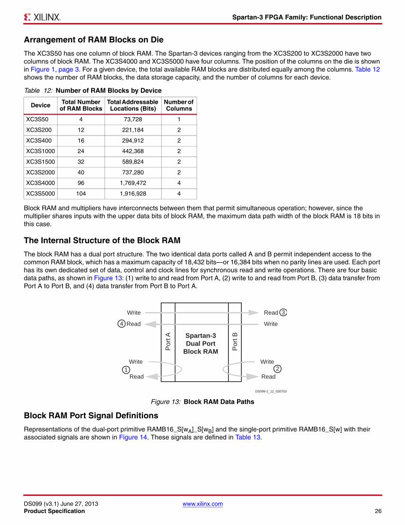
The Internal Structure of the Block RAM
The block RAM has a dual port structure. The two identical data ports called A and B permit independent access to the common RAM block, which has a maximum capacity of 18,432 bits—or 16,384 bits when no parity lines are used. Each port has its own dedicated set of data, control and clock lines for synchronous read and write operations. There are four basic data paths, as shown in Figure 13: (1) write to and read from Port A, (2) write to and read from Port B, (3) data transfer from Port A to Port B, and (4) data transfer from Port B to Port A.
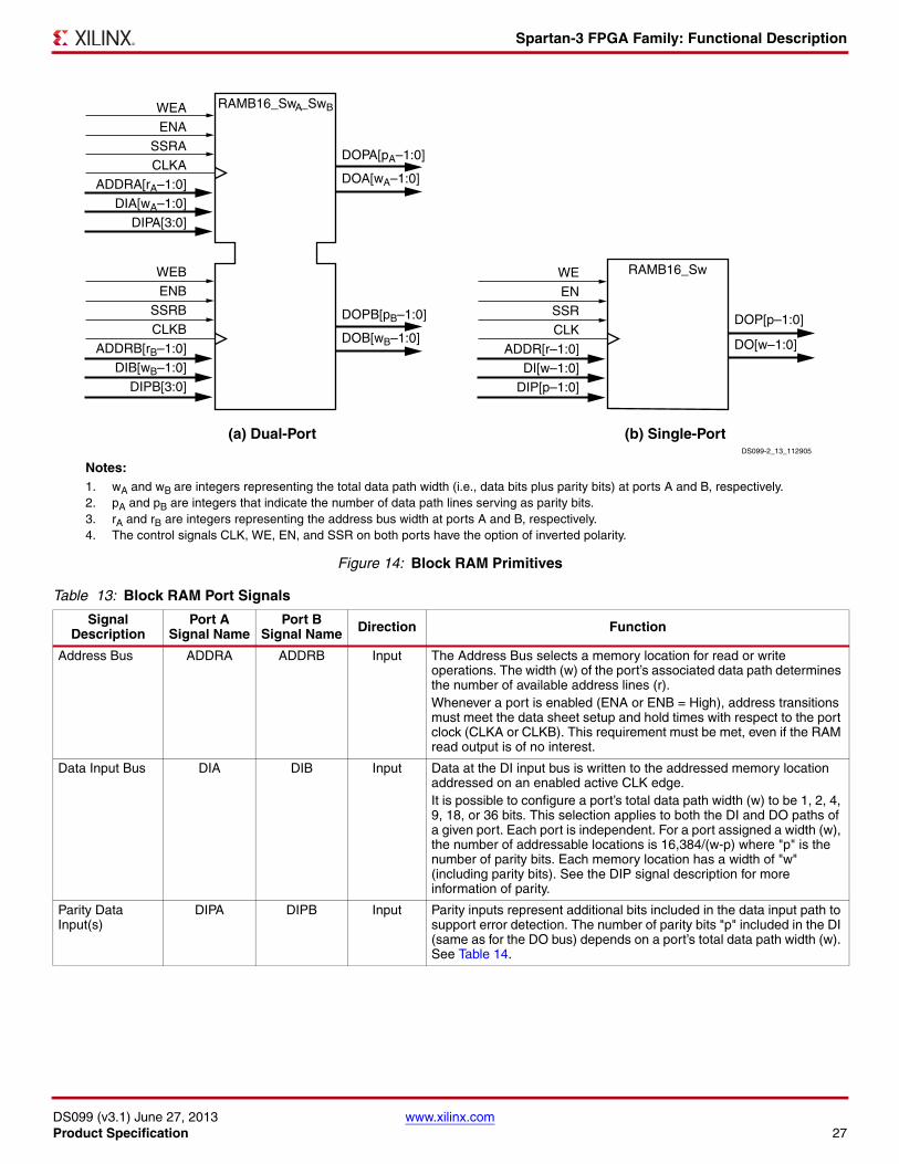
Block RAM Port Signal Definitions
Representations of the dual-port primitive RAMB16_S[wA]_S[wB] and the single-port primitive RAMB16_S[w] with their associated signals are shown in Figure 14. These signals are defined in Table 13.
Table 12: Number of RAM Blocks by Device
Device Total Number of RAM Blocks
Total Addressable Locations (Bits)
Number of Columns
XC3S50 4 73,728 1
XC3S200 12 221,184 2
XC3S400 16 294,912 2
XC3S1000 24 442,368 2
XC3S1500 32 589,824 2
XC3S2000 40 737,280 2
XC3S4000 96 1,769,472 4
XC3S5000 104 1,916,928 4
X-Ref Target - Figure 13
Figure 13: Block RAM Data Paths
DS099-2_12_030703
Spartan-3Dual Port
Block RAM
Read 3
Read
Write
Write
Read
Write
Write
Read
Por
t A
Por
t B
21
4
Spartan-3 FPGA Family: Functional Description
DS099 (v3.1) June 27, 2013 www.xilinx.comProduct Specification 27
X-Ref Target - Figure 14
Figure 14: Block RAM Primitives
Table 13: Block RAM Port Signals
Signal Description
Port A Signal Name
Port B Signal Name Direction Function
Address Bus ADDRA ADDRB Input The Address Bus selects a memory location for read or write operations. The width (w) of the port’s associated data path determines the number of available address lines (r). Whenever a port is enabled (ENA or ENB = High), address transitions must meet the data sheet setup and hold times with respect to the port clock (CLKA or CLKB). This requirement must be met, even if the RAM read output is of no interest.
Data Input Bus DIA DIB Input Data at the DI input bus is written to the addressed memory location addressed on an enabled active CLK edge. It is possible to configure a port’s total data path width (w) to be 1, 2, 4, 9, 18, or 36 bits. This selection applies to both the DI and DO paths of a given port. Each port is independent. For a port assigned a width (w), the number of addressable locations is 16,384/(w-p) where "p" is the number of parity bits. Each memory location has a width of "w" (including parity bits). See the DIP signal description for more information of parity.
Parity Data Input(s)
DIPA DIPB Input Parity inputs represent additional bits included in the data input path to support error detection. The number of parity bits "p" included in the DI (same as for the DO bus) depends on a port’s total data path width (w). See Table 14.
DS099-2_13_112905
WEAENA
SSRACLKA
ADDRA[rA–1:0]DIA[wA–1:0]
DIPA[3:0]
DOPA[pA–1:0]
DOA[wA–1:0]
RAMB16_SwA_SwB
(a) Dual-Port (b) Single-Port
DOPB[pB–1:0]
DOB[wB–1:0]
WEBENB
SSRBCLKB
ADDRB[rB–1:0]DIB[wB–1:0]
DIPB[3:0]
WEEN
SSRCLK
ADDR[r–1:0]DI[w–1:0]
DIP[p–1:0]
DOP[p–1:0]
DO[w–1:0]
RAMB16_Sw
Notes: 1. wA and wB are integers representing the total data path width (i.e., data bits plus parity bits) at ports A and B, respectively.2. pA and pB are integers that indicate the number of data path lines serving as parity bits.3. rA and rB are integers representing the address bus width at ports A and B, respectively.4. The control signals CLK, WE, EN, and SSR on both ports have the option of inverted polarity.
Spartan-3 FPGA Family: Functional Description
DS099 (v3.1) June 27, 2013 www.xilinx.comProduct Specification 28
Port Aspect Ratios
On a given port, it is possible to select a number of different possible widths (w – p) for the DI/DO buses as shown in Table 14. These two buses always have the same width. This data bus width selection is independent for each port. If the data bus width of Port A differs from that of Port B, the Block RAM automatically performs a bus-matching function. When data are written to a port with a narrow bus, then read from a port with a wide bus, the latter port will effectively combine “narrow” words to form “wide” words. Similarly, when data are written into a port with a wide bus, then read from a port with a narrow bus, the latter port will divide “wide” words to form “narrow” words. When the data bus width is eight bits or greater, extra parity bits become available. The width of the total data path (w) is the sum of the DI/DO bus width and any parity bits (p).
The width selection made for the DI/DO bus determines the number of address lines according to the relationship expressed below:
r = 14 – [log(w–p)/log(2)] Equation 1
In turn, the number of address lines delimits the total number (n) of addressable locations or depth according to the following equation:
n = 2r Equation 2
Data Output Bus DOA DOB Output Basic data access occurs whenever WE is inactive. The DO outputs mirror the data stored in the addressed memory location. Data access with WE asserted is also possible if one of the following two attributes is chosen: WRITE_FIRST and READ_FIRST. WRITE_FIRST simultaneously presents the new input data on the DO output port and writes the data to the address RAM location. READ_FIRST presents the previously stored RAM data on the DO output port while writing new data to RAM.A third attribute, NO_CHANGE, latches the DO outputs upon the assertion of WE. It is possible to configure a port’s total data path width (w) to be 1, 2, 4, 9, 18, or 36 bits. This selection applies to both the DI and DO paths. See the DI signal description.
Parity Data Output(s)
DOPA DOPB Output Parity inputs represent additional bits included in the data input path to support error detection. The number of parity bits "p" included in the DI (same as for the DO bus) depends on a port’s total data path width (w). See Table 14.
Write Enable WEA WEB Input When asserted together with EN, this input enables the writing of data to the RAM. In this case, the data access attributes WRITE_FIRST, READ_FIRST or NO_CHANGE determines if and how data is updated on the DO outputs. See the DO signal description. When WE is inactive with EN asserted, read operations are still possible. In this case, a transparent latch passes data from the addressed memory location to the DO outputs.
Clock Enable ENA ENB Input When asserted, this input enables the CLK signal to synchronize Block RAM functions as follows: the writing of data to the DI inputs (when WE is also asserted), the updating of data at the DO outputs as well as the setting/resetting of the DO output latches.When de-asserted, the above functions are disabled.
Set/Reset SSRA SSRB Input When asserted, this pin forces the DO output latch to the value that the SRVAL attribute is set to. A Set/Reset operation on one port has no effect on the other ports functioning, nor does it disturb the memory’s data contents. It is synchronized to the CLK signal.
Clock CLKA CLKB Input This input accepts the clock signal to which read and write operations are synchronized. All associated port inputs are required to meet setup times with respect to the clock signal’s active edge. The data output bus responds after a clock-to-out delay referenced to the clock signal’s active edge.
Table 13: Block RAM Port Signals (Cont’d)
Signal Description
Port A Signal Name
Port B Signal Name Direction Function
Spartan-3 FPGA Family: Functional Description
DS099 (v3.1) June 27, 2013 www.xilinx.comProduct Specification 29
The product of w and n yields the total block RAM capacity. Equation 1 and Equation 2 show that as the data bus width increases, the number of address lines along with the number of addressable memory locations decreases. Using the permissible DI/DO bus widths as inputs to these equations provides the bus width and memory capacity measures shown in Table 14.
Block RAM Data Operations
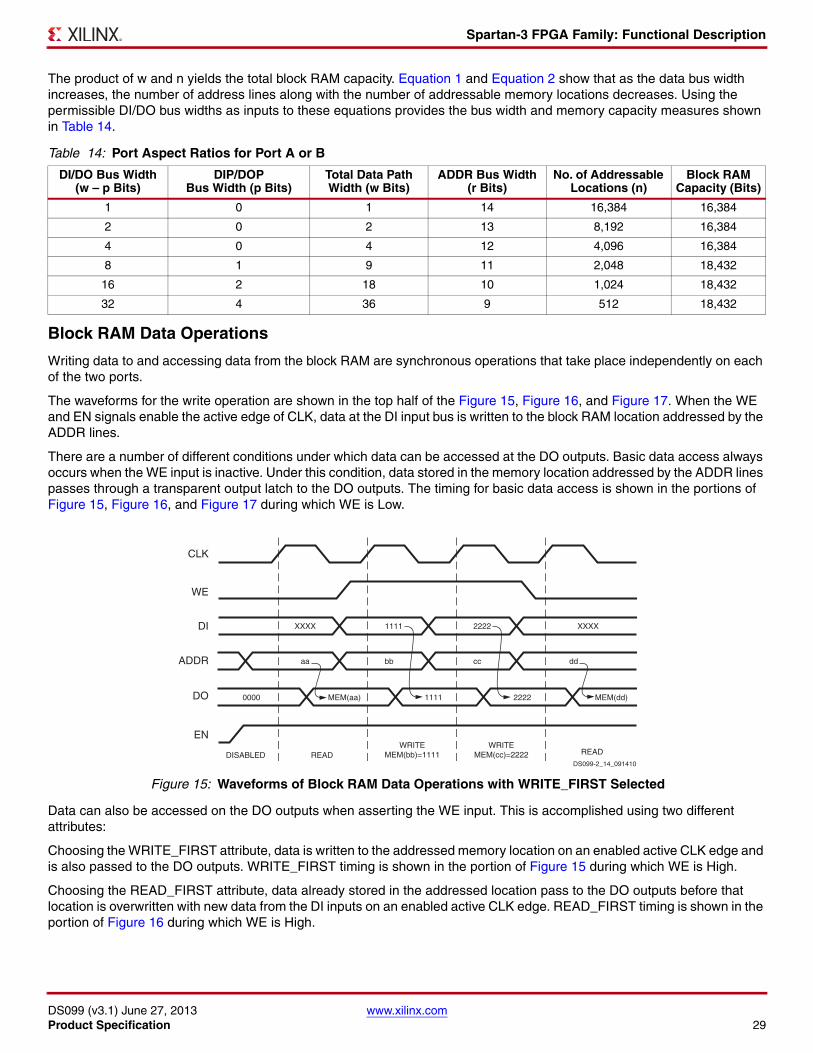
Writing data to and accessing data from the block RAM are synchronous operations that take place independently on each of the two ports.
The waveforms for the write operation are shown in the top half of the Figure 15, Figure 16, and Figure 17. When the WE and EN signals enable the active edge of CLK, data at the DI input bus is written to the block RAM location addressed by the ADDR lines.
There are a number of different conditions under which data can be accessed at the DO outputs. Basic data access always occurs when the WE input is inactive. Under this condition, data stored in the memory location addressed by the ADDR lines passes through a transparent output latch to the DO outputs. The timing for basic data access is shown in the portions of Figure 15, Figure 16, and Figure 17 during which WE is Low.
Data can also be accessed on the DO outputs when asserting the WE input. This is accomplished using two different attributes:
Choosing the WRITE_FIRST attribute, data is written to the addressed memory location on an enabled active CLK edge and is also passed to the DO outputs. WRITE_FIRST timing is shown in the portion of Figure 15 during which WE is High.
Choosing the READ_FIRST attribute, data already stored in the addressed location pass to the DO outputs before that location is overwritten with new data from the DI inputs on an enabled active CLK edge. READ_FIRST timing is shown in the portion of Figure 16 during which WE is High.
Table 14: Port Aspect Ratios for Port A or B
DI/DO Bus Width(w – p Bits)
DIP/DOP Bus Width (p Bits)
Total Data Path Width (w Bits)
ADDR Bus Width (r Bits)
No. of Addressable Locations (n)
Block RAM Capacity (Bits)
1 0 1 14 16,384 16,384
2 0 2 13 8,192 16,384
4 0 4 12 4,096 16,384
8 1 9 11 2,048 18,432
16 2 18 10 1,024 18,432
32 4 36 9 512 18,432
X-Ref Target - Figure 15
Figure 15: Waveforms of Block RAM Data Operations with WRITE_FIRST Selected
CLK
WE
DI
ADDR
DO
EN
DISABLED READ
XXXX 1111 2222 XXXX
aa bb cc dd
0000 MEM(aa) 1111 2222 MEM(dd)
READWRITE
MEM(bb)=1111WRITE
MEM(cc)=2222DS099-2_14_091410
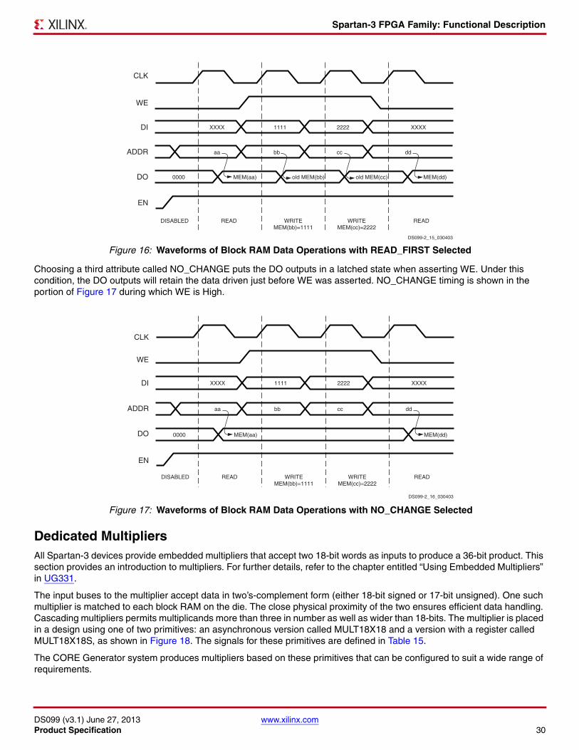
Spartan-3 FPGA Family: Functional Description
DS099 (v3.1) June 27, 2013 www.xilinx.comProduct Specification 30
Choosing a third attribute called NO_CHANGE puts the DO outputs in a latched state when asserting WE. Under this condition, the DO outputs will retain the data driven just before WE was asserted. NO_CHANGE timing is shown in the portion of Figure 17 during which WE is High.
Dedicated MultipliersAll Spartan-3 devices provide embedded multipliers that accept two 18-bit words as inputs to produce a 36-bit product. This section provides an introduction to multipliers. For further details, refer to the chapter entitled “Using Embedded Multipliers” in UG331.
The input buses to the multiplier accept data in two’s-complement form (either 18-bit signed or 17-bit unsigned). One such multiplier is matched to each block RAM on the die. The close physical proximity of the two ensures efficient data handling. Cascading multipliers permits multiplicands more than three in number as well as wider than 18-bits. The multiplier is placed in a design using one of two primitives: an asynchronous version called MULT18X18 and a version with a register called MULT18X18S, as shown in Figure 18. The signals for these primitives are defined in Table 15.
The CORE Generator system produces multipliers based on these primitives that can be configured to suit a wide range of requirements.
X-Ref Target - Figure 16
Figure 16: Waveforms of Block RAM Data Operations with READ_FIRST Selected
X-Ref Target - Figure 17
Figure 17: Waveforms of Block RAM Data Operations with NO_CHANGE Selected
CLK
WE
DI
ADDR
DO
EN
DISABLED READ
XXXX 1111 2222 XXXX
aa bb cc dd
0000 MEM(aa) old MEM(bb) old MEM(cc) MEM(dd)
READWRITEMEM(bb)=1111
WRITEMEM(cc)=2222
DS099-2_15_030403
CLK
WE
DI
ADDR
DO
EN
DISABLED READ
XXXX 1111 2222 XXXX
aa bb cc dd
0000 MEM(aa) MEM(dd)
READWRITEMEM(bb)=1111
WRITEMEM(cc)=2222
DS099-2_16_030403
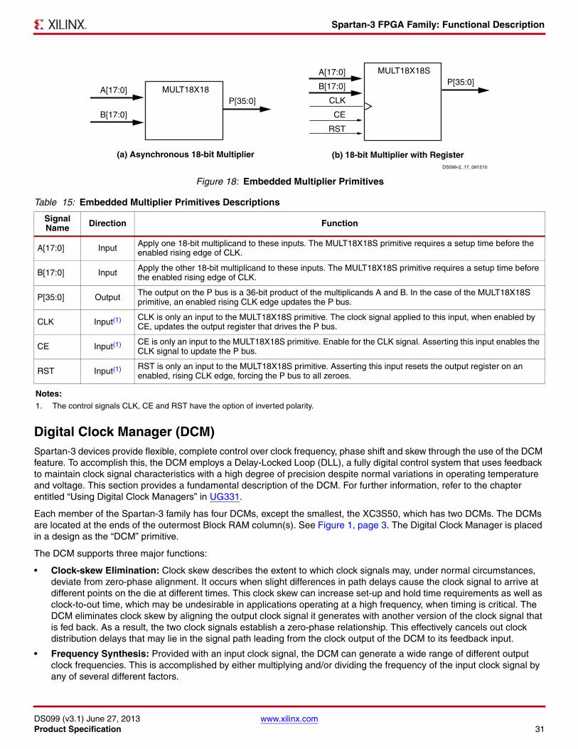
Spartan-3 FPGA Family: Functional Description
DS099 (v3.1) June 27, 2013 www.xilinx.comProduct Specification 31
Digital Clock Manager (DCM)Spartan-3 devices provide flexible, complete control over clock frequency, phase shift and skew through the use of the DCM feature. To accomplish this, the DCM employs a Delay-Locked Loop (DLL), a fully digital control system that uses feedback to maintain clock signal characteristics with a high degree of precision despite normal variations in operating temperature and voltage. This section provides a fundamental description of the DCM. For further information, refer to the chapter entitled “Using Digital Clock Managers” in UG331.
Each member of the Spartan-3 family has four DCMs, except the smallest, the XC3S50, which has two DCMs. The DCMs are located at the ends of the outermost Block RAM column(s). See Figure 1, page 3. The Digital Clock Manager is placed in a design as the “DCM” primitive.
The DCM supports three major functions:
• Clock-skew Elimination: Clock skew describes the extent to which clock signals may, under normal circumstances, deviate from zero-phase alignment. It occurs when slight differences in path delays cause the clock signal to arrive at different points on the die at different times. This clock skew can increase set-up and hold time requirements as well as clock-to-out time, which may be undesirable in applications operating at a high frequency, when timing is critical. The DCM eliminates clock skew by aligning the output clock signal it generates with another version of the clock signal that is fed back. As a result, the two clock signals establish a zero-phase relationship. This effectively cancels out clock distribution delays that may lie in the signal path leading from the clock output of the DCM to its feedback input.
• Frequency Synthesis: Provided with an input clock signal, the DCM can generate a wide range of different output clock frequencies. This is accomplished by either multiplying and/or dividing the frequency of the input clock signal by any of several different factors.
X-Ref Target - Figure 18
Figure 18: Embedded Multiplier Primitives
Table 15: Embedded Multiplier Primitives Descriptions
Signal Name Direction Function
A[17:0] Input Apply one 18-bit multiplicand to these inputs. The MULT18X18S primitive requires a setup time before the enabled rising edge of CLK.
B[17:0] Input Apply the other 18-bit multiplicand to these inputs. The MULT18X18S primitive requires a setup time before the enabled rising edge of CLK.
P[35:0] Output The output on the P bus is a 36-bit product of the multiplicands A and B. In the case of the MULT18X18S primitive, an enabled rising CLK edge updates the P bus.
CLK Input(1) CLK is only an input to the MULT18X18S primitive. The clock signal applied to this input, when enabled by CE, updates the output register that drives the P bus.
CE Input(1) CE is only an input to the MULT18X18S primitive. Enable for the CLK signal. Asserting this input enables the CLK signal to update the P bus.
RST Input(1) RST is only an input to the MULT18X18S primitive. Asserting this input resets the output register on an enabled, rising CLK edge, forcing the P bus to all zeroes.
Notes: 1. The control signals CLK, CE and RST have the option of inverted polarity.
DS099-2_17_091510
(a) Asynchronous 18-bit Multiplier (b) 18-bit Multiplier with Register
A[17:0]
B[17:0]
P[35:0]MULT18X18
A[17:0]
B[17:0]
CLK
CE
RST
P[35:0]MULT18X18S
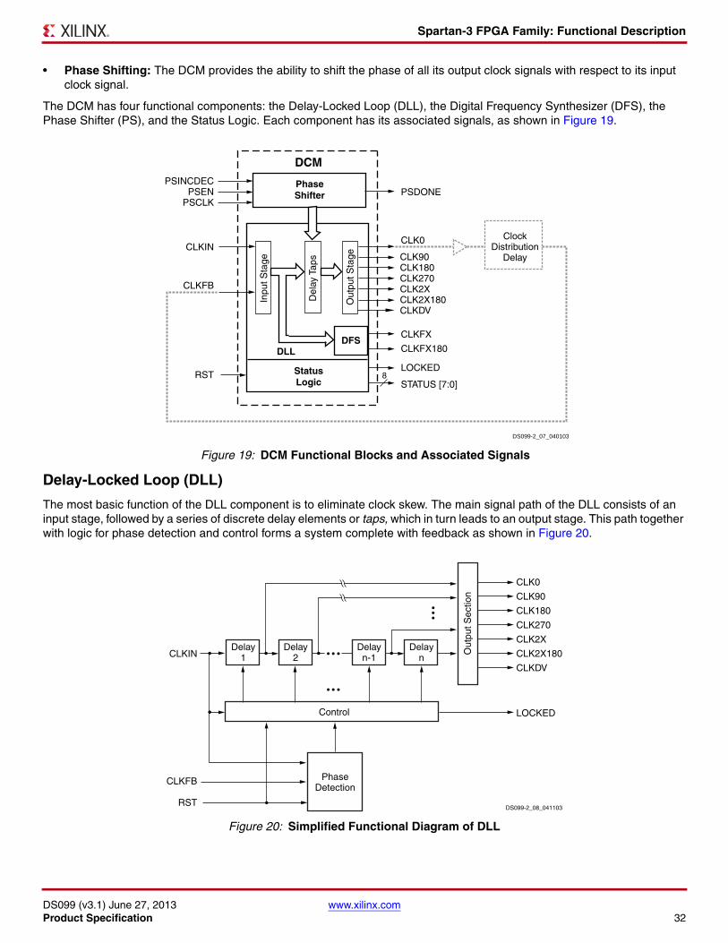
Spartan-3 FPGA Family: Functional Description
DS099 (v3.1) June 27, 2013 www.xilinx.comProduct Specification 32
• Phase Shifting: The DCM provides the ability to shift the phase of all its output clock signals with respect to its input clock signal.
The DCM has four functional components: the Delay-Locked Loop (DLL), the Digital Frequency Synthesizer (DFS), the Phase Shifter (PS), and the Status Logic. Each component has its associated signals, as shown in Figure 19.
Delay-Locked Loop (DLL)
The most basic function of the DLL component is to eliminate clock skew. The main signal path of the DLL consists of an input stage, followed by a series of discrete delay elements or taps, which in turn leads to an output stage. This path together with logic for phase detection and control forms a system complete with feedback as shown in Figure 20.
X-Ref Target - Figure 19
Figure 19: DCM Functional Blocks and Associated Signals
X-Ref Target - Figure 20
Figure 20: Simplified Functional Diagram of DLL
DS099-2_07_040103
PSINCDECPSEN
PSCLK
CLKIN
CLKFB
RSTSTATUS [7:0]
LOCKED8
CLKFX180
CLKFX
CLK0
PSDONE
ClockDistribution
DelayCLK90CLK180CLK270CLK2XCLK2X180CLKDV
StatusLogic
DFSDLL
PhaseShifter
Del
ay T
aps
Out
put S
tage
Inpu
t Sta
ge
DCM
DS099-2_08_041103
CLKINDelayn
CLKFB
RST
CLK0
CLK90
CLK180
CLK270
CLK2X
CLK2X180
CLKDV
Out
put S
ectio
n
Control
Delayn-1
PhaseDetection
LOCKED
Delay2
Delay1
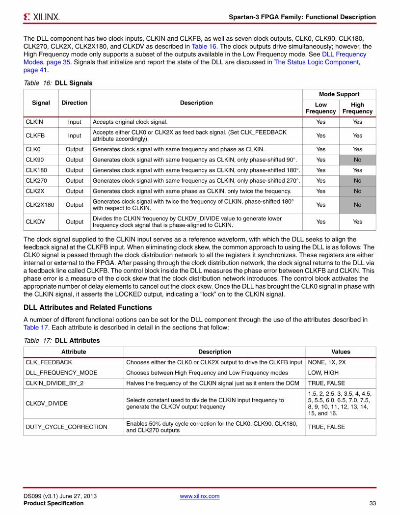
Spartan-3 FPGA Family: Functional Description
DS099 (v3.1) June 27, 2013 www.xilinx.comProduct Specification 33
The DLL component has two clock inputs, CLKIN and CLKFB, as well as seven clock outputs, CLK0, CLK90, CLK180, CLK270, CLK2X, CLK2X180, and CLKDV as described in Table 16. The clock outputs drive simultaneously; however, the High Frequency mode only supports a subset of the outputs available in the Low Frequency mode. See DLL Frequency Modes, page 35. Signals that initialize and report the state of the DLL are discussed in The Status Logic Component, page 41.
The clock signal supplied to the CLKIN input serves as a reference waveform, with which the DLL seeks to align the feedback signal at the CLKFB input. When eliminating clock skew, the common approach to using the DLL is as follows: The CLK0 signal is passed through the clock distribution network to all the registers it synchronizes. These registers are either internal or external to the FPGA. After passing through the clock distribution network, the clock signal returns to the DLL via a feedback line called CLKFB. The control block inside the DLL measures the phase error between CLKFB and CLKIN. This phase error is a measure of the clock skew that the clock distribution network introduces. The control block activates the appropriate number of delay elements to cancel out the clock skew. Once the DLL has brought the CLK0 signal in phase with the CLKIN signal, it asserts the LOCKED output, indicating a “lock” on to the CLKIN signal.
DLL Attributes and Related Functions
A number of different functional options can be set for the DLL component through the use of the attributes described in Table 17. Each attribute is described in detail in the sections that follow:
Table 16: DLL Signals
Signal Direction DescriptionMode Support
Low Frequency
High Frequency
CLKIN Input Accepts original clock signal. Yes Yes
CLKFB Input Accepts either CLK0 or CLK2X as feed back signal. (Set CLK_FEEDBACK attribute accordingly). Yes Yes
CLK0 Output Generates clock signal with same frequency and phase as CLKIN. Yes Yes
CLK90 Output Generates clock signal with same frequency as CLKIN, only phase-shifted 90°. Yes No
CLK180 Output Generates clock signal with same frequency as CLKIN, only phase-shifted 180°. Yes Yes
CLK270 Output Generates clock signal with same frequency as CLKIN, only phase-shifted 270°. Yes No
CLK2X Output Generates clock signal with same phase as CLKIN, only twice the frequency. Yes No
CLK2X180 Output Generates clock signal with twice the frequency of CLKIN, phase-shifted 180° with respect to CLKIN. Yes No
CLKDV Output Divides the CLKIN frequency by CLKDV_DIVIDE value to generate lower frequency clock signal that is phase-aligned to CLKIN. Yes Yes
Table 17: DLL Attributes
Attribute Description Values
CLK_FEEDBACK Chooses either the CLK0 or CLK2X output to drive the CLKFB input NONE, 1X, 2X
DLL_FREQUENCY_MODE Chooses between High Frequency and Low Frequency modes LOW, HIGH
CLKIN_DIVIDE_BY_2 Halves the frequency of the CLKIN signal just as it enters the DCM TRUE, FALSE
CLKDV_DIVIDE Selects constant used to divide the CLKIN input frequency to generate the CLKDV output frequency
1.5, 2, 2.5, 3, 3.5, 4, 4.5, 5, 5.5, 6.0, 6.5, 7.0, 7.5, 8, 9, 10, 11, 12, 13, 14, 15, and 16.
DUTY_CYCLE_CORRECTION Enables 50% duty cycle correction for the CLK0, CLK90, CLK180, and CLK270 outputs TRUE, FALSE
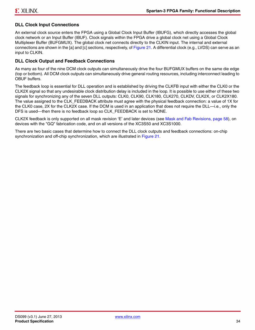
Spartan-3 FPGA Family: Functional Description
DS099 (v3.1) June 27, 2013 www.xilinx.comProduct Specification 34
DLL Clock Input Connections
An external clock source enters the FPGA using a Global Clock Input Buffer (IBUFG), which directly accesses the global clock network or an Input Buffer (IBUF). Clock signals within the FPGA drive a global clock net using a Global Clock Multiplexer Buffer (BUFGMUX). The global clock net connects directly to the CLKIN input. The internal and external connections are shown in the [a] and [c] sections, respectively, of Figure 21. A differential clock (e.g., LVDS) can serve as an input to CLKIN.
DLL Clock Output and Feedback Connections
As many as four of the nine DCM clock outputs can simultaneously drive the four BUFGMUX buffers on the same die edge (top or bottom). All DCM clock outputs can simultaneously drive general routing resources, including interconnect leading to OBUF buffers.
The feedback loop is essential for DLL operation and is established by driving the CLKFB input with either the CLK0 or the CLK2X signal so that any undesirable clock distribution delay is included in the loop. It is possible to use either of these two signals for synchronizing any of the seven DLL outputs: CLK0, CLK90, CLK180, CLK270, CLKDV, CLK2X, or CLK2X180. The value assigned to the CLK_FEEDBACK attribute must agree with the physical feedback connection: a value of 1X for the CLK0 case, 2X for the CLK2X case. If the DCM is used in an application that does not require the DLL—i.e., only the DFS is used—then there is no feedback loop so CLK_FEEDBACK is set to NONE.
CLK2X feedback is only supported on all mask revision ‘E’ and later devices (see Mask and Fab Revisions, page 58), on devices with the "GQ" fabrication code, and on all versions of the XC3S50 and XC3S1000.
There are two basic cases that determine how to connect the DLL clock outputs and feedback connections: on-chip synchronization and off-chip synchronization, which are illustrated in Figure 21.
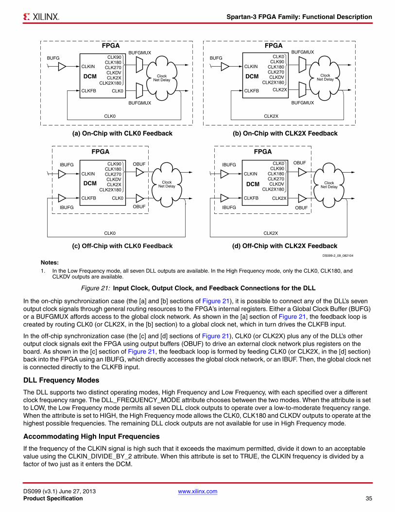
Spartan-3 FPGA Family: Functional Description
DS099 (v3.1) June 27, 2013 www.xilinx.comProduct Specification 35
In the on-chip synchronization case (the [a] and [b] sections of Figure 21), it is possible to connect any of the DLL’s seven output clock signals through general routing resources to the FPGA’s internal registers. Either a Global Clock Buffer (BUFG) or a BUFGMUX affords access to the global clock network. As shown in the [a] section of Figure 21, the feedback loop is created by routing CLK0 (or CLK2X, in the [b] section) to a global clock net, which in turn drives the CLKFB input.
In the off-chip synchronization case (the [c] and [d] sections of Figure 21), CLK0 (or CLK2X) plus any of the DLL’s other output clock signals exit the FPGA using output buffers (OBUF) to drive an external clock network plus registers on the board. As shown in the [c] section of Figure 21, the feedback loop is formed by feeding CLK0 (or CLK2X, in the [d] section) back into the FPGA using an IBUFG, which directly accesses the global clock network, or an IBUF. Then, the global clock net is connected directly to the CLKFB input.
DLL Frequency Modes
The DLL supports two distinct operating modes, High Frequency and Low Frequency, with each specified over a different clock frequency range. The DLL_FREQUENCY_MODE attribute chooses between the two modes. When the attribute is set to LOW, the Low Frequency mode permits all seven DLL clock outputs to operate over a low-to-moderate frequency range. When the attribute is set to HIGH, the High Frequency mode allows the CLK0, CLK180 and CLKDV outputs to operate at the highest possible frequencies. The remaining DLL clock outputs are not available for use in High Frequency mode.
Accommodating High Input Frequencies
If the frequency of the CLKIN signal is high such that it exceeds the maximum permitted, divide it down to an acceptable value using the CLKIN_DIVIDE_BY_2 attribute. When this attribute is set to TRUE, the CLKIN frequency is divided by a factor of two just as it enters the DCM.
X-Ref Target - Figure 21
Figure 21: Input Clock, Output Clock, and Feedback Connections for the DLL
DS099-2_09_082104
CLK90CLK180CLK270CLKDVCLK2X
CLK2X180
CLK0
CLK0
ClockNet Delay
BUFGMUX
BUFGMUX
BUFG
FPGA
(a) On-Chip with CLK0 Feedback
CLKIN
DCM
CLKFB
CLK90CLK180CLK270CLKDVCLK2X
CLK2X180
CLK0
CLK0
ClockNet Delay
IBUFG
IBUFG
FPGA
(c) Off-Chip with CLK0 Feedback
CLKIN
DCM
CLKFB
OBUF
OBUF
CLK2X
CLK2X
IBUFG
IBUFG
FPGA
(d) Off-Chip with CLK2X Feedback
CLKIN
DCM
CLKFB
OBUF
OBUF
CLK0CLK90
CLK180CLK270CLKDV
CLK2X180
CLK2X
CLK2X
ClockNet Delay
ClockNet Delay
BUFGMUX
BUFGMUX
BUFG
FPGA
(b) On-Chip with CLK2X Feedback
CLKIN
DCM
CLKFB
CLK0CLK90
CLK180CLK270CLKDV
CLK2X180
Notes: 1. In the Low Frequency mode, all seven DLL outputs are available. In the High Frequency mode, only the CLK0, CLK180, and
CLKDV outputs are available.
Spartan-3 FPGA Family: Functional Description
DS099 (v3.1) June 27, 2013 www.xilinx.comProduct Specification 36
Coarse Phase Shift Outputs of the DLL Component
In addition to CLK0 for zero-phase alignment to the CLKIN signal, the DLL also provides the CLK90, CLK180 and CLK270 outputs for 90°, 180° and 270° phase-shifted signals, respectively. These signals are described in Table 16, page 33. Their relative timing in the Low Frequency Mode is shown in Figure 22, page 37. The CLK90, CLK180 and CLK270 outputs are not available when operating in the High Frequency mode. (See the description of the DLL_FREQUENCY_MODE attribute in Table 17, page 33.) For control in finer increments than 90°, see Phase Shifter (PS), page 39.
Basic Frequency Synthesis Outputs of the DLL Component
The DLL component provides basic options for frequency multiplication and division in addition to the more flexible synthesis capability of the DFS component, described in a later section. These operations result in output clock signals with frequencies that are either a fraction (for division) or a multiple (for multiplication) of the incoming clock frequency. The CLK2X output produces an in-phase signal that is twice the frequency of CLKIN. The CLK2X180 output also doubles the frequency, but is 180° out-of-phase with respect to CLKIN. The CLKDIV output generates a clock frequency that is a predetermined fraction of the CLKIN frequency. The CLKDV_DIVIDE attribute determines the factor used to divide the CLKIN frequency. The attribute can be set to various values as described in Table 17. The basic frequency synthesis outputs are described in Table 16. Their relative timing in the Low Frequency Mode is shown in Figure 22.
The CLK2X and CLK2X180 outputs are not available when operating in the High Frequency mode. See the description of the DLL_FREQUENCY_MODE attribute in Table 18.
Duty Cycle Correction of DLL Clock Outputs
The CLK2X(1), CLK2X180, and CLKDV(2) output signals ordinarily exhibit a 50% duty cycle—even if the incoming CLKIN signal has a different duty cycle. A 50% duty cycle means that the High and Low times of each clock cycle are equal. The DUTY_CYCLE_CORRECTION attribute determines whether or not duty cycle correction is applied to the CLK0, CLK90, CLK180 and CLK270 outputs. If DUTY_CYCLE_CORRECTION is set to TRUE, then the duty cycle of these four outputs is corrected to 50%. If DUTY_CYCLE_CORRECTION is set to FALSE, then these outputs exhibit the same duty cycle as the CLKIN signal. Figure 22 compares the characteristics of the DLL’s output signals to those of the CLKIN signal.
1. The CLK2X output generates a 25% duty cycle clock at the same frequency as the CLKIN signal until the DLL has achieved lock.
2. The duty cycle of the CLKDV outputs may differ somewhat from 50% (i.e., the signal will be High for less than 50% of the period) when the CLKDV_DIVIDE attribute is set to a non-integer value and the DLL is operating in the High Frequency mode.
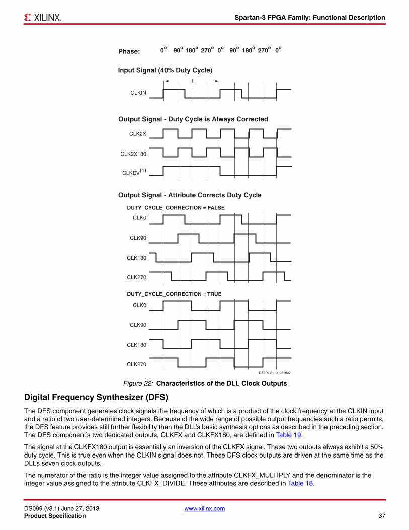
Spartan-3 FPGA Family: Functional Description
DS099 (v3.1) June 27, 2013 www.xilinx.comProduct Specification 37
Digital Frequency Synthesizer (DFS)
The DFS component generates clock signals the frequency of which is a product of the clock frequency at the CLKIN input and a ratio of two user-determined integers. Because of the wide range of possible output frequencies such a ratio permits, the DFS feature provides still further flexibility than the DLL’s basic synthesis options as described in the preceding section. The DFS component’s two dedicated outputs, CLKFX and CLKFX180, are defined in Table 19.
The signal at the CLKFX180 output is essentially an inversion of the CLKFX signal. These two outputs always exhibit a 50% duty cycle. This is true even when the CLKIN signal does not. These DFS clock outputs are driven at the same time as the DLL’s seven clock outputs.
The numerator of the ratio is the integer value assigned to the attribute CLKFX_MULTIPLY and the denominator is the integer value assigned to the attribute CLKFX_DIVIDE. These attributes are described in Table 18.
X-Ref Target - Figure 22
Figure 22: Characteristics of the DLL Clock Outputs
Output Signal - Duty Cycle is Always Corrected
Output Signal - Attribute Corrects Duty Cycle
Phase:
Input Signal (40% Duty Cycle)
0o 90o 180o 270o 0o 90o 180o 270o 0o
DUTY_CYCLE_CORRECTION = FALSE
DUTY_CYCLE_CORRECTION = TRUE
DS099-2_10_051907
CLK2X
CLK2X180
CLKIN
CLKDV(1)
CLK0
CLK90
CLK180
CLK270
CLK0
CLK90
CLK180
CLK270
t
Spartan-3 FPGA Family: Functional Description
DS099 (v3.1) June 27, 2013 www.xilinx.comProduct Specification 38
The output frequency (fCLKFX) can be expressed as a function of the incoming clock frequency (fCLKIN) as follows:
fCLKFX = fCLKIN(CLKFX_MULTIPLY/CLKFX_DIVIDE) Equation 3
Regarding the two attributes, it is possible to assign any combination of integer values, provided that two conditions are met:
• The two values fall within their corresponding ranges, as specified in Table 18.
• The fCLKFX frequency calculated from the above expression accords with the DCM’s operating frequency specifications.
For example, if CLKFX_MULTIPLY = 5 and CLKFX_DIVIDE = 3, then the frequency of the output clock signal would be 5/3 that of the input clock signal.
DFS Frequency Modes
The DFS supports two operating modes, High Frequency and Low Frequency, with each specified over a different clock frequency range. The DFS_FREQUENCY_MODE attribute chooses between the two modes. When the attribute is set to LOW, the Low Frequency mode permits the two DFS outputs to operate over a low-to-moderate frequency range. When the attribute is set to HIGH, the High Frequency mode allows both these outputs to operate at the highest possible frequencies.
DFS With or Without the DLL
The DFS component can be used with or without the DLL component:
Without the DLL, the DFS component multiplies or divides the CLKIN signal frequency according to the respective CLKFX_MULTIPLY and CLKFX_DIVIDE values, generating a clock with the new target frequency on the CLKFX and CLKFX180 outputs. Though classified as belonging to the DLL component, the CLKIN input is shared with the DFS component. This case does not employ feedback loop; therefore, it cannot correct for clock distribution delay.
With the DLL, the DFS operates as described in the preceding case, only with the additional benefit of eliminating the clock distribution delay. In this case, a feedback loop from the CLK0 output to the CLKFB input must be present.
The DLL and DFS components work together to achieve this phase correction as follows: Given values for the CLKFX_MULTIPLY and CLKFX_DIVIDE attributes, the DLL selects the delay element for which the output clock edge coincides with the input clock edge whenever mathematically possible. For example, when CLKFX_MULTIPLY = 5 and CLKFX_DIVIDE = 3, the input and output clock edges will coincide every three input periods, which is equivalent in time to five output periods.
Smaller CLKFX_MULTIPLY and CLKFX_DIVIDE values achieve faster lock times. With no factors common to the two attributes, alignment will occur once with every number of cycles equal to the CLKFX_DIVIDE value. Therefore, it is recommended that the user reduce these values by factoring wherever possible. For example, given CLKFX_MULTIPLY = 9 and CLKFX_DIVIDE = 6, removing a factor of three yields CLKFX_MULTIPLY = 3 and CLKFX_DIVIDE = 2. While both value-pairs will result in the multiplication of clock frequency by 3/2, the latter value-pair will enable the DLL to lock more quickly.
Table 18: DFS Attributes
Attribute Description Values
DFS_FREQUENCY_MODE Chooses between High Frequency and Low Frequency modes Low, High
CLKFX_MULTIPLY Frequency multiplier constant Integer from 2 to 32
CLKFX_DIVIDE Frequency divisor constant Integer from 1 to 32
Table 19: DFS Signals
Signal Direction Description
CLKFX Output Multiplies the CLKIN frequency by the attribute-value ratio (CLKFX_MULTIPLY/CLKFX_DIVIDE) to generate a clock signal with a new target frequency.
CLKFX180 Output Generates a clock signal with same frequency as CLKFX, only shifted 180° out-of-phase.
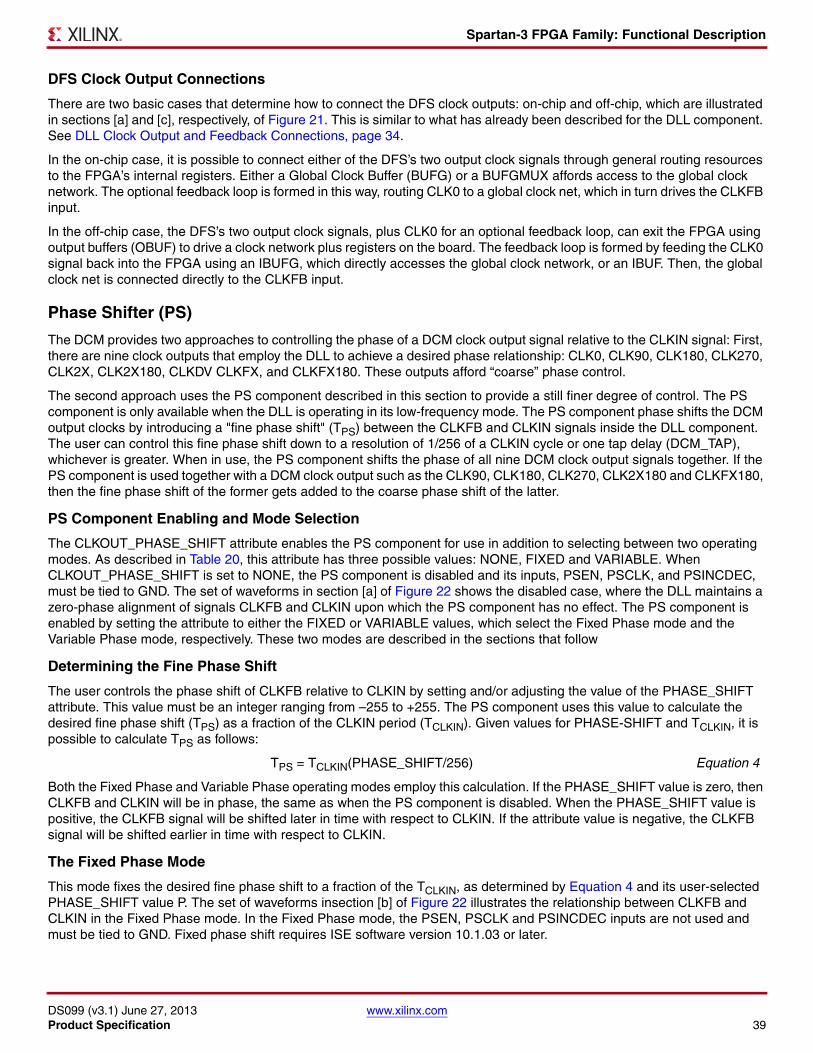
Spartan-3 FPGA Family: Functional Description
DS099 (v3.1) June 27, 2013 www.xilinx.comProduct Specification 39
DFS Clock Output Connections
There are two basic cases that determine how to connect the DFS clock outputs: on-chip and off-chip, which are illustrated in sections [a] and [c], respectively, of Figure 21. This is similar to what has already been described for the DLL component. See DLL Clock Output and Feedback Connections, page 34.
In the on-chip case, it is possible to connect either of the DFS’s two output clock signals through general routing resources to the FPGA’s internal registers. Either a Global Clock Buffer (BUFG) or a BUFGMUX affords access to the global clock network. The optional feedback loop is formed in this way, routing CLK0 to a global clock net, which in turn drives the CLKFB input.
In the off-chip case, the DFS’s two output clock signals, plus CLK0 for an optional feedback loop, can exit the FPGA using output buffers (OBUF) to drive a clock network plus registers on the board. The feedback loop is formed by feeding the CLK0 signal back into the FPGA using an IBUFG, which directly accesses the global clock network, or an IBUF. Then, the global clock net is connected directly to the CLKFB input.
Phase Shifter (PS)
The DCM provides two approaches to controlling the phase of a DCM clock output signal relative to the CLKIN signal: First, there are nine clock outputs that employ the DLL to achieve a desired phase relationship: CLK0, CLK90, CLK180, CLK270, CLK2X, CLK2X180, CLKDV CLKFX, and CLKFX180. These outputs afford “coarse” phase control.
The second approach uses the PS component described in this section to provide a still finer degree of control. The PS component is only available when the DLL is operating in its low-frequency mode. The PS component phase shifts the DCM output clocks by introducing a "fine phase shift" (TPS) between the CLKFB and CLKIN signals inside the DLL component. The user can control this fine phase shift down to a resolution of 1/256 of a CLKIN cycle or one tap delay (DCM_TAP), whichever is greater. When in use, the PS component shifts the phase of all nine DCM clock output signals together. If the PS component is used together with a DCM clock output such as the CLK90, CLK180, CLK270, CLK2X180 and CLKFX180, then the fine phase shift of the former gets added to the coarse phase shift of the latter.
PS Component Enabling and Mode Selection
The CLKOUT_PHASE_SHIFT attribute enables the PS component for use in addition to selecting between two operating modes. As described in Table 20, this attribute has three possible values: NONE, FIXED and VARIABLE. When CLKOUT_PHASE_SHIFT is set to NONE, the PS component is disabled and its inputs, PSEN, PSCLK, and PSINCDEC, must be tied to GND. The set of waveforms in section [a] of Figure 22 shows the disabled case, where the DLL maintains a zero-phase alignment of signals CLKFB and CLKIN upon which the PS component has no effect. The PS component is enabled by setting the attribute to either the FIXED or VARIABLE values, which select the Fixed Phase mode and the Variable Phase mode, respectively. These two modes are described in the sections that follow
Determining the Fine Phase Shift
The user controls the phase shift of CLKFB relative to CLKIN by setting and/or adjusting the value of the PHASE_SHIFT attribute. This value must be an integer ranging from –255 to +255. The PS component uses this value to calculate the desired fine phase shift (TPS) as a fraction of the CLKIN period (TCLKIN). Given values for PHASE-SHIFT and TCLKIN, it is possible to calculate TPS as follows:
TPS = TCLKIN(PHASE_SHIFT/256) Equation 4
Both the Fixed Phase and Variable Phase operating modes employ this calculation. If the PHASE_SHIFT value is zero, then CLKFB and CLKIN will be in phase, the same as when the PS component is disabled. When the PHASE_SHIFT value is positive, the CLKFB signal will be shifted later in time with respect to CLKIN. If the attribute value is negative, the CLKFB signal will be shifted earlier in time with respect to CLKIN.
The Fixed Phase Mode
This mode fixes the desired fine phase shift to a fraction of the TCLKIN, as determined by Equation 4 and its user-selected PHASE_SHIFT value P. The set of waveforms insection [b] of Figure 22 illustrates the relationship between CLKFB and CLKIN in the Fixed Phase mode. In the Fixed Phase mode, the PSEN, PSCLK and PSINCDEC inputs are not used and must be tied to GND. Fixed phase shift requires ISE software version 10.1.03 or later.
Spartan-3 FPGA Family: Functional Description
DS099 (v3.1) June 27, 2013 www.xilinx.comProduct Specification 40
The Variable Phase Mode
The “Variable Phase” mode dynamically adjusts the fine phase shift over time using three inputs to the PS component, namely PSEN, PSCLK and PSINCDEC, as defined in Table 21.
After device configuration, the PS component initially determines TPS by evaluating Equation (4) for the value assigned to the PHASE_SHIFT attribute. Then to dynamically adjust that phase shift, use the three PS inputs to increase or decrease the fine phase shift.
PSINCDEC is synchronized to the PSCLK clock signal, which is enabled by asserting PSEN. It is possible to drive the PSCLK input with the CLKIN signal or any other clock signal. A request for phase adjustment is entered as follows: For each PSCLK cycle that PSINCDEC is High, the PS component adds 1/256 of a CLKIN cycle to TPS. Similarly, for each enabled PSCLK cycle that PSINCDEC is Low, the PS component subtracts 1/256 of a CLKIN cycle from TPS. The phase adjustment may require as many as 100 CLKIN cycles plus three PSCLK cycles to take effect, at which point the output PSDONE goes High for one PSCLK cycle. This pulse indicates that the PS component has finished the present adjustment and is now ready for the next request. Asserting the Reset (RST) input, returns TPS to its original shift time, as determined by the PHASE_SHIFT attribute value. The set of waveforms in section [c] of Figure 23, page 41 illustrates the relationship between CLKFB and CLKIN in the Variable Phase mode.
Table 20: PS Attributes
Attribute Description Values
CLKOUT_PHASE_SHIFT Disables PS component or chooses between Fixed Phase and Variable Phase modes. NONE, FIXED, VARIABLE
PHASE_SHIFT Determines size and direction of initial fine phase shift. Integers from –255 to +255(1)
Notes: 1. The practical range of values will be less when TCLKIN > FINE_SHIFT_RANGE in the Fixed Phase mode, also when TCLKIN >
(FINE_SHIFT_RANGE)/2 in the Variable Phase mode. the FINE_SHIFT_RANGE represents the sum total delay of all taps.
Table 21: Signals for Variable Phase Mode
Signal Direction Description
PSEN(1) Input Enables PSCLK for variable phase adjustment.
PSCLK(1) Input Clock to synchronize phase shift adjustment.
PSINCDEC(1) Input Chooses between increment and decrement for phase adjustment. It is synchronized to the PSCLK signal.
PSDONE Output Goes High to indicate that present phase adjustment is complete and PS component is ready for next phase adjustment request. It is synchronized to the PSCLK signal.
Notes: 1. It is possible to program this input for either a true or inverted polarity
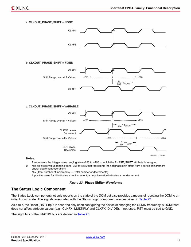
Spartan-3 FPGA Family: Functional Description
DS099 (v3.1) June 27, 2013 www.xilinx.comProduct Specification 41
The Status Logic Component
The Status Logic component not only reports on the state of the DCM but also provides a means of resetting the DCM to an initial known state. The signals associated with the Status Logic component are described in Table 22.
As a rule, the Reset (RST) input is asserted only upon configuring the device or changing the CLKIN frequency. A DCM reset does not affect attribute values (e.g., CLKFX_MULTIPLY and CLKFX_DIVIDE). If not used, RST must be tied to GND.
The eight bits of the STATUS bus are defined in Table 23.
X-Ref Target - Figure 23
Figure 23: Phase Shifter Waveforms
DS099-2_11_031303
CLKIN
CLKFB
* TCLKINP
256
b. CLKOUT_PHASE_SHIFT = FIXED
* TCLKINP
256
Shift Range over all P Values: –255 +255
Shift Range over all P Values: 0
0
–255 +255
Shift Range over all N Values: 0–255 +255
CLKIN
CLKFB beforeDecrement
c. CLKOUT_PHASE_SHIFT = VARIABLE
CLKFB afterDecrement
* TCLKINN
256
CLKIN
CLKFB
a. CLKOUT_PHASE_SHIFT = NONE
Notes: 1. P represents the integer value ranging from –255 to +255 to which the PHASE_SHIFT attribute is assigned.2. N is an integer value ranging from –255 to +255 that represents the net phase shift effect from a series of increment
and/or decrement operations. N = {Total number of increments} – {Total number of decrements}A positive value for N indicates a net increment; a negative value indicates a net decrement.
Spartan-3 FPGA Family: Functional Description
DS099 (v3.1) June 27, 2013 www.xilinx.comProduct Specification 42
Stabilizing DCM Clocks Before User Mode
It is possible to delay the completion of device configuration until after the DLL has achieved a lock condition using the STARTUP_WAIT attribute described in Table 24. This option ensures that the FPGA does not enter user mode—i.e., begin functional operation—until all system clocks generated by the DCM are stable. In order to achieve the delay, it is necessary to set the attribute to TRUE as well as set the BitGen option LCK_cycle to one of the six cycles making up the Startup phase of configuration. The selected cycle defines the point at which configuration will halt until the LOCKED output goes High.
Global Clock NetworkSpartan-3 devices have eight Global Clock inputs called GCLK0 - GCLK7. These inputs provide access to a low-capacitance, low-skew network that is well-suited to carrying high-frequency signals. The Spartan-3 FPGAs clock network is shown in Figure 23. GCLK0 through GCLK3 are located in the center of the bottom edge. GCLK4 through GCLK7 are located in the center of the top edge.
Eight Global Clock Multiplexers (also called BUFGMUX elements) are provided that accept signals from Global Clock inputs and route them to the internal clock network as well as DCMs. Four BUFGMUX elements are located in the center of the bottom edge, just above the GCLK0 - GCLK3 inputs. The remaining four BUFGMUX elements are located in the center of the top edge, just below the GCLK4 - GCLK7 inputs.
Pairs of BUFGMUX elements share global inputs, as shown in Figure 24. For example, the GCLK4 and GCLK5 inputs both potentially connect to BUFGMUX4 and BUFGMUX5 located in the upper right center. A differential clock input uses a pair of GCLK inputs to connect to a single BUFGMUX element.
Table 22: Status Logic Signals
Signal Direction Description
RST Input A High resets the entire DCM to its initial power-on state. Initializes the DLL taps for a delay of zero. Sets the LOCKED output Low. This input is asynchronous.
STATUS[7:0] Output The bit values on the STATUS bus provide information regarding the state of DLL and PS operation
LOCKED Output Indicates that the CLKIN and CLKFB signals are in phase by going High. The two signals are out-of-phase when Low.
Table 23: DCM STATUS Bus
Bit Name Description
0 Phase Shift OverflowA value of 1 indicates a phase shift overflow when one of two conditions occurs: Incrementing (or decrementing) TPS beyond 255/256 of a CLKIN cycle. The DLL is producing its maximum possible phase shift (i.e., all delay taps are active).(1)
1 CLKIN Input Stopped Toggling
A value of 1 indicates that the CLKIN input signal is not toggling. A value of 0 indicates toggling. This bit functions only when the CLKFB input is connected.(2)
2CLKFX/CLKFX180 Output Stopped Toggling
A value of 1 indicates that the CLKFX or CLKFX180 output signals are not toggling. A value of 0 indicates toggling. This bit functions only when using the Digital Frequency Synthesizer (DFS).
3:7 Reserved –
Notes: 1. The DLL phase shift with all delay taps active is specified as the parameter FINE_SHIFT_RANGE.2. If only the DFS clock outputs are used, but none of the DLL clock outputs, this bit will not go High when the CLKIN signal stops.
Table 24: Status Attributes
Attribute Description Values
STARTUP_WAIT Delays transition from configuration to user mode until lock condition is achieved. TRUE, FALSE
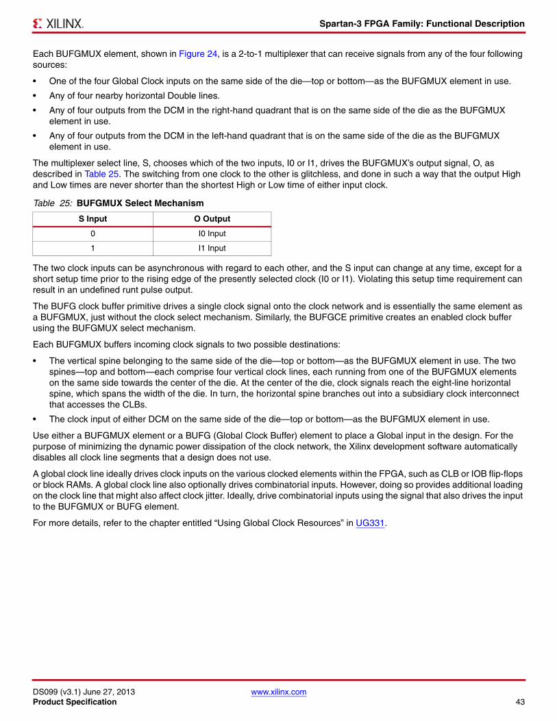
Spartan-3 FPGA Family: Functional Description
DS099 (v3.1) June 27, 2013 www.xilinx.comProduct Specification 43
Each BUFGMUX element, shown in Figure 24, is a 2-to-1 multiplexer that can receive signals from any of the four following sources:
• One of the four Global Clock inputs on the same side of the die—top or bottom—as the BUFGMUX element in use.
• Any of four nearby horizontal Double lines.
• Any of four outputs from the DCM in the right-hand quadrant that is on the same side of the die as the BUFGMUX element in use.
• Any of four outputs from the DCM in the left-hand quadrant that is on the same side of the die as the BUFGMUX element in use.
The multiplexer select line, S, chooses which of the two inputs, I0 or I1, drives the BUFGMUX’s output signal, O, as described in Table 25. The switching from one clock to the other is glitchless, and done in such a way that the output High and Low times are never shorter than the shortest High or Low time of either input clock.
The two clock inputs can be asynchronous with regard to each other, and the S input can change at any time, except for a short setup time prior to the rising edge of the presently selected clock (I0 or I1). Violating this setup time requirement can result in an undefined runt pulse output.
The BUFG clock buffer primitive drives a single clock signal onto the clock network and is essentially the same element as a BUFGMUX, just without the clock select mechanism. Similarly, the BUFGCE primitive creates an enabled clock buffer using the BUFGMUX select mechanism.
Each BUFGMUX buffers incoming clock signals to two possible destinations:
• The vertical spine belonging to the same side of the die—top or bottom—as the BUFGMUX element in use. The two spines—top and bottom—each comprise four vertical clock lines, each running from one of the BUFGMUX elements on the same side towards the center of the die. At the center of the die, clock signals reach the eight-line horizontal spine, which spans the width of the die. In turn, the horizontal spine branches out into a subsidiary clock interconnect that accesses the CLBs.
• The clock input of either DCM on the same side of the die—top or bottom—as the BUFGMUX element in use.
Use either a BUFGMUX element or a BUFG (Global Clock Buffer) element to place a Global input in the design. For the purpose of minimizing the dynamic power dissipation of the clock network, the Xilinx development software automatically disables all clock line segments that a design does not use.
A global clock line ideally drives clock inputs on the various clocked elements within the FPGA, such as CLB or IOB flip-flops or block RAMs. A global clock line also optionally drives combinatorial inputs. However, doing so provides additional loading on the clock line that might also affect clock jitter. Ideally, drive combinatorial inputs using the signal that also drives the input to the BUFGMUX or BUFG element.
For more details, refer to the chapter entitled “Using Global Clock Resources” in UG331.
Table 25: BUFGMUX Select Mechanism
S Input O Output
0 I0 Input
1 I1 Input
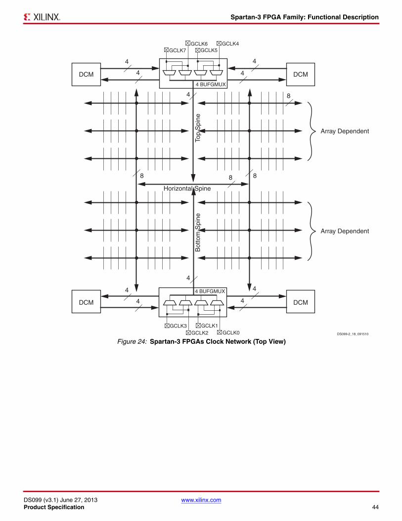
Spartan-3 FPGA Family: Functional Description
DS099 (v3.1) June 27, 2013 www.xilinx.comProduct Specification 44
X-Ref Target - Figure 24
Figure 24: Spartan-3 FPGAs Clock Network (Top View)
4
4
4
4
4
4
4
8
8
4
4
88
Horizontal SpineTo
p S
pine
Bot
tom
Spi
ne
4
DCM DCM
DCM DCM
Array Dependent
Array Dependent
•
•
•
•
•
•
•
•
•
•
•
•
DS099-2_18_091510
4 BUFGMUX
4 BUFGMUX
GCLK1GCLK0
GCLK3GCLK2
GCLK5GCLK4
GCLK7GCLK6
Spartan-3 FPGA Family: Functional Description
DS099 (v3.1) June 27, 2013 www.xilinx.comProduct Specification 45
InterconnectInterconnect (or routing) passes signals among the various functional elements of Spartan-3 devices. There are four kinds of interconnect: Long lines, Hex lines, Double lines, and Direct lines.
Long lines connect to one out of every six CLBs (see section [a] of Figure 25). Because of their low capacitance, these lines are well-suited for carrying high-frequency signals with minimal loading effects (e.g. skew). If all eight Global Clock Inputs are already committed and there remain additional clock signals to be assigned, Long lines serve as a good alternative.
Hex lines connect one out of every three CLBs (see section [b] of Figure 25). These lines fall between Long lines and Double lines in terms of capability: Hex lines approach the high-frequency characteristics of Long lines at the same time, offering greater connectivity.
Double lines connect to every other CLB (see section [c] of Figure 25). Compared to the types of lines already discussed, Double lines provide a higher degree of flexibility when making connections.
Direct lines afford any CLB direct access to neighboring CLBs (see section [d] of Figure 25). These lines are most often used to conduct a signal from a "source" CLB to a Double, Hex, or Long line and then from the longer interconnect back to a Direct line accessing a "destination" CLB.
For more details, refer to the “Using Interconnect” chapter in UG331.
X-Ref Target - Figure 25
(a) Long Lines
(b) Hex Lines
(d) Direct Lines
Figure 25: Types of Interconnect
• • •CLB CLB • • •CLB CLB • • •CLB CLB
6 6 6 6 6
• • •CLB CLB• • •CLB CLB
DS099-2_19_040103
CLB CLB CLB CLB CLB CLBCLB
8
DS099-2_20_040103
CLB
2
CLB CLB
DS099-2_21_040103
CLBCLB CLB
CLBCLB CLB
CLBCLB CLB
DS099-2_22_040103
(c) Double Lines
Spartan-3 FPGA Family: Functional Description
DS099 (v3.1) June 27, 2013 www.xilinx.comProduct Specification 46
ConfigurationSpartan-3 devices are configured by loading application specific configuration data into the internal configuration memory. Configuration is carried out using a subset of the device pins, some of which are "Dedicated" to one function only, while others, indicated by the term "Dual-Purpose", can be re-used as general-purpose User I/Os once configuration is complete.
Depending on the system design, several configuration modes are supported, selectable via mode pins. The mode pins M0, M1, and M2 are Dedicated pins. The mode pin settings are shown in Table 26.
The HSWAP_EN input pin defines whether the I/O pins that are not actively used during configuration have pull-up resistors during configuration. By default, HSWAP_EN is tied High (via an internal pull-up resistor if left floating) which shuts off the pull-up resistors on the user I/O pins during configuration. When HSWAP_EN is tied Low, user I/Os have pull-ups during configuration. The Dedicated configuration pins (CCLK, DONE, PROG_B, M2, M1, M0, HSWAP_EN) and the JTAG pins (TDI, TMS, TCK, and TDO) always have a pull-up resistor to VCCAUX during configuration, regardless of the value on the HSWAP_EN pin. Similarly, the dual-purpose INIT_B pin has an internal pull-up resistor to VCCO_4 or VCCO_BOTTOM, depending on the package style.
Depending on the chosen configuration mode, the FPGA either generates a CCLK output, or CCLK is an input accepting an externally generated clock.
A persist option is available which can be used to force the configuration pins to retain their configuration function even after device configuration is complete. If the persist option is not selected then the configuration pins with the exception of CCLK, PROG_B, and DONE can be used as user I/O in normal operation. The persist option does not apply to the boundary-scan related pins. The persist feature is valuable in applications that readback configuration data after entering the User mode.
Table 27 lists the total number of bits required to configure each FPGA as well as the PROMs suitable for storing those bits. See DS123: Platform Flash In-System Programmable Configuration PROMs data sheet for more information.
The maximum bitstream length that Spartan-3 FPGAs support in serial daisy-chains is 4,294,967,264 bits (4 Gbits), roughly equivalent to a daisy-chain with 323 XC3S5000 FPGAs. This is a limit only for serial daisy-chains where configuration data is passed via the FPGA’s DOUT pin. There is no such limit for JTAG chains.
Table 26: Spartan-3 FPGAs Configuration Mode Pin Settings
Configuration Mode (1) M0 M1 M2 Synchronizing Clock Data Width Serial DOUT(2)
Master Serial 0 0 0 CCLK Output 1 Yes
Slave Serial 1 1 1 CCLK Input 1 Yes
Master Parallel 1 1 0 CCLK Output 8 No
Slave Parallel 0 1 1 CCLK Input 8 No
JTAG 1 0 1 TCK Input 1 No
Notes: 1. The voltage levels on the M0, M1, and M2 pins select the configuration mode.2. The daisy chain is possible only in the Serial modes when DOUT is used.
Table 27: Spartan-3 FPGA Configuration Data
Device File SizesXilinx Platform Flash PROM
Serial Configuration Parallel Configuration
XC3S50 439,264 XCF01S XCF08P
XC3S200 1,047,616 XCF01S XCF08P
XC3S400 1,699,136 XCF02S XCF08P
XC3S1000 3,223,488 XCF04S XCF08P
XC3S1500 5,214,784 XCF08P XCF08P
XC3S2000 7,673,024 XCF08P XCF08P
XC3S4000 11,316,864 XCF16P XCF16P
XC3S5000 13,271,936 XCF16P XCF16P
Spartan-3 FPGA Family: Functional Description
DS099 (v3.1) June 27, 2013 www.xilinx.comProduct Specification 47
The Standard Configuration Interface
Configuration signals belong to one of two different categories: Dedicated or Dual-Purpose. Which category determines which of the FPGA’s power rails supplies the signal’s driver and, thus, helps describe the electrical characteristics at the pin.
The Dedicated configuration pins include PROG_B, HSWAP_EN, TDI, TMS, TCK, TDO, CCLK, DONE, and M0-M2. These pins are powered by the VCCAUX supply.
The Dual-Purpose configuration pins comprise INIT_B, DOUT, BUSY, RDWR_B, CS_B, and DIN/D0-D7. Each of these pins, according to its bank placement, uses the VCCO lines for either Bank 4 (VCCO_4 on most packages, VCCO_BOTTOM on TQ144 and CP132 packages) or Bank 5 (VCCO_5). All the signals used in the serial configuration modes rely on VCCO_4 power. Signals used in the parallel configuration modes and Readback require from VCCO_5 as well as from VCCO_4.
Both the Dedicated signals described above and the Dual-Purpose signals constitute the configuration interface. The Dedicated pins, powered by the 2.5V VCCAUX supply, always use the LVCMOS25 I/O standard. The Dual-Purpose signals, however, are powered by the VCCO_4 supply and also by the VCCO_5 supply in the Parallel configuration modes. The simplest configuration interface uses 2.5V for VCCO_4 and VCCO_5, if required. However, VCCO_4 and, if needed, VCCO_5 can be voltages other than 2.5V but then the configuration interface will have two voltage levels: 2.5V for VCCAUX and a separate VCCO supply. The Dual-Purpose signals default to the LVCMOS input and output levels for the associated VCCO voltage supply.
3.3V-Tolerant Configuration Interface
A 3.3V-tolerant configuration interface simply requires adding a few external resistors as described in detail in XAPP453: The 3.3V Configuration of Spartan-3 FPGAs.
The 3.3V-tolerance is implemented as follows (a similar approach can be used for other supply voltage levels):
Apply 3.3V to VCCO_4 and, in some configuration modes, to VCCO_5 to power the Dual-Purpose configuration pins. This scales the output voltages and input thresholds associated with these pins so that they become 3.3V-compatible.
Apply 2.5V to VCCAUX to power the Dedicated configuration pins. For 3.3V-tolerance, the Dedicated inputs require series resistors to limit the incoming current to 10 mA or less. The Dedicated outputs have reduced noise margin when the FPGA drives a High logic level into another device’s 3.3V receiver. Choose a power regulator or supply that can tolerate reverse current on the VCCAUX lines.
Configuration Modes
Spartan-3 FPGAs support the following five configuration modes:
• Slave Serial mode
• Master Serial mode
• Slave Parallel (SelectMAP) mode
• Master Parallel (SelectMAP) mode
• Boundary-Scan (JTAG) mode (IEEE 1532/IEEE 1149.1)
Slave Serial Mode
In Slave Serial mode, the FPGA receives configuration data in bit-serial form from a serial PROM or other serial source of configuration data. The FPGA on the far right of Figure 26 is set for the Slave Serial mode. The CCLK pin on the FPGA is an input in this mode. The serial bitstream must be set up at the DIN input pin a short time before each rising edge of the externally generated CCLK.
Multiple FPGAs can be daisy-chained for configuration from a single source. After a particular FPGA has been configured, the data for the next device is routed internally to the DOUT pin. The data on the DOUT pin changes on the falling edge of CCLK.
Spartan-3 FPGA Family: Functional Description
DS099 (v3.1) June 27, 2013 www.xilinx.comProduct Specification 48
Slave Serial mode is selected by applying <111> to the mode pins (M0, M1, and M2). A pull-up on the mode pins makes slave serial the default mode if the pins are left unconnected.
Master Serial Mode
In Master Serial mode, the FPGA drives CCLK pin, which behaves as a bidirectional I/O pin. The FPGA in the center of Figure 26 is set for Master Serial mode and connects to the serial configuration PROM and to the CCLK inputs of any slave FPGAs in a configuration daisy-chain. The master FPGA drives the configuration clock on the CCLK pin to the Xilinx Serial PROM, which, in response, provides bit-serial data to the FPGA’s DIN input. The FPGA accepts this data on each rising CCLK edge. After the master FPGA finishes configuring, it passes data on its DOUT pin to the next FPGA device in a daisy-chain. The DOUT data appears after the falling CCLK clock edge.
The Master Serial mode interface is identical to Slave Serial except that an internal oscillator generates the configuration clock (CCLK). A wide range of frequencies can be selected for CCLK, which always starts at a default frequency of 6 MHz. Configuration bits then switch CCLK to a higher frequency for the remainder of the configuration.
Slave Parallel Mode (SelectMAP)
The Parallel or SelectMAP modes support the fastest configuration. Byte-wide data is written into the FPGA with a BUSY flag controlling the flow of data. An external source provides 8-bit-wide data, CCLK, an active-Low Chip Select (CS_B) signal and an active-Low Write signal (RDWR_B). If BUSY is asserted (High) by the FPGA, the data must be held until BUSY goes Low. Data can also be read using the Slave Parallel mode. If RDWR_B is asserted, configuration data is read out of the FPGA as part of a readback operation.
After configuration, it is possible to use any of the Multipurpose pins (DIN/D0-D7, DOUT/BUSY, INIT_B, CS_B, and RDWR_B) as User I/Os. To do this, simply set the BitGen option Persist to No and assign the desired signals to multipurpose configuration pins using the Xilinx development software. Alternatively, it is possible to continue using the configuration port
X-Ref Target - Figure 26
Figure 26: Connection Diagram for Master and Slave Serial Configuration
Notes: 1. There are two ways to use the DONE line. First, one may set the BitGen option DriveDone to "Yes" only for the last
FPGA to be configured in the chain shown above (or for the single FPGA as may be the case). This enables the DONE pin to drive High; thus, no pull-up resistor is necessary. DriveDone is set to "No" for the remaining FPGAs in the chain. Second, DriveDone can be set to "No" for all FPGAs. Then all DONE lines are open-drain and require the pull-up resistor shown in grey. In most cases, a value between 3.3KΩ to 4.7KΩ is sufficient. However, when using DONE synchronously with a long chain of FPGAs, cumulative capacitance may necessitate lower resistor values (e.g. down to 330Ω) in order to ensure a rise time within one clock cycle.
2. For information on how to program the FPGA using 3.3V signals and power, see 3.3V-Tolerant Configuration Interface.
DOUTDIN
CCLK
DONE
INIT_B
Spartan-3FPGA
Master
PROG_B
DIN
CCLK
DONE
INIT_B
Spartan-3FPGA
Slave
PROG_B
DS099_23_112905
D0
CLK
CE
OE/RESET
CF
PlatformFlash PROM
XCF0xSor
XCFxxP
VCCINT
1.2V
VCCAUX
VCCO Bank 4
2.5V
2.5V
4.7KΩAll
2.5V
VCCAUX VCCINT
VCCO Bank 41.2V
1.8V: XCFxxP
VCCINT VCCJ
VCCO
2.5V
2.5V
M0M1M2
M0M1M2
GNDGNDGND
3.3V: XCF0xS
Spartan-3 FPGA Family: Functional Description
DS099 (v3.1) June 27, 2013 www.xilinx.comProduct Specification 49
(e.g. all configuration pins taken together) when operating in the User mode. This is accomplished by setting the Persist option to Yes.
Multiple FPGAs can be configured using the Slave Parallel mode and can be made to start-up simultaneously. Figure 27 shows the device connections. To configure multiple devices in this way, wire the individual CCLK, Data, RDWR_B, and BUSY pins of all the devices in parallel. The individual devices are loaded separately by deasserting the CS_B pin of each device in turn and writing the appropriate data.
X-Ref Target - Figure 27
Figure 27: Connection Diagram for Slave Parallel Configuration
PROG_B
INIT_B
DONE
Spartan-3Slave
INIT_B
D[0:7]
CCLK
RDWR_B
BUSY
CS_B
PROG_B
DONE
CS_B
Spartan-3Slave
INIT_B
GND
D[0:7]
CCLK
RDWR_B
BUSY
CS_B
D[0:7]
CCLK
RDWR_B
BUSY
PROG_B
DONE
CS_B
DS099_24_041103
2.5V
M1M2M0
2.5V
M1M2M0
2.5V
VCCAUX
VCCO Banks 4 & 5
VCCINT
1.2V
4.7KΩ 4.7KΩ
2.5V
VCCAUX
VCCO Banks 4 & 5
VCCINT
1.2V
2.5V
GND
Notes: 1. There are two ways to use the DONE line. First, one may set the BitGen option DriveDone to "Yes" only for the last FPGA to be
configured in the chain shown above (or for the single FPGA as may be the case). This enables the DONE pin to drive High; thus, no pull-up resistor is necessary. DriveDone is set to "No" for the remaining FPGAs in the chain. Second, DriveDone can be set to "No" for all FPGAs. Then all DONE lines are open-drain and require the pull-up resistor shown in grey. In most cases, a value between 3.3KΩ to 4.7KΩ is sufficient. However, when using DONE synchronously with a long chain of FPGAs, cumulative capacitance may necessitate lower resistor values (e.g. down to 330Ω) in order to ensure a rise time within one clock cycle.
2. If the FPGAs use different configuration data files, configure them in sequence by first asserting the CS_B of one FPGA then asserting the CS_B of the other FPGA.
3. For information on how to program the FPGA using 3.3V signals and power, see 3.3V-Tolerant Configuration Interface.
Spartan-3 FPGA Family: Functional Description
DS099 (v3.1) June 27, 2013 www.xilinx.comProduct Specification 50
Master Parallel Mode
In this mode, the FPGA configures from byte-wide data, and the FPGA supplies the CCLK configuration clock. In Master configuration modes, CCLK behaves as a bidirectional I/O pin. Timing is similar to the Slave Parallel mode except that CCLK is supplied by the FPGA. The device connections are shown in Figure 28.
Boundary-Scan (JTAG) Mode
In Boundary-Scan mode, dedicated pins are used for configuring the FPGA. The configuration is done entirely through the IEEE 1149.1 Test Access Port (TAP). FPGA configuration using the Boundary-Scan mode is compatible with the IEEE Std 1149.1-1993 standard and IEEE Std 1532 for In-System Configurable (ISC) devices.
Configuration through the boundary-scan port is always available, regardless of the selected configuration mode. In some cases, however, the mode pin setting may affect proper programming of the device due to various interactions. For example, if the mode pins are set to Master Serial or Master Parallel mode, and the associated PROM is already programmed with a valid configuration image, then there is potential for configuration interference between the JTAG and PROM data. Selecting the Boundary-Scan mode disables the other modes and is the most reliable mode when programming via JTAG.
Configuration Sequence
The configuration of Spartan-3 devices is a three-stage process that occurs after Power-On Reset or the assertion of PROG_B. POR occurs after the VCCINT, VCCAUX, and VCCO Bank 4 supplies have reached their respective maximum input threshold levels (see Table 29, page 59). After POR, the three-stage process begins.
First, the configuration memory is cleared. Next, configuration data is loaded into the memory, and finally, the logic is activated by a start-up process. A flow diagram for the configuration sequence of the Serial and Parallel modes is shown in Figure 29. The flow diagram for the Boundary-Scan configuration sequence appears in Figure 30.
X-Ref Target - Figure 28
Figure 28: Connection Diagram for Master Parallel Configuration
Spartan-3Master
D[0:7]
CCLK
PROG_B
DONE
INIT_B
DATA[0:7]
CCLK
RDWR_B
CS_B
CF
CE
OE/RESET
Platform Flash PROM
DS099_25_112905
2.5V
VCCAUX
VCCO Banks 4 & 5
VCCINT
1.2V
GND
GND
1.8V
VCCINT VCCJ
VCCO
2.5V
XCFxxP
2.5V
All4.7KΩ
Notes: 1. There are two ways to use the DONE line. First, one may set the BitGen option DriveDone to "Yes" only for
the last FPGA to be configured in the chain shown above (or for the single FPGA as may be the case). This enables the DONE pin to drive High; thus, no pull-up resistor is necessary. DriveDone is set to "No" for the remaining FPGAs in the chain. Second, DriveDone can be set to "No" for all FPGAs. Then all DONE lines are open-drain and require the pull-up resistor shown in grey. In most cases, a value between 3.3KΩ to 4.7KΩ is sufficient. However, when using DONE synchronously with a long chain of FPGAs, cumulative capacitance may necessitate lower resistor values (e.g. down to 330Ω) in order to ensure a rise time within one clock cycle.
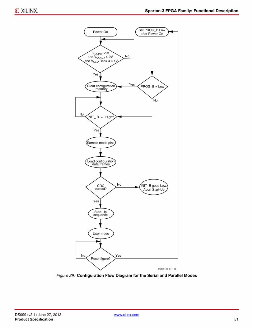
Spartan-3 FPGA Family: Functional Description
DS099 (v3.1) June 27, 2013 www.xilinx.comProduct Specification 51
X-Ref Target - Figure 29
Figure 29: Configuration Flow Diagram for the Serial and Parallel Modes
Sample mode pins
No
No
No
Yes
Yes
YesClear configuration memory
Power-On Set PROG_B Lowafter Power-On
Yes
NoCRCcorrect?
YesNoReconfigure?
Load configurationdata frames
INIT_B goes Low.Abort Start-Up
Start-Upsequence
User mode
INIT_ B = High?
PROG_B = Low
DS099_26_041103
VCCINT >1Vand VCCAUX > 2V
and VCCO Bank 4 > 1V
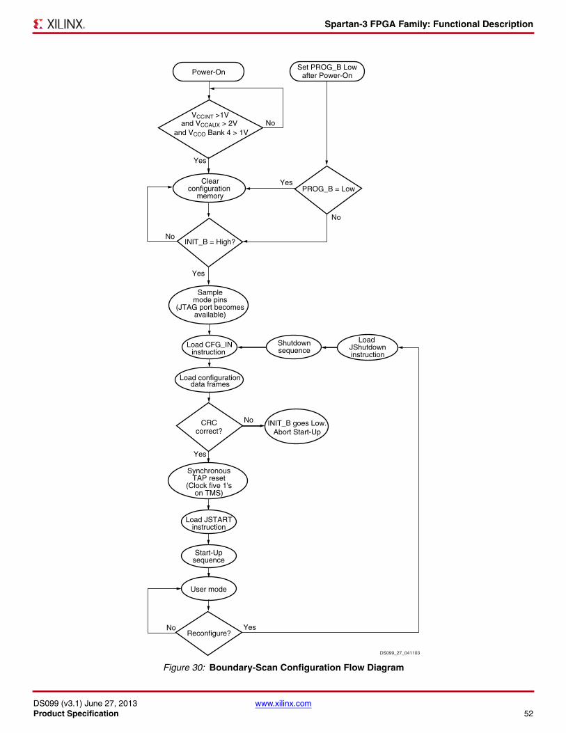
Spartan-3 FPGA Family: Functional Description
DS099 (v3.1) June 27, 2013 www.xilinx.comProduct Specification 52
X-Ref Target - Figure 30
Figure 30: Boundary-Scan Configuration Flow Diagram
Samplemode pins
(JTAG port becomesavailable)
Clearconfiguration
memory
No
No
No
Yes
Yes
Yes
Yes
No
Yes
Power-On
CRCcorrect?
Load CFG_INinstruction
Shutdownsequence
Reconfigure?
Load JSTARTinstruction
SynchronousTAP reset
(Clock five 1'son TMS)
Start-Upsequence
User mode
INIT_B = High?
PROG_B = Low
Load JShutdowninstruction
No
DS099_27_041103
Load configurationdata frames
VCCINT >1Vand VCCAUX > 2V
and VCCO Bank 4 > 1V
INIT_B goes Low.Abort Start-Up
Set PROG_B Lowafter Power-On
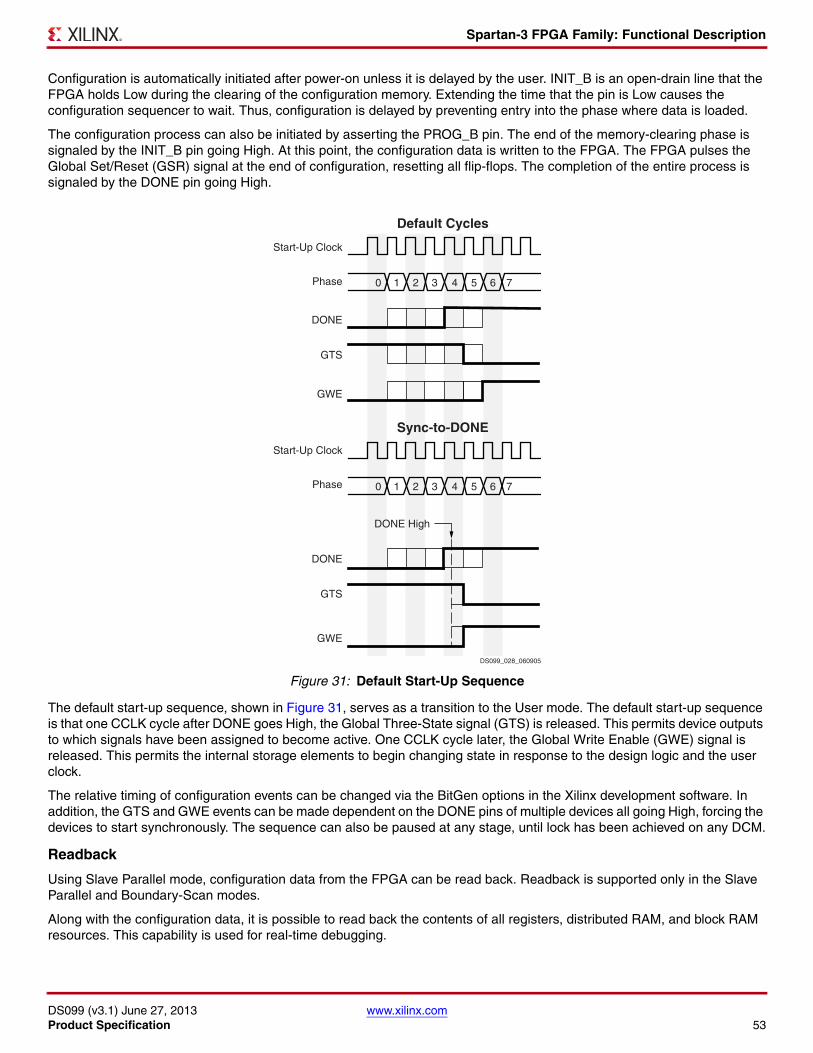
Spartan-3 FPGA Family: Functional Description
DS099 (v3.1) June 27, 2013 www.xilinx.comProduct Specification 53
Configuration is automatically initiated after power-on unless it is delayed by the user. INIT_B is an open-drain line that the FPGA holds Low during the clearing of the configuration memory. Extending the time that the pin is Low causes the configuration sequencer to wait. Thus, configuration is delayed by preventing entry into the phase where data is loaded.
The configuration process can also be initiated by asserting the PROG_B pin. The end of the memory-clearing phase is signaled by the INIT_B pin going High. At this point, the configuration data is written to the FPGA. The FPGA pulses the Global Set/Reset (GSR) signal at the end of configuration, resetting all flip-flops. The completion of the entire process is signaled by the DONE pin going High.
The default start-up sequence, shown in Figure 31, serves as a transition to the User mode. The default start-up sequence is that one CCLK cycle after DONE goes High, the Global Three-State signal (GTS) is released. This permits device outputs to which signals have been assigned to become active. One CCLK cycle later, the Global Write Enable (GWE) signal is released. This permits the internal storage elements to begin changing state in response to the design logic and the user clock.
The relative timing of configuration events can be changed via the BitGen options in the Xilinx development software. In addition, the GTS and GWE events can be made dependent on the DONE pins of multiple devices all going High, forcing the devices to start synchronously. The sequence can also be paused at any stage, until lock has been achieved on any DCM.
Readback
Using Slave Parallel mode, configuration data from the FPGA can be read back. Readback is supported only in the Slave Parallel and Boundary-Scan modes.
Along with the configuration data, it is possible to read back the contents of all registers, distributed RAM, and block RAM resources. This capability is used for real-time debugging.
X-Ref Target - Figure 31
Figure 31: Default Start-Up Sequence
Start-Up Clock
Default Cycles
Sync-to-DONE
0 1 2 3 4 5 6 7
0 1
DONE High
2 3 4 5 6 7
Phase
Start-Up Clock
Phase
DONE
GTS
GWE
DS099_028_060905
DONE
GTS
GWE
Spartan-3 FPGA Family: Functional Description
DS099 (v3.1) June 27, 2013 www.xilinx.comProduct Specification 54
Additional Configuration Details
Additional details about the Spartan-3 FPGA configuration architecture and command set are available in UG332: Spartan-3 Generation Configuration User Guide and in application note XAPP452: Spartan-3 Advanced Configuration Architecture.
Powering Spartan-3 FPGAs
Voltage Regulators
Various power supply manufacturers offer complete power solutions for Xilinx FPGAs, including some with integrated multi-rail regulators specifically designed for Spartan-3 FPGAs. The Xilinx Power Corner web page provides links to vendor solution guides as well as Xilinx power estimation and analysis tools.
Power Distribution System (PDS) Design and Bypass/Decoupling Capacitors
Good power distribution system (PDS) design is important for all FPGA designs, especially for high-performance applications. Proper design results in better overall performance, lower clock and DCM jitter, and a generally more robust system. Before designing the printed circuit board (PCB) for the FPGA design, review application note XAPP623: Power Distribution System (PDS) Design: Using Bypass/Decoupling Capacitors.
Power-On Behavior
Spartan-3 FPGAs have a built-in Power-On Reset (POR) circuit that monitors the three power rails required to successfully configure the FPGA. At power-up, the POR circuit holds the FPGA in a reset state until the VCCINT, VCCAUX, and VCCO Bank 4 supplies reach their respective input threshold levels (see Table 29, page 59). After all three supplies reach their respective threshold, the POR reset is released and the FPGA begins its configuration process.
Because the three supply inputs must be valid to release the POR reset and can be supplied in any order, there are no specific voltage sequencing requirements. However, applying the FPGA’s VCCAUX supply before the VCCINT supply uses the least ICCINT current.
Once all three supplies are valid, the minimum current required to power-on the FPGA is equal to the worst-case quiescent current, as specified in Table 34, page 62. Spartan-3 FPGAs do not require Power-On Surge (POS) current to successfully configure.
Surplus ICCINT if VCCINT Applied before VCCAUX
If the VCCINT supply is applied before the VCCAUX supply, the FPGA may draw a surplus ICCINT current in addition to the ICCINT quiescent current levels specified in Table 34. The momentary additional ICCINT surplus current might be a few hundred milliamperes under nominal conditions, significantly less than the instantaneous current consumed by the bypass capacitors at power-on. However, the surplus current immediately disappears when the VCCAUX supply is applied, and, in response, the FPGA’s ICCINT quiescent current demand drops to the levels specified in Table 34. The FPGA does not use nor does it require the surplus current to successfully power-on and configure. If applying VCCINT- before VCCAUX, ensure that the regulator does not have a foldback feature that could inadvertently shut down in the presence of the surplus current.
Maximum Allowed VCCINT Ramp Rate on Early Devices, if VVCCINTSupply is Last in Sequence
All devices with a mask revision code ‘E’ or later do not have a VCCINT ramp rate requirement. See Mask and Fab Revisions, page 58.
Early Spartan-3 FPGAs were produced at a 200 mm wafer production facility and are identified by a fabrication/process code of "FQ" on the device top marking, as shown in Package Marking, page 5. These "FQ" devices have a maximum VCCINT ramp rate requirement if and only if VCCINT is the last supply to ramp, after the VCCAUX and VCCO Bank 4 supplies. This maximum ramp rate appears as TCCINT in Table 30, page 60.
Minimum Allowed VCCO Ramp Rate on Early Devices
Devices shipped since 2006 essentially have no VCCO ramp rate limits, shown in Table 30, page 60. Similarly, all devices with a mask revision code ‘E’ or later do not have a VCCO ramp rate limit. See Mask and Fab Revisions, page 58.
Spartan-3 FPGA Family: Functional Description
DS099 (v3.1) June 27, 2013 www.xilinx.comProduct Specification 55
Initial Spartan-3 FPGA mask revisions have a limit on how fast the VCCO supply can ramp. The minimum allowed VCCO ramp rate appears as TCCO in Table 30, page 60. The minimum rate is affected by the package inductance. Consequently, the ball grid array and chip-scale packages (CP132, FT256, FG456, FG676, and FG900) allow a faster ramp rate than the quad-flat packages (VQ100, TQ144, and PQ208).
Configuration Data Retention, Brown-Out
The FPGA’s configuration data is stored in robust CMOS configuration latches. The data in these latches is retained even when the voltages drop to the minimum levels necessary to preserve RAM contents. This is specified in Table 31, page 60.
If, after configuration, the VCCAUX or VCCINT supply drops below its data retention voltage, clear the current device configuration using one of the following methods:
• Force the VCCAUX or VCCINT supply voltage below the minimum Power On Reset (POR) voltage threshold Table 29, page 59).
• Assert PROG_B Low.
The POR circuit does not monitor the VCCO_4 supply after configuration. Consequently, dropping the VCCO_4 voltage does not reset the device by triggering a Power-On Reset (POR) event.
No Internal Charge Pumps or Free-Running Oscillators
Some system applications are sensitive to sources of analog noise. Spartan-3 FPGA circuitry is fully static and does not employ internal charge pumps.
The CCLK configuration clock is active during the FPGA configuration process. After configuration completes, the CCLK oscillator is automatically disabled unless the Bitstream Generator (BitGen) option Persist=Yes. See Module 4: Table 80, page 125.
Spartan-3 FPGAs optionally support a featured called Digitally Controlled Impedance (DCI). When used in an application, the DCI logic uses an internal oscillator. The DCI logic is only enabled if the FPGA application specifies an I/O standard that requires DCI (LVDCI_33, LVDCI_25, etc.). If DCI is not used, the associated internal oscillator is also disabled.
In summary, unless an application uses the Persist=Yes option or specifies a DCI I/O standard, an FPGA with no external switching remains fully static.
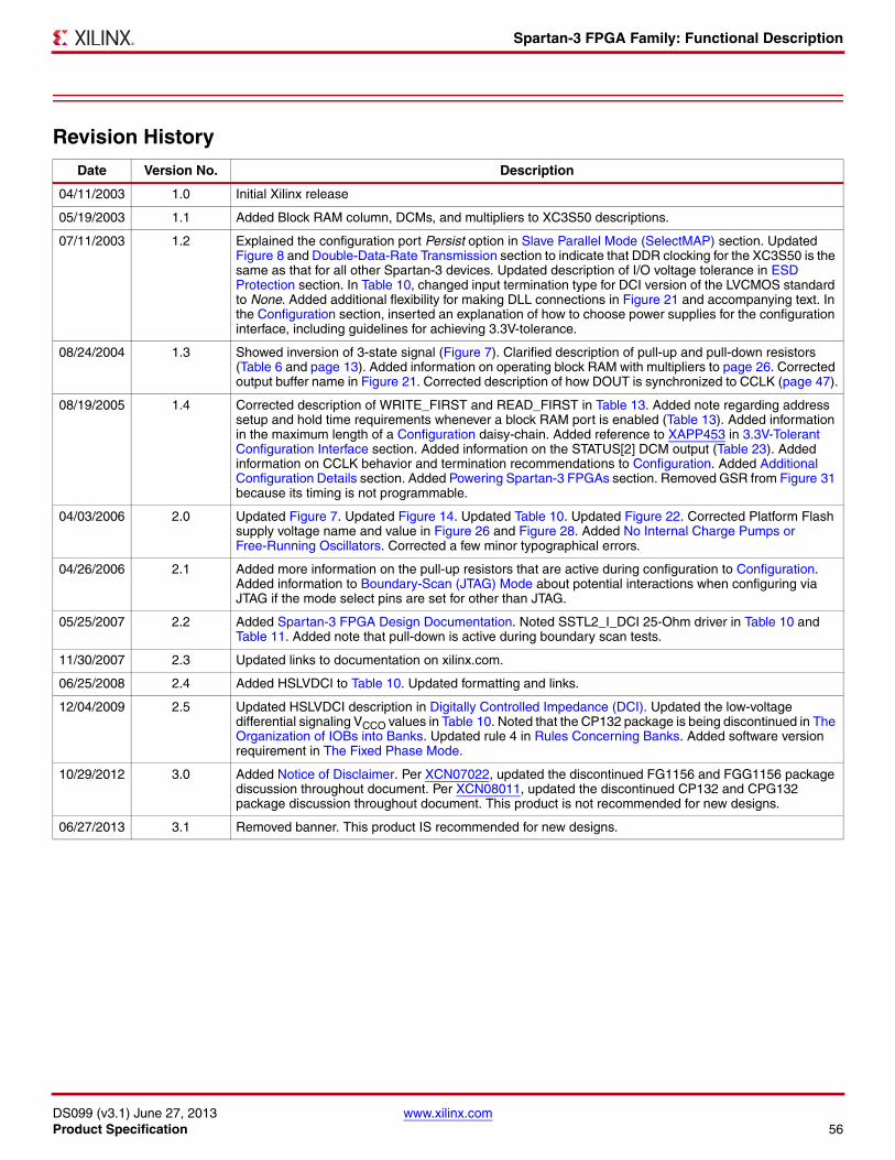
Spartan-3 FPGA Family: Functional Description
DS099 (v3.1) June 27, 2013 www.xilinx.comProduct Specification 56
Revision History
Date Version No. Description
04/11/2003 1.0 Initial Xilinx release
05/19/2003 1.1 Added Block RAM column, DCMs, and multipliers to XC3S50 descriptions.
07/11/2003 1.2 Explained the configuration port Persist option in Slave Parallel Mode (SelectMAP) section. Updated Figure 8 and Double-Data-Rate Transmission section to indicate that DDR clocking for the XC3S50 is the same as that for all other Spartan-3 devices. Updated description of I/O voltage tolerance in ESD Protection section. In Table 10, changed input termination type for DCI version of the LVCMOS standard to None. Added additional flexibility for making DLL connections in Figure 21 and accompanying text. In the Configuration section, inserted an explanation of how to choose power supplies for the configuration interface, including guidelines for achieving 3.3V-tolerance.
08/24/2004 1.3 Showed inversion of 3-state signal (Figure 7). Clarified description of pull-up and pull-down resistors (Table 6 and page 13). Added information on operating block RAM with multipliers to page 26. Corrected output buffer name in Figure 21. Corrected description of how DOUT is synchronized to CCLK (page 47).
08/19/2005 1.4 Corrected description of WRITE_FIRST and READ_FIRST in Table 13. Added note regarding address setup and hold time requirements whenever a block RAM port is enabled (Table 13). Added information in the maximum length of a Configuration daisy-chain. Added reference to XAPP453 in 3.3V-Tolerant Configuration Interface section. Added information on the STATUS[2] DCM output (Table 23). Added information on CCLK behavior and termination recommendations to Configuration. Added Additional Configuration Details section. Added Powering Spartan-3 FPGAs section. Removed GSR from Figure 31 because its timing is not programmable.
04/03/2006 2.0 Updated Figure 7. Updated Figure 14. Updated Table 10. Updated Figure 22. Corrected Platform Flash supply voltage name and value in Figure 26 and Figure 28. Added No Internal Charge Pumps or Free-Running Oscillators. Corrected a few minor typographical errors.
04/26/2006 2.1 Added more information on the pull-up resistors that are active during configuration to Configuration. Added information to Boundary-Scan (JTAG) Mode about potential interactions when configuring via JTAG if the mode select pins are set for other than JTAG.
05/25/2007 2.2 Added Spartan-3 FPGA Design Documentation. Noted SSTL2_I_DCI 25-Ohm driver in Table 10 and Table 11. Added note that pull-down is active during boundary scan tests.
11/30/2007 2.3 Updated links to documentation on xilinx.com.
06/25/2008 2.4 Added HSLVDCI to Table 10. Updated formatting and links.
12/04/2009 2.5 Updated HSLVDCI description in Digitally Controlled Impedance (DCI). Updated the low-voltage differential signaling VCCO values in Table 10. Noted that the CP132 package is being discontinued in The Organization of IOBs into Banks. Updated rule 4 in Rules Concerning Banks. Added software version requirement in The Fixed Phase Mode.
10/29/2012 3.0 Added Notice of Disclaimer. Per XCN07022, updated the discontinued FG1156 and FGG1156 package discussion throughout document. Per XCN08011, updated the discontinued CP132 and CPG132 package discussion throughout document. This product is not recommended for new designs.
06/27/2013 3.1 Removed banner. This product IS recommended for new designs.
Spartan-3 FPGA Family: Functional Description
DS099 (v3.1) June 27, 2013 www.xilinx.comProduct Specification 57
Notice of DisclaimerTHE XILINX HARDWARE FPGA AND CPLD DEVICES REFERRED TO HEREIN (“PRODUCTS”) ARE SUBJECT TO THE TERMS ANDCONDITIONS OF THE XILINX LIMITED WARRANTY WHICH CAN BE VIEWED AT http://www.xilinx.com/warranty.htm. THIS LIMITEDWARRANTY DOES NOT EXTEND TO ANY USE OF PRODUCTS IN AN APPLICATION OR ENVIRONMENT THAT IS NOT WITHIN THESPECIFICATIONS STATED IN THE XILINX DATA SHEET. ALL SPECIFICATIONS ARE SUBJECT TO CHANGE WITHOUT NOTICE.PRODUCTS ARE NOT DESIGNED OR INTENDED TO BE FAIL-SAFE OR FOR USE IN ANY APPLICATION REQUIRING FAIL-SAFEPERFORMANCE, SUCH AS LIFE-SUPPORT OR SAFETY DEVICES OR SYSTEMS, OR ANY OTHER APPLICATION THAT INVOKESTHE POTENTIAL RISKS OF DEATH, PERSONAL INJURY, OR PROPERTY OR ENVIRONMENTAL DAMAGE (“CRITICALAPPLICATIONS”). USE OF PRODUCTS IN CRITICAL APPLICATIONS IS AT THE SOLE RISK OF CUSTOMER, SUBJECT TOAPPLICABLE LAWS AND REGULATIONS.
CRITICAL APPLICATIONS DISCLAIMERXILINX PRODUCTS (INCLUDING HARDWARE, SOFTWARE AND/OR IP CORES) ARE NOT DESIGNED OR INTENDED TO BEFAIL-SAFE, OR FOR USE IN ANY APPLICATION REQUIRING FAIL-SAFE PERFORMANCE, SUCH AS IN LIFE-SUPPORT ORSAFETY DEVICES OR SYSTEMS, CLASS III MEDICAL DEVICES, NUCLEAR FACILITIES, APPLICATIONS RELATED TO THEDEPLOYMENT OF AIRBAGS, OR ANY OTHER APPLICATIONS THAT COULD LEAD TO DEATH, PERSONAL INJURY OR SEVEREPROPERTY OR ENVIRONMENTAL DAMAGE (INDIVIDUALLY AND COLLECTIVELY, “CRITICAL APPLICATIONS”). FURTHERMORE,XILINX PRODUCTS ARE NOT DESIGNED OR INTENDED FOR USE IN ANY APPLICATIONS THAT AFFECT CONTROL OF AVEHICLE OR AIRCRAFT, UNLESS THERE IS A FAIL-SAFE OR REDUNDANCY FEATURE (WHICH DOES NOT INCLUDE USE OFSOFTWARE IN THE XILINX DEVICE TO IMPLEMENT THE REDUNDANCY) AND A WARNING SIGNAL UPON FAILURE TO THEOPERATOR. CUSTOMER AGREES, PRIOR TO USING OR DISTRIBUTING ANY SYSTEMS THAT INCORPORATE XILINXPRODUCTS, TO THOROUGHLY TEST THE SAME FOR SAFETY PURPOSES. TO THE MAXIMUM EXTENT PERMITTED BYAPPLICABLE LAW, CUSTOMER ASSUMES THE SOLE RISK AND LIABILITY OF ANY USE OF XILINX PRODUCTS IN CRITICALAPPLICATIONS.
AUTOMOTIVE APPLICATIONS DISCLAIMERXILINX PRODUCTS ARE NOT DESIGNED OR INTENDED TO BE FAIL-SAFE, OR FOR USE IN ANY APPLICATION REQUIRING FAIL-SAFE PERFORMANCE, SUCH AS APPLICATIONS RELATED TO: (I) THE DEPLOYMENT OF AIRBAGS, (II) CONTROL OF A VEHICLE, UNLESS THERE IS A FAIL-SAFE OR REDUNDANCY FEATURE (WHICH DOES NOT INCLUDE USE OF SOFTWARE IN THE XILINX DEVICE TO IMPLEMENT THE REDUNDANCY) AND A WARNING SIGNAL UPON FAILURE TO THE OPERATOR, OR (III) USES THAT COULD LEAD TO DEATH OR PERSONAL INJURY. CUSTOMER ASSUMES THE SOLE RISK AND LIABILITY OF ANY USE OF XILINX PRODUCTS IN SUCH APPLICATIONS.
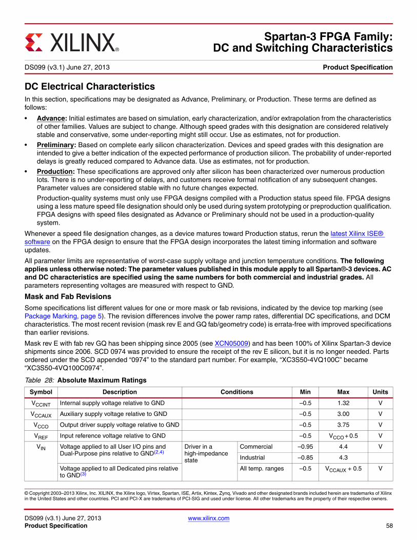
DS099 (v3.1) June 27, 2013 www.xilinx.comProduct Specification 58
© Copyright 2003–2013 Xilinx, Inc. XILINX, the Xilinx logo, Virtex, Spartan, ISE, Artix, Kintex, Zynq, Vivado and other designated brands included herein are trademarks of Xilinx in the United States and other countries. PCI and PCI-X are trademarks of PCI-SIG and used under license. All other trademarks are the property of their respective owners.
DC Electrical CharacteristicsIn this section, specifications may be designated as Advance, Preliminary, or Production. These terms are defined as follows:
• Advance: Initial estimates are based on simulation, early characterization, and/or extrapolation from the characteristics of other families. Values are subject to change. Although speed grades with this designation are considered relatively stable and conservative, some under-reporting might still occur. Use as estimates, not for production.
• Preliminary: Based on complete early silicon characterization. Devices and speed grades with this designation are intended to give a better indication of the expected performance of production silicon. The probability of under-reported delays is greatly reduced compared to Advance data. Use as estimates, not for production.
• Production: These specifications are approved only after silicon has been characterized over numerous production lots. There is no under-reporting of delays, and customers receive formal notification of any subsequent changes. Parameter values are considered stable with no future changes expected.
Production-quality systems must only use FPGA designs compiled with a Production status speed file. FPGA designs using a less mature speed file designation should only be used during system prototyping or preproduction qualification. FPGA designs with speed files designated as Advance or Preliminary should not be used in a production-quality system.
Whenever a speed file designation changes, as a device matures toward Production status, rerun the latest Xilinx ISE® software on the FPGA design to ensure that the FPGA design incorporates the latest timing information and software updates.
All parameter limits are representative of worst-case supply voltage and junction temperature conditions. The following applies unless otherwise noted: The parameter values published in this module apply to all Spartan®-3 devices. AC and DC characteristics are specified using the same numbers for both commercial and industrial grades. All parameters representing voltages are measured with respect to GND.
Mask and Fab RevisionsSome specifications list different values for one or more mask or fab revisions, indicated by the device top marking (see Package Marking, page 5). The revision differences involve the power ramp rates, differential DC specifications, and DCM characteristics. The most recent revision (mask rev E and GQ fab/geometry code) is errata-free with improved specifications than earlier revisions.
Mask rev E with fab rev GQ has been shipping since 2005 (see XCN05009) and has been 100% of Xilinx Spartan-3 device shipments since 2006. SCD 0974 was provided to ensure the receipt of the rev E silicon, but it is no longer needed. Parts ordered under the SCD appended “0974” to the standard part number. For example, “XC3S50-4VQ100C” became “XC3S50-4VQ100C0974”.
106Spartan-3 FPGA Family:
DC and Switching Characteristics
DS099 (v3.1) June 27, 2013 Product Specification
Table 28: Absolute Maximum Ratings
Symbol Description Conditions Min Max Units
VCCINT Internal supply voltage relative to GND –0.5 1.32 V
VCCAUX Auxiliary supply voltage relative to GND –0.5 3.00 V
VCCO Output driver supply voltage relative to GND –0.5 3.75 V
VREF Input reference voltage relative to GND –0.5 VCCO + 0.5 V
VIN Voltage applied to all User I/O pins and Dual-Purpose pins relative to GND(2,4)
Driver in a high-impedance state
Commercial –0.95 4.4 V
Industrial –0.85 4.3
Voltage applied to all Dedicated pins relative to GND(3)
All temp. ranges –0.5 VCCAUX + 0.5 V
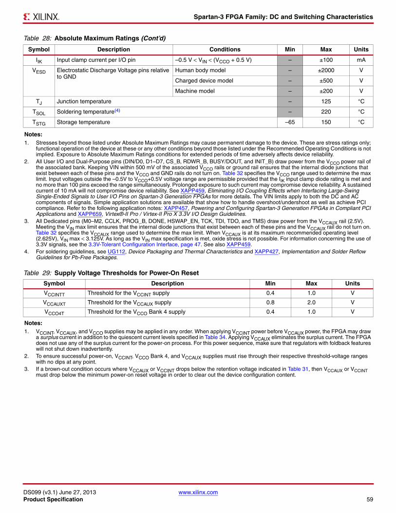
Spartan-3 FPGA Family: DC and Switching Characteristics
DS099 (v3.1) June 27, 2013 www.xilinx.comProduct Specification 59
IIK Input clamp current per I/O pin –0.5 V < VIN < (VCCO + 0.5 V) – ±100 mA
VESD Electrostatic Discharge Voltage pins relative to GND
Human body model – ±2000 V
Charged device model – ±500 V
Machine model – ±200 V
TJ Junction temperature – 125 °C
TSOL Soldering temperature(4) – 220 °C
TSTG Storage temperature –65 150 °C
Notes: 1. Stresses beyond those listed under Absolute Maximum Ratings may cause permanent damage to the device. These are stress ratings only;
functional operation of the device at these or any other conditions beyond those listed under the Recommended Operating Conditions is not implied. Exposure to Absolute Maximum Ratings conditions for extended periods of time adversely affects device reliability.
2. All User I/O and Dual-Purpose pins (DIN/D0, D1–D7, CS_B, RDWR_B, BUSY/DOUT, and INIT_B) draw power from the VCCO power rail of the associated bank. Keeping VIN within 500 mV of the associated VCCO rails or ground rail ensures that the internal diode junctions that exist between each of these pins and the VCCO and GND rails do not turn on. Table 32 specifies the VCCO range used to determine the max limit. Input voltages outside the –0.5V to VCCO+0.5V voltage range are permissible provided that the IIK input clamp diode rating is met and no more than 100 pins exceed the range simultaneously. Prolonged exposure to such current may compromise device reliability. A sustained current of 10 mA will not compromise device reliability. See XAPP459, Eliminating I/O Coupling Effects when Interfacing Large-Swing Single-Ended Signals to User I/O Pins on Spartan-3 Generation FPGAs for more details. The VIN limits apply to both the DC and AC components of signals. Simple application solutions are available that show how to handle overshoot/undershoot as well as achieve PCI compliance. Refer to the following application notes: XAPP457, Powering and Configuring Spartan-3 Generation FPGAs in Compliant PCI Applications and XAPP659, Virtex®-II Pro / Virtex-II Pro X 3.3V I/O Design Guidelines.
3. All Dedicated pins (M0–M2, CCLK, PROG_B, DONE, HSWAP_EN, TCK, TDI, TDO, and TMS) draw power from the VCCAUX rail (2.5V). Meeting the VIN max limit ensures that the internal diode junctions that exist between each of these pins and the VCCAUX rail do not turn on. Table 32 specifies the VCCAUX range used to determine the max limit. When VCCAUX is at its maximum recommended operating level (2.625V), VIN max < 3.125V. As long as the VIN max specification is met, oxide stress is not possible. For information concerning the use of 3.3V signals, see the 3.3V-Tolerant Configuration Interface, page 47. See also XAPP459.
4. For soldering guidelines, see UG112, Device Packaging and Thermal Characteristics and XAPP427, Implementation and Solder Reflow Guidelines for Pb-Free Packages.
Table 29: Supply Voltage Thresholds for Power-On Reset
Symbol Description Min Max Units
VCCINTT Threshold for the VCCINT supply 0.4 1.0 V
VCCAUXT Threshold for the VCCAUX supply 0.8 2.0 V
VCCO4T Threshold for the VCCO Bank 4 supply 0.4 1.0 V
Notes: 1. VCCINT, VCCAUX, and VCCO supplies may be applied in any order. When applying VCCINT power before VCCAUX power, the FPGA may draw
a surplus current in addition to the quiescent current levels specified in Table 34. Applying VCCAUX eliminates the surplus current. The FPGA does not use any of the surplus current for the power-on process. For this power sequence, make sure that regulators with foldback features will not shut down inadvertently.
2. To ensure successful power-on, VCCINT, VCCO Bank 4, and VCCAUX supplies must rise through their respective threshold-voltage ranges with no dips at any point.
3. If a brown-out condition occurs where VCCAUX or VCCINT drops below the retention voltage indicated in Table 31, then VCCAUX or VCCINT must drop below the minimum power-on reset voltage in order to clear out the device configuration content.
Table 28: Absolute Maximum Ratings (Cont’d)
Symbol Description Conditions Min Max Units
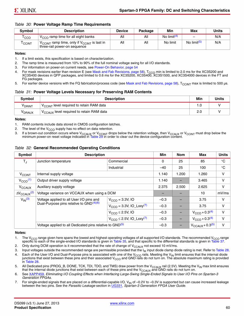
Spartan-3 FPGA Family: DC and Switching Characteristics
DS099 (v3.1) June 27, 2013 www.xilinx.comProduct Specification 60
Table 30: Power Voltage Ramp Time Requirements
Symbol Description Device Package Min Max Units
TCCO VCCO ramp time for all eight banks All All No limit(4) – N/A
TCCINT VCCINT ramp time, only if VCCINT is last in three-rail power-on sequence
All All No limit No limit(5) N/A
Notes: 1. If a limit exists, this specification is based on characterization.2. The ramp time is measured from 10% to 90% of the full nominal voltage swing for all I/O standards.3. For information on power-on current needs, see Power-On Behavior, page 544. For mask revisions earlier than revision E (see Mask and Fab Revisions, page 58), TCCO min is limited to 2.0 ms for the XC3S200 and
XC3S400 devices in QFP packages, and limited to 0.6 ms for the XC3S200, XC3S400, XC3S1500, and XC3S4000 devices in the FT and FG packages.
5. For earlier device versions with the FQ fabrication/process code (see Mask and Fab Revisions, page 58), TCCINT max is limited to 500 µs.
Table 31: Power Voltage Levels Necessary for Preserving RAM Contents
Symbol Description Min Units
VDRINT VCCINT level required to retain RAM data 1.0 V
VDRAUX VCCAUX level required to retain RAM data 2.0 V
Notes: 1. RAM contents include data stored in CMOS configuration latches.2. The level of the VCCO supply has no effect on data retention.3. If a brown-out condition occurs where VCCAUX or VCCINT drops below the retention voltage, then VCCAUX or VCCINT must drop below the
minimum power-on reset voltage indicated in Table 29 in order to clear out the device configuration content.
Table 32: General Recommended Operating Conditions
Symbol Description Min Nom Max Units
TJ Junction temperature Commercial 0 25 85 °C
Industrial –40 25 100 °C
VCCINT Internal supply voltage 1.140 1.200 1.260 V
VCCO(1) Output driver supply voltage 1.140 – 3.465 V
VCCAUX Auxiliary supply voltage 2.375 2.500 2.625 V
ΔVCCAUX(2) Voltage variance on VCCAUX when using a DCM – – 10 mV/ms
VIN(3) Voltage applied to all User I/O pins and
Dual-Purpose pins relative to GND(4)(6)VCCO = 3.3V, IO –0.3 – 3.75 V
VCCO = 3.3V, IO_Lxxy(7) –0.3 – 3.75 V
VCCO ≤ 2.5V, IO –0.3 – VCCO + 0.3(4) V
VCCO ≤ 2.5V, IO_Lxxy(7) –0.3 – VCCO + 0.3(4) V
Voltage applied to all Dedicated pins relative to GND(5) –0.3 – VCCAUX+ 0.3(5) V
Notes: 1. The VCCO range given here spans the lowest and highest operating voltages of all supported I/O standards. The recommended VCCO range
specific to each of the single-ended I/O standards is given in Table 35, and that specific to the differential standards is given in Table 37.2. Only during DCM operation is it recommended that the rate of change of VCCAUX not exceed 10 mV/ms.3. Input voltages outside the recommended range are permissible provided that the IIK input diode clamp diode rating is met. Refer to Table 28.4. Each of the User I/O and Dual-Purpose pins is associated with one of the VCCO rails. Meeting the VIN limit ensures that the internal diode
junctions that exist between these pins and their associated VCCO and GND rails do not turn on. The absolute maximum rating is provided in Table 28.
5. All Dedicated pins (PROG_B, DONE, TCK, TDI, TDO, and TMS) draw power from the VCCAUX rail (2.5V). Meeting the VIN max limit ensures that the internal diode junctions that exist between each of these pins and the VCCAUX and GND rails do not turn on.
6. See XAPP459, Eliminating I/O Coupling Effects when Interfacing Large-Swing Single-Ended Signals to User I/O Pins on Spartan-3 Generation FPGAs.
7. For single-ended signals that are placed on a differential-capable I/O, VIN of –0.2V to –0.3V is supported but can cause increased leakage between the two pins. See the Parasitic Leakage section in UG331, Spartan-3 Generation FPGA User Guide.
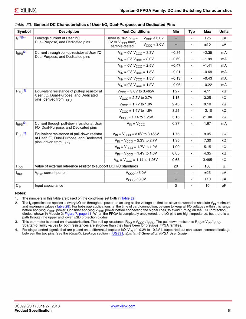
Spartan-3 FPGA Family: DC and Switching Characteristics
DS099 (v3.1) June 27, 2013 www.xilinx.comProduct Specification 61
Table 33: General DC Characteristics of User I/O, Dual-Purpose, and Dedicated Pins
Symbol Description Test Conditions Min Typ Max Units
IL(2)(4) Leakage current at User I/O, Dual-Purpose, and Dedicated pins
Driver is Hi-Z, VIN = 0V or VCCO max,
sample-tested
VCCO ≥ 3.0V – - ±25 μA
VCCO < 3.0V – - ±10 μA
IRPU(3) Current through pull-up resistor at User I/O,
Dual-Purpose, and Dedicated pinsVIN = 0V, VCCO = 3.3V –0.84 - –2.35 mA
VIN = 0V, VCCO = 3.0V –0.69 - –1.99 mA
VIN = 0V, VCCO = 2.5V –0.47 - –1.41 mA
VIN = 0V, VCCO = 1.8V –0.21 - –0.69 mA
VIN = 0V, VCCO = 1.5V –0.13 - –0.43 mA
VIN = 0V, VCCO = 1.2V –0.06 - –0.22 mA
RPU(3) Equivalent resistance of pull-up resistor at
User I/O, Dual-Purpose, and Dedicated pins, derived from IRPU
VCCO = 3.0V to 3.465V 1.27 - 4.11 kΩ
VCCO = 2.3V to 2.7V 1.15 - 3.25 kΩ
VCCO = 1.7V to 1.9V 2.45 - 9.10 kΩ
VCCO = 1.4V to 1.6V 3.25 - 12.10 kΩ
VCCO = 1.14 to 1.26V 5.15 - 21.00 kΩ
IRPD(3) Current through pull-down resistor at User
I/O, Dual-Purpose, and Dedicated pinsVIN = VCCO 0.37 - 1.67 mA
RPD(3) Equivalent resistance of pull-down resistor
at User I/O, Dual-Purpose, and Dedicated pins, driven from IRPD
VIN = VCCO = 3.0V to 3.465V 1.75 - 9.35 kΩ
VIN = VCCO = 2.3V to 2.7V 1.35 - 7.30 kΩ
VIN = VCCO = 1.7V to 1.9V 1.00 - 5.15 kΩ
VIN = VCCO = 1.4V to 1.6V 0.85 - 4.35 kΩ
VIN = VCCO = 1.14 to 1.26V 0.68 - 3.465 kΩ
RDCI Value of external reference resistor to support DCI I/O standards 20 - 100 Ω
IREF VREF current per pin VCCO ≥ 3.0V – - ±25 μA
VCCO < 3.0V – - ±10 μA
CIN Input capacitance 3 - 10 pF
Notes: 1. The numbers in this table are based on the conditions set forth in Table 32.2. The IL specification applies to every I/O pin throughout power-on as long as the voltage on that pin stays between the absolute VIN minimum
and maximum values (Table 28). For hot-swap applications, at the time of card connection, be sure to keep all I/O voltages within this range before applying VCCO power. Consider applying VCCO power before connecting the signal lines, to avoid turning on the ESD protection diodes, shown in Module 2: Figure 7, page 11. When the FPGA is completely unpowered, the I/O pins are high impedance, but there is a path through the upper and lower ESD protection diodes.
3. This parameter is based on characterization. The pull-up resistance RPU = VCCO / IRPU. The pull-down resistance RPD = VIN / IRPD. Spartan-3 family values for both resistances are stronger than they have been for previous FPGA families.
4. For single-ended signals that are placed on a differential-capable I/O, VIN of –0.2V to –0.3V is supported but can cause increased leakage between the two pins. See the Parasitic Leakage section in UG331, Spartan-3 Generation FPGA User Guide.
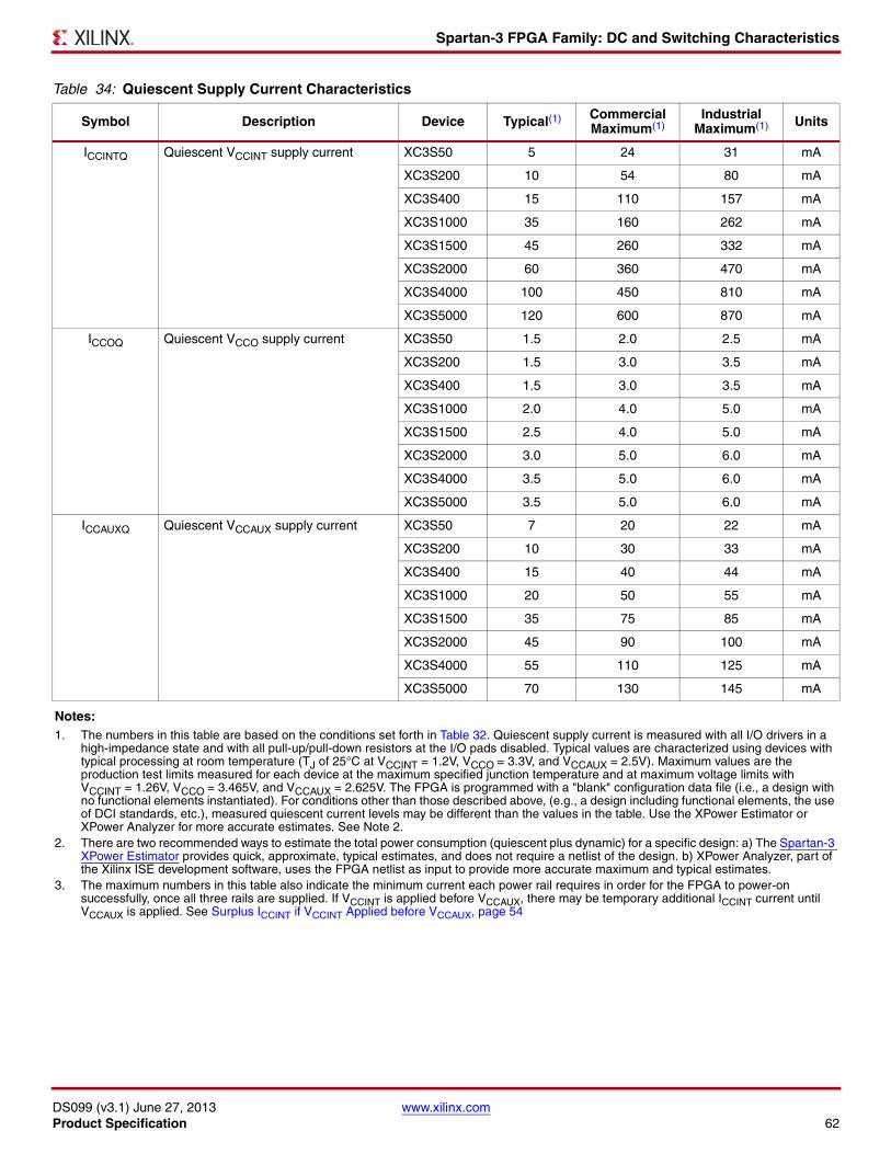
Spartan-3 FPGA Family: DC and Switching Characteristics
DS099 (v3.1) June 27, 2013 www.xilinx.comProduct Specification 62
Table 34: Quiescent Supply Current Characteristics
Symbol Description Device Typical(1) Commercial Maximum(1)
Industrial Maximum(1) Units
ICCINTQ Quiescent VCCINT supply current XC3S50 5 24 31 mA
XC3S200 10 54 80 mA
XC3S400 15 110 157 mA
XC3S1000 35 160 262 mA
XC3S1500 45 260 332 mA
XC3S2000 60 360 470 mA
XC3S4000 100 450 810 mA
XC3S5000 120 600 870 mA
ICCOQ Quiescent VCCO supply current XC3S50 1.5 2.0 2.5 mA
XC3S200 1.5 3.0 3.5 mA
XC3S400 1.5 3.0 3.5 mA
XC3S1000 2.0 4.0 5.0 mA
XC3S1500 2.5 4.0 5.0 mA
XC3S2000 3.0 5.0 6.0 mA
XC3S4000 3.5 5.0 6.0 mA
XC3S5000 3.5 5.0 6.0 mA
ICCAUXQ Quiescent VCCAUX supply current XC3S50 7 20 22 mA
XC3S200 10 30 33 mA
XC3S400 15 40 44 mA
XC3S1000 20 50 55 mA
XC3S1500 35 75 85 mA
XC3S2000 45 90 100 mA
XC3S4000 55 110 125 mA
XC3S5000 70 130 145 mA
Notes: 1. The numbers in this table are based on the conditions set forth in Table 32. Quiescent supply current is measured with all I/O drivers in a
high-impedance state and with all pull-up/pull-down resistors at the I/O pads disabled. Typical values are characterized using devices with typical processing at room temperature (TJ of 25°C at VCCINT = 1.2V, VCCO = 3.3V, and VCCAUX = 2.5V). Maximum values are the production test limits measured for each device at the maximum specified junction temperature and at maximum voltage limits with VCCINT = 1.26V, VCCO = 3.465V, and VCCAUX = 2.625V. The FPGA is programmed with a "blank" configuration data file (i.e., a design with no functional elements instantiated). For conditions other than those described above, (e.g., a design including functional elements, the use of DCI standards, etc.), measured quiescent current levels may be different than the values in the table. Use the XPower Estimator or XPower Analyzer for more accurate estimates. See Note 2.
2. There are two recommended ways to estimate the total power consumption (quiescent plus dynamic) for a specific design: a) The Spartan-3 XPower Estimator provides quick, approximate, typical estimates, and does not require a netlist of the design. b) XPower Analyzer, part of the Xilinx ISE development software, uses the FPGA netlist as input to provide more accurate maximum and typical estimates.
3. The maximum numbers in this table also indicate the minimum current each power rail requires in order for the FPGA to power-on successfully, once all three rails are supplied. If VCCINT is applied before VCCAUX, there may be temporary additional ICCINT current until VCCAUX is applied. See Surplus ICCINT if VCCINT Applied before VCCAUX, page 54
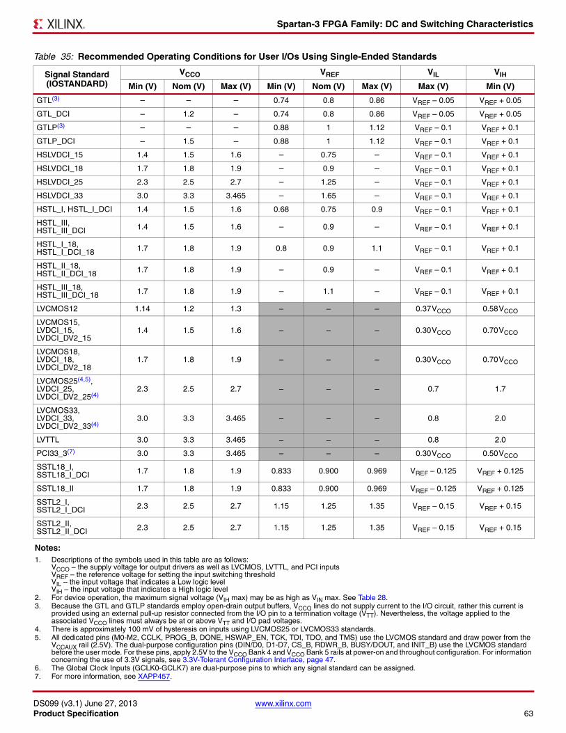
Spartan-3 FPGA Family: DC and Switching Characteristics
DS099 (v3.1) June 27, 2013 www.xilinx.comProduct Specification 63
Table 35: Recommended Operating Conditions for User I/Os Using Single-Ended Standards
Signal Standard(IOSTANDARD)
VCCO VREF VIL VIH
Min (V) Nom (V) Max (V) Min (V) Nom (V) Max (V) Max (V) Min (V)
GTL(3) – – – 0.74 0.8 0.86 VREF – 0.05 VREF + 0.05
GTL_DCI – 1.2 – 0.74 0.8 0.86 VREF – 0.05 VREF + 0.05
GTLP(3) – – – 0.88 1 1.12 VREF – 0.1 VREF + 0.1
GTLP_DCI – 1.5 – 0.88 1 1.12 VREF – 0.1 VREF + 0.1
HSLVDCI_15 1.4 1.5 1.6 – 0.75 – VREF – 0.1 VREF + 0.1
HSLVDCI_18 1.7 1.8 1.9 – 0.9 – VREF – 0.1 VREF + 0.1
HSLVDCI_25 2.3 2.5 2.7 – 1.25 – VREF – 0.1 VREF + 0.1
HSLVDCI_33 3.0 3.3 3.465 – 1.65 – VREF – 0.1 VREF + 0.1
HSTL_I, HSTL_I_DCI 1.4 1.5 1.6 0.68 0.75 0.9 VREF – 0.1 VREF + 0.1
HSTL_III, HSTL_III_DCI 1.4 1.5 1.6 – 0.9 – VREF – 0.1 VREF + 0.1
HSTL_I_18, HSTL_I_DCI_18 1.7 1.8 1.9 0.8 0.9 1.1 VREF – 0.1 VREF + 0.1
HSTL_II_18, HSTL_II_DCI_18 1.7 1.8 1.9 – 0.9 – VREF – 0.1 VREF + 0.1
HSTL_III_18, HSTL_III_DCI_18 1.7 1.8 1.9 – 1.1 – VREF – 0.1 VREF + 0.1
LVCMOS12 1.14 1.2 1.3 – – – 0.37VCCO 0.58VCCO
LVCMOS15, LVDCI_15, LVDCI_DV2_15
1.4 1.5 1.6 – – – 0.30VCCO 0.70VCCO
LVCMOS18, LVDCI_18, LVDCI_DV2_18
1.7 1.8 1.9 – – – 0.30VCCO 0.70VCCO
LVCMOS25(4,5), LVDCI_25, LVDCI_DV2_25(4)
2.3 2.5 2.7 – – – 0.7 1.7
LVCMOS33, LVDCI_33, LVDCI_DV2_33(4)
3.0 3.3 3.465 – – – 0.8 2.0
LVTTL 3.0 3.3 3.465 – – – 0.8 2.0
PCI33_3(7) 3.0 3.3 3.465 – – – 0.30VCCO 0.50VCCO
SSTL18_I, SSTL18_I_DCI 1.7 1.8 1.9 0.833 0.900 0.969 VREF – 0.125 VREF + 0.125
SSTL18_II 1.7 1.8 1.9 0.833 0.900 0.969 VREF – 0.125 VREF + 0.125
SSTL2_I, SSTL2_I_DCI 2.3 2.5 2.7 1.15 1.25 1.35 VREF – 0.15 VREF + 0.15
SSTL2_II, SSTL2_II_DCI 2.3 2.5 2.7 1.15 1.25 1.35 VREF – 0.15 VREF + 0.15
Notes: 1. Descriptions of the symbols used in this table are as follows:
VCCO – the supply voltage for output drivers as well as LVCMOS, LVTTL, and PCI inputsVREF – the reference voltage for setting the input switching thresholdVIL – the input voltage that indicates a Low logic levelVIH – the input voltage that indicates a High logic level
2. For device operation, the maximum signal voltage (VIH max) may be as high as VIN max. See Table 28.3. Because the GTL and GTLP standards employ open-drain output buffers, VCCO lines do not supply current to the I/O circuit, rather this current is
provided using an external pull-up resistor connected from the I/O pin to a termination voltage (VTT). Nevertheless, the voltage applied to the associated VCCO lines must always be at or above VTT and I/O pad voltages.
4. There is approximately 100 mV of hysteresis on inputs using LVCMOS25 or LVCMOS33 standards.5. All dedicated pins (M0-M2, CCLK, PROG_B, DONE, HSWAP_EN, TCK, TDI, TDO, and TMS) use the LVCMOS standard and draw power from the
VCCAUX rail (2.5V). The dual-purpose configuration pins (DIN/D0, D1-D7, CS_B, RDWR_B, BUSY/DOUT, and INIT_B) use the LVCMOS standard before the user mode. For these pins, apply 2.5V to the VCCO Bank 4 and VCCO Bank 5 rails at power-on and throughout configuration. For information concerning the use of 3.3V signals, see 3.3V-Tolerant Configuration Interface, page 47.
6. The Global Clock Inputs (GCLK0-GCLK7) are dual-purpose pins to which any signal standard can be assigned.7. For more information, see XAPP457.
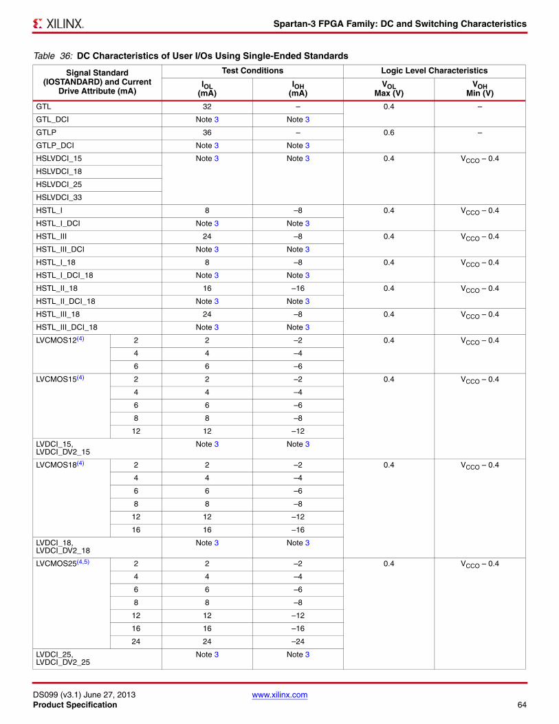
Spartan-3 FPGA Family: DC and Switching Characteristics
DS099 (v3.1) June 27, 2013 www.xilinx.comProduct Specification 64
Table 36: DC Characteristics of User I/Os Using Single-Ended Standards
Signal Standard (IOSTANDARD) and Current
Drive Attribute (mA)
Test Conditions Logic Level Characteristics
IOL(mA)
IOH(mA)
VOLMax (V)
VOHMin (V)
GTL 32 – 0.4 –
GTL_DCI Note 3 Note 3
GTLP 36 – 0.6 –
GTLP_DCI Note 3 Note 3
HSLVDCI_15 Note 3 Note 3 0.4 VCCO – 0.4
HSLVDCI_18
HSLVDCI_25
HSLVDCI_33
HSTL_I 8 –8 0.4 VCCO – 0.4
HSTL_I_DCI Note 3 Note 3
HSTL_III 24 –8 0.4 VCCO – 0.4
HSTL_III_DCI Note 3 Note 3
HSTL_I_18 8 –8 0.4 VCCO – 0.4
HSTL_I_DCI_18 Note 3 Note 3
HSTL_II_18 16 –16 0.4 VCCO – 0.4
HSTL_II_DCI_18 Note 3 Note 3
HSTL_III_18 24 –8 0.4 VCCO – 0.4
HSTL_III_DCI_18 Note 3 Note 3
LVCMOS12(4) 2 2 –2 0.4 VCCO – 0.4
4 4 –4
6 6 –6
LVCMOS15(4) 2 2 –2 0.4 VCCO – 0.4
4 4 –4
6 6 –6
8 8 –8
12 12 –12
LVDCI_15,LVDCI_DV2_15
Note 3 Note 3
LVCMOS18(4) 2 2 –2 0.4 VCCO – 0.4
4 4 –4
6 6 –6
8 8 –8
12 12 –12
16 16 –16
LVDCI_18,LVDCI_DV2_18
Note 3 Note 3
LVCMOS25(4,5) 2 2 –2 0.4 VCCO – 0.4
4 4 –4
6 6 –6
8 8 –8
12 12 –12
16 16 –16
24 24 –24
LVDCI_25,LVDCI_DV2_25
Note 3 Note 3
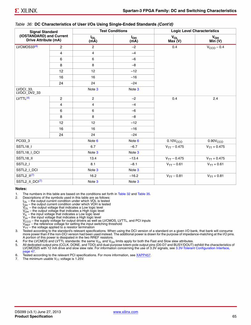
Spartan-3 FPGA Family: DC and Switching Characteristics
DS099 (v3.1) June 27, 2013 www.xilinx.comProduct Specification 65
LVCMOS33(4) 2 2 –2 0.4 VCCO – 0.4
4 4 –4
6 6 –6
8 8 –8
12 12 –12
16 16 –16
24 24 –24
LVDCI_33,LVDCI_DV2_33
Note 3 Note 3
LVTTL(4) 2 2 –2 0.4 2.4
4 4 –4
6 6 –6
8 8 –8
12 12 –12
16 16 –16
24 24 –24
PCI33_3 Note 6 Note 6 0.10VCCO 0.90VCCO
SSTL18_I 6.7 –6.7 VTT – 0.475 VTT + 0.475
SSTL18_I_DCI Note 3 Note 3
SSTL18_II 13.4 –13.4 VTT – 0.475 VTT + 0.475
SSTL2_I 8.1 –8.1 VTT – 0.61 VTT + 0.61
SSTL2_I_DCI Note 3 Note 3
SSTL2_II(7) 16.2 –16.2 VTT – 0.81 VTT + 0.81
SSTL2_II_DCI(7) Note 3 Note 3
Notes: 1. The numbers in this table are based on the conditions set forth in Table 32 and Table 35.2. Descriptions of the symbols used in this table are as follows:
IOL – the output current condition under which VOL is testedIOH – the output current condition under which VOH is testedVOL – the output voltage that indicates a Low logic level VOH – the output voltage that indicates a High logic levelVIL – the input voltage that indicates a Low logic levelVIH – the input voltage that indicates a High logic levelVCCO – the supply voltage for output drivers as well as LVCMOS, LVTTL, and PCI inputsVREF – the reference voltage for setting the input switching thresholdVTT – the voltage applied to a resistor termination
3. Tested according to the standard’s relevant specifications. When using the DCI version of a standard on a given I/O bank, that bank will consume more power than if the non-DCI version had been used instead. The additional power is drawn for the purpose of impedance-matching at the I/O pins. A portion of this power is dissipated in the two RREF resistors.
4. For the LVCMOS and LVTTL standards: the same VOL and VOH limits apply for both the Fast and Slow slew attributes.5. All dedicated output pins (CCLK, DONE, and TDO) and dual-purpose totem-pole output pins (D0-D7 and BUSY/DOUT) exhibit the characteristics of
LVCMOS25 with 12 mA drive and slow slew rate. For information concerning the use of 3.3V signals, see 3.3V-Tolerant Configuration Interface, page 47.
6. Tested according to the relevant PCI specifications. For more information, see XAPP457.7. The minimum usable VTT voltage is 1.25V.
Table 36: DC Characteristics of User I/Os Using Single-Ended Standards (Cont’d)
Signal Standard (IOSTANDARD) and Current
Drive Attribute (mA)
Test Conditions Logic Level Characteristics
IOL(mA)
IOH(mA)
VOLMax (V)
VOHMin (V)
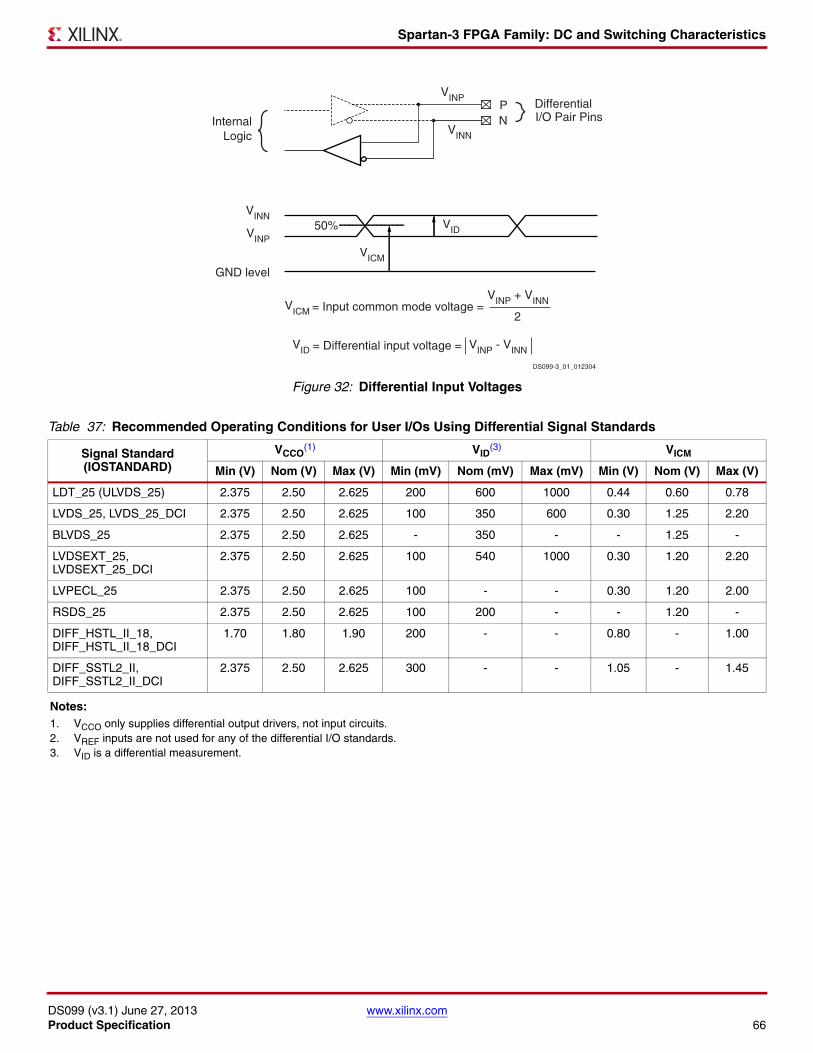
Spartan-3 FPGA Family: DC and Switching Characteristics
DS099 (v3.1) June 27, 2013 www.xilinx.comProduct Specification 66
X-Ref Target - Figure 32
Figure 32: Differential Input Voltages
Table 37: Recommended Operating Conditions for User I/Os Using Differential Signal Standards
Signal Standard(IOSTANDARD)
VCCO(1) VID
(3) VICM
Min (V) Nom (V) Max (V) Min (mV) Nom (mV) Max (mV) Min (V) Nom (V) Max (V)
LDT_25 (ULVDS_25) 2.375 2.50 2.625 200 600 1000 0.44 0.60 0.78
LVDS_25, LVDS_25_DCI 2.375 2.50 2.625 100 350 600 0.30 1.25 2.20
BLVDS_25 2.375 2.50 2.625 - 350 - - 1.25 -
LVDSEXT_25, LVDSEXT_25_DCI
2.375 2.50 2.625 100 540 1000 0.30 1.20 2.20
LVPECL_25 2.375 2.50 2.625 100 - - 0.30 1.20 2.00
RSDS_25 2.375 2.50 2.625 100 200 - - 1.20 -
DIFF_HSTL_II_18, DIFF_HSTL_II_18_DCI
1.70 1.80 1.90 200 - - 0.80 - 1.00
DIFF_SSTL2_II, DIFF_SSTL2_II_DCI
2.375 2.50 2.625 300 - - 1.05 - 1.45
Notes: 1. VCCO only supplies differential output drivers, not input circuits.2. VREF inputs are not used for any of the differential I/O standards.3. VID is a differential measurement.
DS099-3_01_012304
VINN
VINP
GND level
50%
VICM
VICM = Input common mode voltage =
VID
VINP
InternalLogic
DifferentialI/O Pair Pins
VINN
NP
2
VINP + VINN
VID = Differential input voltage = VINP - VINN
Spartan-3 FPGA Family: DC and Switching Characteristics
DS099 (v3.1) June 27, 2013 www.xilinx.comProduct Specification 67
X-Ref Target - Figure 33
Figure 33: Differential Output Voltages
Table 38: DC Characteristics of User I/Os Using Differential Signal Standards
Signal Standard Mask(3) Revision
VOD VOCM VOH VOL
Min (mV) Typ (mV) Max (mV) Min (V) Typ (V) Max (V) Min (V) Max (V)
LDT_25 (ULVDS_25) All 430(4) 600 670 0.495 0.600 0.715 0.71 0.50
LVDS_25 All 100 – 600 0.80 – 1.6 0.85 1.55
‘E’ 200 – 500 1.0 – 1.5 1.10 1.40
BLVDS_25(5) All 250 350 450 – 1.20 – – –
LVDSEXT_25 All 100 – 600 0.80 – 1.6 0.85 1.55
‘E’ 300 – 700 1.0 – 1.5 1.15 1.35
LVPECL_25(5) All – – - – – - 1.35 1.005
RSDS_25(6) All 100 – 600 0.80 – 1.6 0.85 1.55
‘E’ 200 – 500 1.0 – 1.5 1.10 1.40
DIFF_HSTL_II_18 All – – – – – – VCCO – 0.40 0.40
DIFF_SSTL2_II All – – – – – – VTT + 0.80 VTT – 0.80
Notes: 1. The numbers in this table are based on the conditions set forth in Table 32 and Table 37.2. Output voltage measurements for all differential standards are made with a termination resistor (RT) of 100Ω across the N and P pins of the
differential signal pair.3. Mask revision E devices have tighter output ranges but can be used in any design that was in a previous revision. See Mask and Fab
Revisions, page 58.4. This value must be compatible with the receiver to which the FPGA’s output pair is connected. 5. Each LVPECL_25 or BLVDS_25 output-pair requires three external resistors for proper output operation as shown in Figure 34. Each
LVPECL_25 or BLVDS_25 input-pair uses a 100W termination resistor at the receiver.6. Only one of the differential standards RSDS_25, LDT_25, LVDS_25, and LVDSEXT_25 may be used for outputs within a bank.
Each differential standard input-pair requires an external 100Ω termination resistor.
X-Ref Target - Figure 34
Figure 34: External Termination Required for LVPECL and BLVDS Output and Input
DS099-3_02_091710
VOUTN
VOUTP
GND level
50%
VOCM
VOCM
VOD
VOL
VOH
VOUTP
InternalLogic VOUTN
NP
= Output common mode voltage =2
VOUTP + VOUTN
VOD = Output differential voltage =
VOH = Output voltage indicating a High logic level
VOL= Output voltage indicating a Low logic level
VOUTP - VOUTN
DifferentialI/O Pair Pins
ds099-3_08_112105
240Ω
70Ω
70Ω
100Ω
LVPECL LVPECLZ0=50Ω
Z0=50Ω
140Ω
165Ω
165Ω
100Ω
BLVDS BLVDSZ0=50Ω
Z0=50Ω
Spartan-3 FPGA Family: DC and Switching Characteristics
DS099 (v3.1) June 27, 2013 www.xilinx.comProduct Specification 68
Switching CharacteristicsAll Spartan-3 devices are available in two speed grades: –4 and the higher performance –5. Switching characteristics in this document may be designated as Advance, Preliminary, or Production. Each category is defined as follows:
Advance: These specifications are based on simulations only and are typically available soon after establishing FPGA specifications. Although speed grades with this designation are considered relatively stable and conservative, some under-reported delays may still occur.
Preliminary: These specifications are based on complete early silicon characterization. Devices and speed grades with this designation are intended to give a better indication of the expected performance of production silicon. The probability of under-reporting preliminary delays is greatly reduced compared to Advance data.
Production: These specifications are approved once enough production silicon of a particular device family member has been characterized to provide full correlation between speed files and devices over numerous production lots. There is no under-reporting of delays, and customers receive formal notification of any subsequent changes. Typically, the slowest speed grades transition to Production before faster speed grades.
Production-quality systems must use FPGA designs compiled using a Production status speed file. FPGAs designs using a less mature speed file designation may only be used during system prototyping or preproduction qualification. FPGA designs using Advance or Preliminary status speed files should never be used in a production-quality system.
Whenever a speed file designation changes, as a device matures toward Production status, rerun the Xilinx ISE software on the FPGA design to ensure that the FPGA design incorporates the latest timing information and software updates.
Xilinx ISE Software Updates: http://www.xilinx.com/support/download/index.htm
All specified limits are representative of worst-case supply voltage and junction temperature conditions. Unless otherwise noted, the following applies: Parameter values apply to all Spartan-3 devices. All parameters representing voltages are measured with respect to GND.
Selected timing parameters and their representative values are included below either because they are important as general design requirements or they indicate fundamental device performance characteristics. The Spartan-3 FPGA v1.38 speed files are the original source for many but not all of the values. The v1.38 speed files are available in Xilinx Integrated Software Environment (ISE) software version 8.2i.
The speed grade designations for these files are shown in Table 39. For more complete, more precise, and worst-case data, use the values reported by the Xilinx static timing analyzer (TRACE in the Xilinx development software) and back-annotated to the simulation netlist.
Table 39: Spartan-3 FPGA Speed Grade Designations (ISE v8.2i or Later)
Device Advance Preliminary Production
XC3S50 -4, -5 (v1.37 and later)
XC3S200
XC3S400
XC3S1000
XC3S1500
XC3S2000
XC3S4000
XC3S5000 -4, -5 (v1.38 and later)
Spartan-3 FPGA Family: DC and Switching Characteristics
DS099 (v3.1) June 27, 2013 www.xilinx.comProduct Specification 69
I/O Timing
Table 40: Pin-to-Pin Clock-to-Output Times for the IOB Output Path
Symbol Description Conditions Device
Speed Grade
Units-5 -4
Max(2) Max(2)
Clock-to-Output Times
TICKOFDCM When reading from the Output Flip-Flop (OFF), the time from the active transition on the Global Clock pin to data appearing at the Output pin. The DCM is in use.
LVCMOS25(3), 12 mA output drive, Fast slew rate, with DCM(4)
XC3S50 2.04 2.35 ns
XC3S200 1.45 1.75 ns
XC3S400 1.45 1.75 ns
XC3S1000 2.07 2.39 ns
XC3S1500 2.05 2.36 ns
XC3S2000 2.03 2.34 ns
XC3S4000 1.94 2.24 ns
XC3S5000 2.00 2.30 ns
TICKOF When reading from OFF, the time from the active transition on the Global Clock pin to data appearing at the Output pin. The DCM is not in use.
LVCMOS25(3), 12 mA output drive, Fast slew rate, without DCM
XC3S50 3.70 4.24 ns
XC3S200 3.89 4.46 ns
XC3S400 3.91 4.48 ns
XC3S1000 4.00 4.59 ns
XC3S1500 4.07 4.66 ns
XC3S2000 4.19 4.80 ns
XC3S4000 4.44 5.09 ns
XC3S5000 4.38 5.02 ns
Notes: 1. The numbers in this table are tested using the methodology presented in Table 48 and are based on the operating conditions set forth in
Table 32 and Table 35.2. For minimums, use the values reported by the Xilinx timing analyzer.3. This clock-to-output time requires adjustment whenever a signal standard other than LVCMOS25 is assigned to the Global Clock Input or a
standard other than LVCMOS25 with 12 mA drive and Fast slew rate is assigned to the data Output. If the former is true, add the appropriate Input adjustment from Table 44. If the latter is true, add the appropriate Output adjustment from Table 47.
4. DCM output jitter is included in all measurements.
Spartan-3 FPGA Family: DC and Switching Characteristics
DS099 (v3.1) June 27, 2013 www.xilinx.comProduct Specification 70
Table 41: System-Synchronous Pin-to-Pin Setup and Hold Times for the IOB Input Path
Symbol Description Conditions Device
Speed Grade
Units-5 -4
Min Min
Setup Times
TPSDCM When writing to the Input Flip-Flop (IFF), the time from the setup of data at the Input pin to the active transition at a Global Clock pin. The DCM is in use. No Input Delay is programmed.
LVCMOS25(2),IOBDELAY = NONE, with DCM(4)
XC3S50 2.37 2.71 ns
XC3S200 2.13 2.35 ns
XC3S400 2.15 2.36 ns
XC3S1000 2.58 2.95 ns
XC3S1500 2.55 2.91 ns
XC3S2000 2.59 2.96 ns
XC3S4000 2.76 3.15 ns
XC3S5000 2.69 3.08 ns
TPSFD When writing to IFF, the time from the setup of data at the Input pin to an active transition at the Global Clock pin. The DCM is not in use. The Input Delay is programmed.
LVCMOS25(2), IOBDELAY = IFD, without DCM
XC3S50 3.00 3.46 ns
XC3S200 2.63 3.02 ns
XC3S400 2.50 2.87 ns
XC3S1000 3.50 4.03 ns
XC3S1500 3.78 4.35 ns
XC3S2000 4.98 5.73 ns
XC3S4000 5.25 6.05 ns
XC3S5000 5.37 6.18 ns
Hold Times
TPHDCM When writing to IFF, the time from the active transition at the Global Clock pin to the point when data must be held at the Input pin. The DCM is in use. No Input Delay is programmed.
LVCMOS25(3), IOBDELAY = NONE, with DCM(4)
XC3S50 –0.45 –0.40 ns
XC3S200 –0.12 –0.05 ns
XC3S400 –0.12 –0.05 ns
XC3S1000 –0.43 –0.38 ns
XC3S1500 –0.45 –0.40 ns
XC3S2000 –0.47 –0.42 ns
XC3S4000 –0.61 –0.56 ns
XC3S5000 –0.62 –0.57 ns
Spartan-3 FPGA Family: DC and Switching Characteristics
DS099 (v3.1) June 27, 2013 www.xilinx.comProduct Specification 71
TPHFD When writing to IFF, the time from the active transition at the Global Clock pin to the point when data must be held at the Input pin. The DCM is not in use. The Input Delay is programmed.
LVCMOS25(3), IOBDELAY = IFD, without DCM
XC3S50 –0.98 –0.93 ns
XC3S200 –0.40 –0.35 ns
XC3S400 –0.27 –0.22 ns
XC3S1000 –1.19 –1.14 ns
XC3S1500 –1.43 –1.38 ns
XC3S2000 –2.33 –2.28 ns
XC3S4000 –2.47 –2.42 ns
XC3S5000 –2.66 –2.61 ns
Notes: 1. The numbers in this table are tested using the methodology presented in Table 48 and are based on the operating conditions set forth in
Table 32 and Table 35.2. This setup time requires adjustment whenever a signal standard other than LVCMOS25 is assigned to the Global Clock Input or the data
Input. If this is true of the Global Clock Input, subtract the appropriate adjustment from Table 44. If this is true of the data Input, add the appropriate Input adjustment from the same table.
3. This hold time requires adjustment whenever a signal standard other than LVCMOS25 is assigned to the Global Clock Input or the data Input. If this is true of the Global Clock Input, add the appropriate Input adjustment from Table 44. If this is true of the data Input, subtract the appropriate Input adjustment from the same table. When the hold time is negative, it is possible to change the data before the clock’s active edge.
4. DCM output jitter is included in all measurements.
Table 42: Setup and Hold Times for the IOB Input Path
Symbol Description Conditions Device
Speed Grade
Units-5 -4
Min Min
Setup Times
TIOPICK Time from the setup of data at the Input pin to the active transition at the ICLK input of the Input Flip-Flop (IFF). No Input Delay is programmed.
LVCMOS25(2), IOBDELAY = NONE
XC3S50 1.65 1.89 ns
XC3S200 1.37 1.57 ns
XC3S400 1.37 1.57 ns
XC3S1000 1.65 1.89 ns
XC3S1500 1.65 1.89 ns
XC3S2000 1.65 1.89 ns
XC3S4000 1.73 1.99 ns
XC3S5000 1.82 2.09 ns
TIOPICKD Time from the setup of data at the Input pin to the active transition at the IFF’s ICLK input. The Input Delay is programmed.
LVCMOS25(2), IOBDELAY = IFD
XC3S50 4.39 5.04 ns
XC3S200 4.76 5.47 ns
XC3S400 4.63 5.32 ns
XC3S1000 5.02 5.76 ns
XC3S1500 5.40 6.20 ns
XC3S2000 6.68 7.68 ns
XC3S4000 7.16 8.24 ns
XC3S5000 7.33 8.42 ns
Table 41: System-Synchronous Pin-to-Pin Setup and Hold Times for the IOB Input Path (Cont’d)
Symbol Description Conditions Device
Speed Grade
Units-5 -4
Min Min
Spartan-3 FPGA Family: DC and Switching Characteristics
DS099 (v3.1) June 27, 2013 www.xilinx.comProduct Specification 72
Hold Times
TIOICKP Time from the active transition at the IFF’s ICLK input to the point where data must be held at the Input pin. No Input Delay is programmed.
LVCMOS25(3), IOBDELAY = NONE
XC3S50 -0.55 -0.55 ns
XC3S200 -0.29 -0.29 ns
XC3S400 -0.29 -0.29 ns
XC3S1000 -0.55 -0.55 ns
XC3S1500 -0.55 -0.55 ns
XC3S2000 -0.55 -0.55 ns
XC3S4000 -0.61 -0.61 ns
XC3S5000 -0.68 -0.68 ns
TIOICKPD Time from the active transition at the IFF’s ICLK input to the point where data must be held at the Input pin. The Input Delay is programmed.
LVCMOS25(3), IOBDELAY = IFD
XC3S50 -2.74 -2.74 ns
XC3S200 -3.00 -3.00 ns
XC3S400 -2.90 -2.90 ns
XC3S1000 -3.24 -3.24 ns
XC3S1500 -3.55 -3.55 ns
XC3S2000 -4.57 -4.57 ns
XC3S4000 -4.96 -4.96 ns
XC3S5000 -5.09 -5.09 ns
Set/Reset Pulse Width
TRPW_IOB Minimum pulse width to SR control input on IOB
All 0.66 0.76 ns
Notes: 1. The numbers in this table are tested using the methodology presented in Table 48 and are based on the operating conditions set forth in
Table 32 and Table 35.2. This setup time requires adjustment whenever a signal standard other than LVCMOS25 is assigned to the data Input. If this is true, add the
appropriate Input adjustment from Table 44. 3. These hold times require adjustment whenever a signal standard other than LVCMOS25 is assigned to the data Input. If this is true, subtract
the appropriate Input adjustment from Table 44. When the hold time is negative, it is possible to change the data before the clock’s active edge.
Table 42: Setup and Hold Times for the IOB Input Path (Cont’d)
Symbol Description Conditions Device
Speed Grade
Units-5 -4
Min Min
Spartan-3 FPGA Family: DC and Switching Characteristics
DS099 (v3.1) June 27, 2013 www.xilinx.comProduct Specification 73
Table 43: Propagation Times for the IOB Input Path
Symbol Description Conditions Device
Speed Grade
Units-5 -4
Max Max
Propagation Times
TIOPLI The time it takes for data to travel from the Input pin through the IFF latch to the I output with no input delay programmed
LVCMOS25(2), IOBDELAY = NONE
XC3S50 2.01 2.31 ns
XC3S200 1.50 1.72 ns
XC3S400 1.50 1.72 ns
XC3S1000 2.01 2.31 ns
XC3S1500 2.01 2.31 ns
XC3S2000 2.01 2.31 ns
XC3S4000 2.09 2.41 ns
XC3S5000 2.18 2.51 ns
TIOPLID The time it takes for data to travel from the Input pin through the IFF latch to the I output with the input delay programmed
LVCMOS25(2), IOBDELAY = IFD
XC3S50 4.75 5.46 ns
XC3S200 4.89 5.62 ns
XC3S400 4.76 5.48 ns
XC3S1000 5.38 6.18 ns
XC3S1500 5.76 6.62 ns
XC3S2000 7.04 8.09 ns
XC3S4000 7.52 8.65 ns
XC3S5000 7.69 8.84 ns
Notes: 1. The numbers in this table are tested using the methodology presented in Table 48 and are based on the operating conditions set forth in
Table 32 and Table 35.2. This propagation time requires adjustment whenever a signal standard other than LVCMOS25 is assigned to the data Input. When this is
true, add the appropriate Input adjustment from Table 44.
Table 44: Input Timing Adjustments for IOB
Convert Input Time from LVCMOS25 to the Following Signal Standard (IOSTANDARD)
Add the Adjustment Below
UnitsSpeed Grade
-5 -4
Single-Ended Standards
GTL, GTL_DCI 0.44 0.50 ns
GTLP, GTLP_DCI 0.36 0.42 ns
HSLVDCI_15 0.51 0.59 ns
HSLVDCI_18 0.29 0.33 ns
HSLVDCI_25 0.51 0.59 ns
HSLVDCI_33 0.51 0.59 ns
HSTL_I, HSTL_I_DCI 0.51 0.59 ns
HSTL_III, HSTL_III_DCI 0.37 0.42 ns
HSTL_I_18, HSTL_I_DCI_18 0.36 0.41 ns
HSTL_II_18, HSTL_II_DCI_18 0.39 0.45 ns
HSTL_III_18, HSTL_III_DCI_18 0.45 0.52 ns
LVCMOS12 0.63 0.72 ns
Spartan-3 FPGA Family: DC and Switching Characteristics
DS099 (v3.1) June 27, 2013 www.xilinx.comProduct Specification 74
LVCMOS15 0.42 0.49 ns
LVDCI_15 0.38 0.43 ns
LVDCI_DV2_15 0.38 0.44 ns
LVCMOS18 0.24 0.28 ns
LVDCI_18 0.29 0.33 ns
LVDCI_DV2_18 0.28 0.33 ns
LVCMOS25 0 0 ns
LVDCI_25 0.05 0.05 ns
LVDCI_DV2_25 0.04 0.04 ns
LVCMOS33, LVDCI_33, LVDCI_DV2_33 –0.05 –0.02 ns
LVTTL 0.18 0.21 ns
PCI33_3 0.20 0.22 ns
SSTL18_I, SSTL18_I_DCI 0.39 0.45 ns
SSTL18_II 0.39 0.45 ns
SSTL2_I, SSTL2_I_DCI 0.40 0.46 ns
SSTL2_II, SSTL2_II_DCI 0.36 0.41 ns
Differential Standards
LDT_25 (ULVDS_25) 0.76 0.88 ns
LVDS_25, LVDS_25_DCI 0.65 0.75 ns
BLVDS_25 0.34 0.39 ns
LVDSEXT_25, LVDSEXT_25_DCI 0.80 0.92 ns
LVPECL_25 0.18 0.21 ns
RSDS_25 0.43 0.50 ns
DIFF_HSTL_II_18, DIFF_HSTL_II_18_DCI 0.34 0.39 ns
DIFF_SSTL2_II, DIFF_SSTL2_II_DCI 0.65 0.75 ns
Notes: 1. The numbers in this table are tested using the methodology presented in Table 48 and are based on
the operating conditions set forth in Table 32, Table 35, and Table 37.2. These adjustments are used to convert input path times originally specified for the LVCMOS25
standard to times that correspond to other signal standards.
Table 44: Input Timing Adjustments for IOB (Cont’d)
Convert Input Time from LVCMOS25 to the Following Signal Standard (IOSTANDARD)
Add the Adjustment Below
UnitsSpeed Grade
-5 -4
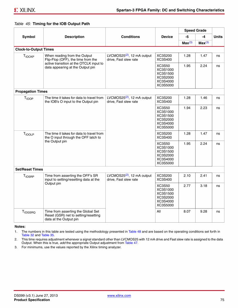
Spartan-3 FPGA Family: DC and Switching Characteristics
DS099 (v3.1) June 27, 2013 www.xilinx.comProduct Specification 75
Table 45: Timing for the IOB Output Path
Symbol Description Conditions Device
Speed Grade
Units-5 -4
Max(3) Max(3)
Clock-to-Output Times
TIOCKP When reading from the Output Flip-Flop (OFF), the time from the active transition at the OTCLK input to data appearing at the Output pin
LVCMOS25(2), 12 mA output drive, Fast slew rate
XC3S200XC3S400
1.28 1.47 ns
XC3S50XC3S1000XC3S1500XC3S2000XC3S4000XC3S5000
1.95 2.24 ns
Propagation Times
TIOOP The time it takes for data to travel from the IOB’s O input to the Output pin
LVCMOS25(2), 12 mA output drive, Fast slew rate
XC3S200XC3S400
1.28 1.46 ns
XC3S50XC3S1000XC3S1500XC3S2000XC3S4000XC3S5000
1.94 2.23 ns
TIOOLP The time it takes for data to travel from the O input through the OFF latch to the Output pin
XC3S200XC3S400
1.28 1.47 ns
XC3S50XC3S1000XC3S1500XC3S2000XC3S4000XC3S5000
1.95 2.24 ns
Set/Reset Times
TIOSRP Time from asserting the OFF’s SR input to setting/resetting data at the Output pin
LVCMOS25(2), 12 mA output drive, Fast slew rate
XC3S200XC3S400
2.10 2.41 ns
XC3S50XC3S1000XC3S1500XC3S2000XC3S4000XC3S5000
2.77 3.18 ns
TIOGSRQ Time from asserting the Global Set Reset (GSR) net to setting/resetting data at the Output pin
All 8.07 9.28 ns
Notes: 1. The numbers in this table are tested using the methodology presented in Table 48 and are based on the operating conditions set forth in
Table 32 and Table 35.2. This time requires adjustment whenever a signal standard other than LVCMOS25 with 12 mA drive and Fast slew rate is assigned to the data
Output. When this is true, add the appropriate Output adjustment from Table 47.3. For minimums, use the values reported by the Xilinx timing analyzer.
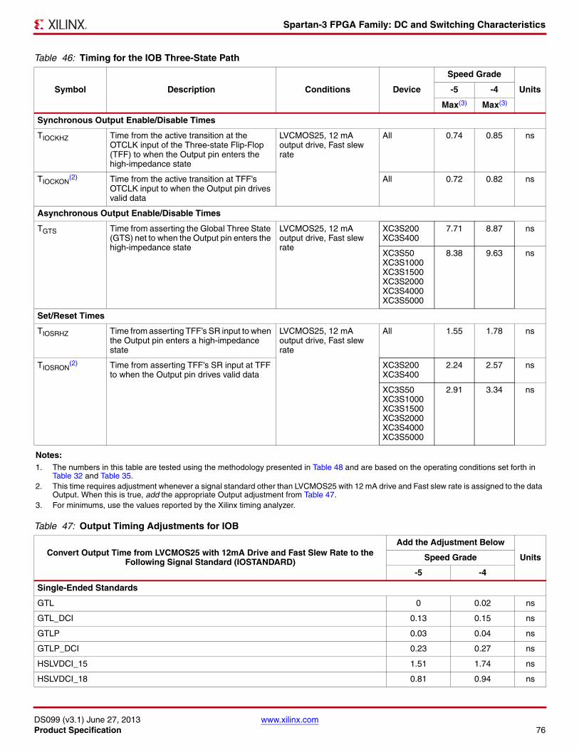
Spartan-3 FPGA Family: DC and Switching Characteristics
DS099 (v3.1) June 27, 2013 www.xilinx.comProduct Specification 76
Table 46: Timing for the IOB Three-State Path
Symbol Description Conditions Device
Speed Grade
Units-5 -4
Max(3) Max(3)
Synchronous Output Enable/Disable Times
TIOCKHZ Time from the active transition at the OTCLK input of the Three-state Flip-Flop (TFF) to when the Output pin enters the high-impedance state
LVCMOS25, 12 mA output drive, Fast slew rate
All 0.74 0.85 ns
TIOCKON(2) Time from the active transition at TFF’s
OTCLK input to when the Output pin drives valid data
All 0.72 0.82 ns
Asynchronous Output Enable/Disable Times
TGTS Time from asserting the Global Three State (GTS) net to when the Output pin enters the high-impedance state
LVCMOS25, 12 mA output drive, Fast slew rate
XC3S200XC3S400
7.71 8.87 ns
XC3S50XC3S1000XC3S1500XC3S2000XC3S4000XC3S5000
8.38 9.63 ns
Set/Reset Times
TIOSRHZ Time from asserting TFF’s SR input to when the Output pin enters a high-impedance state
LVCMOS25, 12 mA output drive, Fast slew rate
All 1.55 1.78 ns
TIOSRON(2) Time from asserting TFF’s SR input at TFF
to when the Output pin drives valid dataXC3S200XC3S400
2.24 2.57 ns
XC3S50XC3S1000XC3S1500XC3S2000XC3S4000XC3S5000
2.91 3.34 ns
Notes: 1. The numbers in this table are tested using the methodology presented in Table 48 and are based on the operating conditions set forth in
Table 32 and Table 35.2. This time requires adjustment whenever a signal standard other than LVCMOS25 with 12 mA drive and Fast slew rate is assigned to the data
Output. When this is true, add the appropriate Output adjustment from Table 47.3. For minimums, use the values reported by the Xilinx timing analyzer.
Table 47: Output Timing Adjustments for IOB
Convert Output Time from LVCMOS25 with 12mA Drive and Fast Slew Rate to the Following Signal Standard (IOSTANDARD)
Add the Adjustment Below
UnitsSpeed Grade
-5 -4
Single-Ended Standards
GTL 0 0.02 ns
GTL_DCI 0.13 0.15 ns
GTLP 0.03 0.04 ns
GTLP_DCI 0.23 0.27 ns
HSLVDCI_15 1.51 1.74 ns
HSLVDCI_18 0.81 0.94 ns
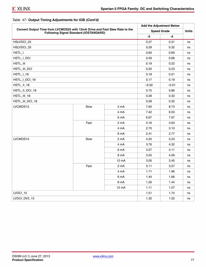
Spartan-3 FPGA Family: DC and Switching Characteristics
DS099 (v3.1) June 27, 2013 www.xilinx.comProduct Specification 77
HSLVDCI_25 0.27 0.31 ns
HSLVDCI_33 0.28 0.32 ns
HSTL_I 0.60 0.69 ns
HSTL_I_DCI 0.59 0.68 ns
HSTL_III 0.19 0.22 ns
HSTL_III_DCI 0.20 0.23 ns
HSTL_I_18 0.18 0.21 ns
HSTL_I_DCI_18 0.17 0.19 ns
HSTL_II_18 –0.02 –0.01 ns
HSTL_II_DCI_18 0.75 0.86 ns
HSTL_III_18 0.28 0.32 ns
HSTL_III_DCI_18 0.28 0.32 ns
LVCMOS12 Slow 2 mA 7.60 8.73 ns
4 mA 7.42 8.53 ns
6 mA 6.67 7.67 ns
Fast 2 mA 3.16 3.63 ns
4 mA 2.70 3.10 ns
6 mA 2.41 2.77 ns
LVCMOS15 Slow 2 mA 4.55 5.23 ns
4 mA 3.76 4.32 ns
6 mA 3.57 4.11 ns
8 mA 3.55 4.09 ns
12 mA 3.00 3.45 ns
Fast 2 mA 3.11 3.57 ns
4 mA 1.71 1.96 ns
6 mA 1.44 1.66 ns
8 mA 1.26 1.44 ns
12 mA 1.11 1.27 ns
LVDCI_15 1.51 1.74 ns
LVDCI_DV2_15 1.32 1.52 ns
Table 47: Output Timing Adjustments for IOB (Cont’d)
Convert Output Time from LVCMOS25 with 12mA Drive and Fast Slew Rate to the Following Signal Standard (IOSTANDARD)
Add the Adjustment Below
UnitsSpeed Grade
-5 -4
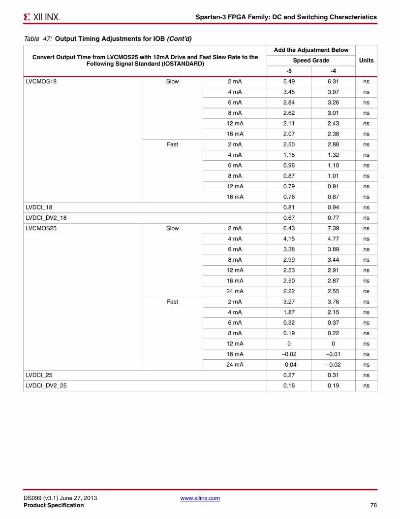
Spartan-3 FPGA Family: DC and Switching Characteristics
DS099 (v3.1) June 27, 2013 www.xilinx.comProduct Specification 78
LVCMOS18 Slow 2 mA 5.49 6.31 ns
4 mA 3.45 3.97 ns
6 mA 2.84 3.26 ns
8 mA 2.62 3.01 ns
12 mA 2.11 2.43 ns
16 mA 2.07 2.38 ns
Fast 2 mA 2.50 2.88 ns
4 mA 1.15 1.32 ns
6 mA 0.96 1.10 ns
8 mA 0.87 1.01 ns
12 mA 0.79 0.91 ns
16 mA 0.76 0.87 ns
LVDCI_18 0.81 0.94 ns
LVDCI_DV2_18 0.67 0.77 ns
LVCMOS25 Slow 2 mA 6.43 7.39 ns
4 mA 4.15 4.77 ns
6 mA 3.38 3.89 ns
8 mA 2.99 3.44 ns
12 mA 2.53 2.91 ns
16 mA 2.50 2.87 ns
24 mA 2.22 2.55 ns
Fast 2 mA 3.27 3.76 ns
4 mA 1.87 2.15 ns
6 mA 0.32 0.37 ns
8 mA 0.19 0.22 ns
12 mA 0 0 ns
16 mA –0.02 –0.01 ns
24 mA –0.04 –0.02 ns
LVDCI_25 0.27 0.31 ns
LVDCI_DV2_25 0.16 0.19 ns
Table 47: Output Timing Adjustments for IOB (Cont’d)
Convert Output Time from LVCMOS25 with 12mA Drive and Fast Slew Rate to the Following Signal Standard (IOSTANDARD)
Add the Adjustment Below
UnitsSpeed Grade
-5 -4
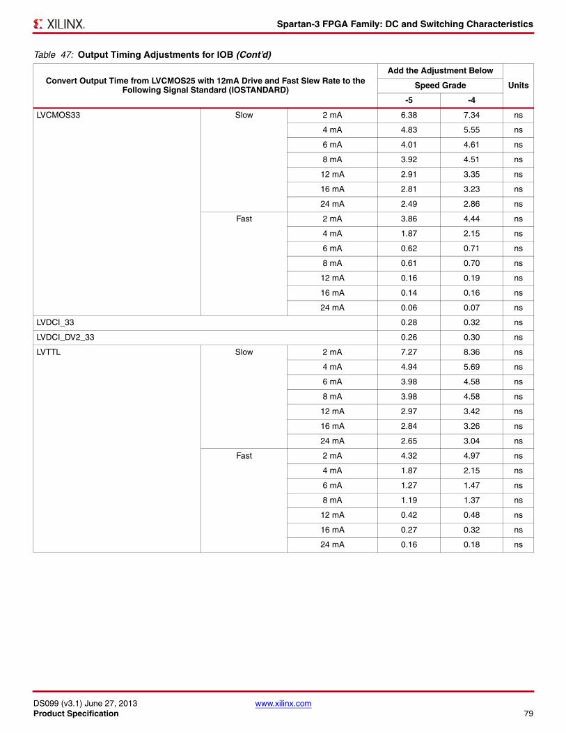
Spartan-3 FPGA Family: DC and Switching Characteristics
DS099 (v3.1) June 27, 2013 www.xilinx.comProduct Specification 79
LVCMOS33 Slow 2 mA 6.38 7.34 ns
4 mA 4.83 5.55 ns
6 mA 4.01 4.61 ns
8 mA 3.92 4.51 ns
12 mA 2.91 3.35 ns
16 mA 2.81 3.23 ns
24 mA 2.49 2.86 ns
Fast 2 mA 3.86 4.44 ns
4 mA 1.87 2.15 ns
6 mA 0.62 0.71 ns
8 mA 0.61 0.70 ns
12 mA 0.16 0.19 ns
16 mA 0.14 0.16 ns
24 mA 0.06 0.07 ns
LVDCI_33 0.28 0.32 ns
LVDCI_DV2_33 0.26 0.30 ns
LVTTL Slow 2 mA 7.27 8.36 ns
4 mA 4.94 5.69 ns
6 mA 3.98 4.58 ns
8 mA 3.98 4.58 ns
12 mA 2.97 3.42 ns
16 mA 2.84 3.26 ns
24 mA 2.65 3.04 ns
Fast 2 mA 4.32 4.97 ns
4 mA 1.87 2.15 ns
6 mA 1.27 1.47 ns
8 mA 1.19 1.37 ns
12 mA 0.42 0.48 ns
16 mA 0.27 0.32 ns
24 mA 0.16 0.18 ns
Table 47: Output Timing Adjustments for IOB (Cont’d)
Convert Output Time from LVCMOS25 with 12mA Drive and Fast Slew Rate to the Following Signal Standard (IOSTANDARD)
Add the Adjustment Below
UnitsSpeed Grade
-5 -4
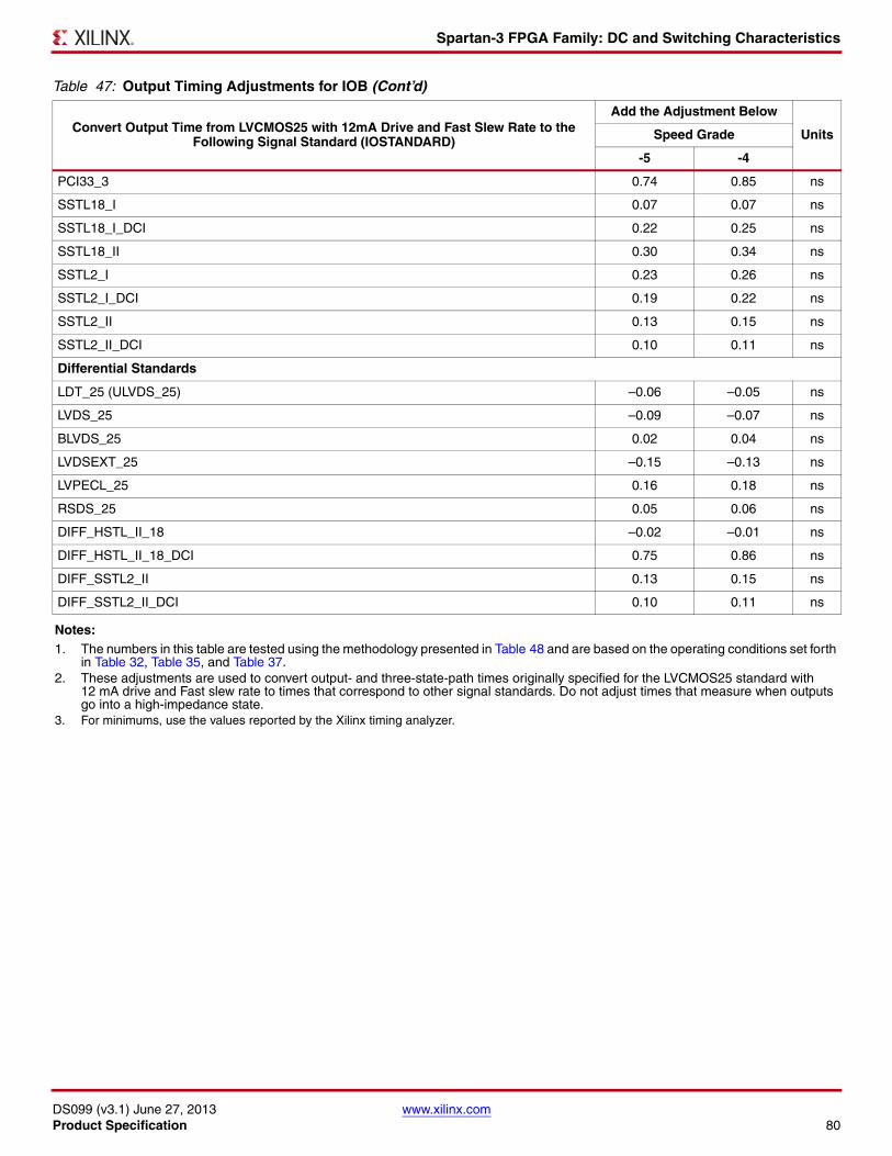
Spartan-3 FPGA Family: DC and Switching Characteristics
DS099 (v3.1) June 27, 2013 www.xilinx.comProduct Specification 80
PCI33_3 0.74 0.85 ns
SSTL18_I 0.07 0.07 ns
SSTL18_I_DCI 0.22 0.25 ns
SSTL18_II 0.30 0.34 ns
SSTL2_I 0.23 0.26 ns
SSTL2_I_DCI 0.19 0.22 ns
SSTL2_II 0.13 0.15 ns
SSTL2_II_DCI 0.10 0.11 ns
Differential Standards
LDT_25 (ULVDS_25) –0.06 –0.05 ns
LVDS_25 –0.09 –0.07 ns
BLVDS_25 0.02 0.04 ns
LVDSEXT_25 –0.15 –0.13 ns
LVPECL_25 0.16 0.18 ns
RSDS_25 0.05 0.06 ns
DIFF_HSTL_II_18 –0.02 –0.01 ns
DIFF_HSTL_II_18_DCI 0.75 0.86 ns
DIFF_SSTL2_II 0.13 0.15 ns
DIFF_SSTL2_II_DCI 0.10 0.11 ns
Notes: 1. The numbers in this table are tested using the methodology presented in Table 48 and are based on the operating conditions set forth
in Table 32, Table 35, and Table 37.2. These adjustments are used to convert output- and three-state-path times originally specified for the LVCMOS25 standard with
12 mA drive and Fast slew rate to times that correspond to other signal standards. Do not adjust times that measure when outputs go into a high-impedance state.
3. For minimums, use the values reported by the Xilinx timing analyzer.
Table 47: Output Timing Adjustments for IOB (Cont’d)
Convert Output Time from LVCMOS25 with 12mA Drive and Fast Slew Rate to the Following Signal Standard (IOSTANDARD)
Add the Adjustment Below
UnitsSpeed Grade
-5 -4
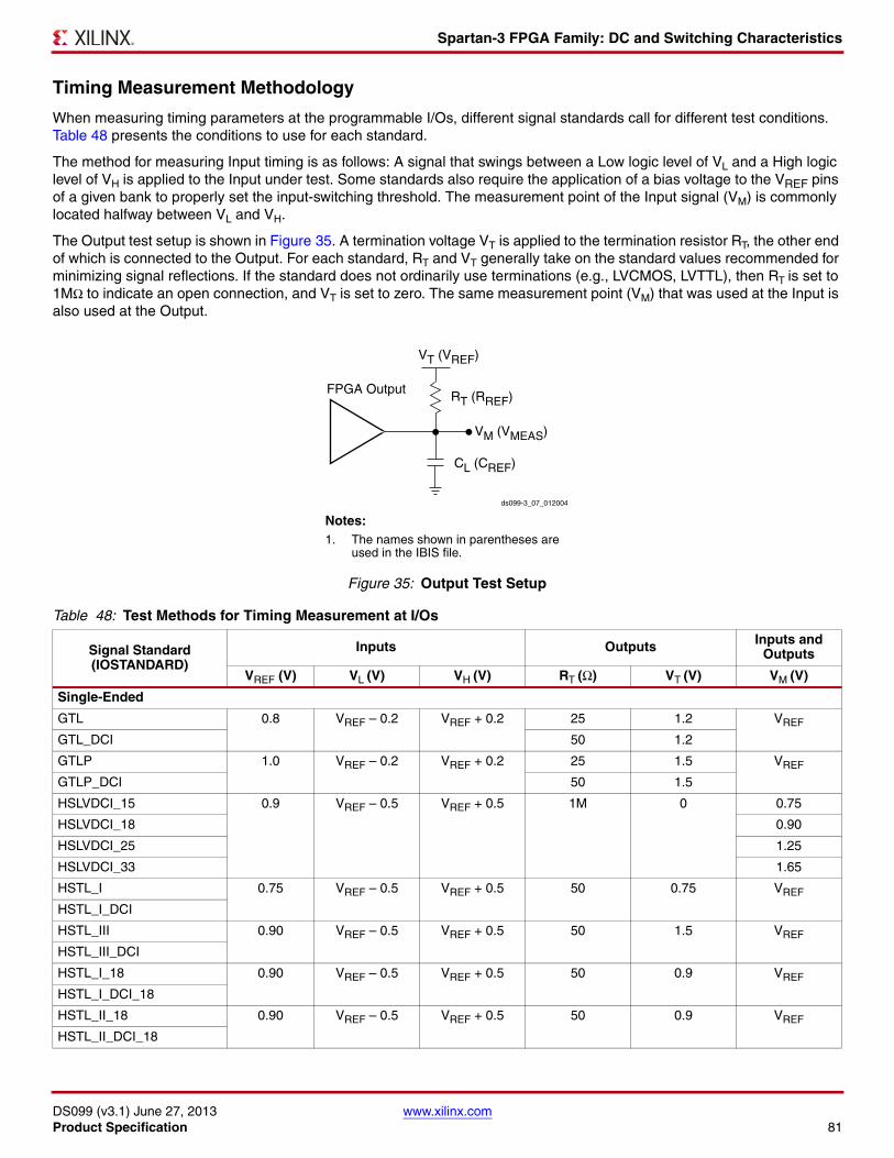
Spartan-3 FPGA Family: DC and Switching Characteristics
DS099 (v3.1) June 27, 2013 www.xilinx.comProduct Specification 81
Timing Measurement Methodology
When measuring timing parameters at the programmable I/Os, different signal standards call for different test conditions. Table 48 presents the conditions to use for each standard.
The method for measuring Input timing is as follows: A signal that swings between a Low logic level of VL and a High logic level of VH is applied to the Input under test. Some standards also require the application of a bias voltage to the VREF pins of a given bank to properly set the input-switching threshold. The measurement point of the Input signal (VM) is commonly located halfway between VL and VH.
The Output test setup is shown in Figure 35. A termination voltage VT is applied to the termination resistor RT, the other end of which is connected to the Output. For each standard, RT and VT generally take on the standard values recommended for minimizing signal reflections. If the standard does not ordinarily use terminations (e.g., LVCMOS, LVTTL), then RT is set to 1MΩ to indicate an open connection, and VT is set to zero. The same measurement point (VM) that was used at the Input is also used at the Output.
X-Ref Target - Figure 35
Figure 35: Output Test Setup
Table 48: Test Methods for Timing Measurement at I/Os
Signal Standard(IOSTANDARD)
Inputs Outputs Inputs and Outputs
VREF (V) VL (V) VH (V) RT (Ω) VT (V) VM (V)
Single-Ended
GTL 0.8 VREF – 0.2 VREF + 0.2 25 1.2 VREF
GTL_DCI 50 1.2
GTLP 1.0 VREF – 0.2 VREF + 0.2 25 1.5 VREF
GTLP_DCI 50 1.5
HSLVDCI_15 0.9 VREF – 0.5 VREF + 0.5 1M 0 0.75
HSLVDCI_18 0.90
HSLVDCI_25 1.25
HSLVDCI_33 1.65
HSTL_I 0.75 VREF – 0.5 VREF + 0.5 50 0.75 VREF
HSTL_I_DCI
HSTL_III 0.90 VREF – 0.5 VREF + 0.5 50 1.5 VREF
HSTL_III_DCI
HSTL_I_18 0.90 VREF – 0.5 VREF + 0.5 50 0.9 VREF
HSTL_I_DCI_18
HSTL_II_18 0.90 VREF – 0.5 VREF + 0.5 50 0.9 VREF
HSTL_II_DCI_18
FPGA Output
VT (VREF)
RT (RREF)
VM (VMEAS)
CL (CREF)
ds099-3_07_012004
Notes: 1. The names shown in parentheses are
used in the IBIS file.
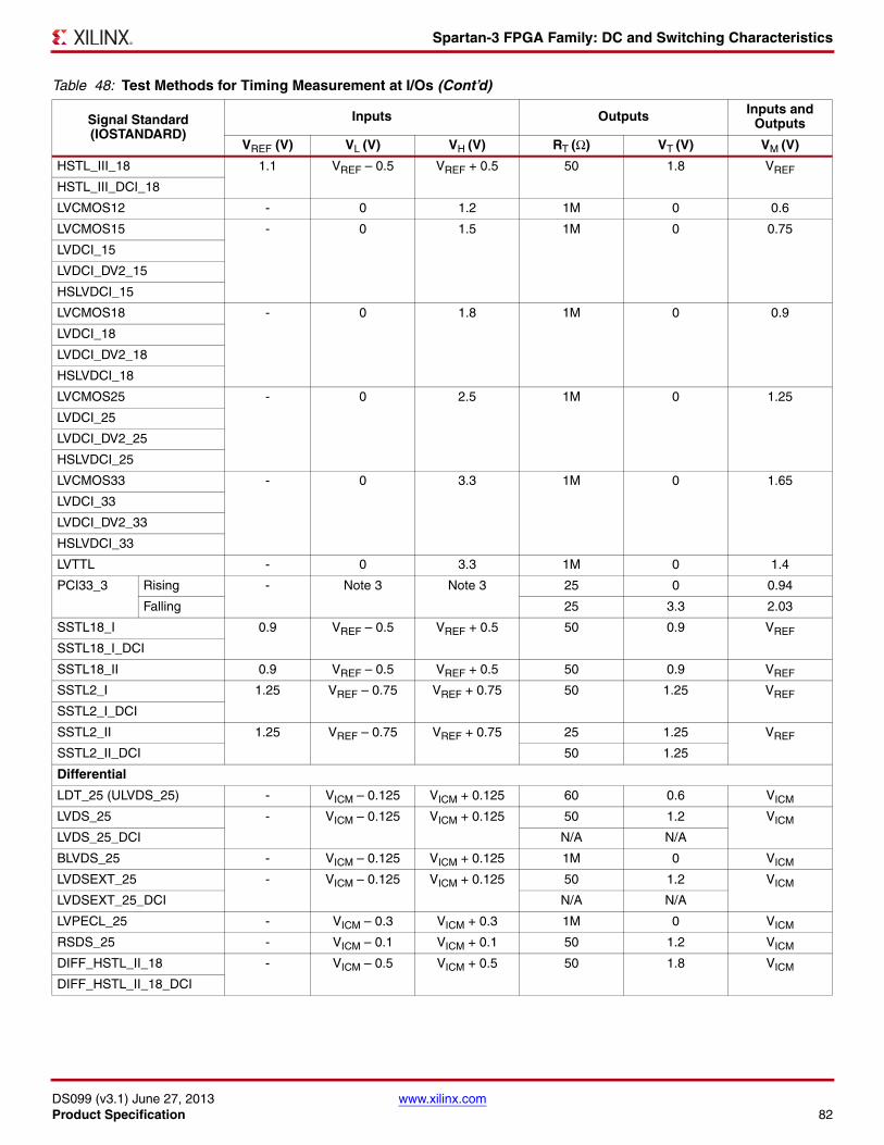
Spartan-3 FPGA Family: DC and Switching Characteristics
DS099 (v3.1) June 27, 2013 www.xilinx.comProduct Specification 82
HSTL_III_18 1.1 VREF – 0.5 VREF + 0.5 50 1.8 VREF
HSTL_III_DCI_18
LVCMOS12 - 0 1.2 1M 0 0.6
LVCMOS15 - 0 1.5 1M 0 0.75
LVDCI_15
LVDCI_DV2_15
HSLVDCI_15
LVCMOS18 - 0 1.8 1M 0 0.9
LVDCI_18
LVDCI_DV2_18
HSLVDCI_18
LVCMOS25 - 0 2.5 1M 0 1.25
LVDCI_25
LVDCI_DV2_25
HSLVDCI_25
LVCMOS33 - 0 3.3 1M 0 1.65
LVDCI_33
LVDCI_DV2_33
HSLVDCI_33
LVTTL - 0 3.3 1M 0 1.4
PCI33_3 Rising - Note 3 Note 3 25 0 0.94
Falling 25 3.3 2.03
SSTL18_I 0.9 VREF – 0.5 VREF + 0.5 50 0.9 VREF
SSTL18_I_DCI
SSTL18_II 0.9 VREF – 0.5 VREF + 0.5 50 0.9 VREF
SSTL2_I 1.25 VREF – 0.75 VREF + 0.75 50 1.25 VREF
SSTL2_I_DCI
SSTL2_II 1.25 VREF – 0.75 VREF + 0.75 25 1.25 VREF
SSTL2_II_DCI 50 1.25
Differential
LDT_25 (ULVDS_25) - VICM – 0.125 VICM + 0.125 60 0.6 VICM
LVDS_25 - VICM – 0.125 VICM + 0.125 50 1.2 VICM
LVDS_25_DCI N/A N/A
BLVDS_25 - VICM – 0.125 VICM + 0.125 1M 0 VICM
LVDSEXT_25 - VICM – 0.125 VICM + 0.125 50 1.2 VICM
LVDSEXT_25_DCI N/A N/A
LVPECL_25 - VICM – 0.3 VICM + 0.3 1M 0 VICM
RSDS_25 - VICM – 0.1 VICM + 0.1 50 1.2 VICM
DIFF_HSTL_II_18 - VICM – 0.5 VICM + 0.5 50 1.8 VICM
DIFF_HSTL_II_18_DCI
Table 48: Test Methods for Timing Measurement at I/Os (Cont’d)
Signal Standard(IOSTANDARD)
Inputs Outputs Inputs and Outputs
VREF (V) VL (V) VH (V) RT (Ω) VT (V) VM (V)
Spartan-3 FPGA Family: DC and Switching Characteristics
DS099 (v3.1) June 27, 2013 www.xilinx.comProduct Specification 83
The capacitive load (CL) is connected between the output and GND. The Output timing for all standards, as published in the speed files and the data sheet, is always based on a CL value of zero. High-impedance probes (less than 1 pF) are used for all measurements. Any delay that the test fixture might contribute to test measurements is subtracted from those measurements to produce the final timing numbers as published in the speed files and data sheet.
Using IBIS Models to Simulate Load Conditions in Application
IBIS Models permit the most accurate prediction of timing delays for a given application. The parameters found in the IBIS model (VREF, RREF, and VMEAS) correspond directly with the parameters used in Table 48, VT, RT, and VM. Do not confuse VREF (the termination voltage) from the IBIS model with VREF (the input-switching threshold) from the table. A fourth parameter, CREF, is always zero. The four parameters describe all relevant output test conditions. IBIS models are found in the Xilinx development software as well as at the following link.
http://www.xilinx.com/support/download/index.htm
Simulate delays for a given application according to its specific load conditions as follows:
1. Simulate the desired signal standard with the output driver connected to the test setup shown in Figure 35. Use parameter values VT, RT, and VM from Table 48. CREF is zero.
2. Record the time to VM.
3. Simulate the same signal standard with the output driver connected to the PCB trace with load. Use the appropriate IBIS model (including VREF, RREF, CREF, and VMEAS values) or capacitive value to represent the load.
4. Record the time to VMEAS.
5. Compare the results of steps 2 and 4. The increase (or decrease) in delay should be added to (or subtracted from) the appropriate Output standard adjustment (Table 47) to yield the worst-case delay of the PCB trace.
DIFF_SSTL2_II - VICM – 0.75 VICM + 0.75 50 1.25 VICM
DIFF_SSTL2_II_DCI
Notes: 1. Descriptions of the relevant symbols are as follows:
VREF – The reference voltage for setting the input switching thresholdVICM – The common mode input voltageVM – Voltage of measurement point on signal transitionVL – Low-level test voltage at Input pinVH – High-level test voltage at Input pinRT – Effective termination resistance, which takes on a value of 1MW when no parallel termination is requiredVT – Termination voltage
2. The load capacitance (CL) at the Output pin is 0 pF for all signal standards.3. According to the PCI specification.
Table 48: Test Methods for Timing Measurement at I/Os (Cont’d)
Signal Standard(IOSTANDARD)
Inputs Outputs Inputs and Outputs
VREF (V) VL (V) VH (V) RT (Ω) VT (V) VM (V)
Spartan-3 FPGA Family: DC and Switching Characteristics
DS099 (v3.1) June 27, 2013 www.xilinx.comProduct Specification 84
Simultaneously Switching Output Guidelines
This section provides guidelines for the maximum allowable number of Simultaneous Switching Outputs (SSOs). These guidelines describe the maximum number of user I/O pins, of a given output signal standard, that should simultaneously switch in the same direction, while maintaining a safe level of switching noise. Meeting these guidelines for the stated test conditions ensures that the FPGA operates free from the adverse effects of ground and power bounce.
Ground or power bounce occurs when a large number of outputs simultaneously switch in the same direction. The output drive transistors all conduct current to a common voltage rail. Low-to-High transitions conduct to the VCCO rail; High-to-Low transitions conduct to the GND rail. The resulting cumulative current transient induces a voltage difference across the inductance that exists between the die pad and the power supply or ground return. The inductance is associated with bonding wires, the package lead frame, and any other signal routing inside the package. Other variables contribute to SSO noise levels, including stray inductance on the PCB as well as capacitive loading at receivers. Any SSO-induced voltage consequently affects internal switching noise margins and ultimately signal quality.
Table 49 and Table 50 provide the essential SSO guidelines. For each device/package combination, Table 49 provides the number of equivalent VCCO/GND pairs. The equivalent number of pairs is based on characterization and will possibly not match the physical number of pairs. For each output signal standard and drive strength, Table 50 recommends the maximum number of SSOs, switching in the same direction, allowed per VCCO/GND pair within an I/O bank. The Table 50 guidelines are categorized by package style. Multiply the appropriate numbers from Table 49 and Table 50 to calculate the maximum number of SSOs allowed within an I/O bank. Exceeding these SSO guidelines may result in increased power or ground bounce, degraded signal integrity, or increased system jitter.
SSOMAX/IO Bank = Table 49 x Table 50
The recommended maximum SSO values assume that the FPGA is soldered on the printed circuit board and that the board uses sound design practices. The SSO values do not apply for FPGAs mounted in sockets, due to the lead inductance introduced by the socket.
The number of SSOs allowed for quad-flat packages (VQ, TQ, PQ) is lower than for ball grid array packages (FG) due to the larger lead inductance of the quad-flat packages. Ball grid array packages are recommended for applications with a large number of simultaneously switching outputs.
Table 49: Equivalent VCCO /GND Pairs per Bank
Device VQ100 CP132 (1)(2) TQ144(1) PQ208 FT256 FG320 FG456 FG676 FG900 FG1156(2)
XC3S50 1 1.5 1.5 2 – – – – – –
XC3S200 1 – 1.5 2 3 – – – – –
XC3S400 – – 1.5 2 3 3 5 – – –
XC3S1000 – – – – 3 3 5 5 – –
XC3S1500 – – – – – 3 5 6 – –
XC3S2000 – – – – – – 5 6 9 –
XC3S4000 – – – – – – – 6 10 12
XC3S5000 – – – – – – – 6 10 12
Notes: 1. The VCCO lines for the pair of banks on each side of the CP132 and TQ144 packages are internally tied together. Each pair of interconnected
banks shares three VCCO/GND pairs. Consequently, the per bank number is 1.5.2. The CP132, CPG132, FG1156, and FGG1156 packages are discontinued. See
http://www.xilinx.com/support/documentation/spartan-3_customer_notices.htm.3. The information in this table also applies to Pb-free packages.
Spartan-3 FPGA Family: DC and Switching Characteristics
DS099 (v3.1) June 27, 2013 www.xilinx.comProduct Specification 85
Table 50: Recommended Number of Simultaneously Switching Outputs per VCCO /GND Pair
Signal Standard(IOSTANDARD)
Package
VQ100 TQ144 PQ208 CP132 FT256, FG320, FG456, FG676, FG900, FG1156
Single-Ended Standards
GTL 0 0 0 1 14
GTL_DCI 0 0 0 1 14
GTLP 0 0 0 1 19
GTLP_DCI 0 0 0 1 19
HSLVDCI_15 6 6 6 6 14
HSLVDCI_18 7 7 7 7 10
HSLVDCI_25 7 7 7 7 11
HSLVDCI_33 10 10 10 10 10
HSTL_I 11 11 11 11 17
HSTL_I_DCI 11 11 11 11 17
HSTL_III 7 7 7 7 7
HSTL_III_DCI 7 7 7 7 7
HSTL_I_18 13 13 13 13 17
HSTL_I_DCI_18 13 13 13 13 17
HSTL_II_18 9 9 9 9 9
HSTL_II_DCI_18 9 9 9 9 9
HSTL_III_18 8 8 8 8 8
HSTL_III_DCI_18 8 8 8 8 8
LVCMOS12 Slow 2 17 17 17 17 55
4 13 13 13 13 32
6 10 10 10 10 18
Fast 2 12 12 12 12 31
4 11 11 11 11 13
6 9 9 9 9 9
LVCMOS15 Slow 2 16 12 12 19 55
4 8 7 7 9 31
6 7 7 7 9 18
8 6 6 6 6 15
12 5 5 5 5 10
Fast 2 10 10 10 13 25
4 6 7 7 7 16
6 7 7 7 7 13
8 6 6 6 6 11
12 6 6 6 6 7
Spartan-3 FPGA Family: DC and Switching Characteristics
DS099 (v3.1) June 27, 2013 www.xilinx.comProduct Specification 86
LVDCI_15 6 6 6 6 14
LVDCI_DV2_15 6 6 6 6 14
HSLVDCI_15 6 6 6 6 14
LVCMOS18 Slow 2 19 13 13 29 64
4 13 8 8 19 34
6 8 8 8 9 22
8 7 7 7 9 18
12 5 5 5 5 13
16 5 5 5 5 10
Fast 2 13 13 13 19 36
4 8 8 8 13 21
6 8 8 8 8 13
8 7 7 7 7 10
12 5 5 5 5 9
16 5 5 5 5 6
LVDCI_18 7 7 7 7 10
LVDCI_DV2_18 7 7 7 7 10
HSLVDCI_18 7 7 7 7 10
LVCMOS25 Slow 2 28 16 12 42 76
4 13 10 10 19 46
6 13 8 8 19 33
8 7 7 7 9 24
12 6 6 6 9 18
16 6 6 6 6 11
24 5 5 5 5 7
Fast 2 17 12 12 26 42
4 10 10 10 13 20
6 8 8 8 13 15
8 7 7 7 7 13
12 6 6 6 6 11
16 6 6 6 6 8
24 5 5 5 5 5
LVDCI_25 7 7 7 7 11
LVDCI_DV2_25 7 7 7 7 11
HSLVDCI_25 7 7 7 7 11
Table 50: Recommended Number of Simultaneously Switching Outputs per VCCO /GND Pair (Cont’d)
Signal Standard(IOSTANDARD)
Package
VQ100 TQ144 PQ208 CP132 FT256, FG320, FG456, FG676, FG900, FG1156
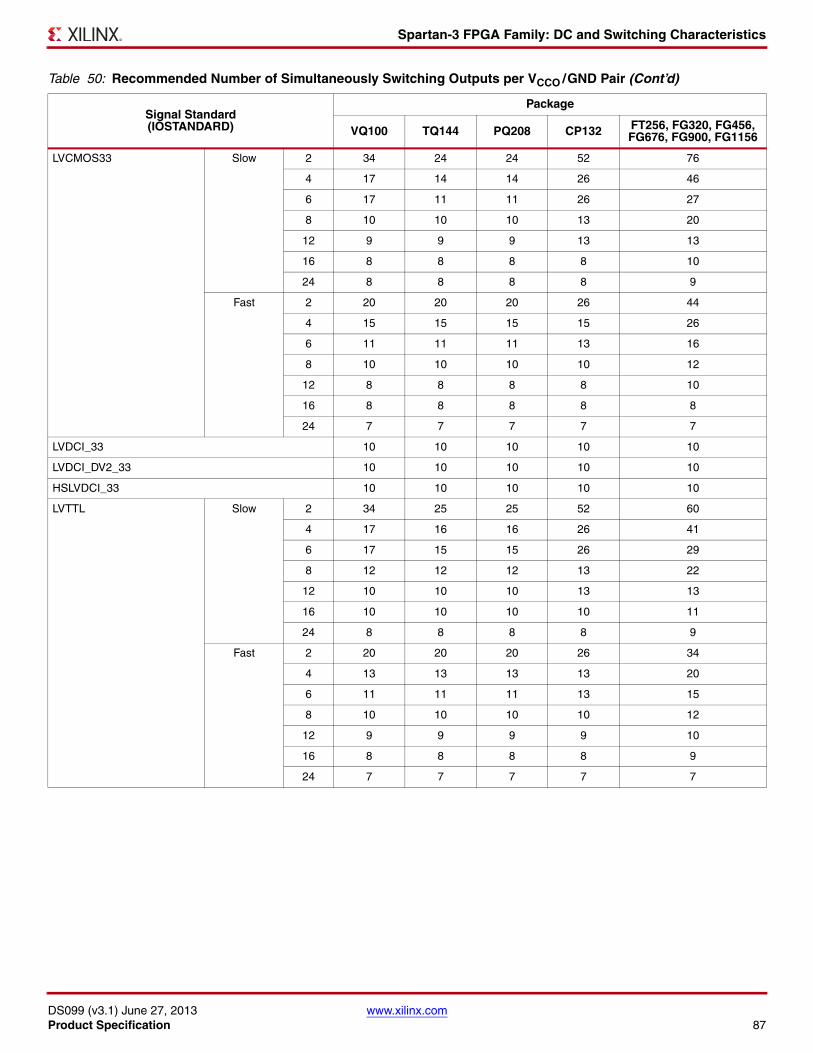
Spartan-3 FPGA Family: DC and Switching Characteristics
DS099 (v3.1) June 27, 2013 www.xilinx.comProduct Specification 87
LVCMOS33 Slow 2 34 24 24 52 76
4 17 14 14 26 46
6 17 11 11 26 27
8 10 10 10 13 20
12 9 9 9 13 13
16 8 8 8 8 10
24 8 8 8 8 9
Fast 2 20 20 20 26 44
4 15 15 15 15 26
6 11 11 11 13 16
8 10 10 10 10 12
12 8 8 8 8 10
16 8 8 8 8 8
24 7 7 7 7 7
LVDCI_33 10 10 10 10 10
LVDCI_DV2_33 10 10 10 10 10
HSLVDCI_33 10 10 10 10 10
LVTTL Slow 2 34 25 25 52 60
4 17 16 16 26 41
6 17 15 15 26 29
8 12 12 12 13 22
12 10 10 10 13 13
16 10 10 10 10 11
24 8 8 8 8 9
Fast 2 20 20 20 26 34
4 13 13 13 13 20
6 11 11 11 13 15
8 10 10 10 10 12
12 9 9 9 9 10
16 8 8 8 8 9
24 7 7 7 7 7
Table 50: Recommended Number of Simultaneously Switching Outputs per VCCO /GND Pair (Cont’d)
Signal Standard(IOSTANDARD)
Package
VQ100 TQ144 PQ208 CP132 FT256, FG320, FG456, FG676, FG900, FG1156
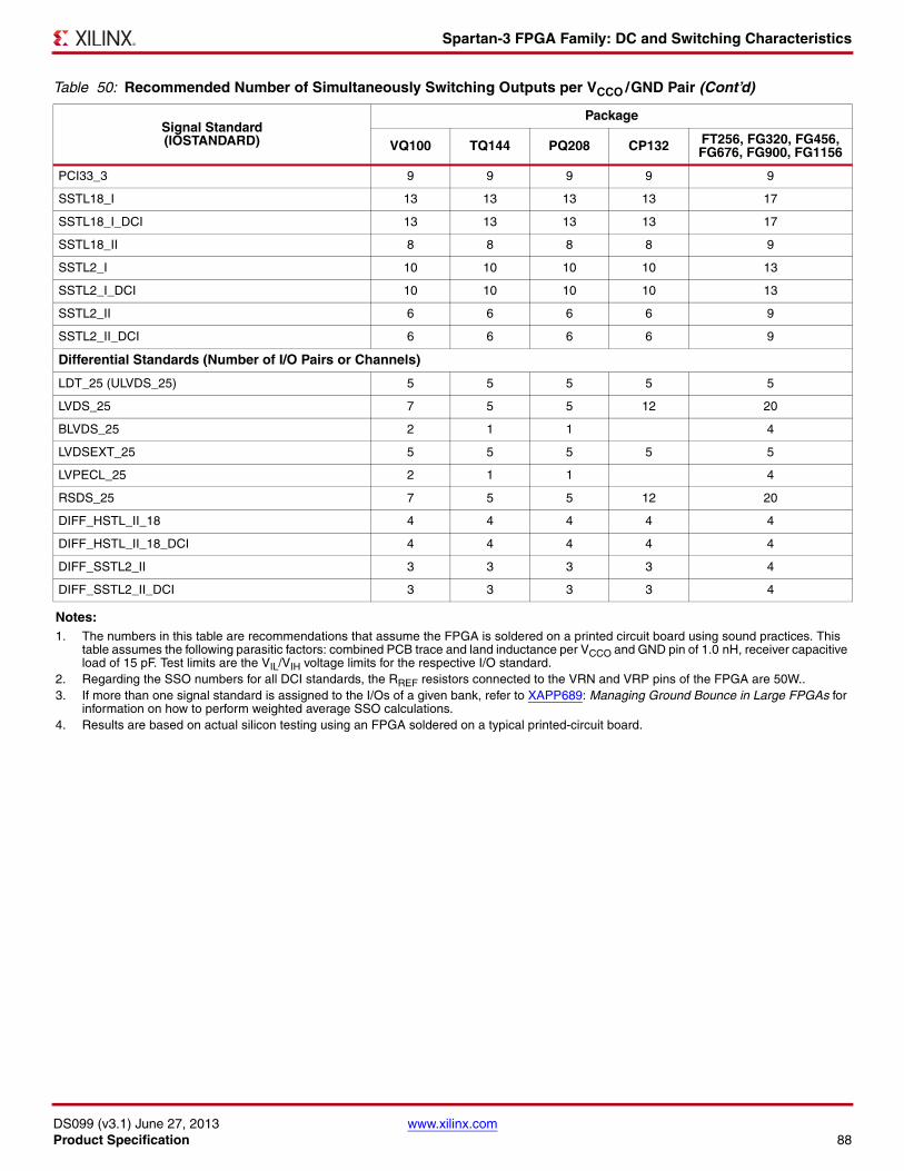
Spartan-3 FPGA Family: DC and Switching Characteristics
DS099 (v3.1) June 27, 2013 www.xilinx.comProduct Specification 88
PCI33_3 9 9 9 9 9
SSTL18_I 13 13 13 13 17
SSTL18_I_DCI 13 13 13 13 17
SSTL18_II 8 8 8 8 9
SSTL2_I 10 10 10 10 13
SSTL2_I_DCI 10 10 10 10 13
SSTL2_II 6 6 6 6 9
SSTL2_II_DCI 6 6 6 6 9
Differential Standards (Number of I/O Pairs or Channels)
LDT_25 (ULVDS_25) 5 5 5 5 5
LVDS_25 7 5 5 12 20
BLVDS_25 2 1 1 4
LVDSEXT_25 5 5 5 5 5
LVPECL_25 2 1 1 4
RSDS_25 7 5 5 12 20
DIFF_HSTL_II_18 4 4 4 4 4
DIFF_HSTL_II_18_DCI 4 4 4 4 4
DIFF_SSTL2_II 3 3 3 3 4
DIFF_SSTL2_II_DCI 3 3 3 3 4
Notes: 1. The numbers in this table are recommendations that assume the FPGA is soldered on a printed circuit board using sound practices. This
table assumes the following parasitic factors: combined PCB trace and land inductance per VCCO and GND pin of 1.0 nH, receiver capacitive load of 15 pF. Test limits are the VIL/VIH voltage limits for the respective I/O standard.
2. Regarding the SSO numbers for all DCI standards, the RREF resistors connected to the VRN and VRP pins of the FPGA are 50W..3. If more than one signal standard is assigned to the I/Os of a given bank, refer to XAPP689: Managing Ground Bounce in Large FPGAs for
information on how to perform weighted average SSO calculations.4. Results are based on actual silicon testing using an FPGA soldered on a typical printed-circuit board.
Table 50: Recommended Number of Simultaneously Switching Outputs per VCCO /GND Pair (Cont’d)
Signal Standard(IOSTANDARD)
Package
VQ100 TQ144 PQ208 CP132 FT256, FG320, FG456, FG676, FG900, FG1156
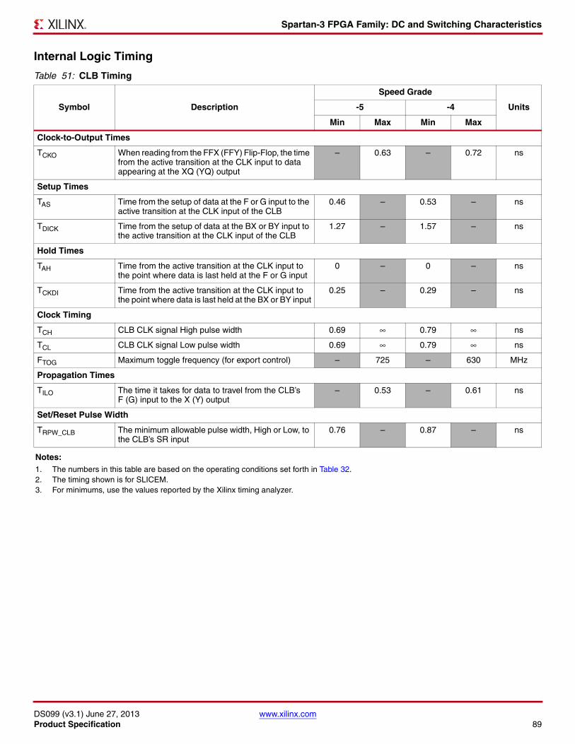
Spartan-3 FPGA Family: DC and Switching Characteristics
DS099 (v3.1) June 27, 2013 www.xilinx.comProduct Specification 89
Internal Logic Timing
Table 51: CLB Timing
Symbol Description
Speed Grade
Units-5 -4
Min Max Min Max
Clock-to-Output Times
TCKO When reading from the FFX (FFY) Flip-Flop, the time from the active transition at the CLK input to data appearing at the XQ (YQ) output
– 0.63 – 0.72 ns
Setup Times
TAS Time from the setup of data at the F or G input to the active transition at the CLK input of the CLB
0.46 – 0.53 – ns
TDICK Time from the setup of data at the BX or BY input to the active transition at the CLK input of the CLB
1.27 – 1.57 – ns
Hold Times
TAH Time from the active transition at the CLK input to the point where data is last held at the F or G input
0 – 0 – ns
TCKDI Time from the active transition at the CLK input to the point where data is last held at the BX or BY input
0.25 – 0.29 – ns
Clock Timing
TCH CLB CLK signal High pulse width 0.69 ∞ 0.79 ∞ ns
TCL CLB CLK signal Low pulse width 0.69 ∞ 0.79 ∞ ns
FTOG Maximum toggle frequency (for export control) – 725 – 630 MHz
Propagation Times
TILO The time it takes for data to travel from the CLB’s F (G) input to the X (Y) output
– 0.53 – 0.61 ns
Set/Reset Pulse Width
TRPW_CLB The minimum allowable pulse width, High or Low, to the CLB’s SR input
0.76 – 0.87 – ns
Notes: 1. The numbers in this table are based on the operating conditions set forth in Table 32.2. The timing shown is for SLICEM.3. For minimums, use the values reported by the Xilinx timing analyzer.
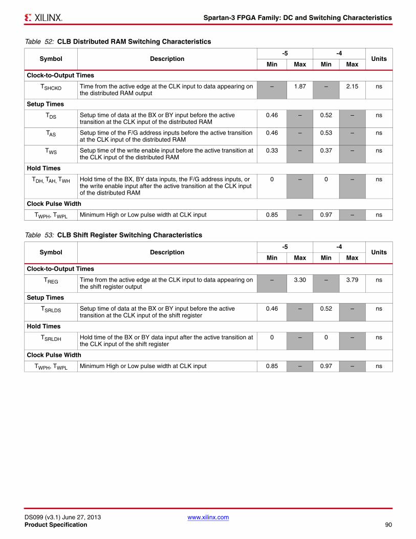
Spartan-3 FPGA Family: DC and Switching Characteristics
DS099 (v3.1) June 27, 2013 www.xilinx.comProduct Specification 90
Table 52: CLB Distributed RAM Switching Characteristics
Symbol Description-5 -4
UnitsMin Max Min Max
Clock-to-Output Times
TSHCKO Time from the active edge at the CLK input to data appearing on the distributed RAM output
– 1.87 – 2.15 ns
Setup Times
TDS Setup time of data at the BX or BY input before the active transition at the CLK input of the distributed RAM
0.46 – 0.52 – ns
TAS Setup time of the F/G address inputs before the active transition at the CLK input of the distributed RAM
0.46 – 0.53 – ns
TWS Setup time of the write enable input before the active transition at the CLK input of the distributed RAM
0.33 – 0.37 – ns
Hold Times
TDH, TAH, TWH Hold time of the BX, BY data inputs, the F/G address inputs, or the write enable input after the active transition at the CLK input of the distributed RAM
0 – 0 – ns
Clock Pulse Width
TWPH, TWPL Minimum High or Low pulse width at CLK input 0.85 – 0.97 – ns
Table 53: CLB Shift Register Switching Characteristics
Symbol Description-5 -4
UnitsMin Max Min Max
Clock-to-Output Times
TREG Time from the active edge at the CLK input to data appearing on the shift register output
– 3.30 – 3.79 ns
Setup Times
TSRLDS Setup time of data at the BX or BY input before the active transition at the CLK input of the shift register
0.46 – 0.52 – ns
Hold Times
TSRLDH Hold time of the BX or BY data input after the active transition at the CLK input of the shift register
0 – 0 – ns
Clock Pulse Width
TWPH, TWPL Minimum High or Low pulse width at CLK input 0.85 – 0.97 – ns
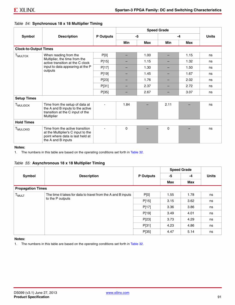
Spartan-3 FPGA Family: DC and Switching Characteristics
DS099 (v3.1) June 27, 2013 www.xilinx.comProduct Specification 91
Table 54: Synchronous 18 x 18 Multiplier Timing
Symbol Description P Outputs
Speed Grade
Units-5 -4
Min Max Min Max
Clock-to-Output Times
TMULTCK When reading from the Multiplier, the time from the active transition at the C clock input to data appearing at the P outputs
P[0] – 1.00 – 1.15 ns
P[15] – 1.15 – 1.32 ns
P[17] – 1.30 – 1.50 ns
P[19] – 1.45 – 1.67 ns
P[23] – 1.76 – 2.02 ns
P[31] – 2.37 – 2.72 ns
P[35] – 2.67 – 3.07 ns
Setup Times
TMULIDCK Time from the setup of data at the A and B inputs to the active transition at the C input of the Multiplier
- 1.84 – 2.11 – ns
Hold Times
TMULCKID Time from the active transition at the Multiplier’s C input to the point where data is last held at the A and B inputs
- 0 – 0 – ns
Notes: 1. The numbers in this table are based on the operating conditions set forth in Table 32.
Table 55: Asynchronous 18 x 18 Multiplier Timing
Symbol Description P Outputs
Speed Grade
Units-5 -4
Max Max
Propagation Times
TMULT The time it takes for data to travel from the A and B inputs to the P outputs
P[0] 1.55 1.78 ns
P[15] 3.15 3.62 ns
P[17] 3.36 3.86 ns
P[19] 3.49 4.01 ns
P[23] 3.73 4.29 ns
P[31] 4.23 4.86 ns
P[35] 4.47 5.14 ns
Notes: 1. The numbers in this table are based on the operating conditions set forth in Table 32.
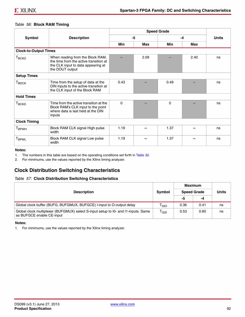
Spartan-3 FPGA Family: DC and Switching Characteristics
DS099 (v3.1) June 27, 2013 www.xilinx.comProduct Specification 92
Clock Distribution Switching Characteristics
Table 56: Block RAM Timing
Symbol Description
Speed Grade
Units-5 -4
Min Max Min Max
Clock-to-Output Times
TBCKO When reading from the Block RAM, the time from the active transition at the CLK input to data appearing at the DOUT output
– 2.09 – 2.40 ns
Setup Times
TBDCK Time from the setup of data at the DIN inputs to the active transition at the CLK input of the Block RAM
0.43 – 0.49 – ns
Hold Times
TBCKD Time from the active transition at the Block RAM’s CLK input to the point where data is last held at the DIN inputs
0 – 0 – ns
Clock Timing
TBPWH Block RAM CLK signal High pulse width
1.19 ∞ 1.37 ∞ ns
TBPWL Block RAM CLK signal Low pulse width
1.19 ∞ 1.37 ∞ ns
Notes: 1. The numbers in this table are based on the operating conditions set forth in Table 32.2. For minimums, use the values reported by the Xilinx timing analyzer.
Table 57: Clock Distribution Switching Characteristics
Description Symbol
Maximum
UnitsSpeed Grade
-5 -4
Global clock buffer (BUFG, BUFGMUX, BUFGCE) I-input to O-output delay TGIO 0.36 0.41 ns
Global clock multiplexer (BUFGMUX) select S-input setup to I0- and I1-inputs. Same as BUFGCE enable CE-input
TGSI 0.53 0.60 ns
Notes: 1. For minimums, use the values reported by the Xilinx timing analyzer.
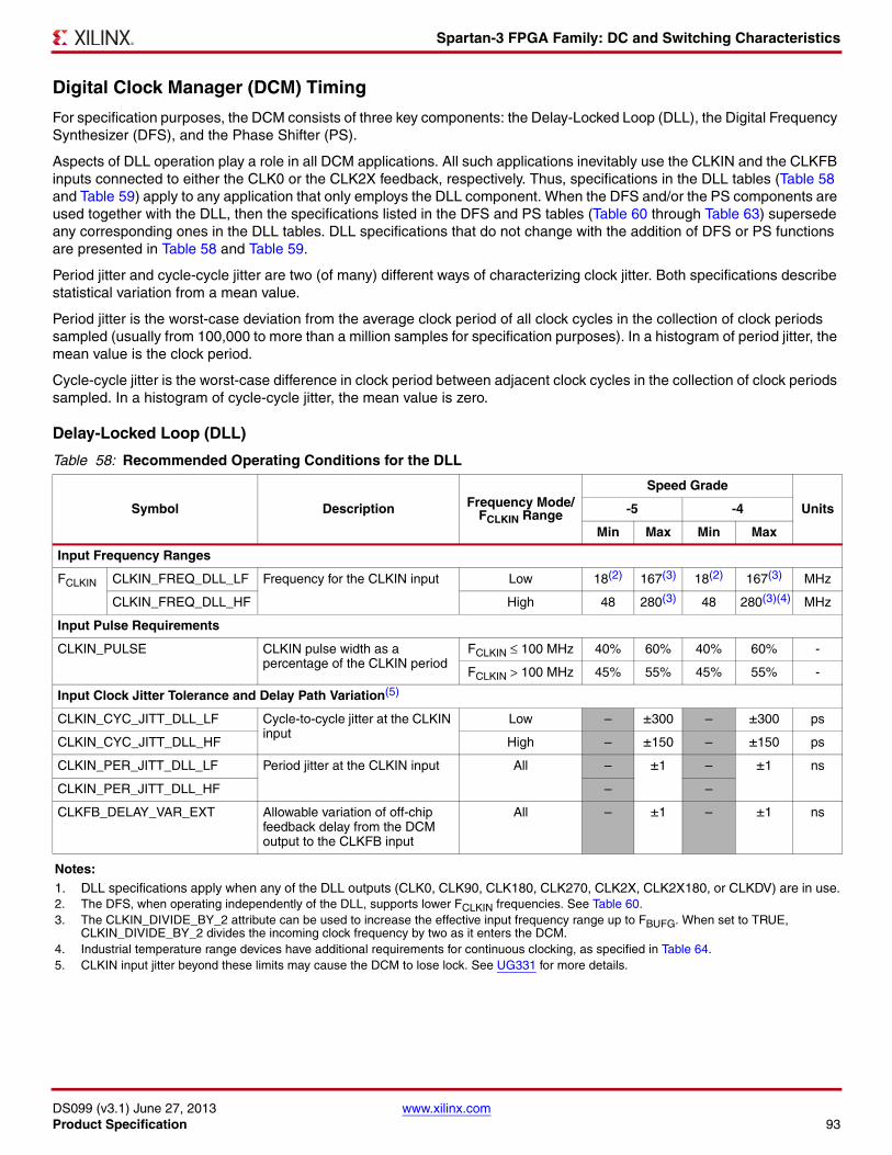
Spartan-3 FPGA Family: DC and Switching Characteristics
DS099 (v3.1) June 27, 2013 www.xilinx.comProduct Specification 93
Digital Clock Manager (DCM) Timing
For specification purposes, the DCM consists of three key components: the Delay-Locked Loop (DLL), the Digital Frequency Synthesizer (DFS), and the Phase Shifter (PS).
Aspects of DLL operation play a role in all DCM applications. All such applications inevitably use the CLKIN and the CLKFB inputs connected to either the CLK0 or the CLK2X feedback, respectively. Thus, specifications in the DLL tables (Table 58 and Table 59) apply to any application that only employs the DLL component. When the DFS and/or the PS components are used together with the DLL, then the specifications listed in the DFS and PS tables (Table 60 through Table 63) supersede any corresponding ones in the DLL tables. DLL specifications that do not change with the addition of DFS or PS functions are presented in Table 58 and Table 59.
Period jitter and cycle-cycle jitter are two (of many) different ways of characterizing clock jitter. Both specifications describe statistical variation from a mean value.
Period jitter is the worst-case deviation from the average clock period of all clock cycles in the collection of clock periods sampled (usually from 100,000 to more than a million samples for specification purposes). In a histogram of period jitter, the mean value is the clock period.
Cycle-cycle jitter is the worst-case difference in clock period between adjacent clock cycles in the collection of clock periods sampled. In a histogram of cycle-cycle jitter, the mean value is zero.
Delay-Locked Loop (DLL)
Table 58: Recommended Operating Conditions for the DLL
Symbol Description Frequency Mode/FCLKIN Range
Speed Grade
Units-5 -4
Min Max Min Max
Input Frequency Ranges
FCLKIN CLKIN_FREQ_DLL_LF Frequency for the CLKIN input Low 18(2) 167(3) 18(2) 167(3) MHz
CLKIN_FREQ_DLL_HF High 48 280(3) 48 280(3)(4) MHz
Input Pulse Requirements
CLKIN_PULSE CLKIN pulse width as a percentage of the CLKIN period
FCLKIN ≤ 100 MHz 40% 60% 40% 60% -
FCLKIN > 100 MHz 45% 55% 45% 55% -
Input Clock Jitter Tolerance and Delay Path Variation(5)
CLKIN_CYC_JITT_DLL_LF Cycle-to-cycle jitter at the CLKIN input
Low – ±300 – ±300 ps
CLKIN_CYC_JITT_DLL_HF High – ±150 – ±150 ps
CLKIN_PER_JITT_DLL_LF Period jitter at the CLKIN input All – ±1 – ±1 ns
CLKIN_PER_JITT_DLL_HF – –
CLKFB_DELAY_VAR_EXT Allowable variation of off-chip feedback delay from the DCM output to the CLKFB input
All – ±1 – ±1 ns
Notes: 1. DLL specifications apply when any of the DLL outputs (CLK0, CLK90, CLK180, CLK270, CLK2X, CLK2X180, or CLKDV) are in use.2. The DFS, when operating independently of the DLL, supports lower FCLKIN frequencies. See Table 60.3. The CLKIN_DIVIDE_BY_2 attribute can be used to increase the effective input frequency range up to FBUFG. When set to TRUE,
CLKIN_DIVIDE_BY_2 divides the incoming clock frequency by two as it enters the DCM.4. Industrial temperature range devices have additional requirements for continuous clocking, as specified in Table 64.5. CLKIN input jitter beyond these limits may cause the DCM to lose lock. See UG331 for more details.
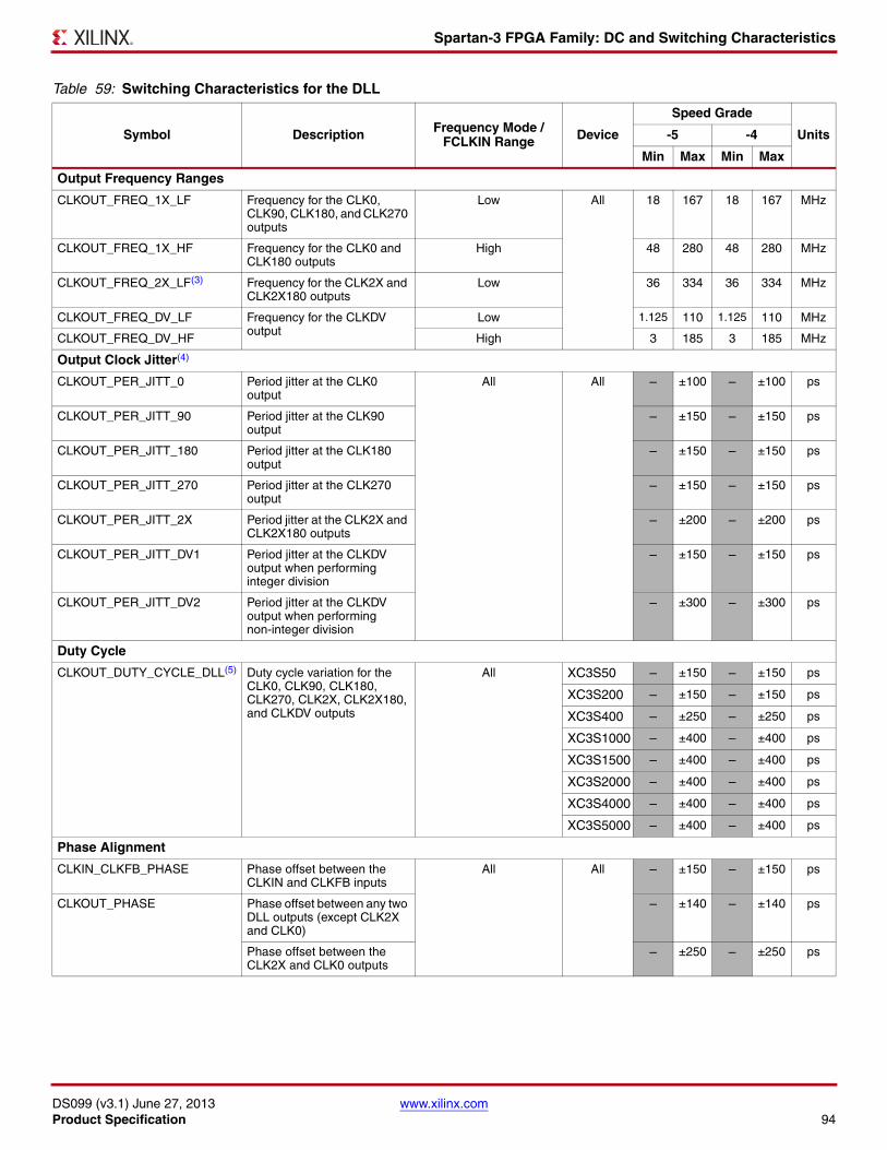
Spartan-3 FPGA Family: DC and Switching Characteristics
DS099 (v3.1) June 27, 2013 www.xilinx.comProduct Specification 94
Table 59: Switching Characteristics for the DLL
Symbol Description Frequency Mode /FCLKIN Range Device
Speed Grade
Units-5 -4
Min Max Min Max
Output Frequency Ranges
CLKOUT_FREQ_1X_LF Frequency for the CLK0, CLK90, CLK180, and CLK270 outputs
Low All 18 167 18 167 MHz
CLKOUT_FREQ_1X_HF Frequency for the CLK0 and CLK180 outputs
High 48 280 48 280 MHz
CLKOUT_FREQ_2X_LF(3) Frequency for the CLK2X and CLK2X180 outputs
Low 36 334 36 334 MHz
CLKOUT_FREQ_DV_LF Frequency for the CLKDV output
Low 1.125 110 1.125 110 MHz
CLKOUT_FREQ_DV_HF High 3 185 3 185 MHz
Output Clock Jitter(4)
CLKOUT_PER_JITT_0 Period jitter at the CLK0 output
All All – ±100 – ±100 ps
CLKOUT_PER_JITT_90 Period jitter at the CLK90 output
– ±150 – ±150 ps
CLKOUT_PER_JITT_180 Period jitter at the CLK180 output
– ±150 – ±150 ps
CLKOUT_PER_JITT_270 Period jitter at the CLK270 output
– ±150 – ±150 ps
CLKOUT_PER_JITT_2X Period jitter at the CLK2X and CLK2X180 outputs
– ±200 – ±200 ps
CLKOUT_PER_JITT_DV1 Period jitter at the CLKDV output when performing integer division
– ±150 – ±150 ps
CLKOUT_PER_JITT_DV2 Period jitter at the CLKDV output when performing non-integer division
– ±300 – ±300 ps
Duty Cycle
CLKOUT_DUTY_CYCLE_DLL(5) Duty cycle variation for the CLK0, CLK90, CLK180, CLK270, CLK2X, CLK2X180, and CLKDV outputs
All XC3S50 – ±150 – ±150 ps
XC3S200 – ±150 – ±150 ps
XC3S400 – ±250 – ±250 ps
XC3S1000 – ±400 – ±400 ps
XC3S1500 – ±400 – ±400 ps
XC3S2000 – ±400 – ±400 ps
XC3S4000 – ±400 – ±400 ps
XC3S5000 – ±400 – ±400 ps
Phase Alignment
CLKIN_CLKFB_PHASE Phase offset between the CLKIN and CLKFB inputs
All All – ±150 – ±150 ps
CLKOUT_PHASE Phase offset between any two DLL outputs (except CLK2X and CLK0)
– ±140 – ±140 ps
Phase offset between the CLK2X and CLK0 outputs
– ±250 – ±250 ps
Spartan-3 FPGA Family: DC and Switching Characteristics
DS099 (v3.1) June 27, 2013 www.xilinx.comProduct Specification 95
Digital Frequency Synthesizer (DFS)
Lock Time
LOCK_DLL When using the DLL alone: The time from deassertion at the DCM’s Reset input to the rising transition at its LOCKED output. When the DCM is locked, the CLKIN and CLKFB signals are in phase
18 MHz ≤ FCLKIN ≤ 30 MHz All – 2.88 – 2.88 ms
30 MHz < FCLKIN ≤ 40 MHz – 2.16 – 2.16 ms
40 MHz < FCLKIN ≤ 50 MHz – 1.20 – 1.20 ms
50 MHz < FCLKIN ≤ 60 MHz – 0.60 – 0.60 ms
FCLKIN > 60 MHz – 0.48 – 0.48 ms
Delay Lines
DCM_TAP Delay tap resolution All All 30.0 60.0 30.0 60.0 ps
Notes: 1. The numbers in this table are based on the operating conditions set forth in Table 32 and Table 58.2. DLL specifications apply when any of the DLL outputs (CLK0, CLK90, CLK180, CLK270, CLK2X, CLK2X180, or CLKDV) are in use.3. Only mask revision ‘E’ and later devices (see Mask and Fab Revisions, page 58) and all revisions of the XC3S50 and the XC3S1000 support
DLL feedback using the CLK2X output. For all other Spartan-3 devices, use feedback from the CLK0 output (instead of the CLK2X output) and set the CLK_FEEDBACK attribute to 1X.
4. Indicates the maximum amount of output jitter that the DCM adds to the jitter on the CLKIN input.5. This specification only applies if the attribute DUTY_CYCLE_CORRECTION = TRUE.
Table 60: Recommended Operating Conditions for the DFS
Symbol Description Frequency Mode
Speed Grade
Units-5 -4
Min Max Min Max
Input Frequency Ranges(2)
FCLKIN CLKIN_FREQ_FX Frequency for the CLKIN input All 1 280 1 280 MHz
Input Clock Jitter Tolerance(3)
CLKIN_CYC_JITT_FX_LF Cycle-to-cycle jitter at the CLKIN input
Low – ±300 – ±300 ps
CLKIN_CYC_JITT_FX_HF High – ±150 – ±150 ps
CLKIN_PER_JITT_FX Period jitter at the CLKIN input All – ±1 – ±1 ns
Notes: 1. DFS specifications apply when either of the DFS outputs (CLKFX or CLKFX180) are used.2. If both DFS and DLL outputs are used on the same DCM, follow the more restrictive CLKIN_FREQ_DLL specifications in Table 58.3. CLKIN input jitter beyond these limits may cause the DCM to lose lock.
Table 59: Switching Characteristics for the DLL (Cont’d)
Symbol Description Frequency Mode /FCLKIN Range Device
Speed Grade
Units-5 -4
Min Max Min Max
Spartan-3 FPGA Family: DC and Switching Characteristics
DS099 (v3.1) June 27, 2013 www.xilinx.comProduct Specification 96
Table 61: Switching Characteristics for the DFS
Symbol Description Frequency Mode Device
Speed Grade
Units-5 -4
Min Max Min Max
Output Frequency Ranges
CLKOUT_FREQ_FX_LF Frequency for the CLKFX and CLKFX180 outputs
Low All 18 210 18 210 MHz
CLKOUT_FREQ_FX_HF High All 210 326(2) 210 307(2) MHz
Output Clock Jitter
CLKOUT_PER_JITT_FX Period jitter at the CLKFX and CLKFX180 outputs
All All Note 3 Note 3 Note 3 Note 3 ps
Duty Cycle(4)
CLKOUT_DUTY_CYCLE_FX Duty cycle precision for the CLKFX and CLKFX180 outputs
All XC3S50 – ±100 – ±100 ps
XC3S200 – ±100 – ±100 ps
XC3S400 – ±250 – ±250 ps
XC3S1000 – ±400 – ±400 ps
XC3S1500 – ±400 – ±400 ps
XC3S2000 – ±400 – ±400 ps
XC3S4000 – ±400 – ±400 ps
XC3S5000 – ±400 – ±400 ps
Phase Alignment
CLKOUT_PHASE Phase offset between the DFS output and the CLK0 output
All All – ±300 – ±300 ps
Lock Time
LOCK_DLL_FX When using the DFS in conjunction with the DLL: The time from deassertion at the DCM’s Reset input to the rising transition at its LOCKED output. When the DCM is locked, the CLKIN and CLKFB signals are in phase.
All All – 10.0 – 10.0 ms
LOCK_FX When using the DFS without the DLL: The time from deassertion at the DCM’s Reset input to the rising transition at its LOCKED output. By asserting the LOCKED signal, the DFS indicates valid CLKFX and CLKFX180 signals.
All All – 10.0 – 10.0 ms
Notes: 1. The numbers in this table are based on the operating conditions set forth in Table 32 and Table 60.2. Mask revisions prior to the E mask revision have a CLKOUT_FREQ_FX_HF max of 280 MHz. See Mask and Fab Revisions, page 58.3. Use the DCM Clocking Wizard in the ISE software for a Spartan-3 device specific number. Jitter number assumes 150 ps of input clock jitter.4. The CLKFX and CLKFX180 outputs always approximate 50% duty cycles.5. DFS specifications apply when either of the DFS outputs (CLKFX or CLKFX180) is in use.
Spartan-3 FPGA Family: DC and Switching Characteristics
DS099 (v3.1) June 27, 2013 www.xilinx.comProduct Specification 97
Phase Shifter (PS)
Phase shifter operation is only supported if the DLL is in low-frequency mode, see Table 58. Fixed phase shift requires ISE software version 10.1.03 (or later).
Table 62: Recommended Operating Conditions for the PS in Variable Phase Mode
Symbol Description Frequency Mode/FCLKIN Range
Speed Grade
Units-5 -4
Min Max Min Max
Operating Frequency Ranges
PSCLK_FREQ (FPSCLK)
Frequency for the PSCLK input
Low 1 167 1 167 MHz
Input Pulse Requirements
PSCLK_PULSE PSCLK pulse width as a percentage of the PSCLK period
Low FCLKIN ≤ 100 MHz 40% 60% 40% 60% -
FCLKIN > 100 MHz 45% 55% 45% 55% -
Table 63: Switching Characteristics for the PS in Variable or Fixed Phase Shift Mode
Symbol Description Frequency Mode/FCLKIN Range
Speed Grade
Units-5 -4
Min Max Min Max
Phase Shifting Range
FINE_SHIFT_RANGE Phase shift range Low – 10.0 – 10.0 ns
Lock Time
LOCK_DLL_PS When using the PS in conjunction with the DLL: The time from deassertion at the DCM’s Reset input to the rising transition at its LOCKED output. When the DCM is locked, the CLKIN and CLKFB signals are in phase.
18 MHz ≤ FCLKIN ≤ 30 MHz – 3.28 – 3.28 ms
30 MHz < FCLKIN ≤ 40 MHz – 2.56 – 2.56 ms
40 MHz < FCLKIN ≤ 50 MHz – 1.60 – 1.60 ms
50 MHz < FCLKIN ≤ 60 MHz – 1.00 – 1.00 ms
60 MHz < FCLKIN ≤ 165 MHz – 0.88 – 0.88 ms
LOCK_DLL_PS_FX When using the PS in conjunction with the DLL and DFS: The time from deassertion at the DCM’s Reset input to the rising transition at its LOCKED output. When the DCM is locked, the CLKIN and CLKFB signals are in phase.
Low – 10.40 – 10.40 ms
Notes: 1. The numbers in this table are based on the operating conditions set forth in Table 32 and Table 62.2. The PS specifications in this table apply when the PS attribute CLKOUT_PHASE_SHIFT= VARIABLE or FIXED.
Spartan-3 FPGA Family: DC and Switching Characteristics
DS099 (v3.1) June 27, 2013 www.xilinx.comProduct Specification 98
Miscellaneous DCM Timing
Table 64: Miscellaneous DCM Timing
Symbol DescriptionDLL
Frequency Mode
Temperature RangeUnits
Commercial Industrial
DCM_INPUT_CLOCK_STOP Maximum duration that the CLKIN and CLKFB signals can be stopped(1,2)
Any 100 100 ms
DCM_RST_PW_MIN Minimum duration of a RST pulse width Any 3 3 CLKINcycles
DCM_RST_PW_MAX(3) Maximum duration of a RST pulse width(1,2) Low N/A N/A seconds
High N/A 10 seconds
DCM_CONFIG_LAG_TIME(4) Maximum duration from VCCINT applied to FPGA configuration successfully completed (DONE pin goes High) and clocks applied to DCM DLL(1,2)
Low N/A N/A minutes
High N/A 10 minutes
Notes: 1. These limits only apply to applications that use the DCM DLL outputs (CLK0, CLK90, CLK180, CLK270, CLK2X, CLK2X180, and CLKDV).
The DCM DFS outputs (CLKFX, CLKFX180) are unaffected. Required due to effects of device cooling: see “Momentarily Stopping CLKIN” in Chapter 3 of UG331.
2. Industrial-temperature applications that use the DLL in High-Frequency mode must use a continuous or increasing operating frequency. The DLL under these conditions does not support reducing the operating frequency once establishing an initial operating frequency.
3. This specification is equivalent to the Virtex-4 FPGA DCM_RESET specification.4. This specification is equivalent to the Virtex-4 FPGA TCONFIG specification.
Spartan-3 FPGA Family: DC and Switching Characteristics
DS099 (v3.1) June 27, 2013 www.xilinx.comProduct Specification 99
Configuration and JTAG TimingX-Ref Target - Figure 36
Figure 36: Waveforms for Power-On and the Beginning of Configuration
Table 65: Power-On Timing and the Beginning of Configuration
Symbol Description DeviceAll Speed Grades
UnitsMin Max
TPOR(2) The time from the application of VCCINT, VCCAUX, and VCCO
Bank 4 supply voltage ramps (whichever occurs last) to the rising transition of the INIT_B pin
XC3S50 – 5 ms
XC3S200 – 5 ms
XC3S400 – 5 ms
XC3S1000 – 5 ms
XC3S1500 – 7 ms
XC3S2000 – 7 ms
XC3S4000 – 7 ms
XC3S5000 – 7 ms
TPROG The width of the low-going pulse on the PROG_B pin All 0.3 – μs
TPL(2) The time from the rising edge of the PROG_B pin to the
rising transition on the INIT_B pinXC3S50 – 2 ms
XC3S200 – 2 ms
XC3S400 – 2 ms
XC3S1000 – 2 ms
XC3S1500 – 3 ms
XC3S2000 – 3 ms
XC3S4000 – 3 ms
XC3S5000 – 3 ms
TINIT Minimum Low pulse width on INIT_B output All 250 – ns
TICCK(3) The time from the rising edge of the INIT_B pin to the
generation of the configuration clock signal at the CCLK output pin
All 0.25 4.0 μs
Notes: 1. The numbers in this table are based on the operating conditions set forth in Table 32. This means power must be applied to all VCCINT, VCCO,
and VCCAUX lines. 2. Power-on reset and the clearing of configuration memory occurs during this period.3. This specification applies only for the Master Serial and Master Parallel modes.
VCCINT(Supply)
(Supply)
(Supply)
VCCAUX
VCCO Bank 4
PROG_B
(Output)
(Open-Drain)
(Input)
INIT_B
CCLK
DS099-3_03_120604
1.2V
2.5V
TICCK
TPROGTPL
TPOR
1.0V
1.0V
2.0V
Notes: 1. The VCCINT, VCCAUX, and VCCO supplies may be applied in any order.2. The Low-going pulse on PROG_B is optional after power-on but necessary for reconfiguration without a power cycle.3. The rising edge of INIT_B samples the voltage levels applied to the mode pins (M0 - M2).
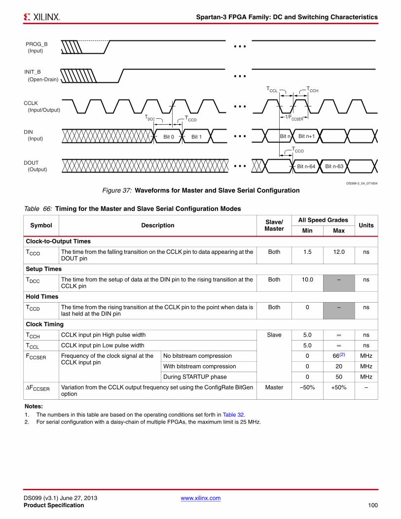
Spartan-3 FPGA Family: DC and Switching Characteristics
DS099 (v3.1) June 27, 2013 www.xilinx.comProduct Specification 100
X-Ref Target - Figure 37
Figure 37: Waveforms for Master and Slave Serial Configuration
Table 66: Timing for the Master and Slave Serial Configuration Modes
Symbol Description Slave/Master
All Speed GradesUnits
Min Max
Clock-to-Output Times
TCCO The time from the falling transition on the CCLK pin to data appearing at the DOUT pin
Both 1.5 12.0 ns
Setup Times
TDCC The time from the setup of data at the DIN pin to the rising transition at the CCLK pin
Both 10.0 – ns
Hold Times
TCCD The time from the rising transition at the CCLK pin to the point when data is last held at the DIN pin
Both 0 – ns
Clock Timing
TCCH CCLK input pin High pulse width Slave 5.0 ∞ ns
TCCL CCLK input pin Low pulse width 5.0 ∞ ns
FCCSER Frequency of the clock signal at the CCLK input pin
No bitstream compression 0 66(2) MHz
With bitstream compression 0 20 MHz
During STARTUP phase 0 50 MHz
ΔFCCSER Variation from the CCLK output frequency set using the ConfigRate BitGen option
Master –50% +50% –
Notes: 1. The numbers in this table are based on the operating conditions set forth in Table 32.2. For serial configuration with a daisy-chain of multiple FPGAs, the maximum limit is 25 MHz.
DS099-3_04_071604
Bit 0 Bit 1 Bit n Bit n+1
Bit n-64 Bit n-63
1/FCCSER
TCCL
TDCC TCCD
TCCH
TCCO
PROG_B(Input)
DIN(Input)
DOUT(Output)
(Open-Drain)INIT_B
(Input/Output)CCLK
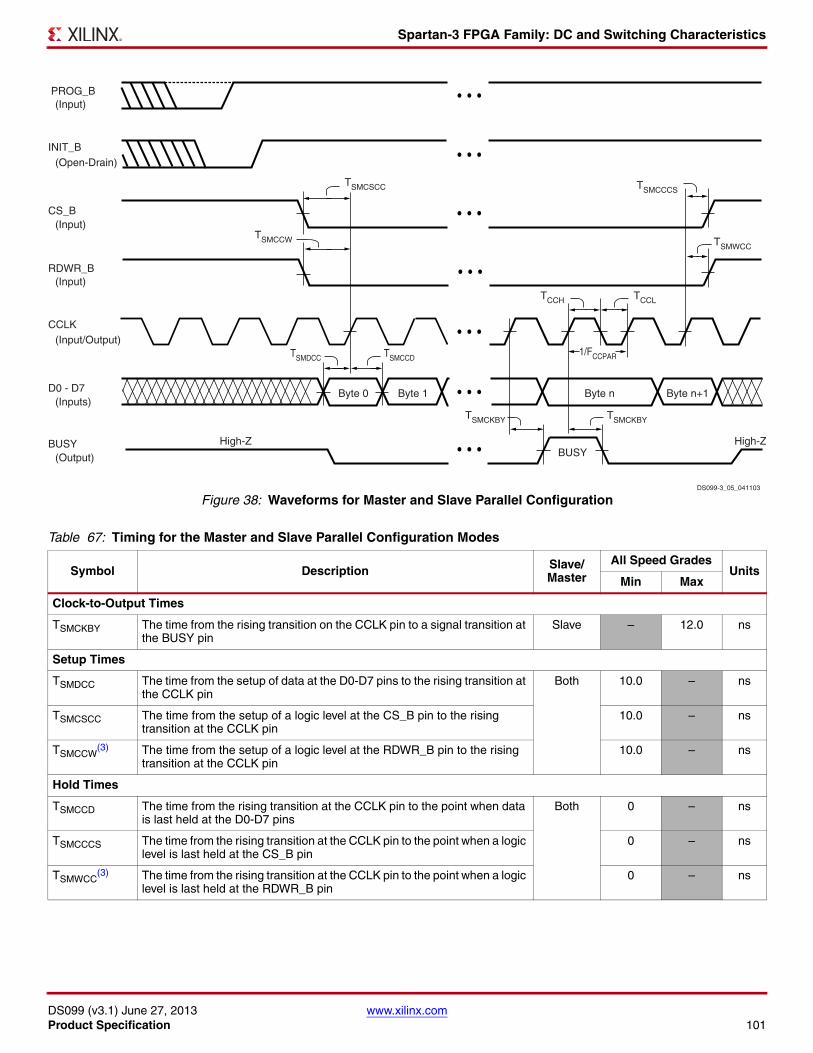
Spartan-3 FPGA Family: DC and Switching Characteristics
DS099 (v3.1) June 27, 2013 www.xilinx.comProduct Specification 101
X-Ref Target - Figure 38
Figure 38: Waveforms for Master and Slave Parallel Configuration
Table 67: Timing for the Master and Slave Parallel Configuration Modes
Symbol Description Slave/Master
All Speed GradesUnits
Min Max
Clock-to-Output Times
TSMCKBY The time from the rising transition on the CCLK pin to a signal transition at the BUSY pin
Slave – 12.0 ns
Setup Times
TSMDCC The time from the setup of data at the D0-D7 pins to the rising transition at the CCLK pin
Both 10.0 – ns
TSMCSCC The time from the setup of a logic level at the CS_B pin to the rising transition at the CCLK pin
10.0 – ns
TSMCCW(3) The time from the setup of a logic level at the RDWR_B pin to the rising
transition at the CCLK pin10.0 – ns
Hold Times
TSMCCD The time from the rising transition at the CCLK pin to the point when data is last held at the D0-D7 pins
Both 0 – ns
TSMCCCS The time from the rising transition at the CCLK pin to the point when a logic level is last held at the CS_B pin
0 – ns
TSMWCC(3) The time from the rising transition at the CCLK pin to the point when a logic
level is last held at the RDWR_B pin0 – ns
DS099-3_05_041103
Byte 0 Byte 1 Byte n
BUSYHigh-Z High-Z
Byte n+1
TSMWCC
1/FCCPAR
TSMCCCS
TCCL
TSMCKBYTSMCKBY
TCCH
TSMCCW
TSMCCD
TSMCSCC
TSMDCC
PROG_B(Input)
(Open-Drain)INIT_B
(Input)CS_B
(Output)BUSY
RDWR_B(Input)
(Input/Output)CCLK
(Inputs)D0 - D7
Spartan-3 FPGA Family: DC and Switching Characteristics
DS099 (v3.1) June 27, 2013 www.xilinx.comProduct Specification 102
Clock Timing
TCCH CCLK input pin High pulse width Slave 5 ∞ ns
TCCL CCLK input pin Low pulse width 5 ∞ ns
FCCPAR Frequency of the clock signal at the CCLK input pin
No bitstream compression
Not using the BUSY pin(4) 0 50 MHz
Using the BUSY pin 0 66 MHz
With bitstream compression 0 20 MHz
During STARTUP phase 0 50 MHz
ΔFCCPAR Variation from the CCLK output frequency set using the BitGen option ConfigRate
Master –50% +50% –
Notes: 1. The numbers in this table are based on the operating conditions set forth in Table 32.2. Some Xilinx documents may refer to Parallel modes as "SelectMAP" modes.3. RDWR_B is synchronized to CCLK for the purpose of performing the Abort operation. The same pin asynchronously controls the driver
impedance of the D0 - D7 pins. To avoid contention when writing configuration data to the D0 - D7 bus, do not bring RDWR_B High when CS_B is Low.
4. In the Slave Parallel mode, it is necessary to use the BUSY pin when the CCLK frequency exceeds this maximum specification.
Table 67: Timing for the Master and Slave Parallel Configuration Modes (Cont’d)
Symbol Description Slave/Master
All Speed GradesUnits
Min Max
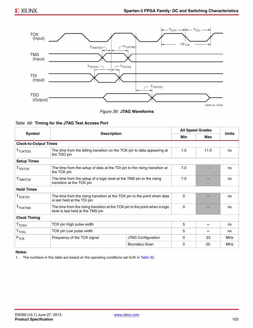
Spartan-3 FPGA Family: DC and Switching Characteristics
DS099 (v3.1) June 27, 2013 www.xilinx.comProduct Specification 103
X-Ref Target - Figure 39
Figure 39: JTAG Waveforms
Table 68: Timing for the JTAG Test Access Port
Symbol DescriptionAll Speed Grades
UnitsMin Max
Clock-to-Output Times
TTCKTDO The time from the falling transition on the TCK pin to data appearing at the TDO pin
1.0 11.0 ns
Setup Times
TTDITCK The time from the setup of data at the TDI pin to the rising transition at the TCK pin
7.0 – ns
TTMSTCK The time from the setup of a logic level at the TMS pin to the rising transition at the TCK pin
7.0 – ns
Hold Times
TTCKTDI The time from the rising transition at the TCK pin to the point when data is last held at the TDI pin
0 – ns
TTCKTMS The time from the rising transition at the TCK pin to the point when a logic level is last held at the TMS pin
0 – ns
Clock Timing
TTCKH TCK pin High pulse width 5 ∞ ns
TTCKL TCK pin Low pulse width 5 ∞ ns
FTCK Frequency of the TCK signal JTAG Configuration 0 33 MHz
Boundary-Scan 0 25 MHz
Notes: 1. The numbers in this table are based on the operating conditions set forth in Table 32.
TCK
TTMSTCK
TMS
TDI
TDO
(Input)
(Input)
(Input)
(Output)
TTCKTMS
TTCKTDI
TTCKTDO
TTDITCK
TCCH TCCL
1/FTCK
DS099_06_102909
Spartan-3 FPGA Family: DC and Switching Characteristics
DS099 (v3.1) June 27, 2013 www.xilinx.comProduct Specification 104
Revision HistoryDate Version Description
04/11/2003 1.0 Initial Xilinx release.
07/11/2003 1.1 Extended Absolute Maximum Rating for junction temperature in Table 28. Added numbers for typical quiescent supply current (Table 34) and DLL timing.
02/06/2004 1.2 Revised VIN maximum rating (Table 28). Added power-on requirements (Table 30), leakage current number (Table 33), and differential output voltage levels (Table 38) for Rev. 0. Published new quiescent current numbers (Table 34). Updated pull-up and pull-down resistor strengths (Table 33). Added LVDCI_DV2 and LVPECL standards (Table 37 and Table 38). Changed CCLK setup time (Table 66 and Table 67).
03/04/2004 1.3 Added timing numbers from v1.29 speed files as well as DCM timing (Table 58 through Table 63).
08/24/2004 1.4 Added reference to errata documents on page 49. Clarified Absolute Maximum Ratings and added ESD information (Table 28). Explained VCCO ramp time measurement (Table 30). Clarified IL specification (Table 33). Updated quiescent current numbers and added information on power-on and surplus current (Table 34). Adjusted VREF range for HSTL_III and HSTL_I_18 and changed VIH min for LVCMOS12 (Table 35). Added note limiting VTT range for SSTL2_II signal standards (Table 36). Calculated VOH and VOL levels for differential standards (Table 38). Updated Switching Characteristics with speed file v1.32 (Table 40 through Table 48 and Table 51 through Table 56). Corrected IOB test conditions (Table 41). Updated DCM timing with latest characterization data (Table 58 through Table 62). Improved DCM CLKIN pulse width specification (Table 58). Recommended use of Virtex-II FPGA Jitter calculator (Table 61). Improved DCM PSCLK pulse width specification (Table 62). Changed Phase Shifter lock time parameter (Table 63). Because the BitGen option Centered_x#_y# is not necessary for Variable Phase Shift mode, removed BitGen command table and referring text. Adjusted maximum CCLK frequency for the slave serial and parallel configuration modes (Table 66). Inverted CCLK waveform (Figure 37). Adjusted JTAG setup times (Table 68).
12/17/2004 1.5 Updated timing parameters to match v1.35 speed file. Improved VCCO ramp time specification (Table 30). Added a note limiting the rate of change of VCCAUX (Table 32). Added typical quiescent current values for the XC3S2000, XC3S4000, and XC3S5000 (Table 34). Increased IOH and IOL for SSTL2-I and SSTL2-II standards (Table 36). Added SSO guidelines for the VQ, TQ, and PQ packages as well as edited SSO guidelines for the FT and FG packages (Table 50). Added maximum CCLK frequencies for configuration using compressed bitstreams (Table 66 and Table 67). Added specifications for the HSLVDCI standards (Table 35, Table 36, Table 44, Table 47, Table 48, and Table 50).
08/19/2005 1.6 Updated timing parameters to match v1.37 speed file. All Spartan-3 FPGA part types, except XC3S5000, promoted to Production status. Removed VCCO ramp rate restriction from all mask revision ‘E’ and later devices (Table 30). Added equivalent resistance values for internal pull-up and pull-down resistors (Table 33). Added worst-case quiescent current values for XC3S2000, XC3S4000, XC3S5000 (Table 34). Added industrial temperature range specification and improved typical quiescent current values (Table 34). Improved the DLL minimum clock input frequency specification from 24 MHz down to 18 MHz (Table 58). Improved the DFS minimum and maximum clock output frequency specifications (Table 60, Table 61). Added new miscellaneous DCM specifications (Table 64), primarily affecting Industrial temperature range applications. Updated Simultaneously Switching Output Guidelines and Table 50 for QFP packages. Added information on SSTL18_II I/O standard and timing to support DDR2 SDRAM interfaces. Added differential (or complementary single-ended) DIFF_HSTL_II_18 and DIFF_SSTL2_II I/O standards, including DCI terminated versions. Added electro-static discharge (ESD) data for the XC3S2000 and larger FPGAs (Table 28). Added link to Spartan-3 FPGA errata notices and how to receive automatic notifications of data sheet or errata changes.
04/03/2006 2.0 Upgraded Module 3, removing Preliminary status. Moved XC3S5000 to Production status in Table 39. Finalized I/O timing on XC3S5000 for v1.38 speed files. Added minimum timing values for various logic and I/O paths. Corrected labels for RPU and RPD and updated RPD conditions for in Table 33. Added final mask revision ‘E’ specifications for LVDS_25, RSDS_25, LVDSEXT_25 differential outputs to Table 38. Added BLVDS termination requirements to Figure 34. Improved recommended Simultaneous Switching Outputs (SSOs) limits in Table 50 for quad-flat packaged based on silicon testing using devices soldered on a printed circuit board. Updated Note 2 in Table 63. Updated Note 6 in Table 30. Added INIT_B minimum pulse width specification, TINIT, to Table 65.
04/26/2006 2.1 Updated document links.
Spartan-3 FPGA Family: DC and Switching Characteristics
DS099 (v3.1) June 27, 2013 www.xilinx.comProduct Specification 105
05/25/2007 2.2 Improved absolute maximum voltage specifications in Table 28, providing additional overshoot allowance. Improved XC3S50 HBM ESD to 2000V in Table 28. Based on extensive 90 nm production data, improved (reduced) the maximum quiescent current limits for the ICCINTQ and ICCOQ specifications in Table 34. Widened the recommended voltage range for the PCI standard and clarified the hysteresis footnote in Table 35. Noted restriction on combining differential outputs in Table 38. Updated footnote 1 in Table 64.
11/30/2007 2.3 Updated 3.3V VCCO max from 3.45V to 3.465V in Table 32 and elsewhere. Reduced tICCK minimum from 0.50μs to 0.25μs in Table 65. Updated links to technical documentation.
06/25/2008 2.4 Clarified dual marking. Added Mask and Fab Revisions. Added references to XAPP459 in Table 28 and Table 32. Removed absolute minimum and added footnote referring to timing analyzer for minimum delay values. Added HSLVDCI to Table 48 and Table 50. Updated tDICK in Table 51 to match largest possible value in speed file. Updated formatting and links.
12/04/2009 2.5 Updated notes 2 and 3 in Table 28. Removed silicon process specific information and revised notes in Table 30. Updated note 3 in Table 32. Updated note 3 in Table 34. Updated note 5 in Table 35. Updated VOL max and VOH min for SSTL2_II in Table 36. Updated note 5 in Table 36. Updated JTAG Waveforms in Figure 39. Updated VICM max for LVPECL_25 in Table 37. Updated RT and VT for LVDS_25_DCI in Table 48. Updated Simultaneously Switching Output Guidelines. Noted that the CP132 package is being discontinued in Table 49. Removed minimum values for TMULTCK clock-to-output times in Table 54. Updated footnote 3 in Table 58. Removed minimum values for TMULT propagation times in Table 55. Removed silicon process specific information and revised notes in Table 61. Updated Phase Shifter (PS).
10/29/2012 3.0 Added Notice of Disclaimer. Per XCN07022, updated the discontinued FG1156 and FGG1156 package discussion throughout document. Per XCN08011, updated the discontinued CP132 and CPG132 package discussion throughout document. Revised description of VIN in Table 32 and added note 7. Added note 4 to Table 33. This product is not recommended for new designs.
06/27/2013 3.1 Removed banner. This product IS recommended for new designs.
Date Version Description
Spartan-3 FPGA Family: DC and Switching Characteristics
DS099 (v3.1) June 27, 2013 www.xilinx.comProduct Specification 106
Notice of DisclaimerTHE XILINX HARDWARE FPGA AND CPLD DEVICES REFERRED TO HEREIN (“PRODUCTS”) ARE SUBJECT TO THE TERMS ANDCONDITIONS OF THE XILINX LIMITED WARRANTY WHICH CAN BE VIEWED AT http://www.xilinx.com/warranty.htm. THIS LIMITEDWARRANTY DOES NOT EXTEND TO ANY USE OF PRODUCTS IN AN APPLICATION OR ENVIRONMENT THAT IS NOT WITHIN THESPECIFICATIONS STATED IN THE XILINX DATA SHEET. ALL SPECIFICATIONS ARE SUBJECT TO CHANGE WITHOUT NOTICE.PRODUCTS ARE NOT DESIGNED OR INTENDED TO BE FAIL-SAFE OR FOR USE IN ANY APPLICATION REQUIRING FAIL-SAFEPERFORMANCE, SUCH AS LIFE-SUPPORT OR SAFETY DEVICES OR SYSTEMS, OR ANY OTHER APPLICATION THAT INVOKESTHE POTENTIAL RISKS OF DEATH, PERSONAL INJURY, OR PROPERTY OR ENVIRONMENTAL DAMAGE (“CRITICALAPPLICATIONS”). USE OF PRODUCTS IN CRITICAL APPLICATIONS IS AT THE SOLE RISK OF CUSTOMER, SUBJECT TOAPPLICABLE LAWS AND REGULATIONS.
CRITICAL APPLICATIONS DISCLAIMERXILINX PRODUCTS (INCLUDING HARDWARE, SOFTWARE AND/OR IP CORES) ARE NOT DESIGNED OR INTENDED TO BEFAIL-SAFE, OR FOR USE IN ANY APPLICATION REQUIRING FAIL-SAFE PERFORMANCE, SUCH AS IN LIFE-SUPPORT ORSAFETY DEVICES OR SYSTEMS, CLASS III MEDICAL DEVICES, NUCLEAR FACILITIES, APPLICATIONS RELATED TO THEDEPLOYMENT OF AIRBAGS, OR ANY OTHER APPLICATIONS THAT COULD LEAD TO DEATH, PERSONAL INJURY OR SEVEREPROPERTY OR ENVIRONMENTAL DAMAGE (INDIVIDUALLY AND COLLECTIVELY, “CRITICAL APPLICATIONS”). FURTHERMORE,XILINX PRODUCTS ARE NOT DESIGNED OR INTENDED FOR USE IN ANY APPLICATIONS THAT AFFECT CONTROL OF AVEHICLE OR AIRCRAFT, UNLESS THERE IS A FAIL-SAFE OR REDUNDANCY FEATURE (WHICH DOES NOT INCLUDE USE OFSOFTWARE IN THE XILINX DEVICE TO IMPLEMENT THE REDUNDANCY) AND A WARNING SIGNAL UPON FAILURE TO THEOPERATOR. CUSTOMER AGREES, PRIOR TO USING OR DISTRIBUTING ANY SYSTEMS THAT INCORPORATE XILINXPRODUCTS, TO THOROUGHLY TEST THE SAME FOR SAFETY PURPOSES. TO THE MAXIMUM EXTENT PERMITTED BYAPPLICABLE LAW, CUSTOMER ASSUMES THE SOLE RISK AND LIABILITY OF ANY USE OF XILINX PRODUCTS IN CRITICALAPPLICATIONS.
AUTOMOTIVE APPLICATIONS DISCLAIMERXILINX PRODUCTS ARE NOT DESIGNED OR INTENDED TO BE FAIL-SAFE, OR FOR USE IN ANY APPLICATION REQUIRING FAIL-SAFE PERFORMANCE, SUCH AS APPLICATIONS RELATED TO: (I) THE DEPLOYMENT OF AIRBAGS, (II) CONTROL OF A VEHICLE, UNLESS THERE IS A FAIL-SAFE OR REDUNDANCY FEATURE (WHICH DOES NOT INCLUDE USE OF SOFTWARE IN THE XILINX DEVICE TO IMPLEMENT THE REDUNDANCY) AND A WARNING SIGNAL UPON FAILURE TO THE OPERATOR, OR (III) USES THAT COULD LEAD TO DEATH OR PERSONAL INJURY. CUSTOMER ASSUMES THE SOLE RISK AND LIABILITY OF ANY USE OF XILINX PRODUCTS IN SUCH APPLICATIONS.
DS099 (v3.1) June 27, 2013 www.xilinx.comProduct Specification 107
© Copyright 2003–2013 Xilinx, Inc. XILINX, the Xilinx logo, Virtex, Spartan, ISE, Artix, Kintex, Zynq, Vivado, and other designated brands included herein are trademarks of Xilinx in the United States and other countries. PCI and PCI-X are trademarks of PCI-SIG and used under license. All other trademarks are the property of their respective owners.
IntroductionThis data sheet module describes the various pins on a Spartan®-3 FPGA and how they connect to the supported component packages.
• The Pin Types section categorizes all of the FPGA pins by their function type.
• The Pin Definitions section provides a top-level description for each pin on the device.
• The Detailed, Functional Pin Descriptions section offers significantly more detail about each pin, especially for the dual- or special-function pins used during device configuration.
• Some pins have associated behavior that is controlled by settings in the configuration bitstream. These options are described in the Bitstream Options section.
• The Package Overview section describes the various packaging options available for Spartan-3 FPGAs. Detailed pin list tables and footprint diagrams are provided for each package solution.
Pin Descriptions
Pin Types
A majority of the pins on a Spartan-3 FPGA are general-purpose, user-defined I/O pins. There are, however, up to 12 different functional types of pins on Spartan-3 device packages, as outlined in Table 69. In the package footprint drawings that follow, the individual pins are color-coded according to pin type as in the table.
272Spartan-3 FPGA Family:
Pinout Descriptions
DS099 (v3.1) June 27, 2013 Product Specification
Table 69: Types of Pins on Spartan-3 FPGAs
Pin Type/ Color Code Description Pin Name
I/O Unrestricted, general-purpose user-I/O pin. Most pins can be paired together to form differential I/Os.
IO, IO_Lxxy_#
DUAL Dual-purpose pin used in some configuration modes during the configuration process and then usually available as a user I/O after configuration. If the pin is not used during configuration, this pin behaves as an I/O-type pin. There are 12 dual-purpose configuration pins on every package. The INIT_B pin has an internal pull-up resistor to VCCO_4 or VCCO_BOTTOM during configuration.
IO_Lxxy_#/DIN/D0, IO_Lxxy_#/D1, IO_Lxxy_#/D2, IO_Lxxy_#/D3, IO_Lxxy_#/D4, IO_Lxxy_#/D5, IO_Lxxy_#/D6, IO_Lxxy_#/D7, IO_Lxxy_#/CS_B, IO_Lxxy_#/RDWR_B, IO_Lxxy_#/BUSY/DOUT, IO_Lxxy_#/INIT_B
CONFIG Dedicated configuration pin. Not available as a user-I/O pin. Every package has seven dedicated configuration pins. These pins are powered by VCCAUX and have a dedicated internal pull-up resistor to VCCAUX during configuration.
CCLK, DONE, M2, M1, M0, PROG_B, HSWAP_EN
JTAG Dedicated JTAG pin. Not available as a user-I/O pin. Every package has four dedicated JTAG pins. These pins are powered by VCCAUX and have a dedicated internal pull-up resistor to VCCAUX during configuration.
TDI, TMS, TCK, TDO
DCI Dual-purpose pin that is either a user-I/O pin or used to calibrate output buffer impedance for a specific bank using Digital Controlled Impedance (DCI). There are two DCI pins per I/O bank.
IO/VRN_#IO_Lxxy_#/VRN_#IO/VRP_#IO_Lxxy_#/VRP_#
Spartan-3 FPGA Family: Pinout Descriptions
DS099 (v3.1) June 27, 2013 www.xilinx.comProduct Specification 108
I/Os with Lxxy_# are part of a differential output pair. ‘L’ indicates differential output capability. The “xx” field is a two-digit integer, unique to each bank that identifies a differential pin-pair. The ‘y’ field is either ‘P’ for the true signal or ‘N’ for the inverted signal in the differential pair. The ‘#’ field is the I/O bank number.
Pin Definitions
Table 70 provides a brief description of each pin listed in the Spartan-3 FPGA pinout tables and package footprint diagrams. Pins are categorized by their pin type, as listed in Table 69. See Detailed, Functional Pin Descriptions for more information.
VREF Dual-purpose pin that is either a user-I/O pin or, along with all other VREF pins in the same bank, provides a reference voltage input for certain I/O standards. If used for a reference voltage within a bank, all VREF pins within the bank must be connected.
IO/VREF_#IO_Lxxy_#/VREF_#
GND Dedicated ground pin. The number of GND pins depends on the package used. All must be connected.
GND
VCCAUX Dedicated auxiliary power supply pin. The number of VCCAUX pins depends on the package used. All must be connected to +2.5V.
VCCAUX
VCCINT Dedicated internal core logic power supply pin. The number of VCCINT pins depends on the package used. All must be connected to +1.2V.
VCCINT
VCCO Dedicated I/O bank, output buffer power supply pin. Along with other VCCO pins in the same bank, this pin supplies power to the output buffers within the I/O bank and sets the input threshold voltage for some I/O standards.
VCCO_#CP132 and TQ144 Packages Only:VCCO_LEFT, VCCO_TOP, VCCO_RIGHT, VCCO_BOTTOM
GCLK Dual-purpose pin that is either a user-I/O pin or an input to a specific global buffer input. Every package has eight dedicated GCLK pins.
IO_Lxxy_#/GCLK0, IO_Lxxy_#/GCLK1, IO_Lxxy_#/GCLK2, IO_Lxxy_#/GCLK3, IO_Lxxy_#/GCLK4, IO_Lxxy_#/GCLK5, IO_Lxxy_#/GCLK6, IO_Lxxy_#/GCLK7
N.C. This package pin is not connected in this specific device/package combination but may be connected in larger devices in the same package.
N.C.
Notes: 1. # = I/O bank number, an integer between 0 and 7.
Table 69: Types of Pins on Spartan-3 FPGAs (Cont’d)
Pin Type/ Color Code Description Pin Name
Spartan-3 FPGA Family: Pinout Descriptions
DS099 (v3.1) June 27, 2013 www.xilinx.comProduct Specification 109
Table 70: Spartan-3 FPGA Pin Definitions
Pin Name Direction Description
I/O: General-purpose I/O pins
I/O User-defined as input, output, bidirectional, three-state output, open-drain output, open-source output
User I/O:Unrestricted single-ended user-I/O pin. Supports all I/O standards except the differential standards.
I/O_Lxxy_# User-defined as input, output, bidirectional, three-state output, open-drain output, open-source output
User I/O, Half of Differential Pair:Unrestricted single-ended user-I/O pin or half of a differential pair. Supports all I/O standards including the differential standards.
DUAL: Dual-purpose configuration pins
IO_Lxxy_#/DIN/D0, IO_Lxxy_#/D1, IO_Lxxy_#/D2, IO_Lxxy_#/D3, IO_Lxxy_#/D4, IO_Lxxy_#/D5, IO_Lxxy_#/D6, IO_Lxxy_#/D7
Input during configurationPossible bidirectional I/O after configuration if SelectMap port is retainedOtherwise, user I/O after configuration
Configuration Data Port:In Parallel (SelectMAP) modes, D0-D7 are byte-wide configuration data pins. These pins become user I/Os after configuration unless the SelectMAP port is retained via the Persist bitstream option.In Serial modes, DIN (D0) serves as the single configuration data input. This pin becomes a user I/O after configuration unless retained by the Persist bitstream option.
IO_Lxxy_#/CS_B Input during Parallel mode configurationPossible input after configuration if SelectMap port is retainedOtherwise, user I/O after configuration
Chip Select for Parallel Mode Configuration:In Parallel (SelectMAP) modes, this is the active-Low Chip Select signal. This pin becomes a user I/O after configuration unless the SelectMAP port is retained via the Persist bitstream option.
IO_Lxxy_#/RDWR_B Input during Parallel mode configurationPossible input after configuration if SelectMap port is retainedOtherwise, user I/O after configuration
Read/Write Control for Parallel Mode Configuration:In Parallel (SelectMAP) modes, this is the active-Low Write Enable, active-High Read Enable signal. This pin becomes a user I/O after configuration unless the SelectMAP port is retained via the Persist bitstream option.
IO_Lxxy_#/BUSY/DOUT
Output during configurationPossible output after configuration if SelectMap port is retainedOtherwise, user I/O after configuration
Configuration Data Rate Control for Parallel Mode, Serial Data Output for Serial Mode:In Parallel (SelectMAP) modes, BUSY throttles the rate at which configuration data is loaded. This pin becomes a user I/O after configuration unless the SelectMAP port is retained via the Persist bitstream option.In Serial modes, DOUT provides preamble and configuration data to downstream devices in a multi-FPGA daisy-chain. This pin becomes a user I/O after configuration.
IO_Lxxy_#/INIT_B Bidirectional (open-drain) during configurationUser I/O after configuration
Initializing Configuration Memory/Detected Configuration Error:When Low, this pin indicates that configuration memory is being cleared. When held Low, this pin delays the start of configuration. After this pin is released or configuration memory is cleared, the pin goes High. During configuration, a Low on this output indicates that a configuration data error occurred. This pin always has an internal pull-up resistor to VCCO_4 or VCCO_BOTTOM during configuration, regardless of the HSWAP_EN pin. This pin becomes a user I/O after configuration.
DCI: Digitally Controlled Impedance reference resistor input pins
IO_Lxxy_#/VRN_# or IO/VRN_#
Input when using DCIOtherwise, same as I/O
DCI Reference Resistor for NMOS I/O Transistor (per bank):If using DCI, a 1% precision impedance-matching resistor is connected between this pin and the VCCO supply for this bank. Otherwise, this pin is a user I/O.
IO_Lxxy_#/VRP_# or IO/VRP_#
Input when using DCIOtherwise, same as I/O
DCI Reference Resistor for PMOS I/O Transistor (per bank):If using DCI, a 1% precision impedance-matching resistor is connected between this pin and the ground supply. Otherwise, this pin is a user I/O.
Spartan-3 FPGA Family: Pinout Descriptions
DS099 (v3.1) June 27, 2013 www.xilinx.comProduct Specification 110
GCLK: Global clock buffer inputs
IO_Lxxy_#/GCLK0, IO_Lxxy_#/GCLK1, IO_Lxxy_#/GCLK2, IO_Lxxy_#/GCLK3, IO_Lxxy_#/GCLK4, IO_Lxxy_#/GCLK5, IO_Lxxy_#/GCLK6, IO_Lxxy_#/GCLK7
Input if connected to global clock buffersOtherwise, same as I/O Global Buffer Input:
Direct input to a low-skew global clock buffer. If not connected to a global clock buffer, this pin is a user I/O.
VREF: I/O bank input reference voltage pins
IO_Lxxy_#/VREF_# orIO/VREF_#
Voltage supply input when VREF pins are used within a bank.Otherwise, same as I/O
Input Buffer Reference Voltage for Special I/O Standards (per bank):If required to support special I/O standards, all the VREF pins within a bank connect to a input threshold voltage source.If not used as input reference voltage pins, these pins are available as individual user-I/O pins.
CONFIG: Dedicated configuration pins (pull-up resistor to VCCAUX always active during configuration, regardless of HSWAP_EN pin)
CCLK Input in Slave configuration modesOutput in Master configuration modes
Configuration Clock:The configuration clock signal synchronizes configuration data. This pin has an internal pull-up resistor to VCCAUX during configuration.
PROG_B Input Program/Configure Device:Active Low asynchronous reset to configuration logic. Asserting PROG_B Low for an extended period delays the configuration process. This pin has an internal pull-up resistor to VCCAUX during configuration.
DONE Bidirectional with open-drain or totem-pole Output
Configuration Done, Delay Start-up Sequence:A Low-to-High output transition on this bidirectional pin signals the end of the configuration process.The FPGA produces a Low-to-High transition on this pin to indicate that the configuration process is complete. The DriveDone bitstream generation option defines whether this pin functions as a totem-pole output that actively drives High or as an open-drain output. An open-drain output requires a pull-up resistor to produce a High logic level. The open-drain option permits the DONE lines of multiple FPGAs to be tied together, so that the common node transitions High only after all of the FPGAs have completed configuration. Externally holding the open-drain output Low delays the start-up sequence, which marks the transition to user mode.
M0, M1, M2 Input Configuration Mode Selection:These inputs select the configuration mode. The logic levels applied to the mode pins are sampled on the rising edge of INIT_B. See Table 75. These pins have an internal pull-up resistor to VCCAUX during configuration, making Slave Serial the default configuration mode.
HSWAP_EN Input Disable Pull-up Resistors During Configuration:A Low on this pin enables pull-up resistors on all pins that are not actively involved in the configuration process. A High value disables all pull-ups, allowing the non-configuration pins to float.
JTAG: JTAG interface pins (pull-up resistor to VCCAUX always active during configuration, regardless of HSWAP_EN pin)
TCK Input JTAG Test Clock:The TCK clock signal synchronizes all JTAG port operations. This pin has an internal pull-up resistor to VCCAUX during configuration.
Table 70: Spartan-3 FPGA Pin Definitions (Cont’d)
Pin Name Direction Description
Spartan-3 FPGA Family: Pinout Descriptions
DS099 (v3.1) June 27, 2013 www.xilinx.comProduct Specification 111
Detailed, Functional Pin Descriptions
I/O Type: Unrestricted, General-purpose I/O Pins
After configuration, I/O-type pins are inputs, outputs, bidirectional I/O, three-state outputs, open-drain outputs, or open-source outputs, as defined in the application
Pins labeled "IO" support all SelectIO™ interface signal standards except differential standards. A given device at most only has a few of these pins.
A majority of the general-purpose I/O pins are labeled in the format “IO_Lxxy_#”. These pins support all SelectIO signal standards, including the differential standards such as LVDS, ULVDS, BLVDS, RSDS, or LDT.
For additional information, see IOBs, page 10
TDI Input JTAG Test Data Input:TDI is the serial data input for all JTAG instruction and data registers. This pin has an internal pull-up resistor to VCCAUX during configuration.
TMS Input JTAG Test Mode Select:The serial TMS input controls the operation of the JTAG port. This pin has an internal pull-up resistor to VCCAUX during configuration.
TDO Output JTAG Test Data Output:TDO is the serial data output for all JTAG instruction and data registers. This pin has an internal pull-up resistor to VCCAUX during configuration.
VCCO: I/O bank output voltage supply pins
VCCO_# Supply Power Supply for Output Buffer Drivers (per bank):These pins power the output drivers within a specific I/O bank.
VCCAUX: Auxiliary voltage supply pins
VCCAUX Supply Power Supply for Auxiliary Circuits:+2.5V power pins for auxiliary circuits, including the Digital Clock Managers (DCMs), the dedicated configuration pins (CONFIG), and the dedicated JTAG pins. All VCCAUX pins must be connected.
VCCINT: Internal core voltage supply pins
VCCINT Supply Power Supply for Internal Core Logic:+1.2V power pins for the internal logic. All pins must be connected.
GND: Ground supply pins
GND Supply Ground:Ground pins, which are connected to the power supply’s return path. All pins must be connected.
N.C.: Unconnected package pins
N.C. Unconnected Package Pin:These package pins are unconnected.
Notes: 1. All unused inputs and bidirectional pins must be tied either High or Low. For unused enable inputs, apply the level that disables the
associated function. One common approach is to activate internal pull-up or pull-down resistors. An alternative approach is to externally connect the pin to either VCCO or GND.
2. All outputs are of the totem-pole type — i.e., they can drive High as well as Low logic levels — except for the cases where “Open Drain” is indicated. The latter can only drive a Low logic level and require a pull-up resistor to produce a High logic level.
Table 70: Spartan-3 FPGA Pin Definitions (Cont’d)
Pin Name Direction Description
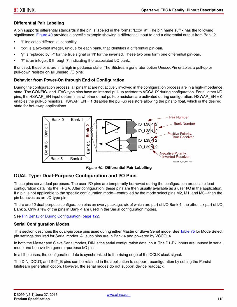
Spartan-3 FPGA Family: Pinout Descriptions
DS099 (v3.1) June 27, 2013 www.xilinx.comProduct Specification 112
Differential Pair Labeling
A pin supports differential standards if the pin is labeled in the format “Lxxy_#”. The pin name suffix has the following significance. Figure 40 provides a specific example showing a differential input to and a differential output from Bank 2.
• ‘L’ indicates differential capability.
• "xx" is a two-digit integer, unique for each bank, that identifies a differential pin-pair.
• ‘y’ is replaced by ‘P’ for the true signal or ‘N’ for the inverted. These two pins form one differential pin-pair.
• ‘#’ is an integer, 0 through 7, indicating the associated I/O bank.
If unused, these pins are in a high impedance state. The Bitstream generator option UnusedPin enables a pull-up or pull-down resistor on all unused I/O pins.
Behavior from Power-On through End of Configuration
During the configuration process, all pins that are not actively involved in the configuration process are in a high-impedance state. The CONFIG- and JTAG-type pins have an internal pull-up resistor to VCCAUX during configuration. For all other I/O pins, the HSWAP_EN input determines whether or not pull-up resistors are activated during configuration. HSWAP_EN = 0 enables the pull-up resistors. HSWAP_EN = 1 disables the pull-up resistors allowing the pins to float, which is the desired state for hot-swap applications.
DUAL Type: Dual-Purpose Configuration and I/O Pins
These pins serve dual purposes. The user-I/O pins are temporarily borrowed during the configuration process to load configuration data into the FPGA. After configuration, these pins are then usually available as a user I/O in the application. If a pin is not applicable to the specific configuration mode—controlled by the mode select pins M2, M1, and M0—then the pin behaves as an I/O-type pin.
There are 12 dual-purpose configuration pins on every package, six of which are part of I/O Bank 4, the other six part of I/O Bank 5. Only a few of the pins in Bank 4 are used in the Serial configuration modes.
See Pin Behavior During Configuration, page 122.
Serial Configuration Modes
This section describes the dual-purpose pins used during either Master or Slave Serial mode. See Table 75 for Mode Select pin settings required for Serial modes. All such pins are in Bank 4 and powered by VCCO_4.
In both the Master and Slave Serial modes, DIN is the serial configuration data input. The D1-D7 inputs are unused in serial mode and behave like general-purpose I/O pins.
In all the cases, the configuration data is synchronized to the rising edge of the CCLK clock signal.
The DIN, DOUT, and INIT_B pins can be retained in the application to support reconfiguration by setting the Persist bitstream generation option. However, the serial modes do not support device readback.
X-Ref Target - Figure 40
Figure 40: Differential Pair Labelling
IO_L38P_2
IO_L38N_2
IO_L39P_2
IO_L39N_2
Bank 0 Bank 1
Bank 4Bank 5
Ban
k 2
Ba
nk
3
Ba
nk
6B
ank
7
Pair Number
Bank Number
Positive Polarity,True Receiver
Negative Polarity,Inverted Receiver
DS099-4_01_091710
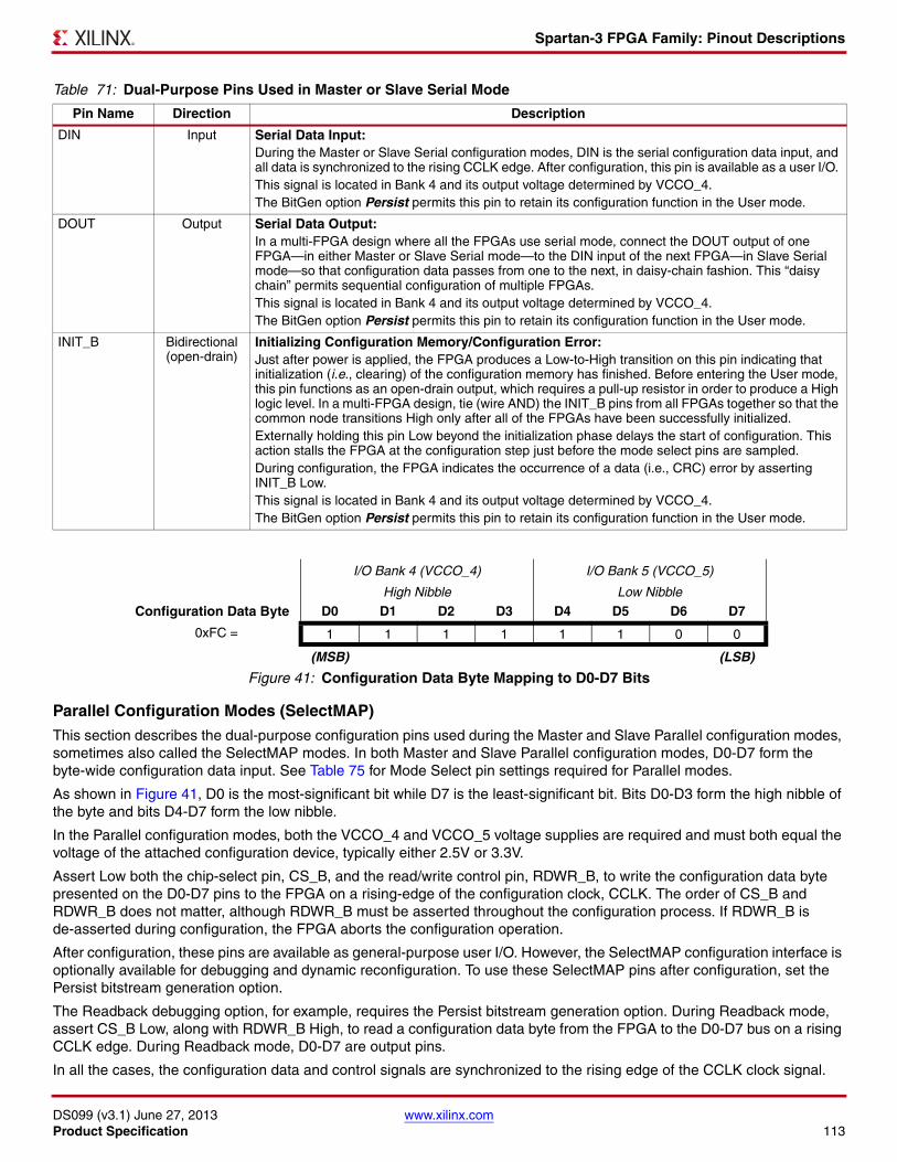
Spartan-3 FPGA Family: Pinout Descriptions
DS099 (v3.1) June 27, 2013 www.xilinx.comProduct Specification 113
X-Ref Target - Figure 41
Parallel Configuration Modes (SelectMAP)
This section describes the dual-purpose configuration pins used during the Master and Slave Parallel configuration modes, sometimes also called the SelectMAP modes. In both Master and Slave Parallel configuration modes, D0-D7 form the byte-wide configuration data input. See Table 75 for Mode Select pin settings required for Parallel modes.
As shown in Figure 41, D0 is the most-significant bit while D7 is the least-significant bit. Bits D0-D3 form the high nibble of the byte and bits D4-D7 form the low nibble.
In the Parallel configuration modes, both the VCCO_4 and VCCO_5 voltage supplies are required and must both equal the voltage of the attached configuration device, typically either 2.5V or 3.3V.
Assert Low both the chip-select pin, CS_B, and the read/write control pin, RDWR_B, to write the configuration data byte presented on the D0-D7 pins to the FPGA on a rising-edge of the configuration clock, CCLK. The order of CS_B and RDWR_B does not matter, although RDWR_B must be asserted throughout the configuration process. If RDWR_B is de-asserted during configuration, the FPGA aborts the configuration operation.
After configuration, these pins are available as general-purpose user I/O. However, the SelectMAP configuration interface is optionally available for debugging and dynamic reconfiguration. To use these SelectMAP pins after configuration, set the Persist bitstream generation option.
The Readback debugging option, for example, requires the Persist bitstream generation option. During Readback mode, assert CS_B Low, along with RDWR_B High, to read a configuration data byte from the FPGA to the D0-D7 bus on a rising CCLK edge. During Readback mode, D0-D7 are output pins.
In all the cases, the configuration data and control signals are synchronized to the rising edge of the CCLK clock signal.
Table 71: Dual-Purpose Pins Used in Master or Slave Serial Mode
Pin Name Direction Description
DIN Input Serial Data Input:During the Master or Slave Serial configuration modes, DIN is the serial configuration data input, and all data is synchronized to the rising CCLK edge. After configuration, this pin is available as a user I/O. This signal is located in Bank 4 and its output voltage determined by VCCO_4.The BitGen option Persist permits this pin to retain its configuration function in the User mode.
DOUT Output Serial Data Output:In a multi-FPGA design where all the FPGAs use serial mode, connect the DOUT output of one FPGA—in either Master or Slave Serial mode—to the DIN input of the next FPGA—in Slave Serial mode—so that configuration data passes from one to the next, in daisy-chain fashion. This “daisy chain” permits sequential configuration of multiple FPGAs.This signal is located in Bank 4 and its output voltage determined by VCCO_4.The BitGen option Persist permits this pin to retain its configuration function in the User mode.
INIT_B Bidirectional (open-drain)
Initializing Configuration Memory/Configuration Error:Just after power is applied, the FPGA produces a Low-to-High transition on this pin indicating that initialization (i.e., clearing) of the configuration memory has finished. Before entering the User mode, this pin functions as an open-drain output, which requires a pull-up resistor in order to produce a High logic level. In a multi-FPGA design, tie (wire AND) the INIT_B pins from all FPGAs together so that the common node transitions High only after all of the FPGAs have been successfully initialized.Externally holding this pin Low beyond the initialization phase delays the start of configuration. This action stalls the FPGA at the configuration step just before the mode select pins are sampled.During configuration, the FPGA indicates the occurrence of a data (i.e., CRC) error by asserting INIT_B Low.This signal is located in Bank 4 and its output voltage determined by VCCO_4.The BitGen option Persist permits this pin to retain its configuration function in the User mode.
I/O Bank 4 (VCCO_4) I/O Bank 5 (VCCO_5)
High Nibble Low Nibble
Configuration Data Byte D0 D1 D2 D3 D4 D5 D6 D7
0xFC = 1 1 1 1 1 1 0 0
(MSB) (LSB)
Figure 41: Configuration Data Byte Mapping to D0-D7 Bits
Spartan-3 FPGA Family: Pinout Descriptions
DS099 (v3.1) June 27, 2013 www.xilinx.comProduct Specification 114
Table 72: Dual-Purpose Configuration Pins for Parallel (SelectMAP) Configuration Modes
Pin Name Direction Description
D0, D1, D2, D3
• Input during configuration
• Output during readback
Configuration Data Port (high nibble):Collectively, the D0-D7 pins are the byte-wide configuration data port for the Parallel (SelectMAP) configuration modes. Configuration data is synchronized to the rising edge of CCLK clock signal.The D0-D3 pins are the high nibble of the configuration data byte and located in Bank 4 and powered by VCCO_4.The BitGen option Persist permits this pin to retain its configuration function in the User mode.
D4, D5, D6, D7
• Input during configuration
• Output during readback
Configuration Data Port (low nibble):The D4-D7 pins are the low nibble of the configuration data byte. However, these signals are located in Bank 5 and powered by VCCO_5.The BitGen option Persist permits this pin to retain its configuration function in the User mode.
CS_B Input Chip Select for Parallel Mode Configuration:Assert this pin Low, together with RDWR_B to write a configuration data byte from the D0-D7 bus to the FPGA on a rising CCLK edge.During Readback, assert this pin Low, along with RDWR_B High, to read a configuration data byte from the FPGA to the D0-D7 bus on a rising CCLK edge.This signal is located in Bank 5 and powered by VCCO_5.The BitGen option Persist permits this pin to retain its configuration function in the User mode.
RDWR_B Input Read/Write Control for Parallel Mode Configuration:In Master and Slave Parallel modes, assert this pin Low together with CS_B to write a configuration data byte from the D0-D7 bus to the FPGA on a rising CCLK edge. Once asserted during configuration, RDWR_B must remain asserted until configuration is complete.During Readback, assert this pin High with CS_B Low to read a configuration data byte from the FPGA to the D0-D7 bus on a rising CCLK edge.This signal is located in Bank 5 and powered by VCCO_5.The BitGen option Persist permits this pin to retain its configuration function in the User mode.
CS_B Function
0 FPGA selected. SelectMAP inputs are valid on the next rising edge of CCLK.
1 FPGA deselected. All SelectMAP inputs are ignored.
RDWR_B Function
0 If CS_B is Low, then load (write) configuration data to the FPGA.
1 This option is valid only if the Persist bitstream option is set to Yes. If CS_B is Low, then read configuration data from the FPGA.
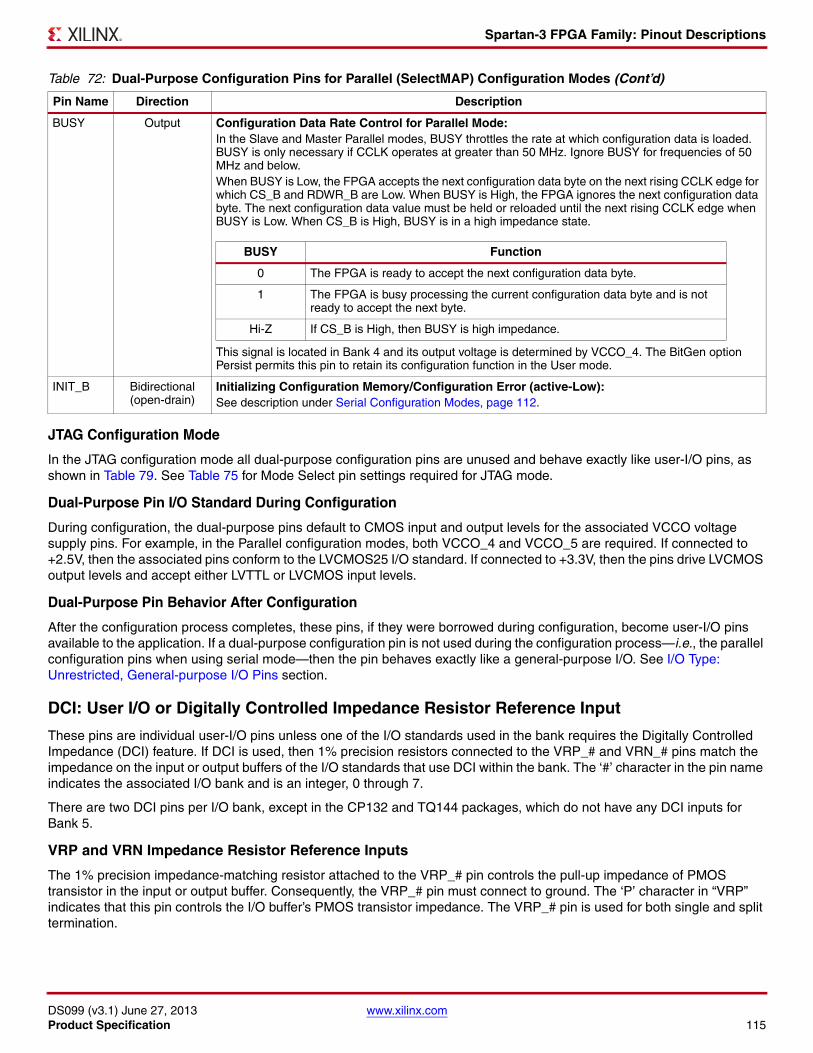
Spartan-3 FPGA Family: Pinout Descriptions
DS099 (v3.1) June 27, 2013 www.xilinx.comProduct Specification 115
JTAG Configuration Mode
In the JTAG configuration mode all dual-purpose configuration pins are unused and behave exactly like user-I/O pins, as shown in Table 79. See Table 75 for Mode Select pin settings required for JTAG mode.
Dual-Purpose Pin I/O Standard During Configuration
During configuration, the dual-purpose pins default to CMOS input and output levels for the associated VCCO voltage supply pins. For example, in the Parallel configuration modes, both VCCO_4 and VCCO_5 are required. If connected to +2.5V, then the associated pins conform to the LVCMOS25 I/O standard. If connected to +3.3V, then the pins drive LVCMOS output levels and accept either LVTTL or LVCMOS input levels.
Dual-Purpose Pin Behavior After Configuration
After the configuration process completes, these pins, if they were borrowed during configuration, become user-I/O pins available to the application. If a dual-purpose configuration pin is not used during the configuration process—i.e., the parallel configuration pins when using serial mode—then the pin behaves exactly like a general-purpose I/O. See I/O Type: Unrestricted, General-purpose I/O Pins section.
DCI: User I/O or Digitally Controlled Impedance Resistor Reference Input
These pins are individual user-I/O pins unless one of the I/O standards used in the bank requires the Digitally Controlled Impedance (DCI) feature. If DCI is used, then 1% precision resistors connected to the VRP_# and VRN_# pins match the impedance on the input or output buffers of the I/O standards that use DCI within the bank. The ‘#’ character in the pin name indicates the associated I/O bank and is an integer, 0 through 7.
There are two DCI pins per I/O bank, except in the CP132 and TQ144 packages, which do not have any DCI inputs forBank 5.
VRP and VRN Impedance Resistor Reference Inputs
The 1% precision impedance-matching resistor attached to the VRP_# pin controls the pull-up impedance of PMOS transistor in the input or output buffer. Consequently, the VRP_# pin must connect to ground. The ‘P’ character in “VRP” indicates that this pin controls the I/O buffer’s PMOS transistor impedance. The VRP_# pin is used for both single and split termination.
BUSY Output Configuration Data Rate Control for Parallel Mode:In the Slave and Master Parallel modes, BUSY throttles the rate at which configuration data is loaded. BUSY is only necessary if CCLK operates at greater than 50 MHz. Ignore BUSY for frequencies of 50 MHz and below.When BUSY is Low, the FPGA accepts the next configuration data byte on the next rising CCLK edge for which CS_B and RDWR_B are Low. When BUSY is High, the FPGA ignores the next configuration data byte. The next configuration data value must be held or reloaded until the next rising CCLK edge when BUSY is Low. When CS_B is High, BUSY is in a high impedance state.
This signal is located in Bank 4 and its output voltage is determined by VCCO_4. The BitGen option Persist permits this pin to retain its configuration function in the User mode.
INIT_B Bidirectional (open-drain)
Initializing Configuration Memory/Configuration Error (active-Low):See description under Serial Configuration Modes, page 112.
Table 72: Dual-Purpose Configuration Pins for Parallel (SelectMAP) Configuration Modes (Cont’d)
Pin Name Direction Description
BUSY Function
0 The FPGA is ready to accept the next configuration data byte.
1 The FPGA is busy processing the current configuration data byte and is not ready to accept the next byte.
Hi-Z If CS_B is High, then BUSY is high impedance.
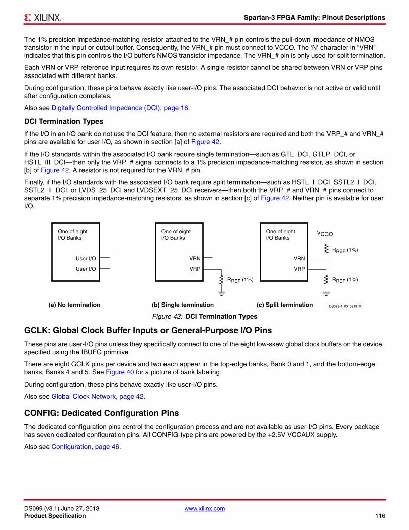
Spartan-3 FPGA Family: Pinout Descriptions
DS099 (v3.1) June 27, 2013 www.xilinx.comProduct Specification 116
The 1% precision impedance-matching resistor attached to the VRN_# pin controls the pull-down impedance of NMOS transistor in the input or output buffer. Consequently, the VRN_# pin must connect to VCCO. The ‘N’ character in “VRN” indicates that this pin controls the I/O buffer’s NMOS transistor impedance. The VRN_# pin is only used for split termination.
Each VRN or VRP reference input requires its own resistor. A single resistor cannot be shared between VRN or VRP pins associated with different banks.
During configuration, these pins behave exactly like user-I/O pins. The associated DCI behavior is not active or valid until after configuration completes.
Also see Digitally Controlled Impedance (DCI), page 16.
DCI Termination Types
If the I/O in an I/O bank do not use the DCI feature, then no external resistors are required and both the VRP_# and VRN_# pins are available for user I/O, as shown in section [a] of Figure 42.
If the I/O standards within the associated I/O bank require single termination—such as GTL_DCI, GTLP_DCI, or HSTL_III_DCI—then only the VRP_# signal connects to a 1% precision impedance-matching resistor, as shown in section [b] of Figure 42. A resistor is not required for the VRN_# pin.
Finally, if the I/O standards with the associated I/O bank require split termination—such as HSTL_I_DCI, SSTL2_I_DCI, SSTL2_II_DCI, or LVDS_25_DCI and LVDSEXT_25_DCI receivers—then both the VRP_# and VRN_# pins connect to separate 1% precision impedance-matching resistors, as shown in section [c] of Figure 42. Neither pin is available for user I/O.
GCLK: Global Clock Buffer Inputs or General-Purpose I/O Pins
These pins are user-I/O pins unless they specifically connect to one of the eight low-skew global clock buffers on the device, specified using the IBUFG primitive.
There are eight GCLK pins per device and two each appear in the top-edge banks, Bank 0 and 1, and the bottom-edge banks, Banks 4 and 5. See Figure 40 for a picture of bank labeling.
During configuration, these pins behave exactly like user-I/O pins.
Also see Global Clock Network, page 42.
CONFIG: Dedicated Configuration Pins
The dedicated configuration pins control the configuration process and are not available as user-I/O pins. Every package has seven dedicated configuration pins. All CONFIG-type pins are powered by the +2.5V VCCAUX supply.
Also see Configuration, page 46.
X-Ref Target - Figure 42
Figure 42: DCI Termination Types
DS099-4_03_091910
VCCO
VRN
VRP
One of eightI/O Banks
RREF (1%)
RREF (1%)
(c) Split termination
VRN
VRP
One of eightI/O Banks
RREF (1%)
(b) Single termination
User I/O
User I/O
One of eightI/O Banks
(a) No termination
Spartan-3 FPGA Family: Pinout Descriptions
DS099 (v3.1) June 27, 2013 www.xilinx.comProduct Specification 117
CCLK: Configuration Clock
The configuration clock signal on this pin synchronizes the reading or writing of configuration data. The CCLK pin is an input-only pin for the Slave Serial and Slave Parallel configuration modes. In the Master Serial and Master Parallel configuration modes, the FPGA drives the CCLK pin and CCLK should be treated as a full bidirectional I/O pin for signal integrity analysis.
Although the CCLK frequency is relatively low, Spartan-3 FPGA output edge rates are fast. Any potential signal integrity problems on the CCLK board trace can cause FPGA configuration to fail. Therefore, pay careful attention to the CCLK signal integrity on the printed circuit board. Signal integrity simulation with IBIS is recommended. For all configuration modes except JTAG, consider the signal integrity at every CCLK trace destination, including the FPGA’s CCLK pin. For more details on CCLK design considerations, see Chapter 2 of UG332, Spartan-3 Generation Configuration User Guide.
During configuration, the CCLK pin has a pull-up resistor to VCCAUX, regardless of the HSWAP_EN pin. After configuration, the CCLK pin is pulled High to VCCAUX by default as defined by the CclkPin bitstream selection, although this behavior is programmable. Any clocks applied to CCLK after configuration are ignored unless the bitstream option Persist is set to Yes, which retains the configuration interface. Persist is set to No by default. However, if Persist is set to Yes, then all clock edges are potentially active events, depending on the other configuration control signals.
The bitstream generator option ConfigRate determines the frequency of the internally-generated CCLK oscillator required for the Master configuration modes. The actual frequency is approximate due to the characteristics of the silicon oscillator and varies by up to 50% over the temperature and voltage range. By default, CCLK operates at approximately 6 MHz. Via the ConfigRate option, the oscillator frequency is set at approximately 3, 6, 12, 25, or 50 MHz. At power-on, CCLK always starts operation at its lowest frequency. The device does not start operating at the higher frequency until the ConfigRate control bits are loaded during the configuration process.
PROG_B: Program/Configure Device
This asynchronous pin initiates the configuration or re-configuration processes. A Low-going pulse resets the configuration logic, initializing the configuration memory. This initialization process cannot finish until PROG_B returns High. Asserting PROG_B Low for an extended period delays the configuration process. At power-up, there is always a pull-up resistor to VCCAUX on this pin, regardless of the HSWAP_EN input. After configuration, the bitstream generator option ProgPin determines whether or not the pull-up resistor is present. By default, the ProgPin option retains the pull-up resistor.
After configuration, hold the PROG_B input High. Any Low-going pulse on PROG_B lasting 300 ns or longer restarts the configuration process.
DONE: Configuration Done, Delay Start-Up Sequence
The FPGA produces a Low-to-High transition on this pin indicating that the configuration process is complete. The bitstream generator option DriveDone determines whether this pin functions as a totem-pole output that can drive High or as an open-drain output. If configured as an open-drain output—which is the default behavior—then a pull-up resistor is required to produce a High logic level. There is a bitstream option that provides an internal pull-up resistor, otherwise an external pull-up resistor is required.
The open-drain option permits the DONE lines of multiple FPGAs to be tied together, so that the common node transitions High only after all of the FPGAs have completed configuration. Externally holding the open-drain DONE pin Low delays the start-up sequence, which marks the transition to user mode.
Table 73: PROG_B Operation
PROG_B Input Response
Power-up Automatically initiates configuration process.
Low-going pulseInitiate (re-)configuration process and continue to completion.
Extended Low Initiate (re-)configuration process and stall process at step where configuration memory is cleared. Process is stalled until PROG_B returns High.
1 If the configuration process is started, continue to completion. If configuration process is complete, stay in User mode.
Spartan-3 FPGA Family: Pinout Descriptions
DS099 (v3.1) June 27, 2013 www.xilinx.comProduct Specification 118
Once the FPGA enters User mode after completing configuration, the DONE pin no longer drives the DONE pin Low. The bitstream generator option DonePin determines whether or not a pull-up resistor is present on the DONE pin to pull the pin to VCCAUX. If the pull-up resistor is eliminated, then the DONE pin must be pulled High using an external pull-up resistor or one of the FPGAs in the design must actively drive the DONE pin High via the DriveDone bitstream generator option.
The bitstream generator option DriveDone causes the FPGA to actively drive the DONE output High after configuration. This option should only be used in single-FPGA designs or on the last FPGA in a multi-FPGA daisy-chain.
By default, the bitstream generator software retains the pull-up resistor and does not actively drive the DONE pin as highlighted in Table 74, which shows the interaction of these bitstream options in single- and multi-FPGA designs.
M2, M1, M0: Configuration Mode Selection
The M2, M1, and M0 inputs select the FPGA configuration mode, as described in Table 75. The logic levels applied to the mode pins are sampled on the rising edge of INIT_B.
Before and during configuration, the mode pins have an internal pull-up resistor to VCCAUX, regardless of the HSWAP_EN pin. If the mode pins are unconnected, then the FPGA defaults to the Slave Serial configuration mode. After configuration successfully completes, any levels applied to these input are ignored. Furthermore, the bitstream generator options M0Pin, M1Pin, and M2Pin determines whether a pull-up resistor, pull-down resistor, or no resistor is present on its respective mode pin, M0, M1, or M2.
Table 74: DonePin and DriveDone Bitstream Option Interaction
DonePin DriveDone Single- or Multi- FPGA Design Comments
Pullnone No Single External pull-up resistor, with value between 330Ω to 3.3kΩ, required on DONE.
Pullnone No Multi External pull-up resistor, with value between 330Ω to 3.3kΩ, required on common node connecting to all DONE pins.
Pullnone Yes Single OK, no external requirements.
Pullnone Yes Multi DriveDone on last device in daisy-chain only. No external requirements.
Pullup No Single OK, but pull-up on DONE pin has slow rise time. May require 330Ω pull-up resistor for high CCLK frequencies.
Pullup No Multi External pull-up resistor, with value between 330Ω to 3.3kΩ, required on common node connecting to all DONE pins.
Pullup Yes Single OK, no external requirements.
Pullup Yes Multi DriveDone on last device in daisy-chain only. No external requirements.
Table 75: Spartan-3 FPGA Mode Select Settings
Configuration Mode M2 M1 M0
Master Serial 0 0 0
Slave Serial 1 1 1
Master Parallel 0 1 1
Slave Parallel 1 1 0
JTAG 1 0 1
Reserved 0 0 1
Reserved 0 1 0
Reserved 1 0 0
After Configuration X X X
Notes: 1. X = don’t care, either 0 or 1.
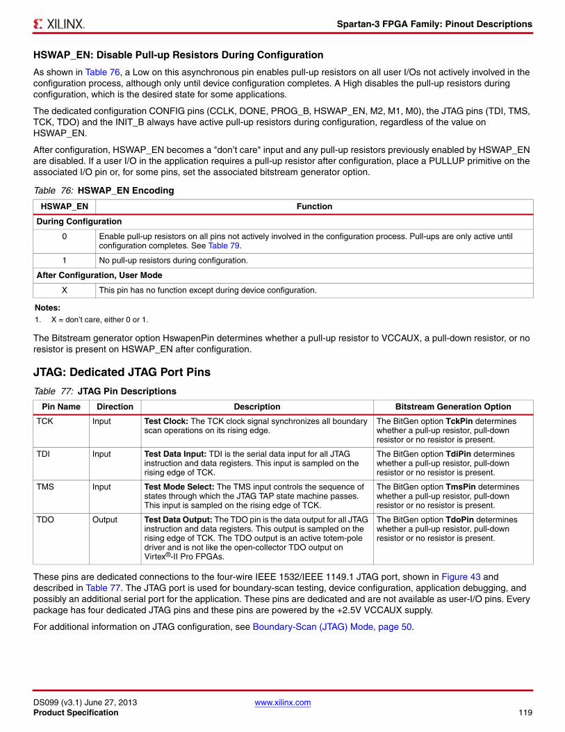
Spartan-3 FPGA Family: Pinout Descriptions
DS099 (v3.1) June 27, 2013 www.xilinx.comProduct Specification 119
HSWAP_EN: Disable Pull-up Resistors During Configuration
As shown in Table 76, a Low on this asynchronous pin enables pull-up resistors on all user I/Os not actively involved in the configuration process, although only until device configuration completes. A High disables the pull-up resistors during configuration, which is the desired state for some applications.
The dedicated configuration CONFIG pins (CCLK, DONE, PROG_B, HSWAP_EN, M2, M1, M0), the JTAG pins (TDI, TMS, TCK, TDO) and the INIT_B always have active pull-up resistors during configuration, regardless of the value on HSWAP_EN.
After configuration, HSWAP_EN becomes a "don’t care" input and any pull-up resistors previously enabled by HSWAP_EN are disabled. If a user I/O in the application requires a pull-up resistor after configuration, place a PULLUP primitive on the associated I/O pin or, for some pins, set the associated bitstream generator option.
The Bitstream generator option HswapenPin determines whether a pull-up resistor to VCCAUX, a pull-down resistor, or no resistor is present on HSWAP_EN after configuration.
JTAG: Dedicated JTAG Port Pins
These pins are dedicated connections to the four-wire IEEE 1532/IEEE 1149.1 JTAG port, shown in Figure 43 and described in Table 77. The JTAG port is used for boundary-scan testing, device configuration, application debugging, and possibly an additional serial port for the application. These pins are dedicated and are not available as user-I/O pins. Every package has four dedicated JTAG pins and these pins are powered by the +2.5V VCCAUX supply.
For additional information on JTAG configuration, see Boundary-Scan (JTAG) Mode, page 50.
Table 76: HSWAP_EN Encoding
HSWAP_EN Function
During Configuration
0 Enable pull-up resistors on all pins not actively involved in the configuration process. Pull-ups are only active until configuration completes. See Table 79.
1 No pull-up resistors during configuration.
After Configuration, User Mode
X This pin has no function except during device configuration.
Notes: 1. X = don’t care, either 0 or 1.
Table 77: JTAG Pin Descriptions
Pin Name Direction Description Bitstream Generation Option
TCK Input Test Clock: The TCK clock signal synchronizes all boundary scan operations on its rising edge.
The BitGen option TckPin determines whether a pull-up resistor, pull-down resistor or no resistor is present.
TDI Input Test Data Input: TDI is the serial data input for all JTAG instruction and data registers. This input is sampled on the rising edge of TCK.
The BitGen option TdiPin determines whether a pull-up resistor, pull-down resistor or no resistor is present.
TMS Input Test Mode Select: The TMS input controls the sequence of states through which the JTAG TAP state machine passes. This input is sampled on the rising edge of TCK.
The BitGen option TmsPin determines whether a pull-up resistor, pull-down resistor or no resistor is present.
TDO Output Test Data Output: The TDO pin is the data output for all JTAG instruction and data registers. This output is sampled on the rising edge of TCK. The TDO output is an active totem-pole driver and is not like the open-collector TDO output on Virtex®-II Pro FPGAs.
The BitGen option TdoPin determines whether a pull-up resistor, pull-down resistor or no resistor is present.
Spartan-3 FPGA Family: Pinout Descriptions
DS099 (v3.1) June 27, 2013 www.xilinx.comProduct Specification 120
IDCODE Register
Spartan-3 FPGAs contain a 32-bit identification register called the IDCODE register, as defined in the IEEE 1149.1 JTAG standard. The fixed value electrically identifies the manufacture (Xilinx) and the type of device being addressed over a JTAG chain. This register allows the JTAG host to identify the device being tested or programmed via JTAG. See Table 78.
Using JTAG Port After Configuration
The JTAG port is always active and available before, during, and after FPGA configuration. Add the BSCAN_SPARTAN3 primitive to the design to create user-defined JTAG instructions and JTAG chains to communicate with internal logic.
Furthermore, the contents of the User ID register within the JTAG port can be specified as a Bitstream Generation option. By default, the 32-bit User ID register contains 0xFFFFFFFF.
Precautions When Using the JTAG Port in 3.3V Environments
The JTAG port is powered by the +2.5V VCCAUX power supply. When connecting to a 3.3V interface, the JTAG input pins must be current-limited using a series resistor. Similarly, the TDO pin is a CMOS output powered from +2.5V. The TDO output can directly drive a 3.3V input but with reduced noise immunity. See 3.3V-Tolerant Configuration Interface, page 47. See also XAPP453: The 3.3V Configuration of Spartan-3 FPGAs for additional details.
The following interface precautions are recommended when connecting the JTAG port to a 3.3V interface.
• Avoid actively driving the JTAG input signals High with 3.3V signal levels. If required in the application, use series current-limiting resistors to keep the current below 10 mA per pin.
• If possible, drive the FPGA JTAG inputs with drivers that can be placed in high-impedance (Hi-Z) after using the JTAG port. Alternatively, drive the FPGA JTAG inputs with open-drain outputs, which only drive Low. In both cases, pull-up resistors are required. The FPGA JTAG pins have pull-up resistors to VCCAUX before configuration and optional pull-up resistors after configuration, controlled by Bitstream Options, page 125.
X-Ref Target - Figure 43
Figure 43: JTAG Port
Table 78: Spartan-3 JTAG IDCODE Register Values (hexadecimal)
Part Number IDCODE Register
XC3S50 0x0140C093
XC3S200 0x01414093
XC3S400 0x0141C093
XC3S1000 0x01428093
XC3S1500 0x01434093
XC3S2000 0x01440093
XC3S4000 0x01448093
XC3S5000 0x01450093
Data In Data Out
Mode Select
Clock
TDI
TMS
TCK
TDO
JTAG Port
DS099_4_04_020811
Spartan-3 FPGA Family: Pinout Descriptions
DS099 (v3.1) June 27, 2013 www.xilinx.comProduct Specification 121
VREF: User I/O or Input Buffer Reference Voltage for Special Interface Standards
These pins are individual user-I/O pins unless collectively they supply an input reference voltage, VREF_#, for any SSTL, HSTL, GTL, or GTLP I/Os implemented in the associated I/O bank. The ‘#’ character in the pin name represents an integer, 0 through 7, that indicates the associated I/O bank.
The VREF function becomes active for this pin whenever a signal standard requiring a reference voltage is used in the associated bank. If used as a user I/O, then each pin behaves as an independent I/O described in the I/O type section. If used for a reference voltage within a bank, then all VREF pins within the bank must be connected to the same reference voltage.
Spartan-3 devices are designed and characterized to support certain I/O standards when VREF is connected to +1.25V, +1.10V, +1.00V, +0.90V, +0.80V, and +0.75V. During configuration, the VREF pins behave exactly like user-I/O pins.
If designing for footprint compatibility across the range of devices in a specific package, and if the VREF_# pins within a bank connect to an input reference voltage, then also connect any N.C. (not connected) pins on the smaller devices in that package to the input reference voltage. More details are provided later for each package type.
N.C. Type: Unconnected Package Pins
Pins marked as “N.C.” are unconnected for the specific device/package combination. For other devices in this same package, this pin may be used as an I/O or VREF connection. In both the pinout tables and the footprint diagrams, unconnected pins are noted with either a black diamond symbol () or a black square symbol ().
If designing for footprint compatibility across multiple device densities, check the pin types of the other Spartan-3 devices available in the same footprint. If the N.C. pin matches to VREF pins in other devices, and the VREF pins are used in the associated I/O bank, then connect the N.C. to the VREF voltage source.
VCCO Type: Output Voltage Supply for I/O Bank
Each I/O bank has its own set of voltage supply pins that determines the output voltage for the output buffers in the I/O bank. Furthermore, for some I/O standards such as LVCMOS, LVCMOS25, LVTTL, etc., VCCO sets the input threshold voltage on the associated input buffers.
Spartan-3 devices are designed and characterized to support various I/O standards for VCCO values of +1.2V, +1.5V, +1.8V, +2.5V, and +3.3V.
Most VCCO pins are labeled as VCCO_# where the ‘#’ symbol represents the associated I/O bank number, an integer ranging from 0 to 7. In the 144-pin TQFP package (TQ144) however, the VCCO pins along an edge of the device are combined into a single VCCO input. For example, the VCCO inputs for Bank 0 and Bank 1 along the top edge of the package are combined and relabeled VCCO_TOP. The bottom, left, and right edges are similarly combined.
In Serial configuration mode, VCCO_4 must be at a level compatible with the attached configuration memory or data source. In Parallel configuration mode, both VCCO_4 and VCCO_5 must be at the same compatible voltage level.
All VCCO inputs to a bank must be connected together and to the voltage supply. Furthermore, there must be sufficient supply decoupling to guarantee problem-free operation, as described in XAPP623: Power Distribution System (PDS) Design: Using Bypass/Decoupling Capacitors.
VCCINT Type: Voltage Supply for Internal Core Logic
Internal core logic circuits such as the configurable logic blocks (CLBs) and programmable interconnect operate from the VCCINT voltage supply inputs. VCCINT must be +1.2V.
All VCCINT inputs must be connected together and to the +1.2V voltage supply. Furthermore, there must be sufficient supply decoupling to guarantee problem-free operation, as described in XAPP623.
VCCAUX Type: Voltage Supply for Auxiliary Logic
The VCCAUX pins supply power to various auxiliary circuits, such as to the Digital Clock Managers (DCMs), the JTAG pins, and to the dedicated configuration pins (CONFIG type). VCCAUX must be +2.5V.
Spartan-3 FPGA Family: Pinout Descriptions
DS099 (v3.1) June 27, 2013 www.xilinx.comProduct Specification 122
All VCCAUX inputs must be connected together and to the +2.5V voltage supply. Furthermore, there must be sufficient supply decoupling to guarantee problem-free operation, as described in XAPP623.
Because VCCAUX connects to the DCMs and the DCMs are sensitive to voltage changes, be sure that the VCCAUX supply and the ground return paths are designed for low noise and low voltage drop, especially that caused by a large number of simultaneous switching I/Os.
GND Type: Ground
All GND pins must be connected and have a low resistance path back to the various VCCO, VCCINT, and VCCAUX supplies.
Pin Behavior During ConfigurationTable 79 shows how various pins behave during the FPGA configuration process. The actual behavior depends on the values applied to the M2, M1, and M0 mode select pins and the HSWAP_EN pin. The mode select pins determine which of the DUAL type pins are active during configuration. In JTAG configuration mode, none of the DUAL-type pins are used for configuration and all behave as user-I/O pins.
All DUAL-type pins not actively used during configuration and all I/O-type, DCI-type, VREF-type, GCLK-type pins are high impedance (floating, three-stated, Hi-Z) during the configuration process. These pins are indicated in Table 79 as shaded table entries or cells. These pins have a pull-up resistor to their associated VCCO if the HSWAP_EN pin is Low. When HSWAP_EN is High, these pull-up resistors are disabled during configuration.
Some pins always have an active pull-up resistor during configuration, regardless of the value applied to the HSWAP_EN pin. After configuration, these pull-up resistors are controlled by Bitstream Options.
• All the dedicated CONFIG-type configuration pins (CCLK, PROG_B, DONE, M2, M1, M0, and HSWAP_EN) have a pull-up resistor to VCCAUX.
• All JTAG-type pins (TCK, TDI, TMS, TDO) have a pull-up resistor to VCCAUX.
• The INIT_B DUAL-purpose pin has a pull-up resistor to VCCO_4 or VCCO_BOTTOM, depending on package style.
After configuration completes, some pins have optional behavior controlled by the configuration bitstream loaded into the part. For example, via the bitstream, all unused I/O pins can be collectively configured as input pins with either a pull-up resistor, a pull-down resistor, or be left in a high-impedance state.
Table 79: Pin Behavior After Power-Up, During Configuration
Pin Name
Configuration Mode Settings <M2:M1:M0>Bitstream
Configuration Option
Serial Modes SelectMap Parallel Modes JTAG Mode <1:0:1>Master <0:0:0> Slave <1:1:1> Master <0:1:1> Slave <1:1:0>
I/O: General-purpose I/O pins
IO UnusedPin
IO_Lxxy_# UnusedPin
DUAL: Dual-purpose configuration pins
IO_Lxxy_#/DIN/D0
DIN (I) DIN (I) D0 (I/O) D0 (I/O) Persist UnusedPin
IO_Lxxy_#/D1
D1 (I/O) D1 (I/O) Persist UnusedPin
IO_Lxxy_#/D2
D2 (I/O) D2 (I/O) Persist UnusedPin
IO_Lxxy_#/D3
D3 (I/O) D3 (I/O) Persist UnusedPin
IO_Lxxy_#/D4
D4 (I/O) D4 (I/O) Persist UnusedPin
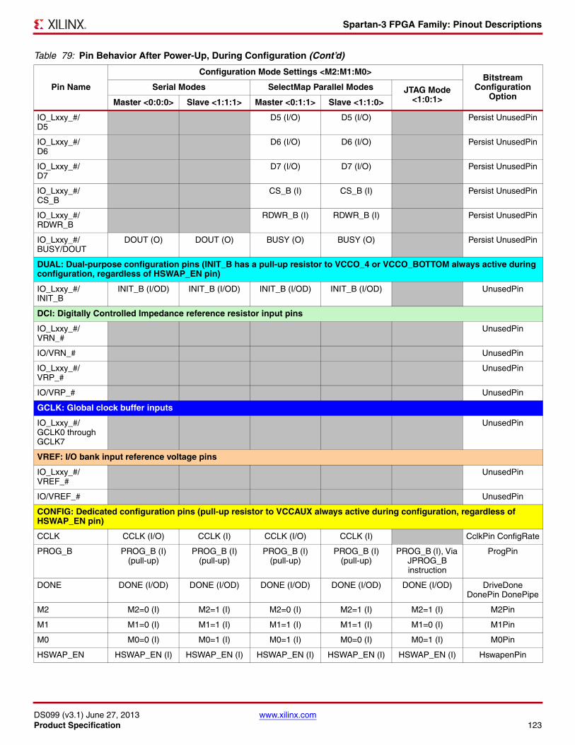
Spartan-3 FPGA Family: Pinout Descriptions
DS099 (v3.1) June 27, 2013 www.xilinx.comProduct Specification 123
IO_Lxxy_#/D5
D5 (I/O) D5 (I/O) Persist UnusedPin
IO_Lxxy_#/D6
D6 (I/O) D6 (I/O) Persist UnusedPin
IO_Lxxy_#/D7
D7 (I/O) D7 (I/O) Persist UnusedPin
IO_Lxxy_#/CS_B
CS_B (I) CS_B (I) Persist UnusedPin
IO_Lxxy_#/RDWR_B
RDWR_B (I) RDWR_B (I) Persist UnusedPin
IO_Lxxy_#/BUSY/DOUT
DOUT (O) DOUT (O) BUSY (O) BUSY (O) Persist UnusedPin
DUAL: Dual-purpose configuration pins (INIT_B has a pull-up resistor to VCCO_4 or VCCO_BOTTOM always active during configuration, regardless of HSWAP_EN pin)
IO_Lxxy_#/INIT_B
INIT_B (I/OD) INIT_B (I/OD) INIT_B (I/OD) INIT_B (I/OD) UnusedPin
DCI: Digitally Controlled Impedance reference resistor input pins
IO_Lxxy_#/VRN_#
UnusedPin
IO/VRN_# UnusedPin
IO_Lxxy_#/VRP_#
UnusedPin
IO/VRP_# UnusedPin
GCLK: Global clock buffer inputs
IO_Lxxy_#/ GCLK0 through GCLK7
UnusedPin
VREF: I/O bank input reference voltage pins
IO_Lxxy_#/VREF_#
UnusedPin
IO/VREF_# UnusedPin
CONFIG: Dedicated configuration pins (pull-up resistor to VCCAUX always active during configuration, regardless of HSWAP_EN pin)
CCLK CCLK (I/O) CCLK (I) CCLK (I/O) CCLK (I) CclkPin ConfigRate
PROG_B PROG_B (I) (pull-up)
PROG_B (I) (pull-up)
PROG_B (I) (pull-up)
PROG_B (I) (pull-up)
PROG_B (I), Via JPROG_B instruction
ProgPin
DONE DONE (I/OD) DONE (I/OD) DONE (I/OD) DONE (I/OD) DONE (I/OD) DriveDone DonePin DonePipe
M2 M2=0 (I) M2=1 (I) M2=0 (I) M2=1 (I) M2=1 (I) M2Pin
M1 M1=0 (I) M1=1 (I) M1=1 (I) M1=1 (I) M1=0 (I) M1Pin
M0 M0=0 (I) M0=1 (I) M0=1 (I) M0=0 (I) M0=1 (I) M0Pin
HSWAP_EN HSWAP_EN (I) HSWAP_EN (I) HSWAP_EN (I) HSWAP_EN (I) HSWAP_EN (I) HswapenPin
Table 79: Pin Behavior After Power-Up, During Configuration (Cont’d)
Pin Name
Configuration Mode Settings <M2:M1:M0>Bitstream
Configuration Option
Serial Modes SelectMap Parallel Modes JTAG Mode <1:0:1>Master <0:0:0> Slave <1:1:1> Master <0:1:1> Slave <1:1:0>
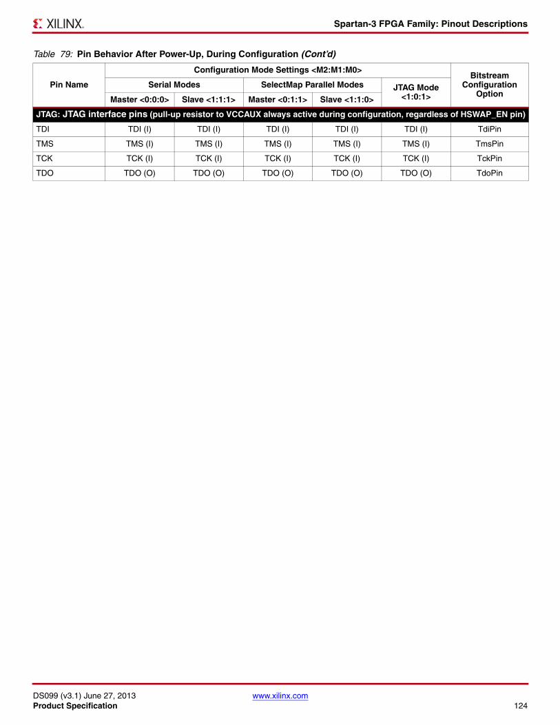
Spartan-3 FPGA Family: Pinout Descriptions
DS099 (v3.1) June 27, 2013 www.xilinx.comProduct Specification 124
JTAG: JTAG interface pins (pull-up resistor to VCCAUX always active during configuration, regardless of HSWAP_EN pin)
TDI TDI (I) TDI (I) TDI (I) TDI (I) TDI (I) TdiPin
TMS TMS (I) TMS (I) TMS (I) TMS (I) TMS (I) TmsPin
TCK TCK (I) TCK (I) TCK (I) TCK (I) TCK (I) TckPin
TDO TDO (O) TDO (O) TDO (O) TDO (O) TDO (O) TdoPin
Table 79: Pin Behavior After Power-Up, During Configuration (Cont’d)
Pin Name
Configuration Mode Settings <M2:M1:M0>Bitstream
Configuration Option
Serial Modes SelectMap Parallel Modes JTAG Mode <1:0:1>Master <0:0:0> Slave <1:1:1> Master <0:1:1> Slave <1:1:0>
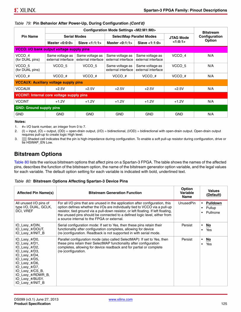
Spartan-3 FPGA Family: Pinout Descriptions
DS099 (v3.1) June 27, 2013 www.xilinx.comProduct Specification 125
Bitstream OptionsTable 80 lists the various bitstream options that affect pins on a Spartan-3 FPGA. The table shows the names of the affected pins, describes the function of the bitstream option, the name of the bitstream generator option variable, and the legal values for each variable. The default option setting for each variable is indicated with bold, underlined text.
VCCO: I/O bank output voltage supply pins
VCCO_4 (for DUAL pins)
Same voltage as external interface
Same voltage as external interface
Same voltage as external interface
Same voltage as external interface
VCCO_4 N/A
VCCO_5 (for DUAL pins)
VCCO_5 VCCO_5 Same voltage as external interface
Same voltage as external interface
VCCO_5 N/A
VCCO_# VCCO_# VCCO_# VCCO_# VCCO_# VCCO_# N/A
VCCAUX: Auxiliary voltage supply pins
VCCAUX +2.5V +2.5V +2.5V +2.5V +2.5V N/A
VCCINT: Internal core voltage supply pins
VCCINT +1.2V +1.2V +1.2V +1.2V +1.2V N/A
GND: Ground supply pins
GND GND GND GND GND GND N/A
Notes: 1. #= I/O bank number, an integer from 0 to 7.2. (I) = input, (O) = output, (OD) = open-drain output, (I/O) = bidirectional, (I/OD) = bidirectional with open-drain output. Open-drain output
requires pull-up to create logic High level.3. Shaded cell indicates that the pin is high-impedance during configuration. To enable a soft pull-up resistor during configuration, drive or
tie HSWAP_EN Low.
Table 80: Bitstream Options Affecting Spartan-3 Device Pins
Affected Pin Name(s) Bitstream Generation FunctionOption
Variable Name
Values (Default)
All unused I/O pins of type I/O, DUAL, GCLK, DCI, VREF
For all I/O pins that are unused in the application after configuration, this option defines whether the I/Os are individually tied to VCCO via a pull-up resistor, tied ground via a pull-down resistor, or left floating. If left floating, the unused pins should be connected to a defined logic level, either from a source internal to the FPGA or external.
UnusedPin • Pulldown • Pullup• Pullnone
IO_Lxxy_#/DIN, IO_Lxxy_#/DOUT, IO_Lxxy_#/INIT_B
Serial configuration mode: If set to Yes, then these pins retain their functionality after configuration completes, allowing for device (re-)configuration. Readback is not supported in with serial mode.
Persist • No • Yes
IO_Lxxy_#/D0, IO_Lxxy_#/D1, IO_Lxxy_#/D2, IO_Lxxy_#/D3, IO_Lxxy_#/D4, IO_Lxxy_#/D5, IO_Lxxy_#/D6, IO_Lxxy_#/D7, IO_Lxxy_#/CS_B, IO_Lxxy_#/RDWR_B, IO_Lxxy_#/BUSY, IO_Lxxy_#/INIT_B
Parallel configuration mode (also called SelectMAP): If set to Yes, then these pins retain their SelectMAP functionality after configuration completes, allowing for device readback and for partial or complete (re-)configuration.
Persist • No • Yes
Table 79: Pin Behavior After Power-Up, During Configuration (Cont’d)
Pin Name
Configuration Mode Settings <M2:M1:M0>Bitstream
Configuration Option
Serial Modes SelectMap Parallel Modes JTAG Mode <1:0:1>Master <0:0:0> Slave <1:1:1> Master <0:1:1> Slave <1:1:0>
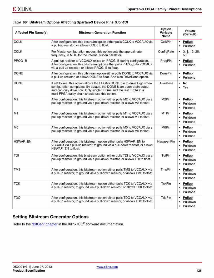
Spartan-3 FPGA Family: Pinout Descriptions
DS099 (v3.1) June 27, 2013 www.xilinx.comProduct Specification 126
Setting Bitstream Generator Options
Refer to the “BitGen” chapter in the Xilinx ISE® software documentation.
CCLK After configuration, this bitstream option either pulls CCLK to VCCAUX via a pull-up resistor, or allows CCLK to float.
CclkPin • Pullup • Pullnone
CCLK For Master configuration modes, this option sets the approximate frequency, in MHz, for the internal silicon oscillator.
ConfigRate • 3, 6, 12, 25, 50
PROG_B A pull-up resistor to VCCAUX exists on PROG_B during configuration. After configuration, this bitstream option either pulls PROG_B to VCCAUX via a pull-up resistor, or allows PROG_B to float.
ProgPin • Pullup • Pullnone
DONE After configuration, this bitstream option either pulls DONE to VCCAUX via a pull-up resistor, or allows DONE to float. See also DriveDone option.
DonePin • Pullup • Pullnone
DONE If set to Yes, this option allows the FPGA’s DONE pin to drive High when configuration completes. By default, the DONE is an open-drain output and can only drive Low. Only single FPGAs and the last FPGA in a multi-FPGA daisy-chain should use this option.
DriveDone • No • Yes
M2 After configuration, this bitstream option either pulls M2 to VCCAUX via a pull-up resistor, to ground via a pull-down resistor, or allows M2 to float.
M2Pin • Pullup • Pulldown• Pullnone
M1 After configuration, this bitstream option either pulls M1 to VCCAUX via a pull-up resistor, to ground via a pull-down resistor, or allows M1 to float.
M1Pin • Pullup • Pulldown• Pullnone
M0 After configuration, this bitstream option either pulls M0 to VCCAUX via a pull-up resistor, to ground via a pull-down resistor, or allows M0 to float.
M0Pin • Pullup • Pulldown• Pullnone
HSWAP_EN After configuration, this bitstream option either pulls HSWAP_EN to VCCAUX via a pull-up resistor, to ground via a pull-down resistor, or allows HSWAP_EN to float.
HswapenPin • Pullup • Pulldown• Pullnone
TDI After configuration, this bitstream option either pulls TDI to VCCAUX via a pull-up resistor, to ground via a pull-down resistor, or allows TDI to float.
TdiPin • Pullup • Pulldown• Pullnone
TMS After configuration, this bitstream option either pulls TMS to VCCAUX via a pull-up resistor, to ground via a pull-down resistor, or allows TMS to float.
TmsPin • Pullup • Pulldown• Pullnone
TCK After configuration, this bitstream option either pulls TCK to VCCAUX via a pull-up resistor, to ground via a pull-down resistor, or allows TCK to float.
TckPin • Pullup • Pulldown• Pullnone
TDO After configuration, this bitstream option either pulls TDO to VCCAUX via a pull-up resistor, to ground via a pull-down resistor, or allows TDO to float.
TdoPin • Pullup • Pulldown• Pullnone
Table 80: Bitstream Options Affecting Spartan-3 Device Pins (Cont’d)
Affected Pin Name(s) Bitstream Generation FunctionOption
Variable Name
Values (Default)
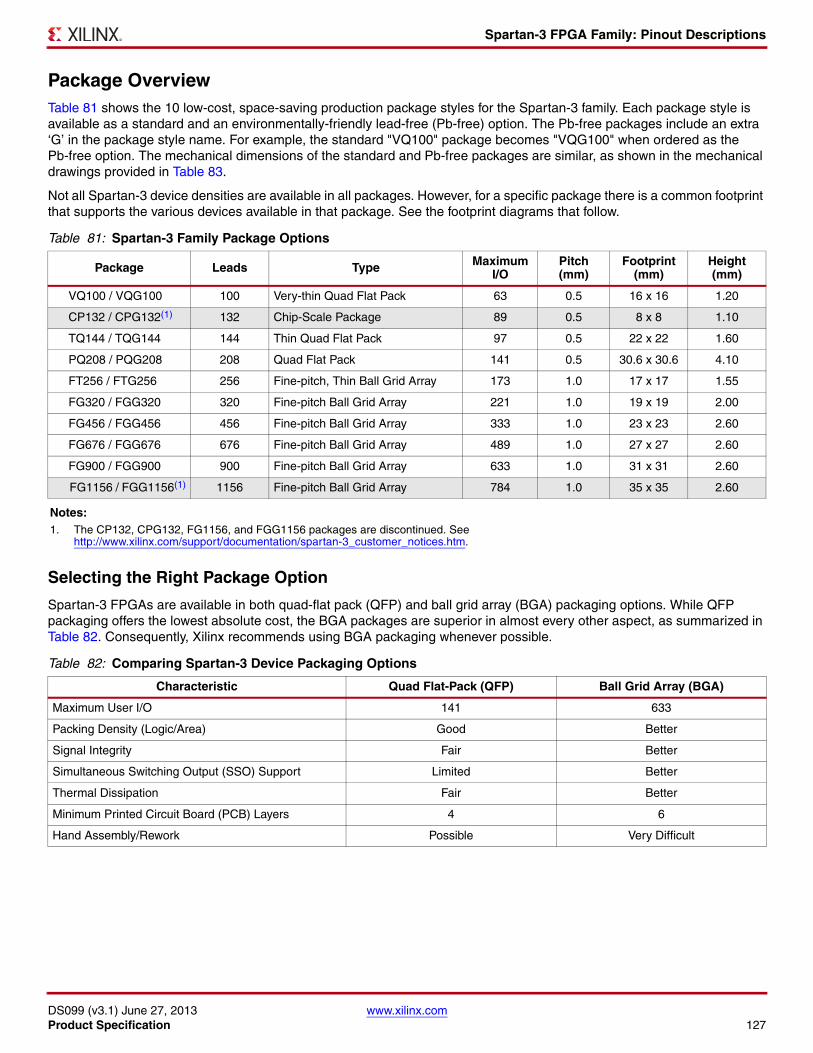
Spartan-3 FPGA Family: Pinout Descriptions
DS099 (v3.1) June 27, 2013 www.xilinx.comProduct Specification 127
Package OverviewTable 81 shows the 10 low-cost, space-saving production package styles for the Spartan-3 family. Each package style is available as a standard and an environmentally-friendly lead-free (Pb-free) option. The Pb-free packages include an extra ‘G’ in the package style name. For example, the standard "VQ100" package becomes "VQG100" when ordered as the Pb-free option. The mechanical dimensions of the standard and Pb-free packages are similar, as shown in the mechanical drawings provided in Table 83.
Not all Spartan-3 device densities are available in all packages. However, for a specific package there is a common footprint that supports the various devices available in that package. See the footprint diagrams that follow.
Selecting the Right Package Option
Spartan-3 FPGAs are available in both quad-flat pack (QFP) and ball grid array (BGA) packaging options. While QFP packaging offers the lowest absolute cost, the BGA packages are superior in almost every other aspect, as summarized in Table 82. Consequently, Xilinx recommends using BGA packaging whenever possible.
Table 81: Spartan-3 Family Package Options
Package Leads Type Maximum I/O
Pitch (mm)
Footprint(mm)
Height (mm)
VQ100 / VQG100 100 Very-thin Quad Flat Pack 63 0.5 16 x 16 1.20
CP132 / CPG132(1) 132 Chip-Scale Package 89 0.5 8 x 8 1.10
TQ144 / TQG144 144 Thin Quad Flat Pack 97 0.5 22 x 22 1.60
PQ208 / PQG208 208 Quad Flat Pack 141 0.5 30.6 x 30.6 4.10
FT256 / FTG256 256 Fine-pitch, Thin Ball Grid Array 173 1.0 17 x 17 1.55
FG320 / FGG320 320 Fine-pitch Ball Grid Array 221 1.0 19 x 19 2.00
FG456 / FGG456 456 Fine-pitch Ball Grid Array 333 1.0 23 x 23 2.60
FG676 / FGG676 676 Fine-pitch Ball Grid Array 489 1.0 27 x 27 2.60
FG900 / FGG900 900 Fine-pitch Ball Grid Array 633 1.0 31 x 31 2.60
FG1156 / FGG1156(1) 1156 Fine-pitch Ball Grid Array 784 1.0 35 x 35 2.60
Notes: 1. The CP132, CPG132, FG1156, and FGG1156 packages are discontinued. See
http://www.xilinx.com/support/documentation/spartan-3_customer_notices.htm.
Table 82: Comparing Spartan-3 Device Packaging Options
Characteristic Quad Flat-Pack (QFP) Ball Grid Array (BGA)
Maximum User I/O 141 633
Packing Density (Logic/Area) Good Better
Signal Integrity Fair Better
Simultaneous Switching Output (SSO) Support Limited Better
Thermal Dissipation Fair Better
Minimum Printed Circuit Board (PCB) Layers 4 6
Hand Assembly/Rework Possible Very Difficult
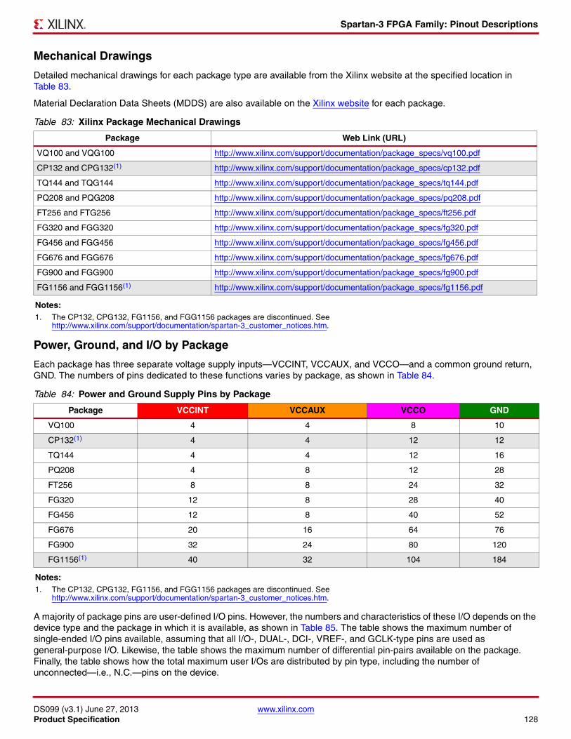
Spartan-3 FPGA Family: Pinout Descriptions
DS099 (v3.1) June 27, 2013 www.xilinx.comProduct Specification 128
Mechanical Drawings
Detailed mechanical drawings for each package type are available from the Xilinx website at the specified location in Table 83.
Material Declaration Data Sheets (MDDS) are also available on the Xilinx website for each package.
Power, Ground, and I/O by Package
Each package has three separate voltage supply inputs—VCCINT, VCCAUX, and VCCO—and a common ground return, GND. The numbers of pins dedicated to these functions varies by package, as shown in Table 84.
A majority of package pins are user-defined I/O pins. However, the numbers and characteristics of these I/O depends on the device type and the package in which it is available, as shown in Table 85. The table shows the maximum number of single-ended I/O pins available, assuming that all I/O-, DUAL-, DCI-, VREF-, and GCLK-type pins are used as general-purpose I/O. Likewise, the table shows the maximum number of differential pin-pairs available on the package. Finally, the table shows how the total maximum user I/Os are distributed by pin type, including the number of unconnected—i.e., N.C.—pins on the device.
Table 83: Xilinx Package Mechanical Drawings
Package Web Link (URL)
VQ100 and VQG100 http://www.xilinx.com/support/documentation/package_specs/vq100.pdf
CP132 and CPG132(1) http://www.xilinx.com/support/documentation/package_specs/cp132.pdf
TQ144 and TQG144 http://www.xilinx.com/support/documentation/package_specs/tq144.pdf
PQ208 and PQG208 http://www.xilinx.com/support/documentation/package_specs/pq208.pdf
FT256 and FTG256 http://www.xilinx.com/support/documentation/package_specs/ft256.pdf
FG320 and FGG320 http://www.xilinx.com/support/documentation/package_specs/fg320.pdf
FG456 and FGG456 http://www.xilinx.com/support/documentation/package_specs/fg456.pdf
FG676 and FGG676 http://www.xilinx.com/support/documentation/package_specs/fg676.pdf
FG900 and FGG900 http://www.xilinx.com/support/documentation/package_specs/fg900.pdf
FG1156 and FGG1156(1) http://www.xilinx.com/support/documentation/package_specs/fg1156.pdf
Notes: 1. The CP132, CPG132, FG1156, and FGG1156 packages are discontinued. See
http://www.xilinx.com/support/documentation/spartan-3_customer_notices.htm.
Table 84: Power and Ground Supply Pins by Package
Package VCCINT VCCAUX VCCO GND
VQ100 4 4 8 10
CP132(1) 4 4 12 12
TQ144 4 4 12 16
PQ208 4 8 12 28
FT256 8 8 24 32
FG320 12 8 28 40
FG456 12 8 40 52
FG676 20 16 64 76
FG900 32 24 80 120
FG1156(1) 40 32 104 184
Notes: 1. The CP132, CPG132, FG1156, and FGG1156 packages are discontinued. See
http://www.xilinx.com/support/documentation/spartan-3_customer_notices.htm.
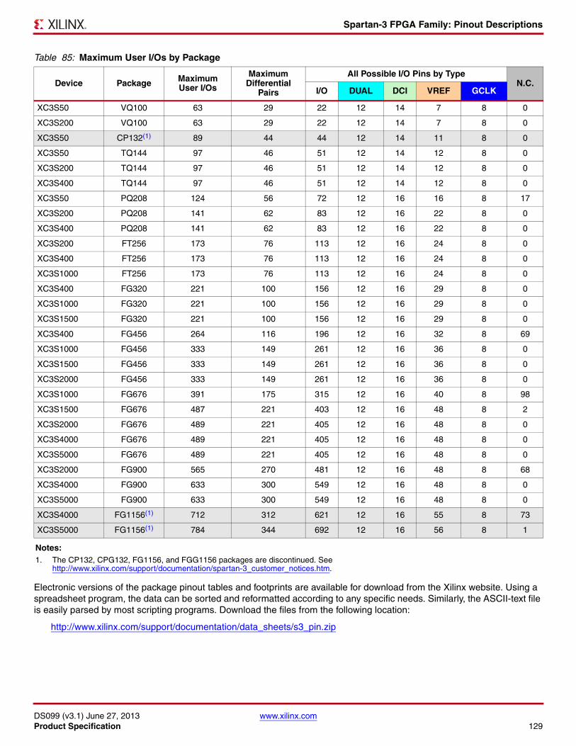
Spartan-3 FPGA Family: Pinout Descriptions
DS099 (v3.1) June 27, 2013 www.xilinx.comProduct Specification 129
Electronic versions of the package pinout tables and footprints are available for download from the Xilinx website. Using a spreadsheet program, the data can be sorted and reformatted according to any specific needs. Similarly, the ASCII-text file is easily parsed by most scripting programs. Download the files from the following location:
http://www.xilinx.com/support/documentation/data_sheets/s3_pin.zip
Table 85: Maximum User I/Os by Package
Device Package Maximum User I/Os
Maximum Differential
Pairs
All Possible I/O Pins by TypeN.C.
I/O DUAL DCI VREF GCLK
XC3S50 VQ100 63 29 22 12 14 7 8 0
XC3S200 VQ100 63 29 22 12 14 7 8 0
XC3S50 CP132(1) 89 44 44 12 14 11 8 0
XC3S50 TQ144 97 46 51 12 14 12 8 0
XC3S200 TQ144 97 46 51 12 14 12 8 0
XC3S400 TQ144 97 46 51 12 14 12 8 0
XC3S50 PQ208 124 56 72 12 16 16 8 17
XC3S200 PQ208 141 62 83 12 16 22 8 0
XC3S400 PQ208 141 62 83 12 16 22 8 0
XC3S200 FT256 173 76 113 12 16 24 8 0
XC3S400 FT256 173 76 113 12 16 24 8 0
XC3S1000 FT256 173 76 113 12 16 24 8 0
XC3S400 FG320 221 100 156 12 16 29 8 0
XC3S1000 FG320 221 100 156 12 16 29 8 0
XC3S1500 FG320 221 100 156 12 16 29 8 0
XC3S400 FG456 264 116 196 12 16 32 8 69
XC3S1000 FG456 333 149 261 12 16 36 8 0
XC3S1500 FG456 333 149 261 12 16 36 8 0
XC3S2000 FG456 333 149 261 12 16 36 8 0
XC3S1000 FG676 391 175 315 12 16 40 8 98
XC3S1500 FG676 487 221 403 12 16 48 8 2
XC3S2000 FG676 489 221 405 12 16 48 8 0
XC3S4000 FG676 489 221 405 12 16 48 8 0
XC3S5000 FG676 489 221 405 12 16 48 8 0
XC3S2000 FG900 565 270 481 12 16 48 8 68
XC3S4000 FG900 633 300 549 12 16 48 8 0
XC3S5000 FG900 633 300 549 12 16 48 8 0
XC3S4000 FG1156(1) 712 312 621 12 16 55 8 73
XC3S5000 FG1156(1) 784 344 692 12 16 56 8 1
Notes: 1. The CP132, CPG132, FG1156, and FGG1156 packages are discontinued. See
http://www.xilinx.com/support/documentation/spartan-3_customer_notices.htm.
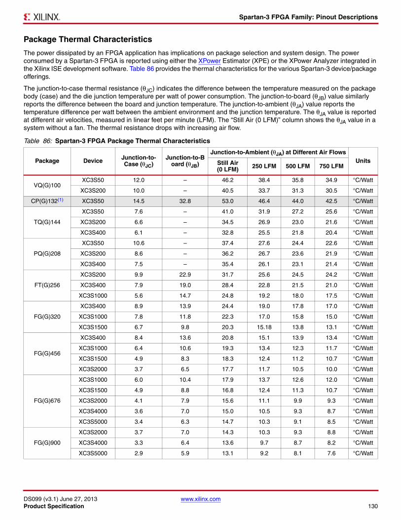
Spartan-3 FPGA Family: Pinout Descriptions
DS099 (v3.1) June 27, 2013 www.xilinx.comProduct Specification 130
Package Thermal Characteristics
The power dissipated by an FPGA application has implications on package selection and system design. The power consumed by a Spartan-3 FPGA is reported using either the XPower Estimator (XPE) or the XPower Analyzer integrated in the Xilinx ISE development software. Table 86 provides the thermal characteristics for the various Spartan-3 device/package offerings.
The junction-to-case thermal resistance (θJC) indicates the difference between the temperature measured on the package body (case) and the die junction temperature per watt of power consumption. The junction-to-board (θJB) value similarly reports the difference between the board and junction temperature. The junction-to-ambient (θJA) value reports the temperature difference per watt between the ambient environment and the junction temperature. The θJA value is reported at different air velocities, measured in linear feet per minute (LFM). The “Still Air (0 LFM)” column shows the θJA value in a system without a fan. The thermal resistance drops with increasing air flow.
Table 86: Spartan-3 FPGA Package Thermal Characteristics
Package Device Junction-to-Case (θJC)
Junction-to-Board (θJB)
Junction-to-Ambient (θJA) at Different Air FlowsUnitsStill Air
(0 LFM) 250 LFM 500 LFM 750 LFM
VQ(G)100XC3S50 12.0 – 46.2 38.4 35.8 34.9 °C/Watt
XC3S200 10.0 – 40.5 33.7 31.3 30.5 °C/Watt
CP(G)132(1) XC3S50 14.5 32.8 53.0 46.4 44.0 42.5 °C/Watt
TQ(G)144
XC3S50 7.6 – 41.0 31.9 27.2 25.6 °C/Watt
XC3S200 6.6 – 34.5 26.9 23.0 21.6 °C/Watt
XC3S400 6.1 – 32.8 25.5 21.8 20.4 °C/Watt
PQ(G)208
XC3S50 10.6 – 37.4 27.6 24.4 22.6 °C/Watt
XC3S200 8.6 – 36.2 26.7 23.6 21.9 °C/Watt
XC3S400 7.5 – 35.4 26.1 23.1 21.4 °C/Watt
FT(G)256
XC3S200 9.9 22.9 31.7 25.6 24.5 24.2 °C/Watt
XC3S400 7.9 19.0 28.4 22.8 21.5 21.0 °C/Watt
XC3S1000 5.6 14.7 24.8 19.2 18.0 17.5 °C/Watt
FG(G)320
XC3S400 8.9 13.9 24.4 19.0 17.8 17.0 °C/Watt
XC3S1000 7.8 11.8 22.3 17.0 15.8 15.0 °C/Watt
XC3S1500 6.7 9.8 20.3 15.18 13.8 13.1 °C/Watt
FG(G)456
XC3S400 8.4 13.6 20.8 15.1 13.9 13.4 °C/Watt
XC3S1000 6.4 10.6 19.3 13.4 12.3 11.7 °C/Watt
XC3S1500 4.9 8.3 18.3 12.4 11.2 10.7 °C/Watt
XC3S2000 3.7 6.5 17.7 11.7 10.5 10.0 °C/Watt
FG(G)676
XC3S1000 6.0 10.4 17.9 13.7 12.6 12.0 °C/Watt
XC3S1500 4.9 8.8 16.8 12.4 11.3 10.7 °C/Watt
XC3S2000 4.1 7.9 15.6 11.1 9.9 9.3 °C/Watt
XC3S4000 3.6 7.0 15.0 10.5 9.3 8.7 °C/Watt
XC3S5000 3.4 6.3 14.7 10.3 9.1 8.5 °C/Watt
FG(G)900
XC3S2000 3.7 7.0 14.3 10.3 9.3 8.8 °C/Watt
XC3S4000 3.3 6.4 13.6 9.7 8.7 8.2 °C/Watt
XC3S5000 2.9 5.9 13.1 9.2 8.1 7.6 °C/Watt
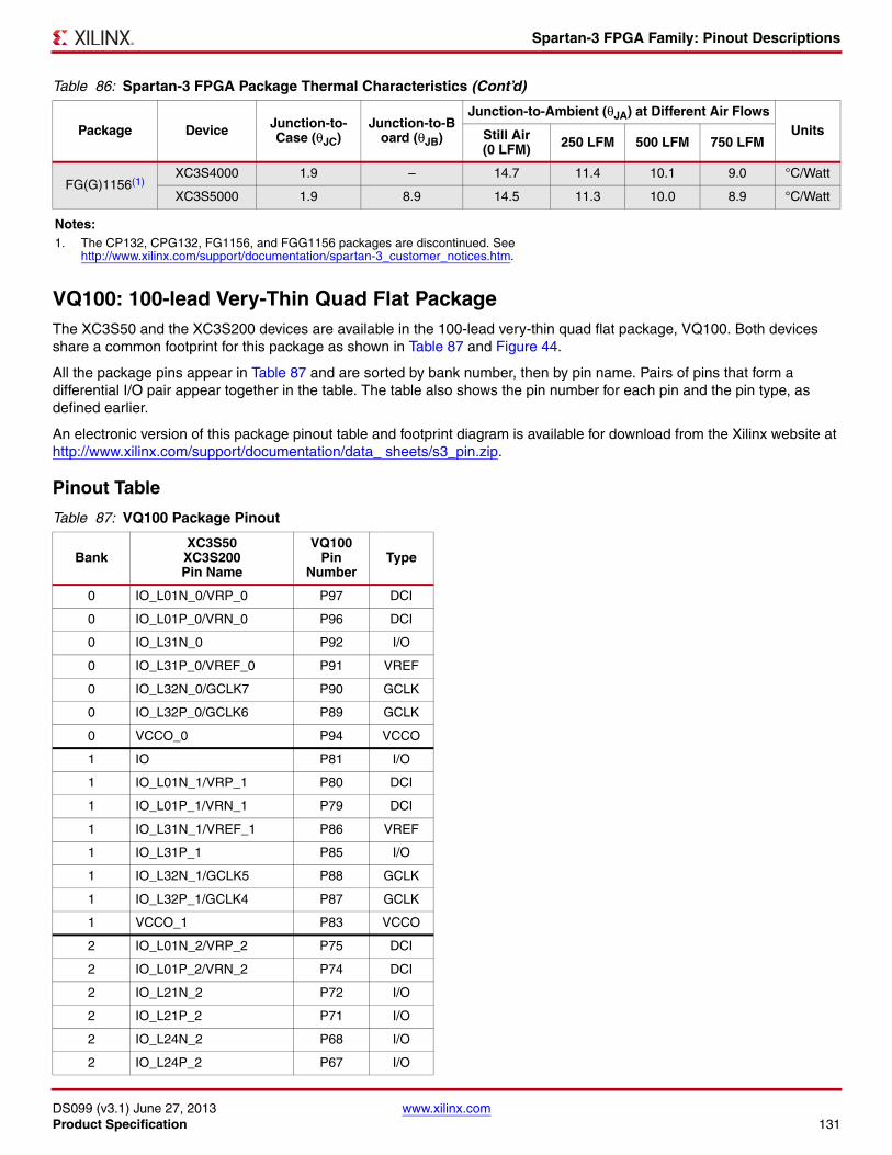
Spartan-3 FPGA Family: Pinout Descriptions
DS099 (v3.1) June 27, 2013 www.xilinx.comProduct Specification 131
VQ100: 100-lead Very-Thin Quad Flat PackageThe XC3S50 and the XC3S200 devices are available in the 100-lead very-thin quad flat package, VQ100. Both devices share a common footprint for this package as shown in Table 87 and Figure 44.
All the package pins appear in Table 87 and are sorted by bank number, then by pin name. Pairs of pins that form a differential I/O pair appear together in the table. The table also shows the pin number for each pin and the pin type, as defined earlier.
An electronic version of this package pinout table and footprint diagram is available for download from the Xilinx website at http://www.xilinx.com/support/documentation/data_ sheets/s3_pin.zip.
Pinout Table
FG(G)1156(1)XC3S4000 1.9 – 14.7 11.4 10.1 9.0 °C/Watt
XC3S5000 1.9 8.9 14.5 11.3 10.0 8.9 °C/Watt
Notes: 1. The CP132, CPG132, FG1156, and FGG1156 packages are discontinued. See
http://www.xilinx.com/support/documentation/spartan-3_customer_notices.htm.
Table 87: VQ100 Package Pinout
BankXC3S50XC3S200Pin Name
VQ100 Pin
NumberType
0 IO_L01N_0/VRP_0 P97 DCI
0 IO_L01P_0/VRN_0 P96 DCI
0 IO_L31N_0 P92 I/O
0 IO_L31P_0/VREF_0 P91 VREF
0 IO_L32N_0/GCLK7 P90 GCLK
0 IO_L32P_0/GCLK6 P89 GCLK
0 VCCO_0 P94 VCCO
1 IO P81 I/O
1 IO_L01N_1/VRP_1 P80 DCI
1 IO_L01P_1/VRN_1 P79 DCI
1 IO_L31N_1/VREF_1 P86 VREF
1 IO_L31P_1 P85 I/O
1 IO_L32N_1/GCLK5 P88 GCLK
1 IO_L32P_1/GCLK4 P87 GCLK
1 VCCO_1 P83 VCCO
2 IO_L01N_2/VRP_2 P75 DCI
2 IO_L01P_2/VRN_2 P74 DCI
2 IO_L21N_2 P72 I/O
2 IO_L21P_2 P71 I/O
2 IO_L24N_2 P68 I/O
2 IO_L24P_2 P67 I/O
Table 86: Spartan-3 FPGA Package Thermal Characteristics (Cont’d)
Package Device Junction-to-Case (θJC)
Junction-to-Board (θJB)
Junction-to-Ambient (θJA) at Different Air FlowsUnitsStill Air
(0 LFM) 250 LFM 500 LFM 750 LFM
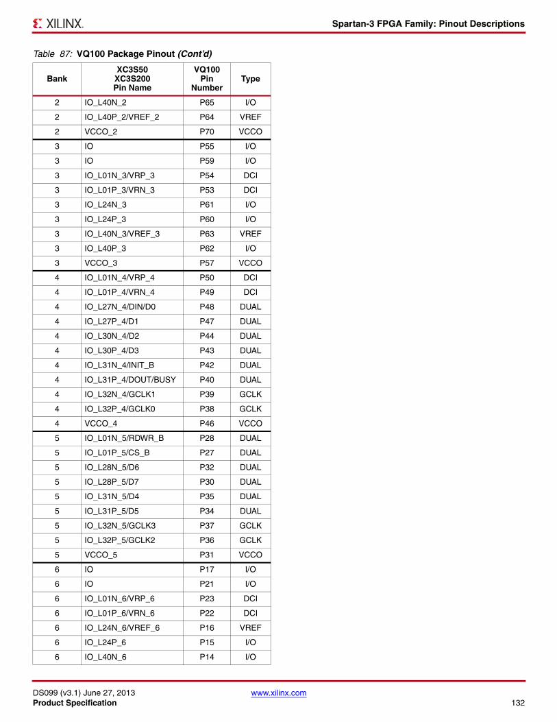
Spartan-3 FPGA Family: Pinout Descriptions
DS099 (v3.1) June 27, 2013 www.xilinx.comProduct Specification 132
2 IO_L40N_2 P65 I/O
2 IO_L40P_2/VREF_2 P64 VREF
2 VCCO_2 P70 VCCO
3 IO P55 I/O
3 IO P59 I/O
3 IO_L01N_3/VRP_3 P54 DCI
3 IO_L01P_3/VRN_3 P53 DCI
3 IO_L24N_3 P61 I/O
3 IO_L24P_3 P60 I/O
3 IO_L40N_3/VREF_3 P63 VREF
3 IO_L40P_3 P62 I/O
3 VCCO_3 P57 VCCO
4 IO_L01N_4/VRP_4 P50 DCI
4 IO_L01P_4/VRN_4 P49 DCI
4 IO_L27N_4/DIN/D0 P48 DUAL
4 IO_L27P_4/D1 P47 DUAL
4 IO_L30N_4/D2 P44 DUAL
4 IO_L30P_4/D3 P43 DUAL
4 IO_L31N_4/INIT_B P42 DUAL
4 IO_L31P_4/DOUT/BUSY P40 DUAL
4 IO_L32N_4/GCLK1 P39 GCLK
4 IO_L32P_4/GCLK0 P38 GCLK
4 VCCO_4 P46 VCCO
5 IO_L01N_5/RDWR_B P28 DUAL
5 IO_L01P_5/CS_B P27 DUAL
5 IO_L28N_5/D6 P32 DUAL
5 IO_L28P_5/D7 P30 DUAL
5 IO_L31N_5/D4 P35 DUAL
5 IO_L31P_5/D5 P34 DUAL
5 IO_L32N_5/GCLK3 P37 GCLK
5 IO_L32P_5/GCLK2 P36 GCLK
5 VCCO_5 P31 VCCO
6 IO P17 I/O
6 IO P21 I/O
6 IO_L01N_6/VRP_6 P23 DCI
6 IO_L01P_6/VRN_6 P22 DCI
6 IO_L24N_6/VREF_6 P16 VREF
6 IO_L24P_6 P15 I/O
6 IO_L40N_6 P14 I/O
Table 87: VQ100 Package Pinout (Cont’d)
BankXC3S50XC3S200Pin Name
VQ100 Pin
NumberType
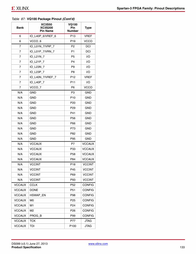
Spartan-3 FPGA Family: Pinout Descriptions
DS099 (v3.1) June 27, 2013 www.xilinx.comProduct Specification 133
6 IO_L40P_6/VREF_6 P13 VREF
6 VCCO_6 P19 VCCO
7 IO_L01N_7/VRP_7 P2 DCI
7 IO_L01P_7/VRN_7 P1 DCI
7 IO_L21N_7 P5 I/O
7 IO_L21P_7 P4 I/O
7 IO_L23N_7 P9 I/O
7 IO_L23P_7 P8 I/O
7 IO_L40N_7/VREF_7 P12 VREF
7 IO_L40P_7 P11 I/O
7 VCCO_7 P6 VCCO
N/A GND P3 GND
N/A GND P10 GND
N/A GND P20 GND
N/A GND P29 GND
N/A GND P41 GND
N/A GND P56 GND
N/A GND P66 GND
N/A GND P73 GND
N/A GND P82 GND
N/A GND P95 GND
N/A VCCAUX P7 VCCAUX
N/A VCCAUX P33 VCCAUX
N/A VCCAUX P58 VCCAUX
N/A VCCAUX P84 VCCAUX
N/A VCCINT P18 VCCINT
N/A VCCINT P45 VCCINT
N/A VCCINT P69 VCCINT
N/A VCCINT P93 VCCINT
VCCAUX CCLK P52 CONFIG
VCCAUX DONE P51 CONFIG
VCCAUX HSWAP_EN P98 CONFIG
VCCAUX M0 P25 CONFIG
VCCAUX M1 P24 CONFIG
VCCAUX M2 P26 CONFIG
VCCAUX PROG_B P99 CONFIG
VCCAUX TCK P77 JTAG
VCCAUX TDI P100 JTAG
Table 87: VQ100 Package Pinout (Cont’d)
BankXC3S50XC3S200Pin Name
VQ100 Pin
NumberType
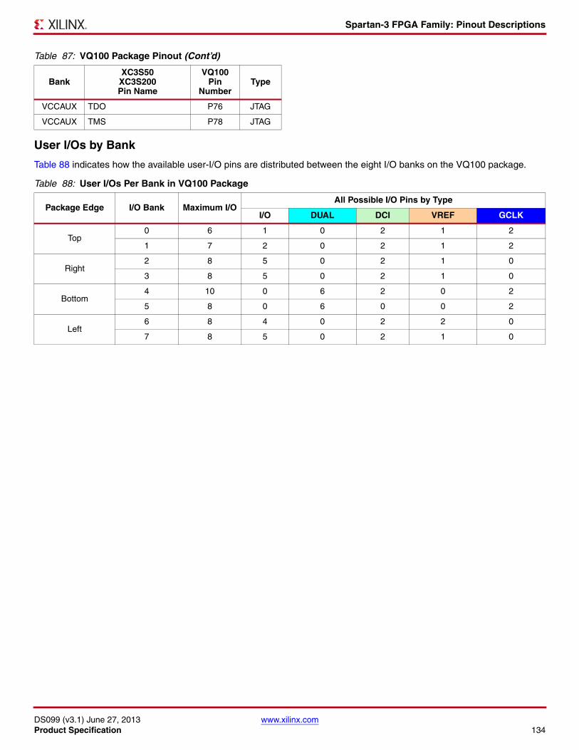
Spartan-3 FPGA Family: Pinout Descriptions
DS099 (v3.1) June 27, 2013 www.xilinx.comProduct Specification 134
User I/Os by Bank
Table 88 indicates how the available user-I/O pins are distributed between the eight I/O banks on the VQ100 package.
VCCAUX TDO P76 JTAG
VCCAUX TMS P78 JTAG
Table 88: User I/Os Per Bank in VQ100 Package
Package Edge I/O Bank Maximum I/OAll Possible I/O Pins by Type
I/O DUAL DCI VREF GCLK
Top0 6 1 0 2 1 2
1 7 2 0 2 1 2
Right2 8 5 0 2 1 0
3 8 5 0 2 1 0
Bottom4 10 0 6 2 0 2
5 8 0 6 0 0 2
Left6 8 4 0 2 2 0
7 8 5 0 2 1 0
Table 87: VQ100 Package Pinout (Cont’d)
BankXC3S50XC3S200Pin Name
VQ100 Pin
NumberType
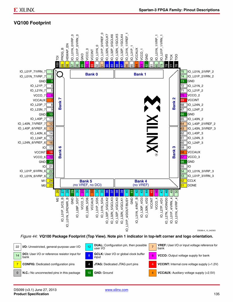
Spartan-3 FPGA Family: Pinout Descriptions
DS099 (v3.1) June 27, 2013 www.xilinx.comProduct Specification 135
VQ100 FootprintX-Ref Target - Figure 44
Figure 44: VQ100 Package Footprint (Top View). Note pin 1 indicator in top-left corner and logo orientation.
22 I/O: Unrestricted, general-purpose user I/O 12 DUAL: Configuration pin, then possible user I/O 7 VREF: User I/O or input voltage reference for
bank
14 DCI: User I/O or reference resistor input for bank 8 GCLK: User I/O or global clock buffer
input 8 VCCO: Output voltage supply for bank
7 CONFIG: Dedicated configuration pins 4 JTAG: Dedicated JTAG port pins 4 VCCINT: Internal core voltage supply (+1.2V)
0 N.C.: No unconnected pins in this package 10 GND: Ground 4 VCCAUX: Auxiliary voltage supply (+2.5V)
TD
I
PR
OG
_B
HS
WA
P_E
N
IO_L
01N
_0/V
RP
_0
IO_L
01P
_0/V
RN
_0
GN
D
VC
CO
_0
VC
CIN
T
IO_L
31N
_0
IO_L
31P
_0/V
RE
F_0
IO_L
32N
_0/G
CLK
7
IO_L
32P
_0/G
CLK
6
IO_L
32N
_1/G
CLK
5
IO_L
32P
_1/G
CLK
4
IO_L
31N
_1/V
RE
F_1
IO_L
31P
_1
VC
CA
UX
VC
CO
_1
GN
D
IO IO_L
01N
_1/V
RP
_1
IO_L
01P
_1/V
RN
_1
TM
S
TC
K
TD
O
100
99 98 97 96 95 94 93 92 91 90 89 88 87 86 85 84 83 82 81 80 79 78 77 76
1 75 IO_L01N_2/VRP_2
2 74 IO_L01P_2/VRN_2
3 73 GND
4 72 IO_L21N_2
5 71 IO_L21P_2
VCCO_7 6 70 VCCO_2
VCCAUX 7 69 VCCINT
8 68 IO_L24N_2
9 67 IO_L24P_2
10 66 GND
11 65 IO_L40N_2
12 64 IO_L40P_2/VREF_2
13 63 IO_L40N_3/VREF_3
14 62 IO_L40P_3
IO_L24P_6
IO_L40P_7
IO_L23P_7
IO_L21P_7
IO_L21N_7
IO_L23N_7
IO_L40N_6
15 61 IO_L24N_3
16 60 IO_L24P_3
IO 17 59 IO
VCCINT 18 58 VCCAUX
VCCO_6 19 57 VCCO_3
GND
GND
GND
IO_L01N_6/VRP_6
IO_L01P_6/VRN_6
IO_L24N_6/VREF_6
IO_L40N_7/VREF_7
IO_L01P_7/VRN_7
IO_L01N_7/VRP_7
IO_L40P_6/VREF_6
20 56 GND
IO 21 55 IO
22 54 IO_L01N_3/VRP_3
23 53 IO_L01P_3/VRN_3
M1 24 52 CCLK
M0 25 51 DONE
26 27 28 29 30 31 32 33 34 35 36 37 38 39 40 41 42 43 44 45 46 47 48 49 50
M2
IO_L
01P
_5/C
S_B
IO_L
01N
_5/R
DW
R_B
GN
D
IO_L
28P
_5/D
7
VC
CO
_5
IO_L
28N
_5/D
6
VC
CA
UX
IO_L
31P
_5/D
5
IO_L
31N
_5/D
4
IO_L
32P
_5/G
CLK
2
IO_L
32N
_5/G
CLK
3
IO_L
32P
_4/G
CLK
0
IO_L
32N
_4/G
CLK
1
GN
D
IO_L
31N
_4/IN
IT_B
IO_L
30P
_4/D
3
IO_L
30N
_4/D
2
VC
CIN
T
VC
CO
_4
IO_L
27P
_4/D
1
IO_L
27N
_4/D
IN/D
0
IO_L
31P
_4/D
OU
T/B
US
Y
IO_L
01P
_4/V
RN
_4
IO_L
01N
_4/V
RP
_4
Ban
k 6
Bank 0 Bank 1
Ban
k 3
Ban
k 2
Bank 4 (no VREF)
Bank 5(no VREF, no DCI)
Ban
k 7
DS099-4_15_042303
Spartan-3 FPGA Family: Pinout Descriptions
DS099 (v3.1) June 27, 2013 www.xilinx.comProduct Specification 136
CP132: 132-Ball Chip-Scale PackageNote: The CP132 and CPG132 packages are discontinued. See www.xilinx.com/support/documentation/spartan-3.htm#19600.
The pinout and footprint for the XC3S50 in the 132-ball chip-scale package, CP132, appear in Table 89 and Figure 45.
All the package pins appear in Table 89 and are sorted by bank number, then by pin name. Pins that form a differential I/O pair appear together in the table. The table also shows the pin number for each pin and the pin type, as defined earlier.
The CP132 footprint has eight I/O banks. However, the voltage supplies for the two I/O banks along an edge are connected together internally. Consequently, there are four output voltage supplies, labeled VCCO_TOP, VCCO_RIGHT, VCCO_BOTTOM, and VCCO_LEFT.
Pinout Table
Table 89: CP132 Package Pinout
Bank XC3S50 Pin Name CP132 Ball Type
0 IO_L01N_0/VRP_0 A3 DCI
0 IO_L01P_0/VRN_0 C4 DCI
0 IO_L27N_0 C5 I/O
0 IO_L27P_0 B5 I/O
0 IO_L30N_0 B6 I/O
0 IO_L30P_0 A6 I/O
0 IO_L31N_0 C7 I/O
0 IO_L31P_0/VREF_0 B7 VREF
0 IO_L32N_0/GCLK7 A7 GCLK
0 IO_L32P_0/GCLK6 C8 GCLK
1 IO_L01N_1/VRP_1 A13 DCI
1 IO_L01P_1/VRN_1 B13 DCI
1 IO_L27N_1 C11 I/O
1 IO_L27P_1 A12 I/O
1 IO_L28N_1 A11 I/O
1 IO_L28P_1 B11 I/O
1 IO_L31N_1/VREF_1 C9 VREF
1 IO_L31P_1 A10 I/O
1 IO_L32N_1/GCLK5 A8 GCLK
1 IO_L32P_1/GCLK4 A9 GCLK
2 IO_L01N_2/VRP_2 D12 DCI
2 IO_L01P_2/VRN_2 C14 DCI
2 IO_L20N_2 E12 I/O
2 IO_L20P_2 E13 I/O
2 IO_L21N_2 E14 I/O
2 IO_L21P_2 F12 I/O
2 IO_L23N_2/VREF_2 F13 VREF
2 IO_L23P_2 F14 I/O
2 IO_L24N_2 G12 I/O
Spartan-3 FPGA Family: Pinout Descriptions
DS099 (v3.1) June 27, 2013 www.xilinx.comProduct Specification 137
2 IO_L24P_2 G13 I/O
2 IO_L40N_2 G14 I/O
2 IO_L40P_2/VREF_2 H12 VREF
3 IO_L01N_3/VRP_3 N13 DCI
3 IO_L01P_3/VRN_3 N14 DCI
3 IO_L20N_3 L12 I/O
3 IO_L20P_3 M14 I/O
3 IO_L22N_3 L14 I/O
3 IO_L22P_3 L13 I/O
3 IO_L23N_3 K13 I/O
3 IO_L23P_3/VREF_3 K12 VREF
3 IO_L24N_3 J12 I/O
3 IO_L24P_3 K14 I/O
3 IO_L40N_3/VREF_3 H14 VREF
3 IO_L40P_3 J13 I/O
4 IO/VREF_4 N12 VREF
4 IO_L01N_4/VRP_4 P12 DCI
4 IO_L01P_4/VRN_4 M11 DCI
4 IO_L27N_4/DIN/D0 M10 DUAL
4 IO_L27P_4/D1 N10 DUAL
4 IO_L30N_4/D2 N9 DUAL
4 IO_L30P_4/D3 P9 DUAL
4 IO_L31N_4/INIT_B M8 DUAL
4 IO_L31P_4/DOUT/BUSY N8 DUAL
4 IO_L32N_4/GCLK1 P8 GCLK
4 IO_L32P_4/GCLK0 M7 GCLK
5 IO_L01N_5/RDWR_B P2 DUAL
5 IO_L01P_5/CS_B N2 DUAL
5 IO_L27N_5/VREF_5 M4 VREF
5 IO_L27P_5 P3 I/O
5 IO_L28N_5/D6 P4 DUAL
5 IO_L28P_5/D7 N4 DUAL
5 IO_L31N_5/D4 M6 DUAL
5 IO_L31P_5/D5 P5 DUAL
5 IO_L32N_5/GCLK3 P7 GCLK
5 IO_L32P_5/GCLK2 P6 GCLK
6 IO_L01N_6/VRP_6 L3 DCI
6 IO_L01P_6/VRN_6 M1 DCI
6 IO_L20N_6 K3 I/O
6 IO_L20P_6 K2 I/O
Table 89: CP132 Package Pinout (Cont’d)
Bank XC3S50 Pin Name CP132 Ball Type
Spartan-3 FPGA Family: Pinout Descriptions
DS099 (v3.1) June 27, 2013 www.xilinx.comProduct Specification 138
6 IO_L22N_6 K1 I/O
6 IO_L22P_6 J3 I/O
6 IO_L23N_6 J2 I/O
6 IO_L23P_6 J1 I/O
6 IO_L24N_6/VREF_6 H3 VREF
6 IO_L24P_6 H2 I/O
6 IO_L40N_6 H1 I/O
6 IO_L40P_6/VREF_6 G3 VREF
7 IO_L01N_7/VRP_7 B2 DCI
7 IO_L01P_7/VRN_7 B1 DCI
7 IO_L21N_7 C1 I/O
7 IO_L21P_7 D3 I/O
7 IO_L22N_7 D1 I/O
7 IO_L22P_7 D2 I/O
7 IO_L23N_7 E2 I/O
7 IO_L23P_7 E3 I/O
7 IO_L24N_7 F3 I/O
7 IO_L24P_7 E1 I/O
7 IO_L40N_7/VREF_7 G1 VREF
7 IO_L40P_7 F2 I/O
0,1 VCCO_TOP B12 VCCO
0,1 VCCO_TOP A4 VCCO
0,1 VCCO_TOP B8 VCCO
2,3 VCCO_RIGHT D13 VCCO
2,3 VCCO_RIGHT H13 VCCO
2,3 VCCO_RIGHT M12 VCCO
4,5 VCCO_BOTTOM N7 VCCO
4,5 VCCO_BOTTOM P11 VCCO
4,5 VCCO_BOTTOM N3 VCCO
6,7 VCCO_LEFT G2 VCCO
6,7 VCCO_LEFT L2 VCCO
6,7 VCCO_LEFT C3 VCCO
N/A GND B4 GND
N/A GND B9 GND
N/A GND C2 GND
N/A GND C12 GND
N/A GND D14 GND
N/A GND F1 GND
N/A GND J14 GND
N/A GND L1 GND
Table 89: CP132 Package Pinout (Cont’d)
Bank XC3S50 Pin Name CP132 Ball Type
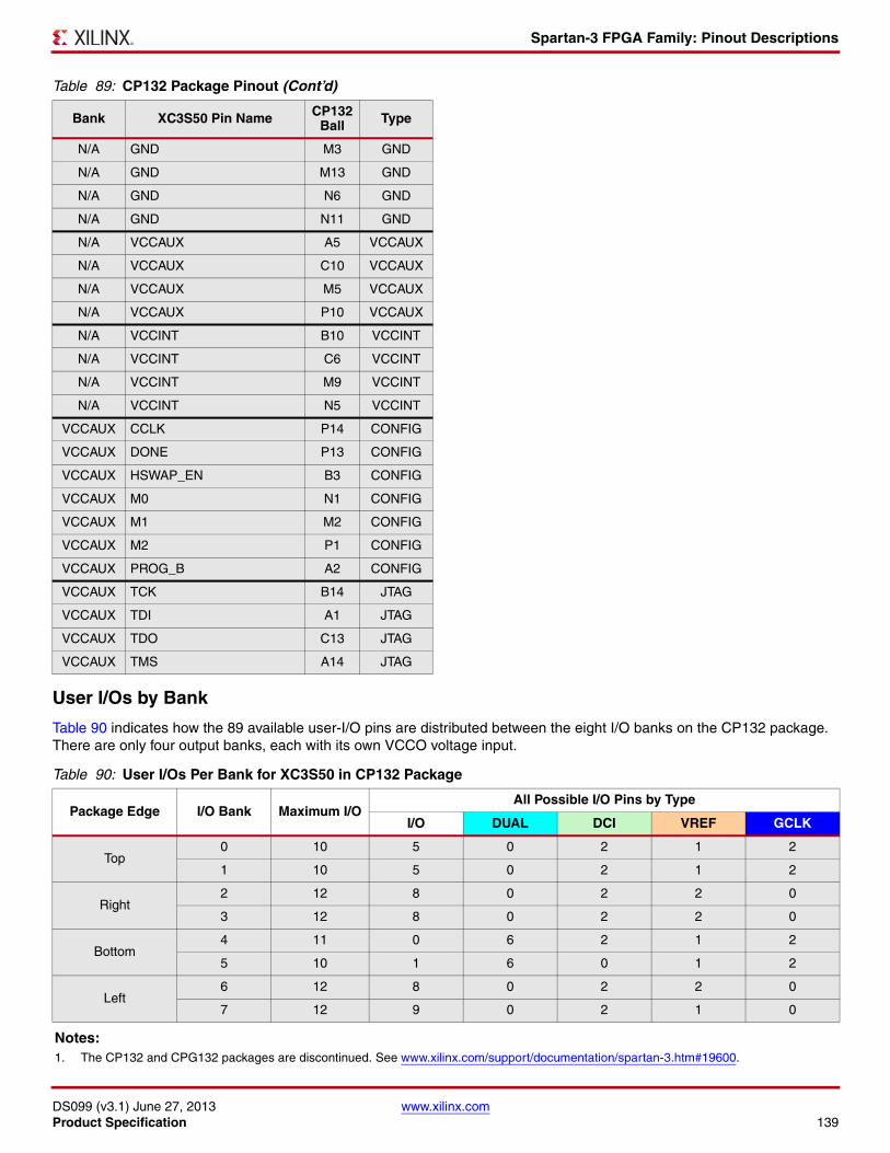
Spartan-3 FPGA Family: Pinout Descriptions
DS099 (v3.1) June 27, 2013 www.xilinx.comProduct Specification 139
User I/Os by Bank
Table 90 indicates how the 89 available user-I/O pins are distributed between the eight I/O banks on the CP132 package. There are only four output banks, each with its own VCCO voltage input.
N/A GND M3 GND
N/A GND M13 GND
N/A GND N6 GND
N/A GND N11 GND
N/A VCCAUX A5 VCCAUX
N/A VCCAUX C10 VCCAUX
N/A VCCAUX M5 VCCAUX
N/A VCCAUX P10 VCCAUX
N/A VCCINT B10 VCCINT
N/A VCCINT C6 VCCINT
N/A VCCINT M9 VCCINT
N/A VCCINT N5 VCCINT
VCCAUX CCLK P14 CONFIG
VCCAUX DONE P13 CONFIG
VCCAUX HSWAP_EN B3 CONFIG
VCCAUX M0 N1 CONFIG
VCCAUX M1 M2 CONFIG
VCCAUX M2 P1 CONFIG
VCCAUX PROG_B A2 CONFIG
VCCAUX TCK B14 JTAG
VCCAUX TDI A1 JTAG
VCCAUX TDO C13 JTAG
VCCAUX TMS A14 JTAG
Table 90: User I/Os Per Bank for XC3S50 in CP132 Package
Package Edge I/O Bank Maximum I/OAll Possible I/O Pins by Type
I/O DUAL DCI VREF GCLK
Top0 10 5 0 2 1 2
1 10 5 0 2 1 2
Right2 12 8 0 2 2 0
3 12 8 0 2 2 0
Bottom4 11 0 6 2 1 2
5 10 1 6 0 1 2
Left6 12 8 0 2 2 0
7 12 9 0 2 1 0
Notes: 1. The CP132 and CPG132 packages are discontinued. See www.xilinx.com/support/documentation/spartan-3.htm#19600.
Table 89: CP132 Package Pinout (Cont’d)
Bank XC3S50 Pin Name CP132 Ball Type
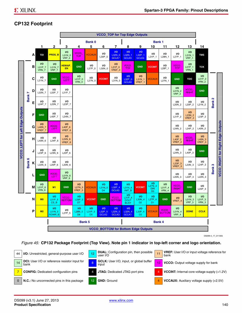
Spartan-3 FPGA Family: Pinout Descriptions
DS099 (v3.1) June 27, 2013 www.xilinx.comProduct Specification 140
CP132 FootprintX-Ref Target - Figure 45
Figure 45: CP132 Package Footprint (Top View). Note pin 1 indicator in top-left corner and logo orientation.
44 I/O: Unrestricted, general-purpose user I/O 12 DUAL: Configuration pin, then possible user I/O 11 VREF: User I/O or input voltage reference for
bank
14 DCI: User I/O or reference resistor input for bank 8 GCLK: User I/O, input, or global buffer
input 12 VCCO: Output voltage supply for bank
7 CONFIG: Dedicated configuration pins 4 JTAG: Dedicated JTAG port pins 4 VCCINT: Internal core voltage supply (+1.2V)
0 N.C.: No unconnected pins in this package 12 GND: Ground 4 VCCAUX: Auxiliary voltage supply (+2.5V)
1 2 3 4 5 6 7 8 9 10 11 12 13 14
A TDI PROG_BVRP_0
VRP_7
VRP_6
VRN_4
VRN_2
VRN_1
VRP_1
VRP_2
VRP_4
VRP_3 VRN_3
VRN_6
VRN_7
VRN_0
VCCO_TOP
VCCO_TOP
VCCO_TOP
VCCO_RIGHT
VCCO_RIGHT
VCCO_RIGHT
VCCO_BOTTOM
VCCO_BOTTOM
VCCO_BOTTOM
VCCO_LEFT
VCCO_LEFT
VCCO_LEFT
VCCAUX
VCCAUX
VCCAUX
VCCAUX
GCLK7 GCLK5
GCLK6
GCLK0
GCLK2 GCLK3 GCLK1
GCLK4TMS
BI/O
I/O
I/O I/O I/O
I/O I/O I/O
I/O I/O I/O
I/O I/O
I/O I/O
I/O
I/O I/O
I/O
I/O
I/O
I/O I/O I/O I/O
I/O I/O I/O I/O I/O
I/OI/O
I/OI/O
I/O
I/O
I/O
I/O
I/O I/O
I/O I/O
I/O
I/O
I/O
I/O
I/O
I/OI/OI/O
I/O
I/OI/O
I/O
I/O
I/O
I/OI/O
I/O
I/O
I/O I/OI/OI/OI/O
I/O
I/O
I/O
I/O I/O
I/O I/O
I/O
I/O I/OI/O
I/OI/O
I/O I/O I/O I/O I/OI/O I/O
I/O
I/O
I/OI/O
HSWAP_EN
VCCINT
VCCINT
VCCINT
VCCINT
TCK
C GND
GND GND
GND
GND
GND
GND
GNDGND
GND
GND
GND
TDO
DL22N_7 L22P_7 L21P_7
L21N_7
L23P_7L24P_7 L23N_7
L24N_7L40P_7
L40P_6L40N_7
L24N_6
L27N_5 L31N_5 L31N_4
L31P_4
L30P_4
L30N_4
L27N_4L01P_4
L01N_4
L01N_3 L01P_3L27P_4
L40N_6 L24P_6
L23P_6 L22P_6
L27P_5
L22N_6 L20P_6 L20N_6
L01N_6
L01P_6
L01P_5
L01N_5 L28N_5 L31P_5
L28P_5
L23N_6
E
F
GVREF_7 VREF_6
VREF_6
VREF_5
VREF_3
VREF_3VREF_2
VREF_2
VREF_1
VREF_0
VREF_4
H
J
K
L
M M1D4 INIT_B
DIND0
L20P_3
L24P_3
L22N_3
L23N_3
L20N_3
L23P_3
L40P_2
L23N_2
L40N_3
L24N_3
L24N_2
L20N_2
L01N_2
L01P_2
L01P_1
L01N_1
L21N_2
L27N_1
L27P_1L31P_1L30P_0
L27P_0
L27N_0
L30N_0
L31N_0 L31N_1L01P_0
L01N_0
L01N_7L01P_7 L31P_0
L32N_0
L32P_0
L32P_4
L32P_5 L32N_5 L32N_4
L32N_1 L32P_1
L28P_1
L28N_1
L20P_2
L40N_2L24P_2
L23P_2L21P_2
L40P_3
L22P_3
N M0CS_B D7
DOUTBUSY D2 D1
P M2RDWR_B D6 D5 D3
DONE CCLK
VCCO_BOTTOM for Bottom Edge Outputs
VCCO_TOP for Top Edge Outputs
VC
CO
_RIG
HT
fo
r R
igh
t E
dg
e O
utp
uts
VC
CO
_LE
FT
fo
r L
eft
Ed
ge
Ou
tpu
ts
Bank 5 Bank 4
Ban
k 2
Ban
k 3
Ban
k 7
Ban
k 6
Bank 0 Bank 1
DS099-4_17_011005
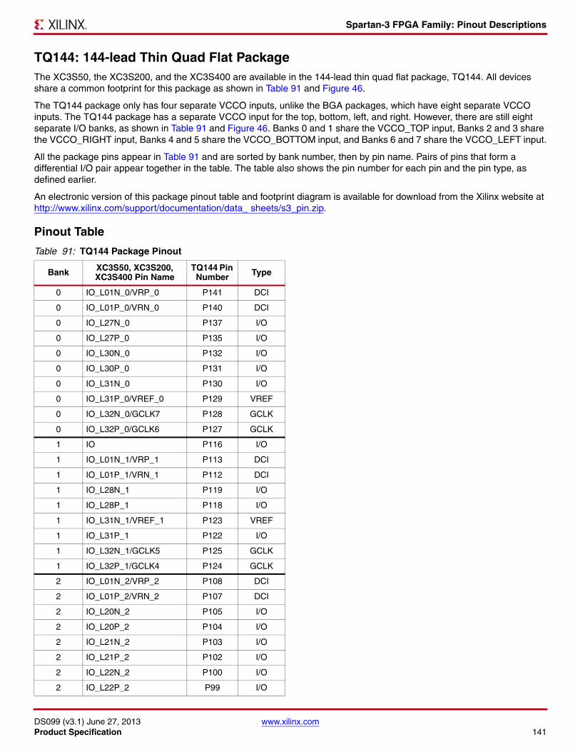
Spartan-3 FPGA Family: Pinout Descriptions
DS099 (v3.1) June 27, 2013 www.xilinx.comProduct Specification 141
TQ144: 144-lead Thin Quad Flat PackageThe XC3S50, the XC3S200, and the XC3S400 are available in the 144-lead thin quad flat package, TQ144. All devices share a common footprint for this package as shown in Table 91 and Figure 46.
The TQ144 package only has four separate VCCO inputs, unlike the BGA packages, which have eight separate VCCO inputs. The TQ144 package has a separate VCCO input for the top, bottom, left, and right. However, there are still eight separate I/O banks, as shown in Table 91 and Figure 46. Banks 0 and 1 share the VCCO_TOP input, Banks 2 and 3 share the VCCO_RIGHT input, Banks 4 and 5 share the VCCO_BOTTOM input, and Banks 6 and 7 share the VCCO_LEFT input.
All the package pins appear in Table 91 and are sorted by bank number, then by pin name. Pairs of pins that form a differential I/O pair appear together in the table. The table also shows the pin number for each pin and the pin type, as defined earlier.
An electronic version of this package pinout table and footprint diagram is available for download from the Xilinx website at http://www.xilinx.com/support/documentation/data_ sheets/s3_pin.zip.
Pinout Table
Table 91: TQ144 Package Pinout
Bank XC3S50, XC3S200, XC3S400 Pin Name
TQ144 Pin Number Type
0 IO_L01N_0/VRP_0 P141 DCI
0 IO_L01P_0/VRN_0 P140 DCI
0 IO_L27N_0 P137 I/O
0 IO_L27P_0 P135 I/O
0 IO_L30N_0 P132 I/O
0 IO_L30P_0 P131 I/O
0 IO_L31N_0 P130 I/O
0 IO_L31P_0/VREF_0 P129 VREF
0 IO_L32N_0/GCLK7 P128 GCLK
0 IO_L32P_0/GCLK6 P127 GCLK
1 IO P116 I/O
1 IO_L01N_1/VRP_1 P113 DCI
1 IO_L01P_1/VRN_1 P112 DCI
1 IO_L28N_1 P119 I/O
1 IO_L28P_1 P118 I/O
1 IO_L31N_1/VREF_1 P123 VREF
1 IO_L31P_1 P122 I/O
1 IO_L32N_1/GCLK5 P125 GCLK
1 IO_L32P_1/GCLK4 P124 GCLK
2 IO_L01N_2/VRP_2 P108 DCI
2 IO_L01P_2/VRN_2 P107 DCI
2 IO_L20N_2 P105 I/O
2 IO_L20P_2 P104 I/O
2 IO_L21N_2 P103 I/O
2 IO_L21P_2 P102 I/O
2 IO_L22N_2 P100 I/O
2 IO_L22P_2 P99 I/O
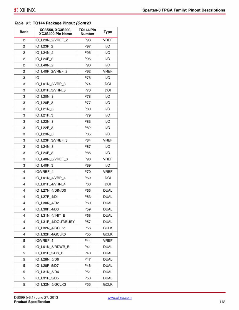
Spartan-3 FPGA Family: Pinout Descriptions
DS099 (v3.1) June 27, 2013 www.xilinx.comProduct Specification 142
2 IO_L23N_2/VREF_2 P98 VREF
2 IO_L23P_2 P97 I/O
2 IO_L24N_2 P96 I/O
2 IO_L24P_2 P95 I/O
2 IO_L40N_2 P93 I/O
2 IO_L40P_2/VREF_2 P92 VREF
3 IO P76 I/O
3 IO_L01N_3/VRP_3 P74 DCI
3 IO_L01P_3/VRN_3 P73 DCI
3 IO_L20N_3 P78 I/O
3 IO_L20P_3 P77 I/O
3 IO_L21N_3 P80 I/O
3 IO_L21P_3 P79 I/O
3 IO_L22N_3 P83 I/O
3 IO_L22P_3 P82 I/O
3 IO_L23N_3 P85 I/O
3 IO_L23P_3/VREF_3 P84 VREF
3 IO_L24N_3 P87 I/O
3 IO_L24P_3 P86 I/O
3 IO_L40N_3/VREF_3 P90 VREF
3 IO_L40P_3 P89 I/O
4 IO/VREF_4 P70 VREF
4 IO_L01N_4/VRP_4 P69 DCI
4 IO_L01P_4/VRN_4 P68 DCI
4 IO_L27N_4/DIN/D0 P65 DUAL
4 IO_L27P_4/D1 P63 DUAL
4 IO_L30N_4/D2 P60 DUAL
4 IO_L30P_4/D3 P59 DUAL
4 IO_L31N_4/INIT_B P58 DUAL
4 IO_L31P_4/DOUT/BUSY P57 DUAL
4 IO_L32N_4/GCLK1 P56 GCLK
4 IO_L32P_4/GCLK0 P55 GCLK
5 IO/VREF_5 P44 VREF
5 IO_L01N_5/RDWR_B P41 DUAL
5 IO_L01P_5/CS_B P40 DUAL
5 IO_L28N_5/D6 P47 DUAL
5 IO_L28P_5/D7 P46 DUAL
5 IO_L31N_5/D4 P51 DUAL
5 IO_L31P_5/D5 P50 DUAL
5 IO_L32N_5/GCLK3 P53 GCLK
Table 91: TQ144 Package Pinout (Cont’d)
Bank XC3S50, XC3S200, XC3S400 Pin Name
TQ144 Pin Number Type
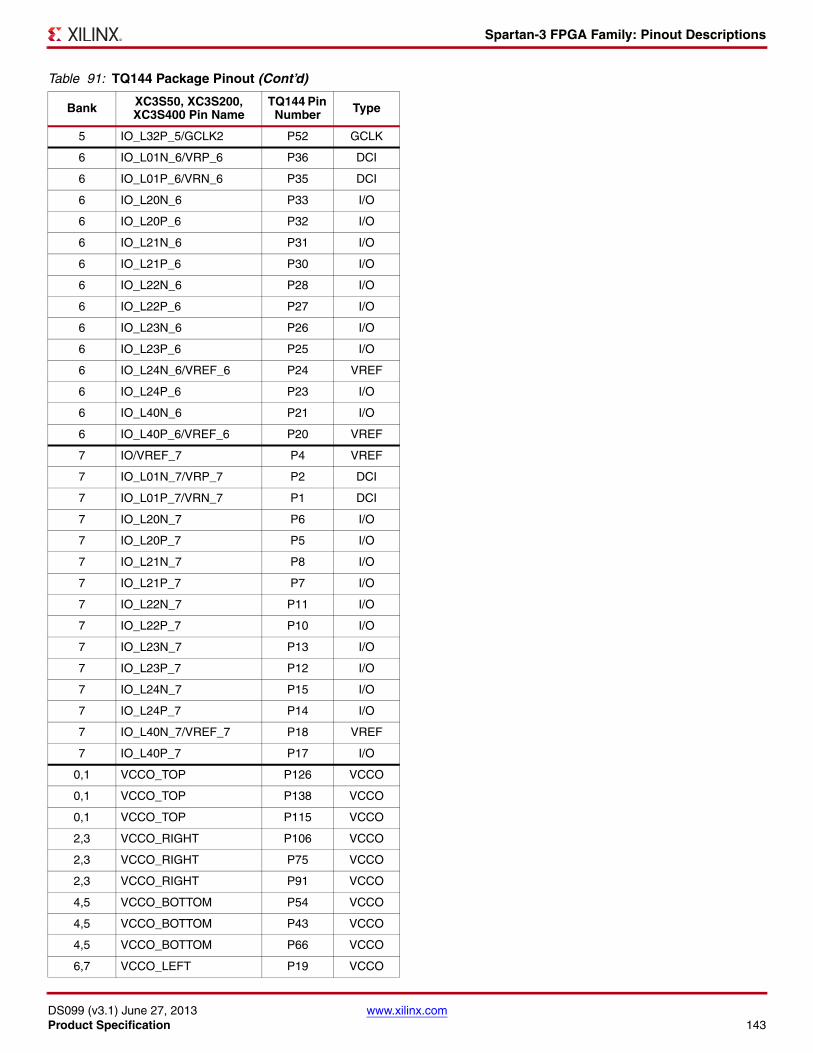
Spartan-3 FPGA Family: Pinout Descriptions
DS099 (v3.1) June 27, 2013 www.xilinx.comProduct Specification 143
5 IO_L32P_5/GCLK2 P52 GCLK
6 IO_L01N_6/VRP_6 P36 DCI
6 IO_L01P_6/VRN_6 P35 DCI
6 IO_L20N_6 P33 I/O
6 IO_L20P_6 P32 I/O
6 IO_L21N_6 P31 I/O
6 IO_L21P_6 P30 I/O
6 IO_L22N_6 P28 I/O
6 IO_L22P_6 P27 I/O
6 IO_L23N_6 P26 I/O
6 IO_L23P_6 P25 I/O
6 IO_L24N_6/VREF_6 P24 VREF
6 IO_L24P_6 P23 I/O
6 IO_L40N_6 P21 I/O
6 IO_L40P_6/VREF_6 P20 VREF
7 IO/VREF_7 P4 VREF
7 IO_L01N_7/VRP_7 P2 DCI
7 IO_L01P_7/VRN_7 P1 DCI
7 IO_L20N_7 P6 I/O
7 IO_L20P_7 P5 I/O
7 IO_L21N_7 P8 I/O
7 IO_L21P_7 P7 I/O
7 IO_L22N_7 P11 I/O
7 IO_L22P_7 P10 I/O
7 IO_L23N_7 P13 I/O
7 IO_L23P_7 P12 I/O
7 IO_L24N_7 P15 I/O
7 IO_L24P_7 P14 I/O
7 IO_L40N_7/VREF_7 P18 VREF
7 IO_L40P_7 P17 I/O
0,1 VCCO_TOP P126 VCCO
0,1 VCCO_TOP P138 VCCO
0,1 VCCO_TOP P115 VCCO
2,3 VCCO_RIGHT P106 VCCO
2,3 VCCO_RIGHT P75 VCCO
2,3 VCCO_RIGHT P91 VCCO
4,5 VCCO_BOTTOM P54 VCCO
4,5 VCCO_BOTTOM P43 VCCO
4,5 VCCO_BOTTOM P66 VCCO
6,7 VCCO_LEFT P19 VCCO
Table 91: TQ144 Package Pinout (Cont’d)
Bank XC3S50, XC3S200, XC3S400 Pin Name
TQ144 Pin Number Type
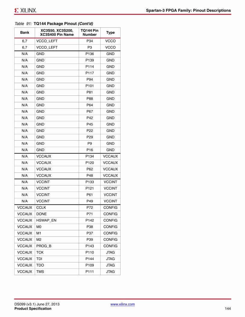
Spartan-3 FPGA Family: Pinout Descriptions
DS099 (v3.1) June 27, 2013 www.xilinx.comProduct Specification 144
6,7 VCCO_LEFT P34 VCCO
6,7 VCCO_LEFT P3 VCCO
N/A GND P136 GND
N/A GND P139 GND
N/A GND P114 GND
N/A GND P117 GND
N/A GND P94 GND
N/A GND P101 GND
N/A GND P81 GND
N/A GND P88 GND
N/A GND P64 GND
N/A GND P67 GND
N/A GND P42 GND
N/A GND P45 GND
N/A GND P22 GND
N/A GND P29 GND
N/A GND P9 GND
N/A GND P16 GND
N/A VCCAUX P134 VCCAUX
N/A VCCAUX P120 VCCAUX
N/A VCCAUX P62 VCCAUX
N/A VCCAUX P48 VCCAUX
N/A VCCINT P133 VCCINT
N/A VCCINT P121 VCCINT
N/A VCCINT P61 VCCINT
N/A VCCINT P49 VCCINT
VCCAUX CCLK P72 CONFIG
VCCAUX DONE P71 CONFIG
VCCAUX HSWAP_EN P142 CONFIG
VCCAUX M0 P38 CONFIG
VCCAUX M1 P37 CONFIG
VCCAUX M2 P39 CONFIG
VCCAUX PROG_B P143 CONFIG
VCCAUX TCK P110 JTAG
VCCAUX TDI P144 JTAG
VCCAUX TDO P109 JTAG
VCCAUX TMS P111 JTAG
Table 91: TQ144 Package Pinout (Cont’d)
Bank XC3S50, XC3S200, XC3S400 Pin Name
TQ144 Pin Number Type
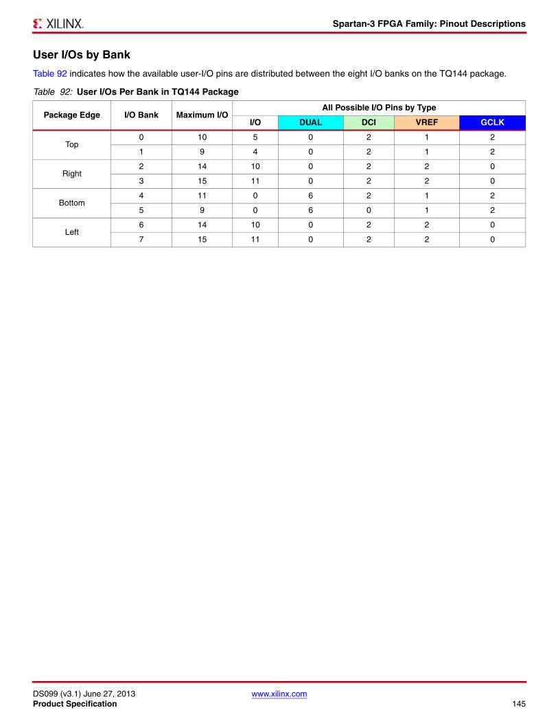
Spartan-3 FPGA Family: Pinout Descriptions
DS099 (v3.1) June 27, 2013 www.xilinx.comProduct Specification 145
User I/Os by Bank
Table 92 indicates how the available user-I/O pins are distributed between the eight I/O banks on the TQ144 package.
Table 92: User I/Os Per Bank in TQ144 Package
Package Edge I/O Bank Maximum I/OAll Possible I/O Pins by Type
I/O DUAL DCI VREF GCLK
Top0 10 5 0 2 1 2
1 9 4 0 2 1 2
Right2 14 10 0 2 2 0
3 15 11 0 2 2 0
Bottom4 11 0 6 2 1 2
5 9 0 6 0 1 2
Left6 14 10 0 2 2 0
7 15 11 0 2 2 0
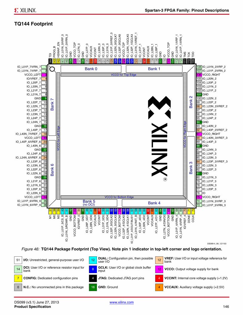
Spartan-3 FPGA Family: Pinout Descriptions
DS099 (v3.1) June 27, 2013 www.xilinx.comProduct Specification 146
TQ144 FootprintX-Ref Target - Figure 46
Figure 46: TQ144 Package Footprint (Top View). Note pin 1 indicator in top-left corner and logo orientation.
51 I/O: Unrestricted, general-purpose user I/O 12 DUAL: Configuration pin, then possible user I/O 12 VREF: User I/O or input voltage reference for
bank
14 DCI: User I/O or reference resistor input for bank 8 GCLK: User I/O or global clock buffer
input 12 VCCO: Output voltage supply for bank
7 CONFIG: Dedicated configuration pins 4 JTAG: Dedicated JTAG port pins 4 VCCINT: Internal core voltage supply (+1.2V)
0 N.C.: No unconnected pins in this package 16 GND: Ground 4 VCCAUX: Auxiliary voltage supply (+2.5V)
IO
TD
I
PR
OG
_B
HS
WA
P_E
N
IO_L
01N
_0/V
RP
_0
IO_L
01P
_0/V
RN
_0
GN
D
VC
CO
_TO
P
IO_L
27N
_0
GN
D
IO_L
27P
_0
VC
CA
UX
VC
CIN
T
IO_L
30N
_0
IO_L
30P
_0
IO_L
31N
_0
IO_L
31P
_0/V
RE
F_0
IO_L
32N
_0/G
CLK
7
IO_L
32P
_0/G
CLK
6
VC
CO
_TO
P
IO_L
32N
_1/G
CLK
5
IO_L
32P
_1/G
CLK
4
IO_L
31N
_1/V
RE
F_1
IO_L
31P
_1
VC
CIN
T
VC
CA
UX
IO_L
28N
_1
IO_L
28P
_1
GN
D
IO VC
CO
_TO
P
GN
D
IO_L
01N
_1/V
RP
_1
IO_L
01P
_1/V
RN
_1
TM
S
TC
K
TD
O
144
143
142
141
140
139
138
137
136
135
134
133
132
131
130
129
128
127
126
125
124
123
122
121
120
119
118
117
116
115
114
113
112
111
110
109
IO_L01P_7/VRN_7 1 108 IO_L01N_2/VRP_2IO_L01N_7/VRP_7 2 107 IO_L01P_2/VRN_2
VCCO_LEFT 3 X 10⁶ VCCO_RIGHTIO/VREF_7 4 105 IO_L20N_2IO_L20P_7 5 104 IO_L20P_2IO_L20N_7 6 103 IO_L21N_2IO_L21P_7 7 102 IO_L21P_2IO_L21N_7 8 101 GND
GND 9 100 IO_L22N_2IO_L22P_7 10 99 IO_L22P_2IO_L22N_7 11 98 IO_L23N_2/VREF_2IO_L23P_7 12 97 IO_L23P_2IO_L23N_7 13 96 IO_L24N_2IO_L24P_7 14 95 IO_L24P_2IO_L24N_7 15 94 GND
GND 16 93 IO_L40N_2IO_L40P_7 17 92 IO_L40P_2/VREF_2
IO_L40N_7/VREF_7 18 91 VCCO_RIGHTVCCO_LEFT 19 90 IO_L40N_3/VREF_3
IO_L40P_6/VREF_6 20 89 IO_L40P_3IO_L40N_6 21 88 GND
GND 22 87 IO_L24N_3IO_L24P_6 23 86 IO_L24P_3
IO_L24N_6/VREF_6 24 85 IO_L23N_3IO_L23P_6 25 84 IO_L23P_3/VREF_3IO_L23N_6 26 83 IO_L22N_3IO_L22P_6 27 82 IO_L22P_3IO_L22N_6 28 81 GND
GND 29 80 IO_L21N_3IO_L21P_6 30 79 IO_L21P_3IO_L21N_6 31 78 IO_L20N_3IO_L20P_6 32 77 IO_L20P_3IO_L20N_6 33 76 IO
VCCO_LEFT 34 75 VCCO_RIGHTIO_L01P_6/VRN_6 35 74 IO_L01N_3/VRP_3IO_L01N_6/VRP_6 36 73 IO_L01P_3/VRN_3
37 38 39 40 41 42 43 44 45 46 47 48 49 50 51 52 53 54 55 56 57 58 59 60 61 62 63 64 65 66 67 68 69 70 71 72
M1
M0
M2
IO_L
01P
_5/C
S_B
_L01
N_5
/RD
WR
_B
GN
D
VC
CO
_BO
TT
OM
IO/V
RE
F_5
GN
D
IO_L
28P
_5/D
7
IO_L
28N
_5/D
6
VC
CA
UX
VC
CIN
T
IO_L
31P
_5/D
5
IO_L
31N
_5/D
4
IO_L
32P
_5/G
CLK
2
IO_L
32N
_5/G
CLK
3
VC
CO
_BO
TT
OM
IO_L
32P
_4/G
CLK
0
IO_L
32N
_4/G
CLK
1
IO_L
31P
_4/D
OU
T/B
US
Y
IO_L
31N
_4/IN
IT_B
IO_L
30P
_4/D
3
IO_L
30N
_4/D
2
VC
CIN
T
VC
CA
UX
IO_L
27P
_4/D
1
GN
D
IO_L
27N
_4/D
IN/D
0
VC
CO
_BO
TT
OM
GN
D
IO_L
01P
_4/V
RN
_4
IO_L
01N
_4/V
RP
_4
IO/V
RE
F_4
DO
NE
CC
LK
Bank 5(no DCI)
Ban
k 3
Ban
k 2
VCCO for Top Edge
VC
CO
for
Rig
ht E
dge
VCCO for Bottom Edge
Bank 0 Bank 1
Ban
k 7
Bank 4
Ban
k 6
VC
CO
for
Left
Edg
e
DS099-4_08_121103
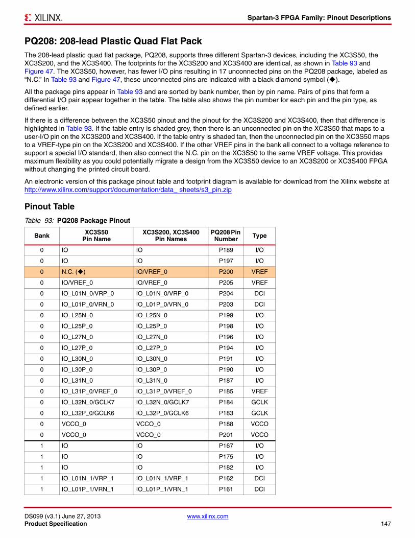
Spartan-3 FPGA Family: Pinout Descriptions
DS099 (v3.1) June 27, 2013 www.xilinx.comProduct Specification 147
PQ208: 208-lead Plastic Quad Flat PackThe 208-lead plastic quad flat package, PQ208, supports three different Spartan-3 devices, including the XC3S50, the XC3S200, and the XC3S400. The footprints for the XC3S200 and XC3S400 are identical, as shown in Table 93 and Figure 47. The XC3S50, however, has fewer I/O pins resulting in 17 unconnected pins on the PQ208 package, labeled as “N.C.” In Table 93 and Figure 47, these unconnected pins are indicated with a black diamond symbol ().
All the package pins appear in Table 93 and are sorted by bank number, then by pin name. Pairs of pins that form a differential I/O pair appear together in the table. The table also shows the pin number for each pin and the pin type, as defined earlier.
If there is a difference between the XC3S50 pinout and the pinout for the XC3S200 and XC3S400, then that difference is highlighted in Table 93. If the table entry is shaded grey, then there is an unconnected pin on the XC3S50 that maps to a user-I/O pin on the XC3S200 and XC3S400. If the table entry is shaded tan, then the unconnected pin on the XC3S50 maps to a VREF-type pin on the XC3S200 and XC3S400. If the other VREF pins in the bank all connect to a voltage reference to support a special I/O standard, then also connect the N.C. pin on the XC3S50 to the same VREF voltage. This provides maximum flexibility as you could potentially migrate a design from the XC3S50 device to an XC3S200 or XC3S400 FPGA without changing the printed circuit board.
An electronic version of this package pinout table and footprint diagram is available for download from the Xilinx website at http://www.xilinx.com/support/documentation/data_ sheets/s3_pin.zip
Pinout Table
Table 93: PQ208 Package Pinout
Bank XC3S50 Pin Name
XC3S200, XC3S400Pin Names
PQ208 Pin Number Type
0 IO IO P189 I/O
0 IO IO P197 I/O
0 N.C. () IO/VREF_0 P200 VREF
0 IO/VREF_0 IO/VREF_0 P205 VREF
0 IO_L01N_0/VRP_0 IO_L01N_0/VRP_0 P204 DCI
0 IO_L01P_0/VRN_0 IO_L01P_0/VRN_0 P203 DCI
0 IO_L25N_0 IO_L25N_0 P199 I/O
0 IO_L25P_0 IO_L25P_0 P198 I/O
0 IO_L27N_0 IO_L27N_0 P196 I/O
0 IO_L27P_0 IO_L27P_0 P194 I/O
0 IO_L30N_0 IO_L30N_0 P191 I/O
0 IO_L30P_0 IO_L30P_0 P190 I/O
0 IO_L31N_0 IO_L31N_0 P187 I/O
0 IO_L31P_0/VREF_0 IO_L31P_0/VREF_0 P185 VREF
0 IO_L32N_0/GCLK7 IO_L32N_0/GCLK7 P184 GCLK
0 IO_L32P_0/GCLK6 IO_L32P_0/GCLK6 P183 GCLK
0 VCCO_0 VCCO_0 P188 VCCO
0 VCCO_0 VCCO_0 P201 VCCO
1 IO IO P167 I/O
1 IO IO P175 I/O
1 IO IO P182 I/O
1 IO_L01N_1/VRP_1 IO_L01N_1/VRP_1 P162 DCI
1 IO_L01P_1/VRN_1 IO_L01P_1/VRN_1 P161 DCI
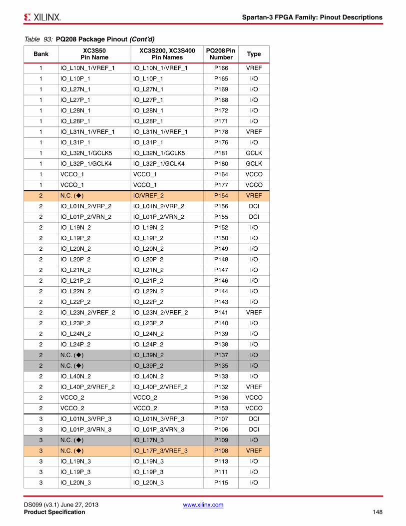
Spartan-3 FPGA Family: Pinout Descriptions
DS099 (v3.1) June 27, 2013 www.xilinx.comProduct Specification 148
1 IO_L10N_1/VREF_1 IO_L10N_1/VREF_1 P166 VREF
1 IO_L10P_1 IO_L10P_1 P165 I/O
1 IO_L27N_1 IO_L27N_1 P169 I/O
1 IO_L27P_1 IO_L27P_1 P168 I/O
1 IO_L28N_1 IO_L28N_1 P172 I/O
1 IO_L28P_1 IO_L28P_1 P171 I/O
1 IO_L31N_1/VREF_1 IO_L31N_1/VREF_1 P178 VREF
1 IO_L31P_1 IO_L31P_1 P176 I/O
1 IO_L32N_1/GCLK5 IO_L32N_1/GCLK5 P181 GCLK
1 IO_L32P_1/GCLK4 IO_L32P_1/GCLK4 P180 GCLK
1 VCCO_1 VCCO_1 P164 VCCO
1 VCCO_1 VCCO_1 P177 VCCO
2 N.C. () IO/VREF_2 P154 VREF
2 IO_L01N_2/VRP_2 IO_L01N_2/VRP_2 P156 DCI
2 IO_L01P_2/VRN_2 IO_L01P_2/VRN_2 P155 DCI
2 IO_L19N_2 IO_L19N_2 P152 I/O
2 IO_L19P_2 IO_L19P_2 P150 I/O
2 IO_L20N_2 IO_L20N_2 P149 I/O
2 IO_L20P_2 IO_L20P_2 P148 I/O
2 IO_L21N_2 IO_L21N_2 P147 I/O
2 IO_L21P_2 IO_L21P_2 P146 I/O
2 IO_L22N_2 IO_L22N_2 P144 I/O
2 IO_L22P_2 IO_L22P_2 P143 I/O
2 IO_L23N_2/VREF_2 IO_L23N_2/VREF_2 P141 VREF
2 IO_L23P_2 IO_L23P_2 P140 I/O
2 IO_L24N_2 IO_L24N_2 P139 I/O
2 IO_L24P_2 IO_L24P_2 P138 I/O
2 N.C. () IO_L39N_2 P137 I/O
2 N.C. () IO_L39P_2 P135 I/O
2 IO_L40N_2 IO_L40N_2 P133 I/O
2 IO_L40P_2/VREF_2 IO_L40P_2/VREF_2 P132 VREF
2 VCCO_2 VCCO_2 P136 VCCO
2 VCCO_2 VCCO_2 P153 VCCO
3 IO_L01N_3/VRP_3 IO_L01N_3/VRP_3 P107 DCI
3 IO_L01P_3/VRN_3 IO_L01P_3/VRN_3 P106 DCI
3 N.C. () IO_L17N_3 P109 I/O
3 N.C. () IO_L17P_3/VREF_3 P108 VREF
3 IO_L19N_3 IO_L19N_3 P113 I/O
3 IO_L19P_3 IO_L19P_3 P111 I/O
3 IO_L20N_3 IO_L20N_3 P115 I/O
Table 93: PQ208 Package Pinout (Cont’d)
Bank XC3S50 Pin Name
XC3S200, XC3S400Pin Names
PQ208 Pin Number Type
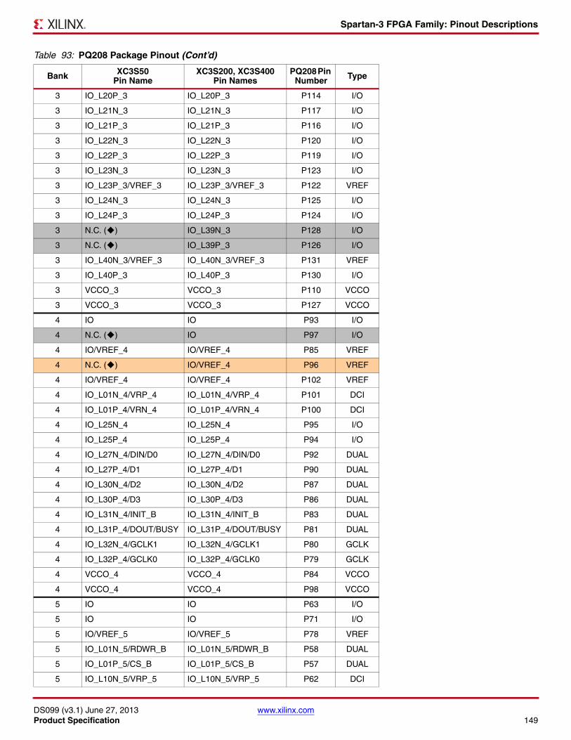
Spartan-3 FPGA Family: Pinout Descriptions
DS099 (v3.1) June 27, 2013 www.xilinx.comProduct Specification 149
3 IO_L20P_3 IO_L20P_3 P114 I/O
3 IO_L21N_3 IO_L21N_3 P117 I/O
3 IO_L21P_3 IO_L21P_3 P116 I/O
3 IO_L22N_3 IO_L22N_3 P120 I/O
3 IO_L22P_3 IO_L22P_3 P119 I/O
3 IO_L23N_3 IO_L23N_3 P123 I/O
3 IO_L23P_3/VREF_3 IO_L23P_3/VREF_3 P122 VREF
3 IO_L24N_3 IO_L24N_3 P125 I/O
3 IO_L24P_3 IO_L24P_3 P124 I/O
3 N.C. () IO_L39N_3 P128 I/O
3 N.C. () IO_L39P_3 P126 I/O
3 IO_L40N_3/VREF_3 IO_L40N_3/VREF_3 P131 VREF
3 IO_L40P_3 IO_L40P_3 P130 I/O
3 VCCO_3 VCCO_3 P110 VCCO
3 VCCO_3 VCCO_3 P127 VCCO
4 IO IO P93 I/O
4 N.C. () IO P97 I/O
4 IO/VREF_4 IO/VREF_4 P85 VREF
4 N.C. () IO/VREF_4 P96 VREF
4 IO/VREF_4 IO/VREF_4 P102 VREF
4 IO_L01N_4/VRP_4 IO_L01N_4/VRP_4 P101 DCI
4 IO_L01P_4/VRN_4 IO_L01P_4/VRN_4 P100 DCI
4 IO_L25N_4 IO_L25N_4 P95 I/O
4 IO_L25P_4 IO_L25P_4 P94 I/O
4 IO_L27N_4/DIN/D0 IO_L27N_4/DIN/D0 P92 DUAL
4 IO_L27P_4/D1 IO_L27P_4/D1 P90 DUAL
4 IO_L30N_4/D2 IO_L30N_4/D2 P87 DUAL
4 IO_L30P_4/D3 IO_L30P_4/D3 P86 DUAL
4 IO_L31N_4/INIT_B IO_L31N_4/INIT_B P83 DUAL
4 IO_L31P_4/DOUT/BUSY IO_L31P_4/DOUT/BUSY P81 DUAL
4 IO_L32N_4/GCLK1 IO_L32N_4/GCLK1 P80 GCLK
4 IO_L32P_4/GCLK0 IO_L32P_4/GCLK0 P79 GCLK
4 VCCO_4 VCCO_4 P84 VCCO
4 VCCO_4 VCCO_4 P98 VCCO
5 IO IO P63 I/O
5 IO IO P71 I/O
5 IO/VREF_5 IO/VREF_5 P78 VREF
5 IO_L01N_5/RDWR_B IO_L01N_5/RDWR_B P58 DUAL
5 IO_L01P_5/CS_B IO_L01P_5/CS_B P57 DUAL
5 IO_L10N_5/VRP_5 IO_L10N_5/VRP_5 P62 DCI
Table 93: PQ208 Package Pinout (Cont’d)
Bank XC3S50 Pin Name
XC3S200, XC3S400Pin Names
PQ208 Pin Number Type
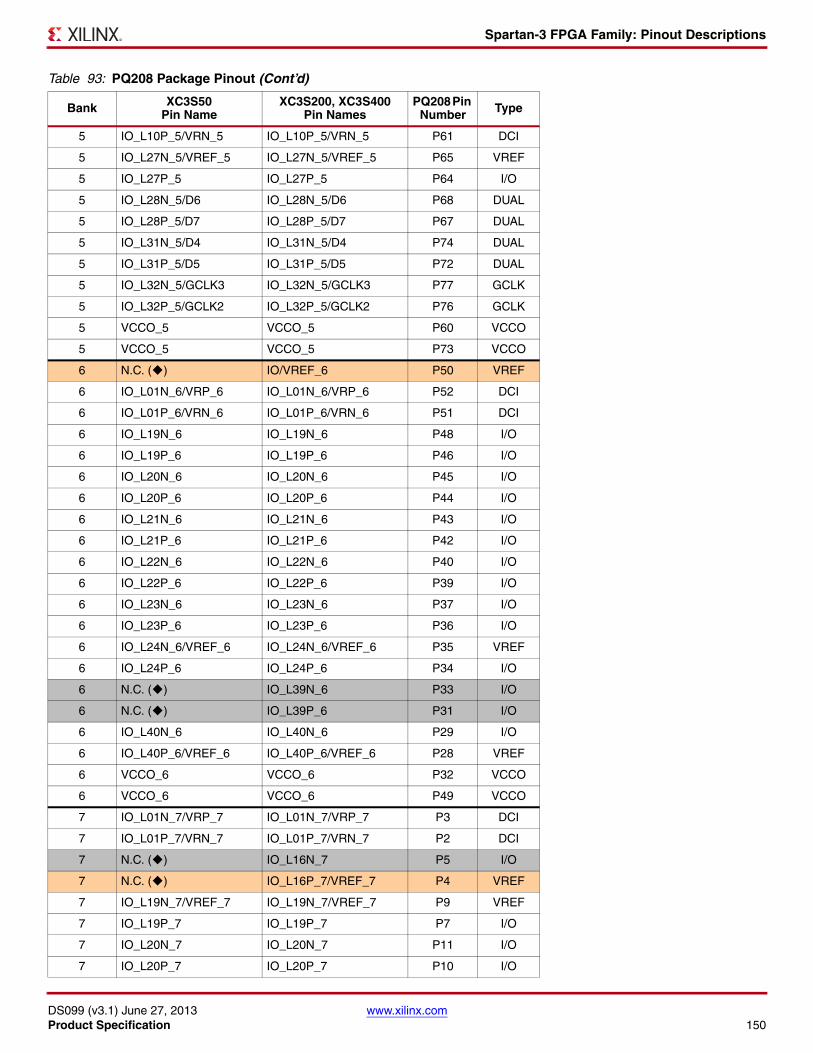
Spartan-3 FPGA Family: Pinout Descriptions
DS099 (v3.1) June 27, 2013 www.xilinx.comProduct Specification 150
5 IO_L10P_5/VRN_5 IO_L10P_5/VRN_5 P61 DCI
5 IO_L27N_5/VREF_5 IO_L27N_5/VREF_5 P65 VREF
5 IO_L27P_5 IO_L27P_5 P64 I/O
5 IO_L28N_5/D6 IO_L28N_5/D6 P68 DUAL
5 IO_L28P_5/D7 IO_L28P_5/D7 P67 DUAL
5 IO_L31N_5/D4 IO_L31N_5/D4 P74 DUAL
5 IO_L31P_5/D5 IO_L31P_5/D5 P72 DUAL
5 IO_L32N_5/GCLK3 IO_L32N_5/GCLK3 P77 GCLK
5 IO_L32P_5/GCLK2 IO_L32P_5/GCLK2 P76 GCLK
5 VCCO_5 VCCO_5 P60 VCCO
5 VCCO_5 VCCO_5 P73 VCCO
6 N.C. () IO/VREF_6 P50 VREF
6 IO_L01N_6/VRP_6 IO_L01N_6/VRP_6 P52 DCI
6 IO_L01P_6/VRN_6 IO_L01P_6/VRN_6 P51 DCI
6 IO_L19N_6 IO_L19N_6 P48 I/O
6 IO_L19P_6 IO_L19P_6 P46 I/O
6 IO_L20N_6 IO_L20N_6 P45 I/O
6 IO_L20P_6 IO_L20P_6 P44 I/O
6 IO_L21N_6 IO_L21N_6 P43 I/O
6 IO_L21P_6 IO_L21P_6 P42 I/O
6 IO_L22N_6 IO_L22N_6 P40 I/O
6 IO_L22P_6 IO_L22P_6 P39 I/O
6 IO_L23N_6 IO_L23N_6 P37 I/O
6 IO_L23P_6 IO_L23P_6 P36 I/O
6 IO_L24N_6/VREF_6 IO_L24N_6/VREF_6 P35 VREF
6 IO_L24P_6 IO_L24P_6 P34 I/O
6 N.C. () IO_L39N_6 P33 I/O
6 N.C. () IO_L39P_6 P31 I/O
6 IO_L40N_6 IO_L40N_6 P29 I/O
6 IO_L40P_6/VREF_6 IO_L40P_6/VREF_6 P28 VREF
6 VCCO_6 VCCO_6 P32 VCCO
6 VCCO_6 VCCO_6 P49 VCCO
7 IO_L01N_7/VRP_7 IO_L01N_7/VRP_7 P3 DCI
7 IO_L01P_7/VRN_7 IO_L01P_7/VRN_7 P2 DCI
7 N.C. () IO_L16N_7 P5 I/O
7 N.C. () IO_L16P_7/VREF_7 P4 VREF
7 IO_L19N_7/VREF_7 IO_L19N_7/VREF_7 P9 VREF
7 IO_L19P_7 IO_L19P_7 P7 I/O
7 IO_L20N_7 IO_L20N_7 P11 I/O
7 IO_L20P_7 IO_L20P_7 P10 I/O
Table 93: PQ208 Package Pinout (Cont’d)
Bank XC3S50 Pin Name
XC3S200, XC3S400Pin Names
PQ208 Pin Number Type
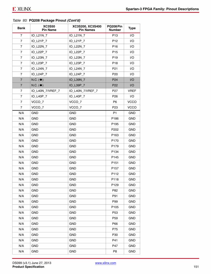
Spartan-3 FPGA Family: Pinout Descriptions
DS099 (v3.1) June 27, 2013 www.xilinx.comProduct Specification 151
7 IO_L21N_7 IO_L21N_7 P13 I/O
7 IO_L21P_7 IO_L21P_7 P12 I/O
7 IO_L22N_7 IO_L22N_7 P16 I/O
7 IO_L22P_7 IO_L22P_7 P15 I/O
7 IO_L23N_7 IO_L23N_7 P19 I/O
7 IO_L23P_7 IO_L23P_7 P18 I/O
7 IO_L24N_7 IO_L24N_7 P21 I/O
7 IO_L24P_7 IO_L24P_7 P20 I/O
7 N.C. () IO_L39N_7 P24 I/O
7 N.C. () IO_L39P_7 P22 I/O
7 IO_L40N_7/VREF_7 IO_L40N_7/VREF_7 P27 VREF
7 IO_L40P_7 IO_L40P_7 P26 I/O
7 VCCO_7 VCCO_7 P6 VCCO
7 VCCO_7 VCCO_7 P23 VCCO
N/A GND GND P1 GND
N/A GND GND P186 GND
N/A GND GND P195 GND
N/A GND GND P202 GND
N/A GND GND P163 GND
N/A GND GND P170 GND
N/A GND GND P179 GND
N/A GND GND P134 GND
N/A GND GND P145 GND
N/A GND GND P151 GND
N/A GND GND P157 GND
N/A GND GND P112 GND
N/A GND GND P118 GND
N/A GND GND P129 GND
N/A GND GND P82 GND
N/A GND GND P91 GND
N/A GND GND P99 GND
N/A GND GND P105 GND
N/A GND GND P53 GND
N/A GND GND P59 GND
N/A GND GND P66 GND
N/A GND GND P75 GND
N/A GND GND P30 GND
N/A GND GND P41 GND
N/A GND GND P47 GND
N/A GND GND P8 GND
Table 93: PQ208 Package Pinout (Cont’d)
Bank XC3S50 Pin Name
XC3S200, XC3S400Pin Names
PQ208 Pin Number Type
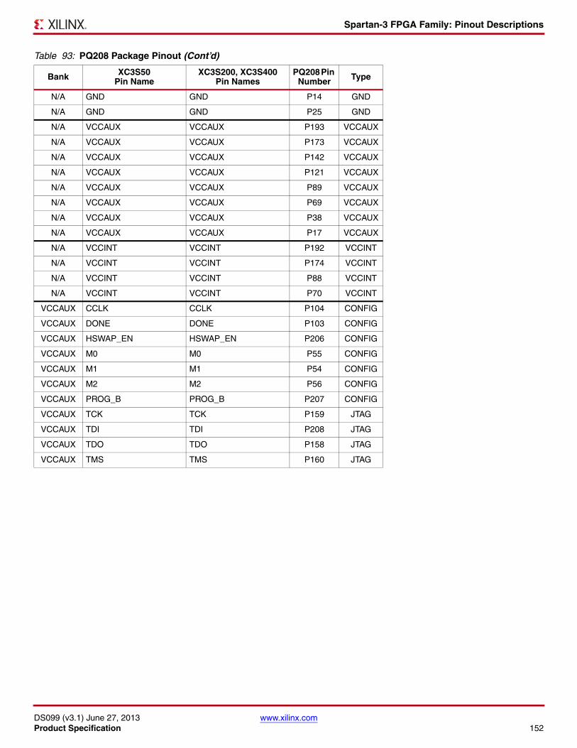
Spartan-3 FPGA Family: Pinout Descriptions
DS099 (v3.1) June 27, 2013 www.xilinx.comProduct Specification 152
N/A GND GND P14 GND
N/A GND GND P25 GND
N/A VCCAUX VCCAUX P193 VCCAUX
N/A VCCAUX VCCAUX P173 VCCAUX
N/A VCCAUX VCCAUX P142 VCCAUX
N/A VCCAUX VCCAUX P121 VCCAUX
N/A VCCAUX VCCAUX P89 VCCAUX
N/A VCCAUX VCCAUX P69 VCCAUX
N/A VCCAUX VCCAUX P38 VCCAUX
N/A VCCAUX VCCAUX P17 VCCAUX
N/A VCCINT VCCINT P192 VCCINT
N/A VCCINT VCCINT P174 VCCINT
N/A VCCINT VCCINT P88 VCCINT
N/A VCCINT VCCINT P70 VCCINT
VCCAUX CCLK CCLK P104 CONFIG
VCCAUX DONE DONE P103 CONFIG
VCCAUX HSWAP_EN HSWAP_EN P206 CONFIG
VCCAUX M0 M0 P55 CONFIG
VCCAUX M1 M1 P54 CONFIG
VCCAUX M2 M2 P56 CONFIG
VCCAUX PROG_B PROG_B P207 CONFIG
VCCAUX TCK TCK P159 JTAG
VCCAUX TDI TDI P208 JTAG
VCCAUX TDO TDO P158 JTAG
VCCAUX TMS TMS P160 JTAG
Table 93: PQ208 Package Pinout (Cont’d)
Bank XC3S50 Pin Name
XC3S200, XC3S400Pin Names
PQ208 Pin Number Type
Spartan-3 FPGA Family: Pinout Descriptions
DS099 (v3.1) June 27, 2013 www.xilinx.comProduct Specification 153
User I/Os by Bank
Table 94 indicates how the available user-I/O pins are distributed between the eight I/O banks for the XC3S50 in the PQ208 package. Similarly, Table 95 shows how the available user-I/O pins are distributed between the eight I/O banks for the XC3S200 and XC3S400 in the PQ208 package.
Table 94: User I/Os Per Bank for XC3S50 in PQ208 Package
Package Edge I/O Bank Maximum I/OAll Possible I/O Pins by Type
I/O DUAL DCI VREF GCLK
Top0 15 9 0 2 2 2
1 15 9 0 2 2 2
Right2 16 13 0 2 2 0
3 16 12 0 2 2 0
Bottom4 15 3 6 2 2 2
5 15 3 6 2 2 2
Left6 16 12 0 2 2 0
7 16 12 0 2 2 0
Table 95: User I/Os Per Bank for XC3S200 and XC3S400 in PQ208 Package
Package Edge I/O Bank Maximum I/OAll Possible I/O Pins by Type
I/O DUAL DCI VREF GCLK
Top0 16 9 0 2 3 2
1 15 9 0 2 2 2
Right2 19 14 0 2 3 0
3 20 15 0 2 3 0
Bottom4 17 4 6 2 3 2
5 15 3 6 2 2 2
Left6 19 14 0 2 3 0
7 20 15 0 2 3 0
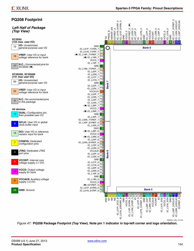
Spartan-3 FPGA Family: Pinout Descriptions
DS099 (v3.1) June 27, 2013 www.xilinx.comProduct Specification 154
PQ208 Footprint X-Ref Target - Figure 47
Left Half of Package (Top View)
XC3S50(124 max. user I/O)
72 I/O: Unrestricted, general-purpose user I/O
16 VREF: User I/O or input voltage reference for bank
17 N.C.: Unconnected pins for XC3S50 ()
XC3S200, XC3S400(141 max user I/O)
83 I/O: Unrestricted, general-purpose user I/O
22 VREF: User I/O or input voltage reference for bank
0 N.C.: No unconnected pins in this package
All devices
12 DUAL: Configuration pin, then possible user I/O
8 GCLK: User I/O or global clock buffer input
16 DCI: User I/O or reference resistor input for bank
7 CONFIG: Dedicated configuration pins
4 JTAG: Dedicated JTAG port pins
4 VCCINT: Internal core voltage supply (+1.2V)
12 VCCO: Output voltage supply for bank
8 VCCAUX: Auxiliary voltage supply (+2.5V)
28 GND: Ground
Figure 47: PQ208 Package Footprint (Top View). Note pin 1 indicator in top-left corner and logo orientation.
TD
IP
RO
G_B
HS
WA
P_E
NIO
/VR
EF
_0IO
_L01
N_0
/VR
P_0
IO_L
01P
_0/V
RN
_0G
ND
VC
CO
_0IO
/VR
EF
_0 (
)IO
_L25
N_0
IO_L
25P
_0IO IO
_L27
N_0
GN
DIO
_L27
P_0
VC
CA
UX
VC
CIN
TIO
_L30
N_0
IO_L
30P
_0IO V
CC
O_0
IO_L
31N
_0G
ND
IO_L
31P
_0/V
RE
F_0
IO_L
32N
_0/G
CLK
7IO
_L32
P_0
/GC
LK6
208
207
206
205
204
203
202
201
200
199
198
197
196
195
194
193
192
191
190
189
188
187
186
185
184
183
GND 1IO_L01P_7/VRN_7IO_L01N_7/VRP_7
() IO_L16P_7/VREF_7 4() IO_L16N_7 5
VCCO_7 6IO_L19P_7 7
GND 8IO_L19N_7/VREF_7 9
IO_L20P_7 10IO_L20N_7 11IO_L21P_7 12IO_L21N_7 13
GND 14IO_L22P_7 15IO_L22N_7 16
UVCCA X 17IO_L23P_7 18IO_L23N_7 19IO_L24P_7 20IO_L24N_7 21
() IO_L39P_7 22VCCO_7 23
() IO_L39N_7 24GND 25
IO_L40P_7 26IO_L40N_7/VREF_7 27IO_L40P_6/VREF_6 28
IO_L40N_6 29GND 30
() IO_L39P_6 31VCCO_6 32
() IO_L39N_6 33IO_L24P_6 34
IO_L24N_6/VREF_6 35IO_L23P_6 36IO_L23N_6 37
VCCAUX 38IO_L22P_6 39IO_L22N_6 40
GND 41IO_L21P_6 42IO_L21N_6 43IO_L20P_6 44IO_L20N_6 45IO_L19P_6 46
GND 47IO_L19N_6 48
VCCO_6 49() IO/VREF_6 50
IO_L01P_6/VRN_6 51IO_L01N_6/VRP_6 52
53 54 55 56 57 58 59 60 61 62 63 64 65 66 67 68 69 70 71 72 73 74 75 76 77 78
GN
DM
1M
0M
2IO
_L01
P_5
/CS
_BIO
_L01
N_5
/RD
WR
_BG
ND
VC
CO
_5IO
_L10
P_5
/VR
N_5
IO_L
10N
_5/V
RP
_5 IOIO
_L27
P_5
IO_L
27N
_5/V
RE
F_5
GN
DIO
_L28
P_5
/D7
IO_L
28N
_5/D
6V
CC
AU
XV
CC
INT IO
IO_L
31P
_5/D
5V
CC
O_5
IO_L
31N
_5/D
4G
ND
IO_L
32P
_5/G
CLK
2IO
_L32
N_5
/GC
LK3
IO/V
RE
F_5
Bank 5
Ban
k 7
Ban
k 6
Bank 0
DS099-4_09a_121103
3
2
Spartan-3 FPGA Family: Pinout Descriptions
DS099 (v3.1) June 27, 2013 www.xilinx.comProduct Specification 155
Right Half of Package (Top View)
Figure 48: PQ208 Package Footprint (Top View) Continued
IO IO_L
32N
_1/G
CLK
5IO
_L32
P_1
/GC
LK4
GN
DIO
_L31
N_1
/VR
EF
_1V
CC
O_1
IO_L
31P
_1IO V
CC
INT
VC
CA
UX
IO_L
28N
_1IO
_L28
P_1
GN
DIO
_L27
N_1
IO_L
27P
_1IO IO
_L10
N_1
/VR
EF
_1IO
_L10
P_1
VC
CO
_1G
ND
IO_L
01N
_1/V
RP
_1IO
_L01
P_1
/VR
N_1
TM
ST
CK
TD
OG
ND
182
181
180
179
178
177
176
175
174
173
172
171
170
169
168
167
166
165
164
163
162
161
160
159
158
157
156 IO_L01N_2/VRP_2155 IO_L01P_2/VRN_2154 IO/VREF_2 ()153 VCCO_2152 IO_L19N_2151 GND150 IO_L19P_2149 IO_L20N_2148 IO_L20P_2147 IO_L21N_2146 IO_L21P_2145 GND144 IO_L22N_2143 IO_L22P_2142 VCCAUX141 IO_L23N_2/VREF_2140 IO_L23P_2139 IO_L24N_2138 IO_L24P_2137 IO_L39N_2 ()136 VCCO_2135 IO_L39P_2 () 134 GND133 IO_L40N_2132 IO_L40P_2/VREF_2131 IO_L40N_3/VREF_3130 IO_L40P_3129 GND128 IO_L39N_3 ()127 VCCO_3126 IO_L39P_3 () 125 IO_L24N_3124 IO_L24P_3123 IO_L23N_3122 IO_L23P_3/VREF_3121 VCCAUX120 IO_L22N_3119 IO_L22P_3118 GND117 IO_L21N_3116 IO_L21P_3115 IO_L20N_3114 IO_L20P_3113 IO_L19N_3112 GND111 IO_L19P_3110 VCCO_3109 IO_L17N_3 ()108 IO_L17P_3/VREF_3 ()107 IO_L01N_3/VRP_3106 IO_L01P_3/VRN_3105 GND
79 80 81 82 83 84 85 86 87 88 89 90 91 92 93 94 95 96 97 98 99 100
101
102
103
104
IO_L
32P
_4/G
CLK
0IO
_L32
N_4
/GC
LK1
IO_L
31P
_4/D
OU
T/B
US
YG
ND
IO_L
31N
_4/IN
IT_B
VC
CO
_4IO
/VR
EF
_4IO
_L30
P_4
/D3
IO_L
30N
_4/D
2V
CC
INT
VC
CA
UX
IO_L
27P
_4/D
1G
NDD
IO_L
27N
_4/D
IN/D
0 IOIO
_L25
P_4
IO_L
25N
_4(
) IO
/VR
EF
_4(
) IO
VC
CO
_4G
ND
IO_L
01P
_4/V
RN
_4IO
_L01
N_4
/VR
P_4
IO/V
RE
F_4
DO
NE
CC
LK
Bank 1
Bank 4
Ban
k 3
Ban
k 2
DS099-4_9b_121103
Spartan-3 FPGA Family: Pinout Descriptions
DS099 (v3.1) June 27, 2013 www.xilinx.comProduct Specification 156
FT256: 256-lead Fine-pitch Thin Ball Grid ArrayThe 256-lead fine-pitch thin ball grid array package, FT256, supports three different Spartan-3 devices, including the XC3S200, the XC3S400, and the XC3S1000. The footprints for all three devices are identical, as shown in Table 96 and Figure 49.
All the package pins appear in Table 96 and are sorted by bank number, then by pin name. Pairs of pins that form a differential I/O pair appear together in the table. The table also shows the pin number for each pin and the pin type, as defined earlier.
An electronic version of this package pinout table and footprint diagram is available for download from the Xilinx website at http://www.xilinx.com/support/documentation/data_ sheets/s3_pin.zip.
Pinout Table
Table 96: FT256 Package Pinout
Bank XC3S200, XC3S400, XC3S1000Pin Name
FT256 Pin Number Type
0 IO A5 I/O
0 IO A7 I/O
0 IO/VREF_0 A3 VREF
0 IO/VREF_0 D5 VREF
0 IO_L01N_0/VRP_0 B4 DCI
0 IO_L01P_0/VRN_0 A4 DCI
0 IO_L25N_0 C5 I/O
0 IO_L25P_0 B5 I/O
0 IO_L27N_0 E6 I/O
0 IO_L27P_0 D6 I/O
0 IO_L28N_0 C6 I/O
0 IO_L28P_0 B6 I/O
0 IO_L29N_0 E7 I/O
0 IO_L29P_0 D7 I/O
0 IO_L30N_0 C7 I/O
0 IO_L30P_0 B7 I/O
0 IO_L31N_0 D8 I/O
0 IO_L31P_0/VREF_0 C8 VREF
0 IO_L32N_0/GCLK7 B8 GCLK
0 IO_L32P_0/GCLK6 A8 GCLK
0 VCCO_0 E8 VCCO
0 VCCO_0 F7 VCCO
0 VCCO_0 F8 VCCO
1 IO A9 I/O
1 IO A12 I/O
1 IO C10 I/O
1 IO/VREF_1 D12 VREF
1 IO_L01N_1/VRP_1 A14 DCI
1 IO_L01P_1/VRN_1 B14 DCI
Spartan-3 FPGA Family: Pinout Descriptions
DS099 (v3.1) June 27, 2013 www.xilinx.comProduct Specification 157
1 IO_L10N_1/VREF_1 A13 VREF
1 IO_L10P_1 B13 I/O
1 IO_L27N_1 B12 I/O
1 IO_L27P_1 C12 I/O
1 IO_L28N_1 D11 I/O
1 IO_L28P_1 E11 I/O
1 IO_L29N_1 B11 I/O
1 IO_L29P_1 C11 I/O
1 IO_L30N_1 D10 I/O
1 IO_L30P_1 E10 I/O
1 IO_L31N_1/VREF_1 A10 VREF
1 IO_L31P_1 B10 I/O
1 IO_L32N_1/GCLK5 C9 GCLK
1 IO_L32P_1/GCLK4 D9 GCLK
1 VCCO_1 E9 VCCO
1 VCCO_1 F9 VCCO
1 VCCO_1 F10 VCCO
2 IO G16 I/O
2 IO_L01N_2/VRP_2 B16 DCI
2 IO_L01P_2/VRN_2 C16 DCI
2 IO_L16N_2 C15 I/O
2 IO_L16P_2 D14 I/O
2 IO_L17N_2 D15 I/O
2 IO_L17P_2/VREF_2 D16 VREF
2 IO_L19N_2 E13 I/O
2 IO_L19P_2 E14 I/O
2 IO_L20N_2 E15 I/O
2 IO_L20P_2 E16 I/O
2 IO_L21N_2 F12 I/O
2 IO_L21P_2 F13 I/O
2 IO_L22N_2 F14 I/O
2 IO_L22P_2 F15 I/O
2 IO_L23N_2/VREF_2 G12 VREF
2 IO_L23P_2 G13 I/O
2 IO_L24N_2 G14 I/O
2 IO_L24P_2 G15 I/O
2 IO_L39N_2 H13 I/O
2 IO_L39P_2 H14 I/O
2 IO_L40N_2 H15 I/O
2 IO_L40P_2/VREF_2 H16 VREF
Table 96: FT256 Package Pinout (Cont’d)
Bank XC3S200, XC3S400, XC3S1000Pin Name
FT256 Pin Number Type
Spartan-3 FPGA Family: Pinout Descriptions
DS099 (v3.1) June 27, 2013 www.xilinx.comProduct Specification 158
2 VCCO_2 G11 VCCO
2 VCCO_2 H11 VCCO
2 VCCO_2 H12 VCCO
3 IO K15 I/O
3 IO_L01N_3/VRP_3 P16 DCI
3 IO_L01P_3/VRN_3 R16 DCI
3 IO_L16N_3 P15 I/O
3 IO_L16P_3 P14 I/O
3 IO_L17N_3 N16 I/O
3 IO_L17P_3/VREF_3 N15 VREF
3 IO_L19N_3 M14 I/O
3 IO_L19P_3 N14 I/O
3 IO_L20N_3 M16 I/O
3 IO_L20P_3 M15 I/O
3 IO_L21N_3 L13 I/O
3 IO_L21P_3 M13 I/O
3 IO_L22N_3 L15 I/O
3 IO_L22P_3 L14 I/O
3 IO_L23N_3 K12 I/O
3 IO_L23P_3/VREF_3 L12 VREF
3 IO_L24N_3 K14 I/O
3 IO_L24P_3 K13 I/O
3 IO_L39N_3 J14 I/O
3 IO_L39P_3 J13 I/O
3 IO_L40N_3/VREF_3 J16 VREF
3 IO_L40P_3 K16 I/O
3 VCCO_3 J11 VCCO
3 VCCO_3 J12 VCCO
3 VCCO_3 K11 VCCO
4 IO T12 I/O
4 IO T14 I/O
4 IO/VREF_4 N12 VREF
4 IO/VREF_4 P13 VREF
4 IO/VREF_4 T10 VREF
4 IO_L01N_4/VRP_4 R13 DCI
4 IO_L01P_4/VRN_4 T13 DCI
4 IO_L25N_4 P12 I/O
4 IO_L25P_4 R12 I/O
4 IO_L27N_4/DIN/D0 M11 DUAL
4 IO_L27P_4/D1 N11 DUAL
Table 96: FT256 Package Pinout (Cont’d)
Bank XC3S200, XC3S400, XC3S1000Pin Name
FT256 Pin Number Type
Spartan-3 FPGA Family: Pinout Descriptions
DS099 (v3.1) June 27, 2013 www.xilinx.comProduct Specification 159
4 IO_L28N_4 P11 I/O
4 IO_L28P_4 R11 I/O
4 IO_L29N_4 M10 I/O
4 IO_L29P_4 N10 I/O
4 IO_L30N_4/D2 P10 DUAL
4 IO_L30P_4/D3 R10 DUAL
4 IO_L31N_4/INIT_B N9 DUAL
4 IO_L31P_4/DOUT/BUSY P9 DUAL
4 IO_L32N_4/GCLK1 R9 GCLK
4 IO_L32P_4/GCLK0 T9 GCLK
4 VCCO_4 L9 VCCO
4 VCCO_4 L10 VCCO
4 VCCO_4 M9 VCCO
5 IO N5 I/O
5 IO P7 I/O
5 IO T5 I/O
5 IO/VREF_5 T8 VREF
5 IO_L01N_5/RDWR_B T3 DUAL
5 IO_L01P_5/CS_B R3 DUAL
5 IO_L10N_5/VRP_5 T4 DCI
5 IO_L10P_5/VRN_5 R4 DCI
5 IO_L27N_5/VREF_5 R5 VREF
5 IO_L27P_5 P5 I/O
5 IO_L28N_5/D6 N6 DUAL
5 IO_L28P_5/D7 M6 DUAL
5 IO_L29N_5 R6 I/O
5 IO_L29P_5/VREF_5 P6 VREF
5 IO_L30N_5 N7 I/O
5 IO_L30P_5 M7 I/O
5 IO_L31N_5/D4 T7 DUAL
5 IO_L31P_5/D5 R7 DUAL
5 IO_L32N_5/GCLK3 P8 GCLK
5 IO_L32P_5/GCLK2 N8 GCLK
5 VCCO_5 L7 VCCO
5 VCCO_5 L8 VCCO
5 VCCO_5 M8 VCCO
6 IO K1 I/O
6 IO_L01N_6/VRP_6 R1 DCI
6 IO_L01P_6/VRN_6 P1 DCI
6 IO_L16N_6 P2 I/O
Table 96: FT256 Package Pinout (Cont’d)
Bank XC3S200, XC3S400, XC3S1000Pin Name
FT256 Pin Number Type
Spartan-3 FPGA Family: Pinout Descriptions
DS099 (v3.1) June 27, 2013 www.xilinx.comProduct Specification 160
6 IO_L16P_6 N3 I/O
6 IO_L17N_6 N2 I/O
6 IO_L17P_6/VREF_6 N1 VREF
6 IO_L19N_6 M4 I/O
6 IO_L19P_6 M3 I/O
6 IO_L20N_6 M2 I/O
6 IO_L20P_6 M1 I/O
6 IO_L21N_6 L5 I/O
6 IO_L21P_6 L4 I/O
6 IO_L22N_6 L3 I/O
6 IO_L22P_6 L2 I/O
6 IO_L23N_6 K5 I/O
6 IO_L23P_6 K4 I/O
6 IO_L24N_6/VREF_6 K3 VREF
6 IO_L24P_6 K2 I/O
6 IO_L39N_6 J4 I/O
6 IO_L39P_6 J3 I/O
6 IO_L40N_6 J2 I/O
6 IO_L40P_6/VREF_6 J1 VREF
6 VCCO_6 J5 VCCO
6 VCCO_6 J6 VCCO
6 VCCO_6 K6 VCCO
7 IO G2 I/O
7 IO_L01N_7/VRP_7 C1 DCI
7 IO_L01P_7/VRN_7 B1 DCI
7 IO_L16N_7 C2 I/O
7 IO_L16P_7/VREF_7 C3 VREF
7 IO_L17N_7 D1 I/O
7 IO_L17P_7 D2 I/O
7 IO_L19N_7/VREF_7 E3 VREF
7 IO_L19P_7 D3 I/O
7 IO_L20N_7 E1 I/O
7 IO_L20P_7 E2 I/O
7 IO_L21N_7 F4 I/O
7 IO_L21P_7 E4 I/O
7 IO_L22N_7 F2 I/O
7 IO_L22P_7 F3 I/O
7 IO_L23N_7 G5 I/O
7 IO_L23P_7 F5 I/O
7 IO_L24N_7 G3 I/O
Table 96: FT256 Package Pinout (Cont’d)
Bank XC3S200, XC3S400, XC3S1000Pin Name
FT256 Pin Number Type
Spartan-3 FPGA Family: Pinout Descriptions
DS099 (v3.1) June 27, 2013 www.xilinx.comProduct Specification 161
7 IO_L24P_7 G4 I/O
7 IO_L39N_7 H3 I/O
7 IO_L39P_7 H4 I/O
7 IO_L40N_7/VREF_7 H1 VREF
7 IO_L40P_7 G1 I/O
7 VCCO_7 G6 VCCO
7 VCCO_7 H5 VCCO
7 VCCO_7 H6 VCCO
N/A GND A1 GND
N/A GND A16 GND
N/A GND B2 GND
N/A GND B9 GND
N/A GND B15 GND
N/A GND F6 GND
N/A GND F11 GND
N/A GND G7 GND
N/A GND G8 GND
N/A GND G9 GND
N/A GND G10 GND
N/A GND H2 GND
N/A GND H7 GND
N/A GND H8 GND
N/A GND H9 GND
N/A GND H10 GND
N/A GND J7 GND
N/A GND J8 GND
N/A GND J9 GND
N/A GND J10 GND
N/A GND J15 GND
N/A GND K7 GND
N/A GND K8 GND
N/A GND K9 GND
N/A GND K10 GND
N/A GND L6 GND
N/A GND L11 GND
N/A GND R2 GND
N/A GND R8 GND
N/A GND R15 GND
N/A GND T1 GND
Table 96: FT256 Package Pinout (Cont’d)
Bank XC3S200, XC3S400, XC3S1000Pin Name
FT256 Pin Number Type
Spartan-3 FPGA Family: Pinout Descriptions
DS099 (v3.1) June 27, 2013 www.xilinx.comProduct Specification 162
N/A GND T16 GND
N/A VCCAUX A6 VCCAUX
N/A VCCAUX A11 VCCAUX
N/A VCCAUX F1 VCCAUX
N/A VCCAUX F16 VCCAUX
N/A VCCAUX L1 VCCAUX
N/A VCCAUX L16 VCCAUX
N/A VCCAUX T6 VCCAUX
N/A VCCAUX T11 VCCAUX
N/A VCCINT D4 VCCINT
N/A VCCINT D13 VCCINT
N/A VCCINT E5 VCCINT
N/A VCCINT E12 VCCINT
N/A VCCINT M5 VCCINT
N/A VCCINT M12 VCCINT
N/A VCCINT N4 VCCINT
N/A VCCINT N13 VCCINT
VCCAUX CCLK T15 CONFIG
VCCAUX DONE R14 CONFIG
VCCAUX HSWAP_EN C4 CONFIG
VCCAUX M0 P3 CONFIG
VCCAUX M1 T2 CONFIG
VCCAUX M2 P4 CONFIG
VCCAUX PROG_B B3 CONFIG
VCCAUX TCK C14 JTAG
VCCAUX TDI A2 JTAG
VCCAUX TDO A15 JTAG
VCCAUX TMS C13 JTAG
Table 96: FT256 Package Pinout (Cont’d)
Bank XC3S200, XC3S400, XC3S1000Pin Name
FT256 Pin Number Type

Spartan-3 FPGA Family: Pinout Descriptions
DS099 (v3.1) June 27, 2013 www.xilinx.comProduct Specification 163
User I/Os by Bank
Table 97 indicates how the available user-I/O pins are distributed between the eight I/O banks on the FT256 package.
Table 97: User I/Os Per Bank in FT256 Package
Package Edge I/O Bank Maximum I/OAll Possible I/O Pins by Type
I/O DUAL DCI VREF GCLK
Top0 20 13 0 2 3 2
1 20 13 0 2 3 2
Right2 23 18 0 2 3 0
3 23 18 0 2 3 0
Bottom4 21 8 6 2 3 2
5 20 7 6 2 3 2
Left6 23 18 0 2 3 0
7 23 18 0 2 3 0
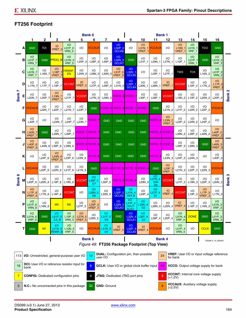
Spartan-3 FPGA Family: Pinout Descriptions
DS099 (v3.1) June 27, 2013 www.xilinx.comProduct Specification 164
FT256 FootprintX-Ref Target - Figure 49
Figure 49: FT256 Package Footprint (Top View)
113 I/O: Unrestricted, general-purpose user I/O 12 DUAL: Configuration pin, then possible user I/O 24 VREF: User I/O or input voltage reference
for bank
16 DCI: User I/O or reference resistor input for bank 8 GCLK: User I/O or global clock buffer input 24 VCCO: Output voltage supply for bank
7 CONFIG: Dedicated configuration pins 4 JTAG: Dedicated JTAG port pins 8 VCCINT: Internal core voltage supply (+1.2V)
0 N.C.: No unconnected pins in this package 32 GND: Ground 8 VCCAUX: Auxiliary voltage supply (+2.5V)
10 11 12 13 14 15 161 2 3 4 5 6 7 8 9
A
B
C
D
E
F
G
H
J
K
L
M
N
P
R
T
Ban
k 6
Ban
k 3
Bank 5 Bank 4
Ban
k 7
Bank 0 Bank 1
Ban
k 2
2
2
3
3
TDIIO
VREF_0
I/O L01P_0 VRN_0
I/O VCCAUX I/OI/O
L32P_0 GCLK6
I/OI/O
L31N_1 VREF_1
VCCAUX I/OI/O
L10N_1 VREF_1
I/O L01N_1 VRP_1
TDO
I/O L01P_7 VRN_7
PROG_BI/O
L01N_0 VRP_0
I/O L25P_0
I/O L28P_0
I/O L30P_0
I/O L32N_0 GCLK7
I/O L31P_1
I/O L29N_1
I/O L27N_1
I/O L10P_1
I/O L01P_1 VRN_1
I/O L01N_2VRP_2
I/O L01N_7 VRP_7
I/O L16N_7
I/O L16P_7
VREF_7
HSWAP_EN
I/O L25N_0
I/O L28N_0
I/O L30N_0
I/O L31P_0
VREF_0
I/O L32N_1 GCLK5
I/O I/O L29P_1
I/O L27P_1
TMS TCK I/O L16N_2
I/O L01P_2VRN_2
I/O L17N_7
I/O L17P_7
I/O L19P_7
VCCINTIO
VREF_0I/O
L27P_0I/O
L29P_0I/O
L31N_0
I/O L32P_1 GCLK4
I/O L30N_1
I/O L28N_1
IO VREF_1 VCCINT I/O
L16P_2I/O
L17N_2
I/O L17P_2VREF_2
I/O L20N_7
I/O L20P_7
I/O L19N_7 VREF_7
I/O L21P_7
VCCINT I/O L27N_0
I/O L29N_0
VCCO_0 VCCO_1 I/O L30P_1
I/O L28P_1
VCCINT I/O L19N_2
I/O L19P_2
I/O L20N_2
I/O L20P_2
VCCAUX I/O L22N_7
I/O L22P_7
I/O L21N_7
I/O L23P_7
VCCO_0 VCCO_0 VCCO_1 VCCO_1 I/O L21N_2
I/O L21P_2
I/O L22N_2
I/O L22P_2
VCCAUX
I/O L40P_7
I/O I/O L24N_7
I/O L24P_7
I/O L23N_7
VCCO_7 VCCO_2I/O
L23N_2 VREF_2
I/O L23P_2
I/O L24N_2
I/O L24P_2
I/O
I/O L40N_7 VREF_7
I/O L39N_7
I/O L39P_7
VCCO_7 VCCO_7 GND
GND GND GND GND
GND
GND
GNDGNDGNDGND
GND
GND
GND
GND
GND
GND
GND
GND
GND
GND
GNDGND
GND
GNDGND
GND GND
GNDGND
VCCO_2 VCCO_2 I/O L39N_2
I/O L39P_2
I/O L40N_2
I/O L40P_2VREF_2
I/O L40P_6
VREF_6
I/O L40N_6
I/O L39P_6
I/O L39N_6
VCCO_6 VCCO_6 VCCO_3 VCCO_3 I/O L39P_3
I/O L39N_3
I/O L40N_3VREF_3
I/O I/O L24P_6
I/O L24N_6 VREF_6
I/O L23P_6
I/O L23N_6
VCCO_6 VCCO_3 I/O L23N_3
I/O L24P_3
I/O L24N_3
I/O I/O L40P_3
VCCAUX I/O L22P_6
I/O L22N_6
I/O L21P_6
I/O L21N_6
VCCO_5 VCCO_5 VCCO_4 VCCO_4I/O
L23P_3 VREF_3
I/O L21N_3
I/O L22P_3
I/O L22N_3
VCCAUX
I/O L20P_6
I/O L20N_6
I/O L19P_6
I/O L19N_6
VCCINTI/O
L28P_5 D7
I/O L30P_5
VCCO_5 VCCO_4 I/O L29N_4
I/O L27N_4
DIN D0
VCCINT I/O L21P_3
I/O L19N_3
I/O L20P_3
I/O L20N_3
I/O L17P_6
VREF_6
I/O L17N_6
I/O L16P_6
VCCINT I/OI/O
L28N_5 D6
I/O L30N_5
I/O L32P_5 GCLK2
I/O L31N_4 INIT_B
I/O L29P_4
I/O L27P_4
D1
IO VREF_4 VCCINT I/O
L19P_3
I/O L17P_3
VREF_3
I/O L17N_3
I/O L01P_6 VRN_6
I/O L16N_6
M0 M2 I/O L27P_5
I/O L29P_5
VREF_5I/O
I/O L32N_5 GCLK3
I/O L31P_4 DOUT BUSY
I/O L30N_4
D2
I/O L28N_4
I/O L25N_4
IO VREF_4
I/O L16P_3
I/O L16N_3
I/O L01N_3VRP_3
I/O L01N_6 VRP_6
I/O L01P_5 CS_B
I/O L10P_5 VRN_5
I/O L27N_5 VREF_5
I/O L29N_5
I/O L31P_5
D5
I/O L32N_4 GCLK1
I/O L30P_4
D3
I/O L28P_4
I/O L25P_4
I/O L01N_4 VRP_4
DONE GNDI/O
L01P_3VRN_3
M1I/O
L01N_5 RDWR_B
I/O L10N_5 VRP_5
I/O VCCAUXI/O
L31N_5 D4
IO VREF_5
I/O L32P_4 GCLK0
IO VREF_4 VCCAUX I/O
I/O L01P_4 VRN_4
I/O CCLK GND
DS099-4_10_030503
Spartan-3 FPGA Family: Pinout Descriptions
DS099 (v3.1) June 27, 2013 www.xilinx.comProduct Specification 165
FG320: 320-lead Fine-pitch Ball Grid ArrayThe 320-lead fine-pitch ball grid array package, FG320, supports three different Spartan-3 devices, including the XC3S400, the XC3S1000, and the XC3S1500. The footprint for all three devices is identical, as shown in Table 98 and Figure 50.
The FG320 package is an 18 x 18 array of solder balls minus the four center balls.
All the package pins appear in Table 98 and are sorted by bank number, then by pin name. Pairs of pins that form a differential I/O pair appear together in the table. The table also shows the pin number for each pin and the pin type, as defined earlier.
An electronic version of this package pinout table and footprint diagram is available for download from the Xilinx website at http://www.xilinx.com/support/documentation/data_ sheets/s3_pin.zip.
Pinout Table
Table 98: FG320 Package Pinout
Bank XC3S400, XC3S1000, XC3S1500 Pin Name
FG320Pin Number Type
0 IO D9 I/O
0 IO E7 I/O
0 IO/VREF_0 B3 VREF
0 IO/VREF_0 D6 VREF
0 IO_L01N_0/VRP_0 A2 DCI
0 IO_L01P_0/VRN_0 A3 DCI
0 IO_L09N_0 B4 I/O
0 IO_L09P_0 C4 I/O
0 IO_L10N_0 C5 I/O
0 IO_L10P_0 D5 I/O
0 IO_L15N_0 A4 I/O
0 IO_L15P_0 A5 I/O
0 IO_L25N_0 B5 I/O
0 IO_L25P_0 B6 I/O
0 IO_L27N_0 C7 I/O
0 IO_L27P_0 D7 I/O
0 IO_L28N_0 C8 I/O
0 IO_L28P_0 D8 I/O
0 IO_L29N_0 E8 I/O
0 IO_L29P_0 F8 I/O
0 IO_L30N_0 A7 I/O
0 IO_L30P_0 A8 I/O
0 IO_L31N_0 B9 I/O
0 IO_L31P_0/VREF_0 A9 VREF
0 IO_L32N_0/GCLK7 E9 GCLK
0 IO_L32P_0/GCLK6 F9 GCLK
0 VCCO_0 B8 VCCO
0 VCCO_0 C6 VCCO
0 VCCO_0 G8 VCCO
Spartan-3 FPGA Family: Pinout Descriptions
DS099 (v3.1) June 27, 2013 www.xilinx.comProduct Specification 166
0 VCCO_0 G9 VCCO
1 IO A11 I/O
1 IO B13 I/O
1 IO D10 I/O
1 IO/VREF_1 A12 VREF
1 IO_L01N_1/VRP_1 A16 DCI
1 IO_L01P_1/VRN_1 A17 DCI
1 IO_L10N_1/VREF_1 A15 VREF
1 IO_L10P_1 B15 I/O
1 IO_L15N_1 C14 I/O
1 IO_L15P_1 C15 I/O
1 IO_L16N_1 A14 I/O
1 IO_L16P_1 B14 I/O
1 IO_L24N_1 D14 I/O
1 IO_L24P_1 D13 I/O
1 IO_L27N_1 E13 I/O
1 IO_L27P_1 E12 I/O
1 IO_L28N_1 C12 I/O
1 IO_L28P_1 D12 I/O
1 IO_L29N_1 F11 I/O
1 IO_L29P_1 E11 I/O
1 IO_L30N_1 C11 I/O
1 IO_L30P_1 D11 I/O
1 IO_L31N_1/VREF_1 A10 VREF
1 IO_L31P_1 B10 I/O
1 IO_L32N_1/GCLK5 E10 GCLK
1 IO_L32P_1/GCLK4 F10 GCLK
1 VCCO_1 B11 VCCO
1 VCCO_1 C13 VCCO
1 VCCO_1 G10 VCCO
1 VCCO_1 G11 VCCO
2 IO J13 I/O
2 IO_L01N_2/VRP_2 C16 DCI
2 IO_L01P_2/VRN_2 C17 DCI
2 IO_L16N_2 B18 I/O
2 IO_L16P_2 C18 I/O
2 IO_L17N_2 D17 I/O
2 IO_L17P_2/VREF_2 D18 VREF
2 IO_L19N_2 D16 I/O
2 IO_L19P_2 E16 I/O
Table 98: FG320 Package Pinout (Cont’d)
Bank XC3S400, XC3S1000, XC3S1500 Pin Name
FG320Pin Number Type
Spartan-3 FPGA Family: Pinout Descriptions
DS099 (v3.1) June 27, 2013 www.xilinx.comProduct Specification 167
2 IO_L20N_2 E17 I/O
2 IO_L20P_2 E18 I/O
2 IO_L21N_2 F15 I/O
2 IO_L21P_2 E15 I/O
2 IO_L22N_2 F14 I/O
2 IO_L22P_2 G14 I/O
2 IO_L23N_2/VREF_2 G18 VREF
2 IO_L23P_2 F17 I/O
2 IO_L24N_2 G15 I/O
2 IO_L24P_2 G16 I/O
2 IO_L27N_2 H13 I/O
2 IO_L27P_2 H14 I/O
2 IO_L34N_2/VREF_2 H16 VREF
2 IO_L34P_2 H15 I/O
2 IO_L35N_2 H17 I/O
2 IO_L35P_2 H18 I/O
2 IO_L39N_2 J18 I/O
2 IO_L39P_2 J17 I/O
2 IO_L40N_2 J15 I/O
2 IO_L40P_2/VREF_2 J14 VREF
2 VCCO_2 F16 VCCO
2 VCCO_2 H12 VCCO
2 VCCO_2 J12 VCCO
3 IO K15 I/O
3 IO_L01N_3/VRP_3 T17 DCI
3 IO_L01P_3/VRN_3 T16 DCI
3 IO_L16N_3 T18 I/O
3 IO_L16P_3 U18 I/O
3 IO_L17N_3 P16 I/O
3 IO_L17P_3/VREF_3 R16 VREF
3 IO_L19N_3 R17 I/O
3 IO_L19P_3 R18 I/O
3 IO_L20N_3 P18 I/O
3 IO_L20P_3 P17 I/O
3 IO_L21N_3 P15 I/O
3 IO_L21P_3 N15 I/O
3 IO_L22N_3 M14 I/O
3 IO_L22P_3 N14 I/O
3 IO_L23N_3 M15 I/O
3 IO_L23P_3/VREF_3 M16 VREF
Table 98: FG320 Package Pinout (Cont’d)
Bank XC3S400, XC3S1000, XC3S1500 Pin Name
FG320Pin Number Type
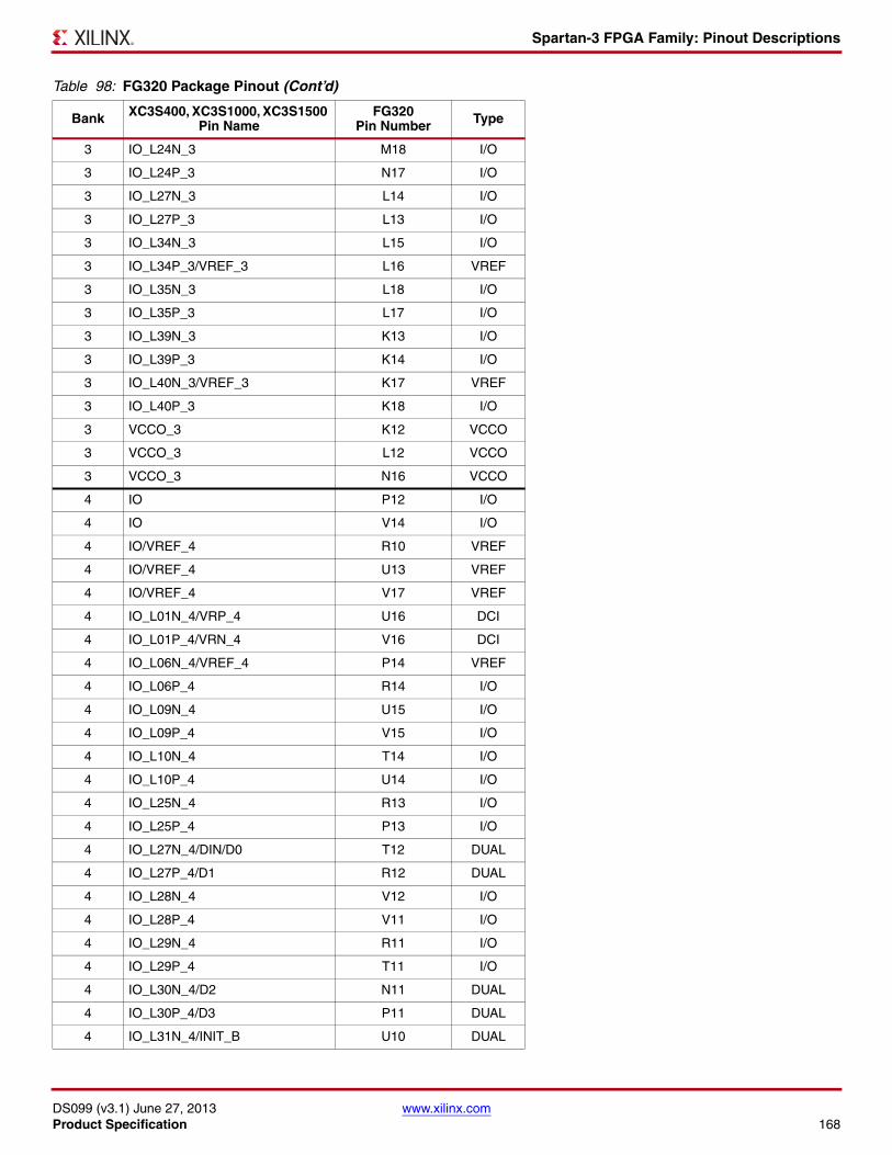
Spartan-3 FPGA Family: Pinout Descriptions
DS099 (v3.1) June 27, 2013 www.xilinx.comProduct Specification 168
3 IO_L24N_3 M18 I/O
3 IO_L24P_3 N17 I/O
3 IO_L27N_3 L14 I/O
3 IO_L27P_3 L13 I/O
3 IO_L34N_3 L15 I/O
3 IO_L34P_3/VREF_3 L16 VREF
3 IO_L35N_3 L18 I/O
3 IO_L35P_3 L17 I/O
3 IO_L39N_3 K13 I/O
3 IO_L39P_3 K14 I/O
3 IO_L40N_3/VREF_3 K17 VREF
3 IO_L40P_3 K18 I/O
3 VCCO_3 K12 VCCO
3 VCCO_3 L12 VCCO
3 VCCO_3 N16 VCCO
4 IO P12 I/O
4 IO V14 I/O
4 IO/VREF_4 R10 VREF
4 IO/VREF_4 U13 VREF
4 IO/VREF_4 V17 VREF
4 IO_L01N_4/VRP_4 U16 DCI
4 IO_L01P_4/VRN_4 V16 DCI
4 IO_L06N_4/VREF_4 P14 VREF
4 IO_L06P_4 R14 I/O
4 IO_L09N_4 U15 I/O
4 IO_L09P_4 V15 I/O
4 IO_L10N_4 T14 I/O
4 IO_L10P_4 U14 I/O
4 IO_L25N_4 R13 I/O
4 IO_L25P_4 P13 I/O
4 IO_L27N_4/DIN/D0 T12 DUAL
4 IO_L27P_4/D1 R12 DUAL
4 IO_L28N_4 V12 I/O
4 IO_L28P_4 V11 I/O
4 IO_L29N_4 R11 I/O
4 IO_L29P_4 T11 I/O
4 IO_L30N_4/D2 N11 DUAL
4 IO_L30P_4/D3 P11 DUAL
4 IO_L31N_4/INIT_B U10 DUAL
Table 98: FG320 Package Pinout (Cont’d)
Bank XC3S400, XC3S1000, XC3S1500 Pin Name
FG320Pin Number Type
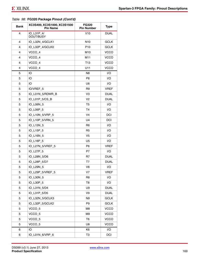
Spartan-3 FPGA Family: Pinout Descriptions
DS099 (v3.1) June 27, 2013 www.xilinx.comProduct Specification 169
4 IO_L31P_4/DOUT/BUSY
V10 DUAL
4 IO_L32N_4/GCLK1 N10 GCLK
4 IO_L32P_4/GCLK0 P10 GCLK
4 VCCO_4 M10 VCCO
4 VCCO_4 M11 VCCO
4 VCCO_4 T13 VCCO
4 VCCO_4 U11 VCCO
5 IO N8 I/O
5 IO P8 I/O
5 IO U6 I/O
5 IO/VREF_5 R9 VREF
5 IO_L01N_5/RDWR_B V3 DUAL
5 IO_L01P_5/CS_B V2 DUAL
5 IO_L06N_5 T5 I/O
5 IO_L06P_5 T4 I/O
5 IO_L10N_5/VRP_5 V4 DCI
5 IO_L10P_5/VRN_5 U4 DCI
5 IO_L15N_5 R6 I/O
5 IO_L15P_5 R5 I/O
5 IO_L16N_5 V5 I/O
5 IO_L16P_5 U5 I/O
5 IO_L27N_5/VREF_5 P6 VREF
5 IO_L27P_5 P7 I/O
5 IO_L28N_5/D6 R7 DUAL
5 IO_L28P_5/D7 T7 DUAL
5 IO_L29N_5 V8 I/O
5 IO_L29P_5/VREF_5 V7 VREF
5 IO_L30N_5 R8 I/O
5 IO_L30P_5 T8 I/O
5 IO_L31N_5/D4 U9 DUAL
5 IO_L31P_5/D5 V9 DUAL
5 IO_L32N_5/GCLK3 N9 GCLK
5 IO_L32P_5/GCLK2 P9 GCLK
5 VCCO_5 M8 VCCO
5 VCCO_5 M9 VCCO
5 VCCO_5 T6 VCCO
5 VCCO_5 U8 VCCO
6 IO K6 I/O
6 IO_L01N_6/VRP_6 T3 DCI
Table 98: FG320 Package Pinout (Cont’d)
Bank XC3S400, XC3S1000, XC3S1500 Pin Name
FG320Pin Number Type
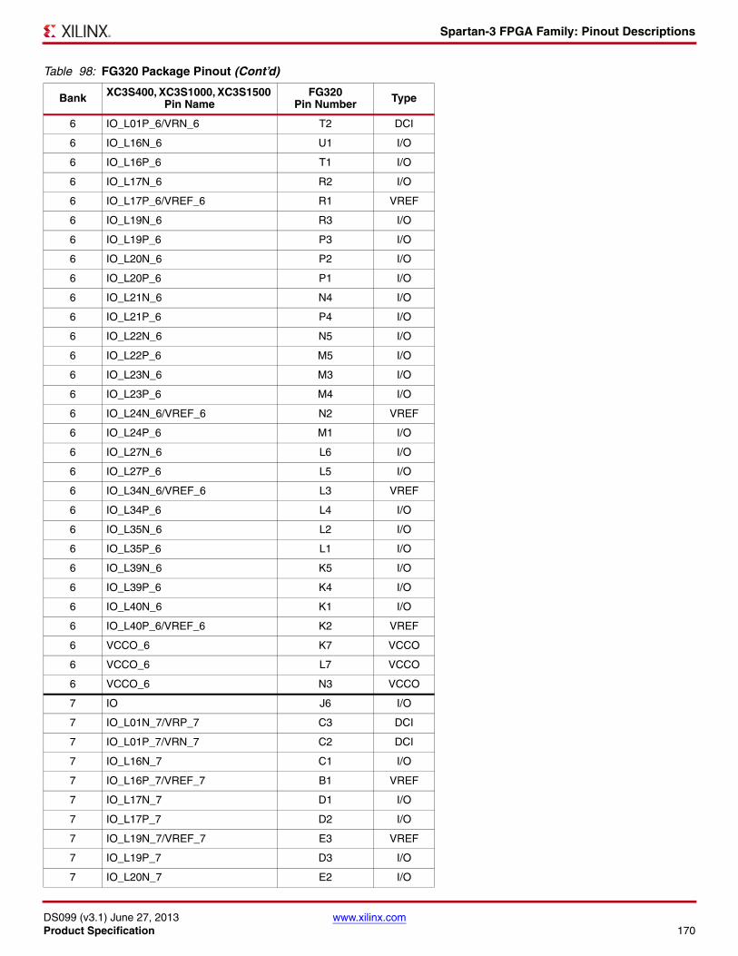
Spartan-3 FPGA Family: Pinout Descriptions
DS099 (v3.1) June 27, 2013 www.xilinx.comProduct Specification 170
6 IO_L01P_6/VRN_6 T2 DCI
6 IO_L16N_6 U1 I/O
6 IO_L16P_6 T1 I/O
6 IO_L17N_6 R2 I/O
6 IO_L17P_6/VREF_6 R1 VREF
6 IO_L19N_6 R3 I/O
6 IO_L19P_6 P3 I/O
6 IO_L20N_6 P2 I/O
6 IO_L20P_6 P1 I/O
6 IO_L21N_6 N4 I/O
6 IO_L21P_6 P4 I/O
6 IO_L22N_6 N5 I/O
6 IO_L22P_6 M5 I/O
6 IO_L23N_6 M3 I/O
6 IO_L23P_6 M4 I/O
6 IO_L24N_6/VREF_6 N2 VREF
6 IO_L24P_6 M1 I/O
6 IO_L27N_6 L6 I/O
6 IO_L27P_6 L5 I/O
6 IO_L34N_6/VREF_6 L3 VREF
6 IO_L34P_6 L4 I/O
6 IO_L35N_6 L2 I/O
6 IO_L35P_6 L1 I/O
6 IO_L39N_6 K5 I/O
6 IO_L39P_6 K4 I/O
6 IO_L40N_6 K1 I/O
6 IO_L40P_6/VREF_6 K2 VREF
6 VCCO_6 K7 VCCO
6 VCCO_6 L7 VCCO
6 VCCO_6 N3 VCCO
7 IO J6 I/O
7 IO_L01N_7/VRP_7 C3 DCI
7 IO_L01P_7/VRN_7 C2 DCI
7 IO_L16N_7 C1 I/O
7 IO_L16P_7/VREF_7 B1 VREF
7 IO_L17N_7 D1 I/O
7 IO_L17P_7 D2 I/O
7 IO_L19N_7/VREF_7 E3 VREF
7 IO_L19P_7 D3 I/O
7 IO_L20N_7 E2 I/O
Table 98: FG320 Package Pinout (Cont’d)
Bank XC3S400, XC3S1000, XC3S1500 Pin Name
FG320Pin Number Type
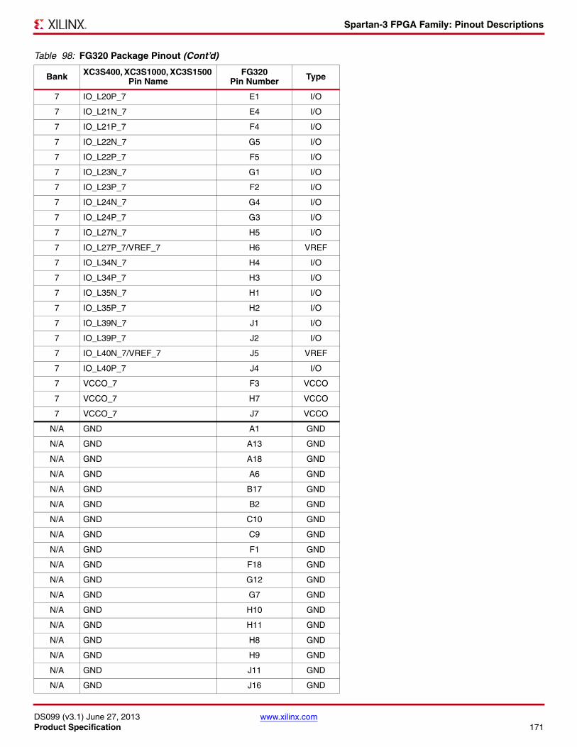
Spartan-3 FPGA Family: Pinout Descriptions
DS099 (v3.1) June 27, 2013 www.xilinx.comProduct Specification 171
7 IO_L20P_7 E1 I/O
7 IO_L21N_7 E4 I/O
7 IO_L21P_7 F4 I/O
7 IO_L22N_7 G5 I/O
7 IO_L22P_7 F5 I/O
7 IO_L23N_7 G1 I/O
7 IO_L23P_7 F2 I/O
7 IO_L24N_7 G4 I/O
7 IO_L24P_7 G3 I/O
7 IO_L27N_7 H5 I/O
7 IO_L27P_7/VREF_7 H6 VREF
7 IO_L34N_7 H4 I/O
7 IO_L34P_7 H3 I/O
7 IO_L35N_7 H1 I/O
7 IO_L35P_7 H2 I/O
7 IO_L39N_7 J1 I/O
7 IO_L39P_7 J2 I/O
7 IO_L40N_7/VREF_7 J5 VREF
7 IO_L40P_7 J4 I/O
7 VCCO_7 F3 VCCO
7 VCCO_7 H7 VCCO
7 VCCO_7 J7 VCCO
N/A GND A1 GND
N/A GND A13 GND
N/A GND A18 GND
N/A GND A6 GND
N/A GND B17 GND
N/A GND B2 GND
N/A GND C10 GND
N/A GND C9 GND
N/A GND F1 GND
N/A GND F18 GND
N/A GND G12 GND
N/A GND G7 GND
N/A GND H10 GND
N/A GND H11 GND
N/A GND H8 GND
N/A GND H9 GND
N/A GND J11 GND
N/A GND J16 GND
Table 98: FG320 Package Pinout (Cont’d)
Bank XC3S400, XC3S1000, XC3S1500 Pin Name
FG320Pin Number Type
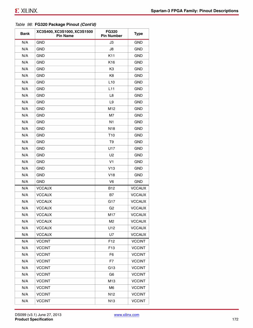
Spartan-3 FPGA Family: Pinout Descriptions
DS099 (v3.1) June 27, 2013 www.xilinx.comProduct Specification 172
N/A GND J3 GND
N/A GND J8 GND
N/A GND K11 GND
N/A GND K16 GND
N/A GND K3 GND
N/A GND K8 GND
N/A GND L10 GND
N/A GND L11 GND
N/A GND L8 GND
N/A GND L9 GND
N/A GND M12 GND
N/A GND M7 GND
N/A GND N1 GND
N/A GND N18 GND
N/A GND T10 GND
N/A GND T9 GND
N/A GND U17 GND
N/A GND U2 GND
N/A GND V1 GND
N/A GND V13 GND
N/A GND V18 GND
N/A GND V6 GND
N/A VCCAUX B12 VCCAUX
N/A VCCAUX B7 VCCAUX
N/A VCCAUX G17 VCCAUX
N/A VCCAUX G2 VCCAUX
N/A VCCAUX M17 VCCAUX
N/A VCCAUX M2 VCCAUX
N/A VCCAUX U12 VCCAUX
N/A VCCAUX U7 VCCAUX
N/A VCCINT F12 VCCINT
N/A VCCINT F13 VCCINT
N/A VCCINT F6 VCCINT
N/A VCCINT F7 VCCINT
N/A VCCINT G13 VCCINT
N/A VCCINT G6 VCCINT
N/A VCCINT M13 VCCINT
N/A VCCINT M6 VCCINT
N/A VCCINT N12 VCCINT
N/A VCCINT N13 VCCINT
Table 98: FG320 Package Pinout (Cont’d)
Bank XC3S400, XC3S1000, XC3S1500 Pin Name
FG320Pin Number Type
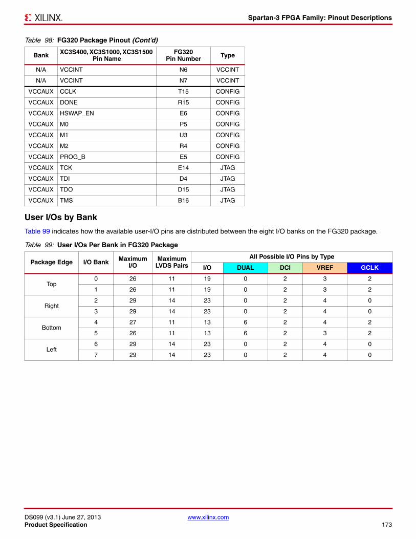
Spartan-3 FPGA Family: Pinout Descriptions
DS099 (v3.1) June 27, 2013 www.xilinx.comProduct Specification 173
User I/Os by Bank
Table 99 indicates how the available user-I/O pins are distributed between the eight I/O banks on the FG320 package.
N/A VCCINT N6 VCCINT
N/A VCCINT N7 VCCINT
VCCAUX CCLK T15 CONFIG
VCCAUX DONE R15 CONFIG
VCCAUX HSWAP_EN E6 CONFIG
VCCAUX M0 P5 CONFIG
VCCAUX M1 U3 CONFIG
VCCAUX M2 R4 CONFIG
VCCAUX PROG_B E5 CONFIG
VCCAUX TCK E14 JTAG
VCCAUX TDI D4 JTAG
VCCAUX TDO D15 JTAG
VCCAUX TMS B16 JTAG
Table 99: User I/Os Per Bank in FG320 Package
Package Edge I/O Bank Maximum I/O
Maximum LVDS Pairs
All Possible I/O Pins by Type
I/O DUAL DCI VREF GCLK
Top0 26 11 19 0 2 3 2
1 26 11 19 0 2 3 2
Right2 29 14 23 0 2 4 0
3 29 14 23 0 2 4 0
Bottom4 27 11 13 6 2 4 2
5 26 11 13 6 2 3 2
Left6 29 14 23 0 2 4 0
7 29 14 23 0 2 4 0
Table 98: FG320 Package Pinout (Cont’d)
Bank XC3S400, XC3S1000, XC3S1500 Pin Name
FG320Pin Number Type
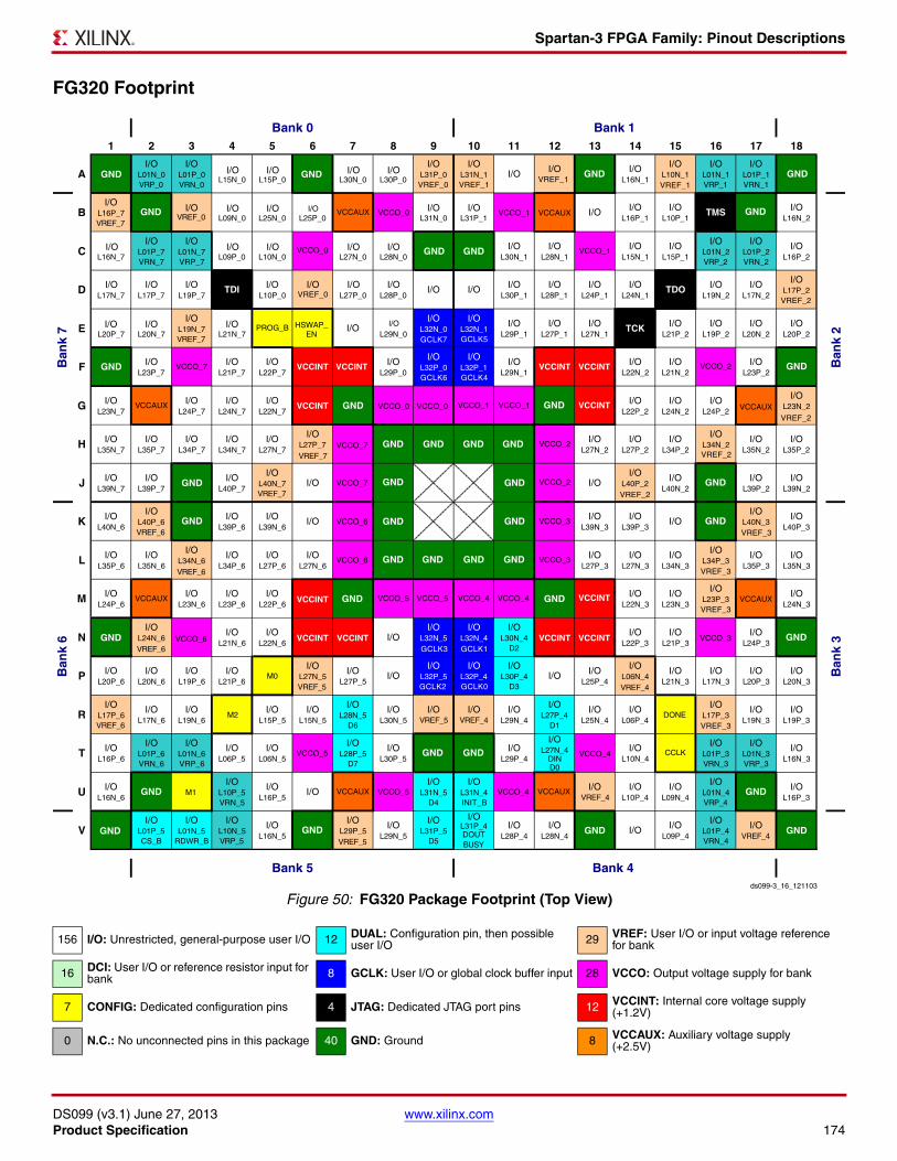
Spartan-3 FPGA Family: Pinout Descriptions
DS099 (v3.1) June 27, 2013 www.xilinx.comProduct Specification 174
FG320 FootprintX-Ref Target - Figure 50
Figure 50: FG320 Package Footprint (Top View)
156 I/O: Unrestricted, general-purpose user I/O 12 DUAL: Configuration pin, then possible user I/O 29 VREF: User I/O or input voltage reference
for bank
16 DCI: User I/O or reference resistor input for bank 8 GCLK: User I/O or global clock buffer input 28 VCCO: Output voltage supply for bank
7 CONFIG: Dedicated configuration pins 4 JTAG: Dedicated JTAG port pins 12 VCCINT: Internal core voltage supply (+1.2V)
0 N.C.: No unconnected pins in this package 40 GND: Ground 8 VCCAUX: Auxiliary voltage supply (+2.5V)
1 2 3 4 5 6 7 8 9 10 11 12 13 14 15 16 17 18
AI/O
L01N_0VRP_0
I/OL01P_0VRN_0
L15N_0 L15P_0 L30N_0 L30P_0
I/OL31P_0
I/O
I/O I/O
L31N_1VREF_1
VREF_1VREF_1
VREF_2
VREF_2
VREF_2
VREF_2
VREF_3
VREF_3
VREF_3
VREF_3
I/O I/O I/OL16N_1
I/OL10N_1
I/OL01N_1VRP_1
I/OL01P_1VRN_1
BI/O
L16P_7VREF_7
VREF_0 L09N_0 L25N_0 L25P_0 L31N_0 L31P_1VCCAUXVCCAUX I/O I/O
L16P_1I/O
L10P_1TMS I/O
L16N_2
CL16N_7
I/OL01P_7VRN_7
I/O
I/O
L01N_7VRP_7
L09P_0 L10N_0 L27N_0 L28N_0I/O
L30N_1I/O
L28N_1VCCO_1 I/O
L15N_1I/O
L15P_1
I/OL01N_2VRP_2
I/OL01P_2VRN_2
I/OL16P_2
DL17N_7
I/OL17P_7
I/O I/O I/O I/O I/O
I/O I/OI/O I/O
I/O
I/O
I/O I/O
I/O I/O I/O I/O
L19P_7TDI
L10P_0 VREF_0
VREF_0
L27P_0 L28P_0I/O I/O I/O
L30P_1I/O
L28P_1I/O
L24P_1I/O
L24N_1TDO I/O
L19N_2I/O
L17N_2
I/OL17P_2
EL20P_7
I/O
I/O
L20N_7
I/OL19N_7
L21N_7PROG_B HSWAP_
EN L29N_0
I/OL32N_0
I/OL32N_1GCLK5
I/OL29P_1
I/OL27P_1
I/OL27N_1
TCK I/OL21P_2
I/OL19P_2
I/OL20N_2
I/OL20P_2
F I/OL23P_7
VCCO_7
VCCO_7
VCCO_0
VCCO_0
VCCO_0
VCCO_0
VCCO_7
VCCO_6
VCCO_6
VCCO_6
I/O
I/O I/O
L21P_7I/O
L22P_7VCCINT
VCCINT
VCCINT
VCCINT VCCINT VCCINT VCCINT
VCCINT
VCCINT VCCINT VCCINT
VCCINT
I/OL29P_0
I/OL32P_0
I/OL32P_1GCLK4GCLK6
GCLK7
I/OL29N_1
I/OL22N_2
I/OL21N_2
I/OL23P_2
G I/OL23N_7
VCCAUX I/OL24P_7
I/OL24N_7
I/OL22N_7
GND
GND
GND
GND
GND GND
GND
GND
GND
GND
GND
GND
GND GND
GND
GND
GND
GND
GND
GND GND
GNDGND
GND GND
GND GND
GND
GND
GND
GND
GND
GND
GND
GND GND GND
GNDVCCO_1
VCCO_2
VCCO_2
VCCO_2
VCCO_1
VCCO_1
I/OL22P_2
I/OL24N_2
I/OL24P_2
I/OL23N_2
H I/OL35N_7
I/O
I/O I/O
L35P_7I/O
L34P_7I/O
L34N_7I/O
L27N_7
I/OL27P_7
I/OL27N_2
I/OL27P_2
I/OL34P_2
I/OL34N_2
I/OL35N_2
I/OL35P_2
J I/OL39N_7
I/OL39P_7
I/OL40P_7
I/OL40N_7VREF_7
VREF_7
VREF_7
I/O GND I/OI/O
L40P_2I/O
L40N_2I/O
L39P_2I/O
L39N_2
K I/OL40N_6
I/OL40P_6
I/OL39P_6
I/OL39N_6
I/O GND I/OL39N_3
I/OL39P_3
I/OI/O
L40N_3I/O
L40P_3
L I/OL35P_6
I/OL35N_6
I/OL34N_6
I/OL34P_6
I/OL27P_6
I/OL27N_6
VCCO_3
VCCO_3
VCCO_3
I/OL27P_3
I/OL27N_3
I/OL34N_3
I/OL34P_3
I/OL35P_3
I/OL35N_3
M I/OL24P_6
I/OL23N_6
I/OL23P_6
I/OL22P_6
VCCO_5
VCCO_5
VCCO_5
VCCO_5 VCCO_4 VCCO_4
VCCO_4
VCCO_4
I/OL22N_3
I/OL23N_3
I/OL23P_3
I/OL24N_3
NI/O
L24N_6I/O
L21N_6I/O
L22N_6I/O
I/OL32N_5
I/OL32N_4
I/OL30N_4
D2
I/OL22P_3
I/OL21P_3
I/OL24P_3
P I/OL20P_6
I/OL20N_6
I/OL19P_6
I/OL21P_6
I/OL27N_5
I/OL27P_5
I/OI/O
L32P_5I/O
L32P_4GCLK0
GCLK1GCLK3
GCLK2
I/OL30P_4
D3I/O I/O
L25P_4
I/OL06N_4
I/OL21N_3
I/OL17N_3
I/OL20P_3
I/OL20N_3
RI/O
L17P_6VREF_6
VREF_6
VREF_6
VREF_6
I/OL17N_6
M1
M2
M0
I/OL19N_6
I/OL15P_5
I/OL15N_5
I/OL28N_5
D6
I/OL30N_5
I/O I/O I/OL29N_4
I/OL27P_4
D1
I/OL25N_4
I/OL06P_4
DONE
CCLK
I/OL17P_3
I/OL19N_3
I/OL19P_3
T I/OL16P_6
I/OL01P_6VRN_6
I/OL01N_6VRP_6
I/OL06P_5
I/OL06N_5
I/OL28P_5
D7
I/OL30P_5
I/OL29P_4
I/OL27N_4
DIND0
I/OL10N_4
I/OL01P_3VRN_3
I/OL01N_3VRP_3
I/OL16N_3
U I/OL16N_6
I/OL10P_5VRN_5
I/OL16P_5
I/O VCCAUX
VCCAUX
VCCAUX
VCCAUX
VCCAUX
I/OL31N_5
D4
I/OL31N_4INIT_B
I/O I/OL10P_4
I/OL09N_4
I/OL01N_4VRP_4
I/OL16P_3
VI/O
L01P_5CS_B
I/OL01N_5
RDWR_B
I/OL10N_5VRP_5
I/OL16N_5
I/OL29P_5
I/OL29N_5
I/OL31P_5
D5
I/OL31P_4DOUTBUSY
I/OL28P_4
I/OL28N_4
I/O I/OL09P_4
I/OL01P_4VRN_4
I/OVREF_4
VREF_4
VREF_4
VREF_4VREF_5
VREF_5
VREF_5
Bank 5 Bank 4
Bank 0 Bank 1
Ban
k 2
Ban
k 3
Ban
k 7
Ban
k 6
ds099-3_16_121103
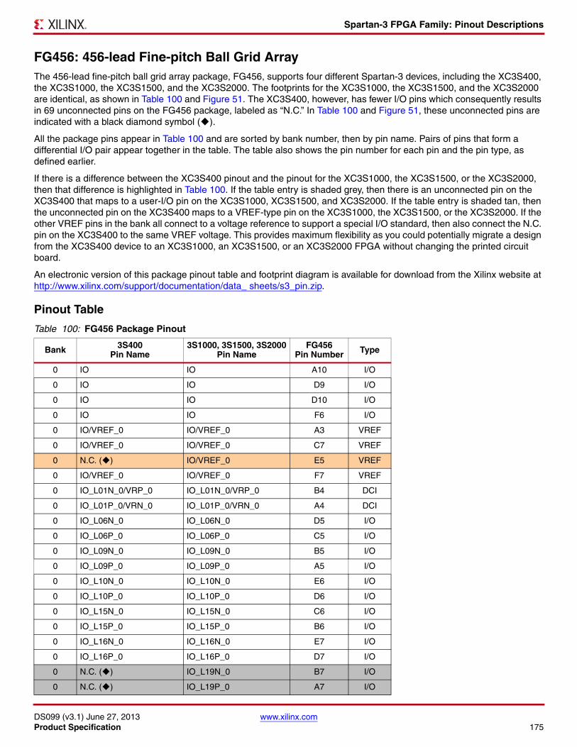
Spartan-3 FPGA Family: Pinout Descriptions
DS099 (v3.1) June 27, 2013 www.xilinx.comProduct Specification 175
FG456: 456-lead Fine-pitch Ball Grid ArrayThe 456-lead fine-pitch ball grid array package, FG456, supports four different Spartan-3 devices, including the XC3S400, the XC3S1000, the XC3S1500, and the XC3S2000. The footprints for the XC3S1000, the XC3S1500, and the XC3S2000 are identical, as shown in Table 100 and Figure 51. The XC3S400, however, has fewer I/O pins which consequently results in 69 unconnected pins on the FG456 package, labeled as “N.C.” In Table 100 and Figure 51, these unconnected pins are indicated with a black diamond symbol ().
All the package pins appear in Table 100 and are sorted by bank number, then by pin name. Pairs of pins that form a differential I/O pair appear together in the table. The table also shows the pin number for each pin and the pin type, as defined earlier.
If there is a difference between the XC3S400 pinout and the pinout for the XC3S1000, the XC3S1500, or the XC3S2000, then that difference is highlighted in Table 100. If the table entry is shaded grey, then there is an unconnected pin on the XC3S400 that maps to a user-I/O pin on the XC3S1000, XC3S1500, and XC3S2000. If the table entry is shaded tan, then the unconnected pin on the XC3S400 maps to a VREF-type pin on the XC3S1000, the XC3S1500, or the XC3S2000. If the other VREF pins in the bank all connect to a voltage reference to support a special I/O standard, then also connect the N.C. pin on the XC3S400 to the same VREF voltage. This provides maximum flexibility as you could potentially migrate a design from the XC3S400 device to an XC3S1000, an XC3S1500, or an XC3S2000 FPGA without changing the printed circuit board.
An electronic version of this package pinout table and footprint diagram is available for download from the Xilinx website at http://www.xilinx.com/support/documentation/data_ sheets/s3_pin.zip.
Pinout Table
Table 100: FG456 Package Pinout
Bank 3S400 Pin Name
3S1000, 3S1500, 3S2000Pin Name
FG456Pin Number Type
0 IO IO A10 I/O
0 IO IO D9 I/O
0 IO IO D10 I/O
0 IO IO F6 I/O
0 IO/VREF_0 IO/VREF_0 A3 VREF
0 IO/VREF_0 IO/VREF_0 C7 VREF
0 N.C. () IO/VREF_0 E5 VREF
0 IO/VREF_0 IO/VREF_0 F7 VREF
0 IO_L01N_0/VRP_0 IO_L01N_0/VRP_0 B4 DCI
0 IO_L01P_0/VRN_0 IO_L01P_0/VRN_0 A4 DCI
0 IO_L06N_0 IO_L06N_0 D5 I/O
0 IO_L06P_0 IO_L06P_0 C5 I/O
0 IO_L09N_0 IO_L09N_0 B5 I/O
0 IO_L09P_0 IO_L09P_0 A5 I/O
0 IO_L10N_0 IO_L10N_0 E6 I/O
0 IO_L10P_0 IO_L10P_0 D6 I/O
0 IO_L15N_0 IO_L15N_0 C6 I/O
0 IO_L15P_0 IO_L15P_0 B6 I/O
0 IO_L16N_0 IO_L16N_0 E7 I/O
0 IO_L16P_0 IO_L16P_0 D7 I/O
0 N.C. () IO_L19N_0 B7 I/O
0 N.C. () IO_L19P_0 A7 I/O
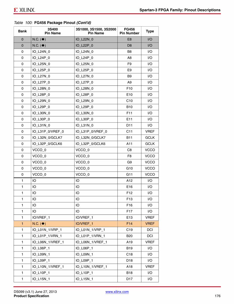
Spartan-3 FPGA Family: Pinout Descriptions
DS099 (v3.1) June 27, 2013 www.xilinx.comProduct Specification 176
0 N.C. () IO_L22N_0 E8 I/O
0 N.C. () IO_L22P_0 D8 I/O
0 IO_L24N_0 IO_L24N_0 B8 I/O
0 IO_L24P_0 IO_L24P_0 A8 I/O
0 IO_L25N_0 IO_L25N_0 F9 I/O
0 IO_L25P_0 IO_L25P_0 E9 I/O
0 IO_L27N_0 IO_L27N_0 B9 I/O
0 IO_L27P_0 IO_L27P_0 A9 I/O
0 IO_L28N_0 IO_L28N_0 F10 I/O
0 IO_L28P_0 IO_L28P_0 E10 I/O
0 IO_L29N_0 IO_L29N_0 C10 I/O
0 IO_L29P_0 IO_L29P_0 B10 I/O
0 IO_L30N_0 IO_L30N_0 F11 I/O
0 IO_L30P_0 IO_L30P_0 E11 I/O
0 IO_L31N_0 IO_L31N_0 D11 I/O
0 IO_L31P_0/VREF_0 IO_L31P_0/VREF_0 C11 VREF
0 IO_L32N_0/GCLK7 IO_L32N_0/GCLK7 B11 GCLK
0 IO_L32P_0/GCLK6 IO_L32P_0/GCLK6 A11 GCLK
0 VCCO_0 VCCO_0 C8 VCCO
0 VCCO_0 VCCO_0 F8 VCCO
0 VCCO_0 VCCO_0 G9 VCCO
0 VCCO_0 VCCO_0 G10 VCCO
0 VCCO_0 VCCO_0 G11 VCCO
1 IO IO A12 I/O
1 IO IO E16 I/O
1 IO IO F12 I/O
1 IO IO F13 I/O
1 IO IO F16 I/O
1 IO IO F17 I/O
1 IO/VREF_1 IO/VREF_1 E13 VREF
1 N.C. () IO/VREF_1 F14 VREF
1 IO_L01N_1/VRP_1 IO_L01N_1/VRP_1 C19 DCI
1 IO_L01P_1/VRN_1 IO_L01P_1/VRN_1 B20 DCI
1 IO_L06N_1/VREF_1 IO_L06N_1/VREF_1 A19 VREF
1 IO_L06P_1 IO_L06P_1 B19 I/O
1 IO_L09N_1 IO_L09N_1 C18 I/O
1 IO_L09P_1 IO_L09P_1 D18 I/O
1 IO_L10N_1/VREF_1 IO_L10N_1/VREF_1 A18 VREF
1 IO_L10P_1 IO_L10P_1 B18 I/O
1 IO_L15N_1 IO_L15N_1 D17 I/O
Table 100: FG456 Package Pinout (Cont’d)
Bank 3S400 Pin Name
3S1000, 3S1500, 3S2000Pin Name
FG456Pin Number Type
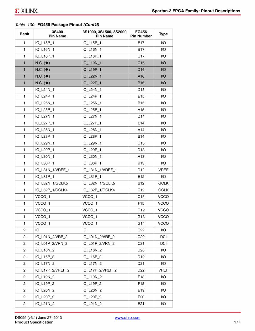
Spartan-3 FPGA Family: Pinout Descriptions
DS099 (v3.1) June 27, 2013 www.xilinx.comProduct Specification 177
1 IO_L15P_1 IO_L15P_1 E17 I/O
1 IO_L16N_1 IO_L16N_1 B17 I/O
1 IO_L16P_1 IO_L16P_1 C17 I/O
1 N.C. () IO_L19N_1 C16 I/O
1 N.C. () IO_L19P_1 D16 I/O
1 N.C. () IO_L22N_1 A16 I/O
1 N.C. () IO_L22P_1 B16 I/O
1 IO_L24N_1 IO_L24N_1 D15 I/O
1 IO_L24P_1 IO_L24P_1 E15 I/O
1 IO_L25N_1 IO_L25N_1 B15 I/O
1 IO_L25P_1 IO_L25P_1 A15 I/O
1 IO_L27N_1 IO_L27N_1 D14 I/O
1 IO_L27P_1 IO_L27P_1 E14 I/O
1 IO_L28N_1 IO_L28N_1 A14 I/O
1 IO_L28P_1 IO_L28P_1 B14 I/O
1 IO_L29N_1 IO_L29N_1 C13 I/O
1 IO_L29P_1 IO_L29P_1 D13 I/O
1 IO_L30N_1 IO_L30N_1 A13 I/O
1 IO_L30P_1 IO_L30P_1 B13 I/O
1 IO_L31N_1/VREF_1 IO_L31N_1/VREF_1 D12 VREF
1 IO_L31P_1 IO_L31P_1 E12 I/O
1 IO_L32N_1/GCLK5 IO_L32N_1/GCLK5 B12 GCLK
1 IO_L32P_1/GCLK4 IO_L32P_1/GCLK4 C12 GCLK
1 VCCO_1 VCCO_1 C15 VCCO
1 VCCO_1 VCCO_1 F15 VCCO
1 VCCO_1 VCCO_1 G12 VCCO
1 VCCO_1 VCCO_1 G13 VCCO
1 VCCO_1 VCCO_1 G14 VCCO
2 IO IO C22 I/O
2 IO_L01N_2/VRP_2 IO_L01N_2/VRP_2 C20 DCI
2 IO_L01P_2/VRN_2 IO_L01P_2/VRN_2 C21 DCI
2 IO_L16N_2 IO_L16N_2 D20 I/O
2 IO_L16P_2 IO_L16P_2 D19 I/O
2 IO_L17N_2 IO_L17N_2 D21 I/O
2 IO_L17P_2/VREF_2 IO_L17P_2/VREF_2 D22 VREF
2 IO_L19N_2 IO_L19N_2 E18 I/O
2 IO_L19P_2 IO_L19P_2 F18 I/O
2 IO_L20N_2 IO_L20N_2 E19 I/O
2 IO_L20P_2 IO_L20P_2 E20 I/O
2 IO_L21N_2 IO_L21N_2 E21 I/O
Table 100: FG456 Package Pinout (Cont’d)
Bank 3S400 Pin Name
3S1000, 3S1500, 3S2000Pin Name
FG456Pin Number Type
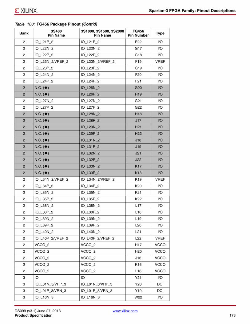
Spartan-3 FPGA Family: Pinout Descriptions
DS099 (v3.1) June 27, 2013 www.xilinx.comProduct Specification 178
2 IO_L21P_2 IO_L21P_2 E22 I/O
2 IO_L22N_2 IO_L22N_2 G17 I/O
2 IO_L22P_2 IO_L22P_2 G18 I/O
2 IO_L23N_2/VREF_2 IO_L23N_2/VREF_2 F19 VREF
2 IO_L23P_2 IO_L23P_2 G19 I/O
2 IO_L24N_2 IO_L24N_2 F20 I/O
2 IO_L24P_2 IO_L24P_2 F21 I/O
2 N.C. () IO_L26N_2 G20 I/O
2 N.C. () IO_L26P_2 H19 I/O
2 IO_L27N_2 IO_L27N_2 G21 I/O
2 IO_L27P_2 IO_L27P_2 G22 I/O
2 N.C. () IO_L28N_2 H18 I/O
2 N.C. () IO_L28P_2 J17 I/O
2 N.C. () IO_L29N_2 H21 I/O
2 N.C. () IO_L29P_2 H22 I/O
2 N.C. () IO_L31N_2 J18 I/O
2 N.C. () IO_L31P_2 J19 I/O
2 N.C. () IO_L32N_2 J21 I/O
2 N.C. () IO_L32P_2 J22 I/O
2 N.C. () IO_L33N_2 K17 I/O
2 N.C. () IO_L33P_2 K18 I/O
2 IO_L34N_2/VREF_2 IO_L34N_2/VREF_2 K19 VREF
2 IO_L34P_2 IO_L34P_2 K20 I/O
2 IO_L35N_2 IO_L35N_2 K21 I/O
2 IO_L35P_2 IO_L35P_2 K22 I/O
2 IO_L38N_2 IO_L38N_2 L17 I/O
2 IO_L38P_2 IO_L38P_2 L18 I/O
2 IO_L39N_2 IO_L39N_2 L19 I/O
2 IO_L39P_2 IO_L39P_2 L20 I/O
2 IO_L40N_2 IO_L40N_2 L21 I/O
2 IO_L40P_2/VREF_2 IO_L40P_2/VREF_2 L22 VREF
2 VCCO_2 VCCO_2 H17 VCCO
2 VCCO_2 VCCO_2 H20 VCCO
2 VCCO_2 VCCO_2 J16 VCCO
2 VCCO_2 VCCO_2 K16 VCCO
2 VCCO_2 VCCO_2 L16 VCCO
3 IO IO Y21 I/O
3 IO_L01N_3/VRP_3 IO_L01N_3/VRP_3 Y20 DCI
3 IO_L01P_3/VRN_3 IO_L01P_3/VRN_3 Y19 DCI
3 IO_L16N_3 IO_L16N_3 W22 I/O
Table 100: FG456 Package Pinout (Cont’d)
Bank 3S400 Pin Name
3S1000, 3S1500, 3S2000Pin Name
FG456Pin Number Type
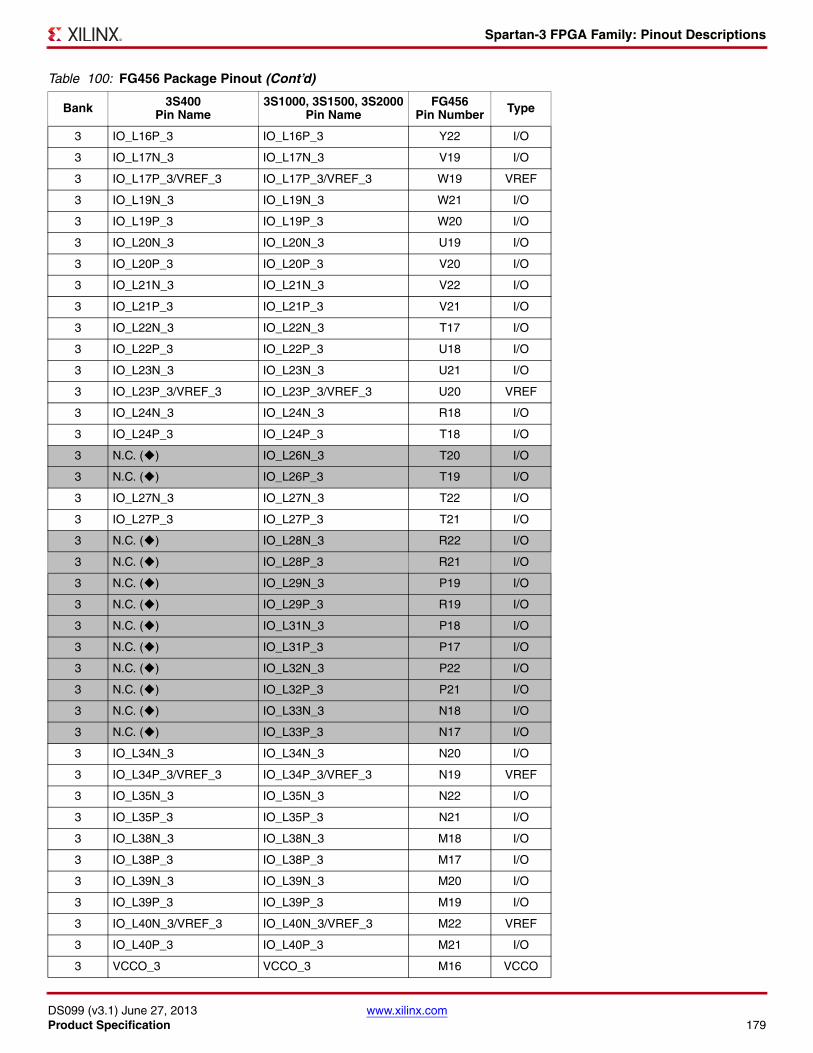
Spartan-3 FPGA Family: Pinout Descriptions
DS099 (v3.1) June 27, 2013 www.xilinx.comProduct Specification 179
3 IO_L16P_3 IO_L16P_3 Y22 I/O
3 IO_L17N_3 IO_L17N_3 V19 I/O
3 IO_L17P_3/VREF_3 IO_L17P_3/VREF_3 W19 VREF
3 IO_L19N_3 IO_L19N_3 W21 I/O
3 IO_L19P_3 IO_L19P_3 W20 I/O
3 IO_L20N_3 IO_L20N_3 U19 I/O
3 IO_L20P_3 IO_L20P_3 V20 I/O
3 IO_L21N_3 IO_L21N_3 V22 I/O
3 IO_L21P_3 IO_L21P_3 V21 I/O
3 IO_L22N_3 IO_L22N_3 T17 I/O
3 IO_L22P_3 IO_L22P_3 U18 I/O
3 IO_L23N_3 IO_L23N_3 U21 I/O
3 IO_L23P_3/VREF_3 IO_L23P_3/VREF_3 U20 VREF
3 IO_L24N_3 IO_L24N_3 R18 I/O
3 IO_L24P_3 IO_L24P_3 T18 I/O
3 N.C. () IO_L26N_3 T20 I/O
3 N.C. () IO_L26P_3 T19 I/O
3 IO_L27N_3 IO_L27N_3 T22 I/O
3 IO_L27P_3 IO_L27P_3 T21 I/O
3 N.C. () IO_L28N_3 R22 I/O
3 N.C. () IO_L28P_3 R21 I/O
3 N.C. () IO_L29N_3 P19 I/O
3 N.C. () IO_L29P_3 R19 I/O
3 N.C. () IO_L31N_3 P18 I/O
3 N.C. () IO_L31P_3 P17 I/O
3 N.C. () IO_L32N_3 P22 I/O
3 N.C. () IO_L32P_3 P21 I/O
3 N.C. () IO_L33N_3 N18 I/O
3 N.C. () IO_L33P_3 N17 I/O
3 IO_L34N_3 IO_L34N_3 N20 I/O
3 IO_L34P_3/VREF_3 IO_L34P_3/VREF_3 N19 VREF
3 IO_L35N_3 IO_L35N_3 N22 I/O
3 IO_L35P_3 IO_L35P_3 N21 I/O
3 IO_L38N_3 IO_L38N_3 M18 I/O
3 IO_L38P_3 IO_L38P_3 M17 I/O
3 IO_L39N_3 IO_L39N_3 M20 I/O
3 IO_L39P_3 IO_L39P_3 M19 I/O
3 IO_L40N_3/VREF_3 IO_L40N_3/VREF_3 M22 VREF
3 IO_L40P_3 IO_L40P_3 M21 I/O
3 VCCO_3 VCCO_3 M16 VCCO
Table 100: FG456 Package Pinout (Cont’d)
Bank 3S400 Pin Name
3S1000, 3S1500, 3S2000Pin Name
FG456Pin Number Type
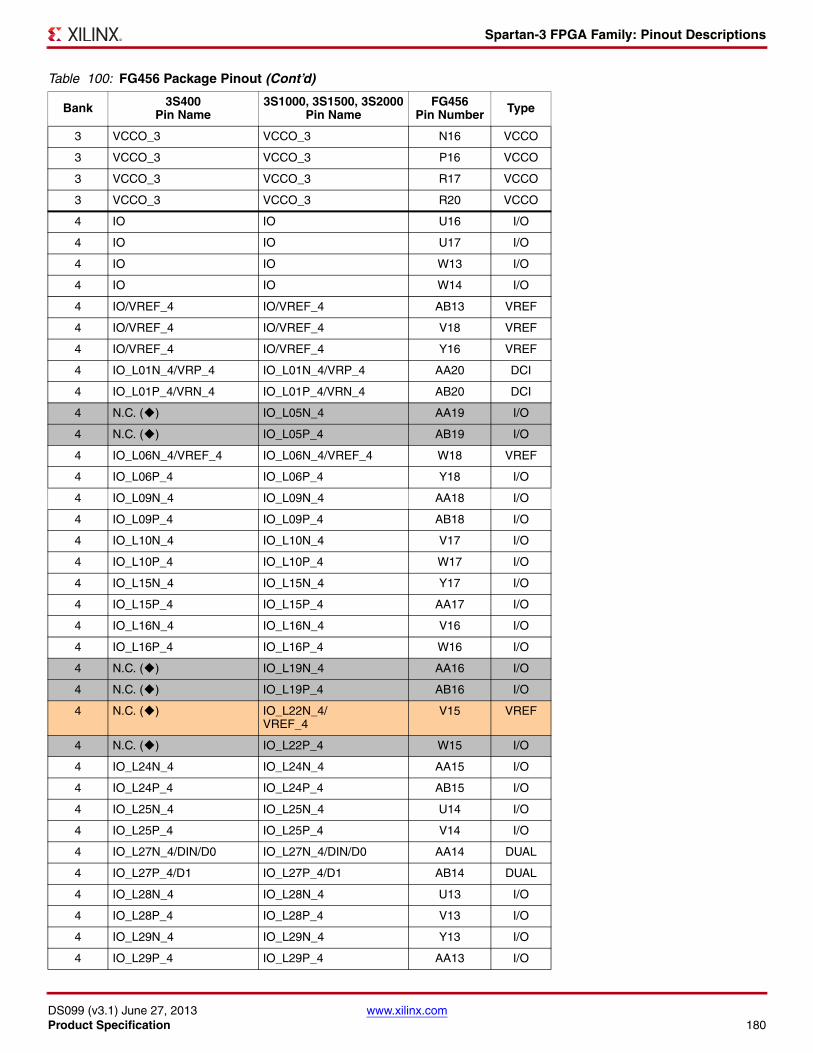
Spartan-3 FPGA Family: Pinout Descriptions
DS099 (v3.1) June 27, 2013 www.xilinx.comProduct Specification 180
3 VCCO_3 VCCO_3 N16 VCCO
3 VCCO_3 VCCO_3 P16 VCCO
3 VCCO_3 VCCO_3 R17 VCCO
3 VCCO_3 VCCO_3 R20 VCCO
4 IO IO U16 I/O
4 IO IO U17 I/O
4 IO IO W13 I/O
4 IO IO W14 I/O
4 IO/VREF_4 IO/VREF_4 AB13 VREF
4 IO/VREF_4 IO/VREF_4 V18 VREF
4 IO/VREF_4 IO/VREF_4 Y16 VREF
4 IO_L01N_4/VRP_4 IO_L01N_4/VRP_4 AA20 DCI
4 IO_L01P_4/VRN_4 IO_L01P_4/VRN_4 AB20 DCI
4 N.C. () IO_L05N_4 AA19 I/O
4 N.C. () IO_L05P_4 AB19 I/O
4 IO_L06N_4/VREF_4 IO_L06N_4/VREF_4 W18 VREF
4 IO_L06P_4 IO_L06P_4 Y18 I/O
4 IO_L09N_4 IO_L09N_4 AA18 I/O
4 IO_L09P_4 IO_L09P_4 AB18 I/O
4 IO_L10N_4 IO_L10N_4 V17 I/O
4 IO_L10P_4 IO_L10P_4 W17 I/O
4 IO_L15N_4 IO_L15N_4 Y17 I/O
4 IO_L15P_4 IO_L15P_4 AA17 I/O
4 IO_L16N_4 IO_L16N_4 V16 I/O
4 IO_L16P_4 IO_L16P_4 W16 I/O
4 N.C. () IO_L19N_4 AA16 I/O
4 N.C. () IO_L19P_4 AB16 I/O
4 N.C. () IO_L22N_4/VREF_4
V15 VREF
4 N.C. () IO_L22P_4 W15 I/O
4 IO_L24N_4 IO_L24N_4 AA15 I/O
4 IO_L24P_4 IO_L24P_4 AB15 I/O
4 IO_L25N_4 IO_L25N_4 U14 I/O
4 IO_L25P_4 IO_L25P_4 V14 I/O
4 IO_L27N_4/DIN/D0 IO_L27N_4/DIN/D0 AA14 DUAL
4 IO_L27P_4/D1 IO_L27P_4/D1 AB14 DUAL
4 IO_L28N_4 IO_L28N_4 U13 I/O
4 IO_L28P_4 IO_L28P_4 V13 I/O
4 IO_L29N_4 IO_L29N_4 Y13 I/O
4 IO_L29P_4 IO_L29P_4 AA13 I/O
Table 100: FG456 Package Pinout (Cont’d)
Bank 3S400 Pin Name
3S1000, 3S1500, 3S2000Pin Name
FG456Pin Number Type
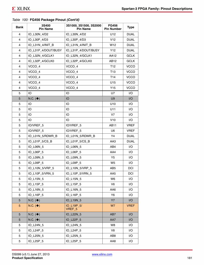
Spartan-3 FPGA Family: Pinout Descriptions
DS099 (v3.1) June 27, 2013 www.xilinx.comProduct Specification 181
4 IO_L30N_4/D2 IO_L30N_4/D2 U12 DUAL
4 IO_L30P_4/D3 IO_L30P_4/D3 V12 DUAL
4 IO_L31N_4/INIT_B IO_L31N_4/INIT_B W12 DUAL
4 IO_L31P_4/DOUT/BUSY IO_L31P_4/DOUT/BUSY Y12 DUAL
4 IO_L32N_4/GCLK1 IO_L32N_4/GCLK1 AA12 GCLK
4 IO_L32P_4/GCLK0 IO_L32P_4/GCLK0 AB12 GCLK
4 VCCO_4 VCCO_4 T12 VCCO
4 VCCO_4 VCCO_4 T13 VCCO
4 VCCO_4 VCCO_4 T14 VCCO
4 VCCO_4 VCCO_4 U15 VCCO
4 VCCO_4 VCCO_4 Y15 VCCO
5 IO IO U7 I/O
5 N.C. () IO U9 I/O
5 IO IO U10 I/O
5 IO IO U11 I/O
5 IO IO V7 I/O
5 IO IO V10 I/O
5 IO/VREF_5 IO/VREF_5 AB11 VREF
5 IO/VREF_5 IO/VREF_5 U6 VREF
5 IO_L01N_5/RDWR_B IO_L01N_5/RDWR_B Y4 DUAL
5 IO_L01P_5/CS_B IO_L01P_5/CS_B AA3 DUAL
5 IO_L06N_5 IO_L06N_5 AB4 I/O
5 IO_L06P_5 IO_L06P_5 AA4 I/O
5 IO_L09N_5 IO_L09N_5 Y5 I/O
5 IO_L09P_5 IO_L09P_5 W5 I/O
5 IO_L10N_5/VRP_5 IO_L10N_5/VRP_5 AB5 DCI
5 IO_L10P_5/VRN_5 IO_L10P_5/VRN_5 AA5 DCI
5 IO_L15N_5 IO_L15N_5 W6 I/O
5 IO_L15P_5 IO_L15P_5 V6 I/O
5 IO_L16N_5 IO_L16N_5 AA6 I/O
5 IO_L16P_5 IO_L16P_5 Y6 I/O
5 N.C. () IO_L19N_5 Y7 I/O
5 N.C. () IO_L19P_5/VREF_5
W7 VREF
5 N.C. () IO_L22N_5 AB7 I/O
5 N.C. () IO_L22P_5 AA7 I/O
5 IO_L24N_5 IO_L24N_5 W8 I/O
5 IO_L24P_5 IO_L24P_5 V8 I/O
5 IO_L25N_5 IO_L25N_5 AB8 I/O
5 IO_L25P_5 IO_L25P_5 AA8 I/O
Table 100: FG456 Package Pinout (Cont’d)
Bank 3S400 Pin Name
3S1000, 3S1500, 3S2000Pin Name
FG456Pin Number Type
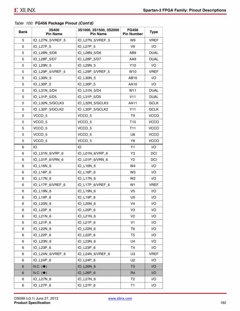
Spartan-3 FPGA Family: Pinout Descriptions
DS099 (v3.1) June 27, 2013 www.xilinx.comProduct Specification 182
5 IO_L27N_5/VREF_5 IO_L27N_5/VREF_5 W9 VREF
5 IO_L27P_5 IO_L27P_5 V9 I/O
5 IO_L28N_5/D6 IO_L28N_5/D6 AB9 DUAL
5 IO_L28P_5/D7 IO_L28P_5/D7 AA9 DUAL
5 IO_L29N_5 IO_L29N_5 Y10 I/O
5 IO_L29P_5/VREF_5 IO_L29P_5/VREF_5 W10 VREF
5 IO_L30N_5 IO_L30N_5 AB10 I/O
5 IO_L30P_5 IO_L30P_5 AA10 I/O
5 IO_L31N_5/D4 IO_L31N_5/D4 W11 DUAL
5 IO_L31P_5/D5 IO_L31P_5/D5 V11 DUAL
5 IO_L32N_5/GCLK3 IO_L32N_5/GCLK3 AA11 GCLK
5 IO_L32P_5/GCLK2 IO_L32P_5/GCLK2 Y11 GCLK
5 VCCO_5 VCCO_5 T9 VCCO
5 VCCO_5 VCCO_5 T10 VCCO
5 VCCO_5 VCCO_5 T11 VCCO
5 VCCO_5 VCCO_5 U8 VCCO
5 VCCO_5 VCCO_5 Y8 VCCO
6 IO IO Y1 I/O
6 IO_L01N_6/VRP_6 IO_L01N_6/VRP_6 Y3 DCI
6 IO_L01P_6/VRN_6 IO_L01P_6/VRN_6 Y2 DCI
6 IO_L16N_6 IO_L16N_6 W4 I/O
6 IO_L16P_6 IO_L16P_6 W3 I/O
6 IO_L17N_6 IO_L17N_6 W2 I/O
6 IO_L17P_6/VREF_6 IO_L17P_6/VREF_6 W1 VREF
6 IO_L19N_6 IO_L19N_6 V5 I/O
6 IO_L19P_6 IO_L19P_6 U5 I/O
6 IO_L20N_6 IO_L20N_6 V4 I/O
6 IO_L20P_6 IO_L20P_6 V3 I/O
6 IO_L21N_6 IO_L21N_6 V2 I/O
6 IO_L21P_6 IO_L21P_6 V1 I/O
6 IO_L22N_6 IO_L22N_6 T6 I/O
6 IO_L22P_6 IO_L22P_6 T5 I/O
6 IO_L23N_6 IO_L23N_6 U4 I/O
6 IO_L23P_6 IO_L23P_6 T4 I/O
6 IO_L24N_6/VREF_6 IO_L24N_6/VREF_6 U3 VREF
6 IO_L24P_6 IO_L24P_6 U2 I/O
6 N.C. () IO_L26N_6 T3 I/O
6 N.C. () IO_L26P_6 R4 I/O
6 IO_L27N_6 IO_L27N_6 T2 I/O
6 IO_L27P_6 IO_L27P_6 T1 I/O
Table 100: FG456 Package Pinout (Cont’d)
Bank 3S400 Pin Name
3S1000, 3S1500, 3S2000Pin Name
FG456Pin Number Type
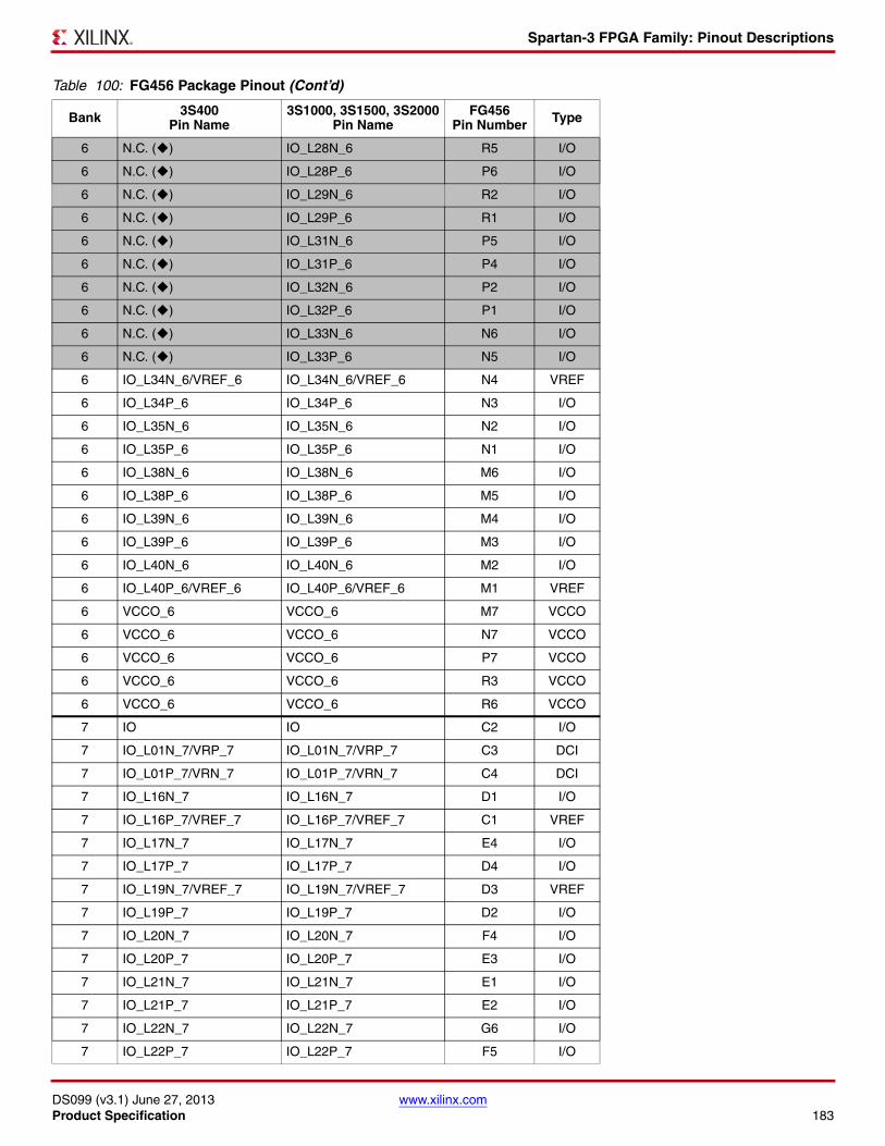
Spartan-3 FPGA Family: Pinout Descriptions
DS099 (v3.1) June 27, 2013 www.xilinx.comProduct Specification 183
6 N.C. () IO_L28N_6 R5 I/O
6 N.C. () IO_L28P_6 P6 I/O
6 N.C. () IO_L29N_6 R2 I/O
6 N.C. () IO_L29P_6 R1 I/O
6 N.C. () IO_L31N_6 P5 I/O
6 N.C. () IO_L31P_6 P4 I/O
6 N.C. () IO_L32N_6 P2 I/O
6 N.C. () IO_L32P_6 P1 I/O
6 N.C. () IO_L33N_6 N6 I/O
6 N.C. () IO_L33P_6 N5 I/O
6 IO_L34N_6/VREF_6 IO_L34N_6/VREF_6 N4 VREF
6 IO_L34P_6 IO_L34P_6 N3 I/O
6 IO_L35N_6 IO_L35N_6 N2 I/O
6 IO_L35P_6 IO_L35P_6 N1 I/O
6 IO_L38N_6 IO_L38N_6 M6 I/O
6 IO_L38P_6 IO_L38P_6 M5 I/O
6 IO_L39N_6 IO_L39N_6 M4 I/O
6 IO_L39P_6 IO_L39P_6 M3 I/O
6 IO_L40N_6 IO_L40N_6 M2 I/O
6 IO_L40P_6/VREF_6 IO_L40P_6/VREF_6 M1 VREF
6 VCCO_6 VCCO_6 M7 VCCO
6 VCCO_6 VCCO_6 N7 VCCO
6 VCCO_6 VCCO_6 P7 VCCO
6 VCCO_6 VCCO_6 R3 VCCO
6 VCCO_6 VCCO_6 R6 VCCO
7 IO IO C2 I/O
7 IO_L01N_7/VRP_7 IO_L01N_7/VRP_7 C3 DCI
7 IO_L01P_7/VRN_7 IO_L01P_7/VRN_7 C4 DCI
7 IO_L16N_7 IO_L16N_7 D1 I/O
7 IO_L16P_7/VREF_7 IO_L16P_7/VREF_7 C1 VREF
7 IO_L17N_7 IO_L17N_7 E4 I/O
7 IO_L17P_7 IO_L17P_7 D4 I/O
7 IO_L19N_7/VREF_7 IO_L19N_7/VREF_7 D3 VREF
7 IO_L19P_7 IO_L19P_7 D2 I/O
7 IO_L20N_7 IO_L20N_7 F4 I/O
7 IO_L20P_7 IO_L20P_7 E3 I/O
7 IO_L21N_7 IO_L21N_7 E1 I/O
7 IO_L21P_7 IO_L21P_7 E2 I/O
7 IO_L22N_7 IO_L22N_7 G6 I/O
7 IO_L22P_7 IO_L22P_7 F5 I/O
Table 100: FG456 Package Pinout (Cont’d)
Bank 3S400 Pin Name
3S1000, 3S1500, 3S2000Pin Name
FG456Pin Number Type
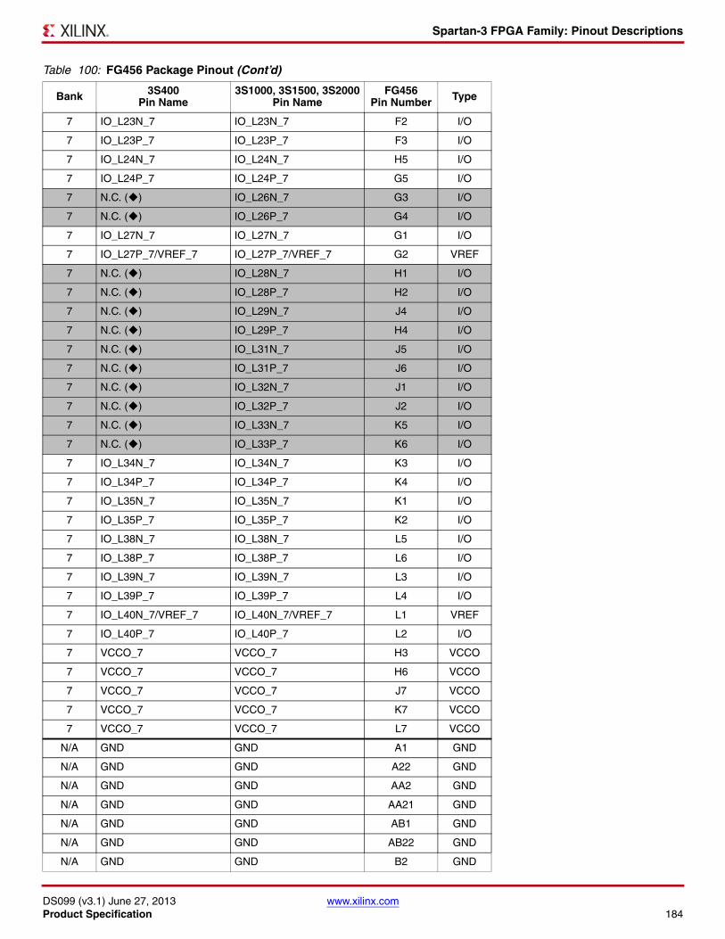
Spartan-3 FPGA Family: Pinout Descriptions
DS099 (v3.1) June 27, 2013 www.xilinx.comProduct Specification 184
7 IO_L23N_7 IO_L23N_7 F2 I/O
7 IO_L23P_7 IO_L23P_7 F3 I/O
7 IO_L24N_7 IO_L24N_7 H5 I/O
7 IO_L24P_7 IO_L24P_7 G5 I/O
7 N.C. () IO_L26N_7 G3 I/O
7 N.C. () IO_L26P_7 G4 I/O
7 IO_L27N_7 IO_L27N_7 G1 I/O
7 IO_L27P_7/VREF_7 IO_L27P_7/VREF_7 G2 VREF
7 N.C. () IO_L28N_7 H1 I/O
7 N.C. () IO_L28P_7 H2 I/O
7 N.C. () IO_L29N_7 J4 I/O
7 N.C. () IO_L29P_7 H4 I/O
7 N.C. () IO_L31N_7 J5 I/O
7 N.C. () IO_L31P_7 J6 I/O
7 N.C. () IO_L32N_7 J1 I/O
7 N.C. () IO_L32P_7 J2 I/O
7 N.C. () IO_L33N_7 K5 I/O
7 N.C. () IO_L33P_7 K6 I/O
7 IO_L34N_7 IO_L34N_7 K3 I/O
7 IO_L34P_7 IO_L34P_7 K4 I/O
7 IO_L35N_7 IO_L35N_7 K1 I/O
7 IO_L35P_7 IO_L35P_7 K2 I/O
7 IO_L38N_7 IO_L38N_7 L5 I/O
7 IO_L38P_7 IO_L38P_7 L6 I/O
7 IO_L39N_7 IO_L39N_7 L3 I/O
7 IO_L39P_7 IO_L39P_7 L4 I/O
7 IO_L40N_7/VREF_7 IO_L40N_7/VREF_7 L1 VREF
7 IO_L40P_7 IO_L40P_7 L2 I/O
7 VCCO_7 VCCO_7 H3 VCCO
7 VCCO_7 VCCO_7 H6 VCCO
7 VCCO_7 VCCO_7 J7 VCCO
7 VCCO_7 VCCO_7 K7 VCCO
7 VCCO_7 VCCO_7 L7 VCCO
N/A GND GND A1 GND
N/A GND GND A22 GND
N/A GND GND AA2 GND
N/A GND GND AA21 GND
N/A GND GND AB1 GND
N/A GND GND AB22 GND
N/A GND GND B2 GND
Table 100: FG456 Package Pinout (Cont’d)
Bank 3S400 Pin Name
3S1000, 3S1500, 3S2000Pin Name
FG456Pin Number Type
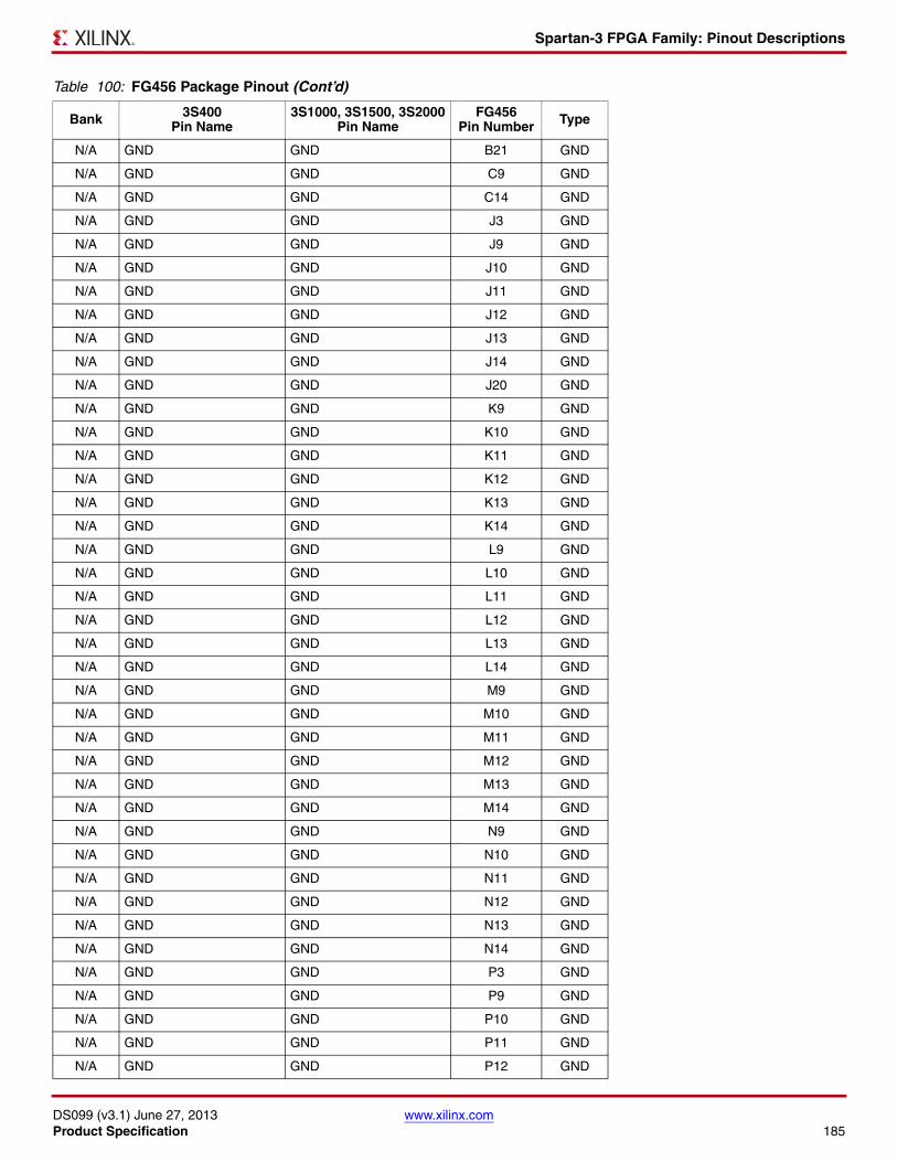
Spartan-3 FPGA Family: Pinout Descriptions
DS099 (v3.1) June 27, 2013 www.xilinx.comProduct Specification 185
N/A GND GND B21 GND
N/A GND GND C9 GND
N/A GND GND C14 GND
N/A GND GND J3 GND
N/A GND GND J9 GND
N/A GND GND J10 GND
N/A GND GND J11 GND
N/A GND GND J12 GND
N/A GND GND J13 GND
N/A GND GND J14 GND
N/A GND GND J20 GND
N/A GND GND K9 GND
N/A GND GND K10 GND
N/A GND GND K11 GND
N/A GND GND K12 GND
N/A GND GND K13 GND
N/A GND GND K14 GND
N/A GND GND L9 GND
N/A GND GND L10 GND
N/A GND GND L11 GND
N/A GND GND L12 GND
N/A GND GND L13 GND
N/A GND GND L14 GND
N/A GND GND M9 GND
N/A GND GND M10 GND
N/A GND GND M11 GND
N/A GND GND M12 GND
N/A GND GND M13 GND
N/A GND GND M14 GND
N/A GND GND N9 GND
N/A GND GND N10 GND
N/A GND GND N11 GND
N/A GND GND N12 GND
N/A GND GND N13 GND
N/A GND GND N14 GND
N/A GND GND P3 GND
N/A GND GND P9 GND
N/A GND GND P10 GND
N/A GND GND P11 GND
N/A GND GND P12 GND
Table 100: FG456 Package Pinout (Cont’d)
Bank 3S400 Pin Name
3S1000, 3S1500, 3S2000Pin Name
FG456Pin Number Type
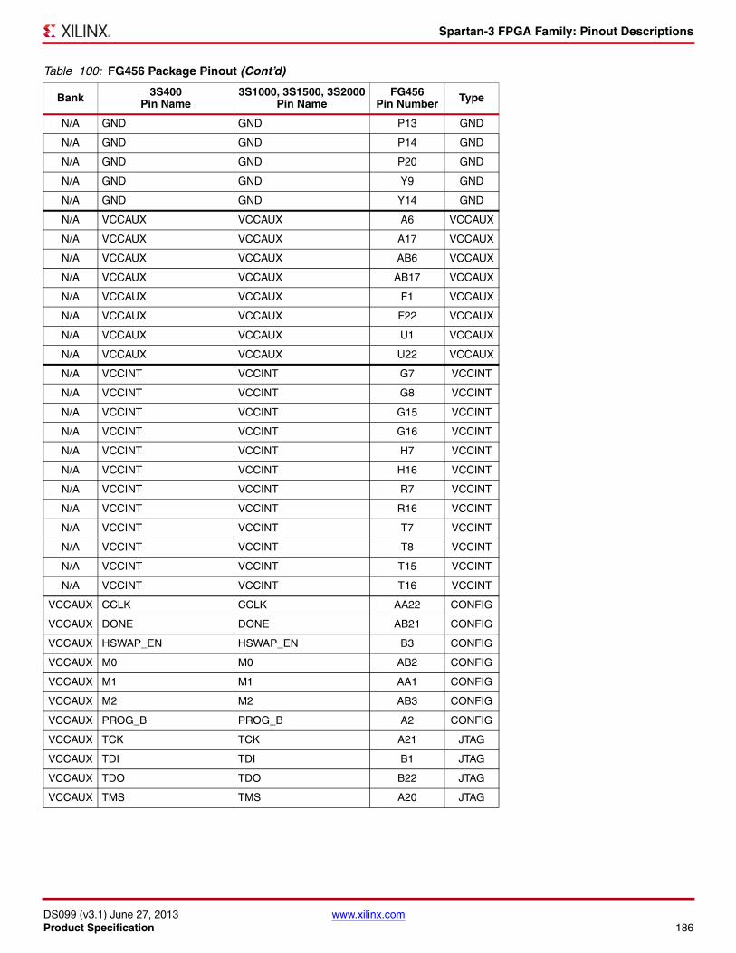
Spartan-3 FPGA Family: Pinout Descriptions
DS099 (v3.1) June 27, 2013 www.xilinx.comProduct Specification 186
N/A GND GND P13 GND
N/A GND GND P14 GND
N/A GND GND P20 GND
N/A GND GND Y9 GND
N/A GND GND Y14 GND
N/A VCCAUX VCCAUX A6 VCCAUX
N/A VCCAUX VCCAUX A17 VCCAUX
N/A VCCAUX VCCAUX AB6 VCCAUX
N/A VCCAUX VCCAUX AB17 VCCAUX
N/A VCCAUX VCCAUX F1 VCCAUX
N/A VCCAUX VCCAUX F22 VCCAUX
N/A VCCAUX VCCAUX U1 VCCAUX
N/A VCCAUX VCCAUX U22 VCCAUX
N/A VCCINT VCCINT G7 VCCINT
N/A VCCINT VCCINT G8 VCCINT
N/A VCCINT VCCINT G15 VCCINT
N/A VCCINT VCCINT G16 VCCINT
N/A VCCINT VCCINT H7 VCCINT
N/A VCCINT VCCINT H16 VCCINT
N/A VCCINT VCCINT R7 VCCINT
N/A VCCINT VCCINT R16 VCCINT
N/A VCCINT VCCINT T7 VCCINT
N/A VCCINT VCCINT T8 VCCINT
N/A VCCINT VCCINT T15 VCCINT
N/A VCCINT VCCINT T16 VCCINT
VCCAUX CCLK CCLK AA22 CONFIG
VCCAUX DONE DONE AB21 CONFIG
VCCAUX HSWAP_EN HSWAP_EN B3 CONFIG
VCCAUX M0 M0 AB2 CONFIG
VCCAUX M1 M1 AA1 CONFIG
VCCAUX M2 M2 AB3 CONFIG
VCCAUX PROG_B PROG_B A2 CONFIG
VCCAUX TCK TCK A21 JTAG
VCCAUX TDI TDI B1 JTAG
VCCAUX TDO TDO B22 JTAG
VCCAUX TMS TMS A20 JTAG
Table 100: FG456 Package Pinout (Cont’d)
Bank 3S400 Pin Name
3S1000, 3S1500, 3S2000Pin Name
FG456Pin Number Type
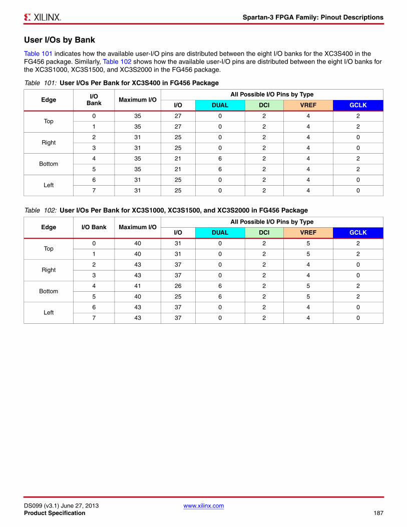
Spartan-3 FPGA Family: Pinout Descriptions
DS099 (v3.1) June 27, 2013 www.xilinx.comProduct Specification 187
User I/Os by Bank
Table 101 indicates how the available user-I/O pins are distributed between the eight I/O banks for the XC3S400 in the FG456 package. Similarly, Table 102 shows how the available user-I/O pins are distributed between the eight I/O banks for the XC3S1000, XC3S1500, and XC3S2000 in the FG456 package.
Table 101: User I/Os Per Bank for XC3S400 in FG456 Package
Edge I/O Bank Maximum I/O
All Possible I/O Pins by Type
I/O DUAL DCI VREF GCLK
Top0 35 27 0 2 4 2
1 35 27 0 2 4 2
Right2 31 25 0 2 4 0
3 31 25 0 2 4 0
Bottom4 35 21 6 2 4 2
5 35 21 6 2 4 2
Left6 31 25 0 2 4 0
7 31 25 0 2 4 0
Table 102: User I/Os Per Bank for XC3S1000, XC3S1500, and XC3S2000 in FG456 Package
Edge I/O Bank Maximum I/OAll Possible I/O Pins by Type
I/O DUAL DCI VREF GCLK
Top0 40 31 0 2 5 2
1 40 31 0 2 5 2
Right2 43 37 0 2 4 0
3 43 37 0 2 4 0
Bottom4 41 26 6 2 5 2
5 40 25 6 2 5 2
Left6 43 37 0 2 4 0
7 43 37 0 2 4 0
Spartan-3 FPGA Family: Pinout Descriptions
DS099 (v3.1) June 27, 2013 www.xilinx.comProduct Specification 188
FG456 Footprint X-Ref Target - Figure 51
Left Half of FG456 Package (Top View)
XC3S400(264 max. user I/O)
196 I/O: Unrestricted, general-purpose user I/O
32 VREF: User I/O or input voltage reference for bank
69 N.C.: Unconnected pins for XC3S400 ()
XC3S1000, XC3S1500, XC3S2000 (333 max user I/O)
261 I/O: Unrestricted, general-purpose user I/O
36 VREF: User I/O or input voltage reference for bank
0 N.C.: No unconnected pins in this package
All devices
12 DUAL: Configuration pin, then possible user I/O
8 GCLK: User I/O or global clock buffer input
16 DCI: User I/O or reference resistor input for bank
7 CONFIG: Dedicated configuration pins
4 JTAG: Dedicated JTAG port pins
12 VCCINT: Internal core voltage supply (+1.2V)
40 VCCO: Output voltage supply for bank
8 VCCAUX: Auxiliary voltage supply (+2.5V)
52 GND: Ground
Figure 51: FG456 Package Footprint (Top View)Bank 5
Bank 0
A
B
C
D
E
F
G
H
J
K
L
M
N
P
R
T
U
V
W
Y
AA
AB
Ban
k 7
Ban
k 6
PROG_BIO
VREF_0
I/O L01P_0 VRN_0
I/O L09P_0
VCCAUXI/O
L19P_0 I/O L24P_0
I/O L27P_0 I/O
I/O L32P_0 GCLK6
TDI HSWAP_EN
I/O L01N_0VRP_0
I/O L09N_0
I/O L15P_0
I/O L19N_0 I/O
L24N_0I/O
L27N_0I/O
L29P_0
I/O L32N_0GCLK7
I/O L16P_7
VREF_7I/O
I/O L01N_7VRP_7
I/O L01P_7 VRN_7
I/O L06P_0
I/O L15N_0
IO VREF_0 VCCO_0 GND
GND
GND
I/O L29N_0
I/O L31P_0
VREF_0
I/O L16N_7
I/O L19P_7
I/O L19N_7VREF_7
I/O L17P_7
I/O L06N_0
I/O L10P_0
I/O L16P_0
I/O L22P_0 I/O I/O I/O
L31N_0
I/O L21N_7
I/O L21P_7
I/O L20P_7
I/O L17N_7
IO VREF_0 I/O
L10N_0I/O
L16N_0
I/O L22N_0 I/O
L25P_0I/O
L28P_0I/O
L30P_0
VCCAUX I/O L23N_7
I/O L23P_7
I/O L20N_7
I/O L22P_7 I/O IO
VREF_0 VCCO_0 I/O L25N_0
I/O L28N_0
I/O L30N_0
I/O L27N_7
I/O L27P_7
VREF_7
I/O L26N_7
I/O L26P_7
I/O L24P_7
I/O L22N_7 VCCINT VCCINT VCCO_0 VCCO_0 VCCO_0
I/O L28N_7
I/O L28P_7 VCCO_7
I/O L29P_7 I/O
L24N_7VCCO_7 VCCINT
I/O L32N_7
I/O L32P_7 GND
I/O L29N_7
I/O L31N_7
I/O L31P_7 VCCO_7
I/O L35N_7
I/O L35P_7
I/O L34N_7
I/O L34P_7
I/O L33N_7
I/O L33P_7 VCCO_7
I/O L40N_7VREF_7
I/O L40P_7
I/O L39N_7
I/O L39P_7
I/O L38N_7
I/O L38P_7
VCCO_7
I/O L40P_6 VREF_6
I/O L40N_6
I/O L39P_6
I/O L39N_6
I/O L38P_6
I/O L38N_6
VCCO_6
GND GND GND
GND GND GND
GND GND GND
GND GND GND
GND GND GND
GND GND GND
I/O L35P_6
I/O L35N_6
I/O L34P_6
I/O L34N_6VREF_6
I/O L33P_6
I/O L33N_6 VCCO_6
I/O L32P_6
I/O L32N_6 GND
I/O L31P_6
I/O L31N_6
I/O L28P_6 VCCO_6
I/O L29P_6
I/O L29N_6 VCCO_6
I/O L26P_6
I/O L28N_6 VCCO_6 VCCINT
I/O L27P_6
I/O L27N_6
I/O L26N_6 I/O
L23P_6I/O
L22P_6I/O
L22N_6 VCCINT VCCINT VCCO_5 VCCO_5 VCCO_5
VCCAUX I/O L24P_6
I/O L24N_6VREF_6
I/O L23N_6
I/O L19P_6
IO VREF_5 I/O VCCO_5 I/O I/O I/O
I/O L21P_6
I/O L21N_6
I/O L20P_6
I/O L20N_6
I/O L19N_6
I/O L15P_5 I/O I/O
L24P_5I/O
L27P_5 I/OI/O
L31P_5 D5
I/O L17P_6
VREF_6
I/O L17N_6
I/O L16P_6
I/O L16N_6
I/O L09P_5
I/O L15N_5
I/O L19P_5 VREF_5
I/O L24N_5
I/O L27N_5VREF_5
I/O L29P_5
VREF_5
I/O L31N_5
D4
I/OI/O
L01P_6 VRN_6
I/O L01N_6VRP_6
I/O L01N_5RDWR_B
I/O L09N_5
I/O L16P_5
I/O L19N_5 VCCO_5 I/O
L29N_5
I/O L32P_5 GCLK2
M1I/O
L01P_5 CS_B
I/O L06P_5
I/O L10P_5 VRN_5
I/O L16N_5
I/O L22P_5 I/O
L25P_5
I/O L28P_5
D7
I/O L30P_5
I/O L32N_5GCLK3
GND
GND
GND
M0 M2 I/O L06N_5
I/O L10N_5 VRP_5
VCCAUXI/O
L22N_5
I/O L25N_5
I/O L28N_5
D6
I/O L30N_5
IO VREF_5
DS099-4_11a_030203
103 41 2 5 6 7 8 9 11
Spartan-3 FPGA Family: Pinout Descriptions
DS099 (v3.1) June 27, 2013 www.xilinx.comProduct Specification 189
Right Half of FG456 Package (Top View)
Figure 52: FG456 Package Footprint (Top View) Continued
12 13 14 15 16 17 18 19 20 21 22Bank 1
Bank 4
A
B
C
D
E
F
G
H
J
K
L
M
N
P
R
T
U
V
W
Y
AA
AB
Ban
k 2
Ban
k 3
I/O I/O L30N_1
I/O L28N_1
I/O L25P_1
I/O L22N_1 VCCAUX
I/O L10N_1VREF_1
I/O L06N_1VREF_1
TMS TCK
TDO
GND
I/O L32N_1GCLK5
I/O L30P_1
I/O L28P_1
I/O L25N_1
I/O I/O
L16N_1I/O
L10P_1I/O
L06P_1
I/O L01P_1 VRN_1
GND
I/O L32P_1 GCLK4
I/O L29N_1 GND VCCO_1
I/O L19N_1 I/O
L16P_1I/O
L09N_1
I/O L01N_1VRP_1
I/O L01N_2VRP_2
I/O L01P_2 VRN_2
I/O
I/O L31N_1 VREF_1
I/O L29P_1
I/O L27N_1
I/O L24N_1
I/O L19P_1 I/O
L15N_1I/O
L09P_1I/O
L16P_2I/O
L16N_2I/O
L17N_2
I/O L17P_2
VREF_2
I/O L31P_1
IO VREF_1
I/O L27P_1
I/O L24P_1 I/O I/O
L15P_1I/O
L19N_2I/O
L20N_2I/O
L20P_2I/O
L21N_2I/O
L21P_2
I/O I/OIO
VREF_1 VCCO_1 I/O I/O I/O L19P_2
I/O L23N_2VREF_2
I/O L24N_2
I/O L24P_2
VCCAUX
VCCO_1 VCCO_1 VCCO_1 VCCINT VCCINT I/O L22N_2
I/O L22P_2
I/O L23P_2
I/O L26N_2 I/O
L27N_2I/O
L27P_2
VCCINT VCCO_2I/O
L28N_2 I/O
L26P_2 VCCO_2I/O
L29N_2 I/O
L29P_2
GND GND GND VCCO_2I/O
L28P_2 I/O
L31N_2 I/O
L31P_2 GNDI/O
L32N_2 I/O
L32P_2
GND GND GND VCCO_2I/O
L33N_2 I/O
L33P_2 I/O
L34N_2VREF_2
I/O L34P_2
I/O L35N_2
I/O L35P_2
GND GND GND VCCO_2 I/O L38N_2
I/O L38P_2
I/O L39N_2
I/O L39P_2
I/O L40N_2
I/O L40P_2
VREF_2
GND GND GND VCCO_3 I/O L38P_3
I/O L38N_3
I/O L39P_3
I/O L39N_3
I/O L40P_3
I/O L40N_3 VREF_3
GND GND GND VCCO_3I/O
L33P_3 I/O
L33N_3 I/O
L34P_3 VREF_3
I/O L34N_3
I/O L35P_3
I/O L35N_3
GND GND GND VCCO_3I/O
L31P_3 I/O
L31N_3I/O
L29N_3 GNDI/O
L32P_3 I/O
L32N_3
VCCINT VCCO_3 I/O L24N_3
I/O L29P_3 VCCO_3
I/O L28P_3
I/O L28N_3
VCCO_4 VCCO_4 VCCO_4 VCCINT VCCINT I/O L22N_3
I/O L24P_3
I/O L26P_3
I/O L26N_3 I/O
L27P_3I/O
L27N_3
I/O L30N_4
D2
I/O L28N_4
I/O L25N_4
VCCO_4 I/O I/O I/O L22P_3
I/O L20N_3
I/O L23P_3
VREF_3
I/O L23N_3
VCCAUX
I/O L30P_4
D3
I/O L28P_4
I/O L25P_4
I/O L22N_4 VREF_4
I/O L16N_4
I/O L10N_4
IO VREF_4
I/O L17N_3
I/O L20P_3
I/O L21P_3
I/O L21N_3
I/O L31N_4INIT_B
I/O I/OI/O
L22P_4 I/O L16P_4
I/O L10P_4
I/O L06N_4 VREF_4
I/O L17P_3
VREF_3
I/O L19P_3
I/O L19N_3
I/O L16N_3
I/O L31P_4 DOUT BUSY
I/O L29N_4 GND VCCO_4
IO VREF_4
I/O L15N_4
I/O L06P_4
I/O L01P_3 VRN_3
I/O L01N_3VRP_3
I/O I/O L16P_3
I/O L32N_4 GCLK1
I/O L29P_4
I/O L27N_4
DIN D0
I/O L24N_4
I/O L19N_4 I/O
L15P_4I/O
L09N_4
I/O L05N_4
I/O L01N_4VRP_4
GND CCLK
I/O L32P_4 GCLK0
IO VREF_4
I/O L27P_4
D1
I/O L24P_4
I/O L19P_4 VCCAUX I/O
L09P_4
I/O L05P_4
I/O L01P_4 VRN_4
DONE GND
DS099-4_11b_030503
L22P_1
Spartan-3 FPGA Family: Pinout Descriptions
DS099 (v3.1) June 27, 2013 www.xilinx.comProduct Specification 190
FG676: 676-lead Fine-pitch Ball Grid ArrayThe 676-lead fine-pitch ball grid array package, FG676, supports five different Spartan-3 devices, including the XC3S1000, XC3S1500, XC3S2000, XC3S4000, and XC3S5000. All five have nearly identical footprints but are slightly different, primarily due to unconnected pins on the XC3S1000 and XC3S1500. For example, because the XC3S1000 has fewer I/O pins, this device has 98 unconnected pins on the FG676 package, labeled as “N.C.” In Table 103 and Figure 53, these unconnected pins are indicated with a black diamond symbol (). The XC3S1500, however, has only two unconnected pins, also labeled “N.C.” in the pinout table but indicated with a black square symbol ().
All the package pins appear in Table 103 and are sorted by bank number, then by pin name. Pairs of pins that form a differential I/O pair appear together in the table. The table also shows the pin number for each pin and the pin type, as defined earlier.
If there is a difference between the XC3S1000, XC3S1500, XC3S2000, XC3S4000, and XC3S5000 pinouts, then that difference is highlighted in Table 103. If the table entry is shaded grey, then there is an unconnected pin on either the XC3S1000 or XC3S1500 that maps to a user-I/O pin on the XC3S2000, XC3S4000, and XC3S5000. If the table entry is shaded tan, then the unconnected pin on either the XC3S1000 or XC3S1500 maps to a VREF-type pin on the XC3S2000, XC3S4000, and XC3S5000. If the other VREF pins in the bank all connect to a voltage reference to support a special I/O standard, then also connect the N.C. pin on the XC3S1000 or XC3S1500 to the same VREF voltage. This provides maximum flexibility as you could potentially migrate a design from the XC3S1000 through to the XC3S5000 FPGA without changing the printed circuit board.
An electronic version of this package pinout table and footprint diagram is available for download from the Xilinx website at http://www.xilinx.com/support/documentation/data_ sheets/s3_pin.zip.
Pinout Table
Table 103: FG676 Package Pinout
Bank XC3S1000Pin Name
XC3S1500Pin Name
XC3S2000Pin Name
XC3S4000Pin Name
XC3S5000Pin Name
FG676 Pin Number Type
0 IO IO IO IO IO_L04N_0(3) A3 I/O
0 IO IO IO IO IO A5 I/O
0 IO IO IO IO IO A6 I/O
0 IO IO IO IO IO_L04P_0(3) C4 I/O
0 N.C. () IO IO IO IO_L13N_0(3) C8 I/O
0 IO IO IO IO IO C12 I/O
0 IO IO IO IO IO E13 I/O
0 IO IO IO IO IO H11 I/O
0 IO IO IO IO IO H12 I/O
0 IO/VREF_0 IO/VREF_0 IO/VREF_0 IO/VREF_0 IO/VREF_0 B3 VREF
0 IO/VREF_0 IO/VREF_0 IO/VREF_0 IO/VREF_0 IO/VREF_0 F7 VREF
0 IO/VREF_0 IO/VREF_0 IO/VREF_0 IO/VREF_0 IO/VREF_0 G10 VREF
0 IO_L01N_0/VRP_0 IO_L01N_0/VRP_0 IO_L01N_0/VRP_0 IO_L01N_0/VRP_0 IO_L01N_0/VRP_0 E5 DCI
0 IO_L01P_0/VRN_0 IO_L01P_0/VRN_0 IO_L01P_0/VRN_0 IO_L01P_0/VRN_0 IO_L01P_0/VRN_0 D5 DCI
0 IO_L05N_0 IO_L05N_0 IO_L05N_0 IO_L05N_0 IO_L05N_0 B4 I/O
0 IO_L05P_0/VREF_0 IO_L05P_0/VREF_0 IO_L05P_0/VREF_0 IO_L05P_0/VREF_0 IO_L05P_0/VREF_0 A4 VREF
0 IO_L06N_0 IO_L06N_0 IO_L06N_0 IO_L06N_0 IO_L06N_0 C5 I/O
0 IO_L06P_0 IO_L06P_0 IO_L06P_0 IO_L06P_0 IO_L06P_0 B5 I/O
0 IO_L07N_0 IO_L07N_0 IO_L07N_0 IO_L07N_0 IO_L07N_0 E6 I/O
0 IO_L07P_0 IO_L07P_0 IO_L07P_0 IO_L07P_0 IO_L07P_0 D6 I/O
0 IO_L08N_0 IO_L08N_0 IO_L08N_0 IO_L08N_0 IO_L08N_0 C6 I/O
0 IO_L08P_0 IO_L08P_0 IO_L08P_0 IO_L08P_0 IO_L08P_0 B6 I/O
Spartan-3 FPGA Family: Pinout Descriptions
DS099 (v3.1) June 27, 2013 www.xilinx.comProduct Specification 191
0 IO_L09N_0 IO_L09N_0 IO_L09N_0 IO_L09N_0 IO_L09N_0 E7 I/O
0 IO_L09P_0 IO_L09P_0 IO_L09P_0 IO_L09P_0 IO_L09P_0 D7 I/O
0 IO_L10N_0 IO_L10N_0 IO_L10N_0 IO_L10N_0 IO_L10N_0 B7 I/O
0 IO_L10P_0 IO_L10P_0 IO_L10P_0 IO_L10P_0 IO_L10P_0 A7 I/O
0 N.C. () IO_L11N_0 IO_L11N_0 IO_L11N_0 IO_L11N_0 G8 I/O
0 N.C. () IO_L11P_0 IO_L11P_0 IO_L11P_0 IO_L11P_0 F8 I/O
0 N.C. () IO_L12N_0 IO_L12N_0 IO_L12N_0 IO(3) E8 I/O
0 N.C. () IO_L12P_0 IO_L12P_0 IO_L12P_0 IO(3) D8 I/O
0 IO_L15N_0 IO_L15N_0 IO_L15N_0 IO_L15N_0 IO_L13P_0(3) B8 I/O
0 IO_L15P_0 IO_L15P_0 IO_L15P_0 IO_L15P_0 IO(3) A8 I/O
0 IO_L16N_0 IO_L16N_0 IO_L16N_0 IO_L16N_0 IO_L16N_0 G9 I/O
0 IO_L16P_0 IO_L16P_0 IO_L16P_0 IO_L16P_0 IO_L16P_0 F9 I/O
0 N.C. () IO_L17N_0 IO_L17N_0 IO_L17N_0 IO_L17N_0 E9 I/O
0 N.C. () IO_L17P_0 IO_L17P_0 IO_L17P_0 IO_L17P_0 D9 I/O
0 N.C. () IO_L18N_0 IO_L18N_0 IO_L18N_0 IO_L18N_0 C9 I/O
0 N.C. () IO_L18P_0 IO_L18P_0 IO_L18P_0 IO_L18P_0 B9 I/O
0 IO_L19N_0 IO_L19N_0 IO_L19N_0 IO_L19N_0 IO_L19N_0 F10 I/O
0 IO_L19P_0 IO_L19P_0 IO_L19P_0 IO_L19P_0 IO_L19P_0 E10 I/O
0 IO_L22N_0 IO_L22N_0 IO_L22N_0 IO_L22N_0 IO_L22N_0 D10 I/O
0 IO_L22P_0 IO_L22P_0 IO_L22P_0 IO_L22P_0 IO_L22P_0 C10 I/O
0 N.C. () IO_L23N_0 IO_L23N_0 IO_L23N_0 IO_L23N_0 B10 I/O
0 N.C. () IO_L23P_0 IO_L23P_0 IO_L23P_0 IO_L23P_0 A10 I/O
0 IO_L24N_0 IO_L24N_0 IO_L24N_0 IO_L24N_0 IO_L24N_0 G11 I/O
0 IO_L24P_0 IO_L24P_0 IO_L24P_0 IO_L24P_0 IO_L24P_0 F11 I/O
0 IO_L25N_0 IO_L25N_0 IO_L25N_0 IO_L25N_0 IO_L25N_0 E11 I/O
0 IO_L25P_0 IO_L25P_0 IO_L25P_0 IO_L25P_0 IO_L25P_0 D11 I/O
0 N.C. () IO_L26N_0 IO_L26N_0 IO_L26N_0 IO_L26N_0 B11 I/O
0 N.C. () IO_L26P_0/VREF_0 IO_L26P_0/VREF_0 IO_L26P_0/VREF_0 IO_L26P_0/VREF_0 A11 VREF
0 IO_L27N_0 IO_L27N_0 IO_L27N_0 IO_L27N_0 IO_L27N_0 G12 I/O
0 IO_L27P_0 IO_L27P_0 IO_L27P_0 IO_L27P_0 IO_L27P_0 H13 I/O
0 IO_L28N_0 IO_L28N_0 IO_L28N_0 IO_L28N_0 IO_L28N_0 F12 I/O
0 IO_L28P_0 IO_L28P_0 IO_L28P_0 IO_L28P_0 IO_L28P_0 E12 I/O
0 IO_L29N_0 IO_L29N_0 IO_L29N_0 IO_L29N_0 IO_L29N_0 B12 I/O
0 IO_L29P_0 IO_L29P_0 IO_L29P_0 IO_L29P_0 IO_L29P_0 A12 I/O
0 IO_L30N_0 IO_L30N_0 IO_L30N_0 IO_L30N_0 IO_L30N_0 G13 I/O
0 IO_L30P_0 IO_L30P_0 IO_L30P_0 IO_L30P_0 IO_L30P_0 F13 I/O
0 IO_L31N_0 IO_L31N_0 IO_L31N_0 IO_L31N_0 IO_L31N_0 D13 I/O
0 IO_L31P_0/VREF_0 IO_L31P_0/VREF_0 IO_L31P_0/VREF_0 IO_L31P_0/VREF_0 IO_L31P_0/VREF_0 C13 VREF
0 IO_L32N_0/GCLK7 IO_L32N_0/GCLK7 IO_L32N_0/GCLK7 IO_L32N_0/GCLK7 IO_L32N_0/GCLK7 B13 GCLK
0 IO_L32P_0/GCLK6 IO_L32P_0/GCLK6 IO_L32P_0/GCLK6 IO_L32P_0/GCLK6 IO_L32P_0/GCLK6 A13 GCLK
0 VCCO_0 VCCO_0 VCCO_0 VCCO_0 VCCO_0 C7 VCCO
0 VCCO_0 VCCO_0 VCCO_0 VCCO_0 VCCO_0 C11 VCCO
Table 103: FG676 Package Pinout (Cont’d)
Bank XC3S1000Pin Name
XC3S1500Pin Name
XC3S2000Pin Name
XC3S4000Pin Name
XC3S5000Pin Name
FG676 Pin Number Type
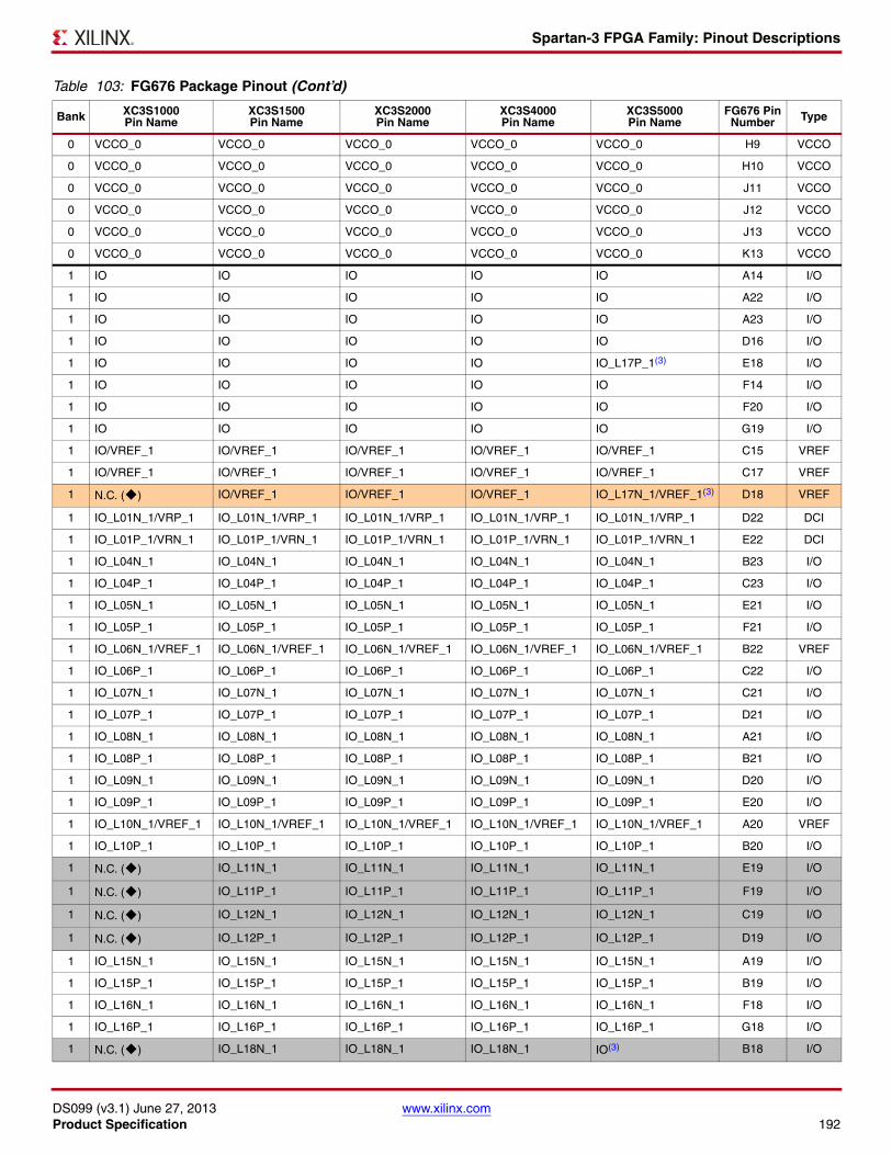
Spartan-3 FPGA Family: Pinout Descriptions
DS099 (v3.1) June 27, 2013 www.xilinx.comProduct Specification 192
0 VCCO_0 VCCO_0 VCCO_0 VCCO_0 VCCO_0 H9 VCCO
0 VCCO_0 VCCO_0 VCCO_0 VCCO_0 VCCO_0 H10 VCCO
0 VCCO_0 VCCO_0 VCCO_0 VCCO_0 VCCO_0 J11 VCCO
0 VCCO_0 VCCO_0 VCCO_0 VCCO_0 VCCO_0 J12 VCCO
0 VCCO_0 VCCO_0 VCCO_0 VCCO_0 VCCO_0 J13 VCCO
0 VCCO_0 VCCO_0 VCCO_0 VCCO_0 VCCO_0 K13 VCCO
1 IO IO IO IO IO A14 I/O
1 IO IO IO IO IO A22 I/O
1 IO IO IO IO IO A23 I/O
1 IO IO IO IO IO D16 I/O
1 IO IO IO IO IO_L17P_1(3) E18 I/O
1 IO IO IO IO IO F14 I/O
1 IO IO IO IO IO F20 I/O
1 IO IO IO IO IO G19 I/O
1 IO/VREF_1 IO/VREF_1 IO/VREF_1 IO/VREF_1 IO/VREF_1 C15 VREF
1 IO/VREF_1 IO/VREF_1 IO/VREF_1 IO/VREF_1 IO/VREF_1 C17 VREF
1 N.C. () IO/VREF_1 IO/VREF_1 IO/VREF_1 IO_L17N_1/VREF_1(3) D18 VREF
1 IO_L01N_1/VRP_1 IO_L01N_1/VRP_1 IO_L01N_1/VRP_1 IO_L01N_1/VRP_1 IO_L01N_1/VRP_1 D22 DCI
1 IO_L01P_1/VRN_1 IO_L01P_1/VRN_1 IO_L01P_1/VRN_1 IO_L01P_1/VRN_1 IO_L01P_1/VRN_1 E22 DCI
1 IO_L04N_1 IO_L04N_1 IO_L04N_1 IO_L04N_1 IO_L04N_1 B23 I/O
1 IO_L04P_1 IO_L04P_1 IO_L04P_1 IO_L04P_1 IO_L04P_1 C23 I/O
1 IO_L05N_1 IO_L05N_1 IO_L05N_1 IO_L05N_1 IO_L05N_1 E21 I/O
1 IO_L05P_1 IO_L05P_1 IO_L05P_1 IO_L05P_1 IO_L05P_1 F21 I/O
1 IO_L06N_1/VREF_1 IO_L06N_1/VREF_1 IO_L06N_1/VREF_1 IO_L06N_1/VREF_1 IO_L06N_1/VREF_1 B22 VREF
1 IO_L06P_1 IO_L06P_1 IO_L06P_1 IO_L06P_1 IO_L06P_1 C22 I/O
1 IO_L07N_1 IO_L07N_1 IO_L07N_1 IO_L07N_1 IO_L07N_1 C21 I/O
1 IO_L07P_1 IO_L07P_1 IO_L07P_1 IO_L07P_1 IO_L07P_1 D21 I/O
1 IO_L08N_1 IO_L08N_1 IO_L08N_1 IO_L08N_1 IO_L08N_1 A21 I/O
1 IO_L08P_1 IO_L08P_1 IO_L08P_1 IO_L08P_1 IO_L08P_1 B21 I/O
1 IO_L09N_1 IO_L09N_1 IO_L09N_1 IO_L09N_1 IO_L09N_1 D20 I/O
1 IO_L09P_1 IO_L09P_1 IO_L09P_1 IO_L09P_1 IO_L09P_1 E20 I/O
1 IO_L10N_1/VREF_1 IO_L10N_1/VREF_1 IO_L10N_1/VREF_1 IO_L10N_1/VREF_1 IO_L10N_1/VREF_1 A20 VREF
1 IO_L10P_1 IO_L10P_1 IO_L10P_1 IO_L10P_1 IO_L10P_1 B20 I/O
1 N.C. () IO_L11N_1 IO_L11N_1 IO_L11N_1 IO_L11N_1 E19 I/O
1 N.C. () IO_L11P_1 IO_L11P_1 IO_L11P_1 IO_L11P_1 F19 I/O
1 N.C. () IO_L12N_1 IO_L12N_1 IO_L12N_1 IO_L12N_1 C19 I/O
1 N.C. () IO_L12P_1 IO_L12P_1 IO_L12P_1 IO_L12P_1 D19 I/O
1 IO_L15N_1 IO_L15N_1 IO_L15N_1 IO_L15N_1 IO_L15N_1 A19 I/O
1 IO_L15P_1 IO_L15P_1 IO_L15P_1 IO_L15P_1 IO_L15P_1 B19 I/O
1 IO_L16N_1 IO_L16N_1 IO_L16N_1 IO_L16N_1 IO_L16N_1 F18 I/O
1 IO_L16P_1 IO_L16P_1 IO_L16P_1 IO_L16P_1 IO_L16P_1 G18 I/O
1 N.C. () IO_L18N_1 IO_L18N_1 IO_L18N_1 IO(3) B18 I/O
Table 103: FG676 Package Pinout (Cont’d)
Bank XC3S1000Pin Name
XC3S1500Pin Name
XC3S2000Pin Name
XC3S4000Pin Name
XC3S5000Pin Name
FG676 Pin Number Type
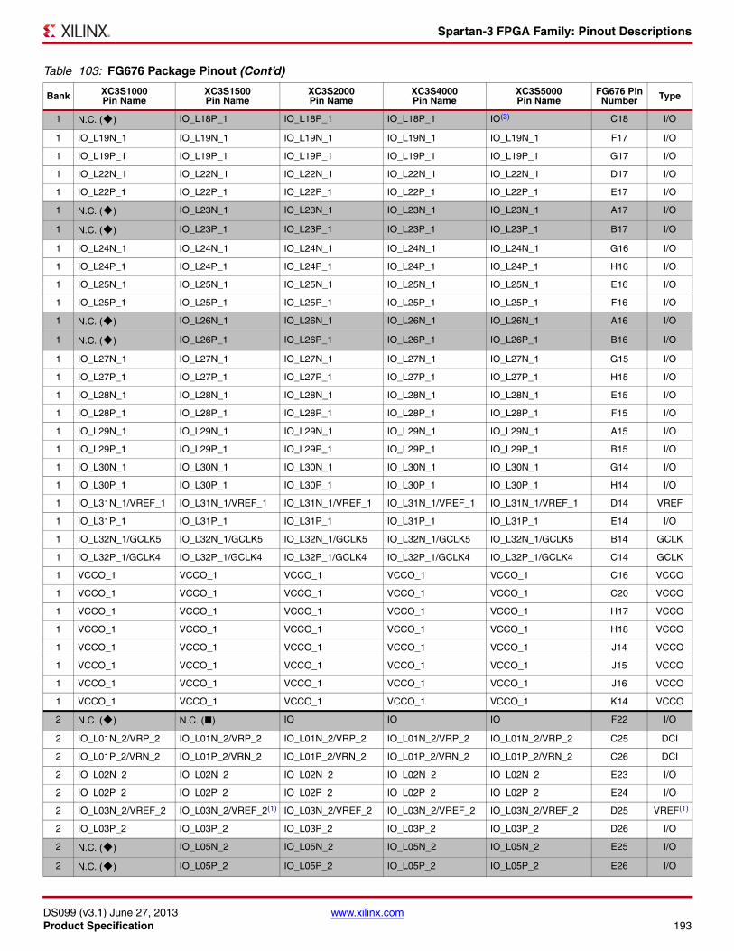
Spartan-3 FPGA Family: Pinout Descriptions
DS099 (v3.1) June 27, 2013 www.xilinx.comProduct Specification 193
1 N.C. () IO_L18P_1 IO_L18P_1 IO_L18P_1 IO(3) C18 I/O
1 IO_L19N_1 IO_L19N_1 IO_L19N_1 IO_L19N_1 IO_L19N_1 F17 I/O
1 IO_L19P_1 IO_L19P_1 IO_L19P_1 IO_L19P_1 IO_L19P_1 G17 I/O
1 IO_L22N_1 IO_L22N_1 IO_L22N_1 IO_L22N_1 IO_L22N_1 D17 I/O
1 IO_L22P_1 IO_L22P_1 IO_L22P_1 IO_L22P_1 IO_L22P_1 E17 I/O
1 N.C. () IO_L23N_1 IO_L23N_1 IO_L23N_1 IO_L23N_1 A17 I/O
1 N.C. () IO_L23P_1 IO_L23P_1 IO_L23P_1 IO_L23P_1 B17 I/O
1 IO_L24N_1 IO_L24N_1 IO_L24N_1 IO_L24N_1 IO_L24N_1 G16 I/O
1 IO_L24P_1 IO_L24P_1 IO_L24P_1 IO_L24P_1 IO_L24P_1 H16 I/O
1 IO_L25N_1 IO_L25N_1 IO_L25N_1 IO_L25N_1 IO_L25N_1 E16 I/O
1 IO_L25P_1 IO_L25P_1 IO_L25P_1 IO_L25P_1 IO_L25P_1 F16 I/O
1 N.C. () IO_L26N_1 IO_L26N_1 IO_L26N_1 IO_L26N_1 A16 I/O
1 N.C. () IO_L26P_1 IO_L26P_1 IO_L26P_1 IO_L26P_1 B16 I/O
1 IO_L27N_1 IO_L27N_1 IO_L27N_1 IO_L27N_1 IO_L27N_1 G15 I/O
1 IO_L27P_1 IO_L27P_1 IO_L27P_1 IO_L27P_1 IO_L27P_1 H15 I/O
1 IO_L28N_1 IO_L28N_1 IO_L28N_1 IO_L28N_1 IO_L28N_1 E15 I/O
1 IO_L28P_1 IO_L28P_1 IO_L28P_1 IO_L28P_1 IO_L28P_1 F15 I/O
1 IO_L29N_1 IO_L29N_1 IO_L29N_1 IO_L29N_1 IO_L29N_1 A15 I/O
1 IO_L29P_1 IO_L29P_1 IO_L29P_1 IO_L29P_1 IO_L29P_1 B15 I/O
1 IO_L30N_1 IO_L30N_1 IO_L30N_1 IO_L30N_1 IO_L30N_1 G14 I/O
1 IO_L30P_1 IO_L30P_1 IO_L30P_1 IO_L30P_1 IO_L30P_1 H14 I/O
1 IO_L31N_1/VREF_1 IO_L31N_1/VREF_1 IO_L31N_1/VREF_1 IO_L31N_1/VREF_1 IO_L31N_1/VREF_1 D14 VREF
1 IO_L31P_1 IO_L31P_1 IO_L31P_1 IO_L31P_1 IO_L31P_1 E14 I/O
1 IO_L32N_1/GCLK5 IO_L32N_1/GCLK5 IO_L32N_1/GCLK5 IO_L32N_1/GCLK5 IO_L32N_1/GCLK5 B14 GCLK
1 IO_L32P_1/GCLK4 IO_L32P_1/GCLK4 IO_L32P_1/GCLK4 IO_L32P_1/GCLK4 IO_L32P_1/GCLK4 C14 GCLK
1 VCCO_1 VCCO_1 VCCO_1 VCCO_1 VCCO_1 C16 VCCO
1 VCCO_1 VCCO_1 VCCO_1 VCCO_1 VCCO_1 C20 VCCO
1 VCCO_1 VCCO_1 VCCO_1 VCCO_1 VCCO_1 H17 VCCO
1 VCCO_1 VCCO_1 VCCO_1 VCCO_1 VCCO_1 H18 VCCO
1 VCCO_1 VCCO_1 VCCO_1 VCCO_1 VCCO_1 J14 VCCO
1 VCCO_1 VCCO_1 VCCO_1 VCCO_1 VCCO_1 J15 VCCO
1 VCCO_1 VCCO_1 VCCO_1 VCCO_1 VCCO_1 J16 VCCO
1 VCCO_1 VCCO_1 VCCO_1 VCCO_1 VCCO_1 K14 VCCO
2 N.C. () N.C. () IO IO IO F22 I/O
2 IO_L01N_2/VRP_2 IO_L01N_2/VRP_2 IO_L01N_2/VRP_2 IO_L01N_2/VRP_2 IO_L01N_2/VRP_2 C25 DCI
2 IO_L01P_2/VRN_2 IO_L01P_2/VRN_2 IO_L01P_2/VRN_2 IO_L01P_2/VRN_2 IO_L01P_2/VRN_2 C26 DCI
2 IO_L02N_2 IO_L02N_2 IO_L02N_2 IO_L02N_2 IO_L02N_2 E23 I/O
2 IO_L02P_2 IO_L02P_2 IO_L02P_2 IO_L02P_2 IO_L02P_2 E24 I/O
2 IO_L03N_2/VREF_2 IO_L03N_2/VREF_2(1) IO_L03N_2/VREF_2 IO_L03N_2/VREF_2 IO_L03N_2/VREF_2 D25 VREF(1)
2 IO_L03P_2 IO_L03P_2 IO_L03P_2 IO_L03P_2 IO_L03P_2 D26 I/O
2 N.C. () IO_L05N_2 IO_L05N_2 IO_L05N_2 IO_L05N_2 E25 I/O
2 N.C. () IO_L05P_2 IO_L05P_2 IO_L05P_2 IO_L05P_2 E26 I/O
Table 103: FG676 Package Pinout (Cont’d)
Bank XC3S1000Pin Name
XC3S1500Pin Name
XC3S2000Pin Name
XC3S4000Pin Name
XC3S5000Pin Name
FG676 Pin Number Type
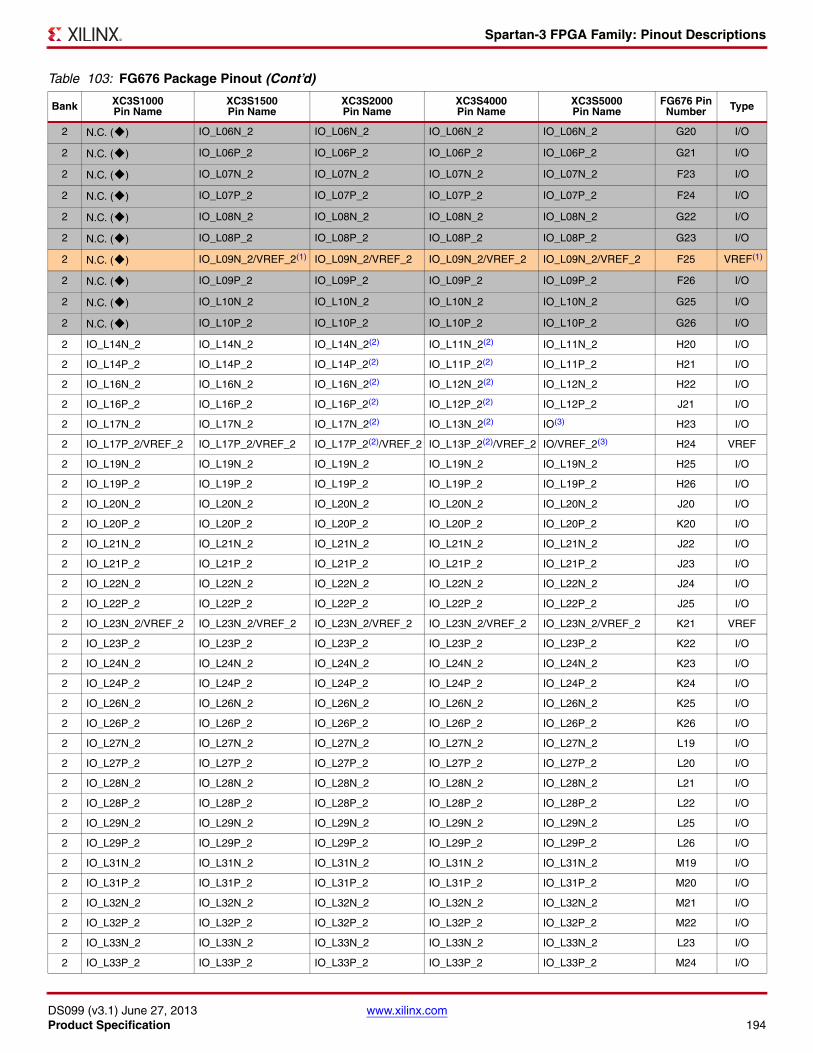
Spartan-3 FPGA Family: Pinout Descriptions
DS099 (v3.1) June 27, 2013 www.xilinx.comProduct Specification 194
2 N.C. () IO_L06N_2 IO_L06N_2 IO_L06N_2 IO_L06N_2 G20 I/O
2 N.C. () IO_L06P_2 IO_L06P_2 IO_L06P_2 IO_L06P_2 G21 I/O
2 N.C. () IO_L07N_2 IO_L07N_2 IO_L07N_2 IO_L07N_2 F23 I/O
2 N.C. () IO_L07P_2 IO_L07P_2 IO_L07P_2 IO_L07P_2 F24 I/O
2 N.C. () IO_L08N_2 IO_L08N_2 IO_L08N_2 IO_L08N_2 G22 I/O
2 N.C. () IO_L08P_2 IO_L08P_2 IO_L08P_2 IO_L08P_2 G23 I/O
2 N.C. () IO_L09N_2/VREF_2(1) IO_L09N_2/VREF_2 IO_L09N_2/VREF_2 IO_L09N_2/VREF_2 F25 VREF(1)
2 N.C. () IO_L09P_2 IO_L09P_2 IO_L09P_2 IO_L09P_2 F26 I/O
2 N.C. () IO_L10N_2 IO_L10N_2 IO_L10N_2 IO_L10N_2 G25 I/O
2 N.C. () IO_L10P_2 IO_L10P_2 IO_L10P_2 IO_L10P_2 G26 I/O
2 IO_L14N_2 IO_L14N_2 IO_L14N_2(2) IO_L11N_2(2) IO_L11N_2 H20 I/O
2 IO_L14P_2 IO_L14P_2 IO_L14P_2(2) IO_L11P_2(2) IO_L11P_2 H21 I/O
2 IO_L16N_2 IO_L16N_2 IO_L16N_2(2) IO_L12N_2(2) IO_L12N_2 H22 I/O
2 IO_L16P_2 IO_L16P_2 IO_L16P_2(2) IO_L12P_2(2) IO_L12P_2 J21 I/O
2 IO_L17N_2 IO_L17N_2 IO_L17N_2(2) IO_L13N_2(2) IO(3) H23 I/O
2 IO_L17P_2/VREF_2 IO_L17P_2/VREF_2 IO_L17P_2(2)/VREF_2 IO_L13P_2(2)/VREF_2 IO/VREF_2(3) H24 VREF
2 IO_L19N_2 IO_L19N_2 IO_L19N_2 IO_L19N_2 IO_L19N_2 H25 I/O
2 IO_L19P_2 IO_L19P_2 IO_L19P_2 IO_L19P_2 IO_L19P_2 H26 I/O
2 IO_L20N_2 IO_L20N_2 IO_L20N_2 IO_L20N_2 IO_L20N_2 J20 I/O
2 IO_L20P_2 IO_L20P_2 IO_L20P_2 IO_L20P_2 IO_L20P_2 K20 I/O
2 IO_L21N_2 IO_L21N_2 IO_L21N_2 IO_L21N_2 IO_L21N_2 J22 I/O
2 IO_L21P_2 IO_L21P_2 IO_L21P_2 IO_L21P_2 IO_L21P_2 J23 I/O
2 IO_L22N_2 IO_L22N_2 IO_L22N_2 IO_L22N_2 IO_L22N_2 J24 I/O
2 IO_L22P_2 IO_L22P_2 IO_L22P_2 IO_L22P_2 IO_L22P_2 J25 I/O
2 IO_L23N_2/VREF_2 IO_L23N_2/VREF_2 IO_L23N_2/VREF_2 IO_L23N_2/VREF_2 IO_L23N_2/VREF_2 K21 VREF
2 IO_L23P_2 IO_L23P_2 IO_L23P_2 IO_L23P_2 IO_L23P_2 K22 I/O
2 IO_L24N_2 IO_L24N_2 IO_L24N_2 IO_L24N_2 IO_L24N_2 K23 I/O
2 IO_L24P_2 IO_L24P_2 IO_L24P_2 IO_L24P_2 IO_L24P_2 K24 I/O
2 IO_L26N_2 IO_L26N_2 IO_L26N_2 IO_L26N_2 IO_L26N_2 K25 I/O
2 IO_L26P_2 IO_L26P_2 IO_L26P_2 IO_L26P_2 IO_L26P_2 K26 I/O
2 IO_L27N_2 IO_L27N_2 IO_L27N_2 IO_L27N_2 IO_L27N_2 L19 I/O
2 IO_L27P_2 IO_L27P_2 IO_L27P_2 IO_L27P_2 IO_L27P_2 L20 I/O
2 IO_L28N_2 IO_L28N_2 IO_L28N_2 IO_L28N_2 IO_L28N_2 L21 I/O
2 IO_L28P_2 IO_L28P_2 IO_L28P_2 IO_L28P_2 IO_L28P_2 L22 I/O
2 IO_L29N_2 IO_L29N_2 IO_L29N_2 IO_L29N_2 IO_L29N_2 L25 I/O
2 IO_L29P_2 IO_L29P_2 IO_L29P_2 IO_L29P_2 IO_L29P_2 L26 I/O
2 IO_L31N_2 IO_L31N_2 IO_L31N_2 IO_L31N_2 IO_L31N_2 M19 I/O
2 IO_L31P_2 IO_L31P_2 IO_L31P_2 IO_L31P_2 IO_L31P_2 M20 I/O
2 IO_L32N_2 IO_L32N_2 IO_L32N_2 IO_L32N_2 IO_L32N_2 M21 I/O
2 IO_L32P_2 IO_L32P_2 IO_L32P_2 IO_L32P_2 IO_L32P_2 M22 I/O
2 IO_L33N_2 IO_L33N_2 IO_L33N_2 IO_L33N_2 IO_L33N_2 L23 I/O
2 IO_L33P_2 IO_L33P_2 IO_L33P_2 IO_L33P_2 IO_L33P_2 M24 I/O
Table 103: FG676 Package Pinout (Cont’d)
Bank XC3S1000Pin Name
XC3S1500Pin Name
XC3S2000Pin Name
XC3S4000Pin Name
XC3S5000Pin Name
FG676 Pin Number Type
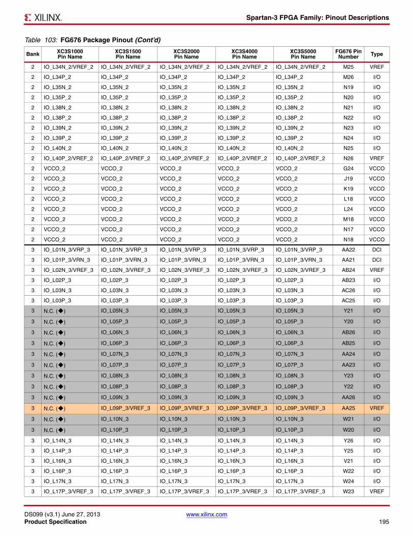
Spartan-3 FPGA Family: Pinout Descriptions
DS099 (v3.1) June 27, 2013 www.xilinx.comProduct Specification 195
2 IO_L34N_2/VREF_2 IO_L34N_2/VREF_2 IO_L34N_2/VREF_2 IO_L34N_2/VREF_2 IO_L34N_2/VREF_2 M25 VREF
2 IO_L34P_2 IO_L34P_2 IO_L34P_2 IO_L34P_2 IO_L34P_2 M26 I/O
2 IO_L35N_2 IO_L35N_2 IO_L35N_2 IO_L35N_2 IO_L35N_2 N19 I/O
2 IO_L35P_2 IO_L35P_2 IO_L35P_2 IO_L35P_2 IO_L35P_2 N20 I/O
2 IO_L38N_2 IO_L38N_2 IO_L38N_2 IO_L38N_2 IO_L38N_2 N21 I/O
2 IO_L38P_2 IO_L38P_2 IO_L38P_2 IO_L38P_2 IO_L38P_2 N22 I/O
2 IO_L39N_2 IO_L39N_2 IO_L39N_2 IO_L39N_2 IO_L39N_2 N23 I/O
2 IO_L39P_2 IO_L39P_2 IO_L39P_2 IO_L39P_2 IO_L39P_2 N24 I/O
2 IO_L40N_2 IO_L40N_2 IO_L40N_2 IO_L40N_2 IO_L40N_2 N25 I/O
2 IO_L40P_2/VREF_2 IO_L40P_2/VREF_2 IO_L40P_2/VREF_2 IO_L40P_2/VREF_2 IO_L40P_2/VREF_2 N26 VREF
2 VCCO_2 VCCO_2 VCCO_2 VCCO_2 VCCO_2 G24 VCCO
2 VCCO_2 VCCO_2 VCCO_2 VCCO_2 VCCO_2 J19 VCCO
2 VCCO_2 VCCO_2 VCCO_2 VCCO_2 VCCO_2 K19 VCCO
2 VCCO_2 VCCO_2 VCCO_2 VCCO_2 VCCO_2 L18 VCCO
2 VCCO_2 VCCO_2 VCCO_2 VCCO_2 VCCO_2 L24 VCCO
2 VCCO_2 VCCO_2 VCCO_2 VCCO_2 VCCO_2 M18 VCCO
2 VCCO_2 VCCO_2 VCCO_2 VCCO_2 VCCO_2 N17 VCCO
2 VCCO_2 VCCO_2 VCCO_2 VCCO_2 VCCO_2 N18 VCCO
3 IO_L01N_3/VRP_3 IO_L01N_3/VRP_3 IO_L01N_3/VRP_3 IO_L01N_3/VRP_3 IO_L01N_3/VRP_3 AA22 DCI
3 IO_L01P_3/VRN_3 IO_L01P_3/VRN_3 IO_L01P_3/VRN_3 IO_L01P_3/VRN_3 IO_L01P_3/VRN_3 AA21 DCI
3 IO_L02N_3/VREF_3 IO_L02N_3/VREF_3 IO_L02N_3/VREF_3 IO_L02N_3/VREF_3 IO_L02N_3/VREF_3 AB24 VREF
3 IO_L02P_3 IO_L02P_3 IO_L02P_3 IO_L02P_3 IO_L02P_3 AB23 I/O
3 IO_L03N_3 IO_L03N_3 IO_L03N_3 IO_L03N_3 IO_L03N_3 AC26 I/O
3 IO_L03P_3 IO_L03P_3 IO_L03P_3 IO_L03P_3 IO_L03P_3 AC25 I/O
3 N.C. () IO_L05N_3 IO_L05N_3 IO_L05N_3 IO_L05N_3 Y21 I/O
3 N.C. () IO_L05P_3 IO_L05P_3 IO_L05P_3 IO_L05P_3 Y20 I/O
3 N.C. () IO_L06N_3 IO_L06N_3 IO_L06N_3 IO_L06N_3 AB26 I/O
3 N.C. () IO_L06P_3 IO_L06P_3 IO_L06P_3 IO_L06P_3 AB25 I/O
3 N.C. () IO_L07N_3 IO_L07N_3 IO_L07N_3 IO_L07N_3 AA24 I/O
3 N.C. () IO_L07P_3 IO_L07P_3 IO_L07P_3 IO_L07P_3 AA23 I/O
3 N.C. () IO_L08N_3 IO_L08N_3 IO_L08N_3 IO_L08N_3 Y23 I/O
3 N.C. () IO_L08P_3 IO_L08P_3 IO_L08P_3 IO_L08P_3 Y22 I/O
3 N.C. () IO_L09N_3 IO_L09N_3 IO_L09N_3 IO_L09N_3 AA26 I/O
3 N.C. () IO_L09P_3/VREF_3 IO_L09P_3/VREF_3 IO_L09P_3/VREF_3 IO_L09P_3/VREF_3 AA25 VREF
3 N.C. () IO_L10N_3 IO_L10N_3 IO_L10N_3 IO_L10N_3 W21 I/O
3 N.C. () IO_L10P_3 IO_L10P_3 IO_L10P_3 IO_L10P_3 W20 I/O
3 IO_L14N_3 IO_L14N_3 IO_L14N_3 IO_L14N_3 IO_L14N_3 Y26 I/O
3 IO_L14P_3 IO_L14P_3 IO_L14P_3 IO_L14P_3 IO_L14P_3 Y25 I/O
3 IO_L16N_3 IO_L16N_3 IO_L16N_3 IO_L16N_3 IO_L16N_3 V21 I/O
3 IO_L16P_3 IO_L16P_3 IO_L16P_3 IO_L16P_3 IO_L16P_3 W22 I/O
3 IO_L17N_3 IO_L17N_3 IO_L17N_3 IO_L17N_3 IO_L17N_3 W24 I/O
3 IO_L17P_3/VREF_3 IO_L17P_3/VREF_3 IO_L17P_3/VREF_3 IO_L17P_3/VREF_3 IO_L17P_3/VREF_3 W23 VREF
Table 103: FG676 Package Pinout (Cont’d)
Bank XC3S1000Pin Name
XC3S1500Pin Name
XC3S2000Pin Name
XC3S4000Pin Name
XC3S5000Pin Name
FG676 Pin Number Type
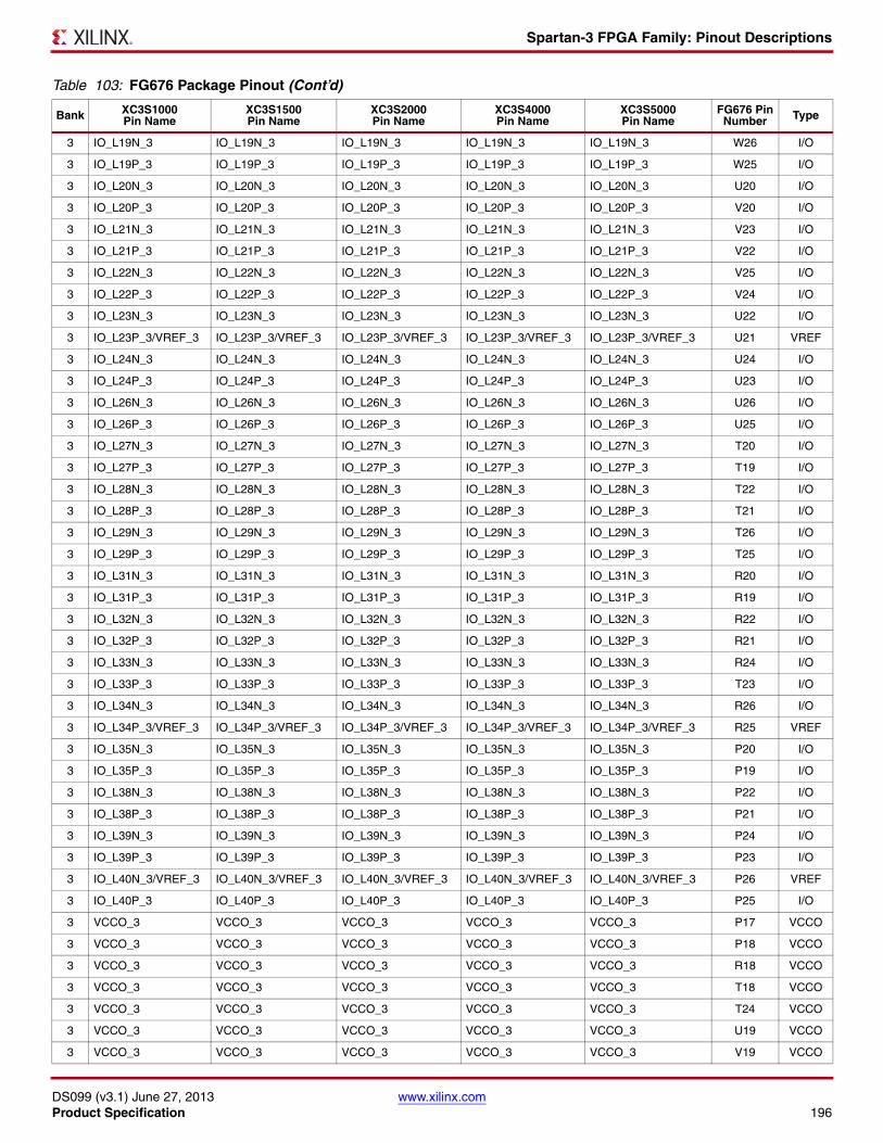
Spartan-3 FPGA Family: Pinout Descriptions
DS099 (v3.1) June 27, 2013 www.xilinx.comProduct Specification 196
3 IO_L19N_3 IO_L19N_3 IO_L19N_3 IO_L19N_3 IO_L19N_3 W26 I/O
3 IO_L19P_3 IO_L19P_3 IO_L19P_3 IO_L19P_3 IO_L19P_3 W25 I/O
3 IO_L20N_3 IO_L20N_3 IO_L20N_3 IO_L20N_3 IO_L20N_3 U20 I/O
3 IO_L20P_3 IO_L20P_3 IO_L20P_3 IO_L20P_3 IO_L20P_3 V20 I/O
3 IO_L21N_3 IO_L21N_3 IO_L21N_3 IO_L21N_3 IO_L21N_3 V23 I/O
3 IO_L21P_3 IO_L21P_3 IO_L21P_3 IO_L21P_3 IO_L21P_3 V22 I/O
3 IO_L22N_3 IO_L22N_3 IO_L22N_3 IO_L22N_3 IO_L22N_3 V25 I/O
3 IO_L22P_3 IO_L22P_3 IO_L22P_3 IO_L22P_3 IO_L22P_3 V24 I/O
3 IO_L23N_3 IO_L23N_3 IO_L23N_3 IO_L23N_3 IO_L23N_3 U22 I/O
3 IO_L23P_3/VREF_3 IO_L23P_3/VREF_3 IO_L23P_3/VREF_3 IO_L23P_3/VREF_3 IO_L23P_3/VREF_3 U21 VREF
3 IO_L24N_3 IO_L24N_3 IO_L24N_3 IO_L24N_3 IO_L24N_3 U24 I/O
3 IO_L24P_3 IO_L24P_3 IO_L24P_3 IO_L24P_3 IO_L24P_3 U23 I/O
3 IO_L26N_3 IO_L26N_3 IO_L26N_3 IO_L26N_3 IO_L26N_3 U26 I/O
3 IO_L26P_3 IO_L26P_3 IO_L26P_3 IO_L26P_3 IO_L26P_3 U25 I/O
3 IO_L27N_3 IO_L27N_3 IO_L27N_3 IO_L27N_3 IO_L27N_3 T20 I/O
3 IO_L27P_3 IO_L27P_3 IO_L27P_3 IO_L27P_3 IO_L27P_3 T19 I/O
3 IO_L28N_3 IO_L28N_3 IO_L28N_3 IO_L28N_3 IO_L28N_3 T22 I/O
3 IO_L28P_3 IO_L28P_3 IO_L28P_3 IO_L28P_3 IO_L28P_3 T21 I/O
3 IO_L29N_3 IO_L29N_3 IO_L29N_3 IO_L29N_3 IO_L29N_3 T26 I/O
3 IO_L29P_3 IO_L29P_3 IO_L29P_3 IO_L29P_3 IO_L29P_3 T25 I/O
3 IO_L31N_3 IO_L31N_3 IO_L31N_3 IO_L31N_3 IO_L31N_3 R20 I/O
3 IO_L31P_3 IO_L31P_3 IO_L31P_3 IO_L31P_3 IO_L31P_3 R19 I/O
3 IO_L32N_3 IO_L32N_3 IO_L32N_3 IO_L32N_3 IO_L32N_3 R22 I/O
3 IO_L32P_3 IO_L32P_3 IO_L32P_3 IO_L32P_3 IO_L32P_3 R21 I/O
3 IO_L33N_3 IO_L33N_3 IO_L33N_3 IO_L33N_3 IO_L33N_3 R24 I/O
3 IO_L33P_3 IO_L33P_3 IO_L33P_3 IO_L33P_3 IO_L33P_3 T23 I/O
3 IO_L34N_3 IO_L34N_3 IO_L34N_3 IO_L34N_3 IO_L34N_3 R26 I/O
3 IO_L34P_3/VREF_3 IO_L34P_3/VREF_3 IO_L34P_3/VREF_3 IO_L34P_3/VREF_3 IO_L34P_3/VREF_3 R25 VREF
3 IO_L35N_3 IO_L35N_3 IO_L35N_3 IO_L35N_3 IO_L35N_3 P20 I/O
3 IO_L35P_3 IO_L35P_3 IO_L35P_3 IO_L35P_3 IO_L35P_3 P19 I/O
3 IO_L38N_3 IO_L38N_3 IO_L38N_3 IO_L38N_3 IO_L38N_3 P22 I/O
3 IO_L38P_3 IO_L38P_3 IO_L38P_3 IO_L38P_3 IO_L38P_3 P21 I/O
3 IO_L39N_3 IO_L39N_3 IO_L39N_3 IO_L39N_3 IO_L39N_3 P24 I/O
3 IO_L39P_3 IO_L39P_3 IO_L39P_3 IO_L39P_3 IO_L39P_3 P23 I/O
3 IO_L40N_3/VREF_3 IO_L40N_3/VREF_3 IO_L40N_3/VREF_3 IO_L40N_3/VREF_3 IO_L40N_3/VREF_3 P26 VREF
3 IO_L40P_3 IO_L40P_3 IO_L40P_3 IO_L40P_3 IO_L40P_3 P25 I/O
3 VCCO_3 VCCO_3 VCCO_3 VCCO_3 VCCO_3 P17 VCCO
3 VCCO_3 VCCO_3 VCCO_3 VCCO_3 VCCO_3 P18 VCCO
3 VCCO_3 VCCO_3 VCCO_3 VCCO_3 VCCO_3 R18 VCCO
3 VCCO_3 VCCO_3 VCCO_3 VCCO_3 VCCO_3 T18 VCCO
3 VCCO_3 VCCO_3 VCCO_3 VCCO_3 VCCO_3 T24 VCCO
3 VCCO_3 VCCO_3 VCCO_3 VCCO_3 VCCO_3 U19 VCCO
3 VCCO_3 VCCO_3 VCCO_3 VCCO_3 VCCO_3 V19 VCCO
Table 103: FG676 Package Pinout (Cont’d)
Bank XC3S1000Pin Name
XC3S1500Pin Name
XC3S2000Pin Name
XC3S4000Pin Name
XC3S5000Pin Name
FG676 Pin Number Type
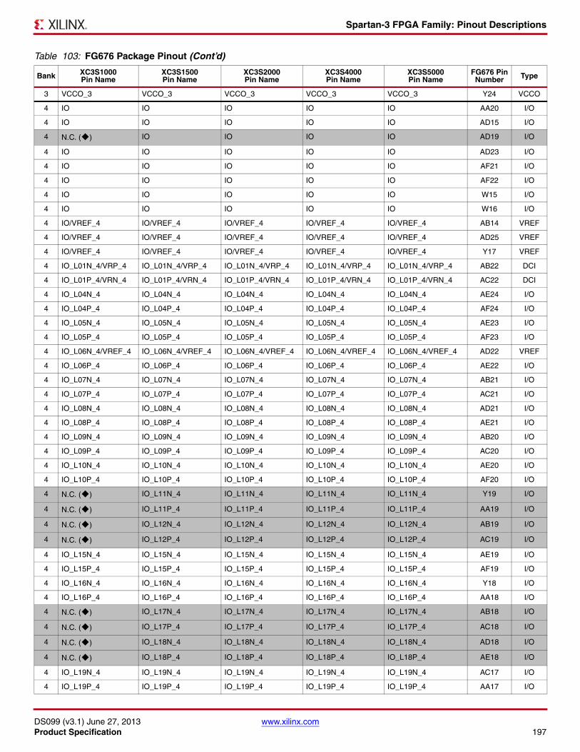
Spartan-3 FPGA Family: Pinout Descriptions
DS099 (v3.1) June 27, 2013 www.xilinx.comProduct Specification 197
3 VCCO_3 VCCO_3 VCCO_3 VCCO_3 VCCO_3 Y24 VCCO
4 IO IO IO IO IO AA20 I/O
4 IO IO IO IO IO AD15 I/O
4 N.C. () IO IO IO IO AD19 I/O
4 IO IO IO IO IO AD23 I/O
4 IO IO IO IO IO AF21 I/O
4 IO IO IO IO IO AF22 I/O
4 IO IO IO IO IO W15 I/O
4 IO IO IO IO IO W16 I/O
4 IO/VREF_4 IO/VREF_4 IO/VREF_4 IO/VREF_4 IO/VREF_4 AB14 VREF
4 IO/VREF_4 IO/VREF_4 IO/VREF_4 IO/VREF_4 IO/VREF_4 AD25 VREF
4 IO/VREF_4 IO/VREF_4 IO/VREF_4 IO/VREF_4 IO/VREF_4 Y17 VREF
4 IO_L01N_4/VRP_4 IO_L01N_4/VRP_4 IO_L01N_4/VRP_4 IO_L01N_4/VRP_4 IO_L01N_4/VRP_4 AB22 DCI
4 IO_L01P_4/VRN_4 IO_L01P_4/VRN_4 IO_L01P_4/VRN_4 IO_L01P_4/VRN_4 IO_L01P_4/VRN_4 AC22 DCI
4 IO_L04N_4 IO_L04N_4 IO_L04N_4 IO_L04N_4 IO_L04N_4 AE24 I/O
4 IO_L04P_4 IO_L04P_4 IO_L04P_4 IO_L04P_4 IO_L04P_4 AF24 I/O
4 IO_L05N_4 IO_L05N_4 IO_L05N_4 IO_L05N_4 IO_L05N_4 AE23 I/O
4 IO_L05P_4 IO_L05P_4 IO_L05P_4 IO_L05P_4 IO_L05P_4 AF23 I/O
4 IO_L06N_4/VREF_4 IO_L06N_4/VREF_4 IO_L06N_4/VREF_4 IO_L06N_4/VREF_4 IO_L06N_4/VREF_4 AD22 VREF
4 IO_L06P_4 IO_L06P_4 IO_L06P_4 IO_L06P_4 IO_L06P_4 AE22 I/O
4 IO_L07N_4 IO_L07N_4 IO_L07N_4 IO_L07N_4 IO_L07N_4 AB21 I/O
4 IO_L07P_4 IO_L07P_4 IO_L07P_4 IO_L07P_4 IO_L07P_4 AC21 I/O
4 IO_L08N_4 IO_L08N_4 IO_L08N_4 IO_L08N_4 IO_L08N_4 AD21 I/O
4 IO_L08P_4 IO_L08P_4 IO_L08P_4 IO_L08P_4 IO_L08P_4 AE21 I/O
4 IO_L09N_4 IO_L09N_4 IO_L09N_4 IO_L09N_4 IO_L09N_4 AB20 I/O
4 IO_L09P_4 IO_L09P_4 IO_L09P_4 IO_L09P_4 IO_L09P_4 AC20 I/O
4 IO_L10N_4 IO_L10N_4 IO_L10N_4 IO_L10N_4 IO_L10N_4 AE20 I/O
4 IO_L10P_4 IO_L10P_4 IO_L10P_4 IO_L10P_4 IO_L10P_4 AF20 I/O
4 N.C. () IO_L11N_4 IO_L11N_4 IO_L11N_4 IO_L11N_4 Y19 I/O
4 N.C. () IO_L11P_4 IO_L11P_4 IO_L11P_4 IO_L11P_4 AA19 I/O
4 N.C. () IO_L12N_4 IO_L12N_4 IO_L12N_4 IO_L12N_4 AB19 I/O
4 N.C. () IO_L12P_4 IO_L12P_4 IO_L12P_4 IO_L12P_4 AC19 I/O
4 IO_L15N_4 IO_L15N_4 IO_L15N_4 IO_L15N_4 IO_L15N_4 AE19 I/O
4 IO_L15P_4 IO_L15P_4 IO_L15P_4 IO_L15P_4 IO_L15P_4 AF19 I/O
4 IO_L16N_4 IO_L16N_4 IO_L16N_4 IO_L16N_4 IO_L16N_4 Y18 I/O
4 IO_L16P_4 IO_L16P_4 IO_L16P_4 IO_L16P_4 IO_L16P_4 AA18 I/O
4 N.C. () IO_L17N_4 IO_L17N_4 IO_L17N_4 IO_L17N_4 AB18 I/O
4 N.C. () IO_L17P_4 IO_L17P_4 IO_L17P_4 IO_L17P_4 AC18 I/O
4 N.C. () IO_L18N_4 IO_L18N_4 IO_L18N_4 IO_L18N_4 AD18 I/O
4 N.C. () IO_L18P_4 IO_L18P_4 IO_L18P_4 IO_L18P_4 AE18 I/O
4 IO_L19N_4 IO_L19N_4 IO_L19N_4 IO_L19N_4 IO_L19N_4 AC17 I/O
4 IO_L19P_4 IO_L19P_4 IO_L19P_4 IO_L19P_4 IO_L19P_4 AA17 I/O
Table 103: FG676 Package Pinout (Cont’d)
Bank XC3S1000Pin Name
XC3S1500Pin Name
XC3S2000Pin Name
XC3S4000Pin Name
XC3S5000Pin Name
FG676 Pin Number Type
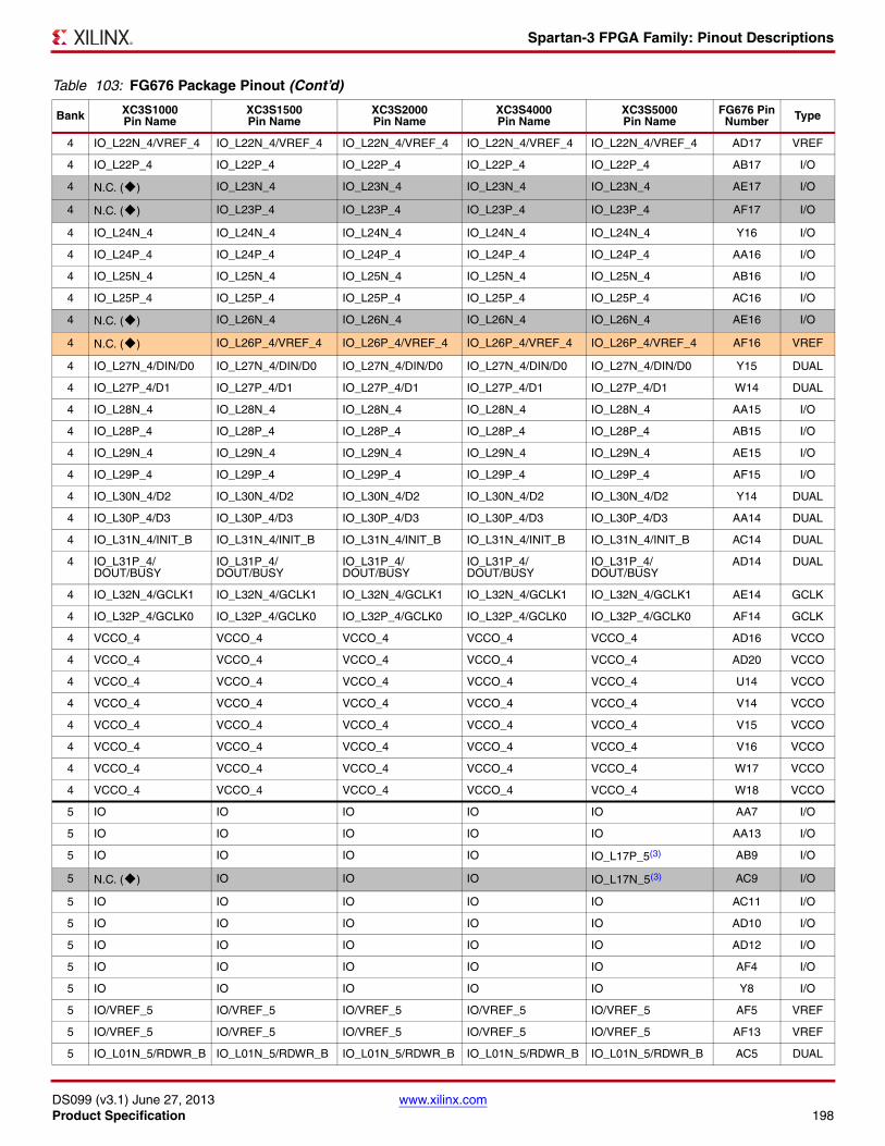
Spartan-3 FPGA Family: Pinout Descriptions
DS099 (v3.1) June 27, 2013 www.xilinx.comProduct Specification 198
4 IO_L22N_4/VREF_4 IO_L22N_4/VREF_4 IO_L22N_4/VREF_4 IO_L22N_4/VREF_4 IO_L22N_4/VREF_4 AD17 VREF
4 IO_L22P_4 IO_L22P_4 IO_L22P_4 IO_L22P_4 IO_L22P_4 AB17 I/O
4 N.C. () IO_L23N_4 IO_L23N_4 IO_L23N_4 IO_L23N_4 AE17 I/O
4 N.C. () IO_L23P_4 IO_L23P_4 IO_L23P_4 IO_L23P_4 AF17 I/O
4 IO_L24N_4 IO_L24N_4 IO_L24N_4 IO_L24N_4 IO_L24N_4 Y16 I/O
4 IO_L24P_4 IO_L24P_4 IO_L24P_4 IO_L24P_4 IO_L24P_4 AA16 I/O
4 IO_L25N_4 IO_L25N_4 IO_L25N_4 IO_L25N_4 IO_L25N_4 AB16 I/O
4 IO_L25P_4 IO_L25P_4 IO_L25P_4 IO_L25P_4 IO_L25P_4 AC16 I/O
4 N.C. () IO_L26N_4 IO_L26N_4 IO_L26N_4 IO_L26N_4 AE16 I/O
4 N.C. () IO_L26P_4/VREF_4 IO_L26P_4/VREF_4 IO_L26P_4/VREF_4 IO_L26P_4/VREF_4 AF16 VREF
4 IO_L27N_4/DIN/D0 IO_L27N_4/DIN/D0 IO_L27N_4/DIN/D0 IO_L27N_4/DIN/D0 IO_L27N_4/DIN/D0 Y15 DUAL
4 IO_L27P_4/D1 IO_L27P_4/D1 IO_L27P_4/D1 IO_L27P_4/D1 IO_L27P_4/D1 W14 DUAL
4 IO_L28N_4 IO_L28N_4 IO_L28N_4 IO_L28N_4 IO_L28N_4 AA15 I/O
4 IO_L28P_4 IO_L28P_4 IO_L28P_4 IO_L28P_4 IO_L28P_4 AB15 I/O
4 IO_L29N_4 IO_L29N_4 IO_L29N_4 IO_L29N_4 IO_L29N_4 AE15 I/O
4 IO_L29P_4 IO_L29P_4 IO_L29P_4 IO_L29P_4 IO_L29P_4 AF15 I/O
4 IO_L30N_4/D2 IO_L30N_4/D2 IO_L30N_4/D2 IO_L30N_4/D2 IO_L30N_4/D2 Y14 DUAL
4 IO_L30P_4/D3 IO_L30P_4/D3 IO_L30P_4/D3 IO_L30P_4/D3 IO_L30P_4/D3 AA14 DUAL
4 IO_L31N_4/INIT_B IO_L31N_4/INIT_B IO_L31N_4/INIT_B IO_L31N_4/INIT_B IO_L31N_4/INIT_B AC14 DUAL
4 IO_L31P_4/DOUT/BUSY
IO_L31P_4/DOUT/BUSY
IO_L31P_4/DOUT/BUSY
IO_L31P_4/DOUT/BUSY
IO_L31P_4/DOUT/BUSY
AD14 DUAL
4 IO_L32N_4/GCLK1 IO_L32N_4/GCLK1 IO_L32N_4/GCLK1 IO_L32N_4/GCLK1 IO_L32N_4/GCLK1 AE14 GCLK
4 IO_L32P_4/GCLK0 IO_L32P_4/GCLK0 IO_L32P_4/GCLK0 IO_L32P_4/GCLK0 IO_L32P_4/GCLK0 AF14 GCLK
4 VCCO_4 VCCO_4 VCCO_4 VCCO_4 VCCO_4 AD16 VCCO
4 VCCO_4 VCCO_4 VCCO_4 VCCO_4 VCCO_4 AD20 VCCO
4 VCCO_4 VCCO_4 VCCO_4 VCCO_4 VCCO_4 U14 VCCO
4 VCCO_4 VCCO_4 VCCO_4 VCCO_4 VCCO_4 V14 VCCO
4 VCCO_4 VCCO_4 VCCO_4 VCCO_4 VCCO_4 V15 VCCO
4 VCCO_4 VCCO_4 VCCO_4 VCCO_4 VCCO_4 V16 VCCO
4 VCCO_4 VCCO_4 VCCO_4 VCCO_4 VCCO_4 W17 VCCO
4 VCCO_4 VCCO_4 VCCO_4 VCCO_4 VCCO_4 W18 VCCO
5 IO IO IO IO IO AA7 I/O
5 IO IO IO IO IO AA13 I/O
5 IO IO IO IO IO_L17P_5(3) AB9 I/O
5 N.C. () IO IO IO IO_L17N_5(3) AC9 I/O
5 IO IO IO IO IO AC11 I/O
5 IO IO IO IO IO AD10 I/O
5 IO IO IO IO IO AD12 I/O
5 IO IO IO IO IO AF4 I/O
5 IO IO IO IO IO Y8 I/O
5 IO/VREF_5 IO/VREF_5 IO/VREF_5 IO/VREF_5 IO/VREF_5 AF5 VREF
5 IO/VREF_5 IO/VREF_5 IO/VREF_5 IO/VREF_5 IO/VREF_5 AF13 VREF
5 IO_L01N_5/RDWR_B IO_L01N_5/RDWR_B IO_L01N_5/RDWR_B IO_L01N_5/RDWR_B IO_L01N_5/RDWR_B AC5 DUAL
Table 103: FG676 Package Pinout (Cont’d)
Bank XC3S1000Pin Name
XC3S1500Pin Name
XC3S2000Pin Name
XC3S4000Pin Name
XC3S5000Pin Name
FG676 Pin Number Type
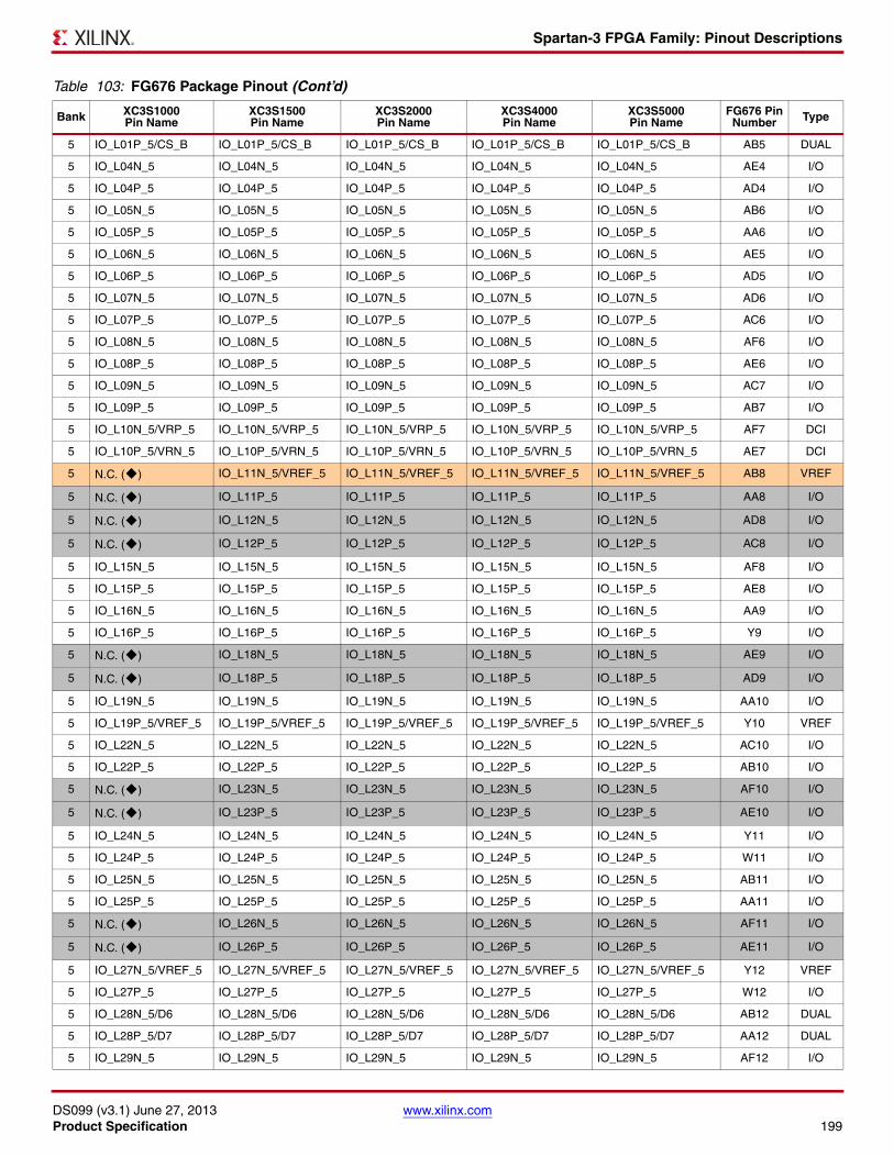
Spartan-3 FPGA Family: Pinout Descriptions
DS099 (v3.1) June 27, 2013 www.xilinx.comProduct Specification 199
5 IO_L01P_5/CS_B IO_L01P_5/CS_B IO_L01P_5/CS_B IO_L01P_5/CS_B IO_L01P_5/CS_B AB5 DUAL
5 IO_L04N_5 IO_L04N_5 IO_L04N_5 IO_L04N_5 IO_L04N_5 AE4 I/O
5 IO_L04P_5 IO_L04P_5 IO_L04P_5 IO_L04P_5 IO_L04P_5 AD4 I/O
5 IO_L05N_5 IO_L05N_5 IO_L05N_5 IO_L05N_5 IO_L05N_5 AB6 I/O
5 IO_L05P_5 IO_L05P_5 IO_L05P_5 IO_L05P_5 IO_L05P_5 AA6 I/O
5 IO_L06N_5 IO_L06N_5 IO_L06N_5 IO_L06N_5 IO_L06N_5 AE5 I/O
5 IO_L06P_5 IO_L06P_5 IO_L06P_5 IO_L06P_5 IO_L06P_5 AD5 I/O
5 IO_L07N_5 IO_L07N_5 IO_L07N_5 IO_L07N_5 IO_L07N_5 AD6 I/O
5 IO_L07P_5 IO_L07P_5 IO_L07P_5 IO_L07P_5 IO_L07P_5 AC6 I/O
5 IO_L08N_5 IO_L08N_5 IO_L08N_5 IO_L08N_5 IO_L08N_5 AF6 I/O
5 IO_L08P_5 IO_L08P_5 IO_L08P_5 IO_L08P_5 IO_L08P_5 AE6 I/O
5 IO_L09N_5 IO_L09N_5 IO_L09N_5 IO_L09N_5 IO_L09N_5 AC7 I/O
5 IO_L09P_5 IO_L09P_5 IO_L09P_5 IO_L09P_5 IO_L09P_5 AB7 I/O
5 IO_L10N_5/VRP_5 IO_L10N_5/VRP_5 IO_L10N_5/VRP_5 IO_L10N_5/VRP_5 IO_L10N_5/VRP_5 AF7 DCI
5 IO_L10P_5/VRN_5 IO_L10P_5/VRN_5 IO_L10P_5/VRN_5 IO_L10P_5/VRN_5 IO_L10P_5/VRN_5 AE7 DCI
5 N.C. () IO_L11N_5/VREF_5 IO_L11N_5/VREF_5 IO_L11N_5/VREF_5 IO_L11N_5/VREF_5 AB8 VREF
5 N.C. () IO_L11P_5 IO_L11P_5 IO_L11P_5 IO_L11P_5 AA8 I/O
5 N.C. () IO_L12N_5 IO_L12N_5 IO_L12N_5 IO_L12N_5 AD8 I/O
5 N.C. () IO_L12P_5 IO_L12P_5 IO_L12P_5 IO_L12P_5 AC8 I/O
5 IO_L15N_5 IO_L15N_5 IO_L15N_5 IO_L15N_5 IO_L15N_5 AF8 I/O
5 IO_L15P_5 IO_L15P_5 IO_L15P_5 IO_L15P_5 IO_L15P_5 AE8 I/O
5 IO_L16N_5 IO_L16N_5 IO_L16N_5 IO_L16N_5 IO_L16N_5 AA9 I/O
5 IO_L16P_5 IO_L16P_5 IO_L16P_5 IO_L16P_5 IO_L16P_5 Y9 I/O
5 N.C. () IO_L18N_5 IO_L18N_5 IO_L18N_5 IO_L18N_5 AE9 I/O
5 N.C. () IO_L18P_5 IO_L18P_5 IO_L18P_5 IO_L18P_5 AD9 I/O
5 IO_L19N_5 IO_L19N_5 IO_L19N_5 IO_L19N_5 IO_L19N_5 AA10 I/O
5 IO_L19P_5/VREF_5 IO_L19P_5/VREF_5 IO_L19P_5/VREF_5 IO_L19P_5/VREF_5 IO_L19P_5/VREF_5 Y10 VREF
5 IO_L22N_5 IO_L22N_5 IO_L22N_5 IO_L22N_5 IO_L22N_5 AC10 I/O
5 IO_L22P_5 IO_L22P_5 IO_L22P_5 IO_L22P_5 IO_L22P_5 AB10 I/O
5 N.C. () IO_L23N_5 IO_L23N_5 IO_L23N_5 IO_L23N_5 AF10 I/O
5 N.C. () IO_L23P_5 IO_L23P_5 IO_L23P_5 IO_L23P_5 AE10 I/O
5 IO_L24N_5 IO_L24N_5 IO_L24N_5 IO_L24N_5 IO_L24N_5 Y11 I/O
5 IO_L24P_5 IO_L24P_5 IO_L24P_5 IO_L24P_5 IO_L24P_5 W11 I/O
5 IO_L25N_5 IO_L25N_5 IO_L25N_5 IO_L25N_5 IO_L25N_5 AB11 I/O
5 IO_L25P_5 IO_L25P_5 IO_L25P_5 IO_L25P_5 IO_L25P_5 AA11 I/O
5 N.C. () IO_L26N_5 IO_L26N_5 IO_L26N_5 IO_L26N_5 AF11 I/O
5 N.C. () IO_L26P_5 IO_L26P_5 IO_L26P_5 IO_L26P_5 AE11 I/O
5 IO_L27N_5/VREF_5 IO_L27N_5/VREF_5 IO_L27N_5/VREF_5 IO_L27N_5/VREF_5 IO_L27N_5/VREF_5 Y12 VREF
5 IO_L27P_5 IO_L27P_5 IO_L27P_5 IO_L27P_5 IO_L27P_5 W12 I/O
5 IO_L28N_5/D6 IO_L28N_5/D6 IO_L28N_5/D6 IO_L28N_5/D6 IO_L28N_5/D6 AB12 DUAL
5 IO_L28P_5/D7 IO_L28P_5/D7 IO_L28P_5/D7 IO_L28P_5/D7 IO_L28P_5/D7 AA12 DUAL
5 IO_L29N_5 IO_L29N_5 IO_L29N_5 IO_L29N_5 IO_L29N_5 AF12 I/O
Table 103: FG676 Package Pinout (Cont’d)
Bank XC3S1000Pin Name
XC3S1500Pin Name
XC3S2000Pin Name
XC3S4000Pin Name
XC3S5000Pin Name
FG676 Pin Number Type
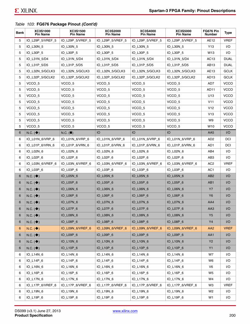
Spartan-3 FPGA Family: Pinout Descriptions
DS099 (v3.1) June 27, 2013 www.xilinx.comProduct Specification 200
5 IO_L29P_5/VREF_5 IO_L29P_5/VREF_5 IO_L29P_5/VREF_5 IO_L29P_5/VREF_5 IO_L29P_5/VREF_5 AE12 VREF
5 IO_L30N_5 IO_L30N_5 IO_L30N_5 IO_L30N_5 IO_L30N_5 Y13 I/O
5 IO_L30P_5 IO_L30P_5 IO_L30P_5 IO_L30P_5 IO_L30P_5 W13 I/O
5 IO_L31N_5/D4 IO_L31N_5/D4 IO_L31N_5/D4 IO_L31N_5/D4 IO_L31N_5/D4 AC13 DUAL
5 IO_L31P_5/D5 IO_L31P_5/D5 IO_L31P_5/D5 IO_L31P_5/D5 IO_L31P_5/D5 AB13 DUAL
5 IO_L32N_5/GCLK3 IO_L32N_5/GCLK3 IO_L32N_5/GCLK3 IO_L32N_5/GCLK3 IO_L32N_5/GCLK3 AE13 GCLK
5 IO_L32P_5/GCLK2 IO_L32P_5/GCLK2 IO_L32P_5/GCLK2 IO_L32P_5/GCLK2 IO_L32P_5/GCLK2 AD13 GCLK
5 VCCO_5 VCCO_5 VCCO_5 VCCO_5 VCCO_5 AD7 VCCO
5 VCCO_5 VCCO_5 VCCO_5 VCCO_5 VCCO_5 AD11 VCCO
5 VCCO_5 VCCO_5 VCCO_5 VCCO_5 VCCO_5 U13 VCCO
5 VCCO_5 VCCO_5 VCCO_5 VCCO_5 VCCO_5 V11 VCCO
5 VCCO_5 VCCO_5 VCCO_5 VCCO_5 VCCO_5 V12 VCCO
5 VCCO_5 VCCO_5 VCCO_5 VCCO_5 VCCO_5 V13 VCCO
5 VCCO_5 VCCO_5 VCCO_5 VCCO_5 VCCO_5 W9 VCCO
5 VCCO_5 VCCO_5 VCCO_5 VCCO_5 VCCO_5 W10 VCCO
6 N.C. () N.C. () IO IO IO AA5 I/O
6 IO_L01N_6/VRP_6 IO_L01N_6/VRP_6 IO_L01N_6/VRP_6 IO_L01N_6/VRP_6 IO_L01N_6/VRP_6 AD2 DCI
6 IO_L01P_6/VRN_6 IO_L01P_6/VRN_6 IO_L01P_6/VRN_6 IO_L01P_6/VRN_6 IO_L01P_6/VRN_6 AD1 DCI
6 IO_L02N_6 IO_L02N_6 IO_L02N_6 IO_L02N_6 IO_L02N_6 AB4 I/O
6 IO_L02P_6 IO_L02P_6 IO_L02P_6 IO_L02P_6 IO_L02P_6 AB3 I/O
6 IO_L03N_6/VREF_6 IO_L03N_6/VREF_6 IO_L03N_6/VREF_6 IO_L03N_6/VREF_6 IO_L03N_6/VREF_6 AC2 VREF
6 IO_L03P_6 IO_L03P_6 IO_L03P_6 IO_L03P_6 IO_L03P_6 AC1 I/O
6 N.C. () IO_L05N_6 IO_L05N_6 IO_L05N_6 IO_L05N_6 AB2 I/O
6 N.C. () IO_L05P_6 IO_L05P_6 IO_L05P_6 IO_L05P_6 AB1 I/O
6 N.C. () IO_L06N_6 IO_L06N_6 IO_L06N_6 IO_L06N_6 Y7 I/O
6 N.C. () IO_L06P_6 IO_L06P_6 IO_L06P_6 IO_L06P_6 Y6 I/O
6 N.C. () IO_L07N_6 IO_L07N_6 IO_L07N_6 IO_L07N_6 AA4 I/O
6 N.C. () IO_L07P_6 IO_L07P_6 IO_L07P_6 IO_L07P_6 AA3 I/O
6 N.C. () IO_L08N_6 IO_L08N_6 IO_L08N_6 IO_L08N_6 Y5 I/O
6 N.C. () IO_L08P_6 IO_L08P_6 IO_L08P_6 IO_L08P_6 Y4 I/O
6 N.C. () IO_L09N_6/VREF_6 IO_L09N_6/VREF_6 IO_L09N_6/VREF_6 IO_L09N_6/VREF_6 AA2 VREF
6 N.C. () IO_L09P_6 IO_L09P_6 IO_L09P_6 IO_L09P_6 AA1 I/O
6 N.C. () IO_L10N_6 IO_L10N_6 IO_L10N_6 IO_L10N_6 Y2 I/O
6 N.C. () IO_L10P_6 IO_L10P_6 IO_L10P_6 IO_L10P_6 Y1 I/O
6 IO_L14N_6 IO_L14N_6 IO_L14N_6 IO_L14N_6 IO_L14N_6 W7 I/O
6 IO_L14P_6 IO_L14P_6 IO_L14P_6 IO_L14P_6 IO_L14P_6 W6 I/O
6 IO_L16N_6 IO_L16N_6 IO_L16N_6 IO_L16N_6 IO_L16N_6 V6 I/O
6 IO_L16P_6 IO_L16P_6 IO_L16P_6 IO_L16P_6 IO_L16P_6 W5 I/O
6 IO_L17N_6 IO_L17N_6 IO_L17N_6 IO_L17N_6 IO_L17N_6 W4 I/O
6 IO_L17P_6/VREF_6 IO_L17P_6/VREF_6 IO_L17P_6/VREF_6 IO_L17P_6/VREF_6 IO_L17P_6/VREF_6 W3 VREF
6 IO_L19N_6 IO_L19N_6 IO_L19N_6 IO_L19N_6 IO_L19N_6 W2 I/O
6 IO_L19P_6 IO_L19P_6 IO_L19P_6 IO_L19P_6 IO_L19P_6 W1 I/O
Table 103: FG676 Package Pinout (Cont’d)
Bank XC3S1000Pin Name
XC3S1500Pin Name
XC3S2000Pin Name
XC3S4000Pin Name
XC3S5000Pin Name
FG676 Pin Number Type
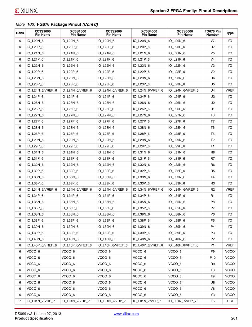
Spartan-3 FPGA Family: Pinout Descriptions
DS099 (v3.1) June 27, 2013 www.xilinx.comProduct Specification 201
6 IO_L20N_6 IO_L20N_6 IO_L20N_6 IO_L20N_6 IO_L20N_6 V7 I/O
6 IO_L20P_6 IO_L20P_6 IO_L20P_6 IO_L20P_6 IO_L20P_6 U7 I/O
6 IO_L21N_6 IO_L21N_6 IO_L21N_6 IO_L21N_6 IO_L21N_6 V5 I/O
6 IO_L21P_6 IO_L21P_6 IO_L21P_6 IO_L21P_6 IO_L21P_6 V4 I/O
6 IO_L22N_6 IO_L22N_6 IO_L22N_6 IO_L22N_6 IO_L22N_6 V3 I/O
6 IO_L22P_6 IO_L22P_6 IO_L22P_6 IO_L22P_6 IO_L22P_6 V2 I/O
6 IO_L23N_6 IO_L23N_6 IO_L23N_6 IO_L23N_6 IO_L23N_6 U6 I/O
6 IO_L23P_6 IO_L23P_6 IO_L23P_6 IO_L23P_6 IO_L23P_6 U5 I/O
6 IO_L24N_6/VREF_6 IO_L24N_6/VREF_6 IO_L24N_6/VREF_6 IO_L24N_6/VREF_6 IO_L24N_6/VREF_6 U4 VREF
6 IO_L24P_6 IO_L24P_6 IO_L24P_6 IO_L24P_6 IO_L24P_6 U3 I/O
6 IO_L26N_6 IO_L26N_6 IO_L26N_6 IO_L26N_6 IO_L26N_6 U2 I/O
6 IO_L26P_6 IO_L26P_6 IO_L26P_6 IO_L26P_6 IO_L26P_6 U1 I/O
6 IO_L27N_6 IO_L27N_6 IO_L27N_6 IO_L27N_6 IO_L27N_6 T8 I/O
6 IO_L27P_6 IO_L27P_6 IO_L27P_6 IO_L27P_6 IO_L27P_6 T7 I/O
6 IO_L28N_6 IO_L28N_6 IO_L28N_6 IO_L28N_6 IO_L28N_6 T6 I/O
6 IO_L28P_6 IO_L28P_6 IO_L28P_6 IO_L28P_6 IO_L28P_6 T5 I/O
6 IO_L29N_6 IO_L29N_6 IO_L29N_6 IO_L29N_6 IO_L29N_6 T2 I/O
6 IO_L29P_6 IO_L29P_6 IO_L29P_6 IO_L29P_6 IO_L29P_6 T1 I/O
6 IO_L31N_6 IO_L31N_6 IO_L31N_6 IO_L31N_6 IO_L31N_6 R8 I/O
6 IO_L31P_6 IO_L31P_6 IO_L31P_6 IO_L31P_6 IO_L31P_6 R7 I/O
6 IO_L32N_6 IO_L32N_6 IO_L32N_6 IO_L32N_6 IO_L32N_6 R6 I/O
6 IO_L32P_6 IO_L32P_6 IO_L32P_6 IO_L32P_6 IO_L32P_6 R5 I/O
6 IO_L33N_6 IO_L33N_6 IO_L33N_6 IO_L33N_6 IO_L33N_6 T4 I/O
6 IO_L33P_6 IO_L33P_6 IO_L33P_6 IO_L33P_6 IO_L33P_6 R3 I/O
6 IO_L34N_6/VREF_6 IO_L34N_6/VREF_6 IO_L34N_6/VREF_6 IO_L34N_6/VREF_6 IO_L34N_6/VREF_6 R2 VREF
6 IO_L34P_6 IO_L34P_6 IO_L34P_6 IO_L34P_6 IO_L34P_6 R1 I/O
6 IO_L35N_6 IO_L35N_6 IO_L35N_6 IO_L35N_6 IO_L35N_6 P8 I/O
6 IO_L35P_6 IO_L35P_6 IO_L35P_6 IO_L35P_6 IO_L35P_6 P7 I/O
6 IO_L38N_6 IO_L38N_6 IO_L38N_6 IO_L38N_6 IO_L38N_6 P6 I/O
6 IO_L38P_6 IO_L38P_6 IO_L38P_6 IO_L38P_6 IO_L38P_6 P5 I/O
6 IO_L39N_6 IO_L39N_6 IO_L39N_6 IO_L39N_6 IO_L39N_6 P4 I/O
6 IO_L39P_6 IO_L39P_6 IO_L39P_6 IO_L39P_6 IO_L39P_6 P3 I/O
6 IO_L40N_6 IO_L40N_6 IO_L40N_6 IO_L40N_6 IO_L40N_6 P2 I/O
6 IO_L40P_6/VREF_6 IO_L40P_6/VREF_6 IO_L40P_6/VREF_6 IO_L40P_6/VREF_6 IO_L40P_6/VREF_6 P1 VREF
6 VCCO_6 VCCO_6 VCCO_6 VCCO_6 VCCO_6 P9 VCCO
6 VCCO_6 VCCO_6 VCCO_6 VCCO_6 VCCO_6 P10 VCCO
6 VCCO_6 VCCO_6 VCCO_6 VCCO_6 VCCO_6 R9 VCCO
6 VCCO_6 VCCO_6 VCCO_6 VCCO_6 VCCO_6 T3 VCCO
6 VCCO_6 VCCO_6 VCCO_6 VCCO_6 VCCO_6 T9 VCCO
6 VCCO_6 VCCO_6 VCCO_6 VCCO_6 VCCO_6 U8 VCCO
6 VCCO_6 VCCO_6 VCCO_6 VCCO_6 VCCO_6 V8 VCCO
6 VCCO_6 VCCO_6 VCCO_6 VCCO_6 VCCO_6 Y3 VCCO
7 IO_L01N_7/VRP_7 IO_L01N_7/VRP_7 IO_L01N_7/VRP_7 IO_L01N_7/VRP_7 IO_L01N_7/VRP_7 F5 DCI
Table 103: FG676 Package Pinout (Cont’d)
Bank XC3S1000Pin Name
XC3S1500Pin Name
XC3S2000Pin Name
XC3S4000Pin Name
XC3S5000Pin Name
FG676 Pin Number Type
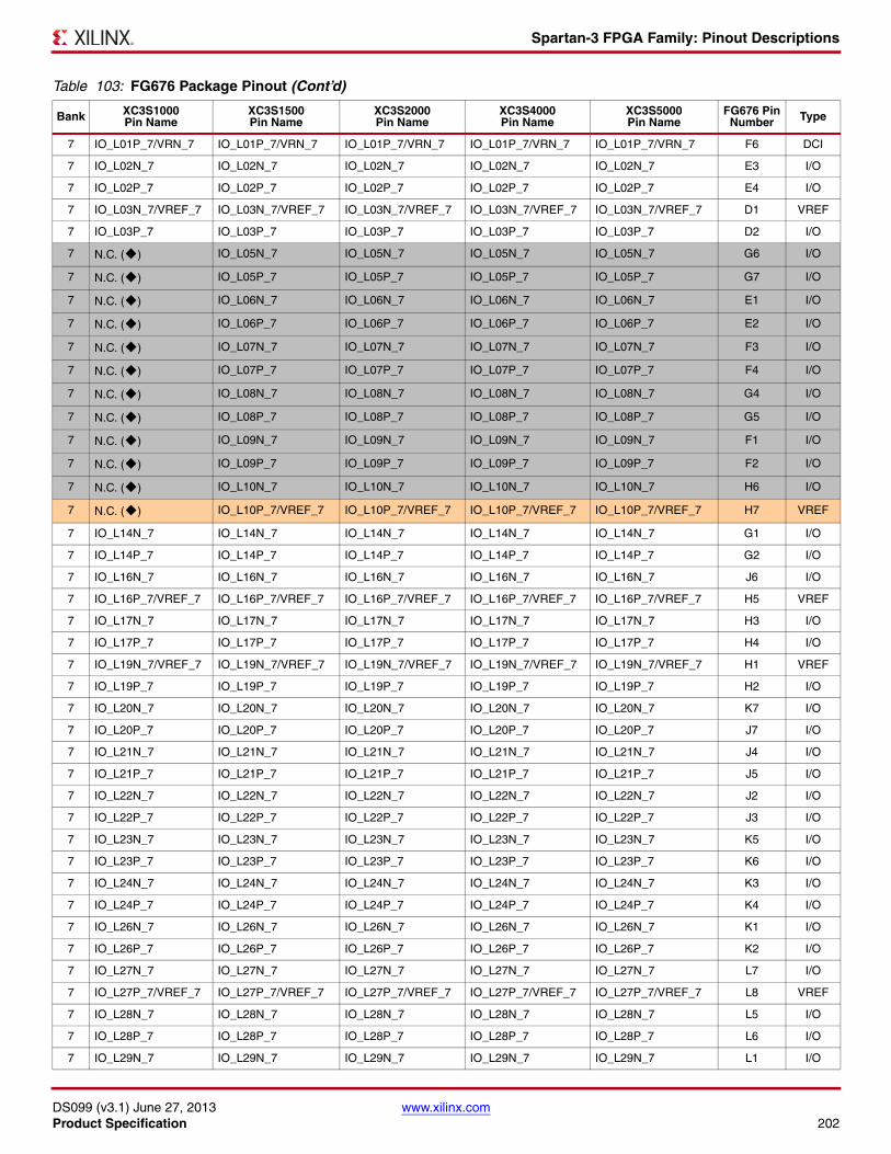
Spartan-3 FPGA Family: Pinout Descriptions
DS099 (v3.1) June 27, 2013 www.xilinx.comProduct Specification 202
7 IO_L01P_7/VRN_7 IO_L01P_7/VRN_7 IO_L01P_7/VRN_7 IO_L01P_7/VRN_7 IO_L01P_7/VRN_7 F6 DCI
7 IO_L02N_7 IO_L02N_7 IO_L02N_7 IO_L02N_7 IO_L02N_7 E3 I/O
7 IO_L02P_7 IO_L02P_7 IO_L02P_7 IO_L02P_7 IO_L02P_7 E4 I/O
7 IO_L03N_7/VREF_7 IO_L03N_7/VREF_7 IO_L03N_7/VREF_7 IO_L03N_7/VREF_7 IO_L03N_7/VREF_7 D1 VREF
7 IO_L03P_7 IO_L03P_7 IO_L03P_7 IO_L03P_7 IO_L03P_7 D2 I/O
7 N.C. () IO_L05N_7 IO_L05N_7 IO_L05N_7 IO_L05N_7 G6 I/O
7 N.C. () IO_L05P_7 IO_L05P_7 IO_L05P_7 IO_L05P_7 G7 I/O
7 N.C. () IO_L06N_7 IO_L06N_7 IO_L06N_7 IO_L06N_7 E1 I/O
7 N.C. () IO_L06P_7 IO_L06P_7 IO_L06P_7 IO_L06P_7 E2 I/O
7 N.C. () IO_L07N_7 IO_L07N_7 IO_L07N_7 IO_L07N_7 F3 I/O
7 N.C. () IO_L07P_7 IO_L07P_7 IO_L07P_7 IO_L07P_7 F4 I/O
7 N.C. () IO_L08N_7 IO_L08N_7 IO_L08N_7 IO_L08N_7 G4 I/O
7 N.C. () IO_L08P_7 IO_L08P_7 IO_L08P_7 IO_L08P_7 G5 I/O
7 N.C. () IO_L09N_7 IO_L09N_7 IO_L09N_7 IO_L09N_7 F1 I/O
7 N.C. () IO_L09P_7 IO_L09P_7 IO_L09P_7 IO_L09P_7 F2 I/O
7 N.C. () IO_L10N_7 IO_L10N_7 IO_L10N_7 IO_L10N_7 H6 I/O
7 N.C. () IO_L10P_7/VREF_7 IO_L10P_7/VREF_7 IO_L10P_7/VREF_7 IO_L10P_7/VREF_7 H7 VREF
7 IO_L14N_7 IO_L14N_7 IO_L14N_7 IO_L14N_7 IO_L14N_7 G1 I/O
7 IO_L14P_7 IO_L14P_7 IO_L14P_7 IO_L14P_7 IO_L14P_7 G2 I/O
7 IO_L16N_7 IO_L16N_7 IO_L16N_7 IO_L16N_7 IO_L16N_7 J6 I/O
7 IO_L16P_7/VREF_7 IO_L16P_7/VREF_7 IO_L16P_7/VREF_7 IO_L16P_7/VREF_7 IO_L16P_7/VREF_7 H5 VREF
7 IO_L17N_7 IO_L17N_7 IO_L17N_7 IO_L17N_7 IO_L17N_7 H3 I/O
7 IO_L17P_7 IO_L17P_7 IO_L17P_7 IO_L17P_7 IO_L17P_7 H4 I/O
7 IO_L19N_7/VREF_7 IO_L19N_7/VREF_7 IO_L19N_7/VREF_7 IO_L19N_7/VREF_7 IO_L19N_7/VREF_7 H1 VREF
7 IO_L19P_7 IO_L19P_7 IO_L19P_7 IO_L19P_7 IO_L19P_7 H2 I/O
7 IO_L20N_7 IO_L20N_7 IO_L20N_7 IO_L20N_7 IO_L20N_7 K7 I/O
7 IO_L20P_7 IO_L20P_7 IO_L20P_7 IO_L20P_7 IO_L20P_7 J7 I/O
7 IO_L21N_7 IO_L21N_7 IO_L21N_7 IO_L21N_7 IO_L21N_7 J4 I/O
7 IO_L21P_7 IO_L21P_7 IO_L21P_7 IO_L21P_7 IO_L21P_7 J5 I/O
7 IO_L22N_7 IO_L22N_7 IO_L22N_7 IO_L22N_7 IO_L22N_7 J2 I/O
7 IO_L22P_7 IO_L22P_7 IO_L22P_7 IO_L22P_7 IO_L22P_7 J3 I/O
7 IO_L23N_7 IO_L23N_7 IO_L23N_7 IO_L23N_7 IO_L23N_7 K5 I/O
7 IO_L23P_7 IO_L23P_7 IO_L23P_7 IO_L23P_7 IO_L23P_7 K6 I/O
7 IO_L24N_7 IO_L24N_7 IO_L24N_7 IO_L24N_7 IO_L24N_7 K3 I/O
7 IO_L24P_7 IO_L24P_7 IO_L24P_7 IO_L24P_7 IO_L24P_7 K4 I/O
7 IO_L26N_7 IO_L26N_7 IO_L26N_7 IO_L26N_7 IO_L26N_7 K1 I/O
7 IO_L26P_7 IO_L26P_7 IO_L26P_7 IO_L26P_7 IO_L26P_7 K2 I/O
7 IO_L27N_7 IO_L27N_7 IO_L27N_7 IO_L27N_7 IO_L27N_7 L7 I/O
7 IO_L27P_7/VREF_7 IO_L27P_7/VREF_7 IO_L27P_7/VREF_7 IO_L27P_7/VREF_7 IO_L27P_7/VREF_7 L8 VREF
7 IO_L28N_7 IO_L28N_7 IO_L28N_7 IO_L28N_7 IO_L28N_7 L5 I/O
7 IO_L28P_7 IO_L28P_7 IO_L28P_7 IO_L28P_7 IO_L28P_7 L6 I/O
7 IO_L29N_7 IO_L29N_7 IO_L29N_7 IO_L29N_7 IO_L29N_7 L1 I/O
Table 103: FG676 Package Pinout (Cont’d)
Bank XC3S1000Pin Name
XC3S1500Pin Name
XC3S2000Pin Name
XC3S4000Pin Name
XC3S5000Pin Name
FG676 Pin Number Type
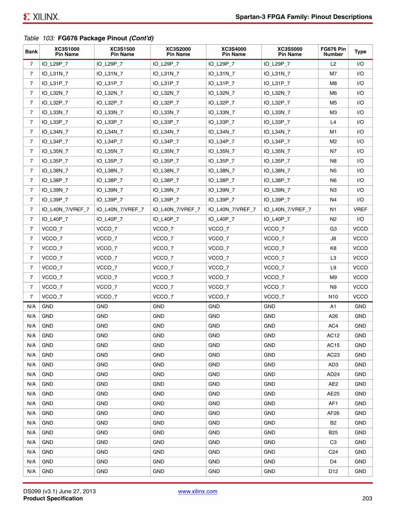
Spartan-3 FPGA Family: Pinout Descriptions
DS099 (v3.1) June 27, 2013 www.xilinx.comProduct Specification 203
7 IO_L29P_7 IO_L29P_7 IO_L29P_7 IO_L29P_7 IO_L29P_7 L2 I/O
7 IO_L31N_7 IO_L31N_7 IO_L31N_7 IO_L31N_7 IO_L31N_7 M7 I/O
7 IO_L31P_7 IO_L31P_7 IO_L31P_7 IO_L31P_7 IO_L31P_7 M8 I/O
7 IO_L32N_7 IO_L32N_7 IO_L32N_7 IO_L32N_7 IO_L32N_7 M6 I/O
7 IO_L32P_7 IO_L32P_7 IO_L32P_7 IO_L32P_7 IO_L32P_7 M5 I/O
7 IO_L33N_7 IO_L33N_7 IO_L33N_7 IO_L33N_7 IO_L33N_7 M3 I/O
7 IO_L33P_7 IO_L33P_7 IO_L33P_7 IO_L33P_7 IO_L33P_7 L4 I/O
7 IO_L34N_7 IO_L34N_7 IO_L34N_7 IO_L34N_7 IO_L34N_7 M1 I/O
7 IO_L34P_7 IO_L34P_7 IO_L34P_7 IO_L34P_7 IO_L34P_7 M2 I/O
7 IO_L35N_7 IO_L35N_7 IO_L35N_7 IO_L35N_7 IO_L35N_7 N7 I/O
7 IO_L35P_7 IO_L35P_7 IO_L35P_7 IO_L35P_7 IO_L35P_7 N8 I/O
7 IO_L38N_7 IO_L38N_7 IO_L38N_7 IO_L38N_7 IO_L38N_7 N5 I/O
7 IO_L38P_7 IO_L38P_7 IO_L38P_7 IO_L38P_7 IO_L38P_7 N6 I/O
7 IO_L39N_7 IO_L39N_7 IO_L39N_7 IO_L39N_7 IO_L39N_7 N3 I/O
7 IO_L39P_7 IO_L39P_7 IO_L39P_7 IO_L39P_7 IO_L39P_7 N4 I/O
7 IO_L40N_7/VREF_7 IO_L40N_7/VREF_7 IO_L40N_7/VREF_7 IO_L40N_7/VREF_7 IO_L40N_7/VREF_7 N1 VREF
7 IO_L40P_7 IO_L40P_7 IO_L40P_7 IO_L40P_7 IO_L40P_7 N2 I/O
7 VCCO_7 VCCO_7 VCCO_7 VCCO_7 VCCO_7 G3 VCCO
7 VCCO_7 VCCO_7 VCCO_7 VCCO_7 VCCO_7 J8 VCCO
7 VCCO_7 VCCO_7 VCCO_7 VCCO_7 VCCO_7 K8 VCCO
7 VCCO_7 VCCO_7 VCCO_7 VCCO_7 VCCO_7 L3 VCCO
7 VCCO_7 VCCO_7 VCCO_7 VCCO_7 VCCO_7 L9 VCCO
7 VCCO_7 VCCO_7 VCCO_7 VCCO_7 VCCO_7 M9 VCCO
7 VCCO_7 VCCO_7 VCCO_7 VCCO_7 VCCO_7 N9 VCCO
7 VCCO_7 VCCO_7 VCCO_7 VCCO_7 VCCO_7 N10 VCCO
N/A GND GND GND GND GND A1 GND
N/A GND GND GND GND GND A26 GND
N/A GND GND GND GND GND AC4 GND
N/A GND GND GND GND GND AC12 GND
N/A GND GND GND GND GND AC15 GND
N/A GND GND GND GND GND AC23 GND
N/A GND GND GND GND GND AD3 GND
N/A GND GND GND GND GND AD24 GND
N/A GND GND GND GND GND AE2 GND
N/A GND GND GND GND GND AE25 GND
N/A GND GND GND GND GND AF1 GND
N/A GND GND GND GND GND AF26 GND
N/A GND GND GND GND GND B2 GND
N/A GND GND GND GND GND B25 GND
N/A GND GND GND GND GND C3 GND
N/A GND GND GND GND GND C24 GND
N/A GND GND GND GND GND D4 GND
N/A GND GND GND GND GND D12 GND
Table 103: FG676 Package Pinout (Cont’d)
Bank XC3S1000Pin Name
XC3S1500Pin Name
XC3S2000Pin Name
XC3S4000Pin Name
XC3S5000Pin Name
FG676 Pin Number Type
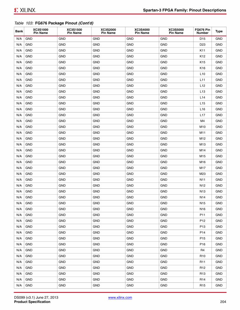
Spartan-3 FPGA Family: Pinout Descriptions
DS099 (v3.1) June 27, 2013 www.xilinx.comProduct Specification 204
N/A GND GND GND GND GND D15 GND
N/A GND GND GND GND GND D23 GND
N/A GND GND GND GND GND K11 GND
N/A GND GND GND GND GND K12 GND
N/A GND GND GND GND GND K15 GND
N/A GND GND GND GND GND K16 GND
N/A GND GND GND GND GND L10 GND
N/A GND GND GND GND GND L11 GND
N/A GND GND GND GND GND L12 GND
N/A GND GND GND GND GND L13 GND
N/A GND GND GND GND GND L14 GND
N/A GND GND GND GND GND L15 GND
N/A GND GND GND GND GND L16 GND
N/A GND GND GND GND GND L17 GND
N/A GND GND GND GND GND M4 GND
N/A GND GND GND GND GND M10 GND
N/A GND GND GND GND GND M11 GND
N/A GND GND GND GND GND M12 GND
N/A GND GND GND GND GND M13 GND
N/A GND GND GND GND GND M14 GND
N/A GND GND GND GND GND M15 GND
N/A GND GND GND GND GND M16 GND
N/A GND GND GND GND GND M17 GND
N/A GND GND GND GND GND M23 GND
N/A GND GND GND GND GND N11 GND
N/A GND GND GND GND GND N12 GND
N/A GND GND GND GND GND N13 GND
N/A GND GND GND GND GND N14 GND
N/A GND GND GND GND GND N15 GND
N/A GND GND GND GND GND N16 GND
N/A GND GND GND GND GND P11 GND
N/A GND GND GND GND GND P12 GND
N/A GND GND GND GND GND P13 GND
N/A GND GND GND GND GND P14 GND
N/A GND GND GND GND GND P15 GND
N/A GND GND GND GND GND P16 GND
N/A GND GND GND GND GND R4 GND
N/A GND GND GND GND GND R10 GND
N/A GND GND GND GND GND R11 GND
N/A GND GND GND GND GND R12 GND
N/A GND GND GND GND GND R13 GND
N/A GND GND GND GND GND R14 GND
N/A GND GND GND GND GND R15 GND
Table 103: FG676 Package Pinout (Cont’d)
Bank XC3S1000Pin Name
XC3S1500Pin Name
XC3S2000Pin Name
XC3S4000Pin Name
XC3S5000Pin Name
FG676 Pin Number Type
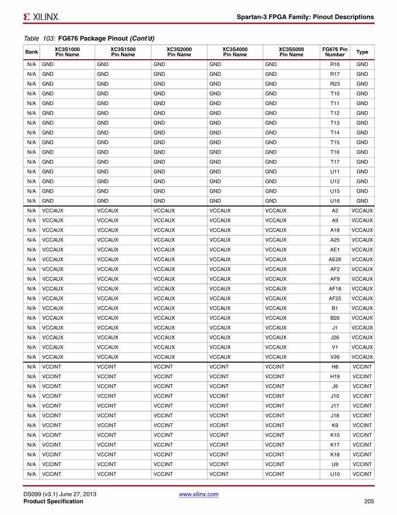
Spartan-3 FPGA Family: Pinout Descriptions
DS099 (v3.1) June 27, 2013 www.xilinx.comProduct Specification 205
N/A GND GND GND GND GND R16 GND
N/A GND GND GND GND GND R17 GND
N/A GND GND GND GND GND R23 GND
N/A GND GND GND GND GND T10 GND
N/A GND GND GND GND GND T11 GND
N/A GND GND GND GND GND T12 GND
N/A GND GND GND GND GND T13 GND
N/A GND GND GND GND GND T14 GND
N/A GND GND GND GND GND T15 GND
N/A GND GND GND GND GND T16 GND
N/A GND GND GND GND GND T17 GND
N/A GND GND GND GND GND U11 GND
N/A GND GND GND GND GND U12 GND
N/A GND GND GND GND GND U15 GND
N/A GND GND GND GND GND U16 GND
N/A VCCAUX VCCAUX VCCAUX VCCAUX VCCAUX A2 VCCAUX
N/A VCCAUX VCCAUX VCCAUX VCCAUX VCCAUX A9 VCCAUX
N/A VCCAUX VCCAUX VCCAUX VCCAUX VCCAUX A18 VCCAUX
N/A VCCAUX VCCAUX VCCAUX VCCAUX VCCAUX A25 VCCAUX
N/A VCCAUX VCCAUX VCCAUX VCCAUX VCCAUX AE1 VCCAUX
N/A VCCAUX VCCAUX VCCAUX VCCAUX VCCAUX AE26 VCCAUX
N/A VCCAUX VCCAUX VCCAUX VCCAUX VCCAUX AF2 VCCAUX
N/A VCCAUX VCCAUX VCCAUX VCCAUX VCCAUX AF9 VCCAUX
N/A VCCAUX VCCAUX VCCAUX VCCAUX VCCAUX AF18 VCCAUX
N/A VCCAUX VCCAUX VCCAUX VCCAUX VCCAUX AF25 VCCAUX
N/A VCCAUX VCCAUX VCCAUX VCCAUX VCCAUX B1 VCCAUX
N/A VCCAUX VCCAUX VCCAUX VCCAUX VCCAUX B26 VCCAUX
N/A VCCAUX VCCAUX VCCAUX VCCAUX VCCAUX J1 VCCAUX
N/A VCCAUX VCCAUX VCCAUX VCCAUX VCCAUX J26 VCCAUX
N/A VCCAUX VCCAUX VCCAUX VCCAUX VCCAUX V1 VCCAUX
N/A VCCAUX VCCAUX VCCAUX VCCAUX VCCAUX V26 VCCAUX
N/A VCCINT VCCINT VCCINT VCCINT VCCINT H8 VCCINT
N/A VCCINT VCCINT VCCINT VCCINT VCCINT H19 VCCINT
N/A VCCINT VCCINT VCCINT VCCINT VCCINT J9 VCCINT
N/A VCCINT VCCINT VCCINT VCCINT VCCINT J10 VCCINT
N/A VCCINT VCCINT VCCINT VCCINT VCCINT J17 VCCINT
N/A VCCINT VCCINT VCCINT VCCINT VCCINT J18 VCCINT
N/A VCCINT VCCINT VCCINT VCCINT VCCINT K9 VCCINT
N/A VCCINT VCCINT VCCINT VCCINT VCCINT K10 VCCINT
N/A VCCINT VCCINT VCCINT VCCINT VCCINT K17 VCCINT
N/A VCCINT VCCINT VCCINT VCCINT VCCINT K18 VCCINT
N/A VCCINT VCCINT VCCINT VCCINT VCCINT U9 VCCINT
N/A VCCINT VCCINT VCCINT VCCINT VCCINT U10 VCCINT
Table 103: FG676 Package Pinout (Cont’d)
Bank XC3S1000Pin Name
XC3S1500Pin Name
XC3S2000Pin Name
XC3S4000Pin Name
XC3S5000Pin Name
FG676 Pin Number Type
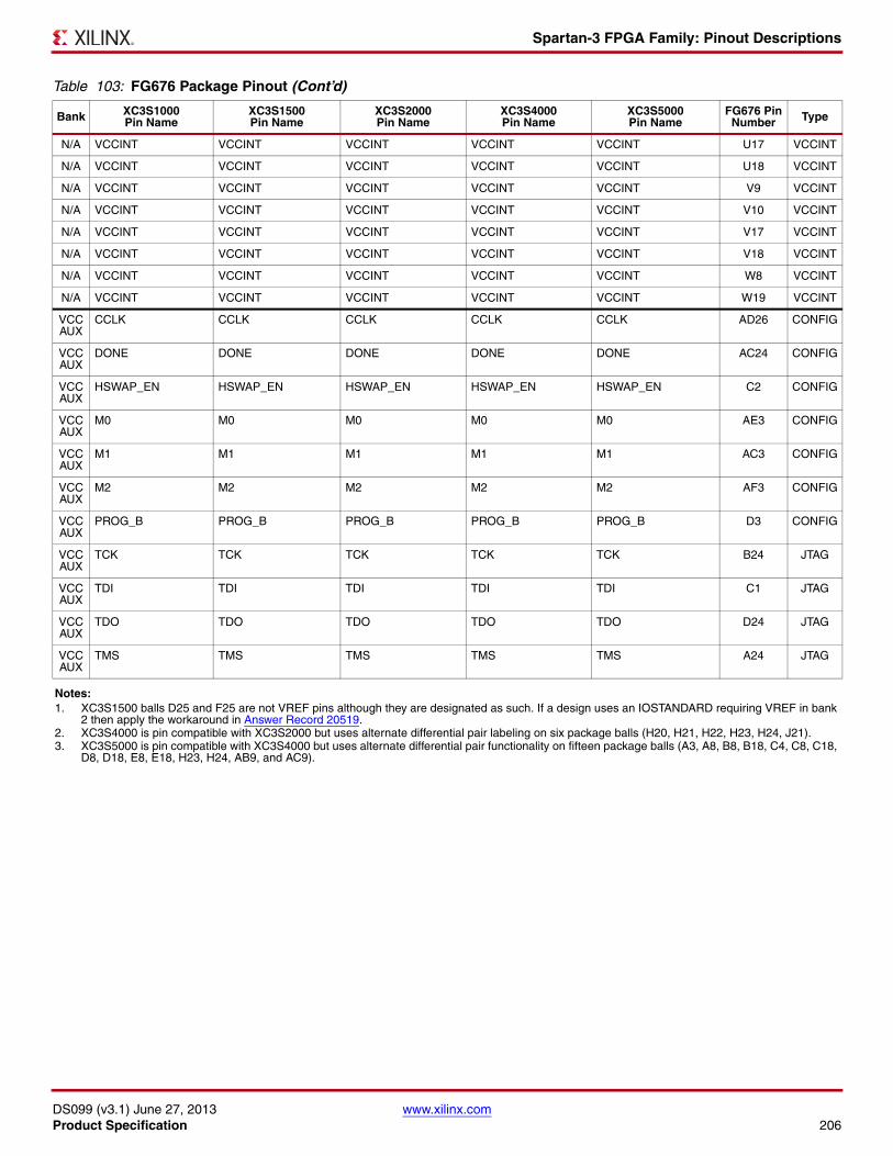
Spartan-3 FPGA Family: Pinout Descriptions
DS099 (v3.1) June 27, 2013 www.xilinx.comProduct Specification 206
N/A VCCINT VCCINT VCCINT VCCINT VCCINT U17 VCCINT
N/A VCCINT VCCINT VCCINT VCCINT VCCINT U18 VCCINT
N/A VCCINT VCCINT VCCINT VCCINT VCCINT V9 VCCINT
N/A VCCINT VCCINT VCCINT VCCINT VCCINT V10 VCCINT
N/A VCCINT VCCINT VCCINT VCCINT VCCINT V17 VCCINT
N/A VCCINT VCCINT VCCINT VCCINT VCCINT V18 VCCINT
N/A VCCINT VCCINT VCCINT VCCINT VCCINT W8 VCCINT
N/A VCCINT VCCINT VCCINT VCCINT VCCINT W19 VCCINT
VCCAUX
CCLK CCLK CCLK CCLK CCLK AD26 CONFIG
VCCAUX
DONE DONE DONE DONE DONE AC24 CONFIG
VCCAUX
HSWAP_EN HSWAP_EN HSWAP_EN HSWAP_EN HSWAP_EN C2 CONFIG
VCCAUX
M0 M0 M0 M0 M0 AE3 CONFIG
VCCAUX
M1 M1 M1 M1 M1 AC3 CONFIG
VCCAUX
M2 M2 M2 M2 M2 AF3 CONFIG
VCCAUX
PROG_B PROG_B PROG_B PROG_B PROG_B D3 CONFIG
VCCAUX
TCK TCK TCK TCK TCK B24 JTAG
VCCAUX
TDI TDI TDI TDI TDI C1 JTAG
VCCAUX
TDO TDO TDO TDO TDO D24 JTAG
VCCAUX
TMS TMS TMS TMS TMS A24 JTAG
Notes: 1. XC3S1500 balls D25 and F25 are not VREF pins although they are designated as such. If a design uses an IOSTANDARD requiring VREF in bank
2 then apply the workaround in Answer Record 20519.2. XC3S4000 is pin compatible with XC3S2000 but uses alternate differential pair labeling on six package balls (H20, H21, H22, H23, H24, J21).3. XC3S5000 is pin compatible with XC3S4000 but uses alternate differential pair functionality on fifteen package balls (A3, A8, B8, B18, C4, C8, C18,
D8, D18, E8, E18, H23, H24, AB9, and AC9).
Table 103: FG676 Package Pinout (Cont’d)
Bank XC3S1000Pin Name
XC3S1500Pin Name
XC3S2000Pin Name
XC3S4000Pin Name
XC3S5000Pin Name
FG676 Pin Number Type
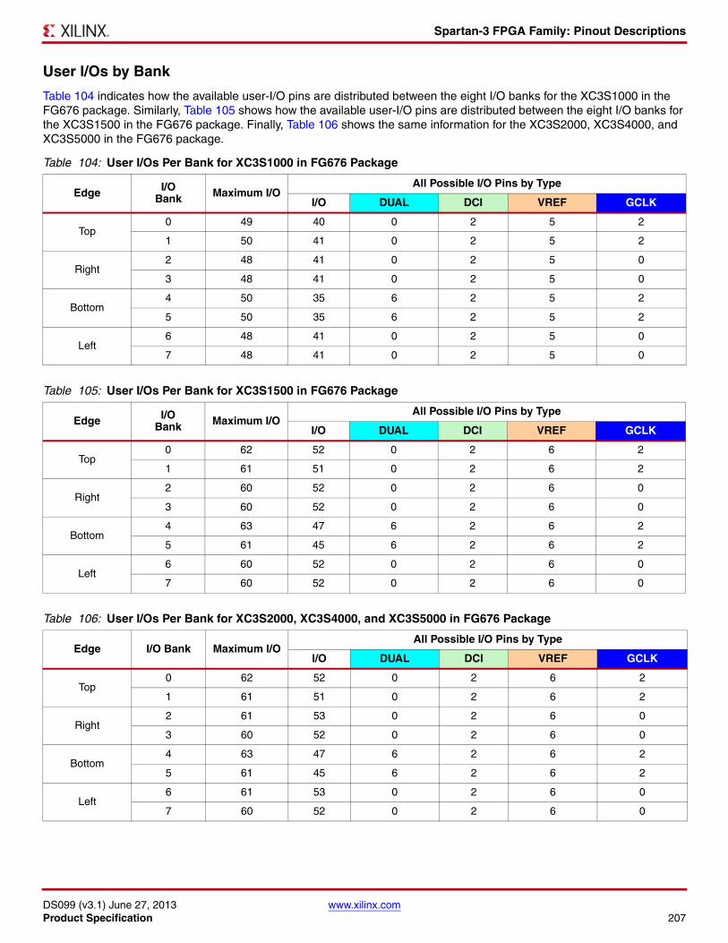
Spartan-3 FPGA Family: Pinout Descriptions
DS099 (v3.1) June 27, 2013 www.xilinx.comProduct Specification 207
User I/Os by Bank
Table 104 indicates how the available user-I/O pins are distributed between the eight I/O banks for the XC3S1000 in the FG676 package. Similarly, Table 105 shows how the available user-I/O pins are distributed between the eight I/O banks for the XC3S1500 in the FG676 package. Finally, Table 106 shows the same information for the XC3S2000, XC3S4000, and XC3S5000 in the FG676 package.
Table 104: User I/Os Per Bank for XC3S1000 in FG676 Package
Edge I/OBank Maximum I/O
All Possible I/O Pins by Type
I/O DUAL DCI VREF GCLK
Top0 49 40 0 2 5 2
1 50 41 0 2 5 2
Right2 48 41 0 2 5 0
3 48 41 0 2 5 0
Bottom4 50 35 6 2 5 2
5 50 35 6 2 5 2
Left6 48 41 0 2 5 0
7 48 41 0 2 5 0
Table 105: User I/Os Per Bank for XC3S1500 in FG676 Package
Edge I/OBank Maximum I/O
All Possible I/O Pins by Type
I/O DUAL DCI VREF GCLK
Top0 62 52 0 2 6 2
1 61 51 0 2 6 2
Right2 60 52 0 2 6 0
3 60 52 0 2 6 0
Bottom4 63 47 6 2 6 2
5 61 45 6 2 6 2
Left6 60 52 0 2 6 0
7 60 52 0 2 6 0
Table 106: User I/Os Per Bank for XC3S2000, XC3S4000, and XC3S5000 in FG676 Package
Edge I/O Bank Maximum I/OAll Possible I/O Pins by Type
I/O DUAL DCI VREF GCLK
Top0 62 52 0 2 6 2
1 61 51 0 2 6 2
Right2 61 53 0 2 6 0
3 60 52 0 2 6 0
Bottom4 63 47 6 2 6 2
5 61 45 6 2 6 2
Left6 61 53 0 2 6 0
7 60 52 0 2 6 0
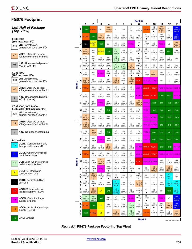
Spartan-3 FPGA Family: Pinout Descriptions
DS099 (v3.1) June 27, 2013 www.xilinx.comProduct Specification 208
FG676 Footprint X-Ref Target - Figure 53
Left Half of Package (Top View)
XC3S1000(391 max. user I/O)
315 I/O: Unrestricted, general-purpose user I/O
40 VREF: User I/O or input voltage reference for bank
98 N.C.: Unconnected pins for XC3S1000 ()
XC3S1500(487 max user I/O)
403 I/O: Unrestricted, general-purpose user I/O
48 VREF: User I/O or input voltage reference for bank
2 N.C.: Unconnected pins for XC3S1500 ()
XC3S2000, XC3S4000, XC3S5000 (489 max user I/O)
405 I/O: Unrestricted, general-purpose user I/O
48 VREF: User I/O or input voltage reference for bank
0 N.C.: No unconnected pins
All devices
12 DUAL: Configuration pin, then possible user I/O
8 GCLK: User I/O or global clock buffer input
16 DCI: User I/O or reference resistor input for bank
7 CONFIG: Dedicated configuration pins
4 JTAG: Dedicated JTAG port pins
20 VCCINT: Internal core voltage supply (+1.2V)
64 VCCO: Output voltage supply for bank
16 VCCAUX: Auxiliary voltage supply (+2.5V)
76 GND: Ground
Figure 53: FG676 Package Footprint (Top View)
21 103 4 5 6 7 8 9 11 12 13Bank 0
A
B
C
D
E
F
G
H
J
K
L
M
N
P
R
T
U
V
W
Y
AA
AB
AC
AD
AE
AF
Ban
k 6
Ban
k 7
Bank 5
VCCAUX I/OI/O
L05P_0 VREF_0
I/O I/OI/O
L10P_0I/O
L15P_0VCCAUX
I/O L23P_0
I/O L26P_0 VREF_0
I/O L29P_0
I/O L32P_0 GCLK6
VCCAUX I/O VREF_0
I/O L05N_0
I/O L06P_0
I/O L08P_0
I/O L10N_0
I/O L15N_0
I/O L18P_0
I/O L23N_0
I/O L26N_0 I/O
L29N_0
I/O L32N_0 GCLK7
TD IHSWAP_
EN I/OI/O
L06N_0I/O
L08N_0VCCO_0
I/O I/O
L18N_0 I/O L22P_0
VCCO_0 I/OI/O
L31P_0 VREF_0
I/O L03N_7 VREF_7
I/O L03P_7
PROG_BI/O
L01P_0 VRN_0
I/O L07P_0
I/O L09P_0
I/O L12P_0
I/O L17P_0 I/O
L22N_0I/O
L25P_0GND
GND GND
GND GND GND GND
GND GNDGND GND
GND GND GND GND
GND GND
GND GND
GND GNDGND
GND GNDGND
GNDGND
I/O L31N_0
I/O L06N_7
I/O L06P_7 I/O
L02N_7I/O
L02P_7
I/O L01N_0 VRP_0
I/O L07N_0
I/O L09N_0
I/O L12N_0
I/O L17N_0 I/O
L19P_0I/O
L25N_0I/O
L28P_0I/O
I/O L09N_7
I/O L09P_7
I/O L07N_7
I/O L07P_7
I/O L01N_7 VRP_7
I/O L01P_7 VRN_7
I/O VREF_0
I/O L11P_0 I/O
L16P_0I/O
L19N_0I/O
L24P_0I/O
L28N_0I/O
L30P_0
I/O L14N_7
I/O L14P_7
VCCO_7I/O
L08N_7 I/O
L08P_7 I/O
L05N_7 I/O
L05P_7 I/O
L11N_0 I/O L16N_0
I/O VREF_0
I/O L24N_0
I/O L27N_0
I/O L30N_0
I/O L19N_7 VREF_7
I/O L19P_7
I/O L17N_7
I/O L17P_7
I/O L16P_7 VREF_7
I/O L10N_7
I/O L10P_7 VREF_7 VCCINT VCCO_0 VCCO_0 I/O I/O
I/O L27P_0
VCCAUX I/O L22N_7
I/O L22P_7
I/O L21N_7
I/O L21P_7
I/O L16N_7
I/O L20P_7
VCCO_7 VCCINT VCCINT VCCO_0 VCCO_0 VCCO_0
I/O L26N_7
I/O L26P_7
I/O L24N_7
I/O L24P_7
I/O L23N_7
I/O L23P_7
I/O L20N_7
VCCO_7 VCCINT VCCINT VCCO_0
I/O L29N_7
I/O L29P_7
VCCO_7 I/O L33P_7
I/O L28N_7
I/O L28P_7
I/O L27N_7
I/O L27P_7 VREF_7
VCCO_7
I/O L34N_7
I/O L34P_7
I/O L33N_7
I/O L32P_7
I/O L32N_7
I/O L31N_7
I/O L31P_7
VCCO_7
I/O L40N_7 VREF_7
I/O L40P_7
I/O L39N_7
I/O L39P_7
I/O L38N_7
I/O L38P_7
I/O L35N_7
I/O L35P_7
VCCO_7 VCCO_7
I/O L40P_6 VREF_6
I/O L40N_6
I/O L39P_6
I/O L39N_6
I/O L38P_6
I/O L38N_6
I/O L35P_6
I/O L35N_6
VCCO_6 VCCO_6
I/O L34P_6
I/O L34N_6 VREF_6
I/O L33P_6
GND
GND
GND
GND
GND
GND
I/O L32P_6
I/O L32N_6
I/O L31P_6
I/O L31N_6
VCCO_6
I/O L29P_6
I/O L29N_6
VCCO_6 I/O L33N_6
I/O L28P_6
I/O L28N_6
I/O L27P_6
I/O L27N_6
VCCO_6
I/O L26P_6
I/O L26N_6
I/O L24P_6
I/O L24N_6 VREF_6
I/O L23P_6
I/O L23N_6
I/O L20P_6
VCCO_6 VCCINT VCCINT VCCO_5
VCCAUX I/O L22P_6
I/O L22N_6
I/O L21P_6
I/O L21N_6
I/O L16N_6
I/O L20N_6
VCCO_6 VCCINT VCCINT VCCO_5 VCCO_5 VCCO_5
I/O L19P_6
I/O L19N_6
I/O L17P_6 VREF_6
I/O L17N_6
I/O L16P_6
I/O L14P_6
I/O L14N_6
VCCINT VCCO_5 VCCO_5 I/O L24P_5
I/O L27P_5
I/O L30P_5
I/O L10P_6
I/O L10N_6 VCCO_6
I/O L08P_6
I/O L08N_6
I/O L06P_6
I/O L06N_6 I/O
I/O L16P_5
I/O L19P_5 VREF_5
I/O L24N_5
I/O L27N_5 VREF_5
I/O L30N_5
I/O L09P_6
I/O L09N_6 VREF_6
I/O L07P_6
I/O L07N_6
I/O
I/O L05P_5
I/O
I/O L11P_5 I/O
L16N_5I/O
L19N_5I/O
L25P_5
I/O L28P_5
D7I/O
I/O L05P_6
I/O L05N_6
I/O L02P_6
I/O L02N_6
I/O L01P_5 CS_B
I/O L05N_5
I/O L09P_5
I/O L11N_5 VREF_5 I/O
I/O L22P_5
I/O L25N_5
I/O L28N_5
D6
I/O L31P_5
D5
I/O L03P_6
I/O L03N_6 VREF_6
M1I/O
L01N_5 RDWR_B
I/O L07P_5
I/O L09N_5
I/O L12P_5
I/O I/O L22N_5
I/O GNDGND
GND
GND
GND
I/O L31N_5
D4
I/O L01P_6 VRN_6
I/O L01N_6 VRP_6
I/O L04P_5
I/O L06P_5
I/O L07N_5
VCCO_5I/O
L12N_5 I/O
L18P_5 I/O VCCO_5 I/OI/O
L32P_5 GCLK2
VCCAUX M0I/O
L04N_5I/O
L06N_5I/O
L08P_5
I/O L10P_5 VRN_5
I/O L15P_5
I/O L18N_5
I/O L23P_5
I/O L26P_5
I/O L29P_5 VREF_5
I/O L32N_5 GCLK3
VCCAUX M2 I/OI/O
VREF_5I/O
L08N_5
I/O L10N_5 VRP_5
I/O L15N_5
VCCAUXI/O
L23N_5 I/O
L26N_5 I/O L29N_5
I/O VREF_5
DS099-4 12a 030203
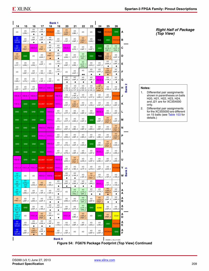
Spartan-3 FPGA Family: Pinout Descriptions
DS099 (v3.1) June 27, 2013 www.xilinx.comProduct Specification 209
Right Half of Package (Top View)
Figure 54: FG676 Package Footprint (Top View) Continued
14 15 16 17 18 19 20 21 22 23 24 25 26Bank 1
Bank 4
A
B
C
D
E
F
G
H
J
K
L
M
N
P
R
T
U
V
W
Y
AA
AB
AC
AD
AE
AF
Ban
k 2
Ban
k 3
I/OI/O
L29N_1
I/O L26N_1
I/O L23N_1 VCCAUX I/O
L15N_1
I/O L10N_1 VREF_1
I/O L08N_1
I/O I/O TMS VCCAUX
I/O L32N_1 GCLK5
I/O L29P_1
I/O L26P_1
I/O L23P_1
I/O L18N_1 I/O
L15P_1I/O
L10P_1I/O
L08P_1
I/O L06N_1 VREF_1
I/O L04N_1
TCK VCCAUX
I/O L32P_1 GCLK4
I/O VREF_1
VCCO_1 I/O VREF_1
I/O L18P_1
I/O L12N_1 VCCO_1 I/O
L07N_1I/O
L06P_1I/O
L04P_1
I/O L01N_2 VRP_2
I/O L01P_2 VRN_2
I/O L31N_1 VREF_1
GND I/OI/O
L22N_1
I/O VREF_1
I/O L12P_1 I/O
L09N_1I/O
L07P_1
I/O L01N_1 VRP_1
GND
GND GND
GNDGNDGNDGND
GND GND GND GND GND
GND
GNDGNDGND
GND GND GND
GNDGNDGNDGND
GND GND GND GND
GNDGND
GND GND
GND
GND
GND
GND
GND
GND
TDOI/O
L03N_2 VREF_2
I/O L03P_2
I/O L31P_1
I/O L28N_1
I/O L25N_1
I/O L22P_1 I/O
I/O L11N_1 I/O
L09P_1I/O
L05N_1
I/O L01P_1 VRN_1
I/O L02N_2
I/O L02P_2
I/O L05N_2
I/O L05P_2
I/OI/O
L28P_1I/O
L25P_1I/O
L19N_1I/O
L16N_1
I/O L11P_1 I/O
I/O L05P_1
I/O
I/O L07N_2
I/O L07P_2
I/O L09N_2 VREF_2
I/O L09P_2
I/O L30N_1
I/O L27N_1
I/O L24N_1
I/O L19P_1
I/O L16P_1
I/O
I/O L06N_2
I/O L06P_2
I/O L08N_2
I/O L08P_2 VCCO_2
I/O L10N_2
I/O L10P_2
I/O L30P_1
I/O L27P_1
I/O L24P_1
VCCO_1 VCCO_1 VCCINTI/O
L14N_2(L11N_2)
I/OL14P_2
(L11P_2)
I/OL16N_2
(L12N_2)
I/OL17N_2
(L13N_2)
I/OL17P_2
(L13P_2)VREF_2
I/O L19N_2
I/O L19P_2
VCCO_1 VCCO_1 VCCO_1 VCCINT VCCINT VCCO_2 I/O L20N_2
I/OL16P_2
(L12P_2)
I/O L21N_2
I/O L21P_2
I/O L22N_2
I/O L22P_2
VCCAUX
VCCO_1 VCCINT VCCINT VCCO_2 I/O L20P_2
I/O L23N_2 VREF_2
I/O L23P_2
I/O L24N_2
I/O L24P_2
I/O L26N_2
I/O L26P_2
VCCO_2 I/O L27N_2
I/O L27P_2
I/O L28N_2
I/O L28P_2
I/O L33N_2
VCCO_2 I/O L29N_2
I/O L29P_2
VCCO_2 I/O L31N_2
I/O L31P_2
I/O L32N_2
I/O L32P_2
I/O L33P_2
I/O L34N_2 VREF_2
I/O L34P_2
VCCO_2 VCCO_2 I/O L35N_2
I/O L35P_2
I/O L38N_2
I/O L38P_2
I/O L39N_2
I/O L39P_2
I/O L40N_2
I/O L40P_2 VREF_2
VCCO_3 VCCO_3 I/O L35P_3
I/O L35N_3
I/O L38P_3
I/O L38N_3
I/O L39P_3
I/O L39N_3
I/O L40P_3
I/O L40N_3 VREF_3
VCCO_3 I/O L31P_3
I/O L31N_3
I/O L32P_3
I/O L32N_3
I/O L33N_3
I/O L34P_3 VREF_3
I/O L34N_3
VCCO_3 I/O L27P_3
I/O L27N_3
I/O L28P_3
I/O L28N_3
I/O L33P_3
VCCO_3 I/O L29P_3
I/O L29N_3
VCCO_4 VCCINT VCCINT VCCO_3 I/O L20N_3
I/O L23P_3 VREF_3
I/O L23N_3
I/O L24P_3
I/O L24N_3
I/O L26P_3
I/O L26N_3
VCCO_4 VCCO_4 VCCO_4 VCCINT VCCINT VCCO_3 I/O L20P_3
I/O L16N_3
I/O L21P_3
I/O L21N_3
I/O L22P_3
I/O L22N_3
VCCAUX
I/O L27P_4
D1I/O I/O VCCO_4 VCCO_4 VCCINT
I/O L10P_3
I/O L10N_3 I/O
L16P_3
I/O L17P_3 VREF_3
I/O L17N_3
I/O L19P_3
I/O L19N_3
I/O L30N_4
D2
I/O L27N_4
DIN D0
I/O L24N_4
I/O VREF_4
I/O L16N_4
I/O L11N_4
I/O L05P_3
I/O L05N_3
I/O L08P_3
I/O L08N_3 VCCO_3 I/O
L14P_3I/O
L14N_3
I/O L30P_4
D3
I/O L28N_4
I/O L24P_4
I/O L19P_4
I/O L16P_4
I/O L11P_4 I/O
I/O L01P_3 VRN_3
I/O L01N_3 VRP_3
I/O L07P_3
I/O L07N_3
I/O L09P_3 VREF_3
I/O L09N_3
IO VREF_4
I/O L28P_4
I/O L25N_4
I/O L22P_4
I/O L17N_4
I/O L12N_4 I/O
L09N_4I/O
L07N_4
I/O L01N_4 VRP_4
I/O L02P_3
I/O L02N_3 VREF_3
I/O L06P_3
I/O L06N_3
I/O L31N_4 INIT_B
I/O L25P_4
I/O L19N_4
I/O L17P_4
I/O L12P_4 I/O
L09P_4I/O
L07P_4
I/O L01P_4 VRN_4
DONEI/O
L03P_3I/O
L03N_3
I/O L31P_4 DOUT BUSY
I/O VCCO_4I/O
L22N_4 VREF_4
I/O L18N_4
I/O VCCO_4 I/O
L08N_4
I/O L06N_4 VREF_4
I/OI/O
VREF_4CCLK
I/O L32N_4 GCLK1
I/O L29N_4
I/O L26N_4
I/O L23N_4
I/O L18P_4
I/O L15N_4
I/O L10N_4
I/O L08P_4
I/O L06P_4
I/O L05N_4
I/O L04N_4
VCCAUX
I/O L32P_4 GCLK0
I/O L29P_4
I/O L26P_4 VREF_4
I/O L23P_4 VCCAUX I/O
L15P_4I/O
L10P_4I/O I/O
I/O L05P_4
I/O L04P_4
VCCAUX
DS099-4_12b_011205
Notes: 1. Differential pair assignments
shown in parentheses on balls H20, H21, H22, H23, H24, and J21 are for XC3S4000 only.
2. Differential pair assignments for the XC3S5000 are different on 15 balls (see Table 103 for details.)
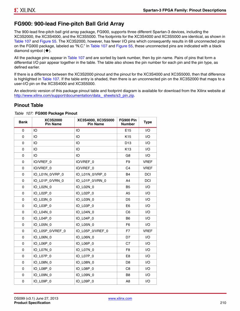
Spartan-3 FPGA Family: Pinout Descriptions
DS099 (v3.1) June 27, 2013 www.xilinx.comProduct Specification 210
FG900: 900-lead Fine-pitch Ball Grid ArrayThe 900-lead fine-pitch ball grid array package, FG900, supports three different Spartan-3 devices, including the XC3S2000, the XC3S4000, and the XC3S5000. The footprints for the XC3S4000 and XC3S5000 are identical, as shown in Table 107 and Figure 55. The XC3S2000, however, has fewer I/O pins which consequently results in 68 unconnected pins on the FG900 package, labeled as “N.C.” In Table 107 and Figure 55, these unconnected pins are indicated with a black diamond symbol ().
All the package pins appear in Table 107 and are sorted by bank number, then by pin name. Pairs of pins that form a differential I/O pair appear together in the table. The table also shows the pin number for each pin and the pin type, as defined earlier.
If there is a difference between the XC3S2000 pinout and the pinout for the XC3S4000 and XC3S5000, then that difference is highlighted in Table 107. If the table entry is shaded, then there is an unconnected pin on the XC3S2000 that maps to a user-I/O pin on the XC3S4000 and XC3S5000.
An electronic version of this package pinout table and footprint diagram is available for download from the Xilinx website at http://www.xilinx.com/support/documentation/data_ sheets/s3_pin.zip.
Pinout Table
Table 107: FG900 Package Pinout
Bank XC3S2000Pin Name
XC3S4000, XC3S5000 Pin Name
FG900 Pin Number Type
0 IO IO E15 I/O
0 IO IO K15 I/O
0 IO IO D13 I/O
0 IO IO K13 I/O
0 IO IO G8 I/O
0 IO/VREF_0 IO/VREF_0 F9 VREF
0 IO/VREF_0 IO/VREF_0 C4 VREF
0 IO_L01N_0/VRP_0 IO_L01N_0/VRP_0 B4 DCI
0 IO_L01P_0/VRN_0 IO_L01P_0/VRN_0 A4 DCI
0 IO_L02N_0 IO_L02N_0 B5 I/O
0 IO_L02P_0 IO_L02P_0 A5 I/O
0 IO_L03N_0 IO_L03N_0 D5 I/O
0 IO_L03P_0 IO_L03P_0 E6 I/O
0 IO_L04N_0 IO_L04N_0 C6 I/O
0 IO_L04P_0 IO_L04P_0 B6 I/O
0 IO_L05N_0 IO_L05N_0 F6 I/O
0 IO_L05P_0/VREF_0 IO_L05P_0/VREF_0 F7 VREF
0 IO_L06N_0 IO_L06N_0 D7 I/O
0 IO_L06P_0 IO_L06P_0 C7 I/O
0 IO_L07N_0 IO_L07N_0 F8 I/O
0 IO_L07P_0 IO_L07P_0 E8 I/O
0 IO_L08N_0 IO_L08N_0 D8 I/O
0 IO_L08P_0 IO_L08P_0 C8 I/O
0 IO_L09N_0 IO_L09N_0 B8 I/O
0 IO_L09P_0 IO_L09P_0 A8 I/O
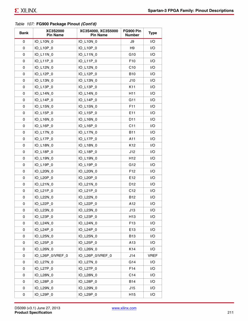
Spartan-3 FPGA Family: Pinout Descriptions
DS099 (v3.1) June 27, 2013 www.xilinx.comProduct Specification 211
0 IO_L10N_0 IO_L10N_0 J9 I/O
0 IO_L10P_0 IO_L10P_0 H9 I/O
0 IO_L11N_0 IO_L11N_0 G10 I/O
0 IO_L11P_0 IO_L11P_0 F10 I/O
0 IO_L12N_0 IO_L12N_0 C10 I/O
0 IO_L12P_0 IO_L12P_0 B10 I/O
0 IO_L13N_0 IO_L13N_0 J10 I/O
0 IO_L13P_0 IO_L13P_0 K11 I/O
0 IO_L14N_0 IO_L14N_0 H11 I/O
0 IO_L14P_0 IO_L14P_0 G11 I/O
0 IO_L15N_0 IO_L15N_0 F11 I/O
0 IO_L15P_0 IO_L15P_0 E11 I/O
0 IO_L16N_0 IO_L16N_0 D11 I/O
0 IO_L16P_0 IO_L16P_0 C11 I/O
0 IO_L17N_0 IO_L17N_0 B11 I/O
0 IO_L17P_0 IO_L17P_0 A11 I/O
0 IO_L18N_0 IO_L18N_0 K12 I/O
0 IO_L18P_0 IO_L18P_0 J12 I/O
0 IO_L19N_0 IO_L19N_0 H12 I/O
0 IO_L19P_0 IO_L19P_0 G12 I/O
0 IO_L20N_0 IO_L20N_0 F12 I/O
0 IO_L20P_0 IO_L20P_0 E12 I/O
0 IO_L21N_0 IO_L21N_0 D12 I/O
0 IO_L21P_0 IO_L21P_0 C12 I/O
0 IO_L22N_0 IO_L22N_0 B12 I/O
0 IO_L22P_0 IO_L22P_0 A12 I/O
0 IO_L23N_0 IO_L23N_0 J13 I/O
0 IO_L23P_0 IO_L23P_0 H13 I/O
0 IO_L24N_0 IO_L24N_0 F13 I/O
0 IO_L24P_0 IO_L24P_0 E13 I/O
0 IO_L25N_0 IO_L25N_0 B13 I/O
0 IO_L25P_0 IO_L25P_0 A13 I/O
0 IO_L26N_0 IO_L26N_0 K14 I/O
0 IO_L26P_0/VREF_0 IO_L26P_0/VREF_0 J14 VREF
0 IO_L27N_0 IO_L27N_0 G14 I/O
0 IO_L27P_0 IO_L27P_0 F14 I/O
0 IO_L28N_0 IO_L28N_0 C14 I/O
0 IO_L28P_0 IO_L28P_0 B14 I/O
0 IO_L29N_0 IO_L29N_0 J15 I/O
0 IO_L29P_0 IO_L29P_0 H15 I/O
Table 107: FG900 Package Pinout (Cont’d)
Bank XC3S2000Pin Name
XC3S4000, XC3S5000 Pin Name
FG900 Pin Number Type
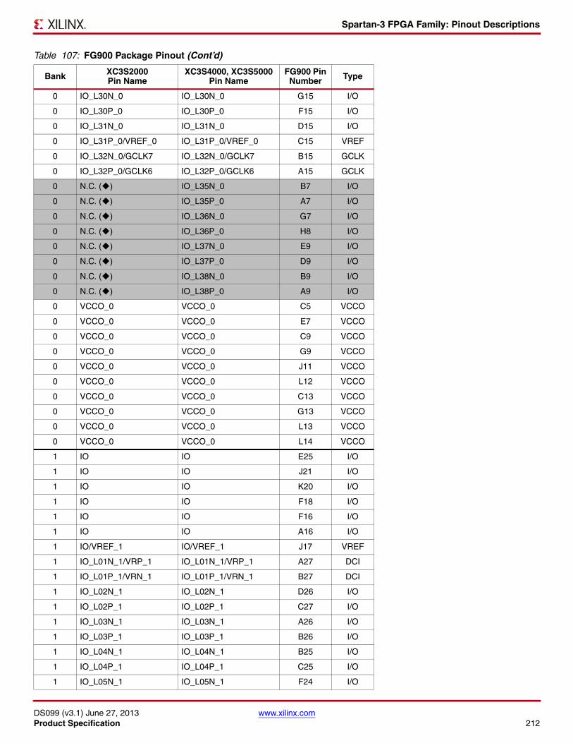
Spartan-3 FPGA Family: Pinout Descriptions
DS099 (v3.1) June 27, 2013 www.xilinx.comProduct Specification 212
0 IO_L30N_0 IO_L30N_0 G15 I/O
0 IO_L30P_0 IO_L30P_0 F15 I/O
0 IO_L31N_0 IO_L31N_0 D15 I/O
0 IO_L31P_0/VREF_0 IO_L31P_0/VREF_0 C15 VREF
0 IO_L32N_0/GCLK7 IO_L32N_0/GCLK7 B15 GCLK
0 IO_L32P_0/GCLK6 IO_L32P_0/GCLK6 A15 GCLK
0 N.C. () IO_L35N_0 B7 I/O
0 N.C. () IO_L35P_0 A7 I/O
0 N.C. () IO_L36N_0 G7 I/O
0 N.C. () IO_L36P_0 H8 I/O
0 N.C. () IO_L37N_0 E9 I/O
0 N.C. () IO_L37P_0 D9 I/O
0 N.C. () IO_L38N_0 B9 I/O
0 N.C. () IO_L38P_0 A9 I/O
0 VCCO_0 VCCO_0 C5 VCCO
0 VCCO_0 VCCO_0 E7 VCCO
0 VCCO_0 VCCO_0 C9 VCCO
0 VCCO_0 VCCO_0 G9 VCCO
0 VCCO_0 VCCO_0 J11 VCCO
0 VCCO_0 VCCO_0 L12 VCCO
0 VCCO_0 VCCO_0 C13 VCCO
0 VCCO_0 VCCO_0 G13 VCCO
0 VCCO_0 VCCO_0 L13 VCCO
0 VCCO_0 VCCO_0 L14 VCCO
1 IO IO E25 I/O
1 IO IO J21 I/O
1 IO IO K20 I/O
1 IO IO F18 I/O
1 IO IO F16 I/O
1 IO IO A16 I/O
1 IO/VREF_1 IO/VREF_1 J17 VREF
1 IO_L01N_1/VRP_1 IO_L01N_1/VRP_1 A27 DCI
1 IO_L01P_1/VRN_1 IO_L01P_1/VRN_1 B27 DCI
1 IO_L02N_1 IO_L02N_1 D26 I/O
1 IO_L02P_1 IO_L02P_1 C27 I/O
1 IO_L03N_1 IO_L03N_1 A26 I/O
1 IO_L03P_1 IO_L03P_1 B26 I/O
1 IO_L04N_1 IO_L04N_1 B25 I/O
1 IO_L04P_1 IO_L04P_1 C25 I/O
1 IO_L05N_1 IO_L05N_1 F24 I/O
Table 107: FG900 Package Pinout (Cont’d)
Bank XC3S2000Pin Name
XC3S4000, XC3S5000 Pin Name
FG900 Pin Number Type

Spartan-3 FPGA Family: Pinout Descriptions
DS099 (v3.1) June 27, 2013 www.xilinx.comProduct Specification 213
1 IO_L05P_1 IO_L05P_1 F25 I/O
1 IO_L06N_1/VREF_1 IO_L06N_1/VREF_1 C24 VREF
1 IO_L06P_1 IO_L06P_1 D24 I/O
1 IO_L07N_1 IO_L07N_1 A24 I/O
1 IO_L07P_1 IO_L07P_1 B24 I/O
1 IO_L08N_1 IO_L08N_1 H23 I/O
1 IO_L08P_1 IO_L08P_1 G24 I/O
1 IO_L09N_1 IO_L09N_1 F23 I/O
1 IO_L09P_1 IO_L09P_1 G23 I/O
1 IO_L10N_1/VREF_1 IO_L10N_1/VREF_1 C23 VREF
1 IO_L10P_1 IO_L10P_1 D23 I/O
1 IO_L11N_1 IO_L11N_1 A23 I/O
1 IO_L11P_1 IO_L11P_1 B23 I/O
1 IO_L12N_1 IO_L12N_1 H22 I/O
1 IO_L12P_1 IO_L12P_1 J22 I/O
1 IO_L13N_1 IO_L13N_1 F22 I/O
1 IO_L13P_1 IO_L13P_1 E23 I/O
1 IO_L14N_1 IO_L14N_1 D22 I/O
1 IO_L14P_1 IO_L14P_1 E22 I/O
1 IO_L15N_1 IO_L15N_1 A22 I/O
1 IO_L15P_1 IO_L15P_1 B22 I/O
1 IO_L16N_1 IO_L16N_1 F21 I/O
1 IO_L16P_1 IO_L16P_1 G21 I/O
1 IO_L17N_1/VREF_1 IO_L17N_1/VREF_1 B21 VREF
1 IO_L17P_1 IO_L17P_1 C21 I/O
1 IO_L18N_1 IO_L18N_1 G20 I/O
1 IO_L18P_1 IO_L18P_1 H20 I/O
1 IO_L19N_1 IO_L19N_1 E20 I/O
1 IO_L19P_1 IO_L19P_1 F20 I/O
1 IO_L20N_1 IO_L20N_1 C20 I/O
1 IO_L20P_1 IO_L20P_1 D20 I/O
1 IO_L21N_1 IO_L21N_1 A20 I/O
1 IO_L21P_1 IO_L21P_1 B20 I/O
1 IO_L22N_1 IO_L22N_1 J19 I/O
1 IO_L22P_1 IO_L22P_1 K19 I/O
1 IO_L23N_1 IO_L23N_1 G19 I/O
1 IO_L23P_1 IO_L23P_1 H19 I/O
1 IO_L24N_1 IO_L24N_1 E19 I/O
1 IO_L24P_1 IO_L24P_1 F19 I/O
1 IO_L25N_1 IO_L25N_1 C19 I/O
Table 107: FG900 Package Pinout (Cont’d)
Bank XC3S2000Pin Name
XC3S4000, XC3S5000 Pin Name
FG900 Pin Number Type
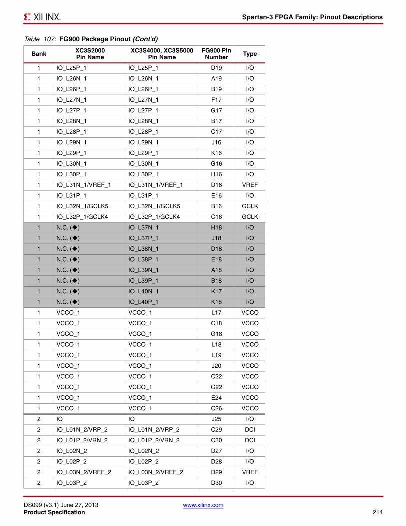
Spartan-3 FPGA Family: Pinout Descriptions
DS099 (v3.1) June 27, 2013 www.xilinx.comProduct Specification 214
1 IO_L25P_1 IO_L25P_1 D19 I/O
1 IO_L26N_1 IO_L26N_1 A19 I/O
1 IO_L26P_1 IO_L26P_1 B19 I/O
1 IO_L27N_1 IO_L27N_1 F17 I/O
1 IO_L27P_1 IO_L27P_1 G17 I/O
1 IO_L28N_1 IO_L28N_1 B17 I/O
1 IO_L28P_1 IO_L28P_1 C17 I/O
1 IO_L29N_1 IO_L29N_1 J16 I/O
1 IO_L29P_1 IO_L29P_1 K16 I/O
1 IO_L30N_1 IO_L30N_1 G16 I/O
1 IO_L30P_1 IO_L30P_1 H16 I/O
1 IO_L31N_1/VREF_1 IO_L31N_1/VREF_1 D16 VREF
1 IO_L31P_1 IO_L31P_1 E16 I/O
1 IO_L32N_1/GCLK5 IO_L32N_1/GCLK5 B16 GCLK
1 IO_L32P_1/GCLK4 IO_L32P_1/GCLK4 C16 GCLK
1 N.C. () IO_L37N_1 H18 I/O
1 N.C. () IO_L37P_1 J18 I/O
1 N.C. () IO_L38N_1 D18 I/O
1 N.C. () IO_L38P_1 E18 I/O
1 N.C. () IO_L39N_1 A18 I/O
1 N.C. () IO_L39P_1 B18 I/O
1 N.C. () IO_L40N_1 K17 I/O
1 N.C. () IO_L40P_1 K18 I/O
1 VCCO_1 VCCO_1 L17 VCCO
1 VCCO_1 VCCO_1 C18 VCCO
1 VCCO_1 VCCO_1 G18 VCCO
1 VCCO_1 VCCO_1 L18 VCCO
1 VCCO_1 VCCO_1 L19 VCCO
1 VCCO_1 VCCO_1 J20 VCCO
1 VCCO_1 VCCO_1 C22 VCCO
1 VCCO_1 VCCO_1 G22 VCCO
1 VCCO_1 VCCO_1 E24 VCCO
1 VCCO_1 VCCO_1 C26 VCCO
2 IO IO J25 I/O
2 IO_L01N_2/VRP_2 IO_L01N_2/VRP_2 C29 DCI
2 IO_L01P_2/VRN_2 IO_L01P_2/VRN_2 C30 DCI
2 IO_L02N_2 IO_L02N_2 D27 I/O
2 IO_L02P_2 IO_L02P_2 D28 I/O
2 IO_L03N_2/VREF_2 IO_L03N_2/VREF_2 D29 VREF
2 IO_L03P_2 IO_L03P_2 D30 I/O
Table 107: FG900 Package Pinout (Cont’d)
Bank XC3S2000Pin Name
XC3S4000, XC3S5000 Pin Name
FG900 Pin Number Type
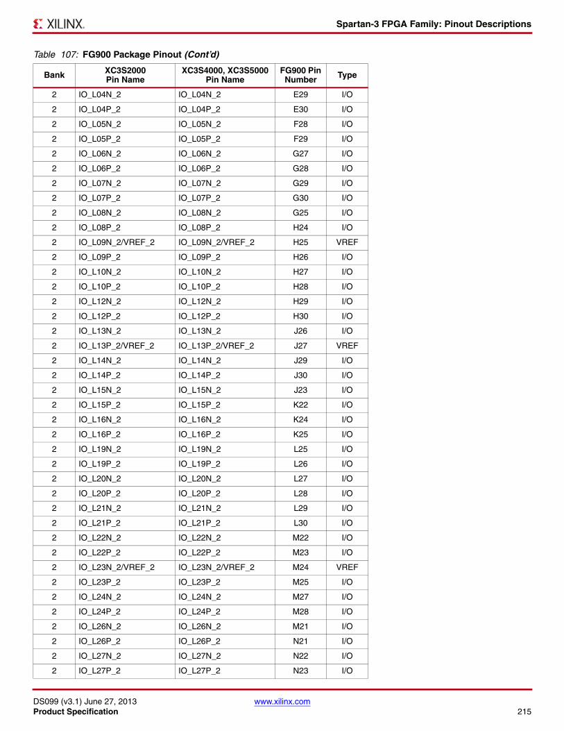
Spartan-3 FPGA Family: Pinout Descriptions
DS099 (v3.1) June 27, 2013 www.xilinx.comProduct Specification 215
2 IO_L04N_2 IO_L04N_2 E29 I/O
2 IO_L04P_2 IO_L04P_2 E30 I/O
2 IO_L05N_2 IO_L05N_2 F28 I/O
2 IO_L05P_2 IO_L05P_2 F29 I/O
2 IO_L06N_2 IO_L06N_2 G27 I/O
2 IO_L06P_2 IO_L06P_2 G28 I/O
2 IO_L07N_2 IO_L07N_2 G29 I/O
2 IO_L07P_2 IO_L07P_2 G30 I/O
2 IO_L08N_2 IO_L08N_2 G25 I/O
2 IO_L08P_2 IO_L08P_2 H24 I/O
2 IO_L09N_2/VREF_2 IO_L09N_2/VREF_2 H25 VREF
2 IO_L09P_2 IO_L09P_2 H26 I/O
2 IO_L10N_2 IO_L10N_2 H27 I/O
2 IO_L10P_2 IO_L10P_2 H28 I/O
2 IO_L12N_2 IO_L12N_2 H29 I/O
2 IO_L12P_2 IO_L12P_2 H30 I/O
2 IO_L13N_2 IO_L13N_2 J26 I/O
2 IO_L13P_2/VREF_2 IO_L13P_2/VREF_2 J27 VREF
2 IO_L14N_2 IO_L14N_2 J29 I/O
2 IO_L14P_2 IO_L14P_2 J30 I/O
2 IO_L15N_2 IO_L15N_2 J23 I/O
2 IO_L15P_2 IO_L15P_2 K22 I/O
2 IO_L16N_2 IO_L16N_2 K24 I/O
2 IO_L16P_2 IO_L16P_2 K25 I/O
2 IO_L19N_2 IO_L19N_2 L25 I/O
2 IO_L19P_2 IO_L19P_2 L26 I/O
2 IO_L20N_2 IO_L20N_2 L27 I/O
2 IO_L20P_2 IO_L20P_2 L28 I/O
2 IO_L21N_2 IO_L21N_2 L29 I/O
2 IO_L21P_2 IO_L21P_2 L30 I/O
2 IO_L22N_2 IO_L22N_2 M22 I/O
2 IO_L22P_2 IO_L22P_2 M23 I/O
2 IO_L23N_2/VREF_2 IO_L23N_2/VREF_2 M24 VREF
2 IO_L23P_2 IO_L23P_2 M25 I/O
2 IO_L24N_2 IO_L24N_2 M27 I/O
2 IO_L24P_2 IO_L24P_2 M28 I/O
2 IO_L26N_2 IO_L26N_2 M21 I/O
2 IO_L26P_2 IO_L26P_2 N21 I/O
2 IO_L27N_2 IO_L27N_2 N22 I/O
2 IO_L27P_2 IO_L27P_2 N23 I/O
Table 107: FG900 Package Pinout (Cont’d)
Bank XC3S2000Pin Name
XC3S4000, XC3S5000 Pin Name
FG900 Pin Number Type
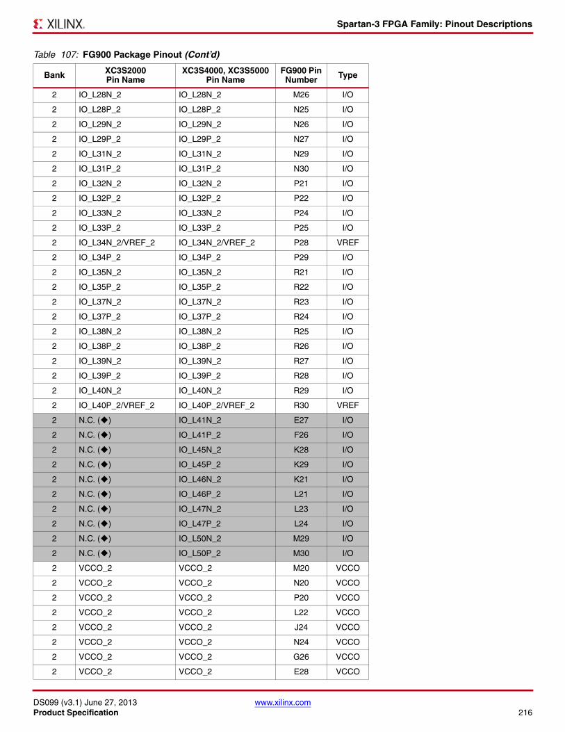
Spartan-3 FPGA Family: Pinout Descriptions
DS099 (v3.1) June 27, 2013 www.xilinx.comProduct Specification 216
2 IO_L28N_2 IO_L28N_2 M26 I/O
2 IO_L28P_2 IO_L28P_2 N25 I/O
2 IO_L29N_2 IO_L29N_2 N26 I/O
2 IO_L29P_2 IO_L29P_2 N27 I/O
2 IO_L31N_2 IO_L31N_2 N29 I/O
2 IO_L31P_2 IO_L31P_2 N30 I/O
2 IO_L32N_2 IO_L32N_2 P21 I/O
2 IO_L32P_2 IO_L32P_2 P22 I/O
2 IO_L33N_2 IO_L33N_2 P24 I/O
2 IO_L33P_2 IO_L33P_2 P25 I/O
2 IO_L34N_2/VREF_2 IO_L34N_2/VREF_2 P28 VREF
2 IO_L34P_2 IO_L34P_2 P29 I/O
2 IO_L35N_2 IO_L35N_2 R21 I/O
2 IO_L35P_2 IO_L35P_2 R22 I/O
2 IO_L37N_2 IO_L37N_2 R23 I/O
2 IO_L37P_2 IO_L37P_2 R24 I/O
2 IO_L38N_2 IO_L38N_2 R25 I/O
2 IO_L38P_2 IO_L38P_2 R26 I/O
2 IO_L39N_2 IO_L39N_2 R27 I/O
2 IO_L39P_2 IO_L39P_2 R28 I/O
2 IO_L40N_2 IO_L40N_2 R29 I/O
2 IO_L40P_2/VREF_2 IO_L40P_2/VREF_2 R30 VREF
2 N.C. () IO_L41N_2 E27 I/O
2 N.C. () IO_L41P_2 F26 I/O
2 N.C. () IO_L45N_2 K28 I/O
2 N.C. () IO_L45P_2 K29 I/O
2 N.C. () IO_L46N_2 K21 I/O
2 N.C. () IO_L46P_2 L21 I/O
2 N.C. () IO_L47N_2 L23 I/O
2 N.C. () IO_L47P_2 L24 I/O
2 N.C. () IO_L50N_2 M29 I/O
2 N.C. () IO_L50P_2 M30 I/O
2 VCCO_2 VCCO_2 M20 VCCO
2 VCCO_2 VCCO_2 N20 VCCO
2 VCCO_2 VCCO_2 P20 VCCO
2 VCCO_2 VCCO_2 L22 VCCO
2 VCCO_2 VCCO_2 J24 VCCO
2 VCCO_2 VCCO_2 N24 VCCO
2 VCCO_2 VCCO_2 G26 VCCO
2 VCCO_2 VCCO_2 E28 VCCO
Table 107: FG900 Package Pinout (Cont’d)
Bank XC3S2000Pin Name
XC3S4000, XC3S5000 Pin Name
FG900 Pin Number Type
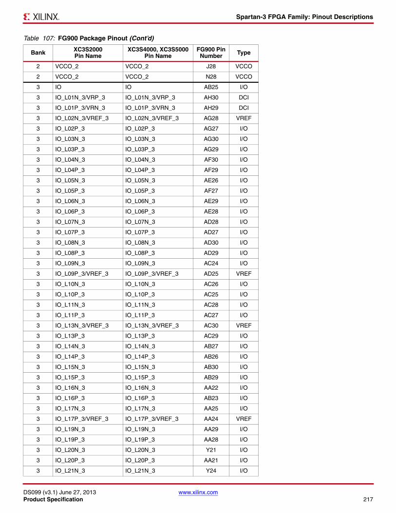
Spartan-3 FPGA Family: Pinout Descriptions
DS099 (v3.1) June 27, 2013 www.xilinx.comProduct Specification 217
2 VCCO_2 VCCO_2 J28 VCCO
2 VCCO_2 VCCO_2 N28 VCCO
3 IO IO AB25 I/O
3 IO_L01N_3/VRP_3 IO_L01N_3/VRP_3 AH30 DCI
3 IO_L01P_3/VRN_3 IO_L01P_3/VRN_3 AH29 DCI
3 IO_L02N_3/VREF_3 IO_L02N_3/VREF_3 AG28 VREF
3 IO_L02P_3 IO_L02P_3 AG27 I/O
3 IO_L03N_3 IO_L03N_3 AG30 I/O
3 IO_L03P_3 IO_L03P_3 AG29 I/O
3 IO_L04N_3 IO_L04N_3 AF30 I/O
3 IO_L04P_3 IO_L04P_3 AF29 I/O
3 IO_L05N_3 IO_L05N_3 AE26 I/O
3 IO_L05P_3 IO_L05P_3 AF27 I/O
3 IO_L06N_3 IO_L06N_3 AE29 I/O
3 IO_L06P_3 IO_L06P_3 AE28 I/O
3 IO_L07N_3 IO_L07N_3 AD28 I/O
3 IO_L07P_3 IO_L07P_3 AD27 I/O
3 IO_L08N_3 IO_L08N_3 AD30 I/O
3 IO_L08P_3 IO_L08P_3 AD29 I/O
3 IO_L09N_3 IO_L09N_3 AC24 I/O
3 IO_L09P_3/VREF_3 IO_L09P_3/VREF_3 AD25 VREF
3 IO_L10N_3 IO_L10N_3 AC26 I/O
3 IO_L10P_3 IO_L10P_3 AC25 I/O
3 IO_L11N_3 IO_L11N_3 AC28 I/O
3 IO_L11P_3 IO_L11P_3 AC27 I/O
3 IO_L13N_3/VREF_3 IO_L13N_3/VREF_3 AC30 VREF
3 IO_L13P_3 IO_L13P_3 AC29 I/O
3 IO_L14N_3 IO_L14N_3 AB27 I/O
3 IO_L14P_3 IO_L14P_3 AB26 I/O
3 IO_L15N_3 IO_L15N_3 AB30 I/O
3 IO_L15P_3 IO_L15P_3 AB29 I/O
3 IO_L16N_3 IO_L16N_3 AA22 I/O
3 IO_L16P_3 IO_L16P_3 AB23 I/O
3 IO_L17N_3 IO_L17N_3 AA25 I/O
3 IO_L17P_3/VREF_3 IO_L17P_3/VREF_3 AA24 VREF
3 IO_L19N_3 IO_L19N_3 AA29 I/O
3 IO_L19P_3 IO_L19P_3 AA28 I/O
3 IO_L20N_3 IO_L20N_3 Y21 I/O
3 IO_L20P_3 IO_L20P_3 AA21 I/O
3 IO_L21N_3 IO_L21N_3 Y24 I/O
Table 107: FG900 Package Pinout (Cont’d)
Bank XC3S2000Pin Name
XC3S4000, XC3S5000 Pin Name
FG900 Pin Number Type
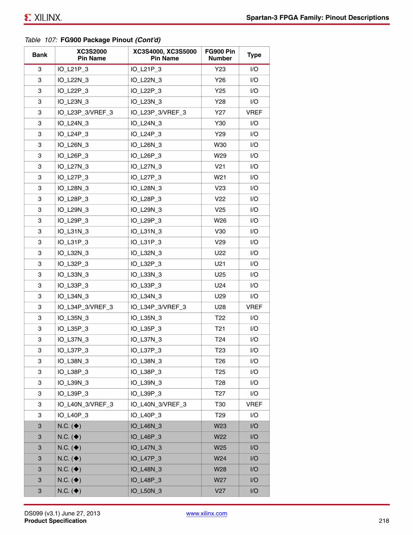
Spartan-3 FPGA Family: Pinout Descriptions
DS099 (v3.1) June 27, 2013 www.xilinx.comProduct Specification 218
3 IO_L21P_3 IO_L21P_3 Y23 I/O
3 IO_L22N_3 IO_L22N_3 Y26 I/O
3 IO_L22P_3 IO_L22P_3 Y25 I/O
3 IO_L23N_3 IO_L23N_3 Y28 I/O
3 IO_L23P_3/VREF_3 IO_L23P_3/VREF_3 Y27 VREF
3 IO_L24N_3 IO_L24N_3 Y30 I/O
3 IO_L24P_3 IO_L24P_3 Y29 I/O
3 IO_L26N_3 IO_L26N_3 W30 I/O
3 IO_L26P_3 IO_L26P_3 W29 I/O
3 IO_L27N_3 IO_L27N_3 V21 I/O
3 IO_L27P_3 IO_L27P_3 W21 I/O
3 IO_L28N_3 IO_L28N_3 V23 I/O
3 IO_L28P_3 IO_L28P_3 V22 I/O
3 IO_L29N_3 IO_L29N_3 V25 I/O
3 IO_L29P_3 IO_L29P_3 W26 I/O
3 IO_L31N_3 IO_L31N_3 V30 I/O
3 IO_L31P_3 IO_L31P_3 V29 I/O
3 IO_L32N_3 IO_L32N_3 U22 I/O
3 IO_L32P_3 IO_L32P_3 U21 I/O
3 IO_L33N_3 IO_L33N_3 U25 I/O
3 IO_L33P_3 IO_L33P_3 U24 I/O
3 IO_L34N_3 IO_L34N_3 U29 I/O
3 IO_L34P_3/VREF_3 IO_L34P_3/VREF_3 U28 VREF
3 IO_L35N_3 IO_L35N_3 T22 I/O
3 IO_L35P_3 IO_L35P_3 T21 I/O
3 IO_L37N_3 IO_L37N_3 T24 I/O
3 IO_L37P_3 IO_L37P_3 T23 I/O
3 IO_L38N_3 IO_L38N_3 T26 I/O
3 IO_L38P_3 IO_L38P_3 T25 I/O
3 IO_L39N_3 IO_L39N_3 T28 I/O
3 IO_L39P_3 IO_L39P_3 T27 I/O
3 IO_L40N_3/VREF_3 IO_L40N_3/VREF_3 T30 VREF
3 IO_L40P_3 IO_L40P_3 T29 I/O
3 N.C. () IO_L46N_3 W23 I/O
3 N.C. () IO_L46P_3 W22 I/O
3 N.C. () IO_L47N_3 W25 I/O
3 N.C. () IO_L47P_3 W24 I/O
3 N.C. () IO_L48N_3 W28 I/O
3 N.C. () IO_L48P_3 W27 I/O
3 N.C. () IO_L50N_3 V27 I/O
Table 107: FG900 Package Pinout (Cont’d)
Bank XC3S2000Pin Name
XC3S4000, XC3S5000 Pin Name
FG900 Pin Number Type
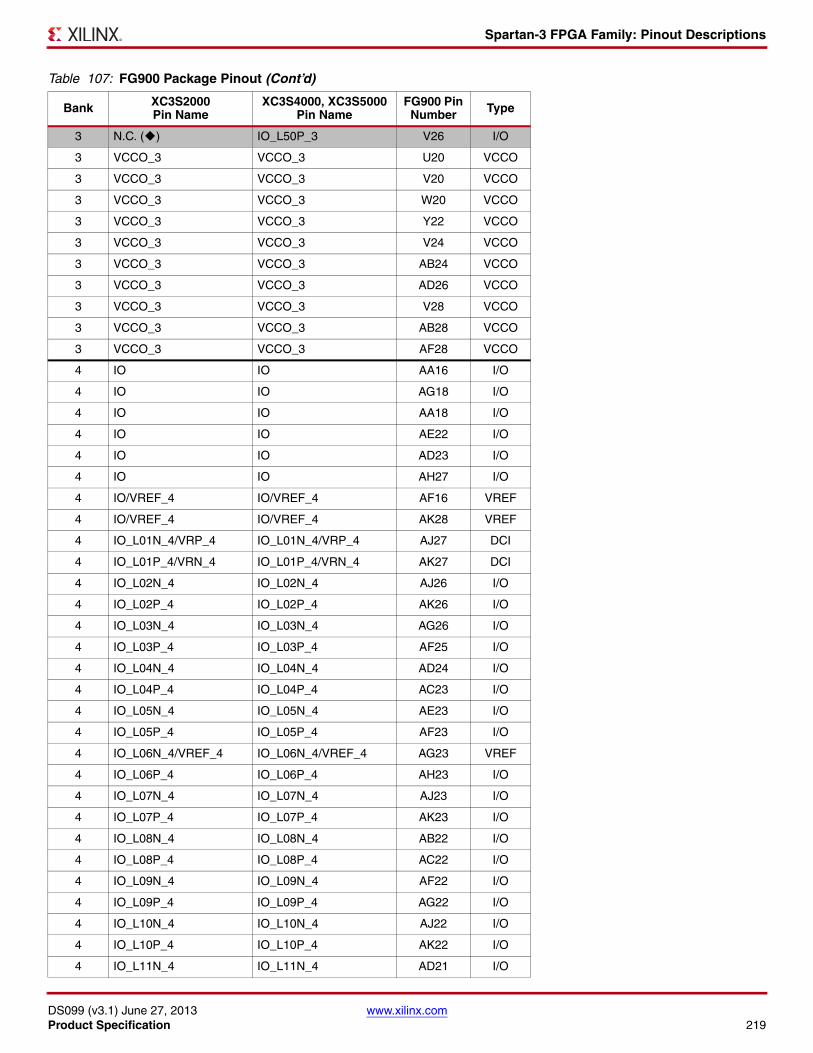
Spartan-3 FPGA Family: Pinout Descriptions
DS099 (v3.1) June 27, 2013 www.xilinx.comProduct Specification 219
3 N.C. () IO_L50P_3 V26 I/O
3 VCCO_3 VCCO_3 U20 VCCO
3 VCCO_3 VCCO_3 V20 VCCO
3 VCCO_3 VCCO_3 W20 VCCO
3 VCCO_3 VCCO_3 Y22 VCCO
3 VCCO_3 VCCO_3 V24 VCCO
3 VCCO_3 VCCO_3 AB24 VCCO
3 VCCO_3 VCCO_3 AD26 VCCO
3 VCCO_3 VCCO_3 V28 VCCO
3 VCCO_3 VCCO_3 AB28 VCCO
3 VCCO_3 VCCO_3 AF28 VCCO
4 IO IO AA16 I/O
4 IO IO AG18 I/O
4 IO IO AA18 I/O
4 IO IO AE22 I/O
4 IO IO AD23 I/O
4 IO IO AH27 I/O
4 IO/VREF_4 IO/VREF_4 AF16 VREF
4 IO/VREF_4 IO/VREF_4 AK28 VREF
4 IO_L01N_4/VRP_4 IO_L01N_4/VRP_4 AJ27 DCI
4 IO_L01P_4/VRN_4 IO_L01P_4/VRN_4 AK27 DCI
4 IO_L02N_4 IO_L02N_4 AJ26 I/O
4 IO_L02P_4 IO_L02P_4 AK26 I/O
4 IO_L03N_4 IO_L03N_4 AG26 I/O
4 IO_L03P_4 IO_L03P_4 AF25 I/O
4 IO_L04N_4 IO_L04N_4 AD24 I/O
4 IO_L04P_4 IO_L04P_4 AC23 I/O
4 IO_L05N_4 IO_L05N_4 AE23 I/O
4 IO_L05P_4 IO_L05P_4 AF23 I/O
4 IO_L06N_4/VREF_4 IO_L06N_4/VREF_4 AG23 VREF
4 IO_L06P_4 IO_L06P_4 AH23 I/O
4 IO_L07N_4 IO_L07N_4 AJ23 I/O
4 IO_L07P_4 IO_L07P_4 AK23 I/O
4 IO_L08N_4 IO_L08N_4 AB22 I/O
4 IO_L08P_4 IO_L08P_4 AC22 I/O
4 IO_L09N_4 IO_L09N_4 AF22 I/O
4 IO_L09P_4 IO_L09P_4 AG22 I/O
4 IO_L10N_4 IO_L10N_4 AJ22 I/O
4 IO_L10P_4 IO_L10P_4 AK22 I/O
4 IO_L11N_4 IO_L11N_4 AD21 I/O
Table 107: FG900 Package Pinout (Cont’d)
Bank XC3S2000Pin Name
XC3S4000, XC3S5000 Pin Name
FG900 Pin Number Type
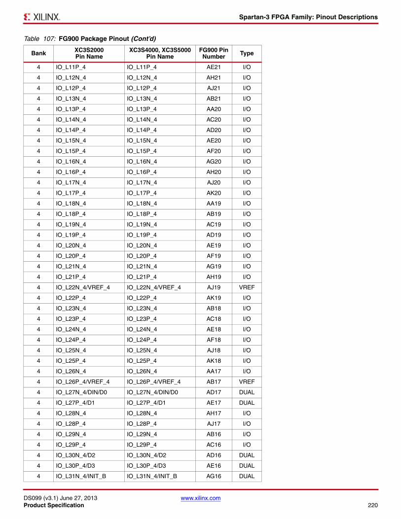
Spartan-3 FPGA Family: Pinout Descriptions
DS099 (v3.1) June 27, 2013 www.xilinx.comProduct Specification 220
4 IO_L11P_4 IO_L11P_4 AE21 I/O
4 IO_L12N_4 IO_L12N_4 AH21 I/O
4 IO_L12P_4 IO_L12P_4 AJ21 I/O
4 IO_L13N_4 IO_L13N_4 AB21 I/O
4 IO_L13P_4 IO_L13P_4 AA20 I/O
4 IO_L14N_4 IO_L14N_4 AC20 I/O
4 IO_L14P_4 IO_L14P_4 AD20 I/O
4 IO_L15N_4 IO_L15N_4 AE20 I/O
4 IO_L15P_4 IO_L15P_4 AF20 I/O
4 IO_L16N_4 IO_L16N_4 AG20 I/O
4 IO_L16P_4 IO_L16P_4 AH20 I/O
4 IO_L17N_4 IO_L17N_4 AJ20 I/O
4 IO_L17P_4 IO_L17P_4 AK20 I/O
4 IO_L18N_4 IO_L18N_4 AA19 I/O
4 IO_L18P_4 IO_L18P_4 AB19 I/O
4 IO_L19N_4 IO_L19N_4 AC19 I/O
4 IO_L19P_4 IO_L19P_4 AD19 I/O
4 IO_L20N_4 IO_L20N_4 AE19 I/O
4 IO_L20P_4 IO_L20P_4 AF19 I/O
4 IO_L21N_4 IO_L21N_4 AG19 I/O
4 IO_L21P_4 IO_L21P_4 AH19 I/O
4 IO_L22N_4/VREF_4 IO_L22N_4/VREF_4 AJ19 VREF
4 IO_L22P_4 IO_L22P_4 AK19 I/O
4 IO_L23N_4 IO_L23N_4 AB18 I/O
4 IO_L23P_4 IO_L23P_4 AC18 I/O
4 IO_L24N_4 IO_L24N_4 AE18 I/O
4 IO_L24P_4 IO_L24P_4 AF18 I/O
4 IO_L25N_4 IO_L25N_4 AJ18 I/O
4 IO_L25P_4 IO_L25P_4 AK18 I/O
4 IO_L26N_4 IO_L26N_4 AA17 I/O
4 IO_L26P_4/VREF_4 IO_L26P_4/VREF_4 AB17 VREF
4 IO_L27N_4/DIN/D0 IO_L27N_4/DIN/D0 AD17 DUAL
4 IO_L27P_4/D1 IO_L27P_4/D1 AE17 DUAL
4 IO_L28N_4 IO_L28N_4 AH17 I/O
4 IO_L28P_4 IO_L28P_4 AJ17 I/O
4 IO_L29N_4 IO_L29N_4 AB16 I/O
4 IO_L29P_4 IO_L29P_4 AC16 I/O
4 IO_L30N_4/D2 IO_L30N_4/D2 AD16 DUAL
4 IO_L30P_4/D3 IO_L30P_4/D3 AE16 DUAL
4 IO_L31N_4/INIT_B IO_L31N_4/INIT_B AG16 DUAL
Table 107: FG900 Package Pinout (Cont’d)
Bank XC3S2000Pin Name
XC3S4000, XC3S5000 Pin Name
FG900 Pin Number Type
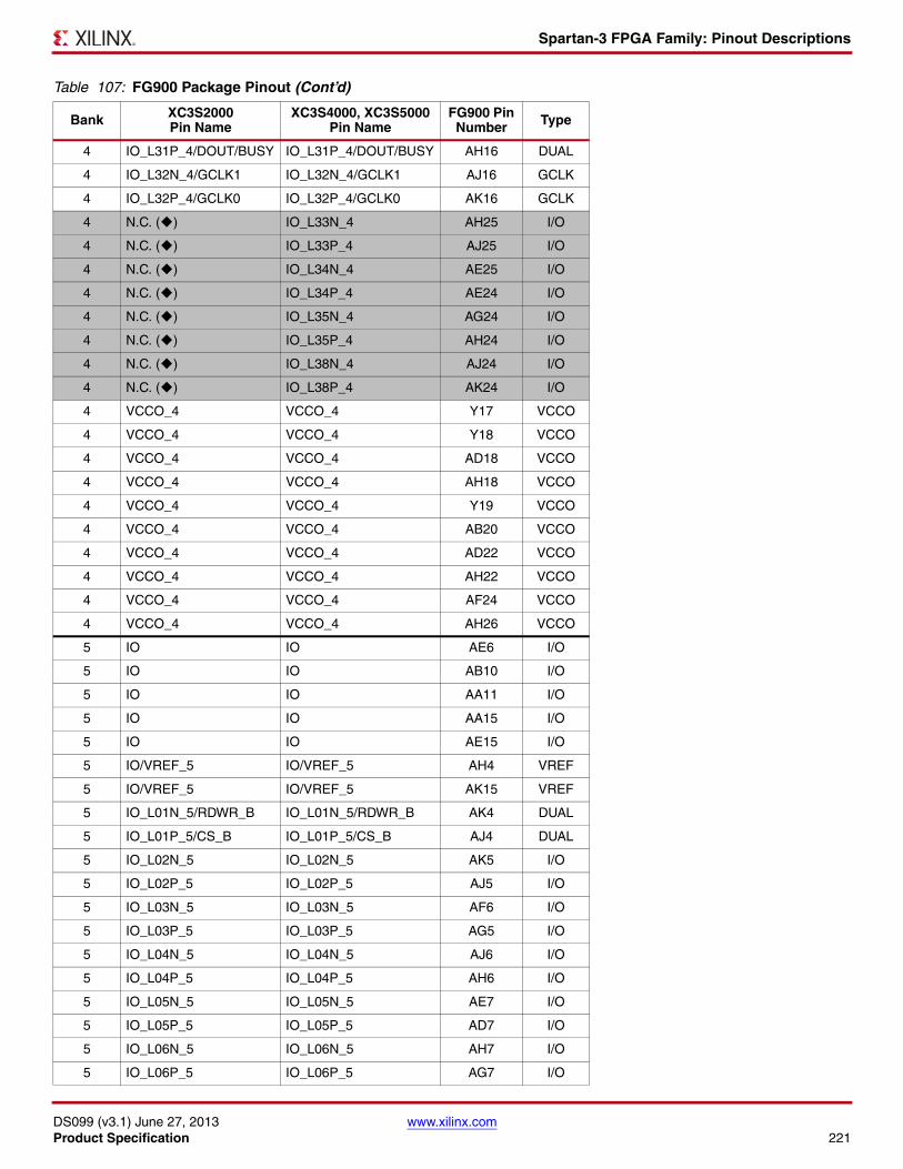
Spartan-3 FPGA Family: Pinout Descriptions
DS099 (v3.1) June 27, 2013 www.xilinx.comProduct Specification 221
4 IO_L31P_4/DOUT/BUSY IO_L31P_4/DOUT/BUSY AH16 DUAL
4 IO_L32N_4/GCLK1 IO_L32N_4/GCLK1 AJ16 GCLK
4 IO_L32P_4/GCLK0 IO_L32P_4/GCLK0 AK16 GCLK
4 N.C. () IO_L33N_4 AH25 I/O
4 N.C. () IO_L33P_4 AJ25 I/O
4 N.C. () IO_L34N_4 AE25 I/O
4 N.C. () IO_L34P_4 AE24 I/O
4 N.C. () IO_L35N_4 AG24 I/O
4 N.C. () IO_L35P_4 AH24 I/O
4 N.C. () IO_L38N_4 AJ24 I/O
4 N.C. () IO_L38P_4 AK24 I/O
4 VCCO_4 VCCO_4 Y17 VCCO
4 VCCO_4 VCCO_4 Y18 VCCO
4 VCCO_4 VCCO_4 AD18 VCCO
4 VCCO_4 VCCO_4 AH18 VCCO
4 VCCO_4 VCCO_4 Y19 VCCO
4 VCCO_4 VCCO_4 AB20 VCCO
4 VCCO_4 VCCO_4 AD22 VCCO
4 VCCO_4 VCCO_4 AH22 VCCO
4 VCCO_4 VCCO_4 AF24 VCCO
4 VCCO_4 VCCO_4 AH26 VCCO
5 IO IO AE6 I/O
5 IO IO AB10 I/O
5 IO IO AA11 I/O
5 IO IO AA15 I/O
5 IO IO AE15 I/O
5 IO/VREF_5 IO/VREF_5 AH4 VREF
5 IO/VREF_5 IO/VREF_5 AK15 VREF
5 IO_L01N_5/RDWR_B IO_L01N_5/RDWR_B AK4 DUAL
5 IO_L01P_5/CS_B IO_L01P_5/CS_B AJ4 DUAL
5 IO_L02N_5 IO_L02N_5 AK5 I/O
5 IO_L02P_5 IO_L02P_5 AJ5 I/O
5 IO_L03N_5 IO_L03N_5 AF6 I/O
5 IO_L03P_5 IO_L03P_5 AG5 I/O
5 IO_L04N_5 IO_L04N_5 AJ6 I/O
5 IO_L04P_5 IO_L04P_5 AH6 I/O
5 IO_L05N_5 IO_L05N_5 AE7 I/O
5 IO_L05P_5 IO_L05P_5 AD7 I/O
5 IO_L06N_5 IO_L06N_5 AH7 I/O
5 IO_L06P_5 IO_L06P_5 AG7 I/O
Table 107: FG900 Package Pinout (Cont’d)
Bank XC3S2000Pin Name
XC3S4000, XC3S5000 Pin Name
FG900 Pin Number Type
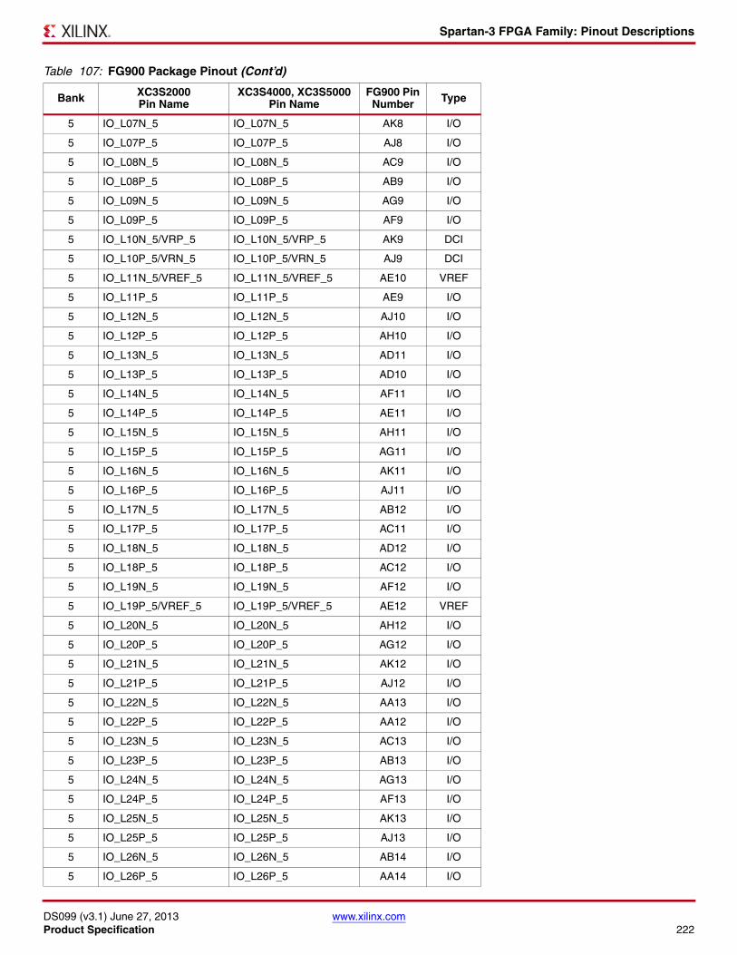
Spartan-3 FPGA Family: Pinout Descriptions
DS099 (v3.1) June 27, 2013 www.xilinx.comProduct Specification 222
5 IO_L07N_5 IO_L07N_5 AK8 I/O
5 IO_L07P_5 IO_L07P_5 AJ8 I/O
5 IO_L08N_5 IO_L08N_5 AC9 I/O
5 IO_L08P_5 IO_L08P_5 AB9 I/O
5 IO_L09N_5 IO_L09N_5 AG9 I/O
5 IO_L09P_5 IO_L09P_5 AF9 I/O
5 IO_L10N_5/VRP_5 IO_L10N_5/VRP_5 AK9 DCI
5 IO_L10P_5/VRN_5 IO_L10P_5/VRN_5 AJ9 DCI
5 IO_L11N_5/VREF_5 IO_L11N_5/VREF_5 AE10 VREF
5 IO_L11P_5 IO_L11P_5 AE9 I/O
5 IO_L12N_5 IO_L12N_5 AJ10 I/O
5 IO_L12P_5 IO_L12P_5 AH10 I/O
5 IO_L13N_5 IO_L13N_5 AD11 I/O
5 IO_L13P_5 IO_L13P_5 AD10 I/O
5 IO_L14N_5 IO_L14N_5 AF11 I/O
5 IO_L14P_5 IO_L14P_5 AE11 I/O
5 IO_L15N_5 IO_L15N_5 AH11 I/O
5 IO_L15P_5 IO_L15P_5 AG11 I/O
5 IO_L16N_5 IO_L16N_5 AK11 I/O
5 IO_L16P_5 IO_L16P_5 AJ11 I/O
5 IO_L17N_5 IO_L17N_5 AB12 I/O
5 IO_L17P_5 IO_L17P_5 AC11 I/O
5 IO_L18N_5 IO_L18N_5 AD12 I/O
5 IO_L18P_5 IO_L18P_5 AC12 I/O
5 IO_L19N_5 IO_L19N_5 AF12 I/O
5 IO_L19P_5/VREF_5 IO_L19P_5/VREF_5 AE12 VREF
5 IO_L20N_5 IO_L20N_5 AH12 I/O
5 IO_L20P_5 IO_L20P_5 AG12 I/O
5 IO_L21N_5 IO_L21N_5 AK12 I/O
5 IO_L21P_5 IO_L21P_5 AJ12 I/O
5 IO_L22N_5 IO_L22N_5 AA13 I/O
5 IO_L22P_5 IO_L22P_5 AA12 I/O
5 IO_L23N_5 IO_L23N_5 AC13 I/O
5 IO_L23P_5 IO_L23P_5 AB13 I/O
5 IO_L24N_5 IO_L24N_5 AG13 I/O
5 IO_L24P_5 IO_L24P_5 AF13 I/O
5 IO_L25N_5 IO_L25N_5 AK13 I/O
5 IO_L25P_5 IO_L25P_5 AJ13 I/O
5 IO_L26N_5 IO_L26N_5 AB14 I/O
5 IO_L26P_5 IO_L26P_5 AA14 I/O
Table 107: FG900 Package Pinout (Cont’d)
Bank XC3S2000Pin Name
XC3S4000, XC3S5000 Pin Name
FG900 Pin Number Type
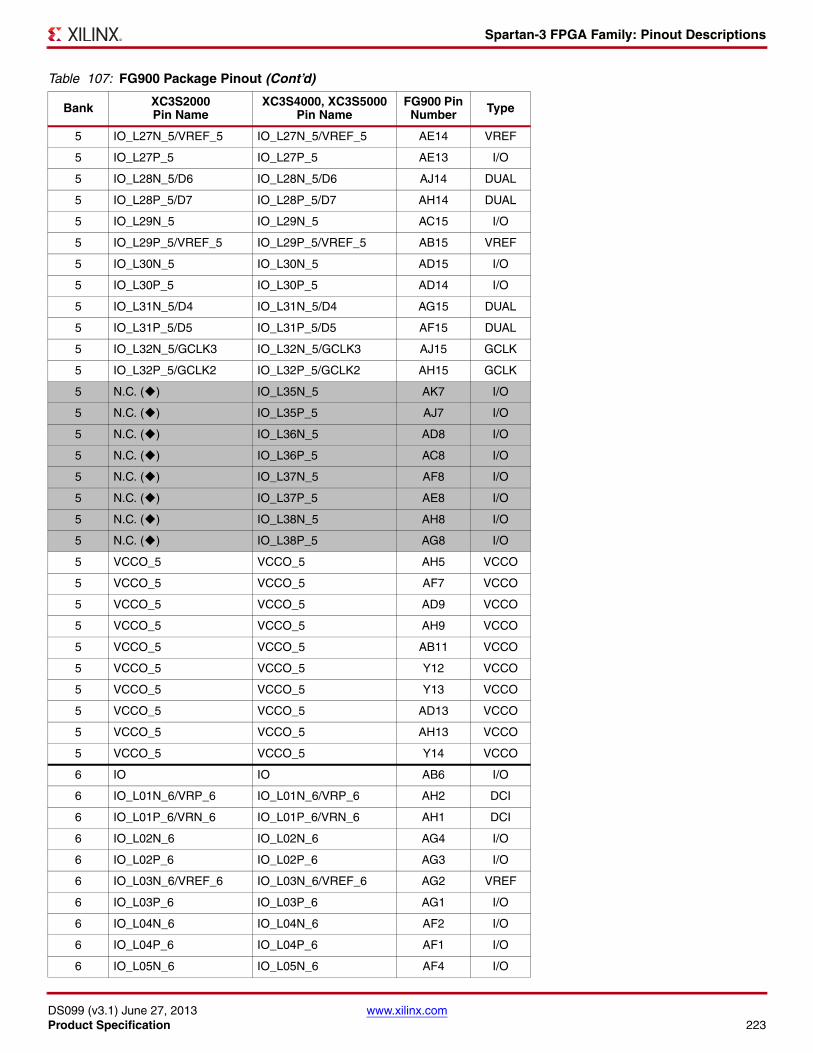
Spartan-3 FPGA Family: Pinout Descriptions
DS099 (v3.1) June 27, 2013 www.xilinx.comProduct Specification 223
5 IO_L27N_5/VREF_5 IO_L27N_5/VREF_5 AE14 VREF
5 IO_L27P_5 IO_L27P_5 AE13 I/O
5 IO_L28N_5/D6 IO_L28N_5/D6 AJ14 DUAL
5 IO_L28P_5/D7 IO_L28P_5/D7 AH14 DUAL
5 IO_L29N_5 IO_L29N_5 AC15 I/O
5 IO_L29P_5/VREF_5 IO_L29P_5/VREF_5 AB15 VREF
5 IO_L30N_5 IO_L30N_5 AD15 I/O
5 IO_L30P_5 IO_L30P_5 AD14 I/O
5 IO_L31N_5/D4 IO_L31N_5/D4 AG15 DUAL
5 IO_L31P_5/D5 IO_L31P_5/D5 AF15 DUAL
5 IO_L32N_5/GCLK3 IO_L32N_5/GCLK3 AJ15 GCLK
5 IO_L32P_5/GCLK2 IO_L32P_5/GCLK2 AH15 GCLK
5 N.C. () IO_L35N_5 AK7 I/O
5 N.C. () IO_L35P_5 AJ7 I/O
5 N.C. () IO_L36N_5 AD8 I/O
5 N.C. () IO_L36P_5 AC8 I/O
5 N.C. () IO_L37N_5 AF8 I/O
5 N.C. () IO_L37P_5 AE8 I/O
5 N.C. () IO_L38N_5 AH8 I/O
5 N.C. () IO_L38P_5 AG8 I/O
5 VCCO_5 VCCO_5 AH5 VCCO
5 VCCO_5 VCCO_5 AF7 VCCO
5 VCCO_5 VCCO_5 AD9 VCCO
5 VCCO_5 VCCO_5 AH9 VCCO
5 VCCO_5 VCCO_5 AB11 VCCO
5 VCCO_5 VCCO_5 Y12 VCCO
5 VCCO_5 VCCO_5 Y13 VCCO
5 VCCO_5 VCCO_5 AD13 VCCO
5 VCCO_5 VCCO_5 AH13 VCCO
5 VCCO_5 VCCO_5 Y14 VCCO
6 IO IO AB6 I/O
6 IO_L01N_6/VRP_6 IO_L01N_6/VRP_6 AH2 DCI
6 IO_L01P_6/VRN_6 IO_L01P_6/VRN_6 AH1 DCI
6 IO_L02N_6 IO_L02N_6 AG4 I/O
6 IO_L02P_6 IO_L02P_6 AG3 I/O
6 IO_L03N_6/VREF_6 IO_L03N_6/VREF_6 AG2 VREF
6 IO_L03P_6 IO_L03P_6 AG1 I/O
6 IO_L04N_6 IO_L04N_6 AF2 I/O
6 IO_L04P_6 IO_L04P_6 AF1 I/O
6 IO_L05N_6 IO_L05N_6 AF4 I/O
Table 107: FG900 Package Pinout (Cont’d)
Bank XC3S2000Pin Name
XC3S4000, XC3S5000 Pin Name
FG900 Pin Number Type
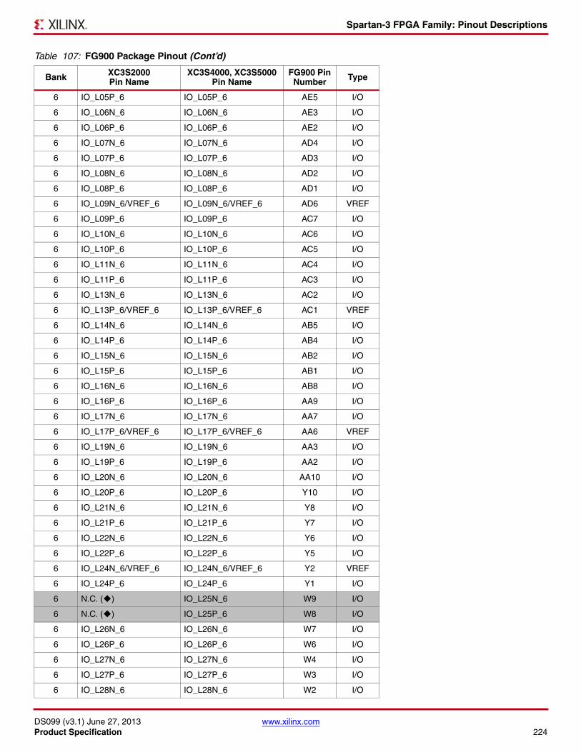
Spartan-3 FPGA Family: Pinout Descriptions
DS099 (v3.1) June 27, 2013 www.xilinx.comProduct Specification 224
6 IO_L05P_6 IO_L05P_6 AE5 I/O
6 IO_L06N_6 IO_L06N_6 AE3 I/O
6 IO_L06P_6 IO_L06P_6 AE2 I/O
6 IO_L07N_6 IO_L07N_6 AD4 I/O
6 IO_L07P_6 IO_L07P_6 AD3 I/O
6 IO_L08N_6 IO_L08N_6 AD2 I/O
6 IO_L08P_6 IO_L08P_6 AD1 I/O
6 IO_L09N_6/VREF_6 IO_L09N_6/VREF_6 AD6 VREF
6 IO_L09P_6 IO_L09P_6 AC7 I/O
6 IO_L10N_6 IO_L10N_6 AC6 I/O
6 IO_L10P_6 IO_L10P_6 AC5 I/O
6 IO_L11N_6 IO_L11N_6 AC4 I/O
6 IO_L11P_6 IO_L11P_6 AC3 I/O
6 IO_L13N_6 IO_L13N_6 AC2 I/O
6 IO_L13P_6/VREF_6 IO_L13P_6/VREF_6 AC1 VREF
6 IO_L14N_6 IO_L14N_6 AB5 I/O
6 IO_L14P_6 IO_L14P_6 AB4 I/O
6 IO_L15N_6 IO_L15N_6 AB2 I/O
6 IO_L15P_6 IO_L15P_6 AB1 I/O
6 IO_L16N_6 IO_L16N_6 AB8 I/O
6 IO_L16P_6 IO_L16P_6 AA9 I/O
6 IO_L17N_6 IO_L17N_6 AA7 I/O
6 IO_L17P_6/VREF_6 IO_L17P_6/VREF_6 AA6 VREF
6 IO_L19N_6 IO_L19N_6 AA3 I/O
6 IO_L19P_6 IO_L19P_6 AA2 I/O
6 IO_L20N_6 IO_L20N_6 AA10 I/O
6 IO_L20P_6 IO_L20P_6 Y10 I/O
6 IO_L21N_6 IO_L21N_6 Y8 I/O
6 IO_L21P_6 IO_L21P_6 Y7 I/O
6 IO_L22N_6 IO_L22N_6 Y6 I/O
6 IO_L22P_6 IO_L22P_6 Y5 I/O
6 IO_L24N_6/VREF_6 IO_L24N_6/VREF_6 Y2 VREF
6 IO_L24P_6 IO_L24P_6 Y1 I/O
6 N.C. () IO_L25N_6 W9 I/O
6 N.C. () IO_L25P_6 W8 I/O
6 IO_L26N_6 IO_L26N_6 W7 I/O
6 IO_L26P_6 IO_L26P_6 W6 I/O
6 IO_L27N_6 IO_L27N_6 W4 I/O
6 IO_L27P_6 IO_L27P_6 W3 I/O
6 IO_L28N_6 IO_L28N_6 W2 I/O
Table 107: FG900 Package Pinout (Cont’d)
Bank XC3S2000Pin Name
XC3S4000, XC3S5000 Pin Name
FG900 Pin Number Type
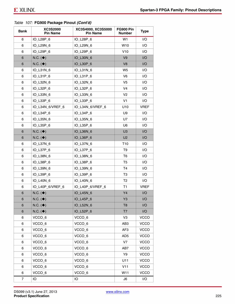
Spartan-3 FPGA Family: Pinout Descriptions
DS099 (v3.1) June 27, 2013 www.xilinx.comProduct Specification 225
6 IO_L28P_6 IO_L28P_6 W1 I/O
6 IO_L29N_6 IO_L29N_6 W10 I/O
6 IO_L29P_6 IO_L29P_6 V10 I/O
6 N.C. () IO_L30N_6 V9 I/O
6 N.C. () IO_L30P_6 V8 I/O
6 IO_L31N_6 IO_L31N_6 W5 I/O
6 IO_L31P_6 IO_L31P_6 V6 I/O
6 IO_L32N_6 IO_L32N_6 V5 I/O
6 IO_L32P_6 IO_L32P_6 V4 I/O
6 IO_L33N_6 IO_L33N_6 V2 I/O
6 IO_L33P_6 IO_L33P_6 V1 I/O
6 IO_L34N_6/VREF_6 IO_L34N_6/VREF_6 U10 VREF
6 IO_L34P_6 IO_L34P_6 U9 I/O
6 IO_L35N_6 IO_L35N_6 U7 I/O
6 IO_L35P_6 IO_L35P_6 U6 I/O
6 N.C. () IO_L36N_6 U3 I/O
6 N.C. () IO_L36P_6 U2 I/O
6 IO_L37N_6 IO_L37N_6 T10 I/O
6 IO_L37P_6 IO_L37P_6 T9 I/O
6 IO_L38N_6 IO_L38N_6 T6 I/O
6 IO_L38P_6 IO_L38P_6 T5 I/O
6 IO_L39N_6 IO_L39N_6 T4 I/O
6 IO_L39P_6 IO_L39P_6 T3 I/O
6 IO_L40N_6 IO_L40N_6 T2 I/O
6 IO_L40P_6/VREF_6 IO_L40P_6/VREF_6 T1 VREF
6 N.C. () IO_L45N_6 Y4 I/O
6 N.C. () IO_L45P_6 Y3 I/O
6 N.C. () IO_L52N_6 T8 I/O
6 N.C. () IO_L52P_6 T7 I/O
6 VCCO_6 VCCO_6 V3 VCCO
6 VCCO_6 VCCO_6 AB3 VCCO
6 VCCO_6 VCCO_6 AF3 VCCO
6 VCCO_6 VCCO_6 AD5 VCCO
6 VCCO_6 VCCO_6 V7 VCCO
6 VCCO_6 VCCO_6 AB7 VCCO
6 VCCO_6 VCCO_6 Y9 VCCO
6 VCCO_6 VCCO_6 U11 VCCO
6 VCCO_6 VCCO_6 V11 VCCO
6 VCCO_6 VCCO_6 W11 VCCO
7 IO IO J6 I/O
Table 107: FG900 Package Pinout (Cont’d)
Bank XC3S2000Pin Name
XC3S4000, XC3S5000 Pin Name
FG900 Pin Number Type
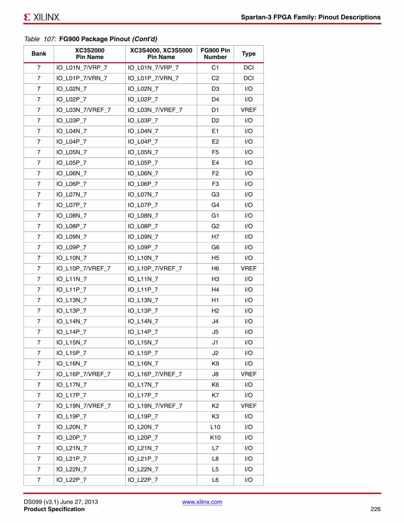
Spartan-3 FPGA Family: Pinout Descriptions
DS099 (v3.1) June 27, 2013 www.xilinx.comProduct Specification 226
7 IO_L01N_7/VRP_7 IO_L01N_7/VRP_7 C1 DCI
7 IO_L01P_7/VRN_7 IO_L01P_7/VRN_7 C2 DCI
7 IO_L02N_7 IO_L02N_7 D3 I/O
7 IO_L02P_7 IO_L02P_7 D4 I/O
7 IO_L03N_7/VREF_7 IO_L03N_7/VREF_7 D1 VREF
7 IO_L03P_7 IO_L03P_7 D2 I/O
7 IO_L04N_7 IO_L04N_7 E1 I/O
7 IO_L04P_7 IO_L04P_7 E2 I/O
7 IO_L05N_7 IO_L05N_7 F5 I/O
7 IO_L05P_7 IO_L05P_7 E4 I/O
7 IO_L06N_7 IO_L06N_7 F2 I/O
7 IO_L06P_7 IO_L06P_7 F3 I/O
7 IO_L07N_7 IO_L07N_7 G3 I/O
7 IO_L07P_7 IO_L07P_7 G4 I/O
7 IO_L08N_7 IO_L08N_7 G1 I/O
7 IO_L08P_7 IO_L08P_7 G2 I/O
7 IO_L09N_7 IO_L09N_7 H7 I/O
7 IO_L09P_7 IO_L09P_7 G6 I/O
7 IO_L10N_7 IO_L10N_7 H5 I/O
7 IO_L10P_7/VREF_7 IO_L10P_7/VREF_7 H6 VREF
7 IO_L11N_7 IO_L11N_7 H3 I/O
7 IO_L11P_7 IO_L11P_7 H4 I/O
7 IO_L13N_7 IO_L13N_7 H1 I/O
7 IO_L13P_7 IO_L13P_7 H2 I/O
7 IO_L14N_7 IO_L14N_7 J4 I/O
7 IO_L14P_7 IO_L14P_7 J5 I/O
7 IO_L15N_7 IO_L15N_7 J1 I/O
7 IO_L15P_7 IO_L15P_7 J2 I/O
7 IO_L16N_7 IO_L16N_7 K9 I/O
7 IO_L16P_7/VREF_7 IO_L16P_7/VREF_7 J8 VREF
7 IO_L17N_7 IO_L17N_7 K6 I/O
7 IO_L17P_7 IO_L17P_7 K7 I/O
7 IO_L19N_7/VREF_7 IO_L19N_7/VREF_7 K2 VREF
7 IO_L19P_7 IO_L19P_7 K3 I/O
7 IO_L20N_7 IO_L20N_7 L10 I/O
7 IO_L20P_7 IO_L20P_7 K10 I/O
7 IO_L21N_7 IO_L21N_7 L7 I/O
7 IO_L21P_7 IO_L21P_7 L8 I/O
7 IO_L22N_7 IO_L22N_7 L5 I/O
7 IO_L22P_7 IO_L22P_7 L6 I/O
Table 107: FG900 Package Pinout (Cont’d)
Bank XC3S2000Pin Name
XC3S4000, XC3S5000 Pin Name
FG900 Pin Number Type
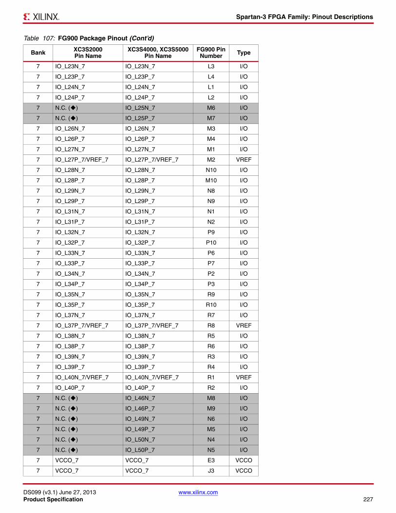
Spartan-3 FPGA Family: Pinout Descriptions
DS099 (v3.1) June 27, 2013 www.xilinx.comProduct Specification 227
7 IO_L23N_7 IO_L23N_7 L3 I/O
7 IO_L23P_7 IO_L23P_7 L4 I/O
7 IO_L24N_7 IO_L24N_7 L1 I/O
7 IO_L24P_7 IO_L24P_7 L2 I/O
7 N.C. () IO_L25N_7 M6 I/O
7 N.C. () IO_L25P_7 M7 I/O
7 IO_L26N_7 IO_L26N_7 M3 I/O
7 IO_L26P_7 IO_L26P_7 M4 I/O
7 IO_L27N_7 IO_L27N_7 M1 I/O
7 IO_L27P_7/VREF_7 IO_L27P_7/VREF_7 M2 VREF
7 IO_L28N_7 IO_L28N_7 N10 I/O
7 IO_L28P_7 IO_L28P_7 M10 I/O
7 IO_L29N_7 IO_L29N_7 N8 I/O
7 IO_L29P_7 IO_L29P_7 N9 I/O
7 IO_L31N_7 IO_L31N_7 N1 I/O
7 IO_L31P_7 IO_L31P_7 N2 I/O
7 IO_L32N_7 IO_L32N_7 P9 I/O
7 IO_L32P_7 IO_L32P_7 P10 I/O
7 IO_L33N_7 IO_L33N_7 P6 I/O
7 IO_L33P_7 IO_L33P_7 P7 I/O
7 IO_L34N_7 IO_L34N_7 P2 I/O
7 IO_L34P_7 IO_L34P_7 P3 I/O
7 IO_L35N_7 IO_L35N_7 R9 I/O
7 IO_L35P_7 IO_L35P_7 R10 I/O
7 IO_L37N_7 IO_L37N_7 R7 I/O
7 IO_L37P_7/VREF_7 IO_L37P_7/VREF_7 R8 VREF
7 IO_L38N_7 IO_L38N_7 R5 I/O
7 IO_L38P_7 IO_L38P_7 R6 I/O
7 IO_L39N_7 IO_L39N_7 R3 I/O
7 IO_L39P_7 IO_L39P_7 R4 I/O
7 IO_L40N_7/VREF_7 IO_L40N_7/VREF_7 R1 VREF
7 IO_L40P_7 IO_L40P_7 R2 I/O
7 N.C. () IO_L46N_7 M8 I/O
7 N.C. () IO_L46P_7 M9 I/O
7 N.C. () IO_L49N_7 N6 I/O
7 N.C. () IO_L49P_7 M5 I/O
7 N.C. () IO_L50N_7 N4 I/O
7 N.C. () IO_L50P_7 N5 I/O
7 VCCO_7 VCCO_7 E3 VCCO
7 VCCO_7 VCCO_7 J3 VCCO
Table 107: FG900 Package Pinout (Cont’d)
Bank XC3S2000Pin Name
XC3S4000, XC3S5000 Pin Name
FG900 Pin Number Type
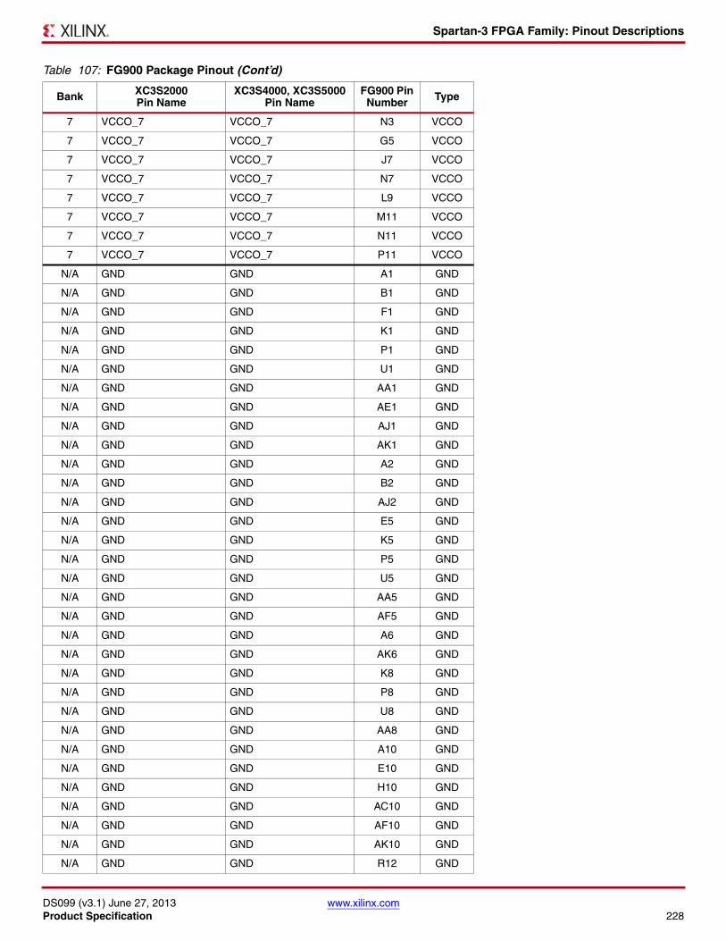
Spartan-3 FPGA Family: Pinout Descriptions
DS099 (v3.1) June 27, 2013 www.xilinx.comProduct Specification 228
7 VCCO_7 VCCO_7 N3 VCCO
7 VCCO_7 VCCO_7 G5 VCCO
7 VCCO_7 VCCO_7 J7 VCCO
7 VCCO_7 VCCO_7 N7 VCCO
7 VCCO_7 VCCO_7 L9 VCCO
7 VCCO_7 VCCO_7 M11 VCCO
7 VCCO_7 VCCO_7 N11 VCCO
7 VCCO_7 VCCO_7 P11 VCCO
N/A GND GND A1 GND
N/A GND GND B1 GND
N/A GND GND F1 GND
N/A GND GND K1 GND
N/A GND GND P1 GND
N/A GND GND U1 GND
N/A GND GND AA1 GND
N/A GND GND AE1 GND
N/A GND GND AJ1 GND
N/A GND GND AK1 GND
N/A GND GND A2 GND
N/A GND GND B2 GND
N/A GND GND AJ2 GND
N/A GND GND E5 GND
N/A GND GND K5 GND
N/A GND GND P5 GND
N/A GND GND U5 GND
N/A GND GND AA5 GND
N/A GND GND AF5 GND
N/A GND GND A6 GND
N/A GND GND AK6 GND
N/A GND GND K8 GND
N/A GND GND P8 GND
N/A GND GND U8 GND
N/A GND GND AA8 GND
N/A GND GND A10 GND
N/A GND GND E10 GND
N/A GND GND H10 GND
N/A GND GND AC10 GND
N/A GND GND AF10 GND
N/A GND GND AK10 GND
N/A GND GND R12 GND
Table 107: FG900 Package Pinout (Cont’d)
Bank XC3S2000Pin Name
XC3S4000, XC3S5000 Pin Name
FG900 Pin Number Type
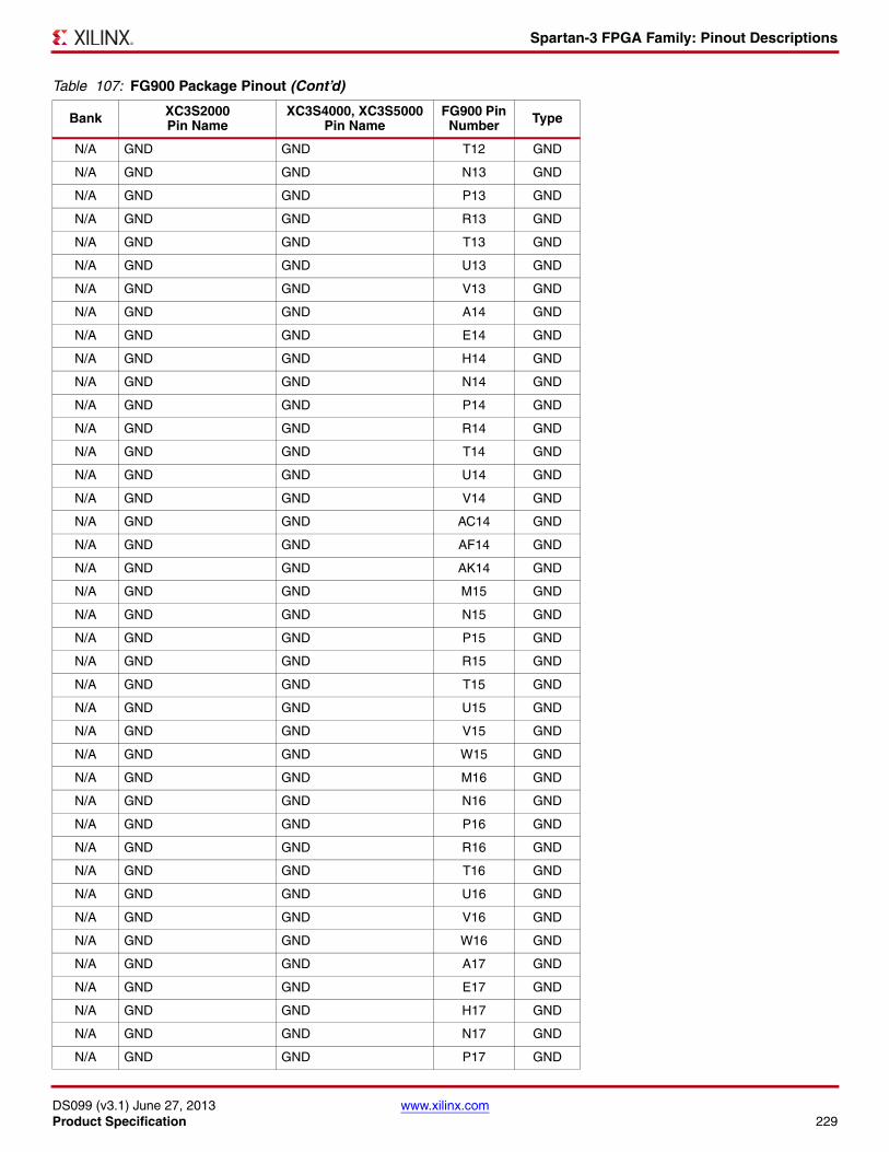
Spartan-3 FPGA Family: Pinout Descriptions
DS099 (v3.1) June 27, 2013 www.xilinx.comProduct Specification 229
N/A GND GND T12 GND
N/A GND GND N13 GND
N/A GND GND P13 GND
N/A GND GND R13 GND
N/A GND GND T13 GND
N/A GND GND U13 GND
N/A GND GND V13 GND
N/A GND GND A14 GND
N/A GND GND E14 GND
N/A GND GND H14 GND
N/A GND GND N14 GND
N/A GND GND P14 GND
N/A GND GND R14 GND
N/A GND GND T14 GND
N/A GND GND U14 GND
N/A GND GND V14 GND
N/A GND GND AC14 GND
N/A GND GND AF14 GND
N/A GND GND AK14 GND
N/A GND GND M15 GND
N/A GND GND N15 GND
N/A GND GND P15 GND
N/A GND GND R15 GND
N/A GND GND T15 GND
N/A GND GND U15 GND
N/A GND GND V15 GND
N/A GND GND W15 GND
N/A GND GND M16 GND
N/A GND GND N16 GND
N/A GND GND P16 GND
N/A GND GND R16 GND
N/A GND GND T16 GND
N/A GND GND U16 GND
N/A GND GND V16 GND
N/A GND GND W16 GND
N/A GND GND A17 GND
N/A GND GND E17 GND
N/A GND GND H17 GND
N/A GND GND N17 GND
N/A GND GND P17 GND
Table 107: FG900 Package Pinout (Cont’d)
Bank XC3S2000Pin Name
XC3S4000, XC3S5000 Pin Name
FG900 Pin Number Type

Spartan-3 FPGA Family: Pinout Descriptions
DS099 (v3.1) June 27, 2013 www.xilinx.comProduct Specification 230
N/A GND GND R17 GND
N/A GND GND T17 GND
N/A GND GND U17 GND
N/A GND GND V17 GND
N/A GND GND AC17 GND
N/A GND GND AF17 GND
N/A GND GND AK17 GND
N/A GND GND N18 GND
N/A GND GND P18 GND
N/A GND GND R18 GND
N/A GND GND T18 GND
N/A GND GND U18 GND
N/A GND GND V18 GND
N/A GND GND R19 GND
N/A GND GND T19 GND
N/A GND GND A21 GND
N/A GND GND E21 GND
N/A GND GND H21 GND
N/A GND GND AC21 GND
N/A GND GND AF21 GND
N/A GND GND AK21 GND
N/A GND GND K23 GND
N/A GND GND P23 GND
N/A GND GND U23 GND
N/A GND GND AA23 GND
N/A GND GND A25 GND
N/A GND GND AK25 GND
N/A GND GND E26 GND
N/A GND GND K26 GND
N/A GND GND P26 GND
N/A GND GND U26 GND
N/A GND GND AA26 GND
N/A GND GND AF26 GND
N/A GND GND A29 GND
N/A GND GND B29 GND
N/A GND GND AJ29 GND
N/A GND GND AK29 GND
N/A GND GND A30 GND
N/A GND GND B30 GND
N/A GND GND F30 GND
Table 107: FG900 Package Pinout (Cont’d)
Bank XC3S2000Pin Name
XC3S4000, XC3S5000 Pin Name
FG900 Pin Number Type
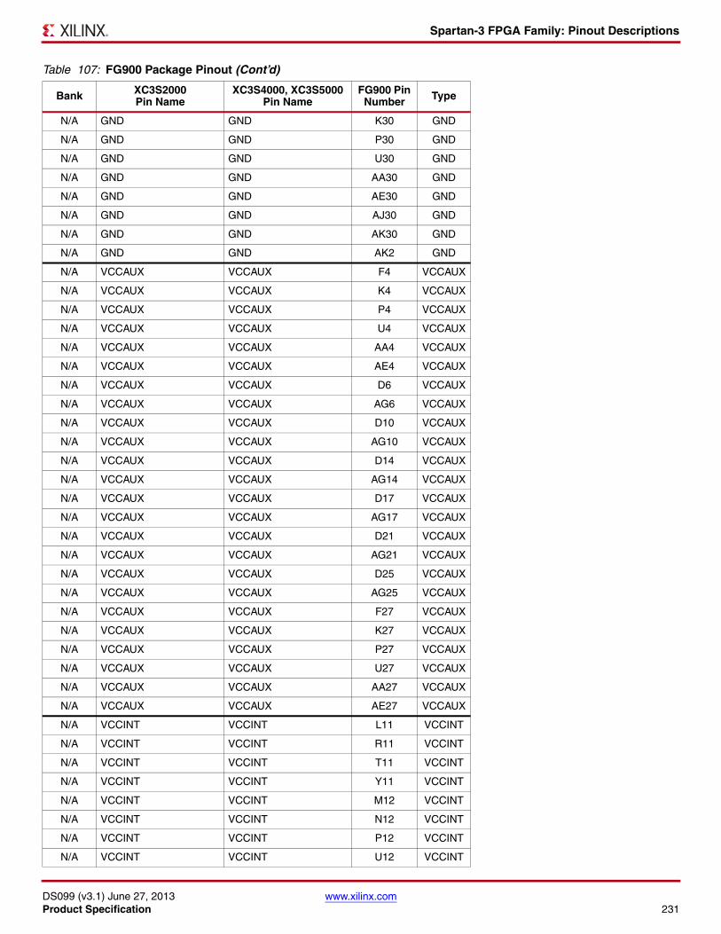
Spartan-3 FPGA Family: Pinout Descriptions
DS099 (v3.1) June 27, 2013 www.xilinx.comProduct Specification 231
N/A GND GND K30 GND
N/A GND GND P30 GND
N/A GND GND U30 GND
N/A GND GND AA30 GND
N/A GND GND AE30 GND
N/A GND GND AJ30 GND
N/A GND GND AK30 GND
N/A GND GND AK2 GND
N/A VCCAUX VCCAUX F4 VCCAUX
N/A VCCAUX VCCAUX K4 VCCAUX
N/A VCCAUX VCCAUX P4 VCCAUX
N/A VCCAUX VCCAUX U4 VCCAUX
N/A VCCAUX VCCAUX AA4 VCCAUX
N/A VCCAUX VCCAUX AE4 VCCAUX
N/A VCCAUX VCCAUX D6 VCCAUX
N/A VCCAUX VCCAUX AG6 VCCAUX
N/A VCCAUX VCCAUX D10 VCCAUX
N/A VCCAUX VCCAUX AG10 VCCAUX
N/A VCCAUX VCCAUX D14 VCCAUX
N/A VCCAUX VCCAUX AG14 VCCAUX
N/A VCCAUX VCCAUX D17 VCCAUX
N/A VCCAUX VCCAUX AG17 VCCAUX
N/A VCCAUX VCCAUX D21 VCCAUX
N/A VCCAUX VCCAUX AG21 VCCAUX
N/A VCCAUX VCCAUX D25 VCCAUX
N/A VCCAUX VCCAUX AG25 VCCAUX
N/A VCCAUX VCCAUX F27 VCCAUX
N/A VCCAUX VCCAUX K27 VCCAUX
N/A VCCAUX VCCAUX P27 VCCAUX
N/A VCCAUX VCCAUX U27 VCCAUX
N/A VCCAUX VCCAUX AA27 VCCAUX
N/A VCCAUX VCCAUX AE27 VCCAUX
N/A VCCINT VCCINT L11 VCCINT
N/A VCCINT VCCINT R11 VCCINT
N/A VCCINT VCCINT T11 VCCINT
N/A VCCINT VCCINT Y11 VCCINT
N/A VCCINT VCCINT M12 VCCINT
N/A VCCINT VCCINT N12 VCCINT
N/A VCCINT VCCINT P12 VCCINT
N/A VCCINT VCCINT U12 VCCINT
Table 107: FG900 Package Pinout (Cont’d)
Bank XC3S2000Pin Name
XC3S4000, XC3S5000 Pin Name
FG900 Pin Number Type
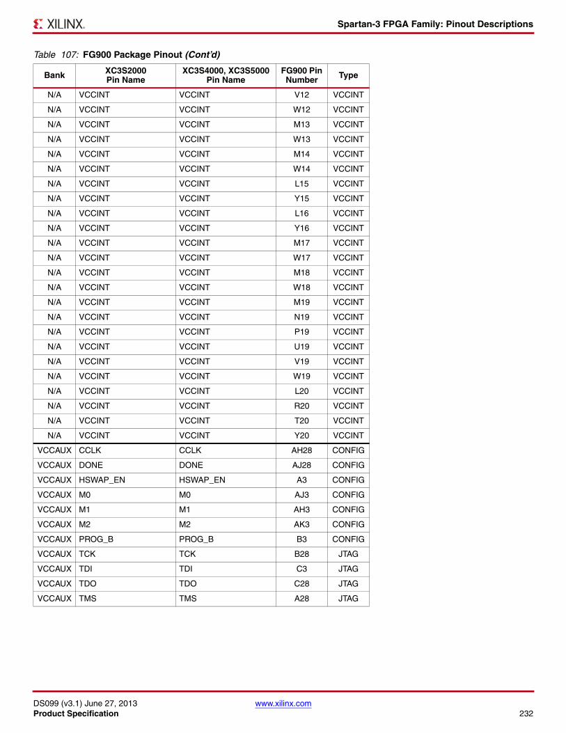
Spartan-3 FPGA Family: Pinout Descriptions
DS099 (v3.1) June 27, 2013 www.xilinx.comProduct Specification 232
N/A VCCINT VCCINT V12 VCCINT
N/A VCCINT VCCINT W12 VCCINT
N/A VCCINT VCCINT M13 VCCINT
N/A VCCINT VCCINT W13 VCCINT
N/A VCCINT VCCINT M14 VCCINT
N/A VCCINT VCCINT W14 VCCINT
N/A VCCINT VCCINT L15 VCCINT
N/A VCCINT VCCINT Y15 VCCINT
N/A VCCINT VCCINT L16 VCCINT
N/A VCCINT VCCINT Y16 VCCINT
N/A VCCINT VCCINT M17 VCCINT
N/A VCCINT VCCINT W17 VCCINT
N/A VCCINT VCCINT M18 VCCINT
N/A VCCINT VCCINT W18 VCCINT
N/A VCCINT VCCINT M19 VCCINT
N/A VCCINT VCCINT N19 VCCINT
N/A VCCINT VCCINT P19 VCCINT
N/A VCCINT VCCINT U19 VCCINT
N/A VCCINT VCCINT V19 VCCINT
N/A VCCINT VCCINT W19 VCCINT
N/A VCCINT VCCINT L20 VCCINT
N/A VCCINT VCCINT R20 VCCINT
N/A VCCINT VCCINT T20 VCCINT
N/A VCCINT VCCINT Y20 VCCINT
VCCAUX CCLK CCLK AH28 CONFIG
VCCAUX DONE DONE AJ28 CONFIG
VCCAUX HSWAP_EN HSWAP_EN A3 CONFIG
VCCAUX M0 M0 AJ3 CONFIG
VCCAUX M1 M1 AH3 CONFIG
VCCAUX M2 M2 AK3 CONFIG
VCCAUX PROG_B PROG_B B3 CONFIG
VCCAUX TCK TCK B28 JTAG
VCCAUX TDI TDI C3 JTAG
VCCAUX TDO TDO C28 JTAG
VCCAUX TMS TMS A28 JTAG
Table 107: FG900 Package Pinout (Cont’d)
Bank XC3S2000Pin Name
XC3S4000, XC3S5000 Pin Name
FG900 Pin Number Type

Spartan-3 FPGA Family: Pinout Descriptions
DS099 (v3.1) June 27, 2013 www.xilinx.comProduct Specification 233
User I/Os by Bank
Table 108 indicates how the available user-I/O pins are distributed between the eight I/O banks for the XC3S2000 in the FG900 package. Similarly, Table 109 shows how the available user-I/O pins are distributed between the eight I/O banks for the XC3S4000 and XC3S5000 in the FG900 package.
Table 108: User I/Os Per Bank for XC3S2000 in FG900 Package
Edge I/O Bank Maximum I/OAll Possible I/O Pins by Type
I/O DUAL DCI VREF GCLK
Top0 71 62 0 2 5 2
1 71 62 0 2 5 2
Right2 69 61 0 2 6 0
3 71 62 0 2 7 0
Bottom4 72 57 6 2 5 2
5 71 55 6 2 6 2
Left6 69 60 0 2 7 0
7 71 62 0 2 7 0
Table 109: User I/Os Per Bank for XC3S4000 and XC3S5000 in FG900 Package
Edge I/O Bank Maximum I/OAll Possible I/O Pins by Type
I/O DUAL DCI VREF GCLK
Top0 79 70 0 2 5 2
1 79 70 0 2 5 2
Right2 79 71 0 2 6 0
3 79 70 0 2 7 0
Bottom4 80 65 6 2 5 2
5 79 63 6 2 6 2
Left6 79 70 0 2 7 0
7 79 70 0 2 7 0
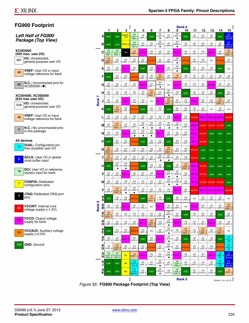
Spartan-3 FPGA Family: Pinout Descriptions
DS099 (v3.1) June 27, 2013 www.xilinx.comProduct Specification 234
FG900 Footprint X-Ref Target - Figure 55
Left Half of FG900 Package (Top View)
XC3S2000(565 max. user I/O)
481 I/O: Unrestricted, general-purpose user I/O
48 VREF: User I/O or input voltage reference for bank
68 N.C.: Unconnected pins for XC3S2000 ()
XC3S4000, XC3S5000(633 max user I/O)
549 I/O: Unrestricted, general-purpose user I/O
48 VREF: User I/O or input voltage reference for bank
0 N.C.: No unconnected pins in this package
All devices
12 DUAL: Configuration pin, then possible user I/O
8 GCLK: User I/O or global clock buffer input
16 DCI: User I/O or reference resistor input for bank
7 CONFIG: Dedicated configuration pins
4 JTAG: Dedicated JTAG port pins
32 VCCINT: Internal core voltage supply (+1.2V)
80 VCCO: Output voltage supply for bank
24 VCCAUX: Auxiliary voltage supply (+2.5V)
120 GND: Ground
Figure 55: FG900 Package Footprint (Top View)
HSWAP_ EN
I/O L01P_0 VRN_0
I/O L02P_0
I/O L35P_0 I/O
L09P_0
I/O L38P_0 I/O
L17P_0I/O
L22P_0I/O
L25P_0
I/O L32P_0 GCLK6
GCLK7PROG_B
I/O L01N_0 VRP_0
I/O L02N_0
I/O L04P_0
I/O L35N_0 I/O
L09N_0
I/O L38N_0 I/O
L12P_0I/O
L17N_0I/O
L22N_0I/O
L25N_0I/O
L28P_0
I/O L32N_0
I/O L01N_7 VRP_7
I/O L01P_7 VRN_7
TDIIO
VREF_0 VCCO_0 I/O L04N_0
I/O L06P_0
I/O L08P_0
VCCO_0 I/O L12N_0
I/O L16P_0
I/O L21P_0
VCCO_0 I/O L28N_0
I/O L31P_0
VREF_0
I/O L03N_7
VREF_7
I/O L03P_7
I/O L02N_7
I/O L02P_7
I/O L03N_0
I/O L06N_0
I/O L08N_0
I/O L37P_0 I/O
L16N_0I/O
L21N_0 I/O I/O L31N_0
I/O L04N_7
I/O L04P_7
VCCO_7 I/O L05P_7
I/O L03P_0
VCCO_0 I/O L07P_0
I/O L37N_0 I/O
L15P_0I/O
L20P_0I/O
L24P_0 I/O
I/O L06N_7
I/O L06P_7
I/O L05N_7
I/O L05N_0
I/O L05P_0 VREF_0
I/O L07N_0
IO VREF_0
I/O L11P_0
I/O L15N_0
I/O L20N_0
I/O L24N_0
I/O L27P_0
I/O L30P_0
I/O L08N_7
I/O L08P_7
I/O L07N_7
I/O L07P_7
VCCO_7 I/O L09P_7
I/O L36N_0 I/O VCCO_0 I/O
L11N_0I/O
L14P_0I/O
L19P_0VCCO_0 I/O
L27N_0I/O
L30N_0
I/O L13N_7
I/O L13P_7
I/O L11N_7
I/O L11P_7
I/O L10N_7
I/O L10P_7
VREF_7
I/O L09N_7
I/O L36P_0 I/O
L10P_0I/O
L14N_0I/O
L19N_0I/O
L23P_0I/O
L29P_0
I/O L15N_7
I/O L15P_7
VCCO_7 I/O L14N_7
I/O L14P_7 I/O VCCO_7
I/O L16P_7
VREF_7
I/O L10N_0
I/O L13N_0
VCCO_0 I/O L18P_0
I/O L23N_0
I/O L26P_0
VREF_0
I/O L29N_0
GNDI/O
L19N_7 VREF_7
I/O L19P_7
VCCAUX
VCCAUX
VCCAUX VCCAUX VCCAUX
VCCAUX
VCCAUX
VCCAUX
VCCAUXVCCAUX
I/O L17N_7
I/O L17P_7
I/O L16N_7
I/O L20P_7
I/O L13P_0
I/O L18N_0 I/O I/O
L26N_0 I/O
I/O L24N_7
I/O L24P_7
I/O L23N_7
I/O L23P_7
I/O L22N_7
I/O L22P_7
I/O L21N_7
I/O L21P_7
VCCO_7 I/O L20N_7 VCCINT VCCO_0 VCCO_0 VCCO_0 VCCINT
I/O L27N_7
I/O L27P_7 VREF_7
I/O L26N_7
I/O L26P_7
I/O L49P_7
I/O L25N_7
I/O L25P_7
I/O L46N_7
I/O L46P_7 I/O
L28P_7VCCO_7 VCCINT VCCINT VCCINT GND
GNDGND
GND
GNDGND
GND
GND
GND
GND
GND GND
GND GND
GNDGND
GND
GND
GND
GNDGNDGND
GNDGNDGND
GNDGNDGND
GNDGNDGND
GNDGNDGND
GNDGNDGND
I/O L31N_7
I/O L31P_7
VCCO_7I/O
L50N_7 I/O
L50P_7 I/O
L49N_7 VCCO_7 I/O L29N_7
I/O L29P_7
I/O L28N_7
VCCO_7 VCCINT
GND I/O L34N_7
I/O L34P_7 GND I/O
L33N_7I/O
L33P_7 GND I/O L32N_7
I/O L32P_7
VCCO_7 VCCINT
I/O L40N_7
VREF_7
I/O L40P_7
I/O L39N_7
I/O L39P_7
I/O L38N_7
I/O L38P_7
I/O L37N_7
I/O L37P_7
VREF_7
I/O L35N_7
I/O L35P_7 VCCINT
I/O L40P_6
VREF_6
I/O L40N_6
I/O L39P_6
I/O L39N_6
I/O L38P_6
I/O L38N_6
I/O L52P_6
I/O L52N_6 I/O
L37P_6I/O
L37N_6 VCCINT
GNDI/O
L36P_6 I/O
L36N_6 GND I/O L35P_6
I/O L35N_6 GND I/O
L34P_6
I/O L34N_6
VREF_6VCCO_6 VCCINT
I/O L33P_6
I/O L33N_6
VCCO_6 I/O L32P_6
I/O L32N_6
I/O L31P_6
VCCO_6I/O
L30P_6 I/O
L30N_6 I/O L29P_6
VCCO_6 VCCINT
I/O L28P_6
I/O L28N_6
I/O L27P_6
I/O L27N_6
I/O L31N_6
I/O L26P_6
I/O L26N_6
I/O L25P_6
I/O L25N_6 I/O
L29N_6VCCO_6 VCCINT VCCINT VCCINT
I/O L24P_6
I/O L24N_6 VREF_6
I/O L45P_6
I/O L45N_6 I/O
L22P_6I/O
L22N_6I/O
L21P_6I/O
L21N_6VCCO_6 I/O
L20P_6 VCCINT VCCO_5 VCCO_5 VCCO_5 VCCINT
GND I/O L19P_6
I/O L19N_6 GND
I/O L17P_6
VREF_6
I/O L17N_6 GND I/O
L16P_6I/O
L20N_6 I/O I/O L22P_5
I/O L22N_5
I/O L26P_5 I/O
I/O L15P_6
I/O L15N_6
VCCO_6 I/O L14P_6
I/O L14N_6 I/O VCCO_6 I/O
L16N_6I/O
L08P_5 I/O VCCO_5 I/O L17N_5
I/O L23P_5
I/O L26N_5
I/O L29P_5
VREF_5
I/O L13P_6 VREF_6
I/O L13N_6
I/O L11P_6
I/O L11N_6
I/O L10P_6
I/O L10N_6
I/O L09P_6
I/O L36P_5 I/O
L08N_5 GND I/O L17P_5
I/O L18P_5
I/O L23N_5 GND I/O
L29N_5
I/O L08P_6
I/O L08N_6
I/O L07P_6
I/O L07N_6
VCCO_6I/O
L09N_6 VREF_6
I/O L05P_5
I/O L36N_5 VCCO_5 I/O
L13P_5I/O
L13N_5I/O
L18N_5VCCO_5 I/O
L30P_5I/O
L30N_5
GND I/O L06P_6
I/O L06N_6
VCCAUX I/O L05P_6 I/O I/O
L05N_5
I/O L37P_5 I/O
L11P_5
I/O L11N_5
VREF_5
I/O L14P_5
I/O L19P_5 VREF_5
I/O L27P_5
I/O L27N_5 VREF_5
I/O
I/O L04P_6
I/O L04N_6
VCCO_6 I/O L05N_6 GND I/O
L03N_5VCCO_5
I/O L37N_5 I/O
L09P_5 GND I/O L14N_5
I/O L19N_5
I/O L24P_5 GND
I/O L31P_5
D5
I/O L03P_6
I/O L03N_6
VREF_6
I/O L02P_6
I/O L02N_6
I/O L03P_5
I/O L06P_5
I/O L38P_5 I/O
L09N_5I/O
L15P_5I/O
L20P_5I/O
L24N_5VCCAUX
I/O L31N_5
D4
I/O L01P_6 VRN_6
I/O L01N_6 VRP_6
M1IO
VREF_5 VCCO_5 I/O L04P_5
I/O L06N_5
I/O L38N_5 VCCO_5 I/O
L12P_5I/O
L15N_5I/O
L20N_5VCCO_5
I/O L28P_5
D7
I/O L32P_5
GND GND M0I/O
L01P_5 CS_B
I/O L02P_5
I/O L04N_5
I/O L35P_5 I/O
L07P_5
I/O L10P_5 VRN_5
I/O L12N_5
I/O L16P_5
I/O L21P_5
I/O L25P_5
I/O L28N_5
D6
I/O L32N_5 GCLK3
GCLK2
GND GND M2I/O
L01N_5 RDWR_B
I/O L02N_5 GND
I/O L35N_5
I/O L07N_5
I/O L10N_5 VRP_5
GND I/O L16N_5
I/O L21N_5
I/O L25N_5 GND
IO VREF_5
10 11 12 13 14 151 2 3 4 5 6 7 8 9Bank 0
A
B
C
D
E
F
G
H
J
K
L
M
N
P
R
T
U
V
W
Y
AA
AB
AC
AD
AE
AF
AG
AH
AJ
AK
Ban
k 7
Ban
k 6
Bank 5 DS099-4_13a_121103
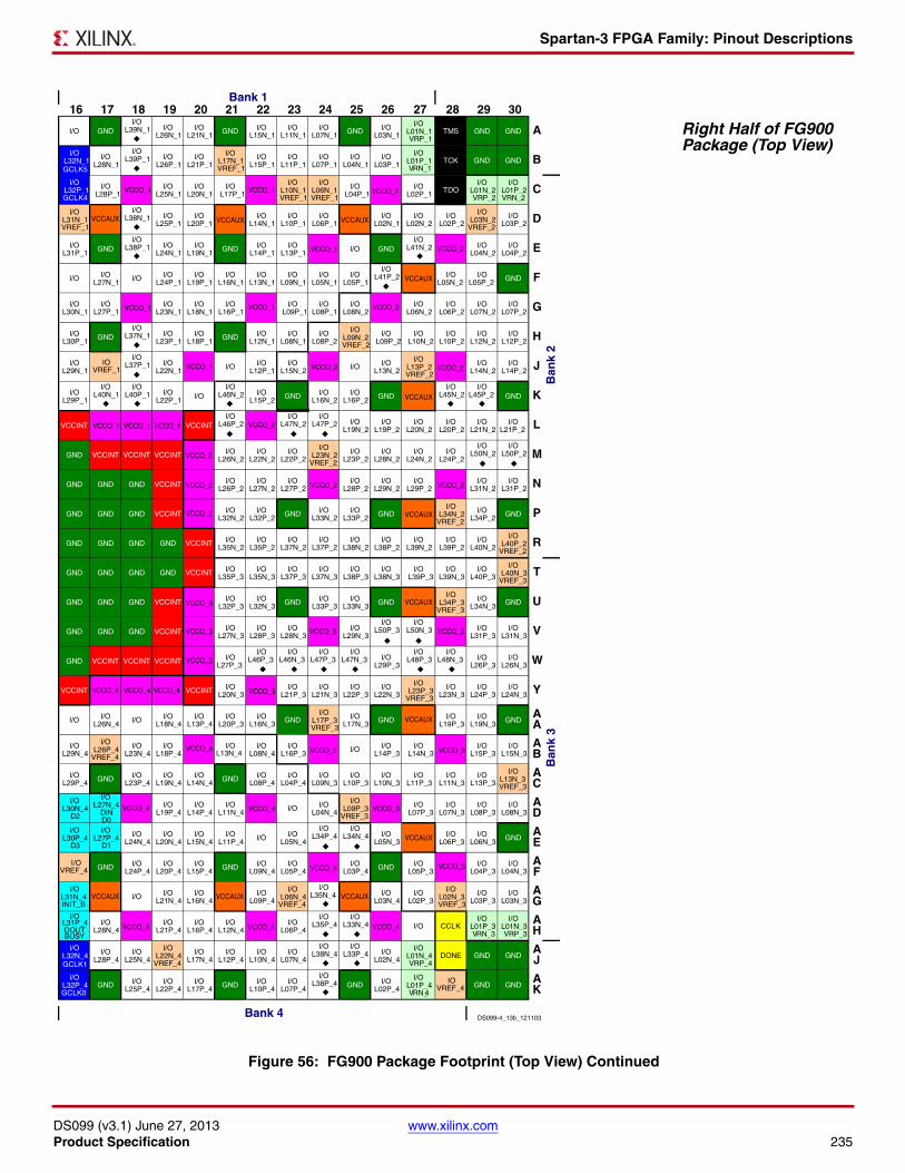
Spartan-3 FPGA Family: Pinout Descriptions
DS099 (v3.1) June 27, 2013 www.xilinx.comProduct Specification 235
Right Half of FG900 Package (Top View)
Figure 56: FG900 Package Footprint (Top View) Continued
I/O GNDI/O
L39N_1
I/O L26N_1
I/O L21N_1 GND I/O
L15N_1I/O
L11N_1I/O
L07N_1 GND I/O L03N_1
I/O L01N_1 VRP_1
TMS GND GND
I/O L32N_1 I/O
L28N_1
I/O L39P_1 I/O
L26P_1I/O
L21P_1
I/O L17N_1 VREF_1
I/O L15P_1
I/O L11P_1
I/O L07P_1
I/O L04N_1
I/O L03P_1
I/O L01P_1VRN_1
TCK GND GND
I/O L32P_1 GCLK4
GCLK5
I/O L28P_1
I/O L25N_1
I/O L20N_1
I/O L17P_1
I/O L10N_1 VREF_1
I/O L06N_1 VREF_1
I/O L04P_1
I/O L02P_1 TDO
I/O L01N_2 VRP_2
I/O L01P_2 VRN_2
I/O L31N_1 VREF_1
VCCAUX VCCAUX VCCAUX
VCCAUX
VCCAUX
VCCAUX
VCCAUX
VCCAUX
VCCAUX
VCCAUXVCCAUXVCCAUX
I/O L38N_1 I/O
L25P_1I/O
L20P_1I/O
L14N_1I/O
L10P_1I/O
L06P_1I/O
L02N_1I/O
L02N_2I/O
L02P_2
I/O L03N_2
VREF_2
I/O L03P_2
I/O L31P_1 GND
I/O L38P_1 I/O
L24N_1I/O
L19N_1 GND I/O L14P_1
I/O L13P_1 I/O GND
I/O L41N_2 I/O
L04N_2I/O
L04P_2
I/O I/O L27N_1 I/O I/O
L24P_1I/O
L19P_1I/O
L16N_1I/O
L13N_1I/O
L09N_1I/O
L05N_1I/O
L05P_1
I/O L41P_2 I/O
L05N_2I/O
L05P_2 GND
I/O L30N_1
I/O L27P_1
I/O L23N_1
I/O L18N_1
I/O L16P_1
I/O L09P_1
I/O L08P_1
I/O L08N_2
I/O L06N_2
I/O L06P_2
I/O L07N_2
I/O L07P_2
I/O L30P_1 GND
I/O L37N_1 I/O
L23P_1I/O
L18P_1 GND I/O L12N_1
I/O L08N_1
I/O L08P_2
I/O L09N_2 VREF_2
I/O L09P_2
I/O L10N_2
I/O L10P_2
I/O L12N_2
I/O L12P_2
I/O L29N_1
IO VREF_1
I/O L37P_1 I/O
L22N_1 I/O I/O L12P_1
I/O L15N_2 I/O I/O
L13N_2
I/O L13P_2 VREF_2
I/O L14N_2
I/O L14P_2
I/O L29P_1
I/O L40N_1
I/O L40P_1 I/O
L22P_1 I/OI/O
L46N_2 I/O L15P_2 GND I/O
L16N_2I/O
L16P_2 GNDI/O
L45N_2 I/O
L45P_2 GND
VCCINT VCCINTI/O
L46P_2 I/O
L47N_2 I/O
L47P_2 I/O L19N_2
I/O L19P_2
I/O L20N_2
I/O L20P_2
I/O L21N_2
I/O L21P_2
GND VCCINT VCCINT VCCINT I/O L26N_2
I/O L22N_2
I/O L22P_2
I/O L23N_2
VREF_2
I/O L23P_2
I/O L28N_2
I/O L24N_2
I/O L24P_2
I/O L50N_2
I/O L50P_2
GND GND GND VCCINT I/O L26P_2
I/O L27N_2
I/O L27P_2
I/O L28P_2
I/O L29N_2
I/O L29P_2
I/O L31N_2
I/O L31P_2
GND GND GND VCCINT I/O L32N_2
I/O L32P_2 GND I/O
L33N_2I/O
L33P_2 GNDI/O
L34N_2 VREF_2
I/O L34P_2 GND
GND GND GND GND VCCINT I/O L35N_2
I/O L35P_2
I/O L37N_2
I/O L37P_2
I/O L38N_2
I/O L38P_2
I/O L39N_2
I/O L39P_2
I/O L40N_2
I/O L40P_2
VREF_2
GND GND GND GND VCCINT I/O L35P_3
I/O L35N_3
I/O L37P_3
I/O L37N_3
I/O L38P_3
I/O L38N_3
I/O L39P_3
I/O L39N_3
I/O L40P_3
I/O L40N_3
VREF_3
GND GND GND VCCINT I/O L32P_3
I/O L32N_3 GND I/O
L33P_3I/O
L33N_3 GNDI/O
L34P_3 VREF_3
I/O L34N_3 GND
GND GND GND VCCINT I/O L27N_3
I/O L28P_3
I/O L28N_3
I/O L29N_3
I/O L50P_3
I/O L50N_3 I/O
L31P_3I/O
L31N_3
GND VCCINT VCCINT VCCINT I/O L27P_3
I/O L46P_3
I/O L46N_3
I/O L47P_3
I/O L47N_3 I/O
L29P_3
I/O L48P_3
I/O L48N_3 I/O
L26P_3I/O
L26N_3
VCCINT VCCO_4 VCCO_4 VCCO_4
VCCO_4
VCCO_4
VCCO_4 VCCO_4 VCCO_4
VCCO_4
VCCO_4
VCCINT I/O L20N_3
I/O L21P_3
I/O L21N_3
I/O L22P_3
I/O L22N_3
I/O L23P_3
VREF_3
I/O L23N_3
I/O L24P_3
I/O L24N_3
I/O I/O L26N_4 I/O I/O
L18N_4I/O
L13P_4I/O
L20P_3I/O
L16N_3 GNDI/O
L17P_3 VREF_3
I/O L17N_3 GND I/O
L19P_3I/O
L19N_3 GND
I/O L29N_4
I/O L26P_4
VREF_4
I/O L23N_4
I/O L18P_4
I/O L13N_4
I/O L08N_4
I/O L16P_3 I/O I/O
L14P_3I/O
L14N_3I/O
L15P_3I/O
L15N_3
I/O L29P_4 GND I/O
L23P_4I/O
L19N_4I/O
L14N_4 GND I/O L08P_4
I/O L04P_4
I/O L09N_3
I/O L10P_3
I/O L10N_3
I/O L11P_3
I/O L11N_3
I/O L13P_3
I/O L13N_3 VREF_3
I/O L30N_4
D2
I/O L27N_4
DIND0
I/O L19P_4
I/O L14P_4
I/O L11N_4 I/O I/O
L04N_4
I/O L09P_3
VREF_3
I/O L07P_3
I/O L07N_3
I/O L08P_3
I/O L08N_3
I/O L30P_4
D3
I/O L27P_4
D1
I/O L24N_4
I/O L20N_4
I/O L15N_4
I/O L11P_4 I/O I/O
L05N_4
I/O L34P_4
I/O L34N_4 I/O
L05N_3I/O
L06P_3I/O
L06N_3 GND
I/OVREF_4 GND I/O
L24P_4I/O
L20P_4I/O
L15P_4 GND I/O L09N_4
I/O L05P_4
I/O L03P_4 GND I/O
L05P_3VCCO_3
VCCO_3VCCO_3
VCCO_3
VCCO_3
VCCO_3 VCCO_3 VCCO_3
VCCO_2VCCO_2
VCCO_2
VCCO_2
VCCO_2
VCCO_2
VCCO_1
VCCO_1
VCCO_1
VCCO_1
VCCO_1
VCCO_1
VCCO_1
VCCO_1 VCCO_1 VCCO_1
VCCO_2
VCCO_2
VCCO_2
VCCO_2
VCCO_3
VCCO_3
I/O L04P_3
I/O L04N_3
I/O L31N_4 INIT_B
I/O I/O L21N_4
I/O L16N_4
I/O L09P_4
I/O L06N_4
VREF_4
I/O L35N_4 I/O
L03N_4I/O
L02P_3
I/O L02N_3 VREF_3
I/O L03P_3
I/O L03N_3
I/OL31P_4 DOUT BUSY
I/O L28N_4
I/O L21P_4
I/O L16P_4
I/O L12N_4
I/O L06P_4
I/O L35P_4
I/O L33N_4 I/O CCLK
I/O L01P_3 VRN_3
I/O L01N_3 VRP_3
I/O L32N_4 I/O
L28P_4I/O
L25N_4
I/O L22N_4
VREF_4
I/O L17N_4
I/O L12P_4
I/O L10N_4
I/O L07N_4
I/O L38N_4
I/O L33P_4 I/O
L02N_4
I/O L01N_4VRP_4
DONE GND GND
I/O L32P_4 GCLK0
GCLK1
GND I/O L25P_4
I/O L22P_4
I/O L17P_4 GND I/O
L10P_4I/O
L07P_4
I/O L38P_4 GND I/O
L02P_4
I/O L01P_4 VRN_4
IO VREF_4 GND GND
16 17 18 19 20 21 22 23 24 25 26 27 28 29 30Bank 1
A
B
C
D
E
F
G
H
J
K
L
M
N
P
R
T
U
V
W
Y
AA
AB
AC
AD
AE
AF
AG
AH
AJ
AK
Bank 4
Ban
k 2
Ban
k 3
DS099-4_13b_121103
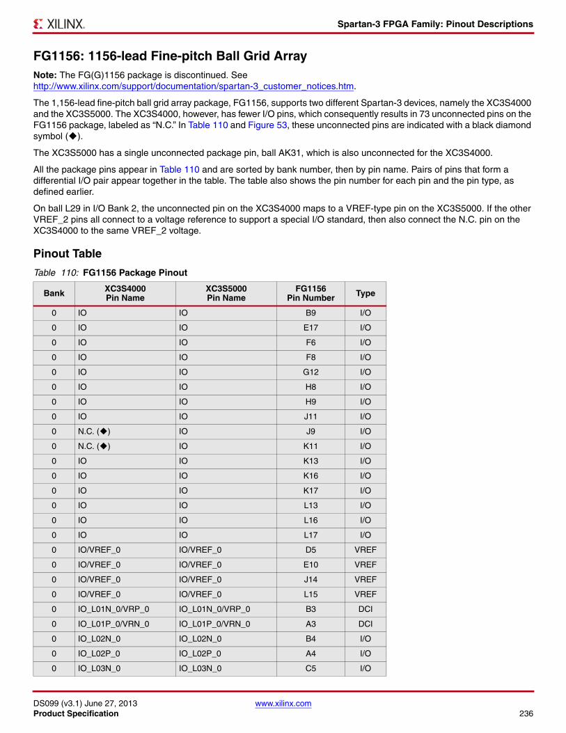
Spartan-3 FPGA Family: Pinout Descriptions
DS099 (v3.1) June 27, 2013 www.xilinx.comProduct Specification 236
FG1156: 1156-lead Fine-pitch Ball Grid ArrayNote: The FG(G)1156 package is discontinued. See http://www.xilinx.com/support/documentation/spartan-3_customer_notices.htm.
The 1,156-lead fine-pitch ball grid array package, FG1156, supports two different Spartan-3 devices, namely the XC3S4000 and the XC3S5000. The XC3S4000, however, has fewer I/O pins, which consequently results in 73 unconnected pins on the FG1156 package, labeled as “N.C.” In Table 110 and Figure 53, these unconnected pins are indicated with a black diamond symbol ().
The XC3S5000 has a single unconnected package pin, ball AK31, which is also unconnected for the XC3S4000.
All the package pins appear in Table 110 and are sorted by bank number, then by pin name. Pairs of pins that form a differential I/O pair appear together in the table. The table also shows the pin number for each pin and the pin type, as defined earlier.
On ball L29 in I/O Bank 2, the unconnected pin on the XC3S4000 maps to a VREF-type pin on the XC3S5000. If the other VREF_2 pins all connect to a voltage reference to support a special I/O standard, then also connect the N.C. pin on the XC3S4000 to the same VREF_2 voltage.
Pinout Table
Table 110: FG1156 Package Pinout
Bank XC3S4000Pin Name
XC3S5000Pin Name
FG1156Pin Number Type
0 IO IO B9 I/O
0 IO IO E17 I/O
0 IO IO F6 I/O
0 IO IO F8 I/O
0 IO IO G12 I/O
0 IO IO H8 I/O
0 IO IO H9 I/O
0 IO IO J11 I/O
0 N.C. () IO J9 I/O
0 N.C. () IO K11 I/O
0 IO IO K13 I/O
0 IO IO K16 I/O
0 IO IO K17 I/O
0 IO IO L13 I/O
0 IO IO L16 I/O
0 IO IO L17 I/O
0 IO/VREF_0 IO/VREF_0 D5 VREF
0 IO/VREF_0 IO/VREF_0 E10 VREF
0 IO/VREF_0 IO/VREF_0 J14 VREF
0 IO/VREF_0 IO/VREF_0 L15 VREF
0 IO_L01N_0/VRP_0 IO_L01N_0/VRP_0 B3 DCI
0 IO_L01P_0/VRN_0 IO_L01P_0/VRN_0 A3 DCI
0 IO_L02N_0 IO_L02N_0 B4 I/O
0 IO_L02P_0 IO_L02P_0 A4 I/O
0 IO_L03N_0 IO_L03N_0 C5 I/O

Spartan-3 FPGA Family: Pinout Descriptions
DS099 (v3.1) June 27, 2013 www.xilinx.comProduct Specification 237
0 IO_L03P_0 IO_L03P_0 B5 I/O
0 IO_L04N_0 IO_L04N_0 D6 I/O
0 IO_L04P_0 IO_L04P_0 C6 I/O
0 IO_L05N_0 IO_L05N_0 B6 I/O
0 IO_L05P_0/VREF_0 IO_L05P_0/VREF_0 A6 VREF
0 IO_L06N_0 IO_L06N_0 F7 I/O
0 IO_L06P_0 IO_L06P_0 E7 I/O
0 IO_L07N_0 IO_L07N_0 G9 I/O
0 IO_L07P_0 IO_L07P_0 F9 I/O
0 IO_L08N_0 IO_L08N_0 D9 I/O
0 IO_L08P_0 IO_L08P_0 C9 I/O
0 IO_L09N_0 IO_L09N_0 J10 I/O
0 IO_L09P_0 IO_L09P_0 H10 I/O
0 IO_L10N_0 IO_L10N_0 G10 I/O
0 IO_L10P_0 IO_L10P_0 F10 I/O
0 IO_L11N_0 IO_L11N_0 L12 I/O
0 IO_L11P_0 IO_L11P_0 K12 I/O
0 IO_L12N_0 IO_L12N_0 J12 I/O
0 IO_L12P_0 IO_L12P_0 H12 I/O
0 IO_L13N_0 IO_L13N_0 F12 I/O
0 IO_L13P_0 IO_L13P_0 E12 I/O
0 IO_L14N_0 IO_L14N_0 D12 I/O
0 IO_L14P_0 IO_L14P_0 C12 I/O
0 IO_L15N_0 IO_L15N_0 B12 I/O
0 IO_L15P_0 IO_L15P_0 A12 I/O
0 IO_L16N_0 IO_L16N_0 H13 I/O
0 IO_L16P_0 IO_L16P_0 G13 I/O
0 IO_L17N_0 IO_L17N_0 D13 I/O
0 IO_L17P_0 IO_L17P_0 C13 I/O
0 IO_L18N_0 IO_L18N_0 L14 I/O
0 IO_L18P_0 IO_L18P_0 K14 I/O
0 IO_L19N_0 IO_L19N_0 H14 I/O
0 IO_L19P_0 IO_L19P_0 G14 I/O
0 IO_L20N_0 IO_L20N_0 F14 I/O
0 IO_L20P_0 IO_L20P_0 E14 I/O
0 IO_L21N_0 IO_L21N_0 D14 I/O
0 IO_L21P_0 IO_L21P_0 C14 I/O
0 IO_L22N_0 IO_L22N_0 B14 I/O
0 IO_L22P_0 IO_L22P_0 A14 I/O
0 IO_L23N_0 IO_L23N_0 K15 I/O
Table 110: FG1156 Package Pinout (Cont’d)
Bank XC3S4000Pin Name
XC3S5000Pin Name
FG1156Pin Number Type
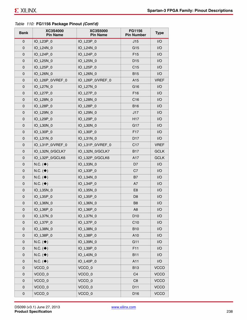
Spartan-3 FPGA Family: Pinout Descriptions
DS099 (v3.1) June 27, 2013 www.xilinx.comProduct Specification 238
0 IO_L23P_0 IO_L23P_0 J15 I/O
0 IO_L24N_0 IO_L24N_0 G15 I/O
0 IO_L24P_0 IO_L24P_0 F15 I/O
0 IO_L25N_0 IO_L25N_0 D15 I/O
0 IO_L25P_0 IO_L25P_0 C15 I/O
0 IO_L26N_0 IO_L26N_0 B15 I/O
0 IO_L26P_0/VREF_0 IO_L26P_0/VREF_0 A15 VREF
0 IO_L27N_0 IO_L27N_0 G16 I/O
0 IO_L27P_0 IO_L27P_0 F16 I/O
0 IO_L28N_0 IO_L28N_0 C16 I/O
0 IO_L28P_0 IO_L28P_0 B16 I/O
0 IO_L29N_0 IO_L29N_0 J17 I/O
0 IO_L29P_0 IO_L29P_0 H17 I/O
0 IO_L30N_0 IO_L30N_0 G17 I/O
0 IO_L30P_0 IO_L30P_0 F17 I/O
0 IO_L31N_0 IO_L31N_0 D17 I/O
0 IO_L31P_0/VREF_0 IO_L31P_0/VREF_0 C17 VREF
0 IO_L32N_0/GCLK7 IO_L32N_0/GCLK7 B17 GCLK
0 IO_L32P_0/GCLK6 IO_L32P_0/GCLK6 A17 GCLK
0 N.C. () IO_L33N_0 D7 I/O
0 N.C. () IO_L33P_0 C7 I/O
0 N.C. () IO_L34N_0 B7 I/O
0 N.C. () IO_L34P_0 A7 I/O
0 IO_L35N_0 IO_L35N_0 E8 I/O
0 IO_L35P_0 IO_L35P_0 D8 I/O
0 IO_L36N_0 IO_L36N_0 B8 I/O
0 IO_L36P_0 IO_L36P_0 A8 I/O
0 IO_L37N_0 IO_L37N_0 D10 I/O
0 IO_L37P_0 IO_L37P_0 C10 I/O
0 IO_L38N_0 IO_L38N_0 B10 I/O
0 IO_L38P_0 IO_L38P_0 A10 I/O
0 N.C. () IO_L39N_0 G11 I/O
0 N.C. () IO_L39P_0 F11 I/O
0 N.C. () IO_L40N_0 B11 I/O
0 N.C. () IO_L40P_0 A11 I/O
0 VCCO_0 VCCO_0 B13 VCCO
0 VCCO_0 VCCO_0 C4 VCCO
0 VCCO_0 VCCO_0 C8 VCCO
0 VCCO_0 VCCO_0 D11 VCCO
0 VCCO_0 VCCO_0 D16 VCCO
Table 110: FG1156 Package Pinout (Cont’d)
Bank XC3S4000Pin Name
XC3S5000Pin Name
FG1156Pin Number Type
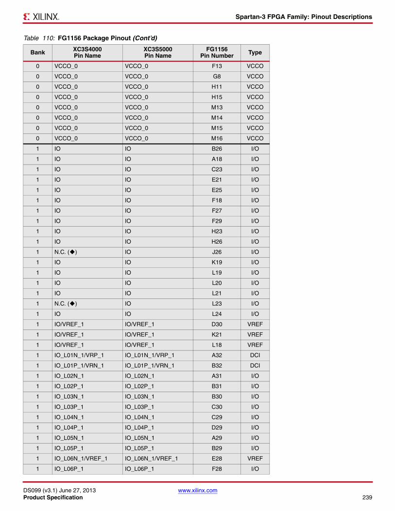
Spartan-3 FPGA Family: Pinout Descriptions
DS099 (v3.1) June 27, 2013 www.xilinx.comProduct Specification 239
0 VCCO_0 VCCO_0 F13 VCCO
0 VCCO_0 VCCO_0 G8 VCCO
0 VCCO_0 VCCO_0 H11 VCCO
0 VCCO_0 VCCO_0 H15 VCCO
0 VCCO_0 VCCO_0 M13 VCCO
0 VCCO_0 VCCO_0 M14 VCCO
0 VCCO_0 VCCO_0 M15 VCCO
0 VCCO_0 VCCO_0 M16 VCCO
1 IO IO B26 I/O
1 IO IO A18 I/O
1 IO IO C23 I/O
1 IO IO E21 I/O
1 IO IO E25 I/O
1 IO IO F18 I/O
1 IO IO F27 I/O
1 IO IO F29 I/O
1 IO IO H23 I/O
1 IO IO H26 I/O
1 N.C. () IO J26 I/O
1 IO IO K19 I/O
1 IO IO L19 I/O
1 IO IO L20 I/O
1 IO IO L21 I/O
1 N.C. () IO L23 I/O
1 IO IO L24 I/O
1 IO/VREF_1 IO/VREF_1 D30 VREF
1 IO/VREF_1 IO/VREF_1 K21 VREF
1 IO/VREF_1 IO/VREF_1 L18 VREF
1 IO_L01N_1/VRP_1 IO_L01N_1/VRP_1 A32 DCI
1 IO_L01P_1/VRN_1 IO_L01P_1/VRN_1 B32 DCI
1 IO_L02N_1 IO_L02N_1 A31 I/O
1 IO_L02P_1 IO_L02P_1 B31 I/O
1 IO_L03N_1 IO_L03N_1 B30 I/O
1 IO_L03P_1 IO_L03P_1 C30 I/O
1 IO_L04N_1 IO_L04N_1 C29 I/O
1 IO_L04P_1 IO_L04P_1 D29 I/O
1 IO_L05N_1 IO_L05N_1 A29 I/O
1 IO_L05P_1 IO_L05P_1 B29 I/O
1 IO_L06N_1/VREF_1 IO_L06N_1/VREF_1 E28 VREF
1 IO_L06P_1 IO_L06P_1 F28 I/O
Table 110: FG1156 Package Pinout (Cont’d)
Bank XC3S4000Pin Name
XC3S5000Pin Name
FG1156Pin Number Type
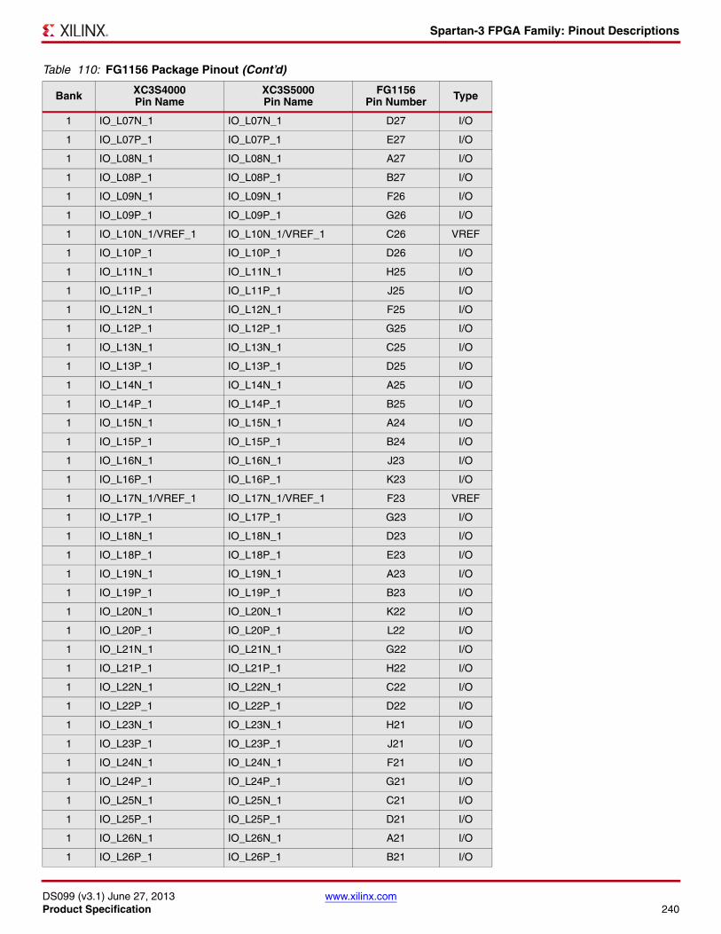
Spartan-3 FPGA Family: Pinout Descriptions
DS099 (v3.1) June 27, 2013 www.xilinx.comProduct Specification 240
1 IO_L07N_1 IO_L07N_1 D27 I/O
1 IO_L07P_1 IO_L07P_1 E27 I/O
1 IO_L08N_1 IO_L08N_1 A27 I/O
1 IO_L08P_1 IO_L08P_1 B27 I/O
1 IO_L09N_1 IO_L09N_1 F26 I/O
1 IO_L09P_1 IO_L09P_1 G26 I/O
1 IO_L10N_1/VREF_1 IO_L10N_1/VREF_1 C26 VREF
1 IO_L10P_1 IO_L10P_1 D26 I/O
1 IO_L11N_1 IO_L11N_1 H25 I/O
1 IO_L11P_1 IO_L11P_1 J25 I/O
1 IO_L12N_1 IO_L12N_1 F25 I/O
1 IO_L12P_1 IO_L12P_1 G25 I/O
1 IO_L13N_1 IO_L13N_1 C25 I/O
1 IO_L13P_1 IO_L13P_1 D25 I/O
1 IO_L14N_1 IO_L14N_1 A25 I/O
1 IO_L14P_1 IO_L14P_1 B25 I/O
1 IO_L15N_1 IO_L15N_1 A24 I/O
1 IO_L15P_1 IO_L15P_1 B24 I/O
1 IO_L16N_1 IO_L16N_1 J23 I/O
1 IO_L16P_1 IO_L16P_1 K23 I/O
1 IO_L17N_1/VREF_1 IO_L17N_1/VREF_1 F23 VREF
1 IO_L17P_1 IO_L17P_1 G23 I/O
1 IO_L18N_1 IO_L18N_1 D23 I/O
1 IO_L18P_1 IO_L18P_1 E23 I/O
1 IO_L19N_1 IO_L19N_1 A23 I/O
1 IO_L19P_1 IO_L19P_1 B23 I/O
1 IO_L20N_1 IO_L20N_1 K22 I/O
1 IO_L20P_1 IO_L20P_1 L22 I/O
1 IO_L21N_1 IO_L21N_1 G22 I/O
1 IO_L21P_1 IO_L21P_1 H22 I/O
1 IO_L22N_1 IO_L22N_1 C22 I/O
1 IO_L22P_1 IO_L22P_1 D22 I/O
1 IO_L23N_1 IO_L23N_1 H21 I/O
1 IO_L23P_1 IO_L23P_1 J21 I/O
1 IO_L24N_1 IO_L24N_1 F21 I/O
1 IO_L24P_1 IO_L24P_1 G21 I/O
1 IO_L25N_1 IO_L25N_1 C21 I/O
1 IO_L25P_1 IO_L25P_1 D21 I/O
1 IO_L26N_1 IO_L26N_1 A21 I/O
1 IO_L26P_1 IO_L26P_1 B21 I/O
Table 110: FG1156 Package Pinout (Cont’d)
Bank XC3S4000Pin Name
XC3S5000Pin Name
FG1156Pin Number Type
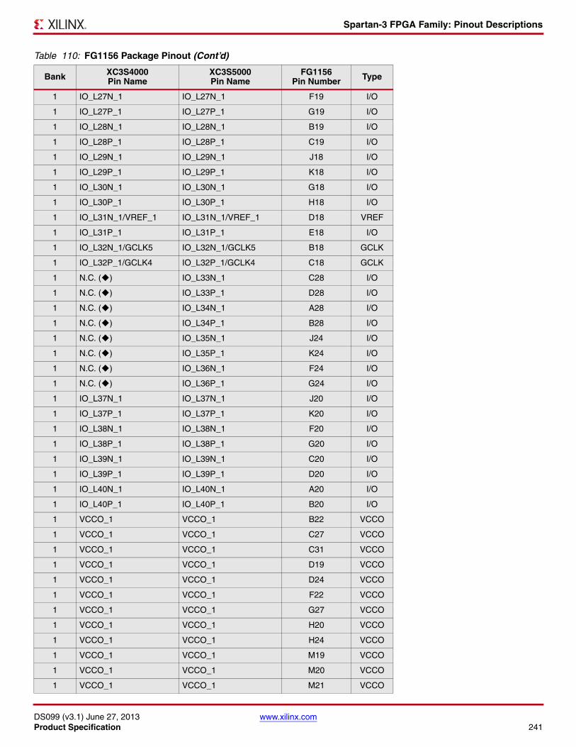
Spartan-3 FPGA Family: Pinout Descriptions
DS099 (v3.1) June 27, 2013 www.xilinx.comProduct Specification 241
1 IO_L27N_1 IO_L27N_1 F19 I/O
1 IO_L27P_1 IO_L27P_1 G19 I/O
1 IO_L28N_1 IO_L28N_1 B19 I/O
1 IO_L28P_1 IO_L28P_1 C19 I/O
1 IO_L29N_1 IO_L29N_1 J18 I/O
1 IO_L29P_1 IO_L29P_1 K18 I/O
1 IO_L30N_1 IO_L30N_1 G18 I/O
1 IO_L30P_1 IO_L30P_1 H18 I/O
1 IO_L31N_1/VREF_1 IO_L31N_1/VREF_1 D18 VREF
1 IO_L31P_1 IO_L31P_1 E18 I/O
1 IO_L32N_1/GCLK5 IO_L32N_1/GCLK5 B18 GCLK
1 IO_L32P_1/GCLK4 IO_L32P_1/GCLK4 C18 GCLK
1 N.C. () IO_L33N_1 C28 I/O
1 N.C. () IO_L33P_1 D28 I/O
1 N.C. () IO_L34N_1 A28 I/O
1 N.C. () IO_L34P_1 B28 I/O
1 N.C. () IO_L35N_1 J24 I/O
1 N.C. () IO_L35P_1 K24 I/O
1 N.C. () IO_L36N_1 F24 I/O
1 N.C. () IO_L36P_1 G24 I/O
1 IO_L37N_1 IO_L37N_1 J20 I/O
1 IO_L37P_1 IO_L37P_1 K20 I/O
1 IO_L38N_1 IO_L38N_1 F20 I/O
1 IO_L38P_1 IO_L38P_1 G20 I/O
1 IO_L39N_1 IO_L39N_1 C20 I/O
1 IO_L39P_1 IO_L39P_1 D20 I/O
1 IO_L40N_1 IO_L40N_1 A20 I/O
1 IO_L40P_1 IO_L40P_1 B20 I/O
1 VCCO_1 VCCO_1 B22 VCCO
1 VCCO_1 VCCO_1 C27 VCCO
1 VCCO_1 VCCO_1 C31 VCCO
1 VCCO_1 VCCO_1 D19 VCCO
1 VCCO_1 VCCO_1 D24 VCCO
1 VCCO_1 VCCO_1 F22 VCCO
1 VCCO_1 VCCO_1 G27 VCCO
1 VCCO_1 VCCO_1 H20 VCCO
1 VCCO_1 VCCO_1 H24 VCCO
1 VCCO_1 VCCO_1 M19 VCCO
1 VCCO_1 VCCO_1 M20 VCCO
1 VCCO_1 VCCO_1 M21 VCCO
Table 110: FG1156 Package Pinout (Cont’d)
Bank XC3S4000Pin Name
XC3S5000Pin Name
FG1156Pin Number Type
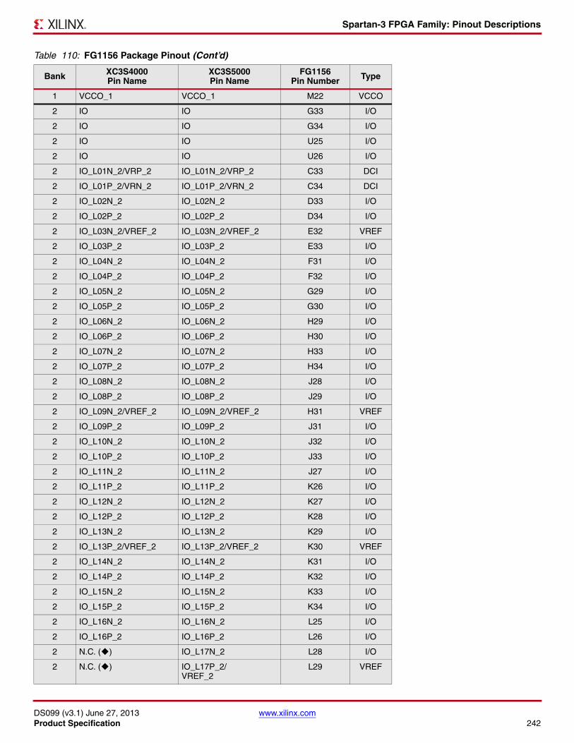
Spartan-3 FPGA Family: Pinout Descriptions
DS099 (v3.1) June 27, 2013 www.xilinx.comProduct Specification 242
1 VCCO_1 VCCO_1 M22 VCCO
2 IO IO G33 I/O
2 IO IO G34 I/O
2 IO IO U25 I/O
2 IO IO U26 I/O
2 IO_L01N_2/VRP_2 IO_L01N_2/VRP_2 C33 DCI
2 IO_L01P_2/VRN_2 IO_L01P_2/VRN_2 C34 DCI
2 IO_L02N_2 IO_L02N_2 D33 I/O
2 IO_L02P_2 IO_L02P_2 D34 I/O
2 IO_L03N_2/VREF_2 IO_L03N_2/VREF_2 E32 VREF
2 IO_L03P_2 IO_L03P_2 E33 I/O
2 IO_L04N_2 IO_L04N_2 F31 I/O
2 IO_L04P_2 IO_L04P_2 F32 I/O
2 IO_L05N_2 IO_L05N_2 G29 I/O
2 IO_L05P_2 IO_L05P_2 G30 I/O
2 IO_L06N_2 IO_L06N_2 H29 I/O
2 IO_L06P_2 IO_L06P_2 H30 I/O
2 IO_L07N_2 IO_L07N_2 H33 I/O
2 IO_L07P_2 IO_L07P_2 H34 I/O
2 IO_L08N_2 IO_L08N_2 J28 I/O
2 IO_L08P_2 IO_L08P_2 J29 I/O
2 IO_L09N_2/VREF_2 IO_L09N_2/VREF_2 H31 VREF
2 IO_L09P_2 IO_L09P_2 J31 I/O
2 IO_L10N_2 IO_L10N_2 J32 I/O
2 IO_L10P_2 IO_L10P_2 J33 I/O
2 IO_L11N_2 IO_L11N_2 J27 I/O
2 IO_L11P_2 IO_L11P_2 K26 I/O
2 IO_L12N_2 IO_L12N_2 K27 I/O
2 IO_L12P_2 IO_L12P_2 K28 I/O
2 IO_L13N_2 IO_L13N_2 K29 I/O
2 IO_L13P_2/VREF_2 IO_L13P_2/VREF_2 K30 VREF
2 IO_L14N_2 IO_L14N_2 K31 I/O
2 IO_L14P_2 IO_L14P_2 K32 I/O
2 IO_L15N_2 IO_L15N_2 K33 I/O
2 IO_L15P_2 IO_L15P_2 K34 I/O
2 IO_L16N_2 IO_L16N_2 L25 I/O
2 IO_L16P_2 IO_L16P_2 L26 I/O
2 N.C. () IO_L17N_2 L28 I/O
2 N.C. () IO_L17P_2/VREF_2
L29 VREF
Table 110: FG1156 Package Pinout (Cont’d)
Bank XC3S4000Pin Name
XC3S5000Pin Name
FG1156Pin Number Type

Spartan-3 FPGA Family: Pinout Descriptions
DS099 (v3.1) June 27, 2013 www.xilinx.comProduct Specification 243
2 IO_L19N_2 IO_L19N_2 M29 I/O
2 IO_L19P_2 IO_L19P_2 M30 I/O
2 IO_L20N_2 IO_L20N_2 M31 I/O
2 IO_L20P_2 IO_L20P_2 M32 I/O
2 IO_L21N_2 IO_L21N_2 M26 I/O
2 IO_L21P_2 IO_L21P_2 N25 I/O
2 IO_L22N_2 IO_L22N_2 N27 I/O
2 IO_L22P_2 IO_L22P_2 N28 I/O
2 IO_L23N_2/VREF_2 IO_L23N_2VREF_2 N31 VREF
2 IO_L23P_2 IO_L23P_2 N32 I/O
2 IO_L24N_2 IO_L24N_2 N24 I/O
2 IO_L24P_2 IO_L24P_2 P24 I/O
2 IO_L26N_2 IO_L26N_2 P29 I/O
2 IO_L26P_2 IO_L26P_2 P30 I/O
2 IO_L27N_2 IO_L27N_2 P31 I/O
2 IO_L27P_2 IO_L27P_2 P32 I/O
2 IO_L28N_2 IO_L28N_2 P33 I/O
2 IO_L28P_2 IO_L28P_2 P34 I/O
2 IO_L29N_2 IO_L29N_2 R24 I/O
2 IO_L29P_2 IO_L29P_2 R25 I/O
2 IO_L30N_2 IO_L30N_2 R28 I/O
2 IO_L30P_2 IO_L30P_2 R29 I/O
2 IO_L31N_2 IO_L31N_2 R31 I/O
2 IO_L31P_2 IO_L31P_2 R32 I/O
2 IO_L32N_2 IO_L32N_2 R33 I/O
2 IO_L32P_2 IO_L32P_2 R34 I/O
2 IO_L33N_2 IO_L33N_2 R26 I/O
2 IO_L33P_2 IO_L33P_2 T25 I/O
2 IO_L34N_2/VREF_2 IO_L34N_2/VREF_2 T28 VREF
2 IO_L34P_2 IO_L34P_2 T29 I/O
2 IO_L35N_2 IO_L35N_2 T32 I/O
2 IO_L35P_2 IO_L35P_2 T33 I/O
2 IO_L37N_2 IO_L37N_2 U27 I/O
2 IO_L37P_2 IO_L37P_2 U28 I/O
2 IO_L38N_2 IO_L38N_2 U29 I/O
2 IO_L38P_2 IO_L38P_2 U30 I/O
2 IO_L39N_2 IO_L39N_2 U31 I/O
2 IO_L39P_2 IO_L39P_2 U32 I/O
2 IO_L40N_2 IO_L40N_2 U33 I/O
2 IO_L40P_2/VREF_2 IO_L40P_2/VREF_2 U34 VREF
Table 110: FG1156 Package Pinout (Cont’d)
Bank XC3S4000Pin Name
XC3S5000Pin Name
FG1156Pin Number Type
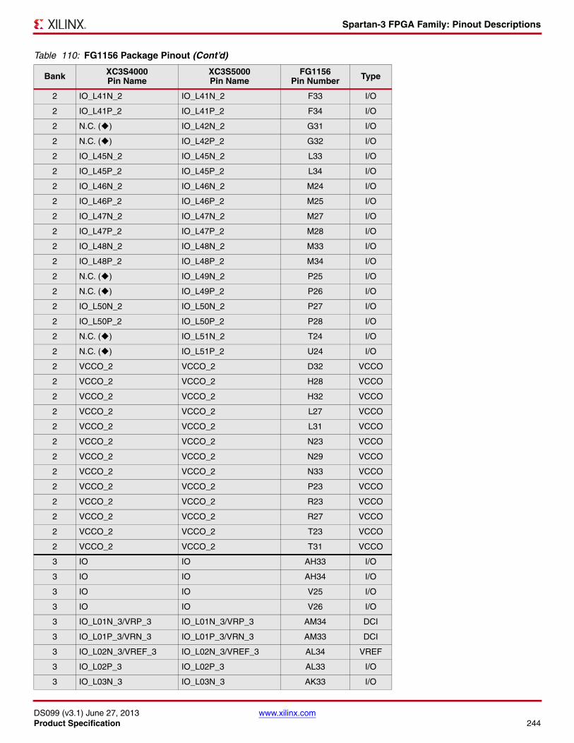
Spartan-3 FPGA Family: Pinout Descriptions
DS099 (v3.1) June 27, 2013 www.xilinx.comProduct Specification 244
2 IO_L41N_2 IO_L41N_2 F33 I/O
2 IO_L41P_2 IO_L41P_2 F34 I/O
2 N.C. () IO_L42N_2 G31 I/O
2 N.C. () IO_L42P_2 G32 I/O
2 IO_L45N_2 IO_L45N_2 L33 I/O
2 IO_L45P_2 IO_L45P_2 L34 I/O
2 IO_L46N_2 IO_L46N_2 M24 I/O
2 IO_L46P_2 IO_L46P_2 M25 I/O
2 IO_L47N_2 IO_L47N_2 M27 I/O
2 IO_L47P_2 IO_L47P_2 M28 I/O
2 IO_L48N_2 IO_L48N_2 M33 I/O
2 IO_L48P_2 IO_L48P_2 M34 I/O
2 N.C. () IO_L49N_2 P25 I/O
2 N.C. () IO_L49P_2 P26 I/O
2 IO_L50N_2 IO_L50N_2 P27 I/O
2 IO_L50P_2 IO_L50P_2 P28 I/O
2 N.C. () IO_L51N_2 T24 I/O
2 N.C. () IO_L51P_2 U24 I/O
2 VCCO_2 VCCO_2 D32 VCCO
2 VCCO_2 VCCO_2 H28 VCCO
2 VCCO_2 VCCO_2 H32 VCCO
2 VCCO_2 VCCO_2 L27 VCCO
2 VCCO_2 VCCO_2 L31 VCCO
2 VCCO_2 VCCO_2 N23 VCCO
2 VCCO_2 VCCO_2 N29 VCCO
2 VCCO_2 VCCO_2 N33 VCCO
2 VCCO_2 VCCO_2 P23 VCCO
2 VCCO_2 VCCO_2 R23 VCCO
2 VCCO_2 VCCO_2 R27 VCCO
2 VCCO_2 VCCO_2 T23 VCCO
2 VCCO_2 VCCO_2 T31 VCCO
3 IO IO AH33 I/O
3 IO IO AH34 I/O
3 IO IO V25 I/O
3 IO IO V26 I/O
3 IO_L01N_3/VRP_3 IO_L01N_3/VRP_3 AM34 DCI
3 IO_L01P_3/VRN_3 IO_L01P_3/VRN_3 AM33 DCI
3 IO_L02N_3/VREF_3 IO_L02N_3/VREF_3 AL34 VREF
3 IO_L02P_3 IO_L02P_3 AL33 I/O
3 IO_L03N_3 IO_L03N_3 AK33 I/O
Table 110: FG1156 Package Pinout (Cont’d)
Bank XC3S4000Pin Name
XC3S5000Pin Name
FG1156Pin Number Type
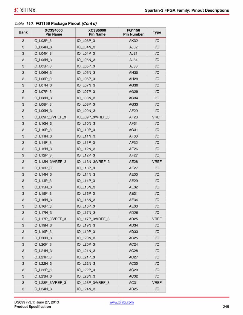
Spartan-3 FPGA Family: Pinout Descriptions
DS099 (v3.1) June 27, 2013 www.xilinx.comProduct Specification 245
3 IO_L03P_3 IO_L03P_3 AK32 I/O
3 IO_L04N_3 IO_L04N_3 AJ32 I/O
3 IO_L04P_3 IO_L04P_3 AJ31 I/O
3 IO_L05N_3 IO_L05N_3 AJ34 I/O
3 IO_L05P_3 IO_L05P_3 AJ33 I/O
3 IO_L06N_3 IO_L06N_3 AH30 I/O
3 IO_L06P_3 IO_L06P_3 AH29 I/O
3 IO_L07N_3 IO_L07N_3 AG30 I/O
3 IO_L07P_3 IO_L07P_3 AG29 I/O
3 IO_L08N_3 IO_L08N_3 AG34 I/O
3 IO_L08P_3 IO_L08P_3 AG33 I/O
3 IO_L09N_3 IO_L09N_3 AF29 I/O
3 IO_L09P_3/VREF_3 IO_L09P_3/VREF_3 AF28 VREF
3 IO_L10N_3 IO_L10N_3 AF31 I/O
3 IO_L10P_3 IO_L10P_3 AG31 I/O
3 IO_L11N_3 IO_L11N_3 AF33 I/O
3 IO_L11P_3 IO_L11P_3 AF32 I/O
3 IO_L12N_3 IO_L12N_3 AE26 I/O
3 IO_L12P_3 IO_L12P_3 AF27 I/O
3 IO_L13N_3/VREF_3 IO_L13N_3/VREF_3 AE28 VREF
3 IO_L13P_3 IO_L13P_3 AE27 I/O
3 IO_L14N_3 IO_L14N_3 AE30 I/O
3 IO_L14P_3 IO_L14P_3 AE29 I/O
3 IO_L15N_3 IO_L15N_3 AE32 I/O
3 IO_L15P_3 IO_L15P_3 AE31 I/O
3 IO_L16N_3 IO_L16N_3 AE34 I/O
3 IO_L16P_3 IO_L16P_3 AE33 I/O
3 IO_L17N_3 IO_L17N_3 AD26 I/O
3 IO_L17P_3/VREF_3 IO_L17P_3/VREF_3 AD25 VREF
3 IO_L19N_3 IO_L19N_3 AD34 I/O
3 IO_L19P_3 IO_L19P_3 AD33 I/O
3 IO_L20N_3 IO_L20N_3 AC25 I/O
3 IO_L20P_3 IO_L20P_3 AC24 I/O
3 IO_L21N_3 IO_L21N_3 AC28 I/O
3 IO_L21P_3 IO_L21P_3 AC27 I/O
3 IO_L22N_3 IO_L22N_3 AC30 I/O
3 IO_L22P_3 IO_L22P_3 AC29 I/O
3 IO_L23N_3 IO_L23N_3 AC32 I/O
3 IO_L23P_3/VREF_3 IO_L23P_3/VREF_3 AC31 VREF
3 IO_L24N_3 IO_L24N_3 AB25 I/O
Table 110: FG1156 Package Pinout (Cont’d)
Bank XC3S4000Pin Name
XC3S5000Pin Name
FG1156Pin Number Type
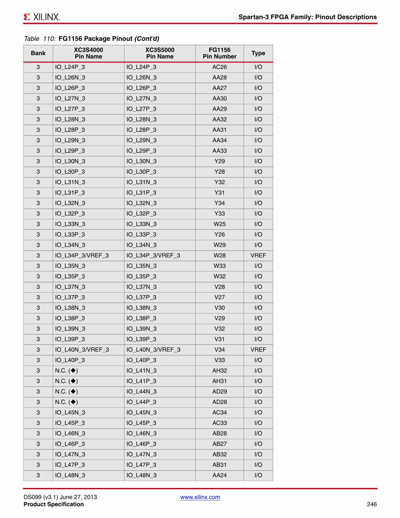
Spartan-3 FPGA Family: Pinout Descriptions
DS099 (v3.1) June 27, 2013 www.xilinx.comProduct Specification 246
3 IO_L24P_3 IO_L24P_3 AC26 I/O
3 IO_L26N_3 IO_L26N_3 AA28 I/O
3 IO_L26P_3 IO_L26P_3 AA27 I/O
3 IO_L27N_3 IO_L27N_3 AA30 I/O
3 IO_L27P_3 IO_L27P_3 AA29 I/O
3 IO_L28N_3 IO_L28N_3 AA32 I/O
3 IO_L28P_3 IO_L28P_3 AA31 I/O
3 IO_L29N_3 IO_L29N_3 AA34 I/O
3 IO_L29P_3 IO_L29P_3 AA33 I/O
3 IO_L30N_3 IO_L30N_3 Y29 I/O
3 IO_L30P_3 IO_L30P_3 Y28 I/O
3 IO_L31N_3 IO_L31N_3 Y32 I/O
3 IO_L31P_3 IO_L31P_3 Y31 I/O
3 IO_L32N_3 IO_L32N_3 Y34 I/O
3 IO_L32P_3 IO_L32P_3 Y33 I/O
3 IO_L33N_3 IO_L33N_3 W25 I/O
3 IO_L33P_3 IO_L33P_3 Y26 I/O
3 IO_L34N_3 IO_L34N_3 W29 I/O
3 IO_L34P_3/VREF_3 IO_L34P_3/VREF_3 W28 VREF
3 IO_L35N_3 IO_L35N_3 W33 I/O
3 IO_L35P_3 IO_L35P_3 W32 I/O
3 IO_L37N_3 IO_L37N_3 V28 I/O
3 IO_L37P_3 IO_L37P_3 V27 I/O
3 IO_L38N_3 IO_L38N_3 V30 I/O
3 IO_L38P_3 IO_L38P_3 V29 I/O
3 IO_L39N_3 IO_L39N_3 V32 I/O
3 IO_L39P_3 IO_L39P_3 V31 I/O
3 IO_L40N_3/VREF_3 IO_L40N_3/VREF_3 V34 VREF
3 IO_L40P_3 IO_L40P_3 V33 I/O
3 N.C. () IO_L41N_3 AH32 I/O
3 N.C. () IO_L41P_3 AH31 I/O
3 N.C. () IO_L44N_3 AD29 I/O
3 N.C. () IO_L44P_3 AD28 I/O
3 IO_L45N_3 IO_L45N_3 AC34 I/O
3 IO_L45P_3 IO_L45P_3 AC33 I/O
3 IO_L46N_3 IO_L46N_3 AB28 I/O
3 IO_L46P_3 IO_L46P_3 AB27 I/O
3 IO_L47N_3 IO_L47N_3 AB32 I/O
3 IO_L47P_3 IO_L47P_3 AB31 I/O
3 IO_L48N_3 IO_L48N_3 AA24 I/O
Table 110: FG1156 Package Pinout (Cont’d)
Bank XC3S4000Pin Name
XC3S5000Pin Name
FG1156Pin Number Type
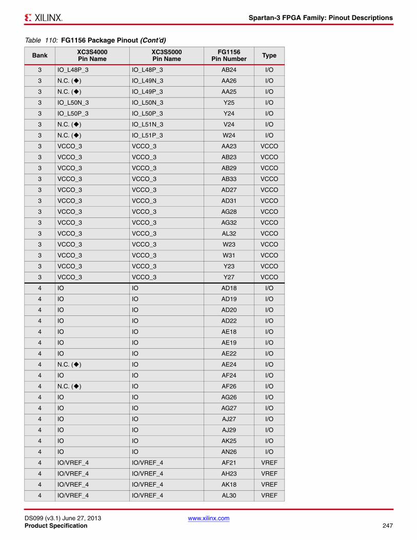
Spartan-3 FPGA Family: Pinout Descriptions
DS099 (v3.1) June 27, 2013 www.xilinx.comProduct Specification 247
3 IO_L48P_3 IO_L48P_3 AB24 I/O
3 N.C. () IO_L49N_3 AA26 I/O
3 N.C. () IO_L49P_3 AA25 I/O
3 IO_L50N_3 IO_L50N_3 Y25 I/O
3 IO_L50P_3 IO_L50P_3 Y24 I/O
3 N.C. () IO_L51N_3 V24 I/O
3 N.C. () IO_L51P_3 W24 I/O
3 VCCO_3 VCCO_3 AA23 VCCO
3 VCCO_3 VCCO_3 AB23 VCCO
3 VCCO_3 VCCO_3 AB29 VCCO
3 VCCO_3 VCCO_3 AB33 VCCO
3 VCCO_3 VCCO_3 AD27 VCCO
3 VCCO_3 VCCO_3 AD31 VCCO
3 VCCO_3 VCCO_3 AG28 VCCO
3 VCCO_3 VCCO_3 AG32 VCCO
3 VCCO_3 VCCO_3 AL32 VCCO
3 VCCO_3 VCCO_3 W23 VCCO
3 VCCO_3 VCCO_3 W31 VCCO
3 VCCO_3 VCCO_3 Y23 VCCO
3 VCCO_3 VCCO_3 Y27 VCCO
4 IO IO AD18 I/O
4 IO IO AD19 I/O
4 IO IO AD20 I/O
4 IO IO AD22 I/O
4 IO IO AE18 I/O
4 IO IO AE19 I/O
4 IO IO AE22 I/O
4 N.C. () IO AE24 I/O
4 IO IO AF24 I/O
4 N.C. () IO AF26 I/O
4 IO IO AG26 I/O
4 IO IO AG27 I/O
4 IO IO AJ27 I/O
4 IO IO AJ29 I/O
4 IO IO AK25 I/O
4 IO IO AN26 I/O
4 IO/VREF_4 IO/VREF_4 AF21 VREF
4 IO/VREF_4 IO/VREF_4 AH23 VREF
4 IO/VREF_4 IO/VREF_4 AK18 VREF
4 IO/VREF_4 IO/VREF_4 AL30 VREF
Table 110: FG1156 Package Pinout (Cont’d)
Bank XC3S4000Pin Name
XC3S5000Pin Name
FG1156Pin Number Type
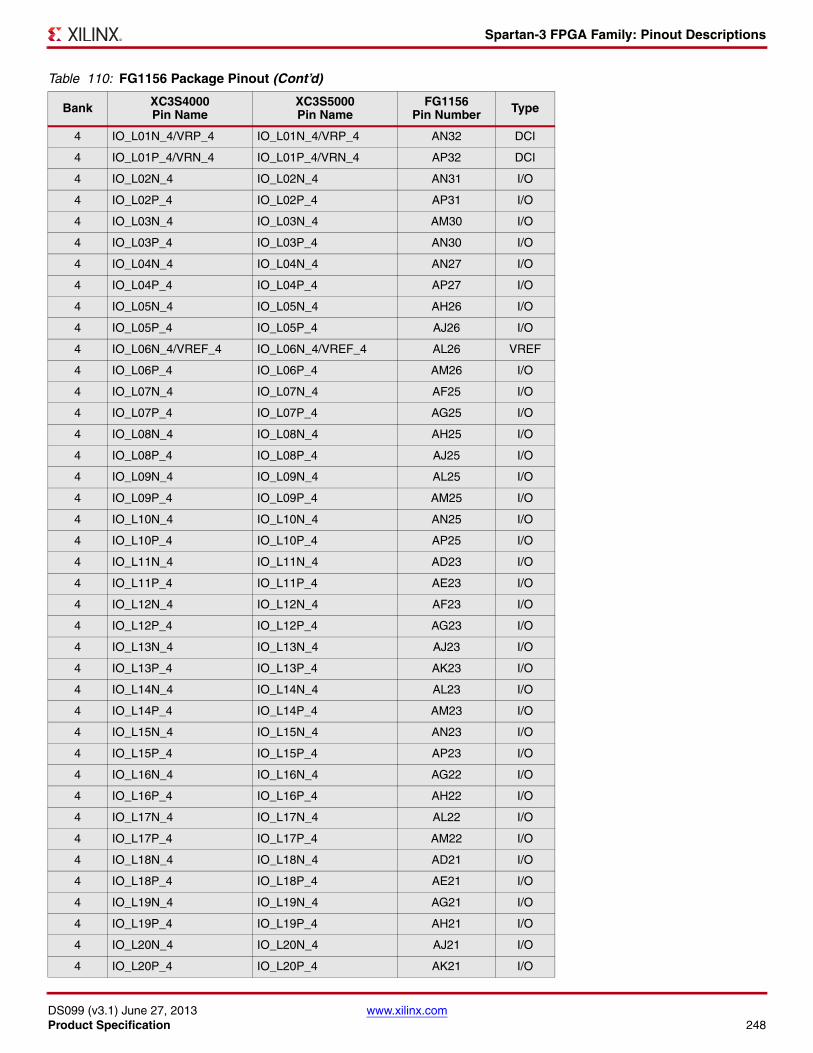
Spartan-3 FPGA Family: Pinout Descriptions
DS099 (v3.1) June 27, 2013 www.xilinx.comProduct Specification 248
4 IO_L01N_4/VRP_4 IO_L01N_4/VRP_4 AN32 DCI
4 IO_L01P_4/VRN_4 IO_L01P_4/VRN_4 AP32 DCI
4 IO_L02N_4 IO_L02N_4 AN31 I/O
4 IO_L02P_4 IO_L02P_4 AP31 I/O
4 IO_L03N_4 IO_L03N_4 AM30 I/O
4 IO_L03P_4 IO_L03P_4 AN30 I/O
4 IO_L04N_4 IO_L04N_4 AN27 I/O
4 IO_L04P_4 IO_L04P_4 AP27 I/O
4 IO_L05N_4 IO_L05N_4 AH26 I/O
4 IO_L05P_4 IO_L05P_4 AJ26 I/O
4 IO_L06N_4/VREF_4 IO_L06N_4/VREF_4 AL26 VREF
4 IO_L06P_4 IO_L06P_4 AM26 I/O
4 IO_L07N_4 IO_L07N_4 AF25 I/O
4 IO_L07P_4 IO_L07P_4 AG25 I/O
4 IO_L08N_4 IO_L08N_4 AH25 I/O
4 IO_L08P_4 IO_L08P_4 AJ25 I/O
4 IO_L09N_4 IO_L09N_4 AL25 I/O
4 IO_L09P_4 IO_L09P_4 AM25 I/O
4 IO_L10N_4 IO_L10N_4 AN25 I/O
4 IO_L10P_4 IO_L10P_4 AP25 I/O
4 IO_L11N_4 IO_L11N_4 AD23 I/O
4 IO_L11P_4 IO_L11P_4 AE23 I/O
4 IO_L12N_4 IO_L12N_4 AF23 I/O
4 IO_L12P_4 IO_L12P_4 AG23 I/O
4 IO_L13N_4 IO_L13N_4 AJ23 I/O
4 IO_L13P_4 IO_L13P_4 AK23 I/O
4 IO_L14N_4 IO_L14N_4 AL23 I/O
4 IO_L14P_4 IO_L14P_4 AM23 I/O
4 IO_L15N_4 IO_L15N_4 AN23 I/O
4 IO_L15P_4 IO_L15P_4 AP23 I/O
4 IO_L16N_4 IO_L16N_4 AG22 I/O
4 IO_L16P_4 IO_L16P_4 AH22 I/O
4 IO_L17N_4 IO_L17N_4 AL22 I/O
4 IO_L17P_4 IO_L17P_4 AM22 I/O
4 IO_L18N_4 IO_L18N_4 AD21 I/O
4 IO_L18P_4 IO_L18P_4 AE21 I/O
4 IO_L19N_4 IO_L19N_4 AG21 I/O
4 IO_L19P_4 IO_L19P_4 AH21 I/O
4 IO_L20N_4 IO_L20N_4 AJ21 I/O
4 IO_L20P_4 IO_L20P_4 AK21 I/O
Table 110: FG1156 Package Pinout (Cont’d)
Bank XC3S4000Pin Name
XC3S5000Pin Name
FG1156Pin Number Type
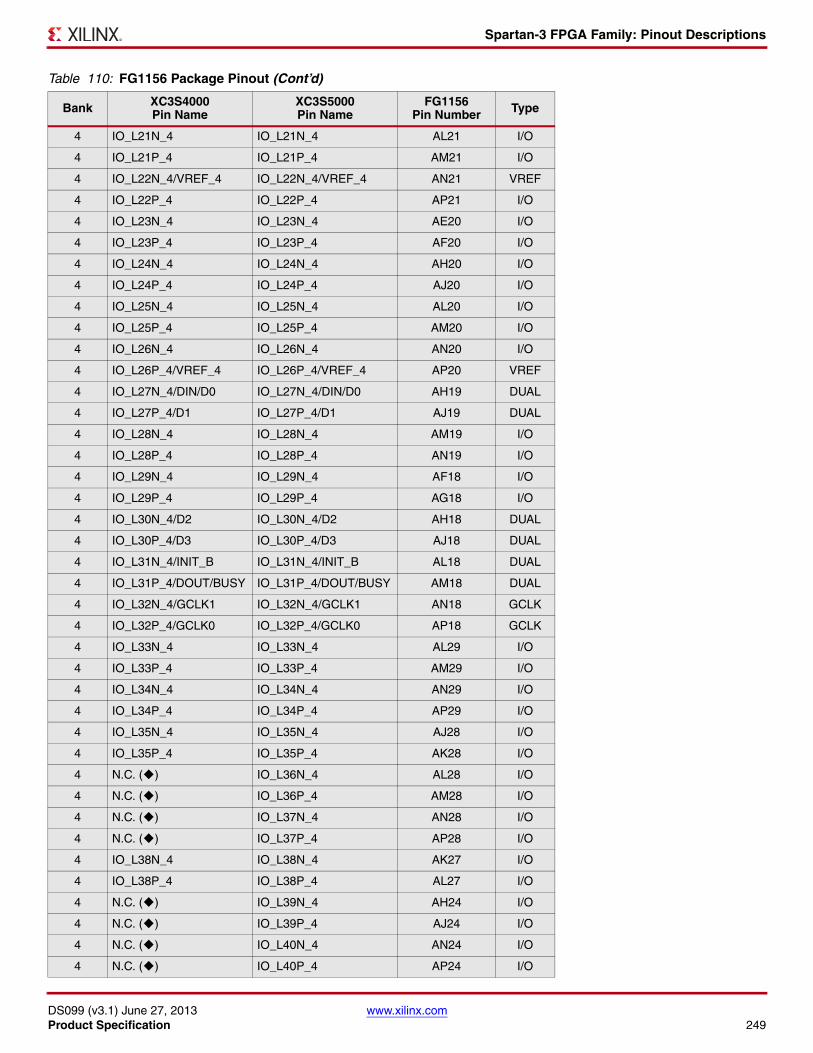
Spartan-3 FPGA Family: Pinout Descriptions
DS099 (v3.1) June 27, 2013 www.xilinx.comProduct Specification 249
4 IO_L21N_4 IO_L21N_4 AL21 I/O
4 IO_L21P_4 IO_L21P_4 AM21 I/O
4 IO_L22N_4/VREF_4 IO_L22N_4/VREF_4 AN21 VREF
4 IO_L22P_4 IO_L22P_4 AP21 I/O
4 IO_L23N_4 IO_L23N_4 AE20 I/O
4 IO_L23P_4 IO_L23P_4 AF20 I/O
4 IO_L24N_4 IO_L24N_4 AH20 I/O
4 IO_L24P_4 IO_L24P_4 AJ20 I/O
4 IO_L25N_4 IO_L25N_4 AL20 I/O
4 IO_L25P_4 IO_L25P_4 AM20 I/O
4 IO_L26N_4 IO_L26N_4 AN20 I/O
4 IO_L26P_4/VREF_4 IO_L26P_4/VREF_4 AP20 VREF
4 IO_L27N_4/DIN/D0 IO_L27N_4/DIN/D0 AH19 DUAL
4 IO_L27P_4/D1 IO_L27P_4/D1 AJ19 DUAL
4 IO_L28N_4 IO_L28N_4 AM19 I/O
4 IO_L28P_4 IO_L28P_4 AN19 I/O
4 IO_L29N_4 IO_L29N_4 AF18 I/O
4 IO_L29P_4 IO_L29P_4 AG18 I/O
4 IO_L30N_4/D2 IO_L30N_4/D2 AH18 DUAL
4 IO_L30P_4/D3 IO_L30P_4/D3 AJ18 DUAL
4 IO_L31N_4/INIT_B IO_L31N_4/INIT_B AL18 DUAL
4 IO_L31P_4/DOUT/BUSY IO_L31P_4/DOUT/BUSY AM18 DUAL
4 IO_L32N_4/GCLK1 IO_L32N_4/GCLK1 AN18 GCLK
4 IO_L32P_4/GCLK0 IO_L32P_4/GCLK0 AP18 GCLK
4 IO_L33N_4 IO_L33N_4 AL29 I/O
4 IO_L33P_4 IO_L33P_4 AM29 I/O
4 IO_L34N_4 IO_L34N_4 AN29 I/O
4 IO_L34P_4 IO_L34P_4 AP29 I/O
4 IO_L35N_4 IO_L35N_4 AJ28 I/O
4 IO_L35P_4 IO_L35P_4 AK28 I/O
4 N.C. () IO_L36N_4 AL28 I/O
4 N.C. () IO_L36P_4 AM28 I/O
4 N.C. () IO_L37N_4 AN28 I/O
4 N.C. () IO_L37P_4 AP28 I/O
4 IO_L38N_4 IO_L38N_4 AK27 I/O
4 IO_L38P_4 IO_L38P_4 AL27 I/O
4 N.C. () IO_L39N_4 AH24 I/O
4 N.C. () IO_L39P_4 AJ24 I/O
4 N.C. () IO_L40N_4 AN24 I/O
4 N.C. () IO_L40P_4 AP24 I/O
Table 110: FG1156 Package Pinout (Cont’d)
Bank XC3S4000Pin Name
XC3S5000Pin Name
FG1156Pin Number Type
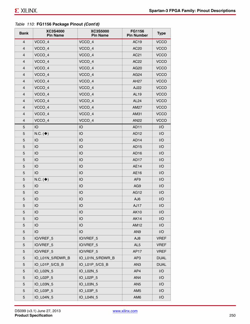
Spartan-3 FPGA Family: Pinout Descriptions
DS099 (v3.1) June 27, 2013 www.xilinx.comProduct Specification 250
4 VCCO_4 VCCO_4 AC19 VCCO
4 VCCO_4 VCCO_4 AC20 VCCO
4 VCCO_4 VCCO_4 AC21 VCCO
4 VCCO_4 VCCO_4 AC22 VCCO
4 VCCO_4 VCCO_4 AG20 VCCO
4 VCCO_4 VCCO_4 AG24 VCCO
4 VCCO_4 VCCO_4 AH27 VCCO
4 VCCO_4 VCCO_4 AJ22 VCCO
4 VCCO_4 VCCO_4 AL19 VCCO
4 VCCO_4 VCCO_4 AL24 VCCO
4 VCCO_4 VCCO_4 AM27 VCCO
4 VCCO_4 VCCO_4 AM31 VCCO
4 VCCO_4 VCCO_4 AN22 VCCO
5 IO IO AD11 I/O
5 N.C. () IO AD12 I/O
5 IO IO AD14 I/O
5 IO IO AD15 I/O
5 IO IO AD16 I/O
5 IO IO AD17 I/O
5 IO IO AE14 I/O
5 IO IO AE16 I/O
5 N.C. () IO AF9 I/O
5 IO IO AG9 I/O
5 IO IO AG12 I/O
5 IO IO AJ6 I/O
5 IO IO AJ17 I/O
5 IO IO AK10 I/O
5 IO IO AK14 I/O
5 IO IO AM12 I/O
5 IO IO AN9 I/O
5 IO/VREF_5 IO/VREF_5 AJ8 VREF
5 IO/VREF_5 IO/VREF_5 AL5 VREF
5 IO/VREF_5 IO/VREF_5 AP17 VREF
5 IO_L01N_5/RDWR_B IO_L01N_5/RDWR_B AP3 DUAL
5 IO_L01P_5/CS_B IO_L01P_5/CS_B AN3 DUAL
5 IO_L02N_5 IO_L02N_5 AP4 I/O
5 IO_L02P_5 IO_L02P_5 AN4 I/O
5 IO_L03N_5 IO_L03N_5 AN5 I/O
5 IO_L03P_5 IO_L03P_5 AM5 I/O
5 IO_L04N_5 IO_L04N_5 AM6 I/O
Table 110: FG1156 Package Pinout (Cont’d)
Bank XC3S4000Pin Name
XC3S5000Pin Name
FG1156Pin Number Type
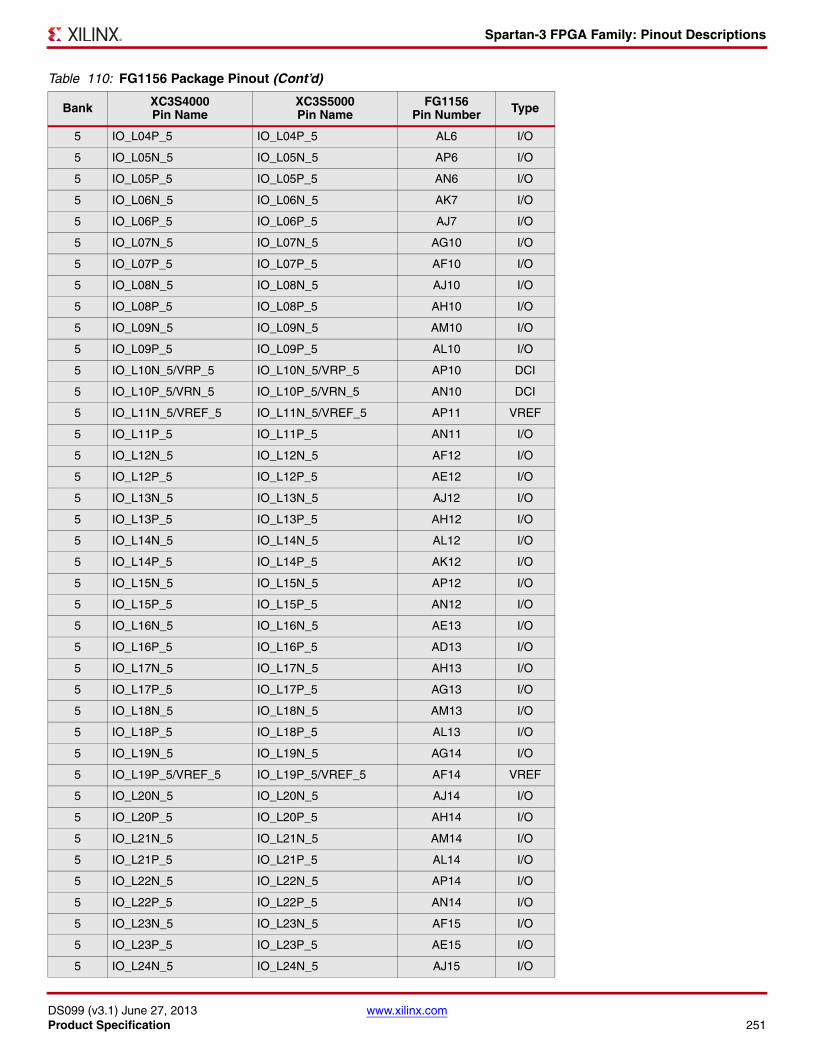
Spartan-3 FPGA Family: Pinout Descriptions
DS099 (v3.1) June 27, 2013 www.xilinx.comProduct Specification 251
5 IO_L04P_5 IO_L04P_5 AL6 I/O
5 IO_L05N_5 IO_L05N_5 AP6 I/O
5 IO_L05P_5 IO_L05P_5 AN6 I/O
5 IO_L06N_5 IO_L06N_5 AK7 I/O
5 IO_L06P_5 IO_L06P_5 AJ7 I/O
5 IO_L07N_5 IO_L07N_5 AG10 I/O
5 IO_L07P_5 IO_L07P_5 AF10 I/O
5 IO_L08N_5 IO_L08N_5 AJ10 I/O
5 IO_L08P_5 IO_L08P_5 AH10 I/O
5 IO_L09N_5 IO_L09N_5 AM10 I/O
5 IO_L09P_5 IO_L09P_5 AL10 I/O
5 IO_L10N_5/VRP_5 IO_L10N_5/VRP_5 AP10 DCI
5 IO_L10P_5/VRN_5 IO_L10P_5/VRN_5 AN10 DCI
5 IO_L11N_5/VREF_5 IO_L11N_5/VREF_5 AP11 VREF
5 IO_L11P_5 IO_L11P_5 AN11 I/O
5 IO_L12N_5 IO_L12N_5 AF12 I/O
5 IO_L12P_5 IO_L12P_5 AE12 I/O
5 IO_L13N_5 IO_L13N_5 AJ12 I/O
5 IO_L13P_5 IO_L13P_5 AH12 I/O
5 IO_L14N_5 IO_L14N_5 AL12 I/O
5 IO_L14P_5 IO_L14P_5 AK12 I/O
5 IO_L15N_5 IO_L15N_5 AP12 I/O
5 IO_L15P_5 IO_L15P_5 AN12 I/O
5 IO_L16N_5 IO_L16N_5 AE13 I/O
5 IO_L16P_5 IO_L16P_5 AD13 I/O
5 IO_L17N_5 IO_L17N_5 AH13 I/O
5 IO_L17P_5 IO_L17P_5 AG13 I/O
5 IO_L18N_5 IO_L18N_5 AM13 I/O
5 IO_L18P_5 IO_L18P_5 AL13 I/O
5 IO_L19N_5 IO_L19N_5 AG14 I/O
5 IO_L19P_5/VREF_5 IO_L19P_5/VREF_5 AF14 VREF
5 IO_L20N_5 IO_L20N_5 AJ14 I/O
5 IO_L20P_5 IO_L20P_5 AH14 I/O
5 IO_L21N_5 IO_L21N_5 AM14 I/O
5 IO_L21P_5 IO_L21P_5 AL14 I/O
5 IO_L22N_5 IO_L22N_5 AP14 I/O
5 IO_L22P_5 IO_L22P_5 AN14 I/O
5 IO_L23N_5 IO_L23N_5 AF15 I/O
5 IO_L23P_5 IO_L23P_5 AE15 I/O
5 IO_L24N_5 IO_L24N_5 AJ15 I/O
Table 110: FG1156 Package Pinout (Cont’d)
Bank XC3S4000Pin Name
XC3S5000Pin Name
FG1156Pin Number Type
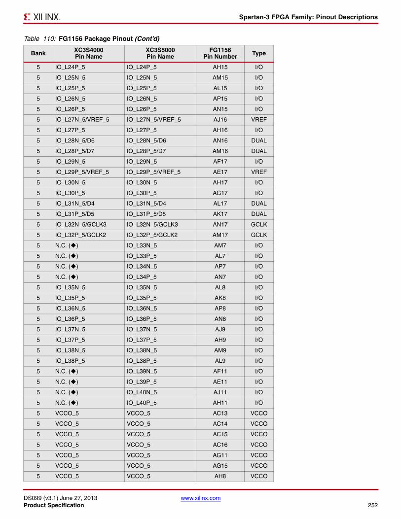
Spartan-3 FPGA Family: Pinout Descriptions
DS099 (v3.1) June 27, 2013 www.xilinx.comProduct Specification 252
5 IO_L24P_5 IO_L24P_5 AH15 I/O
5 IO_L25N_5 IO_L25N_5 AM15 I/O
5 IO_L25P_5 IO_L25P_5 AL15 I/O
5 IO_L26N_5 IO_L26N_5 AP15 I/O
5 IO_L26P_5 IO_L26P_5 AN15 I/O
5 IO_L27N_5/VREF_5 IO_L27N_5/VREF_5 AJ16 VREF
5 IO_L27P_5 IO_L27P_5 AH16 I/O
5 IO_L28N_5/D6 IO_L28N_5/D6 AN16 DUAL
5 IO_L28P_5/D7 IO_L28P_5/D7 AM16 DUAL
5 IO_L29N_5 IO_L29N_5 AF17 I/O
5 IO_L29P_5/VREF_5 IO_L29P_5/VREF_5 AE17 VREF
5 IO_L30N_5 IO_L30N_5 AH17 I/O
5 IO_L30P_5 IO_L30P_5 AG17 I/O
5 IO_L31N_5/D4 IO_L31N_5/D4 AL17 DUAL
5 IO_L31P_5/D5 IO_L31P_5/D5 AK17 DUAL
5 IO_L32N_5/GCLK3 IO_L32N_5/GCLK3 AN17 GCLK
5 IO_L32P_5/GCLK2 IO_L32P_5/GCLK2 AM17 GCLK
5 N.C. () IO_L33N_5 AM7 I/O
5 N.C. () IO_L33P_5 AL7 I/O
5 N.C. () IO_L34N_5 AP7 I/O
5 N.C. () IO_L34P_5 AN7 I/O
5 IO_L35N_5 IO_L35N_5 AL8 I/O
5 IO_L35P_5 IO_L35P_5 AK8 I/O
5 IO_L36N_5 IO_L36N_5 AP8 I/O
5 IO_L36P_5 IO_L36P_5 AN8 I/O
5 IO_L37N_5 IO_L37N_5 AJ9 I/O
5 IO_L37P_5 IO_L37P_5 AH9 I/O
5 IO_L38N_5 IO_L38N_5 AM9 I/O
5 IO_L38P_5 IO_L38P_5 AL9 I/O
5 N.C. () IO_L39N_5 AF11 I/O
5 N.C. () IO_L39P_5 AE11 I/O
5 N.C. () IO_L40N_5 AJ11 I/O
5 N.C. () IO_L40P_5 AH11 I/O
5 VCCO_5 VCCO_5 AC13 VCCO
5 VCCO_5 VCCO_5 AC14 VCCO
5 VCCO_5 VCCO_5 AC15 VCCO
5 VCCO_5 VCCO_5 AC16 VCCO
5 VCCO_5 VCCO_5 AG11 VCCO
5 VCCO_5 VCCO_5 AG15 VCCO
5 VCCO_5 VCCO_5 AH8 VCCO
Table 110: FG1156 Package Pinout (Cont’d)
Bank XC3S4000Pin Name
XC3S5000Pin Name
FG1156Pin Number Type
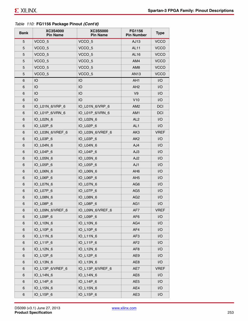
Spartan-3 FPGA Family: Pinout Descriptions
DS099 (v3.1) June 27, 2013 www.xilinx.comProduct Specification 253
5 VCCO_5 VCCO_5 AJ13 VCCO
5 VCCO_5 VCCO_5 AL11 VCCO
5 VCCO_5 VCCO_5 AL16 VCCO
5 VCCO_5 VCCO_5 AM4 VCCO
5 VCCO_5 VCCO_5 AM8 VCCO
5 VCCO_5 VCCO_5 AN13 VCCO
6 IO IO AH1 I/O
6 IO IO AH2 I/O
6 IO IO V9 I/O
6 IO IO V10 I/O
6 IO_L01N_6/VRP_6 IO_L01N_6/VRP_6 AM2 DCI
6 IO_L01P_6/VRN_6 IO_L01P_6/VRN_6 AM1 DCI
6 IO_L02N_6 IO_L02N_6 AL2 I/O
6 IO_L02P_6 IO_L02P_6 AL1 I/O
6 IO_L03N_6/VREF_6 IO_L03N_6/VREF_6 AK3 VREF
6 IO_L03P_6 IO_L03P_6 AK2 I/O
6 IO_L04N_6 IO_L04N_6 AJ4 I/O
6 IO_L04P_6 IO_L04P_6 AJ3 I/O
6 IO_L05N_6 IO_L05N_6 AJ2 I/O
6 IO_L05P_6 IO_L05P_6 AJ1 I/O
6 IO_L06N_6 IO_L06N_6 AH6 I/O
6 IO_L06P_6 IO_L06P_6 AH5 I/O
6 IO_L07N_6 IO_L07N_6 AG6 I/O
6 IO_L07P_6 IO_L07P_6 AG5 I/O
6 IO_L08N_6 IO_L08N_6 AG2 I/O
6 IO_L08P_6 IO_L08P_6 AG1 I/O
6 IO_L09N_6/VREF_6 IO_L09N_6/VREF_6 AF7 VREF
6 IO_L09P_6 IO_L09P_6 AF6 I/O
6 IO_L10N_6 IO_L10N_6 AG4 I/O
6 IO_L10P_6 IO_L10P_6 AF4 I/O
6 IO_L11N_6 IO_L11N_6 AF3 I/O
6 IO_L11P_6 IO_L11P_6 AF2 I/O
6 IO_L12N_6 IO_L12N_6 AF8 I/O
6 IO_L12P_6 IO_L12P_6 AE9 I/O
6 IO_L13N_6 IO_L13N_6 AE8 I/O
6 IO_L13P_6/VREF_6 IO_L13P_6/VREF_6 AE7 VREF
6 IO_L14N_6 IO_L14N_6 AE6 I/O
6 IO_L14P_6 IO_L14P_6 AE5 I/O
6 IO_L15N_6 IO_L15N_6 AE4 I/O
6 IO_L15P_6 IO_L15P_6 AE3 I/O
Table 110: FG1156 Package Pinout (Cont’d)
Bank XC3S4000Pin Name
XC3S5000Pin Name
FG1156Pin Number Type
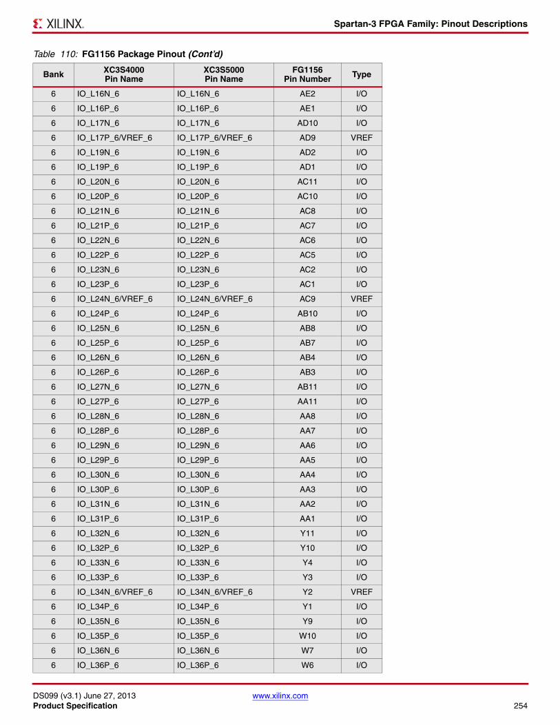
Spartan-3 FPGA Family: Pinout Descriptions
DS099 (v3.1) June 27, 2013 www.xilinx.comProduct Specification 254
6 IO_L16N_6 IO_L16N_6 AE2 I/O
6 IO_L16P_6 IO_L16P_6 AE1 I/O
6 IO_L17N_6 IO_L17N_6 AD10 I/O
6 IO_L17P_6/VREF_6 IO_L17P_6/VREF_6 AD9 VREF
6 IO_L19N_6 IO_L19N_6 AD2 I/O
6 IO_L19P_6 IO_L19P_6 AD1 I/O
6 IO_L20N_6 IO_L20N_6 AC11 I/O
6 IO_L20P_6 IO_L20P_6 AC10 I/O
6 IO_L21N_6 IO_L21N_6 AC8 I/O
6 IO_L21P_6 IO_L21P_6 AC7 I/O
6 IO_L22N_6 IO_L22N_6 AC6 I/O
6 IO_L22P_6 IO_L22P_6 AC5 I/O
6 IO_L23N_6 IO_L23N_6 AC2 I/O
6 IO_L23P_6 IO_L23P_6 AC1 I/O
6 IO_L24N_6/VREF_6 IO_L24N_6/VREF_6 AC9 VREF
6 IO_L24P_6 IO_L24P_6 AB10 I/O
6 IO_L25N_6 IO_L25N_6 AB8 I/O
6 IO_L25P_6 IO_L25P_6 AB7 I/O
6 IO_L26N_6 IO_L26N_6 AB4 I/O
6 IO_L26P_6 IO_L26P_6 AB3 I/O
6 IO_L27N_6 IO_L27N_6 AB11 I/O
6 IO_L27P_6 IO_L27P_6 AA11 I/O
6 IO_L28N_6 IO_L28N_6 AA8 I/O
6 IO_L28P_6 IO_L28P_6 AA7 I/O
6 IO_L29N_6 IO_L29N_6 AA6 I/O
6 IO_L29P_6 IO_L29P_6 AA5 I/O
6 IO_L30N_6 IO_L30N_6 AA4 I/O
6 IO_L30P_6 IO_L30P_6 AA3 I/O
6 IO_L31N_6 IO_L31N_6 AA2 I/O
6 IO_L31P_6 IO_L31P_6 AA1 I/O
6 IO_L32N_6 IO_L32N_6 Y11 I/O
6 IO_L32P_6 IO_L32P_6 Y10 I/O
6 IO_L33N_6 IO_L33N_6 Y4 I/O
6 IO_L33P_6 IO_L33P_6 Y3 I/O
6 IO_L34N_6/VREF_6 IO_L34N_6/VREF_6 Y2 VREF
6 IO_L34P_6 IO_L34P_6 Y1 I/O
6 IO_L35N_6 IO_L35N_6 Y9 I/O
6 IO_L35P_6 IO_L35P_6 W10 I/O
6 IO_L36N_6 IO_L36N_6 W7 I/O
6 IO_L36P_6 IO_L36P_6 W6 I/O
Table 110: FG1156 Package Pinout (Cont’d)
Bank XC3S4000Pin Name
XC3S5000Pin Name
FG1156Pin Number Type
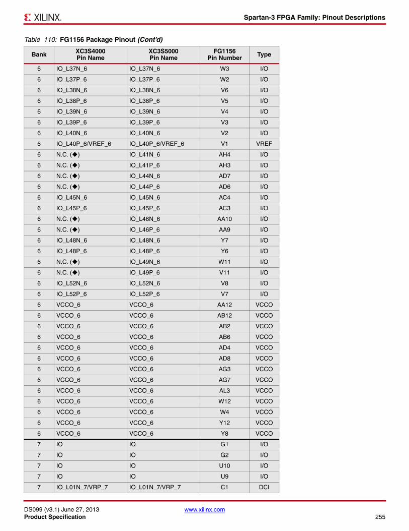
Spartan-3 FPGA Family: Pinout Descriptions
DS099 (v3.1) June 27, 2013 www.xilinx.comProduct Specification 255
6 IO_L37N_6 IO_L37N_6 W3 I/O
6 IO_L37P_6 IO_L37P_6 W2 I/O
6 IO_L38N_6 IO_L38N_6 V6 I/O
6 IO_L38P_6 IO_L38P_6 V5 I/O
6 IO_L39N_6 IO_L39N_6 V4 I/O
6 IO_L39P_6 IO_L39P_6 V3 I/O
6 IO_L40N_6 IO_L40N_6 V2 I/O
6 IO_L40P_6/VREF_6 IO_L40P_6/VREF_6 V1 VREF
6 N.C. () IO_L41N_6 AH4 I/O
6 N.C. () IO_L41P_6 AH3 I/O
6 N.C. () IO_L44N_6 AD7 I/O
6 N.C. () IO_L44P_6 AD6 I/O
6 IO_L45N_6 IO_L45N_6 AC4 I/O
6 IO_L45P_6 IO_L45P_6 AC3 I/O
6 N.C. () IO_L46N_6 AA10 I/O
6 N.C. () IO_L46P_6 AA9 I/O
6 IO_L48N_6 IO_L48N_6 Y7 I/O
6 IO_L48P_6 IO_L48P_6 Y6 I/O
6 N.C. () IO_L49N_6 W11 I/O
6 N.C. () IO_L49P_6 V11 I/O
6 IO_L52N_6 IO_L52N_6 V8 I/O
6 IO_L52P_6 IO_L52P_6 V7 I/O
6 VCCO_6 VCCO_6 AA12 VCCO
6 VCCO_6 VCCO_6 AB12 VCCO
6 VCCO_6 VCCO_6 AB2 VCCO
6 VCCO_6 VCCO_6 AB6 VCCO
6 VCCO_6 VCCO_6 AD4 VCCO
6 VCCO_6 VCCO_6 AD8 VCCO
6 VCCO_6 VCCO_6 AG3 VCCO
6 VCCO_6 VCCO_6 AG7 VCCO
6 VCCO_6 VCCO_6 AL3 VCCO
6 VCCO_6 VCCO_6 W12 VCCO
6 VCCO_6 VCCO_6 W4 VCCO
6 VCCO_6 VCCO_6 Y12 VCCO
6 VCCO_6 VCCO_6 Y8 VCCO
7 IO IO G1 I/O
7 IO IO G2 I/O
7 IO IO U10 I/O
7 IO IO U9 I/O
7 IO_L01N_7/VRP_7 IO_L01N_7/VRP_7 C1 DCI
Table 110: FG1156 Package Pinout (Cont’d)
Bank XC3S4000Pin Name
XC3S5000Pin Name
FG1156Pin Number Type
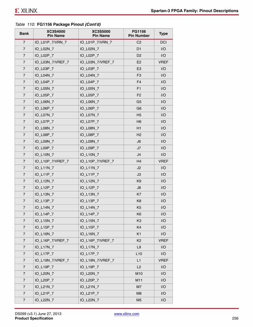
Spartan-3 FPGA Family: Pinout Descriptions
DS099 (v3.1) June 27, 2013 www.xilinx.comProduct Specification 256
7 IO_L01P_7/VRN_7 IO_L01P_7/VRN_7 C2 DCI
7 IO_L02N_7 IO_L02N_7 D1 I/O
7 IO_L02P_7 IO_L02P_7 D2 I/O
7 IO_L03N_7/VREF_7 IO_L03N_7/VREF_7 E2 VREF
7 IO_L03P_7 IO_L03P_7 E3 I/O
7 IO_L04N_7 IO_L04N_7 F3 I/O
7 IO_L04P_7 IO_L04P_7 F4 I/O
7 IO_L05N_7 IO_L05N_7 F1 I/O
7 IO_L05P_7 IO_L05P_7 F2 I/O
7 IO_L06N_7 IO_L06N_7 G5 I/O
7 IO_L06P_7 IO_L06P_7 G6 I/O
7 IO_L07N_7 IO_L07N_7 H5 I/O
7 IO_L07P_7 IO_L07P_7 H6 I/O
7 IO_L08N_7 IO_L08N_7 H1 I/O
7 IO_L08P_7 IO_L08P_7 H2 I/O
7 IO_L09N_7 IO_L09N_7 J6 I/O
7 IO_L09P_7 IO_L09P_7 J7 I/O
7 IO_L10N_7 IO_L10N_7 J4 I/O
7 IO_L10P_7/VREF_7 IO_L10P_7/VREF_7 H4 VREF
7 IO_L11N_7 IO_L11N_7 J2 I/O
7 IO_L11P_7 IO_L11P_7 J3 I/O
7 IO_L12N_7 IO_L12N_7 K9 I/O
7 IO_L12P_7 IO_L12P_7 J8 I/O
7 IO_L13N_7 IO_L13N_7 K7 I/O
7 IO_L13P_7 IO_L13P_7 K8 I/O
7 IO_L14N_7 IO_L14N_7 K5 I/O
7 IO_L14P_7 IO_L14P_7 K6 I/O
7 IO_L15N_7 IO_L15N_7 K3 I/O
7 IO_L15P_7 IO_L15P_7 K4 I/O
7 IO_L16N_7 IO_L16N_7 K1 I/O
7 IO_L16P_7/VREF_7 IO_L16P_7/VREF_7 K2 VREF
7 IO_L17N_7 IO_L17N_7 L9 I/O
7 IO_L17P_7 IO_L17P_7 L10 I/O
7 IO_L19N_7/VREF_7 IO_L19N_7/VREF_7 L1 VREF
7 IO_L19P_7 IO_L19P_7 L2 I/O
7 IO_L20N_7 IO_L20N_7 M10 I/O
7 IO_L20P_7 IO_L20P_7 M11 I/O
7 IO_L21N_7 IO_L21N_7 M7 I/O
7 IO_L21P_7 IO_L21P_7 M8 I/O
7 IO_L22N_7 IO_L22N_7 M5 I/O
Table 110: FG1156 Package Pinout (Cont’d)
Bank XC3S4000Pin Name
XC3S5000Pin Name
FG1156Pin Number Type
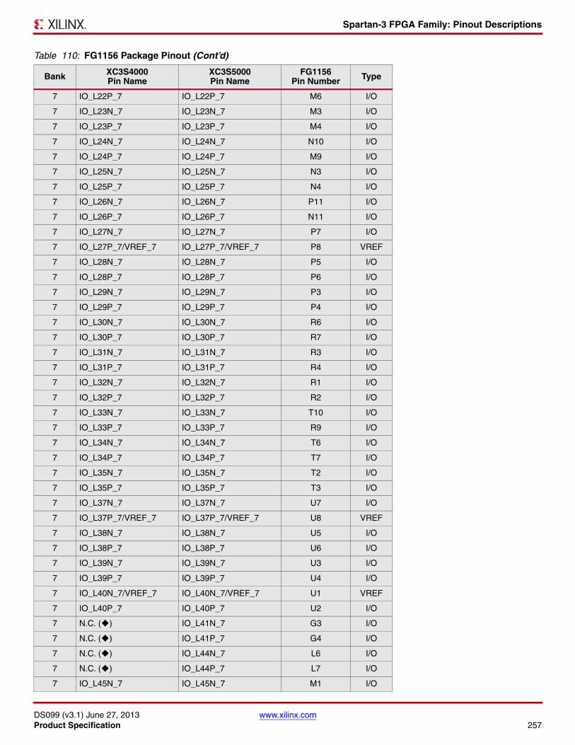
Spartan-3 FPGA Family: Pinout Descriptions
DS099 (v3.1) June 27, 2013 www.xilinx.comProduct Specification 257
7 IO_L22P_7 IO_L22P_7 M6 I/O
7 IO_L23N_7 IO_L23N_7 M3 I/O
7 IO_L23P_7 IO_L23P_7 M4 I/O
7 IO_L24N_7 IO_L24N_7 N10 I/O
7 IO_L24P_7 IO_L24P_7 M9 I/O
7 IO_L25N_7 IO_L25N_7 N3 I/O
7 IO_L25P_7 IO_L25P_7 N4 I/O
7 IO_L26N_7 IO_L26N_7 P11 I/O
7 IO_L26P_7 IO_L26P_7 N11 I/O
7 IO_L27N_7 IO_L27N_7 P7 I/O
7 IO_L27P_7/VREF_7 IO_L27P_7/VREF_7 P8 VREF
7 IO_L28N_7 IO_L28N_7 P5 I/O
7 IO_L28P_7 IO_L28P_7 P6 I/O
7 IO_L29N_7 IO_L29N_7 P3 I/O
7 IO_L29P_7 IO_L29P_7 P4 I/O
7 IO_L30N_7 IO_L30N_7 R6 I/O
7 IO_L30P_7 IO_L30P_7 R7 I/O
7 IO_L31N_7 IO_L31N_7 R3 I/O
7 IO_L31P_7 IO_L31P_7 R4 I/O
7 IO_L32N_7 IO_L32N_7 R1 I/O
7 IO_L32P_7 IO_L32P_7 R2 I/O
7 IO_L33N_7 IO_L33N_7 T10 I/O
7 IO_L33P_7 IO_L33P_7 R9 I/O
7 IO_L34N_7 IO_L34N_7 T6 I/O
7 IO_L34P_7 IO_L34P_7 T7 I/O
7 IO_L35N_7 IO_L35N_7 T2 I/O
7 IO_L35P_7 IO_L35P_7 T3 I/O
7 IO_L37N_7 IO_L37N_7 U7 I/O
7 IO_L37P_7/VREF_7 IO_L37P_7/VREF_7 U8 VREF
7 IO_L38N_7 IO_L38N_7 U5 I/O
7 IO_L38P_7 IO_L38P_7 U6 I/O
7 IO_L39N_7 IO_L39N_7 U3 I/O
7 IO_L39P_7 IO_L39P_7 U4 I/O
7 IO_L40N_7/VREF_7 IO_L40N_7/VREF_7 U1 VREF
7 IO_L40P_7 IO_L40P_7 U2 I/O
7 N.C. () IO_L41N_7 G3 I/O
7 N.C. () IO_L41P_7 G4 I/O
7 N.C. () IO_L44N_7 L6 I/O
7 N.C. () IO_L44P_7 L7 I/O
7 IO_L45N_7 IO_L45N_7 M1 I/O
Table 110: FG1156 Package Pinout (Cont’d)
Bank XC3S4000Pin Name
XC3S5000Pin Name
FG1156Pin Number Type
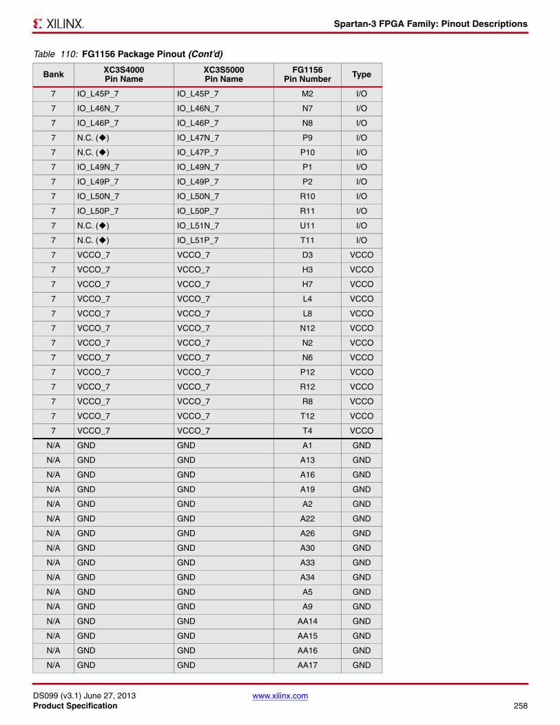
Spartan-3 FPGA Family: Pinout Descriptions
DS099 (v3.1) June 27, 2013 www.xilinx.comProduct Specification 258
7 IO_L45P_7 IO_L45P_7 M2 I/O
7 IO_L46N_7 IO_L46N_7 N7 I/O
7 IO_L46P_7 IO_L46P_7 N8 I/O
7 N.C. () IO_L47N_7 P9 I/O
7 N.C. () IO_L47P_7 P10 I/O
7 IO_L49N_7 IO_L49N_7 P1 I/O
7 IO_L49P_7 IO_L49P_7 P2 I/O
7 IO_L50N_7 IO_L50N_7 R10 I/O
7 IO_L50P_7 IO_L50P_7 R11 I/O
7 N.C. () IO_L51N_7 U11 I/O
7 N.C. () IO_L51P_7 T11 I/O
7 VCCO_7 VCCO_7 D3 VCCO
7 VCCO_7 VCCO_7 H3 VCCO
7 VCCO_7 VCCO_7 H7 VCCO
7 VCCO_7 VCCO_7 L4 VCCO
7 VCCO_7 VCCO_7 L8 VCCO
7 VCCO_7 VCCO_7 N12 VCCO
7 VCCO_7 VCCO_7 N2 VCCO
7 VCCO_7 VCCO_7 N6 VCCO
7 VCCO_7 VCCO_7 P12 VCCO
7 VCCO_7 VCCO_7 R12 VCCO
7 VCCO_7 VCCO_7 R8 VCCO
7 VCCO_7 VCCO_7 T12 VCCO
7 VCCO_7 VCCO_7 T4 VCCO
N/A GND GND A1 GND
N/A GND GND A13 GND
N/A GND GND A16 GND
N/A GND GND A19 GND
N/A GND GND A2 GND
N/A GND GND A22 GND
N/A GND GND A26 GND
N/A GND GND A30 GND
N/A GND GND A33 GND
N/A GND GND A34 GND
N/A GND GND A5 GND
N/A GND GND A9 GND
N/A GND GND AA14 GND
N/A GND GND AA15 GND
N/A GND GND AA16 GND
N/A GND GND AA17 GND
Table 110: FG1156 Package Pinout (Cont’d)
Bank XC3S4000Pin Name
XC3S5000Pin Name
FG1156Pin Number Type

Spartan-3 FPGA Family: Pinout Descriptions
DS099 (v3.1) June 27, 2013 www.xilinx.comProduct Specification 259
N/A GND GND AA18 GND
N/A GND GND AA19 GND
N/A GND GND AA20 GND
N/A GND GND AA21 GND
N/A GND GND AB1 GND
N/A GND GND AB17 GND
N/A GND GND AB18 GND
N/A GND GND AB26 GND
N/A GND GND AB30 GND
N/A GND GND AB34 GND
N/A GND GND AB5 GND
N/A GND GND AB9 GND
N/A GND GND AD3 GND
N/A GND GND AD32 GND
N/A GND GND AE10 GND
N/A GND GND AE25 GND
N/A GND GND AF1 GND
N/A GND GND AF13 GND
N/A GND GND AF16 GND
N/A GND GND AF19 GND
N/A GND GND AF22 GND
N/A GND GND AF30 GND
N/A GND GND AF34 GND
N/A GND GND AF5 GND
N/A GND GND AH28 GND
N/A GND GND AH7 GND
N/A GND GND AK1 GND
N/A GND GND AK13 GND
N/A GND GND AK16 GND
N/A GND GND AK19 GND
N/A GND GND AK22 GND
N/A GND GND AK26 GND
N/A GND GND AK30 GND
N/A GND GND AK34 GND
N/A GND GND AK5 GND
N/A GND GND AK9 GND
N/A GND GND AM11 GND
N/A GND GND AM24 GND
N/A GND GND AM3 GND
N/A GND GND AM32 GND
Table 110: FG1156 Package Pinout (Cont’d)
Bank XC3S4000Pin Name
XC3S5000Pin Name
FG1156Pin Number Type
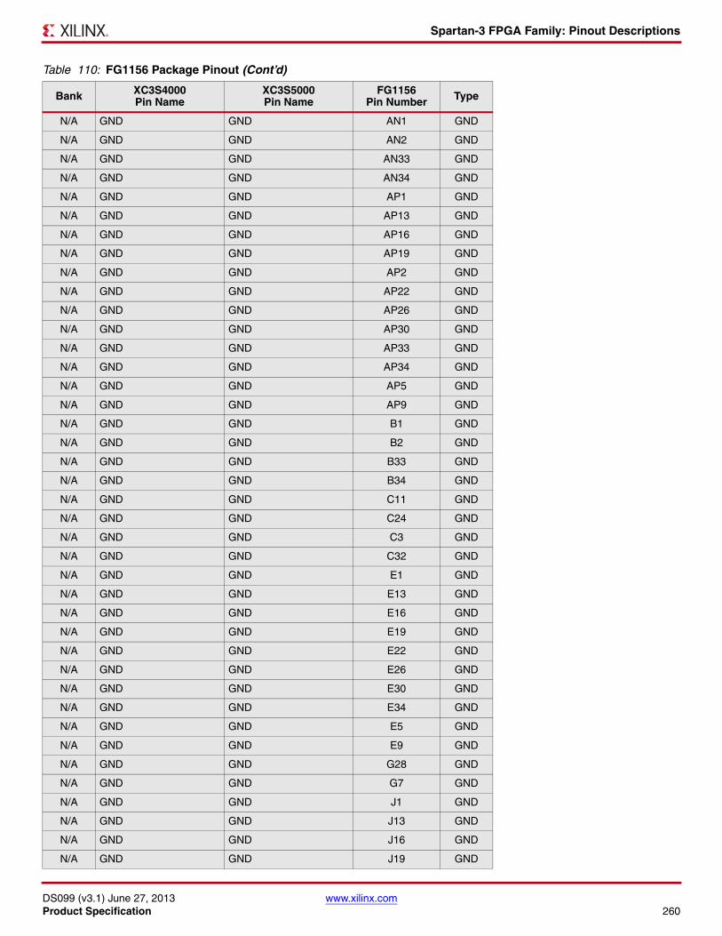
Spartan-3 FPGA Family: Pinout Descriptions
DS099 (v3.1) June 27, 2013 www.xilinx.comProduct Specification 260
N/A GND GND AN1 GND
N/A GND GND AN2 GND
N/A GND GND AN33 GND
N/A GND GND AN34 GND
N/A GND GND AP1 GND
N/A GND GND AP13 GND
N/A GND GND AP16 GND
N/A GND GND AP19 GND
N/A GND GND AP2 GND
N/A GND GND AP22 GND
N/A GND GND AP26 GND
N/A GND GND AP30 GND
N/A GND GND AP33 GND
N/A GND GND AP34 GND
N/A GND GND AP5 GND
N/A GND GND AP9 GND
N/A GND GND B1 GND
N/A GND GND B2 GND
N/A GND GND B33 GND
N/A GND GND B34 GND
N/A GND GND C11 GND
N/A GND GND C24 GND
N/A GND GND C3 GND
N/A GND GND C32 GND
N/A GND GND E1 GND
N/A GND GND E13 GND
N/A GND GND E16 GND
N/A GND GND E19 GND
N/A GND GND E22 GND
N/A GND GND E26 GND
N/A GND GND E30 GND
N/A GND GND E34 GND
N/A GND GND E5 GND
N/A GND GND E9 GND
N/A GND GND G28 GND
N/A GND GND G7 GND
N/A GND GND J1 GND
N/A GND GND J13 GND
N/A GND GND J16 GND
N/A GND GND J19 GND
Table 110: FG1156 Package Pinout (Cont’d)
Bank XC3S4000Pin Name
XC3S5000Pin Name
FG1156Pin Number Type

Spartan-3 FPGA Family: Pinout Descriptions
DS099 (v3.1) June 27, 2013 www.xilinx.comProduct Specification 261
N/A GND GND J22 GND
N/A GND GND J30 GND
N/A GND GND J34 GND
N/A GND GND J5 GND
N/A GND GND K10 GND
N/A GND GND K25 GND
N/A GND GND L3 GND
N/A GND GND L32 GND
N/A GND GND N1 GND
N/A GND GND N17 GND
N/A GND GND N18 GND
N/A GND GND N26 GND
N/A GND GND N30 GND
N/A GND GND N34 GND
N/A GND GND N5 GND
N/A GND GND N9 GND
N/A GND GND P14 GND
N/A GND GND P15 GND
N/A GND GND P16 GND
N/A GND GND P17 GND
N/A GND GND P18 GND
N/A GND GND P19 GND
N/A GND GND P20 GND
N/A GND GND P21 GND
N/A GND GND R14 GND
N/A GND GND R15 GND
N/A GND GND R16 GND
N/A GND GND R17 GND
N/A GND GND R18 GND
N/A GND GND R19 GND
N/A GND GND R20 GND
N/A GND GND R21 GND
N/A GND GND T1 GND
N/A GND GND T14 GND
N/A GND GND T15 GND
N/A GND GND T16 GND
N/A GND GND T17 GND
N/A GND GND T18 GND
N/A GND GND T19 GND
N/A GND GND T20 GND
Table 110: FG1156 Package Pinout (Cont’d)
Bank XC3S4000Pin Name
XC3S5000Pin Name
FG1156Pin Number Type
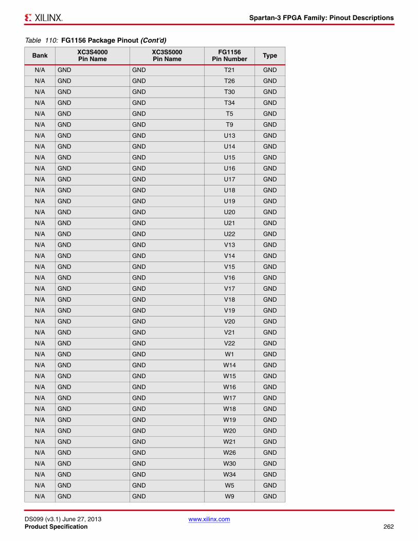
Spartan-3 FPGA Family: Pinout Descriptions
DS099 (v3.1) June 27, 2013 www.xilinx.comProduct Specification 262
N/A GND GND T21 GND
N/A GND GND T26 GND
N/A GND GND T30 GND
N/A GND GND T34 GND
N/A GND GND T5 GND
N/A GND GND T9 GND
N/A GND GND U13 GND
N/A GND GND U14 GND
N/A GND GND U15 GND
N/A GND GND U16 GND
N/A GND GND U17 GND
N/A GND GND U18 GND
N/A GND GND U19 GND
N/A GND GND U20 GND
N/A GND GND U21 GND
N/A GND GND U22 GND
N/A GND GND V13 GND
N/A GND GND V14 GND
N/A GND GND V15 GND
N/A GND GND V16 GND
N/A GND GND V17 GND
N/A GND GND V18 GND
N/A GND GND V19 GND
N/A GND GND V20 GND
N/A GND GND V21 GND
N/A GND GND V22 GND
N/A GND GND W1 GND
N/A GND GND W14 GND
N/A GND GND W15 GND
N/A GND GND W16 GND
N/A GND GND W17 GND
N/A GND GND W18 GND
N/A GND GND W19 GND
N/A GND GND W20 GND
N/A GND GND W21 GND
N/A GND GND W26 GND
N/A GND GND W30 GND
N/A GND GND W34 GND
N/A GND GND W5 GND
N/A GND GND W9 GND
Table 110: FG1156 Package Pinout (Cont’d)
Bank XC3S4000Pin Name
XC3S5000Pin Name
FG1156Pin Number Type
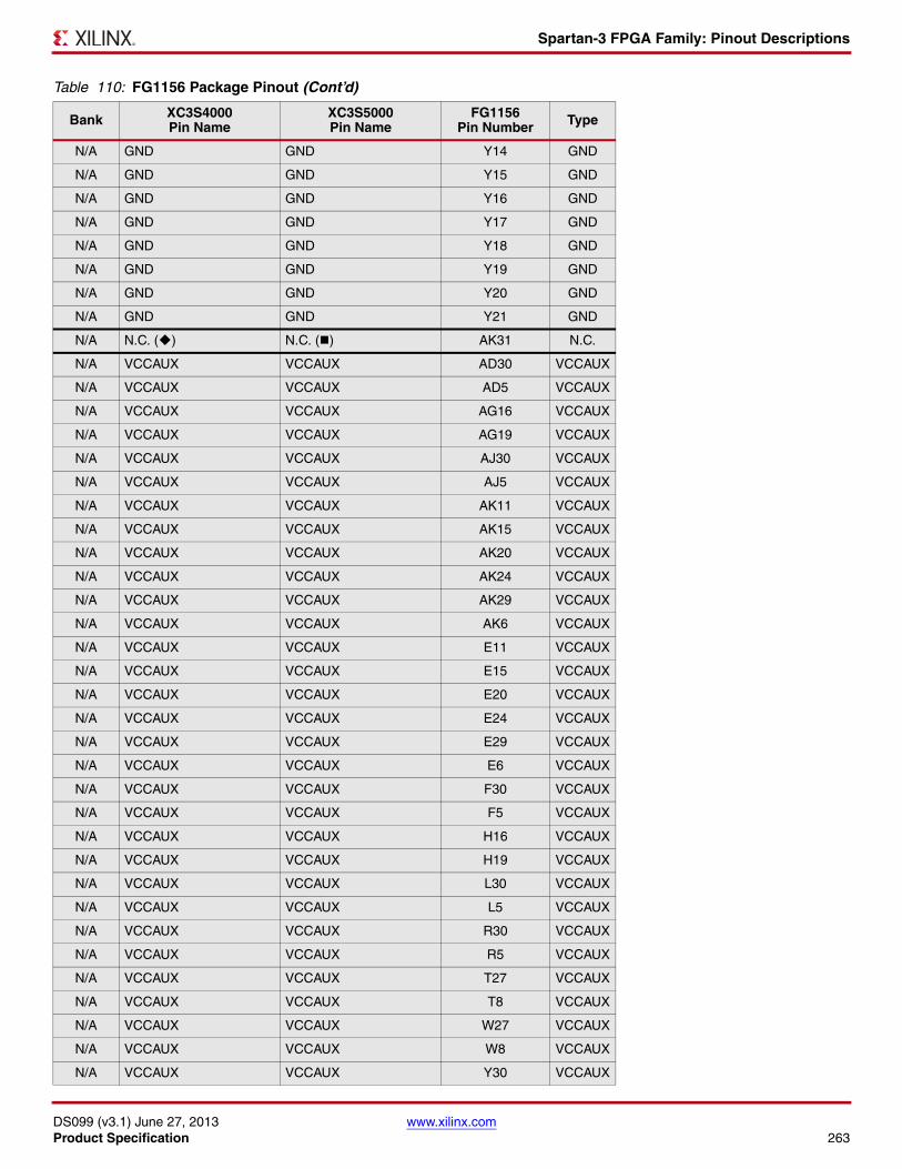
Spartan-3 FPGA Family: Pinout Descriptions
DS099 (v3.1) June 27, 2013 www.xilinx.comProduct Specification 263
N/A GND GND Y14 GND
N/A GND GND Y15 GND
N/A GND GND Y16 GND
N/A GND GND Y17 GND
N/A GND GND Y18 GND
N/A GND GND Y19 GND
N/A GND GND Y20 GND
N/A GND GND Y21 GND
N/A N.C. () N.C. () AK31 N.C.
N/A VCCAUX VCCAUX AD30 VCCAUX
N/A VCCAUX VCCAUX AD5 VCCAUX
N/A VCCAUX VCCAUX AG16 VCCAUX
N/A VCCAUX VCCAUX AG19 VCCAUX
N/A VCCAUX VCCAUX AJ30 VCCAUX
N/A VCCAUX VCCAUX AJ5 VCCAUX
N/A VCCAUX VCCAUX AK11 VCCAUX
N/A VCCAUX VCCAUX AK15 VCCAUX
N/A VCCAUX VCCAUX AK20 VCCAUX
N/A VCCAUX VCCAUX AK24 VCCAUX
N/A VCCAUX VCCAUX AK29 VCCAUX
N/A VCCAUX VCCAUX AK6 VCCAUX
N/A VCCAUX VCCAUX E11 VCCAUX
N/A VCCAUX VCCAUX E15 VCCAUX
N/A VCCAUX VCCAUX E20 VCCAUX
N/A VCCAUX VCCAUX E24 VCCAUX
N/A VCCAUX VCCAUX E29 VCCAUX
N/A VCCAUX VCCAUX E6 VCCAUX
N/A VCCAUX VCCAUX F30 VCCAUX
N/A VCCAUX VCCAUX F5 VCCAUX
N/A VCCAUX VCCAUX H16 VCCAUX
N/A VCCAUX VCCAUX H19 VCCAUX
N/A VCCAUX VCCAUX L30 VCCAUX
N/A VCCAUX VCCAUX L5 VCCAUX
N/A VCCAUX VCCAUX R30 VCCAUX
N/A VCCAUX VCCAUX R5 VCCAUX
N/A VCCAUX VCCAUX T27 VCCAUX
N/A VCCAUX VCCAUX T8 VCCAUX
N/A VCCAUX VCCAUX W27 VCCAUX
N/A VCCAUX VCCAUX W8 VCCAUX
N/A VCCAUX VCCAUX Y30 VCCAUX
Table 110: FG1156 Package Pinout (Cont’d)
Bank XC3S4000Pin Name
XC3S5000Pin Name
FG1156Pin Number Type
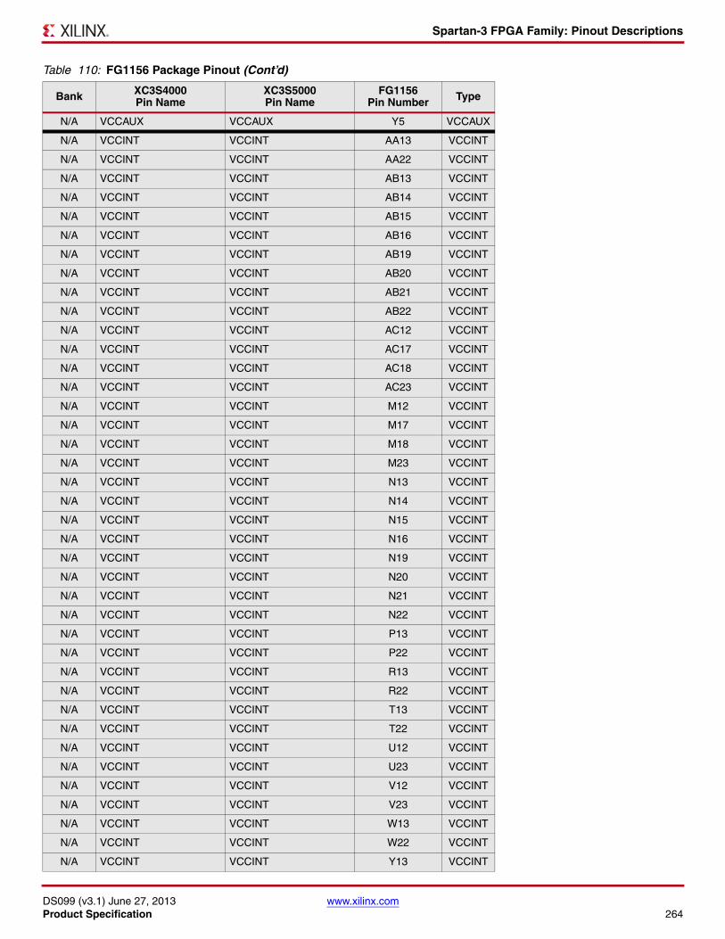
Spartan-3 FPGA Family: Pinout Descriptions
DS099 (v3.1) June 27, 2013 www.xilinx.comProduct Specification 264
N/A VCCAUX VCCAUX Y5 VCCAUX
N/A VCCINT VCCINT AA13 VCCINT
N/A VCCINT VCCINT AA22 VCCINT
N/A VCCINT VCCINT AB13 VCCINT
N/A VCCINT VCCINT AB14 VCCINT
N/A VCCINT VCCINT AB15 VCCINT
N/A VCCINT VCCINT AB16 VCCINT
N/A VCCINT VCCINT AB19 VCCINT
N/A VCCINT VCCINT AB20 VCCINT
N/A VCCINT VCCINT AB21 VCCINT
N/A VCCINT VCCINT AB22 VCCINT
N/A VCCINT VCCINT AC12 VCCINT
N/A VCCINT VCCINT AC17 VCCINT
N/A VCCINT VCCINT AC18 VCCINT
N/A VCCINT VCCINT AC23 VCCINT
N/A VCCINT VCCINT M12 VCCINT
N/A VCCINT VCCINT M17 VCCINT
N/A VCCINT VCCINT M18 VCCINT
N/A VCCINT VCCINT M23 VCCINT
N/A VCCINT VCCINT N13 VCCINT
N/A VCCINT VCCINT N14 VCCINT
N/A VCCINT VCCINT N15 VCCINT
N/A VCCINT VCCINT N16 VCCINT
N/A VCCINT VCCINT N19 VCCINT
N/A VCCINT VCCINT N20 VCCINT
N/A VCCINT VCCINT N21 VCCINT
N/A VCCINT VCCINT N22 VCCINT
N/A VCCINT VCCINT P13 VCCINT
N/A VCCINT VCCINT P22 VCCINT
N/A VCCINT VCCINT R13 VCCINT
N/A VCCINT VCCINT R22 VCCINT
N/A VCCINT VCCINT T13 VCCINT
N/A VCCINT VCCINT T22 VCCINT
N/A VCCINT VCCINT U12 VCCINT
N/A VCCINT VCCINT U23 VCCINT
N/A VCCINT VCCINT V12 VCCINT
N/A VCCINT VCCINT V23 VCCINT
N/A VCCINT VCCINT W13 VCCINT
N/A VCCINT VCCINT W22 VCCINT
N/A VCCINT VCCINT Y13 VCCINT
Table 110: FG1156 Package Pinout (Cont’d)
Bank XC3S4000Pin Name
XC3S5000Pin Name
FG1156Pin Number Type
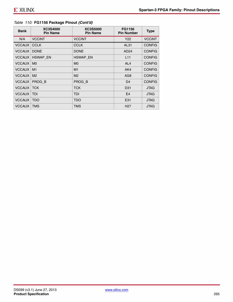
Spartan-3 FPGA Family: Pinout Descriptions
DS099 (v3.1) June 27, 2013 www.xilinx.comProduct Specification 265
N/A VCCINT VCCINT Y22 VCCINT
VCCAUX CCLK CCLK AL31 CONFIG
VCCAUX DONE DONE AD24 CONFIG
VCCAUX HSWAP_EN HSWAP_EN L11 CONFIG
VCCAUX M0 M0 AL4 CONFIG
VCCAUX M1 M1 AK4 CONFIG
VCCAUX M2 M2 AG8 CONFIG
VCCAUX PROG_B PROG_B D4 CONFIG
VCCAUX TCK TCK D31 JTAG
VCCAUX TDI TDI E4 JTAG
VCCAUX TDO TDO E31 JTAG
VCCAUX TMS TMS H27 JTAG
Table 110: FG1156 Package Pinout (Cont’d)
Bank XC3S4000Pin Name
XC3S5000Pin Name
FG1156Pin Number Type
Spartan-3 FPGA Family: Pinout Descriptions
DS099 (v3.1) June 27, 2013 www.xilinx.comProduct Specification 266
User I/Os by Bank
Note: The FG(G)1156 package is discontinued. See http://www.xilinx.com/support/documentation/spartan-3_customer_notices.htm.
Table 111 indicates how the available user-I/O pins are distributed between the eight I/O banks for the XC3S4000 in the FG1156 package. Similarly, Table 112 shows how the available user-I/O pins are distributed between the eight I/O banks for the XC3S5000 in the FG1156 package.
Table 111: User I/Os Per Bank for XC3S4000 in FG1156 Package
Package Edge I/OBank Maximum I/O
All Possible I/O Pins by Type
I/O DUAL DCI VREF GCLK
Top0 90 79 0 2 7 2
1 90 79 0 2 7 2
Right2 88 80 0 2 6 0
3 88 79 0 2 7 0
Bottom4 90 73 6 2 7 2
5 90 73 6 2 7 2
Left6 88 79 0 2 7 0
7 88 79 0 2 7 0
Notes: 1. The FG1156 and FGG1156 packages are discontinued. See www.xilinx.com/support/documentation/spartan-3.htm#19600.
Table 112: User I/Os Per Bank for XC3S5000 in FG1156 Package
Package Edge I/OBank Maximum I/O
All Possible I/O Pins by Type
I/O DUAL DCI VREF GCLK
Top0 100 89 0 2 7 2
1 100 89 0 2 7 2
Right2 96 87 0 2 7 0
3 96 87 0 2 7 0
Bottom4 100 83 6 2 7 2
5 100 83 6 2 7 2
Left6 96 87 0 2 7 0
7 96 87 0 2 7 0
Notes: 1. The FG1156 and FGG1156 packages are discontinued. See www.xilinx.com/support/documentation/spartan-3.htm#19600.
Spartan-3 FPGA Family: Pinout Descriptions
DS099 (v3.1) June 27, 2013 www.xilinx.comProduct Specification 267
FG1156 Footprint
Top Left Corner of FG1156 Package (Top View)
XC3S4000(712 max. user I/O)
621 I/O: Unrestricted, general-purpose user I/O 55 VREF: User I/O or input voltage
reference for bank 73 N.C.: Unconnected pins for XC3S4000 ()
XC3S5000(784 max. user I/O)
692 I/O: Unrestricted, general-purpose user I/O 56 VREF: User I/O or input voltage
reference for bank 1 N.C.: Unconnected pins for XC3S5000 ()
X-Ref Target - Figure 57
Figure 57: FG1156 Package Footprint (Top View)
GND
GND GND
GND
GND
GND
GND
GND GND
GND
GND
GND GND
GND
GND
GND
GND
GND
GND
GND
GND
GND
GND
GND
GND
GND
GND
GND
GND
GND
GND
GND
GND
GND
GND
GND
GND
GND GND GND GND GND
GNDGND
GNDGND
I/O L01P_0 VRN_0
I/O L02P_0
I/O L05P_0 VREF_0
I/O L34P_0 I/O
L36P_0I/O
L38P_0
I/O L40P_0 I/O
L15P_0I/O
L22P_0
I/O L26P_0 VREF_0
I/O L32P_0 GCLK6
I/O L01N_0 VRP_0
I/O L02N_0
I/O L03P_0
I/O L05N_0
I/O L34N_0 I/O
L36N_0I/O
I/O L38N_0
I/O L40N_0 I/O
L15N_0VCCO_0 I/O
L22N_0I/O
L26N_0I/O
L28P_0
I/O L32N_0 GCLK7
I/O L01N_7 VRP_7
I/O L01P_7 VRN_7
VCCO_0 I/O L03N_0
I/O L04P_0
I/O L33P_0 VCCO_0 I/O
L08P_0I/O
L37P_0I/O
L14P_0I/O
L17P_0I/O
L21P_0I/O
L25P_0I/O
L28N_0
I/O L31P_0 VREF_0
I/O L02N_7
I/O L02P_7
VCCO_7 PROG_BIO
VREF_0I/O
L04N_0
I/O L33N_0 I/O
L35P_0I/O
L08N_0I/O
L37N_0VCCO_0 I/O
L14N_0I/O
L17N_0I/O
L21N_0I/O
L25N_0VCCO_0 I/O
L31N_0
I/O L03N_7 VREF_7
I/O L03P_7
TDI VCCAUX I/O L06P_0
I/O L35N_0
IO VREF_0
VCCAUX I/O L13P_0
I/O L20P_0
VCCAUX I/O
I/O L05N_7
I/O L05P_7
I/O L04N_7
I/O L04P_7
VCCAUX I/OI/O
L06N_0I/O
I/O L07P_0
I/O L10P_0
I/O L39P_0 I/O
L13N_0VCCO_0 I/O
L20N_0I/O
L24P_0I/O
L27P_0I/O
L30P_0
I/O I/O I/O
L41N_7 I/O
L41P_7 I/O L06N_7
I/O L06P_7
VCCO_0 I/O L07N_0
I/O L10N_0
I/O L39N_0 I/O
I/O L16P_0
I/O L19P_0
I/O L24N_0
I/O L27N_0
I/O L30N_0
I/O L08N_7
I/O L08P_7
VCCO_7I/O
L10P_7 VREF_7
I/O L07N_7
I/O L07P_7
VCCO_7 I/O I/OI/O
L09P_0VCCO_0 I/O
L12P_0I/O
L16N_0I/O
L19N_0VCCO_0 VCCAUX I/O
L29P_0
I/O L11N_7
I/O L11P_7
I/O L10N_7
I/O L09N_7
I/O L09P_7
I/O L12P_7
I/O I/O L09N_0
I/OI/O
L12N_0IO
VREF_0I/O
L23P_0I/O
L29N_0
I/O L16N_7
I/O L16P_7 VREF_7
I/O L15N_7
I/O L15P_7
I/O L14N_7
I/O L14P_7
I/O L13N_7
I/O L13P_7
I/O L12N_7
I/O I/O L11P_0
I/OI/O
L18P_0I/O
L23N_0I/O I/O
I/O L19N_7 VREF_7
I/O L19P_7
VCCO_7 VCCAUXI/O
L44N_7 I/O
L44P_7 VCCO_7 I/O L17N_7
I/O L17P_7
HSWAP_ EN
I/O L11N_0
I/OI/O
L18N_0IO
VREF_0 I/O I/O
I/O L45N_7
I/O L45P_7
I/O L23N_7
I/O L23P_7
I/O L22N_7
I/O L22P_7
I/O L21N_7
I/O L21P_7
I/O L24P_7
I/O L20N_7
I/O L20P_7
VCCINT VCCO_0 VCCO_0 VCCO_0 VCCO_0 VCCINT
VCCO_7 I/O L25N_7
I/O L25P_7
VCCO_7 I/O L46N_7
I/O L46P_7
I/O L24N_7
I/O L26P_7
VCCO_7 VCCINT VCCINT VCCINT VCCINT
I/O L49N_7
I/O L49P_7
I/O L29N_7
I/O L29P_7
I/O L28N_7
I/O L28P_7
I/O L27N_7
I/O L27P_7 VREF_7
I/O L47N_7
I/O L47P_7 I/O
L26N_7VCCO_7 VCCINT
I/O L32N_7
I/O L32P_7
I/O L31N_7
I/O L31P_7
VCCAUX I/O L30N_7
I/O L30P_7
VCCO_7 I/O L33P_7
I/O L50N_7
I/O L50P_7
VCCO_7 VCCINT
I/O L35N_7
I/O L35P_7
VCCO_7 I/O L34N_7
I/O L34P_7
VCCAUX I/O L33N_7
I/O L51P_7 VCCO_7 VCCINT
I/O L40N_7 VREF_7
I/O L40P_7
I/O L39N_7
I/O L39P_7
I/O L38N_7
I/O L38P_7
I/O L37N_7
I/O L37P_7 VREF_7
I/O I/O
I/O L51N_7
VCCINT
10 11 12 13 14 15 16 171 2 3 4 5 6 7 8 9Bank 0
A
B
C
D
E
F
G
H
J
K
L
M
N
P
R
T
U
Ban
k 7
DS099-4_14a_072903
Spartan-3 FPGA Family: Pinout Descriptions
DS099 (v3.1) June 27, 2013 www.xilinx.comProduct Specification 268
All DevicesTop Right Corner of FG1156 Package (Top View)
12 DUAL: Configuration pin, then possible user I/O 16 DCI: User I/O or reference
resistor input for bank 8 GCLK: User I/O or global clock buffer input
7 CONFIG: Dedicated configuration pins 4 JTAG: Dedicated JTAG port pins 104 VCCO: Output voltage supply
for bank
40 VCCINT: Internal core voltage supply (+1.2V) 32 VCCAUX: Auxiliary voltage
supply (+2.5V) 184 GND: Ground
Figure 58: FG1156 Package Footprint (Top View) Continued
18 19 20 21 22 23 24 25 26 27 28 29 30 31 32 33 34Bank 1
A
B
C
D
E
F
G
H
J
K
L
M
N
P
R
T
U
Ban
k 2
I/OI/O
L40N_1I/O
L26N_1I/O
L19N_1I/O
L15N_1I/O
L14N_1I/O
L08N_1
I/O L34N_1 I/O
L05N_1I/O
L02N_1
I/O L01N_1 VRP_1
I/O L32N_1 GCLK5
I/O L28N_1
I/O L40P_1
I/O L26P_1
VCCO_1 I/O L19P_1
I/O L15P_1
I/O L14P_1
I/OI/O
L08P_1
I/O L34P_1 I/O
L05P_1I/O
L03N_1I/O
L02P_1
I/O L01P_1 VRN_1
I/O L32P_1 GCLK4
I/O L28P_1
I/O L39N_1
I/O L25N_1
I/O L22N_1
I/OI/O
L13N_1
I/O L10N_1 VREF_1
VCCO_1I/O
L33N_1 I/O L04N_1
I/O L03P_1
VCCO_1I/O
L01N_2 VRP_2
I/O L01P_2 VRN_2
I/O L31N_1 VREF_1
VCCO_1 I/O L39P_1
I/O L25P_1
I/O L22P_1
I/O L18N_1
VCCO_1 I/O L13P_1
I/O L10P_1
I/O L07N_1
I/O L33P_1 I/O
L04P_1IO
VREF_1VCCO_2 I/O
L02N_2I/O
L02P_2
I/O L31P_1
VCCAUX I/OI/O
L18P_1VCCAUX I/O
I/O L07P_1
I/O L06N_1 VREF_1
VCCAUX GNDGNDGND
GND
GND GND
GND
GND GND
GND
GND
GND
GND
GNDGND
GNDGNDGND
GND
GND
GND
GND
GND
GND
GND
GND
GND
GND
GND
GND
GND
GND
GND
GND
GND
GND
GND
GND
GND
GND GND
GND
GND GND
GND
GND
TDO
TCK
I/O L03N_2 VREF_2
I/O L03P_2
I/OI/O
L27N_1I/O
L38N_1I/O
L24N_1VCCO_1
I/O L17N_1 VREF_1
I/O L36N_1 I/O
L12N_1I/O
L09N_1I/O
I/O L06P_1
I/O VCCAUX I/O L04N_2
I/O L04P_2
I/O L41N_2
I/O L41P_2
I/O L30N_1
I/O L27P_1
I/O L38P_1
I/O L24P_1
I/O L21N_1
I/O L17P_1
I/O L36P_1 I/O
L12P_1I/O
L09P_1VCCO_1 I/O
L05N_2I/O
L05P_2
I/O L42N_2
I/O L42P_2 I/O I/O
I/O L30P_1
VCCAUX VCCO_1 I/O L23N_1
I/O L21P_1
I/O VCCO_1 I/O L11N_1
I/O TMS VCCO_2 I/O L06N_2
I/O L06P_2
I/O L09N_2 VREF_2
VCCO_2 I/O L07N_2
I/O L07P_2
I/O L29N_1
I/O L37N_1
I/O L23P_1
I/O L16N_1
I/O L35N_1 I/O
L11P_1
I/O I/O L11N_2
I/O L08N_2
I/O L08P_2
I/O L09P_2
I/O L10N_2
I/O L10P_2
I/O L29P_1
I/OI/O
L37P_1IO
VREF_1I/O
L20N_1I/O
L16P_1
I/O L35P_1 I/O
L11P_2I/O
L12N_2I/O
L12P_2I/O
L13N_2
I/O L13P_2 VREF_2
I/O L14N_2
I/O L14P_2
I/O L15N_2
I/O L15P_2
IO VREF_1 I/O I/O I/O
I/O L20P_1
I/O I/O
I/O L16N_2
I/O L16P_2
VCCO_2I/O
L17N_2
I/O L17P_2 VREF_2 VCCAUX VCCO_2 I/O
L45N_2I/O
L45P_2
VCCINT VCCO_1 VCCO_1 VCCO_1 VCCO_1 VCCINTI/O
L46N_2I/O
L46P_2I/O
L21N_2I/O
L47N_2I/O
L47P_2I/O
L19N_2I/O
L19P_2I/O
L20N_2I/O
L20P_2I/O
L48N_2I/O
L48P_2
VCCINT VCCINT VCCINT VCCINT VCCO_2 I/O L24N_2
I/O L21P_2
I/O L22N_2
I/O L22P_2
VCCO_2I/O
L23N_2 VREF_2
I/O L23P_2
VCCO_2
VCCINT VCCO_2 I/O L24P_2
I/O L49N_2
I/O L49P_2 I/O
L50N_2I/O
L50P_2I/O
L26N_2I/O
L26P_2I/O
L27N_2I/O
L27P_2I/O
L28N_2I/O
L28P_2
VCCINT VCCO_2 I/O L29N_2
I/O L29P_2
I/O L33N_2
VCCO_2 I/O L30N_2
I/O L30P_2
VCCAUX I/O L31N_2
I/O L31P_2
I/O L32N_2
I/O L32P_2
VCCINT VCCO_2I/O
L51N_2 I/O L33P_2
VCCAUXI/O
L34N_2 VREF_2
I/O L34P_2
VCCO_2 I/O L35N_2
I/O L35P_2
VCCINT
I/O L51P_2
I/O I/O I/O
L37N_2I/O
L37P_2I/O
L38N_2I/O
L38P_2I/O
L39N_2I/O
L39P_2I/O
L40N_2
I/O L40P_2 VREF_2
DS099-4_14b_072903
Spartan-3 FPGA Family: Pinout Descriptions
DS099 (v3.1) June 27, 2013 www.xilinx.comProduct Specification 269
Bottom Left Corner of FG1156 Package (Top View)
Figure 59: FG1156 Package Footprint (Top View) Continued
I/O L40P_6 VREF_6
I/O L40N_6
I/O L39P_6
I/O L39N_6
I/O L38P_6
I/O L38N_6
I/O L52P_6
I/O L52N_6
I/O I/O
I/O L49P_6 VCCINT
I/O L37P_6
I/O L37N_6
VCCO_6 I/O L36P_6
I/O L36N_6
VCCAUX I/O L35P_6
I/O L49N_6 VCCO_6 VCCINT
I/O L34P_6
I/O L34N_6 VREF_6
I/O L33P_6
I/O L33N_6
VCCAUX I/O L48P_6
I/O L48N_6
VCCO_6 I/O L35N_6
I/O L32P_6
I/O L32N_6
VCCO_6 VCCINT
I/O L31P_6
I/O L31N_6
I/O L30P_6
I/O L30N_6
I/O L29P_6
I/O L29N_6
I/O L28P_6
I/O L28N_6
I/O L46P_6
I/O L46N_6 I/O
L27P_6VCCO_6 VCCINT
VCCO_6 I/O L26P_6
I/O L26N_6
VCCO_6 I/O L25P_6
I/O L25N_6
I/O L24P_6
I/O L27N_6
VCCO_6 VCCINT VCCINT VCCINT VCCINT
I/O L23P_6
I/O L23N_6
I/O L45P_6
I/O L45N_6
I/O L22P_6
I/O L22N_6
I/O L21P_6
I/O L21N_6
I/O L24N_6 VREF_6
I/O L20P_6
I/O L20N_6
VCCINT VCCO_5 VCCO_5 VCCO_5 VCCO_5 VCCINT
I/O L19P_6
I/O L19N_6
VCCO_6 VCCAUXI/O
L44P_6 I/O
L44N_6 VCCO_6I/O
L17P_6 VREF_6
I/O L17N_6
I/OI/O I/O
L16P_5I/O I/O I/O I/O
I/O L16P_6
I/O L16N_6
I/O L15P_6
I/O L15N_6
I/O L14P_6
I/O L14N_6
I/O L13P_6 VREF_6
I/O L13N_6
I/O L12P_6
I/O L39P_5 I/O
L12P_5I/O
L16N_5I/O
I/O L23P_5
I/OI/O
L29P_5 VREF_5
I/O L11P_6
I/O L11N_6
I/O L10P_6
I/O L09P_6
I/O L09N_6 VREF_6
I/O L12N_6
I/O I/O L07P_5
I/O L39N_5 I/O
L12N_5
I/O L19P_5 VREF_5
I/O L23N_5
I/O L29N_5
I/O L08P_6
I/O L08N_6
VCCO_6 I/O L10N_6
I/O L07P_6
I/O L07N_6
VCCO_6 M2 I/OI/O
L07N_5VCCO_5 I/O
I/O L17P_5
I/O L19N_5
VCCO_5 VCCAUX I/O L30P_5
I/O I/O I/O
L41P_6 I/O
L41N_6 I/O L06P_6
I/O L06N_6
VCCO_5 I/O L37P_5
I/O L08P_5
I/O L40P_5 I/O
L13P_5I/O
L17N_5I/O
L20P_5I/O
L24P_5I/O
L27P_5I/O
L30N_5
I/O L05P_6
I/O L05N_6
I/O L04P_6
I/O L04N_6
VCCAUX I/OI/O
L06P_5IO
VREF_5I/O
L37N_5I/O
L08N_5
I/O L40N_5 I/O
L13N_5VCCO_5 I/O
L20N_5I/O
L24N_5
I/O L27N_5 VREF_5
I/O
I/O L03P_6
I/O L03N_6 VREF_6
M1 VCCAUX I/O L06N_5
I/O L35P_5
I/O VCCAUX I/O L14P_5
I/O VCCAUXI/O
L31P_5 D5
I/O L02P_6
I/O L02N_6
VCCO_6 M0IO
VREF_5I/O
L04P_5
I/O L33P_5 I/O
L35N_5I/O
L38P_5I/O
L09P_5VCCO_5 I/O
L14N_5I/O
L18P_5I/O
L21P_5I/O
L25P_5VCCO_5
I/O L31N_5
D4
I/O L01P_6 VRN_6
I/O L01N_6 VRP_6
VCCO_5 I/O L03P_5
I/O L04N_5
I/O L33N_5 VCCO_5 I/O
L38N_5I/O
L09N_5I/O
I/O L18N_5
I/O L21N_5
I/O L25N_5
I/O L28P_5
D7
I/O L32P_5 GCLK2
I/O L01P_5 CS_B
I/O L02P_5
I/O L03N_5
I/O L05P_5
I/O L34P_5 I/O
L36P_5I/O
I/O L10P_5 VRN_5
I/O L11P_5
I/O L15P_5
VCCO_5 I/O L22P_5
I/O L26P_5
I/O L28N_5
D6
I/O L32N_5 GCLK3
I/O L01N_5
RDWR_B
I/O L02N_5
GND GND GND GND
GNDGND
GND GND
GND
GNDGNDGNDGNDGND
GND
GND
GND
GND
GND
GND
GND
GND GND
GND
GNDGND
GND
GND GND
GNDGND
GND
GND
GND
GND
GND
GND
GND
GND
GND
GND
GND
GND
GND
GND
GND
I/O L05N_5
I/O L34N_5
I/O L36N_5
I/O L10N_5 VRP_5
I/O L11N_5 VREF_5
I/O L15N_5
I/O L22N_5
I/O L26N_5
IO VREF_5
Bank 5
10 11 12 13 14 15 16 17
V
W
Y
AA
AB
AC
AD
AE
AF
AG
AH
AJ
AK
AL
AM
AN
AP
Ban
k 6
1 2 3 4 5 6 7 8 9
DS099-4_14c_072503
Spartan-3 FPGA Family: Pinout Descriptions
DS099 (v3.1) June 27, 2013 www.xilinx.comProduct Specification 270
Bottom Right Corner of FG1156 Package (Top View)
Figure 60: FG1156 Package Footprint (Top View) Continued
VCCINT
I/O L51N_3 I/O I/O I/O
L37P_3I/O
L37N_3I/O
L38P_3I/O
L38N_3I/O
L39P_3I/O
L39N_3I/O
L40P_3
I/O L40N_3 VREF_3
VCCINT VCCO_3I/O
L51P_3 I/O L33N_3
VCCAUXI/O
L34P_3 VREF_3
I/O L34N_3
VCCO_3 I/O L35P_3
I/O L35N_3
VCCINT VCCO_3 I/O L50P_3
I/O L50N_3
I/O L33P_3
VCCO_3 I/O L30P_3
I/O L30N_3
VCCAUX I/O L31P_3
I/O L31N_3
I/O L32P_3
I/O L32N_3
VCCINT VCCO_3 I/O L48N_3
I/O L49P_3
I/O L49N_3 I/O
L26P_3I/O
L26N_3I/O
L27P_3I/O
L27N_3I/O
L28P_3I/O
L28N_3I/O
L29P_3I/O
L29N_3
VCCINT VCCINT VCCINT VCCINT VCCO_3 I/O L48P_3
I/O L24N_3
I/O L46P_3
I/O L46N_3
VCCO_3 I/O L47P_3
I/O L47N_3
VCCO_3
VCCINT VCCO_4 VCCO_4 VCCO_4 VCCO_4 VCCINTI/O
L20P_3I/O
L20N_3I/O
L24P_3I/O
L21P_3I/O
L21N_3I/O
L22P_3I/O
L22N_3
I/O L23P_3 VREF_3
I/O L23N_3
I/O L45P_3
I/O L45N_3
I/O I/O I/OI/O
L18N_4I/O
I/O L11N_4
DONEI/O
L17P_3 VREF_3
I/O L17N_3
VCCO_3I/O
L44P_3 I/O
L44N_3 VCCO_3 I/O L19P_3
I/O L19N_3
I/O I/OI/O
L23N_4I/O
L18P_4I/O
I/O L11P_4
I/O I/O L12N_3
I/O L13P_3
I/O L13N_3 VREF_3
I/O L14P_3
I/O L14N_3
I/O L15P_3
I/O L15N_3
I/O L16P_3
I/O L16N_3
I/O L29N_4
I/O L23P_4
IO VREF_4
I/O L12N_4
I/OI/O
L07N_4
I/O I/O L12P_3
I/O L09P_3 VREF_3
I/O L09N_3
I/O L10N_3
I/O L11P_3
I/O L11N_3
I/O L29P_4
VCCAUX VCCO_4 I/O L19N_4
I/O L16N_4
I/O L12P_4
VCCO_4 I/O L07P_4
I/O I/O VCCO_3 I/O L07P_3
I/O L07N_3
I/O L10P_3
VCCO_3 I/O L08P_3
I/O L08N_3
I/O L30N_4
D2
I/O L27N_4
DIN D0
I/O L24N_4
I/O L19P_4
I/O L16P_4
IO VREF_4
I/O L39N_4 I/O
L08N_4I/O
L05N_4VCCO_4 I/O
L06P_3I/O
L06N_3
I/O L41P_3
I/O L41N_3 I/O I/O
I/O L30P_4
D3
I/O L27P_4
D1
I/O L24P_4
I/O L20N_4
VCCO_4 I/O L13N_4
I/O L39P_4 I/O
L08P_4I/O
L05P_4I/O
I/O L35N_4
I/O VCCAUX I/O L04P_3
I/O L04N_3
I/O L05P_3
I/O L05N_3
IO VREF_4
VCCAUX I/O L20P_4
I/O L13P_4
VCCAUX I/OI/O
L38N_4I/O
L35P_4VCCAUX
N.C. I/O L03P_3
I/O L03N_3
I/O L31N_4 INIT_B
VCCO_4 I/O L25N_4
I/O L21N_4
I/O L17N_4
I/O L14N_4
VCCO_4 I/O L09N_4
I/O L06N_4 VREF_4
I/O L38P_4
I/O L36N_4 I/O
L33N_4IO
VREF_4 CCLK VCCO_3 I/O L02P_3
I/O L02N_3 VREF_3
I/O L31P_4 DOUT BUSY
I/O L28N_4
I/O L25P_4
I/O L21P_4
I/O L17P_4
I/O L14P_4
I/O L09P_4
I/O L06P_4
VCCO_4I/O
L36P_4 I/O L33P_4
I/O L03N_4
VCCO_4I/O
L01P_3 VRN_3
I/O L01N_3 VRP_3
I/O L32N_4 GCLK1
I/O L28P_4
I/O L26N_4
I/O L22N_4 VREF_4
VCCO_4 I/O L15N_4
I/O L40N_4 I/O
L10N_4I/O
I/O L04N_4
I/O L37N_4 I/O
L34N_4I/O
L03P_4I/O
L02N_4
I/O L01N_4 VRP_4
I/O L32P_4 GCLK0
I/O L26P_4 VREF_4
I/O L22P_4
I/O L15P_4
I/O L40P_4
I/O L10P_4
I/O L04P_4
I/O L37P_4 I/O
L34P_4I/O
L02P_4
I/O L01P_4 VRN_4
GND
GNDGND
GND
GNDGNDGND
GNDGND
GNDGND
GND
GND GND
GND
GND
GND
GNDGNDGNDGND
GNDGNDGNDGND
GNDGNDGNDGND
GNDGNDGNDGND
GND GND GND
GND GND GND
GNDGND
GND
GND
GND
GND
GND
18 19 20 21 22 23 24 25 26 27 28 29 30 31 32 33 34
Bank 4
V
W
Y
AA
AB
AC
AD
AE
AF
AG
AH
AJ
AK
AL
AM
AN
AP
Ban
k 3
DS099-4_14d_072903
VCCAUX
Spartan-3 FPGA Family: Pinout Descriptions
DS099 (v3.1) June 27, 2013 www.xilinx.comProduct Specification 271
Revision HistoryDate Version Description
04/03/2003 1.0 Initial Xilinx release.
04/21/2003 1.1 Added information on the VQ100 package footprint, including a complete pinout table (Table 87) and footprint diagram (Figure 44). Updated Table 85 with final I/O counts for the VQ100 package. Also added final differential I/O pair counts for the TQ144 package. Added clarifying comments to HSWAP_EN pin description on page 119. Updated the footprint diagram for the FG900 package shown in Figure 55a and Figure 55b. Some thick lines separating I/O banks were incorrect. Made cosmetic changes to Figure 40, Figure 42, and Figure 43. Updated Xilinx hypertext links. Added XC3S200 and XC3S400 to Pin Name column in Table 91.
05/12/2003 1.1.1 AM32 pin was missing GND label in FG1156 package diagram (Figure 53).
07/11/2003 1.1.2 Corrected misspellings of GCLK in Table 69 and Table 70. Changed CMOS25 to LVCMOS25 in Dual-Purpose Pin I/O Standard During Configuration section. Clarified references to Module 2. For XC3S5000 in FG1156 package, corrected N.C. symbol to a black square in Table 110, key, and package drawing.
07/29/2003 1.2 Corrected pin names on FG1156 package. Some package balls incorrectly included LVDS pair names. The affected balls on the FG1156 package include G1, G2, G33, G34, U9, U10, U25, U26, V9, V10, V25, V26, AH1, AH2, AH33, AH34. The number of LVDS pairs is unaffected. Modified affected balls and re-sorted rows in Table 110. Updated affected balls in Figure 53. Also updated ASCII and Excel electronic versions of FG1156 pinout.
08/19/2003 1.2.1 Removed 100 MHz ConfigRate option in CCLK: Configuration Clock section and in Table 80. Added note that TDO is a totem-pole output in Table 77.
10/09/2003 1.2.2 Some pins had incorrect bank designations and were improperly sorted in Table 93. No pin names or functions changed. Renamed DCI_IN to DCI and added black diamond to N.C. pins in Table 93. In Figure 47, removed some extraneous text from pin 106 and corrected spelling of pins 45, 48, and 81.
12/17/2003 1.3 Added FG320 pin tables and pinout diagram (FG320: 320-lead Fine-pitch Ball Grid Array). Made cosmetic changes to the TQ144 footprint (Figure 46), the PQ208 footprint (Figure 47), the FG676 footprint (Figure 53), and the FG900 footprint (Figure 55). Clarified wording in Precautions When Using the JTAG Port in 3.3V Environments section.
02/27/2004 1.4 Clarified wording in Using JTAG Port After Configuration section. In Table 81, reduced package height for FG320 and increased maximum I/O values for the FG676, FG900, and FG1156 packages.
07/13/2004 1.5 Added information on lead-free (Pb-free) package options to the Package Overview section plus Table 81 and Table 83. Clarified the VRN_# reference resistor requirements for I/O standards that use single termination as described in the DCI Termination Types section and in Figure 42b. Graduated from Advance Product Specification to Product Specification.
08/24/2004 1.5.1 Removed XC3S2000 references from FG1156: 1156-lead Fine-pitch Ball Grid Array.
01/17/2005 1.6 Added XC3S50 in CP132 package option. Added XC3S2000 in FG456 package option. Added XC3S4000 in FG676 package option. Added Selecting the Right Package Option section. Modified or added Table 81, Table 83, Table 84, Table 85, Table 89, Table 90, Table 100, Table 102, Table 103, Table 106, Figure 45, and Figure 53.
08/19/2005 1.7 Removed term “weak” from the description of pull-up and pull-down resistors. Added IDCODE Register values. Added signal integrity precautions to CCLK: Configuration Clock and indicated that CCLK should be treated as an I/O during Master mode in Table 79.
04/03/2006 2.0 Added Package Thermal Characteristics. Updated Figure 41 to make it a more obvious example. Added detail about which pins have dedicated pull-up resistors during configuration, regardless of the HSWAP_EN value to Table 70 and to Pin Behavior During Configuration. Updated Precautions When Using the JTAG Port in 3.3V Environments.
04/26/2006 2.1 Corrected swapped data row in Table 86. The Theta-JA with zero airflow column was swapped with the Theta-JC column. Made additional notations on CONFIG and JTAG pins that have pull-up resistors during configuration, regardless of the HSWAP_EN input.
05/25/2007 2.2 Added link on page 128 to Material Declaration Data Sheets. Corrected units typo in Table 74. Added Note 1 to Table 103 about VREF for XC3S1500 in FG676.
Spartan-3 FPGA Family: Pinout Descriptions
DS099 (v3.1) June 27, 2013 www.xilinx.comProduct Specification 272
Notice of DisclaimerTHE XILINX HARDWARE FPGA AND CPLD DEVICES REFERRED TO HEREIN (“PRODUCTS”) ARE SUBJECT TO THE TERMS ANDCONDITIONS OF THE XILINX LIMITED WARRANTY WHICH CAN BE VIEWED AT http://www.xilinx.com/warranty.htm. THIS LIMITEDWARRANTY DOES NOT EXTEND TO ANY USE OF PRODUCTS IN AN APPLICATION OR ENVIRONMENT THAT IS NOT WITHIN THESPECIFICATIONS STATED IN THE XILINX DATA SHEET. ALL SPECIFICATIONS ARE SUBJECT TO CHANGE WITHOUT NOTICE.PRODUCTS ARE NOT DESIGNED OR INTENDED TO BE FAIL-SAFE OR FOR USE IN ANY APPLICATION REQUIRING FAIL-SAFEPERFORMANCE, SUCH AS LIFE-SUPPORT OR SAFETY DEVICES OR SYSTEMS, OR ANY OTHER APPLICATION THAT INVOKESTHE POTENTIAL RISKS OF DEATH, PERSONAL INJURY, OR PROPERTY OR ENVIRONMENTAL DAMAGE (“CRITICALAPPLICATIONS”). USE OF PRODUCTS IN CRITICAL APPLICATIONS IS AT THE SOLE RISK OF CUSTOMER, SUBJECT TOAPPLICABLE LAWS AND REGULATIONS.
CRITICAL APPLICATIONS DISCLAIMERXILINX PRODUCTS (INCLUDING HARDWARE, SOFTWARE AND/OR IP CORES) ARE NOT DESIGNED OR INTENDED TO BEFAIL-SAFE, OR FOR USE IN ANY APPLICATION REQUIRING FAIL-SAFE PERFORMANCE, SUCH AS IN LIFE-SUPPORT ORSAFETY DEVICES OR SYSTEMS, CLASS III MEDICAL DEVICES, NUCLEAR FACILITIES, APPLICATIONS RELATED TO THEDEPLOYMENT OF AIRBAGS, OR ANY OTHER APPLICATIONS THAT COULD LEAD TO DEATH, PERSONAL INJURY OR SEVEREPROPERTY OR ENVIRONMENTAL DAMAGE (INDIVIDUALLY AND COLLECTIVELY, “CRITICAL APPLICATIONS”). FURTHERMORE,XILINX PRODUCTS ARE NOT DESIGNED OR INTENDED FOR USE IN ANY APPLICATIONS THAT AFFECT CONTROL OF AVEHICLE OR AIRCRAFT, UNLESS THERE IS A FAIL-SAFE OR REDUNDANCY FEATURE (WHICH DOES NOT INCLUDE USE OFSOFTWARE IN THE XILINX DEVICE TO IMPLEMENT THE REDUNDANCY) AND A WARNING SIGNAL UPON FAILURE TO THEOPERATOR. CUSTOMER AGREES, PRIOR TO USING OR DISTRIBUTING ANY SYSTEMS THAT INCORPORATE XILINXPRODUCTS, TO THOROUGHLY TEST THE SAME FOR SAFETY PURPOSES. TO THE MAXIMUM EXTENT PERMITTED BYAPPLICABLE LAW, CUSTOMER ASSUMES THE SOLE RISK AND LIABILITY OF ANY USE OF XILINX PRODUCTS IN CRITICALAPPLICATIONS.
AUTOMOTIVE APPLICATIONS DISCLAIMERXILINX PRODUCTS ARE NOT DESIGNED OR INTENDED TO BE FAIL-SAFE, OR FOR USE IN ANY APPLICATION REQUIRING FAIL-SAFE PERFORMANCE, SUCH AS APPLICATIONS RELATED TO: (I) THE DEPLOYMENT OF AIRBAGS, (II) CONTROL OF A VEHICLE, UNLESS THERE IS A FAIL-SAFE OR REDUNDANCY FEATURE (WHICH DOES NOT INCLUDE USE OF SOFTWARE IN THE XILINX DEVICE TO IMPLEMENT THE REDUNDANCY) AND A WARNING SIGNAL UPON FAILURE TO THE OPERATOR, OR (III) USES THAT COULD LEAD TO DEATH OR PERSONAL INJURY. CUSTOMER ASSUMES THE SOLE RISK AND LIABILITY OF ANY USE OF XILINX PRODUCTS IN SUCH APPLICATIONS.
11/30/2007 2.3 Added XC3S5000 FG(G)676 package. Noted that the FG(G)1156 package is being discontinued. Updated Table 86 with latest thermal characteristics data.
06/25/2008 2.4 Updated formatting and links.
12/04/2009 2.5 Added link to UG332 in CCLK: Configuration Clock. Noted that the CP132, CPG132, FG1156, and FGG1156 packages are being discontinued in Table 81, Table 83, Table 84, Table 85, and Table 86. Updated CP132: 132-Ball Chip-Scale Package to indicate that the CP132 and CPG132 packages are being discontinued.
10/29/2012 3.0 Added Notice of Disclaimer. Per XCN07022, updated the FG1156 and FGG1156 package discussion throughout document including in Table 81, Table 83, Table 84, Table 85, and Table 86. Per XCN08011, updated CP132 and CPG132 package discussion throughout document including in Table 81, Table 83, Table 84, Table 85, and Table 86. This product is not recommended for new designs.
06/27/2013 3.1 Removed banner. This product IS recommended for new designs.
Date Version Description