Embed Size (px)
Citation preview
DS136 (v2.1) July 25, 2011 www.xilinx.comProduct Specification 1
© 2006–2011 Xilinx, Inc. All rights reserved. XILINX, the Xilinx logo, the Brand Window, and other designated brands included herein are trademarks of Xilinx, Inc. All other trademarks are the property of their respective owners.
Product Not Recommended for New Designs c
Module 1: Introduction and OverviewDS136-1 (v2.1) July 25, 2011
8 pages
"Summary of QPro Virtex-II Pro Features"
"General Description"
"Architecture"
"IP Core and Reference Support"
"QPro Virtex-II Pro Device/Package Combinations and Maximum I/Os"
"Maximum Performance"
"QPro Virtex-II Pro Ordering Information"
"Valid Ordering Examples"
Module 2: Functional DescriptionDS136-2 (v2.1) July 25, 2011
43 pages
"QPro Virtex-II Pro Array Functional Description"
"Functional Description: Processor Block"
"Functional Description: Embedded PowerPC 405 Core"
"Functional Description: FPGA"
"Routing"
"Configuration"
Module 3: DC and Switching CharacteristicsDS136-3 (v2.1) July 25, 2011
36 pages
"QPro Virtex-II Pro Electrical Characteristics"
"QPro Virtex-II Pro Switching Characteristics"
"QPro Virtex-II Pro Pin-to-Pin Output Parameter Guidelines"
"QPro Virtex-II Pro Pin-to-Pin Input Parameter Guidelines"
"DCM Timing Parameters"
"Source-Synchronous Switching Characteristics"
Module 4: Pinout InformationDS136-4 (v2.1) July 25, 2011
94 pages
"QPro Virtex-II Pro Device/Package Combinations and Maximum I/Os"
"QPro Virtex-II Pro Pin Definitions"
"FG676 Fine-Pitch BGA Package"
"EF1152, and FF1152 Flip-Chip Fine-Pitch BGA Packages"
"EF1704, and FF1704 Flip-Chip Fine-Pitch BGA Packages"
IMPORTANT NOTE: Page, figure, and table numbers begin at 1 for each module, and each module has its own Revision History at the end. Use the PDF bookmarks pane for easy navigation in this volume.
2QPro Virtex-II Pro 1.5V Platform FPGAs
Complete Data Sheet
DS136 (v2.1) July 25, 2011 0 Product Specification
R

DS136 (v2.1) July 25, 2011 www.xilinx.comProduct Specification 2
R
Product Not Recommended for New Designs
DS136-1 (v2.1) July 25, 2011 www.xilinx.com Module 1 of 4Product Specification 1
© 2006–2011 Xilinx, Inc. All rights reserved. XILINX, the Xilinx logo, the Brand Window, and other designated brands included herein are trademarks of Xilinx, Inc. All other trademarks are the property of their respective owners.
Product Not Recommended for New Designs
Summary of QPro Virtex-II Pro Features Guaranteed over the full military temperature range
(–55ºC to +125ºC) or full industrial temperature range (–40ºC to +100ºC)
High-Performance Platform FPGA Solution, Including two IBM PowerPC™ RISC processor blocks
Based on Virtex™-II Platform FPGA Technology
Flexible logic resources
CMOS latch-based in-system configuration
Active Interconnect technology
SelectRAM™+ memory hierarchy
Dedicated 18-bit x 18-bit multiplier blocks
High-performance clock management circuitry
SelectI/O™-Ultra technology
XCITE Digitally Controlled Impedance (DCI) I/O
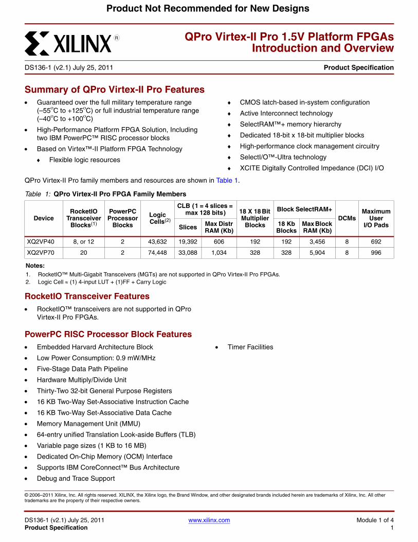
QPro Virtex-II Pro family members and resources are shown in Table 1.
RocketIO Transceiver Features RocketIO™ transceivers are not supported in QPro
Virtex-II Pro FPGAs.
PowerPC RISC Processor Block Features Embedded Harvard Architecture Block
Low Power Consumption: 0.9 mW/MHz
Five-Stage Data Path Pipeline
Hardware Multiply/Divide Unit
Thirty-Two 32-bit General Purpose Registers
16 KB Two-Way Set-Associative Instruction Cache
16 KB Two-Way Set-Associative Data Cache
Memory Management Unit (MMU)
64-entry unified Translation Look-aside Buffers (TLB)
Variable page sizes (1 KB to 16 MB)
Dedicated On-Chip Memory (OCM) Interface
Supports IBM CoreConnect™ Bus Architecture
Debug and Trace Support
Timer Facilities
8QPro Virtex-II Pro 1.5V Platform FPGAs
Introduction and Overview
DS136-1 (v2.1) July 25, 2011 0 Product Specification
R
Table 1: QPro Virtex-II Pro FPGA Family Members
DeviceRocketIO
Transceiver Blocks(1)
PowerPC Processor
Blocks
Logic Cells(2)
CLB ( 1 = 4 slices = max 128 bits ) 18 X 18 Bit
Multiplier Blocks
Block SelectRAM+DCMs
Maximum User
I/O PadsSlices Max Distr RAM (Kb)
18 Kb Blocks
Max Block RAM (Kb)
XQ2VP40 8, or 12 2 43,632 19,392 606 192 192 3,456 8 692
XQ2VP70 20 2 74,448 33,088 1,034 328 328 5,904 8 996
Notes: 1. RocketIO™ Multi-Gigabit Transceivers (MGTs) are not supported in QPro Virtex-II Pro FPGAs.2. Logic Cell (1) 4-input LUT + (1)FF + Carry Logic
Introduction and Overview
DS136-1 (v2.1) July 25, 2011 www.xilinx.com Module 1 of 4Product Specification 2
R
Product Not Recommended for New Designs
QPro Virtex-II Pro Platform FPGA Technology SelectRAM+ Memory Hierarchy
Up to 6 Mb of True Dual-Port RAM in 18 Kb block SelectRAM+ resources
Up to 1,034 Kb of distributed SelectRAM+ resources
High-performance interfaces to external memory
Arithmetic Functions
Dedicated 18-bit x 18-bit multiplier blocks
Fast look-ahead carry logic chains
Flexible Logic Resources
Up to 66,176 internal registers/ latches with Clock Enable
Up to 66,176 look-up tables (LUTs) or cascadable variable (1 to 16 bits) shift registers
Wide multiplexers and wide-input function support
Horizontal cascade chain and Sum-of-Products support
Internal three-state busing
High-Performance Clock Management Circuitry
Eight Digital Clock Manager (DCM) modules
- Precise clock deskew
- Flexible frequency synthesis
- High-resolution phase shifting
16 global clock multiplexer buffers in all parts
Active Interconnect Technology
Fourth-generation segmented routing structure
Fast, predictable routing delay, independent of fanout
Deep sub-micron noise immunity benefits
SelectIO™-Ultra Technology
Up to 996 user I/Os
Twenty-two single-ended standards and ten differential standards
Programmable LVCMOS sink/source current (2 mA to 24 mA) per I/O
XCITE Digitally Controlled Impedance (DCI) I/O
PCI / PCI-X support (refer to XAPP653, 3.3V PCI Design Guidelines, for more information)
Differential signaling
- 512 Mb/s Low-Voltage Differential Signaling I/O (LVDS) with current mode drivers
- On-chip differential termination
- Bus LVDS I/O
- HyperTransport (LDT) I/O with current driver buffers
- Built-in DDR input and output registers
Proprietary high-performance SelectLink technology for communications between Xilinx devices
- High-bandwidth data path
- Double Data Rate (DDR) link
- Web-based HDL generation methodology
CMOS Latch-Based In-System Configuration
Fast SelectMAP™ configuration
Triple Data Encryption Standard (DES) security option (bitstream encryption)
IEEE 1532 support
Partial reconfiguration
Unlimited reprogrammability
Readback capability
Supported by Xilinx Integrated Software Environment (ISE™) Software
Integrated VHDL and Verilog design flows
ChipScope™ Integrated Logic Analyzer
0.13 µm Nine-Layer Copper Process with 90 nm High-Speed Transistors
1.5V (VCCINT) core power supply, dedicated 2.5V VCCAUX auxiliary and VCCO I/O power supplies
IEEE 1149.1 Compatible Boundary-Scan Logic Support
Flip-Chip and Wire-Bond Ball Grid Array (BGA) Packages in Standard 1.00 mm Pitch.
General DescriptionQPro Virtex-II Pro platform FPGAs are well-suited for designs based on IP cores and customized modules. The family incorporates the PowerPC CPU blocks in the Virtex-II Pro architecture. This family of FPGAs empowers complete solutions for telecommunication, wireless, networking, video, and DSP applications.
The Virtex-II Pro architecture and leading-edge 0.13 µm CMOS nine-layer copper process are optimized for high performance designs in a wide range of densities. Combining a wide variety of flexible features and IP cores, the QPro Virtex-II Pro family enhances programmable logic design capabilities and is a powerful alternative to mask-programmed gate arrays.
Introduction and Overview
DS136-1 (v2.1) July 25, 2011 www.xilinx.com Module 1 of 4Product Specification 3
R
Product Not Recommended for New Designs
Architecture
Array Overview
QPro Virtex-II Pro devices are user-programmable gate arrays with various configurable elements and embedded blocks optimized for high-density and high-performance system designs. QPro Virtex-II Pro devices implement the following functionality:
Embedded IBM PowerPC 405 RISC processor blocks.
SelectIO-Ultra blocks provide the interface between package pins and the internal configurable logic. Most popular and leading-edge I/O standards are supported by the programmable IOBs.
Configurable Logic Blocks (CLBs) provide functional elements for combinatorial and synchronous logic, including basic storage elements. BUFTs (three-state buffers) associated with each CLB element drive dedicated segmentable horizontal routing resources.
Block SelectRAM+ memory modules provide large 18 Kb storage elements of True Dual-Port RAM.
Embedded multiplier blocks are 18-bit x 18-bit dedicated multipliers.
Digital Clock Manager (DCM) blocks provide self-calibrating, fully digital solutions for clock distribution delay compensation, clock multiplication and division, and coarse- and fine-grained clock phase shifting.
A new generation of programmable routing resources called Active Interconnect Technology interconnects all these elements. The general routing matrix (GRM) is an array of routing switches. Each programmable element is tied to a switch matrix, allowing multiple connections to the general routing matrix. The overall programmable interconnection is hierarchical and supports high-speed designs.
All programmable elements, including the routing resources, are controlled by values stored in static memory cells. These values are loaded in the memory cells during configuration and can be reloaded to change the functions of the programmable elements.
Features
This section briefly describes QPro Virtex-II Pro features. For more details, refer to "Functional Description" (Module 2).
RocketIO MGT Cores
RocketIO™ transceivers are not supported in QPro Virtex-II Pro FPGAs.
PowerPC 405 Processor Block
The PPC405 RISC CPU can execute instructions at a sustained rate of one instruction per cycle. On-chip
instruction and data cache reduce design complexity and improve system throughput.
The PPC405 features include:
PowerPC RISC CPU
Implements the PowerPC User Instruction Set Architecture (UISA) and extensions for embedded applications
Thirty-two 32-bit general purpose registers (GPRs)
Static branch prediction
Five-stage pipeline with single-cycle execution of most instructions, including loads/stores
Unaligned and aligned load/store support to cache, main memory, and on-chip memory
Hardware multiply/divide for faster integer arithmetic (4-cycle multiply, 35-cycle divide)
Enhanced string and multiple-word handling
Big/little endian operation support
Storage Control
Separate instruction and data cache units, both two-way set-associative and non-blocking
Eight words (32 bytes) per cache line
16 KB array Instruction Cache Unit (ICU), 16 KB array Data Cache Unit (DCU)
Operand forwarding during instruction cache line fill
Copy-back or write-through DCU strategy
Doubleword instruction fetch from cache improves branch latency
Virtual mode memory management unit (MMU)
Translation of the 4 GB logical address space into physical addresses
Software control of page replacement strategy
Supports multiple simultaneous page sizes ranging from 1 KB to 16 MB
OCM controllers provide dedicated interfaces between Block SelectRAM+ memory and processor block instruction and data paths for high-speed access
PowerPC timer facilities
64-bit time base
Programmable interval timer (PIT)
Fixed interval timer (FIT)
Watchdog timer (WDT)
Debug Support
Internal debug mode
External debug mode
Debug Wait mode
Real Time Trace debug mode
Introduction and Overview
DS136-1 (v2.1) July 25, 2011 www.xilinx.com Module 1 of 4Product Specification 4
R
Product Not Recommended for New Designs
Enhanced debug support with logical operators
Instruction trace and trace-back support
Forward or backward trace
Two hardware interrupt levels support
Advanced power management support
Input/Output Blocks (IOBs)
IOBs are programmable and can be categorized as follows:
Input block with an optional single data rate (SDR) or double data rate (DDR) register
Output block with an optional SDR or DDR register and an optional three-state buffer to be driven directly or through an SDR or DDR register
Bidirectional block (any combination of input and output configurations)
These registers are either edge-triggered D-type flip-flops or level-sensitive latches.
IOBs support the following single-ended I/O standards:
LVTTL, LVCMOS (3.3V,(1) 2.5V, 1.8V, and 1.5V)
PCI-X compatible (133 MHz and 66 MHz) at 3.3V (2)
PCI compliant (66 MHz and 33 MHz) at 3.3V (2)
GTL and GTLP
HSTL (1.5V and 1.8V, Class I, II, III, and IV)
SSTL (1.8V and 2.5V, Class I and II)
The DCI I/O feature automatically provides on-chip termination for each single-ended I/O standard.
The IOB elements also support the following differential signaling I/O standards:
LVDS and Extended LVDS (2.5V)
BLVDS (Bus LVDS)
ULVDS
LDT
LVPECL (2.5V)
Two adjacent pads are used for each differential pair. Two or four IOBs connect to one switch matrix to access the routing resources. On-chip differential termination is available for LVDS, LVDS Extended, ULVDS, and LDT standards.
Configurable Logic Blocks (CLBs)
CLB resources include four slices and two three-state buffers. Each slice is equivalent and contains:
Two function generators (F & G)
Two storage elements
Arithmetic logic gates
Large multiplexers
Wide function capability
Fast carry look-ahead chain
Horizontal cascade chain (OR gate)
The function generators F & G are configurable as 4-input look-up tables (LUTs), as 16-bit shift registers, or as 16-bit distributed SelectRAM+ memory.
In addition, the two storage elements are either edge-triggered D-type flip-flops or level-sensitive latches.
Each CLB has internal fast interconnect and connects to a switch matrix to access general routing resources.
Block SelectRAM+ Memory
The block SelectRAM+ memory resources are 18 Kb of True Dual-Port RAM, programmable from 16K x 1 bit to 512 x 36 bit, in various depth and width configurations. Each port is totally synchronous and independent, offering three "read-during-write" modes. Block SelectRAM+ memory is cascadable to implement large embedded storage blocks.
Supported memory configurations for dual-port and single-port modes are shown in Table 2.
18 x 18 Bit Multipliers
A multiplier block is associated with each SelectRAM+ memory block. The multiplier block is a dedicated 18 x 18-bit 2s complement signed multiplier, and is optimized for operations based on the block SelectRAM+ content on one port. The 18 x 18 multiplier can be used independently of the block SelectRAM+ resource. Read/multiply/accumulate operations and DSP filter structures are extremely efficient.
Both the SelectRAM+ memory and the multiplier resource are connected to four switch matrices to access the general routing resources.
Global Clocking
The DCM and global clock multiplexer buffers provide a complete solution for designing high-speed clock schemes.
Up to twelve DCM blocks are available. To generate deskewed internal or external clocks, each DCM can be used to eliminate clock distribution delay. The DCM also provides 90-, 180-, and 270-degree phase-shifted versions of its output clocks. Fine-grained phase shifting offers high-resolution phase adjustments in increments of 1/256 of the clock period. Very flexible frequency synthesis provides a
1. Refer to XAPP659, Virtex-II Pro / Virtex-II Pro X 3.3V I/O Design Guidelines, for more information.
2. Refer to 3.3V PCI Design Guidelines or more information.
Table 2: Dual-Port and Single-Port Configurations
16K x 1 bit 4K x 4 bits 1K x 18 bits
8K x 2 bits 2K x 9 bits 512 x 36 bits
Introduction and Overview
DS136-1 (v2.1) July 25, 2011 www.xilinx.com Module 1 of 4Product Specification 5
R
Product Not Recommended for New Designs
clock output frequency equal to a fractional or integer multiple of the input clock frequency. For exact timing parameters, see "DC and Switching Characteristics" (Module 3).
QPro Virtex-II Pro devices have 16 global clock MUX buffers, with up to eight clock nets per quadrant. Each clock MUX buffer can select one of the two clock inputs and switch glitch-free from one clock to the other. Each DCM can send up to four of its clock outputs to global clock buffers on the same edge. Any global clock pin can drive any DCM on the same edge.
Routing Resources
The IOB, CLB, block SelectRAM+, multiplier, and DCM elements all use the same interconnect scheme and the same access to the global routing matrix. Timing models are shared, greatly improving the predictability of the performance of high-speed designs.
There are a total of 16 global clock lines, with eight available per quadrant. In addition, 24 vertical and horizontal long lines per row or column, as well as massive secondary and local routing resources, provide fast interconnect. QPro Virtex-II Pro buffered interconnects are relatively unaffected by net fanout, and the interconnect layout is designed to minimize crosstalk.
Horizontal and vertical routing resources for each row or column include:
24 long lines
120 hex lines
40 double lines
16 direct connect lines (total in all four directions)
Boundary-Scan
Boundary-scan instructions and associated data registers support a standard methodology for accessing and configuring QPro Virtex-II Pro devices, complying with IEEE
standards 1149.1 and 1532. A system mode and a test mode are implemented. In system mode, a QPro Virtex-II Pro device continues to function while executing non-test boundary-scan instructions. In test mode, boundary-scan test instructions control the I/O pins for testing purposes. The QPro Virtex-II Pro Test Access Port (TAP) supports BYPASS, PRELOAD, SAMPLE, IDCODE, and USERCODE non-test instructions. The EXTEST, INTEST, and HIGHZ test instructions are also supported.
Configuration
QPro Virtex-II Pro devices are configured by loading the bitstream into internal configuration memory using one of the following modes:
Slave-serial mode
Master-serial mode
Slave SelectMAP mode
Master SelectMAP mode
Boundary-Scan mode (IEEE 1532)
A Data Encryption Standard (DES) decryptor is available on-chip to secure the bitstreams. One or two triple-DES key sets can be used to optionally encrypt the configuration data.
Readback and Integrated Logic Analyzer
Configuration data stored in QPro Virtex-II Pro configuration memory can be read back for verification. Along with the configuration data, the contents of all flip-flops and latches, distributed SelectRAM+, and block SelectRAM+ memory resources can be read back. This capability is useful for real-time debugging.
The Xilinx ChipScope Integrated Logic Analyzer (ILA) cores and Integrated Bus Analyzer (IBA) cores, along with the ChipScope Pro Analyzer software, provide a complete solution for accessing and verifying user designs within QPro Virtex-II Pro devices.
IP Core and Reference SupportIntellectual Property is part of the Platform FPGA solution. In addition to existing FPGA fabric cores, the next subsections show some of the currently available hardware and software intellectual properties specially developed for QPro Virtex-II Pro devices by Xilinx. Each IP core is modular, portable, Real-Time Operating System (RTOS) independent, and CoreConnect compatible for ease of design migration. Refer to www.xilinx.com/ipcenter for the latest and most complete list of cores.
Hardware Cores Bus Infrastructure cores (arbiters, bridges, and more)
Memory cores (DDR, Flash, and more)
Peripheral cores (UART, IIC, and more)
Networking cores (ATM, Ethernet, and more)
Software Cores Boot code
Test code
Device drivers
Protocol stacks
RTOS integration
Customized board support package
Introduction and Overview
DS136-1 (v2.1) July 25, 2011 www.xilinx.com Module 1 of 4Product Specification 6
R
Product Not Recommended for New Designs
QPro Virtex-II Pro Device/Package Combinations and Maximum I/OsOfferings include ball grid array (BGA) packages with 1.0 mm pitch. In addition to traditional wire-bond interconnect (FG packages), flip-chip interconnect (FF packages) is used in some of the BGA offerings. Flip-chip interconnect construction supports more I/Os than are possible in wire-bond versions of similar packages, providing a high pin count and excellent power dissipation.
The device/package combination table (Table 3) details the maximum number of user I/Os for each device and package using wire-bond or flip-chip technology.
The I/Os per package count includes all user I/Os except the 15 control pins (CCLK, DONE, M0, M1, M2, PROG_B,
PWRDWN_B, TCK, TDI, TDO, TMS, HSWAP_EN, DXN, DXP, and RSVD), VBATT, and the RocketIO transceiver pins.
Maximum PerformanceMaximum performance of the PowerPC processor block varies, depending on package style and speed grade. See Table 4 for details. "DC and Switching Characteristics" (Module 3) contains the rest of the FPGA fabric performance parameters.
Table 3: QPro Virtex-II Pro Device/Package Combinations and Maximum Number of Available I/Os
Package FG676 FF1152 FF1704/EF1704
Pitch (mm) 1.00 1.00 1.00
Size (mm) 26 x 26 35 x 35 42.5 x 42.5
XQ2VP40 416 692 –
XQ2VP70 – – 996
Table 4: Maximum Processor Block Performance
DeviceSpeed Grade
Units-6 -5
PowerPC Processor Block 350(1) 300 MHz
Notes: 1. IMPORTANT! When CPMC405CLOCK runs at speeds greater
than 350 MHz in -7 Commercial grade dual-processor devices, or greater than 300 MHz in -6 Industrial grade dual-processor devices, users must implement the technology presented in XAPP755, PowerPC 405 Clock Macro for -7(C) and -6(I) Speed Grade Dual-Processor Devices. Refer to Table 1 to identify dual-processor devices.
Introduction and Overview
DS136-1 (v2.1) July 25, 2011 www.xilinx.com Module 1 of 4Product Specification 7
R
Product Not Recommended for New Designs
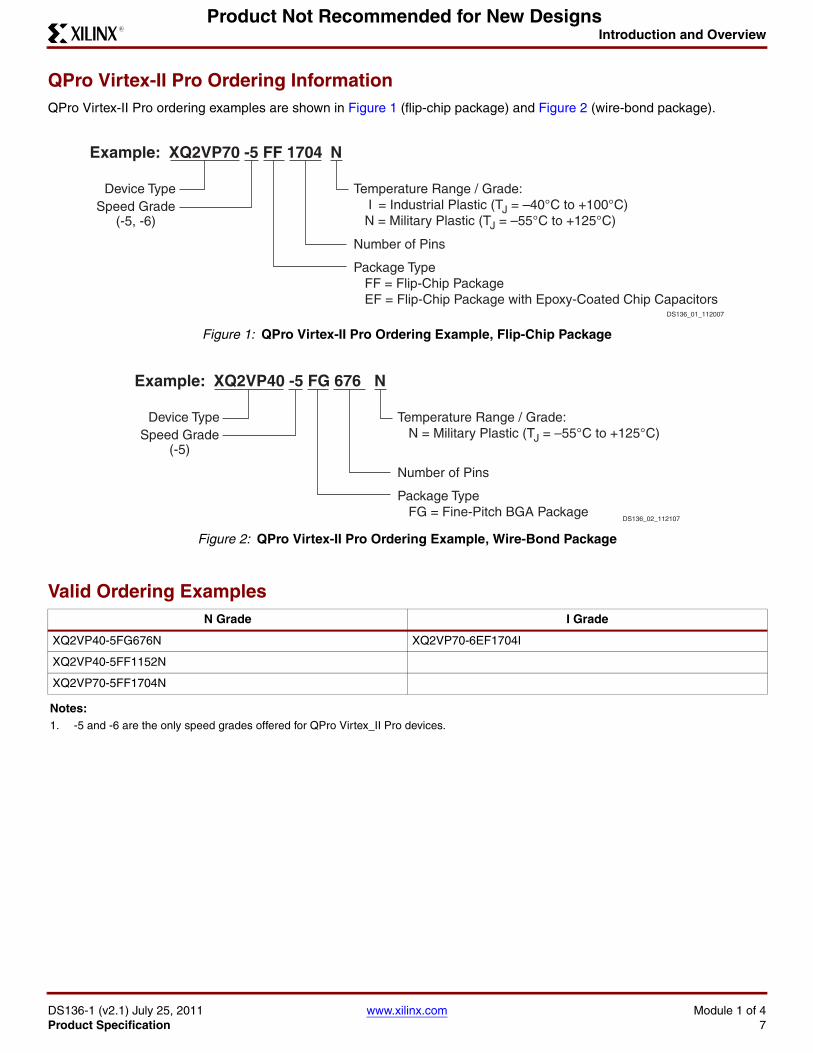
QPro Virtex-II Pro Ordering InformationQPro Virtex-II Pro ordering examples are shown in Figure 1 (flip-chip package) and Figure 2 (wire-bond package).
Valid Ordering Examples
X-Ref Target - Figure 1
Figure 1: QPro Virtex-II Pro Ordering Example, Flip-Chip Package
X-Ref Target - Figure 2
Figure 2: QPro Virtex-II Pro Ordering Example, Wire-Bond Package
Example: XQ2VP70 -5 FF 1704 N
Device Type Temperature Range / Grade: I = Industrial Plastic (TJ = –40°C to +100°C) N = Military Plastic (TJ = –55°C to +125°C)
Number of Pins
Package Type FF = Flip-Chip Package EF = Flip-Chip Package with Epoxy-Coated Chip Capacitors
Speed Grade(-5, -6)
DS136_01_112007
Example: XQ2VP40 -5 FG 676 N
Device Type Temperature Range / Grade: N = Military Plastic (TJ = –55°C to +125°C)
Number of Pins
Package Type FG = Fine-Pitch BGA Package
Speed Grade(-5)
DS136_02_112107
N Grade I Grade
XQ2VP40-5FG676N XQ2VP70-6EF1704I
XQ2VP40-5FF1152N
XQ2VP70-5FF1704N
Notes: 1. -5 and -6 are the only speed grades offered for QPro Virtex_II Pro devices.
Introduction and Overview
DS136-1 (v2.1) July 25, 2011 www.xilinx.com Module 1 of 4Product Specification 8
R
Product Not Recommended for New Designs
Revision HistoryThis section records the change history for this module of the data sheet.
QPro Virtex-II Pro Data SheetThe QPro Virtex-II Pro Data Sheet contains the following modules:
"Introduction and Overview" (Module 1)
"Functional Description" (Module 2)
"DC and Switching Characteristics" (Module 3)
"Pinout Information" (Module 4)
Notice of DisclaimerTHE XILINX HARDWARE FPGA AND CPLD DEVICES REFERRED TO HEREIN (“PRODUCTS”) ARE SUBJECT TO THE TERMS AND CONDITIONS OF THE XILINX LIMITED WARRANTY WHICH CAN BE VIEWED AT http://www.xilinx.com/warranty.htm. THIS LIMITED WARRANTY DOES NOT EXTEND TO ANY USE OF PRODUCTS IN AN APPLICATION OR ENVIRONMENT THAT IS NOT WITHIN THE SPECIFICATIONS STATED IN THE XILINX DATA SHEET. ALL SPECIFICATIONS ARE SUBJECT TO CHANGE WITHOUT NOTICE. PRODUCTS ARE NOT DESIGNED OR INTENDED TO BE FAIL-SAFE OR FOR USE IN ANY APPLICATION REQUIRING FAIL-SAFE PERFORMANCE, SUCH AS LIFE-SUPPORT OR SAFETY DEVICES OR SYSTEMS, OR ANY OTHER APPLICATION THAT INVOKES THE POTENTIAL RISKS OF DEATH, PERSONAL INJURY, OR PROPERTY OR ENVIRONMENTAL DAMAGE (“CRITICAL APPLICATIONS”). USE OF PRODUCTS IN CRITICAL APPLICATIONS IS AT THE SOLE RISK OF CUSTOMER, SUBJECT TO APPLICABLE LAWS AND REGULATIONS.
Date Version Revision
11/29/06 1.0 Initial Xilinx release.
12/20/07 2.0 Change data sheet title. Added support for XQ2VP70-6EF1704I. Removed support for XQV2P70-6MF1704I. Updated document template. Updated URLs.
07/25/11 2.1 Added Product Not Recommended for New Designs banner.
DS136-2 (v2.1) July 25, 2011 www.xilinx.com Module 2 of 4Product Specification 1
© 2006–2011 Xilinx, Inc. All rights reserved. XILINX, the Xilinx logo, the Brand Window, and other designated brands included herein are trademarks of Xilinx, Inc. All other trademarks are the property of their respective owners.
Product Not Recommended for New Designs
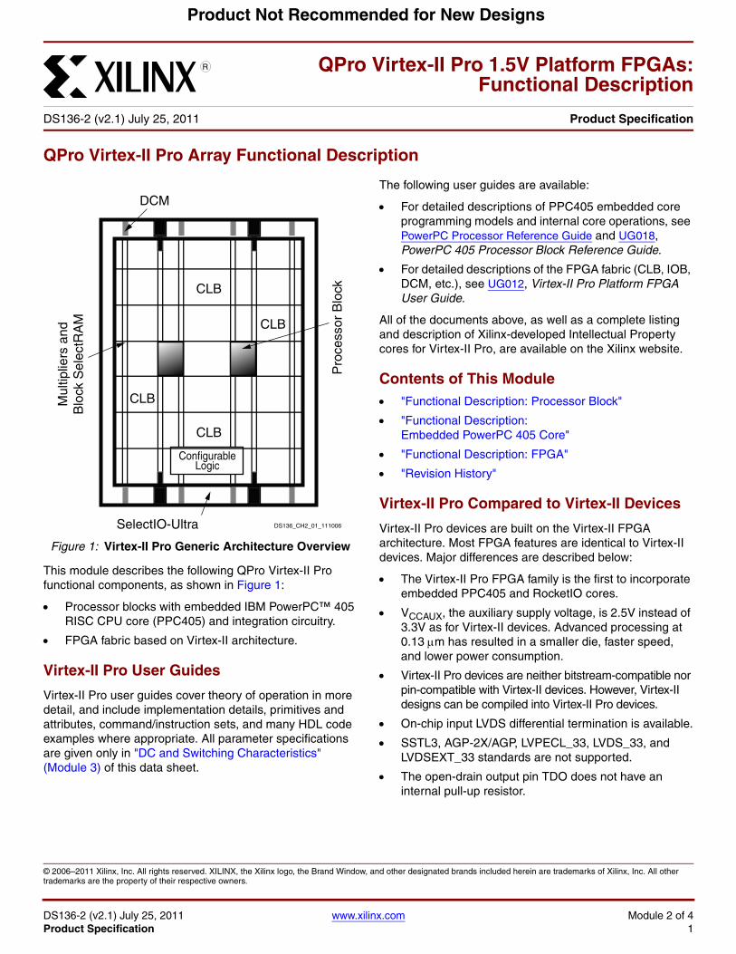
QPro Virtex-II Pro Array Functional Description
This module describes the following QPro Virtex-II Pro functional components, as shown in Figure 1:
Processor blocks with embedded IBM PowerPC™ 405 RISC CPU core (PPC405) and integration circuitry.
FPGA fabric based on Virtex-II architecture.
Virtex-II Pro User Guides
Virtex-II Pro user guides cover theory of operation in more detail, and include implementation details, primitives and attributes, command/instruction sets, and many HDL code examples where appropriate. All parameter specifications are given only in "DC and Switching Characteristics" (Module 3) of this data sheet.
The following user guides are available:
For detailed descriptions of PPC405 embedded core programming models and internal core operations, see PowerPC Processor Reference Guide and UG018, PowerPC 405 Processor Block Reference Guide.
For detailed descriptions of the FPGA fabric (CLB, IOB, DCM, etc.), see UG012, Virtex-II Pro Platform FPGA User Guide.
All of the documents above, as well as a complete listing and description of Xilinx-developed Intellectual Property cores for Virtex-II Pro, are available on the Xilinx website.
Contents of This Module "Functional Description: Processor Block"
"Functional Description: Embedded PowerPC 405 Core"
"Functional Description: FPGA"
"Revision History"
Virtex-II Pro Compared to Virtex-II Devices
Virtex-II Pro devices are built on the Virtex-II FPGA architecture. Most FPGA features are identical to Virtex-II devices. Major differences are described below:
The Virtex-II Pro FPGA family is the first to incorporate embedded PPC405 and RocketIO cores.
VCCAUX, the auxiliary supply voltage, is 2.5V instead of 3.3V as for Virtex-II devices. Advanced processing at 0.13 m has resulted in a smaller die, faster speed, and lower power consumption.
Virtex-II Pro devices are neither bitstream-compatible nor pin-compatible with Virtex-II devices. However, Virtex-II designs can be compiled into Virtex-II Pro devices.
On-chip input LVDS differential termination is available.
SSTL3, AGP-2X/AGP, LVPECL_33, LVDS_33, and LVDSEXT_33 standards are not supported.
The open-drain output pin TDO does not have an internal pull-up resistor.
43 QPro Virtex-II Pro 1.5V Platform FPGAs:
Functional Description
DS136-2 (v2.1) July 25, 2011 Product Specification
R
X-Ref Target - Figure 1
Figure 1: Virtex-II Pro Generic Architecture Overview
CLB
Mul
tiplie
rs a
ndB
lock
Sel
ectR
AM
Pro
cess
or B
lock
ConfigurableLogic
SelectIO-Ultra DS136_CH2_01_111006
DCM
CLB
CLB
CLB
Functional Description
DS136-2 (v2.1) July 25, 2011 www.xilinx.com Module 2 of 4Product Specification 2
R
Product Not Recommended for New Designs
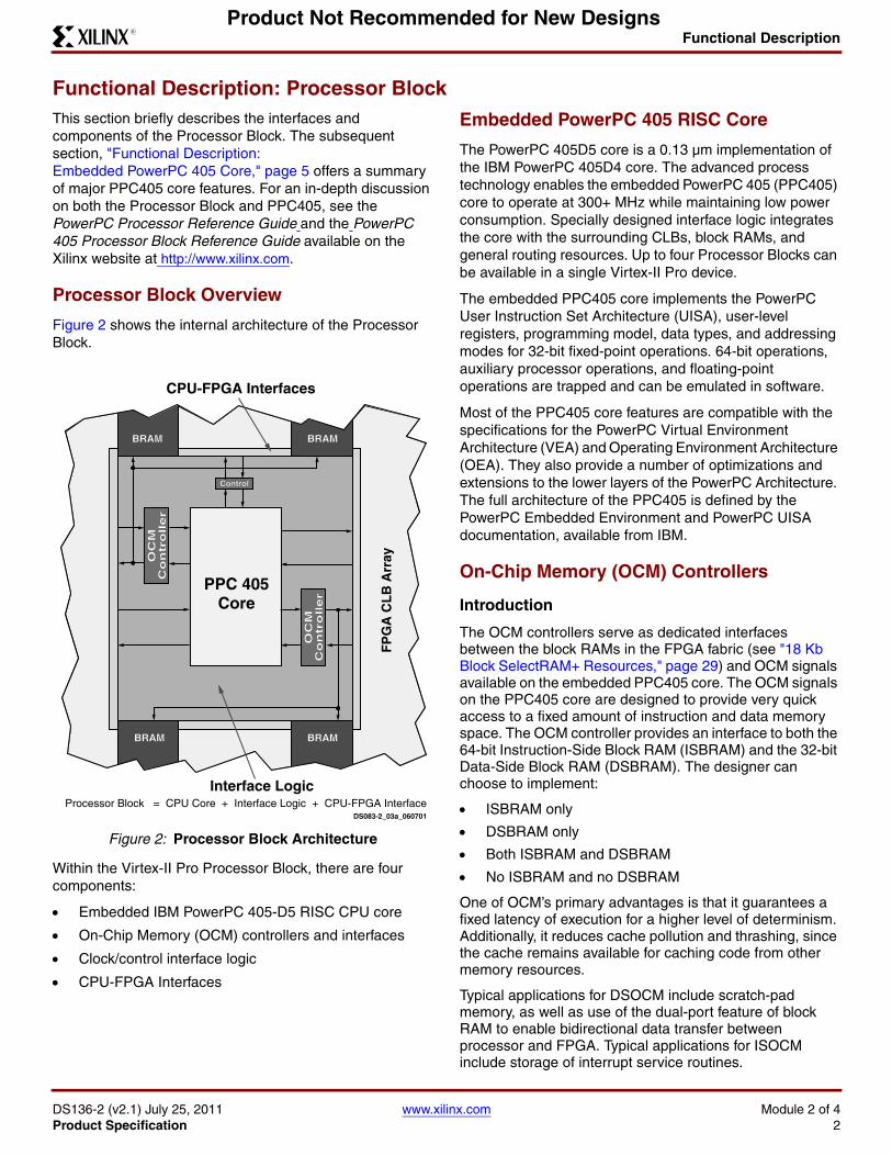
Functional Description: Processor BlockThis section briefly describes the interfaces and components of the Processor Block. The subsequent section, "Functional Description: Embedded PowerPC 405 Core," page 5 offers a summary of major PPC405 core features. For an in-depth discussion on both the Processor Block and PPC405, see the PowerPC Processor Reference Guide and the PowerPC 405 Processor Block Reference Guide available on the Xilinx website at http://www.xilinx.com.
Processor Block Overview
Figure 2 shows the internal architecture of the Processor Block.
Within the Virtex-II Pro Processor Block, there are four components:
Embedded IBM PowerPC 405-D5 RISC CPU core
On-Chip Memory (OCM) controllers and interfaces
Clock/control interface logic
CPU-FPGA Interfaces
Embedded PowerPC 405 RISC Core
The PowerPC 405D5 core is a 0.13 µm implementation of the IBM PowerPC 405D4 core. The advanced process technology enables the embedded PowerPC 405 (PPC405) core to operate at 300+ MHz while maintaining low power consumption. Specially designed interface logic integrates the core with the surrounding CLBs, block RAMs, and general routing resources. Up to four Processor Blocks can be available in a single Virtex-II Pro device.
The embedded PPC405 core implements the PowerPC User Instruction Set Architecture (UISA), user-level registers, programming model, data types, and addressing modes for 32-bit fixed-point operations. 64-bit operations, auxiliary processor operations, and floating-point operations are trapped and can be emulated in software.
Most of the PPC405 core features are compatible with the specifications for the PowerPC Virtual Environment Architecture (VEA) and Operating Environment Architecture (OEA). They also provide a number of optimizations and extensions to the lower layers of the PowerPC Architecture. The full architecture of the PPC405 is defined by the PowerPC Embedded Environment and PowerPC UISA documentation, available from IBM.
On-Chip Memory (OCM) Controllers
Introduction
The OCM controllers serve as dedicated interfaces between the block RAMs in the FPGA fabric (see "18 Kb Block SelectRAM+ Resources," page 29) and OCM signals available on the embedded PPC405 core. The OCM signals on the PPC405 core are designed to provide very quick access to a fixed amount of instruction and data memory space. The OCM controller provides an interface to both the 64-bit Instruction-Side Block RAM (ISBRAM) and the 32-bit Data-Side Block RAM (DSBRAM). The designer can choose to implement:
ISBRAM only
DSBRAM only
Both ISBRAM and DSBRAM
No ISBRAM and no DSBRAM
One of OCM’s primary advantages is that it guarantees a fixed latency of execution for a higher level of determinism. Additionally, it reduces cache pollution and thrashing, since the cache remains available for caching code from other memory resources.
Typical applications for DSOCM include scratch-pad memory, as well as use of the dual-port feature of block RAM to enable bidirectional data transfer between processor and FPGA. Typical applications for ISOCM include storage of interrupt service routines.
X-Ref Target - Figure 2
Figure 2: Processor Block Architecture
Processor Block = CPU Core + Interface Logic + CPU-FPGA Interface DS083-2_03a_060701
PPC 405Core
OC
MC
on
tro
lle
r
OC
MC
on
tro
lle
r
Control
BRAM BRAM
BRAMBRAM
FP
GA
CL
B A
rray
Interface Logic
CPU-FPGA Interfaces
Functional Description
DS136-2 (v2.1) July 25, 2011 www.xilinx.com Module 2 of 4Product Specification 3
R
Product Not Recommended for New Designs
Functional Features
Common Features
Separate Instruction and Data memory interface between processor core and BRAMs in FPGA
Dedicated interface to Device Control Register (DCR) bus for ISOCM and DSOCM
Single-cycle and multi-cycle mode option for I-side and D-side interfaces
Single cycle = one CPU clock cycle; multi-cycle = minimum of two and maximum of eight CPU clock cycles
FPGA configurable DCR addresses within DSOCM and ISOCM.
Independent 16 MB logical memory space available within PPC405 memory map for each of the DSOCM and ISOCM. The number of block RAMs in the device might limit the maximum amount of OCM supported.
Maximum of 64K and 128K bytes addressable from DSOCM and ISOCM interfaces, respectively, using address outputs from OCM directly without additional decoding logic.
Data-Side OCM (DSOCM)
32-bit Data Read bus and 32-bit Data Write bus
Byte write access to DSBRAM support
Second port of dual port DSBRAM is available to read/write from an FPGA interface
22-bit address to DSBRAM port
8-bit DCR Registers: DSCNTL, DSARC
Three alternatives to write into DSBRAM: BRAM initialization, CPU, FPGA H/W using second port
Instruction-Side OCM (ISOCM)
The ISOCM interface contains a 64-bit read only port, for instruction fetches, and a 32-bit write only port, to initialize or test the ISBRAM. When implementing the read only port, the user must deassert the write port inputs. The preferred method of initializing the ISBRAM is through the configuration bitstream.
64-bit Data Read Only bus (two instructions per cycle)
32-bit Data Write Only bus (through DCR)
Separate 21-bit address to ISBRAM
8-bit DCR Registers: ISCNTL, ISARC
32-bit DCR Registers: ISINIT, ISFILL
Two alternatives to write into ISBRAM: BRAM initialization, DCR and write instruction
Clock/Control Interface Logic
The clock/control interface logic provides proper initialization and connections for PPC405 clock/power management, resets, PLB cycle control, and OCM interfaces. It also couples user signals between the FPGA fabric and the embedded PPC405 CPU core.
The processor clock connectivity is similar to CLB clock pins. It can connect either to global clock nets or general routing resources. Therefore the processor clock source can come from DCM, CLB, or user package pin.
CPU-FPGA Interfaces
All Processor Block user pins link up with the general FPGA routing resources through the CPU-FPGA interface. Therefore processor signals have the same routability as other non-Processor Block user signals. Longlines and hex lines travel across the Processor Block both vertically and horizontally, allowing signals to route through the Processor Block.
Processor Local Bus (PLB) Interfaces
The PPC405 core accesses high-speed system resources through PLB interfaces on the instruction and data cache controllers. The PLB interfaces provide separate 32-bit address/64-bit data buses for the instruction and data sides.
The cache controllers are both PLB masters. PLB arbiters are implemented in the FPGA fabric and are available as soft IP cores.
Device Control Register (DCR) Bus Interface
The device control register (DCR) bus has 10 bits of address space for components external to the PPC405 core. Using the DCR bus to manage status and configuration registers reduces PLB traffic and improves system integrity. System resources on the DCR bus are protected or isolated from wayward code since the DCR bus is not part of the system memory map.
External Interrupt Controller (EIC) Interface
Two level-sensitive user interrupt pins (critical and non-critical) are available. They can be either driven by user defined logic or Xilinx soft interrupt controller IP core outside the Processor Block.
Clock/Power Management (CPM) Interface
The CPM interface supports several methods of clock distribution and power management. Three modes of operation that reduce power consumption below the normal operational level are available.
Reset Interface
There are three user reset input pins (core, chip, and system) and three user reset output pins for different levels of reset, if required.
Functional Description
DS136-2 (v2.1) July 25, 2011 www.xilinx.com Module 2 of 4Product Specification 4
R
Product Not Recommended for New Designs
Debug Interface
Debugging interfaces on the embedded PPC405 core, consisting of the JTAG and Trace ports, offer access to resources internal to the core and assist in software development. The JTAG port provides basic JTAG chip testing functionality as well as the ability for external debug tools to gain control of the processor for debug purposes. The Trace port furnishes programmers with a mechanism for acquiring instruction execution traces.
The JTAG port complies with IEEE Std 1149.1, which defines a test access port (TAP) and Boundary-Scan architecture. Extensions to the JTAG interface provide debuggers with processor control that includes stopping, starting, and stepping the PPC405 core. These extensions are compliant with the IEEE 1149.1 specifications for vendor-specific extensions.
The Trace port provides instruction execution trace information to an external trace tool. The PPC405 core is capable of back trace and forward trace. Back trace is the tracing of instructions prior to a debug event while forward trace is the tracing of instructions after a debug event.
The processor JTAG port and the FPGA JTAG port can be accessed independently, or the two can be programmatically linked together and accessed via the dedicated FPGA JTAG pins.
For detailed information on the PPC405 JTAG interface, please refer to the "JTAG Interface" section of the PowerPC 405 Processor Block Reference Guide
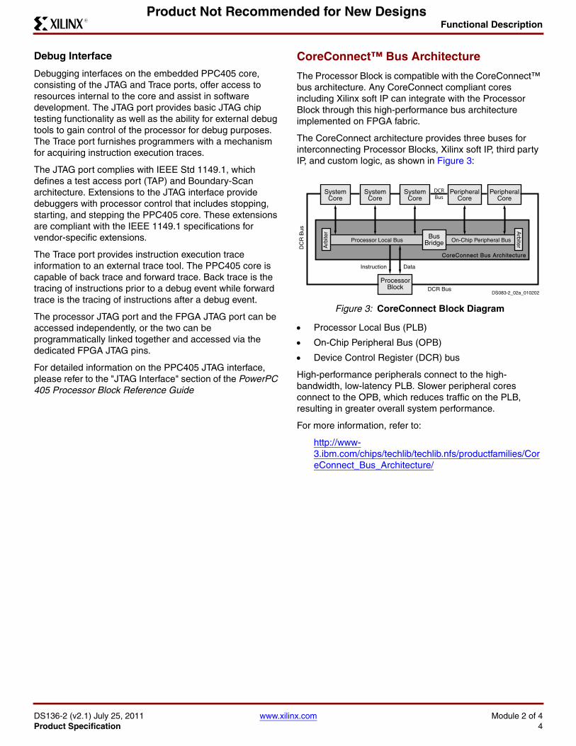
CoreConnect™ Bus Architecture
The Processor Block is compatible with the CoreConnect™ bus architecture. Any CoreConnect compliant cores including Xilinx soft IP can integrate with the Processor Block through this high-performance bus architecture implemented on FPGA fabric.
The CoreConnect architecture provides three buses for interconnecting Processor Blocks, Xilinx soft IP, third party IP, and custom logic, as shown in Figure 3:
Processor Local Bus (PLB)
On-Chip Peripheral Bus (OPB)
Device Control Register (DCR) bus
High-performance peripherals connect to the high-bandwidth, low-latency PLB. Slower peripheral cores connect to the OPB, which reduces traffic on the PLB, resulting in greater overall system performance.
For more information, refer to:
http://www-3.ibm.com/chips/techlib/techlib.nfs/productfamilies/CoreConnect_Bus_Architecture/
X-Ref Target - Figure 3
Figure 3: CoreConnect Block Diagram
DS083-2_02a_010202
SystemCore
SystemCore
SystemCore
ProcessorBlock
PeripheralCore
PeripheralCore
Processor Local Bus On-Chip Peripheral BusBus
Bridge
CoreConnect Bus Architecture
ArbiterA
rbite
r
DCR Bus
Instruction Data
DC
R B
us
DCRBus
Functional Description
DS136-2 (v2.1) July 25, 2011 www.xilinx.com Module 2 of 4Product Specification 5
R
Product Not Recommended for New Designs
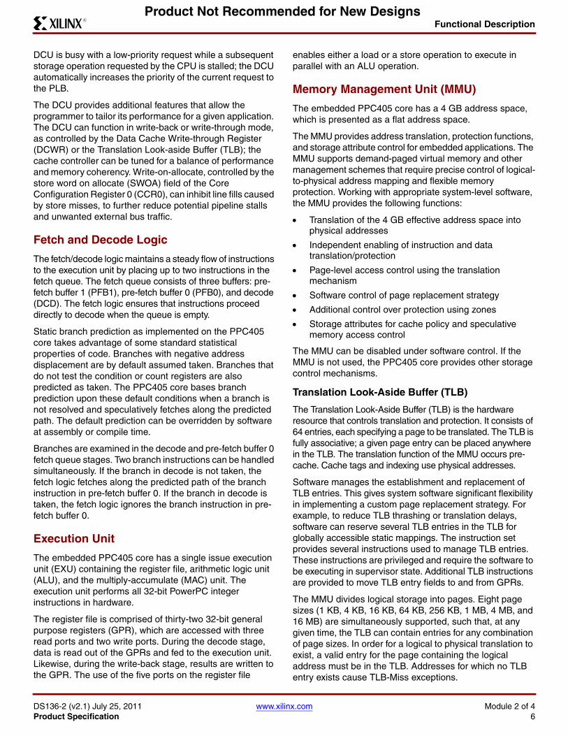
Functional Description: Embedded PowerPC 405 CoreThis section offers a brief overview of the various functional blocks shown in Figure 4.
Embedded PPC405 Core
The embedded PPC405 core is a 32-bit Harvard architecture processor. Figure 4 illustrates its functional blocks:
Cache units
Memory Management unit
Fetch Decode unit
Execution unit
Timers
Debug logic unit
It operates on instructions in a five stage pipeline consisting of a fetch, decode, execute, write-back, and load write-back stage. Most instructions execute in a single cycle, including loads and stores.
Instruction and Data Cache
The embedded PPC405 core provides an instruction cache unit (ICU) and a data cache unit (DCU) that allow concurrent accesses and minimize pipeline stalls. The instruction and data cache array are 16 KB each. Both cache units are two-way set associative. Each way is organized into 256 lines of 32 bytes (eight words). The instruction set provides a rich assortment of cache control instructions, including instructions to read tag information and data arrays.
The PPC405 core accesses external memory through the instruction (ICU) and data cache units (DCU). The cache
units each include a 64-bit PLB master interface, cache arrays, and a cache controller. The ICU and DCU handle cache misses as requests over the PLB to another PLB device such as an external bus interface unit. Cache hits are handled as single cycle memory accesses to the instruction and data caches.
Instruction Cache Unit (ICU)
The ICU provides one or two instructions per cycle to the instruction queue over a 64-bit bus. A line buffer (built into the output of the array for manufacturing test) enables the ICU to be accessed only once for every four instructions, to reduce power consumption by the array.
The ICU can forward any or all of the four or eight words of a line fill to the EXU to minimize pipeline stalls caused by cache misses. The ICU aborts speculative fetches abandoned by the EXU, eliminating unnecessary line fills and enabling the ICU to handle the next EXU fetch. Aborting abandoned requests also eliminates unnecessary external bus activity, thereby increasing external bus utilization.
Data Cache Unit (DCU)
The DCU transfers one, two, three, four, or eight bytes per cycle, depending on the number of byte enables presented by the CPU. The DCU contains a single-element command and store data queue to reduce pipeline stalls; this queue enables the DCU to independently process load/store and cache control instructions. Dynamic PLB request prioritization reduces pipeline stalls even further. When the
X-Ref Target - Figure 4
Figure 4: Embedded PPC405 Core Block Diagram
MACALU
DS083-2_01_062001
PLB MasterInterface
DataOCM
JTAG InstructionTrace
D-CacheController
D-CacheArray
I-CacheController
I-CacheArray
DataCache
Unit
InstructionCache
Unit
32 x 32GPR
Execution Unit (EXU)
PLB MasterInterface
InstructionOCM
Instruction ShadowTLB
(4 Entry)
Unified TLB(64 Entry)
Data ShadowTLB
(8 Entry)
Fetchand
DecodeLogic
3-ElementFetchQueue(PFB1,PFB0,DCD)
Timers
(FIT,PIT,
Watchdog)
Debug Logic
Timers&
Debug
Fetch & DecodeMMU
Cache Units
Execution Unit
Functional Description
DS136-2 (v2.1) July 25, 2011 www.xilinx.com Module 2 of 4Product Specification 6
R
Product Not Recommended for New Designs
DCU is busy with a low-priority request while a subsequent storage operation requested by the CPU is stalled; the DCU automatically increases the priority of the current request to the PLB.
The DCU provides additional features that allow the programmer to tailor its performance for a given application. The DCU can function in write-back or write-through mode, as controlled by the Data Cache Write-through Register (DCWR) or the Translation Look-aside Buffer (TLB); the cache controller can be tuned for a balance of performance and memory coherency. Write-on-allocate, controlled by the store word on allocate (SWOA) field of the Core Configuration Register 0 (CCR0), can inhibit line fills caused by store misses, to further reduce potential pipeline stalls and unwanted external bus traffic.
Fetch and Decode Logic
The fetch/decode logic maintains a steady flow of instructions to the execution unit by placing up to two instructions in the fetch queue. The fetch queue consists of three buffers: pre-fetch buffer 1 (PFB1), pre-fetch buffer 0 (PFB0), and decode (DCD). The fetch logic ensures that instructions proceed directly to decode when the queue is empty.
Static branch prediction as implemented on the PPC405 core takes advantage of some standard statistical properties of code. Branches with negative address displacement are by default assumed taken. Branches that do not test the condition or count registers are also predicted as taken. The PPC405 core bases branch prediction upon these default conditions when a branch is not resolved and speculatively fetches along the predicted path. The default prediction can be overridden by software at assembly or compile time.
Branches are examined in the decode and pre-fetch buffer 0 fetch queue stages. Two branch instructions can be handled simultaneously. If the branch in decode is not taken, the fetch logic fetches along the predicted path of the branch instruction in pre-fetch buffer 0. If the branch in decode is taken, the fetch logic ignores the branch instruction in pre-fetch buffer 0.
Execution Unit
The embedded PPC405 core has a single issue execution unit (EXU) containing the register file, arithmetic logic unit (ALU), and the multiply-accumulate (MAC) unit. The execution unit performs all 32-bit PowerPC integer instructions in hardware.
The register file is comprised of thirty-two 32-bit general purpose registers (GPR), which are accessed with three read ports and two write ports. During the decode stage, data is read out of the GPRs and fed to the execution unit. Likewise, during the write-back stage, results are written to the GPR. The use of the five ports on the register file
enables either a load or a store operation to execute in parallel with an ALU operation.
Memory Management Unit (MMU)
The embedded PPC405 core has a 4 GB address space, which is presented as a flat address space.
The MMU provides address translation, protection functions, and storage attribute control for embedded applications. The MMU supports demand-paged virtual memory and other management schemes that require precise control of logical-to-physical address mapping and flexible memory protection. Working with appropriate system-level software, the MMU provides the following functions:
Translation of the 4 GB effective address space into physical addresses
Independent enabling of instruction and data translation/protection
Page-level access control using the translation mechanism
Software control of page replacement strategy
Additional control over protection using zones
Storage attributes for cache policy and speculative memory access control
The MMU can be disabled under software control. If the MMU is not used, the PPC405 core provides other storage control mechanisms.
Translation Look-Aside Buffer (TLB)
The Translation Look-Aside Buffer (TLB) is the hardware resource that controls translation and protection. It consists of 64 entries, each specifying a page to be translated. The TLB is fully associative; a given page entry can be placed anywhere in the TLB. The translation function of the MMU occurs pre-cache. Cache tags and indexing use physical addresses.
Software manages the establishment and replacement of TLB entries. This gives system software significant flexibility in implementing a custom page replacement strategy. For example, to reduce TLB thrashing or translation delays, software can reserve several TLB entries in the TLB for globally accessible static mappings. The instruction set provides several instructions used to manage TLB entries. These instructions are privileged and require the software to be executing in supervisor state. Additional TLB instructions are provided to move TLB entry fields to and from GPRs.
The MMU divides logical storage into pages. Eight page sizes (1 KB, 4 KB, 16 KB, 64 KB, 256 KB, 1 MB, 4 MB, and 16 MB) are simultaneously supported, such that, at any given time, the TLB can contain entries for any combination of page sizes. In order for a logical to physical translation to exist, a valid entry for the page containing the logical address must be in the TLB. Addresses for which no TLB entry exists cause TLB-Miss exceptions.
Functional Description
DS136-2 (v2.1) July 25, 2011 www.xilinx.com Module 2 of 4Product Specification 7
R
Product Not Recommended for New Designs
To improve performance, four instruction-side and eight data-side TLB entries are kept in shadow arrays. The shadow arrays allow single-cycle address translation and also help to avoid TLB contention between load/store and instruction fetch operations. Hardware manages the replacement and invalidation of shadow-TLB entries; no system software action is required.
Memory Protection
When address translation is enabled, the translation mechanism provides a basic level of protection.
The Zone Protection Register (ZPR) enables the system software to override the TLB access controls. For example, the ZPR provides a way to deny read access to application programs. The ZPR can be used to classify storage by type; access by type can be changed without manipulating individual TLB entries.
The PowerPC Architecture provides WIU0GE (write-back / write-through, cacheability, user-defined 0, guarded, endian) storage attributes that control memory accesses, using bits in the TLB or, when address translation is disabled, storage attribute control registers.
When address translation is enabled, storage attribute control bits in the TLB control the storage attributes associated with the current page. When address translation is disabled, bits in each storage attribute control register control the storage attributes associated with storage regions. Each storage attribute control register contains 32 fields. Each field sets the associated storage attribute for a 128 MB memory region.
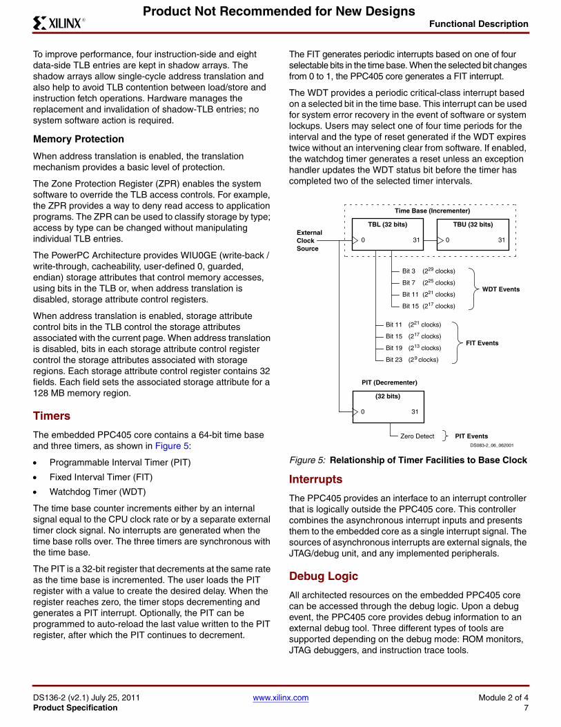
Timers
The embedded PPC405 core contains a 64-bit time base and three timers, as shown in Figure 5:
Programmable Interval Timer (PIT)
Fixed Interval Timer (FIT)
Watchdog Timer (WDT)
The time base counter increments either by an internal signal equal to the CPU clock rate or by a separate external timer clock signal. No interrupts are generated when the time base rolls over. The three timers are synchronous with the time base.
The PIT is a 32-bit register that decrements at the same rate as the time base is incremented. The user loads the PIT register with a value to create the desired delay. When the register reaches zero, the timer stops decrementing and generates a PIT interrupt. Optionally, the PIT can be programmed to auto-reload the last value written to the PIT register, after which the PIT continues to decrement.
The FIT generates periodic interrupts based on one of four selectable bits in the time base. When the selected bit changes from 0 to 1, the PPC405 core generates a FIT interrupt.
The WDT provides a periodic critical-class interrupt based on a selected bit in the time base. This interrupt can be used for system error recovery in the event of software or system lockups. Users may select one of four time periods for the interval and the type of reset generated if the WDT expires twice without an intervening clear from software. If enabled, the watchdog timer generates a reset unless an exception handler updates the WDT status bit before the timer has completed two of the selected timer intervals.
Interrupts
The PPC405 provides an interface to an interrupt controller that is logically outside the PPC405 core. This controller combines the asynchronous interrupt inputs and presents them to the embedded core as a single interrupt signal. The sources of asynchronous interrupts are external signals, the JTAG/debug unit, and any implemented peripherals.
Debug Logic
All architected resources on the embedded PPC405 core can be accessed through the debug logic. Upon a debug event, the PPC405 core provides debug information to an external debug tool. Three different types of tools are supported depending on the debug mode: ROM monitors, JTAG debuggers, and instruction trace tools.
X-Ref Target - Figure 5
Figure 5: Relationship of Timer Facilities to Base Clock
TBU (32 bits)
Bit 3 (229 clocks)
Bit 7 (225 clocks)
Bit 11 (221 clocks)
Bit 15 (217 clocks)
Bit 11 (221 clocks)
Bit 15 (217 clocks)
Bit 19 (213
9
clocks)
Bit 23 (2 clocks)
WDT Events
FIT Events
Time Base (Incrementer)
31
TBL (32 bits)
310 0
PIT (Decrementer)
(32 bits)
310
Zero Detect PIT Events
ExternalClockSource
DS083-2_06_062001
Functional Description
DS136-2 (v2.1) July 25, 2011 www.xilinx.com Module 2 of 4Product Specification 8
R
Product Not Recommended for New Designs
In internal debug mode, a debug event enables exception-handling software at a dedicated interrupt vector to take over the CPU core and communicate with a debug tool. The debug tool has read-write access to all registers and can set hardware or software breakpoints. ROM monitors typically use the internal debug mode.
In external debug mode, the CPU core enters stop state (stops instruction execution) when a debug event occurs. This mode offers a debug tool read-write access to all registers in the PPC405 core. Once the CPU core is in stop state, the debug tool can start the CPU core, step an instruction, freeze the timers, or set hardware or software break points. In addition to CPU core control, the debug logic is capable of writing instructions into the instruction cache, eliminating the need for external memory during initial board bring-up. Communication to a debug tool using external debug mode is through the JTAG port.
Debug wait mode offers the same functionality as external debug mode with one exception. In debug wait mode, the CPU core goes into wait state instead of stop state after a debug event. Wait state is identical to stop state until an interrupt occurs. In wait state, the PPC405 core can vector to an exception handler, service an interrupt and return to wait state. This mode is particularly useful when debugging real time control systems.
Real-time trace debug mode is always enabled. The debug logic continuously broadcasts instruction trace information to the trace port. When a debug event occurs, the debug logic signals an external debug tool to save instruction trace information before and after the event. The number of instructions traced depends on the trace tool.
Debug events signal the debug logic to stop the CPU core, put the CPU core in debug wait state, cause a debug exception or save instruction trace information.
Big Endian and Little Endian Support
The embedded PPC405 core supports big endian or little endian byte ordering for instructions stored in external memory. Since the PowerPC architecture is big endian internally, the ICU rearranges the instructions stored as little endian into the big endian format. Therefore, the instruction cache always contains instructions in big endian format so that the byte ordering is correct for the execution unit. This feature allows the 405 core to be used in systems designed to function in a little endian environment.
Functional Description
DS136-2 (v2.1) July 25, 2011 www.xilinx.com Module 2 of 4Product Specification 9
R
Product Not Recommended for New Designs
Functional Description: FPGA
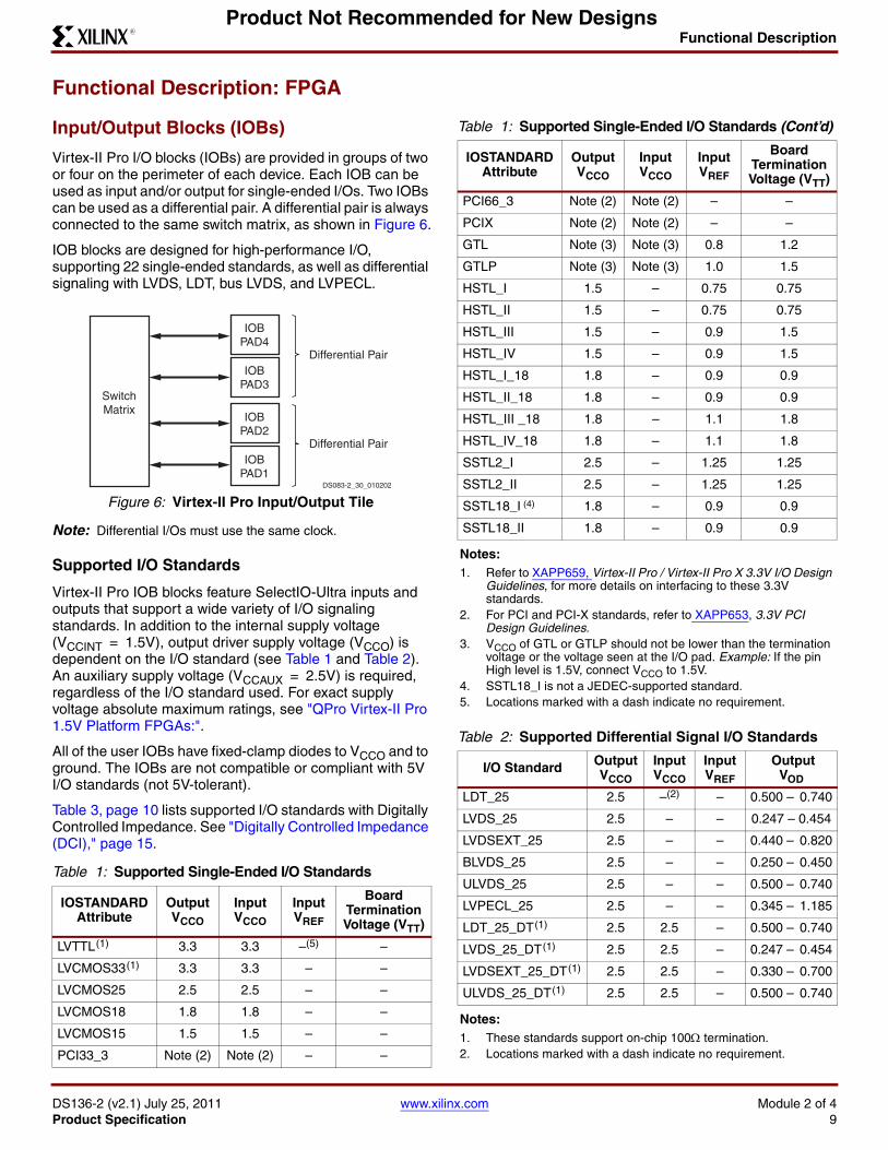
Input/Output Blocks (IOBs)
Virtex-II Pro I/O blocks (IOBs) are provided in groups of two or four on the perimeter of each device. Each IOB can be used as input and/or output for single-ended I/Os. Two IOBs can be used as a differential pair. A differential pair is always connected to the same switch matrix, as shown in Figure 6.
IOB blocks are designed for high-performance I/O, supporting 22 single-ended standards, as well as differential signaling with LVDS, LDT, bus LVDS, and LVPECL.
Note: Differential I/Os must use the same clock.
Supported I/O Standards
Virtex-II Pro IOB blocks feature SelectIO-Ultra inputs and outputs that support a wide variety of I/O signaling standards. In addition to the internal supply voltage (VCCINT = 1.5V), output driver supply voltage (VCCO) is dependent on the I/O standard (see Table 1 and Table 2). An auxiliary supply voltage (VCCAUX = 2.5V) is required, regardless of the I/O standard used. For exact supply voltage absolute maximum ratings, see "QPro Virtex-II Pro 1.5V Platform FPGAs:".
All of the user IOBs have fixed-clamp diodes to VCCO and to ground. The IOBs are not compatible or compliant with 5V I/O standards (not 5V-tolerant).
Table 3, page 10 lists supported I/O standards with Digitally Controlled Impedance. See "Digitally Controlled Impedance (DCI)," page 15.
X-Ref Target - Figure 6
Figure 6: Virtex-II Pro Input/Output Tile
Table 1: Supported Single-Ended I/O Standards
IOSTANDARD Attribute
OutputVCCO
InputVCCO
InputVREF
Board Termination Voltage (VTT)
LVTTL (1) 3.3 3.3 –(5) –
LVCMOS33 (1) 3.3 3.3 – –
LVCMOS25 2.5 2.5 – –
LVCMOS18 1.8 1.8 – –
LVCMOS15 1.5 1.5 – –
PCI33_3 Note (2) Note (2) – –
IOBPAD4
IOBPAD3
Differential Pair
IOBPAD2
IOBPAD1
Differential Pair
SwitchMatrix
DS083-2_30_010202
PCI66_3 Note (2) Note (2) – –
PCIX Note (2) Note (2) – –
GTL Note (3) Note (3) 0.8 1.2
GTLP Note (3) Note (3) 1.0 1.5
HSTL_I 1.5 – 0.75 0.75
HSTL_II 1.5 – 0.75 0.75
HSTL_III 1.5 – 0.9 1.5
HSTL_IV 1.5 – 0.9 1.5
HSTL_I_18 1.8 – 0.9 0.9
HSTL_II_18 1.8 – 0.9 0.9
HSTL_III _18 1.8 – 1.1 1.8
HSTL_IV_18 1.8 – 1.1 1.8
SSTL2_I 2.5 – 1.25 1.25
SSTL2_II 2.5 – 1.25 1.25
SSTL18_I (4) 1.8 – 0.9 0.9
SSTL18_II 1.8 – 0.9 0.9
Notes: 1. Refer to XAPP659, Virtex-II Pro / Virtex-II Pro X 3.3V I/O Design
Guidelines, for more details on interfacing to these 3.3V standards.
2. For PCI and PCI-X standards, refer to XAPP653, 3.3V PCI Design Guidelines.
3. VCCO of GTL or GTLP should not be lower than the termination voltage or the voltage seen at the I/O pad. Example: If the pin High level is 1.5V, connect VCCO to 1.5V.
4. SSTL18_I is not a JEDEC-supported standard.5. Locations marked with a dash indicate no requirement.
Table 2: Supported Differential Signal I/O Standards
I/O Standard OutputVCCO
Input VCCO
InputVREF
OutputVOD
LDT_25 2.5 –(2) – 0.500 – 0.740
LVDS_25 2.5 – – 0.247 – 0.454
LVDSEXT_25 2.5 – – 0.440 – 0.820
BLVDS_25 2.5 – – 0.250 – 0.450
ULVDS_25 2.5 – – 0.500 – 0.740
LVPECL_25 2.5 – – 0.345 – 1.185
LDT_25_DT (1) 2.5 2.5 – 0.500 – 0.740
LVDS_25_DT (1) 2.5 2.5 – 0.247 – 0.454
LVDSEXT_25_DT (1) 2.5 2.5 – 0.330 – 0.700
ULVDS_25_DT (1) 2.5 2.5 – 0.500 – 0.740
Notes: 1. These standards support on-chip 100 termination.2. Locations marked with a dash indicate no requirement.
Table 1: Supported Single-Ended I/O Standards (Cont’d)
IOSTANDARD Attribute
OutputVCCO
InputVCCO
InputVREF
Board Termination Voltage (VTT)
Functional Description
DS136-2 (v2.1) July 25, 2011 www.xilinx.com Module 2 of 4Product Specification 10
R
Product Not Recommended for New Designs
Logic Resources
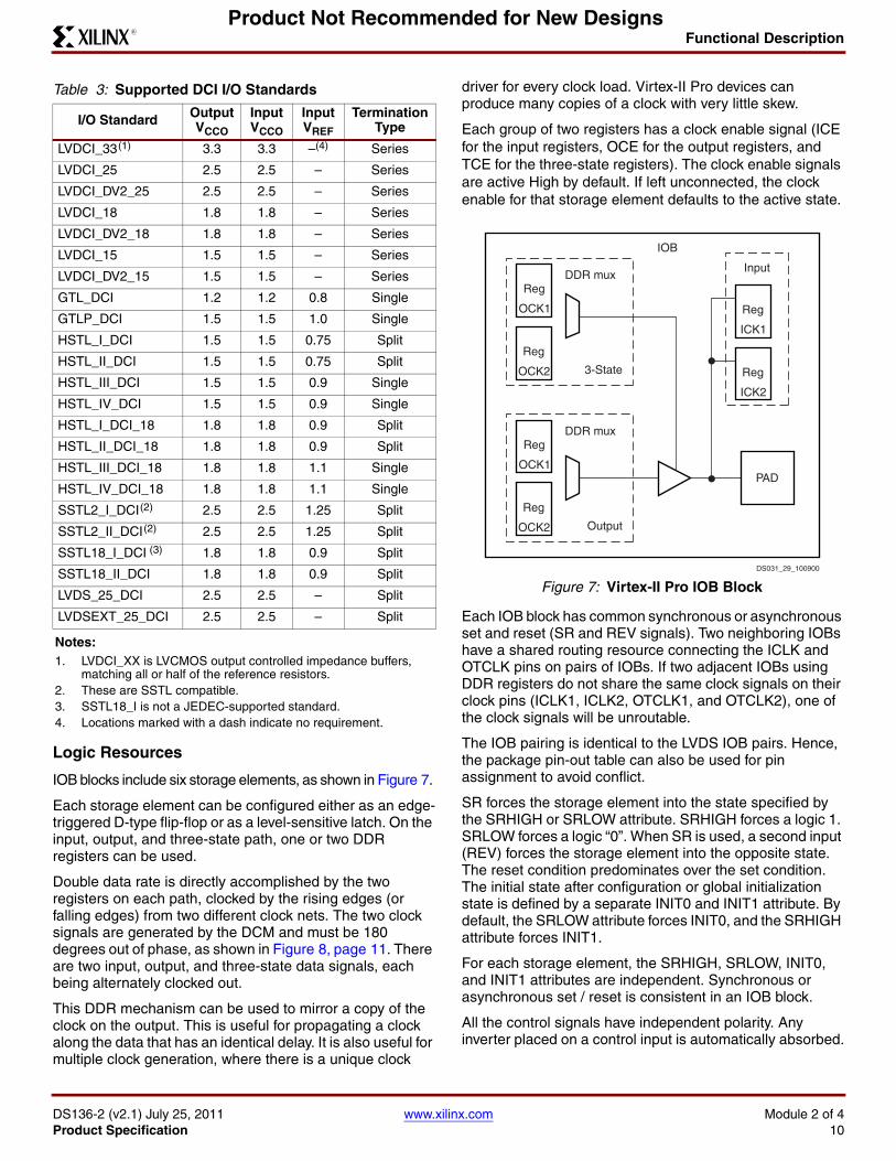
IOB blocks include six storage elements, as shown in Figure 7.
Each storage element can be configured either as an edge-triggered D-type flip-flop or as a level-sensitive latch. On the input, output, and three-state path, one or two DDR registers can be used.
Double data rate is directly accomplished by the two registers on each path, clocked by the rising edges (or falling edges) from two different clock nets. The two clock signals are generated by the DCM and must be 180 degrees out of phase, as shown in Figure 8, page 11. There are two input, output, and three-state data signals, each being alternately clocked out.
This DDR mechanism can be used to mirror a copy of the clock on the output. This is useful for propagating a clock along the data that has an identical delay. It is also useful for multiple clock generation, where there is a unique clock
driver for every clock load. Virtex-II Pro devices can produce many copies of a clock with very little skew.
Each group of two registers has a clock enable signal (ICE for the input registers, OCE for the output registers, and TCE for the three-state registers). The clock enable signals are active High by default. If left unconnected, the clock enable for that storage element defaults to the active state.
Each IOB block has common synchronous or asynchronous set and reset (SR and REV signals). Two neighboring IOBs have a shared routing resource connecting the ICLK and OTCLK pins on pairs of IOBs. If two adjacent IOBs using DDR registers do not share the same clock signals on their clock pins (ICLK1, ICLK2, OTCLK1, and OTCLK2), one of the clock signals will be unroutable.
The IOB pairing is identical to the LVDS IOB pairs. Hence, the package pin-out table can also be used for pin assignment to avoid conflict.
SR forces the storage element into the state specified by the SRHIGH or SRLOW attribute. SRHIGH forces a logic 1. SRLOW forces a logic “0”. When SR is used, a second input (REV) forces the storage element into the opposite state. The reset condition predominates over the set condition. The initial state after configuration or global initialization state is defined by a separate INIT0 and INIT1 attribute. By default, the SRLOW attribute forces INIT0, and the SRHIGH attribute forces INIT1.
For each storage element, the SRHIGH, SRLOW, INIT0, and INIT1 attributes are independent. Synchronous or asynchronous set / reset is consistent in an IOB block.
All the control signals have independent polarity. Any inverter placed on a control input is automatically absorbed.
Table 3: Supported DCI I/O Standards
I/O Standard OutputVCCO
InputVCCO
InputVREF
TerminationType
LVDCI_33 (1) 3.3 3.3 –(4) Series
LVDCI_25 2.5 2.5 – Series
LVDCI_DV2_25 2.5 2.5 – Series
LVDCI_18 1.8 1.8 – Series
LVDCI_DV2_18 1.8 1.8 – Series
LVDCI_15 1.5 1.5 – Series
LVDCI_DV2_15 1.5 1.5 – Series
GTL_DCI 1.2 1.2 0.8 Single
GTLP_DCI 1.5 1.5 1.0 Single
HSTL_I_DCI 1.5 1.5 0.75 Split
HSTL_II_DCI 1.5 1.5 0.75 Split
HSTL_III_DCI 1.5 1.5 0.9 Single
HSTL_IV_DCI 1.5 1.5 0.9 Single
HSTL_I_DCI_18 1.8 1.8 0.9 Split
HSTL_II_DCI_18 1.8 1.8 0.9 Split
HSTL_III_DCI_18 1.8 1.8 1.1 Single
HSTL_IV_DCI_18 1.8 1.8 1.1 Single
SSTL2_I_DCI (2) 2.5 2.5 1.25 Split
SSTL2_II_DCI (2) 2.5 2.5 1.25 Split
SSTL18_I_DCI (3) 1.8 1.8 0.9 Split
SSTL18_II_DCI 1.8 1.8 0.9 Split
LVDS_25_DCI 2.5 2.5 – Split
LVDSEXT_25_DCI 2.5 2.5 – Split
Notes: 1. LVDCI_XX is LVCMOS output controlled impedance buffers,
matching all or half of the reference resistors.2. These are SSTL compatible.3. SSTL18_I is not a JEDEC-supported standard.4. Locations marked with a dash indicate no requirement.
X-Ref Target - Figure 7
Figure 7: Virtex-II Pro IOB Block
Reg
OCK1
Reg
OCK2
Reg
ICK1
Reg
ICK2
DDR muxInput
PAD
3-State
Reg
OCK1
Reg
OCK2
DDR mux
Output
IOB
DS031_29_100900
Functional Description
DS136-2 (v2.1) July 25, 2011 www.xilinx.com Module 2 of 4Product Specification 11
R
Product Not Recommended for New Designs
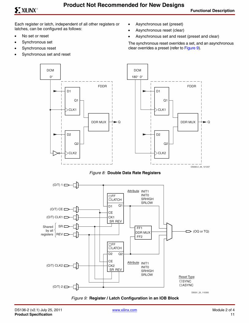
Each register or latch, independent of all other registers or latches, can be configured as follows:
No set or reset
Synchronous set
Synchronous reset
Synchronous set and reset
Asynchronous set (preset)
Asynchronous reset (clear)
Asynchronous set and reset (preset and clear)
The synchronous reset overrides a set, and an asynchronous clear overrides a preset (refer to Figure 9).
X-Ref Target - Figure 8
Figure 8: Double Data Rate RegistersX-Ref Target - Figure 9
Figure 9: Register / Latch Configuration in an IOB Block
D1
CLK1
DDR MUX
Q1
FDDR
D2
CLK2
Q Q
Q2
D1
CLK1
DDR MUX
DCM
Q1
FDDR
D2
CLK2
Q2
180° 0°
DCM
0°
DS083-2_26_121207
FFLATCH
SR REV
D1 Q1
CE
CK1
FFLATCH
SR REV
D2
FF1
FF2DDR MUX
Q2
CECK2
REV
SR
(O/T) CLK1
(OQ or TQ)
(O/T) CE
(O/T) 1
(O/T) CLK2
(O/T) 2
Attribute INIT1INIT0SRHIGHSRLOW
Attribute INIT1INIT0SRHIGHSRLOW
Reset TypeSYNCASYNC
DS031_25_110300
Sharedby all
registers
Functional Description
DS136-2 (v2.1) July 25, 2011 www.xilinx.com Module 2 of 4Product Specification 12
R
Product Not Recommended for New Designs
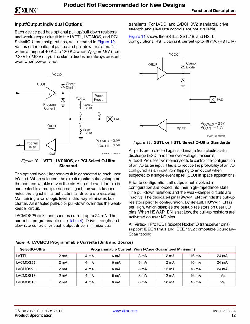
Input/Output Individual Options
Each device pad has optional pull-up/pull-down resistors and weak-keeper circuit in the LVTTL, LVCMOS, and PCI SelectIO-Ultra configurations, as illustrated in Figure 10. Values of the optional pull-up and pull-down resistors fall within a range of 40 K to 120 K when VCCO = 2.5V (from 2.38V to 2.63V only). The clamp diodes are always present, even when power is not.
The optional weak-keeper circuit is connected to each user I/O pad. When selected, the circuit monitors the voltage on the pad and weakly drives the pin High or Low. If the pin is connected to a multiple-source signal, the weak-keeper holds the signal in its last state if all drivers are disabled. Maintaining a valid logic level in this way eliminates bus chatter. An enabled pull-up or pull-down overrides the weak-keeper circuit.
LVCMOS25 sinks and sources current up to 24 mA. The current is programmable (see Table 4). Drive strength and slew rate controls for each output driver minimize bus
transients. For LVDCI and LVDCI_DV2 standards, drive strength and slew rate controls are not available.
Figure 11 shows the SSTL2, SSTL18, and HSTL configurations. HSTL can sink current up to 48 mA. (HSTL IV)
All pads are protected against damage from electrostatic discharge (ESD) and from over-voltage transients. Virtex-II Pro uses two memory cells to control the configuration of an I/O as an input. This is to reduce the probability of an I/O configured as an input from flipping to an output when subjected to a single event upset (SEU) in space applications.
Prior to configuration, all outputs not involved in configuration are forced into their high-impedance state. The pull-down resistors and the weak-keeper circuits are inactive. The dedicated pin HSWAP_EN controls the pull-up resistors prior to configuration. By default, HSWAP_EN is set High, which disables the pull-up resistors on user I/O pins. When HSWAP_EN is set Low, the pull-up resistors are activated on user I/O pins.
All Virtex-II Pro IOBs (except RocketIO transceiver pins) support IEEE 1149.1 and IEEE 1532 compatible Boundary-Scan testing.
X-Ref Target - Figure 10
Figure 10: LVTTL, LVCMOS, or PCI SelectIO-Ultra Standard
VCCO
VCCO
VCCO
WeakKeeper
ProgramDelay
OBUF
IBUF
ProgramCurrent
ClampDiode
PAD
VCCAUX = 2.5V
DS083-2_07_101801
VCCINT = 1.5V
40KΩ – 120KΩ
40KΩ – 120KΩ
X-Ref Target - Figure 11
Figure 11: SSTL or HSTL SelectIO-Ultra Standards
VCCO
OBUF
VREF
ClampDiode
PAD
VCCAUX = 2.5VVCCINT = 1.5V
DS031_24_100900
Table 4: LVCMOS Programmable Currents (Sink and Source)
SelectIO-Ultra Programmable Current (Worst-Case Guaranteed Minimum)
LVTTL 2 mA 4 mA 6 mA 8 mA 12 mA 16 mA 24 mA
LVCMOS33 2 mA 4 mA 6 mA 8 mA 12 mA 16 mA 24 mA
LVCMOS25 2 mA 4 mA 6 mA 8 mA 12 mA 16 mA 24 mA
LVCMOS18 2 mA 4 mA 6 mA 8 mA 12 mA 16 mA n/a
LVCMOS15 2 mA 4 mA 6 mA 8 mA 12 mA 16 mA n/a
Functional Description
DS136-2 (v2.1) July 25, 2011 www.xilinx.com Module 2 of 4Product Specification 13
R
Product Not Recommended for New Designs
Input Path
The Virtex-II Pro IOB input path routes input signals directly to internal logic and / or through an optional input flip-flop or latch, or through the DDR input registers. An optional delay element at the D-input of the storage element eliminates pad-to-pad hold time. The delay is matched to the internal clock-distribution delay of the Virtex-II Pro device, and when used, assures that the pad-to-pad hold time is zero.
Each input buffer can be configured to conform to any of the low-voltage signaling standards supported. In some of these standards the input buffer utilizes a user-supplied threshold voltage, VREF. The need to supply VREF imposes constraints on which standards can be used in the same bank. See I/O banking description.
Output Path
The output path includes a three-state output buffer that drives the output signal onto the pad. The output and / or the 3-state signal can be routed to the buffer directly from the internal logic or through an output / three-state flip-flop or latch, or through the DDR output / three-state registers.
Each output driver can be individually programmed for a wide range of low-voltage signaling standards. In most signaling standards, the output High voltage depends on an externally supplied VCCO voltage. The need to supply VCCO imposes constraints on which standards can be used in the same bank. See I/O banking description.
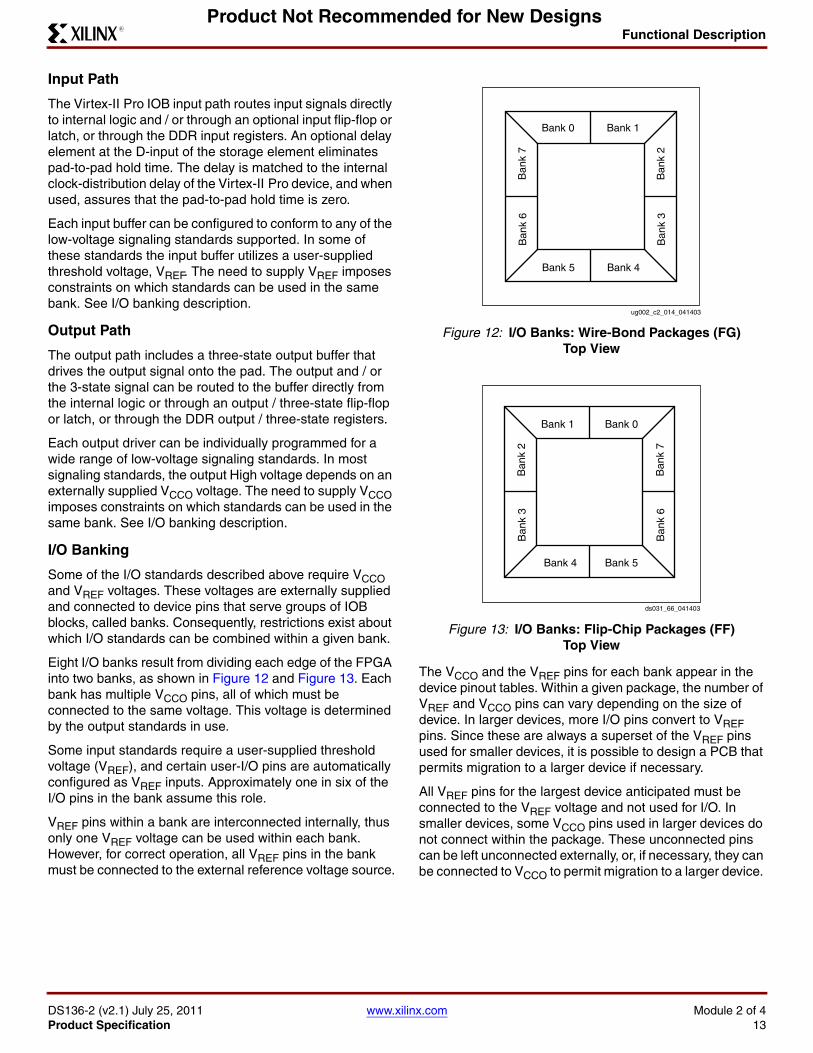
I/O Banking
Some of the I/O standards described above require VCCO and VREF voltages. These voltages are externally supplied and connected to device pins that serve groups of IOB blocks, called banks. Consequently, restrictions exist about which I/O standards can be combined within a given bank.
Eight I/O banks result from dividing each edge of the FPGA into two banks, as shown in Figure 12 and Figure 13. Each bank has multiple VCCO pins, all of which must be connected to the same voltage. This voltage is determined by the output standards in use.
Some input standards require a user-supplied threshold voltage (VREF), and certain user-I/O pins are automatically configured as VREF inputs. Approximately one in six of the I/O pins in the bank assume this role.
VREF pins within a bank are interconnected internally, thus only one VREF voltage can be used within each bank. However, for correct operation, all VREF pins in the bank must be connected to the external reference voltage source.
The VCCO and the VREF pins for each bank appear in the device pinout tables. Within a given package, the number of VREF and VCCO pins can vary depending on the size of device. In larger devices, more I/O pins convert to VREF pins. Since these are always a superset of the VREF pins used for smaller devices, it is possible to design a PCB that permits migration to a larger device if necessary.
All VREF pins for the largest device anticipated must be connected to the VREF voltage and not used for I/O. In smaller devices, some VCCO pins used in larger devices do not connect within the package. These unconnected pins can be left unconnected externally, or, if necessary, they can be connected to VCCO to permit migration to a larger device.
X-Ref Target - Figure 12
Figure 12: I/O Banks: Wire-Bond Packages (FG) Top View
X-Ref Target - Figure 13
Figure 13: I/O Banks: Flip-Chip Packages (FF) Top View
ug002_c2_014_041403
Bank 0 Bank 1
Bank 5 Bank 4
Ban
k 7
Ban
k 6
Ban
k 2
Ban
k 3
ds031_66_041403
Bank 1 Bank 0
Bank 4 Bank 5
Ban
k 2
Ban
k 3
Ban
k 7
Ban
k 6
Functional Description
DS136-2 (v2.1) July 25, 2011 www.xilinx.com Module 2 of 4Product Specification 14
R
Product Not Recommended for New Designs
Rules for Combining I/O Standards in the Same Bank
The following rules must be obeyed to combine different input, output, and bidirectional standards in the same bank:
Combining output standards only. Output standards with the same output VCCO requirement can be combined in the same bank.
Compatible example:
SSTL2_I and LVDS_25 outputs
Incompatible example:
SSTL2_I (output VCCO = 2.5V) and LVCMOS33 (output VCCO = 3.3V) outputs
Combining input standards only. Input standards with the same input VCCO and input VREF requirements can be combined in the same bank.
Compatible example:
LVCMOS15 and HSTL_IV inputs
Incompatible example:
LVCMOS15 (input VCCO = 1.5V) and LVCMOS18 (input VCCO = 1.8V) inputs
Incompatible example:
HSTL_I_DCI_18 (VREF = 0.9V) and HSTL_IV_DCI_18 (VREF = 1.1V) inputs
Combining input standards and output standards. Input standards and output standards with the same input VCCO and output VCCO requirement can be combined in the same bank.
Compatible example:
LVDS_25 output and HSTL_I input
Incompatible example:
LVDS_25 output (output VCCO = 2.5V) and HSTL_I_DCI_18 input (input VCCO = 1.8V)
Combining bidirectional standards with input or output standards. When combining bidirectional I/O with other standards, make sure the bidirectional standard can meet rules 1 through 3 above.
Additional rules for combining DCI I/O standards.
No more than one Single Termination type (input or output) is allowed in the same bank.
Incompatible example:
HSTL_IV_DCI input and HSTL_III_DCI input
No more than one Split Termination type (input or output) is allowed in the same bank.
Incompatible example:
HSTL_I_DCI input and HSTL_II_DCI input
The implementation tools will enforce the above design rules.
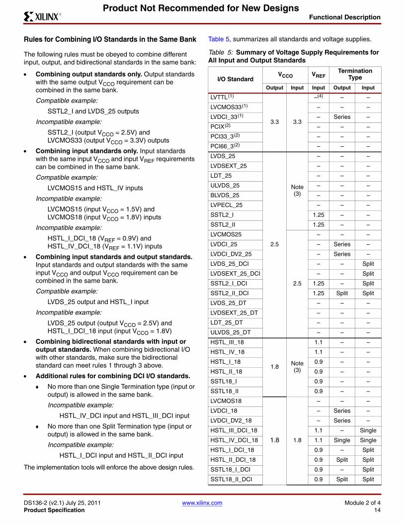
Table 5, summarizes all standards and voltage supplies.
Table 5: Summary of Voltage Supply Requirements for All Input and Output Standards
I/O StandardVCCO VREF
Termination Type
Output Input Input Output Input
LVTTL (1)
3.3 3.3
–(4) – –
LVCMOS33 (1) – – –
LVDCI_33 (1) – Series –
PCIX (2) – – –
PCI33_3 (2) – – –
PCI66_3 (2) – – –
LVDS_25
2.5
Note (3)
– – –
LVDSEXT_25 – – –
LDT_25 – – –
ULVDS_25 – – –
BLVDS_25 – – –
LVPECL_25 – – –
SSTL2_I 1.25 – –
SSTL2_II 1.25 – –
LVCMOS25
2.5
– – –
LVDCI_25 – Series –
LVDCI_DV2_25 – Series –
LVDS_25_DCI – – Split
LVDSEXT_25_DCI – – Split
SSTL2_I_DCI 1.25 – Split
SSTL2_II_DCI 1.25 Split Split
LVDS_25_DT – – –
LVDSEXT_25_DT – – –
LDT_25_DT – – –
ULVDS_25_DT – – –
HSTL_III_18
1.8 Note (3)
1.1 – –
HSTL_IV_18 1.1 – –
HSTL_I_18 0.9 – –
HSTL_II_18 0.9 – –
SSTL18_I 0.9 – –
SSTL18_II 0.9 – –
LVCMOS18
1.8 1.8
– – –
LVDCI_18 – Series –
LVDCI_DV2_18 – Series –
HSTL_III_DCI_18 1.1 – Single
HSTL_IV_DCI_18 1.1 Single Single
HSTL_I_DCI_18 0.9 – Split
HSTL_II_DCI_18 0.9 Split Split
SSTL18_I_DCI 0.9 – Split
SSTL18_II_DCI 0.9 Split Split
Functional Description
DS136-2 (v2.1) July 25, 2011 www.xilinx.com Module 2 of 4Product Specification 15
R
Product Not Recommended for New Designs
Digitally Controlled Impedance (DCI)
Today’s chip output signals with fast edge rates require termination to prevent reflections and maintain signal integrity. High pin count packages (especially ball grid arrays) can not accommodate external termination resistors.
Virtex-II Pro XCITE DCI provides controlled impedance drivers and on-chip termination for single-ended and differential I/Os. This eliminates the need for external resistors and improves signal integrity. The DCI feature can be used on any IOB by selecting one of the DCI I/O standards.
When applied to inputs, DCI provides input parallel termination. When applied to outputs, DCI provides controlled impedance drivers (series termination) or output parallel termination.
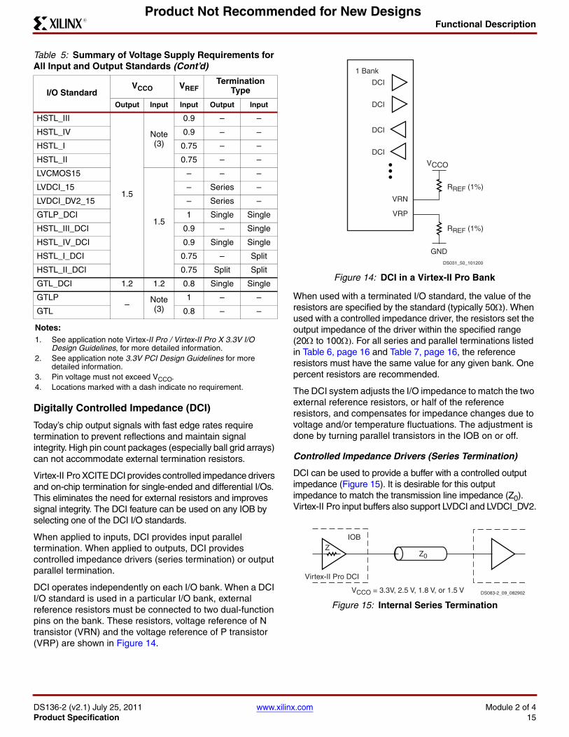
DCI operates independently on each I/O bank. When a DCI I/O standard is used in a particular I/O bank, external reference resistors must be connected to two dual-function pins on the bank. These resistors, voltage reference of N transistor (VRN) and the voltage reference of P transistor (VRP) are shown in Figure 14.
When used with a terminated I/O standard, the value of the resistors are specified by the standard (typically 50). When used with a controlled impedance driver, the resistors set the output impedance of the driver within the specified range (20 to 100. For all series and parallel terminations listed in Table 6, page 16 and Table 7, page 16, the reference resistors must have the same value for any given bank. One percent resistors are recommended.
The DCI system adjusts the I/O impedance to match the two external reference resistors, or half of the reference resistors, and compensates for impedance changes due to voltage and/or temperature fluctuations. The adjustment is done by turning parallel transistors in the IOB on or off.
Controlled Impedance Drivers (Series Termination)
DCI can be used to provide a buffer with a controlled output impedance (Figure 15). It is desirable for this output impedance to match the transmission line impedance (Z0). Virtex-II Pro input buffers also support LVDCI and LVDCI_DV2.
HSTL_III
1.5
Note (3)
0.9 – –
HSTL_IV 0.9 – –
HSTL_I 0.75 – –
HSTL_II 0.75 – –
LVCMOS15
1.5
– – –
LVDCI_15 – Series –
LVDCI_DV2_15 – Series –
GTLP_DCI 1 Single Single
HSTL_III_DCI 0.9 – Single
HSTL_IV_DCI 0.9 Single Single
HSTL_I_DCI 0.75 – Split
HSTL_II_DCI 0.75 Split Split
GTL_DCI 1.2 1.2 0.8 Single Single
GTLP– Note
(3)1 – –
GTL 0.8 – –
Notes: 1. See application note Virtex-II Pro / Virtex-II Pro X 3.3V I/O
Design Guidelines, for more detailed information.2. See application note 3.3V PCI Design Guidelines for more
detailed information.3. Pin voltage must not exceed VCCO.4. Locations marked with a dash indicate no requirement.
Table 5: Summary of Voltage Supply Requirements for All Input and Output Standards (Cont’d)
I/O StandardVCCO VREF
Termination Type
Output Input Input Output Input
X-Ref Target - Figure 14
Figure 14: DCI in a Virtex-II Pro Bank
X-Ref Target - Figure 15
Figure 15: Internal Series Termination
DS031_50_101200
VCCO
GND
DCI
DCI
DCI
DCI
VRN
VRP
1 Bank
RREF (1%)
RREF (1%)
Z0
IOBZ
Virtex-II Pro DCI
DS083-2_09_082902VCCO = 3.3V, 2.5 V, 1.8 V, or 1.5 V
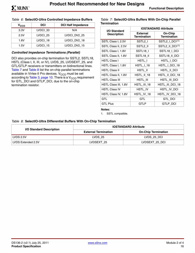
Functional Description
DS136-2 (v2.1) July 25, 2011 www.xilinx.com Module 2 of 4Product Specification 16
R
Product Not Recommended for New Designs
Controlled Impedance Terminations (Parallel)
DCI also provides on-chip termination for SSTL2, SSTL18, HSTL (Class I, II, III, or IV), LVDS_25, LVDSEXT_25, and GTL/GTLP receivers or transmitters on bidirectional lines. Table 7 and Table 8 list the on-chip parallel terminations available in Virtex-II Pro devices. VCCO must be set according to Table 3, page 10. There is a VCCO requirement for GTL_DCI and GTLP_DCI, due to the on-chip termination resistor.
Table 6: SelectIO-Ultra Controlled Impedance Buffers
VCCO DCI DCI Half Impedance
3.3V LVDCI_33 N/A
2.5V LVDCI_25 LVDCI_DV2_25
1.8V LVDCI_18 LVDCI_DV2_18
1.5V LVDCI_15 LVDCI_DV2_15
Table 7: SelectIO-Ultra Buffers With On-Chip Parallel Termination
I/O Standard Description
IOSTANDARD Attribute
External Termination
On-Chip Termination
SSTL Class I, 2.5V SSTL2_I SSTL2_I_DCI (1)
SSTL Class II, 2.5V SSTL2_II SSTL2_II_DCI (1)
SSTL Class I, 1.8V SSTL18_I SSTL18_I_DCI
SSTL Class II, 1.8V SSTL18_II SSTL18_II_DCI
HSTL Class I HSTL_I HSTL_I_DCI
HSTL Class I, 1.8V HSTL_I_18 HSTL_I_DCI_18
HSTL Class II HSTL_II HSTL_II_DCI
HSTL Class II, 1.8V HSTL_II_18 HSTL_II_DCI_18
HSTL Class III HSTL_III HSTL_III_DCI
HSTL Class III, 1.8V HSTL_III_18 HSTL_III_DCI_18
HSTL Class IV HSTL_IV HSTL_IV_DCI
HSTL Class IV, 1.8V HSTL_IV_18 HSTL_IV_DCI_18
GTL GTL GTL_DCI
GTL Plus GTLP GTLP_DCI
Notes: 1. SSTL compatible.
Table 8: SelectIO-Ultra Differential Buffers With On-Chip Termination
I/O Standard DescriptionIOSTANDARD Attribute
External Termination On-Chip Termination
LVDS 2.5V LVDS_25 LVDS_25_DCI
LVDS Extended 2.5V LVDSEXT_25 LVDSEXT_25_DCI
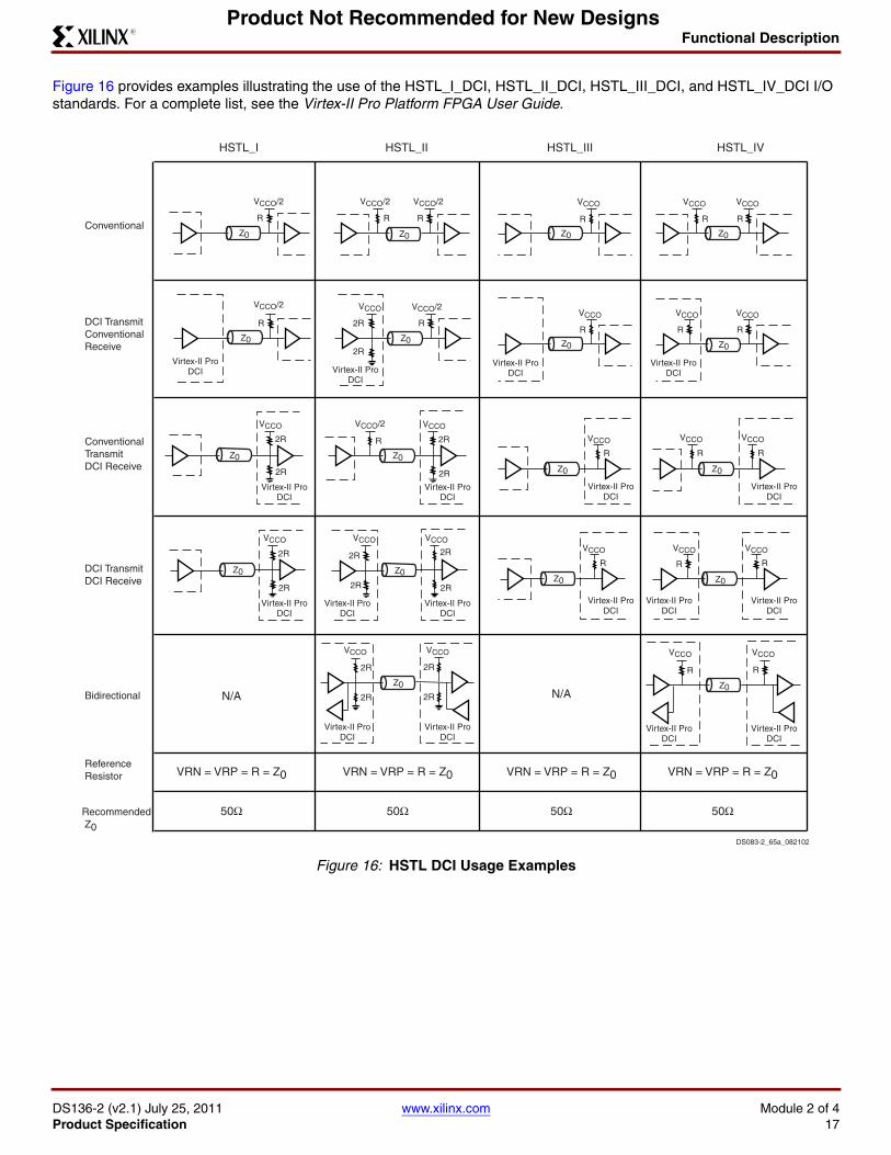
Functional Description
DS136-2 (v2.1) July 25, 2011 www.xilinx.com Module 2 of 4Product Specification 17
R
Product Not Recommended for New Designs
Figure 16 provides examples illustrating the use of the HSTL_I_DCI, HSTL_II_DCI, HSTL_III_DCI, and HSTL_IV_DCI I/O standards. For a complete list, see the Virtex-II Pro Platform FPGA User Guide.
X-Ref Target - Figure 16
Figure 16: HSTL DCI Usage Examples
R R
R R
R R
R R
R R
2R
2R
R
2R
R 2R
2R
2R 2R
2R
DS083-2_65a_082102
Conventional
DCI TransmitConventionalReceive
ConventionalTransmitDCI Receive
DCI TransmitDCI Receive
Bidirectional
ReferenceResistor
RecommendedZ0
VRN = VRP = R = Z0
50Ω
VRN = VRP = R = Z0
50Ω
VRN = VRP = R = Z0
50Ω
VRN = VRP = R = Z0
50Ω
HSTL_I HSTL_II HSTL_III HSTL_IV
N/A N/A
R
R
R
R
Z0
R
R
2R
2R
2R
2R
Z0
Z0
Z0
Z0Z0
Z0Z0
Z0
Z0Z0Z0
Z0
Z0
Z0
Z0
Virtex-II ProDCI
Virtex-II ProDCI
Virtex-II ProDCI
Z0
Virtex-II ProDCI
Virtex-II ProDCI
Virtex-II ProDCI
Virtex-II ProDCI
Virtex-II ProDCI
Virtex-II ProDCI
Virtex-II ProDCI
Virtex-II ProDCI
Virtex-II ProDCI
Virtex-II ProDCI
Virtex-II ProDCI
Virtex-II ProDCIVirtex-II Pro
DCI
Virtex-II ProDCI
Virtex-II ProDCI
2R
2R
2R
2RZ0
R R
VCCO/2
VCCO/2
VCCO/2
VCCO/2
VCCO/2 VCCO/2 VCCO VCCO VCCO
VCCOVCCO
VCCOVCCO
VCCO
VCCO
VCCOVCCOVCCOVCCO
VCCOVCCO
VCCOVCCOVCCO
VCCOVCCOVCCO VCCO
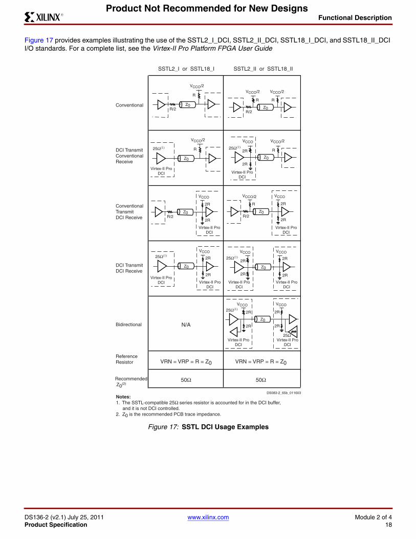
Functional Description
DS136-2 (v2.1) July 25, 2011 www.xilinx.com Module 2 of 4Product Specification 18
R
Product Not Recommended for New Designs
Figure 17 provides examples illustrating the use of the SSTL2_I_DCI, SSTL2_II_DCI, SSTL18_I_DCI, and SSTL18_II_DCI I/O standards. For a complete list, see the Virtex-II Pro Platform FPGA User Guide
X-Ref Target - Figure 17
Figure 17: SSTL DCI Usage Examples
DS083-2_65b_011603
Conventional
DCI TransmitConventionalReceive
ConventionalTransmitDCI Receive
DCI TransmitDCI Receive
Bidirectional
ReferenceResistor
Recommended Z0(2)
VRN = VRP = R = Z0
50Ω
VRN = VRP = R = Z0
50Ω
SSTL2_I or SSTL18_I SSTL2_II or SSTL18_II
N/A
Z0
R
VCCO/2
Z0R/2
R R
VCCO/2 VCCO/2
Z0R/2
R
VCCO/2
Z0R/2
2R
2R
VCCO
Z0R/2
2R
2R
VCCO
2R R
VCCO VCCO/2
2R
Z0
R
VCCO/2
Z0
2R
2R
VCCO
2R
2R
VCCO
Z0
2R
2R
VCCO
Z0
2R
2R
VCCO
2R
2R
VCCO
25Ω(1)
25Ω(1) 25Ω(1)
25Ω(1)
25Ω(1)
25ΩVirtex-II Pro
DCI
Virtex-II ProDCI Virtex-II Pro
DCIVirtex-II Pro
DCIVirtex-II Pro
DCI
Virtex-II ProDCI
Virtex-II ProDCI
Virtex-II ProDCI Virtex-II Pro
DCI
Virtex-II ProDCI
Notes:1. The SSTL-compatible 25Ω series resistor is accounted for in the DCI buffer, and it is not DCI controlled.2. Z0 is the recommended PCB trace impedance.
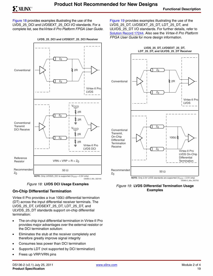
Functional Description
DS136-2 (v2.1) July 25, 2011 www.xilinx.com Module 2 of 4Product Specification 19
R
Product Not Recommended for New Designs
Figure 18 provides examples illustrating the use of the LVDS_25_DCI and LVDSEXT_25_DCI I/O standards. For a complete list, see theVirtex-II Pro Platform FPGA User Guide.
On-Chip Differential Termination
Virtex-II Pro provides a true 100 differential termination (DT) across the input differential receiver terminals. The LVDS_25_DT, LVDSEXT_25_DT, LDT_25_DT, and ULVDS_25_DT standards support on-chip differential termination:
The on-chip input differential termination in Virtex-II Pro provides major advantages over the external resistor or the DCI termination solution:
Eliminates the stub at the receiver completely and therefore greatly improve signal integrity
Consumes less power than DCI termination
Supports LDT (not supported by DCI termination)
Frees up VRP/VRN pins
Figure 19 provides examples illustrating the use of the LVDS_25_DT, LVDSEXT_25_DT, LDT_25_DT, and ULVDS_25_DT I/O standards. For further details, refer to Solution Record 17244. Also see the Virtex-II Pro Platform FPGA User Guide for more design information.
X-Ref Target - Figure 18
Figure 18: LVDS DCI Usage Examples
DS083-2_65c_022103
Conventional
ConventionalTransmitDCI Receive
ReferenceResistor
RecommendedZ0
VRN = VRP = R = Z0
50 Ω
LVDS_25_DCI and LVDSEXT_25_DCI Receiver
Virtex-II ProLVDS DCI
Z0
2R
2R
VCCO
Z0
2R
2R
VCCO
Virtex-II ProLVDS
Z0
2R
Z0
NOTE: Only LVDS25_DCI is supported (VCCO = 2.5V only)
X-Ref Target - Figure 19
Figure 19: LVDS Differential Termination Usage Examples
DS083-2_65e_052703
Conventional
ConventionalTransmit,On-ChipDifferentialTerminationReceive
RecommendedZ0
50 Ω
LVDS_25_DT, LVDSEXT_25_DT, LDT_25_DT, and ULVDS_25_DT Receiver
Virtex-II ProLVDS On-ChipDifferentialTermination
Z0
100Ω
Z0
Virtex-II ProLVDS
Z0
2R
Z0
NOTE: Only 2.5V LVDS standards are supported (VCCO = 2.5V only)
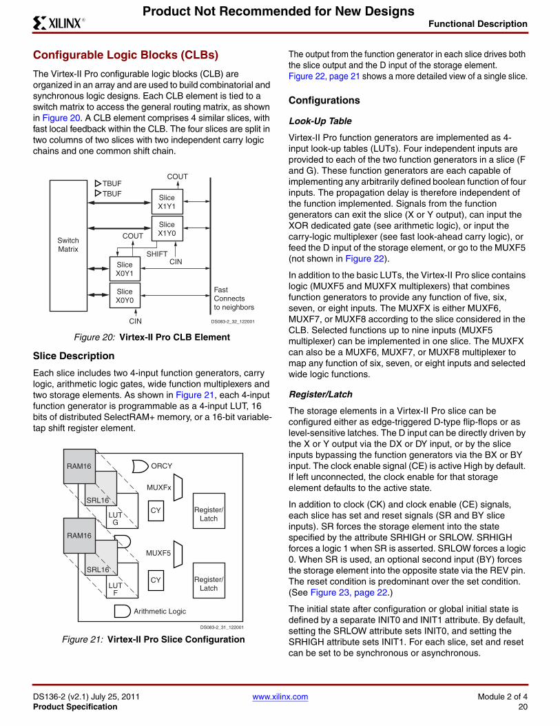
Functional Description
DS136-2 (v2.1) July 25, 2011 www.xilinx.com Module 2 of 4Product Specification 20
R
Product Not Recommended for New Designs
Configurable Logic Blocks (CLBs)
The Virtex-II Pro configurable logic blocks (CLB) are organized in an array and are used to build combinatorial and synchronous logic designs. Each CLB element is tied to a switch matrix to access the general routing matrix, as shown in Figure 20. A CLB element comprises 4 similar slices, with fast local feedback within the CLB. The four slices are split in two columns of two slices with two independent carry logic chains and one common shift chain.
Slice Description
Each slice includes two 4-input function generators, carry logic, arithmetic logic gates, wide function multiplexers and two storage elements. As shown in Figure 21, each 4-input function generator is programmable as a 4-input LUT, 16 bits of distributed SelectRAM+ memory, or a 16-bit variable-tap shift register element.
The output from the function generator in each slice drives both the slice output and the D input of the storage element. Figure 22, page 21 shows a more detailed view of a single slice.
Configurations
Look-Up Table
Virtex-II Pro function generators are implemented as 4-input look-up tables (LUTs). Four independent inputs are provided to each of the two function generators in a slice (F and G). These function generators are each capable of implementing any arbitrarily defined boolean function of four inputs. The propagation delay is therefore independent of the function implemented. Signals from the function generators can exit the slice (X or Y output), can input the XOR dedicated gate (see arithmetic logic), or input the carry-logic multiplexer (see fast look-ahead carry logic), or feed the D input of the storage element, or go to the MUXF5 (not shown in Figure 22).
In addition to the basic LUTs, the Virtex-II Pro slice contains logic (MUXF5 and MUXFX multiplexers) that combines function generators to provide any function of five, six, seven, or eight inputs. The MUXFX is either MUXF6, MUXF7, or MUXF8 according to the slice considered in the CLB. Selected functions up to nine inputs (MUXF5 multiplexer) can be implemented in one slice. The MUXFX can also be a MUXF6, MUXF7, or MUXF8 multiplexer to map any function of six, seven, or eight inputs and selected wide logic functions.
Register/Latch
The storage elements in a Virtex-II Pro slice can be configured either as edge-triggered D-type flip-flops or as level-sensitive latches. The D input can be directly driven by the X or Y output via the DX or DY input, or by the slice inputs bypassing the function generators via the BX or BY input. The clock enable signal (CE) is active High by default. If left unconnected, the clock enable for that storage element defaults to the active state.
In addition to clock (CK) and clock enable (CE) signals, each slice has set and reset signals (SR and BY slice inputs). SR forces the storage element into the state specified by the attribute SRHIGH or SRLOW. SRHIGH forces a logic 1 when SR is asserted. SRLOW forces a logic 0. When SR is used, an optional second input (BY) forces the storage element into the opposite state via the REV pin. The reset condition is predominant over the set condition. (See Figure 23, page 22.)
The initial state after configuration or global initial state is defined by a separate INIT0 and INIT1 attribute. By default, setting the SRLOW attribute sets INIT0, and setting the SRHIGH attribute sets INIT1. For each slice, set and reset can be set to be synchronous or asynchronous.
X-Ref Target - Figure 20
Figure 20: Virtex-II Pro CLB Element
X-Ref Target - Figure 21
Figure 21: Virtex-II Pro Slice Configuration
SliceX1Y1
SliceX1Y0
SliceX0Y1
SliceX0Y0
FastConnectsto neighbors
SwitchMatrix
DS083-2_32_122001
SHIFTCIN
COUT
TBUFCOUT
CIN
TBUF
Register/Latch
MUXF5
MUXFx
CYSRL16
RAM16
LUTG
Register/Latch
Arithmetic Logic
CYLUT
F
DS083-2_31_122001
SRL16
RAM16
ORCY
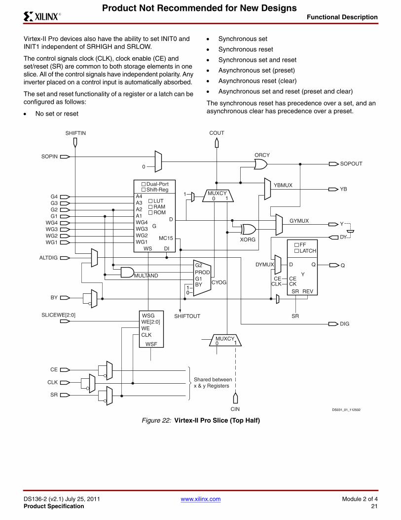
Functional Description
DS136-2 (v2.1) July 25, 2011 www.xilinx.com Module 2 of 4Product Specification 21
R
Product Not Recommended for New Designs
Virtex-II Pro devices also have the ability to set INIT0 and INIT1 independent of SRHIGH and SRLOW.
The control signals clock (CLK), clock enable (CE) and set/reset (SR) are common to both storage elements in one slice. All of the control signals have independent polarity. Any inverter placed on a control input is automatically absorbed.
The set and reset functionality of a register or a latch can be configured as follows:
No set or reset
Synchronous set
Synchronous reset
Synchronous set and reset
Asynchronous set (preset)
Asynchronous reset (clear)
Asynchronous set and reset (preset and clear)
The synchronous reset has precedence over a set, and an asynchronous clear has precedence over a preset.
X-Ref Target - Figure 22
Figure 22: Virtex-II Pro Slice (Top Half)
G4
SOPIN
A4G3 A3G2 A2G1 A1
WG4 WG4WG3 WG3WG2 WG2WG1
BY
WG1
Dual-Port
LUT
FFLATCH
RAMROM
Shift-Reg
D
0
MC15
WS
SR
SR
REV
DI
G
Y
G2
G1BY
10
PROD
D Q
CECECKCLK
MUXCYYB
DIG
DY
Y
0 1
MUXCY0 1
1
SOPOUT
DYMUX
GYMUX
YBMUX
ORCY
WSGWE[2:0]
SHIFTOUT
CYOG
XORG
WECLK
WSF
ALTDIG
CE
SR
CLK
SLICEWE[2:0]
MULTAND
Shared betweenx & y Registers
SHIFTIN COUT
CIN DS031_01_112502
Q
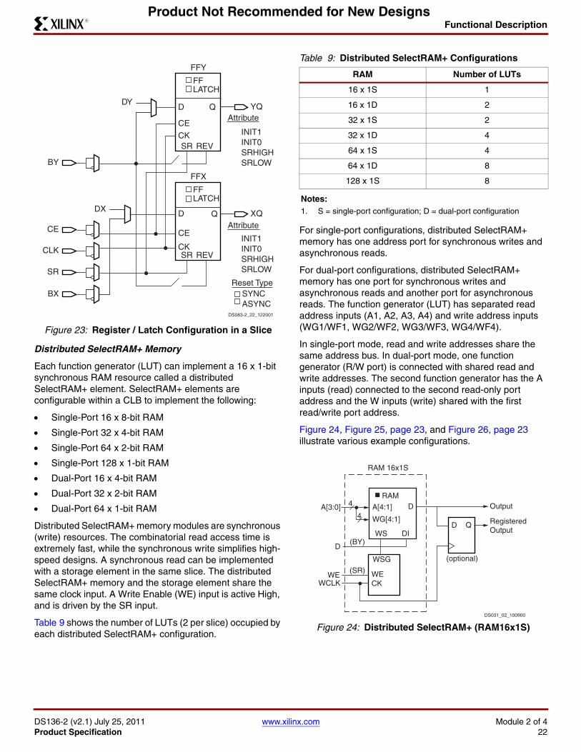
Functional Description
DS136-2 (v2.1) July 25, 2011 www.xilinx.com Module 2 of 4Product Specification 22
R
Product Not Recommended for New Designs
Distributed SelectRAM+ Memory
Each function generator (LUT) can implement a 16 x 1-bit synchronous RAM resource called a distributed SelectRAM+ element. SelectRAM+ elements are configurable within a CLB to implement the following:
Single-Port 16 x 8-bit RAM
Single-Port 32 x 4-bit RAM
Single-Port 64 x 2-bit RAM
Single-Port 128 x 1-bit RAM
Dual-Port 16 x 4-bit RAM
Dual-Port 32 x 2-bit RAM
Dual-Port 64 x 1-bit RAM
Distributed SelectRAM+ memory modules are synchronous (write) resources. The combinatorial read access time is extremely fast, while the synchronous write simplifies high-speed designs. A synchronous read can be implemented with a storage element in the same slice. The distributed SelectRAM+ memory and the storage element share the same clock input. A Write Enable (WE) input is active High, and is driven by the SR input.
Table 9 shows the number of LUTs (2 per slice) occupied by each distributed SelectRAM+ configuration.
For single-port configurations, distributed SelectRAM+ memory has one address port for synchronous writes and asynchronous reads.
For dual-port configurations, distributed SelectRAM+ memory has one port for synchronous writes and asynchronous reads and another port for asynchronous reads. The function generator (LUT) has separated read address inputs (A1, A2, A3, A4) and write address inputs (WG1/WF1, WG2/WF2, WG3/WF3, WG4/WF4).
In single-port mode, read and write addresses share the same address bus. In dual-port mode, one function generator (R/W port) is connected with shared read and write addresses. The second function generator has the A inputs (read) connected to the second read-only port address and the W inputs (write) shared with the first read/write port address.
Figure 24, Figure 25, page 23, and Figure 26, page 23 illustrate various example configurations.
X-Ref Target - Figure 23
Figure 23: Register / Latch Configuration in a Slice
FF
FFY
LATCH
SR REV
D Q
CE
CK
YQ
FF
FFX
LATCH
SR REV
D Q
CE
CK
XQ
CE
DX
DY
BY
CLK
BX
SR
Attribute
INIT1INIT0SRHIGHSRLOW
Attribute
INIT1INIT0SRHIGHSRLOW
Reset TypeSYNCASYNC
DS083-2_22_122001
Table 9: Distributed SelectRAM+ Configurations
RAM Number of LUTs
16 x 1S 1
16 x 1D 2
32 x 1S 2
32 x 1D 4
64 x 1S 4
64 x 1D 8
128 x 1S 8
Notes: 1. S = single-port configuration; D = dual-port configuration
X-Ref Target - Figure 24
Figure 24: Distributed SelectRAM+ (RAM16x1S)
A[3:0]
D
D
DIWS
WSG
WEWCLK
RAM 16x1S
D Q
RAM
WECK
A[4:1]
WG[4:1]
Output
RegisteredOutput
(optional)
(SR)
4
4
(BY)
DS031_02_100900
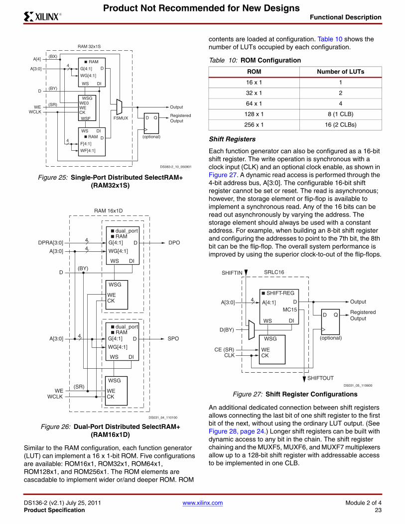
Functional Description
DS136-2 (v2.1) July 25, 2011 www.xilinx.com Module 2 of 4Product Specification 23
R
Product Not Recommended for New Designs
Similar to the RAM configuration, each function generator (LUT) can implement a 16 x 1-bit ROM. Five configurations are available: ROM16x1, ROM32x1, ROM64x1, ROM128x1, and ROM256x1. The ROM elements are cascadable to implement wider or/and deeper ROM. ROM
contents are loaded at configuration. Table 10 shows the number of LUTs occupied by each configuration.
Shift Registers
Each function generator can also be configured as a 16-bit shift register. The write operation is synchronous with a clock input (CLK) and an optional clock enable, as shown in Figure 27. A dynamic read access is performed through the 4-bit address bus, A[3:0]. The configurable 16-bit shift register cannot be set or reset. The read is asynchronous; however, the storage element or flip-flop is available to implement a synchronous read. Any of the 16 bits can be read out asynchronously by varying the address. The storage element should always be used with a constant address. For example, when building an 8-bit shift register and configuring the addresses to point to the 7th bit, the 8th bit can be the flip-flop. The overall system performance is improved by using the superior clock-to-out of the flip-flops.
An additional dedicated connection between shift registers allows connecting the last bit of one shift register to the first bit of the next, without using the ordinary LUT output. (See Figure 28, page 24.) Longer shift registers can be built with dynamic access to any bit in the chain. The shift register chaining and the MUXF5, MUXF6, and MUXF7 multiplexers allow up to a 128-bit shift register with addressable access to be implemented in one CLB.
X-Ref Target - Figure 25
Figure 25: Single-Port Distributed SelectRAM+ (RAM32x1S)
X-Ref Target - Figure 26
Figure 26: Dual-Port Distributed SelectRAM+ (RAM16x1D)
A[3:0]
D
WSG
F5MUX
WEWCLK
RAM 32x1S
D Q
WEWE0
CKWSF
D
DIWS
RAM
G[4:1]
A[4]
WG[4:1]
D
DIWSRAM
F[4:1]
WF[4:1]
Output
RegisteredOutput
(optional)
(SR)
4
(BY)
(BX)
4
DS083-2_10_050901
A[3:0]
D
WSG
WEWCLK
RAM 16x1D
WECK
D
DIWS
RAMG[4:1]
WG[4:1]
dual_port
RAMdual_port
4
(BY)
DPRA[3:0]
SPO
A[3:0]
WSG
WECK
D
DIWS
G[4:1]
WG[4:1]
DPO4
4
DS031_04_110100
(SR)
Table 10: ROM Configuration
ROM Number of LUTs
16 x 1 1
32 x 1 2
64 x 1 4
128 x 1 8 (1 CLB)
256 x 1 16 (2 CLBs)
X-Ref Target - Figure 27
Figure 27: Shift Register Configurations
A[3:0]
SHIFTIN
SHIFTOUT
D(BY)
D
MC15
DI
WSG
CE (SR)CLK
SRLC16
D Q
SHIFT-REG
WECK
A[4:1] Output
RegisteredOutput
(optional)
4
DS031_05_110600
WS
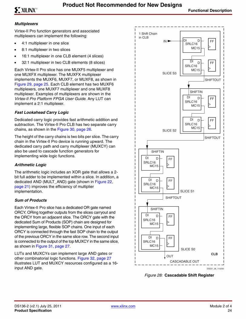
Functional Description
DS136-2 (v2.1) July 25, 2011 www.xilinx.com Module 2 of 4Product Specification 24
R
Product Not Recommended for New Designs
Multiplexers
Virtex-II Pro function generators and associated multiplexers can implement the following:
4:1 multiplexer in one slice
8:1 multiplexer in two slices
16:1 multiplexer in one CLB element (4 slices)
32:1 multiplexer in two CLB elements (8 slices)
Each Virtex-II Pro slice has one MUXF5 multiplexer and one MUXFX multiplexer. The MUXFX multiplexer implements the MUXF6, MUXF7, or MUXF8, as shown in Figure 29, page 25. Each CLB element has two MUXF6 multiplexers, one MUXF7 multiplexer and one MUXF8 multiplexer. Examples of multiplexers are shown in the Virtex-II Pro Platform FPGA User Guide. Any LUT can implement a 2:1 multiplexer.
Fast Lookahead Carry Logic
Dedicated carry logic provides fast arithmetic addition and subtraction. The Virtex-II Pro CLB has two separate carry chains, as shown in the Figure 30, page 26.
The height of the carry chains is two bits per slice. The carry chain in the Virtex-II Pro device is running upward. The dedicated carry path and carry multiplexer (MUXCY) can also be used to cascade function generators for implementing wide logic functions.
Arithmetic Logic
The arithmetic logic includes an XOR gate that allows a 2-bit full adder to be implemented within a slice. In addition, a dedicated AND (MULT_AND) gate (shown in Figure 22, page 21) improves the efficiency of multiplier implementation.
Sum of Products
Each Virtex-II Pro slice has a dedicated OR gate named ORCY, ORing together outputs from the slices carryout and the ORCY from an adjacent slice. The ORCY gate with the dedicated Sum of Products (SOP) chain are designed for implementing large, flexible SOP chains. One input of each ORCY is connected through the fast SOP chain to the output of the previous ORCY in the same slice row. The second input is connected to the output of the top MUXCY in the same slice, as shown in Figure 31, page 27.
LUTs and MUXCYs can implement large AND gates or other combinatorial logic functions. Figure 32, page 27 illustrates LUT and MUXCY resources configured as a 16-input AND gate.
X-Ref Target - Figure 28
Figure 28: Cascadable Shift Register
SRLC16MC15
MC15
D
SRLC16DI
SHIFTIN
CASCADABLE OUT
SLICE S0
SLICE S1
SLICE S2
SLICE S3
1 Shift Chainin CLB
CLB
DS031_06_110200
FF
FFD
SRLC16MC15
MC15
D
SRLC16DI
SHIFTIN
SHIFTOUT
FF
FFD
SRLC16MC15
MC15
D
SRLC16
DI
DI
SHIFTIN
IN
SHIFTOUT
FF
FFD
SRLC16MC15
MC15
D
SRLC16
DI
SHIFTOUT
FF
FFD
DI
DI
DI
OUT
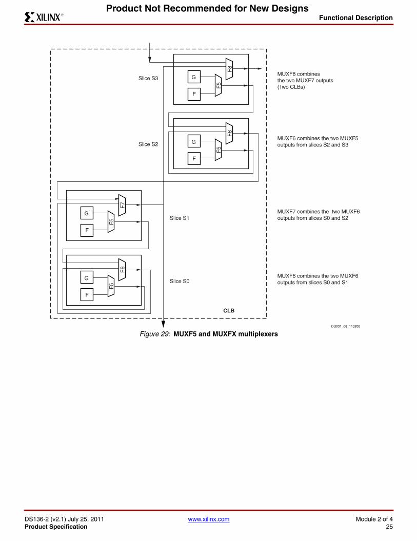
Functional Description
DS136-2 (v2.1) July 25, 2011 www.xilinx.com Module 2 of 4Product Specification 25
R
Product Not Recommended for New Designs
X-Ref Target - Figure 29
Figure 29: MUXF5 and MUXFX multiplexers
Slice S1
Slice S0
Slice S3
Slice S2
CLB
DS031_08_110200
F5
F6
F5
F7
F5
F6
F5
F8
MUXF8 combines the two MUXF7 outputs (Two CLBs)
MUXF6 combines the two MUXF5 outputs from slices S2 and S3
MUXF7 combines the two MUXF6 outputs from slices S0 and S2
MUXF6 combines the two MUXF6outputs from slices S0 and S1
G
F
G
F
G
F
G
F
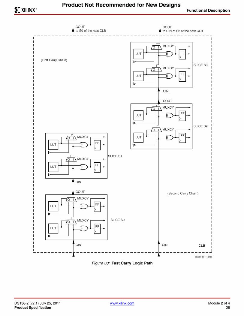
Functional Description
DS136-2 (v2.1) July 25, 2011 www.xilinx.com Module 2 of 4Product Specification 26
R
Product Not Recommended for New Designs
X-Ref Target - Figure 30
Figure 30: Fast Carry Logic Path
FFLUT
O I MUXCY
FFLUT
O I MUXCY
FFLUT
O I MUXCY
FFLUT
O I MUXCY
CIN
CIN CIN
COUT
FFLUT
O I MUXCY
FFLUT
O I MUXCY
FFLUT
O I MUXCY
FFLUT
O I MUXCY
CIN
COUT
COUTto CIN of S2 of the next CLB
COUTto S0 of the next CLB
(First Carry Chain)
(Second Carry Chain)
SLICE S1
SLICE S0
SLICE S3
SLICE S2
CLB
DS031_07_110200
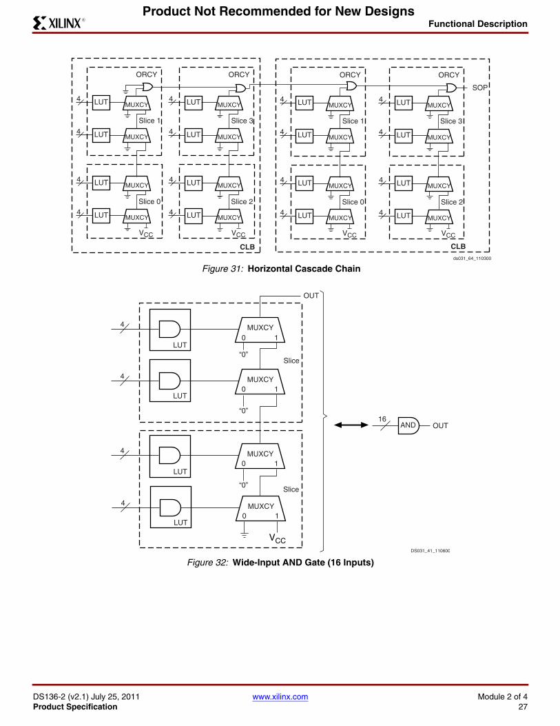
Functional Description
DS136-2 (v2.1) July 25, 2011 www.xilinx.com Module 2 of 4Product Specification 27
R
Product Not Recommended for New Designs
X-Ref Target - Figure 31
Figure 31: Horizontal Cascade Chain
X-Ref Target - Figure 32
Figure 32: Wide-Input AND Gate (16 Inputs)
MUXCY4
MUXCY4
Slice 1
ds031_64_110300
ORCY
LUT
LUT
MUXCY4
MUXCY4
Slice 0
VCC
LUT
LUT
MUXCY4
MUXCY4
Slice 3
ORCY
LUT
LUT
MUXCY4
MUXCY4
Slice 2
VCC
LUT
LUT
SOP
CLB
MUXCY4
MUXCY4
Slice 1
ORCY
LUT
LUT
MUXCY4
MUXCY4
Slice 0
VCC
LUT
LUT
MUXCY4
MUXCY4
Slice 3
ORCY
LUT
LUT
MUXCY4
MUXCY4
Slice 2
VCC
LUT
LUT
CLB
MUXCY
AND
4
16
MUXCY4
“0”
0 1
0 1
“0”
0 1
“0”
MUXCY4
Slice
OUT
OUT
Slice
LUT
DS031_41_110600
LUT
LUT
VCC
MUXCY4
0 1LUT
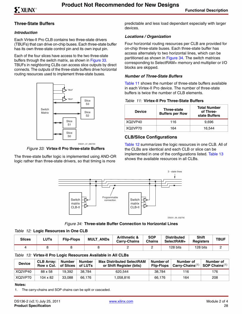
Functional Description
DS136-2 (v2.1) July 25, 2011 www.xilinx.com Module 2 of 4Product Specification 28
R
Product Not Recommended for New Designs
Three-State Buffers
Introduction
Each Virtex-II Pro CLB contains two three-state drivers (TBUFs) that can drive on-chip buses. Each three-state buffer has its own three-state control pin and its own input pin.
Each of the four slices have access to the two three-state buffers through the switch matrix, as shown in Figure 33. TBUFs in neighboring CLBs can access slice outputs by direct connects. The outputs of the three-state buffers drive horizontal routing resources used to implement three-state buses.
The three-state buffer logic is implemented using AND-OR logic rather than three-state drivers, so that timing is more
predictable and less load dependant especially with larger devices.
Locations / Organization
Four horizontal routing resources per CLB are provided for on-chip three-state buses. Each three-state buffer has access alternately to two horizontal lines, which can be partitioned as shown in Figure 34. The switch matrices corresponding to SelectRAM+ memory and multiplier or I/O blocks are skipped.
Number of Three-State Buffers
Table 11 shows the number of three-state buffers available in each Virtex-II Pro device. The number of three-state buffers is twice the number of CLB elements.
CLB/Slice Configurations
Table 12 summarizes the logic resources in one CLB. All of the CLBs are identical and each CLB or slice can be implemented in one of the configurations listed. Table 13 shows the available resources in all CLBs.
X-Ref Target - Figure 33
Figure 33: Virtex-II Pro three-state Buffers
SliceS3
SliceS2
SliceS1
SliceS0
SwitchMatrix
DS031_37_060700
TBUF
TBUF
Table 11: Virtex-II Pro Three-State Buffers
Device Three-state Buffers per Row
Total Number of Three-
state Buffers
XQ2VP40 116 9,696
XQ2VP70 164 16,544
X-Ref Target - Figure 34
Figure 34: Three-state Buffer Connection to Horizontal Lines
Table 12: Logic Resources in One CLB
Slices LUTs Flip-Flops MULT_ANDs Arithmetic & Carry-Chains
SOP Chains
Distributed SelectRAM+
Shift Registers TBUF
4 8 8 8 2 2 128 bits 128 bits 2
Table 13: Virtex-II Pro Logic Resources Available in All CLBs
Device CLB Array: Row x Col.
Number of Slices
Number of LUTs
Max Distributed SelectRAM or Shift Register (bits)
Number of Flip-Flops
Number of Carry-Chains (1)
Number of SOP Chains (1)
XQ2VP40 88 x 58 19,392 38,784 620,544 38,784 116 176
XQ2VP70 104 x 82 33,088 66,176 1,058,816 66,176 164 208
Notes: 1. The carry-chains and SOP chains can be split or cascaded.
SwitchmatrixCLB-II
SwitchmatrixCLB-II
DS031_09_032700
Programmableconnection
3 - state lines
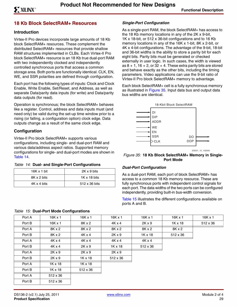
Functional Description
DS136-2 (v2.1) July 25, 2011 www.xilinx.com Module 2 of 4Product Specification 29
R
Product Not Recommended for New Designs
18 Kb Block SelectRAM+ Resources
Introduction
Virtex-II Pro devices incorporate large amounts of 18 Kb block SelectRAM+ resources. These complement the distributed SelectRAM+ resources that provide shallow RAM structures implemented in CLBs. Each Virtex-II Pro block SelectRAM+ resource is an 18 Kb true dual-port RAM with two independently clocked and independently controlled synchronous ports that access a common storage area. Both ports are functionally identical. CLK, EN, WE, and SSR polarities are defined through configuration.
Each port has the following types of inputs: Clock and Clock Enable, Write Enable, Set/Reset, and Address, as well as separate Data/parity data inputs (for write) and Data/parity data outputs (for read).
Operation is synchronous; the block SelectRAM+ behaves like a register. Control, address and data inputs must (and need only) be valid during the set-up time window prior to a rising (or falling, a configuration option) clock edge. Data outputs change as a result of the same clock edge.
Configuration
Virtex-II Pro block SelectRAM+ supports various configurations, including single- and dual-port RAM and various data/address aspect ratios. Supported memory configurations for single- and dual-port modes are shown in Table 14.
Single-Port Configuration
As a single-port RAM, the block SelectRAM+ has access to the 18 Kb memory locations in any of the 2K x 9-bit, 1K x 18-bit, or 512 x 36-bit configurations and to 16 Kb memory locations in any of the 16K x 1-bit, 8K x 2-bit, or 4K x 4-bit configurations. The advantage of the 9-bit, 18-bit and 36-bit widths is the ability to store a parity bit for each eight bits. Parity bits must be generated or checked externally in user logic. In such cases, the width is viewed as 8 + 1, 16 + 2, or 32 + 4. These extra parity bits are stored and behave exactly as the other bits, including the timing parameters. Video applications can use the 9-bit ratio of Virtex-II Pro block SelectRAM+ memory to advantage.
Each block SelectRAM+ cell is a fully synchronous memory as illustrated in Figure 35. Input data bus and output data bus widths are identical.
Dual-Port Configuration
As a dual-port RAM, each port of block SelectRAM+ has access to a common 18 Kb memory resource. These are fully synchronous ports with independent control signals for each port. The data widths of the two ports can be configured independently, providing built-in bus-width conversion.
Table 15 illustrates the different configurations available on ports A and B.
Table 14: Dual- and Single-Port Configurations
16K x 1 bit 2K x 9 bits
8K x 2 bits 1K x 18 bits
4K x 4 bits 512 x 36 bits
X-Ref Target - Figure 35
Figure 35: 18 Kb Block SelectRAM+ Memory in Single-Port Mode
DOP
DIP
ADDR
WE
ENSSR
CLK
18-Kbit Block SelectRAM
DS031_10_102000
DI
DO
Table 15: Dual-Port Mode Configurations
Port A 16K x 1 16K x 1 16K x 1 16K x 1 16K x 1 16K x 1
Port B 16K x 1 8K x 2 4K x 4 2K x 9 1K x 18 512 x 36
Port A 8K x 2 8K x 2 8K x 2 8K x 2 8K x 2
Port B 8K x 2 4K x 4 2K x 9 1K x 18 512 x 36
Port A 4K x 4 4K x 4 4K x 4 4K x 4
Port B 4K x 4 2K x 9 1K x 18 512 x 36
Port A 2K x 9 2K x 9 2K x 9
Port B 2K x 9 1K x 18 512 x 36
Port A 1K x 18 1K x 18
Port B 1K x 18 512 x 36
Port A 512 x 36
Port B 512 x 36
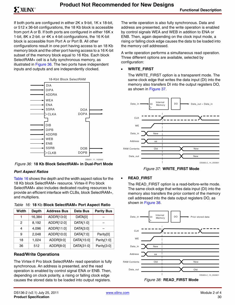
Functional Description
DS136-2 (v2.1) July 25, 2011 www.xilinx.com Module 2 of 4Product Specification 30
R
Product Not Recommended for New Designs
If both ports are configured in either 2K x 9-bit, 1K x 18-bit, or 512 x 36-bit configurations, the 18 Kb block is accessible from port A or B. If both ports are configured in either 16K x 1-bit, 8K x 2-bit. or 4K x 4-bit configurations, the 16 K-bit block is accessible from Port A or Port B. All other configurations result in one port having access to an 18 Kb memory block and the other port having access to a 16 K-bit subset of the memory block equal to 16 Kbs. Each block SelectRAM+ cell is a fully synchronous memory, as illustrated in Figure 36. The two ports have independent inputs and outputs and are independently clocked.
Port Aspect Ratios
Table 16 shows the depth and the width aspect ratios for the 18 Kb block SelectRAM+ resource. Virtex-II Pro block SelectRAM+ also includes dedicated routing resources to provide an efficient interface with CLBs, block SelectRAM+, and multipliers.
Read/Write Operations
The Virtex-II Pro block SelectRAM+ read operation is fully synchronous. An address is presented, and the read operation is enabled by control signal ENA or ENB. Then, depending on clock polarity, a rising or falling clock edge causes the stored data to be loaded into output registers.
The write operation is also fully synchronous. Data and address are presented, and the write operation is enabled by control signals WEA and WEB in addition to ENA or ENB. Then, again depending on the clock input mode, a rising or falling clock edge causes the data to be loaded into the memory cell addressed.
A write operation performs a simultaneous read operation. Three different options are available, selected by configuration:
WRITE_FIRST
The WRITE_FIRST option is a transparent mode. The same clock edge that writes the data input (DI) into the memory also transfers DI into the output registers DO, as shown in Figure 37.
READ_FIRST
The READ_FIRST option is a read-before-write mode. The same clock edge that writes data input (DI) into the memory also transfers the prior content of the memory cell addressed into the data output registers DO, as shown in Figure 38.
X-Ref Target - Figure 36
Figure 36: 18 Kb Block SelectRAM+ in Dual-Port Mode
Table 16: 18 Kb Block SelectRAM+ Port Aspect Ratio
Width Depth Address Bus Data Bus Parity Bus
1 16,384 ADDR[13:0] DATA[0] –
2 8,192 ADDR[12:0] DATA[1:0] –
4 4,096 ADDR[11:0] DATA[3:0] –
9 2,048 ADDR[10:0] DATA[7:0] Parity[0]
18 1,024 ADDR[9:0] DATA[15:0] Parity[1:0]
36 512 ADDR[8:0] DATA[31:0] Parity[3:0]
DOPA
DOPB
DIPA
ADDRA
WEA
ENASSRA
CLKA
DIPB
ADDRB
WEB
ENBSSRB
CLKB
18-Kbit Block SelectRAM
DS031_11_102000
DOB
DOA
DIA
DIB
X-Ref Target - Figure 37
Figure 37: WRITE_FIRST Mode
X-Ref Target - Figure 38
Figure 38: READ_FIRST Mode
CLK
WE
Data_in
Data_in
New
aaAddress
Internal Memory DO Data_out = Data_in
Data_out
DI
DS083-2_14_050901
New
RAM Contents NewOld
CLK
WE
Data_in
Data_in
New
aa
Old
Address
Internal Memory DO Prior stored data
Data_out
DI
DS083-2_13_050901
RAM Contents NewOld
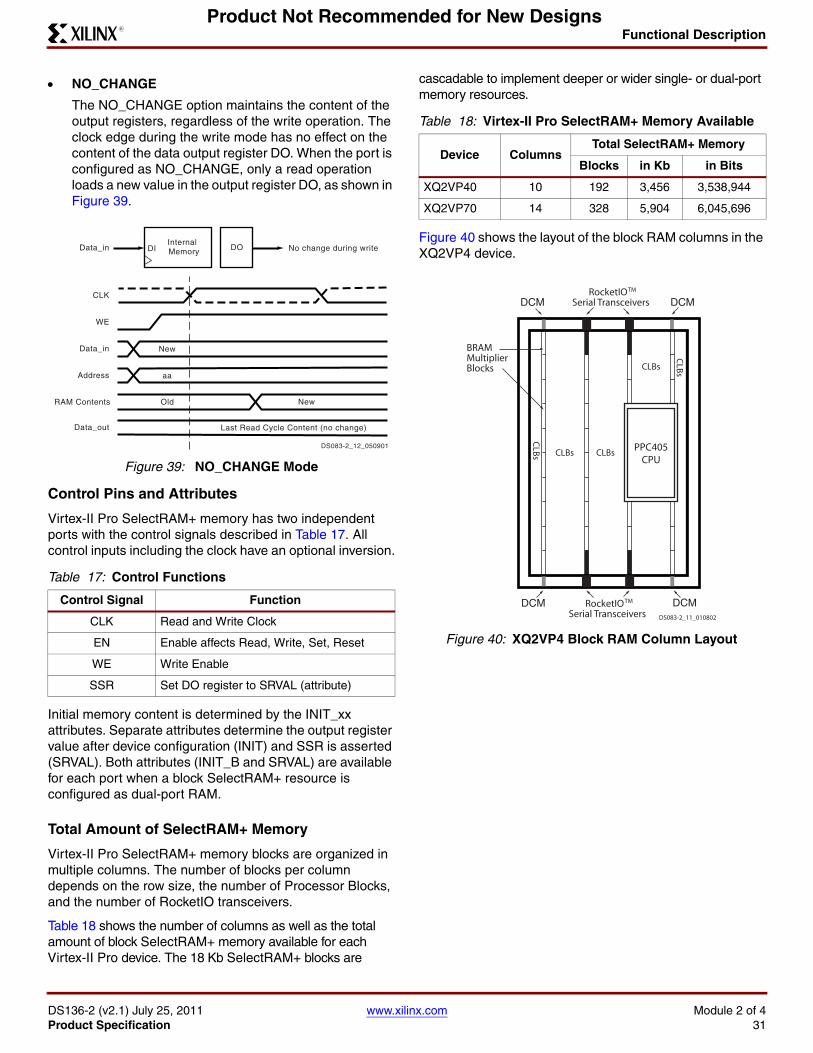
Functional Description
DS136-2 (v2.1) July 25, 2011 www.xilinx.com Module 2 of 4Product Specification 31
R
Product Not Recommended for New Designs
NO_CHANGE
The NO_CHANGE option maintains the content of the output registers, regardless of the write operation. The clock edge during the write mode has no effect on the content of the data output register DO. When the port is configured as NO_CHANGE, only a read operation loads a new value in the output register DO, as shown in Figure 39.
Control Pins and Attributes
Virtex-II Pro SelectRAM+ memory has two independent ports with the control signals described in Table 17. All control inputs including the clock have an optional inversion.
Initial memory content is determined by the INIT_xx attributes. Separate attributes determine the output register value after device configuration (INIT) and SSR is asserted (SRVAL). Both attributes (INIT_B and SRVAL) are available for each port when a block SelectRAM+ resource is configured as dual-port RAM.
Total Amount of SelectRAM+ Memory
Virtex-II Pro SelectRAM+ memory blocks are organized in multiple columns. The number of blocks per column depends on the row size, the number of Processor Blocks, and the number of RocketIO transceivers.
Table 18 shows the number of columns as well as the total amount of block SelectRAM+ memory available for each Virtex-II Pro device. The 18 Kb SelectRAM+ blocks are
cascadable to implement deeper or wider single- or dual-port memory resources.
Figure 40 shows the layout of the block RAM columns in the XQ2VP4 device.
X-Ref Target - Figure 39
Figure 39: NO_CHANGE Mode
Table 17: Control Functions
Control Signal Function
CLK Read and Write Clock
EN Enable affects Read, Write, Set, Reset
WE Write Enable
SSR Set DO register to SRVAL (attribute)
CLK
WE
Data_in
Data_in
New
aa
Last Read Cycle Content (no change)
Address
Internal Memory DO No change during write
Data_out
DI
DS083-2_12_050901
RAM Contents NewOld
Table 18: Virtex-II Pro SelectRAM+ Memory Available
Device ColumnsTotal SelectRAM+ Memory
Blocks in Kb in Bits
XQ2VP40 10 192 3,456 3,538,944
XQ2VP70 14 328 5,904 6,045,696
X-Ref Target - Figure 40
Figure 40: XQ2VP4 Block RAM Column Layout
BRAMMultiplierBlocks
PPC405CPU
CLBs
CLB
s
CLB
s CLBs
CLBs
DS083-2_11_010802
TMRocketIOSerial Transceivers
TMRocketIOSerial Transceivers
DCM DCM
DCM DCM
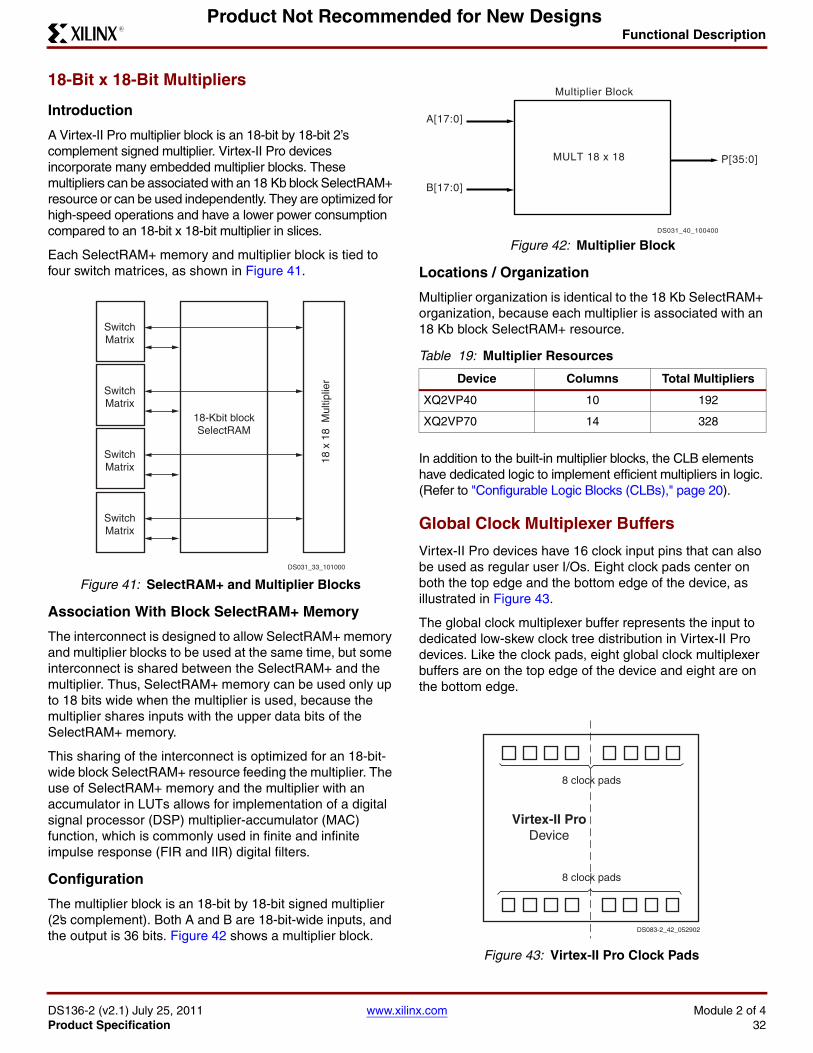
Functional Description
DS136-2 (v2.1) July 25, 2011 www.xilinx.com Module 2 of 4Product Specification 32
R
Product Not Recommended for New Designs
18-Bit x 18-Bit Multipliers
Introduction
A Virtex-II Pro multiplier block is an 18-bit by 18-bit 2’s complement signed multiplier. Virtex-II Pro devices incorporate many embedded multiplier blocks. These multipliers can be associated with an 18 Kb block SelectRAM+ resource or can be used independently. They are optimized for high-speed operations and have a lower power consumption compared to an 18-bit x 18-bit multiplier in slices.
Each SelectRAM+ memory and multiplier block is tied to four switch matrices, as shown in Figure 41.
Association With Block SelectRAM+ Memory
The interconnect is designed to allow SelectRAM+ memory and multiplier blocks to be used at the same time, but some interconnect is shared between the SelectRAM+ and the multiplier. Thus, SelectRAM+ memory can be used only up to 18 bits wide when the multiplier is used, because the multiplier shares inputs with the upper data bits of the SelectRAM+ memory.
This sharing of the interconnect is optimized for an 18-bit-wide block SelectRAM+ resource feeding the multiplier. The use of SelectRAM+ memory and the multiplier with an accumulator in LUTs allows for implementation of a digital signal processor (DSP) multiplier-accumulator (MAC) function, which is commonly used in finite and infinite impulse response (FIR and IIR) digital filters.
Configuration
The multiplier block is an 18-bit by 18-bit signed multiplier (2's complement). Both A and B are 18-bit-wide inputs, and the output is 36 bits. Figure 42 shows a multiplier block.
Locations / Organization
Multiplier organization is identical to the 18 Kb SelectRAM+ organization, because each multiplier is associated with an 18 Kb block SelectRAM+ resource.
In addition to the built-in multiplier blocks, the CLB elements have dedicated logic to implement efficient multipliers in logic. (Refer to "Configurable Logic Blocks (CLBs)," page 20).
Global Clock Multiplexer Buffers
Virtex-II Pro devices have 16 clock input pins that can also be used as regular user I/Os. Eight clock pads center on both the top edge and the bottom edge of the device, as illustrated in Figure 43.
The global clock multiplexer buffer represents the input to dedicated low-skew clock tree distribution in Virtex-II Pro devices. Like the clock pads, eight global clock multiplexer buffers are on the top edge of the device and eight are on the bottom edge.
X-Ref Target - Figure 41
Figure 41: SelectRAM+ and Multiplier Blocks
SwitchMatrix
SwitchMatrix
18-Kbit blockSelectRAM
18 x
18
Mul
tiplie
r
SwitchMatrix
SwitchMatrix
DS031_33_101000
X-Ref Target - Figure 42
Figure 42: Multiplier Block
Table 19: Multiplier Resources
Device Columns Total Multipliers
XQ2VP40 10 192
XQ2VP70 14 328
X-Ref Target - Figure 43
Figure 43: Virtex-II Pro Clock Pads
MULT 18 x 18
A[17:0]
P[35:0]
B[17:0]
Multiplier Block
DS031_40_100400
8 clock pads
8 clock pads
Virtex-II ProDevice
DS083-2_42_052902
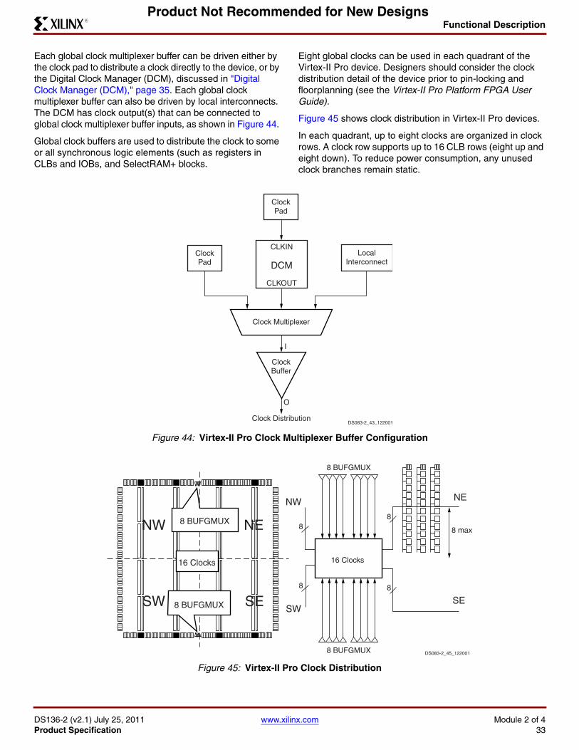
Functional Description
DS136-2 (v2.1) July 25, 2011 www.xilinx.com Module 2 of 4Product Specification 33
R
Product Not Recommended for New Designs
Each global clock multiplexer buffer can be driven either by the clock pad to distribute a clock directly to the device, or by the Digital Clock Manager (DCM), discussed in "Digital Clock Manager (DCM)," page 35. Each global clock multiplexer buffer can also be driven by local interconnects. The DCM has clock output(s) that can be connected to global clock multiplexer buffer inputs, as shown in Figure 44.
Global clock buffers are used to distribute the clock to some or all synchronous logic elements (such as registers in CLBs and IOBs, and SelectRAM+ blocks.
Eight global clocks can be used in each quadrant of the Virtex-II Pro device. Designers should consider the clock distribution detail of the device prior to pin-locking and floorplanning (see the Virtex-II Pro Platform FPGA User Guide).
Figure 45 shows clock distribution in Virtex-II Pro devices.
In each quadrant, up to eight clocks are organized in clock rows. A clock row supports up to 16 CLB rows (eight up and eight down). To reduce power consumption, any unused clock branches remain static.
X-Ref Target - Figure 44
Figure 44: Virtex-II Pro Clock Multiplexer Buffer Configuration
X-Ref Target - Figure 45
Figure 45: Virtex-II Pro Clock Distribution
ClockPad
LocalInterconnect
ClockPad
ClockBuffer
Clock Multiplexer
I
O
Clock Distribution
CLKIN
CLKOUT
DCM
DS083-2_43_122001
8
88
8
NW NE
SWSE
DS083-2_45_122001
8 BUFGMUX
8 max
8 BUFGMUX
16 Clocks
NW NE
SW SE
8 BUFGMUX
8 BUFGMUX
16 Clocks
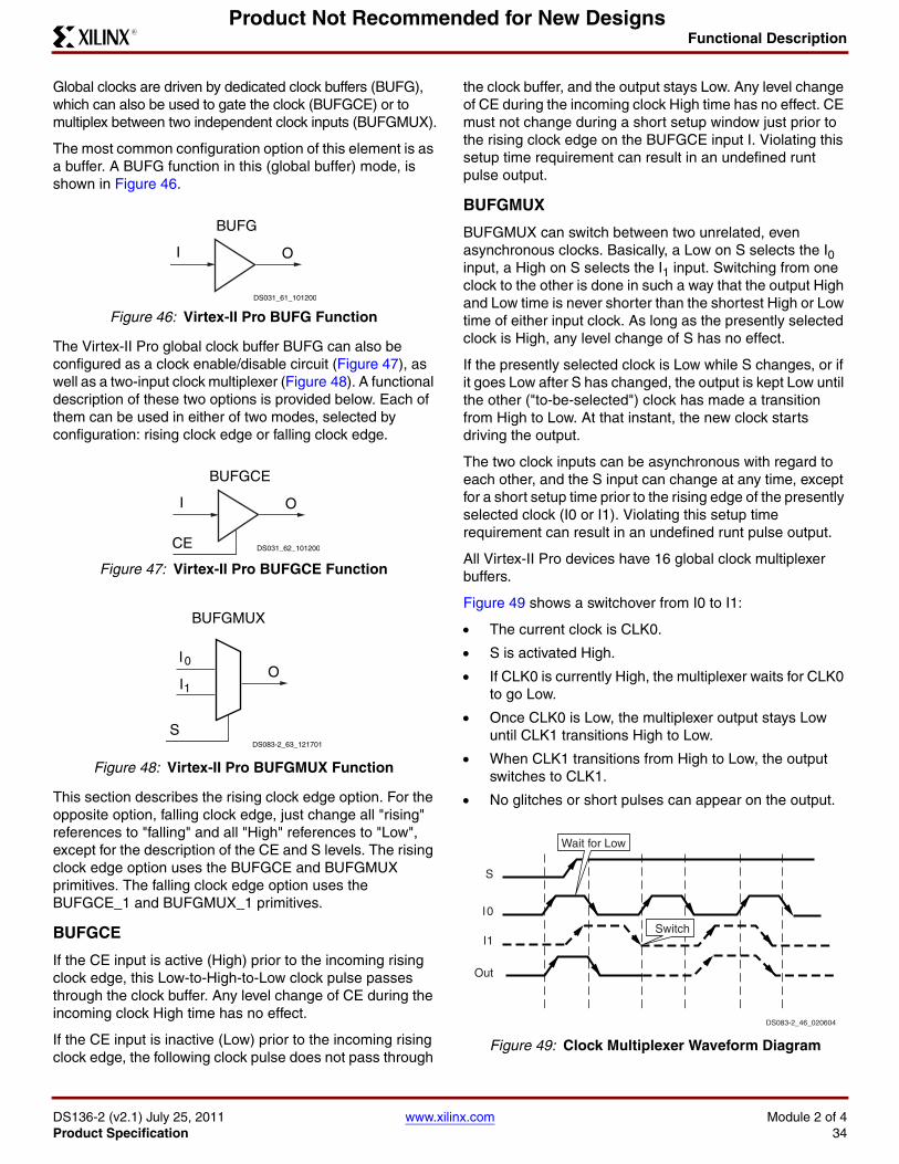
Functional Description
DS136-2 (v2.1) July 25, 2011 www.xilinx.com Module 2 of 4Product Specification 34
R
Product Not Recommended for New Designs
Global clocks are driven by dedicated clock buffers (BUFG), which can also be used to gate the clock (BUFGCE) or to multiplex between two independent clock inputs (BUFGMUX).
The most common configuration option of this element is as a buffer. A BUFG function in this (global buffer) mode, is shown in Figure 46.
The Virtex-II Pro global clock buffer BUFG can also be configured as a clock enable/disable circuit (Figure 47), as well as a two-input clock multiplexer (Figure 48). A functional description of these two options is provided below. Each of them can be used in either of two modes, selected by configuration: rising clock edge or falling clock edge.
This section describes the rising clock edge option. For the opposite option, falling clock edge, just change all "rising" references to "falling" and all "High" references to "Low", except for the description of the CE and S levels. The rising clock edge option uses the BUFGCE and BUFGMUX primitives. The falling clock edge option uses the BUFGCE_1 and BUFGMUX_1 primitives.
BUFGCE
If the CE input is active (High) prior to the incoming rising clock edge, this Low-to-High-to-Low clock pulse passes through the clock buffer. Any level change of CE during the incoming clock High time has no effect.
If the CE input is inactive (Low) prior to the incoming rising clock edge, the following clock pulse does not pass through
the clock buffer, and the output stays Low. Any level change of CE during the incoming clock High time has no effect. CE must not change during a short setup window just prior to the rising clock edge on the BUFGCE input I. Violating this setup time requirement can result in an undefined runt pulse output.
BUFGMUX
BUFGMUX can switch between two unrelated, even asynchronous clocks. Basically, a Low on S selects the I0 input, a High on S selects the I1 input. Switching from one clock to the other is done in such a way that the output High and Low time is never shorter than the shortest High or Low time of either input clock. As long as the presently selected clock is High, any level change of S has no effect.
If the presently selected clock is Low while S changes, or if it goes Low after S has changed, the output is kept Low until the other ("to-be-selected") clock has made a transition from High to Low. At that instant, the new clock starts driving the output.
The two clock inputs can be asynchronous with regard to each other, and the S input can change at any time, except for a short setup time prior to the rising edge of the presently selected clock (I0 or I1). Violating this setup time requirement can result in an undefined runt pulse output.
All Virtex-II Pro devices have 16 global clock multiplexer buffers.
Figure 49 shows a switchover from I0 to I1:
The current clock is CLK0.
S is activated High.
If CLK0 is currently High, the multiplexer waits for CLK0 to go Low.
Once CLK0 is Low, the multiplexer output stays Low until CLK1 transitions High to Low.
When CLK1 transitions from High to Low, the output switches to CLK1.
No glitches or short pulses can appear on the output.
X-Ref Target - Figure 46
Figure 46: Virtex-II Pro BUFG Function
X-Ref Target - Figure 47
Figure 47: Virtex-II Pro BUFGCE Function
X-Ref Target - Figure 48
Figure 48: Virtex-II Pro BUFGMUX Function
OI
BUFG
DS031_61_101200
OI
CE
BUFGCE
DS031_62_101200
OI0
I1
S
BUFGMUX
DS083-2_63_121701
X-Ref Target - Figure 49
Figure 49: Clock Multiplexer Waveform Diagram
S
I0
I1
Out
Wait for Low
Switch
DS083-2_46_020604
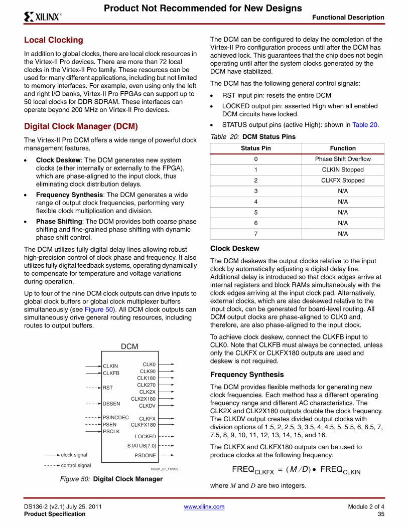
Functional Description
DS136-2 (v2.1) July 25, 2011 www.xilinx.com Module 2 of 4Product Specification 35
R
Product Not Recommended for New Designs
Local Clocking
In addition to global clocks, there are local clock resources in the Virtex-II Pro devices. There are more than 72 local clocks in the Virtex-II Pro family. These resources can be used for many different applications, including but not limited to memory interfaces. For example, even using only the left and right I/O banks, Virtex-II Pro FPGAs can support up to 50 local clocks for DDR SDRAM. These interfaces can operate beyond 200 MHz on Virtex-II Pro devices.
Digital Clock Manager (DCM)
The Virtex-II Pro DCM offers a wide range of powerful clock management features.
Clock Deskew: The DCM generates new system clocks (either internally or externally to the FPGA), which are phase-aligned to the input clock, thus eliminating clock distribution delays.
Frequency Synthesis: The DCM generates a wide range of output clock frequencies, performing very flexible clock multiplication and division.
Phase Shifting: The DCM provides both coarse phase shifting and fine-grained phase shifting with dynamic phase shift control.
The DCM utilizes fully digital delay lines allowing robust high-precision control of clock phase and frequency. It also utilizes fully digital feedback systems, operating dynamically to compensate for temperature and voltage variations during operation.
Up to four of the nine DCM clock outputs can drive inputs to global clock buffers or global clock multiplexer buffers simultaneously (see Figure 50). All DCM clock outputs can simultaneously drive general routing resources, including routes to output buffers.
The DCM can be configured to delay the completion of the Virtex-II Pro configuration process until after the DCM has achieved lock. This guarantees that the chip does not begin operating until after the system clocks generated by the DCM have stabilized.
The DCM has the following general control signals:
RST input pin: resets the entire DCM
LOCKED output pin: asserted High when all enabled DCM circuits have locked.
STATUS output pins (active High): shown in Table 20.
Clock Deskew
The DCM deskews the output clocks relative to the input clock by automatically adjusting a digital delay line. Additional delay is introduced so that clock edges arrive at internal registers and block RAMs simultaneously with the clock edges arriving at the input clock pad. Alternatively, external clocks, which are also deskewed relative to the input clock, can be generated for board-level routing. All DCM output clocks are phase-aligned to CLK0 and, therefore, are also phase-aligned to the input clock.
To achieve clock deskew, connect the CLKFB input to CLK0. Note that CLKFB must always be connected, unless only the CLKFX or CLKFX180 outputs are used and deskew is not required.
Frequency Synthesis
The DCM provides flexible methods for generating new clock frequencies. Each method has a different operating frequency range and different AC characteristics. The CLK2X and CLK2X180 outputs double the clock frequency. The CLKDV output creates divided output clocks with division options of 1.5, 2, 2.5, 3, 3.5, 4, 4.5, 5, 5.5, 6, 6.5, 7, 7.5, 8, 9, 10, 11, 12, 13, 14, 15, and 16.
The CLKFX and CLKFX180 outputs can be used to produce clocks at the following frequency:
where M and D are two integers.
X-Ref Target - Figure 50
Figure 50: Digital Clock Manager
CLKINCLKFB
CLK180CLK270
CLK0CLK90
CLK2XCLK2X180
CLKDV
DCM
DS031_67_112900
CLKFXCLKFX180
LOCKED
STATUS[7:0]
PSDONE
RST
DSSEN
PSINCDECPSENPSCLK
clock signal
control signal
Table 20: DCM Status Pins
Status Pin Function
0 Phase Shift Overflow
1 CLKIN Stopped
2 CLKFX Stopped
3 N/A
4 N/A
5 N/A
6 N/A
7 N/A
FREQCLKFX M D FREQCLKIN=
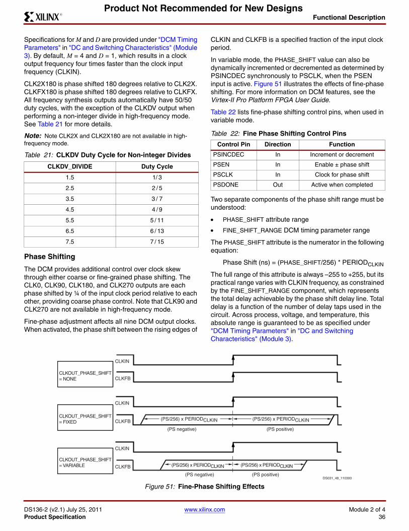
Functional Description
DS136-2 (v2.1) July 25, 2011 www.xilinx.com Module 2 of 4Product Specification 36
R
Product Not Recommended for New Designs
Specifications for M and D are provided under "DCM Timing Parameters" in "DC and Switching Characteristics" (Module 3). By default, M = 4 and D = 1, which results in a clock output frequency four times faster than the clock input frequency (CLKIN).
CLK2X180 is phase shifted 180 degrees relative to CLK2X. CLKFX180 is phase shifted 180 degrees relative to CLKFX. All frequency synthesis outputs automatically have 50/50 duty cycles, with the exception of the CLKDV output when performing a non-integer divide in high-frequency mode. See Table 21 for more details.
Note: Note CLK2X and CLK2X180 are not available in high-frequency mode.
Phase Shifting
The DCM provides additional control over clock skew through either coarse or fine-grained phase shifting. The CLK0, CLK90, CLK180, and CLK270 outputs are each phase shifted by ¼ of the input clock period relative to each other, providing coarse phase control. Note that CLK90 and CLK270 are not available in high-frequency mode.
Fine-phase adjustment affects all nine DCM output clocks. When activated, the phase shift between the rising edges of
CLKIN and CLKFB is a specified fraction of the input clock period.
In variable mode, the PHASE_SHIFT value can also be dynamically incremented or decremented as determined by PSINCDEC synchronously to PSCLK, when the PSEN input is active. Figure 51 illustrates the effects of fine-phase shifting. For more information on DCM features, see the Virtex-II Pro Platform FPGA User Guide.
Table 22 lists fine-phase shifting control pins, when used in variable mode.
Two separate components of the phase shift range must be understood:
PHASE_SHIFT attribute range
FINE_SHIFT_RANGE DCM timing parameter range
The PHASE_SHIFT attribute is the numerator in the following equation:
Phase Shift (ns) = (PHASE_SHIFT/256) * PERIODCLKIN
The full range of this attribute is always –255 to +255, but its practical range varies with CLKIN frequency, as constrained by the FINE_SHIFT_RANGE component, which represents the total delay achievable by the phase shift delay line. Total delay is a function of the number of delay taps used in the circuit. Across process, voltage, and temperature, this absolute range is guaranteed to be as specified under "DCM Timing Parameters" in "DC and Switching Characteristics" (Module 3).
Table 21: CLKDV Duty Cycle for Non-integer Divides
CLKDV_DIVIDE Duty Cycle
1.5 1/ 3
2.5 2 / 5
3.5 3 / 7
4.5 4 / 9
5.5 5 / 11
6.5 6 / 13
7.5 7 / 15
Table 22: Fine Phase Shifting Control Pins
Control Pin Direction Function
PSINCDEC In Increment or decrement
PSEN In Enable ± phase shift
PSCLK In Clock for phase shift
PSDONE Out Active when completed
X-Ref Target - Figure 51
Figure 51: Fine-Phase Shifting Effects
CLKOUT_PHASE_SHIFT= FIXED
CLKOUT_PHASE_SHIFT= VARIABLE
CLKOUT_PHASE_SHIFT= NONE
CLKIN
CLKFB
CLKIN
CLKIN
CLKFB
(PS/256) x PERIODCLKIN
(PS negative)
(PS/256) x PERIODCLKIN
(PS positive)
CLKFB (PS/256) x PERIODCLKIN
(PS negative)
(PS/256) x PERIODCLKIN
(PS positive)DS031_48_110300
Functional Description
DS136-2 (v2.1) July 25, 2011 www.xilinx.com Module 2 of 4Product Specification 37
R
Product Not Recommended for New Designs
Absolute range (fixed mode) = ± FINE_SHIFT_RANGE
Absolute range (variable mode) = ± FINE_SHIFT_RANGE/2
The reason for the difference between fixed and variable modes is as follows. For variable mode to allow symmetric, dynamic sweeps from -255/256 to +255/256, the DCM sets the "zero phase skew" point as the middle of the delay line, thus dividing the total delay line range in half. In fixed mode, since the PHASE_SHIFT value never changes after configuration, the entire delay line is available for insertion into either the CLKIN or CLKFB path (to create either positive or negative skew).
Taking both of these components into consideration, the following are some usage examples:
If PERIODCLKIN = 2 * FINE_SHIFT_RANGE, then PHASE_SHIFT in fixed mode is limited to ± 128, and in variable mode it is limited to ± 64.
If PERIODCLKIN = FINE_SHIFT_RANGE, then PHASE_SHIFT in fixed mode is limited to ± 255, and in variable mode it is limited to ± 128.
If PERIODCLKIN 0.5 * FINE_SHIFT_RANGE, then PHASE_SHIFT is limited to ± 255 in either mode.
Operating Modes
The frequency ranges of DCM input and output clocks depend on the operating mode specified, either low-frequency mode or high-frequency mode, according to Table 23. For actual values, see "DC and Switching Characteristics" (Module 3). The CLK2X, CLK2X180, CLK90, and CLK270 outputs are not available in high-frequency mode.
High or low-frequency mode is selected by an attribute.
Table 23: DCM Frequency Ranges
Output ClockLow-Frequency Mode High-Frequency Mode
CLKIN Input CLK Output CLKIN Input CLK Output
CLK0, CLK180 CLKIN_FREQ_DLL_LF CLKOUT_FREQ_1X_LF CLKIN_FREQ_DLL_HF CLKOUT_FREQ_1X_HF
CLK90, CLK270 CLKIN_FREQ_DLL_LF CLKOUT_FREQ_1X_LF NA NA
CLK2X, CLK2X180 CLKIN_FREQ_DLL_LF CLKOUT_FREQ_2X_LF NA NA
CLKDV CLKIN_FREQ_DLL_LF CLKOUT_FREQ_DV_LF CLKIN_FREQ_DLL_HF CLKOUT_FREQ_DV_HF
CLKFX, CLKFX180 CLKIN_FREQ_FX_LF CLKOUT_FREQ_FX_LF CLKIN_FREQ_FX_HF CLKOUT_FREQ_FX_HF
Functional Description
DS136-2 (v2.1) July 25, 2011 www.xilinx.com Module 2 of 4Product Specification 38
R
Product Not Recommended for New Designs
Routing
DCM Locations/Organization
Virtex-II Pro DCMs are placed on the top and bottom of each block RAM and multiplier column in some combination, as shown in Table 24. The number of DCMs total twice the number of block RAM columns in the device. Refer to Figure 40, page 31 for an illustration of this in the XQ2VP4 device.
Place-and-route software takes advantage of this regular array to deliver optimum system performance and fast compile times. The segmented routing resources are essential to guarantee IP cores portability and to efficiently handle an incremental design flow that is based on modular implementations. Total design time is reduced due to fewer and shorter design iterations.
Hierarchical Routing Resources
Most Virtex-II Pro signals are routed using the global routing resources, which are located in horizontal and vertical routing channels between each switch matrix.
As shown in Figure 52, page 39, Virtex-II Pro has fully buffered programmable interconnections, with a number of resources counted between any two adjacent switch matrix rows or columns. Fanout has minimal impact on the performance of each net.
The long lines are bidirectional wires that distribute signals across the device. Vertical and horizontal long lines span the full height and width of the device.
The hex lines route signals to every third or sixth block away in all four directions. Organized in a staggered pattern, hex lines can only be driven from one end. Hex-line signals can be accessed either at the endpoints or at the midpoint (three blocks from the source).
The double lines route signals to every first or second block away in all four directions. Organized in a staggered pattern, double lines can be driven only at their endpoints. Double-line signals can be accessed either at the endpoints or at the midpoint (one block from the source).
The direct connect lines route signals to neighboring blocks: vertically, horizontally, and diagonally.
The fast connect lines are the internal CLB local interconnections from LUT outputs to LUT inputs.
Dedicated Routing
In addition to the global and local routing resources, dedicated signals are available.
There are eight global clock nets per quadrant. (See "Global Clock Multiplexer Buffers," page 32.)
Horizontal routing resources are provided for on-chip three-state buses. Four partitionable bus lines are provided per CLB row, permitting multiple buses within a row. (See "Three-State Buffers," page 28.)
Two dedicated carry-chain resources per slice column (two per CLB column) propagate carry-chain MUXCY output signals vertically to the adjacent slice. (See "CLB/Slice Configurations," page 28.)
One dedicated SOP chain per slice row (two per CLB row) propagate ORCY output logic signals horizontally to the adjacent slice. (See "Sum of Products," page 24.)
One dedicated shift-chain per CLB connects the output of LUTs in shift-register mode to the input of the next LUT in shift-register mode (vertically) inside the CLB. (See "Shift Registers," page 23.)
Table 24: DCM Organization
Device Block RAM Columns DCMs
XQ2VP40 10 8
XQ2VP70 14 8
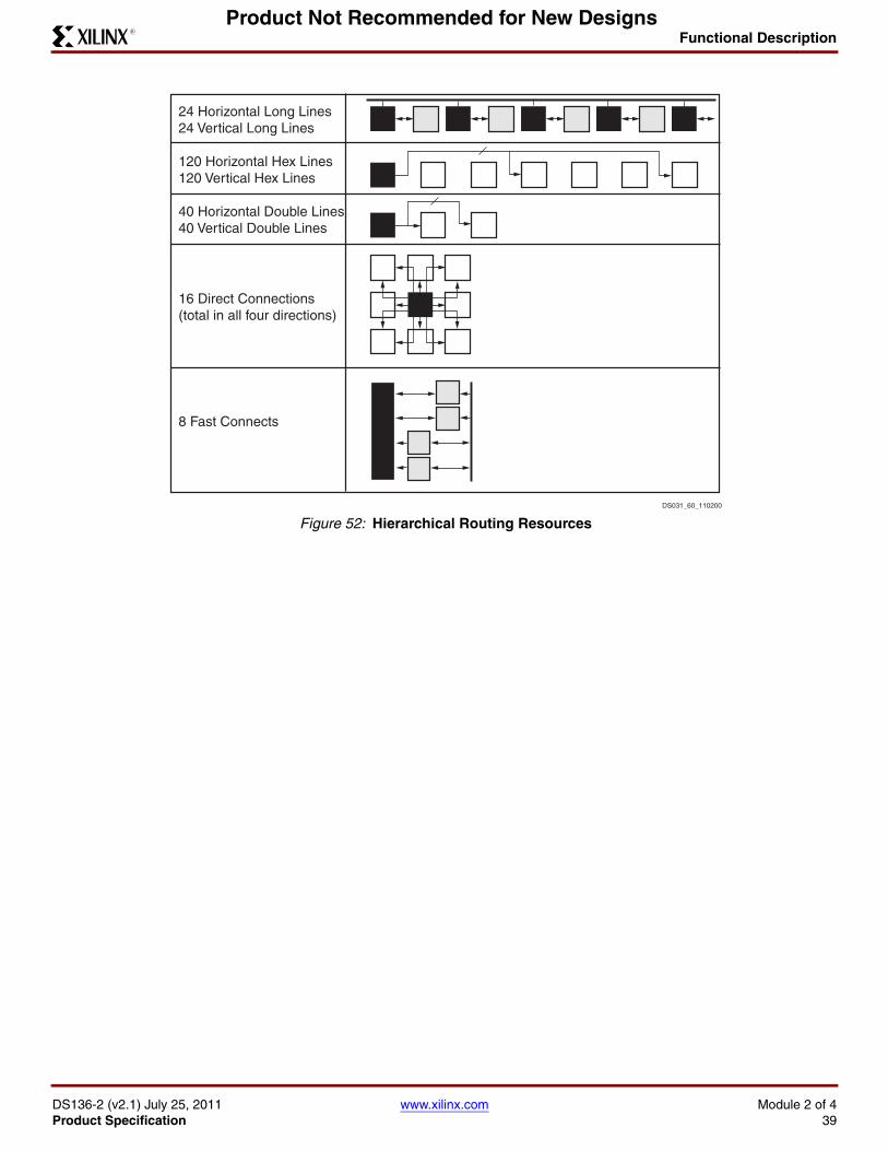
Functional Description
DS136-2 (v2.1) July 25, 2011 www.xilinx.com Module 2 of 4Product Specification 39
R
Product Not Recommended for New Designs
X-Ref Target - Figure 52
Figure 52: Hierarchical Routing Resources
24 Horizontal Long Lines24 Vertical Long Lines
120 Horizontal Hex Lines120 Vertical Hex Lines
40 Horizontal Double Lines40 Vertical Double Lines
16 Direct Connections(total in all four directions)
8 Fast Connects
DS031_60_110200
Functional Description
DS136-2 (v2.1) July 25, 2011 www.xilinx.com Module 2 of 4Product Specification 40
R
Product Not Recommended for New Designs
ConfigurationVirtex-II Pro devices are configured by loading application specific configuration data into the internal configuration memory. Configuration is carried out using a subset of the device pins, some of which are dedicated, while others can be re-used as general purpose inputs and outputs once configuration is complete.
Depending on the system design, several configuration modes are supported, selectable via mode pins. The mode pins M2, M1, and M0 are dedicated pins. The M2, M1, and M0 mode pins should be set at a constant DC voltage level, either through pull-up or pull-down resistors, or tied directly to ground or VCCAUX. The mode pins should not be toggled during and after configuration.
An additional pin, HSWAP_EN is used in conjunction with the mode pins to select whether user I/O pins have pull-ups during configuration. By default, HSWAP_EN is tied High (internal pull-up) which shuts off the pull-ups on the user I/O pins during configuration. When HSWAP_EN is tied Low, user I/Os have pull-ups during configuration. Other dedicated pins are CCLK (the configuration clock pin), DONE, PROG_B, and the boundary-scan pins: TDI, TDO, TMS, and TCK. (The TDO pin is open-drain and does not have an internal pull-up resistor.) Depending on the configuration mode chosen, CCLK can be an output generated by the FPGA, or an input accepting an externally generated clock. The configuration pins and Boundary-Scan pins are independent of the VCCO. The auxiliary power supply (VCCAUX) of 2.5V is used for these pins. All configuration pins are LVCMOS25 12mA. See "DC and Switching Characteristics" (Module 3).
A "persist" option is available which can be used to force the configuration pins to retain their configuration function even after device configuration is complete. If the persist option is not selected then the configuration pins with the exception of CCLK, PROG_B, and DONE can be used as user I/O in normal operation. The persist option does not apply to the boundary-scan related pins. The persist feature is valuable in applications which employ partial reconfiguration or reconfiguration on the fly.
Configuration Modes
Virtex-II Pro supports five configuration modes:
"Slave-Serial Mode"
"Master-Serial Mode"
"Slave SelectMAP Mode"
"Master SelectMAP Mode"
"Boundary-Scan (JTAG, IEEE 1532) Mode"
Refer to Table 26, page 41.
A detailed description of configuration modes is provided in the Virtex-II Pro Platform FPGA User Guide.
Slave-Serial Mode
In slave-serial mode, the FPGA receives configuration data in bit-serial form from a serial PROM or other serial source of configuration data. The CCLK pin on the FPGA is an input in this mode. The serial bitstream must be setup at the DIN input pin a short time before each rising edge of the externally generated CCLK.
Multiple FPGAs can be daisy-chained for configuration from a single source. After a particular FPGA has been configured, the data for the next device is routed internally to the DOUT pin. The data on the DOUT pin changes on the falling edge of CCLK.
Slave-serial mode is selected by applying [111] to the mode pins (M2, M1, M0). A weak pull-up on the mode pins makes slave serial the default mode if the pins are left unconnected.
Master-Serial Mode
In master-serial mode, the CCLK pin is an output pin. It is the Virtex-II Pro FPGA device that drives the configuration clock on the CCLK pin to a Xilinx Serial PROM which in turn feeds bit-serial data to the DIN input. The FPGA accepts this data on each rising CCLK edge. After the FPGA has been loaded, the data for the next device in a daisy-chain is presented on the DOUT pin after the falling CCLK edge.
The interface is identical to slave serial except that an internal oscillator is used to generate the configuration clock (CCLK). A wide range of frequencies can be selected for CCLK which always starts at a slow default frequency. Configuration bits then switch CCLK to a higher frequency for the remainder of the configuration.
Slave SelectMAP Mode
The SelectMAP mode is the fastest configuration option. Byte-wide data is written into the Virtex-II Pro FPGA device with a BUSY flag controlling the flow of data. An external data source provides a byte stream, CCLK, an active Low Chip Select (CS_B) signal and a Write signal (RDWR_B). If BUSY is asserted (High) by the FPGA, the data must be held until BUSY goes Low. Data can also be read using the SelectMAP mode. If RDWR_B is asserted, configuration data is read out of the FPGA as part of a readback operation.
After configuration, the pins of the SelectMAP port can be used as additional user I/O. Alternatively, the port can be retained to permit high-speed 8-bit readback using the persist option.
Multiple Virtex-II Pro FPGAs can be configured using the SelectMAP mode, and be made to start-up simultaneously. To configure multiple devices in this way, wire the individual CCLK, Data, RDWR_B, and BUSY pins of all the devices in
Functional Description
DS136-2 (v2.1) July 25, 2011 www.xilinx.com Module 2 of 4Product Specification 41
R
Product Not Recommended for New Designs
parallel. The individual devices are loaded separately by deasserting the CS_B pin of each device in turn and writing the appropriate data.
Master SelectMAP Mode
This mode is a master version of the SelectMAP mode. The device is configured byte-wide on a CCLK supplied by the Virtex-II Pro FPGA device. Timing is similar to the Slave SerialMAP mode except that CCLK is supplied by the Virtex-II Pro FPGA.
Boundary-Scan (JTAG, IEEE 1532) Mode
In boundary-scan mode, dedicated pins are used for configuring the Virtex-II Pro device. The configuration is done entirely through the IEEE 1149.1 Test Access Port (TAP). Virtex-II Pro device configuration using Boundary-Scan is compliant with IEEE 1149.1-1993 standard and the
new IEEE 1532 standard for In-System Configurable (ISC) devices. The IEEE 1532 standard is backward compliant with the IEEE 1149.1-1993 TAP and state machine. The IEEE Standard 1532 for In-System Configurable (ISC) devices is intended to be programmed, reprogrammed, or tested on the board via a physical and logical protocol. Configuration through the boundary-scan port is always available, independent of the mode selection. Selecting the boundary-scan mode simply turns off the other modes.
Table 25 lists the default total number of bits required to configure each device.
Configuration Sequence
The configuration of Virtex-II Pro devices is a three-phase process. First, the configuration memory is cleared. Next, configuration data is loaded into the memory, and finally, the logic is activated by a start-up process.
Configuration is automatically initiated on power-up unless it is delayed by the user. The INIT_B pin can be held Low using an open-drain driver. An open-drain is required since INIT_B is a bidirectional open-drain pin that is held Low by a Virtex-II Pro FPGA device while the configuration memory is being cleared. Extending the time that the pin is Low causes the configuration sequencer to wait. Thus, configuration is delayed by preventing entry into the phase where data is loaded.
The configuration process can also be initiated by asserting the PROG_B pin. The end of the memory-clearing phase is signaled by the INIT_B pin going High, and the completion of the entire process is signaled by the DONE pin going High. The Global Set/Reset (GSR) signal is pulsed after the last frame of configuration data is written but before the
start-up sequence. The GSR signal resets all flip-flops on the device.
The default start-up sequence is that one CCLK cycle after DONE goes High, the global three-state signal (GTS) is released. This permits device outputs to turn on as necessary. One CCLK cycle later, the Global Write Enable (GWE) signal is released. This permits the internal storage elements to begin changing state in response to the logic and the user clock.
The relative timing of these events can be changed via configuration options in software. In addition, the GTS and GWE events can be made dependent on the DONE pins of multiple devices all going High, forcing the devices to start synchronously. The sequence can also be paused at any stage, until lock has been achieved on any or all DCMs, as well as DCI.
Table 25: Virtex-II Pro Default Bitstream Lengths
Device Number of Configuration Bits
XQ2VP40 15,868,192
XQ2VP70 26,098,976
Table 26: Virtex-II Pro Configuration Mode Pin Settings
Configuration Mode (1) M2 M1 M0 CCLK Direction Data Width Serial DOUT (2)
Master Serial 0 0 0 Out 1 Yes
Slave Serial 1 1 1 In 1 Yes
Master SelectMAP 0 1 1 Out 8 No
Slave SelectMAP 1 1 0 In 8 No
Boundary-Scan 1 0 1 N/A 1 No
Notes: 1. The HSWAP_EN pin controls the pull-ups. Setting M2, M1, and M0 selects the configuration mode, while the HSWAP_EN pin controls
whether or not the pull-ups are used.2. Daisy chaining is possible only in modes where Serial DOUT is used. For example, in SelectMAP modes, the first device does NOT support
daisy chaining of downstream devices.
Functional Description
DS136-2 (v2.1) July 25, 2011 www.xilinx.com Module 2 of 4Product Specification 42
R
Product Not Recommended for New Designs
Readback
In this mode, configuration data from the Virtex-II Pro FPGA device can be read back. Readback is supported only in the SelectMAP (master and slave) and Boundary-Scan mode.
Along with the configuration data, it is possible to read back the contents of all registers, distributed SelectRAM+, and block RAM resources. This capability is used for real-time debugging. For more detailed configuration information, see the Virtex-II Pro Platform FPGA User Guide.
Bitstream Encryption
Virtex-II Pro devices have an on-chip decryptor using one or two sets of three keys for triple-key Data Encryption Standard (DES) operation. Xilinx software tools offer an optional encryption of the configuration data (bitstream) with a triple-key DES determined by the designer.
The keys are stored in the FPGA by JTAG instruction and retained by a battery connected to the VBATT pin, when the device is not powered. Virtex-II Pro devices can be configured with the corresponding encrypted bitstream, using any of the configuration modes described previously.
A detailed description of how to use bitstream encryption is provided in theVirtex-II Pro Platform FPGA User Guide. Your local FAE can also provide specific information on this feature.
Partial Reconfiguration
Partial reconfiguration of Virtex-II Pro devices can be accomplished in either Slave SelectMAP mode or Boundary-Scan mode. Instead of resetting the chip and doing a full configuration, new data is loaded into a specified area of the chip, while the rest of the chip remains in operation. Data is loaded on a column basis, with the smallest load unit being a configuration “frame” of the bitstream (device size dependent).
Partial reconfiguration is useful for applications that require different designs to be loaded into the same area of a chip, or that require the ability to change portions of a design without having to reset or reconfigure the entire chip.
For more information on Partial Reconfiguration in Virtex-II Pro devices, please refer to Xilinx Application Note XAPP290, Two Flows for Partial Reconfiguration.
Revision HistoryThis section records the change history for this module of the data sheet.
QPro Virtex-II Pro Data SheetThe QPro Virtex-II Pro Data Sheet contains the following modules:
"Introduction and Overview" (Module 1)
"Functional Description" (Module 2)
"DC and Switching Characteristics" (Module 3)
"Pinout Information" (Module 4)
Date Version Revision
11/29/06 1.0 Initial Xilinx release.
12/20/07 2.0 Change data sheet title. Added support for XQ2VP70-6EF1704I. Removed support for XQV2P70-6MF1704I. Updated document template. Updated URLs.
07/25/11 2.1 Added Product Not Recommended for New Designs banner.

Functional Description
DS136-2 (v2.1) July 25, 2011 www.xilinx.com Module 2 of 4Product Specification 43
R
Product Not Recommended for New Designs
Notice of DisclaimerTHE XILINX HARDWARE FPGA AND CPLD DEVICES REFERRED TO HEREIN (“PRODUCTS”) ARE SUBJECT TO THE TERMS AND CONDITIONS OF THE XILINX LIMITED WARRANTY WHICH CAN BE VIEWED AT http://www.xilinx.com/warranty.htm. THIS LIMITED WARRANTY DOES NOT EXTEND TO ANY USE OF PRODUCTS IN AN APPLICATION OR ENVIRONMENT THAT IS NOT WITHIN THE SPECIFICATIONS STATED IN THE XILINX DATA SHEET. ALL SPECIFICATIONS ARE SUBJECT TO CHANGE WITHOUT NOTICE. PRODUCTS ARE NOT DESIGNED OR INTENDED TO BE FAIL-SAFE OR FOR USE IN ANY APPLICATION REQUIRING FAIL-SAFE PERFORMANCE, SUCH AS LIFE-SUPPORT OR SAFETY DEVICES OR SYSTEMS, OR ANY OTHER APPLICATION THAT INVOKES THE POTENTIAL RISKS OF DEATH, PERSONAL INJURY, OR PROPERTY OR ENVIRONMENTAL DAMAGE (“CRITICAL APPLICATIONS”). USE OF PRODUCTS IN CRITICAL APPLICATIONS IS AT THE SOLE RISK OF CUSTOMER, SUBJECT TO APPLICABLE LAWS AND REGULATIONS.
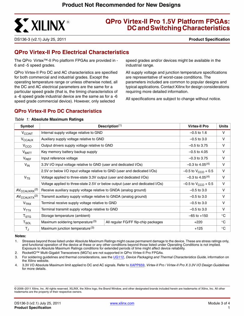
DS136-3 (v2.1) July 25, 2011 www.xilinx.com Module 3 of 4Product Specification 1
© 2006–2011 Xilinx, Inc. All rights reserved. XILINX, the Xilinx logo, the Brand Window, and other designated brands included herein are trademarks of Xilinx, Inc. All other trademarks are the property of their respective owners.
Product Not Recommended for New Designs
QPro Virtex-II Pro Electrical CharacteristicsThe QPro Virtex™-II Pro platform FPGAs are provided in -6 and -5 speed grades.
QPro Virtex-II Pro DC and AC characteristics are specified for both commercial and industrial grades. Except the operating temperature range or unless otherwise noted, all the DC and AC electrical parameters are the same for a particular speed grade (that is, the timing characteristics of a -6 speed grade industrial device are the same as for a -6 speed grade commercial device). However, only selected
speed grades and/or devices might be available in the industrial range.
All supply voltage and junction temperature specifications are representative of worst-case conditions. The parameters included are common to popular designs and typical applications. Contact Xilinx for design considerations requiring more detailed information.
All specifications are subject to change without notice.
QPro Virtex-II Pro DC Characteristics
36 QPro Virtex-II Pro 1.5V Platform FPGAs:
DC and Switching Characteristics
DS136-3 (v2.1) July 25, 2011 Product Specification
R
Table 1: Absolute Maximum Ratings
Symbol Description(1) Virtex-II Pro Units
VCCINT Internal supply voltage relative to GND –0.5 to 1.6 V
VCCAUX Auxiliary supply voltage relative to GND –0.5 to 3.0 V
VCCO Output drivers supply voltage relative to GND –0.5 to 3.75 V
VBATT Key memory battery backup supply –0.5 to 4.05 V
VREF Input reference voltage –0.3 to 3.75 V
VIN 3.3V I/O input voltage relative to GND (user and dedicated I/Os) –0.3 to 4.05 (4) V
2.5V or below I/O input voltage relative to GND (user and dedicated I/Os) –0.5 to VCCO + 0.5 V
VTS Voltage applied to three-state 3.3V output (user and dedicated I/Os) –0.3 to 4.05 (4) V
Voltage applied to three-state 2.5V or below output (user and dedicated I/Os) –0.5 to VCCO + 0.5 V
AVCCAUXRX(2) Receive auxiliary supply voltage relative to GNDA (analog ground) –0.5 to 3.0 V
AVCCAUXTX(2) Transmit auxiliary supply voltage relative to GNDA (analog ground) –0.5 to 3.0 V
VTRX Terminal receive supply voltage relative to GND –0.5 to 3.0 V
VTTX Terminal transmit supply voltage relative to GND –0.5 to 3.0 V
TSTG Storage temperature (ambient) –65 to +150 C
TSOL Maximum soldering temperature (3) All regular FG/FF flip-chip packages +220 C
TJ Maximum junction temperature (3) +125 C
Notes: 1. Stresses beyond those listed under Absolute Maximum Ratings might cause permanent damage to the device. These are stress ratings only,
and functional operation of the device at these or any other conditions beyond those listed under Operating Conditions is not implied. Exposure to Absolute Maximum Ratings conditions for extended periods of time might affect device reliability.
2. RocketIO™ Multi-Gigabit Transceivers (MGTs) are not supported in QPro Virtex-II Pro FPGAs.3. For soldering guidelines and thermal considerations, see the UG112, Device Packaging and Thermal Characteristics Guide, information on
the Xilinx website.4. 3.3V I/O Absolute Maximum limit applied to DC and AC signals. Refer to XAPP659, Virtex-II Pro / Virtex-II Pro X 3.3V I/O Design Guidelines
for more details.
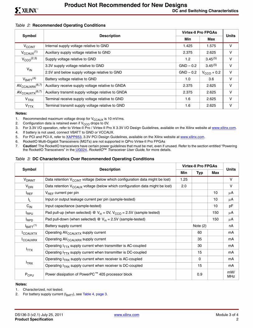
DC and Switching Characteristics
DS136-3 (v2.1) July 25, 2011 www.xilinx.com Module 3 of 4Product Specification 2
R
Product Not Recommended for New Designs
Table 2: Recommended Operating Conditions
Symbol DescriptionVirtex-II Pro FPGAs
UnitsMin Max
VCCINT Internal supply voltage relative to GND 1.425 1.575 V
VCCAUX(1) Auxiliary supply voltage relative to GND 2.375 2.625 V
VCCO(2,3) Supply voltage relative to GND 1.2 3.45 (5) V
VIN
3.3V supply voltage relative to GND GND – 0.2 3.45 (5) V
2.5V and below supply voltage relative to GND GND – 0.2 VCCO + 0.2 V
VBATT(4) Battery voltage relative to GND 1.0 3.6 V
AVCCAUXRX(6,7) Auxiliary receive supply voltage relative to GNDA 2.375 2.625 V
AVCCAUXTX(6,7) Auxiliary transmit supply voltage relative to GNDA 2.375 2.625 V
VTRX Terminal receive supply voltage relative to GND 1.6 2.625 V
VTTX Terminal transmit supply voltage relative to GND 1.6 2.625 V
Notes: 1. Recommended maximum voltage droop for VCCAUX is 10 mV/ms.2. Configuration data is retained even if VCCO drops to 0V.3. For 3.3V I/O operation, refer to Virtex-II Pro / Virtex-II Pro X 3.3V I/O Design Guidelines, available on the Xilinx website at www.xilinx.com.4. If battery is not used, connect VBATT to GND or VCCAUX.5. For PCI and PCI-X, refer to XAPP653, 3.3V PCI Design Guidelines, available on the Xilinx website at www.xilinx.com.6. RocketIO Multi-Gigabit Transceivers (MGTs) are not supported in QPro Virtex-II Pro FPGAs7. Caution! The RocketIO transceivers have certain power guidelines that must be met, even if unused. Refer to the section entitled “Powering
the RocketIO Transceivers” in the UG024, RocketIO™ Transceiver User Guide, for more details.
Table 3: DC Characteristics Over Recommended Operating Conditions
Symbol DescriptionVirtex-II Pro FPGAs
UnitsMin Typ Max
VDRINT Data retention VCCINT voltage (below which configuration data might be lost) 1.25 V
VDRI Data retention VCCAUX voltage (below which configuration data might be lost) 2.0 V
IREF VREF current per pin 10 A
IL Input or output leakage current per pin (sample-tested) 10 A
CIN Input capacitance (sample-tested) 10 pF
IRPU Pad pull-up (when selected) @ Vin = 0V, VCCO = 2.5V (sample tested) 150 A
IRPD Pad pull-down (when selected) @ Vin = 2.5V (sample-tested) 150 A
IBATT (1) Battery supply current Note (2) nA
I CCAUXTX Operating AVCCAUXTX supply current 60 mA
I CCAUXRX Operating AVCCAUXRX supply current 35 mA
ITTXOperating ITTX supply current when transmitter is AC-coupled 30 mA
Operating ITTX supply current when transmitter is DC-coupled 15 mA
ITRXOperating ITRX supply current when receiver is AC-coupled 0 mA
Operating ITRX supply current when receiver is DC-coupled 15 mA
PCPU Power dissipation of PowerPC ™ 405 processor block 0.9 mW/MHz
Notes: 1. Characterized, not tested.2. For battery supply current (IBATT), see Table 4, page 3.
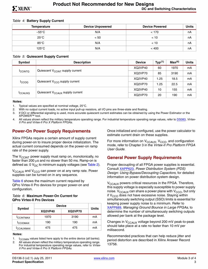
DC and Switching Characteristics
DS136-3 (v2.1) July 25, 2011 www.xilinx.com Module 3 of 4Product Specification 3
R
Product Not Recommended for New Designs
.
Power-On Power Supply Requirements
Xilinx FPGAs require a certain amount of supply current during power-on to insure proper device initialization. The actual current consumed depends on the power-on ramp rate of the power supply.
The VCCINT power supply must ramp on, monotonically, no faster than 200 s and no slower than 50 ms. Ramp-on is defined as: 0 VDC to minimum supply voltages (see Table 2).
VCCAUX and VCCO can power on at any ramp rate. Power supplies can be turned on in any sequence.
Table 6 shows the maximum current required by QPro Virtex-II Pro devices for proper power-on and configuration.
Once initialized and configured, use the power calculator to estimate current drain on these supplies.
For more information on VCCAUX, VCCO , and configuration mode, refer to Chapter 3 in the Virtex-II Pro Platform FPGA User Guide.
General Power Supply Requirements
Proper decoupling of all FPGA power supplies is essential. Consult XAPP623, Power Distribution System (PDS) Design: Using Bypass/Decoupling Capacitors, for detailed information on power distribution system design.
VCCAUX powers critical resources in the FPGA. Therefore, this supply voltage is especially susceptible to power supply noise. VCCAUX can share a power plane with VCCO , but only if VCCO does not have excessive noise. Staying within simultaneously switching output (SSO) limits is essential for keeping power supply noise to a minimum. Refer to XAPP689, Managing Ground Bounce in Large FPGAs, to determine the number of simultaneously switching outputs allowed per bank at the package level.
Changes in VCCAUX voltage beyond 200 mV peak-to-peak should take place at a rate no faster than 10 mV per millisecond.
Recommended practices that can help reduce jitter and period distortion are described in Xilinx Answer Record 13756.
Table 4: Battery Supply Current
Temperature Device Unpowered Device Powered Units
–55C N/A < 170 nA
25C < 50 < 10 nA
85C N/A < 10 nA
125C N/A < 400 nA
Table 5: Quiescent Supply Current
Symbol Description Device Typ (1) Max(4) Units
ICCINTQ Quiescent VCCINT supply currentXQ2VP40 60 1970 mA
XQ2VP70 85 3190 mA
ICCOQ Quiescent VCCO supply currentXQ2VP40 1.25 18.5 mA
XQ2VP70 1.25 22.5 mA
ICCAUXQ Quiescent VCCAUX supply currentXQ2VP40 10 155 mA
XQ2VP70 20 190 mA
Notes: 1. Typical values are specified at nominal voltage, 25°C.2. With no output current loads, no active input pull-up resistors, all I/O pins are three-state and floating.3. If DCI or differential signaling is used, more accurate quiescent current estimates can be obtained by using the Power Estimator or the
XPOWER™ tool.4. All values shown reflect the military temperature operating range. For industrial temperature operating range values, refer to DS083, Virtex-
II Pro and Virtex-II Pro X Platform FPGAs.
Table 6: Maximum Power-On Current for QPro Virtex-II Pro Devices
SymbolDevice
UnitsXQ2VP40 XQ2VP70
ICCINTMAX 1970 3190 mA
ICCIOMAX 190 190 mA
ICCAUXMAX 475 475 mA
Notes: 1. ICCOMIN values listed here apply to the entire device (all banks).2. All values shown reflect the military temperature operating range.
For industrial temperature operating range values, refer to Virtex-II Pro and Virtex-II Pro X Platform FPGAs.
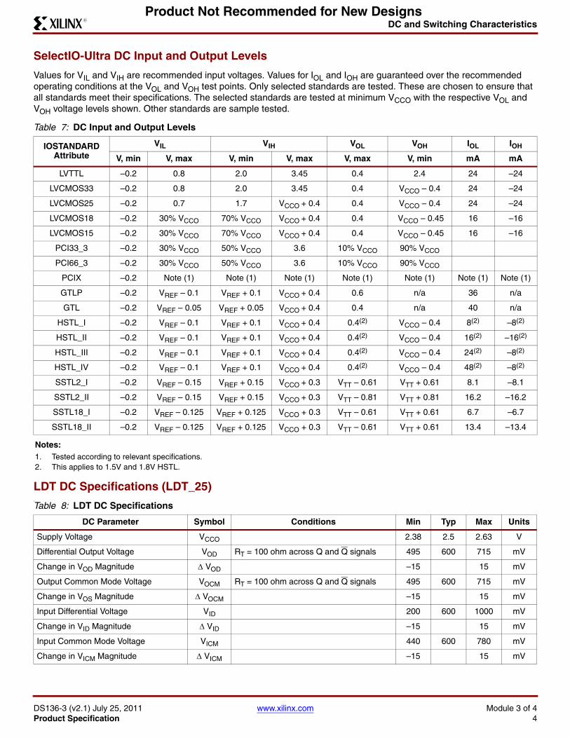
DC and Switching Characteristics
DS136-3 (v2.1) July 25, 2011 www.xilinx.com Module 3 of 4Product Specification 4
R
Product Not Recommended for New Designs
SelectIO-Ultra DC Input and Output Levels
Values for VIL and VIH are recommended input voltages. Values for IOL and IOH are guaranteed over the recommended operating conditions at the VOL and VOH test points. Only selected standards are tested. These are chosen to ensure that all standards meet their specifications. The selected standards are tested at minimum VCCO with the respective VOL and VOH voltage levels shown. Other standards are sample tested.
LDT DC Specifications (LDT_25))
Table 7: DC Input and Output Levels
IOSTANDARD Attribute
VIL VIH VOL VOH IOL IOH
V, min V, max V, min V, max V, max V, min mA mA
LVTTL –0.2 0.8 2.0 3.45 0.4 2.4 24 –24
LVCMOS33 –0.2 0.8 2.0 3.45 0.4 VCCO – 0.4 24 –24
LVCMOS25 –0.2 0.7 1.7 VCCO + 0.4 0.4 VCCO – 0.4 24 –24
LVCMOS18 –0.2 30% VCCO 70% VCCO VCCO + 0.4 0.4 VCCO – 0.45 16 –16
LVCMOS15 –0.2 30% VCCO 70% VCCO VCCO + 0.4 0.4 VCCO – 0.45 16 –16
PCI33_3 –0.2 30% VCCO 50% VCCO 3.6 10% VCCO 90% VCCO
PCI66_3 –0.2 30% VCCO 50% VCCO 3.6 10% VCCO 90% VCCO
PCIX –0.2 Note (1) Note (1) Note (1) Note (1) Note (1) Note (1) Note (1)
GTLP –0.2 VREF – 0.1 VREF + 0.1 VCCO + 0.4 0.6 n/a 36 n/a
GTL –0.2 VREF – 0.05 VREF + 0.05 VCCO + 0.4 0.4 n/a 40 n/a
HSTL_I –0.2 VREF – 0.1 VREF + 0.1 VCCO + 0.4 0.4(2) VCCO – 0.4 8(2) –8(2)
HSTL_II –0.2 VREF – 0.1 VREF + 0.1 VCCO + 0.4 0.4(2) VCCO – 0.4 16(2) –16(2)
HSTL_III –0.2 VREF – 0.1 VREF + 0.1 VCCO + 0.4 0.4(2) VCCO – 0.4 24(2) –8(2)
HSTL_IV –0.2 VREF – 0.1 VREF + 0.1 VCCO + 0.4 0.4(2) VCCO – 0.4 48(2) –8(2)
SSTL2_I –0.2 VREF – 0.15 VREF + 0.15 VCCO + 0.3 VTT – 0.61 VTT + 0.61 8.1 –8.1
SSTL2_II –0.2 VREF – 0.15 VREF + 0.15 VCCO + 0.3 VTT – 0.81 VTT + 0.81 16.2 –16.2
SSTL18_I –0.2 VREF – 0.125 VREF + 0.125 VCCO + 0.3 VTT – 0.61 VTT + 0.61 6.7 –6.7
SSTL18_II –0.2 VREF – 0.125 VREF + 0.125 VCCO + 0.3 VTT – 0.61 VTT + 0.61 13.4 –13.4
Notes: 1. Tested according to relevant specifications.2. This applies to 1.5V and 1.8V HSTL.
Table 8: LDT DC Specifications
DC Parameter Symbol Conditions Min Typ Max Units
Supply Voltage VCCO 2.38 2.5 2.63 V
Differential Output Voltage VOD RT = 100 ohm across Q and Q signals 495 600 715 mV
Change in VOD Magnitude VOD –15 15 mV
Output Common Mode Voltage VOCM RT = 100 ohm across Q and Q signals 495 600 715 mV
Change in VOS Magnitude VOCM –15 15 mV
Input Differential Voltage VID 200 600 1000 mV
Change in VID Magnitude VID –15 15 mV
Input Common Mode Voltage VICM 440 600 780 mV
Change in VICM Magnitude VICM –15 15 mV
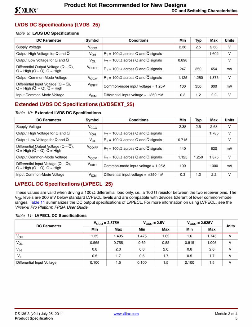
DC and Switching Characteristics
DS136-3 (v2.1) July 25, 2011 www.xilinx.com Module 3 of 4Product Specification 5
R
Product Not Recommended for New Designs
LVDS DC Specifications (LVDS_25)
Extended LVDS DC Specifications (LVDSEXT_25)
LVPECL DC Specifications (LVPECL_25)
These values are valid when driving a 100 differential load only, i.e., a 100 resistor between the two receiver pins. The VOH levels are 200 mV below standard LVPECL levels and are compatible with devices tolerant of lower common-mode ranges. Table 11 summarizes the DC output specifications of LVPECL. For more information on using LVPECL, see the Virtex-II Pro Platform FPGA User Guide.
Table 9: LVDS DC Specifications
DC Parameter Symbol Conditions Min Typ Max Units
Supply Voltage VCCO 2.38 2.5 2.63 V
Output High Voltage for Q and Q VOH RT = 100 across Q and Q signals 1.602 V
Output Low Voltage for Q and Q VOL RT = 100 across Q and Q signals 0.898 V
Differential Output Voltage (Q – Q),Q = High (Q – Q), Q = High
VODIFF RT = 100 across Q and Q signals 247 350 454 mV
Output Common-Mode Voltage VOCM RT = 100 across Q and Q signals 1.125 1.250 1.375 V
Differential Input Voltage (Q – Q),Q = High (Q – Q), Q = High
VIDIFF Common-mode input voltage = 1.25V 100 350 600 mV
Input Common-Mode Voltage VICM Differential input voltage = 350 mV 0.3 1.2 2.2 V
Table 10: Extended LVDS DC Specifications
DC Parameter Symbol Conditions Min Typ Max Units
Supply Voltage VCCO 2.38 2.5 2.63 V
Output High Voltage for Q and Q VOH RT = 100 across Q and Q signals 1.785 V
Output Low Voltage for Q and Q VOL RT = 100 across Q and Q signals 0.715 V
Differential Output Voltage (Q – Q),Q = High (Q – Q), Q = High
VODIFF RT = 100 across Q and Q signals 440 820 mV
Output Common-Mode Voltage VOCM RT = 100 across Q and Q signals 1.125 1.250 1.375 V
Differential Input Voltage (Q – Q),Q = High (Q – Q), Q = High
VIDIFF Common-mode input voltage = 1.25V 100 1000 mV
Input Common-Mode Voltage VICM Differential input voltage = 350 mV 0.3 1.2 2.2 V
Table 11: LVPECL DC Specifications
DC ParameterVCCO = 2.375V VCCO = 2.5V VCCO = 2.625V
UnitsMin Max Min Max Min Max
VOH 1.35 1.495 1.475 1.62 1.6 1.745 V
VOL 0.565 0.755 0.69 0.88 0.815 1.005 V
VIH 0.8 2.0 0.8 2.0 0.8 2.0 V
VIL 0.5 1.7 0.5 1.7 0.5 1.7 V
Differential Input Voltage 0.100 1.5 0.100 1.5 0.100 1.5 V
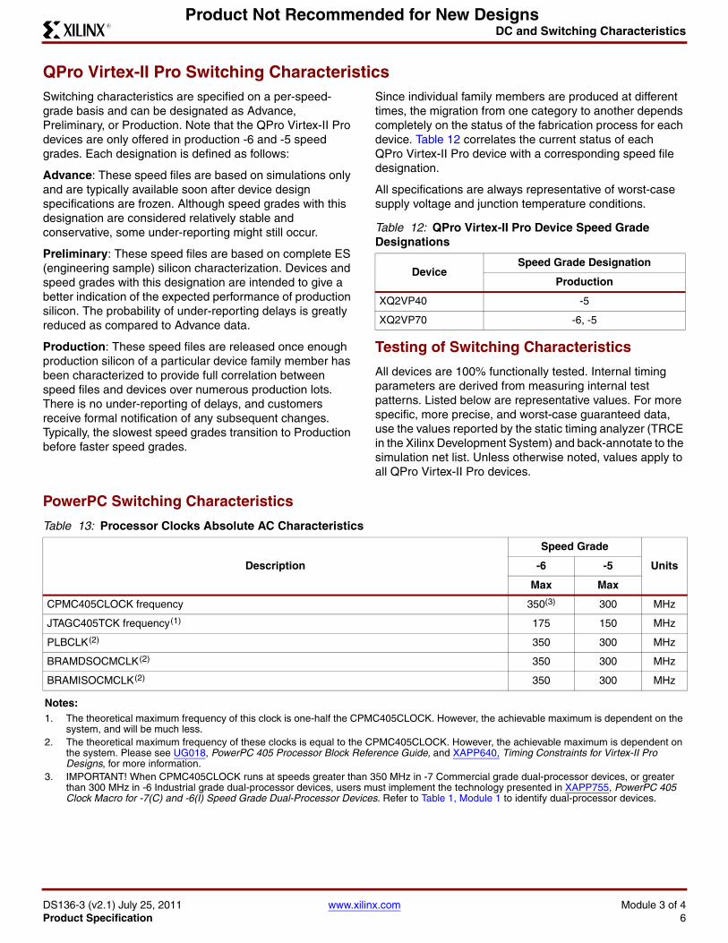
DC and Switching Characteristics
DS136-3 (v2.1) July 25, 2011 www.xilinx.com Module 3 of 4Product Specification 6
R
Product Not Recommended for New Designs
QPro Virtex-II Pro Switching CharacteristicsSwitching characteristics are specified on a per-speed-grade basis and can be designated as Advance, Preliminary, or Production. Note that the QPro Virtex-II Pro devices are only offered in production -6 and -5 speed grades. Each designation is defined as follows:
Advance: These speed files are based on simulations only and are typically available soon after device design specifications are frozen. Although speed grades with this designation are considered relatively stable and conservative, some under-reporting might still occur.
Preliminary: These speed files are based on complete ES (engineering sample) silicon characterization. Devices and speed grades with this designation are intended to give a better indication of the expected performance of production silicon. The probability of under-reporting delays is greatly reduced as compared to Advance data.
Production: These speed files are released once enough production silicon of a particular device family member has been characterized to provide full correlation between speed files and devices over numerous production lots. There is no under-reporting of delays, and customers receive formal notification of any subsequent changes. Typically, the slowest speed grades transition to Production before faster speed grades.
Since individual family members are produced at different times, the migration from one category to another depends completely on the status of the fabrication process for each device. Table 12 correlates the current status of each QPro Virtex-II Pro device with a corresponding speed file designation.
All specifications are always representative of worst-case supply voltage and junction temperature conditions.
Testing of Switching Characteristics
All devices are 100% functionally tested. Internal timing parameters are derived from measuring internal test patterns. Listed below are representative values. For more specific, more precise, and worst-case guaranteed data, use the values reported by the static timing analyzer (TRCE in the Xilinx Development System) and back-annotate to the simulation net list. Unless otherwise noted, values apply to all QPro Virtex-II Pro devices.
PowerPC Switching Characteristics
Table 12: QPro Virtex-II Pro Device Speed Grade Designations
DeviceSpeed Grade Designation
Production
XQ2VP40 -5
XQ2VP70 -6, -5
Table 13: Processor Clocks Absolute AC Characteristics
Description
Speed Grade
Units-6 -5
Max Max
CPMC405CLOCK frequency 350(3) 300 MHz
JTAGC405TCK frequency (1) 175 150 MHz
PLBCLK (2) 350 300 MHz
BRAMDSOCMCLK (2) 350 300 MHz
BRAMISOCMCLK (2) 350 300 MHz
Notes: 1. The theoretical maximum frequency of this clock is one-half the CPMC405CLOCK. However, the achievable maximum is dependent on the
system, and will be much less.2. The theoretical maximum frequency of these clocks is equal to the CPMC405CLOCK. However, the achievable maximum is dependent on
the system. Please see UG018, PowerPC 405 Processor Block Reference Guide, and XAPP640, Timing Constraints for Virtex-II Pro Designs, for more information.
3. IMPORTANT! When CPMC405CLOCK runs at speeds greater than 350 MHz in -7 Commercial grade dual-processor devices, or greater than 300 MHz in -6 Industrial grade dual-processor devices, users must implement the technology presented in XAPP755, PowerPC 405 Clock Macro for -7(C) and -6(I) Speed Grade Dual-Processor Devices. Refer to Table 1, Module 1 to identify dual-processor devices.
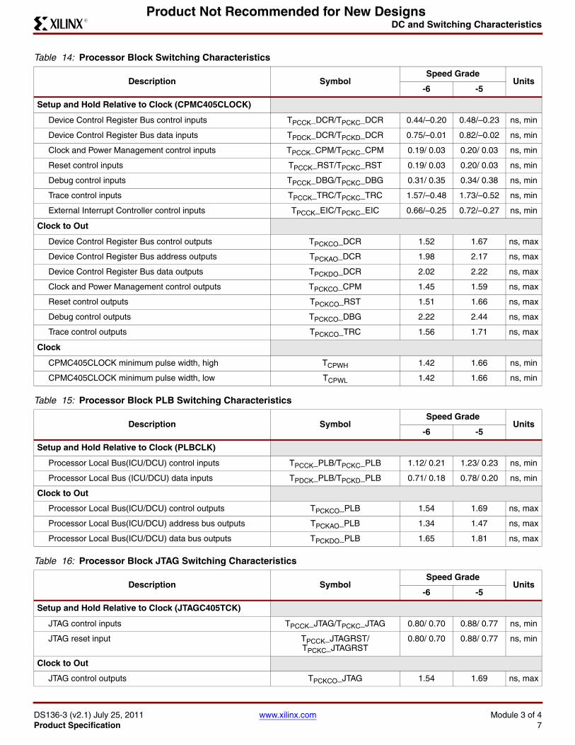
DC and Switching Characteristics
DS136-3 (v2.1) July 25, 2011 www.xilinx.com Module 3 of 4Product Specification 7
R
Product Not Recommended for New Designs
Table 14: Processor Block Switching Characteristics
Description SymbolSpeed Grade
Units-6 -5
Setup and Hold Relative to Clock (CPMC405CLOCK)
Device Control Register Bus control inputs TPCCK_DCR/TPCKC_DCR 0.44/–0.20 0.48/–0.23 ns, min
Device Control Register Bus data inputs TPDCK_DCR/TPCKD_DCR 0.75/–0.01 0.82/–0.02 ns, min
Clock and Power Management control inputs TPCCK_CPM/TPCKC_CPM 0.19/ 0.03 0.20/ 0.03 ns, min
Reset control inputs TPCCK_RST/TPCKC_RST 0.19/ 0.03 0.20/ 0.03 ns, min
Debug control inputs TPCCK_DBG/TPCKC_DBG 0.31/ 0.35 0.34/ 0.38 ns, min
Trace control inputs TPCCK_TRC/TPCKC_TRC 1.57/–0.48 1.73/–0.52 ns, min
External Interrupt Controller control inputs TPCCK_EIC/TPCKC_EIC 0.66/–0.25 0.72/–0.27 ns, min
Clock to Out
Device Control Register Bus control outputs TPCKCO_DCR 1.52 1.67 ns, max
Device Control Register Bus address outputs TPCKAO_DCR 1.98 2.17 ns, max
Device Control Register Bus data outputs TPCKDO_DCR 2.02 2.22 ns, max
Clock and Power Management control outputs TPCKCO_CPM 1.45 1.59 ns, max
Reset control outputs TPCKCO_RST 1.51 1.66 ns, max
Debug control outputs TPCKCO_DBG 2.22 2.44 ns, max
Trace control outputs TPCKCO_TRC 1.56 1.71 ns, max
Clock
CPMC405CLOCK minimum pulse width, high TCPWH 1.42 1.66 ns, min
CPMC405CLOCK minimum pulse width, low TCPWL 1.42 1.66 ns, min
Table 15: Processor Block PLB Switching Characteristics
Description SymbolSpeed Grade
Units-6 -5
Setup and Hold Relative to Clock (PLBCLK)
Processor Local Bus(ICU/DCU) control inputs TPCCK_PLB/TPCKC_PLB 1.12/ 0.21 1.23/ 0.23 ns, min
Processor Local Bus (ICU/DCU) data inputs TPDCK_PLB/TPCKD_PLB 0.71/ 0.18 0.78/ 0.20 ns, min
Clock to Out
Processor Local Bus(ICU/DCU) control outputs TPCKCO_PLB 1.54 1.69 ns, max
Processor Local Bus(ICU/DCU) address bus outputs TPCKAO_PLB 1.34 1.47 ns, max
Processor Local Bus(ICU/DCU) data bus outputs TPCKDO_PLB 1.65 1.81 ns, max
Table 16: Processor Block JTAG Switching Characteristics
Description SymbolSpeed Grade
Units-6 -5
Setup and Hold Relative to Clock (JTAGC405TCK)
JTAG control inputs TPCCK_JTAG/TPCKC_JTAG 0.80/ 0.70 0.88/ 0.77 ns, min
JTAG reset input TPCCK_JTAGRST/ TPCKC_JTAGRST
0.80/ 0.70 0.88/ 0.77 ns, min
Clock to Out
JTAG control outputs TPCKCO_JTAG 1.54 1.69 ns, max
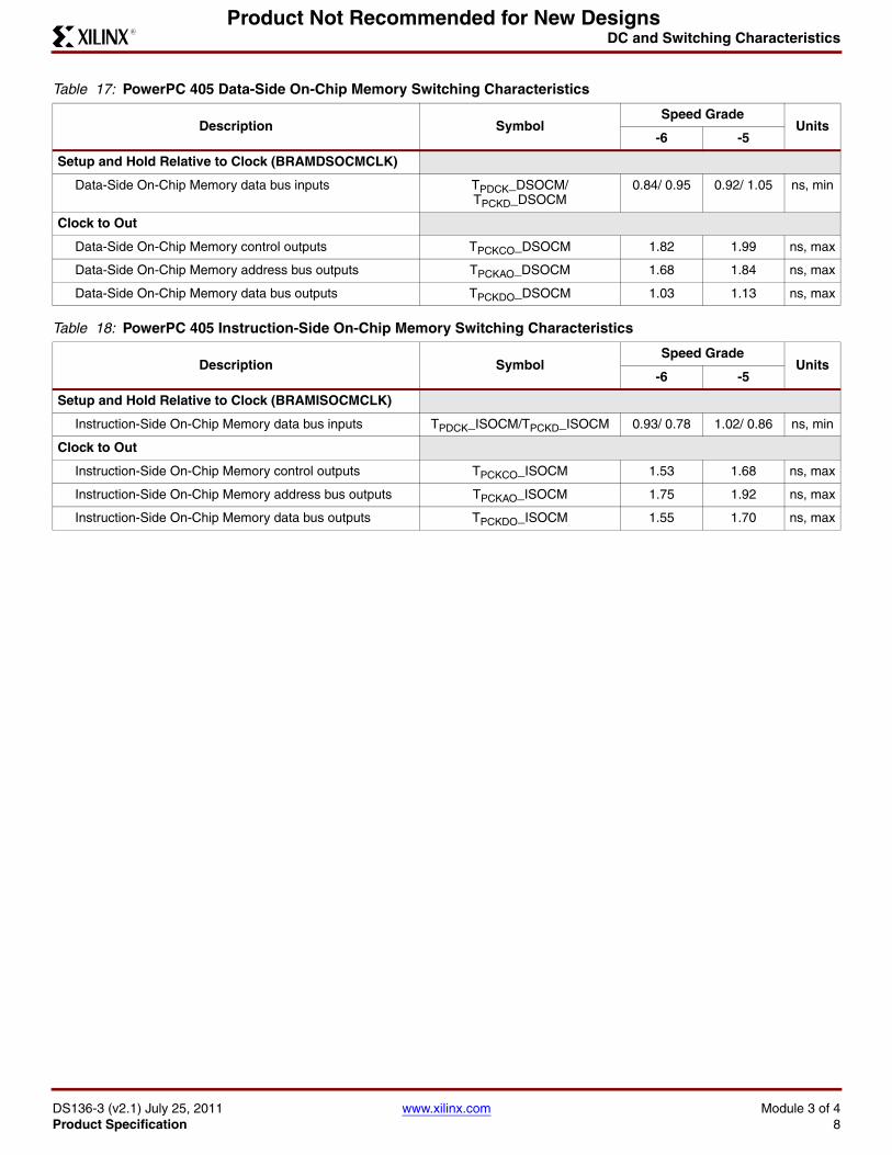
DC and Switching Characteristics
DS136-3 (v2.1) July 25, 2011 www.xilinx.com Module 3 of 4Product Specification 8
R
Product Not Recommended for New Designs
Table 17: PowerPC 405 Data-Side On-Chip Memory Switching Characteristics
Description SymbolSpeed Grade
Units-6 -5
Setup and Hold Relative to Clock (BRAMDSOCMCLK)
Data-Side On-Chip Memory data bus inputs TPDCK_DSOCM/ TPCKD_DSOCM
0.84/ 0.95 0.92/ 1.05 ns, min
Clock to Out
Data-Side On-Chip Memory control outputs TPCKCO_DSOCM 1.82 1.99 ns, max
Data-Side On-Chip Memory address bus outputs TPCKAO_DSOCM 1.68 1.84 ns, max
Data-Side On-Chip Memory data bus outputs TPCKDO_DSOCM 1.03 1.13 ns, max
Table 18: PowerPC 405 Instruction-Side On-Chip Memory Switching Characteristics
Description SymbolSpeed Grade
Units-6 -5
Setup and Hold Relative to Clock (BRAMISOCMCLK)
Instruction-Side On-Chip Memory data bus inputs TPDCK_ISOCM/TPCKD_ISOCM 0.93/ 0.78 1.02/ 0.86 ns, min
Clock to Out
Instruction-Side On-Chip Memory control outputs TPCKCO_ISOCM 1.53 1.68 ns, max
Instruction-Side On-Chip Memory address bus outputs TPCKAO_ISOCM 1.75 1.92 ns, max
Instruction-Side On-Chip Memory data bus outputs TPCKDO_ISOCM 1.55 1.70 ns, max
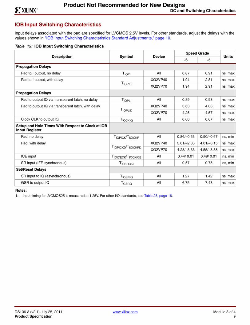
DC and Switching Characteristics
DS136-3 (v2.1) July 25, 2011 www.xilinx.com Module 3 of 4Product Specification 9
R
Product Not Recommended for New Designs
IOB Input Switching Characteristics
Input delays associated with the pad are specified for LVCMOS 2.5V levels. For other standards, adjust the delays with the values shown in "IOB Input Switching Characteristics Standard Adjustments," page 10.
Table 19: IOB Input Switching Characteristics
Description Symbol DeviceSpeed Grade
Units-6 -5
Propagation Delays
Pad to I output, no delay TIOPI All 0.87 0.91 ns, max
Pad to I output, with delayTIOPID
XQ2VP40 1.94 2.81 ns, max
XQ2VP70 1.94 2.91 ns, max
Propagation Delays
Pad to output IQ via transparent latch, no delay TIOPLI All 0.89 0.93 ns, max
Pad to output IQ via transparent latch, with delayTIOPLID
XQ2VP40 3.63 4.03 ns, max
XQ2VP70 4.25 4.57 ns, max
Clock CLK to output IQ TIOCKIQ All 0.60 0.67 ns, max
Setup and Hold Times With Respect to Clock at IOB Input Register
Pad, no delay TIOPICK/TIOICKP All 0.86/–0.63 0.90/–0.67 ns, min
Pad, with delayTIOPICKD/TIOICKPD
XQ2VP40 3.61/–2.83 4.01/–3.15 ns, max
XQ2VP70 4.23/–3.33 4.55/–3.58 ns, max
ICE input TIOICECK/TIOCKICE All 0.44/ 0.01 0.49/ 0.01 ns, min
SR input (IFF, synchronous) TIOSRCKI All 0.57 0.75 ns, min
Set/Reset Delays
SR input to IQ (asynchronous) TIOSRIQ All 1.27 1.42 ns, max
GSR to output IQ TGSRQ All 6.75 7.43 ns, max
Notes: 1. Input timing for LVCMOS25 is measured at 1.25V. For other I/O standards, see Table 23, page 16.
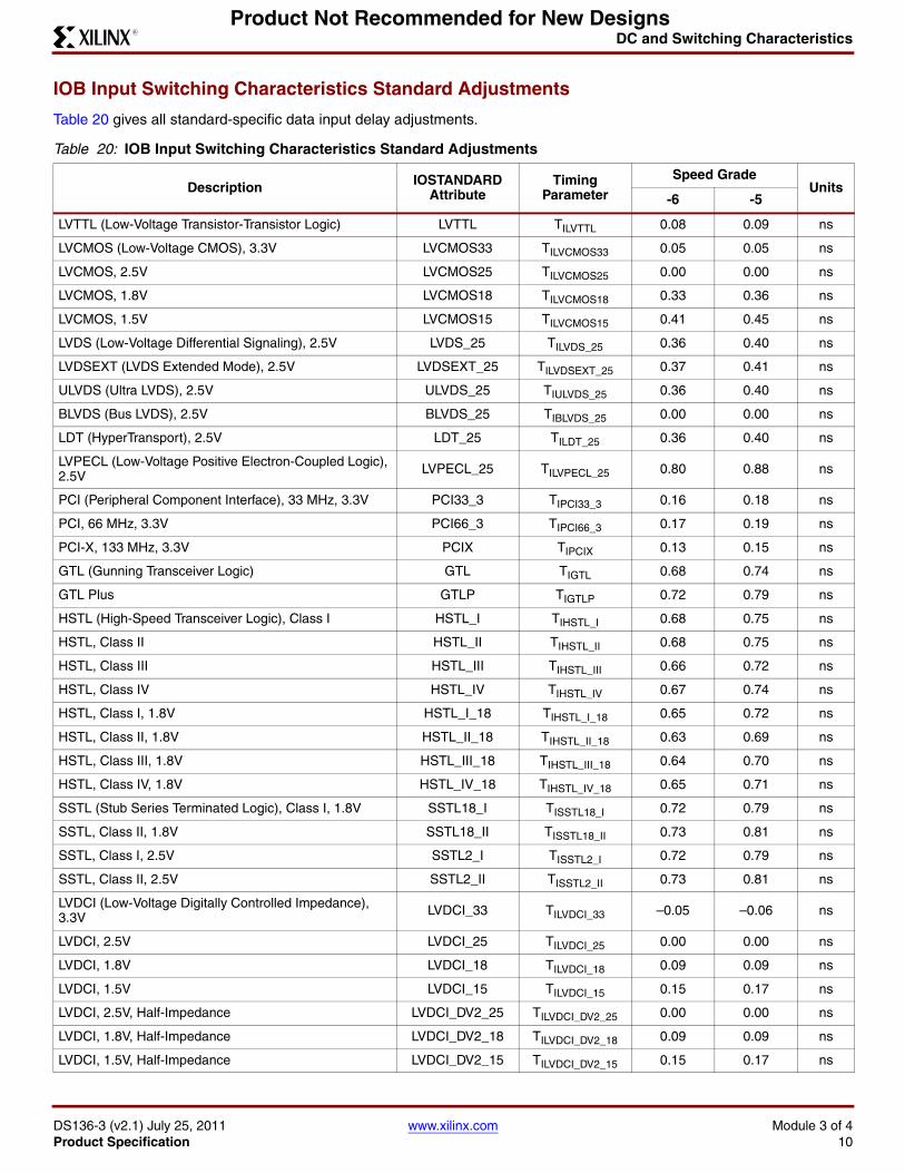
DC and Switching Characteristics
DS136-3 (v2.1) July 25, 2011 www.xilinx.com Module 3 of 4Product Specification 10
R
Product Not Recommended for New Designs
IOB Input Switching Characteristics Standard Adjustments
Table 20 gives all standard-specific data input delay adjustments.
Table 20: IOB Input Switching Characteristics Standard Adjustments
Description IOSTANDARD Attribute
Timing Parameter
Speed GradeUnits
-6 -5
LVTTL (Low-Voltage Transistor-Transistor Logic) LVTTL TILVTTL 0.08 0.09 ns
LVCMOS (Low-Voltage CMOS), 3.3V LVCMOS33 TILVCMOS33 0.05 0.05 ns
LVCMOS, 2.5V LVCMOS25 TILVCMOS25 0.00 0.00 ns
LVCMOS, 1.8V LVCMOS18 TILVCMOS18 0.33 0.36 ns
LVCMOS, 1.5V LVCMOS15 TILVCMOS15 0.41 0.45 ns
LVDS (Low-Voltage Differential Signaling), 2.5V LVDS_25 TILVDS_25 0.36 0.40 ns
LVDSEXT (LVDS Extended Mode), 2.5V LVDSEXT_25 TILVDSEXT_25 0.37 0.41 ns
ULVDS (Ultra LVDS), 2.5V ULVDS_25 TIULVDS_25 0.36 0.40 ns
BLVDS (Bus LVDS), 2.5V BLVDS_25 TIBLVDS_25 0.00 0.00 ns
LDT (HyperTransport), 2.5V LDT_25 TILDT_25 0.36 0.40 ns
LVPECL (Low-Voltage Positive Electron-Coupled Logic), 2.5V LVPECL_25 TILVPECL_25 0.80 0.88 ns
PCI (Peripheral Component Interface), 33 MHz, 3.3V PCI33_3 TIPCI33_3 0.16 0.18 ns
PCI, 66 MHz, 3.3V PCI66_3 TIPCI66_3 0.17 0.19 ns
PCI-X, 133 MHz, 3.3V PCIX TIPCIX 0.13 0.15 ns
GTL (Gunning Transceiver Logic) GTL TIGTL 0.68 0.74 ns
GTL Plus GTLP TIGTLP 0.72 0.79 ns
HSTL (High-Speed Transceiver Logic), Class I HSTL_I TIHSTL_I 0.68 0.75 ns
HSTL, Class II HSTL_II TIHSTL_II 0.68 0.75 ns
HSTL, Class III HSTL_III TIHSTL_III 0.66 0.72 ns
HSTL, Class IV HSTL_IV TIHSTL_IV 0.67 0.74 ns
HSTL, Class I, 1.8V HSTL_I_18 TIHSTL_I_18 0.65 0.72 ns
HSTL, Class II, 1.8V HSTL_II_18 TIHSTL_II_18 0.63 0.69 ns
HSTL, Class III, 1.8V HSTL_III_18 TIHSTL_III_18 0.64 0.70 ns
HSTL, Class IV, 1.8V HSTL_IV_18 TIHSTL_IV_18 0.65 0.71 ns
SSTL (Stub Series Terminated Logic), Class I, 1.8V SSTL18_I TISSTL18_I 0.72 0.79 ns
SSTL, Class II, 1.8V SSTL18_II TISSTL18_II 0.73 0.81 ns
SSTL, Class I, 2.5V SSTL2_I TISSTL2_I 0.72 0.79 ns
SSTL, Class II, 2.5V SSTL2_II TISSTL2_II 0.73 0.81 ns
LVDCI (Low-Voltage Digitally Controlled Impedance), 3.3V LVDCI_33 TILVDCI_33 –0.05 –0.06 ns
LVDCI, 2.5V LVDCI_25 TILVDCI_25 0.00 0.00 ns
LVDCI, 1.8V LVDCI_18 TILVDCI_18 0.09 0.09 ns
LVDCI, 1.5V LVDCI_15 TILVDCI_15 0.15 0.17 ns
LVDCI, 2.5V, Half-Impedance LVDCI_DV2_25 TILVDCI_DV2_25 0.00 0.00 ns
LVDCI, 1.8V, Half-Impedance LVDCI_DV2_18 TILVDCI_DV2_18 0.09 0.09 ns
LVDCI, 1.5V, Half-Impedance LVDCI_DV2_15 TILVDCI_DV2_15 0.15 0.17 ns
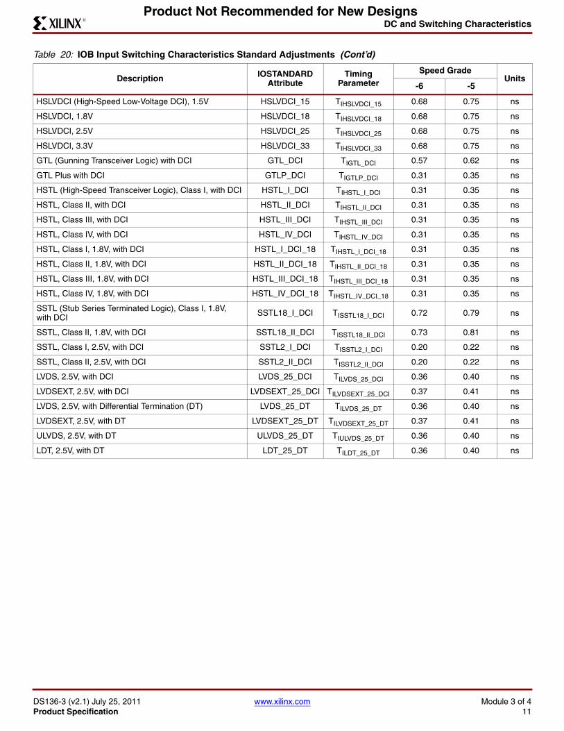
DC and Switching Characteristics
DS136-3 (v2.1) July 25, 2011 www.xilinx.com Module 3 of 4Product Specification 11
R
Product Not Recommended for New Designs
HSLVDCI (High-Speed Low-Voltage DCI), 1.5V HSLVDCI_15 TIHSLVDCI_15 0.68 0.75 ns
HSLVDCI, 1.8V HSLVDCI_18 TIHSLVDCI_18 0.68 0.75 ns
HSLVDCI, 2.5V HSLVDCI_25 TIHSLVDCI_25 0.68 0.75 ns
HSLVDCI, 3.3V HSLVDCI_33 TIHSLVDCI_33 0.68 0.75 ns
GTL (Gunning Transceiver Logic) with DCI GTL_DCI TIGTL_DCI 0.57 0.62 ns
GTL Plus with DCI GTLP_DCI TIGTLP_DCI 0.31 0.35 ns
HSTL (High-Speed Transceiver Logic), Class I, with DCI HSTL_I_DCI TIHSTL_I_DCI 0.31 0.35 ns
HSTL, Class II, with DCI HSTL_II_DCI TIHSTL_II_DCI 0.31 0.35 ns
HSTL, Class III, with DCI HSTL_III_DCI TIHSTL_III_DCI 0.31 0.35 ns
HSTL, Class IV, with DCI HSTL_IV_DCI TIHSTL_IV_DCI 0.31 0.35 ns
HSTL, Class I, 1.8V, with DCI HSTL_I_DCI_18 TIHSTL_I_DCI_18 0.31 0.35 ns
HSTL, Class II, 1.8V, with DCI HSTL_II_DCI_18 TIHSTL_II_DCI_18 0.31 0.35 ns
HSTL, Class III, 1.8V, with DCI HSTL_III_DCI_18 TIHSTL_III_DCI_18 0.31 0.35 ns
HSTL, Class IV, 1.8V, with DCI HSTL_IV_DCI_18 TIHSTL_IV_DCI_18 0.31 0.35 ns
SSTL (Stub Series Terminated Logic), Class I, 1.8V, with DCI SSTL18_I_DCI TISSTL18_I_DCI 0.72 0.79 ns
SSTL, Class II, 1.8V, with DCI SSTL18_II_DCI TISSTL18_II_DCI 0.73 0.81 ns
SSTL, Class I, 2.5V, with DCI SSTL2_I_DCI TISSTL2_I_DCI 0.20 0.22 ns
SSTL, Class II, 2.5V, with DCI SSTL2_II_DCI TISSTL2_II_DCI 0.20 0.22 ns
LVDS, 2.5V, with DCI LVDS_25_DCI TILVDS_25_DCI 0.36 0.40 ns
LVDSEXT, 2.5V, with DCI LVDSEXT_25_DCI TILVDSEXT_25_DCI 0.37 0.41 ns
LVDS, 2.5V, with Differential Termination (DT) LVDS_25_DT TILVDS_25_DT 0.36 0.40 ns
LVDSEXT, 2.5V, with DT LVDSEXT_25_DT TILVDSEXT_25_DT 0.37 0.41 ns
ULVDS, 2.5V, with DT ULVDS_25_DT TIULVDS_25_DT 0.36 0.40 ns
LDT, 2.5V, with DT LDT_25_DT TILDT_25_DT 0.36 0.40 ns
Table 20: IOB Input Switching Characteristics Standard Adjustments (Cont’d)
Description IOSTANDARD Attribute
Timing Parameter
Speed GradeUnits
-6 -5
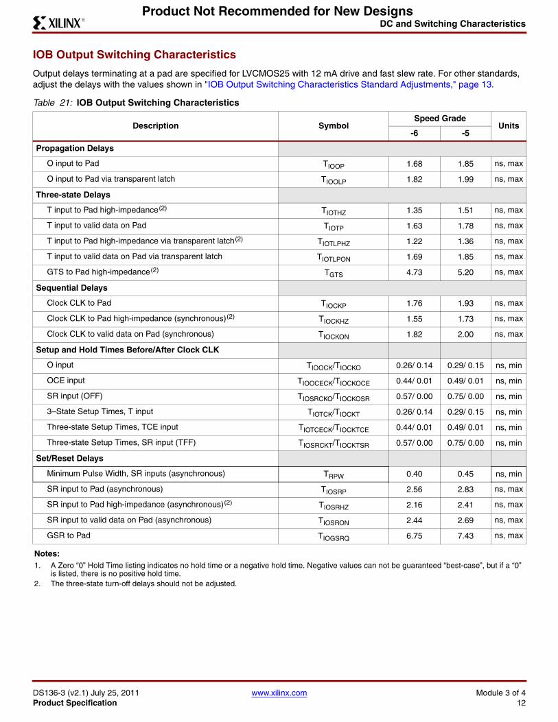
DC and Switching Characteristics
DS136-3 (v2.1) July 25, 2011 www.xilinx.com Module 3 of 4Product Specification 12
R
Product Not Recommended for New Designs
IOB Output Switching Characteristics
Output delays terminating at a pad are specified for LVCMOS25 with 12 mA drive and fast slew rate. For other standards, adjust the delays with the values shown in "IOB Output Switching Characteristics Standard Adjustments," page 13.
Table 21: IOB Output Switching Characteristics
Description SymbolSpeed Grade
Units-6 -5
Propagation Delays
O input to Pad TIOOP 1.68 1.85 ns, max
O input to Pad via transparent latch TIOOLP 1.82 1.99 ns, max
Three-state Delays
T input to Pad high-impedance (2) TIOTHZ 1.35 1.51 ns, max
T input to valid data on Pad TIOTP 1.63 1.78 ns, max
T input to Pad high-impedance via transparent latch (2) TIOTLPHZ 1.22 1.36 ns, max
T input to valid data on Pad via transparent latch TIOTLPON 1.69 1.85 ns, max
GTS to Pad high-impedance (2) TGTS 4.73 5.20 ns, max
Sequential Delays
Clock CLK to Pad TIOCKP 1.76 1.93 ns, max
Clock CLK to Pad high-impedance (synchronous) (2) TIOCKHZ 1.55 1.73 ns, max
Clock CLK to valid data on Pad (synchronous) TIOCKON 1.82 2.00 ns, max
Setup and Hold Times Before/After Clock CLK
O input TIOOCK/TIOCKO 0.26/ 0.14 0.29/ 0.15 ns, min
OCE input TIOOCECK/TIOCKOCE 0.44/ 0.01 0.49/ 0.01 ns, min
SR input (OFF) TIOSRCKO/TIOCKOSR 0.57/ 0.00 0.75/ 0.00 ns, min
3–State Setup Times, T input TIOTCK/TIOCKT 0.26/ 0.14 0.29/ 0.15 ns, min
Three-state Setup Times, TCE input TIOTCECK/TIOCKTCE 0.44/ 0.01 0.49/ 0.01 ns, min
Three-state Setup Times, SR input (TFF) TIOSRCKT/TIOCKTSR 0.57/ 0.00 0.75/ 0.00 ns, min
Set/Reset Delays
Minimum Pulse Width, SR inputs (asynchronous) TRPW 0.40 0.45 ns, min
SR input to Pad (asynchronous) TIOSRP 2.56 2.83 ns, max
SR input to Pad high-impedance (asynchronous) (2) TIOSRHZ 2.16 2.41 ns, max
SR input to valid data on Pad (asynchronous) TIOSRON 2.44 2.69 ns, max
GSR to Pad TIOGSRQ 6.75 7.43 ns, max
Notes: 1. A Zero “0” Hold Time listing indicates no hold time or a negative hold time. Negative values can not be guaranteed “best-case”, but if a “0”
is listed, there is no positive hold time.2. The three-state turn-off delays should not be adjusted.
DC and Switching Characteristics
DS136-3 (v2.1) July 25, 2011 www.xilinx.com Module 3 of 4Product Specification 13
R
Product Not Recommended for New Designs
IOB Output Switching Characteristics Standard Adjustments
Table 22 gives all standard-specific adjustments for output delays terminating at pads, based on standard capacitive load, CREF . Output delays terminating at a pad are specified for LVCMOS25 with 12 mA drive and fast slew rate. For other standards, adjust the delays by the values shown.
Table 22: IOB Output Switching Characteristics Standard Adjustments
Description IOSTANDARD Attribute
Timing Parameter
Speed GradeUnits
-6 -5
LVTTL (Low-Voltage Transistor-Transistor Logic), Slow,2 mA
LVTTL_S2 TOLVTTL_S2 6.24 6.86 ns
LVTTL, Slow, 4 mA LVTTL_S4 TOLVTTL_S4 3.55 3.91 ns
LVTTL, Slow, 6 mA LVTTL_S6 TOLVTTL_S6 2.60 2.86 ns
LVTTL, Slow, 8 mA LVTTL_S8 TOLVTTL_S8 1.69 1.86 ns
LVTTL, Slow, 12 mA LVTTL_S12 TOLVTTL_S12 1.18 1.29 ns
LVTTL, Slow, 16 mA LVTTL_S16 TOLVTTL_S16 0.53 0.58 ns
LVTTL, Slow, 24 mA LVTTL_S24 TOLVTTL_S24 0.42 0.47 ns
LVTTL, Fast, 2 mA LVTTL_F2 TOLVTTL_F2 5.09 5.59 ns
LVTTL, Fast, 4 mA LVTTL_F4 TOLVTTL_F4 2.24 2.46 ns
LVTTL, Fast, 6 mA LVTTL_F6 TOLVTTL_F6 1.26 1.39 ns
LVTTL, Fast, 8 mA LVTTL_F8 TOLVTTL_F8 0.46 0.51 ns
LVTTL, Fast, 12 mA LVTTL_F12 TOLVTTL_F12 0.27 0.30 ns
LVTTL, Fast, 16 mA LVTTL_F16 TOLVTTL_F16 0.06 0.07 ns
LVTTL, Fast, 24 mA LVTTL_F24 TOLVTTL_F24 –0.01 –0.01 ns
LVCMOS (Low-Voltage CMOS), 3.3V, Slow, 2 mA LVCMOS33_S2 TOLVCMOS33_S2 6.23 6.86 ns
LVCMOS, 3.3V, Slow, 4 mA LVCMOS33_S4 TOLVCMOS33_S4 3.61 3.97 ns
LVCMOS, 3.3V, Slow, 6 mA LVCMOS33_S6 TOLVCMOS33_S6 2.60 2.86 ns
LVCMOS, 3.3V, Slow, 8 mA LVCMOS33_S8 TOLVCMOS33_S8 1.69 1.86 ns
LVCMOS, 3.3V, Slow, 12 mA LVCMOS33_S12 TOLVCMOS33_S12 1.18 1.30 ns
LVCMOS, 3.3V, Slow, 16 mA LVCMOS33_S16 TOLVCMOS33_S16 0.52 0.57 ns
LVCMOS, 3.3V, Slow, 24 mA LVCMOS33_S24 TOLVCMOS33_S24 0.44 0.49 ns
LVCMOS, 3.3V, Fast, 2 mA LVCMOS33_F2 TOLVCMOS33_F2 5.13 5.64 ns
LVCMOS, 3.3V, Fast, 4 mA LVCMOS33_F4 TOLVCMOS33_F4 2.25 2.48 ns
LVCMOS, 3.3V, Fast, 6 mA LVCMOS33_F6 TOLVCMOS33_F6 1.28 1.40 ns
LVCMOS, 3.3V, Fast, 8 mA LVCMOS33_F8 TOLVCMOS33_F8 0.47 0.52 ns
LVCMOS, 3.3V, Fast, 12 mA LVCMOS33_F12 TOLVCMOS33_F12 0.26 0.28 ns
LVCMOS, 3.3V, Fast, 16 mA LVCMOS33_F16 TOLVCMOS33_F16 0.02 0.03 ns
LVCMOS, 3.3V, Fast, 24 mA LVCMOS33_F24 TOLVCMOS33_F24 –0.08 –0.09 ns
LVCMOS, 2.5V, Slow, 2 mA LVCMOS25_S2 TOLVCMOS25_S2 4.74 5.21 ns
LVCMOS, 2.5V, Slow, 4 mA LVCMOS25_S4 TOLVCMOS25_S4 2.80 3.07 ns
LVCMOS, 2.5V, Slow, 6 mA LVCMOS25_S6 TOLVCMOS25_S6 2.02 2.22 ns
LVCMOS, 2.5V, Slow, 8 mA LVCMOS25_S8 TOLVCMOS25_S8 1.19 1.31 ns
LVCMOS, 2.5V, Slow, 12 mA LVCMOS25_S12 TOLVCMOS25_S12 0.87 0.96 ns
LVCMOS, 2.5V, Slow, 16 mA LVCMOS25_S16 TOLVCMOS25_S16 0.47 0.52 ns
LVCMOS, 2.5V, Slow, 24 mA LVCMOS25_S24 TOLVCMOS25_S24 0.26 0.28 ns
LVCMOS, 2.5V, Fast, 2 mA LVCMOS25_F2 TOLVCMOS25_F2 3.78 4.16 ns
DC and Switching Characteristics
DS136-3 (v2.1) July 25, 2011 www.xilinx.com Module 3 of 4Product Specification 14
R
Product Not Recommended for New Designs
LVCMOS, 2.5V, Fast, 4 mA LVCMOS25_F4 TOLVCMOS25_F4 1.50 1.65 ns
LVCMOS, 2.5V, Fast, 6 mA LVCMOS25_F6 TOLVCMOS25_F6 0.71 0.78 ns
LVCMOS, 2.5V, Fast, 8 mA LVCMOS25_F8 TOLVCMOS25_F8 0.23 0.25 ns
LVCMOS, 2.5V, Fast, 12 mA LVCMOS25_F12 TOLVCMOS25_F12 0.00 0.00 ns
LVCMOS, 2.5V, Fast, 16 mA LVCMOS25_F16 TOLVCMOS25_F16 –0.03 –0.04 ns
LVCMOS, 2.5V, Fast, 24 mA LVCMOS25_F24 TOLVCMOS25_F24 –-0.15 –0.15 ns
LVCMOS, 1.8V, Slow, 2 mA LVCMOS18_S2 TOLVCMOS18_S2 4.83 5.31 ns
LVCMOS, 1.8V, Slow, 4 mA LVCMOS18_S4 TOLVCMOS18_S4 3.18 3.49 ns
LVCMOS, 1.8V, Slow, 6 mA LVCMOS18_S6 TOLVCMOS18_S6 2.20 2.41 ns
LVCMOS, 1.8V, Slow, 8 mA LVCMOS18_S8 TOLVCMOS18_S8 2.20 2.42 ns
LVCMOS, 1.8V, Slow, 12 mA LVCMOS18_S12 TOLVCMOS18_S12 1.81 1.99 ns
LVCMOS, 1.8V, Slow, 16 mA LVCMOS18_S16 TOLVCMOS18_S16 0.87 0.96 ns
LVCMOS, 1.8V, Fast, 2 mA LVCMOS18_F2 TOLVCMOS18_F2 2.69 2.95 ns
LVCMOS, 1.8V, Fast, 4 mA LVCMOS18_F4 TOLVCMOS18_F4 0.81 0.89 ns
LVCMOS, 1.8V, Fast, 6 mA LVCMOS18_F6 TOLVCMOS18_F6 0.57 0.63 ns
LVCMOS, 1.8V, Fast, 8 mA LVCMOS18_F8 TOLVCMOS18_F8 0.55 0.61 ns
LVCMOS, 1.8V, Fast, 12 mA LVCMOS18_F12 TOLVCMOS18_F12 0.34 0.38 ns
LVCMOS, 1.8V, Fast, 16 mA LVCMOS18_F16 TOLVCMOS18_F16 0.12 0.13 ns
LVCMOS, 1.5V, Slow, 2 mA LVCMOS15_S2 TOLVCMOS15_S2 7.12 7.83 ns
LVCMOS, 1.5V, Slow, 4 mA LVCMOS15_S4 TOLVCMOS15_S4 4.93 5.42 ns
LVCMOS, 1.5V, Slow, 6 mA LVCMOS15_S6 TOLVCMOS15_S6 3.24 3.56 ns
LVCMOS, 1.5V, Slow, 8 mA LVCMOS15_S8 TOLVCMOS15_S8 2.93 3.23 ns
LVCMOS, 1.5V, Slow, 12 mA LVCMOS15_S12 TOLVCMOS15_S12 1.51 1.66 ns
LVCMOS, 1.5V, Slow, 16 mA LVCMOS15_S16 TOLVCMOS15_S16 1.47 1.62 ns
LVCMOS, 1.5V, Fast, 2 mA LVCMOS15_F2 TOLVCMOS15_F2 2.60 2.86 ns
LVCMOS, 1.5V, Fast, 4 mA LVCMOS15_F4 TOLVCMOS15_F4 1.90 2.09 ns
LVCMOS, 1.5V, Fast, 6 mA LVCMOS15_F6 TOLVCMOS15_F6 0.75 0.82 ns
LVCMOS, 1.5V, Fast, 8 mA LVCMOS15_F8 TOLVCMOS15_F8 1.08 1.19 ns
LVCMOS, 1.5V, Fast, 12 mA LVCMOS15_F12 TOLVCMOS15_F12 0.29 0.32 ns
LVCMOS, 1.5V, Fast, 16 mA LVCMOS15_F16 TOLVCMOS15_F16 0.32 0.35 ns
LVDS (Low-Voltage Differential Signaling), 2.5V LVDS_25 TOLVDS_25 0.01 0.01 ns
LVDSEXT (LVDS Extended Mode), 2.5V LVDSEXT_25 TOLVDSEXT_25 0.15 0.16 ns
ULVDS (Ultra LVDS), 2.5V ULVDS_25 TOULVDS_25 0.14 0.16 ns
BLVDS (Bus LVDS), 2.5V BLVDS_25 TOBLVDS_25 0.00 0.00 ns
LDT (HyperTransport), 2.5V LDT_25 TOLDT_25 0.14 0.16 ns
LVPECL (Low-Voltage Positive Electron-Coupled Logic), 2.5V
LVPECL_25 TOLVPECL_25 0.19 0.21 ns
PCI (Peripheral Component Interface), 33 MHz, 3.3V PCI33_3 TOPCI33_3 0.93 1.01 ns
PCI, 66 MHz, 3.3V PCI66_3 TOPCI66_3 0.97 1.05 ns
PCI-X, 133 MHz, 3.3V PCIX TOPCIX 1.02 1.10 ns
GTL (Gunning Transceiver Logic) GTL TOGTL 0.10 0.11 ns
Table 22: IOB Output Switching Characteristics Standard Adjustments (Cont’d)
Description IOSTANDARD Attribute
Timing Parameter
Speed GradeUnits
-6 -5
DC and Switching Characteristics
DS136-3 (v2.1) July 25, 2011 www.xilinx.com Module 3 of 4Product Specification 15
R
Product Not Recommended for New Designs
GTL Plus GTLP TOGTLP 0.05 0.06 ns
HSTL (High-Speed Transceiver Logic), Class I HSTL_I TOHSTL_I 0.64 0.70 ns
HSTL, Class II HSTL_II TOHSTL_II 0.35 0.38 ns
HSTL, Class III HSTL_III TOHSTL_IIII 0.17 0.39 ns
HSTL, Class IV HSTL_IV TOHSTL_IV 0.17 0.19 ns
HSTL, Class I, 1.8V HSTL_I_18 TOHSTL_I_18 0.64 0.70 ns
HSTL, Class II, 1.8V HSTL_II_18 TOHSTL_II_18 0.35 0.38 ns
HSTL, Class III, 1.8V HSTL_III_18 TOHSTL_IIII_18 0.41 0.45 ns
HSTL, Class IV, 1.8V HSTL_IV_18 TOHSTL_IV_18 0.22 0.24 ns
SSTL (Stub Series Terminated Logic), Class I, 1.8V SSTL18_I TOSSTL18_I 0.92 1.01 ns
SSTL, Class II, 1.8V SSTL18_II TOSSTL18_II 0.51 0.56 ns
SSTL, Class I, 2.5V SSTL2_I TOSSTL2_I 0.72 0.79 ns
SSTL, Class II, 2.5V SSTL2_II TOSSTL2_II 0.25 0.27 ns
LVDCI (Low-Voltage Digitally Controlled Impedance), 3.3V
LVDCI_33 TOLVDCI_33 0.83 0.91 ns
LVDCI, 2.5V LVDCI_25 TOLVDCI_25 0.64 0.71 ns
LVDCI, 1.8V LVDCI_18 TOLVDCI_18 0.75 0.82 ns
LVDCI, 1.5V LVDCI_15 TOLVDCI_15 1.15 1.26 ns
LVDCI, 2.5V, Half-Impedance LVDCI_DV2_25 TOLVDCI_DV2_25 0.07 0.08 ns
LVDCI, 1.8V, Half-Impedance LVDCI_DV2_18 TOLVDCI_DV2_18 0.34 0.38 ns
LVDCI, 1.5V, Half-Impedance LVDCI_DV2_15 TOLVDCI_DV2_15 0.69 0.76 ns
HSLVDCI (High-Speed Low-Voltage DCI), 1.5V HSLVDCI_15 TOHSLVDCI_15 1.15 1.26 ns
HSLVDCI, 1.8V HSLVDCI_18 TOHSLVDCI_18 0.75 0.82 ns
HSLVDCI, 2.5V HSLVDCI_25 TOHSLVDCI_25 0.64 0.71 ns
HSLVDCI, 3.3V HSLVDCI_33 TOHSLVDCI_33 0.83 0.91 ns
GTL (Gunning Transceiver Logic) with DCI GTL_DCI TOGTL_DCI 1.39 1.53 ns
GTL Plus with DCI GTLP_DCI TOGTLP_DCI 0.06 0.07 ns
HSTL (High-Speed Transceiver Logic), Class I, with DCI HSTL_I_DCI TOHSTL_I_DCI 0.63 0.69 ns
HSTL, Class II, with DCI HSTL_II_DCI TOHSTL_II_DCI 0.54 0.60 ns
HSTL, Class III, with DCI HSTL_III_DCI TOHSTL_III_DCI 0.36 0.40 ns
HSTL, Class IV, with DCI HSTL_IV_DCI TOHSTL_IV_DCI 2.08 2.29 ns
HSTL, Class I, 1.8V, with DCI HSTL_I_DCI_18 TOHSTL_I_DCI_18 0.63 0.70 ns
HSTL, Class II, 1.8V, with DCI HSTL_II_DCI_18 TOHSTL_II_DCI_18 0.28 0.31 ns
HSTL, Class III, 1.8V, with DCI HSTL_III_DCI_18 TOHSTL_III_DCI_18 0.40 0.44 ns
HSTL, Class IV, 1.8V, with DCI HSTL_IV_DCI_18 TOHSTL_IV_DCI_18 1.70 1.87 ns
SSTL (Stub Series Terminated Logic), Class I, 1.8V, with DCI
SSTL18_I_DCI TOSSTL18_I_DCI 0.62 0.68 ns
SSTL, Class II, 1.8V, with DCI SSTL18_II_DCI TOSSTL18_II_DCI 0.28 0.31 ns
SSTL, Class I, 2.5V, with DCI SSTL2_I_DCI TOSSTL2_I_DCI 0.56 0.61 ns
SSTL, Class II, 2.5V, with DCI SSTL2_II_DCI TOSSTL2_II_DCI 0.56 0.61 ns
Table 22: IOB Output Switching Characteristics Standard Adjustments (Cont’d)
Description IOSTANDARD Attribute
Timing Parameter
Speed GradeUnits
-6 -5
DC and Switching Characteristics
DS136-3 (v2.1) July 25, 2011 www.xilinx.com Module 3 of 4Product Specification 16
R
Product Not Recommended for New Designs
I/O Standard Adjustment Measurement Methodology
Input Delay Measurements
Table 23 shows the test setup parameters used for measuring Input standard adjustments (see Table 20, page 10).
Table 23: Input Delay Measurement Methodology
Description IOSTANDARD Attribute VL (1,2) VH
(1,2) VMEAS (1,4,5)
VREF (1,3,5)
LVTTL (Low-Voltage Transistor-Transistor Logic) LVTTL 0 3.3 1.65 –
LVCMOS (Low-Voltage CMOS), 3.3V LVCMOS33 0 3.3 1.65 –
LVCMOS, 2.5V LVCMOS25 0 2.5 1.25 –
LVCMOS, 1.8V LVCMOS18 0 1.8 0.9 –
LVCMOS, 1.5V LVCMOS15 0 1.5 0.75 –
PCI (Peripheral Component Interface), 33 MHz, 3.3V PCI33_3 Per PCI Specification –
PCI, 66 MHz, 3.3V PCI66_3 Per PCI Specification –
PCI-X, 133 MHz, 3.3V PCIX Per PCI-X Specification –
GTL (Gunning Transceiver Logic) GTL VREF – 0.2 VREF + 0.2 VREF 0.80
GTL Plus GTLP VREF – 0.2 VREF + 0.2 VREF 1.0
HSTL (High-Speed Transceiver Logic), Class I & II HSTL_I, HSTL_II VREF – 0.5 VREF + 0.5 VREF 0.75
HSTL, Class III & IV HSTL_III, HSTL_IV VREF – 0.5 VREF + 0.5 VREF 0.90
HSTL, Class I & II, 1.8V HSTL_I_18, HSTL_II_18 VREF – 0.5 VREF + 0.5 VREF 0.90
HSTL, Class III & IV, 1.8V HSTL_III_18, HSTL_IV_18 VREF – 0.5 VREF + 0.5 VREF 1.08
SSTL (Stub Terminated Trnscvr Logic), Class I & II, 2.5V SSTL2_I, SSTL2_II VREF – 0.75 VREF + 0.75 VREF 1.25
SSTL, Class I & II, 1.8V SSTL18_I, SSTL18_II VREF – 0.5 VREF + 0.5 VREF 0.9
LVDS (Low-Voltage Differential Signaling), 2.5V LVDS_25 1.2 – 0.125 1.2 + 0.125 1.2
LVDSEXT (LVDS Extended Mode), 2.5V LVDSEXT_25 1.2 – 0.125 1.2 + 0.125 1.2
ULVDS (Ultra LVDS), 2.5V ULVDS_25 0.6 – 0.125 0.6 + 0.125 0.6
LDT (HyperTransport), 2.5V LDT_25 0.6 – 0.125 0.6 + 0.125 0.6
LVPECL (Low-Voltage Positive Electron-Coupled Logic), 2.5V LVPECL_25 1.15 – 0.3 1.15 + 0.3 1.15
Notes: 1. Input delay measurement methodology parameters for LVDCI and HSLVDCI are the same as for LVCMOS standards of the same voltage.
Parameters for all other DCI standards are the same as for the corresponding non-DCI standards.2. Input waveform switches between VLand VH.3. Measurements are made at typical, minimum, and maximum VREF values. Reported delays reflect worst case of these measurements. VREF
values listed are typical. See Virtex-II Pro Platform FPGA User Guide for min/max specifications.4. Input voltage level from which measurement starts. 5. Note that this is an input voltage reference that bears no relation to the VREF / VMEAS parameters found in IBIS models and/or noted in
Figure 1, page 17.
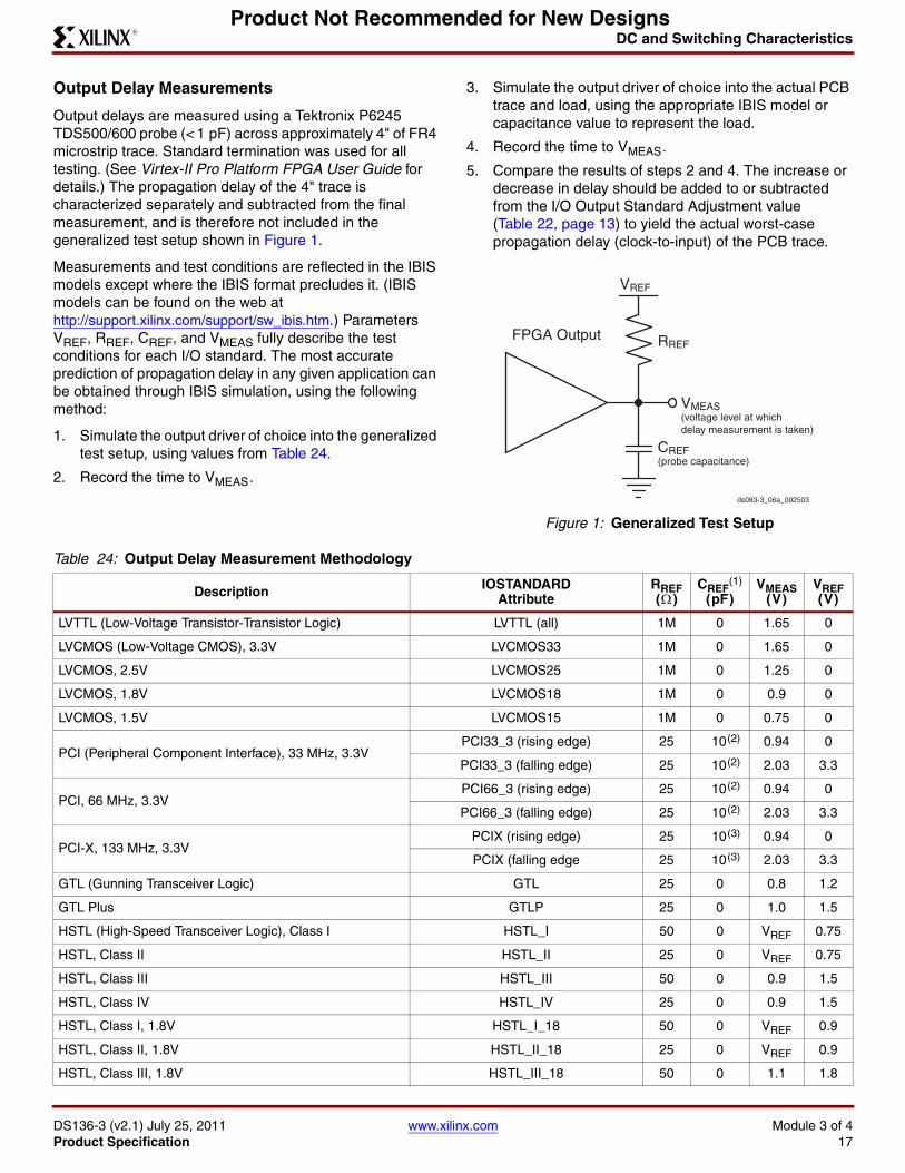
DC and Switching Characteristics
DS136-3 (v2.1) July 25, 2011 www.xilinx.com Module 3 of 4Product Specification 17
R
Product Not Recommended for New Designs
Output Delay Measurements
Output delays are measured using a Tektronix P6245 TDS500/600 probe (< 1 pF) across approximately 4" of FR4 microstrip trace. Standard termination was used for all testing. (See Virtex-II Pro Platform FPGA User Guide for details.) The propagation delay of the 4" trace is characterized separately and subtracted from the final measurement, and is therefore not included in the generalized test setup shown in Figure 1.
Measurements and test conditions are reflected in the IBIS models except where the IBIS format precludes it. (IBIS models can be found on the web at http://support.xilinx.com/support/sw_ibis.htm.) Parameters VREF , RREF , CREF , and VMEAS fully describe the test conditions for each I/O standard. The most accurate prediction of propagation delay in any given application can be obtained through IBIS simulation, using the following method:
1. Simulate the output driver of choice into the generalized test setup, using values from Table 24.
2. Record the time to VMEAS .
3. Simulate the output driver of choice into the actual PCB trace and load, using the appropriate IBIS model or capacitance value to represent the load.
4. Record the time to VMEAS .
5. Compare the results of steps 2 and 4. The increase or decrease in delay should be added to or subtracted from the I/O Output Standard Adjustment value (Table 22, page 13) to yield the actual worst-case propagation delay (clock-to-input) of the PCB trace.
X-Ref Target - Figure 1
Figure 1: Generalized Test Setup
VREF
RREF
VMEAS(voltage level at which delay measurement is taken)
CREF (probe capacitance)
FPGA Output
ds083-3_06a_092503
Table 24: Output Delay Measurement Methodology
Description IOSTANDARDAttribute
RREF ( )
CREF(1)
( pF )VMEAS
( V )VREF( V )
LVTTL (Low-Voltage Transistor-Transistor Logic) LVTTL (all) 1M 0 1.65 0
LVCMOS (Low-Voltage CMOS), 3.3V LVCMOS33 1M 0 1.65 0
LVCMOS, 2.5V LVCMOS25 1M 0 1.25 0
LVCMOS, 1.8V LVCMOS18 1M 0 0.9 0
LVCMOS, 1.5V LVCMOS15 1M 0 0.75 0
PCI (Peripheral Component Interface), 33 MHz, 3.3VPCI33_3 (rising edge) 25 10 (2) 0.94 0
PCI33_3 (falling edge) 25 10 (2) 2.03 3.3
PCI, 66 MHz, 3.3VPCI66_3 (rising edge) 25 10 (2) 0.94 0
PCI66_3 (falling edge) 25 10 (2) 2.03 3.3
PCI-X, 133 MHz, 3.3VPCIX (rising edge) 25 10 (3) 0.94 0
PCIX (falling edge 25 10 (3) 2.03 3.3
GTL (Gunning Transceiver Logic) GTL 25 0 0.8 1.2
GTL Plus GTLP 25 0 1.0 1.5
HSTL (High-Speed Transceiver Logic), Class I HSTL_I 50 0 VREF 0.75
HSTL, Class II HSTL_II 25 0 VREF 0.75
HSTL, Class III HSTL_III 50 0 0.9 1.5
HSTL, Class IV HSTL_IV 25 0 0.9 1.5
HSTL, Class I, 1.8V HSTL_I_18 50 0 VREF 0.9
HSTL, Class II, 1.8V HSTL_II_18 25 0 VREF 0.9
HSTL, Class III, 1.8V HSTL_III_18 50 0 1.1 1.8
DC and Switching Characteristics
DS136-3 (v2.1) July 25, 2011 www.xilinx.com Module 3 of 4Product Specification 18
R
Product Not Recommended for New Designs
HSTL, Class IV, 1.8V HSTL_IV_18 25 0 1.1 1.8
SSTL (Stub Series Terminated Logic), Class I, 1.8V SSTL18_I 50 0 VREF 0.9
SSTL, Class II, 1.8V SSTL18_II 25 0 VREF 0.9
SSTL, Class I, 2.5V SSTL2_I 50 0 VREF 1.25
SSTL, Class II, 2.5V SSTL2_II 25 0 VREF 1.25
LVDS (Low-Voltage Differential Signaling), 2.5V LVDS_25 50 0 VREF 1.2
LVDSEXT (LVDS Extended Mode), 2.5V LVDSEXT_25 50 0 VREF 1.2
BLVDS (Bus LVDS), 2.5V BLVDS_25 1M 0 1.2 0
LDT (HyperTransport), 2.5V LDT_25 50 0 VREF 0.6
LVPECL (Low-Voltage Positive Electron-Coupled Logic), 2.5V LVPECL_25 1M 0 1.23 0
LVDCI/HSLVDCI (Low-Voltage Digitally Controlled Impedance), 3.3V LVDCI_33 1M 0 1.65 0
LVDCI/HSLVDCI, 2.5V LVDCI_25 1M 0 1.25 0
LVDCI/HSLVDCI, 1.8V LVDCI_18 1M 0 0.9 0
LVDCI/HSLVDCI, 1.5V LVDCI_15 1M 0 0.75 0
HSTL (High-Speed Transceiver Logic), Class I & II, with DCI HSTL_I_DCI, HSTL_II_DCI 50 0 VREF 0.75
HSTL, Class III & IV, with DCI HSTL_III_DCI, HSTL_IV_DCI 50 0 0.9 1.5
HSTL, Class I & II, 1.8V, with DCI HSTL_I_DCI_18, HSTL_II_DCI_18 50 0 VREF 0.9
HSTL, Class III & IV, 1.8V, with DCI HSTL_III_DCI_18, HSTL_IV_DCI_18 50 0 1.1 1.8
SSTL (Stub Series Termi.Logic), Class I & II, 1.8V, with DCI SSTL18_I_DCI, SSTL18_II_DCI 50 0 VREF 0.9
SSTL, Class I & II, 2.5V, with DCI SSTL2_I_DCI, SSTL2_II_DCI 50 0 VREF 1.25
GTL (Gunning Transceiver Logic) with DCI GTL_DCI 50 0 0.8 1.2
GTL Plus with DCI GTLP_DCI 50 0 1.0 1.5
Notes: 1. CREF is the capacitance of the probe, nominally 0 pF.2. Measured as per PCI specification.3. Measured as per PCI-X specification.
Table 24: Output Delay Measurement Methodology (Cont’d)
Description IOSTANDARDAttribute
RREF ( )
CREF(1)
( pF )VMEAS
( V )VREF( V )
DC and Switching Characteristics
DS136-3 (v2.1) July 25, 2011 www.xilinx.com Module 3 of 4Product Specification 19
R
Product Not Recommended for New Designs
Clock Distribution Switching Characteristics
CLB Switching Characteristics
Delays originating at F/G inputs vary slightly according to the input used (see Figure 22 in Functional Description (Module 2)). The values listed below are worst-case. Precise values are provided by the timing analyzer.
Table 25: Clock Distribution Switching Characteristics
Description SymbolSpeed Grade
Units-6 -5
Global Clock Buffer I input to O output TGIO 0.057 0.064 ns, max
Global Clock Buffer S input Setup/Hold to I1 an I2 inputs TGSI/TGIS 0.54/–0.12 0.60/–0.13 ns, max
Table 26: CLB Switching Characteristics
Description SymbolSpeed Grade
Units-6 -5
Combinatorial Delays
4-input function: F/G inputs to X/Y outputs TILO 0.32 0.36 ns, max
5-input function: F/G inputs to F5 output TIF5 0.65 0.73 ns, max
5-input function: F/G inputs to X output TIF5X 0.70 0.79 ns, max
FXINA or FXINB inputs to Y output via MUXFX TIFXY 0.32 0.36 ns, max
FXINA input to FX output via MUXFX TINAFX 0.32 0.36 ns, max
FXINB input to FX output via MUXFX TINBFX 0.32 0.36 ns, max
SOPIN input to SOPOUT output via ORCY TSOPSOP 0.13 0.14 ns, max
Incremental delay routing through transparent latch to XQ/YQ outputs
TIFNCTL 0.24 0.27 ns, max
Sequential Delays
FF Clock CLK to XQ/YQ outputs TCKO 0.38 0.42 ns, max
Latch Clock CLK to XQ/YQ outputs TCKLO 0.57 0.64 ns, max
Setup and Hold Times Before/After Clock CLK
BX/BY inputs TDICK/TCKDI 0.24/–0.05 0.27/–0.06 ns, min
DY inputs TDYCK/TCKDY 0.00/ 0.14 0.00/ 0.15 ns, min
DX inputs TDXCK/TCKDX 0.00/ 0.14 0.00/ 0.15 ns, min
CE input TCECK/TCKCE 0.34/ 0.01 0.47/ 0.01 ns, min
SR/BY inputs (synchronous) TRCK /TCKR 0.60/–0.01 0.78/–0.01 ns, min
Clock CLK
Minimum Pulse Width, High TCH 0.40 0.45 ns, min
Minimum Pulse Width, Low TCL 0.40 0.45 ns, min
Set/Reset
Minimum Pulse Width, SR/BY inputs (asynchronous) TRPW 0.40 0.45 ns, min
Delay from SR/BY inputs to XQ/YQ outputs(asynchronous)
TRQ 1.25 1.40 ns, max
Toggle Frequency (for export control) FTOG 1200 1050 MHz
Notes: 1. A Zero “0” Hold Time listing indicates no hold time or a negative hold time. Negative values can not be guaranteed “best-case”, but if a “0”
is listed, there is no positive hold time.
DC and Switching Characteristics
DS136-3 (v2.1) July 25, 2011 www.xilinx.com Module 3 of 4Product Specification 20
R
Product Not Recommended for New Designs
CLB Distributed RAM Switching Characteristics
CLB Shift Register Switching Characteristics
Table 27: CLB Distributed RAM Switching Characteristics
Description SymbolSpeed Grade
Units-6 -5
Sequential Delays
Clock CLK to X/Y outputs (WE active) in 16 x 1 mode TSHCKO16 1.38 1.54 ns, max
Clock CLK to X/Y outputs (WE active) in 32 x 1 mode TSHCKO32 1.75 1.95 ns, max
Clock CLK to F5 output TSHCKOF5 1.68 1.88 ns, max
Setup and Hold Times Before/After Clock CLK
BX/BY data inputs (DIN) TDS/TDH 0.41/–0.07 0.46/–0.08 ns, min
F/G address inputs TAS/TAH 0.47/ 0.00 0.52/ 0.00 ns, min
SR input TWES/TWEH 0.24/ 0.05 0.26/ 0.05 ns, min
Clock CLK
Minimum Pulse Width, High TWPH 0.72 0.79 ns, min
Minimum Pulse Width, Low TWPL 0.72 0.79 ns, min
Minimum clock period to meet address write cycle time TWC 1.44 1.58 ns, min
Notes: 1. A Zero “0” Hold Time listing indicates no hold time or a negative hold time. Negative values cannot be guaranteed “best-case”, but if a “0” is
listed, there is no positive hold time.
Table 28: CLB Shift Register Switching Characteristics
Description SymbolSpeed Grade
Units-6 -5
Sequential Delays
Clock CLK to X/Y outputs TREG 3.12 3.49 ns, max
Clock CLK to X/Y outputs TREG32 3.49 3.90 ns, max
Clock CLK to XB output via MC15 LUT output TREGXB 3.18 3.55 ns, max
Clock CLK to YB output via MC15 LUT output TREGYB 2.88 3.21 ns, max
Clock CLK to Shiftout TCKSH 2.83 3.15 ns, max
Clock CLK to F5 output TREGF5 3.42 3.83 ns, max
Setup and Hold Times Before/After Clock CLK
BX/BY data inputs (DIN) TSRLDS/TSRLDH 0.77/–0.18 0.98/–0.21 ns, min
SR input TWSS/TWSH 0.34/ 0.01 0.47/ 0.01 ns, min
Clock CLK
Minimum Pulse Width, High TSRPH 0.72 0.79 ns, min
Minimum Pulse Width, Low TSRPL 0.72 0.79 ns, min
Notes: 1. A Zero “0” Hold Time listing indicates no hold time or a negative hold time. Negative values cannot be guaranteed “best-case”, but if a “0” is
listed, there is no positive hold time.
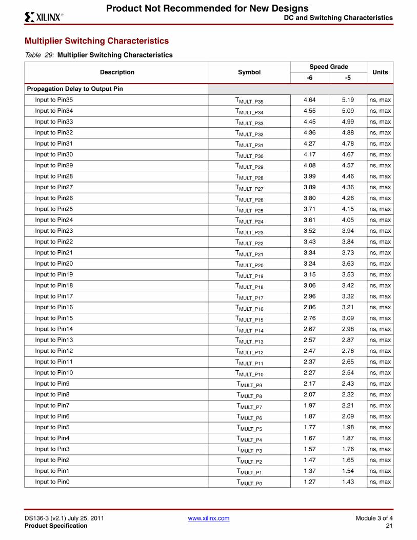
DC and Switching Characteristics
DS136-3 (v2.1) July 25, 2011 www.xilinx.com Module 3 of 4Product Specification 21
R
Product Not Recommended for New Designs
Multiplier Switching Characteristics
Table 29: Multiplier Switching Characteristics
Description SymbolSpeed Grade
Units-6 -5
Propagation Delay to Output Pin
Input to Pin35 TMULT_P35 4.64 5.19 ns, max
Input to Pin34 TMULT_P34 4.55 5.09 ns, max
Input to Pin33 TMULT_P33 4.45 4.99 ns, max
Input to Pin32 TMULT_P32 4.36 4.88 ns, max
Input to Pin31 TMULT_P31 4.27 4.78 ns, max
Input to Pin30 TMULT_P30 4.17 4.67 ns, max
Input to Pin29 TMULT_P29 4.08 4.57 ns, max
Input to Pin28 TMULT_P28 3.99 4.46 ns, max
Input to Pin27 TMULT_P27 3.89 4.36 ns, max
Input to Pin26 TMULT_P26 3.80 4.26 ns, max
Input to Pin25 TMULT_P25 3.71 4.15 ns, max
Input to Pin24 TMULT_P24 3.61 4.05 ns, max
Input to Pin23 TMULT_P23 3.52 3.94 ns, max
Input to Pin22 TMULT_P22 3.43 3.84 ns, max
Input to Pin21 TMULT_P21 3.34 3.73 ns, max
Input to Pin20 TMULT_P20 3.24 3.63 ns, max
Input to Pin19 TMULT_P19 3.15 3.53 ns, max
Input to Pin18 TMULT_P18 3.06 3.42 ns, max
Input to Pin17 TMULT_P17 2.96 3.32 ns, max
Input to Pin16 TMULT_P16 2.86 3.21 ns, max
Input to Pin15 TMULT_P15 2.76 3.09 ns, max
Input to Pin14 TMULT_P14 2.67 2.98 ns, max
Input to Pin13 TMULT_P13 2.57 2.87 ns, max
Input to Pin12 TMULT_P12 2.47 2.76 ns, max
Input to Pin11 TMULT_P11 2.37 2.65 ns, max
Input to Pin10 TMULT_P10 2.27 2.54 ns, max
Input to Pin9 TMULT_P9 2.17 2.43 ns, max
Input to Pin8 TMULT_P8 2.07 2.32 ns, max
Input to Pin7 TMULT_P7 1.97 2.21 ns, max
Input to Pin6 TMULT_P6 1.87 2.09 ns, max
Input to Pin5 TMULT_P5 1.77 1.98 ns, max
Input to Pin4 TMULT_P4 1.67 1.87 ns, max
Input to Pin3 TMULT_P3 1.57 1.76 ns, max
Input to Pin2 TMULT_P2 1.47 1.65 ns, max
Input to Pin1 TMULT_P1 1.37 1.54 ns, max
Input to Pin0 TMULT_P0 1.27 1.43 ns, max
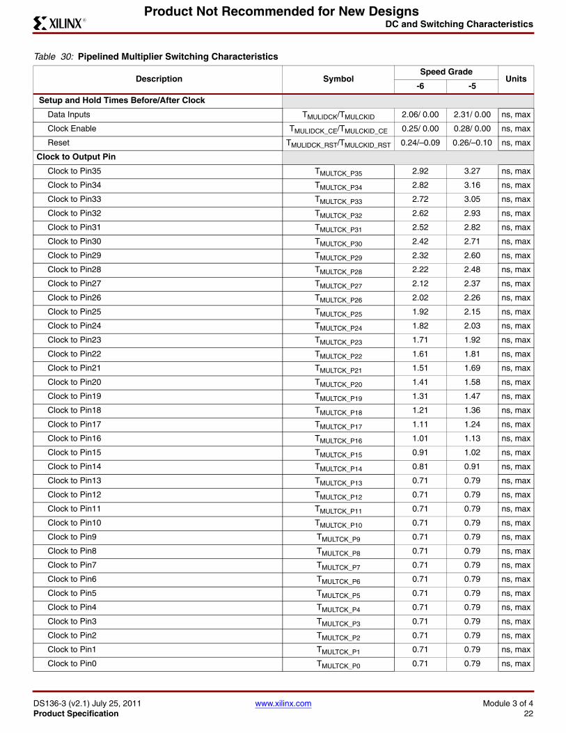
DC and Switching Characteristics
DS136-3 (v2.1) July 25, 2011 www.xilinx.com Module 3 of 4Product Specification 22
R
Product Not Recommended for New Designs
Table 30: Pipelined Multiplier Switching Characteristics
Description SymbolSpeed Grade
Units-6 -5
Setup and Hold Times Before/After Clock
Data Inputs TMULIDCK/TMULCKID 2.06/ 0.00 2.31/ 0.00 ns, max
Clock Enable TMULIDCK_CE/TMULCKID_CE 0.25/ 0.00 0.28/ 0.00 ns, max
Reset TMULIDCK_RST/TMULCKID_RST 0.24/–0.09 0.26/–0.10 ns, max
Clock to Output Pin
Clock to Pin35 TMULTCK_P35 2.92 3.27 ns, max
Clock to Pin34 TMULTCK_P34 2.82 3.16 ns, max
Clock to Pin33 TMULTCK_P33 2.72 3.05 ns, max
Clock to Pin32 TMULTCK_P32 2.62 2.93 ns, max
Clock to Pin31 TMULTCK_P31 2.52 2.82 ns, max
Clock to Pin30 TMULTCK_P30 2.42 2.71 ns, max
Clock to Pin29 TMULTCK_P29 2.32 2.60 ns, max
Clock to Pin28 TMULTCK_P28 2.22 2.48 ns, max
Clock to Pin27 TMULTCK_P27 2.12 2.37 ns, max
Clock to Pin26 TMULTCK_P26 2.02 2.26 ns, max
Clock to Pin25 TMULTCK_P25 1.92 2.15 ns, max
Clock to Pin24 TMULTCK_P24 1.82 2.03 ns, max
Clock to Pin23 TMULTCK_P23 1.71 1.92 ns, max
Clock to Pin22 TMULTCK_P22 1.61 1.81 ns, max
Clock to Pin21 TMULTCK_P21 1.51 1.69 ns, max
Clock to Pin20 TMULTCK_P20 1.41 1.58 ns, max
Clock to Pin19 TMULTCK_P19 1.31 1.47 ns, max
Clock to Pin18 TMULTCK_P18 1.21 1.36 ns, max
Clock to Pin17 TMULTCK_P17 1.11 1.24 ns, max
Clock to Pin16 TMULTCK_P16 1.01 1.13 ns, max
Clock to Pin15 TMULTCK_P15 0.91 1.02 ns, max
Clock to Pin14 TMULTCK_P14 0.81 0.91 ns, max
Clock to Pin13 TMULTCK_P13 0.71 0.79 ns, max
Clock to Pin12 TMULTCK_P12 0.71 0.79 ns, max
Clock to Pin11 TMULTCK_P11 0.71 0.79 ns, max
Clock to Pin10 TMULTCK_P10 0.71 0.79 ns, max
Clock to Pin9 TMULTCK_P9 0.71 0.79 ns, max
Clock to Pin8 TMULTCK_P8 0.71 0.79 ns, max
Clock to Pin7 TMULTCK_P7 0.71 0.79 ns, max
Clock to Pin6 TMULTCK_P6 0.71 0.79 ns, max
Clock to Pin5 TMULTCK_P5 0.71 0.79 ns, max
Clock to Pin4 TMULTCK_P4 0.71 0.79 ns, max
Clock to Pin3 TMULTCK_P3 0.71 0.79 ns, max
Clock to Pin2 TMULTCK_P2 0.71 0.79 ns, max
Clock to Pin1 TMULTCK_P1 0.71 0.79 ns, max
Clock to Pin0 TMULTCK_P0 0.71 0.79 ns, max
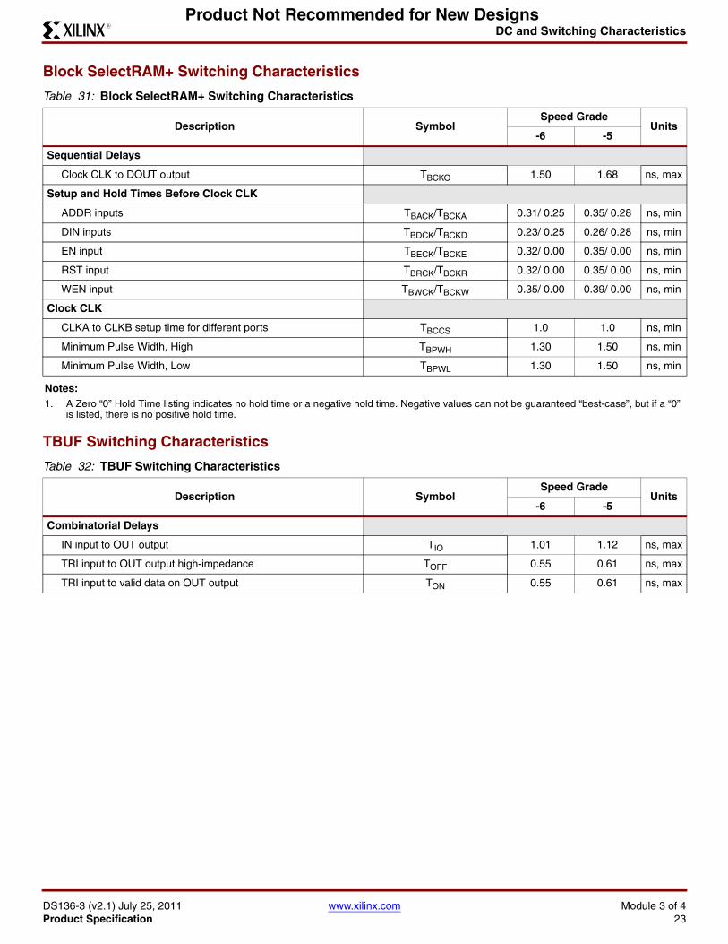
DC and Switching Characteristics
DS136-3 (v2.1) July 25, 2011 www.xilinx.com Module 3 of 4Product Specification 23
R
Product Not Recommended for New Designs
Block SelectRAM+ Switching Characteristics
TBUF Switching Characteristics
Table 31: Block SelectRAM+ Switching Characteristics
Description SymbolSpeed Grade
Units-6 -5
Sequential Delays
Clock CLK to DOUT output TBCKO 1.50 1.68 ns, max
Setup and Hold Times Before Clock CLK
ADDR inputs TBACK/TBCKA 0.31/ 0.25 0.35/ 0.28 ns, min
DIN inputs TBDCK/TBCKD 0.23/ 0.25 0.26/ 0.28 ns, min
EN input TBECK/TBCKE 0.32/ 0.00 0.35/ 0.00 ns, min
RST input TBRCK/TBCKR 0.32/ 0.00 0.35/ 0.00 ns, min
WEN input TBWCK/TBCKW 0.35/ 0.00 0.39/ 0.00 ns, min
Clock CLK
CLKA to CLKB setup time for different ports TBCCS 1.0 1.0 ns, min
Minimum Pulse Width, High TBPWH 1.30 1.50 ns, min
Minimum Pulse Width, Low TBPWL 1.30 1.50 ns, min
Notes: 1. A Zero “0” Hold Time listing indicates no hold time or a negative hold time. Negative values can not be guaranteed “best-case”, but if a “0”
is listed, there is no positive hold time.
Table 32: TBUF Switching Characteristics
Description SymbolSpeed Grade
Units-6 -5
Combinatorial Delays
IN input to OUT output TIO 1.01 1.12 ns, max
TRI input to OUT output high-impedance TOFF 0.55 0.61 ns, max
TRI input to valid data on OUT output TON 0.55 0.61 ns, max
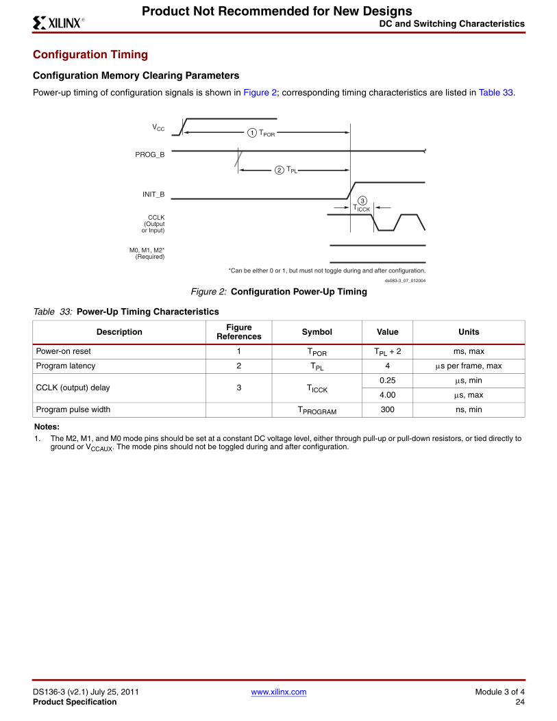
DC and Switching Characteristics
DS136-3 (v2.1) July 25, 2011 www.xilinx.com Module 3 of 4Product Specification 24
R
Product Not Recommended for New Designs
Configuration Timing
Configuration Memory Clearing Parameters
Power-up timing of configuration signals is shown in Figure 2; corresponding timing characteristics are listed in Table 33.
X-Ref Target - Figure 2
Figure 2: Configuration Power-Up Timing
Table 33: Power-Up Timing Characteristics
Description Figure References Symbol Value Units
Power-on reset 1 TPOR TPL + 2 ms, max
Program latency 2 TPL 4 s per frame, max
CCLK (output) delay 3 TICCK0.25 s, min
4.00 s, max
Program pulse width TPROGRAM 300 ns, min
Notes: 1. The M2, M1, and M0 mode pins should be set at a constant DC voltage level, either through pull-up or pull-down resistors, or tied directly to
ground or VCCAUX. The mode pins should not be toggled during and after configuration.
TPL
TICCK
ds083-3_07_012004
TPOR
INIT_B
PROG_B
VCC
*Can be either 0 or 1, but must not toggle during and after configuration.
M0, M1, M2*(Required)
CCLK(Output
or Input)
1
2
3
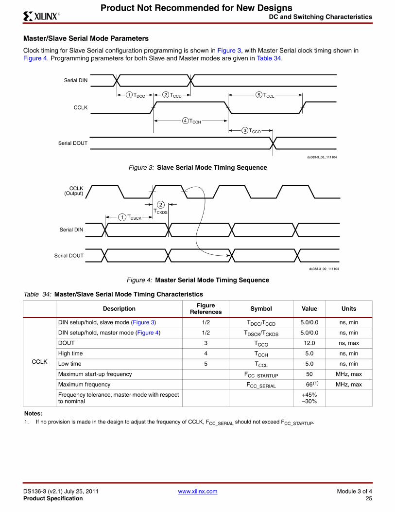
DC and Switching Characteristics
DS136-3 (v2.1) July 25, 2011 www.xilinx.com Module 3 of 4Product Specification 25
R
Product Not Recommended for New Designs
Master/Slave Serial Mode Parameters
Clock timing for Slave Serial configuration programming is shown in Figure 3, with Master Serial clock timing shown in Figure 4. Programming parameters for both Slave and Master modes are given in Table 34.
.
X-Ref Target - Figure 3
Figure 3: Slave Serial Mode Timing Sequence
X-Ref Target - Figure 4
Figure 4: Master Serial Mode Timing Sequence
Table 34: Master/Slave Serial Mode Timing Characteristics
Description Figure References Symbol Value Units
CCLK
DIN setup/hold, slave mode (Figure 3) 1/2 TDCC/TCCD 5.0/0.0 ns, min
DIN setup/hold, master mode (Figure 4) 1/2 TDSCK/TCKDS 5.0/0.0 ns, min
DOUT 3 TCCO 12.0 ns, max
High time 4 TCCH 5.0 ns, min
Low time 5 TCCL 5.0 ns, min
Maximum start-up frequency FCC_STARTUP 50 MHz, max
Maximum frequency FCC_SERIAL 66 (1) MHz, max
Frequency tolerance, master mode with respect to nominal
+45% –30%
Notes: 1. If no provision is made in the design to adjust the frequency of CCLK, FCC_SERIAL should not exceed FCC_STARTUP .
4 TCCH
3 TCCO
5 TCCL2 TCCD1 TDCC
Serial DIN
CCLK
Serial DOUT
ds083-3_08_111104
Serial DIN
CCLK(Output)
Serial DOUT
1
2TCKDS
TDSCK
ds083-3_09_111104
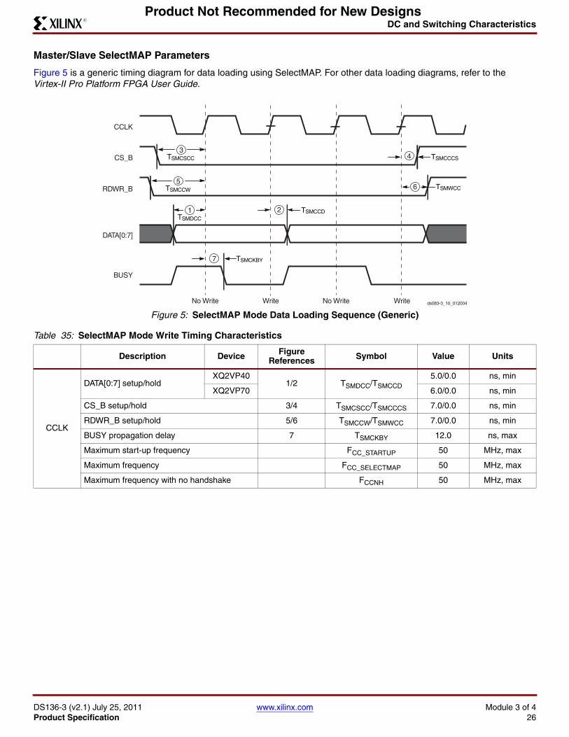
DC and Switching Characteristics
DS136-3 (v2.1) July 25, 2011 www.xilinx.com Module 3 of 4Product Specification 26
R
Product Not Recommended for New Designs
Master/Slave SelectMAP Parameters
Figure 5 is a generic timing diagram for data loading using SelectMAP. For other data loading diagrams, refer to the Virtex-II Pro Platform FPGA User Guide.
X-Ref Target - Figure 5
Figure 5: SelectMAP Mode Data Loading Sequence (Generic)
Table 35: SelectMAP Mode Write Timing Characteristics
Description Device Figure References Symbol Value Units
CCLK
DATA[0:7] setup/hold XQ2VP40
1/2 TSMDCC/TSMCCD5.0/0.0 ns, min
XQ2VP70 6.0/0.0 ns, min
CS_B setup/hold 3/4 TSMCSCC/TSMCCCS 7.0/0.0 ns, min
RDWR_B setup/hold 5/6 TSMCCW/TSMWCC 7.0/0.0 ns, min
BUSY propagation delay 7 TSMCKBY 12.0 ns, max
Maximum start-up frequency FCC_STARTUP 50 MHz, max
Maximum frequency FCC_SELECTMAP 50 MHz, max
Maximum frequency with no handshake FCCNH 50 MHz, max
ds083-3_10_012004
CCLK
No Write Write No Write Write
DATA[0:7]
CS_B
RDWR_B
3
5
BUSY
4
6
7
TSMCSCC
1TSMDCC
2 TSMCCD
TSMCCCS
TSMWCC
TSMCKBY
TSMCCW
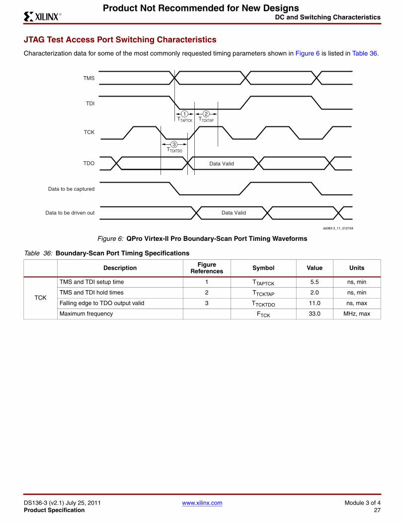
DC and Switching Characteristics
DS136-3 (v2.1) July 25, 2011 www.xilinx.com Module 3 of 4Product Specification 27
R
Product Not Recommended for New Designs
JTAG Test Access Port Switching Characteristics
Characterization data for some of the most commonly requested timing parameters shown in Figure 6 is listed in Table 36.
X-Ref Target - Figure 6FI
Figure 6: QPro Virtex-II Pro Boundary-Scan Port Timing Waveforms
Table 36: Boundary-Scan Port Timing Specifications
Description Figure References Symbol Value Units
TCK
TMS and TDI setup time 1 TTAPTCK 5.5 ns, min
TMS and TDI hold times 2 TTCKTAP 2.0 ns, min
Falling edge to TDO output valid 3 TTCKTDO 11.0 ns, max
Maximum frequency FTCK 33.0 MHz, max
ds083-3_11_012104
Data to be captured
Data to be driven out
TDO
TCK
TDI
TMS
Data Valid
Data Valid
TTCKTDO
TTAPTCK TTCKTAP
1 2
3
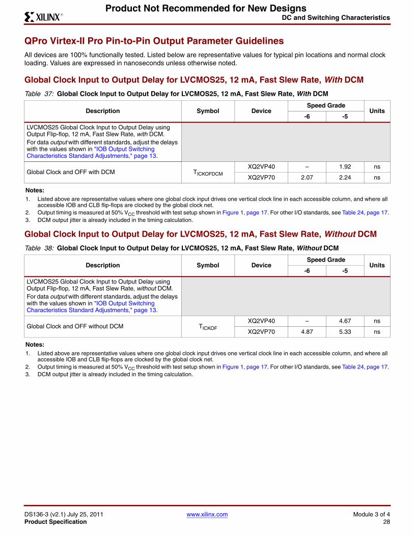
DC and Switching Characteristics
DS136-3 (v2.1) July 25, 2011 www.xilinx.com Module 3 of 4Product Specification 28
R
Product Not Recommended for New Designs
QPro Virtex-II Pro Pin-to-Pin Output Parameter GuidelinesAll devices are 100% functionally tested. Listed below are representative values for typical pin locations and normal clock loading. Values are expressed in nanoseconds unless otherwise noted.
Global Clock Input to Output Delay for LVCMOS25, 12 mA, Fast Slew Rate, With DCM
Global Clock Input to Output Delay for LVCMOS25, 12 mA, Fast Slew Rate, Without DCM
Table 37: Global Clock Input to Output Delay for LVCMOS25, 12 mA, Fast Slew Rate, With DCM
Description Symbol DeviceSpeed Grade
Units-6 -5
LVCMOS25 Global Clock Input to Output Delay using Output Flip-flop, 12 mA, Fast Slew Rate, with DCM. For data output with different standards, adjust the delays with the values shown in "IOB Output Switching Characteristics Standard Adjustments," page 13.
Global Clock and OFF with DCM TICKOFDCMXQ2VP40 – 1.92 ns
XQ2VP70 2.07 2.24 ns
Notes: 1. Listed above are representative values where one global clock input drives one vertical clock line in each accessible column, and where all
accessible IOB and CLB flip-flops are clocked by the global clock net. 2. Output timing is measured at 50% VCC threshold with test setup shown in Figure 1, page 17. For other I/O standards, see Table 24, page 17.3. DCM output jitter is already included in the timing calculation.
Table 38: Global Clock Input to Output Delay for LVCMOS25, 12 mA, Fast Slew Rate, Without DCM
Description Symbol DeviceSpeed Grade
Units-6 -5
LVCMOS25 Global Clock Input to Output Delay using Output Flip-flop, 12 mA, Fast Slew Rate, without DCM. For data output with different standards, adjust the delays with the values shown in "IOB Output Switching Characteristics Standard Adjustments," page 13.
Global Clock and OFF without DCM TICKOFXQ2VP40 – 4.67 ns
XQ2VP70 4.87 5.33 ns
Notes: 1. Listed above are representative values where one global clock input drives one vertical clock line in each accessible column, and where all
accessible IOB and CLB flip-flops are clocked by the global clock net. 2. Output timing is measured at 50% VCC threshold with test setup shown in Figure 1, page 17. For other I/O standards, see Table 24, page 17.3. DCM output jitter is already included in the timing calculation.
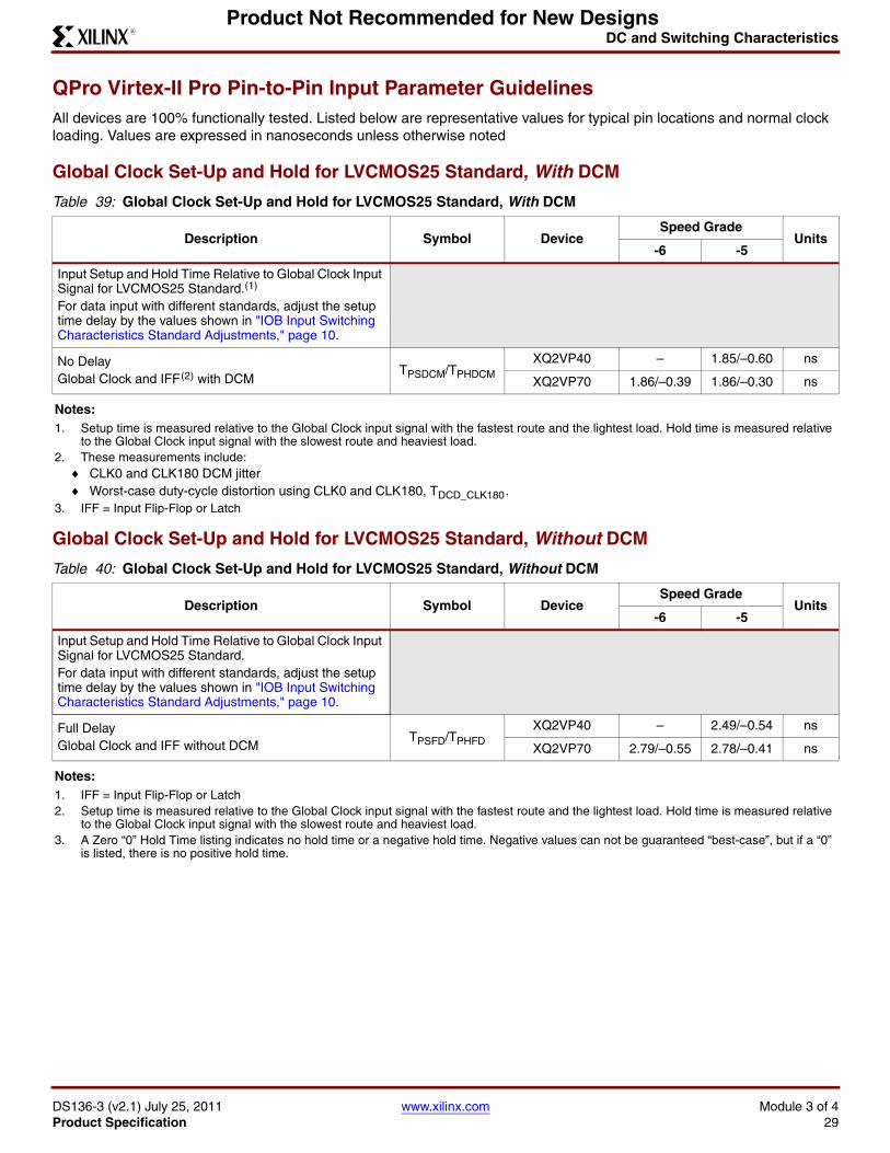
DC and Switching Characteristics
DS136-3 (v2.1) July 25, 2011 www.xilinx.com Module 3 of 4Product Specification 29
R
Product Not Recommended for New Designs
QPro Virtex-II Pro Pin-to-Pin Input Parameter GuidelinesAll devices are 100% functionally tested. Listed below are representative values for typical pin locations and normal clock loading. Values are expressed in nanoseconds unless otherwise noted
Global Clock Set-Up and Hold for LVCMOS25 Standard, With DCM
Global Clock Set-Up and Hold for LVCMOS25 Standard, Without DCM ,
Table 39: Global Clock Set-Up and Hold for LVCMOS25 Standard, With DCM
Description Symbol DeviceSpeed Grade
Units-6 -5
Input Setup and Hold Time Relative to Global Clock Input Signal for LVCMOS25 Standard.(1) For data input with different standards, adjust the setup time delay by the values shown in "IOB Input Switching Characteristics Standard Adjustments," page 10.
No DelayGlobal Clock and IFF (2) with DCM
TPSDCM/TPHDCMXQ2VP40 – 1.85/–0.60 ns
XQ2VP70 1.86/–0.39 1.86/–0.30 ns
Notes: 1. Setup time is measured relative to the Global Clock input signal with the fastest route and the lightest load. Hold time is measured relative
to the Global Clock input signal with the slowest route and heaviest load. 2. These measurements include:
CLK0 and CLK180 DCM jitter Worst-case duty-cycle distortion using CLK0 and CLK180, TDCD_CLK180 .
3. IFF = Input Flip-Flop or Latch
Table 40: Global Clock Set-Up and Hold for LVCMOS25 Standard, Without DCM
Description Symbol DeviceSpeed Grade
Units-6 -5
Input Setup and Hold Time Relative to Global Clock Input Signal for LVCMOS25 Standard. For data input with different standards, adjust the setup time delay by the values shown in "IOB Input Switching Characteristics Standard Adjustments," page 10.
Full DelayGlobal Clock and IFF without DCM
TPSFD/TPHFDXQ2VP40 – 2.49/–0.54 ns
XQ2VP70 2.79/–0.55 2.78/–0.41 ns
Notes: 1. IFF = Input Flip-Flop or Latch2. Setup time is measured relative to the Global Clock input signal with the fastest route and the lightest load. Hold time is measured relative
to the Global Clock input signal with the slowest route and heaviest load.3. A Zero “0” Hold Time listing indicates no hold time or a negative hold time. Negative values can not be guaranteed “best-case”, but if a “0”
is listed, there is no positive hold time.
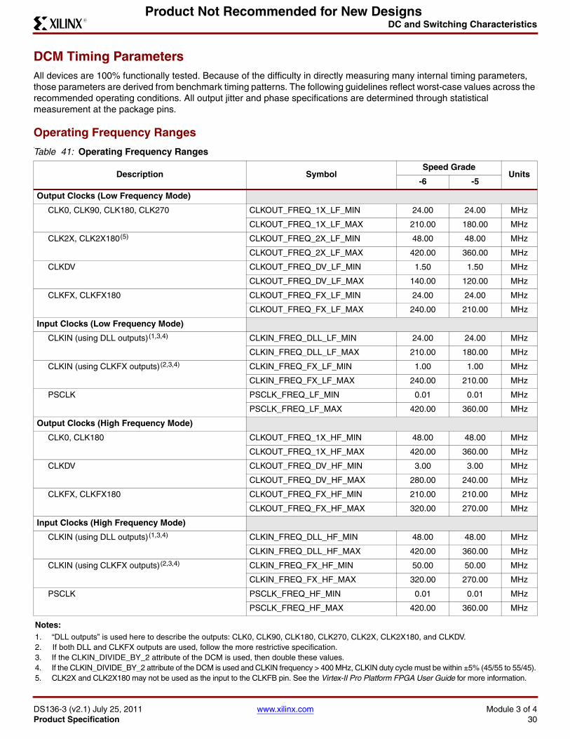
DC and Switching Characteristics
DS136-3 (v2.1) July 25, 2011 www.xilinx.com Module 3 of 4Product Specification 30
R
Product Not Recommended for New Designs
DCM Timing ParametersAll devices are 100% functionally tested. Because of the difficulty in directly measuring many internal timing parameters, those parameters are derived from benchmark timing patterns. The following guidelines reflect worst-case values across the recommended operating conditions. All output jitter and phase specifications are determined through statistical measurement at the package pins.
Operating Frequency Rangese
Table 41: Operating Frequency Ranges
Description SymbolSpeed Grade
Units-6 -5
Output Clocks (Low Frequency Mode)
CLK0, CLK90, CLK180, CLK270 CLKOUT_FREQ_1X_LF_MIN 24.00 24.00 MHz
CLKOUT_FREQ_1X_LF_MAX 210.00 180.00 MHz
CLK2X, CLK2X180 (5) CLKOUT_FREQ_2X_LF_MIN 48.00 48.00 MHz
CLKOUT_FREQ_2X_LF_MAX 420.00 360.00 MHz
CLKDV CLKOUT_FREQ_DV_LF_MIN 1.50 1.50 MHz
CLKOUT_FREQ_DV_LF_MAX 140.00 120.00 MHz
CLKFX, CLKFX180 CLKOUT_FREQ_FX_LF_MIN 24.00 24.00 MHz
CLKOUT_FREQ_FX_LF_MAX 240.00 210.00 MHz
Input Clocks (Low Frequency Mode)
CLKIN (using DLL outputs) (1,3,4) CLKIN_FREQ_DLL_LF_MIN 24.00 24.00 MHz
CLKIN_FREQ_DLL_LF_MAX 210.00 180.00 MHz
CLKIN (using CLKFX outputs) (2,3,4) CLKIN_FREQ_FX_LF_MIN 1.00 1.00 MHz
CLKIN_FREQ_FX_LF_MAX 240.00 210.00 MHz
PSCLK PSCLK_FREQ_LF_MIN 0.01 0.01 MHz
PSCLK_FREQ_LF_MAX 420.00 360.00 MHz
Output Clocks (High Frequency Mode)
CLK0, CLK180 CLKOUT_FREQ_1X_HF_MIN 48.00 48.00 MHz
CLKOUT_FREQ_1X_HF_MAX 420.00 360.00 MHz
CLKDV CLKOUT_FREQ_DV_HF_MIN 3.00 3.00 MHz
CLKOUT_FREQ_DV_HF_MAX 280.00 240.00 MHz
CLKFX, CLKFX180 CLKOUT_FREQ_FX_HF_MIN 210.00 210.00 MHz
CLKOUT_FREQ_FX_HF_MAX 320.00 270.00 MHz
Input Clocks (High Frequency Mode)
CLKIN (using DLL outputs) (1,3,4) CLKIN_FREQ_DLL_HF_MIN 48.00 48.00 MHz
CLKIN_FREQ_DLL_HF_MAX 420.00 360.00 MHz
CLKIN (using CLKFX outputs) (2,3,4) CLKIN_FREQ_FX_HF_MIN 50.00 50.00 MHz
CLKIN_FREQ_FX_HF_MAX 320.00 270.00 MHz
PSCLK PSCLK_FREQ_HF_MIN 0.01 0.01 MHz
PSCLK_FREQ_HF_MAX 420.00 360.00 MHz
Notes: 1. “DLL outputs” is used here to describe the outputs: CLK0, CLK90, CLK180, CLK270, CLK2X, CLK2X180, and CLKDV.2. If both DLL and CLKFX outputs are used, follow the more restrictive specification.3. If the CLKIN_DIVIDE_BY_2 attribute of the DCM is used, then double these values.4. If the CLKIN_DIVIDE_BY_2 attribute of the DCM is used and CLKIN frequency > 400 MHz, CLKIN duty cycle must be within ±5% (45/55 to 55/45).5. CLK2X and CLK2X180 may not be used as the input to the CLKFB pin. See the Virtex-II Pro Platform FPGA User Guide for more information.
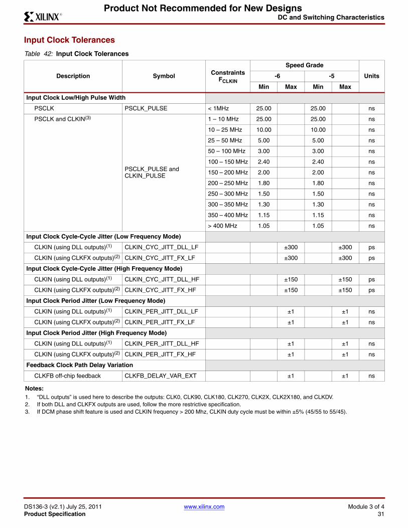
DC and Switching Characteristics
DS136-3 (v2.1) July 25, 2011 www.xilinx.com Module 3 of 4Product Specification 31
R
Product Not Recommended for New Designs
Input Clock Tolerances
Table 42: Input Clock Tolerances
Description Symbol ConstraintsFCLKIN
Speed Grade
Units-6 -5
Min Max Min Max
Input Clock Low/High Pulse Width
PSCLK PSCLK_PULSE < 1MHz 25.00 25.00 ns
PSCLK and CLKIN(3)
PSCLK_PULSE and CLKIN_PULSE
1 – 10 MHz 25.00 25.00 ns
10 – 25 MHz 10.00 10.00 ns
25 – 50 MHz 5.00 5.00 ns
50 – 100 MHz 3.00 3.00 ns
100 – 150 MHz 2.40 2.40 ns
150 – 200 MHz 2.00 2.00 ns
200 – 250 MHz 1.80 1.80 ns
250 – 300 MHz 1.50 1.50 ns
300 – 350 MHz 1.30 1.30 ns
350 – 400 MHz 1.15 1.15 ns
> 400 MHz 1.05 1.05 ns
Input Clock Cycle-Cycle Jitter (Low Frequency Mode)
CLKIN (using DLL outputs)(1) CLKIN_CYC_JITT_DLL_LF ±300 ±300 ps
CLKIN (using CLKFX outputs)(2) CLKIN_CYC_JITT_FX_LF ±300 ±300 ps
Input Clock Cycle-Cycle Jitter (High Frequency Mode)
CLKIN (using DLL outputs)(1) CLKIN_CYC_JITT_DLL_HF ±150 ±150 ps
CLKIN (using CLKFX outputs)(2) CLKIN_CYC_JITT_FX_HF ±150 ±150 ps
Input Clock Period Jitter (Low Frequency Mode)
CLKIN (using DLL outputs)(1) CLKIN_PER_JITT_DLL_LF ±1 ±1 ns
CLKIN (using CLKFX outputs)(2) CLKIN_PER_JITT_FX_LF ±1 ±1 ns
Input Clock Period Jitter (High Frequency Mode)
CLKIN (using DLL outputs)(1) CLKIN_PER_JITT_DLL_HF ±1 ±1 ns
CLKIN (using CLKFX outputs)(2) CLKIN_PER_JITT_FX_HF ±1 ±1 ns
Feedback Clock Path Delay Variation
CLKFB off-chip feedback CLKFB_DELAY_VAR_EXT ±1 ±1 ns
Notes: 1. “DLL outputs” is used here to describe the outputs: CLK0, CLK90, CLK180, CLK270, CLK2X, CLK2X180, and CLKDV.2. If both DLL and CLKFX outputs are used, follow the more restrictive specification.3. If DCM phase shift feature is used and CLKIN frequency > 200 Mhz, CLKIN duty cycle must be within ±5% (45/55 to 55/45).
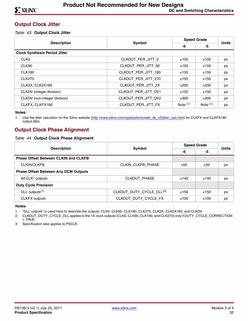
DC and Switching Characteristics
DS136-3 (v2.1) July 25, 2011 www.xilinx.com Module 3 of 4Product Specification 32
R
Product Not Recommended for New Designs
Output Clock Jitter
Output Clock Phase Alignment
Table 43: Output Clock Jitter
Description SymbolSpeed Grade
Units-6 -5
Clock Synthesis Period Jitter
CLK0 CLKOUT_PER_JITT_0 ±100 ±100 ps
CLK90 CLKOUT_PER_JITT_90 ±150 ±150 ps
CLK180 CLKOUT_PER_JITT_180 ±150 ±150 ps
CLK270 CLKOUT_PER_JITT_270 ±150 ±150 ps
CLK2X, CLK2X180 CLKOUT_PER_JITT_2X ±200 ±200 ps
CLKDV (integer division) CLKOUT_PER_JITT_DV1 ±150 ±150 ps
CLKDV (non-integer division) CLKOUT_PER_JITT_DV2 ±300 ±300 ps
CLKFX, CLKFX180 CLKOUT_PER_JITT_FX Note (1) Note (1) ps
Notes: 1. Use the jitter calculator on the Xilinx website (http://www.xilinx.com/applications/web_ds_v2/jitter_calc.htm) for CLKFX and CLKFX180
output jitter.
Table 44: Output Clock Phase Alignment
Description SymbolSpeed Grade
Units-6 -5
Phase Offset Between CLKIN and CLKFB
CLKIN/CLKFB CLKIN_CLKFB_PHASE ±50 ±50 ps
Phase Offset Between Any DCM Outputs
All CLK* outputs CLKOUT_PHASE ±140 ±140 ps
Duty Cycle Precision
DLL outputs(1) CLKOUT_DUTY_CYCLE_DLL(2) ±150 ±150 ps
CLKFX outputs CLKOUT_DUTY_CYCLE_FX ±100 ±100 ps
Notes: 1. “DLL outputs” is used here to describe the outputs: CLK0, CLK90, CLK180, CLK270, CLK2X, CLK2X180, and CLKDV.2. CLKOUT_DUTY_CYCLE_DLL applies to the 1X clock outputs (CLK0, CLK90, CLK180, and CLK270) only if DUTY_CYCLE_CORRECTION
= TRUE.3. Specification also applies to PSCLK.
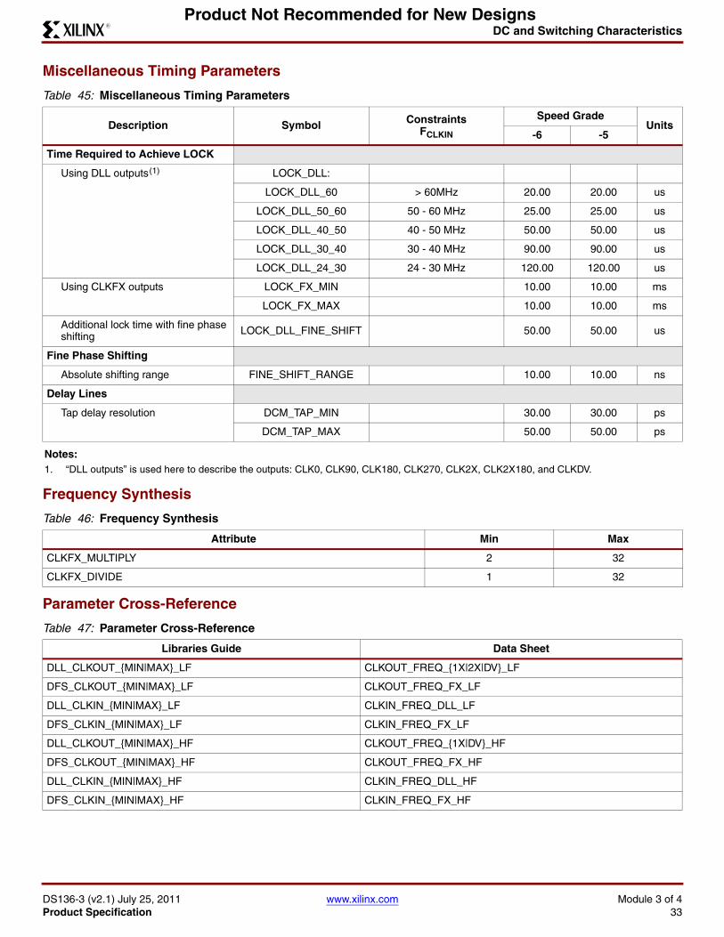
DC and Switching Characteristics
DS136-3 (v2.1) July 25, 2011 www.xilinx.com Module 3 of 4Product Specification 33
R
Product Not Recommended for New Designs
Miscellaneous Timing Parameters
Frequency Synthesis
Parameter Cross-Reference
Table 45: Miscellaneous Timing Parameters
Description Symbol ConstraintsFCLKIN
Speed GradeUnits
-6 -5
Time Required to Achieve LOCK
Using DLL outputs (1) LOCK_DLL:
LOCK_DLL_60 > 60MHz 20.00 20.00 us
LOCK_DLL_50_60 50 - 60 MHz 25.00 25.00 us
LOCK_DLL_40_50 40 - 50 MHz 50.00 50.00 us
LOCK_DLL_30_40 30 - 40 MHz 90.00 90.00 us
LOCK_DLL_24_30 24 - 30 MHz 120.00 120.00 us
Using CLKFX outputs LOCK_FX_MIN 10.00 10.00 ms
LOCK_FX_MAX 10.00 10.00 ms
Additional lock time with fine phase shifting LOCK_DLL_FINE_SHIFT 50.00 50.00 us
Fine Phase Shifting
Absolute shifting range FINE_SHIFT_RANGE 10.00 10.00 ns
Delay Lines
Tap delay resolution DCM_TAP_MIN 30.00 30.00 ps
DCM_TAP_MAX 50.00 50.00 ps
Notes: 1. “DLL outputs” is used here to describe the outputs: CLK0, CLK90, CLK180, CLK270, CLK2X, CLK2X180, and CLKDV.
Table 46: Frequency Synthesis
Attribute Min Max
CLKFX_MULTIPLY 2 32
CLKFX_DIVIDE 1 32
Table 47: Parameter Cross-Reference
Libraries Guide Data Sheet
DLL_CLKOUT_{MIN|MAX}_LF CLKOUT_FREQ_{1X|2X|DV}_LF
DFS_CLKOUT_{MIN|MAX}_LF CLKOUT_FREQ_FX_LF
DLL_CLKIN_{MIN|MAX}_LF CLKIN_FREQ_DLL_LF
DFS_CLKIN_{MIN|MAX}_LF CLKIN_FREQ_FX_LF
DLL_CLKOUT_{MIN|MAX}_HF CLKOUT_FREQ_{1X|DV}_HF
DFS_CLKOUT_{MIN|MAX}_HF CLKOUT_FREQ_FX_HF
DLL_CLKIN_{MIN|MAX}_HF CLKIN_FREQ_DLL_HF
DFS_CLKIN_{MIN|MAX}_HF CLKIN_FREQ_FX_HF
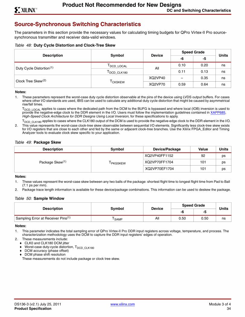
DC and Switching Characteristics
DS136-3 (v2.1) July 25, 2011 www.xilinx.com Module 3 of 4Product Specification 34
R
Product Not Recommended for New Designs
Source-Synchronous Switching CharacteristicsThe parameters in this section provide the necessary values for calculating timing budgets for QPro Virtex-II Pro source-synchronous transmitter and receiver data-valid windows.
Table 48: Duty Cycle Distortion and Clock-Tree Skew
Description Symbol DeviceSpeed Grade
Units-6 -5
Duty Cycle Distortion (1)TDCD_LOCAL
All0.10 0.20 ns
TDCD_CLK180 0.11 0.13 ns
Clock Tree Skew (2) TCKSKEWXQ2VP40 – 0.35 ns
XQ2VP70 0.59 0.64 ns
Notes: 1. These parameters represent the worst-case duty cycle distortion observable at the pins of the device using LVDS output buffers. For cases
where other I/O standards are used, IBIS can be used to calculate any additional duty cycle distortion that might be caused by asymmetrical rise/fall times. TDCD_LOCAL applies to cases where the dedicated path from the DCM to the BUFG is bypassed and where local (IOB) inversion is used to provide the negative-edge clock to the DDR element in the I/O. Users must follow the implementation guidelines contained in XAPP685, High-Speed Clock Architecture for DDR Designs Using Local Inversion, for these specifications to apply.TDCD_CLK180 applies to cases where the CLK180 output of the DCM is used to provide the negative-edge clock to the DDR element in the I/O.
2. This value represents the worst-case clock-tree skew observable between sequential I/O elements. Significantly less clock-tree skew exists for I/O registers that are close to each other and fed by the same or adjacent clock-tree branches. Use the Xilinx FPGA_Editor and Timing Analyzer tools to evaluate clock skew specific to your application.
Table 49: Package Skew
Description Symbol Device/Package Value Units
Package Skew(1) TPKGSKEW
XQ2VP40FF1152 92 ps
XQ2VP70FF1704 101 ps
XQ2VP70EF1704 101 ps
Notes: 1. These values represent the worst-case skew between any two balls of the package: shortest flight time to longest flight time from Pad to Ball
(7.1 ps per mm).2. Package trace length information is available for these device/package combinations. This information can be used to deskew the package.
Table 50: Sample Window
Description Symbol DeviceSpeed Grade
Units-6 -5
Sampling Error at Receiver Pins(1) TSAMP All 0.50 0.50 ns
Notes: 1. This parameter indicates the total sampling error of QPro Virtex-II Pro DDR input registers across voltage, temperature, and process. The
characterization methodology uses the DCM to capture the DDR input registers’ edges of operation.2. These measurements include:
CLK0 and CLK180 DCM jitter Worst-case duty-cycle distortion, TDCD_CLK180 DCM accuracy (phase offset) DCM phase shift resolution
These measurements do not include package or clock tree skew.
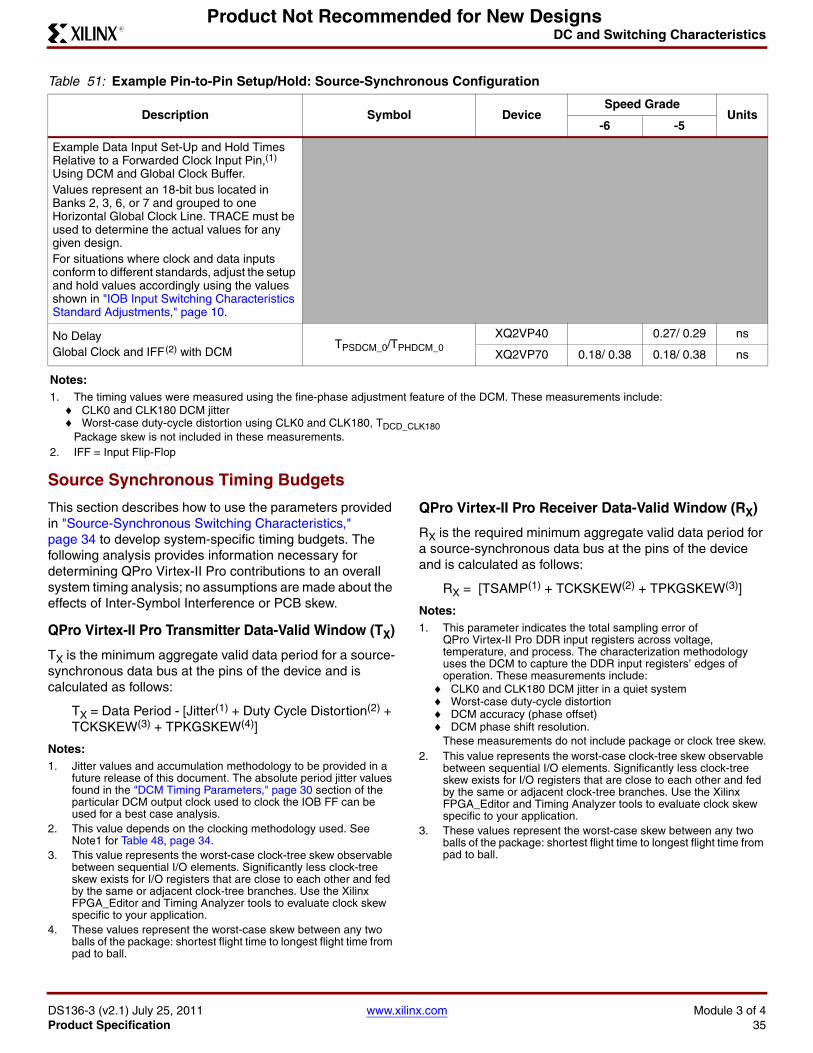
DC and Switching Characteristics
DS136-3 (v2.1) July 25, 2011 www.xilinx.com Module 3 of 4Product Specification 35
R
Product Not Recommended for New Designs
Source Synchronous Timing Budgets
This section describes how to use the parameters provided in "Source-Synchronous Switching Characteristics," page 34 to develop system-specific timing budgets. The following analysis provides information necessary for determining QPro Virtex-II Pro contributions to an overall system timing analysis; no assumptions are made about the effects of Inter-Symbol Interference or PCB skew.
QPro Virtex-II Pro Transmitter Data-Valid Window (TX)
TX is the minimum aggregate valid data period for a source-synchronous data bus at the pins of the device and is calculated as follows:
TX = Data Period - [Jitter(1) + Duty Cycle Distortion(2) + TCKSKEW(3) + TPKGSKEW(4)]
Notes: 1. Jitter values and accumulation methodology to be provided in a
future release of this document. The absolute period jitter values found in the "DCM Timing Parameters," page 30 section of the particular DCM output clock used to clock the IOB FF can be used for a best case analysis.
2. This value depends on the clocking methodology used. See Note1 for Table 48, page 34.
3. This value represents the worst-case clock-tree skew observable between sequential I/O elements. Significantly less clock-tree skew exists for I/O registers that are close to each other and fed by the same or adjacent clock-tree branches. Use the Xilinx FPGA_Editor and Timing Analyzer tools to evaluate clock skew specific to your application.
4. These values represent the worst-case skew between any two balls of the package: shortest flight time to longest flight time from pad to ball.
QPro Virtex-II Pro Receiver Data-Valid Window (RX)
RX is the required minimum aggregate valid data period for a source-synchronous data bus at the pins of the device and is calculated as follows:
RX = [TSAMP(1) + TCKSKEW(2) + TPKGSKEW(3)]
Notes: 1. This parameter indicates the total sampling error of
QPro Virtex-II Pro DDR input registers across voltage, temperature, and process. The characterization methodology uses the DCM to capture the DDR input registers’ edges of operation. These measurements include:
CLK0 and CLK180 DCM jitter in a quiet system Worst-case duty-cycle distortion DCM accuracy (phase offset) DCM phase shift resolution.
These measurements do not include package or clock tree skew.2. This value represents the worst-case clock-tree skew observable
between sequential I/O elements. Significantly less clock-tree skew exists for I/O registers that are close to each other and fed by the same or adjacent clock-tree branches. Use the Xilinx FPGA_Editor and Timing Analyzer tools to evaluate clock skew specific to your application.
3. These values represent the worst-case skew between any two balls of the package: shortest flight time to longest flight time from pad to ball.
Table 51: Example Pin-to-Pin Setup/Hold: Source-Synchronous Configuration
Description Symbol DeviceSpeed Grade
Units-6 -5
Example Data Input Set-Up and Hold Times Relative to a Forwarded Clock Input Pin,(1) Using DCM and Global Clock Buffer. Values represent an 18-bit bus located in Banks 2, 3, 6, or 7 and grouped to one Horizontal Global Clock Line. TRACE must be used to determine the actual values for any given design.For situations where clock and data inputs conform to different standards, adjust the setup and hold values accordingly using the values shown in "IOB Input Switching Characteristics Standard Adjustments," page 10.
No DelayGlobal Clock and IFF (2) with DCM
TPSDCM_0/TPHDCM_0XQ2VP40 0.27/ 0.29 ns
XQ2VP70 0.18/ 0.38 0.18/ 0.38 ns
Notes: 1. The timing values were measured using the fine-phase adjustment feature of the DCM. These measurements include:
CLK0 and CLK180 DCM jitter Worst-case duty-cycle distortion using CLK0 and CLK180, TDCD_CLK180
Package skew is not included in these measurements.2. IFF = Input Flip-Flop
DC and Switching Characteristics
DS136-3 (v2.1) July 25, 2011 www.xilinx.com Module 3 of 4Product Specification 36
R
Product Not Recommended for New Designs
Revision HistoryThis section records the change history for this module of the data sheet.
QPro Virtex-II Pro Data SheetThe QPro Virtex-II Pro Data Sheet contains the following modules:
"Introduction and Overview" (Module 1)
"Functional Description" (Module 2)
"DC and Switching Characteristics" (Module 3)
"Pinout Information" (Module 4)
Notice of DisclaimerTHE XILINX HARDWARE FPGA AND CPLD DEVICES REFERRED TO HEREIN (“PRODUCTS”) ARE SUBJECT TO THE TERMS AND CONDITIONS OF THE XILINX LIMITED WARRANTY WHICH CAN BE VIEWED AT http://www.xilinx.com/warranty.htm. THIS LIMITED WARRANTY DOES NOT EXTEND TO ANY USE OF PRODUCTS IN AN APPLICATION OR ENVIRONMENT THAT IS NOT WITHIN THE SPECIFICATIONS STATED IN THE XILINX DATA SHEET. ALL SPECIFICATIONS ARE SUBJECT TO CHANGE WITHOUT NOTICE. PRODUCTS ARE NOT DESIGNED OR INTENDED TO BE FAIL-SAFE OR FOR USE IN ANY APPLICATION REQUIRING FAIL-SAFE PERFORMANCE, SUCH AS LIFE-SUPPORT OR SAFETY DEVICES OR SYSTEMS, OR ANY OTHER APPLICATION THAT INVOKES THE POTENTIAL RISKS OF DEATH, PERSONAL INJURY, OR PROPERTY OR ENVIRONMENTAL DAMAGE (“CRITICAL APPLICATIONS”). USE OF PRODUCTS IN CRITICAL APPLICATIONS IS AT THE SOLE RISK OF CUSTOMER, SUBJECT TO APPLICABLE LAWS AND REGULATIONS.
Date Version Revision
11/29/06 1.0 Initial Xilinx release.
12/20/07 2.0 Change data sheet title. Added support for XQ2VP70-6EF1704I. Updated the values in Table 5, page 3 and Table 6, page 3. Removed support for XQV2P70-6MF1704I. Updated document template. Updated URLs.
07/25/11 2.1 Added Product Not Recommended for New Designs banner. Changed the ITRX typical value inTable 3.
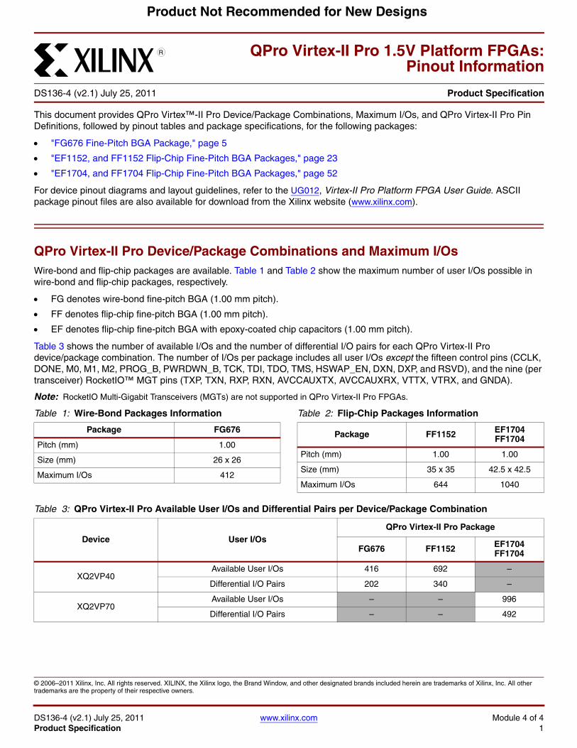
DS136-4 (v2.1) July 25, 2011 www.xilinx.com Module 4 of 4Product Specification 1
© 2006–2011 Xilinx, Inc. All rights reserved. XILINX, the Xilinx logo, the Brand Window, and other designated brands included herein are trademarks of Xilinx, Inc. All other trademarks are the property of their respective owners.
Product Not Recommended for New Designs
This document provides QPro Virtex™-II Pro Device/Package Combinations, Maximum I/Os, and QPro Virtex-II Pro Pin Definitions, followed by pinout tables and package specifications, for the following packages:
"FG676 Fine-Pitch BGA Package," page 5
"EF1152, and FF1152 Flip-Chip Fine-Pitch BGA Packages," page 23
"EF1704, and FF1704 Flip-Chip Fine-Pitch BGA Packages," page 52
For device pinout diagrams and layout guidelines, refer to the UG012, Virtex-II Pro Platform FPGA User Guide. ASCII package pinout files are also available for download from the Xilinx website (www.xilinx.com).
QPro Virtex-II Pro Device/Package Combinations and Maximum I/OsWire-bond and flip-chip packages are available. Table 1 and Table 2 show the maximum number of user I/Os possible in wire-bond and flip-chip packages, respectively.
FG denotes wire-bond fine-pitch BGA (1.00 mm pitch).
FF denotes flip-chip fine-pitch BGA (1.00 mm pitch).
EF denotes flip-chip fine-pitch BGA with epoxy-coated chip capacitors (1.00 mm pitch).
Table 3 shows the number of available I/Os and the number of differential I/O pairs for each QPro Virtex-II Pro device/package combination. The number of I/Os per package includes all user I/Os except the fifteen control pins (CCLK, DONE, M0, M1, M2, PROG_B, PWRDWN_B, TCK, TDI, TDO, TMS, HSWAP_EN, DXN, DXP, and RSVD), and the nine (per transceiver) RocketIO™ MGT pins (TXP, TXN, RXP, RXN, AVCCAUXTX, AVCCAUXRX, VTTX, VTRX, and GNDA).
Note: RocketIO Multi-Gigabit Transceivers (MGTs) are not supported in QPro Virtex-II Pro FPGAs..
94 QPro Virtex-II Pro 1.5V Platform FPGAs:
Pinout Information
DS136-4 (v2.1) July 25, 2011 Product Specification
R
Table 1: Wire-Bond Packages Information
Package FG676
Pitch (mm) 1.00
Size (mm) 26 x 26
Maximum I/Os 412
Table 2: Flip-Chip Packages Information
Package FF1152 EF1704FF1704
Pitch (mm) 1.00 1.00
Size (mm) 35 x 35 42.5 x 42.5
Maximum I/Os 644 1040
Table 3: QPro Virtex-II Pro Available User I/Os and Differential Pairs per Device/Package Combination
Device User I/OsQPro Virtex-II Pro Package
FG676 FF1152 EF1704FF1704
XQ2VP40Available User I/Os 416 692 –
Differential I/O Pairs 202 340 –
XQ2VP70Available User I/Os – – 996
Differential I/O Pairs – – 492
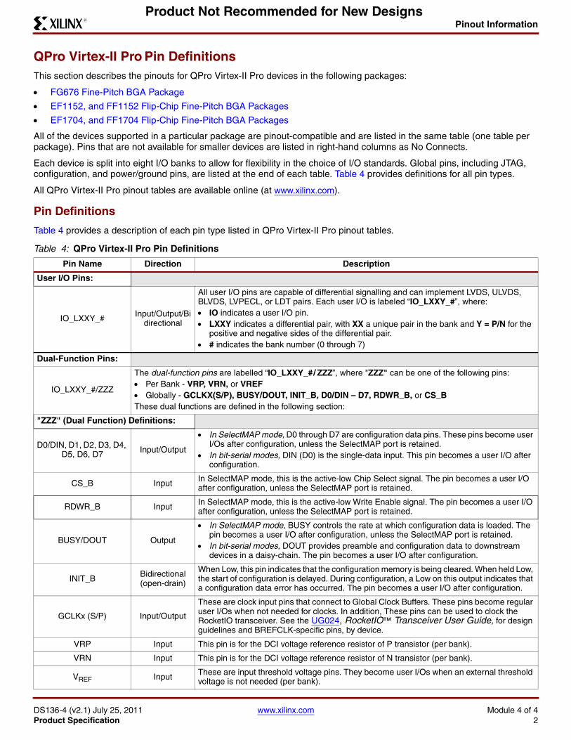
Pinout Information
DS136-4 (v2.1) July 25, 2011 www.xilinx.com Module 4 of 4Product Specification 2
R
Product Not Recommended for New Designs
QPro Virtex-II Pro Pin DefinitionsThis section describes the pinouts for QPro Virtex-II Pro devices in the following packages:
FG676 Fine-Pitch BGA Package
EF1152, and FF1152 Flip-Chip Fine-Pitch BGA Packages
EF1704, and FF1704 Flip-Chip Fine-Pitch BGA Packages
All of the devices supported in a particular package are pinout-compatible and are listed in the same table (one table per package). Pins that are not available for smaller devices are listed in right-hand columns as No Connects.
Each device is split into eight I/O banks to allow for flexibility in the choice of I/O standards. Global pins, including JTAG, configuration, and power/ground pins, are listed at the end of each table. Table 4 provides definitions for all pin types.
All QPro Virtex-II Pro pinout tables are available online (at www.xilinx.com).
Pin Definitions
Table 4 provides a description of each pin type listed in QPro Virtex-II Pro pinout tables.
Table 4: QPro Virtex-II Pro Pin Definitions
Pin Name Direction Description
User I/O Pins:
IO_LXXY_# Input/Output/Bidirectional
All user I/O pins are capable of differential signalling and can implement LVDS, ULVDS, BLVDS, LVPECL, or LDT pairs. Each user I/O is labeled “IO_LXXY_#”, where: IO indicates a user I/O pin. LXXY indicates a differential pair, with XX a unique pair in the bank and Y = P/N for the
positive and negative sides of the differential pair. # indicates the bank number (0 through 7)
Dual-Function Pins:
IO_LXXY_#/ZZZ
The dual-function pins are labelled “IO_LXXY_# / ZZZ”, where "ZZZ" can be one of the following pins: Per Bank - VRP, VRN, or VREF Globally - GCLKX(S/P), BUSY/DOUT, INIT_B, D0/DIN – D7, RDWR_B, or CS_B These dual functions are defined in the following section:
"ZZZ" (Dual Function) Definitions:
D0/DIN, D1, D2, D3, D4, D5, D6, D7 Input/Output
In SelectMAP mode, D0 through D7 are configuration data pins. These pins become user I/Os after configuration, unless the SelectMAP port is retained.
In bit-serial modes, DIN (D0) is the single-data input. This pin becomes a user I/O after configuration.
CS_B Input In SelectMAP mode, this is the active-low Chip Select signal. The pin becomes a user I/O after configuration, unless the SelectMAP port is retained.
RDWR_B Input In SelectMAP mode, this is the active-low Write Enable signal. The pin becomes a user I/O after configuration, unless the SelectMAP port is retained.
BUSY/DOUT Output
In SelectMAP mode, BUSY controls the rate at which configuration data is loaded. The pin becomes a user I/O after configuration, unless the SelectMAP port is retained.
In bit-serial modes, DOUT provides preamble and configuration data to downstream devices in a daisy-chain. The pin becomes a user I/O after configuration.
INIT_B Bidirectional (open-drain)
When Low, this pin indicates that the configuration memory is being cleared. When held Low, the start of configuration is delayed. During configuration, a Low on this output indicates that a configuration data error has occurred. The pin becomes a user I/O after configuration.
GCLKx (S/P) Input/Output
These are clock input pins that connect to Global Clock Buffers. These pins become regular user I/Os when not needed for clocks. In addition, These pins can be used to clock the RocketIO transceiver. See the UG024, RocketIO™ Transceiver User Guide, for design guidelines and BREFCLK-specific pins, by device.
VRP Input This pin is for the DCI voltage reference resistor of P transistor (per bank).
VRN Input This pin is for the DCI voltage reference resistor of N transistor (per bank).
VREF Input These are input threshold voltage pins. They become user I/Os when an external threshold voltage is not needed (per bank).
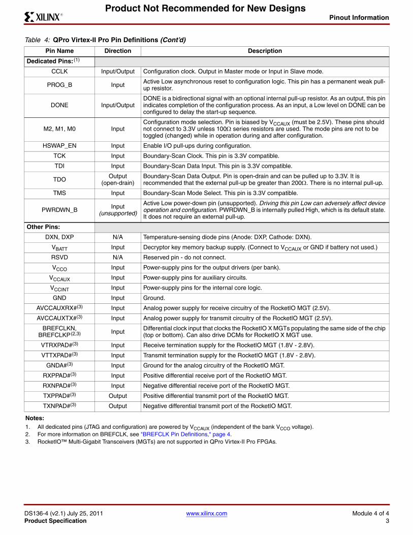
Pinout Information
DS136-4 (v2.1) July 25, 2011 www.xilinx.com Module 4 of 4Product Specification 3
R
Product Not Recommended for New Designs
Dedicated Pins: (1)
CCLK Input/Output Configuration clock. Output in Master mode or Input in Slave mode.
PROG_B Input Active Low asynchronous reset to configuration logic. This pin has a permanent weak pull-up resistor.
DONE Input/OutputDONE is a bidirectional signal with an optional internal pull-up resistor. As an output, this pin indicates completion of the configuration process. As an input, a Low level on DONE can be configured to delay the start-up sequence.
M2, M1, M0 InputConfiguration mode selection. Pin is biased by VCCAUX (must be 2.5V). These pins should not connect to 3.3V unless 100 series resistors are used. The mode pins are not to be toggled (changed) while in operation during and after configuration.
HSWAP_EN Input Enable I/O pull-ups during configuration.
TCK Input Boundary-Scan Clock. This pin is 3.3V compatible.
TDI Input Boundary-Scan Data Input. This pin is 3.3V compatible.
TDO Output(open-drain)
Boundary-Scan Data Output. Pin is open-drain and can be pulled up to 3.3V. It is recommended that the external pull-up be greater than 200. There is no internal pull-up.
TMS Input Boundary-Scan Mode Select. This pin is 3.3V compatible.
PWRDWN_B Input(unsupported)
Active Low power-down pin (unsupported). Driving this pin Low can adversely affect device operation and configuration. PWRDWN_B is internally pulled High, which is its default state. It does not require an external pull-up.
Other Pins:
DXN, DXP N/A Temperature-sensing diode pins (Anode: DXP, Cathode: DXN).
VBATT Input Decryptor key memory backup supply. (Connect to VCCAUX or GND if battery not used.)
RSVD N/A Reserved pin - do not connect.
VCCO Input Power-supply pins for the output drivers (per bank).
VCCAUX Input Power-supply pins for auxiliary circuits.
VCCINT Input Power-supply pins for the internal core logic.
GND Input Ground.
AVCCAUXRX#(3) Input Analog power supply for receive circuitry of the RocketIO MGT (2.5V).
AVCCAUXTX#(3) Input Analog power supply for transmit circuitry of the RocketIO MGT (2.5V).
BREFCLKN, BREFCLKP (2,3) Input Differential clock input that clocks the RocketIO X MGTs populating the same side of the chip
(top or bottom). Can also drive DCMs for RocketIO X MGT use.
VTRXPAD#(3) Input Receive termination supply for the RocketIO MGT (1.8V - 2.8V).
VTTXPAD#(3) Input Transmit termination supply for the RocketIO MGT (1.8V - 2.8V).
GNDA#(3) Input Ground for the analog circuitry of the RocketIO MGT.
RXPPAD#(3) Input Positive differential receive port of the RocketIO MGT.
RXNPAD#(3) Input Negative differential receive port of the RocketIO MGT.
TXPPAD#(3) Output Positive differential transmit port of the RocketIO MGT.
TXNPAD#(3) Output Negative differential transmit port of the RocketIO MGT.
Notes: 1. All dedicated pins (JTAG and configuration) are powered by VCCAUX (independent of the bank VCCO voltage).2. For more information on BREFCLK, see "BREFCLK Pin Definitions," page 4.3. RocketIO™ Multi-Gigabit Transceivers (MGTs) are not supported in QPro Virtex-II Pro FPGAs.
Table 4: QPro Virtex-II Pro Pin Definitions (Cont’d)
Pin Name Direction Description
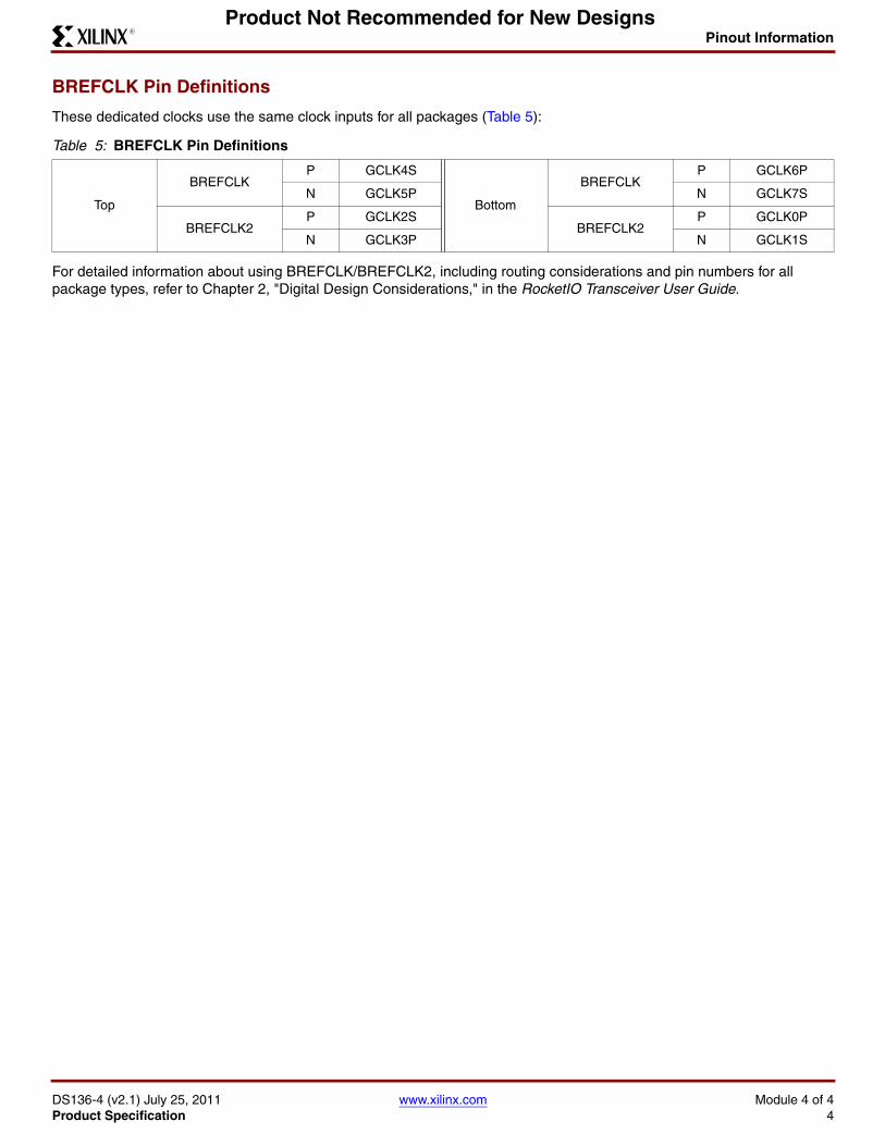
Pinout Information
DS136-4 (v2.1) July 25, 2011 www.xilinx.com Module 4 of 4Product Specification 4
R
Product Not Recommended for New Designs
BREFCLK Pin Definitions
These dedicated clocks use the same clock inputs for all packages (Table 5):
For detailed information about using BREFCLK/BREFCLK2, including routing considerations and pin numbers for all package types, refer to Chapter 2, "Digital Design Considerations," in the RocketIO Transceiver User Guide.
Table 5: BREFCLK Pin Definitions
Top
BREFCLKP GCLK4S
Bottom
BREFCLKP GCLK6P
N GCLK5P N GCLK7S
BREFCLK2P GCLK2S
BREFCLK2P GCLK0P
N GCLK3P N GCLK1S
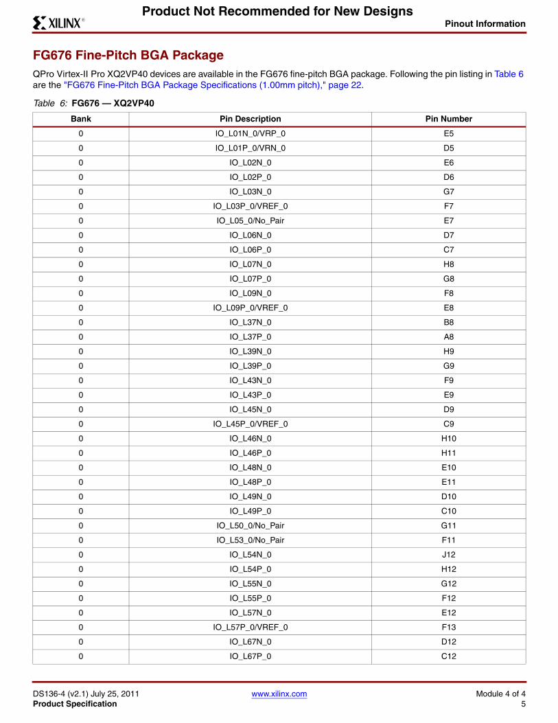
Pinout Information
DS136-4 (v2.1) July 25, 2011 www.xilinx.com Module 4 of 4Product Specification 5
R
Product Not Recommended for New Designs
FG676 Fine-Pitch BGA PackageQPro Virtex-II Pro XQ2VP40 devices are available in the FG676 fine-pitch BGA package. Following the pin listing in Table 6 are the "FG676 Fine-Pitch BGA Package Specifications (1.00mm pitch)," page 22.
Table 6: FG676 — XQ2VP40
Bank Pin Description Pin Number
0 IO_L01N_0/VRP_0 E5
0 IO_L01P_0/VRN_0 D5
0 IO_L02N_0 E6
0 IO_L02P_0 D6
0 IO_L03N_0 G7
0 IO_L03P_0/VREF_0 F7
0 IO_L05_0/No_Pair E7
0 IO_L06N_0 D7
0 IO_L06P_0 C7
0 IO_L07N_0 H8
0 IO_L07P_0 G8
0 IO_L09N_0 F8
0 IO_L09P_0/VREF_0 E8
0 IO_L37N_0 B8
0 IO_L37P_0 A8
0 IO_L39N_0 H9
0 IO_L39P_0 G9
0 IO_L43N_0 F9
0 IO_L43P_0 E9
0 IO_L45N_0 D9
0 IO_L45P_0/VREF_0 C9
0 IO_L46N_0 H10
0 IO_L46P_0 H11
0 IO_L48N_0 E10
0 IO_L48P_0 E11
0 IO_L49N_0 D10
0 IO_L49P_0 C10
0 IO_L50_0/No_Pair G11
0 IO_L53_0/No_Pair F11
0 IO_L54N_0 J12
0 IO_L54P_0 H12
0 IO_L55N_0 G12
0 IO_L55P_0 F12
0 IO_L57N_0 E12
0 IO_L57P_0/VREF_0 F13
0 IO_L67N_0 D12
0 IO_L67P_0 C12
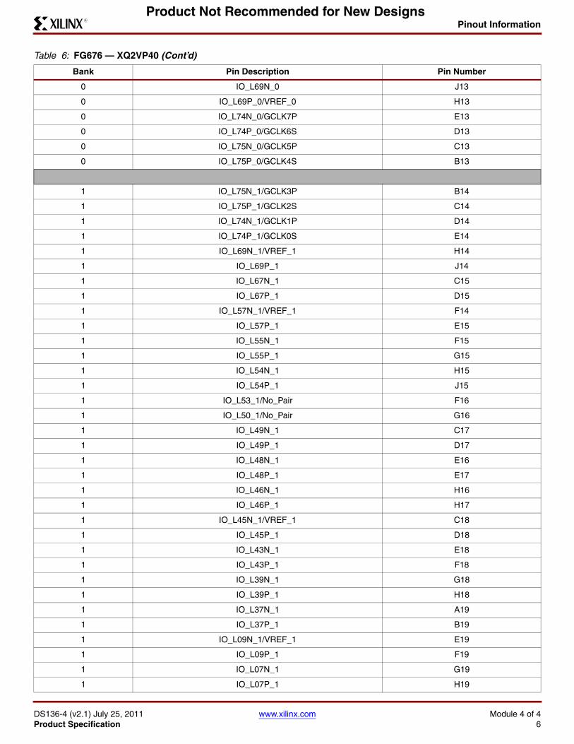
Pinout Information
DS136-4 (v2.1) July 25, 2011 www.xilinx.com Module 4 of 4Product Specification 6
R
Product Not Recommended for New Designs
0 IO_L69N_0 J13
0 IO_L69P_0/VREF_0 H13
0 IO_L74N_0/GCLK7P E13
0 IO_L74P_0/GCLK6S D13
0 IO_L75N_0/GCLK5P C13
0 IO_L75P_0/GCLK4S B13
1 IO_L75N_1/GCLK3P B14
1 IO_L75P_1/GCLK2S C14
1 IO_L74N_1/GCLK1P D14
1 IO_L74P_1/GCLK0S E14
1 IO_L69N_1/VREF_1 H14
1 IO_L69P_1 J14
1 IO_L67N_1 C15
1 IO_L67P_1 D15
1 IO_L57N_1/VREF_1 F14
1 IO_L57P_1 E15
1 IO_L55N_1 F15
1 IO_L55P_1 G15
1 IO_L54N_1 H15
1 IO_L54P_1 J15
1 IO_L53_1/No_Pair F16
1 IO_L50_1/No_Pair G16
1 IO_L49N_1 C17
1 IO_L49P_1 D17
1 IO_L48N_1 E16
1 IO_L48P_1 E17
1 IO_L46N_1 H16
1 IO_L46P_1 H17
1 IO_L45N_1/VREF_1 C18
1 IO_L45P_1 D18
1 IO_L43N_1 E18
1 IO_L43P_1 F18
1 IO_L39N_1 G18
1 IO_L39P_1 H18
1 IO_L37N_1 A19
1 IO_L37P_1 B19
1 IO_L09N_1/VREF_1 E19
1 IO_L09P_1 F19
1 IO_L07N_1 G19
1 IO_L07P_1 H19
Table 6: FG676 — XQ2VP40 (Cont’d)
Bank Pin Description Pin Number
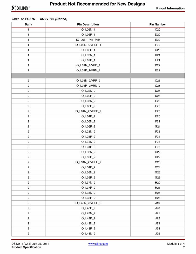
Pinout Information
DS136-4 (v2.1) July 25, 2011 www.xilinx.com Module 4 of 4Product Specification 7
R
Product Not Recommended for New Designs
1 IO_L06N_1 C20
1 IO_L06P_1 D20
1 IO_L05_1/No_Pair E20
1 IO_L03N_1/VREF_1 F20
1 IO_L03P_1 G20
1 IO_L02N_1 D21
1 IO_L02P_1 E21
1 IO_L01N_1/VRP_1 D22
1 IO_L01P_1/VRN_1 E22
2 IO_L01N_2/VRP_2 C25
2 IO_L01P_2/VRN_2 C26
2 IO_L02N_2 D25
2 IO_L02P_2 D26
2 IO_L03N_2 E23
2 IO_L03P_2 F22
2 IO_L04N_2/VREF_2 E25
2 IO_L04P_2 E26
2 IO_L06N_2 F21
2 IO_L06P_2 G21
2 IO_L24N_2 F23
2 IO_L24P_2 F24
2 IO_L31N_2 F25
2 IO_L31P_2 F26
2 IO_L32N_2 G22
2 IO_L32P_2 H22
2 IO_L34N_2/VREF_2 G23
2 IO_L34P_2 G24
2 IO_L36N_2 G25
2 IO_L36P_2 G26
2 IO_L37N_2 H20
2 IO_L37P_2 H21
2 IO_L38N_2 H25
2 IO_L38P_2 H26
2 IO_L40N_2/VREF_2 J19
2 IO_L40P_2 J20
2 IO_L42N_2 J21
2 IO_L42P_2 J22
2 IO_L43N_2 J23
2 IO_L43P_2 J24
2 IO_L44N_2 J25
Table 6: FG676 — XQ2VP40 (Cont’d)
Bank Pin Description Pin Number
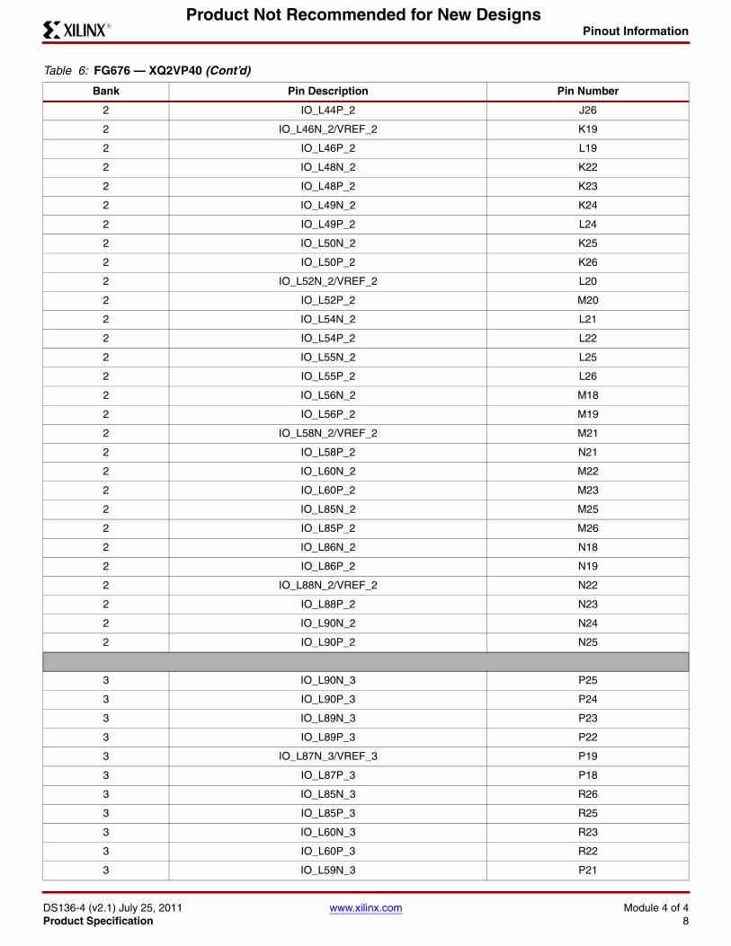
Pinout Information
DS136-4 (v2.1) July 25, 2011 www.xilinx.com Module 4 of 4Product Specification 8
R
Product Not Recommended for New Designs
2 IO_L44P_2 J26
2 IO_L46N_2/VREF_2 K19
2 IO_L46P_2 L19
2 IO_L48N_2 K22
2 IO_L48P_2 K23
2 IO_L49N_2 K24
2 IO_L49P_2 L24
2 IO_L50N_2 K25
2 IO_L50P_2 K26
2 IO_L52N_2/VREF_2 L20
2 IO_L52P_2 M20
2 IO_L54N_2 L21
2 IO_L54P_2 L22
2 IO_L55N_2 L25
2 IO_L55P_2 L26
2 IO_L56N_2 M18
2 IO_L56P_2 M19
2 IO_L58N_2/VREF_2 M21
2 IO_L58P_2 N21
2 IO_L60N_2 M22
2 IO_L60P_2 M23
2 IO_L85N_2 M25
2 IO_L85P_2 M26
2 IO_L86N_2 N18
2 IO_L86P_2 N19
2 IO_L88N_2/VREF_2 N22
2 IO_L88P_2 N23
2 IO_L90N_2 N24
2 IO_L90P_2 N25
3 IO_L90N_3 P25
3 IO_L90P_3 P24
3 IO_L89N_3 P23
3 IO_L89P_3 P22
3 IO_L87N_3/VREF_3 P19
3 IO_L87P_3 P18
3 IO_L85N_3 R26
3 IO_L85P_3 R25
3 IO_L60N_3 R23
3 IO_L60P_3 R22
3 IO_L59N_3 P21
Table 6: FG676 — XQ2VP40 (Cont’d)
Bank Pin Description Pin Number
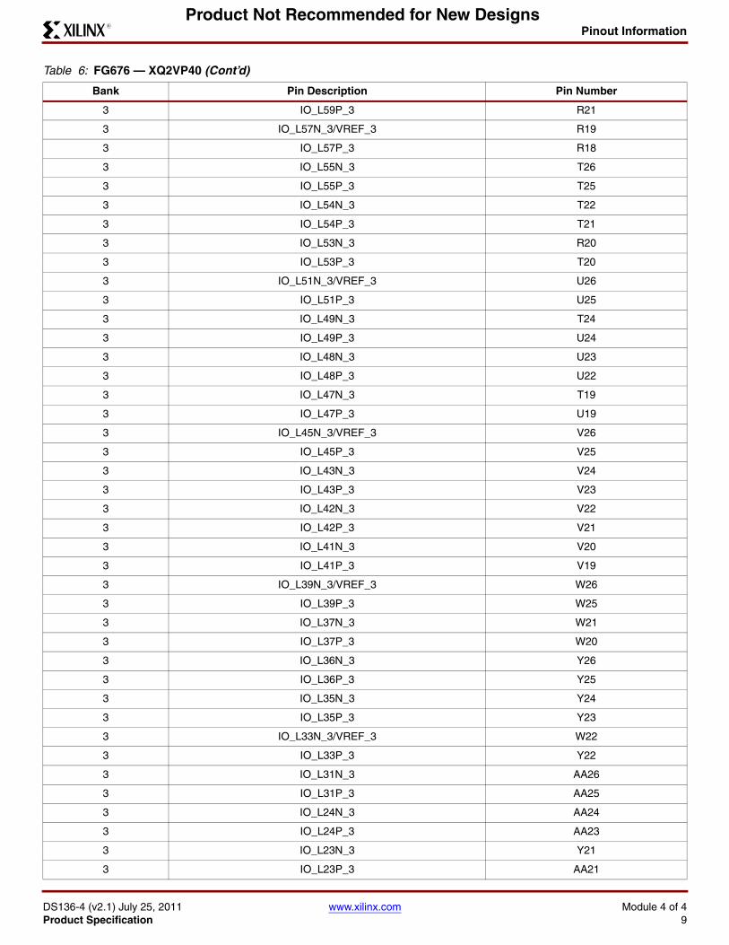
Pinout Information
DS136-4 (v2.1) July 25, 2011 www.xilinx.com Module 4 of 4Product Specification 9
R
Product Not Recommended for New Designs
3 IO_L59P_3 R21
3 IO_L57N_3/VREF_3 R19
3 IO_L57P_3 R18
3 IO_L55N_3 T26
3 IO_L55P_3 T25
3 IO_L54N_3 T22
3 IO_L54P_3 T21
3 IO_L53N_3 R20
3 IO_L53P_3 T20
3 IO_L51N_3/VREF_3 U26
3 IO_L51P_3 U25
3 IO_L49N_3 T24
3 IO_L49P_3 U24
3 IO_L48N_3 U23
3 IO_L48P_3 U22
3 IO_L47N_3 T19
3 IO_L47P_3 U19
3 IO_L45N_3/VREF_3 V26
3 IO_L45P_3 V25
3 IO_L43N_3 V24
3 IO_L43P_3 V23
3 IO_L42N_3 V22
3 IO_L42P_3 V21
3 IO_L41N_3 V20
3 IO_L41P_3 V19
3 IO_L39N_3/VREF_3 W26
3 IO_L39P_3 W25
3 IO_L37N_3 W21
3 IO_L37P_3 W20
3 IO_L36N_3 Y26
3 IO_L36P_3 Y25
3 IO_L35N_3 Y24
3 IO_L35P_3 Y23
3 IO_L33N_3/VREF_3 W22
3 IO_L33P_3 Y22
3 IO_L31N_3 AA26
3 IO_L31P_3 AA25
3 IO_L24N_3 AA24
3 IO_L24P_3 AA23
3 IO_L23N_3 Y21
3 IO_L23P_3 AA21
Table 6: FG676 — XQ2VP40 (Cont’d)
Bank Pin Description Pin Number
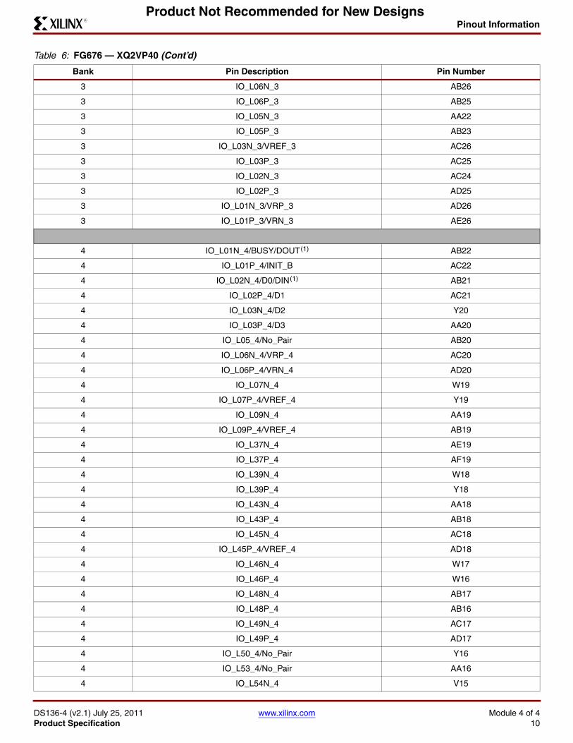
Pinout Information
DS136-4 (v2.1) July 25, 2011 www.xilinx.com Module 4 of 4Product Specification 10
R
Product Not Recommended for New Designs
3 IO_L06N_3 AB26
3 IO_L06P_3 AB25
3 IO_L05N_3 AA22
3 IO_L05P_3 AB23
3 IO_L03N_3/VREF_3 AC26
3 IO_L03P_3 AC25
3 IO_L02N_3 AC24
3 IO_L02P_3 AD25
3 IO_L01N_3/VRP_3 AD26
3 IO_L01P_3/VRN_3 AE26
4 IO_L01N_4/BUSY/DOUT (1) AB22
4 IO_L01P_4/INIT_B AC22
4 IO_L02N_4/D0/DIN (1) AB21
4 IO_L02P_4/D1 AC21
4 IO_L03N_4/D2 Y20
4 IO_L03P_4/D3 AA20
4 IO_L05_4/No_Pair AB20
4 IO_L06N_4/VRP_4 AC20
4 IO_L06P_4/VRN_4 AD20
4 IO_L07N_4 W19
4 IO_L07P_4/VREF_4 Y19
4 IO_L09N_4 AA19
4 IO_L09P_4/VREF_4 AB19
4 IO_L37N_4 AE19
4 IO_L37P_4 AF19
4 IO_L39N_4 W18
4 IO_L39P_4 Y18
4 IO_L43N_4 AA18
4 IO_L43P_4 AB18
4 IO_L45N_4 AC18
4 IO_L45P_4/VREF_4 AD18
4 IO_L46N_4 W17
4 IO_L46P_4 W16
4 IO_L48N_4 AB17
4 IO_L48P_4 AB16
4 IO_L49N_4 AC17
4 IO_L49P_4 AD17
4 IO_L50_4/No_Pair Y16
4 IO_L53_4/No_Pair AA16
4 IO_L54N_4 V15
Table 6: FG676 — XQ2VP40 (Cont’d)
Bank Pin Description Pin Number
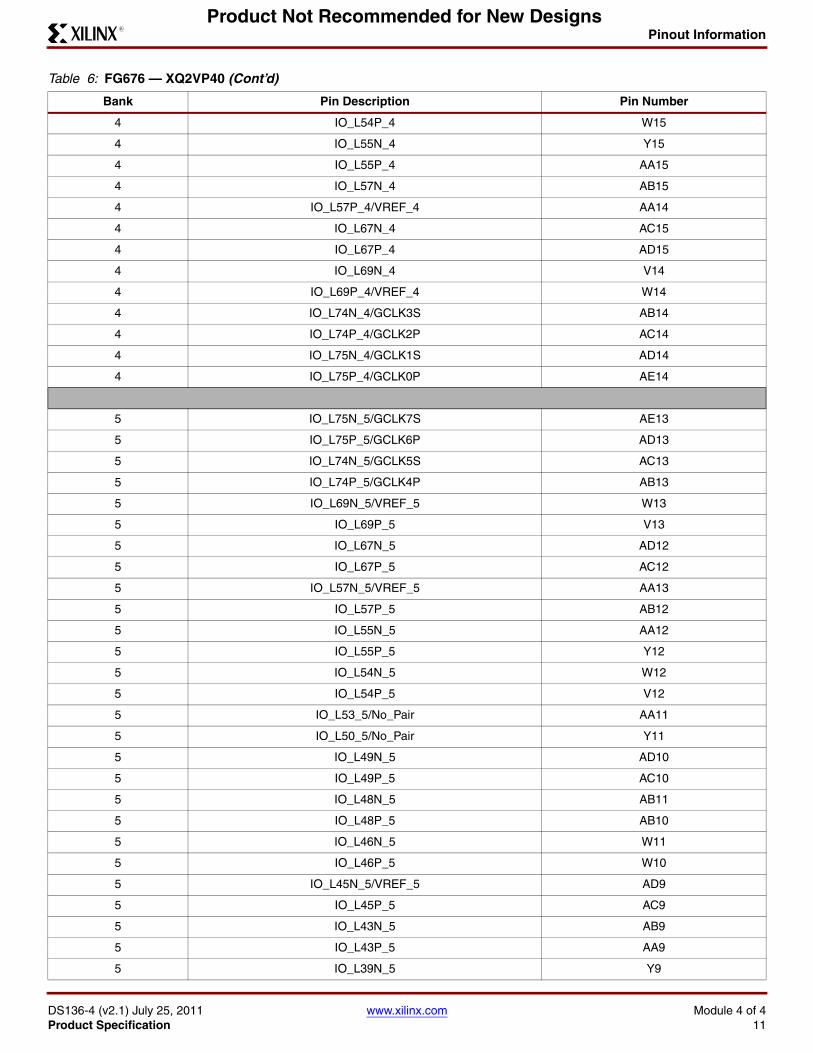
Pinout Information
DS136-4 (v2.1) July 25, 2011 www.xilinx.com Module 4 of 4Product Specification 11
R
Product Not Recommended for New Designs
4 IO_L54P_4 W15
4 IO_L55N_4 Y15
4 IO_L55P_4 AA15
4 IO_L57N_4 AB15
4 IO_L57P_4/VREF_4 AA14
4 IO_L67N_4 AC15
4 IO_L67P_4 AD15
4 IO_L69N_4 V14
4 IO_L69P_4/VREF_4 W14
4 IO_L74N_4/GCLK3S AB14
4 IO_L74P_4/GCLK2P AC14
4 IO_L75N_4/GCLK1S AD14
4 IO_L75P_4/GCLK0P AE14
5 IO_L75N_5/GCLK7S AE13
5 IO_L75P_5/GCLK6P AD13
5 IO_L74N_5/GCLK5S AC13
5 IO_L74P_5/GCLK4P AB13
5 IO_L69N_5/VREF_5 W13
5 IO_L69P_5 V13
5 IO_L67N_5 AD12
5 IO_L67P_5 AC12
5 IO_L57N_5/VREF_5 AA13
5 IO_L57P_5 AB12
5 IO_L55N_5 AA12
5 IO_L55P_5 Y12
5 IO_L54N_5 W12
5 IO_L54P_5 V12
5 IO_L53_5/No_Pair AA11
5 IO_L50_5/No_Pair Y11
5 IO_L49N_5 AD10
5 IO_L49P_5 AC10
5 IO_L48N_5 AB11
5 IO_L48P_5 AB10
5 IO_L46N_5 W11
5 IO_L46P_5 W10
5 IO_L45N_5/VREF_5 AD9
5 IO_L45P_5 AC9
5 IO_L43N_5 AB9
5 IO_L43P_5 AA9
5 IO_L39N_5 Y9
Table 6: FG676 — XQ2VP40 (Cont’d)
Bank Pin Description Pin Number
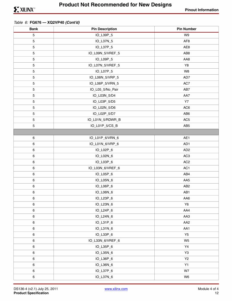
Pinout Information
DS136-4 (v2.1) July 25, 2011 www.xilinx.com Module 4 of 4Product Specification 12
R
Product Not Recommended for New Designs
5 IO_L39P_5 W9
5 IO_L37N_5 AF8
5 IO_L37P_5 AE8
5 IO_L09N_5/VREF_5 AB8
5 IO_L09P_5 AA8
5 IO_L07N_5/VREF_5 Y8
5 IO_L07P_5 W8
5 IO_L06N_5/VRP_5 AD7
5 IO_L06P_5/VRN_5 AC7
5 IO_L05_5/No_Pair AB7
5 IO_L03N_5/D4 AA7
5 IO_L03P_5/D5 Y7
5 IO_L02N_5/D6 AC6
5 IO_L02P_5/D7 AB6
5 IO_L01N_5/RDWR_B AC5
5 IO_L01P_5/CS_B AB5
6 IO_L01P_6/VRN_6 AE1
6 IO_L01N_6/VRP_6 AD1
6 IO_L02P_6 AD2
6 IO_L02N_6 AC3
6 IO_L03P_6 AC2
6 IO_L03N_6/VREF_6 AC1
6 IO_L05P_6 AB4
6 IO_L05N_6 AA5
6 IO_L06P_6 AB2
6 IO_L06N_6 AB1
6 IO_L23P_6 AA6
6 IO_L23N_6 Y6
6 IO_L24P_6 AA4
6 IO_L24N_6 AA3
6 IO_L31P_6 AA2
6 IO_L31N_6 AA1
6 IO_L33P_6 Y5
6 IO_L33N_6/VREF_6 W5
6 IO_L35P_6 Y4
6 IO_L35N_6 Y3
6 IO_L36P_6 Y2
6 IO_L36N_6 Y1
6 IO_L37P_6 W7
6 IO_L37N_6 W6
Table 6: FG676 — XQ2VP40 (Cont’d)
Bank Pin Description Pin Number
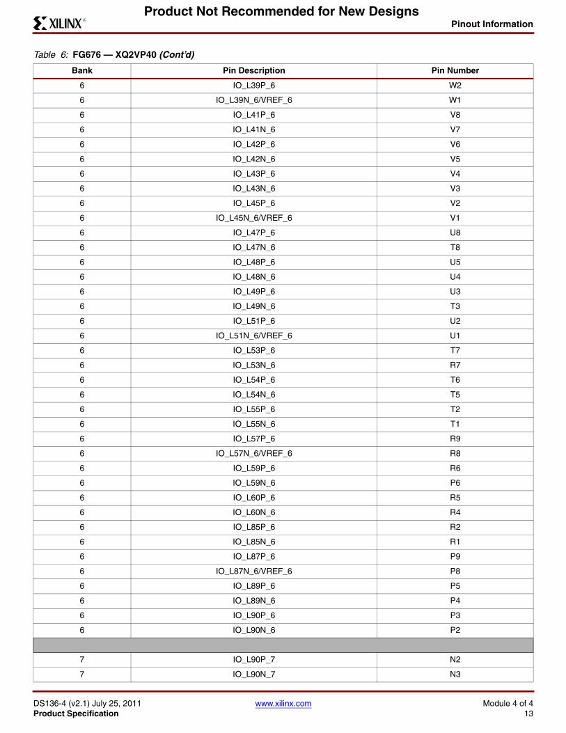
Pinout Information
DS136-4 (v2.1) July 25, 2011 www.xilinx.com Module 4 of 4Product Specification 13
R
Product Not Recommended for New Designs
6 IO_L39P_6 W2
6 IO_L39N_6/VREF_6 W1
6 IO_L41P_6 V8
6 IO_L41N_6 V7
6 IO_L42P_6 V6
6 IO_L42N_6 V5
6 IO_L43P_6 V4
6 IO_L43N_6 V3
6 IO_L45P_6 V2
6 IO_L45N_6/VREF_6 V1
6 IO_L47P_6 U8
6 IO_L47N_6 T8
6 IO_L48P_6 U5
6 IO_L48N_6 U4
6 IO_L49P_6 U3
6 IO_L49N_6 T3
6 IO_L51P_6 U2
6 IO_L51N_6/VREF_6 U1
6 IO_L53P_6 T7
6 IO_L53N_6 R7
6 IO_L54P_6 T6
6 IO_L54N_6 T5
6 IO_L55P_6 T2
6 IO_L55N_6 T1
6 IO_L57P_6 R9
6 IO_L57N_6/VREF_6 R8
6 IO_L59P_6 R6
6 IO_L59N_6 P6
6 IO_L60P_6 R5
6 IO_L60N_6 R4
6 IO_L85P_6 R2
6 IO_L85N_6 R1
6 IO_L87P_6 P9
6 IO_L87N_6/VREF_6 P8
6 IO_L89P_6 P5
6 IO_L89N_6 P4
6 IO_L90P_6 P3
6 IO_L90N_6 P2
7 IO_L90P_7 N2
7 IO_L90N_7 N3
Table 6: FG676 — XQ2VP40 (Cont’d)
Bank Pin Description Pin Number
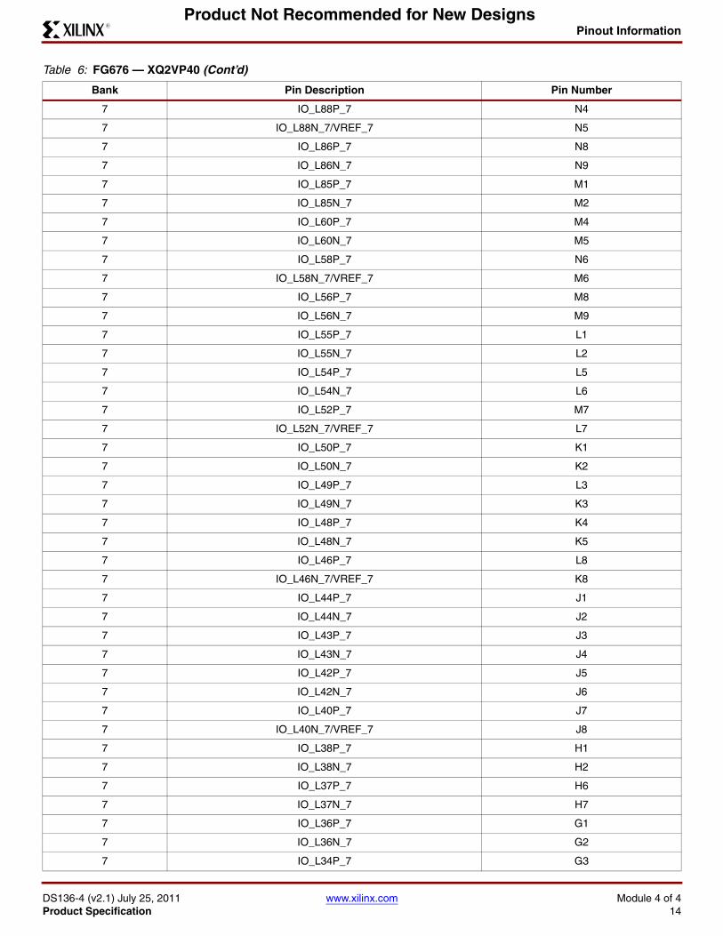
Pinout Information
DS136-4 (v2.1) July 25, 2011 www.xilinx.com Module 4 of 4Product Specification 14
R
Product Not Recommended for New Designs
7 IO_L88P_7 N4
7 IO_L88N_7/VREF_7 N5
7 IO_L86P_7 N8
7 IO_L86N_7 N9
7 IO_L85P_7 M1
7 IO_L85N_7 M2
7 IO_L60P_7 M4
7 IO_L60N_7 M5
7 IO_L58P_7 N6
7 IO_L58N_7/VREF_7 M6
7 IO_L56P_7 M8
7 IO_L56N_7 M9
7 IO_L55P_7 L1
7 IO_L55N_7 L2
7 IO_L54P_7 L5
7 IO_L54N_7 L6
7 IO_L52P_7 M7
7 IO_L52N_7/VREF_7 L7
7 IO_L50P_7 K1
7 IO_L50N_7 K2
7 IO_L49P_7 L3
7 IO_L49N_7 K3
7 IO_L48P_7 K4
7 IO_L48N_7 K5
7 IO_L46P_7 L8
7 IO_L46N_7/VREF_7 K8
7 IO_L44P_7 J1
7 IO_L44N_7 J2
7 IO_L43P_7 J3
7 IO_L43N_7 J4
7 IO_L42P_7 J5
7 IO_L42N_7 J6
7 IO_L40P_7 J7
7 IO_L40N_7/VREF_7 J8
7 IO_L38P_7 H1
7 IO_L38N_7 H2
7 IO_L37P_7 H6
7 IO_L37N_7 H7
7 IO_L36P_7 G1
7 IO_L36N_7 G2
7 IO_L34P_7 G3
Table 6: FG676 — XQ2VP40 (Cont’d)
Bank Pin Description Pin Number
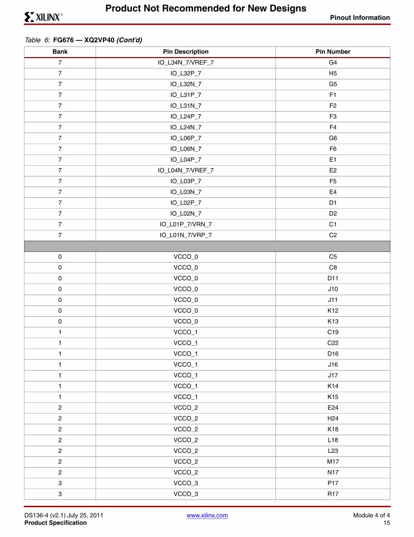
Pinout Information
DS136-4 (v2.1) July 25, 2011 www.xilinx.com Module 4 of 4Product Specification 15
R
Product Not Recommended for New Designs
7 IO_L34N_7/VREF_7 G4
7 IO_L32P_7 H5
7 IO_L32N_7 G5
7 IO_L31P_7 F1
7 IO_L31N_7 F2
7 IO_L24P_7 F3
7 IO_L24N_7 F4
7 IO_L06P_7 G6
7 IO_L06N_7 F6
7 IO_L04P_7 E1
7 IO_L04N_7/VREF_7 E2
7 IO_L03P_7 F5
7 IO_L03N_7 E4
7 IO_L02P_7 D1
7 IO_L02N_7 D2
7 IO_L01P_7/VRN_7 C1
7 IO_L01N_7/VRP_7 C2
0 VCCO_0 C5
0 VCCO_0 C8
0 VCCO_0 D11
0 VCCO_0 J10
0 VCCO_0 J11
0 VCCO_0 K12
0 VCCO_0 K13
1 VCCO_1 C19
1 VCCO_1 C22
1 VCCO_1 D16
1 VCCO_1 J16
1 VCCO_1 J17
1 VCCO_1 K14
1 VCCO_1 K15
2 VCCO_2 E24
2 VCCO_2 H24
2 VCCO_2 K18
2 VCCO_2 L18
2 VCCO_2 L23
2 VCCO_2 M17
2 VCCO_2 N17
3 VCCO_3 P17
3 VCCO_3 R17
Table 6: FG676 — XQ2VP40 (Cont’d)
Bank Pin Description Pin Number
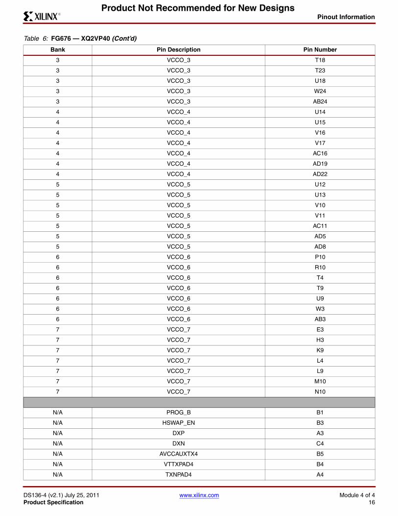
Pinout Information
DS136-4 (v2.1) July 25, 2011 www.xilinx.com Module 4 of 4Product Specification 16
R
Product Not Recommended for New Designs
3 VCCO_3 T18
3 VCCO_3 T23
3 VCCO_3 U18
3 VCCO_3 W24
3 VCCO_3 AB24
4 VCCO_4 U14
4 VCCO_4 U15
4 VCCO_4 V16
4 VCCO_4 V17
4 VCCO_4 AC16
4 VCCO_4 AD19
4 VCCO_4 AD22
5 VCCO_5 U12
5 VCCO_5 U13
5 VCCO_5 V10
5 VCCO_5 V11
5 VCCO_5 AC11
5 VCCO_5 AD5
5 VCCO_5 AD8
6 VCCO_6 P10
6 VCCO_6 R10
6 VCCO_6 T4
6 VCCO_6 T9
6 VCCO_6 U9
6 VCCO_6 W3
6 VCCO_6 AB3
7 VCCO_7 E3
7 VCCO_7 H3
7 VCCO_7 K9
7 VCCO_7 L4
7 VCCO_7 L9
7 VCCO_7 M10
7 VCCO_7 N10
N/A PROG_B B1
N/A HSWAP_EN B3
N/A DXP A3
N/A DXN C4
N/A AVCCAUXTX4 B5
N/A VTTXPAD4 B4
N/A TXNPAD4 A4
Table 6: FG676 — XQ2VP40 (Cont’d)
Bank Pin Description Pin Number
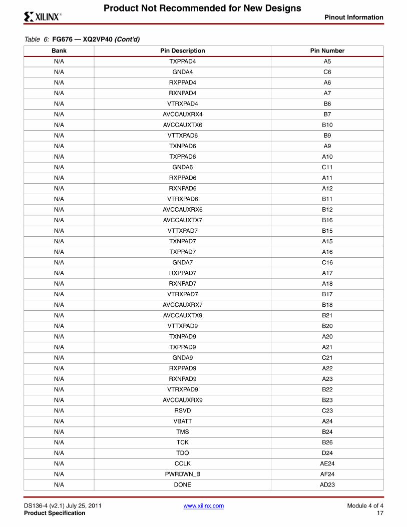
Pinout Information
DS136-4 (v2.1) July 25, 2011 www.xilinx.com Module 4 of 4Product Specification 17
R
Product Not Recommended for New Designs
N/A TXPPAD4 A5
N/A GNDA4 C6
N/A RXPPAD4 A6
N/A RXNPAD4 A7
N/A VTRXPAD4 B6
N/A AVCCAUXRX4 B7
N/A AVCCAUXTX6 B10
N/A VTTXPAD6 B9
N/A TXNPAD6 A9
N/A TXPPAD6 A10
N/A GNDA6 C11
N/A RXPPAD6 A11
N/A RXNPAD6 A12
N/A VTRXPAD6 B11
N/A AVCCAUXRX6 B12
N/A AVCCAUXTX7 B16
N/A VTTXPAD7 B15
N/A TXNPAD7 A15
N/A TXPPAD7 A16
N/A GNDA7 C16
N/A RXPPAD7 A17
N/A RXNPAD7 A18
N/A VTRXPAD7 B17
N/A AVCCAUXRX7 B18
N/A AVCCAUXTX9 B21
N/A VTTXPAD9 B20
N/A TXNPAD9 A20
N/A TXPPAD9 A21
N/A GNDA9 C21
N/A RXPPAD9 A22
N/A RXNPAD9 A23
N/A VTRXPAD9 B22
N/A AVCCAUXRX9 B23
N/A RSVD C23
N/A VBATT A24
N/A TMS B24
N/A TCK B26
N/A TDO D24
N/A CCLK AE24
N/A PWRDWN_B AF24
N/A DONE AD23
Table 6: FG676 — XQ2VP40 (Cont’d)
Bank Pin Description Pin Number
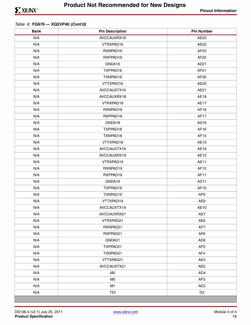
Pinout Information
DS136-4 (v2.1) July 25, 2011 www.xilinx.com Module 4 of 4Product Specification 18
R
Product Not Recommended for New Designs
N/A AVCCAUXRX16 AE23
N/A VTRXPAD16 AE22
N/A RXNPAD16 AF23
N/A RXPPAD16 AF22
N/A GNDA16 AD21
N/A TXPPAD16 AF21
N/A TXNPAD16 AF20
N/A VTTXPAD16 AE20
N/A AVCCAUXTX16 AE21
N/A AVCCAUXRX18 AE18
N/A VTRXPAD18 AE17
N/A RXNPAD18 AF18
N/A RXPPAD18 AF17
N/A GNDA18 AD16
N/A TXPPAD18 AF16
N/A TXNPAD18 AF15
N/A VTTXPAD18 AE15
N/A AVCCAUXTX18 AE16
N/A AVCCAUXRX19 AE12
N/A VTRXPAD19 AE11
N/A RXNPAD19 AF12
N/A RXPPAD19 AF11
N/A GNDA19 AD11
N/A TXPPAD19 AF10
N/A TXNPAD19 AF9
N/A VTTXPAD19 AE9
N/A AVCCAUXTX19 AE10
N/A AVCCAUXRX21 AE7
N/A VTRXPAD21 AE6
N/A RXNPAD21 AF7
N/A RXPPAD21 AF6
N/A GNDA21 AD6
N/A TXPPAD21 AF5
N/A TXNPAD21 AF4
N/A VTTXPAD21 AE4
N/A AVCCAUXTX21 AE5
N/A M2 AD4
N/A M0 AF3
N/A M1 AE3
N/A TDI D3
Table 6: FG676 — XQ2VP40 (Cont’d)
Bank Pin Description Pin Number
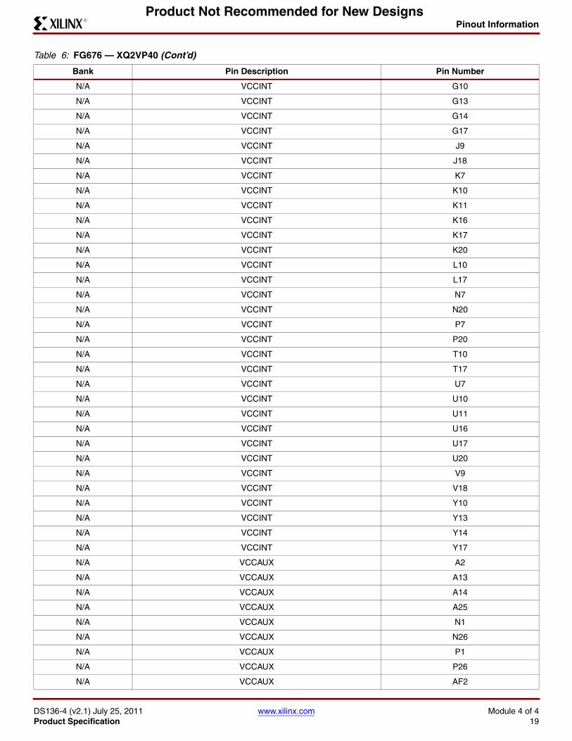
Pinout Information
DS136-4 (v2.1) July 25, 2011 www.xilinx.com Module 4 of 4Product Specification 19
R
Product Not Recommended for New Designs
N/A VCCINT G10
N/A VCCINT G13
N/A VCCINT G14
N/A VCCINT G17
N/A VCCINT J9
N/A VCCINT J18
N/A VCCINT K7
N/A VCCINT K10
N/A VCCINT K11
N/A VCCINT K16
N/A VCCINT K17
N/A VCCINT K20
N/A VCCINT L10
N/A VCCINT L17
N/A VCCINT N7
N/A VCCINT N20
N/A VCCINT P7
N/A VCCINT P20
N/A VCCINT T10
N/A VCCINT T17
N/A VCCINT U7
N/A VCCINT U10
N/A VCCINT U11
N/A VCCINT U16
N/A VCCINT U17
N/A VCCINT U20
N/A VCCINT V9
N/A VCCINT V18
N/A VCCINT Y10
N/A VCCINT Y13
N/A VCCINT Y14
N/A VCCINT Y17
N/A VCCAUX A2
N/A VCCAUX A13
N/A VCCAUX A14
N/A VCCAUX A25
N/A VCCAUX N1
N/A VCCAUX N26
N/A VCCAUX P1
N/A VCCAUX P26
N/A VCCAUX AF2
Table 6: FG676 — XQ2VP40 (Cont’d)
Bank Pin Description Pin Number
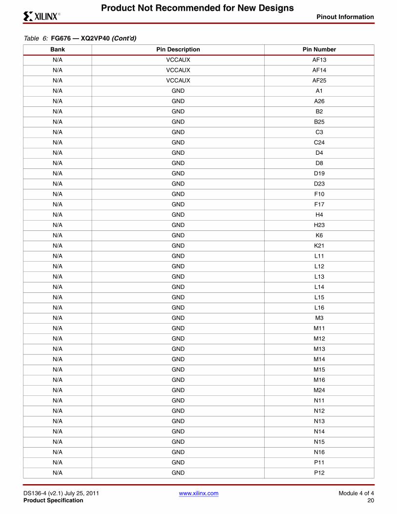
Pinout Information
DS136-4 (v2.1) July 25, 2011 www.xilinx.com Module 4 of 4Product Specification 20
R
Product Not Recommended for New Designs
N/A VCCAUX AF13
N/A VCCAUX AF14
N/A VCCAUX AF25
N/A GND A1
N/A GND A26
N/A GND B2
N/A GND B25
N/A GND C3
N/A GND C24
N/A GND D4
N/A GND D8
N/A GND D19
N/A GND D23
N/A GND F10
N/A GND F17
N/A GND H4
N/A GND H23
N/A GND K6
N/A GND K21
N/A GND L11
N/A GND L12
N/A GND L13
N/A GND L14
N/A GND L15
N/A GND L16
N/A GND M3
N/A GND M11
N/A GND M12
N/A GND M13
N/A GND M14
N/A GND M15
N/A GND M16
N/A GND M24
N/A GND N11
N/A GND N12
N/A GND N13
N/A GND N14
N/A GND N15
N/A GND N16
N/A GND P11
N/A GND P12
Table 6: FG676 — XQ2VP40 (Cont’d)
Bank Pin Description Pin Number
Pinout Information
DS136-4 (v2.1) July 25, 2011 www.xilinx.com Module 4 of 4Product Specification 21
R
Product Not Recommended for New Designs
N/A GND P13
N/A GND P14
N/A GND P15
N/A GND P16
N/A GND R3
N/A GND R11
N/A GND R12
N/A GND R13
N/A GND R14
N/A GND R15
N/A GND R16
N/A GND R24
N/A GND T11
N/A GND T12
N/A GND T13
N/A GND T14
N/A GND T15
N/A GND T16
N/A GND U6
N/A GND U21
N/A GND W4
N/A GND W23
N/A GND AA10
N/A GND AA17
N/A GND AC4
N/A GND AC8
N/A GND AC19
N/A GND AC23
N/A GND AD3
N/A GND AD24
N/A GND AE2
N/A GND AE25
N/A GND AF1
N/A GND AF26
Notes: 1. See Table 4, page 2 for an explanation of the signals available on this pin.
Table 6: FG676 — XQ2VP40 (Cont’d)
Bank Pin Description Pin Number
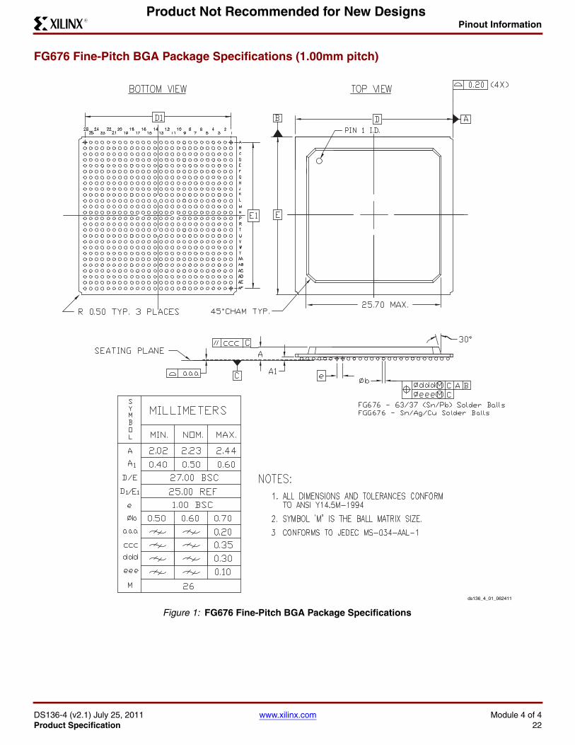
Pinout Information
DS136-4 (v2.1) July 25, 2011 www.xilinx.com Module 4 of 4Product Specification 22
R
Product Not Recommended for New Designs
FG676 Fine-Pitch BGA Package Specifications (1.00mm pitch)X-Ref Target - Figure 1
Figure 1: FG676 Fine-Pitch BGA Package Specifications
ds136_4_01_062411
Pinout Information
DS136-4 (v2.1) July 25, 2011 www.xilinx.com Module 4 of 4Product Specification 23
R
Product Not Recommended for New Designs
EF1152, and FF1152 Flip-Chip Fine-Pitch BGA PackagesQPro Virtex-II Pro XQ2VP40 devices are available in the FF1152 and EF1152 flip-chip fine-pitch BGA packages. Following the pin listing in Table 7 are the "EF1152, and FF1152 Flip-Chip Fine-Pitch BGA Package Specifications (1.00mm pitch)," page 51.
Table 7: EF1152 and FF1152 — XQ2VP40
Bank Pin Description Pin Number No Connects
0 IO_L01N_0/VRP_0 E29
0 IO_L01P_0/VRN_0 E28
0 IO_L02N_0 H26
0 IO_L02P_0 G26
0 IO_L03N_0 H25
0 IO_L03P_0/VREF_0 G25
0 IO_L05_0/No_Pair J25
0 IO_L06N_0 K24
0 IO_L06P_0 J24
0 IO_L07N_0 F26
0 IO_L07P_0 E26
0 IO_L08N_0 D30
0 IO_L08P_0 D29
0 IO_L09N_0 K23
0 IO_L09P_0/VREF_0 J23
0 IO_L19N_0 F24
0 IO_L19P_0 E24
0 IO_L20N_0 D28
0 IO_L20P_0 C28
0 IO_L21N_0 H24
0 IO_L21P_0 G24
0 IO_L25N_0 G23
0 IO_L25P_0 F23
0 IO_L26N_0 E27
0 IO_L26P_0 D27
0 IO_L27N_0 K22
0 IO_L27P_0/VREF_0 J22
0 IO_L37N_0 H22
0 IO_L37P_0 G22
0 IO_L38N_0 D26
0 IO_L38P_0 C26
0 IO_L39N_0 K21
0 IO_L39P_0 J21
0 IO_L43N_0 F22
0 IO_L43P_0 E22
0 IO_L44N_0 E25
0 IO_L44P_0 D25
0 IO_L45N_0 H21
Pinout Information
DS136-4 (v2.1) July 25, 2011 www.xilinx.com Module 4 of 4Product Specification 24
R
Product Not Recommended for New Designs
0 IO_L45P_0/VREF_0 G21
0 IO_L46N_0 D22
0 IO_L46P_0 D23
0 IO_L47N_0 D24
0 IO_L47P_0 C24
0 IO_L48N_0 K20
0 IO_L48P_0 J20
0 IO_L49N_0 F21
0 IO_L49P_0 E21
0 IO_L50_0/No_Pair C21
0 IO_L53_0/No_Pair C22
0 IO_L54N_0 L19
0 IO_L54P_0 K19
0 IO_L55N_0 G20
0 IO_L55P_0 F20
0 IO_L56N_0 D21
0 IO_L56P_0 D20
0 IO_L57N_0 J19
0 IO_L57P_0/VREF_0 H19
0 IO_L67N_0 G19
0 IO_L67P_0 F19
0 IO_L68N_0 E19
0 IO_L68P_0 D19
0 IO_L69N_0 L18
0 IO_L69P_0/VREF_0 K18
0 IO_L73N_0 G18
0 IO_L73P_0 F18
0 IO_L74N_0/GCLK7P E18
0 IO_L74P_0/GCLK6S D18
0 IO_L75N_0/GCLK5P J18
0 IO_L75P_0/GCLK4S H18
1 IO_L75N_1/GCLK3P H17
1 IO_L75P_1/GCLK2S J17
1 IO_L74N_1/GCLK1P D17
1 IO_L74P_1/GCLK0S E17
1 IO_L73N_1 F17
1 IO_L73P_1 G17
1 IO_L69N_1/VREF_1 K17
1 IO_L69P_1 L17
1 IO_L68N_1 D16
1 IO_L68P_1 E16
Table 7: EF1152 and FF1152 — XQ2VP40 (Cont’d)
Bank Pin Description Pin Number No Connects

Pinout Information
DS136-4 (v2.1) July 25, 2011 www.xilinx.com Module 4 of 4Product Specification 25
R
Product Not Recommended for New Designs
1 IO_L67N_1 F16
1 IO_L67P_1 G16
1 IO_L57N_1/VREF_1 H16
1 IO_L57P_1 J16
1 IO_L56N_1 D15
1 IO_L56P_1 D14
1 IO_L55N_1 F15
1 IO_L55P_1 G15
1 IO_L54N_1 K16
1 IO_L54P_1 L16
1 IO_L53_1/No_Pair C13
1 IO_L50_1/No_Pair C14
1 IO_L49N_1 E14
1 IO_L49P_1 F14
1 IO_L48N_1 J15
1 IO_L48P_1 K15
1 IO_L47N_1 C11
1 IO_L47P_1 D11
1 IO_L46N_1 D12
1 IO_L46P_1 D13
1 IO_L45N_1/VREF_1 G14
1 IO_L45P_1 H14
1 IO_L44N_1 D10
1 IO_L44P_1 E10
1 IO_L43N_1 E13
1 IO_L43P_1 F13
1 IO_L39N_1 J14
1 IO_L39P_1 K14
1 IO_L38N_1 C9
1 IO_L38P_1 D9
1 IO_L37N_1 G13
1 IO_L37P_1 H13
1 IO_L27N_1/VREF_1 J13
1 IO_L27P_1 K13
1 IO_L26N_1 D8
1 IO_L26P_1 E8
1 IO_L25N_1 F12
1 IO_L25P_1 G12
1 IO_L21N_1 G11
1 IO_L21P_1 H11
1 IO_L20N_1 C7
1 IO_L20P_1 D7
Table 7: EF1152 and FF1152 — XQ2VP40 (Cont’d)
Bank Pin Description Pin Number No Connects
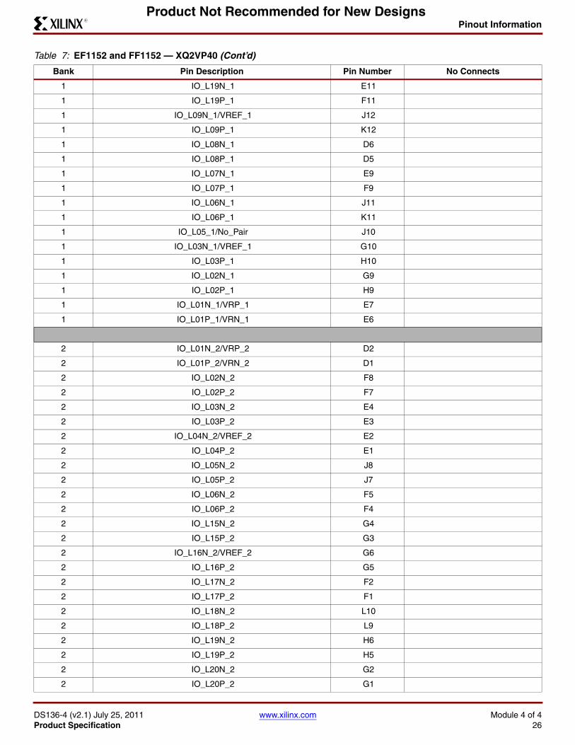
Pinout Information
DS136-4 (v2.1) July 25, 2011 www.xilinx.com Module 4 of 4Product Specification 26
R
Product Not Recommended for New Designs
1 IO_L19N_1 E11
1 IO_L19P_1 F11
1 IO_L09N_1/VREF_1 J12
1 IO_L09P_1 K12
1 IO_L08N_1 D6
1 IO_L08P_1 D5
1 IO_L07N_1 E9
1 IO_L07P_1 F9
1 IO_L06N_1 J11
1 IO_L06P_1 K11
1 IO_L05_1/No_Pair J10
1 IO_L03N_1/VREF_1 G10
1 IO_L03P_1 H10
1 IO_L02N_1 G9
1 IO_L02P_1 H9
1 IO_L01N_1/VRP_1 E7
1 IO_L01P_1/VRN_1 E6
2 IO_L01N_2/VRP_2 D2
2 IO_L01P_2/VRN_2 D1
2 IO_L02N_2 F8
2 IO_L02P_2 F7
2 IO_L03N_2 E4
2 IO_L03P_2 E3
2 IO_L04N_2/VREF_2 E2
2 IO_L04P_2 E1
2 IO_L05N_2 J8
2 IO_L05P_2 J7
2 IO_L06N_2 F5
2 IO_L06P_2 F4
2 IO_L15N_2 G4
2 IO_L15P_2 G3
2 IO_L16N_2/VREF_2 G6
2 IO_L16P_2 G5
2 IO_L17N_2 F2
2 IO_L17P_2 F1
2 IO_L18N_2 L10
2 IO_L18P_2 L9
2 IO_L19N_2 H6
2 IO_L19P_2 H5
2 IO_L20N_2 G2
2 IO_L20P_2 G1
Table 7: EF1152 and FF1152 — XQ2VP40 (Cont’d)
Bank Pin Description Pin Number No Connects

Pinout Information
DS136-4 (v2.1) July 25, 2011 www.xilinx.com Module 4 of 4Product Specification 27
R
Product Not Recommended for New Designs
2 IO_L21N_2 J6
2 IO_L21P_2 J5
2 IO_L22N_2/VREF_2 J4
2 IO_L22P_2 J3
2 IO_L23N_2 K8
2 IO_L23P_2 K7
2 IO_L24N_2 H4
2 IO_L24P_2 H3
2 IO_L31N_2 H2
2 IO_L31P_2 H1
2 IO_L32N_2 M10
2 IO_L32P_2 M9
2 IO_L33N_2 K5
2 IO_L33P_2 K4
2 IO_L34N_2/VREF_2 J2
2 IO_L34P_2 K2
2 IO_L35N_2 L8
2 IO_L35P_2 L7
2 IO_L36N_2 L6
2 IO_L36P_2 L5
2 IO_L37N_2 K1
2 IO_L37P_2 L1
2 IO_L38N_2 N10
2 IO_L38P_2 N9
2 IO_L39N_2 M7
2 IO_L39P_2 M6
2 IO_L40N_2/VREF_2 L2
2 IO_L40P_2 M2
2 IO_L41N_2 N8
2 IO_L41P_2 N7
2 IO_L42N_2 L4
2 IO_L42P_2 L3
2 IO_L43N_2 M4
2 IO_L43P_2 M3
2 IO_L44N_2 P10
2 IO_L44P_2 P9
2 IO_L45N_2 N6
2 IO_L45P_2 N5
2 IO_L46N_2/VREF_2 M1
2 IO_L46P_2 N1
2 IO_L47N_2 P8
2 IO_L47P_2 P7
Table 7: EF1152 and FF1152 — XQ2VP40 (Cont’d)
Bank Pin Description Pin Number No Connects
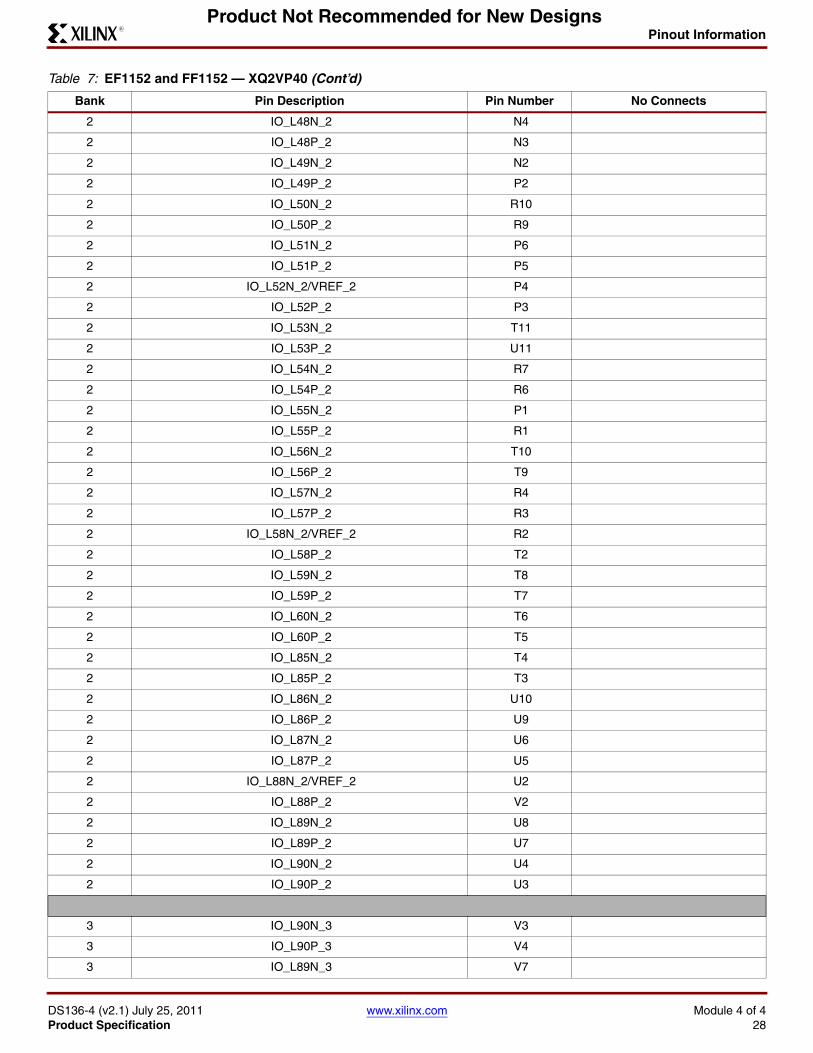
Pinout Information
DS136-4 (v2.1) July 25, 2011 www.xilinx.com Module 4 of 4Product Specification 28
R
Product Not Recommended for New Designs
2 IO_L48N_2 N4
2 IO_L48P_2 N3
2 IO_L49N_2 N2
2 IO_L49P_2 P2
2 IO_L50N_2 R10
2 IO_L50P_2 R9
2 IO_L51N_2 P6
2 IO_L51P_2 P5
2 IO_L52N_2/VREF_2 P4
2 IO_L52P_2 P3
2 IO_L53N_2 T11
2 IO_L53P_2 U11
2 IO_L54N_2 R7
2 IO_L54P_2 R6
2 IO_L55N_2 P1
2 IO_L55P_2 R1
2 IO_L56N_2 T10
2 IO_L56P_2 T9
2 IO_L57N_2 R4
2 IO_L57P_2 R3
2 IO_L58N_2/VREF_2 R2
2 IO_L58P_2 T2
2 IO_L59N_2 T8
2 IO_L59P_2 T7
2 IO_L60N_2 T6
2 IO_L60P_2 T5
2 IO_L85N_2 T4
2 IO_L85P_2 T3
2 IO_L86N_2 U10
2 IO_L86P_2 U9
2 IO_L87N_2 U6
2 IO_L87P_2 U5
2 IO_L88N_2/VREF_2 U2
2 IO_L88P_2 V2
2 IO_L89N_2 U8
2 IO_L89P_2 U7
2 IO_L90N_2 U4
2 IO_L90P_2 U3
3 IO_L90N_3 V3
3 IO_L90P_3 V4
3 IO_L89N_3 V7
Table 7: EF1152 and FF1152 — XQ2VP40 (Cont’d)
Bank Pin Description Pin Number No Connects
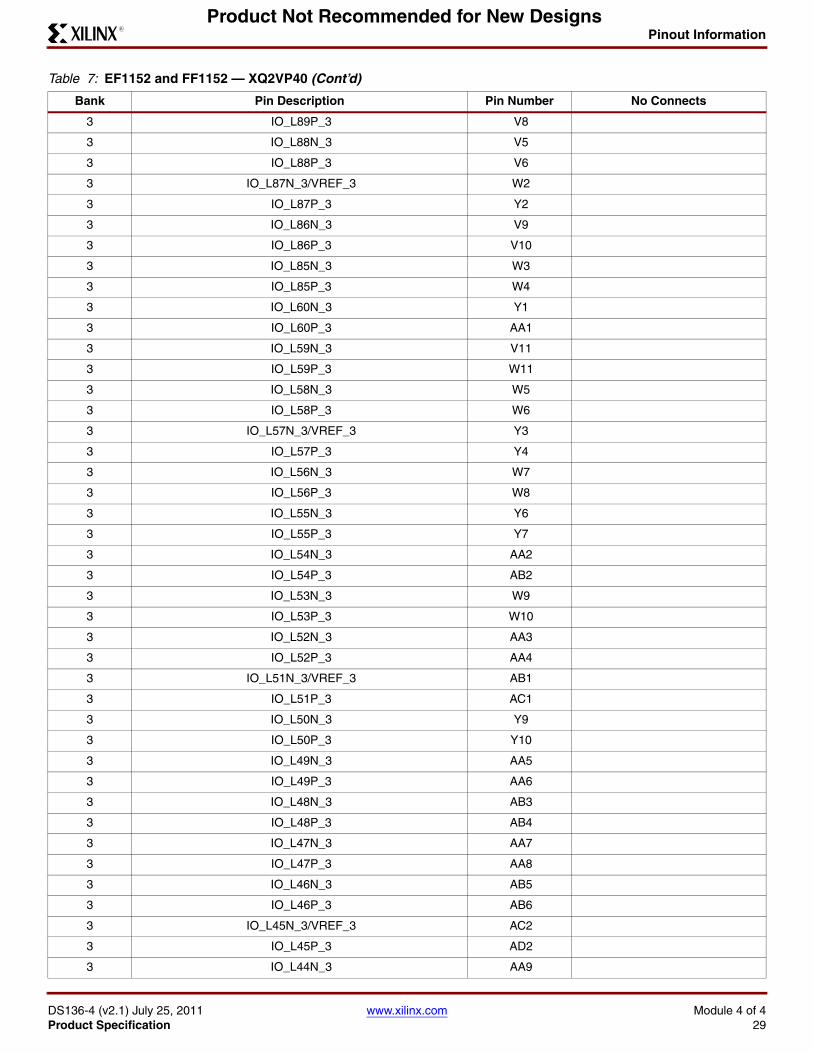
Pinout Information
DS136-4 (v2.1) July 25, 2011 www.xilinx.com Module 4 of 4Product Specification 29
R
Product Not Recommended for New Designs
3 IO_L89P_3 V8
3 IO_L88N_3 V5
3 IO_L88P_3 V6
3 IO_L87N_3/VREF_3 W2
3 IO_L87P_3 Y2
3 IO_L86N_3 V9
3 IO_L86P_3 V10
3 IO_L85N_3 W3
3 IO_L85P_3 W4
3 IO_L60N_3 Y1
3 IO_L60P_3 AA1
3 IO_L59N_3 V11
3 IO_L59P_3 W11
3 IO_L58N_3 W5
3 IO_L58P_3 W6
3 IO_L57N_3/VREF_3 Y3
3 IO_L57P_3 Y4
3 IO_L56N_3 W7
3 IO_L56P_3 W8
3 IO_L55N_3 Y6
3 IO_L55P_3 Y7
3 IO_L54N_3 AA2
3 IO_L54P_3 AB2
3 IO_L53N_3 W9
3 IO_L53P_3 W10
3 IO_L52N_3 AA3
3 IO_L52P_3 AA4
3 IO_L51N_3/VREF_3 AB1
3 IO_L51P_3 AC1
3 IO_L50N_3 Y9
3 IO_L50P_3 Y10
3 IO_L49N_3 AA5
3 IO_L49P_3 AA6
3 IO_L48N_3 AB3
3 IO_L48P_3 AB4
3 IO_L47N_3 AA7
3 IO_L47P_3 AA8
3 IO_L46N_3 AB5
3 IO_L46P_3 AB6
3 IO_L45N_3/VREF_3 AC2
3 IO_L45P_3 AD2
3 IO_L44N_3 AA9
Table 7: EF1152 and FF1152 — XQ2VP40 (Cont’d)
Bank Pin Description Pin Number No Connects

Pinout Information
DS136-4 (v2.1) July 25, 2011 www.xilinx.com Module 4 of 4Product Specification 30
R
Product Not Recommended for New Designs
3 IO_L44P_3 AA10
3 IO_L43N_3 AC3
3 IO_L43P_3 AC4
3 IO_L42N_3 AD1
3 IO_L42P_3 AE1
3 IO_L41N_3 AB7
3 IO_L41P_3 AB8
3 IO_L40N_3 AC6
3 IO_L40P_3 AC7
3 IO_L39N_3/VREF_3 AD3
3 IO_L39P_3 AD4
3 IO_L38N_3 AB9
3 IO_L38P_3 AB10
3 IO_L37N_3 AD5
3 IO_L37P_3 AD6
3 IO_L36N_3 AE2
3 IO_L36P_3 AF2
3 IO_L35N_3 AD7
3 IO_L35P_3 AD8
3 IO_L34N_3 AE4
3 IO_L34P_3 AE5
3 IO_L33N_3/VREF_3 AG1
3 IO_L33P_3 AG2
3 IO_L32N_3 AC9
3 IO_L32P_3 AC10
3 IO_L31N_3 AF3
3 IO_L31P_3 AF4
3 IO_L24N_3 AH1
3 IO_L24P_3 AH2
3 IO_L23N_3 AE7
3 IO_L23P_3 AE8
3 IO_L22N_3 AF5
3 IO_L22P_3 AF6
3 IO_L21N_3/VREF_3 AG3
3 IO_L21P_3 AG4
3 IO_L20N_3 AD9
3 IO_L20P_3 AD10
3 IO_L19N_3 AH3
3 IO_L19P_3 AH4
3 IO_L18N_3 AJ1
3 IO_L18P_3 AJ2
3 IO_L17N_3 AF7
Table 7: EF1152 and FF1152 — XQ2VP40 (Cont’d)
Bank Pin Description Pin Number No Connects
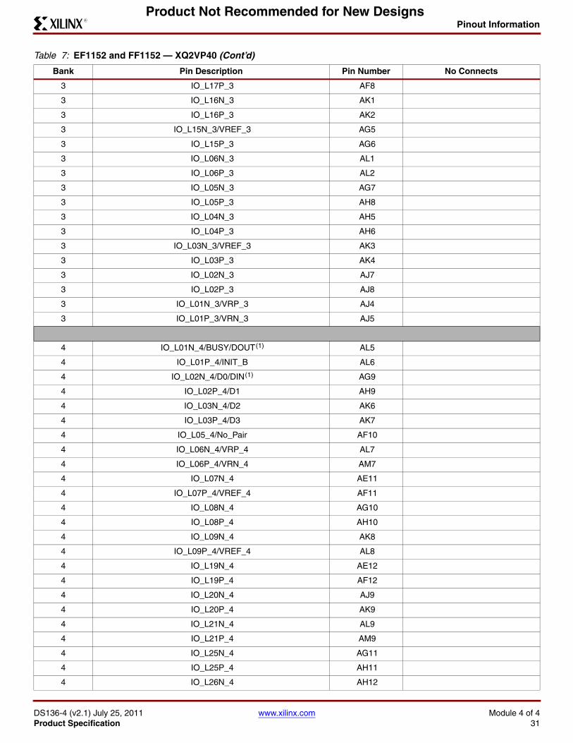
Pinout Information
DS136-4 (v2.1) July 25, 2011 www.xilinx.com Module 4 of 4Product Specification 31
R
Product Not Recommended for New Designs
3 IO_L17P_3 AF8
3 IO_L16N_3 AK1
3 IO_L16P_3 AK2
3 IO_L15N_3/VREF_3 AG5
3 IO_L15P_3 AG6
3 IO_L06N_3 AL1
3 IO_L06P_3 AL2
3 IO_L05N_3 AG7
3 IO_L05P_3 AH8
3 IO_L04N_3 AH5
3 IO_L04P_3 AH6
3 IO_L03N_3/VREF_3 AK3
3 IO_L03P_3 AK4
3 IO_L02N_3 AJ7
3 IO_L02P_3 AJ8
3 IO_L01N_3/VRP_3 AJ4
3 IO_L01P_3/VRN_3 AJ5
4 IO_L01N_4/BUSY/DOUT (1) AL5
4 IO_L01P_4/INIT_B AL6
4 IO_L02N_4/D0/DIN (1) AG9
4 IO_L02P_4/D1 AH9
4 IO_L03N_4/D2 AK6
4 IO_L03P_4/D3 AK7
4 IO_L05_4/No_Pair AF10
4 IO_L06N_4/VRP_4 AL7
4 IO_L06P_4/VRN_4 AM7
4 IO_L07N_4 AE11
4 IO_L07P_4/VREF_4 AF11
4 IO_L08N_4 AG10
4 IO_L08P_4 AH10
4 IO_L09N_4 AK8
4 IO_L09P_4/VREF_4 AL8
4 IO_L19N_4 AE12
4 IO_L19P_4 AF12
4 IO_L20N_4 AJ9
4 IO_L20P_4 AK9
4 IO_L21N_4 AL9
4 IO_L21P_4 AM9
4 IO_L25N_4 AG11
4 IO_L25P_4 AH11
4 IO_L26N_4 AH12
Table 7: EF1152 and FF1152 — XQ2VP40 (Cont’d)
Bank Pin Description Pin Number No Connects

Pinout Information
DS136-4 (v2.1) July 25, 2011 www.xilinx.com Module 4 of 4Product Specification 32
R
Product Not Recommended for New Designs
4 IO_L26P_4 AJ12
4 IO_L27N_4 AK10
4 IO_L27P_4/VREF_4 AL10
4 IO_L37N_4 AE13
4 IO_L37P_4 AF13
4 IO_L38N_4 AG13
4 IO_L38P_4 AH13
4 IO_L39N_4 AJ11
4 IO_L39P_4 AK11
4 IO_L43N_4 AE14
4 IO_L43P_4 AF14
4 IO_L44N_4 AJ13
4 IO_L44P_4 AK13
4 IO_L45N_4 AL11
4 IO_L45P_4/VREF_4 AM11
4 IO_L46N_4 AE15
4 IO_L46P_4 AF15
4 IO_L47N_4 AG14
4 IO_L47P_4 AH14
4 IO_L48N_4 AL13
4 IO_L48P_4 AL12
4 IO_L49N_4 AD16
4 IO_L49P_4 AE16
4 IO_L50_4/No_Pair AJ14
4 IO_L53_4/No_Pair AK14
4 IO_L54N_4 AM14
4 IO_L54P_4 AM13
4 IO_L55N_4 AF16
4 IO_L55P_4 AG16
4 IO_L56N_4 AH15
4 IO_L56P_4 AJ15
4 IO_L57N_4 AL14
4 IO_L57P_4/VREF_4 AL15
4 IO_L67N_4 AD17
4 IO_L67P_4 AE17
4 IO_L68N_4 AH16
4 IO_L68P_4 AJ16
4 IO_L69N_4 AK16
4 IO_L69P_4/VREF_4 AL16
4 IO_L73N_4 AF17
4 IO_L73P_4 AG17
4 IO_L74N_4/GCLK3S AH17
Table 7: EF1152 and FF1152 — XQ2VP40 (Cont’d)
Bank Pin Description Pin Number No Connects
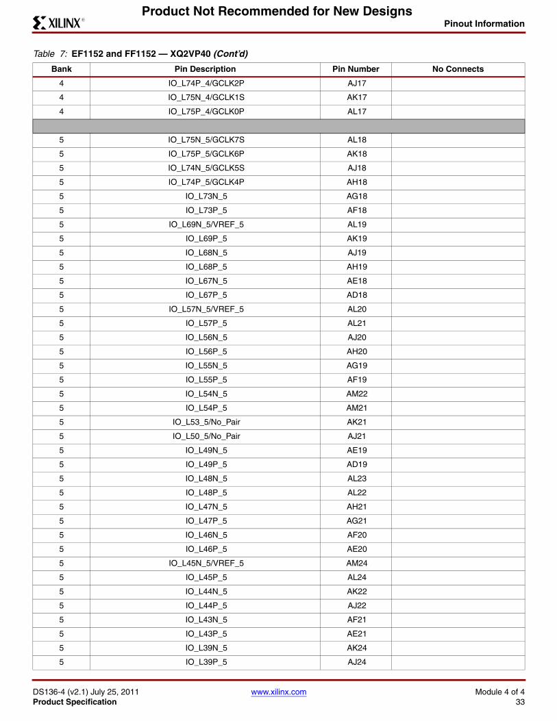
Pinout Information
DS136-4 (v2.1) July 25, 2011 www.xilinx.com Module 4 of 4Product Specification 33
R
Product Not Recommended for New Designs
4 IO_L74P_4/GCLK2P AJ17
4 IO_L75N_4/GCLK1S AK17
4 IO_L75P_4/GCLK0P AL17
5 IO_L75N_5/GCLK7S AL18
5 IO_L75P_5/GCLK6P AK18
5 IO_L74N_5/GCLK5S AJ18
5 IO_L74P_5/GCLK4P AH18
5 IO_L73N_5 AG18
5 IO_L73P_5 AF18
5 IO_L69N_5/VREF_5 AL19
5 IO_L69P_5 AK19
5 IO_L68N_5 AJ19
5 IO_L68P_5 AH19
5 IO_L67N_5 AE18
5 IO_L67P_5 AD18
5 IO_L57N_5/VREF_5 AL20
5 IO_L57P_5 AL21
5 IO_L56N_5 AJ20
5 IO_L56P_5 AH20
5 IO_L55N_5 AG19
5 IO_L55P_5 AF19
5 IO_L54N_5 AM22
5 IO_L54P_5 AM21
5 IO_L53_5/No_Pair AK21
5 IO_L50_5/No_Pair AJ21
5 IO_L49N_5 AE19
5 IO_L49P_5 AD19
5 IO_L48N_5 AL23
5 IO_L48P_5 AL22
5 IO_L47N_5 AH21
5 IO_L47P_5 AG21
5 IO_L46N_5 AF20
5 IO_L46P_5 AE20
5 IO_L45N_5/VREF_5 AM24
5 IO_L45P_5 AL24
5 IO_L44N_5 AK22
5 IO_L44P_5 AJ22
5 IO_L43N_5 AF21
5 IO_L43P_5 AE21
5 IO_L39N_5 AK24
5 IO_L39P_5 AJ24
Table 7: EF1152 and FF1152 — XQ2VP40 (Cont’d)
Bank Pin Description Pin Number No Connects
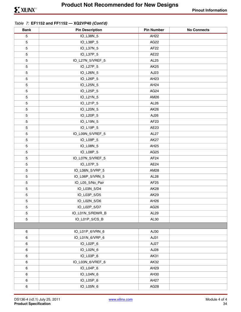
Pinout Information
DS136-4 (v2.1) July 25, 2011 www.xilinx.com Module 4 of 4Product Specification 34
R
Product Not Recommended for New Designs
5 IO_L38N_5 AH22
5 IO_L38P_5 AG22
5 IO_L37N_5 AF22
5 IO_L37P_5 AE22
5 IO_L27N_5/VREF_5 AL25
5 IO_L27P_5 AK25
5 IO_L26N_5 AJ23
5 IO_L26P_5 AH23
5 IO_L25N_5 AH24
5 IO_L25P_5 AG24
5 IO_L21N_5 AM26
5 IO_L21P_5 AL26
5 IO_L20N_5 AK26
5 IO_L20P_5 AJ26
5 IO_L19N_5 AF23
5 IO_L19P_5 AE23
5 IO_L09N_5/VREF_5 AL27
5 IO_L09P_5 AK27
5 IO_L08N_5 AH25
5 IO_L08P_5 AG25
5 IO_L07N_5/VREF_5 AF24
5 IO_L07P_5 AE24
5 IO_L06N_5/VRP_5 AM28
5 IO_L06P_5/VRN_5 AL28
5 IO_L05_5/No_Pair AF25
5 IO_L03N_5/D4 AK28
5 IO_L03P_5/D5 AK29
5 IO_L02N_5/D6 AH26
5 IO_L02P_5/D7 AG26
5 IO_L01N_5/RDWR_B AL29
5 IO_L01P_5/CS_B AL30
6 IO_L01P_6/VRN_6 AJ30
6 IO_L01N_6/VRP_6 AJ31
6 IO_L02P_6 AJ27
6 IO_L02N_6 AJ28
6 IO_L03P_6 AK31
6 IO_L03N_6/VREF_6 AK32
6 IO_L04P_6 AH29
6 IO_L04N_6 AH30
6 IO_L05P_6 AH27
6 IO_L05N_6 AG28
Table 7: EF1152 and FF1152 — XQ2VP40 (Cont’d)
Bank Pin Description Pin Number No Connects

Pinout Information
DS136-4 (v2.1) July 25, 2011 www.xilinx.com Module 4 of 4Product Specification 35
R
Product Not Recommended for New Designs
6 IO_L06P_6 AL33
6 IO_L06N_6 AL34
6 IO_L15P_6 AG29
6 IO_L15N_6/VREF_6 AG30
6 IO_L16P_6 AK33
6 IO_L16N_6 AK34
6 IO_L17P_6 AF27
6 IO_L17N_6 AF28
6 IO_L18P_6 AJ33
6 IO_L18N_6 AJ34
6 IO_L19P_6 AH31
6 IO_L19N_6 AH32
6 IO_L20P_6 AD25
6 IO_L20N_6 AD26
6 IO_L21P_6 AG31
6 IO_L21N_6/VREF_6 AG32
6 IO_L22P_6 AF29
6 IO_L22N_6 AF30
6 IO_L23P_6 AE27
6 IO_L23N_6 AE28
6 IO_L24P_6 AH33
6 IO_L24N_6 AH34
6 IO_L31P_6 AF31
6 IO_L31N_6 AF32
6 IO_L32P_6 AC25
6 IO_L32N_6 AC26
6 IO_L33P_6 AG33
6 IO_L33N_6/VREF_6 AG34
6 IO_L34P_6 AE30
6 IO_L34N_6 AE31
6 IO_L35P_6 AD27
6 IO_L35N_6 AD28
6 IO_L36P_6 AF33
6 IO_L36N_6 AE33
6 IO_L37P_6 AD29
6 IO_L37N_6 AD30
6 IO_L38P_6 AB25
6 IO_L38N_6 AB26
6 IO_L39P_6 AD31
6 IO_L39N_6/VREF_6 AD32
6 IO_L40P_6 AC28
6 IO_L40N_6 AC29
Table 7: EF1152 and FF1152 — XQ2VP40 (Cont’d)
Bank Pin Description Pin Number No Connects

Pinout Information
DS136-4 (v2.1) July 25, 2011 www.xilinx.com Module 4 of 4Product Specification 36
R
Product Not Recommended for New Designs
6 IO_L41P_6 AB27
6 IO_L41N_6 AB28
6 IO_L42P_6 AE34
6 IO_L42N_6 AD34
6 IO_L43P_6 AC31
6 IO_L43N_6 AC32
6 IO_L44P_6 AA25
6 IO_L44N_6 AA26
6 IO_L45P_6 AD33
6 IO_L45N_6/VREF_6 AC33
6 IO_L46P_6 AB29
6 IO_L46N_6 AB30
6 IO_L47P_6 AA27
6 IO_L47N_6 AA28
6 IO_L48P_6 AB31
6 IO_L48N_6 AB32
6 IO_L49P_6 AA29
6 IO_L49N_6 AA30
6 IO_L50P_6 Y25
6 IO_L50N_6 Y26
6 IO_L51P_6 AC34
6 IO_L51N_6/VREF_6 AB34
6 IO_L52P_6 AA31
6 IO_L52N_6 AA32
6 IO_L53P_6 W25
6 IO_L53N_6 W26
6 IO_L54P_6 AB33
6 IO_L54N_6 AA33
6 IO_L55P_6 Y28
6 IO_L55N_6 Y29
6 IO_L56P_6 W27
6 IO_L56N_6 W28
6 IO_L57P_6 Y31
6 IO_L57N_6/VREF_6 Y32
6 IO_L58P_6 W29
6 IO_L58N_6 W30
6 IO_L59P_6 W24
6 IO_L59N_6 V24
6 IO_L60P_6 AA34
6 IO_L60N_6 Y34
6 IO_L85P_6 W31
6 IO_L85N_6 W32
Table 7: EF1152 and FF1152 — XQ2VP40 (Cont’d)
Bank Pin Description Pin Number No Connects
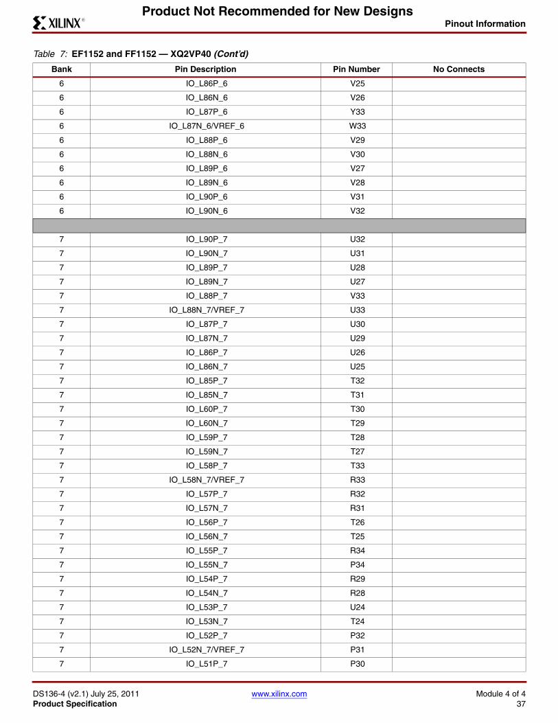
Pinout Information
DS136-4 (v2.1) July 25, 2011 www.xilinx.com Module 4 of 4Product Specification 37
R
Product Not Recommended for New Designs
6 IO_L86P_6 V25
6 IO_L86N_6 V26
6 IO_L87P_6 Y33
6 IO_L87N_6/VREF_6 W33
6 IO_L88P_6 V29
6 IO_L88N_6 V30
6 IO_L89P_6 V27
6 IO_L89N_6 V28
6 IO_L90P_6 V31
6 IO_L90N_6 V32
7 IO_L90P_7 U32
7 IO_L90N_7 U31
7 IO_L89P_7 U28
7 IO_L89N_7 U27
7 IO_L88P_7 V33
7 IO_L88N_7/VREF_7 U33
7 IO_L87P_7 U30
7 IO_L87N_7 U29
7 IO_L86P_7 U26
7 IO_L86N_7 U25
7 IO_L85P_7 T32
7 IO_L85N_7 T31
7 IO_L60P_7 T30
7 IO_L60N_7 T29
7 IO_L59P_7 T28
7 IO_L59N_7 T27
7 IO_L58P_7 T33
7 IO_L58N_7/VREF_7 R33
7 IO_L57P_7 R32
7 IO_L57N_7 R31
7 IO_L56P_7 T26
7 IO_L56N_7 T25
7 IO_L55P_7 R34
7 IO_L55N_7 P34
7 IO_L54P_7 R29
7 IO_L54N_7 R28
7 IO_L53P_7 U24
7 IO_L53N_7 T24
7 IO_L52P_7 P32
7 IO_L52N_7/VREF_7 P31
7 IO_L51P_7 P30
Table 7: EF1152 and FF1152 — XQ2VP40 (Cont’d)
Bank Pin Description Pin Number No Connects
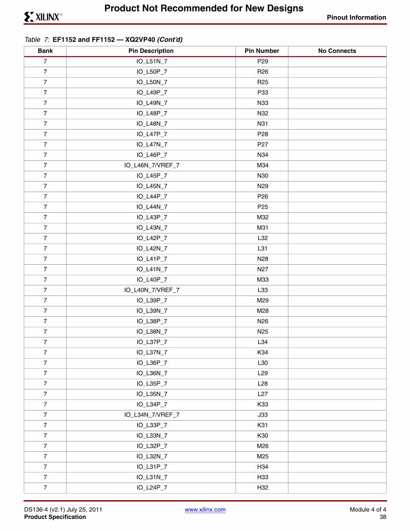
Pinout Information
DS136-4 (v2.1) July 25, 2011 www.xilinx.com Module 4 of 4Product Specification 38
R
Product Not Recommended for New Designs
7 IO_L51N_7 P29
7 IO_L50P_7 R26
7 IO_L50N_7 R25
7 IO_L49P_7 P33
7 IO_L49N_7 N33
7 IO_L48P_7 N32
7 IO_L48N_7 N31
7 IO_L47P_7 P28
7 IO_L47N_7 P27
7 IO_L46P_7 N34
7 IO_L46N_7/VREF_7 M34
7 IO_L45P_7 N30
7 IO_L45N_7 N29
7 IO_L44P_7 P26
7 IO_L44N_7 P25
7 IO_L43P_7 M32
7 IO_L43N_7 M31
7 IO_L42P_7 L32
7 IO_L42N_7 L31
7 IO_L41P_7 N28
7 IO_L41N_7 N27
7 IO_L40P_7 M33
7 IO_L40N_7/VREF_7 L33
7 IO_L39P_7 M29
7 IO_L39N_7 M28
7 IO_L38P_7 N26
7 IO_L38N_7 N25
7 IO_L37P_7 L34
7 IO_L37N_7 K34
7 IO_L36P_7 L30
7 IO_L36N_7 L29
7 IO_L35P_7 L28
7 IO_L35N_7 L27
7 IO_L34P_7 K33
7 IO_L34N_7/VREF_7 J33
7 IO_L33P_7 K31
7 IO_L33N_7 K30
7 IO_L32P_7 M26
7 IO_L32N_7 M25
7 IO_L31P_7 H34
7 IO_L31N_7 H33
7 IO_L24P_7 H32
Table 7: EF1152 and FF1152 — XQ2VP40 (Cont’d)
Bank Pin Description Pin Number No Connects
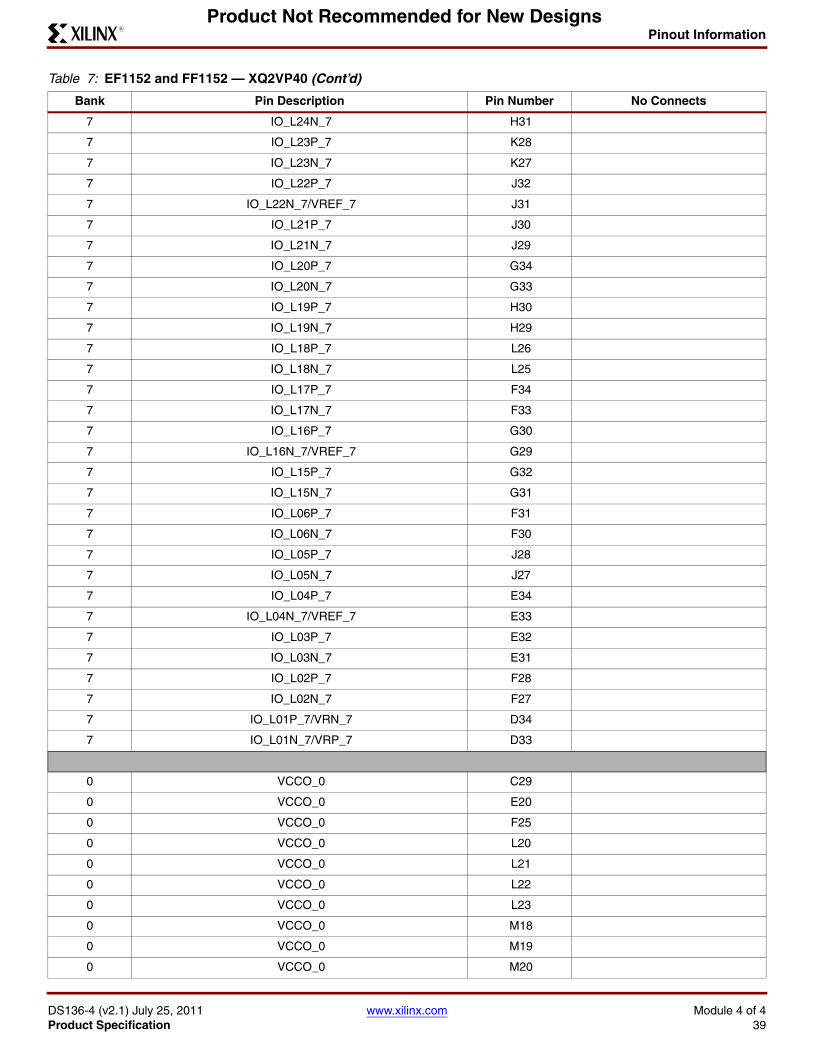
Pinout Information
DS136-4 (v2.1) July 25, 2011 www.xilinx.com Module 4 of 4Product Specification 39
R
Product Not Recommended for New Designs
7 IO_L24N_7 H31
7 IO_L23P_7 K28
7 IO_L23N_7 K27
7 IO_L22P_7 J32
7 IO_L22N_7/VREF_7 J31
7 IO_L21P_7 J30
7 IO_L21N_7 J29
7 IO_L20P_7 G34
7 IO_L20N_7 G33
7 IO_L19P_7 H30
7 IO_L19N_7 H29
7 IO_L18P_7 L26
7 IO_L18N_7 L25
7 IO_L17P_7 F34
7 IO_L17N_7 F33
7 IO_L16P_7 G30
7 IO_L16N_7/VREF_7 G29
7 IO_L15P_7 G32
7 IO_L15N_7 G31
7 IO_L06P_7 F31
7 IO_L06N_7 F30
7 IO_L05P_7 J28
7 IO_L05N_7 J27
7 IO_L04P_7 E34
7 IO_L04N_7/VREF_7 E33
7 IO_L03P_7 E32
7 IO_L03N_7 E31
7 IO_L02P_7 F28
7 IO_L02N_7 F27
7 IO_L01P_7/VRN_7 D34
7 IO_L01N_7/VRP_7 D33
0 VCCO_0 C29
0 VCCO_0 E20
0 VCCO_0 F25
0 VCCO_0 L20
0 VCCO_0 L21
0 VCCO_0 L22
0 VCCO_0 L23
0 VCCO_0 M18
0 VCCO_0 M19
0 VCCO_0 M20
Table 7: EF1152 and FF1152 — XQ2VP40 (Cont’d)
Bank Pin Description Pin Number No Connects
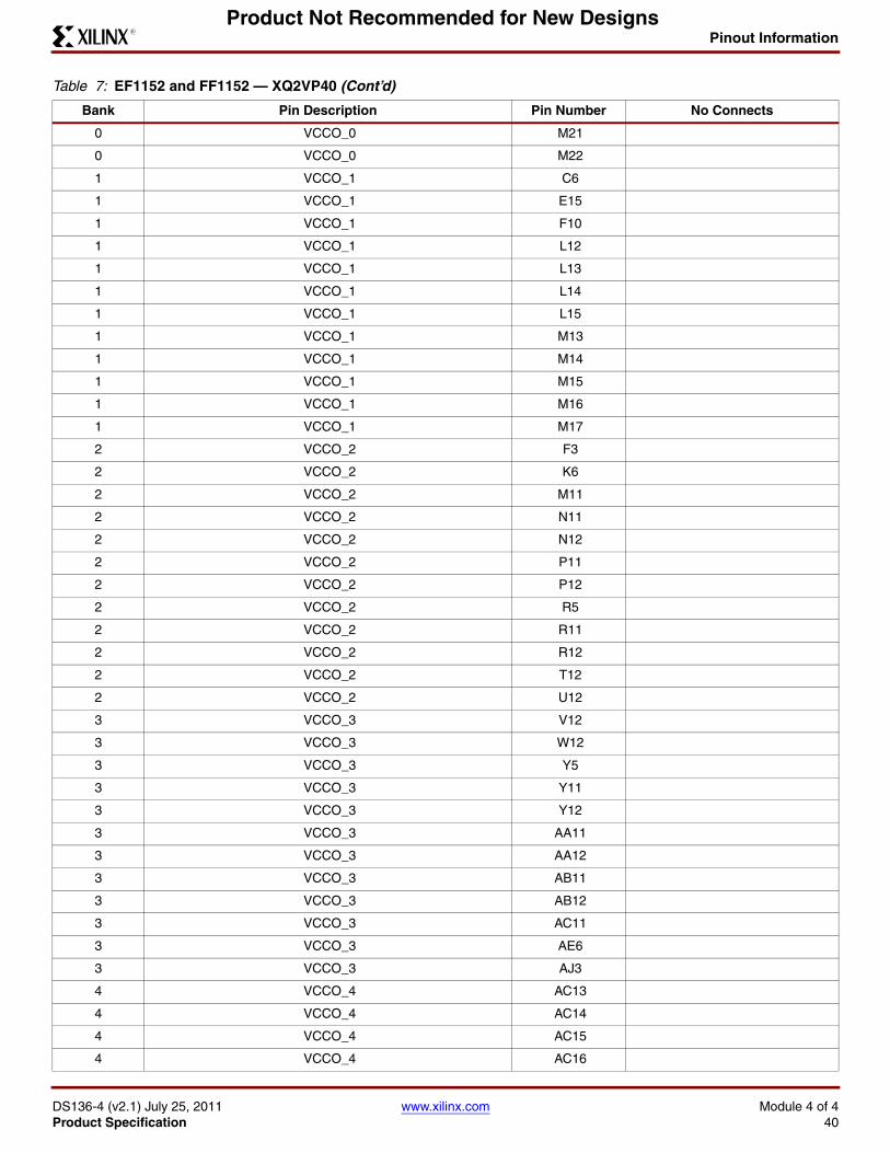
Pinout Information
DS136-4 (v2.1) July 25, 2011 www.xilinx.com Module 4 of 4Product Specification 40
R
Product Not Recommended for New Designs
0 VCCO_0 M21
0 VCCO_0 M22
1 VCCO_1 C6
1 VCCO_1 E15
1 VCCO_1 F10
1 VCCO_1 L12
1 VCCO_1 L13
1 VCCO_1 L14
1 VCCO_1 L15
1 VCCO_1 M13
1 VCCO_1 M14
1 VCCO_1 M15
1 VCCO_1 M16
1 VCCO_1 M17
2 VCCO_2 F3
2 VCCO_2 K6
2 VCCO_2 M11
2 VCCO_2 N11
2 VCCO_2 N12
2 VCCO_2 P11
2 VCCO_2 P12
2 VCCO_2 R5
2 VCCO_2 R11
2 VCCO_2 R12
2 VCCO_2 T12
2 VCCO_2 U12
3 VCCO_3 V12
3 VCCO_3 W12
3 VCCO_3 Y5
3 VCCO_3 Y11
3 VCCO_3 Y12
3 VCCO_3 AA11
3 VCCO_3 AA12
3 VCCO_3 AB11
3 VCCO_3 AB12
3 VCCO_3 AC11
3 VCCO_3 AE6
3 VCCO_3 AJ3
4 VCCO_4 AC13
4 VCCO_4 AC14
4 VCCO_4 AC15
4 VCCO_4 AC16
Table 7: EF1152 and FF1152 — XQ2VP40 (Cont’d)
Bank Pin Description Pin Number No Connects
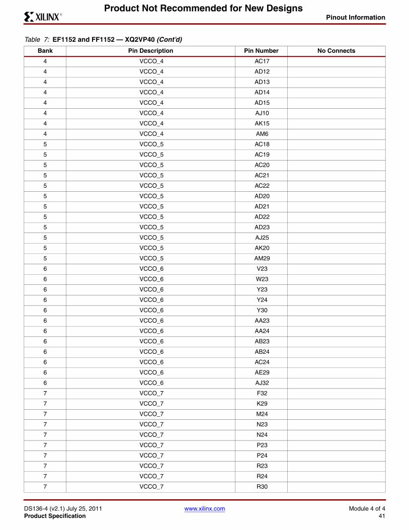
Pinout Information
DS136-4 (v2.1) July 25, 2011 www.xilinx.com Module 4 of 4Product Specification 41
R
Product Not Recommended for New Designs
4 VCCO_4 AC17
4 VCCO_4 AD12
4 VCCO_4 AD13
4 VCCO_4 AD14
4 VCCO_4 AD15
4 VCCO_4 AJ10
4 VCCO_4 AK15
4 VCCO_4 AM6
5 VCCO_5 AC18
5 VCCO_5 AC19
5 VCCO_5 AC20
5 VCCO_5 AC21
5 VCCO_5 AC22
5 VCCO_5 AD20
5 VCCO_5 AD21
5 VCCO_5 AD22
5 VCCO_5 AD23
5 VCCO_5 AJ25
5 VCCO_5 AK20
5 VCCO_5 AM29
6 VCCO_6 V23
6 VCCO_6 W23
6 VCCO_6 Y23
6 VCCO_6 Y24
6 VCCO_6 Y30
6 VCCO_6 AA23
6 VCCO_6 AA24
6 VCCO_6 AB23
6 VCCO_6 AB24
6 VCCO_6 AC24
6 VCCO_6 AE29
6 VCCO_6 AJ32
7 VCCO_7 F32
7 VCCO_7 K29
7 VCCO_7 M24
7 VCCO_7 N23
7 VCCO_7 N24
7 VCCO_7 P23
7 VCCO_7 P24
7 VCCO_7 R23
7 VCCO_7 R24
7 VCCO_7 R30
Table 7: EF1152 and FF1152 — XQ2VP40 (Cont’d)
Bank Pin Description Pin Number No Connects
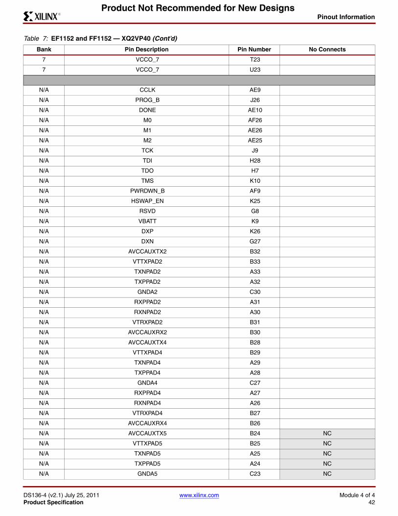
Pinout Information
DS136-4 (v2.1) July 25, 2011 www.xilinx.com Module 4 of 4Product Specification 42
R
Product Not Recommended for New Designs
7 VCCO_7 T23
7 VCCO_7 U23
N/A CCLK AE9
N/A PROG_B J26
N/A DONE AE10
N/A M0 AF26
N/A M1 AE26
N/A M2 AE25
N/A TCK J9
N/A TDI H28
N/A TDO H7
N/A TMS K10
N/A PWRDWN_B AF9
N/A HSWAP_EN K25
N/A RSVD G8
N/A VBATT K9
N/A DXP K26
N/A DXN G27
N/A AVCCAUXTX2 B32
N/A VTTXPAD2 B33
N/A TXNPAD2 A33
N/A TXPPAD2 A32
N/A GNDA2 C30
N/A RXPPAD2 A31
N/A RXNPAD2 A30
N/A VTRXPAD2 B31
N/A AVCCAUXRX2 B30
N/A AVCCAUXTX4 B28
N/A VTTXPAD4 B29
N/A TXNPAD4 A29
N/A TXPPAD4 A28
N/A GNDA4 C27
N/A RXPPAD4 A27
N/A RXNPAD4 A26
N/A VTRXPAD4 B27
N/A AVCCAUXRX4 B26
N/A AVCCAUXTX5 B24 NC
N/A VTTXPAD5 B25 NC
N/A TXNPAD5 A25 NC
N/A TXPPAD5 A24 NC
N/A GNDA5 C23 NC
Table 7: EF1152 and FF1152 — XQ2VP40 (Cont’d)
Bank Pin Description Pin Number No Connects
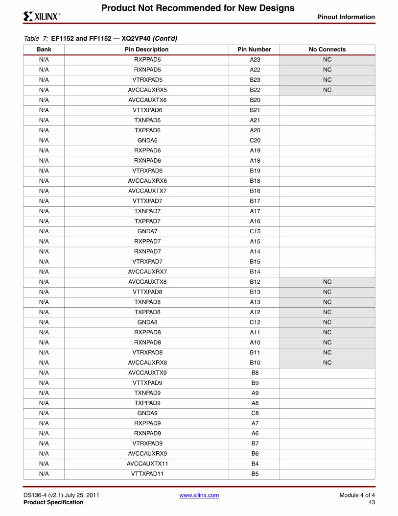
Pinout Information
DS136-4 (v2.1) July 25, 2011 www.xilinx.com Module 4 of 4Product Specification 43
R
Product Not Recommended for New Designs
N/A RXPPAD5 A23 NC
N/A RXNPAD5 A22 NC
N/A VTRXPAD5 B23 NC
N/A AVCCAUXRX5 B22 NC
N/A AVCCAUXTX6 B20
N/A VTTXPAD6 B21
N/A TXNPAD6 A21
N/A TXPPAD6 A20
N/A GNDA6 C20
N/A RXPPAD6 A19
N/A RXNPAD6 A18
N/A VTRXPAD6 B19
N/A AVCCAUXRX6 B18
N/A AVCCAUXTX7 B16
N/A VTTXPAD7 B17
N/A TXNPAD7 A17
N/A TXPPAD7 A16
N/A GNDA7 C15
N/A RXPPAD7 A15
N/A RXNPAD7 A14
N/A VTRXPAD7 B15
N/A AVCCAUXRX7 B14
N/A AVCCAUXTX8 B12 NC
N/A VTTXPAD8 B13 NC
N/A TXNPAD8 A13 NC
N/A TXPPAD8 A12 NC
N/A GNDA8 C12 NC
N/A RXPPAD8 A11 NC
N/A RXNPAD8 A10 NC
N/A VTRXPAD8 B11 NC
N/A AVCCAUXRX8 B10 NC
N/A AVCCAUXTX9 B8
N/A VTTXPAD9 B9
N/A TXNPAD9 A9
N/A TXPPAD9 A8
N/A GNDA9 C8
N/A RXPPAD9 A7
N/A RXNPAD9 A6
N/A VTRXPAD9 B7
N/A AVCCAUXRX9 B6
N/A AVCCAUXTX11 B4
N/A VTTXPAD11 B5
Table 7: EF1152 and FF1152 — XQ2VP40 (Cont’d)
Bank Pin Description Pin Number No Connects
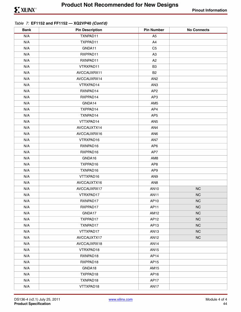
Pinout Information
DS136-4 (v2.1) July 25, 2011 www.xilinx.com Module 4 of 4Product Specification 44
R
Product Not Recommended for New Designs
N/A TXNPAD11 A5
N/A TXPPAD11 A4
N/A GNDA11 C5
N/A RXPPAD11 A3
N/A RXNPAD11 A2
N/A VTRXPAD11 B3
N/A AVCCAUXRX11 B2
N/A AVCCAUXRX14 AN2
N/A VTRXPAD14 AN3
N/A RXNPAD14 AP2
N/A RXPPAD14 AP3
N/A GNDA14 AM5
N/A TXPPAD14 AP4
N/A TXNPAD14 AP5
N/A VTTXPAD14 AN5
N/A AVCCAUXTX14 AN4
N/A AVCCAUXRX16 AN6
N/A VTRXPAD16 AN7
N/A RXNPAD16 AP6
N/A RXPPAD16 AP7
N/A GNDA16 AM8
N/A TXPPAD16 AP8
N/A TXNPAD16 AP9
N/A VTTXPAD16 AN9
N/A AVCCAUXTX16 AN8
N/A AVCCAUXRX17 AN10 NC
N/A VTRXPAD17 AN11 NC
N/A RXNPAD17 AP10 NC
N/A RXPPAD17 AP11 NC
N/A GNDA17 AM12 NC
N/A TXPPAD17 AP12 NC
N/A TXNPAD17 AP13 NC
N/A VTTXPAD17 AN13 NC
N/A AVCCAUXTX17 AN12 NC
N/A AVCCAUXRX18 AN14
N/A VTRXPAD18 AN15
N/A RXNPAD18 AP14
N/A RXPPAD18 AP15
N/A GNDA18 AM15
N/A TXPPAD18 AP16
N/A TXNPAD18 AP17
N/A VTTXPAD18 AN17
Table 7: EF1152 and FF1152 — XQ2VP40 (Cont’d)
Bank Pin Description Pin Number No Connects
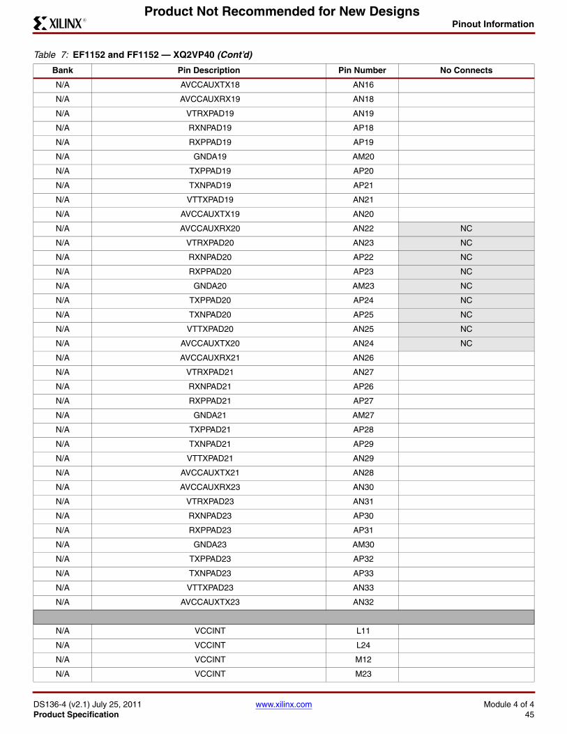
Pinout Information
DS136-4 (v2.1) July 25, 2011 www.xilinx.com Module 4 of 4Product Specification 45
R
Product Not Recommended for New Designs
N/A AVCCAUXTX18 AN16
N/A AVCCAUXRX19 AN18
N/A VTRXPAD19 AN19
N/A RXNPAD19 AP18
N/A RXPPAD19 AP19
N/A GNDA19 AM20
N/A TXPPAD19 AP20
N/A TXNPAD19 AP21
N/A VTTXPAD19 AN21
N/A AVCCAUXTX19 AN20
N/A AVCCAUXRX20 AN22 NC
N/A VTRXPAD20 AN23 NC
N/A RXNPAD20 AP22 NC
N/A RXPPAD20 AP23 NC
N/A GNDA20 AM23 NC
N/A TXPPAD20 AP24 NC
N/A TXNPAD20 AP25 NC
N/A VTTXPAD20 AN25 NC
N/A AVCCAUXTX20 AN24 NC
N/A AVCCAUXRX21 AN26
N/A VTRXPAD21 AN27
N/A RXNPAD21 AP26
N/A RXPPAD21 AP27
N/A GNDA21 AM27
N/A TXPPAD21 AP28
N/A TXNPAD21 AP29
N/A VTTXPAD21 AN29
N/A AVCCAUXTX21 AN28
N/A AVCCAUXRX23 AN30
N/A VTRXPAD23 AN31
N/A RXNPAD23 AP30
N/A RXPPAD23 AP31
N/A GNDA23 AM30
N/A TXPPAD23 AP32
N/A TXNPAD23 AP33
N/A VTTXPAD23 AN33
N/A AVCCAUXTX23 AN32
N/A VCCINT L11
N/A VCCINT L24
N/A VCCINT M12
N/A VCCINT M23
Table 7: EF1152 and FF1152 — XQ2VP40 (Cont’d)
Bank Pin Description Pin Number No Connects
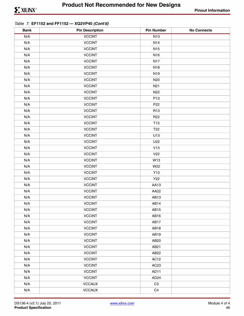
Pinout Information
DS136-4 (v2.1) July 25, 2011 www.xilinx.com Module 4 of 4Product Specification 46
R
Product Not Recommended for New Designs
N/A VCCINT N13
N/A VCCINT N14
N/A VCCINT N15
N/A VCCINT N16
N/A VCCINT N17
N/A VCCINT N18
N/A VCCINT N19
N/A VCCINT N20
N/A VCCINT N21
N/A VCCINT N22
N/A VCCINT P13
N/A VCCINT P22
N/A VCCINT R13
N/A VCCINT R22
N/A VCCINT T13
N/A VCCINT T22
N/A VCCINT U13
N/A VCCINT U22
N/A VCCINT V13
N/A VCCINT V22
N/A VCCINT W13
N/A VCCINT W22
N/A VCCINT Y13
N/A VCCINT Y22
N/A VCCINT AA13
N/A VCCINT AA22
N/A VCCINT AB13
N/A VCCINT AB14
N/A VCCINT AB15
N/A VCCINT AB16
N/A VCCINT AB17
N/A VCCINT AB18
N/A VCCINT AB19
N/A VCCINT AB20
N/A VCCINT AB21
N/A VCCINT AB22
N/A VCCINT AC12
N/A VCCINT AC23
N/A VCCINT AD11
N/A VCCINT AD24
N/A VCCAUX C3
N/A VCCAUX C4
Table 7: EF1152 and FF1152 — XQ2VP40 (Cont’d)
Bank Pin Description Pin Number No Connects
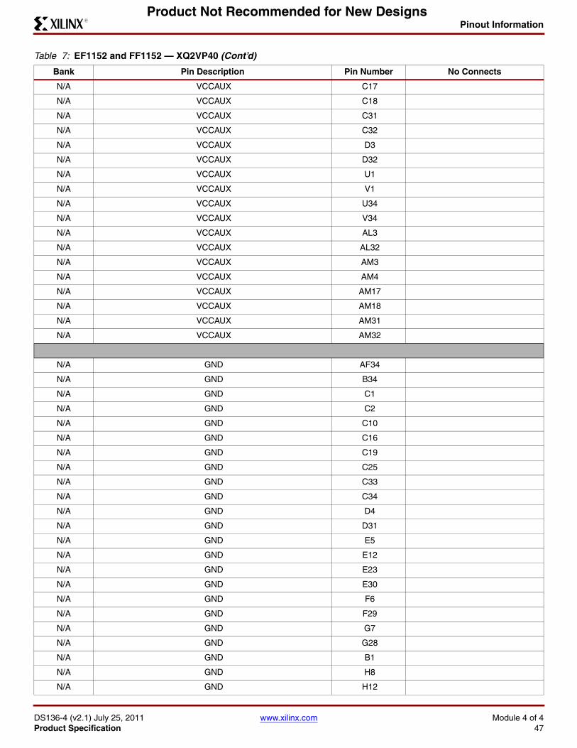
Pinout Information
DS136-4 (v2.1) July 25, 2011 www.xilinx.com Module 4 of 4Product Specification 47
R
Product Not Recommended for New Designs
N/A VCCAUX C17
N/A VCCAUX C18
N/A VCCAUX C31
N/A VCCAUX C32
N/A VCCAUX D3
N/A VCCAUX D32
N/A VCCAUX U1
N/A VCCAUX V1
N/A VCCAUX U34
N/A VCCAUX V34
N/A VCCAUX AL3
N/A VCCAUX AL32
N/A VCCAUX AM3
N/A VCCAUX AM4
N/A VCCAUX AM17
N/A VCCAUX AM18
N/A VCCAUX AM31
N/A VCCAUX AM32
N/A GND AF34
N/A GND B34
N/A GND C1
N/A GND C2
N/A GND C10
N/A GND C16
N/A GND C19
N/A GND C25
N/A GND C33
N/A GND C34
N/A GND D4
N/A GND D31
N/A GND E5
N/A GND E12
N/A GND E23
N/A GND E30
N/A GND F6
N/A GND F29
N/A GND G7
N/A GND G28
N/A GND B1
N/A GND H8
N/A GND H12
Table 7: EF1152 and FF1152 — XQ2VP40 (Cont’d)
Bank Pin Description Pin Number No Connects
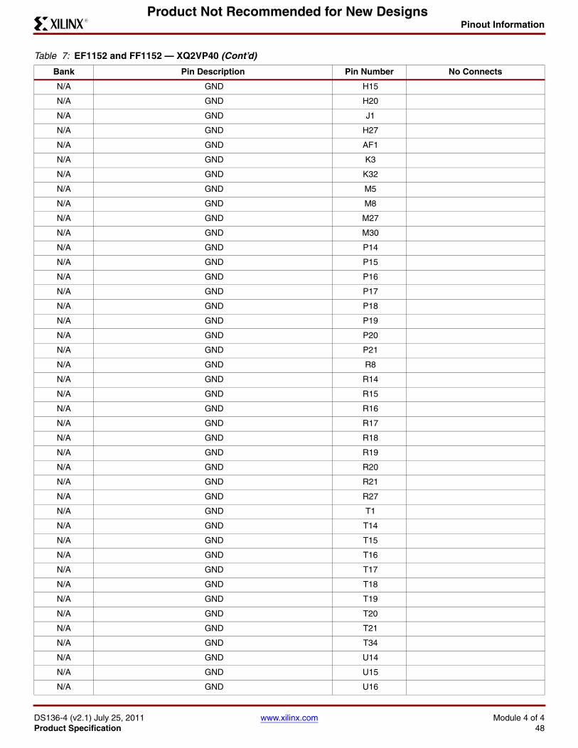
Pinout Information
DS136-4 (v2.1) July 25, 2011 www.xilinx.com Module 4 of 4Product Specification 48
R
Product Not Recommended for New Designs
N/A GND H15
N/A GND H20
N/A GND J1
N/A GND H27
N/A GND AF1
N/A GND K3
N/A GND K32
N/A GND M5
N/A GND M8
N/A GND M27
N/A GND M30
N/A GND P14
N/A GND P15
N/A GND P16
N/A GND P17
N/A GND P18
N/A GND P19
N/A GND P20
N/A GND P21
N/A GND R8
N/A GND R14
N/A GND R15
N/A GND R16
N/A GND R17
N/A GND R18
N/A GND R19
N/A GND R20
N/A GND R21
N/A GND R27
N/A GND T1
N/A GND T14
N/A GND T15
N/A GND T16
N/A GND T17
N/A GND T18
N/A GND T19
N/A GND T20
N/A GND T21
N/A GND T34
N/A GND U14
N/A GND U15
N/A GND U16
Table 7: EF1152 and FF1152 — XQ2VP40 (Cont’d)
Bank Pin Description Pin Number No Connects
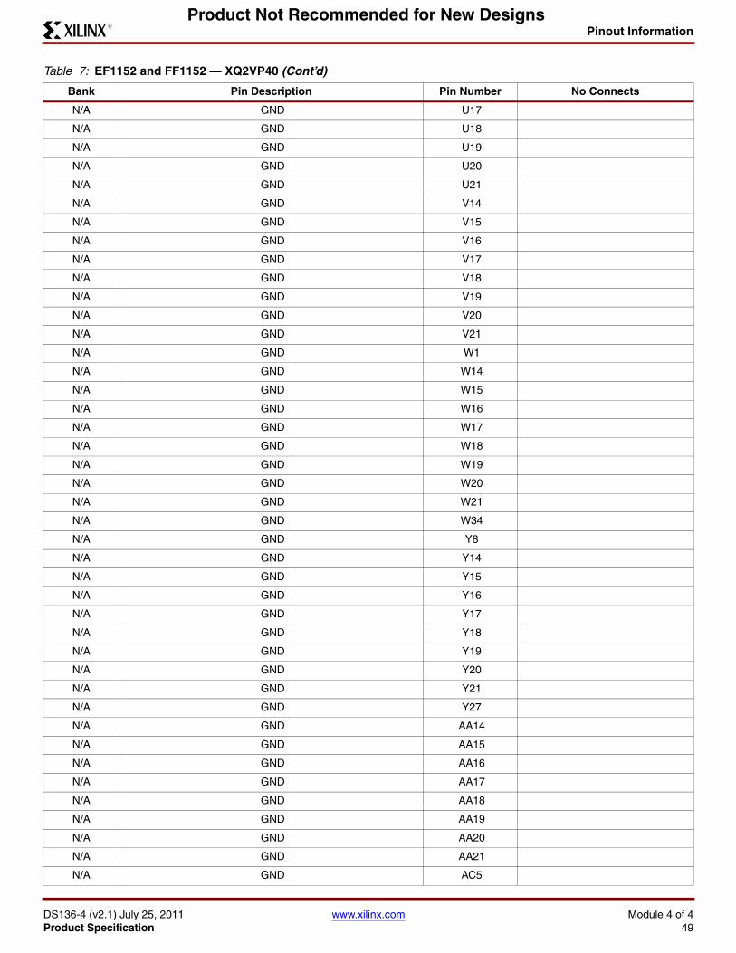
Pinout Information
DS136-4 (v2.1) July 25, 2011 www.xilinx.com Module 4 of 4Product Specification 49
R
Product Not Recommended for New Designs
N/A GND U17
N/A GND U18
N/A GND U19
N/A GND U20
N/A GND U21
N/A GND V14
N/A GND V15
N/A GND V16
N/A GND V17
N/A GND V18
N/A GND V19
N/A GND V20
N/A GND V21
N/A GND W1
N/A GND W14
N/A GND W15
N/A GND W16
N/A GND W17
N/A GND W18
N/A GND W19
N/A GND W20
N/A GND W21
N/A GND W34
N/A GND Y8
N/A GND Y14
N/A GND Y15
N/A GND Y16
N/A GND Y17
N/A GND Y18
N/A GND Y19
N/A GND Y20
N/A GND Y21
N/A GND Y27
N/A GND AA14
N/A GND AA15
N/A GND AA16
N/A GND AA17
N/A GND AA18
N/A GND AA19
N/A GND AA20
N/A GND AA21
N/A GND AC5
Table 7: EF1152 and FF1152 — XQ2VP40 (Cont’d)
Bank Pin Description Pin Number No Connects
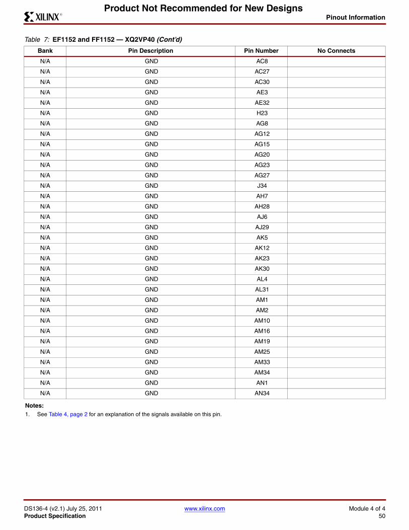
Pinout Information
DS136-4 (v2.1) July 25, 2011 www.xilinx.com Module 4 of 4Product Specification 50
R
Product Not Recommended for New Designs
N/A GND AC8
N/A GND AC27
N/A GND AC30
N/A GND AE3
N/A GND AE32
N/A GND H23
N/A GND AG8
N/A GND AG12
N/A GND AG15
N/A GND AG20
N/A GND AG23
N/A GND AG27
N/A GND J34
N/A GND AH7
N/A GND AH28
N/A GND AJ6
N/A GND AJ29
N/A GND AK5
N/A GND AK12
N/A GND AK23
N/A GND AK30
N/A GND AL4
N/A GND AL31
N/A GND AM1
N/A GND AM2
N/A GND AM10
N/A GND AM16
N/A GND AM19
N/A GND AM25
N/A GND AM33
N/A GND AM34
N/A GND AN1
N/A GND AN34
Notes: 1. See Table 4, page 2 for an explanation of the signals available on this pin.
Table 7: EF1152 and FF1152 — XQ2VP40 (Cont’d)
Bank Pin Description Pin Number No Connects
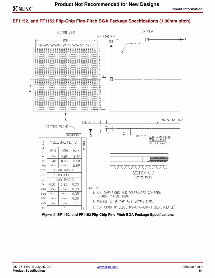
Pinout Information
DS136-4 (v2.1) July 25, 2011 www.xilinx.com Module 4 of 4Product Specification 51
R
Product Not Recommended for New Designs
EF1152, and FF1152 Flip-Chip Fine-Pitch BGA Package Specifications (1.00mm pitch)X-Ref Target - Figure 2
Figure 2: EF1152, and FF1152 Flip-Chip Fine-Pitch BGA Package Specifications
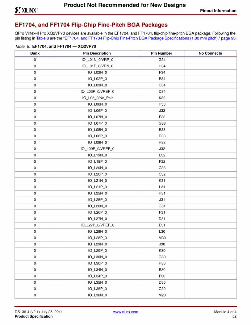
Pinout Information
DS136-4 (v2.1) July 25, 2011 www.xilinx.com Module 4 of 4Product Specification 52
R
Product Not Recommended for New Designs
EF1704, and FF1704 Flip-Chip Fine-Pitch BGA PackagesQPro Virtex-II Pro XQ2VP70 devices are available in the EF1704, and FF1704, flip-chip fine-pitch BGA package. Following the pin listing in Table 8 are the "EF1704, and FF1704 Flip-Chip Fine-Pitch BGA Package Specifications (1.00 mm pitch)," page 93.
Table 8: EF1704, and FF1704 — XQ2VP70
Bank Pin Description Pin Number No Connects
0 IO_L01N_0/VRP_0 G34
0 IO_L01P_0/VRN_0 H34
0 IO_L02N_0 F34
0 IO_L02P_0 E34
0 IO_L03N_0 C34
0 IO_L03P_0/VREF_0 D34
0 IO_L05_0/No_Pair K32
0 IO_L06N_0 H33
0 IO_L06P_0 J33
0 IO_L07N_0 F33
0 IO_L07P_0 G33
0 IO_L08N_0 E33
0 IO_L08P_0 D33
0 IO_L09N_0 H32
0 IO_L09P_0/VREF_0 J32
0 IO_L19N_0 E32
0 IO_L19P_0 F32
0 IO_L20N_0 C33
0 IO_L20P_0 C32
0 IO_L21N_0 K31
0 IO_L21P_0 L31
0 IO_L25N_0 H31
0 IO_L25P_0 J31
0 IO_L26N_0 G31
0 IO_L26P_0 F31
0 IO_L27N_0 D31
0 IO_L27P_0/VREF_0 E31
0 IO_L28N_0 L30
0 IO_L28P_0 M30
0 IO_L29N_0 J30
0 IO_L29P_0 K30
0 IO_L30N_0 G30
0 IO_L30P_0 H30
0 IO_L34N_0 E30
0 IO_L34P_0 F30
0 IO_L35N_0 D30
0 IO_L35P_0 C30
0 IO_L36N_0 M28
Pinout Information
DS136-4 (v2.1) July 25, 2011 www.xilinx.com Module 4 of 4Product Specification 53
R
Product Not Recommended for New Designs
0 IO_L36P_0/VREF_0 M29
0 IO_L78N_0 K29 NC
0 IO_L78P_0 L29 NC
0 IO_L83_0/No_Pair H29 NC
0 IO_L84N_0 F29 NC
0 IO_L84P_0 G29 NC
0 IO_L85N_0 D29 NC
0 IO_L85P_0 E29 NC
0 IO_L86N_0 L28 NC
0 IO_L86P_0 K28 NC
0 IO_L87N_0 H28 NC
0 IO_L87P_0/VREF_0 J28 NC
0 IO_L37N_0 E28
0 IO_L37P_0 F28
0 IO_L38N_0 C29
0 IO_L38P_0 C28
0 IO_L39N_0 L27
0 IO_L39P_0 M27
0 IO_L43N_0 J27
0 IO_L43P_0 K27
0 IO_L44N_0 H27
0 IO_L44P_0 G27
0 IO_L45N_0 E27
0 IO_L45P_0/VREF_0 F27
0 IO_L46N_0 M25
0 IO_L46P_0 M26
0 IO_L47N_0 L26
0 IO_L47P_0 K26
0 IO_L48N_0 H26
0 IO_L48P_0 J26
0 IO_L49N_0 F26
0 IO_L49P_0 G26
0 IO_L50_0/No_Pair D27
0 IO_L53_0/No_Pair D26
0 IO_L54N_0 K25
0 IO_L54P_0 L25
0 IO_L55N_0 G25
0 IO_L55P_0 H25
0 IO_L56N_0 E26
0 IO_L56P_0 E25
0 IO_L57N_0 C25
0 IO_L57P_0/VREF_0 C26
Table 8: EF1704, and FF1704 — XQ2VP70 (Cont’d)
Bank Pin Description Pin Number No Connects
Pinout Information
DS136-4 (v2.1) July 25, 2011 www.xilinx.com Module 4 of 4Product Specification 54
R
Product Not Recommended for New Designs
0 IO_L58N_0 L24
0 IO_L58P_0 M24
0 IO_L59N_0 J24
0 IO_L59P_0 K24
0 IO_L60N_0 G24
0 IO_L60P_0 H24
0 IO_L64N_0 E24
0 IO_L64P_0 F24
0 IO_L65N_0 D24
0 IO_L65P_0 C24
0 IO_L66N_0 M22
0 IO_L66P_0/VREF_0 M23
0 IO_L67N_0 K23
0 IO_L67P_0 L23
0 IO_L68N_0 J23
0 IO_L68P_0 H23
0 IO_L69N_0 E23
0 IO_L69P_0/VREF_0 F23
0 IO_L73N_0 C23
0 IO_L73P_0 D23
0 IO_L74N_0/GCLK7P K22
0 IO_L74P_0/GCLK6S J22
0 IO_L75N_0/GCLK5P F22
0 IO_L75P_0/GCLK4S G22
1 IO_L75N_1/GCLK3P G21
1 IO_L75P_1/GCLK2S F21
1 IO_L74N_1/GCLK1P J21
1 IO_L74P_1/GCLK0S K21
1 IO_L73N_1 D20
1 IO_L73P_1 C20
1 IO_L69N_1/VREF_1 F20
1 IO_L69P_1 E20
1 IO_L68N_1 H20
1 IO_L68P_1 J20
1 IO_L67N_1 L20
1 IO_L67P_1 K20
1 IO_L66N_1/VREF_1 M20
1 IO_L66P_1 M21
1 IO_L65N_1 C19
1 IO_L65P_1 D19
1 IO_L64N_1 F19
Table 8: EF1704, and FF1704 — XQ2VP70 (Cont’d)
Bank Pin Description Pin Number No Connects
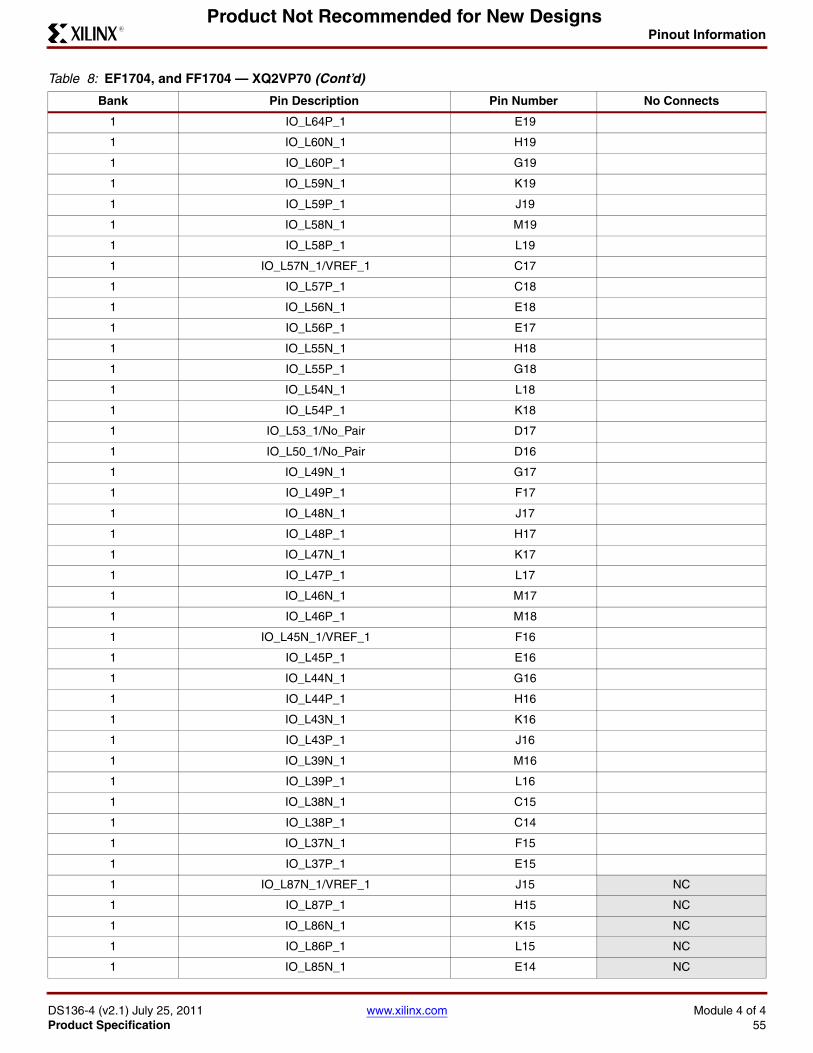
Pinout Information
DS136-4 (v2.1) July 25, 2011 www.xilinx.com Module 4 of 4Product Specification 55
R
Product Not Recommended for New Designs
1 IO_L64P_1 E19
1 IO_L60N_1 H19
1 IO_L60P_1 G19
1 IO_L59N_1 K19
1 IO_L59P_1 J19
1 IO_L58N_1 M19
1 IO_L58P_1 L19
1 IO_L57N_1/VREF_1 C17
1 IO_L57P_1 C18
1 IO_L56N_1 E18
1 IO_L56P_1 E17
1 IO_L55N_1 H18
1 IO_L55P_1 G18
1 IO_L54N_1 L18
1 IO_L54P_1 K18
1 IO_L53_1/No_Pair D17
1 IO_L50_1/No_Pair D16
1 IO_L49N_1 G17
1 IO_L49P_1 F17
1 IO_L48N_1 J17
1 IO_L48P_1 H17
1 IO_L47N_1 K17
1 IO_L47P_1 L17
1 IO_L46N_1 M17
1 IO_L46P_1 M18
1 IO_L45N_1/VREF_1 F16
1 IO_L45P_1 E16
1 IO_L44N_1 G16
1 IO_L44P_1 H16
1 IO_L43N_1 K16
1 IO_L43P_1 J16
1 IO_L39N_1 M16
1 IO_L39P_1 L16
1 IO_L38N_1 C15
1 IO_L38P_1 C14
1 IO_L37N_1 F15
1 IO_L37P_1 E15
1 IO_L87N_1/VREF_1 J15 NC
1 IO_L87P_1 H15 NC
1 IO_L86N_1 K15 NC
1 IO_L86P_1 L15 NC
1 IO_L85N_1 E14 NC
Table 8: EF1704, and FF1704 — XQ2VP70 (Cont’d)
Bank Pin Description Pin Number No Connects
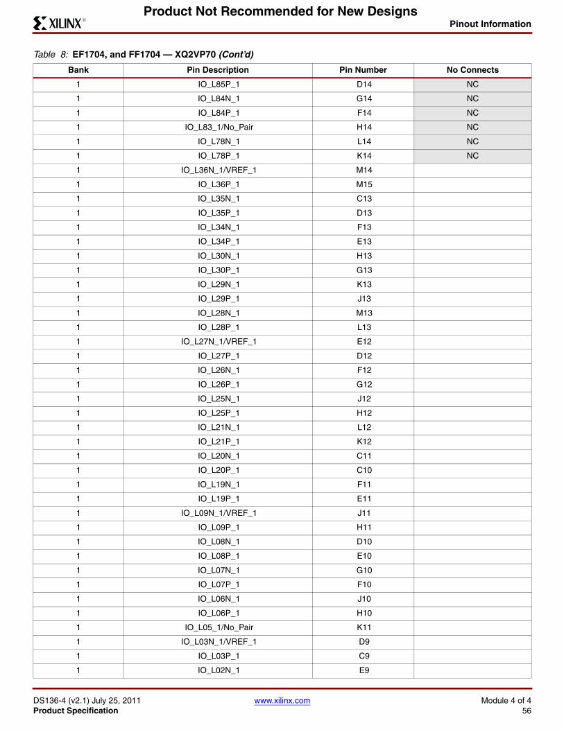
Pinout Information
DS136-4 (v2.1) July 25, 2011 www.xilinx.com Module 4 of 4Product Specification 56
R
Product Not Recommended for New Designs
1 IO_L85P_1 D14 NC
1 IO_L84N_1 G14 NC
1 IO_L84P_1 F14 NC
1 IO_L83_1/No_Pair H14 NC
1 IO_L78N_1 L14 NC
1 IO_L78P_1 K14 NC
1 IO_L36N_1/VREF_1 M14
1 IO_L36P_1 M15
1 IO_L35N_1 C13
1 IO_L35P_1 D13
1 IO_L34N_1 F13
1 IO_L34P_1 E13
1 IO_L30N_1 H13
1 IO_L30P_1 G13
1 IO_L29N_1 K13
1 IO_L29P_1 J13
1 IO_L28N_1 M13
1 IO_L28P_1 L13
1 IO_L27N_1/VREF_1 E12
1 IO_L27P_1 D12
1 IO_L26N_1 F12
1 IO_L26P_1 G12
1 IO_L25N_1 J12
1 IO_L25P_1 H12
1 IO_L21N_1 L12
1 IO_L21P_1 K12
1 IO_L20N_1 C11
1 IO_L20P_1 C10
1 IO_L19N_1 F11
1 IO_L19P_1 E11
1 IO_L09N_1/VREF_1 J11
1 IO_L09P_1 H11
1 IO_L08N_1 D10
1 IO_L08P_1 E10
1 IO_L07N_1 G10
1 IO_L07P_1 F10
1 IO_L06N_1 J10
1 IO_L06P_1 H10
1 IO_L05_1/No_Pair K11
1 IO_L03N_1/VREF_1 D9
1 IO_L03P_1 C9
1 IO_L02N_1 E9
Table 8: EF1704, and FF1704 — XQ2VP70 (Cont’d)
Bank Pin Description Pin Number No Connects
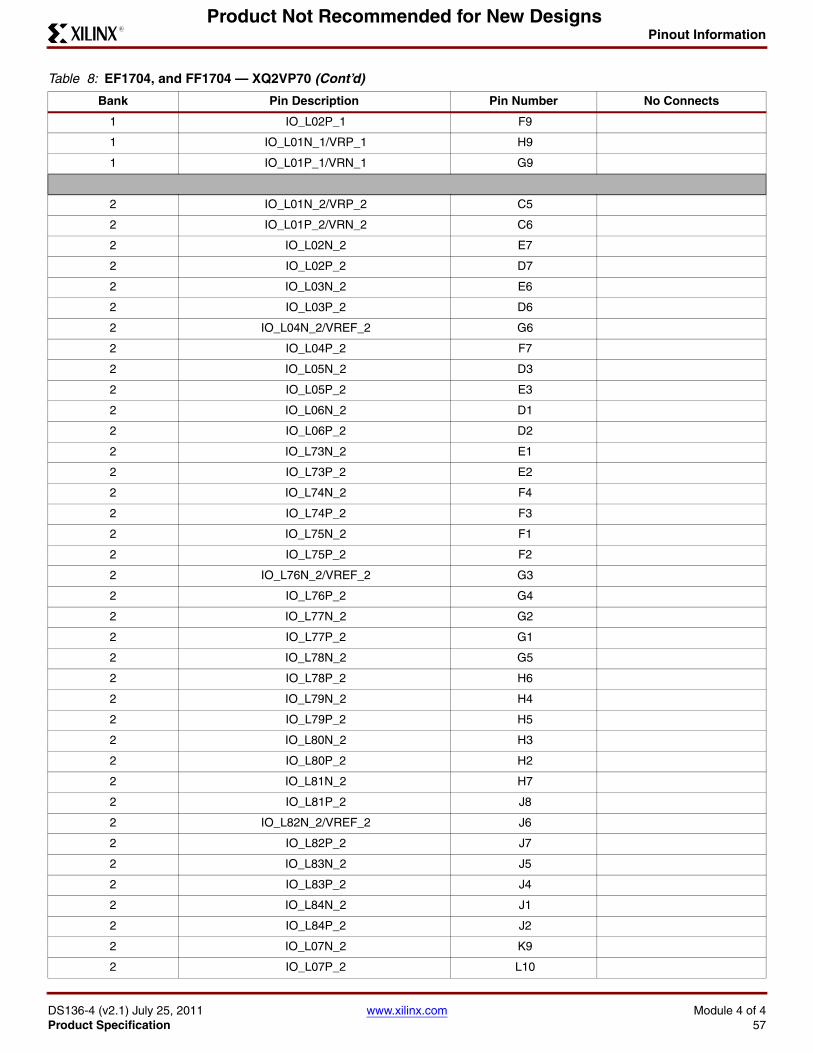
Pinout Information
DS136-4 (v2.1) July 25, 2011 www.xilinx.com Module 4 of 4Product Specification 57
R
Product Not Recommended for New Designs
1 IO_L02P_1 F9
1 IO_L01N_1/VRP_1 H9
1 IO_L01P_1/VRN_1 G9
2 IO_L01N_2/VRP_2 C5
2 IO_L01P_2/VRN_2 C6
2 IO_L02N_2 E7
2 IO_L02P_2 D7
2 IO_L03N_2 E6
2 IO_L03P_2 D6
2 IO_L04N_2/VREF_2 G6
2 IO_L04P_2 F7
2 IO_L05N_2 D3
2 IO_L05P_2 E3
2 IO_L06N_2 D1
2 IO_L06P_2 D2
2 IO_L73N_2 E1
2 IO_L73P_2 E2
2 IO_L74N_2 F4
2 IO_L74P_2 F3
2 IO_L75N_2 F1
2 IO_L75P_2 F2
2 IO_L76N_2/VREF_2 G3
2 IO_L76P_2 G4
2 IO_L77N_2 G2
2 IO_L77P_2 G1
2 IO_L78N_2 G5
2 IO_L78P_2 H6
2 IO_L79N_2 H4
2 IO_L79P_2 H5
2 IO_L80N_2 H3
2 IO_L80P_2 H2
2 IO_L81N_2 H7
2 IO_L81P_2 J8
2 IO_L82N_2/VREF_2 J6
2 IO_L82P_2 J7
2 IO_L83N_2 J5
2 IO_L83P_2 J4
2 IO_L84N_2 J1
2 IO_L84P_2 J2
2 IO_L07N_2 K9
2 IO_L07P_2 L10
Table 8: EF1704, and FF1704 — XQ2VP70 (Cont’d)
Bank Pin Description Pin Number No Connects
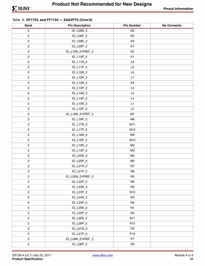
Pinout Information
DS136-4 (v2.1) July 25, 2011 www.xilinx.com Module 4 of 4Product Specification 58
R
Product Not Recommended for New Designs
2 IO_L08N_2 K6
2 IO_L08P_2 K5
2 IO_L09N_2 K8
2 IO_L09P_2 K7
2 IO_L10N_2/VREF_2 K2
2 IO_L10P_2 K1
2 IO_L11N_2 L8
2 IO_L11P_2 L9
2 IO_L12N_2 L6
2 IO_L12P_2 L7
2 IO_L13N_2 K3
2 IO_L13P_2 L3
2 IO_L14N_2 L5
2 IO_L14P_2 L4
2 IO_L15N_2 L1
2 IO_L15P_2 L2
2 IO_L16N_2/VREF_2 M7
2 IO_L16P_2 M8
2 IO_L17N_2 M11
2 IO_L17P_2 M12
2 IO_L18N_2 M9
2 IO_L18P_2 M10
2 IO_L19N_2 M2
2 IO_L19P_2 M3
2 IO_L20N_2 M4
2 IO_L20P_2 M5
2 IO_L21N_2 N7
2 IO_L21P_2 N8
2 IO_L22N_2/VREF_2 N5
2 IO_L22P_2 N6
2 IO_L23N_2 N9
2 IO_L23P_2 N10
2 IO_L24N_2 N3
2 IO_L24P_2 N4
2 IO_L25N_2 N1
2 IO_L25P_2 N2
2 IO_L26N_2 N11
2 IO_L26P_2 N12
2 IO_L27N_2 P9
2 IO_L27P_2 P10
2 IO_L28N_2/VREF_2 P7
2 IO_L28P_2 P8
Table 8: EF1704, and FF1704 — XQ2VP70 (Cont’d)
Bank Pin Description Pin Number No Connects
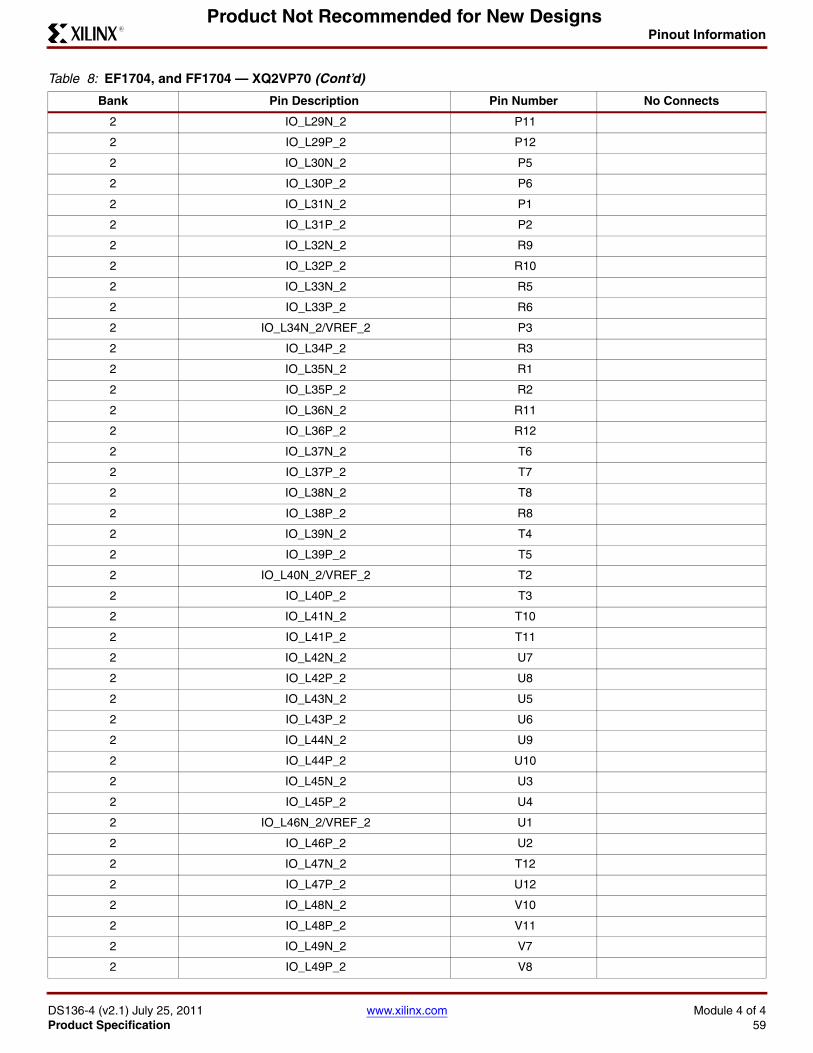
Pinout Information
DS136-4 (v2.1) July 25, 2011 www.xilinx.com Module 4 of 4Product Specification 59
R
Product Not Recommended for New Designs
2 IO_L29N_2 P11
2 IO_L29P_2 P12
2 IO_L30N_2 P5
2 IO_L30P_2 P6
2 IO_L31N_2 P1
2 IO_L31P_2 P2
2 IO_L32N_2 R9
2 IO_L32P_2 R10
2 IO_L33N_2 R5
2 IO_L33P_2 R6
2 IO_L34N_2/VREF_2 P3
2 IO_L34P_2 R3
2 IO_L35N_2 R1
2 IO_L35P_2 R2
2 IO_L36N_2 R11
2 IO_L36P_2 R12
2 IO_L37N_2 T6
2 IO_L37P_2 T7
2 IO_L38N_2 T8
2 IO_L38P_2 R8
2 IO_L39N_2 T4
2 IO_L39P_2 T5
2 IO_L40N_2/VREF_2 T2
2 IO_L40P_2 T3
2 IO_L41N_2 T10
2 IO_L41P_2 T11
2 IO_L42N_2 U7
2 IO_L42P_2 U8
2 IO_L43N_2 U5
2 IO_L43P_2 U6
2 IO_L44N_2 U9
2 IO_L44P_2 U10
2 IO_L45N_2 U3
2 IO_L45P_2 U4
2 IO_L46N_2/VREF_2 U1
2 IO_L46P_2 U2
2 IO_L47N_2 T12
2 IO_L47P_2 U12
2 IO_L48N_2 V10
2 IO_L48P_2 V11
2 IO_L49N_2 V7
2 IO_L49P_2 V8
Table 8: EF1704, and FF1704 — XQ2VP70 (Cont’d)
Bank Pin Description Pin Number No Connects
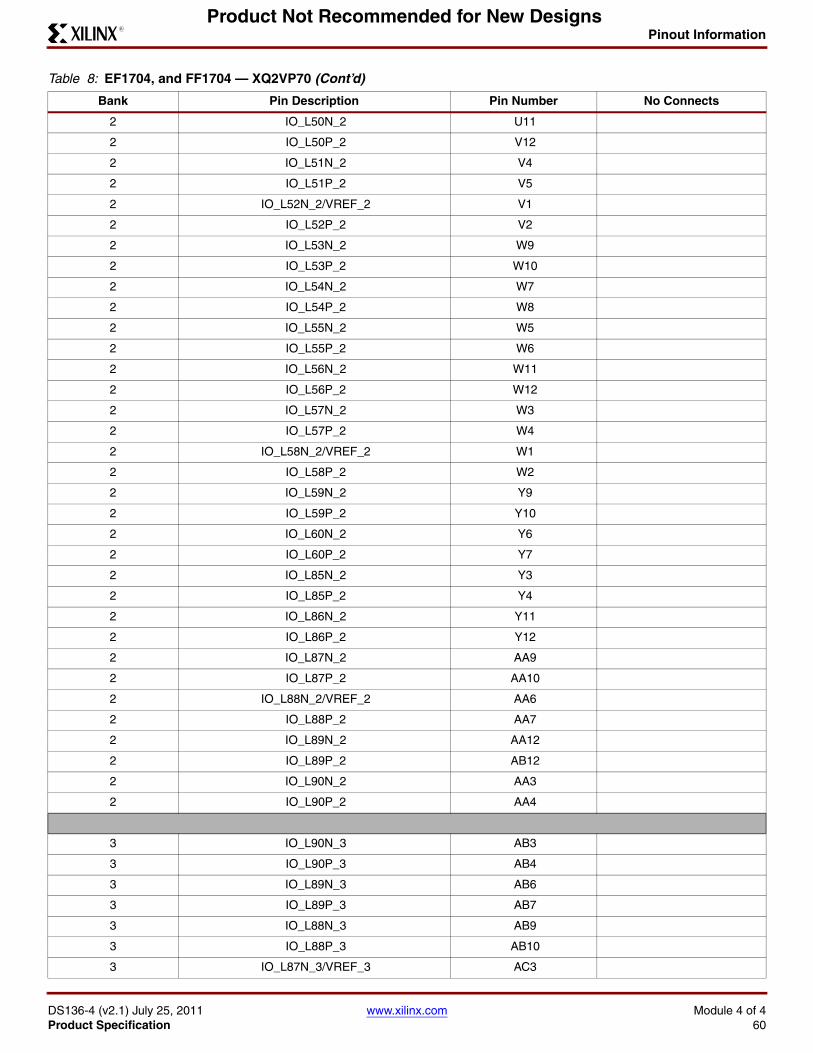
Pinout Information
DS136-4 (v2.1) July 25, 2011 www.xilinx.com Module 4 of 4Product Specification 60
R
Product Not Recommended for New Designs
2 IO_L50N_2 U11
2 IO_L50P_2 V12
2 IO_L51N_2 V4
2 IO_L51P_2 V5
2 IO_L52N_2/VREF_2 V1
2 IO_L52P_2 V2
2 IO_L53N_2 W9
2 IO_L53P_2 W10
2 IO_L54N_2 W7
2 IO_L54P_2 W8
2 IO_L55N_2 W5
2 IO_L55P_2 W6
2 IO_L56N_2 W11
2 IO_L56P_2 W12
2 IO_L57N_2 W3
2 IO_L57P_2 W4
2 IO_L58N_2/VREF_2 W1
2 IO_L58P_2 W2
2 IO_L59N_2 Y9
2 IO_L59P_2 Y10
2 IO_L60N_2 Y6
2 IO_L60P_2 Y7
2 IO_L85N_2 Y3
2 IO_L85P_2 Y4
2 IO_L86N_2 Y11
2 IO_L86P_2 Y12
2 IO_L87N_2 AA9
2 IO_L87P_2 AA10
2 IO_L88N_2/VREF_2 AA6
2 IO_L88P_2 AA7
2 IO_L89N_2 AA12
2 IO_L89P_2 AB12
2 IO_L90N_2 AA3
2 IO_L90P_2 AA4
3 IO_L90N_3 AB3
3 IO_L90P_3 AB4
3 IO_L89N_3 AB6
3 IO_L89P_3 AB7
3 IO_L88N_3 AB9
3 IO_L88P_3 AB10
3 IO_L87N_3/VREF_3 AC3
Table 8: EF1704, and FF1704 — XQ2VP70 (Cont’d)
Bank Pin Description Pin Number No Connects

Pinout Information
DS136-4 (v2.1) July 25, 2011 www.xilinx.com Module 4 of 4Product Specification 61
R
Product Not Recommended for New Designs
3 IO_L87P_3 AC4
3 IO_L86N_3 AC11
3 IO_L86P_3 AC12
3 IO_L85N_3 AC6
3 IO_L85P_3 AC7
3 IO_L60N_3 AC9
3 IO_L60P_3 AC10
3 IO_L59N_3 AD9
3 IO_L59P_3 AD10
3 IO_L58N_3 AD1
3 IO_L58P_3 AD2
3 IO_L57N_3/VREF_3 AD3
3 IO_L57P_3 AD4
3 IO_L56N_3 AD11
3 IO_L56P_3 AD12
3 IO_L55N_3 AD5
3 IO_L55P_3 AD6
3 IO_L54N_3 AD7
3 IO_L54P_3 AD8
3 IO_L53N_3 AE10
3 IO_L53P_3 AE11
3 IO_L52N_3 AE1
3 IO_L52P_3 AE2
3 IO_L51N_3/VREF_3 AE4
3 IO_L51P_3 AE5
3 IO_L50N_3 AF11
3 IO_L50P_3 AE12
3 IO_L49N_3 AE7
3 IO_L49P_3 AE8
3 IO_L48N_3 AF1
3 IO_L48P_3 AF2
3 IO_L47N_3 AG12
3 IO_L47P_3 AF12
3 IO_L46N_3 AF3
3 IO_L46P_3 AF4
3 IO_L45N_3/VREF_3 AF5
3 IO_L45P_3 AF6
3 IO_L44N_3 AF7
3 IO_L44P_3 AF8
3 IO_L43N_3 AF9
3 IO_L43P_3 AF10
3 IO_L42N_3 AG2
Table 8: EF1704, and FF1704 — XQ2VP70 (Cont’d)
Bank Pin Description Pin Number No Connects
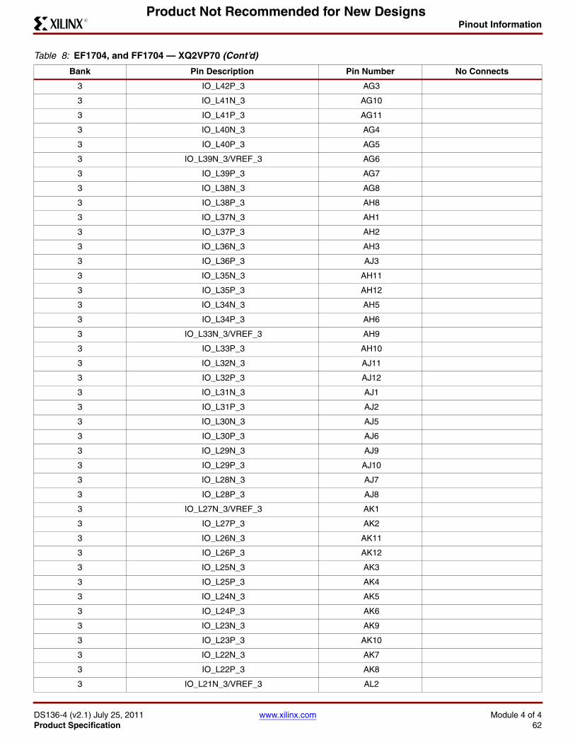
Pinout Information
DS136-4 (v2.1) July 25, 2011 www.xilinx.com Module 4 of 4Product Specification 62
R
Product Not Recommended for New Designs
3 IO_L42P_3 AG3
3 IO_L41N_3 AG10
3 IO_L41P_3 AG11
3 IO_L40N_3 AG4
3 IO_L40P_3 AG5
3 IO_L39N_3/VREF_3 AG6
3 IO_L39P_3 AG7
3 IO_L38N_3 AG8
3 IO_L38P_3 AH8
3 IO_L37N_3 AH1
3 IO_L37P_3 AH2
3 IO_L36N_3 AH3
3 IO_L36P_3 AJ3
3 IO_L35N_3 AH11
3 IO_L35P_3 AH12
3 IO_L34N_3 AH5
3 IO_L34P_3 AH6
3 IO_L33N_3/VREF_3 AH9
3 IO_L33P_3 AH10
3 IO_L32N_3 AJ11
3 IO_L32P_3 AJ12
3 IO_L31N_3 AJ1
3 IO_L31P_3 AJ2
3 IO_L30N_3 AJ5
3 IO_L30P_3 AJ6
3 IO_L29N_3 AJ9
3 IO_L29P_3 AJ10
3 IO_L28N_3 AJ7
3 IO_L28P_3 AJ8
3 IO_L27N_3/VREF_3 AK1
3 IO_L27P_3 AK2
3 IO_L26N_3 AK11
3 IO_L26P_3 AK12
3 IO_L25N_3 AK3
3 IO_L25P_3 AK4
3 IO_L24N_3 AK5
3 IO_L24P_3 AK6
3 IO_L23N_3 AK9
3 IO_L23P_3 AK10
3 IO_L22N_3 AK7
3 IO_L22P_3 AK8
3 IO_L21N_3/VREF_3 AL2
Table 8: EF1704, and FF1704 — XQ2VP70 (Cont’d)
Bank Pin Description Pin Number No Connects
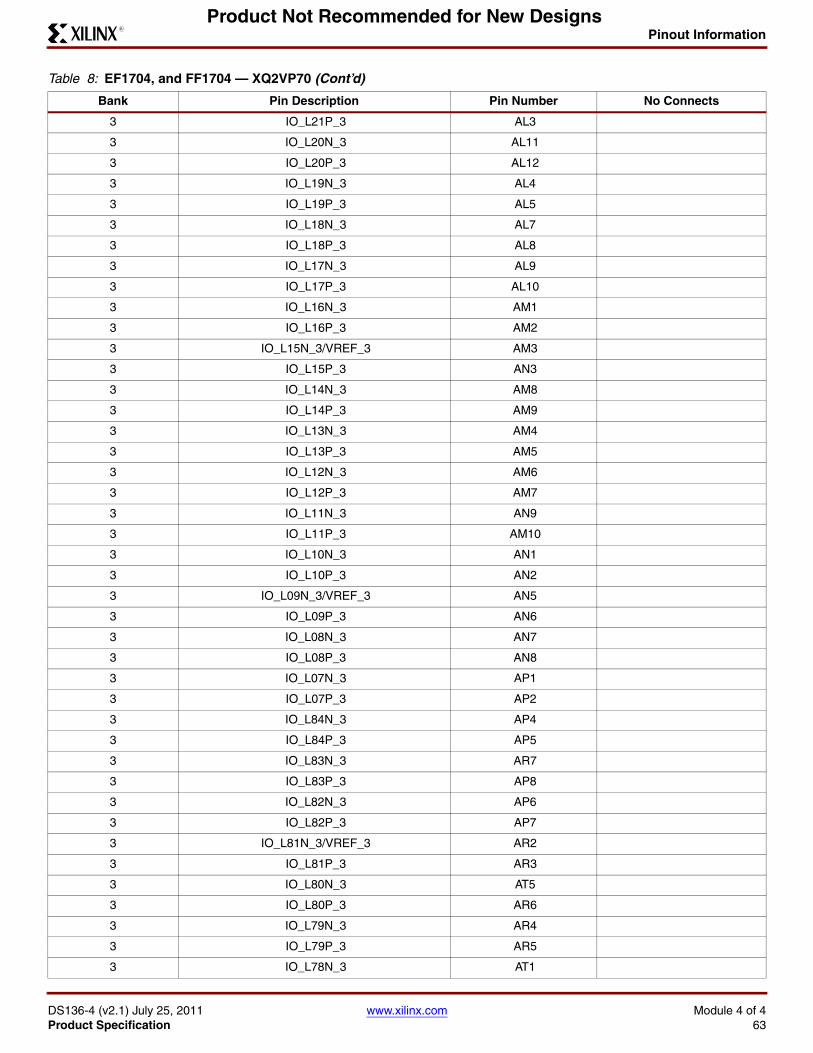
Pinout Information
DS136-4 (v2.1) July 25, 2011 www.xilinx.com Module 4 of 4Product Specification 63
R
Product Not Recommended for New Designs
3 IO_L21P_3 AL3
3 IO_L20N_3 AL11
3 IO_L20P_3 AL12
3 IO_L19N_3 AL4
3 IO_L19P_3 AL5
3 IO_L18N_3 AL7
3 IO_L18P_3 AL8
3 IO_L17N_3 AL9
3 IO_L17P_3 AL10
3 IO_L16N_3 AM1
3 IO_L16P_3 AM2
3 IO_L15N_3/VREF_3 AM3
3 IO_L15P_3 AN3
3 IO_L14N_3 AM8
3 IO_L14P_3 AM9
3 IO_L13N_3 AM4
3 IO_L13P_3 AM5
3 IO_L12N_3 AM6
3 IO_L12P_3 AM7
3 IO_L11N_3 AN9
3 IO_L11P_3 AM10
3 IO_L10N_3 AN1
3 IO_L10P_3 AN2
3 IO_L09N_3/VREF_3 AN5
3 IO_L09P_3 AN6
3 IO_L08N_3 AN7
3 IO_L08P_3 AN8
3 IO_L07N_3 AP1
3 IO_L07P_3 AP2
3 IO_L84N_3 AP4
3 IO_L84P_3 AP5
3 IO_L83N_3 AR7
3 IO_L83P_3 AP8
3 IO_L82N_3 AP6
3 IO_L82P_3 AP7
3 IO_L81N_3/VREF_3 AR2
3 IO_L81P_3 AR3
3 IO_L80N_3 AT5
3 IO_L80P_3 AR6
3 IO_L79N_3 AR4
3 IO_L79P_3 AR5
3 IO_L78N_3 AT1
Table 8: EF1704, and FF1704 — XQ2VP70 (Cont’d)
Bank Pin Description Pin Number No Connects
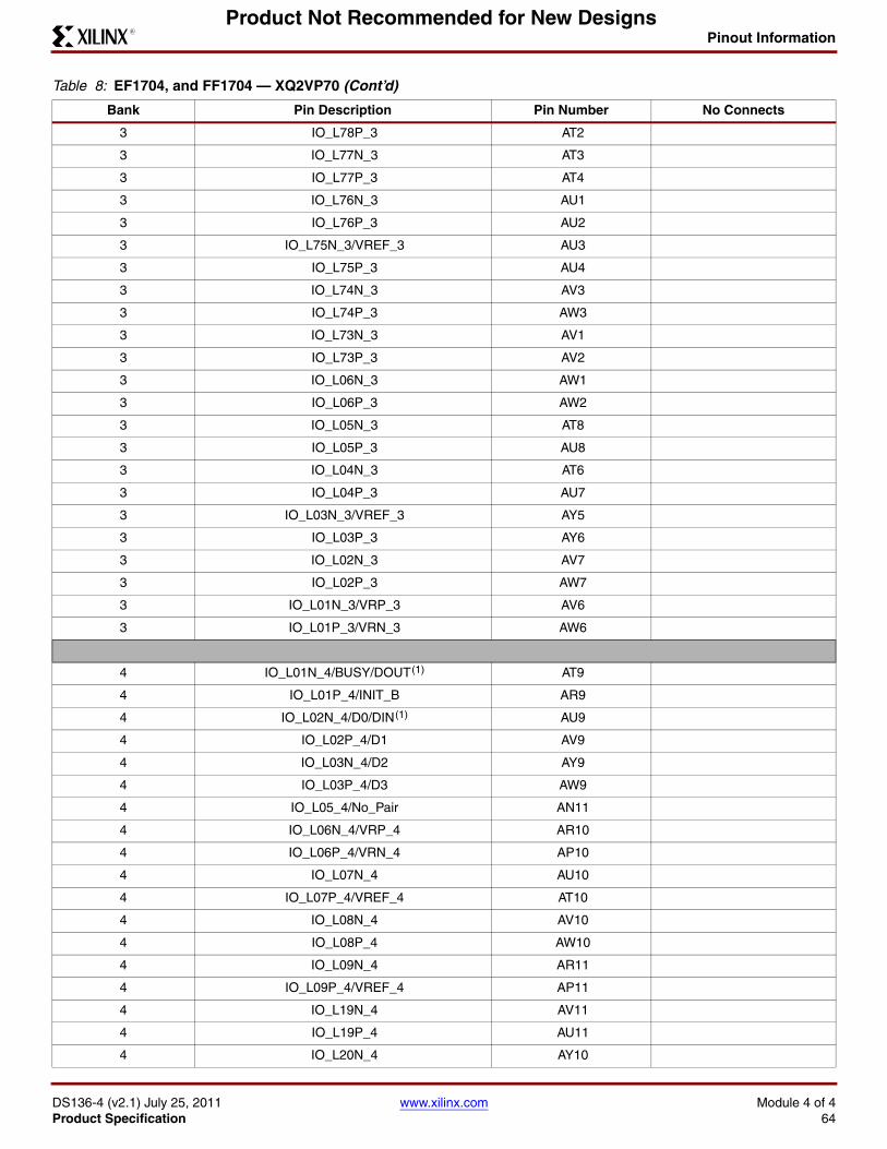
Pinout Information
DS136-4 (v2.1) July 25, 2011 www.xilinx.com Module 4 of 4Product Specification 64
R
Product Not Recommended for New Designs
3 IO_L78P_3 AT2
3 IO_L77N_3 AT3
3 IO_L77P_3 AT4
3 IO_L76N_3 AU1
3 IO_L76P_3 AU2
3 IO_L75N_3/VREF_3 AU3
3 IO_L75P_3 AU4
3 IO_L74N_3 AV3
3 IO_L74P_3 AW3
3 IO_L73N_3 AV1
3 IO_L73P_3 AV2
3 IO_L06N_3 AW1
3 IO_L06P_3 AW2
3 IO_L05N_3 AT8
3 IO_L05P_3 AU8
3 IO_L04N_3 AT6
3 IO_L04P_3 AU7
3 IO_L03N_3/VREF_3 AY5
3 IO_L03P_3 AY6
3 IO_L02N_3 AV7
3 IO_L02P_3 AW7
3 IO_L01N_3/VRP_3 AV6
3 IO_L01P_3/VRN_3 AW6
4 IO_L01N_4/BUSY/DOUT (1) AT9
4 IO_L01P_4/INIT_B AR9
4 IO_L02N_4/D0/DIN (1) AU9
4 IO_L02P_4/D1 AV9
4 IO_L03N_4/D2 AY9
4 IO_L03P_4/D3 AW9
4 IO_L05_4/No_Pair AN11
4 IO_L06N_4/VRP_4 AR10
4 IO_L06P_4/VRN_4 AP10
4 IO_L07N_4 AU10
4 IO_L07P_4/VREF_4 AT10
4 IO_L08N_4 AV10
4 IO_L08P_4 AW10
4 IO_L09N_4 AR11
4 IO_L09P_4/VREF_4 AP11
4 IO_L19N_4 AV11
4 IO_L19P_4 AU11
4 IO_L20N_4 AY10
Table 8: EF1704, and FF1704 — XQ2VP70 (Cont’d)
Bank Pin Description Pin Number No Connects
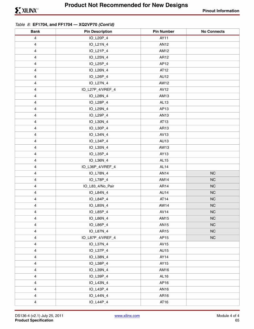
Pinout Information
DS136-4 (v2.1) July 25, 2011 www.xilinx.com Module 4 of 4Product Specification 65
R
Product Not Recommended for New Designs
4 IO_L20P_4 AY11
4 IO_L21N_4 AN12
4 IO_L21P_4 AM12
4 IO_L25N_4 AR12
4 IO_L25P_4 AP12
4 IO_L26N_4 AT12
4 IO_L26P_4 AU12
4 IO_L27N_4 AW12
4 IO_L27P_4/VREF_4 AV12
4 IO_L28N_4 AM13
4 IO_L28P_4 AL13
4 IO_L29N_4 AP13
4 IO_L29P_4 AN13
4 IO_L30N_4 AT13
4 IO_L30P_4 AR13
4 IO_L34N_4 AV13
4 IO_L34P_4 AU13
4 IO_L35N_4 AW13
4 IO_L35P_4 AY13
4 IO_L36N_4 AL15
4 IO_L36P_4/VREF_4 AL14
4 IO_L78N_4 AN14 NC
4 IO_L78P_4 AM14 NC
4 IO_L83_4/No_Pair AR14 NC
4 IO_L84N_4 AU14 NC
4 IO_L84P_4 AT14 NC
4 IO_L85N_4 AW14 NC
4 IO_L85P_4 AV14 NC
4 IO_L86N_4 AM15 NC
4 IO_L86P_4 AN15 NC
4 IO_L87N_4 AR15 NC
4 IO_L87P_4/VREF_4 AP15 NC
4 IO_L37N_4 AV15
4 IO_L37P_4 AU15
4 IO_L38N_4 AY14
4 IO_L38P_4 AY15
4 IO_L39N_4 AM16
4 IO_L39P_4 AL16
4 IO_L43N_4 AP16
4 IO_L43P_4 AN16
4 IO_L44N_4 AR16
4 IO_L44P_4 AT16
Table 8: EF1704, and FF1704 — XQ2VP70 (Cont’d)
Bank Pin Description Pin Number No Connects

Pinout Information
DS136-4 (v2.1) July 25, 2011 www.xilinx.com Module 4 of 4Product Specification 66
R
Product Not Recommended for New Designs
4 IO_L45N_4 AV16
4 IO_L45P_4/VREF_4 AU16
4 IO_L46N_4 AL18
4 IO_L46P_4 AL17
4 IO_L47N_4 AM17
4 IO_L47P_4 AN17
4 IO_L48N_4 AR17
4 IO_L48P_4 AP17
4 IO_L49N_4 AU17
4 IO_L49P_4 AT17
4 IO_L50_4/No_Pair AW16
4 IO_L53_4/No_Pair AW17
4 IO_L54N_4 AN18
4 IO_L54P_4 AM18
4 IO_L55N_4 AT18
4 IO_L55P_4 AR18
4 IO_L56N_4 AV17
4 IO_L56P_4 AV18
4 IO_L57N_4 AY18
4 IO_L57P_4/VREF_4 AY17
4 IO_L58N_4 AM19
4 IO_L58P_4 AL19
4 IO_L59N_4 AP19
4 IO_L59P_4 AN19
4 IO_L60N_4 AT19
4 IO_L60P_4 AR19
4 IO_L64N_4 AV19
4 IO_L64P_4 AU19
4 IO_L65N_4 AW19
4 IO_L65P_4 AY19
4 IO_L66N_4 AL21
4 IO_L66P_4/VREF_4 AL20
4 IO_L67N_4 AN20
4 IO_L67P_4 AM20
4 IO_L68N_4 AP20
4 IO_L68P_4 AR20
4 IO_L69N_4 AV20
4 IO_L69P_4/VREF_4 AU20
4 IO_L73N_4 AY20
4 IO_L73P_4 AW20
4 IO_L74N_4/GCLK3S AN21
4 IO_L74P_4/GCLK2P AP21
Table 8: EF1704, and FF1704 — XQ2VP70 (Cont’d)
Bank Pin Description Pin Number No Connects
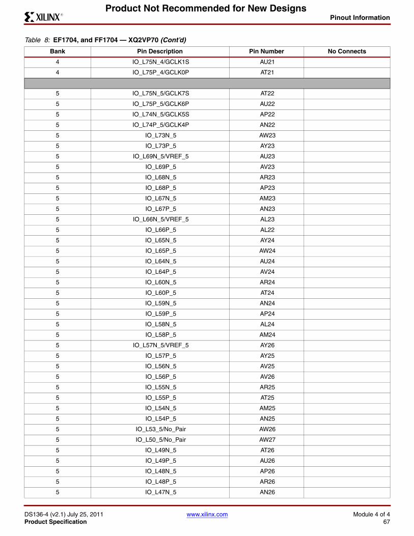
Pinout Information
DS136-4 (v2.1) July 25, 2011 www.xilinx.com Module 4 of 4Product Specification 67
R
Product Not Recommended for New Designs
4 IO_L75N_4/GCLK1S AU21
4 IO_L75P_4/GCLK0P AT21
5 IO_L75N_5/GCLK7S AT22
5 IO_L75P_5/GCLK6P AU22
5 IO_L74N_5/GCLK5S AP22
5 IO_L74P_5/GCLK4P AN22
5 IO_L73N_5 AW23
5 IO_L73P_5 AY23
5 IO_L69N_5/VREF_5 AU23
5 IO_L69P_5 AV23
5 IO_L68N_5 AR23
5 IO_L68P_5 AP23
5 IO_L67N_5 AM23
5 IO_L67P_5 AN23
5 IO_L66N_5/VREF_5 AL23
5 IO_L66P_5 AL22
5 IO_L65N_5 AY24
5 IO_L65P_5 AW24
5 IO_L64N_5 AU24
5 IO_L64P_5 AV24
5 IO_L60N_5 AR24
5 IO_L60P_5 AT24
5 IO_L59N_5 AN24
5 IO_L59P_5 AP24
5 IO_L58N_5 AL24
5 IO_L58P_5 AM24
5 IO_L57N_5/VREF_5 AY26
5 IO_L57P_5 AY25
5 IO_L56N_5 AV25
5 IO_L56P_5 AV26
5 IO_L55N_5 AR25
5 IO_L55P_5 AT25
5 IO_L54N_5 AM25
5 IO_L54P_5 AN25
5 IO_L53_5/No_Pair AW26
5 IO_L50_5/No_Pair AW27
5 IO_L49N_5 AT26
5 IO_L49P_5 AU26
5 IO_L48N_5 AP26
5 IO_L48P_5 AR26
5 IO_L47N_5 AN26
Table 8: EF1704, and FF1704 — XQ2VP70 (Cont’d)
Bank Pin Description Pin Number No Connects
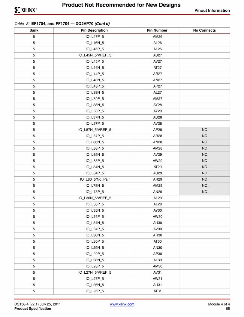
Pinout Information
DS136-4 (v2.1) July 25, 2011 www.xilinx.com Module 4 of 4Product Specification 68
R
Product Not Recommended for New Designs
5 IO_L47P_5 AM26
5 IO_L46N_5 AL26
5 IO_L46P_5 AL25
5 IO_L45N_5/VREF_5 AU27
5 IO_L45P_5 AV27
5 IO_L44N_5 AT27
5 IO_L44P_5 AR27
5 IO_L43N_5 AN27
5 IO_L43P_5 AP27
5 IO_L39N_5 AL27
5 IO_L39P_5 AM27
5 IO_L38N_5 AY28
5 IO_L38P_5 AY29
5 IO_L37N_5 AU28
5 IO_L37P_5 AV28
5 IO_L87N_5/VREF_5 AP28 NC
5 IO_L87P_5 AR28 NC
5 IO_L86N_5 AN28 NC
5 IO_L86P_5 AM28 NC
5 IO_L85N_5 AV29 NC
5 IO_L85P_5 AW29 NC
5 IO_L84N_5 AT29 NC
5 IO_L84P_5 AU29 NC
5 IO_L83_5/No_Pair AR29 NC
5 IO_L78N_5 AM29 NC
5 IO_L78P_5 AN29 NC
5 IO_L36N_5/VREF_5 AL29
5 IO_L36P_5 AL28
5 IO_L35N_5 AY30
5 IO_L35P_5 AW30
5 IO_L34N_5 AU30
5 IO_L34P_5 AV30
5 IO_L30N_5 AR30
5 IO_L30P_5 AT30
5 IO_L29N_5 AN30
5 IO_L29P_5 AP30
5 IO_L28N_5 AL30
5 IO_L28P_5 AM30
5 IO_L27N_5/VREF_5 AV31
5 IO_L27P_5 AW31
5 IO_L26N_5 AU31
5 IO_L26P_5 AT31
Table 8: EF1704, and FF1704 — XQ2VP70 (Cont’d)
Bank Pin Description Pin Number No Connects
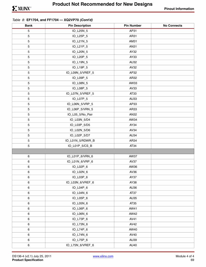
Pinout Information
DS136-4 (v2.1) July 25, 2011 www.xilinx.com Module 4 of 4Product Specification 69
R
Product Not Recommended for New Designs
5 IO_L25N_5 AP31
5 IO_L25P_5 AR31
5 IO_L21N_5 AM31
5 IO_L21P_5 AN31
5 IO_L20N_5 AY32
5 IO_L20P_5 AY33
5 IO_L19N_5 AU32
5 IO_L19P_5 AV32
5 IO_L09N_5/VREF_5 AP32
5 IO_L09P_5 AR32
5 IO_L08N_5 AW33
5 IO_L08P_5 AV33
5 IO_L07N_5/VREF_5 AT33
5 IO_L07P_5 AU33
5 IO_L06N_5/VRP_5 AP33
5 IO_L06P_5/VRN_5 AR33
5 IO_L05_5/No_Pair AN32
5 IO_L03N_5/D4 AW34
5 IO_L03P_5/D5 AY34
5 IO_L02N_5/D6 AV34
5 IO_L02P_5/D7 AU34
5 IO_L01N_5/RDWR_B AR34
5 IO_L01P_5/CS_B AT34
6 IO_L01P_6/VRN_6 AW37
6 IO_L01N_6/VRP_6 AV37
6 IO_L02P_6 AW36
6 IO_L02N_6 AV36
6 IO_L03P_6 AY37
6 IO_L03N_6/VREF_6 AY38
6 IO_L04P_6 AU36
6 IO_L04N_6 AT37
6 IO_L05P_6 AU35
6 IO_L05N_6 AT35
6 IO_L06P_6 AW41
6 IO_L06N_6 AW42
6 IO_L73P_6 AV41
6 IO_L73N_6 AV42
6 IO_L74P_6 AW40
6 IO_L74N_6 AV40
6 IO_L75P_6 AU39
6 IO_L75N_6/VREF_6 AU40
Table 8: EF1704, and FF1704 — XQ2VP70 (Cont’d)
Bank Pin Description Pin Number No Connects

Pinout Information
DS136-4 (v2.1) July 25, 2011 www.xilinx.com Module 4 of 4Product Specification 70
R
Product Not Recommended for New Designs
6 IO_L76P_6 AU41
6 IO_L76N_6 AU42
6 IO_L77P_6 AT39
6 IO_L77N_6 AT40
6 IO_L78P_6 AT41
6 IO_L78N_6 AT42
6 IO_L79P_6 AR38
6 IO_L79N_6 AR39
6 IO_L80P_6 AR37
6 IO_L80N_6 AT38
6 IO_L81P_6 AR40
6 IO_L81N_6/VREF_6 AR41
6 IO_L82P_6 AP36
6 IO_L82N_6 AP37
6 IO_L83P_6 AP35
6 IO_L83N_6 AR36
6 IO_L84P_6 AP38
6 IO_L84N_6 AP39
6 IO_L07P_6 AP41
6 IO_L07N_6 AP42
6 IO_L08P_6 AN35
6 IO_L08N_6 AN36
6 IO_L09P_6 AN37
6 IO_L09N_6/VREF_6 AN38
6 IO_L10P_6 AN41
6 IO_L10N_6 AN42
6 IO_L11P_6 AM33
6 IO_L11N_6 AN34
6 IO_L12P_6 AM36
6 IO_L12N_6 AM37
6 IO_L13P_6 AM38
6 IO_L13N_6 AM39
6 IO_L14P_6 AM34
6 IO_L14N_6 AM35
6 IO_L15P_6 AN40
6 IO_L15N_6/VREF_6 AM40
6 IO_L16P_6 AM41
6 IO_L16N_6 AM42
6 IO_L17P_6 AL33
6 IO_L17N_6 AL34
6 IO_L18P_6 AL35
6 IO_L18N_6 AL36
Table 8: EF1704, and FF1704 — XQ2VP70 (Cont’d)
Bank Pin Description Pin Number No Connects
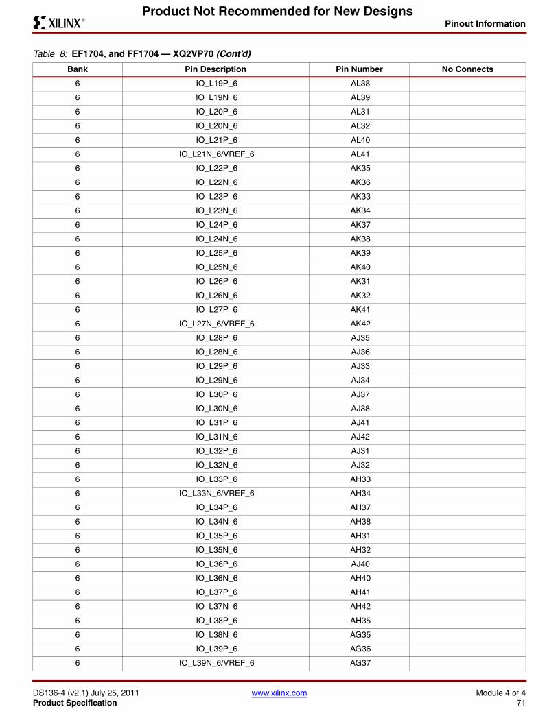
Pinout Information
DS136-4 (v2.1) July 25, 2011 www.xilinx.com Module 4 of 4Product Specification 71
R
Product Not Recommended for New Designs
6 IO_L19P_6 AL38
6 IO_L19N_6 AL39
6 IO_L20P_6 AL31
6 IO_L20N_6 AL32
6 IO_L21P_6 AL40
6 IO_L21N_6/VREF_6 AL41
6 IO_L22P_6 AK35
6 IO_L22N_6 AK36
6 IO_L23P_6 AK33
6 IO_L23N_6 AK34
6 IO_L24P_6 AK37
6 IO_L24N_6 AK38
6 IO_L25P_6 AK39
6 IO_L25N_6 AK40
6 IO_L26P_6 AK31
6 IO_L26N_6 AK32
6 IO_L27P_6 AK41
6 IO_L27N_6/VREF_6 AK42
6 IO_L28P_6 AJ35
6 IO_L28N_6 AJ36
6 IO_L29P_6 AJ33
6 IO_L29N_6 AJ34
6 IO_L30P_6 AJ37
6 IO_L30N_6 AJ38
6 IO_L31P_6 AJ41
6 IO_L31N_6 AJ42
6 IO_L32P_6 AJ31
6 IO_L32N_6 AJ32
6 IO_L33P_6 AH33
6 IO_L33N_6/VREF_6 AH34
6 IO_L34P_6 AH37
6 IO_L34N_6 AH38
6 IO_L35P_6 AH31
6 IO_L35N_6 AH32
6 IO_L36P_6 AJ40
6 IO_L36N_6 AH40
6 IO_L37P_6 AH41
6 IO_L37N_6 AH42
6 IO_L38P_6 AH35
6 IO_L38N_6 AG35
6 IO_L39P_6 AG36
6 IO_L39N_6/VREF_6 AG37
Table 8: EF1704, and FF1704 — XQ2VP70 (Cont’d)
Bank Pin Description Pin Number No Connects
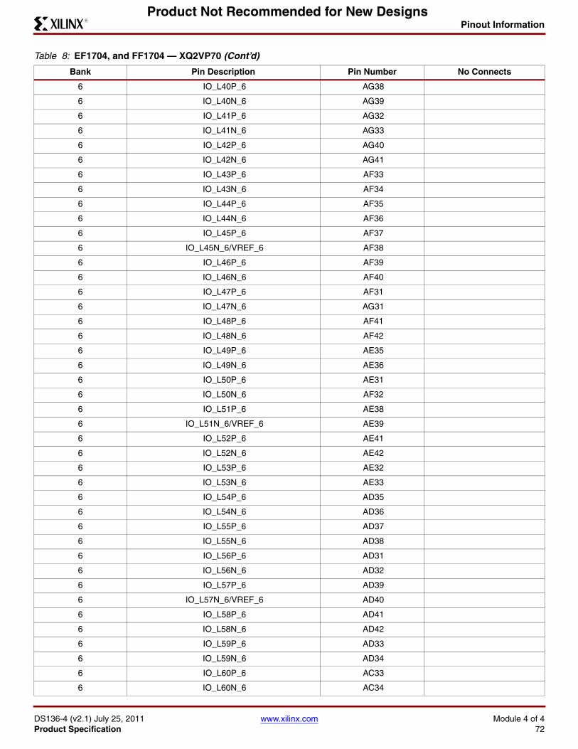
Pinout Information
DS136-4 (v2.1) July 25, 2011 www.xilinx.com Module 4 of 4Product Specification 72
R
Product Not Recommended for New Designs
6 IO_L40P_6 AG38
6 IO_L40N_6 AG39
6 IO_L41P_6 AG32
6 IO_L41N_6 AG33
6 IO_L42P_6 AG40
6 IO_L42N_6 AG41
6 IO_L43P_6 AF33
6 IO_L43N_6 AF34
6 IO_L44P_6 AF35
6 IO_L44N_6 AF36
6 IO_L45P_6 AF37
6 IO_L45N_6/VREF_6 AF38
6 IO_L46P_6 AF39
6 IO_L46N_6 AF40
6 IO_L47P_6 AF31
6 IO_L47N_6 AG31
6 IO_L48P_6 AF41
6 IO_L48N_6 AF42
6 IO_L49P_6 AE35
6 IO_L49N_6 AE36
6 IO_L50P_6 AE31
6 IO_L50N_6 AF32
6 IO_L51P_6 AE38
6 IO_L51N_6/VREF_6 AE39
6 IO_L52P_6 AE41
6 IO_L52N_6 AE42
6 IO_L53P_6 AE32
6 IO_L53N_6 AE33
6 IO_L54P_6 AD35
6 IO_L54N_6 AD36
6 IO_L55P_6 AD37
6 IO_L55N_6 AD38
6 IO_L56P_6 AD31
6 IO_L56N_6 AD32
6 IO_L57P_6 AD39
6 IO_L57N_6/VREF_6 AD40
6 IO_L58P_6 AD41
6 IO_L58N_6 AD42
6 IO_L59P_6 AD33
6 IO_L59N_6 AD34
6 IO_L60P_6 AC33
6 IO_L60N_6 AC34
Table 8: EF1704, and FF1704 — XQ2VP70 (Cont’d)
Bank Pin Description Pin Number No Connects
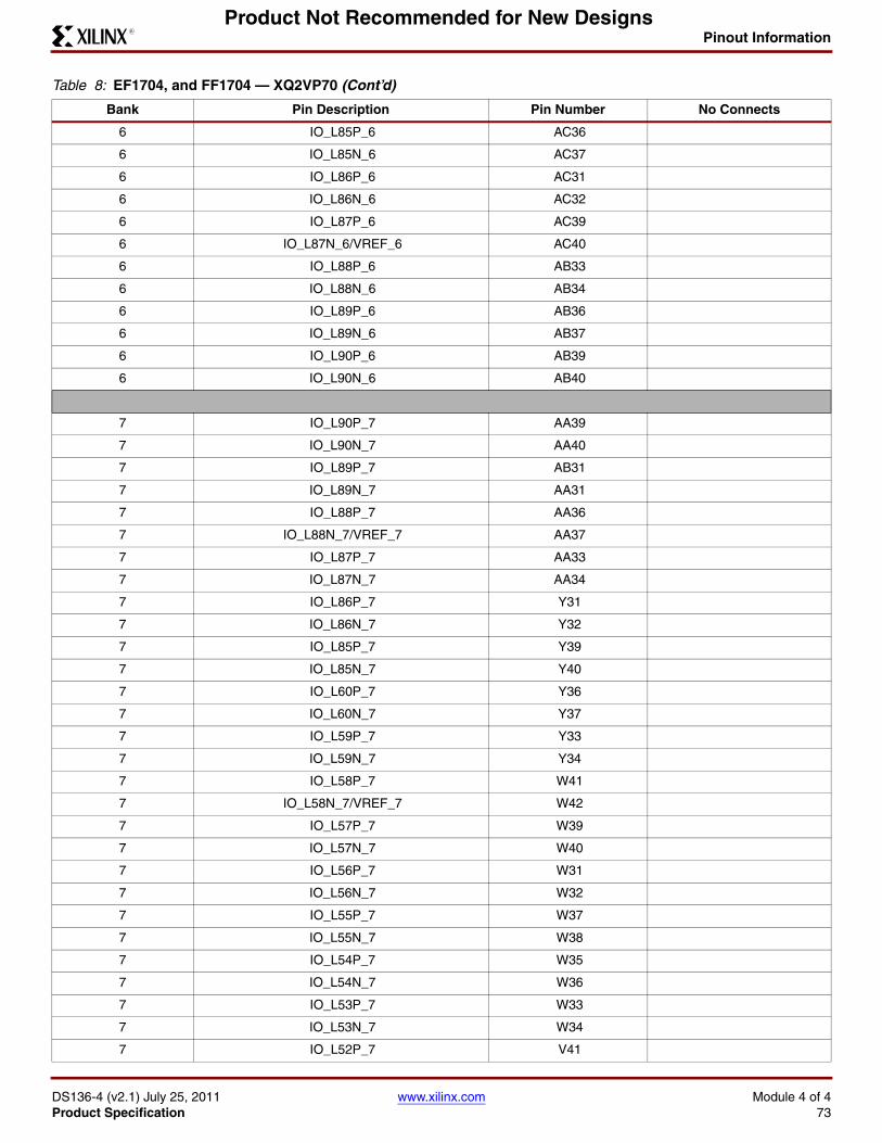
Pinout Information
DS136-4 (v2.1) July 25, 2011 www.xilinx.com Module 4 of 4Product Specification 73
R
Product Not Recommended for New Designs
6 IO_L85P_6 AC36
6 IO_L85N_6 AC37
6 IO_L86P_6 AC31
6 IO_L86N_6 AC32
6 IO_L87P_6 AC39
6 IO_L87N_6/VREF_6 AC40
6 IO_L88P_6 AB33
6 IO_L88N_6 AB34
6 IO_L89P_6 AB36
6 IO_L89N_6 AB37
6 IO_L90P_6 AB39
6 IO_L90N_6 AB40
7 IO_L90P_7 AA39
7 IO_L90N_7 AA40
7 IO_L89P_7 AB31
7 IO_L89N_7 AA31
7 IO_L88P_7 AA36
7 IO_L88N_7/VREF_7 AA37
7 IO_L87P_7 AA33
7 IO_L87N_7 AA34
7 IO_L86P_7 Y31
7 IO_L86N_7 Y32
7 IO_L85P_7 Y39
7 IO_L85N_7 Y40
7 IO_L60P_7 Y36
7 IO_L60N_7 Y37
7 IO_L59P_7 Y33
7 IO_L59N_7 Y34
7 IO_L58P_7 W41
7 IO_L58N_7/VREF_7 W42
7 IO_L57P_7 W39
7 IO_L57N_7 W40
7 IO_L56P_7 W31
7 IO_L56N_7 W32
7 IO_L55P_7 W37
7 IO_L55N_7 W38
7 IO_L54P_7 W35
7 IO_L54N_7 W36
7 IO_L53P_7 W33
7 IO_L53N_7 W34
7 IO_L52P_7 V41
Table 8: EF1704, and FF1704 — XQ2VP70 (Cont’d)
Bank Pin Description Pin Number No Connects
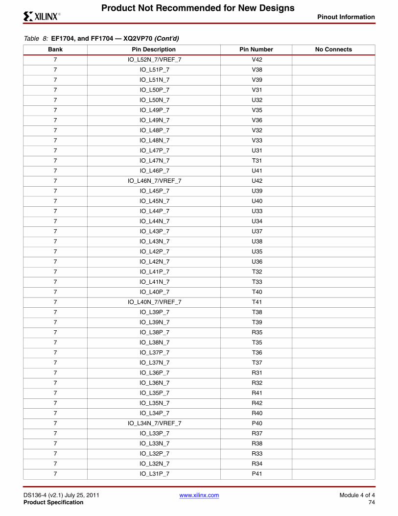
Pinout Information
DS136-4 (v2.1) July 25, 2011 www.xilinx.com Module 4 of 4Product Specification 74
R
Product Not Recommended for New Designs
7 IO_L52N_7/VREF_7 V42
7 IO_L51P_7 V38
7 IO_L51N_7 V39
7 IO_L50P_7 V31
7 IO_L50N_7 U32
7 IO_L49P_7 V35
7 IO_L49N_7 V36
7 IO_L48P_7 V32
7 IO_L48N_7 V33
7 IO_L47P_7 U31
7 IO_L47N_7 T31
7 IO_L46P_7 U41
7 IO_L46N_7/VREF_7 U42
7 IO_L45P_7 U39
7 IO_L45N_7 U40
7 IO_L44P_7 U33
7 IO_L44N_7 U34
7 IO_L43P_7 U37
7 IO_L43N_7 U38
7 IO_L42P_7 U35
7 IO_L42N_7 U36
7 IO_L41P_7 T32
7 IO_L41N_7 T33
7 IO_L40P_7 T40
7 IO_L40N_7/VREF_7 T41
7 IO_L39P_7 T38
7 IO_L39N_7 T39
7 IO_L38P_7 R35
7 IO_L38N_7 T35
7 IO_L37P_7 T36
7 IO_L37N_7 T37
7 IO_L36P_7 R31
7 IO_L36N_7 R32
7 IO_L35P_7 R41
7 IO_L35N_7 R42
7 IO_L34P_7 R40
7 IO_L34N_7/VREF_7 P40
7 IO_L33P_7 R37
7 IO_L33N_7 R38
7 IO_L32P_7 R33
7 IO_L32N_7 R34
7 IO_L31P_7 P41
Table 8: EF1704, and FF1704 — XQ2VP70 (Cont’d)
Bank Pin Description Pin Number No Connects
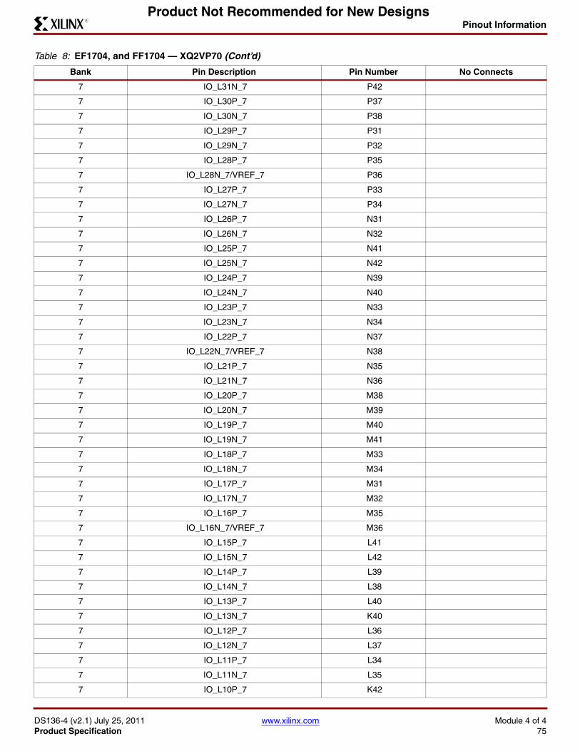
Pinout Information
DS136-4 (v2.1) July 25, 2011 www.xilinx.com Module 4 of 4Product Specification 75
R
Product Not Recommended for New Designs
7 IO_L31N_7 P42
7 IO_L30P_7 P37
7 IO_L30N_7 P38
7 IO_L29P_7 P31
7 IO_L29N_7 P32
7 IO_L28P_7 P35
7 IO_L28N_7/VREF_7 P36
7 IO_L27P_7 P33
7 IO_L27N_7 P34
7 IO_L26P_7 N31
7 IO_L26N_7 N32
7 IO_L25P_7 N41
7 IO_L25N_7 N42
7 IO_L24P_7 N39
7 IO_L24N_7 N40
7 IO_L23P_7 N33
7 IO_L23N_7 N34
7 IO_L22P_7 N37
7 IO_L22N_7/VREF_7 N38
7 IO_L21P_7 N35
7 IO_L21N_7 N36
7 IO_L20P_7 M38
7 IO_L20N_7 M39
7 IO_L19P_7 M40
7 IO_L19N_7 M41
7 IO_L18P_7 M33
7 IO_L18N_7 M34
7 IO_L17P_7 M31
7 IO_L17N_7 M32
7 IO_L16P_7 M35
7 IO_L16N_7/VREF_7 M36
7 IO_L15P_7 L41
7 IO_L15N_7 L42
7 IO_L14P_7 L39
7 IO_L14N_7 L38
7 IO_L13P_7 L40
7 IO_L13N_7 K40
7 IO_L12P_7 L36
7 IO_L12N_7 L37
7 IO_L11P_7 L34
7 IO_L11N_7 L35
7 IO_L10P_7 K42
Table 8: EF1704, and FF1704 — XQ2VP70 (Cont’d)
Bank Pin Description Pin Number No Connects

Pinout Information
DS136-4 (v2.1) July 25, 2011 www.xilinx.com Module 4 of 4Product Specification 76
R
Product Not Recommended for New Designs
7 IO_L10N_7/VREF_7 K41
7 IO_L09P_7 K36
7 IO_L09N_7 K35
7 IO_L08P_7 K38
7 IO_L08N_7 K37
7 IO_L07P_7 L33
7 IO_L07N_7 K34
7 IO_L84P_7 J41
7 IO_L84N_7 J42
7 IO_L83P_7 J39
7 IO_L83N_7 J38
7 IO_L82P_7 J36
7 IO_L82N_7/VREF_7 J37
7 IO_L81P_7 J35
7 IO_L81N_7 H36
7 IO_L80P_7 H41
7 IO_L80N_7 H40
7 IO_L79P_7 H38
7 IO_L79N_7 H39
7 IO_L78P_7 H37
7 IO_L78N_7 G38
7 IO_L77P_7 G42
7 IO_L77N_7 G41
7 IO_L76P_7 G39
7 IO_L76N_7/VREF_7 G40
7 IO_L75P_7 F41
7 IO_L75N_7 F42
7 IO_L74P_7 F40
7 IO_L74N_7 F39
7 IO_L73P_7 E41
7 IO_L73N_7 E42
7 IO_L06P_7 D41
7 IO_L06N_7 D42
7 IO_L05P_7 E40
7 IO_L05N_7 D40
7 IO_L04P_7 F36
7 IO_L04N_7/VREF_7 G37
7 IO_L03P_7 D37
7 IO_L03N_7 E37
7 IO_L02P_7 D36
7 IO_L02N_7 E36
7 IO_L01P_7/VRN_7 C37
Table 8: EF1704, and FF1704 — XQ2VP70 (Cont’d)
Bank Pin Description Pin Number No Connects
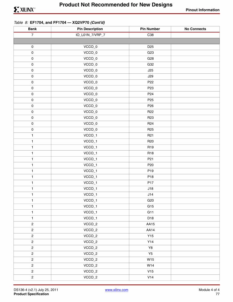
Pinout Information
DS136-4 (v2.1) July 25, 2011 www.xilinx.com Module 4 of 4Product Specification 77
R
Product Not Recommended for New Designs
7 IO_L01N_7/VRP_7 C38
0 VCCO_0 D25
0 VCCO_0 G23
0 VCCO_0 G28
0 VCCO_0 G32
0 VCCO_0 J25
0 VCCO_0 J29
0 VCCO_0 P22
0 VCCO_0 P23
0 VCCO_0 P24
0 VCCO_0 P25
0 VCCO_0 P26
0 VCCO_0 R22
0 VCCO_0 R23
0 VCCO_0 R24
0 VCCO_0 R25
1 VCCO_1 R21
1 VCCO_1 R20
1 VCCO_1 R19
1 VCCO_1 R18
1 VCCO_1 P21
1 VCCO_1 P20
1 VCCO_1 P19
1 VCCO_1 P18
1 VCCO_1 P17
1 VCCO_1 J18
1 VCCO_1 J14
1 VCCO_1 G20
1 VCCO_1 G15
1 VCCO_1 G11
1 VCCO_1 D18
2 VCCO_2 AA15
2 VCCO_2 AA14
2 VCCO_2 Y15
2 VCCO_2 Y14
2 VCCO_2 Y8
2 VCCO_2 Y5
2 VCCO_2 W15
2 VCCO_2 W14
2 VCCO_2 V15
2 VCCO_2 V14
Table 8: EF1704, and FF1704 — XQ2VP70 (Cont’d)
Bank Pin Description Pin Number No Connects
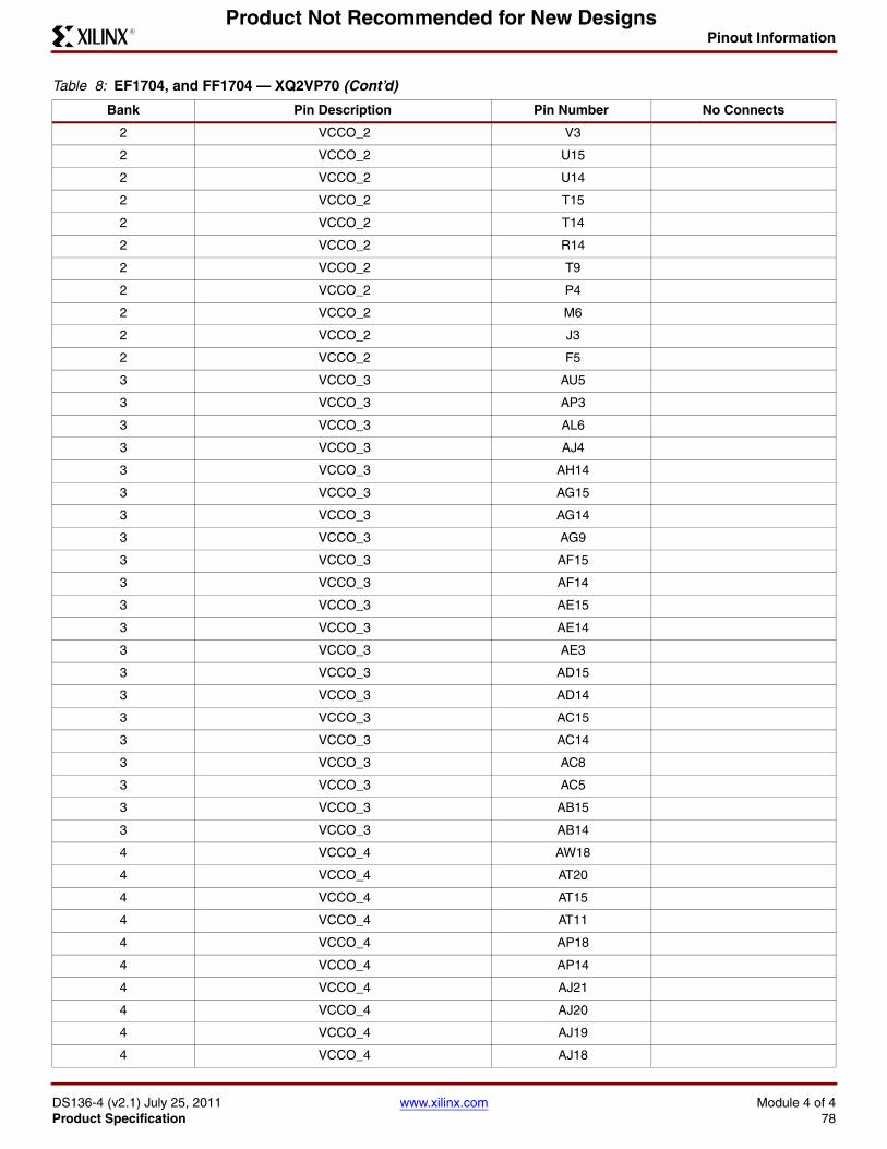
Pinout Information
DS136-4 (v2.1) July 25, 2011 www.xilinx.com Module 4 of 4Product Specification 78
R
Product Not Recommended for New Designs
2 VCCO_2 V3
2 VCCO_2 U15
2 VCCO_2 U14
2 VCCO_2 T15
2 VCCO_2 T14
2 VCCO_2 R14
2 VCCO_2 T9
2 VCCO_2 P4
2 VCCO_2 M6
2 VCCO_2 J3
2 VCCO_2 F5
3 VCCO_3 AU5
3 VCCO_3 AP3
3 VCCO_3 AL6
3 VCCO_3 AJ4
3 VCCO_3 AH14
3 VCCO_3 AG15
3 VCCO_3 AG14
3 VCCO_3 AG9
3 VCCO_3 AF15
3 VCCO_3 AF14
3 VCCO_3 AE15
3 VCCO_3 AE14
3 VCCO_3 AE3
3 VCCO_3 AD15
3 VCCO_3 AD14
3 VCCO_3 AC15
3 VCCO_3 AC14
3 VCCO_3 AC8
3 VCCO_3 AC5
3 VCCO_3 AB15
3 VCCO_3 AB14
4 VCCO_4 AW18
4 VCCO_4 AT20
4 VCCO_4 AT15
4 VCCO_4 AT11
4 VCCO_4 AP18
4 VCCO_4 AP14
4 VCCO_4 AJ21
4 VCCO_4 AJ20
4 VCCO_4 AJ19
4 VCCO_4 AJ18
Table 8: EF1704, and FF1704 — XQ2VP70 (Cont’d)
Bank Pin Description Pin Number No Connects
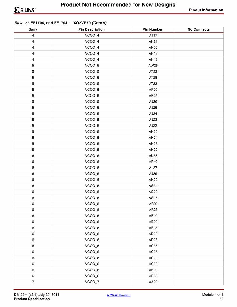
Pinout Information
DS136-4 (v2.1) July 25, 2011 www.xilinx.com Module 4 of 4Product Specification 79
R
Product Not Recommended for New Designs
4 VCCO_4 AJ17
4 VCCO_4 AH21
4 VCCO_4 AH20
4 VCCO_4 AH19
4 VCCO_4 AH18
5 VCCO_5 AW25
5 VCCO_5 AT32
5 VCCO_5 AT28
5 VCCO_5 AT23
5 VCCO_5 AP29
5 VCCO_5 AP25
5 VCCO_5 AJ26
5 VCCO_5 AJ25
5 VCCO_5 AJ24
5 VCCO_5 AJ23
5 VCCO_5 AJ22
5 VCCO_5 AH25
5 VCCO_5 AH24
5 VCCO_5 AH23
5 VCCO_5 AH22
6 VCCO_6 AU38
6 VCCO_6 AP40
6 VCCO_6 AL37
6 VCCO_6 AJ39
6 VCCO_6 AH29
6 VCCO_6 AG34
6 VCCO_6 AG29
6 VCCO_6 AG28
6 VCCO_6 AF29
6 VCCO_6 AF28
6 VCCO_6 AE40
6 VCCO_6 AE29
6 VCCO_6 AE28
6 VCCO_6 AD29
6 VCCO_6 AD28
6 VCCO_6 AC38
6 VCCO_6 AC35
6 VCCO_6 AC29
6 VCCO_6 AC28
6 VCCO_6 AB29
6 VCCO_6 AB28
7 VCCO_7 AA29
Table 8: EF1704, and FF1704 — XQ2VP70 (Cont’d)
Bank Pin Description Pin Number No Connects
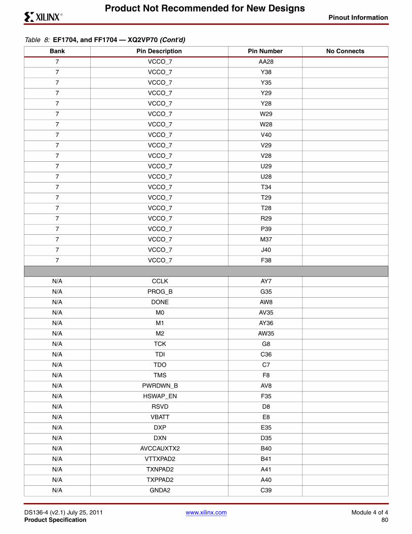
Pinout Information
DS136-4 (v2.1) July 25, 2011 www.xilinx.com Module 4 of 4Product Specification 80
R
Product Not Recommended for New Designs
7 VCCO_7 AA28
7 VCCO_7 Y38
7 VCCO_7 Y35
7 VCCO_7 Y29
7 VCCO_7 Y28
7 VCCO_7 W29
7 VCCO_7 W28
7 VCCO_7 V40
7 VCCO_7 V29
7 VCCO_7 V28
7 VCCO_7 U29
7 VCCO_7 U28
7 VCCO_7 T34
7 VCCO_7 T29
7 VCCO_7 T28
7 VCCO_7 R29
7 VCCO_7 P39
7 VCCO_7 M37
7 VCCO_7 J40
7 VCCO_7 F38
N/A CCLK AY7
N/A PROG_B G35
N/A DONE AW8
N/A M0 AV35
N/A M1 AY36
N/A M2 AW35
N/A TCK G8
N/A TDI C36
N/A TDO C7
N/A TMS F8
N/A PWRDWN_B AV8
N/A HSWAP_EN F35
N/A RSVD D8
N/A VBATT E8
N/A DXP E35
N/A DXN D35
N/A AVCCAUXTX2 B40
N/A VTTXPAD2 B41
N/A TXNPAD2 A41
N/A TXPPAD2 A40
N/A GNDA2 C39
Table 8: EF1704, and FF1704 — XQ2VP70 (Cont’d)
Bank Pin Description Pin Number No Connects

Pinout Information
DS136-4 (v2.1) July 25, 2011 www.xilinx.com Module 4 of 4Product Specification 81
R
Product Not Recommended for New Designs
N/A RXPPAD2 A39
N/A RXNPAD2 A38
N/A VTRXPAD2 B39
N/A AVCCAUXRX2 B38
N/A AVCCAUXTX3 B36
N/A VTTXPAD3 B37
N/A TXNPAD3 A37
N/A TXPPAD3 A36
N/A GNDA3 C35
N/A RXPPAD3 A35
N/A RXNPAD3 A34
N/A VTRXPAD3 B35
N/A AVCCAUXRX3 B34
N/A AVCCAUXTX4 B32
N/A VTTXPAD4 B33
N/A TXNPAD4 A33
N/A TXPPAD4 A32
N/A GNDA4 C31
N/A RXPPAD4 A31
N/A RXNPAD4 A30
N/A VTRXPAD4 B31
N/A AVCCAUXRX4 B30
N/A AVCCAUXTX5 B28
N/A VTTXPAD5 B29
N/A TXNPAD5 A29
N/A TXPPAD5 A28
N/A GNDA5 C27
N/A RXPPAD5 A27
N/A RXNPAD5 A26
N/A VTRXPAD5 B27
N/A AVCCAUXRX5 B26
N/A AVCCAUXTX6 B24
N/A VTTXPAD6 B25
N/A TXNPAD6 A25
N/A TXPPAD6 A24
N/A GNDA6 C22
N/A RXPPAD6 A23
N/A RXNPAD6 A22
N/A VTRXPAD6 B23
N/A AVCCAUXRX6 B22
N/A AVCCAUXTX7 B20
N/A VTTXPAD7 B21
Table 8: EF1704, and FF1704 — XQ2VP70 (Cont’d)
Bank Pin Description Pin Number No Connects
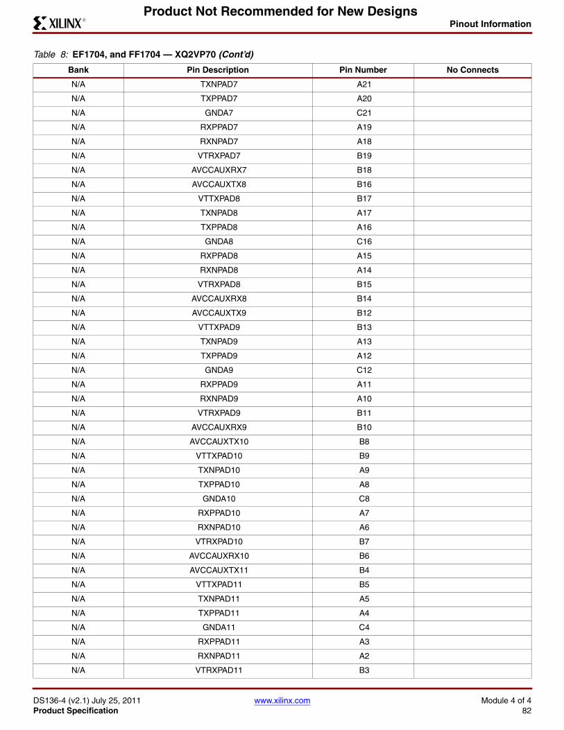
Pinout Information
DS136-4 (v2.1) July 25, 2011 www.xilinx.com Module 4 of 4Product Specification 82
R
Product Not Recommended for New Designs
N/A TXNPAD7 A21
N/A TXPPAD7 A20
N/A GNDA7 C21
N/A RXPPAD7 A19
N/A RXNPAD7 A18
N/A VTRXPAD7 B19
N/A AVCCAUXRX7 B18
N/A AVCCAUXTX8 B16
N/A VTTXPAD8 B17
N/A TXNPAD8 A17
N/A TXPPAD8 A16
N/A GNDA8 C16
N/A RXPPAD8 A15
N/A RXNPAD8 A14
N/A VTRXPAD8 B15
N/A AVCCAUXRX8 B14
N/A AVCCAUXTX9 B12
N/A VTTXPAD9 B13
N/A TXNPAD9 A13
N/A TXPPAD9 A12
N/A GNDA9 C12
N/A RXPPAD9 A11
N/A RXNPAD9 A10
N/A VTRXPAD9 B11
N/A AVCCAUXRX9 B10
N/A AVCCAUXTX10 B8
N/A VTTXPAD10 B9
N/A TXNPAD10 A9
N/A TXPPAD10 A8
N/A GNDA10 C8
N/A RXPPAD10 A7
N/A RXNPAD10 A6
N/A VTRXPAD10 B7
N/A AVCCAUXRX10 B6
N/A AVCCAUXTX11 B4
N/A VTTXPAD11 B5
N/A TXNPAD11 A5
N/A TXPPAD11 A4
N/A GNDA11 C4
N/A RXPPAD11 A3
N/A RXNPAD11 A2
N/A VTRXPAD11 B3
Table 8: EF1704, and FF1704 — XQ2VP70 (Cont’d)
Bank Pin Description Pin Number No Connects
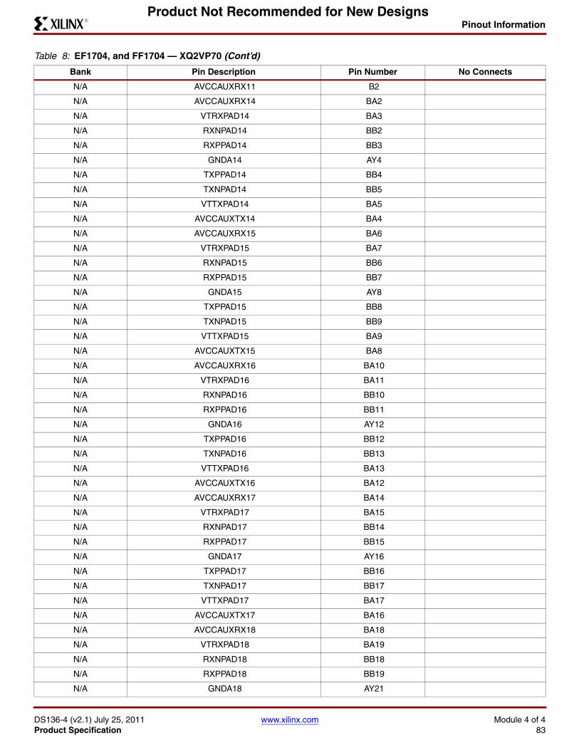
Pinout Information
DS136-4 (v2.1) July 25, 2011 www.xilinx.com Module 4 of 4Product Specification 83
R
Product Not Recommended for New Designs
N/A AVCCAUXRX11 B2
N/A AVCCAUXRX14 BA2
N/A VTRXPAD14 BA3
N/A RXNPAD14 BB2
N/A RXPPAD14 BB3
N/A GNDA14 AY4
N/A TXPPAD14 BB4
N/A TXNPAD14 BB5
N/A VTTXPAD14 BA5
N/A AVCCAUXTX14 BA4
N/A AVCCAUXRX15 BA6
N/A VTRXPAD15 BA7
N/A RXNPAD15 BB6
N/A RXPPAD15 BB7
N/A GNDA15 AY8
N/A TXPPAD15 BB8
N/A TXNPAD15 BB9
N/A VTTXPAD15 BA9
N/A AVCCAUXTX15 BA8
N/A AVCCAUXRX16 BA10
N/A VTRXPAD16 BA11
N/A RXNPAD16 BB10
N/A RXPPAD16 BB11
N/A GNDA16 AY12
N/A TXPPAD16 BB12
N/A TXNPAD16 BB13
N/A VTTXPAD16 BA13
N/A AVCCAUXTX16 BA12
N/A AVCCAUXRX17 BA14
N/A VTRXPAD17 BA15
N/A RXNPAD17 BB14
N/A RXPPAD17 BB15
N/A GNDA17 AY16
N/A TXPPAD17 BB16
N/A TXNPAD17 BB17
N/A VTTXPAD17 BA17
N/A AVCCAUXTX17 BA16
N/A AVCCAUXRX18 BA18
N/A VTRXPAD18 BA19
N/A RXNPAD18 BB18
N/A RXPPAD18 BB19
N/A GNDA18 AY21
Table 8: EF1704, and FF1704 — XQ2VP70 (Cont’d)
Bank Pin Description Pin Number No Connects

Pinout Information
DS136-4 (v2.1) July 25, 2011 www.xilinx.com Module 4 of 4Product Specification 84
R
Product Not Recommended for New Designs
N/A TXPPAD18 BB20
N/A TXNPAD18 BB21
N/A VTTXPAD18 BA21
N/A AVCCAUXTX18 BA20
N/A AVCCAUXRX19 BA22
N/A VTRXPAD19 BA23
N/A RXNPAD19 BB22
N/A RXPPAD19 BB23
N/A GNDA19 AY22
N/A TXPPAD19 BB24
N/A TXNPAD19 BB25
N/A VTTXPAD19 BA25
N/A AVCCAUXTX19 BA24
N/A AVCCAUXRX20 BA26
N/A VTRXPAD20 BA27
N/A RXNPAD20 BB26
N/A RXPPAD20 BB27
N/A GNDA20 AY27
N/A TXPPAD20 BB28
N/A TXNPAD20 BB29
N/A VTTXPAD20 BA29
N/A AVCCAUXTX20 BA28
N/A AVCCAUXRX21 BA30
N/A VTRXPAD21 BA31
N/A RXNPAD21 BB30
N/A RXPPAD21 BB31
N/A GNDA21 AY31
N/A TXPPAD21 BB32
N/A TXNPAD21 BB33
N/A VTTXPAD21 BA33
N/A AVCCAUXTX21 BA32
N/A AVCCAUXRX22 BA34
N/A VTRXPAD22 BA35
N/A RXNPAD22 BB34
N/A RXPPAD22 BB35
N/A GNDA22 AY35
N/A TXPPAD22 BB36
N/A TXNPAD22 BB37
N/A VTTXPAD22 BA37
N/A AVCCAUXTX22 BA36
N/A AVCCAUXRX23 BA38
N/A VTRXPAD23 BA39
Table 8: EF1704, and FF1704 — XQ2VP70 (Cont’d)
Bank Pin Description Pin Number No Connects
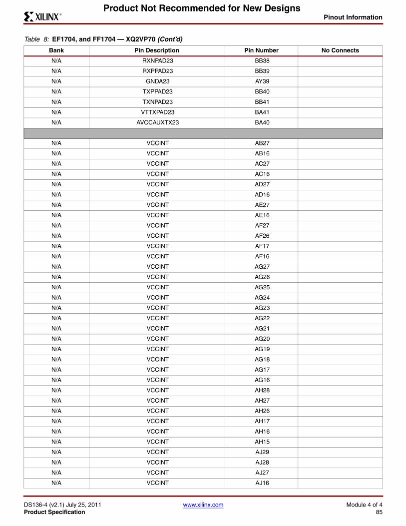
Pinout Information
DS136-4 (v2.1) July 25, 2011 www.xilinx.com Module 4 of 4Product Specification 85
R
Product Not Recommended for New Designs
N/A RXNPAD23 BB38
N/A RXPPAD23 BB39
N/A GNDA23 AY39
N/A TXPPAD23 BB40
N/A TXNPAD23 BB41
N/A VTTXPAD23 BA41
N/A AVCCAUXTX23 BA40
N/A VCCINT AB27
N/A VCCINT AB16
N/A VCCINT AC27
N/A VCCINT AC16
N/A VCCINT AD27
N/A VCCINT AD16
N/A VCCINT AE27
N/A VCCINT AE16
N/A VCCINT AF27
N/A VCCINT AF26
N/A VCCINT AF17
N/A VCCINT AF16
N/A VCCINT AG27
N/A VCCINT AG26
N/A VCCINT AG25
N/A VCCINT AG24
N/A VCCINT AG23
N/A VCCINT AG22
N/A VCCINT AG21
N/A VCCINT AG20
N/A VCCINT AG19
N/A VCCINT AG18
N/A VCCINT AG17
N/A VCCINT AG16
N/A VCCINT AH28
N/A VCCINT AH27
N/A VCCINT AH26
N/A VCCINT AH17
N/A VCCINT AH16
N/A VCCINT AH15
N/A VCCINT AJ29
N/A VCCINT AJ28
N/A VCCINT AJ27
N/A VCCINT AJ16
Table 8: EF1704, and FF1704 — XQ2VP70 (Cont’d)
Bank Pin Description Pin Number No Connects
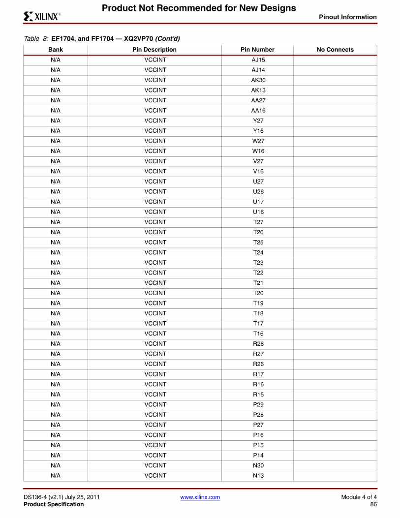
Pinout Information
DS136-4 (v2.1) July 25, 2011 www.xilinx.com Module 4 of 4Product Specification 86
R
Product Not Recommended for New Designs
N/A VCCINT AJ15
N/A VCCINT AJ14
N/A VCCINT AK30
N/A VCCINT AK13
N/A VCCINT AA27
N/A VCCINT AA16
N/A VCCINT Y27
N/A VCCINT Y16
N/A VCCINT W27
N/A VCCINT W16
N/A VCCINT V27
N/A VCCINT V16
N/A VCCINT U27
N/A VCCINT U26
N/A VCCINT U17
N/A VCCINT U16
N/A VCCINT T27
N/A VCCINT T26
N/A VCCINT T25
N/A VCCINT T24
N/A VCCINT T23
N/A VCCINT T22
N/A VCCINT T21
N/A VCCINT T20
N/A VCCINT T19
N/A VCCINT T18
N/A VCCINT T17
N/A VCCINT T16
N/A VCCINT R28
N/A VCCINT R27
N/A VCCINT R26
N/A VCCINT R17
N/A VCCINT R16
N/A VCCINT R15
N/A VCCINT P29
N/A VCCINT P28
N/A VCCINT P27
N/A VCCINT P16
N/A VCCINT P15
N/A VCCINT P14
N/A VCCINT N30
N/A VCCINT N13
Table 8: EF1704, and FF1704 — XQ2VP70 (Cont’d)
Bank Pin Description Pin Number No Connects
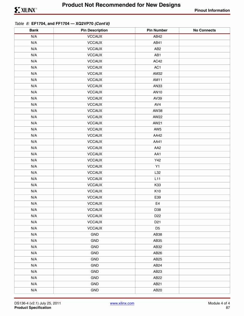
Pinout Information
DS136-4 (v2.1) July 25, 2011 www.xilinx.com Module 4 of 4Product Specification 87
R
Product Not Recommended for New Designs
N/A VCCAUX AB42
N/A VCCAUX AB41
N/A VCCAUX AB2
N/A VCCAUX AB1
N/A VCCAUX AC42
N/A VCCAUX AC1
N/A VCCAUX AM32
N/A VCCAUX AM11
N/A VCCAUX AN33
N/A VCCAUX AN10
N/A VCCAUX AV39
N/A VCCAUX AV4
N/A VCCAUX AW38
N/A VCCAUX AW22
N/A VCCAUX AW21
N/A VCCAUX AW5
N/A VCCAUX AA42
N/A VCCAUX AA41
N/A VCCAUX AA2
N/A VCCAUX AA1
N/A VCCAUX Y42
N/A VCCAUX Y1
N/A VCCAUX L32
N/A VCCAUX L11
N/A VCCAUX K33
N/A VCCAUX K10
N/A VCCAUX E39
N/A VCCAUX E4
N/A VCCAUX D38
N/A VCCAUX D22
N/A VCCAUX D21
N/A VCCAUX D5
N/A GND AB38
N/A GND AB35
N/A GND AB32
N/A GND AB26
N/A GND AB25
N/A GND AB24
N/A GND AB23
N/A GND AB22
N/A GND AB21
N/A GND AB20
Table 8: EF1704, and FF1704 — XQ2VP70 (Cont’d)
Bank Pin Description Pin Number No Connects

Pinout Information
DS136-4 (v2.1) July 25, 2011 www.xilinx.com Module 4 of 4Product Specification 88
R
Product Not Recommended for New Designs
N/A GND AB19
N/A GND AB18
N/A GND AB17
N/A GND AB11
N/A GND AB8
N/A GND AB5
N/A GND AC41
N/A GND AC26
N/A GND AC25
N/A GND AC24
N/A GND AC23
N/A GND AC22
N/A GND AC21
N/A GND AC20
N/A GND AC19
N/A GND AC18
N/A GND AC17
N/A GND AC2
N/A GND AD26
N/A GND AD25
N/A GND AD24
N/A GND AD23
N/A GND AD22
N/A GND AD21
N/A GND AD20
N/A GND AD19
N/A GND AD18
N/A GND AD17
N/A GND AE37
N/A GND AE34
N/A GND AE26
N/A GND AE25
N/A GND AE24
N/A GND AE23
N/A GND AE22
N/A GND AE21
N/A GND AE20
N/A GND AE19
N/A GND AE18
N/A GND AE17
N/A GND AE9
N/A GND AE6
Table 8: EF1704, and FF1704 — XQ2VP70 (Cont’d)
Bank Pin Description Pin Number No Connects

Pinout Information
DS136-4 (v2.1) July 25, 2011 www.xilinx.com Module 4 of 4Product Specification 89
R
Product Not Recommended for New Designs
N/A GND AF25
N/A GND AF24
N/A GND AF23
N/A GND AF22
N/A GND AF21
N/A GND AF20
N/A GND AF19
N/A GND AF18
N/A GND AG42
N/A GND AG1
N/A GND AH39
N/A GND AH36
N/A GND AH7
N/A GND AH4
N/A GND AL42
N/A GND AL1
N/A GND AM22
N/A GND AM21
N/A GND AN39
N/A GND AN4
N/A GND AP34
N/A GND AP9
N/A GND AR42
N/A GND AR35
N/A GND AR22
N/A GND AR21
N/A GND AR8
N/A GND AR1
N/A GND AT36
N/A GND AT7
N/A GND AU37
N/A GND AU25
N/A GND AU18
N/A GND AU6
N/A GND AV38
N/A GND AV22
N/A GND AV21
N/A GND AV5
N/A GND AW39
N/A GND AW32
N/A GND AW28
N/A GND AW15
Table 8: EF1704, and FF1704 — XQ2VP70 (Cont’d)
Bank Pin Description Pin Number No Connects
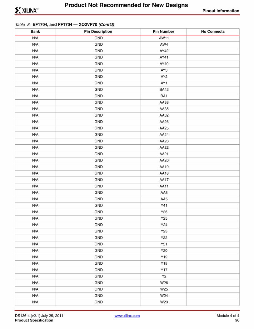
Pinout Information
DS136-4 (v2.1) July 25, 2011 www.xilinx.com Module 4 of 4Product Specification 90
R
Product Not Recommended for New Designs
N/A GND AW11
N/A GND AW4
N/A GND AY42
N/A GND AY41
N/A GND AY40
N/A GND AY3
N/A GND AY2
N/A GND AY1
N/A GND BA42
N/A GND BA1
N/A GND AA38
N/A GND AA35
N/A GND AA32
N/A GND AA26
N/A GND AA25
N/A GND AA24
N/A GND AA23
N/A GND AA22
N/A GND AA21
N/A GND AA20
N/A GND AA19
N/A GND AA18
N/A GND AA17
N/A GND AA11
N/A GND AA8
N/A GND AA5
N/A GND Y41
N/A GND Y26
N/A GND Y25
N/A GND Y24
N/A GND Y23
N/A GND Y22
N/A GND Y21
N/A GND Y20
N/A GND Y19
N/A GND Y18
N/A GND Y17
N/A GND Y2
N/A GND W26
N/A GND W25
N/A GND W24
N/A GND W23
Table 8: EF1704, and FF1704 — XQ2VP70 (Cont’d)
Bank Pin Description Pin Number No Connects
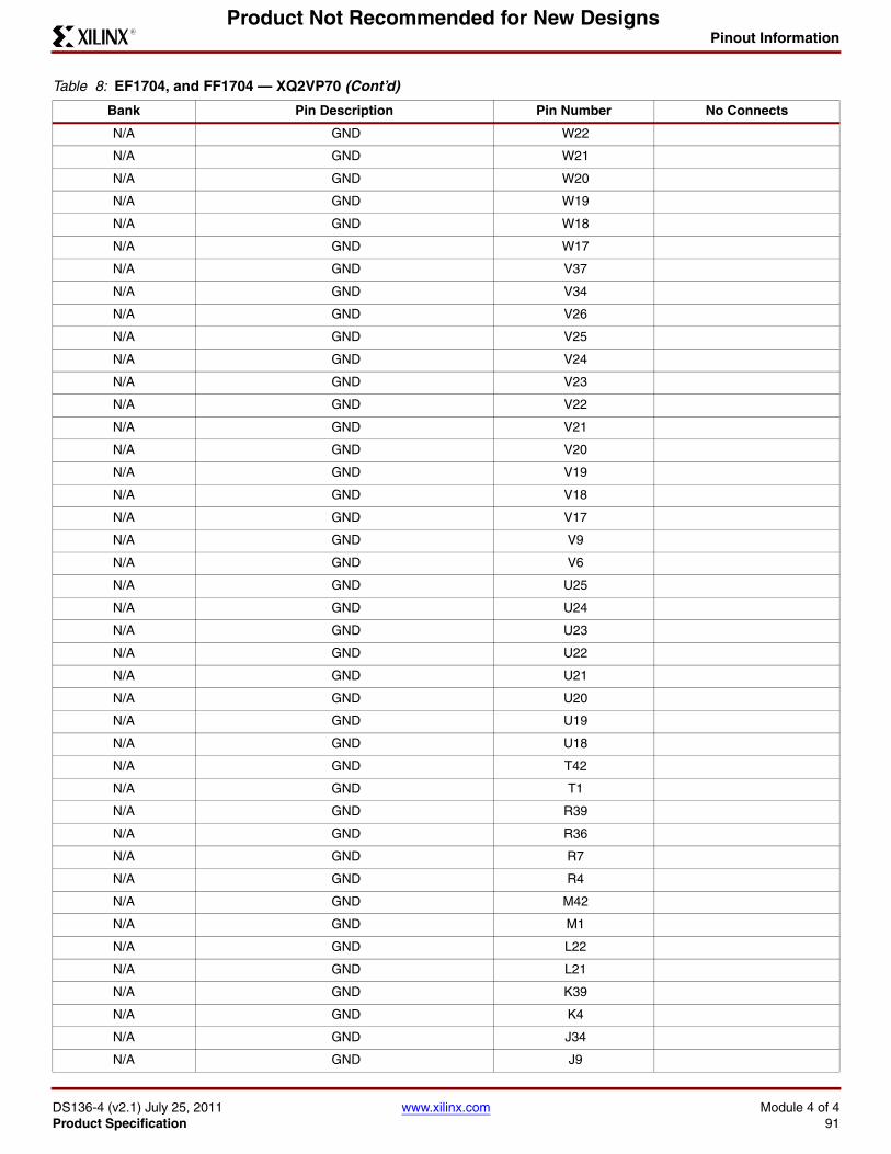
Pinout Information
DS136-4 (v2.1) July 25, 2011 www.xilinx.com Module 4 of 4Product Specification 91
R
Product Not Recommended for New Designs
N/A GND W22
N/A GND W21
N/A GND W20
N/A GND W19
N/A GND W18
N/A GND W17
N/A GND V37
N/A GND V34
N/A GND V26
N/A GND V25
N/A GND V24
N/A GND V23
N/A GND V22
N/A GND V21
N/A GND V20
N/A GND V19
N/A GND V18
N/A GND V17
N/A GND V9
N/A GND V6
N/A GND U25
N/A GND U24
N/A GND U23
N/A GND U22
N/A GND U21
N/A GND U20
N/A GND U19
N/A GND U18
N/A GND T42
N/A GND T1
N/A GND R39
N/A GND R36
N/A GND R7
N/A GND R4
N/A GND M42
N/A GND M1
N/A GND L22
N/A GND L21
N/A GND K39
N/A GND K4
N/A GND J34
N/A GND J9
Table 8: EF1704, and FF1704 — XQ2VP70 (Cont’d)
Bank Pin Description Pin Number No Connects
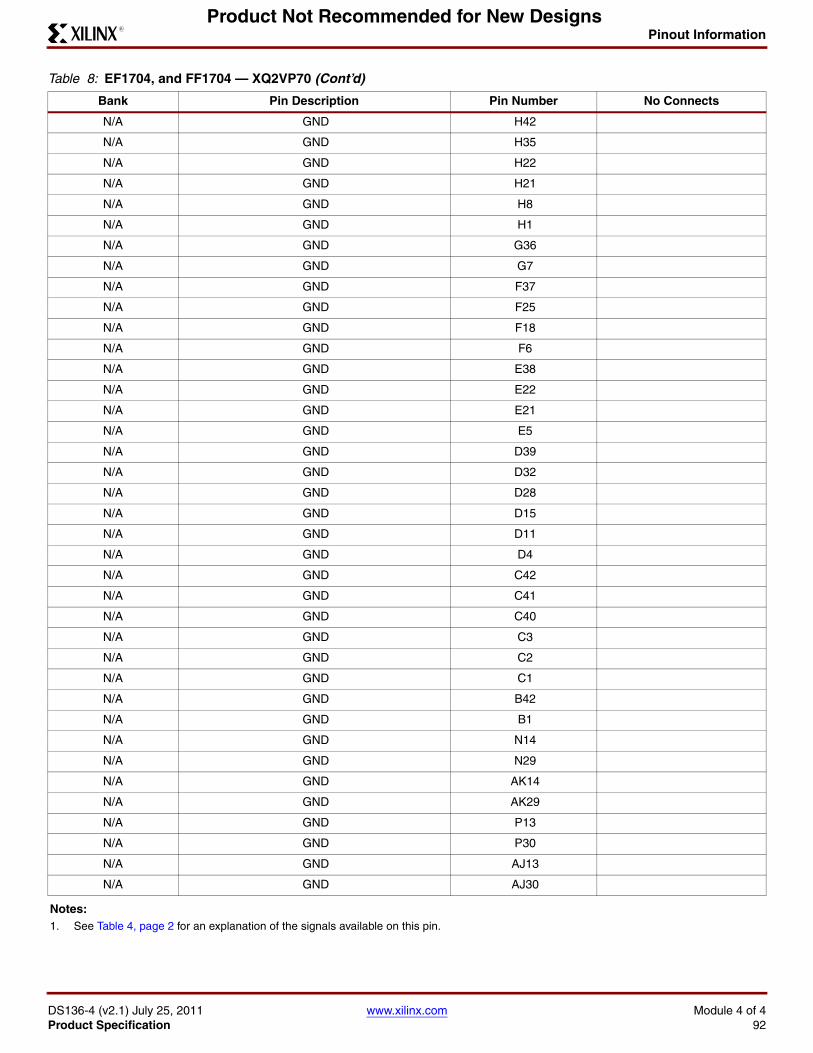
Pinout Information
DS136-4 (v2.1) July 25, 2011 www.xilinx.com Module 4 of 4Product Specification 92
R
Product Not Recommended for New Designs
N/A GND H42
N/A GND H35
N/A GND H22
N/A GND H21
N/A GND H8
N/A GND H1
N/A GND G36
N/A GND G7
N/A GND F37
N/A GND F25
N/A GND F18
N/A GND F6
N/A GND E38
N/A GND E22
N/A GND E21
N/A GND E5
N/A GND D39
N/A GND D32
N/A GND D28
N/A GND D15
N/A GND D11
N/A GND D4
N/A GND C42
N/A GND C41
N/A GND C40
N/A GND C3
N/A GND C2
N/A GND C1
N/A GND B42
N/A GND B1
N/A GND N14
N/A GND N29
N/A GND AK14
N/A GND AK29
N/A GND P13
N/A GND P30
N/A GND AJ13
N/A GND AJ30
Notes: 1. See Table 4, page 2 for an explanation of the signals available on this pin.
Table 8: EF1704, and FF1704 — XQ2VP70 (Cont’d)
Bank Pin Description Pin Number No Connects
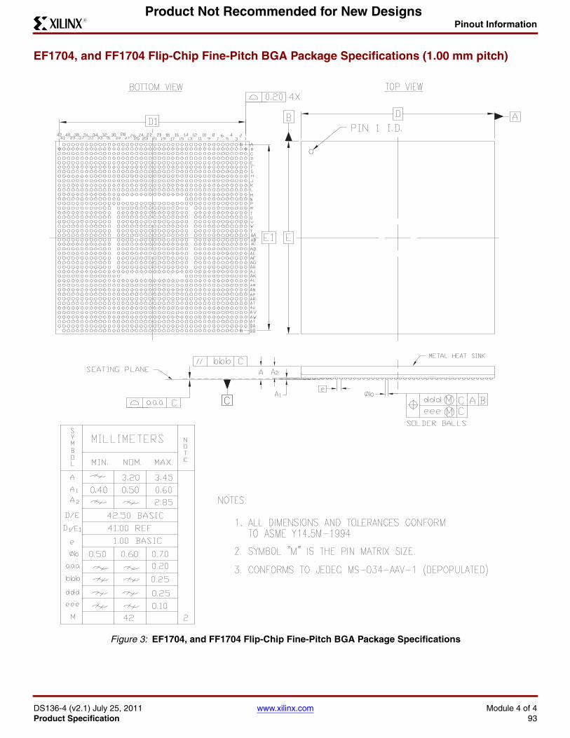
Pinout Information
DS136-4 (v2.1) July 25, 2011 www.xilinx.com Module 4 of 4Product Specification 93
R
Product Not Recommended for New Designs
EF1704, and FF1704 Flip-Chip Fine-Pitch BGA Package Specifications (1.00 mm pitch)X-Ref Target - Figure 3
Figure 3: EF1704, and FF1704 Flip-Chip Fine-Pitch BGA Package Specifications
Pinout Information
DS136-4 (v2.1) July 25, 2011 www.xilinx.com Module 4 of 4Product Specification 94
R
Product Not Recommended for New Designs
Revision HistoryThis section records the change history for this module of the data sheet.
QPro Virtex-II Pro Data SheetThe QPro Virtex-II Pro Data Sheet contains the following modules:
"Introduction and Overview" (Module 1)
"Functional Description" (Module 2)
"DC and Switching Characteristics" (Module 3)
"Pinout Information" (Module 4)
Notice of DisclaimerTHE XILINX HARDWARE FPGA AND CPLD DEVICES REFERRED TO HEREIN (“PRODUCTS”) ARE SUBJECT TO THE TERMS AND CONDITIONS OF THE XILINX LIMITED WARRANTY WHICH CAN BE VIEWED AT http://www.xilinx.com/warranty.htm. THIS LIMITED WARRANTY DOES NOT EXTEND TO ANY USE OF PRODUCTS IN AN APPLICATION OR ENVIRONMENT THAT IS NOT WITHIN THE SPECIFICATIONS STATED IN THE XILINX DATA SHEET. ALL SPECIFICATIONS ARE SUBJECT TO CHANGE WITHOUT NOTICE. PRODUCTS ARE NOT DESIGNED OR INTENDED TO BE FAIL-SAFE OR FOR USE IN ANY APPLICATION REQUIRING FAIL-SAFE PERFORMANCE, SUCH AS LIFE-SUPPORT OR SAFETY DEVICES OR SYSTEMS, OR ANY OTHER APPLICATION THAT INVOKES THE POTENTIAL RISKS OF DEATH, PERSONAL INJURY, OR PROPERTY OR ENVIRONMENTAL DAMAGE (“CRITICAL APPLICATIONS”). USE OF PRODUCTS IN CRITICAL APPLICATIONS IS AT THE SOLE RISK OF CUSTOMER, SUBJECT TO APPLICABLE LAWS AND REGULATIONS.
Date Version Revision
11/29/06 1.0 Initial Xilinx release.
12/20/07 2.0 Change data sheet title. Added support for XQ2VP70-6EF1704I. Removed support for XQV2P70-6MF1704I. Updated document template. Updated URLs.
07/25/11 2.1 Added Product Not Recommended for New Designs banner. Updated Figure 1, page 22,with the newest FG676/FGG676 mechanical drawing.