Embed Size (px)
Citation preview

Spartan-3A and Spartan-3A DSPLibraries Guide for Schematic
DesignsISE 10.1

Xilinx Trademarks and Copyright Information
Xilinx is disclosing this user guide, manual, release note, and/or specification (the “Documentation”) to yousolely for use in the development of designs to operate with Xilinx hardware devices. You may not reproduce,distribute, republish, download, display, post, or transmit the Documentation in any form or by any meansincluding, but not limited to, electronic, mechanical, photocopying, recording, or otherwise, without the priorwritten consent of Xilinx. Xilinx expressly disclaims any liability arising out of your use of the Documentation.Xilinx reserves the right, at its sole discretion, to change the Documentation without notice at any time. Xilinxassumes no obligation to correct any errors contained in the Documentation, or to advise you of any correctionsor updates. Xilinx expressly disclaims any liability in connection with technical support or assistance that may beprovided to you in connection with the Information.
THE DOCUMENTATION IS DISCLOSED TO YOU “AS-IS” WITH NOWARRANTY OF ANY KIND. XILINXMAKES NO OTHER WARRANTIES, WHETHER EXPRESS, IMPLIED, OR STATUTORY, REGARDINGTHE DOCUMENTATION, INCLUDING ANY WARRANTIES OF MERCHANTABILITY, FITNESS FOR APARTICULAR PURPOSE, OR NONINFRINGEMENT OF THIRD-PARTY RIGHTS. IN NO EVENT WILLXILINX BE LIABLE FOR ANY CONSEQUENTIAL, INDIRECT, EXEMPLARY, SPECIAL, OR INCIDENTALDAMAGES, INCLUDING ANY LOSS OF DATA OR LOST PROFITS, ARISING FROM YOUR USE OF THEDOCUMENTATION.
© Copyright 2002 – 2008 Xilinx, Inc. All Rights Reserved. XILINX, the Xilinx logo, the Brand Window and otherdesignated brands included herein are trademarks of Xilinx, Inc. All other trademarks are the property oftheir respective owners.
Libraries Guide
2 www.xilinx.com 10.1
Table of ContentsAbout this Guide ........................................................................................................................................ 11Design Element Retargeting ........................................................................................................................ 13Functional Categories ................................................................................................................................. 17About Design Elements............................................................................................................................... 33
ACC16 ................................................................................................................................................ 34ACC4.................................................................................................................................................. 36ACC8.................................................................................................................................................. 38ADD16................................................................................................................................................ 40ADD4 ................................................................................................................................................. 42ADD8 ................................................................................................................................................. 44ADSU16 .............................................................................................................................................. 46ADSU4................................................................................................................................................ 48ADSU8................................................................................................................................................ 50AND12................................................................................................................................................ 52AND16................................................................................................................................................ 53AND2 ................................................................................................................................................. 54AND2B1.............................................................................................................................................. 55AND2B2.............................................................................................................................................. 56AND3 ................................................................................................................................................. 57AND3B1.............................................................................................................................................. 58AND3B2.............................................................................................................................................. 59AND3B3.............................................................................................................................................. 60AND4 ................................................................................................................................................. 61AND4B1.............................................................................................................................................. 62AND4B2.............................................................................................................................................. 63AND4B3.............................................................................................................................................. 64AND4B4.............................................................................................................................................. 65AND5 ................................................................................................................................................. 66AND5B1.............................................................................................................................................. 67AND5B2.............................................................................................................................................. 68AND5B3.............................................................................................................................................. 69AND5B4.............................................................................................................................................. 70AND5B5.............................................................................................................................................. 71AND6 ................................................................................................................................................. 72AND7 ................................................................................................................................................. 73AND8 ................................................................................................................................................. 74AND9 ................................................................................................................................................. 75BRLSHFT4 .......................................................................................................................................... 76BRLSHFT8 .......................................................................................................................................... 77BSCAN_SPARTAN3A.......................................................................................................................... 79BUF .................................................................................................................................................... 81BUFCF ................................................................................................................................................ 82BUFG.................................................................................................................................................. 83BUFGCE ............................................................................................................................................. 84BUFGMUX.......................................................................................................................................... 85CAPTURE_SPARTAN3A ..................................................................................................................... 86CB16CE............................................................................................................................................... 88CB16CLE............................................................................................................................................. 90CB16CLED .......................................................................................................................................... 92CB16RE............................................................................................................................................... 94CB2CE ................................................................................................................................................ 96CB2CLE .............................................................................................................................................. 98CB2CLED........................................................................................................................................... 100CB2RE................................................................................................................................................ 102CB4CE ............................................................................................................................................... 104CB4CLE ............................................................................................................................................. 106
Libraries Guide
10.1 www.xilinx.com 3
CB4CLED........................................................................................................................................... 108CB4RE................................................................................................................................................ 110CB8CE ............................................................................................................................................... 112CB8CLE ............................................................................................................................................. 114CB8CLED........................................................................................................................................... 116CB8RE................................................................................................................................................ 118CC16CE ............................................................................................................................................. 120CC16CLE ........................................................................................................................................... 122CC16CLED......................................................................................................................................... 124CC16RE.............................................................................................................................................. 126CC8CE ............................................................................................................................................... 128CC8CLE ............................................................................................................................................. 130CC8CLED .......................................................................................................................................... 132CC8RE ............................................................................................................................................... 134CD4CE............................................................................................................................................... 136CD4CLE............................................................................................................................................. 138CD4RE ............................................................................................................................................... 140CD4RLE............................................................................................................................................. 142CJ4CE ................................................................................................................................................ 144CJ4RE ................................................................................................................................................ 145CJ5CE ................................................................................................................................................ 146CJ5RE ................................................................................................................................................ 147CJ8CE ................................................................................................................................................ 148CJ8RE ................................................................................................................................................ 149COMP16 ............................................................................................................................................ 150COMP2 .............................................................................................................................................. 151COMP4 .............................................................................................................................................. 152COMP8 .............................................................................................................................................. 153COMPM16 ......................................................................................................................................... 154COMPM2........................................................................................................................................... 156COMPM4........................................................................................................................................... 157COMPM8........................................................................................................................................... 158COMPMC16....................................................................................................................................... 160COMPMC8 ........................................................................................................................................ 162CR16CE.............................................................................................................................................. 164CR8CE ............................................................................................................................................... 165D2_4E ................................................................................................................................................ 166D3_8E ................................................................................................................................................ 167D4_16E............................................................................................................................................... 168DCM_SP ............................................................................................................................................ 169DEC_CC16 ......................................................................................................................................... 171DEC_CC4........................................................................................................................................... 173DEC_CC8........................................................................................................................................... 174DECODE16 ........................................................................................................................................ 175DECODE32 ........................................................................................................................................ 177DECODE4 .......................................................................................................................................... 178DECODE64 ........................................................................................................................................ 179DECODE8 .......................................................................................................................................... 180DNA_PORT ....................................................................................................................................... 181DSP48A.............................................................................................................................................. 183FD16CE.............................................................................................................................................. 188FD16RE.............................................................................................................................................. 189FD4CE ............................................................................................................................................... 190FD4RE ............................................................................................................................................... 192FD8CE ............................................................................................................................................... 194FD8RE ............................................................................................................................................... 195FDCPE ............................................................................................................................................... 196FDCPE_1............................................................................................................................................ 199FDP ................................................................................................................................................... 201
Libraries Guide
4 www.xilinx.com 10.1
FDP_1 ................................................................................................................................................ 203FDRSE ............................................................................................................................................... 204FDRSE_1 ............................................................................................................................................ 206FJKC .................................................................................................................................................. 208FJKCE ................................................................................................................................................ 209FJKP .................................................................................................................................................. 210FJKPE ................................................................................................................................................ 211FJKRSE .............................................................................................................................................. 213FJKSRE .............................................................................................................................................. 215FTC.................................................................................................................................................... 217FTCE.................................................................................................................................................. 218FTCLE ............................................................................................................................................... 219FTCLEX ............................................................................................................................................. 220FTP .................................................................................................................................................... 221FTPE.................................................................................................................................................. 222FTPLE................................................................................................................................................ 223FTRSE ................................................................................................................................................ 225FTRSLE.............................................................................................................................................. 226FTSRE................................................................................................................................................ 228FTSRLE.............................................................................................................................................. 229GND.................................................................................................................................................. 231IBUF .................................................................................................................................................. 232IBUF_DLY_ADJ .................................................................................................................................. 234IBUF16 ............................................................................................................................................... 236IBUF4................................................................................................................................................. 237IBUF8................................................................................................................................................. 238IBUFDS.............................................................................................................................................. 239IBUFDS_DLY_ADJ.............................................................................................................................. 241IBUFG................................................................................................................................................ 243IBUFGDS ........................................................................................................................................... 244ICAP_SPARTAN3A ............................................................................................................................ 247IDDR2................................................................................................................................................ 248IFD .................................................................................................................................................... 250IFD_1 ................................................................................................................................................. 251IFD16 ................................................................................................................................................. 252IFD4................................................................................................................................................... 253IFD8................................................................................................................................................... 254IFDI ................................................................................................................................................... 255IFDI_1................................................................................................................................................ 256IFDX .................................................................................................................................................. 257IFDX_1............................................................................................................................................... 258IFDX16............................................................................................................................................... 259IFDX4 ................................................................................................................................................ 260IFDX8 ................................................................................................................................................ 261IFDXI ................................................................................................................................................. 262IFDXI_1.............................................................................................................................................. 263ILD .................................................................................................................................................... 264ILD_1................................................................................................................................................. 265ILD16................................................................................................................................................. 266ILD4 .................................................................................................................................................. 267ILD8 .................................................................................................................................................. 268ILDI ................................................................................................................................................... 269ILDI_1................................................................................................................................................ 270ILDX.................................................................................................................................................. 271ILDX_1............................................................................................................................................... 272ILDX16............................................................................................................................................... 273ILDX4 ................................................................................................................................................ 274ILDX8 ................................................................................................................................................ 275ILDXI................................................................................................................................................. 276
Libraries Guide
10.1 www.xilinx.com 5
ILDXI_1 ............................................................................................................................................. 277INV.................................................................................................................................................... 278INV16 ................................................................................................................................................ 279INV4.................................................................................................................................................. 280INV8.................................................................................................................................................. 281IOBUF................................................................................................................................................ 282IOBUFDS ........................................................................................................................................... 284KEEPER ............................................................................................................................................. 286LD16.................................................................................................................................................. 287LD16CE ............................................................................................................................................. 288LD4.................................................................................................................................................... 290LD4CE ............................................................................................................................................... 292LD8.................................................................................................................................................... 294LD8CE ............................................................................................................................................... 295LDCP................................................................................................................................................. 297LDCP_1.............................................................................................................................................. 299LDCPE............................................................................................................................................... 301LDCPE_1 ........................................................................................................................................... 303LUT1 ................................................................................................................................................. 305LUT1_D ............................................................................................................................................. 307LUT1_L.............................................................................................................................................. 309LUT2 ................................................................................................................................................. 311LUT2_D ............................................................................................................................................. 313LUT2_L.............................................................................................................................................. 315LUT3 ................................................................................................................................................. 317LUT3_D ............................................................................................................................................. 319LUT3_L.............................................................................................................................................. 321LUT4 ................................................................................................................................................. 323LUT4_D ............................................................................................................................................. 325LUT4_L.............................................................................................................................................. 327M16_1E .............................................................................................................................................. 329M2_1.................................................................................................................................................. 331M2_1B1 .............................................................................................................................................. 332M2_1B2 .............................................................................................................................................. 333M2_1E................................................................................................................................................ 334M4_1E................................................................................................................................................ 335M8_1E................................................................................................................................................ 336MULT_AND....................................................................................................................................... 338MULT18X18SIO.................................................................................................................................. 339MUXCY ............................................................................................................................................. 341MUXCY_D ......................................................................................................................................... 342MUXCY_L.......................................................................................................................................... 343MUXF5 .............................................................................................................................................. 344MUXF5_D .......................................................................................................................................... 345MUXF5_L........................................................................................................................................... 346MUXF6 .............................................................................................................................................. 347MUXF6_D .......................................................................................................................................... 348MUXF6_L........................................................................................................................................... 349MUXF7 .............................................................................................................................................. 350MUXF7_D .......................................................................................................................................... 352MUXF7_L........................................................................................................................................... 354MUXF8 .............................................................................................................................................. 355MUXF8_D .......................................................................................................................................... 356MUXF8_L........................................................................................................................................... 358NAND12............................................................................................................................................ 359NAND16............................................................................................................................................ 360NAND2 ............................................................................................................................................. 361NAND2B1.......................................................................................................................................... 362NAND2B2.......................................................................................................................................... 363
Libraries Guide
6 www.xilinx.com 10.1
NAND3 ............................................................................................................................................. 364NAND3B1.......................................................................................................................................... 365NAND3B2.......................................................................................................................................... 366NAND3B3.......................................................................................................................................... 367NAND4 ............................................................................................................................................. 368NAND4B1.......................................................................................................................................... 369NAND4B2.......................................................................................................................................... 370NAND4B3.......................................................................................................................................... 371NAND4B4.......................................................................................................................................... 372NAND5 ............................................................................................................................................. 373NAND5B1.......................................................................................................................................... 374NAND5B2.......................................................................................................................................... 375NAND5B3.......................................................................................................................................... 376NAND5B4.......................................................................................................................................... 377NAND5B5.......................................................................................................................................... 378NAND6 ............................................................................................................................................. 379NAND7 ............................................................................................................................................. 380NAND8 ............................................................................................................................................. 381NAND9 ............................................................................................................................................. 382NOR12............................................................................................................................................... 383NOR16............................................................................................................................................... 384NOR2................................................................................................................................................. 385NOR2B1............................................................................................................................................. 386NOR2B2............................................................................................................................................. 387NOR3................................................................................................................................................. 388NOR3B1............................................................................................................................................. 389NOR3B2............................................................................................................................................. 390NOR3B3............................................................................................................................................. 391NOR4................................................................................................................................................. 392NOR4B1............................................................................................................................................. 393NOR4B2............................................................................................................................................. 394NOR4B3............................................................................................................................................. 395NOR4B4............................................................................................................................................. 396NOR5................................................................................................................................................. 397NOR5B1............................................................................................................................................. 398NOR5B2............................................................................................................................................. 399NOR5B3............................................................................................................................................. 400NOR5B4............................................................................................................................................. 401NOR5B5............................................................................................................................................. 402NOR6................................................................................................................................................. 403NOR7................................................................................................................................................. 404NOR8................................................................................................................................................. 405NOR9................................................................................................................................................. 406OBUF................................................................................................................................................. 407OBUF16 ............................................................................................................................................. 409OBUF4 ............................................................................................................................................... 410OBUF8 ............................................................................................................................................... 411OBUFDS ............................................................................................................................................ 412OBUFT............................................................................................................................................... 413OBUFT16 ........................................................................................................................................... 415OBUFT4 ............................................................................................................................................. 417OBUFT8 ............................................................................................................................................. 419OBUFTDS .......................................................................................................................................... 421ODDR2 .............................................................................................................................................. 423OFD................................................................................................................................................... 425OFD_1 ............................................................................................................................................... 426OFD16 ............................................................................................................................................... 427OFD4 ................................................................................................................................................. 428OFD8 ................................................................................................................................................. 429
Libraries Guide
10.1 www.xilinx.com 7
OFDE................................................................................................................................................. 430OFDE_1 ............................................................................................................................................. 431OFDE16 ............................................................................................................................................. 432OFDE4 ............................................................................................................................................... 433OFDE8 ............................................................................................................................................... 434OFDI.................................................................................................................................................. 435OFDI_1 .............................................................................................................................................. 436OFDT................................................................................................................................................. 437OFDT_1 ............................................................................................................................................. 438OFDT16 ............................................................................................................................................. 439OFDT4 ............................................................................................................................................... 440OFDT8 ............................................................................................................................................... 441OFDX................................................................................................................................................. 442OFDX_1 ............................................................................................................................................. 443OFDX16 ............................................................................................................................................. 444OFDX4............................................................................................................................................... 445OFDX8............................................................................................................................................... 446OFDXI ............................................................................................................................................... 447OFDXI_1 ............................................................................................................................................ 448OR12.................................................................................................................................................. 449OR16.................................................................................................................................................. 450OR2 ................................................................................................................................................... 451OR2B1................................................................................................................................................ 452OR2B2................................................................................................................................................ 453OR3 ................................................................................................................................................... 454OR3B1................................................................................................................................................ 455OR3B2................................................................................................................................................ 456OR3B3................................................................................................................................................ 457OR4 ................................................................................................................................................... 458OR4B1................................................................................................................................................ 459OR4B2................................................................................................................................................ 460OR4B3................................................................................................................................................ 461OR4B4................................................................................................................................................ 462OR5 ................................................................................................................................................... 463OR5B1................................................................................................................................................ 464OR5B2................................................................................................................................................ 465OR5B3................................................................................................................................................ 466OR5B4................................................................................................................................................ 467OR5B5................................................................................................................................................ 468OR6 ................................................................................................................................................... 469OR7 ................................................................................................................................................... 470OR8 ................................................................................................................................................... 471OR9 ................................................................................................................................................... 472PULLDOWN...................................................................................................................................... 473PULLUP............................................................................................................................................. 474RAM16X1D ........................................................................................................................................ 475RAM16X1S......................................................................................................................................... 477RAM32X1S......................................................................................................................................... 479RAM64X1S......................................................................................................................................... 481RAMB16BWE ..................................................................................................................................... 483RAMB16BWE_S18 .............................................................................................................................. 486RAMB16BWE_S18_S18........................................................................................................................ 489RAMB16BWE_S18_S9 ......................................................................................................................... 493RAMB16BWE_S36 .............................................................................................................................. 496RAMB16BWE_S36_S18........................................................................................................................ 499RAMB16BWE_S36_S36........................................................................................................................ 503RAMB16BWE_S36_S9 ......................................................................................................................... 506RAMB16BWER................................................................................................................................... 509ROM128X1 ......................................................................................................................................... 513
Libraries Guide
8 www.xilinx.com 10.1
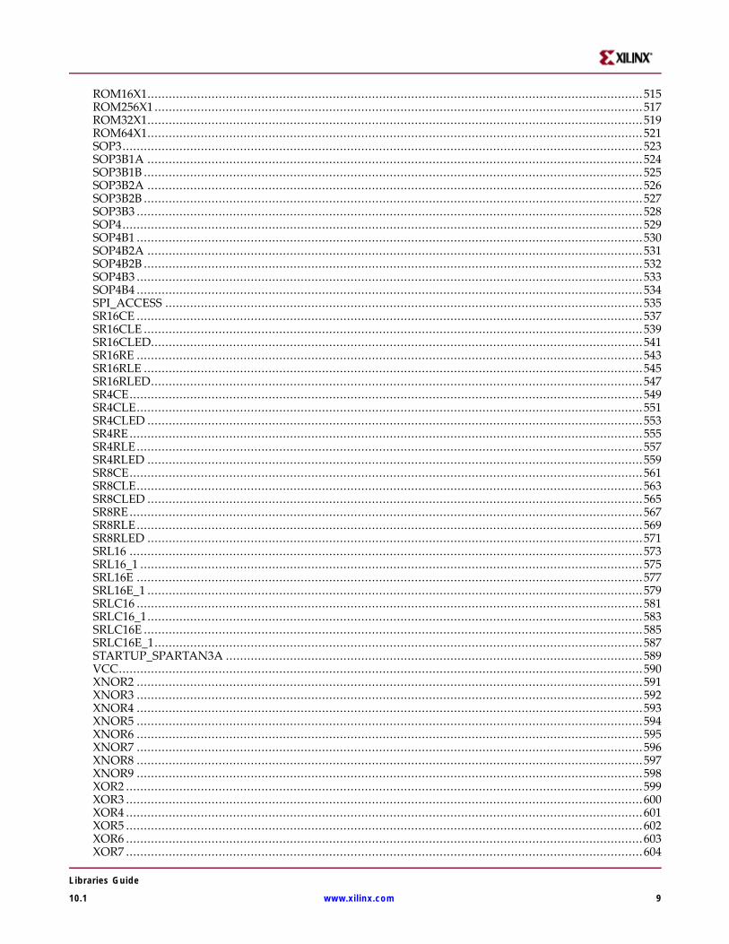
ROM16X1........................................................................................................................................... 515ROM256X1 ......................................................................................................................................... 517ROM32X1........................................................................................................................................... 519ROM64X1........................................................................................................................................... 521SOP3.................................................................................................................................................. 523SOP3B1A ........................................................................................................................................... 524SOP3B1B ............................................................................................................................................ 525SOP3B2A ........................................................................................................................................... 526SOP3B2B ............................................................................................................................................ 527SOP3B3 .............................................................................................................................................. 528SOP4.................................................................................................................................................. 529SOP4B1 .............................................................................................................................................. 530SOP4B2A ........................................................................................................................................... 531SOP4B2B ............................................................................................................................................ 532SOP4B3 .............................................................................................................................................. 533SOP4B4 .............................................................................................................................................. 534SPI_ACCESS ...................................................................................................................................... 535SR16CE .............................................................................................................................................. 537SR16CLE ............................................................................................................................................ 539SR16CLED.......................................................................................................................................... 541SR16RE .............................................................................................................................................. 543SR16RLE ............................................................................................................................................ 545SR16RLED.......................................................................................................................................... 547SR4CE................................................................................................................................................ 549SR4CLE.............................................................................................................................................. 551SR4CLED ........................................................................................................................................... 553SR4RE................................................................................................................................................ 555SR4RLE.............................................................................................................................................. 557SR4RLED ........................................................................................................................................... 559SR8CE................................................................................................................................................ 561SR8CLE.............................................................................................................................................. 563SR8CLED ........................................................................................................................................... 565SR8RE................................................................................................................................................ 567SR8RLE.............................................................................................................................................. 569SR8RLED ........................................................................................................................................... 571SRL16 ................................................................................................................................................ 573SRL16_1 ............................................................................................................................................. 575SRL16E .............................................................................................................................................. 577SRL16E_1 ........................................................................................................................................... 579SRLC16 .............................................................................................................................................. 581SRLC16_1........................................................................................................................................... 583SRLC16E ............................................................................................................................................ 585SRLC16E_1......................................................................................................................................... 587STARTUP_SPARTAN3A ..................................................................................................................... 589VCC................................................................................................................................................... 590XNOR2 .............................................................................................................................................. 591XNOR3 .............................................................................................................................................. 592XNOR4 .............................................................................................................................................. 593XNOR5 .............................................................................................................................................. 594XNOR6 .............................................................................................................................................. 595XNOR7 .............................................................................................................................................. 596XNOR8 .............................................................................................................................................. 597XNOR9 .............................................................................................................................................. 598XOR2 ................................................................................................................................................. 599XOR3 ................................................................................................................................................. 600XOR4 ................................................................................................................................................. 601XOR5 ................................................................................................................................................. 602XOR6 ................................................................................................................................................. 603XOR7 ................................................................................................................................................. 604
Libraries Guide
10.1 www.xilinx.com 9
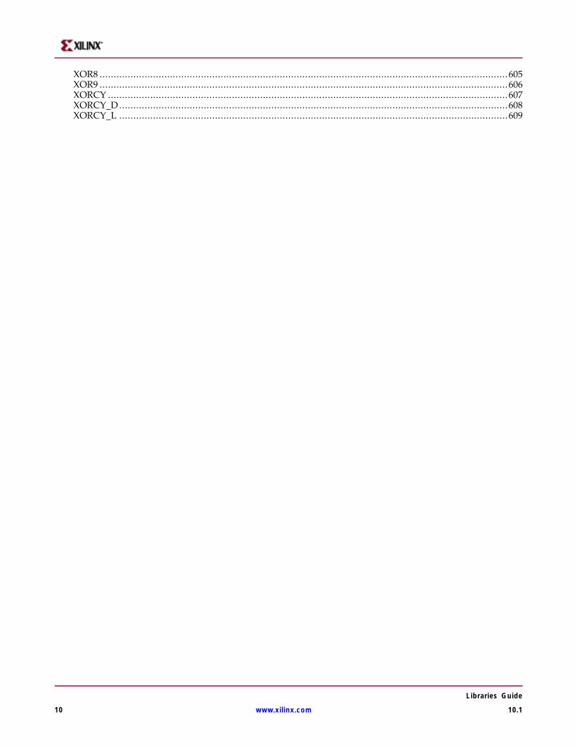
XOR8 ................................................................................................................................................. 605XOR9 ................................................................................................................................................. 606XORCY .............................................................................................................................................. 607XORCY_D.......................................................................................................................................... 608XORCY_L .......................................................................................................................................... 609
Libraries Guide
10 www.xilinx.com 10.1
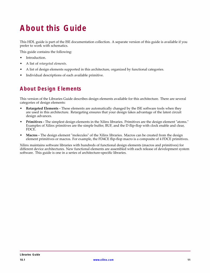
About this GuideThis HDL guide is part of the ISE documentation collection. A separate version of this guide is available if youprefer to work with schematics.
This guide contains the following:
• Introduction.
• A list of retargeted elements.
• A list of design elements supported in this architecture, organized by functional categories.
• Individual descriptions of each available primitive.
About Design ElementsThis version of the Libraries Guide describes design elements available for this architecture. There are severalcategories of design elements:
• Retargeted Elements - These elements are automatically changed by the ISE software tools when theyare used in this architecture. Retargeting ensures that your design takes advantage of the latest circuitdesign advances.
• Primitives - The simplest design elements in the Xilinx libraries. Primitives are the design element "atoms."Examples of Xilinx primitives are the simple buffer, BUF, and the D flip-flop with clock enable and clear,FDCE.
• Macros - The design element "molecules" of the Xilinx libraries. Macros can be created from the designelement primitives or macros. For example, the FD4CE flip-flop macro is a composite of 4 FDCE primitives.
Xilinx maintains software libraries with hundreds of functional design elements (macros and primitives) fordifferent device architectures. New functional elements are assembled with each release of development systemsoftware. This guide is one in a series of architecture-specific libraries.
Libraries Guide
10.1 www.xilinx.com 11

Libraries Guide
12 www.xilinx.com 10.1
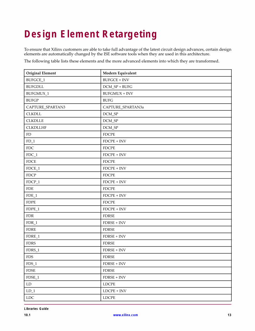
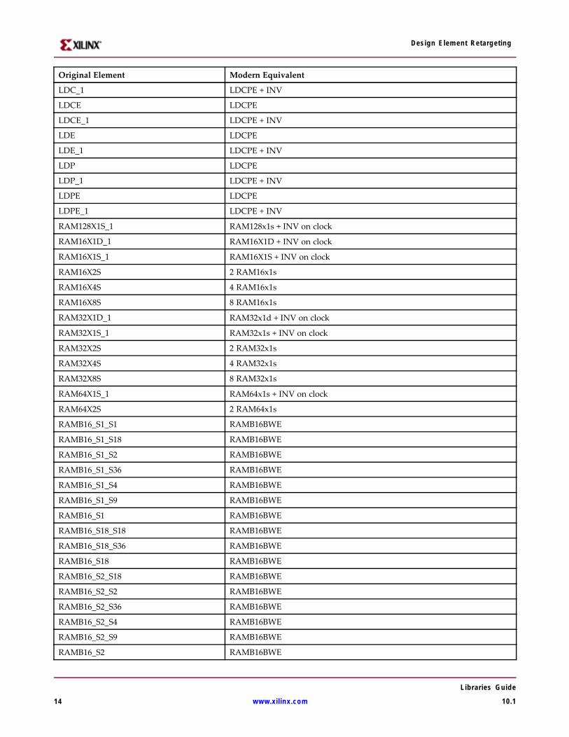
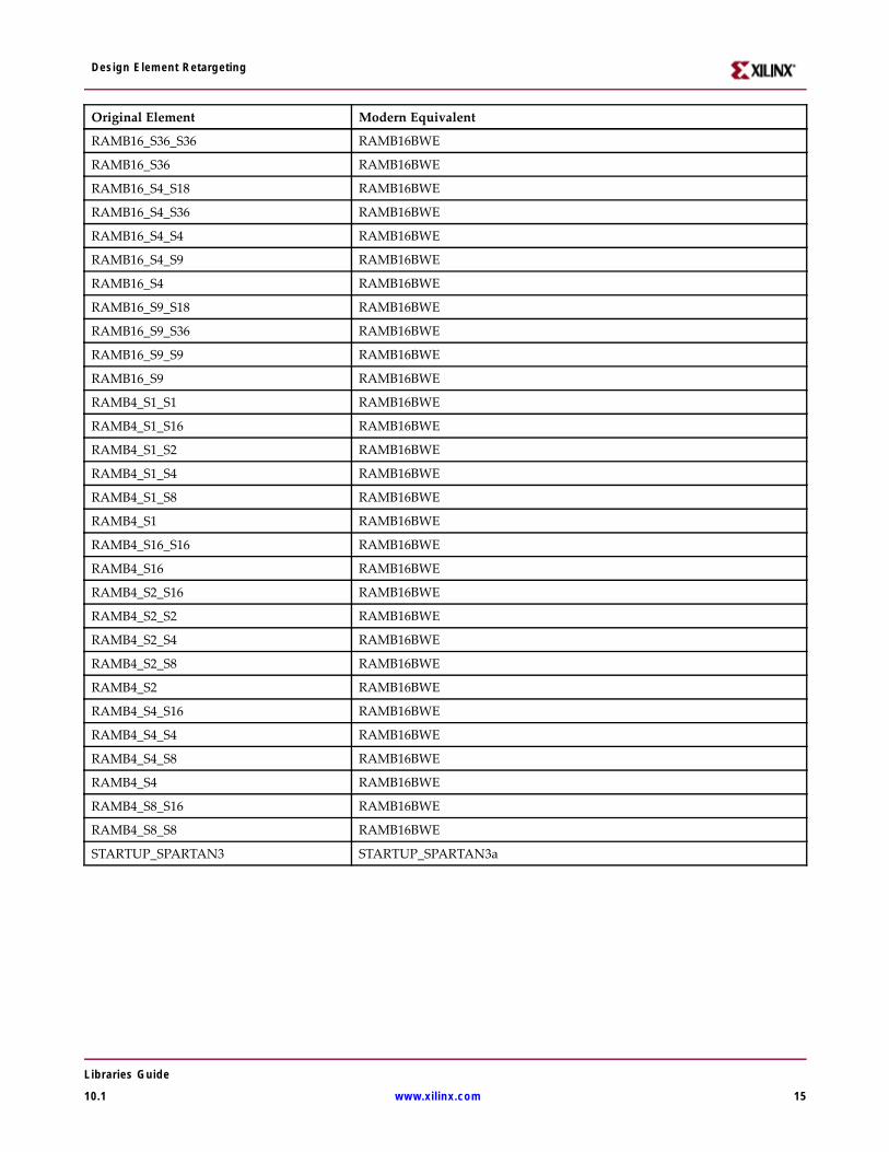
Design Element RetargetingTo ensure that Xilinx customers are able to take full advantage of the latest circuit design advances, certain designelements are automatically changed by the ISE software tools when they are used in this architecture.
The following table lists these elements and the more advanced elements into which they are transformed.
Original Element Modern Equivalent
BUFGCE_1 BUFGCE + INV
BUFGDLL DCM_SP + BUFG
BUFGMUX_1 BUFGMUX + INV
BUFGP BUFG
CAPTURE_SPARTAN3 CAPTURE_SPARTAN3a
CLKDLL DCM_SP
CLKDLLE DCM_SP
CLKDLLHF DCM_SP
FD FDCPE
FD_1 FDCPE + INV
FDC FDCPE
FDC_1 FDCPE + INV
FDCE FDCPE
FDCE_1 FDCPE + INV
FDCP FDCPE
FDCP_1 FDCPE + INV
FDE FDCPE
FDE_1 FDCPE + INV
FDPE FDCPE
FDPE_1 FDCPE + INV
FDR FDRSE
FDR_1 FDRSE + INV
FDRE FDRSE
FDRE_1 FDRSE + INV
FDRS FDRSE
FDRS_1 FDRSE + INV
FDS FDRSE
FDS_1 FDRSE + INV
FDSE FDRSE
FDSE_1 FDRSE + INV
LD LDCPE
LD_1 LDCPE + INV
LDC LDCPE
Libraries Guide
10.1 www.xilinx.com 13
Design Element Retargeting
Original Element Modern Equivalent
LDC_1 LDCPE + INV
LDCE LDCPE
LDCE_1 LDCPE + INV
LDE LDCPE
LDE_1 LDCPE + INV
LDP LDCPE
LDP_1 LDCPE + INV
LDPE LDCPE
LDPE_1 LDCPE + INV
RAM128X1S_1 RAM128x1s + INV on clock
RAM16X1D_1 RAM16X1D + INV on clock
RAM16X1S_1 RAM16X1S + INV on clock
RAM16X2S 2 RAM16x1s
RAM16X4S 4 RAM16x1s
RAM16X8S 8 RAM16x1s
RAM32X1D_1 RAM32x1d + INV on clock
RAM32X1S_1 RAM32x1s + INV on clock
RAM32X2S 2 RAM32x1s
RAM32X4S 4 RAM32x1s
RAM32X8S 8 RAM32x1s
RAM64X1S_1 RAM64x1s + INV on clock
RAM64X2S 2 RAM64x1s
RAMB16_S1_S1 RAMB16BWE
RAMB16_S1_S18 RAMB16BWE
RAMB16_S1_S2 RAMB16BWE
RAMB16_S1_S36 RAMB16BWE
RAMB16_S1_S4 RAMB16BWE
RAMB16_S1_S9 RAMB16BWE
RAMB16_S1 RAMB16BWE
RAMB16_S18_S18 RAMB16BWE
RAMB16_S18_S36 RAMB16BWE
RAMB16_S18 RAMB16BWE
RAMB16_S2_S18 RAMB16BWE
RAMB16_S2_S2 RAMB16BWE
RAMB16_S2_S36 RAMB16BWE
RAMB16_S2_S4 RAMB16BWE
RAMB16_S2_S9 RAMB16BWE
RAMB16_S2 RAMB16BWE
Libraries Guide
14 www.xilinx.com 10.1
Design Element Retargeting
Original Element Modern Equivalent
RAMB16_S36_S36 RAMB16BWE
RAMB16_S36 RAMB16BWE
RAMB16_S4_S18 RAMB16BWE
RAMB16_S4_S36 RAMB16BWE
RAMB16_S4_S4 RAMB16BWE
RAMB16_S4_S9 RAMB16BWE
RAMB16_S4 RAMB16BWE
RAMB16_S9_S18 RAMB16BWE
RAMB16_S9_S36 RAMB16BWE
RAMB16_S9_S9 RAMB16BWE
RAMB16_S9 RAMB16BWE
RAMB4_S1_S1 RAMB16BWE
RAMB4_S1_S16 RAMB16BWE
RAMB4_S1_S2 RAMB16BWE
RAMB4_S1_S4 RAMB16BWE
RAMB4_S1_S8 RAMB16BWE
RAMB4_S1 RAMB16BWE
RAMB4_S16_S16 RAMB16BWE
RAMB4_S16 RAMB16BWE
RAMB4_S2_S16 RAMB16BWE
RAMB4_S2_S2 RAMB16BWE
RAMB4_S2_S4 RAMB16BWE
RAMB4_S2_S8 RAMB16BWE
RAMB4_S2 RAMB16BWE
RAMB4_S4_S16 RAMB16BWE
RAMB4_S4_S4 RAMB16BWE
RAMB4_S4_S8 RAMB16BWE
RAMB4_S4 RAMB16BWE
RAMB4_S8_S16 RAMB16BWE
RAMB4_S8_S8 RAMB16BWE
STARTUP_SPARTAN3 STARTUP_SPARTAN3a
Libraries Guide
10.1 www.xilinx.com 15

Libraries Guide
16 www.xilinx.com 10.1
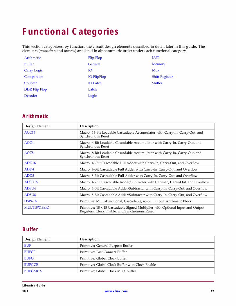
Functional CategoriesThis section categorizes, by function, the circuit design elements described in detail later in this guide. Theelements (primitives and macros) are listed in alphanumeric order under each functional category.
Arithmetic Flip Flop LUT
Buffer General Memory
Carry Logic IO Mux
Comparator IO FlipFlop Shift Register
Counter IO Latch Shifter
DDR Flip Flop Latch
Decoder Logic
ArithmeticDesign Element Description
ACC16 Macro: 16-Bit Loadable Cascadable Accumulator with Carry-In, Carry-Out, andSynchronous Reset
ACC4 Macro: 4-Bit Loadable Cascadable Accumulator with Carry-In, Carry-Out, andSynchronous Reset
ACC8 Macro: 8-Bit Loadable Cascadable Accumulator with Carry-In, Carry-Out, andSynchronous Reset
ADD16 Macro: 16-Bit Cascadable Full Adder with Carry-In, Carry-Out, and Overflow
ADD4 Macro: 4-Bit Cascadable Full Adder with Carry-In, Carry-Out, and Overflow
ADD8 Macro: 8-Bit Cascadable Full Adder with Carry-In, Carry-Out, and Overflow
ADSU16 Macro: 16-Bit Cascadable Adder/Subtracter with Carry-In, Carry-Out, and Overflow
ADSU4 Macro: 4-Bit Cascadable Adder/Subtracter with Carry-In, Carry-Out, and Overflow
ADSU8 Macro: 8-Bit Cascadable Adder/Subtracter with Carry-In, Carry-Out, and Overflow
DSP48A Primitive: Multi-Functional, Cascadable, 48-bit Output, Arithmetic Block
MULT18X18SIO Primitive: 18 x 18 Cascadable Signed Multiplier with Optional Input and OutputRegisters, Clock Enable, and Synchronous Reset
BufferDesign Element Description
BUF Primitive: General Purpose Buffer
BUFCF Primitive: Fast Connect Buffer
BUFG Primitive: Global Clock Buffer
BUFGCE Primitive: Global Clock Buffer with Clock Enable
BUFGMUX Primitive: Global Clock MUX Buffer
Libraries Guide
10.1 www.xilinx.com 17
Functional Categories
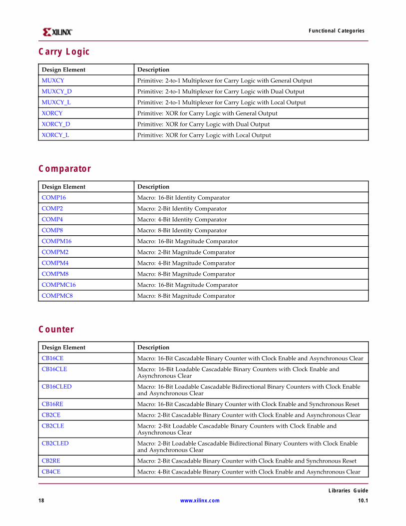
Carry Logic
Design Element Description
MUXCY Primitive: 2-to-1 Multiplexer for Carry Logic with General Output
MUXCY_D Primitive: 2-to-1 Multiplexer for Carry Logic with Dual Output
MUXCY_L Primitive: 2-to-1 Multiplexer for Carry Logic with Local Output
XORCY Primitive: XOR for Carry Logic with General Output
XORCY_D Primitive: XOR for Carry Logic with Dual Output
XORCY_L Primitive: XOR for Carry Logic with Local Output
Comparator
Design Element Description
COMP16 Macro: 16-Bit Identity Comparator
COMP2 Macro: 2-Bit Identity Comparator
COMP4 Macro: 4-Bit Identity Comparator
COMP8 Macro: 8-Bit Identity Comparator
COMPM16 Macro: 16-Bit Magnitude Comparator
COMPM2 Macro: 2-Bit Magnitude Comparator
COMPM4 Macro: 4-Bit Magnitude Comparator
COMPM8 Macro: 8-Bit Magnitude Comparator
COMPMC16 Macro: 16-Bit Magnitude Comparator
COMPMC8 Macro: 8-Bit Magnitude Comparator
Counter
Design Element Description
CB16CE Macro: 16-Bit Cascadable Binary Counter with Clock Enable and Asynchronous Clear
CB16CLE Macro: 16-Bit Loadable Cascadable Binary Counters with Clock Enable andAsynchronous Clear
CB16CLED Macro: 16-Bit Loadable Cascadable Bidirectional Binary Counters with Clock Enableand Asynchronous Clear
CB16RE Macro: 16-Bit Cascadable Binary Counter with Clock Enable and Synchronous Reset
CB2CE Macro: 2-Bit Cascadable Binary Counter with Clock Enable and Asynchronous Clear
CB2CLE Macro: 2-Bit Loadable Cascadable Binary Counters with Clock Enable andAsynchronous Clear
CB2CLED Macro: 2-Bit Loadable Cascadable Bidirectional Binary Counters with Clock Enableand Asynchronous Clear
CB2RE Macro: 2-Bit Cascadable Binary Counter with Clock Enable and Synchronous Reset
CB4CE Macro: 4-Bit Cascadable Binary Counter with Clock Enable and Asynchronous Clear
Libraries Guide
18 www.xilinx.com 10.1
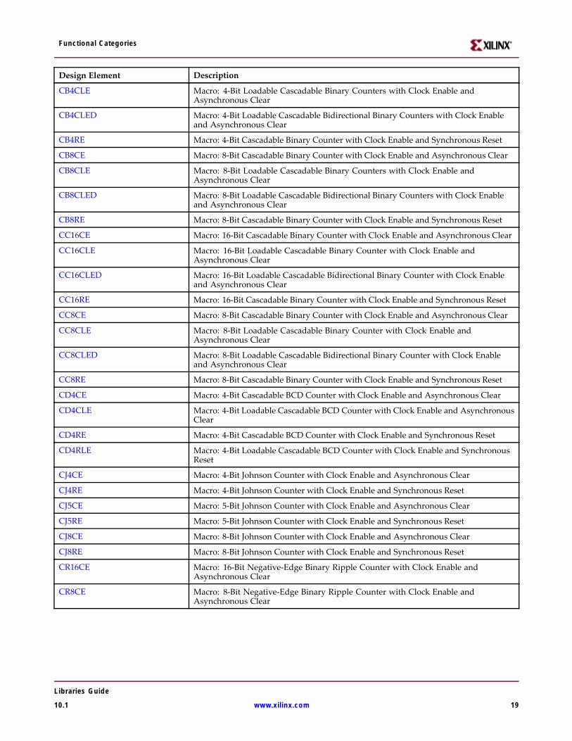
Functional Categories
Design Element Description
CB4CLE Macro: 4-Bit Loadable Cascadable Binary Counters with Clock Enable andAsynchronous Clear
CB4CLED Macro: 4-Bit Loadable Cascadable Bidirectional Binary Counters with Clock Enableand Asynchronous Clear
CB4RE Macro: 4-Bit Cascadable Binary Counter with Clock Enable and Synchronous Reset
CB8CE Macro: 8-Bit Cascadable Binary Counter with Clock Enable and Asynchronous Clear
CB8CLE Macro: 8-Bit Loadable Cascadable Binary Counters with Clock Enable andAsynchronous Clear
CB8CLED Macro: 8-Bit Loadable Cascadable Bidirectional Binary Counters with Clock Enableand Asynchronous Clear
CB8RE Macro: 8-Bit Cascadable Binary Counter with Clock Enable and Synchronous Reset
CC16CE Macro: 16-Bit Cascadable Binary Counter with Clock Enable and Asynchronous Clear
CC16CLE Macro: 16-Bit Loadable Cascadable Binary Counter with Clock Enable andAsynchronous Clear
CC16CLED Macro: 16-Bit Loadable Cascadable Bidirectional Binary Counter with Clock Enableand Asynchronous Clear
CC16RE Macro: 16-Bit Cascadable Binary Counter with Clock Enable and Synchronous Reset
CC8CE Macro: 8-Bit Cascadable Binary Counter with Clock Enable and Asynchronous Clear
CC8CLE Macro: 8-Bit Loadable Cascadable Binary Counter with Clock Enable andAsynchronous Clear
CC8CLED Macro: 8-Bit Loadable Cascadable Bidirectional Binary Counter with Clock Enableand Asynchronous Clear
CC8RE Macro: 8-Bit Cascadable Binary Counter with Clock Enable and Synchronous Reset
CD4CE Macro: 4-Bit Cascadable BCD Counter with Clock Enable and Asynchronous Clear
CD4CLE Macro: 4-Bit Loadable Cascadable BCD Counter with Clock Enable and AsynchronousClear
CD4RE Macro: 4-Bit Cascadable BCD Counter with Clock Enable and Synchronous Reset
CD4RLE Macro: 4-Bit Loadable Cascadable BCD Counter with Clock Enable and SynchronousReset
CJ4CE Macro: 4-Bit Johnson Counter with Clock Enable and Asynchronous Clear
CJ4RE Macro: 4-Bit Johnson Counter with Clock Enable and Synchronous Reset
CJ5CE Macro: 5-Bit Johnson Counter with Clock Enable and Asynchronous Clear
CJ5RE Macro: 5-Bit Johnson Counter with Clock Enable and Synchronous Reset
CJ8CE Macro: 8-Bit Johnson Counter with Clock Enable and Asynchronous Clear
CJ8RE Macro: 8-Bit Johnson Counter with Clock Enable and Synchronous Reset
CR16CE Macro: 16-Bit Negative-Edge Binary Ripple Counter with Clock Enable andAsynchronous Clear
CR8CE Macro: 8-Bit Negative-Edge Binary Ripple Counter with Clock Enable andAsynchronous Clear
Libraries Guide
10.1 www.xilinx.com 19
Functional Categories
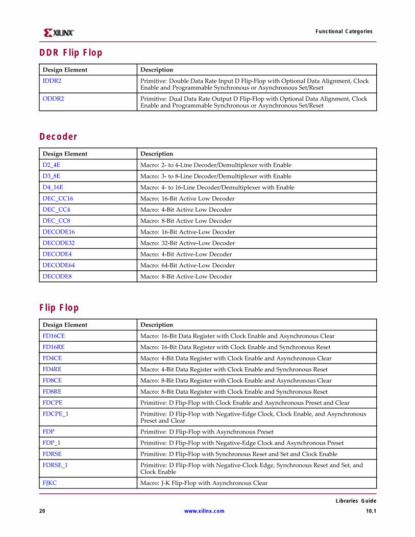
DDR Flip FlopDesign Element Description
IDDR2 Primitive: Double Data Rate Input D Flip-Flop with Optional Data Alignment, ClockEnable and Programmable Synchronous or Asynchronous Set/Reset
ODDR2 Primitive: Dual Data Rate Output D Flip-Flop with Optional Data Alignment, ClockEnable and Programmable Synchronous or Asynchronous Set/Reset
DecoderDesign Element Description
D2_4E Macro: 2- to 4-Line Decoder/Demultiplexer with Enable
D3_8E Macro: 3- to 8-Line Decoder/Demultiplexer with Enable
D4_16E Macro: 4- to 16-Line Decoder/Demultiplexer with Enable
DEC_CC16 Macro: 16-Bit Active Low Decoder
DEC_CC4 Macro: 4-Bit Active Low Decoder
DEC_CC8 Macro: 8-Bit Active Low Decoder
DECODE16 Macro: 16-Bit Active-Low Decoder
DECODE32 Macro: 32-Bit Active-Low Decoder
DECODE4 Macro: 4-Bit Active-Low Decoder
DECODE64 Macro: 64-Bit Active-Low Decoder
DECODE8 Macro: 8-Bit Active-Low Decoder
Flip FlopDesign Element Description
FD16CE Macro: 16-Bit Data Register with Clock Enable and Asynchronous Clear
FD16RE Macro: 16-Bit Data Register with Clock Enable and Synchronous Reset
FD4CE Macro: 4-Bit Data Register with Clock Enable and Asynchronous Clear
FD4RE Macro: 4-Bit Data Register with Clock Enable and Synchronous Reset
FD8CE Macro: 8-Bit Data Register with Clock Enable and Asynchronous Clear
FD8RE Macro: 8-Bit Data Register with Clock Enable and Synchronous Reset
FDCPE Primitive: D Flip-Flop with Clock Enable and Asynchronous Preset and Clear
FDCPE_1 Primitive: D Flip-Flop with Negative-Edge Clock, Clock Enable, and AsynchronousPreset and Clear
FDP Primitive: D Flip-Flop with Asynchronous Preset
FDP_1 Primitive: D Flip-Flop with Negative-Edge Clock and Asynchronous Preset
FDRSE Primitive: D Flip-Flop with Synchronous Reset and Set and Clock Enable
FDRSE_1 Primitive: D Flip-Flop with Negative-Clock Edge, Synchronous Reset and Set, andClock Enable
FJKC Macro: J-K Flip-Flop with Asynchronous Clear
Libraries Guide
20 www.xilinx.com 10.1
Functional Categories
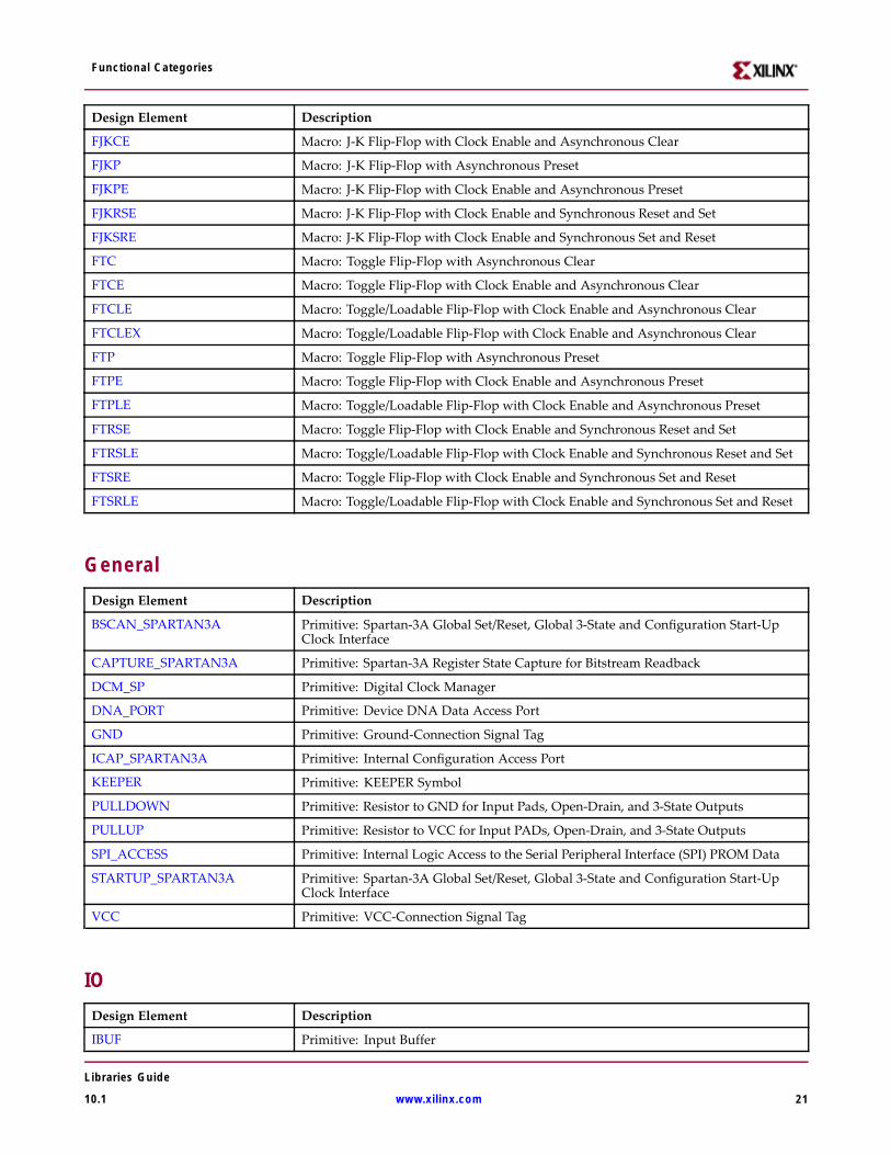
Design Element Description
FJKCE Macro: J-K Flip-Flop with Clock Enable and Asynchronous Clear
FJKP Macro: J-K Flip-Flop with Asynchronous Preset
FJKPE Macro: J-K Flip-Flop with Clock Enable and Asynchronous Preset
FJKRSE Macro: J-K Flip-Flop with Clock Enable and Synchronous Reset and Set
FJKSRE Macro: J-K Flip-Flop with Clock Enable and Synchronous Set and Reset
FTC Macro: Toggle Flip-Flop with Asynchronous Clear
FTCE Macro: Toggle Flip-Flop with Clock Enable and Asynchronous Clear
FTCLE Macro: Toggle/Loadable Flip-Flop with Clock Enable and Asynchronous Clear
FTCLEX Macro: Toggle/Loadable Flip-Flop with Clock Enable and Asynchronous Clear
FTP Macro: Toggle Flip-Flop with Asynchronous Preset
FTPE Macro: Toggle Flip-Flop with Clock Enable and Asynchronous Preset
FTPLE Macro: Toggle/Loadable Flip-Flop with Clock Enable and Asynchronous Preset
FTRSE Macro: Toggle Flip-Flop with Clock Enable and Synchronous Reset and Set
FTRSLE Macro: Toggle/Loadable Flip-Flop with Clock Enable and Synchronous Reset and Set
FTSRE Macro: Toggle Flip-Flop with Clock Enable and Synchronous Set and Reset
FTSRLE Macro: Toggle/Loadable Flip-Flop with Clock Enable and Synchronous Set and Reset
GeneralDesign Element Description
BSCAN_SPARTAN3A Primitive: Spartan-3A Global Set/Reset, Global 3-State and Configuration Start-UpClock Interface
CAPTURE_SPARTAN3A Primitive: Spartan-3A Register State Capture for Bitstream Readback
DCM_SP Primitive: Digital Clock Manager
DNA_PORT Primitive: Device DNA Data Access Port
GND Primitive: Ground-Connection Signal Tag
ICAP_SPARTAN3A Primitive: Internal Configuration Access Port
KEEPER Primitive: KEEPER Symbol
PULLDOWN Primitive: Resistor to GND for Input Pads, Open-Drain, and 3-State Outputs
PULLUP Primitive: Resistor to VCC for Input PADs, Open-Drain, and 3-State Outputs
SPI_ACCESS Primitive: Internal Logic Access to the Serial Peripheral Interface (SPI) PROM Data
STARTUP_SPARTAN3A Primitive: Spartan-3A Global Set/Reset, Global 3-State and Configuration Start-UpClock Interface
VCC Primitive: VCC-Connection Signal Tag
IODesign Element Description
IBUF Primitive: Input Buffer
Libraries Guide
10.1 www.xilinx.com 21
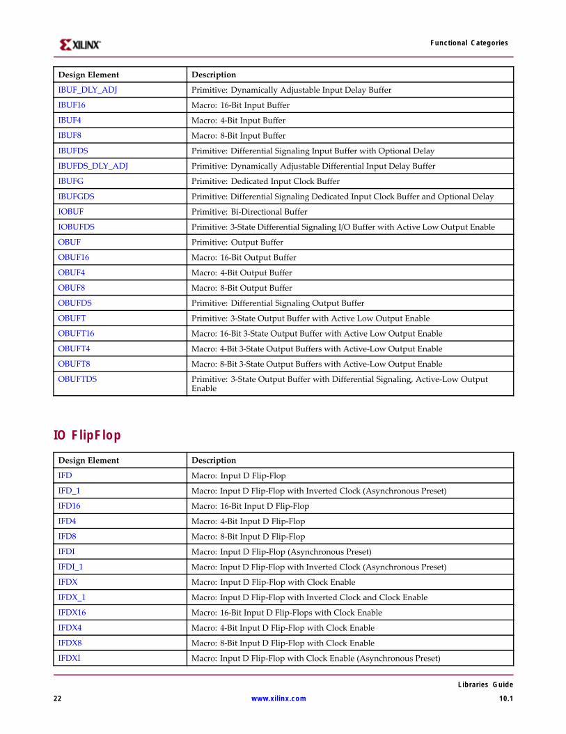
Functional Categories
Design Element Description
IBUF_DLY_ADJ Primitive: Dynamically Adjustable Input Delay Buffer
IBUF16 Macro: 16-Bit Input Buffer
IBUF4 Macro: 4-Bit Input Buffer
IBUF8 Macro: 8-Bit Input Buffer
IBUFDS Primitive: Differential Signaling Input Buffer with Optional Delay
IBUFDS_DLY_ADJ Primitive: Dynamically Adjustable Differential Input Delay Buffer
IBUFG Primitive: Dedicated Input Clock Buffer
IBUFGDS Primitive: Differential Signaling Dedicated Input Clock Buffer and Optional Delay
IOBUF Primitive: Bi-Directional Buffer
IOBUFDS Primitive: 3-State Differential Signaling I/O Buffer with Active Low Output Enable
OBUF Primitive: Output Buffer
OBUF16 Macro: 16-Bit Output Buffer
OBUF4 Macro: 4-Bit Output Buffer
OBUF8 Macro: 8-Bit Output Buffer
OBUFDS Primitive: Differential Signaling Output Buffer
OBUFT Primitive: 3-State Output Buffer with Active Low Output Enable
OBUFT16 Macro: 16-Bit 3-State Output Buffer with Active Low Output Enable
OBUFT4 Macro: 4-Bit 3-State Output Buffers with Active-Low Output Enable
OBUFT8 Macro: 8-Bit 3-State Output Buffers with Active-Low Output Enable
OBUFTDS Primitive: 3-State Output Buffer with Differential Signaling, Active-Low OutputEnable
IO FlipFlop
Design Element Description
IFD Macro: Input D Flip-Flop
IFD_1 Macro: Input D Flip-Flop with Inverted Clock (Asynchronous Preset)
IFD16 Macro: 16-Bit Input D Flip-Flop
IFD4 Macro: 4-Bit Input D Flip-Flop
IFD8 Macro: 8-Bit Input D Flip-Flop
IFDI Macro: Input D Flip-Flop (Asynchronous Preset)
IFDI_1 Macro: Input D Flip-Flop with Inverted Clock (Asynchronous Preset)
IFDX Macro: Input D Flip-Flop with Clock Enable
IFDX_1 Macro: Input D Flip-Flop with Inverted Clock and Clock Enable
IFDX16 Macro: 16-Bit Input D Flip-Flops with Clock Enable
IFDX4 Macro: 4-Bit Input D Flip-Flop with Clock Enable
IFDX8 Macro: 8-Bit Input D Flip-Flop with Clock Enable
IFDXI Macro: Input D Flip-Flop with Clock Enable (Asynchronous Preset)
Libraries Guide
22 www.xilinx.com 10.1
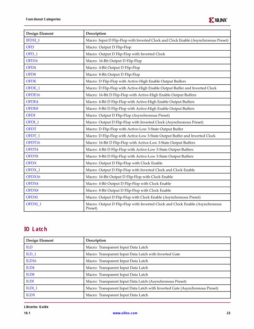
Functional Categories
Design Element Description
IFDXI_1 Macro: Input D Flip-Flop with Inverted Clock and Clock Enable (Asynchronous Preset)
OFD Macro: Output D Flip-Flop
OFD_1 Macro: Output D Flip-Flop with Inverted Clock
OFD16 Macro: 16-Bit Output D Flip-Flop
OFD4 Macro: 4-Bit Output D Flip-Flop
OFD8 Macro: 8-Bit Output D Flip-Flop
OFDE Macro: D Flip-Flop with Active-High Enable Output Buffers
OFDE_1 Macro: D Flip-Flop with Active-High Enable Output Buffer and Inverted Clock
OFDE16 Macro: 16-Bit D Flip-Flop with Active-High Enable Output Buffers
OFDE4 Macro: 4-Bit D Flip-Flop with Active-High Enable Output Buffers
OFDE8 Macro: 8-Bit D Flip-Flop with Active-High Enable Output Buffers
OFDI Macro: Output D Flip-Flop (Asynchronous Preset)
OFDI_1 Macro: Output D Flip-Flop with Inverted Clock (Asynchronous Preset)
OFDT Macro: D Flip-Flop with Active-Low 3-State Output Buffer
OFDT_1 Macro: D Flip-Flop with Active-Low 3-State Output Buffer and Inverted Clock
OFDT16 Macro: 16-Bit D Flip-Flop with Active-Low 3-State Output Buffers
OFDT4 Macro: 4-Bit D Flip-Flop with Active-Low 3-State Output Buffers
OFDT8 Macro: 8-Bit D Flip-Flop with Active-Low 3-State Output Buffers
OFDX Macro: Output D Flip-Flop with Clock Enable
OFDX_1 Macro: Output D Flip-Flop with Inverted Clock and Clock Enable
OFDX16 Macro: 16-Bit Output D Flip-Flop with Clock Enable
OFDX4 Macro: 4-Bit Output D Flip-Flop with Clock Enable
OFDX8 Macro: 8-Bit Output D Flip-Flop with Clock Enable
OFDXI Macro: Output D Flip-Flop with Clock Enable (Asynchronous Preset)
OFDXI_1 Macro: Output D Flip-Flop with Inverted Clock and Clock Enable (AsynchronousPreset)
IO Latch
Design Element Description
ILD Macro: Transparent Input Data Latch
ILD_1 Macro: Transparent Input Data Latch with Inverted Gate
ILD16 Macro: Transparent Input Data Latch
ILD4 Macro: Transparent Input Data Latch
ILD8 Macro: Transparent Input Data Latch
ILDI Macro: Transparent Input Data Latch (Asynchronous Preset)
ILDI_1 Macro: Transparent Input Data Latch with Inverted Gate (Asynchronous Preset)
ILDX Macro: Transparent Input Data Latch
Libraries Guide
10.1 www.xilinx.com 23
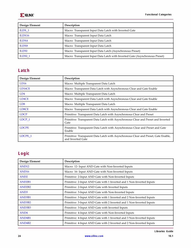
Functional Categories
Design Element Description
ILDX_1 Macro: Transparent Input Data Latch with Inverted Gate
ILDX16 Macro: Transparent Input Data Latch
ILDX4 Macro: Transparent Input Data Latch
ILDX8 Macro: Transparent Input Data Latch
ILDXI Macro: Transparent Input Data Latch (Asynchronous Preset)
ILDXI_1 Macro: Transparent Input Data Latch with Inverted Gate (Asynchronous Preset)
LatchDesign Element Description
LD16 Macro: Multiple Transparent Data Latch
LD16CE Macro: Transparent Data Latch with Asynchronous Clear and Gate Enable
LD4 Macro: Multiple Transparent Data Latch
LD4CE Macro: Transparent Data Latch with Asynchronous Clear and Gate Enable
LD8 Macro: Multiple Transparent Data Latch
LD8CE Macro: Transparent Data Latch with Asynchronous Clear and Gate Enable
LDCP Primitive: Transparent Data Latch with Asynchronous Clear and Preset
LDCP_1 Primitive: Transparent Data Latch with Asynchronous Clear and Preset and InvertedGate
LDCPE Primitive: Transparent Data Latch with Asynchronous Clear and Preset and GateEnable
LDCPE_1 Primitive: Transparent Data Latch with Asynchronous Clear and Preset, Gate Enable,and Inverted Gate
LogicDesign Element Description
AND12 Macro: 12- Input AND Gate with Non-Inverted Inputs
AND16 Macro: 16- Input AND Gate with Non-Inverted Inputs
AND2 Primitive: 2-Input AND Gate with Non-Inverted Inputs
AND2B1 Primitive: 2-Input AND Gate with 1 Inverted and 1 Non-Inverted Inputs
AND2B2 Primitive: 2-Input AND Gate with Inverted Inputs
AND3 Primitive: 3-Input AND Gate with Non-Inverted Inputs
AND3B1 Primitive: 3-Input AND Gate with 1 Inverted and 2 Non-Inverted Inputs
AND3B2 Primitive: 3-Input AND Gate with 2 Inverted and 1 Non-Inverted Inputs
AND3B3 Primitive: 3-Input AND Gate with Inverted Inputs
AND4 Primitive: 4-Input AND Gate with Non-Inverted Inputs
AND4B1 Primitive: 4-Input AND Gate with 1 Inverted and 3 Non-Inverted Inputs
AND4B2 Primitive: 4-Input AND Gate with 2 Inverted and 2 Non-Inverted Inputs
Libraries Guide
24 www.xilinx.com 10.1
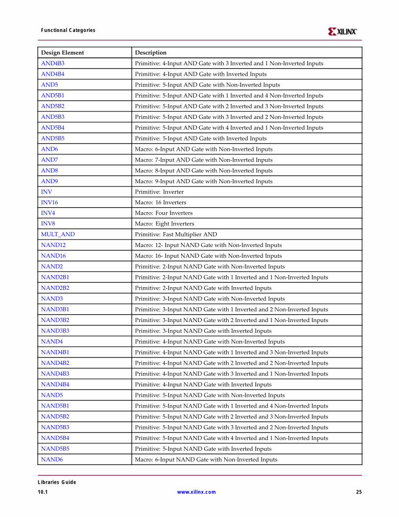
Functional Categories
Design Element Description
AND4B3 Primitive: 4-Input AND Gate with 3 Inverted and 1 Non-Inverted Inputs
AND4B4 Primitive: 4-Input AND Gate with Inverted Inputs
AND5 Primitive: 5-Input AND Gate with Non-Inverted Inputs
AND5B1 Primitive: 5-Input AND Gate with 1 Inverted and 4 Non-Inverted Inputs
AND5B2 Primitive: 5-Input AND Gate with 2 Inverted and 3 Non-Inverted Inputs
AND5B3 Primitive: 5-Input AND Gate with 3 Inverted and 2 Non-Inverted Inputs
AND5B4 Primitive: 5-Input AND Gate with 4 Inverted and 1 Non-Inverted Inputs
AND5B5 Primitive: 5-Input AND Gate with Inverted Inputs
AND6 Macro: 6-Input AND Gate with Non-Inverted Inputs
AND7 Macro: 7-Input AND Gate with Non-Inverted Inputs
AND8 Macro: 8-Input AND Gate with Non-Inverted Inputs
AND9 Macro: 9-Input AND Gate with Non-Inverted Inputs
INV Primitive: Inverter
INV16 Macro: 16 Inverters
INV4 Macro: Four Inverters
INV8 Macro: Eight Inverters
MULT_AND Primitive: Fast Multiplier AND
NAND12 Macro: 12- Input NAND Gate with Non-Inverted Inputs
NAND16 Macro: 16- Input NAND Gate with Non-Inverted Inputs
NAND2 Primitive: 2-Input NAND Gate with Non-Inverted Inputs
NAND2B1 Primitive: 2-Input NAND Gate with 1 Inverted and 1 Non-Inverted Inputs
NAND2B2 Primitive: 2-Input NAND Gate with Inverted Inputs
NAND3 Primitive: 3-Input NAND Gate with Non-Inverted Inputs
NAND3B1 Primitive: 3-Input NAND Gate with 1 Inverted and 2 Non-Inverted Inputs
NAND3B2 Primitive: 3-Input NAND Gate with 2 Inverted and 1 Non-Inverted Inputs
NAND3B3 Primitive: 3-Input NAND Gate with Inverted Inputs
NAND4 Primitive: 4-Input NAND Gate with Non-Inverted Inputs
NAND4B1 Primitive: 4-Input NAND Gate with 1 Inverted and 3 Non-Inverted Inputs
NAND4B2 Primitive: 4-Input NAND Gate with 2 Inverted and 2 Non-Inverted Inputs
NAND4B3 Primitive: 4-Input NAND Gate with 3 Inverted and 1 Non-Inverted Inputs
NAND4B4 Primitive: 4-Input NAND Gate with Inverted Inputs
NAND5 Primitive: 5-Input NAND Gate with Non-Inverted Inputs
NAND5B1 Primitive: 5-Input NAND Gate with 1 Inverted and 4 Non-Inverted Inputs
NAND5B2 Primitive: 5-Input NAND Gate with 2 Inverted and 3 Non-Inverted Inputs
NAND5B3 Primitive: 5-Input NAND Gate with 3 Inverted and 2 Non-Inverted Inputs
NAND5B4 Primitive: 5-Input NAND Gate with 4 Inverted and 1 Non-Inverted Inputs
NAND5B5 Primitive: 5-Input NAND Gate with Inverted Inputs
NAND6 Macro: 6-Input NAND Gate with Non-Inverted Inputs
Libraries Guide
10.1 www.xilinx.com 25
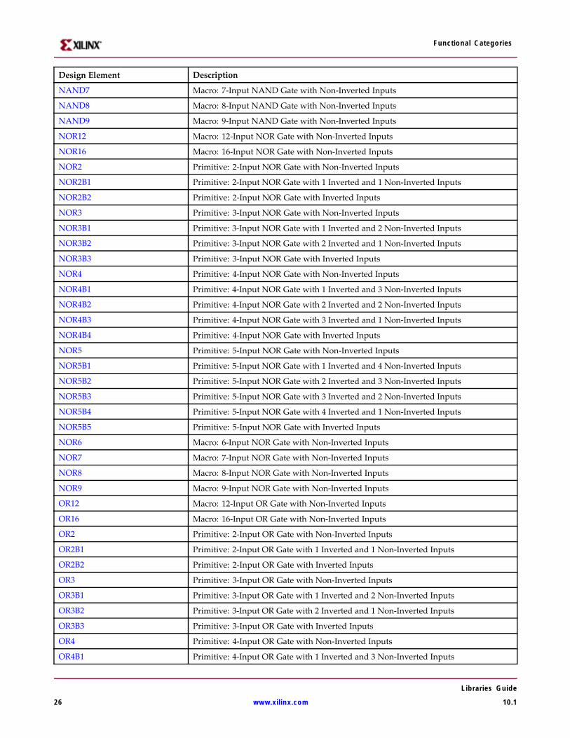
Functional Categories
Design Element Description
NAND7 Macro: 7-Input NAND Gate with Non-Inverted Inputs
NAND8 Macro: 8-Input NAND Gate with Non-Inverted Inputs
NAND9 Macro: 9-Input NAND Gate with Non-Inverted Inputs
NOR12 Macro: 12-Input NOR Gate with Non-Inverted Inputs
NOR16 Macro: 16-Input NOR Gate with Non-Inverted Inputs
NOR2 Primitive: 2-Input NOR Gate with Non-Inverted Inputs
NOR2B1 Primitive: 2-Input NOR Gate with 1 Inverted and 1 Non-Inverted Inputs
NOR2B2 Primitive: 2-Input NOR Gate with Inverted Inputs
NOR3 Primitive: 3-Input NOR Gate with Non-Inverted Inputs
NOR3B1 Primitive: 3-Input NOR Gate with 1 Inverted and 2 Non-Inverted Inputs
NOR3B2 Primitive: 3-Input NOR Gate with 2 Inverted and 1 Non-Inverted Inputs
NOR3B3 Primitive: 3-Input NOR Gate with Inverted Inputs
NOR4 Primitive: 4-Input NOR Gate with Non-Inverted Inputs
NOR4B1 Primitive: 4-Input NOR Gate with 1 Inverted and 3 Non-Inverted Inputs
NOR4B2 Primitive: 4-Input NOR Gate with 2 Inverted and 2 Non-Inverted Inputs
NOR4B3 Primitive: 4-Input NOR Gate with 3 Inverted and 1 Non-Inverted Inputs
NOR4B4 Primitive: 4-Input NOR Gate with Inverted Inputs
NOR5 Primitive: 5-Input NOR Gate with Non-Inverted Inputs
NOR5B1 Primitive: 5-Input NOR Gate with 1 Inverted and 4 Non-Inverted Inputs
NOR5B2 Primitive: 5-Input NOR Gate with 2 Inverted and 3 Non-Inverted Inputs
NOR5B3 Primitive: 5-Input NOR Gate with 3 Inverted and 2 Non-Inverted Inputs
NOR5B4 Primitive: 5-Input NOR Gate with 4 Inverted and 1 Non-Inverted Inputs
NOR5B5 Primitive: 5-Input NOR Gate with Inverted Inputs
NOR6 Macro: 6-Input NOR Gate with Non-Inverted Inputs
NOR7 Macro: 7-Input NOR Gate with Non-Inverted Inputs
NOR8 Macro: 8-Input NOR Gate with Non-Inverted Inputs
NOR9 Macro: 9-Input NOR Gate with Non-Inverted Inputs
OR12 Macro: 12-Input OR Gate with Non-Inverted Inputs
OR16 Macro: 16-Input OR Gate with Non-Inverted Inputs
OR2 Primitive: 2-Input OR Gate with Non-Inverted Inputs
OR2B1 Primitive: 2-Input OR Gate with 1 Inverted and 1 Non-Inverted Inputs
OR2B2 Primitive: 2-Input OR Gate with Inverted Inputs
OR3 Primitive: 3-Input OR Gate with Non-Inverted Inputs
OR3B1 Primitive: 3-Input OR Gate with 1 Inverted and 2 Non-Inverted Inputs
OR3B2 Primitive: 3-Input OR Gate with 2 Inverted and 1 Non-Inverted Inputs
OR3B3 Primitive: 3-Input OR Gate with Inverted Inputs
OR4 Primitive: 4-Input OR Gate with Non-Inverted Inputs
OR4B1 Primitive: 4-Input OR Gate with 1 Inverted and 3 Non-Inverted Inputs
Libraries Guide
26 www.xilinx.com 10.1
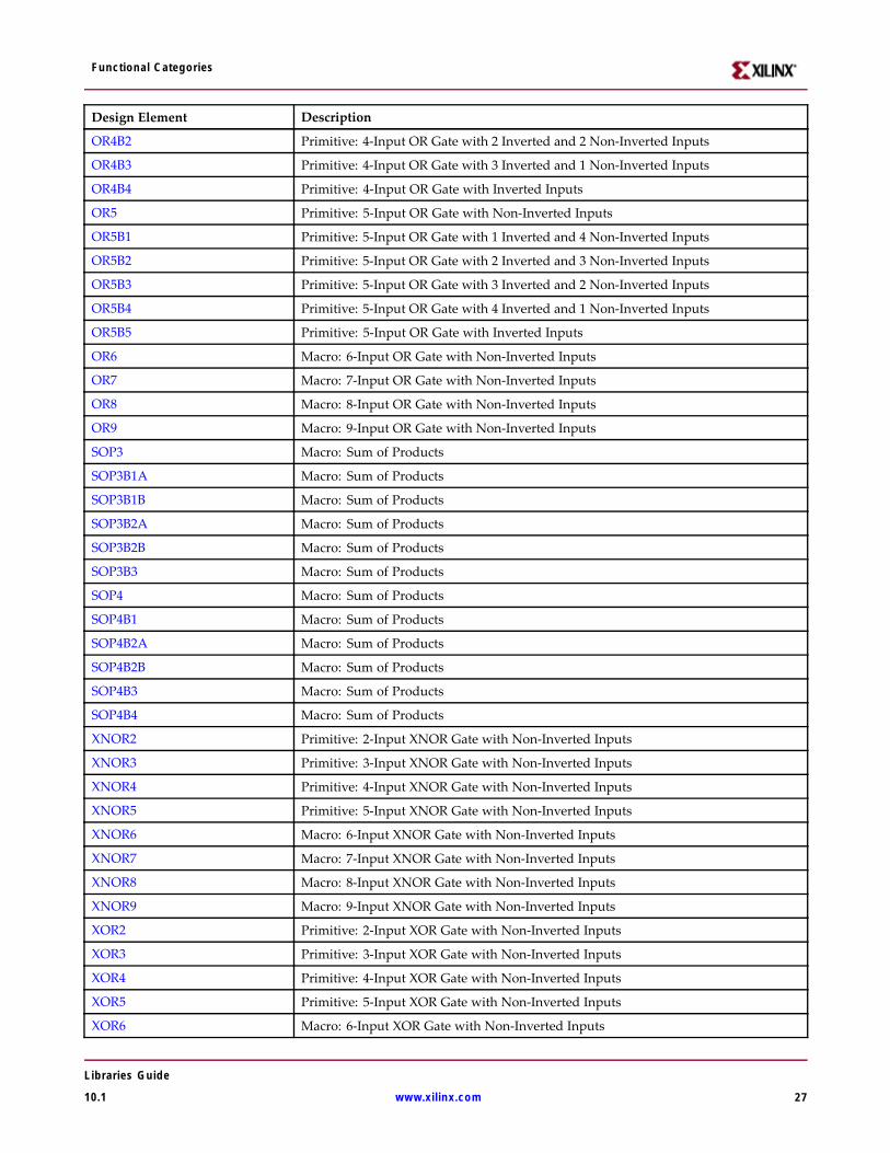
Functional Categories
Design Element Description
OR4B2 Primitive: 4-Input OR Gate with 2 Inverted and 2 Non-Inverted Inputs
OR4B3 Primitive: 4-Input OR Gate with 3 Inverted and 1 Non-Inverted Inputs
OR4B4 Primitive: 4-Input OR Gate with Inverted Inputs
OR5 Primitive: 5-Input OR Gate with Non-Inverted Inputs
OR5B1 Primitive: 5-Input OR Gate with 1 Inverted and 4 Non-Inverted Inputs
OR5B2 Primitive: 5-Input OR Gate with 2 Inverted and 3 Non-Inverted Inputs
OR5B3 Primitive: 5-Input OR Gate with 3 Inverted and 2 Non-Inverted Inputs
OR5B4 Primitive: 5-Input OR Gate with 4 Inverted and 1 Non-Inverted Inputs
OR5B5 Primitive: 5-Input OR Gate with Inverted Inputs
OR6 Macro: 6-Input OR Gate with Non-Inverted Inputs
OR7 Macro: 7-Input OR Gate with Non-Inverted Inputs
OR8 Macro: 8-Input OR Gate with Non-Inverted Inputs
OR9 Macro: 9-Input OR Gate with Non-Inverted Inputs
SOP3 Macro: Sum of Products
SOP3B1A Macro: Sum of Products
SOP3B1B Macro: Sum of Products
SOP3B2A Macro: Sum of Products
SOP3B2B Macro: Sum of Products
SOP3B3 Macro: Sum of Products
SOP4 Macro: Sum of Products
SOP4B1 Macro: Sum of Products
SOP4B2A Macro: Sum of Products
SOP4B2B Macro: Sum of Products
SOP4B3 Macro: Sum of Products
SOP4B4 Macro: Sum of Products
XNOR2 Primitive: 2-Input XNOR Gate with Non-Inverted Inputs
XNOR3 Primitive: 3-Input XNOR Gate with Non-Inverted Inputs
XNOR4 Primitive: 4-Input XNOR Gate with Non-Inverted Inputs
XNOR5 Primitive: 5-Input XNOR Gate with Non-Inverted Inputs
XNOR6 Macro: 6-Input XNOR Gate with Non-Inverted Inputs
XNOR7 Macro: 7-Input XNOR Gate with Non-Inverted Inputs
XNOR8 Macro: 8-Input XNOR Gate with Non-Inverted Inputs
XNOR9 Macro: 9-Input XNOR Gate with Non-Inverted Inputs
XOR2 Primitive: 2-Input XOR Gate with Non-Inverted Inputs
XOR3 Primitive: 3-Input XOR Gate with Non-Inverted Inputs
XOR4 Primitive: 4-Input XOR Gate with Non-Inverted Inputs
XOR5 Primitive: 5-Input XOR Gate with Non-Inverted Inputs
XOR6 Macro: 6-Input XOR Gate with Non-Inverted Inputs
Libraries Guide
10.1 www.xilinx.com 27
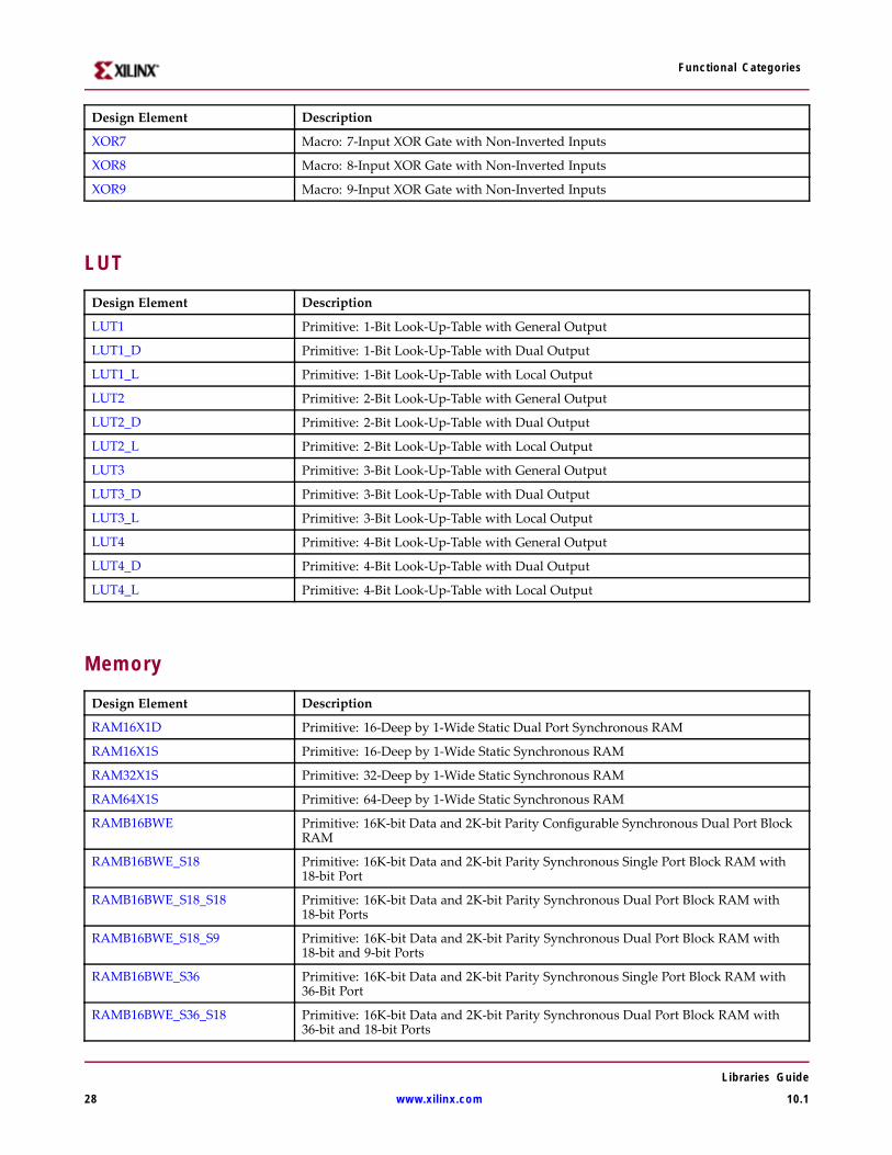
Functional Categories
Design Element Description
XOR7 Macro: 7-Input XOR Gate with Non-Inverted Inputs
XOR8 Macro: 8-Input XOR Gate with Non-Inverted Inputs
XOR9 Macro: 9-Input XOR Gate with Non-Inverted Inputs
LUT
Design Element Description
LUT1 Primitive: 1-Bit Look-Up-Table with General Output
LUT1_D Primitive: 1-Bit Look-Up-Table with Dual Output
LUT1_L Primitive: 1-Bit Look-Up-Table with Local Output
LUT2 Primitive: 2-Bit Look-Up-Table with General Output
LUT2_D Primitive: 2-Bit Look-Up-Table with Dual Output
LUT2_L Primitive: 2-Bit Look-Up-Table with Local Output
LUT3 Primitive: 3-Bit Look-Up-Table with General Output
LUT3_D Primitive: 3-Bit Look-Up-Table with Dual Output
LUT3_L Primitive: 3-Bit Look-Up-Table with Local Output
LUT4 Primitive: 4-Bit Look-Up-Table with General Output
LUT4_D Primitive: 4-Bit Look-Up-Table with Dual Output
LUT4_L Primitive: 4-Bit Look-Up-Table with Local Output
Memory
Design Element Description
RAM16X1D Primitive: 16-Deep by 1-Wide Static Dual Port Synchronous RAM
RAM16X1S Primitive: 16-Deep by 1-Wide Static Synchronous RAM
RAM32X1S Primitive: 32-Deep by 1-Wide Static Synchronous RAM
RAM64X1S Primitive: 64-Deep by 1-Wide Static Synchronous RAM
RAMB16BWE Primitive: 16K-bit Data and 2K-bit Parity Configurable Synchronous Dual Port BlockRAM
RAMB16BWE_S18 Primitive: 16K-bit Data and 2K-bit Parity Synchronous Single Port Block RAM with18-bit Port
RAMB16BWE_S18_S18 Primitive: 16K-bit Data and 2K-bit Parity Synchronous Dual Port Block RAM with18-bit Ports
RAMB16BWE_S18_S9 Primitive: 16K-bit Data and 2K-bit Parity Synchronous Dual Port Block RAM with18-bit and 9-bit Ports
RAMB16BWE_S36 Primitive: 16K-bit Data and 2K-bit Parity Synchronous Single Port Block RAM with36-Bit Port
RAMB16BWE_S36_S18 Primitive: 16K-bit Data and 2K-bit Parity Synchronous Dual Port Block RAM with36-bit and 18-bit Ports
Libraries Guide
28 www.xilinx.com 10.1
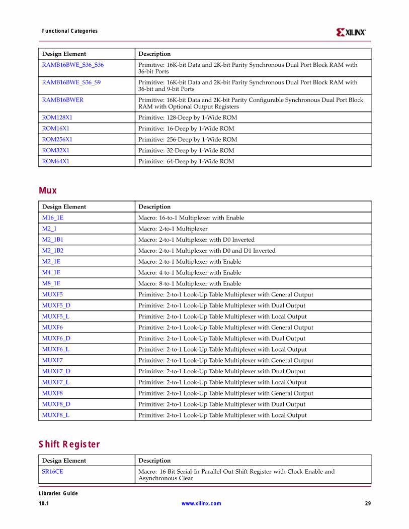
Functional Categories
Design Element Description
RAMB16BWE_S36_S36 Primitive: 16K-bit Data and 2K-bit Parity Synchronous Dual Port Block RAM with36-bit Ports
RAMB16BWE_S36_S9 Primitive: 16K-bit Data and 2K-bit Parity Synchronous Dual Port Block RAM with36-bit and 9-bit Ports
RAMB16BWER Primitive: 16K-bit Data and 2K-bit Parity Configurable Synchronous Dual Port BlockRAM with Optional Output Registers
ROM128X1 Primitive: 128-Deep by 1-Wide ROM
ROM16X1 Primitive: 16-Deep by 1-Wide ROM
ROM256X1 Primitive: 256-Deep by 1-Wide ROM
ROM32X1 Primitive: 32-Deep by 1-Wide ROM
ROM64X1 Primitive: 64-Deep by 1-Wide ROM
MuxDesign Element Description
M16_1E Macro: 16-to-1 Multiplexer with Enable
M2_1 Macro: 2-to-1 Multiplexer
M2_1B1 Macro: 2-to-1 Multiplexer with D0 Inverted
M2_1B2 Macro: 2-to-1 Multiplexer with D0 and D1 Inverted
M2_1E Macro: 2-to-1 Multiplexer with Enable
M4_1E Macro: 4-to-1 Multiplexer with Enable
M8_1E Macro: 8-to-1 Multiplexer with Enable
MUXF5 Primitive: 2-to-1 Look-Up Table Multiplexer with General Output
MUXF5_D Primitive: 2-to-1 Look-Up Table Multiplexer with Dual Output
MUXF5_L Primitive: 2-to-1 Look-Up Table Multiplexer with Local Output
MUXF6 Primitive: 2-to-1 Look-Up Table Multiplexer with General Output
MUXF6_D Primitive: 2-to-1 Look-Up Table Multiplexer with Dual Output
MUXF6_L Primitive: 2-to-1 Look-Up Table Multiplexer with Local Output
MUXF7 Primitive: 2-to-1 Look-Up Table Multiplexer with General Output
MUXF7_D Primitive: 2-to-1 Look-Up Table Multiplexer with Dual Output
MUXF7_L Primitive: 2-to-1 Look-Up Table Multiplexer with Local Output
MUXF8 Primitive: 2-to-1 Look-Up Table Multiplexer with General Output
MUXF8_D Primitive: 2-to-1 Look-Up Table Multiplexer with Dual Output
MUXF8_L Primitive: 2-to-1 Look-Up Table Multiplexer with Local Output
Shift RegisterDesign Element Description
SR16CE Macro: 16-Bit Serial-In Parallel-Out Shift Register with Clock Enable andAsynchronous Clear
Libraries Guide
10.1 www.xilinx.com 29
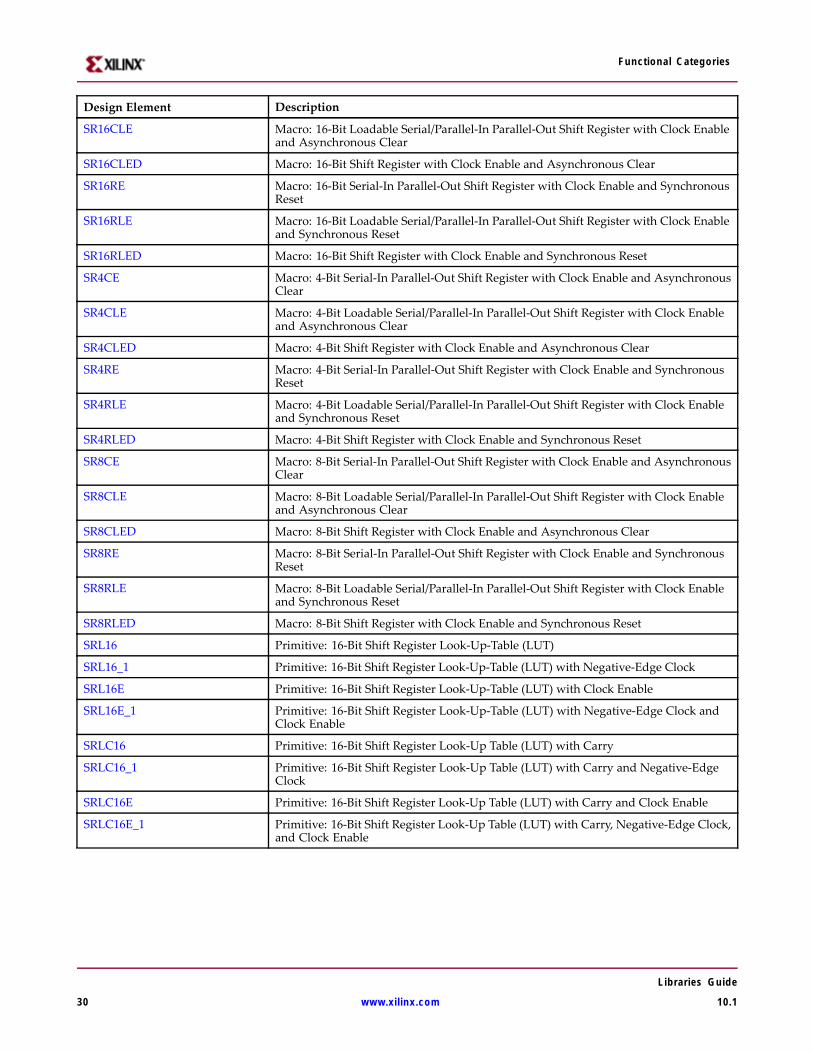
Functional Categories
Design Element Description
SR16CLE Macro: 16-Bit Loadable Serial/Parallel-In Parallel-Out Shift Register with Clock Enableand Asynchronous Clear
SR16CLED Macro: 16-Bit Shift Register with Clock Enable and Asynchronous Clear
SR16RE Macro: 16-Bit Serial-In Parallel-Out Shift Register with Clock Enable and SynchronousReset
SR16RLE Macro: 16-Bit Loadable Serial/Parallel-In Parallel-Out Shift Register with Clock Enableand Synchronous Reset
SR16RLED Macro: 16-Bit Shift Register with Clock Enable and Synchronous Reset
SR4CE Macro: 4-Bit Serial-In Parallel-Out Shift Register with Clock Enable and AsynchronousClear
SR4CLE Macro: 4-Bit Loadable Serial/Parallel-In Parallel-Out Shift Register with Clock Enableand Asynchronous Clear
SR4CLED Macro: 4-Bit Shift Register with Clock Enable and Asynchronous Clear
SR4RE Macro: 4-Bit Serial-In Parallel-Out Shift Register with Clock Enable and SynchronousReset
SR4RLE Macro: 4-Bit Loadable Serial/Parallel-In Parallel-Out Shift Register with Clock Enableand Synchronous Reset
SR4RLED Macro: 4-Bit Shift Register with Clock Enable and Synchronous Reset
SR8CE Macro: 8-Bit Serial-In Parallel-Out Shift Register with Clock Enable and AsynchronousClear
SR8CLE Macro: 8-Bit Loadable Serial/Parallel-In Parallel-Out Shift Register with Clock Enableand Asynchronous Clear
SR8CLED Macro: 8-Bit Shift Register with Clock Enable and Asynchronous Clear
SR8RE Macro: 8-Bit Serial-In Parallel-Out Shift Register with Clock Enable and SynchronousReset
SR8RLE Macro: 8-Bit Loadable Serial/Parallel-In Parallel-Out Shift Register with Clock Enableand Synchronous Reset
SR8RLED Macro: 8-Bit Shift Register with Clock Enable and Synchronous Reset
SRL16 Primitive: 16-Bit Shift Register Look-Up-Table (LUT)
SRL16_1 Primitive: 16-Bit Shift Register Look-Up-Table (LUT) with Negative-Edge Clock
SRL16E Primitive: 16-Bit Shift Register Look-Up-Table (LUT) with Clock Enable
SRL16E_1 Primitive: 16-Bit Shift Register Look-Up-Table (LUT) with Negative-Edge Clock andClock Enable
SRLC16 Primitive: 16-Bit Shift Register Look-Up Table (LUT) with Carry
SRLC16_1 Primitive: 16-Bit Shift Register Look-Up Table (LUT) with Carry and Negative-EdgeClock
SRLC16E Primitive: 16-Bit Shift Register Look-Up Table (LUT) with Carry and Clock Enable
SRLC16E_1 Primitive: 16-Bit Shift Register Look-Up Table (LUT) with Carry, Negative-Edge Clock,and Clock Enable
Libraries Guide
30 www.xilinx.com 10.1
Functional Categories
Shifter
Design Element Description
BRLSHFT4 Macro: 4-Bit Barrel Shifter
BRLSHFT8 Macro: 8-Bit Barrel Shifter
Libraries Guide
10.1 www.xilinx.com 31

Libraries Guide
32 www.xilinx.com 10.1

About Design ElementsThis section describes the design elements that can be used with this architecture. The design elements areorganized alphabetically.
The following information is provided for each design element, where applicable:
• Name of element
• Brief description
• Schematic symbol (if any)
• Logic Table (if any)
• Port Descriptions (if any)
• Design Entry Method
• Available Attributes (if any)
• For more information
You can find examples of VHDL and Verilog instantiation code in the ISE software (in the main menu, select Edit> Language Templates or in the Libraries Guide for HDL Designs for this architecture.
Libraries Guide
10.1 www.xilinx.com 33
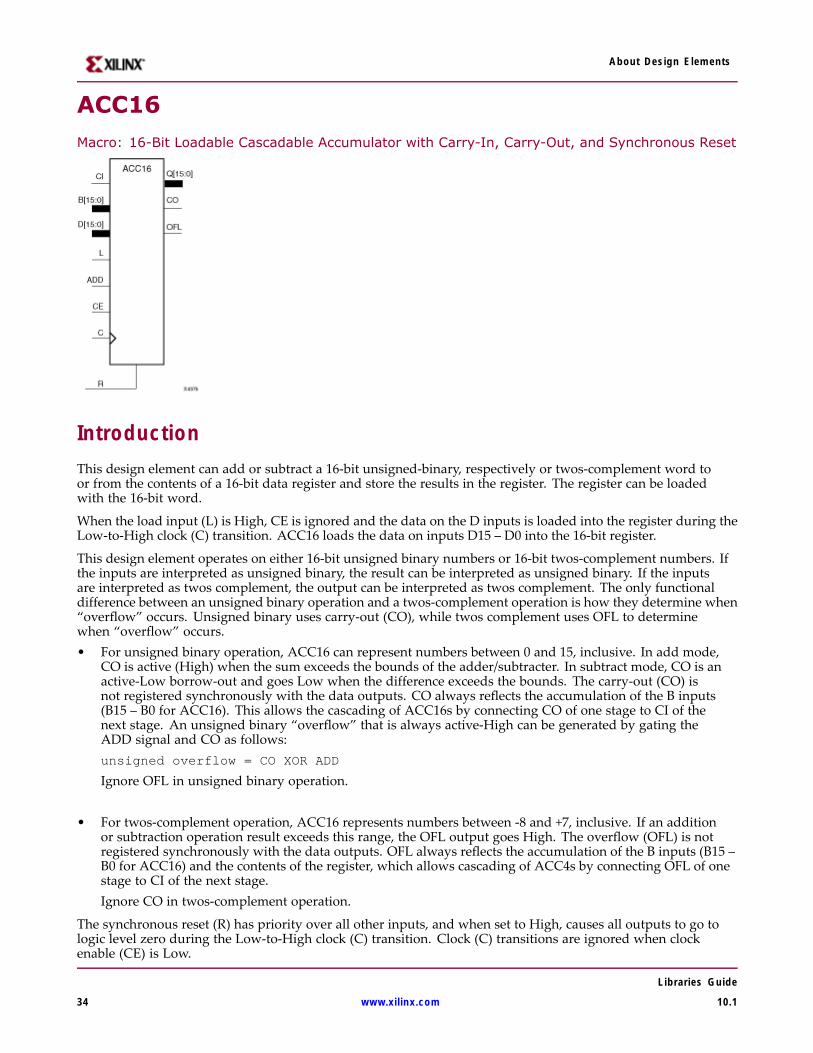
About Design Elements
ACC16Macro: 16-Bit Loadable Cascadable Accumulator with Carry-In, Carry-Out, and Synchronous Reset
IntroductionThis design element can add or subtract a 16-bit unsigned-binary, respectively or twos-complement word toor from the contents of a 16-bit data register and store the results in the register. The register can be loadedwith the 16-bit word.
When the load input (L) is High, CE is ignored and the data on the D inputs is loaded into the register during theLow-to-High clock (C) transition. ACC16 loads the data on inputs D15 – D0 into the 16-bit register.
This design element operates on either 16-bit unsigned binary numbers or 16-bit twos-complement numbers. Ifthe inputs are interpreted as unsigned binary, the result can be interpreted as unsigned binary. If the inputsare interpreted as twos complement, the output can be interpreted as twos complement. The only functionaldifference between an unsigned binary operation and a twos-complement operation is how they determine when“overflow” occurs. Unsigned binary uses carry-out (CO), while twos complement uses OFL to determinewhen “overflow” occurs.• For unsigned binary operation, ACC16 can represent numbers between 0 and 15, inclusive. In add mode,
CO is active (High) when the sum exceeds the bounds of the adder/subtracter. In subtract mode, CO is anactive-Low borrow-out and goes Low when the difference exceeds the bounds. The carry-out (CO) isnot registered synchronously with the data outputs. CO always reflects the accumulation of the B inputs(B15 – B0 for ACC16). This allows the cascading of ACC16s by connecting CO of one stage to CI of thenext stage. An unsigned binary “overflow” that is always active-High can be generated by gating theADD signal and CO as follows:unsigned overflow = CO XOR ADD
Ignore OFL in unsigned binary operation.
• For twos-complement operation, ACC16 represents numbers between -8 and +7, inclusive. If an additionor subtraction operation result exceeds this range, the OFL output goes High. The overflow (OFL) is notregistered synchronously with the data outputs. OFL always reflects the accumulation of the B inputs (B15 –B0 for ACC16) and the contents of the register, which allows cascading of ACC4s by connecting OFL of onestage to CI of the next stage.Ignore CO in twos-complement operation.
The synchronous reset (R) has priority over all other inputs, and when set to High, causes all outputs to go tologic level zero during the Low-to-High clock (C) transition. Clock (C) transitions are ignored when clockenable (CE) is Low.
Libraries Guide
34 www.xilinx.com 10.1
About Design Elements
This design element is asynchronously cleared, outputs Low, when power is applied. For FPGA devices,power-on conditions are simulated when global set/reset (GSR) is active. GSR defaults to active-High but can beinverted by adding an inverter in front of the GSR input of the appropriate STARTUP_architecture symbol.
Logic TableInput Output
R L CE ADD D C Q
1 x x x x ↑ 0
0 1 x x Dn ↑ Dn
0 0 1 1 x ↑ Q0+Bn+CI
0 0 1 0 x ↑ Q0-Bn-CI
0 0 0 x x ↑ No Change
Q0: Previous value of Q
Bn: Value of Data input B
CI: Value of input CI
Design Entry MethodThis design element is only for use in schematics.
For More Information• See the Spartan-3A User Guide.
• See the Spartan-3A Data Sheets.
• See the Spartan-3AN FPGA In-System Flash User Guide.
• See the Spartan-3AN Data Sheets.
Libraries Guide
10.1 www.xilinx.com 35
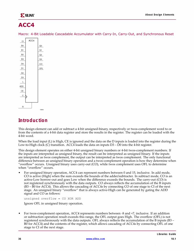
About Design Elements
ACC4Macro: 4-Bit Loadable Cascadable Accumulator with Carry-In, Carry-Out, and Synchronous Reset
IntroductionThis design element can add or subtract a 4-bit unsigned-binary, respectively or twos-complement word to orfrom the contents of a 4-bit data register and store the results in the register. The register can be loaded with the4-bit word.
When the load input (L) is High, CE is ignored and the data on the D inputs is loaded into the register during theLow-to-High clock (C) transition. ACC4 loads the data on inputs D3 – D0 into the 4-bit register.
This design element operates on either 4-bit unsigned binary numbers or 4-bit twos-complement numbers. Ifthe inputs are interpreted as unsigned binary, the result can be interpreted as unsigned binary. If the inputsare interpreted as twos complement, the output can be interpreted as twos complement. The only functionaldifference between an unsigned binary operation and a twos-complement operation is how they determine when“overflow” occurs. Unsigned binary uses carry-out (CO), while twos complement uses OFL to determinewhen “overflow” occurs.• For unsigned binary operation, ACC4 can represent numbers between 0 and 15, inclusive. In add mode,
CO is active (High) when the sum exceeds the bounds of the adder/subtracter. In subtract mode, CO is anactive-Low borrow-out and goes Low when the difference exceeds the bounds. The carry-out (CO) isnot registered synchronously with the data outputs. CO always reflects the accumulation of the B inputs(B3 – B0 for ACC4). This allows the cascading of ACC4s by connecting CO of one stage to CI of the nextstage. An unsigned binary “overflow” that is always active-High can be generated by gating the ADDsignal and CO as follows:unsigned overflow = CO XOR ADD
Ignore OFL in unsigned binary operation.
• For twos-complement operation, ACC4 represents numbers between -8 and +7, inclusive. If an additionor subtraction operation result exceeds this range, the OFL output goes High. The overflow (OFL) is notregistered synchronously with the data outputs. OFL always reflects the accumulation of the B inputs (B3 –B0 for ACC4) and the contents of the register, which allows cascading of ACC4s by connecting OFL of onestage to CI of the next stage.
Libraries Guide
36 www.xilinx.com 10.1
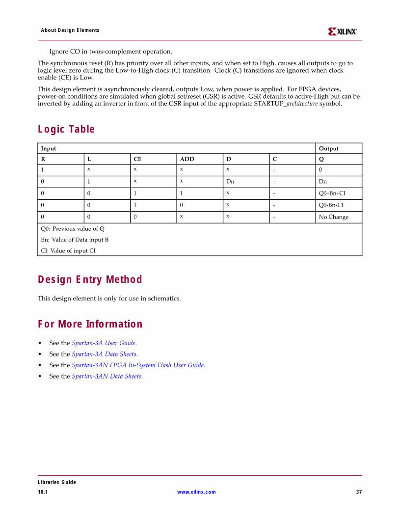
About Design Elements
Ignore CO in twos-complement operation.
The synchronous reset (R) has priority over all other inputs, and when set to High, causes all outputs to go tologic level zero during the Low-to-High clock (C) transition. Clock (C) transitions are ignored when clockenable (CE) is Low.
This design element is asynchronously cleared, outputs Low, when power is applied. For FPGA devices,power-on conditions are simulated when global set/reset (GSR) is active. GSR defaults to active-High but can beinverted by adding an inverter in front of the GSR input of the appropriate STARTUP_architecture symbol.
Logic TableInput Output
R L CE ADD D C Q
1 x x x x ↑ 0
0 1 x x Dn ↑ Dn
0 0 1 1 x ↑ Q0+Bn+CI
0 0 1 0 x ↑ Q0-Bn-CI
0 0 0 x x ↑ No Change
Q0: Previous value of Q
Bn: Value of Data input B
CI: Value of input CI
Design Entry MethodThis design element is only for use in schematics.
For More Information• See the Spartan-3A User Guide.
• See the Spartan-3A Data Sheets.
• See the Spartan-3AN FPGA In-System Flash User Guide.
• See the Spartan-3AN Data Sheets.
Libraries Guide
10.1 www.xilinx.com 37
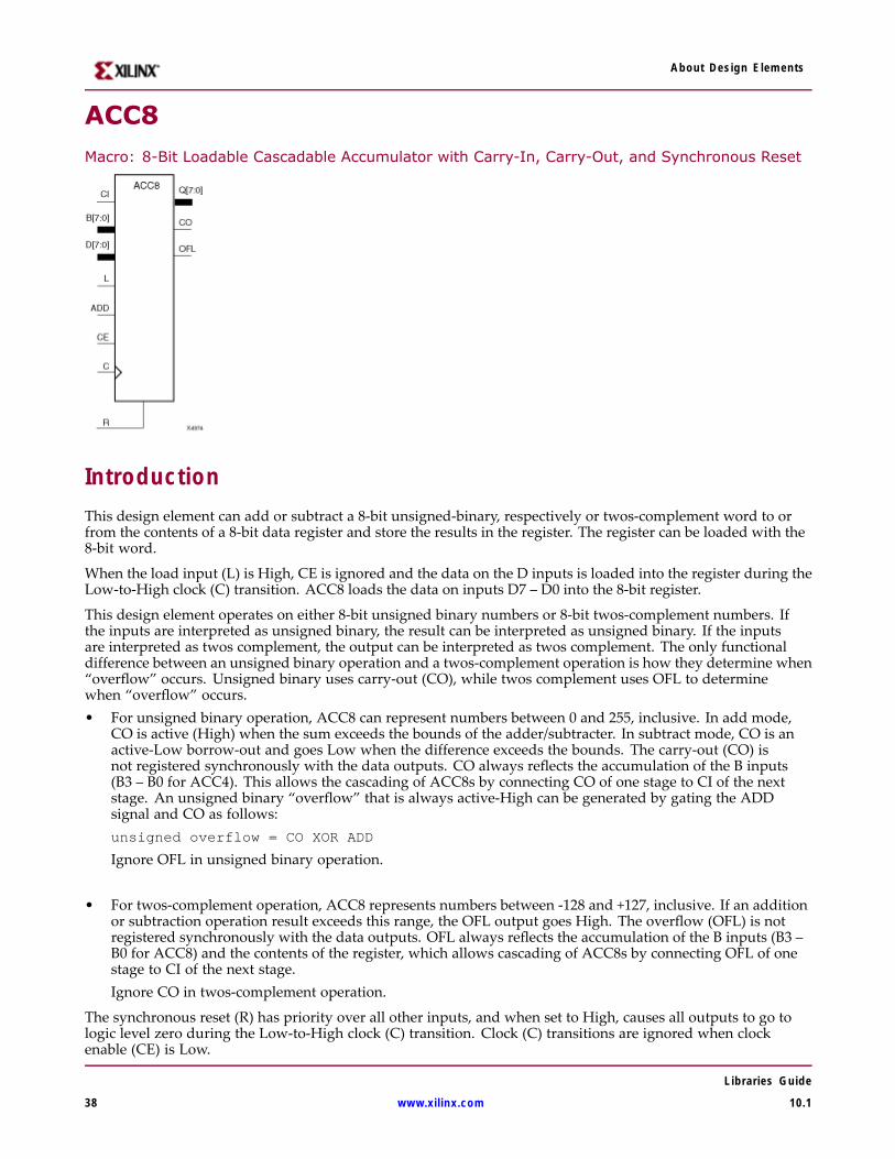
About Design Elements
ACC8Macro: 8-Bit Loadable Cascadable Accumulator with Carry-In, Carry-Out, and Synchronous Reset
IntroductionThis design element can add or subtract a 8-bit unsigned-binary, respectively or twos-complement word to orfrom the contents of a 8-bit data register and store the results in the register. The register can be loaded with the8-bit word.
When the load input (L) is High, CE is ignored and the data on the D inputs is loaded into the register during theLow-to-High clock (C) transition. ACC8 loads the data on inputs D7 – D0 into the 8-bit register.
This design element operates on either 8-bit unsigned binary numbers or 8-bit twos-complement numbers. Ifthe inputs are interpreted as unsigned binary, the result can be interpreted as unsigned binary. If the inputsare interpreted as twos complement, the output can be interpreted as twos complement. The only functionaldifference between an unsigned binary operation and a twos-complement operation is how they determine when“overflow” occurs. Unsigned binary uses carry-out (CO), while twos complement uses OFL to determinewhen “overflow” occurs.• For unsigned binary operation, ACC8 can represent numbers between 0 and 255, inclusive. In add mode,
CO is active (High) when the sum exceeds the bounds of the adder/subtracter. In subtract mode, CO is anactive-Low borrow-out and goes Low when the difference exceeds the bounds. The carry-out (CO) isnot registered synchronously with the data outputs. CO always reflects the accumulation of the B inputs(B3 – B0 for ACC4). This allows the cascading of ACC8s by connecting CO of one stage to CI of the nextstage. An unsigned binary “overflow” that is always active-High can be generated by gating the ADDsignal and CO as follows:unsigned overflow = CO XOR ADD
Ignore OFL in unsigned binary operation.
• For twos-complement operation, ACC8 represents numbers between -128 and +127, inclusive. If an additionor subtraction operation result exceeds this range, the OFL output goes High. The overflow (OFL) is notregistered synchronously with the data outputs. OFL always reflects the accumulation of the B inputs (B3 –B0 for ACC8) and the contents of the register, which allows cascading of ACC8s by connecting OFL of onestage to CI of the next stage.Ignore CO in twos-complement operation.
The synchronous reset (R) has priority over all other inputs, and when set to High, causes all outputs to go tologic level zero during the Low-to-High clock (C) transition. Clock (C) transitions are ignored when clockenable (CE) is Low.
Libraries Guide
38 www.xilinx.com 10.1
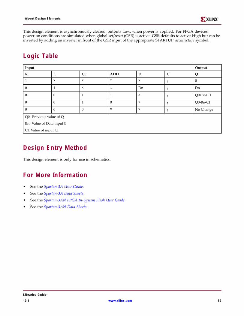
About Design Elements
This design element is asynchronously cleared, outputs Low, when power is applied. For FPGA devices,power-on conditions are simulated when global set/reset (GSR) is active. GSR defaults to active-High but can beinverted by adding an inverter in front of the GSR input of the appropriate STARTUP_architecture symbol.
Logic TableInput Output
R L CE ADD D C Q
1 x x x x ↑ 0
0 1 x x Dn ↑ Dn
0 0 1 1 x ↑ Q0+Bn+CI
0 0 1 0 x ↑ Q0-Bn-CI
0 0 0 x x ↑ No Change
Q0: Previous value of Q
Bn: Value of Data input B
CI: Value of input CI
Design Entry MethodThis design element is only for use in schematics.
For More Information• See the Spartan-3A User Guide.
• See the Spartan-3A Data Sheets.
• See the Spartan-3AN FPGA In-System Flash User Guide.
• See the Spartan-3AN Data Sheets.
Libraries Guide
10.1 www.xilinx.com 39
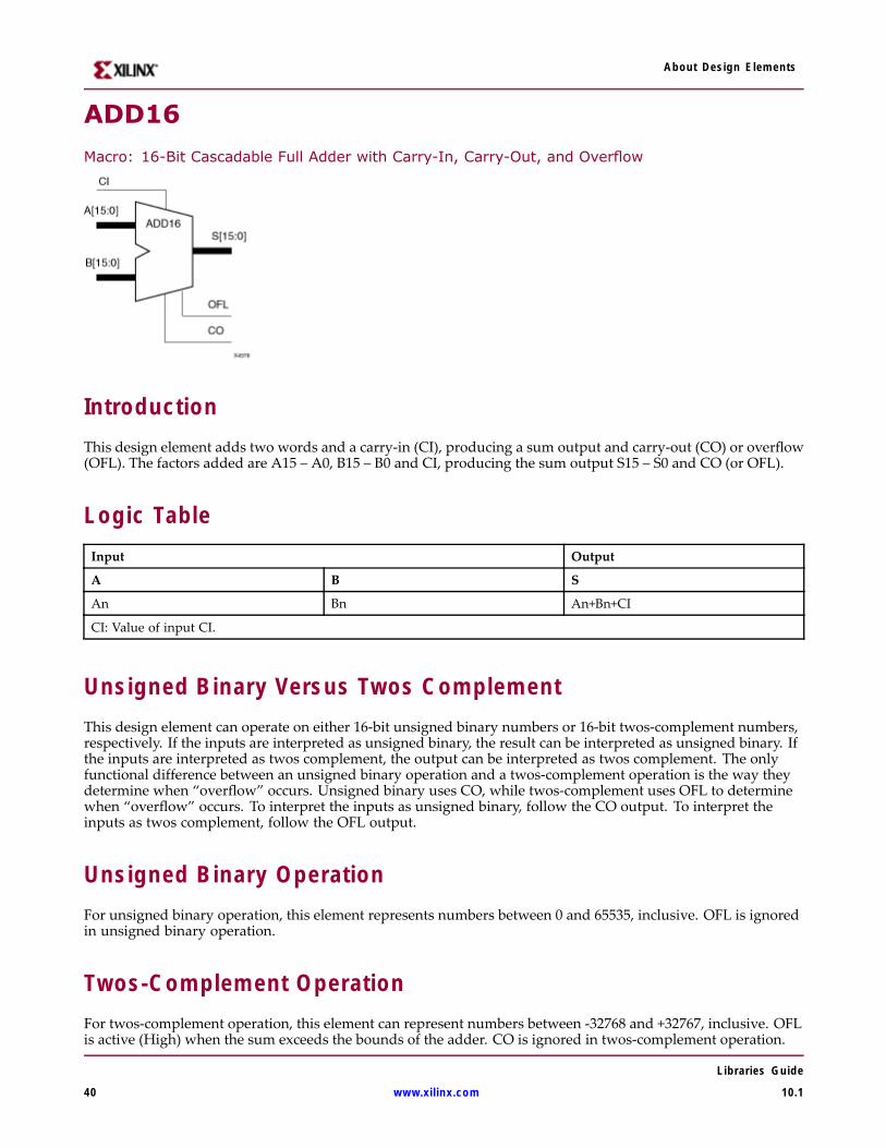
About Design Elements
ADD16
Macro: 16-Bit Cascadable Full Adder with Carry-In, Carry-Out, and Overflow
IntroductionThis design element adds two words and a carry-in (CI), producing a sum output and carry-out (CO) or overflow(OFL). The factors added are A15 – A0, B15 – B0 and CI, producing the sum output S15 – S0 and CO (or OFL).
Logic TableInput Output
A B S
An Bn An+Bn+CI
CI: Value of input CI.
Unsigned Binary Versus Twos ComplementThis design element can operate on either 16-bit unsigned binary numbers or 16-bit twos-complement numbers,respectively. If the inputs are interpreted as unsigned binary, the result can be interpreted as unsigned binary. Ifthe inputs are interpreted as twos complement, the output can be interpreted as twos complement. The onlyfunctional difference between an unsigned binary operation and a twos-complement operation is the way theydetermine when “overflow” occurs. Unsigned binary uses CO, while twos-complement uses OFL to determinewhen “overflow” occurs. To interpret the inputs as unsigned binary, follow the CO output. To interpret theinputs as twos complement, follow the OFL output.
Unsigned Binary OperationFor unsigned binary operation, this element represents numbers between 0 and 65535, inclusive. OFL is ignoredin unsigned binary operation.
Twos-Complement OperationFor twos-complement operation, this element can represent numbers between -32768 and +32767, inclusive. OFLis active (High) when the sum exceeds the bounds of the adder. CO is ignored in twos-complement operation.
Libraries Guide
40 www.xilinx.com 10.1

About Design Elements
Design Entry MethodThis design element is only for use in schematics.
For More Information• See the Spartan-3A User Guide.
• See the Spartan-3A Data Sheets.
• See the Spartan-3AN FPGA In-System Flash User Guide.
• See the Spartan-3AN Data Sheets.
Libraries Guide
10.1 www.xilinx.com 41
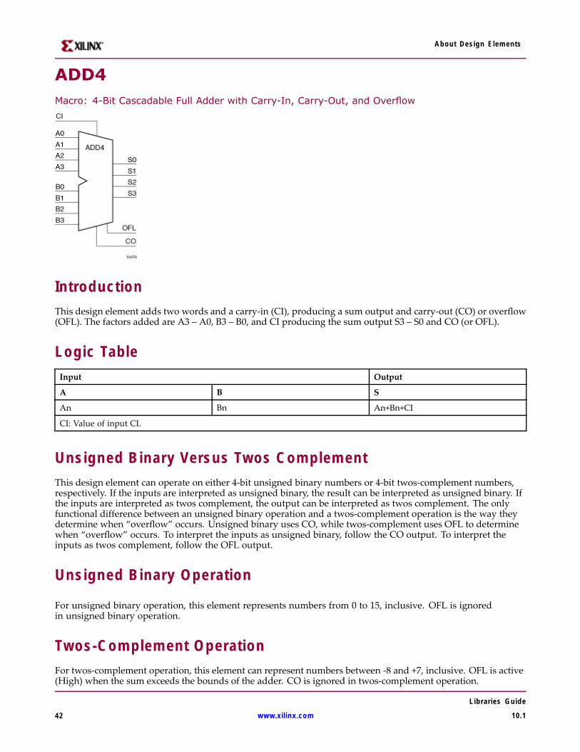
About Design Elements
ADD4Macro: 4-Bit Cascadable Full Adder with Carry-In, Carry-Out, and Overflow
IntroductionThis design element adds two words and a carry-in (CI), producing a sum output and carry-out (CO) or overflow(OFL). The factors added are A3 – A0, B3 – B0, and CI producing the sum output S3 – S0 and CO (or OFL).
Logic TableInput Output
A B S
An Bn An+Bn+CI
CI: Value of input CI.
Unsigned Binary Versus Twos ComplementThis design element can operate on either 4-bit unsigned binary numbers or 4-bit twos-complement numbers,respectively. If the inputs are interpreted as unsigned binary, the result can be interpreted as unsigned binary. Ifthe inputs are interpreted as twos complement, the output can be interpreted as twos complement. The onlyfunctional difference between an unsigned binary operation and a twos-complement operation is the way theydetermine when “overflow” occurs. Unsigned binary uses CO, while twos-complement uses OFL to determinewhen “overflow” occurs. To interpret the inputs as unsigned binary, follow the CO output. To interpret theinputs as twos complement, follow the OFL output.
Unsigned Binary Operation
For unsigned binary operation, this element represents numbers from 0 to 15, inclusive. OFL is ignoredin unsigned binary operation.
Twos-Complement OperationFor twos-complement operation, this element can represent numbers between -8 and +7, inclusive. OFL is active(High) when the sum exceeds the bounds of the adder. CO is ignored in twos-complement operation.
Libraries Guide
42 www.xilinx.com 10.1

About Design Elements
Design Entry MethodThis design element is only for use in schematics.
For More Information• See the Spartan-3A User Guide.
• See the Spartan-3A Data Sheets.
• See the Spartan-3AN FPGA In-System Flash User Guide.
• See the Spartan-3AN Data Sheets.
Libraries Guide
10.1 www.xilinx.com 43
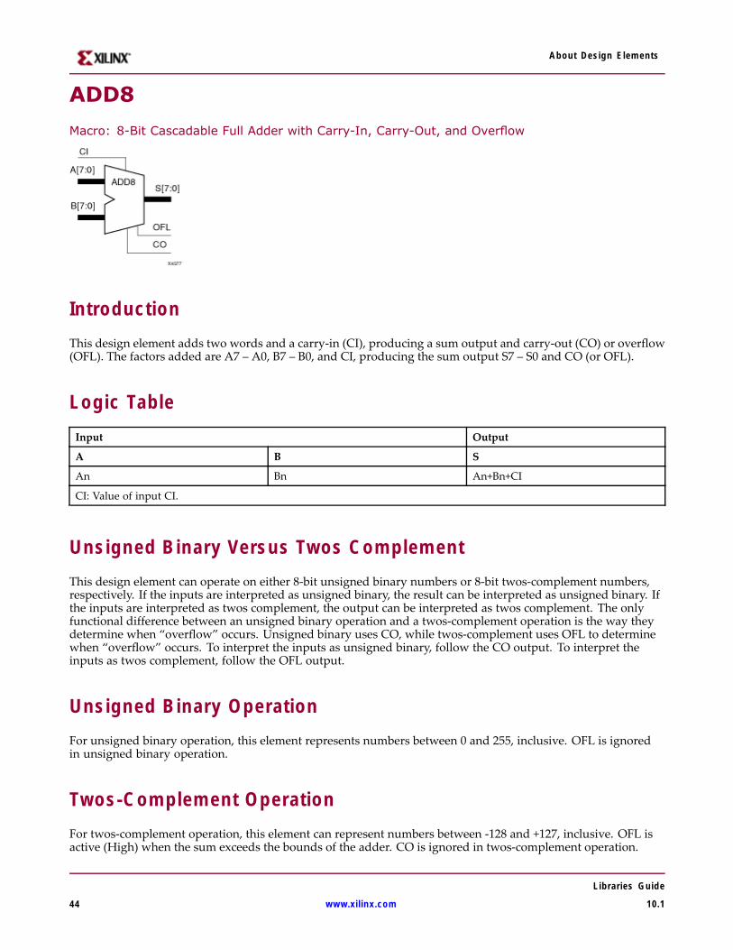
About Design Elements
ADD8
Macro: 8-Bit Cascadable Full Adder with Carry-In, Carry-Out, and Overflow
IntroductionThis design element adds two words and a carry-in (CI), producing a sum output and carry-out (CO) or overflow(OFL). The factors added are A7 – A0, B7 – B0, and CI, producing the sum output S7 – S0 and CO (or OFL).
Logic TableInput Output
A B S
An Bn An+Bn+CI
CI: Value of input CI.
Unsigned Binary Versus Twos ComplementThis design element can operate on either 8-bit unsigned binary numbers or 8-bit twos-complement numbers,respectively. If the inputs are interpreted as unsigned binary, the result can be interpreted as unsigned binary. Ifthe inputs are interpreted as twos complement, the output can be interpreted as twos complement. The onlyfunctional difference between an unsigned binary operation and a twos-complement operation is the way theydetermine when “overflow” occurs. Unsigned binary uses CO, while twos-complement uses OFL to determinewhen “overflow” occurs. To interpret the inputs as unsigned binary, follow the CO output. To interpret theinputs as twos complement, follow the OFL output.
Unsigned Binary OperationFor unsigned binary operation, this element represents numbers between 0 and 255, inclusive. OFL is ignoredin unsigned binary operation.
Twos-Complement OperationFor twos-complement operation, this element can represent numbers between -128 and +127, inclusive. OFL isactive (High) when the sum exceeds the bounds of the adder. CO is ignored in twos-complement operation.
Libraries Guide
44 www.xilinx.com 10.1

About Design Elements
Design Entry MethodThis design element is only for use in schematics.
For More Information• See the Spartan-3A User Guide.
• See the Spartan-3A Data Sheets.
• See the Spartan-3AN FPGA In-System Flash User Guide.
• See the Spartan-3AN Data Sheets.
Libraries Guide
10.1 www.xilinx.com 45
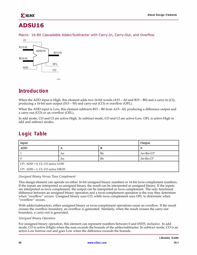
About Design Elements
ADSU16
Macro: 16-Bit Cascadable Adder/Subtracter with Carry-In, Carry-Out, and Overflow
IntroductionWhen the ADD input is High, this element adds two 16-bit words (A15 – A0 and B15 – B0) and a carry-in (CI),producing a 16-bit sum output (S15 – S0) and carry-out (CO) or overflow (OFL).
When the ADD input is Low, this element subtracts B15 – B0 from A15– A0, producing a difference output anda carry-out (CO) or an overflow (OFL).
In add mode, CO and CI are active-High. In subtract mode, CO and CI are active-Low. OFL is active-High inadd and subtract modes.
Logic TableInput Output
ADD A B S
1 An Bn An+Bn+CI*
0 An Bn An-Bn-CI*
CI*: ADD = 0, CI, CO active LOW
CI*: ADD = 1, CI, CO active HIGH
Unsigned Binary Versus Twos Complement
This design element can operate on either 16-bit unsigned binary numbers or 16-bit twos-complement numbers.If the inputs are interpreted as unsigned binary, the result can be interpreted as unsigned binary. If the inputsare interpreted as twos complement, the output can be interpreted as twos complement. The only functionaldifference between an unsigned binary operation and a twos-complement operation is the way they determinewhen “overflow” occurs. Unsigned binary uses CO, while twos complement uses OFL to determine when“overflow” occurs.
With adder/subtracters, either unsigned binary or twos-complement operations cause an overflow. If the resultcrosses the overflow boundary, an overflow is generated. Similarly, when the result crosses the carry-outboundary, a carry-out is generated.
Unsigned Binary Operation
For unsigned binary operation, this element can represent numbers between 0 and 65535, inclusive. In addmode, CO is active (High) when the sum exceeds the bounds of the adder/subtracter. In subtract mode, CO is anactive-Low borrow-out and goes Low when the difference exceeds the bounds.
Libraries Guide
46 www.xilinx.com 10.1
About Design Elements
An unsigned binary “overflow” that is always active-High can be generated by gating the ADD signal and COas follows:unsigned overflow = CO XOR ADD
OFL is ignored in unsigned binary operation.
Twos-Complement Operation
For twos-complement operation, this element can represent numbers between -32768 and +32767, inclusive.
If an addition or subtraction operation result exceeds this range, the OFL output goes High. CO is ignoredin twos-complement operation.
Design Entry MethodThis design element is only for use in schematics.
For More Information• See the Spartan-3A User Guide.
• See the Spartan-3A Data Sheets.
• See the Spartan-3AN FPGA In-System Flash User Guide.
• See the Spartan-3AN Data Sheets.
Libraries Guide
10.1 www.xilinx.com 47
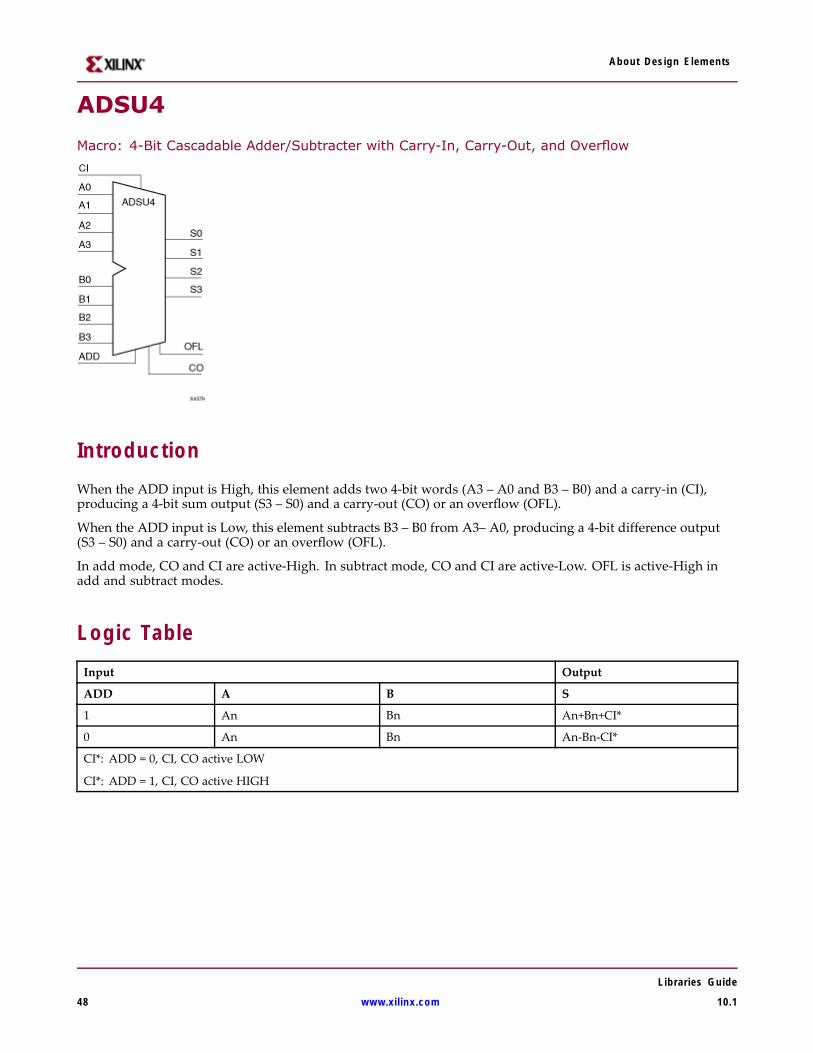
About Design Elements
ADSU4
Macro: 4-Bit Cascadable Adder/Subtracter with Carry-In, Carry-Out, and Overflow
IntroductionWhen the ADD input is High, this element adds two 4-bit words (A3 – A0 and B3 – B0) and a carry-in (CI),producing a 4-bit sum output (S3 – S0) and a carry-out (CO) or an overflow (OFL).
When the ADD input is Low, this element subtracts B3 – B0 from A3– A0, producing a 4-bit difference output(S3 – S0) and a carry-out (CO) or an overflow (OFL).
In add mode, CO and CI are active-High. In subtract mode, CO and CI are active-Low. OFL is active-High inadd and subtract modes.
Logic TableInput Output
ADD A B S
1 An Bn An+Bn+CI*
0 An Bn An-Bn-CI*
CI*: ADD = 0, CI, CO active LOW
CI*: ADD = 1, CI, CO active HIGH
Libraries Guide
48 www.xilinx.com 10.1
About Design Elements
Unsigned Binary Versus Twos Complement
This design element can operate on either 4-bit unsigned binary numbers or 4-bit twos-complement numbers. Ifthe inputs are interpreted as unsigned binary, the result can be interpreted as unsigned binary. If the inputsare interpreted as twos complement, the output can be interpreted as twos complement. The only functionaldifference between an unsigned binary operation and a twos-complement operation is the way they determinewhen “overflow” occurs. Unsigned binary uses CO, while twos complement uses OFL to determine when“overflow” occurs.
With adder/subtracters, either unsigned binary or twos-complement operations cause an overflow. If the resultcrosses the overflow boundary, an overflow is generated. Similarly, when the result crosses the carry-outboundary, a carry-out is generated.
Unsigned Binary Operation
For unsigned binary operation, ADSU4 can represent numbers between 0 and 15, inclusive. In add mode, CO isactive (High) when the sum exceeds the bounds of the adder/subtracter. In subtract mode, CO is an active-Lowborrow-out and goes Low when the difference exceeds the bounds.
An unsigned binary “overflow” that is always active-High can be generated by gating the ADD signal and COas follows:unsigned overflow = CO XOR ADD
OFL is ignored in unsigned binary operation.
Twos-Complement Operation
For twos-complement operation, this element can represent numbers between -8 and +7, inclusive.
If an addition or subtraction operation result exceeds this range, the OFL output goes High. CO is ignoredin twos-complement operation.
Design Entry MethodThis design element is only for use in schematics.
For More Information• See the Spartan-3A User Guide.
• See the Spartan-3A Data Sheets.
• See the Spartan-3AN FPGA In-System Flash User Guide.
• See the Spartan-3AN Data Sheets.
Libraries Guide
10.1 www.xilinx.com 49
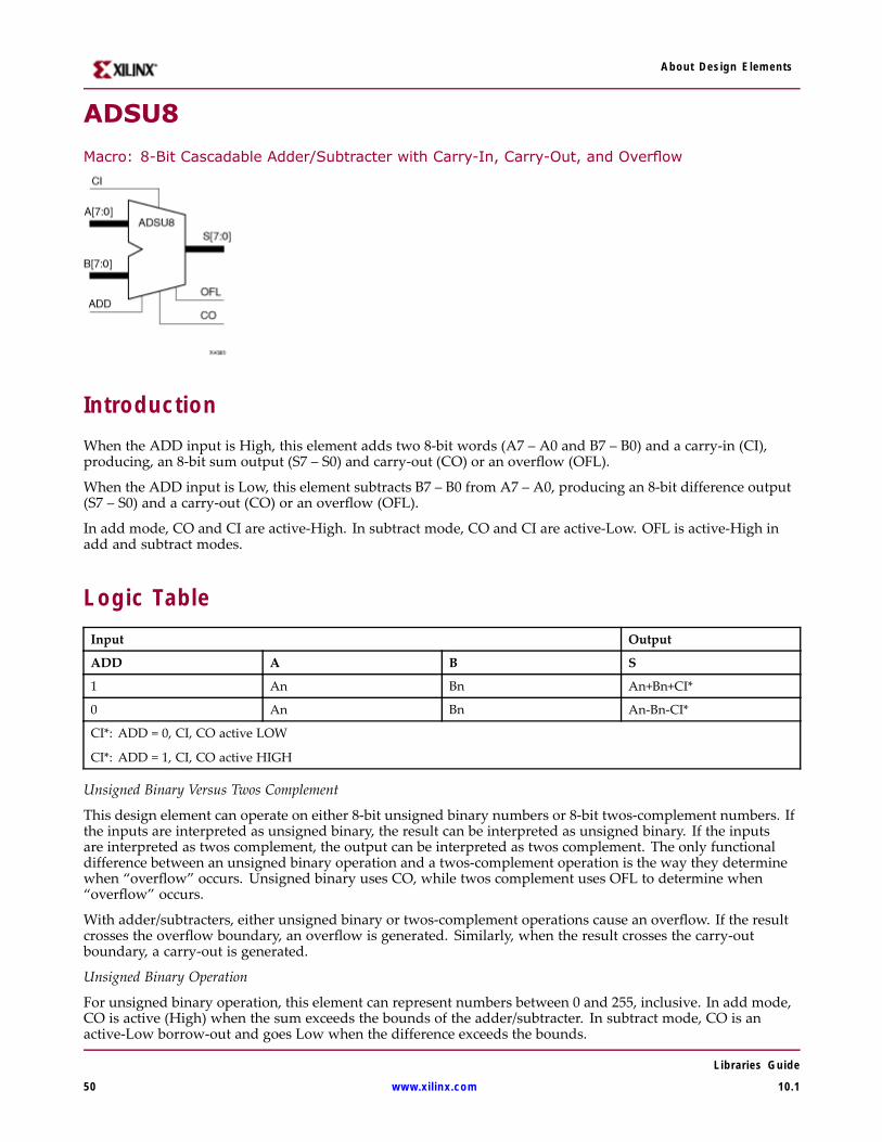
About Design Elements
ADSU8
Macro: 8-Bit Cascadable Adder/Subtracter with Carry-In, Carry-Out, and Overflow
IntroductionWhen the ADD input is High, this element adds two 8-bit words (A7 – A0 and B7 – B0) and a carry-in (CI),producing, an 8-bit sum output (S7 – S0) and carry-out (CO) or an overflow (OFL).
When the ADD input is Low, this element subtracts B7 – B0 from A7 – A0, producing an 8-bit difference output(S7 – S0) and a carry-out (CO) or an overflow (OFL).
In add mode, CO and CI are active-High. In subtract mode, CO and CI are active-Low. OFL is active-High inadd and subtract modes.
Logic TableInput Output
ADD A B S
1 An Bn An+Bn+CI*
0 An Bn An-Bn-CI*
CI*: ADD = 0, CI, CO active LOW
CI*: ADD = 1, CI, CO active HIGH
Unsigned Binary Versus Twos Complement
This design element can operate on either 8-bit unsigned binary numbers or 8-bit twos-complement numbers. Ifthe inputs are interpreted as unsigned binary, the result can be interpreted as unsigned binary. If the inputsare interpreted as twos complement, the output can be interpreted as twos complement. The only functionaldifference between an unsigned binary operation and a twos-complement operation is the way they determinewhen “overflow” occurs. Unsigned binary uses CO, while twos complement uses OFL to determine when“overflow” occurs.
With adder/subtracters, either unsigned binary or twos-complement operations cause an overflow. If the resultcrosses the overflow boundary, an overflow is generated. Similarly, when the result crosses the carry-outboundary, a carry-out is generated.
Unsigned Binary Operation
For unsigned binary operation, this element can represent numbers between 0 and 255, inclusive. In add mode,CO is active (High) when the sum exceeds the bounds of the adder/subtracter. In subtract mode, CO is anactive-Low borrow-out and goes Low when the difference exceeds the bounds.
Libraries Guide
50 www.xilinx.com 10.1
About Design Elements
An unsigned binary “overflow” that is always active-High can be generated by gating the ADD signal and COas follows:unsigned overflow = CO XOR ADD
OFL is ignored in unsigned binary operation.
Twos-Complement Operation
For twos-complement operation, this element can represent numbers between -128 and +127, inclusive.
If an addition or subtraction operation result exceeds this range, the OFL output goes High. CO is ignoredin twos-complement operation.
Design Entry MethodThis design element is only for use in schematics.
For More Information• See the Spartan-3A User Guide.
• See the Spartan-3A Data Sheets.
• See the Spartan-3AN FPGA In-System Flash User Guide.
• See the Spartan-3AN Data Sheets.
Libraries Guide
10.1 www.xilinx.com 51
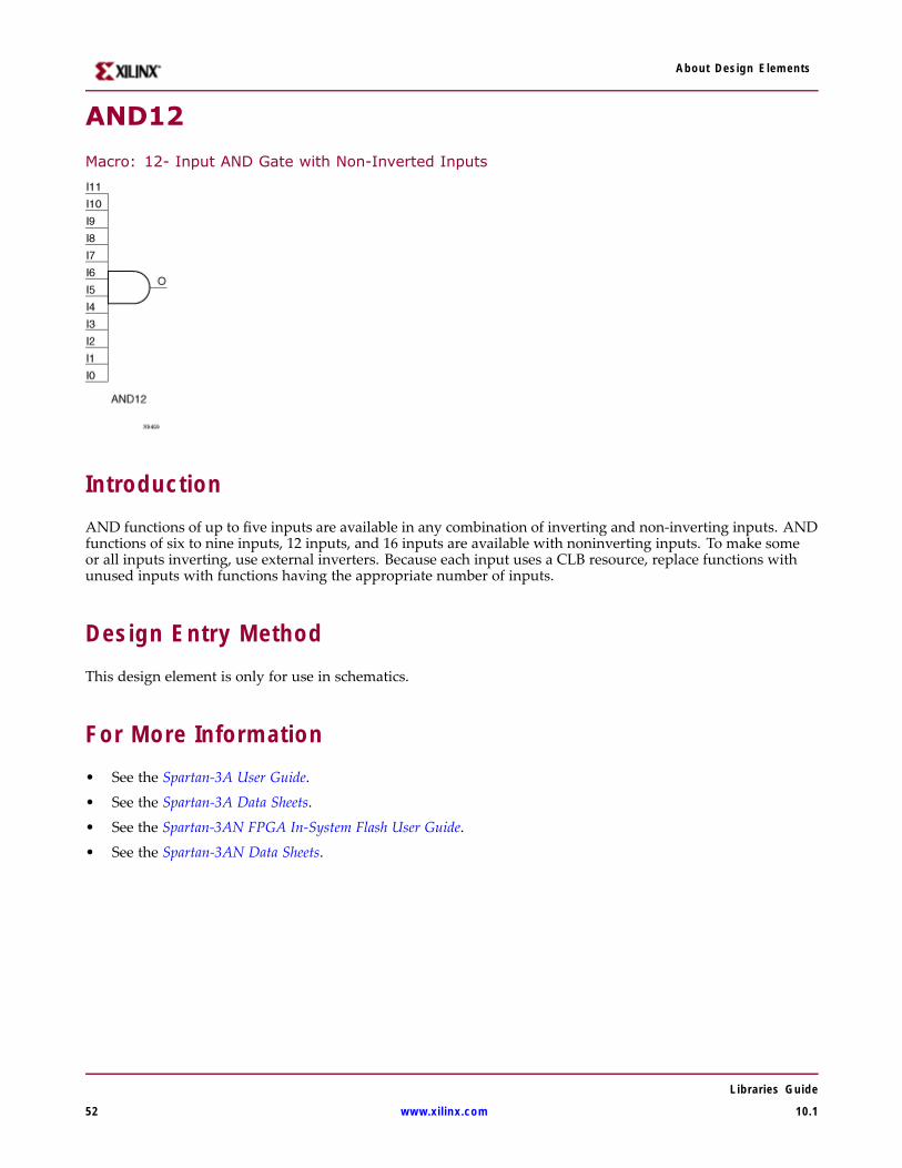
About Design Elements
AND12
Macro: 12- Input AND Gate with Non-Inverted Inputs
IntroductionAND functions of up to five inputs are available in any combination of inverting and non-inverting inputs. ANDfunctions of six to nine inputs, 12 inputs, and 16 inputs are available with noninverting inputs. To make someor all inputs inverting, use external inverters. Because each input uses a CLB resource, replace functions withunused inputs with functions having the appropriate number of inputs.
Design Entry MethodThis design element is only for use in schematics.
For More Information• See the Spartan-3A User Guide.
• See the Spartan-3A Data Sheets.
• See the Spartan-3AN FPGA In-System Flash User Guide.
• See the Spartan-3AN Data Sheets.
Libraries Guide
52 www.xilinx.com 10.1
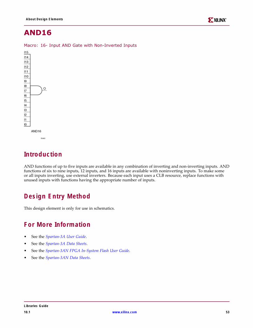
About Design Elements
AND16
Macro: 16- Input AND Gate with Non-Inverted Inputs
IntroductionAND functions of up to five inputs are available in any combination of inverting and non-inverting inputs. ANDfunctions of six to nine inputs, 12 inputs, and 16 inputs are available with noninverting inputs. To make someor all inputs inverting, use external inverters. Because each input uses a CLB resource, replace functions withunused inputs with functions having the appropriate number of inputs.
Design Entry MethodThis design element is only for use in schematics.
For More Information• See the Spartan-3A User Guide.
• See the Spartan-3A Data Sheets.
• See the Spartan-3AN FPGA In-System Flash User Guide.
• See the Spartan-3AN Data Sheets.
Libraries Guide
10.1 www.xilinx.com 53

About Design Elements
AND2
Primitive: 2-Input AND Gate with Non-Inverted Inputs
IntroductionAND functions of up to five inputs are available in any combination of inverting and non-inverting inputs. ANDfunctions of six to nine inputs, 12 inputs, and 16 inputs are available with noninverting inputs. To make someor all inputs inverting, use external inverters. Because each input uses a CLB resource, replace functions withunused inputs with functions having the appropriate number of inputs.
Design Entry MethodThis design element is only for use in schematics.
For More Information• See the Spartan-3A User Guide.
• See the Spartan-3A Data Sheets.
• See the Spartan-3AN FPGA In-System Flash User Guide.
• See the Spartan-3AN Data Sheets.
Libraries Guide
54 www.xilinx.com 10.1
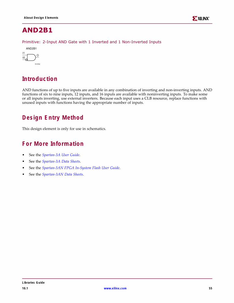
About Design Elements
AND2B1
Primitive: 2-Input AND Gate with 1 Inverted and 1 Non-Inverted Inputs
IntroductionAND functions of up to five inputs are available in any combination of inverting and non-inverting inputs. ANDfunctions of six to nine inputs, 12 inputs, and 16 inputs are available with noninverting inputs. To make someor all inputs inverting, use external inverters. Because each input uses a CLB resource, replace functions withunused inputs with functions having the appropriate number of inputs.
Design Entry MethodThis design element is only for use in schematics.
For More Information• See the Spartan-3A User Guide.
• See the Spartan-3A Data Sheets.
• See the Spartan-3AN FPGA In-System Flash User Guide.
• See the Spartan-3AN Data Sheets.
Libraries Guide
10.1 www.xilinx.com 55
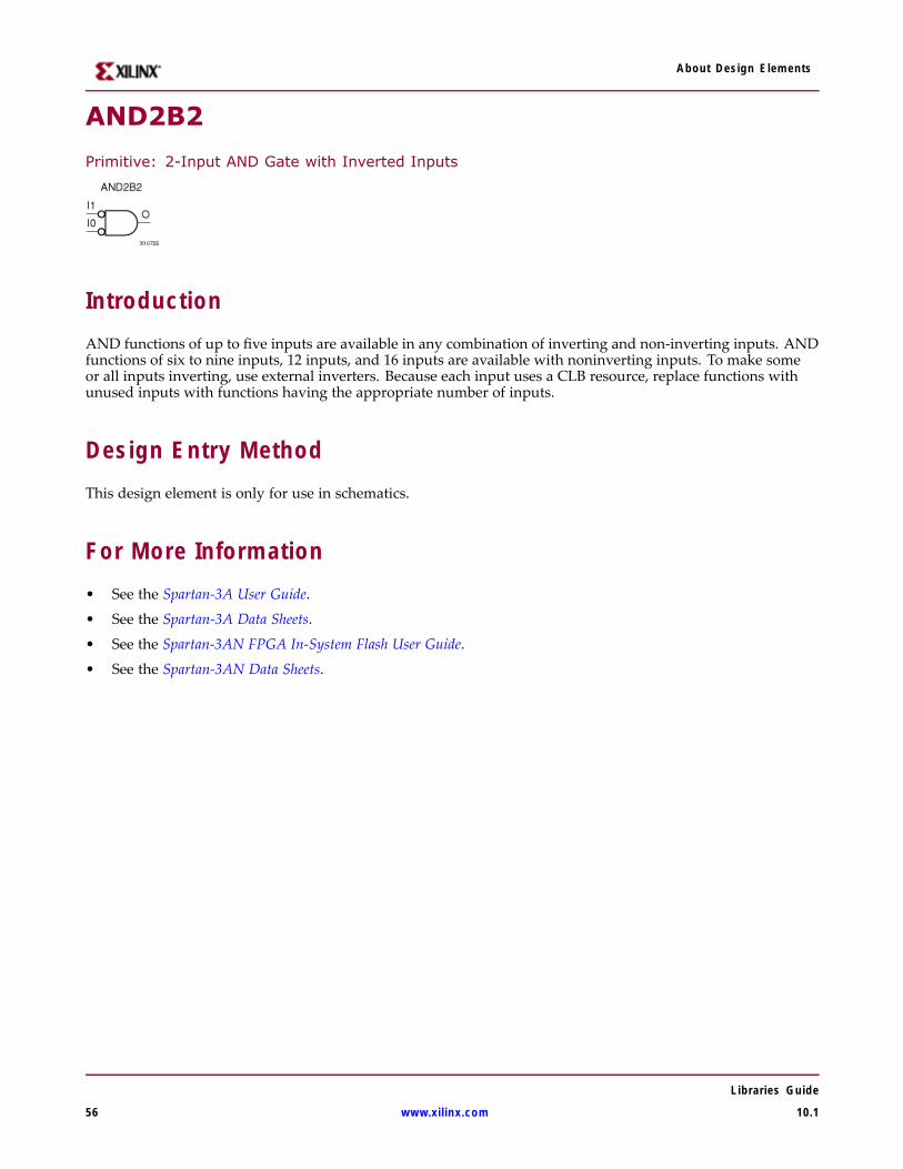
About Design Elements
AND2B2
Primitive: 2-Input AND Gate with Inverted Inputs
IntroductionAND functions of up to five inputs are available in any combination of inverting and non-inverting inputs. ANDfunctions of six to nine inputs, 12 inputs, and 16 inputs are available with noninverting inputs. To make someor all inputs inverting, use external inverters. Because each input uses a CLB resource, replace functions withunused inputs with functions having the appropriate number of inputs.
Design Entry MethodThis design element is only for use in schematics.
For More Information• See the Spartan-3A User Guide.
• See the Spartan-3A Data Sheets.
• See the Spartan-3AN FPGA In-System Flash User Guide.
• See the Spartan-3AN Data Sheets.
Libraries Guide
56 www.xilinx.com 10.1

About Design Elements
AND3
Primitive: 3-Input AND Gate with Non-Inverted Inputs
IntroductionAND functions of up to five inputs are available in any combination of inverting and non-inverting inputs. ANDfunctions of six to nine inputs, 12 inputs, and 16 inputs are available with noninverting inputs. To make someor all inputs inverting, use external inverters. Because each input uses a CLB resource, replace functions withunused inputs with functions having the appropriate number of inputs.
Design Entry MethodThis design element is only for use in schematics.
For More Information• See the Spartan-3A User Guide.
• See the Spartan-3A Data Sheets.
• See the Spartan-3AN FPGA In-System Flash User Guide.
• See the Spartan-3AN Data Sheets.
Libraries Guide
10.1 www.xilinx.com 57
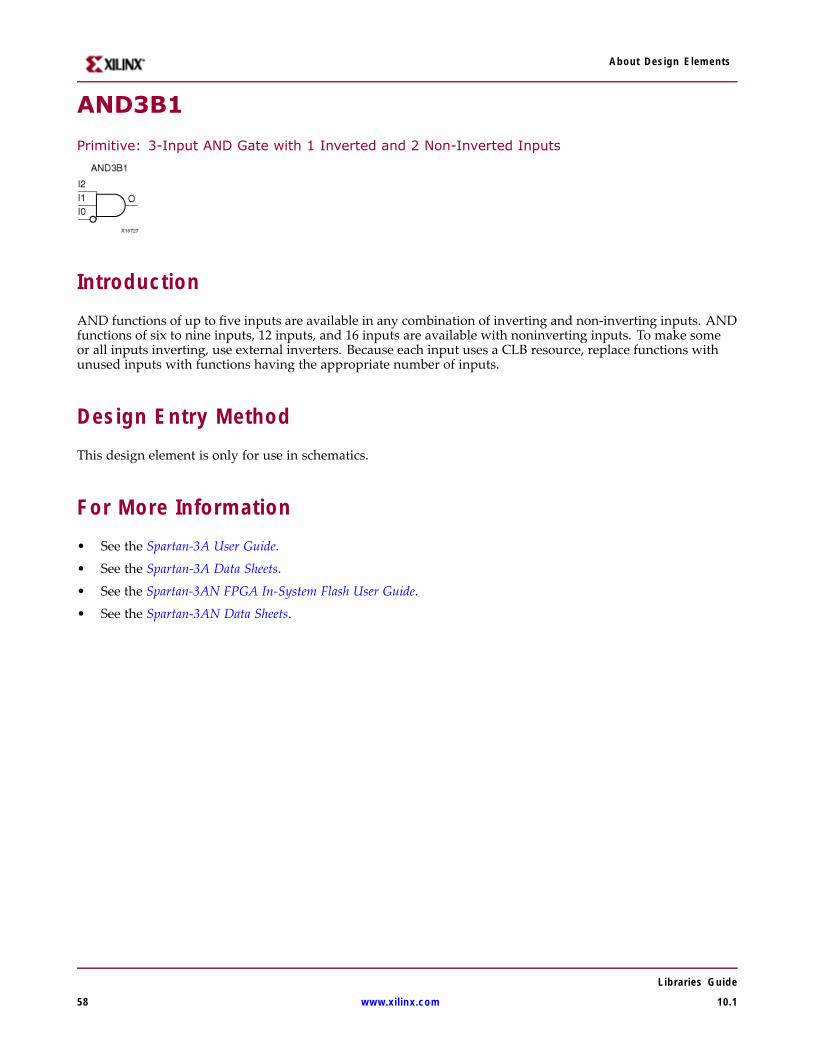
About Design Elements
AND3B1
Primitive: 3-Input AND Gate with 1 Inverted and 2 Non-Inverted Inputs
IntroductionAND functions of up to five inputs are available in any combination of inverting and non-inverting inputs. ANDfunctions of six to nine inputs, 12 inputs, and 16 inputs are available with noninverting inputs. To make someor all inputs inverting, use external inverters. Because each input uses a CLB resource, replace functions withunused inputs with functions having the appropriate number of inputs.
Design Entry MethodThis design element is only for use in schematics.
For More Information• See the Spartan-3A User Guide.
• See the Spartan-3A Data Sheets.
• See the Spartan-3AN FPGA In-System Flash User Guide.
• See the Spartan-3AN Data Sheets.
Libraries Guide
58 www.xilinx.com 10.1

About Design Elements
AND3B2
Primitive: 3-Input AND Gate with 2 Inverted and 1 Non-Inverted Inputs
IntroductionAND functions of up to five inputs are available in any combination of inverting and non-inverting inputs. ANDfunctions of six to nine inputs, 12 inputs, and 16 inputs are available with noninverting inputs. To make someor all inputs inverting, use external inverters. Because each input uses a CLB resource, replace functions withunused inputs with functions having the appropriate number of inputs.
Design Entry MethodThis design element is only for use in schematics.
For More Information• See the Spartan-3A User Guide.
• See the Spartan-3A Data Sheets.
• See the Spartan-3AN FPGA In-System Flash User Guide.
• See the Spartan-3AN Data Sheets.
Libraries Guide
10.1 www.xilinx.com 59

About Design Elements
AND3B3
Primitive: 3-Input AND Gate with Inverted Inputs
IntroductionAND functions of up to five inputs are available in any combination of inverting and non-inverting inputs. ANDfunctions of six to nine inputs, 12 inputs, and 16 inputs are available with noninverting inputs. To make someor all inputs inverting, use external inverters. Because each input uses a CLB resource, replace functions withunused inputs with functions having the appropriate number of inputs.
Design Entry MethodThis design element is only for use in schematics.
For More Information• See the Spartan-3A User Guide.
• See the Spartan-3A Data Sheets.
• See the Spartan-3AN FPGA In-System Flash User Guide.
• See the Spartan-3AN Data Sheets.
Libraries Guide
60 www.xilinx.com 10.1

About Design Elements
AND4
Primitive: 4-Input AND Gate with Non-Inverted Inputs
IntroductionAND functions of up to five inputs are available in any combination of inverting and non-inverting inputs. ANDfunctions of six to nine inputs, 12 inputs, and 16 inputs are available with noninverting inputs. To make someor all inputs inverting, use external inverters. Because each input uses a CLB resource, replace functions withunused inputs with functions having the appropriate number of inputs.
Design Entry MethodThis design element is only for use in schematics.
For More Information• See the Spartan-3A User Guide.
• See the Spartan-3A Data Sheets.
• See the Spartan-3AN FPGA In-System Flash User Guide.
• See the Spartan-3AN Data Sheets.
Libraries Guide
10.1 www.xilinx.com 61

About Design Elements
AND4B1
Primitive: 4-Input AND Gate with 1 Inverted and 3 Non-Inverted Inputs
IntroductionAND functions of up to five inputs are available in any combination of inverting and non-inverting inputs. ANDfunctions of six to nine inputs, 12 inputs, and 16 inputs are available with noninverting inputs. To make someor all inputs inverting, use external inverters. Because each input uses a CLB resource, replace functions withunused inputs with functions having the appropriate number of inputs.
Design Entry MethodThis design element is only for use in schematics.
For More Information• See the Spartan-3A User Guide.
• See the Spartan-3A Data Sheets.
• See the Spartan-3AN FPGA In-System Flash User Guide.
• See the Spartan-3AN Data Sheets.
Libraries Guide
62 www.xilinx.com 10.1
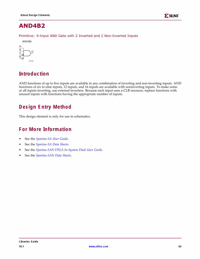
About Design Elements
AND4B2
Primitive: 4-Input AND Gate with 2 Inverted and 2 Non-Inverted Inputs
IntroductionAND functions of up to five inputs are available in any combination of inverting and non-inverting inputs. ANDfunctions of six to nine inputs, 12 inputs, and 16 inputs are available with noninverting inputs. To make someor all inputs inverting, use external inverters. Because each input uses a CLB resource, replace functions withunused inputs with functions having the appropriate number of inputs.
Design Entry MethodThis design element is only for use in schematics.
For More Information• See the Spartan-3A User Guide.
• See the Spartan-3A Data Sheets.
• See the Spartan-3AN FPGA In-System Flash User Guide.
• See the Spartan-3AN Data Sheets.
Libraries Guide
10.1 www.xilinx.com 63

About Design Elements
AND4B3
Primitive: 4-Input AND Gate with 3 Inverted and 1 Non-Inverted Inputs
IntroductionAND functions of up to five inputs are available in any combination of inverting and non-inverting inputs. ANDfunctions of six to nine inputs, 12 inputs, and 16 inputs are available with noninverting inputs. To make someor all inputs inverting, use external inverters. Because each input uses a CLB resource, replace functions withunused inputs with functions having the appropriate number of inputs.
Design Entry MethodThis design element is only for use in schematics.
For More Information• See the Spartan-3A User Guide.
• See the Spartan-3A Data Sheets.
• See the Spartan-3AN FPGA In-System Flash User Guide.
• See the Spartan-3AN Data Sheets.
Libraries Guide
64 www.xilinx.com 10.1
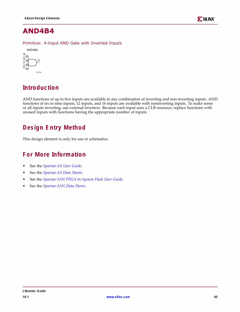
About Design Elements
AND4B4
Primitive: 4-Input AND Gate with Inverted Inputs
IntroductionAND functions of up to five inputs are available in any combination of inverting and non-inverting inputs. ANDfunctions of six to nine inputs, 12 inputs, and 16 inputs are available with noninverting inputs. To make someor all inputs inverting, use external inverters. Because each input uses a CLB resource, replace functions withunused inputs with functions having the appropriate number of inputs.
Design Entry MethodThis design element is only for use in schematics.
For More Information• See the Spartan-3A User Guide.
• See the Spartan-3A Data Sheets.
• See the Spartan-3AN FPGA In-System Flash User Guide.
• See the Spartan-3AN Data Sheets.
Libraries Guide
10.1 www.xilinx.com 65
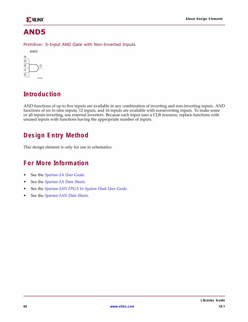
About Design Elements
AND5
Primitive: 5-Input AND Gate with Non-Inverted Inputs
IntroductionAND functions of up to five inputs are available in any combination of inverting and non-inverting inputs. ANDfunctions of six to nine inputs, 12 inputs, and 16 inputs are available with noninverting inputs. To make someor all inputs inverting, use external inverters. Because each input uses a CLB resource, replace functions withunused inputs with functions having the appropriate number of inputs.
Design Entry MethodThis design element is only for use in schematics.
For More Information• See the Spartan-3A User Guide.
• See the Spartan-3A Data Sheets.
• See the Spartan-3AN FPGA In-System Flash User Guide.
• See the Spartan-3AN Data Sheets.
Libraries Guide
66 www.xilinx.com 10.1
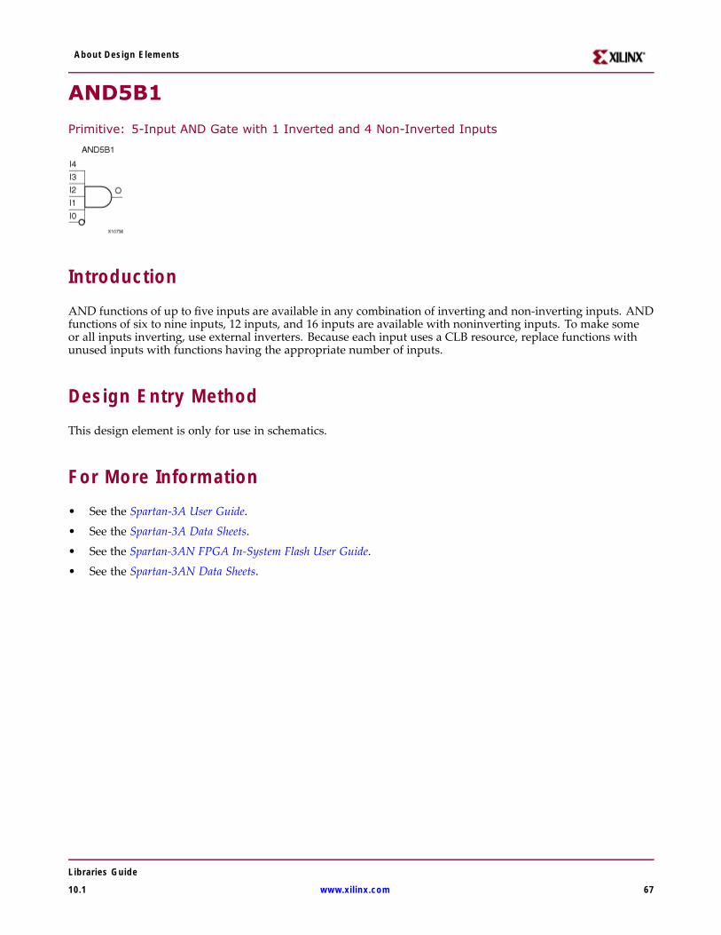
About Design Elements
AND5B1
Primitive: 5-Input AND Gate with 1 Inverted and 4 Non-Inverted Inputs
IntroductionAND functions of up to five inputs are available in any combination of inverting and non-inverting inputs. ANDfunctions of six to nine inputs, 12 inputs, and 16 inputs are available with noninverting inputs. To make someor all inputs inverting, use external inverters. Because each input uses a CLB resource, replace functions withunused inputs with functions having the appropriate number of inputs.
Design Entry MethodThis design element is only for use in schematics.
For More Information• See the Spartan-3A User Guide.
• See the Spartan-3A Data Sheets.
• See the Spartan-3AN FPGA In-System Flash User Guide.
• See the Spartan-3AN Data Sheets.
Libraries Guide
10.1 www.xilinx.com 67
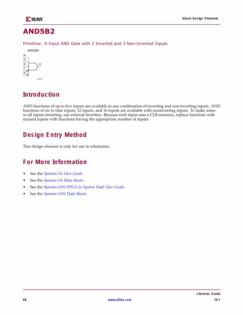
About Design Elements
AND5B2
Primitive: 5-Input AND Gate with 2 Inverted and 3 Non-Inverted Inputs
IntroductionAND functions of up to five inputs are available in any combination of inverting and non-inverting inputs. ANDfunctions of six to nine inputs, 12 inputs, and 16 inputs are available with noninverting inputs. To make someor all inputs inverting, use external inverters. Because each input uses a CLB resource, replace functions withunused inputs with functions having the appropriate number of inputs.
Design Entry MethodThis design element is only for use in schematics.
For More Information• See the Spartan-3A User Guide.
• See the Spartan-3A Data Sheets.
• See the Spartan-3AN FPGA In-System Flash User Guide.
• See the Spartan-3AN Data Sheets.
Libraries Guide
68 www.xilinx.com 10.1

About Design Elements
AND5B3
Primitive: 5-Input AND Gate with 3 Inverted and 2 Non-Inverted Inputs
IntroductionAND functions of up to five inputs are available in any combination of inverting and non-inverting inputs. ANDfunctions of six to nine inputs, 12 inputs, and 16 inputs are available with noninverting inputs. To make someor all inputs inverting, use external inverters. Because each input uses a CLB resource, replace functions withunused inputs with functions having the appropriate number of inputs.
Design Entry MethodThis design element is only for use in schematics.
For More Information• See the Spartan-3A User Guide.
• See the Spartan-3A Data Sheets.
• See the Spartan-3AN FPGA In-System Flash User Guide.
• See the Spartan-3AN Data Sheets.
Libraries Guide
10.1 www.xilinx.com 69

About Design Elements
AND5B4
Primitive: 5-Input AND Gate with 4 Inverted and 1 Non-Inverted Inputs
IntroductionAND functions of up to five inputs are available in any combination of inverting and non-inverting inputs. ANDfunctions of six to nine inputs, 12 inputs, and 16 inputs are available with noninverting inputs. To make someor all inputs inverting, use external inverters. Because each input uses a CLB resource, replace functions withunused inputs with functions having the appropriate number of inputs.
Design Entry MethodThis design element is only for use in schematics.
For More Information• See the Spartan-3A User Guide.
• See the Spartan-3A Data Sheets.
• See the Spartan-3AN FPGA In-System Flash User Guide.
• See the Spartan-3AN Data Sheets.
Libraries Guide
70 www.xilinx.com 10.1
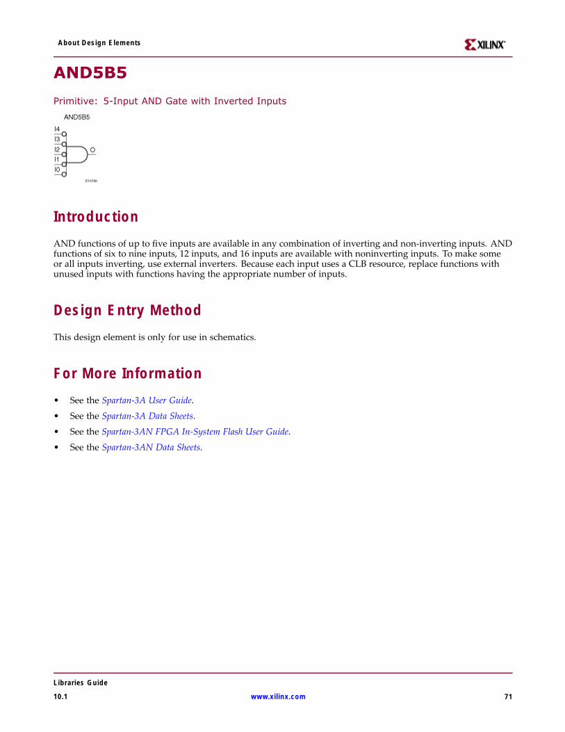
About Design Elements
AND5B5
Primitive: 5-Input AND Gate with Inverted Inputs
IntroductionAND functions of up to five inputs are available in any combination of inverting and non-inverting inputs. ANDfunctions of six to nine inputs, 12 inputs, and 16 inputs are available with noninverting inputs. To make someor all inputs inverting, use external inverters. Because each input uses a CLB resource, replace functions withunused inputs with functions having the appropriate number of inputs.
Design Entry MethodThis design element is only for use in schematics.
For More Information• See the Spartan-3A User Guide.
• See the Spartan-3A Data Sheets.
• See the Spartan-3AN FPGA In-System Flash User Guide.
• See the Spartan-3AN Data Sheets.
Libraries Guide
10.1 www.xilinx.com 71
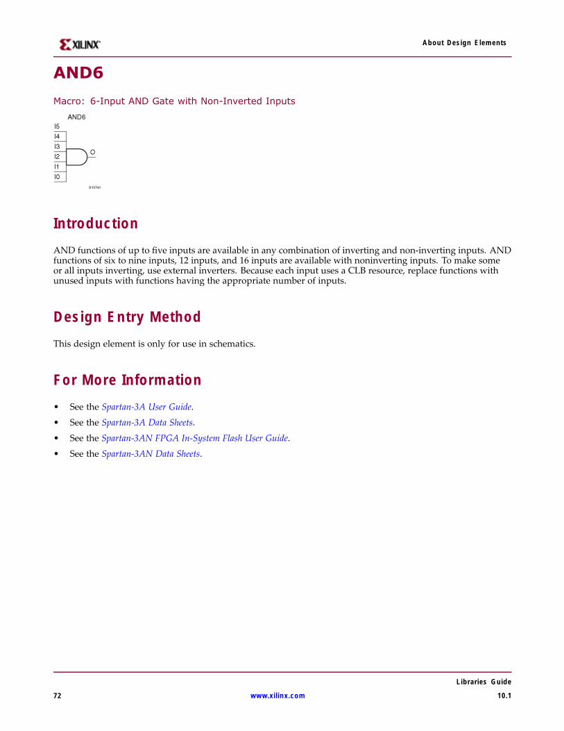
About Design Elements
AND6
Macro: 6-Input AND Gate with Non-Inverted Inputs
IntroductionAND functions of up to five inputs are available in any combination of inverting and non-inverting inputs. ANDfunctions of six to nine inputs, 12 inputs, and 16 inputs are available with noninverting inputs. To make someor all inputs inverting, use external inverters. Because each input uses a CLB resource, replace functions withunused inputs with functions having the appropriate number of inputs.
Design Entry MethodThis design element is only for use in schematics.
For More Information• See the Spartan-3A User Guide.
• See the Spartan-3A Data Sheets.
• See the Spartan-3AN FPGA In-System Flash User Guide.
• See the Spartan-3AN Data Sheets.
Libraries Guide
72 www.xilinx.com 10.1

About Design Elements
AND7
Macro: 7-Input AND Gate with Non-Inverted Inputs
IntroductionAND functions of up to five inputs are available in any combination of inverting and non-inverting inputs. ANDfunctions of six to nine inputs, 12 inputs, and 16 inputs are available with noninverting inputs. To make someor all inputs inverting, use external inverters. Because each input uses a CLB resource, replace functions withunused inputs with functions having the appropriate number of inputs.
Design Entry MethodThis design element is only for use in schematics.
For More Information• See the Spartan-3A User Guide.
• See the Spartan-3A Data Sheets.
• See the Spartan-3AN FPGA In-System Flash User Guide.
• See the Spartan-3AN Data Sheets.
Libraries Guide
10.1 www.xilinx.com 73
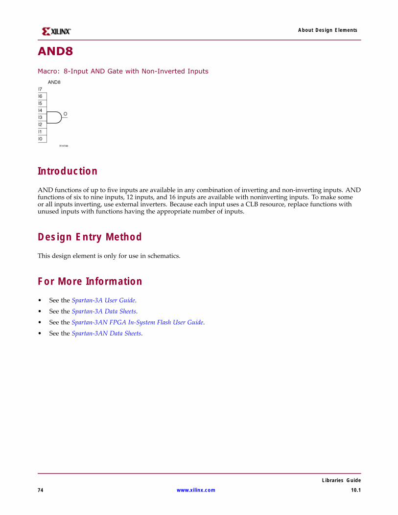
About Design Elements
AND8
Macro: 8-Input AND Gate with Non-Inverted Inputs
IntroductionAND functions of up to five inputs are available in any combination of inverting and non-inverting inputs. ANDfunctions of six to nine inputs, 12 inputs, and 16 inputs are available with noninverting inputs. To make someor all inputs inverting, use external inverters. Because each input uses a CLB resource, replace functions withunused inputs with functions having the appropriate number of inputs.
Design Entry MethodThis design element is only for use in schematics.
For More Information• See the Spartan-3A User Guide.
• See the Spartan-3A Data Sheets.
• See the Spartan-3AN FPGA In-System Flash User Guide.
• See the Spartan-3AN Data Sheets.
Libraries Guide
74 www.xilinx.com 10.1
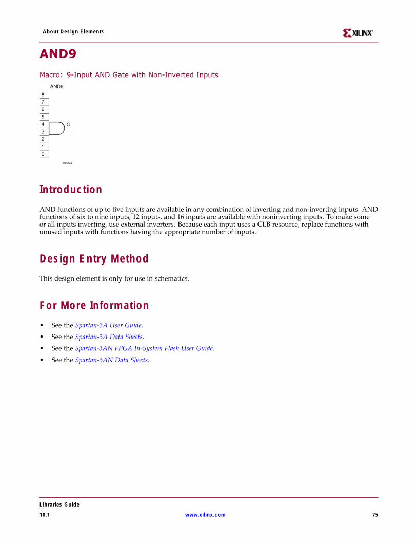
About Design Elements
AND9
Macro: 9-Input AND Gate with Non-Inverted Inputs
IntroductionAND functions of up to five inputs are available in any combination of inverting and non-inverting inputs. ANDfunctions of six to nine inputs, 12 inputs, and 16 inputs are available with noninverting inputs. To make someor all inputs inverting, use external inverters. Because each input uses a CLB resource, replace functions withunused inputs with functions having the appropriate number of inputs.
Design Entry MethodThis design element is only for use in schematics.
For More Information• See the Spartan-3A User Guide.
• See the Spartan-3A Data Sheets.
• See the Spartan-3AN FPGA In-System Flash User Guide.
• See the Spartan-3AN Data Sheets.
Libraries Guide
10.1 www.xilinx.com 75
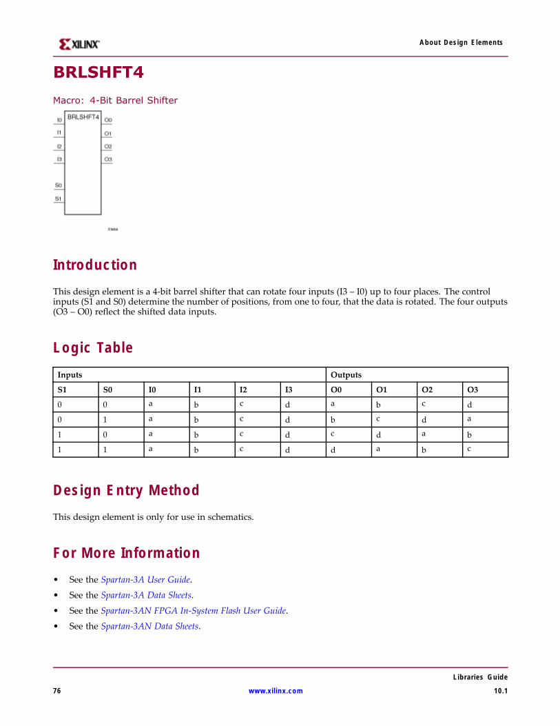
About Design Elements
BRLSHFT4
Macro: 4-Bit Barrel Shifter
IntroductionThis design element is a 4-bit barrel shifter that can rotate four inputs (I3 – I0) up to four places. The controlinputs (S1 and S0) determine the number of positions, from one to four, that the data is rotated. The four outputs(O3 – O0) reflect the shifted data inputs.
Logic TableInputs Outputs
S1 S0 I0 I1 I2 I3 O0 O1 O2 O3
0 0 a b c d a b c d
0 1 a b c d b c d a
1 0 a b c d c d a b
1 1 a b c d d a b c
Design Entry MethodThis design element is only for use in schematics.
For More Information• See the Spartan-3A User Guide.
• See the Spartan-3A Data Sheets.
• See the Spartan-3AN FPGA In-System Flash User Guide.
• See the Spartan-3AN Data Sheets.
Libraries Guide
76 www.xilinx.com 10.1
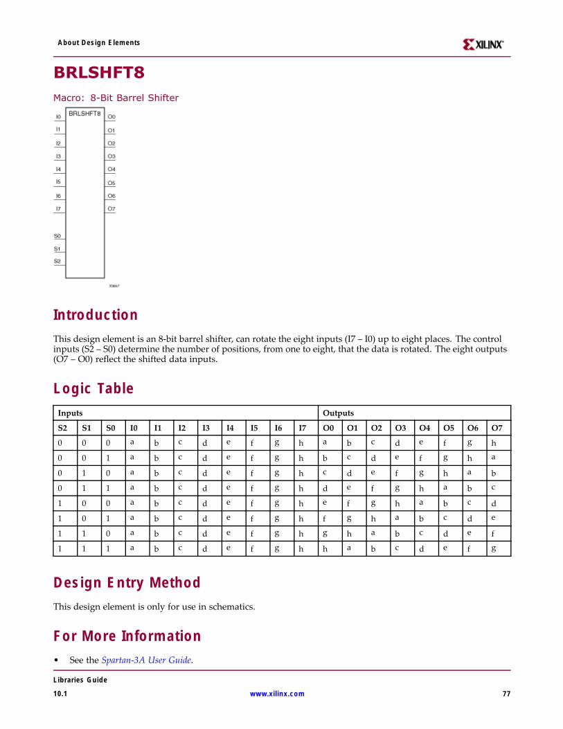
About Design Elements
BRLSHFT8Macro: 8-Bit Barrel Shifter
IntroductionThis design element is an 8-bit barrel shifter, can rotate the eight inputs (I7 – I0) up to eight places. The controlinputs (S2 – S0) determine the number of positions, from one to eight, that the data is rotated. The eight outputs(O7 – O0) reflect the shifted data inputs.
Logic TableInputs Outputs
S2 S1 S0 I0 I1 I2 I3 I4 I5 I6 I7 O0 O1 O2 O3 O4 O5 O6 O7
0 0 0 a b c d e f g h a b c d e f g h
0 0 1 a b c d e f g h b c d e f g h a
0 1 0 a b c d e f g h c d e f g h a b
0 1 1 a b c d e f g h d e f g h a b c
1 0 0 a b c d e f g h e f g h a b c d
1 0 1 a b c d e f g h f g h a b c d e
1 1 0 a b c d e f g h g h a b c d e f
1 1 1 a b c d e f g h h a b c d e f g
Design Entry MethodThis design element is only for use in schematics.
For More Information• See the Spartan-3A User Guide.
Libraries Guide
10.1 www.xilinx.com 77

About Design Elements
• See the Spartan-3A Data Sheets.
• See the Spartan-3AN FPGA In-System Flash User Guide.
• See the Spartan-3AN Data Sheets.
Libraries Guide
78 www.xilinx.com 10.1
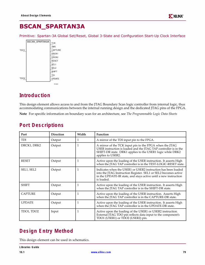
About Design Elements
BSCAN_SPARTAN3APrimitive: Spartan-3A Global Set/Reset, Global 3-State and Configuration Start-Up Clock Interface
IntroductionThis design element allows access to and from the JTAG Boundary Scan logic controller from internal logic, thusaccommodating communications between the internal running design and the dedicated JTAG pins of the FPGA.
Note For specific information on boundary scan for an architecture, see The Programmable Logic Data Sheets
Port DescriptionsPort Direction Width Function
TDI Output 1 A mirror of the TDI input pin to the FPGA.
DRCK1, DRK2 Output 1 A mirror of the TCK input pin to the FPGA when the JTAGUSER instruction is loaded and the JTAG TAP controller is in theSHIFT-DR state. DRK1 applies to the USER1 logic while DRK2applies to USER2.
RESET Output 1 Active upon the loading of the USER instruction. It asserts Highwhen the JTAG TAP controller is in the TEST-LOGIC-RESET state.
SEL1, SEL2 Output 1 Indicates when the USER1 or USER2 instruction has been loadedinto the JTAG Instruction Register. SEL1 or SEL2 becomes activein the UPDATE-IR state, and stays active until a new instructionis loaded.
SHIFT Output 1 Active upon the loading of the USER instruction. It asserts Highwhen the JTAG TAP controller is in the SHIFT-DR state.
CAPTURE Output 1 Active upon the loading of the USER instruction. Asserts Highwhen the JTAG TAP controller is in the CAPTURE-DR state.
UPDATE Output 1 Active upon the loading of the USER instruction. It asserts Highwhen the JTAG TAP controller is in the UPDATE-DR state.
TDO1, TDO2 Input 1 Active upon the loading of the USER1 or USER2 instruction.External JTAG TDO pin reflects data input to the component’sTDO1 (USER1) or TDO2 (USER2) pin.
Design Entry MethodThis design element can be used in schematics.
Libraries Guide
10.1 www.xilinx.com 79

About Design Elements
For More Information• See the Spartan-3A User Guide.
• See the Spartan-3A Data Sheets.
• See the Spartan-3AN FPGA In-System Flash User Guide.
• See the Spartan-3AN Data Sheets.
Libraries Guide
80 www.xilinx.com 10.1
About Design Elements
BUF
Primitive: General Purpose Buffer
IntroductionThis is a general-purpose, non-inverting buffer.
This element is not necessary and is removed by the partitioning software (MAP).
Design Entry MethodThis design element is only for use in schematics.
For More Information• See the Spartan-3A User Guide.
• See the Spartan-3A Data Sheets.
• See the Spartan-3AN FPGA In-System Flash User Guide.
• See the Spartan-3AN Data Sheets.
Libraries Guide
10.1 www.xilinx.com 81
About Design Elements
BUFCF
Fast Connect Buffer
IntroductionThis design element is a single fast connect buffer used to connect the outputs of the LUTs and some dedicatedlogic directly to the input of another LUT. Using this buffer implies CLB packing. No more than four LUTsmay be connected together as a group.
Design Entry MethodThis design element can be used in schematics.
For More Information• See the Spartan-3A User Guide.
• See the Spartan-3A Data Sheets.
• See the Spartan-3AN FPGA In-System Flash User Guide.
• See the Spartan-3AN Data Sheets.
Libraries Guide
82 www.xilinx.com 10.1
About Design Elements
BUFG
Primitive: Global Clock Buffer
IntroductionThis design element is a high-fanout buffer that connects signals to the global routing resources for low skewdistribution of the signal. BUFGs are typically used on clock nets as well other high fanout nets like sets/resetsand clock enables.
Design Entry MethodThis design element can be used in schematics.
For More Information• See the Spartan-3A User Guide.
• See the Spartan-3A Data Sheets.
• See the Spartan-3AN FPGA In-System Flash User Guide.
• See the Spartan-3AN Data Sheets.
Libraries Guide
10.1 www.xilinx.com 83
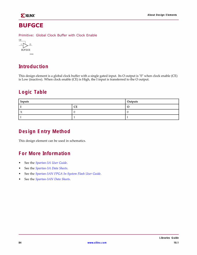
About Design Elements
BUFGCE
Primitive: Global Clock Buffer with Clock Enable
IntroductionThis design element is a global clock buffer with a single gated input. Its O output is "0" when clock enable (CE)is Low (inactive). When clock enable (CE) is High, the I input is transferred to the O output.
Logic TableInputs Outputs
I CE O
X 0 0
I 1 I
Design Entry MethodThis design element can be used in schematics.
For More Information• See the Spartan-3A User Guide.
• See the Spartan-3A Data Sheets.
• See the Spartan-3AN FPGA In-System Flash User Guide.
• See the Spartan-3AN Data Sheets.
Libraries Guide
84 www.xilinx.com 10.1
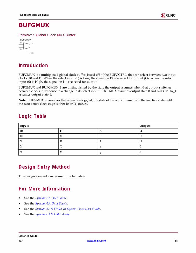
About Design Elements
BUFGMUX
Primitive: Global Clock MUX Buffer
IntroductionBUFGMUX is a multiplexed global clock buffer, based off of the BUFGCTRL, that can select between two inputclocks: I0 and I1. When the select input (S) is Low, the signal on I0 is selected for output (O). When the selectinput (S) is High, the signal on I1 is selected for output.
BUFGMUX and BUFGMUX_1 are distinguished by the state the output assumes when that output switchesbetween clocks in response to a change in its select input. BUGFMUX assumes output state 0 and BUFGMUX_1assumes output state 1.
Note BUFGMUX guarantees that when S is toggled, the state of the output remains in the inactive state untilthe next active clock edge (either I0 or I1) occurs.
Logic TableInputs Outputs
I0 I1 S O
I0 X 0 I0
X I1 1 I1
X X ↑ 0
X X ↓ 0
Design Entry MethodThis design element can be used in schematics.
For More Information• See the Spartan-3A User Guide.
• See the Spartan-3A Data Sheets.
• See the Spartan-3AN FPGA In-System Flash User Guide.
• See the Spartan-3AN Data Sheets.
Libraries Guide
10.1 www.xilinx.com 85
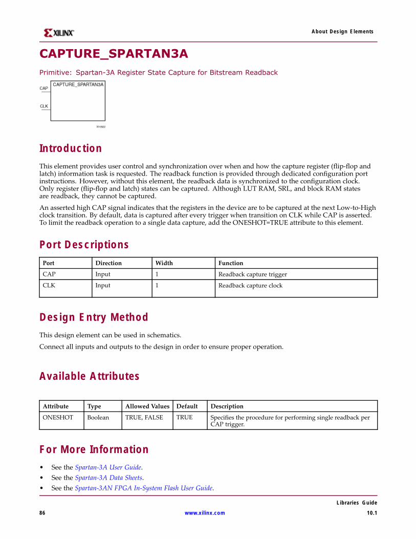
About Design Elements
CAPTURE_SPARTAN3APrimitive: Spartan-3A Register State Capture for Bitstream Readback
IntroductionThis element provides user control and synchronization over when and how the capture register (flip-flop andlatch) information task is requested. The readback function is provided through dedicated configuration portinstructions. However, without this element, the readback data is synchronized to the configuration clock.Only register (flip-flop and latch) states can be captured. Although LUT RAM, SRL, and block RAM statesare readback, they cannot be captured.
An asserted high CAP signal indicates that the registers in the device are to be captured at the next Low-to-Highclock transition. By default, data is captured after every trigger when transition on CLK while CAP is asserted.To limit the readback operation to a single data capture, add the ONESHOT=TRUE attribute to this element.
Port DescriptionsPort Direction Width Function
CAP Input 1 Readback capture trigger
CLK Input 1 Readback capture clock
Design Entry MethodThis design element can be used in schematics.
Connect all inputs and outputs to the design in order to ensure proper operation.
Available Attributes
Attribute Type Allowed Values Default Description
ONESHOT Boolean TRUE, FALSE TRUE Specifies the procedure for performing single readback perCAP trigger.
For More Information• See the Spartan-3A User Guide.• See the Spartan-3A Data Sheets.• See the Spartan-3AN FPGA In-System Flash User Guide.
Libraries Guide
86 www.xilinx.com 10.1

About Design Elements
• See the Spartan-3AN Data Sheets.
Libraries Guide
10.1 www.xilinx.com 87
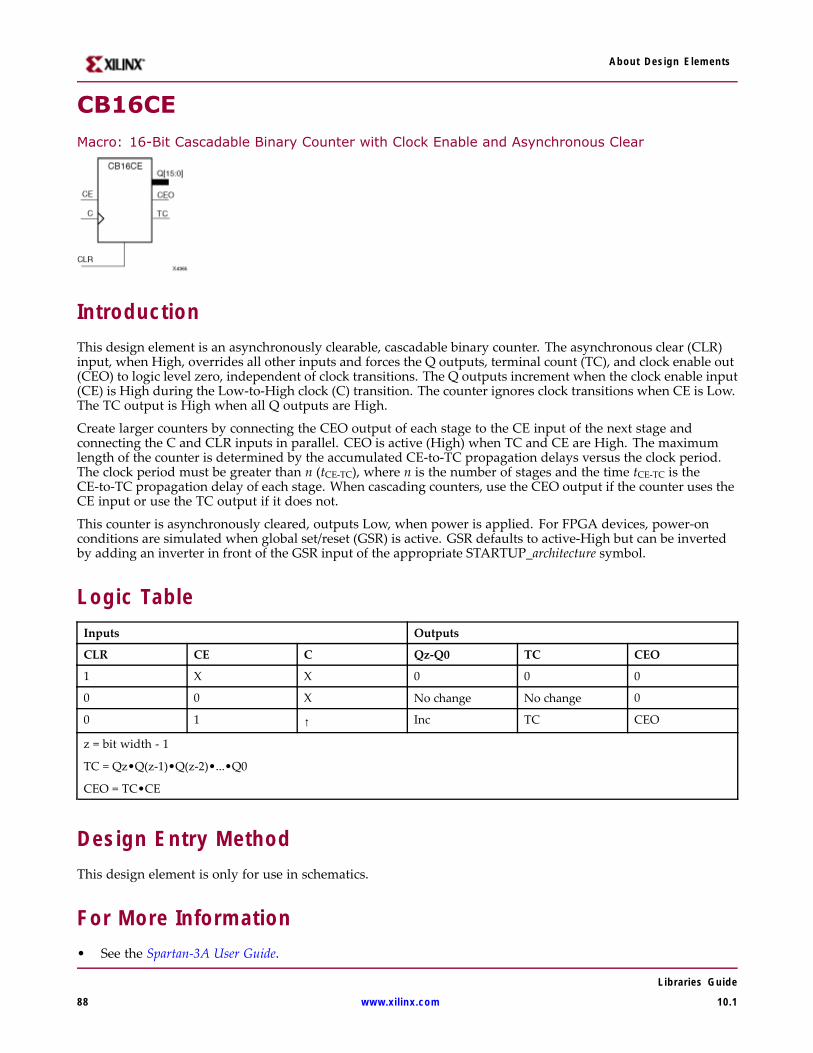
About Design Elements
CB16CEMacro: 16-Bit Cascadable Binary Counter with Clock Enable and Asynchronous Clear
IntroductionThis design element is an asynchronously clearable, cascadable binary counter. The asynchronous clear (CLR)input, when High, overrides all other inputs and forces the Q outputs, terminal count (TC), and clock enable out(CEO) to logic level zero, independent of clock transitions. The Q outputs increment when the clock enable input(CE) is High during the Low-to-High clock (C) transition. The counter ignores clock transitions when CE is Low.The TC output is High when all Q outputs are High.
Create larger counters by connecting the CEO output of each stage to the CE input of the next stage andconnecting the C and CLR inputs in parallel. CEO is active (High) when TC and CE are High. The maximumlength of the counter is determined by the accumulated CE-to-TC propagation delays versus the clock period.The clock period must be greater than n (tCE-TC), where n is the number of stages and the time tCE-TC is theCE-to-TC propagation delay of each stage. When cascading counters, use the CEO output if the counter uses theCE input or use the TC output if it does not.
This counter is asynchronously cleared, outputs Low, when power is applied. For FPGA devices, power-onconditions are simulated when global set/reset (GSR) is active. GSR defaults to active-High but can be invertedby adding an inverter in front of the GSR input of the appropriate STARTUP_architecture symbol.
Logic TableInputs Outputs
CLR CE C Qz-Q0 TC CEO
1 X X 0 0 0
0 0 X No change No change 0
0 1 ↑ Inc TC CEO
z = bit width - 1
TC = Qz•Q(z-1)•Q(z-2)•...•Q0
CEO = TC•CE
Design Entry MethodThis design element is only for use in schematics.
For More Information• See the Spartan-3A User Guide.
Libraries Guide
88 www.xilinx.com 10.1

About Design Elements
• See the Spartan-3A Data Sheets.
• See the Spartan-3AN FPGA In-System Flash User Guide.
• See the Spartan-3AN Data Sheets.
Libraries Guide
10.1 www.xilinx.com 89
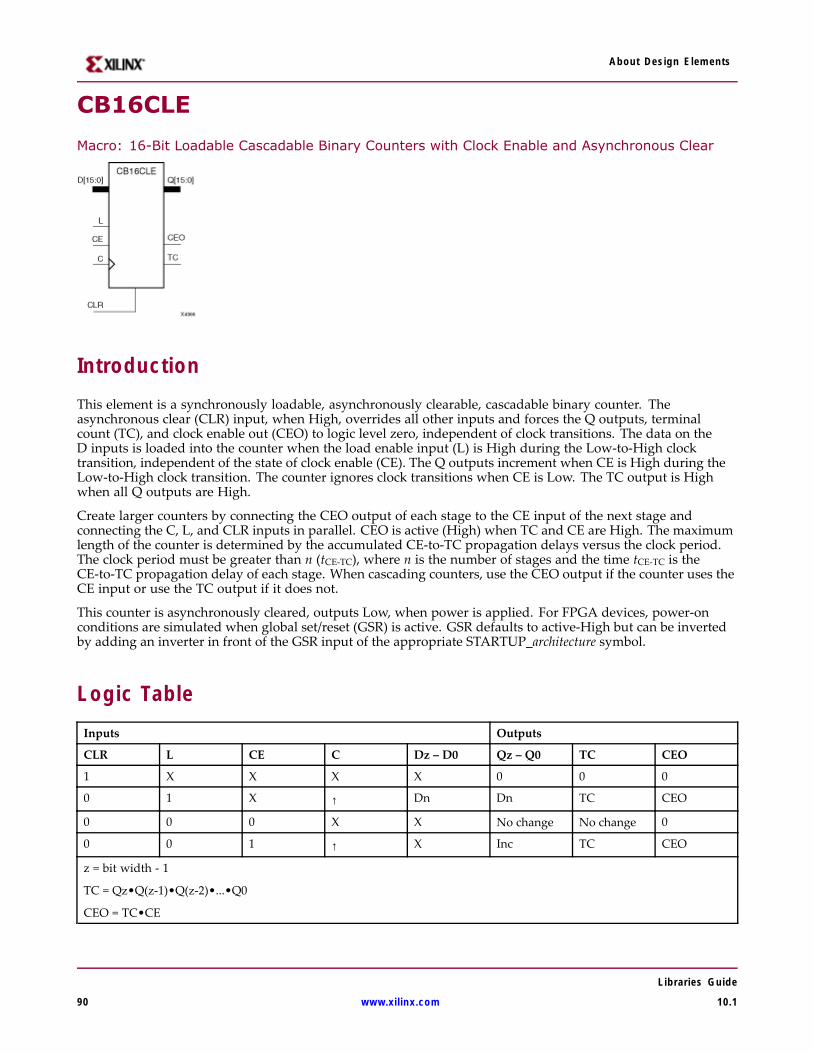
About Design Elements
CB16CLE
Macro: 16-Bit Loadable Cascadable Binary Counters with Clock Enable and Asynchronous Clear
IntroductionThis element is a synchronously loadable, asynchronously clearable, cascadable binary counter. Theasynchronous clear (CLR) input, when High, overrides all other inputs and forces the Q outputs, terminalcount (TC), and clock enable out (CEO) to logic level zero, independent of clock transitions. The data on theD inputs is loaded into the counter when the load enable input (L) is High during the Low-to-High clocktransition, independent of the state of clock enable (CE). The Q outputs increment when CE is High during theLow-to-High clock transition. The counter ignores clock transitions when CE is Low. The TC output is Highwhen all Q outputs are High.
Create larger counters by connecting the CEO output of each stage to the CE input of the next stage andconnecting the C, L, and CLR inputs in parallel. CEO is active (High) when TC and CE are High. The maximumlength of the counter is determined by the accumulated CE-to-TC propagation delays versus the clock period.The clock period must be greater than n (tCE-TC), where n is the number of stages and the time tCE-TC is theCE-to-TC propagation delay of each stage. When cascading counters, use the CEO output if the counter uses theCE input or use the TC output if it does not.
This counter is asynchronously cleared, outputs Low, when power is applied. For FPGA devices, power-onconditions are simulated when global set/reset (GSR) is active. GSR defaults to active-High but can be invertedby adding an inverter in front of the GSR input of the appropriate STARTUP_architecture symbol.
Logic TableInputs Outputs
CLR L CE C Dz – D0 Qz – Q0 TC CEO
1 X X X X 0 0 0
0 1 X ↑ Dn Dn TC CEO
0 0 0 X X No change No change 0
0 0 1 ↑ X Inc TC CEO
z = bit width - 1
TC = Qz•Q(z-1)•Q(z-2)•...•Q0
CEO = TC•CE
Libraries Guide
90 www.xilinx.com 10.1

About Design Elements
Design Entry MethodThis design element is only for use in schematics.
For More Information• See the Spartan-3A User Guide.
• See the Spartan-3A Data Sheets.
• See the Spartan-3AN FPGA In-System Flash User Guide.
• See the Spartan-3AN Data Sheets.
Libraries Guide
10.1 www.xilinx.com 91
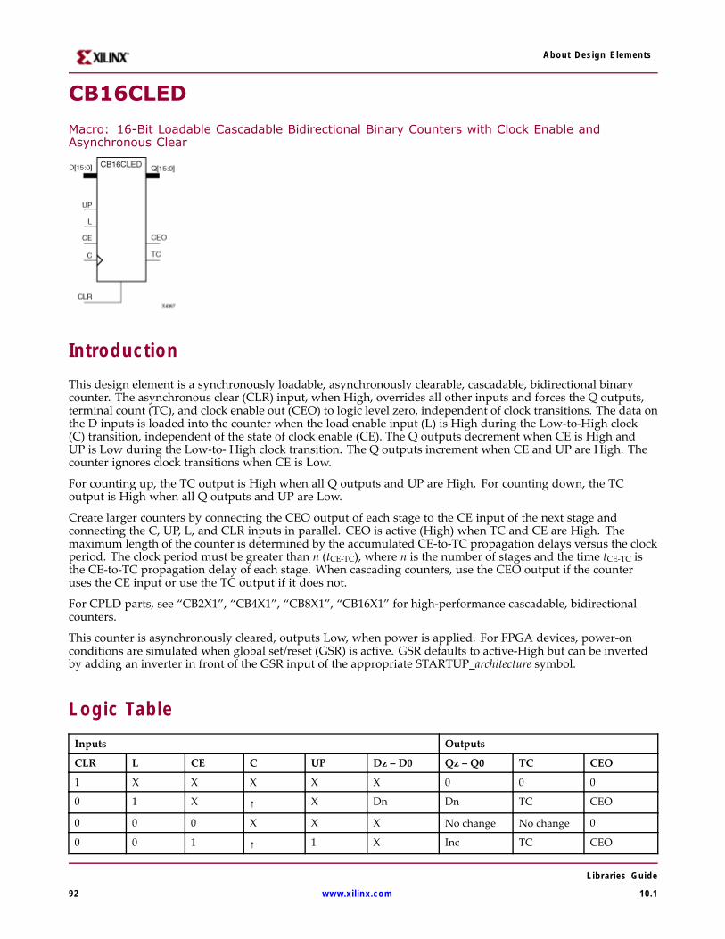
About Design Elements
CB16CLED
Macro: 16-Bit Loadable Cascadable Bidirectional Binary Counters with Clock Enable andAsynchronous Clear
IntroductionThis design element is a synchronously loadable, asynchronously clearable, cascadable, bidirectional binarycounter. The asynchronous clear (CLR) input, when High, overrides all other inputs and forces the Q outputs,terminal count (TC), and clock enable out (CEO) to logic level zero, independent of clock transitions. The data onthe D inputs is loaded into the counter when the load enable input (L) is High during the Low-to-High clock(C) transition, independent of the state of clock enable (CE). The Q outputs decrement when CE is High andUP is Low during the Low-to- High clock transition. The Q outputs increment when CE and UP are High. Thecounter ignores clock transitions when CE is Low.
For counting up, the TC output is High when all Q outputs and UP are High. For counting down, the TCoutput is High when all Q outputs and UP are Low.
Create larger counters by connecting the CEO output of each stage to the CE input of the next stage andconnecting the C, UP, L, and CLR inputs in parallel. CEO is active (High) when TC and CE are High. Themaximum length of the counter is determined by the accumulated CE-to-TC propagation delays versus the clockperiod. The clock period must be greater than n (tCE-TC), where n is the number of stages and the time tCE-TC isthe CE-to-TC propagation delay of each stage. When cascading counters, use the CEO output if the counteruses the CE input or use the TC output if it does not.
For CPLD parts, see “CB2X1”, “CB4X1”, “CB8X1”, “CB16X1” for high-performance cascadable, bidirectionalcounters.
This counter is asynchronously cleared, outputs Low, when power is applied. For FPGA devices, power-onconditions are simulated when global set/reset (GSR) is active. GSR defaults to active-High but can be invertedby adding an inverter in front of the GSR input of the appropriate STARTUP_architecture symbol.
Logic TableInputs Outputs
CLR L CE C UP Dz – D0 Qz – Q0 TC CEO
1 X X X X X 0 0 0
0 1 X ↑ X Dn Dn TC CEO
0 0 0 X X X No change No change 0
0 0 1 ↑ 1 X Inc TC CEO
Libraries Guide
92 www.xilinx.com 10.1

About Design Elements
Inputs Outputs
CLR L CE C UP Dz – D0 Qz – Q0 TC CEO
0 0 1 ↑ 0 X Dec TC CEO
z = bit width - 1
TC = (Qz•Q(z-1)•Q(z-2)•...•Q0•UP) + (Qz•Q(z-1)•Q(z-2)•...•Q0•UP)
CEO = TC•CE
Design Entry MethodThis design element is only for use in schematics.
For More Information• See the Spartan-3A User Guide.
• See the Spartan-3A Data Sheets.
• See the Spartan-3AN FPGA In-System Flash User Guide.
• See the Spartan-3AN Data Sheets.
Libraries Guide
10.1 www.xilinx.com 93
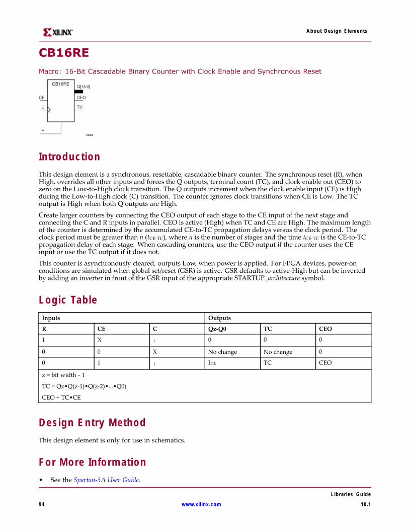
About Design Elements
CB16REMacro: 16-Bit Cascadable Binary Counter with Clock Enable and Synchronous Reset
IntroductionThis design element is a synchronous, resettable, cascadable binary counter. The synchronous reset (R), whenHigh, overrides all other inputs and forces the Q outputs, terminal count (TC), and clock enable out (CEO) tozero on the Low-to-High clock transition. The Q outputs increment when the clock enable input (CE) is Highduring the Low-to-High clock (C) transition. The counter ignores clock transitions when CE is Low. The TCoutput is High when both Q outputs are High.
Create larger counters by connecting the CEO output of each stage to the CE input of the next stage andconnecting the C and R inputs in parallel. CEO is active (High) when TC and CE are High. The maximum lengthof the counter is determined by the accumulated CE-to-TC propagation delays versus the clock period. Theclock period must be greater than n (tCE-TC), where n is the number of stages and the time tCE-TC is the CE-to-TCpropagation delay of each stage. When cascading counters, use the CEO output if the counter uses the CEinput or use the TC output if it does not.
This counter is asynchronously cleared, outputs Low, when power is applied. For FPGA devices, power-onconditions are simulated when global set/reset (GSR) is active. GSR defaults to active-High but can be invertedby adding an inverter in front of the GSR input of the appropriate STARTUP_architecture symbol.
Logic TableInputs Outputs
R CE C Qz-Q0 TC CEO
1 X ↑ 0 0 0
0 0 X No change No change 0
0 1 ↑ Inc TC CEO
z = bit width - 1
TC = Qz•Q(z-1)•Q(z-2)•...•Q0)
CEO = TC•CE
Design Entry MethodThis design element is only for use in schematics.
For More Information• See the Spartan-3A User Guide.
Libraries Guide
94 www.xilinx.com 10.1

About Design Elements
• See the Spartan-3A Data Sheets.
• See the Spartan-3AN FPGA In-System Flash User Guide.
• See the Spartan-3AN Data Sheets.
Libraries Guide
10.1 www.xilinx.com 95
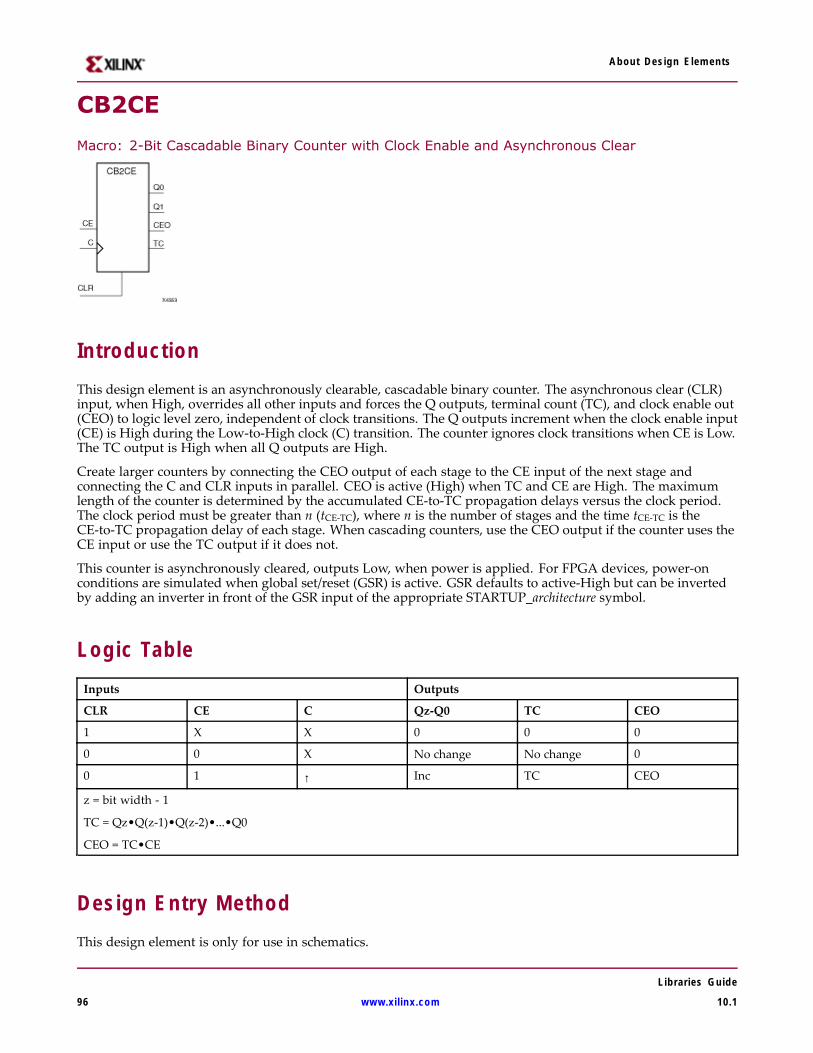
About Design Elements
CB2CE
Macro: 2-Bit Cascadable Binary Counter with Clock Enable and Asynchronous Clear
IntroductionThis design element is an asynchronously clearable, cascadable binary counter. The asynchronous clear (CLR)input, when High, overrides all other inputs and forces the Q outputs, terminal count (TC), and clock enable out(CEO) to logic level zero, independent of clock transitions. The Q outputs increment when the clock enable input(CE) is High during the Low-to-High clock (C) transition. The counter ignores clock transitions when CE is Low.The TC output is High when all Q outputs are High.
Create larger counters by connecting the CEO output of each stage to the CE input of the next stage andconnecting the C and CLR inputs in parallel. CEO is active (High) when TC and CE are High. The maximumlength of the counter is determined by the accumulated CE-to-TC propagation delays versus the clock period.The clock period must be greater than n (tCE-TC), where n is the number of stages and the time tCE-TC is theCE-to-TC propagation delay of each stage. When cascading counters, use the CEO output if the counter uses theCE input or use the TC output if it does not.
This counter is asynchronously cleared, outputs Low, when power is applied. For FPGA devices, power-onconditions are simulated when global set/reset (GSR) is active. GSR defaults to active-High but can be invertedby adding an inverter in front of the GSR input of the appropriate STARTUP_architecture symbol.
Logic TableInputs Outputs
CLR CE C Qz-Q0 TC CEO
1 X X 0 0 0
0 0 X No change No change 0
0 1 ↑ Inc TC CEO
z = bit width - 1
TC = Qz•Q(z-1)•Q(z-2)•...•Q0
CEO = TC•CE
Design Entry MethodThis design element is only for use in schematics.
Libraries Guide
96 www.xilinx.com 10.1

About Design Elements
For More Information• See the Spartan-3A User Guide.
• See the Spartan-3A Data Sheets.
• See the Spartan-3AN FPGA In-System Flash User Guide.
• See the Spartan-3AN Data Sheets.
Libraries Guide
10.1 www.xilinx.com 97
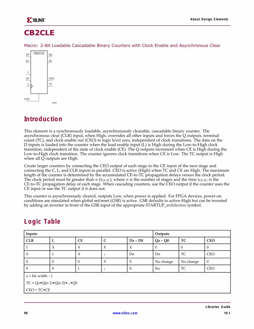
About Design Elements
CB2CLE
Macro: 2-Bit Loadable Cascadable Binary Counters with Clock Enable and Asynchronous Clear
IntroductionThis element is a synchronously loadable, asynchronously clearable, cascadable binary counter. Theasynchronous clear (CLR) input, when High, overrides all other inputs and forces the Q outputs, terminalcount (TC), and clock enable out (CEO) to logic level zero, independent of clock transitions. The data on theD inputs is loaded into the counter when the load enable input (L) is High during the Low-to-High clocktransition, independent of the state of clock enable (CE). The Q outputs increment when CE is High during theLow-to-High clock transition. The counter ignores clock transitions when CE is Low. The TC output is Highwhen all Q outputs are High.
Create larger counters by connecting the CEO output of each stage to the CE input of the next stage andconnecting the C, L, and CLR inputs in parallel. CEO is active (High) when TC and CE are High. The maximumlength of the counter is determined by the accumulated CE-to-TC propagation delays versus the clock period.The clock period must be greater than n (tCE-TC), where n is the number of stages and the time tCE-TC is theCE-to-TC propagation delay of each stage. When cascading counters, use the CEO output if the counter uses theCE input or use the TC output if it does not.
This counter is asynchronously cleared, outputs Low, when power is applied. For FPGA devices, power-onconditions are simulated when global set/reset (GSR) is active. GSR defaults to active-High but can be invertedby adding an inverter in front of the GSR input of the appropriate STARTUP_architecture symbol.
Logic TableInputs Outputs
CLR L CE C Dz – D0 Qz – Q0 TC CEO
1 X X X X 0 0 0
0 1 X ↑ Dn Dn TC CEO
0 0 0 X X No change No change 0
0 0 1 ↑ X Inc TC CEO
z = bit width - 1
TC = Qz•Q(z-1)•Q(z-2)•...•Q0
CEO = TC•CE
Libraries Guide
98 www.xilinx.com 10.1

About Design Elements
Design Entry MethodThis design element is only for use in schematics.
For More Information• See the Spartan-3A User Guide.
• See the Spartan-3A Data Sheets.
• See the Spartan-3AN FPGA In-System Flash User Guide.
• See the Spartan-3AN Data Sheets.
Libraries Guide
10.1 www.xilinx.com 99
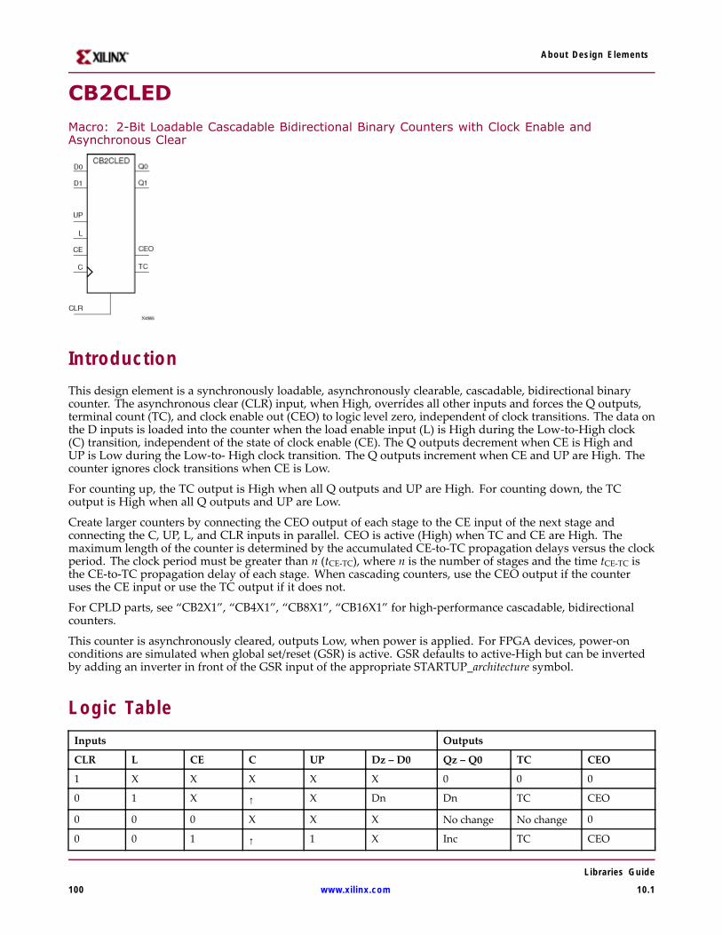
About Design Elements
CB2CLED
Macro: 2-Bit Loadable Cascadable Bidirectional Binary Counters with Clock Enable andAsynchronous Clear
IntroductionThis design element is a synchronously loadable, asynchronously clearable, cascadable, bidirectional binarycounter. The asynchronous clear (CLR) input, when High, overrides all other inputs and forces the Q outputs,terminal count (TC), and clock enable out (CEO) to logic level zero, independent of clock transitions. The data onthe D inputs is loaded into the counter when the load enable input (L) is High during the Low-to-High clock(C) transition, independent of the state of clock enable (CE). The Q outputs decrement when CE is High andUP is Low during the Low-to- High clock transition. The Q outputs increment when CE and UP are High. Thecounter ignores clock transitions when CE is Low.
For counting up, the TC output is High when all Q outputs and UP are High. For counting down, the TCoutput is High when all Q outputs and UP are Low.
Create larger counters by connecting the CEO output of each stage to the CE input of the next stage andconnecting the C, UP, L, and CLR inputs in parallel. CEO is active (High) when TC and CE are High. Themaximum length of the counter is determined by the accumulated CE-to-TC propagation delays versus the clockperiod. The clock period must be greater than n (tCE-TC), where n is the number of stages and the time tCE-TC isthe CE-to-TC propagation delay of each stage. When cascading counters, use the CEO output if the counteruses the CE input or use the TC output if it does not.
For CPLD parts, see “CB2X1”, “CB4X1”, “CB8X1”, “CB16X1” for high-performance cascadable, bidirectionalcounters.
This counter is asynchronously cleared, outputs Low, when power is applied. For FPGA devices, power-onconditions are simulated when global set/reset (GSR) is active. GSR defaults to active-High but can be invertedby adding an inverter in front of the GSR input of the appropriate STARTUP_architecture symbol.
Logic TableInputs Outputs
CLR L CE C UP Dz – D0 Qz – Q0 TC CEO
1 X X X X X 0 0 0
0 1 X ↑ X Dn Dn TC CEO
0 0 0 X X X No change No change 0
0 0 1 ↑ 1 X Inc TC CEO
Libraries Guide
100 www.xilinx.com 10.1
About Design Elements
Inputs Outputs
CLR L CE C UP Dz – D0 Qz – Q0 TC CEO
0 0 1 ↑ 0 X Dec TC CEO
z = bit width - 1
TC = (Qz•Q(z-1)•Q(z-2)•...•Q0•UP) + (Qz•Q(z-1)•Q(z-2)•...•Q0•UP)
CEO = TC•CE
Design Entry MethodThis design element is only for use in schematics.
For More Information• See the Spartan-3A User Guide.
• See the Spartan-3A Data Sheets.
• See the Spartan-3AN FPGA In-System Flash User Guide.
• See the Spartan-3AN Data Sheets.
Libraries Guide
10.1 www.xilinx.com 101
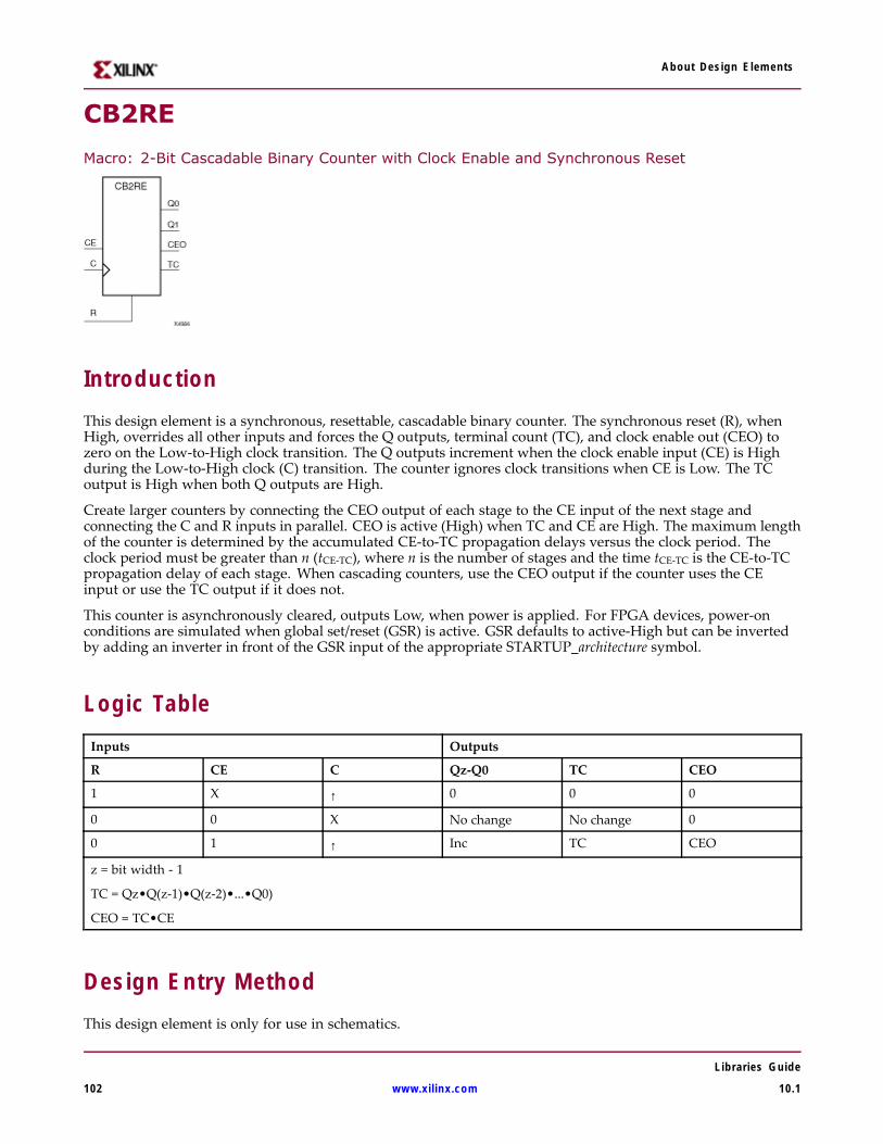
About Design Elements
CB2RE
Macro: 2-Bit Cascadable Binary Counter with Clock Enable and Synchronous Reset
IntroductionThis design element is a synchronous, resettable, cascadable binary counter. The synchronous reset (R), whenHigh, overrides all other inputs and forces the Q outputs, terminal count (TC), and clock enable out (CEO) tozero on the Low-to-High clock transition. The Q outputs increment when the clock enable input (CE) is Highduring the Low-to-High clock (C) transition. The counter ignores clock transitions when CE is Low. The TCoutput is High when both Q outputs are High.
Create larger counters by connecting the CEO output of each stage to the CE input of the next stage andconnecting the C and R inputs in parallel. CEO is active (High) when TC and CE are High. The maximum lengthof the counter is determined by the accumulated CE-to-TC propagation delays versus the clock period. Theclock period must be greater than n (tCE-TC), where n is the number of stages and the time tCE-TC is the CE-to-TCpropagation delay of each stage. When cascading counters, use the CEO output if the counter uses the CEinput or use the TC output if it does not.
This counter is asynchronously cleared, outputs Low, when power is applied. For FPGA devices, power-onconditions are simulated when global set/reset (GSR) is active. GSR defaults to active-High but can be invertedby adding an inverter in front of the GSR input of the appropriate STARTUP_architecture symbol.
Logic TableInputs Outputs
R CE C Qz-Q0 TC CEO
1 X ↑ 0 0 0
0 0 X No change No change 0
0 1 ↑ Inc TC CEO
z = bit width - 1
TC = Qz•Q(z-1)•Q(z-2)•...•Q0)
CEO = TC•CE
Design Entry MethodThis design element is only for use in schematics.
Libraries Guide
102 www.xilinx.com 10.1

About Design Elements
For More Information• See the Spartan-3A User Guide.
• See the Spartan-3A Data Sheets.
• See the Spartan-3AN FPGA In-System Flash User Guide.
• See the Spartan-3AN Data Sheets.
Libraries Guide
10.1 www.xilinx.com 103
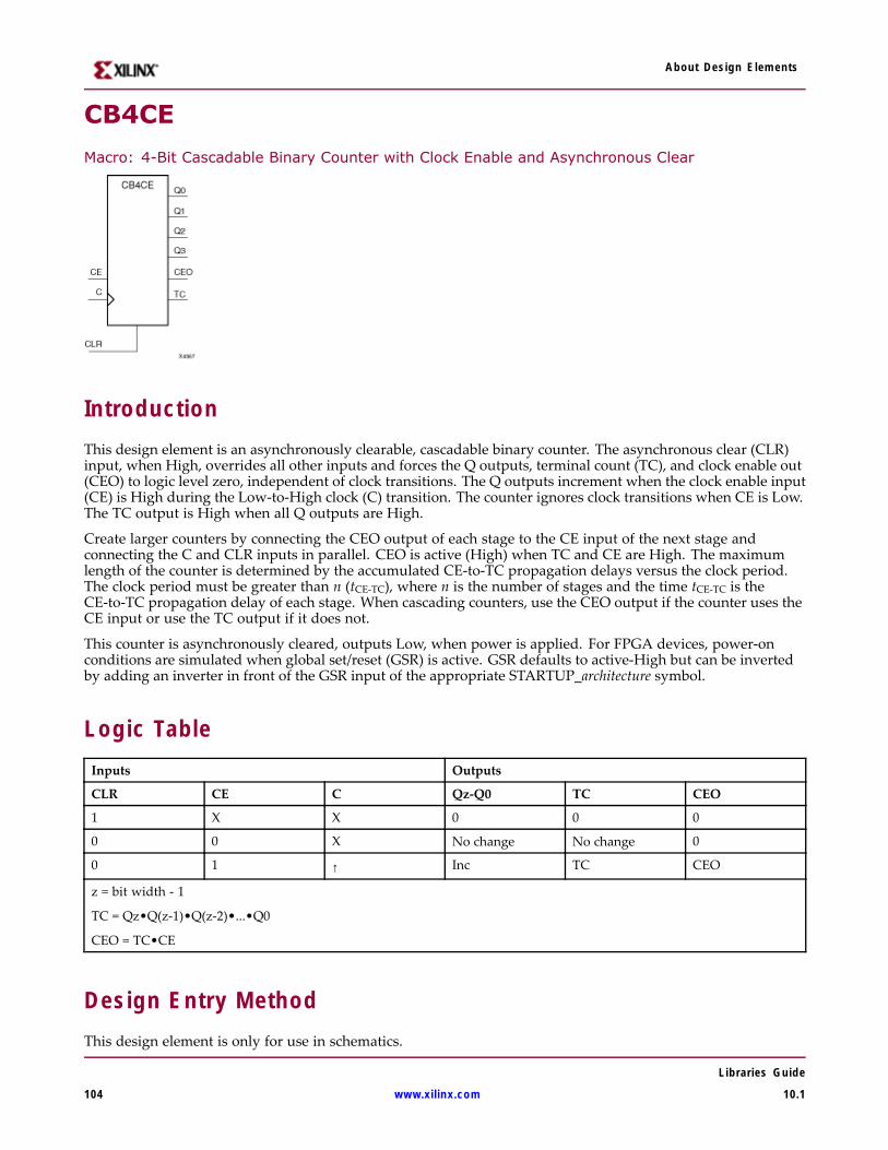
About Design Elements
CB4CE
Macro: 4-Bit Cascadable Binary Counter with Clock Enable and Asynchronous Clear
IntroductionThis design element is an asynchronously clearable, cascadable binary counter. The asynchronous clear (CLR)input, when High, overrides all other inputs and forces the Q outputs, terminal count (TC), and clock enable out(CEO) to logic level zero, independent of clock transitions. The Q outputs increment when the clock enable input(CE) is High during the Low-to-High clock (C) transition. The counter ignores clock transitions when CE is Low.The TC output is High when all Q outputs are High.
Create larger counters by connecting the CEO output of each stage to the CE input of the next stage andconnecting the C and CLR inputs in parallel. CEO is active (High) when TC and CE are High. The maximumlength of the counter is determined by the accumulated CE-to-TC propagation delays versus the clock period.The clock period must be greater than n (tCE-TC), where n is the number of stages and the time tCE-TC is theCE-to-TC propagation delay of each stage. When cascading counters, use the CEO output if the counter uses theCE input or use the TC output if it does not.
This counter is asynchronously cleared, outputs Low, when power is applied. For FPGA devices, power-onconditions are simulated when global set/reset (GSR) is active. GSR defaults to active-High but can be invertedby adding an inverter in front of the GSR input of the appropriate STARTUP_architecture symbol.
Logic TableInputs Outputs
CLR CE C Qz-Q0 TC CEO
1 X X 0 0 0
0 0 X No change No change 0
0 1 ↑ Inc TC CEO
z = bit width - 1
TC = Qz•Q(z-1)•Q(z-2)•...•Q0
CEO = TC•CE
Design Entry MethodThis design element is only for use in schematics.
Libraries Guide
104 www.xilinx.com 10.1

About Design Elements
For More Information• See the Spartan-3A User Guide.
• See the Spartan-3A Data Sheets.
• See the Spartan-3AN FPGA In-System Flash User Guide.
• See the Spartan-3AN Data Sheets.
Libraries Guide
10.1 www.xilinx.com 105
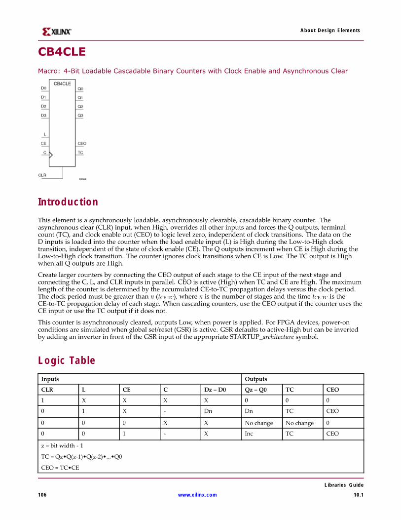
About Design Elements
CB4CLE
Macro: 4-Bit Loadable Cascadable Binary Counters with Clock Enable and Asynchronous Clear
IntroductionThis element is a synchronously loadable, asynchronously clearable, cascadable binary counter. Theasynchronous clear (CLR) input, when High, overrides all other inputs and forces the Q outputs, terminalcount (TC), and clock enable out (CEO) to logic level zero, independent of clock transitions. The data on theD inputs is loaded into the counter when the load enable input (L) is High during the Low-to-High clocktransition, independent of the state of clock enable (CE). The Q outputs increment when CE is High during theLow-to-High clock transition. The counter ignores clock transitions when CE is Low. The TC output is Highwhen all Q outputs are High.
Create larger counters by connecting the CEO output of each stage to the CE input of the next stage andconnecting the C, L, and CLR inputs in parallel. CEO is active (High) when TC and CE are High. The maximumlength of the counter is determined by the accumulated CE-to-TC propagation delays versus the clock period.The clock period must be greater than n (tCE-TC), where n is the number of stages and the time tCE-TC is theCE-to-TC propagation delay of each stage. When cascading counters, use the CEO output if the counter uses theCE input or use the TC output if it does not.
This counter is asynchronously cleared, outputs Low, when power is applied. For FPGA devices, power-onconditions are simulated when global set/reset (GSR) is active. GSR defaults to active-High but can be invertedby adding an inverter in front of the GSR input of the appropriate STARTUP_architecture symbol.
Logic TableInputs Outputs
CLR L CE C Dz – D0 Qz – Q0 TC CEO
1 X X X X 0 0 0
0 1 X ↑ Dn Dn TC CEO
0 0 0 X X No change No change 0
0 0 1 ↑ X Inc TC CEO
z = bit width - 1
TC = Qz•Q(z-1)•Q(z-2)•...•Q0
CEO = TC•CE
Libraries Guide
106 www.xilinx.com 10.1

About Design Elements
Design Entry MethodThis design element is only for use in schematics.
For More Information• See the Spartan-3A User Guide.
• See the Spartan-3A Data Sheets.
• See the Spartan-3AN FPGA In-System Flash User Guide.
• See the Spartan-3AN Data Sheets.
Libraries Guide
10.1 www.xilinx.com 107
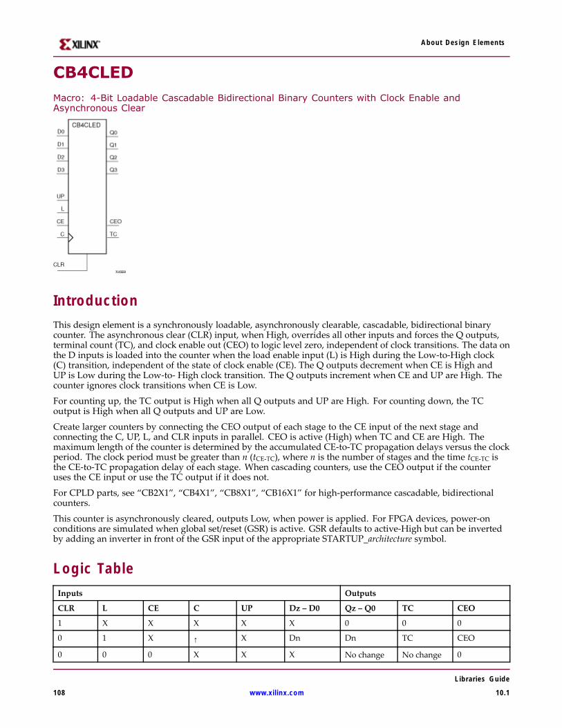
About Design Elements
CB4CLEDMacro: 4-Bit Loadable Cascadable Bidirectional Binary Counters with Clock Enable andAsynchronous Clear
IntroductionThis design element is a synchronously loadable, asynchronously clearable, cascadable, bidirectional binarycounter. The asynchronous clear (CLR) input, when High, overrides all other inputs and forces the Q outputs,terminal count (TC), and clock enable out (CEO) to logic level zero, independent of clock transitions. The data onthe D inputs is loaded into the counter when the load enable input (L) is High during the Low-to-High clock(C) transition, independent of the state of clock enable (CE). The Q outputs decrement when CE is High andUP is Low during the Low-to- High clock transition. The Q outputs increment when CE and UP are High. Thecounter ignores clock transitions when CE is Low.
For counting up, the TC output is High when all Q outputs and UP are High. For counting down, the TCoutput is High when all Q outputs and UP are Low.
Create larger counters by connecting the CEO output of each stage to the CE input of the next stage andconnecting the C, UP, L, and CLR inputs in parallel. CEO is active (High) when TC and CE are High. Themaximum length of the counter is determined by the accumulated CE-to-TC propagation delays versus the clockperiod. The clock period must be greater than n (tCE-TC), where n is the number of stages and the time tCE-TC isthe CE-to-TC propagation delay of each stage. When cascading counters, use the CEO output if the counteruses the CE input or use the TC output if it does not.
For CPLD parts, see “CB2X1”, “CB4X1”, “CB8X1”, “CB16X1” for high-performance cascadable, bidirectionalcounters.
This counter is asynchronously cleared, outputs Low, when power is applied. For FPGA devices, power-onconditions are simulated when global set/reset (GSR) is active. GSR defaults to active-High but can be invertedby adding an inverter in front of the GSR input of the appropriate STARTUP_architecture symbol.
Logic TableInputs Outputs
CLR L CE C UP Dz – D0 Qz – Q0 TC CEO
1 X X X X X 0 0 0
0 1 X ↑ X Dn Dn TC CEO
0 0 0 X X X No change No change 0
Libraries Guide
108 www.xilinx.com 10.1
About Design Elements
Inputs Outputs
CLR L CE C UP Dz – D0 Qz – Q0 TC CEO
0 0 1 ↑ 1 X Inc TC CEO
0 0 1 ↑ 0 X Dec TC CEO
z = bit width - 1
TC = (Qz•Q(z-1)•Q(z-2)•...•Q0•UP) + (Qz•Q(z-1)•Q(z-2)•...•Q0•UP)
CEO = TC•CE
Design Entry MethodThis design element is only for use in schematics.
For More Information• See the Spartan-3A User Guide.
• See the Spartan-3A Data Sheets.
• See the Spartan-3AN FPGA In-System Flash User Guide.
• See the Spartan-3AN Data Sheets.
Libraries Guide
10.1 www.xilinx.com 109
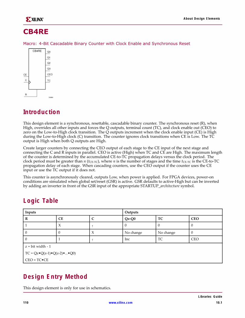
About Design Elements
CB4RE
Macro: 4-Bit Cascadable Binary Counter with Clock Enable and Synchronous Reset
IntroductionThis design element is a synchronous, resettable, cascadable binary counter. The synchronous reset (R), whenHigh, overrides all other inputs and forces the Q outputs, terminal count (TC), and clock enable out (CEO) tozero on the Low-to-High clock transition. The Q outputs increment when the clock enable input (CE) is Highduring the Low-to-High clock (C) transition. The counter ignores clock transitions when CE is Low. The TCoutput is High when both Q outputs are High.
Create larger counters by connecting the CEO output of each stage to the CE input of the next stage andconnecting the C and R inputs in parallel. CEO is active (High) when TC and CE are High. The maximum lengthof the counter is determined by the accumulated CE-to-TC propagation delays versus the clock period. Theclock period must be greater than n (tCE-TC), where n is the number of stages and the time tCE-TC is the CE-to-TCpropagation delay of each stage. When cascading counters, use the CEO output if the counter uses the CEinput or use the TC output if it does not.
This counter is asynchronously cleared, outputs Low, when power is applied. For FPGA devices, power-onconditions are simulated when global set/reset (GSR) is active. GSR defaults to active-High but can be invertedby adding an inverter in front of the GSR input of the appropriate STARTUP_architecture symbol.
Logic TableInputs Outputs
R CE C Qz-Q0 TC CEO
1 X ↑ 0 0 0
0 0 X No change No change 0
0 1 ↑ Inc TC CEO
z = bit width - 1
TC = Qz•Q(z-1)•Q(z-2)•...•Q0)
CEO = TC•CE
Design Entry MethodThis design element is only for use in schematics.
Libraries Guide
110 www.xilinx.com 10.1

About Design Elements
For More Information• See the Spartan-3A User Guide.
• See the Spartan-3A Data Sheets.
• See the Spartan-3AN FPGA In-System Flash User Guide.
• See the Spartan-3AN Data Sheets.
Libraries Guide
10.1 www.xilinx.com 111
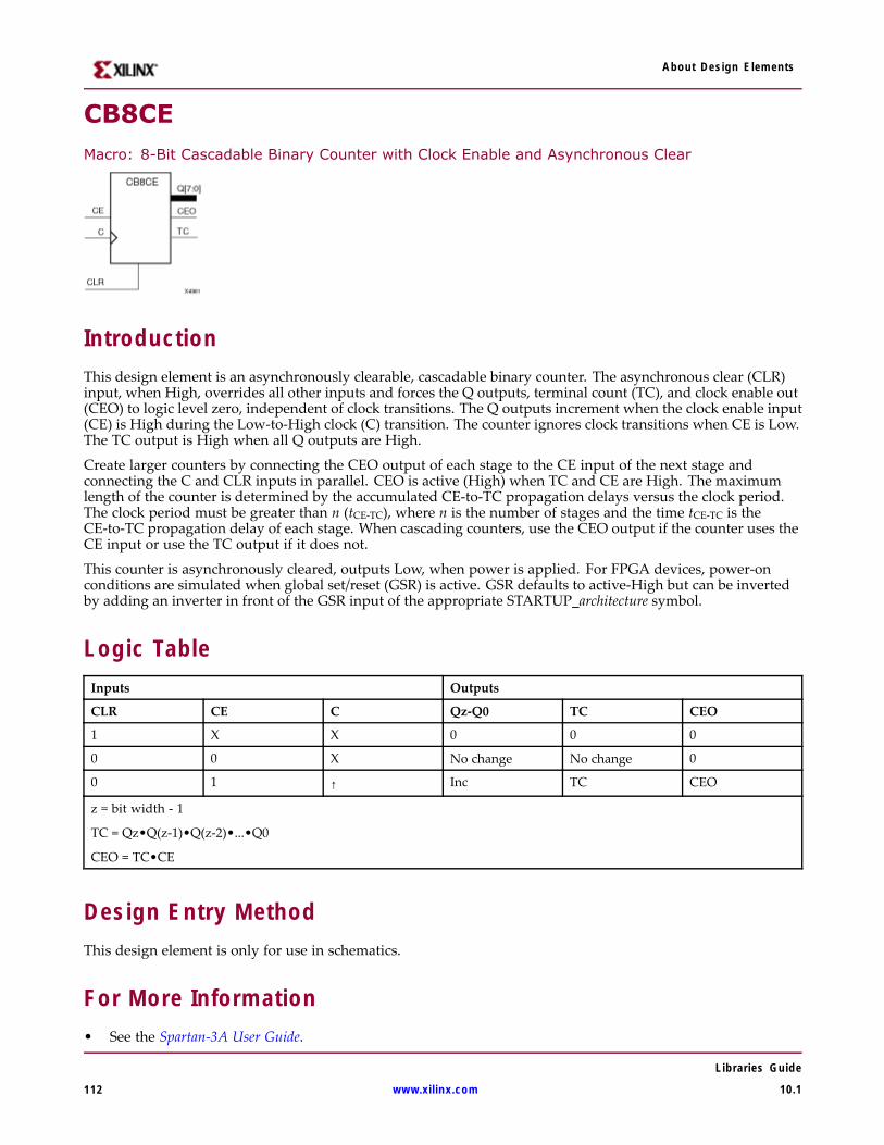
About Design Elements
CB8CEMacro: 8-Bit Cascadable Binary Counter with Clock Enable and Asynchronous Clear
IntroductionThis design element is an asynchronously clearable, cascadable binary counter. The asynchronous clear (CLR)input, when High, overrides all other inputs and forces the Q outputs, terminal count (TC), and clock enable out(CEO) to logic level zero, independent of clock transitions. The Q outputs increment when the clock enable input(CE) is High during the Low-to-High clock (C) transition. The counter ignores clock transitions when CE is Low.The TC output is High when all Q outputs are High.
Create larger counters by connecting the CEO output of each stage to the CE input of the next stage andconnecting the C and CLR inputs in parallel. CEO is active (High) when TC and CE are High. The maximumlength of the counter is determined by the accumulated CE-to-TC propagation delays versus the clock period.The clock period must be greater than n (tCE-TC), where n is the number of stages and the time tCE-TC is theCE-to-TC propagation delay of each stage. When cascading counters, use the CEO output if the counter uses theCE input or use the TC output if it does not.
This counter is asynchronously cleared, outputs Low, when power is applied. For FPGA devices, power-onconditions are simulated when global set/reset (GSR) is active. GSR defaults to active-High but can be invertedby adding an inverter in front of the GSR input of the appropriate STARTUP_architecture symbol.
Logic TableInputs Outputs
CLR CE C Qz-Q0 TC CEO
1 X X 0 0 0
0 0 X No change No change 0
0 1 ↑ Inc TC CEO
z = bit width - 1
TC = Qz•Q(z-1)•Q(z-2)•...•Q0
CEO = TC•CE
Design Entry MethodThis design element is only for use in schematics.
For More Information• See the Spartan-3A User Guide.
Libraries Guide
112 www.xilinx.com 10.1

About Design Elements
• See the Spartan-3A Data Sheets.
• See the Spartan-3AN FPGA In-System Flash User Guide.
• See the Spartan-3AN Data Sheets.
Libraries Guide
10.1 www.xilinx.com 113
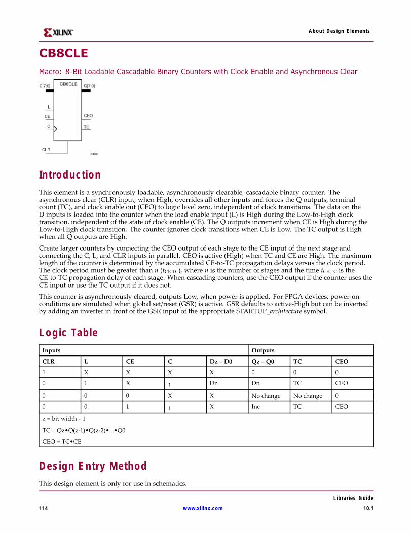
About Design Elements
CB8CLEMacro: 8-Bit Loadable Cascadable Binary Counters with Clock Enable and Asynchronous Clear
IntroductionThis element is a synchronously loadable, asynchronously clearable, cascadable binary counter. Theasynchronous clear (CLR) input, when High, overrides all other inputs and forces the Q outputs, terminalcount (TC), and clock enable out (CEO) to logic level zero, independent of clock transitions. The data on theD inputs is loaded into the counter when the load enable input (L) is High during the Low-to-High clocktransition, independent of the state of clock enable (CE). The Q outputs increment when CE is High during theLow-to-High clock transition. The counter ignores clock transitions when CE is Low. The TC output is Highwhen all Q outputs are High.
Create larger counters by connecting the CEO output of each stage to the CE input of the next stage andconnecting the C, L, and CLR inputs in parallel. CEO is active (High) when TC and CE are High. The maximumlength of the counter is determined by the accumulated CE-to-TC propagation delays versus the clock period.The clock period must be greater than n (tCE-TC), where n is the number of stages and the time tCE-TC is theCE-to-TC propagation delay of each stage. When cascading counters, use the CEO output if the counter uses theCE input or use the TC output if it does not.
This counter is asynchronously cleared, outputs Low, when power is applied. For FPGA devices, power-onconditions are simulated when global set/reset (GSR) is active. GSR defaults to active-High but can be invertedby adding an inverter in front of the GSR input of the appropriate STARTUP_architecture symbol.
Logic TableInputs Outputs
CLR L CE C Dz – D0 Qz – Q0 TC CEO
1 X X X X 0 0 0
0 1 X ↑ Dn Dn TC CEO
0 0 0 X X No change No change 0
0 0 1 ↑ X Inc TC CEO
z = bit width - 1
TC = Qz•Q(z-1)•Q(z-2)•...•Q0
CEO = TC•CE
Design Entry MethodThis design element is only for use in schematics.
Libraries Guide
114 www.xilinx.com 10.1

About Design Elements
For More Information• See the Spartan-3A User Guide.
• See the Spartan-3A Data Sheets.
• See the Spartan-3AN FPGA In-System Flash User Guide.
• See the Spartan-3AN Data Sheets.
Libraries Guide
10.1 www.xilinx.com 115
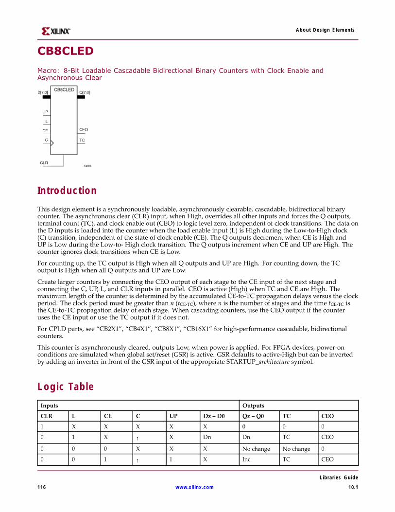
About Design Elements
CB8CLED
Macro: 8-Bit Loadable Cascadable Bidirectional Binary Counters with Clock Enable andAsynchronous Clear
IntroductionThis design element is a synchronously loadable, asynchronously clearable, cascadable, bidirectional binarycounter. The asynchronous clear (CLR) input, when High, overrides all other inputs and forces the Q outputs,terminal count (TC), and clock enable out (CEO) to logic level zero, independent of clock transitions. The data onthe D inputs is loaded into the counter when the load enable input (L) is High during the Low-to-High clock(C) transition, independent of the state of clock enable (CE). The Q outputs decrement when CE is High andUP is Low during the Low-to- High clock transition. The Q outputs increment when CE and UP are High. Thecounter ignores clock transitions when CE is Low.
For counting up, the TC output is High when all Q outputs and UP are High. For counting down, the TCoutput is High when all Q outputs and UP are Low.
Create larger counters by connecting the CEO output of each stage to the CE input of the next stage andconnecting the C, UP, L, and CLR inputs in parallel. CEO is active (High) when TC and CE are High. Themaximum length of the counter is determined by the accumulated CE-to-TC propagation delays versus the clockperiod. The clock period must be greater than n (tCE-TC), where n is the number of stages and the time tCE-TC isthe CE-to-TC propagation delay of each stage. When cascading counters, use the CEO output if the counteruses the CE input or use the TC output if it does not.
For CPLD parts, see “CB2X1”, “CB4X1”, “CB8X1”, “CB16X1” for high-performance cascadable, bidirectionalcounters.
This counter is asynchronously cleared, outputs Low, when power is applied. For FPGA devices, power-onconditions are simulated when global set/reset (GSR) is active. GSR defaults to active-High but can be invertedby adding an inverter in front of the GSR input of the appropriate STARTUP_architecture symbol.
Logic TableInputs Outputs
CLR L CE C UP Dz – D0 Qz – Q0 TC CEO
1 X X X X X 0 0 0
0 1 X ↑ X Dn Dn TC CEO
0 0 0 X X X No change No change 0
0 0 1 ↑ 1 X Inc TC CEO
Libraries Guide
116 www.xilinx.com 10.1

About Design Elements
Inputs Outputs
CLR L CE C UP Dz – D0 Qz – Q0 TC CEO
0 0 1 ↑ 0 X Dec TC CEO
z = bit width - 1
TC = (Qz•Q(z-1)•Q(z-2)•...•Q0•UP) + (Qz•Q(z-1)•Q(z-2)•...•Q0•UP)
CEO = TC•CE
Design Entry MethodThis design element is only for use in schematics.
For More Information• See the Spartan-3A User Guide.
• See the Spartan-3A Data Sheets.
• See the Spartan-3AN FPGA In-System Flash User Guide.
• See the Spartan-3AN Data Sheets.
Libraries Guide
10.1 www.xilinx.com 117
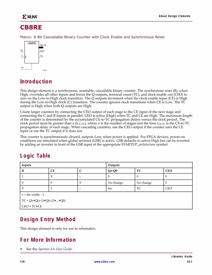
About Design Elements
CB8REMacro: 8-Bit Cascadable Binary Counter with Clock Enable and Synchronous Reset
IntroductionThis design element is a synchronous, resettable, cascadable binary counter. The synchronous reset (R), whenHigh, overrides all other inputs and forces the Q outputs, terminal count (TC), and clock enable out (CEO) tozero on the Low-to-High clock transition. The Q outputs increment when the clock enable input (CE) is Highduring the Low-to-High clock (C) transition. The counter ignores clock transitions when CE is Low. The TCoutput is High when both Q outputs are High.
Create larger counters by connecting the CEO output of each stage to the CE input of the next stage andconnecting the C and R inputs in parallel. CEO is active (High) when TC and CE are High. The maximum lengthof the counter is determined by the accumulated CE-to-TC propagation delays versus the clock period. Theclock period must be greater than n (tCE-TC), where n is the number of stages and the time tCE-TC is the CE-to-TCpropagation delay of each stage. When cascading counters, use the CEO output if the counter uses the CEinput or use the TC output if it does not.
This counter is asynchronously cleared, outputs Low, when power is applied. For FPGA devices, power-onconditions are simulated when global set/reset (GSR) is active. GSR defaults to active-High but can be invertedby adding an inverter in front of the GSR input of the appropriate STARTUP_architecture symbol.
Logic TableInputs Outputs
R CE C Qz-Q0 TC CEO
1 X ↑ 0 0 0
0 0 X No change No change 0
0 1 ↑ Inc TC CEO
z = bit width - 1
TC = Qz•Q(z-1)•Q(z-2)•...•Q0)
CEO = TC•CE
Design Entry MethodThis design element is only for use in schematics.
For More Information• See the Spartan-3A User Guide.
Libraries Guide
118 www.xilinx.com 10.1

About Design Elements
• See the Spartan-3A Data Sheets.
• See the Spartan-3AN FPGA In-System Flash User Guide.
• See the Spartan-3AN Data Sheets.
Libraries Guide
10.1 www.xilinx.com 119
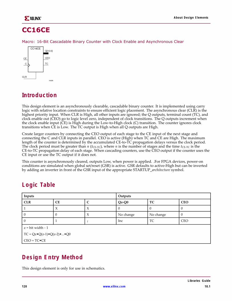
About Design Elements
CC16CE
Macro: 16-Bit Cascadable Binary Counter with Clock Enable and Asynchronous Clear
IntroductionThis design element is an asynchronously clearable, cascadable binary counter. It is implemented using carrylogic with relative location constraints to ensure efficient logic placement. The asynchronous clear (CLR) is thehighest priority input. When CLR is High, all other inputs are ignored; the Q outputs, terminal count (TC), andclock enable out (CEO) go to logic level zero, independent of clock transitions. The Q outputs increment whenthe clock enable input (CE) is High during the Low-to-High clock (C) transition. The counter ignores clocktransitions when CE is Low. The TC output is High when all Q outputs are High.
Create larger counters by connecting the CEO output of each stage to the CE input of the next stage andconnecting the C and CLR inputs in parallel. CEO is active (High) when TC and CE are High. The maximumlength of the counter is determined by the accumulated CE-to-TC propagation delays versus the clock period.The clock period must be greater than n (tCE-TC), where n is the number of stages and the time tCE-TC is theCE-to-TC propagation delay of each stage. When cascading counters, use the CEO output if the counter uses theCE input or use the TC output if it does not.
This counter is asynchronously cleared, outputs Low, when power is applied. .For FPGA devices, power-onconditions are simulated when global set/reset (GSR) is active. GSR defaults to active-High but can be invertedby adding an inverter in front of the GSR input of the appropriate STARTUP_architecture symbol.
Logic TableInputs Outputs
CLR CE C Qz-Q0 TC CEO
1 X X 0 0 0
0 0 X No change No change 0
0 1 ↑ Inc TC CEO
z = bit width - 1
TC = Qz•Q(z-1)•Q(z-2)•...•Q0
CEO = TC•CE
Design Entry MethodThis design element is only for use in schematics.
Libraries Guide
120 www.xilinx.com 10.1

About Design Elements
For More Information• See the Spartan-3A User Guide.
• See the Spartan-3A Data Sheets.
• See the Spartan-3AN FPGA In-System Flash User Guide.
• See the Spartan-3AN Data Sheets.
Libraries Guide
10.1 www.xilinx.com 121
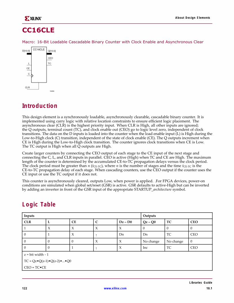
About Design Elements
CC16CLE
Macro: 16-Bit Loadable Cascadable Binary Counter with Clock Enable and Asynchronous Clear
IntroductionThis design element is a synchronously loadable, asynchronously clearable, cascadable binary counter. It isimplemented using carry logic with relative location constraints to ensure efficient logic placement. Theasynchronous clear (CLR) is the highest priority input. When CLR is High, all other inputs are ignored;the Q outputs, terminal count (TC), and clock enable out (CEO) go to logic level zero, independent of clocktransitions. The data on the D inputs is loaded into the counter when the load enable input (L) is High during theLow-to-High clock (C) transition, independent of the state of clock enable (CE). The Q outputs increment whenCE is High during the Low-to-High clock transition. The counter ignores clock transitions when CE is Low.The TC output is High when all Q outputs are High.
Create larger counters by connecting the CEO output of each stage to the CE input of the next stage andconnecting the C, L, and CLR inputs in parallel. CEO is active (High) when TC and CE are High. The maximumlength of the counter is determined by the accumulated CE-to-TC propagation delays versus the clock period.The clock period must be greater than n (tCE-TC), where n is the number of stages and the time tCE-TC is theCE-to-TC propagation delay of each stage. When cascading counters, use the CEO output if the counter uses theCE input or use the TC output if it does not.
This counter is asynchronously cleared, outputs Low, when power is applied. .For FPGA devices, power-onconditions are simulated when global set/reset (GSR) is active. GSR defaults to active-High but can be invertedby adding an inverter in front of the GSR input of the appropriate STARTUP_architecture symbol.
Logic TableInputs Outputs
CLR L CE C Dz – D0 Qz – Q0 TC CEO
1 X X X X 0 0 0
0 1 X ↑ Dn Dn TC CEO
0 0 0 X X No change No change 0
0 0 1 ↑ X Inc TC CEO
z = bit width - 1
TC = Qz•Q(z-1)•Q(z-2)•...•Q0
CEO = TC•CE
Libraries Guide
122 www.xilinx.com 10.1
About Design Elements
Design Entry MethodThis design element is only for use in schematics.
For More Information• See the Spartan-3A User Guide.
• See the Spartan-3A Data Sheets.
• See the Spartan-3AN FPGA In-System Flash User Guide.
• See the Spartan-3AN Data Sheets.
Libraries Guide
10.1 www.xilinx.com 123
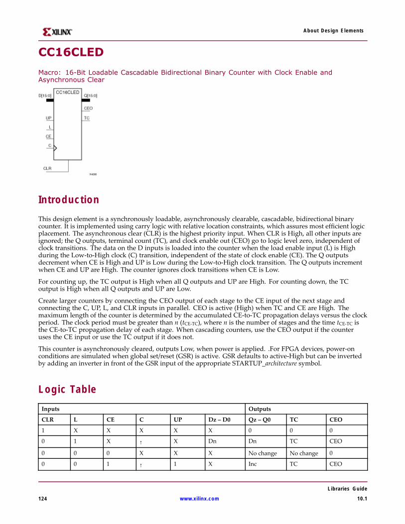
About Design Elements
CC16CLED
Macro: 16-Bit Loadable Cascadable Bidirectional Binary Counter with Clock Enable andAsynchronous Clear
IntroductionThis design element is a synchronously loadable, asynchronously clearable, cascadable, bidirectional binarycounter. It is implemented using carry logic with relative location constraints, which assures most efficient logicplacement. The asynchronous clear (CLR) is the highest priority input. When CLR is High, all other inputs areignored; the Q outputs, terminal count (TC), and clock enable out (CEO) go to logic level zero, independent ofclock transitions. The data on the D inputs is loaded into the counter when the load enable input (L) is Highduring the Low-to-High clock (C) transition, independent of the state of clock enable (CE). The Q outputsdecrement when CE is High and UP is Low during the Low-to-High clock transition. The Q outputs incrementwhen CE and UP are High. The counter ignores clock transitions when CE is Low.
For counting up, the TC output is High when all Q outputs and UP are High. For counting down, the TCoutput is High when all Q outputs and UP are Low.
Create larger counters by connecting the CEO output of each stage to the CE input of the next stage andconnecting the C, UP, L, and CLR inputs in parallel. CEO is active (High) when TC and CE are High. Themaximum length of the counter is determined by the accumulated CE-to-TC propagation delays versus the clockperiod. The clock period must be greater than n (tCE-TC), where n is the number of stages and the time tCE-TC isthe CE-to-TC propagation delay of each stage. When cascading counters, use the CEO output if the counteruses the CE input or use the TC output if it does not.
This counter is asynchronously cleared, outputs Low, when power is applied. .For FPGA devices, power-onconditions are simulated when global set/reset (GSR) is active. GSR defaults to active-High but can be invertedby adding an inverter in front of the GSR input of the appropriate STARTUP_architecture symbol.
Logic TableInputs Outputs
CLR L CE C UP Dz – D0 Qz – Q0 TC CEO
1 X X X X X 0 0 0
0 1 X ↑ X Dn Dn TC CEO
0 0 0 X X X No change No change 0
0 0 1 ↑ 1 X Inc TC CEO
Libraries Guide
124 www.xilinx.com 10.1

About Design Elements
Inputs Outputs
CLR L CE C UP Dz – D0 Qz – Q0 TC CEO
0 0 1 ↑ 0 X Dec TC CEO
z = bit width - 1
TC = (Qz•Q(z-1)•Q(z-2)•...•Q0•UP) + (Qz•Q(z-1)•Q(z-2)•...•Q0•UP)
CEO = TC•CE
Design Entry MethodThis design element is only for use in schematics.
For More Information• See the Spartan-3A User Guide.
• See the Spartan-3A Data Sheets.
• See the Spartan-3AN FPGA In-System Flash User Guide.
• See the Spartan-3AN Data Sheets.
Libraries Guide
10.1 www.xilinx.com 125
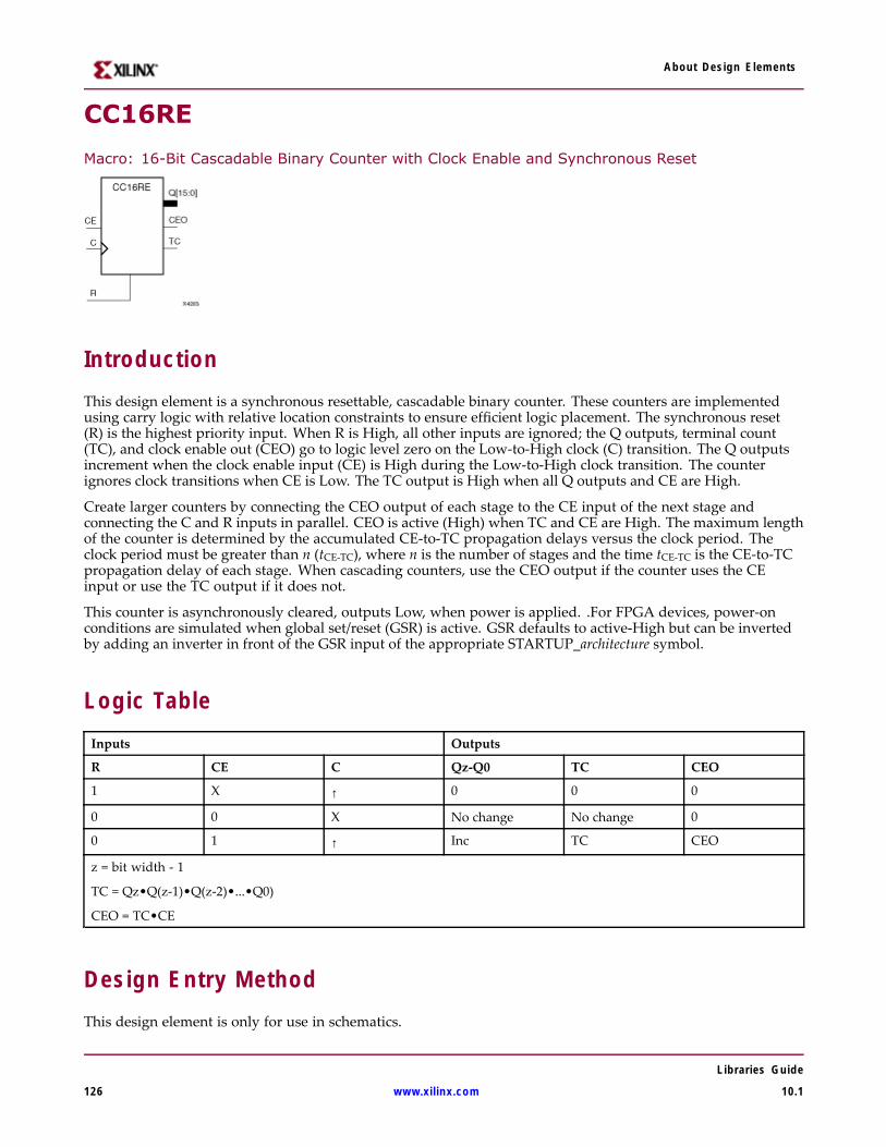
About Design Elements
CC16RE
Macro: 16-Bit Cascadable Binary Counter with Clock Enable and Synchronous Reset
IntroductionThis design element is a synchronous resettable, cascadable binary counter. These counters are implementedusing carry logic with relative location constraints to ensure efficient logic placement. The synchronous reset(R) is the highest priority input. When R is High, all other inputs are ignored; the Q outputs, terminal count(TC), and clock enable out (CEO) go to logic level zero on the Low-to-High clock (C) transition. The Q outputsincrement when the clock enable input (CE) is High during the Low-to-High clock transition. The counterignores clock transitions when CE is Low. The TC output is High when all Q outputs and CE are High.
Create larger counters by connecting the CEO output of each stage to the CE input of the next stage andconnecting the C and R inputs in parallel. CEO is active (High) when TC and CE are High. The maximum lengthof the counter is determined by the accumulated CE-to-TC propagation delays versus the clock period. Theclock period must be greater than n (tCE-TC), where n is the number of stages and the time tCE-TC is the CE-to-TCpropagation delay of each stage. When cascading counters, use the CEO output if the counter uses the CEinput or use the TC output if it does not.
This counter is asynchronously cleared, outputs Low, when power is applied. .For FPGA devices, power-onconditions are simulated when global set/reset (GSR) is active. GSR defaults to active-High but can be invertedby adding an inverter in front of the GSR input of the appropriate STARTUP_architecture symbol.
Logic TableInputs Outputs
R CE C Qz-Q0 TC CEO
1 X ↑ 0 0 0
0 0 X No change No change 0
0 1 ↑ Inc TC CEO
z = bit width - 1
TC = Qz•Q(z-1)•Q(z-2)•...•Q0)
CEO = TC•CE
Design Entry MethodThis design element is only for use in schematics.
Libraries Guide
126 www.xilinx.com 10.1

About Design Elements
For More Information• See the Spartan-3A User Guide.
• See the Spartan-3A Data Sheets.
• See the Spartan-3AN FPGA In-System Flash User Guide.
• See the Spartan-3AN Data Sheets.
Libraries Guide
10.1 www.xilinx.com 127
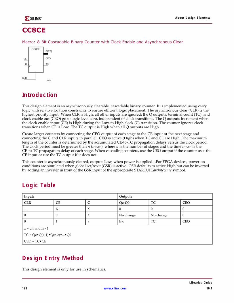
About Design Elements
CC8CE
Macro: 8-Bit Cascadable Binary Counter with Clock Enable and Asynchronous Clear
IntroductionThis design element is an asynchronously clearable, cascadable binary counter. It is implemented using carrylogic with relative location constraints to ensure efficient logic placement. The asynchronous clear (CLR) is thehighest priority input. When CLR is High, all other inputs are ignored; the Q outputs, terminal count (TC), andclock enable out (CEO) go to logic level zero, independent of clock transitions. The Q outputs increment whenthe clock enable input (CE) is High during the Low-to-High clock (C) transition. The counter ignores clocktransitions when CE is Low. The TC output is High when all Q outputs are High.
Create larger counters by connecting the CEO output of each stage to the CE input of the next stage andconnecting the C and CLR inputs in parallel. CEO is active (High) when TC and CE are High. The maximumlength of the counter is determined by the accumulated CE-to-TC propagation delays versus the clock period.The clock period must be greater than n (tCE-TC), where n is the number of stages and the time tCE-TC is theCE-to-TC propagation delay of each stage. When cascading counters, use the CEO output if the counter uses theCE input or use the TC output if it does not.
This counter is asynchronously cleared, outputs Low, when power is applied. .For FPGA devices, power-onconditions are simulated when global set/reset (GSR) is active. GSR defaults to active-High but can be invertedby adding an inverter in front of the GSR input of the appropriate STARTUP_architecture symbol.
Logic TableInputs Outputs
CLR CE C Qz-Q0 TC CEO
1 X X 0 0 0
0 0 X No change No change 0
0 1 ↑ Inc TC CEO
z = bit width - 1
TC = Qz•Q(z-1)•Q(z-2)•...•Q0
CEO = TC•CE
Design Entry MethodThis design element is only for use in schematics.
Libraries Guide
128 www.xilinx.com 10.1

About Design Elements
For More Information• See the Spartan-3A User Guide.
• See the Spartan-3A Data Sheets.
• See the Spartan-3AN FPGA In-System Flash User Guide.
• See the Spartan-3AN Data Sheets.
Libraries Guide
10.1 www.xilinx.com 129
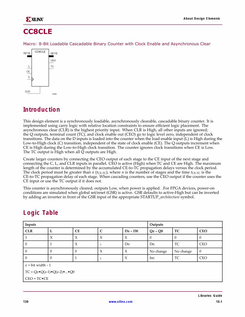
About Design Elements
CC8CLE
Macro: 8-Bit Loadable Cascadable Binary Counter with Clock Enable and Asynchronous Clear
IntroductionThis design element is a synchronously loadable, asynchronously clearable, cascadable binary counter. It isimplemented using carry logic with relative location constraints to ensure efficient logic placement. Theasynchronous clear (CLR) is the highest priority input. When CLR is High, all other inputs are ignored;the Q outputs, terminal count (TC), and clock enable out (CEO) go to logic level zero, independent of clocktransitions. The data on the D inputs is loaded into the counter when the load enable input (L) is High during theLow-to-High clock (C) transition, independent of the state of clock enable (CE). The Q outputs increment whenCE is High during the Low-to-High clock transition. The counter ignores clock transitions when CE is Low.The TC output is High when all Q outputs are High.
Create larger counters by connecting the CEO output of each stage to the CE input of the next stage andconnecting the C, L, and CLR inputs in parallel. CEO is active (High) when TC and CE are High. The maximumlength of the counter is determined by the accumulated CE-to-TC propagation delays versus the clock period.The clock period must be greater than n (tCE-TC), where n is the number of stages and the time tCE-TC is theCE-to-TC propagation delay of each stage. When cascading counters, use the CEO output if the counter uses theCE input or use the TC output if it does not.
This counter is asynchronously cleared, outputs Low, when power is applied. .For FPGA devices, power-onconditions are simulated when global set/reset (GSR) is active. GSR defaults to active-High but can be invertedby adding an inverter in front of the GSR input of the appropriate STARTUP_architecture symbol.
Logic TableInputs Outputs
CLR L CE C Dz – D0 Qz – Q0 TC CEO
1 X X X X 0 0 0
0 1 X ↑ Dn Dn TC CEO
0 0 0 X X No change No change 0
0 0 1 ↑ X Inc TC CEO
z = bit width - 1
TC = Qz•Q(z-1)•Q(z-2)•...•Q0
CEO = TC•CE
Libraries Guide
130 www.xilinx.com 10.1

About Design Elements
Design Entry MethodThis design element is only for use in schematics.
For More Information• See the Spartan-3A User Guide.
• See the Spartan-3A Data Sheets.
• See the Spartan-3AN FPGA In-System Flash User Guide.
• See the Spartan-3AN Data Sheets.
Libraries Guide
10.1 www.xilinx.com 131

About Design Elements
CC8CLED
Macro: 8-Bit Loadable Cascadable Bidirectional Binary Counter with Clock Enable andAsynchronous Clear
IntroductionThis design element is a synchronously loadable, asynchronously clearable, cascadable, bidirectional binarycounter. It is implemented using carry logic with relative location constraints, which assures most efficient logicplacement. The asynchronous clear (CLR) is the highest priority input. When CLR is High, all other inputs areignored; the Q outputs, terminal count (TC), and clock enable out (CEO) go to logic level zero, independent ofclock transitions. The data on the D inputs is loaded into the counter when the load enable input (L) is Highduring the Low-to-High clock (C) transition, independent of the state of clock enable (CE). The Q outputsdecrement when CE is High and UP is Low during the Low-to-High clock transition. The Q outputs incrementwhen CE and UP are High. The counter ignores clock transitions when CE is Low.
For counting up, the TC output is High when all Q outputs and UP are High. For counting down, the TCoutput is High when all Q outputs and UP are Low.
Create larger counters by connecting the CEO output of each stage to the CE input of the next stage andconnecting the C, UP, L, and CLR inputs in parallel. CEO is active (High) when TC and CE are High. Themaximum length of the counter is determined by the accumulated CE-to-TC propagation delays versus the clockperiod. The clock period must be greater than n (tCE-TC), where n is the number of stages and the time tCE-TC isthe CE-to-TC propagation delay of each stage. When cascading counters, use the CEO output if the counteruses the CE input or use the TC output if it does not.
This counter is asynchronously cleared, outputs Low, when power is applied. .For FPGA devices, power-onconditions are simulated when global set/reset (GSR) is active. GSR defaults to active-High but can be invertedby adding an inverter in front of the GSR input of the appropriate STARTUP_architecture symbol.
Logic TableInputs Outputs
CLR L CE C UP Dz – D0 Qz – Q0 TC CEO
1 X X X X X 0 0 0
0 1 X ↑ X Dn Dn TC CEO
0 0 0 X X X No change No change 0
0 0 1 ↑ 1 X Inc TC CEO
Libraries Guide
132 www.xilinx.com 10.1

About Design Elements
Inputs Outputs
CLR L CE C UP Dz – D0 Qz – Q0 TC CEO
0 0 1 ↑ 0 X Dec TC CEO
z = bit width - 1
TC = (Qz•Q(z-1)•Q(z-2)•...•Q0•UP) + (Qz•Q(z-1)•Q(z-2)•...•Q0•UP)
CEO = TC•CE
Design Entry MethodThis design element is only for use in schematics.
For More Information• See the Spartan-3A User Guide.
• See the Spartan-3A Data Sheets.
• See the Spartan-3AN FPGA In-System Flash User Guide.
• See the Spartan-3AN Data Sheets.
Libraries Guide
10.1 www.xilinx.com 133

About Design Elements
CC8RE
Macro: 8-Bit Cascadable Binary Counter with Clock Enable and Synchronous Reset
IntroductionThis design element is a synchronous resettable, cascadable binary counter. These counters are implementedusing carry logic with relative location constraints to ensure efficient logic placement. The synchronous reset(R) is the highest priority input. When R is High, all other inputs are ignored; the Q outputs, terminal count(TC), and clock enable out (CEO) go to logic level zero on the Low-to-High clock (C) transition. The Q outputsincrement when the clock enable input (CE) is High during the Low-to-High clock transition. The counterignores clock transitions when CE is Low. The TC output is High when all Q outputs and CE are High.
Create larger counters by connecting the CEO output of each stage to the CE input of the next stage andconnecting the C and R inputs in parallel. CEO is active (High) when TC and CE are High. The maximum lengthof the counter is determined by the accumulated CE-to-TC propagation delays versus the clock period. Theclock period must be greater than n (tCE-TC), where n is the number of stages and the time tCE-TC is the CE-to-TCpropagation delay of each stage. When cascading counters, use the CEO output if the counter uses the CEinput or use the TC output if it does not.
This counter is asynchronously cleared, outputs Low, when power is applied. .For FPGA devices, power-onconditions are simulated when global set/reset (GSR) is active. GSR defaults to active-High but can be invertedby adding an inverter in front of the GSR input of the appropriate STARTUP_architecture symbol.
Logic TableInputs Outputs
R CE C Qz-Q0 TC CEO
1 X ↑ 0 0 0
0 0 X No change No change 0
0 1 ↑ Inc TC CEO
z = bit width - 1
TC = Qz•Q(z-1)•Q(z-2)•...•Q0)
CEO = TC•CE
Design Entry MethodThis design element is only for use in schematics.
Libraries Guide
134 www.xilinx.com 10.1

About Design Elements
For More Information• See the Spartan-3A User Guide.
• See the Spartan-3A Data Sheets.
• See the Spartan-3AN FPGA In-System Flash User Guide.
• See the Spartan-3AN Data Sheets.
Libraries Guide
10.1 www.xilinx.com 135
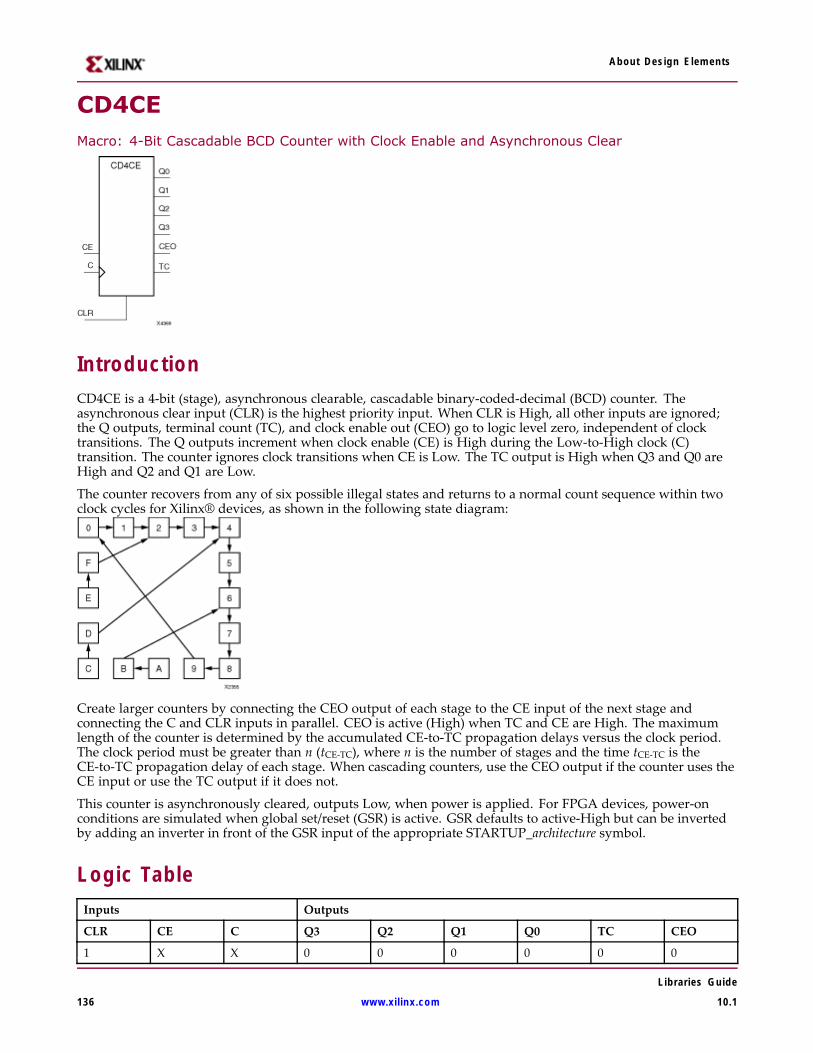
About Design Elements
CD4CEMacro: 4-Bit Cascadable BCD Counter with Clock Enable and Asynchronous Clear
IntroductionCD4CE is a 4-bit (stage), asynchronous clearable, cascadable binary-coded-decimal (BCD) counter. Theasynchronous clear input (CLR) is the highest priority input. When CLR is High, all other inputs are ignored;the Q outputs, terminal count (TC), and clock enable out (CEO) go to logic level zero, independent of clocktransitions. The Q outputs increment when clock enable (CE) is High during the Low-to-High clock (C)transition. The counter ignores clock transitions when CE is Low. The TC output is High when Q3 and Q0 areHigh and Q2 and Q1 are Low.
The counter recovers from any of six possible illegal states and returns to a normal count sequence within twoclock cycles for Xilinx® devices, as shown in the following state diagram:
Create larger counters by connecting the CEO output of each stage to the CE input of the next stage andconnecting the C and CLR inputs in parallel. CEO is active (High) when TC and CE are High. The maximumlength of the counter is determined by the accumulated CE-to-TC propagation delays versus the clock period.The clock period must be greater than n (tCE-TC), where n is the number of stages and the time tCE-TC is theCE-to-TC propagation delay of each stage. When cascading counters, use the CEO output if the counter uses theCE input or use the TC output if it does not.
This counter is asynchronously cleared, outputs Low, when power is applied. For FPGA devices, power-onconditions are simulated when global set/reset (GSR) is active. GSR defaults to active-High but can be invertedby adding an inverter in front of the GSR input of the appropriate STARTUP_architecture symbol.
Logic TableInputs Outputs
CLR CE C Q3 Q2 Q1 Q0 TC CEO
1 X X 0 0 0 0 0 0
Libraries Guide
136 www.xilinx.com 10.1
About Design Elements
Inputs Outputs
CLR CE C Q3 Q2 Q1 Q0 TC CEO
0 1 ↑ Inc Inc Inc Inc TC CEO
0 0 X No Change No Change No Change No Change TC 0
0 1 X 1 0 0 1 1 1
TC = Q3•!Q2•!Q1•Q0
CEO = TC•CE
Design Entry MethodThis design element is only for use in schematics.
For More Information• See the Spartan-3A User Guide.
• See the Spartan-3A Data Sheets.
• See the Spartan-3AN FPGA In-System Flash User Guide.
• See the Spartan-3AN Data Sheets.
Libraries Guide
10.1 www.xilinx.com 137
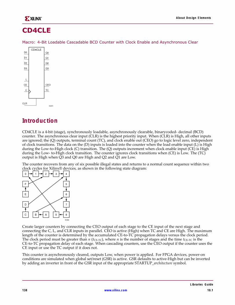
About Design Elements
CD4CLE
Macro: 4-Bit Loadable Cascadable BCD Counter with Clock Enable and Asynchronous Clear
IntroductionCD4CLE is a 4-bit (stage), synchronously loadable, asynchronously clearable, binarycoded- decimal (BCD)counter. The asynchronous clear input (CLR) is the highest priority input. When (CLR) is High, all other inputsare ignored; the (Q) outputs, terminal count (TC), and clock enable out (CEO) go to logic level zero, independentof clock transitions. The data on the (D) inputs is loaded into the counter when the load enable input (L) is Highduring the Low-to-High clock (C) transition. The (Q) outputs increment when clock enable input (CE) is Highduring the Low- to-High clock transition. The counter ignores clock transitions when (CE) is Low. The (TC)output is High when Q3 and Q0 are High and Q2 and Q1 are Low.
The counter recovers from any of six possible illegal states and returns to a normal count sequence within twoclock cycles for Xilinx® devices, as shown in the following state diagram:
Create larger counters by connecting the CEO output of each stage to the CE input of the next stage andconnecting the C, L, and CLR inputs in parallel. CEO is active (High) when TC and CE are High. The maximumlength of the counter is determined by the accumulated CE-to-TC propagation delays versus the clock period.The clock period must be greater than n (tCE-TC), where n is the number of stages and the time tCE-TC is theCE-to-TC propagation delay of each stage. When cascading counters, use the CEO output if the counter uses theCE input or use the TC output if it does not.
This counter is asynchronously cleared, outputs Low, when power is applied. For FPGA devices, power-onconditions are simulated when global set/reset (GSR) is active. GSR defaults to active-High but can be invertedby adding an inverter in front of the GSR input of the appropriate STARTUP_architecture symbol.
Libraries Guide
138 www.xilinx.com 10.1
About Design Elements
Logic TableInputs Outputs
CLR L CE D3 – D0 C Q3 Q2 Q1 Q0 TC CEO
1 X X X X 0 0 0 0 0 0
0 1 X D3 – D0 ↑ D3 D2 D1 D0 TC CEO
0 0 1 X ↑ Inc Inc Inc Inc TC CEO
0 0 0 X X NoChange
NoChange
NoChange
NoChange
TC 0
0 0 1 X X 1 0 0 1 1 1
TC = Q3•!Q2•!Q1•Q0
CEO = TC•CE
Design Entry MethodThis design element is only for use in schematics.
For More Information• See the Spartan-3A User Guide.
• See the Spartan-3A Data Sheets.
• See the Spartan-3AN FPGA In-System Flash User Guide.
• See the Spartan-3AN Data Sheets.
Libraries Guide
10.1 www.xilinx.com 139
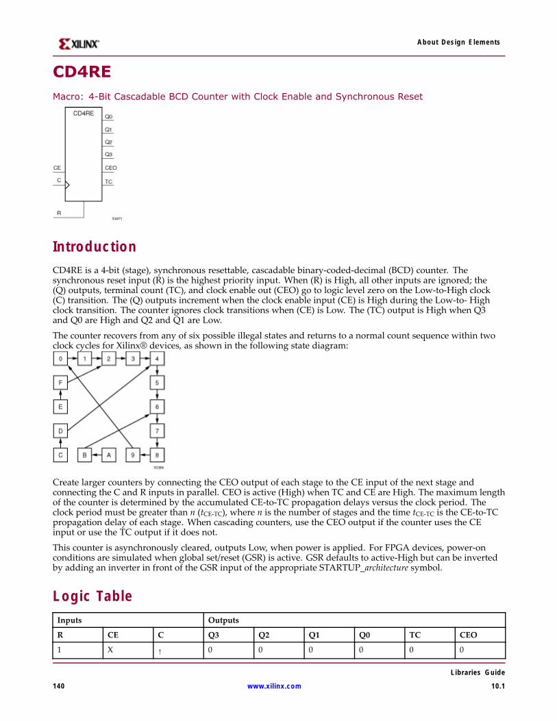
About Design Elements
CD4REMacro: 4-Bit Cascadable BCD Counter with Clock Enable and Synchronous Reset
IntroductionCD4RE is a 4-bit (stage), synchronous resettable, cascadable binary-coded-decimal (BCD) counter. Thesynchronous reset input (R) is the highest priority input. When (R) is High, all other inputs are ignored; the(Q) outputs, terminal count (TC), and clock enable out (CEO) go to logic level zero on the Low-to-High clock(C) transition. The (Q) outputs increment when the clock enable input (CE) is High during the Low-to- Highclock transition. The counter ignores clock transitions when (CE) is Low. The (TC) output is High when Q3and Q0 are High and Q2 and Q1 are Low.
The counter recovers from any of six possible illegal states and returns to a normal count sequence within twoclock cycles for Xilinx® devices, as shown in the following state diagram:
Create larger counters by connecting the CEO output of each stage to the CE input of the next stage andconnecting the C and R inputs in parallel. CEO is active (High) when TC and CE are High. The maximum lengthof the counter is determined by the accumulated CE-to-TC propagation delays versus the clock period. Theclock period must be greater than n (tCE-TC), where n is the number of stages and the time tCE-TC is the CE-to-TCpropagation delay of each stage. When cascading counters, use the CEO output if the counter uses the CEinput or use the TC output if it does not.
This counter is asynchronously cleared, outputs Low, when power is applied. For FPGA devices, power-onconditions are simulated when global set/reset (GSR) is active. GSR defaults to active-High but can be invertedby adding an inverter in front of the GSR input of the appropriate STARTUP_architecture symbol.
Logic TableInputs Outputs
R CE C Q3 Q2 Q1 Q0 TC CEO
1 X ↑ 0 0 0 0 0 0
Libraries Guide
140 www.xilinx.com 10.1
About Design Elements
Inputs Outputs
R CE C Q3 Q2 Q1 Q0 TC CEO
0 1 ↑ Inc Inc Inc Inc TC CEO
0 0 X No Change No Change No Change No Change TC 0
0 1 X 1 0 0 1 1 1
TC = Q3•!Q2•!Q1•Q0
CEO = TC•CE
Design Entry MethodThis design element is only for use in schematics.
For More Information• See the Spartan-3A User Guide.
• See the Spartan-3A Data Sheets.
• See the Spartan-3AN FPGA In-System Flash User Guide.
• See the Spartan-3AN Data Sheets.
Libraries Guide
10.1 www.xilinx.com 141
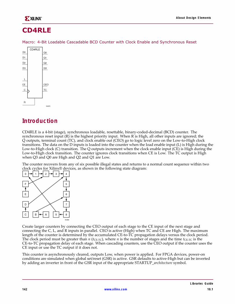
About Design Elements
CD4RLE
Macro: 4-Bit Loadable Cascadable BCD Counter with Clock Enable and Synchronous Reset
IntroductionCD4RLE is a 4-bit (stage), synchronous loadable, resettable, binary-coded-decimal (BCD) counter. Thesynchronous reset input (R) is the highest priority input. When R is High, all other inputs are ignored; theQ outputs, terminal count (TC), and clock enable out (CEO) go to logic level zero on the Low-to-High clocktransitions. The data on the D inputs is loaded into the counter when the load enable input (L) is High during theLow-to-High clock (C) transition. The Q outputs increment when the clock enable input (CE) is High during theLow-to-High clock transition. The counter ignores clock transitions when CE is Low. The TC output is Highwhen Q3 and Q0 are High and Q2 and Q1 are Low.
The counter recovers from any of six possible illegal states and returns to a normal count sequence within twoclock cycles for Xilinx® devices, as shown in the following state diagram:
Create larger counters by connecting the CEO output of each stage to the CE input of the next stage andconnecting the C, L, and R inputs in parallel. CEO is active (High) when TC and CE are High. The maximumlength of the counter is determined by the accumulated CE-to-TC propagation delays versus the clock period.The clock period must be greater than n (tCE-TC), where n is the number of stages and the time tCE-TC is theCE-to-TC propagation delay of each stage. When cascading counters, use the CEO output if the counter uses theCE input or use the TC output if it does not.
This counter is asynchronously cleared, outputs Low, when power is applied. For FPGA devices, power-onconditions are simulated when global set/reset (GSR) is active. GSR defaults to active-High but can be invertedby adding an inverter in front of the GSR input of the appropriate STARTUP_architecture symbol.
Libraries Guide
142 www.xilinx.com 10.1
About Design Elements
Logic TableInputs Outputs
R L CE D3 – D0 C Q3 Q2 Q1 Q0 TC CEO
1 X X X ↑ 0 0 0 0 0 0
0 1 X D3 – D0 ↑ D3 D D D0 TC CEO
0 0 1 X ↑ Inc Inc Inc Inc TC CEO
0 0 0 X X No Change NoChange
NoChange
NoChange
TC 0
0 0 1 X X 1 0 0 1 1 1
TC = Q3•!Q2•!Q1•Q0
CEO = TC•CE
Design Entry MethodThis design element is only for use in schematics.
For More Information• See the Spartan-3A User Guide.
• See the Spartan-3A Data Sheets.
• See the Spartan-3AN FPGA In-System Flash User Guide.
• See the Spartan-3AN Data Sheets.
Libraries Guide
10.1 www.xilinx.com 143
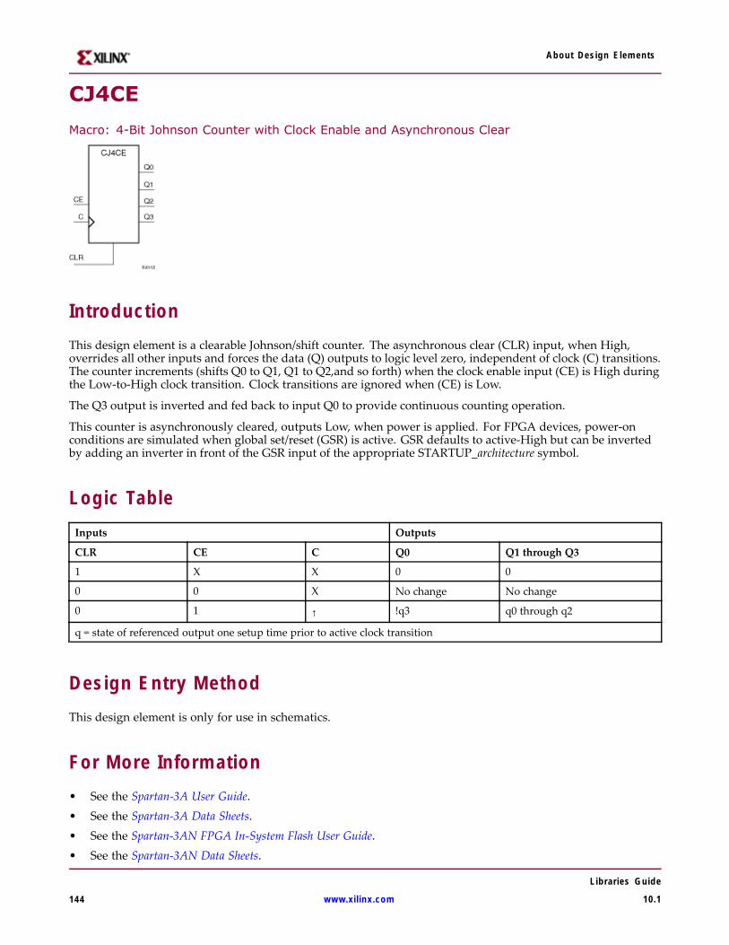
About Design Elements
CJ4CE
Macro: 4-Bit Johnson Counter with Clock Enable and Asynchronous Clear
IntroductionThis design element is a clearable Johnson/shift counter. The asynchronous clear (CLR) input, when High,overrides all other inputs and forces the data (Q) outputs to logic level zero, independent of clock (C) transitions.The counter increments (shifts Q0 to Q1, Q1 to Q2,and so forth) when the clock enable input (CE) is High duringthe Low-to-High clock transition. Clock transitions are ignored when (CE) is Low.
The Q3 output is inverted and fed back to input Q0 to provide continuous counting operation.
This counter is asynchronously cleared, outputs Low, when power is applied. For FPGA devices, power-onconditions are simulated when global set/reset (GSR) is active. GSR defaults to active-High but can be invertedby adding an inverter in front of the GSR input of the appropriate STARTUP_architecture symbol.
Logic TableInputs Outputs
CLR CE C Q0 Q1 through Q3
1 X X 0 0
0 0 X No change No change
0 1 ↑ !q3 q0 through q2
q = state of referenced output one setup time prior to active clock transition
Design Entry MethodThis design element is only for use in schematics.
For More Information• See the Spartan-3A User Guide.• See the Spartan-3A Data Sheets.• See the Spartan-3AN FPGA In-System Flash User Guide.• See the Spartan-3AN Data Sheets.
Libraries Guide
144 www.xilinx.com 10.1
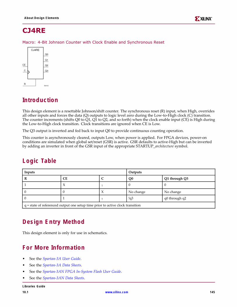
About Design Elements
CJ4RE
Macro: 4-Bit Johnson Counter with Clock Enable and Synchronous Reset
IntroductionThis design element is a resettable Johnson/shift counter. The synchronous reset (R) input, when High, overridesall other inputs and forces the data (Q) outputs to logic level zero during the Low-to-High clock (C) transition.The counter increments (shifts Q0 to Q1, Q1 to Q2, and so forth) when the clock enable input (CE) is High duringthe Low-to-High clock transition. Clock transitions are ignored when CE is Low.
The Q3 output is inverted and fed back to input Q0 to provide continuous counting operation.
This counter is asynchronously cleared, outputs Low, when power is applied. For FPGA devices, power-onconditions are simulated when global set/reset (GSR) is active. GSR defaults to active-High but can be invertedby adding an inverter in front of the GSR input of the appropriate STARTUP_architecture symbol.
Logic TableInputs Outputs
R CE C Q0 Q1 through Q3
1 X ↑ 0 0
0 0 X No change No change
0 1 ↑ !q3 q0 through q2
q = state of referenced output one setup time prior to active clock transition
Design Entry MethodThis design element is only for use in schematics.
For More Information• See the Spartan-3A User Guide.• See the Spartan-3A Data Sheets.• See the Spartan-3AN FPGA In-System Flash User Guide.• See the Spartan-3AN Data Sheets.
Libraries Guide
10.1 www.xilinx.com 145
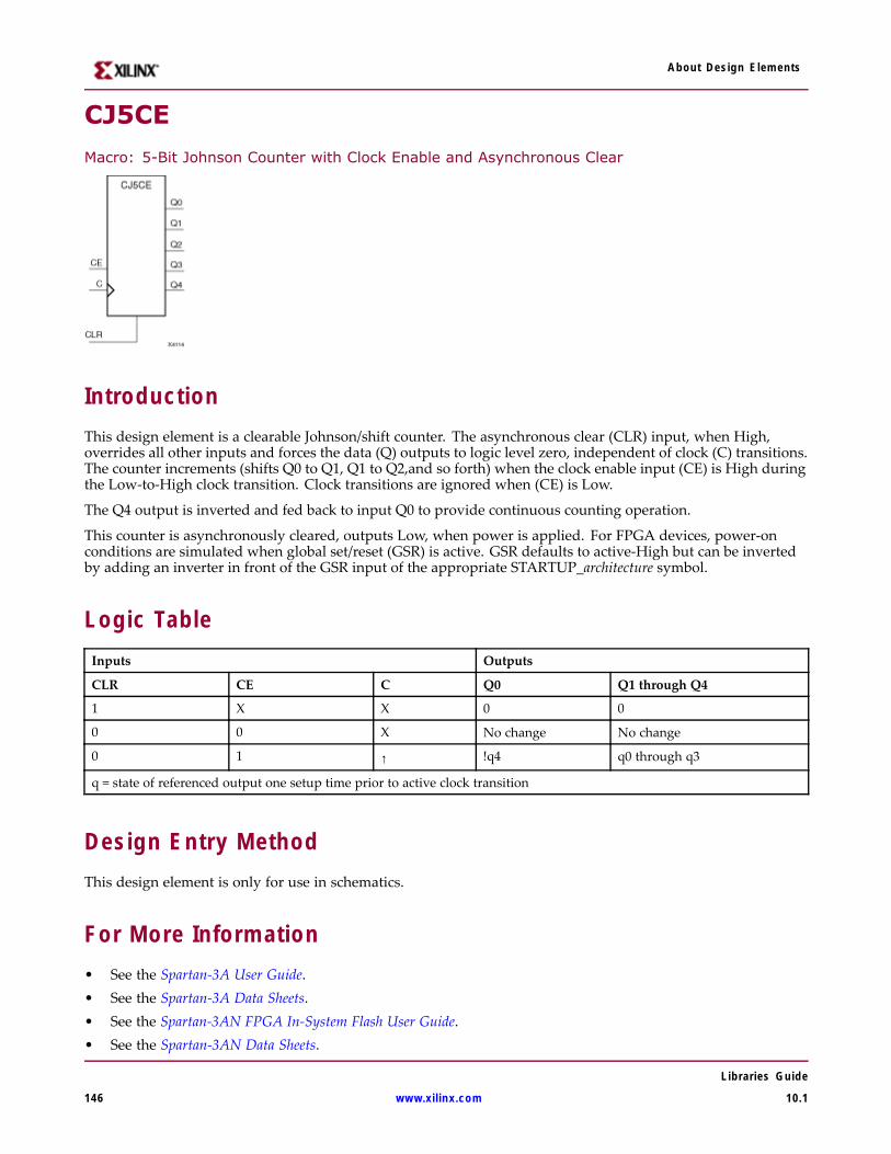
About Design Elements
CJ5CE
Macro: 5-Bit Johnson Counter with Clock Enable and Asynchronous Clear
IntroductionThis design element is a clearable Johnson/shift counter. The asynchronous clear (CLR) input, when High,overrides all other inputs and forces the data (Q) outputs to logic level zero, independent of clock (C) transitions.The counter increments (shifts Q0 to Q1, Q1 to Q2,and so forth) when the clock enable input (CE) is High duringthe Low-to-High clock transition. Clock transitions are ignored when (CE) is Low.
The Q4 output is inverted and fed back to input Q0 to provide continuous counting operation.
This counter is asynchronously cleared, outputs Low, when power is applied. For FPGA devices, power-onconditions are simulated when global set/reset (GSR) is active. GSR defaults to active-High but can be invertedby adding an inverter in front of the GSR input of the appropriate STARTUP_architecture symbol.
Logic TableInputs Outputs
CLR CE C Q0 Q1 through Q4
1 X X 0 0
0 0 X No change No change
0 1 ↑ !q4 q0 through q3
q = state of referenced output one setup time prior to active clock transition
Design Entry MethodThis design element is only for use in schematics.
For More Information• See the Spartan-3A User Guide.• See the Spartan-3A Data Sheets.• See the Spartan-3AN FPGA In-System Flash User Guide.• See the Spartan-3AN Data Sheets.
Libraries Guide
146 www.xilinx.com 10.1
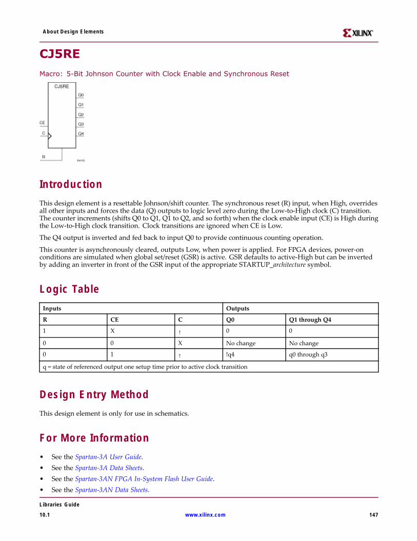
About Design Elements
CJ5RE
Macro: 5-Bit Johnson Counter with Clock Enable and Synchronous Reset
IntroductionThis design element is a resettable Johnson/shift counter. The synchronous reset (R) input, when High, overridesall other inputs and forces the data (Q) outputs to logic level zero during the Low-to-High clock (C) transition.The counter increments (shifts Q0 to Q1, Q1 to Q2, and so forth) when the clock enable input (CE) is High duringthe Low-to-High clock transition. Clock transitions are ignored when CE is Low.
The Q4 output is inverted and fed back to input Q0 to provide continuous counting operation.
This counter is asynchronously cleared, outputs Low, when power is applied. For FPGA devices, power-onconditions are simulated when global set/reset (GSR) is active. GSR defaults to active-High but can be invertedby adding an inverter in front of the GSR input of the appropriate STARTUP_architecture symbol.
Logic TableInputs Outputs
R CE C Q0 Q1 through Q4
1 X ↑ 0 0
0 0 X No change No change
0 1 ↑ !q4 q0 through q3
q = state of referenced output one setup time prior to active clock transition
Design Entry MethodThis design element is only for use in schematics.
For More Information• See the Spartan-3A User Guide.• See the Spartan-3A Data Sheets.• See the Spartan-3AN FPGA In-System Flash User Guide.• See the Spartan-3AN Data Sheets.
Libraries Guide
10.1 www.xilinx.com 147
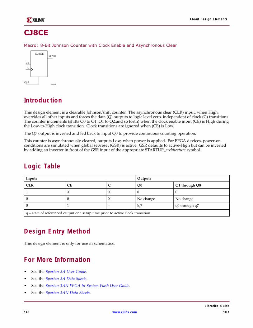
About Design Elements
CJ8CE
Macro: 8-Bit Johnson Counter with Clock Enable and Asynchronous Clear
IntroductionThis design element is a clearable Johnson/shift counter. The asynchronous clear (CLR) input, when High,overrides all other inputs and forces the data (Q) outputs to logic level zero, independent of clock (C) transitions.The counter increments (shifts Q0 to Q1, Q1 to Q2,and so forth) when the clock enable input (CE) is High duringthe Low-to-High clock transition. Clock transitions are ignored when (CE) is Low.
The Q7 output is inverted and fed back to input Q0 to provide continuous counting operation.
This counter is asynchronously cleared, outputs Low, when power is applied. For FPGA devices, power-onconditions are simulated when global set/reset (GSR) is active. GSR defaults to active-High but can be invertedby adding an inverter in front of the GSR input of the appropriate STARTUP_architecture symbol.
Logic TableInputs Outputs
CLR CE C Q0 Q1 through Q8
1 X X 0 0
0 0 X No change No change
0 1 ↑ !q7 q0 through q7
q = state of referenced output one setup time prior to active clock transition
Design Entry MethodThis design element is only for use in schematics.
For More Information• See the Spartan-3A User Guide.
• See the Spartan-3A Data Sheets.
• See the Spartan-3AN FPGA In-System Flash User Guide.
• See the Spartan-3AN Data Sheets.
Libraries Guide
148 www.xilinx.com 10.1
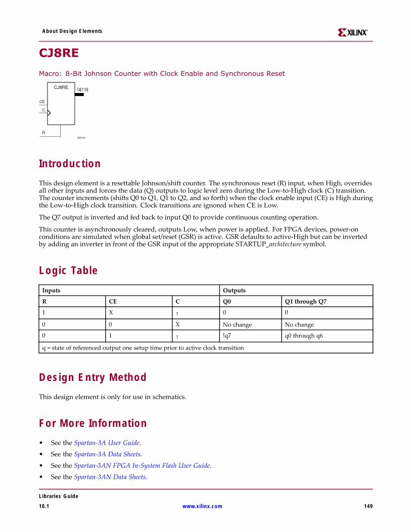
About Design Elements
CJ8RE
Macro: 8-Bit Johnson Counter with Clock Enable and Synchronous Reset
IntroductionThis design element is a resettable Johnson/shift counter. The synchronous reset (R) input, when High, overridesall other inputs and forces the data (Q) outputs to logic level zero during the Low-to-High clock (C) transition.The counter increments (shifts Q0 to Q1, Q1 to Q2, and so forth) when the clock enable input (CE) is High duringthe Low-to-High clock transition. Clock transitions are ignored when CE is Low.
The Q7 output is inverted and fed back to input Q0 to provide continuous counting operation.
This counter is asynchronously cleared, outputs Low, when power is applied. For FPGA devices, power-onconditions are simulated when global set/reset (GSR) is active. GSR defaults to active-High but can be invertedby adding an inverter in front of the GSR input of the appropriate STARTUP_architecture symbol.
Logic TableInputs Outputs
R CE C Q0 Q1 through Q7
1 X ↑ 0 0
0 0 X No change No change
0 1 ↑ !q7 q0 through q6
q = state of referenced output one setup time prior to active clock transition
Design Entry MethodThis design element is only for use in schematics.
For More Information• See the Spartan-3A User Guide.
• See the Spartan-3A Data Sheets.
• See the Spartan-3AN FPGA In-System Flash User Guide.
• See the Spartan-3AN Data Sheets.
Libraries Guide
10.1 www.xilinx.com 149
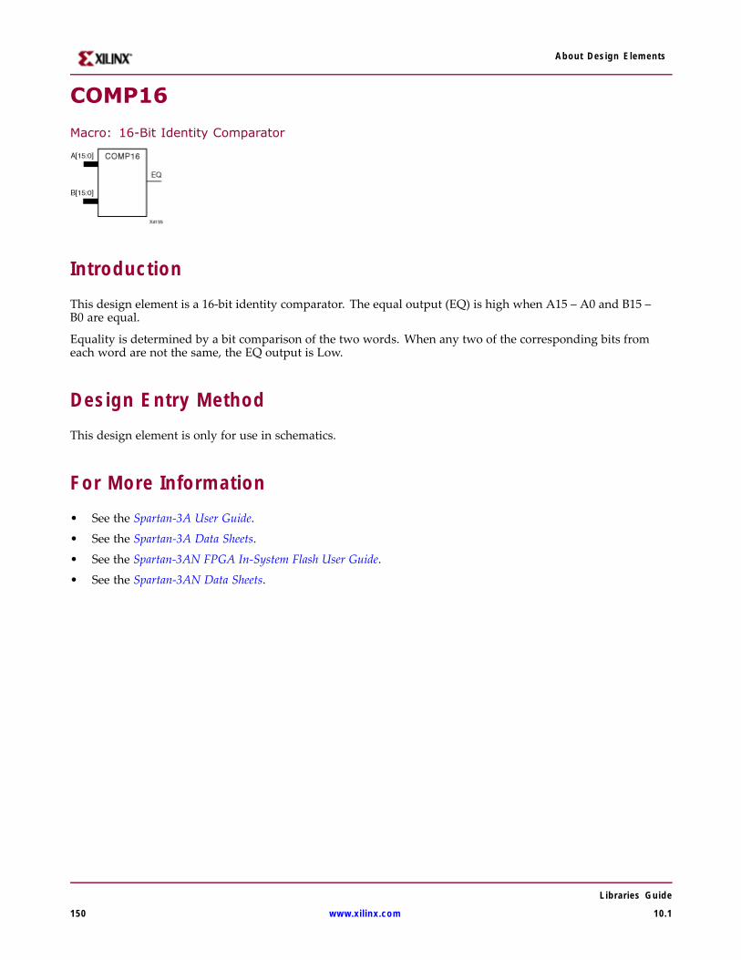
About Design Elements
COMP16
Macro: 16-Bit Identity Comparator
IntroductionThis design element is a 16-bit identity comparator. The equal output (EQ) is high when A15 – A0 and B15 –B0 are equal.
Equality is determined by a bit comparison of the two words. When any two of the corresponding bits fromeach word are not the same, the EQ output is Low.
Design Entry MethodThis design element is only for use in schematics.
For More Information• See the Spartan-3A User Guide.
• See the Spartan-3A Data Sheets.
• See the Spartan-3AN FPGA In-System Flash User Guide.
• See the Spartan-3AN Data Sheets.
Libraries Guide
150 www.xilinx.com 10.1

About Design Elements
COMP2
Macro: 2-Bit Identity Comparator
IntroductionThis design element is a 2-bit identity comparator. The equal output (EQ) is High when the two words A1 – A0and B1 – B0 are equal.
Equality is determined by a bit comparison of the two words. When any two of the corresponding bits fromeach word are not the same, the EQ output is Low.
Design Entry MethodThis design element is only for use in schematics.
For More Information• See the Spartan-3A User Guide.
• See the Spartan-3A Data Sheets.
• See the Spartan-3AN FPGA In-System Flash User Guide.
• See the Spartan-3AN Data Sheets.
Libraries Guide
10.1 www.xilinx.com 151
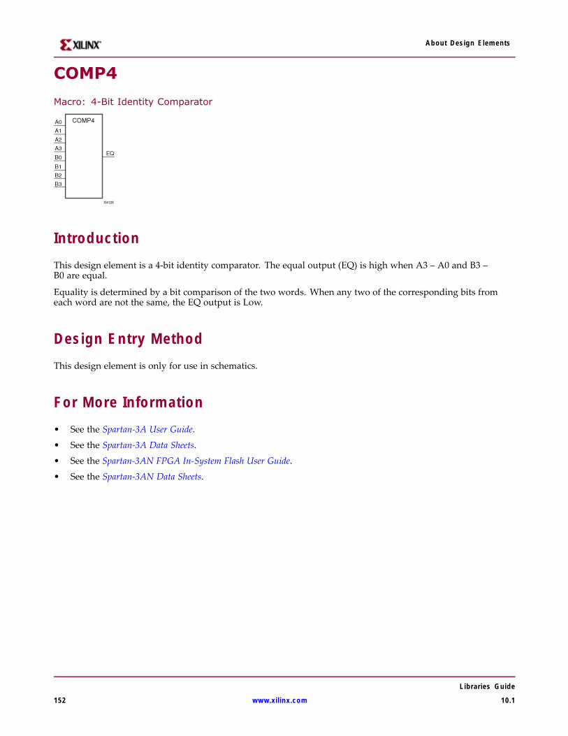
About Design Elements
COMP4
Macro: 4-Bit Identity Comparator
IntroductionThis design element is a 4-bit identity comparator. The equal output (EQ) is high when A3 – A0 and B3 –B0 are equal.
Equality is determined by a bit comparison of the two words. When any two of the corresponding bits fromeach word are not the same, the EQ output is Low.
Design Entry MethodThis design element is only for use in schematics.
For More Information• See the Spartan-3A User Guide.
• See the Spartan-3A Data Sheets.
• See the Spartan-3AN FPGA In-System Flash User Guide.
• See the Spartan-3AN Data Sheets.
Libraries Guide
152 www.xilinx.com 10.1

About Design Elements
COMP8
Macro: 8-Bit Identity Comparator
IntroductionThis design element is an 8-bit identity comparator. The equal output (EQ) is high when A7 – A0 and B7 –B0 are equal.
Equality is determined by a bit comparison of the two words. When any two of the corresponding bits fromeach word are not the same, the EQ output is Low.
Design Entry MethodThis design element is only for use in schematics.
For More Information• See the Spartan-3A User Guide.
• See the Spartan-3A Data Sheets.
• See the Spartan-3AN FPGA In-System Flash User Guide.
• See the Spartan-3AN Data Sheets.
Libraries Guide
10.1 www.xilinx.com 153
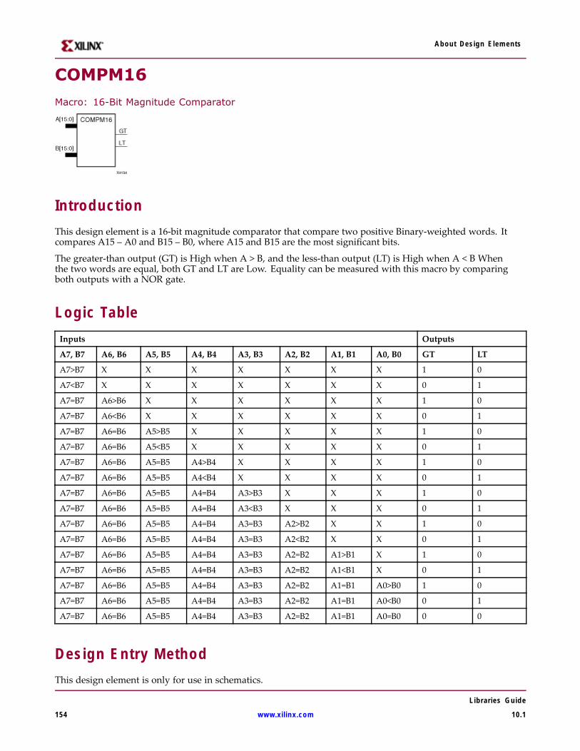
About Design Elements
COMPM16
Macro: 16-Bit Magnitude Comparator
IntroductionThis design element is a 16-bit magnitude comparator that compare two positive Binary-weighted words. Itcompares A15 – A0 and B15 – B0, where A15 and B15 are the most significant bits.
The greater-than output (GT) is High when A > B, and the less-than output (LT) is High when A < B Whenthe two words are equal, both GT and LT are Low. Equality can be measured with this macro by comparingboth outputs with a NOR gate.
Logic TableInputs Outputs
A7, B7 A6, B6 A5, B5 A4, B4 A3, B3 A2, B2 A1, B1 A0, B0 GT LT
A7>B7 X X X X X X X 1 0
A7<B7 X X X X X X X 0 1
A7=B7 A6>B6 X X X X X X 1 0
A7=B7 A6<B6 X X X X X X 0 1
A7=B7 A6=B6 A5>B5 X X X X X 1 0
A7=B7 A6=B6 A5<B5 X X X X X 0 1
A7=B7 A6=B6 A5=B5 A4>B4 X X X X 1 0
A7=B7 A6=B6 A5=B5 A4<B4 X X X X 0 1
A7=B7 A6=B6 A5=B5 A4=B4 A3>B3 X X X 1 0
A7=B7 A6=B6 A5=B5 A4=B4 A3<B3 X X X 0 1
A7=B7 A6=B6 A5=B5 A4=B4 A3=B3 A2>B2 X X 1 0
A7=B7 A6=B6 A5=B5 A4=B4 A3=B3 A2<B2 X X 0 1
A7=B7 A6=B6 A5=B5 A4=B4 A3=B3 A2=B2 A1>B1 X 1 0
A7=B7 A6=B6 A5=B5 A4=B4 A3=B3 A2=B2 A1<B1 X 0 1
A7=B7 A6=B6 A5=B5 A4=B4 A3=B3 A2=B2 A1=B1 A0>B0 1 0
A7=B7 A6=B6 A5=B5 A4=B4 A3=B3 A2=B2 A1=B1 A0<B0 0 1
A7=B7 A6=B6 A5=B5 A4=B4 A3=B3 A2=B2 A1=B1 A0=B0 0 0
Design Entry MethodThis design element is only for use in schematics.
Libraries Guide
154 www.xilinx.com 10.1

About Design Elements
For More Information• See the Spartan-3A User Guide.
• See the Spartan-3A Data Sheets.
• See the Spartan-3AN FPGA In-System Flash User Guide.
• See the Spartan-3AN Data Sheets.
Libraries Guide
10.1 www.xilinx.com 155
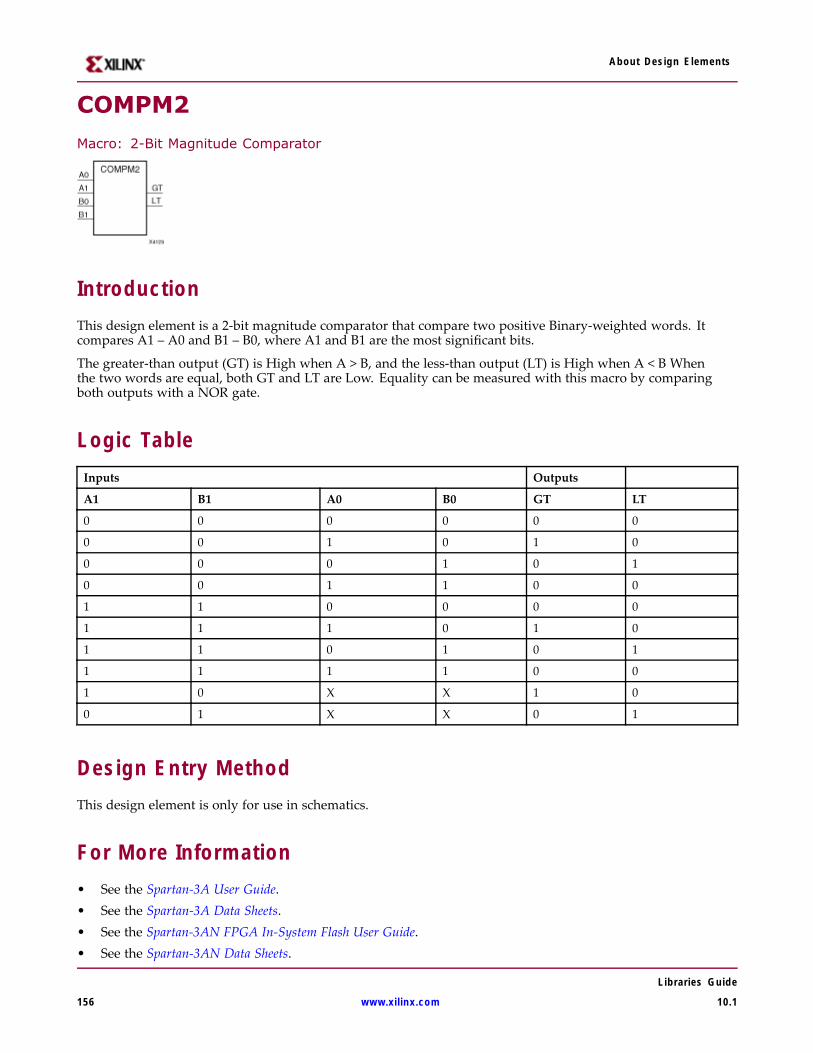
About Design Elements
COMPM2
Macro: 2-Bit Magnitude Comparator
IntroductionThis design element is a 2-bit magnitude comparator that compare two positive Binary-weighted words. Itcompares A1 – A0 and B1 – B0, where A1 and B1 are the most significant bits.
The greater-than output (GT) is High when A > B, and the less-than output (LT) is High when A < B Whenthe two words are equal, both GT and LT are Low. Equality can be measured with this macro by comparingboth outputs with a NOR gate.
Logic TableInputs Outputs
A1 B1 A0 B0 GT LT
0 0 0 0 0 0
0 0 1 0 1 0
0 0 0 1 0 1
0 0 1 1 0 0
1 1 0 0 0 0
1 1 1 0 1 0
1 1 0 1 0 1
1 1 1 1 0 0
1 0 X X 1 0
0 1 X X 0 1
Design Entry MethodThis design element is only for use in schematics.
For More Information• See the Spartan-3A User Guide.• See the Spartan-3A Data Sheets.• See the Spartan-3AN FPGA In-System Flash User Guide.• See the Spartan-3AN Data Sheets.
Libraries Guide
156 www.xilinx.com 10.1
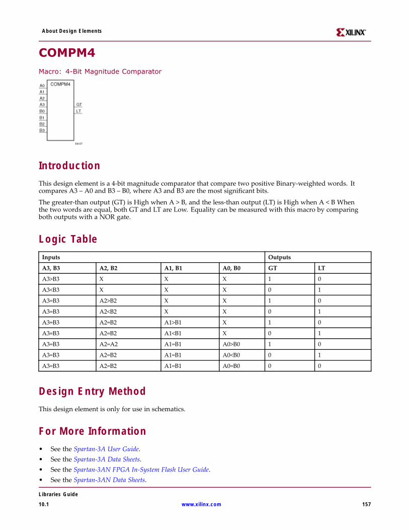
About Design Elements
COMPM4Macro: 4-Bit Magnitude Comparator
IntroductionThis design element is a 4-bit magnitude comparator that compare two positive Binary-weighted words. Itcompares A3 – A0 and B3 – B0, where A3 and B3 are the most significant bits.
The greater-than output (GT) is High when A > B, and the less-than output (LT) is High when A < B Whenthe two words are equal, both GT and LT are Low. Equality can be measured with this macro by comparingboth outputs with a NOR gate.
Logic TableInputs Outputs
A3, B3 A2, B2 A1, B1 A0, B0 GT LT
A3>B3 X X X 1 0
A3<B3 X X X 0 1
A3=B3 A2>B2 X X 1 0
A3=B3 A2<B2 X X 0 1
A3=B3 A2=B2 A1>B1 X 1 0
A3=B3 A2=B2 A1<B1 X 0 1
A3=B3 A2=A2 A1=B1 A0>B0 1 0
A3=B3 A2=B2 A1=B1 A0<B0 0 1
A3=B3 A2=B2 A1=B1 A0=B0 0 0
Design Entry MethodThis design element is only for use in schematics.
For More Information• See the Spartan-3A User Guide.• See the Spartan-3A Data Sheets.• See the Spartan-3AN FPGA In-System Flash User Guide.• See the Spartan-3AN Data Sheets.
Libraries Guide
10.1 www.xilinx.com 157
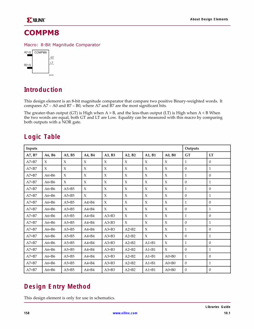
About Design Elements
COMPM8
Macro: 8-Bit Magnitude Comparator
IntroductionThis design element is an 8-bit magnitude comparator that compare two positive Binary-weighted words. Itcompares A7 – A0 and B7 – B0, where A7 and B7 are the most significant bits.
The greater-than output (GT) is High when A > B, and the less-than output (LT) is High when A < B Whenthe two words are equal, both GT and LT are Low. Equality can be measured with this macro by comparingboth outputs with a NOR gate.
Logic TableInputs Outputs
A7, B7 A6, B6 A5, B5 A4, B4 A3, B3 A2, B2 A1, B1 A0, B0 GT LT
A7>B7 X X X X X X X 1 0
A7<B7 X X X X X X X 0 1
A7=B7 A6>B6 X X X X X X 1 0
A7=B7 A6<B6 X X X X X X 0 1
A7=B7 A6=B6 A5>B5 X X X X X 1 0
A7=B7 A6=B6 A5<B5 X X X X X 0 1
A7=B7 A6=B6 A5=B5 A4>B4 X X X X 1 0
A7=B7 A6=B6 A5=B5 A4<B4 X X X X 0 1
A7=B7 A6=B6 A5=B5 A4=B4 A3>B3 X X X 1 0
A7=B7 A6=B6 A5=B5 A4=B4 A3<B3 X X X 0 1
A7=B7 A6=B6 A5=B5 A4=B4 A3=B3 A2>B2 X X 1 0
A7=B7 A6=B6 A5=B5 A4=B4 A3=B3 A2<B2 X X 0 1
A7=B7 A6=B6 A5=B5 A4=B4 A3=B3 A2=B2 A1>B1 X 1 0
A7=B7 A6=B6 A5=B5 A4=B4 A3=B3 A2=B2 A1<B1 X 0 1
A7=B7 A6=B6 A5=B5 A4=B4 A3=B3 A2=B2 A1=B1 A0>B0 1 0
A7=B7 A6=B6 A5=B5 A4=B4 A3=B3 A2=B2 A1=B1 A0<B0 0 1
A7=B7 A6=B6 A5=B5 A4=B4 A3=B3 A2=B2 A1=B1 A0=B0 0 0
Design Entry MethodThis design element is only for use in schematics.
Libraries Guide
158 www.xilinx.com 10.1

About Design Elements
For More Information• See the Spartan-3A User Guide.
• See the Spartan-3A Data Sheets.
• See the Spartan-3AN FPGA In-System Flash User Guide.
• See the Spartan-3AN Data Sheets.
Libraries Guide
10.1 www.xilinx.com 159
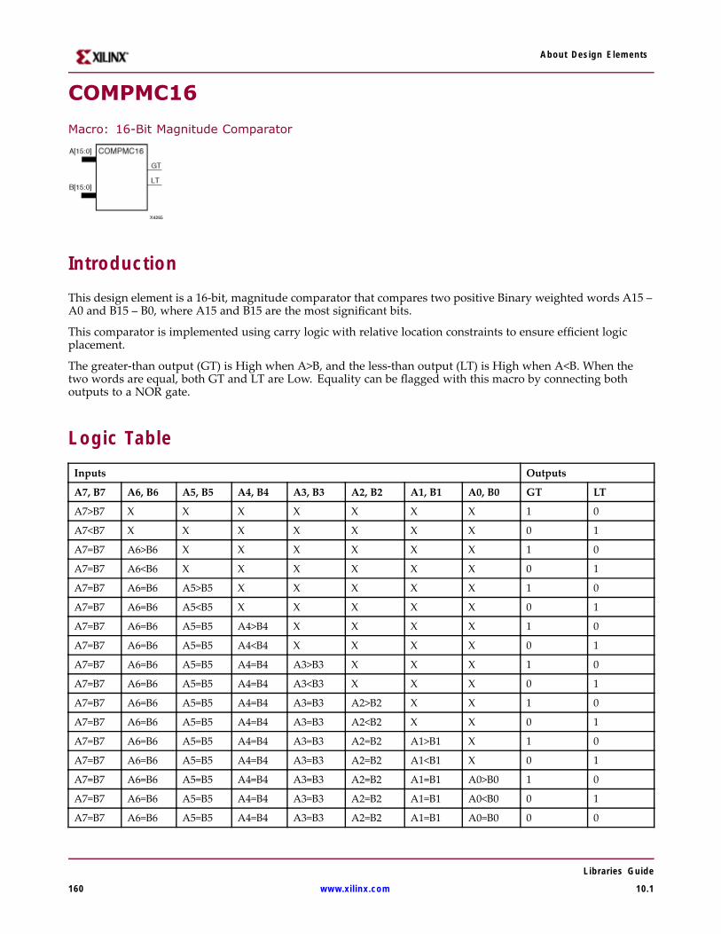
About Design Elements
COMPMC16
Macro: 16-Bit Magnitude Comparator
IntroductionThis design element is a 16-bit, magnitude comparator that compares two positive Binary weighted words A15 –A0 and B15 – B0, where A15 and B15 are the most significant bits.
This comparator is implemented using carry logic with relative location constraints to ensure efficient logicplacement.
The greater-than output (GT) is High when A>B, and the less-than output (LT) is High when A<B. When thetwo words are equal, both GT and LT are Low. Equality can be flagged with this macro by connecting bothoutputs to a NOR gate.
Logic TableInputs Outputs
A7, B7 A6, B6 A5, B5 A4, B4 A3, B3 A2, B2 A1, B1 A0, B0 GT LT
A7>B7 X X X X X X X 1 0
A7<B7 X X X X X X X 0 1
A7=B7 A6>B6 X X X X X X 1 0
A7=B7 A6<B6 X X X X X X 0 1
A7=B7 A6=B6 A5>B5 X X X X X 1 0
A7=B7 A6=B6 A5<B5 X X X X X 0 1
A7=B7 A6=B6 A5=B5 A4>B4 X X X X 1 0
A7=B7 A6=B6 A5=B5 A4<B4 X X X X 0 1
A7=B7 A6=B6 A5=B5 A4=B4 A3>B3 X X X 1 0
A7=B7 A6=B6 A5=B5 A4=B4 A3<B3 X X X 0 1
A7=B7 A6=B6 A5=B5 A4=B4 A3=B3 A2>B2 X X 1 0
A7=B7 A6=B6 A5=B5 A4=B4 A3=B3 A2<B2 X X 0 1
A7=B7 A6=B6 A5=B5 A4=B4 A3=B3 A2=B2 A1>B1 X 1 0
A7=B7 A6=B6 A5=B5 A4=B4 A3=B3 A2=B2 A1<B1 X 0 1
A7=B7 A6=B6 A5=B5 A4=B4 A3=B3 A2=B2 A1=B1 A0>B0 1 0
A7=B7 A6=B6 A5=B5 A4=B4 A3=B3 A2=B2 A1=B1 A0<B0 0 1
A7=B7 A6=B6 A5=B5 A4=B4 A3=B3 A2=B2 A1=B1 A0=B0 0 0
Libraries Guide
160 www.xilinx.com 10.1

About Design Elements
Design Entry MethodThis design element is only for use in schematics.
For More Information• See the Spartan-3A User Guide.
• See the Spartan-3A Data Sheets.
• See the Spartan-3AN FPGA In-System Flash User Guide.
• See the Spartan-3AN Data Sheets.
Libraries Guide
10.1 www.xilinx.com 161

About Design Elements
COMPMC8
Macro: 8-Bit Magnitude Comparator
IntroductionThis design element is an 8-bit, magnitude comparator that compares two positive Binaryweighted words A7 –A0 and B7 – B0, where A7 and B7 are the most significant bits.
This comparator is implemented using carry logic with relative location constraints to ensure efficient logicplacement.
The greater-than output (GT) is High when A>B, and the less-than output (LT) is High when A<B. When thetwo words are equal, both GT and LT are Low. Equality can be flagged with this macro by connecting bothoutputs to a NOR gate.
Logic TableInputs Outputs
A7, B7 A6, B6 A5, B5 A4, B4 A3, B3 A2, B2 A1, B1 A0, B0 GT LT
A7>B7 X X X X X X X 1 0
A7<B7 X X X X X X X 0 1
A7=B7 A6>B6 X X X X X X 1 0
A7=B7 A6<B6 X X X X X X 0 1
A7=B7 A6=B6 A5>B5 X X X X X 1 0
A7=B7 A6=B6 A5<B5 X X X X X 0 1
A7=B7 A6=B6 A5=B5 A4>B4 X X X X 1 0
A7=B7 A6=B6 A5=B5 A4<B4 X X X X 0 1
A7=B7 A6=B6 A5=B5 A4=B4 A3>B3 X X X 1 0
A7=B7 A6=B6 A5=B5 A4=B4 A3<B3 X X X 0 1
A7=B7 A6=B6 A5=B5 A4=B4 A3=B3 A2>B2 X X 1 0
A7=B7 A6=B6 A5=B5 A4=B4 A3=B3 A2<B2 X X 0 1
A7=B7 A6=B6 A5=B5 A4=B4 A3=B3 A2=B2 A1>B1 X 1 0
A7=B7 A6=B6 A5=B5 A4=B4 A3=B3 A2=B2 A1<B1 X 0 1
A7=B7 A6=B6 A5=B5 A4=B4 A3=B3 A2=B2 A1=B1 A0>B0 1 0
A7=B7 A6=B6 A5=B5 A4=B4 A3=B3 A2=B2 A1=B1 A0<B0 0 1
A7=B7 A6=B6 A5=B5 A4=B4 A3=B3 A2=B2 A1=B1 A0=B0 0 0
Libraries Guide
162 www.xilinx.com 10.1

About Design Elements
Design Entry MethodThis design element is only for use in schematics.
For More Information• See the Spartan-3A User Guide.
• See the Spartan-3A Data Sheets.
• See the Spartan-3AN FPGA In-System Flash User Guide.
• See the Spartan-3AN Data Sheets.
Libraries Guide
10.1 www.xilinx.com 163
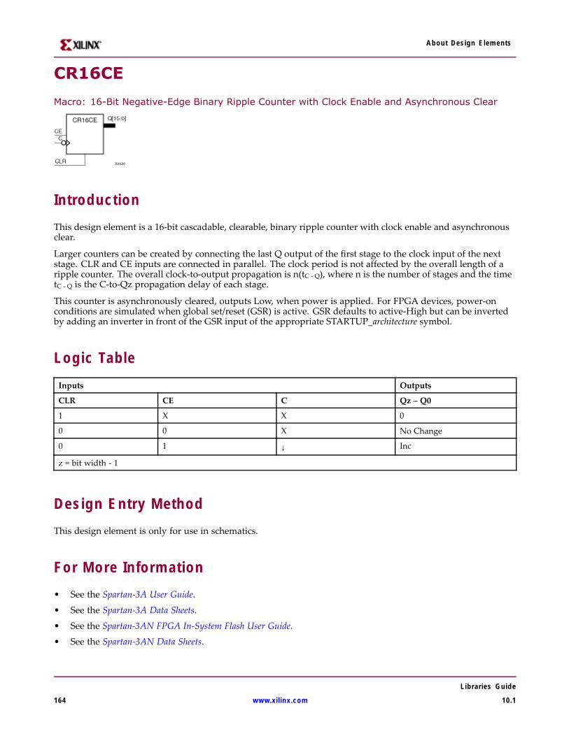
About Design Elements
CR16CE
Macro: 16-Bit Negative-Edge Binary Ripple Counter with Clock Enable and Asynchronous Clear
IntroductionThis design element is a 16-bit cascadable, clearable, binary ripple counter with clock enable and asynchronousclear.
Larger counters can be created by connecting the last Q output of the first stage to the clock input of the nextstage. CLR and CE inputs are connected in parallel. The clock period is not affected by the overall length of aripple counter. The overall clock-to-output propagation is n(tC - Q), where n is the number of stages and the timetC - Q is the C-to-Qz propagation delay of each stage.
This counter is asynchronously cleared, outputs Low, when power is applied. For FPGA devices, power-onconditions are simulated when global set/reset (GSR) is active. GSR defaults to active-High but can be invertedby adding an inverter in front of the GSR input of the appropriate STARTUP_architecture symbol.
Logic TableInputs Outputs
CLR CE C Qz – Q0
1 X X 0
0 0 X No Change
0 1 ↓ Inc
z = bit width - 1
Design Entry MethodThis design element is only for use in schematics.
For More Information• See the Spartan-3A User Guide.
• See the Spartan-3A Data Sheets.
• See the Spartan-3AN FPGA In-System Flash User Guide.
• See the Spartan-3AN Data Sheets.
Libraries Guide
164 www.xilinx.com 10.1
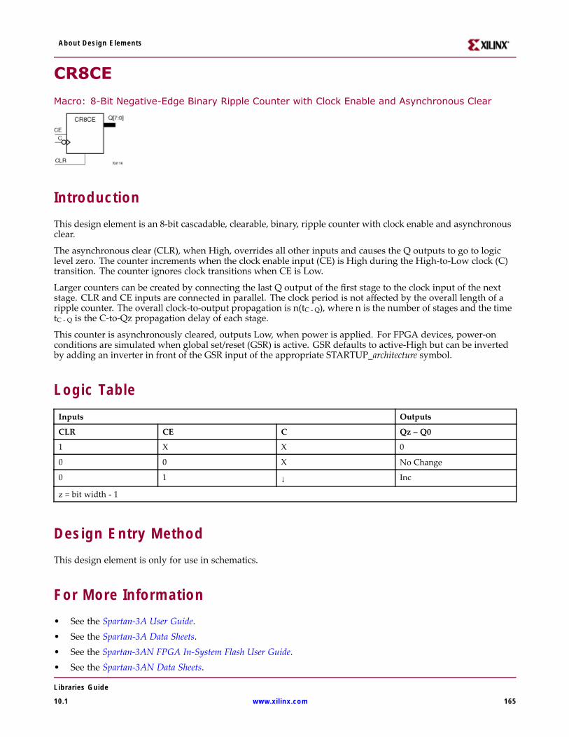
About Design Elements
CR8CE
Macro: 8-Bit Negative-Edge Binary Ripple Counter with Clock Enable and Asynchronous Clear
IntroductionThis design element is an 8-bit cascadable, clearable, binary, ripple counter with clock enable and asynchronousclear.
The asynchronous clear (CLR), when High, overrides all other inputs and causes the Q outputs to go to logiclevel zero. The counter increments when the clock enable input (CE) is High during the High-to-Low clock (C)transition. The counter ignores clock transitions when CE is Low.
Larger counters can be created by connecting the last Q output of the first stage to the clock input of the nextstage. CLR and CE inputs are connected in parallel. The clock period is not affected by the overall length of aripple counter. The overall clock-to-output propagation is n(tC - Q), where n is the number of stages and the timetC - Q is the C-to-Qz propagation delay of each stage.
This counter is asynchronously cleared, outputs Low, when power is applied. For FPGA devices, power-onconditions are simulated when global set/reset (GSR) is active. GSR defaults to active-High but can be invertedby adding an inverter in front of the GSR input of the appropriate STARTUP_architecture symbol.
Logic TableInputs Outputs
CLR CE C Qz – Q0
1 X X 0
0 0 X No Change
0 1 ↓ Inc
z = bit width - 1
Design Entry MethodThis design element is only for use in schematics.
For More Information• See the Spartan-3A User Guide.• See the Spartan-3A Data Sheets.• See the Spartan-3AN FPGA In-System Flash User Guide.• See the Spartan-3AN Data Sheets.
Libraries Guide
10.1 www.xilinx.com 165
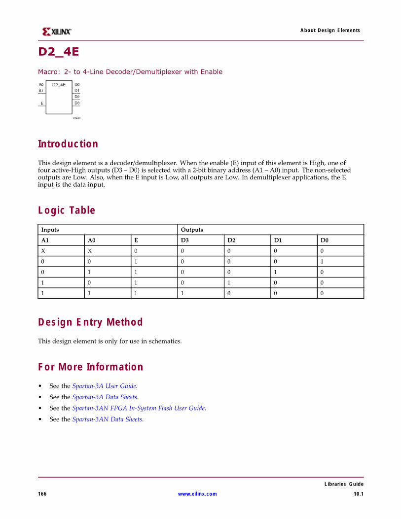
About Design Elements
D2_4E
Macro: 2- to 4-Line Decoder/Demultiplexer with Enable
IntroductionThis design element is a decoder/demultiplexer. When the enable (E) input of this element is High, one offour active-High outputs (D3 – D0) is selected with a 2-bit binary address (A1 – A0) input. The non-selectedoutputs are Low. Also, when the E input is Low, all outputs are Low. In demultiplexer applications, the Einput is the data input.
Logic TableInputs Outputs
A1 A0 E D3 D2 D1 D0
X X 0 0 0 0 0
0 0 1 0 0 0 1
0 1 1 0 0 1 0
1 0 1 0 1 0 0
1 1 1 1 0 0 0
Design Entry MethodThis design element is only for use in schematics.
For More Information• See the Spartan-3A User Guide.
• See the Spartan-3A Data Sheets.
• See the Spartan-3AN FPGA In-System Flash User Guide.
• See the Spartan-3AN Data Sheets.
Libraries Guide
166 www.xilinx.com 10.1
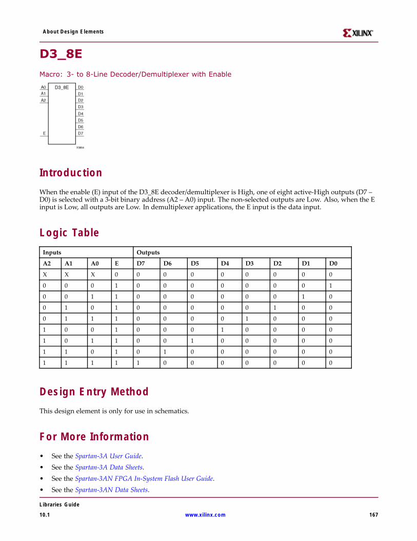
About Design Elements
D3_8E
Macro: 3- to 8-Line Decoder/Demultiplexer with Enable
IntroductionWhen the enable (E) input of the D3_8E decoder/demultiplexer is High, one of eight active-High outputs (D7 –D0) is selected with a 3-bit binary address (A2 – A0) input. The non-selected outputs are Low. Also, when the Einput is Low, all outputs are Low. In demultiplexer applications, the E input is the data input.
Logic TableInputs Outputs
A2 A1 A0 E D7 D6 D5 D4 D3 D2 D1 D0
X X X 0 0 0 0 0 0 0 0 0
0 0 0 1 0 0 0 0 0 0 0 1
0 0 1 1 0 0 0 0 0 0 1 0
0 1 0 1 0 0 0 0 0 1 0 0
0 1 1 1 0 0 0 0 1 0 0 0
1 0 0 1 0 0 0 1 0 0 0 0
1 0 1 1 0 0 1 0 0 0 0 0
1 1 0 1 0 1 0 0 0 0 0 0
1 1 1 1 1 0 0 0 0 0 0 0
Design Entry MethodThis design element is only for use in schematics.
For More Information• See the Spartan-3A User Guide.• See the Spartan-3A Data Sheets.• See the Spartan-3AN FPGA In-System Flash User Guide.• See the Spartan-3AN Data Sheets.
Libraries Guide
10.1 www.xilinx.com 167
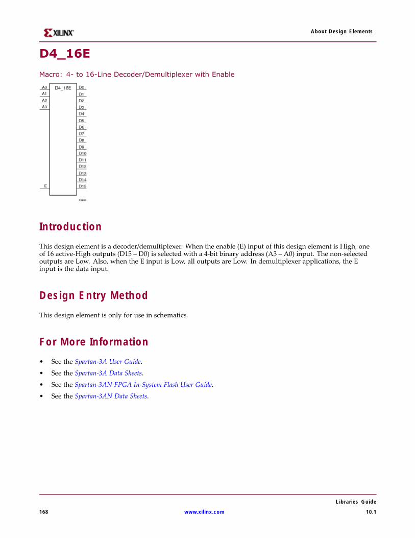
About Design Elements
D4_16E
Macro: 4- to 16-Line Decoder/Demultiplexer with Enable
IntroductionThis design element is a decoder/demultiplexer. When the enable (E) input of this design element is High, oneof 16 active-High outputs (D15 – D0) is selected with a 4-bit binary address (A3 – A0) input. The non-selectedoutputs are Low. Also, when the E input is Low, all outputs are Low. In demultiplexer applications, the Einput is the data input.
Design Entry MethodThis design element is only for use in schematics.
For More Information• See the Spartan-3A User Guide.
• See the Spartan-3A Data Sheets.
• See the Spartan-3AN FPGA In-System Flash User Guide.
• See the Spartan-3AN Data Sheets.
Libraries Guide
168 www.xilinx.com 10.1
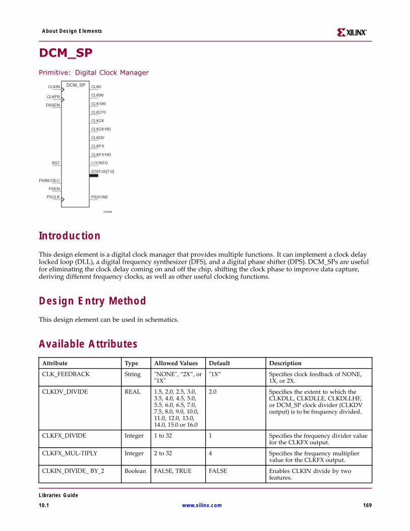
About Design Elements
DCM_SP
Primitive: Digital Clock Manager
IntroductionThis design element is a digital clock manager that provides multiple functions. It can implement a clock delaylocked loop (DLL), a digital frequency synthesizer (DFS), and a digital phase shifter (DPS). DCM_SPs are usefulfor eliminating the clock delay coming on and off the chip, shifting the clock phase to improve data capture,deriving different frequency clocks, as well as other useful clocking functions.
Design Entry MethodThis design element can be used in schematics.
Available AttributesAttribute Type Allowed Values Default Description
CLK_FEEDBACK String "NONE", “2X”, or"1X"
"1X” Specifies clock feedback of NONE,1X, or 2X.
CLKDV_DIVIDE REAL 1.5, 2.0, 2.5, 3.0,3.5, 4.0, 4.5, 5.0,5.5, 6.0, 6.5, 7.0,7.5, 8.0, 9.0, 10.0,11.0, 12.0, 13.0,14.0, 15.0 or 16.0
2.0 Specifies the extent to which theCLKDLL, CLKDLLE, CLKDLLHF,or DCM_SP clock divider (CLKDVoutput) is to be frequency divided.
CLKFX_DIVIDE Integer 1 to 32 1 Specifies the frequency divider valuefor the CLKFX output.
CLKFX_MUL-TIPLY Integer 2 to 32 4 Specifies the frequency multipliervalue for the CLKFX output.
CLKIN_DIVIDE_ BY_2 Boolean FALSE, TRUE FALSE Enables CLKIN divide by twofeatures.
Libraries Guide
10.1 www.xilinx.com 169
About Design Elements
Attribute Type Allowed Values Default Description
CLKIN_PERIOD REAL 0.0001 to 1000 0 Specifies the input period to theDCM_SP CLKIN input in ns.
CLKOUT_PHASE_ SHIFT String "NONE", "FIXED"or "VARIABLE”
"NONE” Specifies the phase shift of NONE,FIXED or VARIABLE.
DESKEW_ADJUST String "SOURCE_SYNCHRONOUS","SYSTEM_SYNCHRONOUS"or "0" to "15”
"SYSTEM_SYNCHRONOUS"
Sets configuration bits affecting theclock delay alignment between theDCM_SP output clocks and an FPGAclock input pin.
FACTORY_JF Hexa-decimal
Any 16-Bit Value C080 The FACTORY_JF attribute affectsthe DCMs jitter filter characteristic.This attribute is set the defaultvalue should not be modified unlessotherwise instructed by Xilinx. Itshould be noted, however, that thisattribute has no effect for Spartan-3Aand Spartan-3E.
PHASE_SHIFT Integer -255 to 255 0 Defines the amount of fixed phaseshift from -255 to 255
DFS_FRE-QUENCY_MODE
String "LOW," "HIGH" “LOW” Specifies the frequency mode of thefrequency synthesizer.
DLL_FRE-QUENCY_MODE
String "LOW", "HIGH" “LOW” --
DSS_MODE String -- “NONE” --
DUTY_CYCLE_CORRECTION
Boolean TRUE, FALSE TRUE Corrects the duty cycle of theCLK0, CLK90, CLK180, and CLK270outputs.
STARTUP_WAIT Boolean TRUE, FALSE TRUE Delays configuration DONE untilDCM LOCK.
For More Information• See the Spartan-3A User Guide.
• See the Spartan-3A Data Sheets.
• See the Spartan-3AN FPGA In-System Flash User Guide.
• See the Spartan-3AN Data Sheets.
Libraries Guide
170 www.xilinx.com 10.1
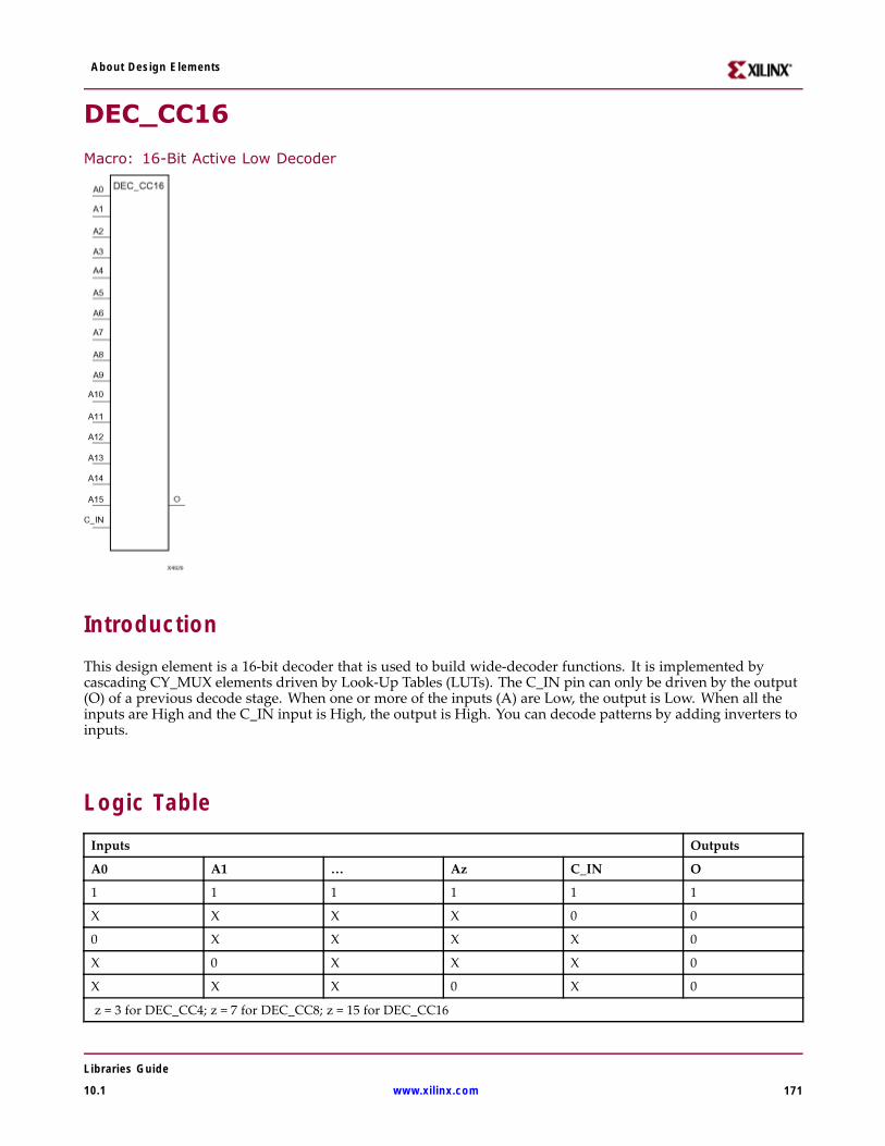
About Design Elements
DEC_CC16
Macro: 16-Bit Active Low Decoder
IntroductionThis design element is a 16-bit decoder that is used to build wide-decoder functions. It is implemented bycascading CY_MUX elements driven by Look-Up Tables (LUTs). The C_IN pin can only be driven by the output(O) of a previous decode stage. When one or more of the inputs (A) are Low, the output is Low. When all theinputs are High and the C_IN input is High, the output is High. You can decode patterns by adding inverters toinputs.
Logic TableInputs Outputs
A0 A1 … Az C_IN O
1 1 1 1 1 1
X X X X 0 0
0 X X X X 0
X 0 X X X 0
X X X 0 X 0
z = 3 for DEC_CC4; z = 7 for DEC_CC8; z = 15 for DEC_CC16
Libraries Guide
10.1 www.xilinx.com 171

About Design Elements
Design Entry MethodThis design element is only for use in schematics.
For More Information• See the Spartan-3A User Guide.
• See the Spartan-3A Data Sheets.
• See the Spartan-3AN FPGA In-System Flash User Guide.
• See the Spartan-3AN Data Sheets.
Libraries Guide
172 www.xilinx.com 10.1
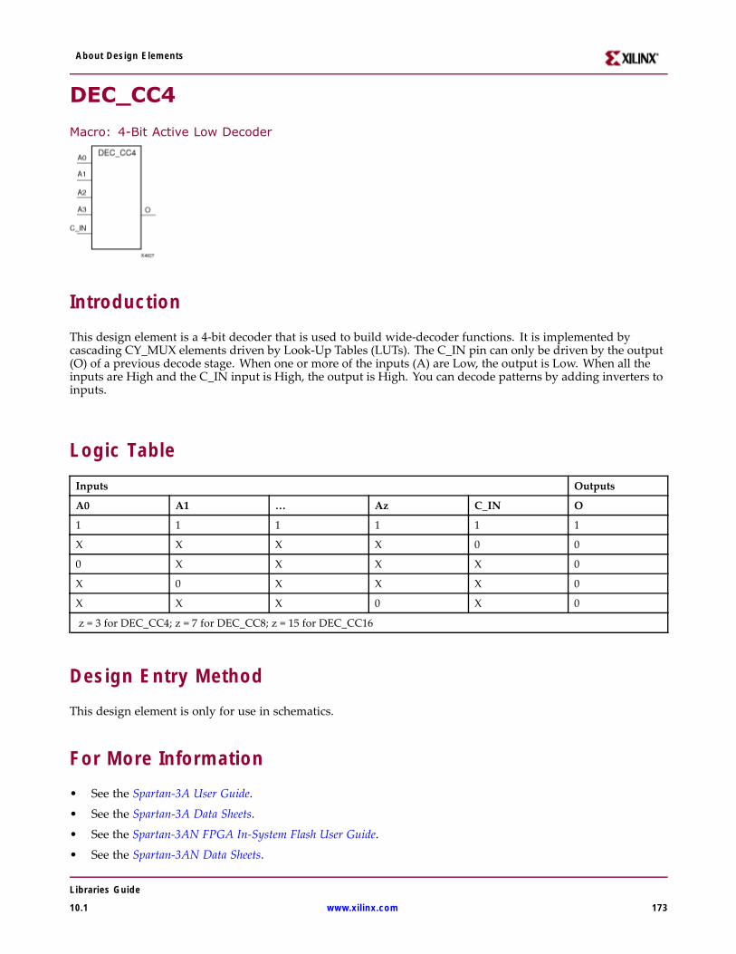
About Design Elements
DEC_CC4
Macro: 4-Bit Active Low Decoder
IntroductionThis design element is a 4-bit decoder that is used to build wide-decoder functions. It is implemented bycascading CY_MUX elements driven by Look-Up Tables (LUTs). The C_IN pin can only be driven by the output(O) of a previous decode stage. When one or more of the inputs (A) are Low, the output is Low. When all theinputs are High and the C_IN input is High, the output is High. You can decode patterns by adding inverters toinputs.
Logic TableInputs Outputs
A0 A1 … Az C_IN O
1 1 1 1 1 1
X X X X 0 0
0 X X X X 0
X 0 X X X 0
X X X 0 X 0
z = 3 for DEC_CC4; z = 7 for DEC_CC8; z = 15 for DEC_CC16
Design Entry MethodThis design element is only for use in schematics.
For More Information• See the Spartan-3A User Guide.
• See the Spartan-3A Data Sheets.
• See the Spartan-3AN FPGA In-System Flash User Guide.
• See the Spartan-3AN Data Sheets.
Libraries Guide
10.1 www.xilinx.com 173
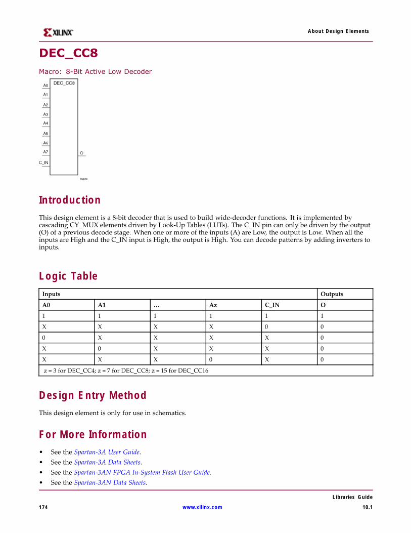
About Design Elements
DEC_CC8Macro: 8-Bit Active Low Decoder
IntroductionThis design element is a 8-bit decoder that is used to build wide-decoder functions. It is implemented bycascading CY_MUX elements driven by Look-Up Tables (LUTs). The C_IN pin can only be driven by the output(O) of a previous decode stage. When one or more of the inputs (A) are Low, the output is Low. When all theinputs are High and the C_IN input is High, the output is High. You can decode patterns by adding inverters toinputs.
Logic TableInputs Outputs
A0 A1 … Az C_IN O
1 1 1 1 1 1
X X X X 0 0
0 X X X X 0
X 0 X X X 0
X X X 0 X 0
z = 3 for DEC_CC4; z = 7 for DEC_CC8; z = 15 for DEC_CC16
Design Entry MethodThis design element is only for use in schematics.
For More Information• See the Spartan-3A User Guide.• See the Spartan-3A Data Sheets.• See the Spartan-3AN FPGA In-System Flash User Guide.• See the Spartan-3AN Data Sheets.
Libraries Guide
174 www.xilinx.com 10.1
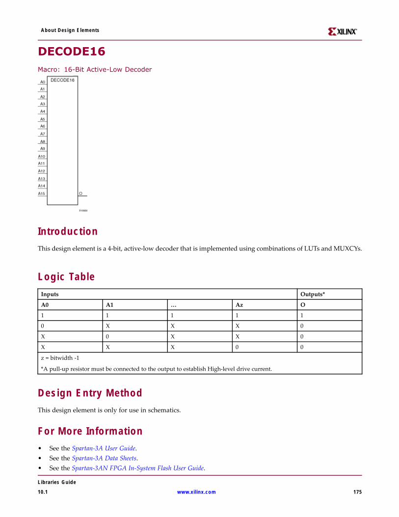
About Design Elements
DECODE16Macro: 16-Bit Active-Low Decoder
IntroductionThis design element is a 4-bit, active-low decoder that is implemented using combinations of LUTs and MUXCYs.
Logic TableInputs Outputs*
A0 A1 … Az O
1 1 1 1 1
0 X X X 0
X 0 X X 0
X X X 0 0
z = bitwidth -1
*A pull-up resistor must be connected to the output to establish High-level drive current.
Design Entry MethodThis design element is only for use in schematics.
For More Information• See the Spartan-3A User Guide.• See the Spartan-3A Data Sheets.• See the Spartan-3AN FPGA In-System Flash User Guide.
Libraries Guide
10.1 www.xilinx.com 175

About Design Elements
• See the Spartan-3AN Data Sheets.
Libraries Guide
176 www.xilinx.com 10.1
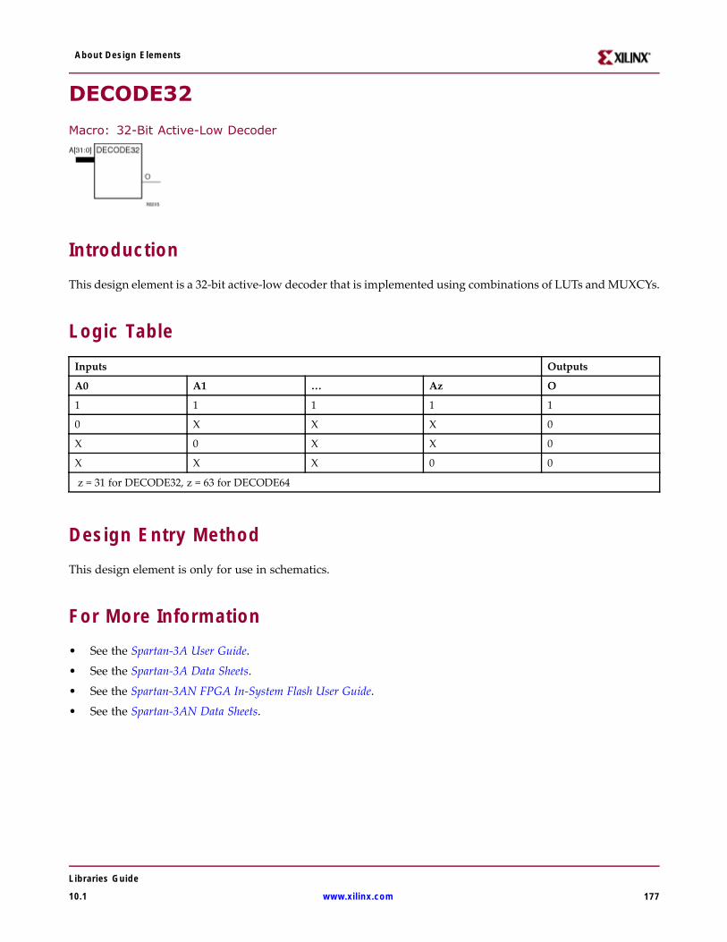
About Design Elements
DECODE32
Macro: 32-Bit Active-Low Decoder
IntroductionThis design element is a 32-bit active-low decoder that is implemented using combinations of LUTs andMUXCYs.
Logic TableInputs Outputs
A0 A1 … Az O
1 1 1 1 1
0 X X X 0
X 0 X X 0
X X X 0 0
z = 31 for DECODE32, z = 63 for DECODE64
Design Entry MethodThis design element is only for use in schematics.
For More Information• See the Spartan-3A User Guide.
• See the Spartan-3A Data Sheets.
• See the Spartan-3AN FPGA In-System Flash User Guide.
• See the Spartan-3AN Data Sheets.
Libraries Guide
10.1 www.xilinx.com 177
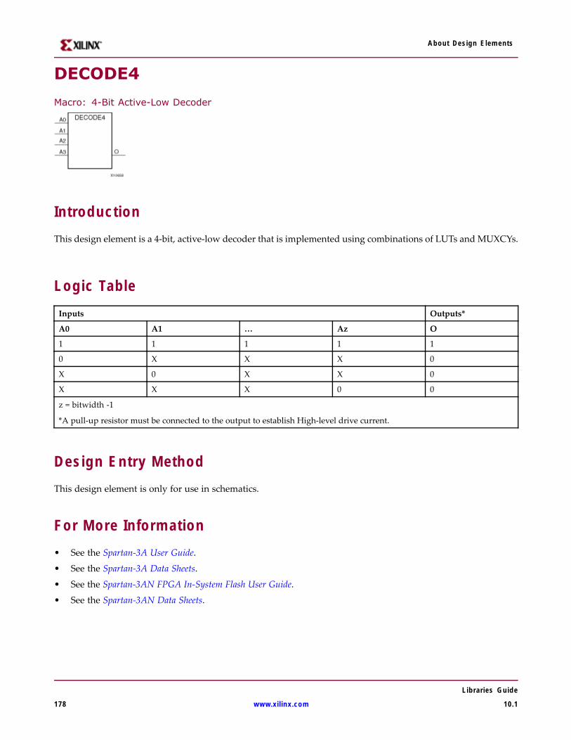
About Design Elements
DECODE4
Macro: 4-Bit Active-Low Decoder
IntroductionThis design element is a 4-bit, active-low decoder that is implemented using combinations of LUTs and MUXCYs.
Logic TableInputs Outputs*
A0 A1 … Az O
1 1 1 1 1
0 X X X 0
X 0 X X 0
X X X 0 0
z = bitwidth -1
*A pull-up resistor must be connected to the output to establish High-level drive current.
Design Entry MethodThis design element is only for use in schematics.
For More Information• See the Spartan-3A User Guide.
• See the Spartan-3A Data Sheets.
• See the Spartan-3AN FPGA In-System Flash User Guide.
• See the Spartan-3AN Data Sheets.
Libraries Guide
178 www.xilinx.com 10.1
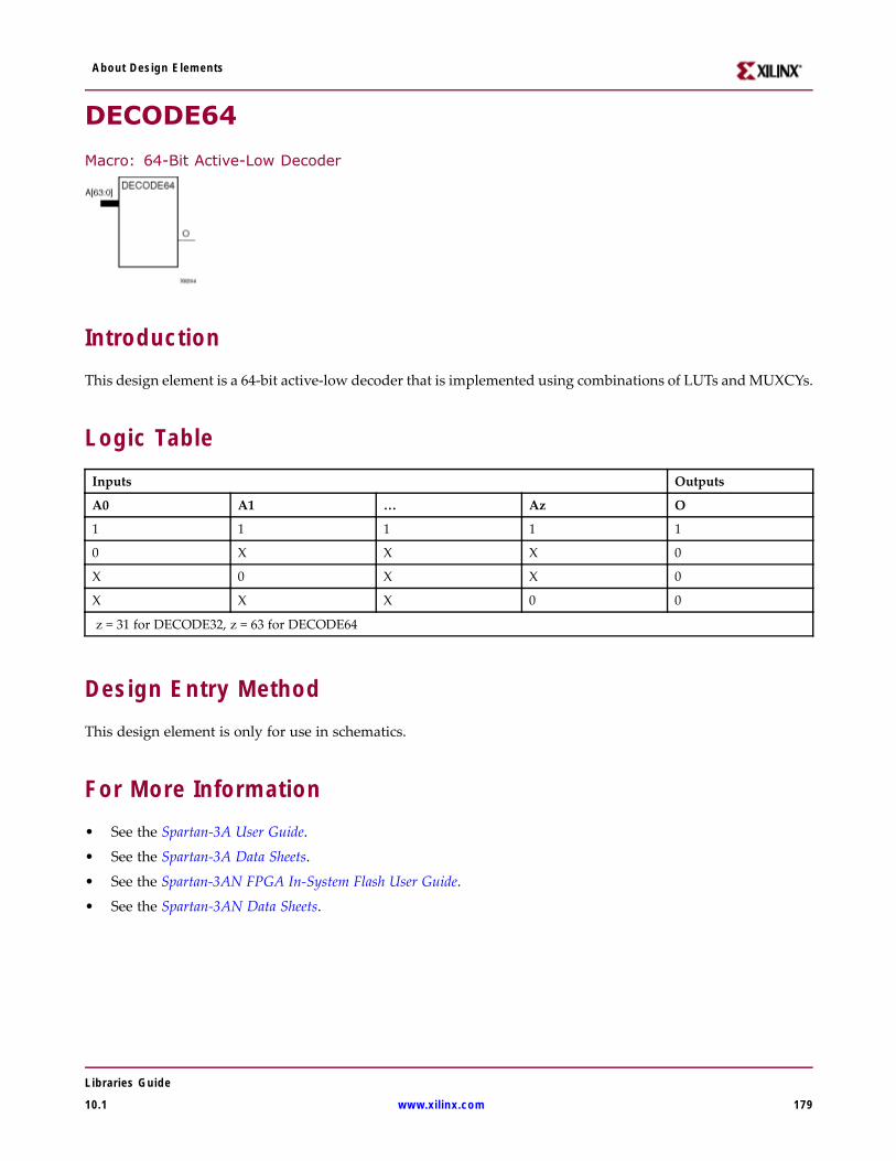
About Design Elements
DECODE64
Macro: 64-Bit Active-Low Decoder
IntroductionThis design element is a 64-bit active-low decoder that is implemented using combinations of LUTs andMUXCYs.
Logic TableInputs Outputs
A0 A1 … Az O
1 1 1 1 1
0 X X X 0
X 0 X X 0
X X X 0 0
z = 31 for DECODE32, z = 63 for DECODE64
Design Entry MethodThis design element is only for use in schematics.
For More Information• See the Spartan-3A User Guide.
• See the Spartan-3A Data Sheets.
• See the Spartan-3AN FPGA In-System Flash User Guide.
• See the Spartan-3AN Data Sheets.
Libraries Guide
10.1 www.xilinx.com 179
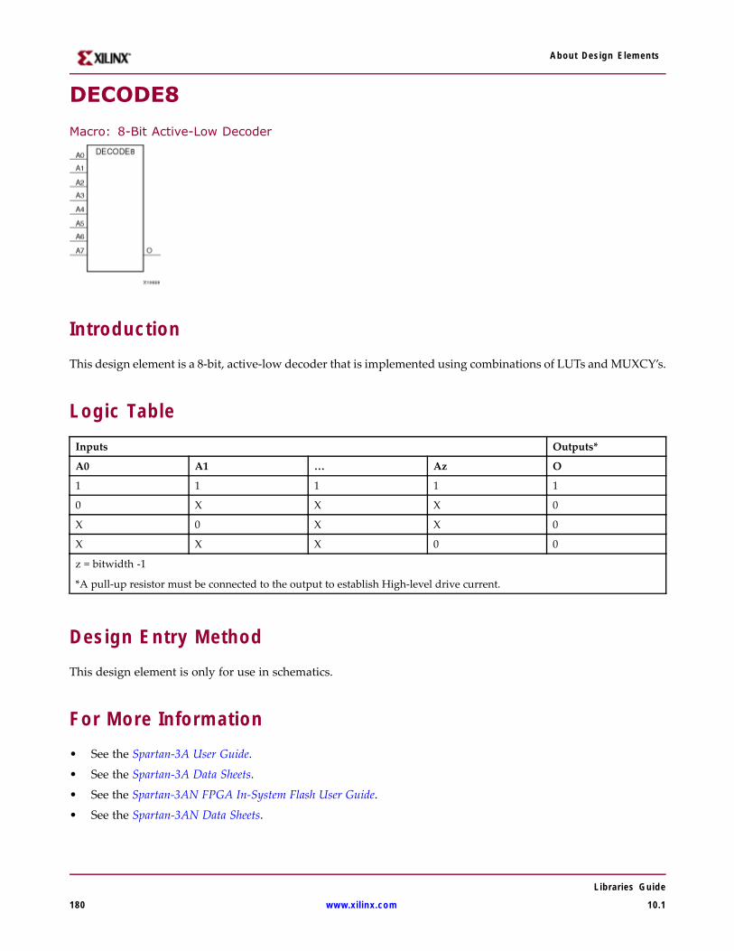
About Design Elements
DECODE8
Macro: 8-Bit Active-Low Decoder
IntroductionThis design element is a 8-bit, active-low decoder that is implemented using combinations of LUTs andMUXCY’s.
Logic TableInputs Outputs*
A0 A1 … Az O
1 1 1 1 1
0 X X X 0
X 0 X X 0
X X X 0 0
z = bitwidth -1
*A pull-up resistor must be connected to the output to establish High-level drive current.
Design Entry MethodThis design element is only for use in schematics.
For More Information• See the Spartan-3A User Guide.
• See the Spartan-3A Data Sheets.
• See the Spartan-3AN FPGA In-System Flash User Guide.
• See the Spartan-3AN Data Sheets.
Libraries Guide
180 www.xilinx.com 10.1
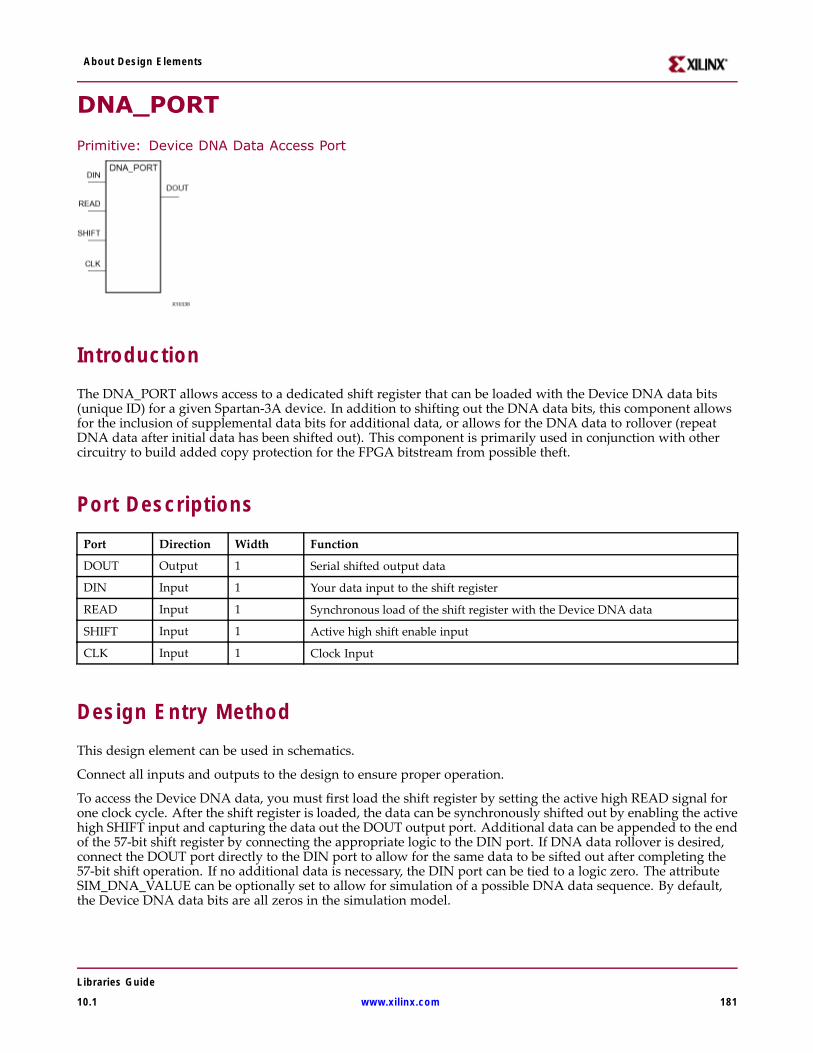
About Design Elements
DNA_PORT
Primitive: Device DNA Data Access Port
IntroductionThe DNA_PORT allows access to a dedicated shift register that can be loaded with the Device DNA data bits(unique ID) for a given Spartan-3A device. In addition to shifting out the DNA data bits, this component allowsfor the inclusion of supplemental data bits for additional data, or allows for the DNA data to rollover (repeatDNA data after initial data has been shifted out). This component is primarily used in conjunction with othercircuitry to build added copy protection for the FPGA bitstream from possible theft.
Port DescriptionsPort Direction Width Function
DOUT Output 1 Serial shifted output data
DIN Input 1 Your data input to the shift register
READ Input 1 Synchronous load of the shift register with the Device DNA data
SHIFT Input 1 Active high shift enable input
CLK Input 1 Clock Input
Design Entry MethodThis design element can be used in schematics.
Connect all inputs and outputs to the design to ensure proper operation.
To access the Device DNA data, you must first load the shift register by setting the active high READ signal forone clock cycle. After the shift register is loaded, the data can be synchronously shifted out by enabling the activehigh SHIFT input and capturing the data out the DOUT output port. Additional data can be appended to the endof the 57-bit shift register by connecting the appropriate logic to the DIN port. If DNA data rollover is desired,connect the DOUT port directly to the DIN port to allow for the same data to be sifted out after completing the57-bit shift operation. If no additional data is necessary, the DIN port can be tied to a logic zero. The attributeSIM_DNA_VALUE can be optionally set to allow for simulation of a possible DNA data sequence. By default,the Device DNA data bits are all zeros in the simulation model.
Libraries Guide
10.1 www.xilinx.com 181

About Design Elements
Available Attributes
Attribute TypeAllowedValues Default Description
SIM_DNA_VALUE 57-bitvector
Any 57-bitvalue
Allzeros
Specifies a DNA value for simulation purposes (the actualvalue will be specific to the particular device used)
For More Information• See the Spartan-3A User Guide.
• See the Spartan-3A Data Sheets.
• See the Spartan-3AN FPGA In-System Flash User Guide.
• See the Spartan-3AN Data Sheets.
Libraries Guide
182 www.xilinx.com 10.1
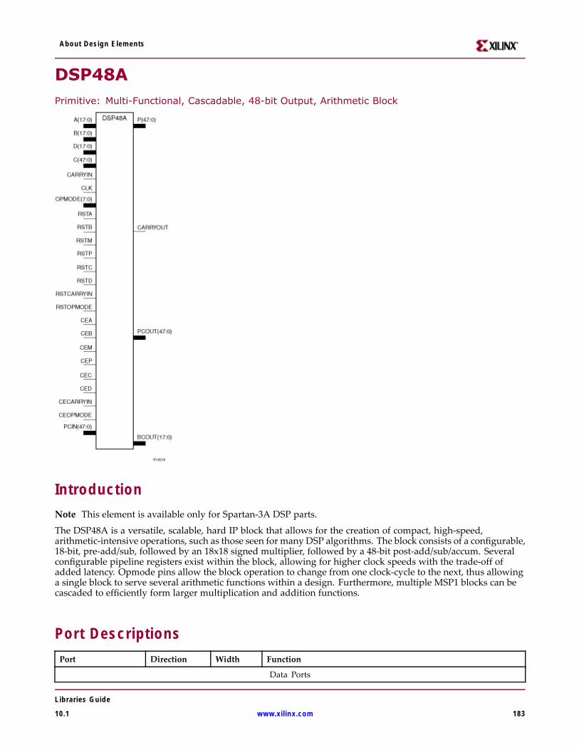
About Design Elements
DSP48APrimitive: Multi-Functional, Cascadable, 48-bit Output, Arithmetic Block
IntroductionNote This element is available only for Spartan-3A DSP parts.
The DSP48A is a versatile, scalable, hard IP block that allows for the creation of compact, high-speed,arithmetic-intensive operations, such as those seen for many DSP algorithms. The block consists of a configurable,18-bit, pre-add/sub, followed by an 18x18 signed multiplier, followed by a 48-bit post-add/sub/accum. Severalconfigurable pipeline registers exist within the block, allowing for higher clock speeds with the trade-off ofadded latency. Opmode pins allow the block operation to change from one clock-cycle to the next, thus allowinga single block to serve several arithmetic functions within a design. Furthermore, multiple MSP1 blocks can becascaded to efficiently form larger multiplication and addition functions.
Port DescriptionsPort Direction Width Function
Data Ports
Libraries Guide
10.1 www.xilinx.com 183
About Design Elements
Port Direction Width Function
A Input 18 18-bit data input to multiplier or post add/sub depending on thevalue of OPMODE[1:0].
B Input 18 18-bit data input to multiplier, pre-add/sub and, perhaps, apost-add/sub depending on the value of OPMODE[3:0].
C Input 48 48-bit data input to post-add/sub.
D Input 18 18-bit data input to pre-add/sub.
CARRYIN Input 1 External carry input to the post-add/sub. Should only be connectedto the CARRYOUT pin of another DSP48A block.
P Output 48 Primary data output.
CARRYOUT Output 1 Carry out signal for post-add/sub. Should only be connected to theCARRYIN pin of another DSP48A.
Control Inputs
CLK Input 1 DSP48A clock
OPMODE Input 8 Control input to select the arithmetic operations of the DSP48A.
OPMODE[1:0] Specifies the source of the X input to the post-add/sub
0 - Specifies to place all zeroes (disable the post-add/sub).
1 - Use the POUT output signal.
2 - Use the concatenated D, B, A input signals.
3 - Use the multiplier product.
OPMODE[3:2] Specifies the source of the Y input to the post-add/sub
0 - Specifies to place all zeroes (disable the post-add/sub andpropagate the multiplier product to POUT).
1 - Use the PCIN.
2 - Use the POUT port (accumulator).
3 - Use the C port.
OPMODE[4] Specifies the use of the pre-add/sub
0 - Selects to use the pre-adder adding or subtracting the values onthe B and D ports prior to the multiplier.
1- Bypass the pre-adder, supplying the data on Port B directly tothe multiplier.
OPMODE[5] Force a value on carry-in to the post-adder. Only applicable whenCARRYINSEL = "OPMODE5".
OPMODE[6] Specifies whether the pre-add/sub is an adder or subtracter
0 - Specifies pre-add/sub to perform an addition operation.
1 - Specifies pre-add/sub to perform a subtract operation.
OPMODE[7] Specifies whether the post-add/sub is an adder or subtracter
0 - Specifies post-add/sub to perform an addition operation.
1 - Specifies post-add/sub to perform a subtract operation.
Reset/Clock Enable Inputs
RSTA Input 1 Active high, reset for the A port registers (AREG=1 or 2). Tie tologic zero if not used. This reset is configurable to be synchronousor asynchronous, depending on the value of the RSTTYPE attribute.
Libraries Guide
184 www.xilinx.com 10.1
About Design Elements
Port Direction Width Function
RSTB Input 1 Active high, reset for the B port registers (BREG!="NONE"). Tie tologic zero if not used. This reset is configurable to be synchronousor asynchronous depending on the value of the RSTTYPE attribute.
RSTC Input 1 Active high, reset for the C input registers (CREG=1). Tie to logiczero if not used. This reset is configurable to be synchronous orasynchronous depending on the value of the RSTTYPE attribute.
RSTD Input 1 Active high, reset for the D port registers (DREG=1). Tie to logiczero if not used. This reset is configurable to be synchronous orasynchronous depending on the value of the RSTTYPE attribute.
RSTM Input 1 Active high, reset for the multiplier registers (MREG=1). Tie to logiczero if not used. This reset is configurable to be synchronous orasynchronous depending on the value of the RSTTYPE attribute.
RSTP Input 1 Active high, reset for the P output registers (PREG=1). Tie to logiczero if not used. This reset is configurable to be synchronous orasynchronous depending on the value of the RSTTYPE attribute.
RSTCARRYIN Input 1 Active high, reset for the carry-in register (CARRYINREG =1). Tie tologic zero if not used. This reset is configurable to be synchronousor asynchronous depending on the value of the RSTTYPE attribute.
RSTOPMODE Input 1 Active high, reset for the OPMODE registers (OPMODEREG=1). Tieto logic zero if not used. This reset is configurable to be synchronousor asynchronous depending on the value of the RSTTYPE attribute.
CEA Input 1 Active high, clock enable for the A port registers (AREG=1 or 2).Tie to logic one if not used and AREG=1 or 2. Tie to logic zeroif AREG=0.
CEB Input 1 Active high, clock enable for the B port registers (BREG!="NONE").Tie to logic one if not used and BREG!="NONE". Tie to logic zeroif BREG="NONE".
CEC Input 1 Active high, clock enable for the C port registers (CREG=1). Tie tologic one if not used and CREG=1. Tie to a logic zero if CREG=0..
CED Input 1 Active high, clock enable for the D port registers (DREG=1). Tie tologic one if not used and DREG=1. Tie to a logic zero if DREG=0.
CEM Input 1 Active high, clock enable for the multiplier registers (MREG=1). Tieto logic one if not used and MREG=1. Tie to a logic zero if MREG=0.
CEP Input 1 Active high, clock enable for the output port registers (PREG=1). Tieto logic one if not used and PREG=1. Tie to a logic zero if PREG=0.
CECARRYIN Input 1 Active high, clock enable for the carry-in registers(CARRYINREG=1). Tie to logic one if not used andCARRYINREG=1. Tie to a logic zero if CARRINREG=0.
CEOPMODE Input 1 Clock enable for the OPMODE input registers (OPMODEREG=1).Tie to logic one if not used and OPMODEREG=1. Tie to a logiczero if OPMODEREG=0.
Cascade Ports
PCIN Input 48 Cascade input for Port P. If used, connect to PCOUT of upstreamcascaded DSP48A. If not used, tie port to all zeros.
PCOUT Output 48 Cascade output for Port P. If used, connect to PCIN of downstreamcascaded DSP48A. If not used, leave unconnected.
BCOUT Output 18 Cascade output for Port B. If used, connect to the B port ofdownstream cascaded DSP48A. If not used, leave unconnected.
Libraries Guide
10.1 www.xilinx.com 185
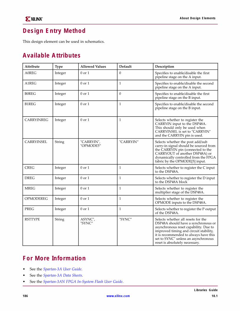
About Design Elements
Design Entry MethodThis design element can be used in schematics.
Available AttributesAttribute Type Allowed Values Default Description
A0REG Integer 0 or 1 0 Specifies to enable/disable the firstpipeline stage on the A input.
A1REG Integer 0 or 1 1 Specifies to enable/disable the secondpipeline stage on the A input.
B0REG Integer 0 or 1 0 Specifies to enable/disable the firstpipeline stage on the B input.
B1REG Integer 0 or 1 1 Specifies to enable/disable the secondpipeline stage on the B input.
CARRYINREG Integer 0 or 1 1 Selects whether to register theCARRYIN input to the DSP48A.This should only be used whenCARRYINSEL is set to "CARRYIN"and the CARRYIN pin is used.
CARRYINSEL String "CARRYIN","OPMODE5”
"CARRYIN” Selects whether the post add/subcarry-in signal should be sourced fromthe CARRYIN pin (connected to theCARRYOUT of another DSP48A) ordynamically controlled from the FPGAfabric by the OPMODE[5] input.
CREG Integer 0 or 1 1 Selects whether to register the C inputto the DSP48A.
DREG Integer 0 or 1 1 Selects whether to register the D inputto the DSP48A block
MREG Integer 0 or 1 1 Selects whether to register themultiplier stage of the DSP48A.
OPMODEREG Integer 0 or 1 1 Selects whether to register theOPMODE inputs to the DSP48A.
PREG Integer 0 or 1 1 Selects whether to register the P outputof the DSP48A.
RSTTYPE String ASYNC","SYNC”
"SYNC” Selects whether all resets for theDSP48A should have a synchronous orasynchronous reset capability. Due toimproved timing and circuit stability,it is recommended to always have thisset to SYNC" unless an asynchronousreset is absolutely necessary.
For More Information• See the Spartan-3A User Guide.• See the Spartan-3A Data Sheets.• See the Spartan-3AN FPGA In-System Flash User Guide.
Libraries Guide
186 www.xilinx.com 10.1

About Design Elements
• See the Spartan-3AN Data Sheets.
Libraries Guide
10.1 www.xilinx.com 187
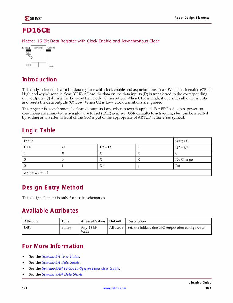
About Design Elements
FD16CEMacro: 16-Bit Data Register with Clock Enable and Asynchronous Clear
IntroductionThis design element is a 16-bit data register with clock enable and asynchronous clear. When clock enable (CE) isHigh and asynchronous clear (CLR) is Low, the data on the data inputs (D) is transferred to the correspondingdata outputs (Q) during the Low-to-High clock (C) transition. When CLR is High, it overrides all other inputsand resets the data outputs (Q) Low. When CE is Low, clock transitions are ignored.
This register is asynchronously cleared, outputs Low, when power is applied. For FPGA devices, power-onconditions are simulated when global set/reset (GSR) is active. GSR defaults to active-High but can be invertedby adding an inverter in front of the GSR input of the appropriate STARTUP_architecture symbol.
Logic TableInputs Outputs
CLR CE Dz – D0 C Qz – Q0
1 X X X 0
0 0 X X No Change
0 1 Dn ↑ Dn
z = bit-width - 1
Design Entry MethodThis design element is only for use in schematics.
Available AttributesAttribute Type Allowed Values Default Description
INIT Binary Any 16-bitValue
All zeros Sets the initial value of Q output after configuration
For More Information• See the Spartan-3A User Guide.• See the Spartan-3A Data Sheets.• See the Spartan-3AN FPGA In-System Flash User Guide.• See the Spartan-3AN Data Sheets.
Libraries Guide
188 www.xilinx.com 10.1
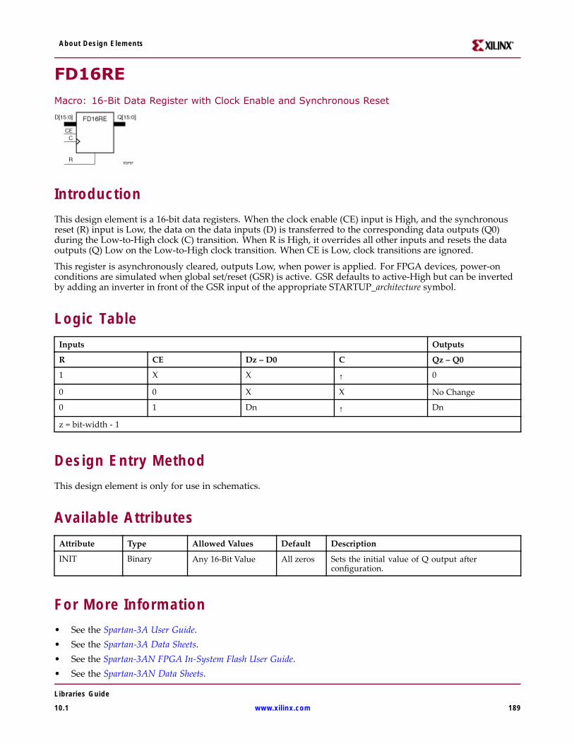
About Design Elements
FD16REMacro: 16-Bit Data Register with Clock Enable and Synchronous Reset
IntroductionThis design element is a 16-bit data registers. When the clock enable (CE) input is High, and the synchronousreset (R) input is Low, the data on the data inputs (D) is transferred to the corresponding data outputs (Q0)during the Low-to-High clock (C) transition. When R is High, it overrides all other inputs and resets the dataoutputs (Q) Low on the Low-to-High clock transition. When CE is Low, clock transitions are ignored.
This register is asynchronously cleared, outputs Low, when power is applied. For FPGA devices, power-onconditions are simulated when global set/reset (GSR) is active. GSR defaults to active-High but can be invertedby adding an inverter in front of the GSR input of the appropriate STARTUP_architecture symbol.
Logic TableInputs Outputs
R CE Dz – D0 C Qz – Q0
1 X X ↑ 0
0 0 X X No Change
0 1 Dn ↑ Dn
z = bit-width - 1
Design Entry MethodThis design element is only for use in schematics.
Available AttributesAttribute Type Allowed Values Default Description
INIT Binary Any 16-Bit Value All zeros Sets the initial value of Q output afterconfiguration.
For More Information• See the Spartan-3A User Guide.• See the Spartan-3A Data Sheets.• See the Spartan-3AN FPGA In-System Flash User Guide.• See the Spartan-3AN Data Sheets.
Libraries Guide
10.1 www.xilinx.com 189
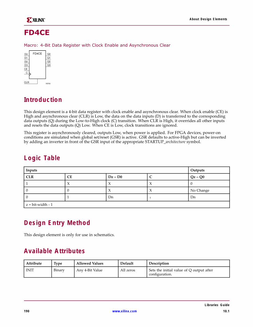
About Design Elements
FD4CE
Macro: 4-Bit Data Register with Clock Enable and Asynchronous Clear
IntroductionThis design element is a 4-bit data register with clock enable and asynchronous clear. When clock enable (CE) isHigh and asynchronous clear (CLR) is Low, the data on the data inputs (D) is transferred to the correspondingdata outputs (Q) during the Low-to-High clock (C) transition. When CLR is High, it overrides all other inputsand resets the data outputs (Q) Low. When CE is Low, clock transitions are ignored.
This register is asynchronously cleared, outputs Low, when power is applied. For FPGA devices, power-onconditions are simulated when global set/reset (GSR) is active. GSR defaults to active-High but can be invertedby adding an inverter in front of the GSR input of the appropriate STARTUP_architecture symbol.
Logic TableInputs Outputs
CLR CE Dz – D0 C Qz – Q0
1 X X X 0
0 0 X X No Change
0 1 Dn ↑ Dn
z = bit-width - 1
Design Entry MethodThis design element is only for use in schematics.
Available AttributesAttribute Type Allowed Values Default Description
INIT Binary Any 4-Bit Value All zeros Sets the initial value of Q output afterconfiguration.
Libraries Guide
190 www.xilinx.com 10.1

About Design Elements
For More Information• See the Spartan-3A User Guide.
• See the Spartan-3A Data Sheets.
• See the Spartan-3AN FPGA In-System Flash User Guide.
• See the Spartan-3AN Data Sheets.
Libraries Guide
10.1 www.xilinx.com 191
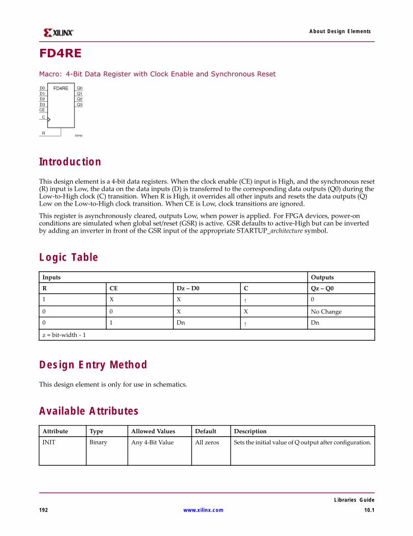
About Design Elements
FD4RE
Macro: 4-Bit Data Register with Clock Enable and Synchronous Reset
IntroductionThis design element is a 4-bit data registers. When the clock enable (CE) input is High, and the synchronous reset(R) input is Low, the data on the data inputs (D) is transferred to the corresponding data outputs (Q0) during theLow-to-High clock (C) transition. When R is High, it overrides all other inputs and resets the data outputs (Q)Low on the Low-to-High clock transition. When CE is Low, clock transitions are ignored.
This register is asynchronously cleared, outputs Low, when power is applied. For FPGA devices, power-onconditions are simulated when global set/reset (GSR) is active. GSR defaults to active-High but can be invertedby adding an inverter in front of the GSR input of the appropriate STARTUP_architecture symbol.
Logic TableInputs Outputs
R CE Dz – D0 C Qz – Q0
1 X X ↑ 0
0 0 X X No Change
0 1 Dn ↑ Dn
z = bit-width - 1
Design Entry MethodThis design element is only for use in schematics.
Available AttributesAttribute Type Allowed Values Default Description
INIT Binary Any 4-Bit Value All zeros Sets the initial value of Q output after configuration.
Libraries Guide
192 www.xilinx.com 10.1

About Design Elements
For More Information• See the Spartan-3A User Guide.
• See the Spartan-3A Data Sheets.
• See the Spartan-3AN FPGA In-System Flash User Guide.
• See the Spartan-3AN Data Sheets.
Libraries Guide
10.1 www.xilinx.com 193
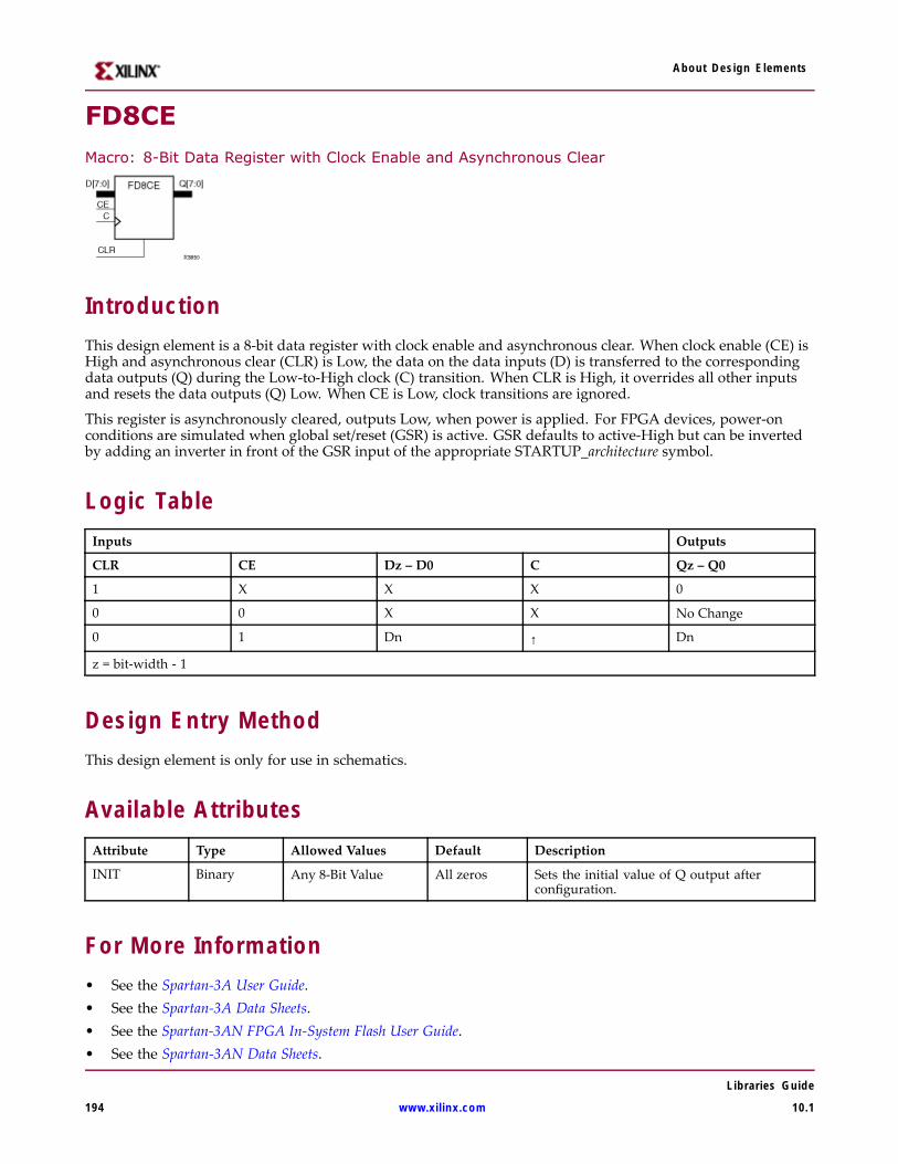
About Design Elements
FD8CEMacro: 8-Bit Data Register with Clock Enable and Asynchronous Clear
IntroductionThis design element is a 8-bit data register with clock enable and asynchronous clear. When clock enable (CE) isHigh and asynchronous clear (CLR) is Low, the data on the data inputs (D) is transferred to the correspondingdata outputs (Q) during the Low-to-High clock (C) transition. When CLR is High, it overrides all other inputsand resets the data outputs (Q) Low. When CE is Low, clock transitions are ignored.
This register is asynchronously cleared, outputs Low, when power is applied. For FPGA devices, power-onconditions are simulated when global set/reset (GSR) is active. GSR defaults to active-High but can be invertedby adding an inverter in front of the GSR input of the appropriate STARTUP_architecture symbol.
Logic TableInputs Outputs
CLR CE Dz – D0 C Qz – Q0
1 X X X 0
0 0 X X No Change
0 1 Dn ↑ Dn
z = bit-width - 1
Design Entry MethodThis design element is only for use in schematics.
Available AttributesAttribute Type Allowed Values Default Description
INIT Binary Any 8-Bit Value All zeros Sets the initial value of Q output afterconfiguration.
For More Information• See the Spartan-3A User Guide.• See the Spartan-3A Data Sheets.• See the Spartan-3AN FPGA In-System Flash User Guide.• See the Spartan-3AN Data Sheets.
Libraries Guide
194 www.xilinx.com 10.1
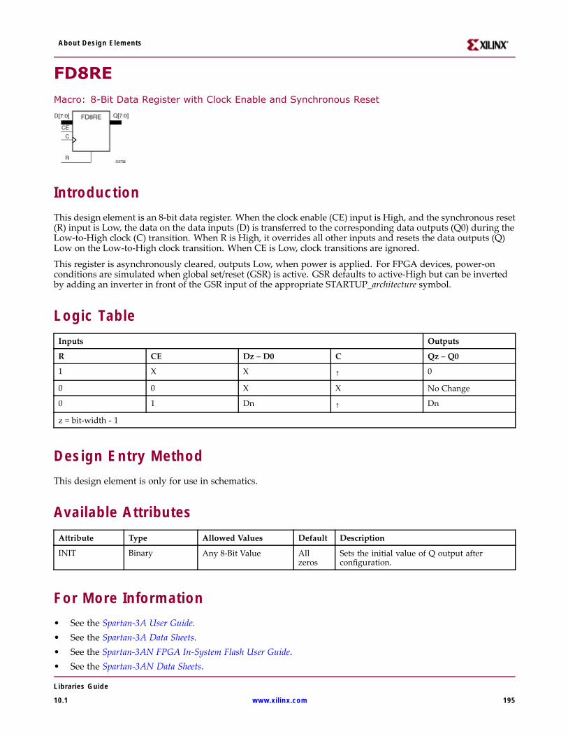
About Design Elements
FD8REMacro: 8-Bit Data Register with Clock Enable and Synchronous Reset
IntroductionThis design element is an 8-bit data register. When the clock enable (CE) input is High, and the synchronous reset(R) input is Low, the data on the data inputs (D) is transferred to the corresponding data outputs (Q0) during theLow-to-High clock (C) transition. When R is High, it overrides all other inputs and resets the data outputs (Q)Low on the Low-to-High clock transition. When CE is Low, clock transitions are ignored.
This register is asynchronously cleared, outputs Low, when power is applied. For FPGA devices, power-onconditions are simulated when global set/reset (GSR) is active. GSR defaults to active-High but can be invertedby adding an inverter in front of the GSR input of the appropriate STARTUP_architecture symbol.
Logic TableInputs Outputs
R CE Dz – D0 C Qz – Q0
1 X X ↑ 0
0 0 X X No Change
0 1 Dn ↑ Dn
z = bit-width - 1
Design Entry MethodThis design element is only for use in schematics.
Available AttributesAttribute Type Allowed Values Default Description
INIT Binary Any 8-Bit Value Allzeros
Sets the initial value of Q output afterconfiguration.
For More Information• See the Spartan-3A User Guide.• See the Spartan-3A Data Sheets.• See the Spartan-3AN FPGA In-System Flash User Guide.• See the Spartan-3AN Data Sheets.
Libraries Guide
10.1 www.xilinx.com 195
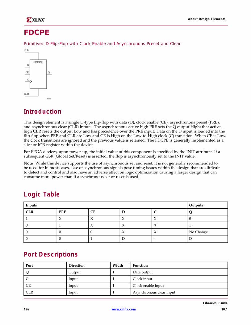
About Design Elements
FDCPEPrimitive: D Flip-Flop with Clock Enable and Asynchronous Preset and Clear
IntroductionThis design element is a single D-type flip-flop with data (D), clock enable (CE), asynchronous preset (PRE),and asynchronous clear (CLR) inputs. The asynchronous active high PRE sets the Q output High; that activehigh CLR resets the output Low and has precedence over the PRE input. Data on the D input is loaded into theflip-flop when PRE and CLR are Low and CE is High on the Low-to-High clock (C) transition. When CE is Low,the clock transitions are ignored and the previous value is retained. The FDCPE is generally implemented as aslice or IOB register within the device.
For FPGA devices, upon power-up, the initial value of this component is specified by the INIT attribute. If asubsequent GSR (Global Set/Reset) is asserted, the flop is asynchronously set to the INIT value.
Note While this device supports the use of asynchronous set and reset, it is not generally recommended tobe used for in most cases. Use of asynchronous signals pose timing issues within the design that are difficultto detect and control and also have an adverse affect on logic optimization causing a larger design that canconsume more power than if a synchronous set or reset is used.
Logic TableInputs Outputs
CLR PRE CE D C Q
1 X X X X 0
0 1 X X X 1
0 0 0 X X No Change
0 0 1 D ↑ D
Port DescriptionsPort Direction Width Function
Q Output 1 Data output
C Input 1 Clock input
CE Input 1 Clock enable input
CLR Input 1 Asynchronous clear input
Libraries Guide
196 www.xilinx.com 10.1
About Design Elements
Port Direction Width Function
D Input 1 Data input
PRE Input 1 Asynchronous set input
Design Entry MethodThis design element can be used in schematics.
Available AttributesAttribute Type Allowed Values Default Description
INIT Binary 0,1 0 Sets the initial value of Q output afterconfiguration and on GSR.
Libraries Guide
10.1 www.xilinx.com 197

About Design Elements
For More Information• See the Spartan-3A User Guide.
• See the Spartan-3A Data Sheets.
• See the Spartan-3AN FPGA In-System Flash User Guide.
• See the Spartan-3AN Data Sheets.
Libraries Guide
198 www.xilinx.com 10.1
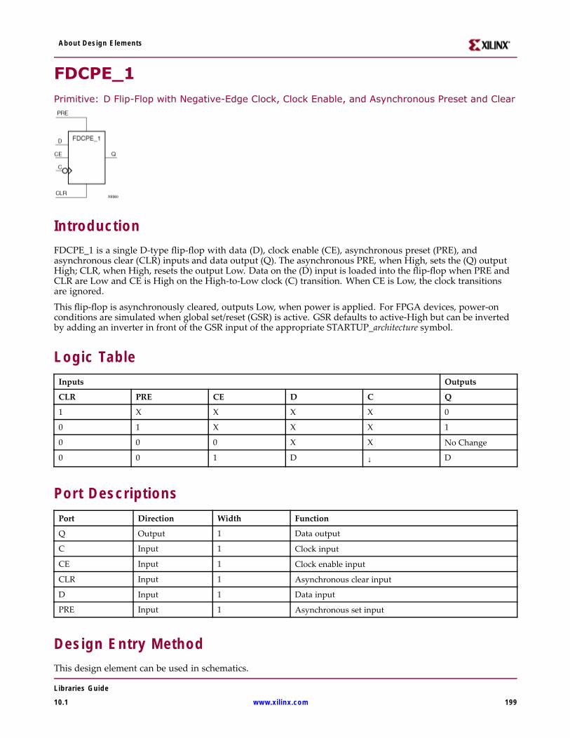
About Design Elements
FDCPE_1Primitive: D Flip-Flop with Negative-Edge Clock, Clock Enable, and Asynchronous Preset and Clear
IntroductionFDCPE_1 is a single D-type flip-flop with data (D), clock enable (CE), asynchronous preset (PRE), andasynchronous clear (CLR) inputs and data output (Q). The asynchronous PRE, when High, sets the (Q) outputHigh; CLR, when High, resets the output Low. Data on the (D) input is loaded into the flip-flop when PRE andCLR are Low and CE is High on the High-to-Low clock (C) transition. When CE is Low, the clock transitionsare ignored.
This flip-flop is asynchronously cleared, outputs Low, when power is applied. For FPGA devices, power-onconditions are simulated when global set/reset (GSR) is active. GSR defaults to active-High but can be invertedby adding an inverter in front of the GSR input of the appropriate STARTUP_architecture symbol.
Logic TableInputs Outputs
CLR PRE CE D C Q
1 X X X X 0
0 1 X X X 1
0 0 0 X X No Change
0 0 1 D ↓ D
Port DescriptionsPort Direction Width Function
Q Output 1 Data output
C Input 1 Clock input
CE Input 1 Clock enable input
CLR Input 1 Asynchronous clear input
D Input 1 Data input
PRE Input 1 Asynchronous set input
Design Entry MethodThis design element can be used in schematics.
Libraries Guide
10.1 www.xilinx.com 199

About Design Elements
Available AttributesAttribute Type Allowed Values Default Description
INIT Binary 0,1 0 Sets the initial value of Q output afterconfiguration.
For More Information• See the Spartan-3A User Guide.
• See the Spartan-3A Data Sheets.
• See the Spartan-3AN FPGA In-System Flash User Guide.
• See the Spartan-3AN Data Sheets.
Libraries Guide
200 www.xilinx.com 10.1
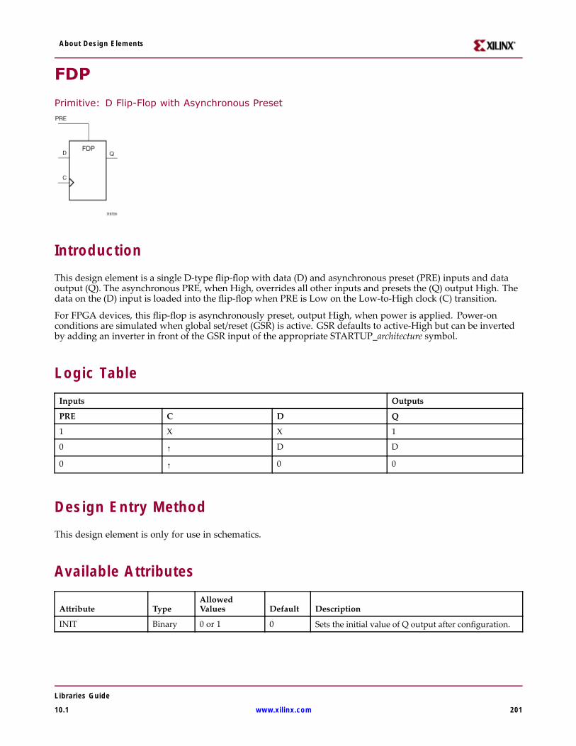
About Design Elements
FDP
Primitive: D Flip-Flop with Asynchronous Preset
IntroductionThis design element is a single D-type flip-flop with data (D) and asynchronous preset (PRE) inputs and dataoutput (Q). The asynchronous PRE, when High, overrides all other inputs and presets the (Q) output High. Thedata on the (D) input is loaded into the flip-flop when PRE is Low on the Low-to-High clock (C) transition.
For FPGA devices, this flip-flop is asynchronously preset, output High, when power is applied. Power-onconditions are simulated when global set/reset (GSR) is active. GSR defaults to active-High but can be invertedby adding an inverter in front of the GSR input of the appropriate STARTUP_architecture symbol.
Logic TableInputs Outputs
PRE C D Q
1 X X 1
0 ↑ D D
0 ↑ 0 0
Design Entry MethodThis design element is only for use in schematics.
Available Attributes
Attribute TypeAllowedValues Default Description
INIT Binary 0 or 1 0 Sets the initial value of Q output after configuration.
Libraries Guide
10.1 www.xilinx.com 201

About Design Elements
For More Information• See the Spartan-3A User Guide.
• See the Spartan-3A Data Sheets.
• See the Spartan-3AN FPGA In-System Flash User Guide.
• See the Spartan-3AN Data Sheets.
Libraries Guide
202 www.xilinx.com 10.1
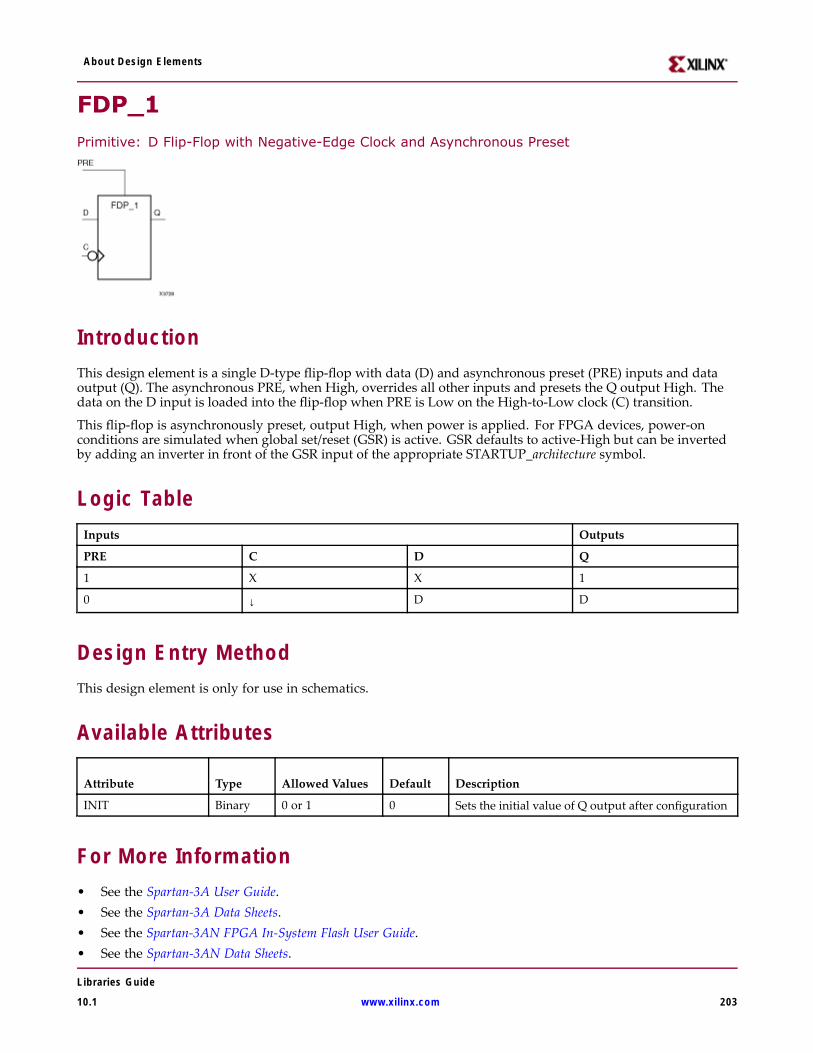
About Design Elements
FDP_1Primitive: D Flip-Flop with Negative-Edge Clock and Asynchronous Preset
IntroductionThis design element is a single D-type flip-flop with data (D) and asynchronous preset (PRE) inputs and dataoutput (Q). The asynchronous PRE, when High, overrides all other inputs and presets the Q output High. Thedata on the D input is loaded into the flip-flop when PRE is Low on the High-to-Low clock (C) transition.
This flip-flop is asynchronously preset, output High, when power is applied. For FPGA devices, power-onconditions are simulated when global set/reset (GSR) is active. GSR defaults to active-High but can be invertedby adding an inverter in front of the GSR input of the appropriate STARTUP_architecture symbol.
Logic TableInputs Outputs
PRE C D Q
1 X X 1
0 ↓ D D
Design Entry MethodThis design element is only for use in schematics.
Available Attributes
Attribute Type Allowed Values Default Description
INIT Binary 0 or 1 0 Sets the initial value of Q output after configuration
For More Information• See the Spartan-3A User Guide.• See the Spartan-3A Data Sheets.• See the Spartan-3AN FPGA In-System Flash User Guide.• See the Spartan-3AN Data Sheets.
Libraries Guide
10.1 www.xilinx.com 203
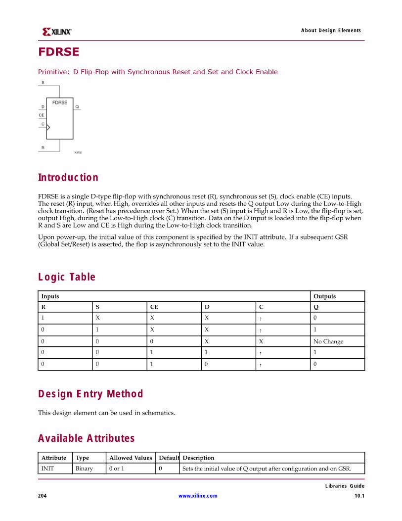
About Design Elements
FDRSE
Primitive: D Flip-Flop with Synchronous Reset and Set and Clock Enable
IntroductionFDRSE is a single D-type flip-flop with synchronous reset (R), synchronous set (S), clock enable (CE) inputs.The reset (R) input, when High, overrides all other inputs and resets the Q output Low during the Low-to-Highclock transition. (Reset has precedence over Set.) When the set (S) input is High and R is Low, the flip-flop is set,output High, during the Low-to-High clock (C) transition. Data on the D input is loaded into the flip-flop whenR and S are Low and CE is High during the Low-to-High clock transition.
Upon power-up, the initial value of this component is specified by the INIT attribute. If a subsequent GSR(Global Set/Reset) is asserted, the flop is asynchronously set to the INIT value.
Logic TableInputs Outputs
R S CE D C Q
1 X X X ↑ 0
0 1 X X ↑ 1
0 0 0 X X No Change
0 0 1 1 ↑ 1
0 0 1 0 ↑ 0
Design Entry MethodThis design element can be used in schematics.
Available AttributesAttribute Type Allowed Values Default Description
INIT Binary 0 or 1 0 Sets the initial value of Q output after configuration and on GSR.
Libraries Guide
204 www.xilinx.com 10.1

About Design Elements
For More Information• See the Spartan-3A User Guide.
• See the Spartan-3A Data Sheets.
• See the Spartan-3AN FPGA In-System Flash User Guide.
• See the Spartan-3AN Data Sheets.
Libraries Guide
10.1 www.xilinx.com 205
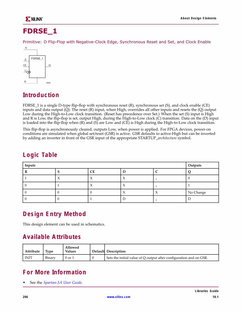
About Design Elements
FDRSE_1Primitive: D Flip-Flop with Negative-Clock Edge, Synchronous Reset and Set, and Clock Enable
IntroductionFDRSE_1 is a single D-type flip-flop with synchronous reset (R), synchronous set (S), and clock enable (CE)inputs and data output (Q). The reset (R) input, when High, overrides all other inputs and resets the (Q) outputLow during the High-to-Low clock transition. (Reset has precedence over Set.) When the set (S) input is Highand R is Low, the flip-flop is set, output High, during the High-to-Low clock (C) transition. Data on the (D) inputis loaded into the flip-flop when (R) and (S) are Low and (CE) is High during the High-to-Low clock transition.
This flip-flop is asynchronously cleared, outputs Low, when power is applied. For FPGA devices, power-onconditions are simulated when global set/reset (GSR) is active. GSR defaults to active-High but can be invertedby adding an inverter in front of the GSR input of the appropriate STARTUP_architecture symbol.
Logic TableInputs Outputs
R S CE D C Q
1 X X X ↓ 0
0 1 X X ↓ 1
0 0 0 X X No Change
0 0 1 D ↓ D
Design Entry MethodThis design element can be used in schematics.
Available Attributes
Attribute TypeAllowedValues Default Description
INIT Binary 0 or 1 0 Sets the initial value of Q output after configuration and on GSR.
For More Information• See the Spartan-3A User Guide.
Libraries Guide
206 www.xilinx.com 10.1

About Design Elements
• See the Spartan-3A Data Sheets.
• See the Spartan-3AN FPGA In-System Flash User Guide.
• See the Spartan-3AN Data Sheets.
Libraries Guide
10.1 www.xilinx.com 207
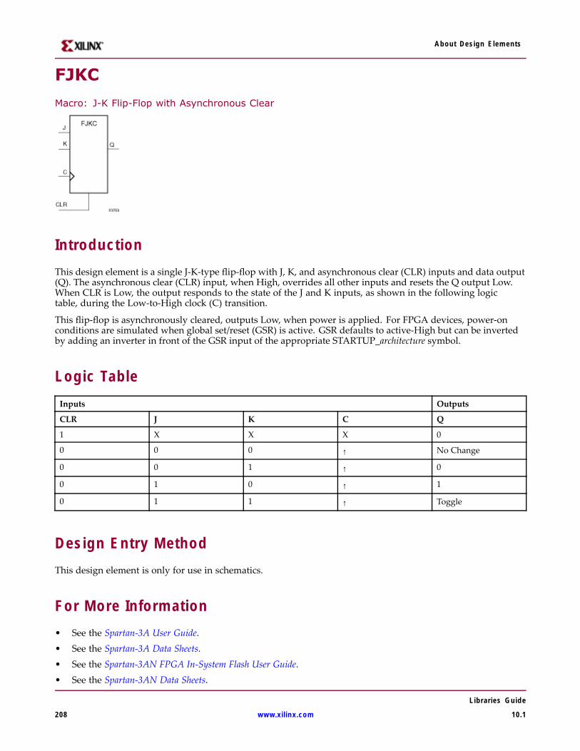
About Design Elements
FJKC
Macro: J-K Flip-Flop with Asynchronous Clear
IntroductionThis design element is a single J-K-type flip-flop with J, K, and asynchronous clear (CLR) inputs and data output(Q). The asynchronous clear (CLR) input, when High, overrides all other inputs and resets the Q output Low.When CLR is Low, the output responds to the state of the J and K inputs, as shown in the following logictable, during the Low-to-High clock (C) transition.
This flip-flop is asynchronously cleared, outputs Low, when power is applied. For FPGA devices, power-onconditions are simulated when global set/reset (GSR) is active. GSR defaults to active-High but can be invertedby adding an inverter in front of the GSR input of the appropriate STARTUP_architecture symbol.
Logic TableInputs Outputs
CLR J K C Q
1 X X X 0
0 0 0 ↑ No Change
0 0 1 ↑ 0
0 1 0 ↑ 1
0 1 1 ↑ Toggle
Design Entry MethodThis design element is only for use in schematics.
For More Information• See the Spartan-3A User Guide.• See the Spartan-3A Data Sheets.• See the Spartan-3AN FPGA In-System Flash User Guide.• See the Spartan-3AN Data Sheets.
Libraries Guide
208 www.xilinx.com 10.1
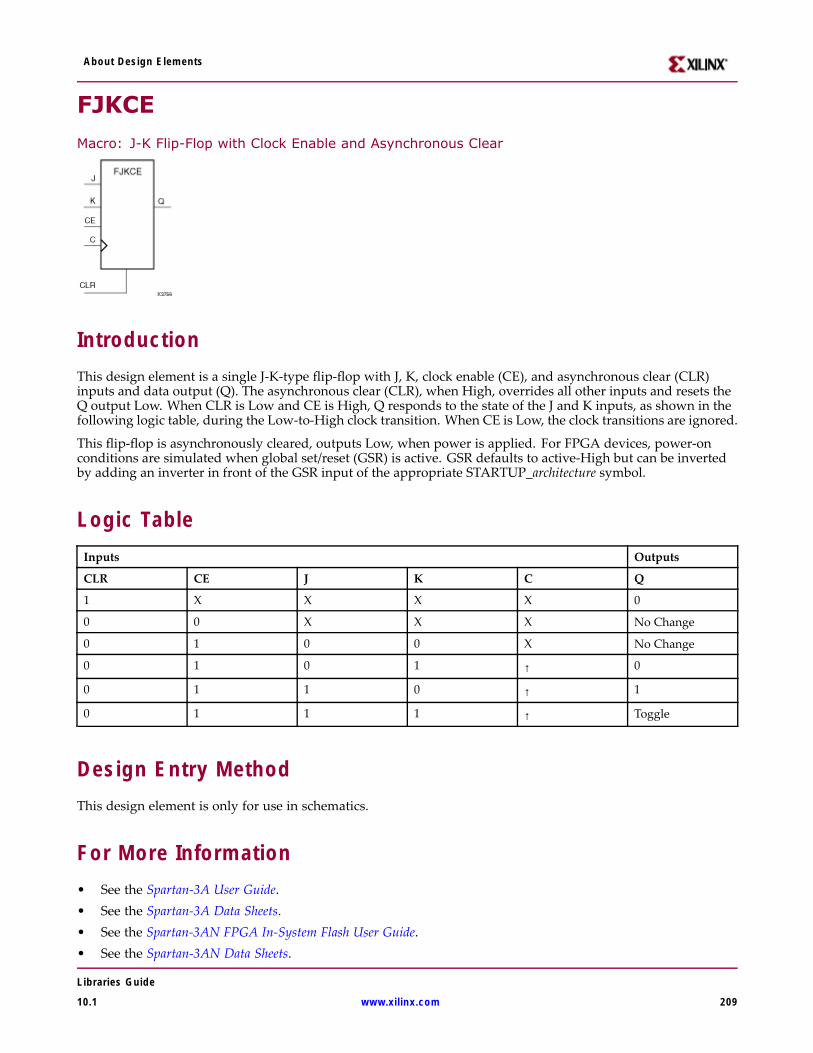
About Design Elements
FJKCE
Macro: J-K Flip-Flop with Clock Enable and Asynchronous Clear
IntroductionThis design element is a single J-K-type flip-flop with J, K, clock enable (CE), and asynchronous clear (CLR)inputs and data output (Q). The asynchronous clear (CLR), when High, overrides all other inputs and resets theQ output Low. When CLR is Low and CE is High, Q responds to the state of the J and K inputs, as shown in thefollowing logic table, during the Low-to-High clock transition. When CE is Low, the clock transitions are ignored.
This flip-flop is asynchronously cleared, outputs Low, when power is applied. For FPGA devices, power-onconditions are simulated when global set/reset (GSR) is active. GSR defaults to active-High but can be invertedby adding an inverter in front of the GSR input of the appropriate STARTUP_architecture symbol.
Logic TableInputs Outputs
CLR CE J K C Q
1 X X X X 0
0 0 X X X No Change
0 1 0 0 X No Change
0 1 0 1 ↑ 0
0 1 1 0 ↑ 1
0 1 1 1 ↑ Toggle
Design Entry MethodThis design element is only for use in schematics.
For More Information• See the Spartan-3A User Guide.• See the Spartan-3A Data Sheets.• See the Spartan-3AN FPGA In-System Flash User Guide.• See the Spartan-3AN Data Sheets.
Libraries Guide
10.1 www.xilinx.com 209
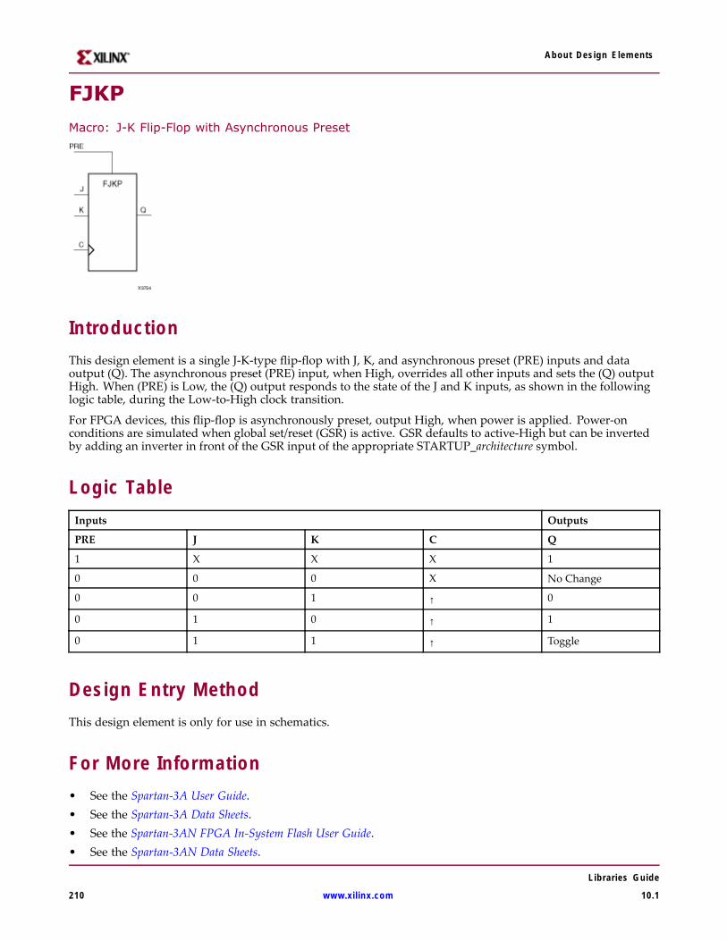
About Design Elements
FJKP
Macro: J-K Flip-Flop with Asynchronous Preset
IntroductionThis design element is a single J-K-type flip-flop with J, K, and asynchronous preset (PRE) inputs and dataoutput (Q). The asynchronous preset (PRE) input, when High, overrides all other inputs and sets the (Q) outputHigh. When (PRE) is Low, the (Q) output responds to the state of the J and K inputs, as shown in the followinglogic table, during the Low-to-High clock transition.
For FPGA devices, this flip-flop is asynchronously preset, output High, when power is applied. Power-onconditions are simulated when global set/reset (GSR) is active. GSR defaults to active-High but can be invertedby adding an inverter in front of the GSR input of the appropriate STARTUP_architecture symbol.
Logic TableInputs Outputs
PRE J K C Q
1 X X X 1
0 0 0 X No Change
0 0 1 ↑ 0
0 1 0 ↑ 1
0 1 1 ↑ Toggle
Design Entry MethodThis design element is only for use in schematics.
For More Information• See the Spartan-3A User Guide.• See the Spartan-3A Data Sheets.• See the Spartan-3AN FPGA In-System Flash User Guide.• See the Spartan-3AN Data Sheets.
Libraries Guide
210 www.xilinx.com 10.1
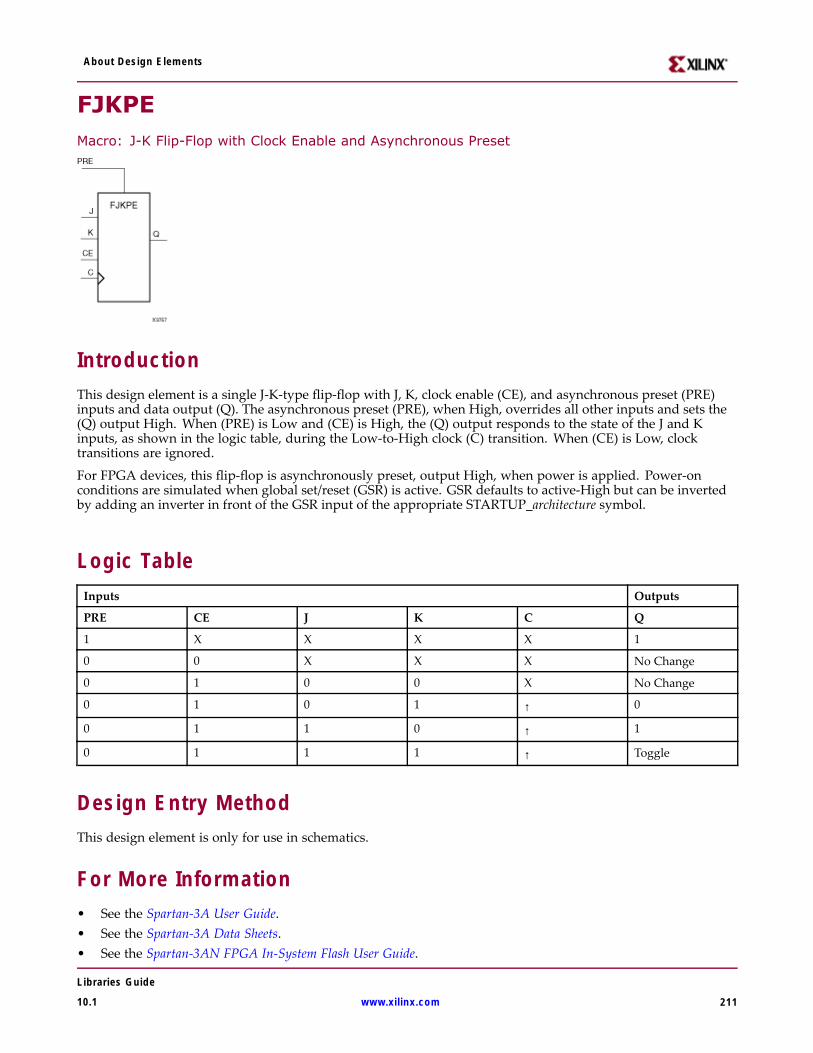
About Design Elements
FJKPEMacro: J-K Flip-Flop with Clock Enable and Asynchronous Preset
IntroductionThis design element is a single J-K-type flip-flop with J, K, clock enable (CE), and asynchronous preset (PRE)inputs and data output (Q). The asynchronous preset (PRE), when High, overrides all other inputs and sets the(Q) output High. When (PRE) is Low and (CE) is High, the (Q) output responds to the state of the J and Kinputs, as shown in the logic table, during the Low-to-High clock (C) transition. When (CE) is Low, clocktransitions are ignored.
For FPGA devices, this flip-flop is asynchronously preset, output High, when power is applied. Power-onconditions are simulated when global set/reset (GSR) is active. GSR defaults to active-High but can be invertedby adding an inverter in front of the GSR input of the appropriate STARTUP_architecture symbol.
Logic TableInputs Outputs
PRE CE J K C Q
1 X X X X 1
0 0 X X X No Change
0 1 0 0 X No Change
0 1 0 1 ↑ 0
0 1 1 0 ↑ 1
0 1 1 1 ↑ Toggle
Design Entry MethodThis design element is only for use in schematics.
For More Information• See the Spartan-3A User Guide.• See the Spartan-3A Data Sheets.• See the Spartan-3AN FPGA In-System Flash User Guide.
Libraries Guide
10.1 www.xilinx.com 211

About Design Elements
• See the Spartan-3AN Data Sheets.
Libraries Guide
212 www.xilinx.com 10.1

About Design Elements
FJKRSEMacro: J-K Flip-Flop with Clock Enable and Synchronous Reset and Set
IntroductionThis design element is a single J-K-type flip-flop with J, K, synchronous reset (R), synchronous set (S), and clockenable (CE) inputs and data output (Q). When synchronous reset (R) is High during the Low-to-High clock (C)transition, all other inputs are ignored and output (Q) is reset Low. When synchronous set (S) is High and (R) isLow, output (Q) is set High. When (R) and (S) are Low and (CE) is High, output (Q) responds to the state ofthe J and K inputs, according to the following logic table, during the Low-to-High clock (C) transition. When(CE) is Low, clock transitions are ignored.
This flip-flop is asynchronously cleared, outputs Low, when power is applied. For FPGA devices, power-onconditions are simulated when global set/reset (GSR) is active. GSR defaults to active-High but can be invertedby adding an inverter in front of the GSR input of the appropriate STARTUP_architecture symbol.
Logic TableInputs Outputs
R S CE J K C Q
1 X X X X ↑ 0
0 1 X X X ↑ 1
0 0 0 X X X No Change
0 0 1 0 0 X No Change
0 0 1 0 1 ↑ 0
0 0 1 1 1 ↑ Toggle
0 0 1 1 0 ↑ 1
Design Entry MethodThis design element is only for use in schematics.
For More Information• See the Spartan-3A User Guide.
Libraries Guide
10.1 www.xilinx.com 213

About Design Elements
• See the Spartan-3A Data Sheets.
• See the Spartan-3AN FPGA In-System Flash User Guide.
• See the Spartan-3AN Data Sheets.
Libraries Guide
214 www.xilinx.com 10.1
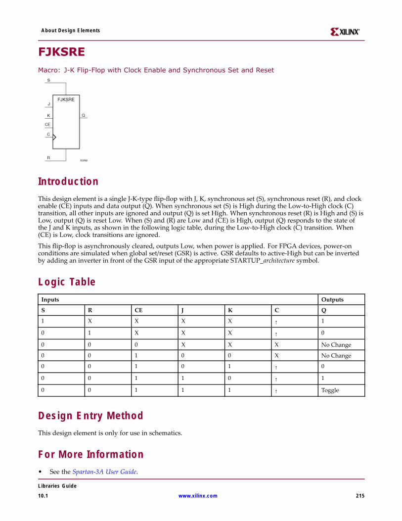
About Design Elements
FJKSREMacro: J-K Flip-Flop with Clock Enable and Synchronous Set and Reset
IntroductionThis design element is a single J-K-type flip-flop with J, K, synchronous set (S), synchronous reset (R), and clockenable (CE) inputs and data output (Q). When synchronous set (S) is High during the Low-to-High clock (C)transition, all other inputs are ignored and output (Q) is set High. When synchronous reset (R) is High and (S) isLow, output (Q) is reset Low. When (S) and (R) are Low and (CE) is High, output (Q) responds to the state ofthe J and K inputs, as shown in the following logic table, during the Low-to-High clock (C) transition. When(CE) is Low, clock transitions are ignored.
This flip-flop is asynchronously cleared, outputs Low, when power is applied. For FPGA devices, power-onconditions are simulated when global set/reset (GSR) is active. GSR defaults to active-High but can be invertedby adding an inverter in front of the GSR input of the appropriate STARTUP_architecture symbol.
Logic TableInputs Outputs
S R CE J K C Q
1 X X X X ↑ 1
0 1 X X X ↑ 0
0 0 0 X X X No Change
0 0 1 0 0 X No Change
0 0 1 0 1 ↑ 0
0 0 1 1 0 ↑ 1
0 0 1 1 1 ↑ Toggle
Design Entry MethodThis design element is only for use in schematics.
For More Information• See the Spartan-3A User Guide.
Libraries Guide
10.1 www.xilinx.com 215

About Design Elements
• See the Spartan-3A Data Sheets.
• See the Spartan-3AN FPGA In-System Flash User Guide.
• See the Spartan-3AN Data Sheets.
Libraries Guide
216 www.xilinx.com 10.1
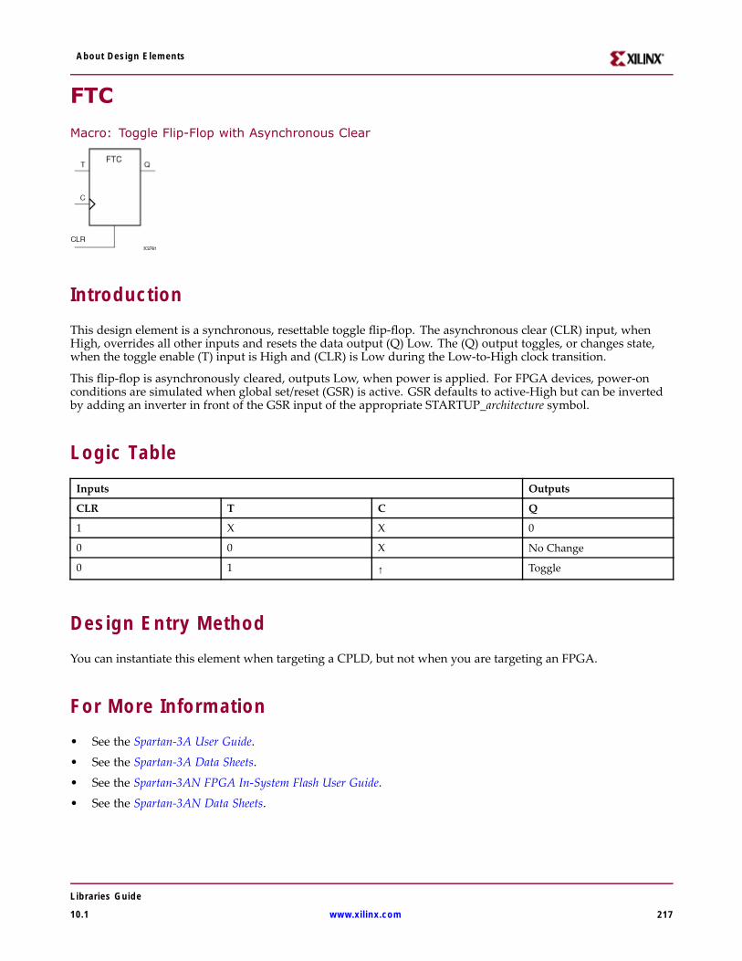
About Design Elements
FTC
Macro: Toggle Flip-Flop with Asynchronous Clear
IntroductionThis design element is a synchronous, resettable toggle flip-flop. The asynchronous clear (CLR) input, whenHigh, overrides all other inputs and resets the data output (Q) Low. The (Q) output toggles, or changes state,when the toggle enable (T) input is High and (CLR) is Low during the Low-to-High clock transition.
This flip-flop is asynchronously cleared, outputs Low, when power is applied. For FPGA devices, power-onconditions are simulated when global set/reset (GSR) is active. GSR defaults to active-High but can be invertedby adding an inverter in front of the GSR input of the appropriate STARTUP_architecture symbol.
Logic TableInputs Outputs
CLR T C Q
1 X X 0
0 0 X No Change
0 1 ↑ Toggle
Design Entry MethodYou can instantiate this element when targeting a CPLD, but not when you are targeting an FPGA.
For More Information• See the Spartan-3A User Guide.
• See the Spartan-3A Data Sheets.
• See the Spartan-3AN FPGA In-System Flash User Guide.
• See the Spartan-3AN Data Sheets.
Libraries Guide
10.1 www.xilinx.com 217
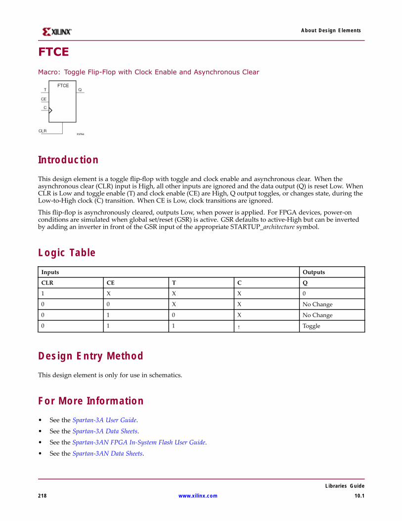
About Design Elements
FTCE
Macro: Toggle Flip-Flop with Clock Enable and Asynchronous Clear
IntroductionThis design element is a toggle flip-flop with toggle and clock enable and asynchronous clear. When theasynchronous clear (CLR) input is High, all other inputs are ignored and the data output (Q) is reset Low. WhenCLR is Low and toggle enable (T) and clock enable (CE) are High, Q output toggles, or changes state, during theLow-to-High clock (C) transition. When CE is Low, clock transitions are ignored.
This flip-flop is asynchronously cleared, outputs Low, when power is applied. For FPGA devices, power-onconditions are simulated when global set/reset (GSR) is active. GSR defaults to active-High but can be invertedby adding an inverter in front of the GSR input of the appropriate STARTUP_architecture symbol.
Logic TableInputs Outputs
CLR CE T C Q
1 X X X 0
0 0 X X No Change
0 1 0 X No Change
0 1 1 ↑ Toggle
Design Entry MethodThis design element is only for use in schematics.
For More Information• See the Spartan-3A User Guide.
• See the Spartan-3A Data Sheets.
• See the Spartan-3AN FPGA In-System Flash User Guide.
• See the Spartan-3AN Data Sheets.
Libraries Guide
218 www.xilinx.com 10.1
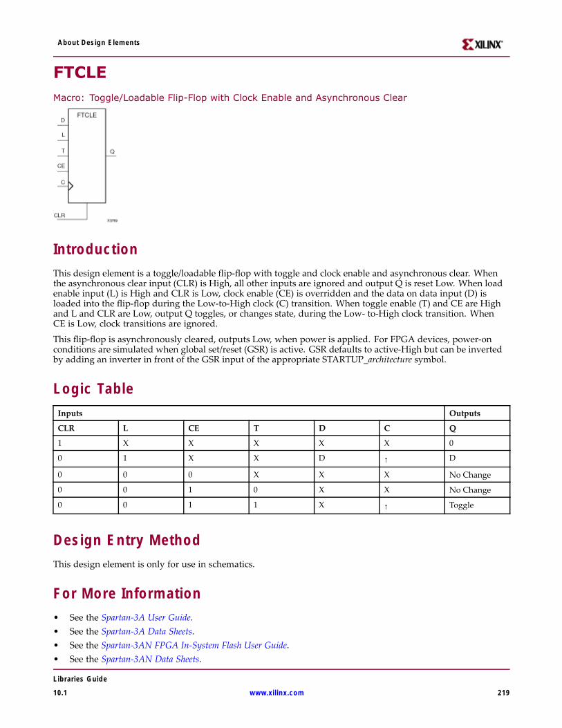
About Design Elements
FTCLEMacro: Toggle/Loadable Flip-Flop with Clock Enable and Asynchronous Clear
IntroductionThis design element is a toggle/loadable flip-flop with toggle and clock enable and asynchronous clear. Whenthe asynchronous clear input (CLR) is High, all other inputs are ignored and output Q is reset Low. When loadenable input (L) is High and CLR is Low, clock enable (CE) is overridden and the data on data input (D) isloaded into the flip-flop during the Low-to-High clock (C) transition. When toggle enable (T) and CE are Highand L and CLR are Low, output Q toggles, or changes state, during the Low- to-High clock transition. WhenCE is Low, clock transitions are ignored.
This flip-flop is asynchronously cleared, outputs Low, when power is applied. For FPGA devices, power-onconditions are simulated when global set/reset (GSR) is active. GSR defaults to active-High but can be invertedby adding an inverter in front of the GSR input of the appropriate STARTUP_architecture symbol.
Logic TableInputs Outputs
CLR L CE T D C Q
1 X X X X X 0
0 1 X X D ↑ D
0 0 0 X X X No Change
0 0 1 0 X X No Change
0 0 1 1 X ↑ Toggle
Design Entry MethodThis design element is only for use in schematics.
For More Information• See the Spartan-3A User Guide.• See the Spartan-3A Data Sheets.• See the Spartan-3AN FPGA In-System Flash User Guide.• See the Spartan-3AN Data Sheets.
Libraries Guide
10.1 www.xilinx.com 219
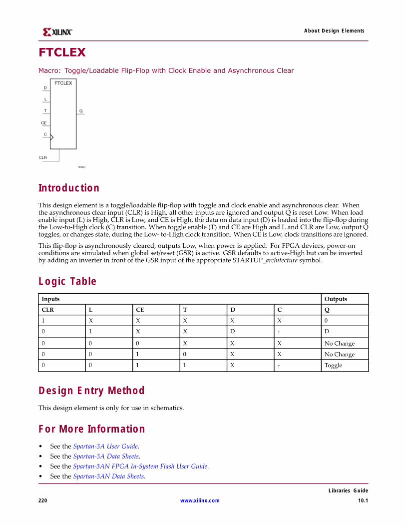
About Design Elements
FTCLEXMacro: Toggle/Loadable Flip-Flop with Clock Enable and Asynchronous Clear
IntroductionThis design element is a toggle/loadable flip-flop with toggle and clock enable and asynchronous clear. Whenthe asynchronous clear input (CLR) is High, all other inputs are ignored and output Q is reset Low. When loadenable input (L) is High, CLR is Low, and CE is High, the data on data input (D) is loaded into the flip-flop duringthe Low-to-High clock (C) transition. When toggle enable (T) and CE are High and L and CLR are Low, output Qtoggles, or changes state, during the Low- to-High clock transition. When CE is Low, clock transitions are ignored.
This flip-flop is asynchronously cleared, outputs Low, when power is applied. For FPGA devices, power-onconditions are simulated when global set/reset (GSR) is active. GSR defaults to active-High but can be invertedby adding an inverter in front of the GSR input of the appropriate STARTUP_architecture symbol.
Logic TableInputs Outputs
CLR L CE T D C Q
1 X X X X X 0
0 1 X X D ↑ D
0 0 0 X X X No Change
0 0 1 0 X X No Change
0 0 1 1 X ↑ Toggle
Design Entry MethodThis design element is only for use in schematics.
For More Information• See the Spartan-3A User Guide.• See the Spartan-3A Data Sheets.• See the Spartan-3AN FPGA In-System Flash User Guide.• See the Spartan-3AN Data Sheets.
Libraries Guide
220 www.xilinx.com 10.1
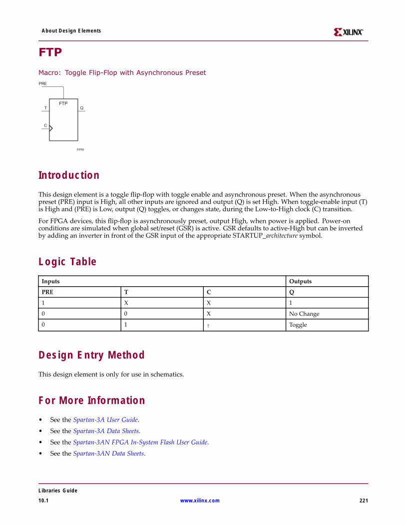
About Design Elements
FTP
Macro: Toggle Flip-Flop with Asynchronous Preset
IntroductionThis design element is a toggle flip-flop with toggle enable and asynchronous preset. When the asynchronouspreset (PRE) input is High, all other inputs are ignored and output (Q) is set High. When toggle-enable input (T)is High and (PRE) is Low, output (Q) toggles, or changes state, during the Low-to-High clock (C) transition.
For FPGA devices, this flip-flop is asynchronously preset, output High, when power is applied. Power-onconditions are simulated when global set/reset (GSR) is active. GSR defaults to active-High but can be invertedby adding an inverter in front of the GSR input of the appropriate STARTUP_architecture symbol.
Logic TableInputs Outputs
PRE T C Q
1 X X 1
0 0 X No Change
0 1 ↑ Toggle
Design Entry MethodThis design element is only for use in schematics.
For More Information• See the Spartan-3A User Guide.
• See the Spartan-3A Data Sheets.
• See the Spartan-3AN FPGA In-System Flash User Guide.
• See the Spartan-3AN Data Sheets.
Libraries Guide
10.1 www.xilinx.com 221
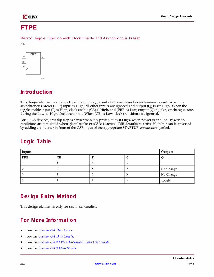
About Design Elements
FTPE
Macro: Toggle Flip-Flop with Clock Enable and Asynchronous Preset
IntroductionThis design element is a toggle flip-flop with toggle and clock enable and asynchronous preset. When theasynchronous preset (PRE) input is High, all other inputs are ignored and output (Q) is set High. When thetoggle enable input (T) is High, clock enable (CE) is High, and (PRE) is Low, output (Q) toggles, or changes state,during the Low-to-High clock transition. When (CE) is Low, clock transitions are ignored.
For FPGA devices, this flip-flop is asynchronously preset, output High, when power is applied. Power-onconditions are simulated when global set/reset (GSR) is active. GSR defaults to active-High but can be invertedby adding an inverter in front of the GSR input of the appropriate STARTUP_architecture symbol.
Logic TableInputs Outputs
PRE CE T C Q
1 X X X 1
0 0 X X No Change
0 1 0 X No Change
0 1 1 ↑ Toggle
Design Entry MethodThis design element is only for use in schematics.
For More Information• See the Spartan-3A User Guide.
• See the Spartan-3A Data Sheets.
• See the Spartan-3AN FPGA In-System Flash User Guide.
• See the Spartan-3AN Data Sheets.
Libraries Guide
222 www.xilinx.com 10.1
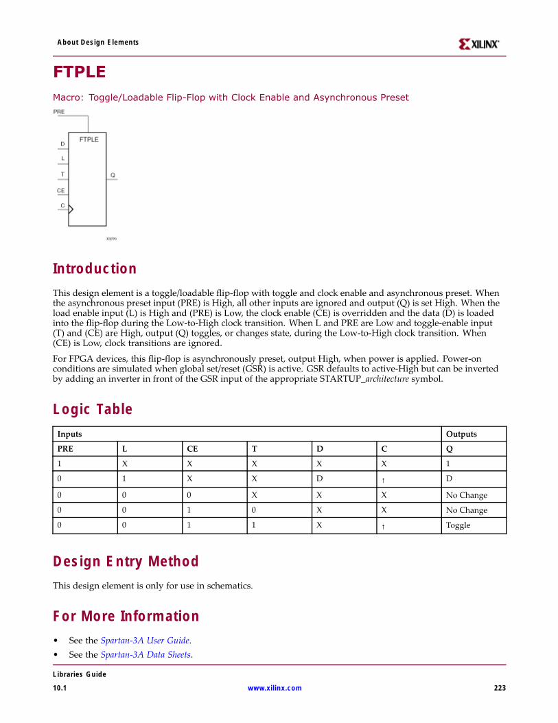
About Design Elements
FTPLEMacro: Toggle/Loadable Flip-Flop with Clock Enable and Asynchronous Preset
IntroductionThis design element is a toggle/loadable flip-flop with toggle and clock enable and asynchronous preset. Whenthe asynchronous preset input (PRE) is High, all other inputs are ignored and output (Q) is set High. When theload enable input (L) is High and (PRE) is Low, the clock enable (CE) is overridden and the data (D) is loadedinto the flip-flop during the Low-to-High clock transition. When L and PRE are Low and toggle-enable input(T) and (CE) are High, output (Q) toggles, or changes state, during the Low-to-High clock transition. When(CE) is Low, clock transitions are ignored.
For FPGA devices, this flip-flop is asynchronously preset, output High, when power is applied. Power-onconditions are simulated when global set/reset (GSR) is active. GSR defaults to active-High but can be invertedby adding an inverter in front of the GSR input of the appropriate STARTUP_architecture symbol.
Logic TableInputs Outputs
PRE L CE T D C Q
1 X X X X X 1
0 1 X X D ↑ D
0 0 0 X X X No Change
0 0 1 0 X X No Change
0 0 1 1 X ↑ Toggle
Design Entry MethodThis design element is only for use in schematics.
For More Information• See the Spartan-3A User Guide.• See the Spartan-3A Data Sheets.
Libraries Guide
10.1 www.xilinx.com 223

About Design Elements
• See the Spartan-3AN FPGA In-System Flash User Guide.
• See the Spartan-3AN Data Sheets.
Libraries Guide
224 www.xilinx.com 10.1
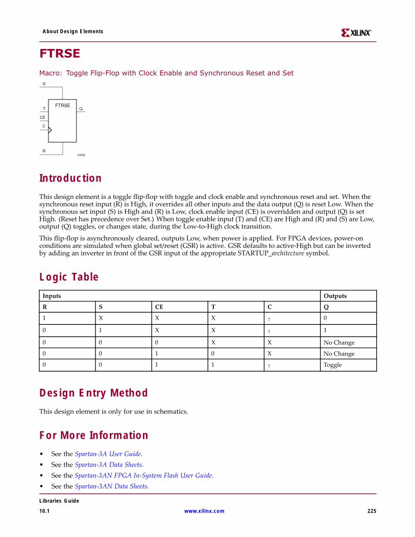
About Design Elements
FTRSE
Macro: Toggle Flip-Flop with Clock Enable and Synchronous Reset and Set
IntroductionThis design element is a toggle flip-flop with toggle and clock enable and synchronous reset and set. When thesynchronous reset input (R) is High, it overrides all other inputs and the data output (Q) is reset Low. When thesynchronous set input (S) is High and (R) is Low, clock enable input (CE) is overridden and output (Q) is setHigh. (Reset has precedence over Set.) When toggle enable input (T) and (CE) are High and (R) and (S) are Low,output (Q) toggles, or changes state, during the Low-to-High clock transition.
This flip-flop is asynchronously cleared, outputs Low, when power is applied. For FPGA devices, power-onconditions are simulated when global set/reset (GSR) is active. GSR defaults to active-High but can be invertedby adding an inverter in front of the GSR input of the appropriate STARTUP_architecture symbol.
Logic TableInputs Outputs
R S CE T C Q
1 X X X ↑ 0
0 1 X X ↑ 1
0 0 0 X X No Change
0 0 1 0 X No Change
0 0 1 1 ↑ Toggle
Design Entry MethodThis design element is only for use in schematics.
For More Information• See the Spartan-3A User Guide.• See the Spartan-3A Data Sheets.• See the Spartan-3AN FPGA In-System Flash User Guide.• See the Spartan-3AN Data Sheets.
Libraries Guide
10.1 www.xilinx.com 225
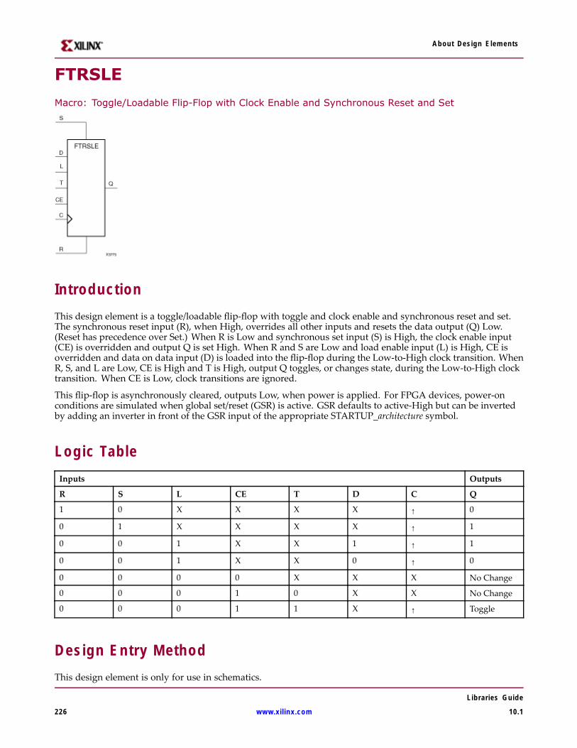
About Design Elements
FTRSLE
Macro: Toggle/Loadable Flip-Flop with Clock Enable and Synchronous Reset and Set
IntroductionThis design element is a toggle/loadable flip-flop with toggle and clock enable and synchronous reset and set.The synchronous reset input (R), when High, overrides all other inputs and resets the data output (Q) Low.(Reset has precedence over Set.) When R is Low and synchronous set input (S) is High, the clock enable input(CE) is overridden and output Q is set High. When R and S are Low and load enable input (L) is High, CE isoverridden and data on data input (D) is loaded into the flip-flop during the Low-to-High clock transition. WhenR, S, and L are Low, CE is High and T is High, output Q toggles, or changes state, during the Low-to-High clocktransition. When CE is Low, clock transitions are ignored.
This flip-flop is asynchronously cleared, outputs Low, when power is applied. For FPGA devices, power-onconditions are simulated when global set/reset (GSR) is active. GSR defaults to active-High but can be invertedby adding an inverter in front of the GSR input of the appropriate STARTUP_architecture symbol.
Logic TableInputs Outputs
R S L CE T D C Q
1 0 X X X X ↑ 0
0 1 X X X X ↑ 1
0 0 1 X X 1 ↑ 1
0 0 1 X X 0 ↑ 0
0 0 0 0 X X X No Change
0 0 0 1 0 X X No Change
0 0 0 1 1 X ↑ Toggle
Design Entry MethodThis design element is only for use in schematics.
Libraries Guide
226 www.xilinx.com 10.1

About Design Elements
For More Information• See the Spartan-3A User Guide.
• See the Spartan-3A Data Sheets.
• See the Spartan-3AN FPGA In-System Flash User Guide.
• See the Spartan-3AN Data Sheets.
Libraries Guide
10.1 www.xilinx.com 227
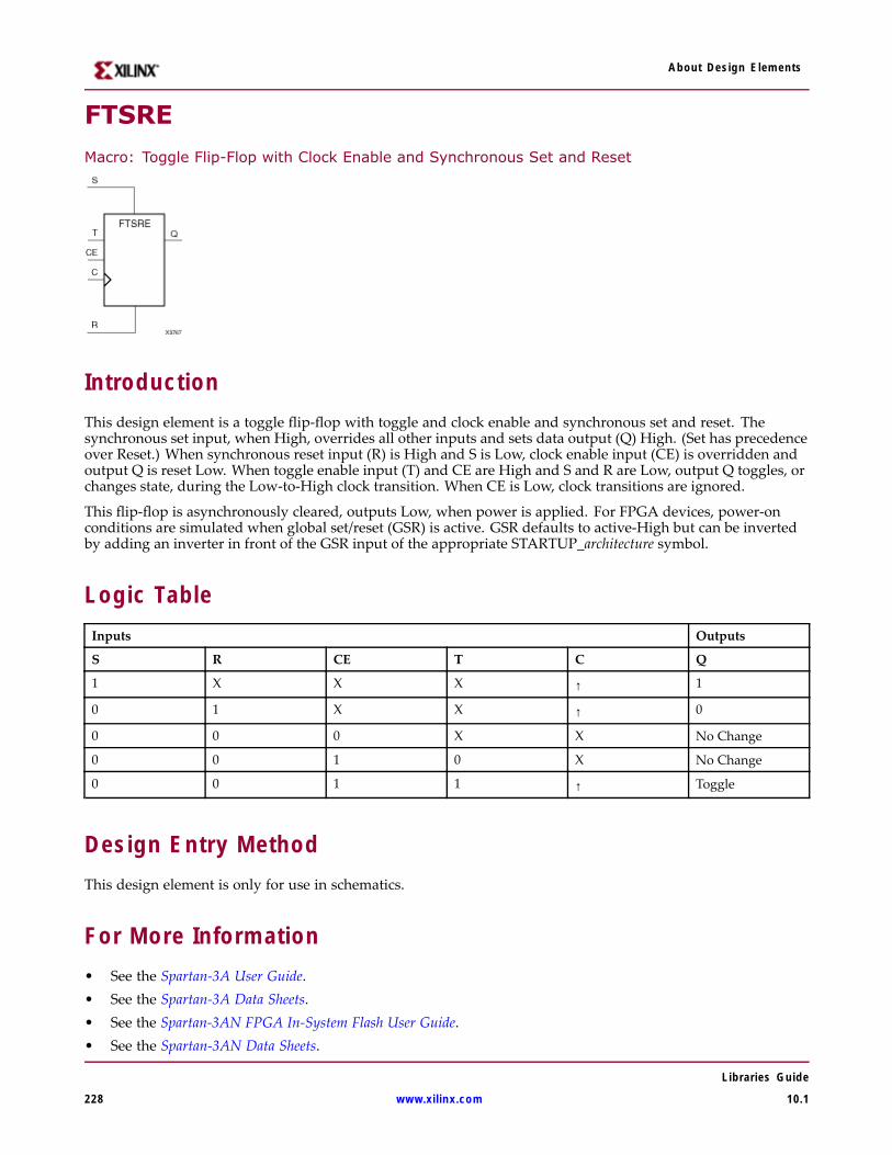
About Design Elements
FTSRE
Macro: Toggle Flip-Flop with Clock Enable and Synchronous Set and Reset
IntroductionThis design element is a toggle flip-flop with toggle and clock enable and synchronous set and reset. Thesynchronous set input, when High, overrides all other inputs and sets data output (Q) High. (Set has precedenceover Reset.) When synchronous reset input (R) is High and S is Low, clock enable input (CE) is overridden andoutput Q is reset Low. When toggle enable input (T) and CE are High and S and R are Low, output Q toggles, orchanges state, during the Low-to-High clock transition. When CE is Low, clock transitions are ignored.
This flip-flop is asynchronously cleared, outputs Low, when power is applied. For FPGA devices, power-onconditions are simulated when global set/reset (GSR) is active. GSR defaults to active-High but can be invertedby adding an inverter in front of the GSR input of the appropriate STARTUP_architecture symbol.
Logic TableInputs Outputs
S R CE T C Q
1 X X X ↑ 1
0 1 X X ↑ 0
0 0 0 X X No Change
0 0 1 0 X No Change
0 0 1 1 ↑ Toggle
Design Entry MethodThis design element is only for use in schematics.
For More Information• See the Spartan-3A User Guide.• See the Spartan-3A Data Sheets.• See the Spartan-3AN FPGA In-System Flash User Guide.• See the Spartan-3AN Data Sheets.
Libraries Guide
228 www.xilinx.com 10.1
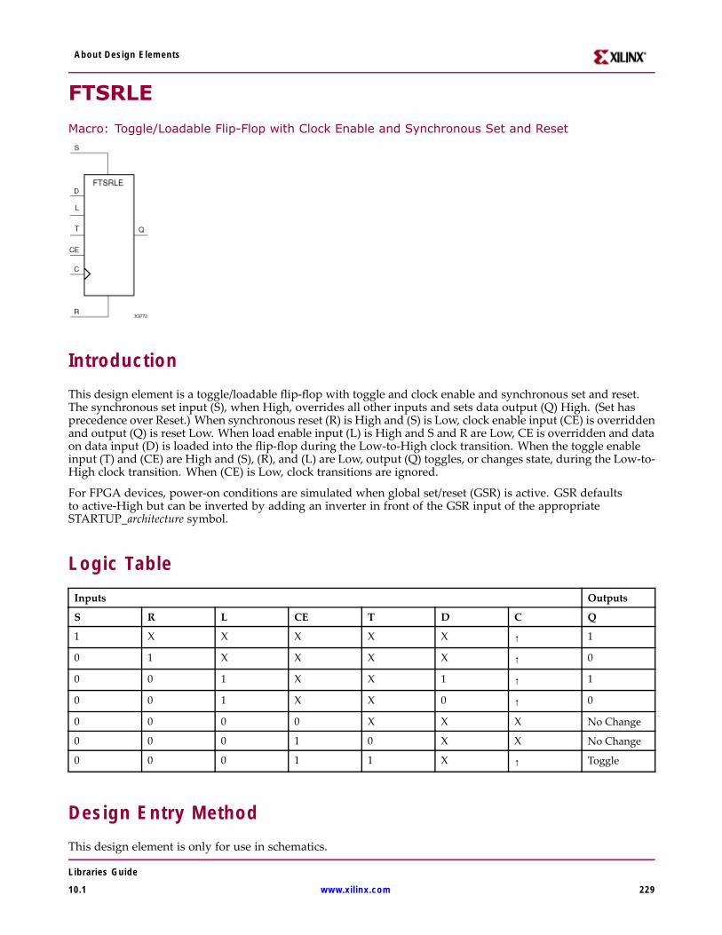
About Design Elements
FTSRLE
Macro: Toggle/Loadable Flip-Flop with Clock Enable and Synchronous Set and Reset
IntroductionThis design element is a toggle/loadable flip-flop with toggle and clock enable and synchronous set and reset.The synchronous set input (S), when High, overrides all other inputs and sets data output (Q) High. (Set hasprecedence over Reset.) When synchronous reset (R) is High and (S) is Low, clock enable input (CE) is overriddenand output (Q) is reset Low. When load enable input (L) is High and S and R are Low, CE is overridden and dataon data input (D) is loaded into the flip-flop during the Low-to-High clock transition. When the toggle enableinput (T) and (CE) are High and (S), (R), and (L) are Low, output (Q) toggles, or changes state, during the Low-to-High clock transition. When (CE) is Low, clock transitions are ignored.
For FPGA devices, power-on conditions are simulated when global set/reset (GSR) is active. GSR defaultsto active-High but can be inverted by adding an inverter in front of the GSR input of the appropriateSTARTUP_architecture symbol.
Logic TableInputs Outputs
S R L CE T D C Q
1 X X X X X ↑ 1
0 1 X X X X ↑ 0
0 0 1 X X 1 ↑ 1
0 0 1 X X 0 ↑ 0
0 0 0 0 X X X No Change
0 0 0 1 0 X X No Change
0 0 0 1 1 X ↑ Toggle
Design Entry MethodThis design element is only for use in schematics.
Libraries Guide
10.1 www.xilinx.com 229

About Design Elements
For More Information• See the Spartan-3A User Guide.
• See the Spartan-3A Data Sheets.
• See the Spartan-3AN FPGA In-System Flash User Guide.
• See the Spartan-3AN Data Sheets.
Libraries Guide
230 www.xilinx.com 10.1
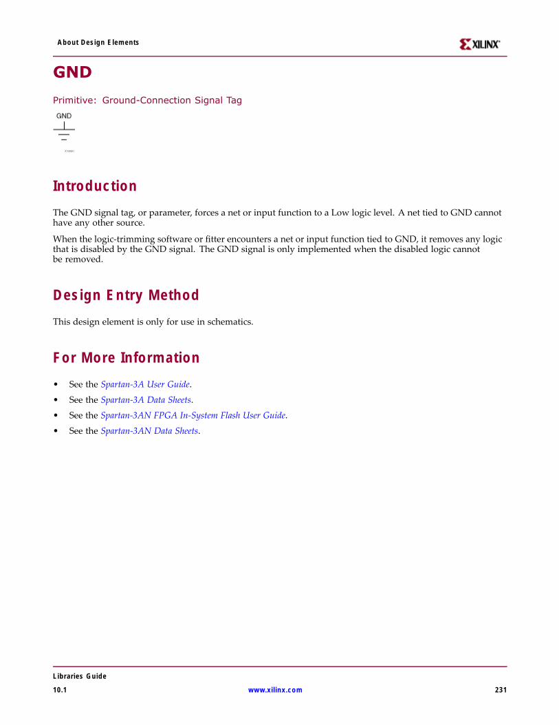
About Design Elements
GND
Primitive: Ground-Connection Signal Tag
IntroductionThe GND signal tag, or parameter, forces a net or input function to a Low logic level. A net tied to GND cannothave any other source.
When the logic-trimming software or fitter encounters a net or input function tied to GND, it removes any logicthat is disabled by the GND signal. The GND signal is only implemented when the disabled logic cannotbe removed.
Design Entry MethodThis design element is only for use in schematics.
For More Information• See the Spartan-3A User Guide.
• See the Spartan-3A Data Sheets.
• See the Spartan-3AN FPGA In-System Flash User Guide.
• See the Spartan-3AN Data Sheets.
Libraries Guide
10.1 www.xilinx.com 231
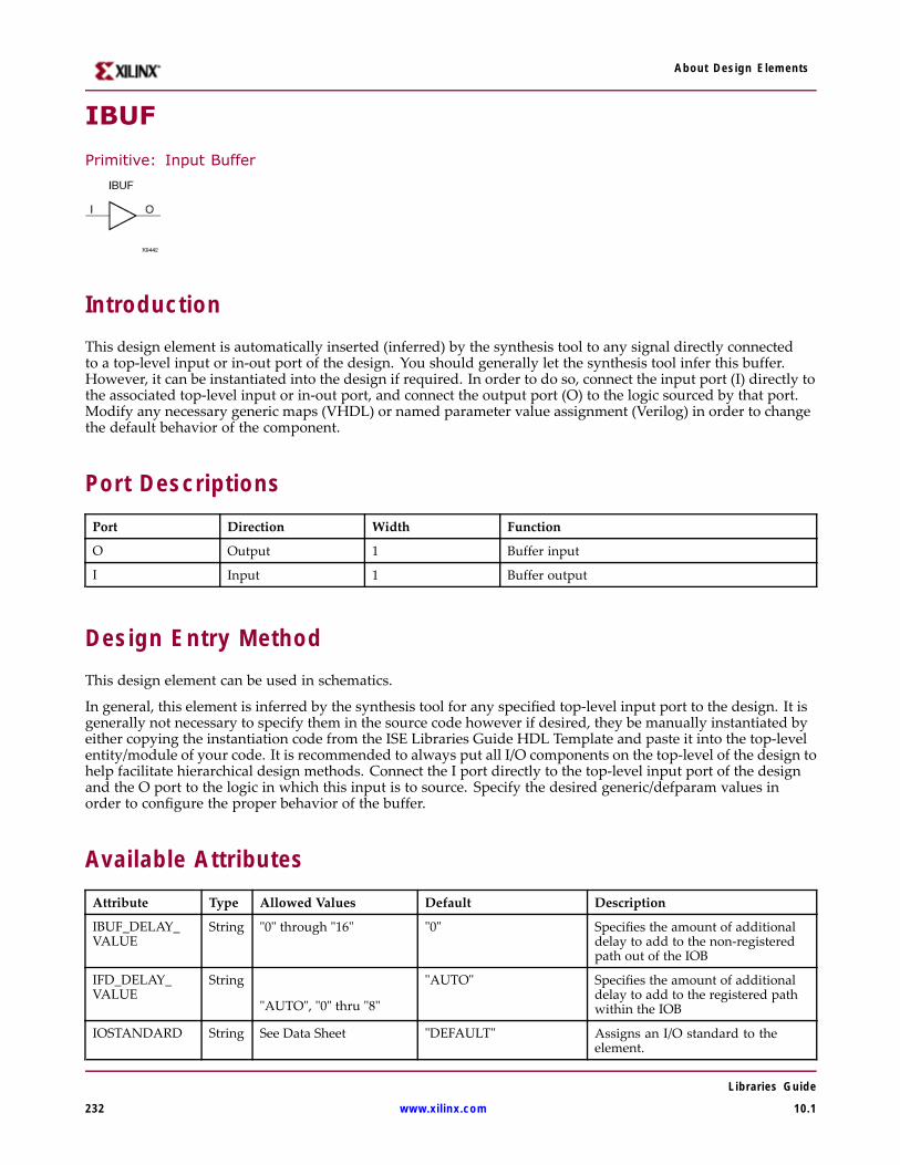
About Design Elements
IBUF
Primitive: Input Buffer
IntroductionThis design element is automatically inserted (inferred) by the synthesis tool to any signal directly connectedto a top-level input or in-out port of the design. You should generally let the synthesis tool infer this buffer.However, it can be instantiated into the design if required. In order to do so, connect the input port (I) directly tothe associated top-level input or in-out port, and connect the output port (O) to the logic sourced by that port.Modify any necessary generic maps (VHDL) or named parameter value assignment (Verilog) in order to changethe default behavior of the component.
Port DescriptionsPort Direction Width Function
O Output 1 Buffer input
I Input 1 Buffer output
Design Entry MethodThis design element can be used in schematics.
In general, this element is inferred by the synthesis tool for any specified top-level input port to the design. It isgenerally not necessary to specify them in the source code however if desired, they be manually instantiated byeither copying the instantiation code from the ISE Libraries Guide HDL Template and paste it into the top-levelentity/module of your code. It is recommended to always put all I/O components on the top-level of the design tohelp facilitate hierarchical design methods. Connect the I port directly to the top-level input port of the designand the O port to the logic in which this input is to source. Specify the desired generic/defparam values inorder to configure the proper behavior of the buffer.
Available AttributesAttribute Type Allowed Values Default Description
IBUF_DELAY_VALUE
String "0" through "16" "0" Specifies the amount of additionaldelay to add to the non-registeredpath out of the IOB
IFD_DELAY_VALUE
String
"AUTO", "0" thru "8"
"AUTO" Specifies the amount of additionaldelay to add to the registered pathwithin the IOB
IOSTANDARD String See Data Sheet "DEFAULT" Assigns an I/O standard to theelement.
Libraries Guide
232 www.xilinx.com 10.1

About Design Elements
For More Information• See the Spartan-3A User Guide.
• See the Spartan-3A Data Sheets.
• See the Spartan-3AN FPGA In-System Flash User Guide.
• See the Spartan-3AN Data Sheets.
Libraries Guide
10.1 www.xilinx.com 233
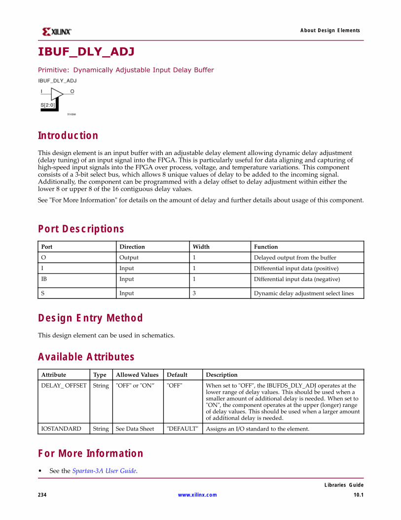
About Design Elements
IBUF_DLY_ADJPrimitive: Dynamically Adjustable Input Delay Buffer
IntroductionThis design element is an input buffer with an adjustable delay element allowing dynamic delay adjustment(delay tuning) of an input signal into the FPGA. This is particularly useful for data aligning and capturing ofhigh-speed input signals into the FPGA over process, voltage, and temperature variations. This componentconsists of a 3-bit select bus, which allows 8 unique values of delay to be added to the incoming signal.Additionally, the component can be programmed with a delay offset to delay adjustment within either thelower 8 or upper 8 of the 16 contiguous delay values.
See "For More Information" for details on the amount of delay and further details about usage of this component.
Port DescriptionsPort Direction Width Function
O Output 1 Delayed output from the buffer
I Input 1 Differential input data (positive)
IB Input 1 Differential input data (negative)
S Input 3 Dynamic delay adjustment select lines
Design Entry MethodThis design element can be used in schematics.
Available AttributesAttribute Type Allowed Values Default Description
DELAY_ OFFSET String "OFF" or "ON” "OFF" When set to "OFF", the IBUFDS_DLY_ADJ operates at thelower range of delay values. This should be used when asmaller amount of additional delay is needed. When set to"ON", the component operates at the upper (longer) rangeof delay values. This should be used when a larger amountof additional delay is needed.
IOSTANDARD String See Data Sheet "DEFAULT" Assigns an I/O standard to the element.
For More Information• See the Spartan-3A User Guide.
Libraries Guide
234 www.xilinx.com 10.1

About Design Elements
• See the Spartan-3A Data Sheets.
• See the Spartan-3AN FPGA In-System Flash User Guide.
• See the Spartan-3AN Data Sheets.
Libraries Guide
10.1 www.xilinx.com 235

About Design Elements
IBUF16
Macro: 16-Bit Input Buffer
IntroductionInput Buffers isolate the internal circuit from the signals coming into the chip. This design element is containedin input/output blocks (IOBs) and allows the specification of the particular I/O Standard to configure the I/O. Ingeneral, an this element should be used for all single-ended data input or bidirectional pins.
Design Entry MethodThis design element can be used in schematics.
In general, this element is inferred by the synthesis tool for any specified top-level input port to the design. It isgenerally not necessary to specify them in the source code however if desired, they be manually instantiated byeither copying the instantiation code from the ISE Libraries Guide HDL Template and paste it into the top-levelentity/module of your code. It is recommended to always put all I/O components on the top-level of the design tohelp facilitate hierarchical design methods. Connect the I port directly to the top-level input port of the designand the O port to the logic in which this input is to source. Specify the desired generic/defparam values inorder to configure the proper behavior of the buffer.
Available AttributesAttribute Type Allowed Values Default Description
IBUF_DELAY_VALUE
String "0" through "16" "0" Specifies the amount of additionaldelay to add to the non-registeredpath out of the IOB
IFD_DELAY_VALUE
String
"AUTO", "0" thru "8"
"AUTO" Specifies the amount of additionaldelay to add to the registered pathwithin the IOB
IOSTANDARD String See Data Sheet "DEFAULT" Assigns an I/O standard to theelement.
For More Information• See the Spartan-3A User Guide.
• See the Spartan-3A Data Sheets.
• See the Spartan-3AN FPGA In-System Flash User Guide.
• See the Spartan-3AN Data Sheets.
Libraries Guide
236 www.xilinx.com 10.1
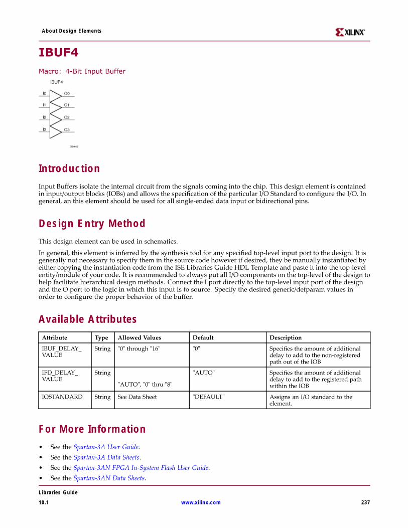
About Design Elements
IBUF4Macro: 4-Bit Input Buffer
IntroductionInput Buffers isolate the internal circuit from the signals coming into the chip. This design element is containedin input/output blocks (IOBs) and allows the specification of the particular I/O Standard to configure the I/O. Ingeneral, an this element should be used for all single-ended data input or bidirectional pins.
Design Entry MethodThis design element can be used in schematics.
In general, this element is inferred by the synthesis tool for any specified top-level input port to the design. It isgenerally not necessary to specify them in the source code however if desired, they be manually instantiated byeither copying the instantiation code from the ISE Libraries Guide HDL Template and paste it into the top-levelentity/module of your code. It is recommended to always put all I/O components on the top-level of the design tohelp facilitate hierarchical design methods. Connect the I port directly to the top-level input port of the designand the O port to the logic in which this input is to source. Specify the desired generic/defparam values inorder to configure the proper behavior of the buffer.
Available AttributesAttribute Type Allowed Values Default Description
IBUF_DELAY_VALUE
String "0" through "16" "0" Specifies the amount of additionaldelay to add to the non-registeredpath out of the IOB
IFD_DELAY_VALUE
String
"AUTO", "0" thru "8"
"AUTO" Specifies the amount of additionaldelay to add to the registered pathwithin the IOB
IOSTANDARD String See Data Sheet "DEFAULT" Assigns an I/O standard to theelement.
For More Information• See the Spartan-3A User Guide.• See the Spartan-3A Data Sheets.• See the Spartan-3AN FPGA In-System Flash User Guide.• See the Spartan-3AN Data Sheets.
Libraries Guide
10.1 www.xilinx.com 237
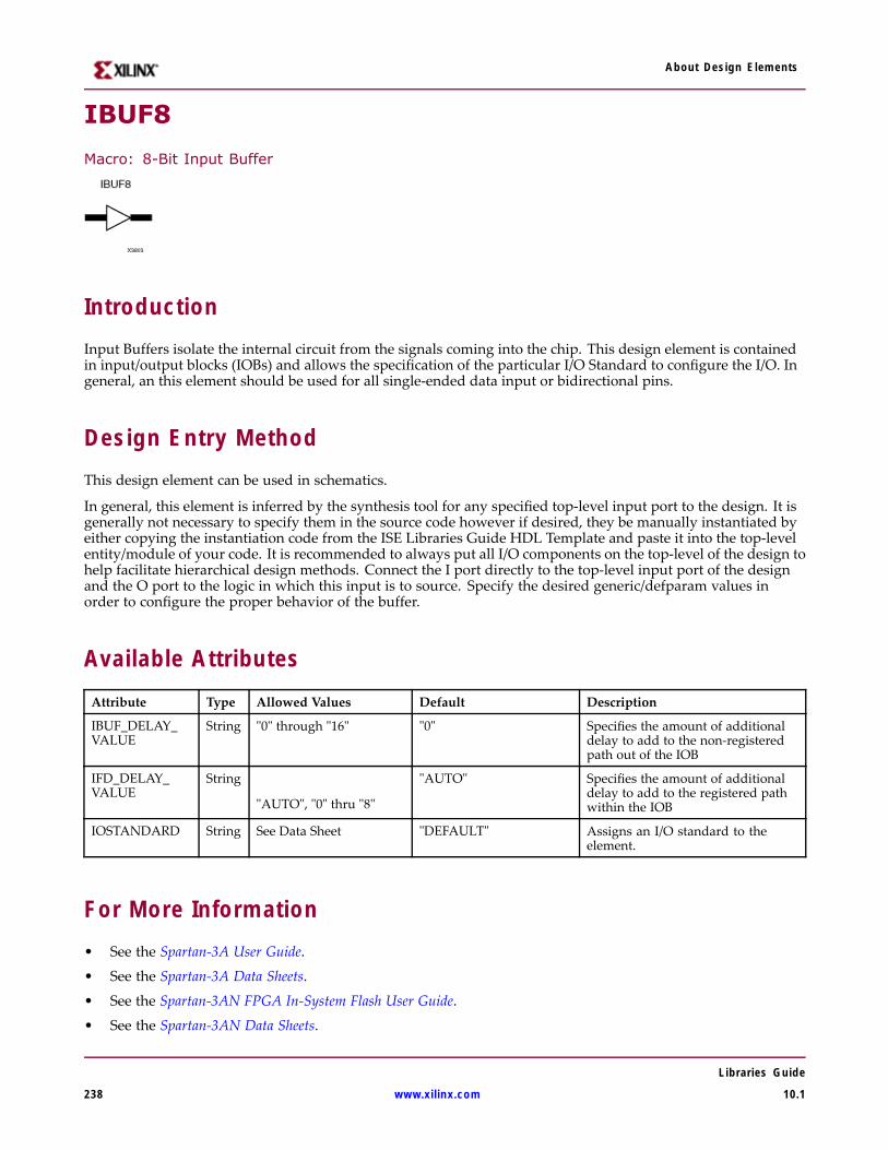
About Design Elements
IBUF8
Macro: 8-Bit Input Buffer
IntroductionInput Buffers isolate the internal circuit from the signals coming into the chip. This design element is containedin input/output blocks (IOBs) and allows the specification of the particular I/O Standard to configure the I/O. Ingeneral, an this element should be used for all single-ended data input or bidirectional pins.
Design Entry MethodThis design element can be used in schematics.
In general, this element is inferred by the synthesis tool for any specified top-level input port to the design. It isgenerally not necessary to specify them in the source code however if desired, they be manually instantiated byeither copying the instantiation code from the ISE Libraries Guide HDL Template and paste it into the top-levelentity/module of your code. It is recommended to always put all I/O components on the top-level of the design tohelp facilitate hierarchical design methods. Connect the I port directly to the top-level input port of the designand the O port to the logic in which this input is to source. Specify the desired generic/defparam values inorder to configure the proper behavior of the buffer.
Available AttributesAttribute Type Allowed Values Default Description
IBUF_DELAY_VALUE
String "0" through "16" "0" Specifies the amount of additionaldelay to add to the non-registeredpath out of the IOB
IFD_DELAY_VALUE
String
"AUTO", "0" thru "8"
"AUTO" Specifies the amount of additionaldelay to add to the registered pathwithin the IOB
IOSTANDARD String See Data Sheet "DEFAULT" Assigns an I/O standard to theelement.
For More Information• See the Spartan-3A User Guide.
• See the Spartan-3A Data Sheets.
• See the Spartan-3AN FPGA In-System Flash User Guide.
• See the Spartan-3AN Data Sheets.
Libraries Guide
238 www.xilinx.com 10.1
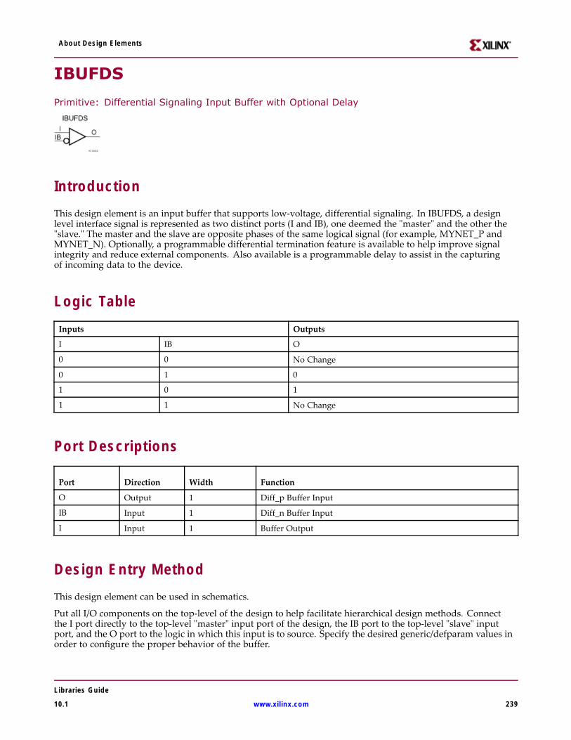
About Design Elements
IBUFDS
Primitive: Differential Signaling Input Buffer with Optional Delay
IntroductionThis design element is an input buffer that supports low-voltage, differential signaling. In IBUFDS, a designlevel interface signal is represented as two distinct ports (I and IB), one deemed the "master" and the other the"slave." The master and the slave are opposite phases of the same logical signal (for example, MYNET_P andMYNET_N). Optionally, a programmable differential termination feature is available to help improve signalintegrity and reduce external components. Also available is a programmable delay to assist in the capturingof incoming data to the device.
Logic TableInputs Outputs
I IB O
0 0 No Change
0 1 0
1 0 1
1 1 No Change
Port Descriptions
Port Direction Width Function
O Output 1 Diff_p Buffer Input
IB Input 1 Diff_n Buffer Input
I Input 1 Buffer Output
Design Entry MethodThis design element can be used in schematics.
Put all I/O components on the top-level of the design to help facilitate hierarchical design methods. Connectthe I port directly to the top-level "master" input port of the design, the IB port to the top-level "slave" inputport, and the O port to the logic in which this input is to source. Specify the desired generic/defparam values inorder to configure the proper behavior of the buffer.
Libraries Guide
10.1 www.xilinx.com 239
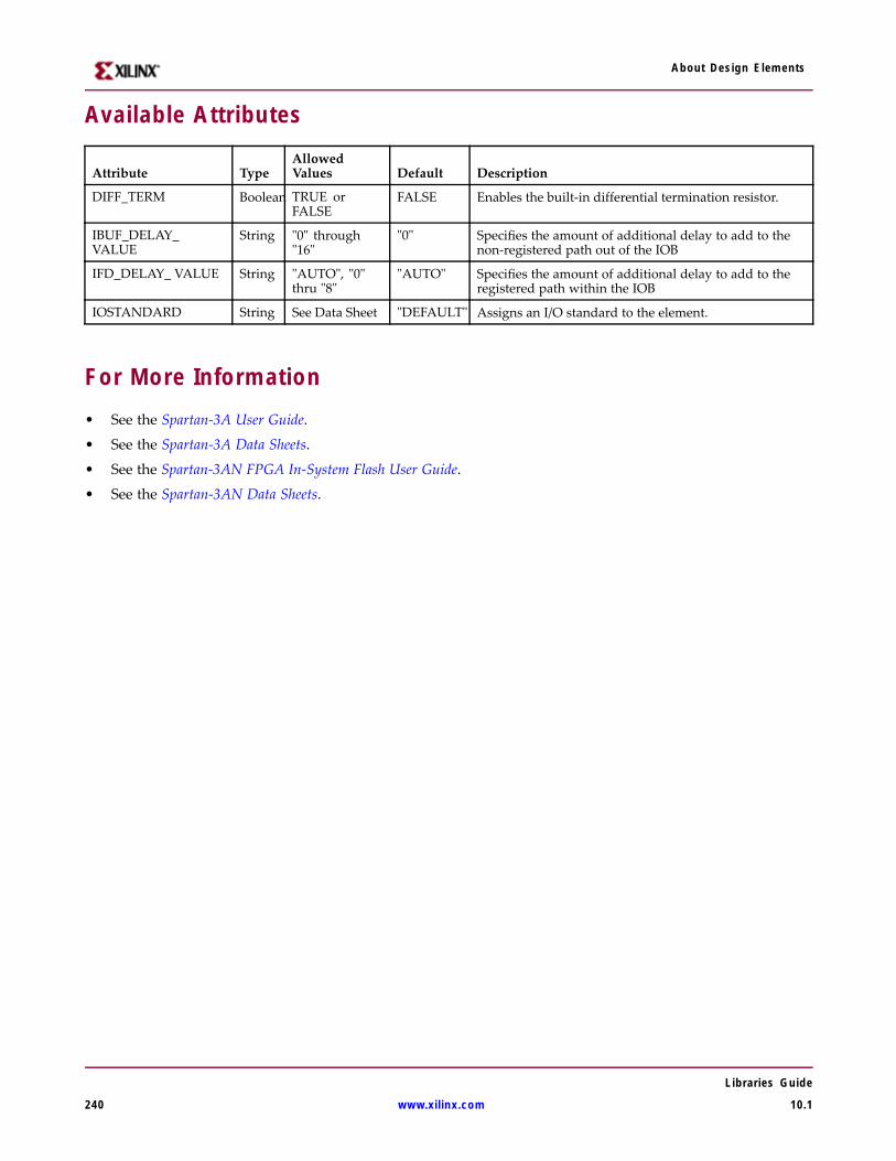
About Design Elements
Available Attributes
Attribute TypeAllowedValues Default Description
DIFF_TERM Boolean TRUE orFALSE
FALSE Enables the built-in differential termination resistor.
IBUF_DELAY_VALUE
String "0" through"16"
"0" Specifies the amount of additional delay to add to thenon-registered path out of the IOB
IFD_DELAY_ VALUE String "AUTO", "0"thru "8"
"AUTO" Specifies the amount of additional delay to add to theregistered path within the IOB
IOSTANDARD String See Data Sheet "DEFAULT" Assigns an I/O standard to the element.
For More Information• See the Spartan-3A User Guide.
• See the Spartan-3A Data Sheets.
• See the Spartan-3AN FPGA In-System Flash User Guide.
• See the Spartan-3AN Data Sheets.
Libraries Guide
240 www.xilinx.com 10.1
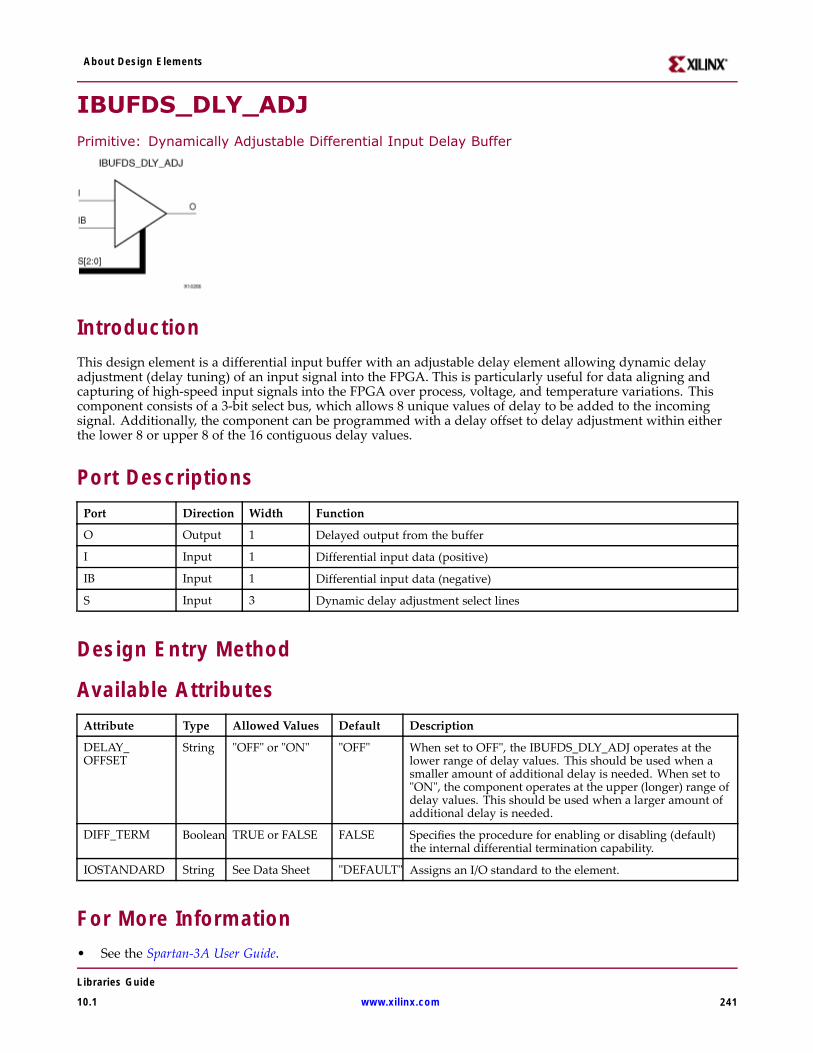
About Design Elements
IBUFDS_DLY_ADJPrimitive: Dynamically Adjustable Differential Input Delay Buffer
IntroductionThis design element is a differential input buffer with an adjustable delay element allowing dynamic delayadjustment (delay tuning) of an input signal into the FPGA. This is particularly useful for data aligning andcapturing of high-speed input signals into the FPGA over process, voltage, and temperature variations. Thiscomponent consists of a 3-bit select bus, which allows 8 unique values of delay to be added to the incomingsignal. Additionally, the component can be programmed with a delay offset to delay adjustment within eitherthe lower 8 or upper 8 of the 16 contiguous delay values.
Port DescriptionsPort Direction Width Function
O Output 1 Delayed output from the buffer
I Input 1 Differential input data (positive)
IB Input 1 Differential input data (negative)
S Input 3 Dynamic delay adjustment select lines
Design Entry Method
Available AttributesAttribute Type Allowed Values Default Description
DELAY_OFFSET
String "OFF" or "ON" "OFF" When set to OFF", the IBUFDS_DLY_ADJ operates at thelower range of delay values. This should be used when asmaller amount of additional delay is needed. When set to"ON", the component operates at the upper (longer) range ofdelay values. This should be used when a larger amount ofadditional delay is needed.
DIFF_TERM Boolean TRUE or FALSE FALSE Specifies the procedure for enabling or disabling (default)the internal differential termination capability.
IOSTANDARD String See Data Sheet "DEFAULT" Assigns an I/O standard to the element.
For More Information• See the Spartan-3A User Guide.
Libraries Guide
10.1 www.xilinx.com 241

About Design Elements
• See the Spartan-3A Data Sheets.
• See the Spartan-3AN FPGA In-System Flash User Guide.
• See the Spartan-3AN Data Sheets.
Libraries Guide
242 www.xilinx.com 10.1
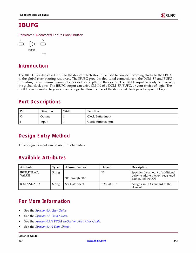
About Design Elements
IBUFG
Primitive: Dedicated Input Clock Buffer
IntroductionThe IBUFG is a dedicated input to the device which should be used to connect incoming clocks to the FPGAto the global clock routing resources. The IBUFG provides dedicated connections to the DCM_SP and BUFGproviding the minimum amount of clock delay and jitter to the device. The IBUFG input can only be driven bythe global clock pins. The IBUFG output can drive CLKIN of a DCM_SP, BUFG, or your choice of logic. TheIBUFG can be routed to your choice of logic to allow the use of the dedicated clock pins for general logic.
Port DescriptionsPort Direction Width Function
O Output 1 Clock Buffer input
I Input 1 Clock Buffer output
Design Entry MethodThis design element can be used in schematics.
Available AttributesAttribute Type Allowed Values Default Description
IBUF_DELAY_VALUE
String
"0" through "16"
"0" Specifies the amount of additionaldelay to add to the non-registeredpath out of the IOB
IOSTANDARD String See Data Sheet "DEFAULT" Assigns an I/O standard to theelement.
For More Information• See the Spartan-3A User Guide.
• See the Spartan-3A Data Sheets.
• See the Spartan-3AN FPGA In-System Flash User Guide.
• See the Spartan-3AN Data Sheets.
Libraries Guide
10.1 www.xilinx.com 243
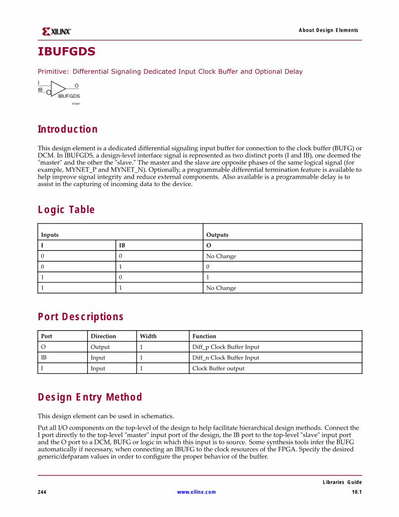
About Design Elements
IBUFGDS
Primitive: Differential Signaling Dedicated Input Clock Buffer and Optional Delay
IntroductionThis design element is a dedicated differential signaling input buffer for connection to the clock buffer (BUFG) orDCM. In IBUFGDS, a design-level interface signal is represented as two distinct ports (I and IB), one deemed the"master" and the other the "slave." The master and the slave are opposite phases of the same logical signal (forexample, MYNET_P and MYNET_N). Optionally, a programmable differential termination feature is available tohelp improve signal integrity and reduce external components. Also available is a programmable delay is toassist in the capturing of incoming data to the device.
Logic Table
Inputs Outputs
I IB O
0 0 No Change
0 1 0
1 0 1
1 1 No Change
Port DescriptionsPort Direction Width Function
O Output 1 Diff_p Clock Buffer Input
IB Input 1 Diff_n Clock Buffer Input
I Input 1 Clock Buffer output
Design Entry MethodThis design element can be used in schematics.
Put all I/O components on the top-level of the design to help facilitate hierarchical design methods. Connect theI port directly to the top-level "master" input port of the design, the IB port to the top-level "slave" input portand the O port to a DCM, BUFG or logic in which this input is to source. Some synthesis tools infer the BUFGautomatically if necessary, when connecting an IBUFG to the clock resources of the FPGA. Specify the desiredgeneric/defparam values in order to configure the proper behavior of the buffer.
Libraries Guide
244 www.xilinx.com 10.1
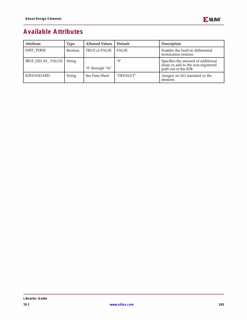
About Design Elements
Available AttributesAttribute Type Allowed Values Default Description
DIFF_TERM Boolean TRUE or FALSE FALSE Enables the built-in differentialtermination resistor.
IBUF_DELAY_ VALUE String
"0" through "16"
"0" Specifies the amount of additionaldelay to add to the non-registeredpath out of the IOB
IOSTANDARD String See Data Sheet "DEFAULT" Assigns an I/O standard to theelement.
Libraries Guide
10.1 www.xilinx.com 245

About Design Elements
For More Information• See the Spartan-3A User Guide.
• See the Spartan-3A Data Sheets.
• See the Spartan-3AN FPGA In-System Flash User Guide.
• See the Spartan-3AN Data Sheets.
Libraries Guide
246 www.xilinx.com 10.1
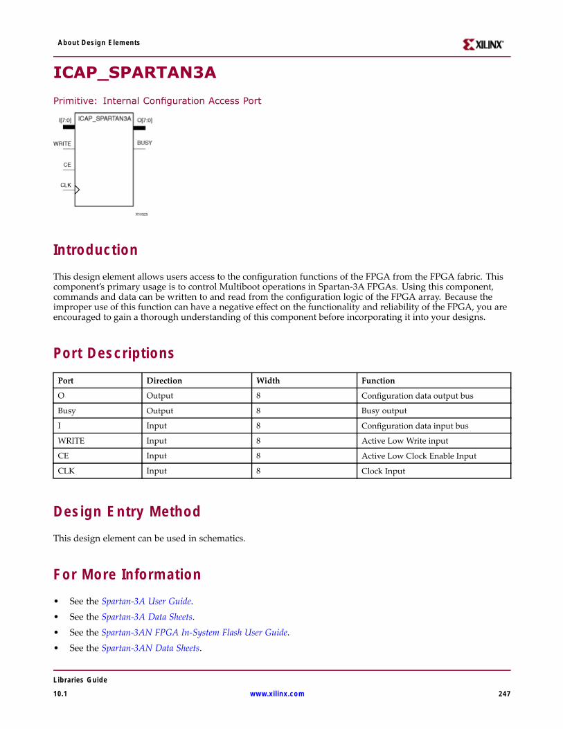
About Design Elements
ICAP_SPARTAN3A
Primitive: Internal Configuration Access Port
IntroductionThis design element allows users access to the configuration functions of the FPGA from the FPGA fabric. Thiscomponent’s primary usage is to control Multiboot operations in Spartan-3A FPGAs. Using this component,commands and data can be written to and read from the configuration logic of the FPGA array. Because theimproper use of this function can have a negative effect on the functionality and reliability of the FPGA, you areencouraged to gain a thorough understanding of this component before incorporating it into your designs.
Port DescriptionsPort Direction Width Function
O Output 8 Configuration data output bus
Busy Output 8 Busy output
I Input 8 Configuration data input bus
WRITE Input 8 Active Low Write input
CE Input 8 Active Low Clock Enable Input
CLK Input 8 Clock Input
Design Entry MethodThis design element can be used in schematics.
For More Information• See the Spartan-3A User Guide.
• See the Spartan-3A Data Sheets.
• See the Spartan-3AN FPGA In-System Flash User Guide.
• See the Spartan-3AN Data Sheets.
Libraries Guide
10.1 www.xilinx.com 247
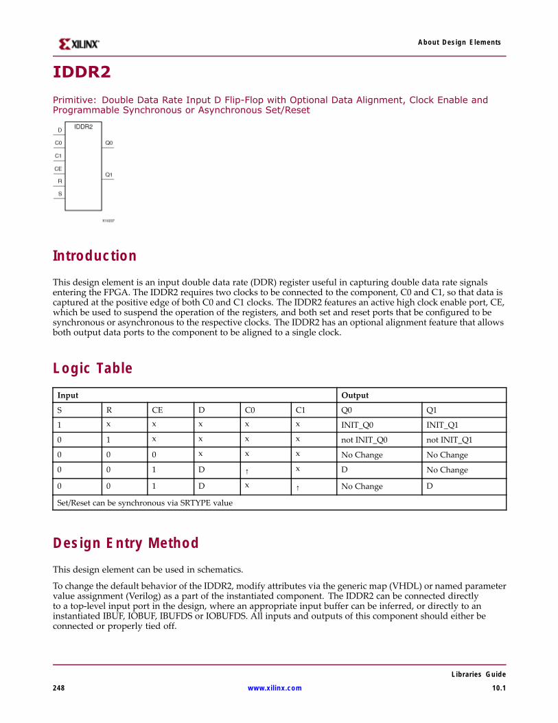
About Design Elements
IDDR2
Primitive: Double Data Rate Input D Flip-Flop with Optional Data Alignment, Clock Enable andProgrammable Synchronous or Asynchronous Set/Reset
IntroductionThis design element is an input double data rate (DDR) register useful in capturing double data rate signalsentering the FPGA. The IDDR2 requires two clocks to be connected to the component, C0 and C1, so that data iscaptured at the positive edge of both C0 and C1 clocks. The IDDR2 features an active high clock enable port, CE,which be used to suspend the operation of the registers, and both set and reset ports that be configured to besynchronous or asynchronous to the respective clocks. The IDDR2 has an optional alignment feature that allowsboth output data ports to the component to be aligned to a single clock.
Logic TableInput Output
S R CE D C0 C1 Q0 Q1
1 x x x x x INIT_Q0 INIT_Q1
0 1 x x x x not INIT_Q0 not INIT_Q1
0 0 0 x x x No Change No Change
0 0 1 D ↑ x D No Change
0 0 1 D x ↑ No Change D
Set/Reset can be synchronous via SRTYPE value
Design Entry MethodThis design element can be used in schematics.
To change the default behavior of the IDDR2, modify attributes via the generic map (VHDL) or named parametervalue assignment (Verilog) as a part of the instantiated component. The IDDR2 can be connected directlyto a top-level input port in the design, where an appropriate input buffer can be inferred, or directly to aninstantiated IBUF, IOBUF, IBUFDS or IOBUFDS. All inputs and outputs of this component should either beconnected or properly tied off.
Libraries Guide
248 www.xilinx.com 10.1
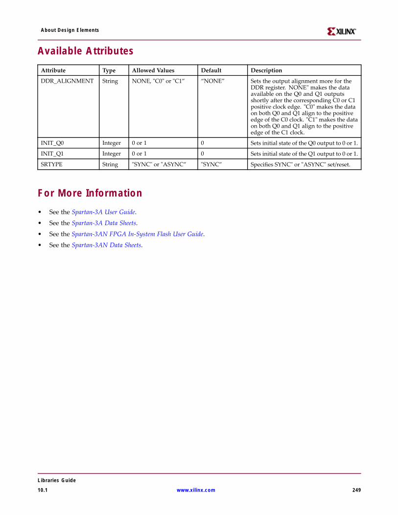
About Design Elements
Available AttributesAttribute Type Allowed Values Default Description
DDR_ALIGNMENT String NONE, "C0" or "C1” “NONE” Sets the output alignment more for theDDR register. NONE" makes the dataavailable on the Q0 and Q1 outputsshortly after the corresponding C0 or C1positive clock edge. "C0" makes the dataon both Q0 and Q1 align to the positiveedge of the C0 clock. "C1" makes the dataon both Q0 and Q1 align to the positiveedge of the C1 clock.
INIT_Q0 Integer 0 or 1 0 Sets initial state of the Q0 output to 0 or 1.
INIT_Q1 Integer 0 or 1 0 Sets initial state of the Q1 output to 0 or 1.
SRTYPE String "SYNC" or "ASYNC” "SYNC” Specifies SYNC" or "ASYNC" set/reset.
For More Information• See the Spartan-3A User Guide.
• See the Spartan-3A Data Sheets.
• See the Spartan-3AN FPGA In-System Flash User Guide.
• See the Spartan-3AN Data Sheets.
Libraries Guide
10.1 www.xilinx.com 249
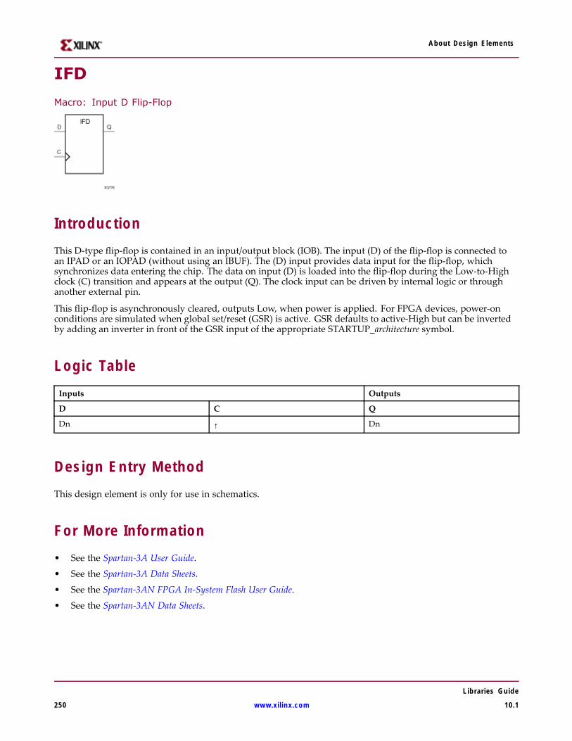
About Design Elements
IFD
Macro: Input D Flip-Flop
IntroductionThis D-type flip-flop is contained in an input/output block (IOB). The input (D) of the flip-flop is connected toan IPAD or an IOPAD (without using an IBUF). The (D) input provides data input for the flip-flop, whichsynchronizes data entering the chip. The data on input (D) is loaded into the flip-flop during the Low-to-Highclock (C) transition and appears at the output (Q). The clock input can be driven by internal logic or throughanother external pin.
This flip-flop is asynchronously cleared, outputs Low, when power is applied. For FPGA devices, power-onconditions are simulated when global set/reset (GSR) is active. GSR defaults to active-High but can be invertedby adding an inverter in front of the GSR input of the appropriate STARTUP_architecture symbol.
Logic TableInputs Outputs
D C Q
Dn ↑ Dn
Design Entry MethodThis design element is only for use in schematics.
For More Information• See the Spartan-3A User Guide.
• See the Spartan-3A Data Sheets.
• See the Spartan-3AN FPGA In-System Flash User Guide.
• See the Spartan-3AN Data Sheets.
Libraries Guide
250 www.xilinx.com 10.1
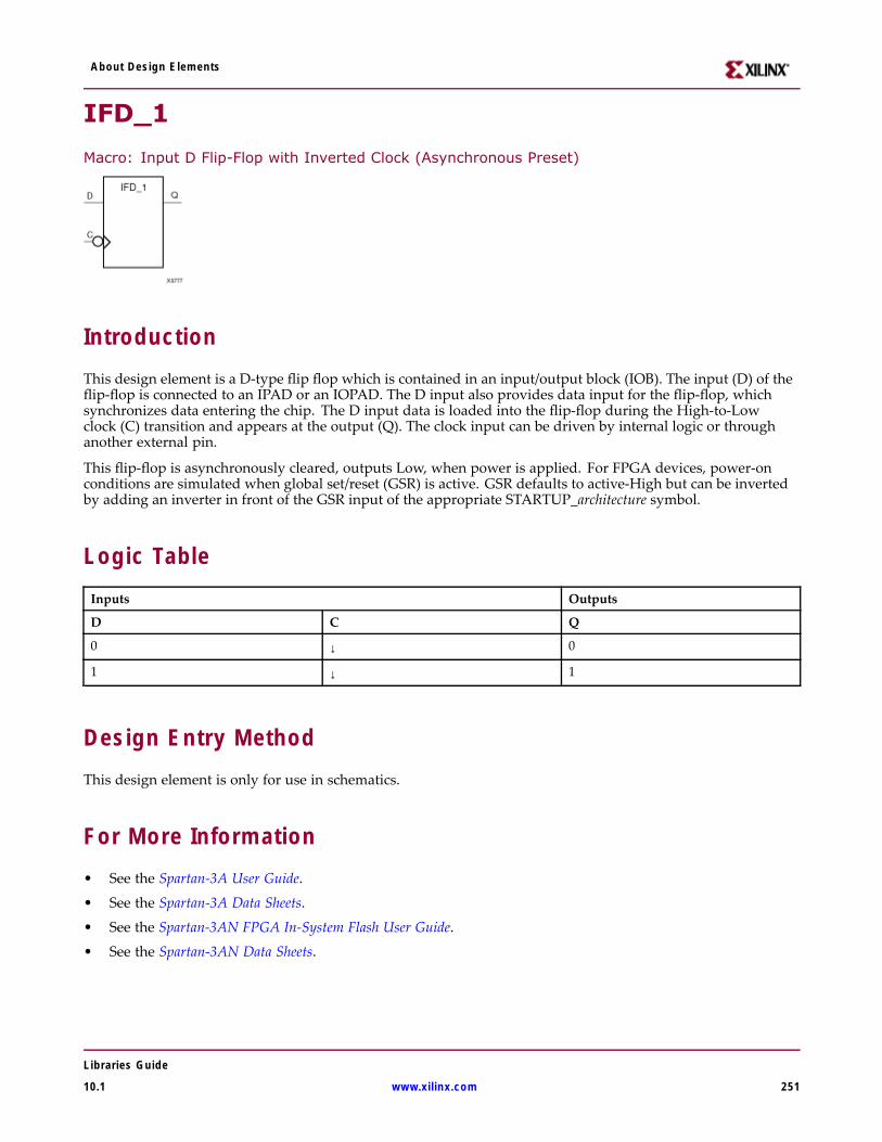
About Design Elements
IFD_1
Macro: Input D Flip-Flop with Inverted Clock (Asynchronous Preset)
IntroductionThis design element is a D-type flip flop which is contained in an input/output block (IOB). The input (D) of theflip-flop is connected to an IPAD or an IOPAD. The D input also provides data input for the flip-flop, whichsynchronizes data entering the chip. The D input data is loaded into the flip-flop during the High-to-Lowclock (C) transition and appears at the output (Q). The clock input can be driven by internal logic or throughanother external pin.
This flip-flop is asynchronously cleared, outputs Low, when power is applied. For FPGA devices, power-onconditions are simulated when global set/reset (GSR) is active. GSR defaults to active-High but can be invertedby adding an inverter in front of the GSR input of the appropriate STARTUP_architecture symbol.
Logic TableInputs Outputs
D C Q
0 ↓ 0
1 ↓ 1
Design Entry MethodThis design element is only for use in schematics.
For More Information• See the Spartan-3A User Guide.
• See the Spartan-3A Data Sheets.
• See the Spartan-3AN FPGA In-System Flash User Guide.
• See the Spartan-3AN Data Sheets.
Libraries Guide
10.1 www.xilinx.com 251
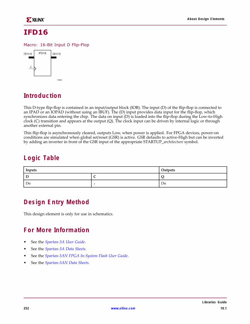
About Design Elements
IFD16
Macro: 16-Bit Input D Flip-Flop
IntroductionThis D-type flip-flop is contained in an input/output block (IOB). The input (D) of the flip-flop is connected toan IPAD or an IOPAD (without using an IBUF). The (D) input provides data input for the flip-flop, whichsynchronizes data entering the chip. The data on input (D) is loaded into the flip-flop during the Low-to-Highclock (C) transition and appears at the output (Q). The clock input can be driven by internal logic or throughanother external pin.
This flip-flop is asynchronously cleared, outputs Low, when power is applied. For FPGA devices, power-onconditions are simulated when global set/reset (GSR) is active. GSR defaults to active-High but can be invertedby adding an inverter in front of the GSR input of the appropriate STARTUP_architecture symbol.
Logic TableInputs Outputs
D C Q
Dn ↑ Dn
Design Entry MethodThis design element is only for use in schematics.
For More Information• See the Spartan-3A User Guide.
• See the Spartan-3A Data Sheets.
• See the Spartan-3AN FPGA In-System Flash User Guide.
• See the Spartan-3AN Data Sheets.
Libraries Guide
252 www.xilinx.com 10.1
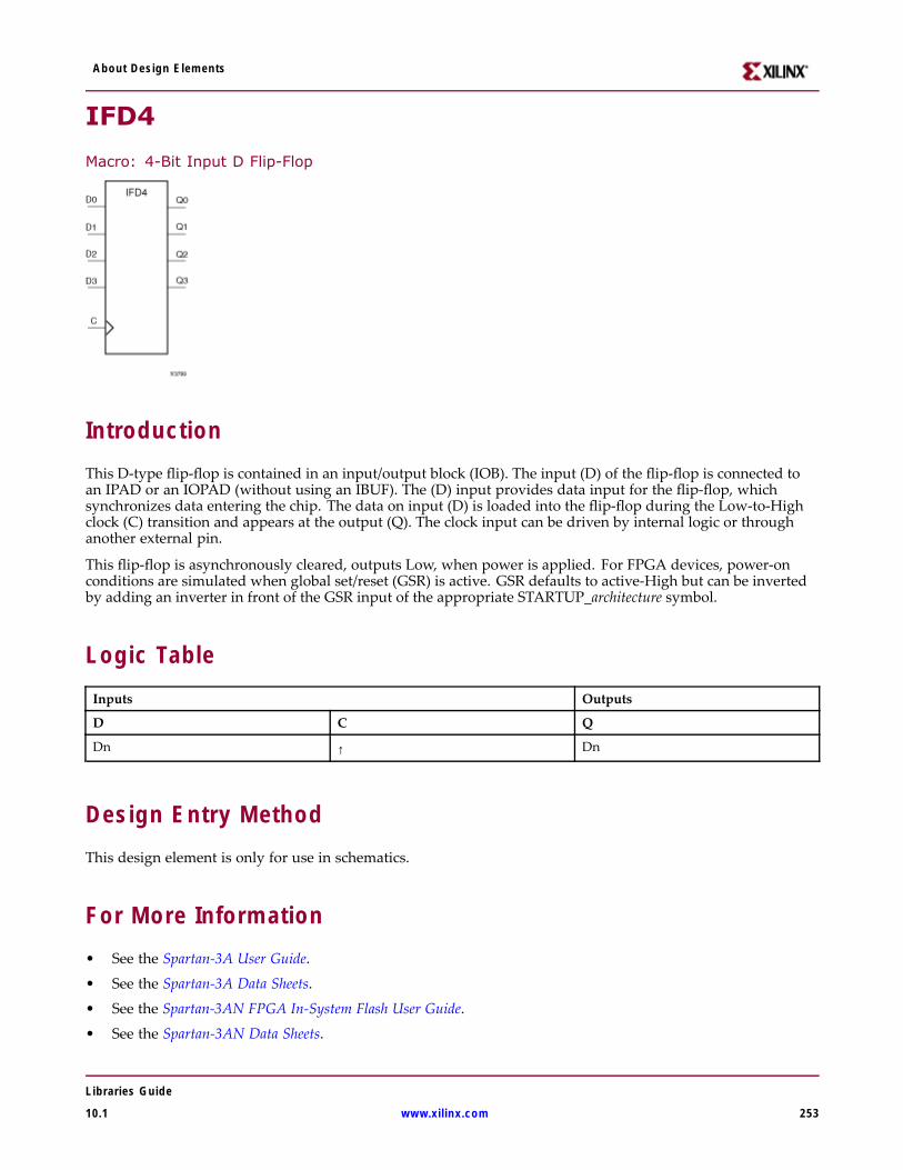
About Design Elements
IFD4
Macro: 4-Bit Input D Flip-Flop
IntroductionThis D-type flip-flop is contained in an input/output block (IOB). The input (D) of the flip-flop is connected toan IPAD or an IOPAD (without using an IBUF). The (D) input provides data input for the flip-flop, whichsynchronizes data entering the chip. The data on input (D) is loaded into the flip-flop during the Low-to-Highclock (C) transition and appears at the output (Q). The clock input can be driven by internal logic or throughanother external pin.
This flip-flop is asynchronously cleared, outputs Low, when power is applied. For FPGA devices, power-onconditions are simulated when global set/reset (GSR) is active. GSR defaults to active-High but can be invertedby adding an inverter in front of the GSR input of the appropriate STARTUP_architecture symbol.
Logic TableInputs Outputs
D C Q
Dn ↑ Dn
Design Entry MethodThis design element is only for use in schematics.
For More Information• See the Spartan-3A User Guide.
• See the Spartan-3A Data Sheets.
• See the Spartan-3AN FPGA In-System Flash User Guide.
• See the Spartan-3AN Data Sheets.
Libraries Guide
10.1 www.xilinx.com 253
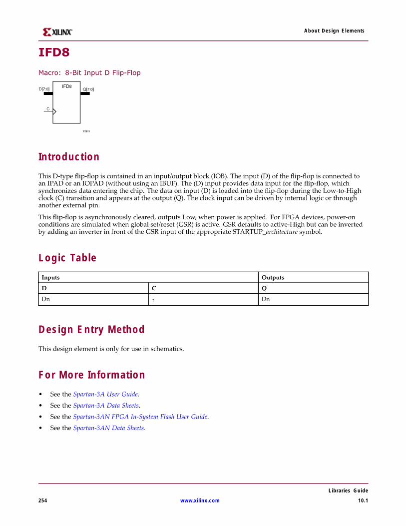
About Design Elements
IFD8
Macro: 8-Bit Input D Flip-Flop
IntroductionThis D-type flip-flop is contained in an input/output block (IOB). The input (D) of the flip-flop is connected toan IPAD or an IOPAD (without using an IBUF). The (D) input provides data input for the flip-flop, whichsynchronizes data entering the chip. The data on input (D) is loaded into the flip-flop during the Low-to-Highclock (C) transition and appears at the output (Q). The clock input can be driven by internal logic or throughanother external pin.
This flip-flop is asynchronously cleared, outputs Low, when power is applied. For FPGA devices, power-onconditions are simulated when global set/reset (GSR) is active. GSR defaults to active-High but can be invertedby adding an inverter in front of the GSR input of the appropriate STARTUP_architecture symbol.
Logic TableInputs Outputs
D C Q
Dn ↑ Dn
Design Entry MethodThis design element is only for use in schematics.
For More Information• See the Spartan-3A User Guide.
• See the Spartan-3A Data Sheets.
• See the Spartan-3AN FPGA In-System Flash User Guide.
• See the Spartan-3AN Data Sheets.
Libraries Guide
254 www.xilinx.com 10.1
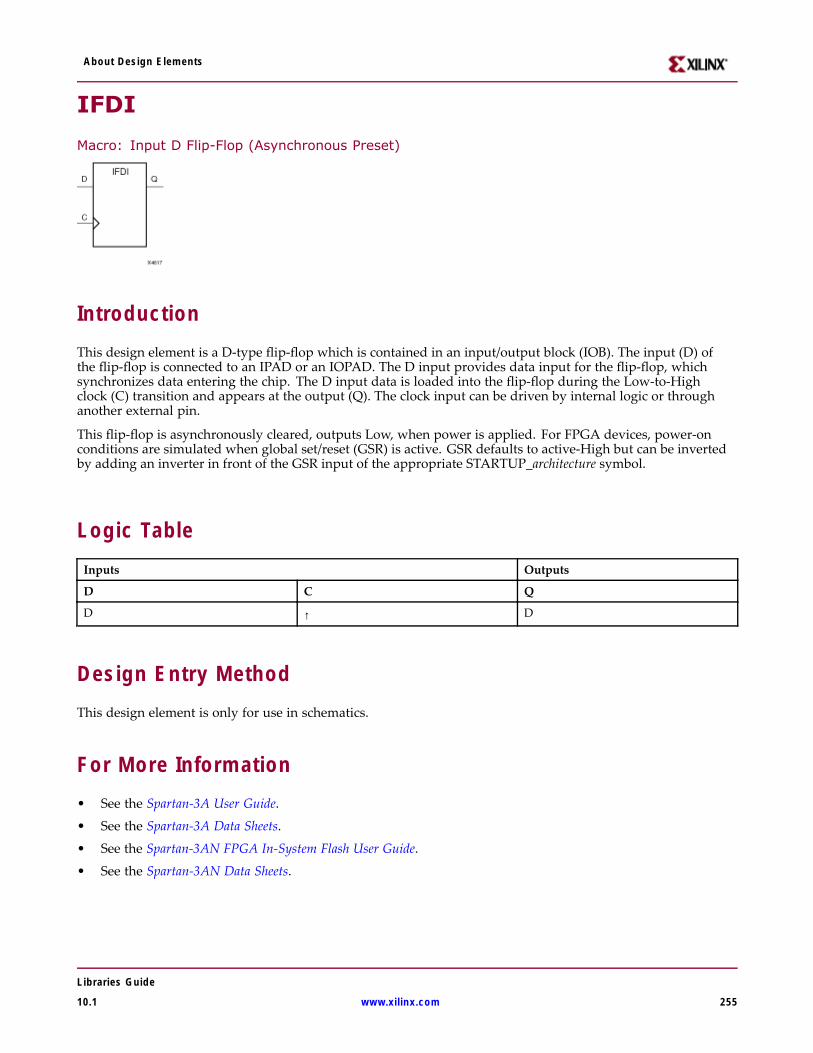
About Design Elements
IFDI
Macro: Input D Flip-Flop (Asynchronous Preset)
IntroductionThis design element is a D-type flip-flop which is contained in an input/output block (IOB). The input (D) ofthe flip-flop is connected to an IPAD or an IOPAD. The D input provides data input for the flip-flop, whichsynchronizes data entering the chip. The D input data is loaded into the flip-flop during the Low-to-Highclock (C) transition and appears at the output (Q). The clock input can be driven by internal logic or throughanother external pin.
This flip-flop is asynchronously cleared, outputs Low, when power is applied. For FPGA devices, power-onconditions are simulated when global set/reset (GSR) is active. GSR defaults to active-High but can be invertedby adding an inverter in front of the GSR input of the appropriate STARTUP_architecture symbol.
Logic TableInputs Outputs
D C Q
D ↑ D
Design Entry MethodThis design element is only for use in schematics.
For More Information• See the Spartan-3A User Guide.
• See the Spartan-3A Data Sheets.
• See the Spartan-3AN FPGA In-System Flash User Guide.
• See the Spartan-3AN Data Sheets.
Libraries Guide
10.1 www.xilinx.com 255
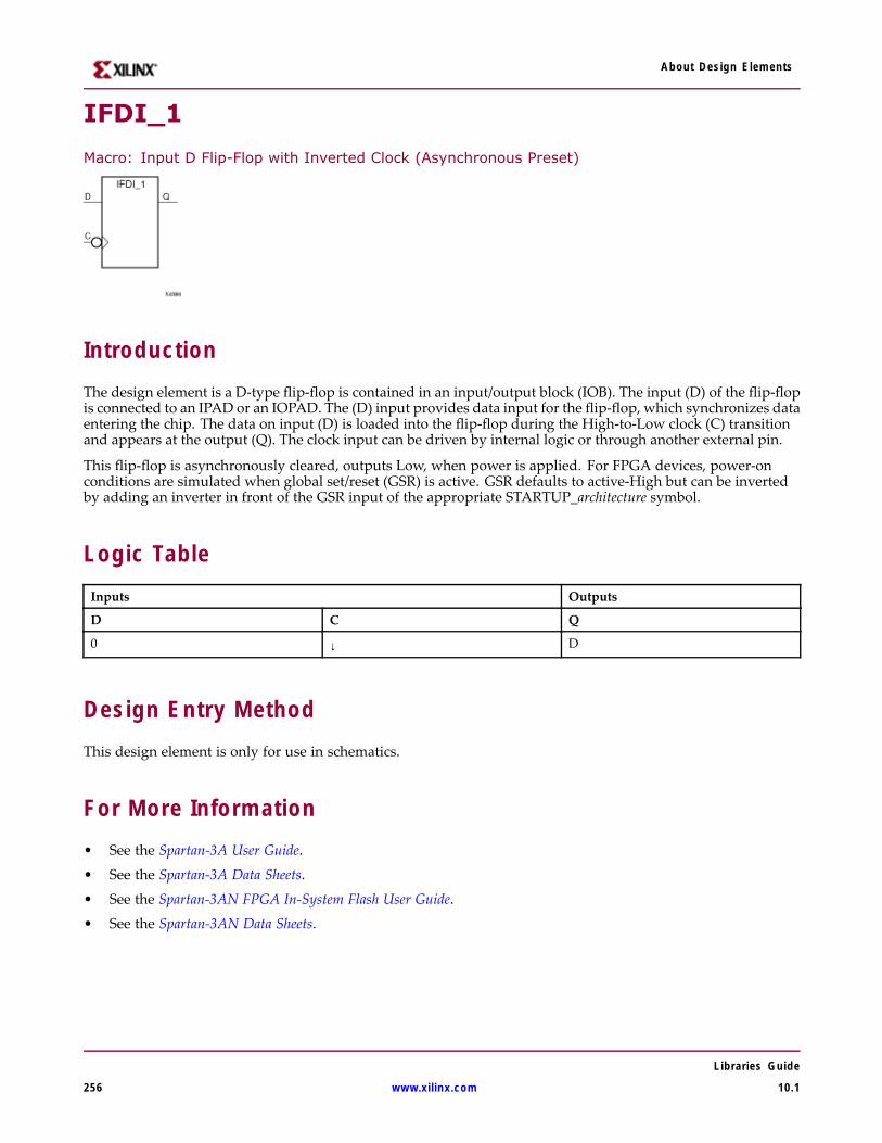
About Design Elements
IFDI_1
Macro: Input D Flip-Flop with Inverted Clock (Asynchronous Preset)
IntroductionThe design element is a D-type flip-flop is contained in an input/output block (IOB). The input (D) of the flip-flopis connected to an IPAD or an IOPAD. The (D) input provides data input for the flip-flop, which synchronizes dataentering the chip. The data on input (D) is loaded into the flip-flop during the High-to-Low clock (C) transitionand appears at the output (Q). The clock input can be driven by internal logic or through another external pin.
This flip-flop is asynchronously cleared, outputs Low, when power is applied. For FPGA devices, power-onconditions are simulated when global set/reset (GSR) is active. GSR defaults to active-High but can be invertedby adding an inverter in front of the GSR input of the appropriate STARTUP_architecture symbol.
Logic TableInputs Outputs
D C Q
0 ↓ D
Design Entry MethodThis design element is only for use in schematics.
For More Information• See the Spartan-3A User Guide.
• See the Spartan-3A Data Sheets.
• See the Spartan-3AN FPGA In-System Flash User Guide.
• See the Spartan-3AN Data Sheets.
Libraries Guide
256 www.xilinx.com 10.1
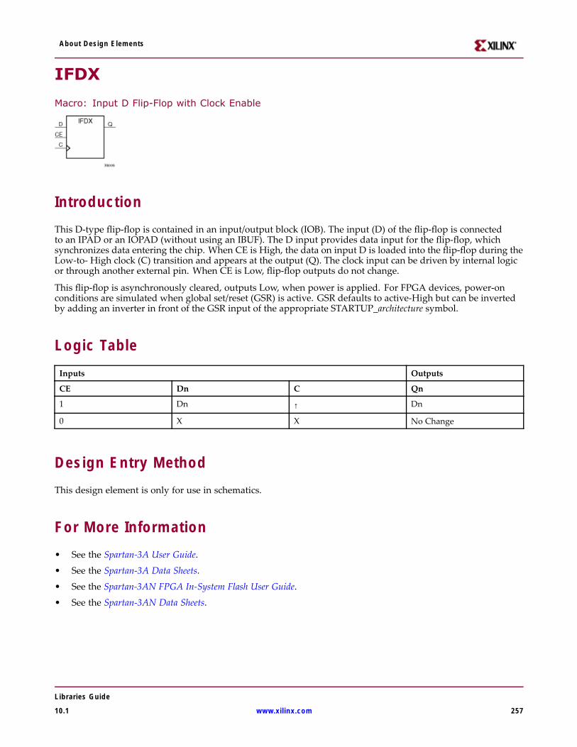
About Design Elements
IFDX
Macro: Input D Flip-Flop with Clock Enable
IntroductionThis D-type flip-flop is contained in an input/output block (IOB). The input (D) of the flip-flop is connectedto an IPAD or an IOPAD (without using an IBUF). The D input provides data input for the flip-flop, whichsynchronizes data entering the chip. When CE is High, the data on input D is loaded into the flip-flop during theLow-to- High clock (C) transition and appears at the output (Q). The clock input can be driven by internal logicor through another external pin. When CE is Low, flip-flop outputs do not change.
This flip-flop is asynchronously cleared, outputs Low, when power is applied. For FPGA devices, power-onconditions are simulated when global set/reset (GSR) is active. GSR defaults to active-High but can be invertedby adding an inverter in front of the GSR input of the appropriate STARTUP_architecture symbol.
Logic TableInputs Outputs
CE Dn C Qn
1 Dn ↑ Dn
0 X X No Change
Design Entry MethodThis design element is only for use in schematics.
For More Information• See the Spartan-3A User Guide.
• See the Spartan-3A Data Sheets.
• See the Spartan-3AN FPGA In-System Flash User Guide.
• See the Spartan-3AN Data Sheets.
Libraries Guide
10.1 www.xilinx.com 257
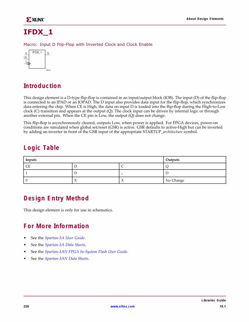
About Design Elements
IFDX_1
Macro: Input D Flip-Flop with Inverted Clock and Clock Enable
IntroductionThis design element is a D-type flip-flop is contained in an input/output block (IOB). The input (D) of the flip-flopis connected to an IPAD or an IOPAD. The D input also provides data input for the flip-flop, which synchronizesdata entering the chip. When CE is High, the data on input D is loaded into the flip-flop during the High-to-Lowclock (C) transition and appears at the output (Q). The clock input can be driven by internal logic or throughanother external pin. When the CE pin is Low, the output (Q) does not change.
This flip-flop is asynchronously cleared, outputs Low, when power is applied. For FPGA devices, power-onconditions are simulated when global set/reset (GSR) is active. GSR defaults to active-High but can be invertedby adding an inverter in front of the GSR input of the appropriate STARTUP_architecture symbol.
Logic TableInputs Outputs
CE D C Q
1 D ↓ D
0 X X No Change
Design Entry MethodThis design element is only for use in schematics.
For More Information• See the Spartan-3A User Guide.
• See the Spartan-3A Data Sheets.
• See the Spartan-3AN FPGA In-System Flash User Guide.
• See the Spartan-3AN Data Sheets.
Libraries Guide
258 www.xilinx.com 10.1
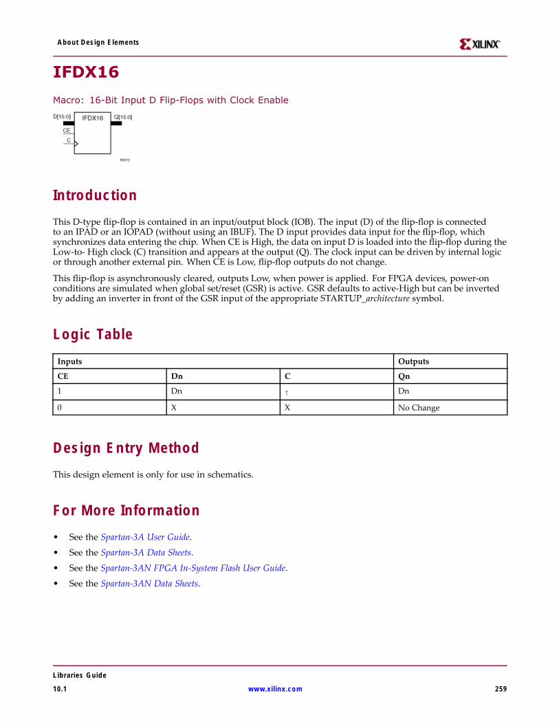
About Design Elements
IFDX16
Macro: 16-Bit Input D Flip-Flops with Clock Enable
IntroductionThis D-type flip-flop is contained in an input/output block (IOB). The input (D) of the flip-flop is connectedto an IPAD or an IOPAD (without using an IBUF). The D input provides data input for the flip-flop, whichsynchronizes data entering the chip. When CE is High, the data on input D is loaded into the flip-flop during theLow-to- High clock (C) transition and appears at the output (Q). The clock input can be driven by internal logicor through another external pin. When CE is Low, flip-flop outputs do not change.
This flip-flop is asynchronously cleared, outputs Low, when power is applied. For FPGA devices, power-onconditions are simulated when global set/reset (GSR) is active. GSR defaults to active-High but can be invertedby adding an inverter in front of the GSR input of the appropriate STARTUP_architecture symbol.
Logic TableInputs Outputs
CE Dn C Qn
1 Dn ↑ Dn
0 X X No Change
Design Entry MethodThis design element is only for use in schematics.
For More Information• See the Spartan-3A User Guide.
• See the Spartan-3A Data Sheets.
• See the Spartan-3AN FPGA In-System Flash User Guide.
• See the Spartan-3AN Data Sheets.
Libraries Guide
10.1 www.xilinx.com 259
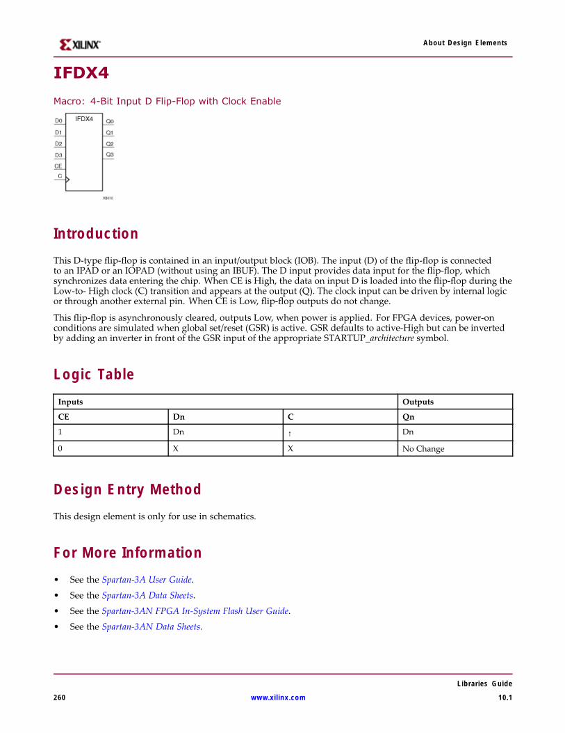
About Design Elements
IFDX4
Macro: 4-Bit Input D Flip-Flop with Clock Enable
IntroductionThis D-type flip-flop is contained in an input/output block (IOB). The input (D) of the flip-flop is connectedto an IPAD or an IOPAD (without using an IBUF). The D input provides data input for the flip-flop, whichsynchronizes data entering the chip. When CE is High, the data on input D is loaded into the flip-flop during theLow-to- High clock (C) transition and appears at the output (Q). The clock input can be driven by internal logicor through another external pin. When CE is Low, flip-flop outputs do not change.
This flip-flop is asynchronously cleared, outputs Low, when power is applied. For FPGA devices, power-onconditions are simulated when global set/reset (GSR) is active. GSR defaults to active-High but can be invertedby adding an inverter in front of the GSR input of the appropriate STARTUP_architecture symbol.
Logic TableInputs Outputs
CE Dn C Qn
1 Dn ↑ Dn
0 X X No Change
Design Entry MethodThis design element is only for use in schematics.
For More Information• See the Spartan-3A User Guide.
• See the Spartan-3A Data Sheets.
• See the Spartan-3AN FPGA In-System Flash User Guide.
• See the Spartan-3AN Data Sheets.
Libraries Guide
260 www.xilinx.com 10.1
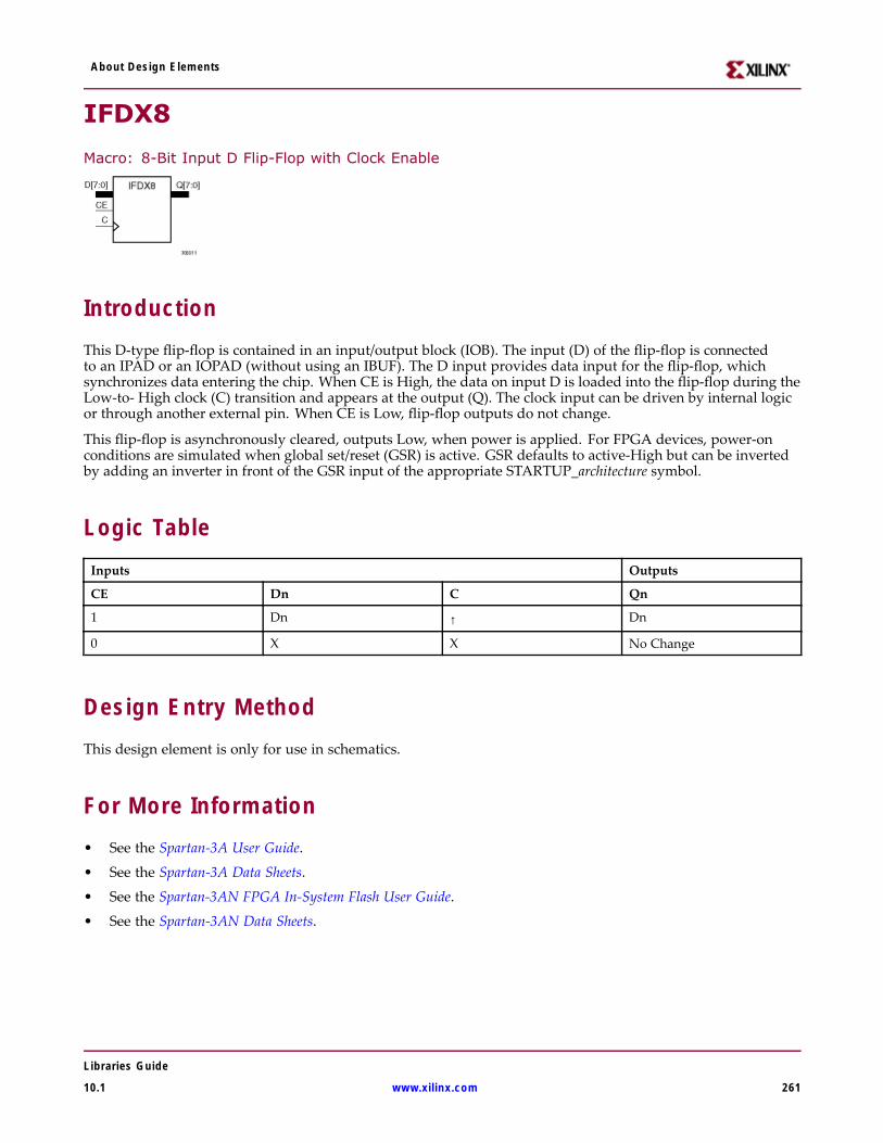
About Design Elements
IFDX8
Macro: 8-Bit Input D Flip-Flop with Clock Enable
IntroductionThis D-type flip-flop is contained in an input/output block (IOB). The input (D) of the flip-flop is connectedto an IPAD or an IOPAD (without using an IBUF). The D input provides data input for the flip-flop, whichsynchronizes data entering the chip. When CE is High, the data on input D is loaded into the flip-flop during theLow-to- High clock (C) transition and appears at the output (Q). The clock input can be driven by internal logicor through another external pin. When CE is Low, flip-flop outputs do not change.
This flip-flop is asynchronously cleared, outputs Low, when power is applied. For FPGA devices, power-onconditions are simulated when global set/reset (GSR) is active. GSR defaults to active-High but can be invertedby adding an inverter in front of the GSR input of the appropriate STARTUP_architecture symbol.
Logic TableInputs Outputs
CE Dn C Qn
1 Dn ↑ Dn
0 X X No Change
Design Entry MethodThis design element is only for use in schematics.
For More Information• See the Spartan-3A User Guide.
• See the Spartan-3A Data Sheets.
• See the Spartan-3AN FPGA In-System Flash User Guide.
• See the Spartan-3AN Data Sheets.
Libraries Guide
10.1 www.xilinx.com 261
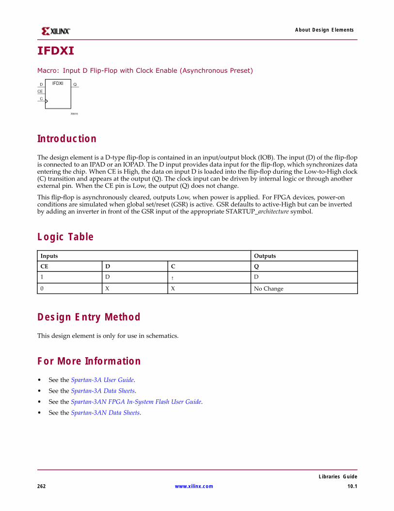
About Design Elements
IFDXI
Macro: Input D Flip-Flop with Clock Enable (Asynchronous Preset)
IntroductionThe design element is a D-type flip-flop is contained in an input/output block (IOB). The input (D) of the flip-flopis connected to an IPAD or an IOPAD. The D input provides data input for the flip-flop, which synchronizes dataentering the chip. When CE is High, the data on input D is loaded into the flip-flop during the Low-to-High clock(C) transition and appears at the output (Q). The clock input can be driven by internal logic or through anotherexternal pin. When the CE pin is Low, the output (Q) does not change.
This flip-flop is asynchronously cleared, outputs Low, when power is applied. For FPGA devices, power-onconditions are simulated when global set/reset (GSR) is active. GSR defaults to active-High but can be invertedby adding an inverter in front of the GSR input of the appropriate STARTUP_architecture symbol.
Logic TableInputs Outputs
CE D C Q
1 D ↑ D
0 X X No Change
Design Entry MethodThis design element is only for use in schematics.
For More Information• See the Spartan-3A User Guide.
• See the Spartan-3A Data Sheets.
• See the Spartan-3AN FPGA In-System Flash User Guide.
• See the Spartan-3AN Data Sheets.
Libraries Guide
262 www.xilinx.com 10.1
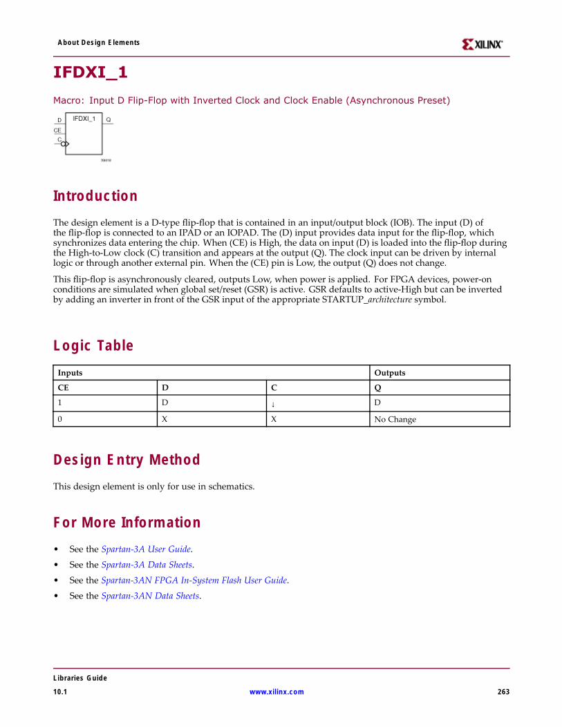
About Design Elements
IFDXI_1
Macro: Input D Flip-Flop with Inverted Clock and Clock Enable (Asynchronous Preset)
IntroductionThe design element is a D-type flip-flop that is contained in an input/output block (IOB). The input (D) ofthe flip-flop is connected to an IPAD or an IOPAD. The (D) input provides data input for the flip-flop, whichsynchronizes data entering the chip. When (CE) is High, the data on input (D) is loaded into the flip-flop duringthe High-to-Low clock (C) transition and appears at the output (Q). The clock input can be driven by internallogic or through another external pin. When the (CE) pin is Low, the output (Q) does not change.
This flip-flop is asynchronously cleared, outputs Low, when power is applied. For FPGA devices, power-onconditions are simulated when global set/reset (GSR) is active. GSR defaults to active-High but can be invertedby adding an inverter in front of the GSR input of the appropriate STARTUP_architecture symbol.
Logic TableInputs Outputs
CE D C Q
1 D ↓ D
0 X X No Change
Design Entry MethodThis design element is only for use in schematics.
For More Information• See the Spartan-3A User Guide.
• See the Spartan-3A Data Sheets.
• See the Spartan-3AN FPGA In-System Flash User Guide.
• See the Spartan-3AN Data Sheets.
Libraries Guide
10.1 www.xilinx.com 263
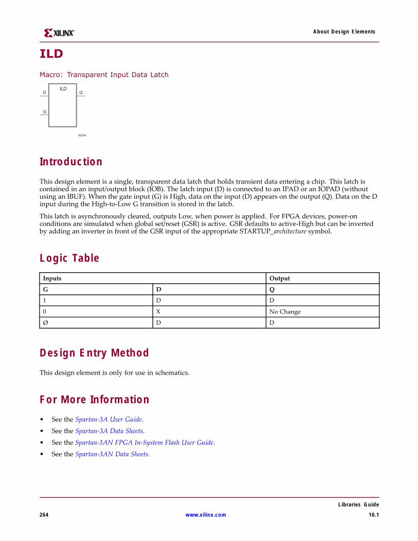
About Design Elements
ILD
Macro: Transparent Input Data Latch
IntroductionThis design element is a single, transparent data latch that holds transient data entering a chip. This latch iscontained in an input/output block (IOB). The latch input (D) is connected to an IPAD or an IOPAD (withoutusing an IBUF). When the gate input (G) is High, data on the input (D) appears on the output (Q). Data on the Dinput during the High-to-Low G transition is stored in the latch.
This latch is asynchronously cleared, outputs Low, when power is applied. For FPGA devices, power-onconditions are simulated when global set/reset (GSR) is active. GSR defaults to active-High but can be invertedby adding an inverter in front of the GSR input of the appropriate STARTUP_architecture symbol.
Logic TableInputs Output
G D Q
1 D D
0 X No Change
Ø D D
Design Entry MethodThis design element is only for use in schematics.
For More Information• See the Spartan-3A User Guide.
• See the Spartan-3A Data Sheets.
• See the Spartan-3AN FPGA In-System Flash User Guide.
• See the Spartan-3AN Data Sheets.
Libraries Guide
264 www.xilinx.com 10.1
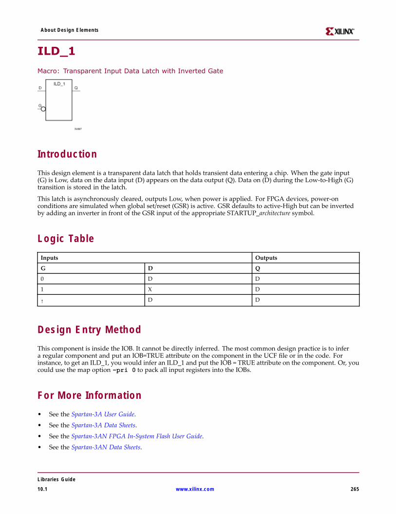
About Design Elements
ILD_1
Macro: Transparent Input Data Latch with Inverted Gate
IntroductionThis design element is a transparent data latch that holds transient data entering a chip. When the gate input(G) is Low, data on the data input (D) appears on the data output (Q). Data on (D) during the Low-to-High (G)transition is stored in the latch.
This latch is asynchronously cleared, outputs Low, when power is applied. For FPGA devices, power-onconditions are simulated when global set/reset (GSR) is active. GSR defaults to active-High but can be invertedby adding an inverter in front of the GSR input of the appropriate STARTUP_architecture symbol.
Logic TableInputs Outputs
G D Q
0 D D
1 X D
↑ D D
Design Entry MethodThis component is inside the IOB. It cannot be directly inferred. The most common design practice is to infera regular component and put an IOB=TRUE attribute on the component in the UCF file or in the code. Forinstance, to get an ILD_1, you would infer an ILD_1 and put the IOB = TRUE attribute on the component. Or, youcould use the map option –pri–pri–pri 000 to pack all input registers into the IOBs.
For More Information• See the Spartan-3A User Guide.
• See the Spartan-3A Data Sheets.
• See the Spartan-3AN FPGA In-System Flash User Guide.
• See the Spartan-3AN Data Sheets.
Libraries Guide
10.1 www.xilinx.com 265
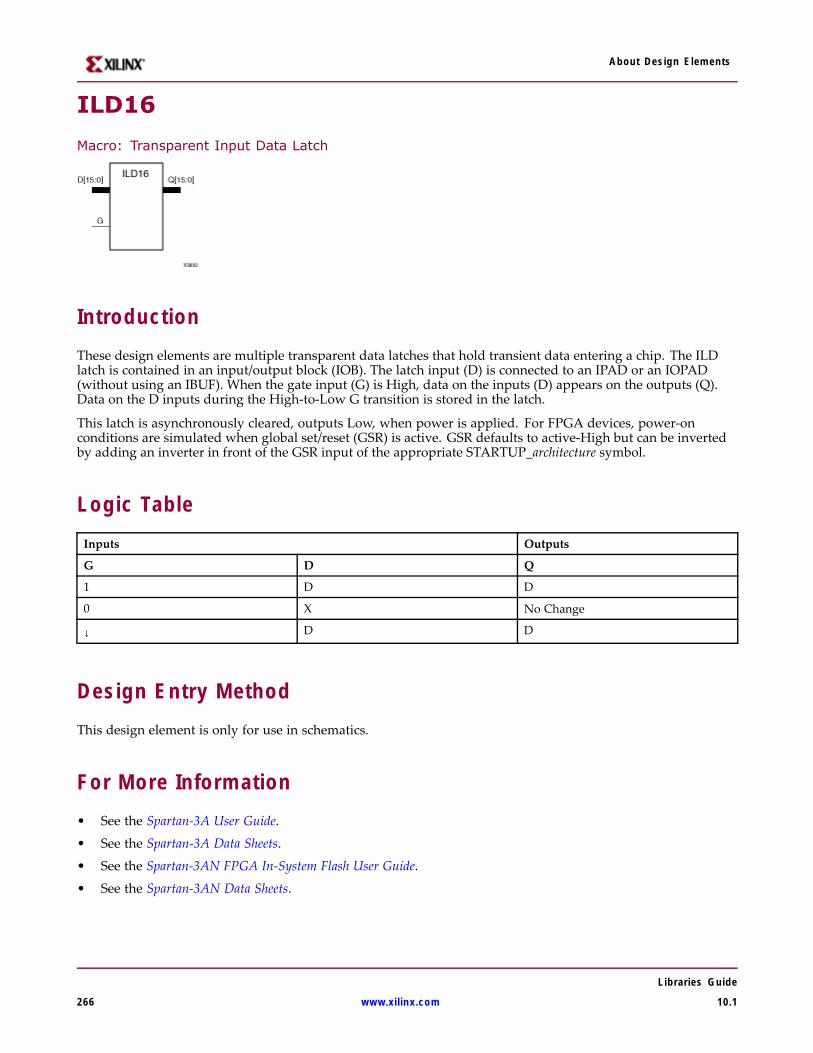
About Design Elements
ILD16
Macro: Transparent Input Data Latch
IntroductionThese design elements are multiple transparent data latches that hold transient data entering a chip. The ILDlatch is contained in an input/output block (IOB). The latch input (D) is connected to an IPAD or an IOPAD(without using an IBUF). When the gate input (G) is High, data on the inputs (D) appears on the outputs (Q).Data on the D inputs during the High-to-Low G transition is stored in the latch.
This latch is asynchronously cleared, outputs Low, when power is applied. For FPGA devices, power-onconditions are simulated when global set/reset (GSR) is active. GSR defaults to active-High but can be invertedby adding an inverter in front of the GSR input of the appropriate STARTUP_architecture symbol.
Logic TableInputs Outputs
G D Q
1 D D
0 X No Change
↓ D D
Design Entry MethodThis design element is only for use in schematics.
For More Information• See the Spartan-3A User Guide.
• See the Spartan-3A Data Sheets.
• See the Spartan-3AN FPGA In-System Flash User Guide.
• See the Spartan-3AN Data Sheets.
Libraries Guide
266 www.xilinx.com 10.1
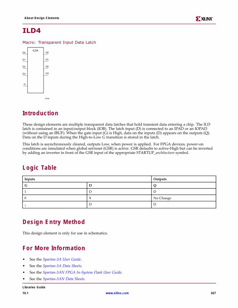
About Design Elements
ILD4
Macro: Transparent Input Data Latch
IntroductionThese design elements are multiple transparent data latches that hold transient data entering a chip. The ILDlatch is contained in an input/output block (IOB). The latch input (D) is connected to an IPAD or an IOPAD(without using an IBUF). When the gate input (G) is High, data on the inputs (D) appears on the outputs (Q).Data on the D inputs during the High-to-Low G transition is stored in the latch.
This latch is asynchronously cleared, outputs Low, when power is applied. For FPGA devices, power-onconditions are simulated when global set/reset (GSR) is active. GSR defaults to active-High but can be invertedby adding an inverter in front of the GSR input of the appropriate STARTUP_architecture symbol.
Logic TableInputs Outputs
G D Q
1 D D
0 X No Change
↓ D D
Design Entry MethodThis design element is only for use in schematics.
For More Information• See the Spartan-3A User Guide.
• See the Spartan-3A Data Sheets.
• See the Spartan-3AN FPGA In-System Flash User Guide.
• See the Spartan-3AN Data Sheets.
Libraries Guide
10.1 www.xilinx.com 267
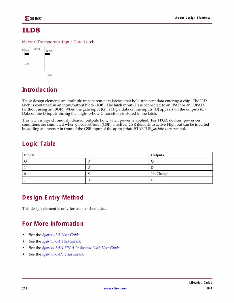
About Design Elements
ILD8
Macro: Transparent Input Data Latch
IntroductionThese design elements are multiple transparent data latches that hold transient data entering a chip. The ILDlatch is contained in an input/output block (IOB). The latch input (D) is connected to an IPAD or an IOPAD(without using an IBUF). When the gate input (G) is High, data on the inputs (D) appears on the outputs (Q).Data on the D inputs during the High-to-Low G transition is stored in the latch.
This latch is asynchronously cleared, outputs Low, when power is applied. For FPGA devices, power-onconditions are simulated when global set/reset (GSR) is active. GSR defaults to active-High but can be invertedby adding an inverter in front of the GSR input of the appropriate STARTUP_architecture symbol.
Logic TableInputs Outputs
G D Q
1 D D
0 X No Change
↓ D D
Design Entry MethodThis design element is only for use in schematics.
For More Information• See the Spartan-3A User Guide.
• See the Spartan-3A Data Sheets.
• See the Spartan-3AN FPGA In-System Flash User Guide.
• See the Spartan-3AN Data Sheets.
Libraries Guide
268 www.xilinx.com 10.1
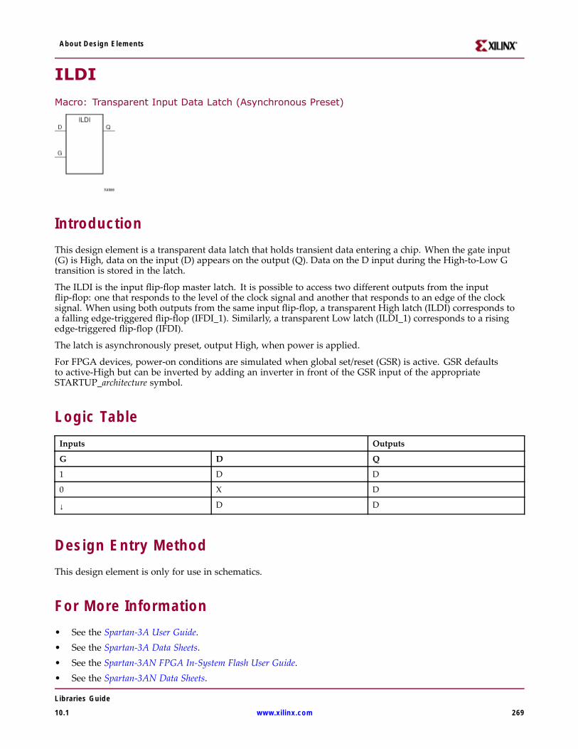
About Design Elements
ILDI
Macro: Transparent Input Data Latch (Asynchronous Preset)
IntroductionThis design element is a transparent data latch that holds transient data entering a chip. When the gate input(G) is High, data on the input (D) appears on the output (Q). Data on the D input during the High-to-Low Gtransition is stored in the latch.
The ILDI is the input flip-flop master latch. It is possible to access two different outputs from the inputflip-flop: one that responds to the level of the clock signal and another that responds to an edge of the clocksignal. When using both outputs from the same input flip-flop, a transparent High latch (ILDI) corresponds toa falling edge-triggered flip-flop (IFDI_1). Similarly, a transparent Low latch (ILDI_1) corresponds to a risingedge-triggered flip-flop (IFDI).
The latch is asynchronously preset, output High, when power is applied.
For FPGA devices, power-on conditions are simulated when global set/reset (GSR) is active. GSR defaultsto active-High but can be inverted by adding an inverter in front of the GSR input of the appropriateSTARTUP_architecture symbol.
Logic TableInputs Outputs
G D Q
1 D D
0 X D
↓ D D
Design Entry MethodThis design element is only for use in schematics.
For More Information• See the Spartan-3A User Guide.• See the Spartan-3A Data Sheets.• See the Spartan-3AN FPGA In-System Flash User Guide.• See the Spartan-3AN Data Sheets.
Libraries Guide
10.1 www.xilinx.com 269
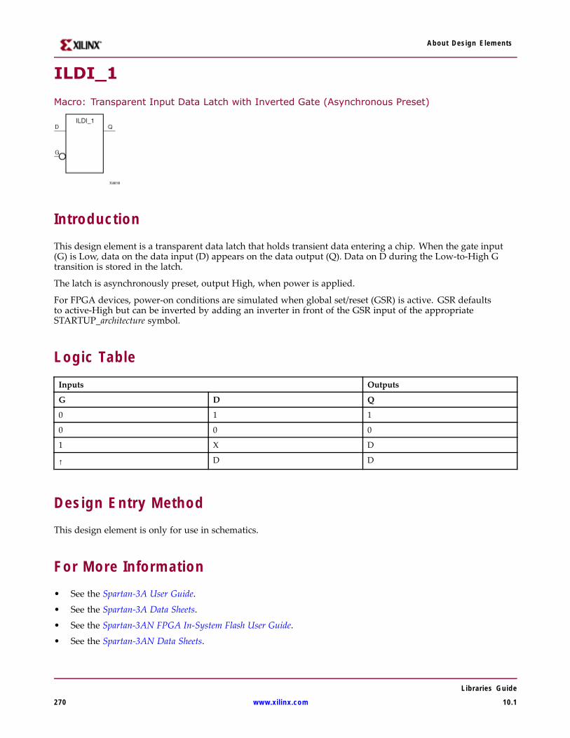
About Design Elements
ILDI_1
Macro: Transparent Input Data Latch with Inverted Gate (Asynchronous Preset)
IntroductionThis design element is a transparent data latch that holds transient data entering a chip. When the gate input(G) is Low, data on the data input (D) appears on the data output (Q). Data on D during the Low-to-High Gtransition is stored in the latch.
The latch is asynchronously preset, output High, when power is applied.
For FPGA devices, power-on conditions are simulated when global set/reset (GSR) is active. GSR defaultsto active-High but can be inverted by adding an inverter in front of the GSR input of the appropriateSTARTUP_architecture symbol.
Logic TableInputs Outputs
G D Q
0 1 1
0 0 0
1 X D
↑ D D
Design Entry MethodThis design element is only for use in schematics.
For More Information• See the Spartan-3A User Guide.
• See the Spartan-3A Data Sheets.
• See the Spartan-3AN FPGA In-System Flash User Guide.
• See the Spartan-3AN Data Sheets.
Libraries Guide
270 www.xilinx.com 10.1
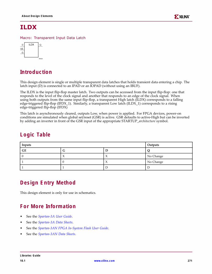
About Design Elements
ILDX
Macro: Transparent Input Data Latch
IntroductionThis design element is single or multiple transparent data latches that holds transient data entering a chip. Thelatch input (D) is connected to an IPAD or an IOPAD (without using an IBUF).
The ILDX is the input flip-flop master latch. Two outputs can be accessed from the input flip-flop: one thatresponds to the level of the clock signal and another that responds to an edge of the clock signal. Whenusing both outputs from the same input flip-flop, a transparent High latch (ILDX) corresponds to a fallingedge-triggered flip-flop (IFDX_1). Similarly, a transparent Low latch (ILDX_1) corresponds to a risingedge-triggered flip-flop (IFDX)
This latch is asynchronously cleared, outputs Low, when power is applied. For FPGA devices, power-onconditions are simulated when global set/reset (GSR) is active. GSR defaults to active-High but can be invertedby adding an inverter in front of the GSR input of the appropriate STARTUP_architecture symbol.
Logic TableInputs Outputs
GE G D Q
0 X X No Change
1 0 X No Change
1 1 D D
Design Entry MethodThis design element is only for use in schematics.
For More Information• See the Spartan-3A User Guide.
• See the Spartan-3A Data Sheets.
• See the Spartan-3AN FPGA In-System Flash User Guide.
• See the Spartan-3AN Data Sheets.
Libraries Guide
10.1 www.xilinx.com 271
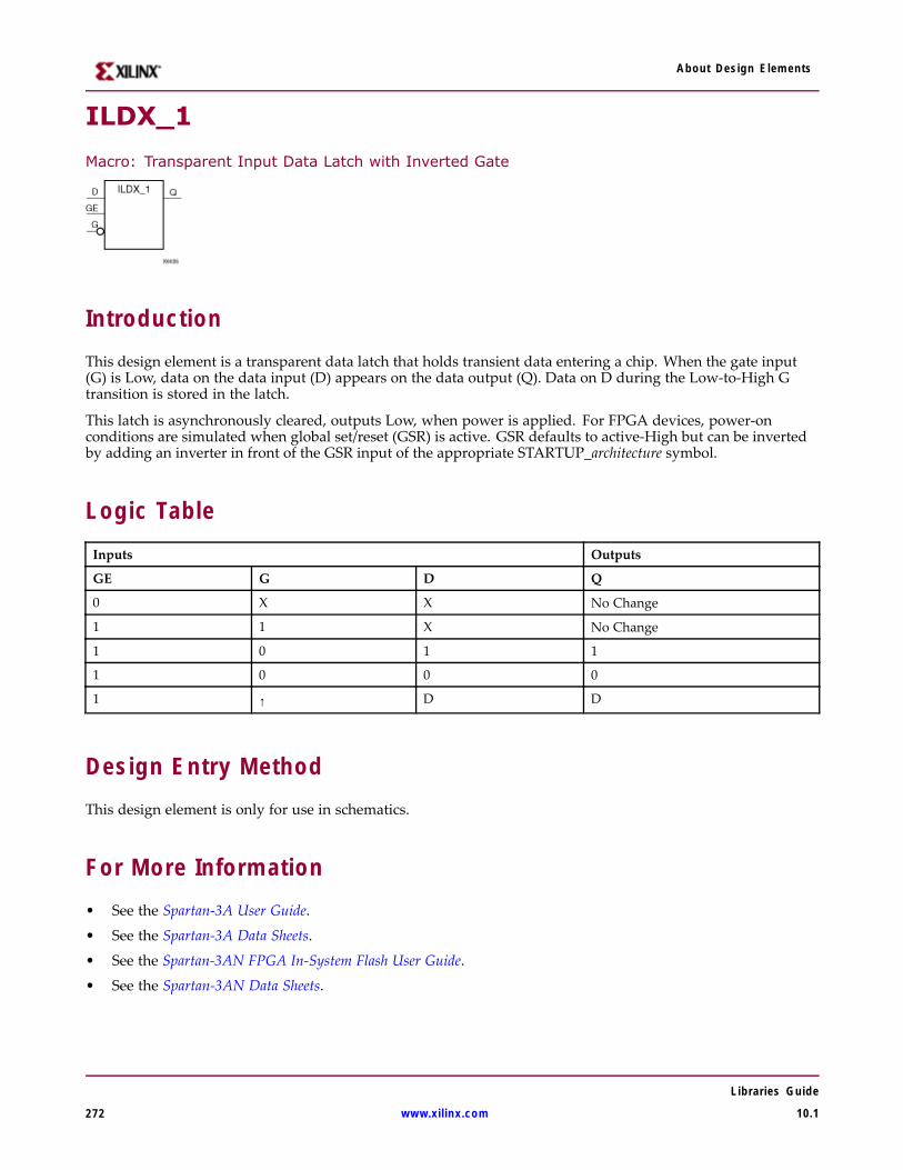
About Design Elements
ILDX_1
Macro: Transparent Input Data Latch with Inverted Gate
IntroductionThis design element is a transparent data latch that holds transient data entering a chip. When the gate input(G) is Low, data on the data input (D) appears on the data output (Q). Data on D during the Low-to-High Gtransition is stored in the latch.
This latch is asynchronously cleared, outputs Low, when power is applied. For FPGA devices, power-onconditions are simulated when global set/reset (GSR) is active. GSR defaults to active-High but can be invertedby adding an inverter in front of the GSR input of the appropriate STARTUP_architecture symbol.
Logic TableInputs Outputs
GE G D Q
0 X X No Change
1 1 X No Change
1 0 1 1
1 0 0 0
1 ↑ D D
Design Entry MethodThis design element is only for use in schematics.
For More Information• See the Spartan-3A User Guide.
• See the Spartan-3A Data Sheets.
• See the Spartan-3AN FPGA In-System Flash User Guide.
• See the Spartan-3AN Data Sheets.
Libraries Guide
272 www.xilinx.com 10.1
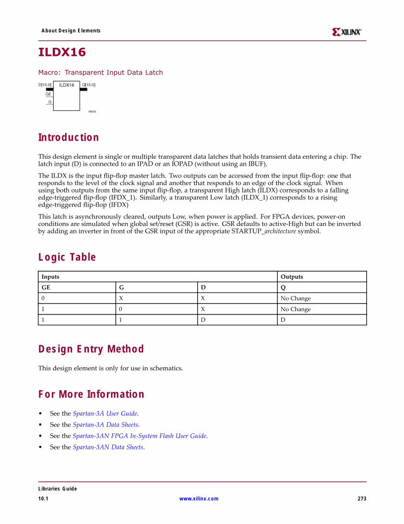
About Design Elements
ILDX16
Macro: Transparent Input Data Latch
IntroductionThis design element is single or multiple transparent data latches that holds transient data entering a chip. Thelatch input (D) is connected to an IPAD or an IOPAD (without using an IBUF).
The ILDX is the input flip-flop master latch. Two outputs can be accessed from the input flip-flop: one thatresponds to the level of the clock signal and another that responds to an edge of the clock signal. Whenusing both outputs from the same input flip-flop, a transparent High latch (ILDX) corresponds to a fallingedge-triggered flip-flop (IFDX_1). Similarly, a transparent Low latch (ILDX_1) corresponds to a risingedge-triggered flip-flop (IFDX)
This latch is asynchronously cleared, outputs Low, when power is applied. For FPGA devices, power-onconditions are simulated when global set/reset (GSR) is active. GSR defaults to active-High but can be invertedby adding an inverter in front of the GSR input of the appropriate STARTUP_architecture symbol.
Logic TableInputs Outputs
GE G D Q
0 X X No Change
1 0 X No Change
1 1 D D
Design Entry MethodThis design element is only for use in schematics.
For More Information• See the Spartan-3A User Guide.
• See the Spartan-3A Data Sheets.
• See the Spartan-3AN FPGA In-System Flash User Guide.
• See the Spartan-3AN Data Sheets.
Libraries Guide
10.1 www.xilinx.com 273
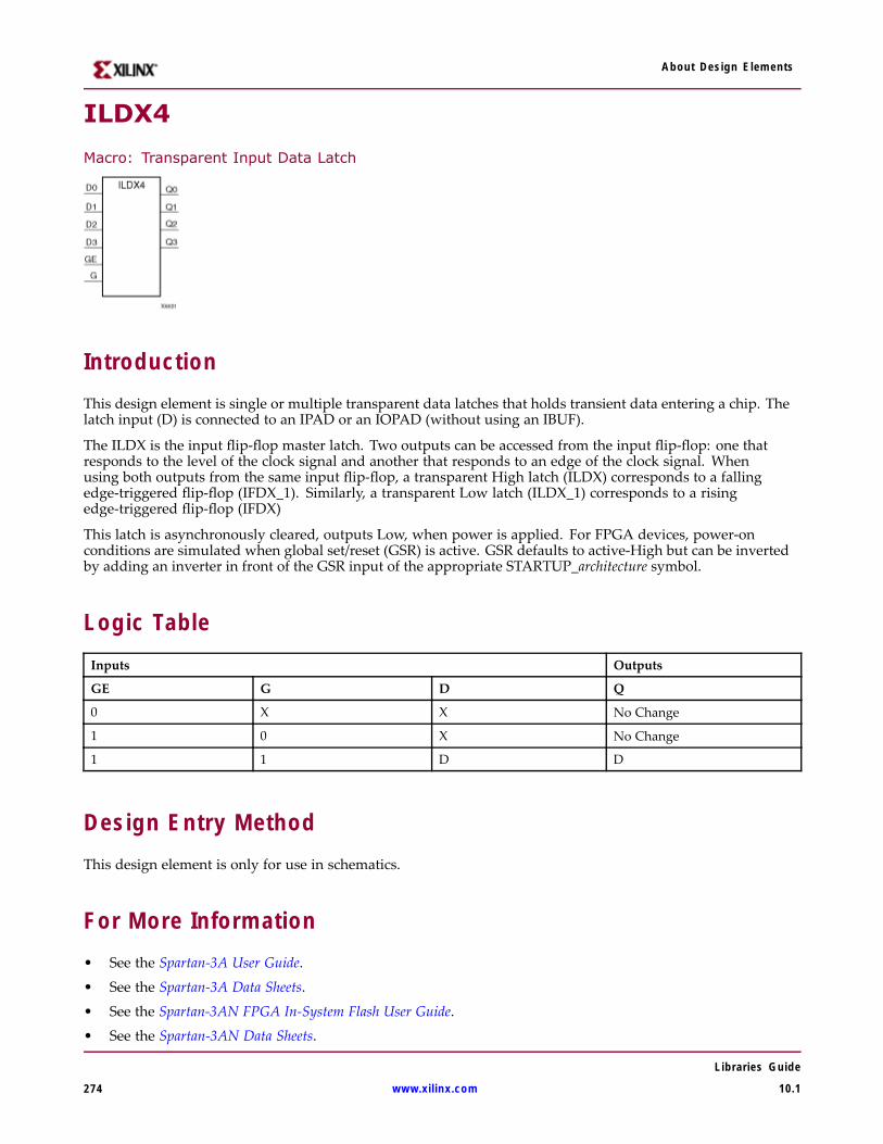
About Design Elements
ILDX4
Macro: Transparent Input Data Latch
IntroductionThis design element is single or multiple transparent data latches that holds transient data entering a chip. Thelatch input (D) is connected to an IPAD or an IOPAD (without using an IBUF).
The ILDX is the input flip-flop master latch. Two outputs can be accessed from the input flip-flop: one thatresponds to the level of the clock signal and another that responds to an edge of the clock signal. Whenusing both outputs from the same input flip-flop, a transparent High latch (ILDX) corresponds to a fallingedge-triggered flip-flop (IFDX_1). Similarly, a transparent Low latch (ILDX_1) corresponds to a risingedge-triggered flip-flop (IFDX)
This latch is asynchronously cleared, outputs Low, when power is applied. For FPGA devices, power-onconditions are simulated when global set/reset (GSR) is active. GSR defaults to active-High but can be invertedby adding an inverter in front of the GSR input of the appropriate STARTUP_architecture symbol.
Logic TableInputs Outputs
GE G D Q
0 X X No Change
1 0 X No Change
1 1 D D
Design Entry MethodThis design element is only for use in schematics.
For More Information• See the Spartan-3A User Guide.
• See the Spartan-3A Data Sheets.
• See the Spartan-3AN FPGA In-System Flash User Guide.
• See the Spartan-3AN Data Sheets.
Libraries Guide
274 www.xilinx.com 10.1
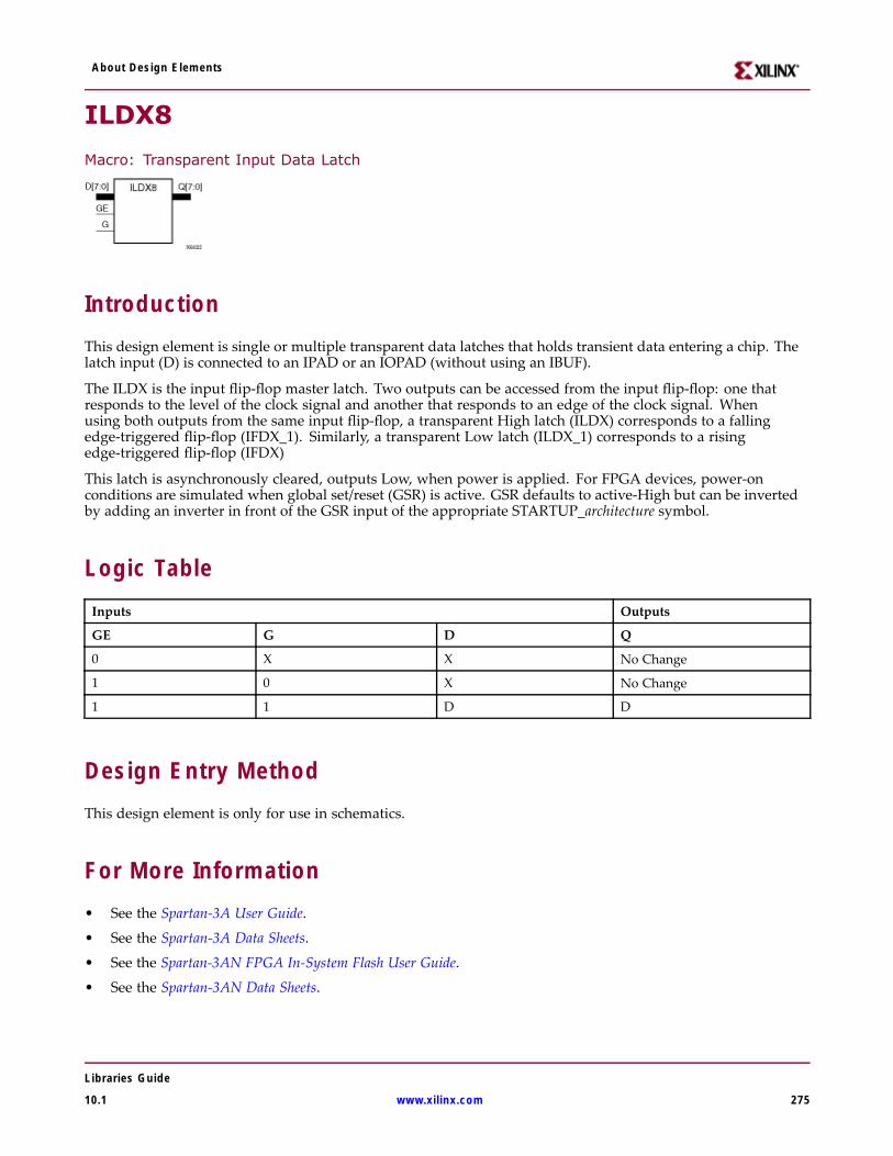
About Design Elements
ILDX8
Macro: Transparent Input Data Latch
IntroductionThis design element is single or multiple transparent data latches that holds transient data entering a chip. Thelatch input (D) is connected to an IPAD or an IOPAD (without using an IBUF).
The ILDX is the input flip-flop master latch. Two outputs can be accessed from the input flip-flop: one thatresponds to the level of the clock signal and another that responds to an edge of the clock signal. Whenusing both outputs from the same input flip-flop, a transparent High latch (ILDX) corresponds to a fallingedge-triggered flip-flop (IFDX_1). Similarly, a transparent Low latch (ILDX_1) corresponds to a risingedge-triggered flip-flop (IFDX)
This latch is asynchronously cleared, outputs Low, when power is applied. For FPGA devices, power-onconditions are simulated when global set/reset (GSR) is active. GSR defaults to active-High but can be invertedby adding an inverter in front of the GSR input of the appropriate STARTUP_architecture symbol.
Logic TableInputs Outputs
GE G D Q
0 X X No Change
1 0 X No Change
1 1 D D
Design Entry MethodThis design element is only for use in schematics.
For More Information• See the Spartan-3A User Guide.
• See the Spartan-3A Data Sheets.
• See the Spartan-3AN FPGA In-System Flash User Guide.
• See the Spartan-3AN Data Sheets.
Libraries Guide
10.1 www.xilinx.com 275
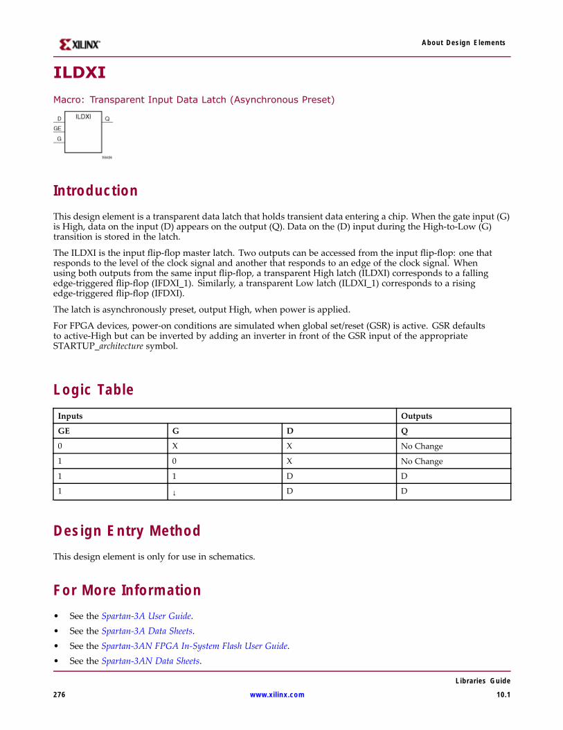
About Design Elements
ILDXI
Macro: Transparent Input Data Latch (Asynchronous Preset)
IntroductionThis design element is a transparent data latch that holds transient data entering a chip. When the gate input (G)is High, data on the input (D) appears on the output (Q). Data on the (D) input during the High-to-Low (G)transition is stored in the latch.
The ILDXI is the input flip-flop master latch. Two outputs can be accessed from the input flip-flop: one thatresponds to the level of the clock signal and another that responds to an edge of the clock signal. Whenusing both outputs from the same input flip-flop, a transparent High latch (ILDXI) corresponds to a fallingedge-triggered flip-flop (IFDXI_1). Similarly, a transparent Low latch (ILDXI_1) corresponds to a risingedge-triggered flip-flop (IFDXI).
The latch is asynchronously preset, output High, when power is applied.
For FPGA devices, power-on conditions are simulated when global set/reset (GSR) is active. GSR defaultsto active-High but can be inverted by adding an inverter in front of the GSR input of the appropriateSTARTUP_architecture symbol.
Logic TableInputs Outputs
GE G D Q
0 X X No Change
1 0 X No Change
1 1 D D
1 ↓ D D
Design Entry MethodThis design element is only for use in schematics.
For More Information• See the Spartan-3A User Guide.• See the Spartan-3A Data Sheets.• See the Spartan-3AN FPGA In-System Flash User Guide.• See the Spartan-3AN Data Sheets.
Libraries Guide
276 www.xilinx.com 10.1
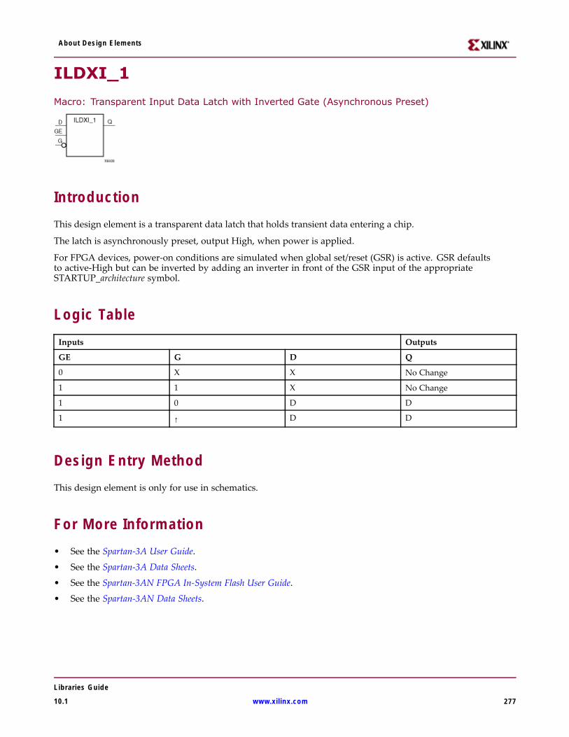
About Design Elements
ILDXI_1
Macro: Transparent Input Data Latch with Inverted Gate (Asynchronous Preset)
IntroductionThis design element is a transparent data latch that holds transient data entering a chip.
The latch is asynchronously preset, output High, when power is applied.
For FPGA devices, power-on conditions are simulated when global set/reset (GSR) is active. GSR defaultsto active-High but can be inverted by adding an inverter in front of the GSR input of the appropriateSTARTUP_architecture symbol.
Logic TableInputs Outputs
GE G D Q
0 X X No Change
1 1 X No Change
1 0 D D
1 ↑ D D
Design Entry MethodThis design element is only for use in schematics.
For More Information• See the Spartan-3A User Guide.
• See the Spartan-3A Data Sheets.
• See the Spartan-3AN FPGA In-System Flash User Guide.
• See the Spartan-3AN Data Sheets.
Libraries Guide
10.1 www.xilinx.com 277
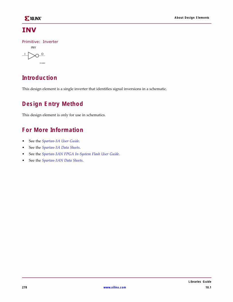
About Design Elements
INV
Primitive: Inverter
IntroductionThis design element is a single inverter that identifies signal inversions in a schematic.
Design Entry MethodThis design element is only for use in schematics.
For More Information• See the Spartan-3A User Guide.
• See the Spartan-3A Data Sheets.
• See the Spartan-3AN FPGA In-System Flash User Guide.
• See the Spartan-3AN Data Sheets.
Libraries Guide
278 www.xilinx.com 10.1
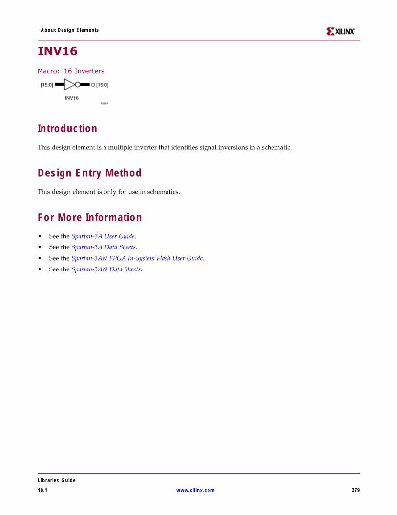
About Design Elements
INV16
Macro: 16 Inverters
IntroductionThis design element is a multiple inverter that identifies signal inversions in a schematic.
Design Entry MethodThis design element is only for use in schematics.
For More Information• See the Spartan-3A User Guide.
• See the Spartan-3A Data Sheets.
• See the Spartan-3AN FPGA In-System Flash User Guide.
• See the Spartan-3AN Data Sheets.
Libraries Guide
10.1 www.xilinx.com 279
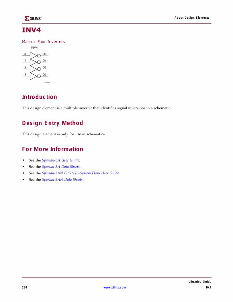
About Design Elements
INV4
Macro: Four Inverters
IntroductionThis design element is a multiple inverter that identifies signal inversions in a schematic.
Design Entry MethodThis design element is only for use in schematics.
For More Information• See the Spartan-3A User Guide.
• See the Spartan-3A Data Sheets.
• See the Spartan-3AN FPGA In-System Flash User Guide.
• See the Spartan-3AN Data Sheets.
Libraries Guide
280 www.xilinx.com 10.1
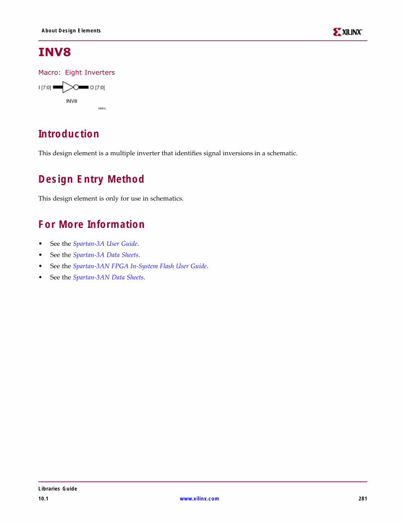
About Design Elements
INV8
Macro: Eight Inverters
IntroductionThis design element is a multiple inverter that identifies signal inversions in a schematic.
Design Entry MethodThis design element is only for use in schematics.
For More Information• See the Spartan-3A User Guide.
• See the Spartan-3A Data Sheets.
• See the Spartan-3AN FPGA In-System Flash User Guide.
• See the Spartan-3AN Data Sheets.
Libraries Guide
10.1 www.xilinx.com 281
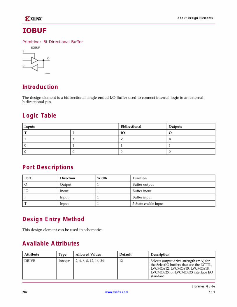
About Design Elements
IOBUF
Primitive: Bi-Directional Buffer
IntroductionThe design element is a bidirectional single-ended I/O Buffer used to connect internal logic to an externalbidirectional pin.
Logic TableInputs Bidirectional Outputs
T I IO O
1 X Z X
0 1 1 1
0 0 0 0
Port DescriptionsPort Direction Width Function
O Output 1 Buffer output
IO Inout 1 Buffer inout
I Input 1 Buffer input
T Input 1 3-State enable input
Design Entry MethodThis design element can be used in schematics.
Available AttributesAttribute Type Allowed Values Default Description
DRIVE Integer 2, 4, 6, 8, 12, 16, 24 12 Selects output drive strength (mA) forthe SelectIO buffers that use the LVTTL,LVCMOS12, LVCMOS15, LVCMOS18,LVCMOS25, or LVCMOS33 interface I/Ostandard.
Libraries Guide
282 www.xilinx.com 10.1
About Design Elements
Attribute Type Allowed Values Default Description
IBUF_DELAY_VALUE
String
"0" through "16"
"0" Specifies the amount of additional delayto add to the non-registered path out ofthe IOB
IFD_DELAY_VALUE
String
"AUTO", "0" thru "8"
"AUTO" Specifies the amount of additional delayto add to the registered path within theIOB
IOSTANDARD String See Data Sheet "DEFAULT" Assigns an I/O standard to the element.
SLEW String "SLOW", "FAST" "SLOW" Sets the output rise and fall time. See theData Sheet for recommendations of thebest setting for this attribute.
For More Information• See the Spartan-3A User Guide.
• See the Spartan-3A Data Sheets.
• See the Spartan-3AN FPGA In-System Flash User Guide.
• See the Spartan-3AN Data Sheets.
Libraries Guide
10.1 www.xilinx.com 283
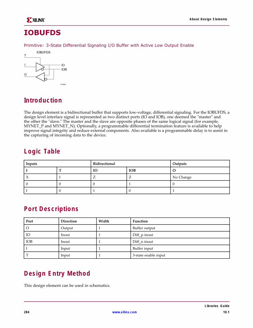
About Design Elements
IOBUFDS
Primitive: 3-State Differential Signaling I/O Buffer with Active Low Output Enable
IntroductionThe design element is a bidirectional buffer that supports low-voltage, differential signaling. For the IOBUFDS, adesign level interface signal is represented as two distinct ports (IO and IOB), one deemed the "master" andthe other the "slave." The master and the slave are opposite phases of the same logical signal (for example,MYNET_P and MYNET_N). Optionally, a programmable differential termination feature is available to helpimprove signal integrity and reduce external components. Also available is a programmable delay is to assist inthe capturing of incoming data to the device.
Logic TableInputs Bidirectional Outputs
I T IO IOB O
X 1 Z Z No Change
0 0 0 1 0
I 0 1 0 1
Port DescriptionsPort Direction Width Function
O Output 1 Buffer output
IO Inout 1 Diff_p inout
IOB Inout 1 Diff_n inout
I Input 1 Buffer input
T Input 1 3-state enable input
Design Entry MethodThis design element can be used in schematics.
Libraries Guide
284 www.xilinx.com 10.1
About Design Elements
Available AttributesAttribute Type Allowed Values Default Description
IBUF_DELAY_VALUE
String
"0" through "16"
"0" Specifies the amount of additional delayto add to the non-registered path outof the IOB
IFD_DELAY_ VALUE String
"AUTO", "0" thru"8"
"AUTO" Specifies the amount of additional delayto add to the registered path within theIOB
IOSTANDARD String See Data Sheet "DEFAULT" Assigns an I/O standard to the element.
For More Information• See the Spartan-3A User Guide.
• See the Spartan-3A Data Sheets.
• See the Spartan-3AN FPGA In-System Flash User Guide.
• See the Spartan-3AN Data Sheets.
Libraries Guide
10.1 www.xilinx.com 285
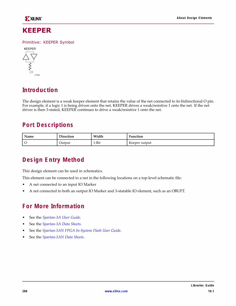
About Design Elements
KEEPER
Primitive: KEEPER Symbol
IntroductionThe design element is a weak keeper element that retains the value of the net connected to its bidirectional O pin.For example, if a logic 1 is being driven onto the net, KEEPER drives a weak/resistive 1 onto the net. If the netdriver is then 3-stated, KEEPER continues to drive a weak/resistive 1 onto the net.
Port DescriptionsName Direction Width Function
O Output 1-Bit Keeper output
Design Entry MethodThis design element can be used in schematics.
This element can be connected to a net in the following locations on a top-level schematic file:
• A net connected to an input IO Marker
• A net connected to both an output IO Marker and 3-statable IO element, such as an OBUFT.
For More Information• See the Spartan-3A User Guide.
• See the Spartan-3A Data Sheets.
• See the Spartan-3AN FPGA In-System Flash User Guide.
• See the Spartan-3AN Data Sheets.
Libraries Guide
286 www.xilinx.com 10.1
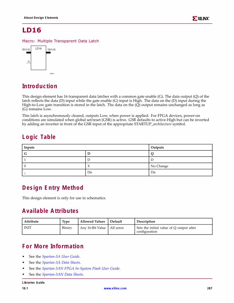
About Design Elements
LD16Macro: Multiple Transparent Data Latch
IntroductionThis design element has 16 transparent data latches with a common gate enable (G). The data output (Q) of thelatch reflects the data (D) input while the gate enable (G) input is High. The data on the (D) input during theHigh-to-Low gate transition is stored in the latch. The data on the (Q) output remains unchanged as long as(G) remains Low.
This latch is asynchronously cleared, outputs Low, when power is applied. For FPGA devices, power-onconditions are simulated when global set/reset (GSR) is active. GSR defaults to active-High but can be invertedby adding an inverter in front of the GSR input of the appropriate STARTUP_architecture symbol.
Logic TableInputs Outputs
G D Q
1 D D
0 X No Change
↓ Dn Dn
Design Entry MethodThis design element is only for use in schematics.
Available AttributesAttribute Type Allowed Values Default Description
INIT Binary Any 16-Bit Value All zeros Sets the initial value of Q output afterconfiguration
For More Information• See the Spartan-3A User Guide.• See the Spartan-3A Data Sheets.• See the Spartan-3AN FPGA In-System Flash User Guide.• See the Spartan-3AN Data Sheets.
Libraries Guide
10.1 www.xilinx.com 287
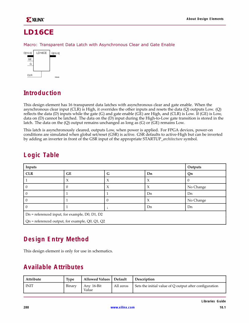
About Design Elements
LD16CE
Macro: Transparent Data Latch with Asynchronous Clear and Gate Enable
IntroductionThis design element has 16 transparent data latches with asynchronous clear and gate enable. When theasynchronous clear input (CLR) is High, it overrides the other inputs and resets the data (Q) outputs Low. (Q)reflects the data (D) inputs while the gate (G) and gate enable (GE) are High, and (CLR) is Low. If (GE) is Low,data on (D) cannot be latched. The data on the (D) input during the High-to-Low gate transition is stored in thelatch. The data on the (Q) output remains unchanged as long as (G) or (GE) remains Low.
This latch is asynchronously cleared, outputs Low, when power is applied. For FPGA devices, power-onconditions are simulated when global set/reset (GSR) is active. GSR defaults to active-High but can be invertedby adding an inverter in front of the GSR input of the appropriate STARTUP_architecture symbol.
Logic TableInputs Outputs
CLR GE G Dn Qn
1 X X X 0
0 0 X X No Change
0 1 1 Dn Dn
0 1 0 X No Change
0 1 ↓ Dn Dn
Dn = referenced input, for example, D0, D1, D2
Qn = referenced output, for example, Q0, Q1, Q2
Design Entry MethodThis design element is only for use in schematics.
Available AttributesAttribute Type AllowedValues Default Description
INIT Binary Any 16-BitValue
All zeros Sets the initial value of Q output after configuration
Libraries Guide
288 www.xilinx.com 10.1

About Design Elements
For More Information• See the Spartan-3A User Guide.
• See the Spartan-3A Data Sheets.
• See the Spartan-3AN FPGA In-System Flash User Guide.
• See the Spartan-3AN Data Sheets.
Libraries Guide
10.1 www.xilinx.com 289
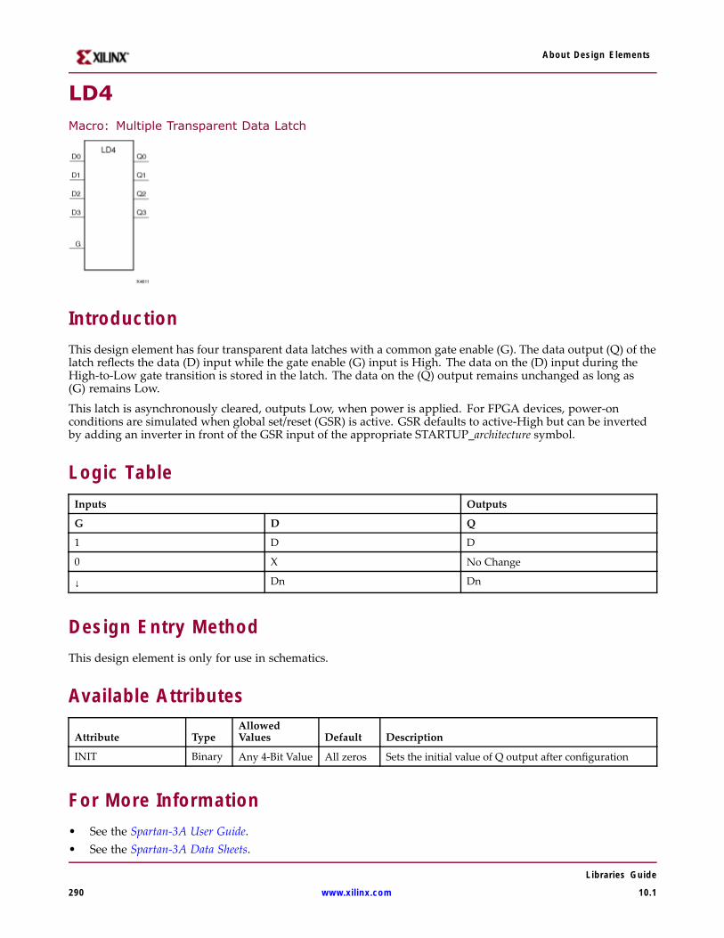
About Design Elements
LD4Macro: Multiple Transparent Data Latch
IntroductionThis design element has four transparent data latches with a common gate enable (G). The data output (Q) of thelatch reflects the data (D) input while the gate enable (G) input is High. The data on the (D) input during theHigh-to-Low gate transition is stored in the latch. The data on the (Q) output remains unchanged as long as(G) remains Low.
This latch is asynchronously cleared, outputs Low, when power is applied. For FPGA devices, power-onconditions are simulated when global set/reset (GSR) is active. GSR defaults to active-High but can be invertedby adding an inverter in front of the GSR input of the appropriate STARTUP_architecture symbol.
Logic TableInputs Outputs
G D Q
1 D D
0 X No Change
↓ Dn Dn
Design Entry MethodThis design element is only for use in schematics.
Available Attributes
Attribute TypeAllowedValues Default Description
INIT Binary Any 4-Bit Value All zeros Sets the initial value of Q output after configuration
For More Information• See the Spartan-3A User Guide.• See the Spartan-3A Data Sheets.
Libraries Guide
290 www.xilinx.com 10.1

About Design Elements
• See the Spartan-3AN FPGA In-System Flash User Guide.
• See the Spartan-3AN Data Sheets.
Libraries Guide
10.1 www.xilinx.com 291
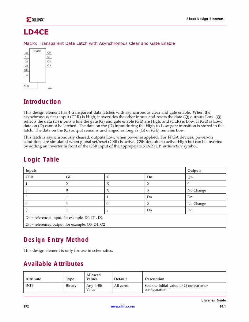
About Design Elements
LD4CEMacro: Transparent Data Latch with Asynchronous Clear and Gate Enable
IntroductionThis design element has 4 transparent data latches with asynchronous clear and gate enable. When theasynchronous clear input (CLR) is High, it overrides the other inputs and resets the data (Q) outputs Low. (Q)reflects the data (D) inputs while the gate (G) and gate enable (GE) are High, and (CLR) is Low. If (GE) is Low,data on (D) cannot be latched. The data on the (D) input during the High-to-Low gate transition is stored in thelatch. The data on the (Q) output remains unchanged as long as (G) or (GE) remains Low.
This latch is asynchronously cleared, outputs Low, when power is applied. For FPGA devices, power-onconditions are simulated when global set/reset (GSR) is active. GSR defaults to active-High but can be invertedby adding an inverter in front of the GSR input of the appropriate STARTUP_architecture symbol.
Logic TableInputs Outputs
CLR GE G Dn Qn
1 X X X 0
0 0 X X No Change
0 1 1 Dn Dn
0 1 0 X No Change
0 1 ↓ Dn Dn
Dn = referenced input, for example, D0, D1, D2
Qn = referenced output, for example, Q0, Q1, Q2
Design Entry MethodThis design element is only for use in schematics.
Available Attributes
Attribute TypeAllowedValues Default Description
INIT Binary Any 4-BitValue
All zeros Sets the initial value of Q output afterconfiguration
Libraries Guide
292 www.xilinx.com 10.1

About Design Elements
For More Information• See the Spartan-3A User Guide.
• See the Spartan-3A Data Sheets.
• See the Spartan-3AN FPGA In-System Flash User Guide.
• See the Spartan-3AN Data Sheets.
Libraries Guide
10.1 www.xilinx.com 293
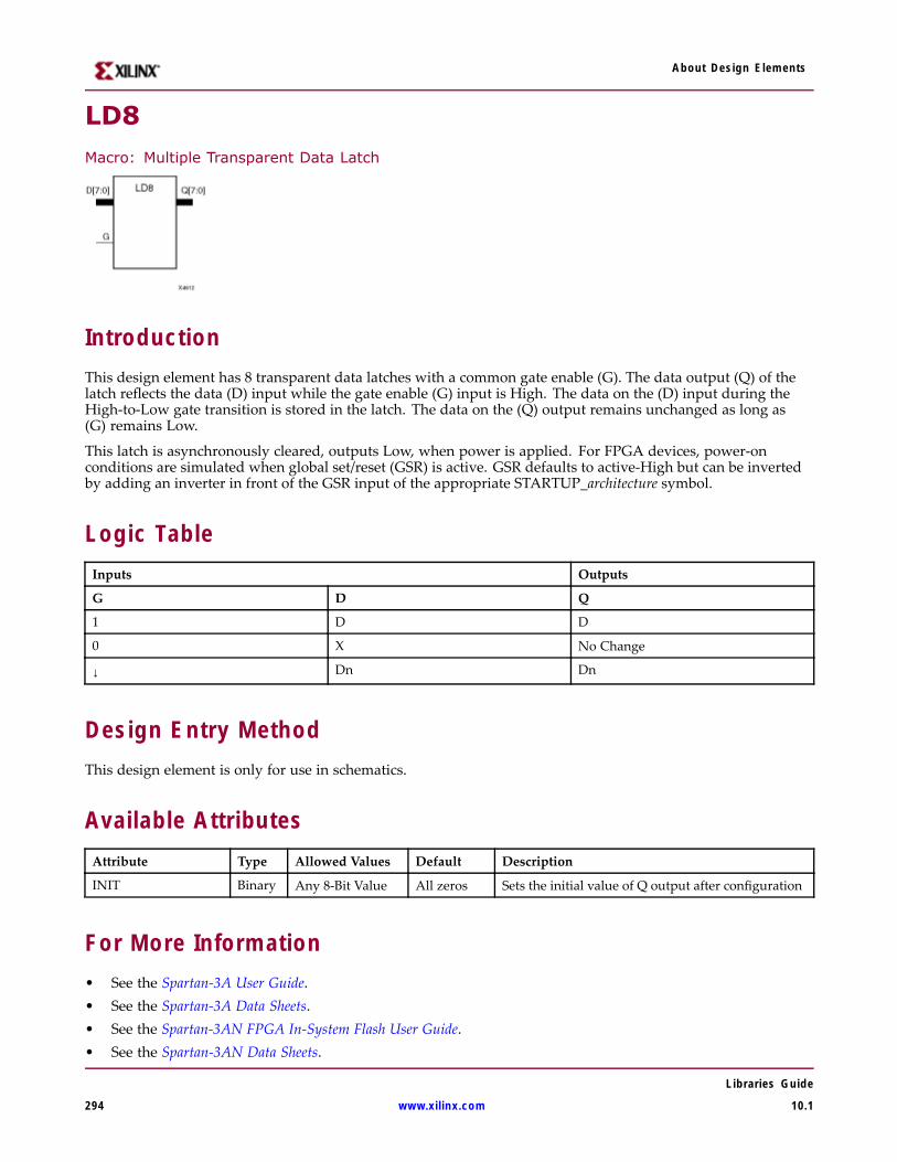
About Design Elements
LD8
Macro: Multiple Transparent Data Latch
IntroductionThis design element has 8 transparent data latches with a common gate enable (G). The data output (Q) of thelatch reflects the data (D) input while the gate enable (G) input is High. The data on the (D) input during theHigh-to-Low gate transition is stored in the latch. The data on the (Q) output remains unchanged as long as(G) remains Low.
This latch is asynchronously cleared, outputs Low, when power is applied. For FPGA devices, power-onconditions are simulated when global set/reset (GSR) is active. GSR defaults to active-High but can be invertedby adding an inverter in front of the GSR input of the appropriate STARTUP_architecture symbol.
Logic TableInputs Outputs
G D Q
1 D D
0 X No Change
↓ Dn Dn
Design Entry MethodThis design element is only for use in schematics.
Available AttributesAttribute Type Allowed Values Default Description
INIT Binary Any 8-Bit Value All zeros Sets the initial value of Q output after configuration
For More Information• See the Spartan-3A User Guide.• See the Spartan-3A Data Sheets.• See the Spartan-3AN FPGA In-System Flash User Guide.• See the Spartan-3AN Data Sheets.
Libraries Guide
294 www.xilinx.com 10.1
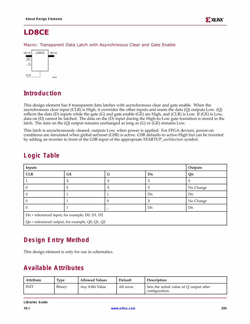
About Design Elements
LD8CE
Macro: Transparent Data Latch with Asynchronous Clear and Gate Enable
IntroductionThis design element has 8 transparent data latches with asynchronous clear and gate enable. When theasynchronous clear input (CLR) is High, it overrides the other inputs and resets the data (Q) outputs Low. (Q)reflects the data (D) inputs while the gate (G) and gate enable (GE) are High, and (CLR) is Low. If (GE) is Low,data on (D) cannot be latched. The data on the (D) input during the High-to-Low gate transition is stored in thelatch. The data on the (Q) output remains unchanged as long as (G) or (GE) remains Low.
This latch is asynchronously cleared, outputs Low, when power is applied. For FPGA devices, power-onconditions are simulated when global set/reset (GSR) is active. GSR defaults to active-High but can be invertedby adding an inverter in front of the GSR input of the appropriate STARTUP_architecture symbol.
Logic TableInputs Outputs
CLR GE G Dn Qn
1 X X X 0
0 0 X X No Change
0 1 1 Dn Dn
0 1 0 X No Change
0 1 ↓ Dn Dn
Dn = referenced input, for example, D0, D1, D2
Qn = referenced output, for example, Q0, Q1, Q2
Design Entry MethodThis design element is only for use in schematics.
Available AttributesAttribute Type Allowed Values Default Description
INIT Binary Any 8-Bit Value All zeros Sets the initial value of Q output afterconfiguration.
Libraries Guide
10.1 www.xilinx.com 295

About Design Elements
For More Information• See the Spartan-3A User Guide.
• See the Spartan-3A Data Sheets.
• See the Spartan-3AN FPGA In-System Flash User Guide.
• See the Spartan-3AN Data Sheets.
Libraries Guide
296 www.xilinx.com 10.1
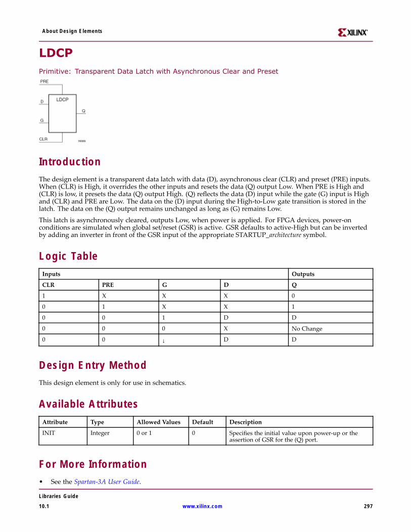
About Design Elements
LDCPPrimitive: Transparent Data Latch with Asynchronous Clear and Preset
IntroductionThe design element is a transparent data latch with data (D), asynchronous clear (CLR) and preset (PRE) inputs.When (CLR) is High, it overrides the other inputs and resets the data (Q) output Low. When PRE is High and(CLR) is low, it presets the data (Q) output High. (Q) reflects the data (D) input while the gate (G) input is Highand (CLR) and PRE are Low. The data on the (D) input during the High-to-Low gate transition is stored in thelatch. The data on the (Q) output remains unchanged as long as (G) remains Low.
This latch is asynchronously cleared, outputs Low, when power is applied. For FPGA devices, power-onconditions are simulated when global set/reset (GSR) is active. GSR defaults to active-High but can be invertedby adding an inverter in front of the GSR input of the appropriate STARTUP_architecture symbol.
Logic TableInputs Outputs
CLR PRE G D Q
1 X X X 0
0 1 X X 1
0 0 1 D D
0 0 0 X No Change
0 0 ↓ D D
Design Entry MethodThis design element is only for use in schematics.
Available AttributesAttribute Type Allowed Values Default Description
INIT Integer 0 or 1 0 Specifies the initial value upon power-up or theassertion of GSR for the (Q) port.
For More Information• See the Spartan-3A User Guide.
Libraries Guide
10.1 www.xilinx.com 297

About Design Elements
• See the Spartan-3A Data Sheets.
• See the Spartan-3AN FPGA In-System Flash User Guide.
• See the Spartan-3AN Data Sheets.
Libraries Guide
298 www.xilinx.com 10.1
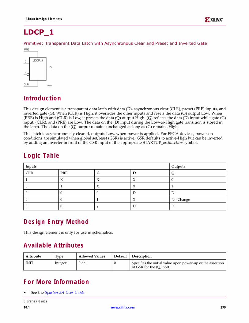
About Design Elements
LDCP_1Primitive: Transparent Data Latch with Asynchronous Clear and Preset and Inverted Gate
IntroductionThis design element is a transparent data latch with data (D), asynchronous clear (CLR), preset (PRE) inputs, andinverted gate (G). When (CLR) is High, it overrides the other inputs and resets the data (Q) output Low. When(PRE) is High and (CLR) is Low, it presets the data (Q) output High. (Q) reflects the data (D) input while gate (G)input, (CLR), and (PRE) are Low. The data on the (D) input during the Low-to-High gate transition is stored inthe latch. The data on the (Q) output remains unchanged as long as (G) remains High.
This latch is asynchronously cleared, outputs Low, when power is applied. For FPGA devices, power-onconditions are simulated when global set/reset (GSR) is active. GSR defaults to active-High but can be invertedby adding an inverter in front of the GSR input of the appropriate STARTUP_architecture symbol.
Logic TableInputs Outputs
CLR PRE G D Q
1 X X X 0
0 1 X X 1
0 0 0 D D
0 0 1 X No Change
0 0 ↑ D D
Design Entry MethodThis design element is only for use in schematics.
Available AttributesAttribute Type Allowed Values Default Description
INIT Integer 0 or 1 0 Specifies the initial value upon power-up or the assertionof GSR for the (Q) port.
For More Information• See the Spartan-3A User Guide.
Libraries Guide
10.1 www.xilinx.com 299

About Design Elements
• See the Spartan-3A Data Sheets.
• See the Spartan-3AN FPGA In-System Flash User Guide.
• See the Spartan-3AN Data Sheets.
Libraries Guide
300 www.xilinx.com 10.1
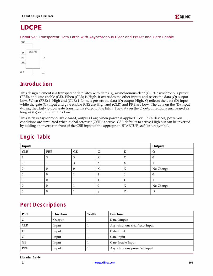
About Design Elements
LDCPEPrimitive: Transparent Data Latch with Asynchronous Clear and Preset and Gate Enable
IntroductionThis design element is a transparent data latch with data (D), asynchronous clear (CLR), asynchronous preset(PRE), and gate enable (GE). When (CLR) is High, it overrides the other inputs and resets the data (Q) outputLow. When (PRE) is High and (CLR) is Low, it presets the data (Q) output High. Q reflects the data (D) inputwhile the gate (G) input and gate enable (GE) are High and (CLR) and PRE are Low. The data on the (D) inputduring the High-to-Low gate transition is stored in the latch. The data on the Q output remains unchanged aslong as (G) or (GE) remains Low.
This latch is asynchronously cleared, outputs Low, when power is applied. For FPGA devices, power-onconditions are simulated when global set/reset (GSR) is active. GSR defaults to active-High but can be invertedby adding an inverter in front of the GSR input of the appropriate STARTUP_architecture symbol.
Logic TableInputs Outputs
CLR PRE GE G D Q
1 X X X X 0
0 1 X X X 1
0 0 0 X X No Change
0 0 1 1 0 0
0 0 1 1 1 1
0 0 1 0 X No Change
0 0 1 ↓ D D
Port DescriptionsPort Direction Width Function
Q Output 1 Data Output
CLR Input 1 Asynchronous clear/reset input
D Input 1 Data Input
G Input 1 Gate Input
GE Input 1 Gate Enable Input
PRE Input 1 Asynchronous preset/set input
Libraries Guide
10.1 www.xilinx.com 301
About Design Elements
Design Entry MethodThis design element can be used in schematics.
Available AttributesAttribute Type Allowed Values Default Description
INIT Integer 0 or 1 0 Sets the initial value of Q output after configuration.
For More Information• See the Spartan-3A User Guide.
• See the Spartan-3A Data Sheets.
• See the Spartan-3AN FPGA In-System Flash User Guide.
• See the Spartan-3AN Data Sheets.
Libraries Guide
302 www.xilinx.com 10.1
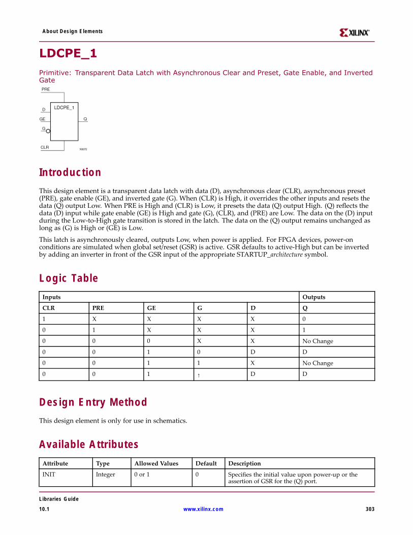
About Design Elements
LDCPE_1
Primitive: Transparent Data Latch with Asynchronous Clear and Preset, Gate Enable, and InvertedGate
IntroductionThis design element is a transparent data latch with data (D), asynchronous clear (CLR), asynchronous preset(PRE), gate enable (GE), and inverted gate (G). When (CLR) is High, it overrides the other inputs and resets thedata (Q) output Low. When PRE is High and (CLR) is Low, it presets the data (Q) output High. (Q) reflects thedata (D) input while gate enable (GE) is High and gate (G), (CLR), and (PRE) are Low. The data on the (D) inputduring the Low-to-High gate transition is stored in the latch. The data on the (Q) output remains unchanged aslong as (G) is High or (GE) is Low.
This latch is asynchronously cleared, outputs Low, when power is applied. For FPGA devices, power-onconditions are simulated when global set/reset (GSR) is active. GSR defaults to active-High but can be invertedby adding an inverter in front of the GSR input of the appropriate STARTUP_architecture symbol.
Logic TableInputs Outputs
CLR PRE GE G D Q
1 X X X X 0
0 1 X X X 1
0 0 0 X X No Change
0 0 1 0 D D
0 0 1 1 X No Change
0 0 1 ↑ D D
Design Entry MethodThis design element is only for use in schematics.
Available AttributesAttribute Type Allowed Values Default Description
INIT Integer 0 or 1 0 Specifies the initial value upon power-up or theassertion of GSR for the (Q) port.
Libraries Guide
10.1 www.xilinx.com 303

About Design Elements
For More Information• See the Spartan-3A User Guide.
• See the Spartan-3A Data Sheets.
• See the Spartan-3AN FPGA In-System Flash User Guide.
• See the Spartan-3AN Data Sheets.
Libraries Guide
304 www.xilinx.com 10.1
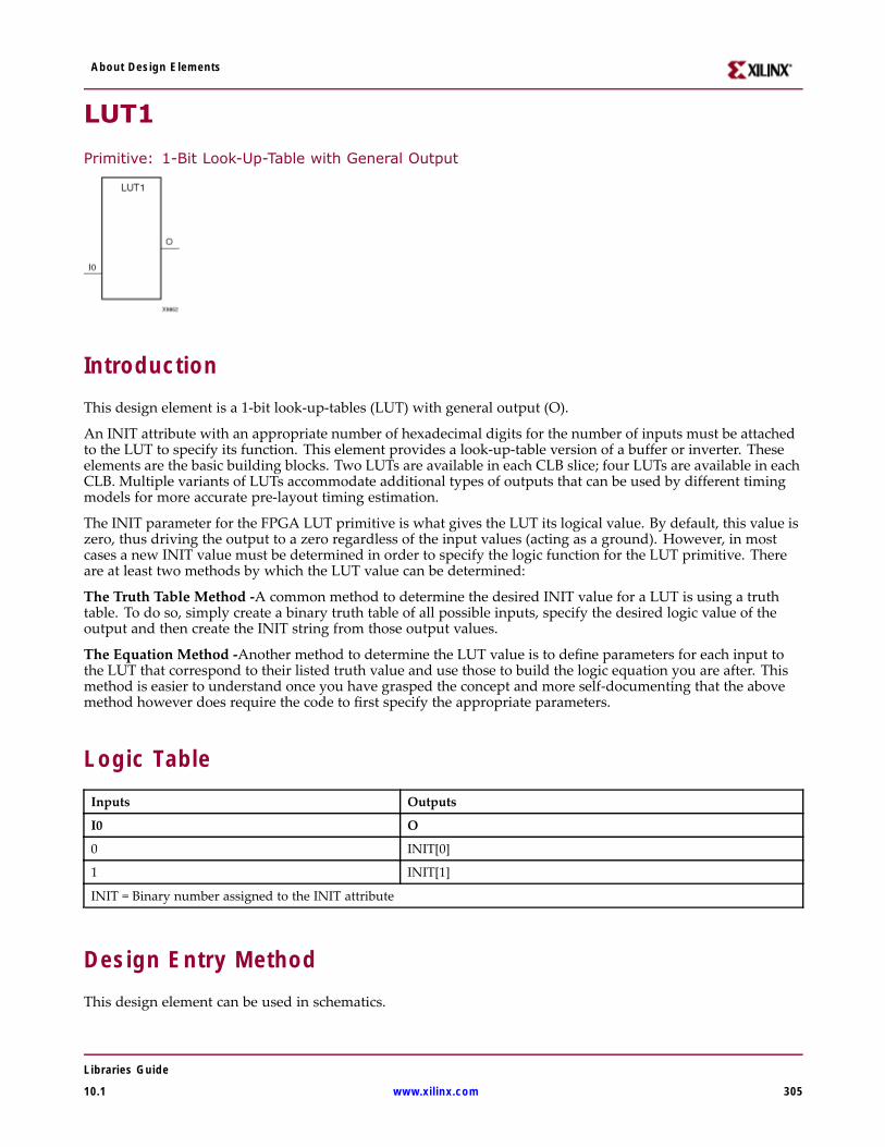
About Design Elements
LUT1
Primitive: 1-Bit Look-Up-Table with General Output
IntroductionThis design element is a 1-bit look-up-tables (LUT) with general output (O).
An INIT attribute with an appropriate number of hexadecimal digits for the number of inputs must be attachedto the LUT to specify its function. This element provides a look-up-table version of a buffer or inverter. Theseelements are the basic building blocks. Two LUTs are available in each CLB slice; four LUTs are available in eachCLB. Multiple variants of LUTs accommodate additional types of outputs that can be used by different timingmodels for more accurate pre-layout timing estimation.
The INIT parameter for the FPGA LUT primitive is what gives the LUT its logical value. By default, this value iszero, thus driving the output to a zero regardless of the input values (acting as a ground). However, in mostcases a new INIT value must be determined in order to specify the logic function for the LUT primitive. Thereare at least two methods by which the LUT value can be determined:
The Truth Table Method -A common method to determine the desired INIT value for a LUT is using a truthtable. To do so, simply create a binary truth table of all possible inputs, specify the desired logic value of theoutput and then create the INIT string from those output values.
The Equation Method -Another method to determine the LUT value is to define parameters for each input tothe LUT that correspond to their listed truth value and use those to build the logic equation you are after. Thismethod is easier to understand once you have grasped the concept and more self-documenting that the abovemethod however does require the code to first specify the appropriate parameters.
Logic TableInputs Outputs
I0 O
0 INIT[0]
1 INIT[1]
INIT = Binary number assigned to the INIT attribute
Design Entry MethodThis design element can be used in schematics.
Libraries Guide
10.1 www.xilinx.com 305
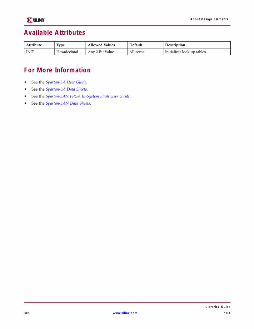
About Design Elements
Available AttributesAttribute Type Allowed Values Default Description
INIT Hexadecimal Any 2-Bit Value All zeros Initializes look-up tables.
For More Information• See the Spartan-3A User Guide.
• See the Spartan-3A Data Sheets.
• See the Spartan-3AN FPGA In-System Flash User Guide.
• See the Spartan-3AN Data Sheets.
Libraries Guide
306 www.xilinx.com 10.1
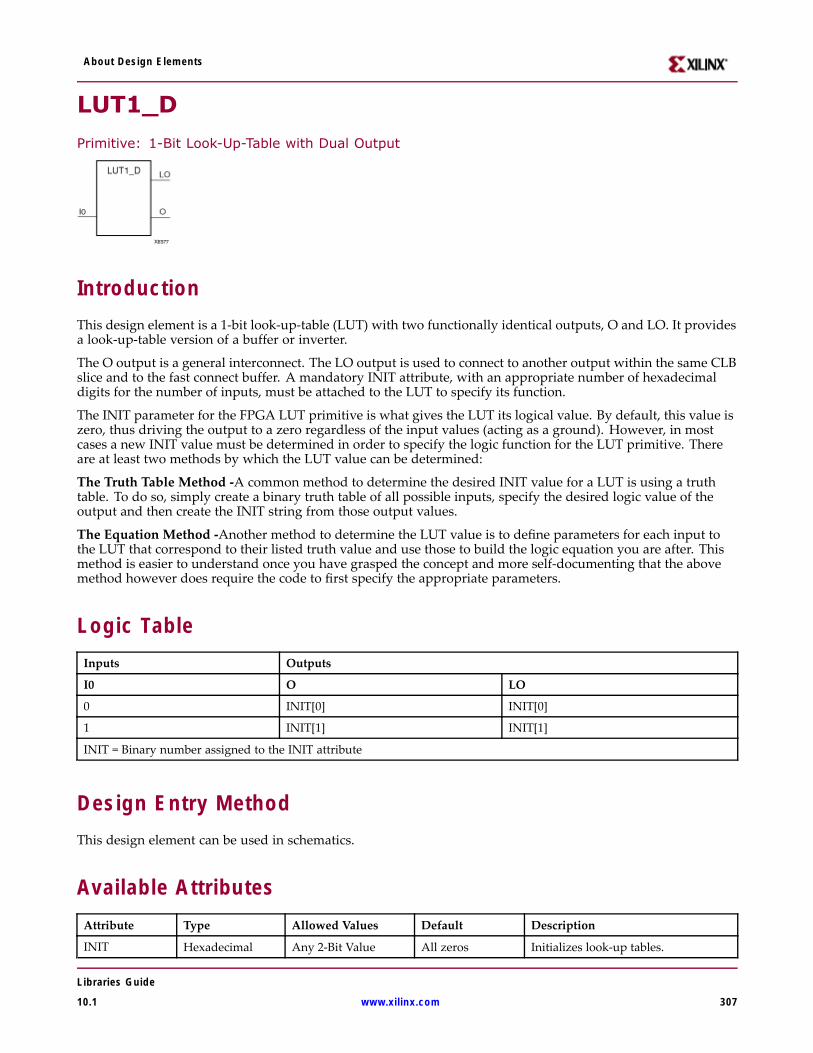
About Design Elements
LUT1_D
Primitive: 1-Bit Look-Up-Table with Dual Output
IntroductionThis design element is a 1-bit look-up-table (LUT) with two functionally identical outputs, O and LO. It providesa look-up-table version of a buffer or inverter.
The O output is a general interconnect. The LO output is used to connect to another output within the same CLBslice and to the fast connect buffer. A mandatory INIT attribute, with an appropriate number of hexadecimaldigits for the number of inputs, must be attached to the LUT to specify its function.
The INIT parameter for the FPGA LUT primitive is what gives the LUT its logical value. By default, this value iszero, thus driving the output to a zero regardless of the input values (acting as a ground). However, in mostcases a new INIT value must be determined in order to specify the logic function for the LUT primitive. Thereare at least two methods by which the LUT value can be determined:
The Truth Table Method -A common method to determine the desired INIT value for a LUT is using a truthtable. To do so, simply create a binary truth table of all possible inputs, specify the desired logic value of theoutput and then create the INIT string from those output values.
The Equation Method -Another method to determine the LUT value is to define parameters for each input tothe LUT that correspond to their listed truth value and use those to build the logic equation you are after. Thismethod is easier to understand once you have grasped the concept and more self-documenting that the abovemethod however does require the code to first specify the appropriate parameters.
Logic TableInputs Outputs
I0 O LO
0 INIT[0] INIT[0]
1 INIT[1] INIT[1]
INIT = Binary number assigned to the INIT attribute
Design Entry MethodThis design element can be used in schematics.
Available AttributesAttribute Type Allowed Values Default Description
INIT Hexadecimal Any 2-Bit Value All zeros Initializes look-up tables.
Libraries Guide
10.1 www.xilinx.com 307

About Design Elements
For More Information• See the Spartan-3A User Guide.
• See the Spartan-3A Data Sheets.
• See the Spartan-3AN FPGA In-System Flash User Guide.
• See the Spartan-3AN Data Sheets.
Libraries Guide
308 www.xilinx.com 10.1
About Design Elements
LUT1_L
Primitive: 1-Bit Look-Up-Table with Local Output
IntroductionThis design element is a 1- bit look-up-tables (LUTs) with a local output (LO) that is used to connect to anotheroutput within the same CLB slice and to the fast connect buffer. It provides a look-up-table version of a bufferor inverter.
A mandatory INIT attribute, with an appropriate number of hexadecimal digits for the number of inputs,must be attached to the LUT to specify its function.
The INIT parameter for the FPGA LUT primitive is what gives the LUT its logical value. By default, this value iszero, thus driving the output to a zero regardless of the input values (acting as a ground). However, in mostcases a new INIT value must be determined in order to specify the logic function for the LUT primitive. Thereare at least two methods by which the LUT value can be determined:
The Truth Table Method -A common method to determine the desired INIT value for a LUT is using a truthtable. To do so, simply create a binary truth table of all possible inputs, specify the desired logic value of theoutput and then create the INIT string from those output values.
The Equation Method -Another method to determine the LUT value is to define parameters for each input tothe LUT that correspond to their listed truth value and use those to build the logic equation you are after. Thismethod is easier to understand once you have grasped the concept and more self-documenting that the abovemethod however does require the code to first specify the appropriate parameters.
Logic TableInputs Outputs
I0 LO
0 INIT[0]
1 INIT[1]
INIT = Binary number assigned to the INIT attribute
Design Entry MethodThis design element can be used in schematics.
Available AttributesAttribute Type Allowed Values Default Description
INIT Hexadecimal Any 2-Bit Value All zeros Initializes look-up tables.
Libraries Guide
10.1 www.xilinx.com 309

About Design Elements
For More Information• See the Spartan-3A User Guide.
• See the Spartan-3A Data Sheets.
• See the Spartan-3AN FPGA In-System Flash User Guide.
• See the Spartan-3AN Data Sheets.
Libraries Guide
310 www.xilinx.com 10.1
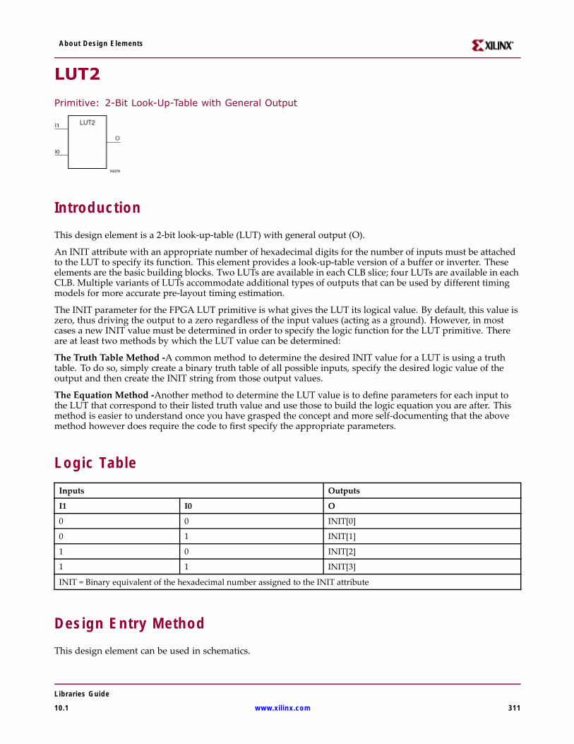
About Design Elements
LUT2
Primitive: 2-Bit Look-Up-Table with General Output
IntroductionThis design element is a 2-bit look-up-table (LUT) with general output (O).
An INIT attribute with an appropriate number of hexadecimal digits for the number of inputs must be attachedto the LUT to specify its function. This element provides a look-up-table version of a buffer or inverter. Theseelements are the basic building blocks. Two LUTs are available in each CLB slice; four LUTs are available in eachCLB. Multiple variants of LUTs accommodate additional types of outputs that can be used by different timingmodels for more accurate pre-layout timing estimation.
The INIT parameter for the FPGA LUT primitive is what gives the LUT its logical value. By default, this value iszero, thus driving the output to a zero regardless of the input values (acting as a ground). However, in mostcases a new INIT value must be determined in order to specify the logic function for the LUT primitive. Thereare at least two methods by which the LUT value can be determined:
The Truth Table Method -A common method to determine the desired INIT value for a LUT is using a truthtable. To do so, simply create a binary truth table of all possible inputs, specify the desired logic value of theoutput and then create the INIT string from those output values.
The Equation Method -Another method to determine the LUT value is to define parameters for each input tothe LUT that correspond to their listed truth value and use those to build the logic equation you are after. Thismethod is easier to understand once you have grasped the concept and more self-documenting that the abovemethod however does require the code to first specify the appropriate parameters.
Logic TableInputs Outputs
I1 I0 O
0 0 INIT[0]
0 1 INIT[1]
1 0 INIT[2]
1 1 INIT[3]
INIT = Binary equivalent of the hexadecimal number assigned to the INIT attribute
Design Entry MethodThis design element can be used in schematics.
Libraries Guide
10.1 www.xilinx.com 311
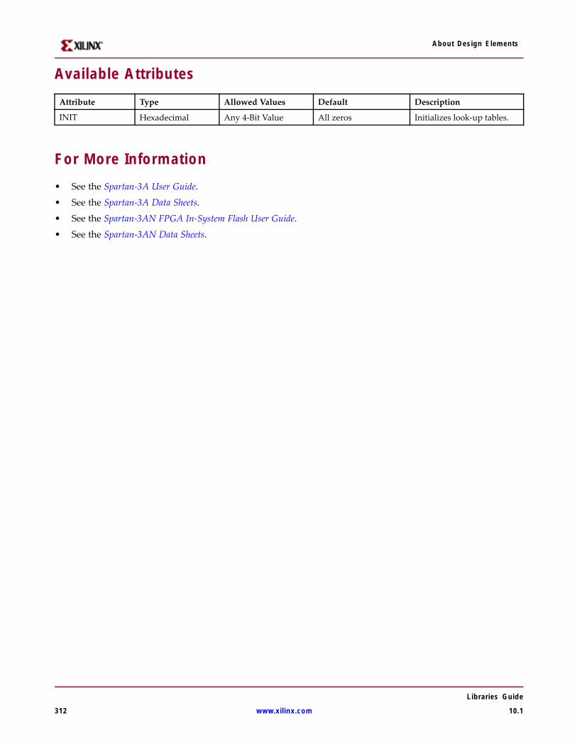
About Design Elements
Available AttributesAttribute Type Allowed Values Default Description
INIT Hexadecimal Any 4-Bit Value All zeros Initializes look-up tables.
For More Information• See the Spartan-3A User Guide.
• See the Spartan-3A Data Sheets.
• See the Spartan-3AN FPGA In-System Flash User Guide.
• See the Spartan-3AN Data Sheets.
Libraries Guide
312 www.xilinx.com 10.1
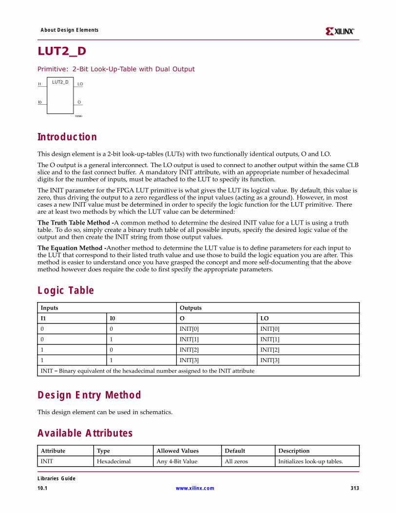
About Design Elements
LUT2_DPrimitive: 2-Bit Look-Up-Table with Dual Output
IntroductionThis design element is a 2-bit look-up-tables (LUTs) with two functionally identical outputs, O and LO.
The O output is a general interconnect. The LO output is used to connect to another output within the same CLBslice and to the fast connect buffer. A mandatory INIT attribute, with an appropriate number of hexadecimaldigits for the number of inputs, must be attached to the LUT to specify its function.
The INIT parameter for the FPGA LUT primitive is what gives the LUT its logical value. By default, this value iszero, thus driving the output to a zero regardless of the input values (acting as a ground). However, in mostcases a new INIT value must be determined in order to specify the logic function for the LUT primitive. Thereare at least two methods by which the LUT value can be determined:
The Truth Table Method -A common method to determine the desired INIT value for a LUT is using a truthtable. To do so, simply create a binary truth table of all possible inputs, specify the desired logic value of theoutput and then create the INIT string from those output values.
The Equation Method -Another method to determine the LUT value is to define parameters for each input tothe LUT that correspond to their listed truth value and use those to build the logic equation you are after. Thismethod is easier to understand once you have grasped the concept and more self-documenting that the abovemethod however does require the code to first specify the appropriate parameters.
Logic TableInputs Outputs
I1 I0 O LO
0 0 INIT[0] INIT[0]
0 1 INIT[1] INIT[1]
1 0 INIT[2] INIT[2]
1 1 INIT[3] INIT[3]
INIT = Binary equivalent of the hexadecimal number assigned to the INIT attribute
Design Entry MethodThis design element can be used in schematics.
Available AttributesAttribute Type Allowed Values Default Description
INIT Hexadecimal Any 4-Bit Value All zeros Initializes look-up tables.
Libraries Guide
10.1 www.xilinx.com 313

About Design Elements
For More Information• See the Spartan-3A User Guide.
• See the Spartan-3A Data Sheets.
• See the Spartan-3AN FPGA In-System Flash User Guide.
• See the Spartan-3AN Data Sheets.
Libraries Guide
314 www.xilinx.com 10.1
About Design Elements
LUT2_LPrimitive: 2-Bit Look-Up-Table with Local Output
IntroductionThis design element is a 2- bit look-up-tables (LUTs) with a local output (LO) that is used to connect to anotheroutput within the same CLB slice and to the fast connect buffer. It provides a look-up-table version of a bufferor inverter.
A mandatory INIT attribute, with an appropriate number of hexadecimal digits for the number of inputs,must be attached to the LUT to specify its function.
The INIT parameter for the FPGA LUT primitive is what gives the LUT its logical value. By default, this value iszero, thus driving the output to a zero regardless of the input values (acting as a ground). However, in mostcases a new INIT value must be determined in order to specify the logic function for the LUT primitive. Thereare at least two methods by which the LUT value can be determined:
The Truth Table Method -A common method to determine the desired INIT value for a LUT is using a truthtable. To do so, simply create a binary truth table of all possible inputs, specify the desired logic value of theoutput and then create the INIT string from those output values.
The Equation Method -Another method to determine the LUT value is to define parameters for each input tothe LUT that correspond to their listed truth value and use those to build the logic equation you are after. Thismethod is easier to understand once you have grasped the concept and more self-documenting that the abovemethod however does require the code to first specify the appropriate parameters.
Logic TableInputs Outputs
I1 I0 LO
0 0 INIT[0]
0 1 INIT[1]
1 0 INIT[2]
1 1 INIT[3]
INIT = Binary equivalent of the hexadecimal number assigned to the INIT attribute
Design Entry MethodThis design element can be used in schematics.
Available AttributesAttribute Type Allowed Values Default Description
INIT Hexadecimal Any 4-Bit Value All zeros Initializes look-up tables.
Libraries Guide
10.1 www.xilinx.com 315

About Design Elements
For More Information• See the Spartan-3A User Guide.
• See the Spartan-3A Data Sheets.
• See the Spartan-3AN FPGA In-System Flash User Guide.
• See the Spartan-3AN Data Sheets.
Libraries Guide
316 www.xilinx.com 10.1
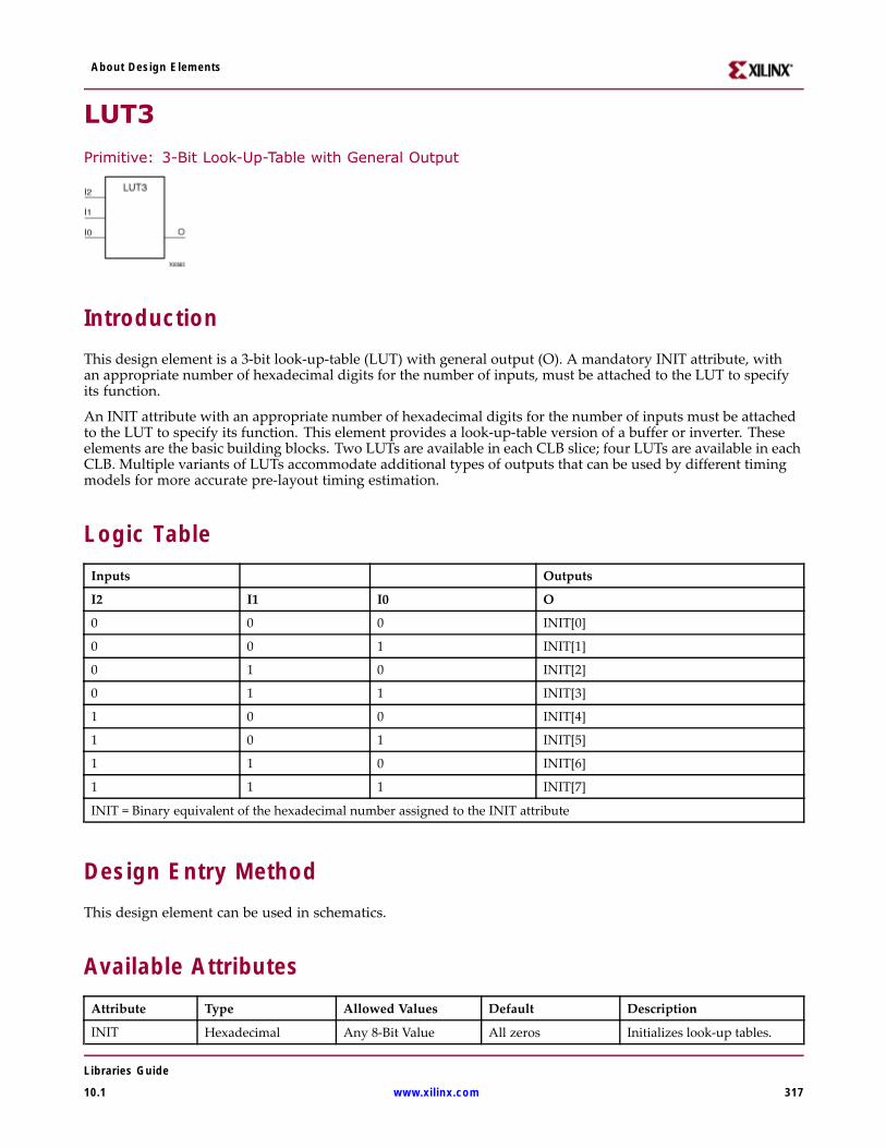
About Design Elements
LUT3
Primitive: 3-Bit Look-Up-Table with General Output
IntroductionThis design element is a 3-bit look-up-table (LUT) with general output (O). A mandatory INIT attribute, withan appropriate number of hexadecimal digits for the number of inputs, must be attached to the LUT to specifyits function.
An INIT attribute with an appropriate number of hexadecimal digits for the number of inputs must be attachedto the LUT to specify its function. This element provides a look-up-table version of a buffer or inverter. Theseelements are the basic building blocks. Two LUTs are available in each CLB slice; four LUTs are available in eachCLB. Multiple variants of LUTs accommodate additional types of outputs that can be used by different timingmodels for more accurate pre-layout timing estimation.
Logic TableInputs Outputs
I2 I1 I0 O
0 0 0 INIT[0]
0 0 1 INIT[1]
0 1 0 INIT[2]
0 1 1 INIT[3]
1 0 0 INIT[4]
1 0 1 INIT[5]
1 1 0 INIT[6]
1 1 1 INIT[7]
INIT = Binary equivalent of the hexadecimal number assigned to the INIT attribute
Design Entry MethodThis design element can be used in schematics.
Available AttributesAttribute Type Allowed Values Default Description
INIT Hexadecimal Any 8-Bit Value All zeros Initializes look-up tables.
Libraries Guide
10.1 www.xilinx.com 317

About Design Elements
For More Information• See the Spartan-3A User Guide.
• See the Spartan-3A Data Sheets.
• See the Spartan-3AN FPGA In-System Flash User Guide.
• See the Spartan-3AN Data Sheets.
Libraries Guide
318 www.xilinx.com 10.1
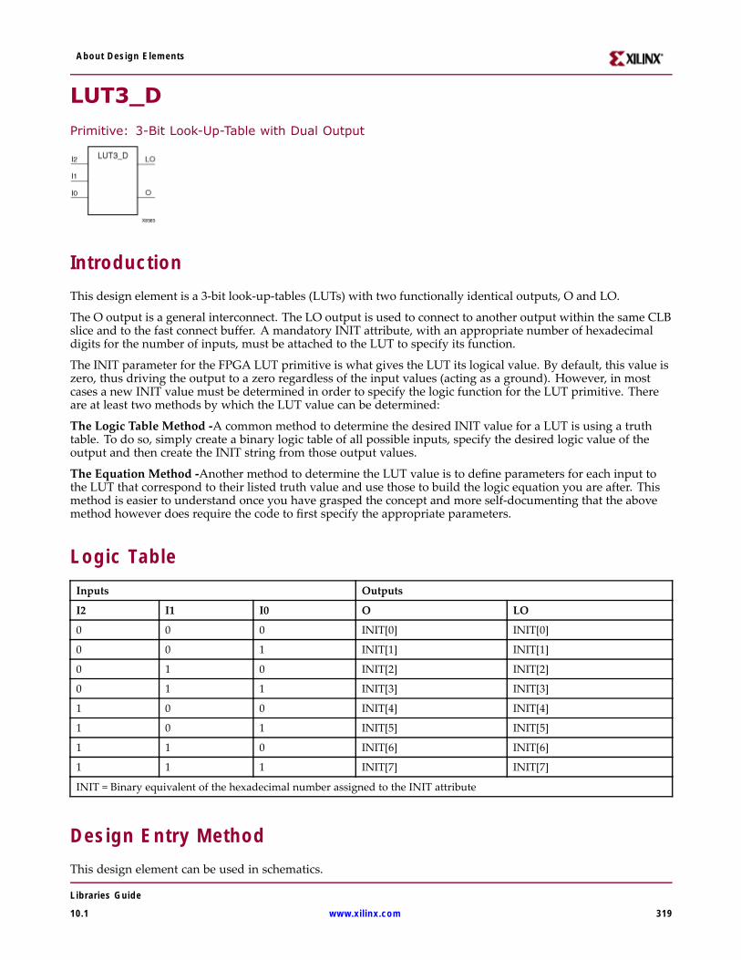
About Design Elements
LUT3_D
Primitive: 3-Bit Look-Up-Table with Dual Output
IntroductionThis design element is a 3-bit look-up-tables (LUTs) with two functionally identical outputs, O and LO.
The O output is a general interconnect. The LO output is used to connect to another output within the same CLBslice and to the fast connect buffer. A mandatory INIT attribute, with an appropriate number of hexadecimaldigits for the number of inputs, must be attached to the LUT to specify its function.
The INIT parameter for the FPGA LUT primitive is what gives the LUT its logical value. By default, this value iszero, thus driving the output to a zero regardless of the input values (acting as a ground). However, in mostcases a new INIT value must be determined in order to specify the logic function for the LUT primitive. Thereare at least two methods by which the LUT value can be determined:
The Logic Table Method -A common method to determine the desired INIT value for a LUT is using a truthtable. To do so, simply create a binary logic table of all possible inputs, specify the desired logic value of theoutput and then create the INIT string from those output values.
The Equation Method -Another method to determine the LUT value is to define parameters for each input tothe LUT that correspond to their listed truth value and use those to build the logic equation you are after. Thismethod is easier to understand once you have grasped the concept and more self-documenting that the abovemethod however does require the code to first specify the appropriate parameters.
Logic TableInputs Outputs
I2 I1 I0 O LO
0 0 0 INIT[0] INIT[0]
0 0 1 INIT[1] INIT[1]
0 1 0 INIT[2] INIT[2]
0 1 1 INIT[3] INIT[3]
1 0 0 INIT[4] INIT[4]
1 0 1 INIT[5] INIT[5]
1 1 0 INIT[6] INIT[6]
1 1 1 INIT[7] INIT[7]
INIT = Binary equivalent of the hexadecimal number assigned to the INIT attribute
Design Entry MethodThis design element can be used in schematics.
Libraries Guide
10.1 www.xilinx.com 319
About Design Elements
Available AttributesAttribute Type Allowed Values Default Description
INIT Hexadecimal Any 8-Bit Value All zeros Initializes look-up tables.
For More Information• See the Spartan-3A User Guide.
• See the Spartan-3A Data Sheets.
• See the Spartan-3AN FPGA In-System Flash User Guide.
• See the Spartan-3AN Data Sheets.
Libraries Guide
320 www.xilinx.com 10.1
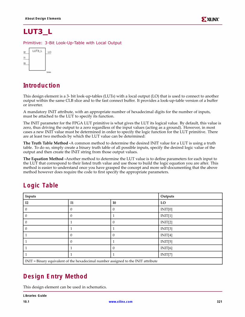
About Design Elements
LUT3_LPrimitive: 3-Bit Look-Up-Table with Local Output
IntroductionThis design element is a 3- bit look-up-tables (LUTs) with a local output (LO) that is used to connect to anotheroutput within the same CLB slice and to the fast connect buffer. It provides a look-up-table version of a bufferor inverter.
A mandatory INIT attribute, with an appropriate number of hexadecimal digits for the number of inputs,must be attached to the LUT to specify its function.
The INIT parameter for the FPGA LUT primitive is what gives the LUT its logical value. By default, this value iszero, thus driving the output to a zero regardless of the input values (acting as a ground). However, in mostcases a new INIT value must be determined in order to specify the logic function for the LUT primitive. Thereare at least two methods by which the LUT value can be determined:
The Truth Table Method -A common method to determine the desired INIT value for a LUT is using a truthtable. To do so, simply create a binary truth table of all possible inputs, specify the desired logic value of theoutput and then create the INIT string from those output values.
The Equation Method -Another method to determine the LUT value is to define parameters for each input tothe LUT that correspond to their listed truth value and use those to build the logic equation you are after. Thismethod is easier to understand once you have grasped the concept and more self-documenting that the abovemethod however does require the code to first specify the appropriate parameters.
Logic TableInputs Outputs
I2 I1 I0 LO
0 0 0 INIT[0]
0 0 1 INIT[1]
0 1 0 INIT[2]
0 1 1 INIT[3]
1 0 0 INIT[4]
1 0 1 INIT[5]
1 1 0 INIT[6]
1 1 1 INIT[7]
INIT = Binary equivalent of the hexadecimal number assigned to the INIT attribute
Design Entry MethodThis design element can be used in schematics.
Libraries Guide
10.1 www.xilinx.com 321
About Design Elements
Available AttributesAttribute Type Allowed Values Default Description
INIT Hexadecimal Any 8-Bit Value All zeros Initializes look-up tables.
For More Information• See the Spartan-3A User Guide.
• See the Spartan-3A Data Sheets.
• See the Spartan-3AN FPGA In-System Flash User Guide.
• See the Spartan-3AN Data Sheets.
Libraries Guide
322 www.xilinx.com 10.1
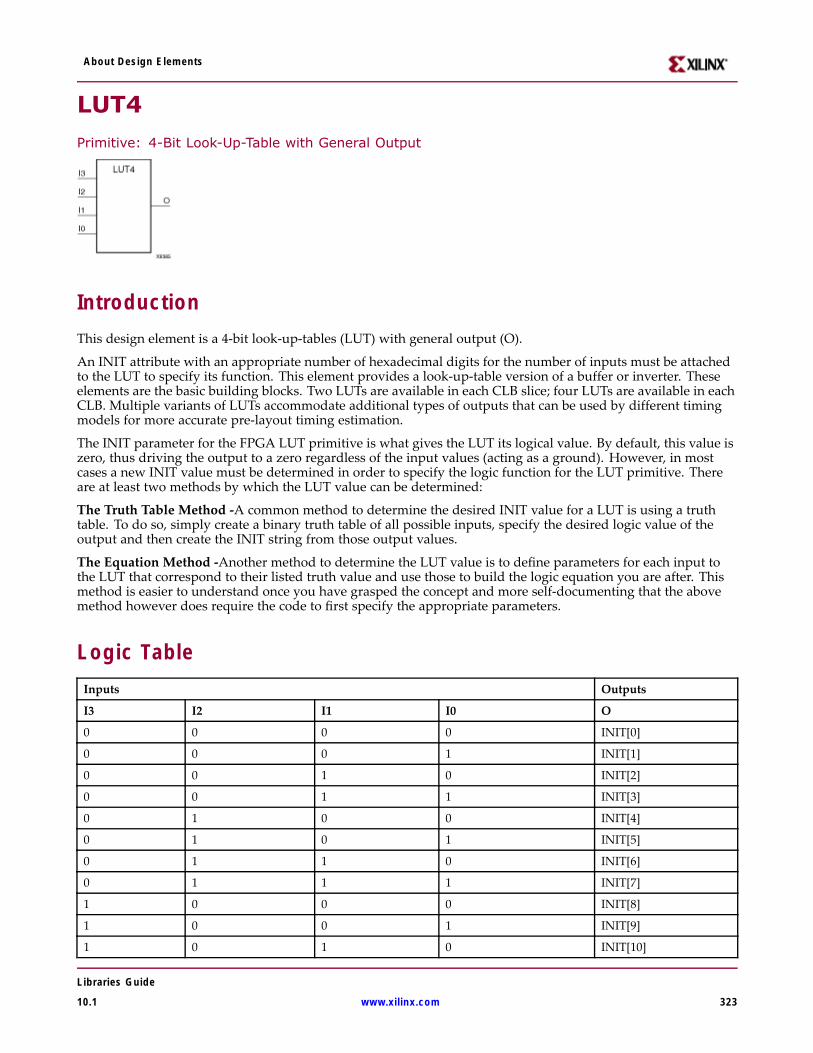
About Design Elements
LUT4
Primitive: 4-Bit Look-Up-Table with General Output
IntroductionThis design element is a 4-bit look-up-tables (LUT) with general output (O).
An INIT attribute with an appropriate number of hexadecimal digits for the number of inputs must be attachedto the LUT to specify its function. This element provides a look-up-table version of a buffer or inverter. Theseelements are the basic building blocks. Two LUTs are available in each CLB slice; four LUTs are available in eachCLB. Multiple variants of LUTs accommodate additional types of outputs that can be used by different timingmodels for more accurate pre-layout timing estimation.
The INIT parameter for the FPGA LUT primitive is what gives the LUT its logical value. By default, this value iszero, thus driving the output to a zero regardless of the input values (acting as a ground). However, in mostcases a new INIT value must be determined in order to specify the logic function for the LUT primitive. Thereare at least two methods by which the LUT value can be determined:
The Truth Table Method -A common method to determine the desired INIT value for a LUT is using a truthtable. To do so, simply create a binary truth table of all possible inputs, specify the desired logic value of theoutput and then create the INIT string from those output values.
The Equation Method -Another method to determine the LUT value is to define parameters for each input tothe LUT that correspond to their listed truth value and use those to build the logic equation you are after. Thismethod is easier to understand once you have grasped the concept and more self-documenting that the abovemethod however does require the code to first specify the appropriate parameters.
Logic TableInputs Outputs
I3 I2 I1 I0 O
0 0 0 0 INIT[0]
0 0 0 1 INIT[1]
0 0 1 0 INIT[2]
0 0 1 1 INIT[3]
0 1 0 0 INIT[4]
0 1 0 1 INIT[5]
0 1 1 0 INIT[6]
0 1 1 1 INIT[7]
1 0 0 0 INIT[8]
1 0 0 1 INIT[9]
1 0 1 0 INIT[10]
Libraries Guide
10.1 www.xilinx.com 323
About Design Elements
Inputs Outputs
I3 I2 I1 I0 O
1 0 1 1 INIT[11]
1 1 0 0 INIT[12]
1 1 0 1 INIT[13]
1 1 1 0 INIT14]
1 1 1 1 INIT[15]
INIT = Binary equivalent of the hexadecimal number assigned to the INIT attribute
Design Entry MethodThis design element can be used in schematics.
Available AttributesAttribute Type Allowed Values Default Description
INIT Hexadecimal Any 16-Bit Value All zeros Initializes look-up tables.
For More Information• See the Spartan-3A User Guide.
• See the Spartan-3A Data Sheets.
• See the Spartan-3AN FPGA In-System Flash User Guide.
• See the Spartan-3AN Data Sheets.
Libraries Guide
324 www.xilinx.com 10.1
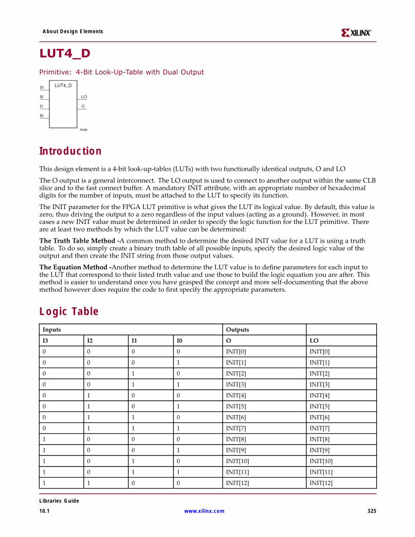
About Design Elements
LUT4_DPrimitive: 4-Bit Look-Up-Table with Dual Output
IntroductionThis design element is a 4-bit look-up-tables (LUTs) with two functionally identical outputs, O and LO
The O output is a general interconnect. The LO output is used to connect to another output within the same CLBslice and to the fast connect buffer. A mandatory INIT attribute, with an appropriate number of hexadecimaldigits for the number of inputs, must be attached to the LUT to specify its function.
The INIT parameter for the FPGA LUT primitive is what gives the LUT its logical value. By default, this value iszero, thus driving the output to a zero regardless of the input values (acting as a ground). However, in mostcases a new INIT value must be determined in order to specify the logic function for the LUT primitive. Thereare at least two methods by which the LUT value can be determined:
The Truth Table Method -A common method to determine the desired INIT value for a LUT is using a truthtable. To do so, simply create a binary truth table of all possible inputs, specify the desired logic value of theoutput and then create the INIT string from those output values.
The Equation Method -Another method to determine the LUT value is to define parameters for each input tothe LUT that correspond to their listed truth value and use those to build the logic equation you are after. Thismethod is easier to understand once you have grasped the concept and more self-documenting that the abovemethod however does require the code to first specify the appropriate parameters.
Logic TableInputs Outputs
I3 I2 I1 I0 O LO
0 0 0 0 INIT[0] INIT[0]
0 0 0 1 INIT[1] INIT[1]
0 0 1 0 INIT[2] INIT[2]
0 0 1 1 INIT[3] INIT[3]
0 1 0 0 INIT[4] INIT[4]
0 1 0 1 INIT[5] INIT[5]
0 1 1 0 INIT[6] INIT[6]
0 1 1 1 INIT[7] INIT[7]
1 0 0 0 INIT[8] INIT[8]
1 0 0 1 INIT[9] INIT[9]
1 0 1 0 INIT[10] INIT[10]
1 0 1 1 INIT[11] INIT[11]
1 1 0 0 INIT[12] INIT[12]
Libraries Guide
10.1 www.xilinx.com 325
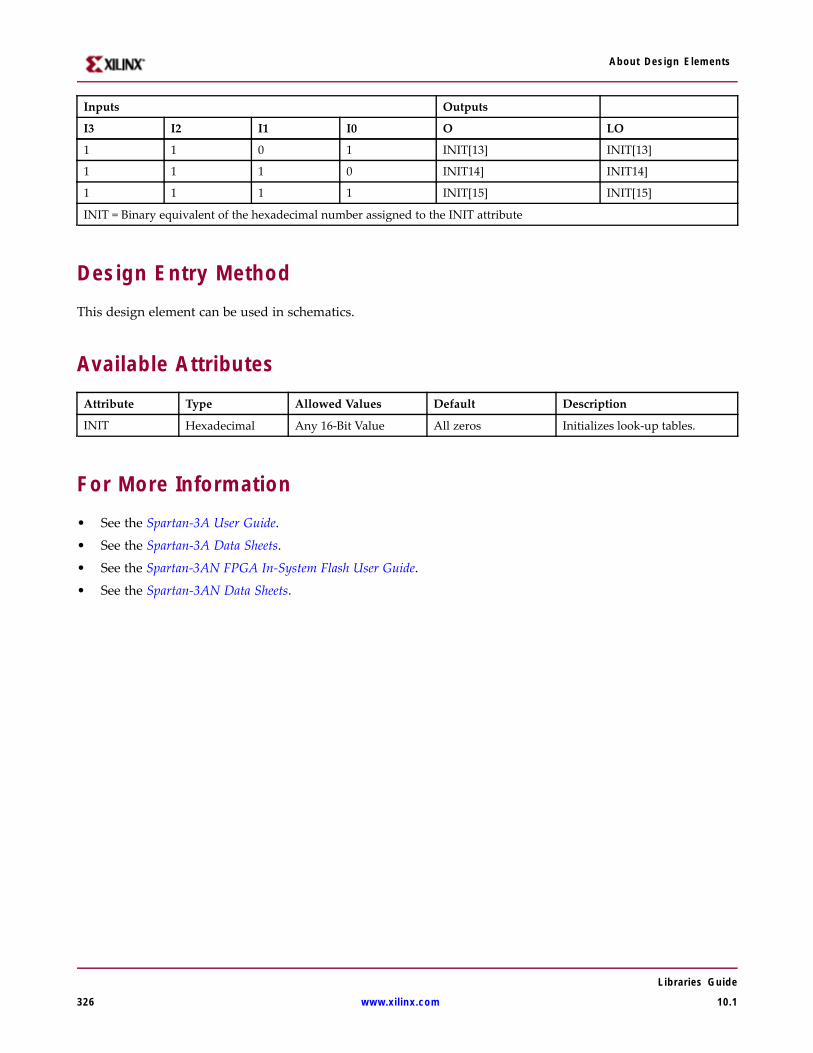
About Design Elements
Inputs Outputs
I3 I2 I1 I0 O LO
1 1 0 1 INIT[13] INIT[13]
1 1 1 0 INIT14] INIT14]
1 1 1 1 INIT[15] INIT[15]
INIT = Binary equivalent of the hexadecimal number assigned to the INIT attribute
Design Entry MethodThis design element can be used in schematics.
Available AttributesAttribute Type Allowed Values Default Description
INIT Hexadecimal Any 16-Bit Value All zeros Initializes look-up tables.
For More Information• See the Spartan-3A User Guide.
• See the Spartan-3A Data Sheets.
• See the Spartan-3AN FPGA In-System Flash User Guide.
• See the Spartan-3AN Data Sheets.
Libraries Guide
326 www.xilinx.com 10.1
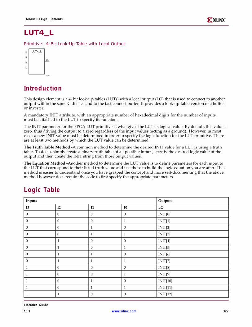
About Design Elements
LUT4_LPrimitive: 4-Bit Look-Up-Table with Local Output
IntroductionThis design element is a 4- bit look-up-tables (LUTs) with a local output (LO) that is used to connect to anotheroutput within the same CLB slice and to the fast connect buffer. It provides a look-up-table version of a bufferor inverter.
A mandatory INIT attribute, with an appropriate number of hexadecimal digits for the number of inputs,must be attached to the LUT to specify its function.
The INIT parameter for the FPGA LUT primitive is what gives the LUT its logical value. By default, this value iszero, thus driving the output to a zero regardless of the input values (acting as a ground). However, in mostcases a new INIT value must be determined in order to specify the logic function for the LUT primitive. Thereare at least two methods by which the LUT value can be determined:
The Truth Table Method -A common method to determine the desired INIT value for a LUT is using a truthtable. To do so, simply create a binary truth table of all possible inputs, specify the desired logic value of theoutput and then create the INIT string from those output values.
The Equation Method -Another method to determine the LUT value is to define parameters for each input tothe LUT that correspond to their listed truth value and use those to build the logic equation you are after. Thismethod is easier to understand once you have grasped the concept and more self-documenting that the abovemethod however does require the code to first specify the appropriate parameters.
Logic TableInputs Outputs
I3 I2 I1 I0 LO
0 0 0 0 INIT[0]
0 0 0 1 INIT[1]
0 0 1 0 INIT[2]
0 0 1 1 INIT[3]
0 1 0 0 INIT[4]
0 1 0 1 INIT[5]
0 1 1 0 INIT[6]
0 1 1 1 INIT[7]
1 0 0 0 INIT[8]
1 0 0 1 INIT[9]
1 0 1 0 INIT[10]
1 0 1 1 INIT[11]
1 1 0 0 INIT[12]
Libraries Guide
10.1 www.xilinx.com 327
About Design Elements
Inputs Outputs
I3 I2 I1 I0 LO
1 1 0 1 INIT[13]
1 1 1 0 INIT14]
1 1 1 1 INIT[15]
INIT = Binary equivalent of the hexadecimal number assigned to the INIT attribute
Design Entry MethodThis design element can be used in schematics.
Available AttributesAttribute Type Allowed Values Default Description
INIT Hexadecimal Any 16-Bit Value All zeros Initializes look-up tables.
For More Information• See the Spartan-3A User Guide.
• See the Spartan-3A Data Sheets.
• See the Spartan-3AN FPGA In-System Flash User Guide.
• See the Spartan-3AN Data Sheets.
Libraries Guide
328 www.xilinx.com 10.1
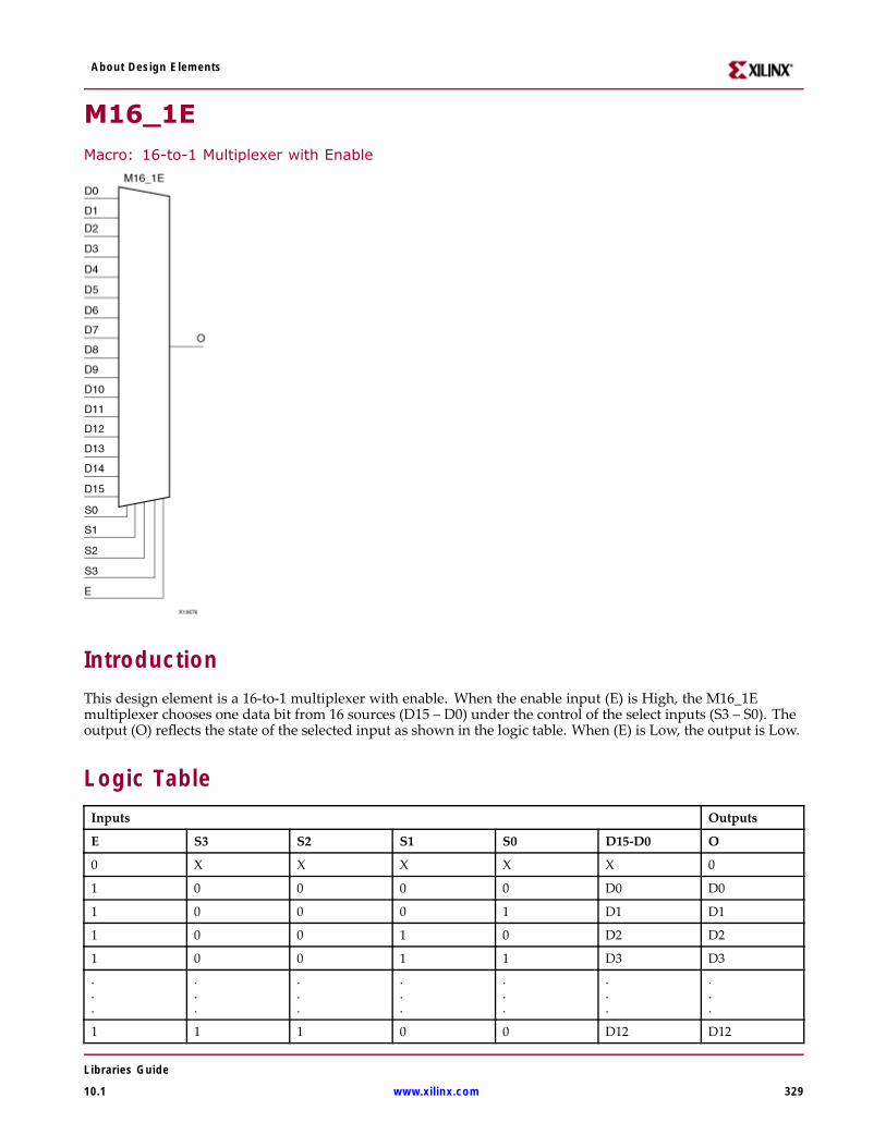
About Design Elements
M16_1EMacro: 16-to-1 Multiplexer with Enable
IntroductionThis design element is a 16-to-1 multiplexer with enable. When the enable input (E) is High, the M16_1Emultiplexer chooses one data bit from 16 sources (D15 – D0) under the control of the select inputs (S3 – S0). Theoutput (O) reflects the state of the selected input as shown in the logic table. When (E) is Low, the output is Low.
Logic TableInputs Outputs
E S3 S2 S1 S0 D15-D0 O
0 X X X X X 0
1 0 0 0 0 D0 D0
1 0 0 0 1 D1 D1
1 0 0 1 0 D2 D2
1 0 0 1 1 D3 D3...
.
.
.
.
.
.
.
.
.
.
.
.
.
.
.
.
.
.
1 1 1 0 0 D12 D12
Libraries Guide
10.1 www.xilinx.com 329
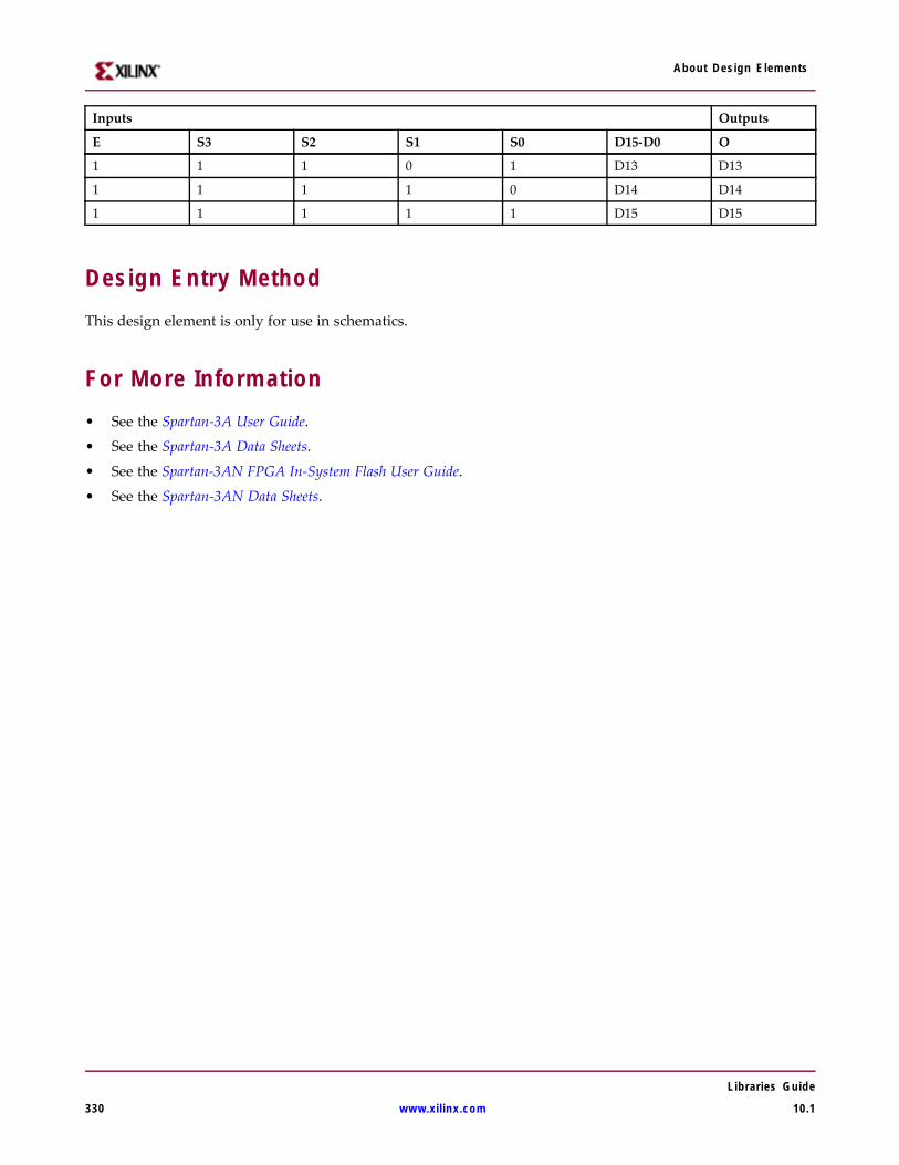
About Design Elements
Inputs Outputs
E S3 S2 S1 S0 D15-D0 O
1 1 1 0 1 D13 D13
1 1 1 1 0 D14 D14
1 1 1 1 1 D15 D15
Design Entry MethodThis design element is only for use in schematics.
For More Information• See the Spartan-3A User Guide.
• See the Spartan-3A Data Sheets.
• See the Spartan-3AN FPGA In-System Flash User Guide.
• See the Spartan-3AN Data Sheets.
Libraries Guide
330 www.xilinx.com 10.1
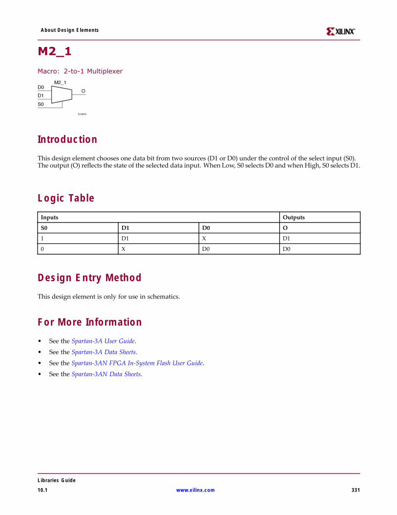
About Design Elements
M2_1
Macro: 2-to-1 Multiplexer
IntroductionThis design element chooses one data bit from two sources (D1 or D0) under the control of the select input (S0).The output (O) reflects the state of the selected data input. When Low, S0 selects D0 and when High, S0 selects D1.
Logic TableInputs Outputs
S0 D1 D0 O
1 D1 X D1
0 X D0 D0
Design Entry MethodThis design element is only for use in schematics.
For More Information• See the Spartan-3A User Guide.
• See the Spartan-3A Data Sheets.
• See the Spartan-3AN FPGA In-System Flash User Guide.
• See the Spartan-3AN Data Sheets.
Libraries Guide
10.1 www.xilinx.com 331
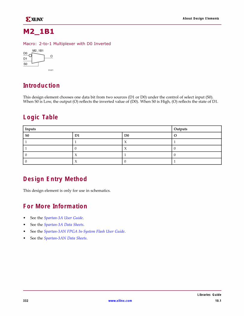
About Design Elements
M2_1B1
Macro: 2-to-1 Multiplexer with D0 Inverted
IntroductionThis design element chooses one data bit from two sources (D1 or D0) under the control of select input (S0).When S0 is Low, the output (O) reflects the inverted value of (D0). When S0 is High, (O) reflects the state of D1.
Logic TableInputs Outputs
S0 D1 D0 O
1 1 X 1
1 0 X 0
0 X 1 0
0 X 0 1
Design Entry MethodThis design element is only for use in schematics.
For More Information• See the Spartan-3A User Guide.
• See the Spartan-3A Data Sheets.
• See the Spartan-3AN FPGA In-System Flash User Guide.
• See the Spartan-3AN Data Sheets.
Libraries Guide
332 www.xilinx.com 10.1
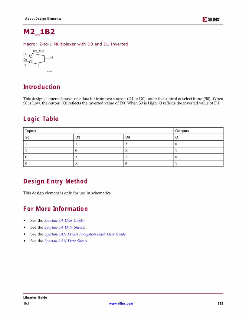
About Design Elements
M2_1B2
Macro: 2-to-1 Multiplexer with D0 and D1 Inverted
IntroductionThis design element chooses one data bit from two sources (D1 or D0) under the control of select input (S0). WhenS0 is Low, the output (O) reflects the inverted value of D0. When S0 is High, O reflects the inverted value of D1.
Logic TableInputs Outputs
S0 D1 D0 O
1 1 X 0
1 0 X 1
0 X 1 0
0 X 0 1
Design Entry MethodThis design element is only for use in schematics.
For More Information• See the Spartan-3A User Guide.
• See the Spartan-3A Data Sheets.
• See the Spartan-3AN FPGA In-System Flash User Guide.
• See the Spartan-3AN Data Sheets.
Libraries Guide
10.1 www.xilinx.com 333
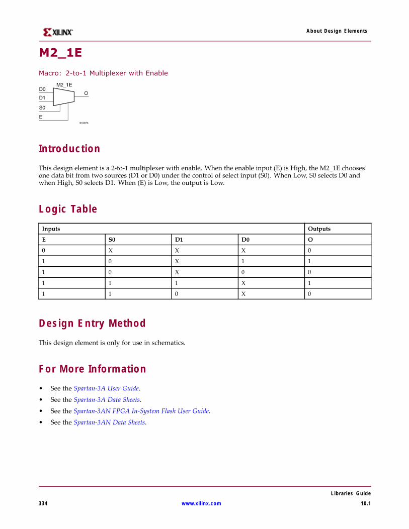
About Design Elements
M2_1E
Macro: 2-to-1 Multiplexer with Enable
IntroductionThis design element is a 2-to-1 multiplexer with enable. When the enable input (E) is High, the M2_1E choosesone data bit from two sources (D1 or D0) under the control of select input (S0). When Low, S0 selects D0 andwhen High, S0 selects D1. When (E) is Low, the output is Low.
Logic TableInputs Outputs
E S0 D1 D0 O
0 X X X 0
1 0 X 1 1
1 0 X 0 0
1 1 1 X 1
1 1 0 X 0
Design Entry MethodThis design element is only for use in schematics.
For More Information• See the Spartan-3A User Guide.
• See the Spartan-3A Data Sheets.
• See the Spartan-3AN FPGA In-System Flash User Guide.
• See the Spartan-3AN Data Sheets.
Libraries Guide
334 www.xilinx.com 10.1
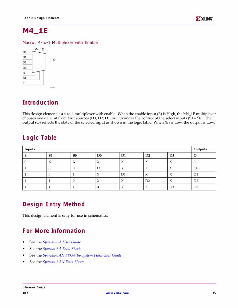
About Design Elements
M4_1E
Macro: 4-to-1 Multiplexer with Enable
IntroductionThis design element is a 4-to-1 multiplexer with enable. When the enable input (E) is High, the M4_1Emultiplexerchooses one data bit from four sources (D3, D2, D1, or D0) under the control of the select inputs (S1 – S0). Theoutput (O) reflects the state of the selected input as shown in the logic table. When (E) is Low, the output is Low.
Logic TableInputs Outputs
E S1 S0 D0 D1 D2 D3 O
0 X X X X X X 0
1 0 0 D0 X X X D0
1 0 1 X D1 X X D1
1 1 0 X X D2 X D2
1 1 1 X X X D3 D3
Design Entry MethodThis design element is only for use in schematics.
For More Information• See the Spartan-3A User Guide.
• See the Spartan-3A Data Sheets.
• See the Spartan-3AN FPGA In-System Flash User Guide.
• See the Spartan-3AN Data Sheets.
Libraries Guide
10.1 www.xilinx.com 335
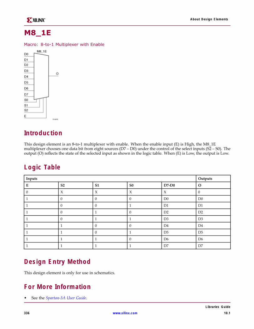
About Design Elements
M8_1EMacro: 8-to-1 Multiplexer with Enable
IntroductionThis design element is an 8-to-1 multiplexer with enable. When the enable input (E) is High, the M8_1Emultiplexer chooses one data bit from eight sources (D7 – D0) under the control of the select inputs (S2 – S0). Theoutput (O) reflects the state of the selected input as shown in the logic table. When (E) is Low, the output is Low.
Logic TableInputs Outputs
E S2 S1 S0 D7-D0 O
0 X X X X 0
1 0 0 0 D0 D0
1 0 0 1 D1 D1
1 0 1 0 D2 D2
1 0 1 1 D3 D3
1 1 0 0 D4 D4
1 1 0 1 D5 D5
1 1 1 0 D6 D6
1 1 1 1 D7 D7
Design Entry MethodThis design element is only for use in schematics.
For More Information• See the Spartan-3A User Guide.
Libraries Guide
336 www.xilinx.com 10.1

About Design Elements
• See the Spartan-3A Data Sheets.
• See the Spartan-3AN FPGA In-System Flash User Guide.
• See the Spartan-3AN Data Sheets.
Libraries Guide
10.1 www.xilinx.com 337
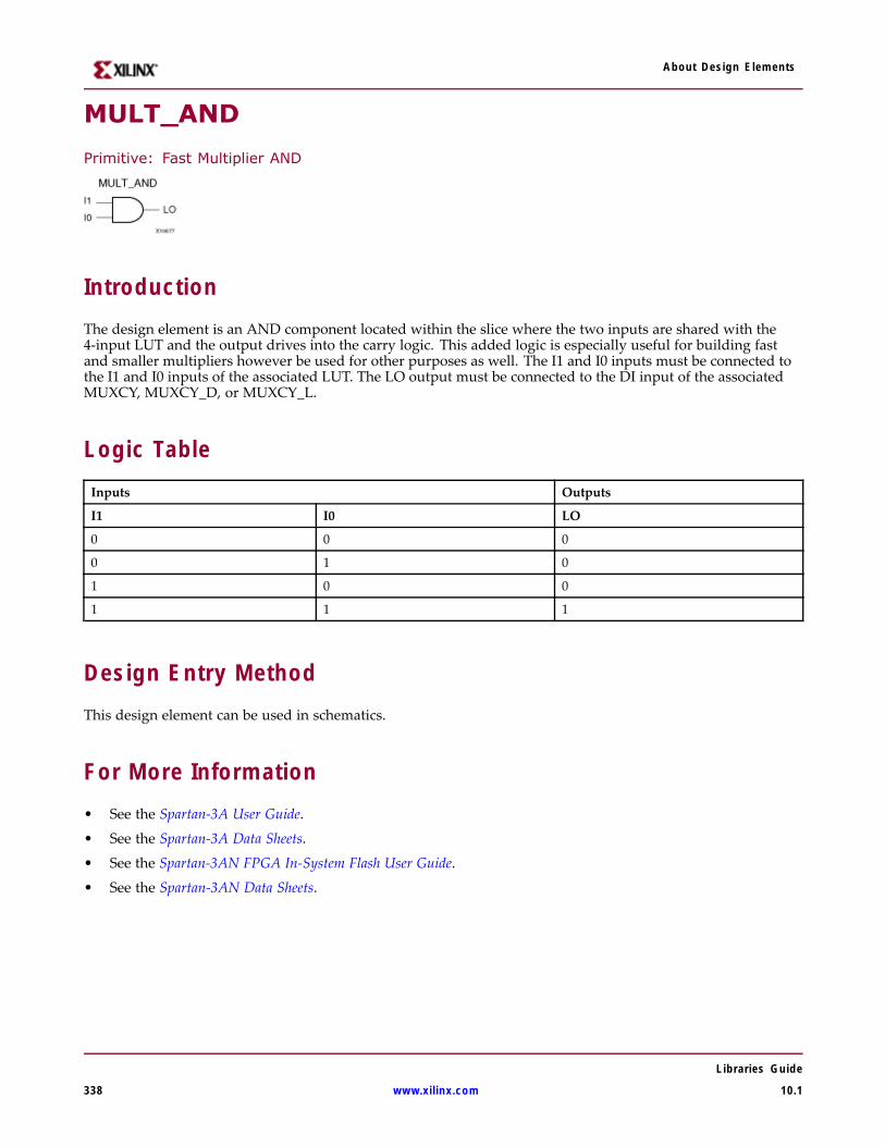
About Design Elements
MULT_AND
Primitive: Fast Multiplier AND
IntroductionThe design element is an AND component located within the slice where the two inputs are shared with the4-input LUT and the output drives into the carry logic. This added logic is especially useful for building fastand smaller multipliers however be used for other purposes as well. The I1 and I0 inputs must be connected tothe I1 and I0 inputs of the associated LUT. The LO output must be connected to the DI input of the associatedMUXCY, MUXCY_D, or MUXCY_L.
Logic TableInputs Outputs
I1 I0 LO
0 0 0
0 1 0
1 0 0
1 1 1
Design Entry MethodThis design element can be used in schematics.
For More Information• See the Spartan-3A User Guide.
• See the Spartan-3A Data Sheets.
• See the Spartan-3AN FPGA In-System Flash User Guide.
• See the Spartan-3AN Data Sheets.
Libraries Guide
338 www.xilinx.com 10.1
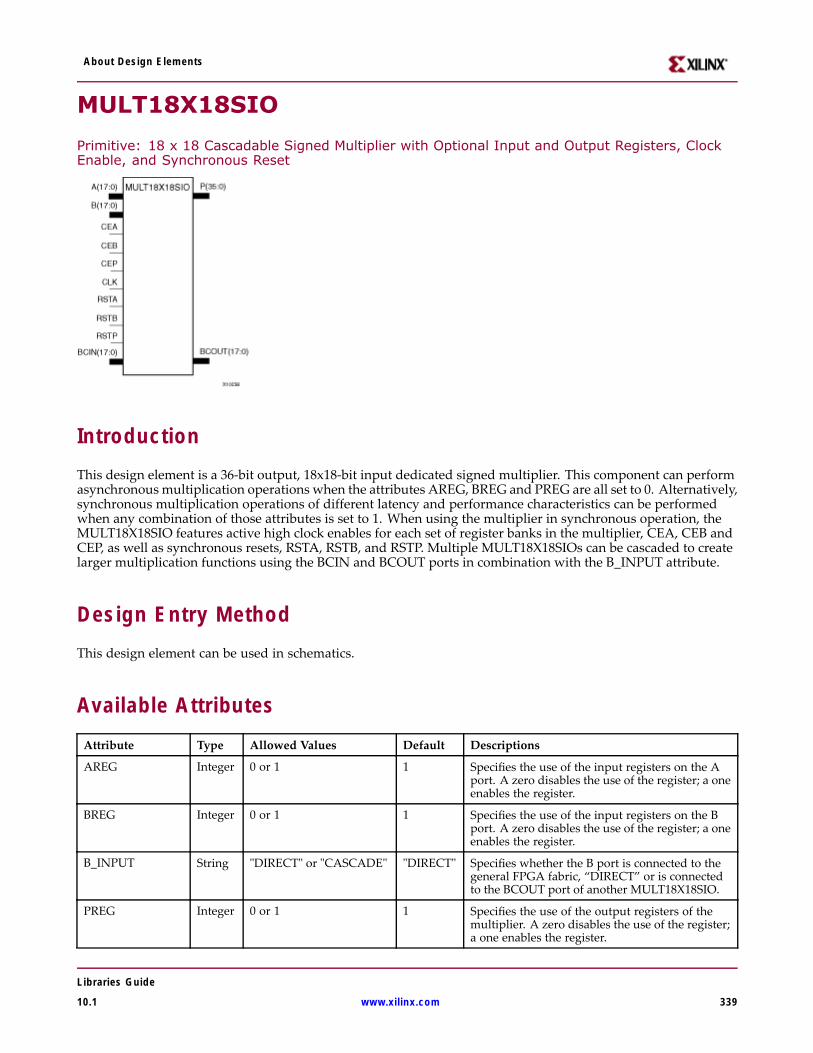
About Design Elements
MULT18X18SIO
Primitive: 18 x 18 Cascadable Signed Multiplier with Optional Input and Output Registers, ClockEnable, and Synchronous Reset
IntroductionThis design element is a 36-bit output, 18x18-bit input dedicated signed multiplier. This component can performasynchronous multiplication operations when the attributes AREG, BREG and PREG are all set to 0. Alternatively,synchronous multiplication operations of different latency and performance characteristics can be performedwhen any combination of those attributes is set to 1. When using the multiplier in synchronous operation, theMULT18X18SIO features active high clock enables for each set of register banks in the multiplier, CEA, CEB andCEP, as well as synchronous resets, RSTA, RSTB, and RSTP. Multiple MULT18X18SIOs can be cascaded to createlarger multiplication functions using the BCIN and BCOUT ports in combination with the B_INPUT attribute.
Design Entry MethodThis design element can be used in schematics.
Available AttributesAttribute Type Allowed Values Default Descriptions
AREG Integer 0 or 1 1 Specifies the use of the input registers on the Aport. A zero disables the use of the register; a oneenables the register.
BREG Integer 0 or 1 1 Specifies the use of the input registers on the Bport. A zero disables the use of the register; a oneenables the register.
B_INPUT String "DIRECT" or "CASCADE" "DIRECT" Specifies whether the B port is connected to thegeneral FPGA fabric, “DIRECT” or is connectedto the BCOUT port of another MULT18X18SIO.
PREG Integer 0 or 1 1 Specifies the use of the output registers of themultiplier. A zero disables the use of the register;a one enables the register.
Libraries Guide
10.1 www.xilinx.com 339

About Design Elements
For More Information• See the Spartan-3A User Guide.
• See the Spartan-3A Data Sheets.
• See the Spartan-3AN FPGA In-System Flash User Guide.
• See the Spartan-3AN Data Sheets.
Libraries Guide
340 www.xilinx.com 10.1
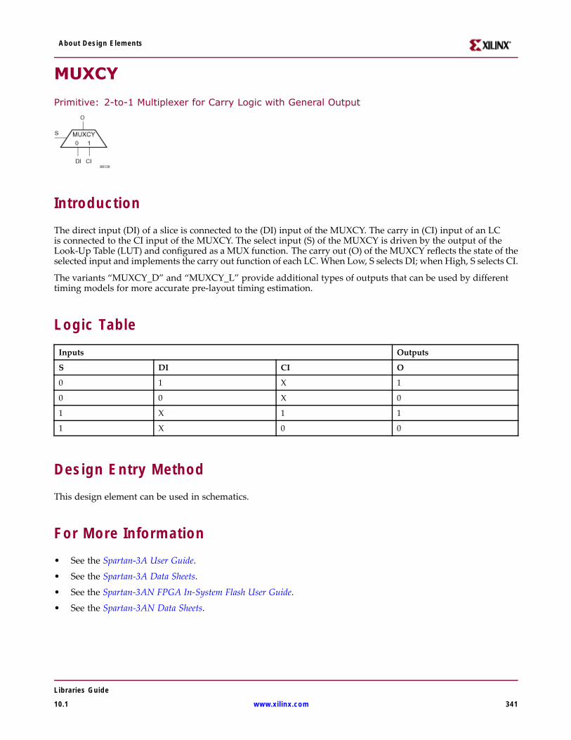
About Design Elements
MUXCY
Primitive: 2-to-1 Multiplexer for Carry Logic with General Output
IntroductionThe direct input (DI) of a slice is connected to the (DI) input of the MUXCY. The carry in (CI) input of an LCis connected to the CI input of the MUXCY. The select input (S) of the MUXCY is driven by the output of theLook-Up Table (LUT) and configured as a MUX function. The carry out (O) of the MUXCY reflects the state of theselected input and implements the carry out function of each LC. When Low, S selects DI; when High, S selects CI.
The variants “MUXCY_D” and “MUXCY_L” provide additional types of outputs that can be used by differenttiming models for more accurate pre-layout timing estimation.
Logic TableInputs Outputs
S DI CI O
0 1 X 1
0 0 X 0
1 X 1 1
1 X 0 0
Design Entry MethodThis design element can be used in schematics.
For More Information• See the Spartan-3A User Guide.
• See the Spartan-3A Data Sheets.
• See the Spartan-3AN FPGA In-System Flash User Guide.
• See the Spartan-3AN Data Sheets.
Libraries Guide
10.1 www.xilinx.com 341
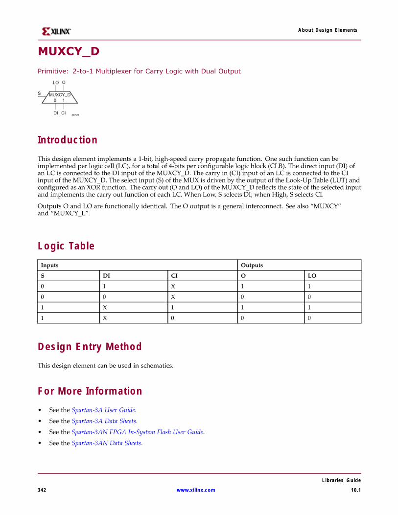
About Design Elements
MUXCY_D
Primitive: 2-to-1 Multiplexer for Carry Logic with Dual Output
IntroductionThis design element implements a 1-bit, high-speed carry propagate function. One such function can beimplemented per logic cell (LC), for a total of 4-bits per configurable logic block (CLB). The direct input (DI) ofan LC is connected to the DI input of the MUXCY_D. The carry in (CI) input of an LC is connected to the CIinput of the MUXCY_D. The select input (S) of the MUX is driven by the output of the Look-Up Table (LUT) andconfigured as an XOR function. The carry out (O and LO) of the MUXCY_D reflects the state of the selected inputand implements the carry out function of each LC. When Low, S selects DI; when High, S selects CI.
Outputs O and LO are functionally identical. The O output is a general interconnect. See also “MUXCY”and “MUXCY_L”.
Logic TableInputs Outputs
S DI CI O LO
0 1 X 1 1
0 0 X 0 0
1 X 1 1 1
1 X 0 0 0
Design Entry MethodThis design element can be used in schematics.
For More Information• See the Spartan-3A User Guide.
• See the Spartan-3A Data Sheets.
• See the Spartan-3AN FPGA In-System Flash User Guide.
• See the Spartan-3AN Data Sheets.
Libraries Guide
342 www.xilinx.com 10.1
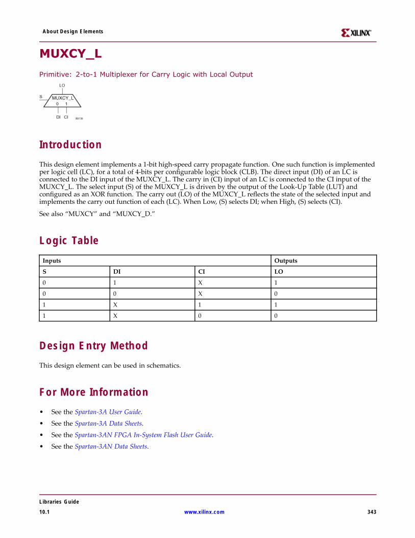
About Design Elements
MUXCY_L
Primitive: 2-to-1 Multiplexer for Carry Logic with Local Output
IntroductionThis design element implements a 1-bit high-speed carry propagate function. One such function is implementedper logic cell (LC), for a total of 4-bits per configurable logic block (CLB). The direct input (DI) of an LC isconnected to the DI input of the MUXCY_L. The carry in (CI) input of an LC is connected to the CI input of theMUXCY_L. The select input (S) of the MUXCY_L is driven by the output of the Look-Up Table (LUT) andconfigured as an XOR function. The carry out (LO) of the MUXCY_L reflects the state of the selected input andimplements the carry out function of each (LC). When Low, (S) selects DI; when High, (S) selects (CI).
See also “MUXCY” and “MUXCY_D.”
Logic TableInputs Outputs
S DI CI LO
0 1 X 1
0 0 X 0
1 X 1 1
1 X 0 0
Design Entry MethodThis design element can be used in schematics.
For More Information• See the Spartan-3A User Guide.
• See the Spartan-3A Data Sheets.
• See the Spartan-3AN FPGA In-System Flash User Guide.
• See the Spartan-3AN Data Sheets.
Libraries Guide
10.1 www.xilinx.com 343
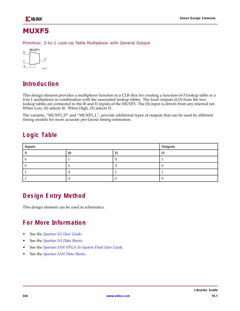
About Design Elements
MUXF5
Primitive: 2-to-1 Look-Up Table Multiplexer with General Output
IntroductionThis design element provides a multiplexer function in a CLB slice for creating a function-of-5 lookup table or a4-to-1 multiplexer in combination with the associated lookup tables. The local outputs (LO) from the twolookup tables are connected to the I0 and I1 inputs of the MUXF5. The (S) input is driven from any internal net.When Low, (S) selects I0. When High, (S) selects I1.
The variants, “MUXF5_D” and “MUXF5_L”, provide additional types of outputs that can be used by differenttiming models for more accurate pre-layout timing estimation.
Logic TableInputs Outputs
S I0 I1 O
0 1 X 1
0 0 X 0
1 X 1 1
1 X 0 0
Design Entry MethodThis design element can be used in schematics.
For More Information• See the Spartan-3A User Guide.
• See the Spartan-3A Data Sheets.
• See the Spartan-3AN FPGA In-System Flash User Guide.
• See the Spartan-3AN Data Sheets.
Libraries Guide
344 www.xilinx.com 10.1
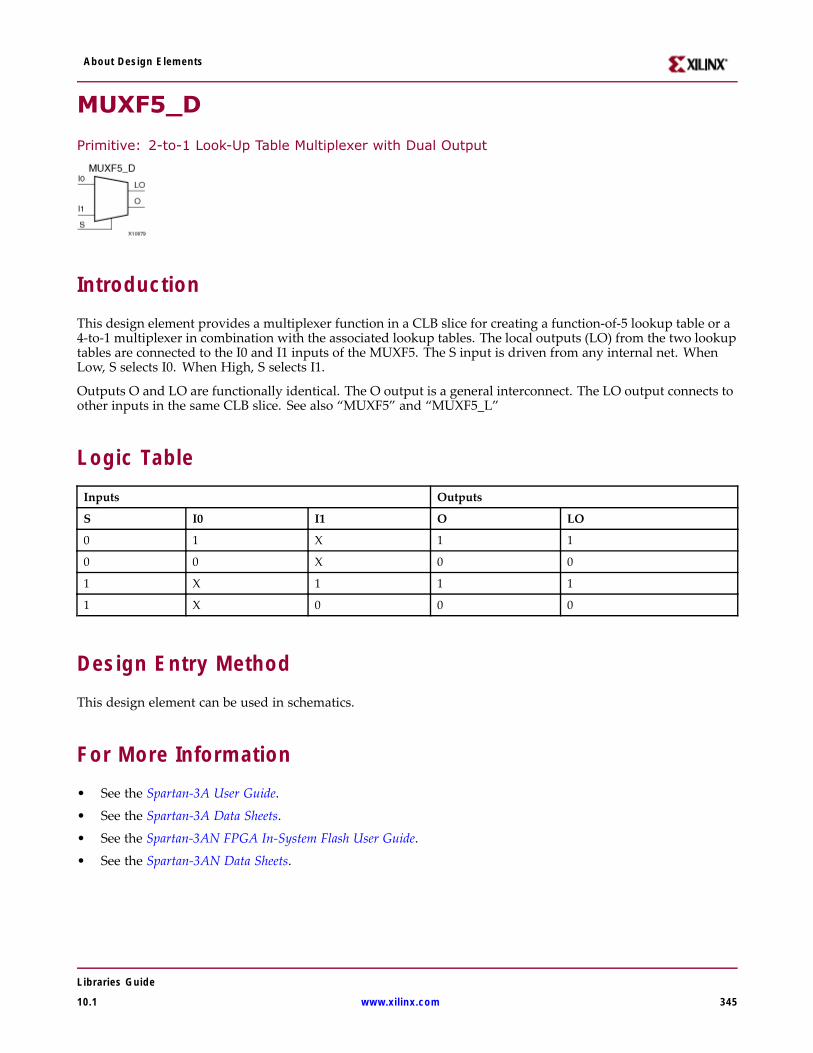
About Design Elements
MUXF5_D
Primitive: 2-to-1 Look-Up Table Multiplexer with Dual Output
IntroductionThis design element provides a multiplexer function in a CLB slice for creating a function-of-5 lookup table or a4-to-1 multiplexer in combination with the associated lookup tables. The local outputs (LO) from the two lookuptables are connected to the I0 and I1 inputs of the MUXF5. The S input is driven from any internal net. WhenLow, S selects I0. When High, S selects I1.
Outputs O and LO are functionally identical. The O output is a general interconnect. The LO output connects toother inputs in the same CLB slice. See also “MUXF5” and “MUXF5_L”
Logic TableInputs Outputs
S I0 I1 O LO
0 1 X 1 1
0 0 X 0 0
1 X 1 1 1
1 X 0 0 0
Design Entry MethodThis design element can be used in schematics.
For More Information• See the Spartan-3A User Guide.
• See the Spartan-3A Data Sheets.
• See the Spartan-3AN FPGA In-System Flash User Guide.
• See the Spartan-3AN Data Sheets.
Libraries Guide
10.1 www.xilinx.com 345
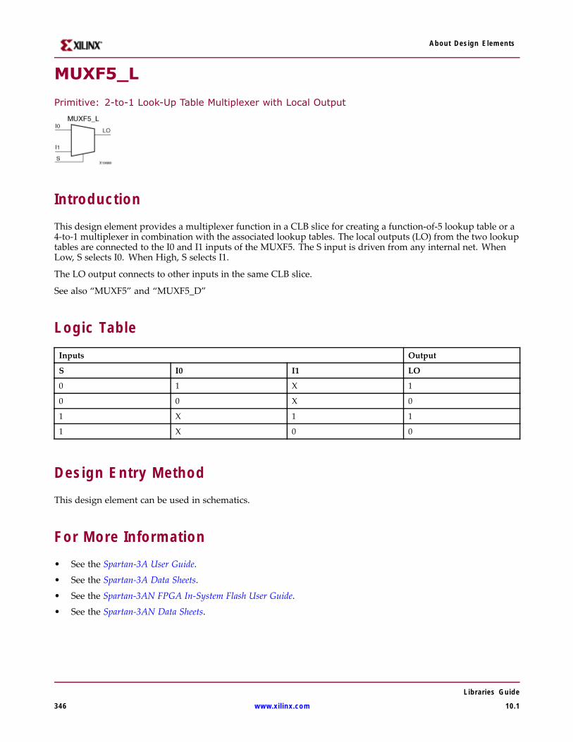
About Design Elements
MUXF5_L
Primitive: 2-to-1 Look-Up Table Multiplexer with Local Output
IntroductionThis design element provides a multiplexer function in a CLB slice for creating a function-of-5 lookup table or a4-to-1 multiplexer in combination with the associated lookup tables. The local outputs (LO) from the two lookuptables are connected to the I0 and I1 inputs of the MUXF5. The S input is driven from any internal net. WhenLow, S selects I0. When High, S selects I1.
The LO output connects to other inputs in the same CLB slice.
See also “MUXF5” and “MUXF5_D”
Logic TableInputs Output
S I0 I1 LO
0 1 X 1
0 0 X 0
1 X 1 1
1 X 0 0
Design Entry MethodThis design element can be used in schematics.
For More Information• See the Spartan-3A User Guide.
• See the Spartan-3A Data Sheets.
• See the Spartan-3AN FPGA In-System Flash User Guide.
• See the Spartan-3AN Data Sheets.
Libraries Guide
346 www.xilinx.com 10.1
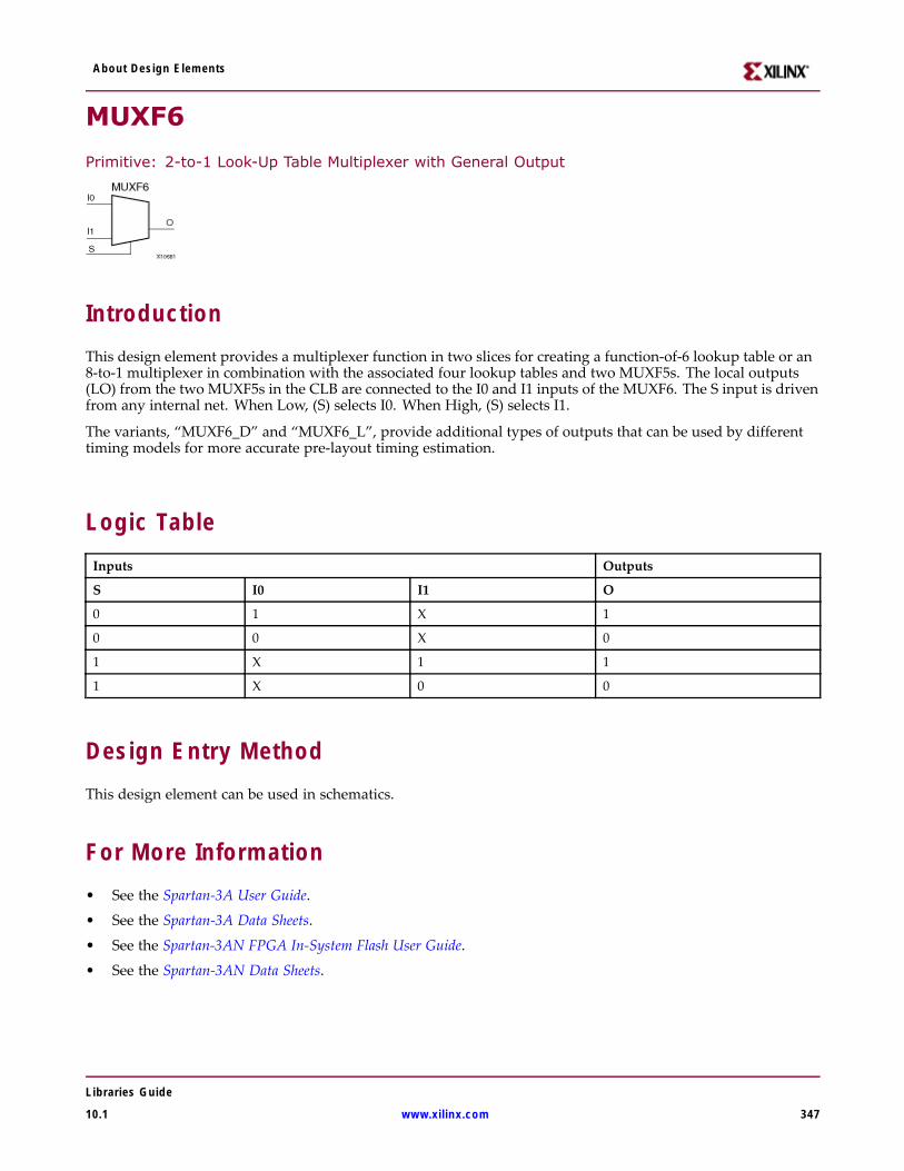
About Design Elements
MUXF6
Primitive: 2-to-1 Look-Up Table Multiplexer with General Output
IntroductionThis design element provides a multiplexer function in two slices for creating a function-of-6 lookup table or an8-to-1 multiplexer in combination with the associated four lookup tables and two MUXF5s. The local outputs(LO) from the two MUXF5s in the CLB are connected to the I0 and I1 inputs of the MUXF6. The S input is drivenfrom any internal net. When Low, (S) selects I0. When High, (S) selects I1.
The variants, “MUXF6_D” and “MUXF6_L”, provide additional types of outputs that can be used by differenttiming models for more accurate pre-layout timing estimation.
Logic TableInputs Outputs
S I0 I1 O
0 1 X 1
0 0 X 0
1 X 1 1
1 X 0 0
Design Entry MethodThis design element can be used in schematics.
For More Information• See the Spartan-3A User Guide.
• See the Spartan-3A Data Sheets.
• See the Spartan-3AN FPGA In-System Flash User Guide.
• See the Spartan-3AN Data Sheets.
Libraries Guide
10.1 www.xilinx.com 347
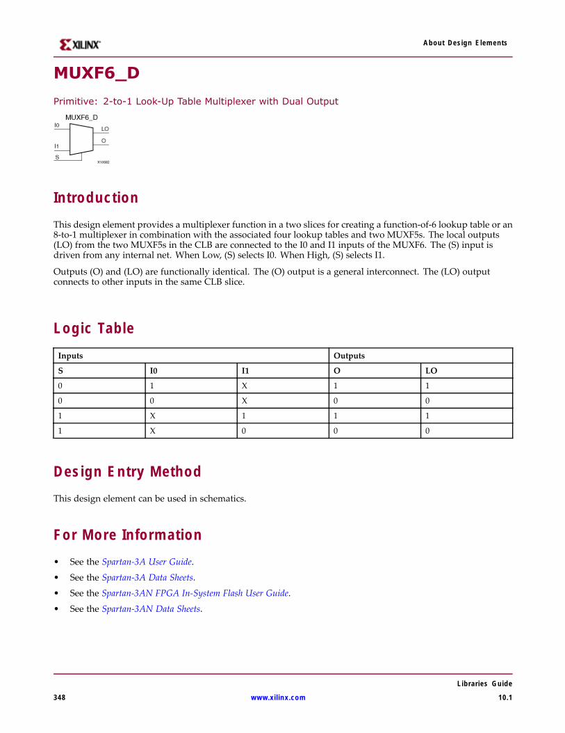
About Design Elements
MUXF6_D
Primitive: 2-to-1 Look-Up Table Multiplexer with Dual Output
IntroductionThis design element provides a multiplexer function in a two slices for creating a function-of-6 lookup table or an8-to-1 multiplexer in combination with the associated four lookup tables and two MUXF5s. The local outputs(LO) from the two MUXF5s in the CLB are connected to the I0 and I1 inputs of the MUXF6. The (S) input isdriven from any internal net. When Low, (S) selects I0. When High, (S) selects I1.
Outputs (O) and (LO) are functionally identical. The (O) output is a general interconnect. The (LO) outputconnects to other inputs in the same CLB slice.
Logic TableInputs Outputs
S I0 I1 O LO
0 1 X 1 1
0 0 X 0 0
1 X 1 1 1
1 X 0 0 0
Design Entry MethodThis design element can be used in schematics.
For More Information• See the Spartan-3A User Guide.
• See the Spartan-3A Data Sheets.
• See the Spartan-3AN FPGA In-System Flash User Guide.
• See the Spartan-3AN Data Sheets.
Libraries Guide
348 www.xilinx.com 10.1
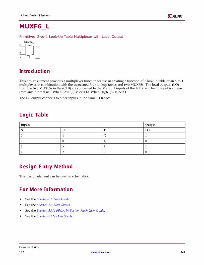
About Design Elements
MUXF6_L
Primitive: 2-to-1 Look-Up Table Multiplexer with Local Output
IntroductionThis design element provides a multiplexer function for use in creating a function-of-6 lookup table or an 8-to-1multiplexer in combination with the associated four lookup tables and two MUXF5s. The local outputs (LO)from the two MUXF5s in the (CLB) are connected to the I0 and I1 inputs of the MUXF6. The (S) input is drivenfrom any internal net. When Low, (S) selects I0. When High, (S) selects I1.
The LO output connects to other inputs in the same CLB slice.
Logic TableInputs Output
S I0 I1 LO
0 1 X 1
0 0 X 0
1 X 1 1
1 X 0 0
Design Entry MethodThis design element can be used in schematics.
For More Information• See the Spartan-3A User Guide.
• See the Spartan-3A Data Sheets.
• See the Spartan-3AN FPGA In-System Flash User Guide.
• See the Spartan-3AN Data Sheets.
Libraries Guide
10.1 www.xilinx.com 349
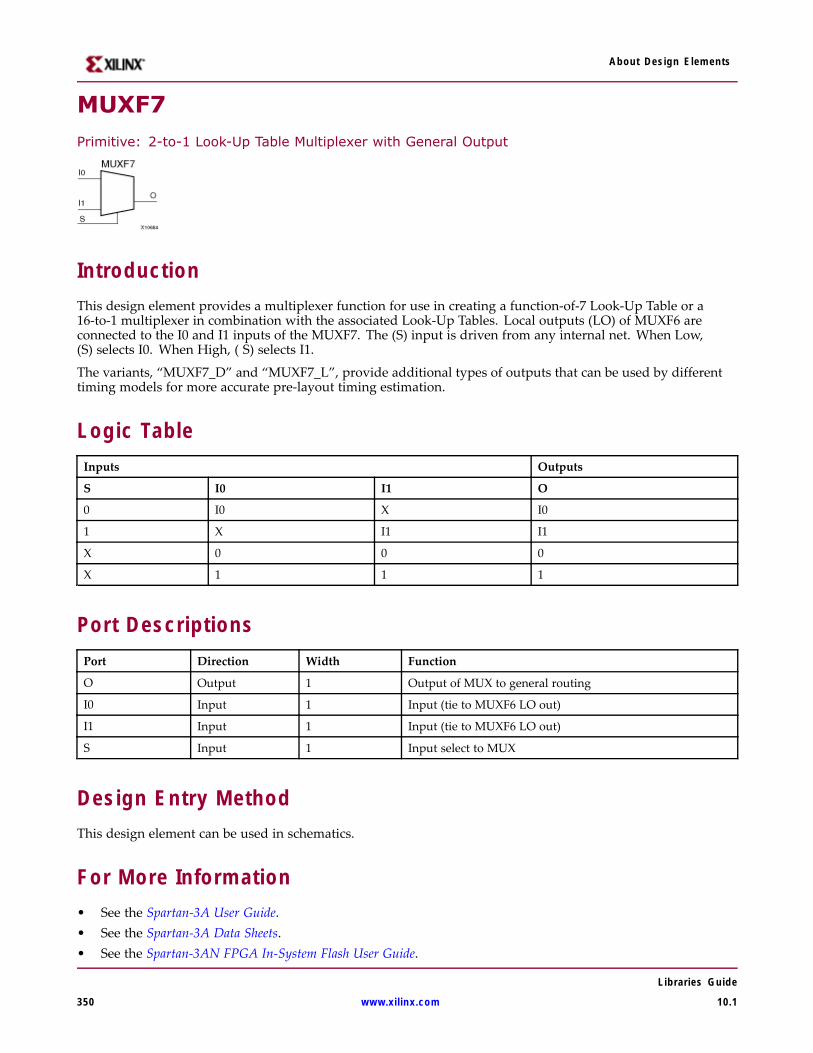
About Design Elements
MUXF7Primitive: 2-to-1 Look-Up Table Multiplexer with General Output
IntroductionThis design element provides a multiplexer function for use in creating a function-of-7 Look-Up Table or a16-to-1 multiplexer in combination with the associated Look-Up Tables. Local outputs (LO) of MUXF6 areconnected to the I0 and I1 inputs of the MUXF7. The (S) input is driven from any internal net. When Low,(S) selects I0. When High, ( S) selects I1.
The variants, “MUXF7_D” and “MUXF7_L”, provide additional types of outputs that can be used by differenttiming models for more accurate pre-layout timing estimation.
Logic TableInputs Outputs
S I0 I1 O
0 I0 X I0
1 X I1 I1
X 0 0 0
X 1 1 1
Port DescriptionsPort Direction Width Function
O Output 1 Output of MUX to general routing
I0 Input 1 Input (tie to MUXF6 LO out)
I1 Input 1 Input (tie to MUXF6 LO out)
S Input 1 Input select to MUX
Design Entry MethodThis design element can be used in schematics.
For More Information• See the Spartan-3A User Guide.• See the Spartan-3A Data Sheets.• See the Spartan-3AN FPGA In-System Flash User Guide.
Libraries Guide
350 www.xilinx.com 10.1

About Design Elements
• See the Spartan-3AN Data Sheets.
Libraries Guide
10.1 www.xilinx.com 351
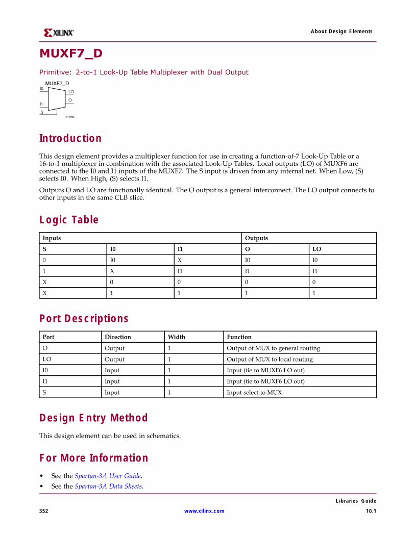
About Design Elements
MUXF7_DPrimitive: 2-to-1 Look-Up Table Multiplexer with Dual Output
IntroductionThis design element provides a multiplexer function for use in creating a function-of-7 Look-Up Table or a16-to-1 multiplexer in combination with the associated Look-Up Tables. Local outputs (LO) of MUXF6 areconnected to the I0 and I1 inputs of the MUXF7. The S input is driven from any internal net. When Low, (S)selects I0. When High, (S) selects I1.
Outputs O and LO are functionally identical. The O output is a general interconnect. The LO output connects toother inputs in the same CLB slice.
Logic TableInputs Outputs
S I0 I1 O LO
0 I0 X I0 I0
1 X I1 I1 I1
X 0 0 0 0
X 1 1 1 1
Port DescriptionsPort Direction Width Function
O Output 1 Output of MUX to general routing
LO Output 1 Output of MUX to local routing
I0 Input 1 Input (tie to MUXF6 LO out)
I1 Input 1 Input (tie to MUXF6 LO out)
S Input 1 Input select to MUX
Design Entry MethodThis design element can be used in schematics.
For More Information• See the Spartan-3A User Guide.• See the Spartan-3A Data Sheets.
Libraries Guide
352 www.xilinx.com 10.1

About Design Elements
• See the Spartan-3AN FPGA In-System Flash User Guide.
• See the Spartan-3AN Data Sheets.
Libraries Guide
10.1 www.xilinx.com 353
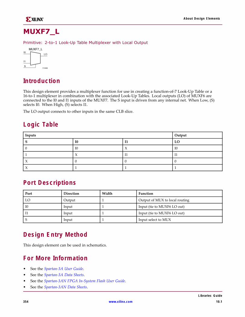
About Design Elements
MUXF7_LPrimitive: 2-to-1 Look-Up Table Multiplexer with Local Output
IntroductionThis design element provides a multiplexer function for use in creating a function-of-7 Look-Up Table or a16-to-1 multiplexer in combination with the associated Look-Up Tables. Local outputs (LO) of MUXF6 areconnected to the I0 and I1 inputs of the MUXF7. The S input is driven from any internal net. When Low, (S)selects I0. When High, (S) selects I1.
The LO output connects to other inputs in the same CLB slice.
Logic TableInputs Output
S I0 I1 LO
0 I0 X I0
1 X I1 I1
X 0 0 0
X 1 1 1
Port DescriptionsPort Direction Width Function
LO Output 1 Output of MUX to local routing
I0 Input 1 Input (tie to MUXF6 LO out)
I1 Input 1 Input (tie to MUXF6 LO out)
S Input 1 Input select to MUX
Design Entry MethodThis design element can be used in schematics.
For More Information• See the Spartan-3A User Guide.• See the Spartan-3A Data Sheets.• See the Spartan-3AN FPGA In-System Flash User Guide.• See the Spartan-3AN Data Sheets.
Libraries Guide
354 www.xilinx.com 10.1
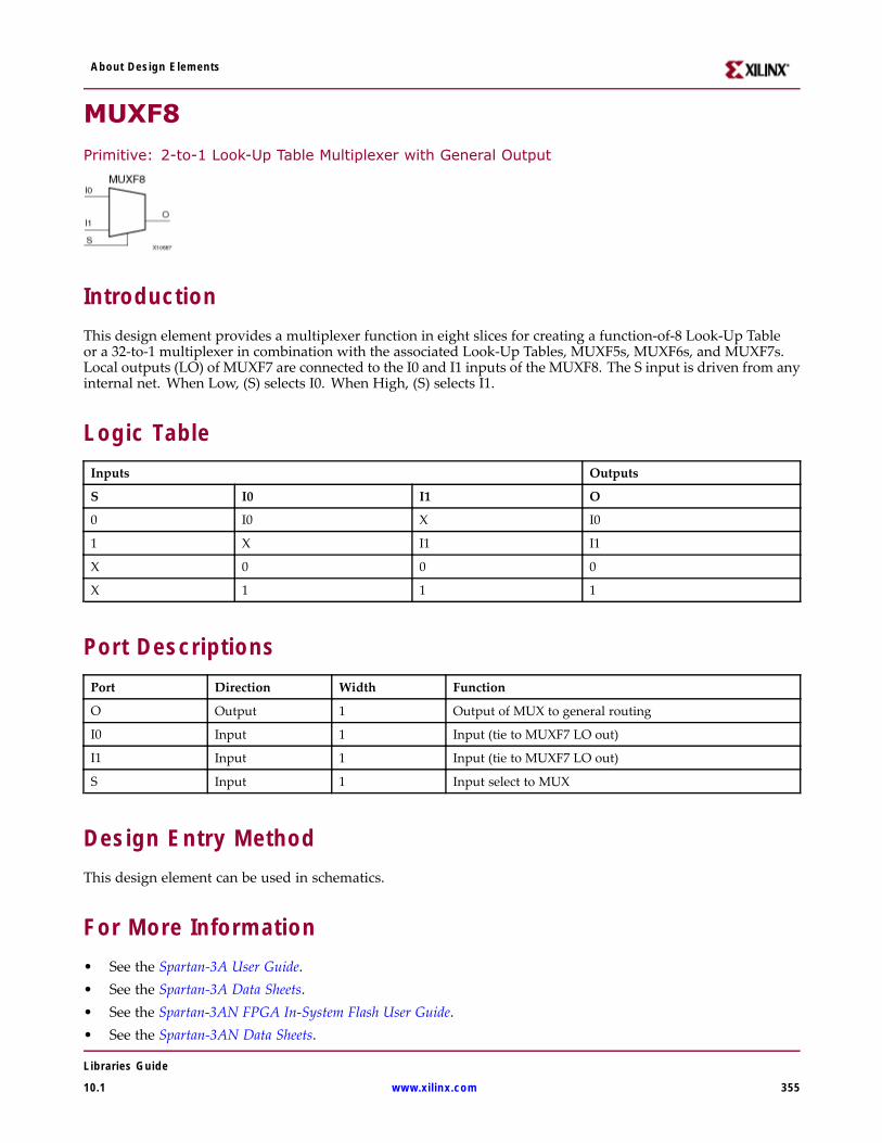
About Design Elements
MUXF8
Primitive: 2-to-1 Look-Up Table Multiplexer with General Output
IntroductionThis design element provides a multiplexer function in eight slices for creating a function-of-8 Look-Up Tableor a 32-to-1 multiplexer in combination with the associated Look-Up Tables, MUXF5s, MUXF6s, and MUXF7s.Local outputs (LO) of MUXF7 are connected to the I0 and I1 inputs of the MUXF8. The S input is driven from anyinternal net. When Low, (S) selects I0. When High, (S) selects I1.
Logic TableInputs Outputs
S I0 I1 O
0 I0 X I0
1 X I1 I1
X 0 0 0
X 1 1 1
Port DescriptionsPort Direction Width Function
O Output 1 Output of MUX to general routing
I0 Input 1 Input (tie to MUXF7 LO out)
I1 Input 1 Input (tie to MUXF7 LO out)
S Input 1 Input select to MUX
Design Entry MethodThis design element can be used in schematics.
For More Information• See the Spartan-3A User Guide.• See the Spartan-3A Data Sheets.• See the Spartan-3AN FPGA In-System Flash User Guide.• See the Spartan-3AN Data Sheets.
Libraries Guide
10.1 www.xilinx.com 355
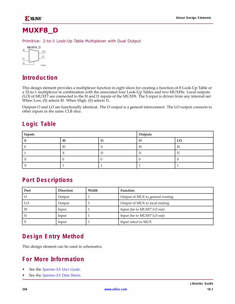
About Design Elements
MUXF8_DPrimitive: 2-to-1 Look-Up Table Multiplexer with Dual Output
IntroductionThis design element provides a multiplexer function in eight slices for creating a function-of-8 Look-Up Table ora 32-to-1 multiplexer in combination with the associated four Look-Up Tables and two MUXF8s. Local outputs(LO) of MUXF7 are connected to the I0 and I1 inputs of the MUXF8. The S input is driven from any internal net.When Low, (S) selects I0. When High, (S) selects I1.
Outputs O and LO are functionally identical. The O output is a general interconnect. The LO output connects toother inputs in the same CLB slice.
Logic TableInputs Outputs
S I0 I1 O LO
0 I0 X I0 I0
1 X I1 I1 I1
X 0 0 0 0
X 1 1 1 1
Port DescriptionsPort Direction Width Function
O Output 1 Output of MUX to general routing
LO Output 1 Output of MUX to local routing
I0 Input 1 Input (tie to MUXF7 LO out)
I1 Input 1 Input (tie to MUXF7 LO out)
S Input 1 Input select to MUX
Design Entry MethodThis design element can be used in schematics.
For More Information• See the Spartan-3A User Guide.• See the Spartan-3A Data Sheets.
Libraries Guide
356 www.xilinx.com 10.1

About Design Elements
• See the Spartan-3AN FPGA In-System Flash User Guide.
• See the Spartan-3AN Data Sheets.
Libraries Guide
10.1 www.xilinx.com 357
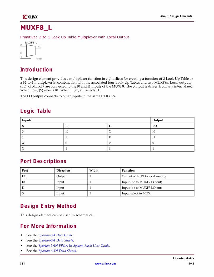
About Design Elements
MUXF8_LPrimitive: 2-to-1 Look-Up Table Multiplexer with Local Output
IntroductionThis design element provides a multiplexer function in eight slices for creating a function-of-8 Look-Up Table ora 32-to-1 multiplexer in combination with the associated four Look-Up Tables and two MUXF8s. Local outputs(LO) of MUXF7 are connected to the I0 and I1 inputs of the MUXF8. The S input is driven from any internal net.When Low, (S) selects I0. When High, (S) selects I1.
The LO output connects to other inputs in the same CLB slice.
Logic TableInputs Output
S I0 I1 LO
0 I0 X I0
1 X I1 I1
X 0 0 0
X 1 1 1
Port DescriptionsPort Direction Width Function
LO Output 1 Output of MUX to local routing
I0 Input 1 Input (tie to MUXF7 LO out)
I1 Input 1 Input (tie to MUXF7 LO out)
S Input 1 Input select to MUX
Design Entry MethodThis design element can be used in schematics.
For More Information• See the Spartan-3A User Guide.• See the Spartan-3A Data Sheets.• See the Spartan-3AN FPGA In-System Flash User Guide.• See the Spartan-3AN Data Sheets.
Libraries Guide
358 www.xilinx.com 10.1
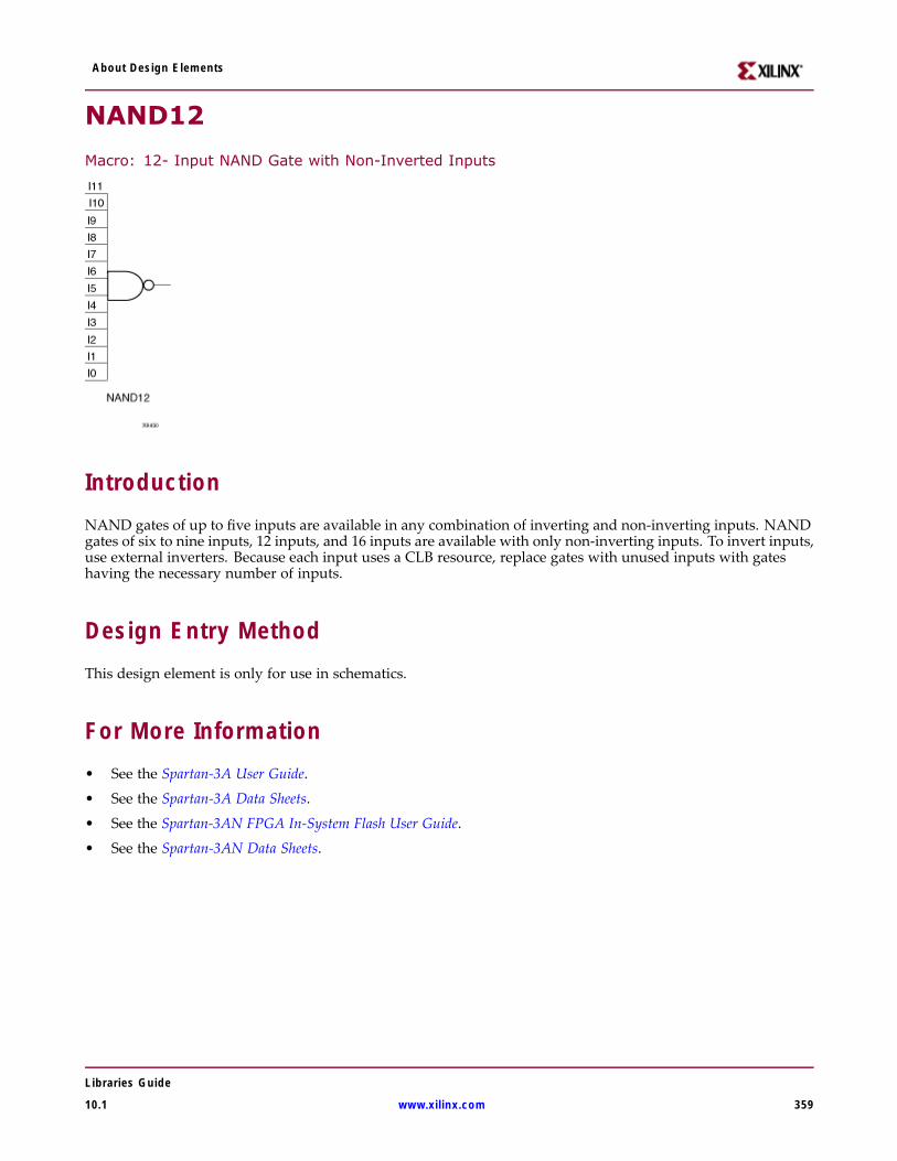
About Design Elements
NAND12
Macro: 12- Input NAND Gate with Non-Inverted Inputs
IntroductionNAND gates of up to five inputs are available in any combination of inverting and non-inverting inputs. NANDgates of six to nine inputs, 12 inputs, and 16 inputs are available with only non-inverting inputs. To invert inputs,use external inverters. Because each input uses a CLB resource, replace gates with unused inputs with gateshaving the necessary number of inputs.
Design Entry MethodThis design element is only for use in schematics.
For More Information• See the Spartan-3A User Guide.
• See the Spartan-3A Data Sheets.
• See the Spartan-3AN FPGA In-System Flash User Guide.
• See the Spartan-3AN Data Sheets.
Libraries Guide
10.1 www.xilinx.com 359
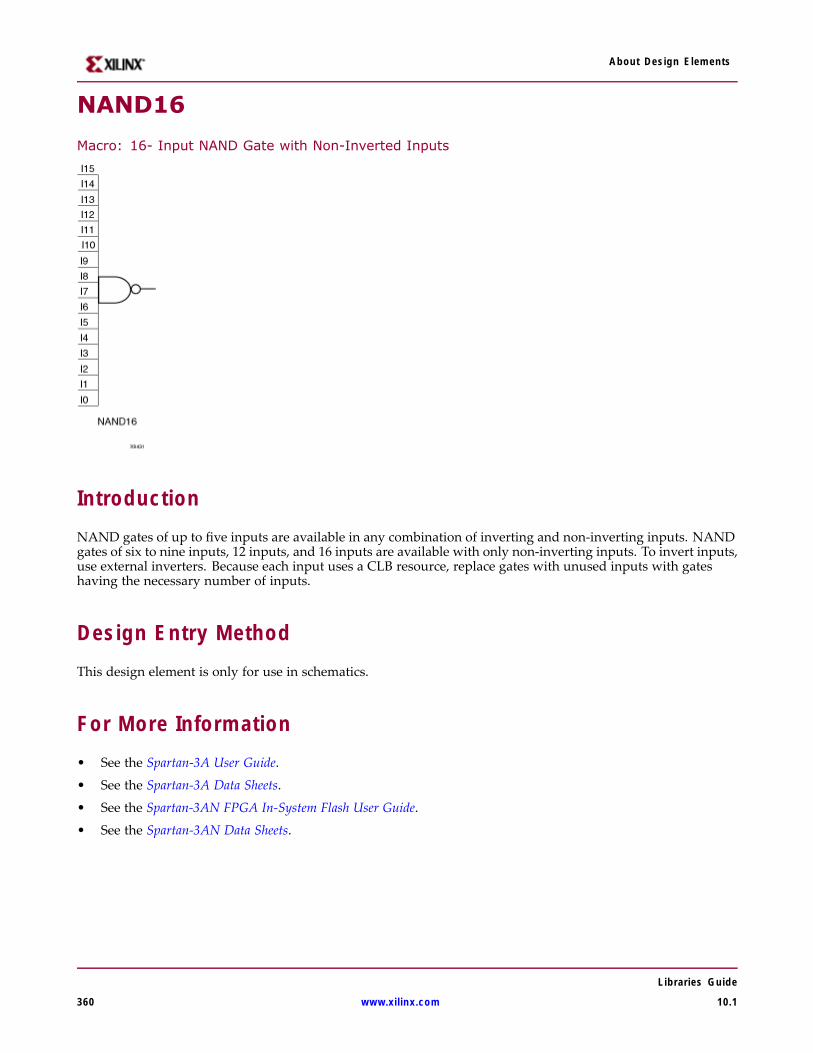
About Design Elements
NAND16
Macro: 16- Input NAND Gate with Non-Inverted Inputs
IntroductionNAND gates of up to five inputs are available in any combination of inverting and non-inverting inputs. NANDgates of six to nine inputs, 12 inputs, and 16 inputs are available with only non-inverting inputs. To invert inputs,use external inverters. Because each input uses a CLB resource, replace gates with unused inputs with gateshaving the necessary number of inputs.
Design Entry MethodThis design element is only for use in schematics.
For More Information• See the Spartan-3A User Guide.
• See the Spartan-3A Data Sheets.
• See the Spartan-3AN FPGA In-System Flash User Guide.
• See the Spartan-3AN Data Sheets.
Libraries Guide
360 www.xilinx.com 10.1

About Design Elements
NAND2
Primitive: 2-Input NAND Gate with Non-Inverted Inputs
IntroductionNAND gates of up to five inputs are available in any combination of inverting and non-inverting inputs. NANDgates of six to nine inputs, 12 inputs, and 16 inputs are available with only non-inverting inputs. To invert inputs,use external inverters. Because each input uses a CLB resource, replace gates with unused inputs with gateshaving the necessary number of inputs.
Design Entry MethodThis design element is only for use in schematics.
For More Information• See the Spartan-3A User Guide.
• See the Spartan-3A Data Sheets.
• See the Spartan-3AN FPGA In-System Flash User Guide.
• See the Spartan-3AN Data Sheets.
Libraries Guide
10.1 www.xilinx.com 361
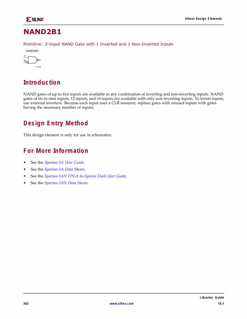
About Design Elements
NAND2B1
Primitive: 2-Input NAND Gate with 1 Inverted and 1 Non-Inverted Inputs
IntroductionNAND gates of up to five inputs are available in any combination of inverting and non-inverting inputs. NANDgates of six to nine inputs, 12 inputs, and 16 inputs are available with only non-inverting inputs. To invert inputs,use external inverters. Because each input uses a CLB resource, replace gates with unused inputs with gateshaving the necessary number of inputs.
Design Entry MethodThis design element is only for use in schematics.
For More Information• See the Spartan-3A User Guide.
• See the Spartan-3A Data Sheets.
• See the Spartan-3AN FPGA In-System Flash User Guide.
• See the Spartan-3AN Data Sheets.
Libraries Guide
362 www.xilinx.com 10.1
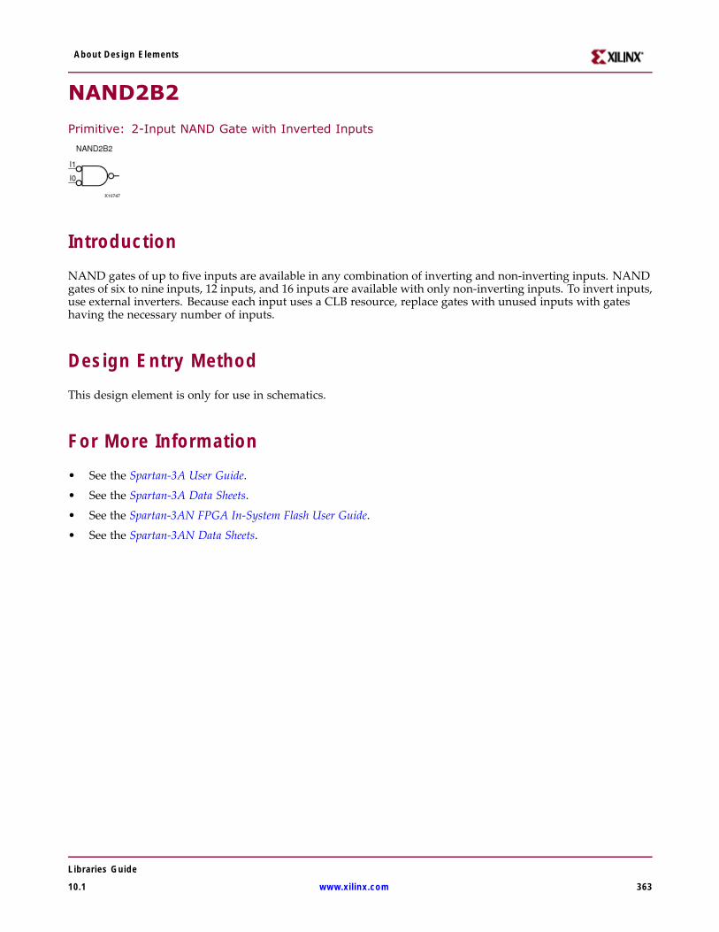
About Design Elements
NAND2B2
Primitive: 2-Input NAND Gate with Inverted Inputs
IntroductionNAND gates of up to five inputs are available in any combination of inverting and non-inverting inputs. NANDgates of six to nine inputs, 12 inputs, and 16 inputs are available with only non-inverting inputs. To invert inputs,use external inverters. Because each input uses a CLB resource, replace gates with unused inputs with gateshaving the necessary number of inputs.
Design Entry MethodThis design element is only for use in schematics.
For More Information• See the Spartan-3A User Guide.
• See the Spartan-3A Data Sheets.
• See the Spartan-3AN FPGA In-System Flash User Guide.
• See the Spartan-3AN Data Sheets.
Libraries Guide
10.1 www.xilinx.com 363
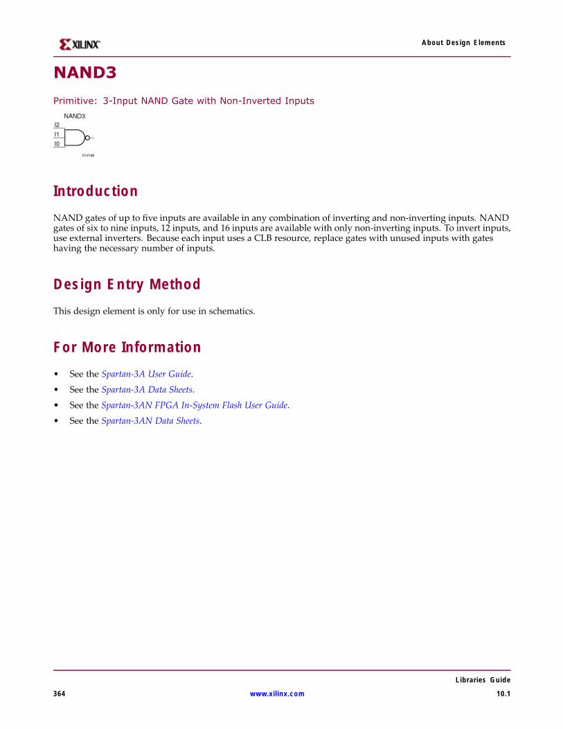
About Design Elements
NAND3
Primitive: 3-Input NAND Gate with Non-Inverted Inputs
IntroductionNAND gates of up to five inputs are available in any combination of inverting and non-inverting inputs. NANDgates of six to nine inputs, 12 inputs, and 16 inputs are available with only non-inverting inputs. To invert inputs,use external inverters. Because each input uses a CLB resource, replace gates with unused inputs with gateshaving the necessary number of inputs.
Design Entry MethodThis design element is only for use in schematics.
For More Information• See the Spartan-3A User Guide.
• See the Spartan-3A Data Sheets.
• See the Spartan-3AN FPGA In-System Flash User Guide.
• See the Spartan-3AN Data Sheets.
Libraries Guide
364 www.xilinx.com 10.1
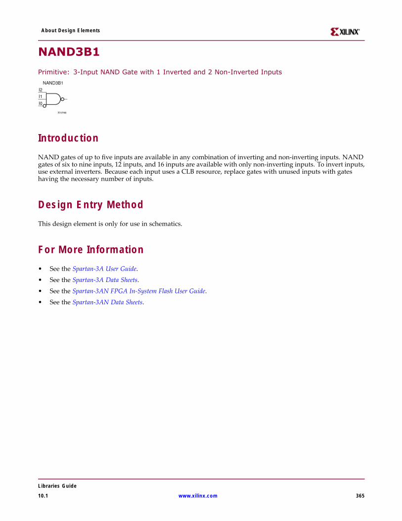
About Design Elements
NAND3B1
Primitive: 3-Input NAND Gate with 1 Inverted and 2 Non-Inverted Inputs
IntroductionNAND gates of up to five inputs are available in any combination of inverting and non-inverting inputs. NANDgates of six to nine inputs, 12 inputs, and 16 inputs are available with only non-inverting inputs. To invert inputs,use external inverters. Because each input uses a CLB resource, replace gates with unused inputs with gateshaving the necessary number of inputs.
Design Entry MethodThis design element is only for use in schematics.
For More Information• See the Spartan-3A User Guide.
• See the Spartan-3A Data Sheets.
• See the Spartan-3AN FPGA In-System Flash User Guide.
• See the Spartan-3AN Data Sheets.
Libraries Guide
10.1 www.xilinx.com 365

About Design Elements
NAND3B2
Primitive: 3-Input NAND Gate with 2 Inverted and 1 Non-Inverted Inputs
IntroductionNAND gates of up to five inputs are available in any combination of inverting and non-inverting inputs. NANDgates of six to nine inputs, 12 inputs, and 16 inputs are available with only non-inverting inputs. To invert inputs,use external inverters. Because each input uses a CLB resource, replace gates with unused inputs with gateshaving the necessary number of inputs.
Design Entry MethodThis design element is only for use in schematics.
For More Information• See the Spartan-3A User Guide.
• See the Spartan-3A Data Sheets.
• See the Spartan-3AN FPGA In-System Flash User Guide.
• See the Spartan-3AN Data Sheets.
Libraries Guide
366 www.xilinx.com 10.1
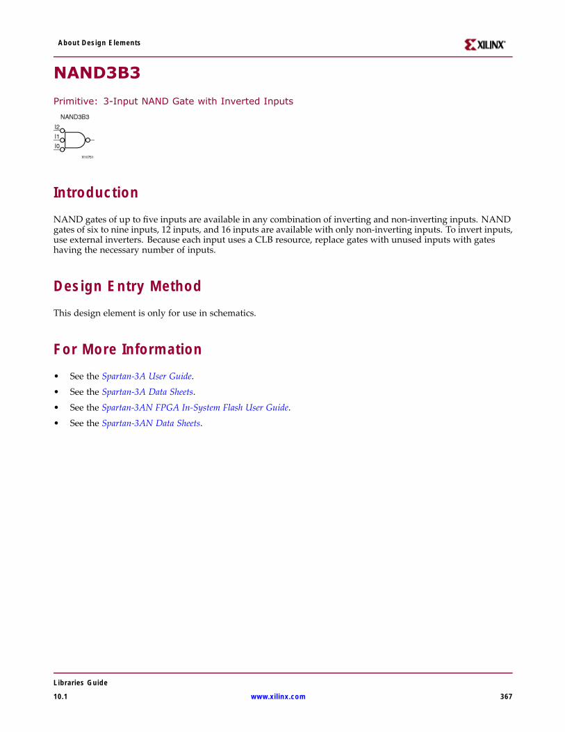
About Design Elements
NAND3B3
Primitive: 3-Input NAND Gate with Inverted Inputs
IntroductionNAND gates of up to five inputs are available in any combination of inverting and non-inverting inputs. NANDgates of six to nine inputs, 12 inputs, and 16 inputs are available with only non-inverting inputs. To invert inputs,use external inverters. Because each input uses a CLB resource, replace gates with unused inputs with gateshaving the necessary number of inputs.
Design Entry MethodThis design element is only for use in schematics.
For More Information• See the Spartan-3A User Guide.
• See the Spartan-3A Data Sheets.
• See the Spartan-3AN FPGA In-System Flash User Guide.
• See the Spartan-3AN Data Sheets.
Libraries Guide
10.1 www.xilinx.com 367
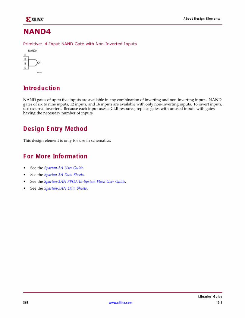
About Design Elements
NAND4
Primitive: 4-Input NAND Gate with Non-Inverted Inputs
IntroductionNAND gates of up to five inputs are available in any combination of inverting and non-inverting inputs. NANDgates of six to nine inputs, 12 inputs, and 16 inputs are available with only non-inverting inputs. To invert inputs,use external inverters. Because each input uses a CLB resource, replace gates with unused inputs with gateshaving the necessary number of inputs.
Design Entry MethodThis design element is only for use in schematics.
For More Information• See the Spartan-3A User Guide.
• See the Spartan-3A Data Sheets.
• See the Spartan-3AN FPGA In-System Flash User Guide.
• See the Spartan-3AN Data Sheets.
Libraries Guide
368 www.xilinx.com 10.1

About Design Elements
NAND4B1
Primitive: 4-Input NAND Gate with 1 Inverted and 3 Non-Inverted Inputs
IntroductionNAND gates of up to five inputs are available in any combination of inverting and non-inverting inputs. NANDgates of six to nine inputs, 12 inputs, and 16 inputs are available with only non-inverting inputs. To invert inputs,use external inverters. Because each input uses a CLB resource, replace gates with unused inputs with gateshaving the necessary number of inputs.
Design Entry MethodThis design element is only for use in schematics.
For More Information• See the Spartan-3A User Guide.
• See the Spartan-3A Data Sheets.
• See the Spartan-3AN FPGA In-System Flash User Guide.
• See the Spartan-3AN Data Sheets.
Libraries Guide
10.1 www.xilinx.com 369

About Design Elements
NAND4B2
Primitive: 4-Input NAND Gate with 2 Inverted and 2 Non-Inverted Inputs
IntroductionNAND gates of up to five inputs are available in any combination of inverting and non-inverting inputs. NANDgates of six to nine inputs, 12 inputs, and 16 inputs are available with only non-inverting inputs. To invert inputs,use external inverters. Because each input uses a CLB resource, replace gates with unused inputs with gateshaving the necessary number of inputs.
Design Entry MethodThis design element is only for use in schematics.
For More Information• See the Spartan-3A User Guide.
• See the Spartan-3A Data Sheets.
• See the Spartan-3AN FPGA In-System Flash User Guide.
• See the Spartan-3AN Data Sheets.
Libraries Guide
370 www.xilinx.com 10.1
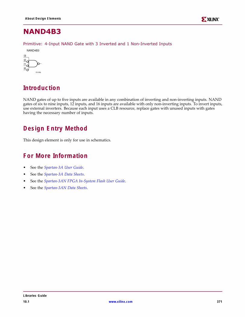
About Design Elements
NAND4B3
Primitive: 4-Input NAND Gate with 3 Inverted and 1 Non-Inverted Inputs
IntroductionNAND gates of up to five inputs are available in any combination of inverting and non-inverting inputs. NANDgates of six to nine inputs, 12 inputs, and 16 inputs are available with only non-inverting inputs. To invert inputs,use external inverters. Because each input uses a CLB resource, replace gates with unused inputs with gateshaving the necessary number of inputs.
Design Entry MethodThis design element is only for use in schematics.
For More Information• See the Spartan-3A User Guide.
• See the Spartan-3A Data Sheets.
• See the Spartan-3AN FPGA In-System Flash User Guide.
• See the Spartan-3AN Data Sheets.
Libraries Guide
10.1 www.xilinx.com 371
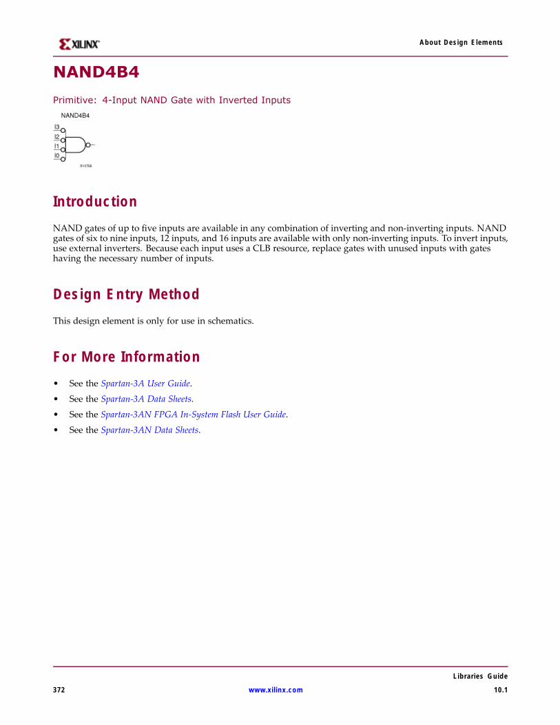
About Design Elements
NAND4B4
Primitive: 4-Input NAND Gate with Inverted Inputs
IntroductionNAND gates of up to five inputs are available in any combination of inverting and non-inverting inputs. NANDgates of six to nine inputs, 12 inputs, and 16 inputs are available with only non-inverting inputs. To invert inputs,use external inverters. Because each input uses a CLB resource, replace gates with unused inputs with gateshaving the necessary number of inputs.
Design Entry MethodThis design element is only for use in schematics.
For More Information• See the Spartan-3A User Guide.
• See the Spartan-3A Data Sheets.
• See the Spartan-3AN FPGA In-System Flash User Guide.
• See the Spartan-3AN Data Sheets.
Libraries Guide
372 www.xilinx.com 10.1
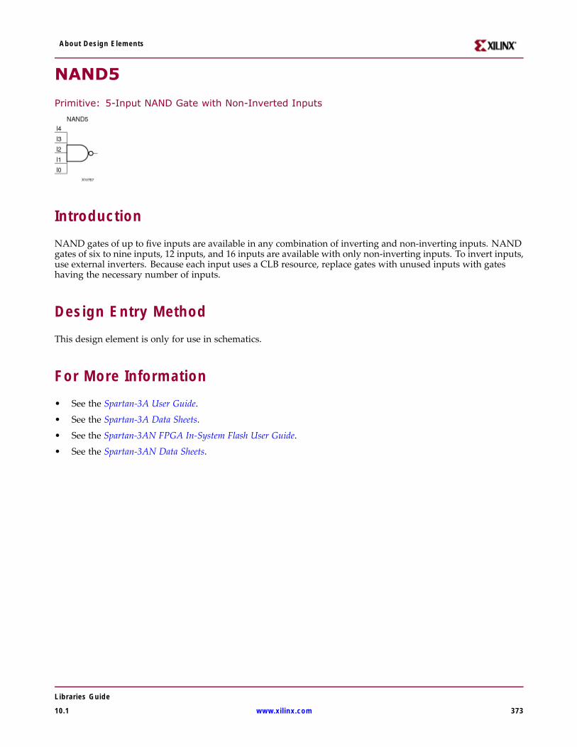
About Design Elements
NAND5
Primitive: 5-Input NAND Gate with Non-Inverted Inputs
IntroductionNAND gates of up to five inputs are available in any combination of inverting and non-inverting inputs. NANDgates of six to nine inputs, 12 inputs, and 16 inputs are available with only non-inverting inputs. To invert inputs,use external inverters. Because each input uses a CLB resource, replace gates with unused inputs with gateshaving the necessary number of inputs.
Design Entry MethodThis design element is only for use in schematics.
For More Information• See the Spartan-3A User Guide.
• See the Spartan-3A Data Sheets.
• See the Spartan-3AN FPGA In-System Flash User Guide.
• See the Spartan-3AN Data Sheets.
Libraries Guide
10.1 www.xilinx.com 373
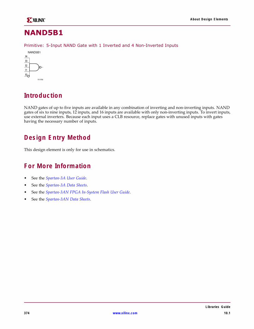
About Design Elements
NAND5B1
Primitive: 5-Input NAND Gate with 1 Inverted and 4 Non-Inverted Inputs
IntroductionNAND gates of up to five inputs are available in any combination of inverting and non-inverting inputs. NANDgates of six to nine inputs, 12 inputs, and 16 inputs are available with only non-inverting inputs. To invert inputs,use external inverters. Because each input uses a CLB resource, replace gates with unused inputs with gateshaving the necessary number of inputs.
Design Entry MethodThis design element is only for use in schematics.
For More Information• See the Spartan-3A User Guide.
• See the Spartan-3A Data Sheets.
• See the Spartan-3AN FPGA In-System Flash User Guide.
• See the Spartan-3AN Data Sheets.
Libraries Guide
374 www.xilinx.com 10.1
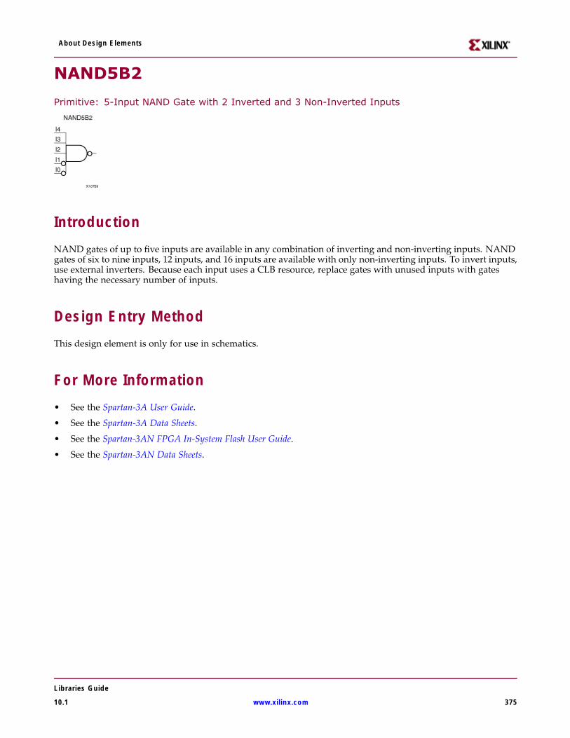
About Design Elements
NAND5B2
Primitive: 5-Input NAND Gate with 2 Inverted and 3 Non-Inverted Inputs
IntroductionNAND gates of up to five inputs are available in any combination of inverting and non-inverting inputs. NANDgates of six to nine inputs, 12 inputs, and 16 inputs are available with only non-inverting inputs. To invert inputs,use external inverters. Because each input uses a CLB resource, replace gates with unused inputs with gateshaving the necessary number of inputs.
Design Entry MethodThis design element is only for use in schematics.
For More Information• See the Spartan-3A User Guide.
• See the Spartan-3A Data Sheets.
• See the Spartan-3AN FPGA In-System Flash User Guide.
• See the Spartan-3AN Data Sheets.
Libraries Guide
10.1 www.xilinx.com 375
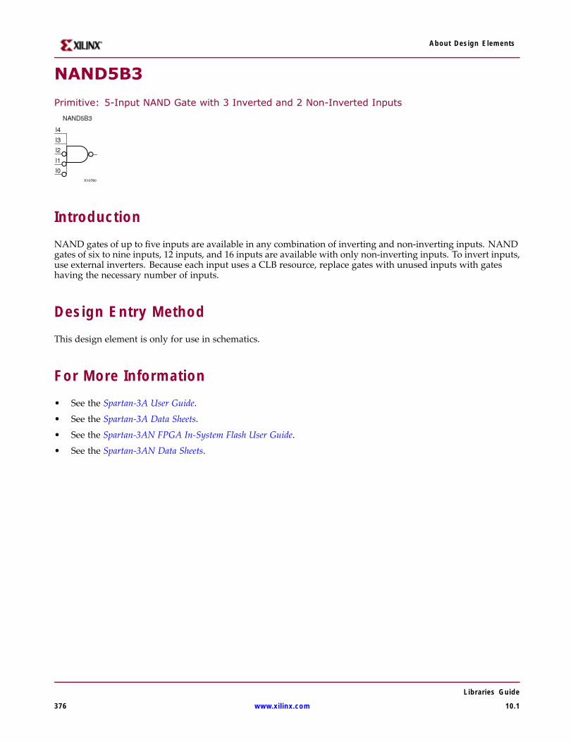
About Design Elements
NAND5B3
Primitive: 5-Input NAND Gate with 3 Inverted and 2 Non-Inverted Inputs
IntroductionNAND gates of up to five inputs are available in any combination of inverting and non-inverting inputs. NANDgates of six to nine inputs, 12 inputs, and 16 inputs are available with only non-inverting inputs. To invert inputs,use external inverters. Because each input uses a CLB resource, replace gates with unused inputs with gateshaving the necessary number of inputs.
Design Entry MethodThis design element is only for use in schematics.
For More Information• See the Spartan-3A User Guide.
• See the Spartan-3A Data Sheets.
• See the Spartan-3AN FPGA In-System Flash User Guide.
• See the Spartan-3AN Data Sheets.
Libraries Guide
376 www.xilinx.com 10.1
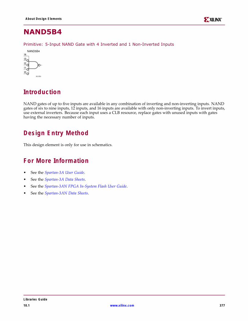
About Design Elements
NAND5B4
Primitive: 5-Input NAND Gate with 4 Inverted and 1 Non-Inverted Inputs
IntroductionNAND gates of up to five inputs are available in any combination of inverting and non-inverting inputs. NANDgates of six to nine inputs, 12 inputs, and 16 inputs are available with only non-inverting inputs. To invert inputs,use external inverters. Because each input uses a CLB resource, replace gates with unused inputs with gateshaving the necessary number of inputs.
Design Entry MethodThis design element is only for use in schematics.
For More Information• See the Spartan-3A User Guide.
• See the Spartan-3A Data Sheets.
• See the Spartan-3AN FPGA In-System Flash User Guide.
• See the Spartan-3AN Data Sheets.
Libraries Guide
10.1 www.xilinx.com 377
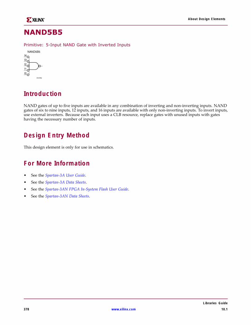
About Design Elements
NAND5B5
Primitive: 5-Input NAND Gate with Inverted Inputs
IntroductionNAND gates of up to five inputs are available in any combination of inverting and non-inverting inputs. NANDgates of six to nine inputs, 12 inputs, and 16 inputs are available with only non-inverting inputs. To invert inputs,use external inverters. Because each input uses a CLB resource, replace gates with unused inputs with gateshaving the necessary number of inputs.
Design Entry MethodThis design element is only for use in schematics.
For More Information• See the Spartan-3A User Guide.
• See the Spartan-3A Data Sheets.
• See the Spartan-3AN FPGA In-System Flash User Guide.
• See the Spartan-3AN Data Sheets.
Libraries Guide
378 www.xilinx.com 10.1

About Design Elements
NAND6
Macro: 6-Input NAND Gate with Non-Inverted Inputs
IntroductionNAND gates of up to five inputs are available in any combination of inverting and non-inverting inputs. NANDgates of six to nine inputs, 12 inputs, and 16 inputs are available with only non-inverting inputs. To invert inputs,use external inverters. Because each input uses a CLB resource, replace gates with unused inputs with gateshaving the necessary number of inputs.
Design Entry MethodThis design element is only for use in schematics.
For More Information• See the Spartan-3A User Guide.
• See the Spartan-3A Data Sheets.
• See the Spartan-3AN FPGA In-System Flash User Guide.
• See the Spartan-3AN Data Sheets.
Libraries Guide
10.1 www.xilinx.com 379
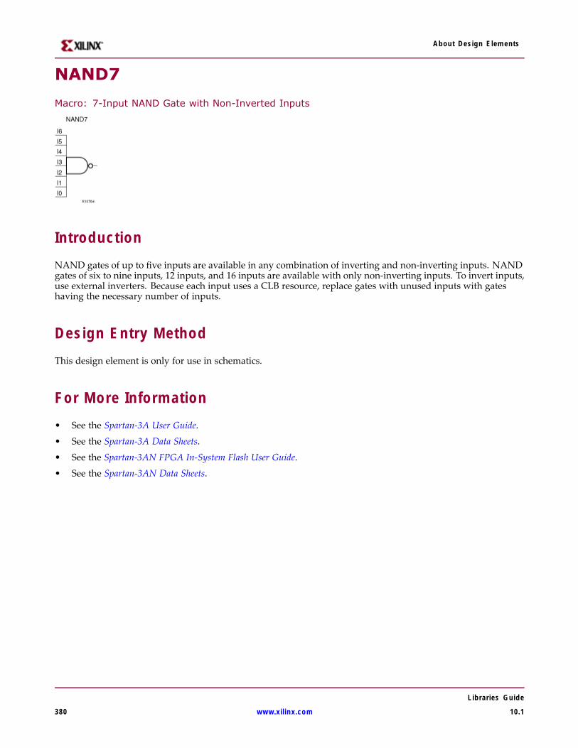
About Design Elements
NAND7
Macro: 7-Input NAND Gate with Non-Inverted Inputs
IntroductionNAND gates of up to five inputs are available in any combination of inverting and non-inverting inputs. NANDgates of six to nine inputs, 12 inputs, and 16 inputs are available with only non-inverting inputs. To invert inputs,use external inverters. Because each input uses a CLB resource, replace gates with unused inputs with gateshaving the necessary number of inputs.
Design Entry MethodThis design element is only for use in schematics.
For More Information• See the Spartan-3A User Guide.
• See the Spartan-3A Data Sheets.
• See the Spartan-3AN FPGA In-System Flash User Guide.
• See the Spartan-3AN Data Sheets.
Libraries Guide
380 www.xilinx.com 10.1
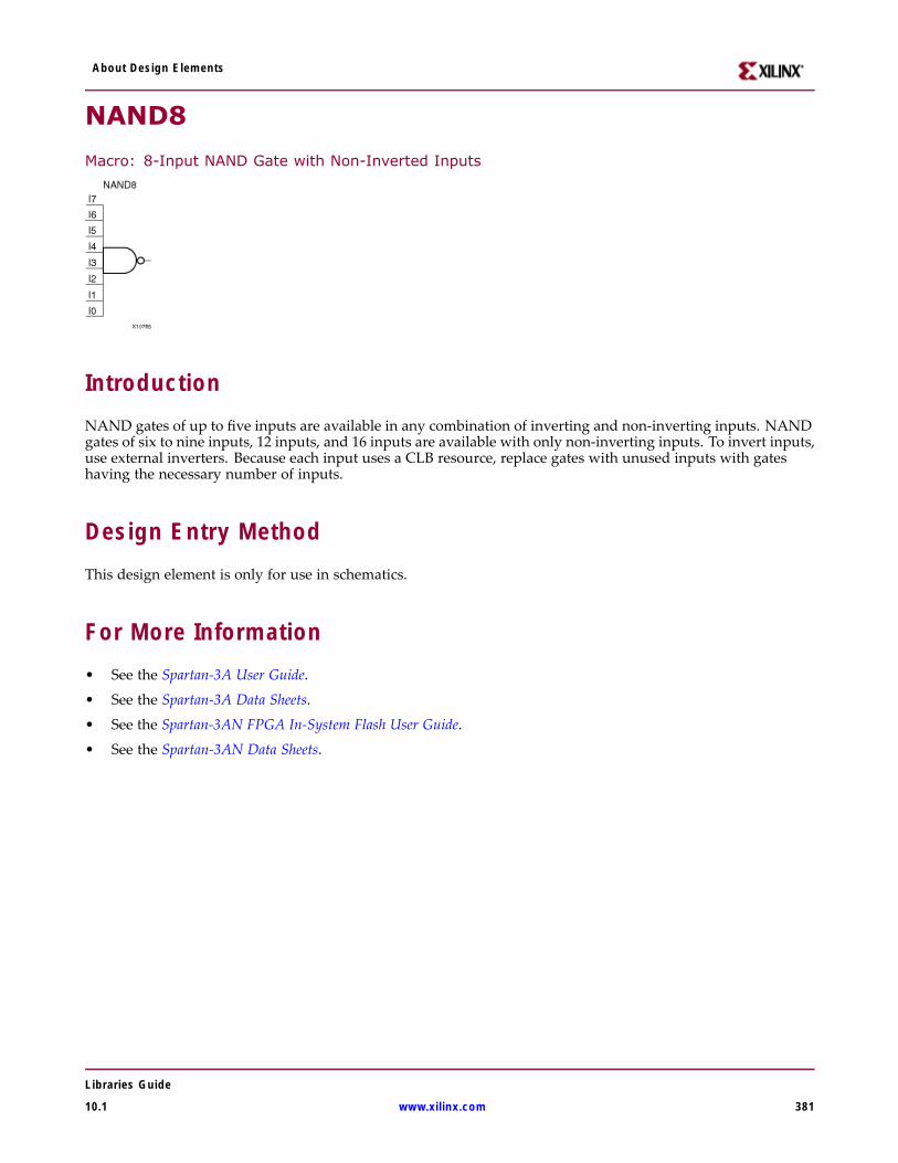
About Design Elements
NAND8
Macro: 8-Input NAND Gate with Non-Inverted Inputs
IntroductionNAND gates of up to five inputs are available in any combination of inverting and non-inverting inputs. NANDgates of six to nine inputs, 12 inputs, and 16 inputs are available with only non-inverting inputs. To invert inputs,use external inverters. Because each input uses a CLB resource, replace gates with unused inputs with gateshaving the necessary number of inputs.
Design Entry MethodThis design element is only for use in schematics.
For More Information• See the Spartan-3A User Guide.
• See the Spartan-3A Data Sheets.
• See the Spartan-3AN FPGA In-System Flash User Guide.
• See the Spartan-3AN Data Sheets.
Libraries Guide
10.1 www.xilinx.com 381
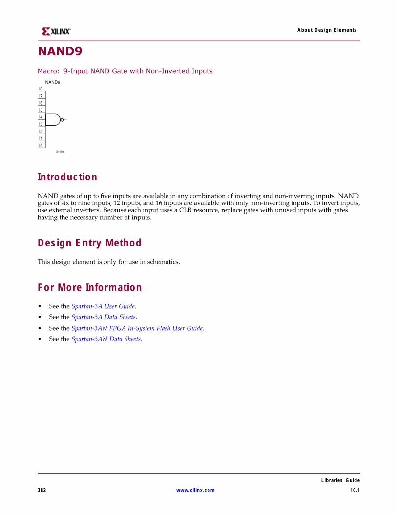
About Design Elements
NAND9
Macro: 9-Input NAND Gate with Non-Inverted Inputs
IntroductionNAND gates of up to five inputs are available in any combination of inverting and non-inverting inputs. NANDgates of six to nine inputs, 12 inputs, and 16 inputs are available with only non-inverting inputs. To invert inputs,use external inverters. Because each input uses a CLB resource, replace gates with unused inputs with gateshaving the necessary number of inputs.
Design Entry MethodThis design element is only for use in schematics.
For More Information• See the Spartan-3A User Guide.
• See the Spartan-3A Data Sheets.
• See the Spartan-3AN FPGA In-System Flash User Guide.
• See the Spartan-3AN Data Sheets.
Libraries Guide
382 www.xilinx.com 10.1
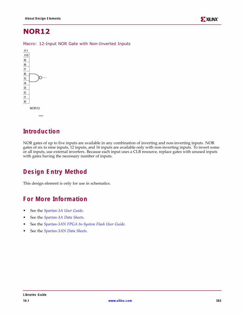
About Design Elements
NOR12
Macro: 12-Input NOR Gate with Non-Inverted Inputs
IntroductionNOR gates of up to five inputs are available in any combination of inverting and non-inverting inputs. NORgates of six to nine inputs, 12 inputs, and 16 inputs are available only with non-inverting inputs. To invert someor all inputs, use external inverters. Because each input uses a CLB resource, replace gates with unused inputswith gates having the necessary number of inputs.
Design Entry MethodThis design element is only for use in schematics.
For More Information• See the Spartan-3A User Guide.
• See the Spartan-3A Data Sheets.
• See the Spartan-3AN FPGA In-System Flash User Guide.
• See the Spartan-3AN Data Sheets.
Libraries Guide
10.1 www.xilinx.com 383
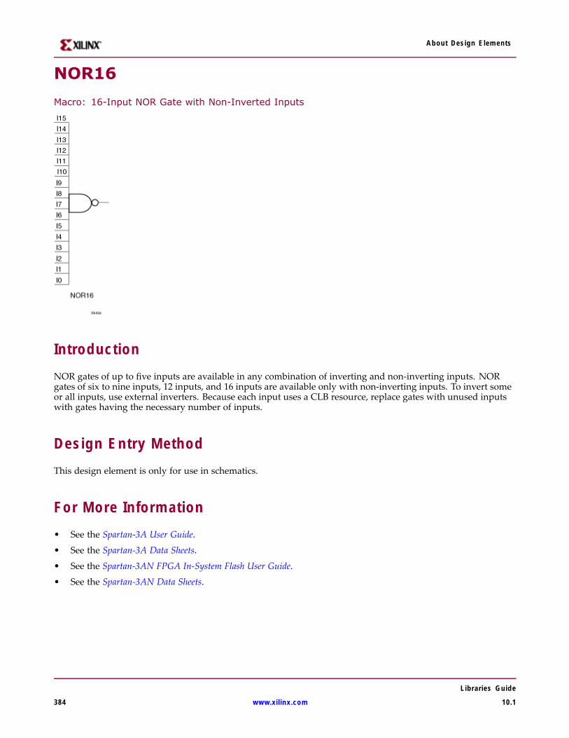
About Design Elements
NOR16
Macro: 16-Input NOR Gate with Non-Inverted Inputs
IntroductionNOR gates of up to five inputs are available in any combination of inverting and non-inverting inputs. NORgates of six to nine inputs, 12 inputs, and 16 inputs are available only with non-inverting inputs. To invert someor all inputs, use external inverters. Because each input uses a CLB resource, replace gates with unused inputswith gates having the necessary number of inputs.
Design Entry MethodThis design element is only for use in schematics.
For More Information• See the Spartan-3A User Guide.
• See the Spartan-3A Data Sheets.
• See the Spartan-3AN FPGA In-System Flash User Guide.
• See the Spartan-3AN Data Sheets.
Libraries Guide
384 www.xilinx.com 10.1
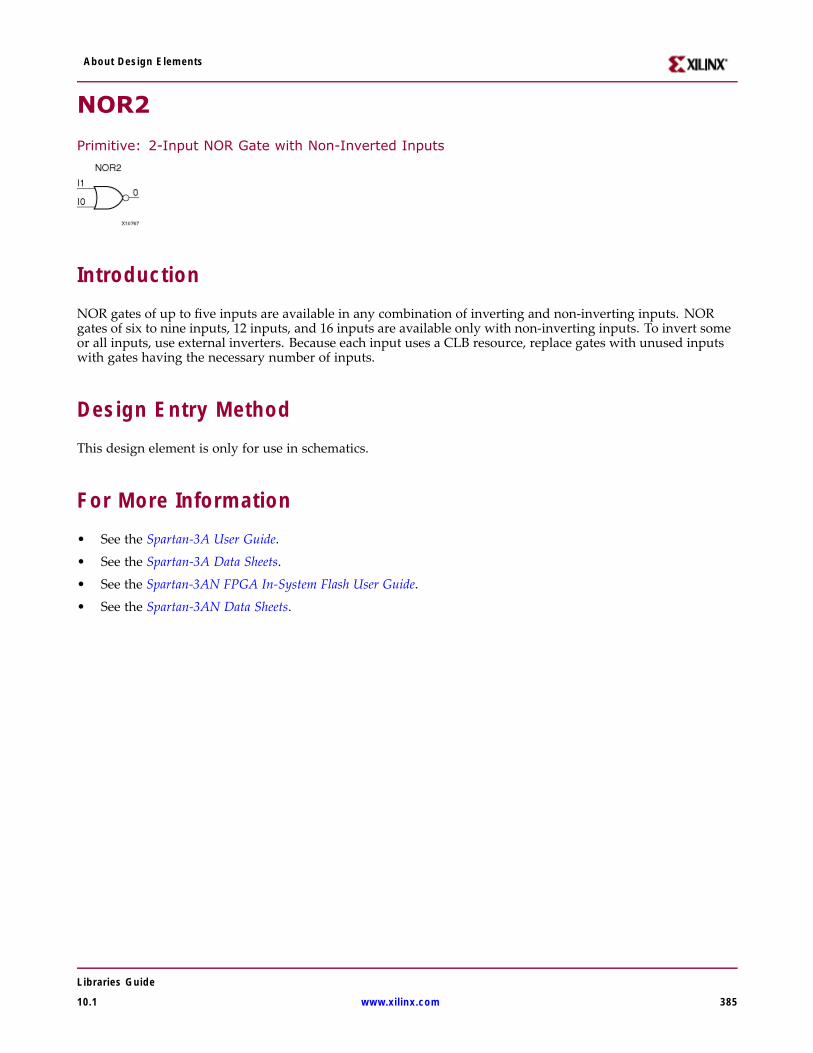
About Design Elements
NOR2
Primitive: 2-Input NOR Gate with Non-Inverted Inputs
IntroductionNOR gates of up to five inputs are available in any combination of inverting and non-inverting inputs. NORgates of six to nine inputs, 12 inputs, and 16 inputs are available only with non-inverting inputs. To invert someor all inputs, use external inverters. Because each input uses a CLB resource, replace gates with unused inputswith gates having the necessary number of inputs.
Design Entry MethodThis design element is only for use in schematics.
For More Information• See the Spartan-3A User Guide.
• See the Spartan-3A Data Sheets.
• See the Spartan-3AN FPGA In-System Flash User Guide.
• See the Spartan-3AN Data Sheets.
Libraries Guide
10.1 www.xilinx.com 385

About Design Elements
NOR2B1
Primitive: 2-Input NOR Gate with 1 Inverted and 1 Non-Inverted Inputs
IntroductionNOR gates of up to five inputs are available in any combination of inverting and non-inverting inputs. NORgates of six to nine inputs, 12 inputs, and 16 inputs are available only with non-inverting inputs. To invert someor all inputs, use external inverters. Because each input uses a CLB resource, replace gates with unused inputswith gates having the necessary number of inputs.
Design Entry MethodThis design element is only for use in schematics.
For More Information• See the Spartan-3A User Guide.
• See the Spartan-3A Data Sheets.
• See the Spartan-3AN FPGA In-System Flash User Guide.
• See the Spartan-3AN Data Sheets.
Libraries Guide
386 www.xilinx.com 10.1

About Design Elements
NOR2B2
Primitive: 2-Input NOR Gate with Inverted Inputs
IntroductionNOR gates of up to five inputs are available in any combination of inverting and non-inverting inputs. NORgates of six to nine inputs, 12 inputs, and 16 inputs are available only with non-inverting inputs. To invert someor all inputs, use external inverters. Because each input uses a CLB resource, replace gates with unused inputswith gates having the necessary number of inputs.
Design Entry MethodThis design element is only for use in schematics.
For More Information• See the Spartan-3A User Guide.
• See the Spartan-3A Data Sheets.
• See the Spartan-3AN FPGA In-System Flash User Guide.
• See the Spartan-3AN Data Sheets.
Libraries Guide
10.1 www.xilinx.com 387

About Design Elements
NOR3
Primitive: 3-Input NOR Gate with Non-Inverted Inputs
IntroductionNOR gates of up to five inputs are available in any combination of inverting and non-inverting inputs. NORgates of six to nine inputs, 12 inputs, and 16 inputs are available only with non-inverting inputs. To invert someor all inputs, use external inverters. Because each input uses a CLB resource, replace gates with unused inputswith gates having the necessary number of inputs.
Design Entry MethodThis design element is only for use in schematics.
For More Information• See the Spartan-3A User Guide.
• See the Spartan-3A Data Sheets.
• See the Spartan-3AN FPGA In-System Flash User Guide.
• See the Spartan-3AN Data Sheets.
Libraries Guide
388 www.xilinx.com 10.1

About Design Elements
NOR3B1
Primitive: 3-Input NOR Gate with 1 Inverted and 2 Non-Inverted Inputs
IntroductionNOR gates of up to five inputs are available in any combination of inverting and non-inverting inputs. NORgates of six to nine inputs, 12 inputs, and 16 inputs are available only with non-inverting inputs. To invert someor all inputs, use external inverters. Because each input uses a CLB resource, replace gates with unused inputswith gates having the necessary number of inputs.
Design Entry MethodThis design element is only for use in schematics.
For More Information• See the Spartan-3A User Guide.
• See the Spartan-3A Data Sheets.
• See the Spartan-3AN FPGA In-System Flash User Guide.
• See the Spartan-3AN Data Sheets.
Libraries Guide
10.1 www.xilinx.com 389
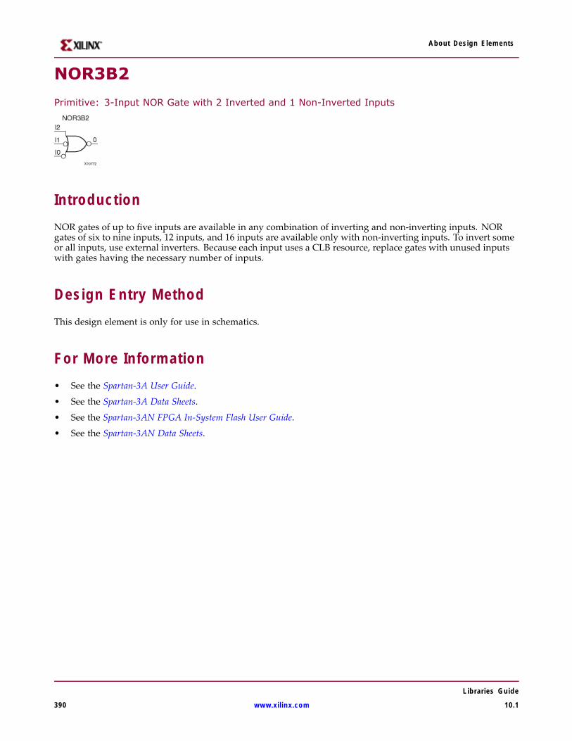
About Design Elements
NOR3B2
Primitive: 3-Input NOR Gate with 2 Inverted and 1 Non-Inverted Inputs
IntroductionNOR gates of up to five inputs are available in any combination of inverting and non-inverting inputs. NORgates of six to nine inputs, 12 inputs, and 16 inputs are available only with non-inverting inputs. To invert someor all inputs, use external inverters. Because each input uses a CLB resource, replace gates with unused inputswith gates having the necessary number of inputs.
Design Entry MethodThis design element is only for use in schematics.
For More Information• See the Spartan-3A User Guide.
• See the Spartan-3A Data Sheets.
• See the Spartan-3AN FPGA In-System Flash User Guide.
• See the Spartan-3AN Data Sheets.
Libraries Guide
390 www.xilinx.com 10.1
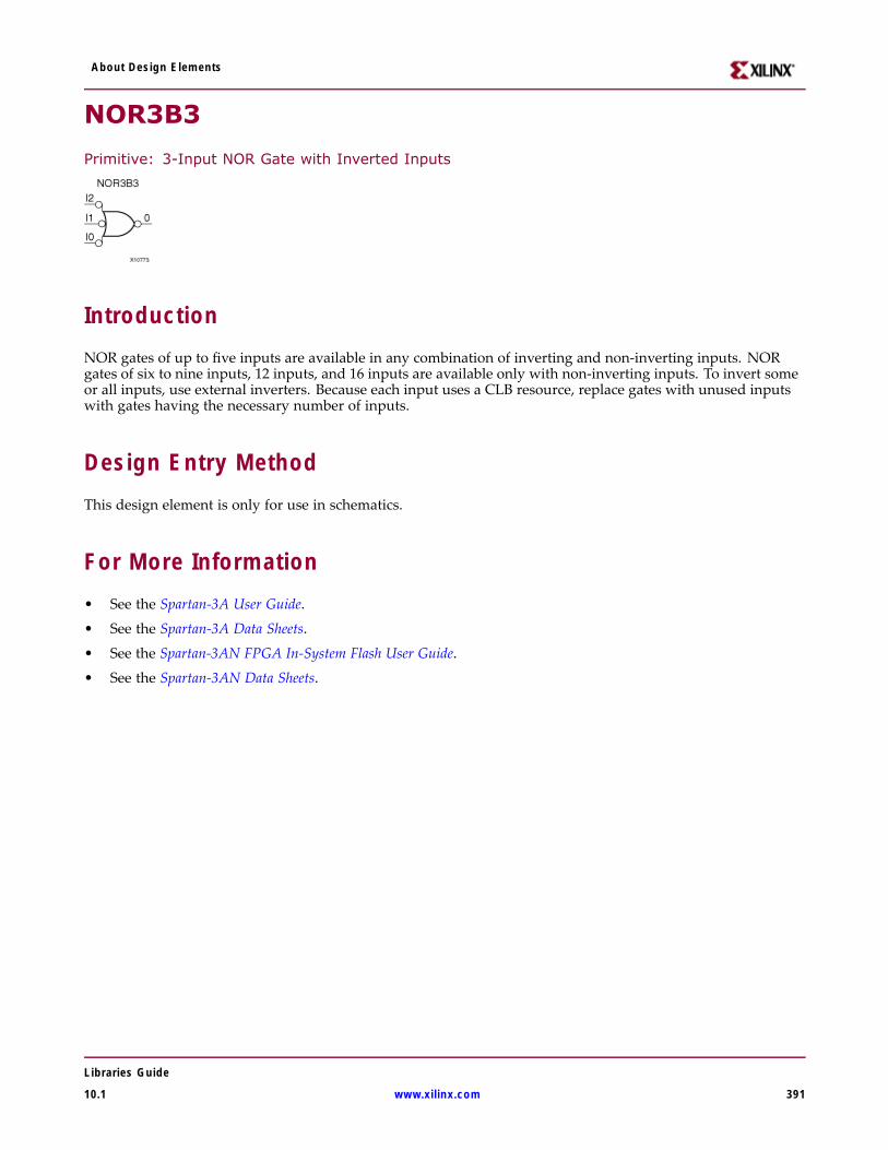
About Design Elements
NOR3B3
Primitive: 3-Input NOR Gate with Inverted Inputs
IntroductionNOR gates of up to five inputs are available in any combination of inverting and non-inverting inputs. NORgates of six to nine inputs, 12 inputs, and 16 inputs are available only with non-inverting inputs. To invert someor all inputs, use external inverters. Because each input uses a CLB resource, replace gates with unused inputswith gates having the necessary number of inputs.
Design Entry MethodThis design element is only for use in schematics.
For More Information• See the Spartan-3A User Guide.
• See the Spartan-3A Data Sheets.
• See the Spartan-3AN FPGA In-System Flash User Guide.
• See the Spartan-3AN Data Sheets.
Libraries Guide
10.1 www.xilinx.com 391
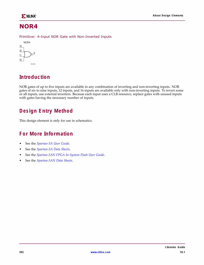
About Design Elements
NOR4
Primitive: 4-Input NOR Gate with Non-Inverted Inputs
IntroductionNOR gates of up to five inputs are available in any combination of inverting and non-inverting inputs. NORgates of six to nine inputs, 12 inputs, and 16 inputs are available only with non-inverting inputs. To invert someor all inputs, use external inverters. Because each input uses a CLB resource, replace gates with unused inputswith gates having the necessary number of inputs.
Design Entry MethodThis design element is only for use in schematics.
For More Information• See the Spartan-3A User Guide.
• See the Spartan-3A Data Sheets.
• See the Spartan-3AN FPGA In-System Flash User Guide.
• See the Spartan-3AN Data Sheets.
Libraries Guide
392 www.xilinx.com 10.1
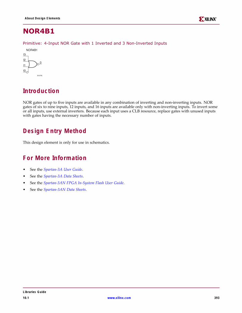
About Design Elements
NOR4B1
Primitive: 4-Input NOR Gate with 1 Inverted and 3 Non-Inverted Inputs
IntroductionNOR gates of up to five inputs are available in any combination of inverting and non-inverting inputs. NORgates of six to nine inputs, 12 inputs, and 16 inputs are available only with non-inverting inputs. To invert someor all inputs, use external inverters. Because each input uses a CLB resource, replace gates with unused inputswith gates having the necessary number of inputs.
Design Entry MethodThis design element is only for use in schematics.
For More Information• See the Spartan-3A User Guide.
• See the Spartan-3A Data Sheets.
• See the Spartan-3AN FPGA In-System Flash User Guide.
• See the Spartan-3AN Data Sheets.
Libraries Guide
10.1 www.xilinx.com 393
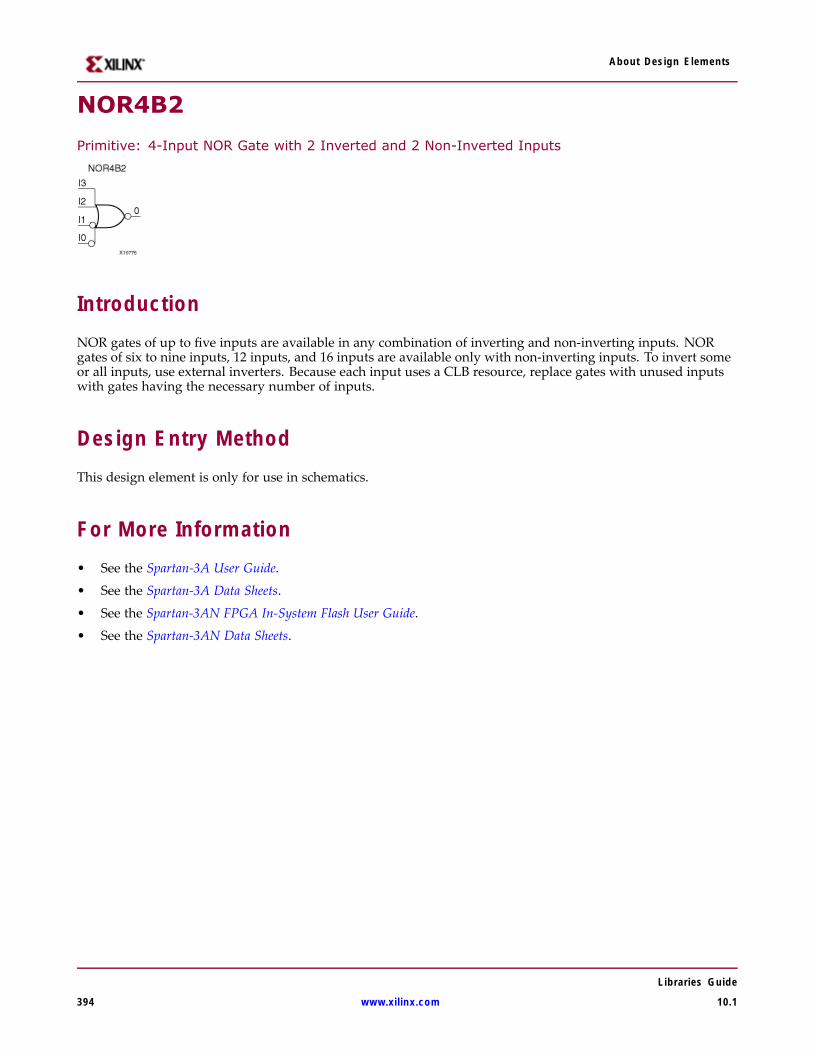
About Design Elements
NOR4B2
Primitive: 4-Input NOR Gate with 2 Inverted and 2 Non-Inverted Inputs
IntroductionNOR gates of up to five inputs are available in any combination of inverting and non-inverting inputs. NORgates of six to nine inputs, 12 inputs, and 16 inputs are available only with non-inverting inputs. To invert someor all inputs, use external inverters. Because each input uses a CLB resource, replace gates with unused inputswith gates having the necessary number of inputs.
Design Entry MethodThis design element is only for use in schematics.
For More Information• See the Spartan-3A User Guide.
• See the Spartan-3A Data Sheets.
• See the Spartan-3AN FPGA In-System Flash User Guide.
• See the Spartan-3AN Data Sheets.
Libraries Guide
394 www.xilinx.com 10.1

About Design Elements
NOR4B3
Primitive: 4-Input NOR Gate with 3 Inverted and 1 Non-Inverted Inputs
IntroductionNOR gates of up to five inputs are available in any combination of inverting and non-inverting inputs. NORgates of six to nine inputs, 12 inputs, and 16 inputs are available only with non-inverting inputs. To invert someor all inputs, use external inverters. Because each input uses a CLB resource, replace gates with unused inputswith gates having the necessary number of inputs.
Design Entry MethodThis design element is only for use in schematics.
For More Information• See the Spartan-3A User Guide.
• See the Spartan-3A Data Sheets.
• See the Spartan-3AN FPGA In-System Flash User Guide.
• See the Spartan-3AN Data Sheets.
Libraries Guide
10.1 www.xilinx.com 395
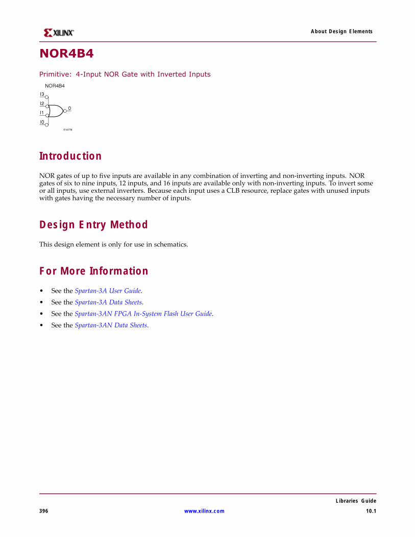
About Design Elements
NOR4B4
Primitive: 4-Input NOR Gate with Inverted Inputs
IntroductionNOR gates of up to five inputs are available in any combination of inverting and non-inverting inputs. NORgates of six to nine inputs, 12 inputs, and 16 inputs are available only with non-inverting inputs. To invert someor all inputs, use external inverters. Because each input uses a CLB resource, replace gates with unused inputswith gates having the necessary number of inputs.
Design Entry MethodThis design element is only for use in schematics.
For More Information• See the Spartan-3A User Guide.
• See the Spartan-3A Data Sheets.
• See the Spartan-3AN FPGA In-System Flash User Guide.
• See the Spartan-3AN Data Sheets.
Libraries Guide
396 www.xilinx.com 10.1
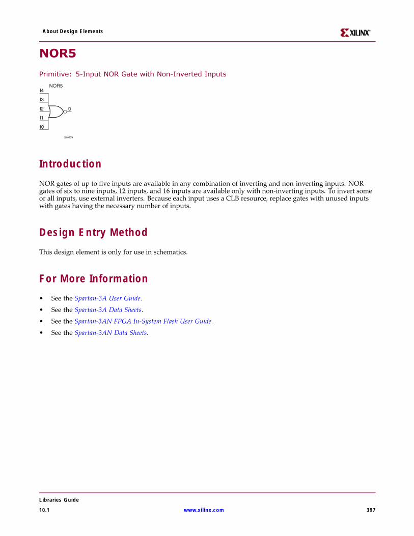
About Design Elements
NOR5
Primitive: 5-Input NOR Gate with Non-Inverted Inputs
IntroductionNOR gates of up to five inputs are available in any combination of inverting and non-inverting inputs. NORgates of six to nine inputs, 12 inputs, and 16 inputs are available only with non-inverting inputs. To invert someor all inputs, use external inverters. Because each input uses a CLB resource, replace gates with unused inputswith gates having the necessary number of inputs.
Design Entry MethodThis design element is only for use in schematics.
For More Information• See the Spartan-3A User Guide.
• See the Spartan-3A Data Sheets.
• See the Spartan-3AN FPGA In-System Flash User Guide.
• See the Spartan-3AN Data Sheets.
Libraries Guide
10.1 www.xilinx.com 397
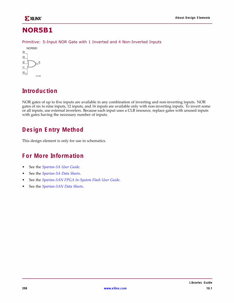
About Design Elements
NOR5B1
Primitive: 5-Input NOR Gate with 1 Inverted and 4 Non-Inverted Inputs
IntroductionNOR gates of up to five inputs are available in any combination of inverting and non-inverting inputs. NORgates of six to nine inputs, 12 inputs, and 16 inputs are available only with non-inverting inputs. To invert someor all inputs, use external inverters. Because each input uses a CLB resource, replace gates with unused inputswith gates having the necessary number of inputs.
Design Entry MethodThis design element is only for use in schematics.
For More Information• See the Spartan-3A User Guide.
• See the Spartan-3A Data Sheets.
• See the Spartan-3AN FPGA In-System Flash User Guide.
• See the Spartan-3AN Data Sheets.
Libraries Guide
398 www.xilinx.com 10.1

About Design Elements
NOR5B2
Primitive: 5-Input NOR Gate with 2 Inverted and 3 Non-Inverted Inputs
IntroductionNOR gates of up to five inputs are available in any combination of inverting and non-inverting inputs. NORgates of six to nine inputs, 12 inputs, and 16 inputs are available only with non-inverting inputs. To invert someor all inputs, use external inverters. Because each input uses a CLB resource, replace gates with unused inputswith gates having the necessary number of inputs.
Design Entry MethodThis design element is only for use in schematics.
For More Information• See the Spartan-3A User Guide.
• See the Spartan-3A Data Sheets.
• See the Spartan-3AN FPGA In-System Flash User Guide.
• See the Spartan-3AN Data Sheets.
Libraries Guide
10.1 www.xilinx.com 399

About Design Elements
NOR5B3
Primitive: 5-Input NOR Gate with 3 Inverted and 2 Non-Inverted Inputs
IntroductionNOR gates of up to five inputs are available in any combination of inverting and non-inverting inputs. NORgates of six to nine inputs, 12 inputs, and 16 inputs are available only with non-inverting inputs. To invert someor all inputs, use external inverters. Because each input uses a CLB resource, replace gates with unused inputswith gates having the necessary number of inputs.
Design Entry MethodThis design element is only for use in schematics.
For More Information• See the Spartan-3A User Guide.
• See the Spartan-3A Data Sheets.
• See the Spartan-3AN FPGA In-System Flash User Guide.
• See the Spartan-3AN Data Sheets.
Libraries Guide
400 www.xilinx.com 10.1
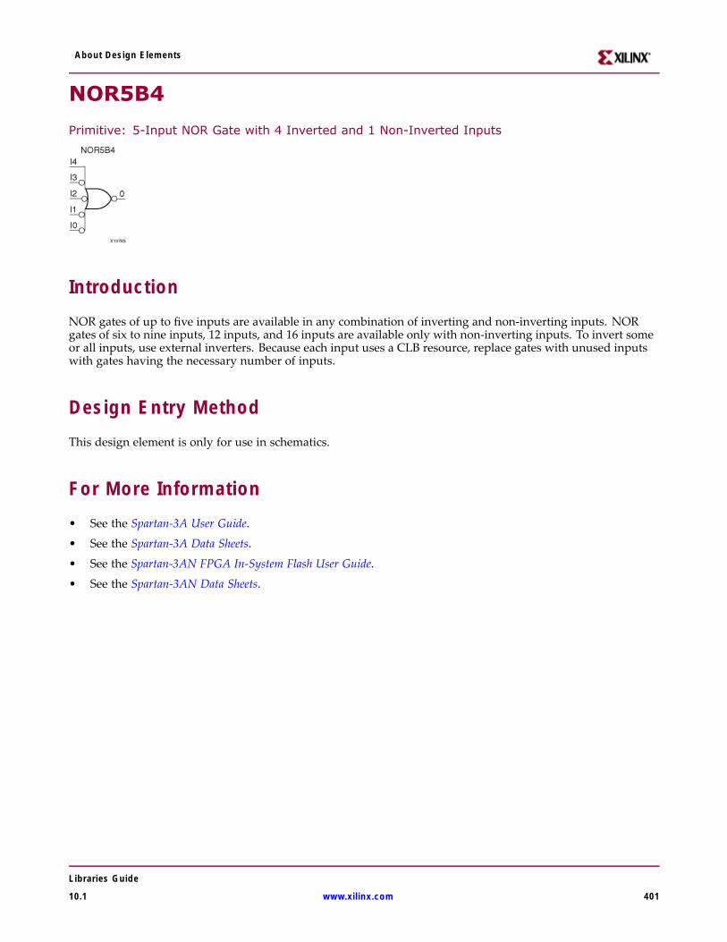
About Design Elements
NOR5B4
Primitive: 5-Input NOR Gate with 4 Inverted and 1 Non-Inverted Inputs
IntroductionNOR gates of up to five inputs are available in any combination of inverting and non-inverting inputs. NORgates of six to nine inputs, 12 inputs, and 16 inputs are available only with non-inverting inputs. To invert someor all inputs, use external inverters. Because each input uses a CLB resource, replace gates with unused inputswith gates having the necessary number of inputs.
Design Entry MethodThis design element is only for use in schematics.
For More Information• See the Spartan-3A User Guide.
• See the Spartan-3A Data Sheets.
• See the Spartan-3AN FPGA In-System Flash User Guide.
• See the Spartan-3AN Data Sheets.
Libraries Guide
10.1 www.xilinx.com 401
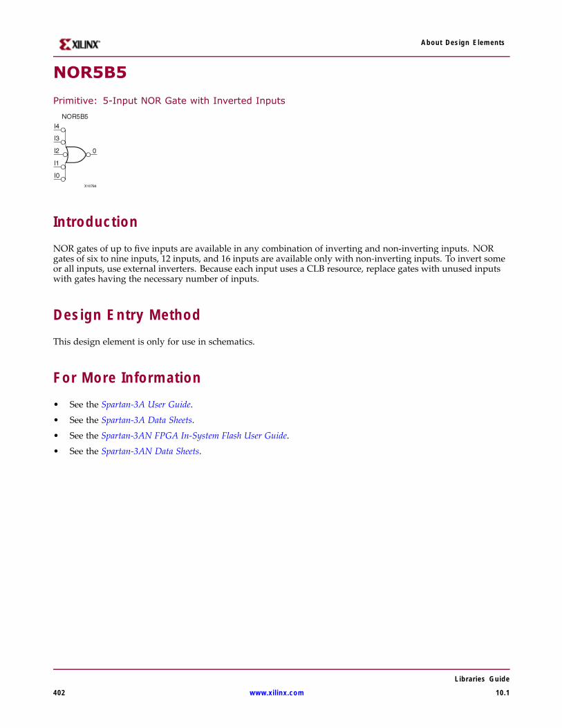
About Design Elements
NOR5B5
Primitive: 5-Input NOR Gate with Inverted Inputs
IntroductionNOR gates of up to five inputs are available in any combination of inverting and non-inverting inputs. NORgates of six to nine inputs, 12 inputs, and 16 inputs are available only with non-inverting inputs. To invert someor all inputs, use external inverters. Because each input uses a CLB resource, replace gates with unused inputswith gates having the necessary number of inputs.
Design Entry MethodThis design element is only for use in schematics.
For More Information• See the Spartan-3A User Guide.
• See the Spartan-3A Data Sheets.
• See the Spartan-3AN FPGA In-System Flash User Guide.
• See the Spartan-3AN Data Sheets.
Libraries Guide
402 www.xilinx.com 10.1
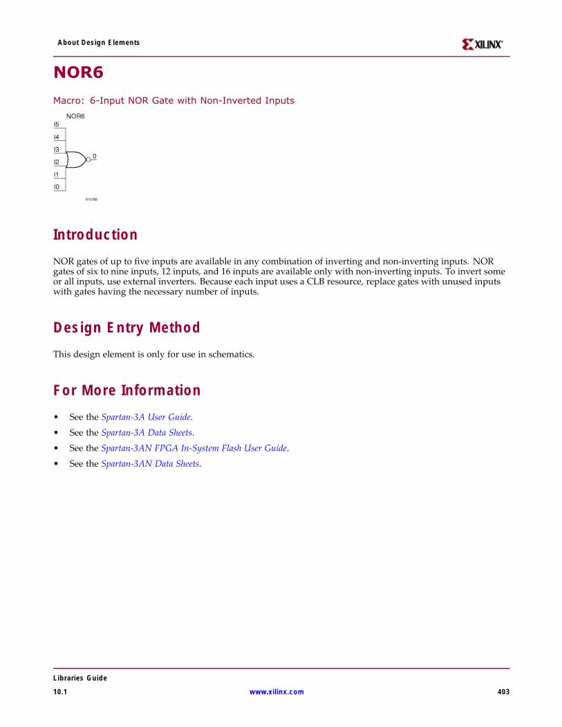
About Design Elements
NOR6
Macro: 6-Input NOR Gate with Non-Inverted Inputs
IntroductionNOR gates of up to five inputs are available in any combination of inverting and non-inverting inputs. NORgates of six to nine inputs, 12 inputs, and 16 inputs are available only with non-inverting inputs. To invert someor all inputs, use external inverters. Because each input uses a CLB resource, replace gates with unused inputswith gates having the necessary number of inputs.
Design Entry MethodThis design element is only for use in schematics.
For More Information• See the Spartan-3A User Guide.
• See the Spartan-3A Data Sheets.
• See the Spartan-3AN FPGA In-System Flash User Guide.
• See the Spartan-3AN Data Sheets.
Libraries Guide
10.1 www.xilinx.com 403
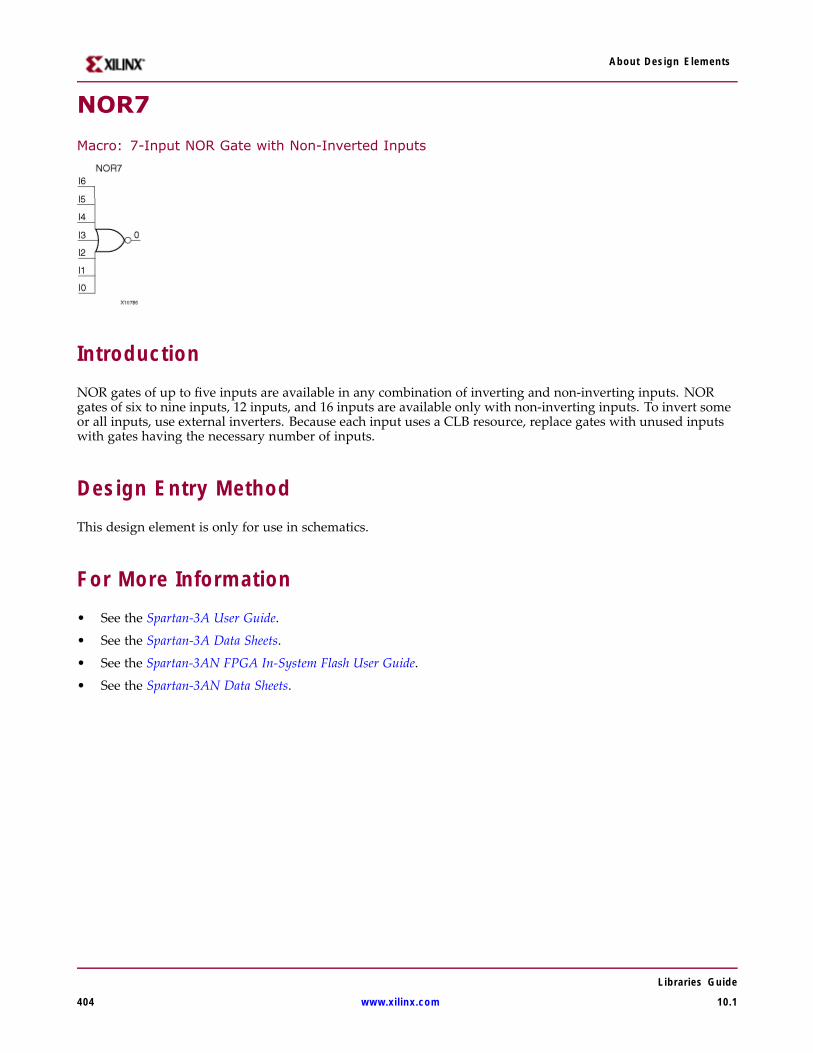
About Design Elements
NOR7
Macro: 7-Input NOR Gate with Non-Inverted Inputs
IntroductionNOR gates of up to five inputs are available in any combination of inverting and non-inverting inputs. NORgates of six to nine inputs, 12 inputs, and 16 inputs are available only with non-inverting inputs. To invert someor all inputs, use external inverters. Because each input uses a CLB resource, replace gates with unused inputswith gates having the necessary number of inputs.
Design Entry MethodThis design element is only for use in schematics.
For More Information• See the Spartan-3A User Guide.
• See the Spartan-3A Data Sheets.
• See the Spartan-3AN FPGA In-System Flash User Guide.
• See the Spartan-3AN Data Sheets.
Libraries Guide
404 www.xilinx.com 10.1
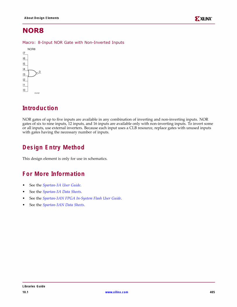
About Design Elements
NOR8
Macro: 8-Input NOR Gate with Non-Inverted Inputs
IntroductionNOR gates of up to five inputs are available in any combination of inverting and non-inverting inputs. NORgates of six to nine inputs, 12 inputs, and 16 inputs are available only with non-inverting inputs. To invert someor all inputs, use external inverters. Because each input uses a CLB resource, replace gates with unused inputswith gates having the necessary number of inputs.
Design Entry MethodThis design element is only for use in schematics.
For More Information• See the Spartan-3A User Guide.
• See the Spartan-3A Data Sheets.
• See the Spartan-3AN FPGA In-System Flash User Guide.
• See the Spartan-3AN Data Sheets.
Libraries Guide
10.1 www.xilinx.com 405
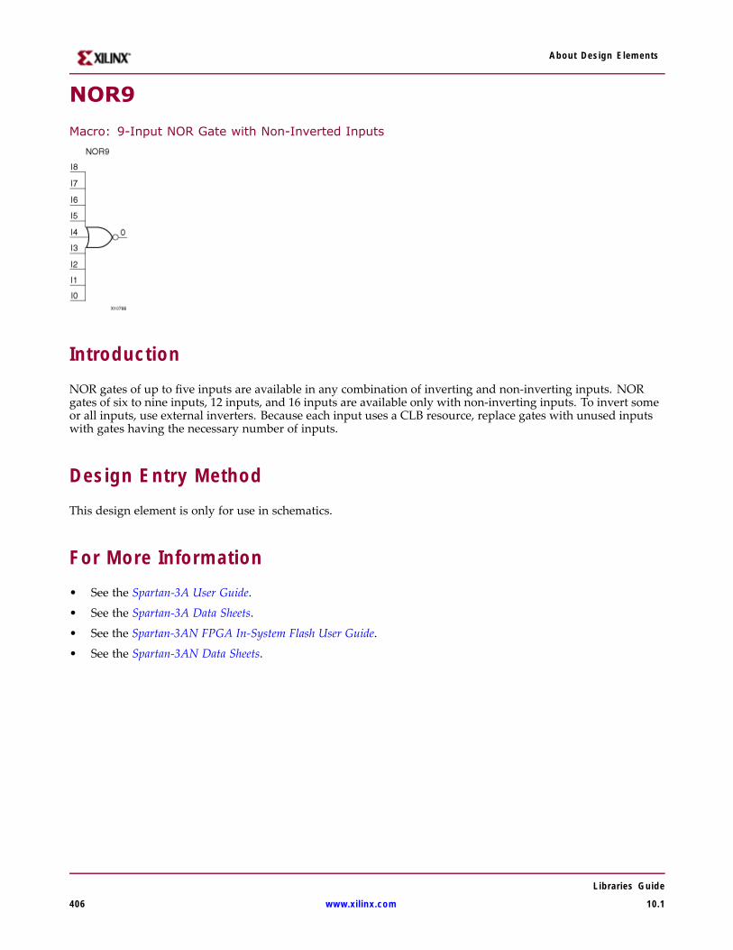
About Design Elements
NOR9
Macro: 9-Input NOR Gate with Non-Inverted Inputs
IntroductionNOR gates of up to five inputs are available in any combination of inverting and non-inverting inputs. NORgates of six to nine inputs, 12 inputs, and 16 inputs are available only with non-inverting inputs. To invert someor all inputs, use external inverters. Because each input uses a CLB resource, replace gates with unused inputswith gates having the necessary number of inputs.
Design Entry MethodThis design element is only for use in schematics.
For More Information• See the Spartan-3A User Guide.
• See the Spartan-3A Data Sheets.
• See the Spartan-3AN FPGA In-System Flash User Guide.
• See the Spartan-3AN Data Sheets.
Libraries Guide
406 www.xilinx.com 10.1
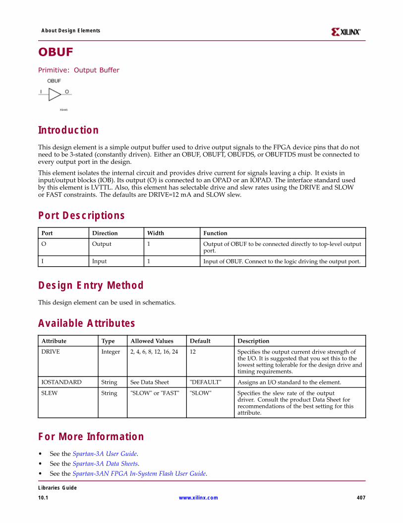
About Design Elements
OBUFPrimitive: Output Buffer
IntroductionThis design element is a simple output buffer used to drive output signals to the FPGA device pins that do notneed to be 3-stated (constantly driven). Either an OBUF, OBUFT, OBUFDS, or OBUFTDS must be connected toevery output port in the design.
This element isolates the internal circuit and provides drive current for signals leaving a chip. It exists ininput/output blocks (IOB). Its output (O) is connected to an OPAD or an IOPAD. The interface standard usedby this element is LVTTL. Also, this element has selectable drive and slew rates using the DRIVE and SLOWor FAST constraints. The defaults are DRIVE=12 mA and SLOW slew.
Port DescriptionsPort Direction Width Function
O Output 1 Output of OBUF to be connected directly to top-level outputport.
I Input 1 Input of OBUF. Connect to the logic driving the output port.
Design Entry MethodThis design element can be used in schematics.
Available AttributesAttribute Type Allowed Values Default Description
DRIVE Integer 2, 4, 6, 8, 12, 16, 24 12 Specifies the output current drive strength ofthe I/O. It is suggested that you set this to thelowest setting tolerable for the design drive andtiming requirements.
IOSTANDARD String See Data Sheet "DEFAULT" Assigns an I/O standard to the element.
SLEW String "SLOW" or "FAST" "SLOW" Specifies the slew rate of the outputdriver. Consult the product Data Sheet forrecommendations of the best setting for thisattribute.
For More Information• See the Spartan-3A User Guide.• See the Spartan-3A Data Sheets.• See the Spartan-3AN FPGA In-System Flash User Guide.
Libraries Guide
10.1 www.xilinx.com 407

About Design Elements
• See the Spartan-3AN Data Sheets.
Libraries Guide
408 www.xilinx.com 10.1
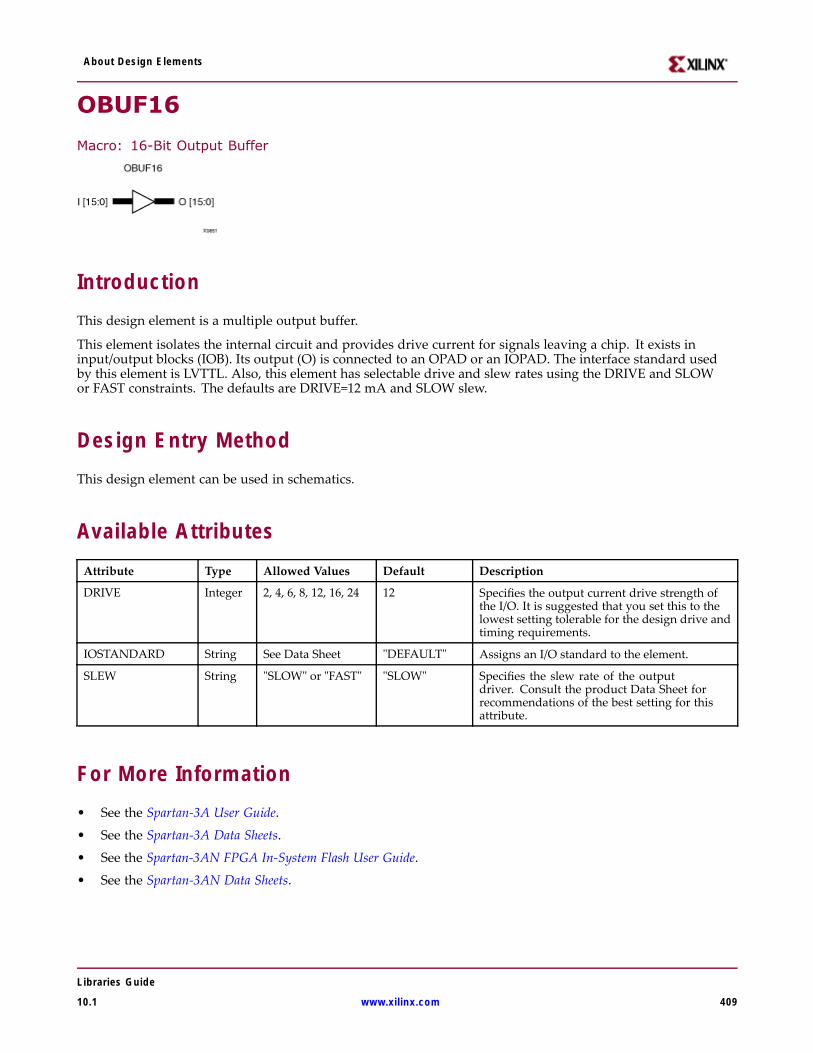
About Design Elements
OBUF16
Macro: 16-Bit Output Buffer
IntroductionThis design element is a multiple output buffer.
This element isolates the internal circuit and provides drive current for signals leaving a chip. It exists ininput/output blocks (IOB). Its output (O) is connected to an OPAD or an IOPAD. The interface standard usedby this element is LVTTL. Also, this element has selectable drive and slew rates using the DRIVE and SLOWor FAST constraints. The defaults are DRIVE=12 mA and SLOW slew.
Design Entry MethodThis design element can be used in schematics.
Available AttributesAttribute Type Allowed Values Default Description
DRIVE Integer 2, 4, 6, 8, 12, 16, 24 12 Specifies the output current drive strength ofthe I/O. It is suggested that you set this to thelowest setting tolerable for the design drive andtiming requirements.
IOSTANDARD String See Data Sheet "DEFAULT" Assigns an I/O standard to the element.
SLEW String "SLOW" or "FAST" "SLOW" Specifies the slew rate of the outputdriver. Consult the product Data Sheet forrecommendations of the best setting for thisattribute.
For More Information• See the Spartan-3A User Guide.
• See the Spartan-3A Data Sheets.
• See the Spartan-3AN FPGA In-System Flash User Guide.
• See the Spartan-3AN Data Sheets.
Libraries Guide
10.1 www.xilinx.com 409
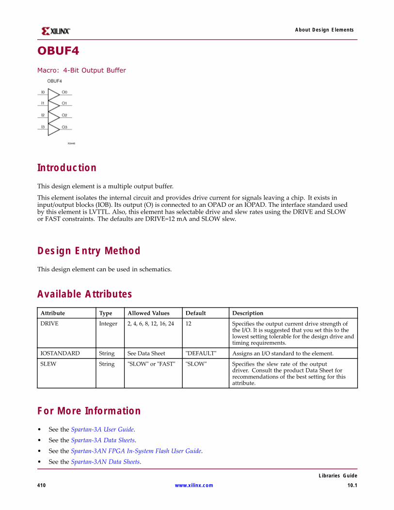
About Design Elements
OBUF4
Macro: 4-Bit Output Buffer
IntroductionThis design element is a multiple output buffer.
This element isolates the internal circuit and provides drive current for signals leaving a chip. It exists ininput/output blocks (IOB). Its output (O) is connected to an OPAD or an IOPAD. The interface standard usedby this element is LVTTL. Also, this element has selectable drive and slew rates using the DRIVE and SLOWor FAST constraints. The defaults are DRIVE=12 mA and SLOW slew.
Design Entry MethodThis design element can be used in schematics.
Available AttributesAttribute Type Allowed Values Default Description
DRIVE Integer 2, 4, 6, 8, 12, 16, 24 12 Specifies the output current drive strength ofthe I/O. It is suggested that you set this to thelowest setting tolerable for the design drive andtiming requirements.
IOSTANDARD String See Data Sheet "DEFAULT" Assigns an I/O standard to the element.
SLEW String "SLOW" or "FAST" "SLOW" Specifies the slew rate of the outputdriver. Consult the product Data Sheet forrecommendations of the best setting for thisattribute.
For More Information• See the Spartan-3A User Guide.
• See the Spartan-3A Data Sheets.
• See the Spartan-3AN FPGA In-System Flash User Guide.
• See the Spartan-3AN Data Sheets.
Libraries Guide
410 www.xilinx.com 10.1
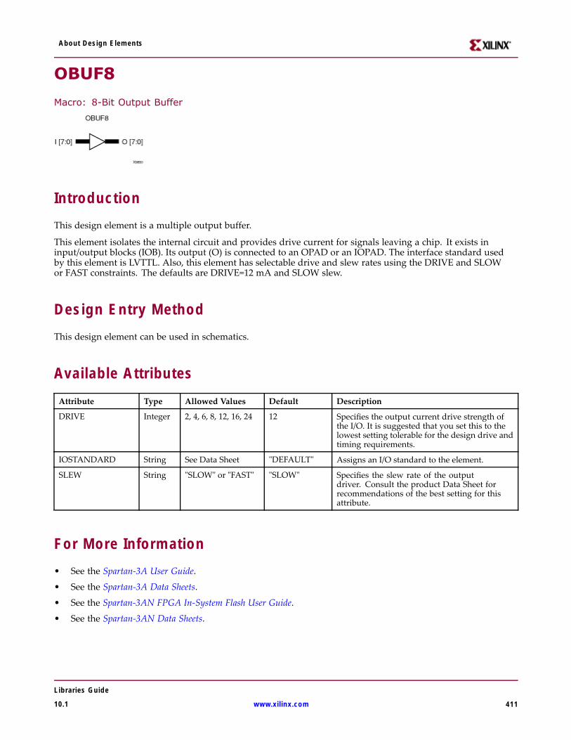
About Design Elements
OBUF8
Macro: 8-Bit Output Buffer
IntroductionThis design element is a multiple output buffer.
This element isolates the internal circuit and provides drive current for signals leaving a chip. It exists ininput/output blocks (IOB). Its output (O) is connected to an OPAD or an IOPAD. The interface standard usedby this element is LVTTL. Also, this element has selectable drive and slew rates using the DRIVE and SLOWor FAST constraints. The defaults are DRIVE=12 mA and SLOW slew.
Design Entry MethodThis design element can be used in schematics.
Available AttributesAttribute Type Allowed Values Default Description
DRIVE Integer 2, 4, 6, 8, 12, 16, 24 12 Specifies the output current drive strength ofthe I/O. It is suggested that you set this to thelowest setting tolerable for the design drive andtiming requirements.
IOSTANDARD String See Data Sheet "DEFAULT" Assigns an I/O standard to the element.
SLEW String "SLOW" or "FAST" "SLOW" Specifies the slew rate of the outputdriver. Consult the product Data Sheet forrecommendations of the best setting for thisattribute.
For More Information• See the Spartan-3A User Guide.
• See the Spartan-3A Data Sheets.
• See the Spartan-3AN FPGA In-System Flash User Guide.
• See the Spartan-3AN Data Sheets.
Libraries Guide
10.1 www.xilinx.com 411
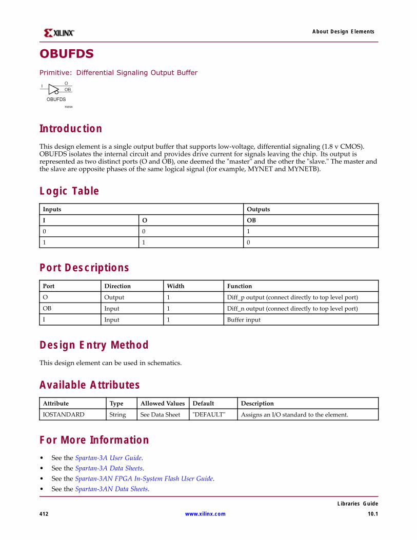
About Design Elements
OBUFDSPrimitive: Differential Signaling Output Buffer
IntroductionThis design element is a single output buffer that supports low-voltage, differential signaling (1.8 v CMOS).OBUFDS isolates the internal circuit and provides drive current for signals leaving the chip. Its output isrepresented as two distinct ports (O and OB), one deemed the "master" and the other the "slave." The master andthe slave are opposite phases of the same logical signal (for example, MYNET and MYNETB).
Logic TableInputs Outputs
I O OB
0 0 1
1 1 0
Port DescriptionsPort Direction Width Function
O Output 1 Diff_p output (connect directly to top level port)
OB Input 1 Diff_n output (connect directly to top level port)
I Input 1 Buffer input
Design Entry MethodThis design element can be used in schematics.
Available AttributesAttribute Type Allowed Values Default Description
IOSTANDARD String See Data Sheet "DEFAULT" Assigns an I/O standard to the element.
For More Information• See the Spartan-3A User Guide.• See the Spartan-3A Data Sheets.• See the Spartan-3AN FPGA In-System Flash User Guide.• See the Spartan-3AN Data Sheets.
Libraries Guide
412 www.xilinx.com 10.1
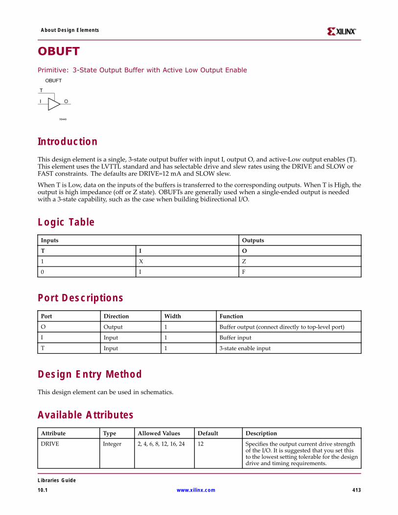
About Design Elements
OBUFT
Primitive: 3-State Output Buffer with Active Low Output Enable
IntroductionThis design element is a single, 3-state output buffer with input I, output O, and active-Low output enables (T).This element uses the LVTTL standard and has selectable drive and slew rates using the DRIVE and SLOW orFAST constraints. The defaults are DRIVE=12 mA and SLOW slew.
When T is Low, data on the inputs of the buffers is transferred to the corresponding outputs. When T is High, theoutput is high impedance (off or Z state). OBUFTs are generally used when a single-ended output is neededwith a 3-state capability, such as the case when building bidirectional I/O.
Logic TableInputs Outputs
T I O
1 X Z
0 I F
Port DescriptionsPort Direction Width Function
O Output 1 Buffer output (connect directly to top-level port)
I Input 1 Buffer input
T Input 1 3-state enable input
Design Entry MethodThis design element can be used in schematics.
Available AttributesAttribute Type Allowed Values Default Description
DRIVE Integer 2, 4, 6, 8, 12, 16, 24 12 Specifies the output current drive strengthof the I/O. It is suggested that you set thisto the lowest setting tolerable for the designdrive and timing requirements.
Libraries Guide
10.1 www.xilinx.com 413
About Design Elements
Attribute Type Allowed Values Default Description
IOSTANDARD String See Data Sheet "DEFAULT" Assigns an I/O standard to the element.
SLEW String "SLOW" or "FAST” "SLOW" Specifies the slew rate of the output driver.See the Data Sheet for recommendations ofthe best setting for this attribute.
For More Information• See the Spartan-3A User Guide.
• See the Spartan-3A Data Sheets.
• See the Spartan-3AN FPGA In-System Flash User Guide.
• See the Spartan-3AN Data Sheets.
Libraries Guide
414 www.xilinx.com 10.1
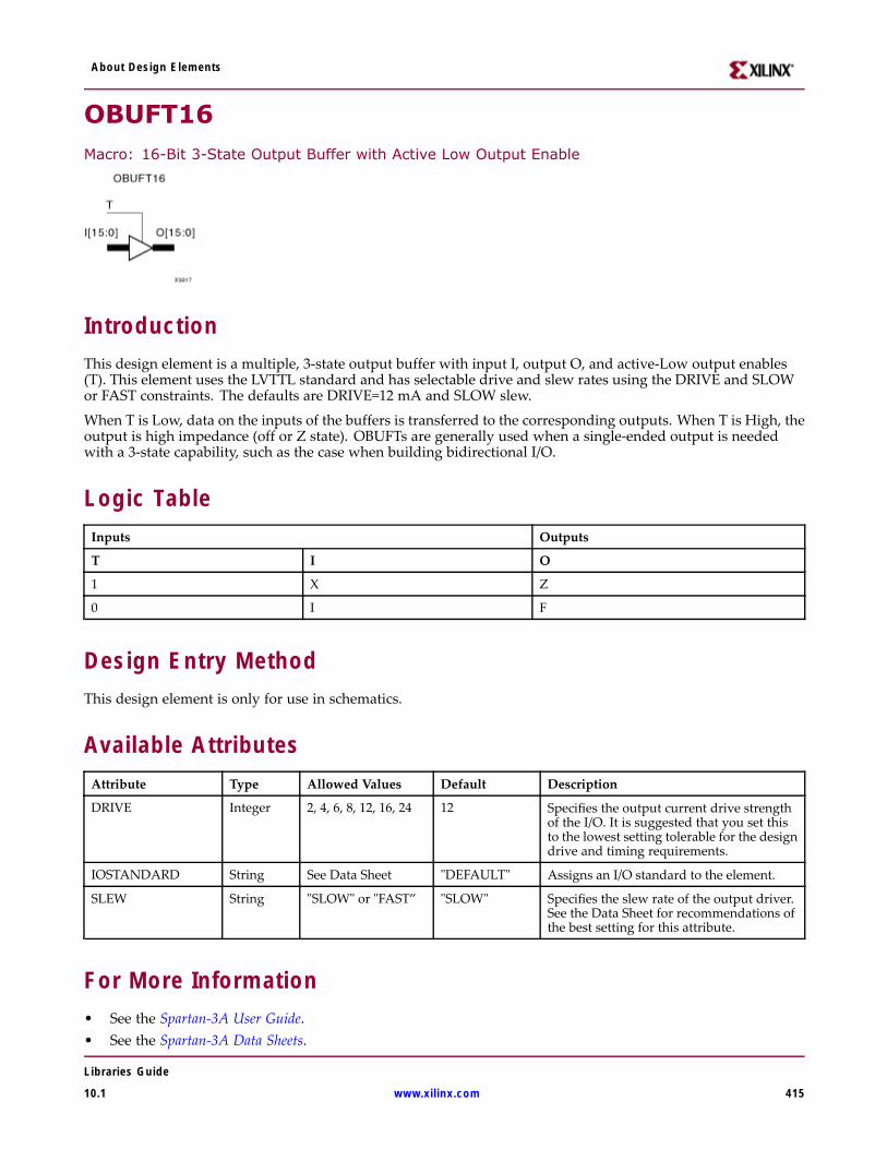
About Design Elements
OBUFT16Macro: 16-Bit 3-State Output Buffer with Active Low Output Enable
IntroductionThis design element is a multiple, 3-state output buffer with input I, output O, and active-Low output enables(T). This element uses the LVTTL standard and has selectable drive and slew rates using the DRIVE and SLOWor FAST constraints. The defaults are DRIVE=12 mA and SLOW slew.
When T is Low, data on the inputs of the buffers is transferred to the corresponding outputs. When T is High, theoutput is high impedance (off or Z state). OBUFTs are generally used when a single-ended output is neededwith a 3-state capability, such as the case when building bidirectional I/O.
Logic TableInputs Outputs
T I O
1 X Z
0 I F
Design Entry MethodThis design element is only for use in schematics.
Available AttributesAttribute Type Allowed Values Default Description
DRIVE Integer 2, 4, 6, 8, 12, 16, 24 12 Specifies the output current drive strengthof the I/O. It is suggested that you set thisto the lowest setting tolerable for the designdrive and timing requirements.
IOSTANDARD String See Data Sheet "DEFAULT" Assigns an I/O standard to the element.
SLEW String "SLOW" or "FAST” "SLOW" Specifies the slew rate of the output driver.See the Data Sheet for recommendations ofthe best setting for this attribute.
For More Information• See the Spartan-3A User Guide.• See the Spartan-3A Data Sheets.
Libraries Guide
10.1 www.xilinx.com 415
About Design Elements
• See the Spartan-3AN FPGA In-System Flash User Guide.
• See the Spartan-3AN Data Sheets.
Libraries Guide
416 www.xilinx.com 10.1
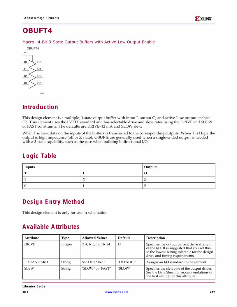
About Design Elements
OBUFT4
Macro: 4-Bit 3-State Output Buffers with Active-Low Output Enable
IntroductionThis design element is a multiple, 3-state output buffer with input I, output O, and active-Low output enables(T). This element uses the LVTTL standard and has selectable drive and slew rates using the DRIVE and SLOWor FAST constraints. The defaults are DRIVE=12 mA and SLOW slew.
When T is Low, data on the inputs of the buffers is transferred to the corresponding outputs. When T is High, theoutput is high impedance (off or Z state). OBUFTs are generally used when a single-ended output is neededwith a 3-state capability, such as the case when building bidirectional I/O.
Logic TableInputs Outputs
T I O
1 X Z
0 I F
Design Entry MethodThis design element is only for use in schematics.
Available AttributesAttribute Type Allowed Values Default Description
DRIVE Integer 2, 4, 6, 8, 12, 16, 24 12 Specifies the output current drive strengthof the I/O. It is suggested that you set thisto the lowest setting tolerable for the designdrive and timing requirements.
IOSTANDARD String See Data Sheet "DEFAULT" Assigns an I/O standard to the element.
SLEW String "SLOW" or "FAST” "SLOW" Specifies the slew rate of the output driver.See the Data Sheet for recommendations ofthe best setting for this attribute.
Libraries Guide
10.1 www.xilinx.com 417

About Design Elements
For More Information• See the Spartan-3A User Guide.
• See the Spartan-3A Data Sheets.
• See the Spartan-3AN FPGA In-System Flash User Guide.
• See the Spartan-3AN Data Sheets.
Libraries Guide
418 www.xilinx.com 10.1

About Design Elements
OBUFT8Macro: 8-Bit 3-State Output Buffers with Active-Low Output Enable
IntroductionThis design element is a multiple, 3-state output buffer with input I, output O, and active-Low output enables(T). This element uses the LVTTL standard and has selectable drive and slew rates using the DRIVE and SLOWor FAST constraints. The defaults are DRIVE=12 mA and SLOW slew.
When T is Low, data on the inputs of the buffers is transferred to the corresponding outputs. When T is High, theoutput is high impedance (off or Z state). OBUFTs are generally used when a single-ended output is neededwith a 3-state capability, such as the case when building bidirectional I/O.
Logic TableInputs Outputs
T I O
1 X Z
0 I F
Design Entry MethodThis design element is only for use in schematics.
Available AttributesAttribute Type Allowed Values Default Description
DRIVE Integer 2, 4, 6, 8, 12, 16, 24 12 Specifies the output current drive strengthof the I/O. It is suggested that you set thisto the lowest setting tolerable for the designdrive and timing requirements.
IOSTANDARD String See Data Sheet "DEFAULT" Assigns an I/O standard to the element.
SLEW String "SLOW" or "FAST” "SLOW" Specifies the slew rate of the output driver.See the Data Sheet for recommendations ofthe best setting for this attribute.
For More Information• See the Spartan-3A User Guide.• See the Spartan-3A Data Sheets.
Libraries Guide
10.1 www.xilinx.com 419

About Design Elements
• See the Spartan-3AN FPGA In-System Flash User Guide.
• See the Spartan-3AN Data Sheets.
Libraries Guide
420 www.xilinx.com 10.1
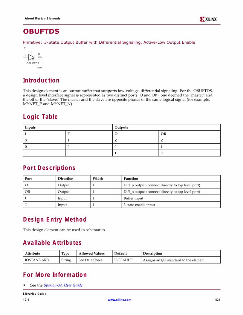
About Design Elements
OBUFTDSPrimitive: 3-State Output Buffer with Differential Signaling, Active-Low Output Enable
IntroductionThis design element is an output buffer that supports low-voltage, differential signaling. For the OBUFTDS,a design level interface signal is represented as two distinct ports (O and OB), one deemed the "master" andthe other the "slave." The master and the slave are opposite phases of the same logical signal (for example,MYNET_P and MYNET_N).
Logic TableInputs Outputs
I T O OB
X 1 Z Z
0 0 0 1
1 0 1 0
Port DescriptionsPort Direction Width Function
O Output 1 Diff_p output (connect directly to top level port)
OB Output 1 Diff_n output (connect directly to top level port)
I Input 1 Buffer input
T Input 1 3-state enable input
Design Entry MethodThis design element can be used in schematics.
Available AttributesAttribute Type Allowed Values Default Description
IOSTANDARD String See Data Sheet "DEFAULT" Assigns an I/O standard to the element.
For More Information• See the Spartan-3A User Guide.
Libraries Guide
10.1 www.xilinx.com 421

About Design Elements
• See the Spartan-3A Data Sheets.
• See the Spartan-3AN FPGA In-System Flash User Guide.
• See the Spartan-3AN Data Sheets.
Libraries Guide
422 www.xilinx.com 10.1
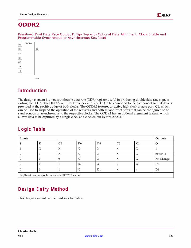
About Design Elements
ODDR2
Primitive: Dual Data Rate Output D Flip-Flop with Optional Data Alignment, Clock Enable andProgrammable Synchronous or Asynchronous Set/Reset
IntroductionThe design element is an output double data rate (DDR) register useful in producing double data rate signalsexiting the FPGA. The ODDR2 requires two clocks (C0 and C1) to be connected to the component so that data isprovided at the positive edge of both clocks. The ODDR2 features an active high clock enable port, CE, whichcan be used to suspend the operation of the registers and both set and reset ports that can be configured to besynchronous or asynchronous to the respective clocks. The ODDR2 has an optional alignment feature, whichallows data to be captured by a single clock and clocked out by two clocks.
Logic TableInputs Outputs
S R CE D0 D1 C0 C1 O
1 X X X X X X 1
0 1 X X X X X not INIT
0 0 0 X X X X No Change
0 0 1 D0 X ↑ X D0
0 0 1 X D1 X ↑ D1
Set/Reset can be synchronous via SRTYPE value
Design Entry MethodThis design element can be used in schematics.
Libraries Guide
10.1 www.xilinx.com 423
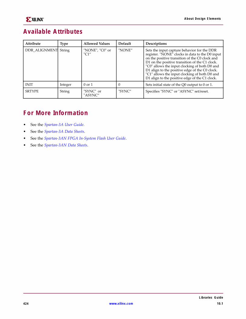
About Design Elements
Available AttributesAttribute Type Allowed Values Default Descriptions
DDR_ALIGNMENT String "NONE", "C0" or"C1”
"NONE” Sets the input capture behavior for the DDRregister. "NONE" clocks in data to the D0 inputon the positive transition of the C0 clock andD1 on the positive transition of the C1 clock."C0" allows the input clocking of both D0 andD1 align to the positive edge of the C0 clock."C1" allows the input clocking of both D0 andD1 align to the positive edge of the C1 clock.
INIT Integer 0 or 1 0 Sets initial state of the Q0 output to 0 or 1.
SRTYPE String "SYNC" or"ASYNC”
"SYNC” Specifies "SYNC" or "ASYNC" set/reset.
For More Information• See the Spartan-3A User Guide.
• See the Spartan-3A Data Sheets.
• See the Spartan-3AN FPGA In-System Flash User Guide.
• See the Spartan-3AN Data Sheets.
Libraries Guide
424 www.xilinx.com 10.1
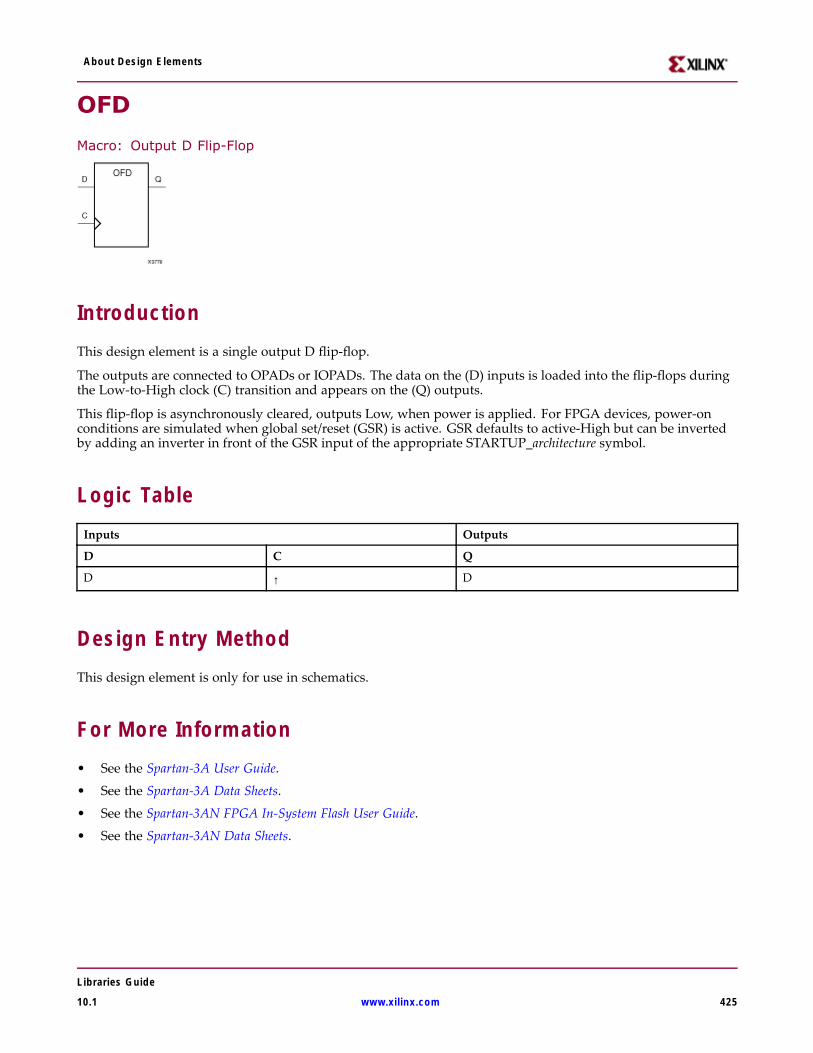
About Design Elements
OFD
Macro: Output D Flip-Flop
IntroductionThis design element is a single output D flip-flop.
The outputs are connected to OPADs or IOPADs. The data on the (D) inputs is loaded into the flip-flops duringthe Low-to-High clock (C) transition and appears on the (Q) outputs.
This flip-flop is asynchronously cleared, outputs Low, when power is applied. For FPGA devices, power-onconditions are simulated when global set/reset (GSR) is active. GSR defaults to active-High but can be invertedby adding an inverter in front of the GSR input of the appropriate STARTUP_architecture symbol.
Logic TableInputs Outputs
D C Q
D ↑ D
Design Entry MethodThis design element is only for use in schematics.
For More Information• See the Spartan-3A User Guide.
• See the Spartan-3A Data Sheets.
• See the Spartan-3AN FPGA In-System Flash User Guide.
• See the Spartan-3AN Data Sheets.
Libraries Guide
10.1 www.xilinx.com 425
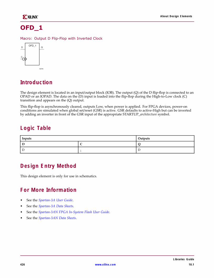
About Design Elements
OFD_1
Macro: Output D Flip-Flop with Inverted Clock
IntroductionThe design element is located in an input/output block (IOB). The output (Q) of the D flip-flop is connected to anOPAD or an IOPAD. The data on the (D) input is loaded into the flip-flop during the High-to-Low clock (C)transition and appears on the (Q) output.
This flip-flop is asynchronously cleared, outputs Low, when power is applied. For FPGA devices, power-onconditions are simulated when global set/reset (GSR) is active. GSR defaults to active-High but can be invertedby adding an inverter in front of the GSR input of the appropriate STARTUP_architecture symbol.
Logic TableInputs Outputs
D C Q
D ↓ D
Design Entry MethodThis design element is only for use in schematics.
For More Information• See the Spartan-3A User Guide.
• See the Spartan-3A Data Sheets.
• See the Spartan-3AN FPGA In-System Flash User Guide.
• See the Spartan-3AN Data Sheets.
Libraries Guide
426 www.xilinx.com 10.1

About Design Elements
OFD16
Macro: 16-Bit Output D Flip-Flop
IntroductionThis design element is a multiple output D flip-flop.
The outputs are connected to OPADs or IOPADs. The data on the (D) inputs is loaded into the flip-flops duringthe Low-to-High clock (C) transition and appears on the (Q) outputs.
This flip-flop is asynchronously cleared, outputs Low, when power is applied. For FPGA devices, power-onconditions are simulated when global set/reset (GSR) is active. GSR defaults to active-High but can be invertedby adding an inverter in front of the GSR input of the appropriate STARTUP_architecture symbol.
Logic TableInputs Outputs
D C Q
D ↑ D
Design Entry MethodThis design element is only for use in schematics.
For More Information• See the Spartan-3A User Guide.
• See the Spartan-3A Data Sheets.
• See the Spartan-3AN FPGA In-System Flash User Guide.
• See the Spartan-3AN Data Sheets.
Libraries Guide
10.1 www.xilinx.com 427
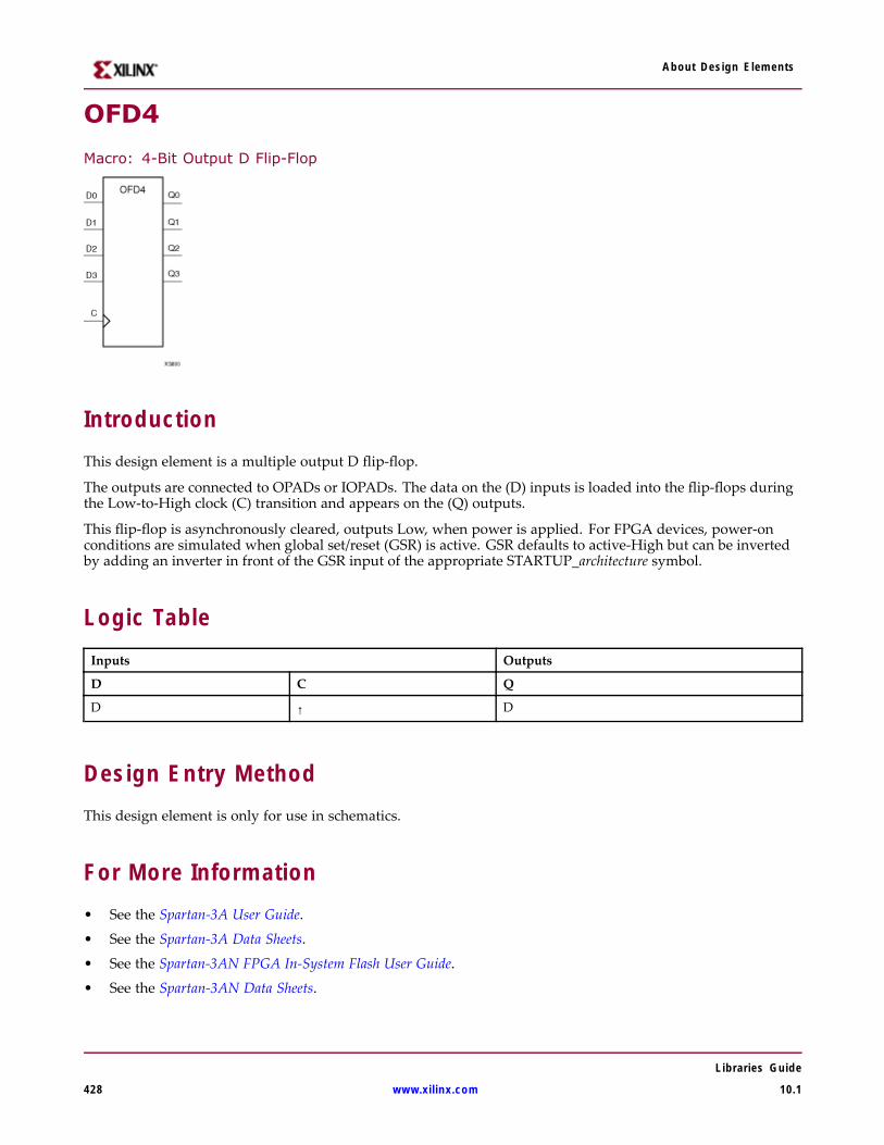
About Design Elements
OFD4
Macro: 4-Bit Output D Flip-Flop
IntroductionThis design element is a multiple output D flip-flop.
The outputs are connected to OPADs or IOPADs. The data on the (D) inputs is loaded into the flip-flops duringthe Low-to-High clock (C) transition and appears on the (Q) outputs.
This flip-flop is asynchronously cleared, outputs Low, when power is applied. For FPGA devices, power-onconditions are simulated when global set/reset (GSR) is active. GSR defaults to active-High but can be invertedby adding an inverter in front of the GSR input of the appropriate STARTUP_architecture symbol.
Logic TableInputs Outputs
D C Q
D ↑ D
Design Entry MethodThis design element is only for use in schematics.
For More Information• See the Spartan-3A User Guide.
• See the Spartan-3A Data Sheets.
• See the Spartan-3AN FPGA In-System Flash User Guide.
• See the Spartan-3AN Data Sheets.
Libraries Guide
428 www.xilinx.com 10.1
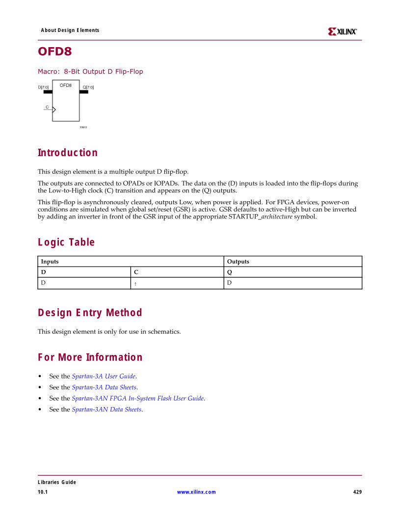
About Design Elements
OFD8
Macro: 8-Bit Output D Flip-Flop
IntroductionThis design element is a multiple output D flip-flop.
The outputs are connected to OPADs or IOPADs. The data on the (D) inputs is loaded into the flip-flops duringthe Low-to-High clock (C) transition and appears on the (Q) outputs.
This flip-flop is asynchronously cleared, outputs Low, when power is applied. For FPGA devices, power-onconditions are simulated when global set/reset (GSR) is active. GSR defaults to active-High but can be invertedby adding an inverter in front of the GSR input of the appropriate STARTUP_architecture symbol.
Logic TableInputs Outputs
D C Q
D ↑ D
Design Entry MethodThis design element is only for use in schematics.
For More Information• See the Spartan-3A User Guide.
• See the Spartan-3A Data Sheets.
• See the Spartan-3AN FPGA In-System Flash User Guide.
• See the Spartan-3AN Data Sheets.
Libraries Guide
10.1 www.xilinx.com 429
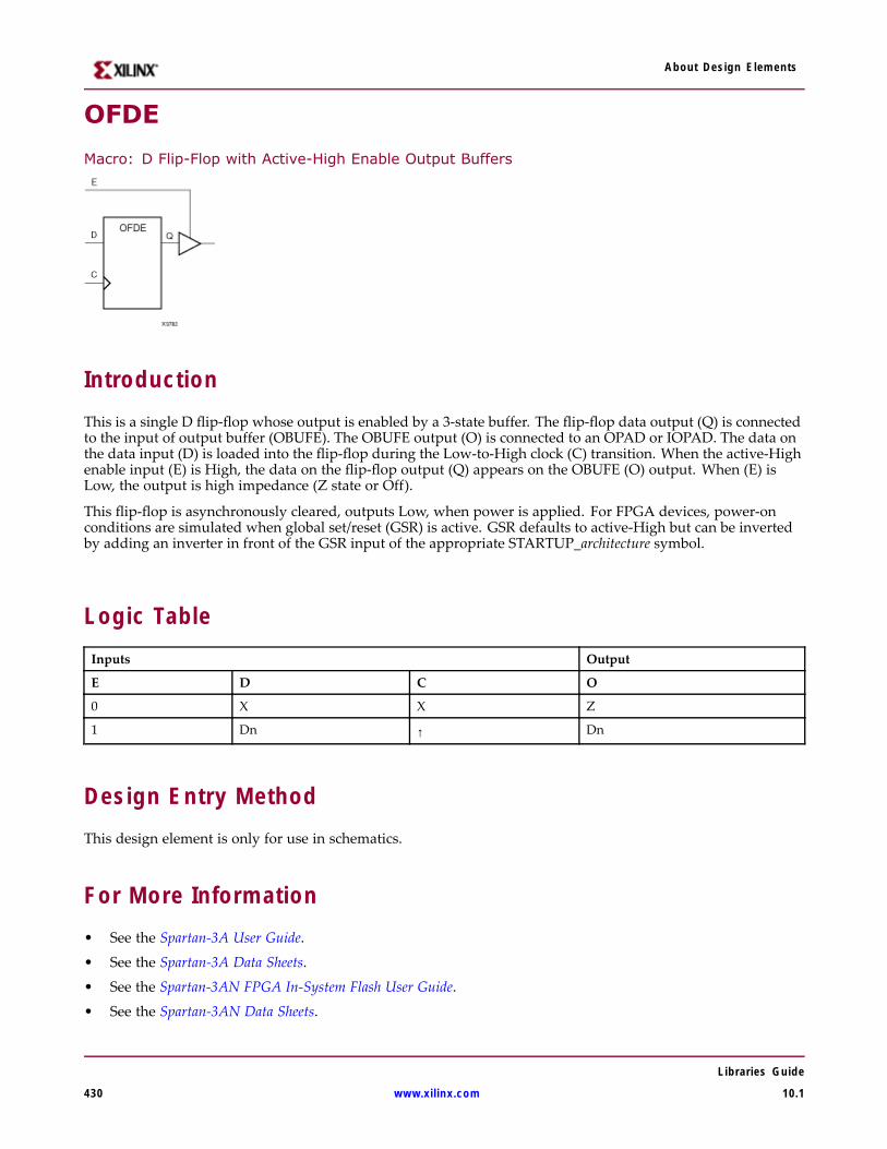
About Design Elements
OFDE
Macro: D Flip-Flop with Active-High Enable Output Buffers
IntroductionThis is a single D flip-flop whose output is enabled by a 3-state buffer. The flip-flop data output (Q) is connectedto the input of output buffer (OBUFE). The OBUFE output (O) is connected to an OPAD or IOPAD. The data onthe data input (D) is loaded into the flip-flop during the Low-to-High clock (C) transition. When the active-Highenable input (E) is High, the data on the flip-flop output (Q) appears on the OBUFE (O) output. When (E) isLow, the output is high impedance (Z state or Off).
This flip-flop is asynchronously cleared, outputs Low, when power is applied. For FPGA devices, power-onconditions are simulated when global set/reset (GSR) is active. GSR defaults to active-High but can be invertedby adding an inverter in front of the GSR input of the appropriate STARTUP_architecture symbol.
Logic TableInputs Output
E D C O
0 X X Z
1 Dn ↑ Dn
Design Entry MethodThis design element is only for use in schematics.
For More Information• See the Spartan-3A User Guide.
• See the Spartan-3A Data Sheets.
• See the Spartan-3AN FPGA In-System Flash User Guide.
• See the Spartan-3AN Data Sheets.
Libraries Guide
430 www.xilinx.com 10.1
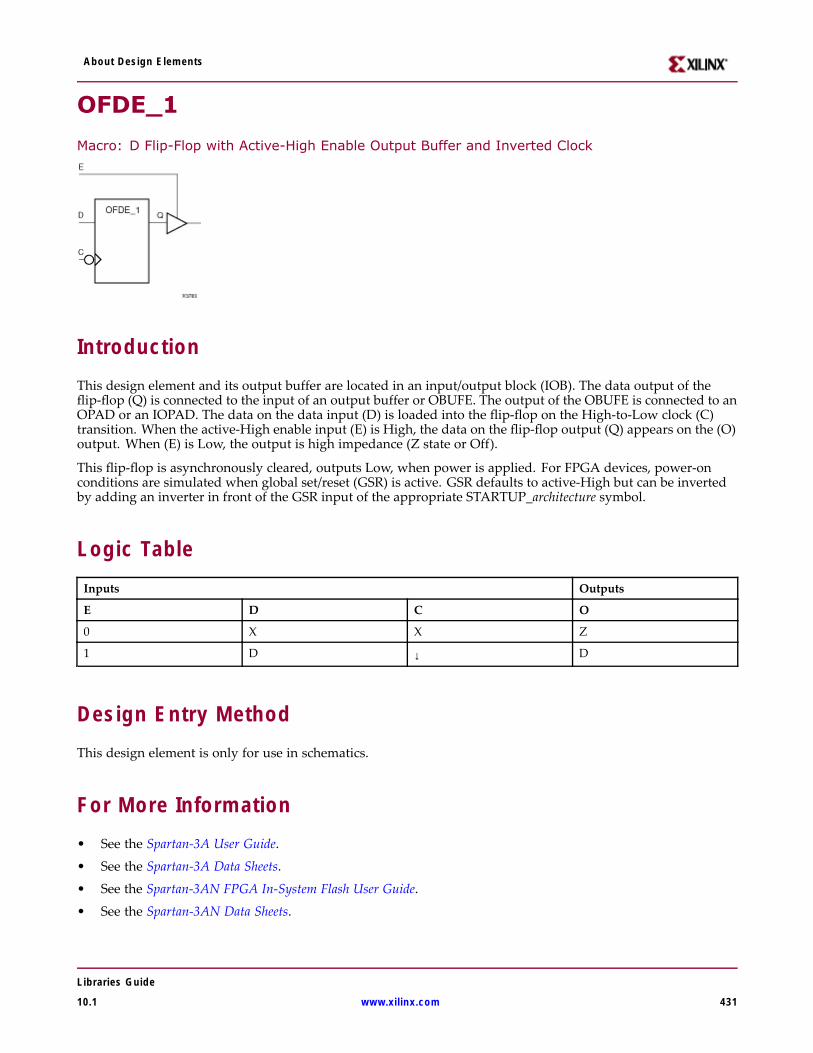
About Design Elements
OFDE_1
Macro: D Flip-Flop with Active-High Enable Output Buffer and Inverted Clock
IntroductionThis design element and its output buffer are located in an input/output block (IOB). The data output of theflip-flop (Q) is connected to the input of an output buffer or OBUFE. The output of the OBUFE is connected to anOPAD or an IOPAD. The data on the data input (D) is loaded into the flip-flop on the High-to-Low clock (C)transition. When the active-High enable input (E) is High, the data on the flip-flop output (Q) appears on the (O)output. When (E) is Low, the output is high impedance (Z state or Off).
This flip-flop is asynchronously cleared, outputs Low, when power is applied. For FPGA devices, power-onconditions are simulated when global set/reset (GSR) is active. GSR defaults to active-High but can be invertedby adding an inverter in front of the GSR input of the appropriate STARTUP_architecture symbol.
Logic TableInputs Outputs
E D C O
0 X X Z
1 D ↓ D
Design Entry MethodThis design element is only for use in schematics.
For More Information• See the Spartan-3A User Guide.
• See the Spartan-3A Data Sheets.
• See the Spartan-3AN FPGA In-System Flash User Guide.
• See the Spartan-3AN Data Sheets.
Libraries Guide
10.1 www.xilinx.com 431
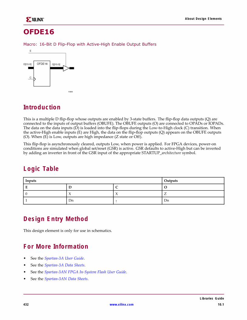
About Design Elements
OFDE16
Macro: 16-Bit D Flip-Flop with Active-High Enable Output Buffers
IntroductionThis is a multiple D flip-flop whose outputs are enabled by 3-state buffers. The flip-flop data outputs (Q) areconnected to the inputs of output buffers (OBUFE). The OBUFE outputs (O) are connected to OPADs or IOPADs.The data on the data inputs (D) is loaded into the flip-flops during the Low-to-High clock (C) transition. Whenthe active-High enable inputs (E) are High, the data on the flip-flop outputs (Q) appears on the OBUFE outputs(O). When (E) is Low, outputs are high impedance (Z state or Off).
This flip-flop is asynchronously cleared, outputs Low, when power is applied. For FPGA devices, power-onconditions are simulated when global set/reset (GSR) is active. GSR defaults to active-High but can be invertedby adding an inverter in front of the GSR input of the appropriate STARTUP_architecture symbol.
Logic TableInputs Outputs
E D C O
0 X X Z
1 Dn ↑ Dn
Design Entry MethodThis design element is only for use in schematics.
For More Information• See the Spartan-3A User Guide.
• See the Spartan-3A Data Sheets.
• See the Spartan-3AN FPGA In-System Flash User Guide.
• See the Spartan-3AN Data Sheets.
Libraries Guide
432 www.xilinx.com 10.1
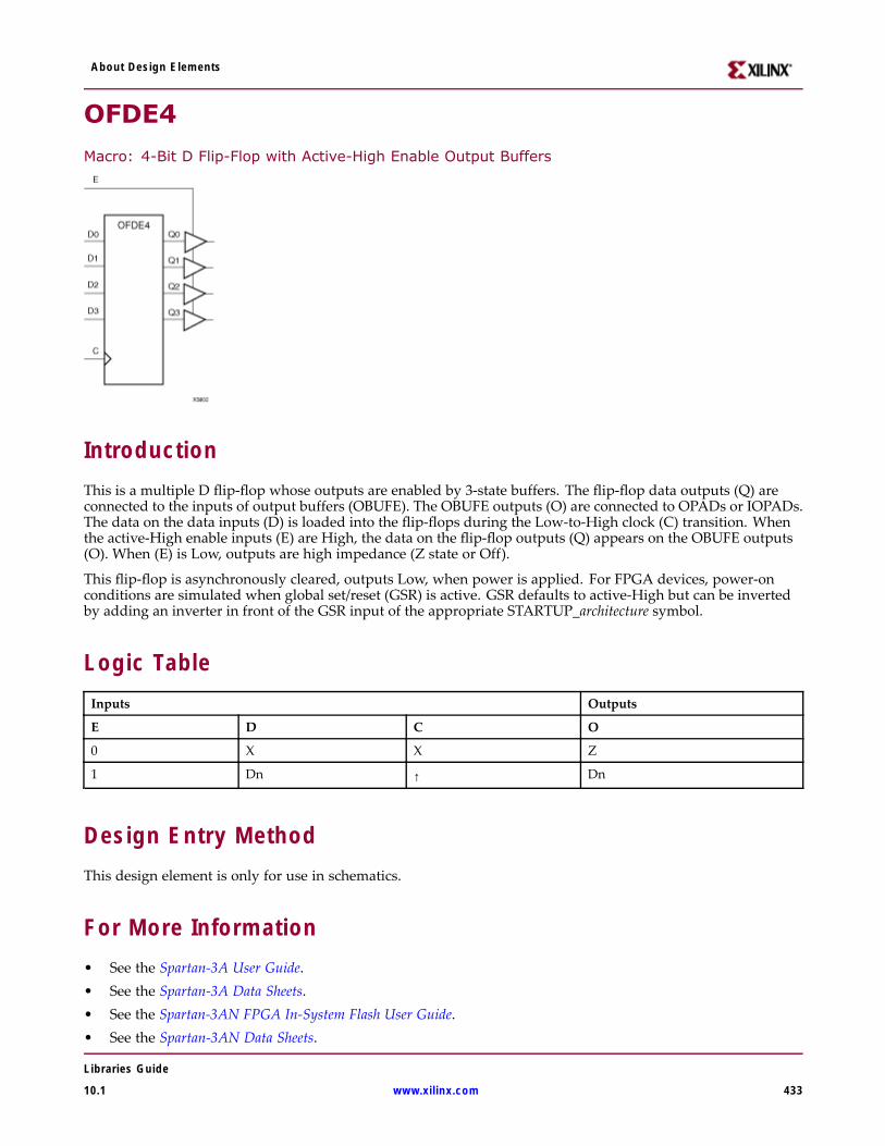
About Design Elements
OFDE4
Macro: 4-Bit D Flip-Flop with Active-High Enable Output Buffers
IntroductionThis is a multiple D flip-flop whose outputs are enabled by 3-state buffers. The flip-flop data outputs (Q) areconnected to the inputs of output buffers (OBUFE). The OBUFE outputs (O) are connected to OPADs or IOPADs.The data on the data inputs (D) is loaded into the flip-flops during the Low-to-High clock (C) transition. Whenthe active-High enable inputs (E) are High, the data on the flip-flop outputs (Q) appears on the OBUFE outputs(O). When (E) is Low, outputs are high impedance (Z state or Off).
This flip-flop is asynchronously cleared, outputs Low, when power is applied. For FPGA devices, power-onconditions are simulated when global set/reset (GSR) is active. GSR defaults to active-High but can be invertedby adding an inverter in front of the GSR input of the appropriate STARTUP_architecture symbol.
Logic TableInputs Outputs
E D C O
0 X X Z
1 Dn ↑ Dn
Design Entry MethodThis design element is only for use in schematics.
For More Information• See the Spartan-3A User Guide.• See the Spartan-3A Data Sheets.• See the Spartan-3AN FPGA In-System Flash User Guide.• See the Spartan-3AN Data Sheets.
Libraries Guide
10.1 www.xilinx.com 433
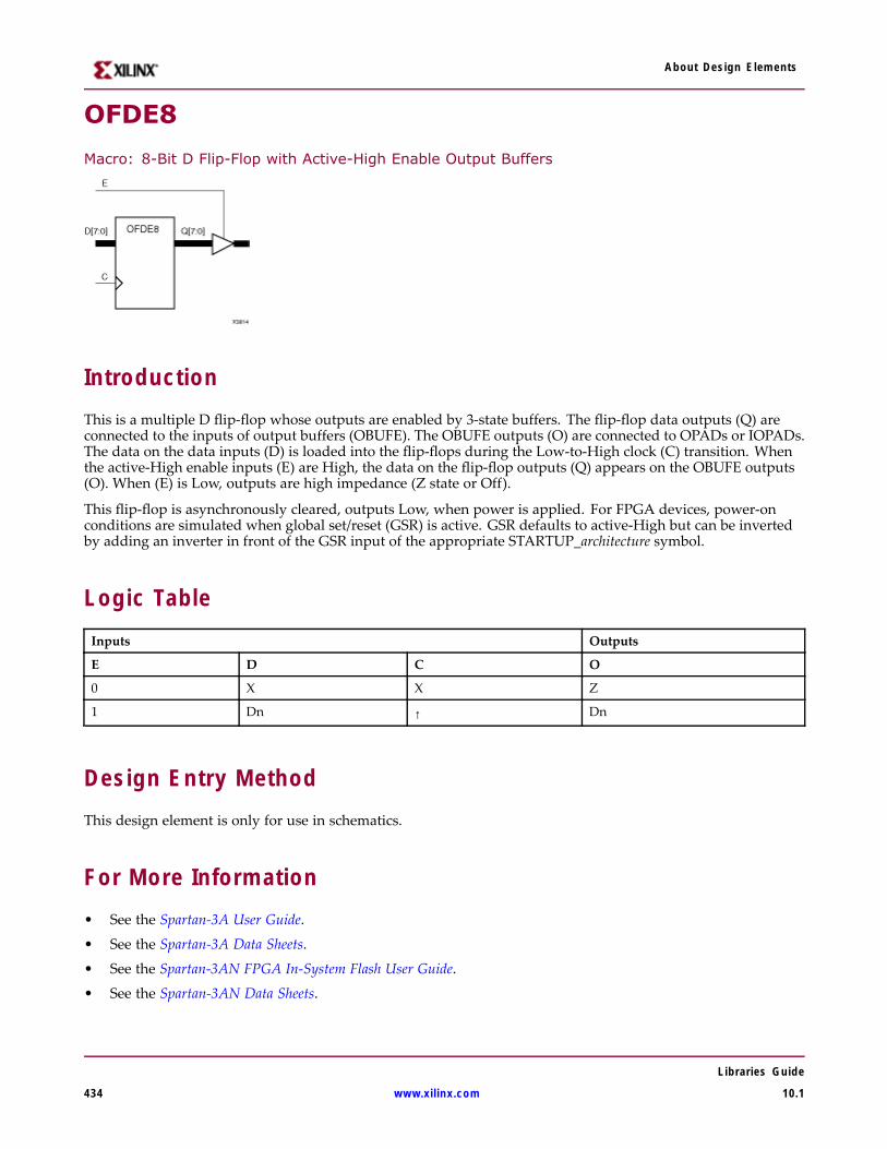
About Design Elements
OFDE8
Macro: 8-Bit D Flip-Flop with Active-High Enable Output Buffers
IntroductionThis is a multiple D flip-flop whose outputs are enabled by 3-state buffers. The flip-flop data outputs (Q) areconnected to the inputs of output buffers (OBUFE). The OBUFE outputs (O) are connected to OPADs or IOPADs.The data on the data inputs (D) is loaded into the flip-flops during the Low-to-High clock (C) transition. Whenthe active-High enable inputs (E) are High, the data on the flip-flop outputs (Q) appears on the OBUFE outputs(O). When (E) is Low, outputs are high impedance (Z state or Off).
This flip-flop is asynchronously cleared, outputs Low, when power is applied. For FPGA devices, power-onconditions are simulated when global set/reset (GSR) is active. GSR defaults to active-High but can be invertedby adding an inverter in front of the GSR input of the appropriate STARTUP_architecture symbol.
Logic TableInputs Outputs
E D C O
0 X X Z
1 Dn ↑ Dn
Design Entry MethodThis design element is only for use in schematics.
For More Information• See the Spartan-3A User Guide.
• See the Spartan-3A Data Sheets.
• See the Spartan-3AN FPGA In-System Flash User Guide.
• See the Spartan-3AN Data Sheets.
Libraries Guide
434 www.xilinx.com 10.1
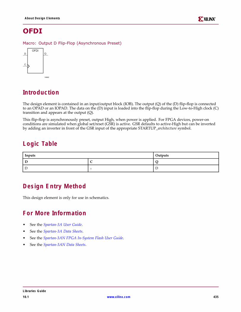
About Design Elements
OFDI
Macro: Output D Flip-Flop (Asynchronous Preset)
IntroductionThe design element is contained in an input/output block (IOB). The output (Q) of the (D) flip-flop is connectedto an OPAD or an IOPAD. The data on the (D) input is loaded into the flip-flop during the Low-to-High clock (C)transition and appears at the output (Q).
This flip-flop is asynchronously preset, output High, when power is applied. For FPGA devices, power-onconditions are simulated when global set/reset (GSR) is active. GSR defaults to active-High but can be invertedby adding an inverter in front of the GSR input of the appropriate STARTUP_architecture symbol.
Logic TableInputs Outputs
D C Q
D ↑ D
Design Entry MethodThis design element is only for use in schematics.
For More Information• See the Spartan-3A User Guide.
• See the Spartan-3A Data Sheets.
• See the Spartan-3AN FPGA In-System Flash User Guide.
• See the Spartan-3AN Data Sheets.
Libraries Guide
10.1 www.xilinx.com 435
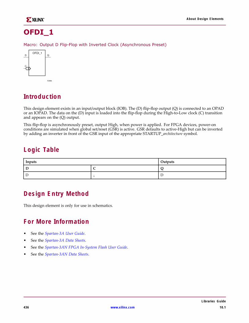
About Design Elements
OFDI_1
Macro: Output D Flip-Flop with Inverted Clock (Asynchronous Preset)
IntroductionThis design element exists in an input/output block (IOB). The (D) flip-flop output (Q) is connected to an OPADor an IOPAD. The data on the (D) input is loaded into the flip-flop during the High-to-Low clock (C) transitionand appears on the (Q) output.
This flip-flop is asynchronously preset, output High, when power is applied. For FPGA devices, power-onconditions are simulated when global set/reset (GSR) is active. GSR defaults to active-High but can be invertedby adding an inverter in front of the GSR input of the appropriate STARTUP_architecture symbol.
Logic TableInputs Outputs
D C Q
D ↓ D
Design Entry MethodThis design element is only for use in schematics.
For More Information• See the Spartan-3A User Guide.
• See the Spartan-3A Data Sheets.
• See the Spartan-3AN FPGA In-System Flash User Guide.
• See the Spartan-3AN Data Sheets.
Libraries Guide
436 www.xilinx.com 10.1
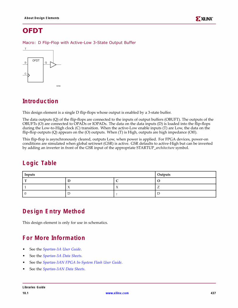
About Design Elements
OFDT
Macro: D Flip-Flop with Active-Low 3-State Output Buffer
IntroductionThis design element is a single D flip-flops whose output is enabled by a 3-state buffer.
The data outputs (Q) of the flip-flops are connected to the inputs of output buffers (OBUFT). The outputs of theOBUFTs (O) are connected to OPADs or IOPADs. The data on the data inputs (D) is loaded into the flip-flopsduring the Low-to-High clock (C) transition. When the active-Low enable inputs (T) are Low, the data on theflip-flop outputs (Q) appears on the (O) outputs. When (T) is High, outputs are high impedance (Off).
This flip-flop is asynchronously cleared, outputs Low, when power is applied. For FPGA devices, power-onconditions are simulated when global set/reset (GSR) is active. GSR defaults to active-High but can be invertedby adding an inverter in front of the GSR input of the appropriate STARTUP_architecture symbol.
Logic TableInputs Outputs
T D C O
1 X X Z
0 D ↑ D
Design Entry MethodThis design element is only for use in schematics.
For More Information• See the Spartan-3A User Guide.
• See the Spartan-3A Data Sheets.
• See the Spartan-3AN FPGA In-System Flash User Guide.
• See the Spartan-3AN Data Sheets.
Libraries Guide
10.1 www.xilinx.com 437
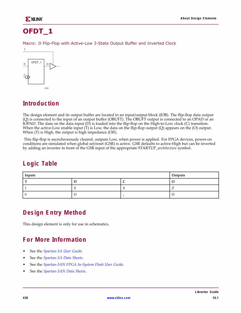
About Design Elements
OFDT_1
Macro: D Flip-Flop with Active-Low 3-State Output Buffer and Inverted Clock
IntroductionThe design element and its output buffer are located in an input/output block (IOB). The flip-flop data output(Q) is connected to the input of an output buffer (OBUFT). The OBUFT output is connected to an OPAD or anIOPAD. The data on the data input (D) is loaded into the flip-flop on the High-to-Low clock (C) transition.When the active-Low enable input (T) is Low, the data on the flip-flop output (Q) appears on the (O) output.When (T) is High, the output is high impedance (Off).
This flip-flop is asynchronously cleared, outputs Low, when power is applied. For FPGA devices, power-onconditions are simulated when global set/reset (GSR) is active. GSR defaults to active-High but can be invertedby adding an inverter in front of the GSR input of the appropriate STARTUP_architecture symbol.
Logic TableInputs Outputs
T D C O
1 X X Z
0 D ↓ D
Design Entry MethodThis design element is only for use in schematics.
For More Information• See the Spartan-3A User Guide.
• See the Spartan-3A Data Sheets.
• See the Spartan-3AN FPGA In-System Flash User Guide.
• See the Spartan-3AN Data Sheets.
Libraries Guide
438 www.xilinx.com 10.1
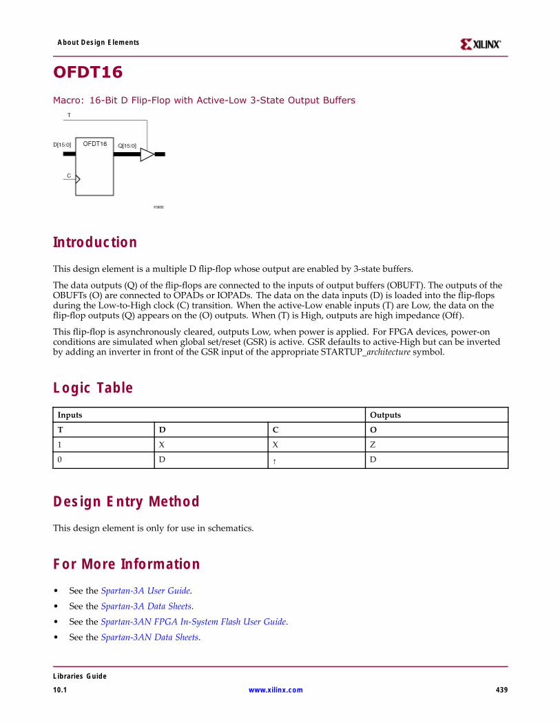
About Design Elements
OFDT16
Macro: 16-Bit D Flip-Flop with Active-Low 3-State Output Buffers
IntroductionThis design element is a multiple D flip-flop whose output are enabled by 3-state buffers.
The data outputs (Q) of the flip-flops are connected to the inputs of output buffers (OBUFT). The outputs of theOBUFTs (O) are connected to OPADs or IOPADs. The data on the data inputs (D) is loaded into the flip-flopsduring the Low-to-High clock (C) transition. When the active-Low enable inputs (T) are Low, the data on theflip-flop outputs (Q) appears on the (O) outputs. When (T) is High, outputs are high impedance (Off).
This flip-flop is asynchronously cleared, outputs Low, when power is applied. For FPGA devices, power-onconditions are simulated when global set/reset (GSR) is active. GSR defaults to active-High but can be invertedby adding an inverter in front of the GSR input of the appropriate STARTUP_architecture symbol.
Logic TableInputs Outputs
T D C O
1 X X Z
0 D ↑ D
Design Entry MethodThis design element is only for use in schematics.
For More Information• See the Spartan-3A User Guide.
• See the Spartan-3A Data Sheets.
• See the Spartan-3AN FPGA In-System Flash User Guide.
• See the Spartan-3AN Data Sheets.
Libraries Guide
10.1 www.xilinx.com 439
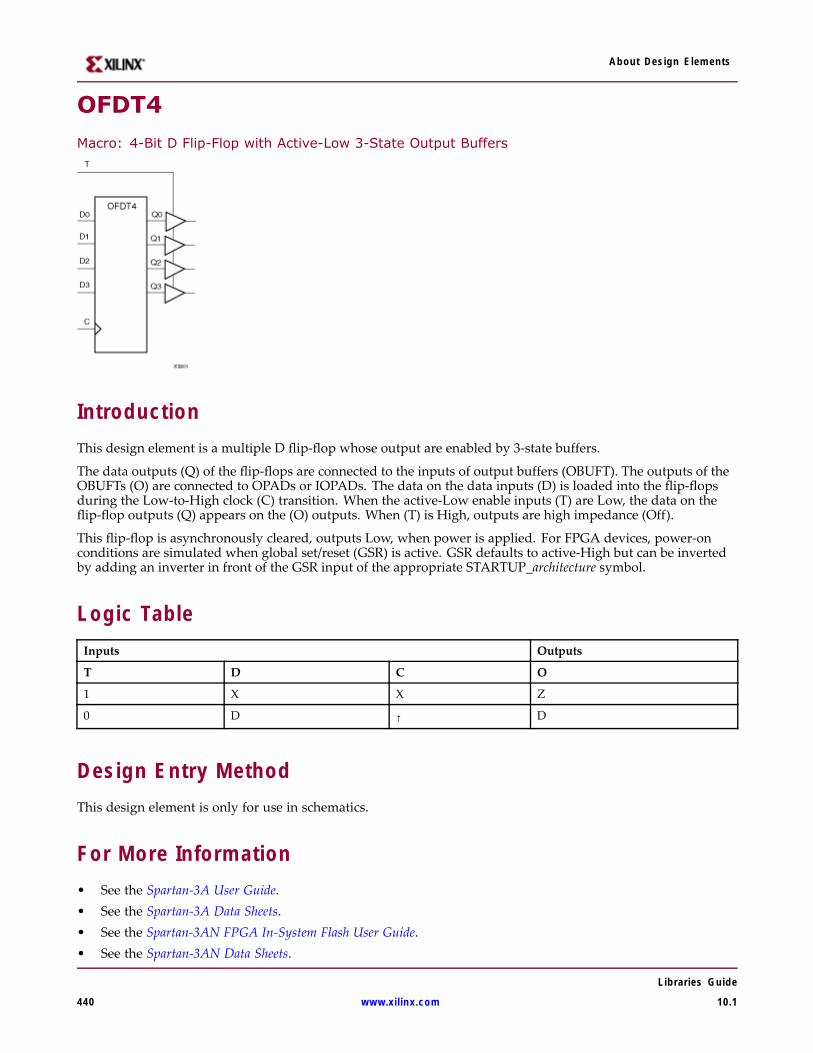
About Design Elements
OFDT4
Macro: 4-Bit D Flip-Flop with Active-Low 3-State Output Buffers
IntroductionThis design element is a multiple D flip-flop whose output are enabled by 3-state buffers.
The data outputs (Q) of the flip-flops are connected to the inputs of output buffers (OBUFT). The outputs of theOBUFTs (O) are connected to OPADs or IOPADs. The data on the data inputs (D) is loaded into the flip-flopsduring the Low-to-High clock (C) transition. When the active-Low enable inputs (T) are Low, the data on theflip-flop outputs (Q) appears on the (O) outputs. When (T) is High, outputs are high impedance (Off).
This flip-flop is asynchronously cleared, outputs Low, when power is applied. For FPGA devices, power-onconditions are simulated when global set/reset (GSR) is active. GSR defaults to active-High but can be invertedby adding an inverter in front of the GSR input of the appropriate STARTUP_architecture symbol.
Logic TableInputs Outputs
T D C O
1 X X Z
0 D ↑ D
Design Entry MethodThis design element is only for use in schematics.
For More Information• See the Spartan-3A User Guide.• See the Spartan-3A Data Sheets.• See the Spartan-3AN FPGA In-System Flash User Guide.• See the Spartan-3AN Data Sheets.
Libraries Guide
440 www.xilinx.com 10.1
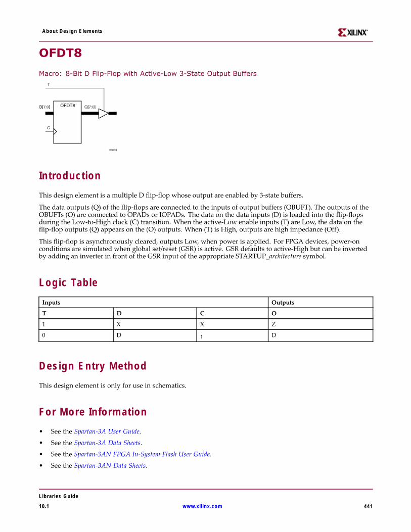
About Design Elements
OFDT8
Macro: 8-Bit D Flip-Flop with Active-Low 3-State Output Buffers
IntroductionThis design element is a multiple D flip-flop whose output are enabled by 3-state buffers.
The data outputs (Q) of the flip-flops are connected to the inputs of output buffers (OBUFT). The outputs of theOBUFTs (O) are connected to OPADs or IOPADs. The data on the data inputs (D) is loaded into the flip-flopsduring the Low-to-High clock (C) transition. When the active-Low enable inputs (T) are Low, the data on theflip-flop outputs (Q) appears on the (O) outputs. When (T) is High, outputs are high impedance (Off).
This flip-flop is asynchronously cleared, outputs Low, when power is applied. For FPGA devices, power-onconditions are simulated when global set/reset (GSR) is active. GSR defaults to active-High but can be invertedby adding an inverter in front of the GSR input of the appropriate STARTUP_architecture symbol.
Logic TableInputs Outputs
T D C O
1 X X Z
0 D ↑ D
Design Entry MethodThis design element is only for use in schematics.
For More Information• See the Spartan-3A User Guide.
• See the Spartan-3A Data Sheets.
• See the Spartan-3AN FPGA In-System Flash User Guide.
• See the Spartan-3AN Data Sheets.
Libraries Guide
10.1 www.xilinx.com 441
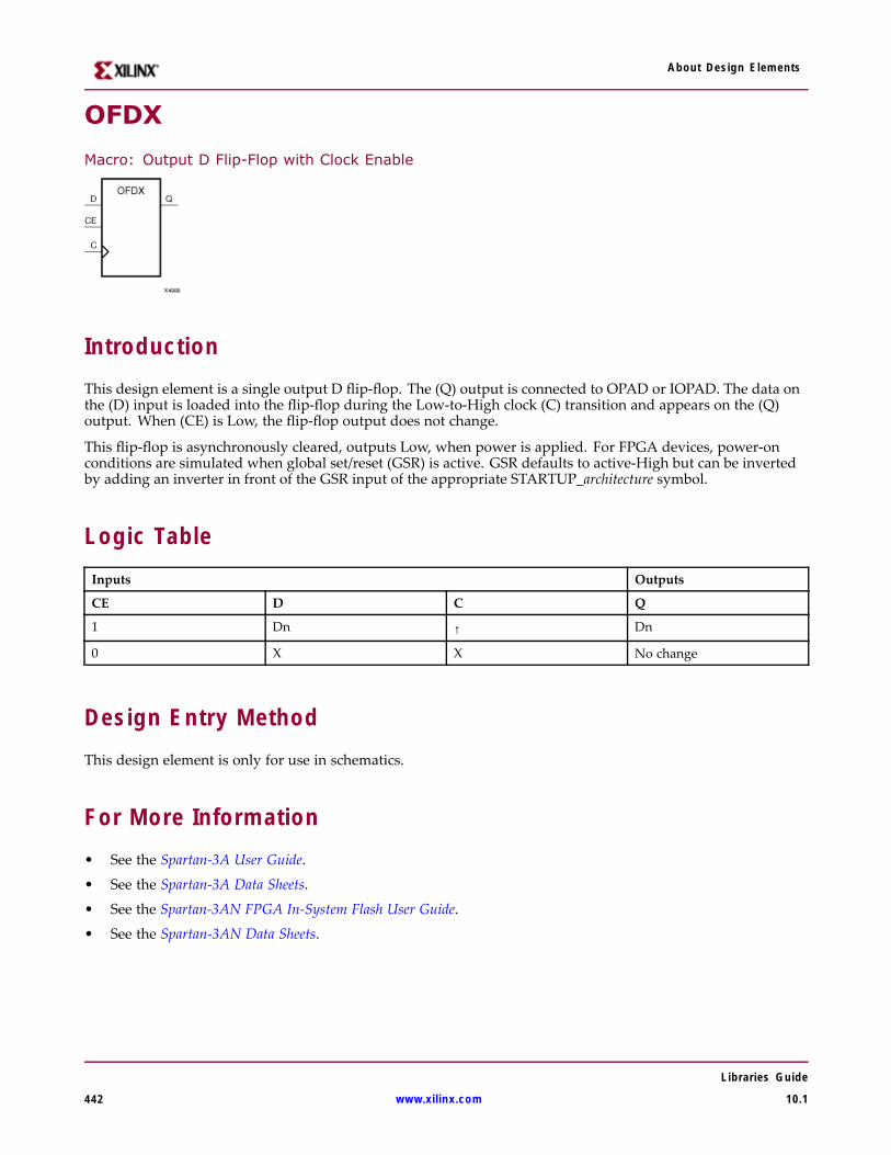
About Design Elements
OFDX
Macro: Output D Flip-Flop with Clock Enable
IntroductionThis design element is a single output D flip-flop. The (Q) output is connected to OPAD or IOPAD. The data onthe (D) input is loaded into the flip-flop during the Low-to-High clock (C) transition and appears on the (Q)output. When (CE) is Low, the flip-flop output does not change.
This flip-flop is asynchronously cleared, outputs Low, when power is applied. For FPGA devices, power-onconditions are simulated when global set/reset (GSR) is active. GSR defaults to active-High but can be invertedby adding an inverter in front of the GSR input of the appropriate STARTUP_architecture symbol.
Logic TableInputs Outputs
CE D C Q
1 Dn ↑ Dn
0 X X No change
Design Entry MethodThis design element is only for use in schematics.
For More Information• See the Spartan-3A User Guide.
• See the Spartan-3A Data Sheets.
• See the Spartan-3AN FPGA In-System Flash User Guide.
• See the Spartan-3AN Data Sheets.
Libraries Guide
442 www.xilinx.com 10.1
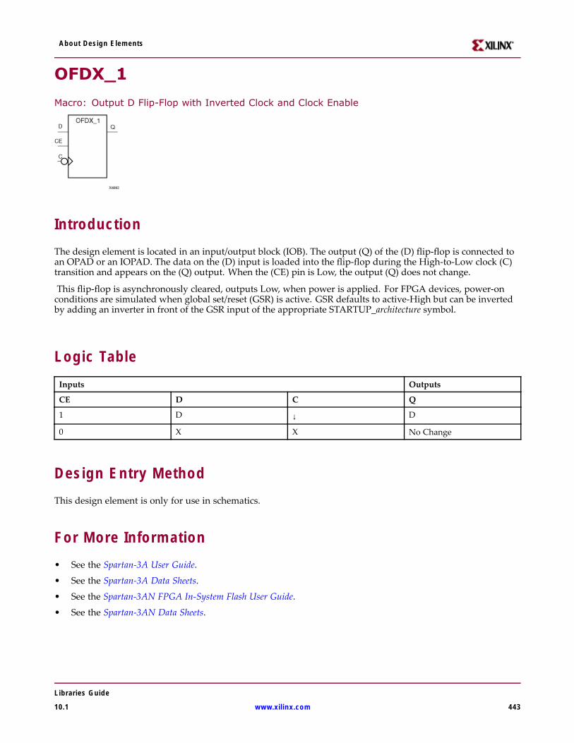
About Design Elements
OFDX_1
Macro: Output D Flip-Flop with Inverted Clock and Clock Enable
IntroductionThe design element is located in an input/output block (IOB). The output (Q) of the (D) flip-flop is connected toan OPAD or an IOPAD. The data on the (D) input is loaded into the flip-flop during the High-to-Low clock (C)transition and appears on the (Q) output. When the (CE) pin is Low, the output (Q) does not change.
This flip-flop is asynchronously cleared, outputs Low, when power is applied. For FPGA devices, power-onconditions are simulated when global set/reset (GSR) is active. GSR defaults to active-High but can be invertedby adding an inverter in front of the GSR input of the appropriate STARTUP_architecture symbol.
Logic TableInputs Outputs
CE D C Q
1 D ↓ D
0 X X No Change
Design Entry MethodThis design element is only for use in schematics.
For More Information• See the Spartan-3A User Guide.
• See the Spartan-3A Data Sheets.
• See the Spartan-3AN FPGA In-System Flash User Guide.
• See the Spartan-3AN Data Sheets.
Libraries Guide
10.1 www.xilinx.com 443

About Design Elements
OFDX16
Macro: 16-Bit Output D Flip-Flop with Clock Enable
IntroductionThis design element is a multiple output D flip-flop. The (Q) output is connected to OPAD or IOPAD. The dataon the (D) input is loaded into the flip-flop during the Low-to-High clock (C) transition and appears on the (Q)output. When (CE) is Low, the flip-flop output does not change.
This flip-flop is asynchronously cleared, outputs Low, when power is applied. For FPGA devices, power-onconditions are simulated when global set/reset (GSR) is active. GSR defaults to active-High but can be invertedby adding an inverter in front of the GSR input of the appropriate STARTUP_architecture symbol.
Logic TableInputs Outputs
CE D C Q
1 Dn ↑ Dn
0 X X No change
Design Entry MethodThis design element is only for use in schematics.
For More Information• See the Spartan-3A User Guide.
• See the Spartan-3A Data Sheets.
• See the Spartan-3AN FPGA In-System Flash User Guide.
• See the Spartan-3AN Data Sheets.
Libraries Guide
444 www.xilinx.com 10.1
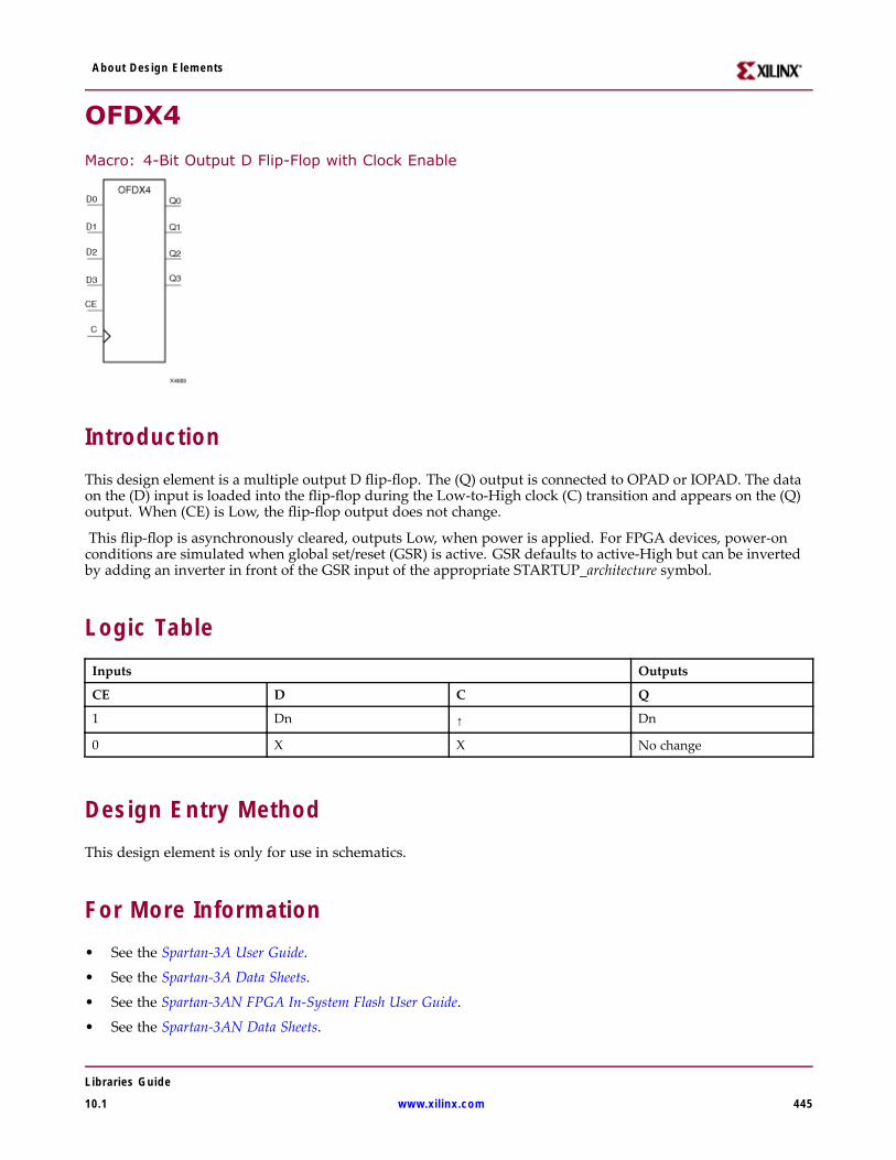
About Design Elements
OFDX4
Macro: 4-Bit Output D Flip-Flop with Clock Enable
IntroductionThis design element is a multiple output D flip-flop. The (Q) output is connected to OPAD or IOPAD. The dataon the (D) input is loaded into the flip-flop during the Low-to-High clock (C) transition and appears on the (Q)output. When (CE) is Low, the flip-flop output does not change.
This flip-flop is asynchronously cleared, outputs Low, when power is applied. For FPGA devices, power-onconditions are simulated when global set/reset (GSR) is active. GSR defaults to active-High but can be invertedby adding an inverter in front of the GSR input of the appropriate STARTUP_architecture symbol.
Logic TableInputs Outputs
CE D C Q
1 Dn ↑ Dn
0 X X No change
Design Entry MethodThis design element is only for use in schematics.
For More Information• See the Spartan-3A User Guide.
• See the Spartan-3A Data Sheets.
• See the Spartan-3AN FPGA In-System Flash User Guide.
• See the Spartan-3AN Data Sheets.
Libraries Guide
10.1 www.xilinx.com 445
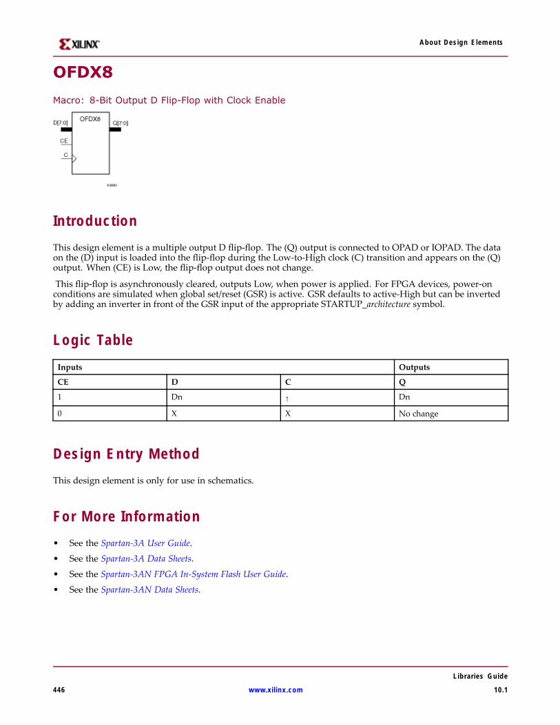
About Design Elements
OFDX8
Macro: 8-Bit Output D Flip-Flop with Clock Enable
IntroductionThis design element is a multiple output D flip-flop. The (Q) output is connected to OPAD or IOPAD. The dataon the (D) input is loaded into the flip-flop during the Low-to-High clock (C) transition and appears on the (Q)output. When (CE) is Low, the flip-flop output does not change.
This flip-flop is asynchronously cleared, outputs Low, when power is applied. For FPGA devices, power-onconditions are simulated when global set/reset (GSR) is active. GSR defaults to active-High but can be invertedby adding an inverter in front of the GSR input of the appropriate STARTUP_architecture symbol.
Logic TableInputs Outputs
CE D C Q
1 Dn ↑ Dn
0 X X No change
Design Entry MethodThis design element is only for use in schematics.
For More Information• See the Spartan-3A User Guide.
• See the Spartan-3A Data Sheets.
• See the Spartan-3AN FPGA In-System Flash User Guide.
• See the Spartan-3AN Data Sheets.
Libraries Guide
446 www.xilinx.com 10.1
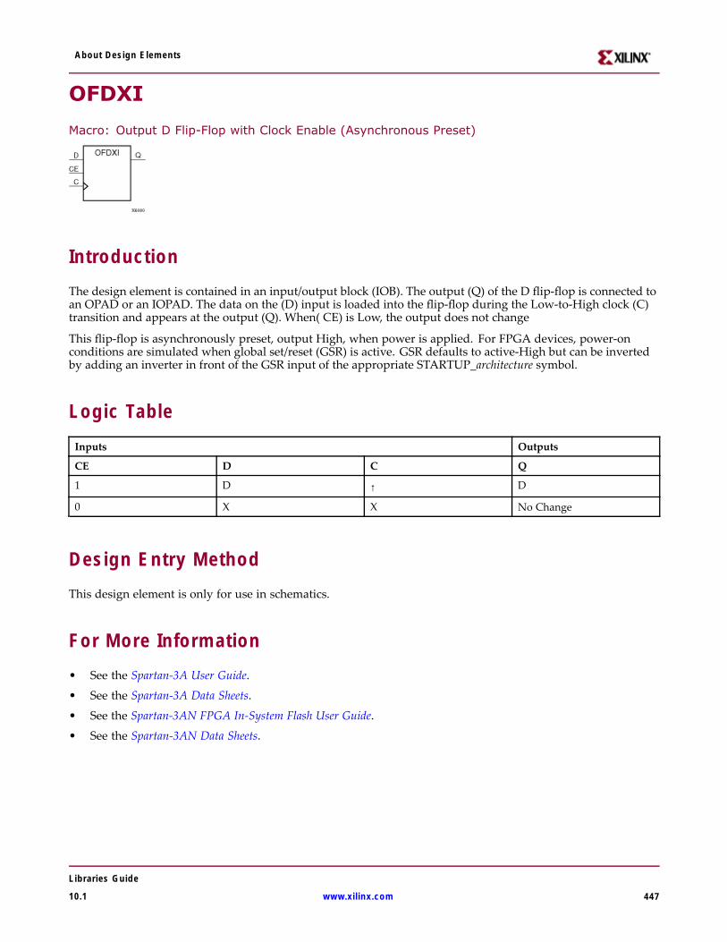
About Design Elements
OFDXI
Macro: Output D Flip-Flop with Clock Enable (Asynchronous Preset)
IntroductionThe design element is contained in an input/output block (IOB). The output (Q) of the D flip-flop is connected toan OPAD or an IOPAD. The data on the (D) input is loaded into the flip-flop during the Low-to-High clock (C)transition and appears at the output (Q). When( CE) is Low, the output does not change
This flip-flop is asynchronously preset, output High, when power is applied. For FPGA devices, power-onconditions are simulated when global set/reset (GSR) is active. GSR defaults to active-High but can be invertedby adding an inverter in front of the GSR input of the appropriate STARTUP_architecture symbol.
Logic TableInputs Outputs
CE D C Q
1 D ↑ D
0 X X No Change
Design Entry MethodThis design element is only for use in schematics.
For More Information• See the Spartan-3A User Guide.
• See the Spartan-3A Data Sheets.
• See the Spartan-3AN FPGA In-System Flash User Guide.
• See the Spartan-3AN Data Sheets.
Libraries Guide
10.1 www.xilinx.com 447
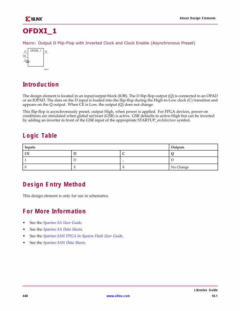
About Design Elements
OFDXI_1
Macro: Output D Flip-Flop with Inverted Clock and Clock Enable (Asynchronous Preset)
IntroductionThe design element is located in an input/output block (IOB). The D flip-flop output (Q) is connected to an OPADor an IOPAD. The data on the D input is loaded into the flip-flop during the High-to-Low clock (C) transition andappears on the Q output. When CE is Low, the output (Q) does not change.
This flip-flop is asynchronously preset, output High, when power is applied. For FPGA devices, power-onconditions are simulated when global set/reset (GSR) is active. GSR defaults to active-High but can be invertedby adding an inverter in front of the GSR input of the appropriate STARTUP_architecture symbol.
Logic TableInputs Outputs
CE D C Q
1 D ↓ D
0 X X No Change
Design Entry MethodThis design element is only for use in schematics.
For More Information• See the Spartan-3A User Guide.
• See the Spartan-3A Data Sheets.
• See the Spartan-3AN FPGA In-System Flash User Guide.
• See the Spartan-3AN Data Sheets.
Libraries Guide
448 www.xilinx.com 10.1
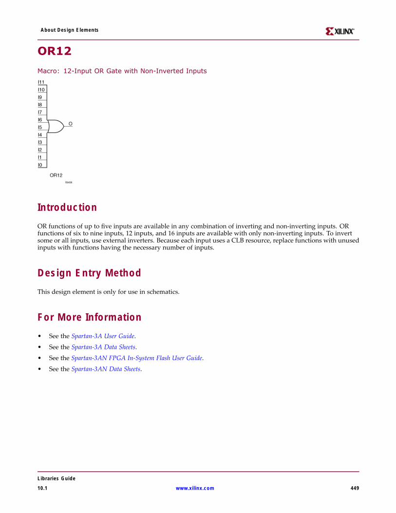
About Design Elements
OR12
Macro: 12-Input OR Gate with Non-Inverted Inputs
IntroductionOR functions of up to five inputs are available in any combination of inverting and non-inverting inputs. ORfunctions of six to nine inputs, 12 inputs, and 16 inputs are available with only non-inverting inputs. To invertsome or all inputs, use external inverters. Because each input uses a CLB resource, replace functions with unusedinputs with functions having the necessary number of inputs.
Design Entry MethodThis design element is only for use in schematics.
For More Information• See the Spartan-3A User Guide.
• See the Spartan-3A Data Sheets.
• See the Spartan-3AN FPGA In-System Flash User Guide.
• See the Spartan-3AN Data Sheets.
Libraries Guide
10.1 www.xilinx.com 449
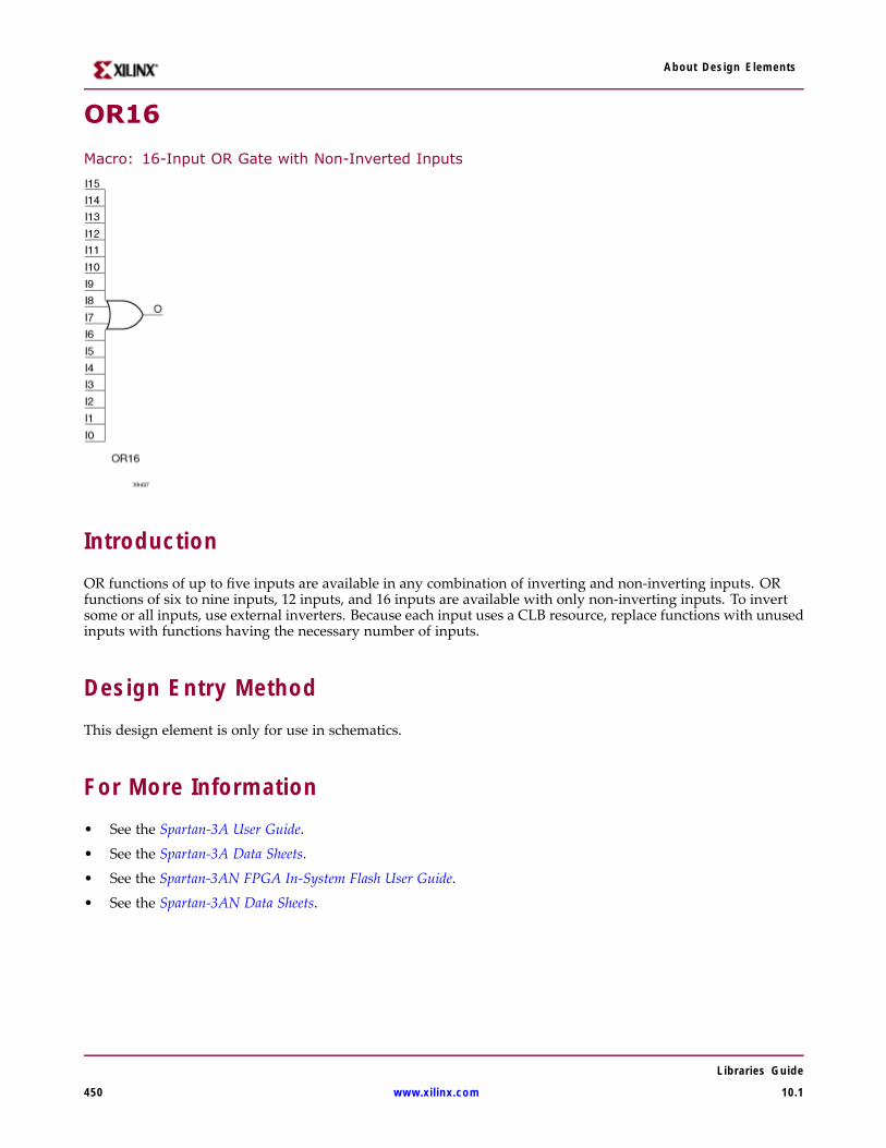
About Design Elements
OR16
Macro: 16-Input OR Gate with Non-Inverted Inputs
IntroductionOR functions of up to five inputs are available in any combination of inverting and non-inverting inputs. ORfunctions of six to nine inputs, 12 inputs, and 16 inputs are available with only non-inverting inputs. To invertsome or all inputs, use external inverters. Because each input uses a CLB resource, replace functions with unusedinputs with functions having the necessary number of inputs.
Design Entry MethodThis design element is only for use in schematics.
For More Information• See the Spartan-3A User Guide.
• See the Spartan-3A Data Sheets.
• See the Spartan-3AN FPGA In-System Flash User Guide.
• See the Spartan-3AN Data Sheets.
Libraries Guide
450 www.xilinx.com 10.1

About Design Elements
OR2
Primitive: 2-Input OR Gate with Non-Inverted Inputs
IntroductionOR functions of up to five inputs are available in any combination of inverting and non-inverting inputs. ORfunctions of six to nine inputs, 12 inputs, and 16 inputs are available with only non-inverting inputs. To invertsome or all inputs, use external inverters. Because each input uses a CLB resource, replace functions with unusedinputs with functions having the necessary number of inputs.
Design Entry MethodThis design element is only for use in schematics.
For More Information• See the Spartan-3A User Guide.
• See the Spartan-3A Data Sheets.
• See the Spartan-3AN FPGA In-System Flash User Guide.
• See the Spartan-3AN Data Sheets.
Libraries Guide
10.1 www.xilinx.com 451

About Design Elements
OR2B1
Primitive: 2-Input OR Gate with 1 Inverted and 1 Non-Inverted Inputs
IntroductionOR functions of up to five inputs are available in any combination of inverting and non-inverting inputs. ORfunctions of six to nine inputs, 12 inputs, and 16 inputs are available with only non-inverting inputs. To invertsome or all inputs, use external inverters. Because each input uses a CLB resource, replace functions with unusedinputs with functions having the necessary number of inputs.
Design Entry MethodThis design element is only for use in schematics.
For More Information• See the Spartan-3A User Guide.
• See the Spartan-3A Data Sheets.
• See the Spartan-3AN FPGA In-System Flash User Guide.
• See the Spartan-3AN Data Sheets.
Libraries Guide
452 www.xilinx.com 10.1

About Design Elements
OR2B2
Primitive: 2-Input OR Gate with Inverted Inputs
IntroductionOR functions of up to five inputs are available in any combination of inverting and non-inverting inputs. ORfunctions of six to nine inputs, 12 inputs, and 16 inputs are available with only non-inverting inputs. To invertsome or all inputs, use external inverters. Because each input uses a CLB resource, replace functions with unusedinputs with functions having the necessary number of inputs.
Design Entry MethodThis design element is only for use in schematics.
For More Information• See the Spartan-3A User Guide.
• See the Spartan-3A Data Sheets.
• See the Spartan-3AN FPGA In-System Flash User Guide.
• See the Spartan-3AN Data Sheets.
Libraries Guide
10.1 www.xilinx.com 453
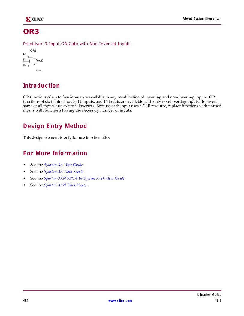
About Design Elements
OR3
Primitive: 3-Input OR Gate with Non-Inverted Inputs
IntroductionOR functions of up to five inputs are available in any combination of inverting and non-inverting inputs. ORfunctions of six to nine inputs, 12 inputs, and 16 inputs are available with only non-inverting inputs. To invertsome or all inputs, use external inverters. Because each input uses a CLB resource, replace functions with unusedinputs with functions having the necessary number of inputs.
Design Entry MethodThis design element is only for use in schematics.
For More Information• See the Spartan-3A User Guide.
• See the Spartan-3A Data Sheets.
• See the Spartan-3AN FPGA In-System Flash User Guide.
• See the Spartan-3AN Data Sheets.
Libraries Guide
454 www.xilinx.com 10.1

About Design Elements
OR3B1
Primitive: 3-Input OR Gate with 1 Inverted and 2 Non-Inverted Inputs
IntroductionOR functions of up to five inputs are available in any combination of inverting and non-inverting inputs. ORfunctions of six to nine inputs, 12 inputs, and 16 inputs are available with only non-inverting inputs. To invertsome or all inputs, use external inverters. Because each input uses a CLB resource, replace functions with unusedinputs with functions having the necessary number of inputs.
Design Entry MethodThis design element is only for use in schematics.
For More Information• See the Spartan-3A User Guide.
• See the Spartan-3A Data Sheets.
• See the Spartan-3AN FPGA In-System Flash User Guide.
• See the Spartan-3AN Data Sheets.
Libraries Guide
10.1 www.xilinx.com 455

About Design Elements
OR3B2
Primitive: 3-Input OR Gate with 2 Inverted and 1 Non-Inverted Inputs
IntroductionOR functions of up to five inputs are available in any combination of inverting and non-inverting inputs. ORfunctions of six to nine inputs, 12 inputs, and 16 inputs are available with only non-inverting inputs. To invertsome or all inputs, use external inverters. Because each input uses a CLB resource, replace functions with unusedinputs with functions having the necessary number of inputs.
Design Entry MethodThis design element is only for use in schematics.
For More Information• See the Spartan-3A User Guide.
• See the Spartan-3A Data Sheets.
• See the Spartan-3AN FPGA In-System Flash User Guide.
• See the Spartan-3AN Data Sheets.
Libraries Guide
456 www.xilinx.com 10.1

About Design Elements
OR3B3
Primitive: 3-Input OR Gate with Inverted Inputs
IntroductionOR functions of up to five inputs are available in any combination of inverting and non-inverting inputs. ORfunctions of six to nine inputs, 12 inputs, and 16 inputs are available with only non-inverting inputs. To invertsome or all inputs, use external inverters. Because each input uses a CLB resource, replace functions with unusedinputs with functions having the necessary number of inputs.
Design Entry MethodThis design element is only for use in schematics.
For More Information• See the Spartan-3A User Guide.
• See the Spartan-3A Data Sheets.
• See the Spartan-3AN FPGA In-System Flash User Guide.
• See the Spartan-3AN Data Sheets.
Libraries Guide
10.1 www.xilinx.com 457

About Design Elements
OR4
Primitive: 4-Input OR Gate with Non-Inverted Inputs
IntroductionOR functions of up to five inputs are available in any combination of inverting and non-inverting inputs. ORfunctions of six to nine inputs, 12 inputs, and 16 inputs are available with only non-inverting inputs. To invertsome or all inputs, use external inverters. Because each input uses a CLB resource, replace functions with unusedinputs with functions having the necessary number of inputs.
Design Entry MethodThis design element is only for use in schematics.
For More Information• See the Spartan-3A User Guide.
• See the Spartan-3A Data Sheets.
• See the Spartan-3AN FPGA In-System Flash User Guide.
• See the Spartan-3AN Data Sheets.
Libraries Guide
458 www.xilinx.com 10.1
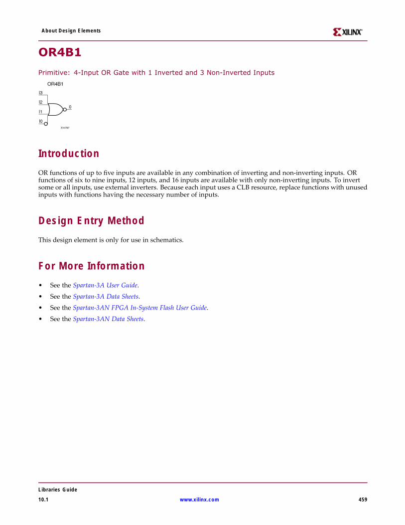
About Design Elements
OR4B1
Primitive: 4-Input OR Gate with 1 Inverted and 3 Non-Inverted Inputs
IntroductionOR functions of up to five inputs are available in any combination of inverting and non-inverting inputs. ORfunctions of six to nine inputs, 12 inputs, and 16 inputs are available with only non-inverting inputs. To invertsome or all inputs, use external inverters. Because each input uses a CLB resource, replace functions with unusedinputs with functions having the necessary number of inputs.
Design Entry MethodThis design element is only for use in schematics.
For More Information• See the Spartan-3A User Guide.
• See the Spartan-3A Data Sheets.
• See the Spartan-3AN FPGA In-System Flash User Guide.
• See the Spartan-3AN Data Sheets.
Libraries Guide
10.1 www.xilinx.com 459
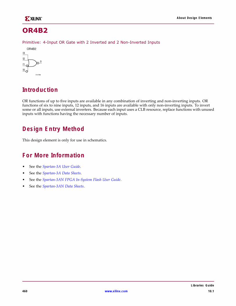
About Design Elements
OR4B2
Primitive: 4-Input OR Gate with 2 Inverted and 2 Non-Inverted Inputs
IntroductionOR functions of up to five inputs are available in any combination of inverting and non-inverting inputs. ORfunctions of six to nine inputs, 12 inputs, and 16 inputs are available with only non-inverting inputs. To invertsome or all inputs, use external inverters. Because each input uses a CLB resource, replace functions with unusedinputs with functions having the necessary number of inputs.
Design Entry MethodThis design element is only for use in schematics.
For More Information• See the Spartan-3A User Guide.
• See the Spartan-3A Data Sheets.
• See the Spartan-3AN FPGA In-System Flash User Guide.
• See the Spartan-3AN Data Sheets.
Libraries Guide
460 www.xilinx.com 10.1
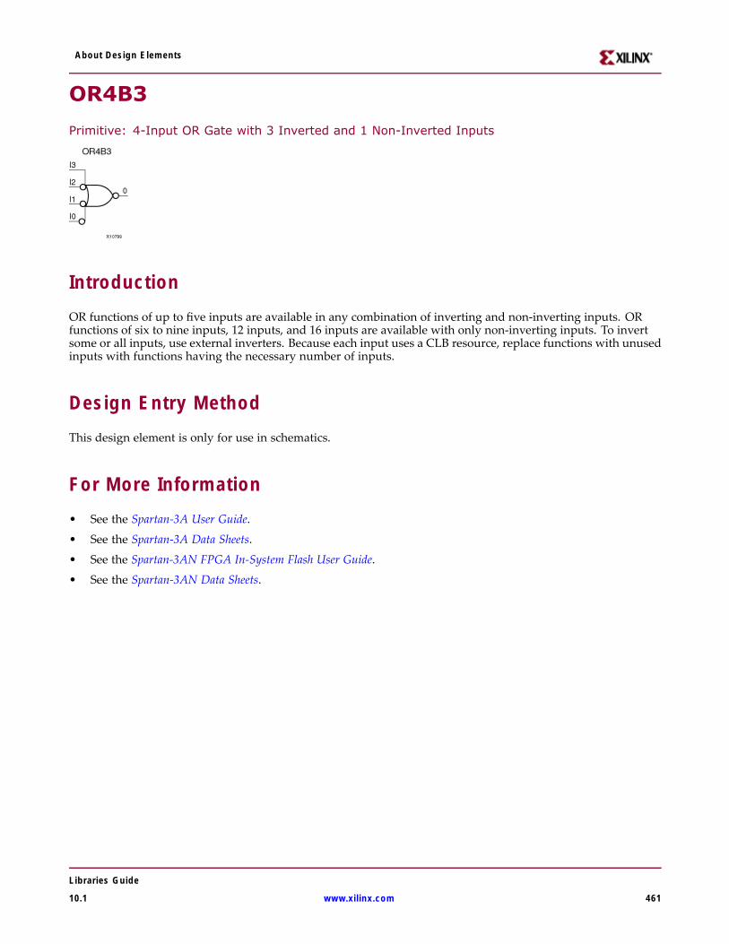
About Design Elements
OR4B3
Primitive: 4-Input OR Gate with 3 Inverted and 1 Non-Inverted Inputs
IntroductionOR functions of up to five inputs are available in any combination of inverting and non-inverting inputs. ORfunctions of six to nine inputs, 12 inputs, and 16 inputs are available with only non-inverting inputs. To invertsome or all inputs, use external inverters. Because each input uses a CLB resource, replace functions with unusedinputs with functions having the necessary number of inputs.
Design Entry MethodThis design element is only for use in schematics.
For More Information• See the Spartan-3A User Guide.
• See the Spartan-3A Data Sheets.
• See the Spartan-3AN FPGA In-System Flash User Guide.
• See the Spartan-3AN Data Sheets.
Libraries Guide
10.1 www.xilinx.com 461
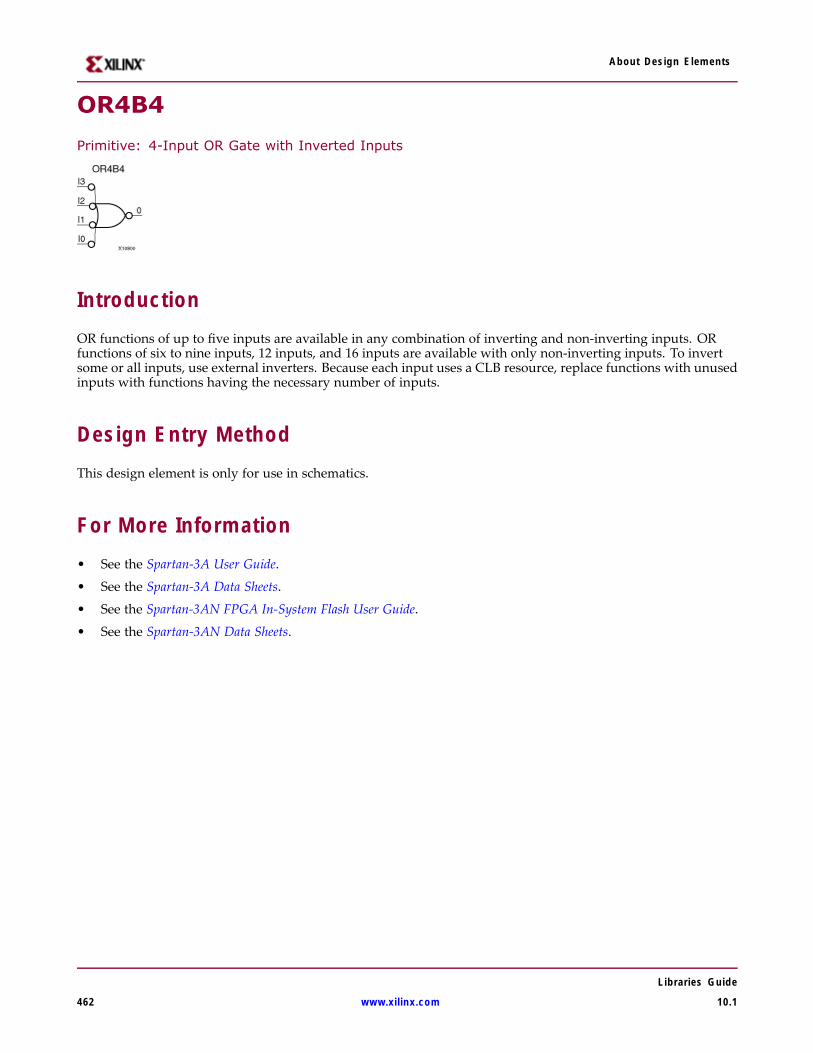
About Design Elements
OR4B4
Primitive: 4-Input OR Gate with Inverted Inputs
IntroductionOR functions of up to five inputs are available in any combination of inverting and non-inverting inputs. ORfunctions of six to nine inputs, 12 inputs, and 16 inputs are available with only non-inverting inputs. To invertsome or all inputs, use external inverters. Because each input uses a CLB resource, replace functions with unusedinputs with functions having the necessary number of inputs.
Design Entry MethodThis design element is only for use in schematics.
For More Information• See the Spartan-3A User Guide.
• See the Spartan-3A Data Sheets.
• See the Spartan-3AN FPGA In-System Flash User Guide.
• See the Spartan-3AN Data Sheets.
Libraries Guide
462 www.xilinx.com 10.1
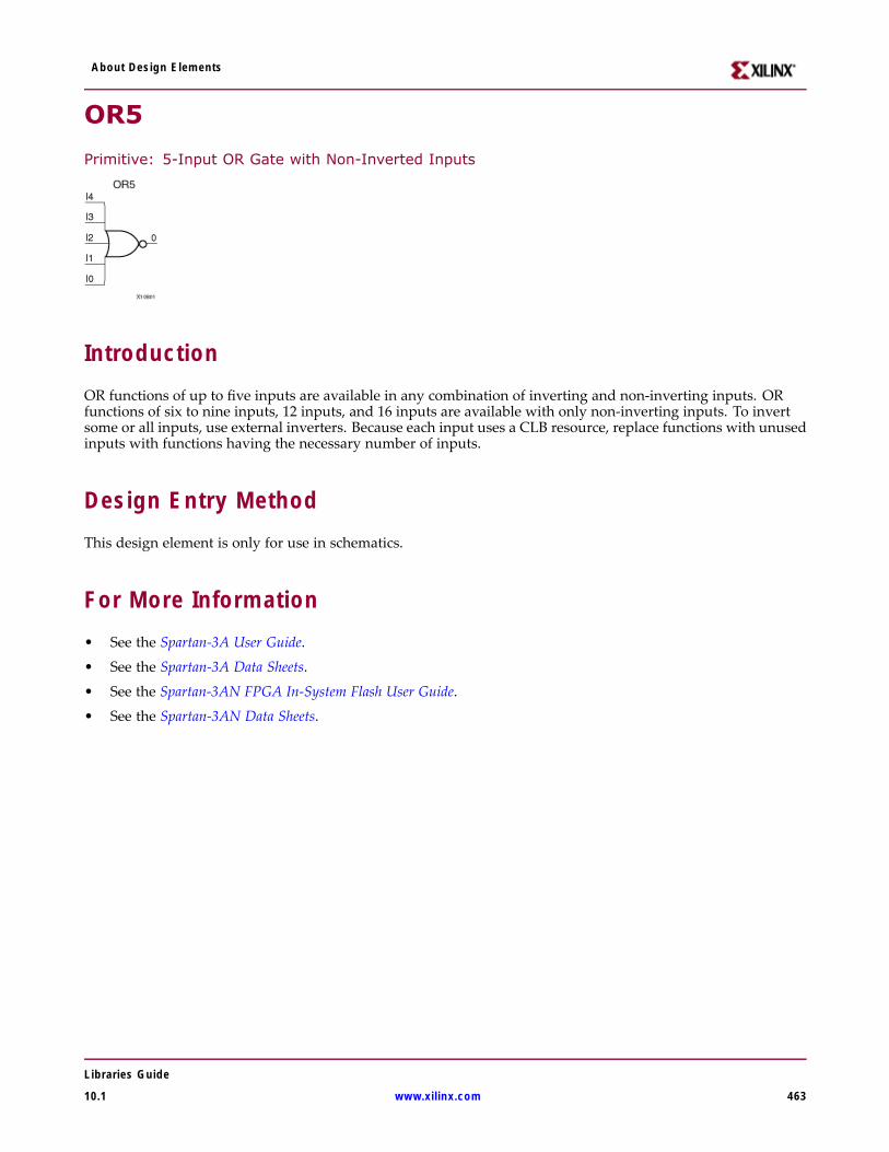
About Design Elements
OR5
Primitive: 5-Input OR Gate with Non-Inverted Inputs
IntroductionOR functions of up to five inputs are available in any combination of inverting and non-inverting inputs. ORfunctions of six to nine inputs, 12 inputs, and 16 inputs are available with only non-inverting inputs. To invertsome or all inputs, use external inverters. Because each input uses a CLB resource, replace functions with unusedinputs with functions having the necessary number of inputs.
Design Entry MethodThis design element is only for use in schematics.
For More Information• See the Spartan-3A User Guide.
• See the Spartan-3A Data Sheets.
• See the Spartan-3AN FPGA In-System Flash User Guide.
• See the Spartan-3AN Data Sheets.
Libraries Guide
10.1 www.xilinx.com 463
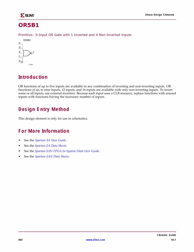
About Design Elements
OR5B1
Primitive: 5-Input OR Gate with 1 Inverted and 4 Non-Inverted Inputs
IntroductionOR functions of up to five inputs are available in any combination of inverting and non-inverting inputs. ORfunctions of six to nine inputs, 12 inputs, and 16 inputs are available with only non-inverting inputs. To invertsome or all inputs, use external inverters. Because each input uses a CLB resource, replace functions with unusedinputs with functions having the necessary number of inputs.
Design Entry MethodThis design element is only for use in schematics.
For More Information• See the Spartan-3A User Guide.
• See the Spartan-3A Data Sheets.
• See the Spartan-3AN FPGA In-System Flash User Guide.
• See the Spartan-3AN Data Sheets.
Libraries Guide
464 www.xilinx.com 10.1

About Design Elements
OR5B2
Primitive: 5-Input OR Gate with 2 Inverted and 3 Non-Inverted Inputs
IntroductionOR functions of up to five inputs are available in any combination of inverting and non-inverting inputs. ORfunctions of six to nine inputs, 12 inputs, and 16 inputs are available with only non-inverting inputs. To invertsome or all inputs, use external inverters. Because each input uses a CLB resource, replace functions with unusedinputs with functions having the necessary number of inputs.
Design Entry MethodThis design element is only for use in schematics.
For More Information• See the Spartan-3A User Guide.
• See the Spartan-3A Data Sheets.
• See the Spartan-3AN FPGA In-System Flash User Guide.
• See the Spartan-3AN Data Sheets.
Libraries Guide
10.1 www.xilinx.com 465

About Design Elements
OR5B3
Primitive: 5-Input OR Gate with 3 Inverted and 2 Non-Inverted Inputs
IntroductionOR functions of up to five inputs are available in any combination of inverting and non-inverting inputs. ORfunctions of six to nine inputs, 12 inputs, and 16 inputs are available with only non-inverting inputs. To invertsome or all inputs, use external inverters. Because each input uses a CLB resource, replace functions with unusedinputs with functions having the necessary number of inputs.
Design Entry MethodThis design element is only for use in schematics.
For More Information• See the Spartan-3A User Guide.
• See the Spartan-3A Data Sheets.
• See the Spartan-3AN FPGA In-System Flash User Guide.
• See the Spartan-3AN Data Sheets.
Libraries Guide
466 www.xilinx.com 10.1
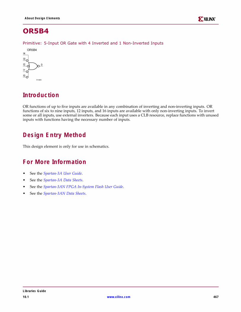
About Design Elements
OR5B4
Primitive: 5-Input OR Gate with 4 Inverted and 1 Non-Inverted Inputs
IntroductionOR functions of up to five inputs are available in any combination of inverting and non-inverting inputs. ORfunctions of six to nine inputs, 12 inputs, and 16 inputs are available with only non-inverting inputs. To invertsome or all inputs, use external inverters. Because each input uses a CLB resource, replace functions with unusedinputs with functions having the necessary number of inputs.
Design Entry MethodThis design element is only for use in schematics.
For More Information• See the Spartan-3A User Guide.
• See the Spartan-3A Data Sheets.
• See the Spartan-3AN FPGA In-System Flash User Guide.
• See the Spartan-3AN Data Sheets.
Libraries Guide
10.1 www.xilinx.com 467

About Design Elements
OR5B5
Primitive: 5-Input OR Gate with Inverted Inputs
IntroductionOR functions of up to five inputs are available in any combination of inverting and non-inverting inputs. ORfunctions of six to nine inputs, 12 inputs, and 16 inputs are available with only non-inverting inputs. To invertsome or all inputs, use external inverters. Because each input uses a CLB resource, replace functions with unusedinputs with functions having the necessary number of inputs.
Design Entry MethodThis design element is only for use in schematics.
For More Information• See the Spartan-3A User Guide.
• See the Spartan-3A Data Sheets.
• See the Spartan-3AN FPGA In-System Flash User Guide.
• See the Spartan-3AN Data Sheets.
Libraries Guide
468 www.xilinx.com 10.1
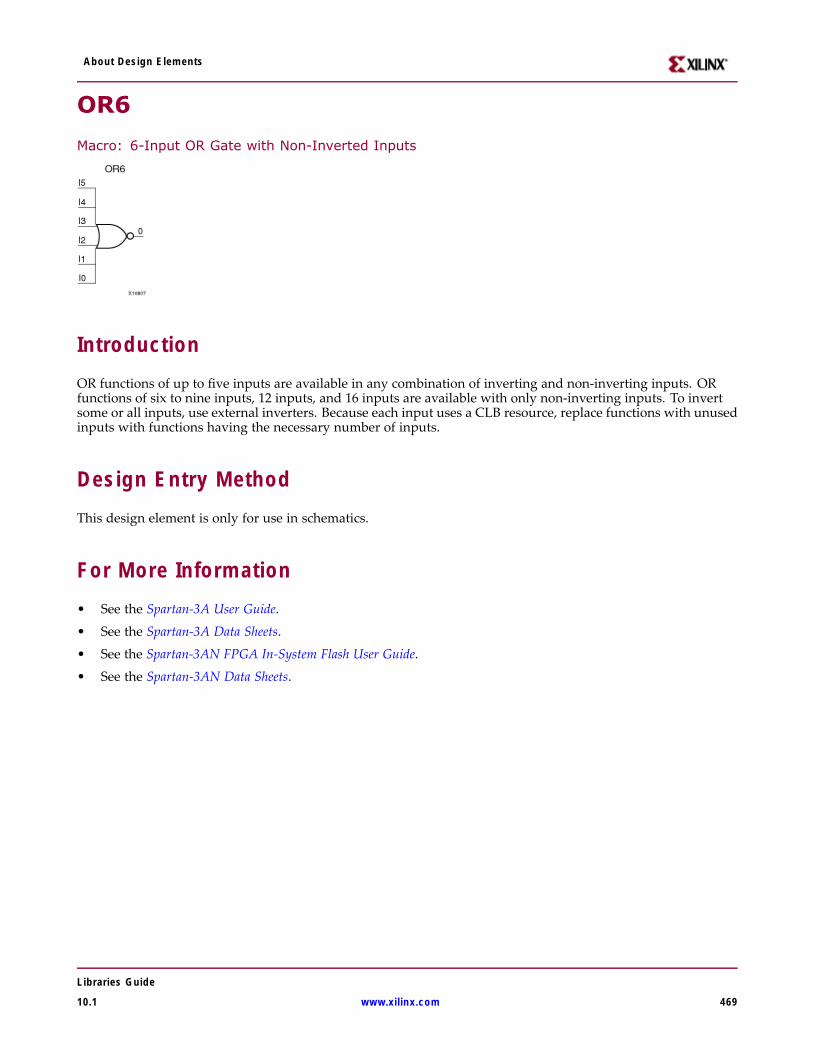
About Design Elements
OR6
Macro: 6-Input OR Gate with Non-Inverted Inputs
IntroductionOR functions of up to five inputs are available in any combination of inverting and non-inverting inputs. ORfunctions of six to nine inputs, 12 inputs, and 16 inputs are available with only non-inverting inputs. To invertsome or all inputs, use external inverters. Because each input uses a CLB resource, replace functions with unusedinputs with functions having the necessary number of inputs.
Design Entry MethodThis design element is only for use in schematics.
For More Information• See the Spartan-3A User Guide.
• See the Spartan-3A Data Sheets.
• See the Spartan-3AN FPGA In-System Flash User Guide.
• See the Spartan-3AN Data Sheets.
Libraries Guide
10.1 www.xilinx.com 469
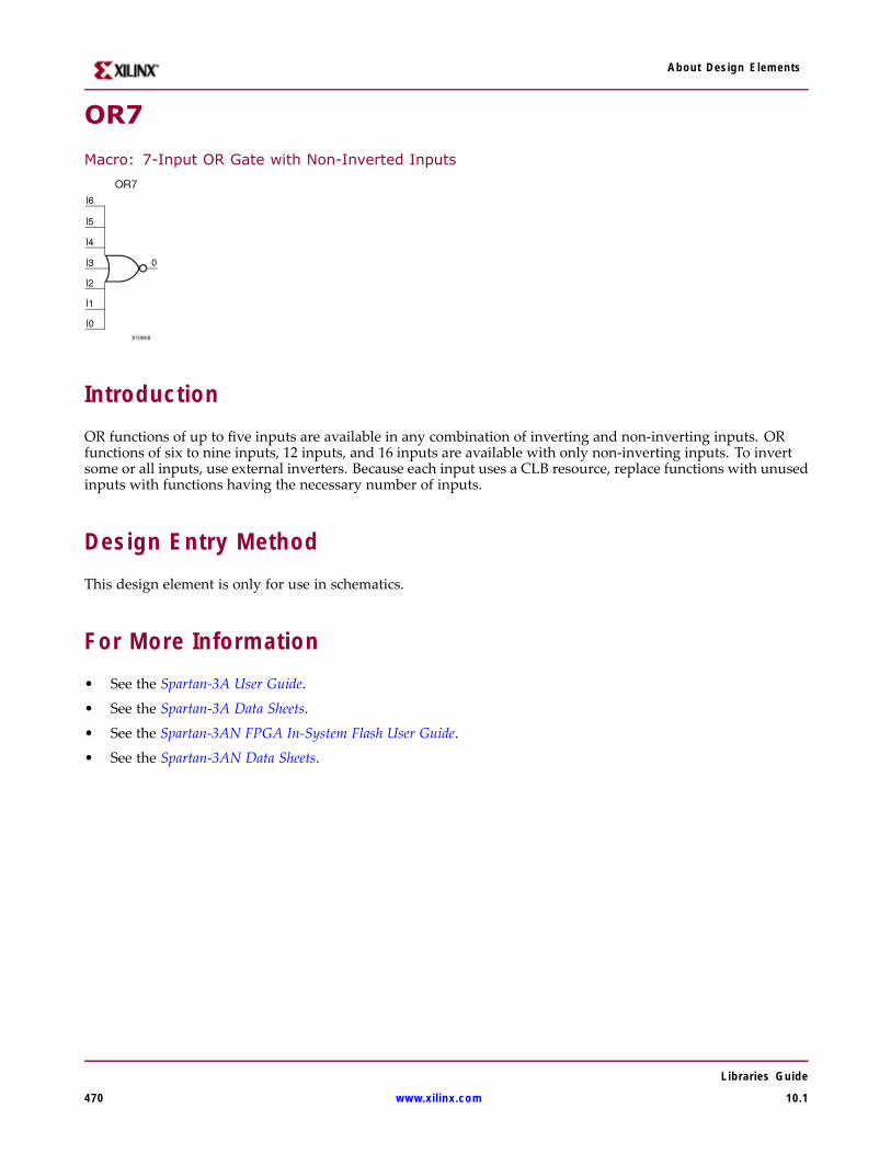
About Design Elements
OR7
Macro: 7-Input OR Gate with Non-Inverted Inputs
IntroductionOR functions of up to five inputs are available in any combination of inverting and non-inverting inputs. ORfunctions of six to nine inputs, 12 inputs, and 16 inputs are available with only non-inverting inputs. To invertsome or all inputs, use external inverters. Because each input uses a CLB resource, replace functions with unusedinputs with functions having the necessary number of inputs.
Design Entry MethodThis design element is only for use in schematics.
For More Information• See the Spartan-3A User Guide.
• See the Spartan-3A Data Sheets.
• See the Spartan-3AN FPGA In-System Flash User Guide.
• See the Spartan-3AN Data Sheets.
Libraries Guide
470 www.xilinx.com 10.1
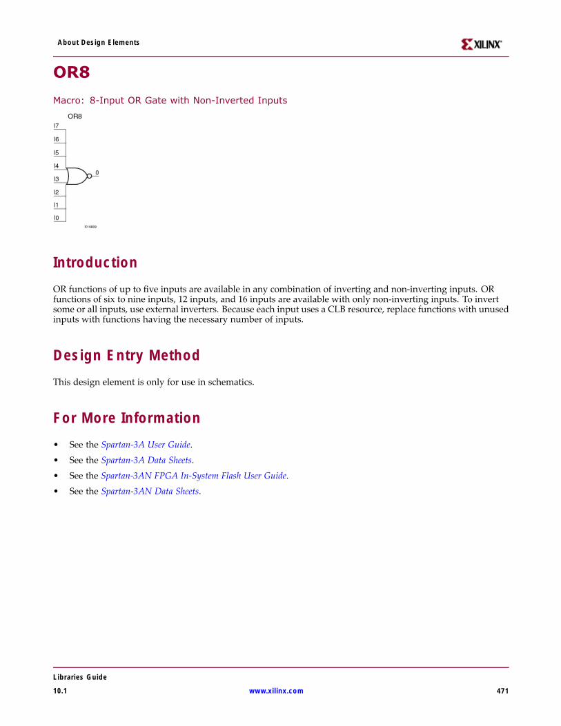
About Design Elements
OR8
Macro: 8-Input OR Gate with Non-Inverted Inputs
IntroductionOR functions of up to five inputs are available in any combination of inverting and non-inverting inputs. ORfunctions of six to nine inputs, 12 inputs, and 16 inputs are available with only non-inverting inputs. To invertsome or all inputs, use external inverters. Because each input uses a CLB resource, replace functions with unusedinputs with functions having the necessary number of inputs.
Design Entry MethodThis design element is only for use in schematics.
For More Information• See the Spartan-3A User Guide.
• See the Spartan-3A Data Sheets.
• See the Spartan-3AN FPGA In-System Flash User Guide.
• See the Spartan-3AN Data Sheets.
Libraries Guide
10.1 www.xilinx.com 471
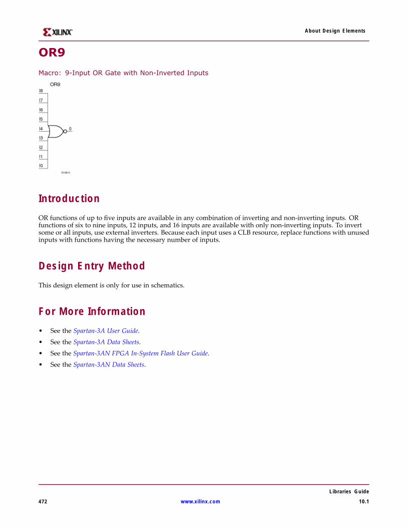
About Design Elements
OR9
Macro: 9-Input OR Gate with Non-Inverted Inputs
IntroductionOR functions of up to five inputs are available in any combination of inverting and non-inverting inputs. ORfunctions of six to nine inputs, 12 inputs, and 16 inputs are available with only non-inverting inputs. To invertsome or all inputs, use external inverters. Because each input uses a CLB resource, replace functions with unusedinputs with functions having the necessary number of inputs.
Design Entry MethodThis design element is only for use in schematics.
For More Information• See the Spartan-3A User Guide.
• See the Spartan-3A Data Sheets.
• See the Spartan-3AN FPGA In-System Flash User Guide.
• See the Spartan-3AN Data Sheets.
Libraries Guide
472 www.xilinx.com 10.1
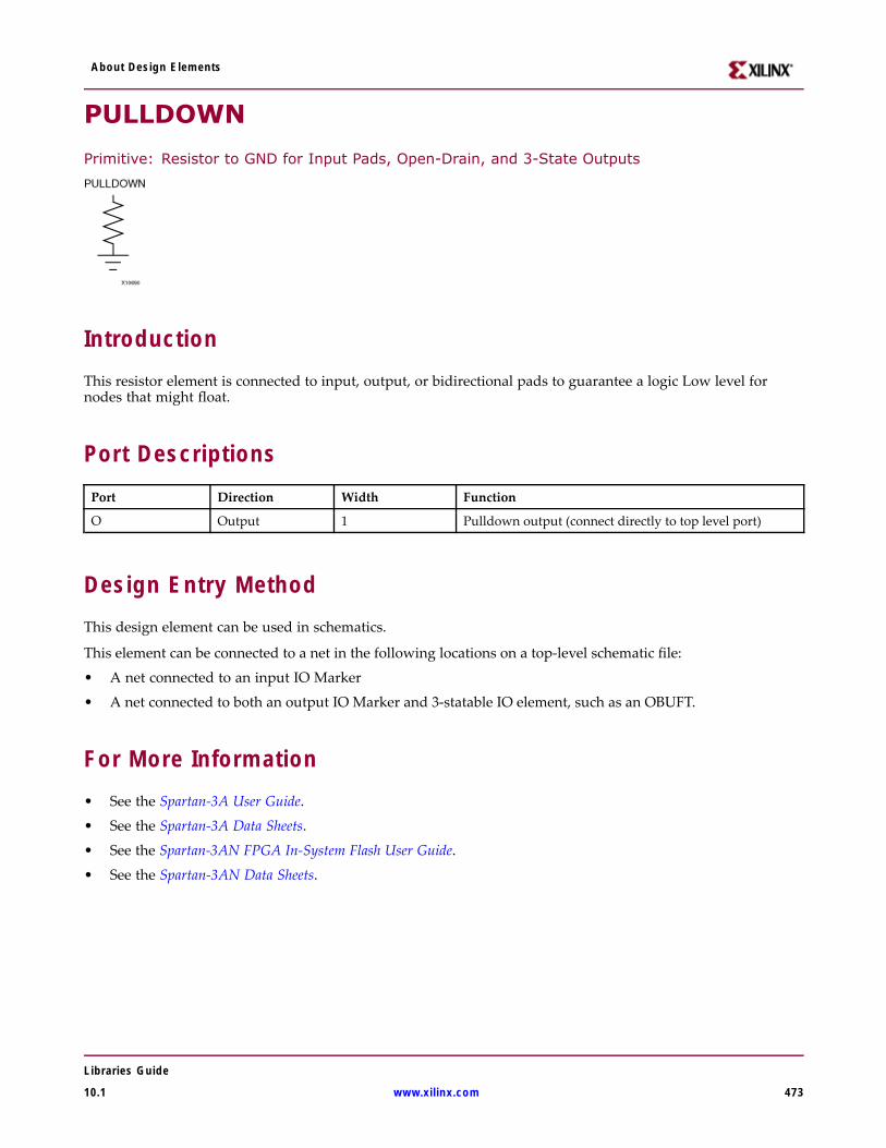
About Design Elements
PULLDOWN
Primitive: Resistor to GND for Input Pads, Open-Drain, and 3-State Outputs
IntroductionThis resistor element is connected to input, output, or bidirectional pads to guarantee a logic Low level fornodes that might float.
Port DescriptionsPort Direction Width Function
O Output 1 Pulldown output (connect directly to top level port)
Design Entry MethodThis design element can be used in schematics.
This element can be connected to a net in the following locations on a top-level schematic file:
• A net connected to an input IO Marker
• A net connected to both an output IO Marker and 3-statable IO element, such as an OBUFT.
For More Information• See the Spartan-3A User Guide.
• See the Spartan-3A Data Sheets.
• See the Spartan-3AN FPGA In-System Flash User Guide.
• See the Spartan-3AN Data Sheets.
Libraries Guide
10.1 www.xilinx.com 473
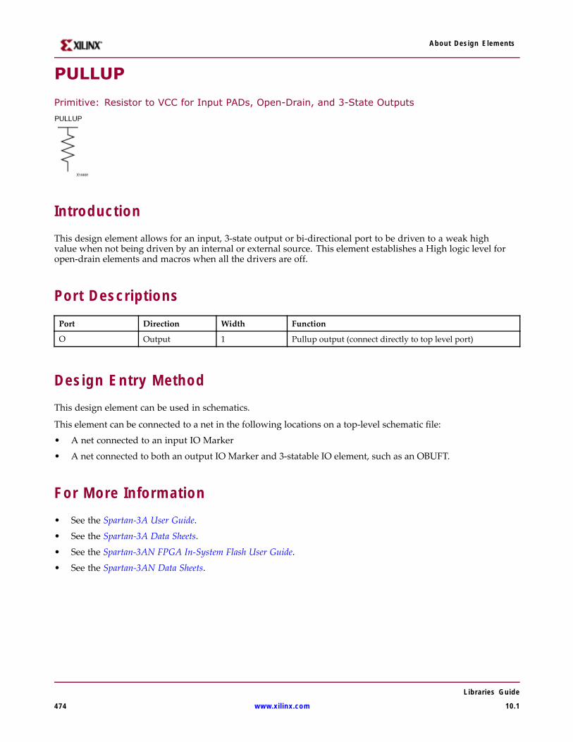
About Design Elements
PULLUP
Primitive: Resistor to VCC for Input PADs, Open-Drain, and 3-State Outputs
IntroductionThis design element allows for an input, 3-state output or bi-directional port to be driven to a weak highvalue when not being driven by an internal or external source. This element establishes a High logic level foropen-drain elements and macros when all the drivers are off.
Port DescriptionsPort Direction Width Function
O Output 1 Pullup output (connect directly to top level port)
Design Entry MethodThis design element can be used in schematics.
This element can be connected to a net in the following locations on a top-level schematic file:
• A net connected to an input IO Marker
• A net connected to both an output IO Marker and 3-statable IO element, such as an OBUFT.
For More Information• See the Spartan-3A User Guide.
• See the Spartan-3A Data Sheets.
• See the Spartan-3AN FPGA In-System Flash User Guide.
• See the Spartan-3AN Data Sheets.
Libraries Guide
474 www.xilinx.com 10.1
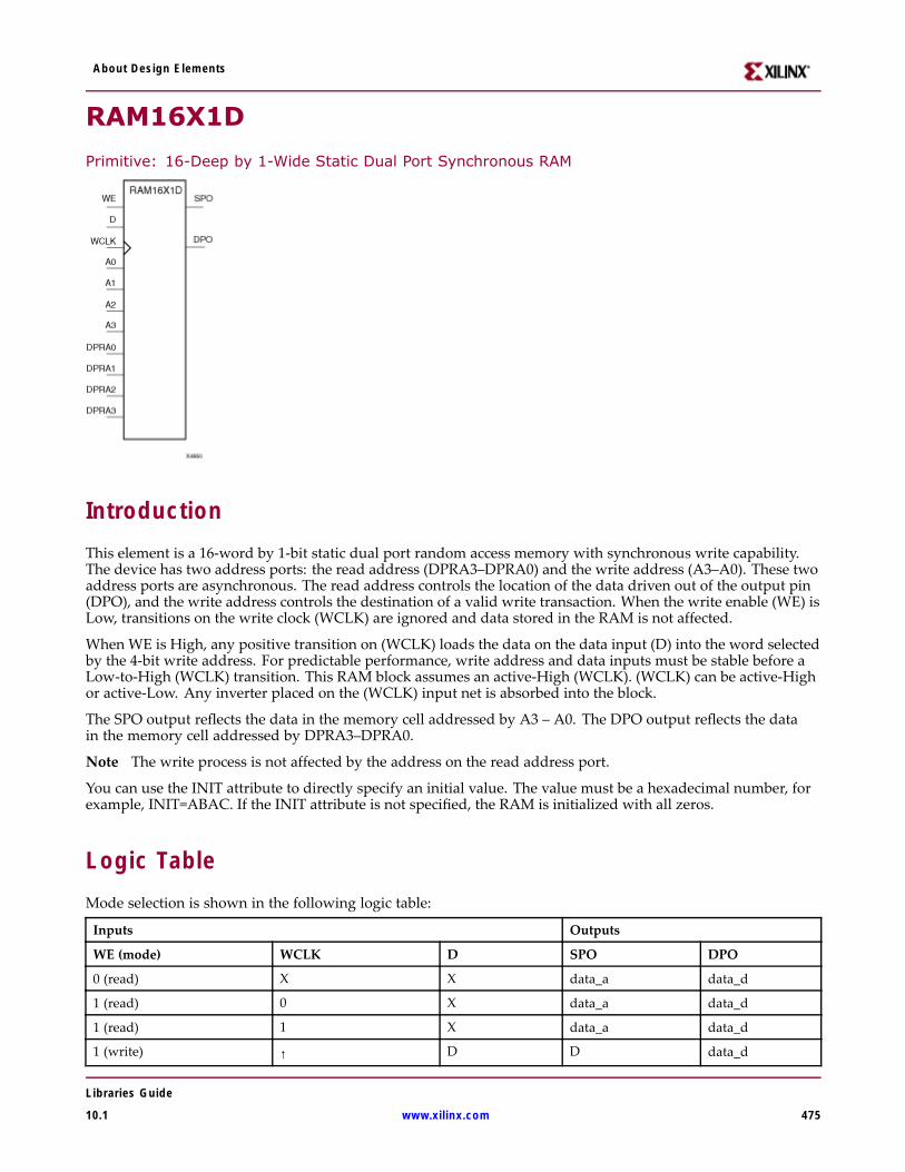
About Design Elements
RAM16X1D
Primitive: 16-Deep by 1-Wide Static Dual Port Synchronous RAM
IntroductionThis element is a 16-word by 1-bit static dual port random access memory with synchronous write capability.The device has two address ports: the read address (DPRA3–DPRA0) and the write address (A3–A0). These twoaddress ports are asynchronous. The read address controls the location of the data driven out of the output pin(DPO), and the write address controls the destination of a valid write transaction. When the write enable (WE) isLow, transitions on the write clock (WCLK) are ignored and data stored in the RAM is not affected.
When WE is High, any positive transition on (WCLK) loads the data on the data input (D) into the word selectedby the 4-bit write address. For predictable performance, write address and data inputs must be stable before aLow-to-High (WCLK) transition. This RAM block assumes an active-High (WCLK). (WCLK) can be active-Highor active-Low. Any inverter placed on the (WCLK) input net is absorbed into the block.
The SPO output reflects the data in the memory cell addressed by A3 – A0. The DPO output reflects the datain the memory cell addressed by DPRA3–DPRA0.
Note The write process is not affected by the address on the read address port.
You can use the INIT attribute to directly specify an initial value. The value must be a hexadecimal number, forexample, INIT=ABAC. If the INIT attribute is not specified, the RAM is initialized with all zeros.
Logic TableMode selection is shown in the following logic table:
Inputs Outputs
WE (mode) WCLK D SPO DPO
0 (read) X X data_a data_d
1 (read) 0 X data_a data_d
1 (read) 1 X data_a data_d
1 (write) ↑ D D data_d
Libraries Guide
10.1 www.xilinx.com 475
About Design Elements
Inputs Outputs
WE (mode) WCLK D SPO DPO
1 (read) ↓ X data_a data_d
data_a = word addressed by bits A3-A0
data_d = word addressed by bits DPRA3-DPRA0
Design Entry MethodThis design element can be used in schematics.
Available AttributesAttribute Type Allowed Values Default Description
INIT Hexadecimal Any 16-Bit Value Allzeros.
Initializes RAMs, registers, and look-uptables.
For More Information• See the Spartan-3A User Guide.
• See the Spartan-3A Data Sheets.
• See the Spartan-3AN FPGA In-System Flash User Guide.
• See the Spartan-3AN Data Sheets.
Libraries Guide
476 www.xilinx.com 10.1
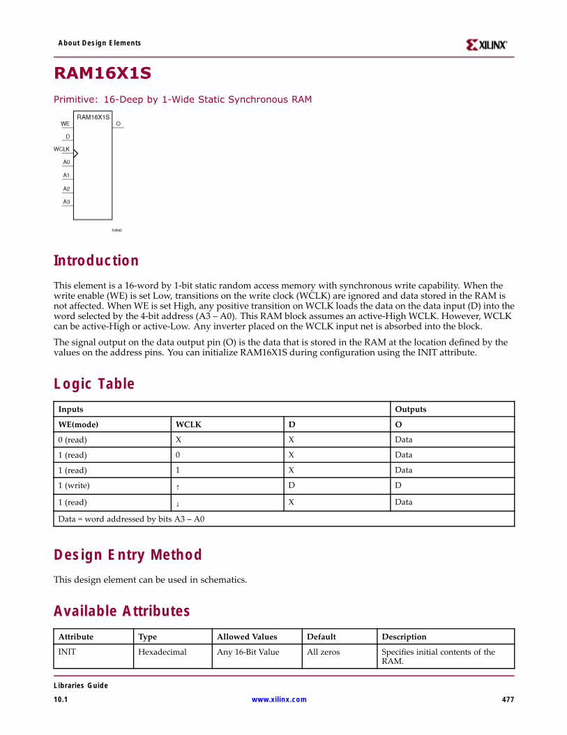
About Design Elements
RAM16X1SPrimitive: 16-Deep by 1-Wide Static Synchronous RAM
IntroductionThis element is a 16-word by 1-bit static random access memory with synchronous write capability. When thewrite enable (WE) is set Low, transitions on the write clock (WCLK) are ignored and data stored in the RAM isnot affected. When WE is set High, any positive transition on WCLK loads the data on the data input (D) into theword selected by the 4-bit address (A3 – A0). This RAM block assumes an active-High WCLK. However, WCLKcan be active-High or active-Low. Any inverter placed on the WCLK input net is absorbed into the block.
The signal output on the data output pin (O) is the data that is stored in the RAM at the location defined by thevalues on the address pins. You can initialize RAM16X1S during configuration using the INIT attribute.
Logic TableInputs Outputs
WE(mode) WCLK D O
0 (read) X X Data
1 (read) 0 X Data
1 (read) 1 X Data
1 (write) ↑ D D
1 (read) ↓ X Data
Data = word addressed by bits A3 – A0
Design Entry MethodThis design element can be used in schematics.
Available AttributesAttribute Type Allowed Values Default Description
INIT Hexadecimal Any 16-Bit Value All zeros Specifies initial contents of theRAM.
Libraries Guide
10.1 www.xilinx.com 477

About Design Elements
For More Information• See the Spartan-3A User Guide.
• See the Spartan-3A Data Sheets.
• See the Spartan-3AN FPGA In-System Flash User Guide.
• See the Spartan-3AN Data Sheets.
Libraries Guide
478 www.xilinx.com 10.1
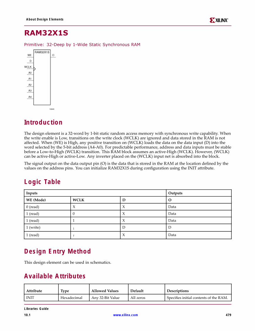
About Design Elements
RAM32X1SPrimitive: 32-Deep by 1-Wide Static Synchronous RAM
IntroductionThe design element is a 32-word by 1-bit static random access memory with synchronous write capability. Whenthe write enable is Low, transitions on the write clock (WCLK) are ignored and data stored in the RAM is notaffected. When (WE) is High, any positive transition on (WCLK) loads the data on the data input (D) into theword selected by the 5-bit address (A4-A0). For predictable performance, address and data inputs must be stablebefore a Low-to-High (WCLK) transition. This RAM block assumes an active-High (WCLK). However, (WCLK)can be active-High or active-Low. Any inverter placed on the (WCLK) input net is absorbed into the block.
The signal output on the data output pin (O) is the data that is stored in the RAM at the location defined by thevalues on the address pins. You can initialize RAM32X1S during configuration using the INIT attribute.
Logic TableInputs Outputs
WE (Mode) WCLK D O
0 (read) X X Data
1 (read) 0 X Data
1 (read) 1 X Data
1 (write) ↓ D D
1 (read) ↑ X Data
Design Entry MethodThis design element can be used in schematics.
Available Attributes
Attribute Type Allowed Values Default Descriptions
INIT Hexadecimal Any 32-Bit Value All zeros Specifies initial contents of the RAM.
Libraries Guide
10.1 www.xilinx.com 479

About Design Elements
For More Information• See the Spartan-3A User Guide.
• See the Spartan-3A Data Sheets.
• See the Spartan-3AN FPGA In-System Flash User Guide.
• See the Spartan-3AN Data Sheets.
Libraries Guide
480 www.xilinx.com 10.1
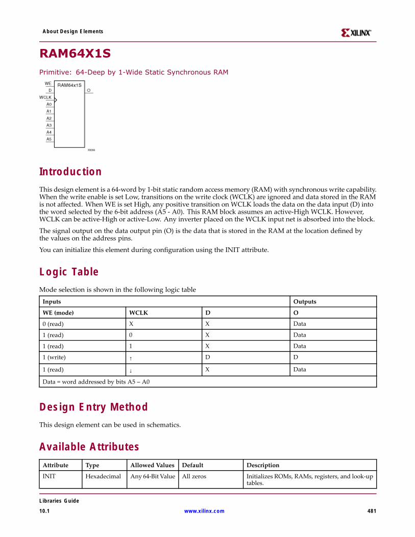
About Design Elements
RAM64X1SPrimitive: 64-Deep by 1-Wide Static Synchronous RAM
IntroductionThis design element is a 64-word by 1-bit static random access memory (RAM) with synchronous write capability.When the write enable is set Low, transitions on the write clock (WCLK) are ignored and data stored in the RAMis not affected. When WE is set High, any positive transition on WCLK loads the data on the data input (D) intothe word selected by the 6-bit address (A5 - A0). This RAM block assumes an active-High WCLK. However,WCLK can be active-High or active-Low. Any inverter placed on the WCLK input net is absorbed into the block.
The signal output on the data output pin (O) is the data that is stored in the RAM at the location defined bythe values on the address pins.
You can initialize this element during configuration using the INIT attribute.
Logic TableMode selection is shown in the following logic table
Inputs Outputs
WE (mode) WCLK D O
0 (read) X X Data
1 (read) 0 X Data
1 (read) 1 X Data
1 (write) ↑ D D
1 (read) ↓ X Data
Data = word addressed by bits A5 – A0
Design Entry MethodThis design element can be used in schematics.
Available AttributesAttribute Type Allowed Values Default Description
INIT Hexadecimal Any 64-Bit Value All zeros Initializes ROMs, RAMs, registers, and look-uptables.
Libraries Guide
10.1 www.xilinx.com 481

About Design Elements
For More Information• See the Spartan-3A User Guide.
• See the Spartan-3A Data Sheets.
• See the Spartan-3AN FPGA In-System Flash User Guide.
• See the Spartan-3AN Data Sheets.
Libraries Guide
482 www.xilinx.com 10.1
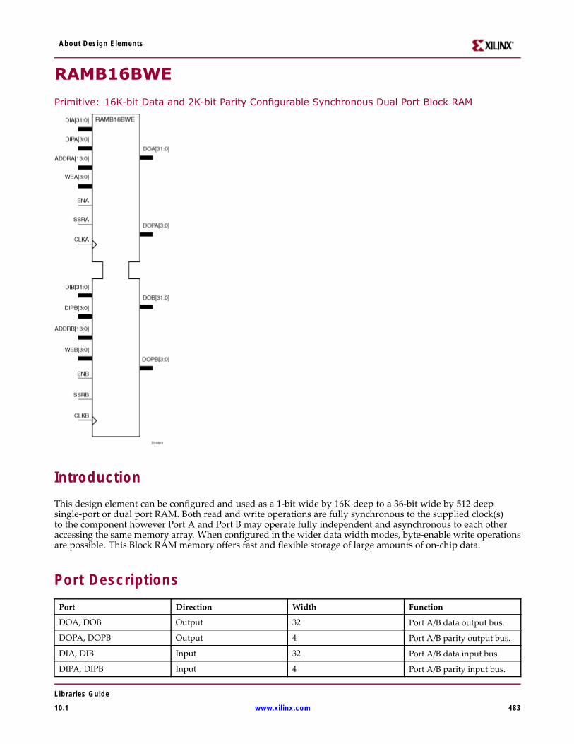
About Design Elements
RAMB16BWE
Primitive: 16K-bit Data and 2K-bit Parity Configurable Synchronous Dual Port Block RAM
IntroductionThis design element can be configured and used as a 1-bit wide by 16K deep to a 36-bit wide by 512 deepsingle-port or dual port RAM. Both read and write operations are fully synchronous to the supplied clock(s)to the component however Port A and Port B may operate fully independent and asynchronous to each otheraccessing the same memory array. When configured in the wider data width modes, byte-enable write operationsare possible. This Block RAM memory offers fast and flexible storage of large amounts of on-chip data.
Port DescriptionsPort Direction Width Function
DOA, DOB Output 32 Port A/B data output bus.
DOPA, DOPB Output 4 Port A/B parity output bus.
DIA, DIB Input 32 Port A/B data input bus.
DIPA, DIPB Input 4 Port A/B parity input bus.
Libraries Guide
10.1 www.xilinx.com 483
About Design Elements
Port Direction Width Function
ADDRA[13:5], ADDRB[13:5] Input 14 Port A/B address inputbus. LSB always exists onADDRA/B[0] while the MSBis determined by the settingsfor DATA_WIDTH_A/B.
WEA[0:0], WEB[0:0] Input 4 Port A/B byte-wide writeenable.
ENA, ENB Input 1 Port A/B enable
SSRA, SSRB Input 1 Port A/B output registerssynchronous reset.
CLKA, CLKB Input 1 Port A/B clock input.
Design Entry MethodThis design element can be used in schematics.
This element can be inferred by most synthesis tools by properly describing the RAM behavior in standard RTLcode (consult synthesis tool documentation for details). Alternatively, CORE Generator can also create thedesired macro for this RAM. If it is desired to have more control over the implementation or placement ofthis component, it may also be directly instantiated. In order to instantiate this component, use the ISE HDLTemplates or instantiation template below and paste into your code. Connect all necessary inputs to the desiredsignals in the design. The CLKA/CLKB clock signals must be tied to an active clock for RAM operation and theSSRA/SSRB reset signals must be either tied to a logic zero or to the proper reset signal. ENA/ENB must either betied to a logic one or a proper RAM port enable signal. Refer to the DATA_WIDTH table below for the necessarydata input, data output, write enable and address connection information for each DATA_WIDTH setting asthe necessary connections for these signals change based on this attribute. All other output signals can be leftunconnected (open) and all unused input signals should be tied to a logic zero.
The following table shows the necessary input and output connections for the variable input ports for eachDATA_WIDTH values for either Port A or Port B:
DATA_WIDTH Value DI, DIP Connections ADDR Connections WE ConnectionsDO, DOPConnections
1 DI[0] ADDR[13:0] Connect WE[3:0] tosingle user WE signal
DO[0]
2 DI[1:0] ADDR[13:1] Connect WE[3:0] tosingle user WE signal
DO[1:0]
4 DI[3:0] ADDR[13:2] Connect WE[3:0] tosingle user WE signal
DO[3:0]
9 DI[7:0], DIP[0] ADDR[13:3] Connect WE[3:0] tosingle user WE signal
DO[7:0], DOP[0]
18 DI[15:0], DIP[1:0] ADDR[13:4] Connect WE[0] andWE[2] to user WE[0]and WE[1] and WE[3]to user WE[1]
DO[15:0], DOP[1:0]
36 DI[31:0], DIP[3:0] ADDR[13:5] Connect each WE[3:0]signal to the associatedbyte write enable.
DO[31:0], DOP[3:0]
Alternatively, the prior RAMB16_Sm_Sn design elements can be instantiated if a byte-enable operation isnot necessary. Also new convenience macros called RAMB16BWE_Sm_Sn are provided to allow for easierinstantiation of this RAM with byte-enable operation. If either of these components is used, the softwareautomatically re-target them to a properly configured RAMB16BWE component.
Libraries Guide
484 www.xilinx.com 10.1
About Design Elements
Available AttributesAttribute Type Allowed Values Default Description
DATA_WIDTH_A,DATA_WIDTH_B
Integer 0, 1, 2, 4, 9, 18, or 36 0 Specifies the configurable data width forPorts A and B.
INIT_A,INIT_B
Hexadecimal Any 36-Bit Value All zeros Specifies the initial value on the Port Boutput after configuration.
SIM_COLLISION_CHECK
String ALL,"WARNING_ONLY","GENERATE_X_ONLY"or "NONE”
"ALL”
Allows modification of the simulationbehavior so that if a memory collisionoccurs:
"ALL" = warning produced and affectedoutputs/memory location go unknown (X).
WARNING_ONLY = warning producedand affected outputs/memory retain lastvalue.
GENERATE_X_ ONLY = no warning,however, affected outputs/memory gounknown (X).
NONE = no warning and affectedoutputs/memory retain last value.
Note: Setting this to a value other than"ALL" can allow problems in the designto go unnoticed during simulation. Careshould be taken when changing the valueof this attribute.
SRVAL_A,SRVAL_B
Hexadecimal Any 36-Bit Value All zeros Specifies the output value of Port B uponthe assertion of the synchronous reset(SSRB) signal.
WRITE_MODE_A,WRITE_MODE_B
String "WRITE_FIRST","READ_FIRST", or"NO_CHANGE”
"WRITE_FIRST”
Specifies output behavior of the port beingwritten to:
WRITE_FIRST" = written value appears onoutput port of the RAM.
READ_FIRST = previous RAM contents forthat memory location appear on the outputport.
NO_CHANGE = previous value on theoutput port remains the same.
INIT_00 to INIT_3F Hexadecimal Any 256-Bit Value All zeros Allows specification of the initial contentsof the 16Kb data memory array.
INITP_00 toINITP_07
Hexadecimal Any 256-Bit Value All zeros Allows specification of the initial contentsof the 2Kb parity data memory array.
For More Information• See the Spartan-3A User Guide.• See the Spartan-3A Data Sheets.• See the Spartan-3AN FPGA In-System Flash User Guide.• See the Spartan-3AN Data Sheets.
Libraries Guide
10.1 www.xilinx.com 485
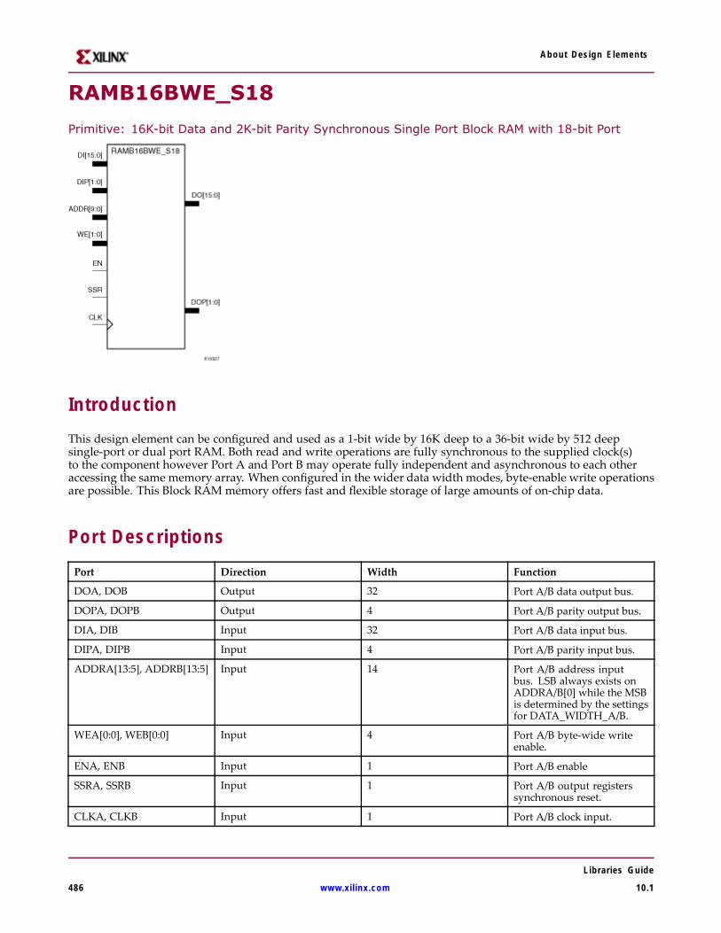
About Design Elements
RAMB16BWE_S18
Primitive: 16K-bit Data and 2K-bit Parity Synchronous Single Port Block RAM with 18-bit Port
IntroductionThis design element can be configured and used as a 1-bit wide by 16K deep to a 36-bit wide by 512 deepsingle-port or dual port RAM. Both read and write operations are fully synchronous to the supplied clock(s)to the component however Port A and Port B may operate fully independent and asynchronous to each otheraccessing the same memory array. When configured in the wider data width modes, byte-enable write operationsare possible. This Block RAM memory offers fast and flexible storage of large amounts of on-chip data.
Port DescriptionsPort Direction Width Function
DOA, DOB Output 32 Port A/B data output bus.
DOPA, DOPB Output 4 Port A/B parity output bus.
DIA, DIB Input 32 Port A/B data input bus.
DIPA, DIPB Input 4 Port A/B parity input bus.
ADDRA[13:5], ADDRB[13:5] Input 14 Port A/B address inputbus. LSB always exists onADDRA/B[0] while the MSBis determined by the settingsfor DATA_WIDTH_A/B.
WEA[0:0], WEB[0:0] Input 4 Port A/B byte-wide writeenable.
ENA, ENB Input 1 Port A/B enable
SSRA, SSRB Input 1 Port A/B output registerssynchronous reset.
CLKA, CLKB Input 1 Port A/B clock input.
Libraries Guide
486 www.xilinx.com 10.1

About Design Elements
Design Entry MethodThis design element can be used in schematics.
This element can be inferred by most synthesis tools by properly describing the RAM behavior in standard RTLcode (consult synthesis tool documentation for details). Alternatively, CORE Generator can also create thedesired macro for this RAM. If it is desired to have more control over the implementation or placement ofthis component, it may also be directly instantiated. In order to instantiate this component, use the ISE HDLTemplates or instantiation template below and paste into your code. Connect all necessary inputs to the desiredsignals in the design. The CLKA/CLKB clock signals must be tied to an active clock for RAM operation and theSSRA/SSRB reset signals must be either tied to a logic zero or to the proper reset signal. ENA/ENB must either betied to a logic one or a proper RAM port enable signal. Refer to the DATA_WIDTH table below for the necessarydata input, data output, write enable and address connection information for each DATA_WIDTH setting asthe necessary connections for these signals change based on this attribute. All other output signals can be leftunconnected (open) and all unused input signals should be tied to a logic zero.
The following table shows the necessary input and output connections for the variable input ports for eachDATA_WIDTH values for either Port A or Port B:
DATA_WIDTH Value DI, DIP Connections ADDR Connections WE ConnectionsDO, DOPConnections
1 DI[0] ADDR[13:0] Connect WE[3:0] tosingle user WE signal
DO[0]
2 DI[1:0] ADDR[13:1] Connect WE[3:0] tosingle user WE signal
DO[1:0]
4 DI[3:0] ADDR[13:2] Connect WE[3:0] tosingle user WE signal
DO[3:0]
9 DI[7:0], DIP[0] ADDR[13:3] Connect WE[3:0] tosingle user WE signal
DO[7:0], DOP[0]
18 DI[15:0], DIP[1:0] ADDR[13:4] Connect WE[0] andWE[2] to user WE[0]and WE[1] and WE[3]to user WE[1]
DO[15:0], DOP[1:0]
36 DI[31:0], DIP[3:0] ADDR[13:5] Connect each WE[3:0]signal to the associatedbyte write enable.
DO[31:0], DOP[3:0]
Alternatively, the prior RAMB16_Sm_Sn design elements can be instantiated if a byte-enable operation isnot necessary. Also new convenience macros called RAMB16BWE_Sm_Sn are provided to allow for easierinstantiation of this RAM with byte-enable operation. If either of these components is used, the softwareautomatically re-target them to a properly configured RAMB16BWE component.
Available AttributesAttribute Type Allowed Values Default Description
DATA_WIDTH_A,DATA_WIDTH_B
Integer 0, 1, 2, 4, 9, 18, or 36 0 Specifies the configurable data width forPorts A and B.
INIT_A,INIT_B
Hexadecimal Any 36-Bit Value All zeros Specifies the initial value on the Port Boutput after configuration.
Libraries Guide
10.1 www.xilinx.com 487

About Design Elements
Attribute Type Allowed Values Default Description
SIM_COLLISION_CHECK
String ALL,"WARNING_ONLY","GENERATE_X_ONLY"or "NONE”
"ALL”
Allows modification of the simulationbehavior so that if a memory collisionoccurs:
"ALL" = warning produced and affectedoutputs/memory location go unknown (X).
WARNING_ONLY = warning producedand affected outputs/memory retain lastvalue.
GENERATE_X_ ONLY = no warning,however, affected outputs/memory gounknown (X).
NONE = no warning and affectedoutputs/memory retain last value.
Note: Setting this to a value other than"ALL" can allow problems in the designto go unnoticed during simulation. Careshould be taken when changing the valueof this attribute.
SRVAL_A,SRVAL_B
Hexadecimal Any 36-Bit Value All zeros Specifies the output value of Port B uponthe assertion of the synchronous reset(SSRB) signal.
WRITE_MODE_A,WRITE_MODE_B
String "WRITE_FIRST","READ_FIRST", or"NO_CHANGE”
"WRITE_FIRST”
Specifies output behavior of the port beingwritten to:
WRITE_FIRST" = written value appears onoutput port of the RAM.
READ_FIRST = previous RAM contents forthat memory location appear on the outputport.
NO_CHANGE = previous value on theoutput port remains the same.
INIT_00 to INIT_3F Hexadecimal Any 256-Bit Value All zeros Allows specification of the initial contentsof the 16Kb data memory array.
INITP_00 toINITP_07
Hexadecimal Any 256-Bit Value All zeros Allows specification of the initial contentsof the 2Kb parity data memory array.
For More Information• See the Spartan-3A User Guide.
• See the Spartan-3A Data Sheets.
• See the Spartan-3AN FPGA In-System Flash User Guide.
• See the Spartan-3AN Data Sheets.
Libraries Guide
488 www.xilinx.com 10.1
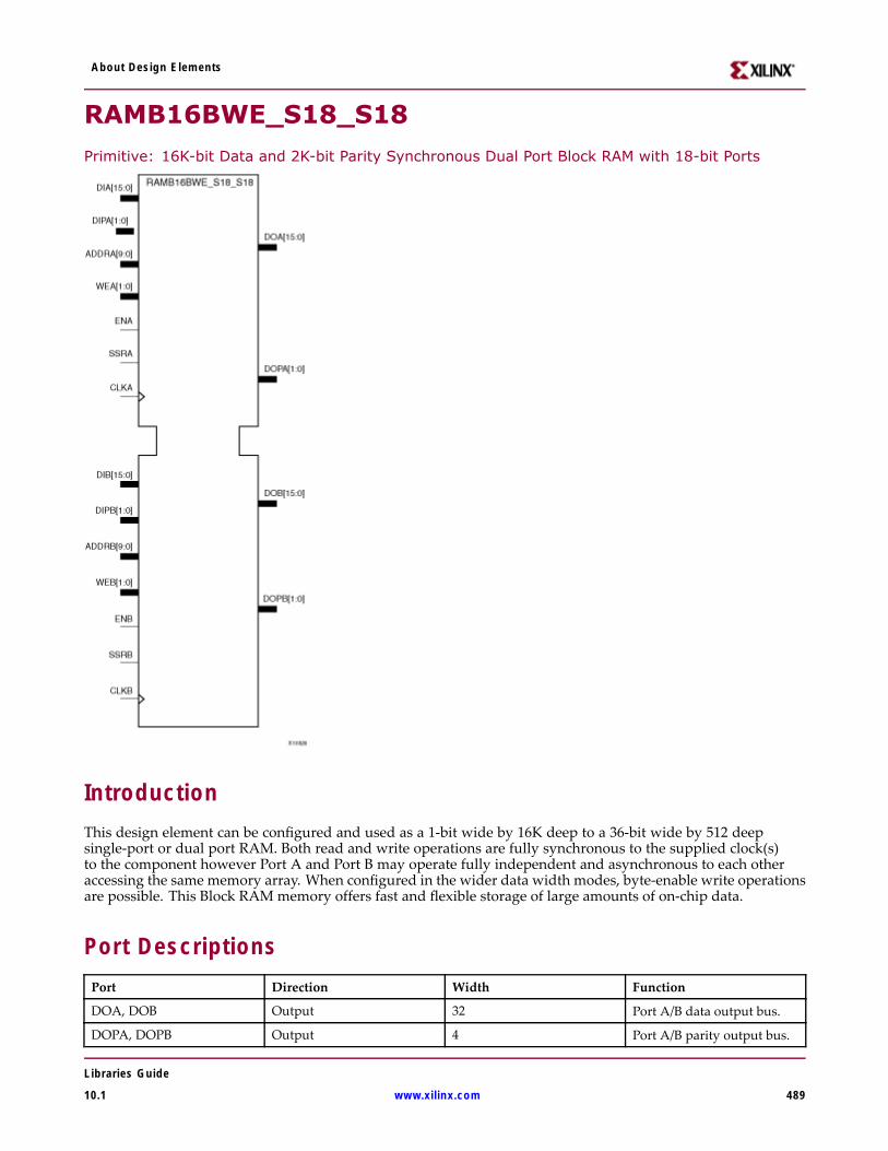
About Design Elements
RAMB16BWE_S18_S18
Primitive: 16K-bit Data and 2K-bit Parity Synchronous Dual Port Block RAM with 18-bit Ports
IntroductionThis design element can be configured and used as a 1-bit wide by 16K deep to a 36-bit wide by 512 deepsingle-port or dual port RAM. Both read and write operations are fully synchronous to the supplied clock(s)to the component however Port A and Port B may operate fully independent and asynchronous to each otheraccessing the same memory array. When configured in the wider data width modes, byte-enable write operationsare possible. This Block RAM memory offers fast and flexible storage of large amounts of on-chip data.
Port DescriptionsPort Direction Width Function
DOA, DOB Output 32 Port A/B data output bus.
DOPA, DOPB Output 4 Port A/B parity output bus.
Libraries Guide
10.1 www.xilinx.com 489

About Design Elements
Port Direction Width Function
DIA, DIB Input 32 Port A/B data input bus.
DIPA, DIPB Input 4 Port A/B parity input bus.
ADDRA[13:5], ADDRB[13:5] Input 14 Port A/B address inputbus. LSB always exists onADDRA/B[0] while the MSBis determined by the settingsfor DATA_WIDTH_A/B.
WEA[0:0], WEB[0:0] Input 4 Port A/B byte-wide writeenable.
ENA, ENB Input 1 Port A/B enable
SSRA, SSRB Input 1 Port A/B output registerssynchronous reset.
CLKA, CLKB Input 1 Port A/B clock input.
Design Entry MethodThis design element can be used in schematics.
This element can be inferred by most synthesis tools by properly describing the RAM behavior in standard RTLcode (consult synthesis tool documentation for details). Alternatively, CORE Generator can also create thedesired macro for this RAM. If it is desired to have more control over the implementation or placement ofthis component, it may also be directly instantiated. In order to instantiate this component, use the ISE HDLTemplates or instantiation template below and paste into your code. Connect all necessary inputs to the desiredsignals in the design. The CLKA/CLKB clock signals must be tied to an active clock for RAM operation and theSSRA/SSRB reset signals must be either tied to a logic zero or to the proper reset signal. ENA/ENB must either betied to a logic one or a proper RAM port enable signal. Refer to the DATA_WIDTH table below for the necessarydata input, data output, write enable and address connection information for each DATA_WIDTH setting asthe necessary connections for these signals change based on this attribute. All other output signals can be leftunconnected (open) and all unused input signals should be tied to a logic zero.
The following table shows the necessary input and output connections for the variable input ports for eachDATA_WIDTH values for either Port A or Port B:
DATA_WIDTH Value DI, DIP Connections ADDR Connections WE ConnectionsDO, DOPConnections
1 DI[0] ADDR[13:0] Connect WE[3:0] tosingle user WE signal
DO[0]
2 DI[1:0] ADDR[13:1] Connect WE[3:0] tosingle user WE signal
DO[1:0]
4 DI[3:0] ADDR[13:2] Connect WE[3:0] tosingle user WE signal
DO[3:0]
9 DI[7:0], DIP[0] ADDR[13:3] Connect WE[3:0] tosingle user WE signal
DO[7:0], DOP[0]
18 DI[15:0], DIP[1:0] ADDR[13:4] Connect WE[0] andWE[2] to user WE[0]and WE[1] and WE[3]to user WE[1]
DO[15:0], DOP[1:0]
36 DI[31:0], DIP[3:0] ADDR[13:5] Connect each WE[3:0]signal to the associatedbyte write enable.
DO[31:0], DOP[3:0]
Libraries Guide
490 www.xilinx.com 10.1
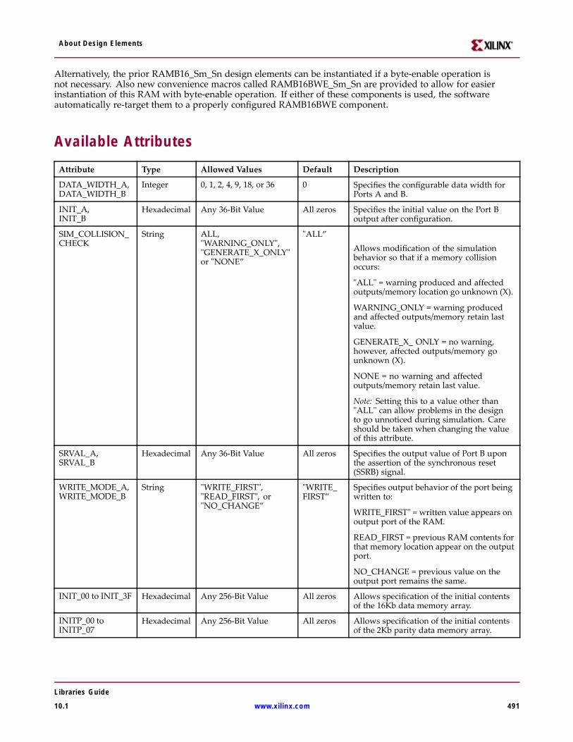
About Design Elements
Alternatively, the prior RAMB16_Sm_Sn design elements can be instantiated if a byte-enable operation isnot necessary. Also new convenience macros called RAMB16BWE_Sm_Sn are provided to allow for easierinstantiation of this RAM with byte-enable operation. If either of these components is used, the softwareautomatically re-target them to a properly configured RAMB16BWE component.
Available AttributesAttribute Type Allowed Values Default Description
DATA_WIDTH_A,DATA_WIDTH_B
Integer 0, 1, 2, 4, 9, 18, or 36 0 Specifies the configurable data width forPorts A and B.
INIT_A,INIT_B
Hexadecimal Any 36-Bit Value All zeros Specifies the initial value on the Port Boutput after configuration.
SIM_COLLISION_CHECK
String ALL,"WARNING_ONLY","GENERATE_X_ONLY"or "NONE”
"ALL”
Allows modification of the simulationbehavior so that if a memory collisionoccurs:
"ALL" = warning produced and affectedoutputs/memory location go unknown (X).
WARNING_ONLY = warning producedand affected outputs/memory retain lastvalue.
GENERATE_X_ ONLY = no warning,however, affected outputs/memory gounknown (X).
NONE = no warning and affectedoutputs/memory retain last value.
Note: Setting this to a value other than"ALL" can allow problems in the designto go unnoticed during simulation. Careshould be taken when changing the valueof this attribute.
SRVAL_A,SRVAL_B
Hexadecimal Any 36-Bit Value All zeros Specifies the output value of Port B uponthe assertion of the synchronous reset(SSRB) signal.
WRITE_MODE_A,WRITE_MODE_B
String "WRITE_FIRST","READ_FIRST", or"NO_CHANGE”
"WRITE_FIRST”
Specifies output behavior of the port beingwritten to:
WRITE_FIRST" = written value appears onoutput port of the RAM.
READ_FIRST = previous RAM contents forthat memory location appear on the outputport.
NO_CHANGE = previous value on theoutput port remains the same.
INIT_00 to INIT_3F Hexadecimal Any 256-Bit Value All zeros Allows specification of the initial contentsof the 16Kb data memory array.
INITP_00 toINITP_07
Hexadecimal Any 256-Bit Value All zeros Allows specification of the initial contentsof the 2Kb parity data memory array.
Libraries Guide
10.1 www.xilinx.com 491

About Design Elements
For More Information• See the Spartan-3A User Guide.
• See the Spartan-3A Data Sheets.
• See the Spartan-3AN FPGA In-System Flash User Guide.
• See the Spartan-3AN Data Sheets.
Libraries Guide
492 www.xilinx.com 10.1
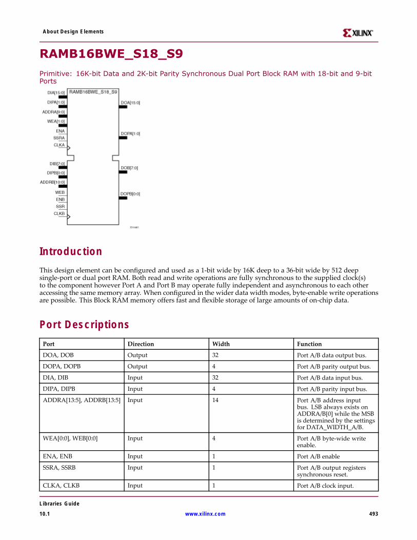
About Design Elements
RAMB16BWE_S18_S9
Primitive: 16K-bit Data and 2K-bit Parity Synchronous Dual Port Block RAM with 18-bit and 9-bitPorts
IntroductionThis design element can be configured and used as a 1-bit wide by 16K deep to a 36-bit wide by 512 deepsingle-port or dual port RAM. Both read and write operations are fully synchronous to the supplied clock(s)to the component however Port A and Port B may operate fully independent and asynchronous to each otheraccessing the same memory array. When configured in the wider data width modes, byte-enable write operationsare possible. This Block RAM memory offers fast and flexible storage of large amounts of on-chip data.
Port DescriptionsPort Direction Width Function
DOA, DOB Output 32 Port A/B data output bus.
DOPA, DOPB Output 4 Port A/B parity output bus.
DIA, DIB Input 32 Port A/B data input bus.
DIPA, DIPB Input 4 Port A/B parity input bus.
ADDRA[13:5], ADDRB[13:5] Input 14 Port A/B address inputbus. LSB always exists onADDRA/B[0] while the MSBis determined by the settingsfor DATA_WIDTH_A/B.
WEA[0:0], WEB[0:0] Input 4 Port A/B byte-wide writeenable.
ENA, ENB Input 1 Port A/B enable
SSRA, SSRB Input 1 Port A/B output registerssynchronous reset.
CLKA, CLKB Input 1 Port A/B clock input.
Libraries Guide
10.1 www.xilinx.com 493
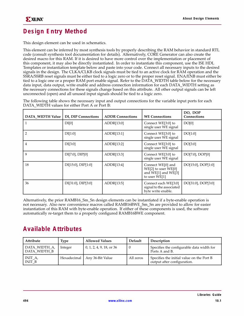
About Design Elements
Design Entry MethodThis design element can be used in schematics.
This element can be inferred by most synthesis tools by properly describing the RAM behavior in standard RTLcode (consult synthesis tool documentation for details). Alternatively, CORE Generator can also create thedesired macro for this RAM. If it is desired to have more control over the implementation or placement ofthis component, it may also be directly instantiated. In order to instantiate this component, use the ISE HDLTemplates or instantiation template below and paste into your code. Connect all necessary inputs to the desiredsignals in the design. The CLKA/CLKB clock signals must be tied to an active clock for RAM operation and theSSRA/SSRB reset signals must be either tied to a logic zero or to the proper reset signal. ENA/ENB must either betied to a logic one or a proper RAM port enable signal. Refer to the DATA_WIDTH table below for the necessarydata input, data output, write enable and address connection information for each DATA_WIDTH setting asthe necessary connections for these signals change based on this attribute. All other output signals can be leftunconnected (open) and all unused input signals should be tied to a logic zero.
The following table shows the necessary input and output connections for the variable input ports for eachDATA_WIDTH values for either Port A or Port B:
DATA_WIDTH Value DI, DIP Connections ADDR Connections WE ConnectionsDO, DOPConnections
1 DI[0] ADDR[13:0] Connect WE[3:0] tosingle user WE signal
DO[0]
2 DI[1:0] ADDR[13:1] Connect WE[3:0] tosingle user WE signal
DO[1:0]
4 DI[3:0] ADDR[13:2] Connect WE[3:0] tosingle user WE signal
DO[3:0]
9 DI[7:0], DIP[0] ADDR[13:3] Connect WE[3:0] tosingle user WE signal
DO[7:0], DOP[0]
18 DI[15:0], DIP[1:0] ADDR[13:4] Connect WE[0] andWE[2] to user WE[0]and WE[1] and WE[3]to user WE[1]
DO[15:0], DOP[1:0]
36 DI[31:0], DIP[3:0] ADDR[13:5] Connect each WE[3:0]signal to the associatedbyte write enable.
DO[31:0], DOP[3:0]
Alternatively, the prior RAMB16_Sm_Sn design elements can be instantiated if a byte-enable operation isnot necessary. Also new convenience macros called RAMB16BWE_Sm_Sn are provided to allow for easierinstantiation of this RAM with byte-enable operation. If either of these components is used, the softwareautomatically re-target them to a properly configured RAMB16BWE component.
Available AttributesAttribute Type Allowed Values Default Description
DATA_WIDTH_A,DATA_WIDTH_B
Integer 0, 1, 2, 4, 9, 18, or 36 0 Specifies the configurable data width forPorts A and B.
INIT_A,INIT_B
Hexadecimal Any 36-Bit Value All zeros Specifies the initial value on the Port Boutput after configuration.
Libraries Guide
494 www.xilinx.com 10.1
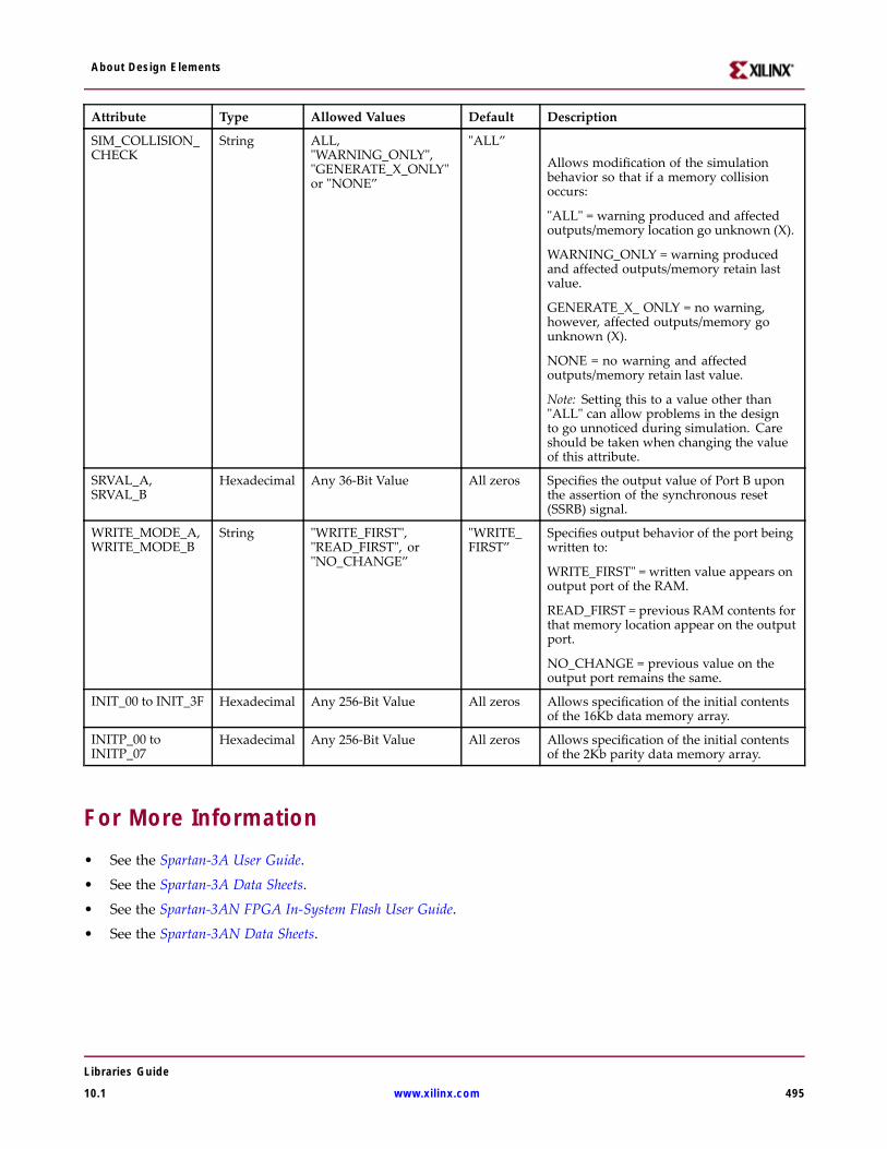
About Design Elements
Attribute Type Allowed Values Default Description
SIM_COLLISION_CHECK
String ALL,"WARNING_ONLY","GENERATE_X_ONLY"or "NONE”
"ALL”
Allows modification of the simulationbehavior so that if a memory collisionoccurs:
"ALL" = warning produced and affectedoutputs/memory location go unknown (X).
WARNING_ONLY = warning producedand affected outputs/memory retain lastvalue.
GENERATE_X_ ONLY = no warning,however, affected outputs/memory gounknown (X).
NONE = no warning and affectedoutputs/memory retain last value.
Note: Setting this to a value other than"ALL" can allow problems in the designto go unnoticed during simulation. Careshould be taken when changing the valueof this attribute.
SRVAL_A,SRVAL_B
Hexadecimal Any 36-Bit Value All zeros Specifies the output value of Port B uponthe assertion of the synchronous reset(SSRB) signal.
WRITE_MODE_A,WRITE_MODE_B
String "WRITE_FIRST","READ_FIRST", or"NO_CHANGE”
"WRITE_FIRST”
Specifies output behavior of the port beingwritten to:
WRITE_FIRST" = written value appears onoutput port of the RAM.
READ_FIRST = previous RAM contents forthat memory location appear on the outputport.
NO_CHANGE = previous value on theoutput port remains the same.
INIT_00 to INIT_3F Hexadecimal Any 256-Bit Value All zeros Allows specification of the initial contentsof the 16Kb data memory array.
INITP_00 toINITP_07
Hexadecimal Any 256-Bit Value All zeros Allows specification of the initial contentsof the 2Kb parity data memory array.
For More Information• See the Spartan-3A User Guide.
• See the Spartan-3A Data Sheets.
• See the Spartan-3AN FPGA In-System Flash User Guide.
• See the Spartan-3AN Data Sheets.
Libraries Guide
10.1 www.xilinx.com 495
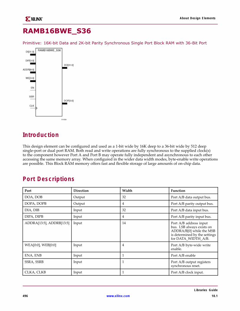
About Design Elements
RAMB16BWE_S36
Primitive: 16K-bit Data and 2K-bit Parity Synchronous Single Port Block RAM with 36-Bit Port
IntroductionThis design element can be configured and used as a 1-bit wide by 16K deep to a 36-bit wide by 512 deepsingle-port or dual port RAM. Both read and write operations are fully synchronous to the supplied clock(s)to the component however Port A and Port B may operate fully independent and asynchronous to each otheraccessing the same memory array. When configured in the wider data width modes, byte-enable write operationsare possible. This Block RAM memory offers fast and flexible storage of large amounts of on-chip data.
Port DescriptionsPort Direction Width Function
DOA, DOB Output 32 Port A/B data output bus.
DOPA, DOPB Output 4 Port A/B parity output bus.
DIA, DIB Input 32 Port A/B data input bus.
DIPA, DIPB Input 4 Port A/B parity input bus.
ADDRA[13:5], ADDRB[13:5] Input 14 Port A/B address inputbus. LSB always exists onADDRA/B[0] while the MSBis determined by the settingsfor DATA_WIDTH_A/B.
WEA[0:0], WEB[0:0] Input 4 Port A/B byte-wide writeenable.
ENA, ENB Input 1 Port A/B enable
SSRA, SSRB Input 1 Port A/B output registerssynchronous reset.
CLKA, CLKB Input 1 Port A/B clock input.
Libraries Guide
496 www.xilinx.com 10.1
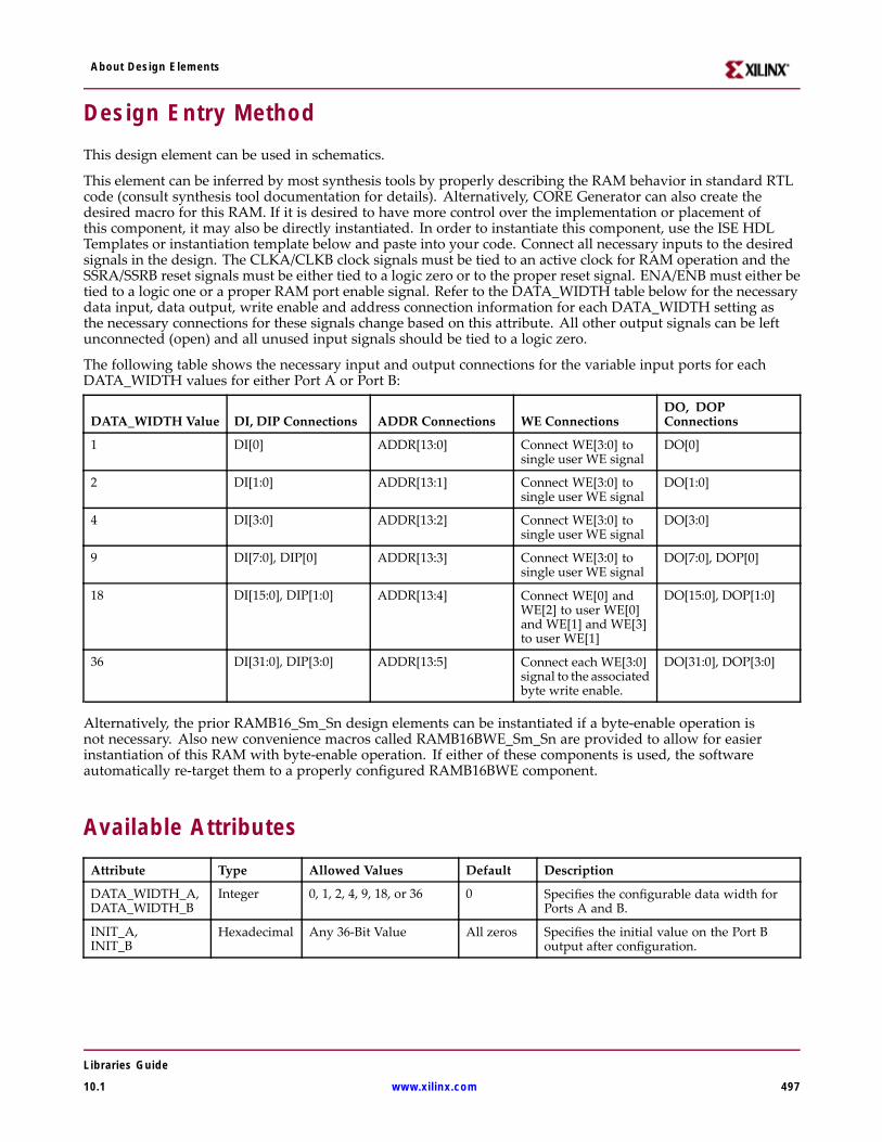
About Design Elements
Design Entry MethodThis design element can be used in schematics.
This element can be inferred by most synthesis tools by properly describing the RAM behavior in standard RTLcode (consult synthesis tool documentation for details). Alternatively, CORE Generator can also create thedesired macro for this RAM. If it is desired to have more control over the implementation or placement ofthis component, it may also be directly instantiated. In order to instantiate this component, use the ISE HDLTemplates or instantiation template below and paste into your code. Connect all necessary inputs to the desiredsignals in the design. The CLKA/CLKB clock signals must be tied to an active clock for RAM operation and theSSRA/SSRB reset signals must be either tied to a logic zero or to the proper reset signal. ENA/ENB must either betied to a logic one or a proper RAM port enable signal. Refer to the DATA_WIDTH table below for the necessarydata input, data output, write enable and address connection information for each DATA_WIDTH setting asthe necessary connections for these signals change based on this attribute. All other output signals can be leftunconnected (open) and all unused input signals should be tied to a logic zero.
The following table shows the necessary input and output connections for the variable input ports for eachDATA_WIDTH values for either Port A or Port B:
DATA_WIDTH Value DI, DIP Connections ADDR Connections WE ConnectionsDO, DOPConnections
1 DI[0] ADDR[13:0] Connect WE[3:0] tosingle user WE signal
DO[0]
2 DI[1:0] ADDR[13:1] Connect WE[3:0] tosingle user WE signal
DO[1:0]
4 DI[3:0] ADDR[13:2] Connect WE[3:0] tosingle user WE signal
DO[3:0]
9 DI[7:0], DIP[0] ADDR[13:3] Connect WE[3:0] tosingle user WE signal
DO[7:0], DOP[0]
18 DI[15:0], DIP[1:0] ADDR[13:4] Connect WE[0] andWE[2] to user WE[0]and WE[1] and WE[3]to user WE[1]
DO[15:0], DOP[1:0]
36 DI[31:0], DIP[3:0] ADDR[13:5] Connect each WE[3:0]signal to the associatedbyte write enable.
DO[31:0], DOP[3:0]
Alternatively, the prior RAMB16_Sm_Sn design elements can be instantiated if a byte-enable operation isnot necessary. Also new convenience macros called RAMB16BWE_Sm_Sn are provided to allow for easierinstantiation of this RAM with byte-enable operation. If either of these components is used, the softwareautomatically re-target them to a properly configured RAMB16BWE component.
Available AttributesAttribute Type Allowed Values Default Description
DATA_WIDTH_A,DATA_WIDTH_B
Integer 0, 1, 2, 4, 9, 18, or 36 0 Specifies the configurable data width forPorts A and B.
INIT_A,INIT_B
Hexadecimal Any 36-Bit Value All zeros Specifies the initial value on the Port Boutput after configuration.
Libraries Guide
10.1 www.xilinx.com 497
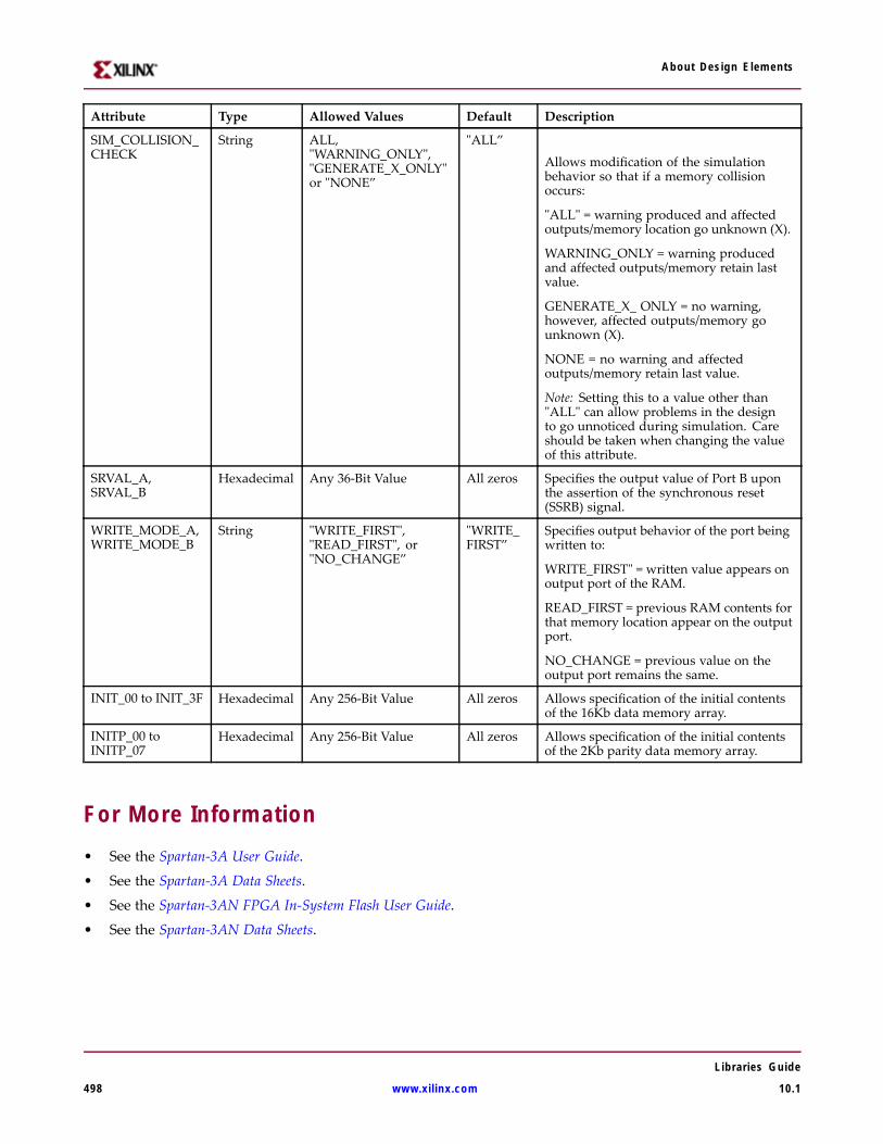
About Design Elements
Attribute Type Allowed Values Default Description
SIM_COLLISION_CHECK
String ALL,"WARNING_ONLY","GENERATE_X_ONLY"or "NONE”
"ALL”
Allows modification of the simulationbehavior so that if a memory collisionoccurs:
"ALL" = warning produced and affectedoutputs/memory location go unknown (X).
WARNING_ONLY = warning producedand affected outputs/memory retain lastvalue.
GENERATE_X_ ONLY = no warning,however, affected outputs/memory gounknown (X).
NONE = no warning and affectedoutputs/memory retain last value.
Note: Setting this to a value other than"ALL" can allow problems in the designto go unnoticed during simulation. Careshould be taken when changing the valueof this attribute.
SRVAL_A,SRVAL_B
Hexadecimal Any 36-Bit Value All zeros Specifies the output value of Port B uponthe assertion of the synchronous reset(SSRB) signal.
WRITE_MODE_A,WRITE_MODE_B
String "WRITE_FIRST","READ_FIRST", or"NO_CHANGE”
"WRITE_FIRST”
Specifies output behavior of the port beingwritten to:
WRITE_FIRST" = written value appears onoutput port of the RAM.
READ_FIRST = previous RAM contents forthat memory location appear on the outputport.
NO_CHANGE = previous value on theoutput port remains the same.
INIT_00 to INIT_3F Hexadecimal Any 256-Bit Value All zeros Allows specification of the initial contentsof the 16Kb data memory array.
INITP_00 toINITP_07
Hexadecimal Any 256-Bit Value All zeros Allows specification of the initial contentsof the 2Kb parity data memory array.
For More Information• See the Spartan-3A User Guide.
• See the Spartan-3A Data Sheets.
• See the Spartan-3AN FPGA In-System Flash User Guide.
• See the Spartan-3AN Data Sheets.
Libraries Guide
498 www.xilinx.com 10.1

About Design Elements
RAMB16BWE_S36_S18Primitive: 16K-bit Data and 2K-bit Parity Synchronous Dual Port Block RAM with 36-bit and 18-bitPorts
IntroductionThis design element can be configured and used as a 1-bit wide by 16K deep to a 36-bit wide by 512 deepsingle-port or dual port RAM. Both read and write operations are fully synchronous to the supplied clock(s)to the component however Port A and Port B may operate fully independent and asynchronous to each otheraccessing the same memory array. When configured in the wider data width modes, byte-enable write operationsare possible. This Block RAM memory offers fast and flexible storage of large amounts of on-chip data.
Port DescriptionsPort Direction Width Function
DOA, DOB Output 32 Port A/B data output bus.
DOPA, DOPB Output 4 Port A/B parity output bus.
Libraries Guide
10.1 www.xilinx.com 499

About Design Elements
Port Direction Width Function
DIA, DIB Input 32 Port A/B data input bus.
DIPA, DIPB Input 4 Port A/B parity input bus.
ADDRA[13:5], ADDRB[13:5] Input 14 Port A/B address inputbus. LSB always exists onADDRA/B[0] while the MSBis determined by the settingsfor DATA_WIDTH_A/B.
WEA[0:0], WEB[0:0] Input 4 Port A/B byte-wide writeenable.
ENA, ENB Input 1 Port A/B enable
SSRA, SSRB Input 1 Port A/B output registerssynchronous reset.
CLKA, CLKB Input 1 Port A/B clock input.
Design Entry MethodThis design element can be used in schematics.
This element can be inferred by most synthesis tools by properly describing the RAM behavior in standard RTLcode (consult synthesis tool documentation for details). Alternatively, CORE Generator can also create thedesired macro for this RAM. If it is desired to have more control over the implementation or placement ofthis component, it may also be directly instantiated. In order to instantiate this component, use the ISE HDLTemplates or instantiation template below and paste into your code. Connect all necessary inputs to the desiredsignals in the design. The CLKA/CLKB clock signals must be tied to an active clock for RAM operation and theSSRA/SSRB reset signals must be either tied to a logic zero or to the proper reset signal. ENA/ENB must either betied to a logic one or a proper RAM port enable signal. Refer to the DATA_WIDTH table below for the necessarydata input, data output, write enable and address connection information for each DATA_WIDTH setting asthe necessary connections for these signals change based on this attribute. All other output signals can be leftunconnected (open) and all unused input signals should be tied to a logic zero.
The following table shows the necessary input and output connections for the variable input ports for eachDATA_WIDTH values for either Port A or Port B:
DATA_WIDTH Value DI, DIP Connections ADDR Connections WE ConnectionsDO, DOPConnections
1 DI[0] ADDR[13:0] Connect WE[3:0] tosingle user WE signal
DO[0]
2 DI[1:0] ADDR[13:1] Connect WE[3:0] tosingle user WE signal
DO[1:0]
4 DI[3:0] ADDR[13:2] Connect WE[3:0] tosingle user WE signal
DO[3:0]
9 DI[7:0], DIP[0] ADDR[13:3] Connect WE[3:0] tosingle user WE signal
DO[7:0], DOP[0]
18 DI[15:0], DIP[1:0] ADDR[13:4] Connect WE[0] andWE[2] to user WE[0]and WE[1] and WE[3]to user WE[1]
DO[15:0], DOP[1:0]
36 DI[31:0], DIP[3:0] ADDR[13:5] Connect each WE[3:0]signal to the associatedbyte write enable.
DO[31:0], DOP[3:0]
Libraries Guide
500 www.xilinx.com 10.1

About Design Elements
Alternatively, the prior RAMB16_Sm_Sn design elements can be instantiated if a byte-enable operation isnot necessary. Also new convenience macros called RAMB16BWE_Sm_Sn are provided to allow for easierinstantiation of this RAM with byte-enable operation. If either of these components is used, the softwareautomatically re-target them to a properly configured RAMB16BWE component.
Available AttributesAttribute Type Allowed Values Default Description
DATA_WIDTH_A,DATA_WIDTH_B
Integer 0, 1, 2, 4, 9, 18, or 36 0 Specifies the configurable data width forPorts A and B.
INIT_A,INIT_B
Hexadecimal Any 36-Bit Value All zeros Specifies the initial value on the Port Boutput after configuration.
SIM_COLLISION_CHECK
String ALL,"WARNING_ONLY","GENERATE_X_ONLY"or "NONE”
"ALL”
Allows modification of the simulationbehavior so that if a memory collisionoccurs:
"ALL" = warning produced and affectedoutputs/memory location go unknown (X).
WARNING_ONLY = warning producedand affected outputs/memory retain lastvalue.
GENERATE_X_ ONLY = no warning,however, affected outputs/memory gounknown (X).
NONE = no warning and affectedoutputs/memory retain last value.
Note: Setting this to a value other than"ALL" can allow problems in the designto go unnoticed during simulation. Careshould be taken when changing the valueof this attribute.
SRVAL_A,SRVAL_B
Hexadecimal Any 36-Bit Value All zeros Specifies the output value of Port B uponthe assertion of the synchronous reset(SSRB) signal.
WRITE_MODE_A,WRITE_MODE_B
String "WRITE_FIRST","READ_FIRST", or"NO_CHANGE”
"WRITE_FIRST”
Specifies output behavior of the port beingwritten to:
WRITE_FIRST" = written value appears onoutput port of the RAM.
READ_FIRST = previous RAM contents forthat memory location appear on the outputport.
NO_CHANGE = previous value on theoutput port remains the same.
INIT_00 to INIT_3F Hexadecimal Any 256-Bit Value All zeros Allows specification of the initial contentsof the 16Kb data memory array.
INITP_00 toINITP_07
Hexadecimal Any 256-Bit Value All zeros Allows specification of the initial contentsof the 2Kb parity data memory array.
Libraries Guide
10.1 www.xilinx.com 501

About Design Elements
For More Information• See the Spartan-3A User Guide.
• See the Spartan-3A Data Sheets.
• See the Spartan-3AN FPGA In-System Flash User Guide.
• See the Spartan-3AN Data Sheets.
Libraries Guide
502 www.xilinx.com 10.1
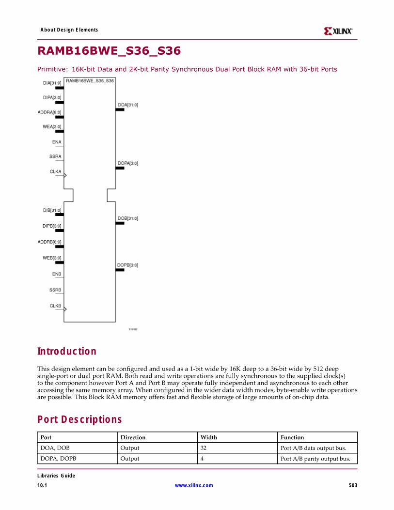
About Design Elements
RAMB16BWE_S36_S36
Primitive: 16K-bit Data and 2K-bit Parity Synchronous Dual Port Block RAM with 36-bit Ports
IntroductionThis design element can be configured and used as a 1-bit wide by 16K deep to a 36-bit wide by 512 deepsingle-port or dual port RAM. Both read and write operations are fully synchronous to the supplied clock(s)to the component however Port A and Port B may operate fully independent and asynchronous to each otheraccessing the same memory array. When configured in the wider data width modes, byte-enable write operationsare possible. This Block RAM memory offers fast and flexible storage of large amounts of on-chip data.
Port DescriptionsPort Direction Width Function
DOA, DOB Output 32 Port A/B data output bus.
DOPA, DOPB Output 4 Port A/B parity output bus.
Libraries Guide
10.1 www.xilinx.com 503
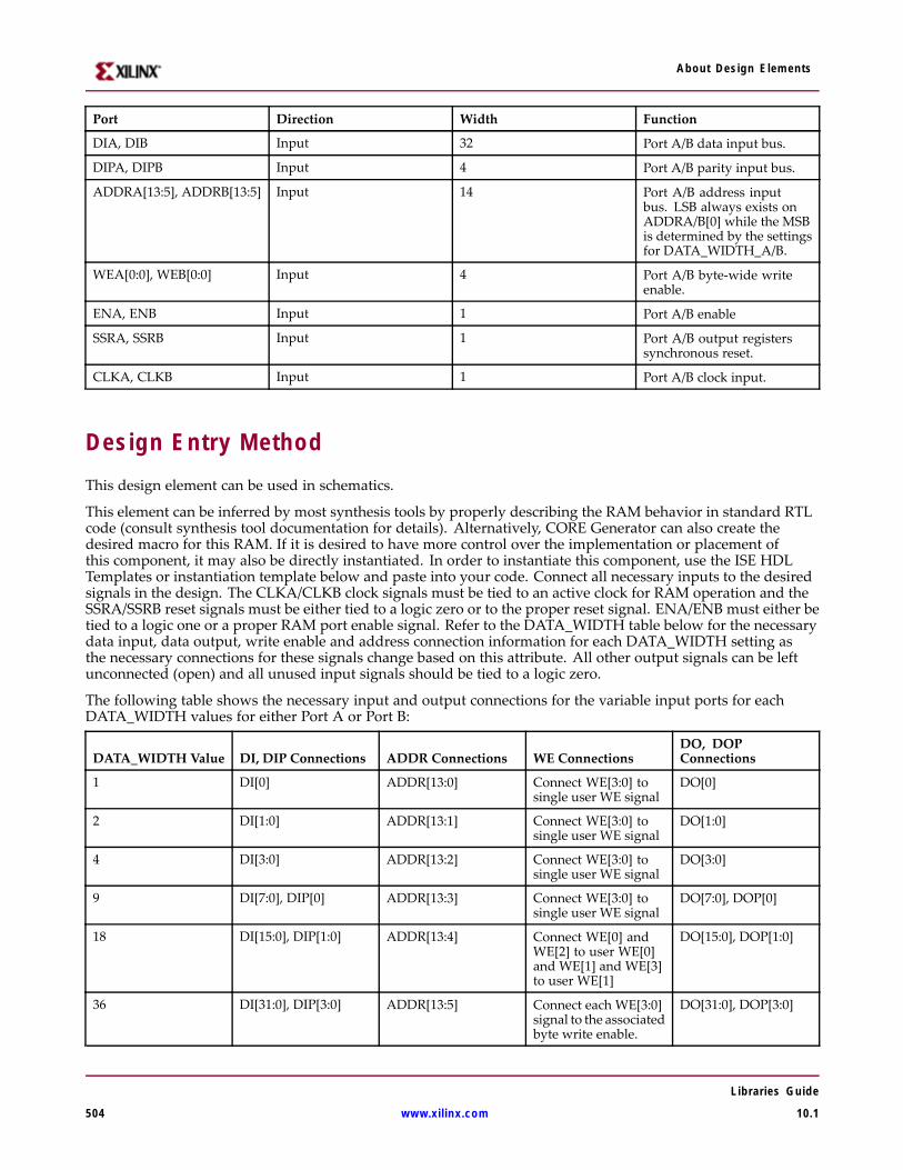
About Design Elements
Port Direction Width Function
DIA, DIB Input 32 Port A/B data input bus.
DIPA, DIPB Input 4 Port A/B parity input bus.
ADDRA[13:5], ADDRB[13:5] Input 14 Port A/B address inputbus. LSB always exists onADDRA/B[0] while the MSBis determined by the settingsfor DATA_WIDTH_A/B.
WEA[0:0], WEB[0:0] Input 4 Port A/B byte-wide writeenable.
ENA, ENB Input 1 Port A/B enable
SSRA, SSRB Input 1 Port A/B output registerssynchronous reset.
CLKA, CLKB Input 1 Port A/B clock input.
Design Entry MethodThis design element can be used in schematics.
This element can be inferred by most synthesis tools by properly describing the RAM behavior in standard RTLcode (consult synthesis tool documentation for details). Alternatively, CORE Generator can also create thedesired macro for this RAM. If it is desired to have more control over the implementation or placement ofthis component, it may also be directly instantiated. In order to instantiate this component, use the ISE HDLTemplates or instantiation template below and paste into your code. Connect all necessary inputs to the desiredsignals in the design. The CLKA/CLKB clock signals must be tied to an active clock for RAM operation and theSSRA/SSRB reset signals must be either tied to a logic zero or to the proper reset signal. ENA/ENB must either betied to a logic one or a proper RAM port enable signal. Refer to the DATA_WIDTH table below for the necessarydata input, data output, write enable and address connection information for each DATA_WIDTH setting asthe necessary connections for these signals change based on this attribute. All other output signals can be leftunconnected (open) and all unused input signals should be tied to a logic zero.
The following table shows the necessary input and output connections for the variable input ports for eachDATA_WIDTH values for either Port A or Port B:
DATA_WIDTH Value DI, DIP Connections ADDR Connections WE ConnectionsDO, DOPConnections
1 DI[0] ADDR[13:0] Connect WE[3:0] tosingle user WE signal
DO[0]
2 DI[1:0] ADDR[13:1] Connect WE[3:0] tosingle user WE signal
DO[1:0]
4 DI[3:0] ADDR[13:2] Connect WE[3:0] tosingle user WE signal
DO[3:0]
9 DI[7:0], DIP[0] ADDR[13:3] Connect WE[3:0] tosingle user WE signal
DO[7:0], DOP[0]
18 DI[15:0], DIP[1:0] ADDR[13:4] Connect WE[0] andWE[2] to user WE[0]and WE[1] and WE[3]to user WE[1]
DO[15:0], DOP[1:0]
36 DI[31:0], DIP[3:0] ADDR[13:5] Connect each WE[3:0]signal to the associatedbyte write enable.
DO[31:0], DOP[3:0]
Libraries Guide
504 www.xilinx.com 10.1

About Design Elements
Alternatively, the prior RAMB16_Sm_Sn design elements can be instantiated if a byte-enable operation isnot necessary. Also new convenience macros called RAMB16BWE_Sm_Sn are provided to allow for easierinstantiation of this RAM with byte-enable operation. If either of these components is used, the softwareautomatically re-target them to a properly configured RAMB16BWE component.
For More Information• See the Spartan-3A User Guide.
• See the Spartan-3A Data Sheets.
• See the Spartan-3AN FPGA In-System Flash User Guide.
• See the Spartan-3AN Data Sheets.
Libraries Guide
10.1 www.xilinx.com 505
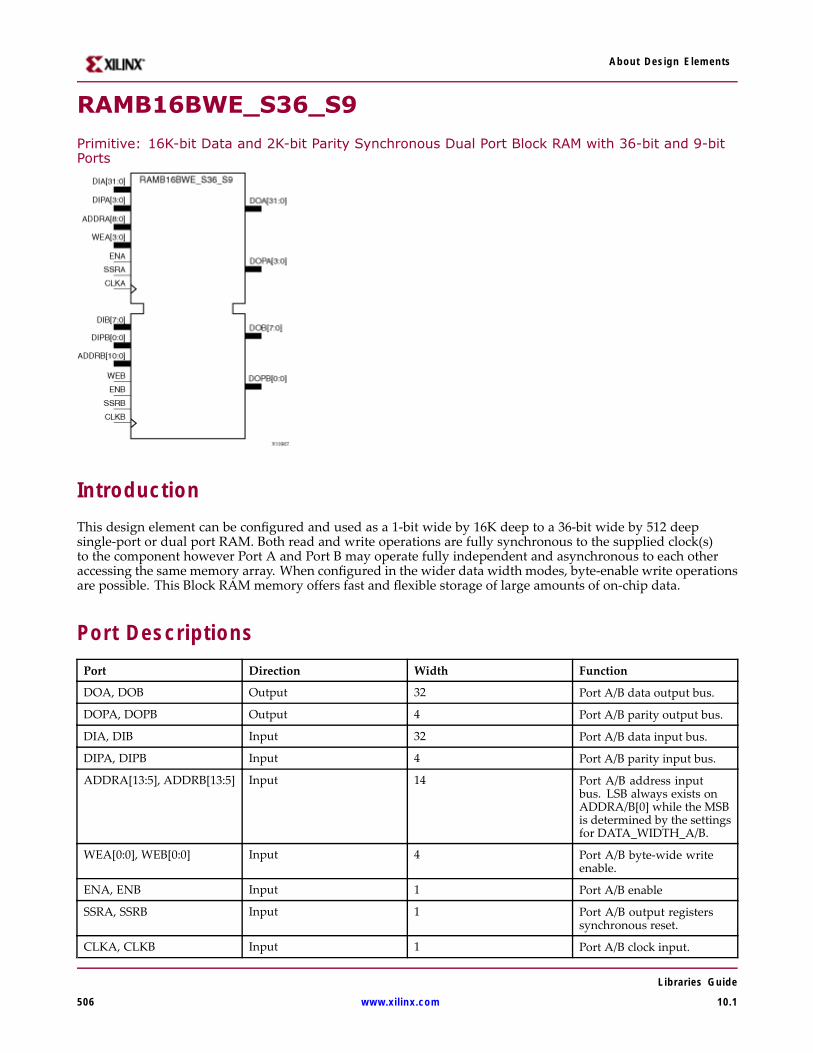
About Design Elements
RAMB16BWE_S36_S9
Primitive: 16K-bit Data and 2K-bit Parity Synchronous Dual Port Block RAM with 36-bit and 9-bitPorts
IntroductionThis design element can be configured and used as a 1-bit wide by 16K deep to a 36-bit wide by 512 deepsingle-port or dual port RAM. Both read and write operations are fully synchronous to the supplied clock(s)to the component however Port A and Port B may operate fully independent and asynchronous to each otheraccessing the same memory array. When configured in the wider data width modes, byte-enable write operationsare possible. This Block RAM memory offers fast and flexible storage of large amounts of on-chip data.
Port DescriptionsPort Direction Width Function
DOA, DOB Output 32 Port A/B data output bus.
DOPA, DOPB Output 4 Port A/B parity output bus.
DIA, DIB Input 32 Port A/B data input bus.
DIPA, DIPB Input 4 Port A/B parity input bus.
ADDRA[13:5], ADDRB[13:5] Input 14 Port A/B address inputbus. LSB always exists onADDRA/B[0] while the MSBis determined by the settingsfor DATA_WIDTH_A/B.
WEA[0:0], WEB[0:0] Input 4 Port A/B byte-wide writeenable.
ENA, ENB Input 1 Port A/B enable
SSRA, SSRB Input 1 Port A/B output registerssynchronous reset.
CLKA, CLKB Input 1 Port A/B clock input.
Libraries Guide
506 www.xilinx.com 10.1

About Design Elements
Design Entry MethodThis design element can be used in schematics.
This element can be inferred by most synthesis tools by properly describing the RAM behavior in standard RTLcode (consult synthesis tool documentation for details). Alternatively, CORE Generator can also create thedesired macro for this RAM. If it is desired to have more control over the implementation or placement ofthis component, it may also be directly instantiated. In order to instantiate this component, use the ISE HDLTemplates or instantiation template below and paste into your code. Connect all necessary inputs to the desiredsignals in the design. The CLKA/CLKB clock signals must be tied to an active clock for RAM operation and theSSRA/SSRB reset signals must be either tied to a logic zero or to the proper reset signal. ENA/ENB must either betied to a logic one or a proper RAM port enable signal. Refer to the DATA_WIDTH table below for the necessarydata input, data output, write enable and address connection information for each DATA_WIDTH setting asthe necessary connections for these signals change based on this attribute. All other output signals can be leftunconnected (open) and all unused input signals should be tied to a logic zero.
The following table shows the necessary input and output connections for the variable input ports for eachDATA_WIDTH values for either Port A or Port B:
DATA_WIDTH Value DI, DIP Connections ADDR Connections WE ConnectionsDO, DOPConnections
1 DI[0] ADDR[13:0] Connect WE[3:0] tosingle user WE signal
DO[0]
2 DI[1:0] ADDR[13:1] Connect WE[3:0] tosingle user WE signal
DO[1:0]
4 DI[3:0] ADDR[13:2] Connect WE[3:0] tosingle user WE signal
DO[3:0]
9 DI[7:0], DIP[0] ADDR[13:3] Connect WE[3:0] tosingle user WE signal
DO[7:0], DOP[0]
18 DI[15:0], DIP[1:0] ADDR[13:4] Connect WE[0] andWE[2] to user WE[0]and WE[1] and WE[3]to user WE[1]
DO[15:0], DOP[1:0]
36 DI[31:0], DIP[3:0] ADDR[13:5] Connect each WE[3:0]signal to the associatedbyte write enable.
DO[31:0], DOP[3:0]
Alternatively, the prior RAMB16_Sm_Sn design elements can be instantiated if a byte-enable operation isnot necessary. Also new convenience macros called RAMB16BWE_Sm_Sn are provided to allow for easierinstantiation of this RAM with byte-enable operation. If either of these components is used, the softwareautomatically re-target them to a properly configured RAMB16BWE component.
Available AttributesAttribute Type Allowed Values Default Description
DATA_WIDTH_A,DATA_WIDTH_B
Integer 0, 1, 2, 4, 9, 18, or 36 0 Specifies the configurable data width forPorts A and B.
INIT_A,INIT_B
Hexadecimal Any 36-Bit Value All zeros Specifies the initial value on the Port Boutput after configuration.
Libraries Guide
10.1 www.xilinx.com 507

About Design Elements
Attribute Type Allowed Values Default Description
SIM_COLLISION_CHECK
String ALL,"WARNING_ONLY","GENERATE_X_ONLY"or "NONE”
"ALL”
Allows modification of the simulationbehavior so that if a memory collisionoccurs:
"ALL" = warning produced and affectedoutputs/memory location go unknown (X).
WARNING_ONLY = warning producedand affected outputs/memory retain lastvalue.
GENERATE_X_ ONLY = no warning,however, affected outputs/memory gounknown (X).
NONE = no warning and affectedoutputs/memory retain last value.
Note: Setting this to a value other than"ALL" can allow problems in the designto go unnoticed during simulation. Careshould be taken when changing the valueof this attribute.
SRVAL_A,SRVAL_B
Hexadecimal Any 36-Bit Value All zeros Specifies the output value of Port B uponthe assertion of the synchronous reset(SSRB) signal.
WRITE_MODE_A,WRITE_MODE_B
String "WRITE_FIRST","READ_FIRST", or"NO_CHANGE”
"WRITE_FIRST”
Specifies output behavior of the port beingwritten to:
WRITE_FIRST" = written value appears onoutput port of the RAM.
READ_FIRST = previous RAM contents forthat memory location appear on the outputport.
NO_CHANGE = previous value on theoutput port remains the same.
INIT_00 to INIT_3F Hexadecimal Any 256-Bit Value All zeros Allows specification of the initial contentsof the 16Kb data memory array.
INITP_00 toINITP_07
Hexadecimal Any 256-Bit Value All zeros Allows specification of the initial contentsof the 2Kb parity data memory array.
For More Information• See the Spartan-3A User Guide.
• See the Spartan-3A Data Sheets.
• See the Spartan-3AN FPGA In-System Flash User Guide.
• See the Spartan-3AN Data Sheets.
Libraries Guide
508 www.xilinx.com 10.1
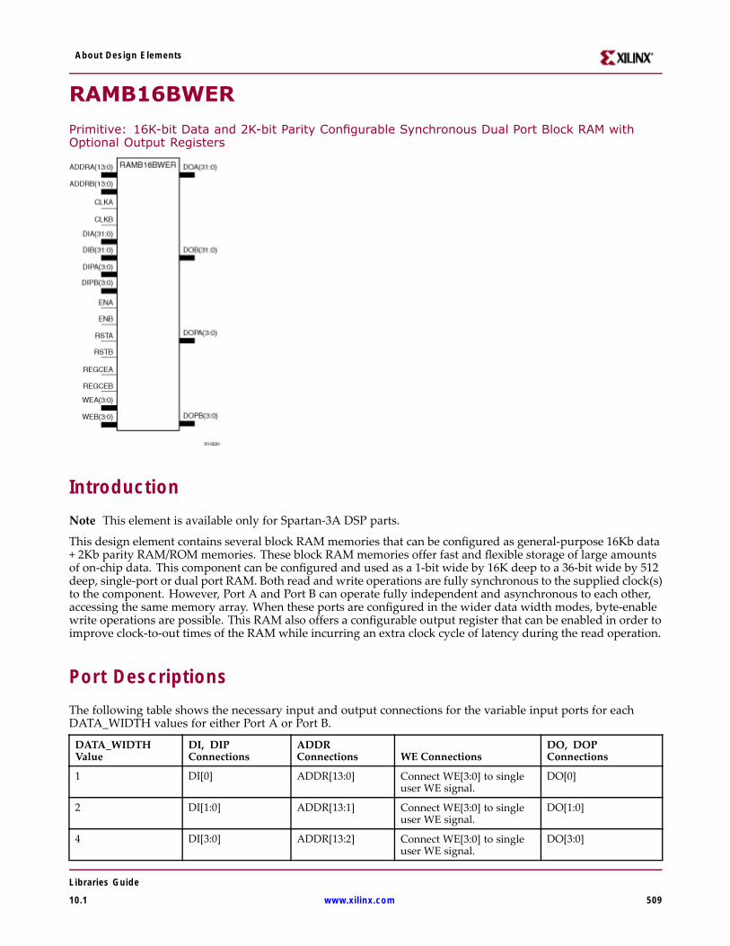
About Design Elements
RAMB16BWER
Primitive: 16K-bit Data and 2K-bit Parity Configurable Synchronous Dual Port Block RAM withOptional Output Registers
IntroductionNote This element is available only for Spartan-3A DSP parts.
This design element contains several block RAMmemories that can be configured as general-purpose 16Kb data+ 2Kb parity RAM/ROMmemories. These block RAM memories offer fast and flexible storage of large amountsof on-chip data. This component can be configured and used as a 1-bit wide by 16K deep to a 36-bit wide by 512deep, single-port or dual port RAM. Both read and write operations are fully synchronous to the supplied clock(s)to the component. However, Port A and Port B can operate fully independent and asynchronous to each other,accessing the same memory array. When these ports are configured in the wider data width modes, byte-enablewrite operations are possible. This RAM also offers a configurable output register that can be enabled in order toimprove clock-to-out times of the RAM while incurring an extra clock cycle of latency during the read operation.
Port DescriptionsThe following table shows the necessary input and output connections for the variable input ports for eachDATA_WIDTH values for either Port A or Port B.
DATA_WIDTHValue
DI, DIPConnections
ADDRConnections WE Connections
DO, DOPConnections
1 DI[0] ADDR[13:0] Connect WE[3:0] to singleuser WE signal.
DO[0]
2 DI[1:0] ADDR[13:1] Connect WE[3:0] to singleuser WE signal.
DO[1:0]
4 DI[3:0] ADDR[13:2] Connect WE[3:0] to singleuser WE signal.
DO[3:0]
Libraries Guide
10.1 www.xilinx.com 509
About Design Elements
DATA_WIDTHValue
DI, DIPConnections
ADDRConnections WE Connections
DO, DOPConnections
9 DI[7:0], DIP[0] ADDR[13:3] Connect WE[3:0] to singleuser WE signal.
DO[7:0], DOP[0]
18 DI[15:0], DIP[1:0] ADDR[13:4] Connect WE[0] and WE[2]to user WE[0] and WE[1]and WE[3] to user WE[1].
DO[15:0], DOP[1:0]
36 DI[31:0], DIP[3:0] ADDR[13:5] Connect each WE[3:0] signalto the associated byte writeenable/.
DO[31:0], DOP[3:0]
Alternatively, the prior RAMB16_Sm_Sn and RAMB16BWER_Sm_Sn elements can be instantiated if the outputregisters are not necessary. If any of these components are used, the software will automatically re-target themthe a properly configured RAMB16BWER element.
Port Direction Width Function
DOA, DOB Output 32 Port A/B data output bus.
DOPA, DOPB Output 4 Port A/B parity output bus.
DIA, DIB Input 32 Port A/B data input bus.
DIPA, DIPB Input 4 Port A/B parity input bus.
ADDRA, ADDRB Input 14 Port A/B address input bus. MSB always exists onADDRA/B[13] while the LSB is determined by the settings forDATA_WIDTH_A/B.
WEA, WEB Input 4 Port A/B byte-wide write enable.
ENA, ENB Input 1 Port A/B enable.
REGCEA, RECEB Input 1 Output register clock enable.
RSTA, RSTB Input 1 Port A/B output registers set/reset. This reset is configurable tobe synchronous or asynchronous, depending on the value ofthe RSTTYPE attribute.
CLKA, CLKB Input 1 Port A/B clock input.
Design Entry MethodThis design element can be used in schematics.
Connect all necessary inputs to the desired signals in the design. The CLKA/CLKB clock signals must be tied toan active clock for RAM operation, and the SRA/SRB reset signals must be either tied to a logic zero or to theproper reset signal. ENA/ENB must either be tied to a logic one or a proper RAM port enable signal. REGCEAand REGCEB must be tied to the proper output register clock enable, or a logic one if the respective DOA_REGor DOB_REG attribute is set to 1. If DOA_REG is set to 0, then tie REGCEA and REGCEB must be set to a logic 0.
Refer to the DATA_WIDTH column in the “Port Description” table (above) for the necessary data input, dataoutput, write enable and address connection information for each DATA_WIDTH setting, since the necessaryconnections for these signals change, based on this attribute. All other output signals can be left unconnected(open) and all unused input signals should be tied to a logic zero.
Available AttributesAttribute Type Allowed Values Default Description
DATA_WIDTH_A,DATA_WIDTH_B
Integer 1, 2, 4, 9, 18, or 36 0 Specifies the configurable datawidth for Ports A and B.
Libraries Guide
510 www.xilinx.com 10.1
About Design Elements
Attribute Type Allowed Values Default Description
DOA_REG, DOB_REG Integer 0 or 1 0 Specifies to use or bypass the outputregisters for the RAM.
INIT_A, INIT_B Hexadecimal Any 36-bit Value All zeroes Specifies the initial value on the PortB output after configuration.
SIM_COLLISION_CHECK String "ALL","WARNING_ONLY","GENERATE_X_ONLY"or "NONE”
"ALL” Allows modification of thesimulation behavior so that if amemory collision occurs:
"ALL" = warning produced andaffected outputs/memory locationgo unknown (X).
"WARNING_ONLY" = warningproduced and affectedoutputs/memory retain lastvalue.
"GENERATE_X_ONLY" = nowarning, however affectedoutputs/memory go unknown (X)
"NONE" = no warning and affectedoutputs/memory retain last value.
Note: Setting this to a value otherthan "ALL" can allow problems inthe design to go unnoticed duringsimulation. Care should be takenwhen changing the value of thisattribute.
SRVAL_A Hexadecimal Any 36-Bit Value All zeroes Specifies the output value of PortA upon the assertion of the reset(RSTA) signal.
SRVAL_B Hexadecimal Any 36-Bit Value All zeroes Specifies the output value of PortB upon the assertion of the reset(RSTB) signal.
RSTTYPE String "ASYNC", "SYNC” "SYNC” Selects whether the RAM outputsshould have a synchronous orasynchronous reset capability. Dueto improved timing and circuitstability, it is recommended toalways have this set to SYNC"unless an asynchronous reset isabsolutely necessary.
WRITE_MODE_A,WRITE_MODE_B
String "WRITE_FIRST","READ_FIRST", or"NO_CHANGE”
"WRITE_FIRST”
Specifies output behavior of the portbeing written to:
"WRITE_FIRST" = written valueappears on output port of the RAM.
"READ_FIRST" = previous RAMcontents for that memory locationappear on the output port.
"NO_CHANGE" = previous valueon the output port remains thesame.
Libraries Guide
10.1 www.xilinx.com 511
About Design Elements
Attribute Type Allowed Values Default Description
INIT_00 to INIT_3F Hexadecimal Any 256-bit value All zeroes Allows specification of the initialcontents of the 16Kb data memoryarray.
INITP_00 to INITP_07 Hexadecimal Any 256-bit value All zeroes Allows specification of the initialcontents of the 2Kb parity datamemory array.
For More Information• See the Spartan-3A User Guide.
• See the Spartan-3A Data Sheets.
• See the Spartan-3AN FPGA In-System Flash User Guide.
• See the Spartan-3AN Data Sheets.
Libraries Guide
512 www.xilinx.com 10.1
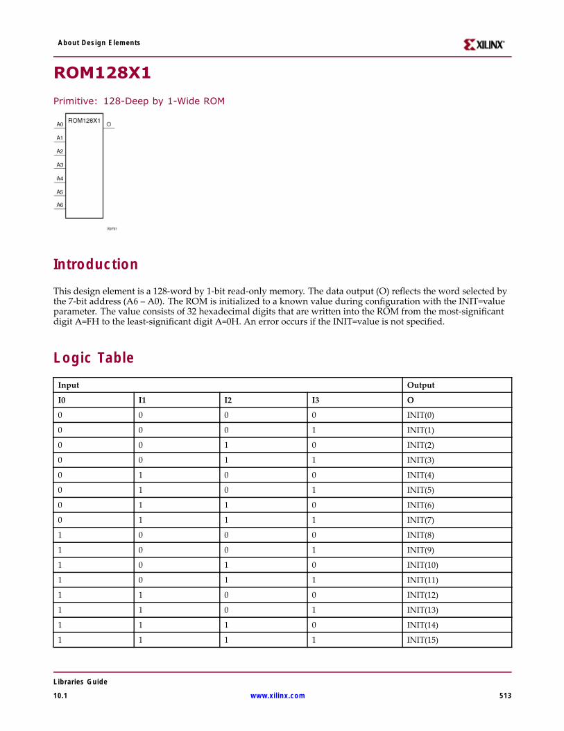
About Design Elements
ROM128X1
Primitive: 128-Deep by 1-Wide ROM
IntroductionThis design element is a 128-word by 1-bit read-only memory. The data output (O) reflects the word selected bythe 7-bit address (A6 – A0). The ROM is initialized to a known value during configuration with the INIT=valueparameter. The value consists of 32 hexadecimal digits that are written into the ROM from the most-significantdigit A=FH to the least-significant digit A=0H. An error occurs if the INIT=value is not specified.
Logic TableInput Output
I0 I1 I2 I3 O
0 0 0 0 INIT(0)
0 0 0 1 INIT(1)
0 0 1 0 INIT(2)
0 0 1 1 INIT(3)
0 1 0 0 INIT(4)
0 1 0 1 INIT(5)
0 1 1 0 INIT(6)
0 1 1 1 INIT(7)
1 0 0 0 INIT(8)
1 0 0 1 INIT(9)
1 0 1 0 INIT(10)
1 0 1 1 INIT(11)
1 1 0 0 INIT(12)
1 1 0 1 INIT(13)
1 1 1 0 INIT(14)
1 1 1 1 INIT(15)
Libraries Guide
10.1 www.xilinx.com 513
About Design Elements
Design Entry MethodThis design element can be used in schematics.
Available AttributesAttribute Type Allowed Values Default Description
INIT Hexadecimal Any 128-Bit Value All zeros Specifies the contents of the ROM.
For More Information• See the Spartan-3A User Guide.
• See the Spartan-3A Data Sheets.
• See the Spartan-3AN FPGA In-System Flash User Guide.
• See the Spartan-3AN Data Sheets.
Libraries Guide
514 www.xilinx.com 10.1
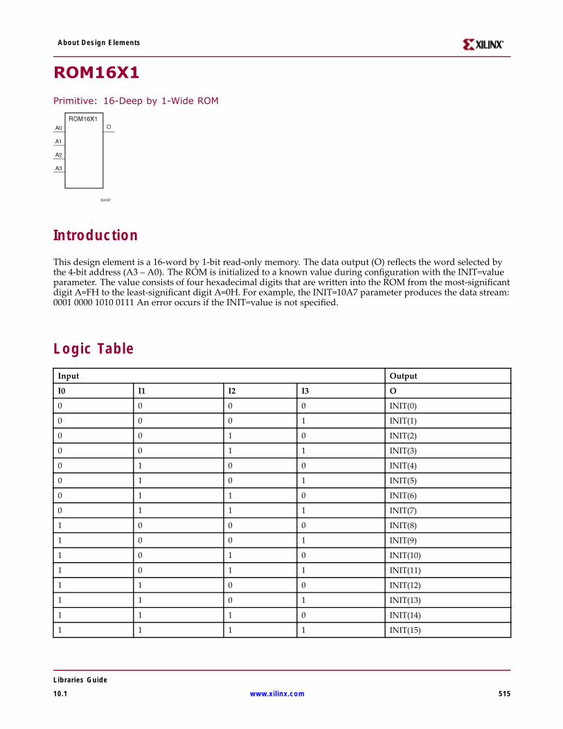
About Design Elements
ROM16X1
Primitive: 16-Deep by 1-Wide ROM
IntroductionThis design element is a 16-word by 1-bit read-only memory. The data output (O) reflects the word selected bythe 4-bit address (A3 – A0). The ROM is initialized to a known value during configuration with the INIT=valueparameter. The value consists of four hexadecimal digits that are written into the ROM from the most-significantdigit A=FH to the least-significant digit A=0H. For example, the INIT=10A7 parameter produces the data stream:0001 0000 1010 0111 An error occurs if the INIT=value is not specified.
Logic TableInput Output
I0 I1 I2 I3 O
0 0 0 0 INIT(0)
0 0 0 1 INIT(1)
0 0 1 0 INIT(2)
0 0 1 1 INIT(3)
0 1 0 0 INIT(4)
0 1 0 1 INIT(5)
0 1 1 0 INIT(6)
0 1 1 1 INIT(7)
1 0 0 0 INIT(8)
1 0 0 1 INIT(9)
1 0 1 0 INIT(10)
1 0 1 1 INIT(11)
1 1 0 0 INIT(12)
1 1 0 1 INIT(13)
1 1 1 0 INIT(14)
1 1 1 1 INIT(15)
Libraries Guide
10.1 www.xilinx.com 515
About Design Elements
Design Entry MethodThis design element can be used in schematics.
Available AttributesAttribute Type Allowed Values Default Description
INIT Hexadecimal Any 16-Bit Value All zeros Specifies the contents of the ROM.
For More Information• See the Spartan-3A User Guide.
• See the Spartan-3A Data Sheets.
• See the Spartan-3AN FPGA In-System Flash User Guide.
• See the Spartan-3AN Data Sheets.
Libraries Guide
516 www.xilinx.com 10.1
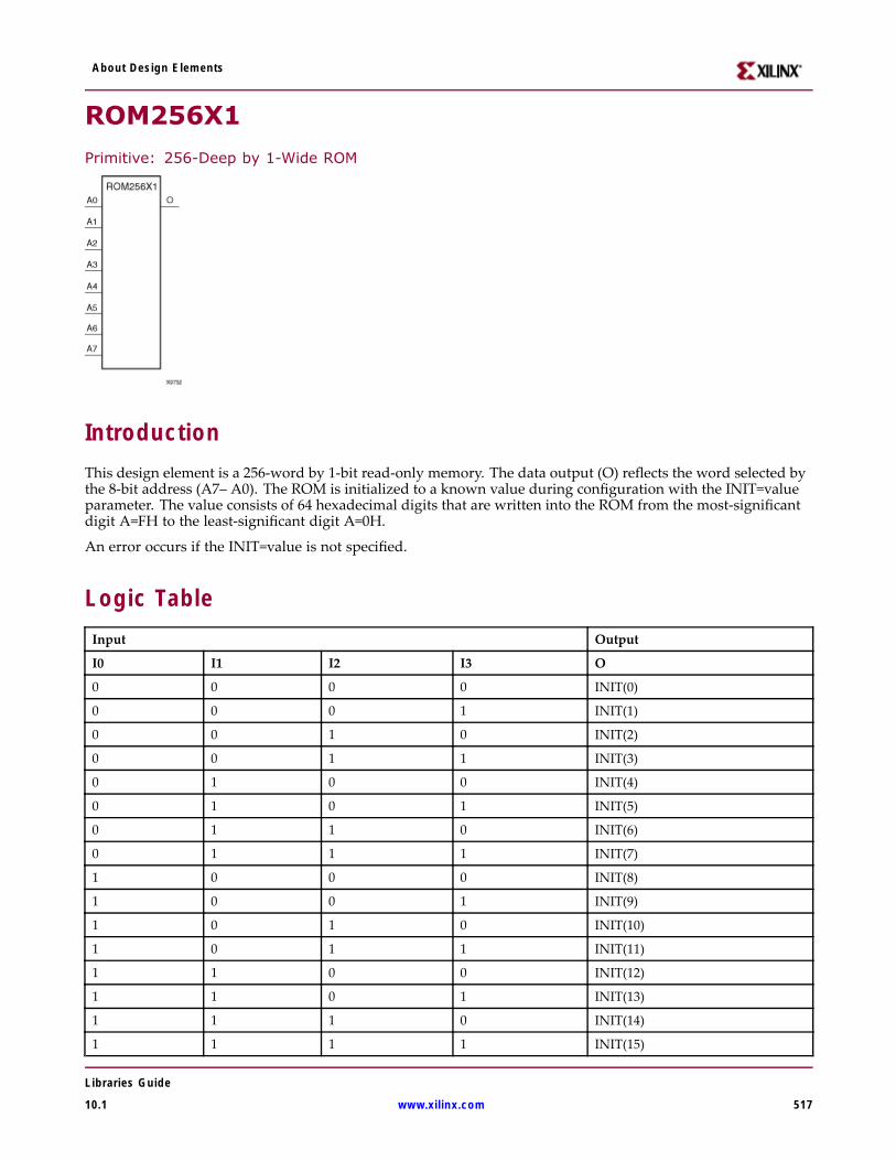
About Design Elements
ROM256X1
Primitive: 256-Deep by 1-Wide ROM
IntroductionThis design element is a 256-word by 1-bit read-only memory. The data output (O) reflects the word selected bythe 8-bit address (A7– A0). The ROM is initialized to a known value during configuration with the INIT=valueparameter. The value consists of 64 hexadecimal digits that are written into the ROM from the most-significantdigit A=FH to the least-significant digit A=0H.
An error occurs if the INIT=value is not specified.
Logic TableInput Output
I0 I1 I2 I3 O
0 0 0 0 INIT(0)
0 0 0 1 INIT(1)
0 0 1 0 INIT(2)
0 0 1 1 INIT(3)
0 1 0 0 INIT(4)
0 1 0 1 INIT(5)
0 1 1 0 INIT(6)
0 1 1 1 INIT(7)
1 0 0 0 INIT(8)
1 0 0 1 INIT(9)
1 0 1 0 INIT(10)
1 0 1 1 INIT(11)
1 1 0 0 INIT(12)
1 1 0 1 INIT(13)
1 1 1 0 INIT(14)
1 1 1 1 INIT(15)
Libraries Guide
10.1 www.xilinx.com 517
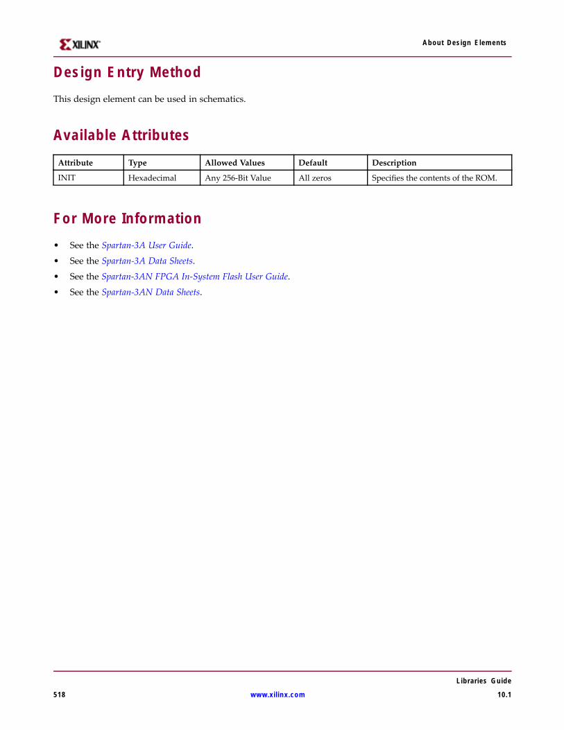
About Design Elements
Design Entry MethodThis design element can be used in schematics.
Available AttributesAttribute Type Allowed Values Default Description
INIT Hexadecimal Any 256-Bit Value All zeros Specifies the contents of the ROM.
For More Information• See the Spartan-3A User Guide.
• See the Spartan-3A Data Sheets.
• See the Spartan-3AN FPGA In-System Flash User Guide.
• See the Spartan-3AN Data Sheets.
Libraries Guide
518 www.xilinx.com 10.1
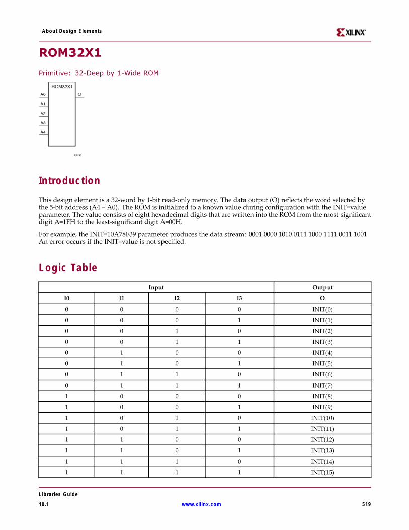
About Design Elements
ROM32X1
Primitive: 32-Deep by 1-Wide ROM
IntroductionThis design element is a 32-word by 1-bit read-only memory. The data output (O) reflects the word selected bythe 5-bit address (A4 – A0). The ROM is initialized to a known value during configuration with the INIT=valueparameter. The value consists of eight hexadecimal digits that are written into the ROM from the most-significantdigit A=1FH to the least-significant digit A=00H.
For example, the INIT=10A78F39 parameter produces the data stream: 0001 0000 1010 0111 1000 1111 0011 1001An error occurs if the INIT=value is not specified.
Logic TableInput Output
I0 I1 I2 I3 O
0 0 0 0 INIT(0)
0 0 0 1 INIT(1)
0 0 1 0 INIT(2)
0 0 1 1 INIT(3)
0 1 0 0 INIT(4)
0 1 0 1 INIT(5)
0 1 1 0 INIT(6)
0 1 1 1 INIT(7)
1 0 0 0 INIT(8)
1 0 0 1 INIT(9)
1 0 1 0 INIT(10)
1 0 1 1 INIT(11)
1 1 0 0 INIT(12)
1 1 0 1 INIT(13)
1 1 1 0 INIT(14)
1 1 1 1 INIT(15)
Libraries Guide
10.1 www.xilinx.com 519

About Design Elements
Design Entry MethodThis design element can be used in schematics.
Available AttributesAttribute Type Allowed Values Default Description
INIT Hexadecimal Any 32-Bit Value All zeros Specifies the contents of the ROM.
For More Information• See the Spartan-3A User Guide.
• See the Spartan-3A Data Sheets.
• See the Spartan-3AN FPGA In-System Flash User Guide.
• See the Spartan-3AN Data Sheets.
Libraries Guide
520 www.xilinx.com 10.1
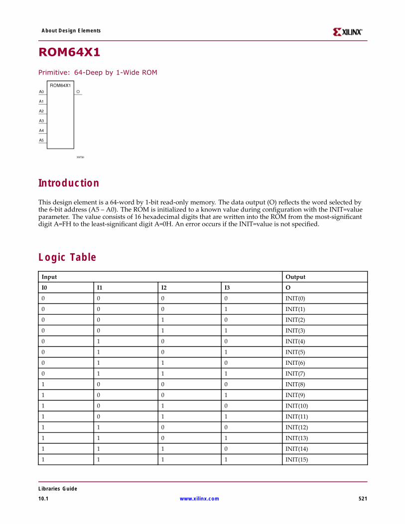
About Design Elements
ROM64X1
Primitive: 64-Deep by 1-Wide ROM
IntroductionThis design element is a 64-word by 1-bit read-only memory. The data output (O) reflects the word selected bythe 6-bit address (A5 – A0). The ROM is initialized to a known value during configuration with the INIT=valueparameter. The value consists of 16 hexadecimal digits that are written into the ROM from the most-significantdigit A=FH to the least-significant digit A=0H. An error occurs if the INIT=value is not specified.
Logic TableInput Output
I0 I1 I2 I3 O
0 0 0 0 INIT(0)
0 0 0 1 INIT(1)
0 0 1 0 INIT(2)
0 0 1 1 INIT(3)
0 1 0 0 INIT(4)
0 1 0 1 INIT(5)
0 1 1 0 INIT(6)
0 1 1 1 INIT(7)
1 0 0 0 INIT(8)
1 0 0 1 INIT(9)
1 0 1 0 INIT(10)
1 0 1 1 INIT(11)
1 1 0 0 INIT(12)
1 1 0 1 INIT(13)
1 1 1 0 INIT(14)
1 1 1 1 INIT(15)
Libraries Guide
10.1 www.xilinx.com 521
About Design Elements
Design Entry MethodThis design element can be used in schematics.
Available AttributesAttribute Type Allowed Values Default Description
INIT Hexadecimal Any 64-Bit Value All zeros Specifies the contents of the ROM.
For More Information• See the Spartan-3A User Guide.
• See the Spartan-3A Data Sheets.
• See the Spartan-3AN FPGA In-System Flash User Guide.
• See the Spartan-3AN Data Sheets.
Libraries Guide
522 www.xilinx.com 10.1

About Design Elements
SOP3
Macro: Sum of Products
IntroductionThree input Sum of Products (SOP) macros provide common logic functions by OR gating the output of oneAND function with one direct input. Variations of inverting and non-inverting inputs are available.
Design Entry MethodThis design element is only for use in schematics.
For More Information• See the Spartan-3A User Guide.
• See the Spartan-3A Data Sheets.
• See the Spartan-3AN FPGA In-System Flash User Guide.
• See the Spartan-3AN Data Sheets.
Libraries Guide
10.1 www.xilinx.com 523
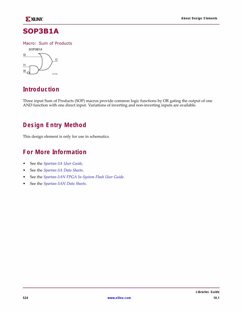
About Design Elements
SOP3B1A
Macro: Sum of Products
IntroductionThree input Sum of Products (SOP) macros provide common logic functions by OR gating the output of oneAND function with one direct input. Variations of inverting and non-inverting inputs are available.
Design Entry MethodThis design element is only for use in schematics.
For More Information• See the Spartan-3A User Guide.
• See the Spartan-3A Data Sheets.
• See the Spartan-3AN FPGA In-System Flash User Guide.
• See the Spartan-3AN Data Sheets.
Libraries Guide
524 www.xilinx.com 10.1

About Design Elements
SOP3B1B
Macro: Sum of Products
IntroductionThree input Sum of Products (SOP) macros provide common logic functions by OR gating the output of oneAND function with one direct input. Variations of inverting and non-inverting inputs are available.
Design Entry MethodThis design element is only for use in schematics.
For More Information• See the Spartan-3A User Guide.
• See the Spartan-3A Data Sheets.
• See the Spartan-3AN FPGA In-System Flash User Guide.
• See the Spartan-3AN Data Sheets.
Libraries Guide
10.1 www.xilinx.com 525

About Design Elements
SOP3B2A
Macro: Sum of Products
IntroductionThree input Sum of Products (SOP) macros provide common logic functions by OR gating the output of oneAND function with one direct input. Variations of inverting and non-inverting inputs are available.
Design Entry MethodThis design element is only for use in schematics.
For More Information• See the Spartan-3A User Guide.
• See the Spartan-3A Data Sheets.
• See the Spartan-3AN FPGA In-System Flash User Guide.
• See the Spartan-3AN Data Sheets.
Libraries Guide
526 www.xilinx.com 10.1
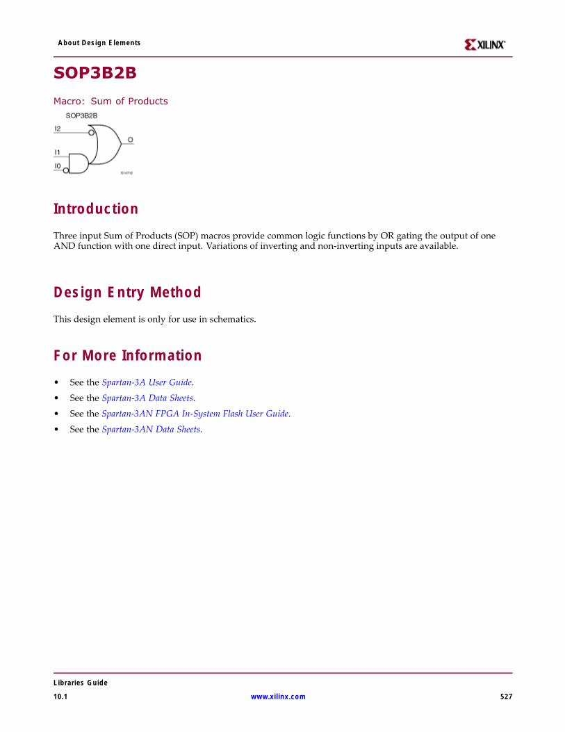
About Design Elements
SOP3B2B
Macro: Sum of Products
IntroductionThree input Sum of Products (SOP) macros provide common logic functions by OR gating the output of oneAND function with one direct input. Variations of inverting and non-inverting inputs are available.
Design Entry MethodThis design element is only for use in schematics.
For More Information• See the Spartan-3A User Guide.
• See the Spartan-3A Data Sheets.
• See the Spartan-3AN FPGA In-System Flash User Guide.
• See the Spartan-3AN Data Sheets.
Libraries Guide
10.1 www.xilinx.com 527

About Design Elements
SOP3B3
Macro: Sum of Products
IntroductionThree input Sum of Products (SOP) macros provide common logic functions by OR gating the output of oneAND function with one direct input. Variations of inverting and non-inverting inputs are available.
Design Entry MethodThis design element is only for use in schematics.
For More Information• See the Spartan-3A User Guide.
• See the Spartan-3A Data Sheets.
• See the Spartan-3AN FPGA In-System Flash User Guide.
• See the Spartan-3AN Data Sheets.
Libraries Guide
528 www.xilinx.com 10.1

About Design Elements
SOP4
Macro: Sum of Products
IntroductionFour input Sum of Products (SOP) macros provide common logic functions by OR gating the outputs of twoAND functions. Variations of inverting and non-inverting inputs are available.
Design Entry MethodThis design element is only for use in schematics.
For More Information• See the Spartan-3A User Guide.
• See the Spartan-3A Data Sheets.
• See the Spartan-3AN FPGA In-System Flash User Guide.
• See the Spartan-3AN Data Sheets.
Libraries Guide
10.1 www.xilinx.com 529
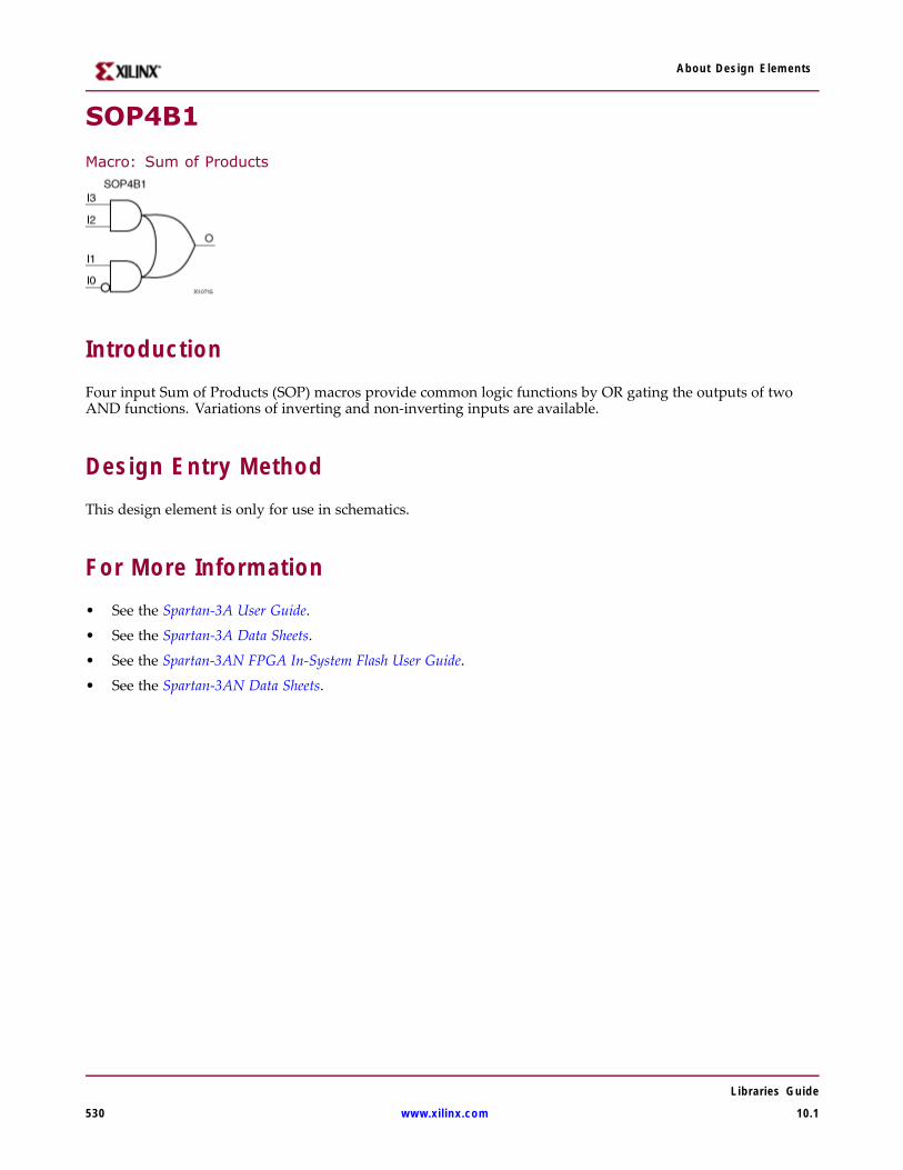
About Design Elements
SOP4B1
Macro: Sum of Products
IntroductionFour input Sum of Products (SOP) macros provide common logic functions by OR gating the outputs of twoAND functions. Variations of inverting and non-inverting inputs are available.
Design Entry MethodThis design element is only for use in schematics.
For More Information• See the Spartan-3A User Guide.
• See the Spartan-3A Data Sheets.
• See the Spartan-3AN FPGA In-System Flash User Guide.
• See the Spartan-3AN Data Sheets.
Libraries Guide
530 www.xilinx.com 10.1

About Design Elements
SOP4B2A
Macro: Sum of Products
IntroductionFour input Sum of Products (SOP) macros provide common logic functions by OR gating the outputs of twoAND functions. Variations of inverting and non-inverting inputs are available.
Design Entry MethodThis design element is only for use in schematics.
For More Information• See the Spartan-3A User Guide.
• See the Spartan-3A Data Sheets.
• See the Spartan-3AN FPGA In-System Flash User Guide.
• See the Spartan-3AN Data Sheets.
Libraries Guide
10.1 www.xilinx.com 531
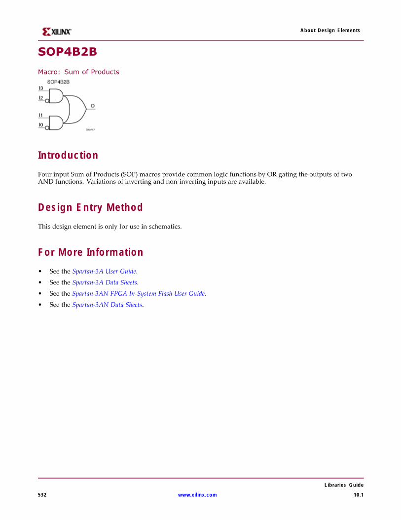
About Design Elements
SOP4B2B
Macro: Sum of Products
IntroductionFour input Sum of Products (SOP) macros provide common logic functions by OR gating the outputs of twoAND functions. Variations of inverting and non-inverting inputs are available.
Design Entry MethodThis design element is only for use in schematics.
For More Information• See the Spartan-3A User Guide.
• See the Spartan-3A Data Sheets.
• See the Spartan-3AN FPGA In-System Flash User Guide.
• See the Spartan-3AN Data Sheets.
Libraries Guide
532 www.xilinx.com 10.1

About Design Elements
SOP4B3
Macro: Sum of Products
IntroductionFour input Sum of Products (SOP) macros provide common logic functions by OR gating the outputs of twoAND functions. Variations of inverting and non-inverting inputs are available.
Design Entry MethodThis design element is only for use in schematics.
For More Information• See the Spartan-3A User Guide.
• See the Spartan-3A Data Sheets.
• See the Spartan-3AN FPGA In-System Flash User Guide.
• See the Spartan-3AN Data Sheets.
Libraries Guide
10.1 www.xilinx.com 533
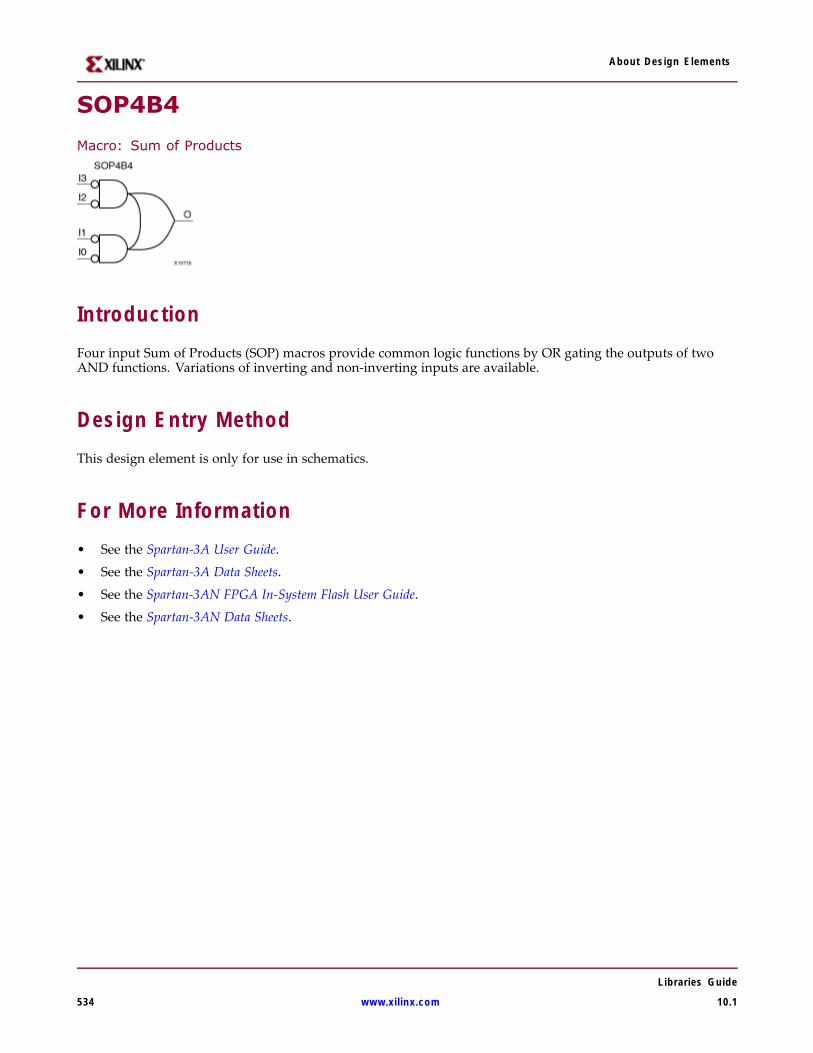
About Design Elements
SOP4B4
Macro: Sum of Products
IntroductionFour input Sum of Products (SOP) macros provide common logic functions by OR gating the outputs of twoAND functions. Variations of inverting and non-inverting inputs are available.
Design Entry MethodThis design element is only for use in schematics.
For More Information• See the Spartan-3A User Guide.
• See the Spartan-3A Data Sheets.
• See the Spartan-3AN FPGA In-System Flash User Guide.
• See the Spartan-3AN Data Sheets.
Libraries Guide
534 www.xilinx.com 10.1
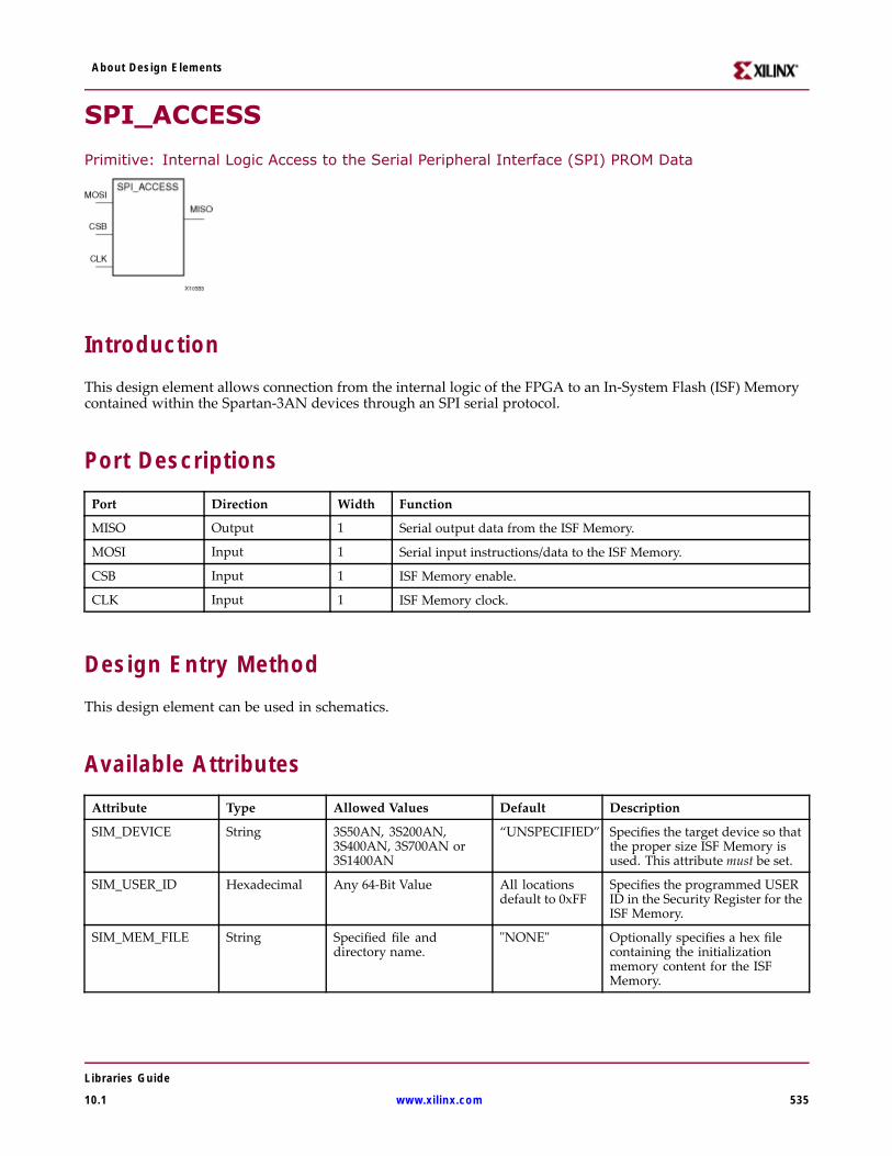
About Design Elements
SPI_ACCESS
Primitive: Internal Logic Access to the Serial Peripheral Interface (SPI) PROM Data
IntroductionThis design element allows connection from the internal logic of the FPGA to an In-System Flash (ISF) Memorycontained within the Spartan-3AN devices through an SPI serial protocol.
Port DescriptionsPort Direction Width Function
MISO Output 1 Serial output data from the ISF Memory.
MOSI Input 1 Serial input instructions/data to the ISF Memory.
CSB Input 1 ISF Memory enable.
CLK Input 1 ISF Memory clock.
Design Entry MethodThis design element can be used in schematics.
Available AttributesAttribute Type Allowed Values Default Description
SIM_DEVICE String 3S50AN, 3S200AN,3S400AN, 3S700AN or3S1400AN
“UNSPECIFIED” Specifies the target device so thatthe proper size ISF Memory isused. This attribute must be set.
SIM_USER_ID Hexadecimal Any 64-Bit Value All locationsdefault to 0xFF
Specifies the programmed USERID in the Security Register for theISF Memory.
SIM_MEM_FILE String Specified file anddirectory name.
"NONE" Optionally specifies a hex filecontaining the initializationmemory content for the ISFMemory.
Libraries Guide
10.1 www.xilinx.com 535
About Design Elements
Attribute Type Allowed Values Default Description
SIM_FACTORY_ID Hexadecimal Any 64-Bit Value All locationsdefault to 0xFF
Specifies the Unique Identifiervalue in the Security Register forsimulation purposes (the actualHW value will be specific to theparticular device used).
SIM_DELAY_TYPE String “ACCURATE”,“SCALED”
“SCALED” Scales down some timingdelays for faster simulation run.“ACCURATE” = timing anddelays consistent with datasheetspecs. “SCALED” = timingnumbers scaled back to run fastersimulation, behavior not affected.
For More Information• See the Spartan-3A User Guide.
• See the Spartan-3A Data Sheets.
• See the Spartan-3AN FPGA In-System Flash User Guide.
• See the Spartan-3AN Data Sheets.
Libraries Guide
536 www.xilinx.com 10.1
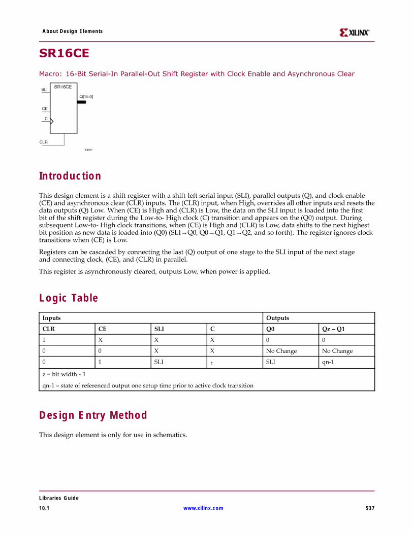
About Design Elements
SR16CE
Macro: 16-Bit Serial-In Parallel-Out Shift Register with Clock Enable and Asynchronous Clear
IntroductionThis design element is a shift register with a shift-left serial input (SLI), parallel outputs (Q), and clock enable(CE) and asynchronous clear (CLR) inputs. The (CLR) input, when High, overrides all other inputs and resets thedata outputs (Q) Low. When (CE) is High and (CLR) is Low, the data on the SLI input is loaded into the firstbit of the shift register during the Low-to- High clock (C) transition and appears on the (Q0) output. Duringsubsequent Low-to- High clock transitions, when (CE) is High and (CLR) is Low, data shifts to the next highestbit position as new data is loaded into (Q0) (SLI→Q0, Q0→Q1, Q1→Q2, and so forth). The register ignores clocktransitions when (CE) is Low.
Registers can be cascaded by connecting the last (Q) output of one stage to the SLI input of the next stageand connecting clock, (CE), and (CLR) in parallel.
This register is asynchronously cleared, outputs Low, when power is applied.
Logic TableInputs Outputs
CLR CE SLI C Q0 Qz – Q1
1 X X X 0 0
0 0 X X No Change No Change
0 1 SLI ↑ SLI qn-1
z = bit width - 1
qn-1 = state of referenced output one setup time prior to active clock transition
Design Entry MethodThis design element is only for use in schematics.
Libraries Guide
10.1 www.xilinx.com 537

About Design Elements
For More Information• See the Spartan-3A User Guide.
• See the Spartan-3A Data Sheets.
• See the Spartan-3AN FPGA In-System Flash User Guide.
• See the Spartan-3AN Data Sheets.
Libraries Guide
538 www.xilinx.com 10.1
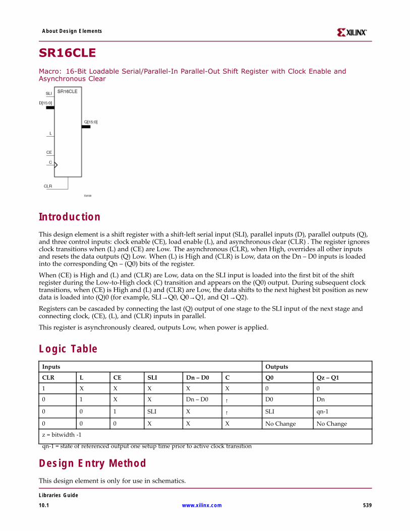
About Design Elements
SR16CLEMacro: 16-Bit Loadable Serial/Parallel-In Parallel-Out Shift Register with Clock Enable andAsynchronous Clear
IntroductionThis design element is a shift register with a shift-left serial input (SLI), parallel inputs (D), parallel outputs (Q),and three control inputs: clock enable (CE), load enable (L), and asynchronous clear (CLR) . The register ignoresclock transitions when (L) and (CE) are Low. The asynchronous (CLR), when High, overrides all other inputsand resets the data outputs (Q) Low. When (L) is High and (CLR) is Low, data on the Dn – D0 inputs is loadedinto the corresponding Qn – (Q0) bits of the register.
When (CE) is High and (L) and (CLR) are Low, data on the SLI input is loaded into the first bit of the shiftregister during the Low-to-High clock (C) transition and appears on the (Q0) output. During subsequent clocktransitions, when (CE) is High and (L) and (CLR) are Low, the data shifts to the next highest bit position as newdata is loaded into (Q)0 (for example, SLI→Q0, Q0→Q1, and Q1→Q2).
Registers can be cascaded by connecting the last (Q) output of one stage to the SLI input of the next stage andconnecting clock, (CE), (L), and (CLR) inputs in parallel.
This register is asynchronously cleared, outputs Low, when power is applied.
Logic TableInputs Outputs
CLR L CE SLI Dn – D0 C Q0 Qz – Q1
1 X X X X X 0 0
0 1 X X Dn – D0 ↑ D0 Dn
0 0 1 SLI X ↑ SLI qn-1
0 0 0 X X X No Change No Change
z = bitwidth -1
qn-1 = state of referenced output one setup time prior to active clock transition
Design Entry MethodThis design element is only for use in schematics.
Libraries Guide
10.1 www.xilinx.com 539

About Design Elements
For More Information• See the Spartan-3A User Guide.
• See the Spartan-3A Data Sheets.
• See the Spartan-3AN FPGA In-System Flash User Guide.
• See the Spartan-3AN Data Sheets.
Libraries Guide
540 www.xilinx.com 10.1
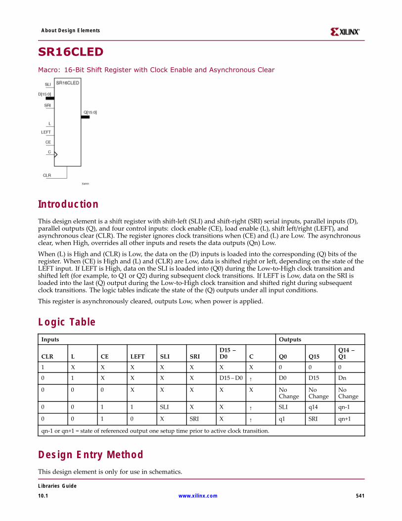
About Design Elements
SR16CLEDMacro: 16-Bit Shift Register with Clock Enable and Asynchronous Clear
IntroductionThis design element is a shift register with shift-left (SLI) and shift-right (SRI) serial inputs, parallel inputs (D),parallel outputs (Q), and four control inputs: clock enable (CE), load enable (L), shift left/right (LEFT), andasynchronous clear (CLR). The register ignores clock transitions when (CE) and (L) are Low. The asynchronousclear, when High, overrides all other inputs and resets the data outputs (Qn) Low.
When (L) is High and (CLR) is Low, the data on the (D) inputs is loaded into the corresponding (Q) bits of theregister. When (CE) is High and (L) and (CLR) are Low, data is shifted right or left, depending on the state of theLEFT input. If LEFT is High, data on the SLI is loaded into (Q0) during the Low-to-High clock transition andshifted left (for example, to Q1 or Q2) during subsequent clock transitions. If LEFT is Low, data on the SRI isloaded into the last (Q) output during the Low-to-High clock transition and shifted right during subsequentclock transitions. The logic tables indicate the state of the (Q) outputs under all input conditions.
This register is asynchronously cleared, outputs Low, when power is applied.
Logic TableInputs Outputs
CLR L CE LEFT SLI SRID15 –D0 C Q0 Q15
Q14 –Q1
1 X X X X X X X 0 0 0
0 1 X X X X D15 –D0 ↑ D0 D15 Dn
0 0 0 X X X X X NoChange
NoChange
NoChange
0 0 1 1 SLI X X ↑ SLI q14 qn-1
0 0 1 0 X SRI X ↑ q1 SRI qn+1
qn-1 or qn+1 = state of referenced output one setup time prior to active clock transition.
Design Entry MethodThis design element is only for use in schematics.
Libraries Guide
10.1 www.xilinx.com 541

About Design Elements
For More Information• See the Spartan-3A User Guide.
• See the Spartan-3A Data Sheets.
• See the Spartan-3AN FPGA In-System Flash User Guide.
• See the Spartan-3AN Data Sheets.
Libraries Guide
542 www.xilinx.com 10.1

About Design Elements
SR16RE
Macro: 16-Bit Serial-In Parallel-Out Shift Register with Clock Enable and Synchronous Reset
IntroductionThis design element is a shift register with shift-left serial input (SLI), parallel outputs (Qn), clock enable (CE),and synchronous reset (R) inputs. The R input, when High, overrides all other inputs during the Low-to-Highclock (C) transition and resets the data outputs (Q) Low.
When (CE) is High and (R) is Low, the data on the (SLI) is loaded into the first bit of the shift register duringthe Low-to-High clock (C) transition and appears on the (Q0) output. During subsequent Low-to-High clocktransitions, when (CE) is High and R is Low, data shifts to the next highest bit position as new data is loaded into(Q0) (for example, SLI→Q0, Q0→Q1, and Q1→Q2). The register ignores clock transitions when (CE) is Low.
Registers can be cascaded by connecting the last (Q) output of one stage to the SLI input of the next stage andconnecting clock, (CE), and (R) in parallel.
This register is asynchronously cleared, outputs Low, when power is applied.
Logic TableInputs Outputs
R CE SLI C Q0 Qz – Q1
1 X X ↑ 0 0
0 0 X X No Change No Change
0 1 SLI ↑ SLI qn-1
z = bitwidth -1
qn-1 = state of referenced output one setup time prior to active clock transition
Design Entry MethodThis design element is only for use in schematics.
Libraries Guide
10.1 www.xilinx.com 543

About Design Elements
For More Information• See the Spartan-3A User Guide.
• See the Spartan-3A Data Sheets.
• See the Spartan-3AN FPGA In-System Flash User Guide.
• See the Spartan-3AN Data Sheets.
Libraries Guide
544 www.xilinx.com 10.1
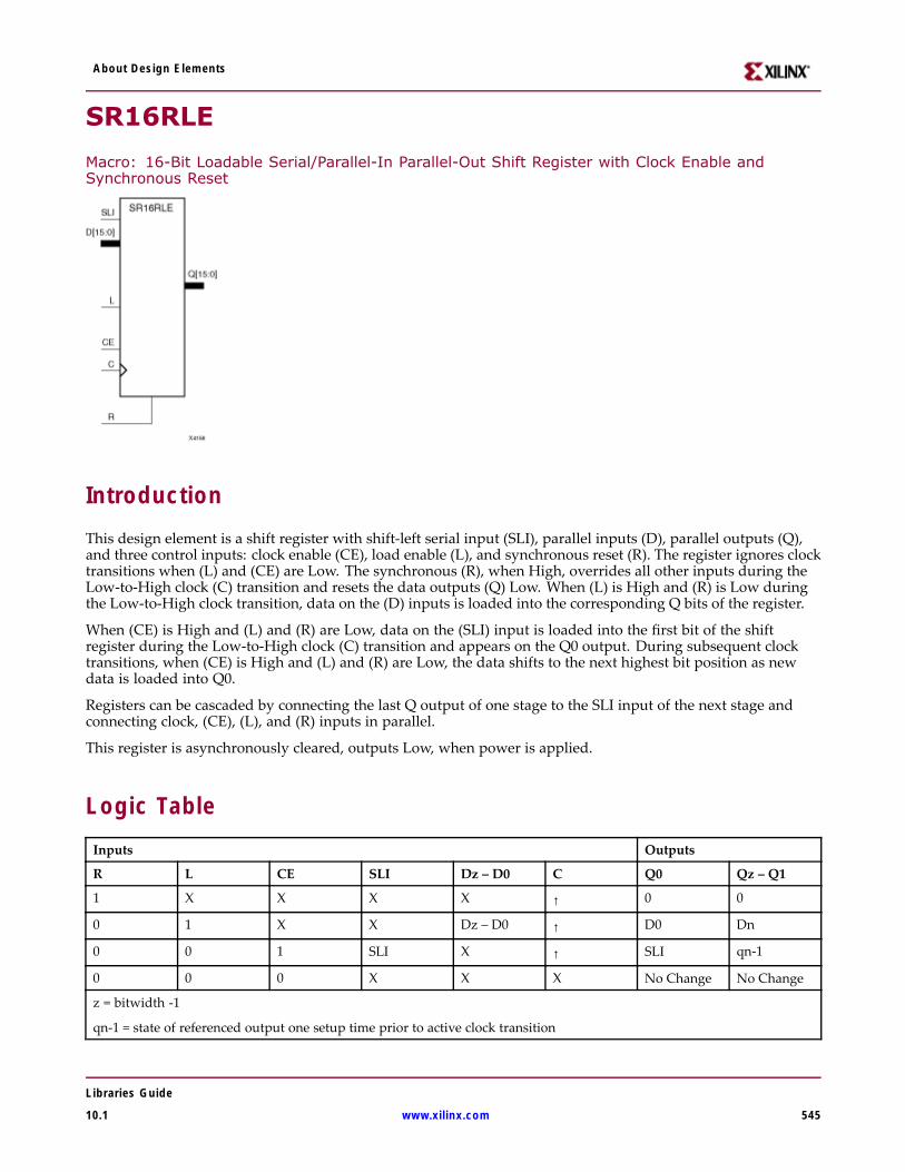
About Design Elements
SR16RLE
Macro: 16-Bit Loadable Serial/Parallel-In Parallel-Out Shift Register with Clock Enable andSynchronous Reset
IntroductionThis design element is a shift register with shift-left serial input (SLI), parallel inputs (D), parallel outputs (Q),and three control inputs: clock enable (CE), load enable (L), and synchronous reset (R). The register ignores clocktransitions when (L) and (CE) are Low. The synchronous (R), when High, overrides all other inputs during theLow-to-High clock (C) transition and resets the data outputs (Q) Low. When (L) is High and (R) is Low duringthe Low-to-High clock transition, data on the (D) inputs is loaded into the corresponding Q bits of the register.
When (CE) is High and (L) and (R) are Low, data on the (SLI) input is loaded into the first bit of the shiftregister during the Low-to-High clock (C) transition and appears on the Q0 output. During subsequent clocktransitions, when (CE) is High and (L) and (R) are Low, the data shifts to the next highest bit position as newdata is loaded into Q0.
Registers can be cascaded by connecting the last Q output of one stage to the SLI input of the next stage andconnecting clock, (CE), (L), and (R) inputs in parallel.
This register is asynchronously cleared, outputs Low, when power is applied.
Logic TableInputs Outputs
R L CE SLI Dz – D0 C Q0 Qz – Q1
1 X X X X ↑ 0 0
0 1 X X Dz – D0 ↑ D0 Dn
0 0 1 SLI X ↑ SLI qn-1
0 0 0 X X X No Change No Change
z = bitwidth -1
qn-1 = state of referenced output one setup time prior to active clock transition
Libraries Guide
10.1 www.xilinx.com 545

About Design Elements
Design Entry MethodThis design element is only for use in schematics.
For More Information• See the Spartan-3A User Guide.
• See the Spartan-3A Data Sheets.
• See the Spartan-3AN FPGA In-System Flash User Guide.
• See the Spartan-3AN Data Sheets.
Libraries Guide
546 www.xilinx.com 10.1

About Design Elements
SR16RLED
Macro: 16-Bit Shift Register with Clock Enable and Synchronous Reset
IntroductionThis design element is a shift register with shift-left (SLI) and shift-right (SRI) serial inputs, parallel inputs (D),parallel outputs (Q) and four control inputs — clock enable (CE), load enable (L), shift left/right (LEFT), andsynchronous reset (R). The register ignores clock transitions when (CE) and (L) are Low. The synchronous (R),when High, overrides all other inputs during the Low-to-High clock (C) transition and resets the data outputs(Q) Low. When (L) is High and (R) is Low during the Low-to-High clock transition, the data on the (D) inputs isloaded into the corresponding (Q) bits of the register.
When (CE) is High and (L) and (R) are Low, data shifts right or left, depending on the state of the LEFT input.If LEFT is High, data on (SLI) is loaded into (Q0) during the Low-to-High clock transition and shifted left (forexample, to Q1 and Q2) during subsequent clock transitions. If LEFT is Low, data on the (SRI) is loaded into thelast (Q) output during the Low-to-High clock transition and shifted right ) during subsequent clock transitions.The logic tables below indicates the state of the (Q) outputs under all input conditions.
This register is asynchronously cleared, outputs Low, when power is applied.
Logic TableInputs Outputs
R L CE LEFT SLI SRID15 –D0 C Q0 Q15
Q14 –Q1
1 X X X X X X ↑ 0 0 0
0 1 X X X X D15 –D0 ↑ D0 D15 Dn
0 0 0 X X X X X NoChange
NoChange
NoChange
0 0 1 1 SLI X X ↑ SLI q14 qn-1
0 0 1 0 X SRI X ↑ q1 SRI qn+1
qn-1 or qn+1 = state of referenced output one setup time prior to active clock transition
Libraries Guide
10.1 www.xilinx.com 547

About Design Elements
Design Entry MethodThis design element is only for use in schematics.
For More Information• See the Spartan-3A User Guide.
• See the Spartan-3A Data Sheets.
• See the Spartan-3AN FPGA In-System Flash User Guide.
• See the Spartan-3AN Data Sheets.
Libraries Guide
548 www.xilinx.com 10.1
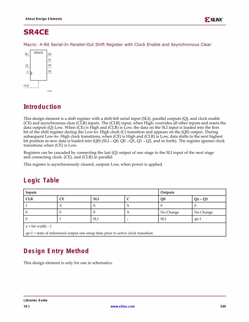
About Design Elements
SR4CE
Macro: 4-Bit Serial-In Parallel-Out Shift Register with Clock Enable and Asynchronous Clear
IntroductionThis design element is a shift register with a shift-left serial input (SLI), parallel outputs (Q), and clock enable(CE) and asynchronous clear (CLR) inputs. The (CLR) input, when High, overrides all other inputs and resets thedata outputs (Q) Low. When (CE) is High and (CLR) is Low, the data on the SLI input is loaded into the firstbit of the shift register during the Low-to- High clock (C) transition and appears on the (Q0) output. Duringsubsequent Low-to- High clock transitions, when (CE) is High and (CLR) is Low, data shifts to the next highestbit position as new data is loaded into (Q0) (SLI→Q0, Q0→Q1, Q1→Q2, and so forth). The register ignores clocktransitions when (CE) is Low.
Registers can be cascaded by connecting the last (Q) output of one stage to the SLI input of the next stageand connecting clock, (CE), and (CLR) in parallel.
This register is asynchronously cleared, outputs Low, when power is applied.
Logic TableInputs Outputs
CLR CE SLI C Q0 Qz – Q1
1 X X X 0 0
0 0 X X No Change No Change
0 1 SLI ↑ SLI qn-1
z = bit width - 1
qn-1 = state of referenced output one setup time prior to active clock transition
Design Entry MethodThis design element is only for use in schematics.
Libraries Guide
10.1 www.xilinx.com 549

About Design Elements
For More Information• See the Spartan-3A User Guide.
• See the Spartan-3A Data Sheets.
• See the Spartan-3AN FPGA In-System Flash User Guide.
• See the Spartan-3AN Data Sheets.
Libraries Guide
550 www.xilinx.com 10.1
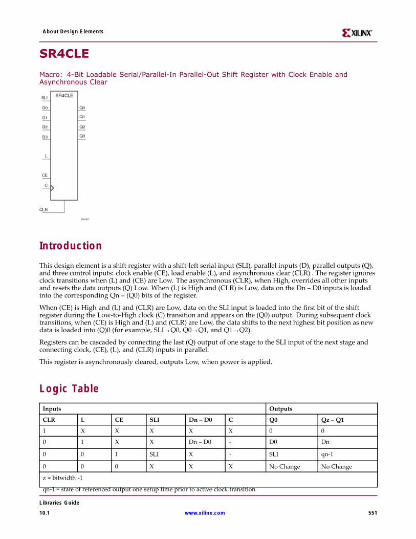
About Design Elements
SR4CLE
Macro: 4-Bit Loadable Serial/Parallel-In Parallel-Out Shift Register with Clock Enable andAsynchronous Clear
IntroductionThis design element is a shift register with a shift-left serial input (SLI), parallel inputs (D), parallel outputs (Q),and three control inputs: clock enable (CE), load enable (L), and asynchronous clear (CLR) . The register ignoresclock transitions when (L) and (CE) are Low. The asynchronous (CLR), when High, overrides all other inputsand resets the data outputs (Q) Low. When (L) is High and (CLR) is Low, data on the Dn – D0 inputs is loadedinto the corresponding Qn – (Q0) bits of the register.
When (CE) is High and (L) and (CLR) are Low, data on the SLI input is loaded into the first bit of the shiftregister during the Low-to-High clock (C) transition and appears on the (Q0) output. During subsequent clocktransitions, when (CE) is High and (L) and (CLR) are Low, the data shifts to the next highest bit position as newdata is loaded into (Q)0 (for example, SLI→Q0, Q0→Q1, and Q1→Q2).
Registers can be cascaded by connecting the last (Q) output of one stage to the SLI input of the next stage andconnecting clock, (CE), (L), and (CLR) inputs in parallel.
This register is asynchronously cleared, outputs Low, when power is applied.
Logic TableInputs Outputs
CLR L CE SLI Dn – D0 C Q0 Qz – Q1
1 X X X X X 0 0
0 1 X X Dn – D0 ↑ D0 Dn
0 0 1 SLI X ↑ SLI qn-1
0 0 0 X X X No Change No Change
z = bitwidth -1
qn-1 = state of referenced output one setup time prior to active clock transition
Libraries Guide
10.1 www.xilinx.com 551

About Design Elements
Design Entry MethodThis design element is only for use in schematics.
For More Information• See the Spartan-3A User Guide.
• See the Spartan-3A Data Sheets.
• See the Spartan-3AN FPGA In-System Flash User Guide.
• See the Spartan-3AN Data Sheets.
Libraries Guide
552 www.xilinx.com 10.1
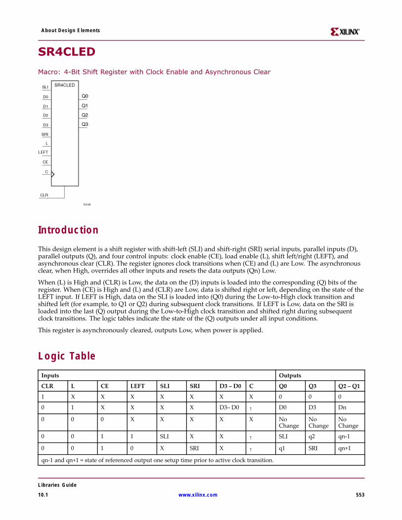
About Design Elements
SR4CLED
Macro: 4-Bit Shift Register with Clock Enable and Asynchronous Clear
IntroductionThis design element is a shift register with shift-left (SLI) and shift-right (SRI) serial inputs, parallel inputs (D),parallel outputs (Q), and four control inputs: clock enable (CE), load enable (L), shift left/right (LEFT), andasynchronous clear (CLR). The register ignores clock transitions when (CE) and (L) are Low. The asynchronousclear, when High, overrides all other inputs and resets the data outputs (Qn) Low.
When (L) is High and (CLR) is Low, the data on the (D) inputs is loaded into the corresponding (Q) bits of theregister. When (CE) is High and (L) and (CLR) are Low, data is shifted right or left, depending on the state of theLEFT input. If LEFT is High, data on the SLI is loaded into (Q0) during the Low-to-High clock transition andshifted left (for example, to Q1 or Q2) during subsequent clock transitions. If LEFT is Low, data on the SRI isloaded into the last (Q) output during the Low-to-High clock transition and shifted right during subsequentclock transitions. The logic tables indicate the state of the (Q) outputs under all input conditions.
This register is asynchronously cleared, outputs Low, when power is applied.
Logic TableInputs Outputs
CLR L CE LEFT SLI SRI D3 – D0 C Q0 Q3 Q2 – Q1
1 X X X X X X X 0 0 0
0 1 X X X X D3– D0 ↑ D0 D3 Dn
0 0 0 X X X X X NoChange
NoChange
NoChange
0 0 1 1 SLI X X ↑ SLI q2 qn-1
0 0 1 0 X SRI X ↑ q1 SRI qn+1
qn-1 and qn+1 = state of referenced output one setup time prior to active clock transition.
Libraries Guide
10.1 www.xilinx.com 553

About Design Elements
Design Entry MethodThis design element is only for use in schematics.
For More Information• See the Spartan-3A User Guide.
• See the Spartan-3A Data Sheets.
• See the Spartan-3AN FPGA In-System Flash User Guide.
• See the Spartan-3AN Data Sheets.
Libraries Guide
554 www.xilinx.com 10.1
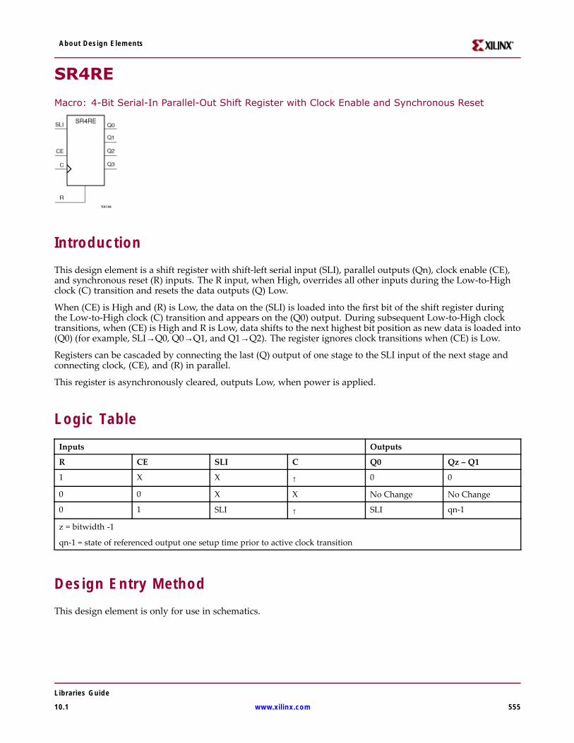
About Design Elements
SR4RE
Macro: 4-Bit Serial-In Parallel-Out Shift Register with Clock Enable and Synchronous Reset
IntroductionThis design element is a shift register with shift-left serial input (SLI), parallel outputs (Qn), clock enable (CE),and synchronous reset (R) inputs. The R input, when High, overrides all other inputs during the Low-to-Highclock (C) transition and resets the data outputs (Q) Low.
When (CE) is High and (R) is Low, the data on the (SLI) is loaded into the first bit of the shift register duringthe Low-to-High clock (C) transition and appears on the (Q0) output. During subsequent Low-to-High clocktransitions, when (CE) is High and R is Low, data shifts to the next highest bit position as new data is loaded into(Q0) (for example, SLI→Q0, Q0→Q1, and Q1→Q2). The register ignores clock transitions when (CE) is Low.
Registers can be cascaded by connecting the last (Q) output of one stage to the SLI input of the next stage andconnecting clock, (CE), and (R) in parallel.
This register is asynchronously cleared, outputs Low, when power is applied.
Logic TableInputs Outputs
R CE SLI C Q0 Qz – Q1
1 X X ↑ 0 0
0 0 X X No Change No Change
0 1 SLI ↑ SLI qn-1
z = bitwidth -1
qn-1 = state of referenced output one setup time prior to active clock transition
Design Entry MethodThis design element is only for use in schematics.
Libraries Guide
10.1 www.xilinx.com 555

About Design Elements
For More Information• See the Spartan-3A User Guide.
• See the Spartan-3A Data Sheets.
• See the Spartan-3AN FPGA In-System Flash User Guide.
• See the Spartan-3AN Data Sheets.
Libraries Guide
556 www.xilinx.com 10.1
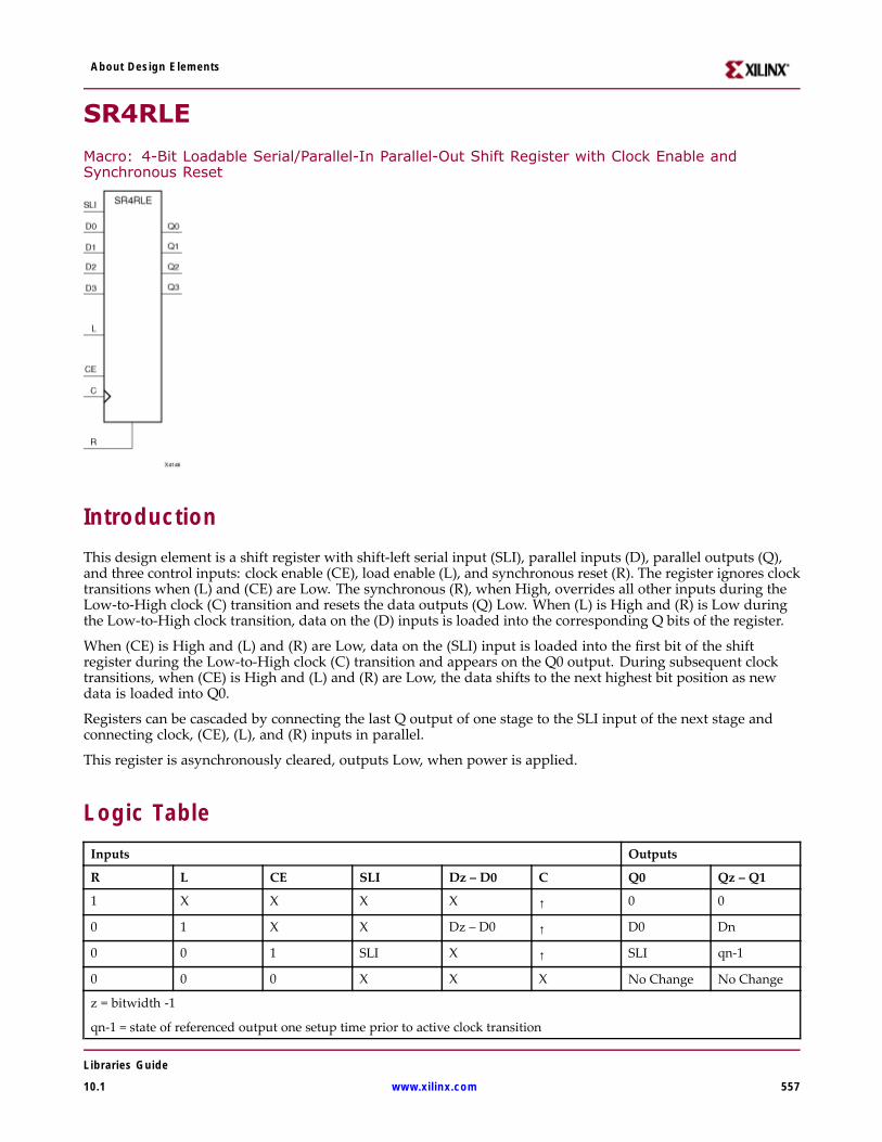
About Design Elements
SR4RLE
Macro: 4-Bit Loadable Serial/Parallel-In Parallel-Out Shift Register with Clock Enable andSynchronous Reset
IntroductionThis design element is a shift register with shift-left serial input (SLI), parallel inputs (D), parallel outputs (Q),and three control inputs: clock enable (CE), load enable (L), and synchronous reset (R). The register ignores clocktransitions when (L) and (CE) are Low. The synchronous (R), when High, overrides all other inputs during theLow-to-High clock (C) transition and resets the data outputs (Q) Low. When (L) is High and (R) is Low duringthe Low-to-High clock transition, data on the (D) inputs is loaded into the corresponding Q bits of the register.
When (CE) is High and (L) and (R) are Low, data on the (SLI) input is loaded into the first bit of the shiftregister during the Low-to-High clock (C) transition and appears on the Q0 output. During subsequent clocktransitions, when (CE) is High and (L) and (R) are Low, the data shifts to the next highest bit position as newdata is loaded into Q0.
Registers can be cascaded by connecting the last Q output of one stage to the SLI input of the next stage andconnecting clock, (CE), (L), and (R) inputs in parallel.
This register is asynchronously cleared, outputs Low, when power is applied.
Logic TableInputs Outputs
R L CE SLI Dz – D0 C Q0 Qz – Q1
1 X X X X ↑ 0 0
0 1 X X Dz – D0 ↑ D0 Dn
0 0 1 SLI X ↑ SLI qn-1
0 0 0 X X X No Change No Change
z = bitwidth -1
qn-1 = state of referenced output one setup time prior to active clock transition
Libraries Guide
10.1 www.xilinx.com 557

About Design Elements
Design Entry MethodThis design element is only for use in schematics.
For More Information• See the Spartan-3A User Guide.
• See the Spartan-3A Data Sheets.
• See the Spartan-3AN FPGA In-System Flash User Guide.
• See the Spartan-3AN Data Sheets.
Libraries Guide
558 www.xilinx.com 10.1
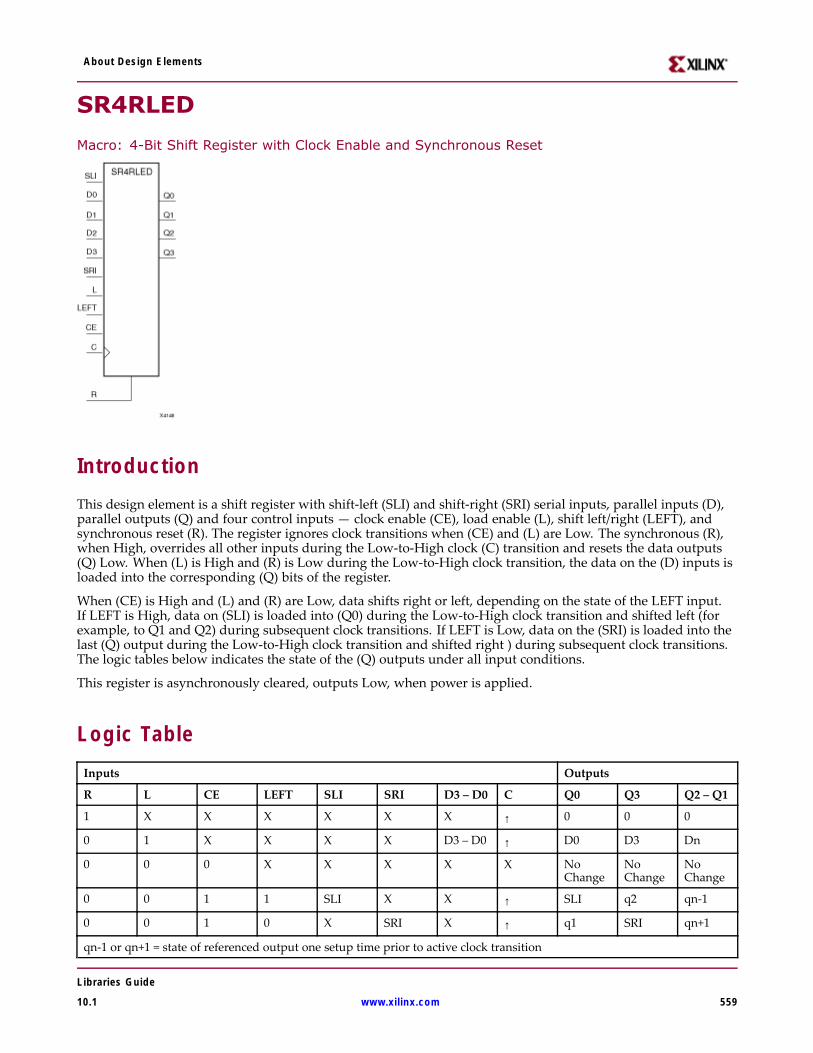
About Design Elements
SR4RLED
Macro: 4-Bit Shift Register with Clock Enable and Synchronous Reset
IntroductionThis design element is a shift register with shift-left (SLI) and shift-right (SRI) serial inputs, parallel inputs (D),parallel outputs (Q) and four control inputs — clock enable (CE), load enable (L), shift left/right (LEFT), andsynchronous reset (R). The register ignores clock transitions when (CE) and (L) are Low. The synchronous (R),when High, overrides all other inputs during the Low-to-High clock (C) transition and resets the data outputs(Q) Low. When (L) is High and (R) is Low during the Low-to-High clock transition, the data on the (D) inputs isloaded into the corresponding (Q) bits of the register.
When (CE) is High and (L) and (R) are Low, data shifts right or left, depending on the state of the LEFT input.If LEFT is High, data on (SLI) is loaded into (Q0) during the Low-to-High clock transition and shifted left (forexample, to Q1 and Q2) during subsequent clock transitions. If LEFT is Low, data on the (SRI) is loaded into thelast (Q) output during the Low-to-High clock transition and shifted right ) during subsequent clock transitions.The logic tables below indicates the state of the (Q) outputs under all input conditions.
This register is asynchronously cleared, outputs Low, when power is applied.
Logic TableInputs Outputs
R L CE LEFT SLI SRI D3 – D0 C Q0 Q3 Q2 – Q1
1 X X X X X X ↑ 0 0 0
0 1 X X X X D3 – D0 ↑ D0 D3 Dn
0 0 0 X X X X X NoChange
NoChange
NoChange
0 0 1 1 SLI X X ↑ SLI q2 qn-1
0 0 1 0 X SRI X ↑ q1 SRI qn+1
qn-1 or qn+1 = state of referenced output one setup time prior to active clock transition
Libraries Guide
10.1 www.xilinx.com 559
About Design Elements
Design Entry MethodThis design element is only for use in schematics.
For More Information• See the Spartan-3A User Guide.
• See the Spartan-3A Data Sheets.
• See the Spartan-3AN FPGA In-System Flash User Guide.
• See the Spartan-3AN Data Sheets.
Libraries Guide
560 www.xilinx.com 10.1

About Design Elements
SR8CE
Macro: 8-Bit Serial-In Parallel-Out Shift Register with Clock Enable and Asynchronous Clear
IntroductionThis design element is a shift register with a shift-left serial input (SLI), parallel outputs (Q), and clock enable(CE) and asynchronous clear (CLR) inputs. The (CLR) input, when High, overrides all other inputs and resets thedata outputs (Q) Low. When (CE) is High and (CLR) is Low, the data on the SLI input is loaded into the firstbit of the shift register during the Low-to- High clock (C) transition and appears on the (Q0) output. Duringsubsequent Low-to- High clock transitions, when (CE) is High and (CLR) is Low, data shifts to the next highestbit position as new data is loaded into (Q0) (SLI→Q0, Q0→Q1, Q1→Q2, and so forth). The register ignores clocktransitions when (CE) is Low.
Registers can be cascaded by connecting the last (Q) output of one stage to the SLI input of the next stageand connecting clock, (CE), and (CLR) in parallel.
This register is asynchronously cleared, outputs Low, when power is applied.
Logic TableInputs Outputs
CLR CE SLI C Q0 Qz – Q1
1 X X X 0 0
0 0 X X No Change No Change
0 1 SLI ↑ SLI qn-1
z = bit width - 1
qn-1 = state of referenced output one setup time prior to active clock transition
Design Entry MethodThis design element is only for use in schematics.
Libraries Guide
10.1 www.xilinx.com 561

About Design Elements
For More Information• See the Spartan-3A User Guide.
• See the Spartan-3A Data Sheets.
• See the Spartan-3AN FPGA In-System Flash User Guide.
• See the Spartan-3AN Data Sheets.
Libraries Guide
562 www.xilinx.com 10.1
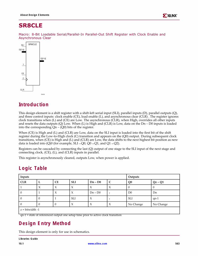
About Design Elements
SR8CLEMacro: 8-Bit Loadable Serial/Parallel-In Parallel-Out Shift Register with Clock Enable andAsynchronous Clear
IntroductionThis design element is a shift register with a shift-left serial input (SLI), parallel inputs (D), parallel outputs (Q),and three control inputs: clock enable (CE), load enable (L), and asynchronous clear (CLR) . The register ignoresclock transitions when (L) and (CE) are Low. The asynchronous (CLR), when High, overrides all other inputsand resets the data outputs (Q) Low. When (L) is High and (CLR) is Low, data on the Dn – D0 inputs is loadedinto the corresponding Qn – (Q0) bits of the register.
When (CE) is High and (L) and (CLR) are Low, data on the SLI input is loaded into the first bit of the shiftregister during the Low-to-High clock (C) transition and appears on the (Q0) output. During subsequent clocktransitions, when (CE) is High and (L) and (CLR) are Low, the data shifts to the next highest bit position as newdata is loaded into (Q)0 (for example, SLI→Q0, Q0→Q1, and Q1→Q2).
Registers can be cascaded by connecting the last (Q) output of one stage to the SLI input of the next stage andconnecting clock, (CE), (L), and (CLR) inputs in parallel.
This register is asynchronously cleared, outputs Low, when power is applied.
Logic TableInputs Outputs
CLR L CE SLI Dn – D0 C Q0 Qz – Q1
1 X X X X X 0 0
0 1 X X Dn – D0 ↑ D0 Dn
0 0 1 SLI X ↑ SLI qn-1
0 0 0 X X X No Change No Change
z = bitwidth -1
qn-1 = state of referenced output one setup time prior to active clock transition
Design Entry MethodThis design element is only for use in schematics.
Libraries Guide
10.1 www.xilinx.com 563

About Design Elements
For More Information• See the Spartan-3A User Guide.
• See the Spartan-3A Data Sheets.
• See the Spartan-3AN FPGA In-System Flash User Guide.
• See the Spartan-3AN Data Sheets.
Libraries Guide
564 www.xilinx.com 10.1
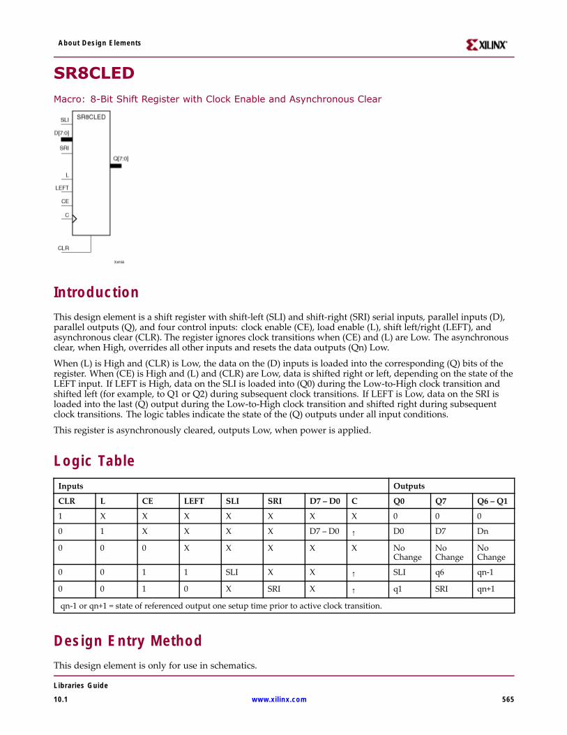
About Design Elements
SR8CLEDMacro: 8-Bit Shift Register with Clock Enable and Asynchronous Clear
IntroductionThis design element is a shift register with shift-left (SLI) and shift-right (SRI) serial inputs, parallel inputs (D),parallel outputs (Q), and four control inputs: clock enable (CE), load enable (L), shift left/right (LEFT), andasynchronous clear (CLR). The register ignores clock transitions when (CE) and (L) are Low. The asynchronousclear, when High, overrides all other inputs and resets the data outputs (Qn) Low.
When (L) is High and (CLR) is Low, the data on the (D) inputs is loaded into the corresponding (Q) bits of theregister. When (CE) is High and (L) and (CLR) are Low, data is shifted right or left, depending on the state of theLEFT input. If LEFT is High, data on the SLI is loaded into (Q0) during the Low-to-High clock transition andshifted left (for example, to Q1 or Q2) during subsequent clock transitions. If LEFT is Low, data on the SRI isloaded into the last (Q) output during the Low-to-High clock transition and shifted right during subsequentclock transitions. The logic tables indicate the state of the (Q) outputs under all input conditions.
This register is asynchronously cleared, outputs Low, when power is applied.
Logic TableInputs Outputs
CLR L CE LEFT SLI SRI D7 – D0 C Q0 Q7 Q6 – Q1
1 X X X X X X X 0 0 0
0 1 X X X X D7 – D0 ↑ D0 D7 Dn
0 0 0 X X X X X NoChange
NoChange
NoChange
0 0 1 1 SLI X X ↑ SLI q6 qn-1
0 0 1 0 X SRI X ↑ q1 SRI qn+1
qn-1 or qn+1 = state of referenced output one setup time prior to active clock transition.
Design Entry MethodThis design element is only for use in schematics.
Libraries Guide
10.1 www.xilinx.com 565

About Design Elements
For More Information• See the Spartan-3A User Guide.
• See the Spartan-3A Data Sheets.
• See the Spartan-3AN FPGA In-System Flash User Guide.
• See the Spartan-3AN Data Sheets.
Libraries Guide
566 www.xilinx.com 10.1
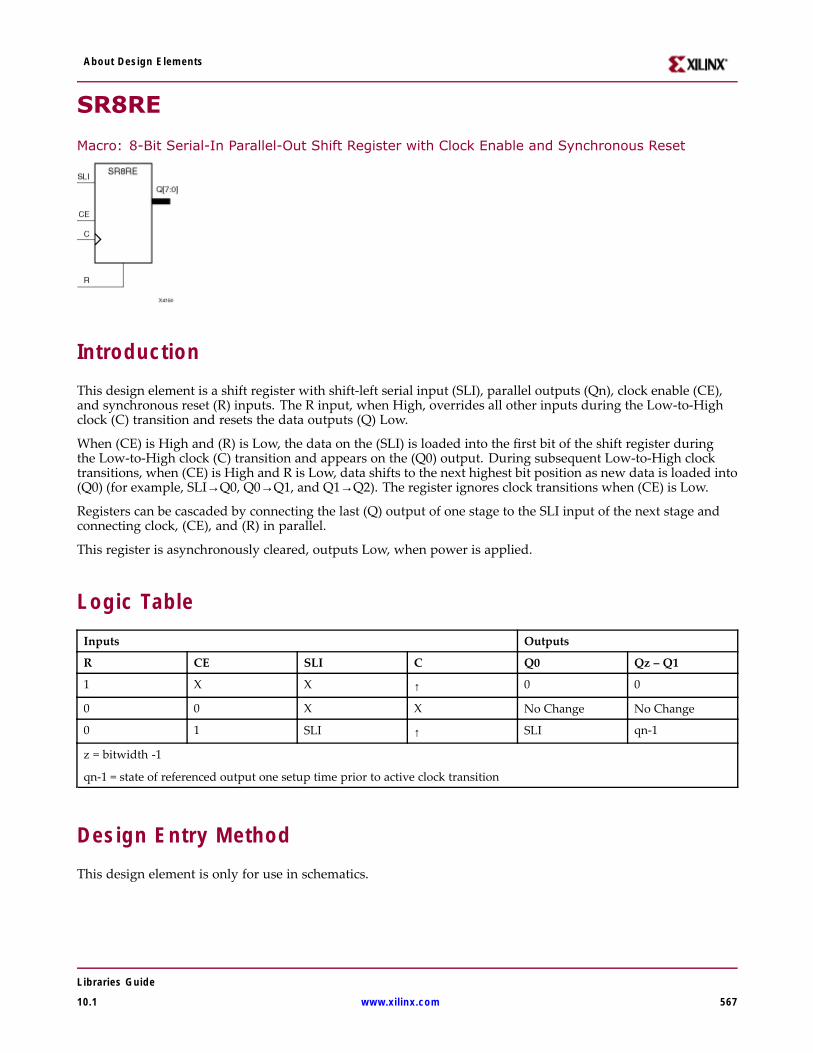
About Design Elements
SR8RE
Macro: 8-Bit Serial-In Parallel-Out Shift Register with Clock Enable and Synchronous Reset
IntroductionThis design element is a shift register with shift-left serial input (SLI), parallel outputs (Qn), clock enable (CE),and synchronous reset (R) inputs. The R input, when High, overrides all other inputs during the Low-to-Highclock (C) transition and resets the data outputs (Q) Low.
When (CE) is High and (R) is Low, the data on the (SLI) is loaded into the first bit of the shift register duringthe Low-to-High clock (C) transition and appears on the (Q0) output. During subsequent Low-to-High clocktransitions, when (CE) is High and R is Low, data shifts to the next highest bit position as new data is loaded into(Q0) (for example, SLI→Q0, Q0→Q1, and Q1→Q2). The register ignores clock transitions when (CE) is Low.
Registers can be cascaded by connecting the last (Q) output of one stage to the SLI input of the next stage andconnecting clock, (CE), and (R) in parallel.
This register is asynchronously cleared, outputs Low, when power is applied.
Logic TableInputs Outputs
R CE SLI C Q0 Qz – Q1
1 X X ↑ 0 0
0 0 X X No Change No Change
0 1 SLI ↑ SLI qn-1
z = bitwidth -1
qn-1 = state of referenced output one setup time prior to active clock transition
Design Entry MethodThis design element is only for use in schematics.
Libraries Guide
10.1 www.xilinx.com 567

About Design Elements
For More Information• See the Spartan-3A User Guide.
• See the Spartan-3A Data Sheets.
• See the Spartan-3AN FPGA In-System Flash User Guide.
• See the Spartan-3AN Data Sheets.
Libraries Guide
568 www.xilinx.com 10.1

About Design Elements
SR8RLE
Macro: 8-Bit Loadable Serial/Parallel-In Parallel-Out Shift Register with Clock Enable andSynchronous Reset
IntroductionThis design element is a shift register with shift-left serial input (SLI), parallel inputs (D), parallel outputs (Q),and three control inputs: clock enable (CE), load enable (L), and synchronous reset (R). The register ignores clocktransitions when (L) and (CE) are Low. The synchronous (R), when High, overrides all other inputs during theLow-to-High clock (C) transition and resets the data outputs (Q) Low. When (L) is High and (R) is Low duringthe Low-to-High clock transition, data on the (D) inputs is loaded into the corresponding Q bits of the register.
When (CE) is High and (L) and (R) are Low, data on the (SLI) input is loaded into the first bit of the shiftregister during the Low-to-High clock (C) transition and appears on the Q0 output. During subsequent clocktransitions, when (CE) is High and (L) and (R) are Low, the data shifts to the next highest bit position as newdata is loaded into Q0.
Registers can be cascaded by connecting the last Q output of one stage to the SLI input of the next stage andconnecting clock, (CE), (L), and (R) inputs in parallel.
This register is asynchronously cleared, outputs Low, when power is applied.
Logic TableInputs Outputs
R L CE SLI Dz – D0 C Q0 Qz – Q1
1 X X X X ↑ 0 0
0 1 X X Dz – D0 ↑ D0 Dn
0 0 1 SLI X ↑ SLI qn-1
0 0 0 X X X No Change No Change
z = bitwidth -1
qn-1 = state of referenced output one setup time prior to active clock transition
Libraries Guide
10.1 www.xilinx.com 569
About Design Elements
Design Entry MethodThis design element is only for use in schematics.
For More Information• See the Spartan-3A User Guide.
• See the Spartan-3A Data Sheets.
• See the Spartan-3AN FPGA In-System Flash User Guide.
• See the Spartan-3AN Data Sheets.
Libraries Guide
570 www.xilinx.com 10.1
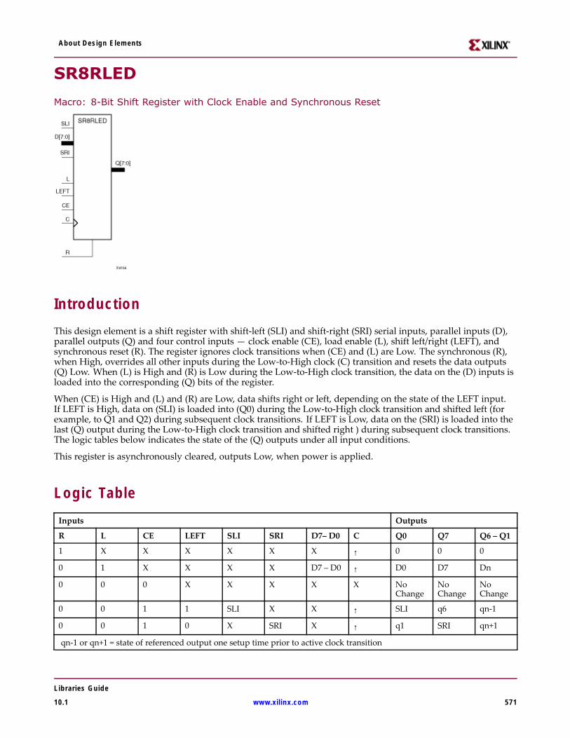
About Design Elements
SR8RLED
Macro: 8-Bit Shift Register with Clock Enable and Synchronous Reset
IntroductionThis design element is a shift register with shift-left (SLI) and shift-right (SRI) serial inputs, parallel inputs (D),parallel outputs (Q) and four control inputs — clock enable (CE), load enable (L), shift left/right (LEFT), andsynchronous reset (R). The register ignores clock transitions when (CE) and (L) are Low. The synchronous (R),when High, overrides all other inputs during the Low-to-High clock (C) transition and resets the data outputs(Q) Low. When (L) is High and (R) is Low during the Low-to-High clock transition, the data on the (D) inputs isloaded into the corresponding (Q) bits of the register.
When (CE) is High and (L) and (R) are Low, data shifts right or left, depending on the state of the LEFT input.If LEFT is High, data on (SLI) is loaded into (Q0) during the Low-to-High clock transition and shifted left (forexample, to Q1 and Q2) during subsequent clock transitions. If LEFT is Low, data on the (SRI) is loaded into thelast (Q) output during the Low-to-High clock transition and shifted right ) during subsequent clock transitions.The logic tables below indicates the state of the (Q) outputs under all input conditions.
This register is asynchronously cleared, outputs Low, when power is applied.
Logic TableInputs Outputs
R L CE LEFT SLI SRI D7– D0 C Q0 Q7 Q6 – Q1
1 X X X X X X ↑ 0 0 0
0 1 X X X X D7 – D0 ↑ D0 D7 Dn
0 0 0 X X X X X NoChange
NoChange
NoChange
0 0 1 1 SLI X X ↑ SLI q6 qn-1
0 0 1 0 X SRI X ↑ q1 SRI qn+1
qn-1 or qn+1 = state of referenced output one setup time prior to active clock transition
Libraries Guide
10.1 www.xilinx.com 571

About Design Elements
Design Entry MethodThis design element is only for use in schematics.
For More Information• See the Spartan-3A User Guide.
• See the Spartan-3A Data Sheets.
• See the Spartan-3AN FPGA In-System Flash User Guide.
• See the Spartan-3AN Data Sheets.
Libraries Guide
572 www.xilinx.com 10.1
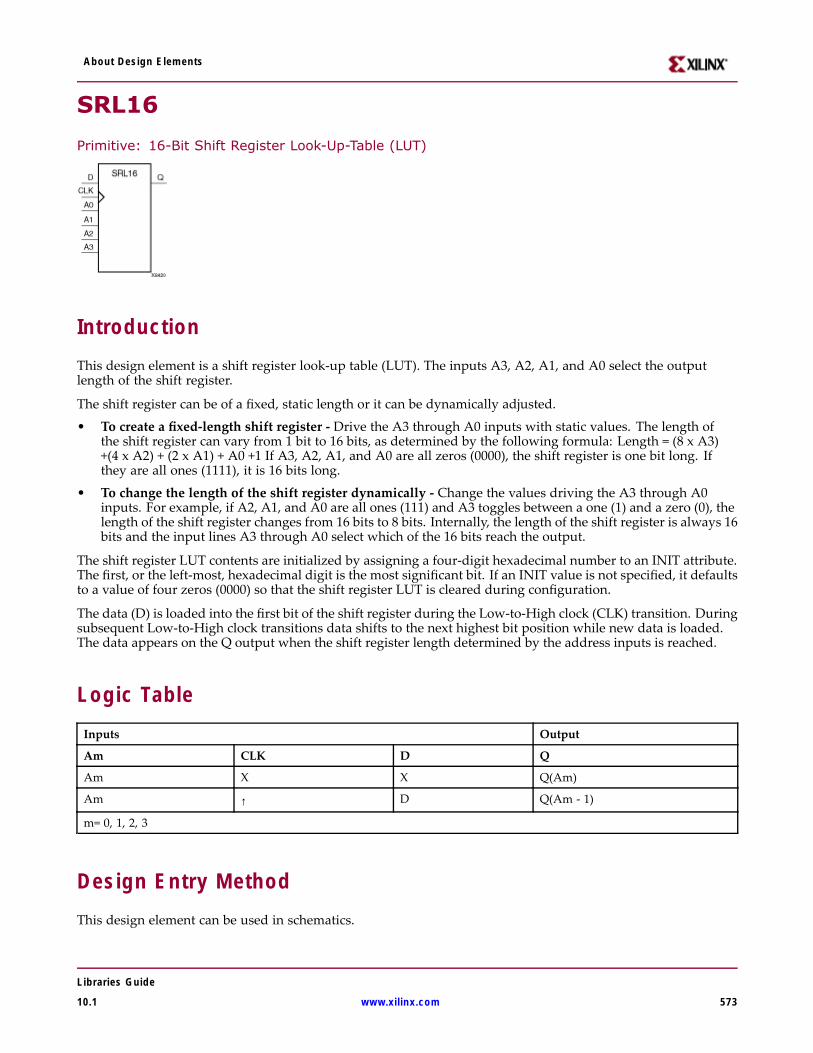
About Design Elements
SRL16
Primitive: 16-Bit Shift Register Look-Up-Table (LUT)
IntroductionThis design element is a shift register look-up table (LUT). The inputs A3, A2, A1, and A0 select the outputlength of the shift register.
The shift register can be of a fixed, static length or it can be dynamically adjusted.
• To create a fixed-length shift register - Drive the A3 through A0 inputs with static values. The length ofthe shift register can vary from 1 bit to 16 bits, as determined by the following formula: Length = (8 x A3)+(4 x A2) + (2 x A1) + A0 +1 If A3, A2, A1, and A0 are all zeros (0000), the shift register is one bit long. Ifthey are all ones (1111), it is 16 bits long.
• To change the length of the shift register dynamically - Change the values driving the A3 through A0inputs. For example, if A2, A1, and A0 are all ones (111) and A3 toggles between a one (1) and a zero (0), thelength of the shift register changes from 16 bits to 8 bits. Internally, the length of the shift register is always 16bits and the input lines A3 through A0 select which of the 16 bits reach the output.
The shift register LUT contents are initialized by assigning a four-digit hexadecimal number to an INIT attribute.The first, or the left-most, hexadecimal digit is the most significant bit. If an INIT value is not specified, it defaultsto a value of four zeros (0000) so that the shift register LUT is cleared during configuration.
The data (D) is loaded into the first bit of the shift register during the Low-to-High clock (CLK) transition. Duringsubsequent Low-to-High clock transitions data shifts to the next highest bit position while new data is loaded.The data appears on the Q output when the shift register length determined by the address inputs is reached.
Logic TableInputs Output
Am CLK D Q
Am X X Q(Am)
Am ↑ D Q(Am - 1)
m= 0, 1, 2, 3
Design Entry MethodThis design element can be used in schematics.
Libraries Guide
10.1 www.xilinx.com 573

About Design Elements
Available AttributesAttribute Type Allowed Values Default Description
INIT Hexadecimal Any 16-Bit Value All zeros Sets the initial value of Q output afterconfiguration.
For More Information• See the Spartan-3A User Guide.
• See the Spartan-3A Data Sheets.
• See the Spartan-3AN FPGA In-System Flash User Guide.
• See the Spartan-3AN Data Sheets.
Libraries Guide
574 www.xilinx.com 10.1
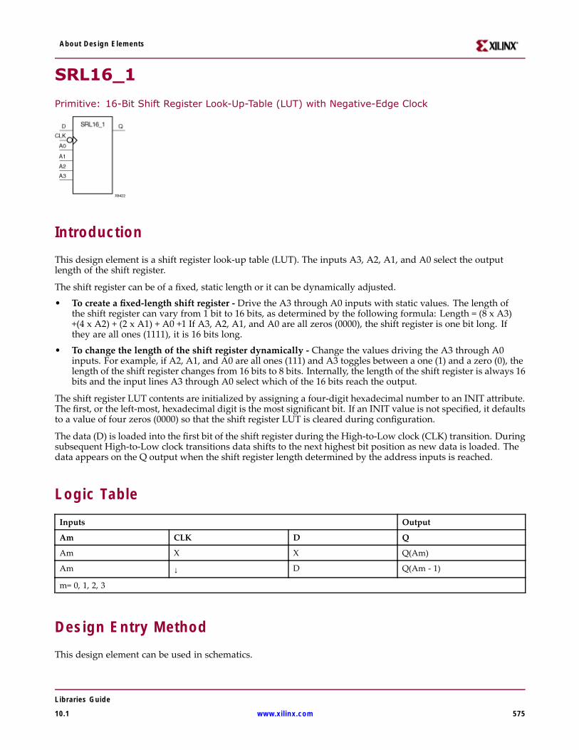
About Design Elements
SRL16_1
Primitive: 16-Bit Shift Register Look-Up-Table (LUT) with Negative-Edge Clock
IntroductionThis design element is a shift register look-up table (LUT). The inputs A3, A2, A1, and A0 select the outputlength of the shift register.
The shift register can be of a fixed, static length or it can be dynamically adjusted.
• To create a fixed-length shift register - Drive the A3 through A0 inputs with static values. The length ofthe shift register can vary from 1 bit to 16 bits, as determined by the following formula: Length = (8 x A3)+(4 x A2) + (2 x A1) + A0 +1 If A3, A2, A1, and A0 are all zeros (0000), the shift register is one bit long. Ifthey are all ones (1111), it is 16 bits long.
• To change the length of the shift register dynamically - Change the values driving the A3 through A0inputs. For example, if A2, A1, and A0 are all ones (111) and A3 toggles between a one (1) and a zero (0), thelength of the shift register changes from 16 bits to 8 bits. Internally, the length of the shift register is always 16bits and the input lines A3 through A0 select which of the 16 bits reach the output.
The shift register LUT contents are initialized by assigning a four-digit hexadecimal number to an INIT attribute.The first, or the left-most, hexadecimal digit is the most significant bit. If an INIT value is not specified, it defaultsto a value of four zeros (0000) so that the shift register LUT is cleared during configuration.
The data (D) is loaded into the first bit of the shift register during the High-to-Low clock (CLK) transition. Duringsubsequent High-to-Low clock transitions data shifts to the next highest bit position as new data is loaded. Thedata appears on the Q output when the shift register length determined by the address inputs is reached.
Logic TableInputs Output
Am CLK D Q
Am X X Q(Am)
Am ↓ D Q(Am - 1)
m= 0, 1, 2, 3
Design Entry MethodThis design element can be used in schematics.
Libraries Guide
10.1 www.xilinx.com 575

About Design Elements
Available AttributesAttribute Type Allowed Values Default Description
INIT Hexadecimal Any 16-Bit Value All zeros Sets the initial value of Q output afterconfiguration
For More Information• See the Spartan-3A User Guide.
• See the Spartan-3A Data Sheets.
• See the Spartan-3AN FPGA In-System Flash User Guide.
• See the Spartan-3AN Data Sheets.
Libraries Guide
576 www.xilinx.com 10.1
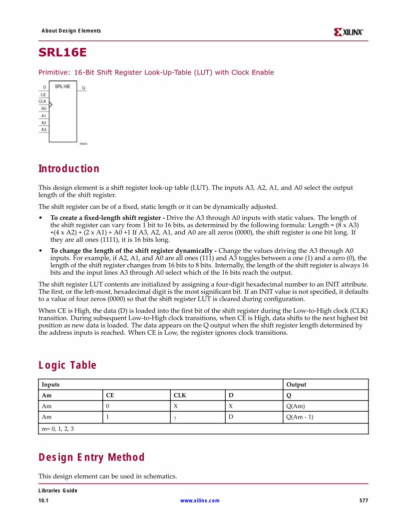
About Design Elements
SRL16E
Primitive: 16-Bit Shift Register Look-Up-Table (LUT) with Clock Enable
IntroductionThis design element is a shift register look-up table (LUT). The inputs A3, A2, A1, and A0 select the outputlength of the shift register.
The shift register can be of a fixed, static length or it can be dynamically adjusted.• To create a fixed-length shift register - Drive the A3 through A0 inputs with static values. The length of
the shift register can vary from 1 bit to 16 bits, as determined by the following formula: Length = (8 x A3)+(4 x A2) + (2 x A1) + A0 +1 If A3, A2, A1, and A0 are all zeros (0000), the shift register is one bit long. Ifthey are all ones (1111), it is 16 bits long.
• To change the length of the shift register dynamically - Change the values driving the A3 through A0inputs. For example, if A2, A1, and A0 are all ones (111) and A3 toggles between a one (1) and a zero (0), thelength of the shift register changes from 16 bits to 8 bits. Internally, the length of the shift register is always 16bits and the input lines A3 through A0 select which of the 16 bits reach the output.
The shift register LUT contents are initialized by assigning a four-digit hexadecimal number to an INIT attribute.The first, or the left-most, hexadecimal digit is the most significant bit. If an INIT value is not specified, it defaultsto a value of four zeros (0000) so that the shift register LUT is cleared during configuration.
When CE is High, the data (D) is loaded into the first bit of the shift register during the Low-to-High clock (CLK)transition. During subsequent Low-to-High clock transitions, when CE is High, data shifts to the next highest bitposition as new data is loaded. The data appears on the Q output when the shift register length determined bythe address inputs is reached. When CE is Low, the register ignores clock transitions.
Logic TableInputs Output
Am CE CLK D Q
Am 0 X X Q(Am)
Am 1 ↑ D Q(Am - 1)
m= 0, 1, 2, 3
Design Entry MethodThis design element can be used in schematics.
Libraries Guide
10.1 www.xilinx.com 577
About Design Elements
Available AttributesAttribute Type Allowed Values Default Description
INIT Hexadecimal Any 16-Bit Value All zeros Sets the initial value of content and output of shiftregister after configuration.
For More Information• See the Spartan-3A User Guide.
• See the Spartan-3A Data Sheets.
• See the Spartan-3AN FPGA In-System Flash User Guide.
• See the Spartan-3AN Data Sheets.
Libraries Guide
578 www.xilinx.com 10.1
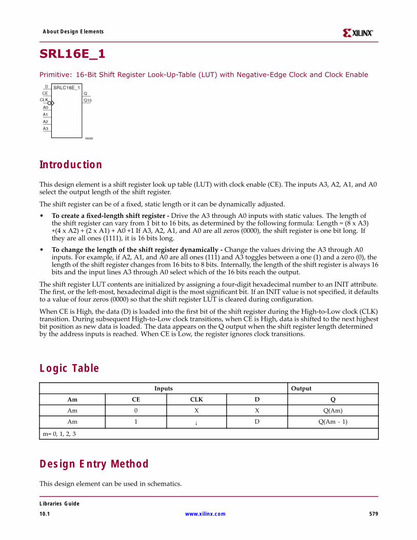
About Design Elements
SRL16E_1
Primitive: 16-Bit Shift Register Look-Up-Table (LUT) with Negative-Edge Clock and Clock Enable
IntroductionThis design element is a shift register look up table (LUT) with clock enable (CE). The inputs A3, A2, A1, and A0select the output length of the shift register.
The shift register can be of a fixed, static length or it can be dynamically adjusted.
• To create a fixed-length shift register - Drive the A3 through A0 inputs with static values. The length ofthe shift register can vary from 1 bit to 16 bits, as determined by the following formula: Length = (8 x A3)+(4 x A2) + (2 x A1) + A0 +1 If A3, A2, A1, and A0 are all zeros (0000), the shift register is one bit long. Ifthey are all ones (1111), it is 16 bits long.
• To change the length of the shift register dynamically - Change the values driving the A3 through A0inputs. For example, if A2, A1, and A0 are all ones (111) and A3 toggles between a one (1) and a zero (0), thelength of the shift register changes from 16 bits to 8 bits. Internally, the length of the shift register is always 16bits and the input lines A3 through A0 select which of the 16 bits reach the output.
The shift register LUT contents are initialized by assigning a four-digit hexadecimal number to an INIT attribute.The first, or the left-most, hexadecimal digit is the most significant bit. If an INIT value is not specified, it defaultsto a value of four zeros (0000) so that the shift register LUT is cleared during configuration.
When CE is High, the data (D) is loaded into the first bit of the shift register during the High-to-Low clock (CLK)transition. During subsequent High-to-Low clock transitions, when CE is High, data is shifted to the next highestbit position as new data is loaded. The data appears on the Q output when the shift register length determinedby the address inputs is reached. When CE is Low, the register ignores clock transitions.
Logic TableInputs Output
Am CE CLK D Q
Am 0 X X Q(Am)
Am 1 ↓ D Q(Am - 1)
m= 0, 1, 2, 3
Design Entry MethodThis design element can be used in schematics.
Libraries Guide
10.1 www.xilinx.com 579

About Design Elements
Available Attributes
Attribute TypeAllowedValues Default Description
INIT Hexadecimal Any 16-BitValue
All zeros Sets the initial value of content and output of shiftregister after configuration.
For More Information• See the Spartan-3A User Guide.
• See the Spartan-3A Data Sheets.
• See the Spartan-3AN FPGA In-System Flash User Guide.
• See the Spartan-3AN Data Sheets.
Libraries Guide
580 www.xilinx.com 10.1
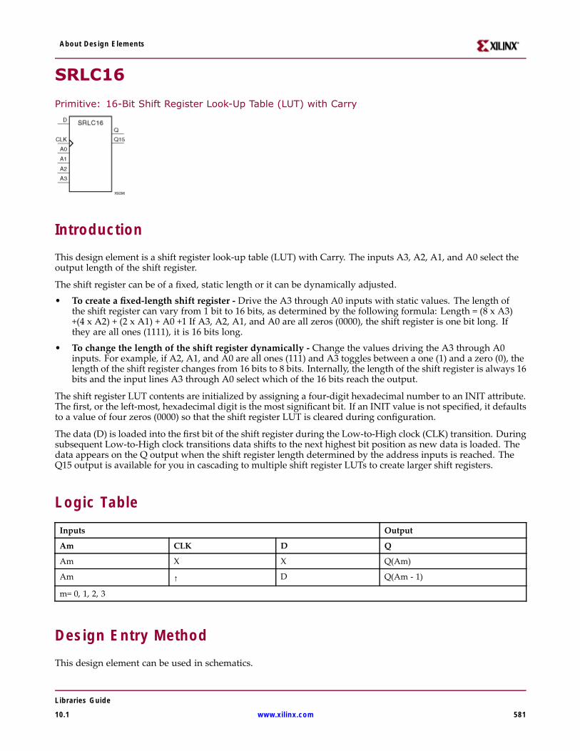
About Design Elements
SRLC16
Primitive: 16-Bit Shift Register Look-Up Table (LUT) with Carry
IntroductionThis design element is a shift register look-up table (LUT) with Carry. The inputs A3, A2, A1, and A0 select theoutput length of the shift register.
The shift register can be of a fixed, static length or it can be dynamically adjusted.
• To create a fixed-length shift register - Drive the A3 through A0 inputs with static values. The length ofthe shift register can vary from 1 bit to 16 bits, as determined by the following formula: Length = (8 x A3)+(4 x A2) + (2 x A1) + A0 +1 If A3, A2, A1, and A0 are all zeros (0000), the shift register is one bit long. Ifthey are all ones (1111), it is 16 bits long.
• To change the length of the shift register dynamically - Change the values driving the A3 through A0inputs. For example, if A2, A1, and A0 are all ones (111) and A3 toggles between a one (1) and a zero (0), thelength of the shift register changes from 16 bits to 8 bits. Internally, the length of the shift register is always 16bits and the input lines A3 through A0 select which of the 16 bits reach the output.
The shift register LUT contents are initialized by assigning a four-digit hexadecimal number to an INIT attribute.The first, or the left-most, hexadecimal digit is the most significant bit. If an INIT value is not specified, it defaultsto a value of four zeros (0000) so that the shift register LUT is cleared during configuration.
The data (D) is loaded into the first bit of the shift register during the Low-to-High clock (CLK) transition. Duringsubsequent Low-to-High clock transitions data shifts to the next highest bit position as new data is loaded. Thedata appears on the Q output when the shift register length determined by the address inputs is reached. TheQ15 output is available for you in cascading to multiple shift register LUTs to create larger shift registers.
Logic TableInputs Output
Am CLK D Q
Am X X Q(Am)
Am ↑ D Q(Am - 1)
m= 0, 1, 2, 3
Design Entry MethodThis design element can be used in schematics.
Libraries Guide
10.1 www.xilinx.com 581

About Design Elements
Available AttributesAttribute Type Allowed Values Default Description
INIT Hexadecimal Any 16-Bit Value All zeros Sets the initial value of content and output of shiftregister after configuration.
For More Information• See the Spartan-3A User Guide.
• See the Spartan-3A Data Sheets.
• See the Spartan-3AN FPGA In-System Flash User Guide.
• See the Spartan-3AN Data Sheets.
Libraries Guide
582 www.xilinx.com 10.1
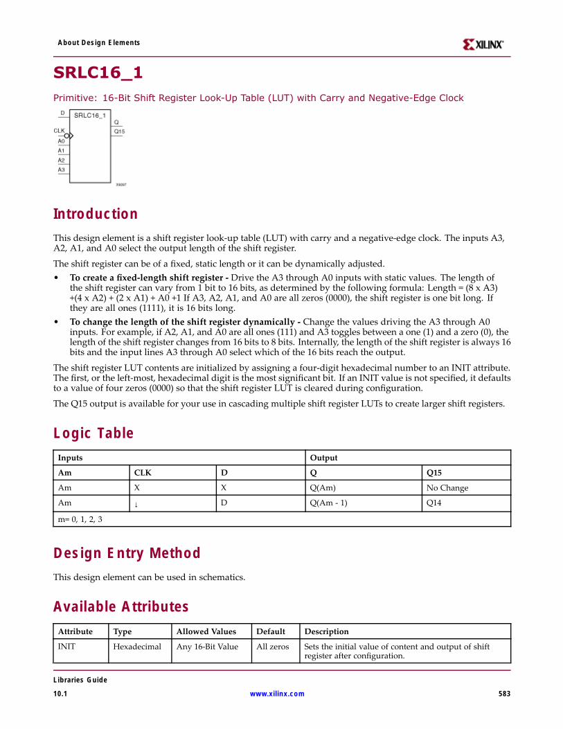
About Design Elements
SRLC16_1Primitive: 16-Bit Shift Register Look-Up Table (LUT) with Carry and Negative-Edge Clock
IntroductionThis design element is a shift register look-up table (LUT) with carry and a negative-edge clock. The inputs A3,A2, A1, and A0 select the output length of the shift register.
The shift register can be of a fixed, static length or it can be dynamically adjusted.• To create a fixed-length shift register - Drive the A3 through A0 inputs with static values. The length of
the shift register can vary from 1 bit to 16 bits, as determined by the following formula: Length = (8 x A3)+(4 x A2) + (2 x A1) + A0 +1 If A3, A2, A1, and A0 are all zeros (0000), the shift register is one bit long. Ifthey are all ones (1111), it is 16 bits long.
• To change the length of the shift register dynamically - Change the values driving the A3 through A0inputs. For example, if A2, A1, and A0 are all ones (111) and A3 toggles between a one (1) and a zero (0), thelength of the shift register changes from 16 bits to 8 bits. Internally, the length of the shift register is always 16bits and the input lines A3 through A0 select which of the 16 bits reach the output.
The shift register LUT contents are initialized by assigning a four-digit hexadecimal number to an INIT attribute.The first, or the left-most, hexadecimal digit is the most significant bit. If an INIT value is not specified, it defaultsto a value of four zeros (0000) so that the shift register LUT is cleared during configuration.
The Q15 output is available for your use in cascading multiple shift register LUTs to create larger shift registers.
Logic TableInputs Output
Am CLK D Q Q15
Am X X Q(Am) No Change
Am ↓ D Q(Am - 1) Q14
m= 0, 1, 2, 3
Design Entry MethodThis design element can be used in schematics.
Available AttributesAttribute Type Allowed Values Default Description
INIT Hexadecimal Any 16-Bit Value All zeros Sets the initial value of content and output of shiftregister after configuration.
Libraries Guide
10.1 www.xilinx.com 583

About Design Elements
For More Information• See the Spartan-3A User Guide.
• See the Spartan-3A Data Sheets.
• See the Spartan-3AN FPGA In-System Flash User Guide.
• See the Spartan-3AN Data Sheets.
Libraries Guide
584 www.xilinx.com 10.1
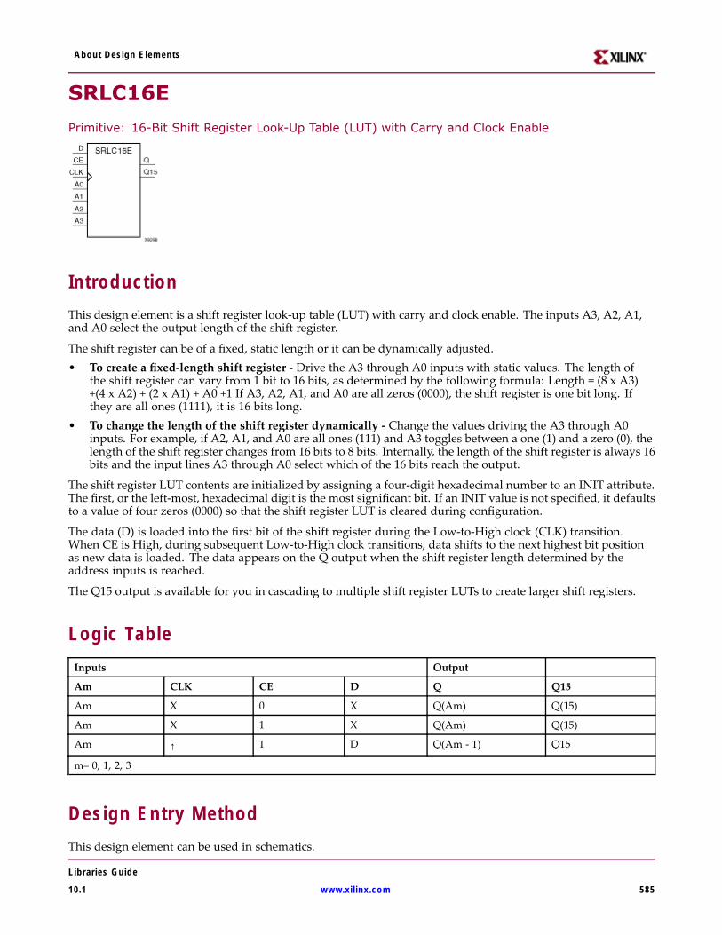
About Design Elements
SRLC16E
Primitive: 16-Bit Shift Register Look-Up Table (LUT) with Carry and Clock Enable
IntroductionThis design element is a shift register look-up table (LUT) with carry and clock enable. The inputs A3, A2, A1,and A0 select the output length of the shift register.
The shift register can be of a fixed, static length or it can be dynamically adjusted.• To create a fixed-length shift register - Drive the A3 through A0 inputs with static values. The length of
the shift register can vary from 1 bit to 16 bits, as determined by the following formula: Length = (8 x A3)+(4 x A2) + (2 x A1) + A0 +1 If A3, A2, A1, and A0 are all zeros (0000), the shift register is one bit long. Ifthey are all ones (1111), it is 16 bits long.
• To change the length of the shift register dynamically - Change the values driving the A3 through A0inputs. For example, if A2, A1, and A0 are all ones (111) and A3 toggles between a one (1) and a zero (0), thelength of the shift register changes from 16 bits to 8 bits. Internally, the length of the shift register is always 16bits and the input lines A3 through A0 select which of the 16 bits reach the output.
The shift register LUT contents are initialized by assigning a four-digit hexadecimal number to an INIT attribute.The first, or the left-most, hexadecimal digit is the most significant bit. If an INIT value is not specified, it defaultsto a value of four zeros (0000) so that the shift register LUT is cleared during configuration.
The data (D) is loaded into the first bit of the shift register during the Low-to-High clock (CLK) transition.When CE is High, during subsequent Low-to-High clock transitions, data shifts to the next highest bit positionas new data is loaded. The data appears on the Q output when the shift register length determined by theaddress inputs is reached.
The Q15 output is available for you in cascading to multiple shift register LUTs to create larger shift registers.
Logic TableInputs Output
Am CLK CE D Q Q15
Am X 0 X Q(Am) Q(15)
Am X 1 X Q(Am) Q(15)
Am ↑ 1 D Q(Am - 1) Q15
m= 0, 1, 2, 3
Design Entry MethodThis design element can be used in schematics.
Libraries Guide
10.1 www.xilinx.com 585

About Design Elements
Available AttributesAttribute Type Allowed Values Default Description
INIT Hexadecimal Any 16-Bit Value All zeros Sets the initial value of content and output of shiftregister after configuration.
For More Information• See the Spartan-3A User Guide.
• See the Spartan-3A Data Sheets.
• See the Spartan-3AN FPGA In-System Flash User Guide.
• See the Spartan-3AN Data Sheets.
Libraries Guide
586 www.xilinx.com 10.1
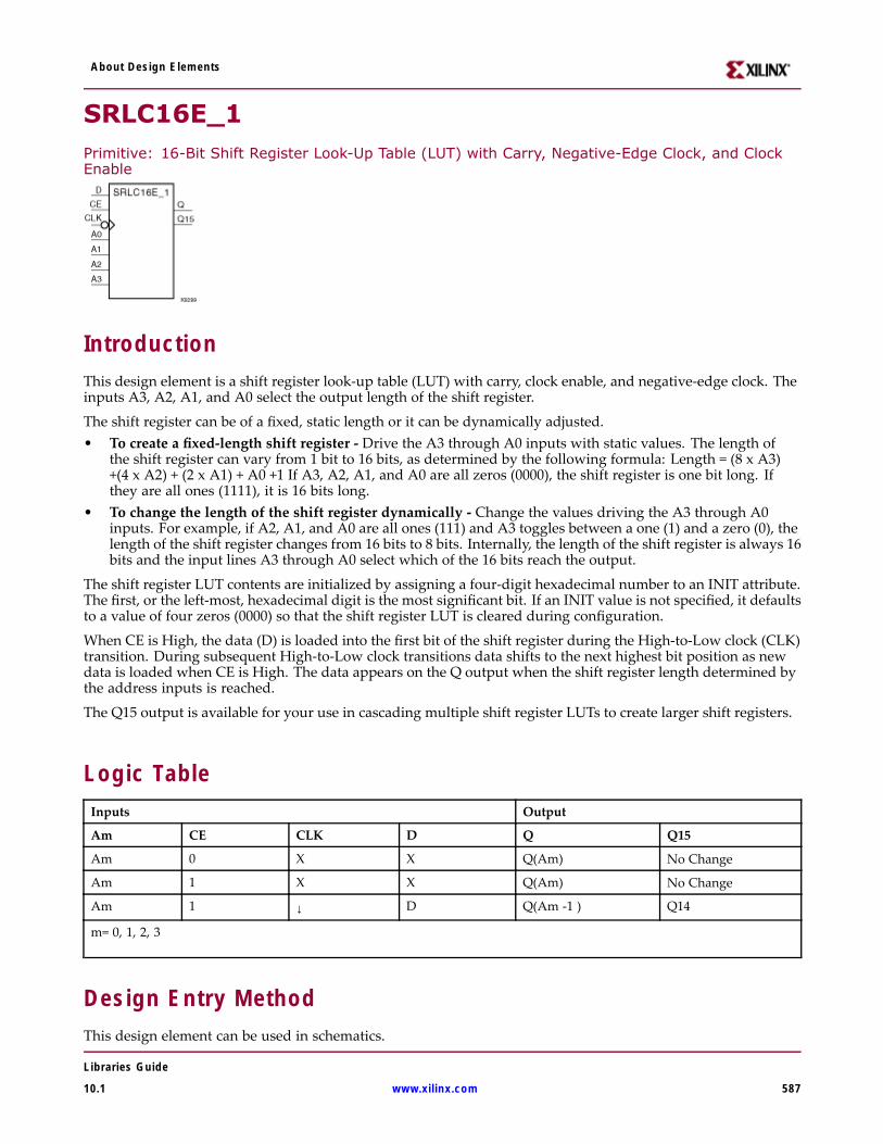
About Design Elements
SRLC16E_1Primitive: 16-Bit Shift Register Look-Up Table (LUT) with Carry, Negative-Edge Clock, and ClockEnable
IntroductionThis design element is a shift register look-up table (LUT) with carry, clock enable, and negative-edge clock. Theinputs A3, A2, A1, and A0 select the output length of the shift register.
The shift register can be of a fixed, static length or it can be dynamically adjusted.• To create a fixed-length shift register - Drive the A3 through A0 inputs with static values. The length of
the shift register can vary from 1 bit to 16 bits, as determined by the following formula: Length = (8 x A3)+(4 x A2) + (2 x A1) + A0 +1 If A3, A2, A1, and A0 are all zeros (0000), the shift register is one bit long. Ifthey are all ones (1111), it is 16 bits long.
• To change the length of the shift register dynamically - Change the values driving the A3 through A0inputs. For example, if A2, A1, and A0 are all ones (111) and A3 toggles between a one (1) and a zero (0), thelength of the shift register changes from 16 bits to 8 bits. Internally, the length of the shift register is always 16bits and the input lines A3 through A0 select which of the 16 bits reach the output.
The shift register LUT contents are initialized by assigning a four-digit hexadecimal number to an INIT attribute.The first, or the left-most, hexadecimal digit is the most significant bit. If an INIT value is not specified, it defaultsto a value of four zeros (0000) so that the shift register LUT is cleared during configuration.
When CE is High, the data (D) is loaded into the first bit of the shift register during the High-to-Low clock (CLK)transition. During subsequent High-to-Low clock transitions data shifts to the next highest bit position as newdata is loaded when CE is High. The data appears on the Q output when the shift register length determined bythe address inputs is reached.
The Q15 output is available for your use in cascading multiple shift register LUTs to create larger shift registers.
Logic TableInputs Output
Am CE CLK D Q Q15
Am 0 X X Q(Am) No Change
Am 1 X X Q(Am) No Change
Am 1 ↓ D Q(Am -1 ) Q14
m= 0, 1, 2, 3
Design Entry MethodThis design element can be used in schematics.
Libraries Guide
10.1 www.xilinx.com 587

About Design Elements
Available Attributes
Attribute TypeAllowedValues Default Description
INIT Hexadecimal Any 16-BitValue
All zeros Sets the initial value of content and output of shift registerafter configuration.
For More Information• See the Spartan-3A User Guide.
• See the Spartan-3A Data Sheets.
• See the Spartan-3AN FPGA In-System Flash User Guide.
• See the Spartan-3AN Data Sheets.
Libraries Guide
588 www.xilinx.com 10.1
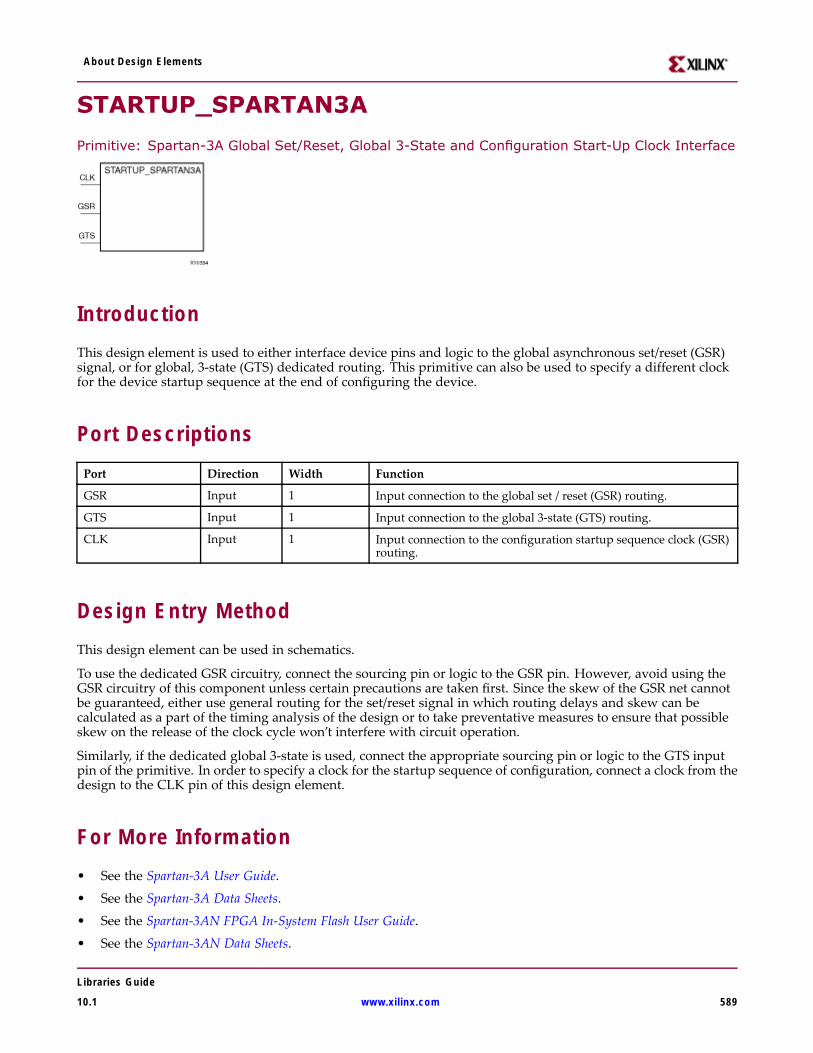
About Design Elements
STARTUP_SPARTAN3A
Primitive: Spartan-3A Global Set/Reset, Global 3-State and Configuration Start-Up Clock Interface
IntroductionThis design element is used to either interface device pins and logic to the global asynchronous set/reset (GSR)signal, or for global, 3-state (GTS) dedicated routing. This primitive can also be used to specify a different clockfor the device startup sequence at the end of configuring the device.
Port DescriptionsPort Direction Width Function
GSR Input 1 Input connection to the global set / reset (GSR) routing.
GTS Input 1 Input connection to the global 3-state (GTS) routing.
CLK Input 1 Input connection to the configuration startup sequence clock (GSR)routing.
Design Entry MethodThis design element can be used in schematics.
To use the dedicated GSR circuitry, connect the sourcing pin or logic to the GSR pin. However, avoid using theGSR circuitry of this component unless certain precautions are taken first. Since the skew of the GSR net cannotbe guaranteed, either use general routing for the set/reset signal in which routing delays and skew can becalculated as a part of the timing analysis of the design or to take preventative measures to ensure that possibleskew on the release of the clock cycle won’t interfere with circuit operation.
Similarly, if the dedicated global 3-state is used, connect the appropriate sourcing pin or logic to the GTS inputpin of the primitive. In order to specify a clock for the startup sequence of configuration, connect a clock from thedesign to the CLK pin of this design element.
For More Information• See the Spartan-3A User Guide.
• See the Spartan-3A Data Sheets.
• See the Spartan-3AN FPGA In-System Flash User Guide.
• See the Spartan-3AN Data Sheets.
Libraries Guide
10.1 www.xilinx.com 589

About Design Elements
VCC
Primitive: VCC-Connection Signal Tag
IntroductionThis design element serves as a signal tag, or parameter, that forces a net or input function to a logic High level.A net tied to this element cannot have any other source.
When the placement and routing software encounters a net or input function tied to this element, it removes anylogic that is disabled by the Vcc signal, which is only implemented when the disabled logic cannot be removed.
Design Entry MethodThis design element is only for use in schematics.
For More Information• See the Spartan-3A User Guide.
• See the Spartan-3A Data Sheets.
• See the Spartan-3AN FPGA In-System Flash User Guide.
• See the Spartan-3AN Data Sheets.
Libraries Guide
590 www.xilinx.com 10.1
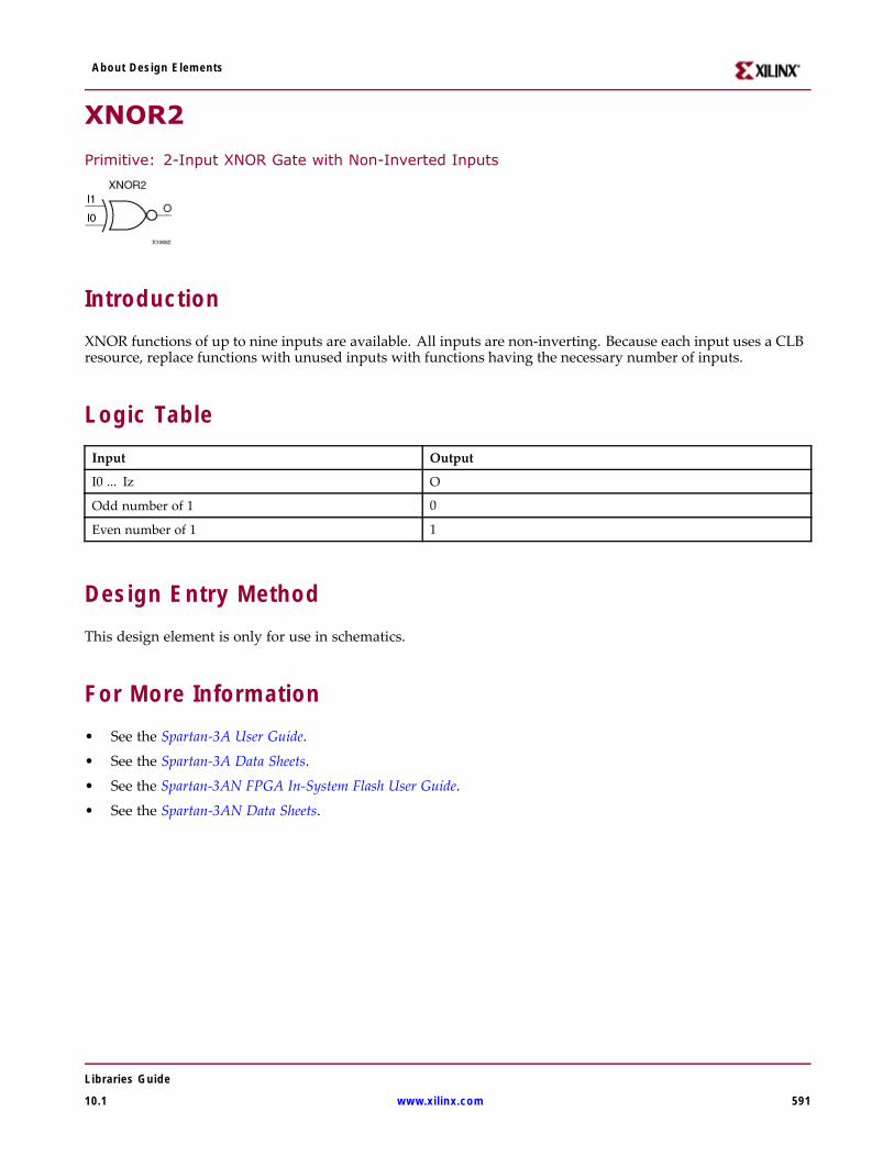
About Design Elements
XNOR2
Primitive: 2-Input XNOR Gate with Non-Inverted Inputs
IntroductionXNOR functions of up to nine inputs are available. All inputs are non-inverting. Because each input uses a CLBresource, replace functions with unused inputs with functions having the necessary number of inputs.
Logic TableInput Output
I0 ... Iz O
Odd number of 1 0
Even number of 1 1
Design Entry MethodThis design element is only for use in schematics.
For More Information• See the Spartan-3A User Guide.
• See the Spartan-3A Data Sheets.
• See the Spartan-3AN FPGA In-System Flash User Guide.
• See the Spartan-3AN Data Sheets.
Libraries Guide
10.1 www.xilinx.com 591
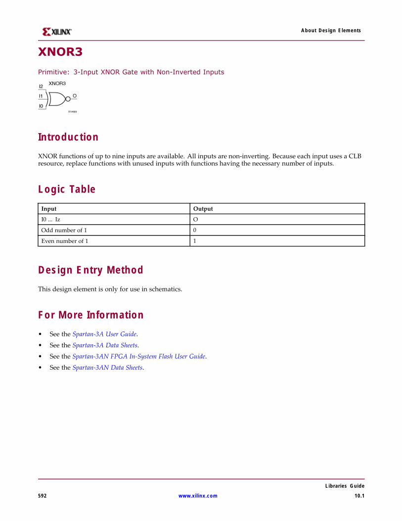
About Design Elements
XNOR3
Primitive: 3-Input XNOR Gate with Non-Inverted Inputs
IntroductionXNOR functions of up to nine inputs are available. All inputs are non-inverting. Because each input uses a CLBresource, replace functions with unused inputs with functions having the necessary number of inputs.
Logic TableInput Output
I0 ... Iz O
Odd number of 1 0
Even number of 1 1
Design Entry MethodThis design element is only for use in schematics.
For More Information• See the Spartan-3A User Guide.
• See the Spartan-3A Data Sheets.
• See the Spartan-3AN FPGA In-System Flash User Guide.
• See the Spartan-3AN Data Sheets.
Libraries Guide
592 www.xilinx.com 10.1
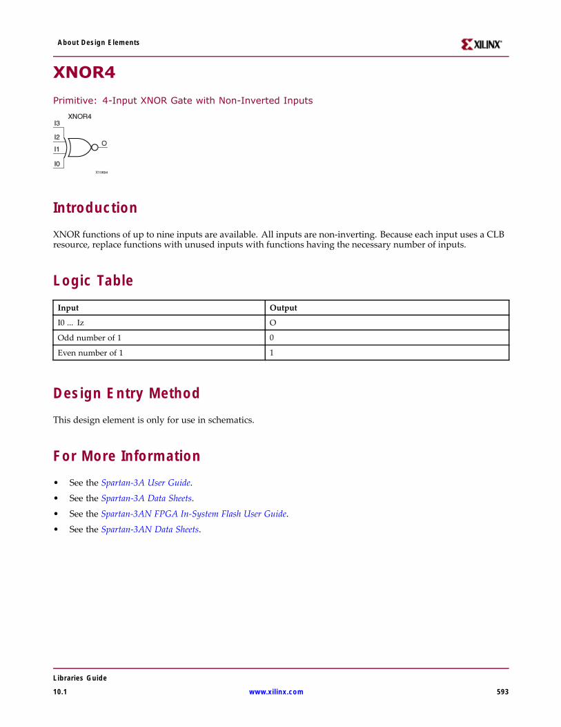
About Design Elements
XNOR4
Primitive: 4-Input XNOR Gate with Non-Inverted Inputs
IntroductionXNOR functions of up to nine inputs are available. All inputs are non-inverting. Because each input uses a CLBresource, replace functions with unused inputs with functions having the necessary number of inputs.
Logic TableInput Output
I0 ... Iz O
Odd number of 1 0
Even number of 1 1
Design Entry MethodThis design element is only for use in schematics.
For More Information• See the Spartan-3A User Guide.
• See the Spartan-3A Data Sheets.
• See the Spartan-3AN FPGA In-System Flash User Guide.
• See the Spartan-3AN Data Sheets.
Libraries Guide
10.1 www.xilinx.com 593
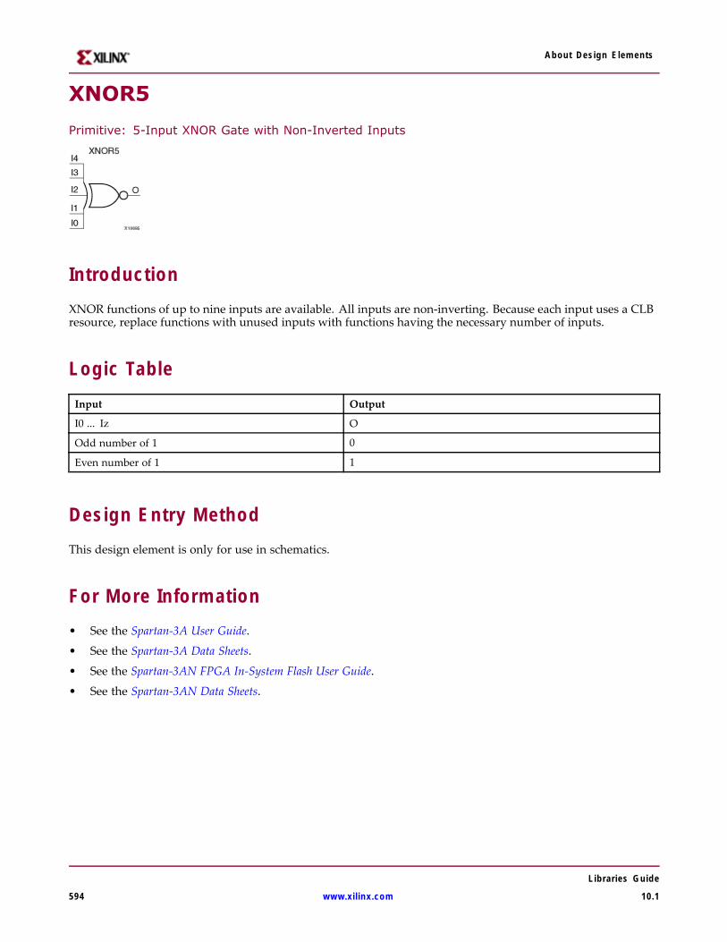
About Design Elements
XNOR5
Primitive: 5-Input XNOR Gate with Non-Inverted Inputs
IntroductionXNOR functions of up to nine inputs are available. All inputs are non-inverting. Because each input uses a CLBresource, replace functions with unused inputs with functions having the necessary number of inputs.
Logic TableInput Output
I0 ... Iz O
Odd number of 1 0
Even number of 1 1
Design Entry MethodThis design element is only for use in schematics.
For More Information• See the Spartan-3A User Guide.
• See the Spartan-3A Data Sheets.
• See the Spartan-3AN FPGA In-System Flash User Guide.
• See the Spartan-3AN Data Sheets.
Libraries Guide
594 www.xilinx.com 10.1
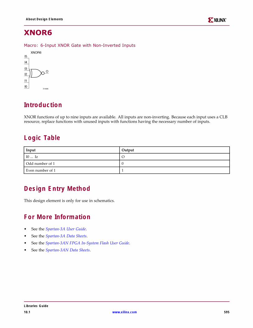
About Design Elements
XNOR6
Macro: 6-Input XNOR Gate with Non-Inverted Inputs
IntroductionXNOR functions of up to nine inputs are available. All inputs are non-inverting. Because each input uses a CLBresource, replace functions with unused inputs with functions having the necessary number of inputs.
Logic TableInput Output
I0 ... Iz O
Odd number of 1 0
Even number of 1 1
Design Entry MethodThis design element is only for use in schematics.
For More Information• See the Spartan-3A User Guide.
• See the Spartan-3A Data Sheets.
• See the Spartan-3AN FPGA In-System Flash User Guide.
• See the Spartan-3AN Data Sheets.
Libraries Guide
10.1 www.xilinx.com 595
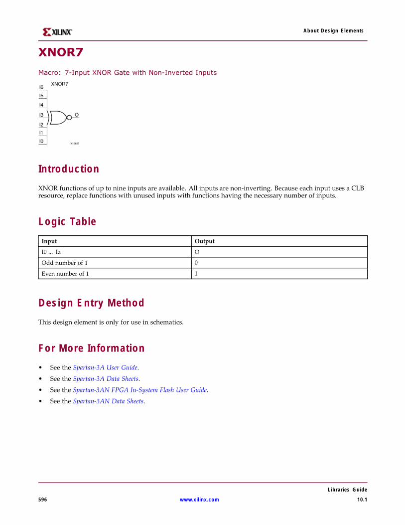
About Design Elements
XNOR7
Macro: 7-Input XNOR Gate with Non-Inverted Inputs
IntroductionXNOR functions of up to nine inputs are available. All inputs are non-inverting. Because each input uses a CLBresource, replace functions with unused inputs with functions having the necessary number of inputs.
Logic TableInput Output
I0 ... Iz O
Odd number of 1 0
Even number of 1 1
Design Entry MethodThis design element is only for use in schematics.
For More Information• See the Spartan-3A User Guide.
• See the Spartan-3A Data Sheets.
• See the Spartan-3AN FPGA In-System Flash User Guide.
• See the Spartan-3AN Data Sheets.
Libraries Guide
596 www.xilinx.com 10.1
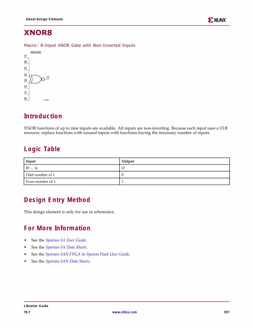
About Design Elements
XNOR8
Macro: 8-Input XNOR Gate with Non-Inverted Inputs
IntroductionXNOR functions of up to nine inputs are available. All inputs are non-inverting. Because each input uses a CLBresource, replace functions with unused inputs with functions having the necessary number of inputs.
Logic TableInput Output
I0 ... Iz O
Odd number of 1 0
Even number of 1 1
Design Entry MethodThis design element is only for use in schematics.
For More Information• See the Spartan-3A User Guide.
• See the Spartan-3A Data Sheets.
• See the Spartan-3AN FPGA In-System Flash User Guide.
• See the Spartan-3AN Data Sheets.
Libraries Guide
10.1 www.xilinx.com 597
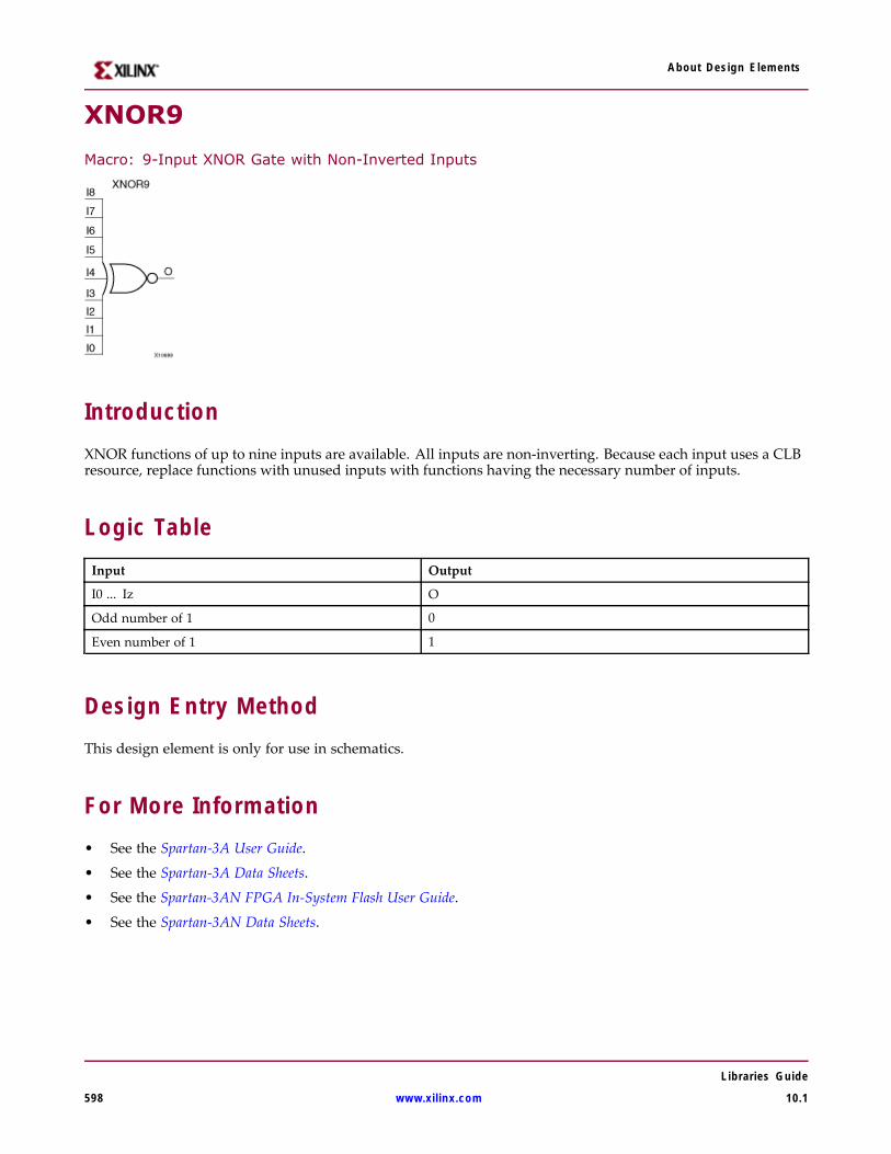
About Design Elements
XNOR9
Macro: 9-Input XNOR Gate with Non-Inverted Inputs
IntroductionXNOR functions of up to nine inputs are available. All inputs are non-inverting. Because each input uses a CLBresource, replace functions with unused inputs with functions having the necessary number of inputs.
Logic TableInput Output
I0 ... Iz O
Odd number of 1 0
Even number of 1 1
Design Entry MethodThis design element is only for use in schematics.
For More Information• See the Spartan-3A User Guide.
• See the Spartan-3A Data Sheets.
• See the Spartan-3AN FPGA In-System Flash User Guide.
• See the Spartan-3AN Data Sheets.
Libraries Guide
598 www.xilinx.com 10.1
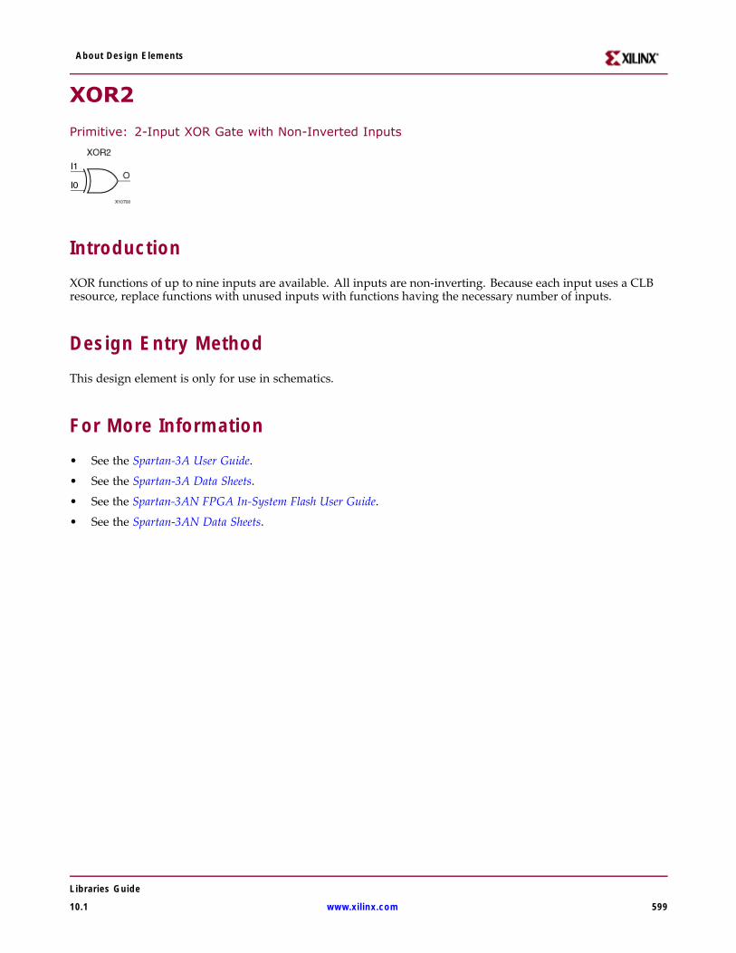
About Design Elements
XOR2
Primitive: 2-Input XOR Gate with Non-Inverted Inputs
IntroductionXOR functions of up to nine inputs are available. All inputs are non-inverting. Because each input uses a CLBresource, replace functions with unused inputs with functions having the necessary number of inputs.
Design Entry MethodThis design element is only for use in schematics.
For More Information• See the Spartan-3A User Guide.
• See the Spartan-3A Data Sheets.
• See the Spartan-3AN FPGA In-System Flash User Guide.
• See the Spartan-3AN Data Sheets.
Libraries Guide
10.1 www.xilinx.com 599
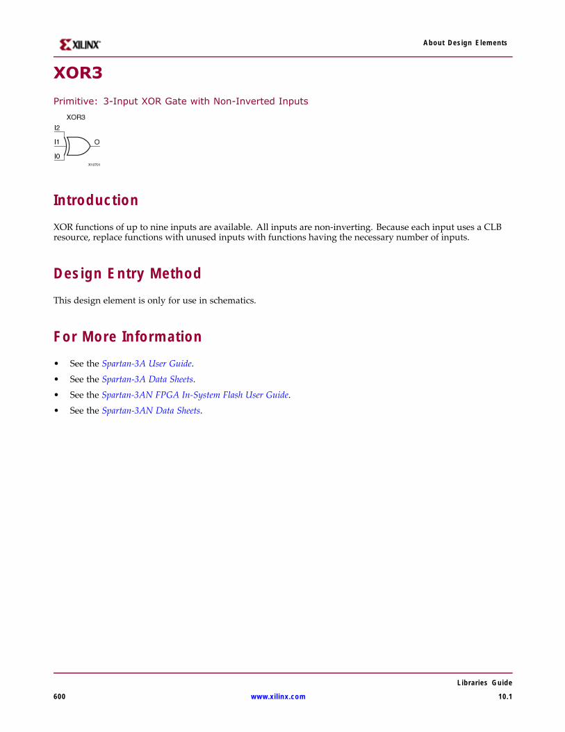
About Design Elements
XOR3
Primitive: 3-Input XOR Gate with Non-Inverted Inputs
IntroductionXOR functions of up to nine inputs are available. All inputs are non-inverting. Because each input uses a CLBresource, replace functions with unused inputs with functions having the necessary number of inputs.
Design Entry MethodThis design element is only for use in schematics.
For More Information• See the Spartan-3A User Guide.
• See the Spartan-3A Data Sheets.
• See the Spartan-3AN FPGA In-System Flash User Guide.
• See the Spartan-3AN Data Sheets.
Libraries Guide
600 www.xilinx.com 10.1
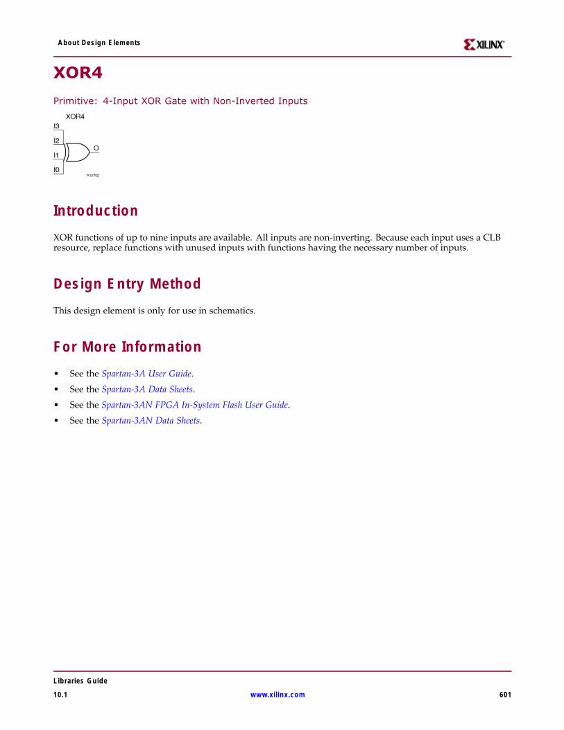
About Design Elements
XOR4
Primitive: 4-Input XOR Gate with Non-Inverted Inputs
IntroductionXOR functions of up to nine inputs are available. All inputs are non-inverting. Because each input uses a CLBresource, replace functions with unused inputs with functions having the necessary number of inputs.
Design Entry MethodThis design element is only for use in schematics.
For More Information• See the Spartan-3A User Guide.
• See the Spartan-3A Data Sheets.
• See the Spartan-3AN FPGA In-System Flash User Guide.
• See the Spartan-3AN Data Sheets.
Libraries Guide
10.1 www.xilinx.com 601
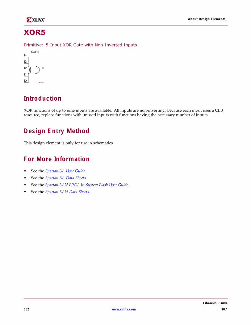
About Design Elements
XOR5
Primitive: 5-Input XOR Gate with Non-Inverted Inputs
IntroductionXOR functions of up to nine inputs are available. All inputs are non-inverting. Because each input uses a CLBresource, replace functions with unused inputs with functions having the necessary number of inputs.
Design Entry MethodThis design element is only for use in schematics.
For More Information• See the Spartan-3A User Guide.
• See the Spartan-3A Data Sheets.
• See the Spartan-3AN FPGA In-System Flash User Guide.
• See the Spartan-3AN Data Sheets.
Libraries Guide
602 www.xilinx.com 10.1
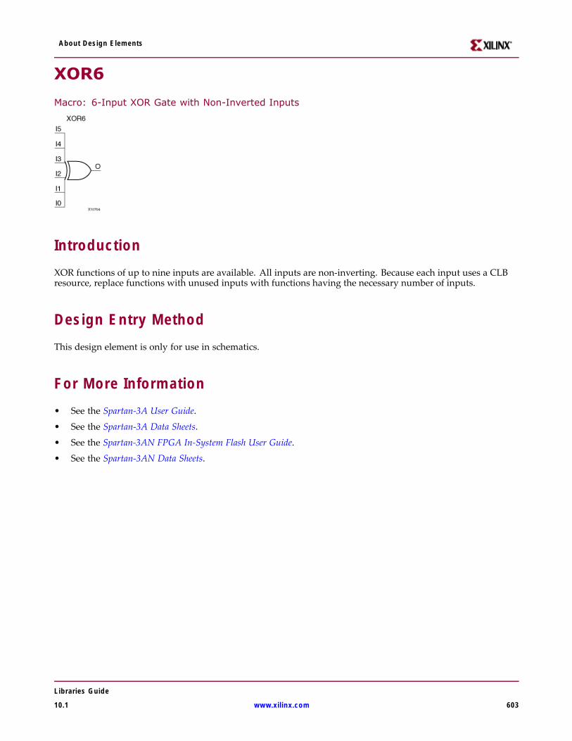
About Design Elements
XOR6
Macro: 6-Input XOR Gate with Non-Inverted Inputs
IntroductionXOR functions of up to nine inputs are available. All inputs are non-inverting. Because each input uses a CLBresource, replace functions with unused inputs with functions having the necessary number of inputs.
Design Entry MethodThis design element is only for use in schematics.
For More Information• See the Spartan-3A User Guide.
• See the Spartan-3A Data Sheets.
• See the Spartan-3AN FPGA In-System Flash User Guide.
• See the Spartan-3AN Data Sheets.
Libraries Guide
10.1 www.xilinx.com 603
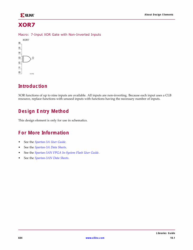
About Design Elements
XOR7
Macro: 7-Input XOR Gate with Non-Inverted Inputs
IntroductionXOR functions of up to nine inputs are available. All inputs are non-inverting. Because each input uses a CLBresource, replace functions with unused inputs with functions having the necessary number of inputs.
Design Entry MethodThis design element is only for use in schematics.
For More Information• See the Spartan-3A User Guide.
• See the Spartan-3A Data Sheets.
• See the Spartan-3AN FPGA In-System Flash User Guide.
• See the Spartan-3AN Data Sheets.
Libraries Guide
604 www.xilinx.com 10.1
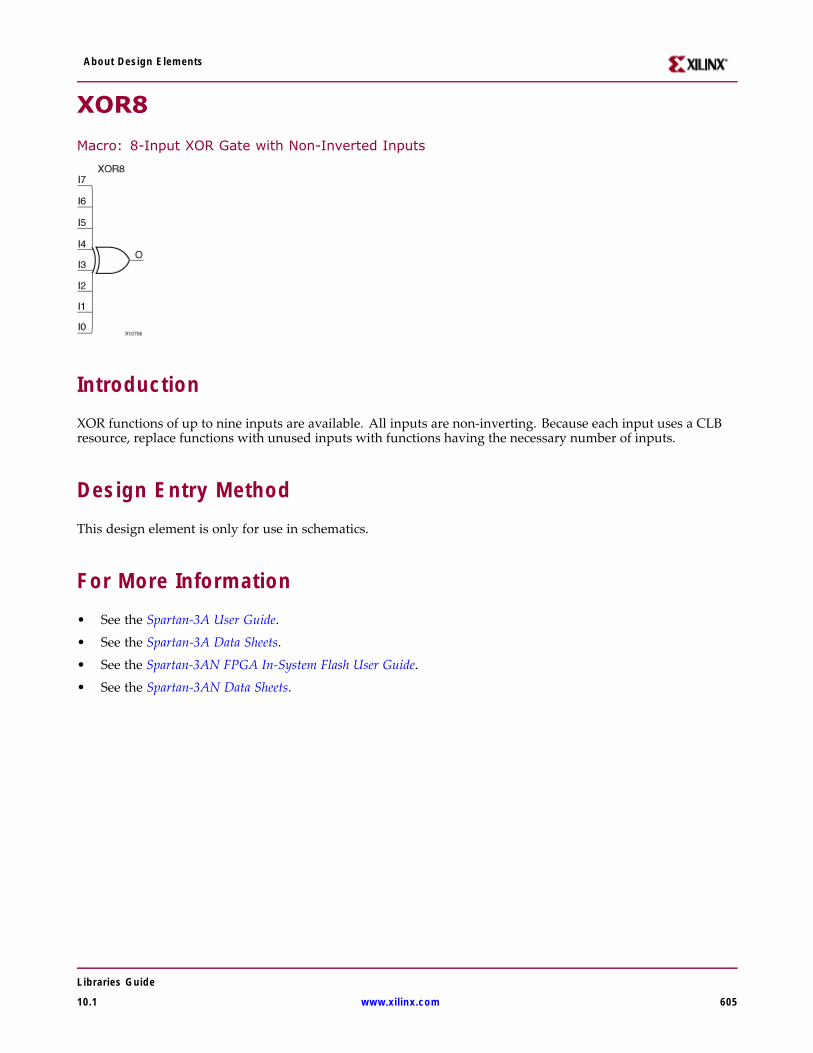
About Design Elements
XOR8
Macro: 8-Input XOR Gate with Non-Inverted Inputs
IntroductionXOR functions of up to nine inputs are available. All inputs are non-inverting. Because each input uses a CLBresource, replace functions with unused inputs with functions having the necessary number of inputs.
Design Entry MethodThis design element is only for use in schematics.
For More Information• See the Spartan-3A User Guide.
• See the Spartan-3A Data Sheets.
• See the Spartan-3AN FPGA In-System Flash User Guide.
• See the Spartan-3AN Data Sheets.
Libraries Guide
10.1 www.xilinx.com 605
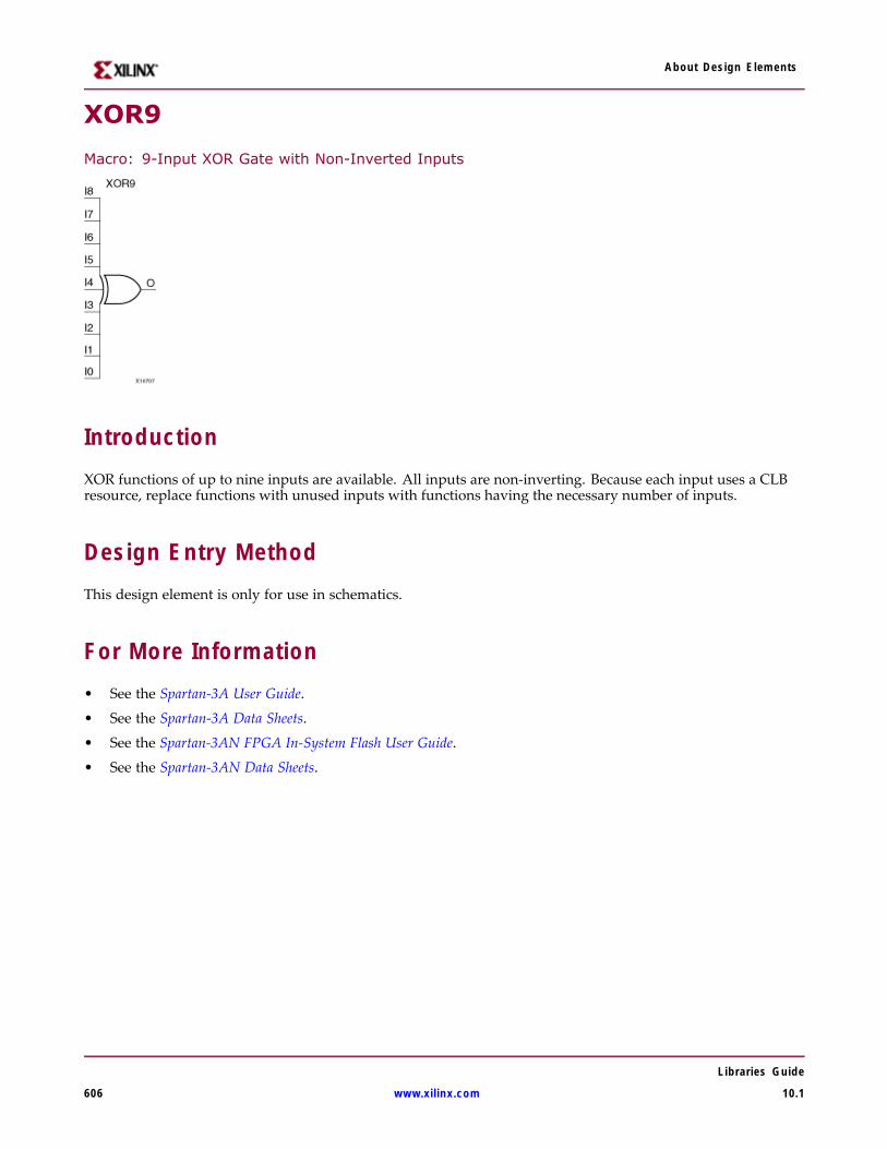
About Design Elements
XOR9
Macro: 9-Input XOR Gate with Non-Inverted Inputs
IntroductionXOR functions of up to nine inputs are available. All inputs are non-inverting. Because each input uses a CLBresource, replace functions with unused inputs with functions having the necessary number of inputs.
Design Entry MethodThis design element is only for use in schematics.
For More Information• See the Spartan-3A User Guide.
• See the Spartan-3A Data Sheets.
• See the Spartan-3AN FPGA In-System Flash User Guide.
• See the Spartan-3AN Data Sheets.
Libraries Guide
606 www.xilinx.com 10.1
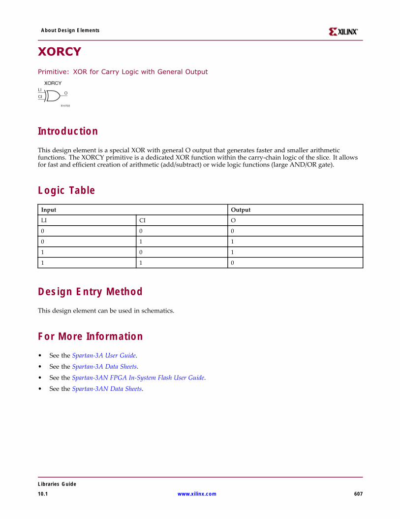
About Design Elements
XORCY
Primitive: XOR for Carry Logic with General Output
IntroductionThis design element is a special XOR with general O output that generates faster and smaller arithmeticfunctions. The XORCY primitive is a dedicated XOR function within the carry-chain logic of the slice. It allowsfor fast and efficient creation of arithmetic (add/subtract) or wide logic functions (large AND/OR gate).
Logic TableInput Output
LI CI O
0 0 0
0 1 1
1 0 1
1 1 0
Design Entry MethodThis design element can be used in schematics.
For More Information• See the Spartan-3A User Guide.
• See the Spartan-3A Data Sheets.
• See the Spartan-3AN FPGA In-System Flash User Guide.
• See the Spartan-3AN Data Sheets.
Libraries Guide
10.1 www.xilinx.com 607
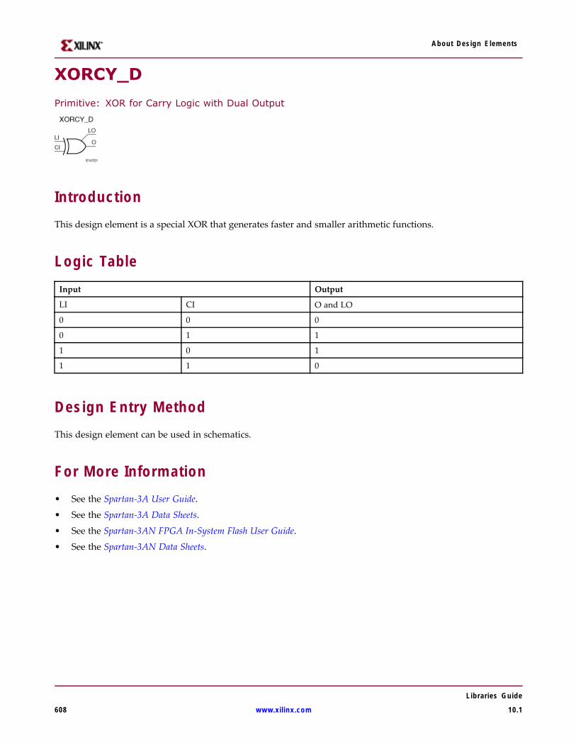
About Design Elements
XORCY_D
Primitive: XOR for Carry Logic with Dual Output
IntroductionThis design element is a special XOR that generates faster and smaller arithmetic functions.
Logic TableInput Output
LI CI O and LO
0 0 0
0 1 1
1 0 1
1 1 0
Design Entry MethodThis design element can be used in schematics.
For More Information• See the Spartan-3A User Guide.
• See the Spartan-3A Data Sheets.
• See the Spartan-3AN FPGA In-System Flash User Guide.
• See the Spartan-3AN Data Sheets.
Libraries Guide
608 www.xilinx.com 10.1
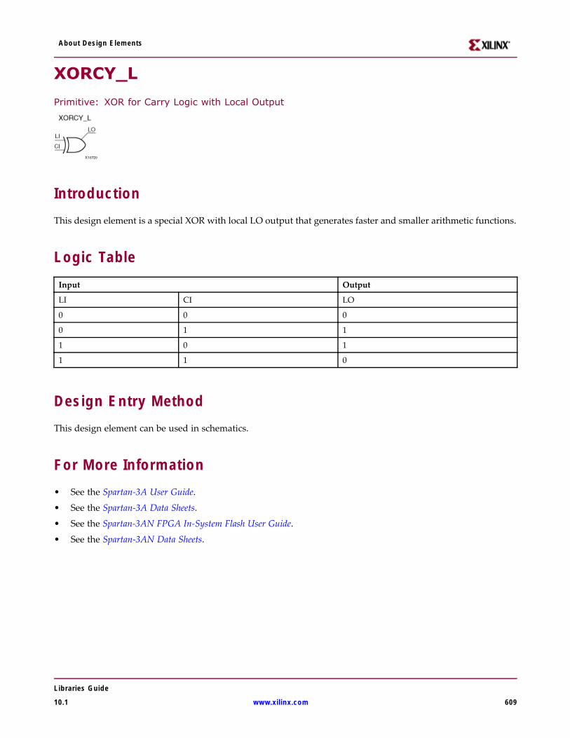
About Design Elements
XORCY_L
Primitive: XOR for Carry Logic with Local Output
IntroductionThis design element is a special XOR with local LO output that generates faster and smaller arithmetic functions.
Logic TableInput Output
LI CI LO
0 0 0
0 1 1
1 0 1
1 1 0
Design Entry MethodThis design element can be used in schematics.
For More Information• See the Spartan-3A User Guide.
• See the Spartan-3A Data Sheets.
• See the Spartan-3AN FPGA In-System Flash User Guide.
• See the Spartan-3AN Data Sheets.
Libraries Guide
10.1 www.xilinx.com 609