Embed Size (px)
Citation preview
R
Synthesis and Simulation Design Guide
10.1

10.1 www.xilinx.com 10.1
Xilinx is disclosing this user guide, manual, release note, and/or specification (the "Documentation") to you solely for use in the development of designs to operate with Xilinx hardware devices. You may not reproduce, distribute, republish, download, display, post, or transmit the Documentation in any form or by any means including, but not limited to, electronic, mechanical, photocopying, recording, or otherwise, without the prior written consent of Xilinx. Xilinx expressly disclaims any liability arising out of your use of the Documentation. Xilinx reserves the right, at its sole discretion, to change the Documentation without notice at any time. Xilinx assumes no obligation to correct any errors contained in the Documentation, or to advise you of any corrections or updates. Xilinx expressly disclaims any liability in connection with technical support or assistance that may be provided to you in connection with the Information.
THE DOCUMENTATION IS DISCLOSED TO YOU “AS-IS” WITH NO WARRANTY OF ANY KIND. XILINX MAKES NO OTHER WARRANTIES, WHETHER EXPRESS, IMPLIED, OR STATUTORY, REGARDING THE DOCUMENTATION, INCLUDING ANY WARRANTIES OF MERCHANTABILITY, FITNESS FOR A PARTICULAR PURPOSE, OR NONINFRINGEMENT OF THIRD-PARTY RIGHTS. IN NO EVENT WILL XILINX BE LIABLE FOR ANY CONSEQUENTIAL, INDIRECT, EXEMPLARY, SPECIAL, OR INCIDENTAL DAMAGES, INCLUDING ANY LOSS OF DATA OR LOST PROFITS, ARISING FROM YOUR USE OF THE DOCUMENTATION.
© 2002–2008 Xilinx, Inc. All rights reserved.
XILINX, the Xilinx logo, the Brand Window, and other designated brands included herein are trademarks of Xilinx, Inc. All other trademarks are the property of their respective owners
R
Synthesis and Simulation Design Guide www.xilinx.com 310.1
R
Preface
About the Synthesis and Simulation Design Guide
This chapter (About the Synthesis and Simulation Design Guide) provides general information about this Guide, and includes:
• “Synthesis and Simulation Design Guide Overview”
• “Synthesis and Simulation Design Guide Design Examples”
• “Synthesis and Simulation Design Guide Contents”
• “Additional Resources”
• “Conventions”
Synthesis and Simulation Design Guide OverviewThe Synthesis and Simulation Design Guide provides a general overview of designing Field Programmable Gate Arrays (FPGA) devices with Hardware Description Languages (HDLs). It includes design hints for the novice HDL user, as well as for the experienced user who is designing FPGA devices for the first time. Before using the Synthesis and Simulation Design Guide, you should be familiar with the operations that are common to all Xilinx tools.
The Synthesis and Simulation Design Guide does not address certain topics that are important when creating Hardware Description Language (HDL) designs, such as:
• Design environment
• Verification techniques
• Constraining in the synthesis tool
• Test considerations
• System verification
For more information, see your synthesis tool documentation.
Synthesis and Simulation Design Guide Design ExamplesThe design examples in the Synthesis and Simulation Design Guide were:
• Created with VHSIC Hardware Description Language (VHDL) and Verilog
Xilinx® endorses Verilog and VHDL equally. VHDL may be more difficult to learn than Verilog, and usually requires more explanation.
4 www.xilinx.com Synthesis and Simulation Design Guide10.1
Preface: About the Synthesis and Simulation Design GuideR
• Compiled with various synthesis tools
• Targeted for the following devices:
♦ Spartan™-II, Spartan-IIE
♦ Spartan-3, Spartan-3E, Spartan-3A
♦ Virtex™, Virtex-E
♦ Virtex-II, Virtex-II Pro
♦ Virtex-4, Virtex-5
Synthesis and Simulation Design Guide ContentsThe Synthesis and Simulation Design Guide contains the following chapters:
• Chapter 1, “Introduction to Synthesis and Simulation,” provides an introduction to synthesis and simulation and describes how to design Field Programmable Gate Arrays (FPGA devices) with Hardware Description Languages (HDLs).
• Chapter 2, “FPGA Design Flow,” describes the steps in a typical FPGA design flow.
• Chapter 3, “General Recommendations for Coding Practices,” contains general information relating to Hardware Description Language (HDL) coding styles and design examples to help you develop an efficient coding style.
• Chapter 4, “Coding for FPGA Flow,” contains specific information relating to coding for FPGA devices.
• Chapter 5, “Using SmartModels,” describes special considerations when simulating designs for Virtex-II Pro, Virtex-4, and Virtex-5 FPGA devices. These devices are platform FPGA devices for designs based on IP cores and customized modules. The family incorporates RocketIO™ and PowerPC™ CPU and Ethernet MAC cores in the FPGA architecture
• Chapter 6, “Simulating Your Design” describes the basic Hardware Description Language (HDL) simulation flow using Xilinx® and third party tools.
• Chapter 7, “Design Considerations,” describes understanding the architecture, clocking resources, defining timing requirements, driving synthesis, choosing implementation options, and evaluating critical paths.
• Appendix A, “Simulating Xilinx Designs in Modelsim”
• Appendix B, “Simulating Xilinx Designs in NCSIM”
• Appendix C, “Simulating Xilinx Designs in Synopsys VCS-MX and VCS-MXi”
Additional ResourcesFor additional documentation, see the Xilinx website at:
http://www.xilinx.com/literature.
To search the Answer Database of silicon, software, and IP questions and answers, or to create a technical support WebCase, see the Xilinx website at:
http://www.xilinx.com/support.
Synthesis and Simulation Design Guide www.xilinx.com 510.1
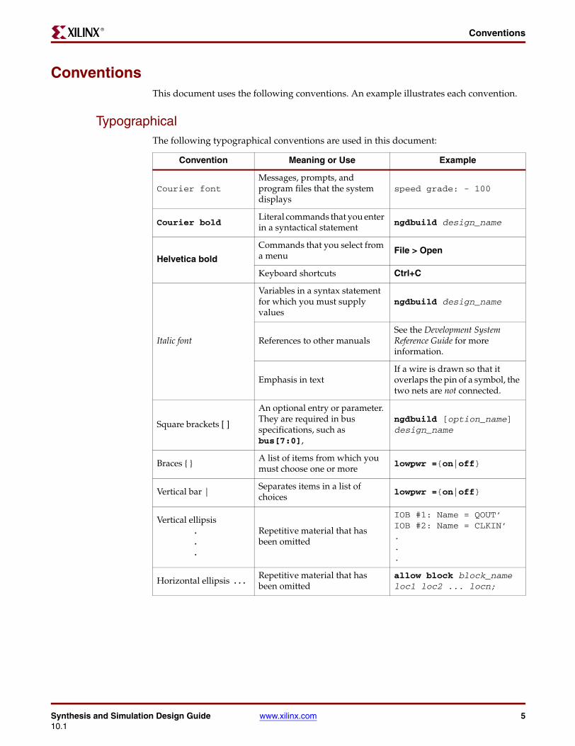
ConventionsR
ConventionsThis document uses the following conventions. An example illustrates each convention.
TypographicalThe following typographical conventions are used in this document:
Convention Meaning or Use Example
Courier fontMessages, prompts, and program files that the system displays
speed grade: - 100
Courier boldLiteral commands that you enter in a syntactical statement ngdbuild design_name
Helvetica bold
Commands that you select from a menu File > Open
Keyboard shortcuts Ctrl+C
Italic font
Variables in a syntax statement for which you must supply values
ngdbuild design_name
References to other manualsSee the Development System Reference Guide for more information.
Emphasis in textIf a wire is drawn so that it overlaps the pin of a symbol, the two nets are not connected.
Square brackets [ ]
An optional entry or parameter. They are required in bus specifications, such as bus[7:0],
ngdbuild [option_name] design_name
Braces { } A list of items from which you must choose one or more
lowpwr ={on|off}
Vertical bar | Separates items in a list of choices
lowpwr ={on|off}
Vertical ellipsis...
Repetitive material that has been omitted
IOB #1: Name = QOUT’ IOB #2: Name = CLKIN’...
Horizontal ellipsis . . .Repetitive material that has been omitted
allow block block_name loc1 loc2 ... locn;
6 www.xilinx.com Synthesis and Simulation Design Guide10.1
Preface: About the Synthesis and Simulation Design GuideR
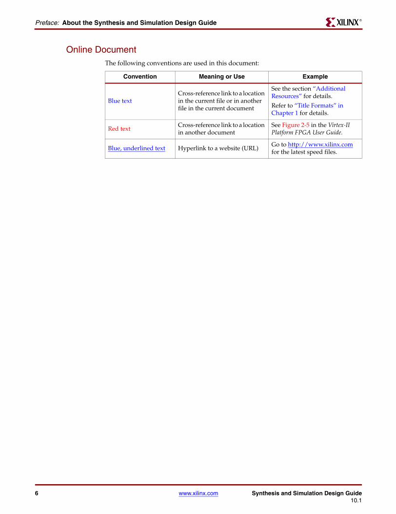
Online DocumentThe following conventions are used in this document:
Convention Meaning or Use Example
Blue textCross-reference link to a location in the current file or in another file in the current document
See the section “Additional Resources” for details.
Refer to “Title Formats” in Chapter 1 for details.
Red textCross-reference link to a location in another document
See Figure 2-5 in the Virtex-II Platform FPGA User Guide.
Blue, underlined text Hyperlink to a website (URL)Go to http://www.xilinx.com for the latest speed files.
Synthesis and Simulation Design Guide www.xilinx.com 710.1
Preface: About the Synthesis and Simulation Design GuideSynthesis and Simulation Design Guide Overview . . . . . . . . . . . . . . . . . . . . . . . . . . . 3Synthesis and Simulation Design Guide Design Examples. . . . . . . . . . . . . . . . . . . . 3 Synthesis and Simulation Design Guide Contents . . . . . . . . . . . . . . . . . . . . . . . . . . . 4Additional Resources . . . . . . . . . . . . . . . . . . . . . . . . . . . . . . . . . . . . . . . . . . . . . . . . . . . . . . . . 4Conventions . . . . . . . . . . . . . . . . . . . . . . . . . . . . . . . . . . . . . . . . . . . . . . . . . . . . . . . . . . . . . . . . . 5
Typographical . . . . . . . . . . . . . . . . . . . . . . . . . . . . . . . . . . . . . . . . . . . . . . . . . . . . . . . . . . . . . 5Online Document . . . . . . . . . . . . . . . . . . . . . . . . . . . . . . . . . . . . . . . . . . . . . . . . . . . . . . . . . . 6
Chapter 1: Introduction to Synthesis and SimulationHardware Description Languages (HDLs) . . . . . . . . . . . . . . . . . . . . . . . . . . . . . . . . . . . 17Advantages of Using Hardware Description Languages
(HDLs) to Design FPGA Devices . . . . . . . . . . . . . . . . . . . . . . . . . . . . . . . . . . . . . . . . . . 18Designing FPGA Devices With Hardware Description Languages (HDLs). . . . 18
Understanding Hardware Description Languages (HDLs) . . . . . . . . . . . . . . . . . . . . . 19Designing FPGA Devices with VHDL . . . . . . . . . . . . . . . . . . . . . . . . . . . . . . . . . . . . . . . 19Designing FPGA Devices with Verilog. . . . . . . . . . . . . . . . . . . . . . . . . . . . . . . . . . . . . . . 19Designing FPGA Devices with Synthesis Tools . . . . . . . . . . . . . . . . . . . . . . . . . . . . . . . 20Using FPGA System Features . . . . . . . . . . . . . . . . . . . . . . . . . . . . . . . . . . . . . . . . . . . . . . 20Designing Hierarchy . . . . . . . . . . . . . . . . . . . . . . . . . . . . . . . . . . . . . . . . . . . . . . . . . . . . . . 20Specifying Speed Requirements . . . . . . . . . . . . . . . . . . . . . . . . . . . . . . . . . . . . . . . . . . . . 20
Chapter 2: FPGA Design FlowDesign Flow Diagram . . . . . . . . . . . . . . . . . . . . . . . . . . . . . . . . . . . . . . . . . . . . . . . . . . . . . . . 22Design Entry Recommendations. . . . . . . . . . . . . . . . . . . . . . . . . . . . . . . . . . . . . . . . . . . . . 23
Use Register Transfer Level (RTL) Code . . . . . . . . . . . . . . . . . . . . . . . . . . . . . . . . . . . . . 23Select the Correct Design Hierarchy . . . . . . . . . . . . . . . . . . . . . . . . . . . . . . . . . . . . . . . . . 23
Architecture Wizard . . . . . . . . . . . . . . . . . . . . . . . . . . . . . . . . . . . . . . . . . . . . . . . . . . . . . . . . . 23Using Architecture Wizard . . . . . . . . . . . . . . . . . . . . . . . . . . . . . . . . . . . . . . . . . . . . . . . . . 23Opening Architecture Wizard . . . . . . . . . . . . . . . . . . . . . . . . . . . . . . . . . . . . . . . . . . . . . . 24Architecture Wizard Components . . . . . . . . . . . . . . . . . . . . . . . . . . . . . . . . . . . . . . . . . . 24
Clocking Wizard . . . . . . . . . . . . . . . . . . . . . . . . . . . . . . . . . . . . . . . . . . . . . . . . . . . . . . . 24RocketIO Wizard . . . . . . . . . . . . . . . . . . . . . . . . . . . . . . . . . . . . . . . . . . . . . . . . . . . . . . 25ChipSync Wizard . . . . . . . . . . . . . . . . . . . . . . . . . . . . . . . . . . . . . . . . . . . . . . . . . . . . . . 25XtremeDSP Slice Wizard. . . . . . . . . . . . . . . . . . . . . . . . . . . . . . . . . . . . . . . . . . . . . . . . . 25
CORE Generator . . . . . . . . . . . . . . . . . . . . . . . . . . . . . . . . . . . . . . . . . . . . . . . . . . . . . . . . . . . . 26About CORE Generator . . . . . . . . . . . . . . . . . . . . . . . . . . . . . . . . . . . . . . . . . . . . . . . . . . . 26CORE Generator Files . . . . . . . . . . . . . . . . . . . . . . . . . . . . . . . . . . . . . . . . . . . . . . . . . . . . . 26
Electronic Data Interchange Format Netlist (EDN) and NGC Files . . . . . . . . . . . . . . . . 26VHDL Template (VHO) Files . . . . . . . . . . . . . . . . . . . . . . . . . . . . . . . . . . . . . . . . . . . . . 26Verilog Template (VEO) Files . . . . . . . . . . . . . . . . . . . . . . . . . . . . . . . . . . . . . . . . . . . . . 26V (Verilog) and VHD (VHDL) Wrapper Files. . . . . . . . . . . . . . . . . . . . . . . . . . . . . . . . . 27ASY (ASCII Symbol) Files. . . . . . . . . . . . . . . . . . . . . . . . . . . . . . . . . . . . . . . . . . . . . . . . 27
Table of Contents
8 www.xilinx.com Synthesis and Simulation Design Guide10.1
R
Functional Simulation. . . . . . . . . . . . . . . . . . . . . . . . . . . . . . . . . . . . . . . . . . . . . . . . . . . . . . . 27Synthesizing and Optimizing . . . . . . . . . . . . . . . . . . . . . . . . . . . . . . . . . . . . . . . . . . . . . . . 27
Creating a Compile Run Script . . . . . . . . . . . . . . . . . . . . . . . . . . . . . . . . . . . . . . . . . . . . . 28Running the TCL Script (Precision RTL Synthesis). . . . . . . . . . . . . . . . . . . . . . . . . . . . . 28Running the TCL Script (Synplify) . . . . . . . . . . . . . . . . . . . . . . . . . . . . . . . . . . . . . . . . . 28Running the TCL Script (XST) . . . . . . . . . . . . . . . . . . . . . . . . . . . . . . . . . . . . . . . . . . . . 29
Modifying Your Code to Successfully Synthesize Your Design . . . . . . . . . . . . . . . . . . 29Reading Cores . . . . . . . . . . . . . . . . . . . . . . . . . . . . . . . . . . . . . . . . . . . . . . . . . . . . . . . . . . . . 29
About Reading Cores . . . . . . . . . . . . . . . . . . . . . . . . . . . . . . . . . . . . . . . . . . . . . . . . . . . 30Reading Cores (XST) . . . . . . . . . . . . . . . . . . . . . . . . . . . . . . . . . . . . . . . . . . . . . . . . . . . . 30Reading Cores (Synplify Pro) . . . . . . . . . . . . . . . . . . . . . . . . . . . . . . . . . . . . . . . . . . . . . 30Reading Cores (Precision RTL Synthesis) . . . . . . . . . . . . . . . . . . . . . . . . . . . . . . . . . . . . 30
Setting Constraints . . . . . . . . . . . . . . . . . . . . . . . . . . . . . . . . . . . . . . . . . . . . . . . . . . . . . . . . . . 30Advantages of Setting Constraints . . . . . . . . . . . . . . . . . . . . . . . . . . . . . . . . . . . . . . . . . . 30Specifying Constraints in the User Constraints File (UCF) . . . . . . . . . . . . . . . . . . . . . . 31Setting Constraints in ISE . . . . . . . . . . . . . . . . . . . . . . . . . . . . . . . . . . . . . . . . . . . . . . . . . . 31
Evaluating Design Size and Performance . . . . . . . . . . . . . . . . . . . . . . . . . . . . . . . . . . . . 31Meeting Design Parameters . . . . . . . . . . . . . . . . . . . . . . . . . . . . . . . . . . . . . . . . . . . . . . . . 31Estimating Device Utilization and Performance . . . . . . . . . . . . . . . . . . . . . . . . . . . . . . . 32Determining Actual Device Utilization and Pre-Routed Performance . . . . . . . . . . . . 32
Determining If Your Design Fits the Specified Device . . . . . . . . . . . . . . . . . . . . . . . . . . 32Mapping Your Design Using Project Navigator . . . . . . . . . . . . . . . . . . . . . . . . . . . . . . . 33Mapping Your Design Using the Command Line . . . . . . . . . . . . . . . . . . . . . . . . . . . . . 33
Evaluating Coding Style and System Features . . . . . . . . . . . . . . . . . . . . . . . . . . . . . . . 34Modifying Code to Improve Design Performance . . . . . . . . . . . . . . . . . . . . . . . . . . . . . 34Using FPGA System Features . . . . . . . . . . . . . . . . . . . . . . . . . . . . . . . . . . . . . . . . . . . . . . 34Using Xilinx-Specific Features of Your Synthesis Tool . . . . . . . . . . . . . . . . . . . . . . . . . 35
Placing and Routing. . . . . . . . . . . . . . . . . . . . . . . . . . . . . . . . . . . . . . . . . . . . . . . . . . . . . . . . . 35Timing Simulation . . . . . . . . . . . . . . . . . . . . . . . . . . . . . . . . . . . . . . . . . . . . . . . . . . . . . . . . . . 35
Chapter 3: General Recommendations for Coding PracticesDesigning With Hardware Description Languages (HDLs) . . . . . . . . . . . . . . . . . . . 37Naming, Labeling, and General Coding Styles . . . . . . . . . . . . . . . . . . . . . . . . . . . . . . . 38
Common Coding Style . . . . . . . . . . . . . . . . . . . . . . . . . . . . . . . . . . . . . . . . . . . . . . . . . . . . 38Xilinx Naming Conventions . . . . . . . . . . . . . . . . . . . . . . . . . . . . . . . . . . . . . . . . . . . . . . . . 38Reserved Names . . . . . . . . . . . . . . . . . . . . . . . . . . . . . . . . . . . . . . . . . . . . . . . . . . . . . . . . . . 38Naming Guidelines for Signals and Instances . . . . . . . . . . . . . . . . . . . . . . . . . . . . . . . . . 39
General Naming Rules for Signals and Instances . . . . . . . . . . . . . . . . . . . . . . . . . . . . . . 39Recommendations for VHDL and Verilog Capitalization . . . . . . . . . . . . . . . . . . . . . . . 39
Matching File Names to Entity and Module Names . . . . . . . . . . . . . . . . . . . . . . . . . . . 40Naming Identifiers . . . . . . . . . . . . . . . . . . . . . . . . . . . . . . . . . . . . . . . . . . . . . . . . . . . . . . . . 40Instantiating Sub-Modules . . . . . . . . . . . . . . . . . . . . . . . . . . . . . . . . . . . . . . . . . . . . . . . . . 40
Instantiating Sub-Modules Recommendations . . . . . . . . . . . . . . . . . . . . . . . . . . . . . . . . 40Incorrect and Correct VHDL and Verilog Coding Examples . . . . . . . . . . . . . . . . . . . . . 41Instantiating Sub-Modules Coding Examples. . . . . . . . . . . . . . . . . . . . . . . . . . . . . . . . . 41
Recommended Length of Line . . . . . . . . . . . . . . . . . . . . . . . . . . . . . . . . . . . . . . . . . . . . . . 42Common File Headers . . . . . . . . . . . . . . . . . . . . . . . . . . . . . . . . . . . . . . . . . . . . . . . . . . . . . 42Indenting and Spacing . . . . . . . . . . . . . . . . . . . . . . . . . . . . . . . . . . . . . . . . . . . . . . . . . . . . 43
Specifying Constants . . . . . . . . . . . . . . . . . . . . . . . . . . . . . . . . . . . . . . . . . . . . . . . . . . . . . . . . 44Using Constants and Parameters to Clarify Code . . . . . . . . . . . . . . . . . . . . . . . . . . . . . 44Using Constants and Parameters VHDL Coding Examples . . . . . . . . . . . . . . . . . . . . . 44
Synthesis and Simulation Design Guide www.xilinx.com 910.1
R
Using Generics and Parameters to Specify Dynamic Bus and Array Widths. . . . . . . 45About Using Generics and Parameters to Specify Dynamic Bus and Array Widths . . . 45Generics and Parameters Coding Examples . . . . . . . . . . . . . . . . . . . . . . . . . . . . . . . . . . 45
TRANSLATE_OFF and TRANSLATE_ON . . . . . . . . . . . . . . . . . . . . . . . . . . . . . . . . . . 46
Chapter 4: Coding for FPGA FlowVHDL and Verilog Limitations . . . . . . . . . . . . . . . . . . . . . . . . . . . . . . . . . . . . . . . . . . . . . . 47Design Hierarchy . . . . . . . . . . . . . . . . . . . . . . . . . . . . . . . . . . . . . . . . . . . . . . . . . . . . . . . . . . . 48
Advantages and Disadvantages of Hierarchical Designs . . . . . . . . . . . . . . . . . . . . . . . 48Using Synthesis Tools with Hierarchical Designs. . . . . . . . . . . . . . . . . . . . . . . . . . . . . . 48
Restrict Shared Resources . . . . . . . . . . . . . . . . . . . . . . . . . . . . . . . . . . . . . . . . . . . . . . . . 49Compile Multiple Instances . . . . . . . . . . . . . . . . . . . . . . . . . . . . . . . . . . . . . . . . . . . . . . 49Restrict Related Combinatorial Logic . . . . . . . . . . . . . . . . . . . . . . . . . . . . . . . . . . . . . . . 49Separate Speed Critical Paths . . . . . . . . . . . . . . . . . . . . . . . . . . . . . . . . . . . . . . . . . . . . . 49Restrict Combinatorial Logic . . . . . . . . . . . . . . . . . . . . . . . . . . . . . . . . . . . . . . . . . . . . . 49Restrict Module Size . . . . . . . . . . . . . . . . . . . . . . . . . . . . . . . . . . . . . . . . . . . . . . . . . . . . 49Register All Outputs . . . . . . . . . . . . . . . . . . . . . . . . . . . . . . . . . . . . . . . . . . . . . . . . . . . . 49Restrict One Clock to Each Module or to Entire Design . . . . . . . . . . . . . . . . . . . . . . . . . 49
Choosing Data Type . . . . . . . . . . . . . . . . . . . . . . . . . . . . . . . . . . . . . . . . . . . . . . . . . . . . . . . . 50Use Std_logic (IEEE 1164) . . . . . . . . . . . . . . . . . . . . . . . . . . . . . . . . . . . . . . . . . . . . . . . . . . 50Declaring Ports . . . . . . . . . . . . . . . . . . . . . . . . . . . . . . . . . . . . . . . . . . . . . . . . . . . . . . . . . . . 50Arrays in Port Declarations . . . . . . . . . . . . . . . . . . . . . . . . . . . . . . . . . . . . . . . . . . . . . . . . 51
Incompatibility with Verilog. . . . . . . . . . . . . . . . . . . . . . . . . . . . . . . . . . . . . . . . . . . . . . 51Inability to Store and Re-Create Original Array Declaration . . . . . . . . . . . . . . . . . . . . . 51Mis-Correlation of Software Pin Names . . . . . . . . . . . . . . . . . . . . . . . . . . . . . . . . . . . . . 51
Minimize Ports Declared as Buffers . . . . . . . . . . . . . . . . . . . . . . . . . . . . . . . . . . . . . . . . . 52Using `timescale . . . . . . . . . . . . . . . . . . . . . . . . . . . . . . . . . . . . . . . . . . . . . . . . . . . . . . . . . . . . 53Mixed Language Designs. . . . . . . . . . . . . . . . . . . . . . . . . . . . . . . . . . . . . . . . . . . . . . . . . . . . 53If Statements and Case Statements . . . . . . . . . . . . . . . . . . . . . . . . . . . . . . . . . . . . . . . . . . 53
Comparing If Statements and Case Statements . . . . . . . . . . . . . . . . . . . . . . . . . . . . . . . . 544–to–1 Multiplexer Design With If Statement . . . . . . . . . . . . . . . . . . . . . . . . . . . . . . . . . 544–to–1 Multiplexer Design With Case Statement . . . . . . . . . . . . . . . . . . . . . . . . . . . . . . 55
Sensitivity List in Process and Always Statements . . . . . . . . . . . . . . . . . . . . . . . . . . . 57Delays in Synthesis Code . . . . . . . . . . . . . . . . . . . . . . . . . . . . . . . . . . . . . . . . . . . . . . . . . . . 58
About Delays in Synthesis Code . . . . . . . . . . . . . . . . . . . . . . . . . . . . . . . . . . . . . . . . . . . . 58Delays in Synthesis Code Coding Examples . . . . . . . . . . . . . . . . . . . . . . . . . . . . . . . . . . 58
Registers and Latches in FPGA Design . . . . . . . . . . . . . . . . . . . . . . . . . . . . . . . . . . . . . . 59Registers in FPGA Design . . . . . . . . . . . . . . . . . . . . . . . . . . . . . . . . . . . . . . . . . . . . . . . . . . 59
About Registers in FPGA Design . . . . . . . . . . . . . . . . . . . . . . . . . . . . . . . . . . . . . . . . . . 59Registers in FPGA Design Coding Examples . . . . . . . . . . . . . . . . . . . . . . . . . . . . . . . . . 59
IOB Registers . . . . . . . . . . . . . . . . . . . . . . . . . . . . . . . . . . . . . . . . . . . . . . . . . . . . . . . . . . . . 61About IOB Registers . . . . . . . . . . . . . . . . . . . . . . . . . . . . . . . . . . . . . . . . . . . . . . . . . . . . 61Dual-Data Rate IOB Registers . . . . . . . . . . . . . . . . . . . . . . . . . . . . . . . . . . . . . . . . . . . . . 62
Latches in FPGA Design . . . . . . . . . . . . . . . . . . . . . . . . . . . . . . . . . . . . . . . . . . . . . . . . . . . 63Implementing Shift Registers . . . . . . . . . . . . . . . . . . . . . . . . . . . . . . . . . . . . . . . . . . . . . . . 64
About Implementing Shift Registers . . . . . . . . . . . . . . . . . . . . . . . . . . . . . . . . . . . . . . . . . 64Describing Shift Registers . . . . . . . . . . . . . . . . . . . . . . . . . . . . . . . . . . . . . . . . . . . . . . . . . . 65
About Describing Shift Registers . . . . . . . . . . . . . . . . . . . . . . . . . . . . . . . . . . . . . . . . . . 65Shift Registers Coding Examples . . . . . . . . . . . . . . . . . . . . . . . . . . . . . . . . . . . . . . . . . . 65
Control Signals . . . . . . . . . . . . . . . . . . . . . . . . . . . . . . . . . . . . . . . . . . . . . . . . . . . . . . . . . . . . . 67
10 www.xilinx.com Synthesis and Simulation Design Guide10.1
R
Set, Resets, and Synthesis Optimization . . . . . . . . . . . . . . . . . . . . . . . . . . . . . . . . . . . . . . 67About Set, Resets, and Synthesis Optimization . . . . . . . . . . . . . . . . . . . . . . . . . . . . . . . 67Global Set/Reset (GSR). . . . . . . . . . . . . . . . . . . . . . . . . . . . . . . . . . . . . . . . . . . . . . . . . . 67Shift Register LUT (SRL). . . . . . . . . . . . . . . . . . . . . . . . . . . . . . . . . . . . . . . . . . . . . . . . . 68Synchronous and Asynchronous Resets . . . . . . . . . . . . . . . . . . . . . . . . . . . . . . . . . . . . . 68
Asynchronous Resets Coding Examples . . . . . . . . . . . . . . . . . . . . . . . . . . . . . . . . . . . . . 68Synchronous Resets Coding Examples . . . . . . . . . . . . . . . . . . . . . . . . . . . . . . . . . . . . . . . 69Using Clock Enable Pin Instead of Gated Clocks . . . . . . . . . . . . . . . . . . . . . . . . . . . . . . 73
About Using Clock Enable Pin Instead of Gated Clocks. . . . . . . . . . . . . . . . . . . . . . . . . 73Using Clock Enable Pin Instead of Gated Clocks Coding Examples. . . . . . . . . . . . . . . . 73
Converting the Gated Clock to a Clock Enable . . . . . . . . . . . . . . . . . . . . . . . . . . . . . . . . 74Initial State of the Registers, Latches, Shift Registers, and RAMs. . . . . . . . . . . . . 75
Initial State of the Registers and Latches . . . . . . . . . . . . . . . . . . . . . . . . . . . . . . . . . . . . . 75Initial State of the Shift Registers . . . . . . . . . . . . . . . . . . . . . . . . . . . . . . . . . . . . . . . . . . . . 76Initial State of the RAMs . . . . . . . . . . . . . . . . . . . . . . . . . . . . . . . . . . . . . . . . . . . . . . . . . . . 76
About Initial State of the RAMs . . . . . . . . . . . . . . . . . . . . . . . . . . . . . . . . . . . . . . . . . . . 76Initial State of the RAMs Coding Examples . . . . . . . . . . . . . . . . . . . . . . . . . . . . . . . . . . 76
Multiplexers . . . . . . . . . . . . . . . . . . . . . . . . . . . . . . . . . . . . . . . . . . . . . . . . . . . . . . . . . . . . . . . . 77About Multiplexers . . . . . . . . . . . . . . . . . . . . . . . . . . . . . . . . . . . . . . . . . . . . . . . . . . . . . . . 77Multiplexers Coding Examples . . . . . . . . . . . . . . . . . . . . . . . . . . . . . . . . . . . . . . . . . . . . . 78
Finite State Machines (FSMs). . . . . . . . . . . . . . . . . . . . . . . . . . . . . . . . . . . . . . . . . . . . . . . . 79FSM Description Style . . . . . . . . . . . . . . . . . . . . . . . . . . . . . . . . . . . . . . . . . . . . . . . . . . . . . 79FSM With One Process . . . . . . . . . . . . . . . . . . . . . . . . . . . . . . . . . . . . . . . . . . . . . . . . . . . . 81FSM With Two or Three Processes . . . . . . . . . . . . . . . . . . . . . . . . . . . . . . . . . . . . . . . . . . 83FSM Recognition and Optimization . . . . . . . . . . . . . . . . . . . . . . . . . . . . . . . . . . . . . . . . . 83Other FSM Features . . . . . . . . . . . . . . . . . . . . . . . . . . . . . . . . . . . . . . . . . . . . . . . . . . . . . . . 84
Implementing Memory. . . . . . . . . . . . . . . . . . . . . . . . . . . . . . . . . . . . . . . . . . . . . . . . . . . . . . 84Block RAM Inference . . . . . . . . . . . . . . . . . . . . . . . . . . . . . . . . . . . . . . . . . . . . . . . . . . . . . . . 85
About Block RAM Inference. . . . . . . . . . . . . . . . . . . . . . . . . . . . . . . . . . . . . . . . . . . . . . . . 85Block RAM Inference Coding Examples . . . . . . . . . . . . . . . . . . . . . . . . . . . . . . . . . . . . . 85
Single-Port RAM in Read-First Mode . . . . . . . . . . . . . . . . . . . . . . . . . . . . . . . . . . . . . . . 86Single-Port RAM in Write-First Mode . . . . . . . . . . . . . . . . . . . . . . . . . . . . . . . . . . . . . . 87Single-Port RAM In No-Change Mode . . . . . . . . . . . . . . . . . . . . . . . . . . . . . . . . . . . . . . 90Dual-Port RAM in Read-First Mode with One Write Port . . . . . . . . . . . . . . . . . . . . . . . 91Dual-Port Block RAM in Read-First Mode With Two Write Ports . . . . . . . . . . . . . . . . . 93
Distributed RAM Inference . . . . . . . . . . . . . . . . . . . . . . . . . . . . . . . . . . . . . . . . . . . . . . . . . 96Single-Port Distributed RAM . . . . . . . . . . . . . . . . . . . . . . . . . . . . . . . . . . . . . . . . . . . . . . . 96Dual-Port Distributed RAM . . . . . . . . . . . . . . . . . . . . . . . . . . . . . . . . . . . . . . . . . . . . . . . . 97
Arithmetic Support . . . . . . . . . . . . . . . . . . . . . . . . . . . . . . . . . . . . . . . . . . . . . . . . . . . . . . . . . 99About Arithmetic Support . . . . . . . . . . . . . . . . . . . . . . . . . . . . . . . . . . . . . . . . . . . . . . . . . 99Arithmetic Support Coding Examples . . . . . . . . . . . . . . . . . . . . . . . . . . . . . . . . . . . . . . 100Order and Group Arithmetic Functions . . . . . . . . . . . . . . . . . . . . . . . . . . . . . . . . . . . . . 107Resource Sharing . . . . . . . . . . . . . . . . . . . . . . . . . . . . . . . . . . . . . . . . . . . . . . . . . . . . . . . . 108
About Resource Sharing . . . . . . . . . . . . . . . . . . . . . . . . . . . . . . . . . . . . . . . . . . . . . . . . 108Resource Sharing Coding Examples . . . . . . . . . . . . . . . . . . . . . . . . . . . . . . . . . . . . . . . 109
Synthesis Tool Naming Conventions . . . . . . . . . . . . . . . . . . . . . . . . . . . . . . . . . . . . . . . 110Instantiating Components and FPGA Primitives . . . . . . . . . . . . . . . . . . . . . . . . . . . . 111
Instantiating FPGA Primitives . . . . . . . . . . . . . . . . . . . . . . . . . . . . . . . . . . . . . . . . . . . . . 111About Instantiating FPGA Primitives . . . . . . . . . . . . . . . . . . . . . . . . . . . . . . . . . . . . . . 111
Instantiating CORE Generator Modules . . . . . . . . . . . . . . . . . . . . . . . . . . . . . . . . . . . . 112Attributes and Constraints . . . . . . . . . . . . . . . . . . . . . . . . . . . . . . . . . . . . . . . . . . . . . . . . . 112
Synthesis and Simulation Design Guide www.xilinx.com 1110.1
R
Attributes. . . . . . . . . . . . . . . . . . . . . . . . . . . . . . . . . . . . . . . . . . . . . . . . . . . . . . . . . . . . . . . 113Synthesis Constraints . . . . . . . . . . . . . . . . . . . . . . . . . . . . . . . . . . . . . . . . . . . . . . . . . . . . 113Implementation Constraints . . . . . . . . . . . . . . . . . . . . . . . . . . . . . . . . . . . . . . . . . . . . . . . 113Passing Attributes . . . . . . . . . . . . . . . . . . . . . . . . . . . . . . . . . . . . . . . . . . . . . . . . . . . . . . . 113Passing Synthesis Constraints . . . . . . . . . . . . . . . . . . . . . . . . . . . . . . . . . . . . . . . . . . . . . 114
VHDL Synthesis Attributes . . . . . . . . . . . . . . . . . . . . . . . . . . . . . . . . . . . . . . . . . . . . . 115Verilog Synthesis Attributes . . . . . . . . . . . . . . . . . . . . . . . . . . . . . . . . . . . . . . . . . . . . . 116
Pipelining and Retiming . . . . . . . . . . . . . . . . . . . . . . . . . . . . . . . . . . . . . . . . . . . . . . . . . . . 116About Pipelining . . . . . . . . . . . . . . . . . . . . . . . . . . . . . . . . . . . . . . . . . . . . . . . . . . . . . . . . 116Before Pipelining . . . . . . . . . . . . . . . . . . . . . . . . . . . . . . . . . . . . . . . . . . . . . . . . . . . . . . . . 117After Pipelining . . . . . . . . . . . . . . . . . . . . . . . . . . . . . . . . . . . . . . . . . . . . . . . . . . . . . . . . . 117About Retiming . . . . . . . . . . . . . . . . . . . . . . . . . . . . . . . . . . . . . . . . . . . . . . . . . . . . . . . . . 118
Chapter 5: Using SmartModelsUsing SmartModels with ISE Simulator . . . . . . . . . . . . . . . . . . . . . . . . . . . . . . . . . . . . 119Using SmartModels to Simulate Designs . . . . . . . . . . . . . . . . . . . . . . . . . . . . . . . . . . . 119SmartModel Simulation Flow . . . . . . . . . . . . . . . . . . . . . . . . . . . . . . . . . . . . . . . . . . . . . . 120About SmartModels. . . . . . . . . . . . . . . . . . . . . . . . . . . . . . . . . . . . . . . . . . . . . . . . . . . . . . . . 120SmartModel Supported Simulators and Operating Systems . . . . . . . . . . . . . . . . . 121Installing SmartModels . . . . . . . . . . . . . . . . . . . . . . . . . . . . . . . . . . . . . . . . . . . . . . . . . . . . 121
Installing SmartModels (Method One) . . . . . . . . . . . . . . . . . . . . . . . . . . . . . . . . . . . . . . 122Installing SmartModels (Method Two). . . . . . . . . . . . . . . . . . . . . . . . . . . . . . . . . . . . . . 123
Installing SmartModels (Method Two on Linux) . . . . . . . . . . . . . . . . . . . . . . . . . . . . . 123Installing SmartModels (Method Two on Linux 64) . . . . . . . . . . . . . . . . . . . . . . . . . . . 123Installing SmartModels (Method Two on Windows) . . . . . . . . . . . . . . . . . . . . . . . . . . 124Installing SmartModels (Method Two on Solaris) . . . . . . . . . . . . . . . . . . . . . . . . . . . . 125
Setting Up and Running Simulation . . . . . . . . . . . . . . . . . . . . . . . . . . . . . . . . . . . . . . . . 125
Chapter 6: Simulating Your DesignAbout Simulating Your Design . . . . . . . . . . . . . . . . . . . . . . . . . . . . . . . . . . . . . . . . . . . . . 127Adhering to Industry Standards . . . . . . . . . . . . . . . . . . . . . . . . . . . . . . . . . . . . . . . . . . . . 128
Simulation Flows . . . . . . . . . . . . . . . . . . . . . . . . . . . . . . . . . . . . . . . . . . . . . . . . . . . . . . . . 128Standards Supported by Xilinx Simulation Flow . . . . . . . . . . . . . . . . . . . . . . . . . . . . . 128Xilinx Supported Simulators and Operating Systems . . . . . . . . . . . . . . . . . . . . . . . . . 129Xilinx Libraries . . . . . . . . . . . . . . . . . . . . . . . . . . . . . . . . . . . . . . . . . . . . . . . . . . . . . . . . . . 130
Simulation Points in HDL Design Flow . . . . . . . . . . . . . . . . . . . . . . . . . . . . . . . . . . . . 130About Simulation Points . . . . . . . . . . . . . . . . . . . . . . . . . . . . . . . . . . . . . . . . . . . . . . . . . . 130
Primary Simulation Points for HDL Designs Diagram . . . . . . . . . . . . . . . . . . . . . . . . . 130Five Simulation Points in HDL Design Flow . . . . . . . . . . . . . . . . . . . . . . . . . . . . . . . . 132Simulation Flow Libraries. . . . . . . . . . . . . . . . . . . . . . . . . . . . . . . . . . . . . . . . . . . . . . . 132VHDL Standard Delay Format (SDF) File. . . . . . . . . . . . . . . . . . . . . . . . . . . . . . . . . . . 132Verilog Standard Delay Format (SDF) File . . . . . . . . . . . . . . . . . . . . . . . . . . . . . . . . . . 133
Register Transfer Level (RTL) . . . . . . . . . . . . . . . . . . . . . . . . . . . . . . . . . . . . . . . . . . . . . 133Post-Synthesis (Pre-NGDBuild) Gate-Level Simulation . . . . . . . . . . . . . . . . . . . . . . . 133Post-NGDBuild (Pre-Map) Gate-Level Simulation . . . . . . . . . . . . . . . . . . . . . . . . . . . . 134Post-Map Partial Timing (Block Delays) . . . . . . . . . . . . . . . . . . . . . . . . . . . . . . . . . . . . 134Timing Simulation Post-Place and Route (Block and Net Delays) . . . . . . . . . . . . . . . 135
Using Test Benches to Provide Stimulus . . . . . . . . . . . . . . . . . . . . . . . . . . . . . . . . . . . . 135About Test Benches . . . . . . . . . . . . . . . . . . . . . . . . . . . . . . . . . . . . . . . . . . . . . . . . . . . . . . 135
12 www.xilinx.com Synthesis and Simulation Design Guide10.1
R
Creating a Test Bench . . . . . . . . . . . . . . . . . . . . . . . . . . . . . . . . . . . . . . . . . . . . . . . . . . . . 136Test Bench Recommendations . . . . . . . . . . . . . . . . . . . . . . . . . . . . . . . . . . . . . . . . . . . . . 136
VHDL and Verilog Libraries and Models . . . . . . . . . . . . . . . . . . . . . . . . . . . . . . . . . . . 137Required Simulation Point Libraries . . . . . . . . . . . . . . . . . . . . . . . . . . . . . . . . . . . . . . . . 137
First Simulation Point: Register Transfer Level (RTL) . . . . . . . . . . . . . . . . . . . . . . . . . 137Second Simulation Point: Post-Synthesis (Pre-NGDBuild) Gate-Level Simulation. . . . 137Third Simulation Point: Post-NGDBuild (Pre-Map) Gate-Level Simulation. . . . . . . . . 138Fourth Simulation Point: Post-Map Partial Timing (Block Delays). . . . . . . . . . . . . . . . 138Fifth Simulation Point: Timing Simulation Post-Place and Route
(Block and Net Delays) . . . . . . . . . . . . . . . . . . . . . . . . . . . . . . . . . . . . . . . . . . . . . . . 138Simulation Phase Library Information . . . . . . . . . . . . . . . . . . . . . . . . . . . . . . . . . . . . . . 138Library Source Files and Compile Order . . . . . . . . . . . . . . . . . . . . . . . . . . . . . . . . . . . . 139
Simulation Library VITAL VHDL Files . . . . . . . . . . . . . . . . . . . . . . . . . . . . . . . . . . . . 139Simulation Library Verilog Files . . . . . . . . . . . . . . . . . . . . . . . . . . . . . . . . . . . . . . . . . . 141
Simulation Libraries . . . . . . . . . . . . . . . . . . . . . . . . . . . . . . . . . . . . . . . . . . . . . . . . . . . . . 141UNISIM Library . . . . . . . . . . . . . . . . . . . . . . . . . . . . . . . . . . . . . . . . . . . . . . . . . . . . . . 142VHDL UNISIM Library . . . . . . . . . . . . . . . . . . . . . . . . . . . . . . . . . . . . . . . . . . . . . . . . 142Verilog UNISIM Library . . . . . . . . . . . . . . . . . . . . . . . . . . . . . . . . . . . . . . . . . . . . . . . . 142UniMacro Library . . . . . . . . . . . . . . . . . . . . . . . . . . . . . . . . . . . . . . . . . . . . . . . . . . . . . 142VHDL UniMacro Library . . . . . . . . . . . . . . . . . . . . . . . . . . . . . . . . . . . . . . . . . . . . . . . 143Verilog UniMacro Library . . . . . . . . . . . . . . . . . . . . . . . . . . . . . . . . . . . . . . . . . . . . . . 143CORE Generator XilinxCoreLib Library . . . . . . . . . . . . . . . . . . . . . . . . . . . . . . . . . . . . 143SIMPRIM Library . . . . . . . . . . . . . . . . . . . . . . . . . . . . . . . . . . . . . . . . . . . . . . . . . . . . . 143SmartModel Libraries . . . . . . . . . . . . . . . . . . . . . . . . . . . . . . . . . . . . . . . . . . . . . . . . . . 144SecureIP Libraries . . . . . . . . . . . . . . . . . . . . . . . . . . . . . . . . . . . . . . . . . . . . . . . . . . . . . 144VHDL SecureIP Library . . . . . . . . . . . . . . . . . . . . . . . . . . . . . . . . . . . . . . . . . . . . . . . . 144Verilog SecureIP Library. . . . . . . . . . . . . . . . . . . . . . . . . . . . . . . . . . . . . . . . . . . . . . . . 144Xilinx Simulation Libraries (COMPXLIB) . . . . . . . . . . . . . . . . . . . . . . . . . . . . . . . . . . . 144
Reducing Simulation Runtimes . . . . . . . . . . . . . . . . . . . . . . . . . . . . . . . . . . . . . . . . . . . . 144Simulation of Configuration Interfaces . . . . . . . . . . . . . . . . . . . . . . . . . . . . . . . . . . . . . 146
JTAG Simulation . . . . . . . . . . . . . . . . . . . . . . . . . . . . . . . . . . . . . . . . . . . . . . . . . . . . . . . . 146SelectMAP Simulation . . . . . . . . . . . . . . . . . . . . . . . . . . . . . . . . . . . . . . . . . . . . . . . . . . . . 147
Slave SelectMAP . . . . . . . . . . . . . . . . . . . . . . . . . . . . . . . . . . . . . . . . . . . . . . . . . . . . . . 147System Level Description . . . . . . . . . . . . . . . . . . . . . . . . . . . . . . . . . . . . . . . . . . . . . . . 148Debugging with the Model . . . . . . . . . . . . . . . . . . . . . . . . . . . . . . . . . . . . . . . . . . . . . . 148Supported Features. . . . . . . . . . . . . . . . . . . . . . . . . . . . . . . . . . . . . . . . . . . . . . . . . . . . 149
Spartan-3AN In-System Flash Simulation . . . . . . . . . . . . . . . . . . . . . . . . . . . . . . . . . . . 150Spartan-3AN In-System Flash Simulation Overview . . . . . . . . . . . . . . . . . . . . . . . . . . 150SPI_ACCESS Supported Commands . . . . . . . . . . . . . . . . . . . . . . . . . . . . . . . . . . . . . . 151SPI_ACCESS Memory Initialization . . . . . . . . . . . . . . . . . . . . . . . . . . . . . . . . . . . . . . . 152SPI_ACCESS Attributes . . . . . . . . . . . . . . . . . . . . . . . . . . . . . . . . . . . . . . . . . . . . . . . . 153
Disabling BlockRAM Collision Checks for Simulation . . . . . . . . . . . . . . . . . . . . . 155About Disabling BlockRAM Collision Checks for Simulation . . . . . . . . . . . . . . . . . . 155SIM_COLLISION_CHECK Strings . . . . . . . . . . . . . . . . . . . . . . . . . . . . . . . . . . . . . . . . . 155
Global Reset and Tristate for Simulation . . . . . . . . . . . . . . . . . . . . . . . . . . . . . . . . . . . 156About Global Reset and Tristate for Simulation . . . . . . . . . . . . . . . . . . . . . . . . . . 156Using Global Tristate (GTS) and Global Set/Reset (GSR)
Signals in an FPGA Device . . . . . . . . . . . . . . . . . . . . . . . . . . . . . . . . . . . . . . . . . . . . . . 157Global Set/Reset (GSR) and Global Tristate (GTS) in Verilog . . . . . . . . . . . . . . . . . . 157
Design Hierarchy and Simulation . . . . . . . . . . . . . . . . . . . . . . . . . . . . . . . . . . . . . . . . . . 157Advantages of Hierarchy . . . . . . . . . . . . . . . . . . . . . . . . . . . . . . . . . . . . . . . . . . . . . . . . . 158Improving Design Utilization and Performance . . . . . . . . . . . . . . . . . . . . . . . . . . . . . . 158
Synthesis and Simulation Design Guide www.xilinx.com 1310.1
R
Good Design Practices . . . . . . . . . . . . . . . . . . . . . . . . . . . . . . . . . . . . . . . . . . . . . . . . . . . . 158Maintaining the Hierarchy . . . . . . . . . . . . . . . . . . . . . . . . . . . . . . . . . . . . . . . . . . . . . . . . 158
Instructing the Synthesis Tool to Maintain the Hierarchy . . . . . . . . . . . . . . . . . . . . . . 159Using the KEEP_HIERARCHY Constraint to Maintain the Hierarchy. . . . . . . . . . . . . 159
Register Transfer Level (RTL) Simulation Using Xilinx Libraries . . . . . . . . . . . . 161Simulating Xilinx Libraries . . . . . . . . . . . . . . . . . . . . . . . . . . . . . . . . . . . . . . . . . . . . . . . . 161Delta Cycles and Race Conditions . . . . . . . . . . . . . . . . . . . . . . . . . . . . . . . . . . . . . . . . . . 161Recommended Simulation Resolution . . . . . . . . . . . . . . . . . . . . . . . . . . . . . . . . . . . . . . 163IP Encryption Methodology . . . . . . . . . . . . . . . . . . . . . . . . . . . . . . . . . . . . . . . . . . . . . . . 163
Generating Gate-Level Netlist (Running NetGen) . . . . . . . . . . . . . . . . . . . . . . . . . . 163Disabling X Propagation for Synchronous Elements . . . . . . . . . . . . . . . . . . . . . . . . 164
X Propagation During Timing Violations . . . . . . . . . . . . . . . . . . . . . . . . . . . . . . . . . . . 164Using the ASYNC_REG Constraint. . . . . . . . . . . . . . . . . . . . . . . . . . . . . . . . . . . . . . . . . 164
MIN/TYP/MAX Simulation . . . . . . . . . . . . . . . . . . . . . . . . . . . . . . . . . . . . . . . . . . . . . . . . 165About MIN/TYP/MAX Simulation . . . . . . . . . . . . . . . . . . . . . . . . . . . . . . . . . . . . . . . . 165
Minimum (MIN) . . . . . . . . . . . . . . . . . . . . . . . . . . . . . . . . . . . . . . . . . . . . . . . . . . . . . . 165Typical (TYP) . . . . . . . . . . . . . . . . . . . . . . . . . . . . . . . . . . . . . . . . . . . . . . . . . . . . . . . . 165Maximum (MAX) . . . . . . . . . . . . . . . . . . . . . . . . . . . . . . . . . . . . . . . . . . . . . . . . . . . . . 166
Obtaining Accurate Timing Simulation Results . . . . . . . . . . . . . . . . . . . . . . . . . . . . . . 166Run Netgen. . . . . . . . . . . . . . . . . . . . . . . . . . . . . . . . . . . . . . . . . . . . . . . . . . . . . . . . . . 166Run Setup Simulation . . . . . . . . . . . . . . . . . . . . . . . . . . . . . . . . . . . . . . . . . . . . . . . . . . 166Run Hold Simulation . . . . . . . . . . . . . . . . . . . . . . . . . . . . . . . . . . . . . . . . . . . . . . . . . . 166
Absolute Min Simulation . . . . . . . . . . . . . . . . . . . . . . . . . . . . . . . . . . . . . . . . . . . . . . . . . 167Using the VOLTAGE and TEMPERATURE Constraints . . . . . . . . . . . . . . . . . . . . . . . 167
Using the VOLTAGE Constraint. . . . . . . . . . . . . . . . . . . . . . . . . . . . . . . . . . . . . . . . . . 168Using the TEMPERATURE Constraint . . . . . . . . . . . . . . . . . . . . . . . . . . . . . . . . . . . . . 168Determining Valid Operating Temperatures and Voltages . . . . . . . . . . . . . . . . . . . . . 168NetGen Options for Different Delay Values . . . . . . . . . . . . . . . . . . . . . . . . . . . . . . . . . 169
Special Considerations for CLKDLL, DCM, and DCM_ADV. . . . . . . . . . . . . . . . 169DLL/DCM Clocks Do Not Appear De-Skewed . . . . . . . . . . . . . . . . . . . . . . . . . . . . . . 169TRACE/Simulation Model Differences for DCM/DLL . . . . . . . . . . . . . . . . . . . . . . . 170Non-LVTTL Input Drivers . . . . . . . . . . . . . . . . . . . . . . . . . . . . . . . . . . . . . . . . . . . . . . . . 171Viewer Considerations . . . . . . . . . . . . . . . . . . . . . . . . . . . . . . . . . . . . . . . . . . . . . . . . . . . 171Attributes for Simulation and Implementation . . . . . . . . . . . . . . . . . . . . . . . . . . . . . . . 171
Understanding Timing Simulation . . . . . . . . . . . . . . . . . . . . . . . . . . . . . . . . . . . . . . . . . 172Importance of Timing Simulation . . . . . . . . . . . . . . . . . . . . . . . . . . . . . . . . . . . . . . . . . . 172
About Importance of Timing Simulation . . . . . . . . . . . . . . . . . . . . . . . . . . . . . . . . . . . 172Functional Simulation. . . . . . . . . . . . . . . . . . . . . . . . . . . . . . . . . . . . . . . . . . . . . . . . . . 172Static Timing Analysis and Equivalency Checking. . . . . . . . . . . . . . . . . . . . . . . . . . . . 172In-System Testing . . . . . . . . . . . . . . . . . . . . . . . . . . . . . . . . . . . . . . . . . . . . . . . . . . . . . 173
Glitches in Your Design . . . . . . . . . . . . . . . . . . . . . . . . . . . . . . . . . . . . . . . . . . . . . . . . . . 173Debugging Timing Problems . . . . . . . . . . . . . . . . . . . . . . . . . . . . . . . . . . . . . . . . . . . . . . 173
Identifying Timing Problems . . . . . . . . . . . . . . . . . . . . . . . . . . . . . . . . . . . . . . . . . . . . 173Setup Violation Messages . . . . . . . . . . . . . . . . . . . . . . . . . . . . . . . . . . . . . . . . . . . . . . . 174
Timing Problem Root Causes . . . . . . . . . . . . . . . . . . . . . . . . . . . . . . . . . . . . . . . . . . . . . . 174Simulation Clock Does Not Meet Timespec . . . . . . . . . . . . . . . . . . . . . . . . . . . . . . . . . 174Unaccounted Clock Skew . . . . . . . . . . . . . . . . . . . . . . . . . . . . . . . . . . . . . . . . . . . . . . . 175Asynchronous Inputs, Asynchronous Clock Domains, Crossing Out-of-Phase . . . . . . 175Asynchronous Clocks . . . . . . . . . . . . . . . . . . . . . . . . . . . . . . . . . . . . . . . . . . . . . . . . . . 175Asynchronous Inputs . . . . . . . . . . . . . . . . . . . . . . . . . . . . . . . . . . . . . . . . . . . . . . . . . . 175Out of Phase Data Paths . . . . . . . . . . . . . . . . . . . . . . . . . . . . . . . . . . . . . . . . . . . . . . . . 176
Debugging Tips . . . . . . . . . . . . . . . . . . . . . . . . . . . . . . . . . . . . . . . . . . . . . . . . . . . . . . . . . 176
14 www.xilinx.com Synthesis and Simulation Design Guide10.1
R
Setup and Hold Violations . . . . . . . . . . . . . . . . . . . . . . . . . . . . . . . . . . . . . . . . . . . . . . . . 176Zero Hold Time Considerations . . . . . . . . . . . . . . . . . . . . . . . . . . . . . . . . . . . . . . . . . . 176Negative Hold Times . . . . . . . . . . . . . . . . . . . . . . . . . . . . . . . . . . . . . . . . . . . . . . . . . . 176RAM Considerations for Setup and Hold Violations . . . . . . . . . . . . . . . . . . . . . . . . . . 177Timing Violations . . . . . . . . . . . . . . . . . . . . . . . . . . . . . . . . . . . . . . . . . . . . . . . . . . . . . 177Collision Checking . . . . . . . . . . . . . . . . . . . . . . . . . . . . . . . . . . . . . . . . . . . . . . . . . . . . 177Hierarchy Considerations . . . . . . . . . . . . . . . . . . . . . . . . . . . . . . . . . . . . . . . . . . . . . . . 177
Simulation Using Xilinx-Supported EDA Simulation Tools . . . . . . . . . . . . . . . . . 178
Chapter 7: Design ConsiderationsUnderstanding the Architecture . . . . . . . . . . . . . . . . . . . . . . . . . . . . . . . . . . . . . . . . . . . . 179
Understanding Hardware Features and Trade-Offs . . . . . . . . . . . . . . . . . . . . . . . . . . 179Slice Structure . . . . . . . . . . . . . . . . . . . . . . . . . . . . . . . . . . . . . . . . . . . . . . . . . . . . . . . . . . . 179Hard-IP Blocks . . . . . . . . . . . . . . . . . . . . . . . . . . . . . . . . . . . . . . . . . . . . . . . . . . . . . . . . . . 180
Use Block Features Optimally. . . . . . . . . . . . . . . . . . . . . . . . . . . . . . . . . . . . . . . . . . . . 180Evaluate the Percentage of BRAMs or DSP Blocks . . . . . . . . . . . . . . . . . . . . . . . . . . . . 180Lock Down Block Placement . . . . . . . . . . . . . . . . . . . . . . . . . . . . . . . . . . . . . . . . . . . . 180Compare Hard-IP Blocks and Slice Logic . . . . . . . . . . . . . . . . . . . . . . . . . . . . . . . . . . . 180Use SelectRAMs . . . . . . . . . . . . . . . . . . . . . . . . . . . . . . . . . . . . . . . . . . . . . . . . . . . . . . 181Compare Placing Logic Functions in Slice Logic or DSP Block. . . . . . . . . . . . . . . . . . . 181
Clocking Resources . . . . . . . . . . . . . . . . . . . . . . . . . . . . . . . . . . . . . . . . . . . . . . . . . . . . . . . . 181Determining Whether Clocking Resources Meet Design Requirements . . . . . . . . . . 181Evaluating Clocking Implementation . . . . . . . . . . . . . . . . . . . . . . . . . . . . . . . . . . . . . . . 182Clock Reporting . . . . . . . . . . . . . . . . . . . . . . . . . . . . . . . . . . . . . . . . . . . . . . . . . . . . . . . . . 183
Clock Report . . . . . . . . . . . . . . . . . . . . . . . . . . . . . . . . . . . . . . . . . . . . . . . . . . . . . . . . . 183Reviewing the Place and Route Report. . . . . . . . . . . . . . . . . . . . . . . . . . . . . . . . . . . . . 183Clock Region Reports . . . . . . . . . . . . . . . . . . . . . . . . . . . . . . . . . . . . . . . . . . . . . . . . . . 184Global Clock Region Report . . . . . . . . . . . . . . . . . . . . . . . . . . . . . . . . . . . . . . . . . . . . . 184Secondary Clock Region Report . . . . . . . . . . . . . . . . . . . . . . . . . . . . . . . . . . . . . . . . . . 185
Defining Timing Requirements . . . . . . . . . . . . . . . . . . . . . . . . . . . . . . . . . . . . . . . . . . . . 187Defining Constraints . . . . . . . . . . . . . . . . . . . . . . . . . . . . . . . . . . . . . . . . . . . . . . . . . . . . . 187Over-Constraining . . . . . . . . . . . . . . . . . . . . . . . . . . . . . . . . . . . . . . . . . . . . . . . . . . . . . . . 187Constraint Coverage . . . . . . . . . . . . . . . . . . . . . . . . . . . . . . . . . . . . . . . . . . . . . . . . . . . . . 188Examples of Non-Consolidated Constraints . . . . . . . . . . . . . . . . . . . . . . . . . . . . . . . . . 188Consolidation of Constraints Using Grouping . . . . . . . . . . . . . . . . . . . . . . . . . . . . . . . 188
Driving Synthesis . . . . . . . . . . . . . . . . . . . . . . . . . . . . . . . . . . . . . . . . . . . . . . . . . . . . . . . . . . 188Creating High-Performance Circuits . . . . . . . . . . . . . . . . . . . . . . . . . . . . . . . . . . . . . . . 188
Use Proper Coding Techniques . . . . . . . . . . . . . . . . . . . . . . . . . . . . . . . . . . . . . . . . . . 188Analyze Inference of Logic . . . . . . . . . . . . . . . . . . . . . . . . . . . . . . . . . . . . . . . . . . . . . . 188Provide a Complete Picture of Your Design . . . . . . . . . . . . . . . . . . . . . . . . . . . . . . . . . 189Use Optimal Software Settings . . . . . . . . . . . . . . . . . . . . . . . . . . . . . . . . . . . . . . . . . . . 189
Helpful Synthesis Attributes . . . . . . . . . . . . . . . . . . . . . . . . . . . . . . . . . . . . . . . . . . . . . . 190Additional Timing Options . . . . . . . . . . . . . . . . . . . . . . . . . . . . . . . . . . . . . . . . . . . . . . . 190
Choosing Implementation Options . . . . . . . . . . . . . . . . . . . . . . . . . . . . . . . . . . . . . . . . . 191Choosing Options for Maximum Performance . . . . . . . . . . . . . . . . . . . . . . . . . . . . . . . 191Performance Evaluation Mode . . . . . . . . . . . . . . . . . . . . . . . . . . . . . . . . . . . . . . . . . . . . 191Packing and Placement Option . . . . . . . . . . . . . . . . . . . . . . . . . . . . . . . . . . . . . . . . . . . . 191Physical Synthesis Options . . . . . . . . . . . . . . . . . . . . . . . . . . . . . . . . . . . . . . . . . . . . . . . . 192Xplorer . . . . . . . . . . . . . . . . . . . . . . . . . . . . . . . . . . . . . . . . . . . . . . . . . . . . . . . . . . . . . . . . . 192
Timing Closure Mode . . . . . . . . . . . . . . . . . . . . . . . . . . . . . . . . . . . . . . . . . . . . . . . . . . 192Best Performance Mode . . . . . . . . . . . . . . . . . . . . . . . . . . . . . . . . . . . . . . . . . . . . . . . . 192
Synthesis and Simulation Design Guide www.xilinx.com 1510.1
R
Evaluating Critical Paths . . . . . . . . . . . . . . . . . . . . . . . . . . . . . . . . . . . . . . . . . . . . . . . . . . . 193Understanding Characteristics of Critical Paths . . . . . . . . . . . . . . . . . . . . . . . . . . . . . . 193Logic Levels . . . . . . . . . . . . . . . . . . . . . . . . . . . . . . . . . . . . . . . . . . . . . . . . . . . . . . . . . . . . 193
Many Logic Levels . . . . . . . . . . . . . . . . . . . . . . . . . . . . . . . . . . . . . . . . . . . . . . . . . . . . 193Few Logic Levels . . . . . . . . . . . . . . . . . . . . . . . . . . . . . . . . . . . . . . . . . . . . . . . . . . . . . 193
Design Preservation With SmartCompile . . . . . . . . . . . . . . . . . . . . . . . . . . . . . . . . . . . 194About Design Preservation With SmartCompile . . . . . . . . . . . . . . . . . . . . . . . . . . . . . 194Deciding Whether to Use Partitions or SmartGuide . . . . . . . . . . . . . . . . . . . . . . . . . . 194
Guidelines for Using Partitions. . . . . . . . . . . . . . . . . . . . . . . . . . . . . . . . . . . . . . . . . . . 195Guidelines for Using SmartGuide. . . . . . . . . . . . . . . . . . . . . . . . . . . . . . . . . . . . . . . . . 195
Design Preservation with Partitions . . . . . . . . . . . . . . . . . . . . . . . . . . . . . . . . . . . . . . . . 195About Design Preservation with Partitions . . . . . . . . . . . . . . . . . . . . . . . . . . . . . . . . . 195Defining Partitions for Design Preservation . . . . . . . . . . . . . . . . . . . . . . . . . . . . . . . . . 196Tips for Using Partitions for Design Preservation . . . . . . . . . . . . . . . . . . . . . . . . . . . . 196
Design Preservation with SmartGuide . . . . . . . . . . . . . . . . . . . . . . . . . . . . . . . . . . . . . . 197About Design Preservation with SmartGuide . . . . . . . . . . . . . . . . . . . . . . . . . . . . . . . 197Optimal Changes for SmartGuide . . . . . . . . . . . . . . . . . . . . . . . . . . . . . . . . . . . . . . . . 197Constraint Changes That Impact SmartGuide . . . . . . . . . . . . . . . . . . . . . . . . . . . . . . . 198Reimplementing Without SmartGuide . . . . . . . . . . . . . . . . . . . . . . . . . . . . . . . . . . . . . 198
Appendix A: Simulating Xilinx Designs in ModelsimSimulating Xilinx Designs in Modelsim . . . . . . . . . . . . . . . . . . . . . . . . . . . . . . . . . . . . 199
Compiling the Xilinx Simulation Libraries . . . . . . . . . . . . . . . . . . . . . . . . . . . . . . . . . . 199Running Simulation from Project Navigator (VHDL or Verilog) . . . . . . . . . . . . . . . . 199Running Functional Simulation in Modelsim (Standalone) . . . . . . . . . . . . . . . . . . . . 200
Running Functional Simulation in MTI Standalone (Verilog) . . . . . . . . . . . . . . . . . . . 200Running Functional Simulation in MTI Standalone (VHDL) . . . . . . . . . . . . . . . . . . . . 200
Running Back Annotated Simulation in Modelsim (Standalone) . . . . . . . . . . . . . . . . 201Running Back Annotated Simulation in MTI Standalone (Verilog) . . . . . . . . . . . . . . . 201Running Back Annotated Simulation in MTI Standalone (VHDL) . . . . . . . . . . . . . . . . 201
Running SmartModel Simulations in Modelsim . . . . . . . . . . . . . . . . . . . . . . . . . . . . 202About Running SmartModel Simulations in Modelsim . . . . . . . . . . . . . . . . . . . . . . . 202Editing the Initialization File . . . . . . . . . . . . . . . . . . . . . . . . . . . . . . . . . . . . . . . . . . . . . . 203Additional Steps . . . . . . . . . . . . . . . . . . . . . . . . . . . . . . . . . . . . . . . . . . . . . . . . . . . . . . . . . 204
Appendix B: Simulating Xilinx Designs in NCSIMRunning Simulation from Project Navigator . . . . . . . . . . . . . . . . . . . . . . . . . . . . . . . . 205Running Simulation in NC-Verilog . . . . . . . . . . . . . . . . . . . . . . . . . . . . . . . . . . . . . . . . 205
Running Simulations in NC-Verilog (Method One ) . . . . . . . . . . . . . . . . . . . . . . . . . . 205Running Simulations in NC-Verilog (Method Two) . . . . . . . . . . . . . . . . . . . . . . . . . . 206
Back-Annotating Delay Values from SDF File . . . . . . . . . . . . . . . . . . . . . . . . . . . . . . . 206Running SmartModel Simulations in NC- Verilog . . . . . . . . . . . . . . . . . . . . . . . . . . . . 207
Running SmartModel Simulation in Cadence NC-Verilog (Linux) . . . . . . . . . . . . . . . 207Running SmartModel Simulation in Cadence NC-Verilog (Linux 64) . . . . . . . . . . . . . 208
Running Simulation in NC-VHDL . . . . . . . . . . . . . . . . . . . . . . . . . . . . . . . . . . . . . . . . . 208Setting Up the Libraries . . . . . . . . . . . . . . . . . . . . . . . . . . . . . . . . . . . . . . . . . . . . . . . . . . 209Running Behavioral Simulation With NC-VHDL. . . . . . . . . . . . . . . . . . . . . . . . . . . . . 209Running Timing Simulation With NC-VHDL . . . . . . . . . . . . . . . . . . . . . . . . . . . . . . . . 209Running SmartModel Simulations in Cadence NC- VHDL . . . . . . . . . . . . . . . . . . . . 210
Running SmartModel Simulation in Cadence NC-VHDL (Linux) . . . . . . . . . . . . . . . . 210Running SmartModel Simulation in Cadence NC-VHDL (Linux 64) . . . . . . . . . . . . . . 211
16 www.xilinx.com Synthesis and Simulation Design Guide10.1
R
Appendix C: Simulating Xilinx Designs in Synopsys VCS-MX and VCS-MXi
Simulating Xilinx Designs from Project Navigator in Synopsys VCS-MX and VCS-MXi 213
Simulating Xilinx Designs in Standalone Synopsys VCS-MX and VCS-MXi 213Using Library Source Files With Compile Time Options . . . . . . . . . . . . . . . . . . . . . . 213Using Shared Pre-Compiled Libraries . . . . . . . . . . . . . . . . . . . . . . . . . . . . . . . . . . . . . . 214Using Unified Usage Model (Three-Step Process) . . . . . . . . . . . . . . . . . . . . . . . . . . . . 215
Three-Step Process Analysis Phase . . . . . . . . . . . . . . . . . . . . . . . . . . . . . . . . . . . . . . . . 215Three-Step Process Elaboration Phase . . . . . . . . . . . . . . . . . . . . . . . . . . . . . . . . . . . . . 215Three-Step Process Simulation Phase . . . . . . . . . . . . . . . . . . . . . . . . . . . . . . . . . . . . . . 215
Using SDF with VCS . . . . . . . . . . . . . . . . . . . . . . . . . . . . . . . . . . . . . . . . . . . . . . . . . . . . . 215Compiling the SDF file at Compile Time . . . . . . . . . . . . . . . . . . . . . . . . . . . . . . . . . . . 215Reading the ASCII SDF File at Runtime . . . . . . . . . . . . . . . . . . . . . . . . . . . . . . . . . . . . 216
Simulating Xilinx Designs Using SmartModel with Synopsys VCS-MX and VCS-MXi 216
About Running SmartModel Simulation in Synopsys VCS-MX and VCS-MXi . . . . 216Running SmartModel Simulation in Synopsys VCS-MX and VCS-MXi (Linux) . . . 216
Synopsys VCS-MX and VCS-MXi (Linux) Setup File . . . . . . . . . . . . . . . . . . . . . . . . . . 216Synopsys VCS-MX and VCS-MXi (Linux) Simulate File. . . . . . . . . . . . . . . . . . . . . . . . 217
Running SmartModel Simulation in Synopsys VCS-MX and VCS-MXi (Linux-64) 217Synopsys VCS-MX and VCS-MXi Setup File (Linux-64). . . . . . . . . . . . . . . . . . . . . . . . 217Synopsys VCS-MX and VCS-MXi Simulate File (Linux-64) . . . . . . . . . . . . . . . . . . . . . 218
Synthesis and Simulation Design Guide www.xilinx.com 1710.1
R
Chapter 1
Introduction to Synthesis and Simulation
This chapter (Introduction to Synthesis and Simulation) provides an introduction to synthesis and simulation. This chapter includes:
• “Hardware Description Languages (HDLs)”
• “Advantages of Using Hardware Description Languages (HDLs) to Design FPGA Devices”
• “Designing FPGA Devices With Hardware Description Languages (HDLs)”
Hardware Description Languages (HDLs)Designers use Hardware Description Languages (HDLs) to describe the behavior and structure of system and circuit designs. Understanding FPGA architecture allows you to create HDL code that effectively uses FPGA system features. To learn more about designing FPGA devices with HDL:
• Enroll in training classes offered by Xilinx® and by synthesis tool vendors.
• Review the HDL design examples in this Guide.
• Download design examples from Xilinx Support.
• Take advantage of the many other resources offered by Xilinx, including:
♦ Documentation
♦ Tutorials
♦ Tech Tips
♦ Service packs
♦ Telephone hotline
♦ Answers database
For more information, see “Additional Resources.”
18 www.xilinx.com Synthesis and Simulation Design Guide10.1
Chapter 1: Introduction to Synthesis and SimulationR
Advantages of Using Hardware Description Languages(HDLs) to Design FPGA Devices
Using Hardware Description Languages (HDLs) to design high-density FPGA devices has the following advantages:
• Top-Down Approach for Large Projects
Designers useHDLs to create complex designs. The top-down approach to system design works well for large HDL projects that require many designers working together. After the design team determines the overall design plan, individual designers can work independently on separate code sections.
• Functional Simulation Early in the Design Flow
You can verify design functionality early in the design flow by simulating the HDL description. Testing your design decisions before the design is implemented at the Register Transfer Level (RTL) or gate level allows you to make any necessary changes early on.
• Synthesis of HDL Code to Gates
Synthesizing your hardware description to target the FPGA implementation:
♦ Decreases design time by allowing a higher-level design specification, rather than specifying the design from the FPGA base elements.
♦ Reduces the errors that can occur during a manual translation of a hardware description to a schematic design.
♦ Allows you to apply the automation techniques used by the synthesis tool (such as machine encoding styles and automatic I/O insertion) during optimization to the original HDL code. This results in greater optimization and efficiency.
• Early Testing of Various Design Implementations
HDLs allow you to test different design implementations early in the design flow. Use the synthesis tool to perform the logic synthesis and optimization into gates. Additionally, Xilinx FPGA devices allow you to implement your design at your computer. Since the synthesis time is short, you have more time to explore different architectural possibilities at the Register Transfer Level (RTL). You can reprogram Xilinx FPGA devices to test several design implementations.
• Reuse of RTL Code
You can retarget RTL code to new FPGA devices with minimum recoding.
Designing FPGA Devices With Hardware Description Languages (HDLs)
This section discusses Designing FPGA Devices with Hardware Description Languages (HDLs), and includes:
• “Understanding Hardware Description Languages (HDLs)”
• “Designing FPGA Devices with VHDL”
• “Designing FPGA Devices with Verilog”
• “Designing FPGA Devices with Synthesis Tools”
• “Using FPGA System Features”
Synthesis and Simulation Design Guide www.xilinx.com 1910.1
Designing FPGA Devices With Hardware Description Languages (HDLs)R
• “Designing Hierarchy”
• “Specifying Speed Requirements”
Understanding Hardware Description Languages (HDLs)If you are used to schematic design entry, you may find it difficult at first to create Hardware Description Languages (HDLs) designs. You must make the transition from graphical concepts, such as block diagrams, state machines, flow diagrams, and truth tables, to abstract representations of design components. To ease this transition, keep your overall design plan in mind as you code in HDL.
To effectively use an HDL, you must understand the:
• Syntax of the language
• Synthesis and simulator tools
• Architecture of your target device
• Implementation tools
Designing FPGA Devices with VHDLVHSIC Hardware Description Language (VHDL) is a hardware description language for designing integrated circuits. Since VHDL was not originally intended as an input to synthesis, many VHDL constructs are not supported by synthesis tools. The high level of abstraction of VHDL makes it easy to describe the system-level components and test benches that are not synthesized. In addition, the various synthesis tools use different subsets of VHDL.
The examples in this Guide work with most FPGA synthesis tools. The coding strategies presented in the remaining chapters of this Guide can help you create Hardware Description Language (HDL) descriptions that can be synthesized.
Designing FPGA Devices with VerilogVerilog is popular for synthesis designs because:
• Verilog is less verbose than traditional VHDL.
• Verilog is standardized as IEEE-STD-1364-95 and IEEE-STD-1364-2001.
Since Verilog was not originally intended as an input to synthesis, many Verilog constructs are not supported by synthesis tools. The Verilog coding examples in this Guide were tested and synthesized with current, commonly-used FPGA synthesis tools. The coding strategies presented in the remaining chapters of this Guide can help you create Hardware Description Language (HDL) descriptions that can be synthesized.
SystemVerilog is a new emerging standard for both synthesis and simulation. It is not known if, or when, this standard will be adopted and supported by the various design tools.
Whether or not you plan to use this new standard, Xilinx recommends that you:
• Review the standard to ensure that your current Verilog code can be readily carried forward as the new standard evolves.
• Review any new keywords specified by the standard.
• Avoid using the new keywords in your current Verilog code.
20 www.xilinx.com Synthesis and Simulation Design Guide10.1
Chapter 1: Introduction to Synthesis and SimulationR
Designing FPGA Devices with Synthesis ToolsMost synthesis tools have special optimization algorithms for Xilinx FPGA devices. Constraints and compiling options perform differently depending on the target device. Some commands and constraints in ASIC synthesis tools do not apply to FPGA devices. If you use them, they may adversely impact your results.
You should understand how your synthesis tool processes designs before you create FPGA designs. Most FPGA synthesis vendors include information in their documentation specifically for Xilinx FPGA devices.
Using FPGA System FeaturesTo improve device performance, area utilization, and power characteristics, create Hardware Description Language (HDL) code that uses FPGA system features such as DCM, multipliers, shift registers, and memory. For a description of these and other features, see the device data sheet and user guide. The choice of the size (width and depth) and functional characteristics must be taken into account by understanding the target FPGA resources and making the proper system choices to best target the underlying architecture.
Designing HierarchyHardware Description Languages (HDLs) give added flexibility in describing the design. Not all HDL code is optimized the same. How and where the functionality is described can have dramatic effects on end optimization. For example:
• Certain techniques may unnecessarily increase the design size and power while decreasing performance.
• Other techniques can result in more optimal designs in terms of any or all of those same metrics.
This Guide will help instruct you in techniques for optional FPGA design methodologies.
Design hierarchy is important in both the implementation of an FPGA and during interactive changes. Some synthesizers maintain the hierarchical boundaries unless you group modules together. Modules should have registered outputs so their boundaries are not an impediment to optimization. Otherwise, modules should be as large as possible within the limitations of your synthesis tool.
The “5,000 gates per module” rule is no longer valid, and can interfere with optimization. Check with your synthesis vendor for the preferred module size. As a last resort, use the grouping commands of your synthesizer, if available. The size and content of the modules influence synthesis results and design implementation. This Guide describes how to create effective design hierarchy.
Specifying Speed RequirementsTo meet timing requirements, you should understand how to set timing constraints in both the synthesis tool and the placement and routing tool. If you specify the desired timing at the beginning, the tools can maximize not only performance, but also area, power, and tool runtime. This usually results in a design that better matches the desired performance. It may also result in a design that is smaller, and which consumes less power and requires less time processing in the tools. For more information, see “Setting Constraints.”
Synthesis and Simulation Design Guide www.xilinx.com 2110.1
R
Chapter 2
FPGA Design Flow
This chapter (FPGA Design Flow) describes the steps in a typical FPGA design flow, and includes:
• “Design Flow Diagram”
• “Design Entry Recommendations”
• “Architecture Wizard”
• “CORE Generator”
• “Functional Simulation”
• “Synthesizing and Optimizing”
• “Setting Constraints”
• “Evaluating Design Size and Performance”
• “Evaluating Coding Style and System Features”
• “Placing and Routing”
• “Timing Simulation”
22 www.xilinx.com Synthesis and Simulation Design Guide10.1
Chapter 2: FPGA Design FlowR
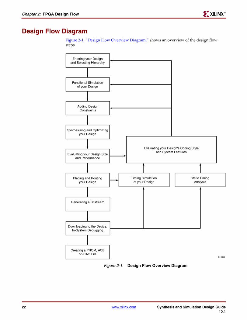
Design Flow DiagramFigure 2-1, “Design Flow Overview Diagram,” shows an overview of the design flow steps.
Figure 2-1: Design Flow Overview Diagram
X10303
Entering your Designand Selecting Hierarchy
Functional Simulationof your Design
Synthesizing and Optimizingyour Design
Adding DesignConstraints
Evaluating your Design Sizeand Performance
Placing and Routingyour Design
Downloading to the Device,In-System Debugging
Generating a Bitstream
Creating a PROM, ACEor JTAG File
Evaluating your Design's Coding Styleand System Features
Timing Simulationof your Design
Static TimingAnalysis
Synthesis and Simulation Design Guide www.xilinx.com 2310.1
Design Entry RecommendationsR
Design Entry RecommendationsThis section discusses Design Entry Recommendations, and includes:
• “Use Register Transfer Level (RTL) Code”
• “Select the Correct Design Hierarchy”
Use Register Transfer Level (RTL) CodeUse Register Transfer Level (RTL) code, and, when possible, do not instantiate specific components. Following these two practices allows for:
• Readable code
• Ability to use the same code for synthesis and simulation
• Faster and simpler simulation
• Portable code for migration to different device families
• Reusable code for future designs
In some cases instantiating optimized CORE Generator™ modules is beneficial with RTL.
Select the Correct Design HierarchySelect the correct design hierarchy to:
• Improve simulation and synthesis results
• Improve debugging
• Allow parallel engineering, in which a team of engineers can work on different parts of the design at the same time
• Improve the placement and routing by reducing routing congestion and improving timing
• Allow for easier code reuse in the current design, as well as in future designs
Architecture WizardThis section discusses Architecture Wizard, and includes:
• “Using Architecture Wizard”
• “Opening Architecture Wizard”
• “Architecture Wizard Components”
Using Architecture WizardUse Architecture Wizard to configure advanced features of Xilinx® devices. Architecture Wizard consists of several components for configuring specific device features. Each component functions as an independent wizard. For more information, see “Architecture Wizard Components.”
Architecture Wizard creates a VHDL, Verilog, or Electronic Data Interchange Format (EDIF) file, depending on the flow type passed to it. The generated Hardware Description Language (HDL) output is a module consisting of one or more primitives and the corresponding properties, and not just a code snippet. This allows the output file to be
24 www.xilinx.com Synthesis and Simulation Design Guide10.1
Chapter 2: FPGA Design FlowR
referenced from the HDL Editor. No User Constraints File (UCF) is output, since the necessary attributes are embedded inside the HDL file.
Opening Architecture WizardThere are three ways to open the Architecture Wizard:
• Open Architecture Wizard from Project Navigator
For information on opening Architecture Wizard in ISE, see the ISE Help, especially Working with Architecture Wizard IP.
• Open Architecture Wizard from CORE Generator
To open the Architecture Wizard from CORE Generator, select any of the Architecture Wizard IP from the list of available IP in the CORE Generator window.
• Open Architecture Wizard from the Command Line
To open Architecture Wizard from the command line, type arwz.
Architecture Wizard ComponentsThis section discusses Architecture Wizard Components, and includes the following:
• “Clocking Wizard”
• “RocketIO Wizard”
• “ChipSync Wizard”
• “XtremeDSP Slice Wizard”
Clocking Wizard
The Clocking Wizard enables:
• Digital clock setup
• DCM and clock buffer viewing
• DRC checking
The Clocking Wizard allows you to:
• View the DCM component
• Specify attributes
• Generate corresponding components and signals
• Execute DRC checks
• Display up to eight clock buffers
• Set up the Feedback Path information
• Set up the Clock Frequency Generator information and execute DRC checks
• View and edit component attributes
• View and edit component constraints
• View and configure one or two Phase Matched Clock Dividers (PMCDs) in a Virtex™-4 device
• View and configure a Phase Locked Loop (PLL) in a Virtex-5 device
Synthesis and Simulation Design Guide www.xilinx.com 2510.1
Architecture WizardR
• Automatically place one component in the XAW file
• Save component settings in a VHDL file
• Save component settings in a Verilog file
RocketIO Wizard
The RocketIO Wizard enables serial connectivity between devices, backplanes, and subsystems.
The RocketIO Wizard allows you to:
• Specify RocketIO type
• Define Channel Bonding options
• Specify General Transmitter Settings, including encoding, CRC, and clock
• Specify General Receptor Settings, including encoding, CRC, and clock
• Provide the ability to specify Synchronization
• Specify Equalization, Signal integrity tip (resister, termination mode...)
• View and edit component attributes
• View and edit component constraints
• Automatically place one component in the XAW file
• Save component settings to a VHDL file or Verilog file
ChipSync Wizard
The ChipSync Wizard applies to Virtex-4 and Virtex-5 devices only.
The ChipSync Wizard:
• Facilitates the implementation of high-speed source synchronous applications.
• Configures a group of I/O blocks into an interface for use in memory, networking, or any other type of bus interface.
• Creates Hardware Description Language (HDL) code with these features configured according to your input:
♦ Width and IO standard of data, address, and clocks for the interface
♦ Additional pins such as reference clocks and control pins
♦ Adjustable input delay for data and clock pins
♦ Clock buffers (BUFIO) for input clocks
♦ ISERDES/OSERDES or IDDR/ODDR blocks to control the width of data, clock enables, and tristate signals to the fabric
XtremeDSP Slice Wizard
The XtremeDSP Slice Wizard applies to Virtex-4 and Virtex-5 devices only.
The XtremeDSP Slice Wizard facilitates the implementation of the XtremeDSP Slice. For more information, see the Virtex-4 and Virtex-5 data sheets, the XtremeDSP for Virtex-4 FPGAs User Guide, and the Virtex-5 XtremeDSP User Guide, both available from the Xilinx user guide web page.
26 www.xilinx.com Synthesis and Simulation Design Guide10.1
Chapter 2: FPGA Design FlowR
CORE GeneratorThis section discusses CORE Generator™, and includes:
• “About CORE Generator”
• “CORE Generator Files”
About CORE GeneratorCORE Generator delivers parameterized Intellectual Property (IP) optimized for Xilinx FPGA devices. It provides a catalog of ready-made functions ranging in complexity from FIFOs and memories to high level system functions. High level system functions can include:
• Reed-Soloman Decoder and Encoder
• FIR filters
• FFTs for DSP applications
• Standard bus interfaces (for example, PCI and PCI-X)
• Connectivity and networking interfaces (for example, Ethernet, SPI-4.2, and PCI Express)
CORE Generator FilesFor a typical core, CORE Generator produces the following files:
• “Electronic Data Interchange Format Netlist (EDN) and NGC Files”
• “VHDL Template (VHO) Files”
• “Verilog Template (VEO) Files”
• “V (Verilog) and VHD (VHDL) Wrapper Files”
• “ASY (ASCII Symbol) Files”
Electronic Data Interchange Format Netlist (EDN) and NGC Files
The Electronic Data Interchange Format (Electronic Data Interchange Format (EDIF) Netlist (EDN) file and NGC files contain the information required to implement the module in a Xilinx FPGA. Since NGC files are in binary format, ASCII NDF files may also be produced to communicate resource and timing information for NGC files to third party synthesis tools. The NDF file is read by the synthesis tool only and is not used for implementation.
VHDL Template (VHO) Files
VHDL template (VHO) template files contain code that can be used as a model for instantiating a CORE Generator module in a VHDL design. VHO files come with a VHDL (VHD) wrapper file.
Verilog Template (VEO) Files
Verilog template (VEO) files contain code that can be used as a model for instantiating a CORE Generator module in a Verilog design. VEO files come with a Verilog (V) wrapper file.
Synthesis and Simulation Design Guide www.xilinx.com 2710.1
Functional SimulationR
V (Verilog) and VHD (VHDL) Wrapper Files
V (Verilog) and VHD (VHDL) wrapper files support functional simulation. These files contain simulation model customization data that is passed to a parameterized simulation model for the core. In the case of Verilog designs, the V wrapper file also provides the port information required to integrate the core into a Verilog design for synthesis.
Some cores may generate actual source code or an additional top level Hardware Description Language (HDL) wrapper with clocking resource and IOB instances to enable you to tailor your clocking scheme to your own requirements. For more information, see the core-specific documentation.
The V and VHD wrapper files mainly support simulation and are not synthesizable.
ASY (ASCII Symbol) Files
ASY (ASCII Symbol) symbol information files allow you to integrate the CORE Generator modules into a schematic design for Mentor or ISE tools.
Functional SimulationUse functional or Register Transfer Level (RTL) simulation to verify syntax and functionality.
When you simulate your design, Xilinx recommends that you:
• Perform Separate Simulations
With larger hierarchical Hardware Description Language (HDL) designs, perform separate simulations on each module before testing your entire design. This makes it easier to debug your code.
• Create a Test Bench
Once each module functions as expected, create a test bench to verify that your entire design functions as planned. Use the same test bench again for the final timing simulation to confirm that your design functions as expected under worst-case delay conditions.
You can use ModelSim simulators with Project Navigator. The appropriate processes appear in Project Navigator when you choose ModelSim as your design simulator, provided you have installed any of the following:
• ModelSim Xilinx Edition III
• ModelSim SE or ModelSim PE
You can also use these simulators with third-party synthesis tools in Project Navigator.
Synthesizing and OptimizingThis section discusses Synthesizing and Optimizing, and includes:
• “Creating a Compile Run Script”
• “Modifying Your Code to Successfully Synthesize Your Design”
• “Reading Cores”
See the following recommendations for compiling your designs to improve your results and decrease the run time. For more information, see your synthesis tool documentation.
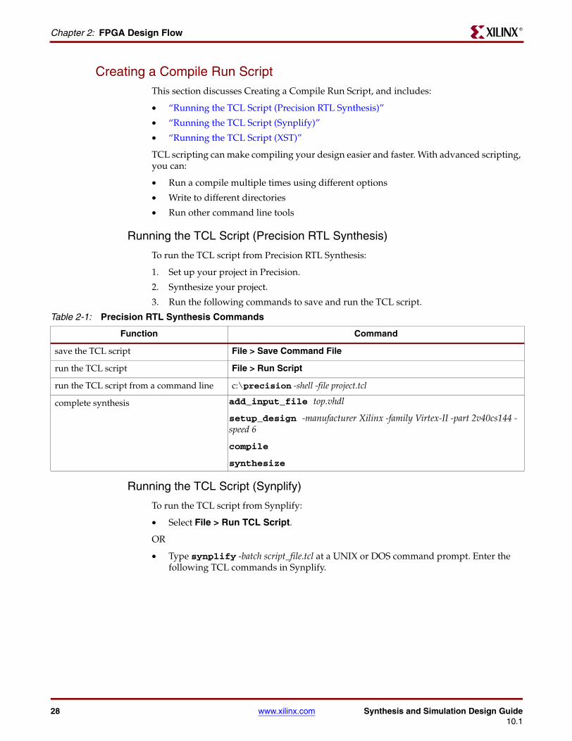
28 www.xilinx.com Synthesis and Simulation Design Guide10.1
Chapter 2: FPGA Design FlowR
Creating a Compile Run ScriptThis section discusses Creating a Compile Run Script, and includes:
• “Running the TCL Script (Precision RTL Synthesis)”
• “Running the TCL Script (Synplify)”
• “Running the TCL Script (XST)”
TCL scripting can make compiling your design easier and faster. With advanced scripting, you can:
• Run a compile multiple times using different options
• Write to different directories
• Run other command line tools
Running the TCL Script (Precision RTL Synthesis)
To run the TCL script from Precision RTL Synthesis:
1. Set up your project in Precision.
2. Synthesize your project.
3. Run the following commands to save and run the TCL script.
Running the TCL Script (Synplify)
To run the TCL script from Synplify:
• Select File > Run TCL Script.
OR
• Type synplify -batch script_file.tcl at a UNIX or DOS command prompt. Enter the following TCL commands in Synplify.
Table 2-1: Precision RTL Synthesis Commands
Function Command
save the TCL script File > Save Command File
run the TCL script File > Run Script
run the TCL script from a command line c:\precision -shell -file project.tcl
complete synthesis add_input_file top.vhdl
setup_design -manufacturer Xilinx -family Virtex-II -part 2v40cs144 -speed 6
compile
synthesize
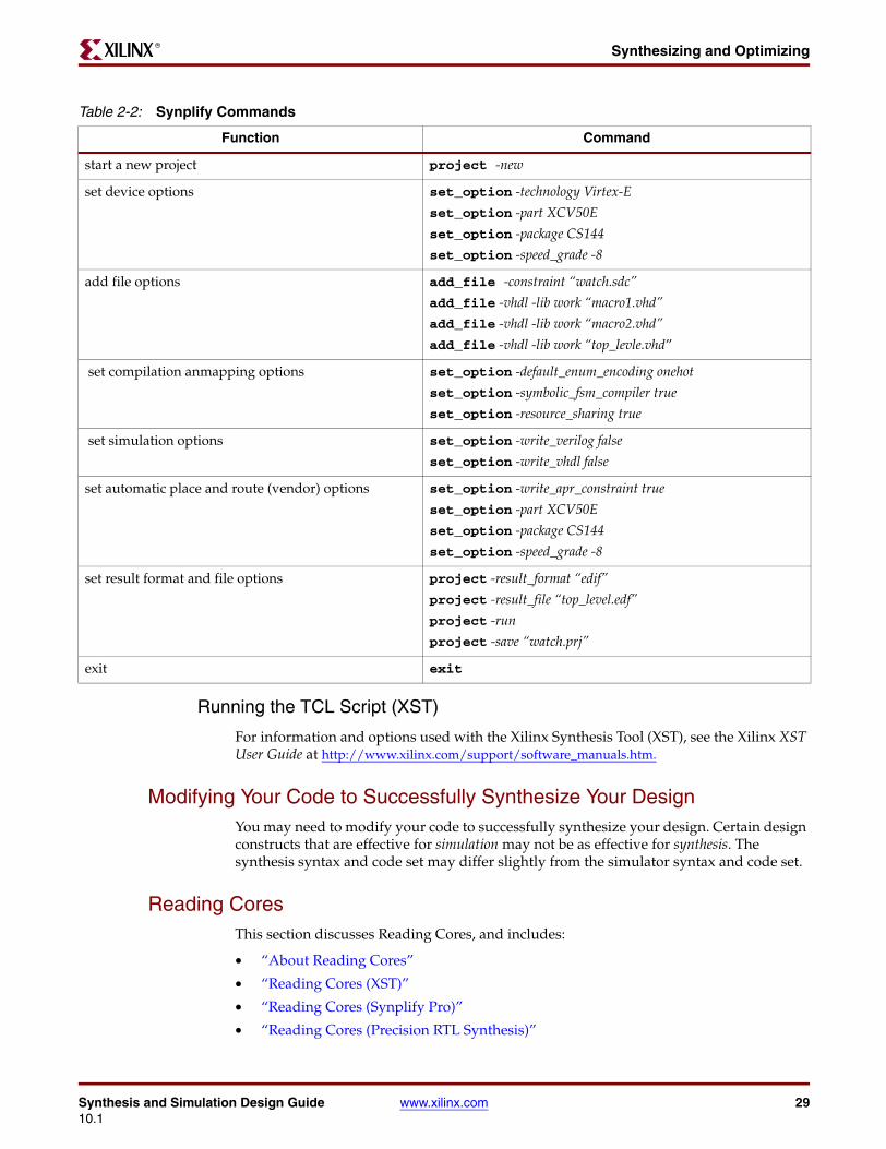
Synthesis and Simulation Design Guide www.xilinx.com 2910.1
Synthesizing and OptimizingR
Running the TCL Script (XST)
For information and options used with the Xilinx Synthesis Tool (XST), see the Xilinx XST User Guide at http://www.xilinx.com/support/software_manuals.htm.
Modifying Your Code to Successfully Synthesize Your DesignYou may need to modify your code to successfully synthesize your design. Certain design constructs that are effective for simulation may not be as effective for synthesis. The synthesis syntax and code set may differ slightly from the simulator syntax and code set.
Reading CoresThis section discusses Reading Cores, and includes:
• “About Reading Cores”
• “Reading Cores (XST)”
• “Reading Cores (Synplify Pro)”
• “Reading Cores (Precision RTL Synthesis)”
Table 2-2: Synplify Commands
Function Command
start a new project project -new
set device options set_option -technology Virtex-E
set_option -part XCV50E
set_option -package CS144
set_option -speed_grade -8
add file options add_file -constraint “watch.sdc”
add_file -vhdl -lib work “macro1.vhd”
add_file -vhdl -lib work “macro2.vhd”
add_file -vhdl -lib work “top_levle.vhd”
set compilation anmapping options set_option -default_enum_encoding onehot
set_option -symbolic_fsm_compiler true
set_option -resource_sharing true
set simulation options set_option -write_verilog false
set_option -write_vhdl false
set automatic place and route (vendor) options set_option -write_apr_constraint true
set_option -part XCV50E
set_option -package CS144
set_option -speed_grade -8
set result format and file options project -result_format “edif”
project -result_file “top_level.edf”
project -run
project -save “watch.prj”
exit exit
30 www.xilinx.com Synthesis and Simulation Design Guide10.1
Chapter 2: FPGA Design FlowR
About Reading Cores
The synthesis tools discussed in this section support incorporating the information in CORE Generator NDF files when performing design timing and area analysis.
Including the IP core NDF files in a design when analyzing a design results in better timing and resource optimizations for the surrounding logic. The NDF is used to estimate the delay through the logic elements associated with the IP core. The synthesis tools do not optimize the IP core itself, nor do they integrate the IP core netlist into the synthesized design output netlist.
Reading Cores (XST)
Run XST using the read_cores switch. When the switch is set to on (the default), XST reads in Electronic Data Interchange Format (EDIF) and NGC netlists. For more information, see:
• Xilinx XST User Guide at http://www.xilinx.com/support/software_manuals.htm
• Project Navigator help
Reading Cores (Synplify Pro)
When reading cores in Synplify Pro, Electronic Data Interchange Format (EDIF) is treated as another source format, but when reading in EDIF, you must specify the top level VHDL or Verilog in your project.
Reading Cores (Precision RTL Synthesis)
Precision RTL Synthesis can add Electronic Data Interchange Format (EDIF) and NGC files to your project as source files. For more information, see the Precision RTL Synthesis help.
Setting ConstraintsThis section discusses Setting Constraints, and includes:
• “Advantages of Setting Constraints”
• “Specifying Constraints in the User Constraints File (UCF)”
• “Setting Constraints in ISE”
Advantages of Setting ConstraintsSetting constraints:
• Allows you to control timing optimization
• Uses synthesis tools and implementation processes more efficiently
• Helps minimize runtime and achieve your design requirements
Precision RTL Synthesis and Synplify constraints editors allow you to apply constraints to your Hardware Description Language (HDL) design. For more information, see your synthesis tool documentation.
You can add the following constraints:
• Clock frequency or cycle and offset
• Input and Output timing
Synthesis and Simulation Design Guide www.xilinx.com 3110.1
Evaluating Design Size and PerformanceR
• Signal Preservation
• Module constraints
• Buffering ports
• Path timing
• Global timing
Specifying Constraints in the User Constraints File (UCF)Constraints defined for synthesis can also be passed to implementation in a Netlist Constraints File (NCF) or the output Electronic Data Interchange Format (EDIF) file. However, Xilinx recommends that you do not pass these constraints to implementation. Instead, specify your constraints separately in a User Constraints File (UCF). The UCF gives you tight control over the overall specifications by giving you the ability to:
• Access more types of constraints
• Define precise timing paths
• Prioritize signal constraints
For recommendations on constraining synthesis and implementation, see “Design Considerations.”For information on specific timing constraints, together with syntax examples, see the Xilinx Constraints Guide at http://www.xilinx.com/support/software_manuals.htm.
Setting Constraints in ISEYou can set constraints in ISE with:
• Constraints Editor
• Floorplanner
• PACE
• Floorplan Editor
For more information, see the ISE Help.
Evaluating Design Size and PerformanceThis section discusses Evaluating Design Size and Performance, and includes:
• “Meeting Design Parameters”
• “Estimating Device Utilization and Performance”
• “Determining Actual Device Utilization and Pre-Routed Performance”
Meeting Design ParametersYour design must:
• Function at the specified speed
• Fit in the targeted device
After your design is compiled, use the reporting options of your synthesis tool to determine preliminary device utilization and performance. After your design is mapped by the Xilinx tools, you can determine the actual device utilization.
32 www.xilinx.com Synthesis and Simulation Design Guide10.1
Chapter 2: FPGA Design FlowR
At this point, you should verify that:
• Your chosen device is large enough to accommodate any future changes or additions
• Your design performs as specified
Estimating Device Utilization and PerformanceUse the area and timing reporting options of your synthesis tool to estimate device utilization and performance. After compiling, use the report area command to obtain a report of device resource utilization. Some synthesis tools provide area reports automatically. For correct command syntax, see your synthesis tool documentation.
The device utilization and performance report lists the compiled cells in your design, as well as information on how your design is mapped in the FPGA. These reports are usually accurate because the synthesis tool creates the logic from your code and maps your design into the FPGA. These reports are different for the various synthesis tools. Some reports specify the minimum number of CLBs required, while other reports specify the “unpacked” number of CLBs to make an allowance for routing. For an accurate comparison, compare reports from the Xilinx mapper tool after implementation.
Any instantiated components, such as CORE Generator modules, Electronic Data Interchange Format (EDIF) files, or other components that your synthesis tool does not recognize during compilation, are not included in the report file. If you include these components, you must include the logic area used by these components when estimating design size. Sections may be trimmed during mapping, resulting in a smaller design.
Use the timing report command of your synthesis tool to obtain a report with estimated data path delays. For more information, see your synthesis tool documentation.
The timing report is based on the logic level delays from the cell libraries and estimated wire-load models. While this report estimates how close you are to your timing goals, it is not the actual timing. An accurate timing report is available only after the design is placed and routed.
Determining Actual Device Utilization and Pre-Routed Performance This section discusses Determining Actual Device Utilization and Pre-Routed Performance, and includes:
• “Determining If Your Design Fits the Specified Device”
• “Mapping Your Design Using Project Navigator”
• “Mapping Your Design Using the Command Line”
Determining If Your Design Fits the Specified Device
To determine if your design fits the specified device, map it using the Xilinx Map program. The generated report file design_name.mrp contains the implemented device utilization information. To read the report file, double-click Map Report in the Project Navigator Processes window. Run the Map program from Project Navigator or from the command line.
Synthesis and Simulation Design Guide www.xilinx.com 3310.1
Evaluating Design Size and PerformanceR
Mapping Your Design Using Project Navigator
To map your design using Project Navigator:
1. Go to the Processes window.
2. Click the plus (+) symbol in front of Implement Design.
3. Double-click Map.
4. To view the Map Report, double-click Map Report.
If the report does not exist, it is generated at this time. A green check mark in front of the report name indicates that the report is up-to-date, and no processing is performed.
5. If the report is not up-to-date:
a. Click the report name.
b. Select Process > Rerun to update the report.
The auto-make process automatically runs only the necessary processes to update the report before displaying it.
Alternatively, you may select Process > Rerun All to re-run all processes (even those processes that are up-to-date) from the top of the design to the stage where the report would be.
6. View the Logic Level Timing Report with the Report Browser. This report shows design performance based on logic levels and best-case routing delays.
7. Run the integrated Timing Analyzer to create a more specific report of design paths (optional).
8. Use the Logic Level Timing Report and any reports generated with the Timing Analyzer or the Map program to evaluate how close you are to your performance and utilization goals.
Use these reports to decide whether to proceed to the place and route phase of implementation, or to go back and modify your design or implementation options to attain your performance goals. You should have some slack in routing delays to allow the place and route tools to successfully complete your design. Use the verbose option in the Timing Analyzer to see block-by-block delay. The timing report of a mapped design (before place and route) shows block delays, as well as minimum routing delays.
A typical Virtex, Virtex-E, Virtex-II, Virtex-II Pro, Virtex-4, or Virtex-5 design should allow 40% of the delay for logic, and 60% of the delay for routing. If most of your time is taken by logic, the design will probably not meet timing after place and route.
Mapping Your Design Using the Command Line
For available options, enter the trce command at the command line without any arguments.
To map your design using the command line:
1. To translate your design, run:
ngdbuild -p target_device design_name.edf (or ngc)
2. To map your design, run:
map design_name.ngd
34 www.xilinx.com Synthesis and Simulation Design Guide10.1
Chapter 2: FPGA Design FlowR
3. Use a text editor to view the Device Summary section of the Map Report <design_name.mrp>.
The Device Summary section contains the device utilization information.
4. Run a timing analysis of the logic level delays from your mapped design as follows:
trce [options] design_name.ncd
Use the Trace reports to:
• See how well the design meets performance goals
• Decide whether to proceed to place and route, or to modify your design or implementation options
Leave some slack in routing delays to allow the place and route tools to successfully complete your design.
Evaluating Coding Style and System FeaturesThis section discusses Evaluating Coding Style and System Features, and includes:
• “Modifying Code to Improve Design Performance”
• “Using FPGA System Features”
• “Using Xilinx-Specific Features of Your Synthesis Tool”
If you are not satisfied with your design performance, re-evaluate your code and make any necessary improvements. Modifying your code and selecting different compiler options can dramatically improve device utilization and speed.
Modifying Code to Improve Design PerformanceTo improve design performance:
1. Reduce levels of logic to improve timing by:
a. Using pipelining and retiming techniques
b. Rewriting the Hardware Description Language (HDL) descriptions
c. Enabling or disabling resource sharing
2. Restructure logic to redefine hierarchical boundaries to help the compiler optimize design logic
3. Perform logic replication to reduce critical nets fanout to improve placement and reduce congestion
4. Take advantage of device resource with the CORE Generator modules
Using FPGA System FeaturesAfter correcting any coding problems, use the following FPGA system features to improve resource utilization and enhance the speed of critical paths:
• Use clock enables.
• Use one-hot encoding for large or complex state machines.
• Use I/O registers when applicable.
Synthesis and Simulation Design Guide www.xilinx.com 3510.1
Placing and RoutingR
• Use dedicated shift registers.
• In Virtex-II and Virtex-II Pro devices, use dedicated multipliers.
• In Virtex-4 and Virtex-5 devices, use the dedicated DSP blocks.
Each device family has a unique set of system features. For more information about the system features available for your target device, see the device data sheet.
Using Xilinx-Specific Features of Your Synthesis ToolUsing the Xilinx-specific features of your synthesis tool allows better control over:
• The logic generated
• The number of logic levels
• The architecture elements used
• Fanout
If design performance is more than a few percentage points away from design requirements, advanced algorithms in the place and route (PAR) tool now make it more efficient to use your synthesis tool to achieve design performance. Most synthesis tools have special options for Xilinx-specific features.
For more information, see your synthesis tool documentation.
Placing and RoutingThe overall goal when placing and routing your design is fast implementation and high-quality results. You may not always accomplish this goal:
• Early in the design cycle, run time is usually more important than quality of results. Later in the design cycle, the reverse is usually true.
• If the targeted device is highly utilized, the routing may become congested, and your design may be difficult to route. In this case, the placer and router may take longer to meet your timing requirements.
• If design constraints are rigorous, it may take longer to correctly place and route your design, and meet the specified timing.
For more information, see the Xilinx Development System Reference Guide at http://www.xilinx.com/support/software_manuals.htm
Timing SimulationTiming simulation is important in verifying circuit operation after the worst-case placed and routed delays are calculated. In many cases, you can use the same test bench that you used for functional simulation to perform a more accurate simulation with less effort. Compare the results from the two simulations to verify that your design is performing as initially specified. The Xilinx tools create a VHDL or Verilog simulation netlist of your placed and routed design, and provide libraries that work with many common Hardware Description Language (HDL) simulators. For more information, see “Simulating Your Design.”
Timing-driven PAR is based on TRACE, the Xilinx timing analysis tool. TRACE is an integrated static timing analysis, and does not depend on input stimulus to the circuit. Placement and routing are executed according to the timing constraints that you specified
36 www.xilinx.com Synthesis and Simulation Design Guide10.1
Chapter 2: FPGA Design FlowR
at the beginning of the design process. TRACE interacts with PAR to make sure that the timing constraints you imposed are met.
If there are timing constraints, TRACE generates a report based on those constraints. If there are no timing constraints, TRACE can optionally generate a timing report containing:
• An analysis that enumerates all clocks and the required OFFSETs for each clock
• An analysis of paths having only combinatorial logic, ordered by delay
For more information on TRACE, see the Xilinx Development System Reference Guide at http://www.xilinx.com/support/software_manuals.htm. For more information on Timing Analysis, see the ISE Timing Analyzer Help.
Synthesis and Simulation Design Guide www.xilinx.com 3710.1
R
Chapter 3
General Recommendations for Coding Practices
This chapter (General Recommendations for Coding Practices) contains general information relating to HDL coding styles and design examples to help you develop an efficient coding style. For specific information relating to coding for FPGA devices, see “Coding for FPGA Flow.” This chapter includes:
• “Designing With Hardware Description Languages (HDLs)”
• “Naming, Labeling, and General Coding Styles”
• “Specifying Constants”
• “TRANSLATE_OFF and TRANSLATE_ON”
Designing With Hardware Description Languages (HDLs)Hardware Description Languages (HDLs) contain many complex constructs that may be difficult to understand at first. The methods and examples included in HDL guides do not always apply to the design of FPGA devices. If you currently use HDLs to design ASIC devices, your established coding style may unnecessarily increase the number of logic levels in FPGA designs.
HDL synthesis tools implement logic based on the coding style of your design. To learn how to efficiently code with HDLs, you can:
• Attend training classes
• Read reference and methodology notes
• See synthesis guidelines and templates available from Xilinx® and synthesis tool vendors
When coding your designs, remember that HDLs are mainly hardware description languages. You should try to find a balance between the quality of the end hardware results and the speed of simulation.
This chapter will not teach you every aspect of VHDL or Verilog, but it should help you develop an efficient coding style.
38 www.xilinx.com Synthesis and Simulation Design Guide10.1
Chapter 3: General Recommendations for Coding PracticesR
Naming, Labeling, and General Coding StylesThis section discusses Naming, Labeling, and General Coding Styles, and includes:
• “Common Coding Style”
• “Xilinx Naming Conventions”
• “Reserved Names”
• “Naming Guidelines for Signals and Instances”
• “Matching File Names to Entity and Module Names”
• “Naming Identifiers”
• “Instantiating Sub-Modules”
• “Recommended Length of Line”
• “Common File Headers”
• “Indenting and Spacing”
Common Coding StyleXilinx recommends that you and your design team agree on a coding style at the beginning of your project. An established coding style allows you to read and understand code written by your team members. Inefficient coding styles can adversely impact synthesis and simulation, resulting in slow circuits. Because portions of existing HDL designs are often used in new designs, you should follow coding standards that are understood by the majority of HDL designers. This chapter describes recommended coding styles that you should establish before you begin your designs.
Xilinx Naming ConventionsUse Xilinx naming conventions for naming signals, variables, and instances that are translated into nets, buses, and symbols.
• Avoid VHDL keywords (such as entity, architecture, signal, and component), even when coding in Verilog.
• Avoid Verilog keywords (such as module, reg, and wire), even when coding in VHDL. See Annex B of System Verilog Spec version 3.1a.
• A user-generated name should not contain a forward slash (/). The forward slash is usually used to denote a hierarchy separator.
• Names must contain at least one non-numeric character.
• Names must not contain a dollar sign ($).
• Names must not use less-than (<) or greater-than signs (>). These signs are sometimes used to denote a bus index.
Reserved NamesThe following FPGA resource names are reserved. Do not use them to name nets or components.
• Device architecture names (such as CLB, IOB, PAD, and Slice)
• Dedicated pin names (such as CLK and INIT)
• GND and VCC
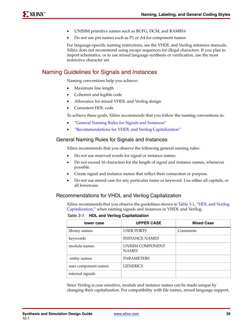
Synthesis and Simulation Design Guide www.xilinx.com 3910.1
Naming, Labeling, and General Coding StylesR
• UNISIM primitive names such as BUFG, DCM, and RAMB16
• Do not use pin names such as P1 or A4 for component names
For language-specific naming restrictions, see the VHDL and Verilog reference manuals. Xilinx does not recommend using escape sequences for illegal characters. If you plan to import schematics, or to use mixed language synthesis or verification, use the most restrictive character set.
Naming Guidelines for Signals and InstancesNaming conventions help you achieve:
• Maximum line length
• Coherent and legible code
• Allowance for mixed VHDL and Verilog design
• Consistent HDL code
To achieve these goals, Xilinx recommends that you follow the naming conventions in:
• “General Naming Rules for Signals and Instances”
• “Recommendations for VHDL and Verilog Capitalization”
General Naming Rules for Signals and Instances
Xilinx recommends that you observe the following general naming rules:
• Do not use reserved words for signal or instance names.
• Do not exceed 16 characters for the length of signal and instance names, whenever possible.
• Create signal and instance names that reflect their connection or purpose.
• Do not use mixed case for any particular name or keyword. Use either all capitals, or all lowercase.
Recommendations for VHDL and Verilog Capitalization
Xilinx recommends that you observe the guidelines shown in Table 3-1, “HDL and Verilog Capitalization,” when naming signals and instances in VHDL and Verilog.
Since Verilog is case sensitive, module and instance names can be made unique by changing their capitalization. For compatibility with file names, mixed language support,
Table 3-1: HDL and Verilog Capitalization
lower case UPPER CASE Mixed Case
library names USER PORTS Comments
keywords INSTANCE NAMES
module names UNISIM COMPONENT NAMES
entity names PARAMETERS
user component names GENERICS
internal signals
40 www.xilinx.com Synthesis and Simulation Design Guide10.1
Chapter 3: General Recommendations for Coding PracticesR
and other tools, Xilinx recommends that you rely on more than just capitalization to make instances unique.
Matching File Names to Entity and Module NamesWhen you name your HDL files:
• Make sure that the VHDL or Verilog source code file name matches the designated name of the entity (VHDL) or module (Verilog) specified in your design file. This is less confusing, and usually makes it easier to create a script file for compiling your design.
• If your design contains more than one entity or module, put each in a separate file with the appropriate file name. For VHDL designs, Xilinx recommends grouping the entity and the associated architecture into the same file.
• Use the same name as your top-level design file for your synthesis script file with either a .do, .scr, .script, or other appropriate default script file extension for your synthesis tool.
Naming IdentifiersFollow these naming practices to make design code easier to debug and reuse:
• Use concise but meaningful identifier names.
• Use meaningful names for wires, regs, signals, variables, types, and any identifier in the code
Example: CONTROL_REGISTER
• Use underscores to make the identifiers easier to read.
Instantiating Sub-ModulesThis section discusses Instantiating Sub-Modules, and includes:
• “Instantiating Sub-Modules Recommendations”
• “Incorrect and Correct VHDL and Verilog Coding Examples”
• “Instantiating Sub-Modules Coding Examples”
Instantiating Sub-Modules Recommendations
Xilinx recommends the following when using instantiating sub-modules:
• Use named association. Named association prevents incorrect connections for the ports of instantiated components.
• Never combine positional and named association in the same statement.
• Use one port mapping per line to:
♦ Improve readability
♦ Provide space for a comment
♦ Allow for easier modification
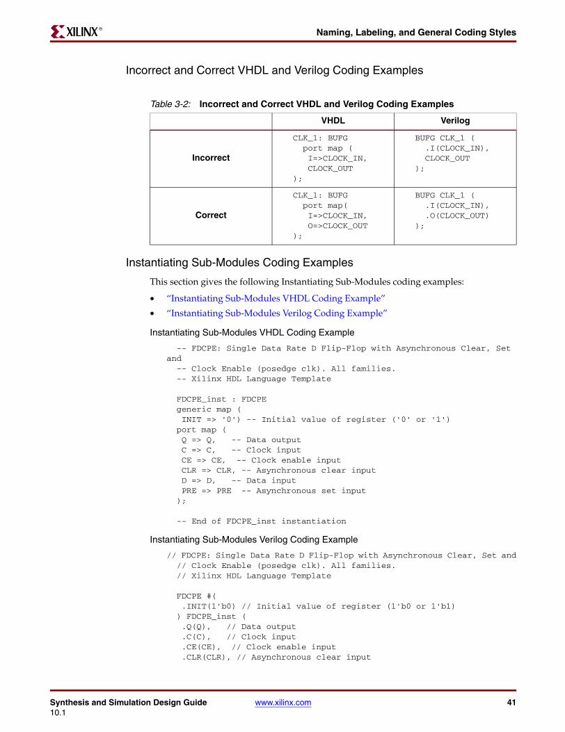
Synthesis and Simulation Design Guide www.xilinx.com 4110.1
Naming, Labeling, and General Coding StylesR
Incorrect and Correct VHDL and Verilog Coding Examples
Instantiating Sub-Modules Coding Examples
This section gives the following Instantiating Sub-Modules coding examples:
• “Instantiating Sub-Modules VHDL Coding Example”
• “Instantiating Sub-Modules Verilog Coding Example”
Instantiating Sub-Modules VHDL Coding Example
-- FDCPE: Single Data Rate D Flip-Flop with Asynchronous Clear, Set and -- Clock Enable (posedge clk). All families. -- Xilinx HDL Language Template FDCPE_inst : FDCPE generic map ( INIT => '0') -- Initial value of register ('0' or '1') port map ( Q => Q, -- Data output C => C, -- Clock input CE => CE, -- Clock enable input CLR => CLR, -- Asynchronous clear input D => D, -- Data input PRE => PRE -- Asynchronous set input ); -- End of FDCPE_inst instantiation
Instantiating Sub-Modules Verilog Coding Example
// FDCPE: Single Data Rate D Flip-Flop with Asynchronous Clear, Set and // Clock Enable (posedge clk). All families. // Xilinx HDL Language Template FDCPE #( .INIT(1'b0) // Initial value of register (1'b0 or 1'b1) ) FDCPE_inst ( .Q(Q), // Data output .C(C), // Clock input .CE(CE), // Clock enable input .CLR(CLR), // Asynchronous clear input
Table 3-2: Incorrect and Correct VHDL and Verilog Coding Examples
VHDL Verilog
Incorrect
CLK_1: BUFG port map ( I=>CLOCK_IN, CLOCK_OUT);
BUFG CLK_1 ( .I(CLOCK_IN), CLOCK_OUT);
Correct
CLK_1: BUFG port map( I=>CLOCK_IN, O=>CLOCK_OUT);
BUFG CLK_1 ( .I(CLOCK_IN), .O(CLOCK_OUT));
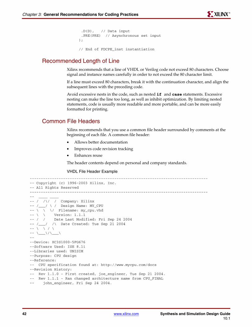
42 www.xilinx.com Synthesis and Simulation Design Guide10.1
Chapter 3: General Recommendations for Coding PracticesR
.D(D), // Data input .PRE(PRE) // Asynchronous set input ); // End of FDCPE_inst instantiation
Recommended Length of LineXilinx recommends that a line of VHDL or Verilog code not exceed 80 characters. Choose signal and instance names carefully in order to not exceed the 80 character limit.
If a line must exceed 80 characters, break it with the continuation character, and align the subsequent lines with the preceding code.
Avoid excessive nests in the code, such as nested if and case statements. Excessive nesting can make the line too long, as well as inhibit optimization. By limiting nested statements, code is usually more readable and more portable, and can be more easily formatted for printing.
Common File HeadersXilinx recommends that you use a common file header surrounded by comments at the beginning of each file. A common file header:
• Allows better documentation
• Improves code revision tracking
• Enhances reuse
The header contents depend on personal and company standards.
VHDL File Header Example
-------------------------------------------------------------------------------- -- Copyright (c) 1996-2003 Xilinx, Inc. -- All Rights Reserved -------------------------------------------------------------------------------- -- ____ ____ -- / /\/ / Company: Xilinx-- /___/ \ / Design Name: MY_CPU -- \ \ \/ Filename: my_cpu.vhd -- \ \ Version: 1.1.1-- / / Date Last Modified: Fri Sep 24 2004-- /___/ /\ Date Created: Tue Sep 21 2004 -- \ \ / \ -- \___\/\___\ -- --Device: XC3S1000-5FG676 --Software Used: ISE 8.1i--Libraries used: UNISIM --Purpose: CPU design --Reference: -- CPU specification found at: http://www.mycpu.com/docs --Revision History: -- Rev 1.1.0 - First created, joe_engineer, Tue Sep 21 2004. -- Rev 1.1.1 - Ran changed architecture name from CPU_FINAL -- john_engineer, Fri Sep 24 2004.
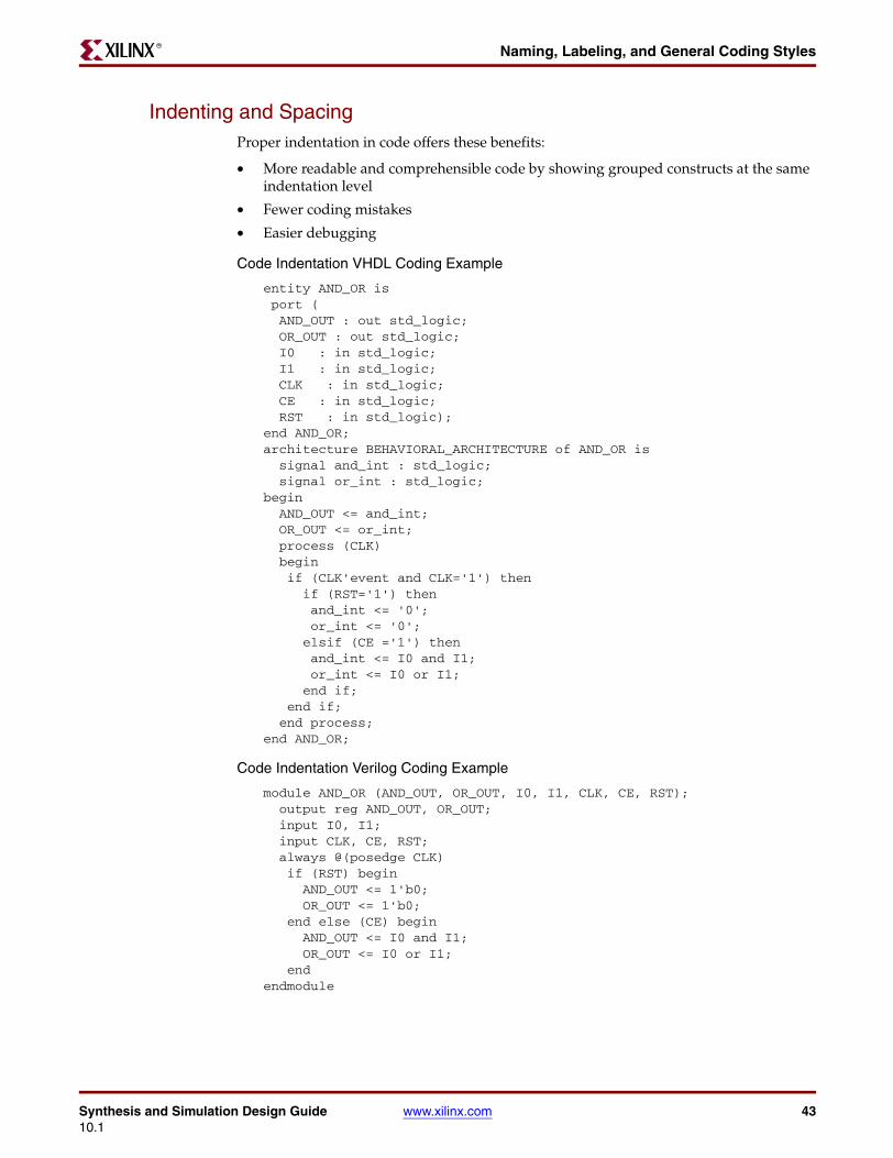
Synthesis and Simulation Design Guide www.xilinx.com 4310.1
Naming, Labeling, and General Coding StylesR
Indenting and SpacingProper indentation in code offers these benefits:
• More readable and comprehensible code by showing grouped constructs at the same indentation level
• Fewer coding mistakes
• Easier debugging
Code Indentation VHDL Coding Example
entity AND_OR is port ( AND_OUT : out std_logic; OR_OUT : out std_logic; I0 : in std_logic; I1 : in std_logic; CLK : in std_logic; CE : in std_logic; RST : in std_logic); end AND_OR; architecture BEHAVIORAL_ARCHITECTURE of AND_OR is signal and_int : std_logic; signal or_int : std_logic;begin AND_OUT <= and_int; OR_OUT <= or_int; process (CLK) begin if (CLK'event and CLK='1') then if (RST='1') then and_int <= '0'; or_int <= '0'; elsif (CE ='1') then and_int <= I0 and I1; or_int <= I0 or I1; end if; end if; end process;end AND_OR;
Code Indentation Verilog Coding Example
module AND_OR (AND_OUT, OR_OUT, I0, I1, CLK, CE, RST); output reg AND_OUT, OR_OUT; input I0, I1; input CLK, CE, RST; always @(posedge CLK) if (RST) begin AND_OUT <= 1'b0; OR_OUT <= 1'b0; end else (CE) begin AND_OUT <= I0 and I1; OR_OUT <= I0 or I1; endendmodule
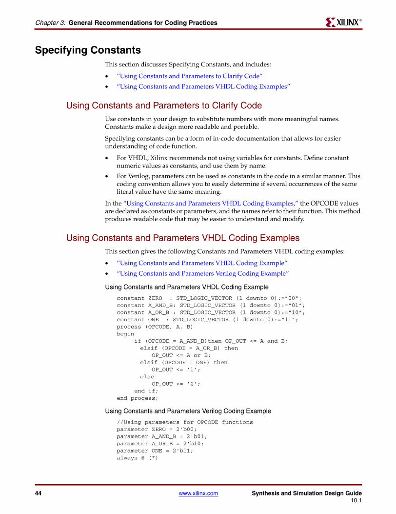
44 www.xilinx.com Synthesis and Simulation Design Guide10.1
Chapter 3: General Recommendations for Coding PracticesR
Specifying ConstantsThis section discusses Specifying Constants, and includes:
• “Using Constants and Parameters to Clarify Code”
• “Using Constants and Parameters VHDL Coding Examples”
Using Constants and Parameters to Clarify CodeUse constants in your design to substitute numbers with more meaningful names. Constants make a design more readable and portable.
Specifying constants can be a form of in-code documentation that allows for easier understanding of code function.
• For VHDL, Xilinx recommends not using variables for constants. Define constant numeric values as constants, and use them by name.
• For Verilog, parameters can be used as constants in the code in a similar manner. This coding convention allows you to easily determine if several occurrences of the same literal value have the same meaning.
In the “Using Constants and Parameters VHDL Coding Examples,” the OPCODE values are declared as constants or parameters, and the names refer to their function. This method produces readable code that may be easier to understand and modify.
Using Constants and Parameters VHDL Coding ExamplesThis section gives the following Constants and Parameters VHDL coding examples:
• “Using Constants and Parameters VHDL Coding Example”
• “Using Constants and Parameters Verilog Coding Example”
Using Constants and Parameters VHDL Coding Example
constant ZERO : STD_LOGIC_VECTOR (1 downto 0):=”00”;constant A_AND_B: STD_LOGIC_VECTOR (1 downto 0):=“01”;constant A_OR_B : STD_LOGIC_VECTOR (1 downto 0):=“10”;constant ONE : STD_LOGIC_VECTOR (1 downto 0):=“11”;process (OPCODE, A, B)begin
if (OPCODE = A_AND_B)then OP_OUT <= A and B; elsif (OPCODE = A_OR_B) then
OP_OUT <= A or B; elsif (OPCODE = ONE) then
OP_OUT <= ‘1’; else
OP_OUT <= ‘0’; end if;
end process;
Using Constants and Parameters Verilog Coding Example
//Using parameters for OPCODE functionsparameter ZERO = 2'b00;parameter A_AND_B = 2'b01;parameter A_OR_B = 2'b10;parameter ONE = 2'b11;always @ (*)
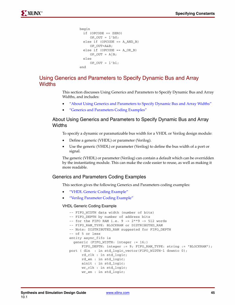
Synthesis and Simulation Design Guide www.xilinx.com 4510.1
Specifying ConstantsR
begin if (OPCODE == ZERO)
OP_OUT = 1'b0;else if (OPCODE == A_AND_B)
OP_OUT=A&B;else if (OPCODE == A_OR_B)
OP_OUT = A|B;else
OP_OUT = 1'b1;end
Using Generics and Parameters to Specify Dynamic Bus and Array Widths
This section discusses Using Generics and Parameters to Specify Dynamic Bus and Array Widths, and includes:
• “About Using Generics and Parameters to Specify Dynamic Bus and Array Widths”
• “Generics and Parameters Coding Examples”
About Using Generics and Parameters to Specify Dynamic Bus and Array Widths
To specify a dynamic or paramatizable bus width for a VHDL or Verilog design module:
• Define a generic (VHDL) or parameter (Verilog).
• Use the generic (VHDL) or parameter (Verilog) to define the bus width of a port or signal.
The generic (VHDL) or parameter (Verilog) can contain a default which can be overridden by the instantiating module. This can make the code easier to reuse, as well as making it more readable.
Generics and Parameters Coding Examples
This section gives the following Generics and Parameters coding examples:
• “VHDL Generic Coding Example”
• “Verilog Parameter Coding Example”
VHDL Generic Coding Example
-- FIFO_WIDTH data width (number of bits)-- FIFO_DEPTH by number of address bits-- for the FIFO RAM i.e. 9 -> 2**9 -> 512 words-- FIFO_RAM_TYPE: BLOCKRAM or DISTRIBUTED_RAM-- Note: DISTRIBUTED_RAM suggested for FIFO_DEPTH-- of 5 or lessentity async_fifo is generic (FIFO_WIDTH: integer := 16;) FIFO_DEPTH: integer := 9; FIFO_RAM_TYPE: string := "BLOCKRAM"); port ( din : in std_logic_vector(FIFO_WIDTH-1 downto 0); rd_clk : in std_logic; rd_en : in std_logic; ainit : in std_logic; wr_clk : in std_logic; wr_en : in std_logic;
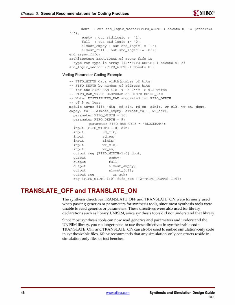
46 www.xilinx.com Synthesis and Simulation Design Guide10.1
Chapter 3: General Recommendations for Coding PracticesR
dout : out std_logic_vector(FIFO_WIDTH-1 downto 0) := (others=> '0'); empty : out std_logic := '1'; full : out std_logic := '0'; almost_empty : out std_logic := '1'; almost_full : out std_logic := '0');end async_fifo;architecture BEHAVIORAL of async_fifo is type ram_type is array ((2**FIFO_DEPTH)-1 downto 0) of std_logic_vector (FIFO_WIDTH-1 downto 0);
Verilog Parameter Coding Example
-- FIFO_WIDTH data width(number of bits)-- FIFO_DEPTH by number of address bits-- for the FIFO RAM i.e. 9 -> 2**9 -> 512 words-- FIFO_RAM_TYPE: BLOCKRAM or DISTRIBUTED_RAM-- Note: DISTRIBUTED_RAM suggested for FIFO_DEPTH-- of 5 or lessmodule async_fifo (din, rd_clk, rd_en, ainit, wr_clk, wr_en, dout, empty, full, almost_empty, almost_full, wr_ack); parameter FIFO_WIDTH = 16; parameter FIFO_DEPTH = 9;
parameter FIFO_RAM_TYPE = "BLOCKRAM"; input [FIFO_WIDTH-1:0] din; input rd_clk; input rd_en; input ainit; input wr_clk; input wr_en; output reg [FIFO_WIDTH-1:0] dout; output empty; output full; output almost_empty; output almost_full; output reg wr_ack; reg [FIFO_WIDTH-1:0] fifo_ram [(2**FIFO_DEPTH)-1:0];
TRANSLATE_OFF and TRANSLATE_ONThe synthesis directives TRANSLATE_OFF and TRANSLATE_ON were formerly used when passing generics or parameters for synthesis tools, since most synthesis tools were unable to read generics or parameters. These directives were also used for library declarations such as library UNISIM, since synthesis tools did not understand that library.
Since most synthesis tools can now read generics and parameters and understand the UNISIM library, you no longer need to use these directives in synthesizable code. TRANSLATE_OFF and TRANSLATE_ON can also be used to embed simulation-only code in synthesizable files. Xilinx recommends that any simulation-only constructs reside in simulation-only files or test benches.
Synthesis and Simulation Design Guide www.xilinx.com 4710.1
R
Chapter 4
Coding for FPGA Flow
This chapter (Coding for FPGA Flow) contains specific information relating to coding for FPGA devices. For general information relating to HDL coding styles and design examples to help you develop an efficient coding style, see “General Recommendations for Coding Practices.” This chapter includes:
• “VHDL and Verilog Limitations”
• “Design Hierarchy”
• “Choosing Data Type”
• “Using `timescale”
• “Mixed Language Designs”
• “If Statements and Case Statements”
• “Sensitivity List in Process and Always Statements”
• “Delays in Synthesis Code”
• “Registers and Latches in FPGA Design”
• “Implementing Shift Registers”
• “Control Signals”
• “Initial State of the Registers, Latches, Shift Registers, and RAMs”
• “Multiplexers”
• “Finite State Machines (FSMs)”
• “Implementing Memory”
• “Block RAM Inference”
• “Distributed RAM Inference”
• “Arithmetic Support”
• “Synthesis Tool Naming Conventions”
• “Instantiating Components and FPGA Primitives”
• “Attributes and Constraints”
• “Pipelining and Retiming”
VHDL and Verilog LimitationsVHDL and Verilog were not originally intended as inputs to synthesis. For this reason, synthesis tools do not support many hardware description and simulation constructs. In addition, synthesis tools may use different subsets of VHDL and Verilog. VHDL and Verilog semantics are well defined for design simulation. The synthesis tools must adhere to these semantics to ensure that designs simulate the same way before and after synthesis.
48 www.xilinx.com Synthesis and Simulation Design Guide10.1
Chapter 4: Coding for FPGA FlowR
Follow the guidelines in the following sections to create code that is most suitable for Xilinx design flow.
Design HierarchyThis section discusses Design Hierarchy, and includes:
• “Advantages and Disadvantages of Hierarchical Designs”
• “Using Synthesis Tools with Hierarchical Designs”
Advantages and Disadvantages of Hierarchical DesignsHardware Description Language (HDL) designs can either be described (synthesized) as a large flat module, or as many small modules. Each methodology has its advantages and disadvantages. As higher density FPGA devices are created, the advantages of hierarchical designs outweigh many of the disadvantages.
Some advantages of hierarchical designs are:
• Provide easier and faster verification and simulation
• Allow several engineers to work on one design at the same time
• Speed up design compilation
• Produce designs that are easier to understand
• Manage the design flow efficiently
Some disadvantages of hierarchical designs are:
• Design mapping into the FPGA may not be optimal across hierarchical boundaries. This can cause lesser device utilization and decreased design performance. If special care is taken, the effect of this can be minimized.
• Design file revision control becomes more difficult.
• Designs become more verbose.
You can overcome most of these disadvantages with careful design consideration when you choose the design hierarchy.
Using Synthesis Tools with Hierarchical DesignsEffectively partitioning your designs can significantly reduce compile time and improve synthesis results. To effectively partition your design:
• “Restrict Shared Resources”
• “Compile Multiple Instances”
• “Restrict Related Combinatorial Logic”
• “Separate Speed Critical Paths”
• “Restrict Combinatorial Logic”
• “Restrict Module Size”
• “Register All Outputs”
• “Restrict One Clock to Each Module or to Entire Design”
Synthesis and Simulation Design Guide www.xilinx.com 4910.1
Design HierarchyR
Restrict Shared Resources
Place resources that can be shared on the same hierarchy level. If these resources are not on the same hierarchy level, the synthesis tool cannot determine if they should be shared.
Compile Multiple Instances
Compile multiple occurrences of the same instance together to reduce the gate count. To increase design speed, do not compile a module in a critical path with other instances.
Restrict Related Combinatorial Logic
Keep related combinatorial logic in the same hierarchical level to allow the synthesis tool to optimize an entire critical path in a single operation. Boolean optimization does not operate across hierarchical boundaries. If a critical path is partitioned across boundaries, logic optimization is restricted. Constraining modules is difficult if combinatorial logic is not restricted to the same hierarchy level.
Separate Speed Critical Paths
To achieve satisfactory synthesis results, locate design modules with different functions at different hierarchy levels. Design speed is the first priority of optimization algorithms. To achieve a design that efficiently utilizes device area, remove timing constraints from design modules.
Restrict Combinatorial Logic
To reduce the number of CLBs used, restrict combinatorial logic that drives a register to the same hierarchical block.
Restrict Module Size
Restrict module size to 100 - 200 CLBs. This range varies based on:
• Your computer configuration
• Whether the design is worked on by a design team
• The target FPGA routing resources
Although smaller blocks give you more control, you may not always obtain the most efficient design. During final compilation, you may want to compile fully from the top down. For more information, see your synthesis tool documentation.
Register All Outputs
Arrange your design hierarchy so that registers drive the module output in each hierarchical block. Registering outputs makes your design easier to constrain, since you only need to constrain the clock period and the ClockToSetup of the previous module. If you have multiple combinatorial blocks at different hierarchy levels, you must manually calculate the delay for each module. Registering the outputs of your design hierarchy can eliminate any possible problems with logic optimization across hierarchical boundaries.
Restrict One Clock to Each Module or to Entire Design
By restricting one clock to each module, you need only to describe the relationship between the clock at the top hierarchy level and each module clock.
50 www.xilinx.com Synthesis and Simulation Design Guide10.1
Chapter 4: Coding for FPGA FlowR
By restricting one clock to the entire design, you need only to describe the clock at the top hierarchy level.
For more information on optimizing logic across hierarchical boundaries and compiling hierarchical designs, see your synthesis tool documentation.
For more information, see Using Partitions in the ISE™ Help.
Choosing Data TypeThis section applies to VHDL only.
This section discusses Choosing Data Type, and includes:
• “Use Std_logic (IEEE 1164)”
• “Declaring Ports”
• “Arrays in Port Declarations.”
• “Minimize Ports Declared as Buffers”
Use Std_logic (IEEE 1164)Use the Std_logic (IEEE 1164) standards for hardware descriptions when coding your design. These standards are recommended for the following reasons:
1. Std_logic applies as a wide range of state values
Std_logic has nine different values that represent most of the states found in digital circuits.
2. Std_logic allows indication of all possible logic states within the FPGA
a. Std_logic not only allows specification of logic high (1) and logic low (0), but also whether a pullup (H) or pulldown (L) is used, or whether an output is in high impedance (Z).
b. Std_logic allows the specification of unknown values (X) due to possible contention, timing violations, or other occurrences, or whether an input or signal is unconnected (U).
c. Std_logic allows a more realistic representation of the FPGA logic for both synthesis and simulation, frequently giving more accurate results.
3. Std_logic easily performs board-level simulation
For example, if you use an integer type for ports for one circuit and standard logic for ports for another circuit, your design can be synthesized. However, you must perform time-consuming type conversions for a board-level simulation.
The back-annotated netlist from Xilinx implementation is in Std_logic. If you do not use Std_logic type to drive your top-level entity in the test bench, you cannot reuse your functional test bench for timing simulation. Some synthesis tools can create a wrapper for type conversion between the two top-level entities. Xilinx does not recommend this practice.
Declaring PortsUse the Std_logic type for all entity port declarations.The Std_logic type makes it easier to integrate the synthesized netlist back into the design hierarchy without requiring
Synthesis and Simulation Design Guide www.xilinx.com 5110.1
Choosing Data TypeR
conversion functions for the ports. The following VHDL coding example uses the Std_logic for port declarations:
Entity alu is port(
A : in STD_LOGIC_VECTOR(3 downto 0); B : in STD_LOGIC_VECTOR(3 downto 0); CLK : in STD_LOGIC; C : out STD_LOGIC_VECTOR(3 downto 0) );
end alu;
If a top-level port is specified as a type other than STD_LOGIC, software generated simulation models (such as timing simulation) may no longer bind to the test bench. This is due to the following factors:
• Type information cannot be stored for a particular design port.
• Simulation of FPGA hardware requires the ability to specify the values of STD_LOGIC such as high-Z (tristate), and X (unknown) in order to properly display hardware behavior.
Xilinx recommends that you not declare arrays as ports. This information cannot be properly represented or re-created. For this reason, Xilinx recommends that you use STD_LOGIC and STD_LOGIC_VECTOR for all top-level port declarations.
Arrays in Port DeclarationsAlthough VHDL allows you to declare a port as an array type, Xilinx recommends that you not do so, for the following reasons:
• “Incompatibility with Verilog”
• “Inability to Store and Re-Create Original Array Declaration”
• “Mis-Correlation of Software Pin Names”
Incompatibility with Verilog
There is no equivalent way to declare a port as an array type in Verilog. Verilog does not allow ports to be declared as arrays. This limits portability across languages. It also limits as the ability to use the code for mixed-language projects.
Inability to Store and Re-Create Original Array Declaration
When you declare a port as an array type in VHDL, the original array declaration cannot be stored and re-created. The Electronic Data Interchange Format (EDIF) netlist format, as well as the Xilinx database, are unable to store the original type declaration for the array.
As a result, when NetGen or another netlister attempts to re-create the design, there is no information as to how the port was originally declared. The resulting netlist generally has mis-matched port declarations and resulting signal names. This is true not only for the top-level port declarations, but also for the lower-level port declarations of a hierarchical design since “KEEP_HIERARCHY” can be used to attempt to preserve those net names.
Mis-Correlation of Software Pin Names
Array port declarations can cause a mis-correlation of the software pin names from the original source code. Since the software must treat each I/O as a separate label, the corresponding name for the broken-out port may not match your expectation. This makes
52 www.xilinx.com Synthesis and Simulation Design Guide10.1
Chapter 4: Coding for FPGA FlowR
design constraint passing, design analysis, and design reporting more difficult to understand.
Minimize Ports Declared as BuffersDo not use buffers when a signal is used internally and as an output port. See the following VHDL coding examples:
• “Signal C Used Internally and As Output Port VHDL Coding Example”
• “Dummy Signal with Port C Declares as Output VHDL Coding Example”
Signal C Used Internally and As Output Port VHDL Coding Example
In the following VHDL coding example, signal C is used internally and as an output port:
Entity alu is port(
A : in STD_LOGIC_VECTOR(3 downto 0); B : in STD_LOGIC_VECTOR(3 downto 0); CLK : in STD_LOGIC; C : buffer STD_LOGIC_VECTOR(3 downto 0) );
end alu;architecture BEHAVIORAL of alu isbegin
process begin if (CLK'event and CLK='1') then
C <= UNSIGNED(A) + UNSIGNED(B) UNSIGNED(C); end if;
end process;end BEHAVIORAL;
Because signal C is used both internally and as an output port, every level of hierarchy in your design that connects to port C must be declared as a buffer. Buffer types are not commonly used in VHDL designs because they can cause errors during synthesis.
Dummy Signal with Port C Declares as Output VHDL Coding Example
To reduce buffer coding in hierarchical designs, insert a dummy signal and declare port C as an output, as shown in the following VHDL coding example:
Entity alu is port(
A : in STD_LOGIC_VECTOR(3 downto 0); B : in STD_LOGIC_VECTOR(3 downto 0); CLK : in STD_LOGIC; C : out STD_LOGIC_VECTOR(3 downto 0));
end alu;architecture BEHAVIORAL of alu is-- dummy signal
signal C_INT : STD_LOGIC_VECTOR(3 downto 0);begin C <= C_INT; process begin if (CLK'event and CLK='1') then
C_INT <= A and B and C_INT;end if;
end process;end BEHAVIORAL;
Synthesis and Simulation Design Guide www.xilinx.com 5310.1
Using `timescaleR
Using `timescaleThis section applies to Verilog only.
All Verilog test bench and source files should contain a ̀ timescale directive, or reference an include file containing a `timescale directive. Place the `timescale directive or reference near the beginning of the source file, and before any module or other design unit definitions in the source file.
Xilinx recommends that you use a `timescale with a resolution of 1ps. Some Xilinx primitive components such as DCM require a 1ps resolution in order to work properly in either functional or timing simulation. There is little or no simulation speed difference for a 1ps resolution as compared to a coarser resolution.
The following `timescale directive is a typical default:
`timescale 1ns / 1ps
Mixed Language DesignsMost FPGA synthesis tools allow you to create projects containing both VHDL and Verilog files. Mixing VHDL and Verilog is restricted to design unit (cell) instantiation only. A VHDL design can instantiate a Verilog module, and a Verilog design can instantiate a VHDL entity.
Since VHDL and Verilog have different features, it is important to follow the rules for creating mixed language projects, including:
• Case sensitivity rules
• How to instantiate a VHDL design unit in a Verilog design
• How to instantiate a Verilog module in a VHDL design
• What data types are permitted
• How generics and parameters must be used
Synthesis tools may differ in mixed language support. For more information, see your synthesis tool documentation.
If Statements and Case StatementsThis section discusses If Statements and Case Statements, and includes:
• “Comparing If Statements and Case Statements”
• “4–to–1 Multiplexer Design With If Statement”
• “4–to–1 Multiplexer Design With Case Statement”
54 www.xilinx.com Synthesis and Simulation Design Guide10.1
Chapter 4: Coding for FPGA FlowR
Comparing If Statements and Case Statements
Most synthesis tools can determine whether the if-elsif conditions are mutually exclusive, and do not create extra logic to build the priority tree.
When writing if statements:
• Make sure that all outputs are defined in all branches of an if statement. If not, it can create latches or long equations on the CE signal. A good way to prevent this is to have default values for all outputs before the if statements.
• Remember that limiting the input signals into an if statement can reduce the number of logic levels. If there are a large number of input signals, determine whether some can be pre-decoded and registered before the if statement.
• Avoid bringing the dataflow into a complex if statement. Only control signals should be generated in complex if-elsif statements.
4–to–1 Multiplexer Design With If StatementThe following coding examples use an if statement in a 4–to–1 multiplexer design:
• “4–to–1 Multiplexer Design With If Statement VHDL Coding Example”
• “4–to–1 Multiplexer Design With If Statement Verilog Coding Example”
4–to–1 Multiplexer Design With If Statement VHDL Coding Example
-- IF_EX.VHDlibrary IEEE;use IEEE.std_logic_1164.all;use IEEE.std_logic_unsigned.all;entity if_ex is
port (SEL: in STD_LOGIC_VECTOR(1 downto 0);A,B,C,D: in STD_LOGIC; MUX_OUT: out STD_LOGIC);
end if_ex;architecture BEHAV of if_ex isbegin
IF_PRO: process (SEL,A,B,C,D) beginif (SEL="00") then MUX_OUT <= A;elsif (SEL="01") then
MUX_OUT <= B; elsif (SEL="10") then
MUX_OUT <= C; elsif (SEL="11") then
MUX_OUT <= D;
Table 4-1: Comparing If Statements and Case Statements
If Statement Case Statement
Creates priority-encoded logic Creates balanced logic
Can contain a set of different expressions Evaluated against a common controlling expression
Use for speed critical paths Use for complex decoding
Synthesis and Simulation Design Guide www.xilinx.com 5510.1
If Statements and Case StatementsR
else MUX_OUT <= '0';
end if;end process; --END IF_PRO
end BEHAV;
4–to–1 Multiplexer Design With If Statement Verilog Coding Example
/////////////////////////////////////////////////// IF_EX.V //// Example of a if statement showing a //// mux created using priority encoded logic //// HDL Synthesis Design Guide for FPGA devices ///////////////////////////////////////////////////module if_ex (input A, B, C, D, input [1:0] SEL, output reg MUX_OUT);always @ (*)
beginif (SEL == 2'b00)
MUX_OUT = A; else if (SEL == 2'b01)
MUX_OUT = B; else if (SEL == 2'b10)
MUX_OUT = C; else if (SEL == 2'b11)
MUX_OUT = D;else
MUX_OUT = 0;end
endmodule
4–to–1 Multiplexer Design With Case StatementThe following coding examples use a case statement for the same multiplexer:
• “4–to–1 Multiplexer Design With Case Statement VHDL Coding Example”
• “4–to–1 Multiplexer Design With Case Statement Verilog Coding Example”
In these examples, the case statement requires only one slice, while the if statement requires two slices in some synthesis tools. In this instance, design the multiplexer using the case statement. Fewer resources are used and the delay path is shorter. When writing case statements, make sure all outputs are defined in all branches.
Figure 4-1, “Case_Ex Implementation Diagram,” shows the implementation of these designs.
4–to–1 Multiplexer Design With Case Statement VHDL Coding Example
-- CASE_EX.VHD-- May 2001library IEEE;use IEEE.std_logic_1164.all;use IEEE.std_logic_unsigned.all;entity case_ex is
port (SEL : in STD_LOGIC_VECTOR(1 downto 0);A,B,C,D: in STD_LOGIC;MUX_OUT: out STD_LOGIC);
56 www.xilinx.com Synthesis and Simulation Design Guide10.1
Chapter 4: Coding for FPGA FlowR
end case_ex;architecture BEHAV of case_ex isbegin
CASE_PRO: process (SEL,A,B,C,D) begin
case SEL iswhen “00” => MUX_OUT <= A;when “01” => MUX_OUT <= B;when “10” => MUX_OUT <= C;when “11” => MUX_OUT <= D;when others => MUX_OUT <= '0';
end case;end process; --End CASE_PRO
end BEHAV;
4–to–1 Multiplexer Design With Case Statement Verilog Coding Example
/////////////////////////////////////////////////// CASE_EX.V //// Example of a Case statement showing //// A mux created using parallel logic //// HDL Synthesis Design Guide for FPGA devices ///////////////////////////////////////////////////module case_ex (input A, B, C, D,input [1:0] SEL,output reg MUX_OUT);
always @ (*) begincase (SEL)2'b00: MUX_OUT = A; 2'b01: MUX_OUT = B; 2'b10: MUX_OUT = C; 2'b11: MUX_OUT = D; default: MUX_OUT = 0;
endcase end
endmodule
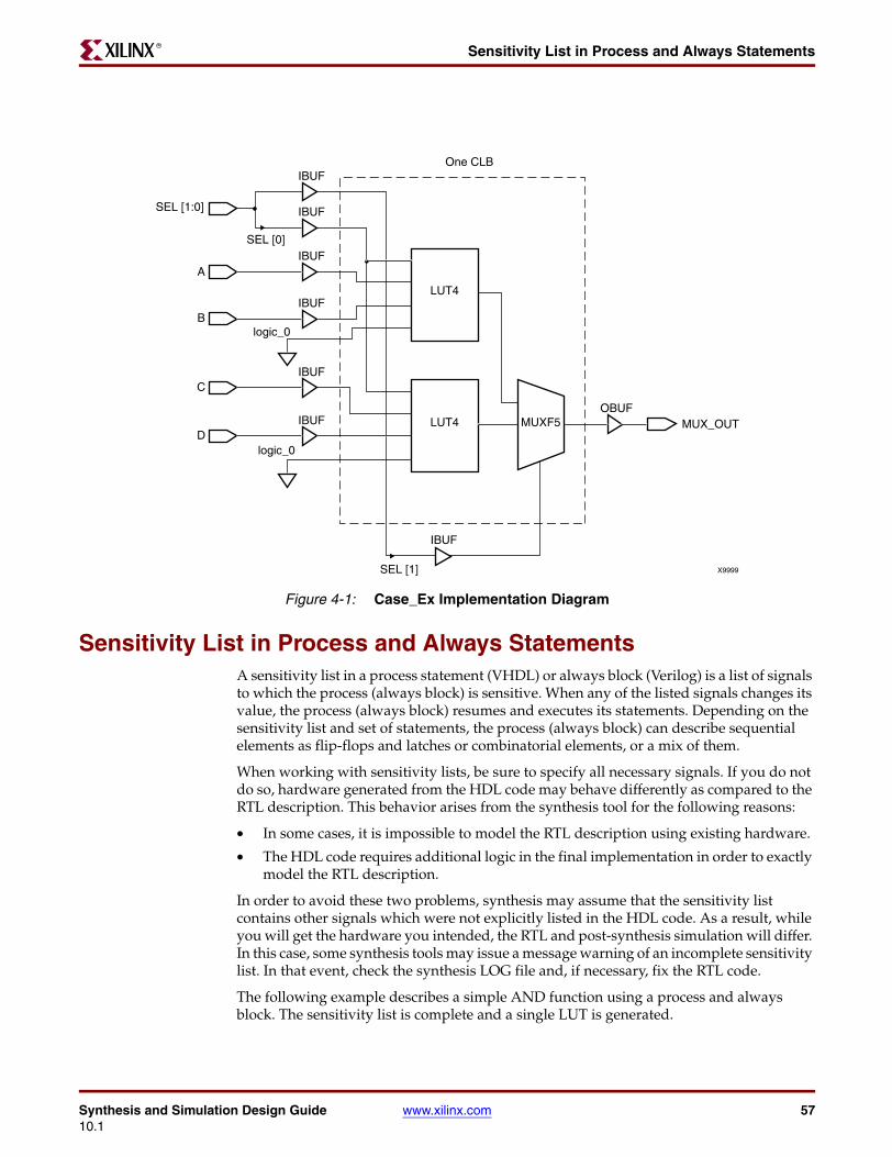
Synthesis and Simulation Design Guide www.xilinx.com 5710.1
Sensitivity List in Process and Always StatementsR
Sensitivity List in Process and Always StatementsA sensitivity list in a process statement (VHDL) or always block (Verilog) is a list of signals to which the process (always block) is sensitive. When any of the listed signals changes its value, the process (always block) resumes and executes its statements. Depending on the sensitivity list and set of statements, the process (always block) can describe sequential elements as flip-flops and latches or combinatorial elements, or a mix of them.
When working with sensitivity lists, be sure to specify all necessary signals. If you do not do so, hardware generated from the HDL code may behave differently as compared to the RTL description. This behavior arises from the synthesis tool for the following reasons:
• In some cases, it is impossible to model the RTL description using existing hardware.
• The HDL code requires additional logic in the final implementation in order to exactly model the RTL description.
In order to avoid these two problems, synthesis may assume that the sensitivity list contains other signals which were not explicitly listed in the HDL code. As a result, while you will get the hardware you intended, the RTL and post-synthesis simulation will differ. In this case, some synthesis tools may issue a message warning of an incomplete sensitivity list. In that event, check the synthesis LOG file and, if necessary, fix the RTL code.
The following example describes a simple AND function using a process and always block. The sensitivity list is complete and a single LUT is generated.
Figure 4-1: Case_Ex Implementation Diagram
IBUF
IBUF
IBUF
IBUF
IBUF
IBUF
IBUF
SEL [1:0]
A
B
C
D
logic_0
logic_0
LUT4
LUT4OBUF
MUX_OUT
SEL [1]
SEL [0]
X9999
One CLB
MUXF5
58 www.xilinx.com Synthesis and Simulation Design Guide10.1
Chapter 4: Coding for FPGA FlowR
VHDL Process Coding Example One
process (a,b)begin
c <= a and b;end process;
Verilog Always Block Coding Example One
always @(a or b)c <= a & b;
The following examples are based on the previous two coding examples, but signal b is omitted from the sensitivity list. In this case, the synthesis tool assumes the presence of b in the sensitivity list and still generates the combinatorial logic (AND function).
VHDL Process Coding Example Two
process (a)begin
c <= a and b;end process;
Verilog Always Block Coding Example One
always @(a)c <= a & b;
Delays in Synthesis CodeThis section discusses Delays in Synthesis Code, and includes:
• “About Delays in Synthesis Code”
• “Delays in Synthesis Code Coding Examples”
About Delays in Synthesis CodeDo not use the Wait for XX ns (VHDL) or the #XX (Verilog) statement in your code. XX specifies the number of nanoseconds that must pass before a condition is executed. This statement does not synthesize to a component. In designs that include this construct, the functionality of the simulated design does not always match the functionality of the synthesized design.
Delays in Synthesis Code Coding ExamplesThis section gives the following Delays in Synthesis Code coding examples:
• “Wait for XX ns Statement VHDL Coding Example”
• “Wait for XX ns Statement Verilog Coding Example”
• “After XX ns Statement VHDL Coding Example”
• “Delay Assignment Verilog Coding Example”
Wait for XX ns Statement VHDL Coding Example
wait for XX ns;
Wait for XX ns Statement Verilog Coding Example
#XX;
Synthesis and Simulation Design Guide www.xilinx.com 5910.1
Registers and Latches in FPGA DesignR
Do not use the ...After XX ns statement in your VHDL code or the Delay assignment in your Verilog code.
After XX ns Statement VHDL Coding Example
(Q <=0 after XX ns)
Delay Assignment Verilog Coding Example
assign #XX Q=0;
XX specifies the number of nanoseconds that must pass before a condition is executed. This statement is usually ignored by the synthesis tool. In this case, the functionality of the simulated design does not match the functionality of the synthesized design.
Registers and Latches in FPGA DesignThis chapter discusses Registers and Latches in FPGA Design and includes:
• “Registers in FPGA Design”
• “IOB Registers”
• “Latches in FPGA Design”
Registers in FPGA DesignThis section discusses Registers in FPGA Design and includes:
• “About Registers in FPGA Design”
• “Registers in FPGA Design Coding Examples”
About Registers in FPGA Design
Xilinx FPGA devices have abundant flip-flops. FPGA architectures support flip-flops with the following control signals:
• Clock Enable
• Asynchronous Set/Reset
• Synchronous Set/Reset
All synthesis tools targeting Xilinx FPGA devices are capable to infer registers with all mentioned above control signals. For more information on control signal usage in FPGA design, see “Control Signals.”
In addition, the value of a flip-flop at device start-up can be set to a logical value 0 or 1. This is known as the initialization state, or INIT. For more information on flip-flop initialization, see ““Initial State of the Registers, Latches, Shift Registers, and RAMs.”
Registers in FPGA Design Coding Examples
This section contains the following Registers in FPGA Design coding examples:
• “Flip-Flop with Positive Edge Clock VHDL Coding Example”
• “Flip-Flop with Positive Edge Clock Verilog Coding Example”
• “Flip-Flop with Positive Edge Clock and Clock Enable VHDL Coding Example”
• “Flip-Flop with Positive Edge Clock and Clock Enable Verilog Coding Example”
60 www.xilinx.com Synthesis and Simulation Design Guide10.1
Chapter 4: Coding for FPGA FlowR
• “Flip-Flop with Negative Edge Clock and Asynchronous Reset VHDL Coding Example”
• “Flip-Flop with Negative Edge Clock and Asynchronous Reset Verilog Coding Example”
• “Flip-Flop with Positive Edge Clock and Synchronous Set VHDL Coding Example”
• “Flip-Flop with Positive Edge Clock and Synchronous Set Verilog Coding Example”
Flip-Flop with Positive Edge Clock VHDL Coding Example
process (C)begin if (C'event and C='1') then Q <= D; end if;end process;
Flip-Flop with Positive Edge Clock Verilog Coding Example
always @(posedge C)begin Q <= D;end
Flip-Flop with Positive Edge Clock and Clock Enable VHDL Coding Example
process (C)begin if (C'event and C='1') then if (CE='1') then Q <= D; end if; end if;end process;
Flip-Flop with Positive Edge Clock and Clock Enable Verilog Coding Example
always @(posedge C)begin if (CE) Q <= D;end
Flip-Flop with Negative Edge Clock and Asynchronous Reset VHDL Coding Example
process (C, CLR)begin if (CLR = '1')then Q <= '0'; elsif (C'event and C='0')then Q <= D; end if;end process;
Synthesis and Simulation Design Guide www.xilinx.com 6110.1
Registers and Latches in FPGA DesignR
Flip-Flop with Negative Edge Clock and Asynchronous Reset Verilog Coding Example
always @(negedge C or posedge CLR)begin if (CLR) Q <= 1'b0; else Q <= D;end
Flip-Flop with Positive Edge Clock and Synchronous Set VHDL Coding Example
process (C)begin if (C'event and C='1') then if (S='1') then Q <= '1'; else Q <= D; end if; end if;end process;
Flip-Flop with Positive Edge Clock and Synchronous Set Verilog Coding Example
always @(posedge C)begin if (S) Q <= 1'b1; else Q <= D;end
IOB RegistersThis section discusses IOB Registers and includes:
• “About IOB Registers”
• “Dual-Data Rate IOB Registers”
About IOB Registers
Input Output Blocks (IOBs) contain several storage elements that can be configured as regular flip-flops or, depending on the FPGA family, as Dual-Data Rate (DDR) registers.
All flip-flops that are to be pushed into the IOB must have a fanout of 1. This applies to output and tristate enable registers. For example, for a 32-bit bidirectional bus, the tristate enable signal must be replicated in the original design so that it has a fanout of 1.
In order to push flip-flops to IOBs, you may use the following methods:
• Use synthesis specific constraint
• Apply IOB=TRUE constraint in UCF file
• Use the –pr command line option in map
Synthesis tools may automatically push flip-flops to IOBs. For more information, see your synthesis tool documentation.
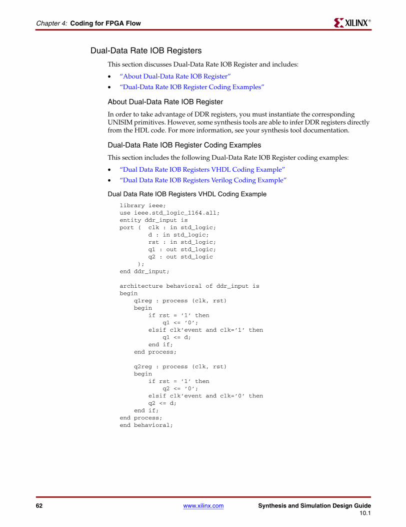
62 www.xilinx.com Synthesis and Simulation Design Guide10.1
Chapter 4: Coding for FPGA FlowR
Dual-Data Rate IOB Registers
This section discusses Dual-Data Rate IOB Register and includes:
• “About Dual-Data Rate IOB Register”
• “Dual-Data Rate IOB Register Coding Examples”
About Dual-Data Rate IOB Register
In order to take advantage of DDR registers, you must instantiate the corresponding UNISIM primitives. However, some synthesis tools are able to infer DDR registers directly from the HDL code. For more information, see your synthesis tool documentation.
Dual-Data Rate IOB Register Coding Examples
This section includes the following Dual-Data Rate IOB Register coding examples:
• “Dual Data Rate IOB Registers VHDL Coding Example”
• “Dual Data Rate IOB Registers Verilog Coding Example”
Dual Data Rate IOB Registers VHDL Coding Example
library ieee; use ieee.std_logic_1164.all;entity ddr_input is port ( clk : in std_logic; d : in std_logic; rst : in std_logic; q1 : out std_logic; q2 : out std_logic );end ddr_input;
architecture behavioral of ddr_input isbegin q1reg : process (clk, rst) begin if rst = ’1’ then q1 <= ’0’; elsif clk’event and clk=’1’ then q1 <= d; end if; end process;
q2reg : process (clk, rst) begin if rst = ’1’ then q2 <= ’0’; elsif clk’event and clk=’0’ then q2 <= d; end if;end process;end behavioral;
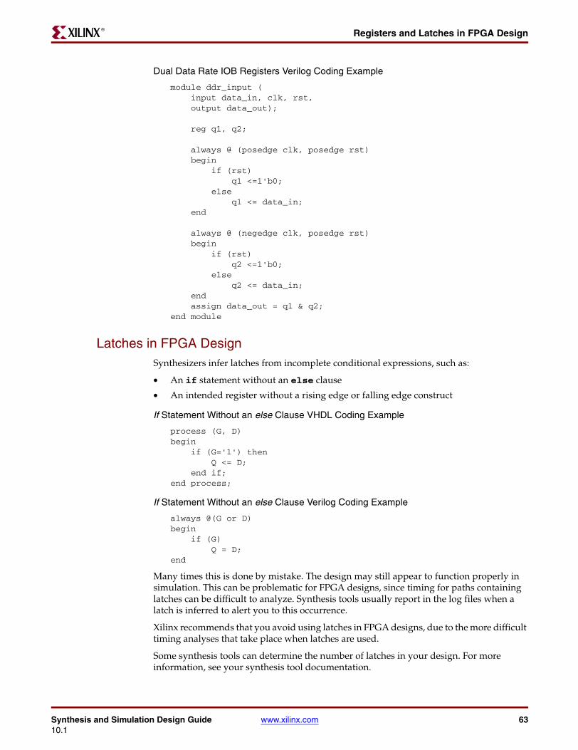
Synthesis and Simulation Design Guide www.xilinx.com 6310.1
Registers and Latches in FPGA DesignR
Dual Data Rate IOB Registers Verilog Coding Example
module ddr_input ( input data_in, clk, rst, output data_out);
reg q1, q2;
always @ (posedge clk, posedge rst) begin if (rst) q1 <=1'b0; else q1 <= data_in; end
always @ (negedge clk, posedge rst) begin if (rst) q2 <=1'b0; else q2 <= data_in; end assign data_out = q1 & q2;end module
Latches in FPGA DesignSynthesizers infer latches from incomplete conditional expressions, such as:
• An if statement without an else clause
• An intended register without a rising edge or falling edge construct
If Statement Without an else Clause VHDL Coding Example
process (G, D)begin if (G='1') then Q <= D; end if;end process;
If Statement Without an else Clause Verilog Coding Example
always @(G or D)begin if (G) Q = D;end
Many times this is done by mistake. The design may still appear to function properly in simulation. This can be problematic for FPGA designs, since timing for paths containing latches can be difficult to analyze. Synthesis tools usually report in the log files when a latch is inferred to alert you to this occurrence.
Xilinx recommends that you avoid using latches in FPGA designs, due to the more difficult timing analyses that take place when latches are used.
Some synthesis tools can determine the number of latches in your design. For more information, see your synthesis tool documentation.
64 www.xilinx.com Synthesis and Simulation Design Guide10.1
Chapter 4: Coding for FPGA FlowR
You should convert all if statements without corresponding else statements and without a clock edge to registers or logic gates. Use the recommended coding styles in the synthesis tool documentation to complete this conversion.
Implementing Shift RegistersThis section discusses Implementing Shift Registers and includes:
• “About Implementing Shift Registers”
• “Describing Shift Registers”
• “Shift Registers Coding Examples”
About Implementing Shift RegistersIn general, a shift register is characterized by the following control and data signals:
• Clock
• Serial input
• Asynchronous set/reset
• Synchronous set/reset
• Synchronous/asynchronous parallel load
• Clock enable
• Serialor parallel output
The shift register output mode may be:
• Serial
Only the contents of the last flip-flop are accessed by the rest of the circuit
• Parallel
The contents of one or several flip-flops, other than the last one, are accessed as Shift modes: for example, left, right.
Xilinx FPGA defvices contain dedicated SRL16 and SRL32 resources (integrated in LUTs) allowing efficiently implement shift registers without using flip-flop resources. However these elements support only LEFT shift operations, and have a limited number of IO signals:
• Clock
• Clock Enable
• Serial Data In
• Serial Data Out
In addition, SRLs have address inputs (LUT A3, A2, A1, A0 inputs for SRL16) determining the length of the shift register. The shift register may be of a fixed, static length, or it may be dynamically adjusted. In dynamic mode each time a new address is applied to the address pins, the new bit position value is available on the Q output after the time delay to access the LUT.
As it was mentioned before Synchronous and Asynchronous set/reset control signals are not available in the SLRs primitives. However some synthesis tools are able to take advantage oaf dedicated SRL resources and propose implementation allowing a significant area savings. For more information, see your synthesis tool documentation.
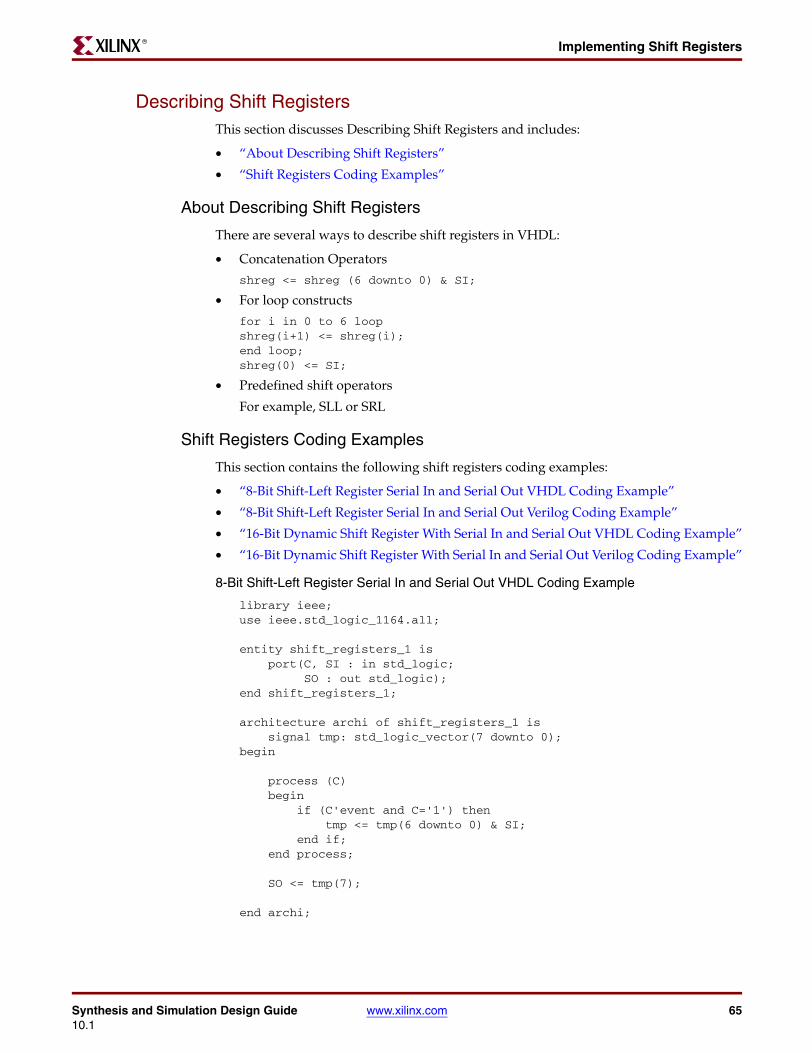
Synthesis and Simulation Design Guide www.xilinx.com 6510.1
Implementing Shift RegistersR
Describing Shift RegistersThis section discusses Describing Shift Registers and includes:
• “About Describing Shift Registers”
• “Shift Registers Coding Examples”
About Describing Shift Registers
There are several ways to describe shift registers in VHDL:
• Concatenation Operators
shreg <= shreg (6 downto 0) & SI;
• For loop constructs
for i in 0 to 6 loop shreg(i+1) <= shreg(i);end loop;shreg(0) <= SI;
• Predefined shift operators
For example, SLL or SRL
Shift Registers Coding Examples
This section contains the following shift registers coding examples:
• “8-Bit Shift-Left Register Serial In and Serial Out VHDL Coding Example”
• “8-Bit Shift-Left Register Serial In and Serial Out Verilog Coding Example”
• “16-Bit Dynamic Shift Register With Serial In and Serial Out VHDL Coding Example”
• “16-Bit Dynamic Shift Register With Serial In and Serial Out Verilog Coding Example”
8-Bit Shift-Left Register Serial In and Serial Out VHDL Coding Example
library ieee;use ieee.std_logic_1164.all;
entity shift_registers_1 is port(C, SI : in std_logic; SO : out std_logic);end shift_registers_1;
architecture archi of shift_registers_1 is signal tmp: std_logic_vector(7 downto 0);begin
process (C) begin if (C'event and C='1') then tmp <= tmp(6 downto 0) & SI; end if; end process;
SO <= tmp(7);
end archi;
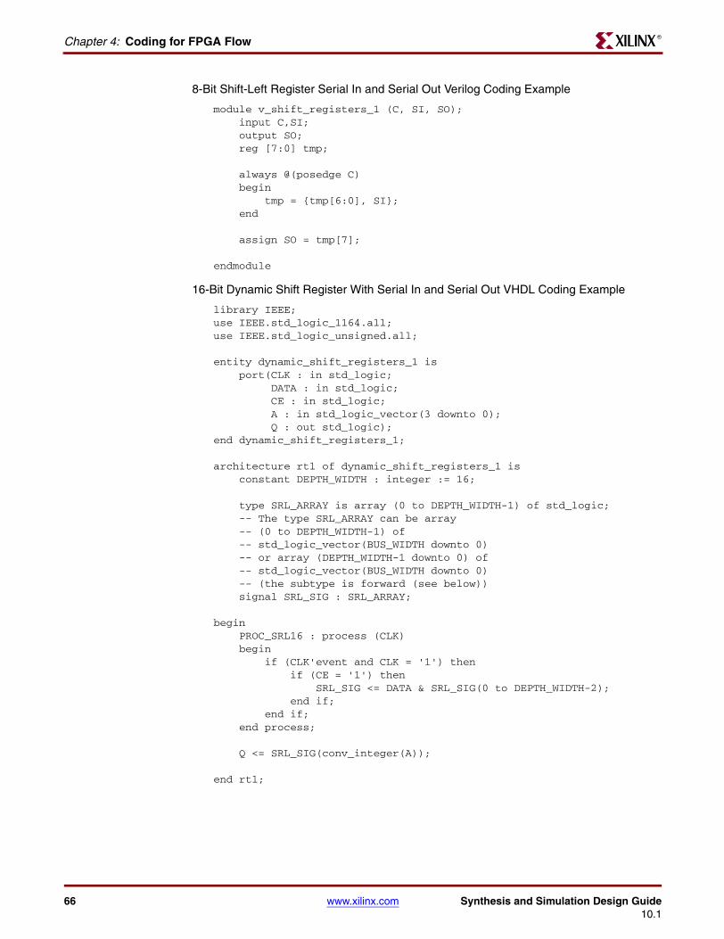
66 www.xilinx.com Synthesis and Simulation Design Guide10.1
Chapter 4: Coding for FPGA FlowR
8-Bit Shift-Left Register Serial In and Serial Out Verilog Coding Example
module v_shift_registers_1 (C, SI, SO); input C,SI; output SO; reg [7:0] tmp;
always @(posedge C) begin tmp = {tmp[6:0], SI}; end
assign SO = tmp[7];
endmodule
16-Bit Dynamic Shift Register With Serial In and Serial Out VHDL Coding Example
library IEEE;use IEEE.std_logic_1164.all;use IEEE.std_logic_unsigned.all;
entity dynamic_shift_registers_1 is port(CLK : in std_logic; DATA : in std_logic; CE : in std_logic; A : in std_logic_vector(3 downto 0); Q : out std_logic);end dynamic_shift_registers_1;
architecture rtl of dynamic_shift_registers_1 is constant DEPTH_WIDTH : integer := 16;
type SRL_ARRAY is array (0 to DEPTH_WIDTH-1) of std_logic; -- The type SRL_ARRAY can be array -- (0 to DEPTH_WIDTH-1) of -- std_logic_vector(BUS_WIDTH downto 0) -- or array (DEPTH_WIDTH-1 downto 0) of -- std_logic_vector(BUS_WIDTH downto 0) -- (the subtype is forward (see below)) signal SRL_SIG : SRL_ARRAY;
begin PROC_SRL16 : process (CLK) begin if (CLK'event and CLK = '1') then if (CE = '1') then SRL_SIG <= DATA & SRL_SIG(0 to DEPTH_WIDTH-2); end if; end if; end process;
Q <= SRL_SIG(conv_integer(A));
end rtl;
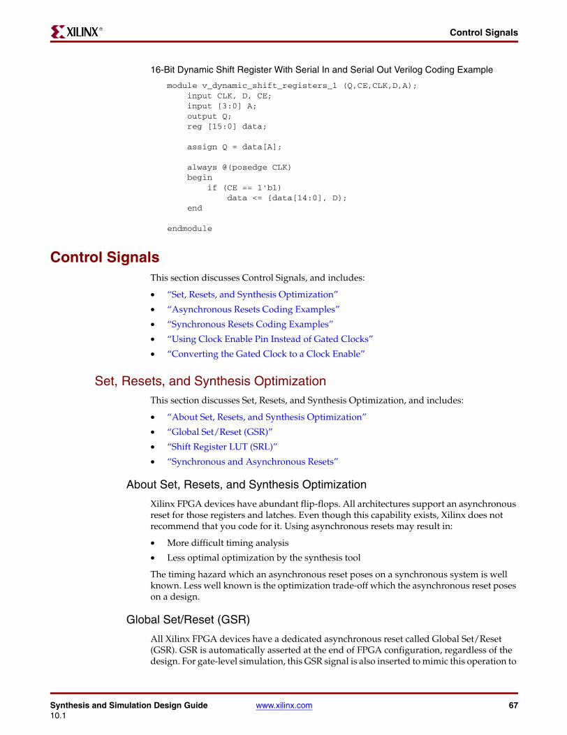
Synthesis and Simulation Design Guide www.xilinx.com 6710.1
Control SignalsR
16-Bit Dynamic Shift Register With Serial In and Serial Out Verilog Coding Example
module v_dynamic_shift_registers_1 (Q,CE,CLK,D,A); input CLK, D, CE; input [3:0] A; output Q; reg [15:0] data;
assign Q = data[A];
always @(posedge CLK) begin if (CE == 1'b1) data <= {data[14:0], D}; end
endmodule
Control SignalsThis section discusses Control Signals, and includes:
• “Set, Resets, and Synthesis Optimization”
• “Asynchronous Resets Coding Examples”
• “Synchronous Resets Coding Examples”
• “Using Clock Enable Pin Instead of Gated Clocks”
• “Converting the Gated Clock to a Clock Enable”
Set, Resets, and Synthesis OptimizationThis section discusses Set, Resets, and Synthesis Optimization, and includes:
• “About Set, Resets, and Synthesis Optimization”
• “Global Set/Reset (GSR)”
• “Shift Register LUT (SRL)”
• “Synchronous and Asynchronous Resets”
About Set, Resets, and Synthesis Optimization
Xilinx FPGA devices have abundant flip-flops. All architectures support an asynchronous reset for those registers and latches. Even though this capability exists, Xilinx does not recommend that you code for it. Using asynchronous resets may result in:
• More difficult timing analysis
• Less optimal optimization by the synthesis tool
The timing hazard which an asynchronous reset poses on a synchronous system is well known. Less well known is the optimization trade-off which the asynchronous reset poses on a design.
Global Set/Reset (GSR)
All Xilinx FPGA devices have a dedicated asynchronous reset called Global Set/Reset (GSR). GSR is automatically asserted at the end of FPGA configuration, regardless of the design. For gate-level simulation, this GSR signal is also inserted to mimic this operation to
68 www.xilinx.com Synthesis and Simulation Design Guide10.1
Chapter 4: Coding for FPGA FlowR
allow accurate simulation of the initialized design as it happens in the silicon. Adding another asynchronous reset to the actual code only duplicates this dedicated feature. It is not necessary for device initialization or simulation initialization.
Shift Register LUT (SRL)
All current Xilinx FPGA devices contain LUTs that may be configured to act as a 16-bit shift register called a Shift Register LUT (SRL). Using any reset when inferring shift registers prohibits the inference of the SRL.
The SRL is an efficient structure for building static and variable length shift registers. A reset (either synchronous or asynchronous) would preclude using this component. This generally leads to a less efficient structure using a combination of registers and, sometimes, logic.
Synchronous and Asynchronous Resets
The choice between synchronous and asynchronous resets can also change the choices of how registers are used within larger IP blocks. For instance, DSP48 in Virtex™-4 and Virtex-5 devices has several registers within the block which, if used, may result in a substantial area savings, as well as improve overall circuit performance.
DSP48 has only a synchronous reset. If a synchronous reset is inferred in registers around logic that could be packed into a DSP48, the registers can also be packed into the component, resulting in a smaller and faster design. If an asynchronous reset is used, the register must remain outside the block, resulting in a less optimal design. Similar optimization applies to the block RAM registers and other components within the FPGA device.
The flip-flops within the FPGA device are configurable to be either an asynchronous set/reset, or a synchronous set/reset. If an asynchronous reset is described in the code, the synthesis tool must configure the flip-flop to use the asynchronous set/reset. This precludes the using any other signals using this resource.
If a synchronous reset (or no reset at all) is described for the flip-flop, the synthesis tool can configure the set/reset as a synchronous operation. Doing so allows the synthesis tool to use this resource as a set/reset from the described code. It may also use this resource to break up the data path. This may result in fewer resources and shorter data paths to the register. Details of these optimizations depend on the code and synthesis tools used.
Asynchronous Resets Coding ExamplesThis section gives the following Asynchronous Resets coding examples:
• “Asynchronous Resets VHDL Coding Example”
• “Asynchronous Resets Verilog Coding Example”
For the same code re-written for synchronous reset, see “Synchronous Resets Coding Examples.”
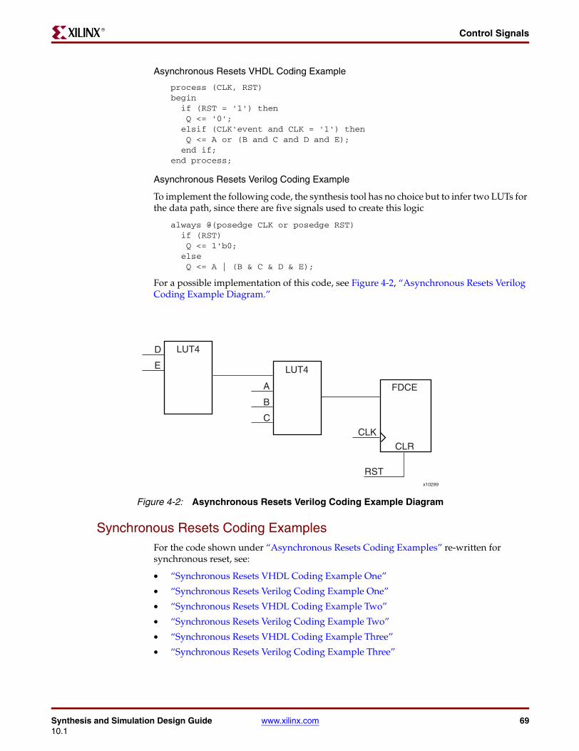
Synthesis and Simulation Design Guide www.xilinx.com 6910.1
Control SignalsR
Asynchronous Resets VHDL Coding Example
process (CLK, RST)begin if (RST = '1') then Q <= '0'; elsif (CLK'event and CLK = '1') then Q <= A or (B and C and D and E); end if;end process;
Asynchronous Resets Verilog Coding Example
To implement the following code, the synthesis tool has no choice but to infer two LUTs for the data path, since there are five signals used to create this logic
always @(posedge CLK or posedge RST) if (RST) Q <= 1'b0; else Q <= A | (B & C & D & E);
For a possible implementation of this code, see Figure 4-2, “Asynchronous Resets Verilog Coding Example Diagram.”
Synchronous Resets Coding ExamplesFor the code shown under “Asynchronous Resets Coding Examples” re-written for synchronous reset, see:
• “Synchronous Resets VHDL Coding Example One”
• “Synchronous Resets Verilog Coding Example One”
• “Synchronous Resets VHDL Coding Example Two”
• “Synchronous Resets Verilog Coding Example Two”
• “Synchronous Resets VHDL Coding Example Three”
• “Synchronous Resets Verilog Coding Example Three”
Figure 4-2: Asynchronous Resets Verilog Coding Example Diagram
A
B
C
D
E
LUT4
LUT4
CLK
RST
CLR
FDCE
x10299
70 www.xilinx.com Synthesis and Simulation Design Guide10.1
Chapter 4: Coding for FPGA FlowR
Synchronous Resets VHDL Coding Example One
process (CLK)begin if (CLK'event and CLK = '1') then if (RST = '1') then Q <= '0'; else Q <= A or (B and C and D and E); end if; end if;end process;
Synchronous Resets Verilog Coding Example One
always @(posedge CLK) if (RST) Q <= 1'b0; else Q <= A | (B & C & D & E);
The synthesis tool now has more flexibility as to how this function can be represented. For a possible implementation of this code, see Figure 4-3, “Synchronous Resets Verilog Coding Example One Diagram.”
In this implementation, the synthesis tool can identify that any time A is active high, Q is always a logic one. With the register now configured with the set/reset as a synchronous operation, the set is now free to be used as part of the synchronous data path. This reduces:
• The amount of logic necessary to implement the function
• The data path delays for the D and E signals
Logic could have also been shifted to the reset side as well if the code was written in a way that was a more beneficial implementation
Figure 4-3: Synchronous Resets Verilog Coding Example One Diagram
C
B
E
D
LUT4
CLK
RST
Q
R
S
FDRSE
x10300
A
Synthesis and Simulation Design Guide www.xilinx.com 7110.1
Control SignalsR
Synchronous Resets VHDL Coding Example Two
Now consider the following addition to the example shown in “Synchronous Resets VHDL Coding Example One.”
process (CLK, RST)begin if (RST = '1') then Q <= '0'; elsif (CLK'event and CLK = '1') then Q <= (F or G or H) and (A or (B and C and D and E)); end if;end process;
Synchronous Resets Verilog Coding Example Two
always @(posedge CLK or posedge RST) if (RST) Q <= 1'b0; else Q <= (F | G | H) & (A | (B & C & D & E));
Since eight signals now contribute to the logic function, a minimum of three LUTs are needed to implement this function. For a possible implementation of this code, see Figure 4-4, “Synchronous Resets Verilog Coding Example Two Diagram.”
Figure 4-4: Synchronous Resets Verilog Coding Example Two Diagram
B
A
C
D
E
LUT4
F
G
H
LUT4
LUT4
CLK
RST
Q
CLR
FDCE
x10301
72 www.xilinx.com Synthesis and Simulation Design Guide10.1
Chapter 4: Coding for FPGA FlowR
Synchronous Resets VHDL Coding Example Three
If the same code is written with a synchronous reset:
process (CLK)begin if (CLK'event and CLK = '1') then if (RST = '1') then Q <= '0'; else Q <= (F or G or H) and (A or (B and C and D and E)); end if; end if;end process;
Synchronous Resets Verilog Coding Example Three
always @(posedge CLK) if (RST) Q <= 1'b0; else Q <= (F | G | H) & (A | (B & C & D & E));
For a possible implementation of this code, see Figure 4-5, “Synchronous Resets Verilog Coding Example Three Diagram.”
The resulting implementation not only uses fewer LUTs to implement the same logic function, but may result in a faster design due to the reduction of logic levels for nearly every signal that creates this function. While these are simple examples, they do show how asynchronous resets force all synchronous data signals on the data input to the register, resulting in a potentially less optimal implementation.
In general, the more signals that fan into a logic function, the more effective using synchronous sets/resets (or no resets at all) can be in minimizing logic resources and in maximizing design performance.
Figure 4-5: Synchronous Resets Verilog Coding Example Three Diagram
LUT4CLK
A
B
C
D
E
RST
F
G
H
QS
R
LUT4
FDRSE
x10302
Synthesis and Simulation Design Guide www.xilinx.com 7310.1
Control SignalsR
Using Clock Enable Pin Instead of Gated ClocksThis section discusses Using Clock Enable Pin Instead of Gated Clocks, and includes:
• “About Using Clock Enable Pin Instead of Gated Clocks”
• “Using Clock Enable Pin Instead of Gated Clocks Coding Examples”
About Using Clock Enable Pin Instead of Gated Clocks
Xilinx recommends that you use the CLB clock enable pin instead of gated clocks. Gated clocks can cause glitches, increased clock delay, clock skew, and other undesirable effects. Using clock enable saves clock resources, and can improve timing characteristic and analysis of the design.
If you want to use a gated clock for power reduction, most FPGA devices now have a clock enabled global buffer resource called BUFGCE. However, a clock enable is still the preferred method to reduce or stop the clock to portions of the design.
Using Clock Enable Pin Instead of Gated Clocks Coding Examples
This section gives the following Using Clock Enable Pin Instead of Gated Clock coding examples:
• “Gated Clock VHDL Coding Example” and “Gated Clock Verilog Coding Example” show a design that uses a gated clock.
• “Clock Enable VHDL Coding Example” and “Clock Enable Verilog Coding Example” show how to modify the gated clock design to use the clock enable pin of the CLB.
Gated Clock VHDL Coding Example
-- The following code is for demonstration purposes only-- Xilinx does not suggest using the following coding style in FPGAslibrary IEEE;use IEEE.std_logic_1164.all;use IEEE.std_logic_unsigned.all;entity gate_clock is
port (DATA, IN1, IN2, LOAD, CLOCK: in STD_LOGIC; OUT1: out STD_LOGIC);
end gate_clock;architecture BEHAVIORAL of gate_clock issignal GATECLK: STD_LOGIC;begin
GATECLK <= (IN1 and IN2 and LOAD and CLOCK);GATE_PR: process (GATECLK) beginif (GATECLK'event and GATECLK='1') then
OUT1 <= DATA;end if;
end process; -- End GATE_PRend BEHAVIORAL;
74 www.xilinx.com Synthesis and Simulation Design Guide10.1
Chapter 4: Coding for FPGA FlowR
Gated Clock Verilog Coding Example
// The following code is for demonstration purposes only// Xilinx does not suggest using the following coding style in FPGAsmodule gate_clock( input DATA, IN1, IN2, LOAD, CLOCK, output reg OUT1); wire GATECLK; assign GATECLK = (IN1 & IN2 & LOAD & CLOCK); always @(posedge GATECLK) OUT1 <= DATA;endmodule
Converting the Gated Clock to a Clock EnableFor VHDL and Verilog coding examples for converting the gated clock to a clock enable, see:
• “Clock Enable VHDL Coding Example”
• “Clock Enable Verilog Coding Example”
Clock Enable VHDL Coding Example
library IEEE;use IEEE.std_logic_1164.all;use IEEE.std_logic_unsigned.all;entity clock_enable is
port (DATA, IN1, IN2, LOAD, CLOCK: in STD_LOGIC; OUT1: out STD_LOGIC);
end clock_enable;architecture BEHAVIORAL of clock_enable is
signal ENABLE: std_logic;begin ENABLE <= IN1 and IN2 and LOAD;
EN_PR: process (CLOCK)beginif (CLOCK'event and CLOCK='1') thenif (ENABLE = '1') thenOUT1 <= DATA;
end if;end if;
end process;end BEHAVIORAL;
Clock Enable Verilog Coding Example
module clock_enable ( input DATA, IN1, IN2, LOAD, CLOCK, output reg OUT1); wire ENABLE;
assign ENABLE = (IN1 & IN2 & LOAD); always @(posedge CLOCK) if (ENABLE) OUT1 <= DATA;endmoduleI
Synthesis and Simulation Design Guide www.xilinx.com 7510.1
Initial State of the Registers, Latches, Shift Registers, and RAMsR
Initial State of the Registers, Latches, Shift Registers, and RAMsThis section discusses Initial State of the Registers, Latches, Shift Registers, and RAMs, and includes:
• “Initial State of the Registers and Latches”
• “Initial State of the Shift Registers”
• “Initial State of the RAMs”
Initial State of the Registers and LatchesFPGA flip-flops are configured as either preset (asynchronous set) or clear (asynchronous reset) during startup. This is known as the initialization state, or INIT. The initial state of the register can be specified as follows:
• If the register is instantiated, it can be specified by setting the INIT generic/parameter value to either a 1 or 0, depending on the desired state. For more information, see the Xilinx Libraries Guides at http://www.xilinx.com/support/software_manuals.htm.
• If the register is inferred, the initial state can be specified by initializing the VHDL signal declaration or the Verilog reg declaration as shown in the following coding examples:
♦ “Initial State of the Registers and Latches VHDL Coding Example One”
♦ “Initial State of the Registers and Latches Verilog Coding Example One”
♦ “Initial State of the Registers and Latches Verilog Coding Example Two”
Initial State of the Registers and Latches VHDL Coding Example One
signal register1 : std_logic := '0'; -- specifying register1 to start as a zerosignal register2 : std_logic := '1'; -- specifying register2 to start as a onesignal register3 : std_logic_vector(3 downto 0):="1011"; -- specifying INIT value for 4-bit register
Initial State of the Registers and Latches Verilog Coding Example One
reg register1 = 1'b0; // specifying regsiter1 to start as a zeroreg register2 = 1'b1; // specifying register2 to start as a onereg [3:0] register3 = 4'b1011; //specifying INIT value for 4-bit register
X-Ref Target - Figure 4-6
Figure 4-7: Implementation of Clock Enable Diagram
D
DATA
IN1
IN2
LOAD
CLOCK
ENABLEAND3
OUT1DFF
CE
C
Q
X4976
76 www.xilinx.com Synthesis and Simulation Design Guide10.1
Chapter 4: Coding for FPGA FlowR
Initial State of the Registers and Latches Verilog Coding Example Two
Another possibility in Verilog is to use an initial statement:
reg [3:0] register3;initial begin register3= 4'b1011;end
Not all synthesis tools support this initialization. To determine whether it is supported, see your synthesis tool documentation. If this initialization is not supported, or if it is not specified in the code, the initial value is determined by the presence or absence of an asynchronous preset in the code. If an asynchronous preset is present, the register initializes to a one. If an asynchronous preset is not present, the register initializes to a logic zero.
Initial State of the Shift RegistersThe definition method of initial values for shift registers is the same used for Registers and Latches. For more information, see “Initial State of the Registers and Latches.”
Initial State of the RAMsThis section discusses Initial State of the RAMs, and includes:
• “About Initial State of the RAMs”
• “Initial State of the RAMs Coding Examples”
About Initial State of the RAMs
The definition method of initial values for RAMs (block or distributed) is similar to the one used for Registers and Latches. The initial state of the RAM can be specified as follows:
• If the RAM is instantiated, it can be specified by setting the INIT_00, INIT_01, … generic/parameter values, depending on the desired state. For more information, see the Xilinx Libraries Guides at http://www.xilinx.com/support/software_manuals.htm.
• If the RAM is inferred, the initial state can be specified by initializing the VHDL signal declaration or using Verilog initial statement as shown in the following coding examples. The initial values could be specified directly in the HDL code, or in an external file containing the initialization data.
Initial State of the RAMs Coding Examples
This section gives the following Initial State of the RAMs coding examples:
• “Initial State of the RAMs VHDL Coding Example”
• “Initial State of the RAMs Verilog Coding Example”
Initial State of the RAMs VHDL Coding Example
type ram_type is array (0 to 63) of std_logic_vector(19 downto 0);signal RAM : ram_type :=( X"0200A", X"00300", X"08101", X"04000", X"08601", X"0233A", X"00300", X"08602", X"02310", X"0203B", X"08300", X"04002", X"08201", X"00500", ... );
Synthesis and Simulation Design Guide www.xilinx.com 7710.1
MultiplexersR
Initial State of the RAMs Verilog Coding Example
reg [19:0] ram [63:0];initial begin ram[63] = 20'h0200A; ram[62] = 20'h00300; ram[61] = 20'h08101; ram[60] = 20'h04000; ram[59] = 20'h08601; ram[58] = 20'h0233A; ... ram[2] = 20'h02341; ram[1] = 20'h08201; ram[0] = 20'h0400D;end
Not all synthesis tools support this initialization. To determine whether it is supported, see your synthesis tool documentation.
MultiplexersThis section discusses Multiplexers and includes:
• “About Multiplexers”
• “Multiplexers Coding Examples”
About MultiplexersThere are several ways to implement multiplexers on Xilinx FPGA devices:
• Using dedicated resources such as MUXF5, MUXF6 ...
• Using Carry chains
• Using LUTs only
The implementation choice is automatically taken by synthesis tool and driven by speed or area design requirements. However some synthesis tools allow the user to control implementation style of multiplexers. For more information, see your synthesis tool documentation.
There are different description styles for multiplexers (MUXs), such as If-Then-Else or Case. When writing MUXs, pay special attention in order to avoid common traps. For example, if you describe a MUX using a Case statement, and you do not specify all values of the selector, the result may be latches instead of a multiplexer.
If you use Verilog, remember that Verilog Case statements can be full or not full, and they can also be parallel or not parallel. A Case statement is:
• FULL if all possible branches are specified
• PARALLEL if it does not contain branches that can be executed simultaneously
Synthesis tools automatically determine the characteristics of the Case statements and generate corresponding logic. In addition they provide a way allowing to guide interpretation of Case statements via special directives. For more information, see your synthesis tool documentation.
78 www.xilinx.com Synthesis and Simulation Design Guide10.1
Chapter 4: Coding for FPGA FlowR
Multiplexers Coding ExamplesThis section indudes the following Multiplexers coding examples:
• “4-to-1 1-Bit MUX Using Case Statement VHDL Coding Example”
• “4-to-1 1-Bit MUX Using Case Statement Verilog Coding Example”
• “4-to-1 1-Bit MUX Using IF Statement VHDL Coding Example”
• “4-to-1 1-Bit MUX Using IF Statement Verilog Coding Example”
4-to-1 1-Bit MUX Using Case Statement VHDL Coding Example
library ieee;use ieee.std_logic_1164.all;
entity multiplexers_2 is port (a, b, c, d : in std_logic; s : in std_logic_vector (1 downto 0); o : out std_logic);end multiplexers_2;
architecture archi of multiplexers_2 isbegin process (a, b, c, d, s) begin case s is when "00" => o <= a; when "01" => o <= b; when "10" => o <= c; when others => o <= d; end case; end process;end archi;
4-to-1 1-Bit MUX Using Case Statement Verilog Coding Example
module v_multiplexers_2 (a, b, c, d, s, o); input a,b,c,d; input [1:0] s; output o; reg o; always @(a or b or c or d or s) begin case (s) 2'b00 : o = a; 2'b01 : o = b; 2'b10 : o = c; default : o = d; endcase endendmodule
Synthesis and Simulation Design Guide www.xilinx.com 7910.1
Finite State Machines (FSMs)R
4-to-1 1-Bit MUX Using IF Statement VHDL Coding Example
library ieee;use ieee.std_logic_1164.all;
entity multiplexers_1 is port (a, b, c, d : in std_logic; s : in std_logic_vector (1 downto 0); o : out std_logic);end multiplexers_1;
architecture archi of multiplexers_1 isbegin process (a, b, c, d, s) begin if (s = "00") then o <= a; elsif (s = "01") then o <= b; elsif (s = "10") then o <= c; else o <= d; end if; end process;end archi;
4-to-1 1-Bit MUX Using IF Statement Verilog Coding Example
module v_multiplexers_1 (a, b, c, d, s, o); input a,b,c,d; input [1:0] s; output o; reg o;
always @(a or b or c or d or s) begin if (s == 2'b00) o = a; else if (s == 2'b01) o = b; else if (s == 2'b10) o = c; else o = d; endendmodule
Finite State Machines (FSMs)This section discusses Finite State Machines (FSMs), and includes:
• “FSM Description Style”
• “FSM With One Process”
• “FSM With Two or Three Processes”
• “FSM Recognition and Optimization”
• “Other FSM Features”
FSM Description StyleMost FPGA synthesis tools propose a large set of templates to describe Finite State Machines (FSMs). There are many ways to describe FSMs. A traditional FSM representation incorporates Mealy and Moore machines, as shown in Figure 4-9, “Mealy and Moore Machines Diagram.”
80 www.xilinx.com Synthesis and Simulation Design Guide10.1
Chapter 4: Coding for FPGA FlowR
For HDL, process (VHDL) and always blocks (Verilog) are the best ways to describe FSMs. Xilinx® uses process to refer to both VHDL processes and Verilog always blocks.
You may have several processes (1, 2 or 3) in your description, consider and decompose the different parts of the preceding model.
The following example shows the Moore Machine with an Asynchronous Reset (RESET):
• 4 states: s1, s2, s3, s4
• 5 transitions
• 1 input: "x1"
• 1 output: "outp"
This model is represented by the bubble diagram shown in Figure 4-11, “Bubble Diagram.”
X-Ref Target - Figure 4-8
Figure 4-9: Mealy and Moore Machines Diagram
Inputs
NextState
Function
RESET
CLOCK
StateRegister
OutputFunction
Outputs
Only for Mealy Machine
X10899
X-Ref Target - Figure 4-10
Figure 4-11: Bubble Diagram
RESET
outp=’1’
outp=’1’ outp=’0’
S1
S4
S2 S3
x1 x1
X10900
Synthesis and Simulation Design Guide www.xilinx.com 8110.1
Finite State Machines (FSMs)R
FSM With One ProcessIn these examples, output signal outp is a register:
• “FSM With One Process VHDL Coding Example”
• “FSM With a Single Always Block Verilog Coding Example”
FSM With One Process VHDL Coding Example
---- State Machine with a single process.--library IEEE;use IEEE.std_logic_1164.all;
entity fsm_1 is port ( clk, reset, x1 : IN std_logic; outp : OUT std_logic);end entity;
architecture beh1 of fsm_1 is type state_type is (s1,s2,s3,s4); signal state: state_type ;
begin process (clk,reset) begin if (reset ='1') then state <=s1; outp<='1'; elsif (clk='1' and clk'event) then case state is when s1 => if x1='1' then state <= s2; outp <= '1'; else state <= s3; outp <= '0'; end if; when s2 => state <= s4; outp <= '0'; when s3 => state <= s4; outp <= '0'; when s4 => state <= s1; outp <= '1'; end case; end if; end process;end beh1;
FSM With a Single Always Block Verilog Coding Example
//// State Machine with a single always block.//module v_fsm_1 (clk, reset, x1, outp); input clk, reset, x1; output outp; reg outp; reg [1:0] state;
parameter s1 = 2'b00; parameter s2 = 2'b01; parameter s3 = 2'b10; parameter s4 = 2'b11;
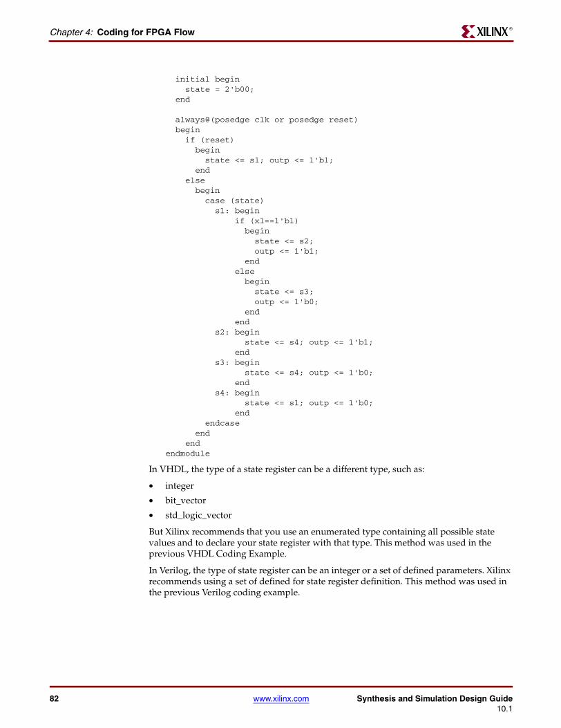
82 www.xilinx.com Synthesis and Simulation Design Guide10.1
Chapter 4: Coding for FPGA FlowR
initial begin state = 2'b00; end
always@(posedge clk or posedge reset) begin if (reset) begin state <= s1; outp <= 1'b1; end else begin case (state) s1: begin if (x1==1'b1) begin state <= s2; outp <= 1'b1; end else begin state <= s3; outp <= 1'b0; end end s2: begin state <= s4; outp <= 1'b1; end s3: begin state <= s4; outp <= 1'b0; end s4: begin state <= s1; outp <= 1'b0; end endcase end endendmodule
In VHDL, the type of a state register can be a different type, such as:
• integer
• bit_vector
• std_logic_vector
But Xilinx recommends that you use an enumerated type containing all possible state values and to declare your state register with that type. This method was used in the previous VHDL Coding Example.
In Verilog, the type of state register can be an integer or a set of defined parameters. Xilinx recommends using a set of defined for state register definition. This method was used in the previous Verilog coding example.
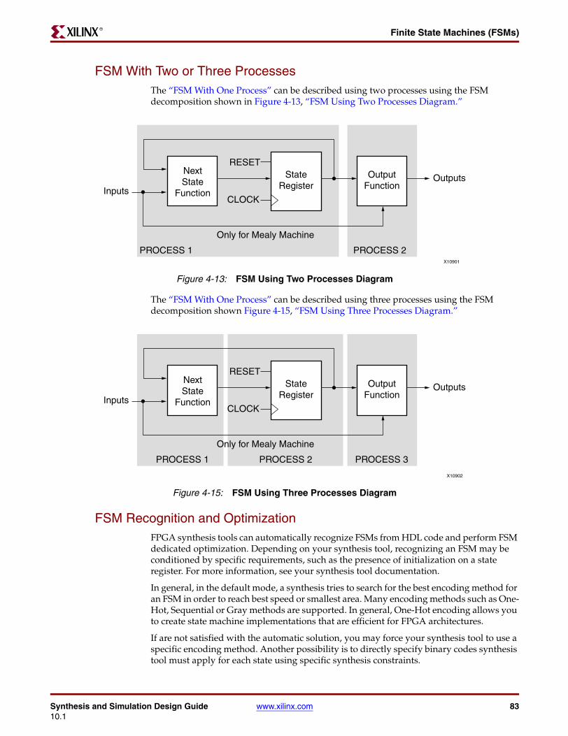
Synthesis and Simulation Design Guide www.xilinx.com 8310.1
Finite State Machines (FSMs)R
FSM With Two or Three ProcessesThe “FSM With One Process” can be described using two processes using the FSM decomposition shown in Figure 4-13, “FSM Using Two Processes Diagram.”
The “FSM With One Process” can be described using three processes using the FSM decomposition shown Figure 4-15, “FSM Using Three Processes Diagram.”
FSM Recognition and OptimizationFPGA synthesis tools can automatically recognize FSMs from HDL code and perform FSM dedicated optimization. Depending on your synthesis tool, recognizing an FSM may be conditioned by specific requirements, such as the presence of initialization on a state register. For more information, see your synthesis tool documentation.
In general, in the default mode, a synthesis tries to search for the best encoding method for an FSM in order to reach best speed or smallest area. Many encoding methods such as One-Hot, Sequential or Gray methods are supported. In general, One-Hot encoding allows you to create state machine implementations that are efficient for FPGA architectures.
If are not satisfied with the automatic solution, you may force your synthesis tool to use a specific encoding method. Another possibility is to directly specify binary codes synthesis tool must apply for each state using specific synthesis constraints.
X-Ref Target - Figure 4-12
Figure 4-13: FSM Using Two Processes Diagram
Inputs
NextState
Function
RESET
CLOCK
StateRegister
OutputFunction
Outputs
Only for Mealy Machine
PROCESS 1 PROCESS 2X10901
X-Ref Target - Figure 4-14
Figure 4-15: FSM Using Three Processes Diagram
Inputs
NextState
Function
RESET
CLOCK
StateRegister
OutputFunction
Outputs
Only for Mealy Machine
PROCESS 1 PROCESS 2 PROCESS 3
X10902
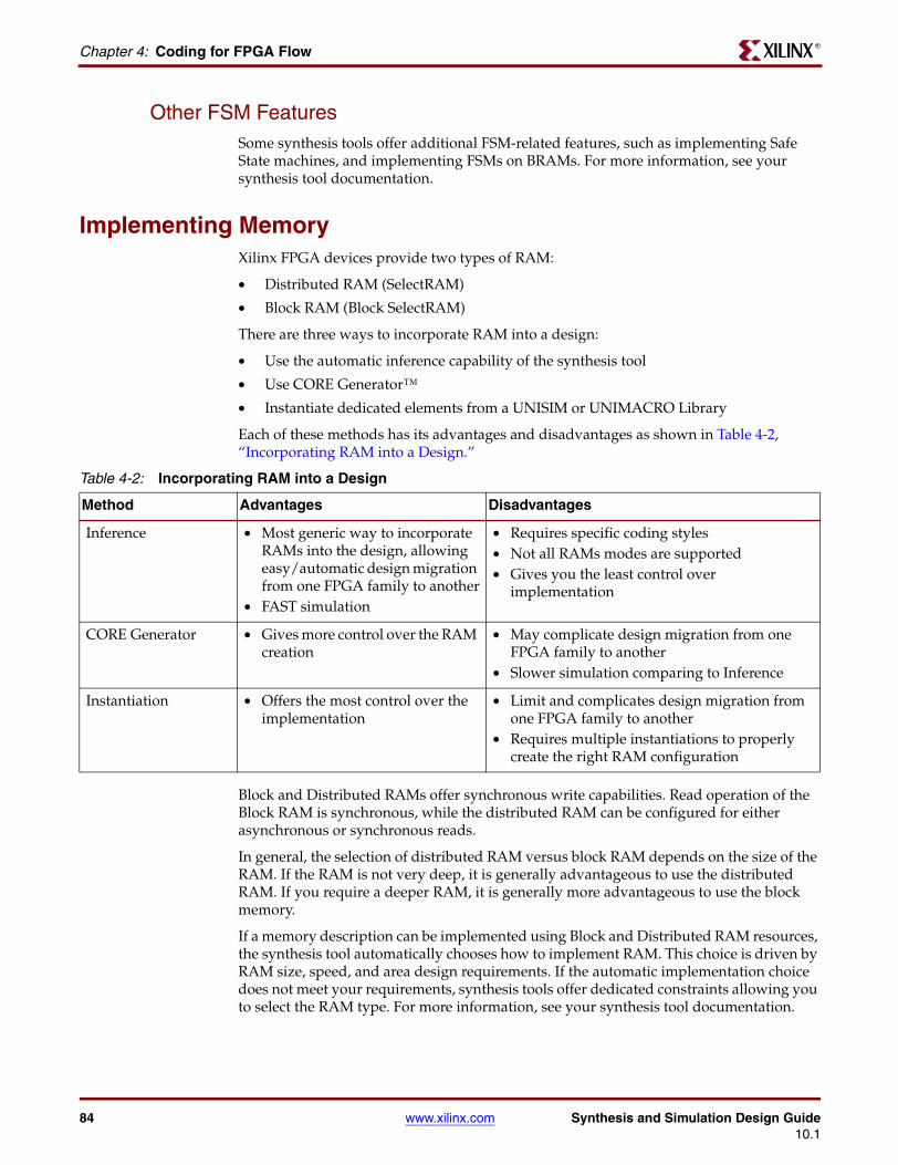
84 www.xilinx.com Synthesis and Simulation Design Guide10.1
Chapter 4: Coding for FPGA FlowR
Other FSM FeaturesSome synthesis tools offer additional FSM-related features, such as implementing Safe State machines, and implementing FSMs on BRAMs. For more information, see your synthesis tool documentation.
Implementing MemoryXilinx FPGA devices provide two types of RAM:
• Distributed RAM (SelectRAM)
• Block RAM (Block SelectRAM)
There are three ways to incorporate RAM into a design:
• Use the automatic inference capability of the synthesis tool
• Use CORE Generator™
• Instantiate dedicated elements from a UNISIM or UNIMACRO Library
Each of these methods has its advantages and disadvantages as shown in Table 4-2, “Incorporating RAM into a Design.”
Block and Distributed RAMs offer synchronous write capabilities. Read operation of the Block RAM is synchronous, while the distributed RAM can be configured for either asynchronous or synchronous reads.
In general, the selection of distributed RAM versus block RAM depends on the size of the RAM. If the RAM is not very deep, it is generally advantageous to use the distributed RAM. If you require a deeper RAM, it is generally more advantageous to use the block memory.
If a memory description can be implemented using Block and Distributed RAM resources, the synthesis tool automatically chooses how to implement RAM. This choice is driven by RAM size, speed, and area design requirements. If the automatic implementation choice does not meet your requirements, synthesis tools offer dedicated constraints allowing you to select the RAM type. For more information, see your synthesis tool documentation.
Table 4-2: Incorporating RAM into a Design
Method Advantages Disadvantages
Inference • Most generic way to incorporate RAMs into the design, allowing easy/automatic design migration from one FPGA family to another
• FAST simulation
• Requires specific coding styles• Not all RAMs modes are supported• Gives you the least control over
implementation
CORE Generator • Gives more control over the RAM creation
• May complicate design migration from one FPGA family to another
• Slower simulation comparing to Inference
Instantiation • Offers the most control over the implementation
• Limit and complicates design migration from one FPGA family to another
• Requires multiple instantiations to properly create the right RAM configuration
Synthesis and Simulation Design Guide www.xilinx.com 8510.1
Block RAM InferenceR
Since all Xilinx RAMs have the ability to be initialized, the RAMs may also be configured either as a ROM (Read Only Memory), or as a RAM with pre-defined contents.
Initialization of RAMs can be done directly from HDL code. For more information, see “Initial State of the Registers, Latches, Shift Registers, and RAMs.”
Some synthesis tools provide additional control over RAM inference and optimization process, such as pipelining, automatic Block RAM packing, and automatic Block RAM resource management. For more information, see your synthesis tool documentation.
For additional information about Implementing Memory, see:
• “Block RAM Inference”
• “Distributed RAM Inference”
Block RAM InferenceThis section discusses Block RAM Inference and includes:
• “About Block RAM Inference”
• “Block RAM Inference Coding Examples”
About Block RAM InferenceXilinx Block RAMs are True Dual-Port Block resources. Each port is totally independent and can be configured with different depth and width. Read and write operations are synchronous. Beginning with the Virtex-II device family, Block RAM resources offer different read/write synchronization modes:
• Read-First
• Write-First
• No-Change
The latest FPGA device families such as Virtex-5 offer additional enhancements, including:
• Cascadable Block RAMs
• Pipelined output registers
• Byte-Wide Write Enable
BRAM inference capabilities differ from one synthesis tool to another. For more information, see your synthesis tool documentation.
Block RAM Inference Coding ExamplesThe coding examples shown in this section provide coding styles for the most frequently used Block RAM configurations, which are supported by most synthesis tools. This section includes the following Block RAM Inference coding examples:
• “Single-Port RAM in Read-First Mode”
• “Single-Port RAM in Write-First Mode”
• “Single-Port RAM In No-Change Mode”
• “Dual-Port RAM in Read-First Mode with One Write Port”
• “Dual-Port Block RAM in Read-First Mode With Two Write Ports”
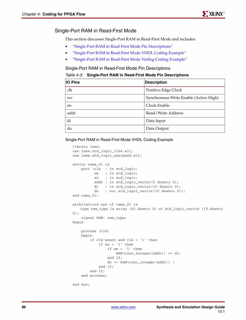
86 www.xilinx.com Synthesis and Simulation Design Guide10.1
Chapter 4: Coding for FPGA FlowR
Single-Port RAM in Read-First Mode
This section discusses Single-Port RAM in Read-First Mode and includes:
• “Single-Port RAM in Read-First Mode Pin Descriptions”
• “Single-Port RAM in Read-First Mode VHDL Coding Example”
• “Single-Port RAM in Read-First Mode Verilog Coding Example”
Single-Port RAM in Read-First Mode Pin Descriptions
Single-Port RAM in Read-First Mode VHDL Coding Example
library ieee;use ieee.std_logic_1164.all;use ieee.std_logic_unsigned.all;
entity rams_01 is port (clk : in std_logic; we : in std_logic; en : in std_logic; addr : in std_logic_vector(5 downto 0); di : in std_logic_vector(15 downto 0); do : out std_logic_vector(15 downto 0));end rams_01;
architecture syn of rams_01 is type ram_type is array (63 downto 0) of std_logic_vector (15 downto 0); signal RAM: ram_type;begin
process (clk) begin if clk'event and clk = '1' then if en = '1' then if we = '1' then RAM(conv_integer(addr)) <= di; end if; do <= RAM(conv_integer(addr)) ; end if; end if; end process;
end syn;
Table 4-3: Single-Port RAM in Read-First Mode Pin Descriptions
IO Pins Description
clk Positive-Edge Clock
we Synchronous Write Enable (Active High)
en Clock Enable
addr Read/Write Address
di Data Input
do Data Output
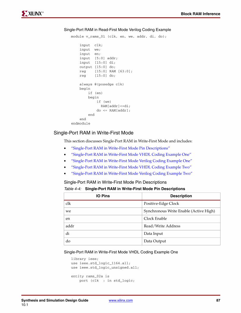
Synthesis and Simulation Design Guide www.xilinx.com 8710.1
Block RAM InferenceR
Single-Port RAM in Read-First Mode Verilog Coding Example
module v_rams_01 (clk, en, we, addr, di, do);
input clk; input we; input en; input [5:0] addr; input [15:0] di; output [15:0] do; reg [15:0] RAM [63:0]; reg [15:0] do;
always @(posedge clk) begin if (en) begin if (we) RAM[addr]<=di; do <= RAM[addr]; end endendmodule
Single-Port RAM in Write-First Mode
This section discusses Single-Port RAM in Write-First Mode and includes:
• “Single-Port RAM in Write-First Mode Pin Descriptions”
• “Single-Port RAM in Write-First Mode VHDL Coding Example One”
• “Single-Port RAM in Write-First Mode Verilog Coding Example One”
• “Single-Port RAM in Write-First Mode VHDL Coding Example Two”
• “Single-Port RAM in Write-First Mode Verilog Coding Example Two”
Single-Port RAM in Write-First Mode Pin Descriptions
Single-Port RAM in Write-First Mode VHDL Coding Example One
library ieee;use ieee.std_logic_1164.all;use ieee.std_logic_unsigned.all;
entity rams_02a is port (clk : in std_logic;
Table 4-4: Single-Port RAM in Write-First Mode Pin Descriptions
IO Pins Description
clk Positive-Edge Clock
we Synchronous Write Enable (Active High)
en Clock Enable
addr Read/Write Address
di Data Input
do Data Output
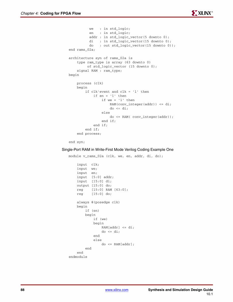
88 www.xilinx.com Synthesis and Simulation Design Guide10.1
Chapter 4: Coding for FPGA FlowR
we : in std_logic; en : in std_logic; addr : in std_logic_vector(5 downto 0); di : in std_logic_vector(15 downto 0); do : out std_logic_vector(15 downto 0));end rams_02a;
architecture syn of rams_02a is type ram_type is array (63 downto 0) of std_logic_vector (15 downto 0); signal RAM : ram_type;begin
process (clk) begin if clk'event and clk = '1' then if en = '1' then if we = '1' then RAM(conv_integer(addr)) <= di; do <= di; else do <= RAM( conv_integer(addr)); end if; end if; end if; end process;
end syn;
Single-Port RAM in Write-First Mode Verilog Coding Example One
module v_rams_02a (clk, we, en, addr, di, do);
input clk; input we; input en; input [5:0] addr; input [15:0] di; output [15:0] do; reg [15:0] RAM [63:0]; reg [15:0] do;
always @(posedge clk) begin if (en) begin if (we) begin RAM[addr] <= di; do <= di; end else do <= RAM[addr]; end endendmodule
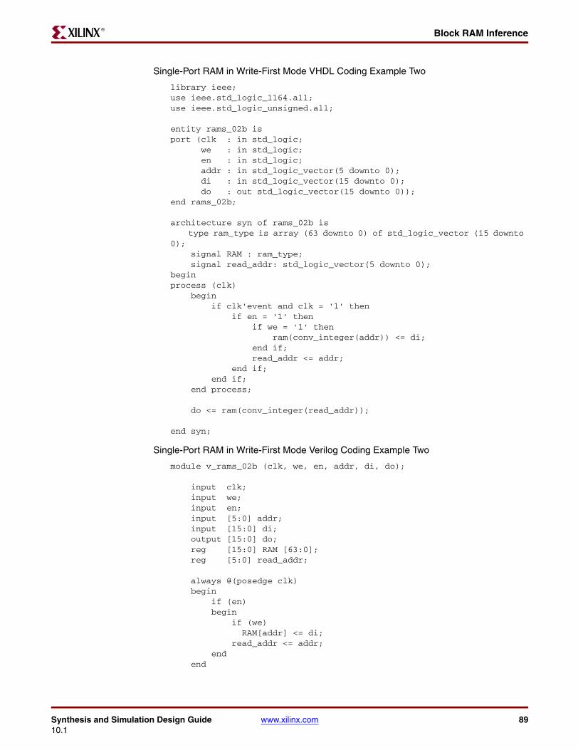
Synthesis and Simulation Design Guide www.xilinx.com 8910.1
Block RAM InferenceR
Single-Port RAM in Write-First Mode VHDL Coding Example Two
library ieee;use ieee.std_logic_1164.all;use ieee.std_logic_unsigned.all;
entity rams_02b isport (clk : in std_logic; we : in std_logic; en : in std_logic; addr : in std_logic_vector(5 downto 0); di : in std_logic_vector(15 downto 0); do : out std_logic_vector(15 downto 0));end rams_02b;
architecture syn of rams_02b is type ram_type is array (63 downto 0) of std_logic_vector (15 downto 0); signal RAM : ram_type; signal read_addr: std_logic_vector(5 downto 0);beginprocess (clk) begin if clk'event and clk = '1' then if en = '1' then if we = '1' then ram(conv_integer(addr)) <= di; end if; read_addr <= addr; end if; end if; end process;
do <= ram(conv_integer(read_addr));
end syn;
Single-Port RAM in Write-First Mode Verilog Coding Example Two
module v_rams_02b (clk, we, en, addr, di, do);
input clk; input we; input en; input [5:0] addr; input [15:0] di; output [15:0] do; reg [15:0] RAM [63:0]; reg [5:0] read_addr;
always @(posedge clk) begin if (en) begin if (we) RAM[addr] <= di; read_addr <= addr; end end
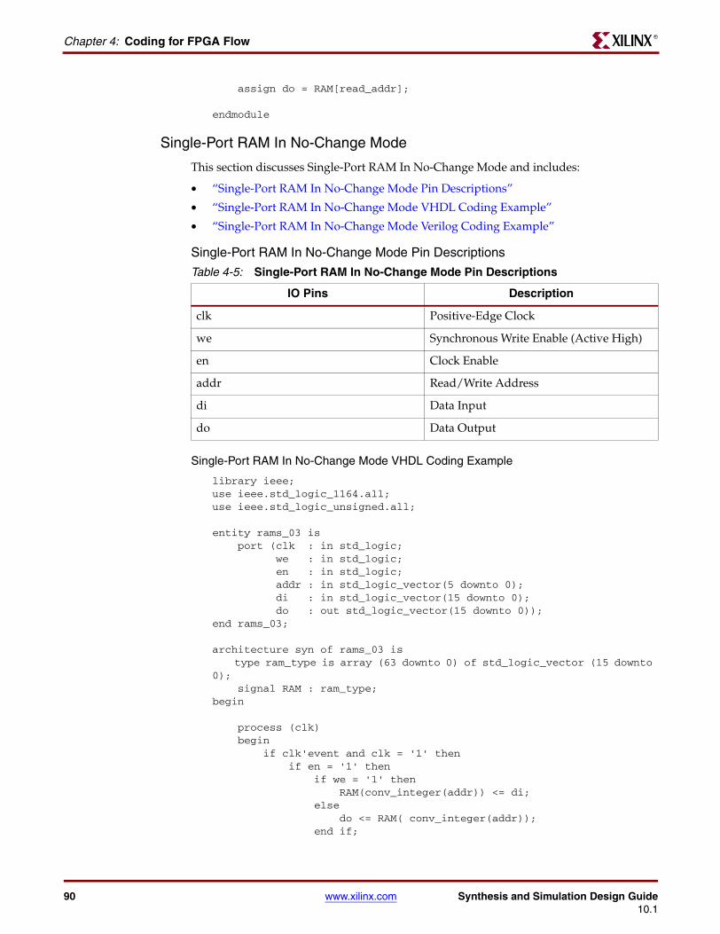
90 www.xilinx.com Synthesis and Simulation Design Guide10.1
Chapter 4: Coding for FPGA FlowR
assign do = RAM[read_addr];
endmodule
Single-Port RAM In No-Change Mode
This section discusses Single-Port RAM In No-Change Mode and includes:
• “Single-Port RAM In No-Change Mode Pin Descriptions”
• “Single-Port RAM In No-Change Mode VHDL Coding Example”
• “Single-Port RAM In No-Change Mode Verilog Coding Example”
Single-Port RAM In No-Change Mode Pin Descriptions
Single-Port RAM In No-Change Mode VHDL Coding Example
library ieee;use ieee.std_logic_1164.all;use ieee.std_logic_unsigned.all;
entity rams_03 is port (clk : in std_logic; we : in std_logic; en : in std_logic; addr : in std_logic_vector(5 downto 0); di : in std_logic_vector(15 downto 0); do : out std_logic_vector(15 downto 0));end rams_03;
architecture syn of rams_03 is type ram_type is array (63 downto 0) of std_logic_vector (15 downto 0); signal RAM : ram_type;begin
process (clk) begin if clk'event and clk = '1' then if en = '1' then if we = '1' then RAM(conv_integer(addr)) <= di; else do <= RAM( conv_integer(addr)); end if;
Table 4-5: Single-Port RAM In No-Change Mode Pin Descriptions
IO Pins Description
clk Positive-Edge Clock
we Synchronous Write Enable (Active High)
en Clock Enable
addr Read/Write Address
di Data Input
do Data Output
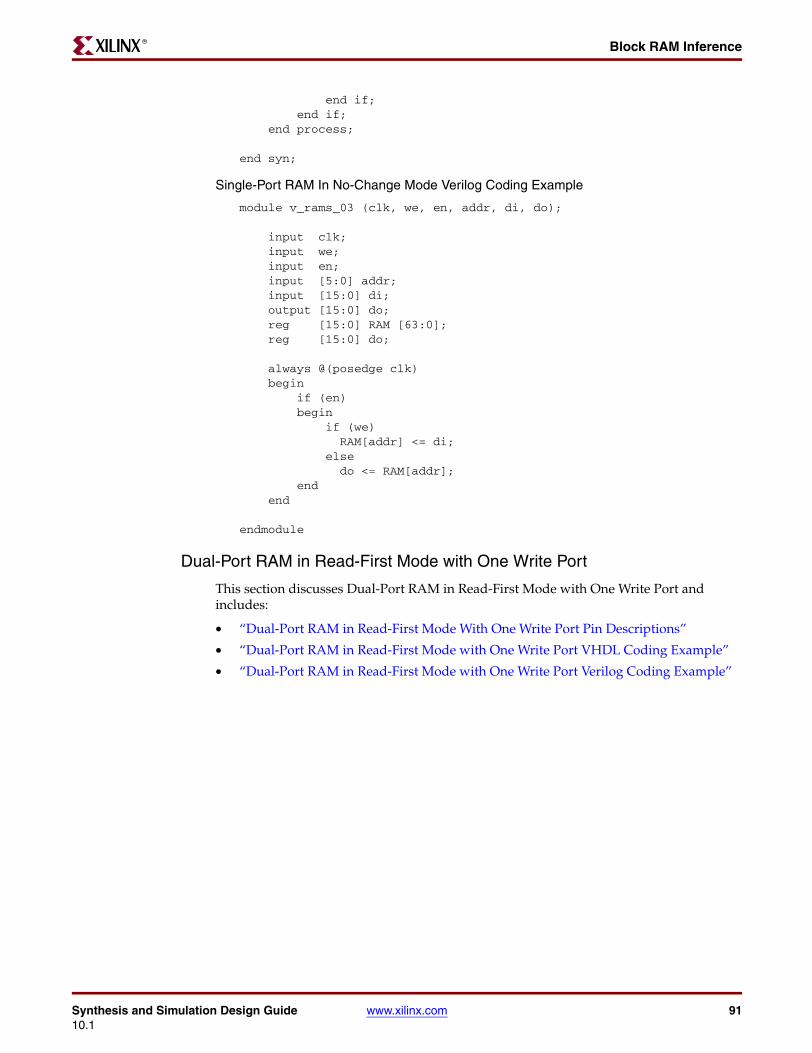
Synthesis and Simulation Design Guide www.xilinx.com 9110.1
Block RAM InferenceR
end if; end if; end process;
end syn;
Single-Port RAM In No-Change Mode Verilog Coding Example
module v_rams_03 (clk, we, en, addr, di, do);
input clk; input we; input en; input [5:0] addr; input [15:0] di; output [15:0] do; reg [15:0] RAM [63:0]; reg [15:0] do;
always @(posedge clk) begin if (en) begin if (we) RAM[addr] <= di; else do <= RAM[addr]; end end
endmodule
Dual-Port RAM in Read-First Mode with One Write Port
This section discusses Dual-Port RAM in Read-First Mode with One Write Port and includes:
• “Dual-Port RAM in Read-First Mode With One Write Port Pin Descriptions”
• “Dual-Port RAM in Read-First Mode with One Write Port VHDL Coding Example”
• “Dual-Port RAM in Read-First Mode with One Write Port Verilog Coding Example”
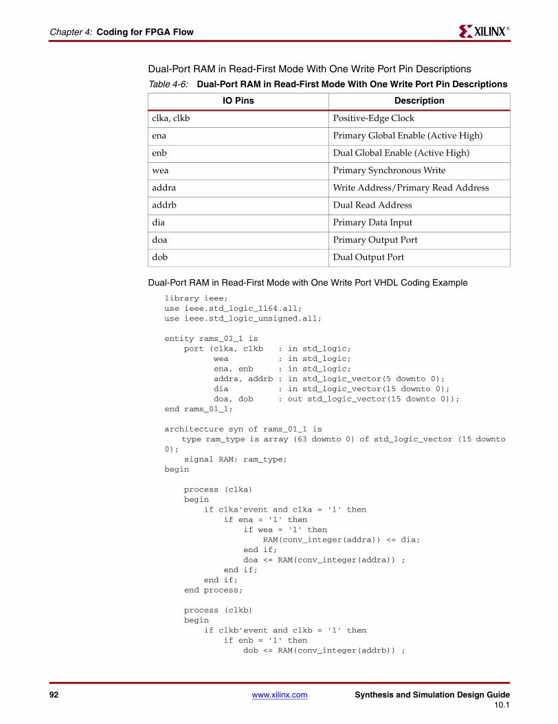
92 www.xilinx.com Synthesis and Simulation Design Guide10.1
Chapter 4: Coding for FPGA FlowR
Dual-Port RAM in Read-First Mode With One Write Port Pin Descriptions
Dual-Port RAM in Read-First Mode with One Write Port VHDL Coding Example
library ieee;use ieee.std_logic_1164.all;use ieee.std_logic_unsigned.all;
entity rams_01_1 is port (clka, clkb : in std_logic; wea : in std_logic; ena, enb : in std_logic; addra, addrb : in std_logic_vector(5 downto 0); dia : in std_logic_vector(15 downto 0); doa, dob : out std_logic_vector(15 downto 0));end rams_01_1;
architecture syn of rams_01_1 is type ram_type is array (63 downto 0) of std_logic_vector (15 downto 0); signal RAM: ram_type;begin
process (clka) begin if clka'event and clka = '1' then if ena = '1' then if wea = '1' then RAM(conv_integer(addra)) <= dia; end if; doa <= RAM(conv_integer(addra)) ; end if; end if; end process;
process (clkb) begin if clkb'event and clkb = '1' then if enb = '1' then dob <= RAM(conv_integer(addrb)) ;
Table 4-6: Dual-Port RAM in Read-First Mode With One Write Port Pin Descriptions
IO Pins Description
clka, clkb Positive-Edge Clock
ena Primary Global Enable (Active High)
enb Dual Global Enable (Active High)
wea Primary Synchronous Write
addra Write Address/Primary Read Address
addrb Dual Read Address
dia Primary Data Input
doa Primary Output Port
dob Dual Output Port
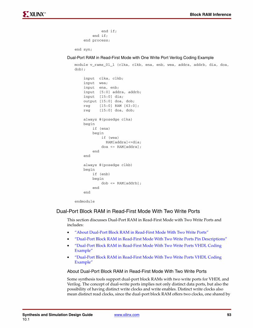
Synthesis and Simulation Design Guide www.xilinx.com 9310.1
Block RAM InferenceR
end if; end if; end process;
end syn;
Dual-Port RAM in Read-First Mode with One Write Port Verilog Coding Example
module v_rams_01_1 (clka, clkb, ena, enb, wea, addra, addrb, dia, doa, dob);
input clka, clkb; input wea; input ena, enb; input [5:0] addra, addrb; input [15:0] dia; output [15:0] doa, dob; reg [15:0] RAM [63:0]; reg [15:0] doa, dob;
always @(posedge clka) begin if (ena) begin if (wea) RAM[addra]<=dia; doa <= RAM[addra]; end end
always @(posedge clkb) begin if (enb) begin dob <= RAM[addrb]; end end
endmodule
Dual-Port Block RAM in Read-First Mode With Two Write Ports
This section discusses Dual-Port RAM in Read-First Mode with Two Write Ports and includes:
• “About Dual-Port Block RAM in Read-First Mode With Two Write Ports”
• “Dual-Port Block RAM in Read-First Mode With Two Write Ports Pin Descriptions”
• “Dual-Port Block RAM in Read-First Mode With Two Write Ports VHDL Coding Example”
• “Dual-Port Block RAM in Read-First Mode With Two Write Ports VHDL Coding Example”
About Dual-Port Block RAM in Read-First Mode With Two Write Ports
Some synthesis tools support dual-port block RAMs with two write ports for VHDL and Verilog. The concept of dual-write ports implies not only distinct data ports, but also the possibility of having distinct write clocks and write enables. Distinct write clocks also mean distinct read clocks, since the dual-port block RAM offers two clocks, one shared by
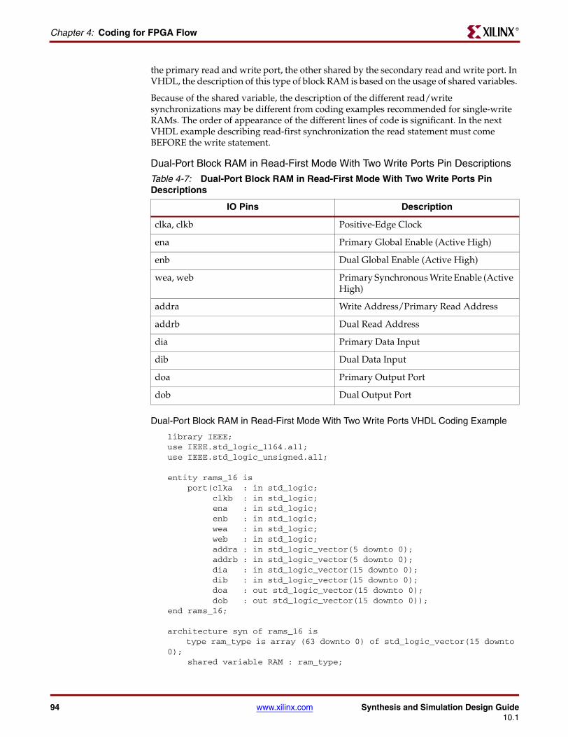
94 www.xilinx.com Synthesis and Simulation Design Guide10.1
Chapter 4: Coding for FPGA FlowR
the primary read and write port, the other shared by the secondary read and write port. In VHDL, the description of this type of block RAM is based on the usage of shared variables.
Because of the shared variable, the description of the different read/write synchronizations may be different from coding examples recommended for single-write RAMs. The order of appearance of the different lines of code is significant. In the next VHDL example describing read-first synchronization the read statement must come BEFORE the write statement.
Dual-Port Block RAM in Read-First Mode With Two Write Ports Pin Descriptions
Dual-Port Block RAM in Read-First Mode With Two Write Ports VHDL Coding Example
library IEEE;use IEEE.std_logic_1164.all;use IEEE.std_logic_unsigned.all;
entity rams_16 is port(clka : in std_logic; clkb : in std_logic; ena : in std_logic; enb : in std_logic; wea : in std_logic; web : in std_logic; addra : in std_logic_vector(5 downto 0); addrb : in std_logic_vector(5 downto 0); dia : in std_logic_vector(15 downto 0); dib : in std_logic_vector(15 downto 0); doa : out std_logic_vector(15 downto 0); dob : out std_logic_vector(15 downto 0));end rams_16;
architecture syn of rams_16 is type ram_type is array (63 downto 0) of std_logic_vector(15 downto 0); shared variable RAM : ram_type;
Table 4-7: Dual-Port Block RAM in Read-First Mode With Two Write Ports Pin Descriptions
IO Pins Description
clka, clkb Positive-Edge Clock
ena Primary Global Enable (Active High)
enb Dual Global Enable (Active High)
wea, web Primary Synchronous Write Enable (Active High)
addra Write Address/Primary Read Address
addrb Dual Read Address
dia Primary Data Input
dib Dual Data Input
doa Primary Output Port
dob Dual Output Port
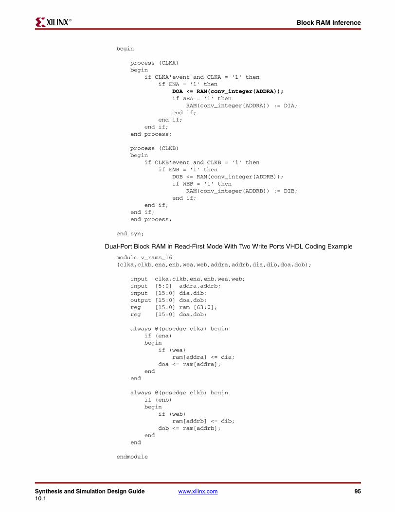
Synthesis and Simulation Design Guide www.xilinx.com 9510.1
Block RAM InferenceR
begin
process (CLKA) begin if CLKA'event and CLKA = '1' then if ENA = '1' then DOA <= RAM(conv_integer(ADDRA)); if WEA = '1' then RAM(conv_integer(ADDRA)) := DIA; end if; end if; end if; end process;
process (CLKB) begin if CLKB'event and CLKB = '1' then if ENB = '1' then DOB <= RAM(conv_integer(ADDRB)); if WEB = '1' then RAM(conv_integer(ADDRB)) := DIB; end if; end if; end if; end process;
end syn;
Dual-Port Block RAM in Read-First Mode With Two Write Ports VHDL Coding Example
module v_rams_16 (clka,clkb,ena,enb,wea,web,addra,addrb,dia,dib,doa,dob);
input clka,clkb,ena,enb,wea,web; input [5:0] addra,addrb; input [15:0] dia,dib; output [15:0] doa,dob; reg [15:0] ram [63:0]; reg [15:0] doa,dob;
always @(posedge clka) begin if (ena) begin if (wea) ram[addra] <= dia; doa <= ram[addra]; end end
always @(posedge clkb) begin if (enb) begin if (web) ram[addrb] <= dib; dob <= ram[addrb]; end end
endmodule
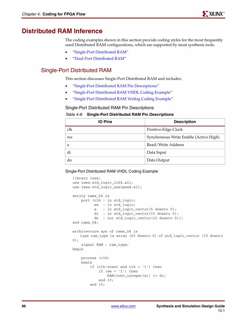
96 www.xilinx.com Synthesis and Simulation Design Guide10.1
Chapter 4: Coding for FPGA FlowR
Distributed RAM InferenceThe coding examples shown in this section provide coding styles for the most frequently used Distributed RAM configurations, which are supported by most synthesis tools.
• “Single-Port Distributed RAM”
• “Dual-Port Distributed RAM”
Single-Port Distributed RAMThis section discusses Single-Port Distributed RAM and includes:
• “Single-Port Distributed RAM Pin Descriptions”
• “Single-Port Distributed RAM VHDL Coding Example”
• “Single-Port Distributed RAM Verilog Coding Example”
Single-Port Distributed RAM Pin Descriptions
Single-Port Distributed RAM VHDL Coding Example
library ieee;use ieee.std_logic_1164.all;use ieee.std_logic_unsigned.all;
entity rams_04 is port (clk : in std_logic; we : in std_logic; a : in std_logic_vector(5 downto 0); di : in std_logic_vector(15 downto 0); do : out std_logic_vector(15 downto 0));end rams_04;
architecture syn of rams_04 is type ram_type is array (63 downto 0) of std_logic_vector (15 downto 0); signal RAM : ram_type;begin
process (clk) begin if (clk'event and clk = '1') then if (we = '1') then RAM(conv_integer(a)) <= di; end if; end if;
Table 4-8: Single-Port Distributed RAM Pin Descriptions
IO Pins Description
clk Positive-Edge Clock
we Synchronous Write Enable (Active High)
a Read/Write Address
di Data Input
do Data Output
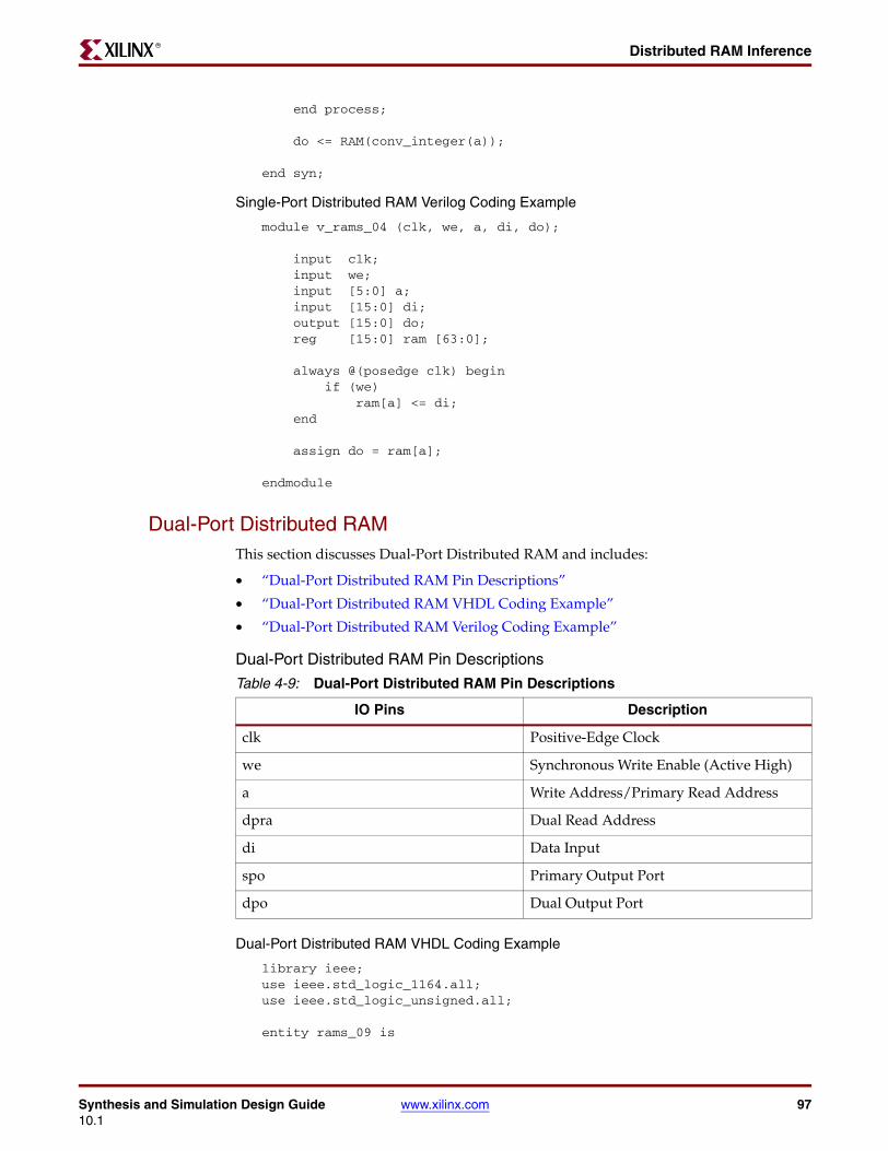
Synthesis and Simulation Design Guide www.xilinx.com 9710.1
Distributed RAM InferenceR
end process;
do <= RAM(conv_integer(a));
end syn;
Single-Port Distributed RAM Verilog Coding Example
module v_rams_04 (clk, we, a, di, do);
input clk; input we; input [5:0] a; input [15:0] di; output [15:0] do; reg [15:0] ram [63:0];
always @(posedge clk) begin if (we) ram[a] <= di; end
assign do = ram[a];
endmodule
Dual-Port Distributed RAMThis section discusses Dual-Port Distributed RAM and includes:
• “Dual-Port Distributed RAM Pin Descriptions”
• “Dual-Port Distributed RAM VHDL Coding Example”
• “Dual-Port Distributed RAM Verilog Coding Example”
Dual-Port Distributed RAM Pin Descriptions
Dual-Port Distributed RAM VHDL Coding Example
library ieee;use ieee.std_logic_1164.all;use ieee.std_logic_unsigned.all;
entity rams_09 is
Table 4-9: Dual-Port Distributed RAM Pin Descriptions
IO Pins Description
clk Positive-Edge Clock
we Synchronous Write Enable (Active High)
a Write Address/Primary Read Address
dpra Dual Read Address
di Data Input
spo Primary Output Port
dpo Dual Output Port
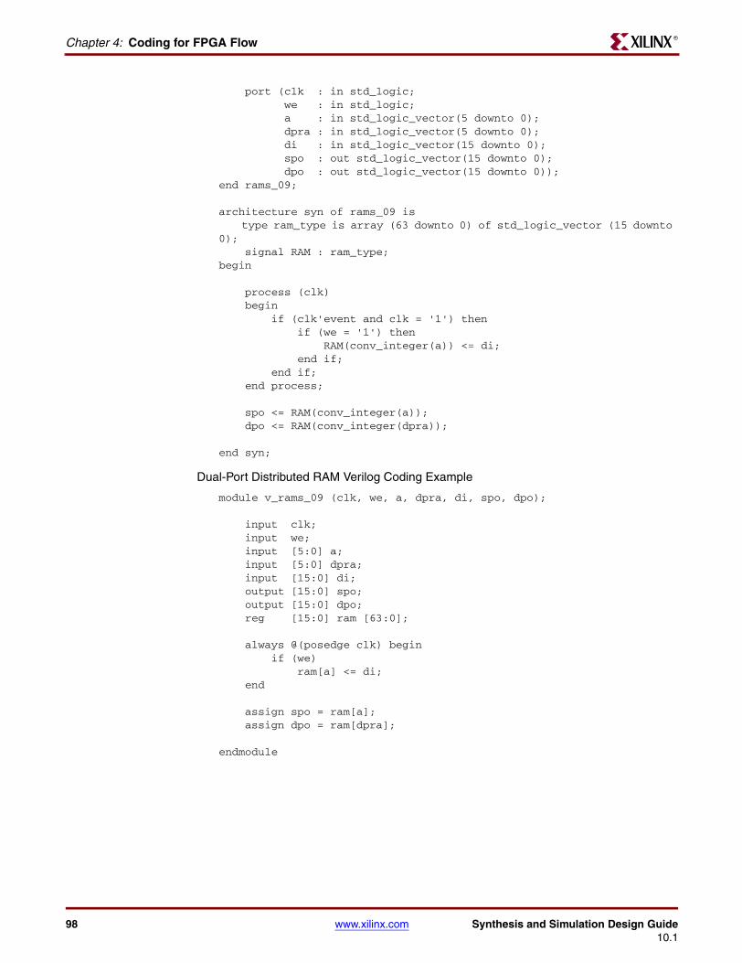
98 www.xilinx.com Synthesis and Simulation Design Guide10.1
Chapter 4: Coding for FPGA FlowR
port (clk : in std_logic; we : in std_logic; a : in std_logic_vector(5 downto 0); dpra : in std_logic_vector(5 downto 0); di : in std_logic_vector(15 downto 0); spo : out std_logic_vector(15 downto 0); dpo : out std_logic_vector(15 downto 0));end rams_09;
architecture syn of rams_09 is type ram_type is array (63 downto 0) of std_logic_vector (15 downto 0); signal RAM : ram_type;begin
process (clk) begin if (clk'event and clk = '1') then if (we = '1') then RAM(conv_integer(a)) <= di; end if; end if; end process;
spo <= RAM(conv_integer(a)); dpo <= RAM(conv_integer(dpra));
end syn;
Dual-Port Distributed RAM Verilog Coding Example
module v_rams_09 (clk, we, a, dpra, di, spo, dpo);
input clk; input we; input [5:0] a; input [5:0] dpra; input [15:0] di; output [15:0] spo; output [15:0] dpo; reg [15:0] ram [63:0];
always @(posedge clk) begin if (we) ram[a] <= di; end
assign spo = ram[a]; assign dpo = ram[dpra];
endmodule
Synthesis and Simulation Design Guide www.xilinx.com 9910.1
Arithmetic SupportR
Arithmetic SupportThis section discusses Arithmetic Support and includes:
• “About Arithmetic Support”
• “Arithmetic Support Coding Examples”
• “Order and Group Arithmetic Functions”
• “Order and Group Arithmetic Functions”
About Arithmetic SupportXilinx FPGA devices traditionally contain several hardware resources such as LUTs and Carry Chains. These hardware resources efficiently implement various arithmetic operations such as adders, subtractors, counters, accumulators, and comparators.
With the release of the Virtex-4 device, Xilinx introduced a new primitive called DSP48. This block was further enhanced in later families such as Virtex-5 and Spartan-3A DSP. DSP48 allows you to create numerous functions, including multipliers, adders, counters, barrel shifters, comparators, accumulators, multiply accumulate, complex multipliers, and others.
Currently, synthesis tools support the most important and frequently used DSP48 modes for DSP applications such as multipliers, adders/subtractors, multiply adders/subtractors, and multiply accumulate. The synthesis tools also take advantage of the internal registers available in DSP48, as well as the dynamic OPMODE port.
DSP48 fast connections allow you to efficiently build fast DSP48 chains as filters. These fast connections are automatically supported by synthesis tools today.
The level of DSP48 support may differ from one synthesis tool to another. For more information, see your synthesis tool documentation.
Since there are several ways to implement the same arithmetic operation on the target device, synthesis tools make automatic choices depending on the operation type, size, context usage, or timing requirements. In some situations, the automatic choice may not meet your goals. Synthesis tools therefore offer several constraints to control implementation process such as use_dsp48 in XST or syn_dspstyle in Synplicity. For more information, see your synthesis tool documentation.
If you migrate a design previously implemented using an older and FPGA device family to a newer one with a DSP48 block, and you want to take advantage of available DSP48 blocks, you must be aware of the following rules in order to get the best performance.
• DSP48 blocks give you the best performance when fully pipelined. You should add additional pipelining stages in order to get the best performance.
• Internal DSP48 registers support synchronous set and reset signals. Asynchronous set and reset signals are not supported. You must replace asynchronous initialization signals by synchronous ones. Some synthesis tools may automatically make this replacement. This operation renders the generated netlist NOT equivalent to the initial RTL description. For more information, see your synthesis tool documentation.
• For DSP applications, use chain structures instead of tree structures in your RTL description in order to take full advantage of the DSP48 capabilities.
For more information on DSP48 blocks and specific DSP application coding style, see the ExtremeDSP User Guide for your target family
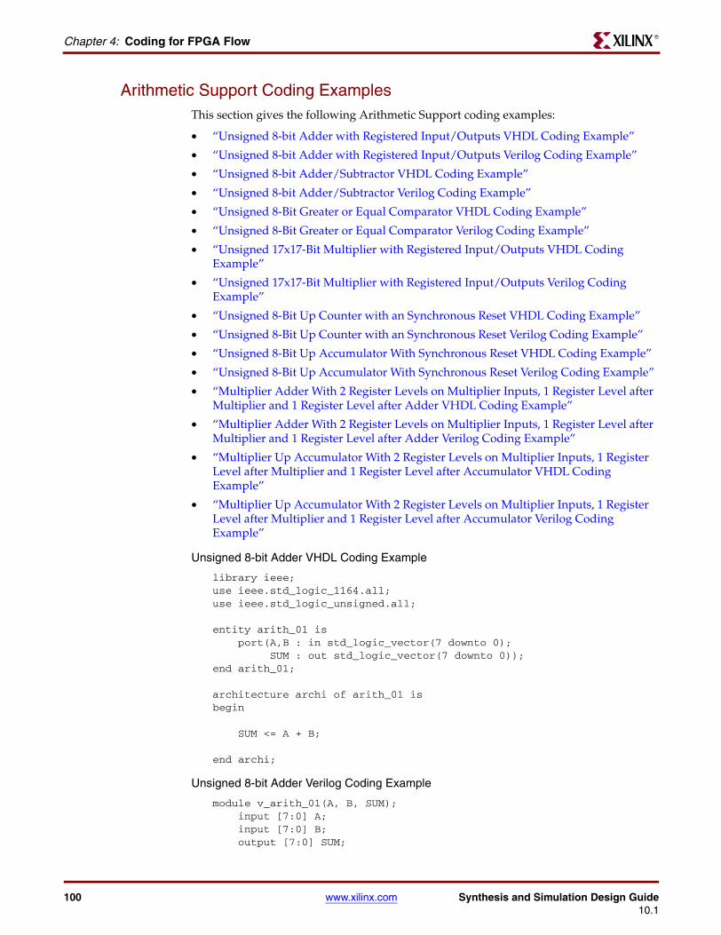
100 www.xilinx.com Synthesis and Simulation Design Guide10.1
Chapter 4: Coding for FPGA FlowR
Arithmetic Support Coding ExamplesThis section gives the following Arithmetic Support coding examples:
• “Unsigned 8-bit Adder with Registered Input/Outputs VHDL Coding Example”
• “Unsigned 8-bit Adder with Registered Input/Outputs Verilog Coding Example”
• “Unsigned 8-bit Adder/Subtractor VHDL Coding Example”
• “Unsigned 8-bit Adder/Subtractor Verilog Coding Example”
• “Unsigned 8-Bit Greater or Equal Comparator VHDL Coding Example”
• “Unsigned 8-Bit Greater or Equal Comparator Verilog Coding Example”
• “Unsigned 17x17-Bit Multiplier with Registered Input/Outputs VHDL Coding Example”
• “Unsigned 17x17-Bit Multiplier with Registered Input/Outputs Verilog Coding Example”
• “Unsigned 8-Bit Up Counter with an Synchronous Reset VHDL Coding Example”
• “Unsigned 8-Bit Up Counter with an Synchronous Reset Verilog Coding Example”
• “Unsigned 8-Bit Up Accumulator With Synchronous Reset VHDL Coding Example”
• “Unsigned 8-Bit Up Accumulator With Synchronous Reset Verilog Coding Example”
• “Multiplier Adder With 2 Register Levels on Multiplier Inputs, 1 Register Level after Multiplier and 1 Register Level after Adder VHDL Coding Example”
• “Multiplier Adder With 2 Register Levels on Multiplier Inputs, 1 Register Level after Multiplier and 1 Register Level after Adder Verilog Coding Example”
• “Multiplier Up Accumulator With 2 Register Levels on Multiplier Inputs, 1 Register Level after Multiplier and 1 Register Level after Accumulator VHDL Coding Example”
• “Multiplier Up Accumulator With 2 Register Levels on Multiplier Inputs, 1 Register Level after Multiplier and 1 Register Level after Accumulator Verilog Coding Example”
Unsigned 8-bit Adder VHDL Coding Example
library ieee;use ieee.std_logic_1164.all;use ieee.std_logic_unsigned.all;
entity arith_01 is port(A,B : in std_logic_vector(7 downto 0); SUM : out std_logic_vector(7 downto 0));end arith_01;
architecture archi of arith_01 isbegin
SUM <= A + B;
end archi;
Unsigned 8-bit Adder Verilog Coding Example
module v_arith_01(A, B, SUM); input [7:0] A; input [7:0] B; output [7:0] SUM;
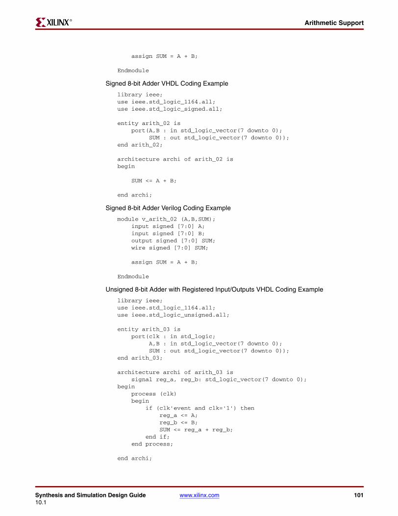
Synthesis and Simulation Design Guide www.xilinx.com 10110.1
Arithmetic SupportR
assign SUM = A + B;
Endmodule
Signed 8-bit Adder VHDL Coding Example
library ieee;use ieee.std_logic_1164.all;use ieee.std_logic_signed.all;
entity arith_02 is port(A,B : in std_logic_vector(7 downto 0); SUM : out std_logic_vector(7 downto 0));end arith_02;
architecture archi of arith_02 isbegin
SUM <= A + B;
end archi;
Signed 8-bit Adder Verilog Coding Example
module v_arith_02 (A,B,SUM); input signed [7:0] A; input signed [7:0] B; output signed [7:0] SUM; wire signed [7:0] SUM;
assign SUM = A + B;
Endmodule
Unsigned 8-bit Adder with Registered Input/Outputs VHDL Coding Example
library ieee;use ieee.std_logic_1164.all;use ieee.std_logic_unsigned.all;
entity arith_03 is port(clk : in std_logic; A,B : in std_logic_vector(7 downto 0); SUM : out std_logic_vector(7 downto 0));end arith_03;
architecture archi of arith_03 is signal reg_a, reg_b: std_logic_vector(7 downto 0);begin process (clk) begin if (clk'event and clk='1') then reg_a <= A; reg_b <= B; SUM <= reg_a + reg_b; end if; end process;
end archi;
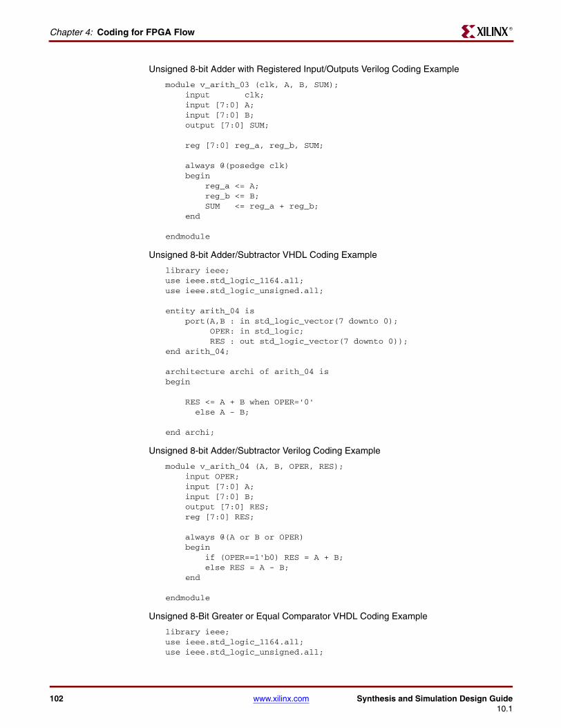
102 www.xilinx.com Synthesis and Simulation Design Guide10.1
Chapter 4: Coding for FPGA FlowR
Unsigned 8-bit Adder with Registered Input/Outputs Verilog Coding Example
module v_arith_03 (clk, A, B, SUM); input clk; input [7:0] A; input [7:0] B; output [7:0] SUM;
reg [7:0] reg_a, reg_b, SUM;
always @(posedge clk) begin reg_a <= A; reg_b <= B; SUM <= reg_a + reg_b; end
endmodule
Unsigned 8-bit Adder/Subtractor VHDL Coding Example
library ieee;use ieee.std_logic_1164.all;use ieee.std_logic_unsigned.all;
entity arith_04 is port(A,B : in std_logic_vector(7 downto 0); OPER: in std_logic; RES : out std_logic_vector(7 downto 0));end arith_04;
architecture archi of arith_04 isbegin
RES <= A + B when OPER='0' else A - B;
end archi;
Unsigned 8-bit Adder/Subtractor Verilog Coding Example
module v_arith_04 (A, B, OPER, RES); input OPER; input [7:0] A; input [7:0] B; output [7:0] RES; reg [7:0] RES;
always @(A or B or OPER) begin if (OPER==1'b0) RES = A + B; else RES = A - B; end
endmodule
Unsigned 8-Bit Greater or Equal Comparator VHDL Coding Example
library ieee;use ieee.std_logic_1164.all;use ieee.std_logic_unsigned.all;
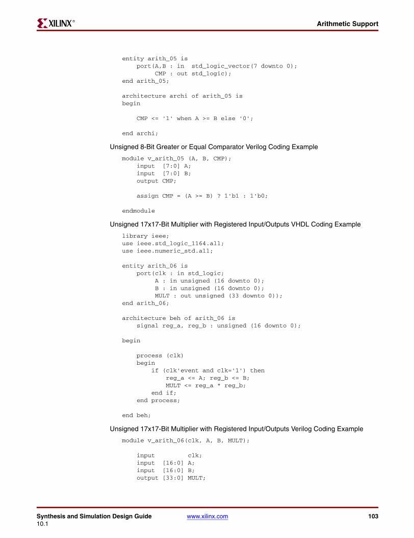
Synthesis and Simulation Design Guide www.xilinx.com 10310.1
Arithmetic SupportR
entity arith_05 is port(A,B : in std_logic_vector(7 downto 0); CMP : out std_logic);end arith_05;
architecture archi of arith_05 isbegin
CMP <= '1' when A >= B else '0';
end archi;
Unsigned 8-Bit Greater or Equal Comparator Verilog Coding Example
module v_arith_05 (A, B, CMP); input [7:0] A; input [7:0] B; output CMP;
assign CMP = (A >= B) ? 1'b1 : 1'b0;
endmodule
Unsigned 17x17-Bit Multiplier with Registered Input/Outputs VHDL Coding Example
library ieee;use ieee.std_logic_1164.all;use ieee.numeric_std.all;
entity arith_06 is port(clk : in std_logic; A : in unsigned (16 downto 0); B : in unsigned (16 downto 0); MULT : out unsigned (33 downto 0));end arith_06;
architecture beh of arith_06 is signal reg_a, reg_b : unsigned (16 downto 0);
begin process (clk) begin if (clk'event and clk='1') then reg_a <= A; reg_b <= B; MULT <= reg_a * reg_b; end if; end process;
end beh;
Unsigned 17x17-Bit Multiplier with Registered Input/Outputs Verilog Coding Example
module v_arith_06(clk, A, B, MULT);
input clk; input [16:0] A; input [16:0] B; output [33:0] MULT;
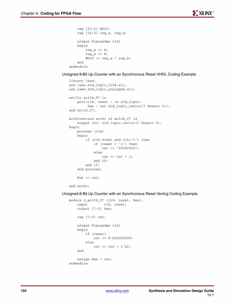
104 www.xilinx.com Synthesis and Simulation Design Guide10.1
Chapter 4: Coding for FPGA FlowR
reg [33:0] MULT; reg [16:0] reg_a, reg_b; always @(posedge clk) begin reg_a <= A; reg_b <= B; MULT <= reg_a * reg_b; endendmodule
Unsigned 8-Bit Up Counter with an Synchronous Reset VHDL Coding Example
library ieee;use ieee.std_logic_1164.all;use ieee.std_logic_unsigned.all;
entity arith_07 is port(clk, reset : in std_logic; Res : out std_logic_vector(7 downto 0));end arith_07;
architecture archi of arith_07 is signal cnt: std_logic_vector(7 downto 0);begin process (clk) begin if (clk'event and clk='1') then if (reset = '1') then cnt <= "00000000"; else cnt <= cnt + 1; end if; end if; end process;
Res <= cnt;
end archi;
Unsigned 8-Bit Up Counter with an Synchronous Reset Verilog Coding Example
module v_arith_07 (clk, reset, Res); input clk, reset; output [7:0] Res;
reg [7:0] cnt;
always @(posedge clk) begin if (reset) cnt <= 8'b00000000; else cnt <= cnt + 1'b1; end
assign Res = cnt;endmodule
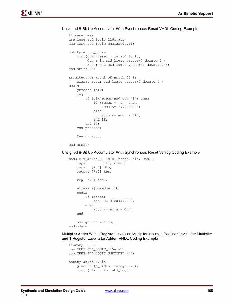
Synthesis and Simulation Design Guide www.xilinx.com 10510.1
Arithmetic SupportR
Unsigned 8-Bit Up Accumulator With Synchronous Reset VHDL Coding Example
library ieee;use ieee.std_logic_1164.all;use ieee.std_logic_unsigned.all;
entity arith_08 is port(clk, reset : in std_logic; din : in std_logic_vector(7 downto 0); Res : out std_logic_vector(7 downto 0));end arith_08;
architecture archi of arith_08 is signal accu: std_logic_vector(7 downto 0);begin process (clk) begin if (clk'event and clk='1') then if (reset = '1') then accu <= "00000000"; else accu <= accu + din; end if; end if; end process;
Res <= accu;
end archi;
Unsigned 8-Bit Up Accumulator With Synchronous Reset Verilog Coding Example
module v_arith_08 (clk, reset, din, Res); input clk, reset; input [7:0] din; output [7:0] Res;
reg [7:0] accu;
always @(posedge clk) begin if (reset) accu <= 8'b00000000; else accu <= accu + din; end
assign Res = accu;endmodule
Multiplier Adder With 2 Register Levels on Multiplier Inputs, 1 Register Level after Multiplier and 1 Register Level after Adder VHDL Coding Example
library IEEE;use IEEE.STD_LOGIC_1164.ALL;use IEEE.STD_LOGIC_UNSIGNED.ALL;
entity arith_09 is generic (p_width: integer:=8); port (clk : in std_logic;
106 www.xilinx.com Synthesis and Simulation Design Guide10.1
Chapter 4: Coding for FPGA FlowR
A, B : in std_logic_vector(7 downto 0); C : in std_logic_vector(15 downto 0); RES : out std_logic_vector(15 downto 0));end arith_09;
architecture beh of arith_09 is signal reg1_A, reg2_A, reg1_B, reg2_B : std_logic_vector(7 downto 0); signal reg_C, reg_mult : std_logic_vector(15 downto 0);begin
process (clk) begin if (clk'event and clk='1') then reg1_A <= A; reg2_A <= reg1_A; reg1_B <= B; reg2_B <= reg1_B; reg_C <= C; reg_mult <= reg2_A * reg2_B; RES <= reg_mult + reg_C; end if; end process;
end beh;
Multiplier Adder With 2 Register Levels on Multiplier Inputs, 1 Register Level after Multiplier and 1 Register Level after Adder Verilog Coding Example
module v_arith_09 (clk, A, B, C, RES);
input clk; input [7:0] A; input [7:0] B; input [15:0] C; output [15:0] RES; reg [7:0] reg1_A, reg2_A, reg1_B, reg2_B; reg [15:0] reg_C, reg_mult, RES;
always @(posedge clk) begin reg1_A <= A; reg2_A <= reg1_A; reg1_B <= B; reg2_B <= reg1_B; reg_C <= C; reg_mult <= reg2_A * reg2_B; RES <= reg_mult + reg_C; end
endmodule
Multiplier Up Accumulator With 2 Register Levels on Multiplier Inputs, 1 Register Level after Multiplier and 1 Register Level after Accumulator VHDL Coding Example
library IEEE;use IEEE.STD_LOGIC_1164.ALL;use IEEE.STD_LOGIC_UNSIGNED.ALL;
entity arith_10 is port (clk : in std_logic; A, B : in std_logic_vector(7 downto 0); RES : out std_logic_vector(15 downto 0));end arith_10;
Synthesis and Simulation Design Guide www.xilinx.com 10710.1
Arithmetic SupportR
architecture beh of arith_10 is signal reg1_A, reg2_A, reg1_B, reg2_B : std_logic_vector(7 downto 0); signal reg_mult, reg_accu : std_logic_vector(15 downto 0);begin
process (clk) begin if (clk'event and clk='1') then reg1_A <= A; reg2_A <= reg1_A; reg1_B <= B; reg2_B <= reg1_B; reg_mult <= reg2_A * reg2_B; reg_accu <= reg_accu + reg_mult; end if; end process;
RES <= reg_accu;
end beh;
Multiplier Up Accumulator With 2 Register Levels on Multiplier Inputs, 1 Register Level after Multiplier and 1 Register Level after Accumulator Verilog Coding Example
module v_arith_10 (clk, A, B, RES);
input clk; input [7:0] A; input [7:0] B; output [15:0] RES; reg [7:0] reg1_A, reg2_A, reg1_B, reg2_B; reg [15:0] reg_mult, reg_accu; wire [15:0] RES;
always @(posedge clk) begin reg1_A <= A; reg2_A <= reg1_A; reg1_B <= B; reg2_B <= reg1_B; reg_mult <= reg2_A * reg2_B; reg_accu <= reg_accu + reg_mult; end
assign RES = reg_accu;
endmodule
Order and Group Arithmetic FunctionsThe ordering and grouping of arithmetic functions can influence design performance. For example, the following two VHDL statements are not necessarily equivalent:
ADD <= A1 + A2 + A3 + A4;ADD <= (A1 + A2) + (A3 + A4);
For Verilog, the following two statements are not necessarily equivalent:
ADD = A1 + A2 + A3 + A4;ADD = (A1 + A2) + (A3 + A4);
108 www.xilinx.com Synthesis and Simulation Design Guide10.1
Chapter 4: Coding for FPGA FlowR
The first statement cascades three adders in series. The second statement creates two adders in parallel: A1 + A2 and A3 + A4. In the second statement, the two additions are evaluated in parallel and the results are combined with a third adder. Register Transfer Level (RTL) simulation results are the same for both statements. The second statement results in a faster circuit after synthesis (depending on the bit width of the input signals).
Although the second statement generally results in a faster circuit, in some cases, you may want to use the first statement. For example, if the A4 signal reaches the adder later than the other signals, the first statement produces a faster implementation because the cascaded structure creates fewer logic levels for A4. This structure allows A4 to catch up to the other signals. In this case, A1 is the fastest signal followed by A2 and A3. A4 is the slowest signal.
Most synthesis tools can balance or restructure the arithmetic operator tree if timing constraints require it. However, Xilinx recommends that you code your design for your selected structure.
Resource SharingThis section discusses Resource Sharing, and includes:
• “About Resource Sharing”
• “Resource Sharing Coding Examples”
About Resource Sharing
Resource sharing uses a single functional block (such as an adder or comparator) to implement several operators in the HDL code. Use resource sharing to improve design performance by reducing the gate count and the routing congestion. If you do not use resource sharing, each HDL operation is built with separate circuitry. You may want to disable resource sharing for speed critical paths in your design.
The following operators can be shared either with instances of the same operator or with an operator on the same line.
*+ -> >= < <=
For example, a + (plus) operator can be shared with instances of other + (plus) operators or with – (minus) operators. An * (asterisk) operator can be shared only with other * (asterisk) operators.
You can implement arithmetic functions (+, –, magnitude comparators) with gates or with your synthesis tool module library. The library functions use modules that take advantage of the carry logic in the FPGA devices. Carry logic and its dedicated routing increase the speed of arithmetic functions that are larger than 4 bits. To increase speed, use the module library if your design contains arithmetic functions that are larger than 4 bits, or if your design contains only one arithmetic function. Resource sharing of the module library automatically occurs in most synthesis tools if the arithmetic functions are in the same process.
Resource sharing adds additional logic levels to multiplex the inputs to implement more than one function. You may not want to use it for arithmetic functions that are part of a time critical path.
Since resource sharing allows you to reduce design resources, the device area required for your design is also decreased. The area used for a shared resource depends on the type and
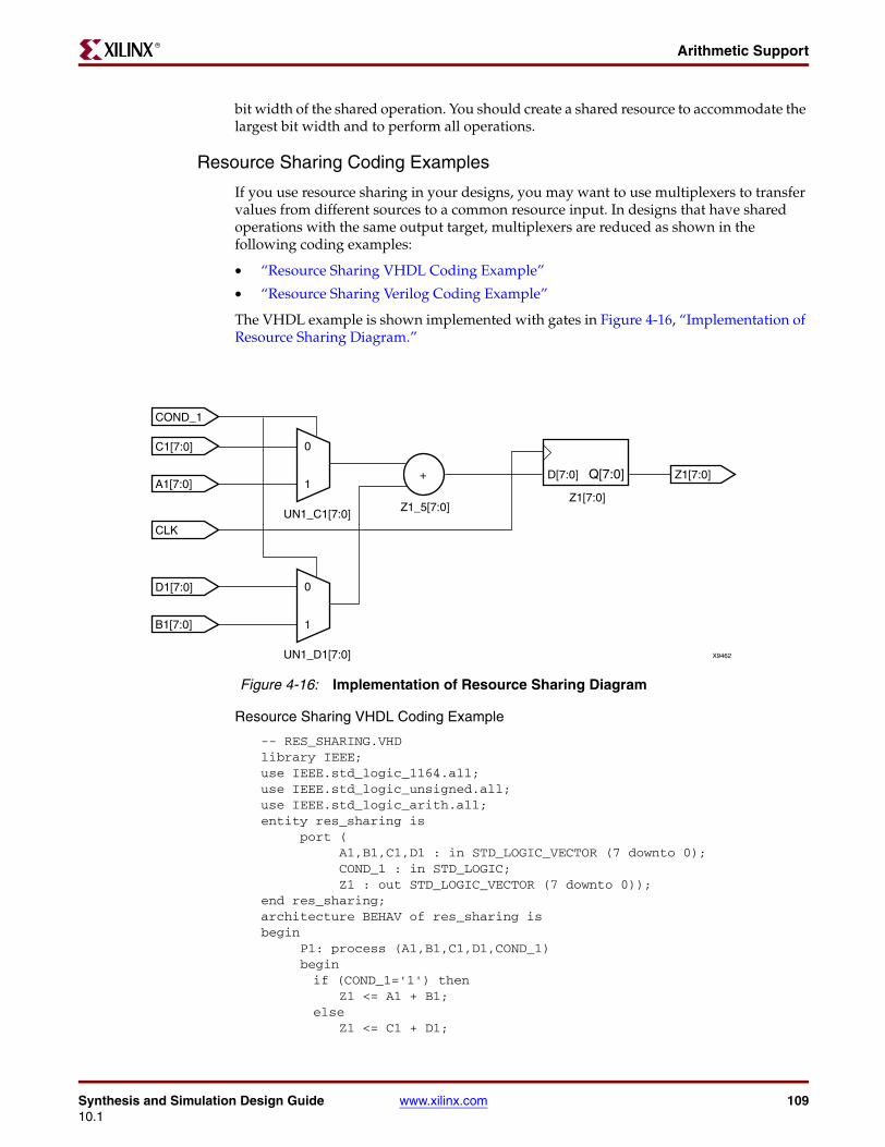
Synthesis and Simulation Design Guide www.xilinx.com 10910.1
Arithmetic SupportR
bit width of the shared operation. You should create a shared resource to accommodate the largest bit width and to perform all operations.
Resource Sharing Coding Examples
If you use resource sharing in your designs, you may want to use multiplexers to transfer values from different sources to a common resource input. In designs that have shared operations with the same output target, multiplexers are reduced as shown in the following coding examples:
• “Resource Sharing VHDL Coding Example”
• “Resource Sharing Verilog Coding Example”
The VHDL example is shown implemented with gates in Figure 4-16, “Implementation of Resource Sharing Diagram.”
Resource Sharing VHDL Coding Example
-- RES_SHARING.VHDlibrary IEEE;use IEEE.std_logic_1164.all;use IEEE.std_logic_unsigned.all;use IEEE.std_logic_arith.all;entity res_sharing is
port (A1,B1,C1,D1 : in STD_LOGIC_VECTOR (7 downto 0);COND_1 : in STD_LOGIC;Z1 : out STD_LOGIC_VECTOR (7 downto 0));
end res_sharing;architecture BEHAV of res_sharing isbegin
P1: process (A1,B1,C1,D1,COND_1)beginif (COND_1='1') then
Z1 <= A1 + B1;else
Z1 <= C1 + D1;
Figure 4-16: Implementation of Resource Sharing Diagram
X9462
+
UN1_C1[7:0]Z1_5[7:0]
0
1
COND_1
C1[7:0]
A1[7:0]
UN1_D1[7:0]
0
1
CLK
D1[7:0]
B1[7:0]
Z1[7:0]
Z1[7:0]
D[7:0] Q[7:0]
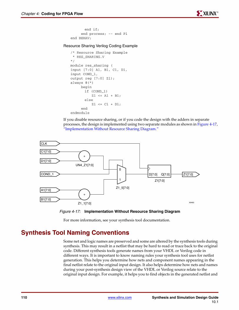
110 www.xilinx.com Synthesis and Simulation Design Guide10.1
Chapter 4: Coding for FPGA FlowR
end if;end process; -- end P1
end BEHAV;
Resource Sharing Verilog Coding Example
/* Resource Sharing Example * RES_SHARING.V*/module res_sharing (input [7:0] A1, B1, C1, D1,input COND_1,output reg [7:0] Z1);always @(*)
beginif (COND_1)
Z1 <= A1 + B1;else
Z1 <= C1 + D1;end
endmodule
If you disable resource sharing, or if you code the design with the adders in separate processes, the design is implemented using two separate modules as shown in Figure 4-17, “Implementation Without Resource Sharing Diagram.”
For more information, see your synthesis tool documentation.
Synthesis Tool Naming ConventionsSome net and logic names are preserved and some are altered by the synthesis tools during synthesis. This may result in a netlist that may be hard to read or trace back to the original code. Different synthesis tools generate names from your VHDL or Verilog code in different ways. It is important to know naming rules your synthesis tool uses for netlist generation. This helps you determine how nets and component names appearing in the final netlist relate to the original input design. It also helps determine how nets and names during your post-synthesis design view of the VHDL or Verilog source relate to the original input design. For example, it helps you to find objects in the generated netlist and
Figure 4-17: Implementation Without Resource Sharing Diagram
X9463
+
+
UN4_Z1[7:0]
Z1_1[7:0]
CLK
C1[7:0]
D1[7:0]
Z1_5[7:0]
0
1
COND_1
A1[7:0]
B1[7:0]
Z1[7:0]
Z1[7:0]
D[7:0] Q[7:0]
Synthesis and Simulation Design Guide www.xilinx.com 11110.1
Instantiating Components and FPGA PrimitivesR
apply implementation constraints by means of the User Constraints File (UCF) to them. For more information, see your synthesis tool documentation.
Instantiating Components and FPGA PrimitivesThis section discusses Instantiating Components and FPGA Primitives, and includes:
• “Instantiating FPGA Primitives”
• “Instantiating CORE Generator Modules”
Xilinx provides a set of libraries containing architecture specific and customized components that can be explicitly instantiated as components in your design.
Instantiating FPGA PrimitivesThis section discusses Instantiating FPGA Primitives and includes:
• “About Instantiating FPGA Primitives”
• “Declaring Component and Port Map VHDL Coding Example”
• “Declaring Component and Port Map Verilog Coding Example”
About Instantiating FPGA Primitives
Architecture specific components that are built into the implementation tool's library are available for instantiation without the need to specify a definition. These components are marked as primitive in the Xilinx Libraries Guides. For more information, see the Xilinx Libraries Guides at http://www.xilinx.com/support/software_manuals.htm. Components marked as macro in the Xilinx Libraries Guides are not built into the implementation tool's library and therefore cannot be instantiated. The macro components in the Xilinx Libraries Guides define the schematic symbols. When macros are used, the schematic tool decomposes the macros into their primitive elements when the schematic tool writes out the netlist. FPGA primitives can be instantiated in VHDL and Verilog. All FPGA primitives are situated in the UNISIM Library.
Declaring Component and Port Map VHDL Coding Example
library IEEE;use IEEE.std_logic_1164.all;library unisim;use unisim.vcomponents.all;entity flops is port(
di : in std_logic;ce : in std_logic;clk : in std_logic;qo : out std_logic;rst : in std_logic);
end flops;
architecture inst of flops isbeginU0 : FDCE port map(
D => di,CE => ce,C => clk,CLR => rst,Q => qo);
112 www.xilinx.com Synthesis and Simulation Design Guide10.1
Chapter 4: Coding for FPGA FlowR
end inst;
Declaring Component and Port Map Verilog Coding Example
module flops ( input d1, ce, clk, rst, output q1); FDCE u1 (
.D (d1),
.CE (ce),
.C (clk),
.CLR (rst),
.Q (q1));endmodule
Some synthesis tools may require you to explicitly include a Unisim library to the project. For more information, see your synthesis tool documentation.
Many Xilinx Primitives have a set of associated properties. These constraints can be added to the primitive through:
• VHDL attribute passing
• Verilog attribute passing
• VHDL generic passing
• Verilog parameter passing
• User Constraints File (UCF)
For more information on how to use these properties, see “Attributes and Constraints.”
Instantiating CORE Generator ModulesCORE Generator™ generates:
• An Electronic Data Interchange Format (EDIF) or NGC netlist, or both, to describe the functionality
• A component instantiation template for HDL instantiation
For information on instantiating a CORE Generator module in ISE, see the ISE Help, especially, “Working with CORE Generator IP.” For more information on CORE Generator, see the CORE Generator Help.
Attributes and ConstraintsThis section discusses Attributes and Constraints, and includes:
• “Attributes”
• “Synthesis Constraints”
• “Implementation Constraints”
• “Passing Attributes”
• “Passing Synthesis Constraints”
Some designers use attribute and constraint interchangeably, while other designers give them different meanings. Language constructs use attribute and directive in similar yet different senses. Xilinx documentation uses attributes and constraints as defined in this section.
Synthesis and Simulation Design Guide www.xilinx.com 11310.1
Attributes and ConstraintsR
AttributesAn attribute is a property associated with a device architecture primitive component that affects an instantiated component’s functionality or implementation. Attributes are passed as follows:
• In VHDL, by means of generic maps
• In Verilog, by means of defparams or inline parameter passing
Examples of attributes are:
• The INIT property on a LUT4 component
• The CLKFX_DIVIDE property on a DCM
All attributes are described in the Xilinx Libraries Guides as a part of the primitive component description. For more information, see the Xilinx Libraries Guides at http://www.xilinx.com/support/software_manuals.htm.
Synthesis ConstraintsSynthesis constraints direct the synthesis tool optimization technique for a particular design or piece of HDL code. They are either embedded within the VHDL or Verilog code, or within a separate synthesis constraints file.
Examples of synthesis constraints are:
• USE_DSP48 (XST)
• RAM_STYLE (XST)
For more information, see your synthesis tool documentation.
Implementation ConstraintsImplementation constraints are instructions given to the FPGA implementation tools to direct the mapping, placement, timing, or other guidelines for the implementation tools to follow while processing an FPGA design. Implementation constraints are generally placed in the User Constraints File (UCF), but may exist in the HDL code, or in a synthesis constraints file.
Examples of implementation constraints are:
• “LOC” (placement)
• “PERIOD” (timing)
For more information about implementation constraints, see the Xilinx Constraints Guide at http://www.xilinx.com/support/software_manuals.htm.
Passing AttributesAttributes are properties that are attached to Xilinx primitive instantiations in order to specify their behavior. They should be passed via the generic (VHDL) or parameter (Verilog) mechanism to ensure that they are properly passed to both synthesis and simulation.
114 www.xilinx.com Synthesis and Simulation Design Guide10.1
Chapter 4: Coding for FPGA FlowR
VHDL Primitive Attribute Coding Example
The following VHDL coding example shows an example of setting the INIT primitive attribute for an instantiated RAM16X1S which will specify the initial contents of this RAM symbol to the hexadecimal value of A1B2.
small_ram_inst : RAM16X1S generic map ( INIT => X"A1B2") port map ( O => ram_out, -- RAM output A0 => addr(0), -- RAM address[0] input A1 => addr(1), -- RAM address[1] input A2 => addr(2), -- RAM address[2] input A3 => addr(3), -- RAM address[3] input D => data_in, -- RAM data input WCLK => clock, -- Write clock input WE => we -- Write enable input );
Verilog Primitive Attribute Coding Example
The following Verilog coding example shows an instantiated IBUFDS symbol in which the DIFF_TERM and “IOSTANDARD” are specified as "FALSE" and "LVDS_25" respectively.
IBUFDS #(.CAPACITANCE("DONT_CARE"), // "LOW", "NORMAL", "DONT_CARE"
(Virtex-4/5 only).DIFF_TERM("FALSE"), // Differential Termination
(Virtex-4/5, Spartan-3E/3A).IBUF_DELAY_VALUE("0"), // Specify the amount of added
input delay for // the buffer, "0"-"16" (Spartan-3E/3A only).IFD_DELAY_VALUE("AUTO"), // Specify the amount of added
delay for input // register, "AUTO", "0"-"8" (Spartan-3E/3A
only).IOSTANDARD("DEFAULT") // Specify the input I/O standard
) IBUFDS_inst ( .O(O), // Buffer output .I(I), // Diff_p buffer input (connect directly to top-level port) .IB(IB) // Diff_n buffer input (connect directly to top-level port) );
Passing Synthesis ConstraintsThis section discusses Passing Synthesis Constraints, and includes:
• “VHDL Synthesis Attributes”
• “Verilog Synthesis Attributes”
A constraint can be attached to HDL objects in your design, or specified from a separate constraints file. You can pass constraints to HDL objects in two ways:
• Predefine data that describes an object
• Directly attach an attribute to an HDL object
Predefined attributes can be passed with a COMMAND file or constraints file in your synthesis tool, or you can place attributes directly in your HDL code.
Synthesis and Simulation Design Guide www.xilinx.com 11510.1
Attributes and ConstraintsR
This section illustrates passing attributes in HDL code only. For information on passing attributes via the command file, see your synthesis tool documentation.
VHDL Synthesis Attributes
The following are examples of VHDL attributes:
• “Attribute Declaration Example”
• “Attribute Use on a Port or Signal Example”
• “Attribute Use on an Instance Example”
• “Attribute Use on a Component Example”
Attribute Declaration Example
attribute attribute_name : attribute_type;
Attribute Use on a Port or Signal Example
attribute attribute_name of object_name : signal is attribute_value
See the following example:
library IEEE;use IEEE.std_logic_1164.all;entity d_register is
port (CLK, DATA: in STD_LOGIC;Q: out STD_LOGIC);
attribute FAST : string;attribute FAST of Q : signal is "true";
end d_register;
Attribute Use on an Instance Example
attribute attribute_name of object_name : label is attribute_value
See the following example:
architecture struct of spblkrams isattribute LOC: string;attribute LOC of SDRAM_CLK_IBUFG: label is "AA27";Begin -- IBUFG: Single-ended global clock input buffer -- All FPGA -- Xilinx HDL Language Template SDRAM_CLK_IBUFG : IBUFG generic map ( IOSTANDARD => "DEFAULT") port map ( O => SDRAM_CLK_o, -- Clock buffer output I => SDRAM_CLK_i -- Clock buffer input ); -- End of IBUFG_inst instantiation
Attribute Use on a Component Example
attribute attribute_name of object_name : component is attribute_value
See the following example:
architecture xilinx of tenths_ex isattribute black_box : boolean;
116 www.xilinx.com Synthesis and Simulation Design Guide10.1
Chapter 4: Coding for FPGA FlowR
component tenthsport (
CLOCK : in STD_LOGIC;CLK_EN : in STD_LOGIC;Q_OUT : out STD_LOGIC_VECTOR(9 downto 0));
end component;attribute black_box of tenths : component is true;begin
Verilog Synthesis Attributes
Most vendors adopt identical syntax for passing attributes in VHDL, but not in Verilog. Historically attribute passing in Verilog was done via method called meta-comments. Each synthesis tool adopted its own syntax for meta-comments. For meta-comment syntax, see your synthesis tool documentation.
Verilog 2001 provides a uniform syntax for passing attributes. Since the attribute is declared immediately before the object is declared, the object name is not mentioned during the attribute declaration.
(* attribute_name = "attribute_value" *)Verilog_object;
See the following example:
(* RLOC = "R1C0.S0" *) FDCE #( .INIT(1'b0) // Initial value of register (1'b0 or 1'b1)) U2 ( .Q(q1), // Data output .C(clk), // Clock input .CE(ce), // Clock enable input .CLR(rst), // Asynchronous clear input .D(q0) // Data input);
Not all synthesis tools support this method of attribute passing. For more information, see your synthesis tool documentation.
Pipelining and RetimingThis section discusses Pipelining and Retiming, and includes:
• “About Pipelining”
• “Before Pipelining”
• “After Pipelining”
• “About Retiming”
About PipeliningYou can use pipelining to:
• Dramatically improve device performance at the cost of added latency (more clock cycles to process the data)
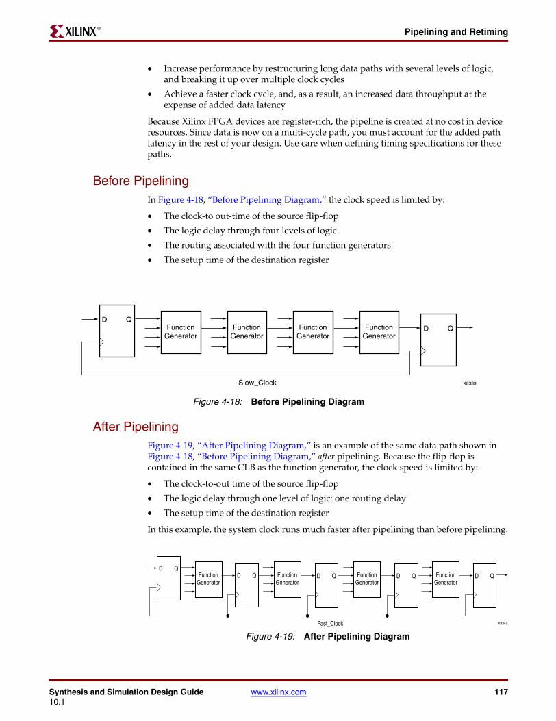
Synthesis and Simulation Design Guide www.xilinx.com 11710.1
Pipelining and RetimingR
• Increase performance by restructuring long data paths with several levels of logic, and breaking it up over multiple clock cycles
• Achieve a faster clock cycle, and, as a result, an increased data throughput at the expense of added data latency
Because Xilinx FPGA devices are register-rich, the pipeline is created at no cost in device resources. Since data is now on a multi-cycle path, you must account for the added path latency in the rest of your design. Use care when defining timing specifications for these paths.
Before PipeliningIn Figure 4-18, “Before Pipelining Diagram,” the clock speed is limited by:
• The clock-to out-time of the source flip-flop
• The logic delay through four levels of logic
• The routing associated with the four function generators
• The setup time of the destination register
After PipeliningFigure 4-19, “After Pipelining Diagram,” is an example of the same data path shown in Figure 4-18, “Before Pipelining Diagram,” after pipelining. Because the flip-flop is contained in the same CLB as the function generator, the clock speed is limited by:
• The clock-to-out time of the source flip-flop
• The logic delay through one level of logic: one routing delay
• The setup time of the destination register
In this example, the system clock runs much faster after pipelining than before pipelining.
Figure 4-18: Before Pipelining Diagram
X8339
FunctionGenerator
QDQDFunction
GeneratorFunction
Generator
Slow_Clock
FunctionGenerator
Figure 4-19: After Pipelining Diagram
X8340
FunctionGenerator
QDQD QDFunction
GeneratorFunction
Generator
Fast_Clock
FunctionGenerator
QD QD
118 www.xilinx.com Synthesis and Simulation Design Guide10.1
Chapter 4: Coding for FPGA FlowR
About RetimingSeveral synthesis tools can automatically move available registers in the design across logic (move forward or backward) in order to increase design speed. This process, depending on the synthesis tool, is called Retiming or Register Balancing.
The advantage of this optimization is that you do not need to modify your design in order to increase design speed. However, this process may significantly increase the number of flip-flops in the design.
For more information, see your synthesis tool documentation.
Synthesis and Simulation Design Guide www.xilinx.com 11910.1
R
Chapter 5
Using SmartModels
This chapter (Using SmartModels) describes special considerations when simulating designs for Virtex™-II Pro, Virtex-4, and Virtex-5 FPGA devices. These devices are platform FPGA devices for designs based on IP cores and customized modules. The family incorporates RocketIO™ and PowerPC™ CPU and Ethernet MAC cores in the FPGA architecture.
This chapter includes:
• “Using SmartModels with ISE Simulator”
• “Using SmartModels with ISE Simulator”
• “SmartModel Simulation Flow”
• “About SmartModels”
• “SmartModel Supported Simulators and Operating Systems”
• “Installing SmartModels”
• “Setting Up and Running Simulation”
Using SmartModels with ISE SimulatorThere is no need to set up SmartModels for ISE™ Simulator. The HARD IP Blocks in these devices is fully supported in ISE Simulator without any additional setup.
Using SmartModels to Simulate DesignsThis section discusses Using SmartModels to Simulate Designs. It assumes familiarity with the Xilinx® FPGA simulation flow.
SmartModels are an encrypted version of the actual Hardware Description Language (HDL) code. SmartModels allow you to simulate functionality without access to the code itself. Simulating these new features requires using Synopsys SmartModels along with the user design.
Table 5-1: Architecture Specific SmartModels
SmartModel Virtex-II Pro Virtex-4 Virtex-5 FPGACore
DCC_FPGACORE N/A N/A N/A √
EMAC N/A √ N/A N/A
GT √ N/A N/A N/A
GT10 N/A N/A N/A N/A
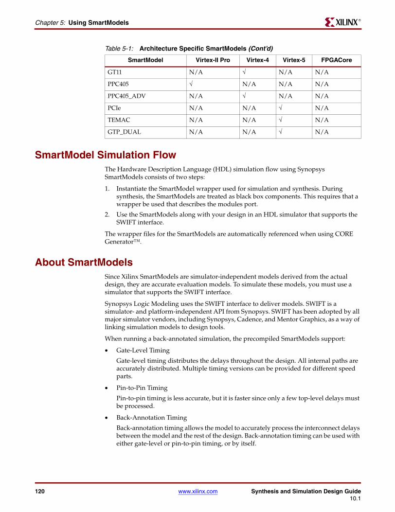
120 www.xilinx.com Synthesis and Simulation Design Guide10.1
Chapter 5: Using SmartModelsR
SmartModel Simulation FlowThe Hardware Description Language (HDL) simulation flow using Synopsys SmartModels consists of two steps:
1. Instantiate the SmartModel wrapper used for simulation and synthesis. During synthesis, the SmartModels are treated as black box components. This requires that a wrapper be used that describes the modules port.
2. Use the SmartModels along with your design in an HDL simulator that supports the SWIFT interface.
The wrapper files for the SmartModels are automatically referenced when using CORE Generator™.
About SmartModelsSince Xilinx SmartModels are simulator-independent models derived from the actual design, they are accurate evaluation models. To simulate these models, you must use a simulator that supports the SWIFT interface.
Synopsys Logic Modeling uses the SWIFT interface to deliver models. SWIFT is a simulator- and platform-independent API from Synopsys. SWIFT has been adopted by all major simulator vendors, including Synopsys, Cadence, and Mentor Graphics, as a way of linking simulation models to design tools.
When running a back-annotated simulation, the precompiled SmartModels support:
• Gate-Level Timing
Gate-level timing distributes the delays throughout the design. All internal paths are accurately distributed. Multiple timing versions can be provided for different speed parts.
• Pin-to-Pin Timing
Pin-to-pin timing is less accurate, but it is faster since only a few top-level delays must be processed.
• Back-Annotation Timing
Back-annotation timing allows the model to accurately process the interconnect delays between the model and the rest of the design. Back-annotation timing can be used with either gate-level or pin-to-pin timing, or by itself.
GT11 N/A √ N/A N/A
PPC405 √ N/A N/A N/A
PPC405_ADV N/A √ N/A N/A
PCIe N/A N/A √ N/A
TEMAC N/A N/A √ N/A
GTP_DUAL N/A N/A √ N/A
Table 5-1: Architecture Specific SmartModels (Cont’d)
SmartModel Virtex-II Pro Virtex-4 Virtex-5 FPGACore
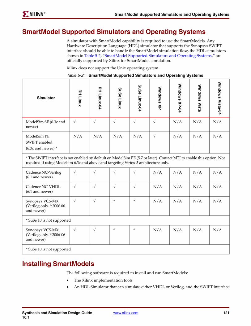
Synthesis and Simulation Design Guide www.xilinx.com 12110.1
SmartModel Supported Simulators and Operating SystemsR
SmartModel Supported Simulators and Operating SystemsA simulator with SmartModel capability is required to use the SmartModels. Any Hardware Description Language (HDL) simulator that supports the Synopsys SWIFT interface should be able to handle the SmartModel simulation flow, the HDL simulators shown in Table 5-2, “SmartModel Supported Simulators and Operating Systems,” are officially supported by Xilinx for SmartModel simulation.
Xilinx does not support the Unix operating system.
Table 5-2: SmartModel Supported Simulators and Operating Systems
Installing SmartModelsThe following software is required to install and run SmartModels:
• The Xilinx implementation tools
• An HDL Simulator that can simulate either VHDL or Verilog, and the SWIFT interface
Simulator
RH
Lin
ux
RH
Lin
ux-64
Su
Se L
inu
x
Su
Se L
inu
x-64
Win
dow
s XP
Win
dow
s XP
-64
Win
dow
s Vista
Win
do
ws V
ista-64
ModelSim SE (6.3c and newer)
√ √ √ √ √ N/A N/A N/A
ModelSim PE
SWIFT enabled
(6.3c and newer) *
N/A N/A N/A N/A √ N/A N/A N/A
* The SWIFT interface is not enabled by default on ModelSim PE (5.7 or later). Contact MTI to enable this option. Not required if using Modelsim 6.3c and above and targeting Virtex-5 architecture only.
Cadence NC-Verilog (6.1 and newer)
√ √ √ √ N/A N/A N/A N/A
Cadence NC-VHDL (6.1 and newer)
√ √ √ √ N/A N/A N/A N/A
Synopsys VCS-MX (Verilog only. Y2006.06 and newer)
√ √ * * N/A N/A N/A N/A
* SuSe 10 is not supported
Synopsys VCS-MXi (Verilog only. Y2006-06 and newer)
√ √ * * N/A N/A N/A N/A
* SuSe 10 is not supported
122 www.xilinx.com Synthesis and Simulation Design Guide10.1
Chapter 5: Using SmartModelsR
SmartModels are installed with the Xilinx implementation tools, but they are not immediately ready for use. There are two ways to use them:
• In “Installing SmartModels (Method One),” use the precompiled models. Use this method if your design does not use any other vendors’ SmartModels.
• In “Installing SmartModels (Method Two),” install the SmartModels with additional SmartModels incorporated in the design. Compile all SmartModels into a common library for the simulator to use.
Installing SmartModels (Method One)The Xilinx ISE™ installer sets the correct environment to work with SmartModels by default. If this fails, you must make the following settings for the SmartModels to function correctly.
Installing SmartModels (Method One on Linux)
To use the SmartModels on Linux, set the following variables:
setenv LMC_HOME $XILINX/smartmodel/lin/installed_lin
Installing SmartModels (Method One on Linux 64)
To use the SmartModels on Linux 64, set the following variables:
setenv LMC_HOME $XILINX/smartmodel/lin64/installed_lin64
Installing SmartModels (Method One on Windows)
To use the SmartModels on Windows, set the following variable:
LMC_HOME = %XILINX%\smartmodel\nt\installed_nt
Installing SmartModels (Method One on Solaris)
To use the SmartModels on Solaris, set the following variables:
setenv LMC_HOME $XILINX/smartmodel/sol/installed_sol
The SmartModels are not extracted by default. The Xilinx ISE installer sets the environment variable LMC_HOME, which points to the location to which the SmartModels are extracted. In order to extract the SmartModels, run compxlib with the appropriate switches. For more information, see “Compiling Xilinx Simulation Libraries (COMPXLIB)” in the Development System Reference Guide at http://www.xilinx.com/support/software_manuals.htm.
Synthesis and Simulation Design Guide www.xilinx.com 12310.1
Installing SmartModelsR
Installing SmartModels (Method Two)Note: The software sl_admin is not developed by Xilinx, which does not support all sl_admin options. For example, some sl_admin options specify simulators which are not supported by Xilinx
Caution! Use this method only if “Installing SmartModels (Method One)” did not work correctly.
Installing SmartModels (Method Two on Linux)
To install SmartModels on Linux:
1. Run the sl_admin.csh program from the $XILINX/smartmodel/lin/image directory using the following commands:
a. $ cd $XILINX/smartmodel/lin/image
b. $ sl_admin.csh
2. Select SmartModels To Install.
a. In the Set Library Directory dialog box, change the default directory from image/linux to installed.
b. Click OK.
c. If the directory does not exist, the program asks if you want to create it. Click OK.
d. In the Install From dialog box, click Open to use the default directory.
e. In the Select Models to Install, click Add All to select all models.
f. Click Continue.
g. In the Select Platforms for Installation dialog box:
- For Platforms, select Linux.
- For EDAV Packages, select Other.
h. Click Install.
i. When Install complete appears, and the status line changes to Ready, the SmartModels have been installed
3. Continue to perform other operations such as accessing documentation and running checks on your newly installed library (optional).
4. Select File > Exit.
To properly use the newly compiled models, set the LMC_HOME variable to the image directory. For example:
setenv LMC_HOME $XILINX/smartmodel/lin/installed_lin
Installing SmartModels (Method Two on Linux 64)
To install SmartModels on Linux 64:
1. Run the sl_admin.csh program from the $XILINX/smartmodel/lin64/image directory using the following commands:
a. $ cd $XILINX/smartmodel/lin64/image
b. $ sl_admin.csh
2. Select SmartModels To Install.
a. In the Set Library Directory dialog box, change the default directory from image/amd64 to installed.
b. Click OK.
124 www.xilinx.com Synthesis and Simulation Design Guide10.1
Chapter 5: Using SmartModelsR
c. If the directory does not exist, the program asks if you want to create it. Click OK. In the Install From dialog box, click Open to use the default directory.
d. In the Select Models to Install, click Add All to select all models.
e. Click Continue.
f. In the Select Platforms for Installation dialog box:
- For Platforms, select RHEL 3.0 Linux on amd64.
- For EDAV Packages, select Other.
g. Click Install.
h. When Install complete appears, and the status line changes to Ready, the SmartModels have been installed
3. Continue to perform other operations such as accessing documentation and running checks on your newly installed library (optional).
4. Select File > Exit.
To properly use the newly compiled models, set the LMC_HOME variable to the image directory. For example:
setenv LMC_HOME $XILINX/smartmodel/lin64/installed_lin64
Installing SmartModels (Method Two on Windows)
To install SmartModels on Windows:
1. Run sl_admin.exe from the %XILINX%\smartmodel\nt\image\pcnt directory.
2. Select SmartModels To Install.
a. In the Set Library Directory dialog box, change the default directory from image\pcnt to installed.
b. Click OK.
c. If the directory does not exist, the program asks if you want to create it. Click OK.
d. Click Install on the left side of the sl_admin window. This allows you choose the models to install.
e. In the Install From dialog box, click Browse.
f. Select the %XILINX%\smartmodel\nt\image directory. Click OK to select that directory.
g. In the Select Models to Install dialog box, click Add All.
h. Click OK.
i. In the Choose Platform window:
- For Platforms, select Wintel.
- For EDAV Packages, select Other.
j. Click OK.
k. When Install complete appears, the SmartModels have been installed.
3. Continue to perform other operations such as accessing documentation and running checks on your newly installed library (optional).
4. Select File > Exit.
Synthesis and Simulation Design Guide www.xilinx.com 12510.1
Setting Up and Running SimulationR
To properly use the newly compiled models, set the LMC_HOME variable to the image directory. For example:
Set LMC_HOME=%XILINX%\smartmodel\nt\installed_nt
Installing SmartModels (Method Two on Solaris)
To install SmartModels on Solaris:
1. Run sl_admin.csh from the $XILINX/smartmodel/sol/image directory using the following commands:
a. $ cd $XILINX/smartmodel/sol/image
b. $ sl_admin.csh
2. Select SmartModels To Install.
a. In the Set Library Directory dialog box , change the default directory from image/sol to installed.
b. Click OK.
c. If the directory does not exist, the program asks if you want to create it. Click OK.
d. In the Install From dialog box, click Open to use the default directory.
e. In the Select Models to Install dialog box, click Add All to select all models.
f. Click Continue.
g. In the Select Platforms for Installation dialog box:
- For Platforms, select Sun-4.
- For EDAV Packages, select Other.
h. Click Install.
i. When Install complete appears, and the status line changes to Ready, the SmartModels have been installed.
j. Continue to perform other operations such as accessing documentation and running checks on your newly installed library (optional).
k. Select File > Exit.
To properly use the newly compiled models, set the LMC_HOME variable to the image directory. For example:
setenv LMC_HOME $XILINX/smartmodel/sol/installed_sol
Setting Up and Running SimulationFor information on setting up and running simulation, see:
• Appendix A, “Simulating Xilinx Designs in Modelsim”
• Appendix B, “Simulating Xilinx Designs in NCSIM”
• Appendix C, “Simulating Xilinx Designs in Synopsys VCS-MX and VCS-MXi”

126 www.xilinx.com Synthesis and Simulation Design Guide10.1
Chapter 5: Using SmartModelsR
Synthesis and Simulation Design Guide www.xilinx.com 12710.1
R
Chapter 6
Simulating Your Design
This chapter (Simulating Your Design) describes the basic Hardware Description Language (HDL) simulation flow using Xilinx® and third party tools, and includes:
• “About Simulating Your Design”
• “Adhering to Industry Standards”
• “Simulation Points in HDL Design Flow”
• “Using Test Benches to Provide Stimulus”
• “VHDL and Verilog Libraries and Models”
• “Simulation of Configuration Interfaces”
• “Disabling BlockRAM Collision Checks for Simulation”
• “Global Reset and Tristate for Simulation”
• “Design Hierarchy and Simulation”
• “Register Transfer Level (RTL) Simulation Using Xilinx Libraries”
• “Generating Gate-Level Netlist (Running NetGen)”
• “Disabling X Propagation for Synchronous Elements”
• “MIN/TYP/MAX Simulation”
• “Special Considerations for CLKDLL, DCM, and DCM_ADV”
• “Understanding Timing Simulation”
• “Simulation Using Xilinx-Supported EDA Simulation Tools”
About Simulating Your DesignIncreasing design size and complexity, as well as improvements in design synthesis and simulation tools, have made Hardware Description Languages (HDLs) the preferred design languages of most integrated circuit designers. The two leading HDL synthesis and simulation languages are Verilog and VHDL. Both have been adopted as IEEE standards.
The Xilinx ISE™ software is designed to be used with several HDL synthesis and simulation tools that provide a solution for programmable logic designs from beginning to end. ISE provides libraries, netlist readers, and netlist writers, along with powerful place and route tools, that integrate with your HDL design environment on PC and Linux workstation platforms.
128 www.xilinx.com Synthesis and Simulation Design Guide10.1
Chapter 6: Simulating Your DesignR
Adhering to Industry StandardsXilinx adheres to relevant industry standards:
• “Simulation Flows”
• “Standards Supported by Xilinx Simulation Flow”
• “Xilinx Supported Simulators and Operating Systems”
• “Xilinx Libraries”
Simulation FlowsObserve the rules shown in Table 6-1, “Compile Order Dependency,” when compiling source files.
Xilinx recommends that you:
• Specify the test fixture file before the HDL netlist.
• Give the name testbench to the main module in the test fixture file.
This name is consistent with the name used by default in the ISE Project Navigator. If this name is used, no changes are necessary to the option in ISE in order to perform simulation from that environment.
Standards Supported by Xilinx Simulation FlowThe standards shown in Table 6-2, “Standards Supported by Xilinx Simulation Flow,” are supported by the Xilinx simulation flow.
Although the Xilinx HDL netlisters produce IEEE-STD-1076-2000 VHDL code or IEEE-STD-1364-2001 Verilog code, that does not restrict using newer or older standards for the creation of test benches or other simulation files. If the simulator supports both older and newer standards, both standards can generally be used in these simulation files. You must indicate to the simulator during code compilation which standard was used to create the file.
Table 6-1: Compile Order Dependency
HDL Dependency Compile Order
Verilog Independent Any order
VHDL Dependent Bottom-up
Table 6-2: Standards Supported by Xilinx Simulation Flow
Description Version
VHDL IEEE-STD-1076-2000
VITAL Modeling Standard IEEE-STD-1076.4-2000
Verilog IEEE-STD-1364-2001
Standard Delay Format (SDF) OVI 3.0
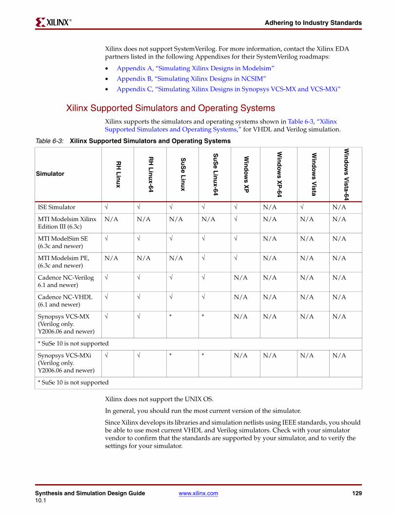
Synthesis and Simulation Design Guide www.xilinx.com 12910.1
Adhering to Industry StandardsR
Xilinx does not support SystemVerilog. For more information, contact the Xilinx EDA partners listed in the following Appendixes for their SystemVerilog roadmaps:
• Appendix A, “Simulating Xilinx Designs in Modelsim”
• Appendix B, “Simulating Xilinx Designs in NCSIM”
• Appendix C, “Simulating Xilinx Designs in Synopsys VCS-MX and VCS-MXi”
Xilinx Supported Simulators and Operating SystemsXilinx supports the simulators and operating systems shown in Table 6-3, “Xilinx Supported Simulators and Operating Systems,” for VHDL and Verilog simulation.
Xilinx does not support the UNIX OS.
In general, you should run the most current version of the simulator.
Since Xilinx develops its libraries and simulation netlists using IEEE standards, you should be able to use most current VHDL and Verilog simulators. Check with your simulator vendor to confirm that the standards are supported by your simulator, and to verify the settings for your simulator.
Table 6-3: Xilinx Supported Simulators and Operating Systems
Simulator
RH
Lin
ux
RH
Lin
ux-64
Su
Se L
inu
x
Su
Se L
inu
x-64
Win
do
ws X
P
Win
dow
s XP
-64
Win
dow
s Vista
Win
dow
s Vista-64
ISE Simulator √ √ √ √ √ N/A √ N/A
MTI Modelsim Xilinx Edition III (6.3c)
N/A N/A N/A N/A √ N/A N/A N/A
MTI ModelSim SE (6.3c and newer)
√ √ √ √ √ N/A N/A N/A
MTI Modelsim PE, (6.3c and newer)
N/A N/A N/A √ √ N/A N/A N/A
Cadence NC-Verilog 6.1 and newer)
√ √ √ √ N/A N/A N/A N/A
Cadence NC-VHDL (6.1 and newer)
√ √ √ √ N/A N/A N/A N/A
Synopsys VCS-MX (Verilog only. Y2006.06 and newer)
√ √ * * N/A N/A N/A N/A
* SuSe 10 is not supported
Synopsys VCS-MXi (Verilog only. Y2006.06 and newer)
√ √ * * N/A N/A N/A N/A
* SuSe 10 is not supported
130 www.xilinx.com Synthesis and Simulation Design Guide10.1
Chapter 6: Simulating Your DesignR
Xilinx LibrariesThe Xilinx VHDL libraries are tied to the IEEE-STD-1076.4-2000 VITAL standard for simulation acceleration. VITAL 2000 is in turn based on the IEEE-STD-1076-93 VHDL language. Because of this, the Xilinx libraries must be compiled as 1076-93.
VITAL libraries include some additional processing for timing checks and back-annotation styles. The UNISIM library turns these timing checks off for unit delay functional simulation. The SIMPRIM back-annotation library keeps these checks on by default to allow accurate timing simulations.
Simulation Points in HDL Design FlowThis section discusses Simulation Points in Hardware Description Language (HDL) Design Flow, and includes:
• “About Simulation Points”
• “Register Transfer Level (RTL)”
• “Post-Synthesis (Pre-NGDBuild) Gate-Level Simulation”
• “Post-NGDBuild (Pre-Map) Gate-Level Simulation”
• “Post-Map Partial Timing (Block Delays)”
• “Timing Simulation Post-Place and Route (Block and Net Delays)”
About Simulation PointsThis section discusses About Simulation Points, and includes:
• “Primary Simulation Points for HDL Designs Diagram”
• “Five Simulation Points in HDL Design Flow”
• “VHDL Standard Delay Format (SDF) File”
• “Verilog Standard Delay Format (SDF) File”
Xilinx supports functional and timing simulation of Hardware Description Language (HDL) designs as shown in “Five Simulation Points in HDL Design Flow.”
Primary Simulation Points for HDL Designs Diagram
Figure 6-1, “Primary Simulation Points for HDL Designs Diagram,” shows the points of the design flow.
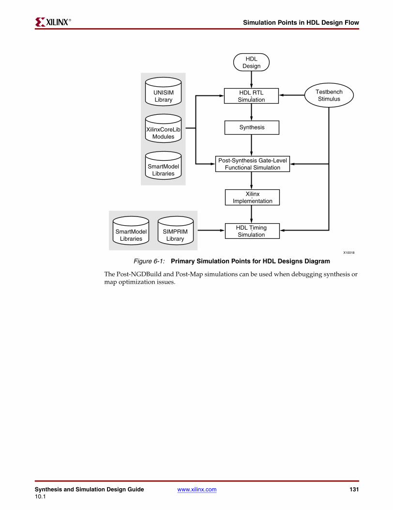
Synthesis and Simulation Design Guide www.xilinx.com 13110.1
Simulation Points in HDL Design FlowR
The Post-NGDBuild and Post-Map simulations can be used when debugging synthesis or map optimization issues.
Figure 6-1: Primary Simulation Points for HDL Designs DiagramX10018
HDL RTLSimulation
Synthesis
XilinxImplementation
HDL TimingSimulation
HDLDesign
TestbenchStimulus
Post-Synthesis Gate-LevelFunctional Simulation
SIMPRIMLibrary
UNISIMLibrary
XilinxCoreLibModules
SmartModelLibraries
SmartModelLibraries
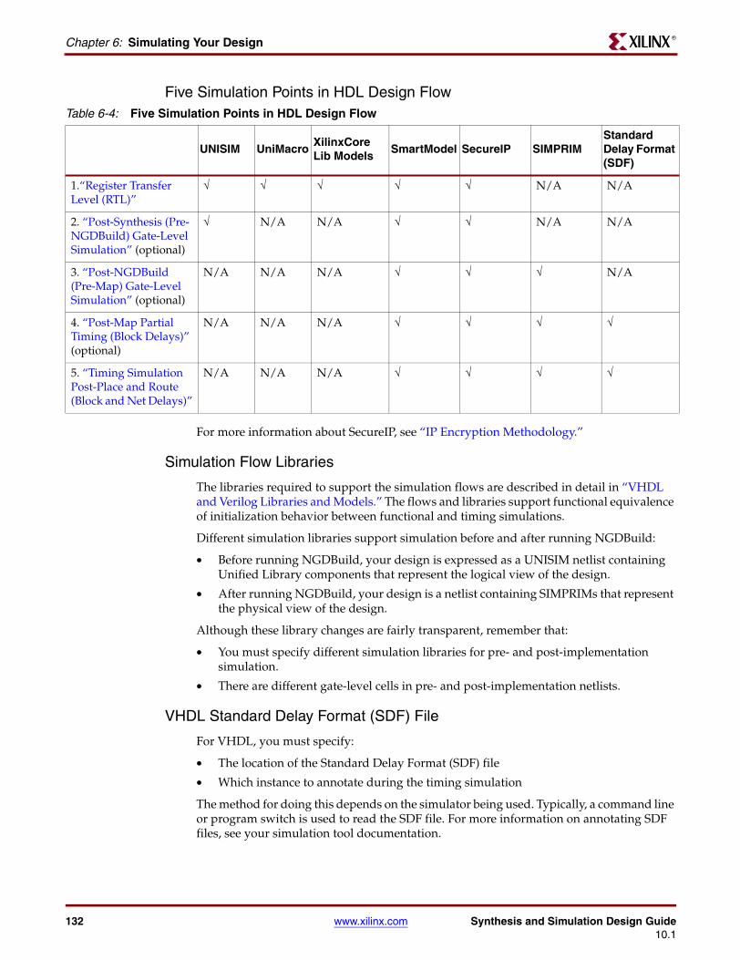
132 www.xilinx.com Synthesis and Simulation Design Guide10.1
Chapter 6: Simulating Your DesignR
Five Simulation Points in HDL Design Flow
For more information about SecureIP, see “IP Encryption Methodology.”
Simulation Flow Libraries
The libraries required to support the simulation flows are described in detail in “VHDL and Verilog Libraries and Models.” The flows and libraries support functional equivalence of initialization behavior between functional and timing simulations.
Different simulation libraries support simulation before and after running NGDBuild:
• Before running NGDBuild, your design is expressed as a UNISIM netlist containing Unified Library components that represent the logical view of the design.
• After running NGDBuild, your design is a netlist containing SIMPRIMs that represent the physical view of the design.
Although these library changes are fairly transparent, remember that:
• You must specify different simulation libraries for pre- and post-implementation simulation.
• There are different gate-level cells in pre- and post-implementation netlists.
VHDL Standard Delay Format (SDF) File
For VHDL, you must specify:
• The location of the Standard Delay Format (SDF) file
• Which instance to annotate during the timing simulation
The method for doing this depends on the simulator being used. Typically, a command line or program switch is used to read the SDF file. For more information on annotating SDF files, see your simulation tool documentation.
Table 6-4: Five Simulation Points in HDL Design Flow
UNISIM UniMacroXilinxCoreLib Models
SmartModel SecureIP SIMPRIMStandard Delay Format (SDF)
1.“Register Transfer Level (RTL)”
√ √ √ √ √ N/A N/A
2. “Post-Synthesis (Pre-NGDBuild) Gate-Level Simulation” (optional)
√ N/A N/A √ √ N/A N/A
3. “Post-NGDBuild (Pre-Map) Gate-Level Simulation” (optional)
N/A N/A N/A √ √ √ N/A
4. “Post-Map Partial Timing (Block Delays)” (optional)
N/A N/A N/A √ √ √ √
5. “Timing Simulation Post-Place and Route (Block and Net Delays)”
N/A N/A N/A √ √ √ √
Synthesis and Simulation Design Guide www.xilinx.com 13310.1
Simulation Points in HDL Design FlowR
Verilog Standard Delay Format (SDF) File
For Verilog, within the simulation netlist the Verilog system task $sdf_annotate specifies the name of the Standard Delay Format (SDF) file to be read.
• If the simulator supports $sdf_annotate, the SDF file is automatically read when the simulator compiles the Verilog simulation netlist.
• If the simulator does not support $sdf_annotate, in order to apply timing values to the gate-level netlist, you must manually instruct the simulator to annotate the SDF file.
Register Transfer Level (RTL)Register Transfer Level (RTL) may include:
• RTL Code
• Instantiated UNISIM library components
• Instantiated UniMacro components
• XilinxCoreLib and UNISIM gate-level models (CORE Generator™)
• SmartModels
• SecureIP
The RTL-level (behavioral) simulation enables you to verify or simulate a description at the system or chip level. This first pass simulation is typically performed to verify code syntax, and to confirm that the code is functioning as intended. At this step, no timing information is provided, and simulation should be performed in unit-delay mode to avoid the possibility of a race condition.
RTL simulation is not architecture-specific unless the design contains instantiated UNISIM or CORE Generator components. To support these instantiations, Xilinx provides the UNISIM and XilinxCoreLib libraries. You can use CORE Generator components if:
• You do not want to rely on the module generation capabilities of the synthesis tool, or
• The design requires larger structures.
Keep the code behavioral for the initial design creation. Do not instantiate specific components unless necessary. This allows for:
• More readable code
• Faster and simpler simulation
• Code portability (the ability to migrate to different device families)
• Code reuse (the ability to use the same code in future designs)
You may find it necessary to instantiate components if the component is not inferable.
Post-Synthesis (Pre-NGDBuild) Gate-Level SimulationPost-Synthesis (Pre-NGDBuild) Gate-Level Simulation may include one of the following (optional):
• Gate-level netlist containing UNISIM library components
• SmartModels
• SecureIP
134 www.xilinx.com Synthesis and Simulation Design Guide10.1
Chapter 6: Simulating Your DesignR
Most synthesis tools can write out a post-synthesis HDL netlist for a design. If the VHDL or Verilog netlists are written for UNISIM library components, you may use the netlists to simulate the design and evaluate the synthesis results.
Caution! Xilinx does not support this method if the netlists are written in terms of the vendor's own simulation models.
Post-NGDBuild (Pre-Map) Gate-Level SimulationPost-NGDBuild (Pre-Map) Gate-Level Simulation (optional) may include:
• Gate-level netlist containing SIMPRIM library components
• SmartModels
• SecureIP
The post-NGDBuild (pre-map) gate-level functional simulation is used when it is not possible to simulate the direct output of the synthesis tool. This occurs when the tool cannot write UNISIM-compatible VHDL or Verilog netlists. In this case, the NGD file produced from NGDBUILD is the input into the Xilinx simulation netlister, NetGen. NetGen creates a structural simulation netlist based on SIMPRIM models.
Like post-synthesis simulation, post-NGDBuild simulation allows you to verify that your design has been synthesized correctly, and you can begin to identify any differences due to the lower level of abstraction. Unlike the post-synthesis pre-NGDBuild simulation, there are Global Set/Reset (GSR) and Global Tristate (GTS) nets that must be initialized, just as for post-Map and post-PAR simulation. For more information on using the GSR and GTS signals for post-NGDBuild simulation, see “Global Reset and Tristate for Simulation.”
Post-Map Partial Timing (Block Delays)Post-Map Partial Timing (Block Delays) may include the following (optional):
• Gate-level netlist containing SIMPRIM library components
• Standard Delay Format (SDF) files
• SmartModels
• SecureIP
You may also perform simulation after mapping the design. Post-Map simulation occurs before placing and routing. This simulation includes the block delays for the design, but not the routing delays. Since routing is not taking into consideration, the simulation results may be inaccurate. Run this simulation as a debug step only if post-place and route simulation shows failures.
As with the post-NGDBuild simulation, NetGen is used to create the structural simulation. Running the simulation netlister tool, NetGen, creates a Standard Delay Format (SDF) file. The delays for the design are stored in the SDF file which contains all block or logic delays. It does not contain any of the routing delays for the design since the design has not yet been placed and routed. As with all NetGen created netlists, Global Set/Reset (GSR) and Global Tristate (GTS) signals must be accounted for. For more information on using the GSR and GTS signals for post-NGDBuild simulation, see “Global Reset and Tristate for Simulation.”
Synthesis and Simulation Design Guide www.xilinx.com 13510.1
Using Test Benches to Provide StimulusR
Timing Simulation Post-Place and Route (Block and Net Delays)Timing Simulation Post-Place and Route Full Timing (Block and Net Delays) may include:
• Gate-level netlist containing SIMPRIM library components
• Standard Delay Format (SDF) files
• SmartModels
• SecureIP
After your design has completed the place and route process in the Xilinx Implementation Tools, a timing simulation netlist can be created. You now begin to see how your design behaves in the actual circuit. The overall functionality of the design was defined in the beginning, but timing information can not be accurately calculated until the design has been placed and routed.
The previous simulations that used NetGen created a structural netlist based on SIMPRIM models. This netlist comes from the placed and routed Native Circuit Description (NCD) file. This netlist has Global Set/Reset (GSR) and Global Tristate (GTS) nets that must be initialized. For more information on initializing the GSR and GTS nets, see “Global Reset and Tristate for Simulation.”
When you run timing simulation, a Standard Delay Format (SDF) file is created as with the post-Map simulation. This SDF file contains all block and routing delays for the design.
Xilinx highly recommends running this flow. For more information, see “Importance of Timing Simulation.”
Using Test Benches to Provide Stimulus This section discusses Using Test Benches to Provide Stimulus, and includes:
• “About Test Benches”
• “Creating a Test Bench”
• “Test Bench Recommendations”
Before you perform simulation, create a test bench or test fixture to apply the stimulus to the design.
About Test BenchesA test bench is Hardware Description Language (HDL) code written for the simulator that:
• Instantiates the design netlists
• Initializes the design
• Applies stimuli to verify the functionality of the design
You can also set up the test bench to display the desired simulation output to a file, waveform, or screen.
A test bench can be simple in structure and sequentially apply stimulus to specific inputs. A test bench can also be complex, and may include:
• Subroutine calls
• Stimulus read in from external files
136 www.xilinx.com Synthesis and Simulation Design Guide10.1
Chapter 6: Simulating Your DesignR
• Conditional stimulus
• Other more complex structures
The test bench has the following advantages over interactive simulation:
• It allows repeatable simulation throughout the design process.
• It provides documentation of the test conditions.
Creating a Test BenchUse any of the following to create a test bench and simulate a design:
• Create a Test Bench in ISE Tools
The ISE tools create a template test bench containing the proper structure, library references, and design instantiation based on your design files from Project Navigator. This greatly eases test bench development at the beginning stages of the design.
• Create a Test Bench in Waveform Editor
You may use Waveform Editor to automatically create a test bench by drawing the intended stimulus and the expected outputs in a waveform viewer. For more information, see the ISE help and the ISE Simulator help.
• Create a Test Bench in NetGen
You can use NetGen to create a test bench file. The -tb switch for NetGen creates a test fixture or test bench template. The Verilog test fixture file has a .tv extension. The VHDL test bench file has a .tvhd extension.
Test Bench RecommendationsXilinx recommends the following when you create and run a test bench:
• Give the name testbench to the main module or entity name in the test bench file. Always specify the `timescale in Verilog testbench files.
• Specify the instance name for the instantiated top-level of the design in the test bench as UUT.
These names are consistent with the default names used by ISE for calling the test bench and annotating the Standard Delay Format (SDF) file when invoking the simulator.
• Initialize all inputs to the design within the test bench at simulation time zero in order to properly begin simulation with known values.
• Apply stimulus data after 100 ns in order to account for the default Global Set/Reset pulse used in SIMPRIM-based simulation. The clock source should begin before the Global Set/Reset (GSR) is released. For more information, see “Global Reset and Tristate for Simulation.”
Synthesis and Simulation Design Guide www.xilinx.com 13710.1
VHDL and Verilog Libraries and ModelsR
VHDL and Verilog Libraries and ModelsThis section discusses VHDL and Verilog Libraries and Models, and includes:
• “Required Simulation Point Libraries”
• “Simulation Phase Library Information”
• “Library Source Files and Compile Order”
Required Simulation Point LibrariesThe five simulation points require the following libraries:
• UNISIM
• UniMacro
• CORE Generator (XilinxCoreLib)
• SmartModel
• SecureIP
• SIMPRIM
The libraries required for each of the five simulation points are:
• “First Simulation Point: Register Transfer Level (RTL)”
• “Second Simulation Point: Post-Synthesis (Pre-NGDBuild) Gate-Level Simulation”
• “Third Simulation Point: Post-NGDBuild (Pre-Map) Gate-Level Simulation”
• “Fourth Simulation Point: Post-Map Partial Timing (Block Delays)”
• “Fifth Simulation Point: Timing Simulation Post-Place and Route (Block and Net Delays)”
First Simulation Point: Register Transfer Level (RTL)
The first point, “Register Transfer Level (RTL),” is a behavioral description of your design at the register transfer level. RTL simulation is not architecture-specific unless your design contains instantiated UNISIM, or CORE Generator components.
To support these instantiations, Xilinx provides the following libraries:
• Unisim UniMacro
• CORE Generator Behavioral XilinxCoreLib
• SecureIP
• SmartModel
Second Simulation Point: Post-Synthesis (Pre-NGDBuild) Gate-Level Simulation
The second simulation point is “Post-Synthesis (Pre-NGDBuild) Gate-Level Simulation.”
The synthesis tool must write out the HDL netlist using UNISIM primitives. Otherwise, the synthesis vendor provides its own post-synthesis simulation library, which is not supported by Xilinx. If there is IP in the design that is a blackbox for the synthesis tools, ngcbuild must run before netgen. Ngcbuild combines all the ngc and EDIF files into a single ngc; netgen can be then run on this ngc file. For more information on running
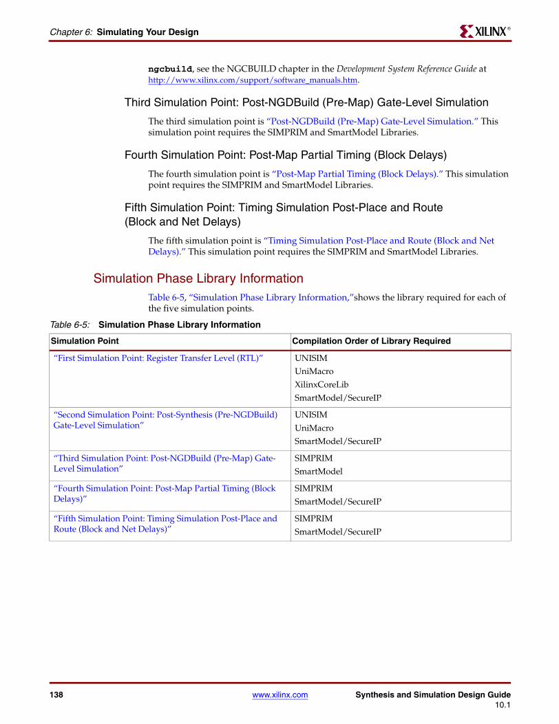
138 www.xilinx.com Synthesis and Simulation Design Guide10.1
Chapter 6: Simulating Your DesignR
ngcbuild, see the NGCBUILD chapter in the Development System Reference Guide at http://www.xilinx.com/support/software_manuals.htm.
Third Simulation Point: Post-NGDBuild (Pre-Map) Gate-Level Simulation
The third simulation point is “Post-NGDBuild (Pre-Map) Gate-Level Simulation.” This simulation point requires the SIMPRIM and SmartModel Libraries.
Fourth Simulation Point: Post-Map Partial Timing (Block Delays)
The fourth simulation point is “Post-Map Partial Timing (Block Delays).” This simulation point requires the SIMPRIM and SmartModel Libraries.
Fifth Simulation Point: Timing Simulation Post-Place and Route(Block and Net Delays)
The fifth simulation point is “Timing Simulation Post-Place and Route (Block and Net Delays).” This simulation point requires the SIMPRIM and SmartModel Libraries.
Simulation Phase Library InformationTable 6-5, “Simulation Phase Library Information,”shows the library required for each of the five simulation points.
Table 6-5: Simulation Phase Library Information
Simulation Point Compilation Order of Library Required
“First Simulation Point: Register Transfer Level (RTL)” UNISIM
UniMacro
XilinxCoreLib
SmartModel/SecureIP
“Second Simulation Point: Post-Synthesis (Pre-NGDBuild) Gate-Level Simulation”
UNISIM
UniMacro
SmartModel/SecureIP
“Third Simulation Point: Post-NGDBuild (Pre-Map) Gate-Level Simulation”
SIMPRIM
SmartModel
“Fourth Simulation Point: Post-Map Partial Timing (Block Delays)”
SIMPRIM
SmartModel/SecureIP
“Fifth Simulation Point: Timing Simulation Post-Place and Route (Block and Net Delays)”
SIMPRIM
SmartModel/SecureIP
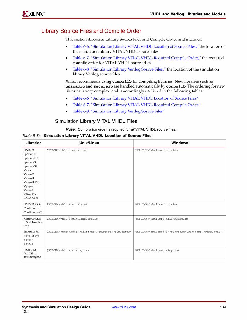
Synthesis and Simulation Design Guide www.xilinx.com 13910.1
VHDL and Verilog Libraries and ModelsR
Library Source Files and Compile OrderThis section discusses Library Source Files and Compile Order and includes:
• Table 6-6, “Simulation Library VITAL VHDL Location of Source Files,” the location of the simulation library VITAL VHDL source files
• Table 6-7, “Simulation Library VITAL VHDL Required Compile Order,” the required compile order for VITAL VHDL source files
• Table 6-8, “Simulation Library Verilog Source Files,” the location of the simulation library Verilog source files
Xilinx recommends using compxlib for compiling libraries. New libraries such as unimacro and secureip are handled automatically by compxlib. The ordering for new libraries is very complex, and is accordingly not listed in the following tables:
• Table 6-6, “Simulation Library VITAL VHDL Location of Source Files”
• Table 6-7, “Simulation Library VITAL VHDL Required Compile Order”
• Table 6-8, “Simulation Library Verilog Source Files”
Simulation Library VITAL VHDL Files
Note: Compilation order is required for all VITAL VHDL source files.
Table 6-6: Simulation Library VITAL VHDL Location of Source Files
Libraries Unix/Linux Windows
UNISIM Spartan-IISpartan-IIESpartan-3Spartan-3EVirtexVirtex-EVirtex-IIVirtex-II ProVirtex-4Virtex-5Xilinx IBMFPGA Core
$XILINX/vhdl/src/unisims %XILINX%\vhdl\src\unisims
UNISIM 9500CoolRunnerCoolRunner-II
$XILINX/vhdl/src/unisims %XILINX%\vhdl\src\unisims
XilinxCoreLibFPGA Families only
$XILINX/vhdl/src/XilinxCoreLib %XILINX%\vhdl\src\XilinxCoreLib
SmartModelVirtex-II ProVirtex-4Virtex-5
$XILINX/smartmodel/<platform>/wrappers/<simulator> %XILINX%\smartmodel\<platform>\wrappers\<simulator>
SIMPRIM (All Xilinx Technologies)
$XILINX/vhdl/src/simprims %XILINX%\vhdl\src\simprims
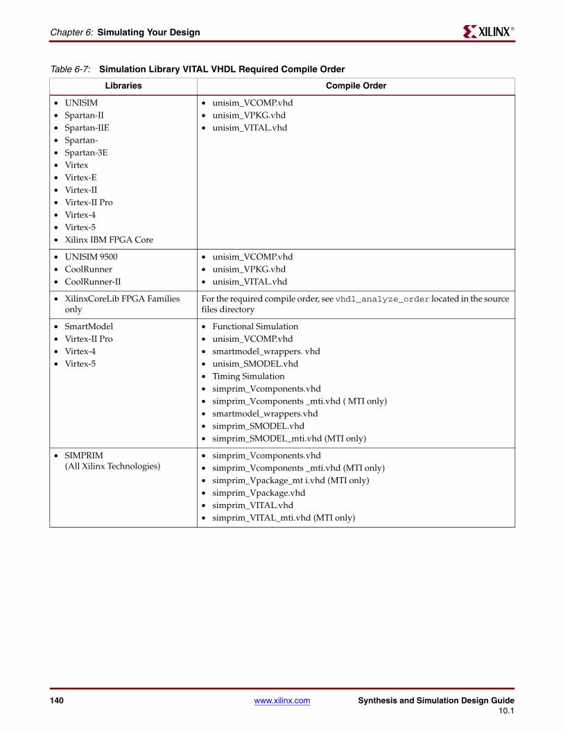
140 www.xilinx.com Synthesis and Simulation Design Guide10.1
Chapter 6: Simulating Your DesignR
Table 6-7: Simulation Library VITAL VHDL Required Compile Order
Libraries Compile Order
• UNISIM • Spartan-II• Spartan-IIE• Spartan-• Spartan-3E• Virtex• Virtex-E• Virtex-II• Virtex-II Pro• Virtex-4• Virtex-5• Xilinx IBM FPGA Core
• unisim_VCOMP.vhd• unisim_VPKG.vhd• unisim_VITAL.vhd
• UNISIM 9500• CoolRunner• CoolRunner-II
• unisim_VCOMP.vhd• unisim_VPKG.vhd• unisim_VITAL.vhd
• XilinxCoreLib FPGA Families only
For the required compile order, see vhdl_analyze_order located in the source files directory
• SmartModel• Virtex-II Pro• Virtex-4• Virtex-5
• Functional Simulation• unisim_VCOMP.vhd• smartmodel_wrappers. vhd• unisim_SMODEL.vhd • Timing Simulation• simprim_Vcomponents.vhd• simprim_Vcomponents _mti.vhd ( MTI only)• smartmodel_wrappers.vhd• simprim_SMODEL.vhd• simprim_SMODEL_mti.vhd (MTI only)
• SIMPRIM (All Xilinx Technologies)
• simprim_Vcomponents.vhd• simprim_Vcomponents _mti.vhd (MTI only)• simprim_Vpackage_mt i.vhd (MTI only)• simprim_Vpackage.vhd• simprim_VITAL.vhd• simprim_VITAL_mti.vhd (MTI only)
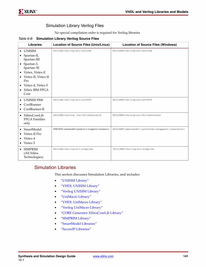
Synthesis and Simulation Design Guide www.xilinx.com 14110.1
VHDL and Verilog Libraries and ModelsR
Simulation Library Verilog Files
No special compilation order is required for Verilog libraries
Simulation LibrariesThis section discusses Simulation Libraries, and includes:
• “UNISIM Library”
• “VHDL UNISIM Library”
• “Verilog UNISIM Library”
• “UniMacro Library”
• “VHDL UniMacro Library”
• “Verilog UniMacro Library”
• “CORE Generator XilinxCoreLib Library”
• “SIMPRIM Library”
• “SmartModel Libraries”
• “SecureIP Libraries”
Table 6-8: Simulation Library Verilog Source Files
Libraries Location of Source Files (Unix/Linux) Location of Source Files (Windows)
• UNISIM • Spartan-II,
Spartan-IIE• Spartan-3,
Spartan-3E• Virtex, Virtex-E• Virtex-II, Virtex-II
Pro• Virtex-4, Virtex-5• Xilinx IBM FPGA
Core
$XILINX/verilog/src/unisims %XILINX%\verilog\src\unisims
• UNISIM 9500• CoolRunner• CoolRunner-II
$XILINX/verilog/src/uni9000 %XILINX%\verilog\src\uni9000
• XilinxCoreLib FPGA Families only
$XILINX/verilog /src/XilinxCoreLib %XILINX%\verilog\src\XilinxCoreLib
• SmartModel• Virtex-II Pro• Virtex-4• Virtex-5
$XILINX/ smartmodel/<platform>/ wrappers/<simulator> %XILINX%\smartmodel\<platform>\wrappers\<simulator>
• SIMPRIM (All Xilinx Technologies)
$XILINX/verilog/src/simprims %XILINX%\verilog\src\simprims
142 www.xilinx.com Synthesis and Simulation Design Guide10.1
Chapter 6: Simulating Your DesignR
• “VHDL SecureIP Library”
• “Verilog SecureIP Library”
• “Xilinx Simulation Libraries (COMPXLIB)”
UNISIM Library
The UNISIM Library is used for functional simulation and synthesis only. This library includes:
• All Xilinx Unified Library primitives that are inferred by most synthesis tools
• Primitives that are commonly instantiated, such as DCMs, BUFGs, and MGTs
You should infer most design functionality using behavioral Register Transfer Level (RTL) code unless:
• The desired component is not inferable by your synthesis tool, or
• You want to take manual control of mapping and placement of a function
VHDL UNISIM Library
The VHDL UNISIM library is split into four files containing:
• The component declarations (unisim_VCOMP.vhd)
• Package files (unisim_VPKG.vhd)
• Entity and architecture declarations (unisim_VITAL.vhd)
• SmartModel declarations (unisim_SMODEL.vhd)
All primitives for all Xilinx device families are specified in these files. To use these primitives, place the following two lines at the beginning of each file:
Library UNISIM;use UNISIM.vcomponents.all;
Verilog UNISIM Library
For Verilog, each library component is specified in a separate file. This allows automatic library expansion using the -y library specification switch. All Verilog module names and file names are all upper case. For example, module BUFG is BUFG.v, and module IBUF is IBUF.v. Since Verilog is case-sensitive, make sure that all UNISIM primitive instantiations adhere to this upper-case naming convention.
If you are using pre-compiled libraries, use the correct directive to point to the precompiled libraries. Following is an example for Modelsim:
-L unisims_ver
UniMacro Library
The UniMacro library:
• Is used for functional simulation only.
• Provides macros to aid the instantiation of complex Xilinx primitives.
• Is an abstraction of the primitives in the unsim library. The synthesis tools automatically expand the unimacros to their underlying primitives.
For more information, see the Xilinx Libraries Guides at http://www.xilinx.com/support/software_manuals.htm.
Synthesis and Simulation Design Guide www.xilinx.com 14310.1
VHDL and Verilog Libraries and ModelsR
VHDL UniMacro Library
To use these macros, place the following two lines at the beginning of each file, in addition to the unisim declarations:
Library UNIMACRO;use UNIMACRO.vcomponents.all
Verilog UniMacro Library
For Verilog, each macro component is specified in a separate file. This allows automatic library expansion using the -y library specification switch. All Verilog module names and file names are all upper case. Since Verilog is case-sensitive, make sure that all UniMacro instantiations adhere to this upper-case naming convention.
If you are using pre-compiled libraries, use the correct directive to point to the precompiled libraries. Following is an example for Modelsim:
-L unimacro_ver
CORE Generator XilinxCoreLib Library
The Xilinx CORE Generator is a graphical intellectual property (IP) design tool for creating high-level modules such as:
• FIR Filters
• FIFOs
• CAMs
• Other advanced IP
You can customize and pre-optimize modules to take advantage of the inherent architectural features of Xilinx FPGA devices, such as:
• Block multipliers
• SRLs
• Fast carry logic
• On-chip single-port RAM
• On-chip dual-port RAM
You can also select the appropriate HDL model type as output to integrate into your HDL design.
The CORE Generator HDL library models are used for Register Transfer Level (RTL) simulation.
SIMPRIM Library
The SIMPRIM library is used for the following simulations:
• Post Ngdbuild (gate level functional)
• Post-Map (partial timing)
• Post-Place-and-Route (full timing)
The SIMPRIM library is architecture independent.
144 www.xilinx.com Synthesis and Simulation Design Guide10.1
Chapter 6: Simulating Your DesignR
SmartModel Libraries
If you are using ISE Simulator, there is no need to set up SmartModels. The HARD IP Blocks in these devices is fully supported in ISE Simulator without any additional setup steps needed. If you are using Modelsim 6.3c and above with Virtex-5 devices, you do not need to set up SmartModels. For more information, see “IP Encryption Methodology.”.
The SmartModel Libraries are used to model complex functions of modern FPGA devices such as the PowerPC™ and the RocketIO™. SmartModels are encrypted source files that communicate with simulators via the SWIFT interface.
The SmartModel Libraries require additional installation steps to properly install on your system. Additional setup within the simulator may also be required. For more information on how to install and set up the SmartModel Libraries, see “Using SmartModels.”
SecureIP Libraries
HARD IP Blocks are fully supported in ISE Simulator without additional setup. If you are using Modelsim 6.3c and above with Virtex-5 devices, you do not need to set up SmartModels. For more information, see “IP Encryption Methodology.”
VHDL SecureIP Library
If you are using VHDL for your design entry, a mixed-language license is required to run any Hard-IP simulation. Contact your vendor for pricing options for mixed-language simulation.
To use SecureIP, place the following two lines at the beginning of each file:
Library UNISIM;use UNISIM.vcomponents.all;
Verilog SecureIP Library
For Verilog, each component is specified in a separate file. This allows automatic library expansion using the -y library specification switch.
If you are using pre-compiled libraries, use the correct directive to point to the precompiled libraries. Following is an example for Modelsim:
-L securip
Xilinx Simulation Libraries (COMPXLIB)
Caution! Do NOT use with ModelSim XE (Xilinx Edition) or ISE Simulator.
Before beginning functional simulation, you must compile the Xilinx Simulation Libraries for the target simulator. Xilinx provides a tool called COMPXLIB for this purpose. For more information, see the Xilinx Development System Reference Guide at http://www.xilinx.com/support/software_manuals.htm.
Reducing Simulation RuntimesXilinx simulation models have an optional generic/parameter (SIM_MODE ) that can reduce the simulation runtimes. SIM_MODE has two settings:
• SIM_MODE = "SAFE"
• SIM_MODE = "FAST"
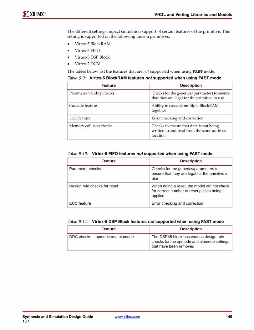
Synthesis and Simulation Design Guide www.xilinx.com 14510.1
VHDL and Verilog Libraries and ModelsR
The different settings impact simulation support of certain features of the primitive. This setting is supported on the following unisim primitives:
• Virtex-5 BlockRAM
• Virtex-5 FIFO
• Virtex-5 DSP Block
• Virtex-2 DCM
The tables below list the features that are not supported when using FAST mode.
Table 6-9: Virtex-5 BlockRAM features not supported when using FAST mode
Feature Description
Parameter validity checks Checks for the generics/parameters to ensure that they are legal for the primitive in use
Cascade feature Ability to cascade multiple BlockRAMs together
ECC feature Error checking and correction
Memory collision checks Checks to ensure that data is not being written to and read from the same address location
Table 6-10: Virtex-5 FIFO features not supported when using FAST mode
Feature Description
Parameter checks Checks for the generics/parameters to ensure that they are legal for the primitive in use
Design rule checks for reset When doing a reset, the model will not check for correct number of reset pulses being applied
ECC feature Error checking and correction
Table 6-11: Virtex-5 DSP Block features not supported when using FAST mode
Feature Description
DRC checks – opmode and alumode The DSP48 block has various design rule checks for the opmode and alumode settings that have been removed
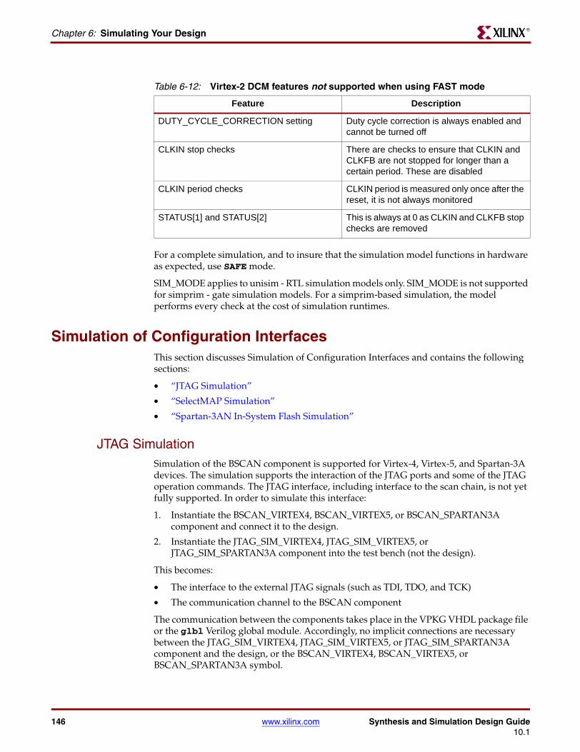
146 www.xilinx.com Synthesis and Simulation Design Guide10.1
Chapter 6: Simulating Your DesignR
For a complete simulation, and to insure that the simulation model functions in hardware as expected, use SAFE mode.
SIM_MODE applies to unisim - RTL simulation models only. SIM_MODE is not supported for simprim - gate simulation models. For a simprim-based simulation, the model performs every check at the cost of simulation runtimes.
Simulation of Configuration InterfacesThis section discusses Simulation of Configuration Interfaces and contains the following sections:
• “JTAG Simulation”
• “SelectMAP Simulation”
• “Spartan-3AN In-System Flash Simulation”
JTAG SimulationSimulation of the BSCAN component is supported for Virtex-4, Virtex-5, and Spartan-3A devices. The simulation supports the interaction of the JTAG ports and some of the JTAG operation commands. The JTAG interface, including interface to the scan chain, is not yet fully supported. In order to simulate this interface:
1. Instantiate the BSCAN_VIRTEX4, BSCAN_VIRTEX5, or BSCAN_SPARTAN3A component and connect it to the design.
2. Instantiate the JTAG_SIM_VIRTEX4, JTAG_SIM_VIRTEX5, or JTAG_SIM_SPARTAN3A component into the test bench (not the design).
This becomes:
• The interface to the external JTAG signals (such as TDI, TDO, and TCK)
• The communication channel to the BSCAN component
The communication between the components takes place in the VPKG VHDL package file or the glbl Verilog global module. Accordingly, no implicit connections are necessary between the JTAG_SIM_VIRTEX4, JTAG_SIM_VIRTEX5, or JTAG_SIM_SPARTAN3A component and the design, or the BSCAN_VIRTEX4, BSCAN_VIRTEX5, or BSCAN_SPARTAN3A symbol.
Table 6-12: Virtex-2 DCM features not supported when using FAST mode
Feature Description
DUTY_CYCLE_CORRECTION setting Duty cycle correction is always enabled and cannot be turned off
CLKIN stop checks There are checks to ensure that CLKIN and CLKFB are not stopped for longer than a certain period. These are disabled
CLKIN period checks CLKIN period is measured only once after the reset, it is not always monitored
STATUS[1] and STATUS[2] This is always at 0 as CLKIN and CLKFB stop checks are removed
Synthesis and Simulation Design Guide www.xilinx.com 14710.1
Simulation of Configuration InterfacesR
Stimulus can be driven and viewed from the JTAG_SIM_VIRTEX4, JTAG_SIM_VIRTEX5, or JTAG_SIM_SPARTAN3A component within the test bench to understand the operation of the JTAG/BSCAN function. Instantiation templates for both of these components are available in both the ISE HDL Templates in Project Navigator and the Xilinx Virtex-4 and Virtex-5 Libraries Guides at http://www.xilinx.com/support/software_manuals.htm.
SelectMAP SimulationThis section discusses SelectMAP Simulation and includes:
• “Slave SelectMAP”
• “System Level Description”
• “Debugging with the Model”
• “Supported Features”
Slave SelectMAP
The configuration simulation model allows supported configuration interfaces to be simulated ultimately showing the DONE pin going high. This is a model of how the supported devices will react to stimulus on the supported configuration interface. For a list of supported interfaces and devices, see Table 6-13, “Supported Configuration Devices and Modes.” The model is set up to handle control signal activity as well as bit file downloading. Included are internal register settings such as the CRC, IDCODE, and Status Registers. The Sync Word can be monitored as it enters the device and the Start Up Sequence can be monitored as it progresses. Figure 6-3, “Block Diagram of Model Interaction,”shows how the system should map from the hardware to the simulation environment. The configuration process is specifically outlined in the Configuration User Guide for each device family. These guides contain information on the configuration sequence as well as the configuration interfaces.
Table 6-13: Supported Configuration Devices and Modes
Devices SelectMAP Serial SPI BPI
Virtex-5 Yes No No No
Spartan-3A Yes No No No
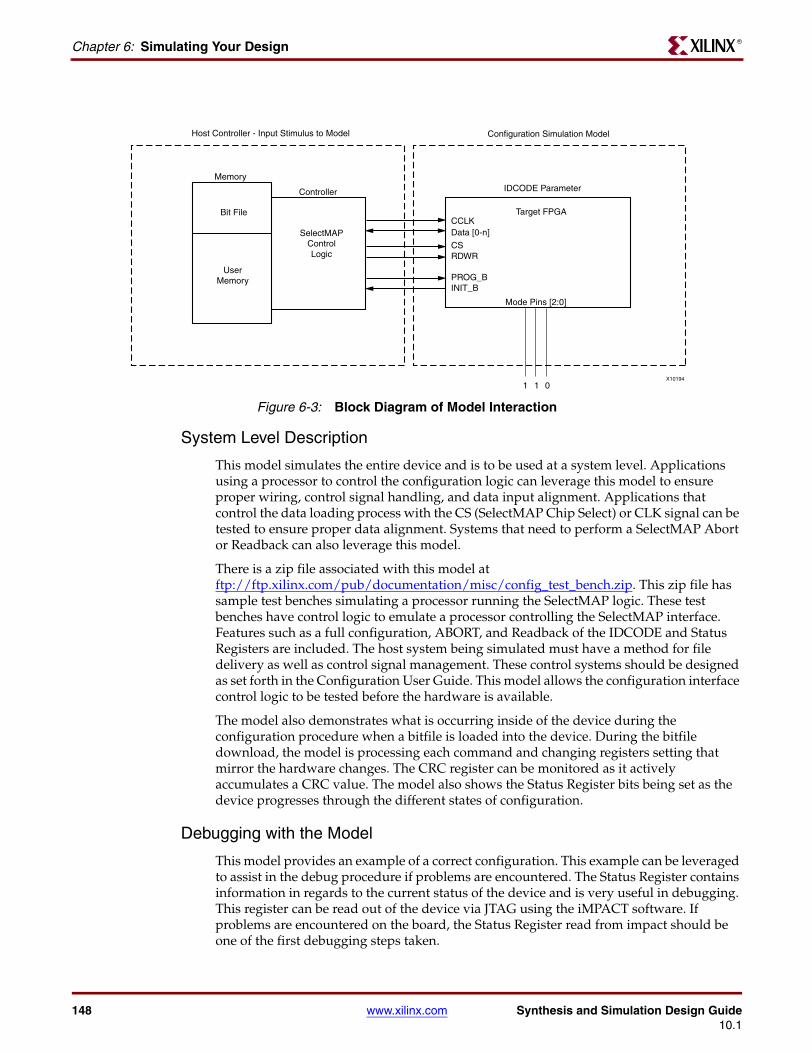
148 www.xilinx.com Synthesis and Simulation Design Guide10.1
Chapter 6: Simulating Your DesignR
System Level Description
This model simulates the entire device and is to be used at a system level. Applications using a processor to control the configuration logic can leverage this model to ensure proper wiring, control signal handling, and data input alignment. Applications that control the data loading process with the CS (SelectMAP Chip Select) or CLK signal can be tested to ensure proper data alignment. Systems that need to perform a SelectMAP Abort or Readback can also leverage this model.
There is a zip file associated with this model at ftp://ftp.xilinx.com/pub/documentation/misc/config_test_bench.zip. This zip file has sample test benches simulating a processor running the SelectMAP logic. These test benches have control logic to emulate a processor controlling the SelectMAP interface. Features such as a full configuration, ABORT, and Readback of the IDCODE and Status Registers are included. The host system being simulated must have a method for file delivery as well as control signal management. These control systems should be designed as set forth in the Configuration User Guide. This model allows the configuration interface control logic to be tested before the hardware is available.
The model also demonstrates what is occurring inside of the device during the configuration procedure when a bitfile is loaded into the device. During the bitfile download, the model is processing each command and changing registers setting that mirror the hardware changes. The CRC register can be monitored as it actively accumulates a CRC value. The model also shows the Status Register bits being set as the device progresses through the different states of configuration.
Debugging with the Model
This model provides an example of a correct configuration. This example can be leveraged to assist in the debug procedure if problems are encountered. The Status Register contains information in regards to the current status of the device and is very useful in debugging. This register can be read out of the device via JTAG using the iMPACT software. If problems are encountered on the board, the Status Register read from impact should be one of the first debugging steps taken.
X-Ref Target - Figure 6-2
Figure 6-3: Block Diagram of Model Interaction
Host Controller - Input Stimulus to Model Configuration Simulation Model
IDCODE ParameterMemory
Controller
Target FPGABit File
UserMemory
SelectMAPControlLogic
CCLKData [0-n]
RDWR
PROG_BINIT_B
CS
Mode Pins [2:0]
1 1 0X10194
Synthesis and Simulation Design Guide www.xilinx.com 14910.1
Simulation of Configuration InterfacesR
Once the status register has been read, it can be mapped to the simulation. This will point out what stage of configuration the device is in. For example, the GHIGH bit is set after the data load if this bit has not been set the data loading did not complete. The GTW, GWE, and DONE signals all set in BitGen that are released in the start up sequence can be monitored.
The model also allows for error injection. The active CRC logic detects any problems if the data load is paused and started again with any problems. Bit flips manually inserted in the bitfile are also detected and handled just as the device would handle this error.
Supported Features
Each device-specific Configuration User Guide outlines the supported methods of interacting with each configuration interface. This guide outlines items discussed in the Configuration User Guides which are not supported by the model. Table 6-14, “Spartan-3A Slave SelectMAP Features Supported by the Model,” and Table 6-15, “Virtex-5 Slave SelectMAP Features Supported by the Model,” list features discussed in the User Guides not supported by the model.
Readback of configuration data is not supported by the model. The model does not store configuration data provided although a CRC value is calculated. Readback can only be performed on specific registers to ensure a valid command sequence and signal handling is provided to the device. The model is not intended to allow readback data files to be produced.
Table 6-14: Spartan-3A Slave SelectMAP Features Supported by the Model
Features (Config User Guide / Software Manual Sections) Supported
Master mode No
Daisy Chaining - Spartan-3E/Spartan-3A Slave Parallel Daisy Chains
Yes
Daisy Chaining - Slave Parallel Daisy Chains Using Any Modern Xilinx FPGA Family
No
SelectMAP Data Loading Yes
Continuous SelectMAP Data Loading Yes
SelectMAP Data Loading Yes
Non-Continuous SelectMAP Data Loading Yes
SelectMAP ABORT Yes
SelectMAP Reconfiguration No
SelectMAP Data Ordering Yes
Reconfiguration and MultiBoot No
Configuration CRC – CRC Checking during Configuration
Yes
Configuration CRC – Post-Configuration CRC
No
150 www.xilinx.com Synthesis and Simulation Design Guide10.1
Chapter 6: Simulating Your DesignR
Spartan-3AN In-System Flash SimulationThis section discusses Spartan-3AN In-System Flash Simulation and includes:
• “Spartan-3AN In-System Flash Simulation Overview”
• “SPI_ACCESS Supported Commands”
• “SPI_ACCESS Memory Initialization”
• “SPI_ACCESS Attributes”
Spartan-3AN In-System Flash Simulation Overview
Spartan-3AN devices have an internal memory feature that can be used for initial configuration, multiboot, user memory, or a combination of these. To access the memory once the device is configured, the application loaded into the FPGA device must use a
BitGen modifications to DONE_cycle, GTS_cycle, GWE_cycle
Yes
BitGen modifications other options from the default value
Altering DONE, GTS, and GWE release positions affects onlytheir timing
Table 6-15: Virtex-5 Slave SelectMAP Features Supported by the Model
Features (Config User Guide / Software Manual Sections) Supported
Master mode No
Single Device SelectMAP Configuration Yes
Multiple Device SelectMAP Configuration Yes
Parallel Daisy Chain Yes
Ganged SelectMAP Yes
SelectMAP Data Loading Yes
SelectMAP ABORT Yes
SelectMAP Reconfiguration No
SelectMAP Data Ordering Yes
Readback and Configuration Verification Only the IDCODE and Status Registers can be readback
Reconfiguration and MultiBoot No
Readback CRC No
BitGen modificaitons to DONE_cycle, GTS_cycle, GWE_cycle
Altering DONE, GTS, and GWE release positions affects only their timing
BitGen modifications other options from the default value
No
Table 6-14: Spartan-3A Slave SelectMAP Features Supported by the Model (Cont’d)
Features (Config User Guide / Software Manual Sections) Supported
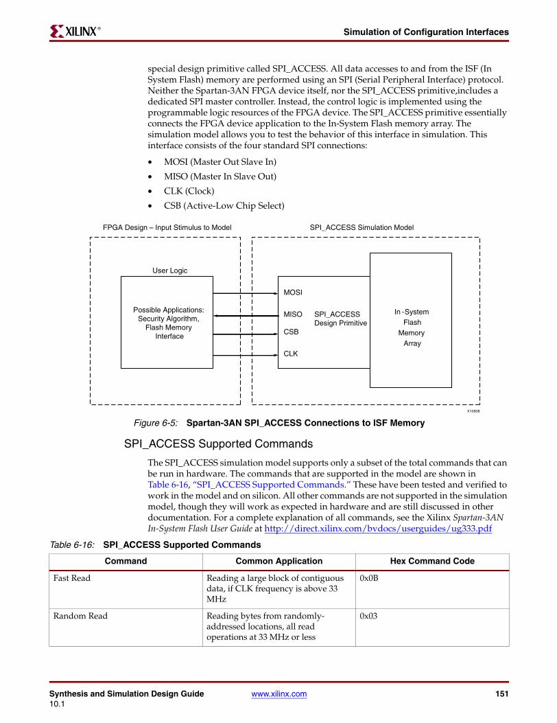
Synthesis and Simulation Design Guide www.xilinx.com 15110.1
Simulation of Configuration InterfacesR
special design primitive called SPI_ACCESS. All data accesses to and from the ISF (In System Flash) memory are performed using an SPI (Serial Peripheral Interface) protocol. Neither the Spartan-3AN FPGA device itself, nor the SPI_ACCESS primitive,includes a dedicated SPI master controller. Instead, the control logic is implemented using the programmable logic resources of the FPGA device. The SPI_ACCESS primitive essentially connects the FPGA device application to the In-System Flash memory array. The simulation model allows you to test the behavior of this interface in simulation. This interface consists of the four standard SPI connections:
• MOSI (Master Out Slave In)
• MISO (Master In Slave Out)
• CLK (Clock)
• CSB (Active-Low Chip Select)
SPI_ACCESS Supported Commands
The SPI_ACCESS simulation model supports only a subset of the total commands that can be run in hardware. The commands that are supported in the model are shown in Table 6-16, “SPI_ACCESS Supported Commands.” These have been tested and verified to work in the model and on silicon. All other commands are not supported in the simulation model, though they will work as expected in hardware and are still discussed in other documentation. For a complete explanation of all commands, see the Xilinx Spartan-3AN In-System Flash User Guide at http://direct.xilinx.com/bvdocs/userguides/ug333.pdf
X-Ref Target - Figure 6-4
Figure 6-5: Spartan-3AN SPI_ACCESS Connections to ISF Memory
MOSI
MISO
CSB
CLK
SPI_ACCESSDesign Primitive
User Logic
FPGA Design – Input Stimulus to Model SPI_ACCESS Simulation Model
Possible Applications:Security Algorithm,
Flash MemoryInterface
In -SystemFlash
MemoryArray
X10908
Table 6-16: SPI_ACCESS Supported Commands
Command Common Application Hex Command Code
Fast Read Reading a large block of contiguous data, if CLK frequency is above 33 MHz
0x0B
Random Read Reading bytes from randomly-addressed locations, all read operations at 33 MHz or less
0x03
152 www.xilinx.com Synthesis and Simulation Design Guide10.1
Chapter 6: Simulating Your DesignR
SPI_ACCESS Memory Initialization
The user-created memory file used to initialize the ISF is a list of Hex bytes in ASCII format. The file should have one ASCII coded hex byte on each line, where the number of lines is decided by the memory size. See Table 6-17, “ISF Available Memory Size.” The file initializes the ISF memory space.
Status Register Read Check ready/busy for programming commands, result of compare, protection, addressing mode, and similar
0xD7
Information Read Read JEDEC Manufacturer and Device ID
0x9F
Security Register Read Performs a read on the contents of the security register.
0x77
Security Register Program Programs the User-Defined Field in the Security Register
0x9B
Buffer Write Write data to SRAM page buffer; when complete, transfer to ISF memory using Buffer to Page Program command
Buffer1- 0x84
Buffer2- 0x87 Buffer to Page Program with Built-in Erase
First erases selected memory page and programs page with data from designated buffer
Buffer1- 0x83 Buffer2- 0x86 Buffer to Page Program without Built-in Erase
Program a previously erased page with data from designated buffer
Buffer1- 0x88 Buffer2- 0x89
Page Program Through Buffer with Erase
Combines Buffer Write with Buffer to Page Program with Built-in Erase command
Buffer1- 0x82
Buffer2- 0x85 Page to Buffer Compare Verify that the ISF memory array was programmed correctly
Buffer1- 0x60 Buffer2- 0x61 Page to Buffer Transfer
Transfers the entire contents of a selected ISF memory page to the specified SRAM page buffer
Buffer1- 0x53 Buffer2- 0x55
Sector Erase Erases any unprotected, unlocked sector in the main memory
0x7C
Page Erase Erases any individual page in the ISF memory array
0x81
Table 6-16: SPI_ACCESS Supported Commands (Cont’d)
Command Common Application Hex Command Code
Synthesis and Simulation Design Guide www.xilinx.com 15310.1
Simulation of Configuration InterfacesR
If the size of the memory in the file does not match the size of the memory for the device, a message warns that the file is either too large or too small.
• If the initialization file is too short, the rest of the memory is filled with 0xFF.
• If the initialization file is too long, the unneeded bytes are left unused.
Table 6-17, “ISF Available Memory Size,” shows the memory size available for each of the devices.
SPI_ACCESS Attributes
Five attributes can be set for the SPI_ACCESS component.
• “SPI_ACCESS SIM_DEVICE Attribute”
• “SPI_ACCESS SIM_USER_ID Attribute”
• “SPI_ACCESS SIM_MEM_FILE Attribute”
• “SPI_ACCESS SIM_FACTORY_ID Attribute”
• “SPI_ACCESS SIM_DELAY_TYPE Attribute”
SPI_ACCESS SIM_DEVICE Attribute
SIM_DEVICE defines which Spartan-3AN device you are using. This allows the proper SPI Flash size to be set. SIM_DEVICE is required
SPI_ACCESS SIM_USER_ID Attribute
SIM_USER_ID is used in simulation to initialize the User-Defined Field of the Security Register. In hardware, it can be programmed with any value at any time. This field is one-time programmable (OTP). The default delivered state is erased, and all locations are 0xFF. SIM_USER_ID is a 512 bit reg in Verilog and a 512 bit bit_vector in VHDL with the exact hex values you want in simulation. Bit 511 is the first bit out of the user portion of the security register. Bit 0 is the last bit out of the user portion of the security register.
SPI_ACCESS SIM_MEM_FILE Attribute
SIM_MEM_FILE specifies the file and directory name of the memory initialization file. For more information, see “SPI_ACCESS Memory Initialization.”
SPI_ACCESS SIM_FACTORY_ID Attribute
SIM_FACTORY_ID is used for simulation purposes only. SIM_FACTORY_ID allows you to set a unique value to the Unique Identifier portion of the security register. This value is read back by sending an Information Read command. The default for the Factory ID is all ones.
Table 6-17: ISF Available Memory Size
Device ISF Memory BitsAvailable User
Memory (Bytes)Lines in Initialization
File
3S50AN 1M + 135,168 135,168
3S200AN 4M + 540,672 540,672
3S400AN 4M + 540,672 540,672
3S700AN 8M + 1,081,344 1,081,344
3S1400AN 16M + 2,162,688 2,162,688
154 www.xilinx.com Synthesis and Simulation Design Guide10.1
Chapter 6: Simulating Your DesignR
In simulation, the FACTORY_ID can be written only once. As soon as a value other than one is detected in the factory ID, no further writing is allowed.
In the hardware, each individual device has a unique factory programmed ID in this field. It cannot be reprogrammed or erased.
SPI_ACCESS SIM_DELAY_TYPE Attribute
SIM_DELAY_TYPE is used to scale the chip delays down to more reasonable values for simulation. If SIM_DELAY_TYPE is set to ACCURATE, the model enforces the real timing specifications such as five (5) seconds for sector erase. If SIM_DELAY_TYPE is set to SCALED, it enforces much shorter time delays which are scaled back for faster simulation runtimes. The device behavior is not affected.
Table 6-18: SPI_ACCESS Available Attributes
Attribute Type Allowed Values Default Description
SIM_DEVICE String “3S50AN”, “3S200AN”, “3S400AN”, “3S700AN” or “3S1400AN”
“3S1400AN” Specifies the target device so that the proper size SPI Memory is used. This attribute should be modified to match the device under test.
SIM_USER_ID 64-byte Hex Value Any 64-byte hex value
All locations default to 0xFF
Specifies the programmed USER ID in the Security Register for the SPI Memory
SIM_MEM_FILE String Specified file and directory name
“NONE” Optionally specifies a hex file containing the initialization memory content for the SPI Memory
SIM_FACTORY_ID 64-byte Hex Value Any 64-byte Hex Value
All locations default to 0xFF
Specifies the Unique Identifier value in the Security Register for simulation purposes (the actual HW value will be specific to the particular device used).
SIM_DELAY_TYPE String “ACCURATE”, “SCALED”
“SCALED” Scales down some timing delays for faster simulation run. “ACCURATE” = timing and delays consistent with datasheet specs. “SCALED” = timing numbers scaled back to run faster simulation, behavior not affected.
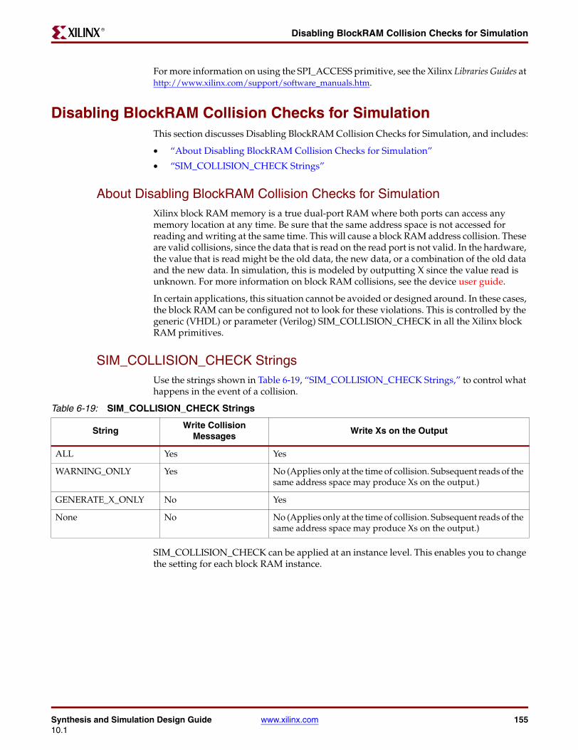
Synthesis and Simulation Design Guide www.xilinx.com 15510.1
Disabling BlockRAM Collision Checks for SimulationR
For more information on using the SPI_ACCESS primitive, see the Xilinx Libraries Guides at http://www.xilinx.com/support/software_manuals.htm.
Disabling BlockRAM Collision Checks for SimulationThis section discusses Disabling BlockRAM Collision Checks for Simulation, and includes:
• “About Disabling BlockRAM Collision Checks for Simulation”
• “SIM_COLLISION_CHECK Strings”
About Disabling BlockRAM Collision Checks for SimulationXilinx block RAM memory is a true dual-port RAM where both ports can access any memory location at any time. Be sure that the same address space is not accessed for reading and writing at the same time. This will cause a block RAM address collision. These are valid collisions, since the data that is read on the read port is not valid. In the hardware, the value that is read might be the old data, the new data, or a combination of the old data and the new data. In simulation, this is modeled by outputting X since the value read is unknown. For more information on block RAM collisions, see the device user guide.
In certain applications, this situation cannot be avoided or designed around. In these cases, the block RAM can be configured not to look for these violations. This is controlled by the generic (VHDL) or parameter (Verilog) SIM_COLLISION_CHECK in all the Xilinx block RAM primitives.
SIM_COLLISION_CHECK StringsUse the strings shown in Table 6-19, “SIM_COLLISION_CHECK Strings,” to control what happens in the event of a collision.
SIM_COLLISION_CHECK can be applied at an instance level. This enables you to change the setting for each block RAM instance.
Table 6-19: SIM_COLLISION_CHECK Strings
StringWrite Collision
MessagesWrite Xs on the Output
ALL Yes Yes
WARNING_ONLY Yes No (Applies only at the time of collision. Subsequent reads of the same address space may produce Xs on the output.)
GENERATE_X_ONLY No Yes
None No No (Applies only at the time of collision. Subsequent reads of the same address space may produce Xs on the output.)
156 www.xilinx.com Synthesis and Simulation Design Guide10.1
Chapter 6: Simulating Your DesignR
Global Reset and Tristate for SimulationThis section discusses Global Reset and Tristate for Simulation, and includes:
• “About Global Reset and Tristate for Simulation”
• “Using Global Tristate (GTS) and Global Set/Reset (GSR) Signals in an FPGA Device”
• “Global Set/Reset (GSR) and Global Tristate (GTS) in Verilog”
About Global Reset and Tristate for Simulation
Xilinx FPGA devices have dedicated routing and circuitry that connects to every register in the device. The dedicated global Global Set/Reset (GSR) net is asserted, and is released during configuration immediately after the device is configured. All the flip-flops and latches receive this reset, and are either set or reset, depending on how the registers are defined.
Although you can access the GSR net after configuration, Xilinx does not recommend using the GSR circuitry in place of a manual reset. This is because the FPGA devices offer high-speed backbone routing for high fanout signals such as a system reset. This backbone route is faster than the dedicated GSR circuitry, and is easier to analyze than the dedicated global routing that transports the GSR signal.
In back-end simulations, a GSR signal is automatically pulsed for the first 100 ns to simulate the reset that occurs after configuration. A GSR pulse can optionally be supplied in front end functional simulations, but is not necessary if the design has a local reset that resets all registers. When you create a test bench, remember that the GSR pulse occurs automatically in the back-end simulation. This holds all registers in reset for the first 100 ns of the simulation.
In addition to the dedicated global GSR, all output buffers are set to a high impedance state during configuration mode with the dedicated Global Tristate (GTS) net. All general-purpose outputs are affected whether they are regular, tristate, or bi-directional outputs during normal operation. This ensures that the outputs do not erroneously drive other devices as the FPGA device is configured.
In simulation, the GTS signal is usually not driven. The circuitry for driving GTS is available in the back-end simulation and can be optionally added for the front end simulation, but the GTS pulse width is set to 0 by default.
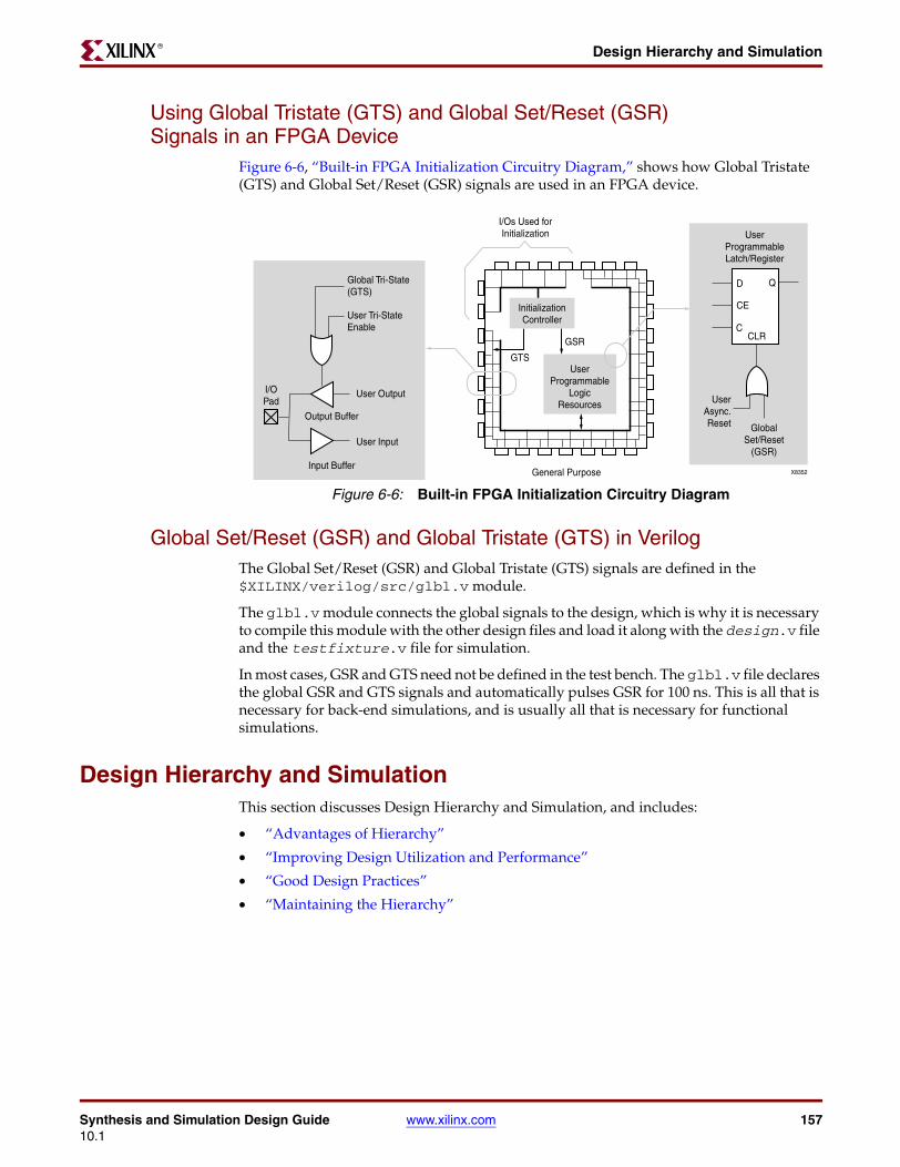
Synthesis and Simulation Design Guide www.xilinx.com 15710.1
Design Hierarchy and SimulationR
Using Global Tristate (GTS) and Global Set/Reset (GSR)Signals in an FPGA Device
Figure 6-6, “Built-in FPGA Initialization Circuitry Diagram,” shows how Global Tristate (GTS) and Global Set/Reset (GSR) signals are used in an FPGA device.
Global Set/Reset (GSR) and Global Tristate (GTS) in VerilogThe Global Set/Reset (GSR) and Global Tristate (GTS) signals are defined in the $XILINX/verilog/src/glbl.v module.
The glbl.v module connects the global signals to the design, which is why it is necessary to compile this module with the other design files and load it along with the design.v file and the testfixture.v file for simulation.
In most cases, GSR and GTS need not be defined in the test bench. The glbl.v file declares the global GSR and GTS signals and automatically pulses GSR for 100 ns. This is all that is necessary for back-end simulations, and is usually all that is necessary for functional simulations.
Design Hierarchy and SimulationThis section discusses Design Hierarchy and Simulation, and includes:
• “Advantages of Hierarchy”
• “Improving Design Utilization and Performance”
• “Good Design Practices”
• “Maintaining the Hierarchy”
Figure 6-6: Built-in FPGA Initialization Circuitry Diagram
X8352
UserProgrammableLatch/Register
Global Tri-State(GTS)
User OutputI/OPad
Output Buffer
Input Buffer
User Input
User Tri-StateEnable
General Purpose
I/Os Used forInitialization
GTS
GSR
UserAsync.Reset Global
Set/Reset(GSR)
InitializationController
UserProgrammable
LogicResources
QD
CLRC
CE

158 www.xilinx.com Synthesis and Simulation Design Guide10.1
Chapter 6: Simulating Your DesignR
Advantages of HierarchyHierarchy:
• Makes the design easier to read
• Makes the design easier to re-use
• Allows partitioning for a multi-engineer team
• Improves verification
Improving Design Utilization and PerformanceTo improve design utilization and performance, the synthesis tool or the Xilinx® implementation tools often flatten or modify the design hierarchy. After this flattening and restructuring of the design hierarchy in synthesis and implementation, it may become impossible to reconstruct the hierarchy.
As a result, much of the advantage of using the original design hierarchy in Register Transfer Level (RTL) verification is lost in back-end verification. In order to improve visibility of the design for back-end simulation, the Xilinx design flow allows for retention of the original design hierarchy.
To preserve the design hierarchy through implementation with little or no degradation in performance or increase in design resources:
• Follow stricter design rules.
• Carefully select the design hierarchy so that optimization is not necessary across the design hierarchy.
Good Design PracticesSome good design practices to follow are:
• Register all outputs exiting a preserved entity or module.
• Do not allow critical timing paths to span multiple entities or modules.
• Keep related or possibly shared logic in the same entity or module.
• Place all logic that is to be placed or merged into the I/O (such as IOB registers, tristate buffers, and instantiated I/O buffers) in the top-level module or entity for the design. This includes double-data rate registers used in the I/O.
• Manually duplicate high-fanout registers at hierarchy boundaries if improved timing is necessary.
Maintaining the HierarchyThis section discusses Maintaining the Hierarchy, and includes:
• “Instructing the Synthesis Tool to Maintain the Hierarchy”
• “Using the KEEP_HIERARCHY Constraint to Maintain the Hierarchy”

Synthesis and Simulation Design Guide www.xilinx.com 15910.1
Design Hierarchy and SimulationR
Instructing the Synthesis Tool to Maintain the Hierarchy
To maintain the entire hierarchy (or specified parts of the hierarchy) during synthesis, you must first instruct the synthesis tool to preserve hierarchy for all levels (or for each selected level of hierarchy). This may be done with:
• A global switch
• A compiler directive in the source files
• A synthesis command
For more information on how to retain hierarchy, see your synthesis tool documentation.
After taking the necessary steps to preserve hierarchy, and properly synthesizing the design, the synthesis tool creates a hierarchical implementation file (Electronic Data Interchange Format (EDIF) or NGC) that retains the hierarchy.
Using the KEEP_HIERARCHY Constraint to Maintain the Hierarchy
Before implementing the design with the Xilinx software, place a “KEEP_HIERARCHY” constraint on each instance in the design in which the hierarchy is to be preserved. “KEEP_HIERARCHY” tells the Xilinx software which parts of the design should not be flattened or modified to maintain proper hierarchy boundaries.
“KEEP_HIERARCHY” may be passed in the source code as an attribute, as an instance constraint in the Netlist Constraints File (NCF) or User Constraints File (UCF), or may be automatically generated by the synthesis tool. For more information, see your synthesis tool documentation.
After the design is mapped, placed, and routed, run NetGen using the following parameters to properly back-annotate the hierarchy of the design.
netgen -sim -ofmt {vhdl|verilog}design_name.ncd netlist_name
This is the NetGen default when you use ISE or XFLOW to generate the simulation files. It is necessary to know this only if you plan to execute NetGen outside of ISE or XFLOW, or if you have modified the default options in ISE or XFLOW. When you run NetGen in the preceding manner, all hierarchy that was specified to “KEEP_HIERARCHY” is reconstructed in the resulting VHDL or Verilog netlist.
NetGen can write out a separate netlist file and Standard Delay Format (SDF) file for each level of preserved hierarchy. This capability allows for full timing simulation of individual portions of the design, which in turn allows for:
• Greater test bench re-use
• Team-based verification methods
• The potential for reduced overall verification times
Use the –mhf switch to produce individual files for each “KEEP_HIERARCHY” instance in the design. You can also use the –mhf switch together with the –dir switch to place all associated files in a separate directory.
netgen -sim -ofmt {vhdl|verilog} -mhf -dir
directory_name design_name.ncd
When you run NetGen with the –mhf switch, NetGen produces a text file called design_mhf_info.txt. The design_mhf_info.txt file lists all produced module and entity names, their associated instance names, Standard Delay Format (SDF) files, and sub modules. The design_mhf_info.txt file is useful for determining proper
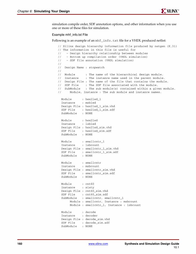
160 www.xilinx.com Synthesis and Simulation Design Guide10.1
Chapter 6: Simulating Your DesignR
simulation compile order, SDF annotation options, and other information when you use one or more of these files for simulation.
Example mhf_info.txt File
Following is an example of an mhf_info.txt file for a VHDL produced netlist:
// Xilinx design hierarchy information file produced by netgen (K.31) // The information in this file is useful for // - Design hierarchy relationship between modules // - Bottom up compilation order (VHDL simulation) // - SDF file annotation (VHDL simulation) //// Design Name : stopwatch//// Module : The name of the hierarchical design module.// Instance : The instance name used in the parent module.// Design File : The name of the file that contains the module.// SDF File : The SDF file associated with the module.// SubModule : The sub module(s) contained within a given module.// Module, Instance : The sub module and instance names.
Module : hex2led_1 Instance : msbled Design File : hex2led_1_sim.vhd SDF File : hex2led_1_sim.sdf SubModule : NONE
Module : hex2led Instance : lsbled Design File : hex2led_sim.vhd SDF File : hex2led_sim.sdf SubModule : NONE
Module : smallcntr_1 Instance : lsbcount Design File : smallcntr_1_sim.vhd SDF File : smallcntr_1_sim.sdf SubModule : NONE
Module : smallcntr Instance : msbcount Design File : smallcntr_sim.vhd SDF File : smallcntr_sim.sdf SubModule : NONE
Module : cnt60 Instance : sixty Design File : cnt60_sim.vhd SDF File : cnt60_sim.sdf SubModule : smallcntr, smallcntr_1 Module : smallcntr, Instance : msbcount Module : smallcntr_1, Instance : lsbcount
Module : decode Instance : decoder Design File : decode_sim.vhd SDF File : decode_sim.sdf SubModule : NONE
Synthesis and Simulation Design Guide www.xilinx.com 16110.1
Register Transfer Level (RTL) Simulation Using Xilinx LibrariesR
Module : dcm1 Instance : Inst_dcm1 Design File : dcm1_sim.vhd SDF File : dcm1_sim.sdf SubModule : NONE
Module : statmach Instance : MACHINE Design File : statmach_sim.vhd SDF File : statmach_sim.sdf SubModule : NONE
Module : stopwatch Design File : stopwatch_timesim.vhd SDF File : stopwatch_timesim.sdf SubModule : statmach, dcm1, decode, cnt60, hex2led, hex2led_1 Module : statmach, Instance : MACHINE Module : dcm1, Instance : Inst_dcm1 Module : decode, Instance : decoder Module : cnt60, Instance : sixty Module : hex2led, Instance : lsbled Module : hex2led_1, Instance : msbled
Hierarchy created by generate statements may not match the original simulation due to naming differences between the simulator and synthesis engines for generated instances.
Register Transfer Level (RTL) Simulation Using Xilinx LibrariesThis section discusses Register Transfer Level (RTL) Simulation Using Xilinx Libraries, and includes:
• “Simulating Xilinx Libraries”
• “Delta Cycles and Race Conditions”
• “Recommended Simulation Resolution”
Simulating Xilinx LibrariesXilinx simulation libraries can be simulated using any simulator that supports the VHDL-93 and Verilog-2001 language standards. Certain delay and modelling information is built into the libraries, which is required to correctly simulate the Xilinx hardware devices.
Do not change data signals at clock edges, even for functional simulation. The simulators add a unit delay between the signals that change at the same simulator time. If the data changes at the same time as a clock, it is possible that the data input will be scheduled by the simulator to occur after the clock edge. The data will not go through until the next clock edge, although it is possible that the intent was to have the data clocked in before the first clock edge. To avoid such unintended simulation results, do not switch data signals and clock signals simultaneously.
Delta Cycles and Race ConditionsAll Xilinx-supported simulators are event-based simulators. Event-based simulators can process multiple events at a given simulation time. While these events are being processed, the simulator may not advance the simulation time. This time is commonly referred to as delta cycles. There can be multiple delta cycles in a given simulation time. Simulation time
162 www.xilinx.com Synthesis and Simulation Design Guide10.1
Chapter 6: Simulating Your DesignR
is advanced only when there are no more transactions to process. For this reason, simulators may give unexpected results. The following VHDL coding example shows how an unexpected result can occur.
VHDL Coding Example With Unexpected Results
clk_b <= clk;clk_prcs : process (clk)begin if (clk'event and clk='1') then result <= data; end if;end process;
clk_b_prcs : process (clk_b)begin if (clk_b'event and clk_b='1') then result1 <= result; end if;end process;
In this example, there are two synchronous processes:
• clk
• clk_b
The simulator performs the clk <= clk_b assignment before advancing the simulation time. As a result, events that should occur in two clock edges will occur instead in one clock edge, causing a race condition.
Recommended ways to introduce causality in simulators for such cases include:
• Do not change clock and data at the same time. Insert a delay at every output.
• Be sure to use the same clock.
• Force a delta delay by using a temporary signal as follows:
clk_b <= clk;clk_prcs : process (clk)begin if (clk'event and clk='1') then result <= data; result_temp <= result; end if;end process;
clk_b_prcs : process (clk_b)begin if (clk_b'event and clk_b='1') then result1 <= result_temp; end if;end process;
Almost every event-based simulator can display delta cycles. Use this to your advantage when debugging simulation issues.
Synthesis and Simulation Design Guide www.xilinx.com 16310.1
Generating Gate-Level Netlist (Running NetGen)R
Recommended Simulation ResolutionXilinx recommends that you run simulations using a resolution of 1 ps. Some Xilinx primitive components, such as DCM, require a 1 ps resolution in order to work properly in either functional or timing simulation.
There is no simulator performance gain by using coarser resolution with the Xilinx simulation models. Since much simulation time is spent in delta cycles, and delta cycles are not affected by simulator resolution, no significant simulation performance can be obtained.
Xilinx recommends that you not run at a finer resolution such as fs. Some simulators may round the numbers, while other simulators may truncate the numbers.
Picosecond is used as the minimum resolution since all testing equipment can measure timing only to the nearest picosecond resolution. Xilinx strongly recommends using ps for all Hardware Description Language (HDL) simulation purposes.
IP Encryption MethodologyXilinx leverages the latest encryption methodology as specified in Verilog LRM - IEEE Std 1364™-2005. Virtex-5 simulation models for the Hard-IP such as PowerPC, MGT, and PCIe leverages this technology. Since this standard is relatively new, simulator vendor support is currently limited.
Xilinx supports the following simulators for this methodology:
• Mentor Graphics Modelsim 6.3c and above
• Mentor Graphics QuestaSim 6.3c and above
Everything is automatically handled by means of Compxlib, provided the appropriate version of the simulator is present on your computer. When running a simulation with this new methodology in Verilog, you must reference the following library:
secureip
For most simulators, this can be done by using the -L switch as an argument to the simulator, such as -L secureip. For more information, see “SecureIP Libraries.”
For the switch to use with your simulator, see your simulator documentation.
Caution! If using VHDL as the design entry, a mixed-language license is required to run any Hard-IP simulation using this new IP Encryption Methodology
Generating Gate-Level Netlist (Running NetGen)NetGen can create a verification netlist file from your design files. You can create a timing simulation netlist as follows:
• Running NetGen from Project Navigator
For information on creating a back-annotated simulation netlist in Project Navigator, see the ISE Help.
• Running NetGen from XFLOW
To display the available options for XFLOW, and for a complete list of the XFLOW option files, type xflow at the prompt without any arguments. For complete descriptions of the options and the option files, see the Xilinx Development System Reference Guide at http://www.xilinx.com/support/software_manuals.htm.
164 www.xilinx.com Synthesis and Simulation Design Guide10.1
Chapter 6: Simulating Your DesignR
• Running NetGen from the Command Line or a Script File
To create a simulation netlist from the command line or a script file, see the Netgen chapter in the Xilinx Development System Reference Guide at http://www.xilinx.com/support/software_manuals.htm.
Disabling X Propagation for Synchronous ElementsThis section discusses Disabling X Propagation for Synchronous Elements, and includes:
• “X Propagation During Timing Violations”
• “Using the ASYNC_REG Constraint”
X Propagation During Timing ViolationsWhen a timing violation occurs during a timing simulation, the default behavior of a latch, register, RAM, or other synchronous element outputs an X to the simulator.
This occurs because the actual output value is not known. The output of the register could:
• Retain its previous value
• Update to the new value
• Go metastable, in which a definite value is not settled upon until some time after the clocking of the synchronous element
Since this value cannot be determined, and accurate simulation results cannot be guaranteed, the element outputs an X to represent an unknown value. The X output remains until the next clock cycle in which the next clocked value updates the output if another violation does not occur.
X generation can significantly affect simulation. For example, an X generated by one register can be propagated to others on subsequent clock cycles. This may cause large portions of the design being tested to become unknown. To correct this:
• On a synchronous path, analyze the path and fix any timing problems associated with this or other paths to ensure a properly operating circuit.
• On an asynchronous path, if you cannot otherwise avoid timing violations, disable the X propagation on synchronous elements during timing violations.
When X propagation is disabled, the previous value is retained at the output of the register. In the actual silicon, the register may have changed to the 'new' value. Disabling X propagation may yield simulation results that do not match the silicon behavior.
Caution! Exercise care when using this option. Use it only if you cannot otherwise avoid timing violations.
Using the ASYNC_REG ConstraintThe “ASYNC_REG” constraint:
• Identifies asynchronous registers in the design
• Disables X propagation for those registers
Synthesis and Simulation Design Guide www.xilinx.com 16510.1
MIN/TYP/MAX SimulationR
“ASYNC_REG” can be attached to a register in the front end design by:
• An attribute in the Hardware Description Language (HDL) code, or
• A constraint in the User Constraints File (UCF)
The registers to which “ASYNC_REG” is attached retain the previous value during timing simulation, and do not output an X to simulation.
Caution! A timing violation error may still occur. Use care, as the new value may have been clocked in as well.
“ASYNC_REG” is applicable to CLB and IOB registers and latches only. If you cannot avoid clocking in asynchronous data, Xilinx recommends that you do so for IOB or CLB registers only. Clocking in asynchronous signals to RAM, Shift Register LUT (SRL), or other synchronous elements has less deterministic results, and therefore should be avoided.
Xilinx highly recommends that you first properly synchronize any asynchronous signal in a register, latch, or FIFO before writing to a RAM, SRL, or any other synchronous element.
MIN/TYP/MAX SimulationThis section discusses MIN/TYP/MAX Simulation, and includes:
• “About MIN/TYP/MAX Simulation”
• “Obtaining Accurate Timing Simulation Results”
• “Absolute Min Simulation”
About MIN/TYP/MAX SimulationThe Standard Delay Format (SDF) file allows you to specify three sets of delay values for simulation:
• “Minimum (MIN)”
• “Typical (TYP)”
• “Maximum (MAX)”
Xilinx uses these values to allow the simulation of the target architecture under various operating conditions. By allowing for the simulation across various operating conditions, you can perform more accurate setup and hold timing verification.
Minimum (MIN)
Minimum (MIN) represents the device under the best case operating conditions. The base case operating conditions are defined as the minimum operating temperature, the maximum voltage, and the best case process variations. Under best case conditions, the data paths of the device have the minimum delay possible, while the clock path delays are the maximum possible relative to the data path delays. This situation is ideal for hold time verification of the device.
Typical (TYP)
Typical (TYP) represents the typical operating conditions of the device. In this situation, the clock and data path delays are both the maximum possible. This is different from the “Maximum (MAX)” field, in which the clock paths are the minimum possible relative to
166 www.xilinx.com Synthesis and Simulation Design Guide10.1
Chapter 6: Simulating Your DesignR
the maximum data paths. Xilinx generated Standard Delay Format (SDF) files do not take advantage of this field.
Maximum (MAX)
Maximum (MAX) represents the delays under the worst case operating conditions of the device. The worst case operating conditions are defined as the maximum operating temperature, the minimum voltage, and the worst case process variations. Under worst case conditions, the data paths of the device have the maximum delay possible, while the clock path delays are the minimum possible relative to the data path delays. This situation is ideal for setup time verification of the device.
Obtaining Accurate Timing Simulation ResultsThis section discusses Obtaining Accurate Timing Simulation Results. In order to obtain the most accurate setup and hold timing simulations:
• “Run Netgen”
• “Run Setup Simulation”
• “Run Hold Simulation”
Run Netgen
To obtain accurate Standard Delay Format (SDF) numbers, run netgen with -pcf pointing to a valid Physical Constraints File (PCF). Netgen must be run with -pcf, since newer Xilinx devices take advantage of relative mins for timing information. Once netgen is called with -pcf, the “Minimum (MIN)” and “Maximum (MAX)” numbers in the SDF file will be different for the components.
Once the correct SDF file is created, two types of simulation must be run for complete timing closure:
• Setup Simulation
• Hold Simulation
In order to run the different simulations, the simulator must be called with the appropriate switches.
Run Setup Simulation
To perform a Setup Simulation, specify values in the “Maximum (MAX)” field with the following command line modifier:
-SDFMAX
Run Hold Simulation
To perform the most accurate Hold Simulation, specify values in the “Minimum (MIN)” field with the following command line modifier:
-SDFMIN
For more information on how to pass the Standard Delay Format (SDF) switches to the simulator, see your simulator tool documentation.
Synthesis and Simulation Design Guide www.xilinx.com 16710.1
MIN/TYP/MAX SimulationR
Absolute Min SimulationNetGen can optionally produce absolute minimum delay values for simulation by applying the -s min switch. The resulting Standard Delay Format (SDF) file produced from NetGen has the absolute process minimums populated in all three SDF fields:
• “Minimum (MIN)”
• “Typical (TYP)”
• “Maximum (MAX)”
Absolute process “Minimum (MIN)” values are the absolute fastest delays that a path can run in the target architecture given the best operating conditions within the specifications of the architecture:
• Lowest temperature
• Highest voltage
• Best possible silicon
Generally, these process minimum delay values are only useful for checking board-level, chip-to-chip timing for high-speed data paths in best case and worst case conditions.
By default, the worst case delay values are derived from the worst temperature, voltage, and silicon process for a particular target architecture. If better temperature and voltage characteristics can be ensured during the operation of the circuit, you can use prorated worst case values in the simulation to gain better performance results. The default would apply worst case timing values over the specified “TEMPERATURE” and “VOLTAGE” within the operating conditions recommended for the device.
Netgen generates Standard Delay Format (SDF) files with “Minimum (MIN)” numbers only for devices that support absolute min timing numbers.
Using the VOLTAGE and TEMPERATURE ConstraintsThis section discusses Using the VOLTAGE and TEMPERATURE Constraints, and includes:
• “Using the VOLTAGE Constraint”
• “Using the TEMPERATURE Constraint”
• “Determining Valid Operating Temperatures and Voltages”
• “NetGen Options for Different Delay Values”
Prorating is a linear scaling operation. It applies to existing speed file delays, and is applied globally to all delays. The prorating constraints, the “VOLTAGE” constraint and the “TEMPERATURE” constraint, provide a method for determining timing delay characteristics based on known environmental parameters.
168 www.xilinx.com Synthesis and Simulation Design Guide10.1
Chapter 6: Simulating Your DesignR
Using the VOLTAGE Constraint
The “VOLTAGE” constraint provides a means of prorating delay characteristics based on the specified voltage applied to the device. The User Constraints File (UCF) syntax is:
VOLTAGE=value[V]
where
value
is an integer or real number specifying the voltage, and
units
is an optional parameter specifying the unit of measure.
Using the TEMPERATURE Constraint
The “TEMPERATURE” constraint provides a means of prorating device delay characteristics based on the specified junction temperature. The User Constraints File (UCF) syntax is:
TEMPERATURE=value[C|F|K]
where
value
is an integer or a real number specifying the temperature, and
C, F, and K
are the temperature units:
• C =degrees Celsius (default)
• F = degrees Fahrenheit
• K =degrees Kelvin
The resulting values in the Standard Delay Format (SDF) fields when using prorated “VOLTAGE” and “TEMPERATURE” values are the prorated worst case values.
Determining Valid Operating Temperatures and Voltages
To determine the specific range of valid operating temperatures and voltages for the target architecture, see the device data sheet. If the temperature or voltage specified in the constraint does not fall within the supported range, the constraint is ignored and an architecture specific default value is used instead.
Not all architectures support prorated timing values. For simulation, the “VOLTAGE” and “TEMPERATURE” constraints are processed from the User Constraints File (UCF) into the Physical Constraints File (PCF). The PCF must then be referenced when running NetGen in order to pass the operating conditions to the delay annotator.
To generate a simulation netlist using prorating for VHDL, type:
netgen -sim -ofmt vhdl [options] -pcf design.pcf design.ncd
To generate a simulation netlist using prorating for Verilog, type:
netgen -sim -ofmt verilog [options] -pcf design.pcf design.ncd
Combining both minimum values overrides prorating, and results in issuing only absolute process MIN values for the simulation Standard Delay Format (SDF) file.
Synthesis and Simulation Design Guide www.xilinx.com 16910.1
Special Considerations for CLKDLL, DCM, and DCM_ADVR
Prorating is available for certain FPGA devices only. It is not intended for military and industrial ranges. It is applicable only within commercial operating ranges.
NetGen Options for Different Delay Values
Special Considerations for CLKDLL, DCM, and DCM_ADVThis section discusses Special Considerations for CLKDLL, DCM and DCM_ADV, and includes:
• “DLL/DCM Clocks Do Not Appear De-Skewed”
• “TRACE/Simulation Model Differences for DCM/DLL”
• “Non-LVTTL Input Drivers”
• “Viewer Considerations”
• “Attributes for Simulation and Implementation”
• “Understanding Timing Simulation”
DLL/DCM Clocks Do Not Appear De-SkewedThe DLL and DCM components remove the clock delay from the clock entering into the chip. As a result, the incoming clock and the clocks feeding the registers in the device have a minimal skew within the range specified in the databook for any given device. In timing simulation, the clocks may not appear to be de-skewed within the range specified. This is due to the way the delays in the Standard Delay Format (SDF) file are handled by some simulators.
The SDF file annotates the CLOCK PORT delay on the X_FF components. Some simulators may show the clock signal in the waveform viewer before taking this delay into account. If the simulator is not properly de-skewing the clock, see your simulator tool documentation to determine if your simulator tool is displaying the input port delays in the waveform viewer at the input nodes. If so, when the CLOCK PORT delay on the X_FF is added to the internal clock signal, it should line up within the device specifications in the waveform viewer with the input port clock. The simulation is still functioning properly, the waveform viewer is just not displaying the signal at the expected node. To verify that the DLL/DCM is functioning correctly, delays from the SDF file may need to be accounted for manually to calculate the actual skew between the input and internal clocks.
Table 6-20: NetGen Options for Different Delay Values
NetGen Option MIN:TYP:MAX Field in SDF File Produced by NetGen –sim
-pcf <pcf_file> MIN:MIN(Hold time) TYP:TYP(Ignore) MAX:MAX(Setup time)
default MAX:MAX:MAX
–s min Process MIN: Process MIN: Process MIN
Prorated voltage or temperature in User Constraints File or Physical Constraints File (PCF)
Prorated MAX: Prorated MAX: Prorated MAX
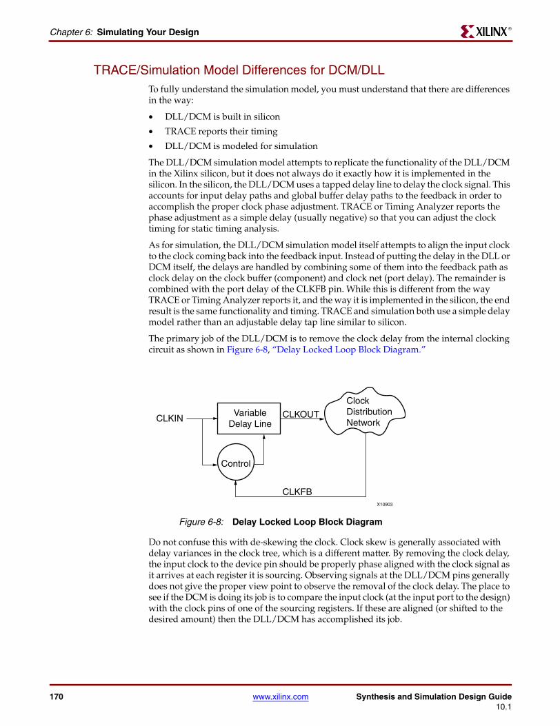
170 www.xilinx.com Synthesis and Simulation Design Guide10.1
Chapter 6: Simulating Your DesignR
TRACE/Simulation Model Differences for DCM/DLLTo fully understand the simulation model, you must understand that there are differences in the way:
• DLL/DCM is built in silicon
• TRACE reports their timing
• DLL/DCM is modeled for simulation
The DLL/DCM simulation model attempts to replicate the functionality of the DLL/DCM in the Xilinx silicon, but it does not always do it exactly how it is implemented in the silicon. In the silicon, the DLL/DCM uses a tapped delay line to delay the clock signal. This accounts for input delay paths and global buffer delay paths to the feedback in order to accomplish the proper clock phase adjustment. TRACE or Timing Analyzer reports the phase adjustment as a simple delay (usually negative) so that you can adjust the clock timing for static timing analysis.
As for simulation, the DLL/DCM simulation model itself attempts to align the input clock to the clock coming back into the feedback input. Instead of putting the delay in the DLL or DCM itself, the delays are handled by combining some of them into the feedback path as clock delay on the clock buffer (component) and clock net (port delay). The remainder is combined with the port delay of the CLKFB pin. While this is different from the way TRACE or Timing Analyzer reports it, and the way it is implemented in the silicon, the end result is the same functionality and timing. TRACE and simulation both use a simple delay model rather than an adjustable delay tap line similar to silicon.
The primary job of the DLL/DCM is to remove the clock delay from the internal clocking circuit as shown in Figure 6-8, “Delay Locked Loop Block Diagram.”
Do not confuse this with de-skewing the clock. Clock skew is generally associated with delay variances in the clock tree, which is a different matter. By removing the clock delay, the input clock to the device pin should be properly phase aligned with the clock signal as it arrives at each register it is sourcing. Observing signals at the DLL/DCM pins generally does not give the proper view point to observe the removal of the clock delay. The place to see if the DCM is doing its job is to compare the input clock (at the input port to the design) with the clock pins of one of the sourcing registers. If these are aligned (or shifted to the desired amount) then the DLL/DCM has accomplished its job.
X-Ref Target - Figure 6-7
Figure 6-8: Delay Locked Loop Block Diagram
CLKIN CLKOUT
CLKFB
ClockDistributionNetwork
VariableDelay Line
Control
X10903
Synthesis and Simulation Design Guide www.xilinx.com 17110.1
Special Considerations for CLKDLL, DCM, and DCM_ADVR
Non-LVTTL Input DriversWhen non-LVTTL input buffer drivers drive the clock, the DCM does not adjust for the type of input buffer. Instead, the DCM has a single delay value to provide the optimal amount of clock delay across all I/O standards. If you are using the same input standard for the data, the delay values should track, and usually not cause a problem.
Even if you are not using the same input standard, the amount of delay variance usually does not cause hold time failures. The delay variance is small compared to the amount of input delay. The delay variance is calculated in both static timing analysis and simulation. Proper setup time values should occur during both static timing analysis and simulation.
Viewer ConsiderationsDepending on the simulator, the waveform viewer may not depict the delay timing in the expected manner. Some simulators (including ModelSim) combine interconnect and port delays with the input pins of the component delays. While the simulation results are correct, the depiction in the waveform viewer may be unexpected.
Since interconnect delays are combined, when you look at a pin using the ModelSim viewer, you do not see the transition as it happens on the pin. The simulation acts properly, but when attempting to calculate clock delay, the interconnect delays before the clock pin must be taken into account if the simulator you are using combines these interconnect delays with component delays.
For more information, search the Xilinx Answer Database for the following topic: “ModelSim Simulations: Input and Output clocks of the DCM and CLKDLL models do not appear to be de-skewed (VHDL, Verilog).”
Attributes for Simulation and Implementation Make sure that the same attributes are passed for simulation and implementation. During implementation, DLL/DCM attributes may be passed by:
• The synthesis tool (generic or inline parameter declaration)
• The User Constraints File (UCF)
For Register Transfer Level (RTL) simulation of the UNISIM models, the simulation attributes must be passed by means of:
• A generic (VHDL)
• Inline parameters (Verilog)
If you do not use the default setting for the DLL/DCM, make sure that the attributes for RTL simulation are the same as those used for implementation. If not, there may be differences between RTL simulation and the actual device implementation.
To make sure that the attributes passed to implementation are the same as those used for simulation, use the generic mapping method (VHDL) or inline parameter passing (Verilog), provided your synthesis tool supports these methods for passing functional attributes.
172 www.xilinx.com Synthesis and Simulation Design Guide10.1
Chapter 6: Simulating Your DesignR
Understanding Timing SimulationThis section discusses Understanding Timing Simulation, and includes:
• “Importance of Timing Simulation”
• “Glitches in Your Design”
• “Debugging Timing Problems”
• “Timing Problem Root Causes”
• “Debugging Tips”
• “Setup and Hold Violations”
In back annotated (timing) simulation, the introduction of delays can cause the behavior to be different from what is expected. Most problems are caused due to timing violations in the design, and are reported by the simulator. There are a few other situations that can occur as discussed in this section.
Importance of Timing SimulationThis section discusses Importance of Timing Simulation, and includes:
• “About Importance of Timing Simulation”
• “Functional Simulation”
• “Static Timing Analysis and Equivalency Checking”
• “In-System Testing”
About Importance of Timing Simulation
FPGA devices require both functional and timing simulation to ensure successful designs. FPGA designs are growing in complexity. Traditional verification methodologies are no longer sufficient. In the past, simulation was not an important stage in the FPGA design flow. Currently simulation is becoming one of the most critical stages. Timing simulation is especially important when designing for advanced FPGA devices.
Functional Simulation
While functional simulation is an important part of the verification process, it should not be the only part. Functional simulation tests only for the functional capabilities of the Register Transfer Level (RTL) design. It does not include any timing information, nor does it take into consideration changes made to the original design due to implementation and optimization
Static Timing Analysis and Equivalency Checking
Many designers see Static Timing Analysis and Equivalency Checking as the only analysis needed to verify that the design meets timing. There are many drawbacks to using Static Timing Analysis and Equivalency Checking as the only timing analysis methodology. Static analysis cannot find any of the problems that can be seen when running a design dynamically. It can only show if the design as a whole meets setup and hold requirements. It is generally only as good as the timing constraints applied.
In a real system, dynamic factors such as Block Ram collisions can cause timing violations on the FPGA device. With the introduction of Dual Port Block Rams in FPGA devices, care should be taken not to read and write to the same location at the same time, as this results
Synthesis and Simulation Design Guide www.xilinx.com 17310.1
Understanding Timing SimulationR
in incorrect data being read back. Static analysis is unable to find this problem. Similarly, if there are misconstrued timespecs, static timing analysis cannot find this problem.
In-System Testing
Most designers rely on In-System Testing as the ultimate test. If the design works on the board, and passes the test suites, they view the device as ready for release. While In-System Testing is definitely effective for some purposes, it may not immediately detect all potential problems. At times the design must be run for a lengthy period before corner-case issues become apparent. For example, issues such as timing violations may not become apparent in the same way in all devices. By the time these corner-case issues manifest themselves, the design may already be in the hands of the end customer. It will mean high costs, downtime, and frustration to try to resolve the problem. In order to properly complete In-System Testing, all hardware hurdles such as problems with SSO, Cross-talk, and other board related issues must be overcome. Any external interfaces must also be connected before beginning the In-System Testing, increasing the time to market.
The traditional methods of verification are not sufficient for a fully verified system. There are compelling reasons to do dynamic timing analysis.
Glitches in Your Design When a glitch (small pulse) occurs in an FPGA circuit or any integrated circuit, the glitch may be passed along by the transistors and interconnect (transport) in the circuit, or it may be swallowed and not passed (internal) to the next resource in the FPGA. This depends on the width of the glitch and the type of resource the glitch passes through. To produce more accurate simulation of how signals are propagated within the silicon, Xilinx models this behavior in the timing simulation netlist.
For VHDL simulation, library components are instantiated by netgen and proper values are annotated for pulse rejection in the simulation netlist. The result of these constructs in the simulation netlists is a more true-to-life simulation model, and therefore a more accurate simulation.
For Verilog simulation, this information is passed by the PATHPULSE construct in the Standard Delay Format (SDF) file. This construct is used to specify the size of pulses to be rejected or swallowed on components in the netlist.
Debugging Timing ProblemsThis section discusses Debugging Timing Problems, and includes:
• “Identifying Timing Problems”
• “Setup Violation Messages”
Identifying Timing Problems
In back-annotated (timing) simulation, the simulator processes timing information in the Standard Delay Format (SDF) file. This may cause timing violations if the circuit is operated too fast, or if there are asynchronous components in the design.
This section explains some common timing violations, and gives advice on how to debug and correct them.
After you run timing simulation, review any warning or error messages generated by your simulator.
174 www.xilinx.com Synthesis and Simulation Design Guide10.1
Chapter 6: Simulating Your DesignR
Setup Violation Messages
The following example is a typical setup violation message from ModelSim for a Verilog design. Message formats vary from simulator to simulator, but all contain the same basic information. For more information, see your simulator tool documentation.
# ** Error:/path/to/xilinx/verilog/src/simprims/X_RAMD16.v(96):$setup(negedge WE:29138 ps, posedge CLK:29151 ps, 373 ps);# Time:29151 ps Iteration:0 Instance: /test_bench/u1/\U1/X_RAMD16\
Setup Violation Message Line One
# ** Error:/path/to/xilinx/verilog/src/simprims/X_RAMD16.v(96):
Line One points to the line in the simulation model that is in error. In this example, the failing line is line 96 of the Verilog file X_RAMD16.
Setup Violation Message Line Two
$setup(negedge WE:29138 ps, posedge CLK:29151 ps, 373 ps);
Line Two gives information about the two signals that caused the error:
• The type of violation, such as $setup, $hold, or $recovery. This example is a $setup violation.
• The name of each signal involved in the violation, followed by the simulation time at which that signal last changed values. In this example, the failing signals are the negative-going edge of the signal WE, which last changed at 29138 picoseconds, and the positive-going edge of the signal CLK, which last changed at 29151 picoseconds.
• The allotted amount of time for the setup. In this example, the signal on WE should be stable for 373 pico seconds before the clock transitions. Since WE changed only 13 pico seconds before the clock, the simulator reported a violation.
Setup Violation Message Line Three
# Time:29151 ps Iteration:0 Instance: /test_bench/u1/\U1/X_RAMD16\
Line Three gives the simulation time at which the error was reported, and the instance in the structural design (time_sim) in which the violation occurred.
Timing Problem Root CausesTiming violations, such as $setuphold, occur any time data changes at a register input (either data or clock enable) within the setup or hold time window for that particular register. The most typical causes for timing violations are:
• “Simulation Clock Does Not Meet Timespec”
• “Unaccounted Clock Skew”
• “Asynchronous Inputs, Asynchronous Clock Domains, Crossing Out-of-Phase”
For more information, see “Timing Closure Mode.”
Simulation Clock Does Not Meet Timespec
If the frequency of the clock specified during simulation is greater than the frequency of the clock specified in the timing constraints, this over-clocking can cause timing violations. For example, if the simulation clock has a frequency of 5 ns, and a “PERIOD” constraint is set at 10 ns, a timing violation can occur. This situation can also be complicated by the presence of DLL or DCM in the clock path.
Synthesis and Simulation Design Guide www.xilinx.com 17510.1
Understanding Timing SimulationR
This problem is usually caused either by an error in the test bench or by an error in the constraint specification. Make sure that the constraints match the conditions in the test bench, and correct any inconsistencies. If you modify the constraints, re-run the design through place and route to make sure that all constraints are met.
Unaccounted Clock Skew
Clock skew is the difference between the amount of time the clock signal takes to reach the destination register, and the amount of time the clock signal takes to reach the source register. The data must reach the destination register within a single clock period plus or minus the amount of clock skew. While clock skew is usually not a problem when you use global buffers, it can be a concern if you use the local routing network for your clock signals.
To determine if clock skew is the problem, run a setup test in TRACE and read the report. For directions on how to run a setup check, see the Xilinx Development System Reference Guide, “TRACE” at http://www.xilinx.com/support/software_manuals.htm. For information on using Timing Analyzer to determine clock skew, see Timing Analyzer in the ISE Help.
Asynchronous Inputs, Asynchronous Clock Domains, Crossing Out-of-Phase
Timing violations can be caused by data paths that:
• Are not controlled by the simulation clock
• Are not clock controlled at all
• Cross asynchronous clock boundaries
• Have asynchronous inputs
• Cross data paths out of phase
Asynchronous Clocks
If the design has two or more clock domains, any path that crosses data from one domain to another can cause timing problems. Although data paths that cross from one clock domain to another are not always asynchronous, it is always best to be cautious.
Always treat the following as asynchronous:
• Two clocks with unrelated frequencies
• Any clocking signal coming from off-chip
• Any time a register’s clock is gated (unless extreme caution is used)
To see if the path in question crosses asynchronous clock boundaries, check the source code and the Timing Analysis report. If your design does not allow enough time for the path to be properly clocked into the other domain, you may need to redesign your clocking scheme. Consider using an asynchronous FIFO as a better way to pass data from one clock domain to another.
Asynchronous Inputs
Data paths that are not controlled by a clocked element are asynchronous inputs. Because they are not clock controlled, they can easily violate setup and hold time specifications.
Check the source code to see if the path in question is synchronous to the input register. If synchronization is not possible, you can use the ASYNC_REG constraint to work around the problem. For more information, see “Using the ASYNC_REG Constraint.”
176 www.xilinx.com Synthesis and Simulation Design Guide10.1
Chapter 6: Simulating Your DesignR
Out of Phase Data Paths
Data paths can be clock controlled at the same frequency, but nevertheless can have setup or hold violations because the clocks are out of phase. Even if the clock frequencies are a derivative of each other, improper phase alignment could cause setup violations.
To see if the path in question crosses another path with an out of phase clock, check the source code and the Timing Analysis report.
Debugging TipsWhen you have a timing violation, ask:
• Was the clock path analyzed by TRACE or Timing Analyzer?
• Did TRACE or Timing Analyzer report that the data path can run at speeds being clocked in simulation?
• Is clock skew being accounted for in this path delay?
• Does subtracting the clock path delay from the data path delay still allow clocking speeds?
• Will slowing down the clock speeds eliminate the $setup or $hold time violations?
• Does this data path cross clock boundaries (from one clock domain to another)? Are the clocks synchronous to each other? Is there appreciable clock skew or phase difference between these clocks?
• If this path is an input path to the device, does changing the time at which the input stimulus is applied eliminate the $setup or $hold time violations?
Depending on your answers, you may need to change your design or test bench to accommodate the simulation conditions. For more information, see “Design Considerations.”
Setup and Hold ViolationsThis section discusses Setup and Hold Violations, and includes:
• “Zero Hold Time Considerations”
• “Negative Hold Times”
• “RAM Considerations for Setup and Hold Violations”
Zero Hold Time Considerations
While Xilinx data sheets report that there are zero hold times on the internal registers and I/O registers with the default delay and using a global clock buffer, it is still possible to receive a $hold violation from the simulator. This $hold violation is really a $setup violation on the register. In order to obtain an accurate representation of the CLB delays, part of the setup time must be modeled as a hold time.
Negative Hold Times
Older Xilinx simulation models truncate negative hold times and specify them as zero hold times. While this truncation does not cause inaccuracies in simulation, it results in a more pessimistic timing model than can actually be achieved in the FPGA device. This makes it more difficult to meet stringent timing requirements.
Synthesis and Simulation Design Guide www.xilinx.com 17710.1
Understanding Timing SimulationR
Negative hold times are now specified in the timing models. Specifying negative hold times provides a wider, yet more accurate, representation of the timing window. The setup and hold parameters for the synchronous models are combined into a single setuphold parameter. Such combining does not change the timing simulation methodology.
There are no longer separate violation messages for setup and hold when using Cadence NC-Verilog. They are combined into a single setuphold violation message.
RAM Considerations for Setup and Hold Violations
This section discusses RAM Considerations for Setup and Hold Violations, and includes:
• “Timing Violations”
• “Collision Checking”
• “Hierarchy Considerations”
Timing Violations
Xilinx devices contain two types of memories:
• Block RAM
• Distributed RAM
Since block RAM and distributed RAM are synchronous elements, you must take care to avoid timing violations. To guarantee proper data storage, the data input, address lines, and enables, must all be stable before the clock signal arrives.
Collision Checking
Block RAMs also perform synchronous read operations. During a read cycle, the addresses and enables must be stable before the clock signal arrives, or a timing violation may occur.
When you use block RAM in dual-port mode, take special care to avoid memory collisions. A memory collision occurs when:
1. One port is being written to, and
2. An attempt is made to either read or write to the other port at the same address at the same time (or within a very short period of time thereafter)
The model warns you if a collision occurs.
If the RAM is being read on one port as it is being written to on the other port, the model outputs an X value signifying an unknown output. If the two ports are writing data to the same address at the same time, the model can write unknown data into memory. Take special care to avoid this situation, as unknown results may occur. For the hardware documentation on collision checking, see “Design Considerations: Using Block SelectRAM Memory,” in the device user guide.
You can use the generic (VHDL) or parameter (Verilog) “Disabling BlockRAM Collision Checks for Simulation” to disable these checks in the model.
Hierarchy Considerations
It is possible for the top-level signals to switch correctly, keeping the setup and hold times accounted for, while at the same time, an error is reported at the lowest level primitive. As the signals travel down the hierarchy to the lowest level primitive, the delays
178 www.xilinx.com Synthesis and Simulation Design Guide10.1
Chapter 6: Simulating Your DesignR
they experience can reduce the differences between them to the point that they violate the setup time.
To correct this problem:
1. Browse the design hierarchy, and add the signals of the instance reporting the error to the top-level waveform. Make sure that the setup time is actually being violated at the lower level.
2. Step back through the structural design until a link between an Register Transfer Level (RTL) (pre-synthesis) design path and this instance reporting the error can be determined.
3. Constrain the RTL path using timing constraints so that the timing violation no longer occurs. Usually, most implemented designs have a small percentage of unconstrained paths after timing constraints have been applied, and these are the ones where $setup and $hold violations usually occur.
The debugging steps for $hold violations and $setup violations are identical.
Simulation Using Xilinx-Supported EDA Simulation ToolsFor more information on simulation using Xilinx-supported EDA simulation tools, see:
• Appendix A, “Simulating Xilinx Designs in Modelsim”
• Appendix B, “Simulating Xilinx Designs in NCSIM”
• Appendix C, “Simulating Xilinx Designs in Synopsys VCS-MX and VCS-MXi”
Synthesis and Simulation Design Guide www.xilinx.com 17910.1
R
Chapter 7
Design Considerations
This chapter (Design Considerations) discusses Design Considerations, and includes:
• “Understanding the Architecture”
• “Clocking Resources”
• “Defining Timing Requirements”
• “Driving Synthesis”
• “Choosing Implementation Options”
• “Evaluating Critical Paths”
• “Design Preservation With SmartCompile”
Understanding the ArchitectureThis section discusses Understanding the Architecture, and includes:
• “Understanding Hardware Features and Trade-Offs”
• “Slice Structure”
• “Hard-IP Blocks”
Understanding Hardware Features and Trade-OffsWhen you evaluate a new FPGA architecture, you must take into account the hardware features and the trade-offs that can be made in the architecture. Most FPGA designers describe their designs behaviorally in a hardware description language such as VHDL or Verilog, and rely upon a synthesis tool to map to the architecture.
Keep the specific architecture in mind as you write the Hardware Description Language (HDL) code to ensure that the synthesis tool maps to the hardware in the most efficient way, ensuring maximum performance. Before you begin your design, Xilinx® recommends that you review the user guide and data sheet for the target architecture.
Slice StructureThe slice contains the basic elements for implementing both sequential and combinatorial circuits in an FPGA device. In order to minimize area and optimize performance of a design, it is important to know if a design is effectively using the slice features. Here are some things to consider.
• What basic elements are contained with a slice? What are the different configurations for each of those basic elements? For example, a look-up table (LUT) can also be configured as a distributed RAM or a shift register.
180 www.xilinx.com Synthesis and Simulation Design Guide10.1
Chapter 7: Design ConsiderationsR
• What are the dedicated interconnects between those basic elements? For example, could the fanout of a LUT to multiple registers prevent optimal packing of a slice?
• What common inputs do the elements of a slice share such as control signals and clocks that would potentially limit its packing? Using Registers with common set/reset, clock enable, and clocks improves the packing of the design. By using logic replication, the same reset net may have multiple unique names, and prevents optimal register packing in a slice. Consider turning off Logic Replication for reset nets and clock enables in the synthesis flow.
• What is the size of the LUT, and how many LUTs are required to implement certain combinatorial functions of a design?
Hard-IP BlocksIf a hard-IP block, such as a BRAM or DSP block, appears repeatedly as the source or destination of your critical paths, try the following:
• “Use Block Features Optimally”
• “Evaluate the Percentage of BRAMs or DSP Blocks”
• “Lock Down Block Placement”
• “Compare Hard-IP Blocks and Slice Logic”
• “Use SelectRAMs”
• “Compare Placing Logic Functions in Slice Logic or DSP Block”
Use Block Features Optimally
Verify that you are using the block features to their fullest extent. In certain FPGA architectures, these blocks contain a variety of pipeline registers that reduce the block's setup and clock-to-out times. Typically, these internal registers have synchronous sets and resets. Make sure that the Hardware Description Language (HDL) describes this behavior. Gate-level schematic viewers, such as the one available in ISE™ Project Navigator or Synplify PRO's HDL analyst, can be used to analyze how a synthesis tool infers a hard-IP block and all of its features.
Evaluate the Percentage of BRAMs or DSP Blocks
Evaluate the percentage of BRAMs or DSP blocks that you are using. Both types of blocks are located in a limited number of columns dispersed throughout the FPGA fabric. This results in a more limited placement, particularly when a high percentage is used. The software can be further restricted by placement constraints for I/O or logic interfacing to those blocks.
Lock Down Block Placement
If a design is using a high percentage of BRAMs or DSP blocks which limit performance, consider locking down their placement with location constraints. For more information, see the Xilinx Constraints Guide at http://www.xilinx.com/support/software_manuals.htm.
Compare Hard-IP Blocks and Slice Logic
Consider the trade-off between using hard-IP blocks and slice logic. Determining whether to use slice logic over hard-IP blocks should mainly be done when a hard-IP block is consistently showing up as the source or destination of your critical path and the features of the hard-IP block have been used to their fullest.
Synthesis and Simulation Design Guide www.xilinx.com 18110.1
Clocking ResourcesR
Use SelectRAMs
If a design has a variety of memory requirements, consider using SelectRAMs, composed of LUTs, in addition to BRAMs. Since SelectRAM is composed of LUTs, it has greater placement flexibility. In the case of DSP blocks, it could potentially be beneficial to move one of the dedicated pipeline registers to a slice register to make it easier to place logic interfacing to the DSP blocks.
Compare Placing Logic Functions in Slice Logic or DSP Block
Determine whether certain logic functions, such as adders, should be placed in the slice logic or the DSP block. Many synthesis tools can infer DSP blocks for adders and counters if the number of blocks inferred for more complex DSP functions does not exceed the number of blocks in the target device. Review the synthesis report to see where the inference of these blocks occurred.
For Synplify PRO, use the syn_allowed_resources attribute to control the number of blocks that the tool can infer. For more information, see the Synplify PRO documentation. If design performance is degrading due to a high percentage of DSP blocks, and it is difficult to place all the blocks with respect to their interface logic, the syn_allowed_resources attribute can be helpful.
Clocking ResourcesThis section discusses Clocking Resources, and includes:
• “Determining Whether Clocking Resources Meet Design Requirements”
• “Evaluating Clocking Implementation”
• “Clock Reporting”
Determining Whether Clocking Resources Meet Design RequirementsYou must determine whether the clocking resources of the target architecture meet design requirements. These may include:
• Number and type of clock routing resources
• Maximum allowed frequency of each of the clock routing resources
• Number of dedicated clock input pins
• Number and type of resources available for clock manipulation, such as DCMs and PLLs
• Features and restrictions of DCMs and PLLs in terms of frequency, jitter, and flexibility in the manipulation of clocks
For most Xilinx FPGA architectures, the devices are divided into clock regions and there are restrictions on the number of clock routing resources available in each of those regions. Since the number of total clock routing resources is typically greater than the number of clocks available to a region, many designs exceed the number of clocks available for one particular region. When this occurs, the software must place the design so that the clocks can be dispersed among multiple regions. This can be done only if there are no restrictions in place that force it to place synchronous elements in a way that violates the clock region rules.
182 www.xilinx.com Synthesis and Simulation Design Guide10.1
Chapter 7: Design ConsiderationsR
Evaluating Clocking ImplementationWhen evaluating how to implement the clocking for a design, analyze the following before board layout:
• What clock frequencies and phase variations must be generated for a design using either the DCM or PLL?
• Does the design use any hard-IP blocks that require multiple clocks? If so, what types of resources are required for these blocks. How are they placed with respect to the device's clock regions?
For example, the Virtex™-4 Tri-Mode Ethernet Macs can utilize five or more global clock resources in a clock region that allows a maximum of eight global clock resources. In these cases, Xilinx recommends that you minimize the number of additional I/O pins you lock to the I/O bank associated with that clock region that would require different clocking resources.
• What are the total number of clocks required for your design? What is the loading for each of these clock domains? What type of clock routing resource and respective clock buffer is used?
Depending on the FPGA architecture, there can be several types of clocking resources to utilize. For example, Virtex-5 has I/O, regional, and global clock routing resources. It is important to understand how to balance each of these routing resources, particularly in a design with a large number of clocks, to ensure that a design does not violate the architecture's clock region rules.
• What specific I/O pins should the clocks be placed on? How can that impact BUFG/DCM/PLL placement?
For most architectures, if a clock is coming into an I/O and going directly to a BUFG, DCM, or PLL, the BUFG, DCM, or PLL must be on the same half of the device (top or bottom, left or right) of the FPGA as the I/O. DCM or PLL outputs that connect to BUFGs must have those BUFGs on the same edge of the device. Therefore, if you place all of your clock I/O on one edge of the device, you could potentially run out of resources on that edge, and be left with resources on another edge that can't use dedicated high quality routing resources due to the pin placement. Local routing may then be needed, which degrades the quality of the clock and adds unwanted routing delay.
• With the routing resources picked, hard-IP identified, and pin location constraints taken into account, what is the distribution of clock resources into the different clock regions?
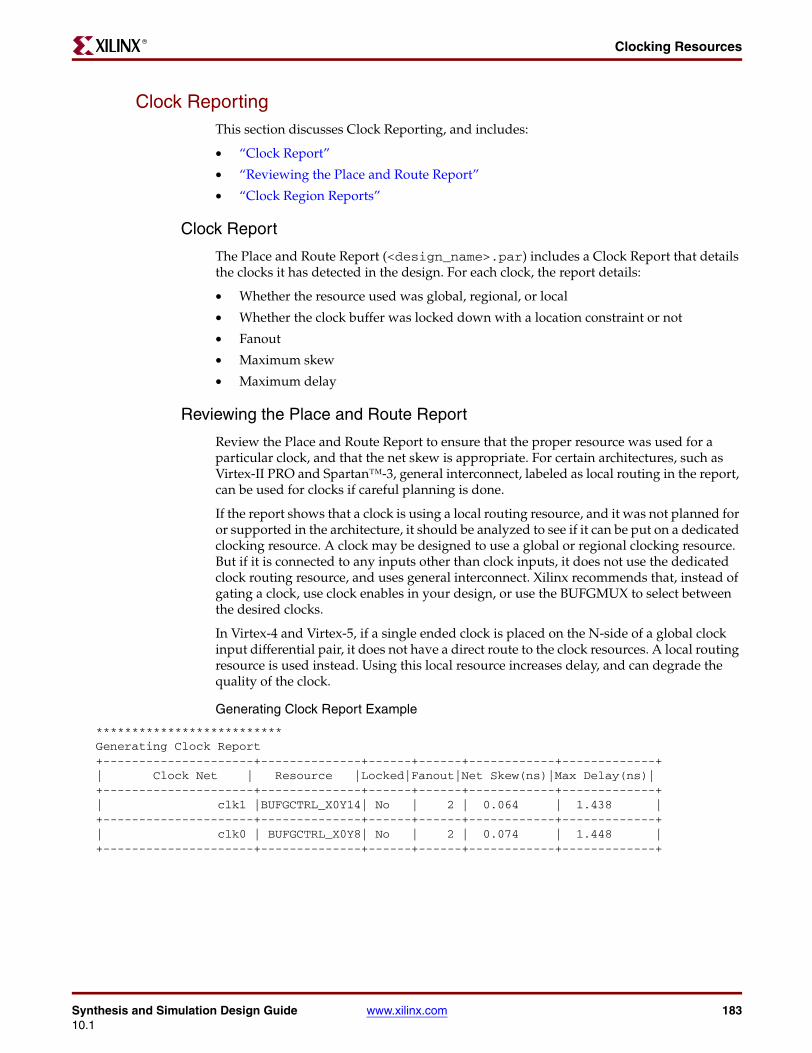
Synthesis and Simulation Design Guide www.xilinx.com 18310.1
Clocking ResourcesR
Clock ReportingThis section discusses Clock Reporting, and includes:
• “Clock Report”
• “Reviewing the Place and Route Report”
• “Clock Region Reports”
Clock Report
The Place and Route Report (<design_name>.par) includes a Clock Report that details the clocks it has detected in the design. For each clock, the report details:
• Whether the resource used was global, regional, or local
• Whether the clock buffer was locked down with a location constraint or not
• Fanout
• Maximum skew
• Maximum delay
Reviewing the Place and Route Report
Review the Place and Route Report to ensure that the proper resource was used for a particular clock, and that the net skew is appropriate. For certain architectures, such as Virtex-II PRO and Spartan™-3, general interconnect, labeled as local routing in the report, can be used for clocks if careful planning is done.
If the report shows that a clock is using a local routing resource, and it was not planned for or supported in the architecture, it should be analyzed to see if it can be put on a dedicated clocking resource. A clock may be designed to use a global or regional clocking resource. But if it is connected to any inputs other than clock inputs, it does not use the dedicated clock routing resource, and uses general interconnect. Xilinx recommends that, instead of gating a clock, use clock enables in your design, or use the BUFGMUX to select between the desired clocks.
In Virtex-4 and Virtex-5, if a single ended clock is placed on the N-side of a global clock input differential pair, it does not have a direct route to the clock resources. A local routing resource is used instead. Using this local resource increases delay, and can degrade the quality of the clock.
Generating Clock Report Example
**************************Generating Clock Report+---------------------+--------------+------+------+------------+-------------+| Clock Net | Resource |Locked|Fanout|Net Skew(ns)|Max Delay(ns)|+---------------------+--------------+------+------+------------+-------------+| clk1 |BUFGCTRL_X0Y14| No | 2 | 0.064 | 1.438 |+---------------------+--------------+------+------+------------+-------------+| clk0 | BUFGCTRL_X0Y8| No | 2 | 0.074 | 1.448 |+---------------------+--------------+------+------+------------+-------------+
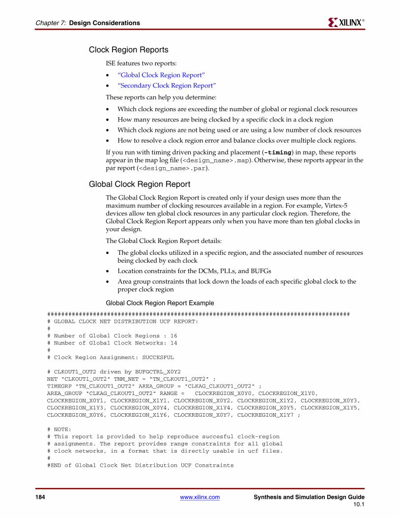
184 www.xilinx.com Synthesis and Simulation Design Guide10.1
Chapter 7: Design ConsiderationsR
Clock Region Reports
ISE features two reports:
• “Global Clock Region Report”
• “Secondary Clock Region Report”
These reports can help you determine:
• Which clock regions are exceeding the number of global or regional clock resources
• How many resources are being clocked by a specific clock in a clock region
• Which clock regions are not being used or are using a low number of clock resources
• How to resolve a clock region error and balance clocks over multiple clock regions.
If you run with timing driven packing and placement (-timing) in map, these reports appear in the map log file (<design_name>.map). Otherwise, these reports appear in the par report (<design_name>.par).
Global Clock Region Report
The Global Clock Region Report is created only if your design uses more than the maximum number of clocking resources available in a region. For example, Virtex-5 devices allow ten global clock resources in any particular clock region. Therefore, the Global Clock Region Report appears only when you have more than ten global clocks in your design.
The Global Clock Region Report details:
• The global clocks utilized in a specific region, and the associated number of resources being clocked by each clock
• Location constraints for the DCMs, PLLs, and BUFGs
• Area group constraints that lock down the loads of each specific global clock to the proper clock region
Global Clock Region Report Example
####################################################################################### GLOBAL CLOCK NET DISTRIBUTION UCF REPORT:## Number of Global Clock Regions : 16# Number of Global Clock Networks: 14## Clock Region Assignment: SUCCESFUL
# CLKOUT1_OUT2 driven by BUFGCTRL_X0Y2NET "CLKOUT1_OUT2" TNM_NET = "TN_CLKOUT1_OUT2" ;TIMEGRP "TN_CLKOUT1_OUT2" AREA_GROUP = "CLKAG_CLKOUT1_OUT2" ;AREA_GROUP "CLKAG_CLKOUT1_OUT2" RANGE = CLOCKREGION_X0Y0, CLOCKREGION_X1Y0, CLOCKREGION_X0Y1, CLOCKREGION_X1Y1, CLOCKREGION_X0Y2, CLOCKREGION_X1Y2, CLOCKREGION_X0Y3, CLOCKREGION_X1Y3, CLOCKREGION_X0Y4, CLOCKREGION_X1Y4, CLOCKREGION_X0Y5, CLOCKREGION_X1Y5, CLOCKREGION_X0Y6, CLOCKREGION_X1Y6, CLOCKREGION_X0Y7, CLOCKREGION_X1Y7 ;
# NOTE: # This report is provided to help reproduce succesful clock-region # assignments. The report provides range constraints for all global # clock networks, in a format that is directly usable in ucf files. ##END of Global Clock Net Distribution UCF Constraints
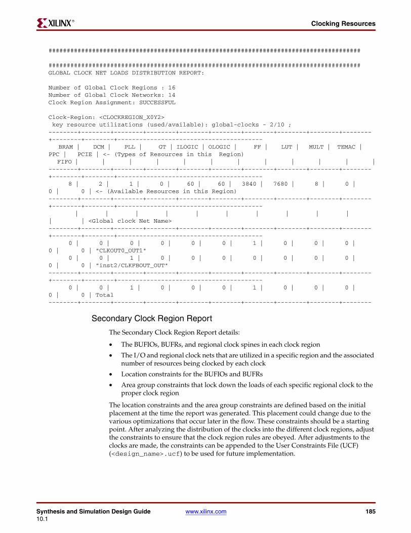
Synthesis and Simulation Design Guide www.xilinx.com 18510.1
Clocking ResourcesR
######################################################################################
######################################################################################GLOBAL CLOCK NET LOADS DISTRIBUTION REPORT:
Number of Global Clock Regions : 16Number of Global Clock Networks: 14Clock Region Assignment: SUCCESSFUL
Clock-Region: <CLOCKREGION_X0Y2> key resource utilizations (used/available): global-clocks - 2/10 ;--------+--------+--------+--------+--------+--------+--------+--------+--------+--------+--------+--------+---------------------------------------- BRAM | DCM | PLL | GT | ILOGIC | OLOGIC | FF | LUT | MULT | TEMAC | PPC | PCIE | <- (Types of Resources in this Region) FIFO | | | | | | | | | | | |--------+--------+--------+--------+--------+--------+--------+--------+--------+--------+--------+--------+---------------------------------------- 8 | 2 | 1 | 0 | 60 | 60 | 3840 | 7680 | 8 | 0 | 0 | 0 | <- (Available Resources in this Region)--------+--------+--------+--------+--------+--------+--------+--------+--------+--------+--------+--------+---------------------------------------- | | | | | | | | | | | | <Global clock Net Name>--------+--------+--------+--------+--------+--------+--------+--------+--------+--------+--------+--------+---------------------------------------- 0 | 0 | 0 | 0 | 0 | 0 | 1 | 0 | 0 | 0 | 0 | 0 | "CLKOUT0_OUT1" 0 | 0 | 1 | 0 | 0 | 0 | 0 | 0 | 0 | 0 | 0 | 0 | "inst2/CLKFBOUT_OUT"--------+--------+--------+--------+--------+--------+--------+--------+--------+--------+--------+--------+---------------------------------------- 0 | 0 | 1 | 0 | 0 | 0 | 1 | 0 | 0 | 0 | 0 | 0 | Total--------+--------+--------+--------+--------+--------+--------+--------+--------+--------
Secondary Clock Region Report
The Secondary Clock Region Report details:
• The BUFIOs, BUFRs, and regional clock spines in each clock region
• The I/O and regional clock nets that are utilized in a specific region and the associated number of resources being clocked by each clock
• Location constraints for the BUFIOs and BUFRs
• Area group constraints that lock down the loads of each specific regional clock to the proper clock region
The location constraints and the area group constraints are defined based on the initial placement at the time the report was generated. This placement could change due to the various optimizations that occur later in the flow. These constraints should be a starting point. After analyzing the distribution of the clocks into the different clock regions, adjust the constraints to ensure that the clock region rules are obeyed. After adjustments to the clocks are made, the constraints can be appended to the User Constraints File (UCF) (<design_name>.ucf) to be used for future implementation.
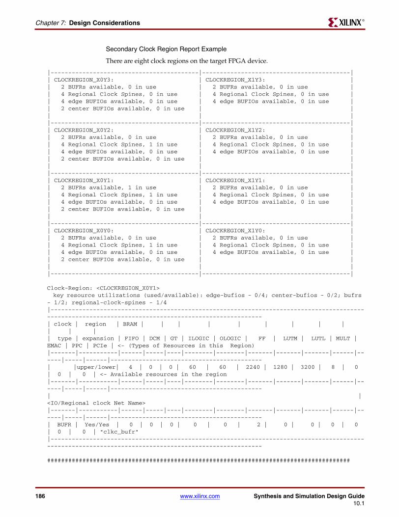
186 www.xilinx.com Synthesis and Simulation Design Guide10.1
Chapter 7: Design ConsiderationsR
Secondary Clock Region Report Example
There are eight clock regions on the target FPGA device.
|------------------------------------------|------------------------------------------|| CLOCKREGION_X0Y3: | CLOCKREGION_X1Y3: || 2 BUFRs available, 0 in use | 2 BUFRs available, 0 in use || 4 Regional Clock Spines, 0 in use | 4 Regional Clock Spines, 0 in use || 4 edge BUFIOs available, 0 in use | 4 edge BUFIOs available, 0 in use || 2 center BUFIOs available, 0 in use | || | ||------------------------------------------|------------------------------------------|| CLOCKREGION_X0Y2: | CLOCKREGION_X1Y2: || 2 BUFRs available, 0 in use | 2 BUFRs available, 0 in use || 4 Regional Clock Spines, 1 in use | 4 Regional Clock Spines, 0 in use || 4 edge BUFIOs available, 0 in use | 4 edge BUFIOs available, 0 in use || 2 center BUFIOs available, 0 in use | || | ||------------------------------------------|------------------------------------------|| CLOCKREGION_X0Y1: | CLOCKREGION_X1Y1: || 2 BUFRs available, 1 in use | 2 BUFRs available, 0 in use || 4 Regional Clock Spines, 1 in use | 4 Regional Clock Spines, 0 in use || 4 edge BUFIOs available, 0 in use | 4 edge BUFIOs available, 0 in use || 2 center BUFIOs available, 0 in use | || | ||------------------------------------------|------------------------------------------|| CLOCKREGION_X0Y0: | CLOCKREGION_X1Y0: || 2 BUFRs available, 0 in use | 2 BUFRs available, 0 in use || 4 Regional Clock Spines, 1 in use | 4 Regional Clock Spines, 0 in use || 4 edge BUFIOs available, 0 in use | 4 edge BUFIOs available, 0 in use || 2 center BUFIOs available, 0 in use | || | ||------------------------------------------|------------------------------------------|
Clock-Region: <CLOCKREGION_X0Y1> key resource utilizations (used/available): edge-bufios - 0/4; center-bufios - 0/2; bufrs - 1/2; regional-clock-spines - 1/4|------------------------------------------------------------------------------------------------------------------------------------------------------| clock | region | BRAM | | | | | | | | | | | || type | expansion | FIFO | DCM | GT | ILOGIC | OLOGIC | FF | LUTM | LUTL | MULT | EMAC | PPC | PCIe | <- (Types of Resources in this Region)|-------|-----------|------|-----|----|--------|--------|-------|-------|-------|------|------|-----|------|-------------------------------------------| |upper/lower| 4 | 0 | 0 | 60 | 60 | 2240 | 1280 | 3200 | 8 | 0 | 0 | 0 | <- Available resources in the region|-------|-----------|------|-----|----|--------|--------|-------|-------|-------|------|------|-----|------|-------------------------------------------| | <IO/Regional clock Net Name>|-------|-----------|------|-----|----|--------|--------|-------|-------|-------|------|------|-----|------|-------------------------------------------| BUFR | Yes/Yes | 0 | 0 | 0 | 0 | 0 | 2 | 0 | 0 | 0 | 0 | 0 | 0 | "clkc_bufr"|------------------------------------------------------------------------------------------------------------------------------------------------------
######################################################################################
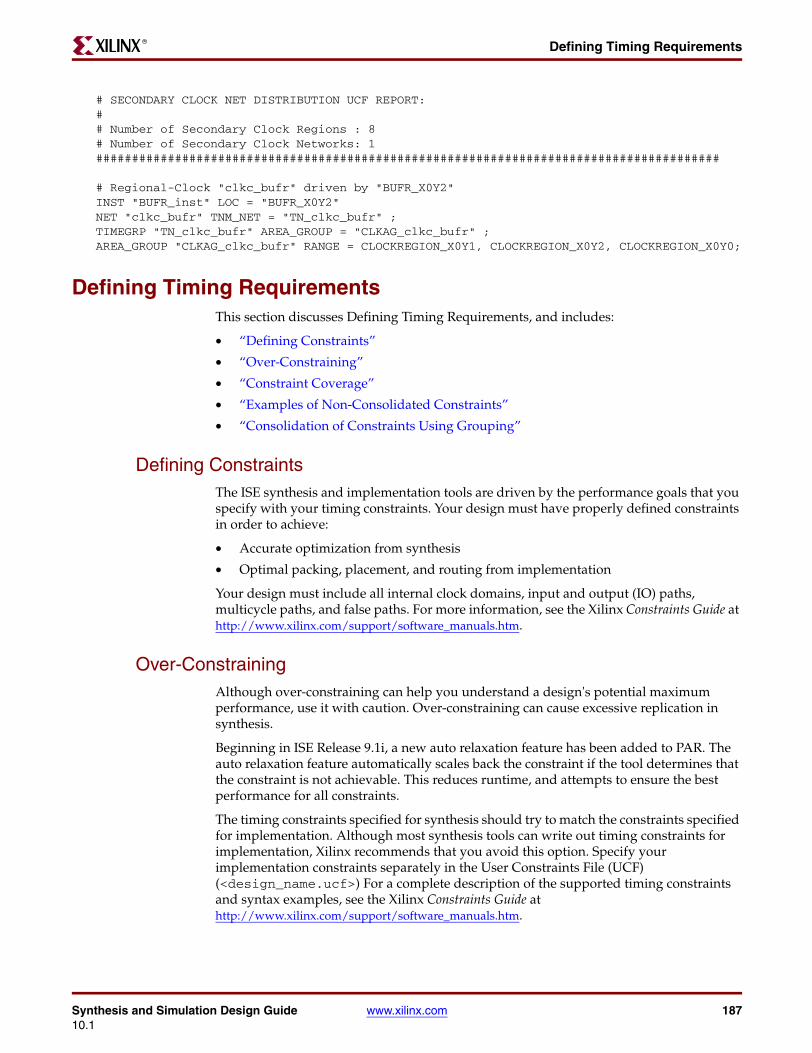
Synthesis and Simulation Design Guide www.xilinx.com 18710.1
Defining Timing RequirementsR
# SECONDARY CLOCK NET DISTRIBUTION UCF REPORT:## Number of Secondary Clock Regions : 8# Number of Secondary Clock Networks: 1#######################################################################################
# Regional-Clock "clkc_bufr" driven by "BUFR_X0Y2"INST "BUFR_inst" LOC = "BUFR_X0Y2"NET "clkc_bufr" TNM_NET = "TN_clkc_bufr" ;TIMEGRP "TN_clkc_bufr" AREA_GROUP = "CLKAG_clkc_bufr" ;AREA_GROUP "CLKAG_clkc_bufr" RANGE = CLOCKREGION_X0Y1, CLOCKREGION_X0Y2, CLOCKREGION_X0Y0;
Defining Timing RequirementsThis section discusses Defining Timing Requirements, and includes:
• “Defining Constraints”
• “Over-Constraining”
• “Constraint Coverage”
• “Examples of Non-Consolidated Constraints”
• “Consolidation of Constraints Using Grouping”
Defining ConstraintsThe ISE synthesis and implementation tools are driven by the performance goals that you specify with your timing constraints. Your design must have properly defined constraints in order to achieve:
• Accurate optimization from synthesis
• Optimal packing, placement, and routing from implementation
Your design must include all internal clock domains, input and output (IO) paths, multicycle paths, and false paths. For more information, see the Xilinx Constraints Guide at http://www.xilinx.com/support/software_manuals.htm.
Over-ConstrainingAlthough over-constraining can help you understand a design's potential maximum performance, use it with caution. Over-constraining can cause excessive replication in synthesis.
Beginning in ISE Release 9.1i, a new auto relaxation feature has been added to PAR. The auto relaxation feature automatically scales back the constraint if the tool determines that the constraint is not achievable. This reduces runtime, and attempts to ensure the best performance for all constraints.
The timing constraints specified for synthesis should try to match the constraints specified for implementation. Although most synthesis tools can write out timing constraints for implementation, Xilinx recommends that you avoid this option. Specify your implementation constraints separately in the User Constraints File (UCF) (<design_name.ucf>) For a complete description of the supported timing constraints and syntax examples, see the Xilinx Constraints Guide at http://www.xilinx.com/support/software_manuals.htm.
188 www.xilinx.com Synthesis and Simulation Design Guide10.1
Chapter 7: Design ConsiderationsR
Constraint CoverageIn your synthesis report, check for any replicated registers, and ensure that timing constraints that might apply to the original register also cover the replicated registers for implementation. To minimize implementation runtime and memory usage, write timing constraints by grouping the maximum number of paths with the same timing requirement first before generating a specific timespec.
Examples of Non-Consolidated ConstraintsTIMESPEC "TS_firsttimespec" = FROM "flopa" TO "flopb" 10ns;TIMESPEC "TS_secondtimespec" = FROM "flopc" TO "flopb" 10ns;TIMESPEC "TS_thirdtimespec" = FROM "flopd" TO "flopb" 10ns;
Consolidation of Constraints Using GroupingINST "flopa" TNM = "flopgroup";INST "flopc" TNM = "flopgroup";INST "flopd" TNM = "flopgroup";TIMESPEC "TS_consolidated" = FROM "flopgroup" TO "flopb" 10ns;
Driving SynthesisThis section discusses Driving Synthesis, and includes:
• “Creating High-Performance Circuits”
• “Helpful Synthesis Attributes”
• “Additional Timing Options”
Creating High-Performance CircuitsTo create high-performance circuits, Xilinx recommends that you:
• “Use Proper Coding Techniques”
• “Analyze Inference of Logic”
• “Provide a Complete Picture of Your Design”
• “Use Optimal Software Settings”
Use Proper Coding Techniques
Proper coding techniques ensure that the inferences of your behavioral Hardware Description Language (HDL) code made by the synthesis tool maximize the architectural features of the device. The language templates in ISE Project Navigator contain coding examples in both Verilog and VHDL.
Analyze Inference of Logic
Check to see that the design is maximizing the features of the block, and that the synthesis tool is properly inferring the expected features from your Hardware Description Language (HDL) code. Gate level schematic viewers, such as HDL Analyst in Synplify PRO, can help with your analysis. When using BRAMs, use the dedicated output pipeline registers when possible in order to reduce the clock-to-out delay of data leaving the RAM. The DSP blocks
Synthesis and Simulation Design Guide www.xilinx.com 18910.1
Driving SynthesisR
also have a variety of pipeline registers that reduce the setup and clock-to-out timing of these blocks.
Provide a Complete Picture of Your Design
Make sure that the synthesis tool has a complete picture of your design:
• If a design contains IP generated by CORE Generator™, third party IP, or any other lower level blackboxed netlists, include those netlists in the synthesis project. Although the synthesis tool cannot optimize logic within the netlist, it can better optimize the Hardware Description Language (HDL) code that interfaces to these lower level netlists.
• The tool must understand the performance goals of a design using the timing constraints that you supplied. If there are critical paths in your implementation that are not seen as critical in synthesis, use the -route constraint from Synplify PRO to force synthesis to focus on that path.
Use Optimal Software Settings
You can modify a variety of software settings in synthesis to achieve optimal design. Xilinx recommends that you begin with a baseline set of software options, then incrementally add new switches to understand their effects. A variety of attribute settings can affect logic inference and synthesis optimization. Changing these attribute settings can affect synthesis with out having to re-code. See Table 7-1, “Helpful Synthesis Attributes.”
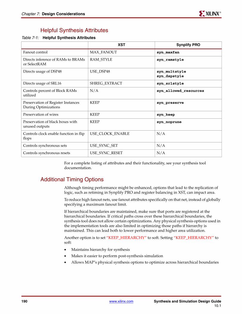
190 www.xilinx.com Synthesis and Simulation Design Guide10.1
Chapter 7: Design ConsiderationsR
Helpful Synthesis Attributes
For a complete listing of attributes and their functionality, see your synthesis tool documentation.
Additional Timing OptionsAlthough timing performance might be enhanced, options that lead to the replication of logic, such as retiming in Synplify PRO and register balancing in XST, can impact area.
To reduce high fanout nets, use fanout attributes specifically on that net, instead of globally specifying a maximum fanout limit.
If hierarchical boundaries are maintained, make sure that ports are registered at the hierarchical boundaries. If critical paths cross over these hierarchical boundaries, the synthesis tool does not allow certain optimizations. Any physical synthesis options used in the implementation tools are also limited in optimizing those paths if hierarchy is maintained. This can lead both to lower performance and higher area utilization.
Another option is to set “KEEP_HIERARCHY” to soft. Setting “KEEP_HIERARCHY” to soft:
• Maintains hierarchy for synthesis
• Makes it easier to perform post-synthesis simulation
• Allows MAP’s physical synthesis options to optimize across hierarchical boundaries
Table 7-1: Helpful Synthesis Attributes
XST Synplify PRO
Fanout control MAX_FANOUT syn_maxfan
Directs inference of RAMs to BRAMs or SelectRAM
RAM_STYLE syn_ramstyle
Directs usage of DSP48 USE_DSP48 syn_multstylesyn_dspstyle
Directs usage of SRL16 SHREG_EXTRACT syn_srlstyle
Controls percent of Block RAMs utilized
N/A syn_allowed_resources
Preservation of Register Instances During Optimizations
KEEP syn_preserve
Preservation of wires KEEP syn_keep
Preservation of black boxes with unused outputs
KEEP syn_noprune
Controls clock enable function in flip flops
USE_CLOCK_ENABLE N/A
Controls synchronous sets USE_SYNC_SET N/A
Controls synchronous resets USE_SYNC_RESET N/A
Synthesis and Simulation Design Guide www.xilinx.com 19110.1
Choosing Implementation OptionsR
Before you begin implementation:
• Review the warnings in your synthesis report.
• Check the RTL schematic view to see how the synthesis tool is interpreting the Hardware Description Language (HDL) code. Use the technology schematic to understand how the HDL code is mapping to the target architecture.
Choosing Implementation OptionsThis section discusses Choosing Implementation Options, and includes:
• “Choosing Options for Maximum Performance”
• “Performance Evaluation Mode”
• “Packing and Placement Option”
• “Physical Synthesis Options”
• “Xplorer”
Choosing Options for Maximum PerformanceWhich options to use for maximum performance can be unique to each design. The answer depends on:
• Your design performance goals
• The synthesis flow used
• Its overall structure
Performance Evaluation ModeIf you have not specified any timing constraints, use Performance Evaluation Mode to get a quick idea of design performance. The ISE software automatically generates timing constraints for each internal clock for the implementation tool only. To automatically invoke Performance Evaluation Mode, do not specify a User Constraints File (UCF). Performance Evaluation Mode enables you to obtain high performance results from the implementation tool without specifying timing goals.
Packing and Placement OptionTry the timing driven packing and placement option (map -timing) in MAP for all architectures that support it. When map -timing is enabled, MAP does both the packing and placement, while PAR does only the routing. By tightly integrating packing and placement, and having both processes understand the timing information, the software can take better advantage of the hardware and provide better performance.
For Virtex-5 devices, timing driven packing and placement is the only way to run MAP. Because of the added complexity of the Virtex-5 slice structure, you can achieve efficient packing only by using this strategy. For best performance, Xilinx recommends that you run MAP and PAR with their effort levels set to High. While runtime is longer compared to Standard effort level, you achieve better initial results.
192 www.xilinx.com Synthesis and Simulation Design Guide10.1
Chapter 7: Design ConsiderationsR
Physical Synthesis OptionsPhysical synthesis options in implementation can re-optimize and pack logic based on knowledge of the critical paths of a design, leading to better placement and routing. The physical synthesis options are implemented during MAP. They include:
• Global netlist optimization
• Localized logic optimization
• Retiming
• Register duplication
• Equivalent register removal
For more information, see Xilinx White Paper 230, “Physical Synthesis and Optimization with ISE 8.1i.” These physical synthesis options provide the greatest benefit to designs that do not follow the guidelines for synthesis outlined in the previous paragraph. Physical synthesis can lead to increased area due to replication of logic.
XplorerUse ISE Xplorer to determine which implementation options provide maximum design performance. Xplorer has two modes of operation:
• “Timing Closure Mode”
• “Best Performance Mode”
It is usually best to run Xplorer over the weekend since it typically runs more than a single iteration of MAP and PAR. Once Xplorer has selected the optimal tools settings, continue to use these settings for the subsequent design runs. If you have made many design changes since the original Xplorer run, and your design is no longer meeting timing with the options determined by Xplorer, consider running Xplorer again.
Timing Closure Mode
You can access Timing Closure mode from Project Navigator or the command line. Timing Closure mode evaluates your timing constraints, then tries different sets of implementation options to achieve your timing goals. Although initial runtime can be longer because of the need to run multiple implementations, once you have the optimal set of options, you may reduce the number of design iterations necessary to achieve timing closure.
Best Performance Mode
In Best Performance Mode, you can focus on a particular clock domain. Xplorer tries to achieve the best frequency for the clock. This is especially helpful when benchmarking a design's maximum performance.
Synthesis and Simulation Design Guide www.xilinx.com 19310.1
Evaluating Critical PathsR
Evaluating Critical PathsThis section discusses Evaluating Critical Paths, and includes:
• “Understanding Characteristics of Critical Paths”
• “Logic Levels”
Understanding Characteristics of Critical PathsBy understanding the characteristics of your critical path, you can make better decisions for the next design iteration. A data path is comprised of both logic and interconnect delay. Individual component delays that make up logic delay are fixed. Logic delay can be reduced only if the number of logic levels are reduced, or if the structure of the logic is changed. In comparison, interconnect delay is much more variable, and is dependent on the placement of the logic.
Logic LevelsThis section discusses Logic Levels, and includes:
• “Many Logic Levels”
• “Few Logic Levels”
Many Logic Levels
When your design has excessive logic levels that lead to many routing interconnects:
• Evaluate using the physical synthesis options in MAP.
• Verify that the critical paths reported in implementation match those reported in synthesis. If they do not, use constraints such as -route from Synplify PRO to focus the synthesis tool on these paths.
• Review your Hardware Description Language (HDL) code to ensure that it is taking the best advantage of the hardware.
• Make sure inferencing is occurring properly, particularly for hard-IP blocks.
Few Logic Levels
If there are few logic levels, but certain data paths do not meet your performance requirements:
• Evaluate fan out on routes with long delay.
• If the critical path's destination is the clock enable or synchronous set/reset input of a flop, try implementing the SR/CE logic using the sourcing LUT.
XST has attributes that can be applied globally or locally to disable the inference of registers with synchronous sets or resets or clock enables. Instead they infer the synchronous set or reset or clock enable function on the data input of the flip flop. This may allow better packing of LUTs and FFs into the same slice. This can be especially useful for Virtex-5 devices where there are four registers in each slice, and each must use the same control logic pins.
• If a critical path contains hard-IP blocks such as Block RAMs or DSP48s, check that the design is taking full advantage of the embedded registers. Understand when to make the trade-off between using these hard blocks versus using slice logic.
194 www.xilinx.com Synthesis and Simulation Design Guide10.1
Chapter 7: Design ConsiderationsR
• Do a placement analysis. If logic appears to be placed far apart from each other, floorplanning of critical blocks may be required. Try to floorplan only the logic that is required to meet the timing objectives. Over floorplanning can cause worse performance.
• Evaluate clock path skew. If the clock skew appears to be larger than expected, load the design in FPGA Editor and verify that all clock resources are routed on dedicated clocking resources. If they are not, this could lead to large clock skew.
Design Preservation With SmartCompileThis section discusses Design Preservation with SmartCompile and includes:
• “About Design Preservation With SmartCompile”
• “Deciding Whether to Use Partitions or SmartGuide”
• “Design Preservation with Partitions”
• “Design Preservation with SmartGuide”
About Design Preservation With SmartCompileUse SmartCompile to preserve the unchanged portions of a design. SmartCompile consists of two methods:
• Partitions
• SmartGuide
Deciding Whether to Use Partitions or SmartGuideAlthough Partitions generally provide the best design flow, the design must follow good design practices such as registering the outputs of Partitions. For more information, see Xilinx Application Note XAPP918, “Incremental Design Reuse with Partitions.” If your design does not work well with Partitions, or you are at the end of the design cycle, then SmartGuide is preferable. Use the following guidelines to help you decide whether to use Partitions or SmartGuide:
• “Guidelines for Using Partitions”
• “Guidelines for Using SmartGuide”
Table 7-2: Comparison of Partitions and SmartGuide
Feature/Function Partitions SmartGuide
Re-uses a previous implementation Yes Yes
Unchanged modules are guaranteed the same implementation
Yes No
Require design planning Yes No
Runtime reduction Synthesis through Place and Route Map, Place, and Route
Ease of use Easy Easier

Synthesis and Simulation Design Guide www.xilinx.com 19510.1
Design Preservation With SmartCompileR
Guidelines for Using Partitions
Use Partitions when:
• You do not want to re-simulate those portions of the design that did not change.
• One or more modules have difficult timing, and you want to preserve implementation in order to maintain the timing paths.
• You are still making changes to the design and you want to increase turns per day by reducing implementation runtime. (Use PRESERVE=PLACEMENT)
Guidelines for Using SmartGuide
Use SmartGuide when:
• A design is finished and meets timing, but you are making small design changes and want to reduce runtime.
• A design is finished and meets timing, but you need to change an attribute or move a pin location.
• You want to leverage previous results, but design hierarchy does work well with Partitions. If the design does not meet timing, runtime may or may not be reduced.
Design Preservation with PartitionsThis section discusses Design Preservation with Partitions and contains:
• “About Design Preservation with Partitions”
• “Defining Partitions for Design Preservation”
• “Tips for Using Partitions for Design Preservation”
About Design Preservation with Partitions
If a design includes Partitions, ISE analyzes the modules to determine if they are (a) up-to-date or (b) out-of-date, with respect to the previous implementation.
• If the Partition is out-of-date, it is completely re-implemented. No preservation occurs.
• If the Partition is up-to-date, ISE copies it without change from the previous implementation. The Partition is completely preserved, from synthesized netlist through routing.
Setting the Partition attribute on a module:
• Isolates the module from the rest of the design
• Protects the module interface (connectivity across the Partition boundary) against modification between implementations
• Enables the components and nets within the Partition to be copied from a previous implementation into the current implementation.
Copying design information:
• Is faster than reimplementing it
• Assures exact duplication of the previous implementation
For more information, see Partitions Overview in the ISE Help.
196 www.xilinx.com Synthesis and Simulation Design Guide10.1
Chapter 7: Design ConsiderationsR
Defining Partitions for Design Preservation
You can use Partitions to achieve the following design goals:
• Decreasing runtime
To decrease runtime, divide the design into four to ten Partitions, each of which contains equivalent amounts of logic. If one Partition is modified, the others are preserved. The amount of preservation is proportional to the number of Partitions.
• Meeting timing
Create a Partition when meeting timing is difficult. Try to contain the logic that is difficult to meet timing in a Partition. Once timing is met for that Partition, do not modify it. Partitions ensure that the logic in the Partition is preserved, even if logic outside the Partition is modified.
There is a point of diminishing returns when adding Partitions. The Partition interface is a barrier to optimization. If a critical timing path or packing problem can be solved only by optimizing across a Partition interface, remove the Partition. Creating registers on the Partition interface reduces the likelihood of a timing or packing problem.
Both XST and Synplify Pro can be used to specify RTL Partitions.
Tips for Using Partitions for Design Preservation
• Partitions must be re-implemented after a command line change, or implementation option change. The following project or implementation changes force all Partitions to be re-implemented:
♦ Map-timing
♦ Effort levels
♦ All command line changes
• Partitions can nest hierarchically and be defined on any HDL module instance in the design. A module with multiple instances can have multiple Partitions (a Partition for each instance). The top level of the HDL design defaults to be a Partition.
• Partitions automatically detect input source changes. Source changes include HDL changes and certain changes in constraint files such as physical constraints and LOC ranges in the UCF.
• Partitions automatically detect command line changes. If an option changes, such as effort levels on the implementation tools, all Partitions are reimplemented.
• Logic may be in the top level Partition.
• Command line users must use tcl to create and modify Partitions. The implementation applications may be called from within a tcl script, or they may be called from a make file by using the -ise switch. You can not implement a design with Partitions by calling ngdbuild, map, or par without using the -ise switch.
• Partitions do not require floorplanning. If floorplanning is desired, use the graphical Floorplanning tool to create area_group ranges for the Partition’s instance.
• To limit timing constraints to a specific Partition, as opposed to the entire design:
♦ Create a UCF for the Partition
♦ Create the timing constraints within that UCF
• The following options are not compatible with Partitions:
♦ MPPR
♦ global_opt
Synthesis and Simulation Design Guide www.xilinx.com 19710.1
Design Preservation With SmartCompileR
Design Preservation with SmartGuideThis section discusses Design Preservation with SmartGuide and includes:
• “About Design Preservation with SmartGuide”
• “Optimal Changes for SmartGuide”
• “Constraint Changes That Impact SmartGuide”
• “Reimplementing Without SmartGuide”
About Design Preservation with SmartGuide
SmartGuide instructs MAP to use results from a previous implementation to guide the current implementation, based on a placed and routed NCD file. SmartGuide can help achieve consistency of results while also improving runtime.
SmartGuide can be enabled in:
• Project Navigator
• TCL
• The command line
For more information on how to enable SmartGuide, see:
• ISE Help
• The Xilinx Development Systems Reference Guide at http://www.xilinx.com/support/software_manuals.htm.
Optimal Changes for SmartGuide
SmartGuide is most useful for small logic changes, such as modifying a logic equation. Since large changes (such as adding new modules and instances) affect the design hierarchy, they reduce the probability of successfully matching components from a previous implementation.
The changes that work well with SmartGuide are:
• A small logic change (less than 10 percent) in one or two modules
• Moving a pin location
• Changing an attribute on a component
• Changing a timing constraint
The options specified in MAP and PAR for the current implementation should match the options specified for the previous implementation used to generate the guide file. This ensures that similar algorithms and optimizations are run between both runs, ensuring the best match.
Changing both timing and placement constraints can impact the results of SmartGuide. If you are changing many constraints, Xilinx recommends that you allow the tools to run without SmartGuide, then use the output of the initial run with the changed constraints as your guide file for subsequent runs.
198 www.xilinx.com Synthesis and Simulation Design Guide10.1
Chapter 7: Design ConsiderationsR
Constraint Changes That Impact SmartGuide
The following constraint changes can impact the results of SmartGuide:
• Moving a pin location
Moving a pin location typically works well. Only the changed pin and net are re-routed. Difficulties may occur if the pin is moved to a congested area and requires moving nets in order to route the net that connects to the changed pin. This can cause a ripple affect in order to route the design and meet timing.
• Moving a component
Moving a component is similar to moving a pin location. Moving a component can be beneficial if it helps with timing; but it can be deleterious if the new component is moved to a congested area.
• Relaxing a timing constraint
Relaxing a timing constraint can greatly help SmartGuide if a failing path now meets timing. SmartGuide always tries to meet timing regardless whether the logic has changed or not. For this reason, Xilinx recommends using SmartGuide only on designs that meet timing.
• Tightening a timing constraint
Xilinx does not recommend tightening a timing constraint. If the change in constraints now causes a path to fail, SmartGuide will re-implement that path and any other logic in order to route and meet timing
Reimplementing Without SmartGuide
After about ten guided implementations, Xilinx recommends that you reimplement without using SmartGuide in order to fully optimize the entire design. Reimplementing without SmartGuide allows optimizations between logic that had previously been guided by SmartGuide, and logic that is new or modified.
Synthesis and Simulation Design Guide www.xilinx.com 19910.1
R
Appendix A
Simulating Xilinx Designs in Modelsim
This Appendix discusses Simulating Xilinx Designs in Modelsim, and includes:
• “Simulating Xilinx Designs in Modelsim”
• “Running SmartModel Simulations in Modelsim”
Simulating Xilinx Designs in ModelsimThis section discusses Simulating Xilinx Designs in Modelsim and includes:
• “Compiling the Xilinx Simulation Libraries”
• “Running Simulation from Project Navigator (VHDL or Verilog)”
• “Running Functional Simulation in Modelsim (Standalone)”
• “Running Back Annotated Simulation in Modelsim (Standalone)”
Compiling the Xilinx Simulation LibrariesBefore beginning functional simulation, you must compile the Xilinx Simulation Libraries for the target simulator. Xilinx provides a tool called COMPXLIB for this purpose. For more information, see the Xilinx Development System Reference Guide at http://www.xilinx.com/support/software_manuals.htm.
Running Simulation from Project Navigator (VHDL or Verilog) Project Navigator automatically creates the commands needed to run the simulation.
1. In the Sources pulldown menu, choose the simulation to run (Behavioral/ Post Route Simulation).
2. Select the Testbench in the Sources window
3. Run the Simulate <respective> Model process in the Processes window.
200 www.xilinx.com Synthesis and Simulation Design Guide10.1
R
Running Functional Simulation in Modelsim (Standalone)This section discusses Running Functional Simulation in Modelsim (Standalone) and includes:
• “Running Functional Simulation in MTI Standalone (Verilog)”
• “Running Functional Simulation in MTI Standalone (VHDL)”
Running Functional Simulation in MTI Standalone (Verilog)
To run functional simulation in MTI standalone (Verilog):
1. Compile the following:
a. glbl.v module
b. source files
c. testbench
For example:
vlog $env(XILINX)/verilog/src/glbl.v <source1>.v <source2).v ... <testbench>.v
For more information about the glbl.v module, see “Global Reset and Tristate for Simulation.”
2. Load the design in ModelSim.
a. Use the -L switch to point to the libraries used in the design
b. Load the glbl.v module
For example:
vsim -t ps -L unisims_ver -L xilinxcorelib_ver work.<testbench> work.glbl
Note: The glbl.v automatically pulses Global Set/Reset (GSR) for the first 100 ns of the simulation.
Running Functional Simulation in MTI Standalone (VHDL)
To run functional simulation in MTI standalone (VHDL):
1. Compile the following:
a. source files
b. testbench
For example:
vcom -93 <source1>.vhd <source2>.vhd ... testbench.vhd
2. Load the design:
vsim -t 1ps work.<testbench>
Synthesis and Simulation Design Guide www.xilinx.com 20110.1
Simulating Xilinx Designs in ModelsimR
Running Back Annotated Simulation in Modelsim (Standalone)This section discusses Running Back Annotated Simulation in Modelsim (Standalone) and includes:
• “Running Back Annotated Simulation in MTI Standalone (Verilog)”
• “Running Back Annotated Simulation in MTI Standalone (VHDL)”
Running Back Annotated Simulation in MTI Standalone (Verilog)
To run back annotated simulation in MTI Standalone (Verilog):
1. Create the Simulation Model.
a. To create the simulation model using Project Navigator:
Under each stage in the Implement Design process, there is a Generate Simulation Model Process. For instance, under the Place and Route process is the Generate Post-Place and Route Simulation Model. This runs the NetGen utility to generate a simulation model and an SDF file with the timing information. The default name of the model and the SDF file are <design_name>_timesim.v and <design_name>_timesim.sdf. Right-click the Simulate Process to change the properties for generating the model. Click Help for a description of each property.
b. To create the simulation model using the command line:
NetGen is the executable that creates simulation models. For more information, see the Xilinx Development System Reference Guide at http://www.xilinx.com/support/software_manuals.htm
2. Load the design in ModelSim.
a. Use the -L switch to point to the Verilog SimPrim models that define the behavior of the components in the simulation model.
b. Load the glbl module.
For example:
vsim -t ps -L simprims_ver work.<testbench> work.glbl
Note: For Verilog, the timing simulation netlist has a $sdf_annotate statement that calls the SDF file. Therefore the SDF file is automatically pulled in when loading the simulation. The glbl.v automatically pulses Global Set/Reset (GSR) for the first 100 ns of the simulation.
Running Back Annotated Simulation in MTI Standalone (VHDL)
To run back annotated simulation in MTI Standalone (VHDL):
1. Create the Simulation Model.
a. To create the simulation model using Project Navigator:
Under each stage in the Implement Design process, there is a Generate Simulation Model Process. For instance, under the Place and Route process is the Generate Post-Place and Route Simulation Model. This runs the NetGen utility to generate a simulation model and an SDF file with the timing information. The default name of the model and the SDF file are <design_name>_timesim.vhd and <design_name>_timesim.sdf. Right-click the Simulate Process to change the properties for generating the model. Click Help for a description of each property.
202 www.xilinx.com Synthesis and Simulation Design Guide10.1
R
b. To create the simulation model using the command line:
NetGen is the executable that creates simulation models. For more information, see the Xilinx Development System Reference Guide at http://www.xilinx.com/support/software_manuals.htm
2. Compile the following:
a. generated simulation model
b. testbench
For example:
vcom -93 <design_name>_timesim.vhd testbench.vhd
3. Load the design, including the SDF (Standard delay format) file.
For example:
vsim -t ps -sdfmax /UUT=<design_name>_timesim.sdf work.testbench
You must supply MTI with the following information:
• The region where the SDF file should be applied. The region tells MTI where the timing simulation netlist generated by the Xilinx tools is instantiated. Assume that the entity name in your testbench is TESTBENCH and the simulation netlist is instantiated inside the testbench with an instance name of UUT. The region for this example would be /TESTBENCH/UUT.
• The location of the SDF file. If the SDF file is located in the same directory as the simulation netlist, you need to supply only the name of the SDF file. Otherwise, you must specify the entire path to the SDF file.
Following is an example of the VSIM command line:
vsim -t ps -sdfmax /testbench/uut=c:/project/sim/time_sim.sdf work.testbench
Running SmartModel Simulations in ModelsimThis section discusses Running SmartModel Simulations in Modelsim aind includes:
• “About Running SmartModel Simulations in Modelsim”
• “Editing the Initialization File”
• “Additional Steps”
About Running SmartModel Simulations in ModelsimThe Xilinx Hard IP simulation flow uses Synopsys VMC models to simulate Hard-IP Blocks in the FPGA devices. For more information, see “Using SmartModels.” Because VMC models are simulator-independent models derived from the actual design, they are accurate evaluation models. To simulate these models, you must use a simulator that supports the SWIFT Interface.
Although ModelSim SE and ModelSim PE both support the SWIFT interface, you must modify the default ModelSim setup to enable this feature. The ModelSim install directory contains an initialization file called modelsim.ini In this initialization file, you can edit interface and simulator settings to default to your preferences. Parts of the modelsim.ini file must be edited to work properly with the Xilinx simulation models.
Synthesis and Simulation Design Guide www.xilinx.com 20310.1
Running SmartModel Simulations in ModelsimR
Editing the Initialization FileTo make the changes to the modelsim.ini initialization file, edit either of the following:
• The modelsim.ini file located in the Modelsim installation directory, OR
• The ModelSim environment variable setting in the MTI setup script.
Point to the modelsim.ini file located in the design directory of each example.
Edit the modelsim.ini file as follows:
1. After the lines:
; Simulator resolution
; Set to fs, ps, ns, us, ms, or sec with optional prefix of 1, 10, or 100.
change:
Resolution = ns
to:
Resolution = ps
2. After the lines:
; Specify whether paths in simulator commands should be described; in VHDL or Verilog format. For VHDL, PathSeparator = /; for Verilog, PathSeparator = .
comment the following statement by adding a semicolon (;) at the beginning of the line:
PathSeparator = /
3. After the line:
; List of dynamically loaded objects for Verilog PLI applications
add the following statements:
♦ Windows
Veriuser=$LMC_HOME/lib/pcnt.lib/swiftpli_mti.dll
♦ Linux
Veriuser = $LMC_HOME/lib/linux.lib/swiftpli_mti.so
♦ Linux64
$LMC_HOME/lib/amd64.lib/swiftpli_mti.so
4. After the line:
; Logic Modeling's SmartModel SWIFT software (Windows NT)
add the following statements:
♦ Windows
libsm = $MODEL_TECH/libsm.dll
libswift=$LMC_HOME/lib/pcnt.lib/libswift.dll
♦ Linux
libsm = $MODEL_TECH/libsm.sl
libswift = $LMC_HOME/lib/linux.lib/libswift.so
204 www.xilinx.com Synthesis and Simulation Design Guide10.1
R
♦ Linux 64
libsm = $MODEL_TECH/libsm.sl
libswift = $LMC_HOME/lib/amd64.lib/libswift.so
5. Do the following:
Caution! Do not skip this step.
♦ Windows
Make sure that %LMC_HOME%\lib\pcnt.lib is in the Path user variable.
♦ Linux
setenv LD_LIBRARY_PATH $LMC_HOME/lib/linux.lib:$LD_LIBRARY_PATH
♦ Linux 64
setenv LD_LIBRARY_PATH $LMC_HOME/lib/amd64.lib:$LD_LIBRARY_PATH
Caution! Do not change the order in which the commands appear in the modelsim.ini file. Simulation may fail if you do not follow the recommended order.
Additional StepsAfter editing the modelsim.ini file:
1. Run CompXLib with the -arch <device_name> option to compile the SmartModel wrapper files into the UniSim and SimPrim libraries.
♦ For more information on the specific command for your system, run compxlib -help on the command line.
♦ For more information about CompXLib, see the Xilinx Development System Reference Guide at http://www.xilinx.com/support/software_manuals.htm.
2. To verify that the SmartModels have been set up correctly, enter the following line in the ModelSim command window:
VSIM>vsim unisim.ppc405
If there are no errors upon loading, the simulator is set up correctly.
3. If you are running ModelSim Standalone with an mpf file, make these changes in the modelsim.ini file referenced by the mpf project file as well.
Synthesis and Simulation Design Guide www.xilinx.com 20510.1
R
Appendix B
Simulating Xilinx Designs in NCSIM
This Appendix discusses Simulating Xilinx Designs in NCSIM and includes:
• “Running Simulation from Project Navigator”
• “Running Simulation in NC-Verilog”
• “Running Simulation in NC-VHDL”
Running Simulation from Project NavigatorNCSIM is not integrated with Project Navigator.
Running Simulation in NC-VerilogThis section discusses Running Simulation in NC-Verilog and includes:
• “Running Simulations in NC-Verilog (Method One )”
• “Running Simulations in NC-Verilog (Method Two)”
• “Running SmartModel Simulations in NC- Verilog”
Running Simulations in NC-Verilog (Method One )Method One uses library source files with compile time options (similar to Verilog-XL). Depending on the makeup of your design (for example, Xilinx® instantiated primitives, COREGen® components) for RTL simulation, specify the following at the command line:
ncverilog -y $XILINX/verilog/src/unisims -y$XILINX/verilog/src/XilinxCoreLib \ +incdir+$XILINX/verilog/src +libext+.v $XILINX/verilog/src/glbl.v \ <testfixture>.v <design>.v
The $XILINX/verilog/src/unisims area contains the Unified Library components for RTL simulation. The $XILINX/verilog/src/simprims area contains generic simulation primitives.
For timing simulation and post-map simulation, or for post-translate simulation, the SimPrim-based libraries are used. Specify the following at the command line:
ncverilog -y $XILINX/verilog/src/simprims $XILINX/verilog/src/glbl.v\+libext+.v <testfixture>.v <design>.v
For more information about annotating SDF files, see “Back-Annotating Delay Values from SDF File.”
206 www.xilinx.com Synthesis and Simulation Design Guide10.1
R
Running Simulations in NC-Verilog (Method Two)Method Two uses shared pre-compiled libraries. Before beginning simulation for this method, you must compile the Xilinx Simulation Libraries for the target simulator. Xilinx provides a tool called COMPXLIB for this purpose. For more information, see the Xilinx Development System Reference Guide at http://www.xilinx.com/support/software_manuals.htm
Depending on the makeup of the design (for example, Xilinx instantiated primitives, COREGen) for RTL simulation, edit the hdl.var and cds.lib to specify the library mapping as shown in the following examples:
• “CDS.LIB Example”
• “HDL.VAR Example”
CDS.LIB Example
# cds.lib DEFINE worklib worklib
HDL.VAR Example
# hdl.var DEFINE LIB_MAP ($LIB_MAP, + => worklib)
After setting up the libraries, compile and simulate the design:
ncvlog -messages -update $XILINX/verilog/src/glbl.v <testfixture>.v <design>.v ncelab -messages <testfixture_name> glbl ncsim -messages <testfixture_name>
The -update option of NCVlog enables incremental compilation.
Back-Annotating Delay Values from SDF File
This section discusses how to back-annotate delay values from an SDF file.
The NC-Verilog simulator only reads compiled SDF files; the SDF source file is supplied as an argument in a $sdf_annotate task by NetGen. For more information on Netgen, see the Xilinx Development System Reference Guide at http://www.xilinx.com/support/software_manuals.htm
SDF files must be with NCSDFC to annotate the timing information contained in the SDF file:
ncsdfc sdf_filename.sdf
NCSDFC creates a file called sdf_filename.sdf.X. If a compiled file exists, NCSDFC checks to make sure that the date of the compiled file is newer than the date of the source file and that the version of the compiled file matches the version of NCSDFC. If either check fails, the SDF file is recompiled. Otherwise, the compiled file is read.
For Back Annotated simulation, the SimPrim-based libraries (except for Post Synthesis) are used. Specify the following at the command line:
ncvlog -messages -update $XILINX/verilog/src/glbl.v <testfixture>.v time_sim.v ncelab -messages -autosdf <testfixture_name> glbl ncsim -messages <testfixture_name>
Synthesis and Simulation Design Guide www.xilinx.com 20710.1
Running Simulation in NC-VerilogR
Running SmartModel Simulations in NC- VerilogThis section discusses Running SmartModel Simulations in NC- Verilog and includes:
• “Running SmartModel Simulation in Cadence NC-Verilog (Linux)”
• “Running SmartModel Simulation in Cadence NC-Verilog (Linux 64)”
Running SmartModel Simulation in Cadence NC-Verilog (Linux)
This section discusses running SmartModel simulation in Cadence NC-Verilog (Linux) and includes:
• “Cadence NC-Verilog (Linux) Setup File”
• “Cadence NC-Verilog (Linux) Setup Simulate File”
Edit the following files in the $Xilinx/smartmodel/lin/wrappers/ directory to set up and run a simulation utilizing the SWIFT interface.
Cadence NC-Verilog (Linux) Setup File
The Cadence NC-Verilog (Linux) setup file defines the simulation variables. Set the parameters in the angle brackets (< >) to match your system configuration.
Cadence NC-Verilog (Linux) Setup File Example
setenv XILINX <Xilinx path>setenv CDS_INST_DIR <Cadence path>setenv LM_LICENSE_FILE <license.dat>:$LM_LICENSE_FILEsetenv LMC_HOME $XILINX/smartmodel/lin/installed_linsetenv LMC_CONFIG $LMC_HOME/data/linux.lmcsetenv LD_LIBRARY_PATH$CDS_INST_DIR/tools/lib:$LMC_HOME/sim/pli/src:$LMC_HOME/lib/linux.lib:$LD_LIBRARY_PATHsetenv LMC_CDS_VCONFIG $CDS_INST_DIR/tools/verilog/bin/vconfigsetenv PATH ${LMC_HOME}/bin ${CDS_INST_DIR}/tools/bin ${PATH}setenv PATH ${XILINX}/bin/lin ${PATH}
Cadence NC-Verilog (Linux) Setup Simulate File
The Cadence NC-Verilog (Linux) simulate file is an NC-Verilog compilation simulation script. It specifies which files must be compiled and loaded for simulation. Include the design and testbench files to use this file to simulate a design. Set the parameters in the angle brackets (< >) to match your system configuration.
Cadence NC-Verilog (Linux) Simulate File Example
ncverilog \<design>.v <testbench>.v \${XILINX}/verilog/src/glbl.v \-y ${XILINX}/verilog/src/unisims +libext+.v \-y ${XILINX}/verilog/src/simprims +libext+.v \-y ${XILINX}/smartmodel/lin/wrappers/ncverilog +libext+.v \+loadpli1=swiftpli:swift_boot +incdir+$LMC_HOME/sim/pli/src \+access+r+w
208 www.xilinx.com Synthesis and Simulation Design Guide10.1
R
Running SmartModel Simulation in Cadence NC-Verilog (Linux 64)
This section discusses running SmartModel simulation in Cadence NC-Verilog (Linux 64) and includes:
• “Cadence NC-Verilog (Linux 64) Setup File”
• “Cadence NC-Verilog (Linux 64) Simulate File”
Edit the following files in the $Xilinx/smartmodel/lin64/wrappers/ directory to set up and run a simulation utilizing the SWIFT interface.
Cadence NC-Verilog (Linux 64) Setup File
The Cadence NC-Verilog (Linux 64) setup file defines the simulation variables. Set the parameters in the angle brackets (< >) to match your system configuration.
Cadence NC-Verilog (Linux 64) Setup File Example
setenv XILINX <Xilinx path>setenv CDS_INST_DIR <Cadence path>setenv LM_LICENSE_FILE <license.dat>:$LM_LICENSE_FILEsetenv LMC_HOME $XILINX/smartmodel/lin/installed_linsetenv LMC_CONFIG $LMC_HOME/data/amd64.lmcsetenv LD_LIBRARY_PATH$CDS_INST_DIR/tools/lib:$LMC_HOME/sim/pli/src:$LMC_HOME/lib/amd64.lib:$LD_LIBRARY_PATHsetenv LMC_CDS_VCONFIG $CDS_INST_DIR/tools/verilog/bin/vconfigsetenv PATH ${LMC_HOME}/bin ${CDS_INST_DIR}/tools/bin ${PATH}setenv PATH ${XILINX}/bin/lin64 ${PATH}
Cadence NC-Verilog (Linux 64) Simulate File
The Cadence NC-Verilog (Linux-64) simulate file is an NC-Verilog compilation simulation script. It specifies which files must be compiled and loaded for simulation. Include the design and testbench files to use this file to simulate a design.
Cadence NC-Verilog (Linux-64) Simulate File Example
ncverilog +nc64bit\<design>.v <testbench>.v \${XILINX}/verilog/src/glbl.v \-y ${XILINX}/verilog/src/unisims +libext+.v \-y ${XILINX}/verilog/src/simprims +libext+.v \-y ${XILINX}/smartmodel/lin/wrappers/ncverilog +libext+.v \+loadpli1=swiftpli:swift_boot +incdir+$LMC_HOME/sim/pli/src \+access+r+w
Running Simulation in NC-VHDLThis section discusses Running Simulation in NC-VHDL and includes:
• “Setting Up the Libraries”
• “Running Behavioral Simulation With NC-VHDL”
• “Running Timing Simulation With NC-VHDL”
• “Running SmartModel Simulations in Cadence NC- VHDL”
Synthesis and Simulation Design Guide www.xilinx.com 20910.1
Running Simulation in NC-VHDLR
Setting Up the LibrariesBefore beginning simulation, you must compile the Xilinx Simulation Libraries for the target simulator. Xilinx provides a tool called COMPXLIB for this purpose. For more information, see the Xilinx Development System Reference Guide at http://www.xilinx.com/support/software_manuals.htm
Depending on the makeup of the design (for example, Xilinx instantiated primitives, COREGen) for RTL simulation, edit the hdl.var and cds.lib to specify the library mapping as shown in the following examples:
• “CDS.LIB Example”
• “HDL.VAR Example”
CDS.LIB Example
# cds.lib DEFINE worklib worklib
HDL.VAR Example
# hdl.var DEFINE LIB_MAP ($LIB_MAP, + => worklib)
Running Behavioral Simulation With NC-VHDLAfter setting up the libraries, compile and simulate the design as follows:
ncvhdl <testbench>.vhd <design_name>.vhd ncelab -lib_binding -vhdl_time_precision 1ps -work worklib -cdslib cds.lib -access +wc worklib.testbench:behavior ncsim -extassertmsg -gui -cdslib cds.lib worklib.<testbench>:<architecture_name>
Running Timing Simulation With NC-VHDLFor timing simulation the SDF file will need to be compiled and then added to the ncelab line.
To compile the SDF, run the command:
ncsdfc <name_of_sdf_file>
This comand writes out a <name_of_sdf_file>.X file, which is a compiled SDF file. If a compiled file exists, NCSDFC checks to make sure that the date of the compiled file is newer than the date of the source file and that the version of the compiled file matches the version of NCSDFC. Then, in the ncelab stage there is a switch -SDF_CMD_FILE <file_name>, which expects a command file for the SDF file.
SDF_CMD_FILE Example
// SDF command file sdf_cmd1
COMPILED_SDF_FILE = "dcmt_timesim_vhd.sdf.X", SCOPE = :uut, MTM_CONTROL = "MAXIMUM", SCALE_FACTORS = "1.0:1.0:1.0", SCALE_TYPE = "FROM_MTM";
// END OF FILE: sdf_cmd
210 www.xilinx.com Synthesis and Simulation Design Guide10.1
R
Once the SDF is annotated correctly, change NC-Elab to the following:
ncelab -vhdl_time_precision 1ps -work worklib -cdslib cds.lib -SDF_CMD_FILE <file_name> -access +wc worklib.<testbench>:<architecture_name>
If you are using IUS5.5 or higher, run the following command:
ncelab -lib_binding -vhdl_time_precision 1ps -work worklib -cdslib cds.lib -SDF_CMD_FILE <file_name> -access +wc worklib.<testbench>:<architecture_name>
Running SmartModel Simulations in Cadence NC- VHDL
This section discusses Running SmartModel Simulations in Cadence NC- VHDL and includes:• “Running SmartModel Simulation in Cadence NC-VHDL (Linux)”
• “Running SmartModel Simulation in Cadence NC-VHDL (Linux 64)”
Running SmartModel Simulation in Cadence NC-VHDL (Linux)
This section discusses running SmartModel simulation in Cadence NC-VHDL (Linux) and includes:
• “Cadence NC-VHDL (Linux) Setup File”
• “Cadence NC-VHDL (Linux) Simulate File”
Cadence NC-VHDL (Linux) Setup File
The Cadence NC-VHDL (Linux) setup file defines the simulation variables. Set the parameters in the angle brackets (< >) to match your system configuration.
Cadence NC-VHDL (Linux) Setup File Example
setenv XILINX <Xilinx path>setenv CDS_INST_DIR <Cadence path>setenv LM_LICENSE_FILE <license.dat>:$LM_LICENSE_FILEsetenv LMC_HOME $XILINX/smartmodel/lin/installed_linsetenv LMC_CONFIG $LMC_HOME/data/linux.lmcsetenv LD_LIBRARY_PATH$CDS_INST_DIR/tools/lib:$LMC_HOME/sim/pli/src:$LMC_HOME/lib/linux.lib:$LD_LIBRARY_PATHsetenv LMC_TIMEUNIT -12setenv PATH ${LMC_HOME}/bin ${CDS_INST_DIR}/tools/bin ${PATH}setenv PATH ${XILINX}/bin/lin ${PATH}
Cadence NC-VHDL (Linux) Simulate File
The Cadence NC-VHDL (Linux) simulate file is an NC-VHDL compilation simulation script. It specifies which files must be compiled and loaded for simulation. Include the design and testbench files to use this file to simulate a design. Set the parameters in the angle brackets (< >) to match your system configuration.
Cadence NC-VHDL (Linux) Simulate File Example One
Run the following command for IUS 5.4 and lower:
ncvhdl v93 <testbench>.vhd <design>.vhdncelab -work worklib -cdslib cds.lib -access +wcworklib.<testbench>:<view>
Synthesis and Simulation Design Guide www.xilinx.com 21110.1
Running Simulation in NC-VHDLR
Cadence NC-VHDL (Linux) Simulate File Example Two
Run the following command for IUS 5.5 and higher:
ncelab -lib_binding -work worklib -cdslib cds.lib -access +wcworklib.<testbench>:<view>ncsim +access+rw -gui -cdslib cds.lib worklib.<testbench>:<view>
Running SmartModel Simulation in Cadence NC-VHDL (Linux 64)
This section discusses running SmartModel simulation in Cadence NC-VHDL (Linux 64) and includes:
• “Cadence NC-VHDL (Linux-64) Setup File”
• “Cadence NC-VHDL (Linux-64) Simulate File”
Cadence NC-VHDL (Linux-64) Setup File
The Cadence NC-VHDL (Linux-64) setup file defines the simulation variables. Set the parameters in the angle brackets (< >) to match your system configuration.
Cadence NC-VHDL (Linux-64) Setup File Example
setenv XILINX <Xilinx path>setenv CDS_INST_DIR <Cadence path>setenv LM_LICENSE_FILE <license.dat>:$LM_LICENSE_FILEsetenv LMC_HOME $XILINX/smartmodel/lin/installed_linsetenv LMC_CONFIG $LMC_HOME/data/amd64.lmcsetenv LD_LIBRARY_PATH$CDS_INST_DIR/tools/lib:$LMC_HOME/sim/pli/src:$LMC_HOME/lib/amd64.lib:$LD_LIBRARY_PATHsetenv LMC_TIMEUNIT -12setenv PATH ${LMC_HOME}/bin ${CDS_INST_DIR}/tools/bin ${PATH}setenv PATH ${XILINX}/bin/lin64 ${PATH}
Cadence NC-VHDL (Linux-64) Simulate File
The Cadence NC-VHDL (Linux-64) simulate file is an NC-VHDL compilation simulation script. It specifies which files must be compiled and loaded for simulation. Include the design and testbench files to use this file to simulate a design. Set the parameters in the angle brackets (< >) to match your system configuration.
Cadence NC-VHDL (Linux 64) Simulate File Example
Use the following command for IUS 5.5 and higher:
ncelab -lib_binding -work worklib -cdslib cds.lib -access +wcworklib.<testbench>:<view>ncsim -64BIT +access+rw -gui -cdslib cds.lib worklib.<testbench>:<view>
Synthesis and Simulation Design Guide www.xilinx.com 21310.1
R
Appendix C
Simulating Xilinx Designs in Synopsys VCS-MX and VCS-MXi
This Appendix discusses Simulating Xilinx Designs in Synopsys VCS-MX and VCS-MXi and includes:
• “Simulating Xilinx Designs from Project Navigator in Synopsys VCS-MX and VCS-MXi”
• “Simulating Xilinx Designs in Standalone Synopsys VCS-MX and VCS-MXi”
• “Simulating Xilinx Designs Using SmartModel with Synopsys VCS-MX and VCS-MXi”
Simulating Xilinx Designs from Project Navigator in Synopsys VCS-MX and VCS-MXi
Synopsys VCS-MX and VCS-MXi are not integrated with Project Navigator.
Simulating Xilinx Designs in Standalone Synopsys VCS-MX and VCS-MXi
You can run a standalone simulation with Synopsys VCS-MX and VCS-MXi as follows:
• “Using Library Source Files With Compile Time Options”
• “Using Shared Pre-Compiled Libraries”
• “Using Unified Usage Model (Three-Step Process)”
Using Library Source Files With Compile Time OptionsDepending upon the makeup of the design (Xilinx® instantiated primitives or CORE Generator™ components), for RTL simulation, specify the following at the command line:
vcs -y $XILINX/verilog/src/unisims -y $XILINX/verilog/src/xilinxcorelib \ +incdir+$XILINX/verilog/src +libext+.v $XILINX/verilog/src/glbl.v \ -Mupdate -R <testfixture>.v <design>.v
For timing simulation, the SimPrims-based libraries are used. Specify the following at the command line:
vcs +compsdf -y $XILINX/verilog/src/simprims $XILINX/verilog/src/glbl.v \ +libext+.v -Mupdate -R <testfixture>.v time_sim.v
214 www.xilinx.com Synthesis and Simulation Design Guide10.1
R
For information on back-annotating the SDF file for timing simulation, see “Using SDF with VCS.”
The -R option automatically simulates the executable after compilation.
The -Mupdate option enables incremental compilation. Modules may be recompiled for one of the following reasons:
• The target of a hierarchical reference has changed.
• A compile time constant, such as a parameter, has changed.
• The ports of a module instantiated in the module have changed.
• Module inlining. For example, the merging internally in VCS of a group of module definitions into a larger module definition that leads to faster simulation. These affected modules are again recompiled. This is performed only once.
Using Shared Pre-Compiled LibrariesBefore beginning functional simulation, you must compile the Xilinx Simulation Libraries for the target simulator. Xilinx provides a tool called COMPXLIB for this purpose. For more information, see the Xilinx Development System Reference Guide at http://www.xilinx.com/support/software_manuals.htm.
Depending upon the makeup of the design (Xilinx instantiated primitives or CORE Generator components), for RTL simulation, specify the following at the command-line:
vcs -Mupdate -Mlib=<compiled_dir>/unisims_ver -y $XILINX/verilog/src/unisims \ -Mlib=<compiled_dir>/xilinxcorelib_ver - +incdir+$XILINX/verilog/src \ +libext+.v $XILINX/verilog/src/glbl.v -R <testfixture>.v <design>.v
For timing simulation or post-NGD2VER, the SimPrims-based libraries are used. Specify the following at the command-line:
vcs +compsdf -Mupdate -Mlib=<compiled_lib_dir>/simprims_ver \ -y $XILINX/verilog/src/simprims $XILINX/verilog/src/glbl.v +libext+.v \ -R <testfixture>.v time_sim.v
For information on back-annotating the SDF file for timing simulation, see “Using SDF with VCS.”
The -R option automatically simulates the executable after compilation.
The -Mlib=<compiled_lib_dir> option provides VCS with a central place to look for the descriptor information before it compiles a module and a central place to obtain the object files when it links the executables together.
The -Mupdate option enables incremental compilation. Modules may be recompiled for one of the following reasons:
• The target of a hierarchical reference has changed.
• A compile time constant such as a parameter has changed.
• The ports of a module instantiated in the module have changed.
• Module inlining. For example, merging internally in VCS a group of module definitions into a larger module definition leads to faster simulation. These affected modules are again recompiled. This is performed only once.
Synthesis and Simulation Design Guide www.xilinx.com 21510.1
Simulating Xilinx Designs in Standalone Synopsys VCS-MX and VCS-MXiR
Using Unified Usage Model (Three-Step Process)The three-step process consists of the following phases:
• “Three-Step Process Analysis Phase”
• “Three-Step Process Elaboration Phase”
• “Three-Step Process Simulation Phase”
Three-Step Process Analysis Phase
The three-step process analysis phase consists of:
• vlogan [vlogan_options] file2.v file3.v file4.v
Analyze all Verilog files except the top-level Verilog file.
• vhdlan [vhdlan_options] file5.vhd file6.vhd
Analyze the VHDL bottom-most entity first, then move up in order.
Three-Step Process Elaboration Phase
The three-step process elaboration phase consists of:
vcs [vcs_options] entity
Three-Step Process Simulation Phase
The three-step process simulation phase consists of:
simv [simv_options]
For more information, see the VCS User Guide, usually located in your VCS install directory at VCS_HOME/doc/UserGuide/vcsmx_ug_uum.pdf.
Using SDF with VCSThere are two methods for back annotating delay values from an SDF file:
• “Compiling the SDF file at Compile Time”
• “Reading the ASCII SDF File at Runtime”
Compiling the SDF file at Compile Time
To compile the SDF file at compile time, run the +compsdf option as follows:
vcsi -R -f options.f +compsdf
VCS defaults to an SDF file that has the same name as the top-level simulation netlist. To use a different SDF file, specify the SDF file name after the +compsdf option. You don’t have to have any table files on the command line. VCS automatically determines the required capabilities.
216 www.xilinx.com Synthesis and Simulation Design Guide10.1
R
Reading the ASCII SDF File at Runtime
To read the ASCII SDF file at runtime, you must provide a table file with the -P option as follows:
1. Create a PLI table file (sdf.tab) that maps the $sdf_annotate system task to the C function sdf_annotate_call.
2. Use the -P switch to specify this file as follows:
vcs -P sdf.tab -y $XILINX/verilog/src/simprims +libext+.v time_sim.v
The following is an example of an entry in the sdf.tab file:
$sdf_annotate call=sdf_ annotate_ call acc+=tchk, mp, mipb:%CELL+
Simulating Xilinx Designs Using SmartModel with Synopsys VCS-MX and VCS-MXi
This section discusses Using SmartModel with Synopsys VCS-MX and VCS-MXi and includes:
• “About Running SmartModel Simulation in Synopsys VCS-MX and VCS-MXi”
• “Running SmartModel Simulation in Synopsys VCS-MX and VCS-MXi (Linux)”
• “Running SmartModel Simulation in Synopsys VCS-MX and VCS-MXi (Linux-64)”
About Running SmartModel Simulation in Synopsys VCS-MX and VCS-MXi
The Hard IP simulation flow uses Synopsys VMC models to simulate the IBM PowerPC microprocessor and RocketIO multi-gigabit transceiver. Since VMC models are simulator-independent models derived from the actual design, they are accurate evaluation models. To simulate these models, you must use a simulator that supports the SWIFT interface.
You must first run CompXLib to install SmartModels. For more information on CompXLib, see the Xilinx Development System Reference Guide at http://www.xilinx.com/support/software_manuals.htm
Xilinx provides 64-bit SmartModel support for Linux.
Running SmartModel Simulation in Synopsys VCS-MX and VCS-MXi (Linux)
This section discusses running SmartModel simulation in Synopsys VCS-MX and VCS-MXi (Linux).
Edit the following files in the $Xilinx/smartmodel/lin/wrappers/ directory to set up and run a simulation utilizing the SWIFT interface:
• “Synopsys VCS-MX and VCS-MXi (Linux) Setup File”
• “Synopsys VCS-MX and VCS-MXi (Linux) Simulate File”
Synopsys VCS-MX and VCS-MXi (Linux) Setup File
The Synopsys VCS-MX and VCS-MXi (Linux) setup file defines the simulation variables. Set the parameters in the angle brackets (< >) to match your system configuration.
Synthesis and Simulation Design Guide www.xilinx.com 21710.1
Simulating Xilinx Designs Using SmartModel with Synopsys VCS-MX and VCS-MXiR
Synopsys VCS-MX and VCS-MXSetup (Linux) File Example
setenv XILINX <Xilinx path>setenv VCS_HOME <VCS path>setenv LM_LICENSE_FILE <license.dat>:${LM_LICENSE_FILE}setenv VCS_SWIFT_NOTES 1setenv LMC_HOME $XILINX/smartmodel/lin/installed_linsetenv LMC_CONFIG $LMC_HOME/data/linux.lmcsetenv VCS_CC gccsetenv LD_LIBRARY_PATH $LMC_HOME/sim/pli/src:$LMC_HOME/lib/linux.lib:$LD_LIBRARY_PATHsetenv PATH ${LMC_HOME}/bin ${VCS_HOME}/bin ${PATH}setenv PATH ${XILINX}/bin/lin ${PATH}
Synopsys VCS-MX and VCS-MXi (Linux) Simulate File
The Synopsys VCS-MX and VCS-MXi (Linux)simulate file is a VCS compilation simula-tion script. It specifies which files must be compiled and loaded for simulation. Include the design and testbench files to use this file to simulate a design. Set the parameters in the angle brackets (< >) to match your system configuration.
Synopsys VCS-MX and VCS-MXi (Linux) Example Simulate File
vcs -lmc-swift \<design>.v <testbench>.v \${XILINX}/verilog/src/glbl.v \-y ${XILINX}/verilog/src/unisims +libext+.v \-y ${XILINX}/verilog/src/simprims +libext+.v \-y ${XILINX}/smartmodel/lin/wrappers/vcsmxverilog +libext+.v \sim -l vcs.log
Running SmartModel Simulation in Synopsys VCS-MX and VCS-MXi (Linux-64)
This section discusses running SmartModel simulation in Synopsys VCS-MX and VCS-MXi (Linux-64). Xilinx recommends using 32-bit simulation unless a 64-bit simulation is needed due to memory space limitations. Simulation performance is usually slower in a 64-bit simulator. When running VCS-MX on Linux 64, use VCS-MX X2006.06 or newer.
Edit the following files in the $Xilinx/smartmodel/lin64/wrappers/ directory to set up and run a simulation utilizing the SWIFT interface:
• “Synopsys VCS-MX and VCS-MXi Setup File (Linux-64)”
• “Synopsys VCS-MX and VCS-MXi Setup File (Linux-64)”
Synopsys VCS-MX and VCS-MXi Setup File (Linux-64)
The Synopsys VCS-MX and VCS-MXi (Linux-64) setup file defines the simulation variables. Set the parameters in the angle brackets (< >) to match your system configuration.
Synopsys VCS-MX and VCS-MX (Linux-64) Setup File Example
setenv XILINX <Xilinx path>setenv VCS_HOME <VCS path>setenv LM_LICENSE_FILE <license.dat>:${LM_LICENSE_FILE}setenv VCS_SWIFT_NOTES 1setenv LMC_HOME $XILINX/smartmodel/lin64/installed_linsetenv LMC_CONFIG $LMC_HOME/data/amd64.lmc
218 www.xilinx.com Synthesis and Simulation Design Guide10.1
R
setenv VCS_CC gccsetenv LD_LIBRARY_PATH $LMC_HOME/sim/pli/src:$LMC_HOME/lib/amd64.lib:$LD_LIBRARY_PATHsetenv PATH ${LMC_HOME}/bin :${VCS_HOME}/amd64/bin: ${VCS_HOME}/bin:${PATH}setenv PATH ${XILINX}/bin/lin64 ${PATH}
Synopsys VCS-MX and VCS-MXi Simulate File (Linux-64)
The Synopsys VCS-MX and VCS-MXi (Linux-64) simulate file is a VCS compilation simu-lation script. It specifies which files must be compiled and loaded for simulation. Include the design and testbench files to use this file to simulate a design. Set the parameters in the angle brackets (< >) to match your system configuration.
Synopsys VCS-MX and VCS-MXi (Linux-64) Example Simulate File
vcs -lmc-swift -full64\<design>.v <testbench>.v \${XILINX}/verilog/src/glbl.v \-y ${XILINX}/verilog/src/unisims +libext+.v \-y ${XILINX}/verilog/src/simprims +libext+.v \-y ${XILINX}/smartmodel/lin/wrappers/vcsmxverilog +libext+.v \sim -l vcs.log