Embed Size (px)
Citation preview
LogiCORE IPSpartan-6 FPGAGTP TransceiverWizard v1.11User Guide
UG546 (v1.11) October 19, 2011
The information disclosed to you hereunder (the "Materials") is provided solely for the selection and use of Xilinx products. To the maximum extent permitted by applicable law: (1) Materials are made available "AS IS" and with all faults, Xilinx hereby DISCLAIMS ALL WARRANTIES AND CONDITIONS, EXPRESS, IMPLIED, OR STATUTORY, INCLUDING BUT NOT LIMITED TO WARRANTIES OF MERCHANTABILITY, NON-INFRINGEMENT, OR FITNESS FOR ANY PARTICULAR PURPOSE; and (2) Xilinx shall not be liable (whether in contract or tort, including negligence, or under any other theory of liability) for any loss or damage of any kind or nature related to, arising under, or in connection with, the Materials (including your use of the Materials), including for any direct, indirect, special, incidental, or consequential loss or damage (including loss of data, profits, goodwill, or any type of loss or damage suffered as a result of any action brought by a third party) even if such damage or loss was reasonably foreseeable or Xilinx had been advised of the possibility of the same. Xilinx assumes no obligation to correct any errors contained in the Materials, or to advise you of any corrections or update. You may not reproduce, modify, distribute, or publicly display the Materials without prior written consent. Certain products are subject to the terms and conditions of the Limited Warranties which can be viewed at http://www.xilinx.com/warranty.htm; IP cores may be subject to warranty and support terms contained in a license issued to you by Xilinx. Xilinx products are not designed or intended to be fail-safe or for use in any application requiring fail-safe performance; you assume sole risk and liability for use of Xilinx products in Critical Applications: http://www.xilinx.com/warranty.htm#critapps.
© Copyright 2009–2011 Xilinx, Inc. Xilinx, the Xilinx logo, Artix, ISE, Kintex, Spartan, Virtex, Zynq, and other designated brands included herein are trademarks of Xilinx in the United States and other countries. CPRI is a trademark of Siemens AG. PCI, PCIe and PCI Express are trademarks of PCI-SIG and used under license. All other trademarks are the property of their respective owners.
Revision HistoryThe following table shows the revision history for this document.
Date Version Revision
06/24/09 1.2 Initial Xilinx release.
09/16/09 1.3 Update version of tools and Wizard.
12/02/09 1.4Update version of tools and Wizard. Added Recommended Design Experience, page 11 and replaced Appendix A: References with Related Xilinx Documents, page 11.
04/19/10 1.5Wizard 1.5 release. Update version of tools and Wizard. Edits to Tools and System Requirements, Table 3-17, and Table 5-8.
07/23/10 1.6 Update version of tools and Wizard.
09/21/10 1.7 Update version of tools and Wizard v1.7.
12/14/10 1.8 Update version of tools and Wizard v1.8. Added Advanced Clocking feature to Table 3-1, page 23.
03/01/11 1.9
Updated version of tools and Wizard v1.9. Removed the Conventions section from the Preface. In Chapter 1, Introduction, removed the Additional Wizard Resources section and moved the content to Related Xilinx Documents; updated link to ISE software documentation in Related Xilinx Documents. In Chapter 2, Installing the Wizard, removed service pack information; in Before You Begin, changed My Support account to xilinx.com account. Changed Cadence IUS to Cadence Incisive Enterprise Simulator (IES). Chapter 3, Running the Wizard, added note in Setting Up the Project about GUI screenshots used in the guide. Renamed title of Figure 3-3. Changed the Decoding 8B/10B description in Table 3-5. Renamed title of Figure 5-1. Changed demo_tb filename extension in Table 5-7. Minor typographical corrections.
Spartan-6 FPGA GTP Transceiver Wizard v1.11 www.xilinx.com UG546 (v1.11) October 19, 2011
06/22/11 1.10
Update version of tools and Wizard v1.10. Integrated DS713, LogiCORE IP Spartan-6 GTP Transceiver Wizard Data Sheet into UG546, LogiCORE IP Spartan-6 FPGA GTP Transceiver Wizard. The title of the integrated document UG546 is LogiCORE IP Spartan-6 FPGA GTP Transceiver Wizard v1.11 User Guide.
In Chapter 1, Introduction, added Features, Supported Devices, Provided with the Wizard, and Ordering Information. Updated Recommended Design Experience.
In Chapter 2, Installing the Wizard, updated Tools and System Requirements.
In Chapter 3, Running the Wizard, added Functional Overview, Figure 3-1, Structure of the GTP Transceiver Wrapper, Example Design, and Testbench, Figure 3-2, and Example Design—PCI EXPRESS Configuration. Expanded title Configuring and Generating the Wrapper. Revised Table 3-8. Added 3/4 VTTRX to Termination Voltage descriptions in Table 3-14.
In Chapter 5, Detailed Example Design, revised ChipScope Pro tools description, added planAhead_ise.bat, planAhead_ise.bat, and planAhead_ise.tcl to Table 5-5.
10/19/11 1.11
Update version of tools and Wizard v1.11.
Chapter 1: Updated About the Wizard. In Ordering Information, replaced 13.2 with 13.3.
Chapter 3: Updated Figure 3-10. In Table 3-7, replaced REFCLKOUT with REFCLKPLL. Removed REFCLKOUT from Table 3-9.
Chapter 4: Added Netlist Simulation of the Example Design.
Chapter 5: Added demo_tb_imp.v[hd] to Table 5-7. Added simulation/netlist, page 52, including Table 5-9.
Date Version Revision
UG546 (v1.11) October 19, 2011 www.xilinx.com Spartan-6 FPGA GTP Transceiver Wizard v1.11

Spartan-6 FPGA GTP Transceiver Wizard v1.11 www.xilinx.com UG546 (v1.11) October 19, 2011
Table of Contents
Revision History . . . . . . . . . . . . . . . . . . . . . . . . . . . . . . . . . . . . . . . . . . . . . . . . . . . . . . . . . . . . . 2
Preface: About This GuideGuide Contents . . . . . . . . . . . . . . . . . . . . . . . . . . . . . . . . . . . . . . . . . . . . . . . . . . . . . . . . . . . . . . 7Additional Resources . . . . . . . . . . . . . . . . . . . . . . . . . . . . . . . . . . . . . . . . . . . . . . . . . . . . . . . . 7
Chapter 1: IntroductionAbout the Wizard . . . . . . . . . . . . . . . . . . . . . . . . . . . . . . . . . . . . . . . . . . . . . . . . . . . . . . . . . . . . 9
Features . . . . . . . . . . . . . . . . . . . . . . . . . . . . . . . . . . . . . . . . . . . . . . . . . . . . . . . . . . . . . . . . . 10Supported Devices . . . . . . . . . . . . . . . . . . . . . . . . . . . . . . . . . . . . . . . . . . . . . . . . . . . . . . . . 10Provided with the Wizard . . . . . . . . . . . . . . . . . . . . . . . . . . . . . . . . . . . . . . . . . . . . . . . . . 10
Recommended Design Experience . . . . . . . . . . . . . . . . . . . . . . . . . . . . . . . . . . . . . . . . . . . 11Related Xilinx Documents . . . . . . . . . . . . . . . . . . . . . . . . . . . . . . . . . . . . . . . . . . . . . . . . . . . 11Technical Support. . . . . . . . . . . . . . . . . . . . . . . . . . . . . . . . . . . . . . . . . . . . . . . . . . . . . . . . . . . 11Ordering Information . . . . . . . . . . . . . . . . . . . . . . . . . . . . . . . . . . . . . . . . . . . . . . . . . . . . . . . 11Feedback. . . . . . . . . . . . . . . . . . . . . . . . . . . . . . . . . . . . . . . . . . . . . . . . . . . . . . . . . . . . . . . . . . . . 12
Wizard . . . . . . . . . . . . . . . . . . . . . . . . . . . . . . . . . . . . . . . . . . . . . . . . . . . . . . . . . . . . . . . . . . 12Document . . . . . . . . . . . . . . . . . . . . . . . . . . . . . . . . . . . . . . . . . . . . . . . . . . . . . . . . . . . . . . . 12
Chapter 2: Installing the WizardTools and System Requirements. . . . . . . . . . . . . . . . . . . . . . . . . . . . . . . . . . . . . . . . . . . . . 13
Operating Systems . . . . . . . . . . . . . . . . . . . . . . . . . . . . . . . . . . . . . . . . . . . . . . . . . . . . . . . . 13Design Tools . . . . . . . . . . . . . . . . . . . . . . . . . . . . . . . . . . . . . . . . . . . . . . . . . . . . . . . . . . . . . 13
Before You Begin . . . . . . . . . . . . . . . . . . . . . . . . . . . . . . . . . . . . . . . . . . . . . . . . . . . . . . . . . . . 14Installing the Wizard . . . . . . . . . . . . . . . . . . . . . . . . . . . . . . . . . . . . . . . . . . . . . . . . . . . . . . . . 14Verifying Your Installation . . . . . . . . . . . . . . . . . . . . . . . . . . . . . . . . . . . . . . . . . . . . . . . . . . 14
Chapter 3: Running the WizardOverview . . . . . . . . . . . . . . . . . . . . . . . . . . . . . . . . . . . . . . . . . . . . . . . . . . . . . . . . . . . . . . . . . . . 15
Functional Overview . . . . . . . . . . . . . . . . . . . . . . . . . . . . . . . . . . . . . . . . . . . . . . . . . . . . . . 15Structure of the GTP Transceiver Wrapper, Example Design, and Testbench . . . . . . 17Example Design—PCI EXPRESS Configuration . . . . . . . . . . . . . . . . . . . . . . . . . . . . . . . 18
Setting Up the Project . . . . . . . . . . . . . . . . . . . . . . . . . . . . . . . . . . . . . . . . . . . . . . . . . . . . . . . 19Creating a Directory . . . . . . . . . . . . . . . . . . . . . . . . . . . . . . . . . . . . . . . . . . . . . . . . . . . . . . 19Setting the Project Options . . . . . . . . . . . . . . . . . . . . . . . . . . . . . . . . . . . . . . . . . . . . . . . . . 20
Configuring and Generating the Wrapper . . . . . . . . . . . . . . . . . . . . . . . . . . . . . . . . . . . 21GTP Transceiver Placement and Clocking . . . . . . . . . . . . . . . . . . . . . . . . . . . . . . . . . . . . 22Line Rate and Protocol Template . . . . . . . . . . . . . . . . . . . . . . . . . . . . . . . . . . . . . . . . . . . . 248B/10B Optional Ports . . . . . . . . . . . . . . . . . . . . . . . . . . . . . . . . . . . . . . . . . . . . . . . . . . . . 27Synchronization and Clocking . . . . . . . . . . . . . . . . . . . . . . . . . . . . . . . . . . . . . . . . . . . . . . 28RX Comma Alignment . . . . . . . . . . . . . . . . . . . . . . . . . . . . . . . . . . . . . . . . . . . . . . . . . . . . 30Preemphasis, Termination, and Equalization . . . . . . . . . . . . . . . . . . . . . . . . . . . . . . . . . 32
Spartan-6 FPGA GTP Transceiver Wizard v1.11 www.xilinx.com 5UG546 (v1.11) October 19, 2011
RX OOB, PRBS, and Loss of Sync . . . . . . . . . . . . . . . . . . . . . . . . . . . . . . . . . . . . . . . . . . . 34RX PCI EXPRESS and SATA Features . . . . . . . . . . . . . . . . . . . . . . . . . . . . . . . . . . . . . . . 36Channel Bonding and Clock Correction . . . . . . . . . . . . . . . . . . . . . . . . . . . . . . . . . . . . . . 38Clock Correction Sequence . . . . . . . . . . . . . . . . . . . . . . . . . . . . . . . . . . . . . . . . . . . . . . . . . 40Summary . . . . . . . . . . . . . . . . . . . . . . . . . . . . . . . . . . . . . . . . . . . . . . . . . . . . . . . . . . . . . . . . 41
Chapter 4: Quick Start Example DesignOverview . . . . . . . . . . . . . . . . . . . . . . . . . . . . . . . . . . . . . . . . . . . . . . . . . . . . . . . . . . . . . . . . . . . 43Functional Simulation of the Example Design . . . . . . . . . . . . . . . . . . . . . . . . . . . . . . . 43
Using ModelSim . . . . . . . . . . . . . . . . . . . . . . . . . . . . . . . . . . . . . . . . . . . . . . . . . . . . . . . . . . 43Using the ISE Simulator . . . . . . . . . . . . . . . . . . . . . . . . . . . . . . . . . . . . . . . . . . . . . . . . . . . 44
Implementing the Example Design . . . . . . . . . . . . . . . . . . . . . . . . . . . . . . . . . . . . . . . . . . 44Netlist Simulation of the Example Design . . . . . . . . . . . . . . . . . . . . . . . . . . . . . . . . . . . 45
Using ModelSim . . . . . . . . . . . . . . . . . . . . . . . . . . . . . . . . . . . . . . . . . . . . . . . . . . . . . . . . . . 45Using ChipScope Pro Cores with the Wizard. . . . . . . . . . . . . . . . . . . . . . . . . . . . . . . . . 45
Chapter 5: Detailed Example DesignDirectory and File Structure . . . . . . . . . . . . . . . . . . . . . . . . . . . . . . . . . . . . . . . . . . . . . . . . . 47Directory and File Contents . . . . . . . . . . . . . . . . . . . . . . . . . . . . . . . . . . . . . . . . . . . . . . . . . 48
<project directory> . . . . . . . . . . . . . . . . . . . . . . . . . . . . . . . . . . . . . . . . . . . . . . . . . . . . . . . 48<project directory>/<component name> . . . . . . . . . . . . . . . . . . . . . . . . . . . . . . . . . . . . 48<component name>/doc . . . . . . . . . . . . . . . . . . . . . . . . . . . . . . . . . . . . . . . . . . . . . . . . . . 49<component name>/example design . . . . . . . . . . . . . . . . . . . . . . . . . . . . . . . . . . . . . . . . 49<component name>/implement . . . . . . . . . . . . . . . . . . . . . . . . . . . . . . . . . . . . . . . . . . . . 50implement/results . . . . . . . . . . . . . . . . . . . . . . . . . . . . . . . . . . . . . . . . . . . . . . . . . . . . . . . . 51<component name>/simulation . . . . . . . . . . . . . . . . . . . . . . . . . . . . . . . . . . . . . . . . . . . . 51simulation/functional . . . . . . . . . . . . . . . . . . . . . . . . . . . . . . . . . . . . . . . . . . . . . . . . . . . . . 51simulation/netlist . . . . . . . . . . . . . . . . . . . . . . . . . . . . . . . . . . . . . . . . . . . . . . . . . . . . . . . . 52
Example Design Description . . . . . . . . . . . . . . . . . . . . . . . . . . . . . . . . . . . . . . . . . . . . . . . . 52Example Design Hierarchy . . . . . . . . . . . . . . . . . . . . . . . . . . . . . . . . . . . . . . . . . . . . . . . . . . 54
6 www.xilinx.com Spartan-6 FPGA GTP Transceiver Wizard v1.11UG546 (v1.11) October 19, 2011
Preface
About This Guide
This guide describes the Spartan®-6 FPGA GTP Transceiver Wizard (hereinafter called the Wizard).
Guide ContentsThis guide contains the following chapters:
• Chapter 1, Introduction describes the Wizard and related information, including additional resources, technical support, and submitting feedback to Xilinx.
• Chapter 2, Installing the Wizard, provides information about installing the Wizard.
• Chapter 3, Running the Wizard, provides an overview of the Wizard and a step-by-step tutorial to generate a sample GTP transceiver wrapper with the CORE Generator ™ tool.
• Chapter 4, Quick Start Example Design, introduces the example design that is included with the GTP Transceiver wrappers. The example design demonstrates how to use the wrappers and demonstrates some of the key features of the GTP transceiver.
• Chapter 5, Detailed Example Design, provides detailed information about the example design, including a description of files and the directory structure generated by the CORE Generator tool, the purpose and contents of the provided scripts, the contents of the example HDL wrappers, and the operation of the demonstration testbench.
Additional ResourcesTo find additional documentation, see:
http://www.xilinx.com/support/documentation/index.htm.
To search the Answer Database of silicon, software, and IP questions and answers, or to create a technical support WebCase, see:
http://www.xilinx.com/support/mysupport.htm.
Spartan-6 FPGA GTP Transceiver Wizard v1.11 www.xilinx.com 7UG546 (v1.11) October 19, 2011

Preface: About This Guide
8 www.xilinx.com Spartan-6 FPGA GTP Transceiver Wizard v1.11UG546 (v1.11) October 19, 2011
Chapter 1
Introduction
This chapter introduces the Spartan®-6 FPGA GTP Transceiver Wizard and provides related information, including additional resources, technical support, and submitting feedback to Xilinx.
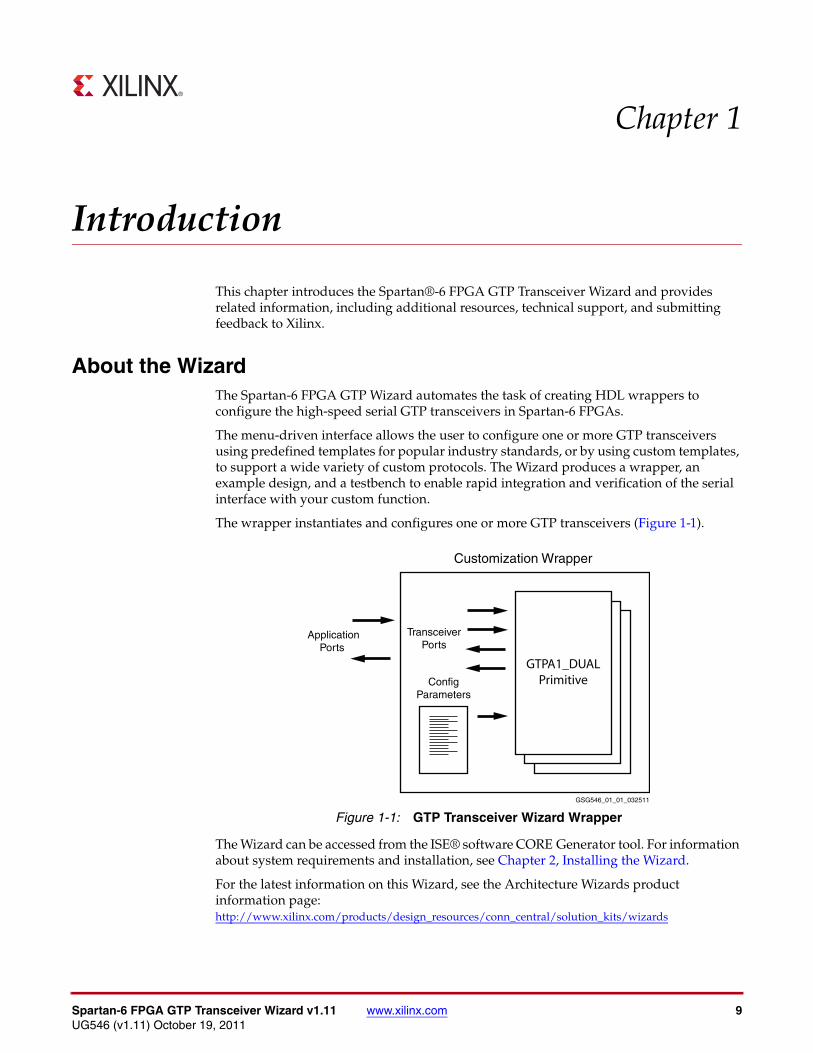
About the WizardThe Spartan-6 FPGA GTP Wizard automates the task of creating HDL wrappers to configure the high-speed serial GTP transceivers in Spartan-6 FPGAs.
The menu-driven interface allows the user to configure one or more GTP transceivers using predefined templates for popular industry standards, or by using custom templates, to support a wide variety of custom protocols. The Wizard produces a wrapper, an example design, and a testbench to enable rapid integration and verification of the serial interface with your custom function.
The wrapper instantiates and configures one or more GTP transceivers (Figure 1-1).
The Wizard can be accessed from the ISE® software CORE Generator tool. For information about system requirements and installation, see Chapter 2, Installing the Wizard.
For the latest information on this Wizard, see the Architecture Wizards product information page: http://www.xilinx.com/products/design_resources/conn_central/solution_kits/wizards
X-Ref Target - Figure 1-1
Figure 1-1: GTP Transceiver Wizard Wrapper
ApplicationPorts
Customization Wrapper
GTPA1_DUALPrimitive
GSG546_01_01_032511
TransceiverPorts
ConfigParameters
Spartan-6 FPGA GTP Transceiver Wizard v1.11 www.xilinx.com 9UG546 (v1.11) October 19, 2011
Chapter 1: Introduction
For documentation, see the Spartan-6 FPGA GTP Transceiver Wizard page: http://www.xilinx.com/support/documentation/ipfpgafeaturedesign_iointerface_s6gtpwizard.htm
FeaturesThe Wizard has these features:
• Creates customized HDL wrappers to configure Spartan-6 FPGA GTP transceivers
• Predefined templates automate transceiver configuration for industry standard protocols such as: CPRI™, DisplayPort, Gigabit Ethernet, High-Definition Serial Digital Interface (HD-SDI), Open Base Station Architecture Initiative (OBSAI), PCI EXPRESS ® (PCIe ®) generation I, Serial RapidIO, 10 Gb Attachment Unit Interface (XAUI), Aurora 8B/10B, Serial Advanced Technology Attachment (SATA) 1.5 Gb/s, and SATA 3 Gb/s
• Custom protocols can be specified using the Start from Scratch option in the GUI.
• Automatically configures transceiver analog settings of the Spartan-6 FPGA GTP transceivers
• Supports 8B/10B encoding/decoding
• Includes an example design with a companion testbench as well as implementation and simulation scripts
Supported DevicesThe Wizard supports the Spartan-6 LXT family. For a complete listing of supported devices, see XTP025, IP Release Notes Guide for this Wizard. For more information on the Spartan-6 devices, see DS160, Spartan-6 Family Overview.
Provided with the WizardThe following are provided with the Wizard:
• Documentation: This user guide
• Design Files: Verilog and VHDL
• Example Design: Verilog and VHDL
• Testbench: Verilog and VHDL
• Constraints File: Synthesis constraints file
• Simulation Model: Verilog and VHDL
10 www.xilinx.com Spartan-6 FPGA GTP Transceiver Wizard v1.11UG546 (v1.11) October 19, 2011
Recommended Design Experience
Recommended Design ExperienceThe Wizard is a fully verified solution that helps automate the task of defining parameter settings for Spartan-6 FPGA GTP transceivers. The additional challenge associated with implementing a complete design depends on the configuration and required functionality of the application. For best results, previous experience building high-performance, pipelined FPGA designs using Xilinx implementation software and user constraints files (UCF) is recommended.
For those with less experience, Xilinx offers various training classes to help with various aspects of designing with Xilinx FPGAs. These include classes on such topics as designing for performance and designing with multi-gigabit serial I/O. For more information, see http://www.xilinx.com/training.
Xilinx sales representatives can provide a closer review and estimation of specific design requirements.
Related Xilinx DocumentsFor detailed information and updates about the Wizard, see the following:
• UG546, LogiCORE IP Spartan-6 FPGA GTP Transceiver Wizard v1.11 User Guide
• XTP025, IP Release Notes Guide for the Wizard
Prior to generating the Wizard, users should be familiar with the following:
1. DS160: Spartan-6 Family Overview
2. UG386: Spartan-6 FPGA GTP Transceivers User Guide 3. ISE software documentation at http://www.xilinx.com/ise
Technical SupportFor technical support, go to www.xilinx.com/support. Questions are routed to a team of engineers with expertise using this Wizard.
Xilinx provides technical support for use of this product as described in this guide. Xilinx cannot guarantee timing, functionality, or support of this product for designs that do not follow these guidelines.
Ordering InformationThe Wizard is provided free of charge under the terms of the Xilinx End User License Agreement. The Wizard can be generated by the ISE software CORE Generator tool v13.3 or higher, which is a standard component of the ISE Design Suite. For more information, visit the Architecture Wizards web page. Information about additional LogiCORE modules is available at the IP Center. For pricing and availability of other LogiCORE modules and software, contact a local Xilinx sales representative.
Spartan-6 FPGA GTP Transceiver Wizard v1.11 www.xilinx.com 11UG546 (v1.11) October 19, 2011
Chapter 1: Introduction
FeedbackXilinx welcomes comments and suggestions about the Wizard and the accompanying documentation.
WizardFor comments or suggestions about the Wizard, submit a WebCase from www.xilinx.com/support. (Registration is required to log in to WebCase.) Be sure to include the following information:
• Product name
• Wizard version number
• List of parameter settings
• Explanation of any comments, including whether the case is requesting an enhancement (improvement) or reporting a defect (something is not working correctly)
DocumentFor comments or suggestions about this document, submit a WebCase from www.xilinx.com/support. (Registration is required to log in to WebCase.) Be sure to include the following information:
• Document title
• Document number
• Page number(s) to direct applicable comments
• Explanation of any comments, including whether the case is requesting an enhancement (improvement) or reporting a defect (something is not working correctly)
12 www.xilinx.com Spartan-6 FPGA GTP Transceiver Wizard v1.11UG546 (v1.11) October 19, 2011
Chapter 2
Installing the Wizard
This chapter provides instructions for installing the Spartan®-6 FPGA GTP Transceiver Wizard in the ISE® Design Suite CORE Generator™ tool.
Tools and System Requirements
Operating SystemsFor a list of system requirements, see the ISE Design Suite 13: Release Notes Guide.
Design Tools
Design Entry
• ISE Design Suite CORE Generator software 13.3
• PlanAhead™ software 13.3
Simulation
• ISE Simulator (ISim) 13.3
• Mentor Graphics ModelSim 6.6d
• Cadence Incisive Enterprise Simulator (IES) 10.2
• Synopsys Verilog Compiler Simulator (VCS) and VCS MX 2010.06
See XTP025, IP Release Notes Guide for the Wizard for the required service pack; ISE software service packs can be downloaded from http://www.xilinx.com/support/download.htm.
Synthesis
• XST 13.3
• Synopsys Synplify Pro E-2011.03-SP2
Spartan-6 FPGA GTP Transceiver Wizard v1.11 www.xilinx.com 13UG546 (v1.11) October 19, 2011
Chapter 2: Installing the Wizard
Before You BeginBefore installing the Wizard, you must have a MySupport account and the ISE 13.3 software installed on your system. If you already have an account and have the software installed, go to Installing the Wizard, otherwise do the following:
1. Click Login at the top of the Xilinx home page then follow the onscreen instructions to create a MySupport account.
2. Install the ISE 13.3 software.
For the software installation instructions, see the ISE Design Suite Release Notes and Installation Guide available in ISE software Documentation.
Installing the WizardThe Wizard is included with the ISE 13.3 software. Follow the ISE 13.3 installation instructions in the ISE Installation and Release Notes available in www.xilinx.com/support/documentation under the Design Tools tab.
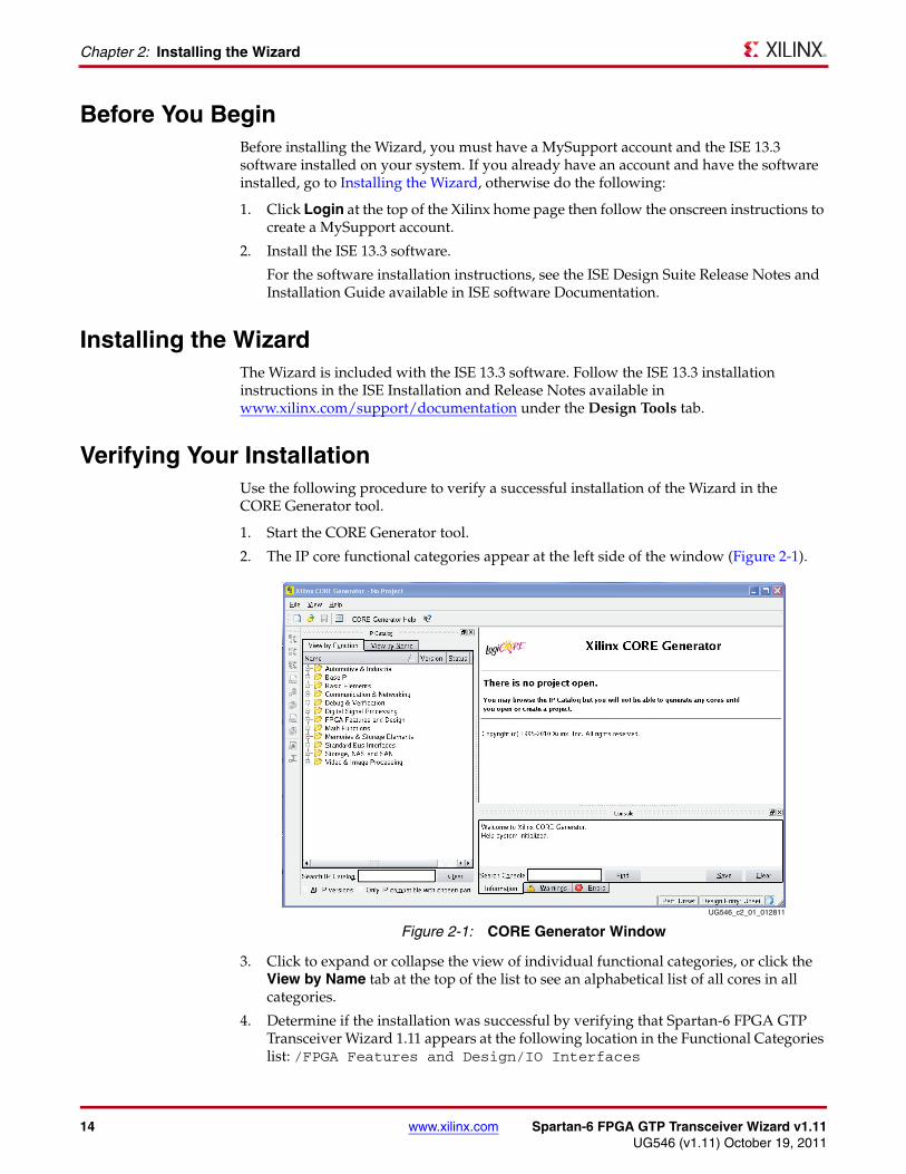
Verifying Your InstallationUse the following procedure to verify a successful installation of the Wizard in the CORE Generator tool.
1. Start the CORE Generator tool.
2. The IP core functional categories appear at the left side of the window (Figure 2-1).
3. Click to expand or collapse the view of individual functional categories, or click the View by Name tab at the top of the list to see an alphabetical list of all cores in all categories.
4. Determine if the installation was successful by verifying that Spartan-6 FPGA GTP Transceiver Wizard 1.11 appears at the following location in the Functional Categories list: /FPGA Features and Design/IO Interfaces
X-Ref Target - Figure 2-1
Figure 2-1: CORE Generator WindowUG546_c2_01_012811
14 www.xilinx.com Spartan-6 FPGA GTP Transceiver Wizard v1.11UG546 (v1.11) October 19, 2011
Chapter 3
Running the Wizard
OverviewThis chapter provides a step-by-step procedure for generating a Spartan®-6 FPGA GTP transceiver wrapper, implementing the wrapper in hardware using the accompanying example design, and simulating the wrapper with the provided example testbench.
Note: The screen captures in this chapter are conceptual representatives of their subjects and provide general information only. For the latest information, see the CORE Generator ™ tool.
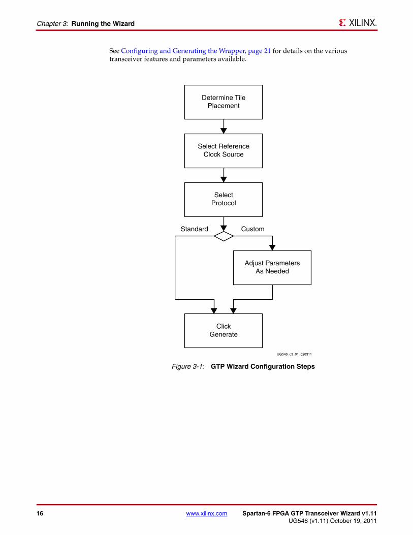
Functional OverviewFigure 3-1, page 16 shows the steps required to configure GTP transceivers using the Spartan-6 FPGA GTP Transceiver Wizard. Start the CORE Generator software and select the Spartan-6 FPGA GTP Transceiver Wizard, then follow the chart to configure the transceivers and generate a wrapper that includes an accompanying example design.
• To use an existing template with no changes, click Generate.
• To modify a standard template or start from scratch, proceed through the Wizard and adjust the settings as needed.
Spartan-6 FPGA GTP Transceiver Wizard v1.11 www.xilinx.com 15UG546 (v1.11) October 19, 2011
Chapter 3: Running the Wizard
See Configuring and Generating the Wrapper, page 21 for details on the various transceiver features and parameters available.
X-Ref Target - Figure 3-1
Figure 3-1: GTP Wizard Configuration Steps
Determine TilePlacement
Select ReferenceClock Source
SelectProtocol
ClickGenerate
Adjust ParametersAs Needed
Standard Custom
UG546_c3_01_020311
16 www.xilinx.com Spartan-6 FPGA GTP Transceiver Wizard v1.11UG546 (v1.11) October 19, 2011
Overview
Structure of the GTP Transceiver Wrapper, Example Design, and Testbench
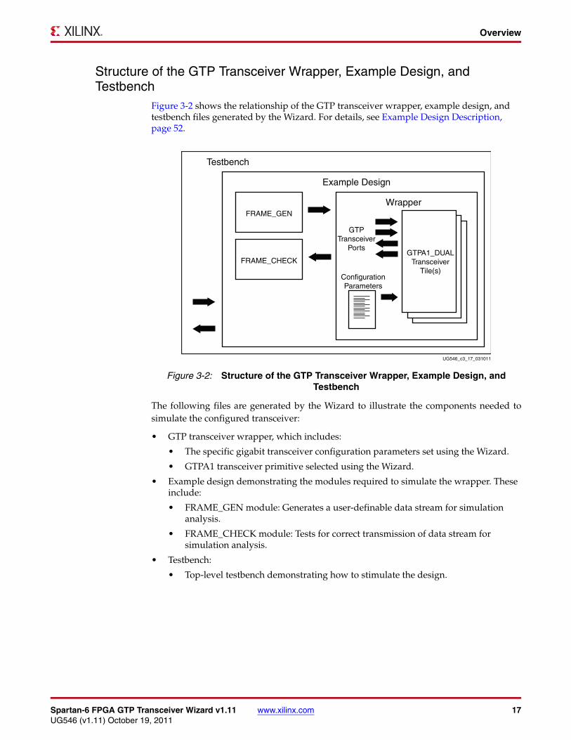
Figure 3-2 shows the relationship of the GTP transceiver wrapper, example design, and testbench files generated by the Wizard. For details, see Example Design Description, page 52.
The following files are generated by the Wizard to illustrate the components needed to simulate the configured transceiver:
• GTP transceiver wrapper, which includes:
• The specific gigabit transceiver configuration parameters set using the Wizard.
• GTPA1 transceiver primitive selected using the Wizard.
• Example design demonstrating the modules required to simulate the wrapper. These include:
• FRAME_GEN module: Generates a user-definable data stream for simulation analysis.
• FRAME_CHECK module: Tests for correct transmission of data stream for simulation analysis.
• Testbench:
• Top-level testbench demonstrating how to stimulate the design.
X-Ref Target - Figure 3-2
Figure 3-2: Structure of the GTP Transceiver Wrapper, Example Design, and Testbench
Example Design
UG546_c3_17_031011
Wrapper
GTPTransceiver
Ports
ConfigurationParameters
Testbench
FRAME_GEN
FRAME_CHECKGTPA1_DUAL
TransceiverTile(s)
Spartan-6 FPGA GTP Transceiver Wizard v1.11 www.xilinx.com 17UG546 (v1.11) October 19, 2011
Chapter 3: Running the Wizard
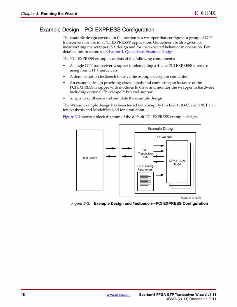
Example Design—PCI EXPRESS ConfigurationThe example design covered in this section is a wrapper that configures a group of GTP transceivers for use in a PCI EXPRESS® application. Guidelines are also given for incorporating the wrapper in a design and for the expected behavior in operation. For detailed information, see Chapter 4, Quick Start Example Design.
The PCI EXPRESS example consists of the following components:
• A single GTP transceiver wrapper implementing a 4-lane PCI EXPRESS interface using four GTP transceivers
• A demonstration testbench to drive the example design in simulation
• An example design providing clock signals and connecting an instance of the PCI EXPRESS wrapper with modules to drive and monitor the wrapper in hardware, including optional ChipScope™ Pro tool support
• Scripts to synthesize and simulate the example design
The Wizard example design has been tested with Synplify Pro E-2011.03-SP2 and XST 13.3 for synthesis and ModelSim 6.6d for simulation.
Figure 3-3 shows a block diagram of the default PCI EXPRESS example design.X-Ref Target - Figure 3-3
Figure 3-3: Example Design and Testbench—PCI EXPRESS Configuration
PCIE ConfigParameters
GTPTransceiver
Ports
Example Design
GTPA1_DUALTile(s)
GSG546_03_01_021509
PCIE Wrapper
Test Bench
18 www.xilinx.com Spartan-6 FPGA GTP Transceiver Wizard v1.11UG546 (v1.11) October 19, 2011
Setting Up the Project
Setting Up the ProjectBefore generating the example design, set up the project as described in Creating a Directory and Setting the Project Options.
Creating a DirectoryTo set up the example project, first create a directory using the following steps:
1. Change directory to the desired location. This example uses the following location and directory name:
/Projects/pcie_example
2. Start the CORE Generator™ tool.
For help starting and using the CORE Generator tool, see CORE Generator Help, available in ISE® software documentation.
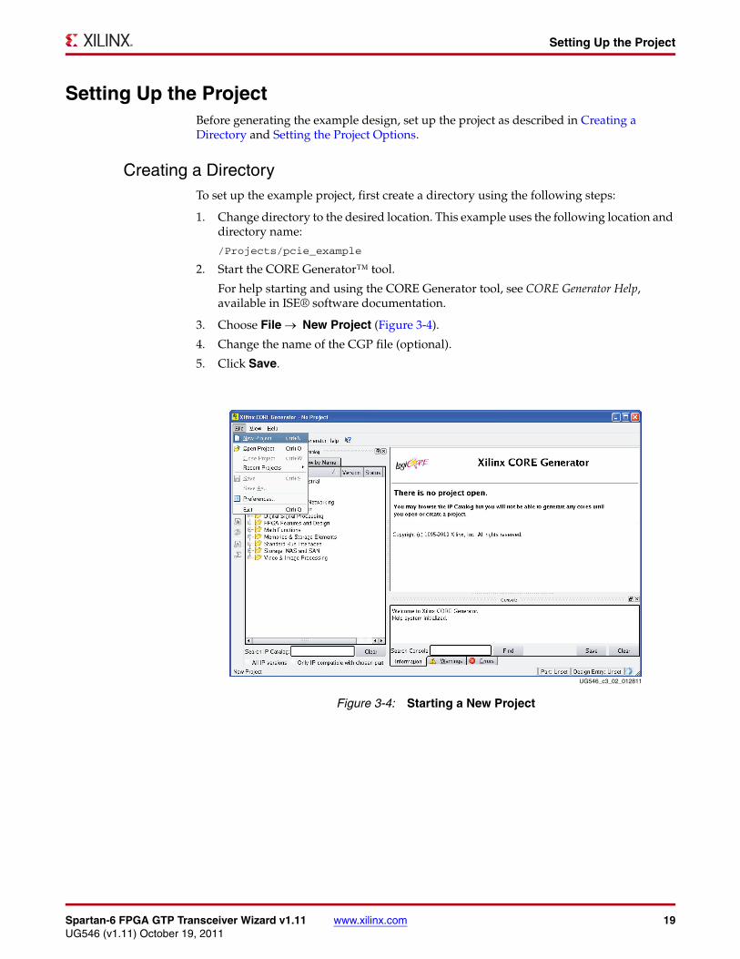
3. Choose File New Project (Figure 3-4).
4. Change the name of the CGP file (optional).
5. Click Save.
X-Ref Target - Figure 3-4
Figure 3-4: Starting a New Project
UG546_c3_02_012811
Spartan-6 FPGA GTP Transceiver Wizard v1.11 www.xilinx.com 19UG546 (v1.11) October 19, 2011
Chapter 3: Running the Wizard
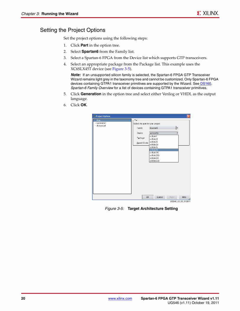
Setting the Project OptionsSet the project options using the following steps:
1. Click Part in the option tree.
2. Select Spartan6 from the Family list.
3. Select a Spartan-6 FPGA from the Device list which supports GTP transceivers.
4. Select an appropriate package from the Package list. This example uses the XC6SLX45T device (see Figure 3-5).
Note: If an unsupported silicon family is selected, the Spartan-6 FPGA GTP Transceiver Wizard remains light grey in the taxonomy tree and cannot be customized. Only Spartan-6 FPGA devices containing GTPA1 transceiver primitives are supported by the Wizard. See DS160, Spartan-6 Family Overview for a list of devices containing GTPA1 transceiver primitives.
5. Click Generation in the option tree and select either Verilog or VHDL as the output language.
6. Click OK.X-Ref Target - Figure 3-5
Figure 3-5: Target Architecture Setting
UG546_c3_03_012811
20 www.xilinx.com Spartan-6 FPGA GTP Transceiver Wizard v1.11UG546 (v1.11) October 19, 2011
Configuring and Generating the Wrapper
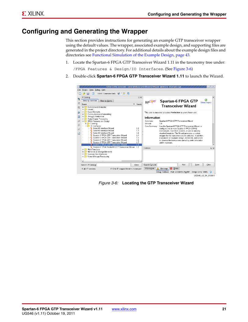
Configuring and Generating the WrapperThis section provides instructions for generating an example GTP transceiver wrapper using the default values. The wrapper, associated example design, and supporting files are generated in the project directory. For additional details about the example design files and directories see Functional Simulation of the Example Design, page 43.
1. Locate the Spartan-6 FPGA GTP Transceiver Wizard 1.11 in the taxonomy tree under:
/FPGA Features & Design/IO Interfaces. (See Figure 3-6)
2. Double-click Spartan-6 FPGA GTP Transceiver Wizard 1.11 to launch the Wizard. X-Ref Target - Figure 3-6
Figure 3-6: Locating the GTP Transceiver Wizard
UG546_c3_04_012811
Spartan-6 FPGA GTP Transceiver Wizard v1.11 www.xilinx.com 21UG546 (v1.11) October 19, 2011
Chapter 3: Running the Wizard
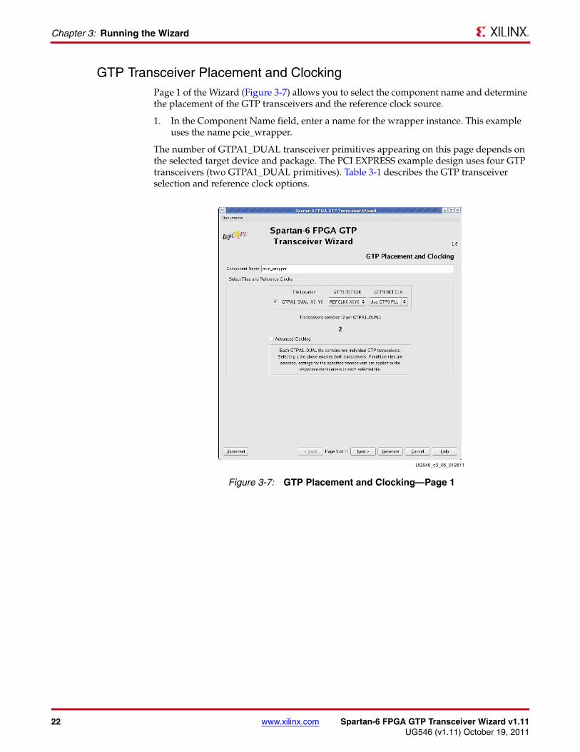
GTP Transceiver Placement and ClockingPage 1 of the Wizard (Figure 3-7) allows you to select the component name and determine the placement of the GTP transceivers and the reference clock source.
1. In the Component Name field, enter a name for the wrapper instance. This example uses the name pcie_wrapper.
The number of GTPA1_DUAL transceiver primitives appearing on this page depends on the selected target device and package. The PCI EXPRESS example design uses four GTP transceivers (two GTPA1_DUAL primitives). Table 3-1 describes the GTP transceiver selection and reference clock options.X-Ref Target - Figure 3-7
Figure 3-7: GTP Placement and Clocking—Page 1
UG546_c3_05_012811
22 www.xilinx.com Spartan-6 FPGA GTP Transceiver Wizard v1.11UG546 (v1.11) October 19, 2011
Configuring and Generating the Wrapper
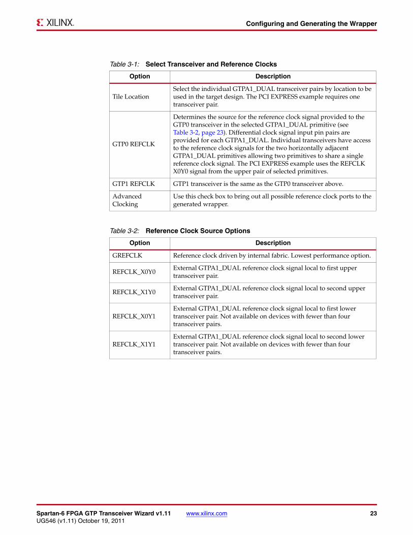
Table 3-1: Select Transceiver and Reference Clocks
Option Description
Tile LocationSelect the individual GTPA1_DUAL transceiver pairs by location to be used in the target design. The PCI EXPRESS example requires one transceiver pair.
GTP0 REFCLK
Determines the source for the reference clock signal provided to the GTP0 transceiver in the selected GTPA1_DUAL primitive (see Table 3-2, page 23). Differential clock signal input pin pairs are provided for each GTPA1_DUAL. Individual transceivers have access to the reference clock signals for the two horizontally adjacent GTPA1_DUAL primitives allowing two primitives to share a single reference clock signal. The PCI EXPRESS example uses the REFCLK X0Y0 signal from the upper pair of selected primitives.
GTP1 REFCLK GTP1 transceiver is the same as the GTP0 transceiver above.
Advanced Clocking
Use this check box to bring out all possible reference clock ports to the generated wrapper.
Table 3-2: Reference Clock Source Options
Option Description
GREFCLK Reference clock driven by internal fabric. Lowest performance option.
REFCLK_X0Y0External GTPA1_DUAL reference clock signal local to first upper transceiver pair.
REFCLK_X1Y0External GTPA1_DUAL reference clock signal local to second upper transceiver pair.
REFCLK_X0Y1External GTPA1_DUAL reference clock signal local to first lower transceiver pair. Not available on devices with fewer than four transceiver pairs.
REFCLK_X1Y1External GTPA1_DUAL reference clock signal local to second lower transceiver pair. Not available on devices with fewer than four transceiver pairs.
Spartan-6 FPGA GTP Transceiver Wizard v1.11 www.xilinx.com 23UG546 (v1.11) October 19, 2011
Chapter 3: Running the Wizard
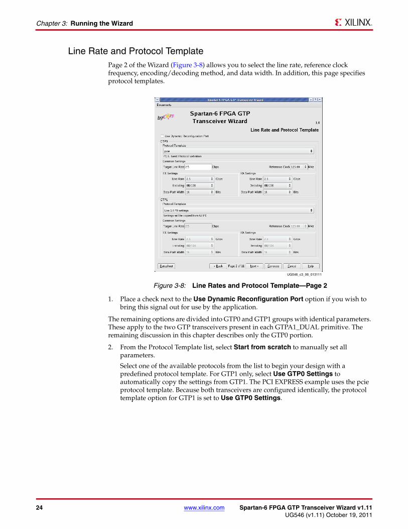
Line Rate and Protocol TemplatePage 2 of the Wizard (Figure 3-8) allows you to select the line rate, reference clock frequency, encoding/decoding method, and data width. In addition, this page specifies protocol templates.
1. Place a check next to the Use Dynamic Reconfiguration Port option if you wish to bring this signal out for use by the application.
The remaining options are divided into GTP0 and GTP1 groups with identical parameters. These apply to the two GTP transceivers present in each GTPA1_DUAL primitive. The remaining discussion in this chapter describes only the GTP0 portion.
2. From the Protocol Template list, select Start from scratch to manually set all parameters.
Select one of the available protocols from the list to begin your design with a predefined protocol template. For GTP1 only, select Use GTP0 Settings to automatically copy the settings from GTP1. The PCI EXPRESS example uses the pcie protocol template. Because both transceivers are configured identically, the protocol template option for GTP1 is set to Use GTP0 Settings.
X-Ref Target - Figure 3-8
Figure 3-8: Line Rates and Protocol Template—Page 2
UG546_c3_06_013111
24 www.xilinx.com Spartan-6 FPGA GTP Transceiver Wizard v1.11UG546 (v1.11) October 19, 2011
Configuring and Generating the Wrapper
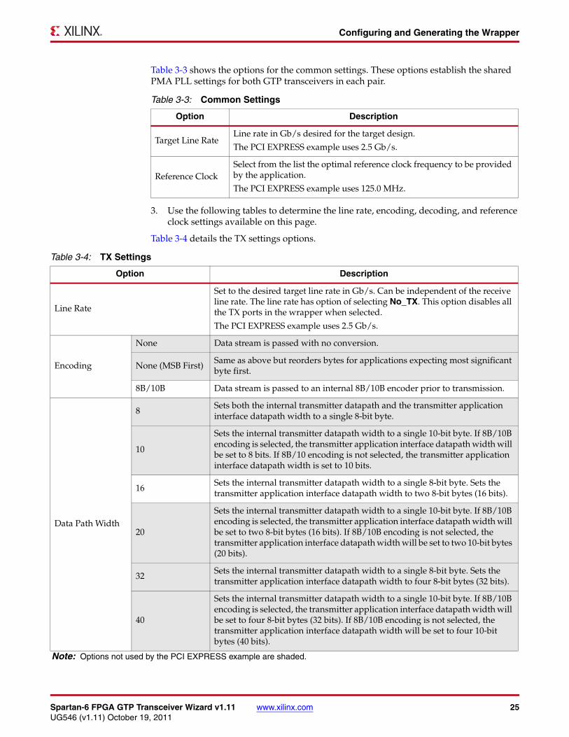
Table 3-3 shows the options for the common settings. These options establish the shared PMA PLL settings for both GTP transceivers in each pair.
3. Use the following tables to determine the line rate, encoding, decoding, and reference clock settings available on this page.
Table 3-4 details the TX settings options.
Table 3-3: Common Settings
Option Description
Target Line RateLine rate in Gb/s desired for the target design.
The PCI EXPRESS example uses 2.5 Gb/s.
Reference ClockSelect from the list the optimal reference clock frequency to be provided by the application.
The PCI EXPRESS example uses 125.0 MHz.
Table 3-4: TX Settings
Option Description
Line Rate
Set to the desired target line rate in Gb/s. Can be independent of the receive line rate. The line rate has option of selecting No_TX. This option disables all the TX ports in the wrapper when selected.
The PCI EXPRESS example uses 2.5 Gb/s.
Encoding
None Data stream is passed with no conversion.
None (MSB First) Same as above but reorders bytes for applications expecting most significant byte first.
8B/10B Data stream is passed to an internal 8B/10B encoder prior to transmission.
Data Path Width
8Sets both the internal transmitter datapath and the transmitter application interface datapath width to a single 8-bit byte.
10
Sets the internal transmitter datapath width to a single 10-bit byte. If 8B/10B encoding is selected, the transmitter application interface datapath width will be set to 8 bits. If 8B/10 encoding is not selected, the transmitter application interface datapath width is set to 10 bits.
16Sets the internal transmitter datapath width to a single 8-bit byte. Sets the transmitter application interface datapath width to two 8-bit bytes (16 bits).
20
Sets the internal transmitter datapath width to a single 10-bit byte. If 8B/10B encoding is selected, the transmitter application interface datapath width will be set to two 8-bit bytes (16 bits). If 8B/10B encoding is not selected, the transmitter application interface datapath width will be set to two 10-bit bytes (20 bits).
32Sets the internal transmitter datapath width to a single 8-bit byte. Sets the transmitter application interface datapath width to four 8-bit bytes (32 bits).
40
Sets the internal transmitter datapath width to a single 10-bit byte. If 8B/10B encoding is selected, the transmitter application interface datapath width will be set to four 8-bit bytes (32 bits). If 8B/10B encoding is not selected, the transmitter application interface datapath width will be set to four 10-bit bytes (40 bits).
Note: Options not used by the PCI EXPRESS example are shaded.
Spartan-6 FPGA GTP Transceiver Wizard v1.11 www.xilinx.com 25UG546 (v1.11) October 19, 2011
Chapter 3: Running the Wizard
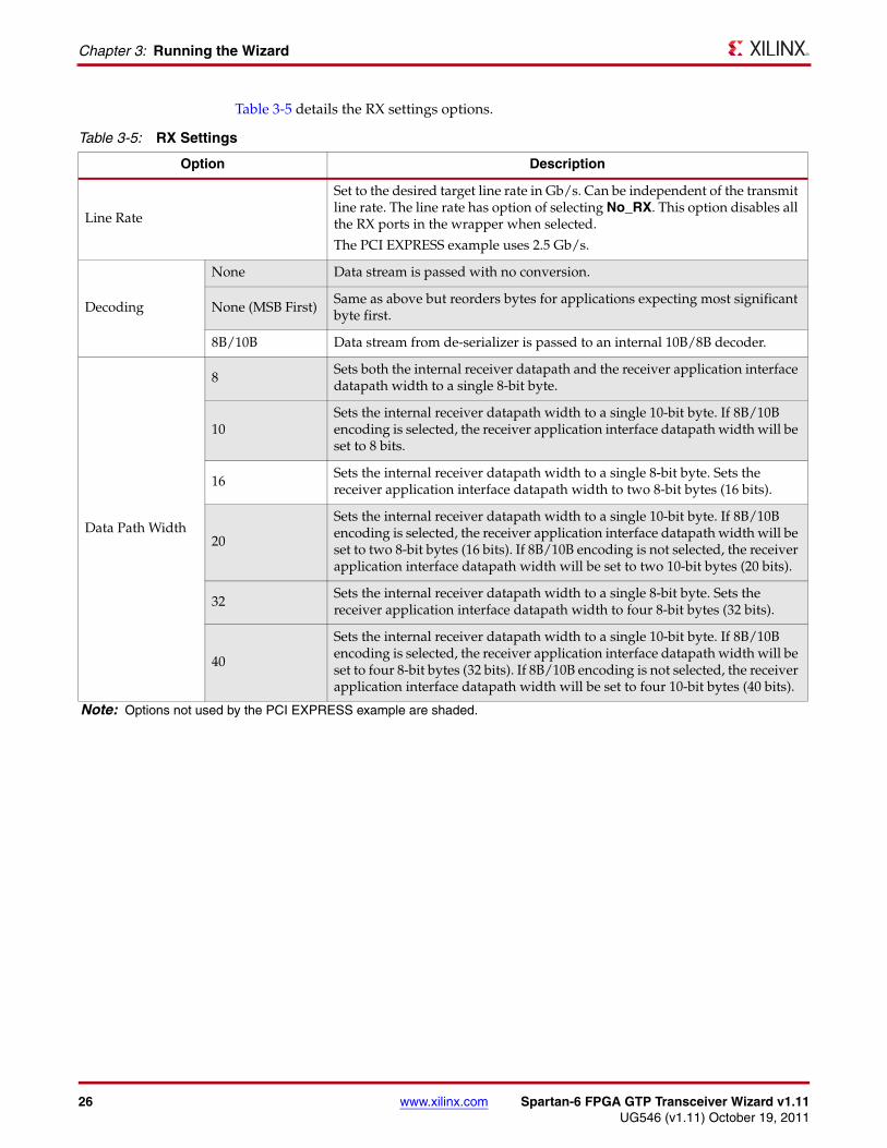
Table 3-5 details the RX settings options.
Table 3-5: RX Settings
Option Description
Line Rate
Set to the desired target line rate in Gb/s. Can be independent of the transmit line rate. The line rate has option of selecting No_RX. This option disables all the RX ports in the wrapper when selected.
The PCI EXPRESS example uses 2.5 Gb/s.
Decoding
None Data stream is passed with no conversion.
None (MSB First)Same as above but reorders bytes for applications expecting most significant byte first.
8B/10B Data stream from de-serializer is passed to an internal 10B/8B decoder.
Data Path Width
8Sets both the internal receiver datapath and the receiver application interface datapath width to a single 8-bit byte.
10Sets the internal receiver datapath width to a single 10-bit byte. If 8B/10B encoding is selected, the receiver application interface datapath width will be set to 8 bits.
16Sets the internal receiver datapath width to a single 8-bit byte. Sets the receiver application interface datapath width to two 8-bit bytes (16 bits).
20
Sets the internal receiver datapath width to a single 10-bit byte. If 8B/10B encoding is selected, the receiver application interface datapath width will be set to two 8-bit bytes (16 bits). If 8B/10B encoding is not selected, the receiver application interface datapath width will be set to two 10-bit bytes (20 bits).
32Sets the internal receiver datapath width to a single 8-bit byte. Sets the receiver application interface datapath width to four 8-bit bytes (32 bits).
40
Sets the internal receiver datapath width to a single 10-bit byte. If 8B/10B encoding is selected, the receiver application interface datapath width will be set to four 8-bit bytes (32 bits). If 8B/10B encoding is not selected, the receiver application interface datapath width will be set to four 10-bit bytes (40 bits).
Note: Options not used by the PCI EXPRESS example are shaded.
26 www.xilinx.com Spartan-6 FPGA GTP Transceiver Wizard v1.11UG546 (v1.11) October 19, 2011
Configuring and Generating the Wrapper
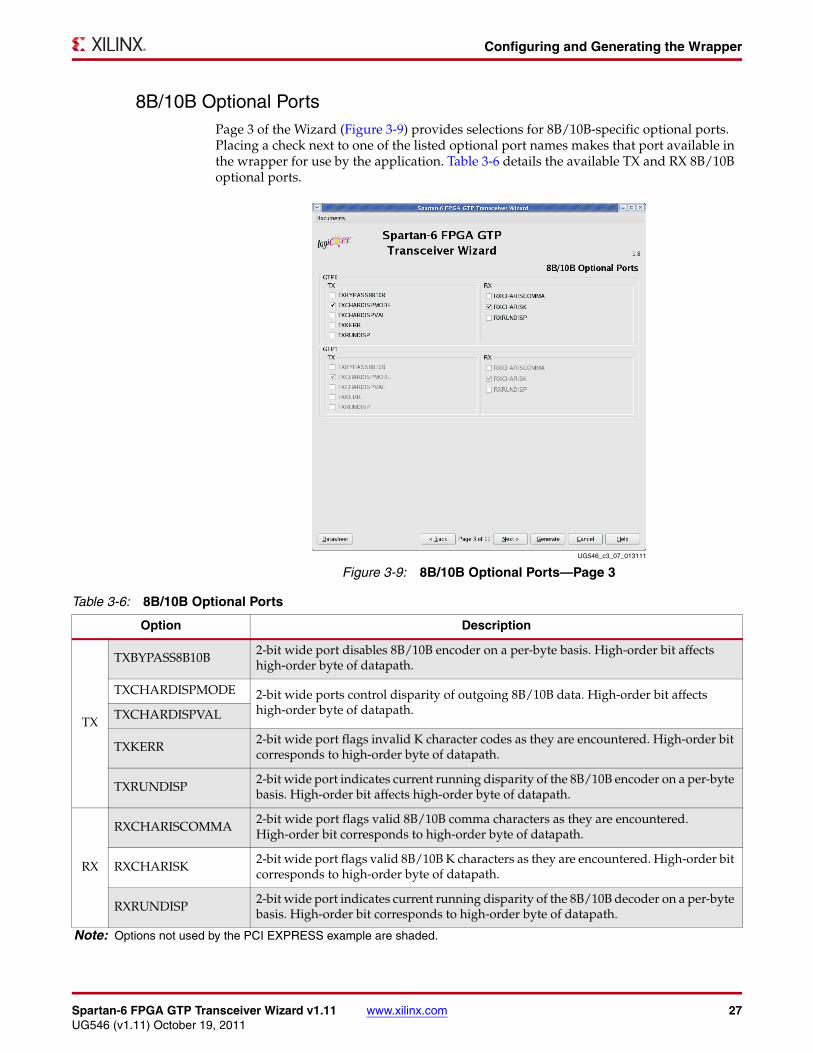
8B/10B Optional PortsPage 3 of the Wizard (Figure 3-9) provides selections for 8B/10B-specific optional ports. Placing a check next to one of the listed optional port names makes that port available in the wrapper for use by the application. Table 3-6 details the available TX and RX 8B/10B optional ports.X-Ref Target - Figure 3-9
Figure 3-9: 8B/10B Optional Ports—Page 3UG546_c3_07_013111
Table 3-6: 8B/10B Optional Ports
Option Description
TX
TXBYPASS8B10B2-bit wide port disables 8B/10B encoder on a per-byte basis. High-order bit affects high-order byte of datapath.
TXCHARDISPMODE 2-bit wide ports control disparity of outgoing 8B/10B data. High-order bit affects high-order byte of datapath.TXCHARDISPVAL
TXKERR2-bit wide port flags invalid K character codes as they are encountered. High-order bit corresponds to high-order byte of datapath.
TXRUNDISP2-bit wide port indicates current running disparity of the 8B/10B encoder on a per-byte basis. High-order bit affects high-order byte of datapath.
RX
RXCHARISCOMMA2-bit wide port flags valid 8B/10B comma characters as they are encountered. High-order bit corresponds to high-order byte of datapath.
RXCHARISK2-bit wide port flags valid 8B/10B K characters as they are encountered. High-order bit corresponds to high-order byte of datapath.
RXRUNDISP2-bit wide port indicates current running disparity of the 8B/10B decoder on a per-byte basis. High-order bit corresponds to high-order byte of datapath.
Note: Options not used by the PCI EXPRESS example are shaded.
Spartan-6 FPGA GTP Transceiver Wizard v1.11 www.xilinx.com 27UG546 (v1.11) October 19, 2011
Chapter 3: Running the Wizard
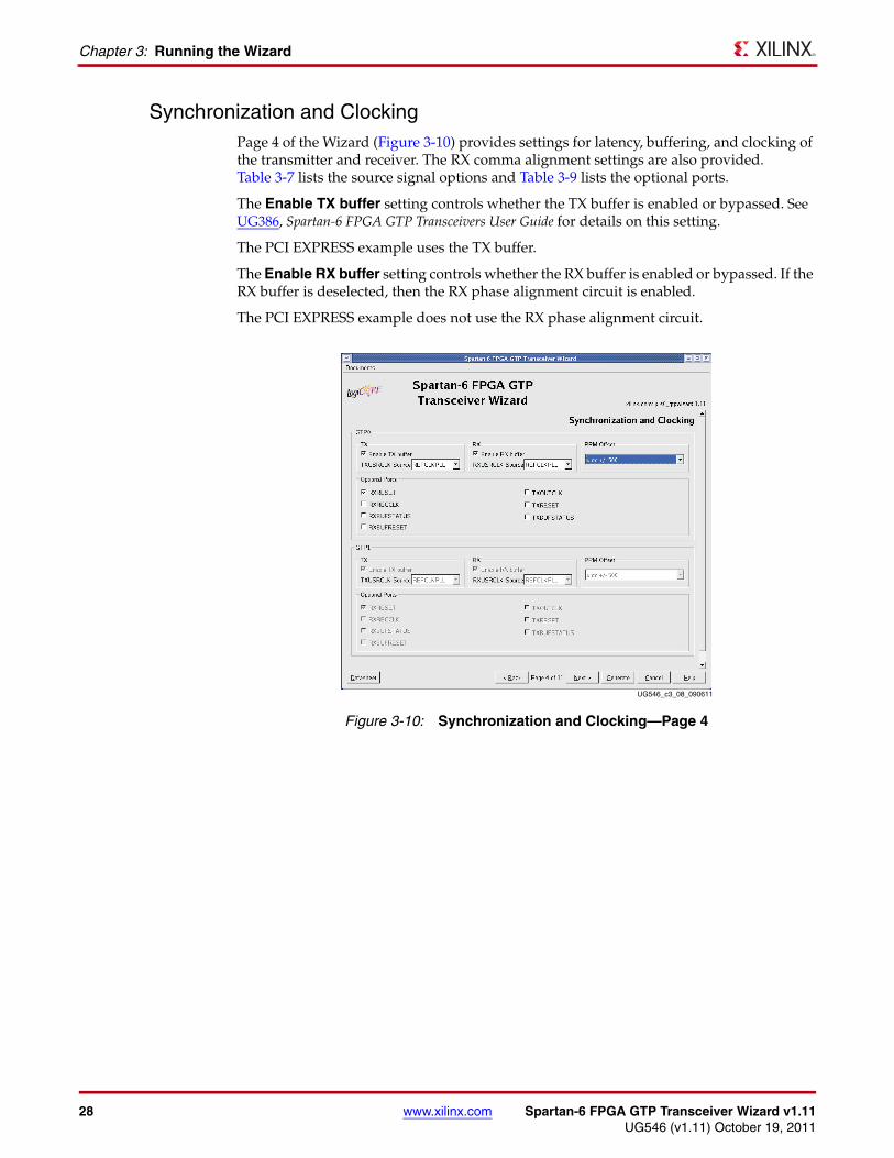
Synchronization and ClockingPage 4 of the Wizard (Figure 3-10) provides settings for latency, buffering, and clocking of the transmitter and receiver. The RX comma alignment settings are also provided. Table 3-7 lists the source signal options and Table 3-9 lists the optional ports.
The Enable TX buffer setting controls whether the TX buffer is enabled or bypassed. See UG386, Spartan-6 FPGA GTP Transceivers User Guide for details on this setting.
The PCI EXPRESS example uses the TX buffer.
The Enable RX buffer setting controls whether the RX buffer is enabled or bypassed. If the RX buffer is deselected, then the RX phase alignment circuit is enabled.
The PCI EXPRESS example does not use the RX phase alignment circuit.X-Ref Target - Figure 3-10
Figure 3-10: Synchronization and Clocking—Page 4
UG546_c3_08_090611
28 www.xilinx.com Spartan-6 FPGA GTP Transceiver Wizard v1.11UG546 (v1.11) October 19, 2011
Configuring and Generating the Wrapper
Table 3-7 details the TXUSRCLK and RXUSRCLK source signal options.
Table 3-8 shows the available PPM offset settings. The PPM Offset setting optimizes the receiver CDR logic for the desired PPM tolerance range.
Table 3-9 shows the optional ports available for synchronization and clocking.
Table 3-7: TXUSRCLK and RXUSRCLK Source
Option Description
TX
TXOUTCLKTXUSRCLK is driven by TXOUTCLK. This option is not available if the TX phase alignment circuit is used.
REFCLKPLLTXUSRCLK is driven by REFCLKPLL. This option is required if the TX phase alignment circuit is used.
Enable External TXUSRCLK
Brings the TXUSRCLK input signal out to a port at the top-level of the wrapper so it can be provided by the application. Optionally available when single-byte datapath width is used and TX buffer bypass is disabled. Not available for 2-byte datapath width. Mandatory with 4-byte datapath width.
RX
TXOUTCLKRXUSRCLK is driven by TXOUTCLK. This option is not available if the RX phase alignment circuit is used.
RXRECCLKRXUSRCLK is driven by RXRECCLK. This option is required if the RX phase alignment circuit is used.
REFCLKPLLRXUSRCLK is driven by REFCLKPLL. This option is not available if the RX phase alignment circuit is used.
Enable External RXUSRCLK
Brings the RXUSRCLK input signal out to a port at the top-level of the wrapper so it can be provided by the application. Optionally available when single-byte datapath width is used without channel bonding. Not available for 2-byte datapath width. Mandatory with 4-byte datapath width.
Note: Options not used by the PCI EXPRESS example are shaded.
Table 3-8: PPM Offset
Option Description
0 (Synchronous) Use with synchronous applications (zero tolerance).
Up to ± 500 For applications where clock tolerance is below 500 PPM.
Table 3-9: Optional Ports
Option Description
RXRESET Active-High reset signal for the receiver PCS logic.
RXRECCLKRecovered clock signal from the CDR logic. This option is required when selected as an input to RXUSRCLK.
RXBUFSTATUSIndicates the condition of the RX elastic buffer. This option is not available when the RX phase alignment circuit is used.
RXBUFRESETActive-High reset signal for the RX elastic buffer logic. This option is not available when the RX phase alignment circuit is used.
TXOUTCLKParallel clock signal generated by the GTP transceiver. This option is required when selected as an input to either TXUSRCLK or RXUSRCLK. This option is not available when the TX phase alignment circuit is used.
Spartan-6 FPGA GTP Transceiver Wizard v1.11 www.xilinx.com 29UG546 (v1.11) October 19, 2011
Chapter 3: Running the Wizard
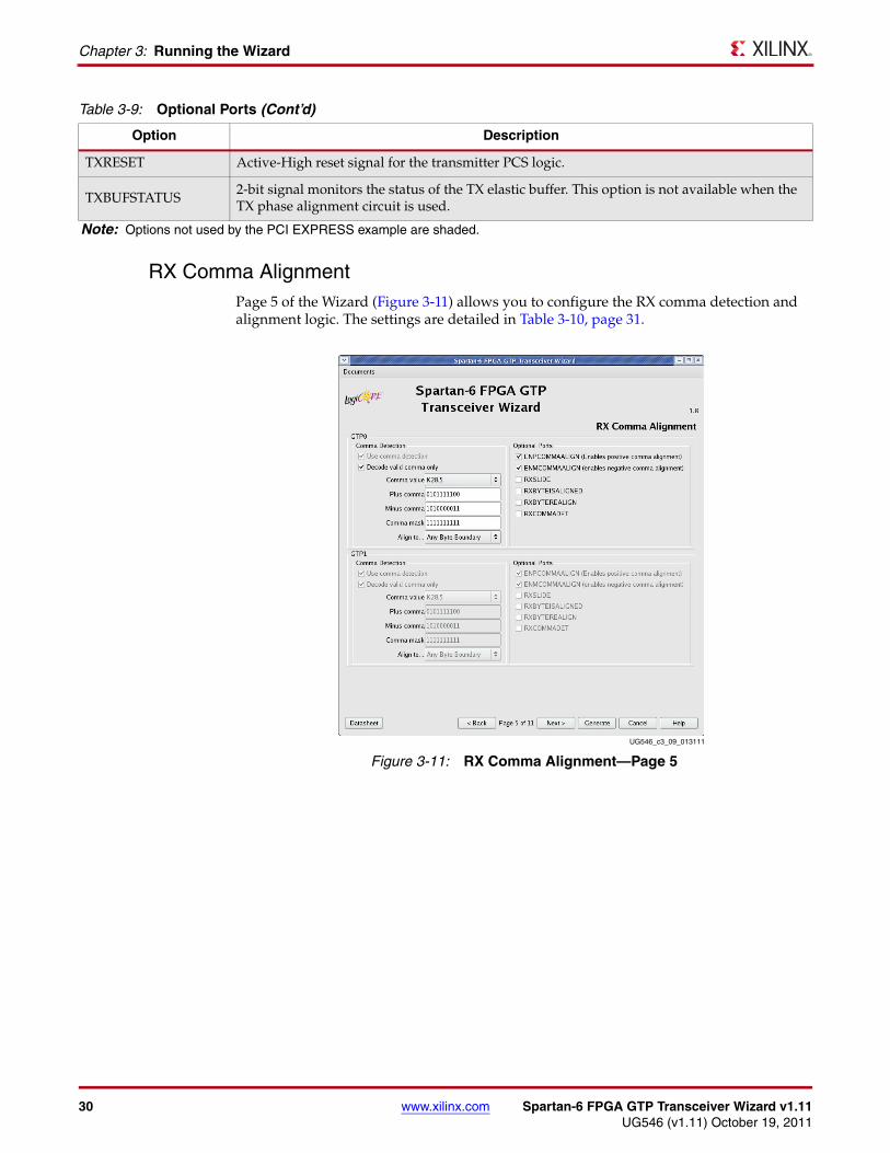
RX Comma AlignmentPage 5 of the Wizard (Figure 3-11) allows you to configure the RX comma detection and alignment logic. The settings are detailed in Table 3-10, page 31.
TXRESET Active-High reset signal for the transmitter PCS logic.
TXBUFSTATUS2-bit signal monitors the status of the TX elastic buffer. This option is not available when the TX phase alignment circuit is used.
Note: Options not used by the PCI EXPRESS example are shaded.
Table 3-9: Optional Ports (Cont’d)
Option Description
X-Ref Target - Figure 3-11
Figure 3-11: RX Comma Alignment—Page 5
UG546_c3_09_013111
30 www.xilinx.com Spartan-6 FPGA GTP Transceiver Wizard v1.11UG546 (v1.11) October 19, 2011
Configuring and Generating the Wrapper
Table 3-11 shows the optional ports available on this page.
Table 3-10: Comma Detection
Option Description
Use Comma DetectionEnables receive comma detection. Used to identify special protocol comma and framing characters in the data stream.
Decode Valid Comma OnlyWhen receive comma detection is enabled, limits the detection to specific defined comma characters.
Comma ValueSelect one of several standard comma patterns or User Defined to enter a custom pattern.
The PCI EXPRESS example is K28.5.
Plus Comma10-bit binary pattern representing the positive-disparity comma character to match. The rightmost bit of the pattern is the first bit to arrive serially.
The PCI EXPRESS example uses 0101111100.
Minus Comma10-bit binary pattern representing the negative-disparity comma character to match. The rightmost bit of the pattern is the first bit to arrive serially.
The PCI EXPRESS example uses 1010000011.
Comma Mask
10-bit binary pattern representing the mask for the comma match patterns. A 1 bit indicates the corresponding bit in the comma patterns is to be matched. A 0 bit indicates don’t care for the corresponding bit in the comma patterns.
The PCI EXPRESS example matches all ten bits (1111111111).
Align to...
Any Byte Boundary When a comma is detected, the data stream is aligned using the comma pattern to the nearest byte boundary.
Even Byte BoundariesWhen a comma is detected, the data stream is aligned using the comma pattern to the nearest even byte boundary. This option is available only for 16- and 20-bit RX data interfaces.
Note: Options not used by the PCI EXPRESS example are shaded.
Table 3-11: Optional Ports
Option Description
ENPCOMMAALIGNActive-High signal which enables the byte boundary alignment process when a plus comma pattern is detected.
ENMCOMMAALIGNActive-High signal which enables the byte boundary alignment process when a minus comma pattern is detected.
RXSLIDEActive-High signal that causes the byte alignment to be adjusted by one bit with each assertion. Takes precedence over normal comma alignment.
RXBYTEISALIGNED Active-High signal indicating that the parallel data stream is aligned to byte boundaries.
RXBYTEREALIGNActive-High signal indicating that byte alignment has changed with a recent comma detection. Note that data errors can occur with this condition.
RXCOMMADETActive-High signal indicating the comma alignment logic has detected a comma pattern in the data stream.
Note: Options not used by the PCI EXPRESS example are shaded.
Spartan-6 FPGA GTP Transceiver Wizard v1.11 www.xilinx.com 31UG546 (v1.11) October 19, 2011
Chapter 3: Running the Wizard
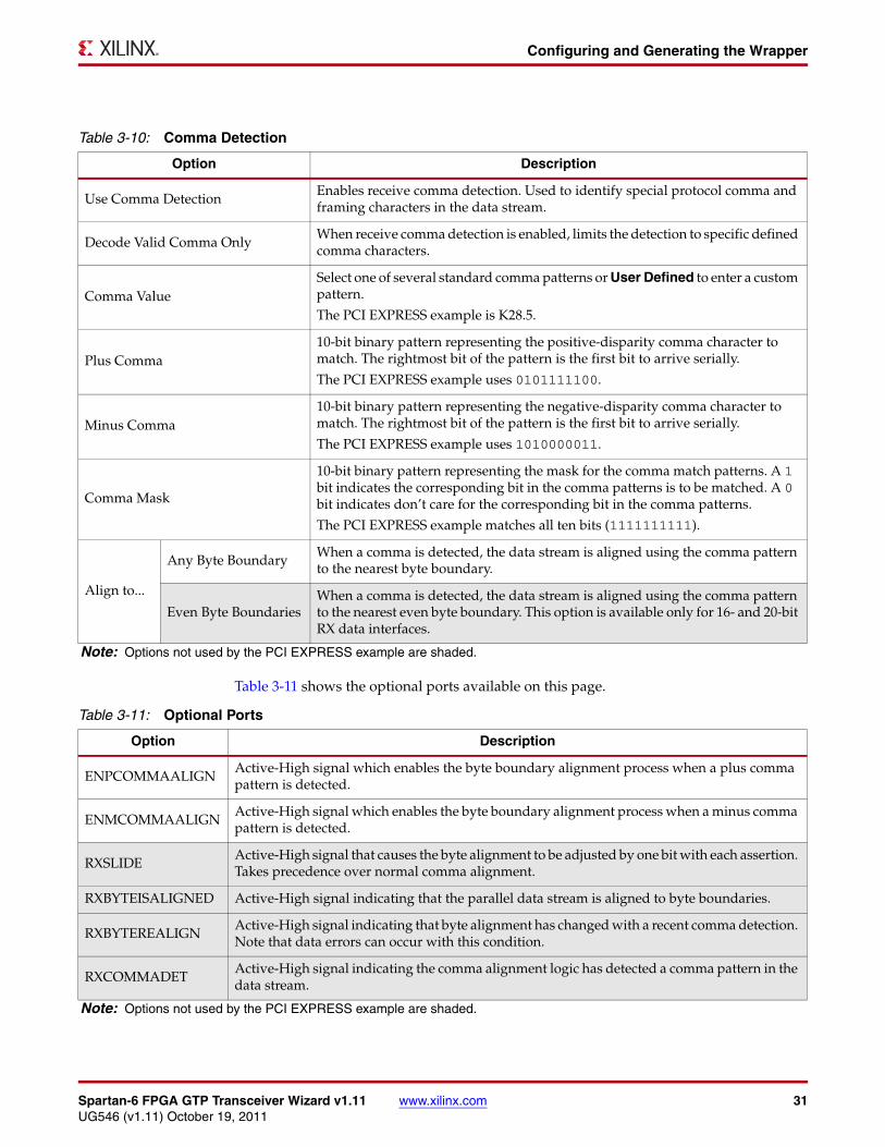
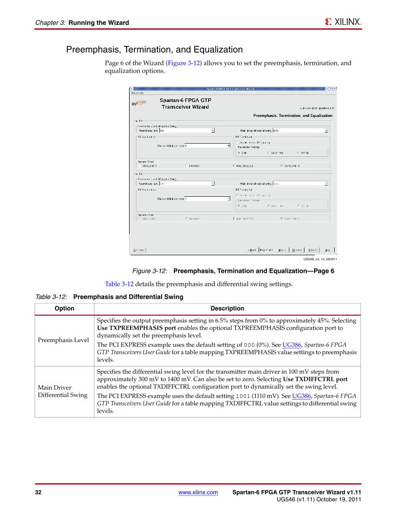
Preemphasis, Termination, and EqualizationPage 6 of the Wizard (Figure 3-12) allows you to set the preemphasis, termination, and equalization options.
Table 3-12 details the preemphasis and differential swing settings.
X-Ref Target - Figure 3-12
Figure 3-12: Preemphasis, Termination and Equalization—Page 6
UG546_c3_10_050311
Table 3-12: Preemphasis and Differential Swing
Option Description
Preemphasis Level
Specifies the output preemphasis setting in 6.5% steps from 0% to approximately 45%. Selecting Use TXPREEMPHASIS port enables the optional TXPREEMPHASIS configuration port to dynamically set the preemphasis level.
The PCI EXPRESS example uses the default setting of 000 (0%). See UG386, Spartan-6 FPGA GTP Transceivers User Guide for a table mapping TXPREEMPHASIS value settings to preemphasis levels.
Main Driver Differential Swing
Specifies the differential swing level for the transmitter main driver in 100 mV steps from approximately 300 mV to 1400 mV. Can also be set to zero. Selecting Use TXDIFFCTRL port enables the optional TXDIFFCTRL configuration port to dynamically set the swing level.
The PCI EXPRESS example uses the default setting 1001 (1110 mV). See UG386, Spartan-6 FPGA GTP Transceivers User Guide for a table mapping TXDIFFCTRL value settings to differential swing levels.
32 www.xilinx.com Spartan-6 FPGA GTP Transceiver Wizard v1.11UG546 (v1.11) October 19, 2011
Configuring and Generating the Wrapper
Table 3-13 describes the RX equalization settings.
Table 3-14 describes the RX termination settings.
Table 3-15 shows the optional ports available on this page.
Table 3-13: RX Equalization
Option Description
Wide Band/High Pass Ratio
Controls the proportion of signal derived from the high pass filter and from the unfiltered receiver (wide band) when RX equalization is active. Select a percentage ratio from the drop-down list.
The PCI EXPRESS example uses setting 11 (bypass with gain).
Table 3-14: RX Termination
Option Description
Disable Internal AC CouplingBypasses the internal AC coupling capacitor. Use this option for DC coupling applications or for external AC coupling.
Termination Voltage
Selecting GND grounds the internal termination network. Selecting VTTRX or 3/4 VTTRX applies an internal voltage reference source to the internal termination network.
The PCI EXPRESS example uses the GND setting.
Note: Options not used by the PCI EXPRESS example are shaded.
Table 3-15: Optional Ports
Option Description
TXPOLARITY Active-High signal to invert the polarity of the transmitter output.
TXINHIBIT Active-High signal forces transmitter output to steady state.
RXCDRRESET Active-High reset signal causes the CDR logic to unlock and return to the shared PLL frequency.
RXPOLARITY Active-High signal inverts the polarity of the receive data signal.
Note: Options not used by the PCI EXPRESS example are shaded.
Spartan-6 FPGA GTP Transceiver Wizard v1.11 www.xilinx.com 33UG546 (v1.11) October 19, 2011
Chapter 3: Running the Wizard
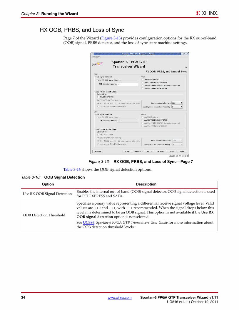
RX OOB, PRBS, and Loss of SyncPage 7 of the Wizard (Figure 3-13) provides configuration options for the RX out-of-band (OOB) signal, PRBS detector, and the loss of sync state machine settings.
Table 3-16 shows the OOB signal detection options.
X-Ref Target - Figure 3-13
Figure 3-13: RX OOB, PRBS, and Loss of Sync—Page 7
UG546_c3_11_013111
Table 3-16: OOB Signal Detection
Option Description
Use RX OOB Signal DetectionEnables the internal out-of-band (OOB) signal detector. OOB signal detection is used for PCI EXPRESS and SATA.
OOB Detection Threshold
Specifies a binary value representing a differential receive signal voltage level. Valid values are 110 and 111, with 111 recommended. When the signal drops below this level it is determined to be an OOB signal. This option is not available if the Use RX OOB signal detection option is not selected.
See UG386, Spartan-6 FPGA GTP Transceivers User Guide for more information about the OOB detection threshold levels.
34 www.xilinx.com Spartan-6 FPGA GTP Transceiver Wizard v1.11UG546 (v1.11) October 19, 2011
Configuring and Generating the Wrapper
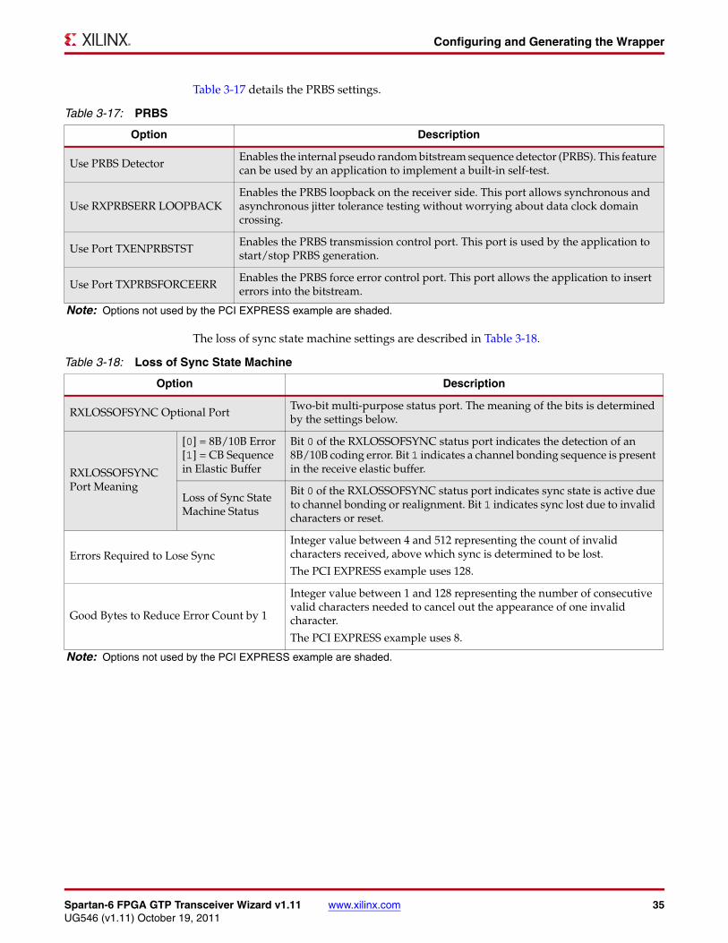
Table 3-17 details the PRBS settings.
The loss of sync state machine settings are described in Table 3-18.
Table 3-17: PRBS
Option Description
Use PRBS DetectorEnables the internal pseudo random bitstream sequence detector (PRBS). This feature can be used by an application to implement a built-in self-test.
Use RXPRBSERR LOOPBACKEnables the PRBS loopback on the receiver side. This port allows synchronous and asynchronous jitter tolerance testing without worrying about data clock domain crossing.
Use Port TXENPRBSTSTEnables the PRBS transmission control port. This port is used by the application to start/stop PRBS generation.
Use Port TXPRBSFORCEERREnables the PRBS force error control port. This port allows the application to insert errors into the bitstream.
Note: Options not used by the PCI EXPRESS example are shaded.
Table 3-18: Loss of Sync State Machine
Option Description
RXLOSSOFSYNC Optional Port Two-bit multi-purpose status port. The meaning of the bits is determined by the settings below.
RXLOSSOFSYNC Port Meaning
[0] = 8B/10B Error [1] = CB Sequence in Elastic Buffer
Bit 0 of the RXLOSSOFSYNC status port indicates the detection of an 8B/10B coding error. Bit 1 indicates a channel bonding sequence is present in the receive elastic buffer.
Loss of Sync State Machine Status
Bit 0 of the RXLOSSOFSYNC status port indicates sync state is active due to channel bonding or realignment. Bit 1 indicates sync lost due to invalid characters or reset.
Errors Required to Lose SyncInteger value between 4 and 512 representing the count of invalid characters received, above which sync is determined to be lost.
The PCI EXPRESS example uses 128.
Good Bytes to Reduce Error Count by 1
Integer value between 1 and 128 representing the number of consecutive valid characters needed to cancel out the appearance of one invalid character.
The PCI EXPRESS example uses 8.
Note: Options not used by the PCI EXPRESS example are shaded.
Spartan-6 FPGA GTP Transceiver Wizard v1.11 www.xilinx.com 35UG546 (v1.11) October 19, 2011
Chapter 3: Running the Wizard
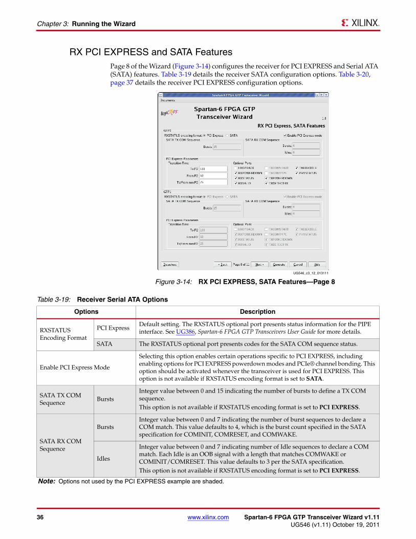
RX PCI EXPRESS and SATA FeaturesPage 8 of the Wizard (Figure 3-14) configures the receiver for PCI EXPRESS and Serial ATA (SATA) features. Table 3-19 details the receiver SATA configuration options. Table 3-20, page 37 details the receiver PCI EXPRESS configuration options.X-Ref Target - Figure 3-14
Figure 3-14: RX PCI EXPRESS, SATA Features—Page 8UG546_c3_12_013111
Table 3-19: Receiver Serial ATA Options
Options Description
RXSTATUS Encoding Format
PCI ExpressDefault setting. The RXSTATUS optional port presents status information for the PIPE interface. See UG386, Spartan-6 FPGA GTP Transceivers User Guide for more details.
SATA The RXSTATUS optional port presents codes for the SATA COM sequence status.
Enable PCI Express Mode
Selecting this option enables certain operations specific to PCI EXPRESS, including enabling options for PCI EXPRESS powerdown modes and PCIe® channel bonding. This option should be activated whenever the transceiver is used for PCI EXPRESS. This option is not available if RXSTATUS encoding format is set to SATA.
SATA TX COM Sequence
BurstsInteger value between 0 and 15 indicating the number of bursts to define a TX COM sequence.This option is not available if RXSTATUS encoding format is set to PCI EXPRESS.
SATA RX COM Sequence
BurstsInteger value between 0 and 7 indicating the number of burst sequences to declare a COM match. This value defaults to 4, which is the burst count specified in the SATA specification for COMINIT, COMRESET, and COMWAKE.
Idles
Integer value between 0 and 7 indicating number of Idle sequences to declare a COM match. Each Idle is an OOB signal with a length that matches COMWAKE or COMINIT/COMRESET. This value defaults to 3 per the SATA specification.This option is not available if RXSTATUS encoding format is set to PCI EXPRESS.
Note: Options not used by the PCI EXPRESS example are shaded.
36 www.xilinx.com Spartan-6 FPGA GTP Transceiver Wizard v1.11UG546 (v1.11) October 19, 2011
Configuring and Generating the Wrapper
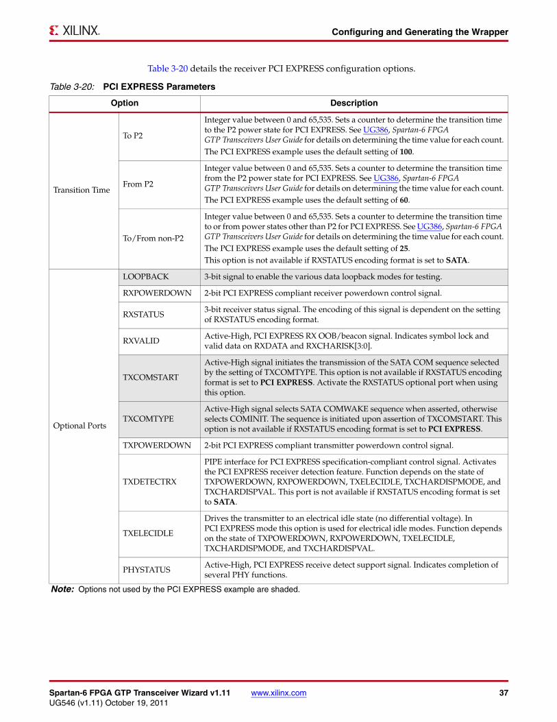
Table 3-20 details the receiver PCI EXPRESS configuration options.
Table 3-20: PCI EXPRESS Parameters
Option Description
Transition Time
To P2
Integer value between 0 and 65,535. Sets a counter to determine the transition time to the P2 power state for PCI EXPRESS. See UG386, Spartan-6 FPGA GTP Transceivers User Guide for details on determining the time value for each count.The PCI EXPRESS example uses the default setting of 100.
From P2
Integer value between 0 and 65,535. Sets a counter to determine the transition time from the P2 power state for PCI EXPRESS. See UG386, Spartan-6 FPGA GTP Transceivers User Guide for details on determining the time value for each count.The PCI EXPRESS example uses the default setting of 60.
To/From non-P2
Integer value between 0 and 65,535. Sets a counter to determine the transition time to or from power states other than P2 for PCI EXPRESS. See UG386, Spartan-6 FPGA GTP Transceivers User Guide for details on determining the time value for each count.The PCI EXPRESS example uses the default setting of 25.This option is not available if RXSTATUS encoding format is set to SATA.
Optional Ports
LOOPBACK 3-bit signal to enable the various data loopback modes for testing.
RXPOWERDOWN 2-bit PCI EXPRESS compliant receiver powerdown control signal.
RXSTATUS3-bit receiver status signal. The encoding of this signal is dependent on the setting of RXSTATUS encoding format.
RXVALIDActive-High, PCI EXPRESS RX OOB/beacon signal. Indicates symbol lock and valid data on RXDATA and RXCHARISK[3:0].
TXCOMSTART
Active-High signal initiates the transmission of the SATA COM sequence selected by the setting of TXCOMTYPE. This option is not available if RXSTATUS encoding format is set to PCI EXPRESS. Activate the RXSTATUS optional port when using this option.
TXCOMTYPEActive-High signal selects SATA COMWAKE sequence when asserted, otherwise selects COMINIT. The sequence is initiated upon assertion of TXCOMSTART. This option is not available if RXSTATUS encoding format is set to PCI EXPRESS.
TXPOWERDOWN 2-bit PCI EXPRESS compliant transmitter powerdown control signal.
TXDETECTRX
PIPE interface for PCI EXPRESS specification-compliant control signal. Activates the PCI EXPRESS receiver detection feature. Function depends on the state of TXPOWERDOWN, RXPOWERDOWN, TXELECIDLE, TXCHARDISPMODE, and TXCHARDISPVAL. This port is not available if RXSTATUS encoding format is set to SATA.
TXELECIDLE
Drives the transmitter to an electrical idle state (no differential voltage). In PCI EXPRESS mode this option is used for electrical idle modes. Function depends on the state of TXPOWERDOWN, RXPOWERDOWN, TXELECIDLE, TXCHARDISPMODE, and TXCHARDISPVAL.
PHYSTATUSActive-High, PCI EXPRESS receive detect support signal. Indicates completion of several PHY functions.
Note: Options not used by the PCI EXPRESS example are shaded.
Spartan-6 FPGA GTP Transceiver Wizard v1.11 www.xilinx.com 37UG546 (v1.11) October 19, 2011
Chapter 3: Running the Wizard
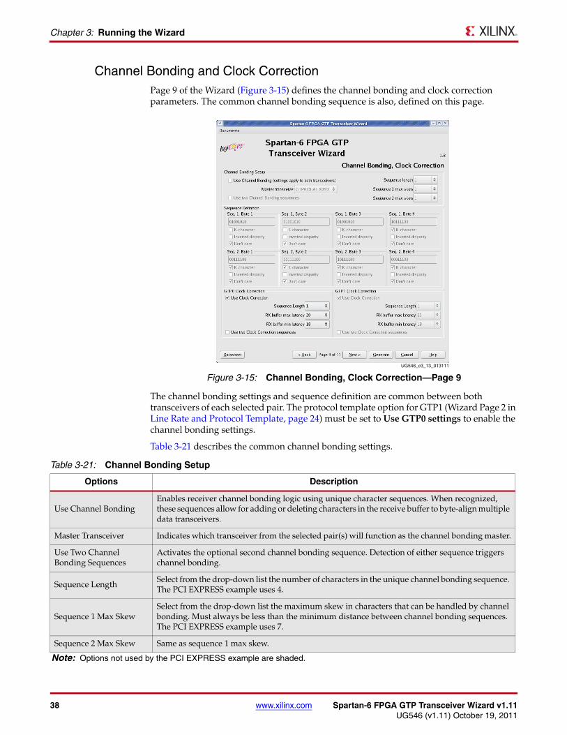
Channel Bonding and Clock CorrectionPage 9 of the Wizard (Figure 3-15) defines the channel bonding and clock correction parameters. The common channel bonding sequence is also, defined on this page.
The channel bonding settings and sequence definition are common between both transceivers of each selected pair. The protocol template option for GTP1 (Wizard Page 2 in Line Rate and Protocol Template, page 24) must be set to Use GTP0 settings to enable the channel bonding settings.
Table 3-21 describes the common channel bonding settings.
X-Ref Target - Figure 3-15
Figure 3-15: Channel Bonding, Clock Correction—Page 9UG546_c3_13_013111
Table 3-21: Channel Bonding Setup
Options Description
Use Channel BondingEnables receiver channel bonding logic using unique character sequences. When recognized, these sequences allow for adding or deleting characters in the receive buffer to byte-align multiple data transceivers.
Master Transceiver Indicates which transceiver from the selected pair(s) will function as the channel bonding master.
Use Two Channel Bonding Sequences
Activates the optional second channel bonding sequence. Detection of either sequence triggers channel bonding.
Sequence LengthSelect from the drop-down list the number of characters in the unique channel bonding sequence. The PCI EXPRESS example uses 4.
Sequence 1 Max SkewSelect from the drop-down list the maximum skew in characters that can be handled by channel bonding. Must always be less than the minimum distance between channel bonding sequences. The PCI EXPRESS example uses 7.
Sequence 2 Max Skew Same as sequence 1 max skew.
Note: Options not used by the PCI EXPRESS example are shaded.
38 www.xilinx.com Spartan-6 FPGA GTP Transceiver Wizard v1.11UG546 (v1.11) October 19, 2011
Configuring and Generating the Wrapper
Table 3-22 describes the channel bonding sequence definition.
Table 3-23, page 39 describes the clock correction settings.
Table 3-22: Sequence Definition
Option Description
Byte (Symbol)
Set each symbol to match the pattern the protocol requires. The PCI EXPRESS sequence length is 8 bits. 01001010 is used for the first three symbols of sequence 1. Symbol 4, sequence 1 and symbol 3, sequence 2 are set to 10111100. Symbols 1 and 2 of sequence 2 are set to 00111100. Symbol 4 of sequence 2 is set to 00011100.
K CharacterThis option is available when 8B/10B decoding is selected. When checked, the symbol is an 8B/10B K character.
Inverted DisparitySome protocols with 8B/10B decoding use symbols with deliberately inverted disparity. This option should be checked when such symbols are expected in the sequence.
Don’t CareMultiple-byte sequences can have wild card symbols by checking this option. Unused bytes in the sequence automatically have this option set.
Note: Options not used by the PCI EXPRESS example are shaded.
Table 3-23: Clock Correction
Option Description
Use Clock CorrectionEnables receiver clock correction logic using unique character sequences. When recognized, these sequences allow for adding or deleting characters in the receive buffer to prevent buffer underflow/overflow due to small differences in the transmit/receive clock frequencies.
Sequence LengthSelect from the drop-down list the number of characters (subsequences) in the unique clock correction sequence.
The PCI EXPRESS example uses 1.
Rx Buffer Max Latency
Select from the drop-down list the maximum number of characters to permit in the receive buffer before clock correction attempts to delete incoming clock correction sequences. Also determines the maximum latency of the receive buffer in RXUSRCLK cycles.
The PCI EXPRESS example uses 20.
Rx Buffer Min Latency
Select from the drop-down list the minimum number of characters to permit in the receive buffer before clock correction attempts to add extra clock correction sequences to the receive buffer. Also determines the minimum latency of the receive buffer in RXUSRCLK cycles.
The PCI EXPRESS example uses 28.
Use Two Clock Correction Sequences
Activates the optional second clock correction sequence. Detection of either sequence triggers clock correction.
Note: Options not used by the PCI EXPRESS example are shaded.
Spartan-6 FPGA GTP Transceiver Wizard v1.11 www.xilinx.com 39UG546 (v1.11) October 19, 2011
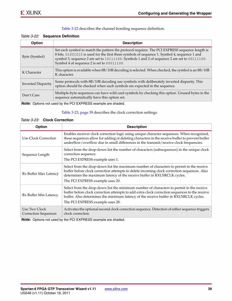
Chapter 3: Running the Wizard
Clock Correction SequencePage 10 of the Wizard (Figure 3-16) defines the clock correction sequence. See Table 3-24 for details.X-Ref Target - Figure 3-16
Figure 3-16: Clock Correction Sequence—Page 10UG546_c3_14_013111
Table 3-24: Clock Correction Sequence
Option Description
Byte (Symbol)Set each symbol to match the pattern the protocol requires. The PCI EXPRESS sequence length is 8 bits. 00011100 is used for the first symbol of sequence 1. The remaining symbols are disabled because the sequence length is set to 1.
K CharacterThis option is available when 8B/10B decoding is selected. When checked, the symbol is an 8B/10B K character.
Inverted DisparitySome protocols with 8B/10B decoding use symbols with deliberately inverted disparity. This option should be checked when such symbols are expected in the sequence.
Don’t CareMultiple-byte sequences can have wild card symbols by checking this option. Unused bytes in the sequence automatically have this option set.
Note: Options not used by the PCI EXPRESS example are shaded.
40 www.xilinx.com Spartan-6 FPGA GTP Transceiver Wizard v1.11UG546 (v1.11) October 19, 2011
Configuring and Generating the Wrapper
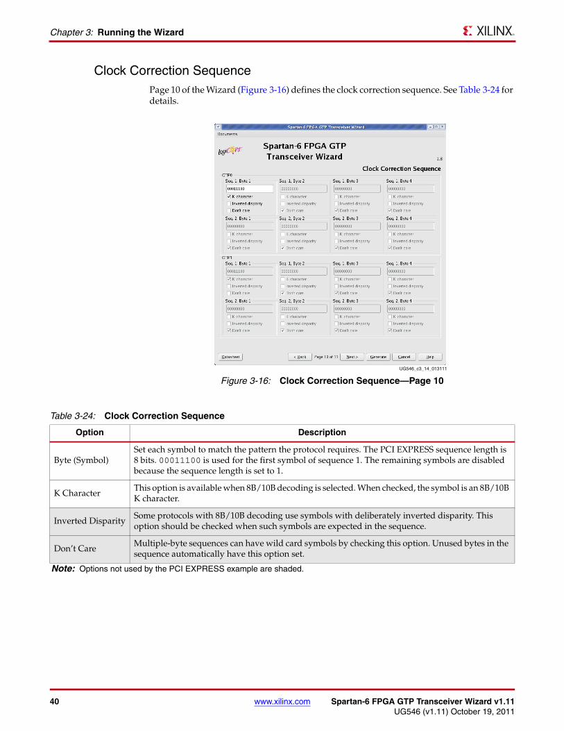
SummaryPage 11 of the Wizard (Figure 3-17) provides a summary of the selected configuration parameters. After reviewing the settings, click Generate to exit and generate the wrapper.X-Ref Target - Figure 3-17
Figure 3-17: Summary—Page 11
UG546_c3_15_013111
Spartan-6 FPGA GTP Transceiver Wizard v1.11 www.xilinx.com 41UG546 (v1.11) October 19, 2011

Chapter 3: Running the Wizard
42 www.xilinx.com Spartan-6 FPGA GTP Transceiver Wizard v1.11UG546 (v1.11) October 19, 2011
Chapter 4
Quick Start Example Design
OverviewThis chapter introduces the example design that is included with the Spartan®-6 FPGA GTP transceiver wrappers for the Spartan-6 LXT family. The example design demonstrates how to use the wrappers and demonstrates some of the key features of the GTP transceiver. For detailed information about the example design, see Chapter 5, Detailed Example Design.
Functional Simulation of the Example DesignThe Spartan-6 FPGA GTP Transceiver Wizard (hereinafter called the Wizard) provides a quick way to simulate and observe the behavior of the wrapper using the provided example design and script files.
Using ModelSimPrior to simulating the wrapper with ModelSim, the functional (gate-level) simulation models must be generated. All source files in the following directories must be compiled to a single library as shown in Table 4-1. See the Synthesis and Simulation Design Guide for ISE® 13.3 available in the ISE software documentation for instructions on how to compile ISE simulation libraries.
The Wizard provides a command line script for use within ModelSim. To run a VHDL or Verilog ModelSim simulation of the wrapper, use the following instructions:
1. Launch the Modelsim simulator and set the current directory to
<project_directory>/<component_name>/simulation/functional
2. Set the MTI_LIBS variable:
modelsim> setenv MTI_LIBS <path to compiled libraries>
3. Launch the simulation script:
modelsim> do simulate_mti.do
Table 4-1: Required ModelSim Simulation Libraries
HDL Library Source Directories
Verilog UNISIMS_VER <Xilinx dir>/verilog/src/unisims<Xilinx dir>/secureip/mti
VHDL UNISIM <Xilinx dir>/vhdl/src/unisims/primitive<Xilinx dir>/secureip/mti
Spartan-6 FPGA GTP Transceiver Wizard v1.11 www.xilinx.com 43UG546 (v1.11) October 19, 2011
Chapter 4: Quick Start Example Design
The ModelSim script compiles the example design and testbench, and adds the relevant signals to the wave window.
Using the ISE SimulatorWhen using the ISE Simulator (ISim), the required simulation device libraries are precompiled, and are updated automatically when service packs and IP updates are installed. There is no need to run CompXlib to compile libraries, or to manually download updated libraries.
The Wizard also generates a perl script for use with ISim. To run a VHDL or Verilog simulation of the wrapper, use the following instructions:
1. Set the current directory to
<project_directory>/<component_name>/simulation/functional
2. Launch the simulation script:
• For Windows
simulate_isim.bat
• For Linux
% simulate_isim.sh
The ISim script compiles the example design and testbench, and adds the relevant signals to the wave window.
Implementing the Example DesignWhen all of the parameters are set as desired, click Generate to create a directory structure under the provided Component Name. Wrapper generation proceeds and the generated output populates the appropriate subdirectories.
The directory structure for the PCI EXPRESS® example is provided in Chapter 5, Detailed Example Design.
After wrapper generation is complete, the results can be tested in hardware. The provided example design incorporates the wrapper and additional blocks, allowing the wrapper to be driven and monitored in hardware. The generated output also includes several scripts to assist in running the Xilinx software.
From the command prompt, navigate to the project directory and type the following:
For Windows
> cd pcie_wrapper\implement> implement.bat
For Linux
% cd pcie_wrapper/implement% implement.sh
Table 4-2: Required ISim Simulation Libraries
HDL Library Source Directories
Verilog UNISIMS_VER <Xilinx dir>/verilog/hdp/<OS>/unisims_ver
VHDL UNISIM <Xilinx dir>/vhdl/hdp/<OS>/unisim
Note: OS refers to the following operating systems: lin, lin64, nt, nt64.
44 www.xilinx.com Spartan-6 FPGA GTP Transceiver Wizard v1.11UG546 (v1.11) October 19, 2011
Netlist Simulation of the Example Design
These commands execute a script that synthesizes, builds, maps, places, and routes the example design and produces a bitmap file. The resulting files are placed in the implement/results directory.
Netlist Simulation of the Example DesignThe Spartan-6 FPGA GTP Transceiver Wizard provides a script to perform simulations on the routed netlist of the example design.
Note: Timing checks are not enabled.
Using ModelSimPrior to performing netlist simulation with ModelSim, the generated design should successfully pass through implementation. All source files in the following directories must be compiled to a single library, as shown in Table 4-3. See the Synthesis and Simulation Design Guide for ISE® 13.3 available in the ISE software documentation, for instructions on how to compile ISE simulation libraries.
The Wizard provides a command line script for use within ModelSim. To run a VHDL or Verilog ModelSim simulation of the wrapper, use the following instructions:
1. Launch the Modelsim simulator and set the current directory to:
<project_directory>/<component_name>/simulation/netlist
2. Set the MTI_LIBS variable:
modelsim> setenv MTI_LIBS <path to compiled libraries>
2. Launch the simulation script:
modelsim> do simulate_mti.do
The ModelSim script compiles and simulates the routed netlist of the example design and testbench.
Using ChipScope Pro Cores with the WizardThe ChipScope™ Pro Integrated Controller (ICON) and Virtual Input/Output (VIO) cores aid in debugging and validating the design in board. To assist with debugging, these ChipScope cores are provided with the Spartan-6 FPGA GTP Transceiver Wizard wrapper, which is enabled by setting USE_CHIPSCOPE as 1 in the <component_name>_top_example_design file.
Table 4-3: Required ModelSim Netlist Simulation Libraries
HDL Library Source Directories
Verilog SIMPRIMS_VER <Xilinx dir>/verilog/src/simprims
<Xilinx dir>/secureip/mti
VHDL SIMPRIM <Xilinx dir>/vhdl/src/simprims/primitive
<Xilinx dir>/secureip/mti
Spartan-6 FPGA GTP Transceiver Wizard v1.11 www.xilinx.com 45UG546 (v1.11) October 19, 2011

Chapter 4: Quick Start Example Design
46 www.xilinx.com Spartan-6 FPGA GTP Transceiver Wizard v1.11UG546 (v1.11) October 19, 2011
Chapter 5
Detailed Example Design
This chapter provides detailed information about the example design, including a description of files and the directory structure generated by the CORE Generator™ tool, the purpose and contents of the provided scripts, the contents of the example HDL wrappers, and the operation of the demonstration testbench.
Directory and File Structure<project directory>topdirectory
Top-level project directory; name is user-defined
<project directory>/<component name>opdirectory
Wizard release notes file
<component name>/docProduct documentation
<component name>/example design Verilog and VHDL design files
<component name>/implementImplementation script files
implement/resultsResults directory, created after implementation scripts are run, and contains implement script results
<component name>/simulationSimulation scripts
simulation/functionalFunctional simulation files
simulation/netlistNetlist simulation files
Spartan-6 FPGA GTP Transceiver Wizard v1.11 www.xilinx.com 47UG546 (v1.11) October 19, 2011
Chapter 5: Detailed Example Design
Directory and File ContentsThe Spartan®-6 FPGA GTP Transceiver Wizard directories and their associated files are defined in the following sections.
<project directory> The <project directory> contains all the CORE Generator tool’s project files.
<project directory>/<component name>The <component name> directory contains the README file provided with the Wizard, which might include last-minute changes and updates.
Table 5-1: Project Directory
Name Description
<component_name>.v[hd] Main GTP transceiver wrapper. Instantiates individual GTP transceiver wrappers. For use in the target design.
<component_name>.[veo | vho] GTP transceiver wrapper files instantiation templates. Includes templates for the GTP transceiver wrapper module, the IBUFDS, and essential GTP transceiver support modules (such as TX_SYNC).
<component_name>.xco Log file from the CORE Generator tool describing which options were used to generate the GTP transceiver wrapper. An XCO file is generated by the CORE Generator tool for each wizard wrapper that it creates in the current project directory. An XCO file can also be used as an input to the CORE Generator tool.
<component_name>_tile.v[hd] Individual GTPA1_DUAL transceiver wrapper to be instantiated in the main GTP transceiver wrapper. Instantiates the selected GTPA1_DUAL transceivers with settings for the selected protocol.
Back to Top
Table 5-2: GTP Wrapper Component Name
Name Description
<project_dir>/<component_name>
s6_gtpwizard_readme.txt README file for the Wizard.
<component_name>.pf Protocol description for the selected protocol from the Wizard.
Back to Top
48 www.xilinx.com Spartan-6 FPGA GTP Transceiver Wizard v1.11UG546 (v1.11) October 19, 2011
Directory and File Contents
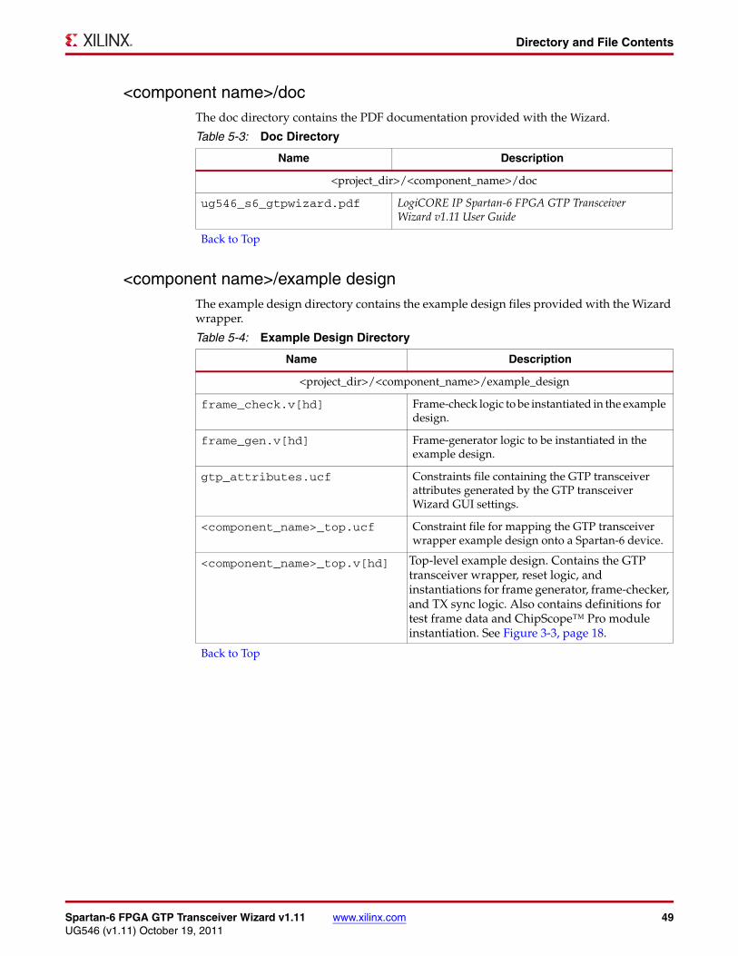
<component name>/docThe doc directory contains the PDF documentation provided with the Wizard.
<component name>/example designThe example design directory contains the example design files provided with the Wizard wrapper.
Table 5-3: Doc Directory
Name Description
<project_dir>/<component_name>/doc
ug546_s6_gtpwizard.pdf LogiCORE IP Spartan-6 FPGA GTP Transceiver Wizard v1.11 User Guide
Back to Top
Table 5-4: Example Design Directory
Name Description
<project_dir>/<component_name>/example_design
frame_check.v[hd] Frame-check logic to be instantiated in the example design.
frame_gen.v[hd] Frame-generator logic to be instantiated in the example design.
gtp_attributes.ucf Constraints file containing the GTP transceiver attributes generated by the GTP transceiver Wizard GUI settings.
<component_name>_top.ucf Constraint file for mapping the GTP transceiver wrapper example design onto a Spartan-6 device.
<component_name>_top.v[hd] Top-level example design. Contains the GTP transceiver wrapper, reset logic, and instantiations for frame generator, frame-checker, and TX sync logic. Also contains definitions for test frame data and ChipScope™ Pro module instantiation. See Figure 3-3, page 18.
Back to Top
Spartan-6 FPGA GTP Transceiver Wizard v1.11 www.xilinx.com 49UG546 (v1.11) October 19, 2011
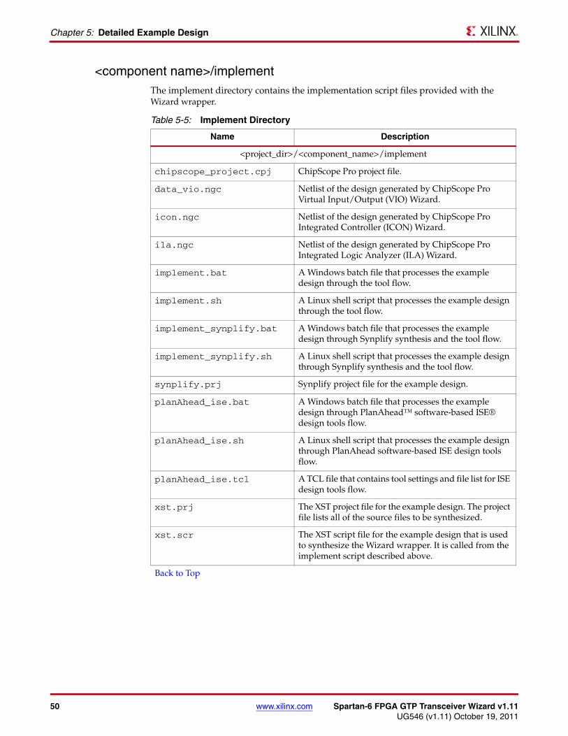
Chapter 5: Detailed Example Design
<component name>/implementThe implement directory contains the implementation script files provided with the Wizard wrapper.
Table 5-5: Implement Directory
Name Description
<project_dir>/<component_name>/implement
chipscope_project.cpj ChipScope Pro project file.
data_vio.ngc Netlist of the design generated by ChipScope Pro Virtual Input/Output (VIO) Wizard.
icon.ngc Netlist of the design generated by ChipScope Pro Integrated Controller (ICON) Wizard.
ila.ngc Netlist of the design generated by ChipScope Pro Integrated Logic Analyzer (ILA) Wizard.
implement.bat A Windows batch file that processes the example design through the tool flow.
implement.sh A Linux shell script that processes the example design through the tool flow.
implement_synplify.bat A Windows batch file that processes the example design through Synplify synthesis and the tool flow.
implement_synplify.sh A Linux shell script that processes the example design through Synplify synthesis and the tool flow.
synplify.prj Synplify project file for the example design.
planAhead_ise.bat A Windows batch file that processes the example design through PlanAhead™ software-based ISE® design tools flow.
planAhead_ise.sh A Linux shell script that processes the example design through PlanAhead software-based ISE design tools flow.
planAhead_ise.tcl A TCL file that contains tool settings and file list for ISE design tools flow.
xst.prj The XST project file for the example design. The project file lists all of the source files to be synthesized.
xst.scr The XST script file for the example design that is used to synthesize the Wizard wrapper. It is called from the implement script described above.
Back to Top
50 www.xilinx.com Spartan-6 FPGA GTP Transceiver Wizard v1.11UG546 (v1.11) October 19, 2011
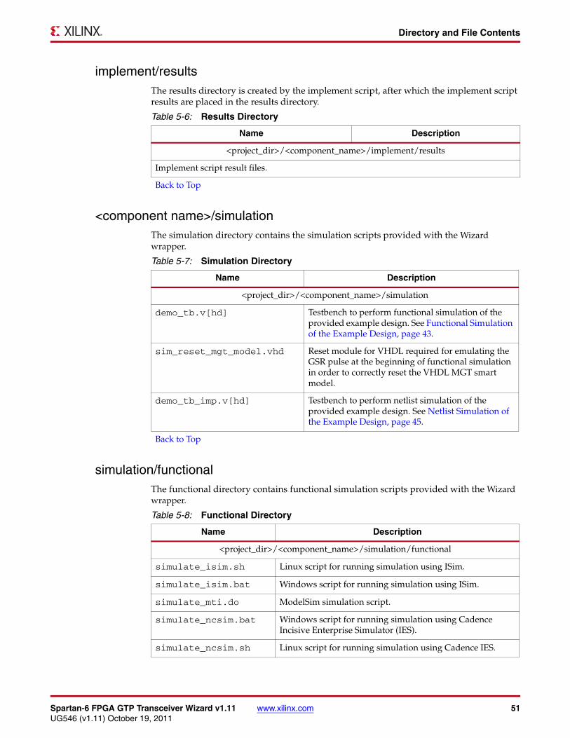
Directory and File Contents
implement/resultsThe results directory is created by the implement script, after which the implement script results are placed in the results directory.
<component name>/simulationThe simulation directory contains the simulation scripts provided with the Wizard wrapper.
simulation/functionalThe functional directory contains functional simulation scripts provided with the Wizard wrapper.
Table 5-6: Results Directory
Name Description
<project_dir>/<component_name>/implement/results
Implement script result files.
Back to Top
Table 5-7: Simulation Directory
Name Description
<project_dir>/<component_name>/simulation
demo_tb.v[hd] Testbench to perform functional simulation of the provided example design. See Functional Simulation of the Example Design, page 43.
sim_reset_mgt_model.vhd Reset module for VHDL required for emulating the GSR pulse at the beginning of functional simulation in order to correctly reset the VHDL MGT smart model.
demo_tb_imp.v[hd] Testbench to perform netlist simulation of the provided example design. See Netlist Simulation of the Example Design, page 45.
Back to Top
Table 5-8: Functional Directory
Name Description
<project_dir>/<component_name>/simulation/functional
simulate_isim.sh Linux script for running simulation using ISim.
simulate_isim.bat Windows script for running simulation using ISim.
simulate_mti.do ModelSim simulation script.
simulate_ncsim.bat Windows script for running simulation using Cadence Incisive Enterprise Simulator (IES).
simulate_ncsim.sh Linux script for running simulation using Cadence IES.
Spartan-6 FPGA GTP Transceiver Wizard v1.11 www.xilinx.com 51UG546 (v1.11) October 19, 2011
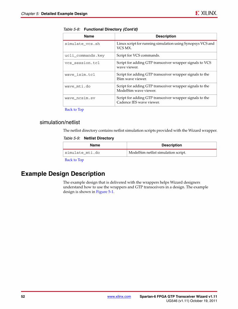
Chapter 5: Detailed Example Design
simulation/netlistThe netlist directory contains netlist simulation scripts provided with the Wizard wrapper.
Example Design DescriptionThe example design that is delivered with the wrappers helps Wizard designers understand how to use the wrappers and GTP transceivers in a design. The example design is shown in Figure 5-1.
simulate_vcs.sh Linux script for running simulation using Synopsys VCS and VCS MX.
ucli_commands.key Script for VCS commands.
vcs_session.tcl Script for adding GTP transceiver wrapper signals to VCS wave viewer.
wave_isim.tcl Script for adding GTP transceiver wrapper signals to the ISim wave viewer.
wave_mti.do Script for adding GTP transceiver wrapper signals to the ModelSim wave viewer.
wave_ncsim.sv Script for adding GTP transceiver wrapper signals to the Cadence IES wave viewer.
Back to Top
Table 5-8: Functional Directory (Cont’d)
Name Description
Table 5-9: Netlist Directory
Name Description
simulate_mti.do ModelSim netlist simulation script.
Back to Top
52 www.xilinx.com Spartan-6 FPGA GTP Transceiver Wizard v1.11UG546 (v1.11) October 19, 2011
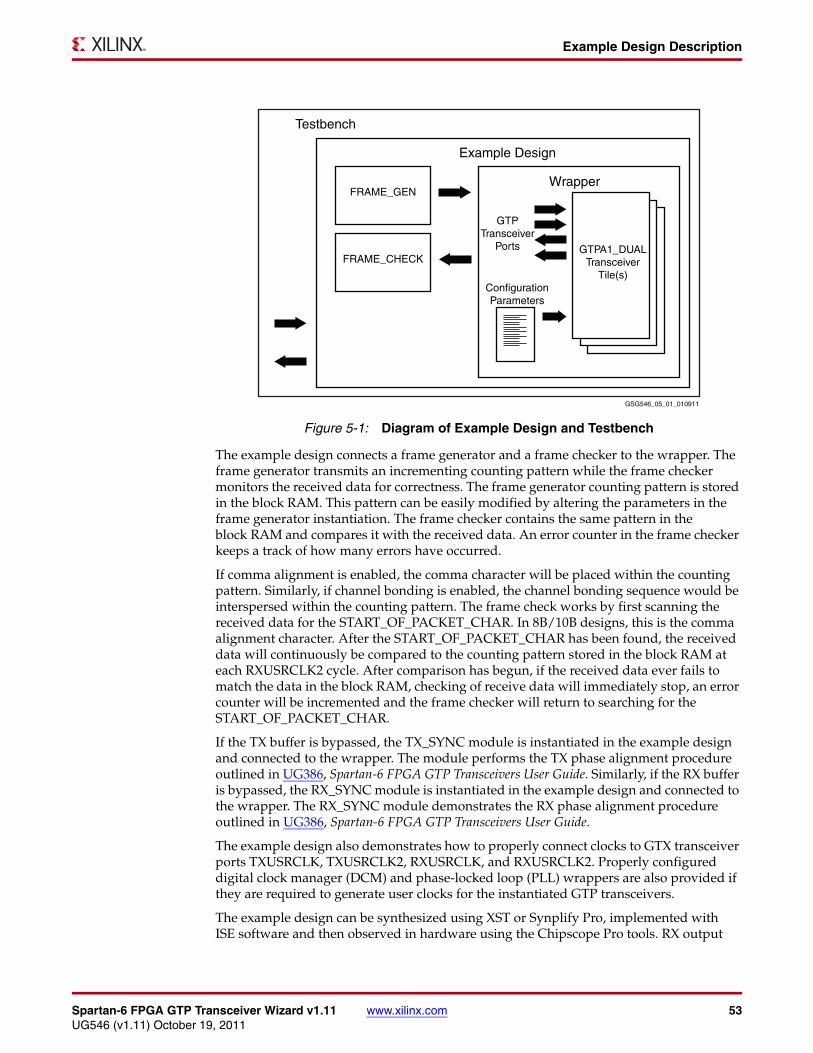
Example Design Description
The example design connects a frame generator and a frame checker to the wrapper. The frame generator transmits an incrementing counting pattern while the frame checker monitors the received data for correctness. The frame generator counting pattern is stored in the block RAM. This pattern can be easily modified by altering the parameters in the frame generator instantiation. The frame checker contains the same pattern in the block RAM and compares it with the received data. An error counter in the frame checker keeps a track of how many errors have occurred.
If comma alignment is enabled, the comma character will be placed within the counting pattern. Similarly, if channel bonding is enabled, the channel bonding sequence would be interspersed within the counting pattern. The frame check works by first scanning the received data for the START_OF_PACKET_CHAR. In 8B/10B designs, this is the comma alignment character. After the START_OF_PACKET_CHAR has been found, the received data will continuously be compared to the counting pattern stored in the block RAM at each RXUSRCLK2 cycle. After comparison has begun, if the received data ever fails to match the data in the block RAM, checking of receive data will immediately stop, an error counter will be incremented and the frame checker will return to searching for the START_OF_PACKET_CHAR.
If the TX buffer is bypassed, the TX_SYNC module is instantiated in the example design and connected to the wrapper. The module performs the TX phase alignment procedure outlined in UG386, Spartan-6 FPGA GTP Transceivers User Guide. Similarly, if the RX buffer is bypassed, the RX_SYNC module is instantiated in the example design and connected to the wrapper. The RX_SYNC module demonstrates the RX phase alignment procedure outlined in UG386, Spartan-6 FPGA GTP Transceivers User Guide.
The example design also demonstrates how to properly connect clocks to GTX transceiver ports TXUSRCLK, TXUSRCLK2, RXUSRCLK, and RXUSRCLK2. Properly configured digital clock manager (DCM) and phase-locked loop (PLL) wrappers are also provided if they are required to generate user clocks for the instantiated GTP transceivers.
The example design can be synthesized using XST or Synplify Pro, implemented with ISE software and then observed in hardware using the Chipscope Pro tools. RX output
X-Ref Target - Figure 5-1
Figure 5-1: Diagram of Example Design and Testbench
Example Design
Testbench
GSG546_05_01_010911
Wrapper
GTPTransceiver
Ports
ConfigurationParameters
FRAME_GEN
FRAME_CHECKGTPA1_DUAL
TransceiverTile(s)
Spartan-6 FPGA GTP Transceiver Wizard v1.11 www.xilinx.com 53UG546 (v1.11) October 19, 2011
Chapter 5: Detailed Example Design
ports such as RXDATA can be observed on the ChipScope Pro ILA core while input ports can be controlled from the ChipScope Pro VIO core. A ChipScope Pro project file is also included with each example design.
For the example design to work properly in simulation or in hardware, both the transmit and receive side need to be configured with the same line rate, encoding, and datapath width in the GUI.
Example Design HierarchyThe hierarchy for the design used in this example is:
example_tb|___example_mgt_top
|___mgt_userclk_source_pll|___ibufds|___frame_gen|___frame_check|___pcie_wrapper
|___pcie_wrapper_tile |___gtpa1_dual
54 www.xilinx.com Spartan-6 FPGA GTP Transceiver Wizard v1.11UG546 (v1.11) October 19, 2011