Embed Size (px)
Citation preview

Vivado Design Suite Tutorial: Embedded Processor Hardware Design
UG940 (v 2013.1) March 20, 2013
Embedded Processor Hardware Design www.xilinx.com 2 UG940 (v 2013.1) March 20, 2013
Notice of Disclaimer The information disclosed to you hereunder (the "Materials") is provided solely for the selection and use of Xilinx products. To the maximum extent permitted by applicable law: (1) Materials are made available "AS IS" and with all faults, Xilinx hereby DISCLAIMS ALL WARRANTIES AND CONDITIONS, EXPRESS, IMPLIED, OR STATUTORY, INCLUDING BUT NOT LIMITED TO WARRANTIES OF MERCHANTABILITY, NON-INFRINGEMENT, OR FITNESS FOR ANY PARTICULAR PURPOSE; and (2) Xilinx shall not be liable (whether in contract or tort, including negligence, or under any other theory of liability) for any loss or damage of any kind or nature related to, arising under, or in connection with, the Materials (including your use of the Materials), including for any direct, indirect, special, incidental, or consequential loss or damage (including loss of data, profits, goodwill, or any type of loss or damage suffered as a result of any action brought by a third party) even if such damage or loss was reasonably foreseeable or Xilinx had been advised of the possibility of the same. Xilinx assumes no obligation to correct any errors contained in the Materials or to notify you of updates to the Materials or to product specifications. You may not reproduce, modify, distribute, or publicly display the Materials without prior written consent. Certain products are subject to the terms and conditions of the Limited Warranties which can be viewed at http://www.xilinx.com/warranty.htm; IP cores may be subject to warranty and support terms contained in a license issued to you by Xilinx. Xilinx products are not designed or intended to be fail-safe or for use in any application requiring fail-safe performance; you assume sole risk and liability for use of Xilinx products in Critical Applications: http://www.xilinx.com/warranty.htm#critapps.
©Copyright 2013 Xilinx, Inc. Xilinx, the Xilinx logo, Artix, ISE, Kintex, Spartan, Virtex, Zynq, Vivado and other designated brands included herein are trademarks of Xilinx in the United States and other countries. All other trademarks are the property of their respective owners.
Revision History The following table shows the revision history for this document.
Date Version Changes
03/20/13 2013.1 New release for Vivado Design Suite version 2013.1.
Embedded Processor Hardware Design www.xilinx.com 3 UG940 (v 2013.1) March 20, 2013
Table of Contents Embedded Processor Hardware Design .................................................................................................................................. 1
Revision History .................................................................................................................................................. 2
Programming and Debugging Embedded Processors Using Vivado Design Suite ...................... 5
Introduction ......................................................................................................................................................... 5
Software Requirements ................................................................................................................................... 5
Hardware Requirements .................................................................................................................................. 5
Tutorial Design Description ........................................................................................................................... 6
Lab 1: Programming a Zynq-7000 Processor ....................................................................................... 6
Lab 2: SDK and Logic Analyzer .................................................................................................................. 6
Lab 3: Programming a Microblaze Processor ...................................................................................... 7
Locating Tutorial Design Files ....................................................................................................................... 7
Lab 1: Building a Zynq-7000 Processor Design in the Vivado IDE ....................................................... 8
Step 1: Invoke Vivado IDE and Create a Project ..................................................................................... 8
Step 2: Create an IP Integrator Design .................................................................................................... 10
Add IP ................................................................................................................................................................ 11
Customize Instantiated IP .......................................................................................................................... 13
Use the Block Designer Assistance ........................................................................................................ 15
Step 3: Using MARK_DEBUG ........................................................................................................................ 19
Step 4: Generate HDL Design Files ............................................................................................................ 22
Step 5: Assign Signals to Debug ................................................................................................................ 23
Step 6: Assign Debug Net to an ILA Core............................................................................................... 25
Step 7: Implement Design and Generate Bitstream ........................................................................... 28
Step 8: Export Hardware to SDK................................................................................................................. 30
Export to SDK ................................................................................................................................................. 30
Conclusion .......................................................................................................................................................... 31
Lab 2: Using SDK and the Vivado IDE Logic Analyzer ............................................................................ 32
Introduction ....................................................................................................................................................... 32
Step 1: Start the SDK Hardware Server .................................................................................................... 32
Embedded Processor Hardware Design www.xilinx.com 4 UG940 (v 2013.1) March 20, 2013
Configure the JTAG Port ............................................................................................................................ 36
Add a Breakpoint .......................................................................................................................................... 39
Step 2: Connect to the Vivado Logic Analyzer ...................................................................................... 40
Conclusion .......................................................................................................................................................... 47
Lab 3: Using the Embedded Microblaze Processor ................................................................................. 48
Introduction ....................................................................................................................................................... 48
Step 1: Invoke the Vivado IDE and Create a Project ........................................................................... 49
Step 2: Create an IP Integrator Design .................................................................................................... 51
Customize the MicroBlaze Processor .................................................................................................... 53
Add peripherals: AXI Timer, and AXI Uartlite ..................................................................................... 67
Use Connection Automation .................................................................................................................... 68
Concatenate Interrupt Signals ................................................................................................................. 71
Connect MIG Input and Reset Ports ...................................................................................................... 75
Step 3: Create Constraints ............................................................................................................................. 77
Step 4: Memory Mapping the Peripherals in IP Integrator ............................................................... 81
Step 5: Creating a Top-Level Verilog Wrapper ...................................................................................... 82
Step 6: Take the design through implementation ................................................................................ 83
Step 7: Exporting the design to SDK ......................................................................................................... 83
Step 8: Configuring FreeRTOS ..................................................................................................................... 84
Step 9: Creating a freeRTOS “Hello World” Application .................................................................... 86
Step 10: Executing the System on a KC705 Board ............................................................................... 88
Conclusion ........................................................................................................................................................... 91

Embedded Processor Hardware Design www.xilinx.com 5 UG940 (v 2013.1) March 20, 2013
Chapter 1
Programming and Debugging Embedded Processors Using Vivado Design Suite
Introduction This tutorial shows how to build a basic Zynq™-7000 AP SoC processor and a Microblaze™ processor design using the Vivado™ Integrated Development Environment (IDE).
In this tutorial, you use the Vivado IP integrator to build a processor design, and then debug the design with the Xilinx® Software Development Kit (SDK) and the Vivado logic analyzer.
Note: This document contains information about the new Vivado IP integrator environment, a licensed early access feature in the 2013.1 release. Contact your Field Applications Engineer to obtain a license.
IMPORTANT: The Vivado IP integrator is the replacement for Xilinx Platform Studio (XPS) for embedded processor designs, including designs targeting Zynq™ devices and MicroBlaze™ processors. XPS only supports designs targeting MicroBlaze processors, not Zynq devices. Both IP integrator and XPS are available from the Vivado IDE.
Software Requirements Before starting the tutorial, be sure that the Vivado Design Suite Enterprise Edition is operational, and that you have installed the relevant tutorial design data. For installation instructions and information, see the Vivado Design Suite User Guide: Release Notes, Installation, and Licensing (UG973).
Hardware Requirements Xilinx recommends a minimum of 2 GB of RAM when using the Vivado Design Suite on larger devices.
Tutorial Design Description
Embedded Processor Hardware Design www.xilinx.com 6 UG940 (v 2013.1) March 20, 2013
Tutorial Design Description
Lab 1: Programming a Zynq-7000 Processor
Lab 1 uses the Zynq-7000 Processing Subsystem (PS) IP, and two peripherals that are instantiated in the Programmable Logic (PL) and connected using the AXI Interconnect. The Lab uses:
• The ZYNQ ZC702 Evaluation Board
• IP in the PL are:
• A General Purpose IO (GPIO)
• A Block Memory
• An AXI BRAM Controller
Lab 1 shows how to graphically build a design in the Vivado IP integrator and use the Designer Assistance feature to connect the IP to the Zynq PS. The lab also takes advantage of the Board Automation feature for the ZYNQ ZC702 Evaluation Board.
After you construct the design, you generate the Hardware Design Language (HDL) for the design as well as for the IP. Then you compile the design and generate a bitstream.
You use the MARK_DEBUG properties on the hardware to enable debug of the PL. Then, you export the hardware description of the design to SDK for software debug.
Lab 2: SDK and Logic Analyzer
Lab 2 requires that you have the Software Development Kit (SDK) software installed on your machine.
In Lab 2, you use the SDK software to build and debug the design software, and learn how to connect to the hardware server (hw_server) application that SDK uses to communicate with the Zynq-7000 processors. Then you perform logic analysis on the design with a connected board.
Locating Tutorial Design Files
Embedded Processor Hardware Design www.xilinx.com 7 UG940 (v 2013.1) March 20, 2013
Lab 3: Programming a Microblaze Processor
Lab 3 uses the Xilinx MicroBlaze processor in the Vivado IP integrator to create a design and perform the same export to SDK, software design, and logic analysis.
Hardware and Software Requirements
The following hardware and software are required for Lab 3.
Hardware Requirements
• Xilinx Kintex-7 KC705 board
• One USB (Type A to Type B)
• JTAG platform US Cable or Digilent Cable
• Power cable to the board
Software Requirements
• Vivado Design Suite 2013.1
• SDK (version 14.5 or above)
Required Design Files
• freeRTOS folder that contains the operating system needed in SDK
• mig_7_series_pin_layout.ucf
Locating Tutorial Design Files Design data is in the ug940-design-files.zip file, which is directly below this tutorial: http://www.xilinx.com/support/documentation/sw_manuals/xilinx2013_1/ug940-vivado-tutorial-embedded-design.pdf.
Embedded Processor Hardware Design www.xilinx.com 8 UG940 (v 2013.1) March 20, 2013
Lab 1
Lab 1: Building a Zynq-7000 Processor Design in the Vivado IDE
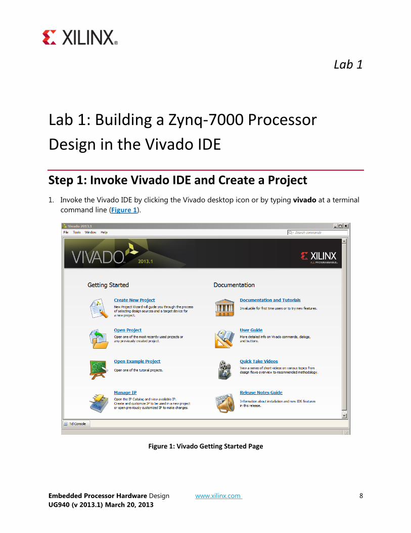
Step 1: Invoke Vivado IDE and Create a Project Invoke the Vivado IDE by clicking the Vivado desktop icon or by typing vivado at a terminal 1.
command line (Figure 1).
Figure 1: Vivado Getting Started Page
Step 1: Invoke Vivado IDE and Create a Project
Embedded Processor Hardware Design www.xilinx.com 9 UG940 (v 2013.1) March 20, 2013
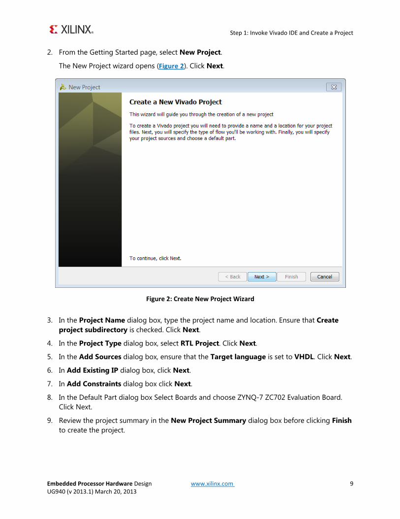
From the Getting Started page, select New Project. 2.
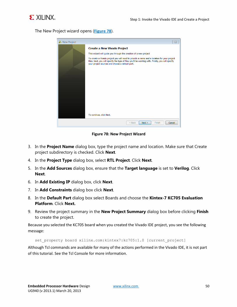
The New Project wizard opens (Figure 2). Click Next.
Figure 2: Create New Project Wizard
In the Project Name dialog box, type the project name and location. Ensure that Create 3.project subdirectory is checked. Click Next.
In the Project Type dialog box, select RTL Project. Click Next. 4.
In the Add Sources dialog box, ensure that the Target language is set to VHDL. Click Next. 5.
In Add Existing IP dialog box, click Next. 6.
In Add Constraints dialog box click Next. 7.
In the Default Part dialog box Select Boards and choose ZYNQ-7 ZC702 Evaluation Board. 8.Click Next.
Review the project summary in the New Project Summary dialog box before clicking Finish 9.to create the project.
Step 2: Create an IP Integrator Design
Embedded Processor Hardware Design www.xilinx.com 10 UG940 (v 2013.1) March 20, 2013
Step 2: Create an IP Integrator Design In the Flow Navigator, select the Create Block Design option (Figure 3). 1.
Figure 3: Flow Navigator: Create Block Design
The Create Block Design popup menu opens.
Specify a name for your IP subsystem design (Figure 4). 2.
Figure 4: Create Block Design Menu
Step 2: Create an IP Integrator Design
Embedded Processor Hardware Design www.xilinx.com 11 UG940 (v 2013.1) March 20, 2013
Add IP
In the Vivado IP integrator canvas, right-click, and select Add IP (Figure 5). 1.
Figure 5: Add IP Option
Alternatively, you can also click on the Add IP link in the IPI canvas (Figure 6).
Figure 6: Adding IP from the Add IP Link in IPI Canvas
The IP Catalog opens, (Figure 7).
In the search field, type zynq to find the ZYNQ7 Processing System IP, then press the Enter 2.key on the keyboard.
Figure 7: Zynq Selection in Search Field
Because you selected the ZC702 board when you created the project, the Vivado IP integrator configures the design appropriately.
Step 2: Create an IP Integrator Design
Embedded Processor Hardware Design www.xilinx.com 12 UG940 (v 2013.1) March 20, 2013
In the TCL Console you see the following message: create_bd_cell -type ip -vlnv xilinx.com:ip:processing_system7:5.01 processing_system7_1 INFO: [PS7-6] Configuring Board Preset zc702. There is a TCL command for all the actions performed in the IPI block diagram. However, those commands are not shown in this document. Please look at the TCL console for information on those commands.
Next, connect the DDR and FIXED_IO interfaces on the PS7 IP to top-level interface ports in the design.
Hover over the DDR and FIXED_IO interfaces until the cursor turns into a pencil and then 3.individually right-click the DDR and FIXED_IO interfaces on the PS7 IP.
For each IP select Make External (do not select USBIND_0), (Figure 8). 4.
Figure 8: Make External Option
Now you can add peripherals to go in the processing logic (PL).
Right-click the Block Design window, and select Add IP. 5.
Type the following names in the search field of the IP integrator catalog individually: 6.
• GPIO
• AXI BRAM Controller
• Block Memory Generator
The Block Design window matches Figure 9. The relative positions of these IP are different.
Step 2: Create an IP Integrator Design
Embedded Processor Hardware Design www.xilinx.com 13 UG940 (v 2013.1) March 20, 2013
Figure 9: Block Design Window with Three IP
Customize Instantiated IP
Double-click, or right-click the Block Memory Generator IP, and select Customize Block 1.(Figure 10).
Figure 10: Customize Block Option
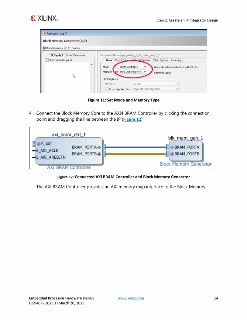
The Re-customize IP dialog box opens (Figure 11).
In the Basic tab of the dialog box, set: 2.
• Mode to BRAM Controller
• Memory Type to True Dual Port RAM
Click OK. 3.
Step 2: Create an IP Integrator Design
Embedded Processor Hardware Design www.xilinx.com 14 UG940 (v 2013.1) March 20, 2013
Figure 11: Set Mode and Memory Type
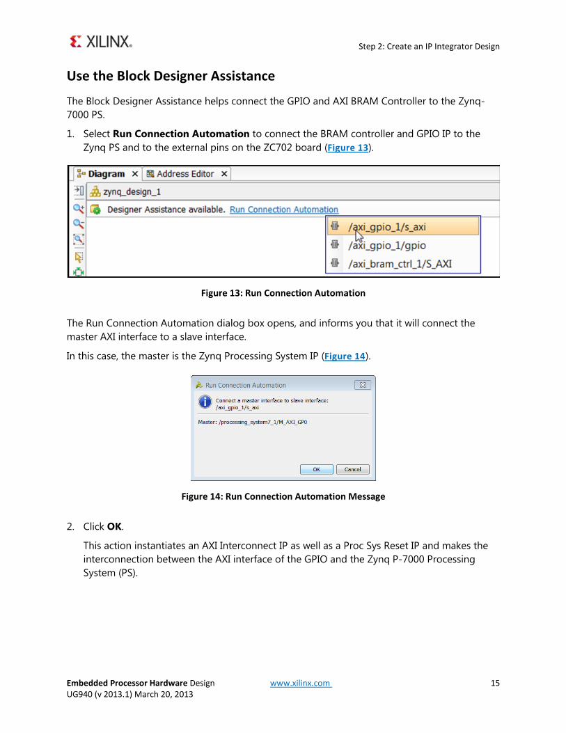
Connect the Block Memory Core to the AXI4 BRAM Controller by clicking the connection 4.point and dragging the line between the IP (Figure 12).
Figure 12: Connected AXI BRAM Controller and Block Memory Generator
The AXI BRAM Controller provides an AXI memory map interface to the Block Memory.
Step 2: Create an IP Integrator Design
Embedded Processor Hardware Design www.xilinx.com 15 UG940 (v 2013.1) March 20, 2013
Use the Block Designer Assistance
The Block Designer Assistance helps connect the GPIO and AXI BRAM Controller to the Zynq-7000 PS.
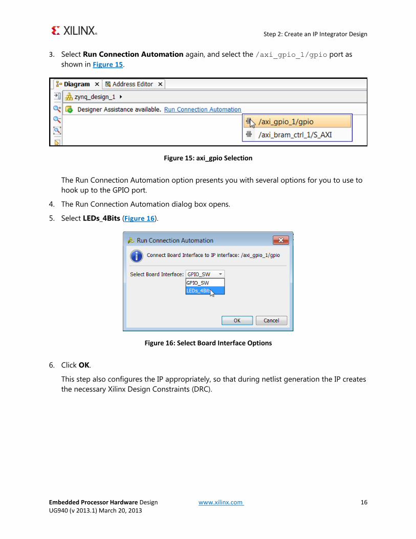
Select Run Connection Automation to connect the BRAM controller and GPIO IP to the 1.Zynq PS and to the external pins on the ZC702 board (Figure 13).
Figure 13: Run Connection Automation
The Run Connection Automation dialog box opens, and informs you that it will connect the master AXI interface to a slave interface.
In this case, the master is the Zynq Processing System IP (Figure 14).
Figure 14: Run Connection Automation Message
Click OK. 2.
This action instantiates an AXI Interconnect IP as well as a Proc Sys Reset IP and makes the interconnection between the AXI interface of the GPIO and the Zynq P-7000 Processing System (PS).
Step 2: Create an IP Integrator Design
Embedded Processor Hardware Design www.xilinx.com 16 UG940 (v 2013.1) March 20, 2013
Select Run Connection Automation again, and select the /axi_gpio_1/gpio port as 3.shown in Figure 15.
Figure 15: axi_gpio Selection
The Run Connection Automation option presents you with several options for you to use to hook up to the GPIO port.
The Run Connection Automation dialog box opens. 4.
Select LEDs_4Bits (Figure 16). 5.
Figure 16: Select Board Interface Options
Click OK. 6.
This step also configures the IP appropriately, so that during netlist generation the IP creates the necessary Xilinx Design Constraints (DRC).
Step 2: Create an IP Integrator Design
Embedded Processor Hardware Design www.xilinx.com 17 UG940 (v 2013.1) March 20, 2013
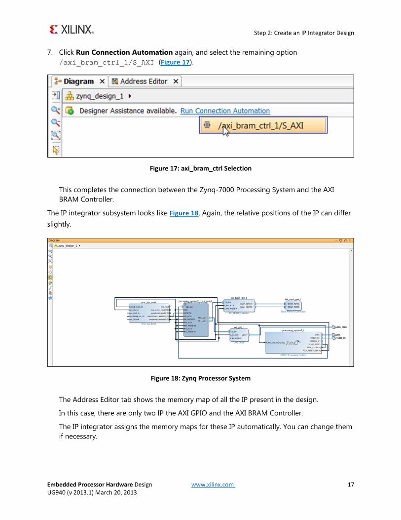
Click Run Connection Automation again, and select the remaining option 7./axi_bram_ctrl_1/S_AXI (Figure 17).
Figure 17: axi_bram_ctrl Selection
This completes the connection between the Zynq-7000 Processing System and the AXI BRAM Controller.
The IP integrator subsystem looks like Figure 18. Again, the relative positions of the IP can differ slightly.
Figure 18: Zynq Processor System
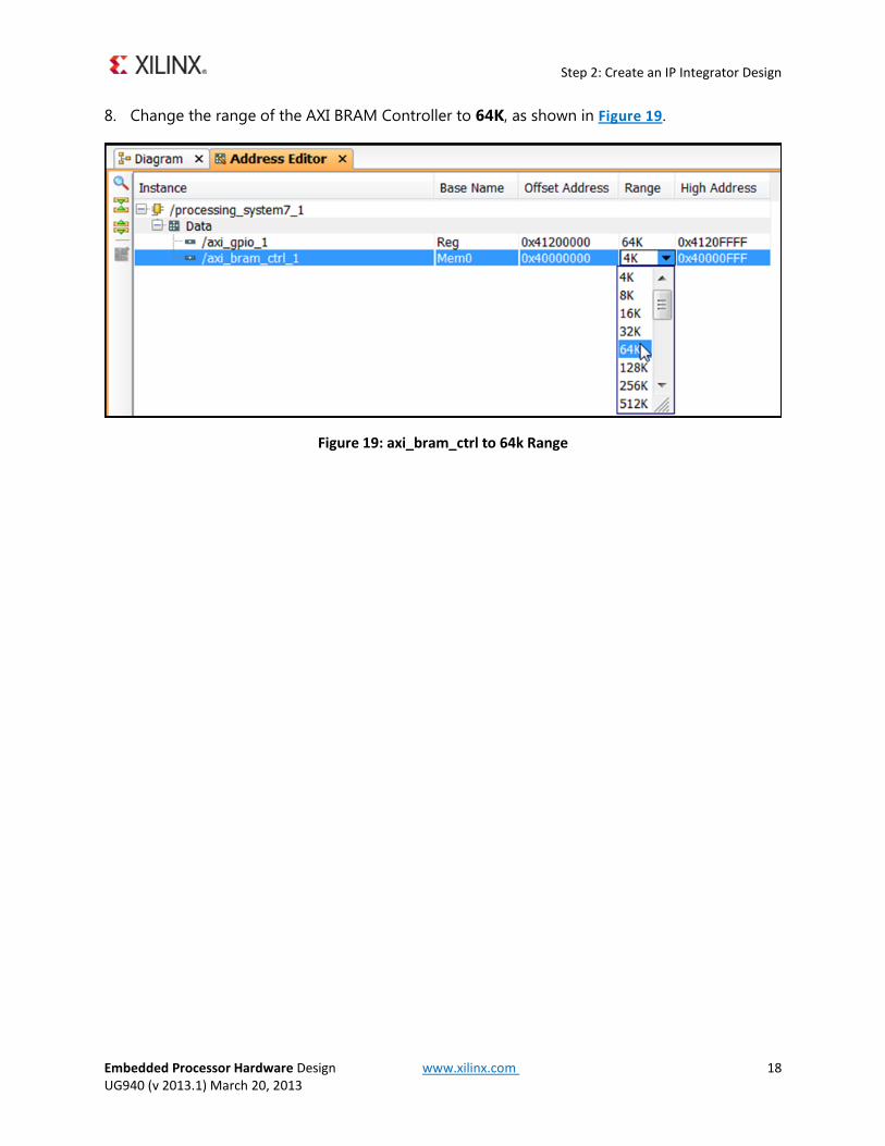
The Address Editor tab shows the memory map of all the IP present in the design.
In this case, there are only two IP the AXI GPIO and the AXI BRAM Controller.
The IP integrator assigns the memory maps for these IP automatically. You can change them if necessary.
Step 2: Create an IP Integrator Design
Embedded Processor Hardware Design www.xilinx.com 18 UG940 (v 2013.1) March 20, 2013
Change the range of the AXI BRAM Controller to 64K, as shown in Figure 19. 8.
Figure 19: axi_bram_ctrl to 64k Range
Step 3: Using MARK_DEBUG
Embedded Processor Hardware Design www.xilinx.com 19 UG940 (v 2013.1) March 20, 2013
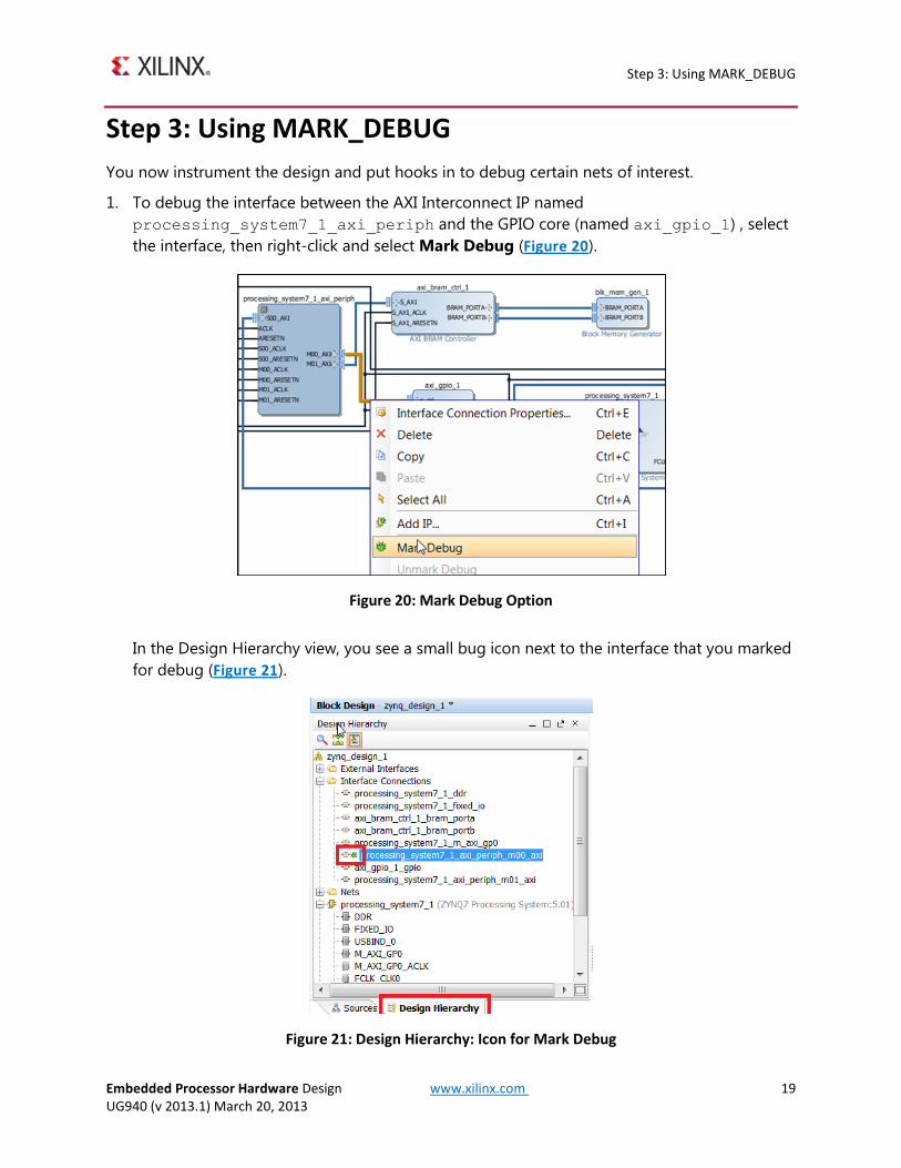
Step 3: Using MARK_DEBUG You now instrument the design and put hooks in to debug certain nets of interest.
To debug the interface between the AXI Interconnect IP named 1.processing_system7_1_axi_periph and the GPIO core (named axi_gpio_1) , select the interface, then right-click and select Mark Debug (Figure 20).
Figure 20: Mark Debug Option
In the Design Hierarchy view, you see a small bug icon next to the interface that you marked for debug (Figure 21).
Figure 21: Design Hierarchy: Icon for Mark Debug
Step 3: Using MARK_DEBUG
Embedded Processor Hardware Design www.xilinx.com 20 UG940 (v 2013.1) March 20, 2013
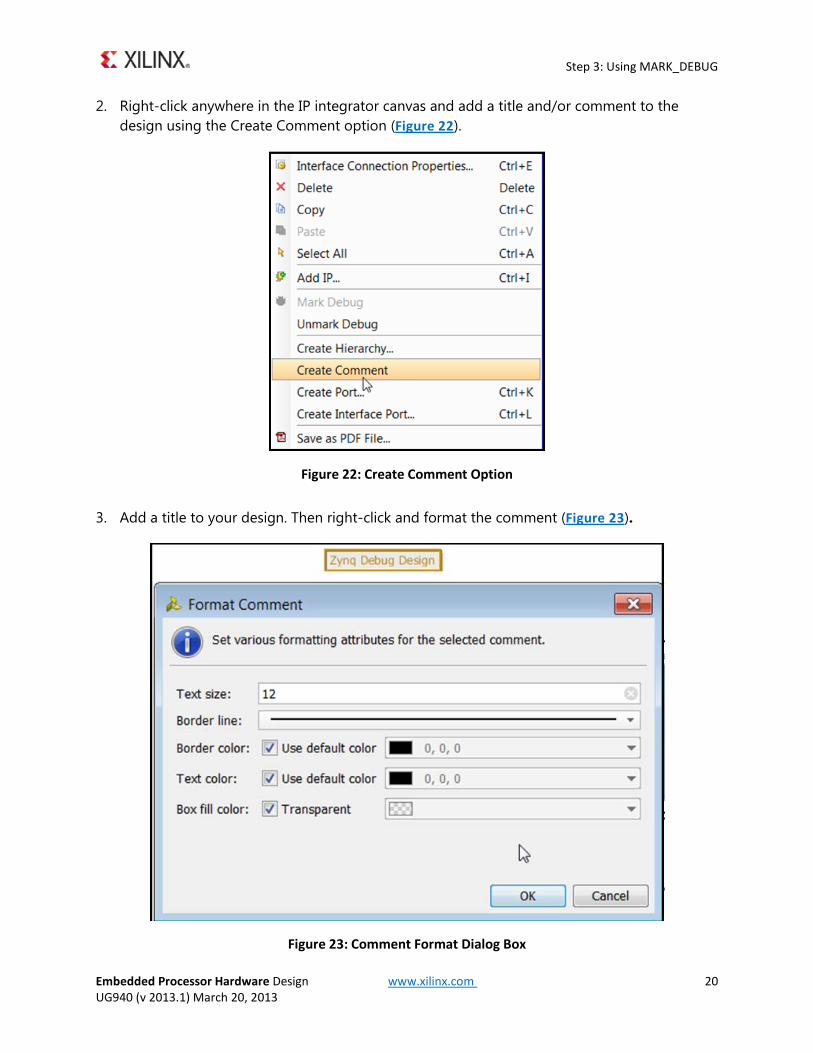
Right-click anywhere in the IP integrator canvas and add a title and/or comment to the 2.design using the Create Comment option (Figure 22).
Figure 22: Create Comment Option
Add a title to your design. Then right-click and format the comment (Figure 23). 3.
Figure 23: Comment Format Dialog Box
Step 3: Using MARK_DEBUG
Embedded Processor Hardware Design www.xilinx.com 21 UG940 (v 2013.1) March 20, 2013
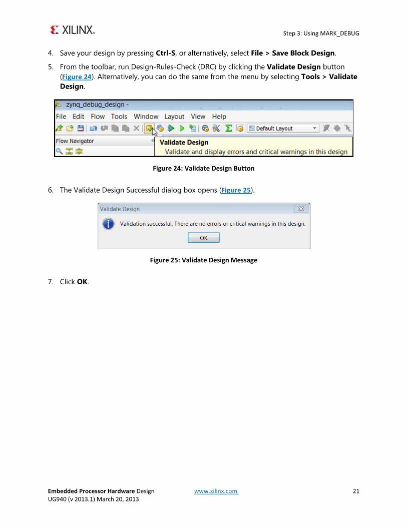
Save your design by pressing Ctrl-S, or alternatively, select File > Save Block Design. 4.
From the toolbar, run Design-Rules-Check (DRC) by clicking the Validate Design button 5.(Figure 24). Alternatively, you can do the same from the menu by selecting Tools > Validate Design.
Figure 24: Validate Design Button
The Validate Design Successful dialog box opens (Figure 25). 6.
Figure 25: Validate Design Message
Click OK. 7.
Step 4: Generate HDL Design Files
Embedded Processor Hardware Design www.xilinx.com 22 UG940 (v 2013.1) March 20, 2013
Step 4: Generate HDL Design Files You now generate the HDL files for the design.
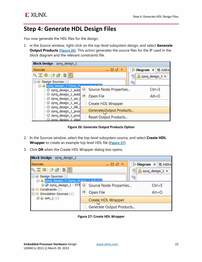
In the Source window, right-click on the top-level subsystem design, and select Generate 1.Output Products (Figure 26). This action generates the source files for the IP used in the block diagram and the relevant constraints file.
Figure 26: Generate Output Products Option
In the Sources window, select the top-level subsystem source, and select Create HDL 2.Wrapper to create an example top level HDL file (Figure 27).
Click OK when the Create HDL Wrapper dialog box opens. 3.
Figure 27: Create HDL Wrapper
Step 5: Assign Signals to Debug
Embedded Processor Hardware Design www.xilinx.com 23 UG940 (v 2013.1) March 20, 2013
Step 5: Assign Signals to Debug Now assign the signals to debug in hardware.
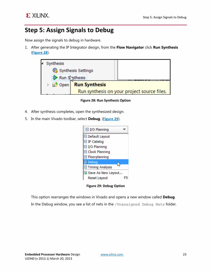
1. After generating the IP Integrator design, from the Flow Navigator click Run Synthesis (Figure 28).
Figure 28: Run Synthesis Option
After synthesis completes, open the synthesized design. 4.
In the main Vivado toolbar, select Debug, (Figure 29). 5.
Figure 29: Debug Option
This option rearranges the windows in Vivado and opens a new window called Debug.
In the Debug window, you see a list of nets in the /Unassigned Debug Nets folder.
Step 5: Assign Signals to Debug
Embedded Processor Hardware Design www.xilinx.com 24 UG940 (v 2013.1) March 20, 2013
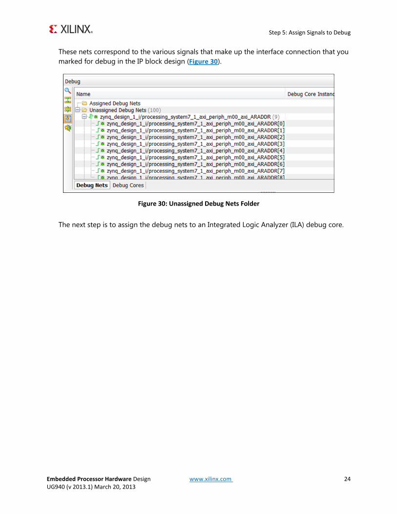
These nets correspond to the various signals that make up the interface connection that you marked for debug in the IP block design (Figure 30).
Figure 30: Unassigned Debug Nets Folder
The next step is to assign the debug nets to an Integrated Logic Analyzer (ILA) debug core.
Step 6: Assign Debug Net to an ILA Core
Embedded Processor Hardware Design www.xilinx.com 25 UG940 (v 2013.1) March 20, 2013
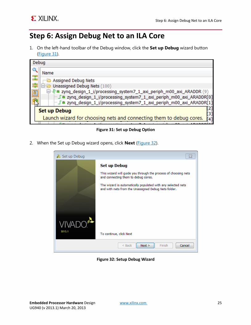
Step 6: Assign Debug Net to an ILA Core On the left-hand toolbar of the Debug window, click the Set up Debug wizard button 1.
(Figure 31).
Figure 31: Set up Debug Option
When the Set up Debug wizard opens, click Next (Figure 32). 2.
Figure 32: Setup Debug Wizard
Step 6: Assign Debug Net to an ILA Core
Embedded Processor Hardware Design www.xilinx.com 26 UG940 (v 2013.1) March 20, 2013
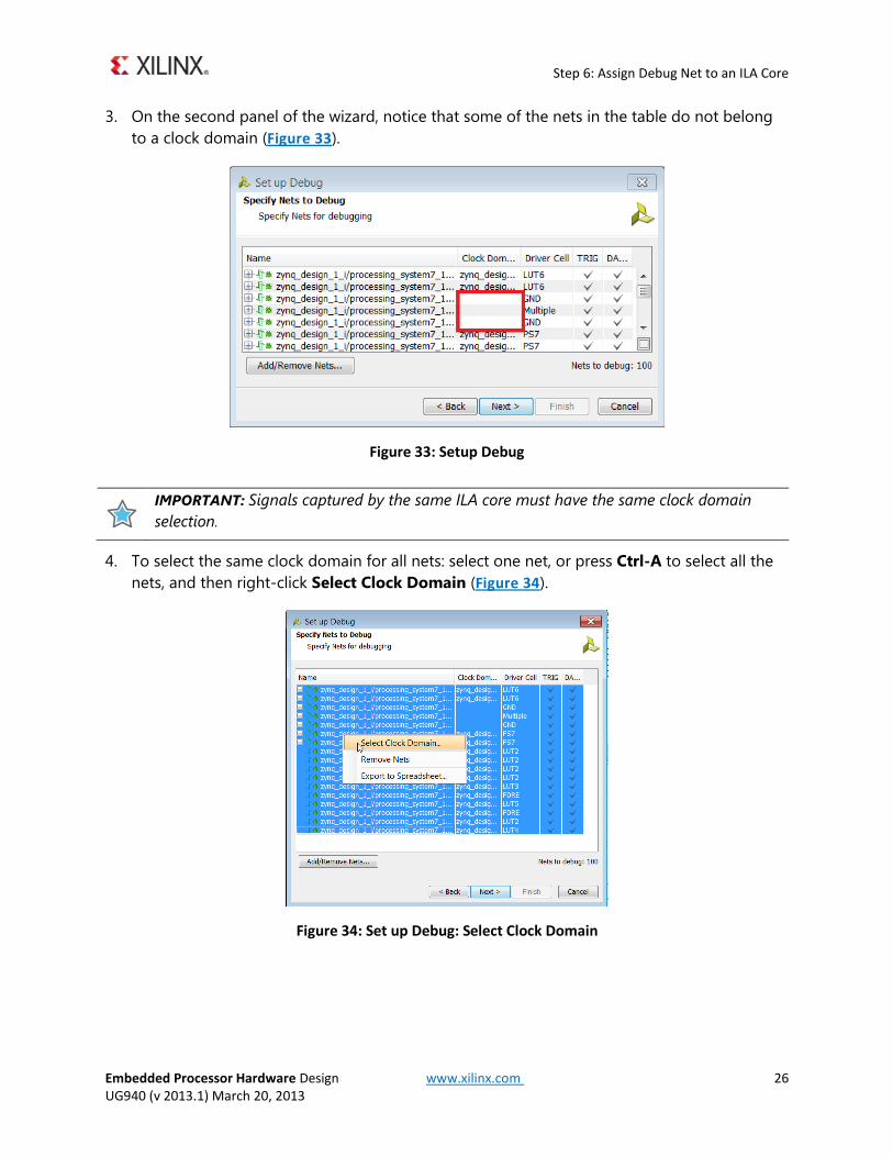
On the second panel of the wizard, notice that some of the nets in the table do not belong 3.to a clock domain (Figure 33).
Figure 33: Setup Debug
IMPORTANT: Signals captured by the same ILA core must have the same clock domain selection.
To select the same clock domain for all nets: select one net, or press Ctrl-A to select all the 4.nets, and then right-click Select Clock Domain (Figure 34).
Figure 34: Set up Debug: Select Clock Domain
Step 6: Assign Debug Net to an ILA Core
Embedded Processor Hardware Design www.xilinx.com 27 UG940 (v 2013.1) March 20, 2013
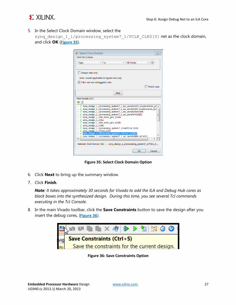
In the Select Clock Domain window, select the 5.zynq_design_1_i/processing_system7_1/FCLK_CLK0[0] net as the clock domain, and click OK (Figure 35).
Figure 35: Select Clock Domain Option
Click Next to bring up the summary window. 6.
Click Finish. 7.
Note: It takes approximately 30 seconds for Vivado to add the ILA and Debug Hub cores as black boxes into the synthesized design. During this time, you see several Tcl commands executing in the Tcl Console.
In the main Vivado toolbar, click the Save Constraints button to save the design after you 8.insert the debug cores, (Figure 36).
Figure 36: Save Constraints Option
Step 7: Implement Design and Generate Bitstream
Embedded Processor Hardware Design www.xilinx.com 28 UG940 (v 2013.1) March 20, 2013
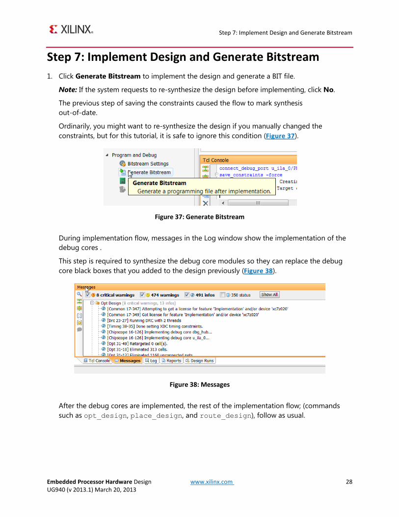
Step 7: Implement Design and Generate Bitstream Click Generate Bitstream to implement the design and generate a BIT file. 1.
Note: If the system requests to re-synthesize the design before implementing, click No.
The previous step of saving the constraints caused the flow to mark synthesis out-of-date.
Ordinarily, you might want to re-synthesize the design if you manually changed the constraints, but for this tutorial, it is safe to ignore this condition (Figure 37).
Figure 37: Generate Bitstream
During implementation flow, messages in the Log window show the implementation of the debug cores .
This step is required to synthesize the debug core modules so they can replace the debug core black boxes that you added to the design previously (Figure 38).
Figure 38: Messages
After the debug cores are implemented, the rest of the implementation flow; (commands such as opt_design, place_design, and route_design), follow as usual.
Step 7: Implement Design and Generate Bitstream
Embedded Processor Hardware Design www.xilinx.com 29 UG940 (v 2013.1) March 20, 2013
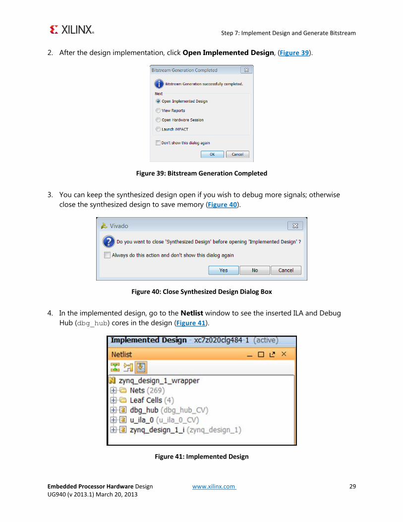
After the design implementation, click Open Implemented Design, (Figure 39). 2.
Figure 39: Bitstream Generation Completed
You can keep the synthesized design open if you wish to debug more signals; otherwise 3.close the synthesized design to save memory (Figure 40).
Figure 40: Close Synthesized Design Dialog Box
In the implemented design, go to the Netlist window to see the inserted ILA and Debug 4.Hub (dbg_hub) cores in the design (Figure 41).
Figure 41: Implemented Design
Step 8: Export Hardware to SDK
Embedded Processor Hardware Design www.xilinx.com 30 UG940 (v 2013.1) March 20, 2013
Step 8: Export Hardware to SDK In this step, you export the hardware description to SDK. You use this in Lab2.
The IP integrator design, the Implemented design, as well as the bitstream, must be open to export the design to SDK.
IMPORTANT: For the Digilent driver to install, you must power on and connect the board to the host PC before launching SDK.
Export to SDK
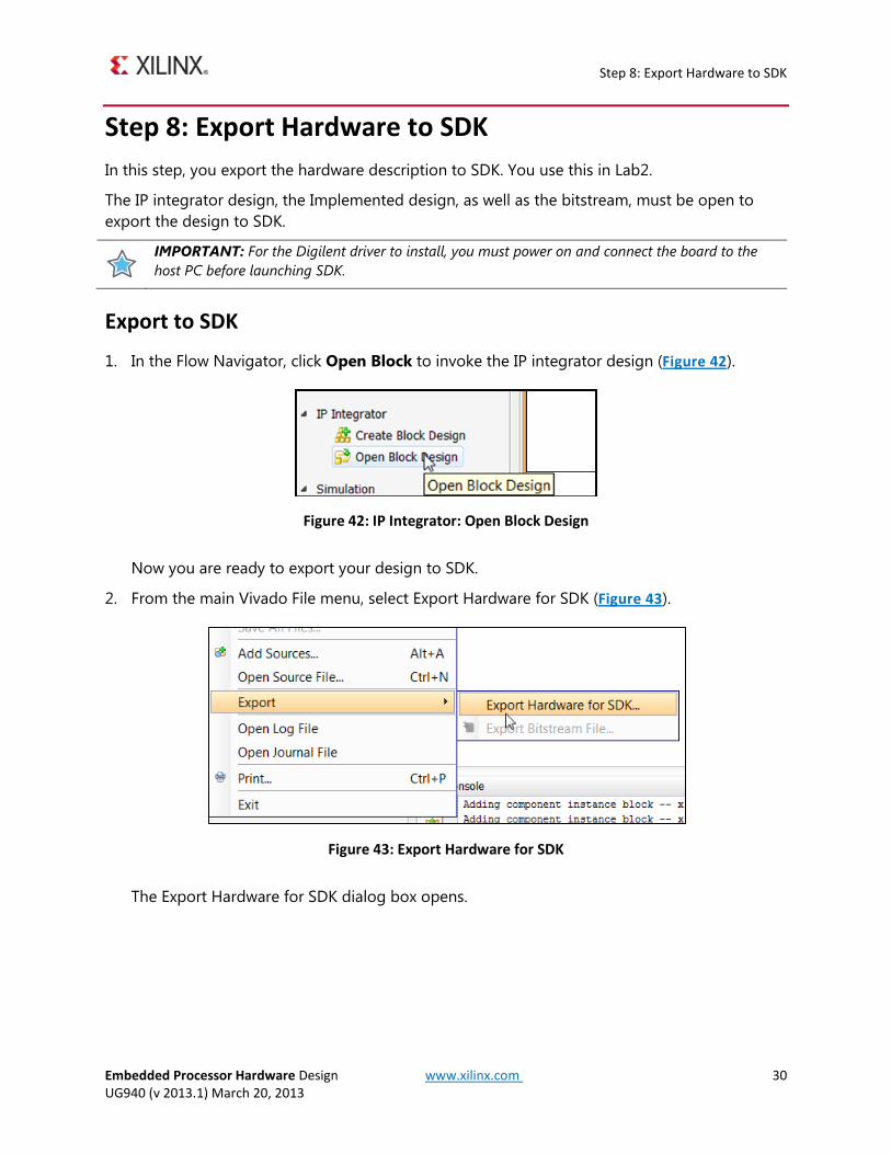
In the Flow Navigator, click Open Block to invoke the IP integrator design (Figure 42). 1.
Figure 42: IP Integrator: Open Block Design
Now you are ready to export your design to SDK.
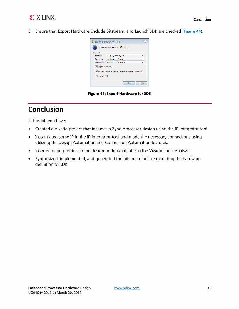
From the main Vivado File menu, select Export Hardware for SDK (Figure 43). 2.
Figure 43: Export Hardware for SDK
The Export Hardware for SDK dialog box opens.
Conclusion
Embedded Processor Hardware Design www.xilinx.com 31 UG940 (v 2013.1) March 20, 2013
Ensure that Export Hardware, Include Bitstream, and Launch SDK are checked (Figure 44). 3.
Figure 44: Export Hardware for SDK
Conclusion In this lab you have:
• Created a Vivado project that includes a Zynq processor design using the IP integrator tool.
• Instantiated some IP in the IP integrator tool and made the necessary connections using utilizing the Design Automation and Connection Automation features.
• Inserted debug probes in the design to debug it later in the Vivado Logic Analyzer.
• Synthesized, implemented, and generated the bitstream before exporting the hardware definition to SDK.
Embedded Processor Hardware Design www.xilinx.com 32 UG940 (v 2013.1) March 20, 2013
Lab 2
Lab 2: Using SDK and the Vivado IDE Logic Analyzer
Introduction You can run this lab after Lab 1. Make sure that you followed all the steps in Lab 1 before proceeding.
Before using SDK to build and debug the design, it is important to start the hardware server (hw_server) application that SDK uses to communicate with the Zynq™-7000 processors.
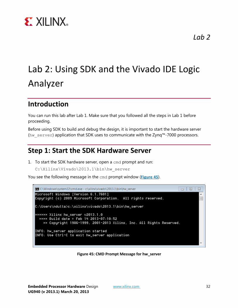
Step 1: Start the SDK Hardware Server To start the SDK hardware server, open a cmd prompt and run: 1.C:\Xilinx\Vivado\2013.1\bin\hw_server
You see the following message in the cmd prompt window (Figure 45).
Figure 45: CMD Prompt Message for hw_server
Step 1: Start the SDK Hardware Server
Embedded Processor Hardware Design www.xilinx.com 33 UG940 (v 2013.1) March 20, 2013
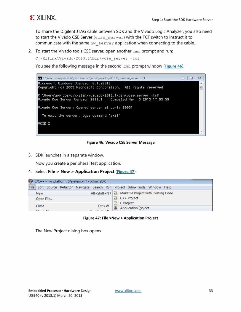
To share the Digilent JTAG cable between SDK and the Vivado Logic Analyzer, you also need to start the Vivado CSE Server (vcse_server) with the TCF switch to instruct it to communicate with the same hw_server application when connecting to the cable.
To start the Vivado tools CSE server, open another cmd prompt and run: 2.C:\Xilinx\Vivado\2013.1\bin\vcse_server –tcf
You see the following message in the second cmd prompt window (Figure 46).
Figure 46: Vivado CSE Server Message
SDK launches in a separate window. 3.
Now you create a peripheral test application.
Select File > New > Application Project (Figure 47). 4.
Figure 47: File >New > Application Project
The New Project dialog box opens.
Step 1: Start the SDK Hardware Server
Embedded Processor Hardware Design www.xilinx.com 34 UG940 (v 2013.1) March 20, 2013
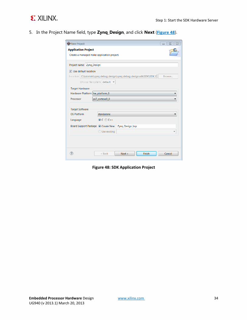
In the Project Name field, type Zynq_Design, and click Next (Figure 48). 5.
Figure 48: SDK Application Project
Step 1: Start the SDK Hardware Server
Embedded Processor Hardware Design www.xilinx.com 35 UG940 (v 2013.1) March 20, 2013
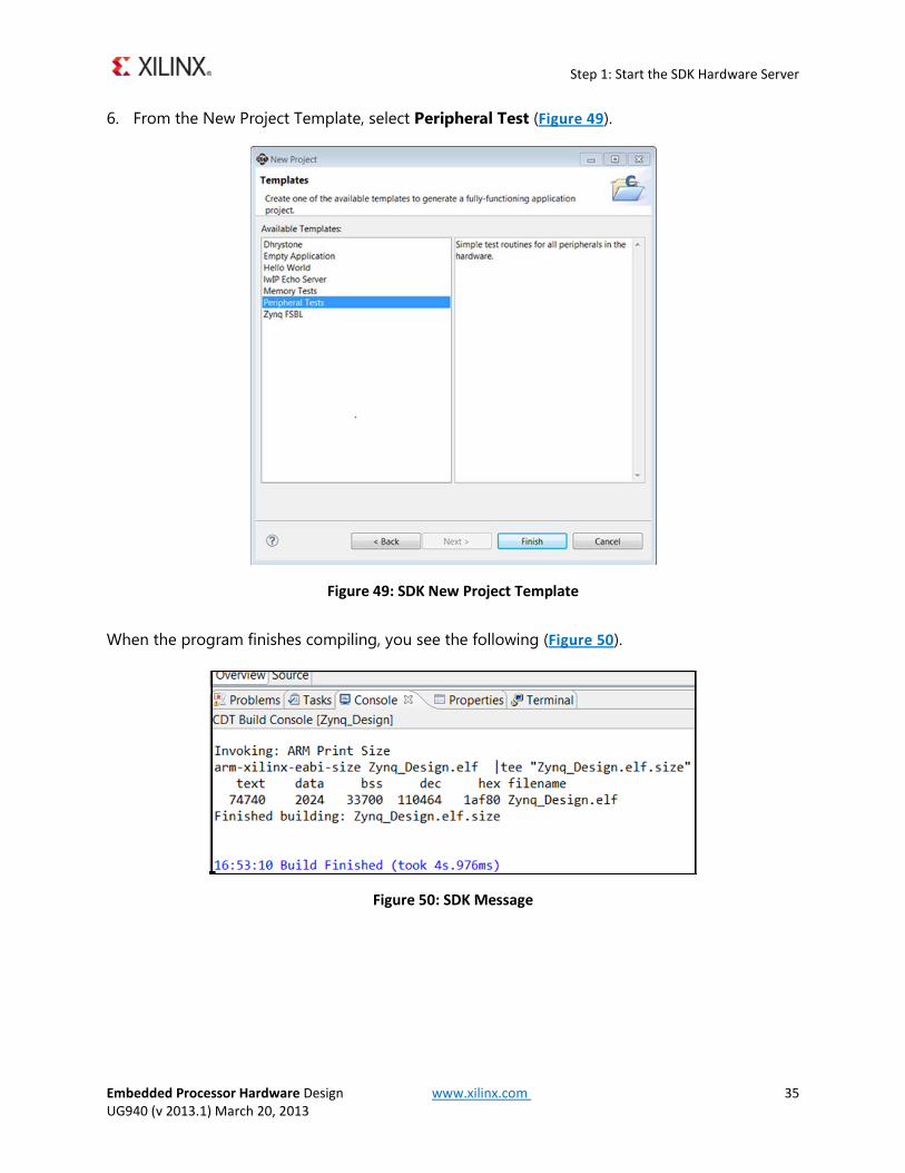
From the New Project Template, select Peripheral Test (Figure 49). 6.
Figure 49: SDK New Project Template
When the program finishes compiling, you see the following (Figure 50).
Figure 50: SDK Message
Step 1: Start the SDK Hardware Server
Embedded Processor Hardware Design www.xilinx.com 36 UG940 (v 2013.1) March 20, 2013
Configure the JTAG Port
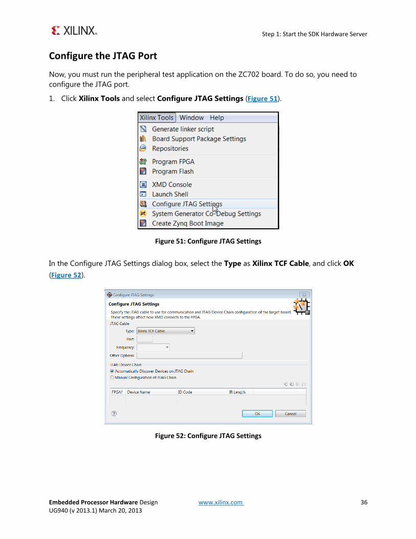
Now, you must run the peripheral test application on the ZC702 board. To do so, you need to configure the JTAG port.
Click Xilinx Tools and select Configure JTAG Settings (Figure 51). 1.
Figure 51: Configure JTAG Settings
In the Configure JTAG Settings dialog box, select the Type as Xilinx TCF Cable, and click OK (Figure 52).
Figure 52: Configure JTAG Settings
Step 1: Start the SDK Hardware Server
Embedded Processor Hardware Design www.xilinx.com 37 UG940 (v 2013.1) March 20, 2013
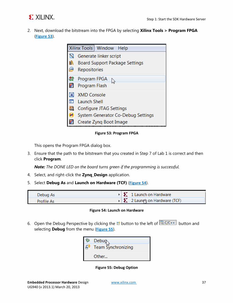
Next, download the bitstream into the FPGA by selecting Xilinx Tools > Program FPGA 2.(Figure 53).
Figure 53: Program FPGA
This opens the Program FPGA dialog box.
Ensure that the path to the bitstream that you created in Step 7 of Lab 1 is correct and then 3.click Program.
Note: The DONE LED on the board turns green if the programming is successful.
Select, and right-click the Zynq_Design application. 4.
Select Debug As and Launch on Hardware (TCF) (Figure 54). 5.
Figure 54: Launch on Hardware
Open the Debug Perspective by clicking the button to the left of button and 6.selecting Debug from the menu (Figure 55).
Figure 55: Debug Option
Step 1: Start the SDK Hardware Server
Embedded Processor Hardware Design www.xilinx.com 38 UG940 (v 2013.1) March 20, 2013
Set the terminal by selecting the Terminal 1 tab and clicking the Settings button 7.(Figure 56).
Figure 56: Settings Button
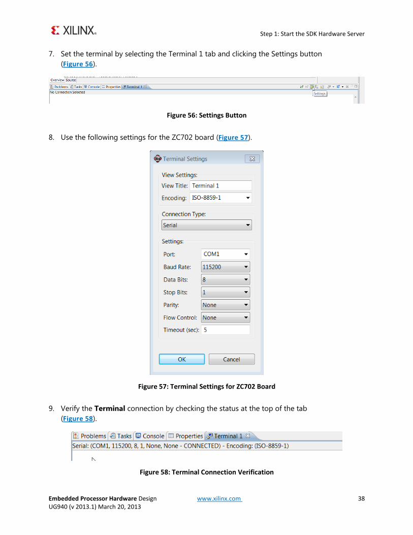
Use the following settings for the ZC702 board (Figure 57). 8.
Figure 57: Terminal Settings for ZC702 Board
Verify the Terminal connection by checking the status at the top of the tab 9.(Figure 58).
Figure 58: Terminal Connection Verification
Step 1: Start the SDK Hardware Server
Embedded Processor Hardware Design www.xilinx.com 39 UG940 (v 2013.1) March 20, 2013
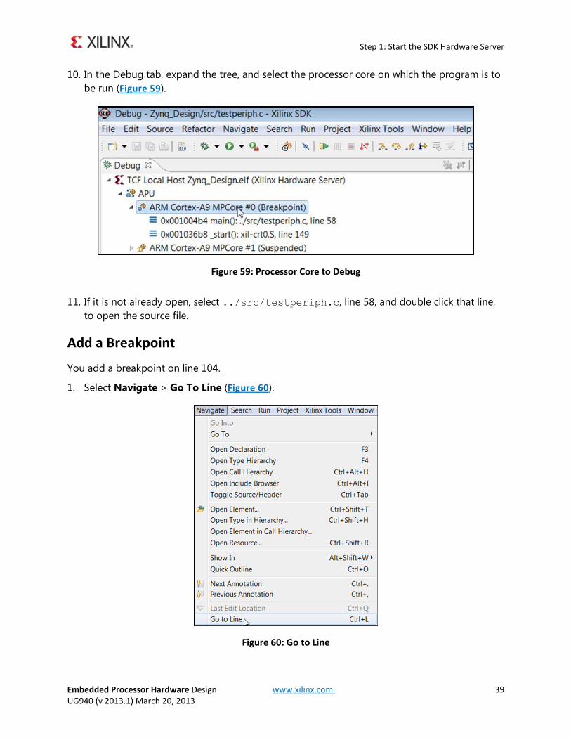
In the Debug tab, expand the tree, and select the processor core on which the program is to 10.be run (Figure 59).
Figure 59: Processor Core to Debug
If it is not already open, select ../src/testperiph.c, line 58, and double click that line, 11.to open the source file.
Add a Breakpoint
You add a breakpoint on line 104.
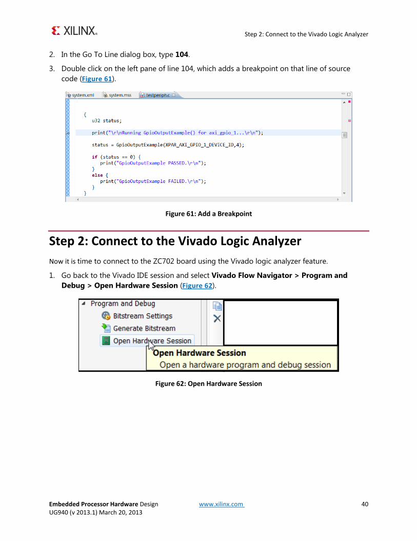
1. Select Navigate > Go To Line (Figure 60).
Figure 60: Go to Line
Step 2: Connect to the Vivado Logic Analyzer
Embedded Processor Hardware Design www.xilinx.com 40 UG940 (v 2013.1) March 20, 2013
2. In the Go To Line dialog box, type 104.
3. Double click on the left pane of line 104, which adds a breakpoint on that line of source code (Figure 61).
Figure 61: Add a Breakpoint
Step 2: Connect to the Vivado Logic Analyzer Now it is time to connect to the ZC702 board using the Vivado logic analyzer feature.
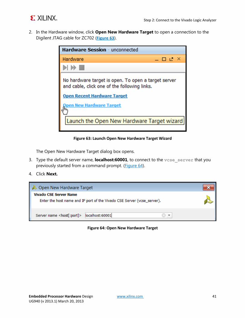
Go back to the Vivado IDE session and select Vivado Flow Navigator > Program and 1.Debug > Open Hardware Session (Figure 62).
Figure 62: Open Hardware Session
Step 2: Connect to the Vivado Logic Analyzer
Embedded Processor Hardware Design www.xilinx.com 41 UG940 (v 2013.1) March 20, 2013
In the Hardware window, click Open New Hardware Target to open a connection to the 2.Digilent JTAG cable for ZC702 (Figure 63).
Figure 63: Launch Open New Hardware Target Wizard
The Open New Hardware Target dialog box opens.
Type the default server name, localhost:60001, to connect to the vcse_server that you 3.previously started from a command prompt. (Figure 64).
Click Next. 4.
Figure 64: Open New Hardware Target
Step 2: Connect to the Vivado Logic Analyzer
Embedded Processor Hardware Design www.xilinx.com 42 UG940 (v 2013.1) March 20, 2013
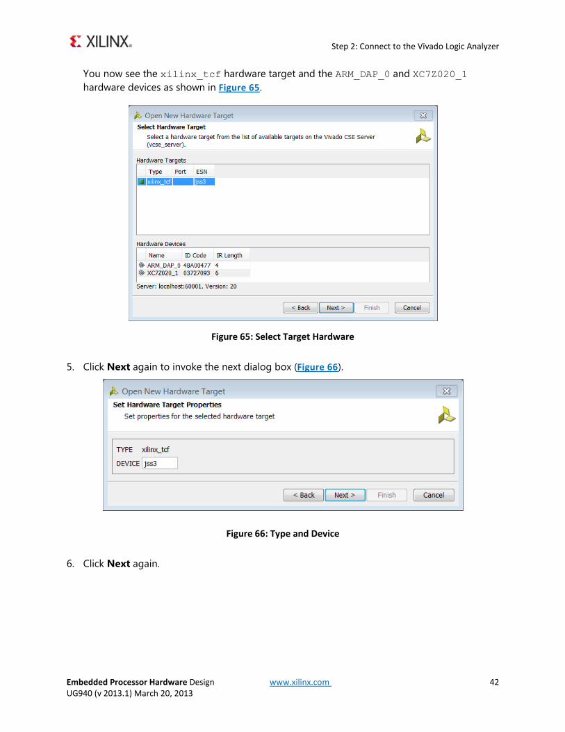
You now see the xilinx_tcf hardware target and the ARM_DAP_0 and XC7Z020_1 hardware devices as shown in Figure 65.
Figure 65: Select Target Hardware
Click Next again to invoke the next dialog box (Figure 66). 5.
Figure 66: Type and Device
Click Next again. 6.
Step 2: Connect to the Vivado Logic Analyzer
Embedded Processor Hardware Design www.xilinx.com 43 UG940 (v 2013.1) March 20, 2013
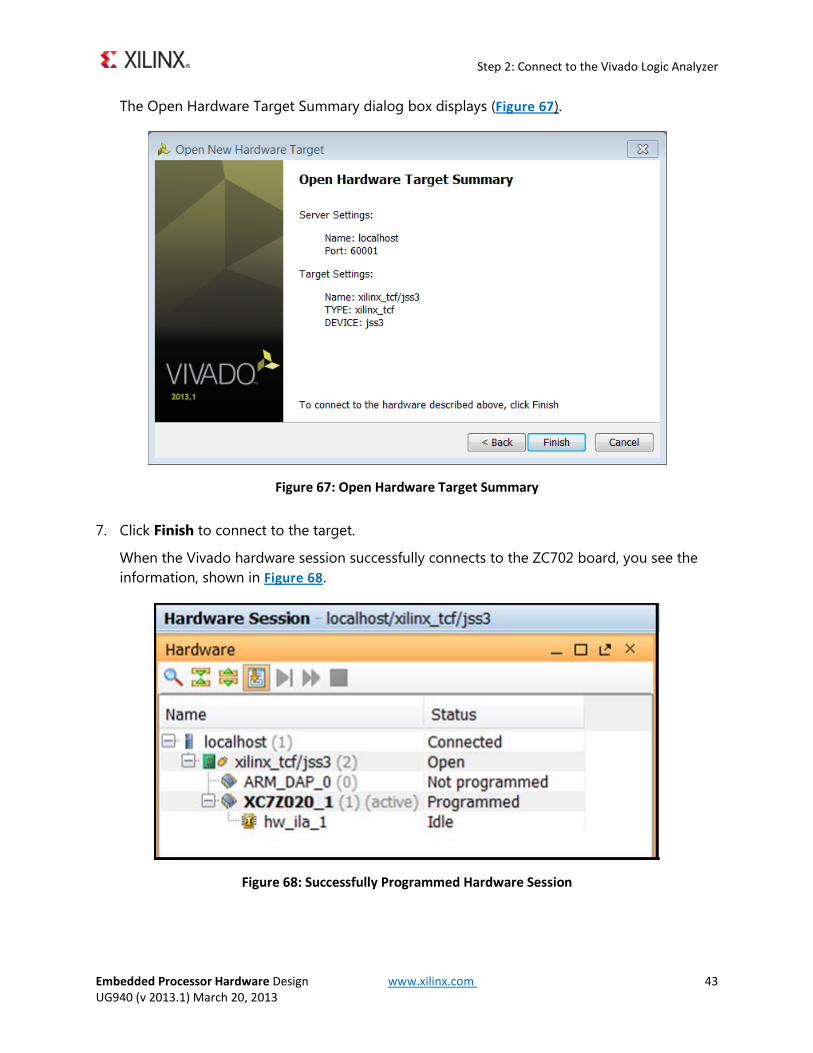
The Open Hardware Target Summary dialog box displays (Figure 67).
Figure 67: Open Hardware Target Summary
Click Finish to connect to the target. 7.
When the Vivado hardware session successfully connects to the ZC702 board, you see the information, shown in Figure 68.
Figure 68: Successfully Programmed Hardware Session
Step 2: Connect to the Vivado Logic Analyzer
Embedded Processor Hardware Design www.xilinx.com 44 UG940 (v 2013.1) March 20, 2013
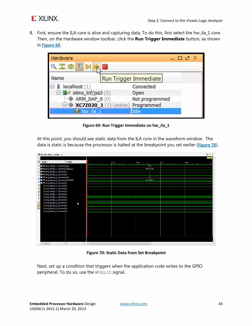
First, ensure the ILA core is alive and capturing data. To do this, first select the hw_ila_1 core. 8.Then, on the Hardware window toolbar, click the Run Trigger Immediate button, as shown in Figure 69.
Figure 69: Run Trigger Immediate on hw_ila_1
At this point, you should see static data from the ILA core in the waveform window. The data is static is because the processor is halted at the breakpoint you set earlier (Figure 70).
Figure 70: Static Data from Set Breakpoint
Next, set up a condition that triggers when the application code writes to the GPIO peripheral. To do so, use the WVALID signal.
Step 2: Connect to the Vivado Logic Analyzer
Embedded Processor Hardware Design www.xilinx.com 45 UG940 (v 2013.1) March 20, 2013
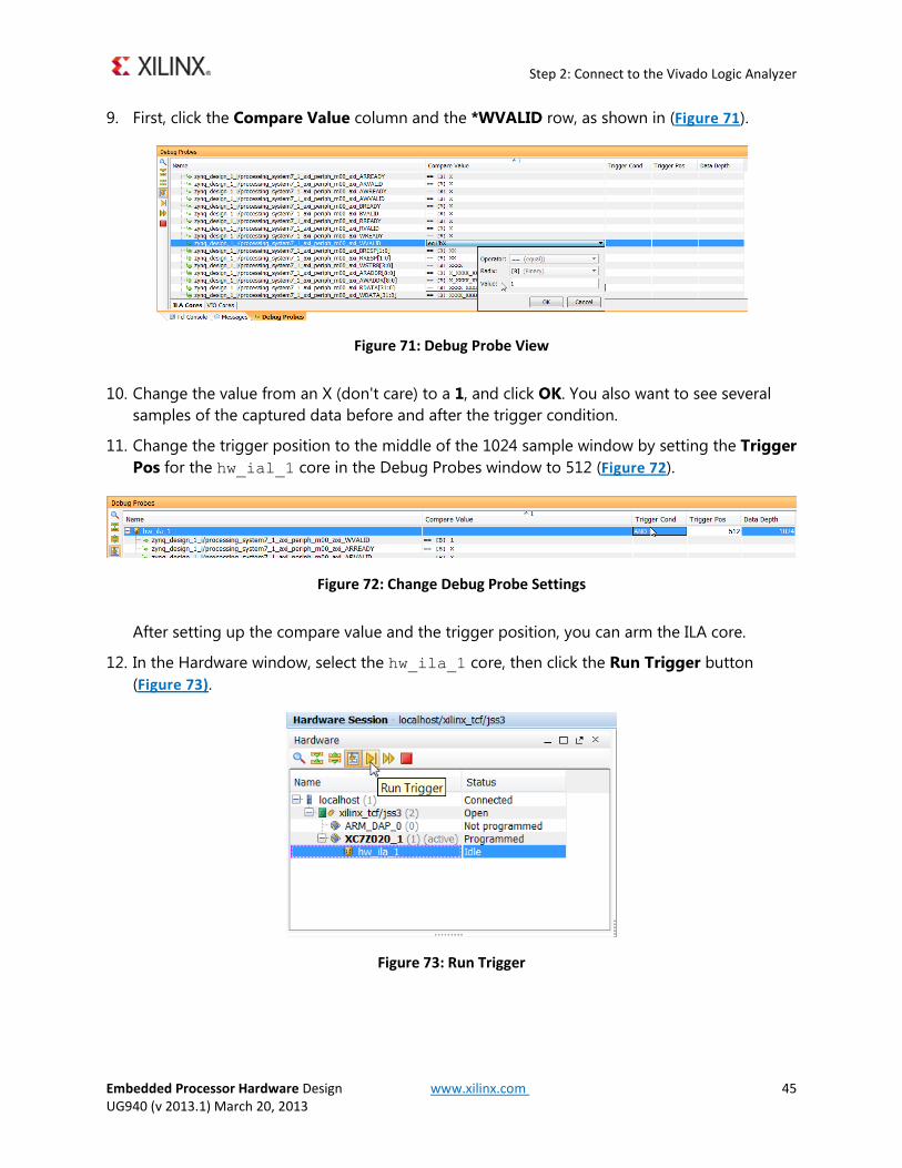
First, click the Compare Value column and the *WVALID row, as shown in (Figure 71). 9.
Figure 71: Debug Probe View
Change the value from an X (don't care) to a 1, and click OK. You also want to see several 10.samples of the captured data before and after the trigger condition.
Change the trigger position to the middle of the 1024 sample window by setting the Trigger 11.Pos for the hw_ial_1 core in the Debug Probes window to 512 (Figure 72).
Figure 72: Change Debug Probe Settings
After setting up the compare value and the trigger position, you can arm the ILA core.
In the Hardware window, select the hw_ila_1 core, then click the Run Trigger button 12.(Figure 73).
Figure 73: Run Trigger
Step 2: Connect to the Vivado Logic Analyzer
Embedded Processor Hardware Design www.xilinx.com 46 UG940 (v 2013.1) March 20, 2013
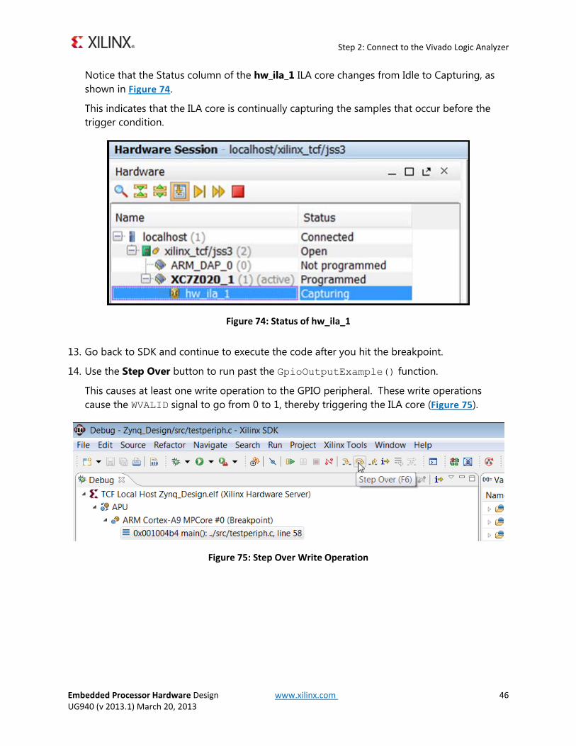
Notice that the Status column of the hw_ila_1 ILA core changes from Idle to Capturing, as shown in Figure 74.
This indicates that the ILA core is continually capturing the samples that occur before the trigger condition.
Figure 74: Status of hw_ila_1
Go back to SDK and continue to execute the code after you hit the breakpoint. 13.
Use the Step Over button to run past the GpioOutputExample() function. 14.
This causes at least one write operation to the GPIO peripheral. These write operations cause the WVALID signal to go from 0 to 1, thereby triggering the ILA core (Figure 75).
Figure 75: Step Over Write Operation
Conclusion
Embedded Processor Hardware Design www.xilinx.com 47 UG940 (v 2013.1) March 20, 2013
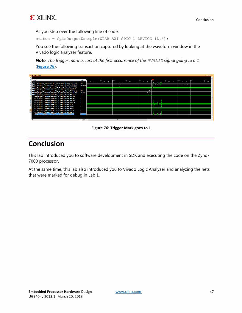
As you step over the following line of code: status = GpioOutputExample(XPAR_AXI_GPIO_1_DEVICE_ID,4);
You see the following transaction captured by looking at the waveform window in the Vivado logic analyzer feature.
Note: The trigger mark occurs at the first occurrence of the WVALID signal going to a 1 (Figure 76).
Figure 76: Trigger Mark goes to 1
Conclusion This lab introduced you to software development in SDK and executing the code on the Zynq-7000 processor.
At the same time, this lab also introduced you to Vivado Logic Analyzer and analyzing the nets that were marked for debug in Lab 1.
Embedded Processor Hardware Design www.xilinx.com 48 UG940 (v 2013.1) March 20, 2013
Lab 3
Lab 3: Using the Embedded Microblaze Processor
Introduction In this tutorial you create a simple MicroBlaze™ system for a Kintex™-7 FPGA using Vivado™ IP integrator. You can use a machine on any Operating System for this tutorial.
The MicroBlaze system includes native Xilinx IP such as the:
• MicroBlaze processor
• AXI Timer
• AXI block RAM
• Double Data Rate 3 (DDR3) memory
• UARTLite
• Debug Module (MDM)
• Proc Sys Reset
• Interrupt Controller
• local memory bus (LMB)
These are the basic building blocks used in a typical MicroBlaze system.
In addition to creating the system described above, this tutorial also describes porting an operating system on a Kintex™ device that you develop in the Xilinx Software Development Kit (SDK) in the Vivado Design Suite. The application code developed in SDK prints “Hello World” in an OS thread.
This tutorial targets the Xilinx KC705 FPGA Evaluation Board, and uses the 2013.1 version of Vivado Design Suite. To test your system on a KC705 board, you must use a terminal emulation program such as TeraTerm or Hyperterminal.
You must also ensure that you have the device drivers for the board installed correctly.
Step 1: Invoke the Vivado IDE and Create a Project
Embedded Processor Hardware Design www.xilinx.com 49 UG940 (v 2013.1) March 20, 2013
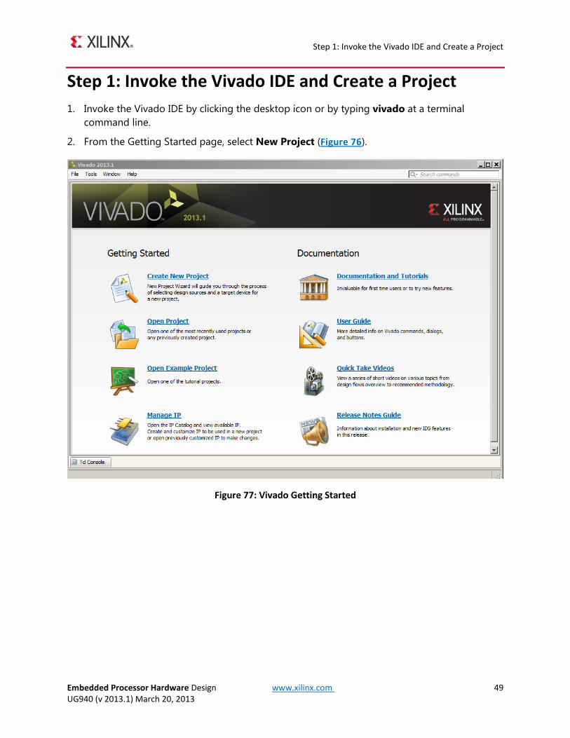
Step 1: Invoke the Vivado IDE and Create a Project Invoke the Vivado IDE by clicking the desktop icon or by typing vivado at a terminal 1.
command line.
From the Getting Started page, select New Project (Figure 76). 2.
Figure 77: Vivado Getting Started
Step 1: Invoke the Vivado IDE and Create a Project
Embedded Processor Hardware Design www.xilinx.com 50 UG940 (v 2013.1) March 20, 2013
The New Project wizard opens (Figure 78).
Figure 78: New Project Wizard
In the Project Name dialog box, type the project name and location. Make sure that Create 3.project subdirectory is checked. Click Next.
In the Project Type dialog box, select RTL Project. Click Next. 4.
In the Add Sources dialog box, ensure that the Target language is set to Verilog. Click 5.Next.
In Add Existing IP dialog box, click Next. 6.
In Add Constraints dialog box click Next. 7.
In the Default Part dialog box select Boards and choose the Kintex-7 KC705 Evaluation 8.Platform. Click Next.
Review the project summary in the New Project Summary dialog box before clicking Finish 9.to create the project.
Because you selected the KC705 board when you created the Vivado IDE project, you see the following message:
set_property board xilinx.com:kintex7:kc705:1.0 [current_project]
Although Tcl commands are available for many of the actions performed in the Vivado IDE, it is not part of this tutorial. See the Tcl Console for more information.
Step 2: Create an IP Integrator Design
Embedded Processor Hardware Design www.xilinx.com 51 UG940 (v 2013.1) March 20, 2013
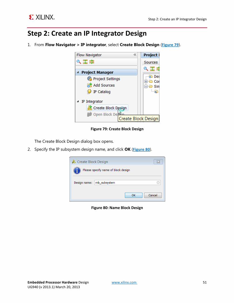
Step 2: Create an IP Integrator Design From Flow Navigator > IP integrator, select Create Block Design (Figure 79). 1.
Figure 79: Create Block Design
The Create Block Design dialog box opens.
Specify the IP subsystem design name, and click OK (Figure 80). 2.
Figure 80: Name Block Design
Step 2: Create an IP Integrator Design
Embedded Processor Hardware Design www.xilinx.com 52 UG940 (v 2013.1) March 20, 2013
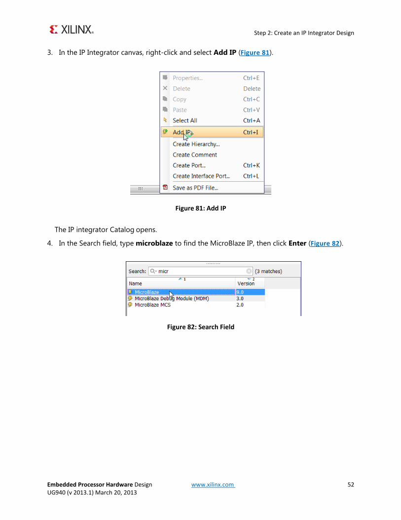
In the IP Integrator canvas, right-click and select Add IP (Figure 81). 3.
Figure 81: Add IP
The IP integrator Catalog opens.
In the Search field, type microblaze to find the MicroBlaze IP, then click Enter (Figure 82). 4.
Figure 82: Search Field
Step 2: Create an IP Integrator Design
Embedded Processor Hardware Design www.xilinx.com 53 UG940 (v 2013.1) March 20, 2013
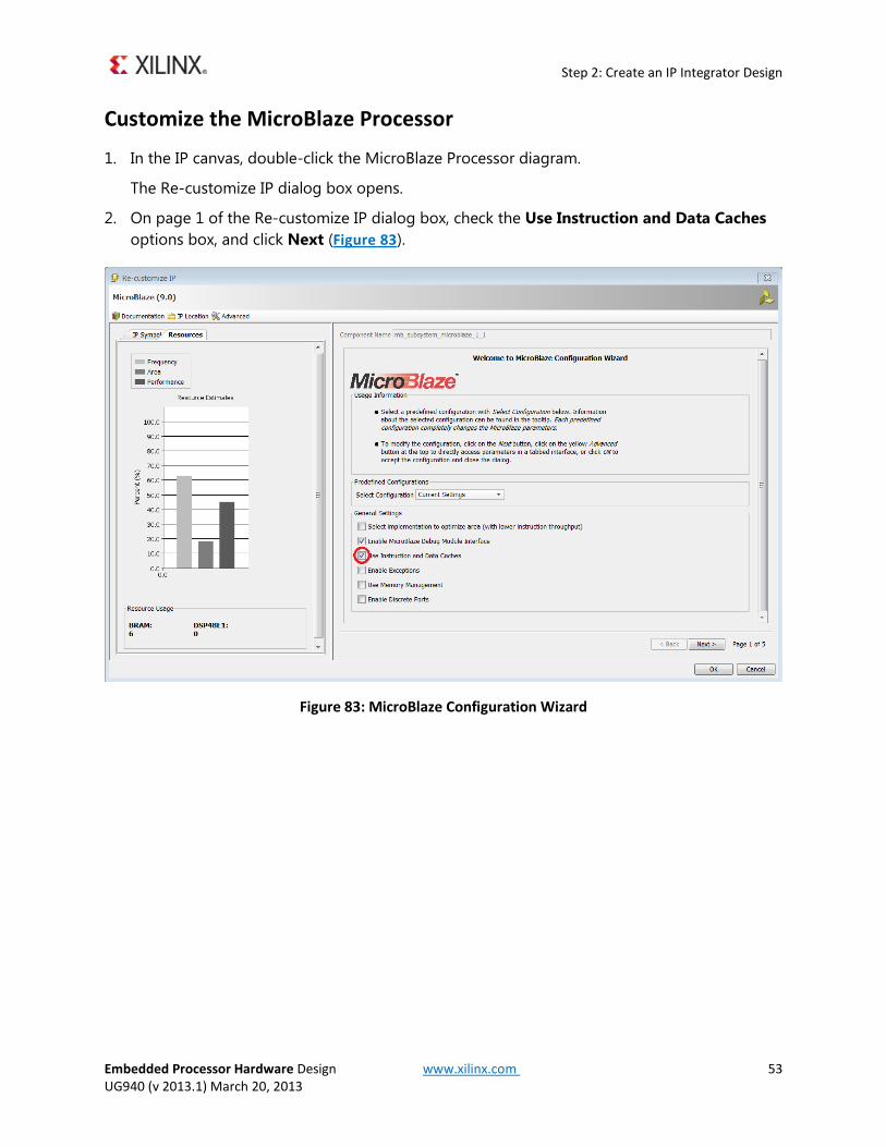
Customize the MicroBlaze Processor
In the IP canvas, double-click the MicroBlaze Processor diagram. 1.
The Re-customize IP dialog box opens.
On page 1 of the Re-customize IP dialog box, check the Use Instruction and Data Caches 2.options box, and click Next (Figure 83).
Figure 83: MicroBlaze Configuration Wizard
Step 2: Create an IP Integrator Design
Embedded Processor Hardware Design www.xilinx.com 54 UG940 (v 2013.1) March 20, 2013
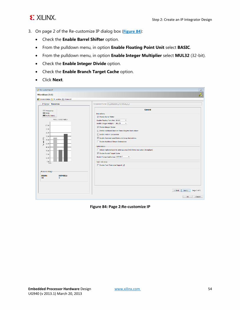
On page 2 of the Re-customize IP dialog box (Figure 84): 3.
• Check the Enable Barrel Shifter option.
• From the pulldown menu, in option Enable Floating Point Unit select BASIC.
• From the pulldown menu, in option Enable Integer Multiplier select MUL32 (32-bit).
• Check the Enable Integer Divide option.
• Check the Enable Branch Target Cache option.
• Click Next.
Figure 84: Page 2:Re-customize IP

Step 2: Create an IP Integrator Design
Embedded Processor Hardware Design www.xilinx.com 55 UG940 (v 2013.1) March 20, 2013
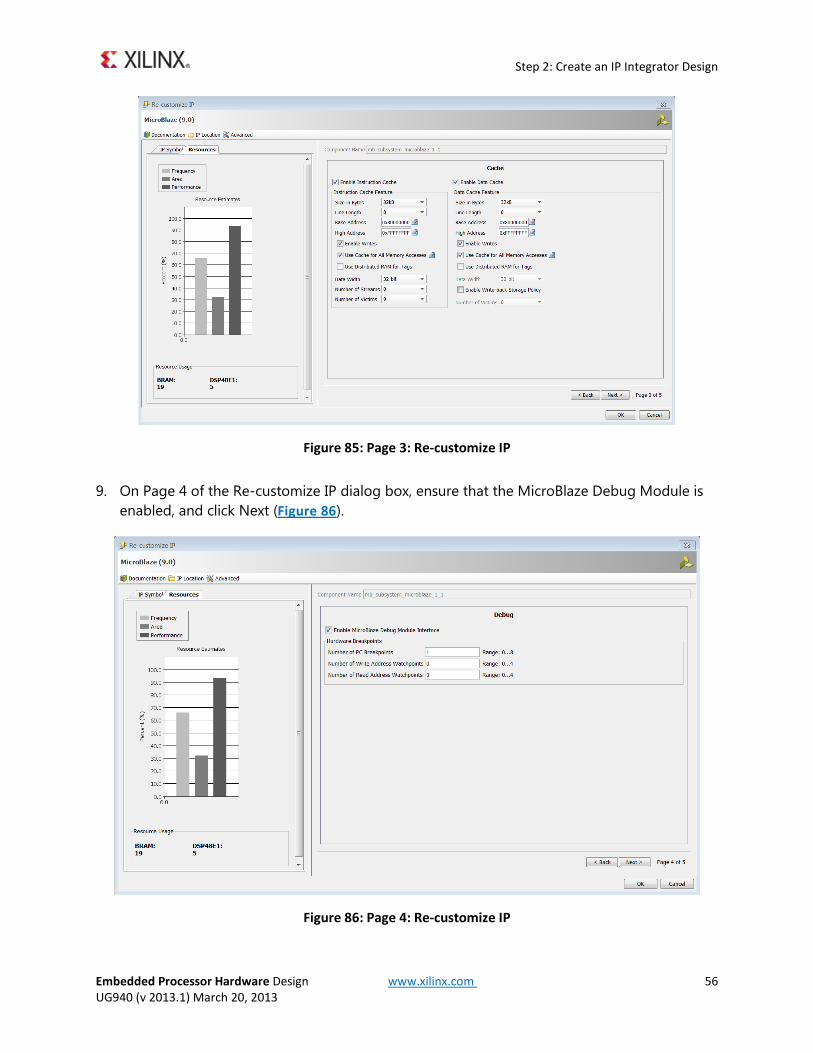
On page 3 of the MicroBlaze Re-customize IP dialog box (Figure 85): 4.
• For both the Instruction Cache and Data Cache:
• Set the Size in Bytes option to 32 KB.
• Set the Line length option to 8.
• Set High Address to 0xFFFFFFFF.
• Set the Base Address to 0x80000000.
• Enable Use Cache for All Memory Accesses for both Instruction Cache as well as Data Cache by clicking on the edit icon first and then checking the check box
Next, ensure that the size of the cacheable segment of memory (that is, the memory space 5.between the Base and High addresses of the Instruction Cache and Data Cache) is a power of 2.
Additionally, ensure that the Base address and the High address of both Data Cache and 6.Instruction Cache are the same.
Ensure that all IP that are slaves of the Instruction Cache , and that the Data Cache buses 7.fall within this cacheable segment. Otherwise, the MicroBlaze processor cannot access those IP.
Note: For any IP connected only to the Instruction Cache and Data Cache bus, you must enable the Use Cache for All Memory Access option. In this example, the Instruction Cache and Data Cache buses are the sole masters of DDR and block RAM; therefore, you must enable this option. In other configurations, you must decide whether to enable this option per the design requirements.
Click Next. 8.
Step 2: Create an IP Integrator Design
Embedded Processor Hardware Design www.xilinx.com 56 UG940 (v 2013.1) March 20, 2013
Figure 85: Page 3: Re-customize IP
On Page 4 of the Re-customize IP dialog box, ensure that the MicroBlaze Debug Module is 9.enabled, and click Next (Figure 86).
Figure 86: Page 4: Re-customize IP
Step 2: Create an IP Integrator Design
Embedded Processor Hardware Design www.xilinx.com 57 UG940 (v 2013.1) March 20, 2013
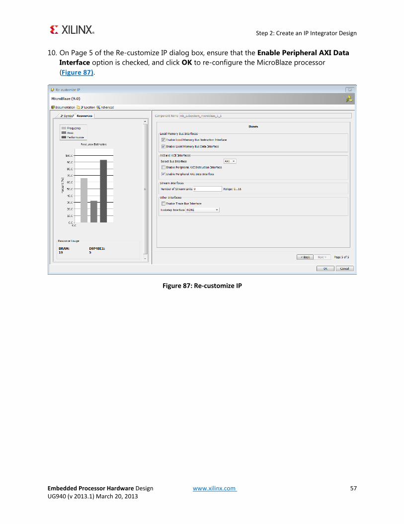
On Page 5 of the Re-customize IP dialog box, ensure that the Enable Peripheral AXI Data 10.Interface option is checked, and click OK to re-configure the MicroBlaze processor (Figure 87).
Figure 87: Re-customize IP
Step 2: Create an IP Integrator Design
Embedded Processor Hardware Design www.xilinx.com 58 UG940 (v 2013.1) March 20, 2013
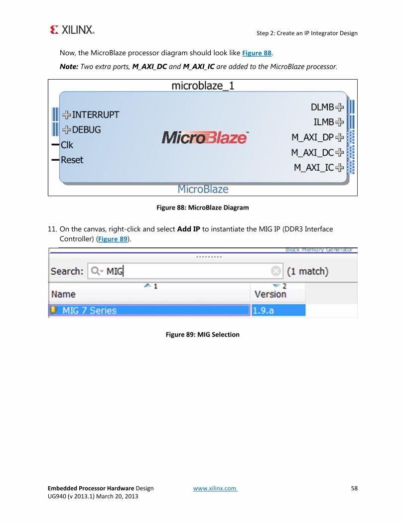
Now, the MicroBlaze processor diagram should look like Figure 88.
Note: Two extra ports, M_AXI_DC and M_AXI_IC are added to the MicroBlaze processor.
Figure 88: MicroBlaze Diagram
On the canvas, right-click and select Add IP to instantiate the MIG IP (DDR3 Interface 11.Controller) (Figure 89).
Figure 89: MIG Selection
Step 2: Create an IP Integrator Design
Embedded Processor Hardware Design www.xilinx.com 59 UG940 (v 2013.1) March 20, 2013
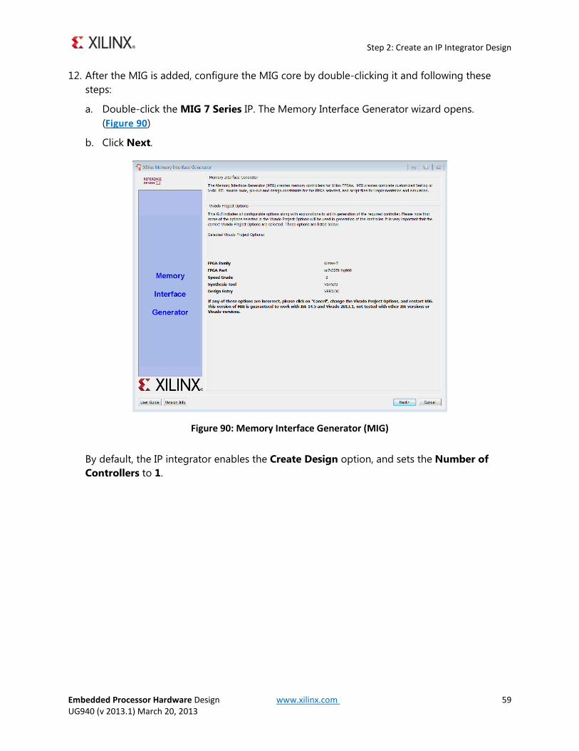
After the MIG is added, configure the MIG core by double-clicking it and following these 12.steps:
a. Double-click the MIG 7 Series IP. The Memory Interface Generator wizard opens. (Figure 90)
b. Click Next.
Figure 90: Memory Interface Generator (MIG)
By default, the IP integrator enables the Create Design option, and sets the Number of Controllers to 1.

Step 2: Create an IP Integrator Design
Embedded Processor Hardware Design www.xilinx.com 60 UG940 (v 2013.1) March 20, 2013
c. Ensure that the AXI4 interface checkbox is checked, and click Next (Figure 91).
Figure 91: Page 2: MIG Options
d. In the Pin Compatible FPGAs page, select nothing, and click Next.
e. In the next page, DDR3 SDRAM memory is checked by default, click Next.
f. Set the value of the Clock Period to 2500 ps (400.00 MHz), and select the Memory Type as SODIMMs. This changes the Memory Part to MT8JTF12864HZ-1G6.
Step 2: Create an IP Integrator Design
Embedded Processor Hardware Design www.xilinx.com 61 UG940 (v 2013.1) March 20, 2013
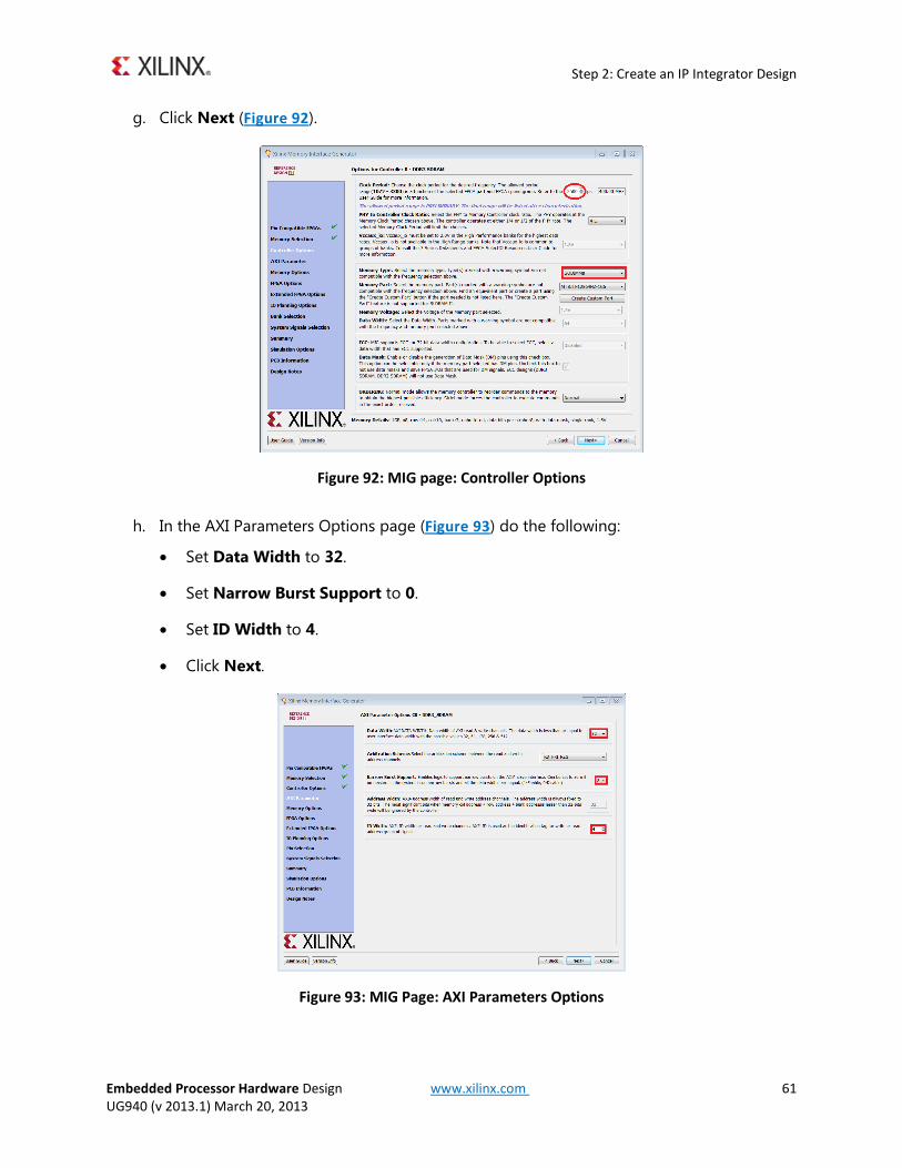
g. Click Next (Figure 92).
Figure 92: MIG page: Controller Options
h. In the AXI Parameters Options page (Figure 93) do the following:
• Set Data Width to 32.
• Set Narrow Burst Support to 0.
• Set ID Width to 4.
• Click Next.
Figure 93: MIG Page: AXI Parameters Options
Step 2: Create an IP Integrator Design
Embedded Processor Hardware Design www.xilinx.com 62 UG940 (v 2013.1) March 20, 2013
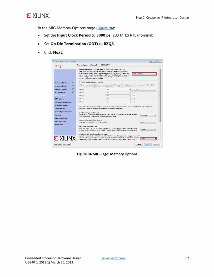
i. In the MIG Memory Options page (Figure 94):
• Set the Input Clock Period to 5000 ps (200 MHz) RTL (nominal)
• Set On Die Termination (ODT) to RZQ6.
• Click Next.
Figure 94:MIG Page: Memory Options
Step 2: Create an IP Integrator Design
Embedded Processor Hardware Design www.xilinx.com 63 UG940 (v 2013.1) March 20, 2013
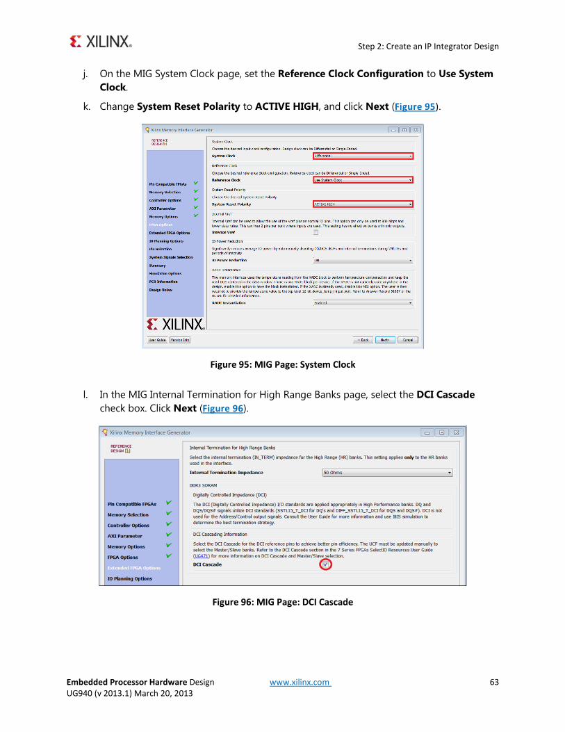
j. On the MIG System Clock page, set the Reference Clock Configuration to Use System Clock.
k. Change System Reset Polarity to ACTIVE HIGH, and click Next (Figure 95).
Figure 95: MIG Page: System Clock
l. In the MIG Internal Termination for High Range Banks page, select the DCI Cascade check box. Click Next (Figure 96).
Figure 96: MIG Page: DCI Cascade
Step 2: Create an IP Integrator Design
Embedded Processor Hardware Design www.xilinx.com 64 UG940 (v 2013.1) March 20, 2013
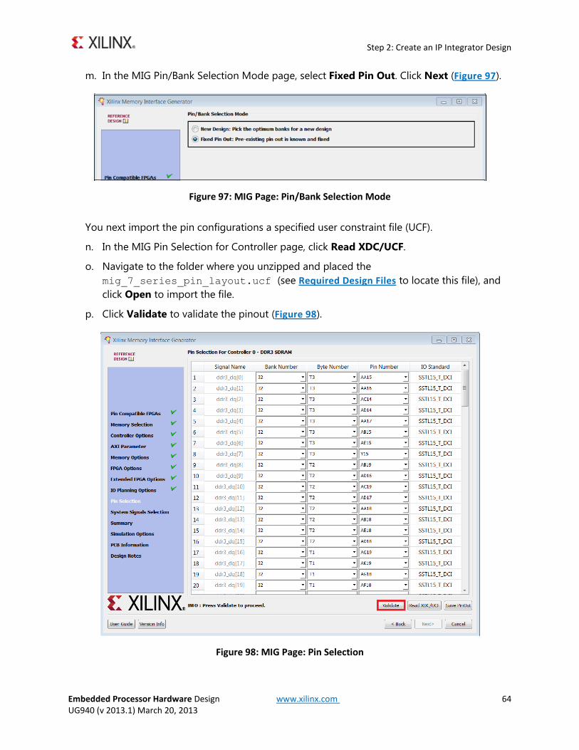
m. In the MIG Pin/Bank Selection Mode page, select Fixed Pin Out. Click Next (Figure 97).
Figure 97: MIG Page: Pin/Bank Selection Mode
You next import the pin configurations a specified user constraint file (UCF).
n. In the MIG Pin Selection for Controller page, click Read XDC/UCF.
o. Navigate to the folder where you unzipped and placed the mig_7_series_pin_layout.ucf (see Required Design Files to locate this file), and click Open to import the file.
p. Click Validate to validate the pinout (Figure 98).
Figure 98: MIG Page: Pin Selection
Step 2: Create an IP Integrator Design
Embedded Processor Hardware Design www.xilinx.com 65 UG940 (v 2013.1) March 20, 2013
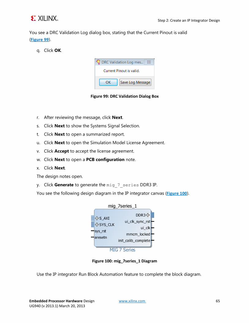
You see a DRC Validation Log dialog box, stating that the Current Pinout is valid (Figure 99).
q. Click OK.
Figure 99: DRC Validation Dialog Box
r. After reviewing the message, click Next.
s. Click Next to show the Systems Signal Selection.
t. Click Next to open a summarized report.
u. Click Next to open the Simulation Model License Agreement.
v. Click Accept to accept the license agreement.
w. Click Next to open a PCB configuration note.
x. Click Next.
The design notes open.
y. Click Generate to generate the mig_7_series DDR3 IP.
You see the following design diagram in the IP integrator canvas (Figure 100).
Figure 100: mig_7series_1 Diagram
Use the IP integrator Run Block Automation feature to complete the block diagram.
Step 2: Create an IP Integrator Design
Embedded Processor Hardware Design www.xilinx.com 66 UG940 (v 2013.1) March 20, 2013
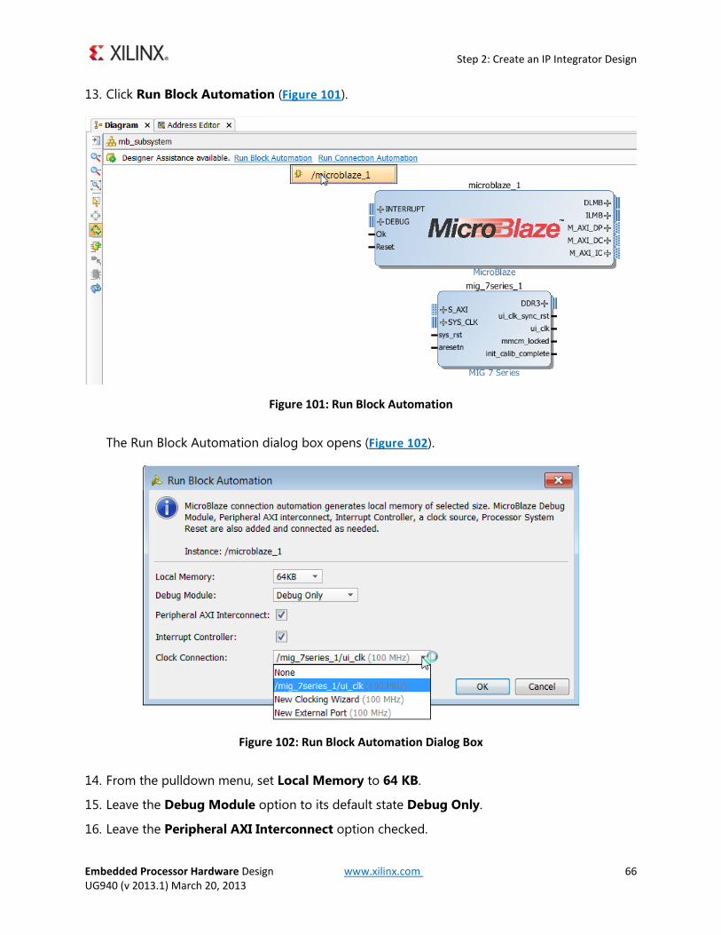
Click Run Block Automation (Figure 101). 13.
Figure 101: Run Block Automation
The Run Block Automation dialog box opens (Figure 102).
Figure 102: Run Block Automation Dialog Box
From the pulldown menu, set Local Memory to 64 KB. 14.
Leave the Debug Module option to its default state Debug Only. 15.
Leave the Peripheral AXI Interconnect option checked. 16.
Step 2: Create an IP Integrator Design
Embedded Processor Hardware Design www.xilinx.com 67 UG940 (v 2013.1) March 20, 2013
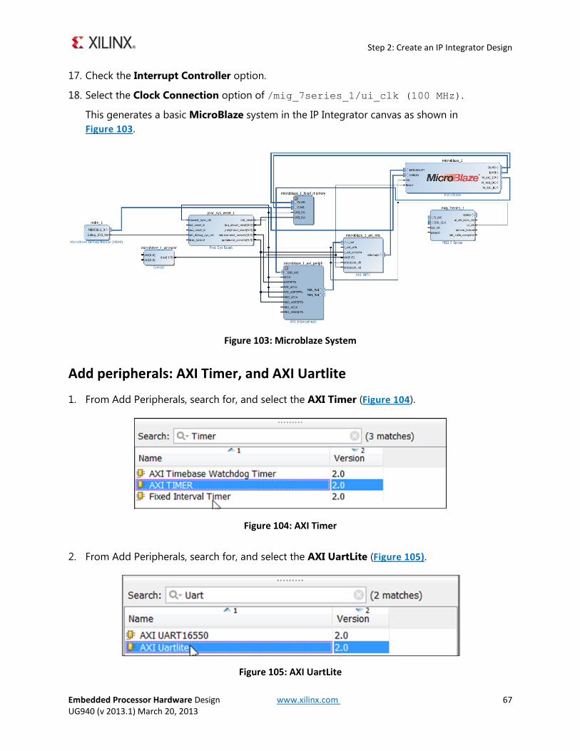
Check the Interrupt Controller option. 17.
Select the Clock Connection option of /mig_7series_1/ui_clk (100 MHz). 18.
This generates a basic MicroBlaze system in the IP Integrator canvas as shown in Figure 103.
Figure 103: Microblaze System
Add peripherals: AXI Timer, and AXI Uartlite
From Add Peripherals, search for, and select the AXI Timer (Figure 104). 1.
Figure 104: AXI Timer
From Add Peripherals, search for, and select the AXI UartLite (Figure 105). 2.
Figure 105: AXI UartLite
Step 2: Create an IP Integrator Design
Embedded Processor Hardware Design www.xilinx.com 68 UG940 (v 2013.1) March 20, 2013
Make a connection between the /mig_7series_1/ui_clk_sync_rst port and 3./proc_sys_reset_1/ext_reset_in port. To do this hover the mouse over the ui_clk_sync_rst port or the ext_reset_in port.
The cursor changes to a pencil to signify that you can draw a connection.
Click the port and drag the pencil over to the destination port (while clicking the mouse) and 4.let go of the mouse when you are on the destination port.
Notice that a checkmark shows where there are possible connections (Figure 105).
Figure 106: Port Connections
Use Connection Automation
Use the IP integrator Connection Automation feature to make some of the connections in the subsystem design.
Click Run Connection Automation (Figure 107). 1.
Figure 107: Run Connection Automation
The Run Connection Automation feature provides several connection options that you can select to make connections between the MicroBlaze processor and the peripherals using the AXI Interconnect.
Step 2: Create an IP Integrator Design
Embedded Processor Hardware Design www.xilinx.com 69 UG940 (v 2013.1) March 20, 2013
Click Run Connection Automation and select /axi_timer_1/s_axi (Figure 108). 2.
You make the connections to the MIG later.
Figure 108: axi_timer_1/s_axi
The Run Connection Automation dialog box opens (Figure 109).
Click OK. 3.
Figure 109: Run Connection Automation Dialog Box
This connects the s_axi port of the timer to the AXI Interconnect peripheral.
Click Run Connection Automation again, and select /axi_uartlite_1/s_axi (Figure 110). 4.
Figure 110: axi_uartlite_1
The Run Connection Automation dialog opens, indicating the connection that is possible to make.
Step 2: Create an IP Integrator Design
Embedded Processor Hardware Design www.xilinx.com 70 UG940 (v 2013.1) March 20, 2013
Click Run Connection Automation and select /axi_uartlite_1/uart. (Figure 111). 5.
Figure 111: axi_uartlite_1
The Run Connection Automation dialog box opens.
Click OK. 6.
This connects the uart pin of the Uartlite to external ports.
At this point, your IP integrator canvas looks like Figure 112 .
Figure 112: MicroBlaze Connected to UART and AXI Timer
Step 2: Create an IP Integrator Design
Embedded Processor Hardware Design www.xilinx.com 71 UG940 (v 2013.1) March 20, 2013
Concatenate Interrupt Signals
Now, you complete the input connections to the Concat IP. The Concat IP is used to concatenate the interrupt signal generated from the AXI Timer and the AXI Uartlite.
First, connect the interrupt port of the AXI Timer to the input port In0[0:0] of Concat. 1.
Connect the interrupt port of AXI Uartlite to the input port In1[0:0] of Concat. The 2.connections should look like Figure 113.
Figure 113: Connected Interrupt Ports
Add an AXI BRAM Controller and a Block Memory Generator IP by right-clicking the IP 3.integrator canvas, and typing the names in the IP Catalog Search box (Figure 114 and Figure 115).
Figure 114: AXI BRAM Controller
Figure 115: Block Memory Controller
Step 2: Create an IP Integrator Design
Embedded Processor Hardware Design www.xilinx.com 72 UG940 (v 2013.1) March 20, 2013
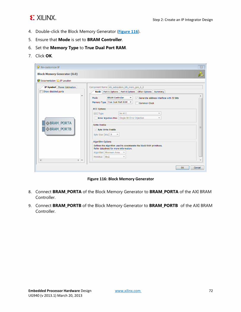
Double-click the Block Memory Generator (Figure 116). 4.
Ensure that Mode is set to BRAM Controller. 5.
Set the Memory Type to True Dual Port RAM. 6.
Click OK. 7.
Figure 116: Block Memory Generator
Connect BRAM_PORTA of the Block Memory Generator to BRAM_PORTA of the AXI BRAM 8.Controller.
Connect BRAM_PORTB of the Block Memory Generator to BRAM_PORTB of the AXI BRAM 9.Controller.
Step 2: Create an IP Integrator Design
Embedded Processor Hardware Design www.xilinx.com 73 UG940 (v 2013.1) March 20, 2013
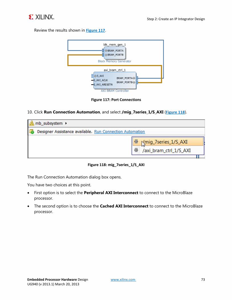
Review the results shown in Figure 117.
Figure 117: Port Connections
Click Run Connection Automation, and select /mig_7series_1/S_AXI (Figure 118). 10.
Figure 118: mig_7series_1/S_AXI
The Run Connection Automation dialog box opens.
You have two choices at this point.
• First option is to select the Peripheral AXI Interconnect to connect to the MicroBlaze processor.
• The second option is to choose the Cached AXI Interconnect to connect to the MicroBlaze processor.
Step 2: Create an IP Integrator Design
Embedded Processor Hardware Design www.xilinx.com 74 UG940 (v 2013.1) March 20, 2013
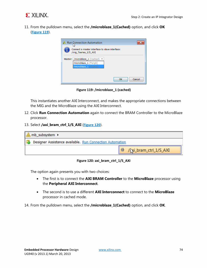
From the pulldown menu, select the /microblaze_1(Cached) option, and click OK 11.(Figure 119).
Figure 119: /microblaze_1 (cached)
This instantiates another AXI Interconnect, and makes the appropriate connections between the MIG and the MicroBlaze using the AXI Interconnect.
Click Run Connection Automation again to connect the BRAM Controller to the MicroBlaze 12.processor.
Select /axi_bram_ctrl_1/S_AXI (Figure 120). 13.
Figure 120: axi_bram_ctrl_1/S_AXI
The option again presents you with two choices:
• The first is to connect the AXI BRAM Controller to the MicroBlaze processor using the Peripheral AXI Interconnect.
• The second is to use a different AXI Interconnect to connect to the MicroBlaze processor in cached mode.
From the pulldown menu, select the /microblaze_1(Cached) option, and click OK. 14.
Step 2: Create an IP Integrator Design
Embedded Processor Hardware Design www.xilinx.com 75 UG940 (v 2013.1) March 20, 2013
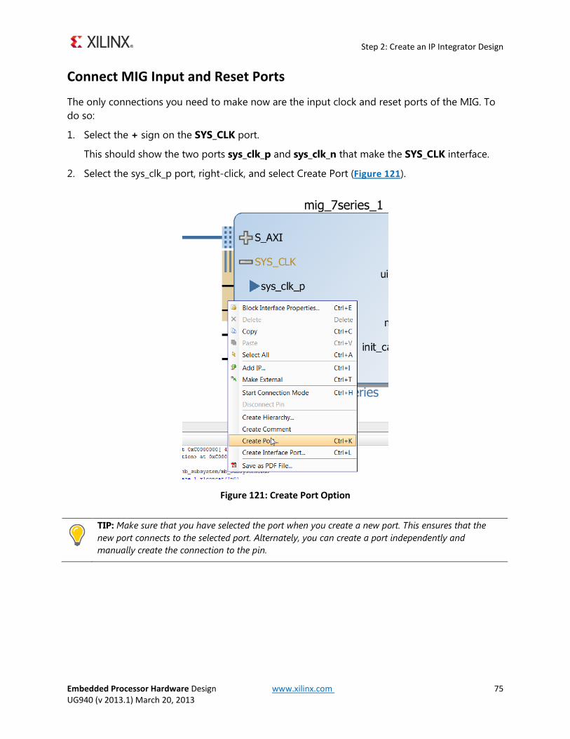
Connect MIG Input and Reset Ports
The only connections you need to make now are the input clock and reset ports of the MIG. To do so:
Select the + sign on the SYS_CLK port. 1.
This should show the two ports sys_clk_p and sys_clk_n that make the SYS_CLK interface.
Select the sys_clk_p port, right-click, and select Create Port (Figure 121). 2.
Figure 121: Create Port Option
TIP: Make sure that you have selected the port when you create a new port. This ensures that the new port connects to the selected port. Alternately, you can create a port independently and manually create the connection to the pin.
Step 2: Create an IP Integrator Design
Embedded Processor Hardware Design www.xilinx.com 76 UG940 (v 2013.1) March 20, 2013
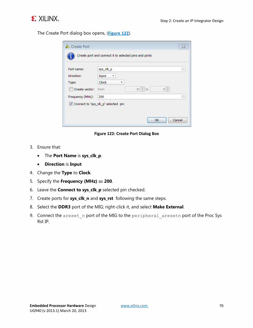
The Create Port dialog box opens, (Figure 122).
Figure 122: Create Port Dialog Box
Ensure that: 3.
• The Port Name is sys_clk_p.
• Direction is Input
Change the Type to Clock. 4.
Specify the Frequency (MHz) as 200. 5.
Leave the Connect to sys_clk_p selected pin checked. 6.
Create ports for sys_clk_n and sys_rst following the same steps. 7.
Select the DDR3 port of the MIG; right-click it, and select Make External. 8.
Connect the areset_n port of the MIG to the peripheral_aresetn port of the Proc Sys 9.Rst IP.
Step 3: Create Constraints
Embedded Processor Hardware Design www.xilinx.com 77 UG940 (v 2013.1) March 20, 2013
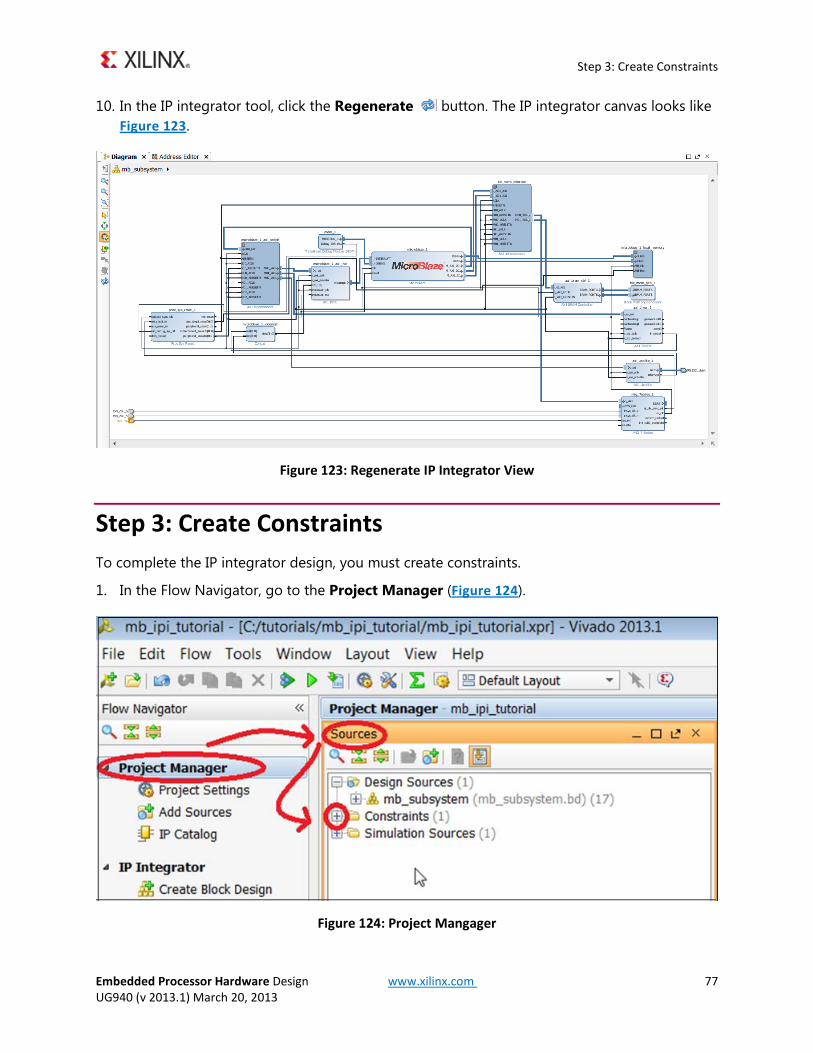
In the IP integrator tool, click the Regenerate button. The IP integrator canvas looks like 10.Figure 123.
Figure 123: Regenerate IP Integrator View
Step 3: Create Constraints To complete the IP integrator design, you must create constraints.
In the Flow Navigator, go to the Project Manager (Figure 124). 1.
Figure 124: Project Mangager
Step 3: Create Constraints
Embedded Processor Hardware Design www.xilinx.com 78 UG940 (v 2013.1) March 20, 2013
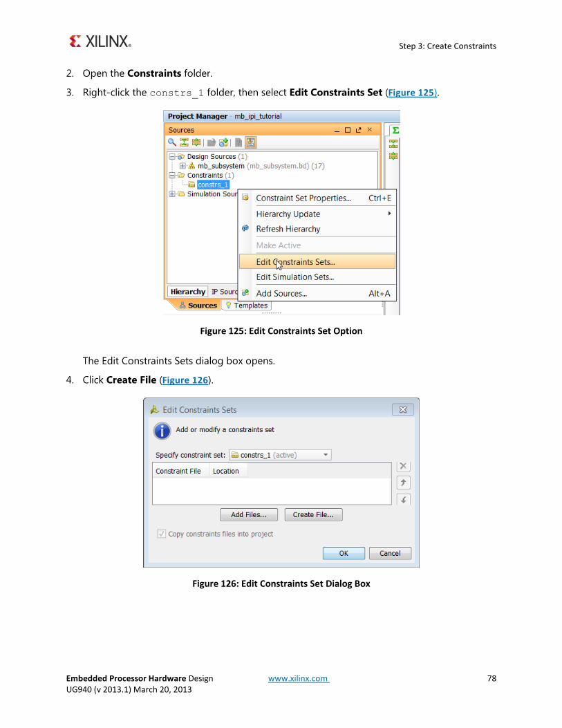
Open the Constraints folder. 2.
Right-click the constrs_1 folder, then select Edit Constraints Set (Figure 125). 3.
Figure 125: Edit Constraints Set Option
The Edit Constraints Sets dialog box opens.
Click Create File (Figure 126). 4.
Figure 126: Edit Constraints Set Dialog Box
Step 3: Create Constraints
Embedded Processor Hardware Design www.xilinx.com 79 UG940 (v 2013.1) March 20, 2013
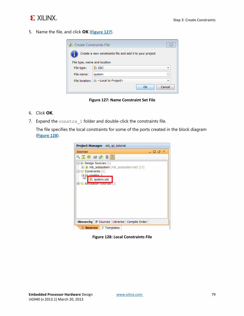
Name the file, and click OK (Figure 127). 5.
Figure 127: Name Constraint Set File
Click OK. 6.
Expand the constrs_1 folder and double-click the constraints file. 7.
The file specifies the local constraints for some of the ports created in the block diagram (Figure 128).
Figure 128: Local Constraints File

Step 3: Create Constraints
Embedded Processor Hardware Design www.xilinx.com 80 UG940 (v 2013.1) March 20, 2013
In the constraints file, add the following lines of code for the KC705 board with the Kintex-7 8.FPGA. set_property LOC AD11 [ get_ports sys_clk_n] set_property IOSTANDARD DIFF_SSTL15 [ get_ports sys_clk_n] set_property LOC AD12 [ get_ports sys_clk_p] set_property IOSTANDARD DIFF_SSTL15 [ get_ports sys_clk_p] set_property LOC AB7 [ get_ports sys_rst] set_property IOSTANDARD LVCMOS15 [ get_ports sys_rst] set_property LOC M19 [ get_ports RX] # additional constraints # create_clock -name sys_clk_pin -period "5.0" [get_ports "sys_clk_p"] # Added for RevC board set_property slave_banks {32 34} [get_iobanks 33]
TIP: You might have noticed that the constraints for the RS232_Uart port are not included in the above constraints file. That is because Vivado automatically generates the appropriate constraints for those ports because you selected the target board as the KC705 board. This is the board automation feature of the Vivado IDE IP integrator that you can use to hook up ports such as clocks, resets, GPIOS, and UART to the pins on the target board.
Save the file by either clicking the Ctrl+S keys, or use the File > File Save menu. 9.
Step 4: Memory Mapping the Peripherals in IP Integrator
Embedded Processor Hardware Design www.xilinx.com 81 UG940 (v 2013.1) March 20, 2013
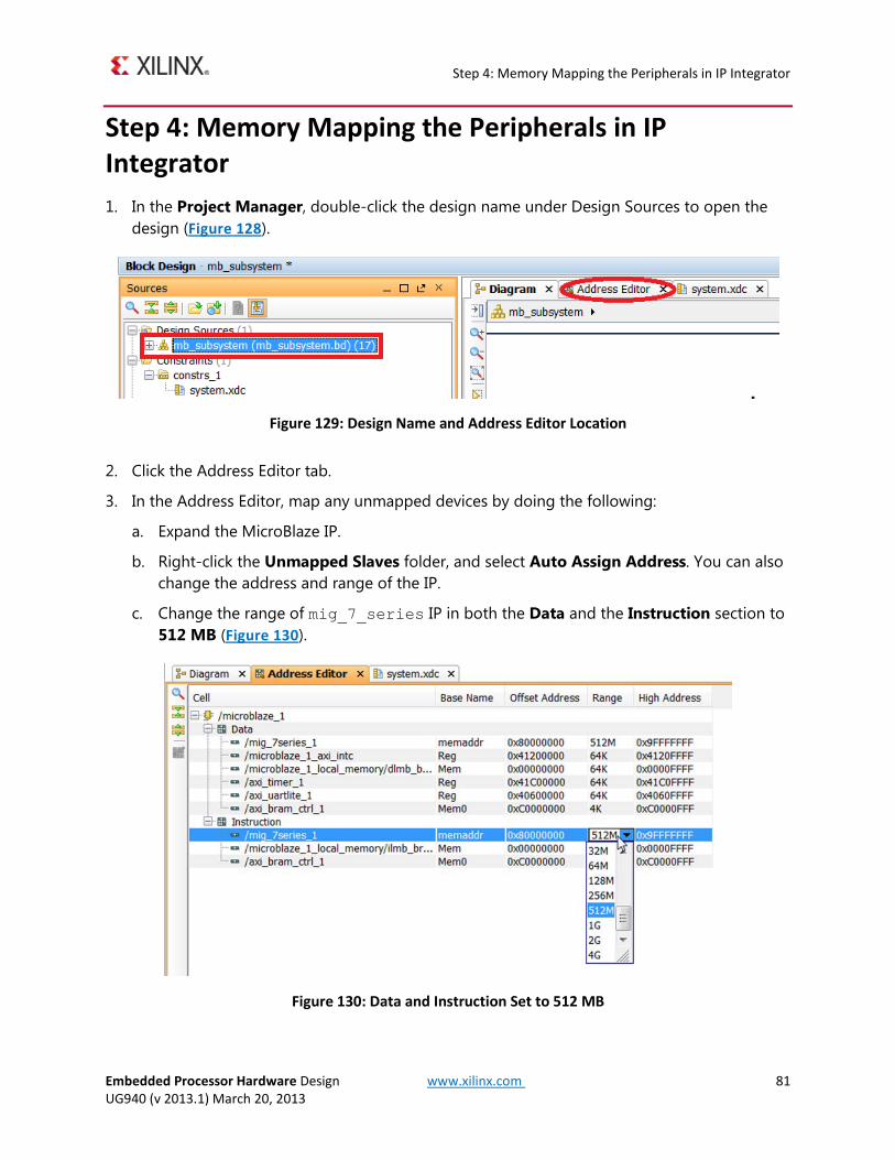
Step 4: Memory Mapping the Peripherals in IP Integrator
In the Project Manager, double-click the design name under Design Sources to open the 1.design (Figure 128).
Figure 129: Design Name and Address Editor Location
Click the Address Editor tab. 2.
In the Address Editor, map any unmapped devices by doing the following: 3.
a. Expand the MicroBlaze IP.
b. Right-click the Unmapped Slaves folder, and select Auto Assign Address. You can also change the address and range of the IP.
c. Change the range of mig_7_series IP in both the Data and the Instruction section to 512 MB (Figure 130).
Figure 130: Data and Instruction Set to 512 MB
Step 5: Creating a Top-Level Verilog Wrapper
Embedded Processor Hardware Design www.xilinx.com 82 UG940 (v 2013.1) March 20, 2013
Save your design. 4.
You must also ensure that the memory in which you are going to run and store your software is within in the cacheable address range that you specified when you assigned values to the cache(s) Base address and cache(s) High address.
This occurs when you enable Instruction Cache and Data Cache, and upon re-configuring the MicroBlaze processor.
To use either MIG DDR or AXI block RAM, those IP must be in the cacheable area; otherwise, the MicroBlaze processor cannot read or write to or from them.
You can also use this map to manually include or exclude IP from the cacheable region or otherwise specify their address.
You can also use this map to manually include or exclude IP from the cacheable region or otherwise specify their address.
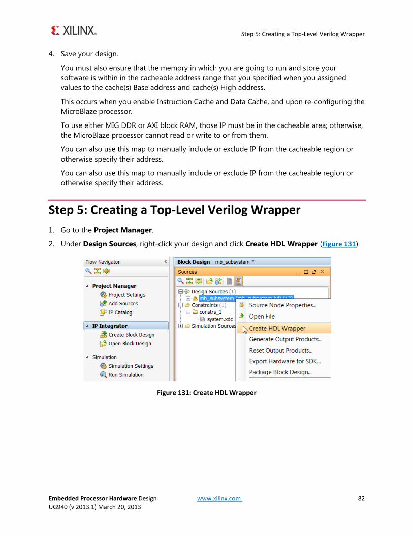
Step 5: Creating a Top-Level Verilog Wrapper Go to the Project Manager. 1.
Under Design Sources, right-click your design and click Create HDL Wrapper (Figure 131). 2.
Figure 131: Create HDL Wrapper
Step 6: Take the design through implementation
Embedded Processor Hardware Design www.xilinx.com 83 UG940 (v 2013.1) March 20, 2013
Step 6: Take the design through implementation In the Flow Navigator:
Click Run Synthesis. 1.
Click Run Implementation. 2.
Click Generate Bitstream 3.
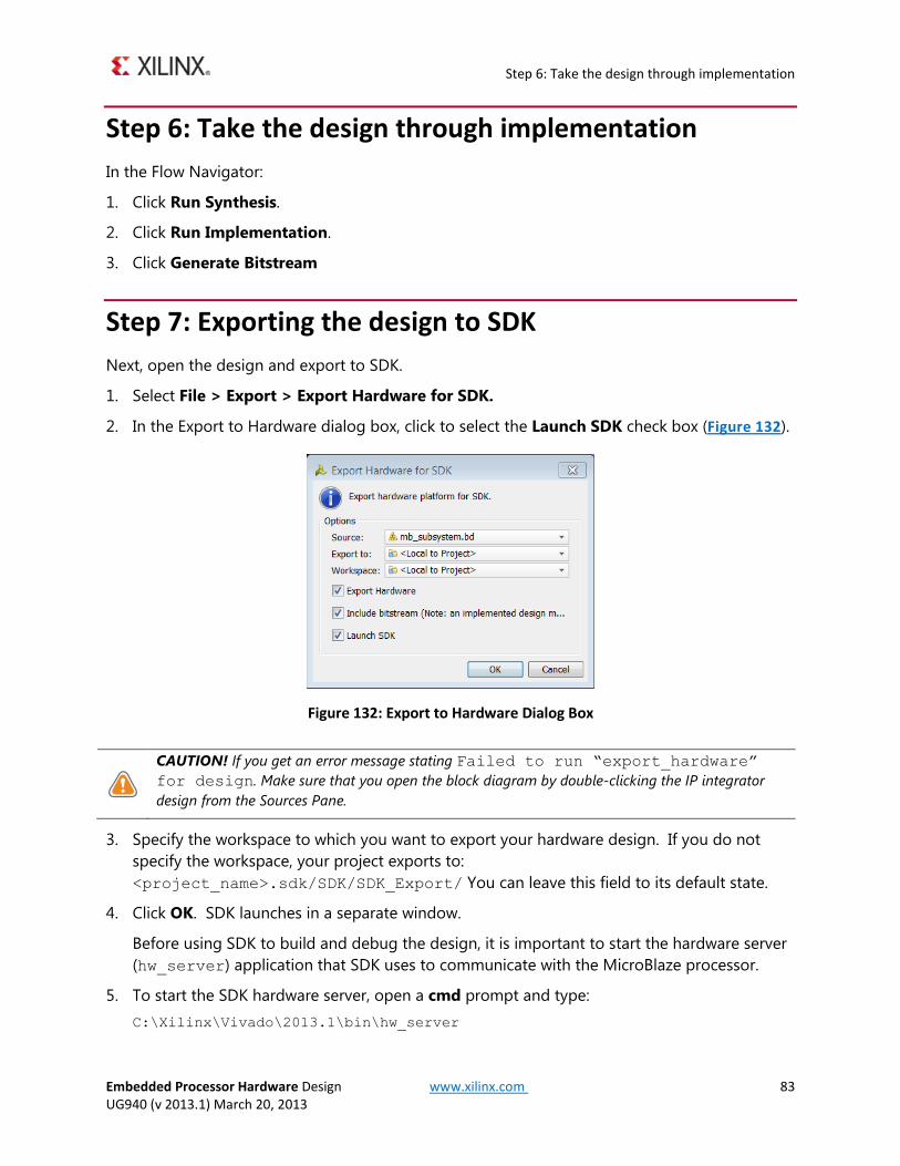
Step 7: Exporting the design to SDK Next, open the design and export to SDK.
Select File > Export > Export Hardware for SDK. 1.
In the Export to Hardware dialog box, click to select the Launch SDK check box (Figure 132). 2.
Figure 132: Export to Hardware Dialog Box
CAUTION! If you get an error message stating Failed to run “export_hardware” for design. Make sure that you open the block diagram by double-clicking the IP integrator design from the Sources Pane.
Specify the workspace to which you want to export your hardware design. If you do not 3.specify the workspace, your project exports to: <project_name>.sdk/SDK/SDK_Export/ You can leave this field to its default state.
Click OK. SDK launches in a separate window. 4.
Before using SDK to build and debug the design, it is important to start the hardware server (hw_server) application that SDK uses to communicate with the MicroBlaze processor.
To start the SDK hardware server, open a cmd prompt and type: 5.C:\Xilinx\Vivado\2013.1\bin\hw_server
Step 8: Configuring FreeRTOS
Embedded Processor Hardware Design www.xilinx.com 84 UG940 (v 2013.1) March 20, 2013
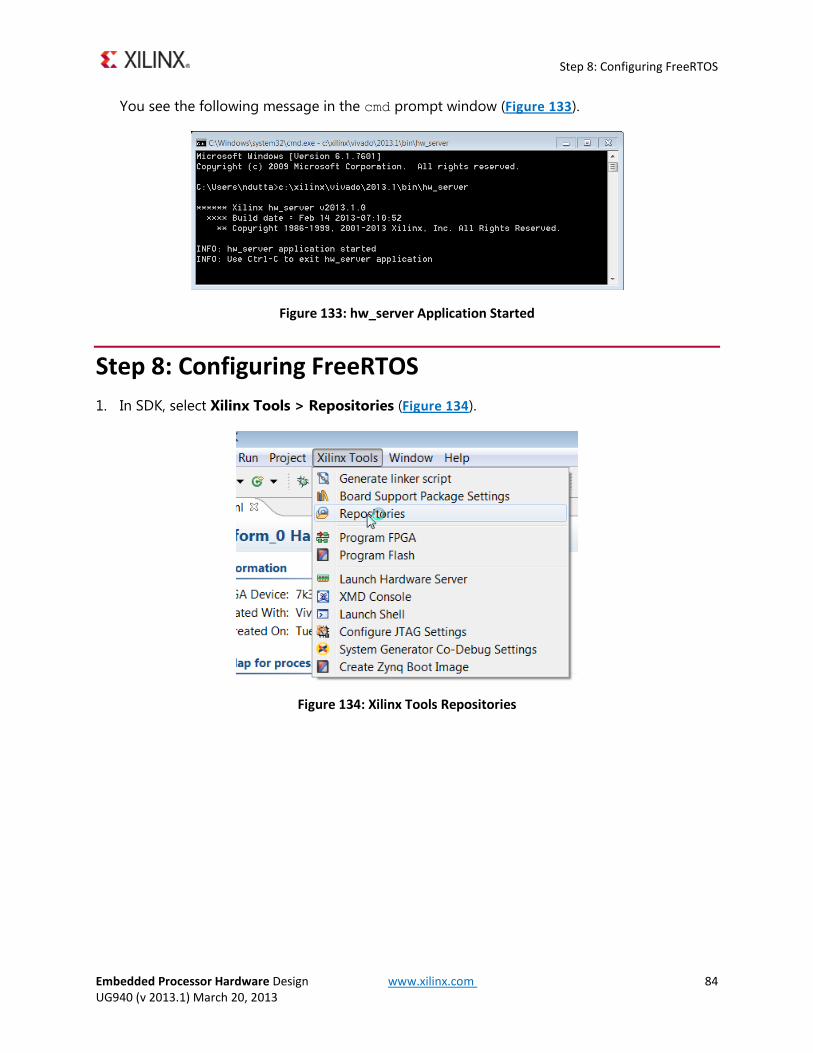
You see the following message in the cmd prompt window (Figure 133).
Figure 133: hw_server Application Started
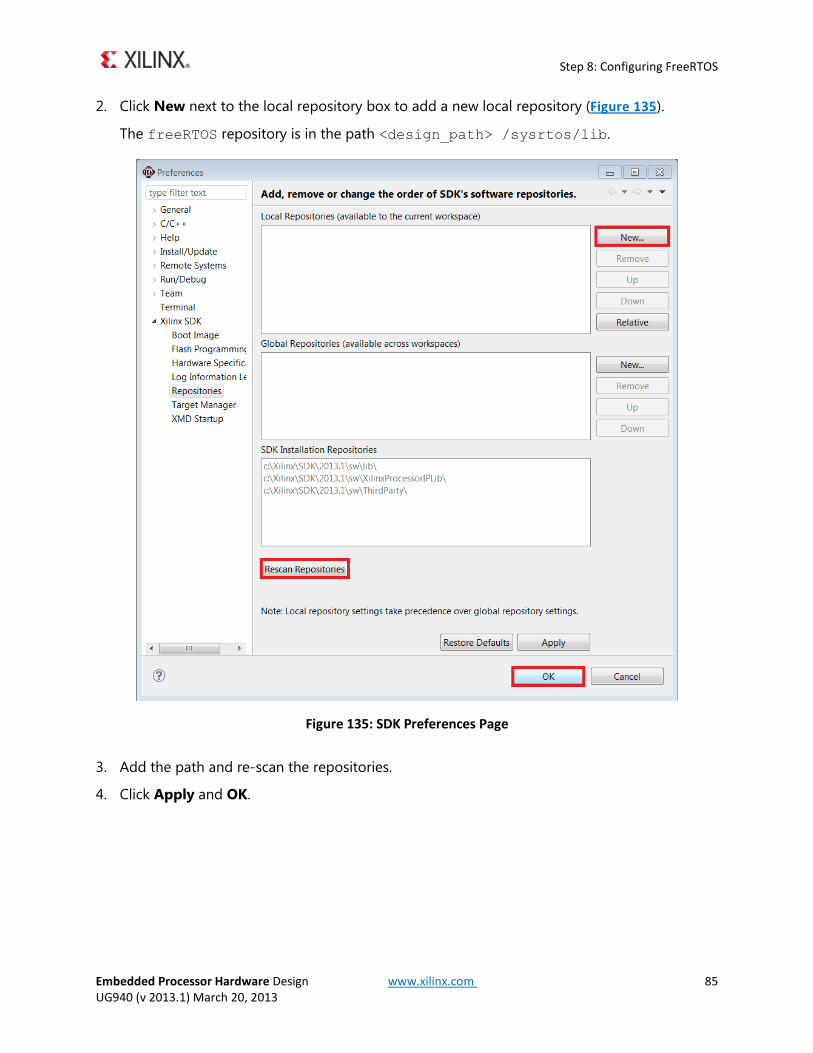
Step 8: Configuring FreeRTOS In SDK, select Xilinx Tools > Repositories (Figure 134). 1.
Figure 134: Xilinx Tools Repositories
Step 8: Configuring FreeRTOS
Embedded Processor Hardware Design www.xilinx.com 85 UG940 (v 2013.1) March 20, 2013
Click New next to the local repository box to add a new local repository (Figure 135). 2.
The freeRTOS repository is in the path <design_path> /sysrtos/lib.
Figure 135: SDK Preferences Page
Add the path and re-scan the repositories. 3.
Click Apply and OK. 4.
Step 9: Creating a freeRTOS “Hello World” Application
Embedded Processor Hardware Design www.xilinx.com 86 UG940 (v 2013.1) March 20, 2013
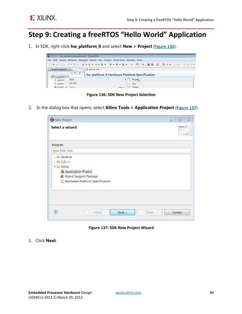
Step 9: Creating a freeRTOS “Hello World” Application 1. In SDK, right-click hw_platform_0 and select New > Project (Figure 136).
Figure 136: SDK New Project Selection
2. In the dialog box that opens, select Xilinx Tools > Application Project (Figure 137).
Figure 137: SDK New Project Wizard
3. Click Next.
Step 9: Creating a freeRTOS “Hello World” Application
Embedded Processor Hardware Design www.xilinx.com 87 UG940 (v 2013.1) March 20, 2013
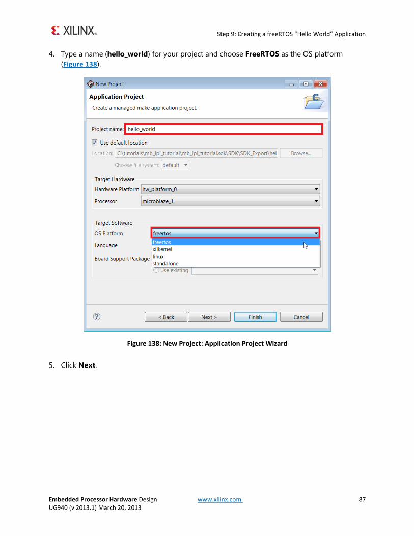
4. Type a name (hello_world) for your project and choose FreeRTOS as the OS platform (Figure 138).
Figure 138: New Project: Application Project Wizard
5. Click Next.
Step 10: Executing the System on a KC705 Board
Embedded Processor Hardware Design www.xilinx.com 88 UG940 (v 2013.1) March 20, 2013
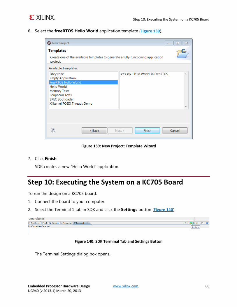
6. Select the freeRTOS Hello World application template (Figure 139).
Figure 139: New Project: Template Wizard
7. Click Finish.
SDK creates a new “Hello World” application.
Step 10: Executing the System on a KC705 Board To run the design on a KC705 board:
Connect the board to your computer. 1.
Select the Terminal 1 tab in SDK and click the Settings button (Figure 140). 2.
Figure 140: SDK Terminal Tab and Settings Button
The Terminal Settings dialog box opens.
Step 10: Executing the System on a KC705 Board
Embedded Processor Hardware Design www.xilinx.com 89 UG940 (v 2013.1) March 20, 2013
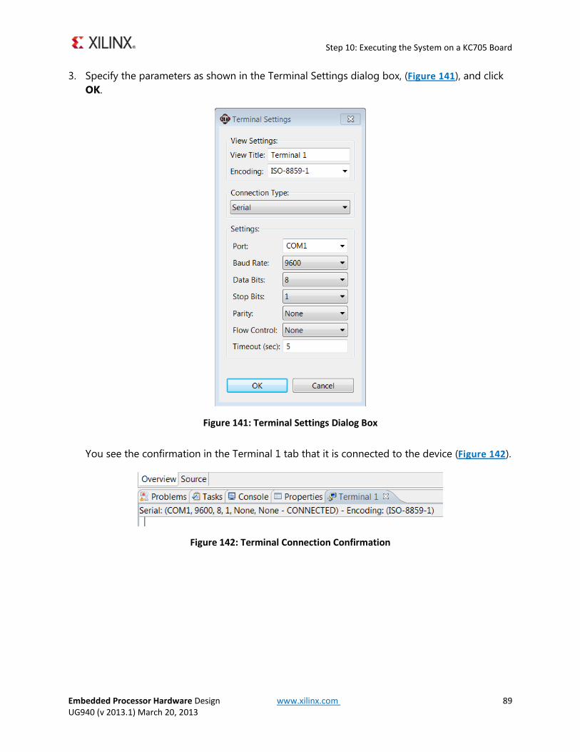
Specify the parameters as shown in the Terminal Settings dialog box, (Figure 141), and click 3.OK.
Figure 141: Terminal Settings Dialog Box
You see the confirmation in the Terminal 1 tab that it is connected to the device (Figure 142).
Figure 142: Terminal Connection Confirmation
Step 10: Executing the System on a KC705 Board
Embedded Processor Hardware Design www.xilinx.com 90 UG940 (v 2013.1) March 20, 2013
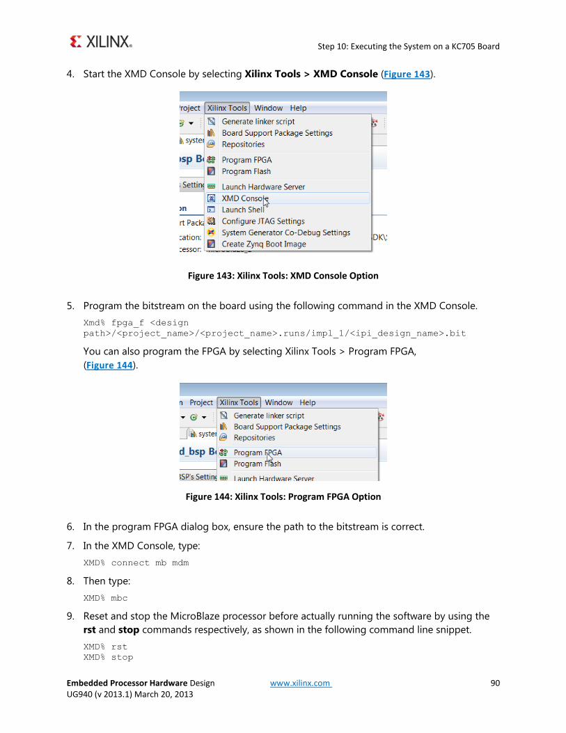
Start the XMD Console by selecting Xilinx Tools > XMD Console (Figure 143). 4.
Figure 143: Xilinx Tools: XMD Console Option
Program the bitstream on the board using the following command in the XMD Console. 5.Xmd% fpga_f <design path>/<project_name>/<project_name>.runs/impl_1/<ipi_design_name>.bit
You can also program the FPGA by selecting Xilinx Tools > Program FPGA, (Figure 144).
Figure 144: Xilinx Tools: Program FPGA Option
In the program FPGA dialog box, ensure the path to the bitstream is correct. 6.
In the XMD Console, type: 7.XMD% connect mb mdm
Then type: 8.XMD% mbc
Reset and stop the MicroBlaze processor before actually running the software by using the 9.rst and stop commands respectively, as shown in the following command line snippet. XMD% rst XMD% stop
Conclusion
Embedded Processor Hardware Design www.xilinx.com 91 UG940 (v 2013.1) March 20, 2013
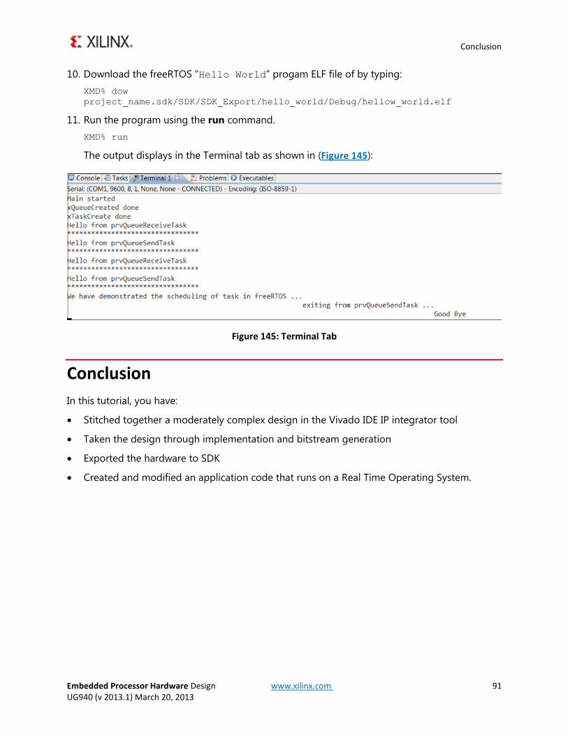
Download the freeRTOS “Hello World” progam ELF file of by typing: 10.XMD% dow project_name.sdk/SDK/SDK_Export/hello_world/Debug/hellow_world.elf
Run the program using the run command. 11.XMD% run
The output displays in the Terminal tab as shown in (Figure 145):
Figure 145: Terminal Tab
Conclusion In this tutorial, you have:
• Stitched together a moderately complex design in the Vivado IDE IP integrator tool
• Taken the design through implementation and bitstream generation
• Exported the hardware to SDK
• Created and modified an application code that runs on a Real Time Operating System.