Embed Size (px)
Citation preview
XMUT303 – Note 2 - 1
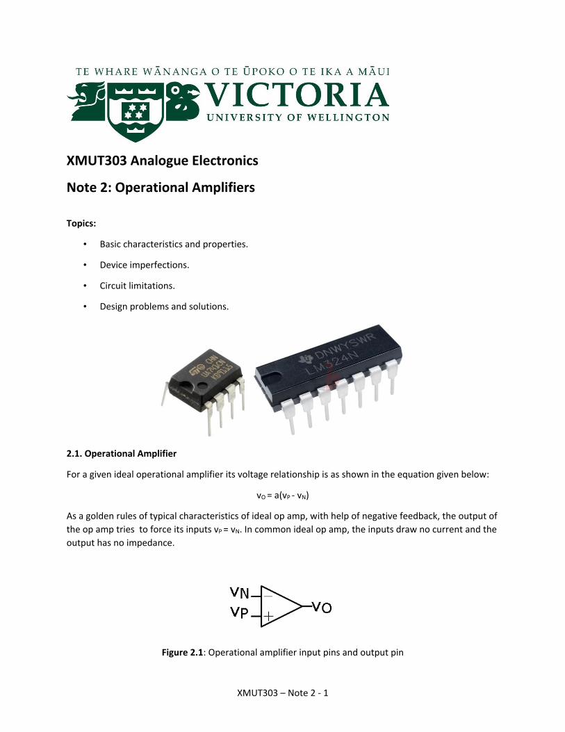
XMUT303 Analogue Electronics
Note 2: Operational Amplifiers
Topics:
• Basic characteristics and properties.
• Device imperfections.
• Circuit limitations.
• Design problems and solutions.
2.1. Operational Amplifier
For a given ideal operational amplifier its voltage relationship is as shown in the equation given below:
vO = a(vP - vN)
As a golden rules of typical characteristics of ideal op amp, with help of negative feedback, the output of
the op amp tries to force its inputs vP = vN. In common ideal op amp, the inputs draw no current and the
output has no impedance.
Figure 2.1: Operational amplifier input pins and output pin
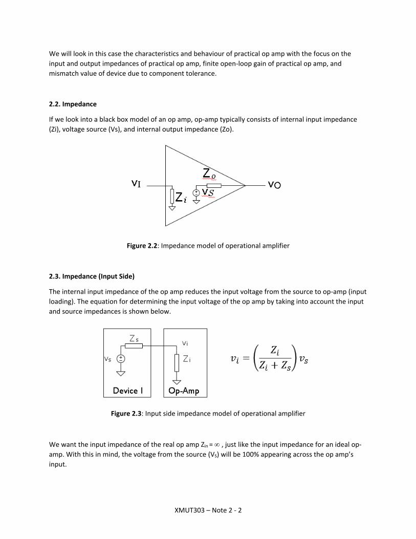
XMUT303 – Note 2 - 2
We will look in this case the characteristics and behaviour of practical op amp with the focus on the
input and output impedances of practical op amp, finite open-loop gain of practical op amp, and
mismatch value of device due to component tolerance.
2.2. Impedance
If we look into a black box model of an op amp, op-amp typically consists of internal input impedance
(Zi), voltage source (Vs), and internal output impedance (Zo).
Figure 2.2: Impedance model of operational amplifier
2.3. Impedance (Input Side)
The internal input impedance of the op amp reduces the input voltage from the source to op-amp (input
loading). The equation for determining the input voltage of the op amp by taking into account the input
and source impedances is shown below.
Figure 2.3: Input side impedance model of operational amplifier
We want the input impedance of the real op amp Zin = , just like the input impedance for an ideal op-
amp. With this in mind, the voltage from the source (VS) will be 100% appearing across the op amp’s
input.
XMUT303 – Note 2 - 3
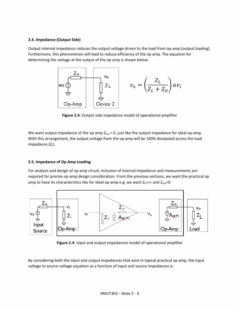
2.4. Impedance (Output Side)
Output internal impedance reduces the output voltage driven to the load from op-amp (output loading).
Furthermore, this phenomenon will lead to reduce efficiency of the op amp. The equation for
determining the voltage at the output of the op amp is shown below.
Figure 2.4: Output side impedance model of operational amplifier
We want output impedance of the op amp Zout = 0, just like the output impedance for ideal op-amp.
With this arrangement, the output voltage from the op amp will be 100% dissipated across the load
impedance (ZL).
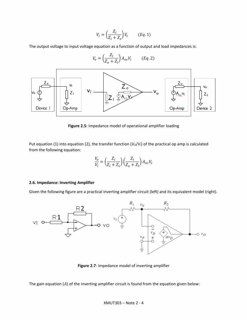
2.5. Impedance of Op Amp Loading
For analysis and design of op amp circuit, inclusion of internal impedance and measurements are
required for precise op-amp design consideration. From the previous sections, we want the practical op
amp to have its characteristics like for ideal op-amp e.g. we want Zin= and Zout=0
Figure 2.4: Input and output impedances model of operational amplifier
By considering both the input and output impedances that exist in typical practical op amp, the input
voltage to source voltage equation as a function of input and source impedances is:
XMUT303 – Note 2 - 4
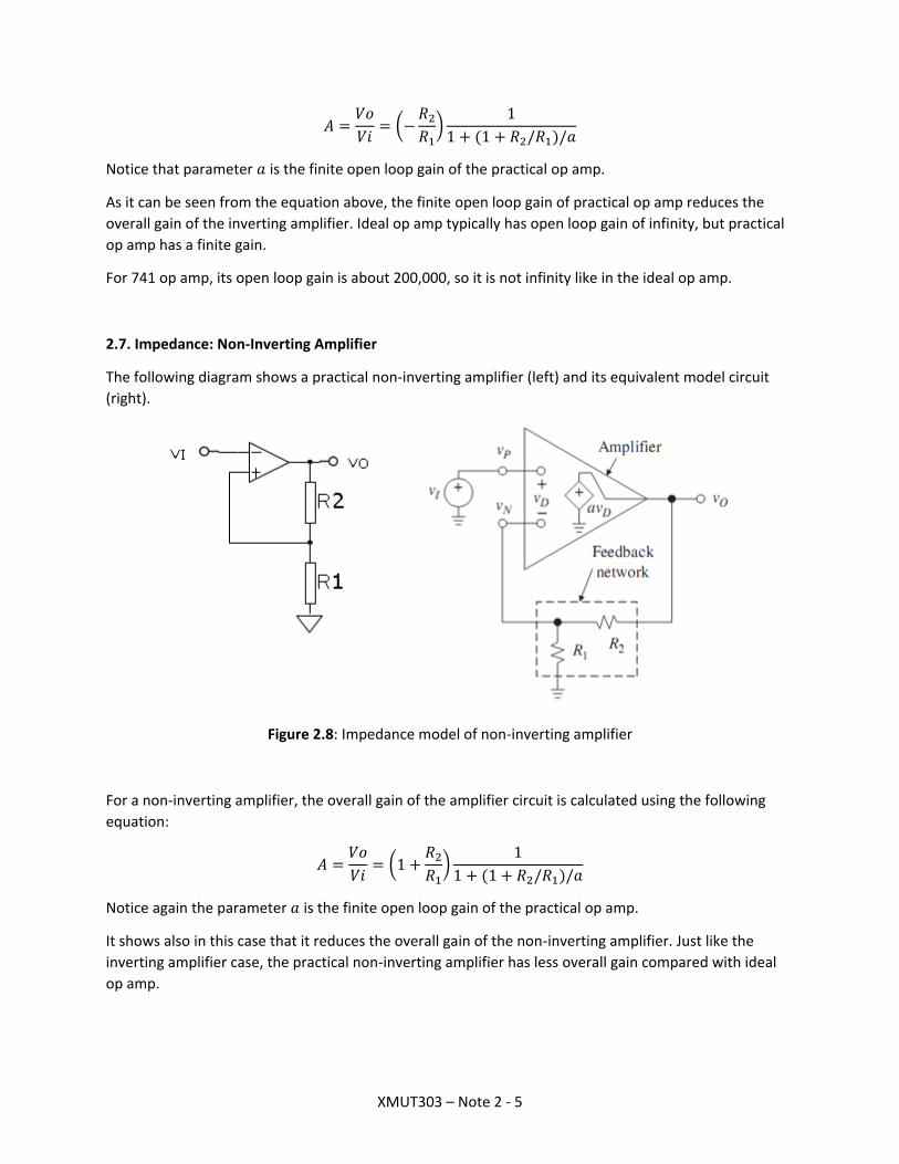
𝑉𝑖 = (𝑍𝑖
𝑍𝑖 + 𝑍𝑠) 𝑉𝑠 (𝐸𝑞. 1)
The output voltage to input voltage equation as a function of output and load impedances is:
𝑉𝑜 = (𝑍𝑙
𝑍𝑜 + 𝑍𝑙) 𝐴𝑜𝑐𝑉𝑖 (𝐸𝑞. 2)
Figure 2.5: Impedance model of operational amplifier loading
Put equation (1) into equation (2), the transfer function (VO/VI) of the practical op amp is calculated
from the following equation:
𝑉𝑜
𝑉𝑖= (
𝑍𝑖
𝑍𝑖 + 𝑍𝑠) (
𝑍𝑙
𝑍𝑜 + 𝑍𝑙) 𝐴𝑜𝑐𝑉𝑠
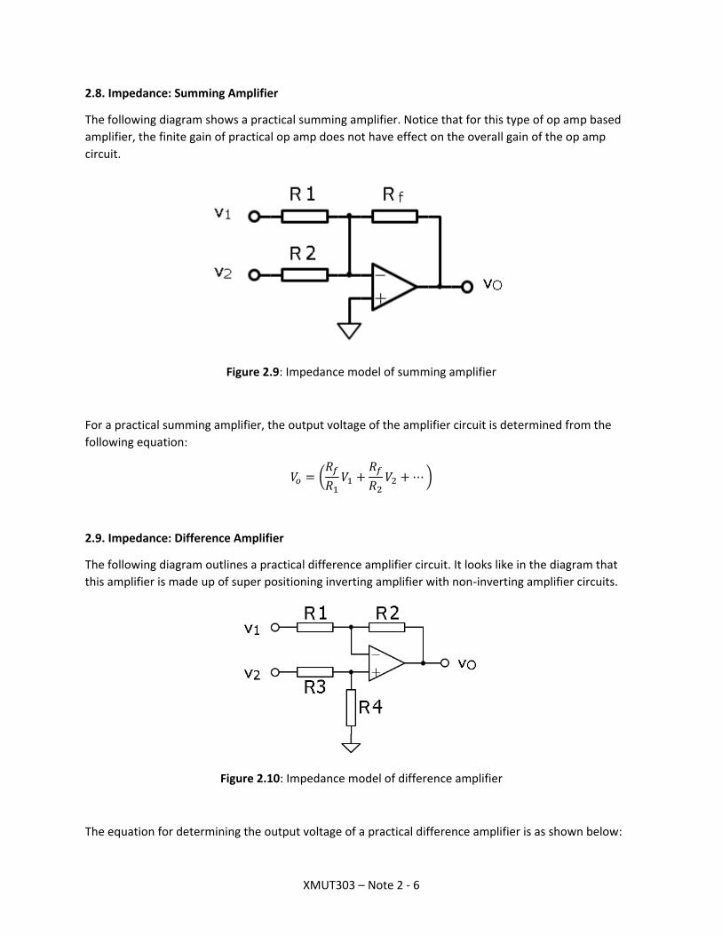
2.6. Impedance: Inverting Amplifier
Given the following figure are a practical inverting amplifier circuit (left) and its equivalent model (right).
Figure 2.7: Impedance model of inverting amplifier
The gain equation (𝐴) of the inverting amplifier circuit is found from the equation given below:
XMUT303 – Note 2 - 5
𝐴 =𝑉𝑜
𝑉𝑖= (−
𝑅2
𝑅1)
1
1 + (1 + 𝑅2/𝑅1)/𝑎
Notice that parameter 𝑎 is the finite open loop gain of the practical op amp.
As it can be seen from the equation above, the finite open loop gain of practical op amp reduces the
overall gain of the inverting amplifier. Ideal op amp typically has open loop gain of infinity, but practical
op amp has a finite gain.
For 741 op amp, its open loop gain is about 200,000, so it is not infinity like in the ideal op amp.
2.7. Impedance: Non-Inverting Amplifier
The following diagram shows a practical non-inverting amplifier (left) and its equivalent model circuit
(right).
Figure 2.8: Impedance model of non-inverting amplifier
For a non-inverting amplifier, the overall gain of the amplifier circuit is calculated using the following
equation:
𝐴 =𝑉𝑜
𝑉𝑖= (1 +
𝑅2
𝑅1)
1
1 + (1 + 𝑅2/𝑅1)/𝑎
Notice again the parameter 𝑎 is the finite open loop gain of the practical op amp.
It shows also in this case that it reduces the overall gain of the non-inverting amplifier. Just like the
inverting amplifier case, the practical non-inverting amplifier has less overall gain compared with ideal
op amp.
XMUT303 – Note 2 - 6
2.8. Impedance: Summing Amplifier
The following diagram shows a practical summing amplifier. Notice that for this type of op amp based
amplifier, the finite gain of practical op amp does not have effect on the overall gain of the op amp
circuit.
Figure 2.9: Impedance model of summing amplifier
For a practical summing amplifier, the output voltage of the amplifier circuit is determined from the
following equation:
𝑉𝑜 = (𝑅𝑓
𝑅1𝑉1 +
𝑅𝑓
𝑅2𝑉2 + ⋯ )
2.9. Impedance: Difference Amplifier
The following diagram outlines a practical difference amplifier circuit. It looks like in the diagram that
this amplifier is made up of super positioning inverting amplifier with non-inverting amplifier circuits.
Figure 2.10: Impedance model of difference amplifier
The equation for determining the output voltage of a practical difference amplifier is as shown below:
XMUT303 – Note 2 - 7
𝑉𝑜 =𝑅2
𝑅1(
1 + 𝑅1/𝑅2
1 + 𝑅3/𝑅4𝑉2 − 𝑉1)
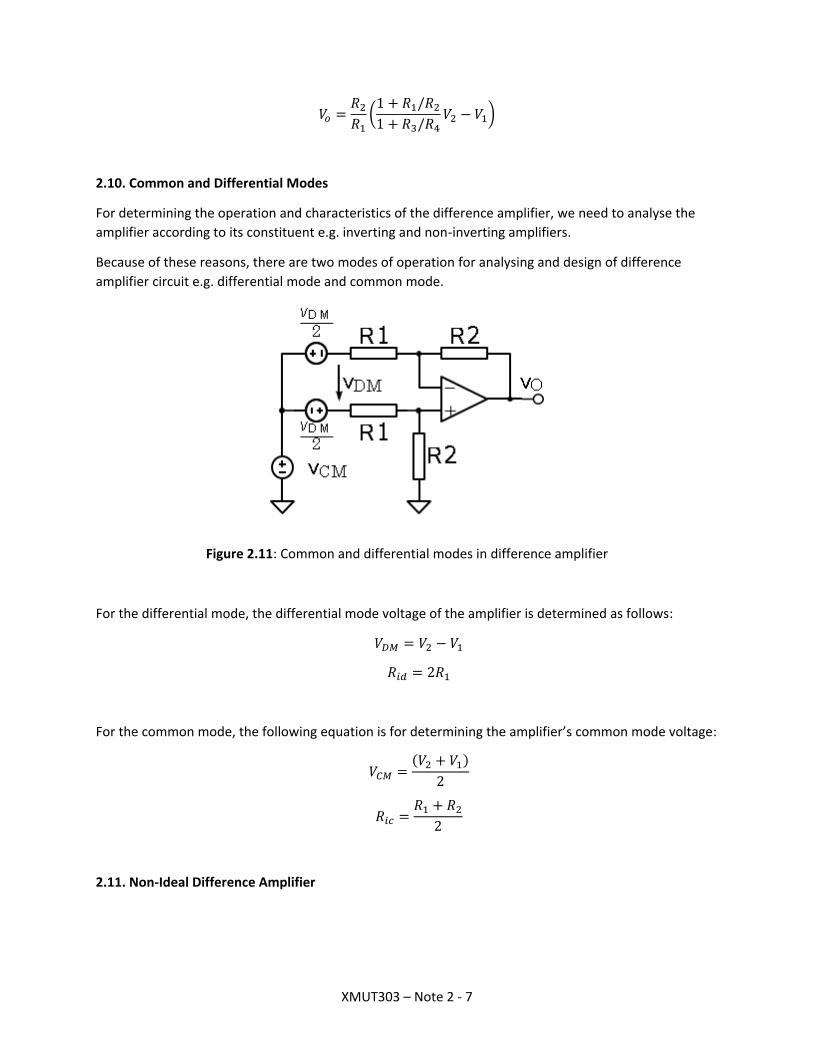
2.10. Common and Differential Modes
For determining the operation and characteristics of the difference amplifier, we need to analyse the
amplifier according to its constituent e.g. inverting and non-inverting amplifiers.
Because of these reasons, there are two modes of operation for analysing and design of difference
amplifier circuit e.g. differential mode and common mode.
Figure 2.11: Common and differential modes in difference amplifier
For the differential mode, the differential mode voltage of the amplifier is determined as follows:
𝑉𝐷𝑀 = 𝑉2 − 𝑉1
𝑅𝑖𝑑 = 2𝑅1
For the common mode, the following equation is for determining the amplifier’s common mode voltage:
𝑉𝐶𝑀 =(𝑉2 + 𝑉1)
2
𝑅𝑖𝑐 =𝑅1 + 𝑅2
2
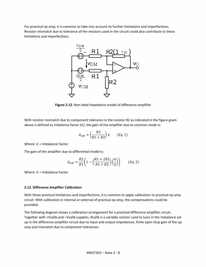
2.11. Non-Ideal Difference Amplifier
XMUT303 – Note 2 - 8
For practical op amp, it is common to take into account its further limitations and imperfections.
Resistor mismatch due to tolerance of the resistors used in the circuit could also contribute to these
limitations and imperfections.
Figure 2.12: Non-ideal impedance model of difference amplifier
With resistor mismatch due to component tolerance in the resistor R2 as indicated in the figure given
above is defined as imbalance factor (∈), the gain of the amplifier due to common mode is:
𝐴𝐶𝑀 = (𝑅2
𝑅1 + 𝑅2) ∈ (𝐸𝑞. 1)
Where: ∈ = Imbalance Factor
The gain of the amplifier due to differential model is:
𝐴𝐷𝑀 =𝑅2
𝑅1(1 − (
𝑅1 + 2𝑅2
𝑅1 + 𝑅2) (
∈
2)) (𝐸𝑞. 2)
Where: ∈ = Imbalance Factor
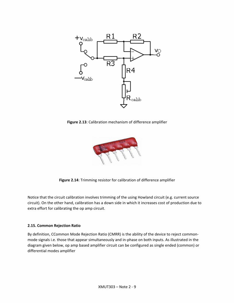
2.12. Difference Amplifier Calibration
With those practical limitations and imperfections, it is common to apply calibration to practical op amp
circuit. With calibration in internal or external of practical op amp, the compensations could be
provided.
The following diagram shows a calibration arrangement for a practical difference amplifier circuit.
Together with +Vcalib and –Vcalib supplies, Rcalib is a variable resistor used to tune in the imbalance set
up in the difference amplifier circuit due to input and output impedances, finite open loop gain of the op
amp and mismatch due to component tolerances.
XMUT303 – Note 2 - 9
Figure 2.13: Calibration mechanism of difference amplifier
Figure 2.14: Trimming resistor for calibration of difference amplifier
Notice that the circuit calibration involves trimming of the using Howland circuit (e.g. current source
circuit). On the other hand, calibration has a down side in which it increases cost of production due to
extra effort for calibrating the op amp circuit.
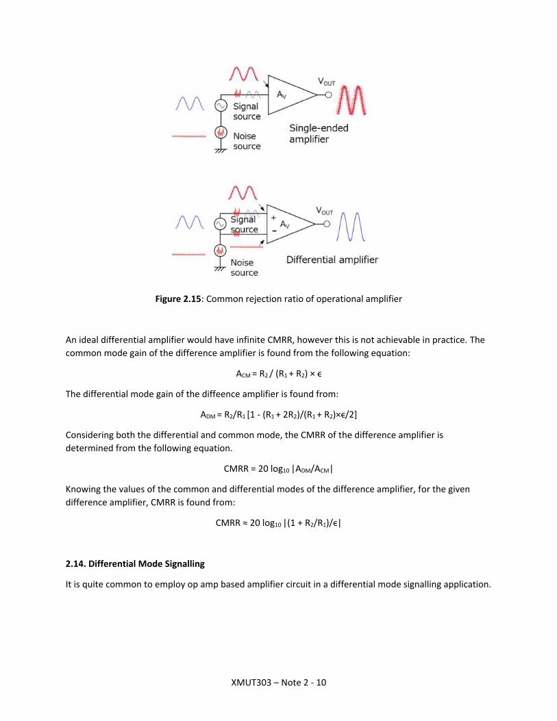
2.15. Common Rejection Ratio
By definition, CCommon Mode Rejection Ratio (CMRR) is the ability of the device to reject common-
mode signals i.e. those that appear simultaneously and in-phase on both inputs. As illustrated in the
diagram given below, op amp based amplifier circuit can be configured as single ended (common) or
differential modes amplifier
XMUT303 – Note 2 - 10
Figure 2.15: Common rejection ratio of operational amplifier
An ideal differential amplifier would have infinite CMRR, however this is not achievable in practice. The
common mode gain of the difference amplifier is found from the following equation:
ACM = R2 / (R1 + R2) × ϵ
The differential mode gain of the diffeence amplifier is found from:
ADM = R2/R1 [1 - (R1 + 2R2)/(R1 + R2)×ϵ/2]
Considering both the differential and common mode, the CMRR of the difference amplifier is
determined from the following equation.
CMRR = 20 log10 |ADM/ACM|
Knowing the values of the common and differential modes of the difference amplifier, for the given
difference amplifier, CMRR is found from:
CMRR ≈ 20 log10 |(1 + R2/R1)/ϵ|
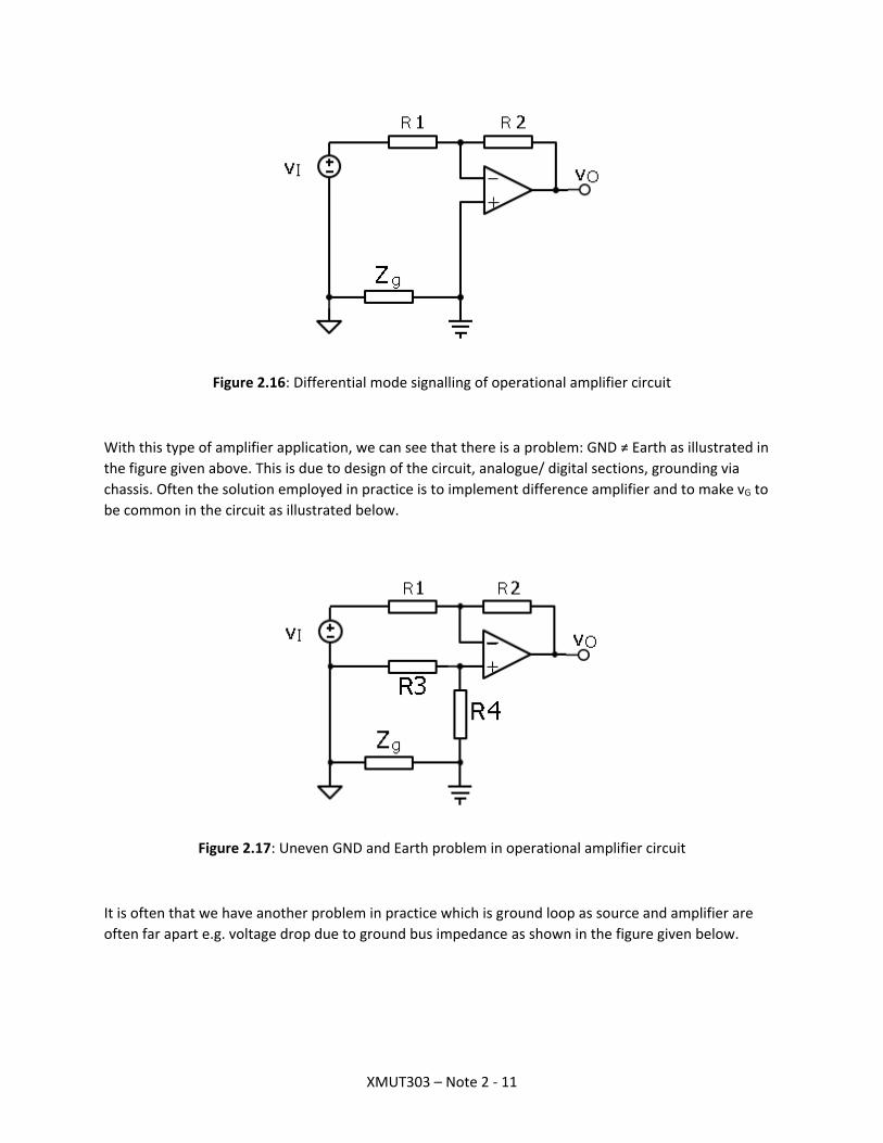
2.14. Differential Mode Signalling
It is quite common to employ op amp based amplifier circuit in a differential mode signalling application.
XMUT303 – Note 2 - 11
Figure 2.16: Differential mode signalling of operational amplifier circuit
With this type of amplifier application, we can see that there is a problem: GND ≠ Earth as illustrated in
the figure given above. This is due to design of the circuit, analogue/ digital sections, grounding via
chassis. Often the solution employed in practice is to implement difference amplifier and to make vG to
be common in the circuit as illustrated below.
Figure 2.17: Uneven GND and Earth problem in operational amplifier circuit
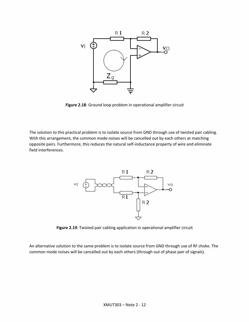
It is often that we have another problem in practice which is ground loop as source and amplifier are
often far apart e.g. voltage drop due to ground bus impedance as shown in the figure given below.
XMUT303 – Note 2 - 12
Figure 2.18: Ground loop problem in operational amplifier circuit
The solution to this practical problem is to isolate source from GND through use of twisted pair cabling.
With this arrangement, the common mode noises will be cancelled out by each others at matching
opposite pairs. Furthermore, this reduces the natural self-inductance property of wire and eliminate
field interferences.
Figure 2.19: Twisted pair cabling application in operational amplifier circuit
An alternative solution to the same problem is to isolate source from GND through use of RF choke. The
common mode noises will be cancelled out by each others (through out of phase pair of signals).
XMUT303 – Note 2 - 13
Figure 2.20: RF choke application in operational amplifier circuit
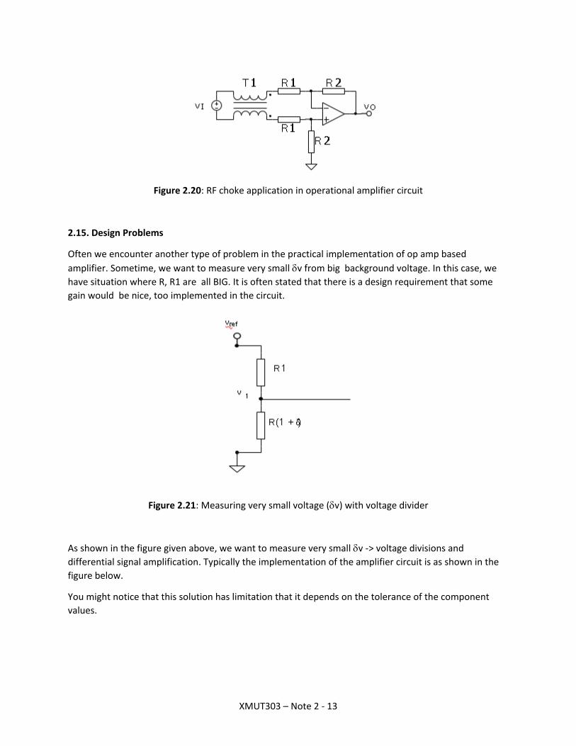
2.15. Design Problems
Often we encounter another type of problem in the practical implementation of op amp based
amplifier. Sometime, we want to measure very small v from big background voltage. In this case, we
have situation where R, R1 are all BIG. It is often stated that there is a design requirement that some
gain would be nice, too implemented in the circuit.
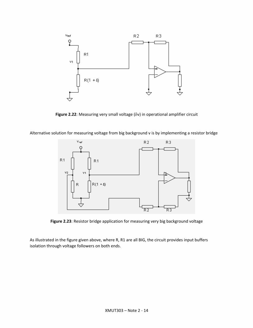
Figure 2.21: Measuring very small voltage (v) with voltage divider
As shown in the figure given above, we want to measure very small v -> voltage divisions and
differential signal amplification. Typically the implementation of the amplifier circuit is as shown in the
figure below.
You might notice that this solution has limitation that it depends on the tolerance of the component
values.
XMUT303 – Note 2 - 14
Figure 2.22: Measuring very small voltage (v) in operational amplifier circuit
Alternative solution for measuring voltage from big background v is by implementing a resistor bridge
Figure 2.23: Resistor bridge application for measuring very big background voltage
As illustrated in the figure given above, where R, R1 are all BIG, the circuit provides input buffers
isolation through voltage followers on both ends.
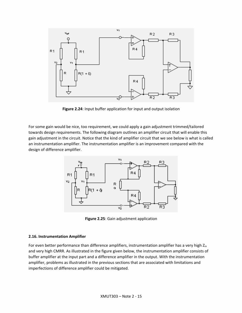
XMUT303 – Note 2 - 15
Figure 2.24: Input buffer application for input and output isolation
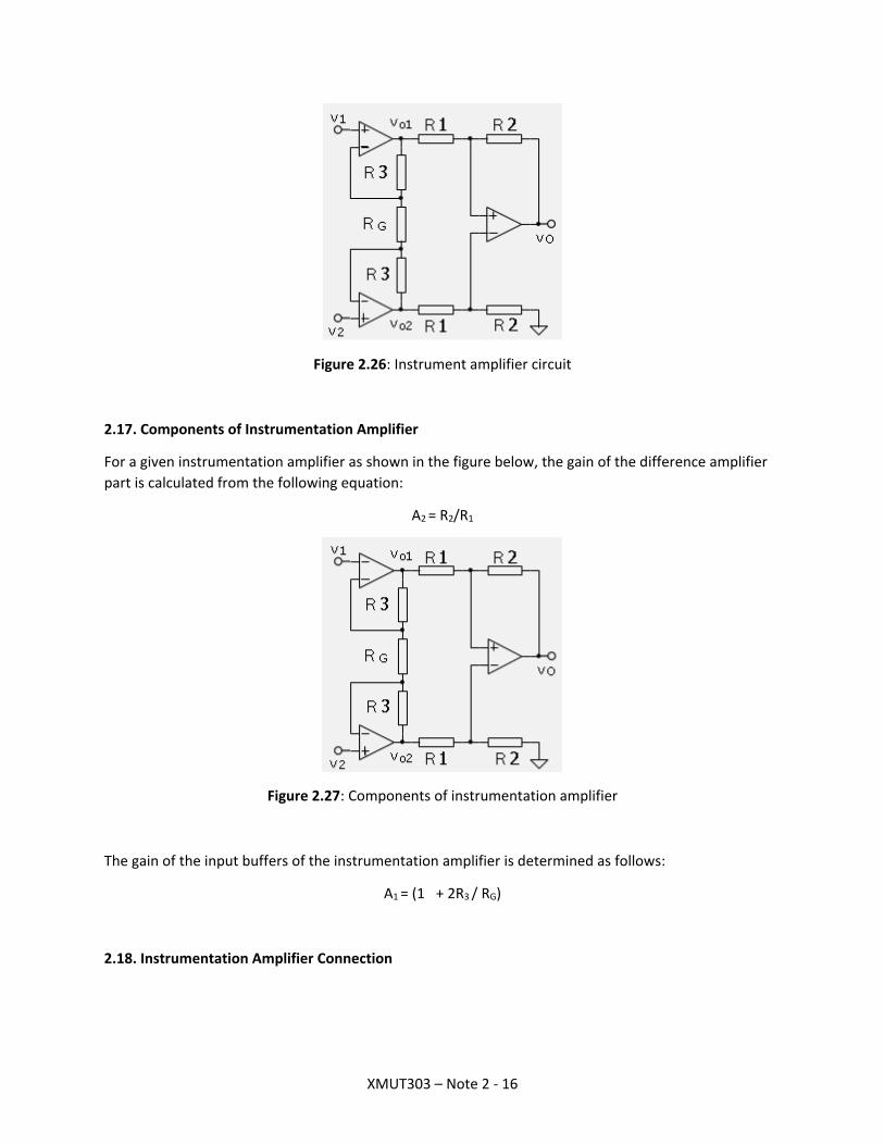
For some gain would be nice, too requirement, we could apply a gain adjustment trimmed/tailored
towards design requirements. The following diagram outlines an amplifier circuit that will enable this
gain adjustment in the circuit. Notice that the kind of amplifier circuit that we see below is what is called
an instrumentation amplifier. The instrumentation amplifier is an improvement compared with the
design of difference amplifier.
Figure 2.25: Gain adjustment application
2.16. Instrumentation Amplifier
For even better performance than difference amplifiers, instrumentation amplifier has a very high Zin
and very high CMRR. As illustrated in the figure given below, the instrumentation amplifier consists of
buffer amplifier at the input part and a difference amplifier in the output. With the instrumentation
amplifier, problems as illustrated in the previous sections that are associated with limitations and
imperfections of difference amplifier could be mitigated.
XMUT303 – Note 2 - 16
Figure 2.26: Instrument amplifier circuit
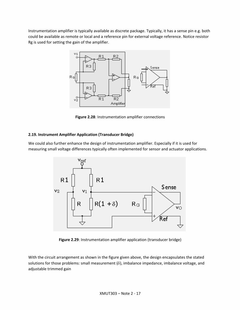
2.17. Components of Instrumentation Amplifier
For a given instrumentation amplifier as shown in the figure below, the gain of the difference amplifier
part is calculated from the following equation:
A2 = R2/R1
Figure 2.27: Components of instrumentation amplifier
The gain of the input buffers of the instrumentation amplifier is determined as follows:
A1 = (1 + 2R3 / RG)
2.18. Instrumentation Amplifier Connection
XMUT303 – Note 2 - 17
Instrumentation amplifier is typically available as discrete package. Typically, it has a sense pin e.g. both
could be available as remote or local and a reference pin for external voltage reference. Notice resistor
Rg is used for setting the gain of the amplifier.
Figure 2.28: Instrumentation amplifier connections
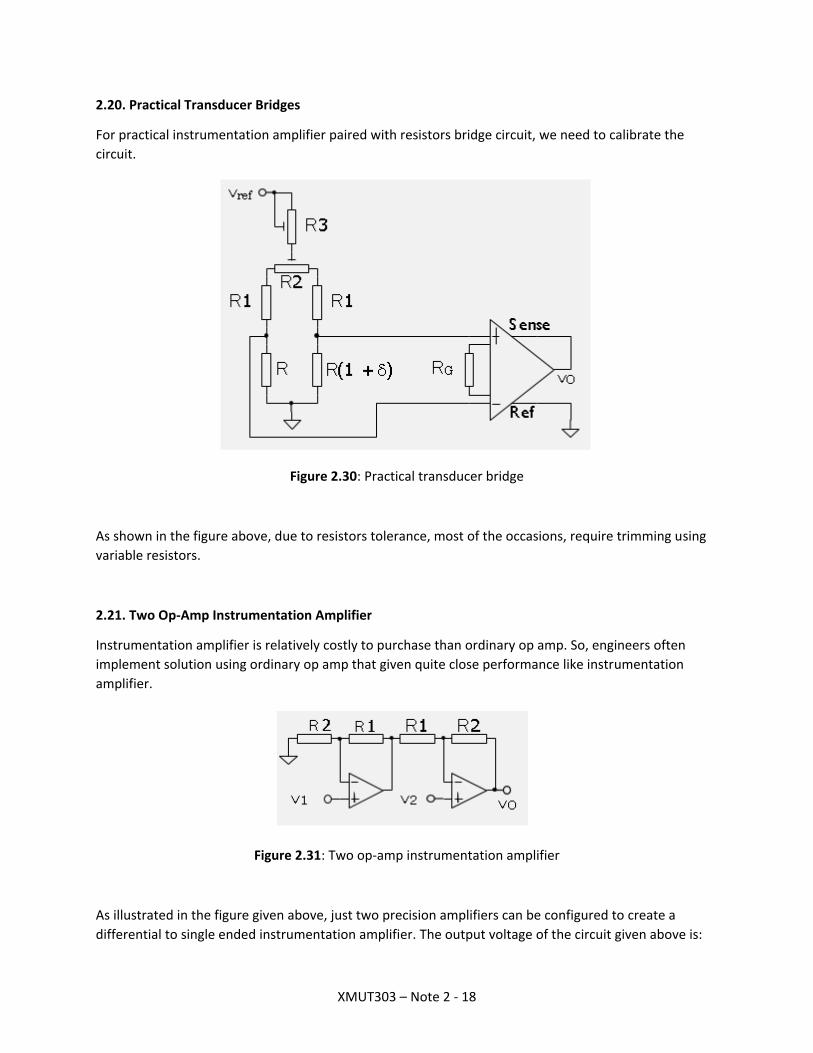
2.19. Instrument Amplifier Application (Transducer Bridge)
We could also further enhance the design of instrumentation amplifier. Especially if it is used for
measuring small voltage differences typically often implemented for sensor and actuator applications.
Figure 2.29: Instrumentation amplifier application (transducer bridge)
With the circuit arrangement as shown in the figure given above, the design encapsulates the stated
solutions for those problems: small measurement (), imbalance impedance, imbalance voltage, and
adjustable trimmed gain
XMUT303 – Note 2 - 18
2.20. Practical Transducer Bridges
For practical instrumentation amplifier paired with resistors bridge circuit, we need to calibrate the
circuit.
Figure 2.30: Practical transducer bridge
As shown in the figure above, due to resistors tolerance, most of the occasions, require trimming using
variable resistors.
2.21. Two Op-Amp Instrumentation Amplifier
Instrumentation amplifier is relatively costly to purchase than ordinary op amp. So, engineers often
implement solution using ordinary op amp that given quite close performance like instrumentation
amplifier.
Figure 2.31: Two op-amp instrumentation amplifier
As illustrated in the figure given above, just two precision amplifiers can be configured to create a
differential to single ended instrumentation amplifier. The output voltage of the circuit given above is:
XMUT303 – Note 2 - 19
vO = (1+ R2/R1) (v2 - v1)
Moreover, this solution is cheap to be implemented as substitute of instrumentation amplifier, but
notice that its design is lacking asymmetric of differential arrangement of the inputs of the amplifier.
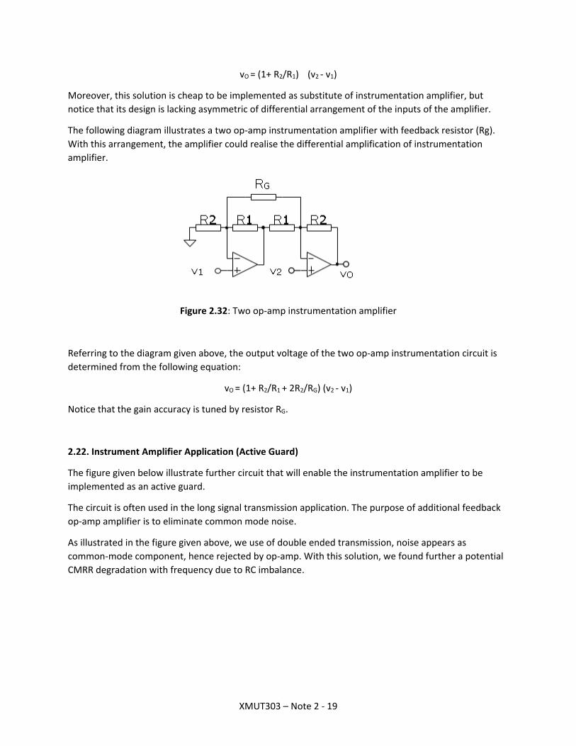
The following diagram illustrates a two op-amp instrumentation amplifier with feedback resistor (Rg).
With this arrangement, the amplifier could realise the differential amplification of instrumentation
amplifier.
Figure 2.32: Two op-amp instrumentation amplifier
Referring to the diagram given above, the output voltage of the two op-amp instrumentation circuit is
determined from the following equation:
vO = (1+ R2/R1 + 2R2/RG) (v2 - v1)
Notice that the gain accuracy is tuned by resistor RG.
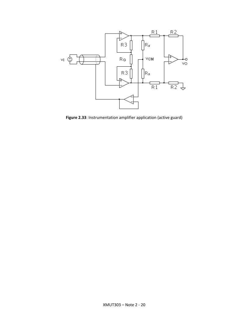
2.22. Instrument Amplifier Application (Active Guard)
The figure given below illustrate further circuit that will enable the instrumentation amplifier to be
implemented as an active guard.
The circuit is often used in the long signal transmission application. The purpose of additional feedback
op-amp amplifier is to eliminate common mode noise.
As illustrated in the figure given above, we use of double ended transmission, noise appears as
common-mode component, hence rejected by op-amp. With this solution, we found further a potential
CMRR degradation with frequency due to RC imbalance.
XMUT303 – Note 2 - 20
Figure 2.33: Instrumentation amplifier application (active guard)