INVESTIGATION OF PROCESS FABRICATION FOR LOW-NOISE P-TYPE DIFFUSED PIEZORESISTORS
By
ROBERT DIEME
A DISSERTATION PRESENTED TO THE GRADUATE SCHOOL OF THE UNIVERSITY OF FLORIDA IN PARTIAL FULFILLMENT
OF THE REQUIREMENTS FOR THE DEGREE OF DOCTOR OF PHILOSOPHY
UNIVERSITY OF FLORIDA
2009
1
© 2009 Robert Diémé
2

To my father and mother.
3

ACKNOWLEDGMENTS
I would like to thank my advisor, Dr. Toshikazu Nishida, for his guidance and
encouragement. I also would like to express my gratitude to Dr. Mark Sheplak, Dr. Gijs
Bosman, and Dr. Kevin Jones, for their ideas and encouragement. I would also like to thank Dr.
Louis N. Cattafesta III for help with my experiments. I also thank Bryan L. Zachary, Nicholas
G. Rudawski, Jack Y. Zhang, and all Interdisciplinary Microsystems Group (IMG) students for
their help and support.
I thank my father, mother, brother, sisters, and friends for their prayers, support, and
encouragement through my study. Special thanks go to Rev. John D. Gillespie for his advice and
all the people at St. Augustine Church. Finally, I thank God for all of the grace He gives me.
4
TABLE OF CONTENTS page
ACKNOWLEDGMENTS ...............................................................................................................4
LIST OF TABLES...........................................................................................................................9
LIST OF FIGURES .......................................................................................................................11
ABSTRACT...................................................................................................................................17
CHAPTER
1 INTRODUCTION ..................................................................................................................19
1.1 Motivation.....................................................................................................................19 1.2 Objective and Outline ...................................................................................................20
2 BACKGROUND ....................................................................................................................22
2.1 Test Vehicle: Piezoresistor............................................................................................22 2.1.1 Computation of Piezoresistor Resistance under Non-Degenerate
Approximation ..................................................................................................23 2.1.1.1 Resistance computation with uniform carrier concentration under
non-degenerate approximation ...........................................................24 2.1.1.2 Resistance computation with non-uniform carrier concentration
under non-degenerate approximation .................................................24 2.2 MEMS Piezoresistive Microphone ...............................................................................26
2.2.1 MEMS piezoresistive Microphone Voltage Output..........................................26 2.2.2 MEMS Piezoresistive Microphone Sensitivity .................................................27 2.2.3 MEMS Piezoresistive Microphone Minimum Detectable Signal.....................27
2.3 Noise and Noise Power Spectral Density......................................................................28 2.4 Noise Sources in Piezoresistor ......................................................................................29
2.4.1 Electrical Thermal Noise...................................................................................29 2.4.2 Mechanical Thermal Noise ...............................................................................30 2.4.3 Low Frequency Noise .......................................................................................30
2.4.3.1 Hooge’s model....................................................................................31 2.4.3.2 McWhorter’s model............................................................................32
2.4.4 Shot Noise .........................................................................................................33 2.5 Defects in Semiconductors............................................................................................34
2.5.1 Bulk Defects......................................................................................................34 2.5.2 Interface Traps ..................................................................................................35
2.6 Process Dependence of 1/f Noise..................................................................................36 2.7 Summary .......................................................................................................................38
5
3 PIEZORESISTOR DESIGN ..................................................................................................41
3.1 Introduction...................................................................................................................41 3.1.1 Piezoresistor Design with Uniform Doping Concentration ..............................41 3.1.2 Piezoresistor Design with Gaussian Non-Uniform Doping Concentration ......42 3.1.3 Fabrication Non-Idealities.................................................................................43
3.1.3.1 Transient enhanced diffusion (TED) ..................................................43 3.1.3.2 Oxidation enhanced diffusion (OED).................................................44 3.1.3.3 Impurity segregation...........................................................................44
3.1.4 Fundamental Physics That Affect Electrical Activation of Impurities .............45 3.2 Piezoresistor Design Parameters ...................................................................................47
3.2.1 Piezoresistor Impurity Profile ...........................................................................47 3.2.2 Piezoresistor Resistance ....................................................................................47 3.2.3 Piezoresistor Surface Area ................................................................................48 3.2.4 Piezoresistor Volume ........................................................................................48
3.3 Test Structures Design ..................................................................................................48 3.4 Boron Profile Simulations.............................................................................................49
3.4.1 Analytical Calculation.......................................................................................49 3.4.2 Limited Source Diffusion: Ion Implantation.....................................................49 3.4.3 Annealing After Ion implantation .....................................................................50 3.4.5 Florida Object Oriented Process Simulator (FLOOPS) ....................................51
3.4.5.1 Simplest FLOOPS (Fermi model) ......................................................52 3.4.5.2 More accurate FLOOPS (Pair model) ................................................52
3.5 P-type Piezoresistor Implant and Annealing Condition................................................52 3.5.1 Piezoresistor Generation 1 (PG1)......................................................................52 3.5.2 Piezoresistor Generation 2 (PG2)......................................................................54
3.5.2.1 Boron implanted piezoresistors at 20 keV with a dose 7x1014 cm-2...55 3.5.2.2 Boron implanted piezoresistors at 40 keV with a dose 7x1014 cm-2
through SiO2 .......................................................................................56 3.5.2.3 Boron solid source diffused piezoresistors for 25 min at 950 C.........56 3.5.2.4 Boron solid source diffused piezoresistors for 25 min at 950 C
followed by phosphorus solid source diffusion for 5 min at 800 C....57 3.6 Additional Test Structures.............................................................................................57
3.6.1 P-type Capacitor................................................................................................57 3.6.2 P/N Diode..........................................................................................................58 3.6.3 Van der Pauw Structure ....................................................................................59 3.6.4 Carrier Concentration Test Structures...............................................................59
3.6.4.1 Spreading resistance technique...........................................................60 3.6.4.2 Secondary ion mass spectroscopy (SIMS) technique.........................60 3.6.4.3 Capacitance-voltage technique ...........................................................60 3.6.4.4 Hall measurement technique...............................................................61
3.7 Summary .......................................................................................................................62
4 EXPERIMENTAL METHOD................................................................................................78
4.1 Piezoresistor Experimental Methods.............................................................................78 4.1.1 Piezoresistor I-V Measurement.........................................................................78
6
4.1.2 Piezoresistor Noise Measurements ...................................................................79 4.1.2.1 Noise measurement setup ...................................................................79 4.1.2.2 Equipment setting for noise PSD measurement .................................80 4.1.2.3 Noise power spectral density extraction .............................................80
4.2 P/N Diode Experimental Method..................................................................................82 4.2.1 P/N Diode DC Current-Voltage ........................................................................82 4.2.2 P/N Diode Shot Noise Measurement ................................................................82
4.2.2.1 P/N diode noise measurement setup ...................................................82 4.2.2.2 Shot noise power spectral density extraction......................................83
4.3 P-Type Capacitor Experimental Method ......................................................................83 4.4 Transmission Electron Microscopy...............................................................................85 4.5 Van Der Pauw Structure ...............................................................................................86
4.5.1 Sheet Resistance................................................................................................86 4.5.2 Line Width ........................................................................................................86 4.5.3 Contact Resistance ............................................................................................87
4.6 Hall Effect Measurement ..............................................................................................87 4.7 Summary .......................................................................................................................87
5 FABRICATION AND MEASUREMENT RESULTS..........................................................91
5.1 Implantation, Solid-Source, and Annealing of Test Structures.....................................91 5.2 Characterization of Fabricated Test Structures .............................................................92
5.2.1 Piezoresistor Test Structures .............................................................................92 5.2.2 P-type Capacitor Test Structure ........................................................................94 5.2.3 P/N Diode Test Structure ..................................................................................95 5.2.4 Van der Pauw Test Structure ............................................................................95 5.2.5 Hall Effect Test Structure..................................................................................96
5.3 Investigation of Process Dependence of 1/F Noise ......................................................97 5.3.1 Noise PSD of piezoresistors R6 for B, 20 keV, 7x1014 cm-2, and 7o tilt...........98 5.3.2 Noise PSD of piezoresistors R6 for B, 40 keV, 7x1014 cm-2 through 0.1 µm
of SiO2 101 5.3.3 Noise PSD of solid-source diffused piezoresistors R9 of wafers C1 and C2 .102
5.4 Hooge Parameter and 1/F Noise Analysis and Discussion.........................................103 5.5 Shot Noise Measurements...........................................................................................104 5.6 Number of Carrier Dependence of 1/F Noise .............................................................105
5.6.1 Fabrication and Measurements of Test Structures ..........................................105 5.6.1 Noise PSD Measurements...............................................................................106 5.6.2 Analysis and Discussion .................................................................................107
5.7 Summary .....................................................................................................................108
6 DEFECTS MEASUREMENTS AND ANALYSIS.............................................................134
6.2 Bulk Defects in Piezoresistors ....................................................................................134 6.2.1 Cross-Section Transmission Electron Microscopy (XTEM) ..........................134 6.2.2 Plan View Transmission Electron Microscopy (PTEM) ................................135
6.3 Interface Trap Density.................................................................................................136 6.4 Correlation of Noise Voltage PSD to Defects ............................................................137
7
6.4.1 Noise Voltage PSD of 20 keV Boron Implanted Piezoresistors and Defects .137 6.4.2 Noise Voltage PSD of 40 keV Boron Implanted Piezoresistors through 0.1
µm of SiO2 and Defects ..................................................................................138 6.4.3 Noise Voltage PSD of Solid Source Diffused Piezoresistors and Interface
Traps 140 6.5 Summary .....................................................................................................................140
7 CONCLUSION AND FUTURE WORK .............................................................................154
APPENDIX
A PIEZORESISTIVITY...........................................................................................................157
B MEMS PIEZORESISTIVE MICROPHONE VOLTAGE OUTPUT ..................................160
C DIFFRENCE BETWEEN HOOGE AND MCWHORTER 1/F NOISE MODEL ..............162
D PROCESS FLOW.................................................................................................................165
D.1 Generation 1 Process...................................................................................................165 D.2 Generation 2 Process...................................................................................................169
LIST OF REFERENCES.............................................................................................................175
BIOGRAPHICAL SKETCH .......................................................................................................180
8
LIST OF TABLES
Table page 3-1 Wafer characteristics used to fabricate test structures generation 1. .................................63
3-2 Process steps for piezoresistor test structures generation 1. ..............................................63
3-3 Wafer characteristics used to fabricate test structures generation 2. .................................63
3-4 Process steps for piezoresistor test structures generation 2. ..............................................64
3-5 Implant and annealing conditions of test structures generation 1......................................64
3-6 Dimensions, surface area, and volume of piezoresistors assuming uniform doping profile.................................................................................................................................65
4-1 Low-noise preamplifier SRS 560 setting...........................................................................89
4-2 Spectrum analyzer SRS 785 setting...................................................................................89
5-1 Resistance of piezoresistors of generation 2 process. ......................................................110
5-2 The junction depths and surface concentrations of SIMS profiles of generation 2 process..............................................................................................................................110
5-3 Dimensions of the pMOSC1 and pMOSC2 of generation 2 process...............................110
5-4 Measured oxide thicknesses with Ellipsometer and pMOSC C-V of generation 2 process..............................................................................................................................111
5-5 Dimensions of the three P/N diodes of generation 2 process. .........................................111
5-6 Measured SR , and WΔ CR of generation 2 processes. ...................................................111
5-7 Computed electrical active dose, , implanted dose, Q, and fraction of active dose AAN
AAN Q for each generation 2 process. ............................................................................112
5-8 Hooge parameters of each of the three piezoresistors of process 2A (B, 20 keV, 7x1014 cm-2, 7o tilt and 5 min dry, 5 min wet and 10 min dry at 900 C). ........................112
5-9 Hooge parameter α using number of carrier obtained from Hall Effect measurements of generation 2 process. ...................................................................................................112
5-10 Resistance of fabricated junction isolated piezoresistors of generation 1 process. .........113
6-1 Slopes of regression lines and the 95 % confidence intervals. ........................................142
9
6-2 Line length, loop area, and faulted loop area of the B 20 keV and 40 keV with inert anneal and oxidation. .......................................................................................................142
A-1 Piezoresistive coefficients of silicon................................................................................159
A-2 Transverse and longitudinal piezoresistance coefficients of silicon for <110> direction ...........................................................................................................................159
10
LIST OF FIGURES
Figure page 2-1 Piezoresistor A) plan view B) cross-section. .....................................................................39
2-2 Piezoresistors configured in Wheatstone bridge................................................................39
2-3 Trapping-detrapping model for 1/f noise. A) Energy band diagram of trapping and detrapping at two trap levels, B) Lorentzian spectrum of two trap levels in comparison with thermal noise. .........................................................................................40
2-4 “Category I damage” adapted from Jones et al. ................................................................40
3-1 Piezoresistor A) top view and B) cross-section. ................................................................65
3-2 Uniform doping concentration...........................................................................................66
3-3 Non-uniform doping concentration (Gaussian Profile). ....................................................66
3-4 Illustration of boron profiles when secondary effect such segregation (A) , oxidation enhance diffusion (B), transient enhanced diffusion (C) are present during processing and comparison of a Gaussian profile with and a non-ideal boron distribution (D)..........67
3-5 Piezoresistors with same sheet resistance, but different number of squares and resistance............................................................................................................................67
3-6 Piezoresistors with same resistance, different surface area and same number of square. ................................................................................................................................68
3-7 Simulated boron profile for piezoresistor generation 1. ....................................................68
3-8 Piezoresistors test structures A1) Piezoresistor 7, A2) Piezoresistor 8, A3) piezoresistor 9 and B) piezoresistor cross-section. ............................................................69
3-9 Boron 20 keV implanted-silicon and anneal flow chart. ...................................................70
3-10 Boron, 20 keV, 7x1014 cm-2, 7°tilt implant and anneal 1 (Dt1). ........................................70
3-11 Boron, 20 keV, 7x1014 cm-2, 7°tilt implant and anneal 2 (Dt2). ........................................71
3-12 Boron, 20 keV, 7x1014 cm-2, 7°tilt implant and anneal 3 (Dt3). ........................................71
3-13 Boron 40 keV implanted-silicon and anneal flow chart. ...................................................72
3-14 Boron, 40 keV, 7x1014 cm-2, 0°tilt implant and anneal 1 (Dt1). ........................................72
3-15 Boron, 40 keV, 7x1014 cm-2, 0°tilt implant and anneal 2 (Dt2). ........................................73
11
3-16 Boron, 40 keV, 7x1014 cm-2, 0°tilt implant and anneal 3 (Dt3). ........................................73
3-17 Boron, 40 keV, 7x1014 cm-2, 0°tilt implant and anneal 4 (Dt4). ........................................74
3-18 Boron solid source diffusion in n-silicon and anneal flow chart. ......................................74
3-19 Analytical calculation of boron solid source diffusion in n-silicon and anneal 3 (Dt3). ...75
3-20 Boron and Phosphorus solid source diffusions in n-silicon and anneal flow chart. ..........75
3-21 Capacitor layout A) plan view and B) cross-section. ........................................................76
3-22 P/N diode layout A) plan view and B) cross-section.........................................................76
3-23 Plan view of a Van der Pauw structure..............................................................................77
3-24 Hall Effect structure A) plan view and B) cross-section. ..................................................77
4-1 Piezoresistor noise measurement A) setup and B) small circuit noise representation.......89
4-2 Diode noise measurement A) setup and B) small circuit noise representation..................90
4-3 Capacitance-Voltage measurement setup adapter from Sah..............................................90
5-1 As-implant profiles of boron with B, 20 keV, 7x1014 cm-2, 7o tilt of generation 2 process..............................................................................................................................113
5-2 As-implant profiles of boron with B, 40 keV, 7x1014 cm-2 through 0.1 µm of SiO2 of generation 2 process.........................................................................................................114
5-3 SIMS profiles of wafers with B, 20 keV, 7e14 cm-2, 7o tilt of generation 2 process.......114
5-4 SIMS profiles of wafers with B, 40 keV, 7x1014 cm-2 through 0.1 µm of SiO2 of generation 2 process.........................................................................................................115
5-5 SIMS profiles of solid-source diffused wafers C1 and C2 of generation 2 process. .......115
5-6 Piezoresistor test structure 9 of generation 2 process. .....................................................116
5-7 C-V measurement of pMOSC2 of wafer 2E of generation 2 process..............................116
5-8 I-V characteristics of Resistor 6, Diode 1 and Diode 2 of process 1A of generation 2 process..............................................................................................................................117
5-9 Logarithmic scale of the forward bias Diode 1 of generation 2 process. ........................117
5-10 Reverse bias current of the forward bias Diode 1 of generation 2 process......................118
12
5-11 Sheet hall coefficient SHR for the B, 20 keV, 7x1014 cm-2, 7o tilt implanted piezoresistors of generation 2 process. ............................................................................118
5-12 Sheet hall coefficient SHR for the B, 40 keV, 7x1014 cm-2 through 0.1 µm of SiO2 implanted piezoresistors subjected to only inert annealing of generation 2 process. ......119
5-13 Sheet hall coefficient SHR for the B, 40 keV, 7x1014 cm-2 through 0.1 µm of SiO2 implanted piezoresistors subjected to inert annealing and oxidation of generation 2 process..............................................................................................................................119
5-14 Sheet hall coefficient SHR for the solid source diffused piezoresistors of generation 2 process..............................................................................................................................120
5-15 I-V characteristic of resistor 6 of wafer 2A of generation 2 process. ..............................120
5-16 Noise voltage PSD of piezoresistor R6 of wafer 2A of generation 2 process. ................121
5-17 Noise voltage average PSD of three piezoresistors R6 of wafer 2A of generation 2 process..............................................................................................................................121
5-18 Noise voltage PSDs average of three piezoresistors R6 of wafer 2A, 2E, and 1A of generation 2 process.........................................................................................................122
5-19 PSDs and their uncertainties of three different piezoresistors of .process 2A (B, 20 keV, 7x1014 cm-2, 7o tilt and 5 min dry, 5 min wet and 10 min dry at 900 C).................122
5-20 The fitted lines of the three PSDs of process 2A (B, 20 keV, 7x1014 cm-2, 7o tilt and 5 min dry, 5 min wet and 10 min dry at 900 C)..................................................................123
5-21 Noise voltage average PSDs of three piezoresistors R6 of wafer 2B and 5A of generation 2 process.........................................................................................................123
5-22 Noise voltage average PSDs of three piezoresistors R6 of wafer 3E and 4A of generation 2 process.........................................................................................................124
5-23 I-V characteristic of piezoresistor R9 of wafer C1 of generation 2 process....................124
5-24 I-V characteristic of piezoresistor R9 of wafer C2 of generation 2 process....................125
5-25 Noise voltage average PSDs of three piezoresistors R9 of wafer C1 and C2 of generation 2 process.........................................................................................................125
5-26 Noise voltage PSDs of C1 and C2 with N of C2 used for C1 at 1Hz of generation 2 process..............................................................................................................................126
5-27 Resistor geometry before and after diffusion, A) plan-view and B) cross-section..........126
13
5-28 Shot noise of resistor 6 of process 1A of generation 2 of generation 2 process. .............127
5-29 Top views of piezoresistors test structures 7 A1), 8 A2) and 9 A3) and a cross-section B) of generation 1 process. ..................................................................................128
5-30 Secondary ion mass spectroscopy (SIMS) obtained from Evans Analytical Group for the fabricated piezoresistors of generation 1 process. .....................................................128
5-31 I-V characteristic of piezoresistor R1B1W of generation 1 process................................129
5-32 Noise voltage PSD of R1B1W of generation 1 process. .................................................129
5-33 I-V characteristic of piezoresistor R3A12E of generation 1 process...............................130
5-34 Noise voltage PSD of R3A12E of generation 1 process..................................................130
5-35 I-V characteristic of junction isolated piezoresistor test structure 1 (R1B1W) of generation 1 process.........................................................................................................131
5-36 Shot noise of piezoresistor test structure 1(R1B1W) of generation 1 process. ...............131
5-37 Noise voltage PSD of piezoresistor test structure 1 (R1B1W) and piezoresistor test structure 12 (R3A12E) are biased respectively at 1.49 Vdc and 1.48 Vdc of generation 1 process.........................................................................................................132
5-38 Noise measurement PSDs A) of piezoresistors 1 2 3, and R R R at same voltage and B) of number of carriers of piezoresistors 1 2 3, and R R R at same voltage of generation 1 process..............................................................................................................................133
6-1 Focus ion beam (FIB) on a piezoresistor test structure....................................................142
6-2 The XTEM of piezoresistor implanted with B, 20 keV, 7x1014 cm-2 of generation 2 process, A) 2A, B) 2E, C) 1A. .........................................................................................143
6-3 XTEM of piezoresistor generation 2 implanted with B, 40 keV, 7x1014 cm-2 through 0.1 µm of SiO2 of generation 2 process, A) 2B, B) 3E, C) 4A), D) 5A. .........................143
6-4 The XTEM of piezoresistor A) solid source diffusions of B, 25 min, 950 C, B) solid source diffusions of B, 25 min, 950 C and P, 5 min, 800 C of generation 2 process. .....144
6-5 Ten PTEM pictures for process 2A of generation 2 process, implanted with B, 20 keV, 7x1014 cm-2 and annealed for 5 min dry, 5 min wet and 10 min dry at 900 C. .......144
6-6 PTEM of the 20 keV implanted test structures A) 2A, B) 2E, C) 1A. ............................145
6-7 PTEM of the 40 keV implanted test structures A) 2B, B) 3E, C) 4A, D) 5A..................145
14
6-8 Defects densities as a function of anneal time of the 20 keV implanted test structures of generation 2 process. ...................................................................................................146
6-9 Regression line of the defect density versus annealing time for the B 20 keV. ..............146
6-10 Defects densities as a function of anneal time of the 40 keV implanted test structures with only inert anneal of generation 2 process. ...............................................................147
6-11 Defects densities as a function of anneal time of the 40 keV implanted test structures with inert anneal and oxidation of generation 2 process..................................................147
6-12 PTEM of processes 40 keV, 7x1014 cm-2, through 0.1 µm of SiO2., A) 3E (10 min in N2 and 5 min dry, 5 min wet and 10 min dry oxidation at 900 C) and B) 4A (30 min in N2 and 5 min dry, 5 min wet and 10 min dry oxidation at 900 C)...............................148
6-13 Surface terminated defects versus the annealing time of the 20 keV implanted test structures of generation 2 process....................................................................................148
6-14 Surface terminated defects versus the annealing time of the 40 keV implanted test structures with only inert anneal of generation 2 process................................................149
6-15 Surface terminated defects versus the annealing time of the 40 keV implanted test structures with inert anneal and oxidation of generation 2 process. ................................149
6-16 Defects count versus loop size of the 20 keV implanted test structures of generation 2 process...........................................................................................................................150
6-17 Defects count versus loop size of the 40 keV implanted test structures with only inert anneal of generation 2 process.........................................................................................150
6-18 Defects count versus loop size of the 40 keV implanted test structures with inert anneal and oxidation of generation 2 process. .................................................................151
6-19 Measured and ideal high frequency C-V of process 2E, implanted with B, 20 keV, 7x1014 cm-2 and annealed for 10 min N2 and 5 min dry, 5 min wet and 10 min dry oxide at 900 C, of generation 2 process..........................................................................151
6-20 Energy level versus the DIT of the 20 keV implanted test structures. of generation 2 process..............................................................................................................................152
6-21 Energy level versus the DIT of the 40 keV implanted test structures with only inert anneal of generation 2 process.........................................................................................152
6-22 Energy level versus the DIT of the 40 keV implanted test structures with inert anneal and oxidation of generation 2 process. ............................................................................153
6-23 Energy level versus the DIT of the solid source diffused test structures of generation 2 process...........................................................................................................................153
15
A-1 Polar plots of longitudinal A) and transverse B) piezoresistance coefficients for p-type (100) silicon. ............................................................................................................159
16
Abstract of Dissertation Presented to the Graduate School of the University of Florida in Partial Fulfillment of the Requirements for the Degree of Doctor of Philosophy
INVESTIGATION OF PROCESS FABRICATION FOR LOW-NOISE P-TYPE DIFFUSED PIEZORESISTORS
By
Robert Diémé
December 2009 Chair: Toshikazu Nishida Major: Electrical and Computer Engineering
The geometry and process dependence of 1/f noise in p-type piezoresistors was
systematically investigated in this work. P-type piezoresistors were fabricated with 20 keV
boron implants, 40keV boron implants with implant oxide, and solid-source diffusion and
varying isochronal 900C inert anneals on test-structures of different surface area and volume.
The devices were characterized electrically using I-V, C-V, and power spectral density noise
measurements. The defects were visualized using cross-section (XTEM) and plane view TEM
(PTEM). In addition, the influence of carrier number on piezoresistors 1/f noise was
investigated. For the first time, the measured 1/f noise in piezoresistors is systematically
compared to bulk defect densities measured with TEM and interface trap densities from HFCV
after each annealing condition of the piezoresistors. For p-type piezoresistors implanted with 20
keV boron at 7x1014 cm-3 dose and isochronally annealed at 900C for varying times in inert N2
followed by a short dry/wet/dry oxidation at the same temperature, increasing inert anneals
resulted in decreasing 1/f noise as well as bulk defect densities measured by PTEM. A decrease
of the 1/f noise and bulk defect densities with increased annealing times was also observed on p-
type piezoresistors implanted with 40 keV boron at 7x1014 cm-3 dose through 0.1 µm of SiO2
with only inert anneal at 900 C. However, for the p-type piezoresistors implanted with 40 keV
17
boron at 7x1014 cm-3 dose through 0.1 µm of SiO2 with inert anneal and additional dry/wet/dry
oxidation, increased 1/f noise was observed with increased inert anneal time (10 min versus 30
min) at 900 C although the bulk trap density decreased. From TEM, it appeared that the PSDs of
the piezoresistors implanted with 40 keV boron at 7x1014 cm-3 dose through 0.1 µm of SiO2 with
inert anneal and oxidation track the faulted loop areas. A phosphorous counter-doped solid-
source diffused p-type piezoresistor had less noise than the boron-only solid-source diffused
piezoresistor which is attributed to the boron centroid further from the Si/SiO2 interface.
18
CHAPTER 1 INTRODUCTION
The trend in integrated circuit (IC) technology is to fabricate small size devices while
focusing simultaneously on improving their performance, their reliability, and their affordability.
In the field of integrated circuits technology, microelectromechanical systems (MEMS), also
known as microsystems design, allows the fabrication of miniature systems such as sensors and
actuators. These miniature system transducers used in field such as automotive, aeronautic,
environmental, and medical are typically on the micrometer scale. A few examples of miniature
systems are piezoresistive pressure sensors, microphones, accelerometers, and cantilevers. Key
specifications include sensitivity, linearity, frequency response, selectivity, and dynamic range.
The latter specification refers to the range of input signal magnitudes that can be measured. It is
not surprising that the fabrication process, material properties, and geometric dimension have
enormous effects on the MEMS performance, in particular the noise floor or minimum detectable
signal.
1.1 Motivation
Noise plays an important role in the performance of MEMS transducers since it determines
the minimum signal that can be detected. For example, in the MEMS piezoresistive microphone,
the minimum detectable signal (MDS) and the signal-to-noise ratio (S/N) can be reduced by
improving the transducer sensitivity, reducing the noise, or both. The reduction of the noise
generated from piezoresistors configured in a Wheatstone bridge can be achieved by
understanding the physical phenomena that lead to its occurrence. For example, anecdotally, two
piezoresistive microphones with the same diaphragm geometry but different piezoresistor
structure and process flow exhibited significantly different noise characteristics. The first
microphone employed dielectrically isolated 1x1018 cm-3 doped piezoresistor which underwent
19
DRIE and high temperature anneal while the second piezoresistor used a junction isolated 1x10¹⁹
cm-3 doped piezoresistor with less high temperature anneal. With multiple differences, it is
difficult to pinpoint the geometry trends and the annealing factor that affect the device noise.
1.2 Objective and Outline
The objective of this work is to systematically investigate the dependencies of noise in
piezoresistors geometry, passivation, and fabrication process. Such an understanding can
facilitate the design of low-noise piezoresistive transducers such as microphones. Thus, we
investigate low frequency noise through varying the process fabrication (implant energy,
annealing condition, and oxide thickness) and geometry (surface and volume) of piezoresistors.
In order to relate the noise to the physical defects in the silicon, techniques such as Transmission
Electron Microscopy (TEM) are used for defect density analysis. Noise measurements on
piezoresistors are analyzed, and the results are used to provide guidelines for the fabrication of
low noise piezoresistors.
The contributions of this work are first a systematic correlation of the noise voltage PSD to
the bulk defects and surface traps of the piezoresistors and second the effect of the number of
carriers on 1/f noise. The systematic correlation of the noise voltage PSD to the bulk defects and
surface traps is done by measuring the defects of ion implanted or solid source diffused
piezoresistors at various implants and anneals conditions, measured the noise voltage PSD of the
piezoresistors after each annealing condition and correlated the defects to the measured 1/f noise.
The effect of the number of carriers on 1/f noise is studied in piezoresistors with identical process
fabrication. However some piezoresistors have same resistance and different volume while other
piezoresistors have different resistance and different volumes. In addition to the ion implanted
piezoresistors, two different conditions of solid source diffused piezoresistors are used to study
the effect of number of carriers and surface traps on the 1/f noise.
20
The dissertation is organized as follow; in chapter 2, we discuss the background of
piezoresistors, piezoresistive microphone, noise source, defects in semiconductors and process
dependence of 1/f noise. In Chapter 3, the piezoresistor design of the test structures is presented.
The experimental method is described in Chapter 4 and is followed by the fabrication and
measurement results in Chapter 5 and the defect measurement and analysis in Chapter 6. The
conclusion and future work are discussed in Chapter 7.
21
CHAPTER 2 BACKGROUND
This chapter discusses the background for the motivation of this research. We start by
presenting the strain sensitive resistive element (piezoresistor) that is employed for the noise
investigation. An example of a piezoresistive MEMS microphone which uses piezoresistors for
sensing pressure-induced diaphragm strain is briefly described. The effect of the noise on the
performance of such a device is shown through the minimum detectable signal. The
mathematical and physical foundation of noise, the various noise sources, and potential defects
that cause noise are discussed. We finally present summaries of previous studies of noise in
semiconductor devices.
2.1 Test Vehicle: Piezoresistor
A piezoresistor is typically a p-type resistor made most commonly today via ion-
implantation, which is based on the bombardment of foreign impurity species (boron) into a
piezoresistive semiconductor material such as crystalline silicon. The property of a material,
such as silicon, for which the resistivity changes when submitted to stress is called
piezoresistivity. Piezoresistors play a critical role in the non-energy conserving dissipative
transduction of the strain signal from the mechanical domain to the electrical domain. This
ability to change resistivity known as the piezoresistive effect, ρρΔ , gives rise to a much larger
gauge factor in semiconductors (two orders of magnitude) than in metals. The relation between
the resistivity and the applied stress is described by the piezoresistance coefficients. The
resistivity of a piezoresistor is expressed as follows;
[1 cmq p
ρμ
= Ω− ] . (2-1)
22
In the expression above, is the electronic charge, q μ is the carrier mobility, and is the carrier
concentration. Additional information on piezoresistivity is given in Appendix A.
p
2.1.1 Computation of Piezoresistor Resistance under Non-Degenerate Approximation
The resistance of the piezoresistor is calculated in two ways: 1) for a uniform carrier
concentration and 2) for a non-uniform carrier concentration. In both computations, we assume
non-degenerate semiconductors. A semiconductor is said to be non-degenerate if the Fermi level
is in the band gap at a distance of greater than3 away from the conduction and valence band
edges. In this case, the impurity concentration is low and the Fermi-Dirac distribution is
approximated by the Boltzman’s approximation as shown in Equation 2-2,38
kT
( )( ) ( )
1
1F FE E E E
kT kTf E e e
−⎛ − ⎞ ⎛ − − ⎞⎜ ⎟ ⎜⎜ ⎟ ⎜⎝ ⎠ ⎝
⎧ ⎫⎪ ⎪= +⎨ ⎬⎪ ⎪⎭⎩
⎟⎟⎠ , (2-2)
where is the Fermi energy, is the Boltzman’s constant, and T is the temperature in Kelvin.
Under this approximation, the electron and hole concentrations are given in Equation 2-3 and
Equation 2-4.38
FE k
( )C FE EkT
CN N e⎛ ⎞− −⎜ ⎟⎜ ⎟⎝ ⎠ (2-3)
( )F VE EkT
VP N e⎛ ⎞− −⎜ ⎟⎜ ⎟⎝ ⎠ (2-4)
CN and are respectively the effective densities of states in the conduction and valence bands.
and are respectively the conduction and valence band edges.
VN
CE VE
23
2.1.1.1 Resistance computation with uniform carrier concentration under non-degenerate approximation
The resistance of the piezoresistor is computed using Equation 2-5 shown below,
[ ]j
LRX Wρ
= Ω , (2-5)
where ρ is the resistivity as shown in Equation 2-1, jX is the junction depth, L the piezoresistor
length and W the piezoresistor width. This computation of the resistance is not very accurate
because in reality the impurities are not uniformly distributed in the semiconductor after the
implant and subsequent anneal and thermal oxidation used to activate the impurities and grow
the oxide layers. A better approximation of the resistance is discussed next.
2.1.1.2 Resistance computation with non-uniform carrier concentration under non-degenerate approximation
The sheet resistance of the piezoresistor for a non-uniform profile is computed using
Equation 2-6,1
( ) ( )[ ]
0
1 jS x
B
Rq n x N n x dxμ
= Ω
−⎡ ⎤ ⎡ ⎤⎣ ⎦ ⎣ ⎦∫, (2-6)
where is the impurity distribution, is background doping concentration and ( )n x BN ( )n xμ ⎡ ⎤⎣ ⎦
is the mobility as a function of the impurity profile.
Given an initial fixed or limited impurity dose that is thermally driven in at temperature,
T, a first approximation of the impurity profile is given by a Gaussian distribution as shown in
Equation 2-7,1
( ) ( )2 2
4, 40,x xDtQC x t e C t e
Dtπ
⎛ ⎞ ⎛ ⎞− −⎜ ⎟ ⎜ ⎟⎜ ⎟ ⎜⎝ ⎠ ⎝= = Dt ⎟⎠ . (2-7)
24
( )D T is the temperature dependent impurity diffusivity, t is the drive-in time, Dt is the “thermal
budget” and Q is the dose. However, a non-ideal profile results after fabrication due to second
order process effects. Therefore, it is necessary to experimentally measure the final impurity
profile. Experimental techniques include secondary ion mass spectroscopy (SIMS). The
concentration of the dopants is obtained by bombarding ions such as O+ and Cs+ into the sample
at a constant rate. The collisions cause the atoms in the sample to be ejected, analyzed and
counted. However, SIMS gives the atomic impurity concentration, which does not always
represent the electrically active carrier concentration. For example, when a semiconductor is
heavily doped or is submitted to low temperature, not all impurities are ionized and one speaks
of impurity deionization. At high doping concentration ( )18 3 1 10 cm−≥ × , the Fermi level lies
within below the conduction band or within 3 above the valence band. Since the
targeted doping concentration is greater the 1x1018 cm-3, impurity deionization must be
considered in the resistance design for piezoresistors. To account for the electrical active carrier
concentration, techniques widely used in the industry are spreading resistance profiling and Hall
Effect.
3kT kT
A more accurate computation of the resistance is obtained when we deviate from the
assumption of a non-degenerate semiconductor to a degenerate one. A semiconductor is said to
be a degenerate semiconductor when the carrier concentration is significantly large ( )
and the Fermi energy is less than 3 from the valence band. In order to compute the carrier
concentrations, one must use the Fermi-Dirac distribution, i.e. the Boltzmann approximation is
no longer valid. The Fermi-Dirac integral of order
0.1 VP N>
kT
1 2 is given in Equation 2-8,38
25
( ) ( )1 20
2 dF1 e ε η
ε εηπ
∞
−=
+∫ , (2-8)
where ( )CE E kTε = − is the normalized electron kinetic energy and ( )F CE E kTη = − . Using
Fermi-Dirac distribution, the electron and hole concentrations are given by Equation 2-9 and
Equation 2-10,38
( )
1 2F F CC
E EN N
kT⎡ ⎤−
= ⎢ ⎥⎣ ⎦
, (2-9)
( )
1 2F V FV
E EP N
kT⎡ ⎤−
= ⎢ ⎥⎣ ⎦
. (2-10)
2.2 MEMS Piezoresistive Microphone
The detection of acoustic pressure-induced strain via a corresponding resistance change is
the basic transduction mechanism of MEMS piezoresistive microphones. The diaphragm of a
MEMS piezoresistive microphone deflects when pressure is applied. This deflection produces a
change in the resistance of the four piezoresistors located at the diaphragm edge where stress is
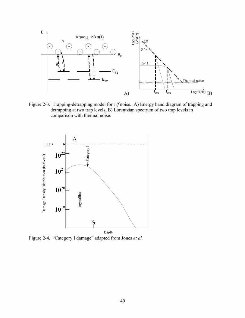
maximum in a Wheatstone bridge configuration as shown in Figure 2-2. The four piezoresistors
in the Wheatstone bridge are positioned such that two piezoresistors sense the stress parallel to
the current flow and the other two piezoresistors sense the stress perpendicular to the current
flow.
2.2.1 MEMS piezoresistive Microphone Voltage Output
When the four piezoresistors R1, R2, R3, and R4 are equal, the Wheatstone bridge is said to
be balanced. Thus at zero pressure, the output voltage, Vout, is zero. When the pressure on the
diaphragm is non-zero, the diaphragm deflects and the resistances of the four piezoresistors
change in equal magnitude. However, the resistance change of 1R and 3R have opposite signs to
26
that of 2R and 4R as indicated in Figure 2-2 by arrows. If 1 2 3 4R R R R R= = = = and change
with equal magnitude, RΔ , the resulting piezoresistive microphone output voltage is given by
Equation 2-11,
out biasRV V
RΔ
Δ = , (2-11)
where RΔ is the change in resistance, R is the normalized unstrained resistance, and Vbias is the
bias voltage. Appendix B provides additional information on MEMS piezoresistive microphone
voltage output.
2.2.2 MEMS Piezoresistive Microphone Sensitivity
The sensitivity of a MEMS piezoresistive microphone is given by the ratio of the output
voltage to the input pressure. The normalized sensitivity, which is the sensitivity divided by the
bias voltage, is shown in Equation 2-12,
1 1 1out out
bias bias
V V RSV p V p R p
Δ Δ= ≈ = , (2-12)
where Vbias is the voltage applied to the microphone, outVΔ is the differential output voltage, and
RΔ is the resistance modulation of the piezoresistor.
2.2.3 MEMS Piezoresistive Microphone Minimum Detectable Signal
The lower limit of the dynamic range of a MEMS piezoresistive microphone is the
minimum detectable signal (MDS). The expression of the MDS, which is the ratio of the output
referred noise voltage to the sensitivity, is given in Equation 2-13,
PSD dfNoiseMDS
Sensitivity Sensitivity
×= = ∫ . (2-13)
27

From Equation 2-13, we see that the MDS can be reduced by lowering the noise or increasing the
transducer sensitivity.
2.3 Noise and Noise Power Spectral Density
In general, a disturbance can be described as an unwanted internal or external signal
(acoustic, electrical) of a system that contaminates the signal of interest. In the electrical
domain, disturbances can originate from the environment or from within the device itself via
current or voltage fluctuations. To reduce any contamination of the desired signal from external
disturbances such as power line 60 Hz ac interference, techniques such as shielding and proper
wiring may be used. However, shielding or proper wiring cannot reduce the intrinsic non-
deterministic random fluctuations that originate from the device. This intrinsic random
fluctuation in voltage or current or generally effort or flow is termed noise. Since noise is a
random process, analyzing it in the time domain does not give useful information regarding its
average magnitude. Therefore, we employ the power spectral density function which gives the
magnitude of the random signal squared over a range of frequencies for noise measurements.
The power spectral density function as described by Bendat and Piersol2 is given in Equation 2-
14,
( )2
0
,lim x
x f
f fG
fΔ →
Ψ Δ=
Δ, (2-14)
where ( ) (2 2
0
1, lim , ,T
x T)f f x t f
T→∞Ψ Δ = Δ∫ f dt is the mean square value of a sample time record
between frequencies f and f f+ Δ .
28
2.4 Noise Sources in Piezoresistor
Noise in semiconductor piezoresistors can be affected by defect density, temperature,
doping concentration, and bias voltage. A semiconductor is in equilibrium, and its properties
remain constant independent of time when it is not subjected to a bias voltage or any external
stimuli such as light or thermal gradient. However, when bias or stimuli are applied to a
semiconductor, the device is in non-equilibrium, thus its properties are no longer constant.
MEMS sensors are subjected to different noise mechanisms depending on whether they are at
equilibrium or at non-equilibrium.
Semiconductors are solid-state materials with conductivities lying between those of
insulators and conductors (1x10⁻⁸ and 1x10⁴ S/cm). Semiconductor materials are very attractive
and widely used in electronic devices since their conductivity can change with doping
concentration, temperature, and light. Next we consider different noise mechanisms in silicon
semiconductor-based MEMS piezoresistive microphones.
2.4.1 Electrical Thermal Noise
Electrical thermal noise, also known as Johnson noise, describes voltage fluctuations at the
terminal of a conductor or semiconductor at equilibrium. These fluctuations are caused by the
random vibrations of charge carriers in equilibrium with the lattice at temperature, T. Work by
Nyquist3and Johnson
4 led to the expression of the thermal noise power spectral density given in
Equation 2-15,
2
4 th BVS k RT Hz⎡ ⎤= ⎢ ⎥⎣ ⎦
, (2-15)
where kB is the Boltzmann constant, R is the resistance, and T is the temperature in Kelvin.
From Equation 2-15, we notice that electrical thermal noise is independent of bias voltage
but depends on temperature. Electrical thermal noise is not affected by bias voltage since the
29
agitation of the charge carriers by thermal lattice vibrations is present regardless of bias voltage.
However, it is temperature dependent since more agitation of the carriers occurs when the
temperature is increased. In addition, Johnson noise is frequency independent because lattice
vibrations are random, thus not related to any single time constant.
2.4.2 Mechanical Thermal Noise
Mechanical thermal noise is the mechanical analogue of electrical thermal noise.5 By the
fluctuation-dissipation theorem, any dissipative mechanism that results in mechanical damping
must be balanced by a fluctuation force to maintain macroscopic energy balance, hence thermal
equilibrium. The expression of the mechanical thermal noise is given in Equation 2-16,
2
4 mth B mNS K R T Hz⎡ ⎤= ⎢ ⎥⎣ ⎦
, (2-16)
where mR is the equivalent mechanical resistance of the sensor. In a MEMS microphone
mechanical damping can originate from the vent channel and the diaphragm.
2.4.3 Low Frequency Noise
Low frequency noise is a frequency dependent non-equilibrium noise. When an actual
piezoresistor is subjected to an external stimulus (voltage, light), an excess noise at low
frequencies is observed above the thermal noise floor. Since it is inversely proportional to
frequency, it is also known as 1/f noise. The mechanism that generates 1/f noise is still an active
area of research. Two widely discussed mechanisms of 1/f noise are the fluctuation in the
mobility (Δμ) described by Hooge6 and the fluctuation in the number of carriers (Δn) developed
by McWhorter. 7
30
2.4.3.1 Hooge’s model
Hooge6 originally conducted experiments on noise in homogeneous samples at low
frequency and observed low frequency noise with an inverse frequency dependence. He
suggested that this 1/f noise at low frequency is a bulk phenomenon6 and is due to fluctuations
in the mobility (Δμ).8, 9, 10
Hooge gave an empirical formula for the noise power spectral density
of 1/f noise in his publications6 as shown in Equation 2-17,
2 2
VV VS HzNf
α ⎡ ⎤= ⎢ ⎥⎣ ⎦. (2-17)
In Equation 2-17, α, known as the Hooge parameter, is an empirical material parameter
varying from 1x10⁻⁶ to 1x10⁻³, V is the bias voltage, N is the number of carriers, and f is the
frequency. Hooge’s equation indicates a square bias voltage dependence for the low frequency
noise. Thus, this noise mechanism is only present when a voltage is applied. In addition,
Equation 2-17 shows that the noise power spectral density is inversely proportional to the
number of carriers, N. Thus, the low frequency noise depends on the doping concentration n
and volume V as shown in Equation 2-18 through the dependence on N,
N n V= ∗ . (2-18)
The accurate computation of the number of carriers is important for an accurate estimated
of α, or conversely, for the design of the 1/f noise given α. In some works, the number of
carriers used to compute the Hooge parameter is extracted assuming a homogeneous
semiconductor. Thus, the current density and electric field has been assumed to be the same in
the bulk of the piezoresistor. However, for our diffused piezoresistor, computing the number of
carriers using Equation 2-18, might lead to an over-estimate of the number of carriers. To
31
illustrate the importance of the number of carriers, , let us use the example of two
piezoresistors
N
1 and 2R R and with same resistance R but a different estimate of the number of
carriers, with . Using Equation 2.17, although the resistors have the same
Hooge parameter
1 2 and N N 21 > N N
α , the predicted 1/f noise PSD of resistor 1R will be less than that of the
resistor 2R .
To better estimate the number of carriers in an inhomogeneous semiconductor, we use Hall
Effect measurement to obtain the active dose, which is multiplied by the piezoresistor aera to
obtain as shown in Equation 2-19. N
AAN N A= ∗ (2-19)
where AAN is the electrical active dose expressed in 2cm− and A is the area of the sample.
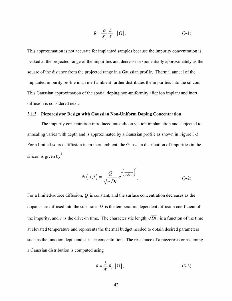
2.4.3.2 McWhorter’s model
McWhorter7 conducted his experiments on germanium samples and concluded that 1/f
noise is a surface effect. At the semiconductor surfaces and interfaces, physical defects give rise
to electronic traps that capture and emit charge. He postulated that 1/f noise is caused by
fluctuations of the number of charge carriers due to trapping and detrapping of charge carriers at
these traps. The Lorentzian generation-recombination spectrum resulting from the trapping and
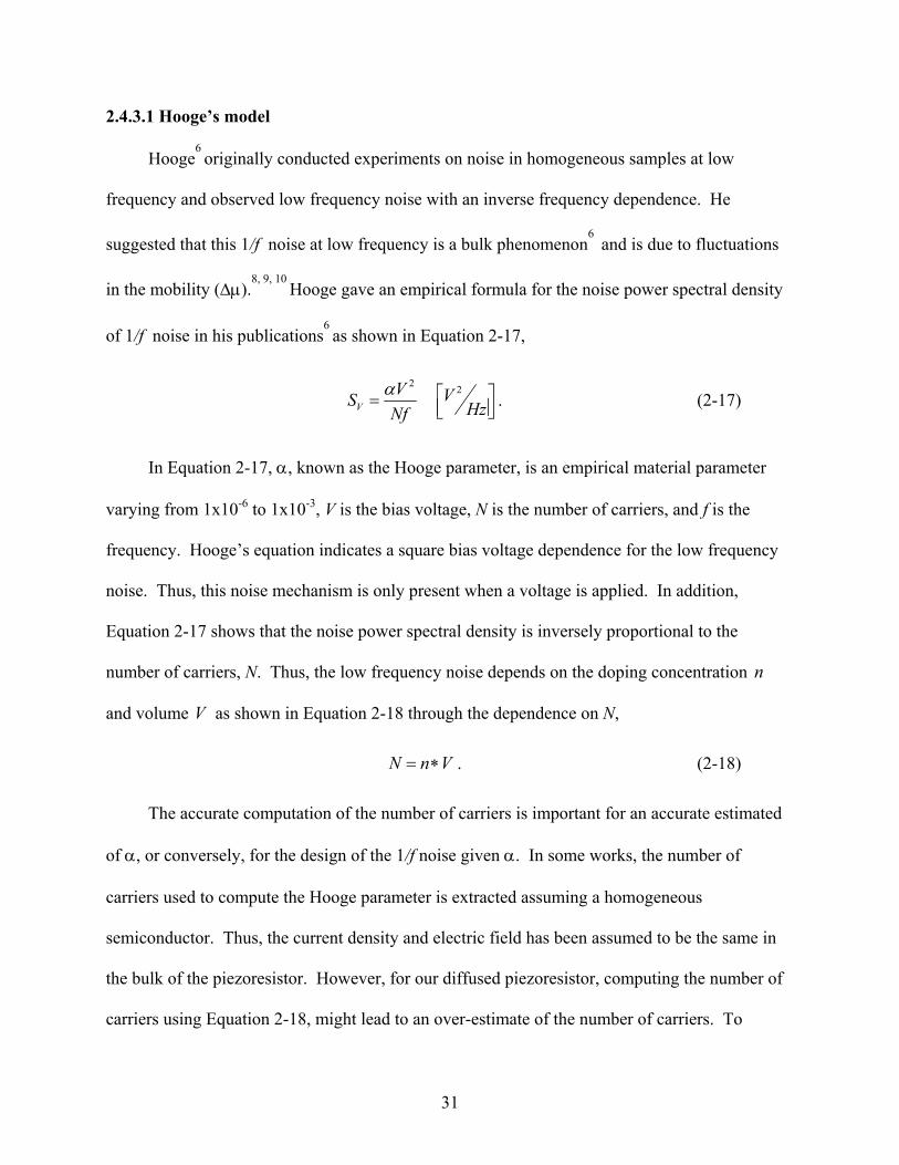
detrapping of the charge carriers at trap levels is given by Equation 2-20,11
( )( )21 2
tGR GR
t
S f Af
τπ τ
=+
(2-20)
32
where AGR is proportional to the density of the trap levels, and tτ is the tunneling time constant.
Figure 2-3 describes the energy band diagram with two trap levels and their associated
Lorentzian spectra with a corner frequency at 31
2dBfπτ
= .
Since electrons located in trap centers far from the conduction band require more energy
for generation-recombination to occur, τ is larger for deep trap centers than shallow trap centers
as illustrated in Figure 2-3. Summing the noise power spectral densities for a continuum of trap
levels, we observe a 1/f noise shape up to the cut off frequency where the curve rolls off as 1/f2.
The 1/f noise observed at low frequencies is caused by fluctuations in the number of carriers in
the conduction and valence bands due to trapping and detrapping of carriers located at multiple
trap levels. The Hooge and McWhorter 1/f noise models are illustrated via the predicted
resistance fluctuations in a p-type resistor in Appendix C.
Both Hooge’s and McWhorter’s 1/f noise models are actively used or modified to analyze
and interpret low frequency noise measurements in electronic devices.12,13, 14
However, since
Hooge’s model describes the low frequency noise through parameters (voltage, number of
carriers, and Hooge parameter) that are easily manipulated it is very attractive for analysis.
Designers can model low 1/f noise piezoresistor by adjusting or modifying these parameters.
2.4.4 Shot Noise
Schottky15
investigated noise in vacuum tubes. In a semiconductor, when charge carriers
cross a potential barrier independently and randomly, fluctuations occur in the average current, I.
These fluctuations give rise to shot noise which is a non-equilibrium noise. In particular, shot
noise is observed in a P/N junction due to the fluctuations in the average current I induced by the
33
random crossing of carriers over a potential barrier. The shot noise power spectral density is
given in Equation 2-21,
2
2 IAS qI Hz⎡ ⎤= ⎢ ⎥⎣ ⎦
, (2-21)
where q is the electron charge, and I is the current.
Equation 2-21 shows that shot noise is directly proportional to the average current I, hence it is
only present under bias conditions, and is frequency independent.
2.5 Defects in Semiconductors
Defects have been cited to be the major cause of low frequency noise. As described
earlier, there are two well known theories6, 7 for the presence of the non-equilibrium 1/f noise. In
this section, we present mechanisms that create different defects in the bulk of a semiconductor
that has been subjected to pre-amorphization, ion implantation, and diffusion. We also discuss
defects at the semiconductor surface (Si/SiO2 interface) that may give rise to low frequency
noise.
2.5.1 Bulk Defects
Ion implantation is widely used for the introduction of foreign species in a semiconductor
material such as silicon. Some advantages of ion implantation are the capacity to control the
dopant concentration, the use of relatively low temperature, and reduced lateral distribution of
the dopant. However, ion implantation has also some disadvantages. One of the disadvantages
is the introduction of point defects such as interstitials and vacancies into the crystalline lattice.
Annealing is used after ion implantation to recrystallize the silicon substrate and promote the
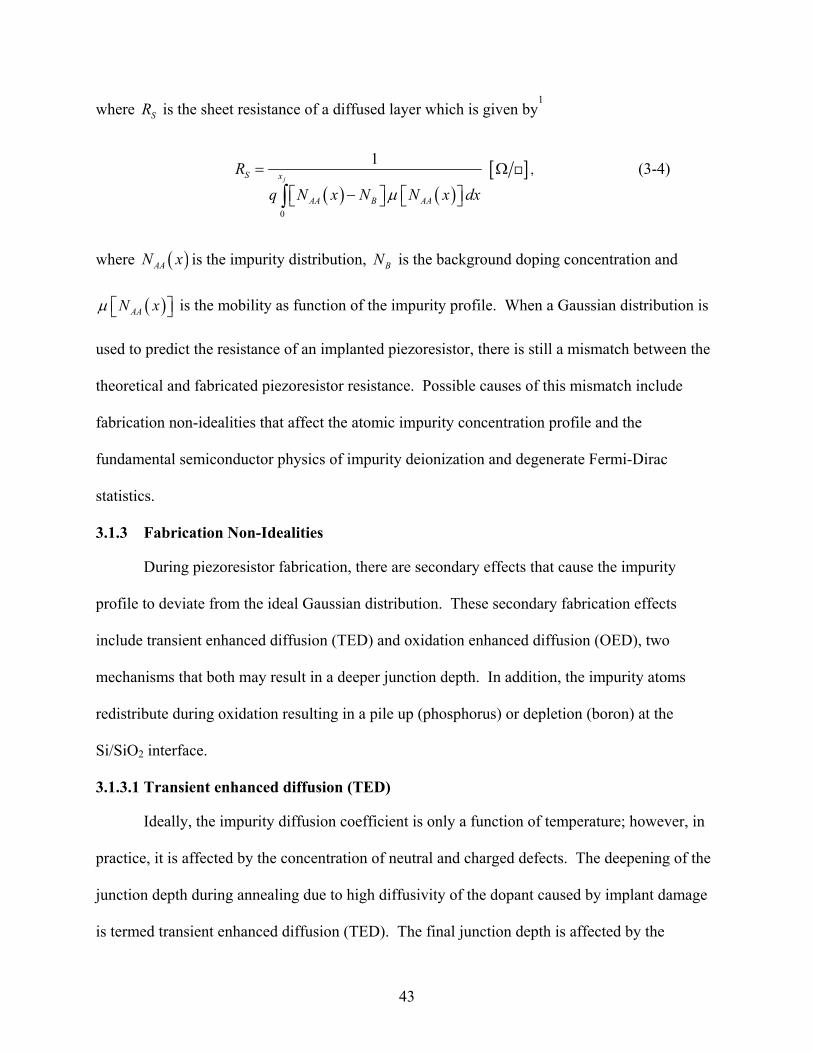
activation of the dopant. The type of defects formed after annealing have been categorized by
Jones et al.16
The first category is termed “Category I Damage” by Jones et al.16
In this case,
34
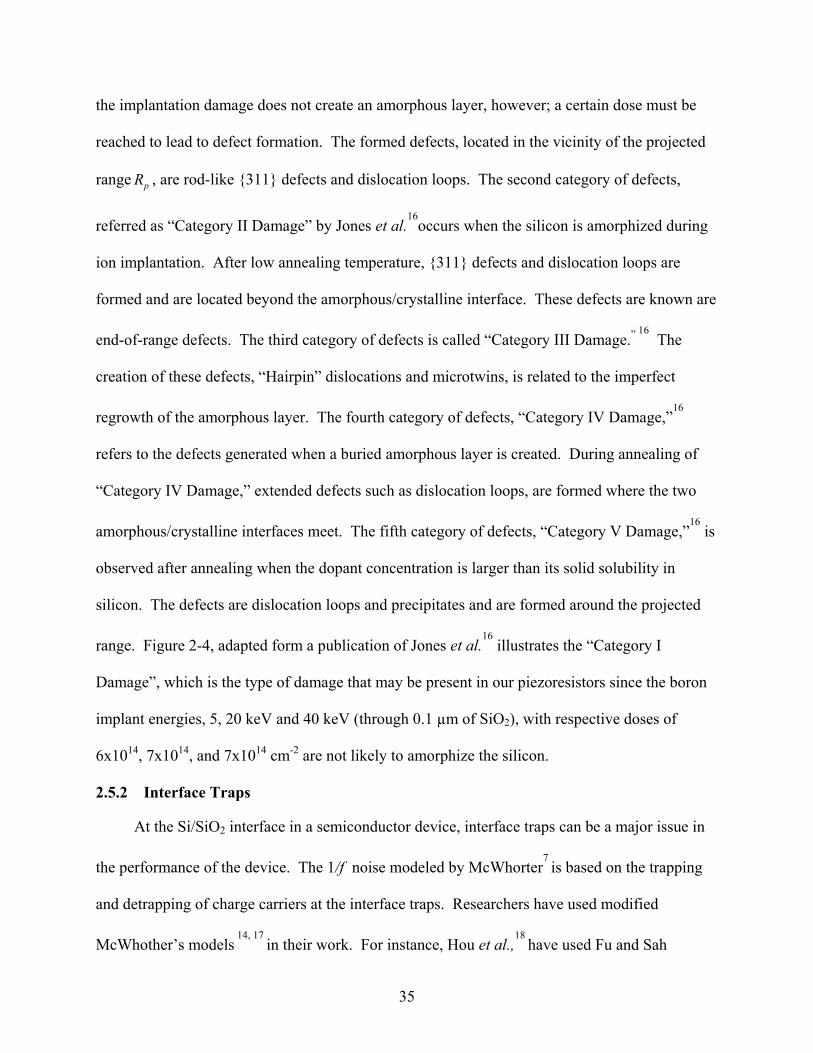
the implantation damage does not create an amorphous layer, however; a certain dose must be
reached to lead to defect formation. The formed defects, located in the vicinity of the projected
range pR , are rod-like 311 defects and dislocation loops. The second category of defects,
referred as “Category II Damage” by Jones et al.16
occurs when the silicon is amorphized during
ion implantation. After low annealing temperature, 311 defects and dislocation loops are
formed and are located beyond the amorphous/crystalline interface. These defects are known are
end-of-range defects. The third category of defects is called “Category III Damage.” 16
The
creation of these defects, “Hairpin” dislocations and microtwins, is related to the imperfect
regrowth of the amorphous layer. The fourth category of defects, “Category IV Damage,”16
refers to the defects generated when a buried amorphous layer is created. During annealing of
“Category IV Damage,” extended defects such as dislocation loops, are formed where the two
amorphous/crystalline interfaces meet. The fifth category of defects, “Category V Damage,”16
is
observed after annealing when the dopant concentration is larger than its solid solubility in
silicon. The defects are dislocation loops and precipitates and are formed around the projected
range. Figure 2-4, adapted form a publication of Jones et al.16
illustrates the “Category I
Damage”, which is the type of damage that may be present in our piezoresistors since the boron
implant energies, 5, 20 keV and 40 keV (through 0.1 µm of SiO2), with respective doses of
6x10¹⁴, 7x10¹⁴, and 7x1014 cm-2 are not likely to amorphize the silicon.
2.5.2 Interface Traps
At the Si/SiO2 interface in a semiconductor device, interface traps can be a major issue in
the performance of the device. The 1/f noise modeled by McWhorter7 is based on the trapping
and detrapping of charge carriers at the interface traps. Researchers have used modified
McWhother’s models 14, 17
in their work. For instance, Hou et al.,18 have used Fu and Sah
35
model17
in their oxide trapping noise simulations. The density of traps at the Si/SiO2 interface
can be measured using Terman’s19
method which employed a high C-V frequency measurement
of a capacitor. In Chapter 4 we discuss the experimental method to compute the interface trap
density, . itD
2.6 Process Dependence of 1/f Noise
Various hypotheses on the source of the 1/f noise, their relation to the process fabrication
(defects) and geometry have been provided by authors to describe the limiting factors.
Summaries process dependence of 1/f noise, defect formation and energy distribution of defects
in semiconductors are provided. Researchers such as Bilger et al. 20
, Vandamme and Ooterhoff21
, Clevers22
, Harley and Kenny23,12
, Yu et al. 13, 24
, Davenport et al.25
, Mallon et al.26
, E. Cocheteau
et al.27
, and B. Belier et al.28
have studied the process dependence of 1/f noise by varying
parameters such as impurity species (boron, B , or boron fluoride, 2BF ), pre-amorphization, ion
implantation (energy, dose) with or without implant oxide, annealing condition (furnace or
RTA), surface passivation (thermal oxide, PECVD oxide, nitride), materials (crystal, amorphous
and poly silicon), and device dimensions. Their results indicate that low 1/f noise and low Hooge
parameters can be achieved through low implant energy, long annealing conditions, good oxide
quality, and large number of carriers. To illustrate the effect of impurity we examine the works
of Cocheteau et al.27
and Belier et al.28
who both implanted their samples with 2BF instead of B .
However, Belier et al.28
performed Ge -preamorphization prior to ion implantation. Results from
Cocheteau et al.27
show higher noise than they expected, thus Cocheteau et al.27
suggested that
an increase in annealing time to reduce 1/f noise. As for Belier et al.28
their devices with
preamorphization have less low-frequency noise than those without preamorphization. Belier et
36
al.28
recommended the lowering of preamorphization and implant energies to further reduce the
1/f noise. The defect evolutions and the defect types with their locations in implanted samples
with or without amorphization have been studied by researchers such as Jones et al.16
, Li and
Jones29
, Liu et al.30
, and Girginoudi and Tsiarapas.31
In addition, as discussed in Section 2.5.1,
Jones et al. 16
have categorized the types of defects and their locations after ion implantation and
annealing and have described factors such as implant species, ion implantation (energy and dose)
that lead to the defects formations and locations. The defect concentrations and energy levels in
samples implanted with BF2, B or F-B, and inert annealed or oxidized were investigated by
authors such as Yarykin and Steinman32
, Boussaid et al.33
, Benzohra et al 34
, Kaniewski et al.35
and Girginoudi and Tsiarapas.31
Boussaid et al.33
results show energy levels caused by the boron
implantation and annealing and other energy levels associated with the preamorphization. In
their work, Boussaid et al.33
show that the DLTS peaks of defects associated with Ge-
preamorphization increases as the Ge energy increases. In addition, samples with fluorine have
higher defect concentrations than those without fluorine. The reverse bias currents of the p+n
diodes fabricated by and Girginoudi and Tsiarapas31
are large but decrease as the deep level
density decreases due to lower preamorphization energies and higher annealing temperatures.
Low frequency noise has also been used by researchers such as Michelutti et al.36
to investigate
the effect of environment on pressure sensors. Their measurements show that temperature
influences 1/f noise in corroded and non-corroded samples. Other scientists such as Park and
Hwang37
have shown methods to fabricated shallow junction for MOSFET devices. Park and
Hwang37
implanted B and BF2. After ion implantation both profiles have approximately the
same junction depth but after annealing the BF2 profiles have shallower junction depths than
37
those of B. All the results presented in this section are important since they present the process
dependence of 1/f noise, defect formation and energy distribution of defects in semiconductors.
This dissertation addresses the process dependence of 1/f noise not only with 1/f noise magnitude
as a function of annealing times but also with a systematic correlation of the 1/f noise to the
defects densities obtained with TEM and HFCV after each annealing condition. The effect of the
number of carriers on 1/f noise is studied first in piezoresistors with same resistance and different
volume and piezoresistors with different resistances and volumes that underwent the same ion
implantation and annealing conditions. Second, the number of carriers is studied on
piezoresistors with two different solid source diffusion conditions, to limit the interaction of the
carriers with the interface traps, but with same annealing conditions. This allows to see if the
reduction of the 1/f noise is due to the number of carriers or the additional solid source diffusion.
2.7 Summary
There is a need to correlate the noise present in the devices to fabrication process and to
the physical defects characterized by surface analytical techniques such as TEM. Therefore, an
investigation of the correlation of noise and defects in implanted, solid source diffused and
annealed piezoresistors is performed. Now that the background of the research and the
contribution of this work were discussed, the piezoresistor design is presented next.
38
A
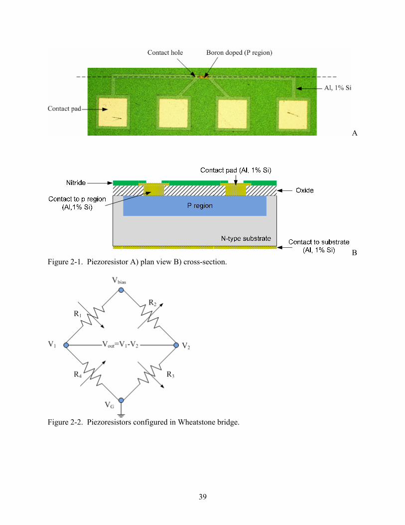
B Figure 2-1. Piezoresistor A) plan view B) cross-section.
Figure 2-2. Piezoresistors configured in Wheatstone bridge.
39
EC
E
--
-- --
--n
g r
ET1
ET2
I(t)=qµn eAn(t)
A)
Log
PSD
(V2/H
z)
f3dB Log f (Hz)f3dB
1/f
g-r 1
g-r 2
Thermal noise
B)
Figure 2-3. Trapping-detrapping model for 1/f noise. A) Energy band diagram of trapping and detrapping at two trap levels, B) Lorentzian spectrum of two trap levels in comparison with thermal noise.
Cat
egor
y I
Dam
age
Den
sity
Dis
tribu
tion
(keV
/cm
3 )
crys
talli
ne
Figure 2-4. “Category I damage” adapted from Jones et al.
40

CHAPTER 3 PIEZORESISTOR DESIGN
In this chapter, we present the theoretical design of piezoresistors and their realization via
microfabrication that are used to study the process dependence of piezoresistor noise. We start
by presenting the design of a piezoresistor assuming a non-degenerate semiconductor for both
uniform and non-uniform impurity concentration profiles. Afterwards, we discuss the key
resistor design parameters such as resistivity, resistance, and surface-to-volume ratio. We also
consider non-idealities in the fabrication process that affect the impurity profile. We finish by
presenting the design of the piezoresistor test structures.
3.1 Introduction
A p-type silicon piezoresistor is typically fabricated via ion-implantation of boron into
crystalline silicon. The geometry of the piezoresistor is defined in Figure 3-1 where L and W
are the length and width of the piezoresistor, is the contact width, andCW jX is the junction
depth. In the depth direction, the spatial dependence of the boron concentration affects the
conductivity and the resulting resistance measured between the two contacts. In the next section,
the simplest (ideal) case of a uniform impurity profile is first considered. This simplifying
assumption is then relaxed to derive more accurate resistance estimates for practical fabrication
processes.
3.1.1 Piezoresistor Design with Uniform Doping Concentration
The ideal case of a spatially uniform impurity profile in the depth direction is considered
first as illustrated in Figure 3-2. Furthermore, the concentration is assumed to be low enough
such that the carrier concentration is non-degenerate, and the Boltzmann approximation for
carrier statistics can be employed. For p-type silicon, this means a carrier concentration less than
1x1018 cm-3.38
In this case, the resistance of a uniformly doped piezoresistor is given by
41
[ ] j
LRX Wρ
= Ω . (3-1)
This approximation is not accurate for implanted samples because the impurity concentration is
peaked at the projected range of the impurities and decreases exponentially approximately as the
square of the distance from the projected range in a Gaussian profile. Thermal anneal of the
implanted impurity profile in an inert ambient further distributes the impurities into the silicon.
This Gaussian approximation of the spatial doping non-uniformity after ion implant and inert
diffusion is considered next.
3.1.2 Piezoresistor Design with Gaussian Non-Uniform Doping Concentration
The impurity concentration introduced into silicon via ion implantation and subjected to
annealing varies with depth and is approximated by a Gaussian profile as shown in Figure 3-3.
For a limited-source diffusion in an inert ambient, the Gaussian distribution of impurities in the
silicon is given by1
( )2
2,xDtQN x t e
Dtπ
⎛ ⎞−⎜ ⎟⎝ ⎠= . (3-2)
For a limited-source diffusion, is constant, and the surface concentration decreases as the
dopants are diffused into the substrate. is the temperature dependent diffusion coefficient of
the impurity, and t is the drive-in time. The characteristic length,
Q
D
Dt , is a function of the time
at elevated temperature and represents the thermal budget needed to obtain desired parameters
such as the junction depth and surface concentration. The resistance of a piezoresistor assuming
a Gaussian distribution is computed using
[ ]SLR R
W= Ω , (3-3)
42
where SR is the sheet resistance of a diffused layer which is given by1
( ) ( )[ ]
0
1 jS x
AA B AA
Rq N x N N x dxμ
= Ω
−⎡ ⎤ ⎡ ⎤⎣ ⎦ ⎣ ⎦∫, (3-4)
where ( )AAN x is the impurity distribution, is the background doping concentration and
is the mobility as function of the impurity profile. When a Gaussian distribution is
used to predict the resistance of an implanted piezoresistor, there is still a mismatch between the
theoretical and fabricated piezoresistor resistance. Possible causes of this mismatch include
fabrication non-idealities that affect the atomic impurity concentration profile and the
fundamental semiconductor physics of impurity deionization and degenerate Fermi-Dirac
statistics.
BN
( )AAN xμ ⎡⎣ ⎤⎦
3.1.3 Fabrication Non-Idealities
During piezoresistor fabrication, there are secondary effects that cause the impurity
profile to deviate from the ideal Gaussian distribution. These secondary fabrication effects
include transient enhanced diffusion (TED) and oxidation enhanced diffusion (OED), two
mechanisms that both may result in a deeper junction depth. In addition, the impurity atoms
redistribute during oxidation resulting in a pile up (phosphorus) or depletion (boron) at the
Si/SiO2 interface.
3.1.3.1 Transient enhanced diffusion (TED)
Ideally, the impurity diffusion coefficient is only a function of temperature; however, in
practice, it is affected by the concentration of neutral and charged defects. The deepening of the
junction depth during annealing due to high diffusivity of the dopant caused by implant damage
is termed transient enhanced diffusion (TED). The final junction depth is affected by the
43
annealing temperature used to activate the dopant in the semiconductor when implant damage is
present. The choice of the diffusion temperature is critical for TED. Deal et al.,1 discuss the
effect of time and temperature on TED. Deal et al.,1 use a figure from Crowder
39 that shows the
effect of temperature on TED. In that figure from Crowder39
there is more diffusion for the
lower temperature.
3.1.3.2 Oxidation enhanced diffusion (OED)
During oxidation, there is injection of extra interstitials into the bulk of the silicon which
may cause an increase of the dopant diffusion rate resulting in a deeper junction depth. This
phenomenon is termed oxidation enhanced diffusion (OED) and is observed during the oxidation
of boron implanted silicon.1
3.1.3.3 Impurity segregation
When two different materials are in contact, dopant present in one material segregate into
the materials until equilibrium is reached.1 Dopant segregation may cause a depletion or a pileup
of the dopant near the materials interface. For example, during thermal oxide growth, boron
preferentially segregates into the oxide causing a depletion of the boron concentration in the
silicon near the Si/SiO2 interface. Thus, during oxidation or annealing in an oxidizing ambient,
the predicted surface concentration may decrease due to boron segregation into the SiO2 leading
to a reduction of the total boron dose in the silicon. The segregation of boron in SiO2 were
studied by Fair and Tsai.40 Figure 3-4 shows boron profiles assuming ideal (Gaussian) and the
non-ideal boron distribution that may result from TED, OED, and impurity segregation. In
Figure 3-4, the non-ideal profile has a smaller surface concentration than the ideal Gaussian
profile but also has a deeper junction depth.
44
3.1.4 Fundamental Physics That Affect Electrical Activation of Impurities
Another parameter to consider in the piezoresistor design is the electrically active
concentration of impurities which can differ from the atomic concentration. This difference is
due to the fundamental physics of impurity deionization and degenerate carrier statistics
discussed in Chapter 2. In both cases, the concentration of the neutral donor and acceptor are
estimated by taking into account the occupation factor of the donor impurities Df and acceptor
impurities Af given in Equation 3.5 and 3-6.38
1
11D FD E EkT
D
fe
g
−⎛ ⎞⎜ ⎟⎝ ⎠
=
+
(3-5)
1
11F AA E EkT
A
fe
g
−⎛ ⎞⎜ ⎟⎝ ⎠
=
+
(3-6)
where Dg and Ag are the donor and acceptor site degeneracy factor, is the Fermi level, FE DE is
the donor level, and AE the acceptor level. The charge neutrality equation which allows the
computation of the electron and hole concentration at thermal equilibrium is given in
Equation 3-7,38
( ) ( ) 0DD D AA Aq P N N N N N⎡ ⎤− + − − − =⎣ ⎦ , (3-7)
where and are the hole and electron concentrations,P N DDN and AAN are the donor and
acceptor impurity concentrations, and DN and AN are the concentrations of electrons and holes
trapped respectively at the donor and acceptor sites. Thus, the quantities ( )DD DN N− and
( )AA AN N− represent the concentration of ionized donors and the concentration of ionized
45
acceptors respectively. Since we take into account impurity deionization, DN and AN are not
assumed to be zero but rather are computed using the donor and acceptor occupation factors and
the respective impurity concentrations from38
D D DDN f N= , (3-8)
and
A A AAN f N= . (3-9)
Using ( )1D DD D DD D DD DD DN N N N f N N f+ = − = − = − , the concentration of ionized donors is
given by
1
1F DD DD E EkT
D
N Ng e
+−⎛ ⎞
⎜ ⎟⎝ ⎠
⎛ ⎞⎜ ⎟
= ⎜ ⎟⎜ ⎟+⎝ ⎠
, (3-10)
and the concentration of ionized acceptors is given by
1
1A FA AA E EkT
A
N Ng e
−−⎛ ⎞
⎜ ⎟⎝ ⎠
⎛ ⎞⎜ ⎟
= ⎜ ⎟⎜ ⎟+⎝ ⎠
. (3-11)
The electrical active carrier concentration is obtained by solving the general charge
neutrality condition, Equation 3-7 together with the mass action laws,
1 2 1 2F C V F
C VE E ENP N N F F
kT kT− −⎛ ⎞ ⎛= ⋅ ⋅⎜ ⎟ ⎜
⎝ ⎠ ⎝
E ⎞⎟⎠
.
46

3.2 Piezoresistor Design Parameters
Four key parameters are considered in the piezoresistor design. These parameters are the
piezoresistor impurity profile, resistance, surface area, and volume. Associated with the impurity
profile are the doping process details such as implant energy, annealing time and ambient. The
overall purpose for the variation of these four parameters is to study the process and geometry
dependencies of 1/f noise in piezoresistors. The impurity profile is used to compute the number
of carriers , which in turn is used in the computation of the Hooge parameterN α . From
Equation 2-17, we see that as increases, the 1/f noise decreases for a specific value of N α . In
addition, the 1/f noise may originate from the bulk or the surface of the piezoresistor. Thus, by
varying the surface area and the volume of the piezoresistor, we change the surface to volume
ratio to investigate whether the carriers are more affected by the defects in the bulk or the surface
traps when the piezoresistor is in non-equilibrium.
3.2.1 Piezoresistor Impurity Profile
For fixed implant and annealing conditions the junction depth and surface concentration
are unchanged for piezoresistors with different dimensions in the same wafer. Then the sheet
resistance SR , the ratio of the resistivity to the junction depth, will be the same for all
piezoresistors. Therefore, to design piezoresistors with different resistances, one may manipulate
the piezoresistor width and length.
3.2.2 Piezoresistor Resistance
Piezoresistors with four different resistances have been designed. Since the junction depth
and doping profile are the same for all the piezoresistors, the four different resistances have been
obtained by varying the number of squares, which is the ratio of the length to the width of the
47
piezoresistor L W . Figure 3-5, adapted from Jaeger41
shows two piezoresistors with the same
sheet resistance, but different number of squares L W and hence resistance.
3.2.3 Piezoresistor Surface Area
Piezoresistors with different surface area but same resistance are obtained by changing
while maintaining the same number of squares,L W× L W . Figure 3-6, adapted from Jaeger,41
shows two piezoresistors with the same resistance, R , same number of squares, L W , but
different surface area.
3.2.4 Piezoresistor Volume
The piezoresistor volume is approximately equal to the product of the total surface area
and the junction depth. It will vary as the surface area or the junction depth of the piezoresistors
is changed. Thus, piezoresistors with the same resistance and different volume are also obtained.
If the junction depth, jX , is the same, then the ratio of the surface area to volume is constant and
equal to 1 jX . In the next section, the photomask design is outlined.
3.3 Test Structures Design
The piezoresistor photomask design varies the four parameters described earlier. The
process flow is summarized in Appendix D. A total of four photomasks have been designed in
AutoCAD for the fabrication of the test structures. The first mask is the implant mask, the
second is the contact mask, the third is the metal mask, and the fourth is the bond pad mask. Two
generations of test structures, generation 1 and generation 2, have been fabricated. The
difference between the two generations is in the order that the implant and oxide growth are
performed and also the removal of an oxide layer before implant. In addition to the
piezoresistors, we have designed additional test structures which are the p-type capacitor, P/N
junction diode, Van der Pauw structures and Hall Effect structures. The wafers used for the
48
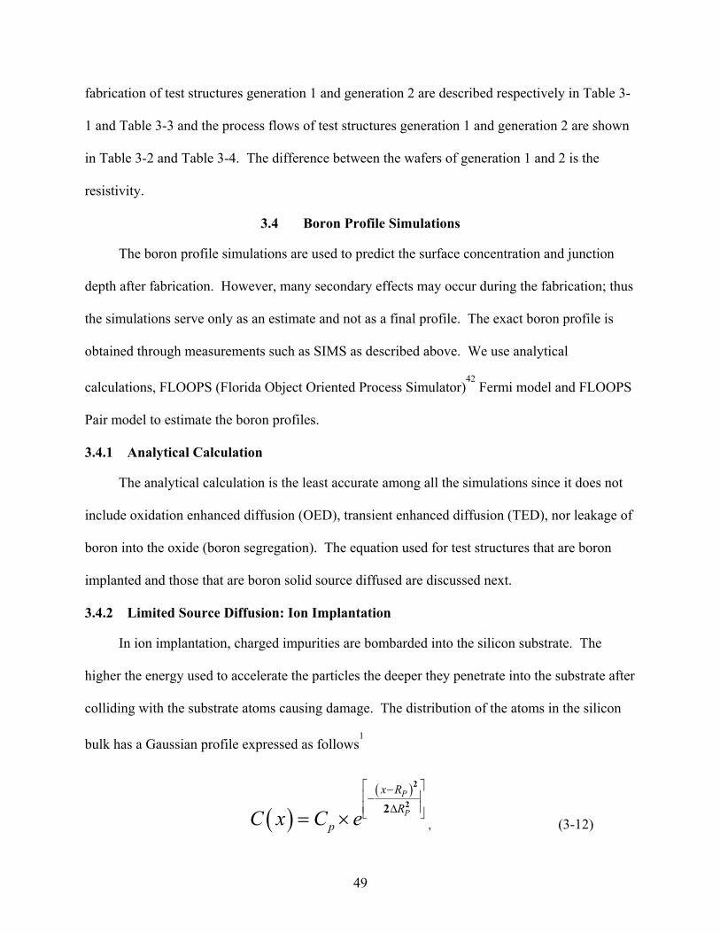
fabrication of test structures generation 1 and generation 2 are described respectively in Table 3-
1 and Table 3-3 and the process flows of test structures generation 1 and generation 2 are shown
in Table 3-2 and Table 3-4. The difference between the wafers of generation 1 and 2 is the
resistivity.
3.4 Boron Profile Simulations
The boron profile simulations are used to predict the surface concentration and junction
depth after fabrication. However, many secondary effects may occur during the fabrication; thus
the simulations serve only as an estimate and not as a final profile. The exact boron profile is
obtained through measurements such as SIMS as described above. We use analytical
calculations, FLOOPS (Florida Object Oriented Process Simulator)42
Fermi model and FLOOPS
Pair model to estimate the boron profiles.
3.4.1 Analytical Calculation
The analytical calculation is the least accurate among all the simulations since it does not
include oxidation enhanced diffusion (OED), transient enhanced diffusion (TED), nor leakage of
boron into the oxide (boron segregation). The equation used for test structures that are boron
implanted and those that are boron solid source diffused are discussed next.
3.4.2 Limited Source Diffusion: Ion Implantation
In ion implantation, charged impurities are bombarded into the silicon substrate. The
higher the energy used to accelerate the particles the deeper they penetrate into the substrate after
colliding with the substrate atoms causing damage. The distribution of the atoms in the silicon
bulk has a Gaussian profile expressed as follows1
( )( )2
22P
P
x RR
pC x C e
⎡ ⎤−⎢ ⎥−⎢ ⎥Δ⎣ ⎦= × , (3-12)
49
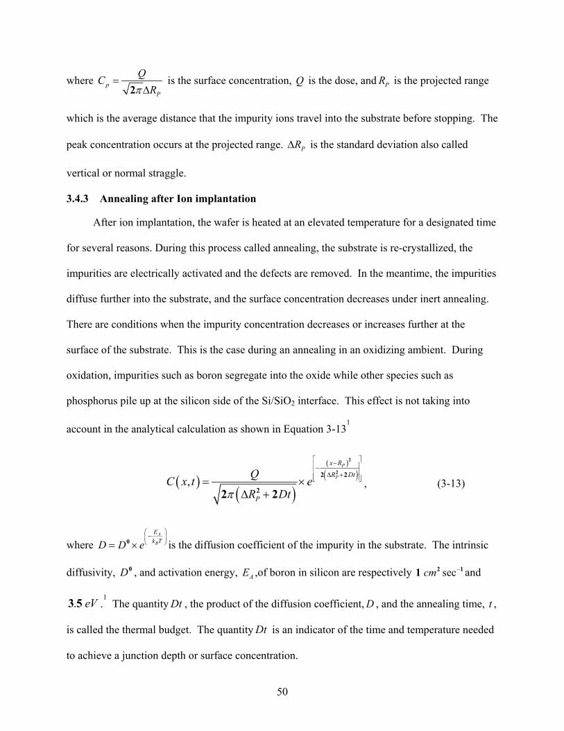
where 2p
P
QCRπ
=Δ
is the surface concentration, Q is the dose, and PR is the projected range
which is the average distance that the impurity ions travel into the substrate before stopping. The
peak concentration occurs at the projected range. PRΔ is the standard deviation also called
vertical or normal straggle.
3.4.3 Annealing after Ion implantation
After ion implantation, the wafer is heated at an elevated temperature for a designated time
for several reasons. During this process called annealing, the substrate is re-crystallized, the
impurities are electrically activated and the defects are removed. In the meantime, the impurities
diffuse further into the substrate, and the surface concentration decreases under inert annealing.
There are conditions when the impurity concentration decreases or increases further at the
surface of the substrate. This is the case during an annealing in an oxidizing ambient. During
oxidation, impurities such as boron segregate into the oxide while other species such as
phosphorus pile up at the silicon side of the Si/SiO2 interface. This effect is not taking into
account in the analytical calculation as shown in Equation 3-131
( )( )
( )( ),
2
22 2
22 2
P
P
x R
R Dt
P
QC x t eR Dtπ
⎡ ⎤−⎢ ⎥−⎢ ⎥Δ +⎢ ⎥⎣ ⎦= ×
Δ +, (3-13)
where 0A
B
Ek TD D e
⎛ ⎞−⎜ ⎟⎝= × ⎠
1
is the diffusion coefficient of the impurity in the substrate. The intrinsic
diffusivity, , and activation energy, ,of boron in silicon are respectively 0D AE sec21 cm − and
.1 The quantity.3 5 eV Dt , the product of the diffusion coefficient, , and the annealing time, t ,
is called the thermal budget. The quantity
D
Dt is an indicator of the time and temperature needed
to achieve a junction depth or surface concentration.
50
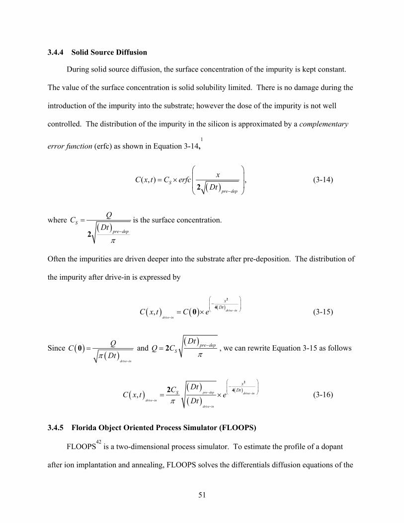
3.4.4 Solid Source Diffusion
During solid source diffusion, the surface concentration of the impurity is kept constant.
The value of the surface concentration is solid solubility limited. There is no damage during the
introduction of the impurity into the substrate; however the dose of the impurity is not well
controlled. The distribution of the impurity in the silicon is approximated by a complementary
error function (erfc) as shown in Equation 3-14,1
( )
( , )2
S
pre dep
xC x t C erfcDt
−
⎛ ⎞⎜= ×⎜⎝ ⎠
⎟⎟
, (3-14)
where ( )
2S
pre dep
QCDt
π−
= is the surface concentration.
Often the impurities are driven deeper into the substrate after pre-deposition. The distribution of
the impurity after drive-in is expressed by
( ) ( ) ( ),
2
40 drive in
drive in
xDt
C x t C e −
−
⎛ ⎞⎜ ⎟−⎜⎝= ×
⎟⎠ (3-15)
Since ( )( )
0drive in
QCDtπ
−
= and ( )
2 pre depS
DtQ C
π−= , we can rewrite Equation 3-15 as follows
( )( )( )
( ),
2
42 pre dep drive in
drive in
drive in
xDtS
DtCC x t eDtπ
− −
−
−
⎛ ⎞⎜ ⎟−⎜⎝= ×
⎟⎠ (3-16)
3.4.5 Florida Object Oriented Process Simulator (FLOOPS)
FLOOPS42
is a two-dimensional process simulator. To estimate the profile of a dopant
after ion implantation and annealing, FLOOPS solves the differentials diffusion equations of the
51
impurity atoms and the point defects differentials equations. The initial distribution of the point
defects, vacancies and interstitials, is determined by the implantation process. Two FLOOPS
diffusion models, Fermi model and pair model, are used to approximate the boron profiles of our
processes prior to fabrication.
3.4.5.1 Simplest FLOOPS (Fermi model)
The FLOOPS Fermi model is the simplest FLOOPS simulation. In the Fermi model,
diffusion is described as a concentration-dependent diffusivity.59
It is more sophisticated than
the analytical calculation shown above.
3.4.5.2 More accurate FLOOPS (Pair model)
In this model, the diffusion of the dopant occurs via dopant-interstitial or dopant-vacancy
pairs.59
FLOOPS Pair model includes TED, impurity segregation and OED which shows a
drastic deepening of the profile when oxidation enhanced diffusion (OED) is modeled. It is more
sophisticated that the analytical calculation and the FLOOPS Fermi model.
3.5 P-type Piezoresistor Implant and Annealing Condition
The details of the implant and annealing condition for the p-type piezoresistors is discussed
in the context of the resistance, surface area, and volume.
3.5.1 Piezoresistor Generation 1 (PG1)
The junction isolated piezoresistors are designed to have various lengths and widths to
obtain different surface areas. The purpose of varying the surface-to-volume ratio is to find out
whether the low frequency noise is more strongly dependent on the surface area based on
McWhorter’s theory7 or the volume-distributed bulk defects based on Hooge’s theory.
6 As
stated earlier if the junction depth, jX , is constant, then the ratio of the surface area to volume is
constant and equal to 1 jX . This is the case for the piezoresistor design. The implant and
52
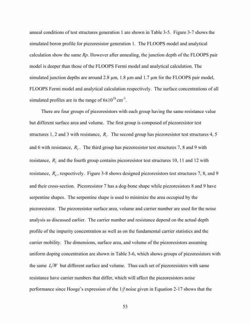
anneal conditions of test structures generation 1 are shown in Table 3-5. Figure 3-7 shows the
simulated boron profile for piezoresistor generation 1. The FLOOPS model and analytical
calculation show the same Rp. However after annealing, the junction depth of the FLOOPS pair
model is deeper than those of the FLOOPS Fermi model and analytical calculation. The
simulated junction depths are around 2.8 µm, 1.8 µm and 1.7 µm for the FLOOPS pair model,
FLOOPS Fermi model and analytical calculation respectively. The surface concentrations of all
simulated profiles are in the range of 6x1018 cm-3.
There are four groups of piezoresistors with each group having the same resistance value
but different surface area and volume. The first group is composed of piezoresistor test
structures 1, 2 and 3 with resistance, 1R . The second group has piezoresistor test structures 4, 5
and 6 with resistance, 2R . The third group has piezoresistor test structures 7, 8 and 9 with
resistance, 3R and the fourth group contains piezoresistor test structures 10, 11 and 12 with
resistance, 4R , respectively. Figure 3-8 shows designed piezoresistors test structures 7, 8, and 9
and their cross-section. Piezoresistor 7 has a dog-bone shape while piezoresistors 8 and 9 have
serpentine shapes. The serpentine shape is used to minimize the area occupied by the
piezoresistor. The piezoresistor surface area, volume and carrier number are used for the noise
analysis as discussed earlier. The carrier number and resistance depend on the actual depth
profile of the impurity concentration as well as on the fundamental carrier statistics and the
carrier mobility. The dimensions, surface area, and volume of the piezoresistors assuming
uniform doping concentration are shown in Table 3-6, which shows groups of piezoresistors with
the same L W but different surface and volume. Thus each set of piezoresistors with same
resistance have carrier numbers that differ, which will affect the piezoresistors noise
performance since Hooge’s expression of the 1/f noise given in Equation 2-17 shows that the
53
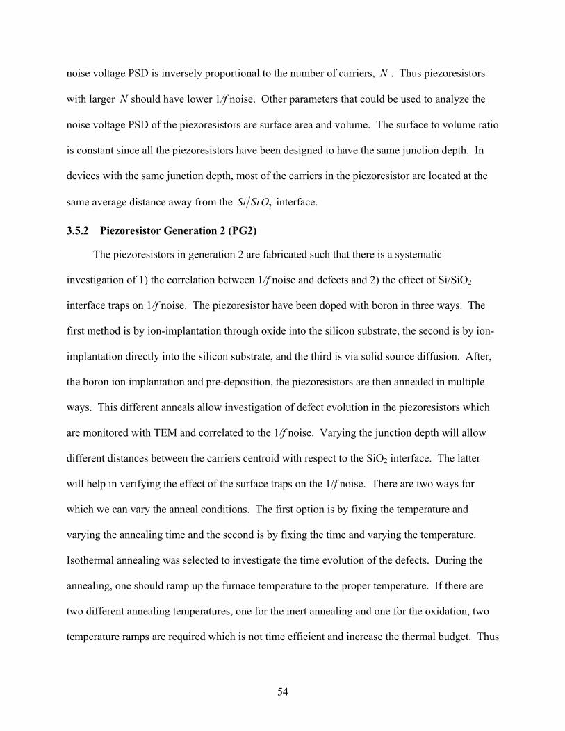
noise voltage PSD is inversely proportional to the number of carriers, . Thus piezoresistors
with larger should have lower 1/f noise. Other parameters that could be used to analyze the
noise voltage PSD of the piezoresistors are surface area and volume. The surface to volume ratio
is constant since all the piezoresistors have been designed to have the same junction depth. In
devices with the same junction depth, most of the carriers in the piezoresistor are located at the
same average distance away from the
N
N
2Si Si O interface.
3.5.2 Piezoresistor Generation 2 (PG2)
The piezoresistors in generation 2 are fabricated such that there is a systematic
investigation of 1) the correlation between 1/f noise and defects and 2) the effect of Si/SiO2
interface traps on 1/f noise. The piezoresistor have been doped with boron in three ways. The
first method is by ion-implantation through oxide into the silicon substrate, the second is by ion-
implantation directly into the silicon substrate, and the third is via solid source diffusion. After,
the boron ion implantation and pre-deposition, the piezoresistors are then annealed in multiple
ways. This different anneals allow investigation of defect evolution in the piezoresistors which
are monitored with TEM and correlated to the 1/f noise. Varying the junction depth will allow
different distances between the carriers centroid with respect to the SiO2 interface. The latter
will help in verifying the effect of the surface traps on the 1/f noise. There are two ways for
which we can vary the anneal conditions. The first option is by fixing the temperature and
varying the annealing time and the second is by fixing the time and varying the temperature.
Isothermal annealing was selected to investigate the time evolution of the defects. During the
annealing, one should ramp up the furnace temperature to the proper temperature. If there are
two different annealing temperatures, one for the inert annealing and one for the oxidation, two
temperature ramps are required which is not time efficient and increase the thermal budget. Thus
54
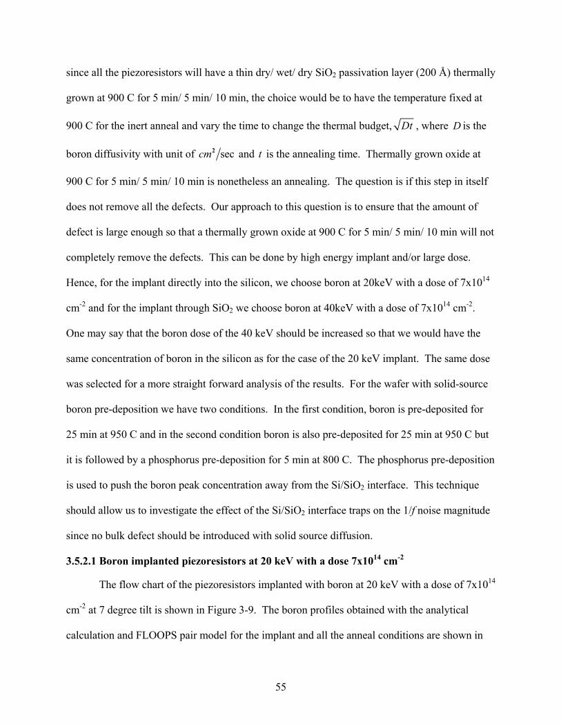
since all the piezoresistors will have a thin dry/ wet/ dry SiO2 passivation layer (200 Å) thermally
grown at 900 C for 5 min/ 5 min/ 10 min, the choice would be to have the temperature fixed at
900 C for the inert anneal and vary the time to change the thermal budget, Dt , where is the
boron diffusivity with unit of
D
sec2cm and t is the annealing time. Thermally grown oxide at
900 C for 5 min/ 5 min/ 10 min is nonetheless an annealing. The question is if this step in itself
does not remove all the defects. Our approach to this question is to ensure that the amount of
defect is large enough so that a thermally grown oxide at 900 C for 5 min/ 5 min/ 10 min will not
completely remove the defects. This can be done by high energy implant and/or large dose.
Hence, for the implant directly into the silicon, we choose boron at 20keV with a dose of 7x10¹⁴
cm-2 and for the implant through SiO2 we choose boron at 40keV with a dose of 7x1014 cm-2.
One may say that the boron dose of the 40 keV should be increased so that we would have the
same concentration of boron in the silicon as for the case of the 20 keV implant. The same dose
was selected for a more straight forward analysis of the results. For the wafer with solid-source
boron pre-deposition we have two conditions. In the first condition, boron is pre-deposited for
25 min at 950 C and in the second condition boron is also pre-deposited for 25 min at 950 C but
it is followed by a phosphorus pre-deposition for 5 min at 800 C. The phosphorus pre-deposition
is used to push the boron peak concentration away from the Si/SiO2 interface. This technique
should allow us to investigate the effect of the Si/SiO2 interface traps on the 1/f noise magnitude
since no bulk defect should be introduced with solid source diffusion.
3.5.2.1 Boron implanted piezoresistors at 20 keV with a dose 7x1014 cm-2
The flow chart of the piezoresistors implanted with boron at 20 keV with a dose of 7x10¹⁴
cm-2 at 7 degree tilt is shown in Figure 3-9. The boron profiles obtained with the analytical
calculation and FLOOPS pair model for the implant and all the anneal conditions are shown in
55
Figure 3-10, Figure 3-11, and Figure 3-12. In all figures, the as-implant and post-anneal profiles
obtained with FLOOPS pair model have deeper junctions than those of the analytical solution.
We also notice after annealing a decrease in the peak concentration of the FLOOPS pair model
while no significant change is observed for the analytical calculation. These differences in the
profiles are due to the fact that the FLOOPS pair model take into account secondary effects such
as TED, OED, and impurity segregation as discussed in Section 3.4.5.2. However, both models
predict the same implant projected range, Rp, around 0.1 µm. The predicted junction depths
after annealing are in the ranges of 0.25 µm and 0.75 µm for the analytical calculation and
FLOOPS pair model respectively from the wafer surface.
3.5.2.2 Boron implanted piezoresistors at 40 keV with a dose 7x1014 cm-2 through SiO2
The flow chart of the piezoresistors implanted with boron at 40 keV with a dose 7x10¹⁴
cm-2 at 0 degree tilt through SiO2 is shown in Figure 3-13. The boron profiles obtained with the
analytical calculation and FLOOPS pair model for the implant and all the anneal conditions are
shown in Figure 3-14, Figure 3-15, Figure 3-16, and Figure 17. Here also, as in the case of the
20 keV implant, all figures for the as-implant and post-anneal profiles obtained with FLOOPS
pair model have deeper junctions than those of the analytical solutions. A decrease in the peak
concentration is noticed for the FLOOPS pair model while no significant change is observed for
the analytical calculation in Figure 3-14, Figure 3-15, Figure 3-16, and Figure 17. The predicted
junction depths after annealing are in the ranges of 0.35 µm and 0.75 µm for the analytical
calculation and FLOOPS pair model except for the piezoresistor with only inert anneal which has
a junction depth of 0.47 µm. The junction depths are measured from the wafer surface.
3.5.2.3 Boron solid source diffused piezoresistors for 25 min at 950 C
The flow chart of the piezoresistors with boron solid source diffusion for 25 min at 950 C
56

is shown in Figure 3-18. The boron profile obtained with the pre-deposition analytical
calculation and the anneal condition is shown in Figure 3-19. The difference between junction
depths for the pre-deposition and post annealing profiles are small. The junction depths are
around 0.13 µm and 0.17 µm for the pre-deposition and post annealing profiles respectively
while the surface concentrations are in the range of 2x1020 cm-3 and 9x1019 cm-3 for the pre-
deposition and post annealing profiles.
3.5.2.4 Boron solid source diffused piezoresistors for 25 min at 950 C followed by phosphorus solid source diffusion for 5 min at 800 C
The flow chart of the piezoresistors with boron pre-deposition for 25 min at 950 C
followed by phosphorus pre-deposition for 5 min at 800 C is shown in Figure 3-20. Next we will
discuss the other test structures such as the P-type capacitors, the P/N diode, the Van der Pauw
and the Hall Effect structures.
3.6 Additional Test Structures
In addition the piezoresistors, we fabricate additional test structures such as p-type
capacitors, P/N diodes, Van der Pauw structures, and Hall effect structures. We use the p-type
capacitor is to measure the oxide thickness and computed the interface trap densities. The P/N
diode is used to measure the junction leakage current and the shot noise. The sheet resistance
and contact resistance are measured using the Van de Pauw structure while the electrical active
carriers are measured using the Hall Effect structure.
3.6.1 P-type Capacitor
Equipments such as Nanospec and Ellipsometer are commonly used to measure oxide
thicknesses optically. The capacitance-voltage, C-V, characteristic of a p-type capacitor can also
be used not only for oxide thickness measurement but also for the computation of interface trap
density. Figure 3-21 shows the plan view and cross-section of a p-type capacitor. The
57
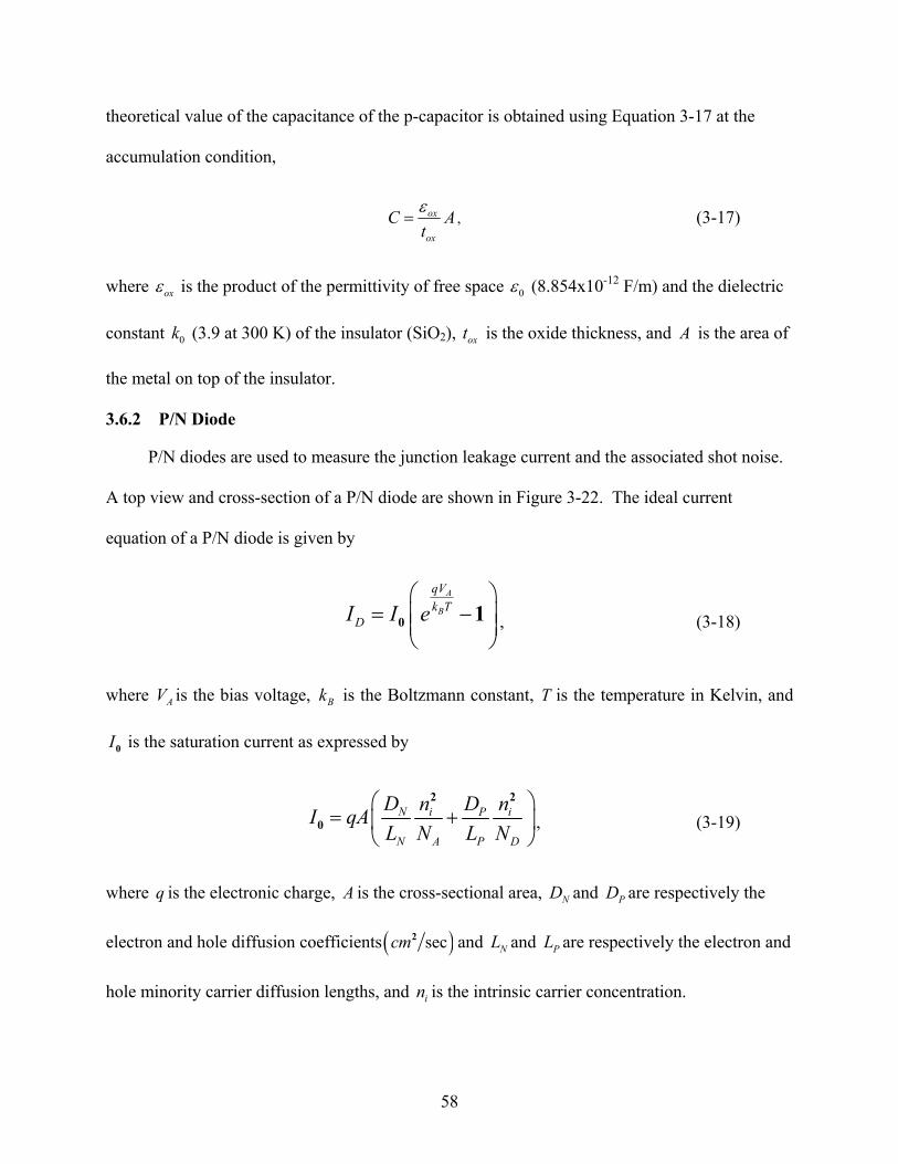
theoretical value of the capacitance of the p-capacitor is obtained using Equation 3-17 at the
accumulation condition,
ox
ox
C Atε
= , (3-17)
where oxε is the product of the permittivity of free space 0ε (8.854x10⁻¹² F/m) and the dielectric
constant (3.9 at 300 K) of the insulator (SiO2), is the oxide thickness, and 0k oxt A is the area of
the metal on top of the insulator.
3.6.2 P/N Diode
P/N diodes are used to measure the junction leakage current and the associated shot noise.
A top view and cross-section of a P/N diode are shown in Figure 3-22. The ideal current
equation of a P/N diode is given by
0 1A
B
qVk T
DI I e⎛ ⎞
= −⎜⎜⎝ ⎠
⎟⎟ , (3-18)
where is the bias voltage, is the Boltzmann constant, T is the temperature in Kelvin, and AV Bk
0I is the saturation current as expressed by
2 2
0N i iP
N A P D
D n nDI qAL N L N
⎛ ⎞= +⎜
⎝ ⎠⎟ , (3-19)
where is the electronic charge, q A is the cross-sectional area, and ND PD are respectively the
electron and hole diffusion coefficients ( )sec2cm and and NL PL are respectively the electron and
hole minority carrier diffusion lengths, and is the intrinsic carrier concentration. in
58

3.6.3 Van der Pauw Structure
Van der Pauw structures are used to measure the sheet resistance, line width, and contact
resistance. The top view of the Van der Pauw structure layout is shown in Figure 3-23. From
Figure 3-23, the sheet resistance is calculated from voltages and currents measured at contact
pads A, B, C and D using
12 ln 2
AB ADs
CD BC
V VRI I
π ⎛ ⎞= +⎜
⎝ ⎠⎟ (3-20)
Equation 3-21 and Equation 3-22 are used to compute the line width, ΔW, and contact resistance,
CR ,
m
S
RW L WR
⎛ ⎞Δ = −⎜ ⎟
⎝ ⎠ (3-21)
FGC
GE
VRI
= , (3-22)
where DEm
CF
VRI
= , L is given by the center to center spacing between D and E, and W is the width
of the bar. In the next section, we present test structures used for extracting the carrier
concentration.
3.6.4 Carrier Concentration Test Structures
Several methods exist to compute the carrier concentration in semiconductor devices.
Methods that are used to measure or estimate the carrier concentration in semiconductor devices
include spreading resistance, SIMS, capacitance-voltage profiling, and Hall Effect. Each method
has advantages and disadvantages.
59
3.6.4.1 Spreading resistance technique
In the spreading resistance technique, the surface of the semiconductor is cut at an angle
rendering the measurement destructive. Two-point metal probes are used to measure the
resistivities of the layers along the depth of the beveled area while successively comparing it
against standards.1 A disadvantage of the spreading resistance is the tedious sample preparation
and measurement analysis.
3.6.4.2 Secondary ion mass spectroscopy (SIMS) technique
Secondary ion mass spectroscopy (SIMS) provides the dopant concentration of both
uniform and nonuniform doped samples. It is also a destructive method. In this method, ion
beams such as O+ and Cs+ are focused on the sample silicon substrate. These ions collide with
the impurity in the substrate causing them to be ejected. The resulting secondary ions are
analyzed and counted. In this method, one disadvantage is that the profile consists of the foreign
atom concentration. In some applications such as ours, where the sample is heavily doped,
impurity deionization occurs, thus the atomic concentration does not represent the electrically
active carrier concentration in which we are interested. Thus, SIMS may overestimate the carrier
concentration which will lead to an inaccurate number of carriers and thus an error in the
estimate of the Hooge parameterα . However, SIMS can be useful in determining the junction
depth and the profile of atoms residing in each layer such as boron in oxide due to boron
segregation during oxidation. This information can be used to approximate the boron dose
before and after thermal oxidation into the silicon.
3.6.4.3 Capacitance-voltage technique
In the capacitance-voltage technique, devices that exhibit a voltage dependence
capacitance such as Schottky diode, P/N junction, and MOS capacitor (MOSC) are used. The
doping profile can be obtained from the DC voltage dependent space charge layer thickness in a
60
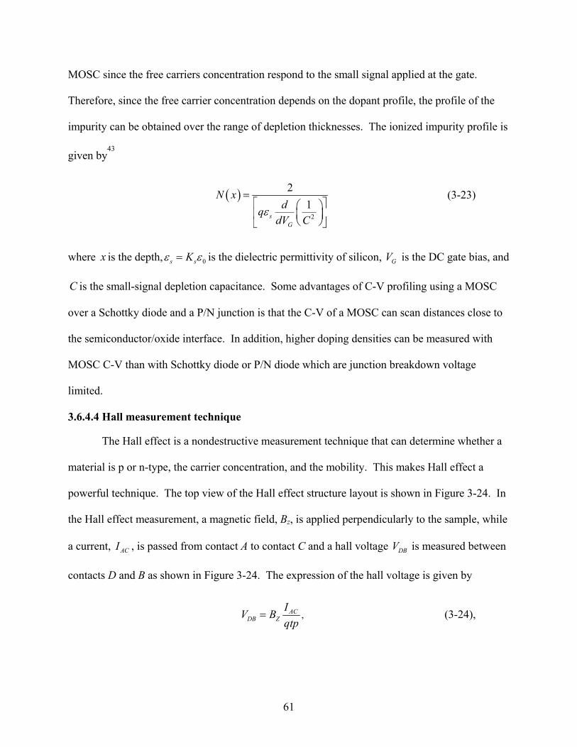
MOSC since the free carriers concentration respond to the small signal applied at the gate.
Therefore, since the free carrier concentration depends on the dopant profile, the profile of the
impurity can be obtained over the range of depletion thicknesses. The ionized impurity profile is
given by43
( )2
21
sG
N xdq
dV Cε
=⎡ ⎤⎛ ⎞
⎜ ⎟⎢ ⎥⎝ ⎠⎣ ⎦
(3-23)
where x is the depth, 0s sKε ε= is the dielectric permittivity of silicon, is the DC gate bias, and
is the small-signal depletion capacitance. Some advantages of C-V profiling using a MOSC
over a Schottky diode and a P/N junction is that the C-V of a MOSC can scan distances close to
the semiconductor/oxide interface. In addition, higher doping densities can be measured with
MOSC C-V than with Schottky diode or P/N diode which are junction breakdown voltage
limited.
GV
C
3.6.4.4 Hall measurement technique
The Hall effect is a nondestructive measurement technique that can determine whether a
material is p or n-type, the carrier concentration, and the mobility. This makes Hall effect a
powerful technique. The top view of the Hall effect structure layout is shown in Figure 3-24. In
the Hall effect measurement, a magnetic field, Bz, is applied perpendicularly to the sample, while
a current, ACI , is passed from contact A to contact C and a hall voltage DBV is measured between
contacts D and B as shown in Figure 3-24. The expression of the hall voltage is given by
ACDB Z
IV Bqtp
= , (3-24),
61
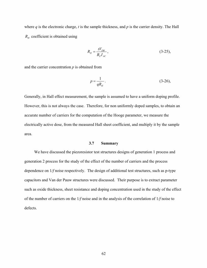
where q is the electronic charge, t is the sample thickness, and p is the carrier density. The Hall
HR coefficient is obtained using
DBH
Z AC
tVRB I
= , (3-25),
and the carrier concentration p is obtained from
1
H
pqR
= . (3-26),
Generally, in Hall effect measurement, the sample is assumed to have a uniform doping profile.
However, this is not always the case. Therefore, for non uniformly doped samples, to obtain an
accurate number of carriers for the computation of the Hooge parameter, we measure the
electrically active dose, from the measured Hall sheet coefficient, and multiply it by the sample
area.
3.7 Summary
We have discussed the piezoresistor test structures designs of generation 1 process and
generation 2 process for the study of the effect of the number of carriers and the process
dependence on 1/f noise respectively. The design of additional test structures, such as p-type
capacitors and Van der Pauw structures were discussed. Their purpose is to extract parameter
such as oxide thickness, sheet resistance and doping concentration used in the study of the effect
of the number of carriers on the 1/f noise and in the analysis of the correlation of 1/f noise to
defects.
62
Table 3-1. Wafer characteristics used to fabricate test structures generation 1. Diameter Type Orientation Resistivity Thickness
4 inch N (100) 2.0-5.0 Ω-cm 500-550 µm
Table 3-2. Process steps for piezoresistor test structures generation 1. Process Step 1. RCA wafer clean (n-Si, 100 mm diameter., CZ (100), 2-5 Ω-cm, 500-550 μm thick) 2. Thick isolation oxide growth 3. Lithography for implant mask 4. Oxide etch 5. Photoresist strip 6. Ion implantation 7. RCA wafer clean 8. N2 anneal + dry/wet/dry oxidation 9. Lithography for contact hole 10. Oxide etch 11. Photoresist strip 12. Front side metallization (Al, 1% Si) 13. Lithography for metal bond pad 14. Metal etch 15. Back side metallization (Al, 1% Si) 16. Photoresist strip 17. Nitride passivation deposition step and patterning 18. Post metallization anneal (Forming gas 96%N2, 4% H2) 19. Wafer dice 20. Chip die attach and wirebond
Table 3-3. Wafer characteristics used to fabricate test structures generation 2. Diameter Type Orientation Resistivity Thickness
4 inch N (100) 0.5-1.0 Ω-cm 500-550 µm
63
Table 3-4. Process steps for piezoresistor test structures generation 2. Process Step 1. RCA of wafers (n-Si, 4 in, CZ <100>, 0.5-1 Ω-cm, 525 ± 25 μm) single side polished.
(UF) 2. Grow thick isolation mask dry/wet/dry SiO2 (70/23/70 min at 1100 °C) and spin resist.
(UF) 3. Lithography for a) channel implant or b) channel solid-source predep (UF) 4. Etch dry/wet/dry oxide where channel a) implant or b) solid-source predep is to be
performed. (UF) 5. Photoresist strip. (UF) 6. RCA clean (UF) 7. Growth thin dry/wet/dry SiO2 and lithography for channel implant with mask 2 (dark
field). 8. Ion implantation 9. Photoresist strip and RCA wafer organic clean (SC-1) 10. Inert anneal in N2 and dry/wet/dry SiO2 of wafers 11. Lithography for contact holes with mask 3 (dark field). This applies to wafers with and
without thin oxide implant masks. 12. Etch oxide for contact holes 13. Photoresist strip and front side metallization on top wafer-polished surface 14. Lithography for metal with mask 4 (clear field), metal etch and photo resist strip 15. Nitride passivation deposition (PECVD) on top of wafer-polished surface 16. Lithography for contact pads with mask 5 (dark field), nitride etch and back side
metallization on bottom of wafer-unpolished surface 17. Post metallization anneal (forming gas 96% N2, 4% H2) 18. Wafer dicing 19. Packaging
Table 3-5. Implant and annealing conditions of test structures generation 1.
Species Energy (keV)
Dose (cm-3)
Tilt (degree) Inert anneal in N2 Dry/Wet/Dry oxide
Boron 5 6x10¹⁴ 7 300 min, 1050 C 65/21/65 min, 950 C
64
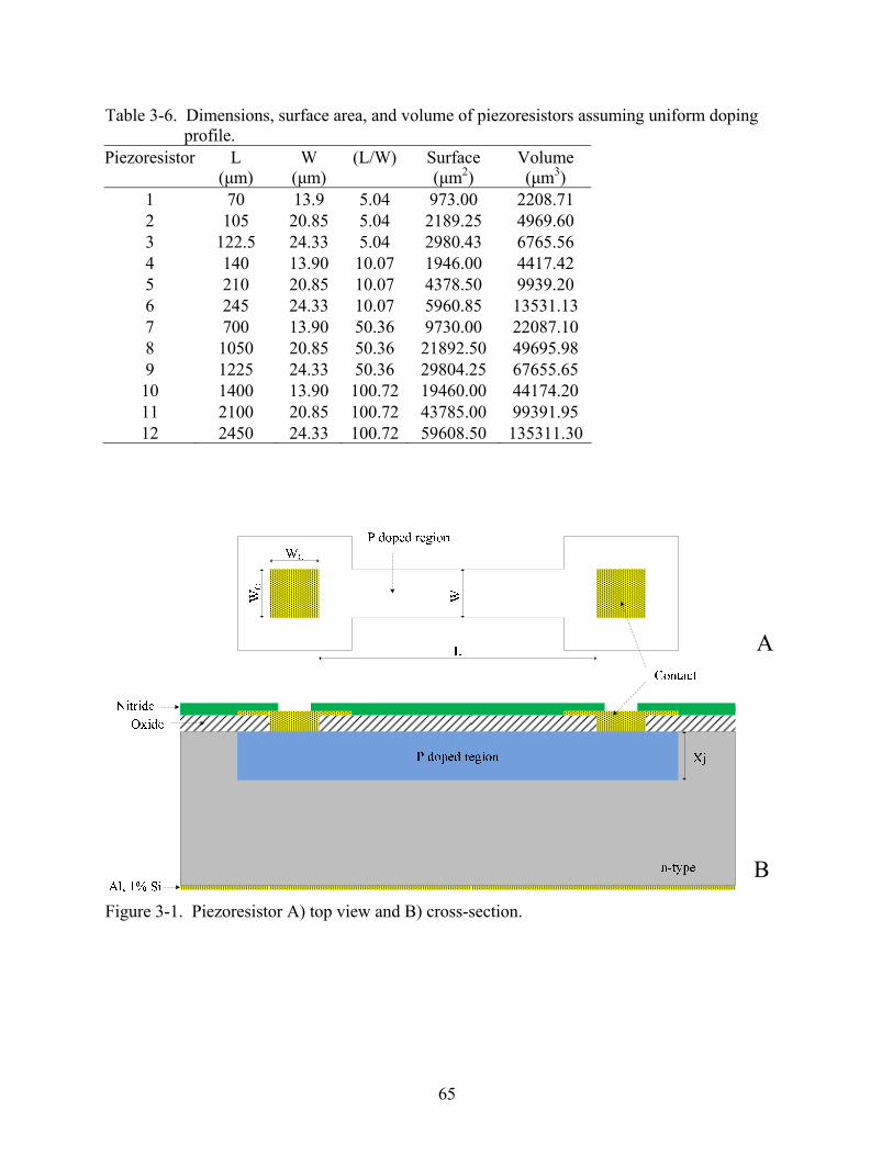
Table 3-6. Dimensions, surface area, and volume of piezoresistors assuming uniform doping profile.
Piezoresistor L (μm)
W (μm)
(L/W) Surface (μm2)
Volume (μm3)
1 70 13.9 5.04 973.00 2208.71 2 105 20.85 5.04 2189.25 4969.60 3 122.5 24.33 5.04 2980.43 6765.56 4 140 13.90 10.07 1946.00 4417.42 5 210 20.85 10.07 4378.50 9939.20 6 245 24.33 10.07 5960.85 13531.13 7 700 13.90 50.36 9730.00 22087.10 8 1050 20.85 50.36 21892.50 49695.98 9 1225 24.33 50.36 29804.25 67655.65 10 1400 13.90 100.72 19460.00 44174.20 11 2100 20.85 100.72 43785.00 99391.95 12 2450 24.33 100.72 59608.50 135311.30
A
B
Figure 3-1. Piezoresistor A) top view and B) cross-section.
65
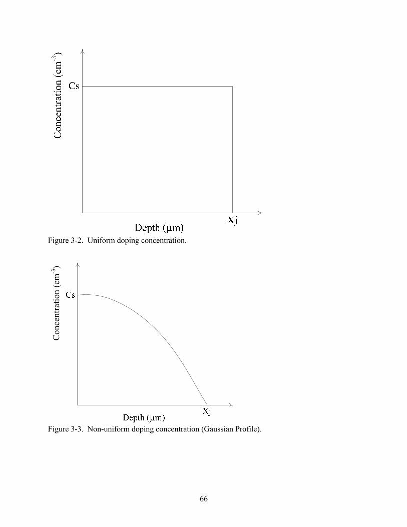
Figure 3-2. Uniform doping concentration.
Con
cent
ratio
n (c
m-3
)
Figure 3-3. Non-uniform doping concentration (Gaussian Profile).
66
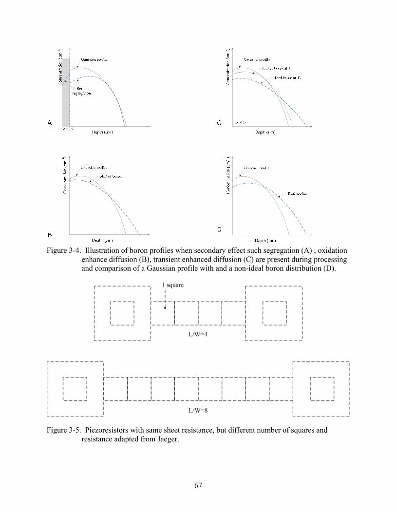
Figure 3-4. Illustration of boron profiles when secondary effect such segregation (A) , oxidation
enhance diffusion (B), transient enhanced diffusion (C) are present during processing and comparison of a Gaussian profile with and a non-ideal boron distribution (D).
Figure 3-5. Piezoresistors with same sheet resistance, but different number of squares and resistance adapted from Jaeger.
67
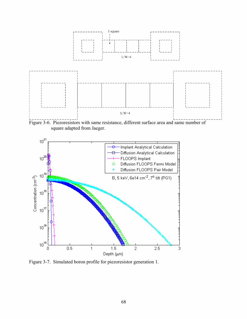
Figure 3-6. Piezoresistors with same resistance, different surface area and same number of
square adapted from Jaeger.
Figure 3-7. Simulated boron profile for piezoresistor generation 1.
68
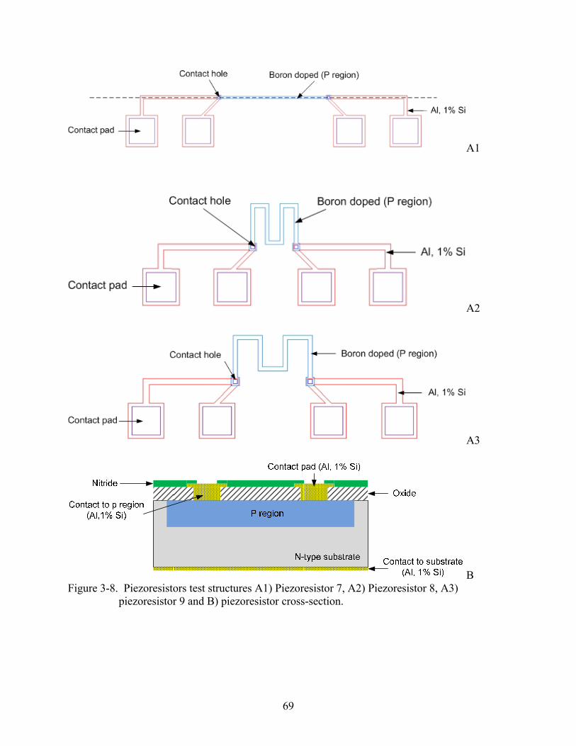
A1
A2
A3
B Figure 3-8. Piezoresistors test structures A1) Piezoresistor 7, A2) Piezoresistor 8, A3)
piezoresistor 9 and B) piezoresistor cross-section.
69
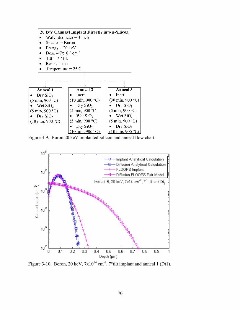
Figure 3-9. Boron 20 keV implanted-silicon and anneal flow chart.
Figure 3-10. Boron, 20 keV, 7x1014 cm-2, 7°tilt implant and anneal 1 (Dt1).
70
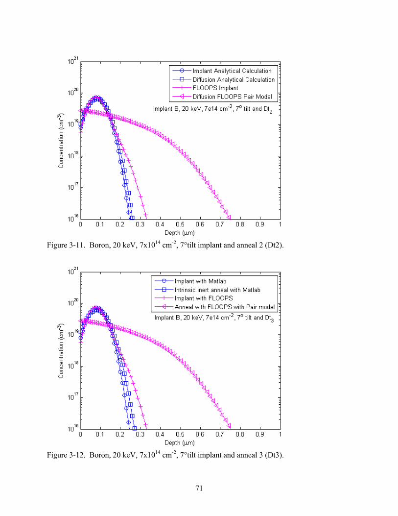
Figure 3-11. Boron, 20 keV, 7x1014 cm-2, 7°tilt implant and anneal 2 (Dt2).
Figure 3-12. Boron, 20 keV, 7x1014 cm-2, 7°tilt implant and anneal 3 (Dt3).
71
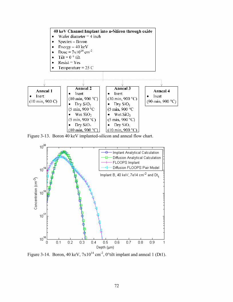
Figure 3-13. Boron 40 keV implanted-silicon and anneal flow chart.
Figure 3-14. Boron, 40 keV, 7x1014 cm-2, 0°tilt implant and anneal 1 (Dt1).
72
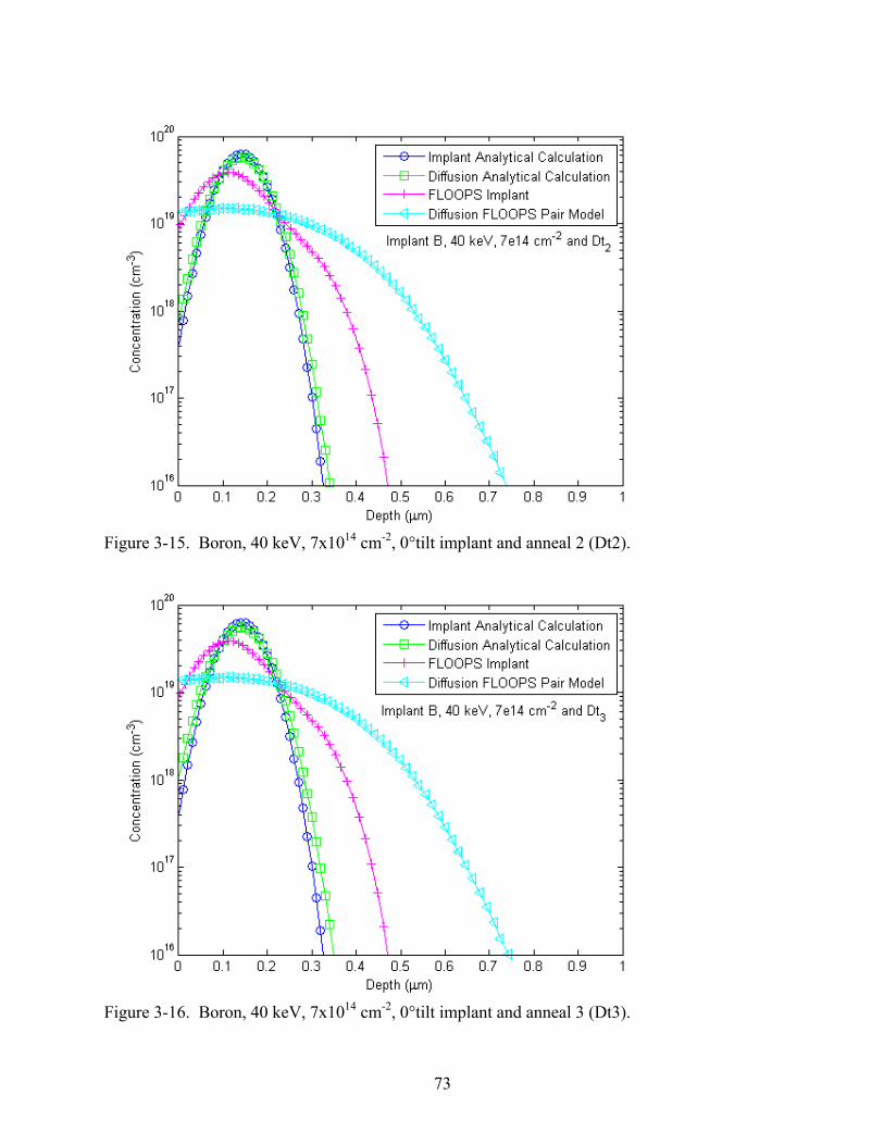
Figure 3-15. Boron, 40 keV, 7x1014 cm-2, 0°tilt implant and anneal 2 (Dt2).
Figure 3-16. Boron, 40 keV, 7x1014 cm-2, 0°tilt implant and anneal 3 (Dt3).
73
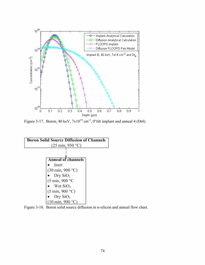
Figure 3-17. Boron, 40 keV, 7x1014 cm-2, 0°tilt implant and anneal 4 (Dt4).
Figure 3-18. Boron solid source diffusion in n-silicon and anneal flow chart.
74
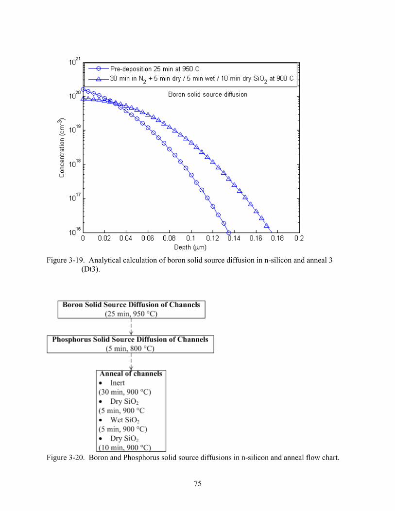
Figure 3-19. Analytical calculation of boron solid source diffusion in n-silicon and anneal 3
(Dt3).
Figure 3-20. Boron and Phosphorus solid source diffusions in n-silicon and anneal flow chart.
75
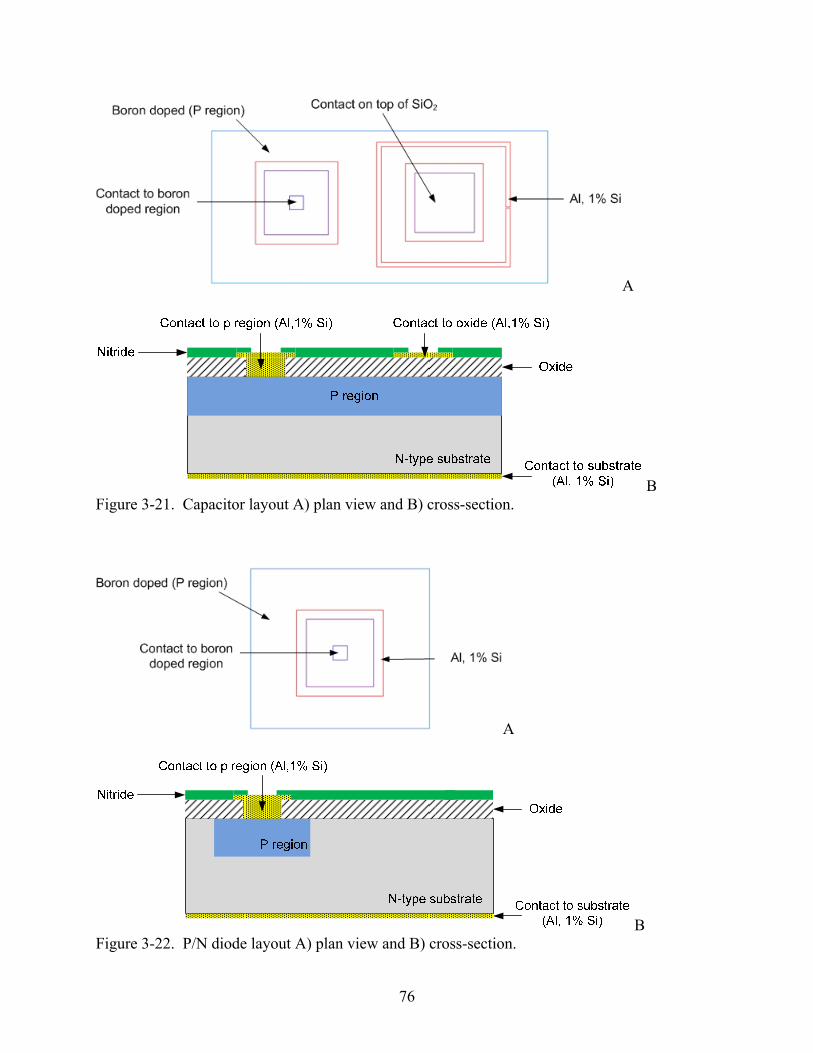
A
B Figure 3-21. Capacitor layout A) plan view and B) cross-section.
A
B Figure 3-22. P/N diode layout A) plan view and B) cross-section.
76
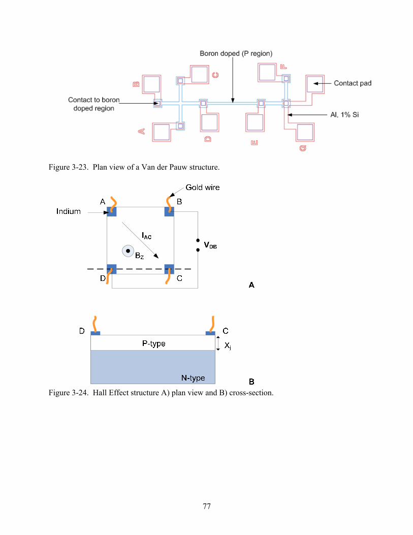
Figure 3-23. Plan view of a Van der Pauw structure.
Figure 3-24. Hall Effect structure A) plan view and B) cross-section.
77
CHAPTER 4 EXPERIMENTAL METHOD
In this chapter, we elaborate on the experiments that are conducted using the test structures
designed in Chapter 3. We discuss the equipments, measurement setup, and measurement
analysis for each experiment to be conducted. We start with the experimental method for the
characterization of the piezoresistors, which is followed by that of the p-type capacitor and the
P/N diode. The goal of these experiments is to study the effect of the number of carriers on the
1/f noise using the piezoresistors test structures of generation 1, the process dependence of 1/f
noise and correlate the low frequency noise to defects using test structures of generation 2.
4.1 Piezoresistor Experimental Methods
In this section, we discuss two important measurements to be conducted on piezoresistors
which are the I-V and the noise measurements.
4.1.1 Piezoresistor I-V Measurement
The I-V characteristics are measured to obtain the piezoresistor resistances and their
linearity range. This linear range is useful since it allows us to know the range of voltages to
apply to the piezoresistors during the noise measurements. The piezoresistor resistance is also
useful since it allows us to compute the theoretical thermal noise that will be compared with the
measured value. Thus, this gives us confidence in the measurement. The I-V characteristic of
the piezoresistor is obtained with the Agilent Semiconductor Parameter Analyzer 4155C and a
probe station. We place probes on the piezoresistor contacts and then sweep voltages across the
piezoresistor while simultaneously recording the corresponding currents. Afterwards, we plot the
current versus the voltage and use the slope of the curve to obtain the resistance value. Since the
piezoresistors are junction isolated, during the I-V measurement, a voltage is applied to the n-
type substrate to reverse bias the P/N junction and thus potentially avoid leakage current. Once
78
we know the piezoresistor linear range and resistance, we then proceed to the noise
measurement.
4.1.2 Piezoresistor Noise Measurements
There are three phases for the piezoresistor noise measurement. The first one is the noise
setup, the second is the equipment settings, and the third is noise extraction. The noise
measurement is used to measure the excess noise of the piezoresistor and the P/N diode.
4.1.2.1 Noise measurement setup
The equipment used for the noise measurement are three nested Faraday cages, a low-noise
preamplifier (SRS 560), a dynamic signal analyzer (SRS 785), lead acid batteries, metal film
resistors, double shielded coaxial cables (RG-223/U), BNC connectors, and LabView to
automate the measurements. The noise measurement setup uses DC bias voltages. The
combination of lead acid battery, short cable, triple shielded Faraday cage and single point
ground help to reduce potential extrinsic interference signals such as radio signals (AM, FM) at
high frequencies and power line interference at 60 Hz and their harmonics. Figure 4-1 A) and B)
shows the piezoresistor noise measurement setup and the small signal noise representation for
the extraction of the noise of the device under test (DUT).
In Figure 4-1, the current noise PSD associated with the bias resistor ( and the DUT )
)
biasR
( DUTR are respectively and biasi RS
DUTi RS . and are the input referred current and
voltage noise PSD of the low noise amplifier. They are obtained respectively via open and short
circuit noise measurements of the low-noise preamplifier.
i AmpS v AmpS
iR and G represent respectively the
noise free input impedance and gain of the pre-amplifier, and is the raw measured voltage
noise PSD. After proper shielding, another important consideration for the noise measurement is
the equipment settings which are discussed next.
vOutS
79
4.1.2.2 Equipment setting for noise PSD measurement
As mentioned earlier, we use a low-noise preamplifier (SRS 560), a spectrum analyzer
(SRS 785), and a computer with LabView to collect the data. Table 4-1 shows the low-noise
amplifier settings. The amplifier input A is set to ac coupling because we are interested in the
time-varying signal. The gain is set to 1000 to ensure that the output signal of the preamplifier is
higher than the noise floor of the spectrum analyzer allowing accurate noise measurement. The
output of the low-noise amplifier is fed to the input A of the spectrum analyzer. Table 4-2 shows
the spectrum analyzer settings. The coupling is set to ac since we are interested in small signal
fluctuations. A Hanning window is selected for the measurement of the random signal because it
provides good selectivity and reduces power spectral density leakage. A list of spans, FFT lines,
and bin widths is given in Table 4-2. The overall power spectral density is obtained by
overlapping the measurements of the different spans. At low frequencies, the binwidth is smaller
to ensure better frequency resolution and therefore good accuracy of the measurements. All
these different equipment settings are set in LabView which automates the measurements. In
addition to the proper shielding, equipment settings, and measurement automation, one needs to
correctly extract the DUT noise PSD from the raw measured noise PSD. In the next section, we
show how to extract the DUT noise.
4.1.2.3 Noise power spectral density extraction
The piezoresistor noise voltage PSD is extracted by noise circuit analysis of the noise
equivalent circuit shown in Figure 4-1 B). The raw output noise voltage PSD expression is given
in Equation 4-1.
( )( )( )
222
2 / / / // / bias DUT
ivOut vAmp iR iAmp iR bias DUT i
i bias DUT
RS G S S S S R R RR R R
⎡ ⎤⎢ ⎥= + + +⎢ ⎥+⎡ ⎤⎣ ⎦⎣ ⎦
(4-1)
80
In Equation 4-1, the open-circuit noise PSD of the SRS 560, , is negligible
compared to the other noise sources. Also note that
iAmpS
i biasR R and i DUTR R , thus
and ( ) ( )// // //bias DUT i bias DUTR R R R R≈( )
2
2//
i
i bias DUT
RR R R+⎡ ⎤⎣ ⎦
is reduced to one
since . ( )//i bias DUT iR R R R+ ≈
Therefore, . ( )( )22 / /bias DUTvOut vAmp iR iR bias DUTS G S S S R R⎡ ⎤= + +⎣ ⎦
Solving for DUTiRS , we obtain
( )
22
2 - Hz/ /DUT bias
vOutvAmp
iR iRbias DUT
S SGS S
R R
−A⎡ ⎤= ⎣ ⎦ . (4-2)
The noise voltage DUTvRS is obtained by multiplying
DUTiRS by DUTR squared as shown below,
2 2 V HzDUT DUTvR iR DUTS S R ⎡ ⎤= × ⎣ ⎦ (4-3)
The bias resistor ( is a metal film resistor which has very little 1/f noise, thus it does
not contribute to the measured excess noise. However, since it still contributes thermal noise, to
minimize the effect of the bias resistor thermal noise on the measurement, we select a
)biasR
biasR with a
resistance much larger than that of the resistance of the device under test, DUTR , so that the
parallel combination of the two resistances equals that of the DUTR . Finally, the bias voltage
across DUTR is varied by fixing the large impedance, biasR , and changing the battery
voltage ( )batteryV . In addition to the piezoresistor excess noise, we measure the P/N diode shot
noise. In the next section, we will discuss the P/N diode experimental method.
81
4.2 P/N Diode Experimental Method
There are two important measurements to be conducted with the P/N diode. The first is the
DC current-voltage characteristic, and the second is the shot noise.
4.2.1 P/N Diode DC Current-Voltage
The P/N diode current-voltage measurement is a useful monitor of the reverse bias
voltage prior to voltage breakdown and also of the turn on voltage. For wafers with a uniform
background concentration of 1x1016 cm-3 and an abrupt junction, the theoretical breakdown
voltage is around 60 V,38
which is sufficiently large enough for our application. However, the
actual breakdown voltage needs to be verified. The setup for the I-V measurement of the
piezoresistor applies also for the P/N diode I-V characteristics. However, for the P/N diode, one
probe makes contact with the p-type region and the other with the n-type substrate. The P/N
diode shot noise is discussed next. Although we have P/N diode test structures, we measure the
shot noise directly on the piezoresistor substrate isolation junction for which we have measured
the noise voltage PSD as described in Section 4.1.2.3.
4.2.2 P/N Diode Shot Noise Measurement
The origin of the shot noise has been discussed in Chapter 2, Section 2.4.4. It has also
been shown to be proportional to the DC current passing through the P/N diode.
4.2.2.1 P/N diode noise measurement setup
Although we use the same shielding method for the shot noise measurement and
equipment settings, the resistor biasing network for the P/N diode shot noise is different than that
of the piezoresistor. Figure 4-2 shows the noise measurement setup for the P/N diode noise
measurement. In Figure 4-2, , and are the noise current sources associated
respectively with the bias resistors
1biasiRS2biasiRS
3biasiRS
1biasR , and 2biasR 3biasR . The noise associated with the diode
82
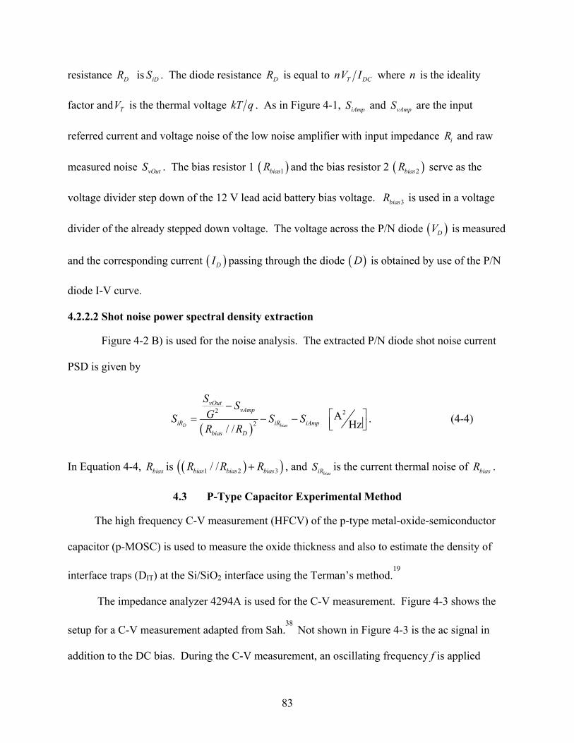
resistance DR is . The diode resistance iDS DR is equal to T DCnV I where is the ideality
factor and is the thermal voltage
n
TV kT q . As in Figure 4-1, and are the input
referred current and voltage noise of the low noise amplifier with input impedance
iAmpS vAmpS
iR and raw
measured noise . The bias resistor 1 vOutS ( )1biasR and the bias resistor 2 ( )2biasR serve as the
voltage divider step down of the 12 V lead acid battery bias voltage. 3biasR is used in a voltage
divider of the already stepped down voltage. The voltage across the P/N diode ( )DV is measured
and the corresponding current ( )DI passing through the diode ( )D is obtained by use of the P/N
diode I-V curve.
4.2.2.2 Shot noise power spectral density extraction
Figure 4-2 B) is used for the noise analysis. The extracted P/N diode shot noise current
PSD is given by
( )
2 2
2A Hz/ /D bias
vOutvAmp
iR iR iAmpbias D
S SGS S SR R
−⎡ ⎤= − − ⎢ ⎥⎣ ⎦
. (4-4)
In Equation 4-4, biasR is , and is the current thermal noise of ( )( )1 2 3/ /bias bias biasR R R+biasiRS biasR .
4.3 P-Type Capacitor Experimental Method
The high frequency C-V measurement (HFCV) of the p-type metal-oxide-semiconductor
capacitor (p-MOSC) is used to measure the oxide thickness and also to estimate the density of
interface traps (DIT) at the Si/SiO2 interface using the Terman’s method.19
The impedance analyzer 4294A is used for the C-V measurement. Figure 4-3 shows the
setup for a C-V measurement adapted from Sah.38
Not shown in Figure 4-3 is the ac signal in
addition to the DC bias. During the C-V measurement, an oscillating frequency f is applied
83
through the surper imposed ac signal while the DC voltage is swept from negative to positive
voltages. From the measured capacitance, the oxide thickness is computed using Equation 3-17
in accumulation, which for a p-MOSC is at the maximum applied negative gate voltage where
the majority holes accumulate at the silicon surface. The accumulation and inversion
capacitances respectively, and , are extracted from the HFCV and used to compute the
semiconductor capacitance
oxC invC
sC from
21 F cms
inv ox
CA A
C C
⎡ ⎤= ⎢ ⎥⎣ ⎦⎛ ⎞−⎜ ⎟
⎝ ⎠
. (4-5)
Next, the carrier concentration, , is obtained by solving AAN
12
0
2s AA
sS
K qNC εφ
⎛ ⎞⎜ ⎟⎝ ⎠⎡ ⎤
= ⎢ ⎥⎣ ⎦
, (4-6)
where Sφ is the surface potential expressed by
2 ln AAS
i
NkTq n
φ⎛ ⎞⎛ ⎞
= ⎜⎜ ⎟⎝ ⎠ ⎝ ⎠
⎟ . (4-7)
In Equations 4-5, 4-6 and 4-7, is the electronic charge, q sK is the semiconductor
dielectric constant, 0ε is the permittivity of free space, k is the Boltzmann constant, T is the
temperature in Kelvin, and A is the cross-sectional area of the MOSC. The extracted carrier
concentration, , and oxide thickness are then used to compute and plot the ideal high
frequency C-V of the p-MOSC on the same figure as the measured high frequency C-V. For
each capacitance value, the corresponding measured and ideal gate voltages, , are recorded and
AAN
GV
84
a difference between the two is computed. The interface trap density, DIT, is
then computed from the measured distortion between the ideal and actual HFCV curves in terms
of a surface potential,
idealG G GV V VΔ = −
Sφ dependent GVΔ using
2 12 ox G
itS
C d VD cmq dφ
− −⎛ ⎞Δ eV⎡ ⎤= ⎜ ⎟ ⎣ ⎦⎝ ⎠
. (4-8)
Next we discuss the transmission electron microscopy (TEM), a technique used to
visualize and count the defects in the silicon.
4.4 Transmission Electron Microscopy
Transmission electron microscopy (TEM) allows the visualization of the defects in the
bulk of the piezoresistors. In this technique, the image is formed by electrons that pass through
thinned samples, via ion milling, and hit a photographic plate. One can use cross-section TEM
(XTEM) and plan-view TEM (PTEM) to visualize and analyze the defects in the sample. XTEM
allows sides view of the defects thus its depth into the sample while the PTEM allows a top view
of the defects therefore can be used to compute the defect densities. PTEM is made out of
samples that have about 3 mm diameter. The samples are polished using polishing jigs and
aluminum power. After the sample is thinned, it is mounted face down on a Teflon holder which
has a hole at its center. A wax is used on the edge of the sample to secure it on the holder. A
hole at the center of the sample it made by etching it from the back side with HF:HNO3
(25%:75%) solution. The edges of the sample that are cover with wax are not etched. After
etching the hole the samples are released from the holder by applying acetone to the wax.
Region around the hole are thin enough and are electron transparent. It is in these electron
transparent regions that PTEM pictures are taken. For XTEM a thin electron transparent section
of the sample in obtained via focus ion beam (FIB). Since we have oxide on the surface of our
85
samples which is not conductive, we carbon coat the samples prior to inserting them in the
chamber of the Dual Beam SEM-Focused Ion Beam (FEI Strata DB235) system. After, the
section is cut with the FIB station and placed on a sample holder, it is inserted in JEOL TEM
200CX instrument to obtain cross-section images. Next we discuss the Van der Pauw structure.
4.5 Van Der Pauw Structure
The Van der Pauw structure is very useful since it allows the computation of the sheet
resistance, SR , of a doped semiconductor which is related to the surface concentration. In
addition to the sheet resistance, the Van der Pauw structure allows the measurement of the line
width, , and the contact resistance,WΔ CR , of the structures. The detailed equations are
summarized in Chapter 3.
4.5.1 Sheet Resistance
The Agilent Semiconductor Parameter Analyzer 4155C and a probe station are used to
measure the sheet resistance SR . We place probes on the four contacts A, B, C and D of the Van
der Pauw structure, and we inject a current through two contacts while we record the
corresponding voltage across the two other of contacts. The sheet resistance is computed using
Equation 3-20 and can be used to compute the resistance of a piezoresistor for a given number of
squares L W .
4.5.2 Line Width
For the line width measurement, we also use the Agilent Semiconductor Parameter
Analyzer 4155C and a probe station. This measurement gives insight on any lithography error
that occurs during fabrication. The line width is measured using Equation 3-21 in Chapter 3,
Section 3.7.5.
WΔ
86
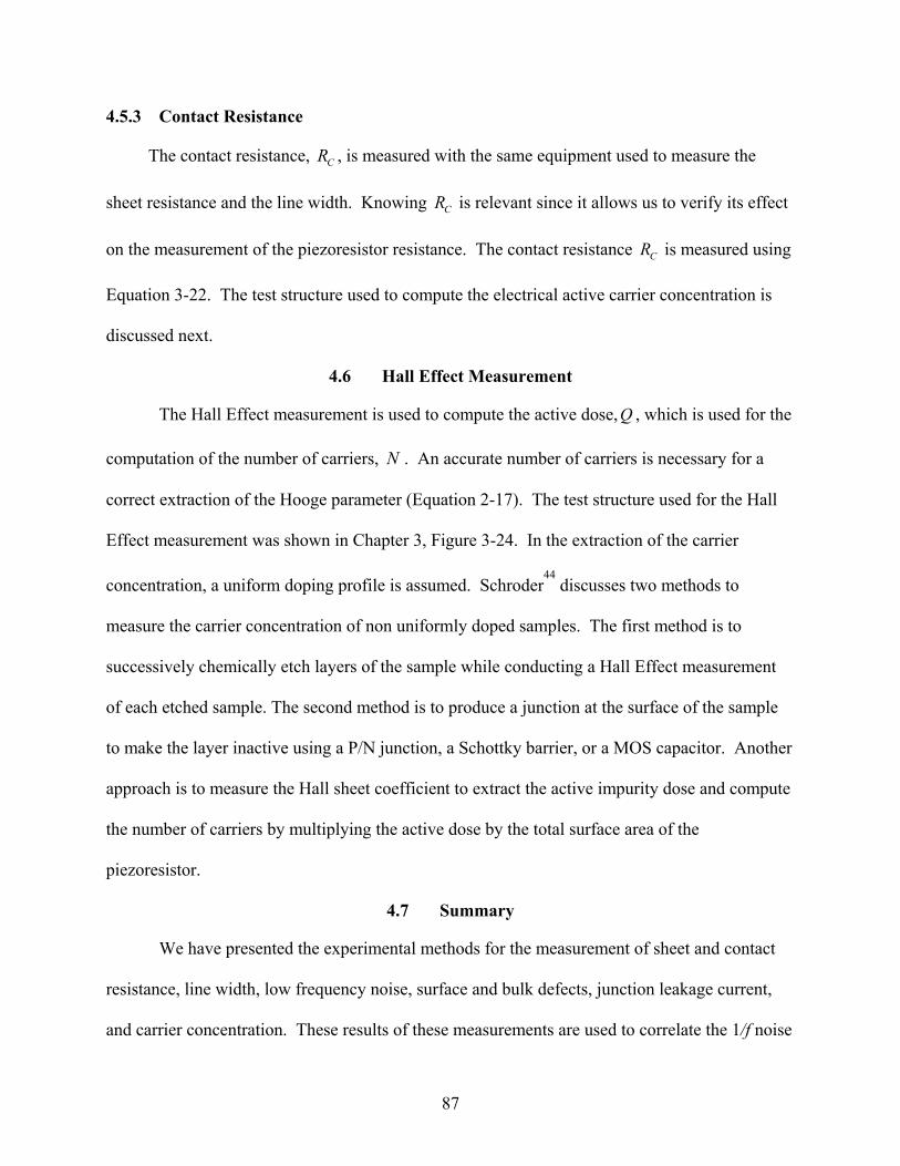
4.5.3 Contact Resistance
The contact resistance, CR , is measured with the same equipment used to measure the
sheet resistance and the line width. Knowing CR is relevant since it allows us to verify its effect
on the measurement of the piezoresistor resistance. The contact resistance CR is measured using
Equation 3-22. The test structure used to compute the electrical active carrier concentration is
discussed next.
4.6 Hall Effect Measurement
The Hall Effect measurement is used to compute the active dose, , which is used for the
computation of the number of carriers, . An accurate number of carriers is necessary for a
correct extraction of the Hooge parameter (Equation 2-17). The test structure used for the Hall
Effect measurement was shown in Chapter 3, Figure 3-24. In the extraction of the carrier
concentration, a uniform doping profile is assumed. Schroder44
discusses two methods to
measure the carrier concentration of non uniformly doped samples. The first method is to
successively chemically etch layers of the sample while conducting a Hall Effect measurement
of each etched sample. The second method is to produce a junction at the surface of the sample
to make the layer inactive using a P/N junction, a Schottky barrier, or a MOS capacitor. Another
approach is to measure the Hall sheet coefficient to extract the active impurity dose and compute
the number of carriers by multiplying the active dose by the total surface area of the
piezoresistor.
Q
N
4.7 Summary
We have presented the experimental methods for the measurement of sheet and contact
resistance, line width, low frequency noise, surface and bulk defects, junction leakage current,
and carrier concentration. These results of these measurements are used to correlate the 1/f noise
87

to the defects, relate the low frequency noise to the number of carriers and compute the Hooge
parameter. The experiments will help monitor the 1/f noise of the piezoresistor with increasing
annealing time. In the next chapter, the fabrication and measurement results are discussed.
88
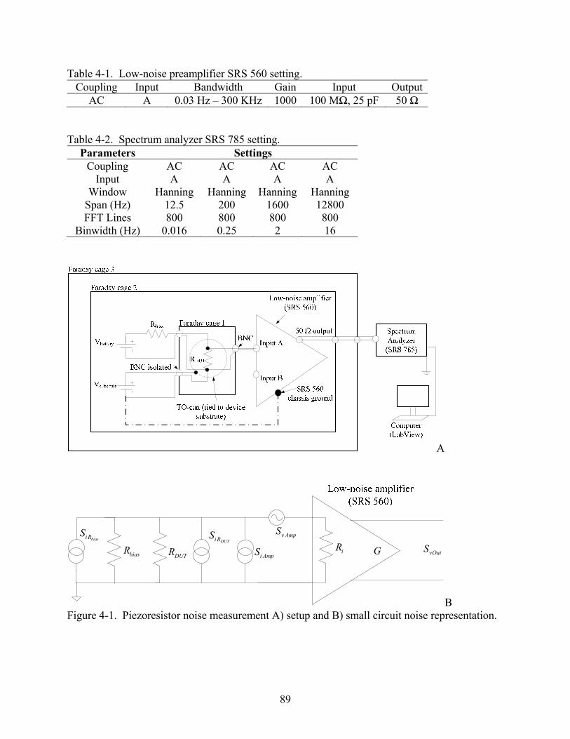
Table 4-1. Low-noise preamplifier SRS 560 setting. Coupling Input Bandwidth Gain Input Output
AC A 0.03 Hz – 300 KHz 1000 100 MΩ, 25 pF 50 Ω Table 4-2. Spectrum analyzer SRS 785 setting.
Parameters Settings Coupling AC AC AC AC
Input A A A A Window Hanning Hanning Hanning Hanning
Span (Hz) 12.5 200 1600 12800 FFT Lines 800 800 800 800
Binwidth (Hz) 0.016 0.25 2 16
A
biasi RS
biasRDUTR
DUTi RS
i AmpS
v AmpS
iR G vOutS
B Figure 4-1. Piezoresistor noise measurement A) setup and B) small circuit noise representation.
89
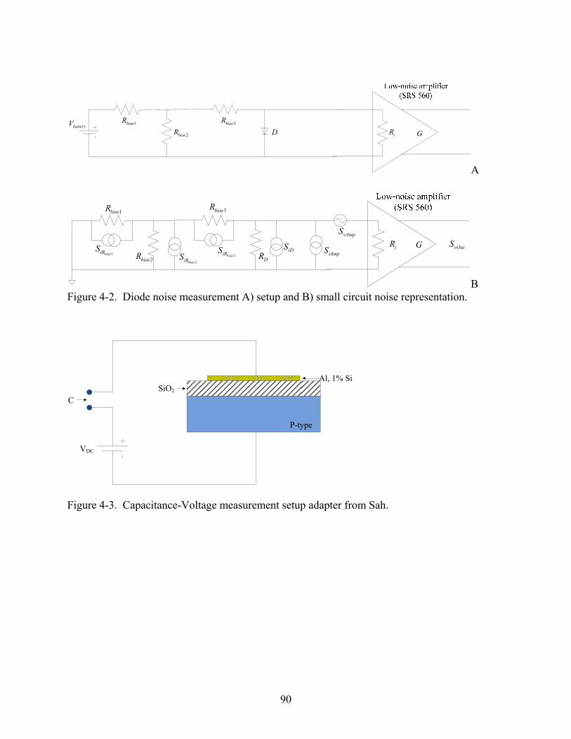
1biasR
2biasR3biasR
D iR GbatteryV
A
1biasR
2biasR
3biasR
iRDR
G1biasiRS
2biasiRS
3biasiRS iDS iAmpS
vAmpS vOutS
B Figure 4-2. Diode noise measurement A) setup and B) small circuit noise representation.
Al, 1% SiSiO2
P-type
VDC
C
Figure 4-3. Capacitance-Voltage measurement setup adapter from Sah.
90
CHAPTER 5 FABRICATION AND MEASUREMENT RESULTS
In Chapter 3, we presented the design of the test structures and in Chapter 4 the
experimental methods. In this Chapter, we show the fabricated test structures and the
measurement results. We start with the fabrication results of the test structures and follow with
the measurements results which include the I-V characteristics for the piezoresistors and diodes,
the sheet resistance, the p-type capacitor, and the noise voltage PSD of the piezoresistors and the
diodes. We use these measurements to compare the theoretical design results to the fabricated
test structures and to monitor the effect of annealing time and the effect of the number of carriers
on the 1/f noise.
5.1 Implantation, Solid-Source, and Annealing of Test Structures
The test structures were fabricated at Coresystems, Georgia Institute of Technology,
MEMS-exchange and at the UF nanofabrication clean room. The process flows are detailed in
Appendix D. The ion implantation of the piezoresistors was done at Coresystems. Test
structures using generation 1 processes were annealed at MEMS-exchange while those of
generation 2 processes were annealed at Georgia Institute of Technology. The geometry of the
fabricated test structures of generation 2 is the same as those of generation 1 with exceptions in
the diode and capacitor dimensions. The process variables of ion implantation, annealing, oxide
and nitride thickness were varied in generation 2. We present the fabrication results and
measurements of all the tests structures of generation 2 since a combination of the results is
needed to monitor the process dependence on 1/f noise and to correlate the low frequency noise
to defect densities. We present the results of piezoresistors generation 1 to study the effect of the
number of carriers on the 1/f noise.
91
5.2 Characterization of Fabricated Test Structures
Prior to the study of the process dependence of 1/f noise, we electrically characterize the
fabricated generation 2 process test structures such as piezoresistors, p-type capacitors, P/N
diodes, Van der Pauw and Hall Effect structures for two reasons; first, it is used to compare the
measurements to the theoretically predicted results. Second, the characterization of the test
structures help to extract parameters such as oxide thickness and Hall sheet coefficient, compute
the interface trap density and number of carriers. It also provides the linear range of the
piezoresistor with the I-V characterization of the piezoresistor and the junction leakage current of
the piezoresistor.
5.2.1 Piezoresistor Test Structures
A comparison of the theoretical design to the fabricated piezoresistors is presented in
terms of resistances, profiles, and oxide thicknesses. The I-V characteristics are used to obtain
the resistances of the fabricated junction isolated piezoresistors of each fabrication process.
Table 5-1 shows the measured resistances of piezoresistors 6 and 9 when the piezoresistor is
biased from -10 V to 10 V. In that voltage range the I-V curve is linear. Therefore, the
piezoresistors can be biased up to 10 V during the noise measurement. Process 2A, which
correspond to a boron implant at 20 keV with a dose of 7x1014 cm-2 at 7o tilt follow by a thermal
oxidation of 5 min dry, 5 min wet and 10 min dry at 900 C, has a theoretical resistance of 1559.6
Ω for piezoresistor 6. However, the fabricated piezoresistor 6 has a resistance around 2200 Ω.
The theoretical resistance was computed using the profile obtained from the FLOOPS pair
model.
The FLOOPS pair model profiles are compared to the SIMS profiles. Regarding SIMS
accuracy, the SIMS data has a 10 % uncertainty according to the company that did the
measurements. The estimate of the atomic dopant number is affected by the inaccuracy of the
92
SIMS measurement. Note that the true atomic number will be larger than the true carrier number
since not all dopants are electrically active and ionized. Instances where this does not hold must
be due to inaccuracies in the measurements. The profile using the FLOOPS pair model predicted
a junction depth of 0.72 µm and a surface concentration 2x1019 cm-3 at the Si/SiO2 for all the B
20 keV implant processes. From SIMS process 2A, which corresponds to a boron implant at 20
keV with a dose of 7x1014 cm-2 at 7o tilt followed by a thermal oxidation of 5 min dry, 5 min wet
and 10 min dry at 900 C, has a junction depth of 0.54 µm and a surface concentration of 1.42
x1019 cm-3. All the theoretical junction depths obtained from FLOOPS pair model have deeper
junction depths than those of the SIMS profiles except for process 2B which correspond to boron
implanted at 40 keV through 0.1 µm of SiO2 with a dose of 7x1014 cm-2 and annealed for 10 min
at 900 C in N2. The as-implant SIMS boron profiles for the 20 keV and 40 keV are shown in
Figure 5-1, and Figure 5-2. The respective peak concentrations for the 20 keV and 40 keV from
SIMS measurements are 0.08 µm and 0.15 µm. The post annealed profiles obtained with SIMS
for the 20 keV, 40 keV and solid source diffusions are shown in Figure 5-3, Figure 5-4 and
Figure 5-5. The junction depth and surface concentration of each SIMS profile is listed in Table
5-2. The junction depths and surface concentrations are about the same. The noise floor of the
SIMS is about 1x1017 cm-3 while the background concentration of the wafers is about 1x1016 cm-
3. The oxide thickness through which the 40 keV boron is implanted shown in Figure 5-4 is
0.089 µm.
The theoretical profiles for the solid source diffused piezoresistor were obtained using the
analytical calculation. The results show shallower junction depths and higher surface
concentrations of the theoretical profiles than those of the measured SIMS. Also, the SIMS
profiles show that the surface concentration of the phosphorous in the piezoresistors with
93
phosphorous counter-doped solid-source diffusion is higher than the phosphorous surface
concentration in the phosphorous without phosphorous counter-doped solid-source diffusion.
The piezoresistors with phosphorous counter-doped solid-source diffusion have deeper junction
depths. Next we discuss the fabricated pMOSC generation 2.
5.2.2 P-type Capacitor Test Structure
The p-type capacitors are used to measure the oxide thickness and the interface trap density
(DIT). Two capacitors of different dimensions were designed. Table 5-3 shows the dimensions
of the two capacitors, pMOSC1 and pMOSC2. In Table 5-4, we show the oxide thickness
measured with Ellipsometer and pMOSC capacitance-voltage (C-V) measurements for the
implanted and solid source diffused resistors. The measured oxide values with the Ellipsometer
and the pMOSC C-V are within the range of the theoretical computed values which were 0.02
µm for the 20 keV and solid source diffused structures and 0.1 µm for the 40 keV implants.
Figure 5-7 shows the C-V profile of pMOSC2 of wafer 2E. In Figure 5-7, the DC voltage is
varied from -2 V to 6.5 V, from accumulation to inversion. The accumulation voltage was
limited to -2 V to avoid damaging the capacitor. The depletion region of the C-V lies between
these two voltages and that is needed to measure the density of interface traps (DIT) using
Terman’s method.19
The theoretical value using an estimated oxide thickness 200 Å MOSC is
846 pF. Using the measured oxide thickness with the Ellipsometer (252.12 Å), the estimated
capacitance is 671 pF. From the C-V measurement shown in Figure 5-7 at accumulation the
measured capacitance is 560 pF and using Equation 3-17 we compute an oxide thickness of 302
Å. The uncertainty in the oxide thicknesses is estimated to be 5%. This number is based on the
inaccuracies of the C-V in the accumulation region. The latter electrical oxide thickness
obtained from C-V is used since the Ellipsometer measurements were done prior to completion
94
of the device while the C-V is measured on the finished device. We discuss next the fabricated
P/N test structure.
5.2.3 P/N Diode Test Structure
The P/N diodes of generation 2 process have two sizes. Table 5-5 shows the dimensions of
the two P/N diodes. The I-V characteristics of resistor 6, diode 1 and diode 2 are shown in
Figure 5-8. Using logarithmic scale, the reverse bias and forward bias currents of diode 1 are
shown in Figure 5-9 and Figure 5-10. The magnitude of the reverse bias current at -1 Vdc, -3
Vdc and -10 Vdc are respectively 3.15x10⁻⁹, 3.87x10⁻⁸, and 1.94 x10⁻⁷ A as shown in Figure 5-10
for the current at -1 Vdc.
5.2.4 Van der Pauw Test Structure
The Van der Pauw structure is used to compute the sheet resistance SR , the line width WΔ ,
and the contact resistance CR as presented in Chapter 4. Table 5-6 shows the measured SR , WΔ
and CR for each of the processes. The sheet resistance varies between 61.22 for wafer C2 to
224.87 Ω for wafer 2A as shown on Table 5-6. The measured SR agree with the measured
resistances for the implanted piezoresistors. For a given piezoresistor, say R6, the solid source
diffused piezoresistors show lower resistance than the implanted cases. This can be observed
from the measured SR . Referring to Equation 5-1, the resistance R is linearly proportional to SR .
[ ] SLR R
W= Ω (5-1)
where L and W are the length and width of the piezoresistor. So, for a given ratio L W as
SR varies, the resistance, R , also changes. The line width, WΔ , are about 2 µm for all the
processes except for the solid source diffused resistors where it is 4.88 µm and 2.95 µm for C1
95
and C2 respectively. The contact resistance CR is larger for the implanted piezoresistors and
smaller for the solid source diffused ones C1 and C2. Contact resistance, CR , is a function of
doping concentration. As the doping concentration increases, the specific contact resistance, cρ ,
decreases. The contact resistance can be obtained from the specific contact resistance using
Equation 5-2.
[ ] cCR
Aρ
Ω= , (5-2)
where A is the contact area. The specific contact resistance of aluminum-1.5 % silicon to p-type
silicon with doping concentration of 1x1019 cm-3 is 1x10⁻⁶ 2cmΩ .45
Therefore, the theoretical
contact resistance is 0.17 . However, the measured contact resistances vary between 10.52 Ω Ω
to 39.28 Ω . An ideal theoretical contact resistance is very difficult to predict and achieve.
Although the measured contact resistance is higher than the theoretical contact resistance, the
value of the contact resistance, 39.28 Ω , is negligible compared to the resistance of the resistor
channel, 2200Ω . Therefore, the contact resistance does not affect the measured noise voltage
PSD. Next we discuss the Hall Effect measurements.
5.2.5 Hall Effect Test Structure
The Hall Effect measurements as described in Chapter 4 have been performed on each
implant, solid-source, and annealing process. The Hall Effect measurement allows the
computation of the electrical active dopant that is needed to compute the number of carriers used
in the calculation of the Hooge parameter. Figure 5-11, Figure 5-12, Figure 5-13, and
Figure 5-14 show the plot of magnetic field, ZB , versus the product of the magnetic field, ZB ,
and the sheet hall coefficient SHR . The positive slope indicates a p-type doping profile and gives
96
the value of SHR . Knowing SHR , we then can compute the active dopant concentration .
Table 5-7 shows the computed active dopant concentration , the SIMS dose, Q, and the
fraction of activated dose,
AAN
AAN
AAN Q . In some cases, such as process 2E, the calculated electrically
active dose exceeds 100 %. This discrepancy is due to errors in the SIMS and Hall effect
measurements. The maximum possible percentage for the electrically active dose is 100%.
5.3 Investigation of Process Dependence of 1/F Noise
In this section, we measured the noise voltage PSD of each generation 2 process and
monitor the low frequency noise as a function of increased anneal time with fixed temperature.
The noise measurements of piezoresistors fabricated with the process flow shown in Table 3.4
are presented. In generation 2 process, there are nine processes that have been used in the
fabrication of piezoresistors as shown in Chapter 3, Section 3.7.2 in order to investigate the
process dependence of 1/f noise. The I-V characteristics and the noise voltage PSDs of
piezoresistor for the implanted piezoresistors and for the solid source diffused
piezoresistors are presented. The reason why is used for the solid source diffused
piezoresistors is because they have a resistance that is the closest to for the implanted
piezoresistors. For each process, three noise voltage PSDs were measured at the same bias
voltage. The average and standard deviation of the three noise voltage PSDs of each process was
then computed. The noise voltage PSDs are presented as a function of the implant condition and
annealing processes. The average noise voltage PSDs of the piezoresistors implanted at 20 keV,
the average noise voltage PSDs of the piezoresistors implanted at 40 keV, and the average noise
voltage PSDs of the solid source diffused piezoresistors are presented.
6R 9R
9R
6R
97
5.3.1 Noise PSD of Piezoresistors R6 for B, 20 keV, 7x1014 cm-2, and 7o Tilt
The voltage PSD is compared for 20 keV B implanted samples subjected to different
annealing times at 900 C. A model is that as the anneal time increases, the bulk defect densities
decrease. A decrease of defects should result in a reduction of the 1/f noise PSD. In order to
investigate this model hypothesis, piezoresistors are implanted at 20 keV B and annealed at 900
C with times of 20 min, 30 min and 50 min. The defect densities are monitored via the measured
1/f noise voltage PSDs of the piezoresistors. The annealing conditions of the test structures
implanted with 20 keV B, at 7x1014 cm-2 dose, and 7o tilt are shown in Table 5-7. The I-V
characteristics are obtained by varying the voltage from -10 V to 10 V and are shown in Figure
5-15 for process 2A. The three noise voltage PSDs of three piezoresistors of wafer 2A (5 min
dry, 5 min wet and 10 min dry at 900 C) at same bias voltage are shown in Figure 5-16. The
average and standard deviation of the three noise voltage PSDs are shown in Figure 5-17. The I-
V characteristics, the three noise voltage PSDs at same bias voltage of three piezoresistors R6
and the average noise voltage PSDs of wafer 2E (10 min N2 and 5 min dry, 5 min wet and 10
min dry oxide at 900 C) and wafer 1A (30 min N2 and 5 min dry, 5 min wet and 10 min dry
oxide at 900 C) are also measured. In Figure 5-18, we show the average noise PSDs of wafer
2A, wafer 2E, and wafer 1A which have respective corner frequencies are 1900 Hz, 1530 Hz and
958 Hz. The longer the annealing condition (inert and oxidation), the lower is the noise voltage
PSDs and the smaller the corner frequency. In Figure 5-18, process 2A has a higher noise
voltage PSD, followed by process 2E, then by process 1A. The annealing time of process 2A,
2E and 1A are 20 min, 30 min and 50 min at 900 C respectively. The uncertainty of the Hooge
parameter is obtained by propagating the uncertainties of the measured values such as the PSD,
the number of carriers, the power dependence of the frequency,
6R
β , and the bias voltage. Three
98
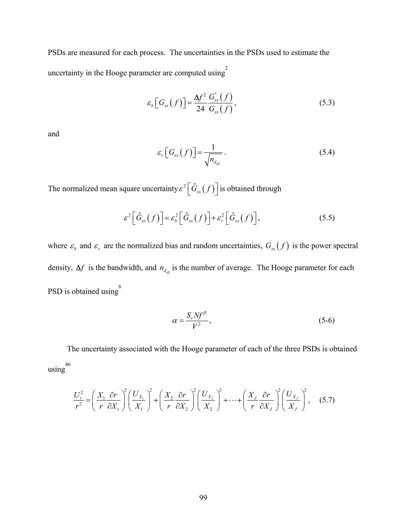
PSDs are measured for each process. The uncertainties in the PSDs used to estimate the
uncertainty in the Hooge parameter are computed using2
( ) ( )( )
''2
24xx
b xxxx
G ffG fG f
ε Δ=⎡ ⎤⎣ ⎦ , (5.3)
and
( ) 1
eff
r xxd
G fn
ε =⎡ ⎤⎣ ⎦ . (5.4)
The normalized mean square uncertainty ( )2 ˆxxG fε ⎡ ⎤
⎣ ⎦ is obtained through
, (5.5) ( ) ( ) ( )2 2 2ˆ ˆ ˆxx b xx r xxG f G f G fε ε ε⎡ ⎤ ⎡ ⎤ ⎡= +⎣ ⎦ ⎣ ⎦ ⎣
⎤⎦
where bε and rε are the normalized bias and random uncertainties, ( )xxG f is the power spectral
density, fΔ is the bandwidth, and is the number of average. The Hooge parameter for each
PSD is obtained using6
effdn
2vS NfV
β
α = , (5-6)
The uncertainty associated with the Hooge parameter of each of the three PSDs is obtained
using46
1 2
22 2 22 221 2
21 1 2 2
JXX X Jr
J J
UU U XU X Xr r rr r X X r X X r X X
⎛ ⎞⎛ ⎞ ⎛ ⎞ ⎛ ⎞⎛ ⎞ ⎛ ⎞∂ ∂ ∂= + + + ⎜⎜ ⎟ ⎜ ⎟ ⎜ ⎟⎜ ⎟ ⎜ ⎟∂ ∂ ∂⎝ ⎠ ⎝ ⎠ ⎝ ⎠⎝ ⎠ ⎝ ⎠ ⎝ ⎠
⎟ , (5.7)
99
where is an experimental result which is a function of measured variablesr J iX , rUr
is the
relative uncertainty of the result and iX
i
UX
are the relative uncertainties for each variable. The
fitted line is obtained from MatLab curve fitting tool, cftool. The Hooge parameter is computed
at 1 Hz. This makes the frequency f independent of the factorβ . The value of the PSD at 1 Hz
used to compute the Hooge parameter is obtained from the fitted line at 1 Hz. The Hooge
parameter of each process is obtained by taking the average of three Hooge parameters extracted
as described above on three different devices. The uncertainty in the Hooge parameter is then
obtained by applying Equation 5-4 to the average shown in Equation 5-5.
1 2
33α α αα + +
= . (5.8)
Figure 5-16, shows the PSDs without the setup noise of three different piezoresistors of
process 2A (B, 20 keV, 7x1014 cm-2, 7o tilt and 5 min dry, 5 min wet and 10 min dry at 900 C).
Figure 5-19, shows the uncertainties of the PSDs for each different piezoresistor of process 2A.
The fitted lines of the three PSDs of process 2A are shown in Figure 5-20. The Hooge
parameters for each of the three piezoresistors measured to characterize process 2A are shown in
Table 5-8.
The Hooge parameters for all the processes are shown in Table 5-9. The Hooge parameter
for processes 2A, 2E and 1A are respectively 4.41x10⁻⁴ ± 1.38x10⁻⁴, 3.42x10⁻⁴ ± 1.17x10⁻⁴,
1.06x10⁻⁴ ± 3.77x10⁻⁵. The noise voltage PSD shows that as the annealing time increases, the 1/f
noise PSD and the Hooge parameters decrease for the 20 keV B annealed at 900 C. The
uncertainties in the extracted Hooge parameter make a definitive conclusion difficult. Extensive
measurements over a wider range of process conditions are recommended for future work.
100
5.3.2 Noise PSD of Piezoresistors R6 for B, 40 keV, 7x1014 cm-2 through 0.1 µm of SiO2
The voltage PSD is compared for 40 keV B implanted samples subjected to different
annealing times at 900 C. The decrease of the defect densities are monitored via the measured
1/f noise voltage PSD of the piezoresistors. The piezoresistors implanted at 40 keV are annealed
at 900 C with times of 10 min, 30 min, 50 min and 90 min. The same measurements described
in Section 5.3.1 for the I-V characteristics and average noise voltage PSDs are performed for the
wafers implanted at B, 40 keV, 7x1014 cm-2 through 0.1 µm of SiO2. Figure 5-21 shows the
average noise voltage PSDs of wafer 2B and wafer 5A which were not oxidized after the inert
anneals as shown in Table 5-8. The corner frequency for wafer 2B is 1790 Hz and 1680 Hz for
wafer 5A. The longer the annealing condition (inert) the lower is the noise voltage PSDs and the
smaller the corner frequency. Processes 2B and 5A are annealed respectively for 10 min and 90
min respectively at 900 C and the noise voltage of process 2B is higher than that of process 5A.
Figure 5-22 shows the average noise voltage PSDs of wafer 3E and wafer 4A with respective
corner frequencies of 442 Hz and 2960 Hz. The annealing conditions of process 3E and 4A are
shown in Table 5-8. In contrast to wafer 2B and wafer 5A, the wafer 4A with the longer the
annealing condition (inert and oxidation) shows higher noise and corner frequency than wafer 3E
with shorter annealing. The Hooge parameter is computed as described in Section 5.3.1 with the
number carriers obtained from Hall Effect measurement of process 2B, 3E, 4A and 5A. Table 5-
8 shows the Hooge parameters. The Hooge parameter for processes 2B, 5A, 3E, and 4A are
respectively 9.67x10⁻⁴ ± 4.13x10⁻⁴, 4.94x10⁻⁴ ± 1.73x10⁻⁴, 8.58x10⁻⁵ ± 2.84x10⁻⁵, 7.97x10⁻⁴ ±
3.15x10⁻⁴. As the annealing time increases, the 1/f noise PSDs and the Hooge parameters for
processes 2B and 5A that were not oxidized decrease. However, for the oxidized processes 3E
and 4A where the annealing time increases, the noise voltage PSD also increases. The 40 keV
101
with oxidation gives unexpected results. This could be explained by the faulted loop areas in the
piezoresistors as discussed in Chapter 6.
5.3.3 Noise PSD of Solid-Source Diffused Piezoresistors R9 of Wafers C1 and C2
Solid source diffusion is used to avoid damage created in the piezoresistor during ion
implantation. However, interface traps at the Si/SiO2 interface are still present in the
piezoresistors. Hence, 1/f noise can still originate from the interface traps. To study the effect of
the interface traps on the 1/f noise two processes for solid source diffusion were made. Process
C1 was solid source diffused with B for 25 min at 950 C while process C2 was first solid source
diffused with B for 25 min at 950 C and then solid source diffused with P for 5 min at 800 C.
The phosphorous solid source diffusion is used to reduce the interaction of the carriers with the
interface traps during device operation. Piezoresistor test structure 9 is used for the noise
measurements because it has a resistance in some cases comparable to each other and
comparable to those of R6 for the implanted resistors in other cases. The I-V characteristics are
shown in Figure 5-23 and Figure 5-24 for process C1 and C2 respectively. The I-V of both
processes are linear from -10 V to 10 V, but those of C2 do not overlap as reflected in the
observed variation of resistances as shown in Table 5-1. The average noise voltage PSDs of C1
and C2 are shown in Figure 5-25. The average noise voltage PSD of wafer C2 is lower than that
of wafer C1 and their respective corner frequencies 112 Hz are and 418 Hz. The lower average
noise voltage PSD of C2 could be due to the phosphorus deposition after the boron diffusion. It
is possible that surface traps may not play an important role in the noise magnitude of C2 since
the phosphorous near the surface would push the holes distribution away from the surface traps
at the Si/SiO2 interface. The surface trap density is computed in the next chapter. The other
possible explanation for lower noise is a larger number of carriers N. To verify this assumption,
we substituted the number of carriers of C2 into the Hooge expression of the 1/f noise, Equation
102
2-17, at 1 Hz. The noise voltage PSD resulting from that computation, presented in Figure 5-26,
shows a decrease in the noise voltage PSD; however, the value of the noise voltage PSD of C1 at
1 Hz does not overlap with that of C2 at 1 Hz. Although, the Hooge model is based on mobility
fluctuations (bulk defects), it is used as a figure of merit for the solid source diffused
piezoresistors which have much lower bulk defects and where the 1/f noise is presumably due to
carrier fluctuations (surface defects). The Hooge parameter is computed obtained as described in
Section 5.3.1 with the number carriers obtained from Hall Effect measurement of process C1 and
C2. Table 5-8 shows the Hooge parameters. The Hooge parameter for process C1 and C2 are
respectively 6.89x10⁻⁴ ± 2.92x10⁻⁴, and 2.38x10⁻⁴ ± 1.20x10⁻⁴. The noise voltage PSD shows that
the process, C2, with phosphorus solid source diffusion has lower1/f noise voltage PSD and
Hooge parameters than the process without phosphorous, C1. In the absence of ion implantation
induced defects, the noise voltage PSD measurements indicate that the phosphorus solid source
diffusion may play a role in the noise reduction by keeping the holes away from the interface
traps. Next we analyze the noise voltage.
5.4 Hooge Parameter and 1/F Noise Analysis and Discussion
In this section, we analyze the measured noise voltage PSDs in terms of their Hooge
parameter α. As mentioned earlier, the Hooge parameter is employed as an empirical a figure of
merit of the quality of the crystal. There are other models such as the McWhorter model7 which
is based on the carrier fluctuation. The number of carriers, , used to compute the Hooge
parameter is estimated from Hall effect measurements. The uncertainty in is obtained by
propagating the uncertainties of the dose and of the area
N
N
Q A .
*N Q A= . (5.9)
103
After diffusion, the length and width of the resistor differ from that of the actual mask.
The largest possible increase in the width and length is 2 jx , where jx is the junction depth as
illustrated in Figure 5-27. For the measured resistors, the length and widths are 245 µm and 24.3
µm respectively. The junction depth measured with SIMS is 0.5 µm. Thus 2 jx is 1 µm. A 3 %
uncertainty in the area was used to account for lateral diffusion. The Hooge parameters of all the
processes are shown in Table 5-8 where it is observed that the Hooge parameter decreases as the
defect density decreases with increased annealing time except for processes 3E and 4A. In these
two processes implanted with B 40 keV and subjected to inert anneal and oxidation, the PSDs
appear to track the faulted loop areas as it is discussed in Chapter 6.
Current crowding on metal contacts has been studied by Murrmann and Widmann.47
Current crowding may cause localized heating and thus play a role in electromigration.
However, the current density in the resistor during noise measurement is very low; for example,
the current density used during the measurement of process 2A is 22.56x10 A cm2 , over three
orders of magnitude lower than the typical current density threshold for electromigration.
Therefore, current crowding is not an issue in the measurements. During oxidation, boron
segregates into the silicon dioxide. Therefore, there is a reduction of the boron dose in the
silicon. The implanted boron dose was 7x1014 cm-2. Using the SIMS profiles after oxidation, the
boron dose in the silicon varies from 4.5x10¹⁴ to 6.7x1014 cm-2. This indicates that approximately
36 % to 4.3 % of the boron dose resides in the silicon dioxide. The effect of the boron inside the
silicon dioxide on the measured noise PSD needs to be studied.
5.5 Shot Noise Measurements
The shot noise is measured on piezoresistors instead of the fabricated P/N diodes to have
an insight of the quality of the defects in the piezoresistors. The P/N diode I-V characteristics of
104
resistor 6, diode 1 and diode 2 of process 1A of generation 2 are shown in Figure 5-8. Figure 5-
28 shows the shot noise of R6 for process 1A. The current used for the measurement is taken in
the linear region of the I-V. The shot noise measurements of piezoresistor R6 of process 1A
reveal the presence of high density bulk and surface defects. The shot noise magnitude given by
Equation 2-21 is obtained in the measurement at high frequencies (> 1x10⁴ Hz). This is an
indication of significant defects in the crystal lattice.
5.6 Number of Carrier Dependence of 1/F Noise
In this section we study the effect of the number of carriers on the low frequency noise.
We use piezoresistor test structures 1, 6 and 12 of generation 1 process for the investigation. The
process flow of generation 1 process is described in Appendix D.
5.6.1 Fabrication and Measurements of Test Structures
The test structures have been fabricated at MEMS-exchange, Coresystems and at the UF
nanofabrication clean room. MEMS-exchange services have been used for the annealing
treatments. The ion implantations of piezoresistors have been done at Coresystems. As
discussed in Chapter 3, piezoresistors were designed to have the same resistance with different
surface areas and volumes. In Figure 5-29 we show the top views and a cross-section of
piezoresistors test structures 7 (R1B7N), 8 (R1B8E) and 9 (R1B9W) which have different
dimensions but respective resistance values of 8217.17 Ω, 8209.27 Ω, and 8419.17 Ω.
Measured resistances of the fabricated junction isolated piezoresistors are shown in Table 5-10.
The boron profile obtained via secondary ion mass spectroscopy (SIMS) performed by Evans
Analytical Group is shown in Figure 5-30. In Figure 5-30, the surface concentration is about
1x1018 cm-3 and junction depth is about 2.27 µm. The Van der Pauw structures are used to
measure the sheet resistance, line width, and contact resistance. The measured sheet resistance is
105
178.70 Ω/. The line width and contact resistance using Equation 3-20 and Equation 3-21 are
respectively 0.018 μm and 4 Ω.
5.6.1 Noise PSD Measurements
In order to explore the number of carrier and surface to volume ratio dependency of 1/f
noise, we perform noise measurements on piezoresistors and 1, 2, 3 and 12. Piezoresistors 1, 2,
and 3 have the same resistance but different number of carriers while piezoresistor 12 have a
different resistance and number of carrier. Table 5-10 shows the piezoresistor nomenclatures
and their resistances. In Table 5-10, the nomenclature “R1B1W” means piezoresistor of row 1,
from quadrant B in the wafer, piezoresistor test structure 1 and location west in the chip. This
allows us to avoid measuring the same piezoresistor multiple times. The number of carriers used
to compute the Hooge parameter is extracted using the SIMS profiles since there was no space
reserved for Hall Effect measurement. Although SIMS gives the atomic concentration of the
dopant, it will be sufficient for our application which is to see how the number of carriers affects
the 1/f noise. However, the number of carriers obtain from SIMS is not appropriate for the
computation of the Hooge parameter. The number of carriers, , is obtained by multiplying the
dose, Q , obtained from the SIMS profile with the piezoresistor area
N
A ,
N Q A= ∗ . (5-10)
The I-V characteristics and noise voltage power spectral density (PSD) of three
piezoresistor test structures 1 have been measured. Figure 5-31 shows the I-V characteristic of
piezoresistor R1B1W at three bias voltages. The noise voltage PSDs are shown in Figure 5-32.
The corner frequency, which is the frequency at which the 1/f noise and the thermal noise
coincide, when the piezoresistor is biased at 4.65 V dc is larger than 12.8 kHz. Figure 5-33
shows the I-V characteristic of piezoresistor R3A12E. The noise voltage PSD is shown in Figure
106
5-34. The corner frequency when the piezoresistor is biased at 1.48 V dc is around 70 Hz. At
the same bias voltage, piezoresistor 12 has less noise and smaller corner frequency than
piezoresistor 1.
To obtain insight about the defect concentration in the piezoresistor bulk, shot noise
measurements are performed on the junction isolated piezoresistor test structure 1. First, the I-V
characteristic of the P/N diode as shown in Figure 5-35 is measured. The shot noise is measured
for currents of 1.54x10⁻⁷, 3.30x10⁻⁷, and 4.81x10⁻⁷ A, which are in the linear region of the P/N
diode I-V characteristic. Figure 5-36 shows the shot noise of piezoresistor test structure 1. In
Figure 5-36, the corner frequency cf , is 10 Hz (I = 1.54 x10⁻⁷) which is much lower than that of
resistor 6 of process 1A.
5.6.2 Analysis and Discussion
In this section, we analyze the measured noise voltage PSDs in terms of their number of
carriers and dimensions (surface area and volume). In this section it is shown how the number of
carriers affects the low noise frequency. Piezoresistor 1 has been designed to have a smaller area
than piezoresistor 12. Figure 5-37 shows the noise voltage PSDs of piezoresistor test structure 1
(R1B1W) and piezoresistor test structure 12 (R3A12E) biased at 1.49 Vdc and 1.48 Vdc
respectively. In Figure 5-37, the noise voltage PSD of piezoresistor test structure 12 (R3A12E)
is smaller than that of piezoresistor test structure 1 (R1B1W). This may be due to the fact of a
larger number of carriers for piezoresistor test structure 12 (R3A12E). Hooge’s empirical
relation of the 1/f noise (Equation 2-17) shows that the 1/f noise is inversely proportional to the
number of carriers, . To further investigate the effect of the number of carriers we perform
noise measurements of three piezoresistors with identical resistances. Some piezoresistors were
designed to have the same resistance value and different surface area and volume. This is for
N
107
example the case of piezoresistor test structures 1, 2 and 3. As shown in Table 3-1, piezoresistor
test structure 3 has the larger surface area and volume followed by piezoresistor test structure 2
and piezoresistor test structure 1. In addition, these piezoresistors have the same junction depth
thus different number of carriers. The effect of the surface at the Si/SiO2 interface cannot be
used for the noise analysis since all piezoresistors have the same surface to volume ratio. A
same surface to volume ratio means that the carriers in the piezoresistors are equally affected by
the surface traps. Therefore, the main parameter that affects the 1/f noise is the number of
carriers. Figure 5-38 A) and B) show the noise voltage PSDs of piezoresistor test structures 1, 2
and 3 biased respectively at 4.69 Vdc, 4.80 Vdc and 4.88 Vdc. In Figure 5-38 A), among the
three piezoresistor test structures, piezoresistor test structure 3 which has the largest number of
carriers has the lowest 1/f noise voltage PSD. Figure 5-38 B) shows the noise PSD at 10 Hz for
piezoresistors 1 2 3, and R R R at the same bias voltage as a function of number of carriers. The
noise voltage PSD decreases as the number of carrier increases.
5.7 Summary
The fabricated test structures and the measurements based on the experimental methods of
Chapter 4 have been presented. The carrier concentrations using the Hall measurement, and the
sheet resistance, contact resistance and line width using the Van der Pauw structure are
measured. The C-V of the pMOSC is presented and the oxide thickness computed. The I-V of
the piezoresistors is linear from -10 V to 10 V. It is shown that the average noise voltage PSDs
for the implanted piezoresistors decreases as the annealing time increases for the 20 keV implant
and for the 40 keV process without oxidation. However, an exception of the decrease of the 1/f
noise with longer annealing is observed for the 40 keV process, 3E and 4A, with oxidation. The
process with longer annealed time, 4A, has higher noise voltage PSD magnitude than of 3E with
108
shorter anneal time. The measured shot noise for the generation 2 process coincides with the
theoretical shot noise at high frequencies (>1x10⁴ Hz) which is an indication of the presence of
defects in the crystal. The 1/f noise dominates at low frequencies. The shot noise of generation
1 process shows a corner frequency at 10 Hz. This indicates less bulk defects in the piezoresistor
of the generation 1 process. The effect of the number of carriers was studied with resistors of
different resistance and dimensions as well as resistors of same resistance and different
dimensions. The noise voltage PSDs show that resistors with larger number of carriers have less
1/f noise. Next, the defects in the test structures are measured and the analyses of the relations of
the defects to the measured noise voltage PSD of piezoresistor generation 2 are also performed.
109
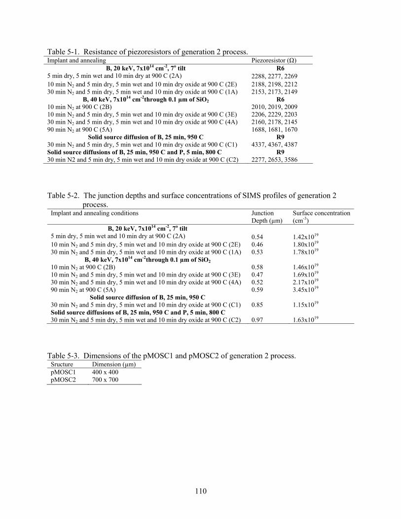
Table 5-1. Resistance of piezoresistors of generation 2 process. Implant and annealing Piezoresistor (Ω)
B, 20 keV, 7x1014 cm-2, 7o tilt R6 5 min dry, 5 min wet and 10 min dry at 900 C (2A) 2288, 2277, 2269 10 min N2 and 5 min dry, 5 min wet and 10 min dry oxide at 900 C (2E) 2188, 2198, 2212 30 min N2 and 5 min dry, 5 min wet and 10 min dry oxide at 900 C (1A) 2153, 2173, 2149
B, 40 keV, 7x1014 cm-2through 0.1 µm of SiO2 R6 10 min N2 at 900 C (2B) 2010, 2019, 2009 10 min N2 and 5 min dry, 5 min wet and 10 min dry oxide at 900 C (3E) 2206, 2229, 2203 30 min N2 and 5 min dry, 5 min wet and 10 min dry oxide at 900 C (4A) 2160, 2178, 2145 90 min N2 at 900 C (5A) 1688, 1681, 1670
Solid source diffusion of B, 25 min, 950 C R9 30 min N2 and 5 min dry, 5 min wet and 10 min dry oxide at 900 C (C1) 4337, 4367, 4387 Solid source diffusions of B, 25 min, 950 C and P, 5 min, 800 C R9 30 min N2 and 5 min dry, 5 min wet and 10 min dry oxide at 900 C (C2) 2277, 2653, 3586 Table 5-2. The junction depths and surface concentrations of SIMS profiles of generation 2
process. Implant and annealing conditions Junction
Depth (µm) Surface concentration (cm-3)
B, 20 keV, 7x1014 cm-2, 7o tilt 5 min dry, 5 min wet and 10 min dry at 900 C (2A) 0.54 1.42x10¹⁹ 10 min N2 and 5 min dry, 5 min wet and 10 min dry oxide at 900 C (2E) 0.46 1.80x10¹⁹ 30 min N2 and 5 min dry, 5 min wet and 10 min dry oxide at 900 C (1A) 0.53 1.78x10¹⁹
B, 40 keV, 7x1014 cm-2through 0.1 µm of SiO2 10 min N2 at 900 C (2B) 0.58 1.46x10¹⁹ 10 min N2 and 5 min dry, 5 min wet and 10 min dry oxide at 900 C (3E) 0.47 1.69x10¹⁹ 30 min N2 and 5 min dry, 5 min wet and 10 min dry oxide at 900 C (4A) 0.52 2.17x10¹⁹ 90 min N2 at 900 C (5A) 0.59 3.45x10¹⁹
Solid source diffusion of B, 25 min, 950 C 30 min N2 and 5 min dry, 5 min wet and 10 min dry oxide at 900 C (C1) 0.85 1.15x10¹⁹ Solid source diffusions of B, 25 min, 950 C and P, 5 min, 800 C 30 min N2 and 5 min dry, 5 min wet and 10 min dry oxide at 900 C (C2) 0.97 1.63x10¹⁹
Table 5-3. Dimensions of the pMOSC1 and pMOSC2 of generation 2 process.
Sructure Dimension (µm) pMOSC1 400 x 400 pMOSC2 700 x 700
110
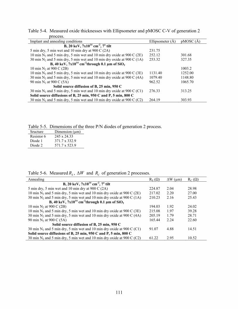
Table 5-4. Measured oxide thicknesses with Ellipsometer and pMOSC C-V of generation 2 process.
Implant and annealing conditions Ellipsometer (Å) pMOSC (Å) B, 20 keV, 7x1014 cm-2, 7o tilt
5 min dry, 5 min wet and 10 min dry at 900 C (2A) 231.75 10 min N2 and 5 min dry, 5 min wet and 10 min dry oxide at 900 C (2E) 252.12 301.68 30 min N2 and 5 min dry, 5 min wet and 10 min dry oxide at 900 C (1A) 253.32 327.35
B, 40 keV, 7x1014 cm-2through 0.1 µm of SiO2 10 min N2 at 900 C (2B) 1003.2 10 min N2 and 5 min dry, 5 min wet and 10 min dry oxide at 900 C (3E) 1131.40 1252.00 30 min N2 and 5 min dry, 5 min wet and 10 min dry oxide at 900 C (4A) 1079.40 1148.80 90 min N2 at 900 C (5A) 962.52 1065.70
Solid source diffusion of B, 25 min, 950 C 30 min N2 and 5 min dry, 5 min wet and 10 min dry oxide at 900 C (C1) 276.33 313.25 Solid source diffusions of B, 25 min, 950 C and P, 5 min, 800 C 30 min N2 and 5 min dry, 5 min wet and 10 min dry oxide at 900 C (C2) 264.19 303.93
Table 5-5. Dimensions of the three P/N diodes of generation 2 process.
Sructure Dimension (µm) Resistor 6 245 x 24.33 Diode 1 371.7 x 332.9 Diode 2 571.7 x 523.9
Table 5-6. Measured SR , and WΔ CR of generation 2 processes. Annealing RS (Ω) ΔW (µm) RC (Ω)
B, 20 keV, 7x1014 cm-2, 7o tilt 5 min dry, 5 min wet and 10 min dry at 900 C (2A) 224.87 2.04 28.98 10 min N2 and 5 min dry, 5 min wet and 10 min dry oxide at 900 C (2E) 217.02 2.20 27.00 30 min N2 and 5 min dry, 5 min wet and 10 min dry oxide at 900 C (1A) 210.23 2.16 25.43
B, 40 keV, 7x1014 cm-2through 0.1 µm of SiO2 10 min N2 at 900 C (2B) 194.03 1.92 24.02 10 min N2 and 5 min dry, 5 min wet and 10 min dry oxide at 900 C (3E) 215.08 1.97 39.28 30 min N2 and 5 min dry, 5 min wet and 10 min dry oxide at 900 C (4A) 205.19 1.79 28.71 90 min N2 at 900 C (5A) 165.44 2.24 22.60
Solid source diffusion of B, 25 min, 950 C 30 min N2 and 5 min dry, 5 min wet and 10 min dry oxide at 900 C (C1) 91.07 4.88 14.51 Solid source diffusions of B, 25 min, 950 C and P, 5 min, 800 C 30 min N2 and 5 min dry, 5 min wet and 10 min dry oxide at 900 C (C2) 61.22 2.95 10.52
111
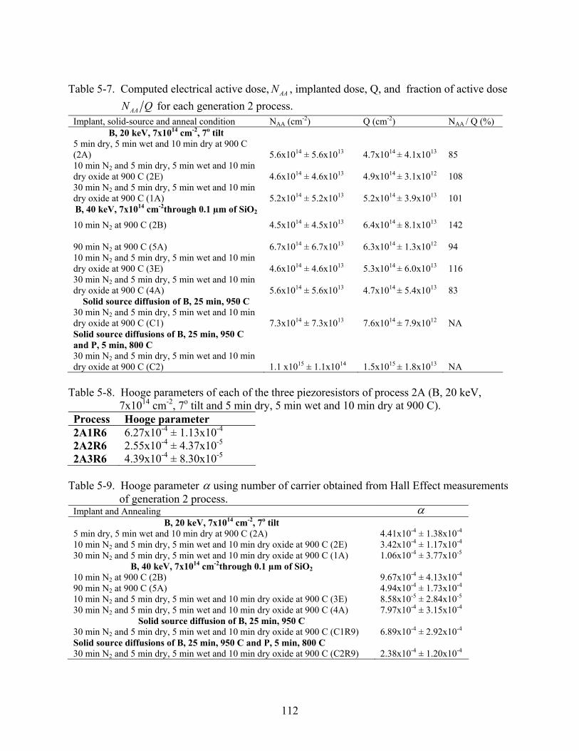
Table 5-7. Computed electrical active dose, , implanted dose, Q, and fraction of active dose AAN
AAN Q for each generation 2 process. Implant, solid-source and anneal condition NAA (cm-2) Q (cm-2) NAA / Q (%)
B, 20 keV, 7x1014 cm-2, 7o tilt 5 min dry, 5 min wet and 10 min dry at 900 C (2A) 5.6x10¹⁴ ± 5.6x10¹³ 4.7x10¹⁴ ± 4.1x10¹³ 85 10 min N2 and 5 min dry, 5 min wet and 10 min dry oxide at 900 C (2E) 4.6x10¹⁴ ± 4.6x10¹³ 4.9x10¹⁴ ± 3.1x10¹² 108 30 min N2 and 5 min dry, 5 min wet and 10 min dry oxide at 900 C (1A) 5.2x10¹⁴ ± 5.2x10¹³ 5.2x10¹⁴ ± 3.9x10¹³ 101 B, 40 keV, 7x1014 cm-2through 0.1 µm of SiO2
10 min N2 at 900 C (2B) 4.5x10¹⁴ ± 4.5x10¹³ 6.4x10¹⁴ ± 8.1x10¹³ 142 90 min N2 at 900 C (5A) 6.7x10¹⁴ ± 6.7x10¹³ 6.3x10¹⁴ ± 1.3x10¹² 94 10 min N2 and 5 min dry, 5 min wet and 10 min dry oxide at 900 C (3E) 4.6x10¹⁴ ± 4.6x10¹³ 5.3x10¹⁴ ± 6.0x10¹³ 116 30 min N2 and 5 min dry, 5 min wet and 10 min dry oxide at 900 C (4A) 5.6x10¹⁴ ± 5.6x10¹³ 4.7x10¹⁴ ± 5.4x10¹³ 83
Solid source diffusion of B, 25 min, 950 C 30 min N2 and 5 min dry, 5 min wet and 10 min dry oxide at 900 C (C1) 7.3x10¹⁴ ± 7.3x10¹³ 7.6x10¹⁴ ± 7.9x10¹² NA Solid source diffusions of B, 25 min, 950 C and P, 5 min, 800 C 30 min N2 and 5 min dry, 5 min wet and 10 min dry oxide at 900 C (C2) 1.1 x10¹⁵ ± 1.1x10¹⁴ 1.5x10¹⁵ ± 1.8x10¹³ NA
Table 5-8. Hooge parameters of each of the three piezoresistors of process 2A (B, 20 keV,
7x1014 cm-2, 7o tilt and 5 min dry, 5 min wet and 10 min dry at 900 C). Process Hooge parameter 2A1R6 6.27x10⁻⁴ ± 1.13x10⁻⁴ 2A2R6 2.55x10⁻⁴ ± 4.37x10⁻⁵ 2A3R6 4.39x10⁻⁴ ± 8.30x10⁻⁵
Table 5-9. Hooge parameter α using number of carrier obtained from Hall Effect measurements
of generation 2 process. Implant and Annealing α
B, 20 keV, 7x1014 cm-2, 7o tilt 5 min dry, 5 min wet and 10 min dry at 900 C (2A) 4.41x10⁻⁴ ± 1.38x10⁻⁴ 10 min N2 and 5 min dry, 5 min wet and 10 min dry oxide at 900 C (2E) 3.42x10⁻⁴ ± 1.17x10⁻⁴ 30 min N2 and 5 min dry, 5 min wet and 10 min dry oxide at 900 C (1A) 1.06x10⁻⁴ ± 3.77x10⁻⁵
B, 40 keV, 7x1014 cm-2through 0.1 µm of SiO2 10 min N2 at 900 C (2B) 9.67x10⁻⁴ ± 4.13x10⁻⁴ 90 min N2 at 900 C (5A) 4.94x10⁻⁴ ± 1.73x10⁻⁴ 10 min N2 and 5 min dry, 5 min wet and 10 min dry oxide at 900 C (3E) 8.58x10⁻⁵ ± 2.84x10⁻⁵ 30 min N2 and 5 min dry, 5 min wet and 10 min dry oxide at 900 C (4A) 7.97x10⁻⁴ ± 3.15x10⁻⁴
Solid source diffusion of B, 25 min, 950 C 30 min N2 and 5 min dry, 5 min wet and 10 min dry oxide at 900 C (C1R9) 6.89x10⁻⁴ ± 2.92x10⁻⁴ Solid source diffusions of B, 25 min, 950 C and P, 5 min, 800 C 30 min N2 and 5 min dry, 5 min wet and 10 min dry oxide at 900 C (C2R9) 2.38x10⁻⁴ ± 1.20x10⁻⁴
112
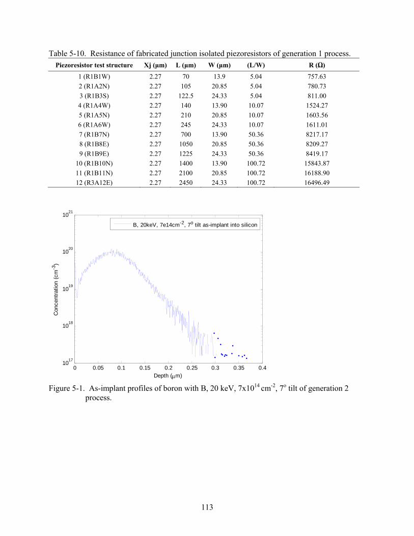
Table 5-10. Resistance of fabricated junction isolated piezoresistors of generation 1 process. Piezoresistor test structure Xj (μm) L (μm) W (μm) (L/W) R (Ω)
1 (R1B1W) 2.27 70 13.9 5.04 757.63 2 (R1A2N) 2.27 105 20.85 5.04 780.73 3 (R1B3S) 2.27 122.5 24.33 5.04 811.00 4 (R1A4W) 2.27 140 13.90 10.07 1524.27 5 (R1A5N) 2.27 210 20.85 10.07 1603.56 6 (R1A6W) 2.27 245 24.33 10.07 1611.01 7 (R1B7N) 2.27 700 13.90 50.36 8217.17 8 (R1B8E) 2.27 1050 20.85 50.36 8209.27 9 (R1B9E) 2.27 1225 24.33 50.36 8419.17
10 (R1B10N) 2.27 1400 13.90 100.72 15843.87 11 (R1B11N) 2.27 2100 20.85 100.72 16188.90 12 (R3A12E) 2.27 2450 24.33 100.72 16496.49
0 0.05 0.1 0.15 0.2 0.25 0.3 0.35 0.41017
1018
1019
1020
1021
Depth (μm)
Con
cent
ratio
n (c
m-3
)
B, 20keV, 7e14cm-2, 7o tilt as-implant into silicon
Figure 5-1. As-implant profiles of boron with B, 20 keV, 7x1014 cm-2, 7o tilt of generation 2
process.
113
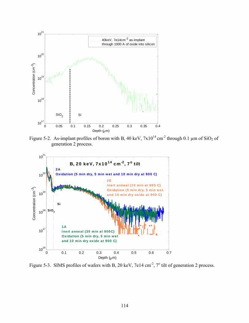
0 0.05 0.1 0.15 0.2 0.25 0.3 0.35 0.41017
1018
1019
1020
1021
Depth (μm)
Con
cent
ratio
n (c
m-3
)
40keV, 7e14cm-2 as-implantthrough 1000 A of oxide into silicon
SiO2 Si
Figure 5-2. As-implant profiles of boron with B, 40 keV, 7x1014 cm-2 through 0.1 µm of SiO2 of
generation 2 process.
0 0.1 0.2 0.3 0.4 0.5 0.6 0.71016
1017
1018
1019
1020
1021
Depth (μm)
Con
cent
ratio
n (c
m-3
)
2A Oxidation (5 min dry, 5 min wet and 10 min dry at 900 C)
2E Inert anneal (10 min at 900 C) Oxidation (5 min dry, 5 min wet and 10 min dry oxide at 900 C)
1A Inert anneal (30 min at 900C) Oxidation (5 min dry, 5 min wet and 10 min dry oxide at 900 C)
B, 20 keV, 7x1014 cm-2, 7o tilt
SiO2
Si
Figure 5-3. SIMS profiles of wafers with B, 20 keV, 7e14 cm-2, 7o tilt of generation 2 process.
114
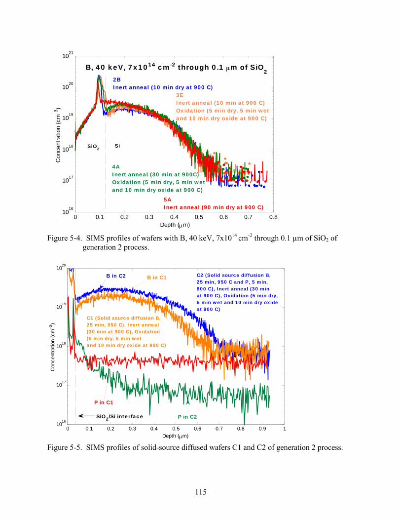
0 0.1 0.2 0.3 0.4 0.5 0.6 0.7 0.810
16
1017
1018
1019
1020
1021
Depth (μm)
Con
cent
ratio
n (c
m-3
)
3E Inert anneal (10 min at 900 C) Oxidation (5 min dry, 5 min wet and 10 min dry oxide at 900 C)
2B Inert anneal (10 min dry at 900 C)
4A Inert anneal (30 min at 900C) Oxidation (5 min dry, 5 min wet and 10 min dry oxide at 900 C)
SiO2
B, 40 keV, 7x1014 cm-2 through 0.1 μm of SiO2
Si
5AInert anneal (90 min dry at 900 C)
Figure 5-4. SIMS profiles of wafers with B, 40 keV, 7x1014 cm-2 through 0.1 µm of SiO2 of
generation 2 process.
0 0.1 0.2 0.3 0.4 0.5 0.6 0.7 0.8 0.9 110
16
1017
1018
1019
1020
Depth (μm)
Con
cent
ratio
n (c
m-3
)
SiO2/Si interface
B in C2 C2 (Solid source diffusion B, 25 min, 950 C and P, 5 min, 800 C), Inert anneal (30 minat 900 C), Oxidation (5 min dry, 5 min wet and 10 min dry oxide at 900 C)
P in C1
B in C1
C1 (Solid source diffusion B, 25 min, 950 C), Inert anneal (30 min at 900 C), Oxidation (5 min dry, 5 min wet and 10 min dry oxide at 900 C)
P in C2
Figure 5-5. SIMS profiles of solid-source diffused wafers C1 and C2 of generation 2 process.
115
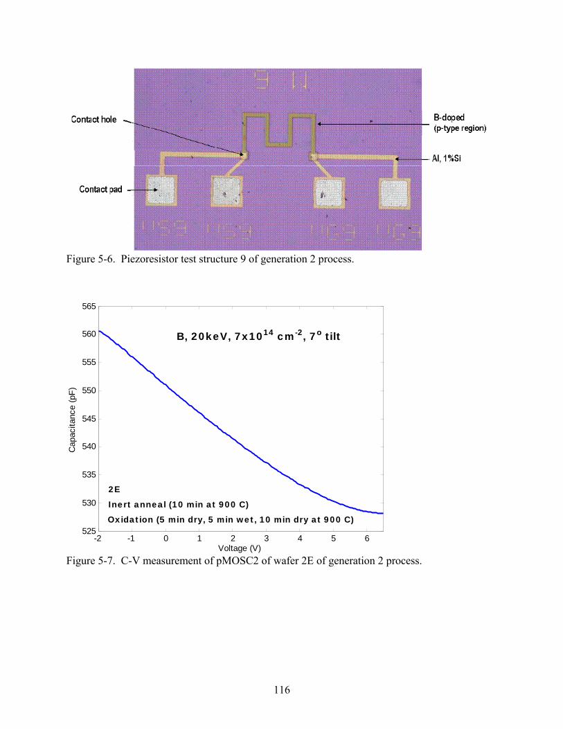
Figure 5-6. Piezoresistor test structure 9 of generation 2 process.
-2 -1 0 1 2 3 4 5 6525
530
535
540
545
550
555
560
565
Voltage (V)
Cap
acita
nce
(pF)
B, 20keV, 7x1014 cm-2, 7o tilt
Inert anneal (10 min at 900 C)
Oxidation (5 min dry, 5 min wet, 10 min dry at 900 C)
2E
Figure 5-7. C-V measurement of pMOSC2 of wafer 2E of generation 2 process.
116
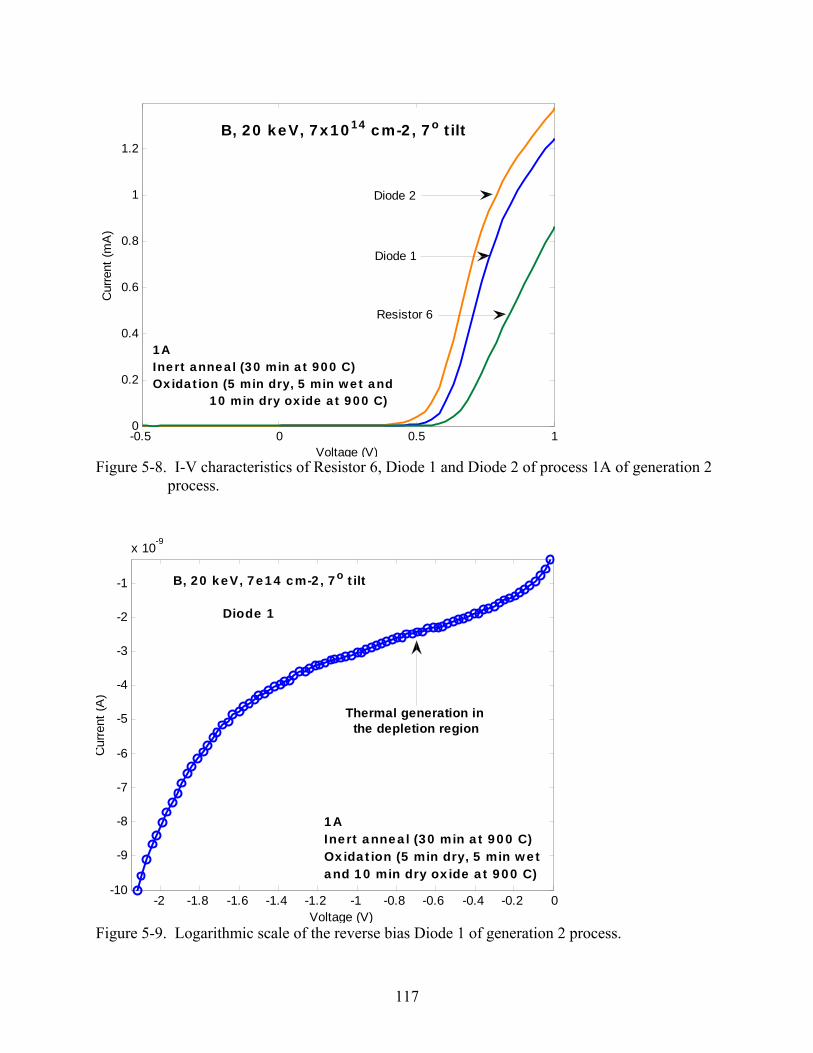
-0.5 0 0.5 10
0.2
0.4
0.6
0.8
1
1.2
Voltage (V)
Cur
rent
(mA
)
B, 20 keV, 7x1014 cm-2, 7o tilt
Diode 1
Diode 2
Resistor 6
1AInert anneal (30 min at 900 C)Oxidation (5 min dry, 5 min wet and 10 min dry oxide at 900 C)
Figure 5-8. I-V characteristics of Resistor 6, Diode 1 and Diode 2 of process 1A of generation 2
process.
-2 -1.8 -1.6 -1.4 -1.2 -1 -0.8 -0.6 -0.4 -0.2 0-10
-9
-8
-7
-6
-5
-4
-3
-2
-1
x 10-9
Voltage (V)
Cur
rent
(A)
Diode 1
B, 20 keV, 7e14 cm-2, 7o tilt
1A Inert anneal (30 min at 900 C) Oxidation (5 min dry, 5 min wet and 10 min dry oxide at 900 C)
Thermal generation in the depletion region
Figure 5-9. Logarithmic scale of the reverse bias Diode 1 of generation 2 process.
117
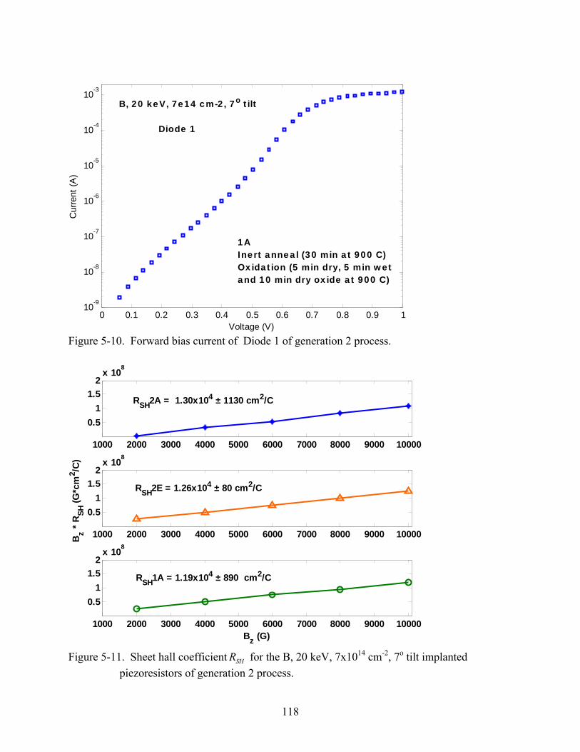
0 0.1 0.2 0.3 0.4 0.5 0.6 0.7 0.8 0.9 110-9
10-8
10-7
10-6
10-5
10-4
10-3
Voltage (V)
Cur
rent
(A)
B, 20 keV, 7e14 cm-2, 7o tilt
1A Inert anneal (30 min at 900 C) Oxidation (5 min dry, 5 min wet and 10 min dry oxide at 900 C)
Diode 1
Figure 5-10. Forward bias current of Diode 1 of generation 2 process.
1000 2000 3000 4000 5000 6000 7000 8000 9000 10000
0.51
1.52
x 108
RSH2A = 1.30x10⁴ ± 1130 cm2/C
1000 2000 3000 4000 5000 6000 7000 8000 9000 10000
0.51
1.52
x 108
RSH2E = 1.26x10⁴ ± 80 cm2/C
1000 2000 3000 4000 5000 6000 7000 8000 9000 10000
0.51
1.52
x 108
Bz (G)
B z * R
SH (G
*cm
2 /C)
RSH1A = 1.19x10⁴ ± 890 cm2/C
Figure 5-11. Sheet hall coefficient SHR for the B, 20 keV, 7x1014 cm-2, 7o tilt implanted
piezoresistors of generation 2 process.
118
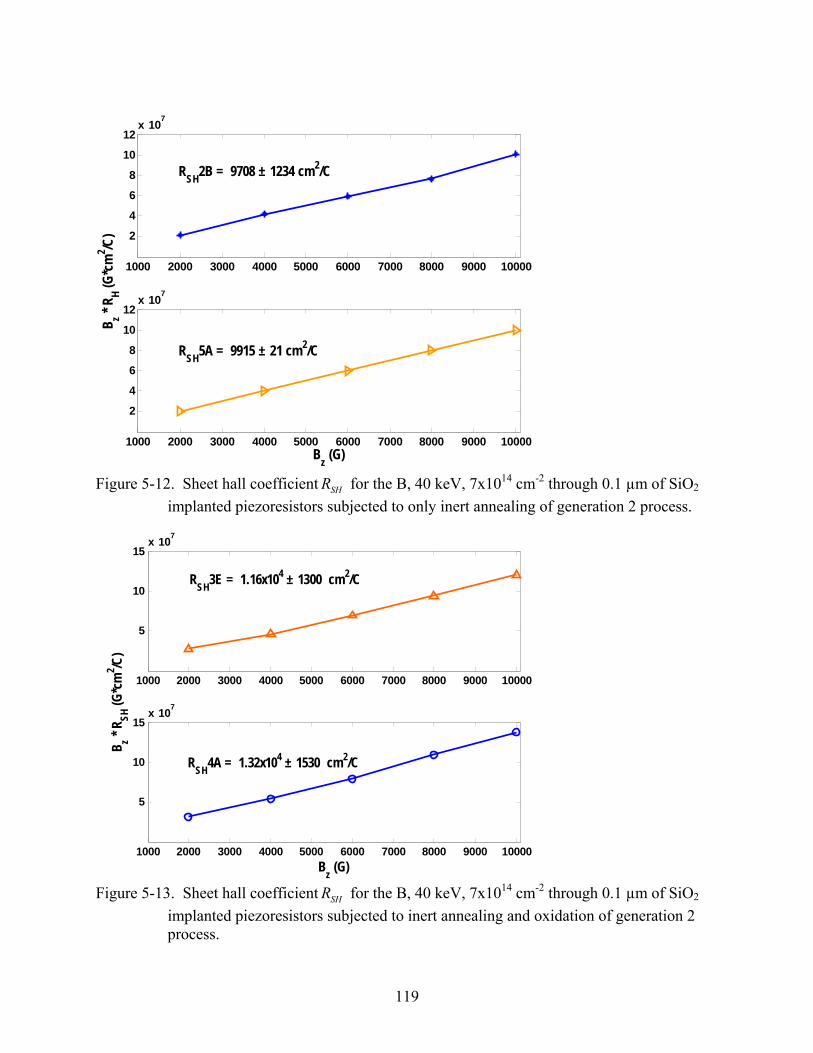
1000 2000 3000 4000 5000 6000 7000 8000 9000 10000
2
4
6
8
10
12x 107
RSH2B = 9708 ± 1234 cm2/C
1000 2000 3000 4000 5000 6000 7000 8000 9000 10000
2
4
6
8
10
12x 107
Bz (G)
B z * R H (G
*cm
2 /C)
RSH5A = 9915 ± 21 cm2/C
Figure 5-12. Sheet hall coefficient SHR for the B, 40 keV, 7x1014 cm-2 through 0.1 µm of SiO2
implanted piezoresistors subjected to only inert annealing of generation 2 process.
1000 2000 3000 4000 5000 6000 7000 8000 9000 10000
5
10
15x 107
RSH3E = 1.16x10⁴ ± 1300 cm2/C
1000 2000 3000 4000 5000 6000 7000 8000 9000 10000
5
10
15x 107
Bz (G)
B z * R SH
(G*c
m2 /C
)
RSH4A = 1.32x10⁴ ± 1530 cm2/C
Figure 5-13. Sheet hall coefficient SHR for the B, 40 keV, 7x1014 cm-2 through 0.1 µm of SiO2
implanted piezoresistors subjected to inert annealing and oxidation of generation 2 process.
119
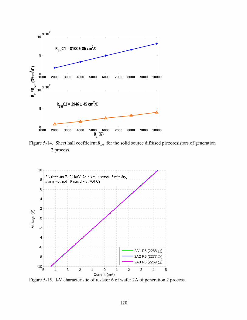
1000 2000 3000 4000 5000 6000 7000 8000 9000 100000
5
10x 107
RSHC1 = 8183 ± 86 cm2/C
1000 2000 3000 4000 5000 6000 7000 8000 9000 100000
5
10x 107
B z * R SH
(G*c
m2 /C
)
Bz (G)
RSHC2 = 3946 ± 45 cm2/C
Figure 5-14. Sheet hall coefficient SHR for the solid source diffused piezoresistors of generation
2 process.
-5 -4 -3 -2 -1 0 1 2 3 4 5-10
-8
-6
-4
-2
0
2
4
6
8
10
Current (mA)
Vol
tage
(V)
2A1 R6 (2288 Ω)2A2 R6 (2277 Ω)2A3 R6 (2269 Ω)
Figure 5-15. I-V characteristic of resistor 6 of wafer 2A of generation 2 process.
120
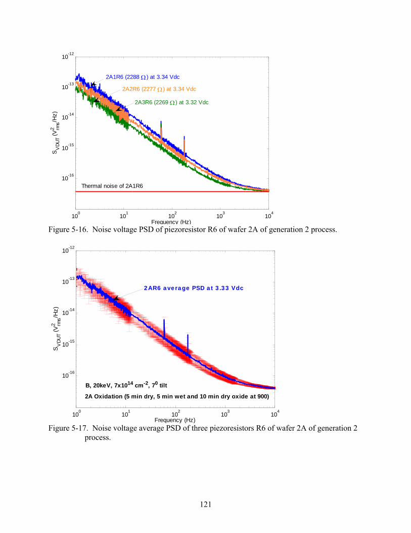
100 101 102 103 104
10-16
10-15
10-14
10-13
10-12
Frequency (Hz)
SV
DUT (V
rms
2/H
z)
2A1R6 (2288 Ω) at 3.34 Vdc
2A2R6 (2277 Ω) at 3.34 Vdc
2A3R6 (2269 Ω) at 3.32 Vdc
Thermal noise of 2A1R6
Figure 5-16. Noise voltage PSD of piezoresistor R6 of wafer 2A of generation 2 process.
100 101 102 103 104
10-16
10-15
10-14
10-13
10-12
Frequency (Hz)
SV
DUT (V
rms
2/H
z)
2AR6 average PSD at 3.33 Vdc
B, 20keV, 7x1014 cm-2, 70 tilt
2A Oxidation (5 min dry, 5 min wet and 10 min dry oxide at 900)
Figure 5-17. Noise voltage average PSD of three piezoresistors R6 of wafer 2A of generation 2
process.
121
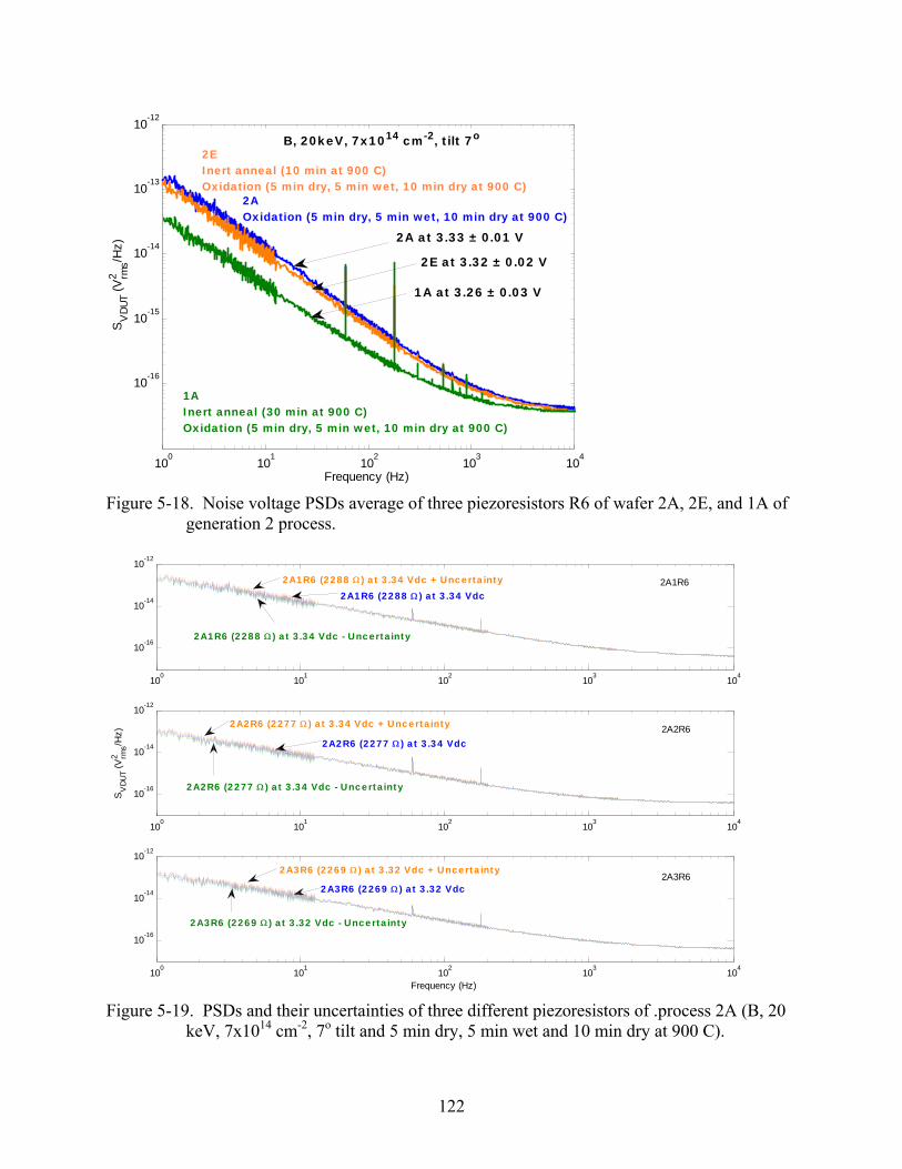
100
101
102
103
104
10-16
10-15
10-14
10-13
10-12
Frequency (Hz)
SV
DUT (V
rms
2/H
z)
B, 20keV, 7x1014 cm-2, tilt 7o
2A at 3.33 ± 0.01 V
2E at 3.32 ± 0.02 V
1A at 3.26 ± 0.03 V
2A Oxidation (5 min dry, 5 min wet, 10 min dry at 900 C)
2E Inert anneal (10 min at 900 C) Oxidation (5 min dry, 5 min wet, 10 min dry at 900 C)
1A Inert anneal (30 min at 900 C) Oxidation (5 min dry, 5 min wet, 10 min dry at 900 C)
Figure 5-18. Noise voltage PSDs average of three piezoresistors R6 of wafer 2A, 2E, and 1A of
generation 2 process.
100 101 102 103 104
10-16
10-14
10-12
2A1R6 (2288 Ω ) at 3.34 Vdc - Uncertainty
2A1R6 (2288 Ω ) at 3.34 Vdc
2A1R6 (2288 Ω ) at 3.34 Vdc + Uncertainty
100 101 102 103 104
10-16
10-14
10-12
SV
DUT (V
rms
2/H
z)
2A2R6 (2277 Ω ) at 3.34 Vdc
2A2R6 (2277 Ω ) at 3.34 Vdc - Uncertainty
2A2R6 (2277 Ω ) at 3.34 Vdc + Uncertainty
100 101 102 103 104
10-16
10-14
10-12
Frequency (Hz)
2A3R6 (2269 Ω ) at 3.32 Vdc
2A3R6 (2269 Ω ) at 3.32 Vdc - Uncertainty
2A3R6 (2269 Ω ) at 3.32 Vdc + Uncertainty
2A1R6
2A2R6
2A3R6
Figure 5-19. PSDs and their uncertainties of three different piezoresistors of .process 2A (B, 20
keV, 7x1014 cm-2, 7o tilt and 5 min dry, 5 min wet and 10 min dry at 900 C).
122
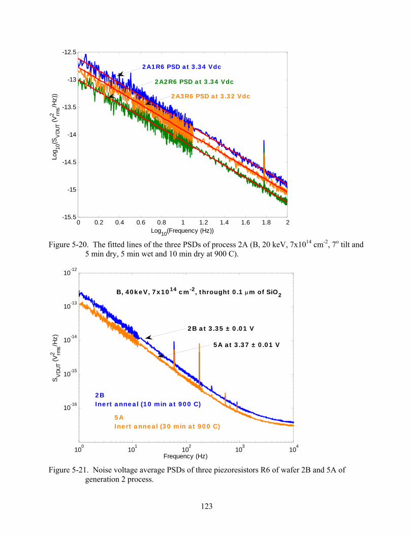
0 0.2 0.4 0.6 0.8 1 1.2 1.4 1.6 1.8 2-15.5
-15
-14.5
-14
-13.5
-13
-12.5
Log10(Frequency (Hz))
Log 10
(SV
DUT (V
rms
2/H
z))
2A1R6 PSD at 3.34 Vdc
2A2R6 PSD at 3.34 Vdc
2A3R6 PSD at 3.32 Vdc
Figure 5-20. The fitted lines of the three PSDs of process 2A (B, 20 keV, 7x1014 cm-2, 7o tilt and
5 min dry, 5 min wet and 10 min dry at 900 C).
100 101 102 103 104
10-16
10-15
10-14
10-13
10-12
Frequency (Hz)
SV
DUT (V
rms
2/H
z)
B, 40keV, 7x1014 cm-2, throught 0.1 μm of SiO2
2B at 3.35 ± 0.01 V
5A at 3.37 ± 0.01 V
2B Inert anneal (10 min at 900 C)
5A Inert anneal (30 min at 900 C)
Figure 5-21. Noise voltage average PSDs of three piezoresistors R6 of wafer 2B and 5A of
generation 2 process.
123
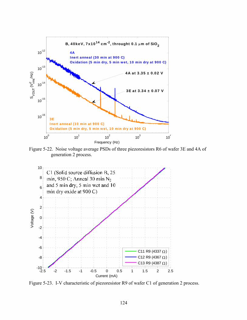
100 101 102 103 104
10-16
10-15
10-14
10-13
10-12
Frequency (Hz)
SV
DUT (V
rms
2/H
z)
B, 40keV, 7x1014 cm-2, throught 0.1 μm of SiO2
3E at 3.34 ± 0.07 V
4A at 3.35 ± 0.02 V
4A Inert anneal (30 min at 900 C) Oxidation (5 min dry, 5 min wet, 10 min dry at 900 C)
3E Inert anneal (10 min at 900 C) Oxidation (5 min dry, 5 min wet, 10 min dry at 900 C)
Figure 5-22. Noise voltage average PSDs of three piezoresistors R6 of wafer 3E and 4A of
generation 2 process.
-2.5 -2 -1.5 -1 -0.5 0 0.5 1 1.5 2 2.5-10
-8
-6
-4
-2
0
2
4
6
8
10
Current (mA)
Vol
tage
(V)
C11 R9 (4337 Ω )C12 R9 (4367 Ω )C13 R9 (4387 Ω )
Figure 5-23. I-V characteristic of piezoresistor R9 of wafer C1 of generation 2 process.
124
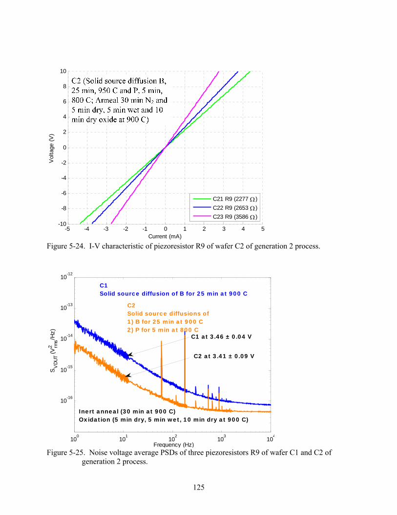
-5 -4 -3 -2 -1 0 1 2 3 4 5-10
-8
-6
-4
-2
0
2
4
6
8
10
Current (mA)
Vol
tage
(V)
C21 R9 (2277 Ω)C22 R9 (2653 Ω)C23 R9 (3586 Ω)
Figure 5-24. I-V characteristic of piezoresistor R9 of wafer C2 of generation 2 process.
100 101 102 103 104
10-16
10-15
10-14
10-13
10-12
Frequency (Hz)
SV
DUT (V
rms
2/H
z)
C1 Solid source diffusion of B for 25 min at 900 C
C2 Solid source diffusions of1) B for 25 min at 900 C 2) P for 5 min at 800 C
C1 at 3.46 ± 0.04 V
C2 at 3.41 ± 0.09 V
Inert anneal (30 min at 900 C) Oxidation (5 min dry, 5 min wet, 10 min dry at 900 C)
Figure 5-25. Noise voltage average PSDs of three piezoresistors R9 of wafer C1 and C2 of
generation 2 process.
125
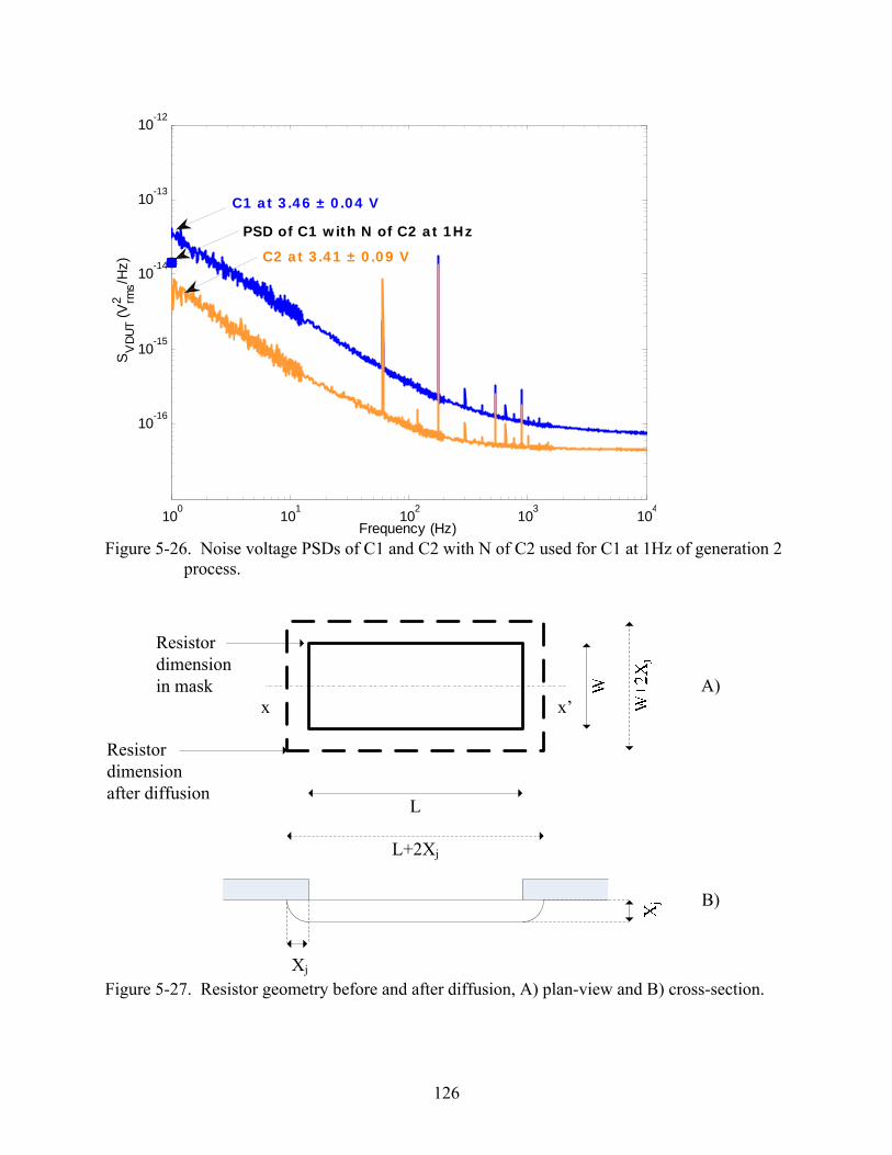
100 101 102 103 104
10-16
10-15
10-14
10-13
10-12
Frequency (Hz)
SV
DUT (V
rms
2/H
z)
C1 at 3.46 ± 0.04 V
PSD of C1 with N of C2 at 1Hz
C2 at 3.41 ± 0.09 V
Figure 5-26. Noise voltage PSDs of C1 and C2 with N of C2 used for C1 at 1Hz of generation 2
process.
L
L+2Xj
Xj
A)
B)
Resistor dimension in mask
Resistor dimension after diffusion
x x’
Figure 5-27. Resistor geometry before and after diffusion, A) plan-view and B) cross-section.
126
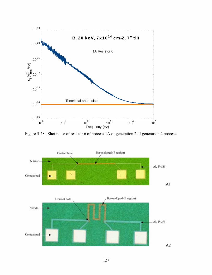
100 101 102 103 104 10510-25
10-24
10-23
10-22
10-21
10-20
10-19
Frequency (Hz)
SI (A
2 rms/H
z)
Theoritical shot noise
B, 20 keV, 7x1014 cm-2, 7o tilt
1A Resistor 6
Figure 5-28. Shot noise of resistor 6 of process 1A of generation 2 of generation 2 process.
A1
A2
127
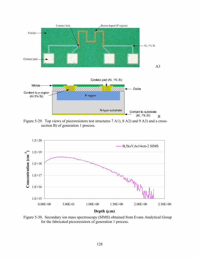
A3
B Figure 5-29. Top views of piezoresistors test structures 7 A1), 8 A2) and 9 A3) and a cross-
section B) of generation 1 process.
1.E+15
1.E+16
1.E+17
1.E+18
1.E+19
1.E+20
0.00E+00 5.00E-01 1.00E+00 1.50E+00 2.00E+00 2.50E+00
Depth (μm)
Con
cent
ratio
n (c
m-3
)
B,5keV,6e14cm-2 SIMS
Figure 5-30. Secondary ion mass spectroscopy (SIMS) obtained from Evans Analytical Group
for the fabricated piezoresistors of generation 1 process.
128
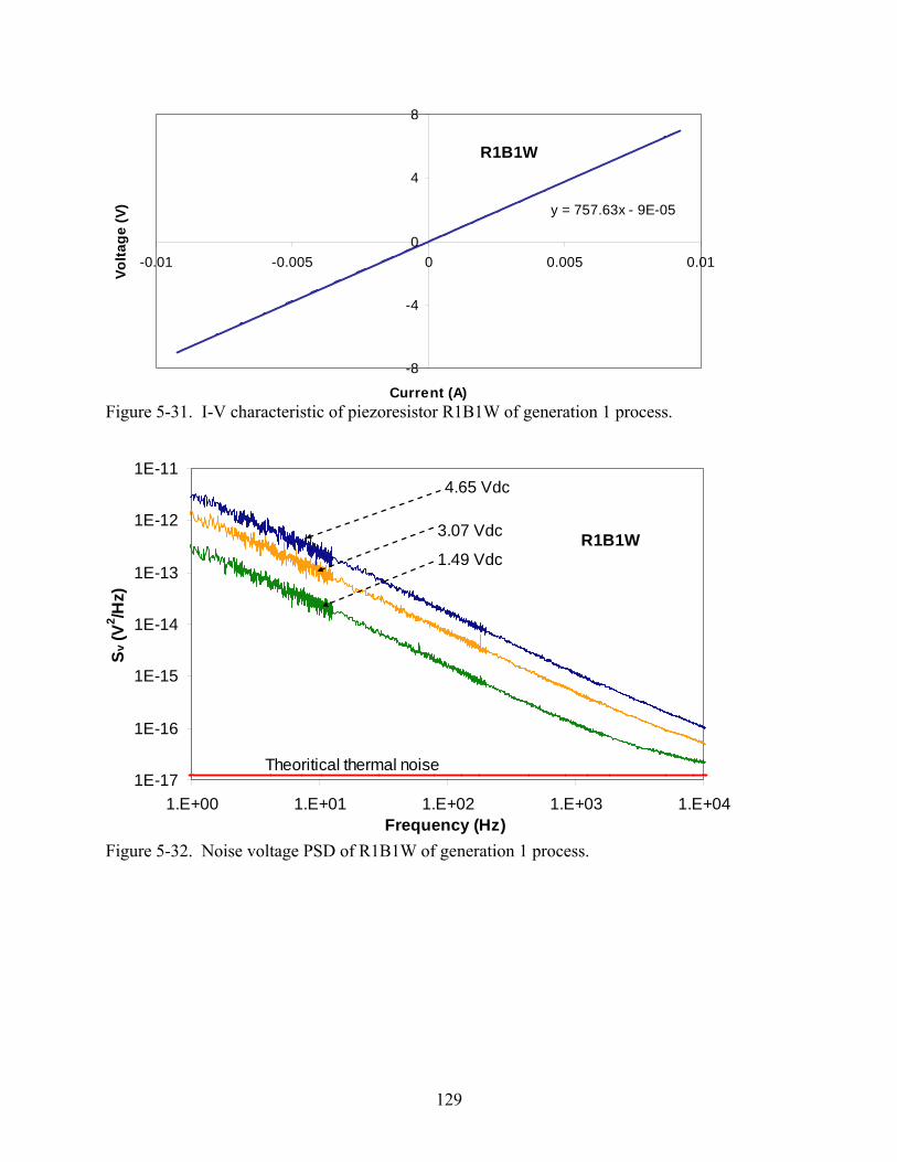
R1B1W
y = 757.63x - 9E-05
-8
-4
0
4
8
-0.01 -0.005 0 0.005 0.01
Current (A)
Volta
ge (V
)
Figure 5-31. I-V characteristic of piezoresistor R1B1W of generation 1 process.
1E-17
1E-16
1E-15
1E-14
1E-13
1E-12
1E-11
1.E+00 1.E+01 1.E+02 1.E+03 1.E+04Frequency (Hz)
Sv (V
2 /Hz)
Theoritical thermal noise
4.65 Vdc
3.07 Vdc
1.49 VdcR1B1W
Figure 5-32. Noise voltage PSD of R1B1W of generation 1 process.
129
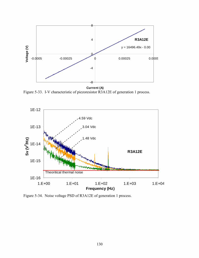
R3A12E
y = 16496.49x - 0.00
-8
-4
0
4
8
-0.0005 -0.00025 0 0.00025 0.0005
Current (A)
Volta
ge (V
)
Figure 5-33. I-V characteristic of piezoresistor R3A12E of generation 1 process.
1E-16
1E-15
1E-14
1E-13
1E-12
1.E+00 1.E+01 1.E+02 1.E+03 1.E+04Frequency (Hz)
Sv (V
2 /Hz)
Theoritical thermal noise
4.59 Vdc
3.04 Vdc
1.48 Vdc
R3A12E
Figure 5-34. Noise voltage PSD of R3A12E of generation 1 process.
130
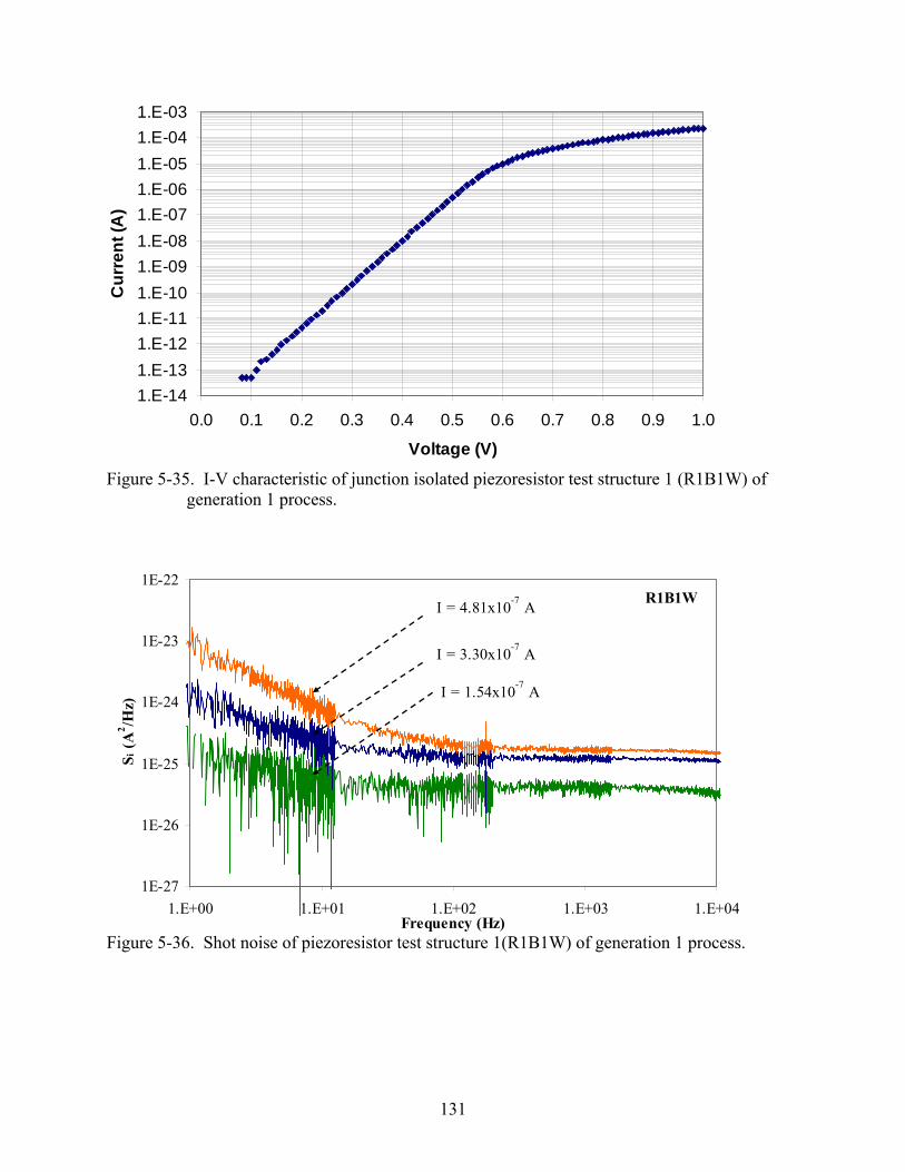
1.E-141.E-131.E-121.E-111.E-101.E-091.E-081.E-071.E-061.E-051.E-041.E-03
0.0 0.1 0.2 0.3 0.4 0.5 0.6 0.7 0.8 0.9 1.0
Voltage (V)
Cur
rent
(A)
Figure 5-35. I-V characteristic of junction isolated piezoresistor test structure 1 (R1B1W) of
generation 1 process.
1E-27
1E-26
1E-25
1E-24
1E-23
1E-22
1.E+00 1.E+01 1.E+02 1.E+03 1.E+04Frequency (Hz)
Si (A
2 /Hz)
I = 4.81x10⁻⁷ A
I = 3.30x10⁻⁷ A
I = 1.54x10⁻⁷ A
R1B1W
Figure 5-36. Shot noise of piezoresistor test structure 1(R1B1W) of generation 1 process.
131
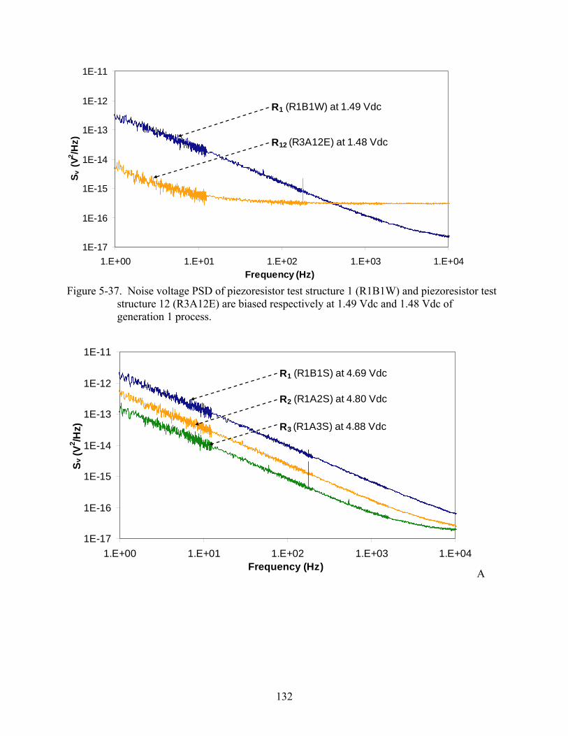
1E-17
1E-16
1E-15
1E-14
1E-13
1E-12
1E-11
1.E+00 1.E+01 1.E+02 1.E+03 1.E+04Frequency (Hz)
S v (V
2 /Hz)
R1 (R1B1W) at 1.49 Vdc
R12 (R3A12E) at 1.48 Vdc
Figure 5-37. Noise voltage PSD of piezoresistor test structure 1 (R1B1W) and piezoresistor test
structure 12 (R3A12E) are biased respectively at 1.49 Vdc and 1.48 Vdc of generation 1 process.
1E-17
1E-16
1E-15
1E-14
1E-13
1E-12
1E-11
1.E+00 1.E+01 1.E+02 1.E+03 1.E+04Frequency (Hz)
Sv (V
2 /Hz)
R1 (R1B1S) at 4.69 Vdc
R2 (R1A2S) at 4.80 Vdc
R3 (R1A3S) at 4.88 Vdc
A
132
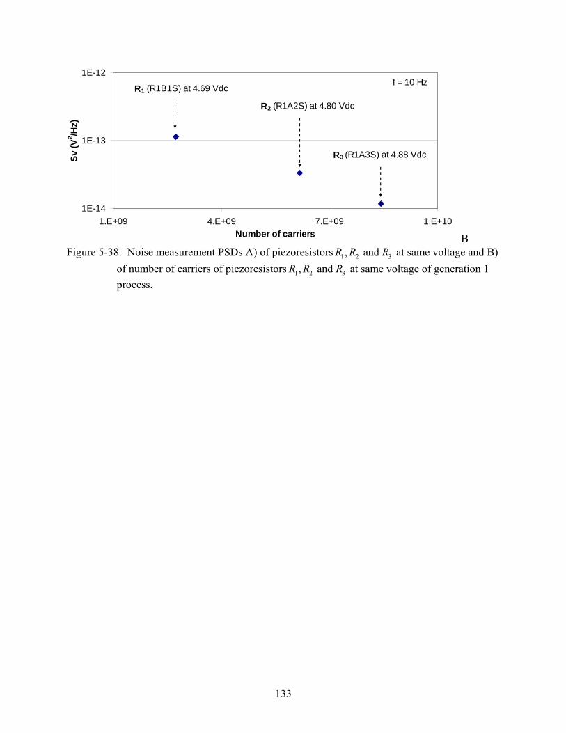
1E-14
1E-13
1E-12
1.E+09 4.E+09 7.E+09 1.E+10Number of carriers
Sv (V
2 /Hz)
f = 10 HzR1 (R1B1S) at 4.69 Vdc
R2 (R1A2S) at 4.80 Vdc
R3 (R1A3S) at 4.88 Vdc
B Figure 5-38. Noise measurement PSDs A) of piezoresistors 1 2 3, and R R R at same voltage and B)
of number of carriers of piezoresistors 1 2 3, and R R R at same voltage of generation 1 process.
133
CHAPTER 6 DEFECTS MEASUREMENTS AND ANALYSIS
In this Chapter, further studies of the process dependence of 1/f noise are performed by
using transmission electron microscopy (TEM) to visualize the bulk defects in the piezoresistors
and the high frequency C-V of pMOSC to extract the density of interface traps for each
fabrication process of generation 2.
6.2 Bulk Defects in Piezoresistors
The experimental methods to compute the bulk defects and interface trap densities were
described in Chapter 4. The bulk defects are studied with XTEM and PTEM. In Section 4.4,
XTEM and PTEM are described. The sample preparation for XTEM is done with focus ion
beam, which allows a thin section of the piezoresistor to be cut from the sample as shown in
Figure 6-1. For a PTEM sample preparation, a sample is thinned, then a hole a made in the
sample. The PTEM are taken with the same magnification for consistency.
6.2.1 Cross-Section Transmission Electron Microscopy (XTEM)
The XTEM is used to see the depth of the defects into the samples. The XTEM of
piezoresistor implanted with B, 7x1014 cm-2 at 20 keV, 40 keV and solid source diffused are
shown in Figure 6-2, Figure 6-3 and Figure 6-4. All the implanted piezoresistors show
dislocation loops while those that are solid source diffused do not show visible defects. Point
defects might still be present in the solid source diffused piezoresistors but they are not visible
with XTEM. It is assumed that all the defects consist of dislocation loops. Some loops
terminate at the surface which serves a sink for the defects as they grow in size during inert
annealing and oxidation. The locations of the defects are in the projected range, Rp, which are
0.0658 µm and 0.1283 µm for 20 keV boron implant in silicon and for 40 keV boron implant in
134
SiO2 respectively. Since we have found defects in our ion implanted samples, we compute their
defect densities using pictures taken from plan view TEM.
6.2.2 Plan View Transmission Electron Microscopy (PTEM)
To determine the defect densities, we use PTEM since it allows a top view of the defects.
We compute the overall defect densities and the surface terminated defects only for the ion
implanted test structures since the solid source diffused ones did not show any visible bulk
defects. According to Ostwald ripening process48
smaller defects shrink in favor of larger ones
during annealing. Therefore the number of defect density decreases but the dislocation loop size
increases as the anneal time increases at fix temperature. The defect density is computed by
taking ten PTEM pictures of each process, counting the defects in each process and dividing by
the area. Details of ion implantations and annealing conditions are given in Table 5-7 in Chapter
5. Figure 6-5 shows ten PTEM pictures for process 2A and Figure 6-6 and Figure 6-7 show the
PTEM of the 20 keV and 40 keV implanted test structures respectively. The defect densities are
computed from pictures such as those shown in Figure 6-6 and Figure 6-7 and plotted as function
of anneal time. Figure 6-8, Figure 6-10 and Figure 6-11 show the defects densities as a function
of anneal time for the 20 keV implanted piezoresistor, 40 keV implanted piezoresistors without
oxidation and 40 keV implanted piezoresistors with oxidation respectively. For all the processes
as the anneal time increases the defect density decreases. The surface terminated defects
increase as the anneal time increases. This is because the smaller defects disappear in favor of
the larger ones and during oxidation interstitials that are injected in the silicon participate in the
enlargement of the loops.48
Figure 6-13, Figure 6-14 and Figure 6-15 show the surface
terminated defects versus the annealing time for the 20 keV implanted piezoresistor, 40 keV
implanted piezoresistors without oxidation and 40 keV implanted piezoresistors with oxidation.
135
The visualization of the growth of the defects as the annealing time increases is done by plotting
the defects density versus the defect size. The defect size is measured from the longer axis of a
loop. Figure 6-16, Figure 6-17 and Figure 6-18 show the Ostwald ripening process. 48
As the
annealing time increases we observe that the defects are larger in size but their densities
decrease. The observed defects with TEM are not the only defects present in the bulk of the
piezoresistors. There still could be point defects not visible to TEM that can contribute to the
measured noise source. Now that the bulk defects through XTEM and PTEM have been studied,
next the defects located at the Si/SiO2 interface are investigated.
6.3 Interface Trap Density
As mentioned earlier in Chapter 4, the high frequency C-V of the pMOSC is used for the
computation of the interface trap density (DIT). Figure 6-19 shows the measured and ideal high
frequency C-V of wafer 2E.49
The parallel shift of the measured C-V curve with respect to the
ideal along the voltage axis indicates the presence of charged oxide traps known as fixed oxide
charges. The presence of interface traps are revealed by the distortion of the measured C-V
curve with respect to the ideal curve and are successfully measured using the Terman’s method.
19 The negative gate voltage shift on Figure 6-19 is due to positive oxide charge.38 The high
doping concentration of the test structures causes a high voltage for the onset of the inversion
capacitance. Going through the experiment method described in Chapter 4, Section 4.3 the oxide
thickness and carrier concentration are computed. The oxide thicknesses obtained from the C-V
at accumulation are listed in Table 5-4. The energy level versus the DIT are shown in Figure 6-
20, Figure 6-21, Figure 6-22, and Figure 6-23. Values of the order of 1x1012 cm-2 eV-1to 1x10¹³
cm-2 eV-1 extracted from our test structures indicate poor oxide quality for all the processes. The
DIT for a good quality oxide is in the order of 1x1010 cm-2 eV-1. Now that the defect densities are
136
computed, an attempt to correlate the measured 1/f noise voltage PSD to the bulk defect densities
measured with PTEM and interface trap densities obtained with Terman’s method19
is made.
6.4 Correlation of Noise Voltage PSD to Defects
Since defects are the source of low frequency noise, the 1/f noise magnitude is monitored
as a function of the bulk defect and interface trap densities. The bulk defects densities were
measured using PTEM and high frequency C-V were used for the computation of interface trap
densities.
6.4.1 Noise Voltage PSD of 20 keV Boron Implanted Piezoresistors and Defects
In the analysis, it is assumed that all the bulk defects in the piezoresistors consist of
dislocation loops and that all defects are potential traps. For annealing times of 20 min, 30 min
and to 50 min the bulk defect densities decrease as shown in Figure 6-8 from 6.82x108 cm-2 to
5.89x108 cm-2 and to 5.16x108 cm-2 respectively. The measured noise voltage PSD, Figure 5-18,
decreases as the defect density decreases with increasing annealing time. There is a correlation
between the bulk defect densities and the measured noise voltage PSDs.
The uncertainties in the defect densities overlap. A Monte Carlo simulation, with 100,000
iterations using the MATLAB function randn is used to fit a line and estimate the uncertainty in
the variables.46
Figure 6-9 shows the Monte Carlo simulation of the PTEM defect density for
process 2A, process 2E, and process 1A. Figure 6-9 is plotted in the linear scale. A linear
regression was performed on the data in Figure 6-9. The linear regression indicates a negative
slope. Table 6-1 shows the slope of the regression line and the 95 % confidence intervals for the
20 keV implant.
137
Figure 6-9 indicates a decrease of the defect density with annealing time increase although
the uncertainty is large. Further measurements over a wider annealing time is recommended as
future work to obtain more conclusive data.
Using the Terman’s method,19
the interface trap densities (DIT) are computed as shown in
Figure 6-20. The DIT of process 2E and 1A are shown in Figure 6-20. Both wafers have large
DIT. At midgap the DIT are in the order of 1x10¹³ and 1 x10¹² eV-1cm-2 respectively for process
2E and 1A. Here, the process with the lower DIT has the lower noise PSD as shown in Figure 5-
18. A correlation exits between the DIT and the 1/f noise. The non-uniform doping profiles show
surface concentrations 1.80x10¹⁹ and 1.78x1019 cm-3 of process 2E and 1A are respectively. The
peak concentration is not at the surface and piezoresistors are not field devices, therefore the
carriers will be affected by bulk defects located at the peak concentrations.
6.4.2 Noise Voltage PSD of 40 keV Boron Implanted Piezoresistors through 0.1 µm of SiO2 and Defects
The bulk defects in the piezoresistors implanted with boron, 40 keV, 7x1014 cm-2, through
0.1 µm of SiO2 are of the same type as those for the wafers implanted with boron, 20 keV, 7x10¹⁴
cm-2, 7o tilt. As the annealing increases, the defect density decreases as shown in Figure 6-10
and Figure 6-11. Monte Carlo simulations, with 100,000 iterations using the MATLAB function
randn are used to fit lines and estimate the uncertainties in the variables in Figure 6-10 and
Figure 6-11.46
The linear regressions indicate negative slopes. Table 6-1 shows the slopes of the
regression lines and the 95 % confidence intervals for the 40 keV implants.
However, the noise voltage PSD decreases as the defect density decreases for only the two
processes with only inert anneal, process 2B and process 5A, as shown in Figure 5-21 and Figure
6-10. In this case, there is a correlation between the measured defect densities and 1/f noise. For
138
the processes with oxidation, process 3E and process 4A, the noise voltage PSDs do not decrease
as the bulk defect density decreases as shown in Figure 5-22 and Figure 6-11.
To explain this trend, we measure the line length, the loop area, and the area of the faulted
loops for process 3E (10 min in N2 and 5 min dry, 5 min wet and 10 min dry oxidation at 900 C)
and process 4A (30 min in N2 and 5 min dry, 5 min wet and 10 min dry oxidation at 900 C). The
measurements are conducted on only the readily observed loops. Figure 6-12 shows PTEM of
process 3E and process 4A. The line length is the total perimeter of the loops in three PTEM
images. For the round loops, the perimeter is approximated by using Dπ for the non-surface
terminated round defects, ( ) 2Dπ for the surface terminated round defects, and for the
elongated defects. is the longest axis for a round loops, and is the length of the elongated
defects. The loop area is the total area of the loops in three PTEM images. For the round loops,
the area is approximated by using
2l
D l
( )22Dπ for the non-surface terminated round defects
and ( )22Dπ⎡⎣ 2⎤⎦ for the surface terminated round defects. The elongated defects are not
included in the loop area computation.
The faulted loop area is the total area of the loops in three PTEM images for only the
faulted non-surface terminated and surface terminated round defects. The equations used for the
faulted loop areas are identical to those of the loop areas discussed above. Table 6-2 shows the
computed line lengths, loop areas, and faulted loop areas of the B 20 keV and 40 keV with inert
anneal and oxidization. In Table 6-2, as the annealing time increases from 30 min to 50 min at
900 C, the line lengths decrease for both the B 20 keV and B 40 keV. However, the loop areas
and the faulted loop areas increase. The PTEM show that the 1/f noise PSDs track the bulk
defect densities except for process 3E and 4A. In these samples implanted with B 40 keV with
139
inert anneal and oxidation, the PSDs appear to track the faulted loop areas. Extensive
measurements over a wider range of process conditions are recommended for future work.
Terman’s method19
was used to measure the interface trap densities (DIT) in the
piezoresistors. The interface trap densities for the 40 keV implants are shown in Figure 6-21 and
Figure 6-22. The processes with only inert anneal after the implant, 2B and 5A, have DIT of the
same order as shown in Figure 6-21. In addition, their junction are about the same, Table 5-2,
therefore these two processes are equally affected by the interface traps. However, for processes
3E and 4A, with inert anneal and oxidation after the implant the interface trap densities are lower
for the process with longer annealing as shown in Figure 6-22. The 1/f noise is however larger
for the device with lower DIT and lower bulk defects. The results from processes 3E and 4A
suggest that bulk 1/f noise is the dominant source for the 1/f noise in these piezoresistors and that
the PSDs appear to track the faulted loop areas.
6.4.3 Noise Voltage PSD of Solid Source Diffused Piezoresistors and Interface Traps
The interface trap densities for the solid source diffused piezoresistors C1 and C2 are of
same magnitude as shown in Figure 6-23. However the noise voltage PSD of C2 is much less
than that of C1. This could be due to the fact the phosphorus diffused after the boron diffusion
for process C2 reduces the interaction of the holes with the interface traps. Therefore, the less
the interaction of the carriers with the interface traps the less is the 1/f noise.
6.5 Summary
XTEM, PTEM pictures and the HFCV C-V measurements were used to visualize and
compute the bulk and surface defect densities in the piezoresistors. Measurement results show
that as the annealing time increases, the bulk defect density decreases for all implanted samples.
This reduction in bulk defect densities is correlated to the decrease of the noise voltage PSDs of
the 20 keV implanted piezoresistors and of the 40 keV implanted piezoresistors with only inert
140
anneal. However, a possible link between the defects and the noise voltage PSDs for the 40 keV
implanted piezoresistors with inert anneal and oxidation is the faulted loop areas.
For the solid source diffused piezoresistors, the process with phosphorous solid source
diffusion in addition to the boron solid source diffusion has lower 1/f noise. This suggests that
the phosphorous cause a reduction of the interaction of the hole with the surface traps. The
interface traps decrease for the 20 keV implanted piezoresistors and the 40 keV implanted
piezoresistors with inert anneal and oxidation as the annealing time increases. However, the DIT
is of the same magnitude for the 40 keV implanted piezoresistors with only inert and the solid
source diffused piezoresistors. The bulk defects are the dominant noise source of the
piezoresistors. During devices operation the current flows in the bulk which has high defect
concentrations.
141
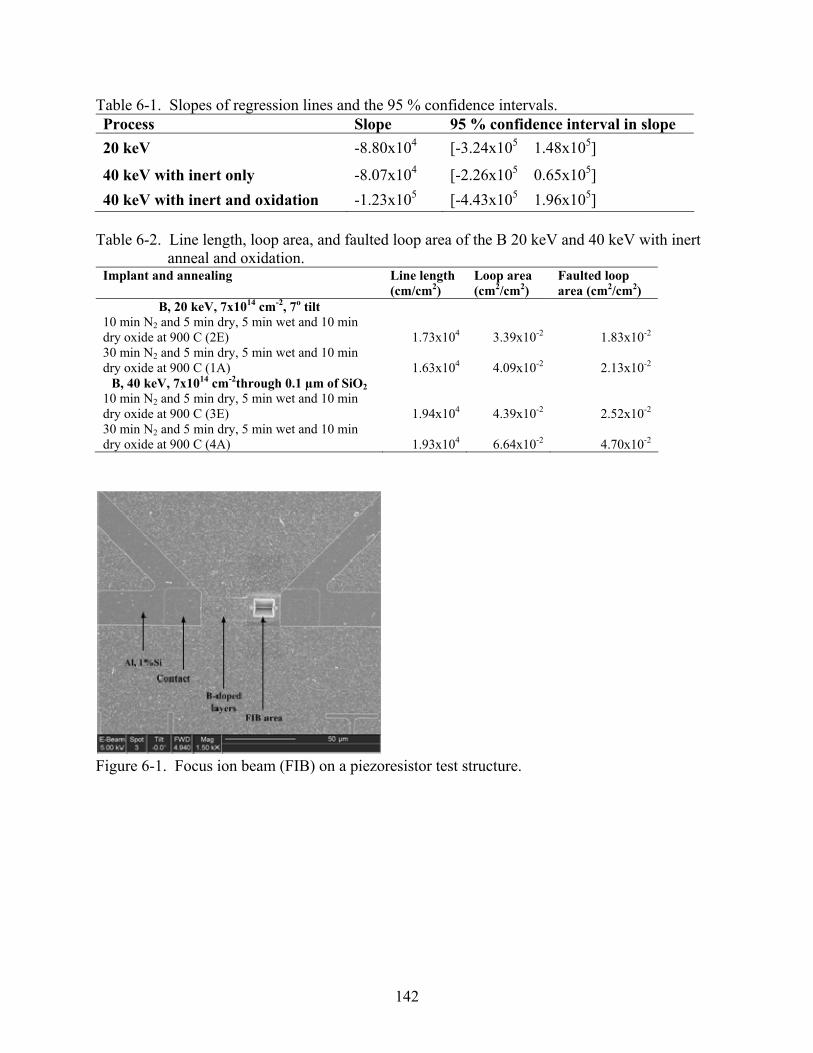
Table 6-1. Slopes of regression lines and the 95 % confidence intervals. Process Slope 95 % confidence interval in slope 20 keV -8.80x10⁴ [-3.24x10⁵ 1.48x10⁵]
40 keV with inert only -8.07x10⁴ [-2.26x10⁵ 0.65x10⁵] 40 keV with inert and oxidation -1.23x10⁵ [-4.43x10⁵ 1.96x10⁵]
Table 6-2. Line length, loop area, and faulted loop area of the B 20 keV and 40 keV with inert
anneal and oxidation. Implant and annealing Line length
(cm/cm2) Loop area (cm2/cm2)
Faulted loop area (cm2/cm2)
B, 20 keV, 7x1014 cm-2, 7o tilt 10 min N2 and 5 min dry, 5 min wet and 10 min dry oxide at 900 C (2E) 1.73x10⁴ 3.39x10⁻² 1.83x10⁻² 30 min N2 and 5 min dry, 5 min wet and 10 min dry oxide at 900 C (1A) 1.63x10⁴ 4.09x10⁻² 2.13x10⁻²
B, 40 keV, 7x1014 cm-2through 0.1 µm of SiO2 10 min N2 and 5 min dry, 5 min wet and 10 min dry oxide at 900 C (3E) 1.94x10⁴ 4.39x10⁻² 2.52x10⁻² 30 min N2 and 5 min dry, 5 min wet and 10 min dry oxide at 900 C (4A) 1.93x10⁴ 6.64x10⁻² 4.70x10⁻²
Figure 6-1. Focus ion beam (FIB) on a piezoresistor test structure.
142
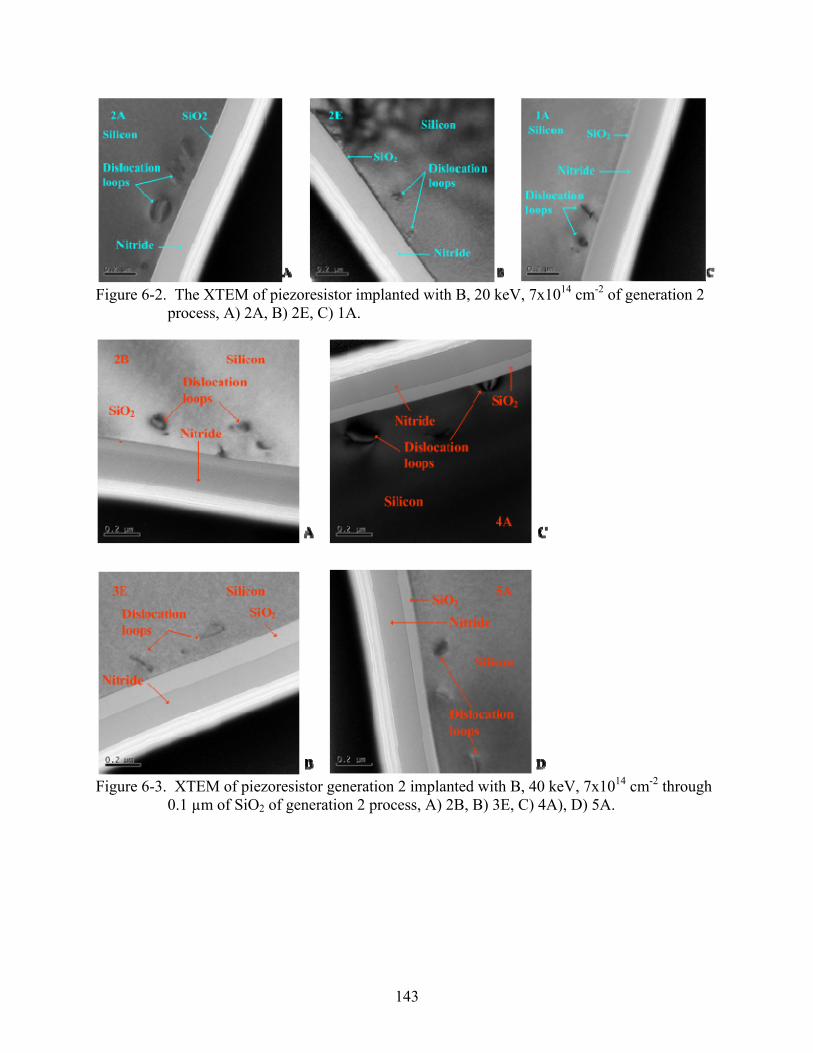
Figure 6-2. The XTEM of piezoresistor implanted with B, 20 keV, 7x1014 cm-2 of generation 2
process, A) 2A, B) 2E, C) 1A.
Figure 6-3. XTEM of piezoresistor generation 2 implanted with B, 40 keV, 7x1014 cm-2 through
0.1 µm of SiO2 of generation 2 process, A) 2B, B) 3E, C) 4A), D) 5A.
143
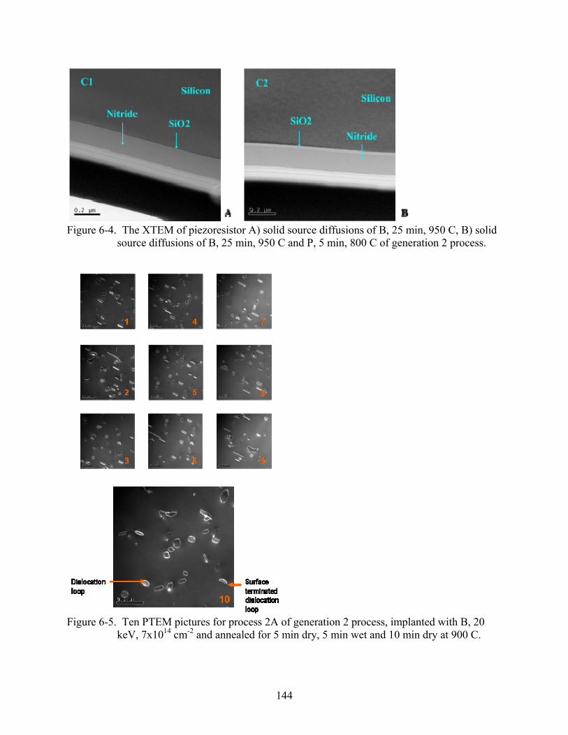
Figure 6-4. The XTEM of piezoresistor A) solid source diffusions of B, 25 min, 950 C, B) solid
source diffusions of B, 25 min, 950 C and P, 5 min, 800 C of generation 2 process.
Figure 6-5. Ten PTEM pictures for process 2A of generation 2 process, implanted with B, 20
keV, 7x1014 cm-2 and annealed for 5 min dry, 5 min wet and 10 min dry at 900 C.
144
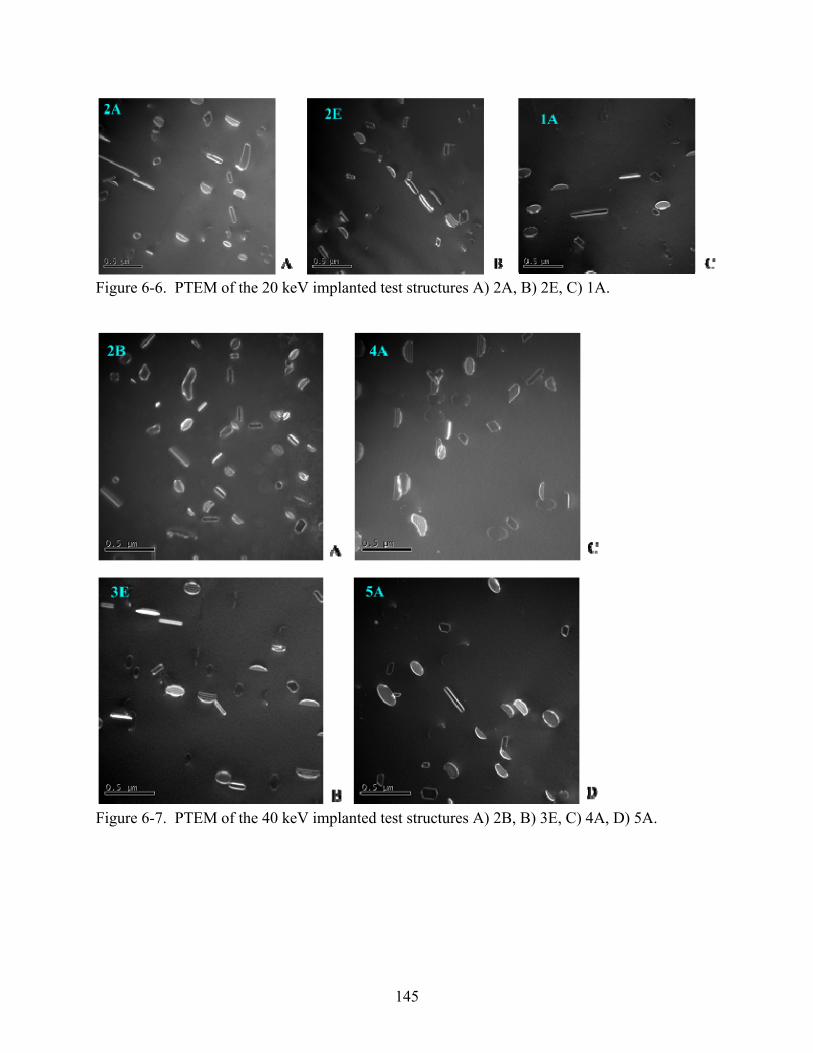
Figure 6-6. PTEM of the 20 keV implanted test structures A) 2A, B) 2E, C) 1A.
Figure 6-7. PTEM of the 40 keV implanted test structures A) 2B, B) 3E, C) 4A, D) 5A.
145
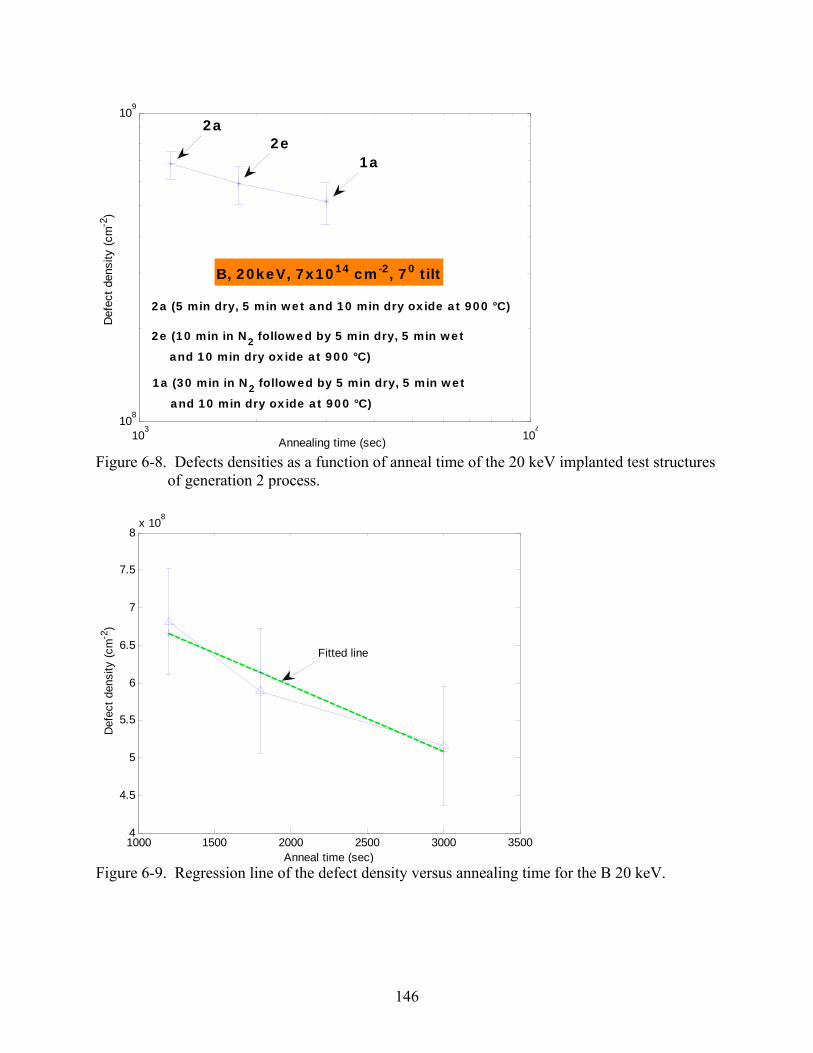
103 104108
109
Annealing time (sec)
Def
ect d
ensi
ty (c
m-2
)
B, 20keV, 7x1014 cm-2, 70 tilt
2a (5 min dry, 5 min wet and 10 min dry oxide at 900 °C)
2e (10 min in N2 followed by 5 min dry, 5 min wet
and 10 min dry oxide at 900 °C)
1a (30 min in N2 followed by 5 min dry, 5 min wet
and 10 min dry oxide at 900 °C)
2e1a
2a
Figure 6-8. Defects densities as a function of anneal time of the 20 keV implanted test structures
of generation 2 process.
1000 1500 2000 2500 3000 35004
4.5
5
5.5
6
6.5
7
7.5
8x 10⁸
Anneal time (sec)
Def
ect d
ensi
ty (c
m-2
)
Fitted line
Figure 6-9. Regression line of the defect density versus annealing time for the B 20 keV.
146
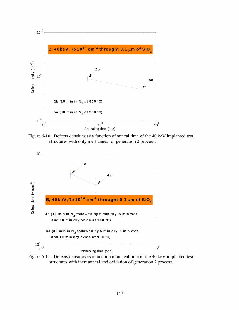
102 103 104108
109
1010
Annealing time (sec)
Def
ect d
ensi
ty (c
m-2
)
B, 40keV, 7x1014 cm-2 throught 0.1 μm of SiO2
2b (10 min in N2 at 900 °C)
5a (90 min in N2 at 900 °C)
2b
5a
Figure 6-10. Defects densities as a function of anneal time of the 40 keV implanted test
structures with only inert anneal of generation 2 process.
103 104108
109
Annealing time (sec)
Def
ect d
ensi
ty (c
m-2
)
B, 40keV, 7x1014 cm-2 throught 0.1 μm of SiO2
3e (10 min in N2 followed by 5 min dry, 5 min wet
and 10 min dry oxide at 900 °C)
4a (30 min in N2 followed by 5 min dry, 5 min wet
and 10 min dry oxide at 900 °C)
3e
4a
Figure 6-11. Defects densities as a function of anneal time of the 40 keV implanted test
structures with inert anneal and oxidation of generation 2 process.
147
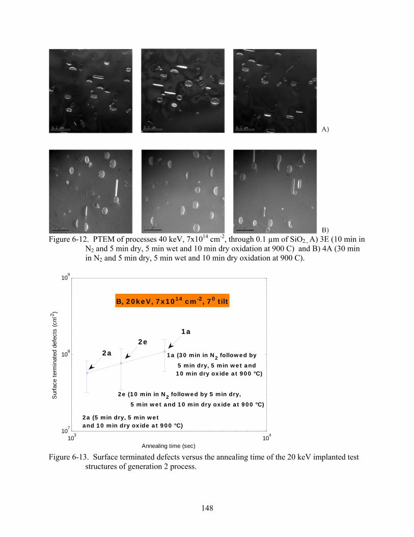
Figure 6-12. PTEM of processes 40 keV, 7x1014 cm-2, through 0.1 µm of SiO2., A) 3E (10 min in
N2 and 5 min dry, 5 min wet and 10 min dry oxidation at 900 C) and B) 4A (30 min in N2 and 5 min dry, 5 min wet and 10 min dry oxidation at 900 C).
103 104107
108
109
Annealing time (sec)
Sur
face
term
inat
ed d
efec
ts (c
m-2
)
B, 20keV, 7x1014 cm-2, 70 tilt
2a (5 min dry, 5 min wet and 10 min dry oxide at 900 °C)
2e (10 min in N2 followed by 5 min dry,
5 min wet and 10 min dry oxide at 900 °C)
1a (30 min in N2 followed by
5 min dry, 5 min wet and 10 min dry oxide at 900 °C)
2a2e
1a
Figure 6-13. Surface terminated defects versus the annealing time of the 20 keV implanted test
structures of generation 2 process.
148
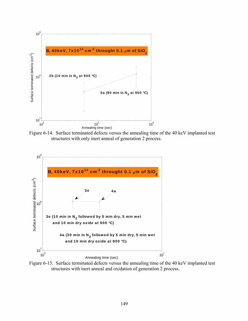
102 103 104107
108
109
Annealing time (sec)
Sur
face
term
inat
ed d
efec
ts (c
m-2
) B, 40keV, 7x1014 cm-2 throught 0.1 μm of SiO2
2b (10 min in N2 at 900 °C)
5a (90 min in N2 at 900 °C)
Figure 6-14. Surface terminated defects versus the annealing time of the 40 keV implanted test
structures with only inert anneal of generation 2 process.
103
104
107
108
109
Annealing time (sec)
Sur
face
term
inat
ed d
efec
ts (c
m-2
)
B, 40keV, 7x1014 cm-2 throught 0.1 μm of SiO2
3e (10 min in N2 followed by 5 min dry, 5 min wet
and 10 min dry oxide at 900 °C)
4a (30 min in N2 followed by 5 min dry, 5 min wet
and 10 min dry oxide at 900 °C)
3e 4a
Figure 6-15. Surface terminated defects versus the annealing time of the 40 keV implanted test
structures with inert anneal and oxidation of generation 2 process.
149
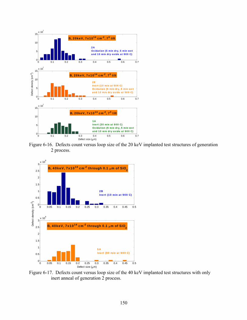
0 0.1 0.2 0.3 0.4 0.5 0.6 0.70
5
10
15x 10
7
B, 20keV, 7x1014 cm-2, 70 tilt
2A Oxidation (5 min dry, 5 min wet and 10 min dry oxide at 900 C)
0 0.1 0.2 0.3 0.4 0.5 0.6 0.70
5
10
15x 107
Def
ect d
ensi
ty (c
m-2
)
B, 20keV, 7x1014 cm-2, 70 tilt
2E Inert (10 min at 900 C) Oxidation (5 min dry, 5 min wet and 10 min dry oxide at 900 C)
0 0.1 0.2 0.3 0.4 0.5 0.6
15x 10
7
0.70
5
B, 20keV, 7x1014 cm-2, 70 tilt10
1A Inert (30 min at 900 C) Oxidation (5 min dry, 5 min wet and 10 min dry oxide at 900 C)
Defect size (μm)
Figure 6-16. Defects count versus loop size of the 20 keV implanted test structures of generation 2 process.
0 0.05 0.1 0.15 0.2 0.25 0.3 0.35 0.4 0.45 0.50
0.5
1
1.5
2
2.5
3x 10
8
B, 40keV, 7x1014 cm-2 through 0.1 μm of SiO2
2B Inert (10 min at 900 C)
0 0.05 0.1 0.15 0.2 0.25 0.3 0.35 0.4 0.45 0.50
0.5
1
1.5
2
2.5
3x 10
8
Defect size (μm)
Def
ect d
ensi
ty (c
m-2
)
B, 40keV, 7x1014 cm-2 through 0.1 μm of SiO2
5A Inert (90 min at 900 C)
Figure 6-17. Defects count versus loop size of the 40 keV implanted test structures with only
inert anneal of generation 2 process.
150
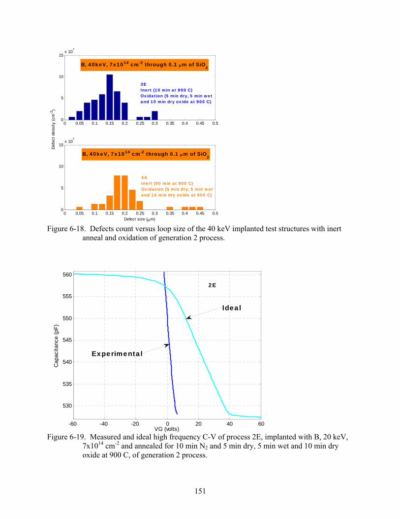
0 0.05 0.1 0.15 0.2 0.25 0.3 0.35 0.4 0.45 0.50
5
10
15x 107
B, 40keV, 7x1014 cm-2 through 0.1 μm of SiO2
3E Inert (10 min at 900 C) Oxidation (5 min dry, 5 min wet and 10 min dry oxide at 900 C)
0 0.05 0.1 0.15 0.2 0.25 0.3 0.35 0.4 0.45 0.50
5
10
15x 10
7
Defect size (μm)
Def
ect d
ensi
ty (c
m-2
)
B, 40keV, 7x1014 cm-2 through 0.1 μm of SiO2
4A Inert (90 min at 900 C) Oxidation (5 min dry, 5 min wet and 10 min dry oxide at 900 C)
Figure 6-18. Defects count versus loop size of the 40 keV implanted test structures with inert
anneal and oxidation of generation 2 process.
-60 -40 -20 0 20 40 60
530
535
540
545
550
555
560
VG (volts)
Cap
acita
nce
(pF)
Ideal
Experimental
2E
Figure 6-19. Measured and ideal high frequency C-V of process 2E, implanted with B, 20 keV,
7x1014 cm-2 and annealed for 10 min N2 and 5 min dry, 5 min wet and 10 min dry oxide at 900 C, of generation 2 process.
151
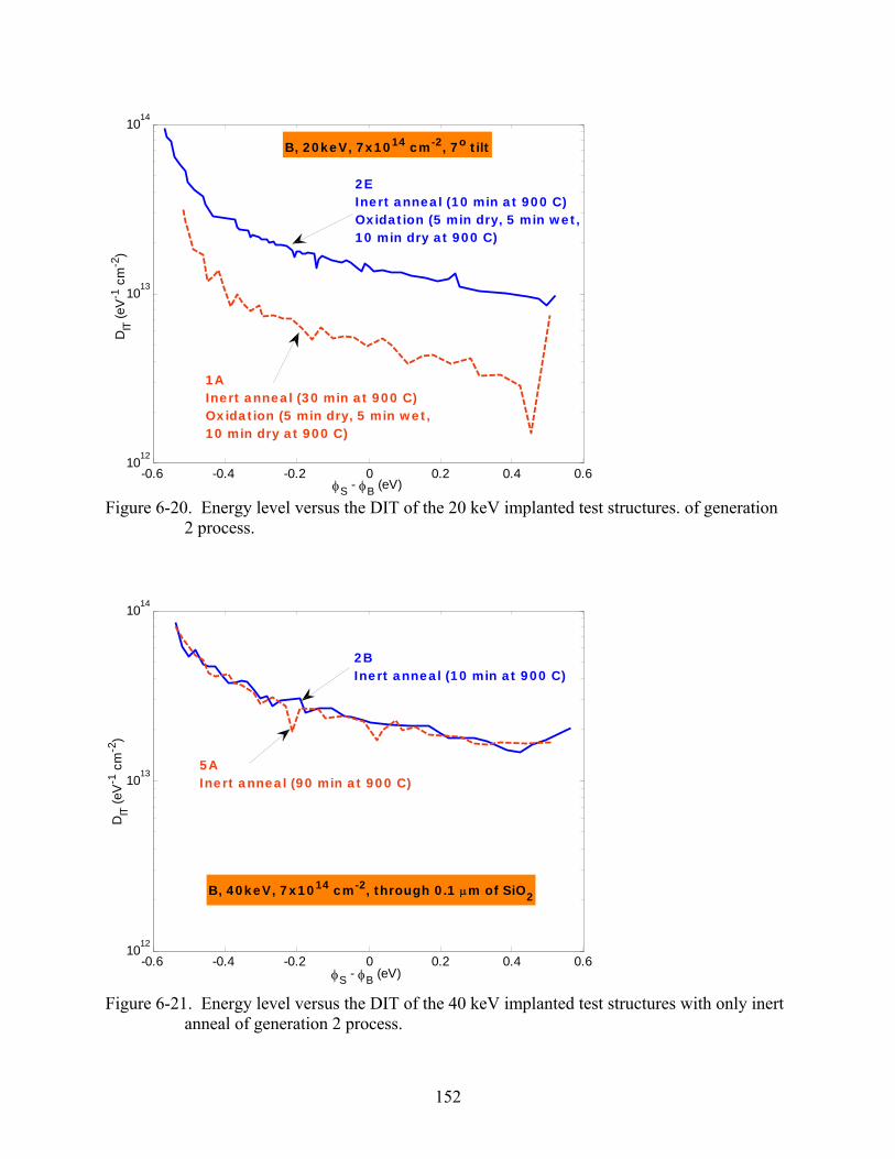
-0.6 -0.4 -0.2 0 0.2 0.4 0.610
12
1013
1014
φS - φB (eV)
DIT
(eV
-1 c
m-2
)
B, 20keV, 7x1014 cm-2, 7o tilt
2E Inert anneal (10 min at 900 C) Oxidation (5 min dry, 5 min wet, 10 min dry at 900 C)
1A Inert anneal (30 min at 900 C) Oxidation (5 min dry, 5 min wet, 10 min dry at 900 C)
Figure 6-20. Energy level versus the DIT of the 20 keV implanted test structures. of generation
2 process.
-0.6 -0.4 -0.2 0 0.2 0.4 0.61012
1013
1014
φS - φB (eV)
DIT
(eV
-1 c
m-2
)
B, 40keV, 7x1014 cm-2, through 0.1 μm of SiO2
2BInert anneal (10 min at 900 C)
5A Inert anneal (90 min at 900 C)
Figure 6-21. Energy level versus the DIT of the 40 keV implanted test structures with only inert
anneal of generation 2 process.
152
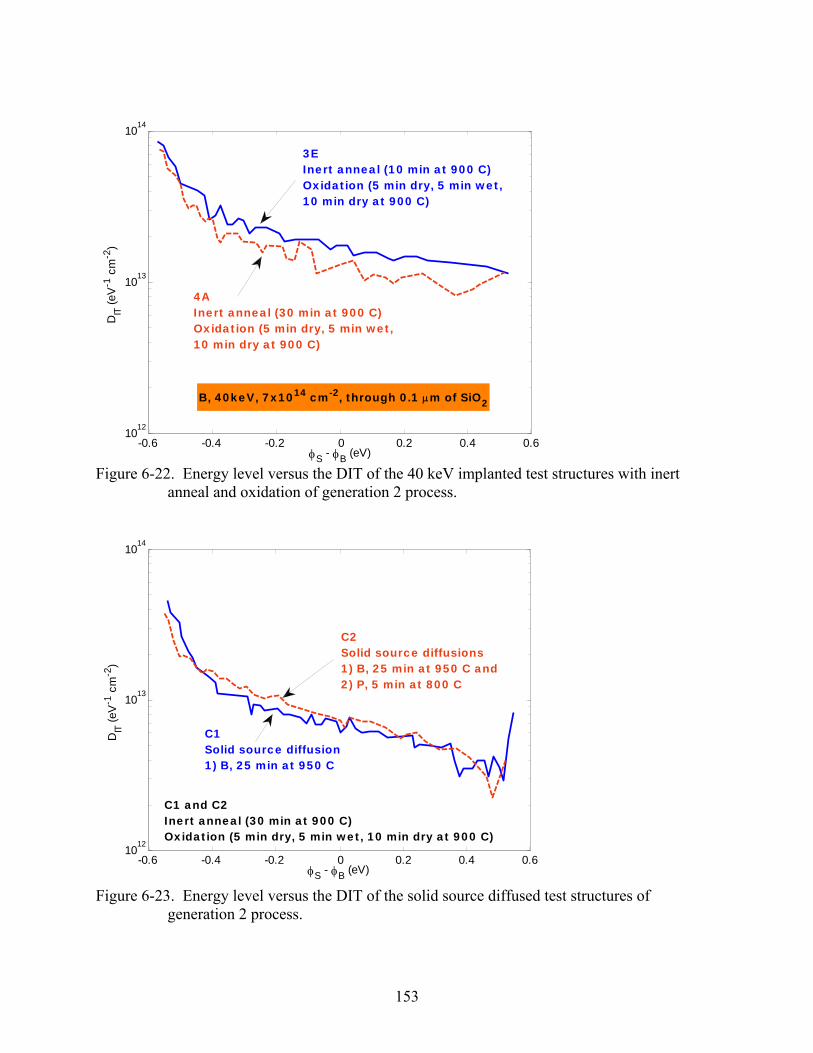
-0.6 -0.4 -0.2 0 0.2 0.4 0.61012
1013
1014
φS - φB (eV)
DIT
(eV
-1 c
m-2
)
B, 40keV, 7x1014 cm-2, through 0.1 μm of SiO2
3E Inert anneal (10 min at 900 C) Oxidation (5 min dry, 5 min wet, 10 min dry at 900 C)
4A Inert anneal (30 min at 900 C) Oxidation (5 min dry, 5 min wet, 10 min dry at 900 C)
Figure 6-22. Energy level versus the DIT of the 40 keV implanted test structures with inert
anneal and oxidation of generation 2 process.
-0.6 -0.4 -0.2 0 0.2 0.4 0.610
12
1013
1014
φS - φB (eV)
DIT
(eV
-1 c
m-2
)
C1 Solid source diffusion 1) B, 25 min at 950 C
C2 Solid source diffusions 1) B, 25 min at 950 C and 2) P, 5 min at 800 C
C1 and C2 Inert anneal (30 min at 900 C)Oxidation (5 min dry, 5 min wet, 10 min dry at 900 C)
Figure 6-23. Energy level versus the DIT of the solid source diffused test structures of
generation 2 process.
153
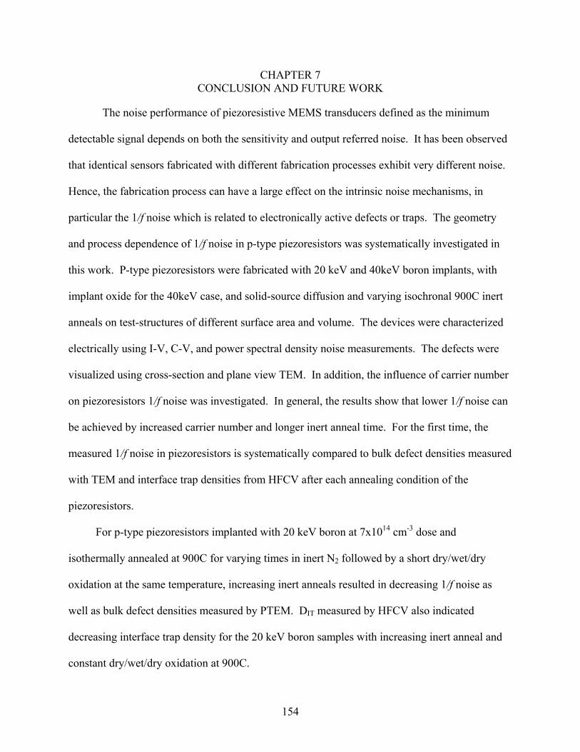
CHAPTER 7 CONCLUSION AND FUTURE WORK
The noise performance of piezoresistive MEMS transducers defined as the minimum
detectable signal depends on both the sensitivity and output referred noise. It has been observed
that identical sensors fabricated with different fabrication processes exhibit very different noise.
Hence, the fabrication process can have a large effect on the intrinsic noise mechanisms, in
particular the 1/f noise which is related to electronically active defects or traps. The geometry
and process dependence of 1/f noise in p-type piezoresistors was systematically investigated in
this work. P-type piezoresistors were fabricated with 20 keV and 40keV boron implants, with
implant oxide for the 40keV case, and solid-source diffusion and varying isochronal 900C inert
anneals on test-structures of different surface area and volume. The devices were characterized
electrically using I-V, C-V, and power spectral density noise measurements. The defects were
visualized using cross-section and plane view TEM. In addition, the influence of carrier number
on piezoresistors 1/f noise was investigated. In general, the results show that lower 1/f noise can
be achieved by increased carrier number and longer inert anneal time. For the first time, the
measured 1/f noise in piezoresistors is systematically compared to bulk defect densities measured
with TEM and interface trap densities from HFCV after each annealing condition of the
piezoresistors.
For p-type piezoresistors implanted with 20 keV boron at 7x1014 cm-3 dose and
isothermally annealed at 900C for varying times in inert N2 followed by a short dry/wet/dry
oxidation at the same temperature, increasing inert anneals resulted in decreasing 1/f noise as
well as bulk defect densities measured by PTEM. DIT measured by HFCV also indicated
decreasing interface trap density for the 20 keV boron samples with increasing inert anneal and
constant dry/wet/dry oxidation at 900C.
154
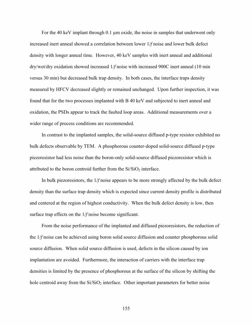
For the 40 keV implant through 0.1 µm oxide, the noise in samples that underwent only
increased inert anneal showed a correlation between lower 1/f noise and lower bulk defect
density with longer anneal time. However, 40 keV samples with inert anneal and additional
dry/wet/dry oxidation showed increased 1/f noise with increased 900C inert anneal (10 min
versus 30 min) but decreased bulk trap density. In both cases, the interface traps density
measured by HFCV decreased slightly or remained unchanged. Upon further inspection, it was
found that for the two processes implanted with B 40 keV and subjected to inert anneal and
oxidation, the PSDs appear to track the faulted loop areas. Additional measurements over a
wider range of process conditions are recommended.
In contrast to the implanted samples, the solid-source diffused p-type resistor exhibited no
bulk defects observable by TEM. A phosphorous counter-doped solid-source diffused p-type
piezoresistor had less noise than the boron-only solid-source diffused piezoresistor which is
attributed to the boron centroid further from the Si/SiO2 interface.
In bulk piezoresistors, the 1/f noise appears to be more strongly affected by the bulk defect
density than the surface trap density which is expected since current density profile is distributed
and centered at the region of highest conductivity. When the bulk defect density is low, then
surface trap effects on the 1/f noise become significant.
From the noise performance of the implanted and diffused piezoresistors, the reduction of
the 1/f noise can be achieved using boron solid source diffusion and counter phosphorous solid
source diffusion. When solid source diffusion is used, defects in the silicon caused by ion
implantation are avoided. Furthermore, the interaction of carriers with the interface trap
densities is limited by the presence of phosphorous at the surface of the silicon by shifting the
hole centroid away from the Si/SiO2 interface. Other important parameters for better noise
155

performance are good oxide quality and large carrier number. The less the interface traps the
less the trapping and detrapping of carriers at the interface. The larger the number of carriers, the
lower the 1/f noise as illustrated by the Hooge formulation of the low frequency noise which
shows an inverse proportionality between the low frequency noise and the number of carriers.
The distribution of the trap energy levels and their capture cross sections and the defect
concentrations in the piezoresistors using deep level transient spectroscopy and isothermal
transient capacitance ΔC(t,T) 50, 51, 52 are worth investigating. In addition to boron implant, the
correlation of 1/f noise to defects can be studied in preamorphized and low energy ion implanted
piezoresistors with BF2 followed by rapid thermal annealing. This study would help analyze and
correlate the 1/f noise to defects in piezoresistors with shallower junctions and higher electrical
active carrier concentrations.
156
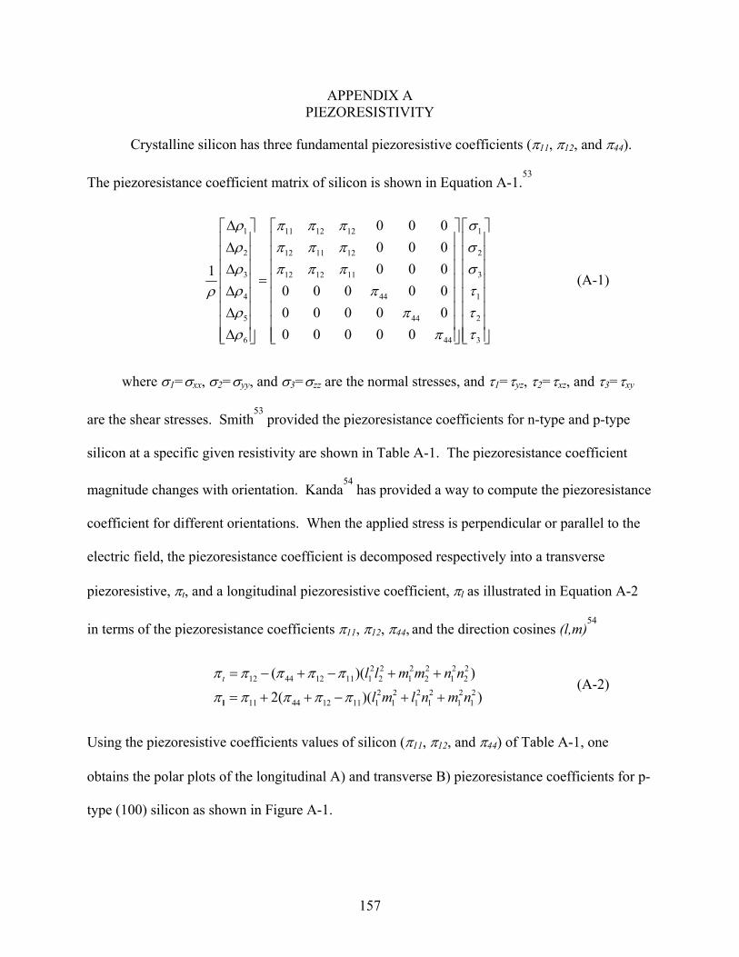
APPENDIX A PIEZORESISTIVITY
Crystalline silicon has three fundamental piezoresistive coefficients (π11, π12, and π44).
The piezoresistance coefficient matrix of silicon is shown in Equation A-1.53
1 111 12 12
2 212 11 12
3 312 12 11
4 144
5 244
6 344
0 0 00 0 00 0 01
0 0 0 0 00 0 0 0 00 0 0 0 0
ρ σπ π πρ σπ π πρ σπ π πρ τπρρ τπρ τπ
Δ⎡ ⎤ ⎡⎡ ⎤⎢ ⎥ ⎢⎢ ⎥Δ⎢ ⎥ ⎢⎢ ⎥⎢ ⎥ ⎢⎢ ⎥Δ
=⎢ ⎥ ⎢⎢Δ⎢ ⎥ ⎢⎢ ⎥⎢ ⎥ ⎢⎢ ⎥Δ⎢ ⎥ ⎢⎢ ⎥Δ ⎢ ⎥⎢ ⎥ ⎢⎣ ⎦⎣ ⎦ ⎣
⎤⎥⎥⎥⎥⎥⎥⎥⎥⎥⎦
)
(A-1)
where σ1=σxx, σ2=σyy, and σ3=σzz are the normal stresses, and τ1=τyz, τ2=τxz, and τ3=τxy
are the shear stresses. Smith53
provided the piezoresistance coefficients for n-type and p-type
silicon at a specific given resistivity are shown in Table A-1. The piezoresistance coefficient
magnitude changes with orientation. Kanda54
has provided a way to compute the piezoresistance
coefficient for different orientations. When the applied stress is perpendicular or parallel to the
electric field, the piezoresistance coefficient is decomposed respectively into a transverse
piezoresistive, πt, and a longitudinal piezoresistive coefficient, πl as illustrated in Equation A-2
in terms of the piezoresistance coefficients π11, π12, π44, and the direction cosines (l,m)54
(A-2) 2 2 2 2 2 2
12 44 12 11 1 2 1 2 1 22 2 2 2 2 2
11 44 12 11 1 1 1 1 1 1
( )(
2( )( )l
t l l m m n n
l m l n m n
π π π π π
π π π π π
= − + − + +
= + + − + +
Using the piezoresistive coefficients values of silicon (π11, π12, and π44) of Table A-1, one
obtains the polar plots of the longitudinal A) and transverse B) piezoresistance coefficients for p-
type (100) silicon as shown in Figure A-1.
157
In Figure A-1, the piezoresistance coefficients are larger in the <110> direction. In addition, we
notice that the transverse piezoresistance coefficients are approximately equal but have opposite
sign compared to the longitudinal piezoresistance coefficient. To take advantage of the equality
in magnitude and difference in sign, in the design of piezoresistive microphone, researchers such
as Saini55
orient the piezoresistors in such directions in a Wheatstone bridge configuration.
Table A-2 provides the transverse and longitudinal piezoresistance coefficients of silicon along
the <110> direction on a (100) wafer for room temperature and lowly doped silicon. In Table A-
2 above, for <110> p-type silicon, the πl is has opposite sign but has almost the same magnitude
as πt. However, his is not the case for the n-type silicon where πl and πt have not only the same
sign but also they differ in magnitudes. The piezoresistance coefficients are inversely
proportional to the doping concentration. Equation A-1 shows that as the doping concentration
increases, the resistivity decreases, thus a decrease in the resistance. The dependence of the
piezoresistive coefficients on doping concentration and temperature using Fermi-Dirac statistics
have been studied by Kanda.54
However, at high doping concentration, Kanda’s theoretical
prediction of the piezoresistance coefficients is different from more recent studies by Harley and
Kenny.12
By fitting data from Manson et al.,56
Tufte and Stetzer,57
and Kerr and Milnes,58
Harley and Kenny12
show that at high doping concentration one can approximate the decrease of
the piezoresistance coefficient by a straight line.
158
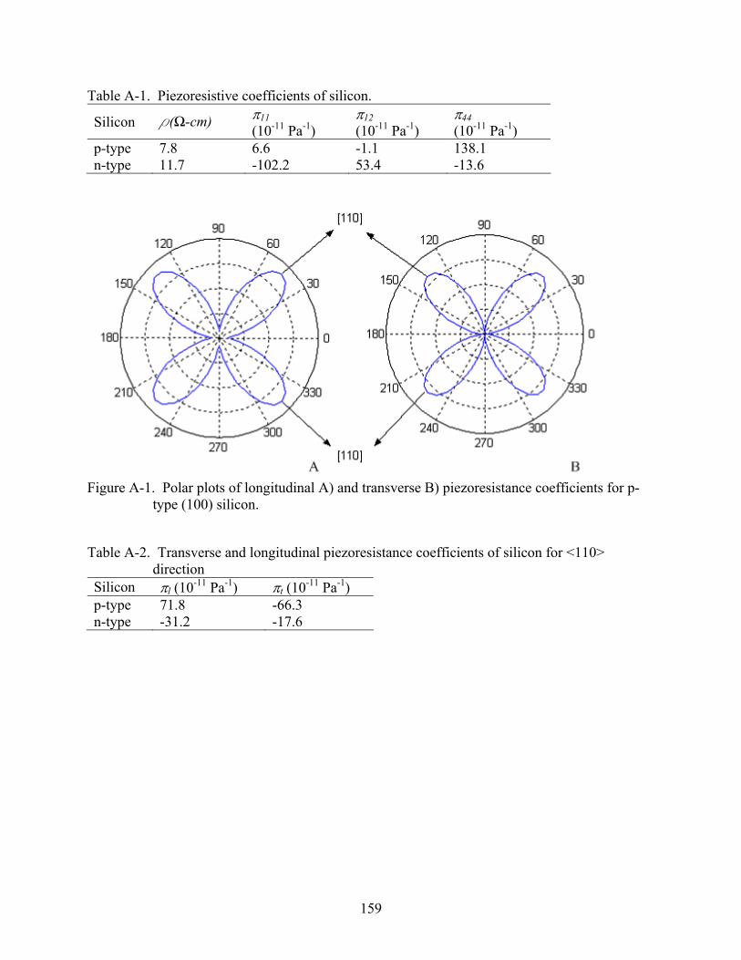
Table A-1. Piezoresistive coefficients of silicon.
Silicon ρ(Ω-cm) π11 (10-11 Pa-1)
π12 (10-11 Pa-1)
π44 (10-11 Pa-1)
p-type 7.8 6.6 -1.1 138.1 n-type 11.7 -102.2 53.4 -13.6
Figure A-1. Polar plots of longitudinal A) and transverse B) piezoresistance coefficients for p-
type (100) silicon.
Table A-2. Transverse and longitudinal piezoresistance coefficients of silicon for <110>
direction Silicon πl (10-11 Pa-1) πt (10-11 Pa-1) p-type 71.8 -66.3 n-type -31.2 -17.6
159

APPENDIX B MEMS PIEZORESISTIVE MICROPHONE VOLTAGE OUTPUT
When pressure or force is applied to the microphone’s membrane, it induces stress
resulting in strain on the membrane. The stress and strain have an impact on the piezoresistors
located at the edge of the membrane where the stress is maximum. Strain is the change per unit
length of the piezoresistors and is expressed as shown in Equation B-1.
LL
ε Δ= (B-1)
where ΔL is the change in the original length and L is the original length of the resistor. The
expression of the strain sensitivity, also known as gauge factor G0, is shown in Equation B-2.
( )00
R RG
εΔ
= (B-2)
where ΔR is the chance of resistance R and ε is the strain.
The resistance of a semiconductor resistor is given in Equation B-3.
lRwt
ρ= (B-3)
where ρ is the resistivity, and l , w and t are respectively the length, width and thickness of the
resistor. The expression RRΔ is obtained by differentiating Equation B-3 and dividing the
resulting expression by the resistance R as illustrated in Equation B-4.
R l w t
R l w tρρ
Δ Δ Δ Δ Δ= + − − (B-4)
Using the Poisson’s ratio, the strain sensitivity G becomes
160
( )1 2R
RGρρυ
ε ε
ΔΔ= = + + (B-5)
In Equation B-5, ( )1 2υ+ is due to the geometry change and ρρΔ is due to the piezoresistive
effect. For metal, the piezoresistive effect is negligible and therefore the gauge factor can be
expressed in term of its geometrical change only as shown in Equation B-6.
(1 2R
RG )υε
Δ= = + (B-6)
Since υ is less than 0.5, G for metal is about two. For semiconductor, the gauge factor, G, is
dominated by the piezoresistive effect ρρΔ and can have a magnitude in the range of 100. The
expression of sensor output voltage outVΔ given in Equation B-7 describes a linear relation
between the input pressure on the membrane of the microphone and the output voltage of the
Wheatstone bridge configuration.
0out biasV G VεΔ = (B-7)
Using Equation B-6, we express the bridge output voltage ΔVout in terms of the change in
resistance RΔ , the resistance R and the bias voltage Vbias.
out biasRV V
RΔ
Δ = (B-8)
Hence with application of an external bias the piezoresistive microphone provides a linear
output voltage related with resistance change. If a mechanical transfer function relating RΔ to
pressure is linear, then a linear acoustic transducer is achieved.
161
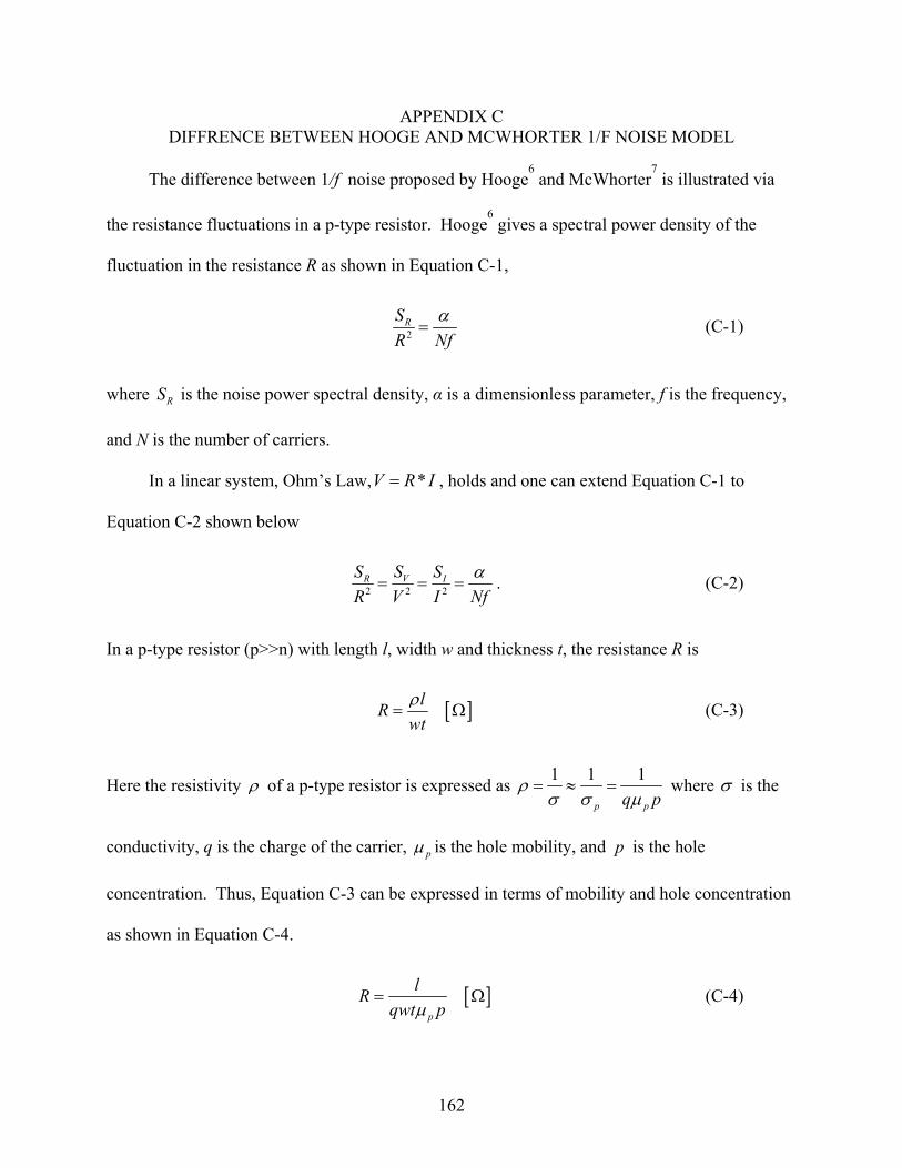
APPENDIX C DIFFRENCE BETWEEN HOOGE AND MCWHORTER 1/F NOISE MODEL
The difference between 1/f noise proposed by Hooge6 and McWhorter
7 is illustrated via
the resistance fluctuations in a p-type resistor. Hooge6 gives a spectral power density of the
fluctuation in the resistance R as shown in Equation C-1,
2RS
R Nfα
= (C-1)
where is the noise power spectral density, α is a dimensionless parameter, f is the frequency,
and N is the number of carriers.
RS
In a linear system, Ohm’s Law, *V R I= , holds and one can extend Equation C-1 to
Equation C-2 shown below
2 2 2VR ISS S
R V I Nfα
= = = . (C-2)
In a p-type resistor (p>>n) with length l, width w and thickness t, the resistance R is
[ ] lRwtρ
= Ω (C-3)
Here the resistivity ρ of a p-type resistor is expressed as 1 1 1
p pq pρ
σ σ μ= ≈ = where σ is the
conductivity, q is the charge of the carrier, pμ is the hole mobility, and is the hole
concentration. Thus, Equation C-3 can be expressed in terms of mobility and hole concentration
as shown in Equation C-4.
p
[ ] p
lRqwt pμ
= Ω (C-4)
162
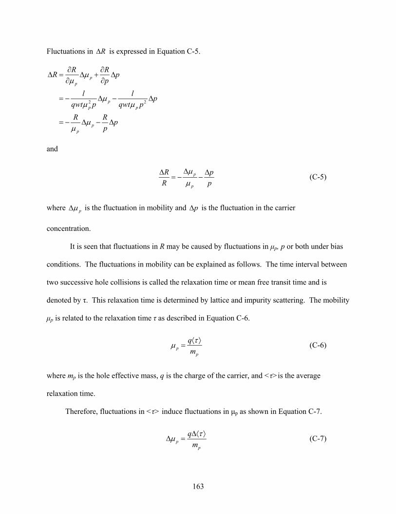
Fluctuations in RΔ is expressed in Equation C-5.
2 2
pp
pp p
pp
R RR pp
l l pqwt p qwt p
R R pp
μμ
μμ μ
μμ
∂ ∂Δ = Δ + Δ
∂ ∂
= − Δ − Δ
= − Δ − Δ
and
p
p
R pR p
μμΔΔ Δ
= − − (C-5)
where pμΔ is the fluctuation in mobility and pΔ is the fluctuation in the carrier
concentration.
It is seen that fluctuations in R may be caused by fluctuations in μp, p or both under bias
conditions. The fluctuations in mobility can be explained as follows. The time interval between
two successive hole collisions is called the relaxation time or mean free transit time and is
denoted by τ. This relaxation time is determined by lattice and impurity scattering. The mobility
μp is related to the relaxation time τ as described in Equation C-6.
pp
qmτμ ⟨ ⟩
= (C-6)
where mp is the hole effective mass, q is the charge of the carrier, and <τ>is the average
relaxation time.
Therefore, fluctuations in <τ> induce fluctuations in μp as shown in Equation C-7.
pp
qmτμ Δ⟨ ⟩
Δ = (C-7)
163
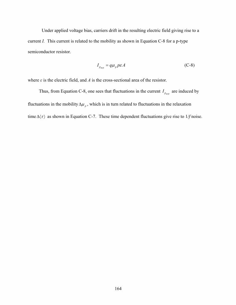
Under applied voltage bias, carriers drift in the resulting electric field giving rise to a
current I. This current is related to the mobility as shown in Equation C-8 for a p-type
semiconductor resistor.
driftp pI q p Aμ ε= (C-8)
where ε is the electric field, and A is the cross-sectional area of the resistor.
Thus, from Equation C-8, one sees that fluctuations in the current driftpI are induced by
fluctuations in the mobility pμΔ , which is in turn related to fluctuations in the relaxation
time τΔ⟨ ⟩ as shown in Equation C-7. These time dependent fluctuations give rise to 1/f noise.
164
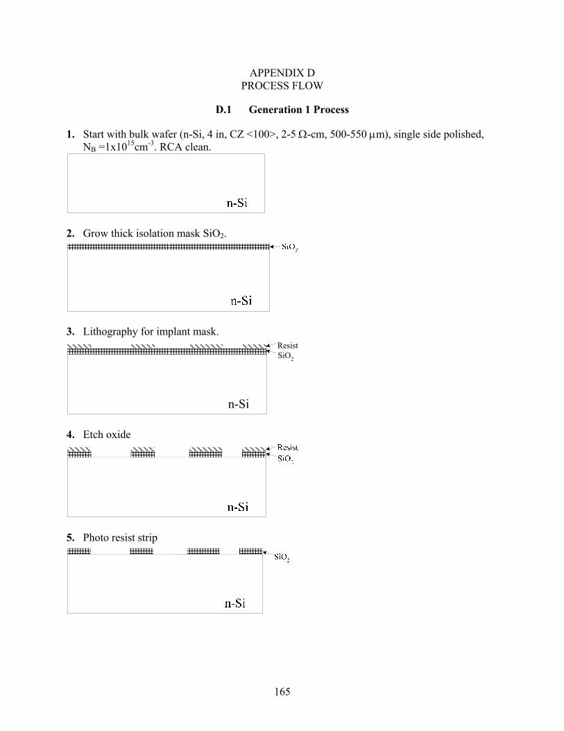
APPENDIX D PROCESS FLOW
D.1 Generation 1 Process
1. Start with bulk wafer (n-Si, 4 in, CZ <100>, 2-5 Ω-cm, 500-550 μm), single side polished, NB =1x1015cm-3. RCA clean.
2. Grow thick isolation mask SiO2.
3. Lithography for implant mask.
n-Si
SiO2
Resist
4. Etch oxide
5. Photo resist strip
165
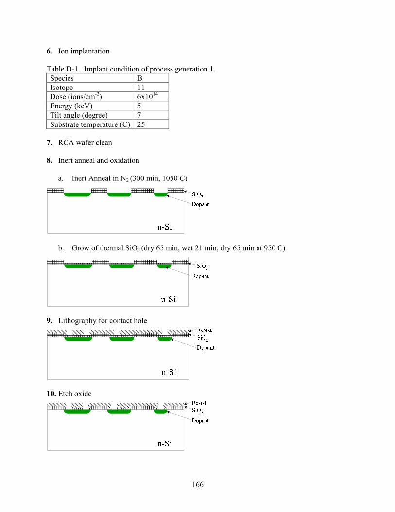
6. Ion implantation
Table D-1. Implant condition of process generation 1. Species B Isotope 11 Dose (ions/cm-2) 6x10¹⁴ Energy (keV) 5 Tilt angle (degree) 7 Substrate temperature (C) 25
7. RCA wafer clean 8. Inert anneal and oxidation
a. Inert Anneal in N2 (300 min, 1050 C)
b. Grow of thermal SiO2 (dry 65 min, wet 21 min, dry 65 min at 950 C)
9. Lithography for contact hole
10. Etch oxide
166
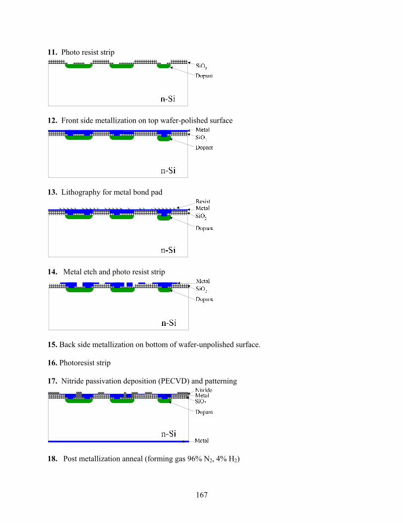
11. Photo resist strip
12. Front side metallization on top wafer-polished surface
13. Lithography for metal bond pad
14. Metal etch and photo resist strip
15. Back side metallization on bottom of wafer-unpolished surface. 16. Photoresist strip 17. Nitride passivation deposition (PECVD) and patterning
18. Post metallization anneal (forming gas 96% N2, 4% H2)
167
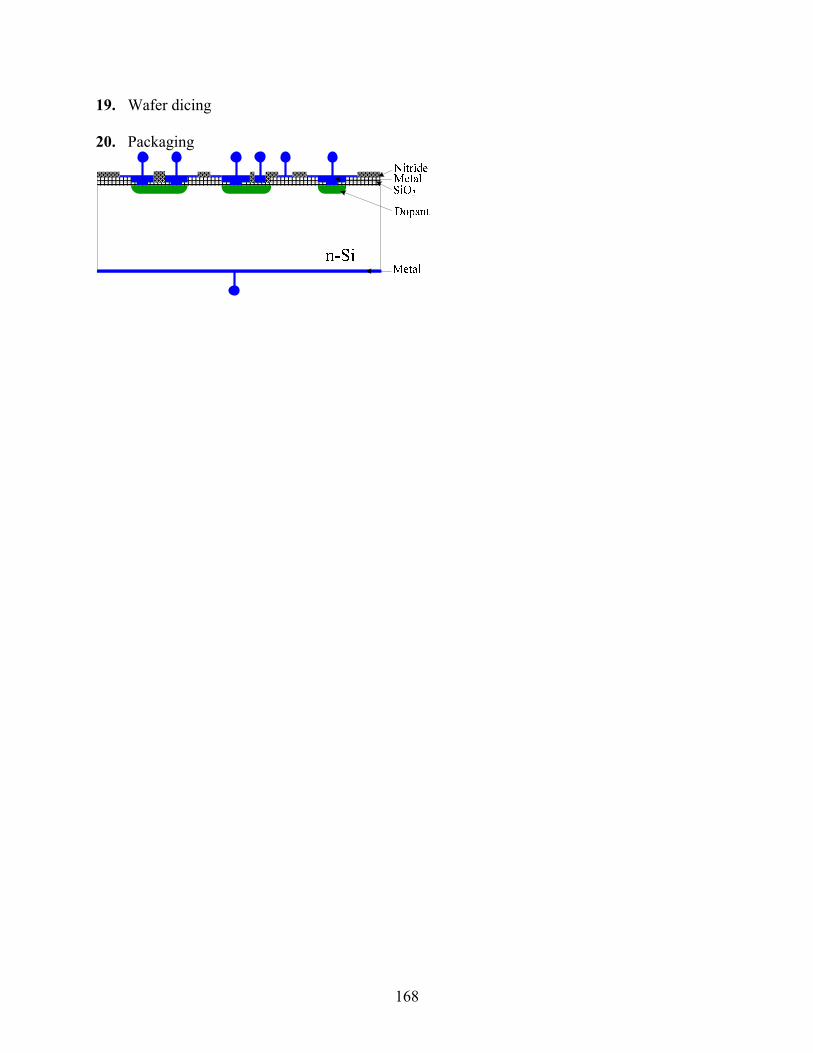
19. Wafer dicing
20. Packaging
168
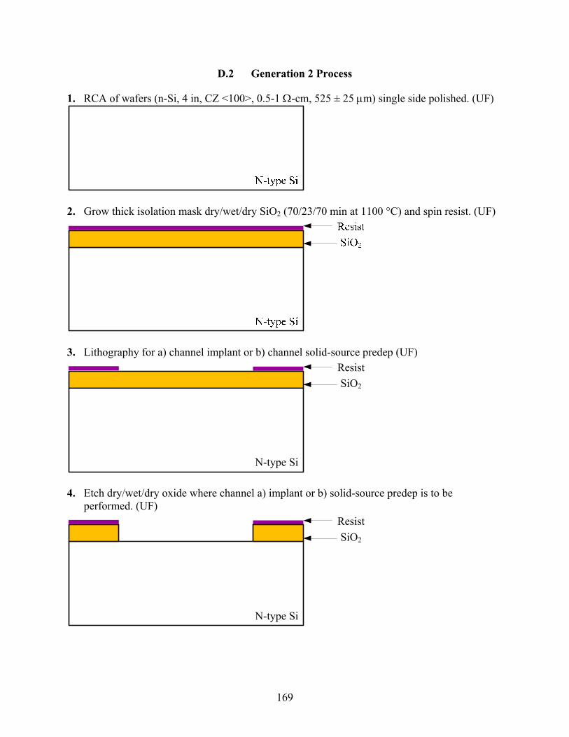
D.2 Generation 2 Process
1. RCA of wafers (n-Si, 4 in, CZ <100>, 0.5-1 Ω-cm, 525 ± 25 μm) single side polished. (UF)
2. Grow thick isolation mask dry/wet/dry SiO2 (70/23/70 min at 1100 °C) and spin resist. (UF)
3. Lithography for a) channel implant or b) channel solid-source predep (UF)
N-type Si
SiO2
Resist
4. Etch dry/wet/dry oxide where channel a) implant or b) solid-source predep is to be
performed. (UF)
N-type Si
SiO2
Resist
169
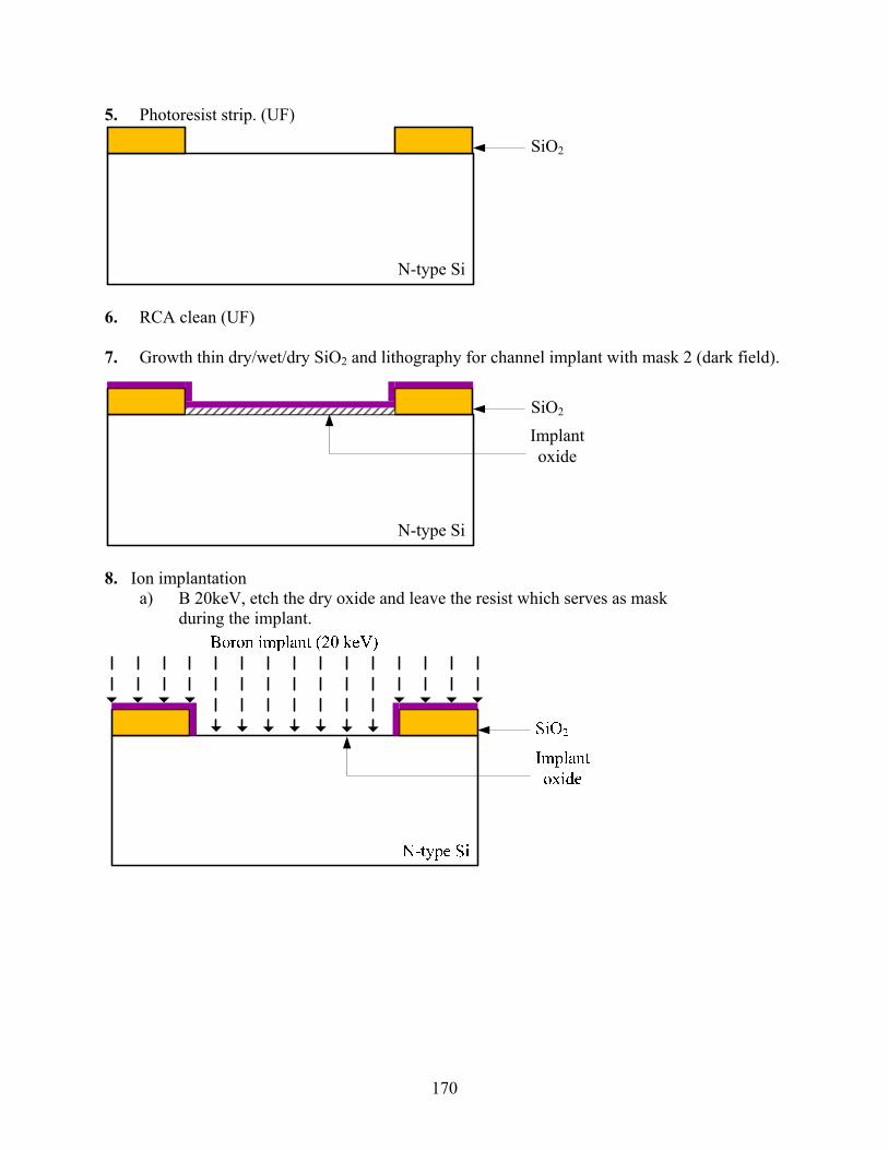
5. Photoresist strip. (UF)
N-type Si
SiO2
6. RCA clean (UF) 7. Growth thin dry/wet/dry SiO2 and lithography for channel implant with mask 2 (dark field).
N-type Si
SiO2
Implant oxide
8. Ion implantation a) B 20keV, etch the dry oxide and leave the resist which serves as mask
during the implant.
170
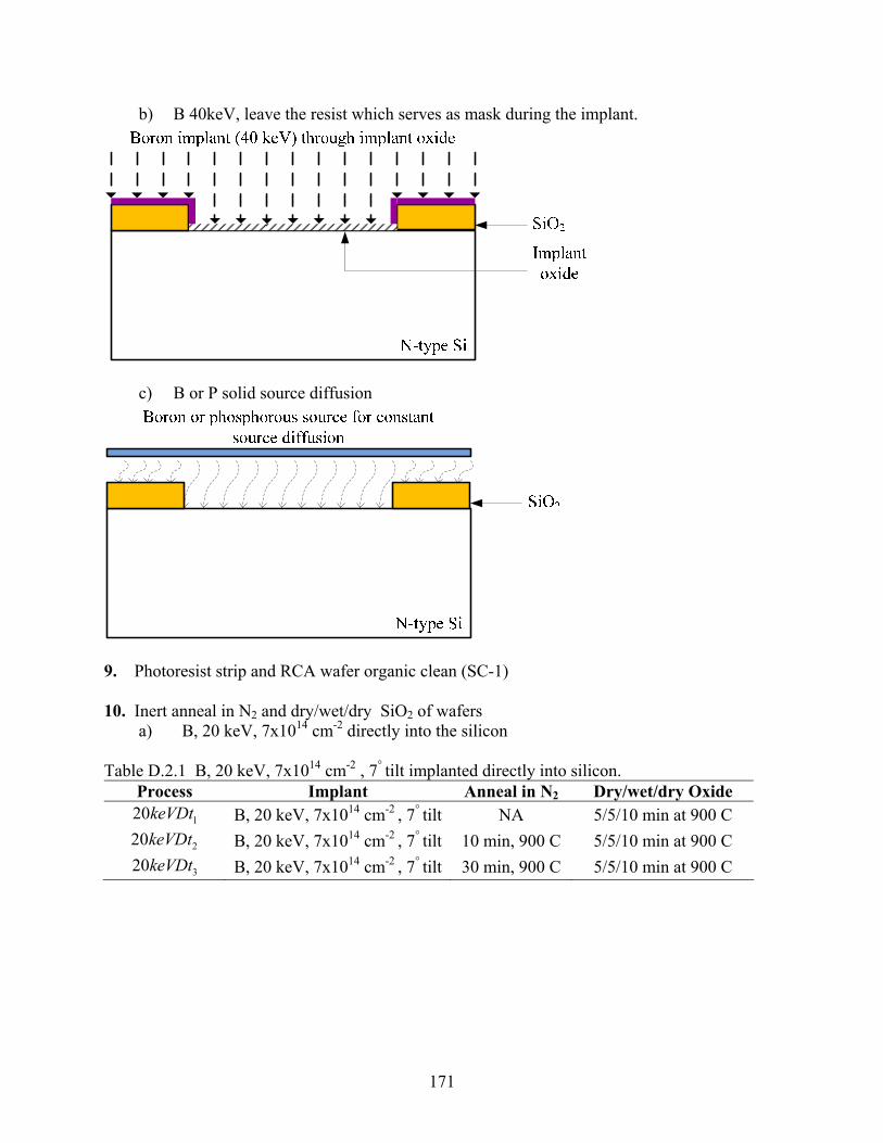
b) B 40keV, leave the resist which serves as mask during the implant.
c) B or P solid source diffusion
9. Photoresist strip and RCA wafer organic clean (SC-1) 10. Inert anneal in N2 and dry/wet/dry SiO2 of wafers
a) B, 20 keV, 7x1014 cm-2 directly into the silicon Table D.2.1 B, 20 keV, 7x1014 cm-2 , 7° tilt implanted directly into silicon.
Process Implant Anneal in N2 Dry/wet/dry Oxide 120keVDt B, 20 keV, 7x1014 cm-2 , 7° tilt NA 5/5/10 min at 900 C
220keVDt B, 20 keV, 7x1014 cm-2 , 7° tilt 10 min, 900 C 5/5/10 min at 900 C
320keVDt B, 20 keV, 7x1014 cm-2 , 7° tilt 30 min, 900 C 5/5/10 min at 900 C
171
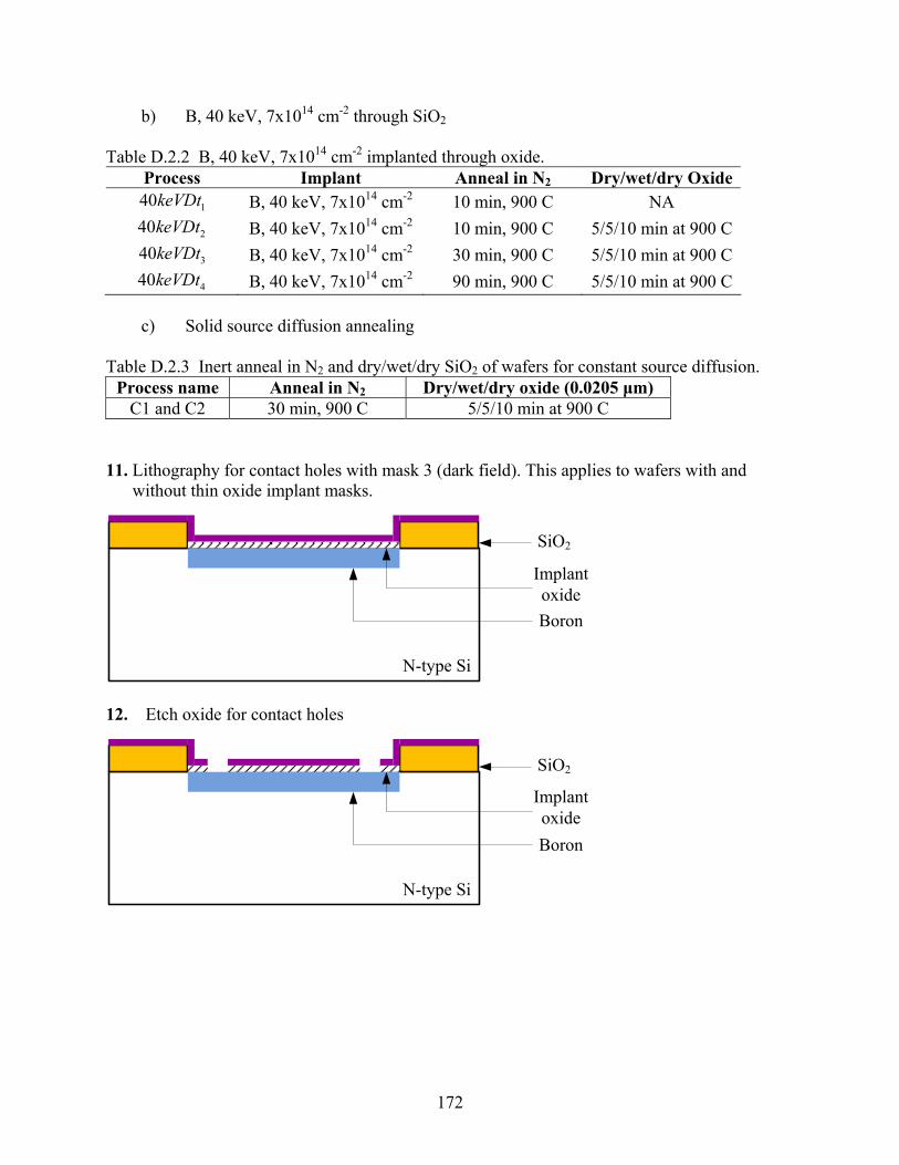
b) B, 40 keV, 7x1014 cm-2 through SiO2 Table D.2.2 B, 40 keV, 7x1014 cm-2 implanted through oxide.
Process Implant Anneal in N2 Dry/wet/dry Oxide140keVDt B, 40 keV, 7x1014 cm-2 10 min, 900 C NA
240keVDt B, 40 keV, 7x1014 cm-2 10 min, 900 C 5/5/10 min at 900 C
340keVDt B, 40 keV, 7x1014 cm-2 30 min, 900 C 5/5/10 min at 900 C
440keVDt B, 40 keV, 7x1014 cm-2 90 min, 900 C 5/5/10 min at 900 C c) Solid source diffusion annealing
Table D.2.3 Inert anneal in N2 and dry/wet/dry SiO2 of wafers for constant source diffusion. Process name Anneal in N2 Dry/wet/dry oxide (0.0205 μm)
C1 and C2 30 min, 900 C 5/5/10 min at 900 C 11. Lithography for contact holes with mask 3 (dark field). This applies to wafers with and
without thin oxide implant masks.
N-type Si
SiO2
Implant oxideBoron
12. Etch oxide for contact holes
N-type Si
SiO2
Implant oxideBoron
172
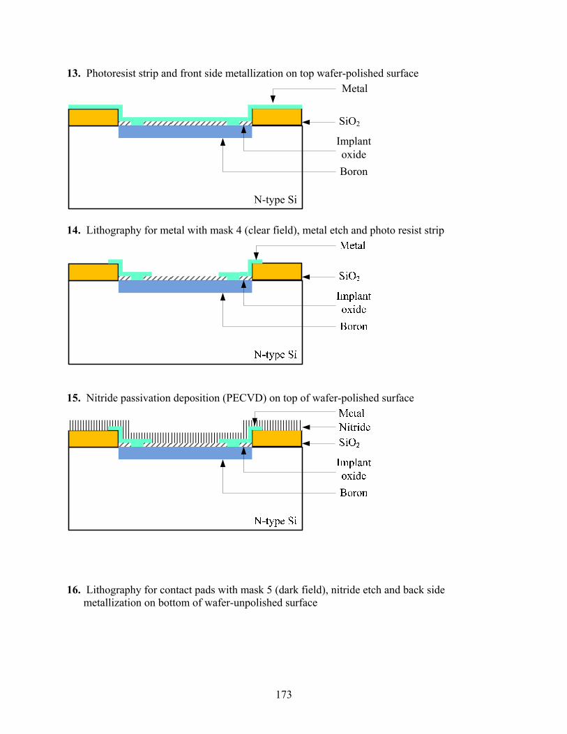
13. Photoresist strip and front side metallization on top wafer-polished surface
N-type Si
SiO2
Implant oxideBoron
Metal
14. Lithography for metal with mask 4 (clear field), metal etch and photo resist strip
15. Nitride passivation deposition (PECVD) on top of wafer-polished surface
16. Lithography for contact pads with mask 5 (dark field), nitride etch and back side
metallization on bottom of wafer-unpolished surface
173
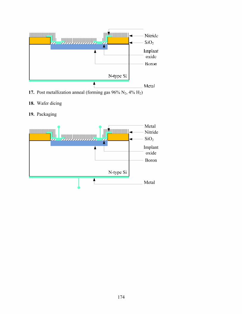
17. Post metallization anneal (forming gas 96% N2, 4% H2) 18. Wafer dicing 19. Packaging
Metal
N-type Si
SiO2
Implant oxideBoron
MetalNitride
174
LIST OF REFERENCES
1D. Deal, J. D. Plummer, and P. B. Griffin, Silicon VLSI Technology Fundamentals,
Practice and Modeling (Prentice Hall, NJ, 2000). 2J. S. Bendat and A.G. Piersol, Random Data: Analysis and Measurement Procedures
(John Wiley & Sons, New-York, 1971). 3H. Nyquist, “Thermal agitation of electric charge in conductors,” Phys. Rev. 32, 110-113
(1928). 4J. B. Johnson, “Thermal agitation of electricity in conductors,” Phys. Rev. 32, 97-109
(1928). 5T. B. Gabrielson, “Mechanical-thermal noise in micromachined acoustic and vibration
sensors,” IEEE Trans. Electron Devices 40(5), 903-909 (1993). 6F. N. Hooge, “1/f noise is no surface effect,” Phys. Lett. A 29(3), 139-140 (1969).
7A. McWhorter, “1/f Noise and germanium surface properties,” Semiconductor Surface
Physics (University of Pennsylvania, Philadelphia, 1957), pp. 207-228. 8F. N. Hooge, “1/f noise,” Physica B 83, 14-23 (1976).
9F. N. Hooge, “Lattice scattering causes 1/f noise,” Phys. Lett. A 66, 315-316 (1978).
10
F. N. Hooge and L.K.J. Vandamme, “On the origin of 1/f noise,” Fourteenth International Conference on the Physics of Semiconductors, Edinburgh, UK, 4-8 September 1978, Inst. Phys. Conference Ser. 43, 565-568 (1979). 11
E. Simoen and C. Claeys, “On the flicker noise in submicron silicon MOSFETs,” Solid- State Electron. 43, 865-882 (1998). 12
J. A. Harley and T. W. Kenny, “1/F noise considerations for the design and process optimization of piezoresistive cantilevers,” J. Microelectromech. Syst. 9(2), 226-235 (2000). 13
X. Yu, J. Thaysen, O. Hansen, and A. Boisen, “Optimization of sensitivity and noise in piezoresistive cantilevers,” J. Appl. Phys. 92(10), 6296-6301 (2002). 14
Z. Celik and T. Y. Hsiang, “Study of 1/f noise in n-MOSFET's: linear region,” IEEE Trans. Electron Devices ED-32(12), 2797-2802 (1985).
175
15W. Schottky, “Über spontane stromschwankungen in verschiedenen Elektrizitätsleiter,”
Annalen der Physik 57, 541-567 (1918). 16
K. S. Jones, S. Prussin, and E.R. Weber, “A systematic analysis of defects in ion implanted silicon, Appl. Phys. A 45,1-34 (1988). 17
H.-S. Fu and C.-T. Sah, “Theory and experiments on surface 1/f noise,” IEEE Trans. Electron Devices ED-19, 273-285 (1972). 18
F.-C. Hou, G. Bosman, and M. E. Law, “Simulation of oxide trapping noise in submicron n-channel MOSFETs, IEEE Trans. Electron Devices 50(3), 846-852 (2003). 19
L. M. Terman, “An investigation of surface states at a silicon/silicon oxide interface employing metal-oxide-silicon diodes,” Solid-State Electron. 5(5), p. 285-299 (1962). 20
H. R. Bilger, J. L. Tandon, and M.-A. Nicolet, “Excess noise measurements in ion- implanted silicon resistors,” Solid-State Electron. 17, 599-605 (1974). 21
L. K. J. Vandamme and S. Oosterhoff, “Annealing of ion-implanted resistors reduces the 1/f noise,” J. Appl. Phys. 59(9), 3169-3174 (1986). 22
R. H. M. Clevers, “Volume and temperature dependence of the 1/f noise parameter α,” Physica B 154, 214-224 (1989). 23
J. A. Harley, T.W. Kenny, “High-Sensitivity Piezoresistive Cantaliver under 1000 A Thick,” Appl. Phys. Lett. 75(2), 289-291 (1999). 24
X. Yu, T. Li, and D. Zang, “Noise-Analyzing of Piezoresistive Silicon Materials,” Seventh International Conference on Solid-State and Integrated Circuits Technology 3, 2194-2197 (2004). 25
A. A. Davenport, P. Lim, and B. Pruitt, “Noise studies in implanted piezoresistors,” Proceedings of IMEC 2005, ASME international mechanical engineering congress and exposition 2005, Orlando, FL. 26
J. R. Mallon Jr., A.J. Rasteger, A.A. Barlian, M.T. Meyer, T. H. Fung, and B. L. Pruit, “Low 1/f noise, full bridge, microcantilever with longitudinal and transverse piezoresistors,” Appl. Phys. Lett. 92, 033508 - 033508-3 (2008). 27
E. Cocheteau, B. Belier, L. Bary, and R. Plana, “Formation of ultra-shallow p+/n junctions using BF2 implantation for the fabrication of improved piezoresistive cantilevers,” Eleventh International Conference on Solid-State Sensors and Actuators 2001, Munich, Germany.
176
28B. Belier, C. Bergaud, E. Cocheteau, L. Bary, and R. Plana, “Formation of implanted
piezoresistors under 100-nm thick for nanoelectromechanical systems,” Fifteen IEEE International Conference on Micro Electro Mechanical Systems, Las Vegas, NV 2002, pp. 360-363. 29
J.-H. Li and K.S. Jones, “311 Defects in silicon: the source of the loops,” Appl. Phys. Lett. 73(25), 3748-3750 (1998). 30
J. Liu, K.S. Jones, D. F. Downey, S. Mehta, “Onset of extended defect formation and enhanced diffusion for ultra-low energy boron implants,” Material Research Society Symposium Proceedings 568, San Francisco, CA, 9-14 (1999). 31
D. Girginoudi and C. Tsiarapas, “Comparative study on EOR and deep level defects in preamorphised Si implanted with B+, BF2
+ and F+–B+,” Nucl. Instr. and Meth. in Phys. Res. B 266(16), 3565-3576 (2008). 32
N. Yarykin and E. Steinman, “Comparative study of the plastic deformation- and implantation-induced centers in silicon,” Physica B 340-342, 756-759 (2003). 33
F. Boussaid, F. Olivie, D. Alquier, and A. Martinez, “Electrically active defects in BF2+
implanted and germanium preamorphized silicon,” Nucl. Instr. and Meth. in Phys. Res. B 134, 195-201 (1998). 34
M. Benzohra, F. Olivie, F. Boussaid, D. Alquier, and A. Martinez, “Electronic defect levels in ultra-shallow p+n-junctions formed by low-energy B ion implantation into Ge- preamorphized silicon,” Jpn. J. Appl. Phys. 36, 4346-4350 (1997). 35
J. Kaniewski, M. Kaniewska, and A.R. Peaker, “Deep levels associated with oxidation induced stacking faults in n-type silicon,” Appl. Phys. Lett. 60(3), 359-361 (1992). 36
L. Michelutti, N. Mathieu, A. Chovet, and A. Galerie, “Influence of chemical corrosion on resistivity and 1/f noise of polysilicon gauges,” Microelectron. Reliab. 40, 179-183 (2000). 37
J. Park and H. Hwang, “Comparison of ultra-low-energy ion implantation of boron and BF2,” Material Research Society Symposium Proceedings 568, San Francisco, CA, 71- 75 (1999). 38
C. -T. Sah, Fundamentals of Solid-State Electronics (World Scientific, Singapore, 1991). 39
S. W. Crowder, “Processing physics in silicon-on-insulator material,” Ph.D. thesis, Stanford University, Palo Alto, CA, 1995.
177
40R. B. Fair and J. C. C. Tsai, “Theory and direct measurement of boron segregation in
SiO2 during dry, near dry, and wet O2 oxidation,” J. Electrochem. Soc. 125, 2050-2058 (1978). 41
R. C. Jaeger, “Introduction to Microelectronic Fabrication,” Second Edition (Prentice Hall, NJ, 2002). 42
M. E. Law, FLOOPS and FLOOPS http://www.swamp.tec.ufl.edu/~flooxs/ [cited; Available from: http://www.swamp.tec.ufl.edu/~flooxs/] (2009). 43
W. van Gelder and E.H. Nicollian, “Silicon impurity distribution as revealed by pulsed MOS C-V measurements,” J. Electrochem. Soc. 118, 138-141 (1971). 44
D. K. Schroder, Semiconductor Material and Device Characterization (Wiley- Interscience, New York, 2006). 45
G. P. Carver, J. J. Kopanski, D. B. Novotny, and R. A. Forman, “Specific contact resistivity of metal-semiconductor contacts-A new, accurate method linked to spreading resistance,” IEEE Trans. Electron Devices 35(4), 489-497 (1988). 46
H. W. Coleman and W. G. Steele, Experimentation and Uncertainty Analysis for Engineers (John Wiley and Sons, New York, 1999). 47
H. Murrmann and D. Widmann, “Current crowding on metal contacts to planer devices,” Solid-State Circuits Conference, Digest of Technical Papers, 1969 IEEE Internationa XII 1969, pp. 162-163. 48
W. Ostwald, “Lehrbuch der Allgemeinen Chemie,” Vol. 2, part 1, Leipzig, Germany (1896). 49
R. F. Pierret, Semiconductor Device Fundamentals (Addison Wesley Longman, USA, 1996). 50
D. V. Lang, “Deep-level transient spectroscopy: A new method to characterize traps in Semiconductors,” J. Appl. Phys. 45, 3023-3032 (1974). 51
C. -T. Sah, L. Forbes, L. L. Rosier, A. F. Tasch Jr., “Thermal and optical emission and capture rates and cross sections of electrons and holes at imperfection centers in semiconductors from photo and dark junction current and capacitance experiments” Solid-State Electron. 13, 759-788 (1970). 52
C. -T. Sah, “Bulk and interface imperfections in semiconductors,” Solid-State Electron. 19, 975-990 (1976).
178
53C. S. Smith, “Piezoresistance effects in germanium and silicon, Phys. Rev. 94, 42-49
(1954). 54
Y. Kanda, “Piezoresistance effect in silicon,” Sens. Actuators, A 28, 83-91 (1991). 55
R. Saini, “Design of a MEMS Based Piezoresistive Microphone,” M.S. thesis, Aerospace Engineering, Mechanics, and Engineering Science, University of Florida Gainesville, FL, 2001. 56
W. P. Mason, J. J. Forst, and L. M. Tornillo, “Recent developments in semiconductor strain transducers,” Fifteenth Annual Conference Proceedings of the Instrumentation Society of America 1962, pp. 110-120. 57
E. L. Stelzer and O. N. Tufte, “Piezoresistive properties of silicon diffused layers,” J. Appl. Phys. 34(2), 313-318 (1963). 58
A. G. Milnes and D. R. Kerr, “Piezoresistance of diffused layers in cubic semiconductors,” J. Appl. Phys. 34(4), 727-731 (1963). 59
R. Doering and Y.Nishi, Handbook of Semiconductor Manufacturing Technology (CRC Press, Boca Raton, 2008)
179
BIOGRAPHICAL SKETCH
Robert Diémé was born in Senegal. After finishing high school in 1995, he received the
Associate of Arts certificate from Tallahassee Community College in December 1998. He
graduated with a bachelor’s degree in electrical engineering from the University of Florida in
December 2001 and received a Master of Science in electrical engineering from the University of
Florida in spring 2005 under the guidance of Dr. Toshikazu Nishida. He began pursuing a
doctorate concentrating in the investigation of noise in piezoresistors, in the summer 2005.
180
Recommended