Semester Project
Advanced NEMS Group
CHARACTERIZATION OF MECHANICAL PROPERTIES OF MICRO/NANO BEAMS
Fall Semester 2016
Student
Soumya Yandrapalli
Supervisors
Prof. Guillermo Villanueva
Dr. Tom Larsen

Table of Contents Abstract ........................................................................................................................................................... 2
1. Introduction ................................................................................................................................................ 3
1.1 Theoretical Model ..................................................................................................................................... 3
1.2 Fabrication ................................................................................................................................................ 4
2. Experimental Setup ..................................................................................................................................... 6
2.1 Control of the Source meter ..................................................................................................................... 6
3. Results ......................................................................................................................................................... 7
3.1 Results based on I-V Characteristics ......................................................................................................... 8
4. Conclusion .................................................................................................................................................12
References ....................................................................................................................................................13
Appendix 1: Matlab code for SRS Source Meter ...........................................................................................14
Appendix 2: Matab code for Keitley’s Series 2400 Source Meter Unit ........................................................15
Appendix 3: Process Flow .............................................................................................................................18
Thickness : 2 um .......................................................................................................................................18
Appendix 4: Run Card ...................................................................................................................................20

Abstract In this project, characterization of a series of previously fabricated Aluminium clamped-clamped micro
beams and cantilevers by electrical measurements in order to investigate the effects of scaling down
on mechanical properties of micro/nano structures is presented. The Young’s modulus that depends
on the thickness of the microstructure, residual stress and surface properties as opposed to a constant
Young’s modulus in macro scale theories was investigated. Due to insufficient sample space and high
stresses during fabrication, a correlation was not obtained.
Keywords- Aluminium beams, Coupled Stress theory, Residual Stress theory, Surface Elasticity theory,
Combined stress model, electrical characterization.
1. Introduction
1.1 Theoretical Model
Experimental work [1,2] show that at the microstructures do not follow classical Euler Bernoulli beam
theory and the Young’s modulus does not remain constant with dimensions, in particular the
thickness. The main theoretical models that explain the behaviour of mechanical properties on scaling
down are Residual Stress Theory (RST), Couple Stress Theory (CST), Grain Boundaries Theory (GBT),
Surface Stress Theory (SST) and Surface Elasticity Theory (SET) [3]. In order to obtain a combined
model to explain the behaviour, the RST, CST and SET were considered neglecting the SST and GBT
since they are considered as secondary effects and not applicable to all cases.
The GBT is applicable when the thickness of the structure is equal to few times the grain size. This is
not a frequent occurrence in the micro-scale. The SST is also neglected since it cannot be applied to
Cantilevers and other free structures as they have zero surface stress and the effect of SST is similar
to noise that is not observed experimentally.
The CST predicts the stiffening effect on scaling down by taking into account the length scaling effect
in the Euler-Bernoulli theory. The addition component arising due to this effect can be described by
an ‘Effective Young’s Modulus’ 𝐸𝑒𝑓𝑓 given by
𝐸𝑒𝑓𝑓 = 𝐸 + 24 (𝐸
1 + 𝜈) (
𝑙
ℎ)
2
(1)
Where E is the Young’s Modulus, 𝜈 is the Poisson’s ratio, 𝑙 is the length scaling parameter and h is the
thickness of the beam.
The SET also accounts for stiffening or softening but it is a surface effect theory as opposed to CST that
accounts only for Bulk stiffening. This arises to due to the surface being of a more amorphous nature
due to defects and having different interatomic interactions with respect to those of bulk atoms. The
equation of 𝐸𝑒𝑓𝑓 is derived from composite beam theory, where the microstructure consists of a bulk
volume with bulk material properties and is surrounded by a thin shell with surface material properties
[4]. This relation is given by Equation (3), where 𝛿 is the thickness of the shell, the Surface Elasticity is
𝐶𝑠 is
𝐶𝑆 = 𝛿(𝐸𝑏𝑢𝑙𝑘 − 𝐸𝑠𝑢𝑟𝑓) (2)
𝐸𝑒𝑓𝑓 = 𝐸𝑏𝑢𝑙𝑘 − 6𝐶𝑆 (1
ℎ) (3)
Finally the RST should be taken into account to model the intrinsic stresses (particularly in clamped-
clamped beams) developed to micro fabrication of the structure. The 𝐸𝑒𝑓𝑓 for a clamped-clamped
beam is derived to be [3]:
𝐸𝑒𝑓𝑓 = 𝐸 +3
10σ0 (
𝐿
ℎ)
2
(4)
Where 𝜎0the intrinsic stress and L is the length of the beam. Taking these three theories into account,
a combined model for a clamped-clamped beam has been proposed by [3] given by:
𝐸𝑒𝑓𝑓 = 𝐸𝑏𝑢𝑙𝑘 − 6𝐶𝑠 (1
ℎ) +
24𝐸
1 + 𝜈𝑙2 (
1
ℎ)
2
+3
10𝜎0 (
𝐿
ℎ)
2
(5)
Applying a combined model of the Coupled Stress Theory, Surface Elasticity Theory and Residual Stress
theory to existing experimental data has shown promising results [3]. In order to further develop this
combined model, the Advanced NEMS group has fabricated Aluminium clamped-clamped micro
beams and cantilevers to study in detail by characterization and observing the trend of the 𝐸𝑒𝑓𝑓 as a
function of dimensions, surface elasticity and residual stress. This is done by finding the pull in voltage
(𝑉𝑃) of each beam which is a function of 𝐸𝑒𝑓𝑓 as describe in Equation (5) for a clamped-clamped beam
[5].
𝑉𝑃 = 3.08 ∗ √𝑔3ℎ3𝐸𝑒𝑓𝑓
𝜖0𝐿4 (6)
1.2 Fabrication
The aluminium microstructures were fabricating on Si wafer with a layer of 200nm wet oxide. The
process flow consists of six steps briefly described below and the process flow and run card is attached
in the appendix. These structures were fabricated by Kaitlin Howell of the ANMES group.
1) Deposition of Al 2) Photolithography 3) Dry Etch of Al
4) Dry Etch of SiO2 5) Dry etch of Si 6) Wet etch of SiO2
Step 1: Aluminium of 2𝜇𝑚 thickness was deposited by sputtering on the Si wafer with a 200nm thick SiO2
layer on top.
Step 2: Photolithography was carried out with the patterns of the beams and electrodes required using AZ
ECI positive photoresist of thickness 3𝜇𝑚. The photolithography has a CD of 1𝜇𝑚.
Step 3: Using the post baked mask as protection, the rest of the Aluminium was removed by Dry Etching.
SiO2 PR
Al Si
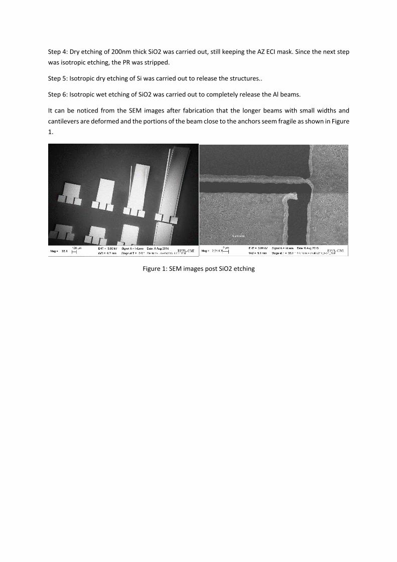
Step 4: Dry etching of 200nm thick SiO2 was carried out, still keeping the AZ ECI mask. Since the next step
was isotropic etching, the PR was stripped.
Step 5: Isotropic dry etching of Si was carried out to release the structures..
Step 6: Isotropic wet etching of SiO2 was carried out to completely release the Al beams.
It can be noticed from the SEM images after fabrication that the longer beams with small widths and
cantilevers are deformed and the portions of the beam close to the anchors seem fragile as shown in Figure
1.
Figure 1: SEM images post SiO2 etching
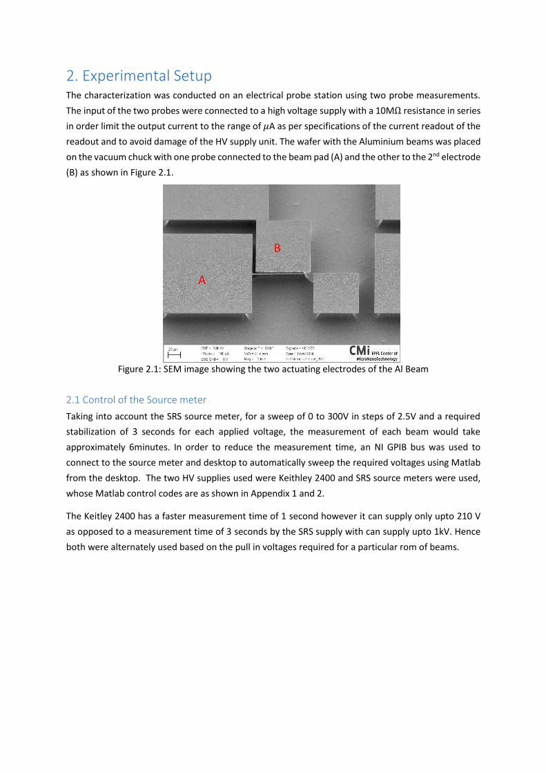
2. Experimental Setup The characterization was conducted on an electrical probe station using two probe measurements.
The input of the two probes were connected to a high voltage supply with a 10MΩ resistance in series
in order limit the output current to the range of 𝜇A as per specifications of the current readout of the
readout and to avoid damage of the HV supply unit. The wafer with the Aluminium beams was placed
on the vacuum chuck with one probe connected to the beam pad (A) and the other to the 2nd electrode
(B) as shown in Figure 2.1.
Figure 2.1: SEM image showing the two actuating electrodes of the Al Beam
2.1 Control of the Source meter
Taking into account the SRS source meter, for a sweep of 0 to 300V in steps of 2.5V and a required
stabilization of 3 seconds for each applied voltage, the measurement of each beam would take
approximately 6minutes. In order to reduce the measurement time, an NI GPIB bus was used to
connect to the source meter and desktop to automatically sweep the required voltages using Matlab
from the desktop. The two HV supplies used were Keithley 2400 and SRS source meters were used,
whose Matlab control codes are as shown in Appendix 1 and 2.
The Keitley 2400 has a faster measurement time of 1 second however it can supply only upto 210 V
as opposed to a measurement time of 3 seconds by the SRS supply with can supply upto 1kV. Hence
both were alternately used based on the pull in voltages required for a particular rom of beams.
A
B
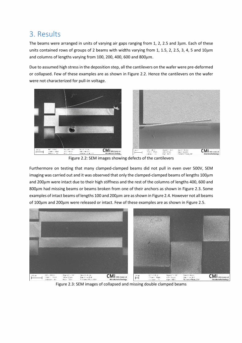
3. Results The beams were arranged in units of varying air gaps ranging from 1, 2, 2.5 and 3𝜇𝑚. Each of these
units contained rows of groups of 2 beams with widths varying from 1, 1.5, 2, 2.5, 3, 4, 5 and 10𝜇𝑚
and columns of lengths varying from 100, 200, 400, 600 and 800𝜇𝑚.
Due to assumed high stress in the deposition step, all the cantilevers on the wafer were pre-deformed
or collapsed. Few of these examples are as shown in Figure 2.2. Hence the cantilevers on the wafer
were not characterized for pull-in voltage.
Figure 2.2: SEM images showing defects of the cantilevers
Furthermore on testing that many clamped-clamped beams did not pull in even over 500V, SEM
imaging was carried out and it was observed that only the clamped-clamped beams of lengths 100𝜇m
and 200𝜇m were intact due to their high stiffness and the rest of the columns of lengths 400, 600 and
800𝜇𝑚 had missing beams or beams broken from one of their anchors as shown in Figure 2.3. Some
examples of intact beams of lengths 100 and 200𝜇𝑚 are as shown in Figure 2.4. However not all beams
of 100𝜇𝑚 and 200𝜇𝑚 were released or intact. Few of these examples are as shown in Figure 2.5.
Figure 2.3: SEM images of collapsed and missing double clamped beams
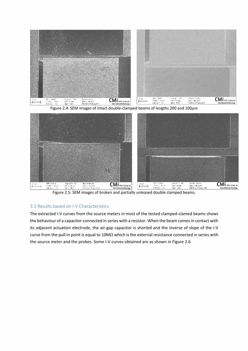
Figure 2.4: SEM images of intact double-clamped beams of lengths 200 and 100𝜇𝑚
Figure 2.5: SEM images of broken and partially unleased double clamped beams.
3.1 Results based on I-V Characteristics
The extracted I-V curves from the source meters in most of the tested clamped-clamed beams shows
the behaviour of a capacitor connected in series with a resistor. When the beam comes in contact with
its adjacent actuation electrode, the air-gap capacitor is shorted and the inverse of slope of the I-V
curve from the pull in point is equal to 10MΩ which is the external resistance connected in series with
the source meter and the probes. Some I-V curves obtained are as shown in Figure 2.6

Figure 2.6: IV curves obtained from voltage sweep using SRS Sourcemeter and GPIB interface with Matlab
A compilation of the pull in voltages as a function of widths, airgaps and lengths of the clamped-
clamped beams is as shown in Figure 2.7. The pull-in voltage is expected to decrease with an increase
in length, increase with increase in width and increase with increase in gap. However as seen from
Figure 2.7 there is no correlation between the dimensions of the beams and the pull in voltage. This
is attributed to:
1) Due to stresses in the deposition step as seen from the deformed beams in Figure 2.8 a, the
stiffness and mechanical behaviour cannot be predicted.
2) Due to insufficient control in etching process or material defects as seen in section 1.2, the
beam does not snap in symmetrically due to weak anchors as can be seen in Figure 2.8 b.
Leading to reduced correlation between pull-in voltage and dimensions.
3) Since high voltages ranging from 150-500V are being applied, charge crowding at the anchors
leading to breaking and snapping of the beam at the anchor with ‘burnt marks’ as in Figure
2.8 c.
4) Many data points are missing as in Figure 2.7 g and h due to no pull-in voltage (including 1kV)
as shown in Figure 2.8 d. This could be attributed to high stiffness or unreleased beams.
Particularly in the beams of larger width (5 and 10𝜇𝑚) and shorter length100𝜇𝑚.
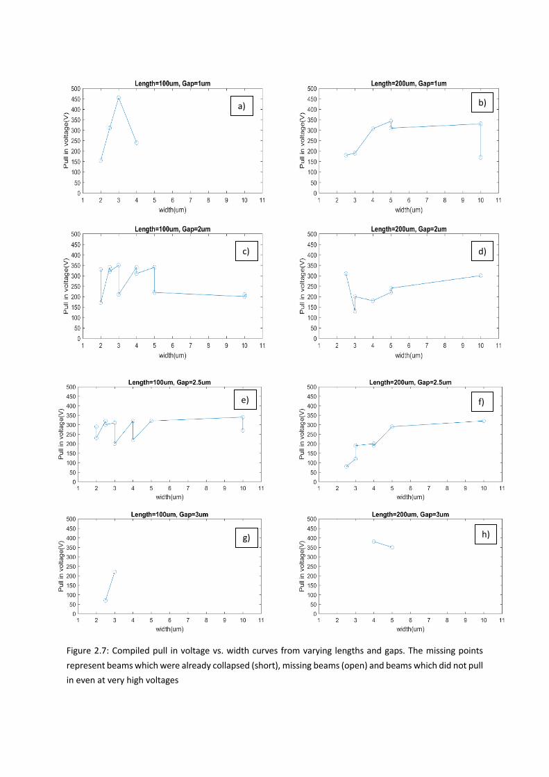
Figure 2.7: Compiled pull in voltage vs. width curves from varying lengths and gaps. The missing points
represent beams which were already collapsed (short), missing beams (open) and beams which did not pull
in even at very high voltages
g) h)
e) f)
c) d)
a) b)
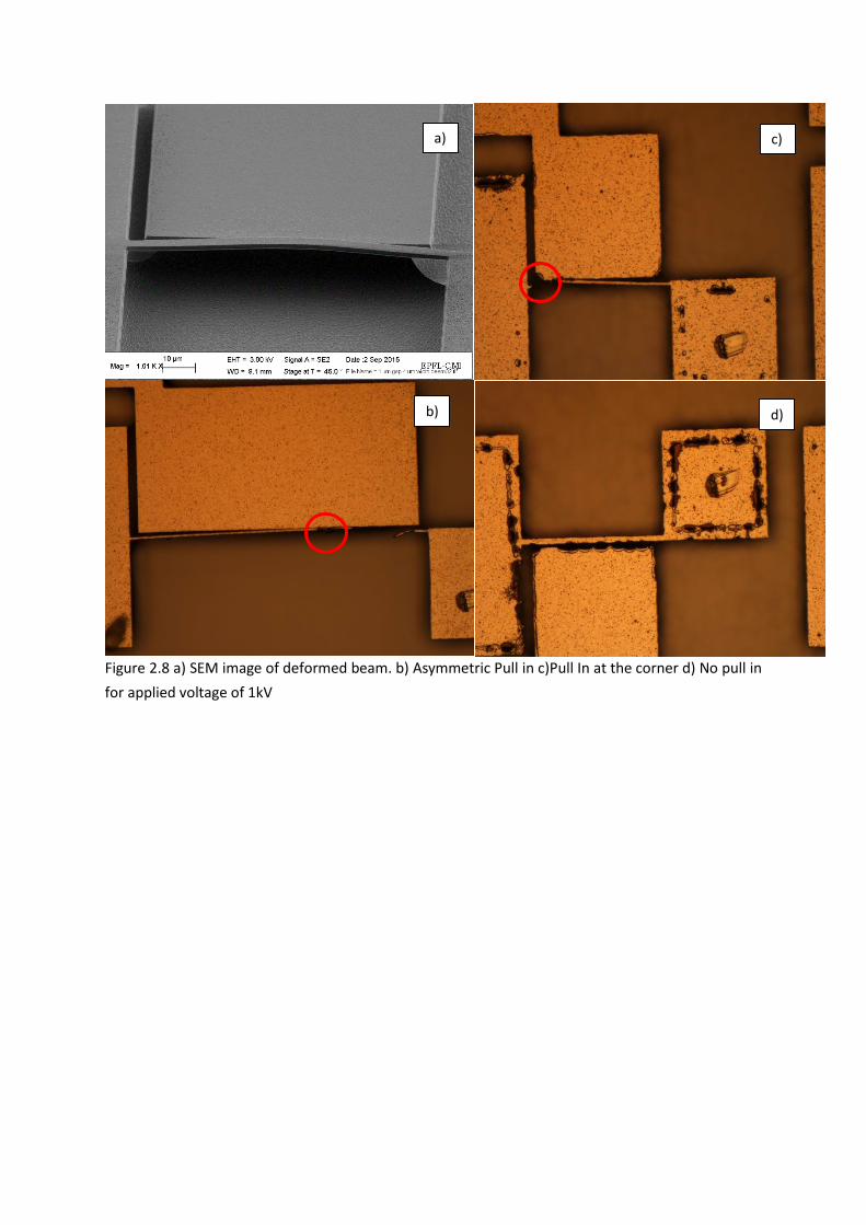
Figure 2.8 a) SEM image of deformed beam. b) Asymmetric Pull in c)Pull In at the corner d) No pull in
for applied voltage of 1kV
a)
b)
c)
d)

4. Conclusion During this semester project, electrical characterization of fabricated Al clamped-clamped beams for
investigating mechanical properties of micro structures was carried out. Matlab codes were
implemented to control the Keithley 2400 and SRS source meters using GPIB interface.
Unfortunately due to lack of large sample space, i.e. missing cantilevers and only the shortest two
lengths (100, 200𝜇m) of clamped-clamped beams with highest stiffnesses being present out of 5
lengths as well as lack of correlation between the dimensions of the beams with pull-in voltage, the
obtained data could not be analysed further. Future work would include optimizing the etching
process to obtain higher yield and investigating the reasons for occurrence of the pre-stressed beams.
I would like to thank Dr Tom Larsen for directly me throughout this project to help me setup the
measurement system and his insightful suggestions to come to the right conclusions for the behaviour
we were observing. I would like to thank Prof. Guillermo Villanueva for this opportunity to work with
the ANEMS group and his guidance and suggestions with progressing in this project smoothly and in
the right direction.

References 1. Ballestra, A.; Brusa, E.; de Pasquale, G.; Munteanu, M.G.; Soma, A. FEM modelling and experimental
characterization of microbeams in presence of residual stress. Analog Integr. Circuits Singal Process.
2010, 63, 477–488.
2. Ni, H.; Li, X.D.; Gao, H.S. Elastic modulus of amorphous SiO2 nanowires. Appl. Phys. Lett. 2006, 88,
doi:10.1063/1.2165275.
3. Abazari, A. M., Safavi, S. M., Rezazadeh, G., & Villanueva, L. G. (2015). Modelling the Size Effects on
the Mechanical Properties of Micro/Nano Structures.Sensors,15(11), 28543-28562.
4. Nilsson, S.G.; Borrise, X.; Montelius, L. Size effect on Young’s modulus of thin chromium cantilevers. Appl. Phys. Lett. 2004, 85, 3555–3557. 5. Chowdhury, S., Ahmadi, M., & Miller, W. C. (2006). Pull-in voltage study of electrostatically actuated
fixed-fixed beams using a VLSI on-chip interconnect capacitance model. Journal of
Microelectromechanical Systems, 15(3), 639-651.

Appendix 1: Matlab code for SRS Source Meter function IV(filename,Vstart,Vstep,Vstop)
% Find a GPIB object.
obj1 = instrfind('Type', 'gpib', 'BoardIndex', 0, 'PrimaryAddress', 13,
'Tag', '');
% Create the GPIB object if it does not exist
% otherwise use the object that was found.
if isempty(obj1)
obj1 = gpib('NI', 0, 13);
else
fclose(obj1);
obj1 = obj1(1)
end
% Connect to instrument object, obj1.
fopen(obj1);
% Communicating with instrument object, obj1.
fprintf(obj1, '*RST'); %Reset
fprintf(obj1,'HVON'); %High Voltage setting on: Doesn't work without
this
fprintf(obj1,'ILIM0.001'); % Setting current limit
fprintf(obj1,'VLIM600'); %Setting voltage limit
ii=0;
timewait=((Vstop-Vstart)/Vstep)*4
for i=Vstart:Vstep:Vstop %Loop to sweep voltage
volt=i
ii=ii+1;
str1=num2str(volt); % converting voltage value to string
voltset=strcat('VSET',str1); % Concatenating string
fprintf(obj1,voltset); % Setting voltage
pause(4)
data3 = query(obj1, 'VSET?'); % Reading/query set voltage
data4 = query(obj1, 'VOUT?'); % Reading/query output voltage
vout(ii)=str2double(data4); % converting string to double
vset(ii)=str2double(data3);
if volt~=vset(ii) % Break the loop if voltage is not set correctly
break
end
data2 = query(obj1, 'IOUT?'); % Reading/query set current
iout(ii)=str2double(data2);
end
fprintf(obj1, '*RST');
figure
plot(vset,iout,'b-o')
xlabel('V (volt)')
ylabel('I (A)')
end

Appendix 2: Matab code for Keitley’s Series 2400 Source Meter Unit
function out=IV_Curve_New(filename,V_Start,V_Stop,V_Step)
%Slightly modified code from Keithley
http://www.keithley.com/matlab/instruments
%Makes an I-V sweep using a 4-wire configuration - Keithley 2400
%sourcemeter
%1: Connect current wires to the input/output.
%2: Connect voltage wires to 4-wire sense.
%3: Set min and max current and step size
%4: Run the code
% Find a GPIB object.
obj1 = instrfind('Type', 'gpib', 'BoardIndex', 0, 'PrimaryAddress', 24,
'Tag', '');
% Create the GPIB object if it does not exist
% otherwise use the object that was found.
if isempty(obj1)
obj1 = gpib('NI', 0, 24);
else
fclose(obj1);
obj1 = obj1(1)
end
% Create the instrument object.
g.InputBufferSize = 1000; %Make sure that the buffer size is larget enough
% Set the property values.
set(obj1, 'BoardIndex', 0);
set(obj1, 'ByteOrder', 'littleEndian');
set(obj1, 'BytesAvailableFcn', '');
set(obj1, 'BytesAvailableFcnCount', 48);
set(obj1, 'BytesAvailableFcnMode', 'eosCharCode');
set(obj1, 'CompareBits', 8);
set(obj1, 'EOIMode', 'on');
set(obj1, 'EOSCharCode', 'LF');
set(obj1, 'EOSMode', 'read&write');
set(obj1, 'ErrorFcn', '');
set(obj1, 'InputBufferSize', 2000);
set(obj1, 'Name', 'GPIB0-24');
set(obj1, 'OutputBufferSize', 2000);
set(obj1, 'OutputEmptyFcn', '');
set(obj1, 'PrimaryAddress', 24);
set(obj1, 'RecordDetail', 'compact');
set(obj1, 'RecordMode', 'overwrite');
set(obj1, 'RecordName', 'record.txt');
set(obj1, 'SecondaryAddress', 0);
set(obj1, 'Tag', '');
set(obj1, 'Timeout', 10);
set(obj1, 'TimerFcn', '');
set(obj1, 'TimerPeriod', 1);
set(obj1, 'UserData', []);
if nargout > 0
out = obj1;
end
%%%%%%%%%%%%%%%%%%%%%%%%%%%%%%%%%%%%%%%%%%%%%%%%%%%%%%%
%%%%%%%%%%%%%%%%%%%%%%%%%%%%%%%%%%%%%%%%%%%%%%%%%%%%%%%
%Find buffer size
BufferSize = (V_Stop-V_Start)/V_Step
% Model 2400 Specific Functions
% Sweep current and measure back voltage
fopen(obj1)
fprintf(obj1,':*RST')
% setup the 2400 to generate an SRQ on buffer full
fprintf(obj1,':*ESE 0')
fprintf(obj1,':*CLS')
fprintf(obj1,':STAT:MEAS:ENAB 1024')
fprintf(obj1,':*SRE 1')
% buffer set up
fprintf(obj1,':TRAC:CLE')
fprintf(obj1,':TRAC:POIN %d', BufferSize) % buffer size
% Set up the Sweep
fprintf(obj1,':SOUR:FUNC:MODE VOLT')
fprintf(obj1,':SOUR:VOLT:STAR %f',V_Start) %Voltage start [V]
fprintf(obj1,':SOUR:VOLT:STOP %f', V_Stop) %Voltage stop [V]
fprintf(obj1,':SOUR:VOLT:STEP %f', V_Step) %Voltage step size [V]
fprintf(obj1,':SOUR:CLE:AUTO ON')
fprintf(obj1,':SOUR:VOLT:MODE SWE')
fprintf(obj1,':SOUR:SWE:SPAC LIN')
fprintf(obj1,':SOUR:DEL:AUTO OFF')
fprintf(obj1,':SOUR:DEL 0.5')
fprintf(obj1,':SENS:FUNC "CURR"')
fprintf(obj1,':SENS:FUNC:CONC ON')
fprintf(obj1,':SENS:VOLT:RANG:AUTO OFF')
%%%%%%%%%%%%%%%%%%%%%%%%%%%%%%%%%%%%%%%%%%
% IMPORTANT: if the unit goes into compliance,
% adjust the compliance or the range value
fprintf(obj1,':SENS:CURR:PROT 5E-3')
%fprintf(obj1,':SENS:CURR:PROT:LEV ') % voltage compliance
%fprintf(obj1,':SENS:VOLT:RANG 7') % volt measurement range
%%%%%%%%%%%%%%%%%%%%%%%%%%%%%%%%%%%%%%%%%%%
fprintf(obj1,':SENS:CURR:NPLC 1')
fprintf(obj1,':FORM:ELEM:SENS CURR,VOLT')
fprintf(obj1,':TRIG:COUN %d', BufferSize)
fprintf(obj1,':TRIG:DEL 2') %Set source delay to 500 ms
fprintf(obj1,':SYST:AZER:STAT OFF')
fprintf(obj1,':SYST:TIME:RES:AUTO ON')
fprintf(obj1,':TRAC:TST:FORM ABS')
fprintf(obj1,':TRAC:FEED:CONT NEXT')
fprintf(obj1,':OUTP ON')
fprintf(obj1,':INIT')
for T = 1:BufferSize*5
T
BufferSize*5
pause(1)
end
% Used the serial poll function to wait for SRQ
val = [1]; % 1st instrument in the gpib object, not the gpib add
spoll(obj1,val); % keep control until SRQ
fprintf(obj1,':TRAC:DATA?')
A = scanstr(obj1,',','%f');
%parse the data & plot
Curr=A(4:2:length(A),1); %Take out the first point as it always looks wired
Volts=A(3:2:length(A)-1,1); %Take out the first point as it always looks
wired
figure(1);
plot(Volts,Curr,':bo','LineWidth',0.5,...
'MarkerEdgeColor','k',...
'MarkerFaceColor','r',...
'MarkerSize',5)
xlabel('Source-volts (V)'),ylabel('Measured-current(A)')
title('Keithley 2400: Sweeps V & Measure I');
figure(2)
plot(Volts, Volts./Curr,':bo','LineWidth',0.5,...
'MarkerEdgeColor','k',...
'MarkerFaceColor','r',...
'MarkerSize',5)
xlabel('Source-volts (V)'),ylabel('Measured-Resistance(Ohm)')
save(filename)
% reset all the registers & clean up
% if the registers are not properly reset,
% subsequent runs will not work!
fprintf(obj1,':*RST')
fprintf(obj1,':*CLS ')
fprintf(obj1,':*SRE 0')
% make sure STB bit is 0
STB = query(obj1, '*STB?');
fclose(obj1)
delete(obj1)
clear obj1
end
%%%%%%%%%%%%%%%%%%%%%%%%%%%%%%%%%%%%%%%%%%%%%%%%%%%%%%%
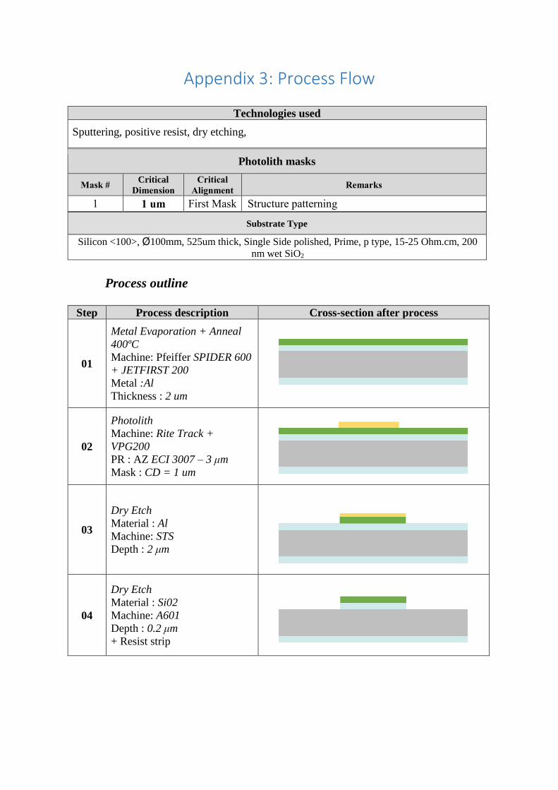
Appendix 3: Process Flow
Technologies used
Sputtering, positive resist, dry etching,
Photolith masks
Mask # Critical
Dimension Critical
Alignment Remarks
1 1 um First Mask Structure patterning
Substrate Type
Silicon <100>, Ø100mm, 525um thick, Single Side polished, Prime, p type, 15-25 Ohm.cm, 200
nm wet SiO2
Process outline
Step Process description Cross-section after process
01
Metal Evaporation + Anneal
400ºC
Machine: Pfeiffer SPIDER 600
+ JETFIRST 200
Metal :Al
Thickness : 2 um
02
Photolith
Machine: Rite Track +
VPG200
PR : AZ ECI 3007 – 3 μm
Mask : CD = 1 um
03
Dry Etch
Material : Al
Machine: STS
Depth : 2 μm
04
Dry Etch
Material : Si02
Machine: A601
Depth : 0.2 μm
+ Resist strip
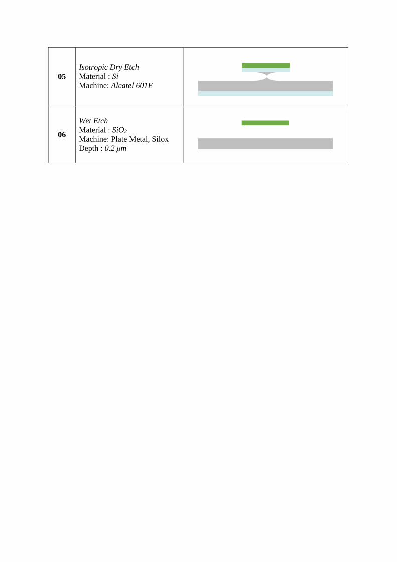
05
Isotropic Dry Etch
Material : Si
Machine: Alcatel 601E
06
Wet Etch
Material : SiO2
Machine: Plate Metal, Silox
Depth : 0.2 μm
Appendix 4: Run Card
Recommended