DAS-1600/1400 Series User’s Guide
.frm Page 1 Monday, June 6, 1994 2:45 PM
DAS-1600/1400 Series User’s Guide
Revision A June 1994 Part Number: 81490
The information contained in this manual is believed to be accurate and reliable. However, the manufacturer assumes no responsibility for its use or for any infringements of patents or other rights of third parties that may result from its use. No license is granted by implication or otherwise under any patent rights of the manufacturer.
THE MANUFACTURER SHALL NOT BE LIABLE FOR ANY SPECIAL, INCIDENTAL, OR CONSEQUENTIAL DAMAGES RELATED TO THE USE OF THIS PRODUCT. THIS PRODUCT IS NOT DESIGNED WITH COMPONENTS OF A LEVEL OF RELIABILITY SUITABLE FOR USE IN LIFE SUPPORT OR CRITICAL APPLICATIONS.
All brand and product names are trademarks or registered trademarks of their respective companies.
0 Copyright Keithley Instruments, Inc., 1994.
All rights reserved. Reproduction or adaptation of any part of this documentation beyond that permitted by Section 117 of the 1976 United States Copyright Act without permission of the Copvight owner is unlawful.
lhOOug.toc Page iii Monday, June 6, 1994 2:46 PM
Table of Contents
Preface Manual Organization. . . . . Related Documents
1 Overview Features ...................................... Supporting Software ............................ Accessories ...................................
2 Functional Description Analog Input Features ...........................
Differential/Single-Ended Selection .............. UnipolariBipolar Selection ..................... Channei Selection in Expanded Configurations. .... Gain Selection. .............................. Conversion Modes ........................... Clock Sources ............................... Triggers .................................... Data Transfer Modes. .........................
Analog Output Features (DA.%1600 Series Only) Digital I/O Features ............................. Counter/Timer Features. ......................... Wait State Selection. ............................ Power ........................................
xi . Xl,1
. 1-l 1-3 1-7
.2-3
.2-3 2-3
.2-4 . .2-5 .2-6
.,2-x .2-9
.%I0 2-11
:2-12 .2-13 .2-14 .2-14
3 Setup and Installation Iuspecting Your Package .............................. ,3-l Installing the Software Package. ........................ ,3-2
Installing the DAS-1600/1400 Series Staudard Software. . .3-Z Installing the ASO- and ASO- Advanced Software Option...........................................3 -3
DOS Installation. ................................ 3-3 Windows Installation ............................ .3-4
Creating a Configuration File .......................... ,3-6 Default Configuration File .......................... .3-6 Configuration Utility. ............................... 3-X
1600ug.toc Page iv Monday, June 6, 1994 2:46 PM
4
Setting Switch-Configurable Options 3-14 Setting the DAC BipolarRluipolar Switch (DAS- 1600 Series Only) ,3- 15
Setting the DACO aud DACl Reference Voltage Switches (DAS-1600 Series Only) . .3-15 Selting the ADC Bipolar/Unipolar Switch , ,3-16 Setting the Chau 8/16 Switch .3-16 Setting au Alternate Base Address . ,3-16 Setting the Clock Select Switch ,3-18 Setting the Wait State Enable Switch . .3-18 Setting the DMA Channel Select Switch ,3-18
Installing the Board . . .3- 18
4 Cabling and Wiring Attaching Screw Terminal Connectors and Accessories ,4-Z
Attaching an STC-37 .4-2 Attaching an STP-37. . ~. .4-5 Attaching an STA-16.. ,4-6 Attaching an STA-LJ . .4-8
Attaching Expansion Accessories ,4- IO Attaching an EXP-16 or EXP-16/A Expansion Accessory .4- 11 Attaching an EXP-GP Expansion Accessory ,4- 12 Attaching Multiple Expausion Accessories ,4- 13
Attaching an ISO- Accessory. .4- 15 Attaching SSH Accessories. ,4-16
Attaching an SSH-4/A . . . . ,4- 17 Attaching an SSH-8 .4- 17
Attaching an MB Series Backplane. ,4-20 Attaching an MB01 Backplane. .4-21 Attaching au MB02 Backplane. . .4-22
Connecting Analog Signals . . ,4-24 Precautions for Using DAS-1601/1401Boards at
High Gains . . . . . . . . . . . . . . . . . . . . . . . . . . . . . . . . . . ...4-2 Additional Precautions .4-25 Connecting a Signal to a Single-Ended Analog Input .4-26 Connecting a Signal to a Differeutial Analog Input .4-27
Common Connection Schemes for Differential Inputs ,4-27 Avoiding Ground Loops with Differential Inputs .4-29
Connecting Analog Output Signals. ,4-3 1
4
5 The Control Panel
iv
4 4
4 1600ug.toc Page v Monday, June 6, 1994 2:46 PM
4
6 Calibration Equipment Requirements. ............................ ..6- 1 Potentiometers and Test Points .......................... 6-1 Calibration Utility ................................... .6-2
7 Troubleshooting Problem Isolation . . . . . . . . . . . . . . . . . . . . . . . . . . . . . . . . . . ...7-I
Identifying Symptoms and Possible Causes. . ,7-l Testing the Board and Host Computer .7-4 Testing the Accessory Slot and I/O Connections ,7-5
Technical Support , ,7-6
A Specifications
B Connector Pin Assignments Main I/O Connector (Jl) . . .B-2 PI0 Cable Connector (J2) (DAS-1600 Series Only). .B-3
c Using the DA-S-1600 External Driver Options Supported ................................... .C- I Quick Start ........................................ ..c- 2
Setting Up the Board. .............................. .C-2 Loading the DAS-1600 External Driver. ............... .C-3 Loading the External Driver in Multiple Board
Configurations. .................................. .C-3 Using the External Driver with Application SoftwarePackages.. ............................ ..C- 4
VIEWDAC.....................................C- 4 EASYESTLXIAG.. ........................... .C-4 ASYST........................................C- 5
DAS- 1600 External Driver Characteristics ................ .C-5 Channels and Gains. ............................... .C-5 Cascading Multiple Expansion Accessories. ............ .C-6 Setting Expansion Accessory Gains ................... .C-7 ConversionModes.. ............................. ..C- 8
Using Pseudo-Digital Output Channels. ............. .C-8 BurstModeandSSHMode.. ..................... C-10 Altering the Burst Mode Conversion Rate. ........... C-l I
Clock Sources....................................C-14 Triggers ........................................ .c-14
4
2 1600ug.toc Page vi Monday, June 6, 1994 2:46 PM
Using Pseudo-Digital Output Channels, Types of Analog Triggers. ................... Using a Hysteresis Value ....................
Synchronous, DMA, and Interrupt Operations, ..... Digital I/O Characteristics .....................
DAS-1600 Series Boards .................... DAS-1400 Series Boards ....................
Counter/Timer Functions ...................... Event Counting ........................... Pulse Output ..............................
Software Interrupt Vectors ..................... DAS- 1600 External Driver Error Messages ..........
D Keithley Memory Manager Installing and Setting Up the KMM. ................
Using KMMSETUPEXE ...................... Using a Text Editor. ..........................
Removing the KMM ............................
.c-14
.c-17
.C-18
.c-19
.c-20
.c-20
.C-24
.C-25
.C-25
.C-26
.C-26
.C-27
D-2 D-2 D-3
. D-4
E Register-Level Address Map Register Functions ................................... .E-1 ADC Registers (Base Address +Oh and + lh) .............. .E-3 MUX Scan Register (Base Address +2h) ................. .E-4 Unidirectional Digital Input and Output Registers
(Base Address +3h) ................................. .E-5 DAC Output Registers (Base Address +4h to +7h)
(DAS-1600 Series Only) ............................ ..E -7 DACO.. ....................................... ..E- 7 DACl ......................................... ..E- 8 DAC Controller Modes. ............................ .E-8
Status Register A (Base Address +8h). .................. .E-10 Control Register (Base Address +9h) ................... .E- 12 Counter Enable/Burst Length Register (Base Address +Ah) .E-14 Gain Selection/Burst Rate Register (Base Addresses +Bh). .. .E-16 8ZC54 Programmable Interval Counter/I?mer (Base Addresses +Ch, +Dh, +Eh, +Ph) ................. .E- 18
Generating Square Waves of Programmed Frequency, .E-20 Measuring Frequency and Period. ................... .E-21 Using Counter 0 for Generating Programmable Time Delays .................................. ..E-2 2
vi
8 1600ug.toc Page vii Monday, June 6, 1994 2:46 PM
82C54 Counter/Tiier Control Register (Base Address +Fh) . . . . .E-23 Readback Command Byte (Returned when
SC1 and SC0 are 1) . .E-26 Status Byte Format (Returned if STA =O) .E-27
Bidirectional Digital Ports A, B, CL, and CH 8255A-5 Programmable Peripheral Interface
(Base Address +400h to +403h). . . .E-28 Control Register (Base Address +403h). .E-29
Conversion Disable Register (Base Address +404h). .I%32 Burst Mode Enable Register (Base Address +405h). .E-33 1600/1400 Mode Enable Register (Base Address +406h). . .E-33 Status Register B (Base Address +407h), . .E-33
Index
List of Figures Figure 2-l. Figure 2-2.
Figure 2-3. Figure 3-l.
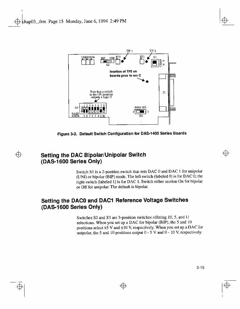
Figure 3-2.
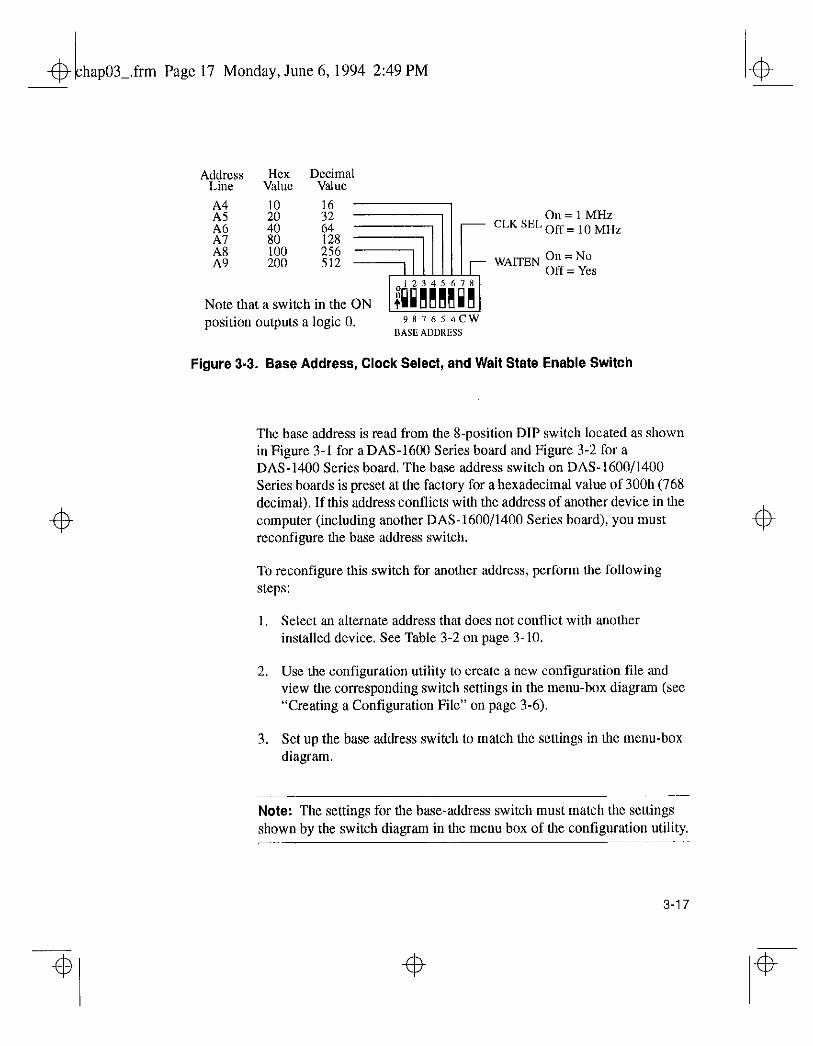
Figure 3-3.
Figure 4-1. Figure 4-2. Figure 4-3. Figure 4-4. Figure 4-5. Figure 4-6. Figure 4-7. Figure 4-8. Figure 4-9.
Functional Block Diagram.. I . . .2-2 Expanding the Analog Inputs of DAS-1600/1400 Series Boards.. . . .2-4 Timing Relationships of Conversion Modes. .2-7 Default Switch Configuration for DAS-1600 Series Boards. . . . . . . . .3-14 Default Switch Configuration for DAS-1400 Series Boards. .3-15 Base Address, Clock Select, and Wait State Enable Switch.................................3-17 Attaching an STC-37 Screw Terminal Connector. 4-3 Pin Assignments of the Main I/O Connector (Jl) .4-4 Attaching an STP-37 to the Main I/O Connector .4-5 Attaching an STA-16. . .4-7 STA-16 Terminal Names.. I . .4-7 Cabling and Connections for Attaching an STA-U4-8 STA-U Terminal Names . . .4-9 Pin Assignments of PI0 Cable Connector (52). .4-10 Attaching anEXP-16 or EXP-16/A Expansion Accessory.. . . . .‘. . , . . , . .4-11
Figure 4-10. Attaching an EXP-GP Expansion Accessory ,4- 13 Figure 4-l 1. Attaching Multiple Expansion Accessories. .4-14 Figure 4-12. Attaching Multiple Expansion Accessories
withanSTA-16orSTA-U . . ~ ~ . 4-15
vii
4 1600ug.toc Page viii Monday, June 6, 1994 2:46 PM
4
Figure 4-13. Attaching an ISO- Accessory .4-16 Figure 4-14. A Typical SSH-8 Application .4-16 Figure 4-15. Attaching an SSH-4/A Accessory. .4-17 Figure 4-16. Attaching SSH-8 Accessories .4-18 Figure 4-17. Attaching SSH-8 and STA-16 Accessories, .4-19 Figure 4-18. Typical Measurement and Control Application .4-20 Figure 4-19. Attaching an MB01 Backplane. .4-21 Figure 4-20. Attaching Multiple MB02 Backplanes .4-22 Figure 4-21. MB02 I/O Connections 4-23 Figure 4-22. Connections for Wiring a Signal Source to a
DAS-1600/1400 Series Board Configured for Single-Ended Inputs . . .4-26
Figure 4-23. Three Methods of Wiring Differential Inputs .4-28 Figure 4-24. A Differential Input Configuration that Avoids a
GroundLoop............................4-30 Figure 4-25. Differential Input Configuration with a
GroundLoop............................4-30 Figure B-l. Pin Assignments of Main I/O Connector (II) on
DAS-1600/1400 Series . .B-2 Figure B-2. Pin Assignments of PI0 Cable Connector (52). .B-3 Figure C-l. Analog Trigger Conditions .C-18 Figure C-2. Using a Hysteresis Value. .C- 19
List of Tables Table 1. Table 2. Table 2-l.
Finding Information. xii Related Documents . xiii DAS-1601/1401 Gains, Ranges, and Throughput Rates for Unipolar and Bipolar Selections .2-6 DAS-1602/1402 Gains, Ranges, and Throughput Rates for Unipolar and Bipolar Selections 2-6 Default Configuration File Settings. .3-7 Standard Address Assignments. .3- 10 Standard Interrupt Request (IRQ) Assigmnents .3- 11 EXP-16 and EXP-16/A Terminal Names .4-l I EXP-GP Terminal Names .4-12 MB Series Backplanes. .4-21 DAC Input and Output Connections. .4-31 Troubleshooting Information. . ,7-2 Analog Input Specifications . . . . . . A- 1 Analog Output Specifications . . A-4 Digital I/O Specifications (g-bits on Main Connector). . . . . A-5
Table 2-2.
Table 3-l. Table 3-2. Table 3-3. Table 4- 1. Table 4-2. Table 4-3. Table 4-4. Table 7-1. Table A-l. Table A-2. Table A-3.
4
4
4 1600ug.toc Page ix Monday, June 6, 1994 2:46 PM 4
4
Table A-4.
Table A-5. Table A-6. Table A-7. Table C- 1. Table C-2. Table C-3.
Table C-4. Table C-5. Table C-6.
Table C-7.
Table C-8.
Table C-9.
Digital I/O Specifications (24-bits on Auxiliary Connector) Programmable Counter/Timer Specifications. Power Supply Requirements. . Environmental Specifications Supported Gains and Gain Codes Logical and Physical Channels Pseudo-Digital Output Channels (Burst / SSH Mode). Default Settling Times. Common Settling Times Pseudo-Digital Output Channels (Analog Trigger) Digital I/O Channel Usage; No EXPs, All Ports Output Digital I/O Channel Usage; EXPs Used, All Ports Output . . Digital I/O Channel Usage; No EXPs, A and B Output, CL and CH Input.
A-5 A-6 A-6 A-7 .C-6 .c-I
.c-9 .c-12 .C-13
.c-15
.c-21
.c-22
.c-23 Table C- 10. Digital I/O Channel Usage;
No EXPs, B and CH Output, A and CL Input. .C-23 Table C-l 1. Digital I/O Channel Usage; No EXPs .C-24 Table C-12. Digital l/O Channel Usage; EXPsUsed .C-24 Table C- 13. Counter/Timer Functions. .C-25 Table C-14. Interrupt Vectors . . . . . .C-26 Table C- 15. Error Messages .C-27 TableE-1. Register-Level Address Map. . . . . .E-2 Table E-2. DAC Bipolar Output Modes .E-9 Table E-3. DAC Unipolar Output Modes . .E- 10 Table E-4. Logic State of Status Register A; MUX (Bit 5). .E-11 Table E-5. Logic State of Status Register A; UB (Bit 6) .E-1 I Table E-6. Control Register: Pacer Clock Source Selection .E-12 Table E-7. Control Register: Interrupt Level Selection
Bits4,5, and 6.. . . . . .I%13 Table E-8. Gain Selection/Burst Rate Register:
Gain Selection Bits 0 and 1 .E-16 Table E-9. Counter/Timer Address Map. .E- 18 Table E-10. 82C54 Counterlrimer Control Register:
Selecting Functionality . . .E-24 Table E- 11. 82C54 Counter/Timer Control Register:
Bits 4 and 5 . . . . . . . . . . . . . . . . . . . . . . . . . . . ..E-~
4
ix
4 4
4 1600ug.toc Page x Monday, June 6, 1994 2:46 PM
Table E-12. 82C54 Counterlrimer Control Register: Readback Command .E-26
Table E-13. Counter Status Byte Selection: Bits 0, 1, and 2. .E-27 Table E- 14. PPI Register Address Map. E-28 Table E- 15. Mode Selection for Ports A and CH .E-30 Table E- 16. PI0 Control Word. . .E-3 1
4
reface.frm Page xi Monday, June 6, 1994 2:47 PM
Preface
This guide is for persons needing to understand the installation, interface requirements, functions, and operation of the following products:
. The DAS-1601 and DAS-1602 boards, which are referred to collectively as DAS- 1600 Series boards.
. The DAS-1401 and DAS-1402 boards, which are referred to collectively as DAS-1400 Series boards.
Unless this manual refers specifically to a particular board, it refers to all models collectively as the DAS-1600/1400 Series boards.
To follow the information and instructions contained in this manual, you must be familiar with the operation of an IBMTM PC/XT or compatible in the MS-DOS’ or WindowsTM environment. You must also be familiar with data acquisition principles and their applications.
Manual Organization
Table 1 lists the topics that this guide focuses on and indicates where you can find information about a topic.
Table 1. Finding Information
xi
4
reface.frm Page xii Monday, June 6, 1994 2:47 PM
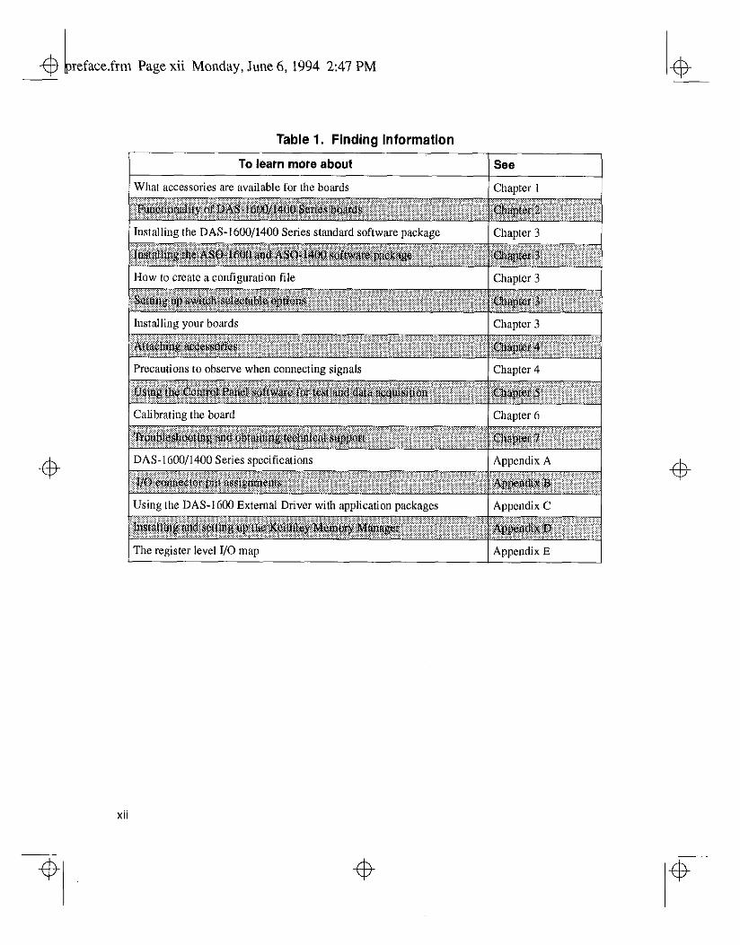
Table 1. Finding Information
reface.frm Page xiii Monday, June 6, 1994 2:47 PM
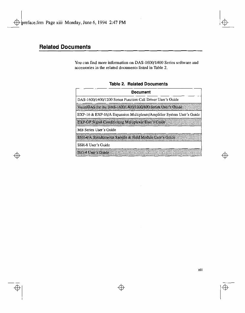
Related Documents
You can fiud more information on DAS-1600/1400 Series software and accessories in the related documents listed in Table 2.
Table 2. Related Documents
Document
DAS-1600/1400/1200 Series Function Call Driver User’s Guide
MB Series User’s Guide I
SSH-8 User’s Guide
4 reface.frm Page xiv Monday, June 6.1994 247 PM
4
4 hapOlL.frm Page 1 Monday, June 6,1994 2:48 PM
Overview
4
The DAS-1600/1400 Series is a family of high-performaucc analog and digital I/O boards for IBM PC/XT, PC AT, and compatible computers. The DAS-1601 and DAS-1401 are high-gain boards, while the DAS-1602 and DAS-1402 are low-gain boards.
This chapter describes the features of the DAS-1600/1400 Series boards, the software that supports them, and available accessories.
Features
4
4 The features shared by the DAS-1600 Series and DAS-1400 Series are as follows:
. Boards are switch-configurable for 16 single-ended or eight differential analog input channels.
. Analog inputs are switch-configurable for either unipolar (O-10 V) or bipolar (*lo V) signals.
. Analog input channels are individually programmed for gain. The DAS-1601/1401 have programmable gaius of I, IO, 100, and 500. The DAS-1602/1402 have programmable gains of 1, 2,4, and 8.
. Analog inputs are sampled at a maximum of 100 ksamples/s with 12-bit resolution.
. The base I/O address and Direct Memory Address (DMA) channel are switch-configurable; interrupt levels are software-configurable.
l-l
4 4
hapOlL.frm Page 2 Monday, June 6,1994 2:48 PM
l Burst mode sampling capability emulates simultaneous sample-and-hold (SSH) operation,
. Analog-to-digital (A/D) conversions can be started through any of the following methods:
- software command
- onboard pacer clock
- external pacer clock
. External Simultaneous Sample-and-Hold (SSH) hardware is supported.
. Data transfers can be performed by any of the following methods:
- program control
- interrupt service routines
- DMA transfer
. The boards perform g-bit data transfers on the ISA bus.
. A 3-channel programmable counter/timer (82C54) provides timing for analog input operations or generation of output pulses at any rate from to 1 pulse/hour to 100 kHz. The 82C54 counter/timer can also be used to measure frequency, period, and pulse width.
. The boards have four unidirectional digital inputs and four unidirectional digital outputs.
. The boards are backward compatible with the DAS-16Gl and DAS-16G2 boards.
Programs for the DAS-16Gl and DAS-16G2 boards run on the DAS-1600 Series without modification. The DAS-1400 Series maintains backward compatibility with the analog input section of the DAS16Gl.
I-2 Overview
43 k hapOlL.frm Page 3 Monday, June 6, 1994 2:48 PM
DAS-1600 Series boards provide the following additional features:
. Two 12.bit digital-to-analog converter (DAC) channels. The outputs of these channels have switch-configurable output ranges of O-5 V, O-10 V, *5 V, and&l0 V full scale. In addition, you can apply an external reference to provide analog outputs in other ranges or to use the DACs as programmable attenuators.
. Additional % bits of bidirectional digital I/O via the PI0 cable connector (52). These 24 bits are configured as two B-bit ports and two 4-bit ports that you can set independently for input or output.
The 24.bit digital port is compatible with the PIO-I2 board. You can use these ports to gate the counter/timer, conuol multiplexers, and read the status of external devices.
For more information on these features, refer to the functional description in Chapter 2.
Supporting Software
The following software is available for operating DAS-1600/1400 Series boards:
. DAS-1600/1400 Series standard software package -This package, which comes with the board, is provided on U-inch and 5.25.inch diskettes. The package includes function libraries for writing application programs under DOS using Microsoft’ QuickBasic’rM, Microsoft@ Professional Basic, or Microsoft’ Visual BasicTM for DOS. The package also includes support files, example programs, and the following utility programs:
- Configuration Utility -The configuration utility (CFG1600.EXE) is a DOS-based program for creating or modifying a DAS-1600/1400 Series configuration file.
1-3
.frm Page 4 Monday, June 6, 1994 2:48 PM
A configuration file contains the settings used by the DAS-1600/1400/1200 Series Function Call Driver and other driver software for configuring a board. For more information on the configuration utility, refer to “Creating a Configuration File” on page 3-6.
Calibration Utility - The calibration utility (CAL1600,EXE or CAL1400.EXE) is a DOS-based program for calibrating the analog I/O circuitry of DAS-1600/1400 Series boards, For more information on the calibration utility, refer to Chapter 6.
- Confrol Panel - The Control Panel (CTL1600,EXE) is a DOS-based stand-alone program. This tool provides access to all DAS-1600/1400 Series board operations without programming.
The Control Panel provides a means of testing the board and your application; it is also a means of performing simple applications and saving data to a disk tile. Refer to Chapter 5 for more information about the Control Panel.
- DAS-1600 External Driver - The External Driver (DAS1600,EXE) for DAS-1600, DAS-1400, and DAS-1200 Series boards provides control and communication between data acquisition and analysis packages and the boards.
DAS 1600.EXE executes as a terminate-and-stay-resident (TSR) program that occupies a small amount of memory in the host.
. ASO- and ASO- -Advanced Software Option. This option includes both Windows and DOS versions; both versions are supplied on 3.5.inch and 5.25-inch diskettes. The ASO- and ASO- include function libraries for application programs that you write for MS-DOS and Windows environments in the following languages:
- Microsoft and Borland’ C/C++
- Borland Turbo Pascal@
- Microsoft Visual Basic for Windows
- Microsoft Quick@
- Microsoft Visual CHUM
1-4 Overview
irrn Page 5 Monday, June 6,1994 2:48 PM
Refer to the DAS-1600/1400/1200 Series Function Cull Driver User’s Guide for more information.
The ASO- and ASO- software package also contains miscellaneous support files, example programs, and the following:
Confgurution Utility - The configuration utility (CFG 1600.EXE) is a program for creating or modifying a DAS-1600/1400 Series configuration file.
A configuration file contains the settings used by the DAS-1600/1400/1200 Series Function Call Driver and other driver software for configuring a board. For more information on the configuration utility, referto “Creating a Configuration File” on page 3-6.
- Calibration Utility - The calibration utility (CAL1600.EXF or CAL1400.EXE) is a DOS-based program for calibrating the analog I/O circuitry of the DAS-1600/1400 Series boards. For more information on the calibration utility, refer to Chapter 6.
- Control Panel -The Control Panel is a stand-alone program supplied in a DOS version (CTL1600,EXE) and a Windows version (CTL1600W.EXE). This program provides access to all DAS-1600/1400 Series operations without programming.
Control Panel operations include acquiring analog inputs, controlling analog outputs, and controlling digital I/O. The control panel provides a means of testing the board and your application: it is also a means of performing simple applications and saving data to a disk file.
The Windows version allows you to graphically represent up to eight analog inputs and transfer acquired data to other Windows applications through the Windows Dynamic Data Exchange (DDE) feature. Refer to Chapter 5 for more information on the Control Panel.
- Port 110 software - If you are programming in the Windows environment, you can use the Port I/O (PIO) software to program DAS-1600/1400 Series boards at the register level using I/O instructions. Refer to the PORTIO.TXT file for more information.
1-5
4 hapOl_.frm Page 6 Monday, June 6, 1994 2:48 PM
4
VDAS-1600 - VisualDASTM Custom Controls for Visual Basic for Windows. VisualDAS simplifies the setup of data acquisition operations. The package includes a comprehensive user’s guide, offers extensive online help, and furnishes software on 3.5-inch and 5.25-inch diskettes.
Dab acquisition and analysis application software VIEWDAC@, EASYEST LX@, and EASYEST AGTM are integrated software packages available for DAS-1600/1400 Series boards, Programming tools, such as ASYST@ scientific and engineering programming Ianguage, are also available to help you in writing your application programs.
Note: If you use VIEWDAC, EASYEST LX, EASYEST AG, or ASYST to program your DAS-1600/1400 Series board, you must use the DAS-1600 External Driver. This driver is included in the DAS-1600/1400 Series standard software package and is described in Appendix C.
Other data acquisition and analysis packages include the following:
- SNAP-MASTER - Data acquisition and analysis package from H.E.M. Data Corporation (only available for Windows).
- NOTEBOOKhJOTEBOOKpro Menu-driven data acquisition and analysis from Laboratory Technologies Corporation (available for both DOS and Windows).
- STREAMER Menu-driven data acquisition software for high-speed transfers of DAS-1600/1400 Series data to a hard disk (only available for DOS).
l-6 Overview
& ! hapOlLkm Page 7 Monday, June 6, 1994 2:48 PM
4
Accessories
The following accessories are available for use with the DAS-1600/1400 Series boards.
.
.
.
.
.
.
.
.
.
.
STA-16 - Screw terminal adapter accessory. You can use this accessory to connect signals from the main I/O connector (Jl) to screw terminals.
STA-U - Universal screw terminal accessory. You can use this accessory to connect signals from the PI0 cable connector (52) to screw terminals,
STC-37 - Direct DAS-1600/1400 Series board to screw terminal interface.
STP-37 - Screw terminal panel with a 37.pin D-type connector.
NO-4 -4-channel isolated expansion multiplexer.
SSH-4/A 4-channel simultaneous sample-and-hold accessory.
SSH-8 S-channel simultaneous sample-and-hold accessory.
MB Series modules and backplanes -Plug-in, isolated, signal-conditioning modules and the backplanes that hold them.
EXP-16 and EXP-16/A 16-channel expansion multiplexer and signal conditioning boards; requires the S- 1600 cable and the PG-408A option.
EXP-GP - S-channel signal conditioning board with Wheatatone bridge and RTD interface; requires the S-1600 cable.
1-7
4 I hap0lLfrm Page 8 Monday, June 6, 1994 2:48 PM
hap02-.frm Page 1 Monday, June 6,1994 2:48 PM
2 Functional Description
This chapter describes the following features of DAS-1600/1400 Series boards:
. Analog input features
l Analog output features
. Digital I/O features
. 82C54 counter/timer features
l Wait state selection
s Power
These descriptions are offered to familiarize you with the operating options and to enable you to make the best use of your board. The block diagram in Figure 2-1 represents both the DAS-1600 and DAS-1400 Series boards.
2-1
hap02Lfrm Page 2 Monday, June 6, 1994 2:48 PM
/ DASl6WSerlesonly /
i ,. ,. DASlGW Series only
2-2
interval timer
ISA PC AT, PWT BIJS
Figure 2-1. Functional Block Diagram
Functional Description
hap02-.frm Page 3 Monday, June 6,1994 2:48 PM
Analog input Features
The analog input section of a DAS-1600/1400 Series board multiplexes all the active input channels (up to 16 single-ended or eight differential) down to a single, 12-bit sampling analog-to-digital converter (ADC).
Other features of this section include input configurations, gain selection, conversion modes, triggers, clock sources, and data transfer modes. These features are described in the following sections.
Differential/Single-Ended Selection
Using configuration switches, you can select either eight differential or 16 single-ended inputs. Differential inputs measure the difference between two signals. Single-ended inputs are referred to a common ground.
Generally, you want to use differential inputs for low-level signals whose noise component is a significant part of the signal or for signals that have non-ground common mode. You want to use single-ended inputs for high-level signals whose noise component is not significant.
The specific level at which input configurations work best is dependent upon the application. However, you generally use differential inputs for voltage ranges of 100 mV and less.
UnipolarlBipolar Selection
Using configuration switches, you can set the DAS-1600/1400 Series boards to operate in either unipolar or bipolar input mode. A unipolar signal is always positive (0 to 10 V, for example), while a bipolar signal can swing up and down between negative and positive peak values (-10 V to +lO V, for example).
The DAS-160011400 Series boards use left-justified, offset binary to represent signals. In a given input range with the same peak-voltage capacity for both modes, unipolar mode doubles the converter’s resolution.
4
2-3
4 4
.frm Page 4 Monday, June 6, 1994 2:48 PM
Channel Selection in Expanded Configurations
As previously mentioned, the DAS-1600/1400 Series supports 16 single-ended or eight differential analog input channels. If you require additional analog input channels or signal conditioning for transducer inputs, you can use any combination of up to eight 16.channel EXI-16 or EXP-16/A expansion boards, and/or eight X-channel EXP-GP expansion boards to increase the number of available channels to 128.
When you daisy-chain expansion boards from the analog inputs, it is recommended that the first expansion board multiplex onboard channel 0, the next expansion board multiplex channel 1, and so on. Selection of an onboard channel is made via jumper settings on the expansion board.
You can access any unused onboard channels by including an STA-16 screw terminal accessory in the daisy-chain configuration. Figure 2-2 illustrates how expansion boards and accessories interface with the analog channels of DAS-1600/1400 Series boards.
DAS-1600/1400 Series Soards
Figure 2-Z. Expanding the Analog Inputs of DAS-1600/1400 Series Boards
2-4 Functional Description
-@- -
hap02Lfrm Page 5 Monday, June 6,1994 2:48 PM
You can also use up to four MB02 backplanes to increase the number of available channels to 64 isolated or 12 non-isolated. For more information about connecting channel expansion boards, refer to Chapter 4.
Notes: You must specify a single-ended iuput configuration for all onboard channels associated with channels on MB02 backplanes.
If you are using EXP-16, EXP-16/A, or EXP-GP expansion accessories or MB Series backplanes, the digital output lines of the DAS-1600/1400 Series board select a particular channel on the expansion board or backplane to read.
Gain Selection
The programmable gain that you select is applied to an incoming signal as a multiplication factor; gain allows you to amplify a signal to a range that the ADC can accurately measure.
For example, if the ADC handles signals in the f10 V range and you want to measure a signal in the range of 311.0 V, you would use a gain of 10 to amplify the signal to the f10 V range. Similarly, if you wanted to measure a sigual that was already in the f10 V range, you would select a gain of 1.
The available gains, lheir corresponding input ranges, and throughput rates are listed in Table 2-1 for the DAS-1601/1401 and Table 2-2 for the DAS-1602/1402.
2-5
4 I hap02Lfrm Page 6 Monday, June 6, 1994 2:48 PM
Table 2-1. DAS-1601/1401 Gains, Ranges, and Throughput Rates for Unipolar and Bipolar Selections
Gain Unipolar Range Bipolar Range Maximum
Throughput Rate
100 ksamples/s
500 0.0 to +20 mv -20 to +20 mv 30 ksmplesls
Table 2-2. DAS-1602/1402 Gains, Ranges, and Throughput Rates for Unipolar and Bipolar Selections
Gain Unipolar Range Bipolar Range Maximum
Throughput Rate
Conversion Modes
DAS-1600/1400 Series boards support the following conversion modes:
. Paced mode - Paced mode is the default data conversion mode and is the mode best-suited for continuous scanning of multiple channels at a constant rate. In paced mode, the conversion rate equals the pacer clock rate. The sample rate, which is the rate at which a single channel is sampled, is the pacer clock rate divided by the number of channels being sampled.
2-6 Functional Description
.frm Page 7 Monday, June 6,1994 2:48 PM
. Burst mode - In burst mode, each pulse from the pacer clock begins a scan of one to sixteen channels. The conversion rate during a burst mode scan is equal to the rate of the burst mode conversion clock. The sample rate, which is the rate at which a single channel is sampled, is equal to the pacer clock rate.
DAS-1600/1400 Series software allows you to program the pacer clock to adjust the interval between burst mode scans. This software also allows you to adjust the burst mode conversion rate. The burst mode conversion clock frequency is programmable for a range of 3.94 kHz to 100 kHz.
Burst mode can also be used for pseudo-simultaneous sample-and-hold in conjunction with DMA or interrupt operations.
The sample rate (pacer clock rate) should be set for no more than the burst mode conversion clock rate divided by the number of channels in the burst. The maximum burst mode conversion clock rate is gain-sensitive, as shown in Table 2-1 and Table 2-2.
Figure 2-3 shows the timing relationships of the paced and burst modes for analog input channel 4 to channel 7.
Pacer Clock 1 L Paced Mode Convemkms CM Ch5
Burst Mode Convenlona cl,4 cl,5 ch6 ch7 cl,4 CM ch6 cl,7
Burst Mode ConversIon Clock r-i nrLrln
Figure 2-3. Timing Relationships of Conversion Modes
2-7
.frm Page 8 Monday, June 6, 1994 2:48 PM
4
Clock Sources
The following clock sources are available for conversions on DAS-1600/1400 Series boards:
. Software - DAS-1600/1400 Series boards allow you to acquire single or multiple samples under program control.
. Hardware (internal clock source) - The internal pacer clock is derived from the onboard UC54 counter/timer and a switch-configurable, crystal-controlled 1 MHz or 10 MHz timebase. The pacer clock uses two cascaded counters of the 82C54. The maximum allowable rate is 100 ksamples/s, and the minimum conversions per hour is determined as follows:
1OMHz ~ = 2.328 x 10-3= 8.38
IMHZ ~ 232 232 = 2.328x 10m4= 0.838
When not used to pace the analog input, the internal clock source can pace other events, such as digital I/O and analog outputs (on the DAS-1600 Series boards), through the use of intermpts.
. Hardware (external clock source) -The external pacer clock source must be an externally applied, TTL-compatible, rising-edge signal attached to the IPO/TRIG O/KPCLK pin (25) of the main I/O connector (Jl).
An external clock source is useful if you want to pace at rates not available with the 82C54 counter/timer, if you want to pact at uneven intervals, or if you want to pace on the basis of an external event. An external clock also allows you to synchronize multiple boards with a common timing source.
4
4
Functional Description
4 I@
hap02Lfrm Page 9 Monday, June 6,1994 2:48 PM
Notes: The ADC acquires samples at amaximnm of 100 ksamples/s (one sample every 10.0 ps). If you are using an external clock, make sure that it does not initiate conversions at a faster rate than the ADC can handle.
If you are acquiring samples from multiple channels, the maximum sampling rate for each channel is equal to 100 ksamples/s divided by the number of channels.
Triggers
A trigger starts an analog input operation. The polarity of external triggers in the DAS-1600/1400 Series boards is software-cotlfigurable, You can use one of the following trigger sources to start an analog input operation:
. Internal - When you enable the analog input operation, conversions begin immediately.
. External Analog -While an analog trigger is not a hardware feature of the DAS-1600/1400 Series boards, you can program an analog trigger using one of the analog input channels as the trigger channel. The DAS-1600/1400/1200 Series Function Call Driver provides functions for an analog trigger; refer to the DAS-1600/1400/1200 Series Function Call Driver User’s Guide for more information.
l External Digital - While a digital trigger is not a hardware feature of the DAS-1600/1400 Series boards, you can program a digital trigger using one of the digital input channels as the trigger channel. The DAS-1600/1400/1200 Series Function Call Driver provides functions for a digital trigger; refer to the DAS-1600/1400/1200 Series Function Call Driver User’s Guide for more information,
Connect the digital trigger to the digital input IPl/XTRIG pin (6) of the main I/O connector (Jl). Trigger types are as follows:
- Positive-edge trigger - Conversions begin on the rising edge of the trigger signal.
- Negative-edge trigger - Conversions begin on the falling edge of the trigger signal.
4
2-9
4 4
.frm Page 10 Monday, June 6,1994 2:48 PM
Positive-level trigger - Conversions begin when the signal is above a positive level. See Table A-3 on page A-5 for logic levels.
- Negative-level trigger - Conversions begin when the signal is below a negative level. See Table A-3 on page A-5 for logic levels.
Data Transfer Modes
You can transfer data from the DAS-1600/1400 Series boards to the computer using the following data transfer modes:
Single mode - In a single-mode operation, a data acquisition board acquires a single sample from a single channel: you cannot perform any other operation until the single-mode operation is complete.
Synchronous - In a synchronous-mode operation, a data acquisition board acquires one or more samples from one or more channels; you cannot perform any other operation until the synchronous-mode operation is complete.
Interrupt You can program the board to acquire data, then generate an interrupt when data is available for transfer. Wheo interrupt mode is used, data is transferred by an interrupt service routine; you can perform other operations while an interrupt mode operation is in progress. The interrupt level is software-configurable.
Unpredictable interrupt latencies in the Windows environment tend to make maximum board speeds unachievable in the interrupt mode. When in the Windows environment, you are advised to use DMA mode instead of interrupt mode.
DMA - DMA is a method of bypassing the CPU to transfer data directly between an I/O device and computer memory. In the IBM PC family, DMA is directed by the DMA controller and executes independently while the CPU is executing other instructions. Therefore, you can perform other operations while a DMA mode operation is in progress. The ability to run independently of the CPU and at high-transfer rates makes DMA an attractive method for transferring data in data acquisition systems.
2-l 0 Functional Description
+b I hap02-.frm Page 11 Monday, June 6, 1994 2:48 PM
+
DAS-1600/1400 Series boards can use either DMA channel I or 3 to perform single-cycle DMA transfers of A/D data from the board to memory.
Generally, if you are programming an operation in the Windows Enhanced Mode, you should use DMA to acquire data reliably at maximum board speeds.
Analog Output Features (DAS-1600 Series Only)
The analog output section of DAS-1600 Series boards consists of two digital-to-analog converters (DACs) with 12-bit resolution and a precision voltage source. Both DACs have switch-configurable output ranges of O-5 V, O-10 V, f5 V, f10 V. In addition, you can use external references to generate analog outputs in other ranges. The DACs power up to 0 V at reset.
The two DACs have a capacitive load~.drive up to 100 pF and an output current drive of up to ?;5 mA.
You can pace the analog output with interrupts generated by the onboard pacer clock when the analog inputs are disabled.
You can write single values to the DACs using synchronous mode 01 single mode. You can write multiple values to the DACs using synchronous mode or interrnpt mode.
The DAS-1600 Series provides a -5 V (fO.05 V) precision reference voltage that is derived from the DAC reference voltage. Typical applications for precision voltages are providing a DC reference input for the DACs and providing offsets and bridge excitation to user-supplied input circuits.
2-11
.frm Page 12 Monday, June 6,1994 2:48 PM
4
Digital I/O Features
DAS-1600/1400 Series boards contain four digital inputs (IPO to IP3) and four digital outputs (OPO to OP3) that are accessible through the main I/O connector (Jl).
Logic I on an I/O Line indicates that the input/output is high; logic 0 on an I/O line indicates that the input/output is low (see Table A-3 on page A-5 for logic levels). The digital inputs are compatible with TTL-level signals, These inputs are provided with 10 kQ pull-up resistors to +5 V, therefore, the inputs appear high (logic I) with no signal connected.
The DAS-1600 Series boards have an additional 24 bits of bidirectional digital I/O available on the PI0 cable connector (J2). These 24 bits are configured as two X-bit ports (A and B) and two 4-bit ports (CL and CH); you can set each port independently for input or output.
You can use the digital inputs and outputs for any general-purpose tasks except the following:
. If you are using an external digital trigger or gate, you must use digital input line IPl/XTRIG to attach the trigger and digital input line IP2/CTR 0 GATE to attach the counter 0 gate signal. In either of these cases, you cannot use the corresponding bit for general-purpose digital input.
. If you are using an external pacer clock, you must use digital input line IPODRIG O/XPCLK to attach the external pacer clock signal: in this case, you cannot use IPO/TRIG O/XPCLK for general-purpose digital input.
When the analog inputs are disabled, you can pace the digital I/O with interrupts generated by the onboard pacer clock.
You can read and write a single value from and to a DAS-1600/1400 Series board using synchronous mode or single mode. You can read and write multiple values from and to a DAS-1600/1400 Series board using synchronous mode or interrupt mode.
4
4
z-12 Functional Description
43 hap02-.frm Page 13 Monday, June 6, 1994 2:4X PM
4+
Counter/Timer Features
The DAS-1600/1400 Series includes an 82C54 with three programmable counters. Counters 1 and 2 are permanently cascaded and are used as the internal A/D pacer clock.
Counter 0 is not used by the board, but can be used for functions such as waveform generation, measuring frequency and period, and generating time delays. You access counter 0 functions through the board’s l/O registers or through the Function Call Driver.
Note: Attempts to combine register-level programming of counter/timer functions with Function Call Driver programming can produce unexpected results because the Function Call Driver relies on structures it sets up.
You can use software to select IPO/TRIG O/XPCLK (pin 25) of the main I/O connector for use as a hardware gate. The gate provides a means of holding off clock pulses (from counteis 1 and 2) to the ADC until IPO/TRIG O/XPCLK goes high.
2-13
43 hap02-.frm Page 14 Monday, June 6, 1994 2:48 PM
Wait State Selection
Although most current-generation PCs and compatibles extend bus cycles during S-bit data transfers, the DAS-1600/1400 Series provides a switch-configurable option that allows you to enable or disable wait states that extend bus cycles during 8-bit data transfers.
Inclusion of this option maintains backward compatibility with DAS- 16Gx Series boards that may be used in early generation machines.
Power
2-14
+5 V power is available from tbe main I/O connector. The +5 V supply is brought out from your host computer.
Functional Description
.frm Page 1 Tuesday, June 7,1994 3:lO PM
4
3 Setup and Installation
This chapter describes inspection, software installation, configuration, and hardware installation for DAS-1600/1400 Series boards.
Read this chapter before you attempt to install and use your DAS-1600/1400 Series board.
Inspecting Your Package
Caution: A discharge of static electricity from your hands can seriously damage certain electrical components on any circuit board. Before handling any board, discharge static electricity from yourself by touching a grounded conductor such as your computer chassis (your computer must be turned off). Whenever you handle a board, hold it by the edges and avoid touching any board components, cable connectors, or gold-plated edge connectors.
Use the following procedure to unwrap and inspect a DAS-1600/1400 Series board:
1. Factory packaging of the DAS-1600/1400 Series boards includes a final wrap of protective, anti-static material. Remove the board from its anti-static wrapping material. You may wish to store the wrapping material for possible future use.
2. Inspect the board for signs of damage. If damage is apparent, arrange to return the board to the factory (see “Technical Support” on page 7-6).
4
3-I
4 ! hap03Lfrm Page 2 Monday, June 6,1994 2:49 PM
4
3. Check the remaining contents of your package against the packing list to be sure your order is complete. Report any missing items immediately.
4. When you are satisfied with the inspection, proceed with the software and hardware setup instructions.
Note: Data acquisition products are factory calibraled; they require no further adjustment prior to installation. If at a later time you decide to recalibrate the board, refer to Chapter 6 for instructions.
lnstallina the Software Package
This section provides installation procedures for the DAS- 1600/1400 Series standard software package and the ASO- and ASO- software package. Before you work with the software from any package, make a copy of all diskettes in the package. Use the copies as your working diskettes, and store the originals as backup diskettes.
Installing the DAS-1600/1400 Series Standard Software
The DAS-1600/1400 Series standard software package is for the DOS environment only. Use the following procedure to install this package:
1. Insert diskette #l into an appropriate floppy-disk drive of your computer,
2. Change to the drive containing the diskette and enter the following at the DOS prompt:
INSTALL
3. Respond to the installation program prompts.
4. When the installation program requests a designation for the drive that is to receive your software, enter a designation of your choosing or defer to the default designation of C.
4
4
3-2 Setup and Installation
4
hap03_.frtn Page 3 Monday, June 6, 1994 2:49 PM
5. When the installation program requests a name for the directory that is to receive the software, enter a name of your choosing or accept the default name.
The installation program automatically creates a hierarchical directory tree on the specified drive and then copies all files, expanding any compressed files, to the new directory.
6. Insert any additional disks, as required by the installation program.
The installation program notifies you when it completes the installation. After the installation, you may want to review the following files:
l README.TXT - An ASCII text file containing information available after the publication of this manual.
l EXAMPLEKTXT - An ASCII text file containing notes and tips on how to successfully compile and execute the supplied example programs.
l FILESTXT - An ASCII text file that lists and describes all the files that can be installed.
Installing the ASO- and ASO- Advanced Software Option
The ASO- and ASO- advanced software option contains software for both the DOS and Windows environments. This section contains procedures for installing both versions.
DOS lnsfallation
Use the following procedure to install the DOS version of the ASO- and ASO- software package:
1. Insert diskette #l into an appropriate floppy-disk drive of your computer.
3-3
hap03-.frm Page 4 Monday, June 6,1994 2:49 PM
2. Change to the drive containing the diskette and enter the following at the DOS prompt:
INSTALL
3. Respond to the installation program prompts.
4. When the installation program requests a designation for the drive that is to receive your software, enter a designation of your choosing or defer to the default designation of C.
5. When the installation program requests a name for the directory that is to receive the software, enter a name of your choosing or accept the default name.
The installation program automatically creates a hierarchical directory tree on the specified drive and then copies all files, expanding any compressed files, to the new directory.
6. Insert any additional disks, as required by the installation program.
The installation program notifies you when it completes the installation. After the installation, you may want to review the following files:
. README.TXT - An ASCII text file containing information available after the publication of this manual.
. EXAMPLESTXT - An ASCII text file containing notes and tips on how to successfully compile and execute the supplied example programs.
l FILES.TXT - An ASCII text file that lists and describes all the files that can be installed.
Windows Installation
Use the following procedure to install the Windows portion of the ASO- and ASO- software package:
1. Insert diskette #l into an appropriate floppy-disk drive of your computer.
2. Enter the Windows environment,
3-4 Setup and Installation
+b hap03-.frm Page 5 Monday, June 6, 1994 2:49 PM
3. From the Program Manager Pile menu, select Run.
4. In the Command Line text box, type the letter of the drive containing your Windows diskette and follow with SETUP. For example, if your diskette is in drive B, type the following:
B : SETUP
5. Select OK.
6. Respond to the installation program prompts.
7. When the installation program requests a designation for the drive that is to receive your software, enter a designation of your choosing or defer to the default designation of C.
8. When the installation program requests a name for the directory that is to receive the software, enter a name of your choosing or accept the default name.
The installation program automatically creates a hierarchical directory tree on the specified drive and then copies all files, expanding any compressed files, to the new directory.
The installation program also creates a DAS- 1600 program manager group containing icons for all DAS-1600 programs and information tiles.
9. Insert any additional disks, as required by the installation program
The installation program notifies you when it completes the installation. After the installation, you may want to review the following files:
l README.TXT - An ASCII text file containing information available after the publication of this manual.
l EXAMPLES.TXT - An ASCII text file containing notes and tips on how to successfully compile and execute the supplied example programs.
l FILESTXT - An ASCII text file that lists and describes all the files that can be installed.
3-5
+b hap03Lfrm Page 6 Monday, June 6, 1994 2:49 PM
Creatinn a Configuration File
The configuration Ile contains a list of the configuration options and a setting for each. The file is used by application packages such as VIEWDAC and EASYEST LX as well as programs wrilten using the Function Call Driver. When you set up software to operate your DAS-1600/1400 Series board, you specify the name of the configuration file.
The switch-configurable options that you enter into the configuration file are also used to create a graphic representation that you can use as a reference when you set up switches on your board. Setting switch-configurable options is discussed under “Setting Switch-Configurable Options” on page 3-14.
The configuration file you specify can be either the default configuration file for the board you are installing or a file you create with the configuration utility. The following sections describe the default configuration file and the configuration utility.
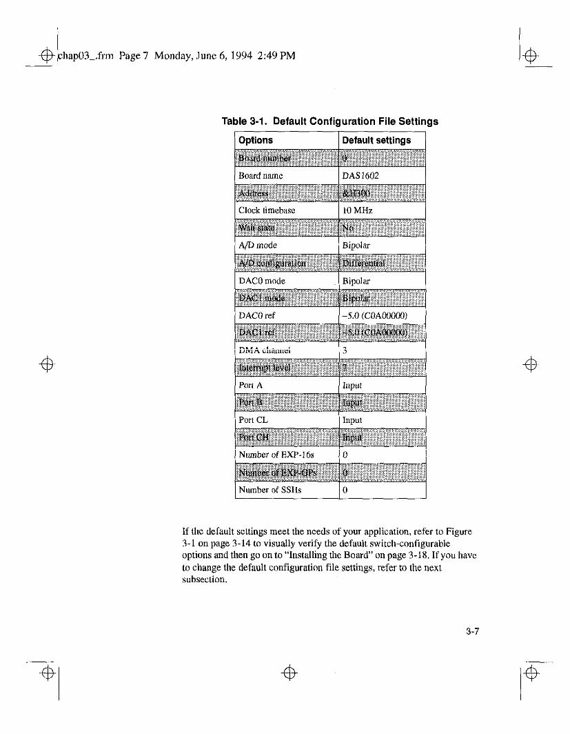
Default Configuration File
3-6
A default configuration tile called DAS1600.CFG is provided in both the DAS-1600/1400 Series standard software package and the ASO-I 600 and ASO- software package. The default configuration file contains an ASCII list of the configuration options that apply to a DAS-1602 board.
Table 3-l lists the configuration options and their default settings.
Setup and Installation
4+ ! hap03Lfrtn Page 7 Monday, June 6, 1994 2:49 PM
Table 3-1. Default Configuration File Settings
Port A
If the default settings meet the needs of your application, refer to Figure 3-1 on page 3-14 to visually verify the default switch-configurable options and then go on to “Installing the Board” on page 3-18. If you have to change the default configuration file settings, refer to the next subsection.
3-7
43 hap03-.frm Page 8 Monday, June 6,1994 249 PM
Configuration Utility
The configuration utility, CFG1600,EXE. is furnished in both the DAS-1600/1400 Series standard software package and the ASO- and ASO- software package. This utility enables you to modify an existing configuration file or to create a new configuration file for up to two boards. To modify or create a configuration file, use the following procedure:
1. Start the configuration utility from DOS or Windows as follows:
- From DOS, change to the directory containing CFG1600.EXE and enter the following at the DOS prompt:
CFG1600 <filename>
where the optional <filename> is the name of the configuration file you want to modify or create. If the file is not located in your default directory, include its full pathname.
- From Windows, select Run from the Program Manager File menu. Enter the following in the Command Line dialog box, and select, OK.
path CFG1600 <filename>
where path is the complete path to CFG 1600.EXE and the optional <filename> is the name of the configuration tile you wish to modify or create. If tbe file is not located in your default directory, include its full pathname.
Whetherfilename is an existing file in the directory containing CFG1600,EXE or a file to be created, it is the name displayed by the configuration utility’s opening screen. However, the settings displayed forfilenume may differ as follows:
Iffilename is an existing file, the configuration utility displays the settings contained in this existing file.
Iffilename is a file to be created, the configuration utility displays the default configuration settings.
3-8 Setup and Installation
f& b hap03-.frm Page 9 Monday, June 6.1994 2:49 PM
If no entry was made forfilename, the configuration utility displays the default configuration file DAS 1600.CFG.
Note: If you alter the default configuration file, you should rename il and then create a new default configuration file by starting the configuration utility with nofilename and saving the results without change.
DAS-1601 DAS-1401 DAS-1201
DAS-1602 DAS-1402 DAS-1202
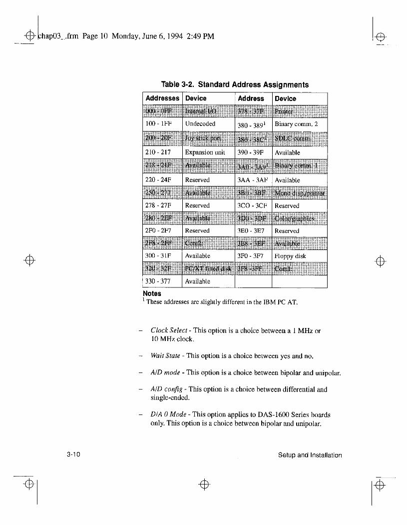
- Ease address -This option requires selection of a 3-digit hexadecimal address, The addresses you can select range from 200h to 3FOh. Base addresses presented for selection begin on even boundaries that increment by 16 (OOFh).
When selecting a base address, do not select an address that conflicts with those already in use. Table 3-2 lists standard address assignments and their corresponding devices.
2. In the opening screen, enter the number of boards you plan to configure (1 or 2).
After you make this entry, the utility program displays the configuration witldow for the first board (board 0, which is shown in the upper-left corner of the window). The window contains the following configuration options:
- Board name -This option identifies the board you are installing. You can select one of the following:
3-9
hap03Lfrm Page 10 Monday, June 6,1994 2:49 PM
Table 3-2. Standard Address Assignments
1 Addresses 1 Device 1 Address 1 Device I
100 1FF Undecoded 380 - 389’ Binary comm. 2
210 - 217 Expansion unit 390 - 39F Available ,..... ..,..,.. ,. ,,-,, ,, ;::++ .I. :..::;:.:.:
.,.. 1:1:::‘r’1~1~~~~~ ~~~~~~~~~~~~~~‘::~~~Ei ~~~~~~~I:.‘:‘:: ~:i’:li.:i’i;i:ii:iii-iiiii:i:‘:‘:i :“:i~:l:‘:~::::.::~::i:.:i:‘::‘:’::’:::”’~.:.:.:.: :.: ~~..~~.~.~..~~..~~.~.~.~.~..~.~, .:.:.,.:, .:, .: ..,..,. ,:.
220 24F Reserved 3AA - 3AF Available
Notes ’ These addresses are slightly different in the IBM PC AT.
- Clock Select - This option is a choice between a 1 MHz or 10 MHz clock.
- Wait State This option is a choice between yes and no.
- A/D mode - This option is a choice between bipolar and unipolar.
- A/D co& - This option is a choice between differential and single-ended.
- D/A 0 Mode - This option applies to DAS-1600 Series boards only. This option is a choice between bipolar and unipolar.
3-10 Setup and Installation
44 - hap03 .frm Page 11 Monday, June 6,1994 2:49 PM
4
- D/A 1 Mode -This option applies to DAS-1600 Series boards only. This option is a choice between bipolar and unipolar.
DMA channel -This option is a choice between DMA channels 3 and 1.
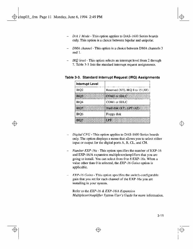
- IRQ level This option selects an interrupt level from 2 through 7. Table 3-3 lists the standard interrupt request assignments.
Table 3-3. Standard interrupt Request (IRQ) Assignments
Interrupt Level
IRQ2 1 Reserved (XT), IRQ 8 to 15 (AT)
IRQ6 Floppy disk
- Digital CFG - This option applies to DAS-1600 Series boards only. The option displays a menu that allows you to select either input or output for the digital ports A, B, CL, and CH.
Number EXf-16s - This option specifies the number of EXP-16 and EXP-16/A expansion multiplexer/amplifiers that you are going to install. You can select from 0 to 8 EXF16s. When a value other than 0 is selected, the EXP-16 Gains option is applicable.
- EXP-I6 Gains - This option specifies the switch-configurable gain that you set for each channel of the EXP-16s you are installing in your system.
Refer to the EXP-16 & EXP-161A Expansion Multiplexer/Amplifier System User:r Guide for more information.
4
4
4 4
3-11
4
frm Page 12 Monday, June 6,1994 2:49 PM
Number EXP-GPs This option specifies the number of EXP-GP general-purpose multiplexer and signal conditioning modules that you are going to install. You can select from 0 to 8 EXP-GPs. When a value other than 0 is selected, the EXP-Cl’ Gains option is applicable.
EXP-GP Gains -This option displays two menus. The first menu selects the switch-configurable gain multiplier that you set up for all EXP-GP channels. The factors you can choose from are Xl or x2.5.
The second level menu selects the switch-configurable gain factor you are setting for each individual channel of the EXP-GP boards you are installing in your system.
Refer to the EXP-GP Signal Conditioning Multiplexer lJser’.r Guide for more information,
CJK Channel - If your application uses thermocouples, it is suggested that you use the cold-junction compensation (UC) circuit of the EXP-GP; this option selects the channel that you are connecting the CJC sensor to.
Number of SSHs - This option specifies the number of simultaneous sample-and-hold boards that you are installing in your system. You can select a maximum of four when you are installing SSH-4/A boards and a maximum of two when installing SSH-8 boards.
SSH Type - This option is a choice between SSH-4/A and SSH-8 simultaneous sample-and-hold boards.
3-I 2
Warning: When you select SSH-8 as an SSH Type, you must select a 10 MHz clock (in the Clock Select option). Selecting a 1 MHz clock for use with an SSH-8 causes the Function Call Driver and the DAS-1600 External Driver to report an error (28714) and terminate.
Setup and Installation
.frm Page 13 Monday, June 6,1994 2:49 PM
- SSH Gains - This option specifies the switch-configurable gains that you set up for each channel of your SSH-4/A or SSH-8.
SSH 4/A Mode - This option is a choice. between master and slave modes.
- SSH Timing -This option is a choice between internal and external.
Refer to the SSH-4A User’s Guide or SSH-8 User’s Guide for more information.
- AID Gain - Not applicable to DAS-1600/1400 Series boards.
3. To change the setting for a configuration option, use the arrow keys to highlight the option and press t~nterl to display a list of option settings. Use the arrow keys to highlight the required setting and then press [inter] to select the setting. These instructions are summarized in the Commands/Status box at the bottom of the screen.
4. When you complete your selections for a board, you can view a graphic representation of the switch positions that correspond to the options you have selected by pressing [SI for “Show Switches”.
You can use this graphic representation to set up and verify the switch-configurable options that you have selected. If you have any questions or require additional information, refer to “Setting Switch-Configurable Options” on page 3- 14.
5. If you are configuring more than one board, press [Nl for “Next Board” to display the menu box for the next board.
6. When you complete the changes for all boards, press [ESC]
7. The configuration utility asks whether to save the changes. Press [YI
fOrpsor [NI fOrno.
3-13
4 hap03-.frm Page 14 Monday, June 6,1994 2:49 PM
4
Setting Switch-Configurable Options
This section contains information and.illustrations that you can use to verify default switch configurations and reconfigure switch-configurable options. Chapters 1 and 2 contain information about product features that help you determine the board configuration that best suits the needs of your application.
If you are using a board configuration other than the default, you most generate a configuration file with the configuration utility. You can use the utility’s [show switches1 command to generate a graphic representation of switch positions for the options you have selected.
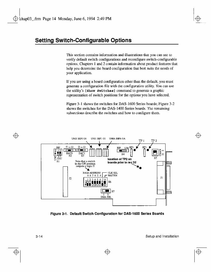
Figure 3-1 shows the switches for DAS-1600 Series boards; Figure 3-2 shows the switches for the DAS-1400 Series boards. The remaining subsections describe the switches and how to configure them.
3-14
Figure 3-1. Default Switch Configuration for DAS-1600 Series Boards
Setup and Installation
4
4
4 +b
4L - hap03 .frm Page 15 Monday, June 6,1994 2:49 PM 4
4
TP 1 TP2
location of TP2 on boards prior 10 rev C
-0
Figure 3-2. Default Switch Configuration for DAS-1400 Series Boards
Setting the DAC BipolarNnipolar Switch (DAS-1600 Series Only)
Switch Sl is a 2-position switch that sets DAC 0 and DAC 1 for unipolar (UNI) or bipolar (BE’) mode. The left switch (labeled 0) is for DAC 0; the right switch (labeled 1) is for DAC 1. Switch either section On for bipolar or Off for unipolar. The default is bipolar.
Setting the DACO and DACl Reference Voltage Switches (DAS-1600 Series Only)
Switches S2 and S3 are 3-position switches olfering 10,5, and U selections. When you set up a DAC for bipolar (SIP), the 5 and IO positions select f5 V and fl0 V, respectively. When you set up a DAC for unipolar, the 5 and 10 positions output 0 - 5 V and 0 - 10 V, respectively.
4
3-15
4 (4
44 - hap03 .frm Page 16 Monday, June 6,1994 2:49 PM 4
The U position on both switches selects the external reference voltage that you connect to D/A 0 REF IN (pin 10) and D/A 1 REF IN (pin 26). The default setting selects a +5 V reference signal for both DAC 0 and DAC 1.
For additional information on user-supplied reference voltages, set Vin definitions given in Table E-2 and Table E-3.
Setting the ADC BipolaWnipolar Switch
Switch S4 (S2 on the DAS-1400 Series) is a 2.position switch that sets A/D operation to bipolar (BIP) or unipolar (UNI) mode. The default setting is bipolar (BIP).
Setting the Chan 6116 Switch
Switch S5 on the DAS-1600 Series board (or switch Sl on the DAS-1400 Series board) is a 2-position switch that configures the A/D inputs as eight differential or 16 single-ended inputs. The default setting is eight differential inputs.
Setting an Alternate Base Address
3-16
Switch S6 (S3 on the DAS-1400 Series) is a single, X-position DIP switch that accommodates the base address, the clock select, and the wait state enable parameters. The default base address setting is 300h (786 decimal).
Figure 3-3 shows the default switch positions for the base address, clock select, and wait state enable switches.
Setup and Installation
4
4 4
.frm Page 17 Monday, June 6,1994 2:49 PM
4
Af!%F HtX Decimal Vallle VdUe
Ii: 10
29
CLK SEL On = 1 MHz
128 Off=lOMHz
it too 200 ::; WAITEN O” = No
Off = Yes
Note that a switch in the ON position outputs a logic 0. 987654CW
BASE ADORESS
Figure 3-3. Base Address, Clock Select, and Wait State Enable Switch
The base address is read from the S-position DIP switch located as shown in Figure 3-1 for aDAS- Series board and Figure 3-2 for a DAS-1400 Series board. The base address switch on DAS-1600/1400 Series boards is preset at the factory for a hexadecimal value of30011 (768 decimal). If this address conflicts with the address of another device in the computer (including another DAS-1600/1400 Series board), you must reconfigure the base address switch.
To reconfigure this switch for anolher address, perform the following steps:
1. Select an alternate address that does not conflict with another installed device. See Table 3-2 on page 3-10.
2. Use the configuration utility to create a new configuration file and view the corresponding switch settings in the menu-box diagram (see “Creating a Configuration File” on page 3-6).
3. Set up the base address switch to match the settings in the menu-box diagram.
Note: The settings for the base-address switch must match the settings shown by the switch diagram in tbe menu box of the configuration utility.
4
4
3-17
+b hap03-.frm Page 18 Monday, June 6, 1994 2:49 PM
Setting the Clock Select Switch
Position number 7 of the base address switch (see Figure 3-3) selects either a I MHz or 10 MHz clock for the internal pacer clock. The default is 10 MHz (Off).
Setting the Wait State Enable Switch
Position number 8 of the base address switch (see Figure 3-3) enables wait states. The default setting is NO (On). If you experience intermittent errors, you may correct the problem by setting this option to YES (Off).
Setting the DMA Channel Select Switch
Switch S7 (S4 on the DAS-1400 Series) is a Z-position slide switch that selects DMA channel 1 or 3. The default setting is 3.
Installing the Board
Caution: Installing or removing a board while power is on can damage your computer.
After reviewing your computer manufacturer’s documentation for accessing computer internals, use the following steps to install a DAS-1600/1400 Series board in an accessory slot of your computer:
1. Turn off power to the computer and all attached equipment.
Note: You must observe the current-capacity limits of the PC supply; allow for the power used by any other boards that may be it] use. See Table A-6 for DAS-1600/1400 Series power requirements.
2. Remove the computer chassis cover.
Setup and Installation
.frtn Page 19 Monday, June 6,1994 2:49 PM
3. Select an unoccupied accessory slot, and remove the corresponding blank plate and retaining screws from the I/O connector panel. Save the retaining screws for re-use in later steps.
4. If you are installing a DAS-1600 Series board and your application uses the additional 24-bit digital I/O, remove the blank plate and retaining screws of the adjacent slot. Save the retaining screws for x-use in later steps.
5. Make sure the option switch settings match the settings shown in the configuration-utility switch diagram.
6. Insert the board in the selected slot and secure the main I/O connector mounting flange with the retaining screws.
7. When using the additional %-bit digital I/O of a DAS-1600 Series board, connect the board end of the PI0 cable to the PI0 cable cotmector (52) on the board. When connecting the cable, align the raised arrow of the PI0 cable with the arrow imprinted on the PI0 cable connector (J2). Secure the mounting flange on the PI0 cable to the connector panel next to the main I/O connector (Jl) with the retaining screws.
8. Replace the computer cover,
9. Turn on power to the computer.
You can use the Control Panel (see Chapter 5) to verify board operation.
You are now ready to make I/O connections. Refer to Chapter 4 fat descriptions of common I/O accessories and connections for DAS-1600/1400 Series boards.
e-
+P
3-19

hap03_.frm Page 20 Monday, June 6,1994 2:49 PM
+P i hap04-.frm Page I Monday, June 6,1994 2:50 PM
4
+b
Cabling and Wiring
In most applications, you use accessories to connect external I/O devices to the DAS-1600/1400 Series boards. Accessories extend signals from the main I/O connector (Jl) and the PI0 cable connector (52) to corresponding screw terminals of the accessory.
In the case of DAS-1600 Series boards, 24 bits of parallel bidirectional digital I/O is channeled to the rear panel of the host PC by a flat ribbon cable known as the PI0 cable. The board end of the PI0 cable attaches to the PI0 cable connector (J2) on the board. The other end of the PI0 cable is fitted with a standard 37-pin D-type connector and a mounting flange that installs in the connector panel next to the main I/O connector (Jl). The PI0 cable comes with all DAS-1600 Series boards.
This chapter describes the cabling and accessories required for attaching field wiring to your DAS-1600/1400 Series boards.
Caution: To avoid electrical damage, tarn off power to the computer and any attached accessories before making connections to DAS-1600/1400 Series boards.
4-1
+b- hap04Lfrm Page 2 Monday, June 6, 1994 2:50 PM
Attaching Screw Terminal Connectors and Accessories
You can use the following screw terminal connectors and accessories to simplify connection of field wiring to DAS-1600/1400 Series boards:
. STC-37 Screw Terminal Connector; when using a DAS-1600 Series board, your application may require two connectors
l STP-37 Screw Terminal Panel: whet1 using a DAS-1600 Series hoard, your application may require two panels
. STA-16 Screw Terminal Accessory
. STA-U Universal Screw Terminal Accessory
The following sections describe how to attach these accessories to the DAS-1600/1400 Series boards.
Attaching an STC-37
4-2
The screw terminals on the STC-37 screw terminal connector allow you to colmect field wiring to a DAS-1600/1400 Series board. The screw terminals accept wire sizes 12-22 AWG.
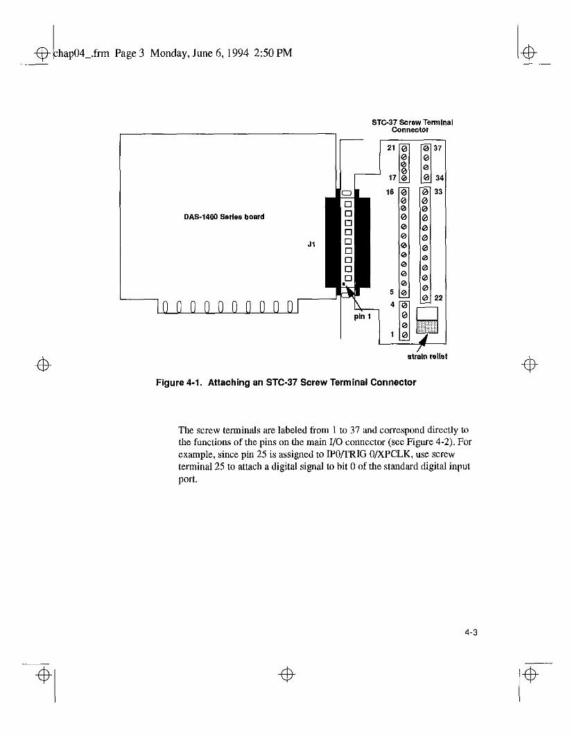
To connect an STC-37 to the main I/O connector (Jl) of a DAS-1600/1400 Series board, directly attach the 37.pin comiector on the STC-37 to the main I/O connector (Jl). Figure 4-1 illustrates the connection of an STC-37 to a DAS-1400 Series board.
Note: Your application may require connections to the main I/O connector (Jl) and connections to the PI0 cable connector (52). When two STC-37 connectors are required, you should consider wire sizes and service area requirements. These considerations may suggest the use of an alternate accessory.
Cabling and Wiring
hap04Lfrm Page 3 Monday, June 6, 1994 2:50 PM
DAS-1460 Series board
Jl
nn00nnnnn0r-
STG37 Screw Termlnal
Figure 4-1. Attaching an STC-37 Screw Terminal Connector
The screw terminals are labeled from I to 37 and correspond directly to the functions of the pins on the main I/O connector (see Figure 4-2). For example, since pin 25 is assigned to IPO/I’RIG O/XPCLK, use screw terminal 25 to attach a digital signal to bit 0 of the standard digital input port.
4-3
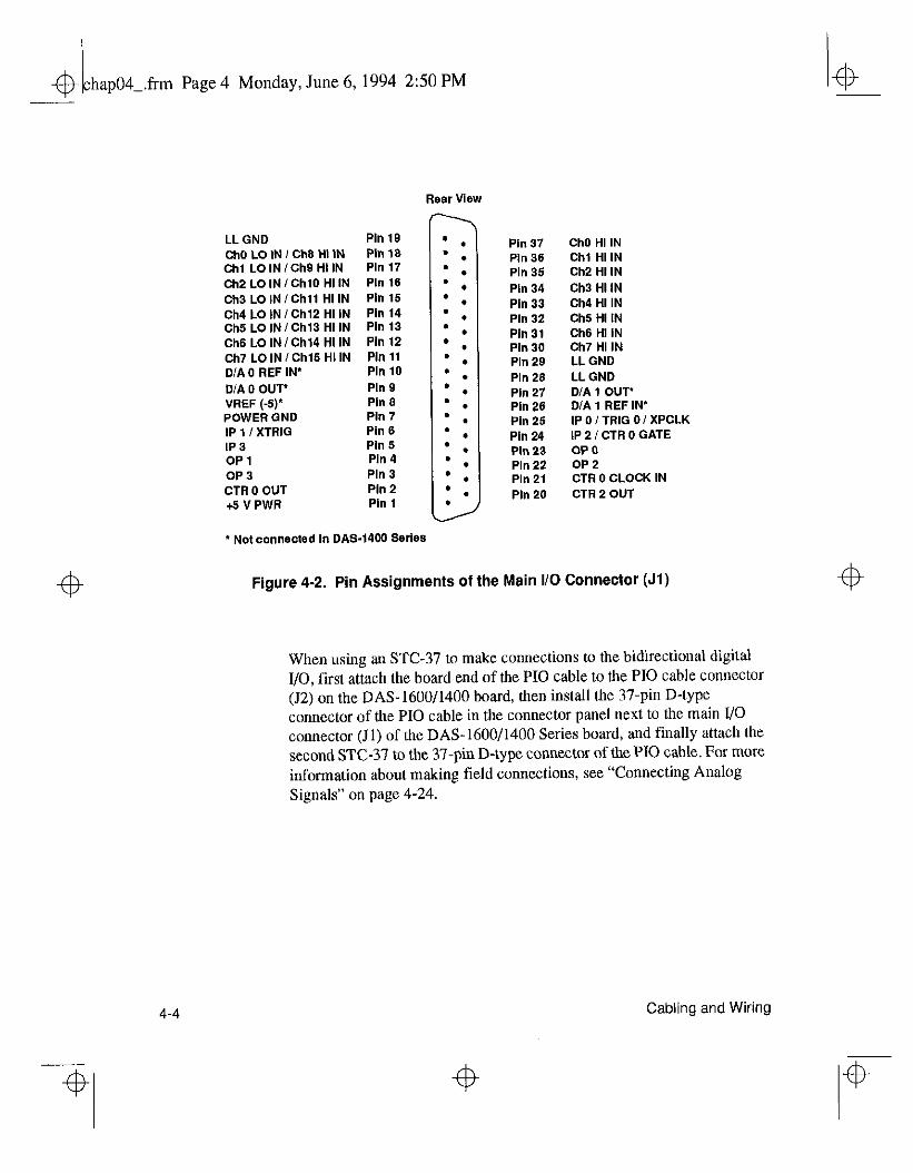
frtn Page 4 Monday, June 6,1994 2:50 PM
4
4-4
LL GND ChO LO IN I Ch6 HI IN Chl LO IN / Ch9 HI IN Ch2 LO IN / ChlO HI IN Ch3 LO IN / Chll HI IN Ch4 LO IN / Ch12 HI IN Ch6 LO IN / Ch13 HI IN Ch6 LO IN I Ch14 HI IN Ch7 LO IN I Ch15 HI IN WA 0 FIEF IN* WA 0 OUT’ “REF (-5)* POWER GND IP 1 I XTRIG IP 3 OPl OP3 CTR 0 OUT t5VPWR
Pin 19 wn 19 PI” 17 PI” 16 Pin 15 Pin 14 PI” 13 PI” 12 PI” 11 PI” 10 PI” 9 PI” 9 PI” 7 PI” 6 PI” 5 PI” 4 PI” 3 Pin 2 PI” 1
Rear view ’ . l .
l .
’ l
l .
l .
’ l
’ .
l .
II l .
’ .
l .
’ .
l .
’ .
l .
l .
’ . .
Pin 37 ChO HI IN P,” 36 Chl HI IN PI” 35 Ch2 HI IN Pin 34 Ch3 HI IN Pin 33 Ch4 HI IN Pln 32 ChJ HI IN Pin 31 Ch6 HI IN PI” 30 Ch7 HI IN PI” 29 LL GND PI” 26 LL GND Pln 27 D/A 1 OUT* Pln 26 D/A 1 REF IN* Pin 25 IP 0 i TRIG 0 / XPCLK PI” 24 IP 2 / CTR 0 GATE Pln 23 OPO PI” 22 OP2 PI” 21 CTR 0 CLOCK IN Pin 20 CTR 2 OUT
* NO, connected I” DAS-1400 Series
Figure 4-2. Pin Assignments of the Main l/O Connector (Jl)
When using an STC-37 to make connections to the bidirectional digital I/O, first attach the board end of the PI0 cable to the PI0 cable connector (12) on the DAS-1600/1400 board, then install the 37-pin D-type connector of the PI0 cable in the connector panel next to the main l/O connector (Jl) of the DAS-1600/1400 Series board, and finally attach the second STC-37 to the 37.pin D-type connector of the PI0 cable. For more information about making field connections, see “Connecting Analog Signals” on page 4-24.
Cabling and Wiring
4
4
4 14
hapOC.frm Page 5 Monday, June 6, 1994 2:50 PM
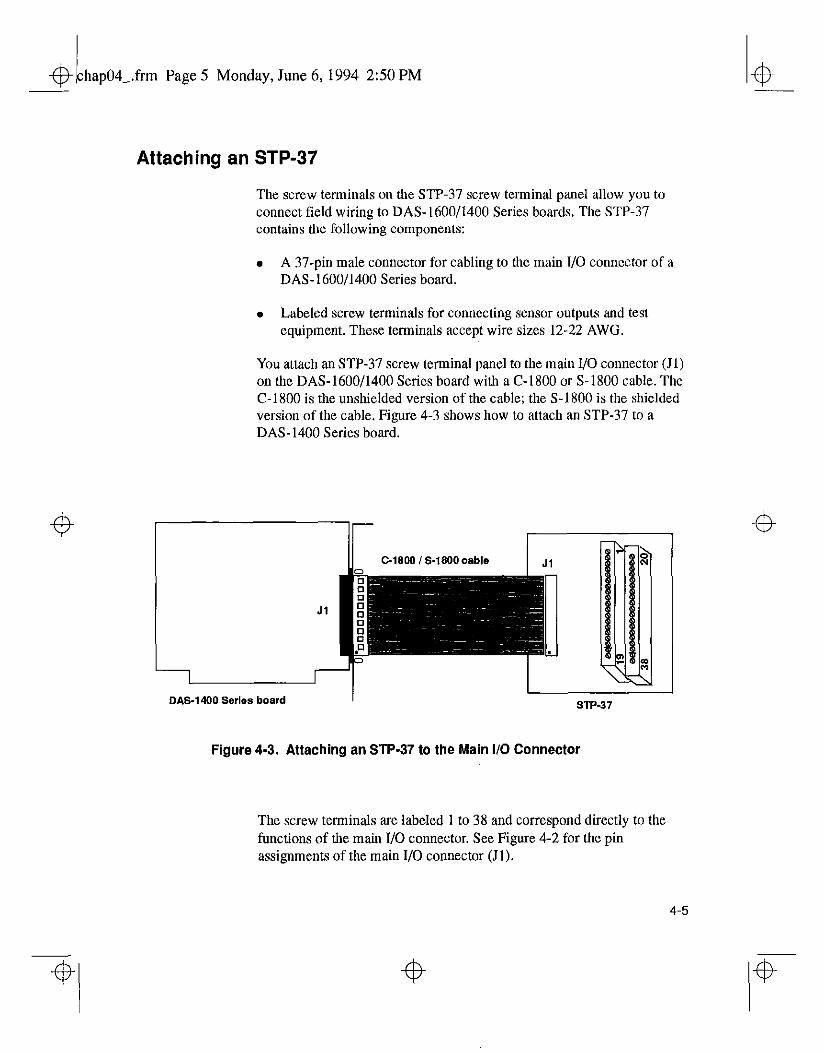
Attaching an STP-37
The screw terminals on the STP-37 screw terminal panel allow you to connect tield wiring to DAS-1600/1400 Series boards. The STP-37 contains the following components:
. A 37-pin male connector for cabling to the main I/O connector of a DAS-1600/1400 Series board.
. Labeled screw terminals for connecting sensor outputs and test equipment. These terminals accept wire sizes 12-22 AWG.
You attach an STP-37 screw terminal panel to the main I/O connector (JI) on the DAS-1600/1400 Series board with a C-1800 or S-1800 cable. The C-1800 is the unshielded version of the cable; the S-1800 is the shielded version of the cable. Figure 4-3 shows how to attach an STP-37 to a DAS-1400 Series board.
Figure 4-3. Attaching an STP-37 to the Main 110 Connector
The screw terminals are labeled 1 to 38 and correspond directly to the functions of the main I/O connector. See Figure 4-2 for the pin assignments of the main I/O connector (Jl).
4-5
43 t hap04_.frm Page 6 Monday, June 6, 1994 2:50 PM
When using an STP-37 to make connections to the bidirectional digital I/O, first attach the board end of the PI0 cable to the PI0 cable connector (J2) on the DAS-1600/1400 Series board, then install the 37-pin D-type connector of the PI0 cable in the connector panel next to the main I/O connector (Jl) of the DAS-1600/1400 Series board, and finally attach the STP-37 to the 37-pin D-type connector of the PI0 cable. See Figure 4-X for the pin assignments of the 37.pin D-type connector of the PI0 cable.
Attaching an STA-16
4-6
The screw terminals on the STA-16 screw terminal accessory allow you to connect field wiring to DAS-1600/1400 Series boards. The STA-16 contains the following components:
. Two 37-pin male connectors. Ones for cabling to the main I/O connector of a DAS-1600/1400 Series board and a second for daisy-chaining additional accessories.
. Labeled screw terminals for connecting sensor outputs and test equipment. These terminals accept wire sizes 12-22 AWG.
l A breadboard area for user-installed circuitry.
You attach an STA- 16 screw terminal accessory to the main I/O connector (JI) on the DAS-1600/1400 Series board with a C-1800 or S-1800 cable. The C-1800 is the unshielded version of the cable; the S-1800 is the shielded version of the cable. Figure 4-4 shows how to attach an STA-16 to a DAS-1400 Series board.
Cabling and Wiring
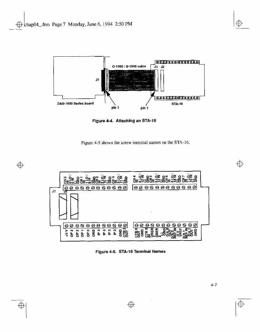
frm Page 7 Monday, June 6, 1994 2:50 PM
DAS.1400 Series board ’ \ / STA.16 pin 1 pin 1
Figure 4-4. Attaching an STA-16
Figure 4-5 shows the screw terminal names on the STA-16.
4
4
4
4
4-7
4
4Ic - hap04 .frm Page 8 Monday, June 6, 1994 2:50 PM
4
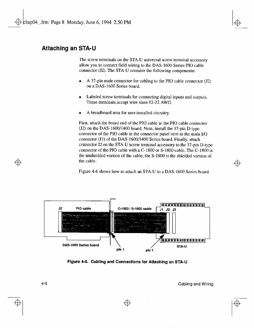
Attaching an STA-U
The screw terminals on the STA-U universal screw terminal accessory allow you to comtect field wiring to the DAS-1600 Series PI0 cable connector (J2). The STA-U contains the following components:
. A 37-pin male connector for cabling to the PI0 cable connector (J2) on a DAS-1600 Series board.
. Labeled screw terminals for connecting digital inputs and outputs. These terminals accept wire sizes 12-22 AWG.
. A breadboard area for user-installed circuitry.
First, attach the board end of the PI0 cable to the PI0 cable connector (52) on the DAS-1600/1400 board. Next, install the 37.pin D-type connector of the PI0 cable in the connector panel next to tbe main I/O connector (Jl) of the DAS-1600/1400 Series board. Finally, attach connector J2 on the STA-U screw terminal accessory to the 37-pin D-type connector of the PI0 cable with a C- 1800 or S- 1800 cable. The C- 1800 is the unshielded version of the cable; the S-1800 is the shielded version of the cable.
Figure 4-6 shows bow to attach an STA-U to a DAS-1600 Series board.
-
pin 1 pin 1
Figure 4-6. Cabling and Connections for Attaching an STA-U
4
4
4
4-8
4
Cabling and Wiring
I4
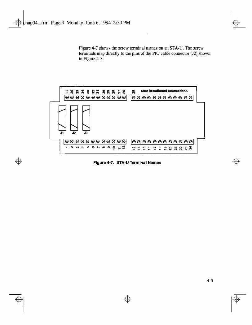
4 hapOC.frm Page 9 Monday, June 6, 1994 2:50 PM
4
Figure 4-7 shows the screw terminal names on an STA-U. The screw terminals map directly to the pins of the PI0 cable connector (52) showo in Figure 4-8.
Figure 4-7. STA-U Terminal Names
I4
4
4-9
4
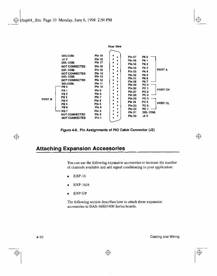
.frm Page 10 Monday, June 6,1994 2:50 PM
DIGCOM. +5 v DIG. COM. NOT CONNECTED DIG. COM. NOT CONNECTED DIG. COM. NOT CONNECTED D,G.COM.
r PBO PBI PB2
PORT B PB3 PB4 PE!5 PB6
L-P;7 NOT CONNECTED NOT CONNECTED
Pill 19 Pill 18 Pin 17
Pin 16 Pin 15 Ph 14 Pill 13 Pill 12 P,” 11 Ph 10 Pill 9 Pin 8 Pill 7 Pill 6 Pill 5 Ph 4 Pi” 3 Pin 2 Ph 1
l .
’ .
’ .
l .
l .
’ .
l .
l .
l .
:
l .
l .
’ .
’ .
l .
l l
l L
l l
l . .
4
Ph 37 Pln 36 Pill 35 Ph 34 Ph 33 Pln 32 Pill 31 Pill 30 Pill 29 Ph 28 Pin 27 Pill 26 Pin 25 Ph 24 Pln 23 Pin 22 Ph 2, Pin 20
PA0 PA1 PA2 PA3 PA4 PA5 PA6 PA7
1 PORT A
-I
PC0 PC 1 PC2 1 PORT CH
PC3 PC4 - PC5 PORT CL PC6 PC7 DIG. COM.
Figure 4-8. Pin Assignments of PI0 Cable Connector (JZ)
Attaching Expansion Accessories
You can use the following expansion accessories to increase the number of channels available and add signal conditioning to your application:
. EXP-16
. EXP16/A
. EXP-GP
The following section describes how to attach these expansion accessories to DAS-1600/1400 Series boards.
4-10 Cabling and Wiring
4 4
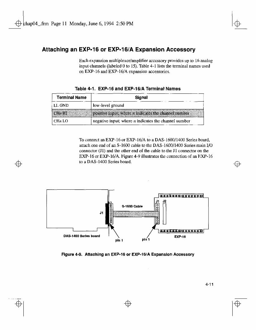
& hap04-.frm Page 11 Monday, June 6,1994 2:50 PM
4
Attaching an EXP-16 or EXP-16/A Expansion Accessory
Each expansion multiplexer/amplifier accessory provides up to 16 analog input channels (labeled 0 to 15). Table 4-l lists the terminal names used on EXP-16 and EXP-16/A expansion accessories.
Table 4-1. EXP-16 and EXP-16/A Terminal Names
Terminal Name Signal
LL GND low-level mound
CHn LO negative input; where n indicates the channel number
To connect an EXP- 16 or EXP- 16/A to a DAS- 1600/1400 Series board, attach one end of an S-1600 cable to the DAS-1600/1400 Series main I/O connector (Jl) and the other end of the cable to the Jl connector on the EXP-16 or EXP-16/A. Figure 4-9 illustrates the connection of an EXP-16 to a DAS-1400 Series board.
DAS-1400 Series board
-l8r EXP-16
Figure 4-9. Attaching an EXP-16 or EXP-16/A Expansion Accessory
4
4
4-11
4
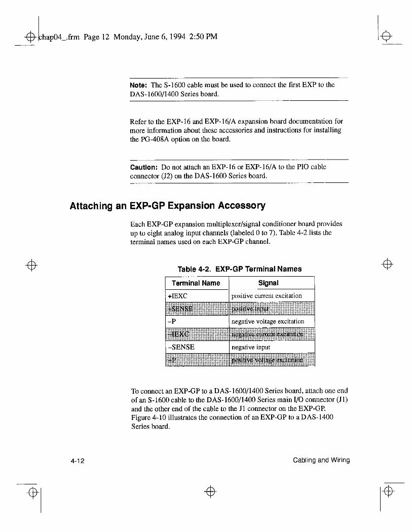
4 hap04-.frm Page 12 Monday, June 6,1994 2:50 PM
Note: The S-1600 cable must be used to connect the first EXP to the DAS-1600/1400 Series board.
Refer to the EXP-16 and EXP-16/A expansion board documentation for more information about these accessories and instructions for installing the PG-408A option on the board.
Caution: Do not attach an EXP-16 or EXP-16/A to the PI0 cable connector (J2) on the DAS-1600 Series board.
Attaching an EXP-GP Expansion Accessory
Each EXP-GP expansion multiplexer/signal conditioner board provides up to eight analog input channels (labeled 0 to 7). Table 4-2 lists the terminal names used on each EXP-GP channel.
4-12
Table 4-2. EXP-GP Terminal Names
1 Terminal Name / Signal 1
+IExc positive current excitation
-P negative voltage excitation ~~ :it;.:.l::‘:.:.~,..“:.ili.-:i::.:.: i....i..,.,l.i....l....i.... ,.... :. .,./,.,./..,./,.,.,...,./.,.._,,,.,.,.,,,.,.,.,.,...,.,,,.,.,...,........,..,..,..,.....,..,............,....,...,.,, -SENSE negative input
To connect an EXP-GP to a DAS-1600/1400 Series board, attach one end of an S-1600 cable to the DAS- 1600/1400 Series main I/O connector (Jl) and the other end of the cable to the I1 connector on the EXP-GP. Figure 4-10 illustrates the connection of an EXP-GP to a DAS-1400 Series board.
Cabling and Wiring
4
4 4 4
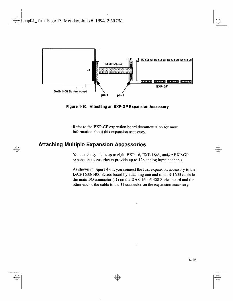
4 t hap04-.frm Page 13 Monday, June 6, 1994 250 PM 4
4
Figure 4-10. Attaching an EXP-GP Expansion Accessory
Refer to the EXP-GP expansion board documentation for more information about this expansion accessory.
Attaching Multiple Expansion Accessories
You can daisy-chain up to eight EXP-16, EXP-16/A, and/or EXP-GP expansion accessories to provide up to 128 analog input channels.
As shown in Figure 4- 1 I, you connect the first expansion accessory to the DAS-1600/1400 Series board by attaching one end of an S-1600 cable to the main I/O connector (Jl) on the DAS-1600/1400 Series board and the other end of the cable to the Jl connector on the expansion accessory.
4
4-13
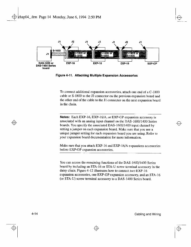
frm Page 14 Monday, June 6, 1994 2:50 PM
Jl J2 Jl J2 Jl J2 Ji
4
4-14
Figure 4-11. Attaching Multiple Expansion Accessories
To connect additional expansion accessories, attach one end of a C-1800 cable or S-1800 to the J’2 connector on the previous expansion board and the other end of the cable to the Jl connector on the next expansion board in the chain.
Notes: Each EXF-16, EXP-16/A, or EXP-GP expansion accessory is associated with an analog input channel on the DAS- 1600/1400 Series boards. You specify the associated DAS-160011400 input channel by setting a jumper on each expansion bdard. Make sure that you use a unique jumper setting for each expansion board you are using. Refer to your expansion board documentation for more information.
Make sure that you attach EXP-16 and EXP-16/A expansions accessories before EXP-GP expansion accessories.
You can access the remaining functions of the DAS-1600/1400 Series board by including an STA-16 or STA-U screw terminal accessory in the daisy chain. Figure 4-12 illustrates how to connect two EXP-16 expansion accessories, one EXP-GP expansion accessory, and an STA-16 (or STA-U) screw terminal accessory to a DAS-1400 Series board.
Cabling and Wiring
4
4
4 4
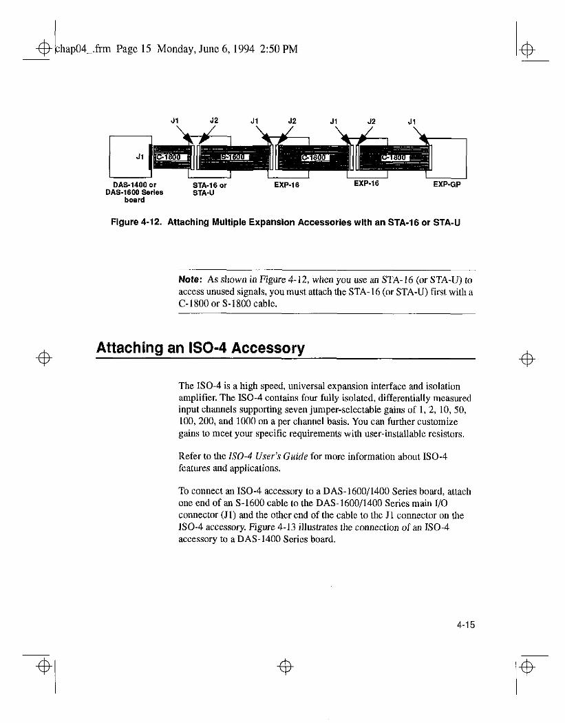
4 I *hapOC.frtn Page 15 Monday, June 6,1994 2:50 PM
4
Jl J2 Jl J2 Jl J2 J1
I I I I I I I I DAM400 or STA-16 or EXP-16 EXP-16 EXP.GP
DAS-16W Series STA-U board
Figure 4-12. Attaching Multiple Expansion Accessories with an STA-16 or STA-U
Note: As shown in Figure 4- 12, when you use an STA- 16 (or STA-U) to access unused signals, you must attach the STA-16 (or STA-U) first with a C-1800 or S-1800 cable.
Attachina an ISO- Accessorv
The ISO- is a high speed, universal expansion interface and isolation amplifier. The ISO- contains four fully isolated, differentially measured input channels supporting seven jumper-selectable gains of 1,2, 10, 50, 100,200, and 1000 on a per channel basis. You can further customize gains to meet your specific requirements with user-installable resistors.
Refer to the IS0-4 User’s Guide for more information about ISO- features and applications.
To connect an ISO- accessory to a DAS-1600/1400 Series board, attach one end of an S-1600 cable to the DAS-1600/1400 Series main I/O connector (II) and the other end of the cable to the Jl connector on the ISO- accessory. Figure 4-13 illustrates the connection of an ISO- accessory to a DAS-1400 Series board.
4
4
4-15
4
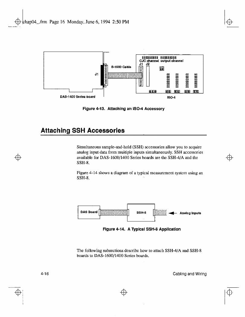
.frm Page 16 Monday, June 6,1994 2:50 PM
4
41
DAS-1400 Series board
Figure 4-13. Attaching an IS04 Accessory
Attachinn SSH Accessories
Simultaneous sample-and-hold (SSH) accessories allow you to acquire analog input data from multiple inputs simultaneously. SSH accessories available for DAS-1600/1400 Series boards are the SSH-4/A and the SSH-8.
Figure 4-14 shows a diagram of a typical measurement system using an SSH-8.
Figure 4-14. A Typical SSH-8 Application
The following subsections describe. how to attach SSH-4/A and SSH-8 boards to DAS-1600/1400 Series boards.
4
4
4
4-16 Cabling and Wiring
4
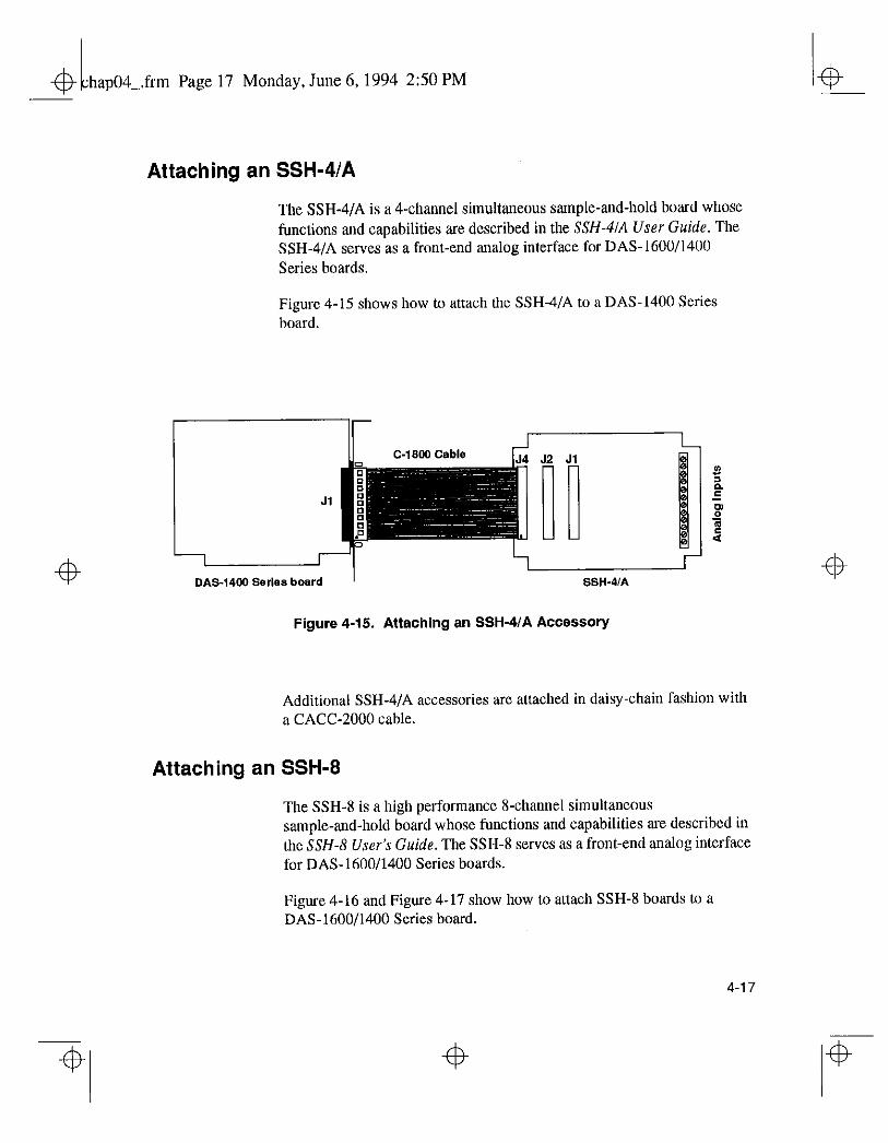
hap04-.frm Page 17 Monday, June 6,1994 2:50 PM
4
Attaching an SSH-4/A
The SSH-4/A is a 4-channel simultaneous sample-and-hold board whose functions and capabilities are described in the #H-4/A User Guide. The SSH-4/A serves as a front-end analog interface for DAS-1600/1400 Series boards.
Figure 4-15 shows how to attach the SSH-4/A to a DAS-1400 Series board.
Figure 4-15. Attaching an SSH-4/A Accessory
Additional SSH-4/A accessories are attached in daisy-chain fashion with a CACC-2000 cable.
Attaching an SSH-8
The SSH-8 is a high performance X-channel simultaneous sample-and-hold board whose functions and capabilities are described in the SSH-8 User’s Guide. The SSH-8 serves as a front-end analog interface for DAS-1600/1400 Series boards.
Figure 4-16 and Figure 4-17 show how to attach SSH-8 boards to a DAS-1600/1400 Series board.
4
4
($
4-17
4
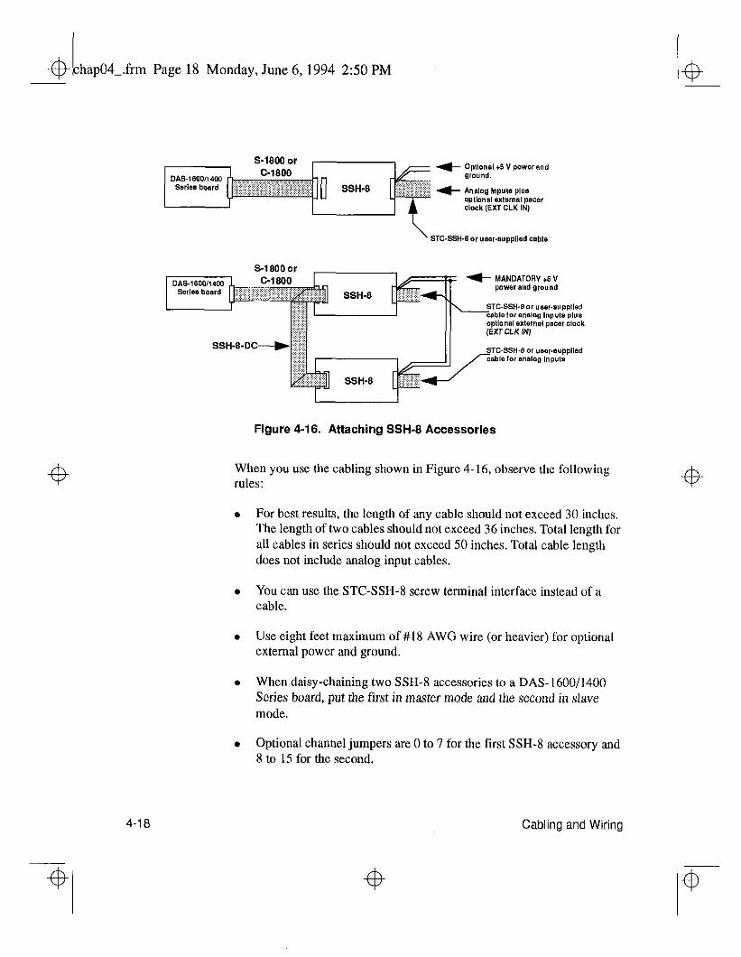
.frm Page 18 Monday, June 6,1994 2:50 PM
4
Figure 4-16. Attaching SSH-8 Accessories
When you use the cabling shown in Figure 4-16, observe the following rules:
For best results, the length of any cable should not exceed 30 inches. The length of two cables should not exceed 36 inches. Total length for all cables in series should not exceed 50 inches. Total cable length does not include analog input cables.
You can use the STC-SSH-8 screw terminal interface instead of a cable.
Use eight feet maximum of #IX AWG wire (or heavier) for optional external power and ground.
When daisy-chaining two SSH-8 accessories to a DAS-1600/1400 Series board, put the first in master mode and the second in slave mode.
Optional channel jumpers are 0 to 7 for the first SSH-8 accessory and 8 to 15 for the second.
4
4-18
4
Cabling and Wiring
4
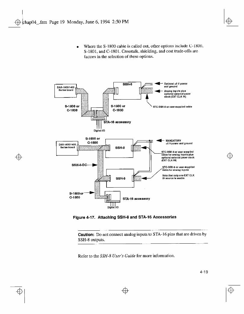
4 hap04_.frm Page 19 Monday, June 6, 1994 250 PM
l Where the S-1800 cable is called out, other options include C-1800, S-1801, and C-1801. Crosstalk, shielding, and cost trade-offs are factors in the selection of these options.
4 4
Caution: Do not connect analog inputs to STA-16 pins that are driven by SSH-8 outputs.
Refer to the SSH-8 User’s Guide for more information.
4
4-19
4
frm Page 20 Monday, June 6, 1994 250 PM
Attaching an MB Series Backplane
MB Series modules are ideally suited to applications where monitoring and control of temperature, pressure, flow, and other analog signals are required. Figure 4-18 shows a block diagram of a typical MB Series measurement and control application.
mV, V, Thermocouple, RTD, Slraln Gauge, 4-20 mA / O-20 mA
4-20
oto+5v/isv
$. &2OmA/~2OmA
Figure 4-18. Typical Measurement and Control Application
Table 4-3 provides a brief summary the backplanes available for use with MB Series modules.
Cabling and Wiring
frm Page 21 Monday, June 6,1994 2:50 PM
Table 4-3. MB Series Backplanes
Model Description
MB01 Holds up to 16 modules ‘and mounts in a 19.inch equipment rack. Provides direct channel-to-channel connection to an a DAS-1600/1400 Series board making it suitable for high-speed, high-resolution applications.
STA-MB Holds up to four modules and provides general-purpose screw terminal connections for all other signals on the DAS1600/1400 Series board.
Attaching an MB01 Backplane
Use the C16-MB1 cable to connect a DAS-1600/1400 Series board to an MB01 backplane. This cable connects MB01 channels 0 through 15 to analog input channels 0 through 15 on the DAS-1600/1400 Series board. Refer to Figure 4- 19 for a cabling diagram.
use WnneclOr Pl or P2 (Identical pinouts)
Figure 4-19. Attaching an MB01 Backplane
I4
4
4
4-21
4
4 hap04Qcm Page 22 Monday, June 6,1994 2:50 PM
Note: The channel connections are single-ended. Make sure that the DAS-1600/1400 Series board is set for 16-channel, single-ended operation.
Attaching an MB02 Backplane
Figure 4-20 shows how to connect a DAS-1600/1400 Series board to up to four MB02 backplanes. The STA-SCM16 interface connects one MB02 board to one analog input channel of the DAS-1600/1400 Series board. One C-2600 cable connects each MB02 to the STA-SCM16, and the C-1800 cable connects the STA-SCM16 to the DAS-1600/1400 Series board.
4-22
Figure 4-20. Attaching Multiple MB02 Backplanes
Figure 4-21 shows how the STA-SCM16 connects DAS-1600/1400 Series boards with MB02 backplanes.
4
Cabling and Wiring
4 I-$
&- hap04-.frm Page 23 Monday, June 6,1994 2:50 PM
D/A CH 0 OUT
D/A CH 1 OUT
DAS.1606 Series board Backplane Connectors
STA-SCM16
Figure 4-21. MB02 I/O Connections
The four digital output lines on the DAS-1600/1400 Series boards select one of the 16 MB02 channels. For example, if you set the digital output lines to 1000 (8 decimal), MB02 channel 8 is selected on all four backplanes. Analog input channels 0 to 3 on the DAS-1600/1400 Series board map directly to the connectors labeled 0 to 3 on the STA-SCM16.
In this arrangement, the channel connections are single-ended. Make sure that the DAS-1600/1400 Series board is set for single-ended, 16-channel operation.
Refer to the ME Series User’s Guide for more information.
4
4-23
4 4
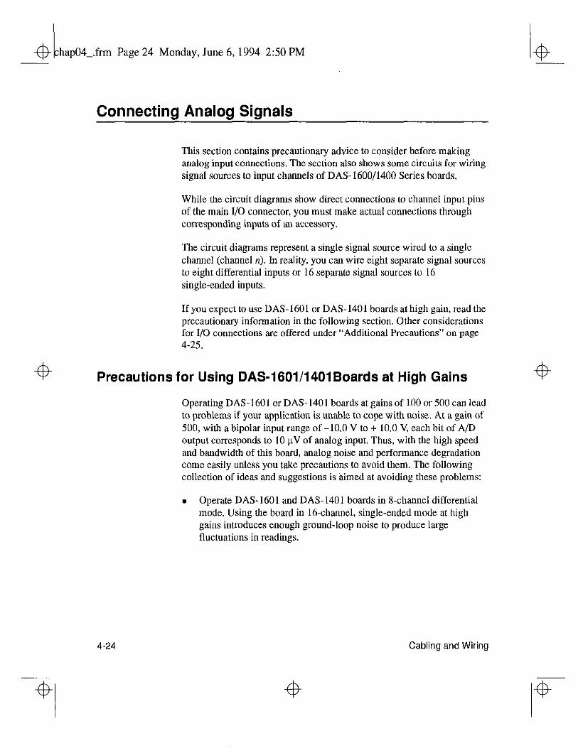
4 t hap04Lfrm Page 24 Monday, June 6, 1994 2:50 PM
4
Connecting Analog Signals
This section contains precautionary advice to consider before making analog input connections. The section also shows some circuits for wiring signal sources to input channels of DAS-1600/1400 Series boards.
While the circuit diagrams show direct connections to channel input pins of the main I/O connector, you must make actual connections through corresponding inputs of an accessory.
The circuit diagrams represent a single signal source wired to a single chamiel (channel n). In reality, you can wire eight separate signal sources to eight differential inputs or 16 separate signal sources to 16 single-ended inputs.
If you expect to use DAS-1601 or DAS-1401 boards at high gain, read the precautionary information in the following section. Other considerations for I/O connections are offered under “Additional Precautions” on page 4-25.
Precautions for Using DAS-1601/1401Boards at High Gains
Operating DAS-1601 or DAS-1401 boards at gains of 100 or 500 can lead to problems if your application is unable to cope with noise. At a gain of 500, with a bipolar input range of -10.0 V to + 10.0 V, each bit of A/D output corresponds to 10 uV of analog input. Thus, with the high speed and bandwidth of this board, analog noise and performance degradation come easily unless you take precautions to avoid them. The following collection of ideas and suggestions is aimed at avoiding these problems:
. Operate DAS-1601 and DAS-1401 boards in 8-channel differential mode. Using the board in 16.channel, single-ended mode at high gains introduces enough ground-loop noise to produce large fluctuations in readings.
4
4
4-24
4
Cabling and Wiring
4
+b t hap04-.frm Page 25 Monday, June 6,1994 2:50 PM
. Minimize noise from crosstalk and induced-voltage pickup in the flat cables and screw terminal accessories by using shielded cable. Connect the shield to LL GND and the inner conductors to Channel LO and HI. Channel LO and LL GND should have a DC return (or connection) at some point; this return should be as close to the signal source as possible. Induced noise from RF and magnetic fields can easily exceed tens of microvolts, even on one- or two-foot cables; shielded cable eliminates this problem.
. Avoid bi-metallic junctions in the input circuitry. For example, the kovar leads, used on reed relays, typically have a thermal emf to copper of 40 IV/Y!. Thermals can introduce strange random variations caused by air currents and so on.
. Consider filtering. This approach can use hardware (resistors, capacitors, and so on) but is often accomplished more easily with software. Instead of reading the channel once, read it 10 or more times in quick succession and average the readings. If the noise is random and gaussian, it will be reduced by the square-root of the number of readings.
Additional Precautions
Do not mix your data acquisition inputs with the AC line, or you risk damaging the computer. Data acquisition systems provide access to inputs of the computer. An inadvertent short between data and power lines can cause extensive and costly damage to your computer. The manufacturer can accept no liability for this type of accident. To prevent this problem, use the following precautions:
. Avoid direct connections to the AC line.
. Make sure all connections are tight and sound so that signal wires are not likely to come loose and short to high voltages.
. Use isolation amplifiers and transformers where necessary.
4-25
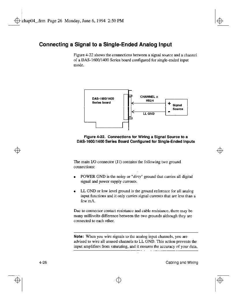
.frtn Page 26 Monday, June 6,1994 2:50 PM
Connecting a Signal to a Single-Ended Analog Input
Figure 4-22 shows the connections between a signal source and a channel of a DAS-1600/1400 Series board configured for single-ended input mode.
4-26
3 DAS-1600/1400
CHANNEL n
Serlea board < HIGH
+ signal SO”PFJ
< LLGND -
3
r Figure 4-22. Connections for Wiring a Signal Source to a
DAS-1600/1400 Series Board Configured for Single-Ended Inputs
The main I/O connector (Jl) contains the following two ground connections:
. POWER GND is the noisy or “dirty” ground that carries all digital signal and power supply currents.
l LL GND or low level ground is the ground reference for all analog input functions and it only carries signal currents that are less than a few mA.
Due to connector contact resistance and cable resistance, there may be many millivolts difference between the two grounds although they are connected to each other.
Note: When you wire signals to the analog input channels, you arc advised to wire all unused channels to LL GND. This action prevents the input amplifiers from saturating, and it ensures the accuracy of your data.
Cabling and Wiring
4
4 Page 27 Monday, June 6,1994 2:50 PM
Connecting a Signal to a Differential Analog Input
This section describes common connection schemes for differential inputs. The section also discusses the principles for avoiding ground loops.
Common Connection Schemes for Differential Inputs
Figure 4-23 shows three methods of wiring a signal source to a channel of a DAS-1600/1400 Series board configured for differential input mode.
4-27
4
4
4
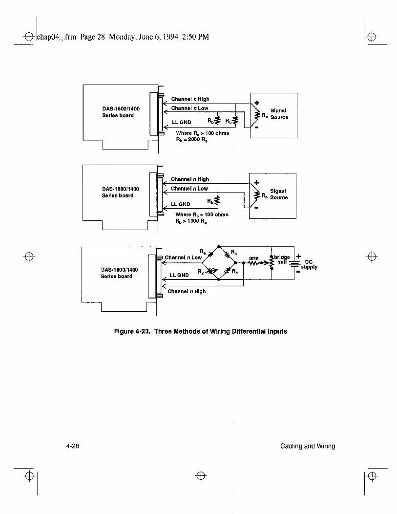
frm Page 28 Monday, June 6,1994 2:50 PM
4-28
DA!3.1600/1400 Series board
di. Channel n High
DAS-1600/1400 Series board
mnel n High
lnnel n LOW
Where R. < 100 ohms Fib > 1000 R,
Figure 4-23. Three Methods of Wiring Differential Inputs
Cabling and Wiring
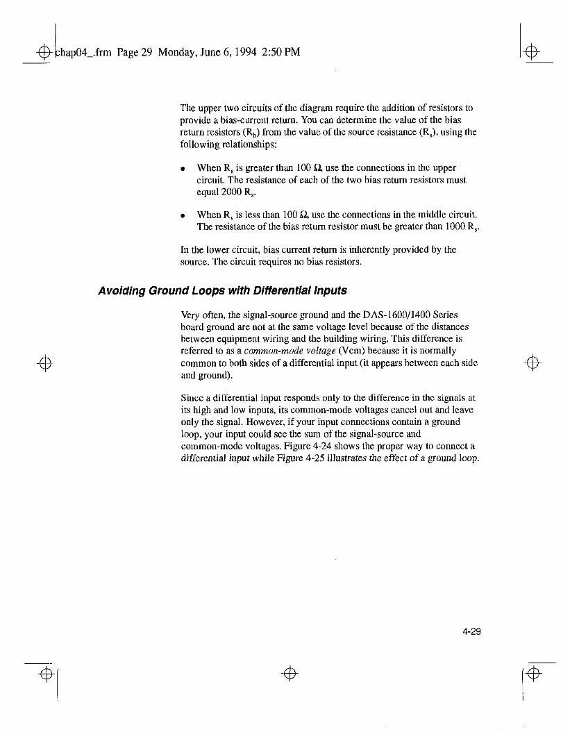
.frm Page 29 Monday, June 6,1994 2:50 PM
4
The upper two circuits of the diagram require the addition of resistors to provide a bias-current return. You can determine the value of the bias return resistors (Rb) from the value of the source resistance (R,), ushtg the following relationships:
. When R, is greater than 100 S& use the connections in the upper circuit. The resistance of each of the two bias return resistors must equal 2000 R,.
. When R, is less than 100 Ll, use the connections in the middle circuit. The resistance of the bias return resistor must be greater than 1000 R,.
In the lower circuit, bias current return is inherently provided by the source. The circuit requires no bias resistors.
Avoiding Ground Loops with Differential Inputs
Very often, the signal-source ground and the DAS-1600/1400 Series board ground are not at the same voltage level because of the distances between equipment wiring and the building wiring. This difference is referred to as a commorz-mode voltage (Vcm) because it is normally common to both sides of a differential input (it appears between each side and ground).
Since a differential input responds only to the difference in the signals at its high and low inputs, its common-mode voltages cancel out and leave only the signal. However, if your input connections contain a ground loop, your input could see the sum of the signal-source and common-mode voltages. Figure 4-24 shows the proper way to connect a differential input while Figure 4-25 illustrates the effect of a ground loop.
4
4-29
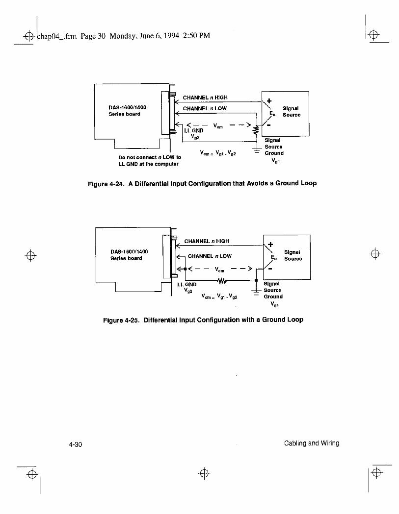
4 I hap04Lfrm Page 30 Monday, June 6.1994 2:50 PM
4
4-30 Cabling and Wiring
Figure 4-24. A Differential Input Configuration that Avoids a Ground Loop
DAS-1600/14W Series board
3 CHANNEL n HIGH
-? i + CHANNEL n LOW
,Fe
SIgnal SOUW3
N - - v., -- > r m
3 AA. LL GND SIgnal
“02 SO”,CB vcnl E vg1 vg2 = Ground
“01
Figure 4-25. Differential Input Configuration with a Ground Loop
4
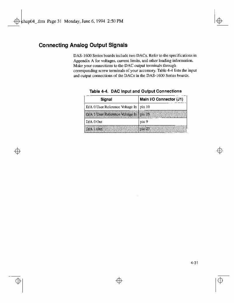
4 hap04-.frm Page 31 Monday, June 6,1994 2:50 PM
4
Connecting Analog Output Signals
DAS-1600 Series boards include two DACs. Refer to the specifications in Appendix A for voltages, current limits, and other loading information. Make your connections to the DAC output terminals through corresponding screw terminals of your accessory. Table 4-4 lists the input and output connections of the DACs in the DAS-1600 Series boards.
Table 4-4. DAC Input and Output Connections
Sianal 1 Main I/O Connector (Jl) /
4-31
4
4
4

frm Page 32 Monday, June 6,1994 2:50 PM 4
4 4
4 4
4 ! hap055frm Page 1 Monday, June 6, 1994 2:52 PM
5
4
The Control Panel
The Control Panel is a utility program for testing the functions of your DAS-1600/1400 Series boards; it is available in a DOS version (CTLl600.EXB) and a Windows version (CTLl600W.EXE). The DOS version is part of both the DAS-1600/1400 Series standard software package and the ASO- and ASO- software package. The Windows version is a part of the ASO- and ASO- software package only.
Note: Before using the Windows version of the Control Panel, you arc advised to install the Keithley Memory Manager (VDMAD.386) to ensnre the allocation of a memory buffer large enough for Control Panel needs, Refer to Appendix D for details of the Keithley Memory Manager.
To use the Control Panel, perform the following steps:
1. Start the Control Panel from the DOS or Windows environments as follows:
- Ifyou are in the DOS environment, change to the directory containing the CTLl600BXE program and enter the following at the DOS prompt:
CTL1600
- Ifyou are in the Windows environment, double click on the Control Panel icon in the DAS-1600 Group window, which is within the Program Manager window.
After the Control Panel starts, it asks you for the name of a configuration file.
4
4
4 4
5-1
4
Page 2 Monday, June 6, 1994 2:52 PM
4
5-2
4
2. To use the settings from the default configuration tile, select OK. If you prefer to use the settings from another configuration file, enter the name of that file and select OK.
After the Control Panel accepts the name of a configuration file, it displays the DAS-1600 TEST & CONTROL panel. This panel contains the controls that allow you to acquire, read, and transfer data and to set up and display parameters.
3. To set up and perform an operation, select the appropriate buttons. To obtain information on the setup and performance of an operation, use the Help option in the Control Panel menu. To obtain information on DAS-1600/1400 Series board functions and parameters, refer to Chapter 2.
4. To set up and perform a digital I/O operation, select Digital I/O from the Control Panel menu; to set up and perform a D/A operation, select D/A from the Control Panel menu. When the Control Panel displays the DIGITAL I/O & D/A panel, you can select appropriate buttons to proceed with your operation.
5. If you are working in the Windows environment, you can use the Control Panel’s Dynamic Data Exchange (DDE) to transfer data to another Windows program by selecting DDE from the Control Panel menu and use the Display options/Graphics panel to graph up to eight channels.
6. Use the File menu to open, close, or save a file.
7. When you finish using the Control Panel, select the Exit option from the File men” to terminate the program.
The Control Panel
4
4 4
hapOb.frm Page 1 Monday, June 6,1994 2:52 PM
6 Calibration
Your DAS-1600/1400 Series board is initially calibrated at the factory. You are advised to check the calibration of a board every six months and to calibrate again when necessary. This chapter provides the information you need to calibrate a DAS-1600/1400 Series board.
Equipment Requirements
The equipment requirements for calibrating a DAS-1600/1400 Series board are as follows:
l A digital voltmeter accurate to a minimum of 5 l/2 digits
. An adjustable f10 V power source
Potentiometers and Test Points
Figure 3-1 on page 3-14 and Figure 3-2 on page 3-15 show the locations of the potentiometers aad test points that are used during the calibration of a DAS-1600 Series or DAS-1400 Series board.
The calibration utility, described in the next section, directs you to components and explains what to do with them during the calibration process.
6-l
& k hapOh.frm Page 2 Monday, June 6, 1994 2:52 PM
Calibration Utility
To calibrate a DAS-1600 Series board, use the DOS-based CAL1600.EXE calibration utility. To calibrate a DAS-1400 Series board, use the DOS-based CAL1400.EXE calibration utility. These utilities are included in both the DAS-1600/1400 Series standard software package and the ASO- and ASO- software package.
Start the calibration utility by changing to its directory and entering the following at the DOS prompt:
CAL1600
CAL1400
Follow the utility-program prompts as they appear; the program guides you through the calibration process.
6-2 Calibration
4 hap07-.frm Page 1 Monday, June 6,1994 2:53 PM
7
4
Troubleshooting
If your DAS-1600/1400 Series board is not operating properly, use the information in this chapter to isolate the problem. If the problem appears serious enough to warrant technical support, refer to “Technical Support” on page l-6.
Problem Isolation
If you encounter a problem with a DAS-1600/1400 Series board, use the instructions in this section to isolate the cause of the problem before calling the factory.
Identifying Symptoms and Possible Causes
Use the troubleshooting information in Table 7-l lo try to isolate the problem. Table 7-1 lists general symptoms and possible solutions fool problems with DAS-1600/1400 Series boards.
7-1
4
4
4 k hap07_.frm Page 2 Monday, June 6,1994 2:53 PM
4
iymptom
laud does not :spond
F I- E
Table 7-1. Troubleshooting Information
‘ossible Cause Possible Solution
lase address is incorrect. Ensure that the base address switch on the board is set correctly and that your program references the s~mc base address. If the base address is set correctly, ensure that no other computer device is using any of the I/O locations beginning at the specified base address. See Table 3-2 for a list of standard address assignments. If necessary, reconfigure the base address. Refer to page 3-16 for instructions on setting the base address.
‘The board is incorrectly aligned Check installation. in the accessory slot.
lltermitteot peration
running BIOS setup.
The board is overheating. Check environmental and ambient temperature. See the documentatiot~ for
Bus cycles require wait state. Enable wait states on the DAS-1600/1400 Series board.
7-2 Troubleshooting
a hap07-.frm Page 3 Monday, June 6, 1994 253 PM
Table 7-1. Troubleshooting Information (cont.)
Symptom Possible Cause Possible Solution
Computer does noI Board not seated properly. Check that the board is properly I
The power supply of the host Check the needs of all system devices computer is too small to handle aad obtain n larger power supply if all the devices installed in your llt%SSSXY. system.
System lockup
If your board is not operating properly after using the information in Table 7-1, continue with the next two sections to further isolate the problem.
7-3
2 k hap07-.frm Page 4 Monday, June 6,1994 2:53 PM
Testing the Board and Host Computer
To isolate the problem to the DAS-1600/1400 Series board or to the host computer, use the following steps:
1. Turn the power to the host computer OFF, and remove power connections to the computer.
Caution: Removing a board with the power ON can cause damage to your board and/or computer.
2. While keeping connections to accessories intact, unplug the accessory connector(s) or cable(s) from the DAS-1600/1400 Series board(s).
3. Remove the DAS-I600/1400 Series board(s) from the computer and visually check for damage. If a board is obviously damaged, refer to “Technical Support” on page 7-6.
4. With the DAS-1600/1400 Series board(s) out of the computer, check the computer for proper operation. Power up the computer and perform any necessary diagnostics.
At this point, if you have another DAS-1600/1400 Series board that you know is functional, you can test the slot and I/O connections using the instructions in the next section. If you do not have another board, refer to page 7-6 for instructions on calling the factory.
7-4 Troubleshooting
-@ hap07-.frm Page 5 Monday, June 6,1994 2:53 PM
Testing the Accessory Slot and I/O Connections
When you are sure that the computer is operating properly, test the computer accessory slot and I/O connections using another DAS-1600/1400 Series board that you know is functional. To test the computer accessory slot and the I/O connections, follow these steps:
1. Remove computer power again, and install a DAS-1600/1400 Series board that you know is functional. Do not make any I/O connections.
2. Turn computer power ON and check operation with the functional board in place. This test checks the computer accessory slot. If you were using more than one DAS-1600/1400 Series board when the problem occurred, use the functional board to test the other slot(s) as well.
3. If the accessory slots are functional, use the functional board to check the I/O connections. Recomrect and check the operation of the I/O connections, one at a time.
4. If operation fails for an I/O connection, check the individual inputs one at a time for shorts and opens.
5. If operation remains normal to this point, the problem is in the DAS-1600/1400 Series board(s) originally in the computer. If you were using more than one board, try each board one at a time in the computer to determine which is faulty.
6. If you cannot isolate the problem, refer to the next section for instructions on obtaining assistance.
7-5
.frm Page 6 Monday, June 6, 1994 2:53 PM
Technical Support
Before returning any equipment for repair, call the factory. Please make sure that you have the following information available before you call:
DAS-1600/1400 Series Board Confifiguration
Computer
Operating System
Software package
CompiIer (if applicable)
Accessories
Model Serial # Revision code Base address setting Interrupt level setting Number of channels Input (SE. or Diff.) Mode (tmi. or hip.) DMA than(s) Number of SSH-8 brds. Number of EXP brds.
Manufacturer CPU type Clock speed (MHz) KB of RAM Video system BIOS type
DOS version Windows version Windows mode
NiUlle Serial # Version Invoice/Order #
LmIgUage Manufacturer Version
7-6 Troubleshooting
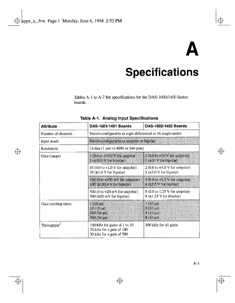
.frm Page 1 Monday, June 6, 1994 2:53 PM
A Specifications
Tables A-l to A-7 list specifications for the DAS-1600/1400 Series boards.
1 Attribute
Table A-l. Analog Input Specifications
1 DAS-1601/1401 Boards / DAS-1602/1402 Boards
Number of channels / ‘_ Swtch configurable BS eight differential or 16 single-ended I
Illput mode
Resolution 1 12-bits (1 part in 4096 or 244 ppm)
500 (0 to +20 mV for unipolar) 8 (0.0 to 1.25 V for umipolar) 500 (i20 mV for bipolar) 8 (il.25 V for bipolar)
Gain (settling time)
Throughput’ 100 kHz for gains of 1 to 10 100 kHz for all gains 70 kHz for a gain of 100 30 kHz for a gain of 500
A-l
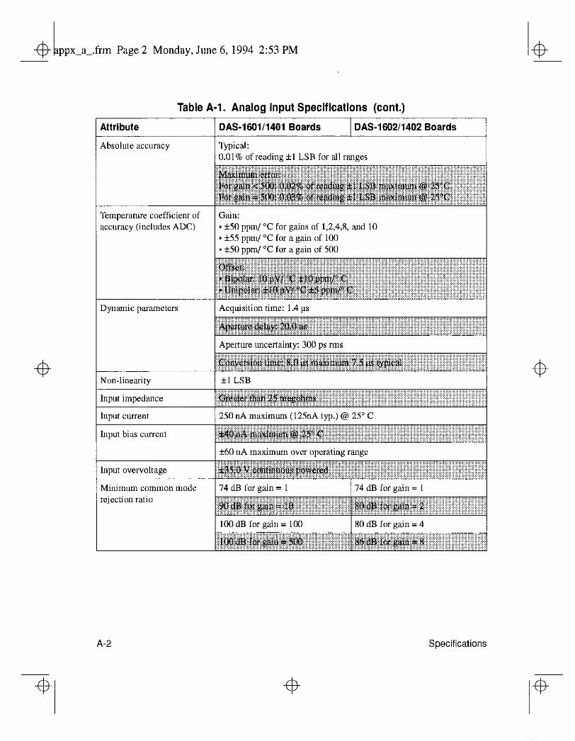
43 appx-a-.frm Page 2 Monday, June 6, 1994 2:53 PM
Table A-l. Analog Input Specifications (cont.)
1 Attribute DAS-1601/1401 Boards DAS-160211402 Boards I
Absolute accuracy Typical: 0.01% of readhe fl LSB for all ramze~
Temperature coefficient of accmacy (includes ADC)
Gain: - f50 ppm/ OC for gains of 1.2.4,s. and 10 - f55 ppm/ ‘C for a gain of 100 * *SO ppm/ “C for a gaio of 500
1 Dynamic parameters 1 Acquisition time: 1.4 ps I
rejection ratio
A-2 Specifications
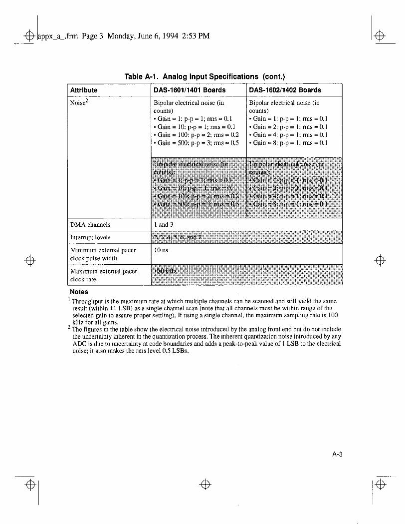
4L -- ppx a .frm Page 3 Monday, June 6, 1994 2:53 PM
Table A-l. Analog Input Specifications (cont.)
Attribute DAS-1601/1401 Boards DAS-1602/1402 Boards
Noise’ Bipolar electrical noise (in Bipolar electrical noise (in counts) counts) .Gain=l:p-p=l;rms=O.l .Gai~l=l:p-p=l;l-ms=O.l . Gain = lo: p-p = 1; rms = 0.1 -Gain=2:p-p=l;rms=O.l * Gain = 100: p-p = 2; rms = 0.2 . Gain = 4: p-p = 1: rms = 0.1 * Gain = 500: p-p = 3; rms = 0.5 .Gain=8:p-p=l;rms=O.l
DMA chzumels 1 and 3
Minimum external pacer clock pulse width
Maximum external pacer clock rate
Notes ’ Throughput is the maximum rate at which multiple channels can be scanned and still yield the same
result (within -tl LSB) as R single ch,mnel scilll (note that all channels must be within range of the selected gain to assure proper settling). If using a single channel, the maximum sampling rate is 100 kHz for all gains.
‘The figures in the table show the electrical noise introduced by the analog front end but do not include the uncertainty inherent in the quantization process. The inherent quantization noise introduced by any ADC is due to uncertainty at code boundaries and adds a peal-to-peak value of 1 LSB to the electrical noise: it also makes therms level 0.5 LSBs.
4
A-3
4
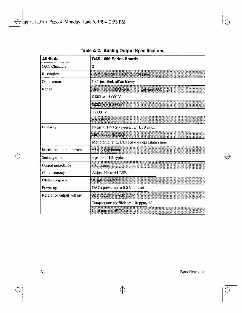
.frm Page 4 Monday, June 6,1994 2:53 PM
Table A-2. Analog Output Specifications
1 Attribute 1 DAS-1600 Series Boards
A-4 Specifications
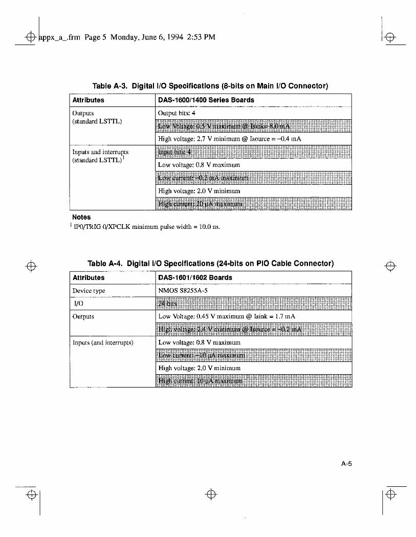
$ 1 ppx a - -’ frm Page 5 Monday, June 6,1994 2:53 PM
Table A-3. Digital I/O Specifications (&bits on Main I/O Connector)
Attributes DAS-1600/1400 Series Boards
1 Outuut bits: 4
Notes ’ IPO/TRIG O/XPCLK minimum pulse width = 10.0 ns.
Table A-4. Digital I/O Specifications (24-bits on PI0 Cable Connector)
Attributes DAS-1601/1602 Boards
Device type NMOS S82SSA-5
Outputs Low Voltage: 0.45 V maximum @ Isink = 1.7 mA I
Inputs (and interrupts) Low voltage: 0.8 V maximum
~
Hieh voltare: 2.0 V minimum
A-5
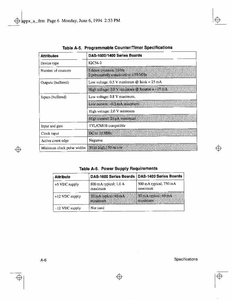
frm Page 6 Monday, June 6, 1994 2:53 PM
4
Table A-5. Programmable Counter/Timer Specifications
Attributes DAS-WOO/1400 Series Boards
Table A-6. Power Supply Requirements
Attribute
+5 VDC supply
DAS-1600 Series Boards DAS-1400 Series Boards
800 mA typical: I.0 A 500 mA typical; 750 mA mwdmum maximum
+I2 VDC supply
- 12 VDC supply Not used
4
A-6
4
Specifications
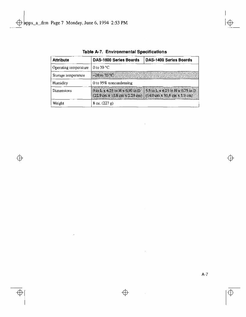
.frm Page 7 Monday, June 6, 1994 2:53 PM
4
Table A-7. Environmental Specifications
( Attribute / DAS-1600 Series Boards 1 DAS-1400 Series Boards 1
/ ODerating temperature I 0 to 70 “C
Storage temperihture ~~~~r~~~~~~~~~~~~~~~~~~~~~~~~~~~~ ~~~~...a.~,.;,.:.:-~.~~~~.~.. .i.,..iil~l.. I .~._,..,........, ..,.., ‘...‘~:,: .,.....:.. ~ .,......,.., j j
Humiditv 0 to 95% noncondensine
Dimensions
Weight 8 oz. (227 g)
4
A-7
4

ppx_a_.frtn Page 8 Monday, June 6, 1994 2:53 PM
4
4 4
4
1 4 -- ppx b .frm Page 1 Monday, June 6, I994 2:54 PM 4
4
4
B Connector Pin Assignments
This appendix contains pin assignments for the I/O connectors of the DAS-1600/1400 Series boards. See Figure 3-l and Figure 3-2 for the location of the main I/O connector (Jl).
B-1
4 4
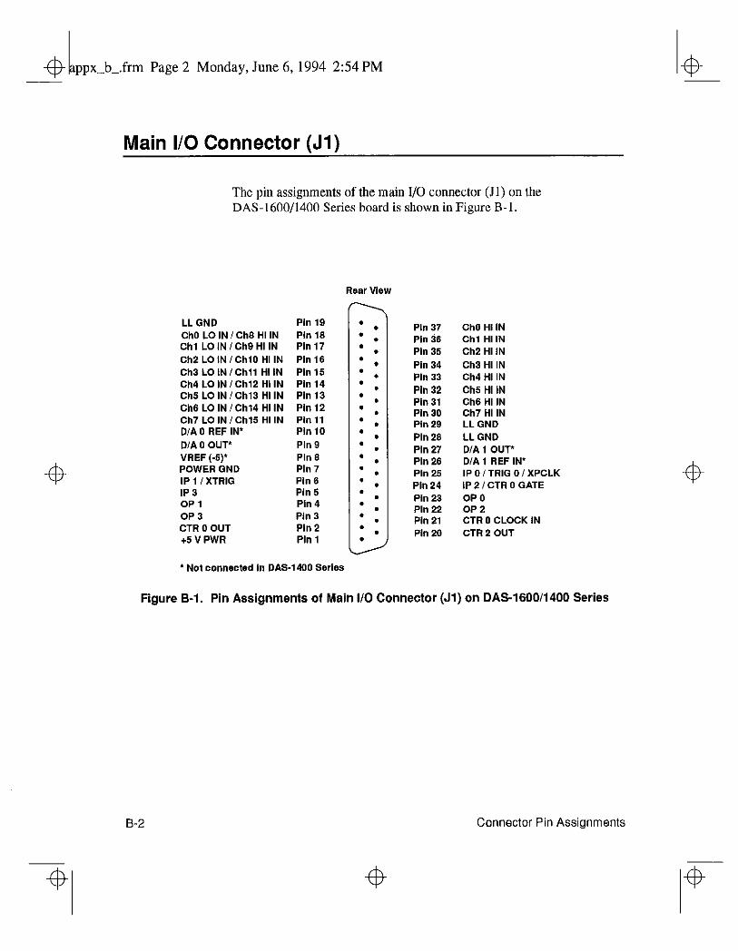
frm Page 2 Monday, June 6,1YY4 2:54 PM
4
4
Main I/O Connector (Jl)
The pin assignments of the main I/O connector (Jl) on the DAS-1600/1400 Series board is shown in Figure B-l.
LL GND ChO LO IN I Ch6 HI IN Chl LO IN / ChS HI IN Ch2 LO IN / ChlO HI IN Ch3 LO IN I Chll HI IN Ch4 LO IN / Ch12 HI IN Ch5 LO IN / Ch13 HI IN Ch6 LO IN ICh14 HI IN Ch7 LO IN /Ch15 HI IN D/A 0 REF IN’ D/A 0 OUT’ VREF (-5)’ POWER GND IP 1 / XTRIG IP3 OPl OP3 CTR 0 OUT +6 V PWR
Pi” 19 Pi” 16 PI” 17 PI” 16 PI”15 PI” 14 PI” 13 PI”12 PI”11 PIlllO Pill 9 Phi 6 PI” 7 PI” 6 PI” 5 Pi” 4 PI” 3 PI” 2 PI” 1
Rear View
PI” 37 PI” 36 PI” 35 PI” 34 PI” 33 PI” 32 PI” 31 PI” 30 PI” 29 Pill 26 PI” 27 PI” 26 PI” 25 PI” 24 Pin 23 Pi” 22 Pi” 21 Pi” 20
ChO HI IN Chl HI IN Ch2 HI IN Ch3 HI IN Ch4 HI IN Ch5 HI IN Ch6 HI IN Ch7 HI IN LL GND LL GND WA 1 OUT’ D/A 1 REF IN’ IP 0 i TRIG 0 / XPCLK IP 2 I CTR 0 GATE OPO 0;; CTR 0 CLOCK IN CTR 2 OUT
* Not connected I” DAS-1400 Series
Figure B-1. Pin Assignments of Main l/O Connector (Jl) on DAS-1600/1400 Series
B-2
4
Connector Pin Assignments
4
4
4
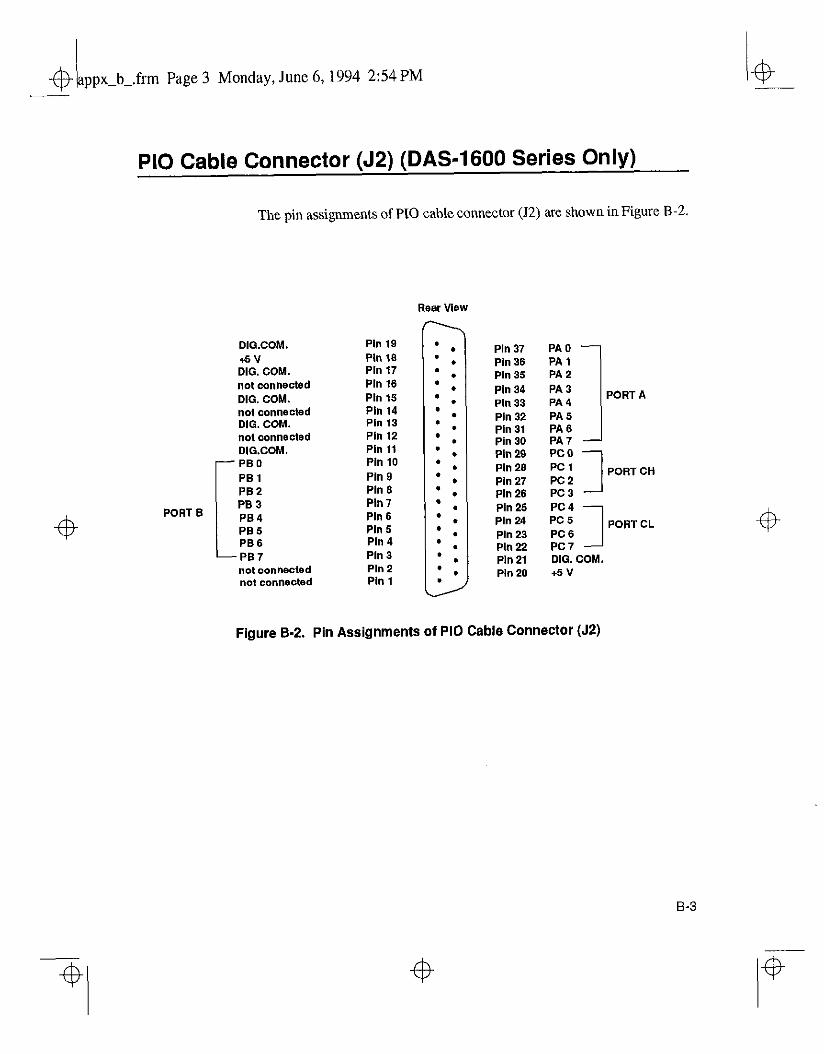
ppx-b-.frm Page 3 Monday, June 6,1YY4 2:54 PM
4
PI0 Cable Connector (52) (DAS-1600 Series Only)
The pin assignments of PI0 cable connector (J2) are shown in Figure B-2.
Rear View
DIGCOM. +5V DIG. COW not connected DIG. COM. not connected DIG. COM. not connected DIG.COM.
r PBO PB 1 PB2
PORT B PB3 PB4 PB5 PBS
LPB7 not connected no, connected
PI” 19 Pill 18 PI” 17 Pin 16 PI” 15 PI” 14 PI” 13 PI” 12 PI” 11 PI” 10 PI” 9 PI” 6 Ph 7 PI” 5 PI” 5 PI” 4 PI” 3 PI” 2 PI” 1
l .
’ .
l .
’ .
* .
* .
l .
l .
’ .
l .
l .
l .
* .
l .
’ .
* .
’ .
’ . .
PI” 37 PA 0 Pin 36 PA 1 PI” 35 PA 2
Pi” 34 PA3 PI” 33 PA4 PI” 32 PA5 PI” 31 PA6 Pin 30 PA7 1 PORT A
Pill 2% PC0 Pin 26 PC1 1 PORT CH Pi” 27 PC2 PI” 26 PC3 PI” 25 PC4 PI” 24 PC5 PORT CL
PI” 23 PC6 PI” 22 PC7 1 Ph 21 DIG. COM. PI”20 +5 v
Figure B-2. Pin Assignments of PI0 Cable Connector (52)
B-3
4
h-
4
4

.frm Page 4 Monday, June 6,1YY4 2:54 PM
4
frm Page 1 Monday, June 6.1994 2:54 PM
C Using the DAS-1600
External Driver
The DAS-1600 External Driver (DAS 1600.EXE) allows the following data acquisition and analysis packages to exchange data with DAS-1600/1400/1200 Series boards:
. VIEWDAC
. EASYEST LX
. EASYEST AG
. ASYST
You use the external driver characteristics described in this appendix by selecting menu items and entering text in dialog boxes of the software package in use.
Options Supported
The DAS-1600 External Driver supports the following options:
. Analog input operations, including interrupt and Direct Memory Access (DMA) - 16 single-ended or eight differential 12-bit analog input channels
- Up to 136 channels through EXP-16 and EXP-GP support
l Two 12-bit digital-to-analog output channels (DAS-1600 Series only)
. 32 digital I/O bits on DAS-1600 Series and DAS-1200 Series boards, and eight digital I/O bits on DAS-1400 Series boards
4
4
C-l
4
1 6 -- ppx c .frm Page 2 Monday, June 6.1994 2:54 PM
. Analog triggering
. Simultaneous sample-and-hold through the SSH-4A
l Event counting
. Pulse output
Quick Start
The following sections describe how to install and access the DAS-1600 External Driver.
Setting Up the Board
c-2
Prior to starting the external driver, perform the following steps:
1. Install the DAS-1600/1400/1200 standard software package. See “Installing the Software Package” on page 3-2 for installation instructions.
2. Verify that the switch-configuration of your board matches the options set in your configuration file. See “Creating a Configuration File” on page 3-6 for instructions on using and creating configuration files. For information on setting up the board, see “Setting Switch-Configurable Options” on page 3-14.
3. Install me board in your computer. See “Installing the Board” on page 3-18 for installation procedures.
4. Connect the appropriate signals to your DAS-1600/1400/1200 Scrics hoard, keeping the following in mind:
External digital trigger - Connect the external digital trigger to the IPl/XTRIG pin (6) on the main I/O connector.
- External clock Connect dwextemal clock signal to the W&TRIG O/XPCLK pin (25) on the main I/O connector.
- Event counting Connect the event signal to the CTR 0 CLOCK IN pin (21) on the main I/O connector.
- Pulse output Connect the pulse output signal to the CTR 2 OUT pin (20) on the main I/O connector.
Using the DAS-1600 External Driver
1 $ -- ppx c .frm Page 3 Monday, June 6, 1994 2:54 PM
4
4
Loading the DAS-1600 External Driver
You must load the DAS-1600 External Driver, DAS 1600,EXE, each time you start up your computer in order for your application program to recognize it. The DAS-1600 External Driver remains in memory until you turn off or reboot your computer.
To load the DAS-I600 External Driver, access the directory containing DAS 1600,EXE and enter the following at the DOS prompt:
da1600 <filename>
where the optional <filename> is the name of the configuration file you are using. If you do not specify a configuration file, the driver searches for the default configuration file, DAS1600,CFG, in the current direclory.
Note: You can also load the DAS-1600 External Driver automatically whenever you start the computer by modifying your AUTOEXECBAT tile.
Loading the External Driver in Multiple Board Configurations
The number of DAS-1600/1400/1200 Series boards that you can install in your system is limited by the available slots in your computer. Each memory-resident external driver can support two DAS-1600/1400/1200 Series boards. The number of external drivers that you can load is limited only by the amount of available memory in your computer.
Note: Some operations may not be available when using multiple DAS boards depending on the system resources that the operations require and how system resources are allocated.
To access more than two boards, load the DAS-1600 External Driver as many times as you have configuration files. For example, to access three boards, you can create two configuration files called D 1600-l.CFG and D1600-2.CFG.
4
4
.frm Page 4 Monday, June 6,1994 254 PM
In this example, D1600-l.CFG contains the configuration data for two boards at addresses 30011 and 3 10h and D 1600-2.CFG contains the configuration data for a single board at address 34011. To load the DAS-1600 External Drivers, use the following syntax:
DAS1600 D1600.J.CFG DAS1600 D1600p2.CFG
Using the External Driver with Application Software Packages
This section describes how to access the DAS-1600 External Driver when using VIEWDAC, EASYEST LX, EASYEST AG, and ASYST. For additional information, refer to your VIEWDAC, EASYEST LX / AG, or ASYST documentation.
VIE WDA C
All DAS tasks within VIEWDAC have an associated dialog box. Select the DAS Device pop-up menu in this dialog box and click on the DAS 1600 entry.
Note: If the DAS-1600 External Driver is the only driver installed in your system, VIEWDAC DAS tasks automatically select the driver.
EASVEST LX / AG
If the DAS-1600 External Driver is the only driver installed in your system, your EASYEST LX / AG application programs access the DAS-1600 External Driver automatically.
If more than one driver is installed, you must perform the following steps to access the DAS-1600 External Driver:
1. Select Devices from the EASYEST LX / AG menu bar.
2. From the DAS Configuration screen, select option 1, DAS Board Selection.
3. Select the appropriate external driver (board name) from the displayed list.
c-4 Using the DA%1600 External Driver
frm Page 5 Monday, June 6, 1994 2:54 PM
ASYST
If you are using ASYST, always perform the following steps to access the DAS-1600 External Driver:
1. After loading the DAS-1600 External Driver, start up ASYST version 2.10 or greater and permanently load the Data Acq Master and the Ext DAS Driver Support system overlays from the Data Acquisition menu. ASYST automatically searches for and creates a DAS device called DAS1600.
2. Enter the following at the OK prompt to make the DAS-1600/1400/1200 Series board the current device:
DAS1600
DAS-1600 External Driver Characteristics
The following sections describe special attributes and operating characteristics of the DAS-1600 External Driver.
Channels and Gains
The external driver supports channel-gain queues of 128 channels for DAS-1600 Series and DAS-1400 Series boards. Channel-gain queues are not supported for DAS-1200 Series boards. Table C-l lists the gains and corresponding gain codes supported by DAS-1600/1400/1200 Series boards.
C-6
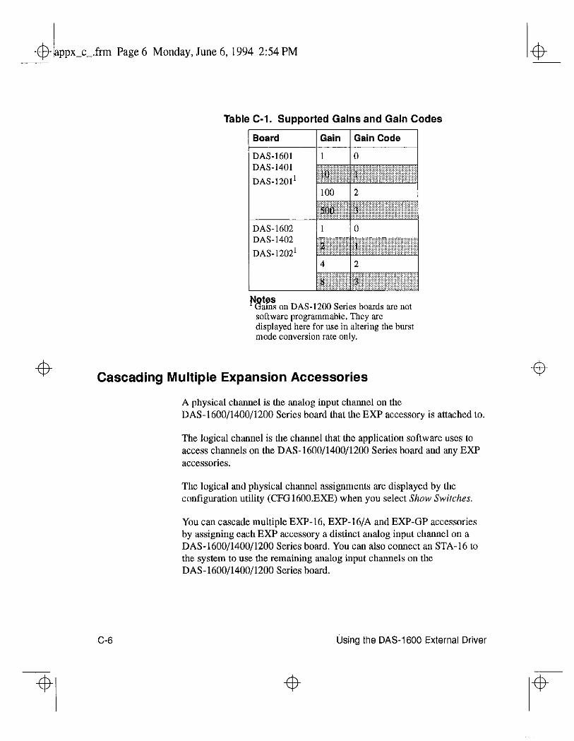
.frm Page 6 Monday, June 6, 1994 2:54 PM
4
4
Table C-l. Supported Gains and Gain Codes
Board Gain Gain Code
DAS-1601 I1 IO
1 DAS-1602 j 1 10 I
pp ams on DAS-1200 Series boards are not software programmable. They are displayed here for use in altering the burst mode conversion rate~only.
Cascading Multiple Expansion Accessories
C-6
A physical channel is the analog input channel on the DAS-1600/1400/1200 Series board that the EXP accessory is attached lo.
The logical channel is the channel that the application software uses to access channels on the DAS-1600/1400/1200 Series board and any EXP accessories.
The logical and physical channel assignments are displayed by the configuration utility (CFG1600.EXE) when you select Show Switches.
You can cascade multiple EXP-16, EXP-16/A and EXP-GP accessories by assigning each EXP accessory a distinct analog input channel on a DAS-1600/1400/1200 Series board. You can also connect au STA-16 to the system to use the remaining aualog input channels on the DAS-1600/1400/1200 Series board.
Using the DAS-1600 External Driver
4
4
4
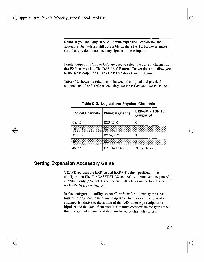
.frm Page 7 Monday, June 6, 1994 2:54 PM
4
Note: If you are using an STA-16 with expansion accessories, the accessory channels are still accessible on the STA-16. However, make sure that you do not connect any signals to these inputs.
Digital output bits OPO to OP3 are used to select the current channel on the EXP accessories. The DAS-1600 External Driver does not allow you to use these output bits if any EXP accessories are configured.
Table C-2 shows the relationship between the logical and physical channels on a DAS-1602 when using two EXP-GPs and two EXP-16s.
Table C-2. Logical and Physical Channels
Logical Channels Physical Channel EXP-GP ’ EXP-16 Jumper J4 I I
oto 15 EXP-16: 0 IO
Setting Expansion Accessory Gains
VIEWDAC uses the EXP-16 and EXP-GP gains specified in the configuration file. For EASYEST LX and AG, you must set the gain of channel 0 only (channel 0 is on the first EXP-16 or on the first EXP-GP if no EXP-16s are configured).
In the configuration utility, select Show Switches to display the EXP logical-to-physical-channel mapping table. In this case, the gain of all channels is relative to the setting of the A/D range type (unipolar or bipolar) and the gain of channel 0. You must compensate for gains other than the gain of channel 0 if the gain for other channels differs.
4
4
c-7
frm Page 8 Monday, June 6, 1994 2:54 PM
4
C-E
4
Note: When using a gain of 0.5 on the EXP-16. the maximum input range is f12 V, not f20 V.
Conversion Modes
The following sections describe how the DAS-1600 External Driver supports the burst and SSH conversion modes.
Using Pseudo-Digital Output Channels
Burst mode and SSH mode are not standard features of the softwarc. To access these features, the DAS- 1600 External Driver uses pseudo-digital output channels.
Pseudo-digital output channels are digital output channels supported by the software: these channels are used by DAS- 1600/1400/1200 Series boards for control only, not for output.
Note: Only values written to digital output channel 0 affect the digital output lines on the DAS-1600/1400/1200 Series board. Values written to the pseudo-digital output channels are intercepted by the DAS- 1600 External Driver and are used to set up the non-standard features.
Table C-6 lista the pseudo-digital channels used by the DAS-1600 External Driver for burst mode and SSH mode operations.
Using the DAS-1600 External Driver
4 4
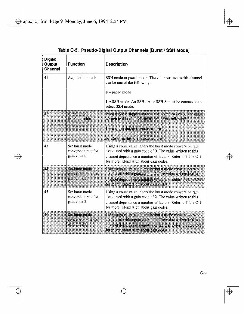
.frm Page 9 Monday, June 6, 1994 2:54 PM
Table C-3. Pseudo-Digital Output Channels (Burst / SSH Mode)
Digital output Channel
41
Function Description
Acquisition nmde SSH mode or paced mode. The value written to this channel can be one of the following:
0 = paced mode
1 = SSH mode. An SSH-4A or SSH-8 must be connected to select SSH mode.
Set burst mode conversion rate for gain code 0
Using a count value, alters the burst mode conversion rate associated with a gain code of 0. The value written to this channel depends on a number of factors. Refer to Table C-l for more information about gain codes.
Set burst mode conversion rate for gain code 2
Using a count value, alters the burst mode conversion rate associated with a gain code of 2. The value writlen to this channel depends on a number of factors. Refer m Table C-l for snore information about nain codes.
4
4
4
c-9
.frm Page 10 Monday, June 6,1994 254 PM
+b
Burst Mode and SSH Mode
Burst mode is a software simulated simultaneous sample-and-hold feature in which successive analog input channels are sampled as quickly as possible.
Note: When using the DAS-1600 External Driver, burst mode is supported for DMA operations only.
The burst mode conversion rate defaults to a gain-dependent value that you can alter. Refer to page C- 11 for information on altering the burst mode conversion rate.
SSH (simultaneous sample-and-hold) mode is a hardware feature that requires use of an SSH4A or SSH-8. The requested channels are sampled nearly instantaneously and held until read. The rate between scans is set by the sample frequency.
c-10
Warning: When you select SSH-X as an SSH Type in the configuration utility, you must select a 10 MHz clock (in the Clock Select option). Selecting a 1 MHz clock for use with an SSH-8, causes the Function Call Driver and the DAS-1600 External Driver to report an error (28714) and terminate.
Note that in burst mode, the data is skewed slightly; in SSH mode, the data is not skewed.
When using VIEWDAC or EASYEST LX / AG, you specify the sampling frequency as the per channel rate. For example, specifying a frequency of 1 kHz when acquiring from two channels in paced (normal) mode results in an aggregate board rate of 2 kHz.
When using burst or SSH mode, the specified sampling frequency is also a per channel rate. For example, if you specify a frequency of 1 kHz when acquiring from two channels in burst or SSH mode, the two channels are sampled nearly instantaneously and are sampled again after 1 ms (1 kHz).
Using the DAS-1600 External Driver
+B +b
1 43 -- ppx c .frm Page 11 Monday, June 6, 1994 2:54 PM
+b
When using ASYST, you specify the conversion delay rather than the per channel rate. The conversion delay is the time between conversions, which translates to a sampling rate that is dependent on the number of channels to scan.
For example, specifying a conversion delay of 1 ms when acquiring from one channel equates to a 1 kHz sampling rate. Adding a second channel drops the per channel rate to 500 Hz.
When using burst or SSH mode, the conversion delay is interpreted the same way even though the time between channels is nearly instantaneous, For example, to sample two channels at a 1 kHz sampling rate, you would specify a conversion delay of 0.5 ms for each channel, even though the time between scans is actually 1 ms. This interpretation allows you to calculate sampling rates that apply with or without burst or SSH mode.
The scan sequence in ASYST is as follows:
Paced (normal) mode:
0 [cd] 1 [cd] 2 [cd] (n-l) [cd] 0 [cd] 1 [cd]
Burst oi- SSH mode:
0 1 2 3 (n-l) [cd*n] 0 1 2 3 (n-l) [cd%] 0 12 3
cd = conversion delay specified; n = number of channels
0 = start channel; [ ] = actual time delay
Altering the Burst Mode Conversion Rate
When a DAS-1600/1400/1200 Series board operates ,in DMA burst mode, it acquires data in a burst from the channels specified by the start/stop parameters. The burst is programmed to run at the maximum possible rate, which is determined by the gain setting. The higher the gain, the more settling time is required and the slower the burst mode conversion rate.
C-l 1
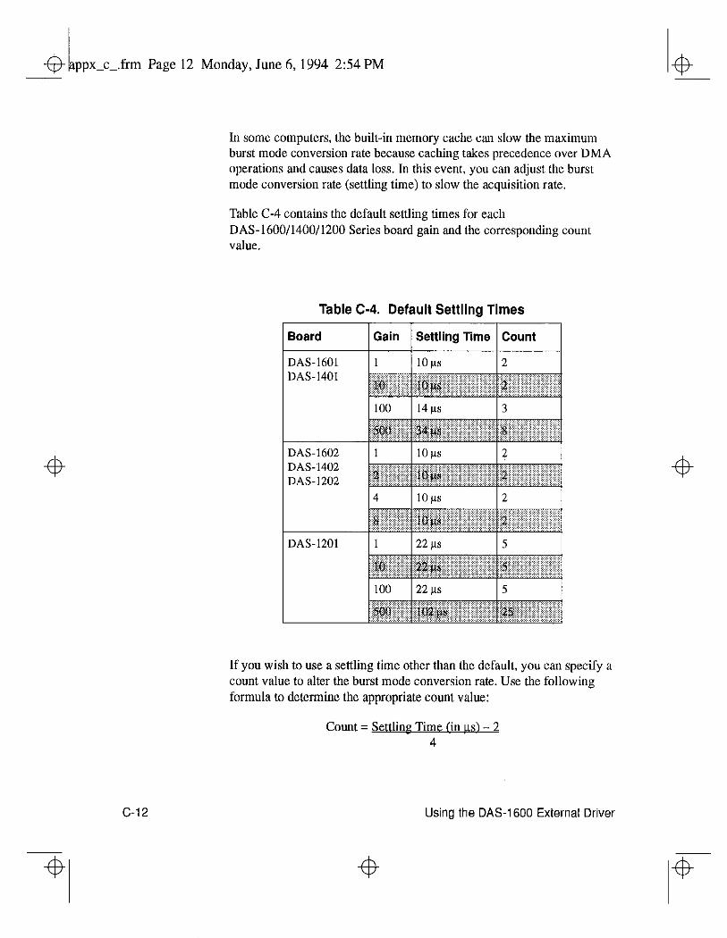
.frm Page 12 Monday, June 6, 1994 254 PM
4
c-12
4
In some computers, the built-in memory cache can slow the maximum burst mode conversion rate because caching takes precedence over DMA operations and causes data loss. In this event, you can adjust the burst mode conversion rate (settling time) to slow the acquisition rate.
Table C-4 contains the default settling times for each DAS-1600/1400/1200 Series board gain and the corresponding count value.
Table C-4. Default Settling Times
Board Gain Settling Time Count
DAS-1601 I1 1ous 12
1 DAS-1602 1 1 / DAS-1402 DAS-1202
1 DAS-1201 1 1 122Lls 15 I
If you wish to use a settling time other than the default, you can specify a count value to alter the burst mode conversion rate. Use the following formula to determine the appropriate count value:
Count = Settling Time tin us1 - 2 4
Using the DAS-1600 External Driver
4
4
4
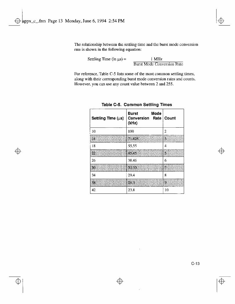
.frm Page 13 Monday, June 6,1994 2:54 PM
The relationship between the settling time and the burst mode conversion rate is shown in the following equation:
Settling Time (in us) = 1 MHz Burst Mode Conversion Rate
For reference, Table C-5 lists some of the most common settling times, along with their corresponding burst mode conversion rates and counts. However, you can use any count value between 2 and 255.
Table C-5. Common Settling Times
Burst Mode Settling Time (p) Conversion Rate Count
W-W
C-l 3
.frm Page 14 Monday, June 6.1994 2:54 PM
Clock Sources
The DAS-1600 External Driver supports an internal and external clock source, as follows:
. Internal clock source -A conversion begins without waiting for an external clock signal and proceeds at the specified rate until finished. With the jumper in the 1 MHz position, the clock resolution is 1 ns. With the jumper in the 10 MHz position, the clock resolution is 0.1 ns.
. External clock source -The software waits for a rising edge at the IPODRIG O/XF’CLK pin (25) input before starting each conversion. Acquisition proceeds and is paced by the external clock until the requested amount of data is acquired.
Triggers
The following sections describe how the DAS-1600 External Driver supports an external analog and external digital trigger,
Note: When using external analog and external digital triggering, make sure that you provide a valid trigger to the DAS-1600 External Driver. If no trigger is found, the computer will appear to be hung as the DAS-1600 External Driver waits indefinitely for the trigger.
Using Pseudo-Digital Output Channels
External analog and external digital triggers are not standard features of the software. To access these features, the DAS-1600 External Driver uses pseudo-digital output channels.
Pseudo-digital output channels are digital output channels supported by the software: these channels are used by DAS- 1600/1400/1200 Series boards for control only, not for output.
c-14 Using the DA.51600 External Driver
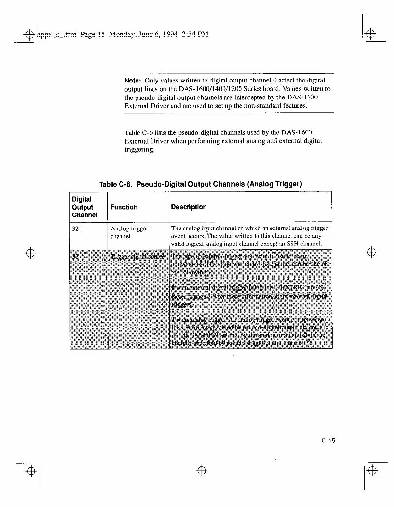
-@ ppx-c-.frm Page 15 Monday, June 6, 1994 2:54 PM
Note: Only values written to digital output channel 0 affect the digital output lines on the DAS-1600/1400/1200 Series board. Values written to the pseudo-digital output channels are intercepted by the DAS-1600 External Driver and are used to set up the non-standard features.
Table C-6 lists the pseudo-digital channels used by the DAS-1600 External Driver when performing external analog and external digital triggering.
Table C-6. Pseudo-Digital Output Channels (Analog Trigger)
Digital output Channel
Function Description
The analog input channel on which an external analog trigger event occurs. The value written to this channel can bc any valid logical analog input channel except an SSH clnumel.
c-15
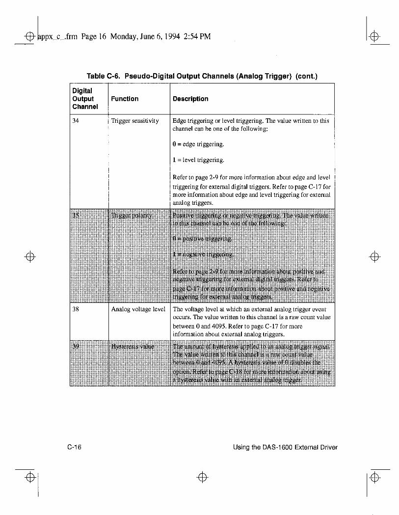
1 4 -- ppx c .fcm Page 16 Monday, June 6,1994 2:54 PM
4
Table C-6. Pseudo-Digital Output Channels (Analog Trigger) (cont.)
Digital
r
output Channel
Description
34
38
C-l 6
Wgger sensitivity
Analog voltage level
Edge triggering or level triggering. The value written to this channel can be one of the following:
0 = edge triggering.
1 = level triggering.
Refer to page 2-9 for more information about edge and level
triggeriug for external digital triggers. Refer to page C-17 for more information about edge and level triggering for external analog triggers.
The voltage level at which an external analog trigger event occurs. The value written to this channel is a raw count value between 0 and 4095. Refer to page C-17 for more information about external analog triggers.
Using the DAS-I 600 External Driver
4
4
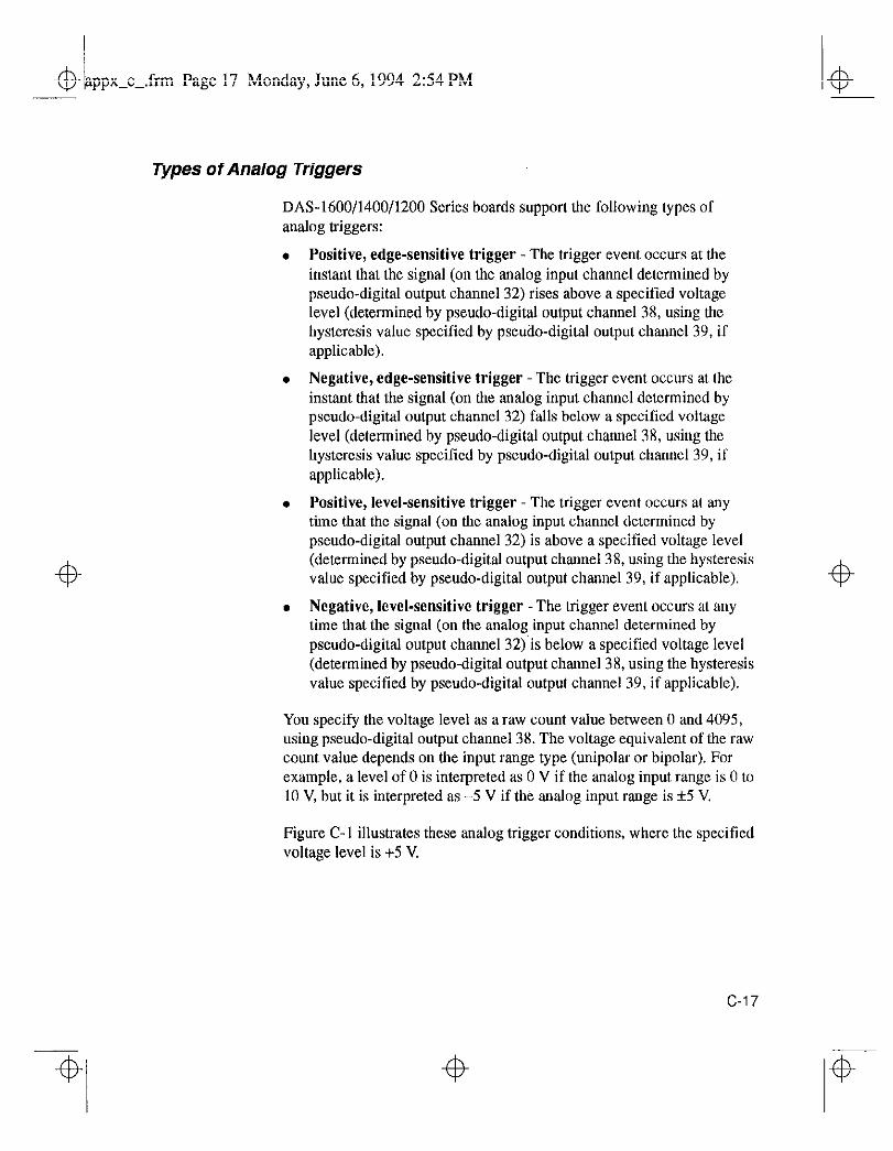
.frm Page 17 Monday, June 6,1994 2:54 PM
4
4
Types of Analog Triggers
DAS-1600/1400/1200 Series boards support the following types of analog triggers:
. Positive, edge-sensitive trigger - The trigger event occurs at the instant that the signal (on the analog input channel determined by pseudo-digital output channel 32) rises above a specified voltage level (determined by pseudo-digital output channel 38, using the hysteresis value specified by pseudo-digital output channel 39, if applicable).
. Negative, edge-sensitive trigger -The trigger event occurs at the instant that the signal (on the analog input channel determined by pseudo-digital output channel 32) falls below a specified voltage level (determined by pseudo-digital output channel 38, using the hysteresis value specified by pseudo-digital output channel 39, if applicable).
. Positive, level-sensitive trigger The trigger event occurs at any time that the signal (on the analog input channel determined by pseudo-digital output channel 32) is above a specified voltage level (determined by pseudo-digital output channel 38, using the hysteresis value specified by pseudo-digital output channel 39, if applicable).
l Negative, level-sensitive trigger -The trigger event occurs at any time that the signal (on the analog input channel determined by pseudo-digital output channel 32) is below a specified voltage level (determined by pseudo-digital output channel 38, using the hysteresis value specified by pseudo-digital output channel 39, if applicable).
You specify the voltage level as a raw count value between 0 and 4095, using pseudo-digital output channel 38. The voltage equivalent of the raw count value depends on the input range type (unipolar or bipolar). For example, a level of 0 is interpreted as 0 V if the analog input range is 0 to 10 V, but it is interpreted as -5 V if the analog input range is f5 V.
Figure C-l illustrates these analog trigger conditions, where the specified voltage level is +5 V.
4
4
c-17
4 4
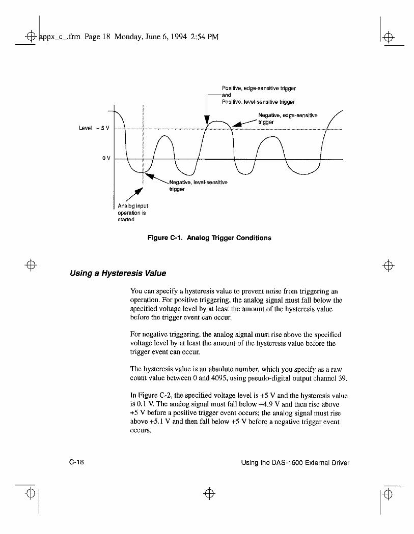
.frm Page 18 Monday, June 6, 1994 2:54 PM
4
Positive. edge-sensitive trigger
Positive, level-sensitive trigger
Negative, edge-sensitive
: Negative, level-sensitive trigger operation is started
Figure C-l. Analog Trigger Conditions
Using a Hysteresis Value
C-l 8
You can specify a hysteresis value to prevent noise from triggering an operation. For positive triggering, the analog signal must fall below the specified voltage level by at least the amount of the hysteresis value before the trigger event can occur.
For negative triggering, the analog signal must rise above the specified voltage level by at least the amount of the hysteresis value before the trigger event can occur.
The hysteresis value is an absolute number, which you specify as a raw count value between 0 and 4095, using pseudo-digital output channel 39.
In Figure C-2, the specified voltage level is +5 V and the hysteresis value is 0.1 V. The analog signal must fall below +4.9 V and then rise above +5 V before a positive trigger event occurs; the analog signal must rise above +5.1 V and then fall below +5 V before a negative trigger event occurs.
Using the DAS-1600 External Driver
4
4
4 4
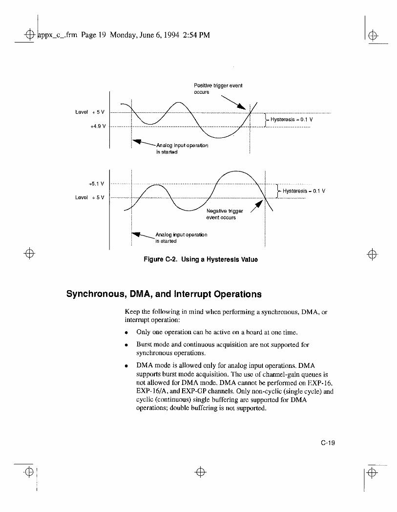
.frm Page 19 Monday, June 6,1994 2:54 PM
Positive trigger event ^^ ^. .^ “CCYlS
Level t5” x ,Ll....................... l...y . . . .._...._.._....._.._..................
+A,.9 v 1 / u \ ) )Hystmsis=O.lV ,..,..,,.,,.,..,..,..,,.,,.,,.,,. i .,..,..,.,,.,..,..,..,,.,,.,,.,,.,..,..,..,..,..,..,,.,,.,.,, ,,,.,,.,,._ +” ..,..,,.,,., ,.,..,..,,.,,.,,..,..,..,.,,.,,..,..,..,..,..,,.,,.,..,..,..,,.,...,..,.
Figure C-2. Using a Hysteresis Value
Synchronous, DMA, and Interrupt Operations
Hysteresis = 0.1 V
Keep the following in mind when performing a synchronous, DMA, or interrupt operation:
. Only one operation cao be active on a board at one time.
. Burst mode and continuous acquisition are not supported for synchronous operations.
. DMA mode is allowed only for analog input operations. DMA supports burst mode acquisition. The use of channel-gain queues is not allowed for DMA mode. DMA cannot be performed on EXP-16, EXP-16/A, and EXP-GP channels. Only non-cyclic (single cycle) and cyclic (continuous) single buffering are supported for DMA operations: double buffering is not supported.
c-19
b & --. ppx c frm Page 20 Monday, June 6,1994 2:54 PM
. Interrupt mode is supported for analog input, analog output, and digital I/O operations. Burst mode is not supported for interrupt operations. Only non-cyclic (single cycle) and cyclic (continuous) single buffering are supported for interrupt operations; double buffering is not supported.
Note: Because the DAS-1600 External Driver cannot detect all interrupt overrun conditions, ensure that interrupt operation speeds are valid for your system.
Digital I/O Characteristics
Note: Since the extended digital ports (32 to 46) require 12 output bits, the software always shows aminimum of 12 available bits, no matter how a digital output port is configured. If a digital output port is configured for X,4, or 0 output bits, you can disregard the extra bits, The following subsections describe the digital I/O support for the DAS boards.
DAS- 1600/l 200 Series Boards
c-20
The DAS-1600/1200 Series boards have four unidirectional digital input bits and four unidirectional digital output bits. In addition, an Intel X255 provides 24 bits of bidirectional digital I/O. These 24 bits are organized into four ports (ports A, B, CL, and CH); you can configure each port for either input or output.
Note: When an EXF’ accessory is configured, the four unidirectional digital output bits are dedicated to EXP accessory control and are not available for digital output.
The external driver supports one digital input channel and one digital output channel on each board (if any bits are available). The number of bits used in each channel depends on the port configuration and whether an EXP accessory is configured.
Using the DAS-1600 External Driver
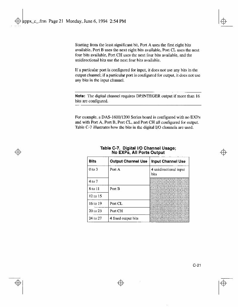
.frtn Page 21 Monday, June 6,1994 2:54 PM 4
Starting from the least significant bit, Port A uses the first eight bits available, Port B uses the next eight bits available, Port CL uses the next four bits available, Port CH uses the next four bits available, and the unidirectional bits use the next four bits available.
If a particular port is configured for input, it does not use any bits in the output channel; if a particular port is configured for output, it does not USC any bits in the input channel.
Note: The digital channel requires DPINTEGER output if more than I6 bits are configured.
For example, a DAS-1600/1200 Series board is configured with no EXPs and with Port A, Port B, Port CL, and Port CH all configured for output. Table C-7 illustrates how the bits in the digital I/O channels are used.
Table C-7. Digital l/O Channel Usage; No EXPs, All Ports Output
Bits
oto3
Output Channel Use Input Channel Use
Port A 4 unidirectional input bits
Port B
I 16 to 19 1 Port CL
I20 to 23 1 Port CH
1 24 to 27 14 fixed output bits
c-21
4
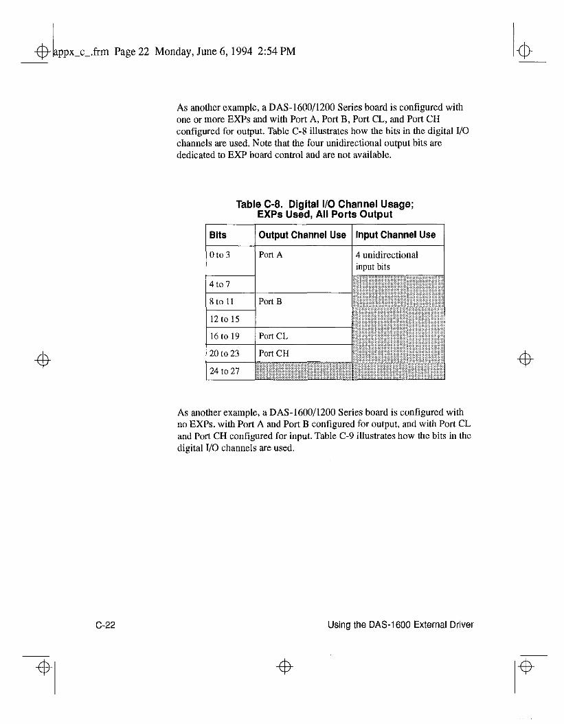
.frm Page 22 Monday, June 6,1994 2:54 PM
4
c-22 Using the DAS-1600 External Driver
As another example, a DAS-1600/1200 Series board is configured with one or more EXPs and with Port A, Port B, Port CL, and Port CH configured for output. Table C-8 illustrates how the bits in the digital I/O channels are used. Note that the four unidirectional output bits are dedicated to EXP board control and are not available.
Table C-8. Digital l/O Channel Usage; EXPs Used, All Ports Output
Bits
oto3
Output Channel Use Input Channel Use
Port A 4 unidirectional input bits
(Rtoll ]PortB
I I 12 to 15
116tol9 tPortCL
/ 20 to 23 I Port CH
As another example, a DAS-1600/1200 Series board is configured with no EXPs, with Port A and Port B configured for output, and with Port CL and Port CH configured for input. Table C-9 illustrates how me bits in the digital I/O channels are used.
4
4 4
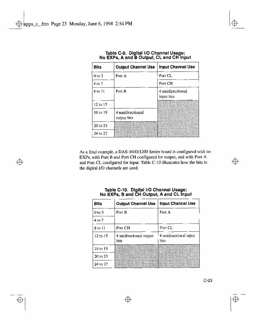
k 4 -- ppx c .fcm Page 23 Monday, June 6,1994 2:54 PM
4
Table C-9. Digital I/O Channel Usage; No EXPs, A and B Output, CL and CH Input
Bits Output Channel Use Input Channel Use
0 to 3 Port A Port CL
4 to 7 Port CH
sto 11 Port B 4 unidirectional
As a final example, a DAS-1600/1200 Series board is configured with no EXPs, with Port B and Port CH configured for output, and with Port A and Port CL configured for input. Table C-10 illustrates how the bits in the digital I/O channels are used.
Table C-10. Digital I/O Channel Usage; No EXPs, B and CH Output, A and CL Input
Output Channel Use Input Channel Use
8to 11 Port CH Port CL
12to 1s 4 unidirectional output 4 unidirectional input bits bits
4
C-23
4 +b
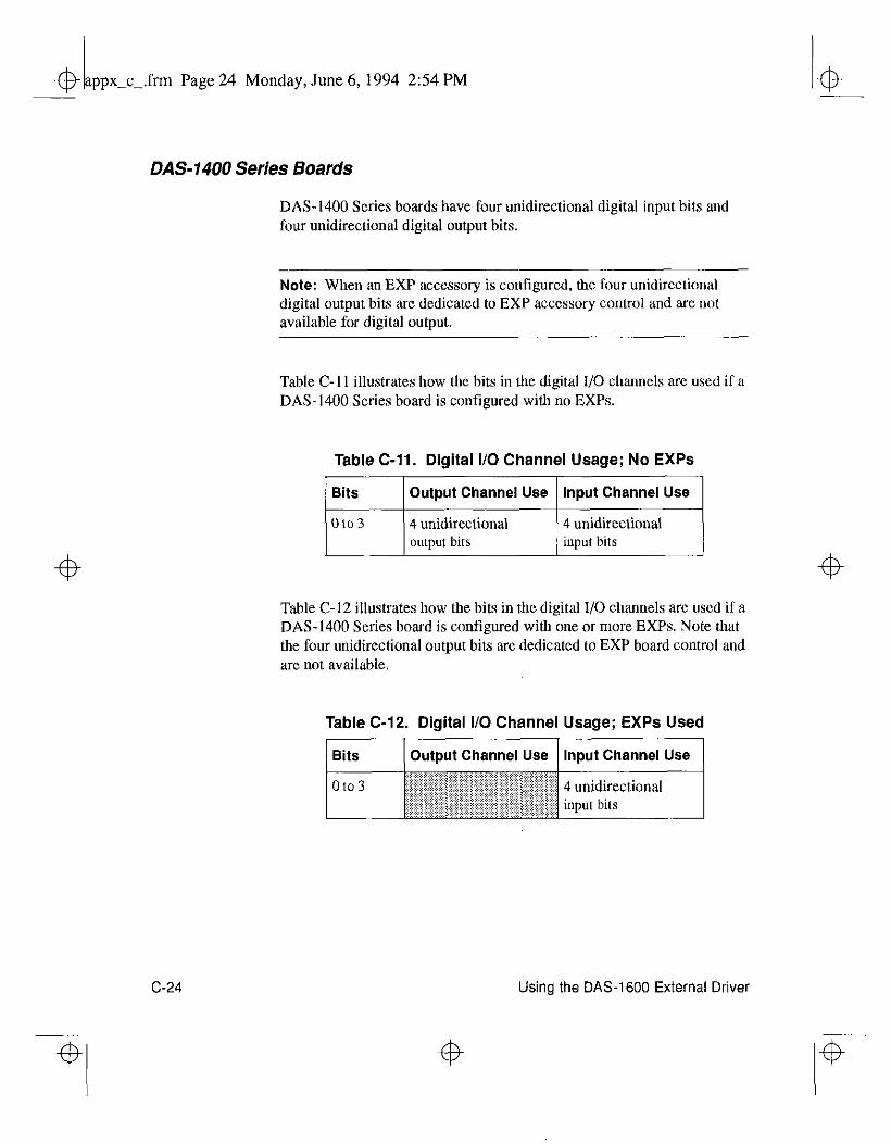
frm Page 24 Monday, June 6, 1994 2:54 PM
DAS-1400 Series Boards
DAS-1400 Series boards have four unidirectional digital input bits and four unidirectional digital output bits.
C-24
Note: When an EXP accessory is configured, the four unidirectional digital output bits are dedicated to EXP accessory control and are not available for digital output.
Table C- 11 illustrates how the bits in the digital I/O channels are used if a DAS-1400 Series board is configured with no EXPs.
Table C-11. Digital l/O Channel Usage; No EXPs
Output Channel Use Input Channel Use
Table C-12 illustrates how the bits in the digital l/O channels are used if a DAS-1400 Series board is configured with one or more EXPs. Note that the four unidirectional output bits are dedicated to EXP board control and are not available.
Table C-12. Digital l/O Channel Usage; EXPs Used
Output Channel Use Input Channel Use
Using the DAS-I 600 External Driver
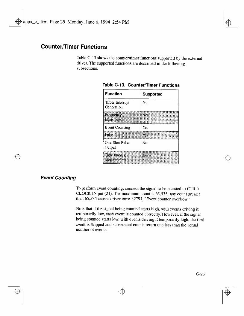
1 $ -- ppx c .frm Page 25 Monday, June 6, 1994 2:54 PM
Counter/Timer Functions
Table C-13 shows the counter/timer functions supported by the external driver. The supported functions are described in the following subsections.
Table C-13. Counter/Timer Functions
Event Counting
To perform event counting, connect the signal to be counted to CTR 0 CLOCK IN pin (21). The maximum count is 65,535: any count greatel than 65,535 causes driver error 32791, “Event counter overflow,”
Note that if the signal being counted starts high, with events driving it temporarily low, each event is counted correctly. However, if the signal being counted starts low, with events driving it temporarily high, the first event is skipped and subsequent counts return one less than the actual number of events.
c-25
4
1 4 -- ppx c .frm Page 26 Monday, June h,1994 2:54 PM
Pulse Output
A pulse output generates a pulse train on the CTR 2 OUT pin (20). The duty cycle of the pulse train is fixed at 50% due to the nature of the 8254 counter/timer circuitry.
Software Interrupt Vectors
The DAS-1600 External Driver uses two software interrupt veclors for communicating with the application package. The interrupt vectors used are two of the user vectors (60h to 67h) that are set aside by DOS.
When conflicts with other devices or programs occur, you can set each of the interrupt vectors to use a location that is different from the default.
You can change the interrupt vectors by using the DOS SET command to change the environment variables read by the DAS-1600 External Driver. Table C-14 lists the environment variables used.
Table C-14. Interrupt Vectors
Interrupt Default Interrupt Environment Vector Variable’
Device linking vector 6611 ‘DAS DS=xx’
Critical error veckx 6% ‘DAS CE=xx’
Note: Do not confuse these software interrupt vectors with the hardware interrupt levels used by DAS-1600/1400/1200 Series boards.
4
C-26
4
Using the DAS-1600 External Driver
4
.frm Page 27 Monday, June 6,1994 2:54 PM
4
DAS-1600 External Driver Error Messages
Table C-15 lists the error messages that may occur during operation of the DAS-1600 External Driver.
Table C-15. Error Messages
Error Error Message Description Number
No errors were encountered. I
28699 Resource Busy An attetnpt was made to execute interrupt and DMA operations simultaneously. Only one of these operations is allowed at one time.
28701 Channel Gain Array Not Supported
A DMA operation was attempted with a channel-gain queue. This is an illegal operation.
/287o3 / Incorrect A/D Uni/Bip The Unipolar/Bipolar switch on the baud does not Switch Setting match the setting that you coofigured in the driver.
Incorrect A/D 16/X Channel The single-ended/ differential switch on the board Switch Setting does not match the setting that you configured in the
driver.
28707 BadNumofSSH An illegal number of SSH accessories was specified: check configuration file, value should be 1 to4
28709 BadSSHGain Illeral eain selection: check confieuration file
4
4
C-27
4
.frm Page28 Monday, June6,1994 2:54PM
Table C-15. Error Messages (cont.)
1 %tber 1 Error Message Description
I
28711 BadSSHTiming Illegal SSH timing selection: check configuration file, timing should be internal or external
l28714 I BadSSHPacer Illegal clock selection: check configuration file, clock must be 10 Mhz I
i32774 i A/D Not Initialized An A/D conversion was requested before the A/D
circuitry was initialized.
/ 32716 / Digital Inout Not Initialized 1 A dirital inout ooeration was reauested before the
1 32778 1 Timer Not Initialized 1 The counter/timer circuitry has not been initialized.
4
4
C-28 Using the DAS-1600 External Driver
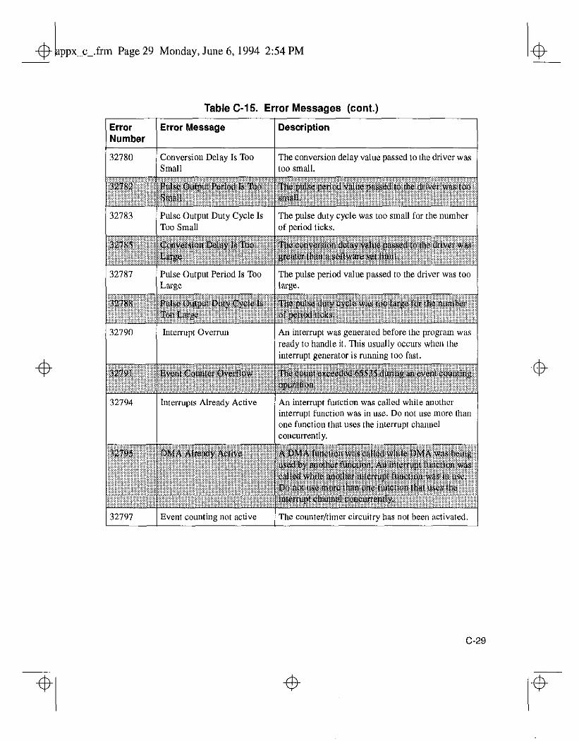
.frm Page 29 Monday, June 6,1994 2:54 PM
Table C-15. Error Messages (cont.)
Error Error Message Description Number
Conversion Delay Is Too The conversion delay value passed to the driver was
/ 32783 / Too Small Pulse Output Duty Cycle Is
/ of period ticks. The pulse duty cycle was too small for the number
Interrupt Overrun An intexupt was generated before the program was ready to handle it. This usually occurs wheo the interrupt generator is running too fast.
32794 Interrupts Already Active An interrupt ftiction WRS called while another interrupt function was in use. Do not use more than one function that uses the interrupt chaunel concurrenntl y.
32797 Event counting Lmt active The counter/timer circuitry has not been activated.
c-29
.frm Page30 Monday, June6,1994 2:54PM
ppx-d_.frtn Page 1 Monday, June 6, 1994 2:55 PM
D Keithley Memory Manager
The process that Windows uses to allocate memory can limit the amount of memory available to DAS boards operating in Windows Enhanced mode. To reserve a memory heap large enough for the needs of your application, use the Keithley Memory Manager (KMM), included in the AS0 software package.
The reserved memory heap is part of the total physical memory available in your system. When you start up Windows, the KMM reserves the memory heap. Then, whenever your application program requests memory, the memory buffer is allocated from the reserved memory heap instead of from the Windows global heap. The KMM is DAS board independent and can be used by multiple DAS Windows application programs simultaneously.
Note: The memory allocated with the KMM can be used by any DMA controller, if applicable.
The following are supplied with the KMM:
l VDMAD.386 - Customized version of Microsoft’s Virtual DMA Driver, This tile consists of a copy of Microsoft’s Virtual DMA Driver and a group of functions that are added to perform the KMM functions. When you use the KMM to reserve a memory heap, Microsoft’s Virtual DMA Driver is replaced by the VDMAD.386 file.
Note: If you have multiple versions of VDMAD.386, it is recommended that you install the latest version; to determine which version is the latest version, refer to the time stamp of the file.
D-l
b 4$ -_. ppx d frm Page 2 Monday, June 6, 1994 2:55 PM
4
. KMMSETUP.EXE - Windows program that helps you set up the VDMAD.386 parameters and then modifies your SYSTEM.INI file
accordingly.
Installing and Setting Up the KMM
To install and set up the KMM whenever you start up Windows, you must modify the SYSTEM.INI file. You can modify the SYSTEMIN file using either the KMMSETUPEXE program or a text editor.
Using KMMSETUP.EXE
D-2
Ushlg the KMMSETUP.EXE program, you can modify your Windows SYSTEM.INI file as follows:
1. Invoke KMMSETUP.EXE in one of the following ways:
- From the Program Manager menu, choose File and then Run, and then type the complete path and program name for KMMSETUP.
Select the KMMSETUP icon, if installed.
2. In the New VDMAD.386 box, enter the path and name of the VDMAD.386 file, as follows:
C:\WINDOWS\VDMAD.386
Thestringyou enter replaces *vdmadinthe device=*vdmadlinein
your SYSTEM.INI file.
Note: Normally, the VDMAD.386 file is stored in the WINDOWS directory. If it is stored elsewhere, enter the correct path and name or use the Browse button to find the file.
3. Notice the Current Setting box. The value specified reflects the current size of the reserved memory heap in KBytes.
Keithley Memory Manager
4
4 4
Ii 4 -- ppx d .frm Page 3 Monday, June 6, 1994 2:55 PM
4
4. In the Desired Setting box, enter the desired size of the reserved memory heap in KBytes.
The valueyouenterreplaces ~~~~KEID~HEAPSIZE= lineinthe
[386Enh] section of your SYSTEM.INI file.
Notes: The memory size you specify is no longer available to Windows. For example, if your computer has 8 MBytes of memory installed and you specify REIDMAHEAPSIZE=~~~~ (I MByte), Windows can only see and use 7 MBytes.
If you specify a value less than 128, a 128 KByte minimum heap size is assumed. The maximum heap size is limited only by the physical memory installed in your system and by Windows itself.
5. Select the Update button to update the SYSTEM.INI file with the changes you have made.
6. Restart Windows to ensure that the system changes take effect.
Using a Text Editor
Using a text editor, you can modify your Windows SYSTEM.INI tile in the [386Enh] section, as follows:
1. Replace the line device=*vdmad with the following:
device=c:\windows\vdmad.386
Note: Normally, the VDMAD.386 file is stored in the WINDOWS directory. If it is stored elsewhere, enter the correct path and name.
2. Add the following line:
I<EIDMAHEAPSIZE=<size>
where size indicates the desired size of the reserved memory heap in KBytes.
4
n-3
frm Page 4 Monday, June 6, 1994 2:55 PM
4
D-4
Notes: The memory size you specify is no longer available to Windows. For example, if your computer has 8 MBytes of memory installed and you specify KEIDMAHEAPSIZE=IOOO (1 MByte), Windows can only see and use 7 MBytes.
If you do not add the KEIDMAHEAPSIZE keyword or if the size you specify is less than 128, a 128 KByte minimum heap size is assumed. The maximum heap size is limited only by the physical memory installed in your system and by Windows itself.
3. Restart Windows to ensure that the system changes take effect.
Removing the KMM
If you make changes to the SYSTEMIN file, you can always remove the updated information from the SYSTEM.INI file and return all previously reserved memory to Windows.
If you are using KMMSETUI?EXE, select the Remove button to remove the updated information. If you are using a text editor, modify and/or delete the appropriate lines in SYSTEM.INI. In both cases, make sure that you restart Windows to ensure that the system changes take effect.
Keithley Memory Manager
.frm Page 1 Monday, June 6, 1994 2:56 PM
Register-Level Address Map
DAS-1600/1400 Series boards are programmable at the register-level using I/O instructions. In BASIC, I/O instructions are INP(X) and OUT X,Y. In assembly and most other low-level languages, the I/O instructions are similar to BASIC’s I/O instructions; for example, the assembly language equivalents are IN AL,DX and OUT DX,AL.
As an aid to register-level programming, this chapter describes each I/O register in terms of function, address, bit structure, and bit functions. The chapter does not describe how to program at the register-level.
Reaister Functions
DAS-1600/1400 Series register functions are categorized as follows:
. Analog-to-Digital converter (ADC) registers
. MUX scan register
. Digital input and output registers
. Digital-to-Analog converter (DAC) output registers (DAS-1600 Series only)
l Status registers
l Control register
. Programmable gain selection and burst rate register
. Counter enable and burst length register
E-l
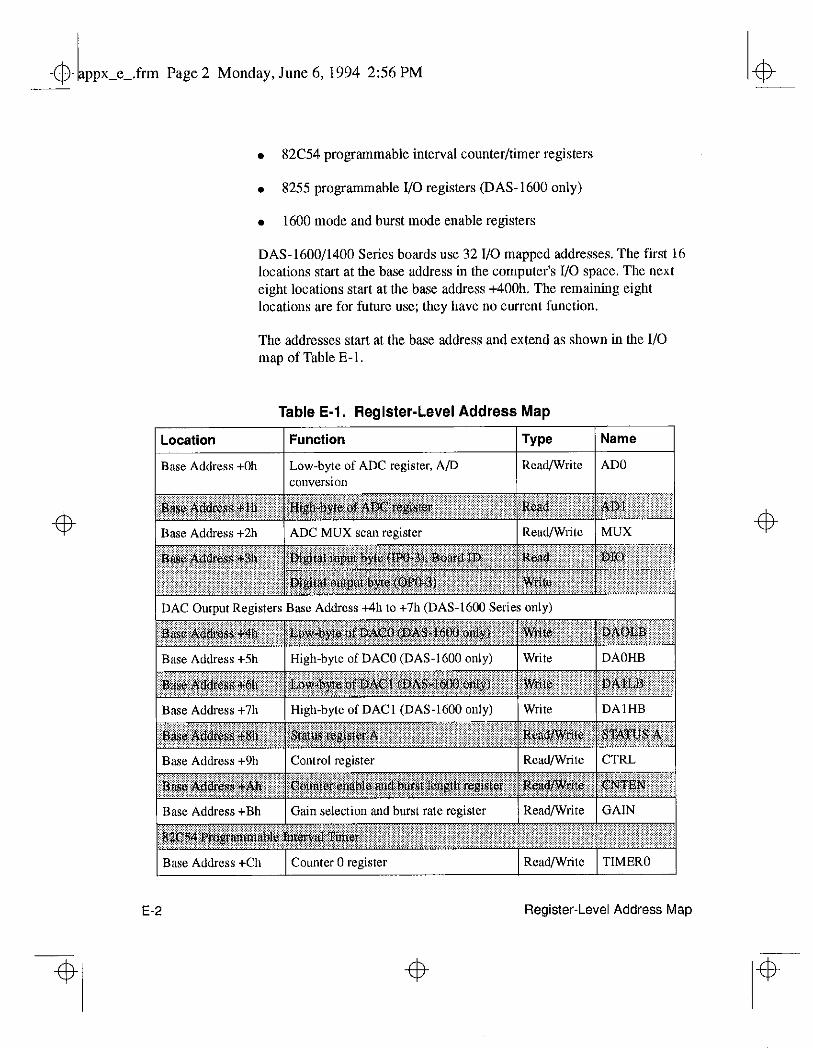
.frm Page 2 Monday, June 6, 1994 2:56 PM
4
4
. 82C54 programmable interval counter/timer registers
. 8255 programmable I/O registers (DAS-1600 only)
. 1600 mode and burst mode enable registers
DAS-1600/1400 Series boards use 32 I/O mapped addresses. The first 16 locations start at the base address in the computer’s I/O space. The next eight locations start at the base address +400h. The remaining eight locations are for future use; they have no current function.
The addresses start at the base address and extend as shown in the I/O map of Table E-l.
Table E-l. Register-Level Address Map
Location Function TYPO Name
Base Address +Ob Low-byte of ADC register, A/D Read/Write ADO conversion
/ Base Address +‘2h 1 ADC MUX scan rerister 1 Read/Wlilc 1 MUX 1
Base Address +Bh
E-2 Register-Level Address Map
ffi
4
4 14,
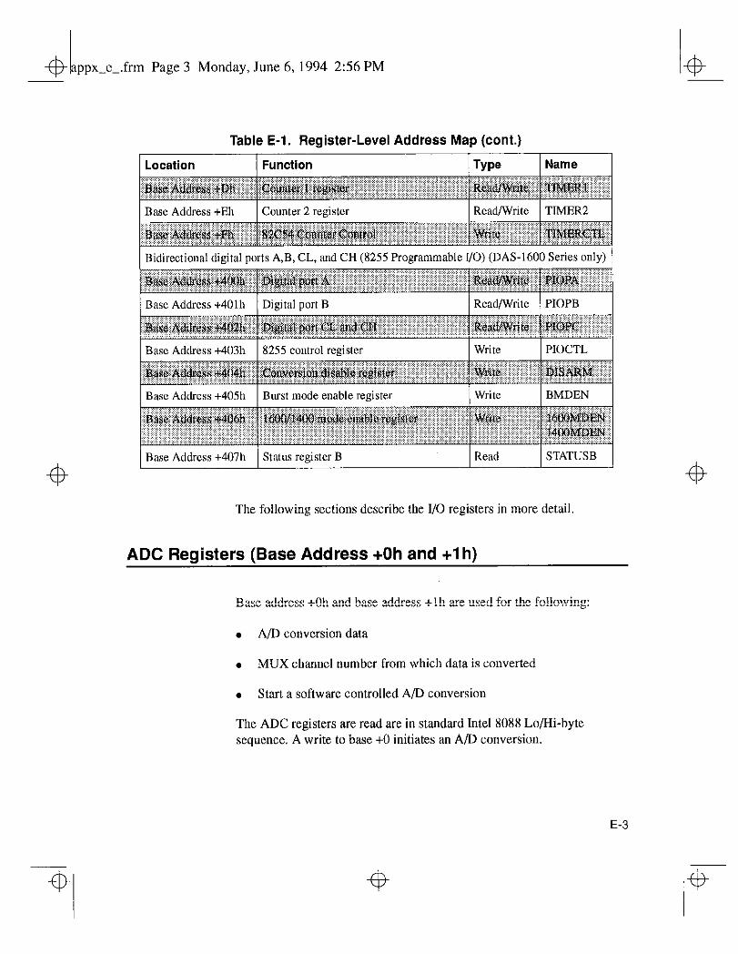
frm Page 3 Monday, June 6, 1994 2:56 PM
Location
Table E-l. Register-Level Address Map (cont.)
/ Function 1 TYPO Name
The following sections describe the I/O registers in more detail.
ADC Registers (Base Address +Oh and +l h)
Base address +Oh and base address +lb are used for the following:
. A/D conversion data
. MUX channel number from which data is converted
. Start a software controlled A/D conversion
The ADC registers are read are in standard Intel 8088 Lo/Hi-byte sequence. A write to base +0 initiates an A/D conversion.
E-3
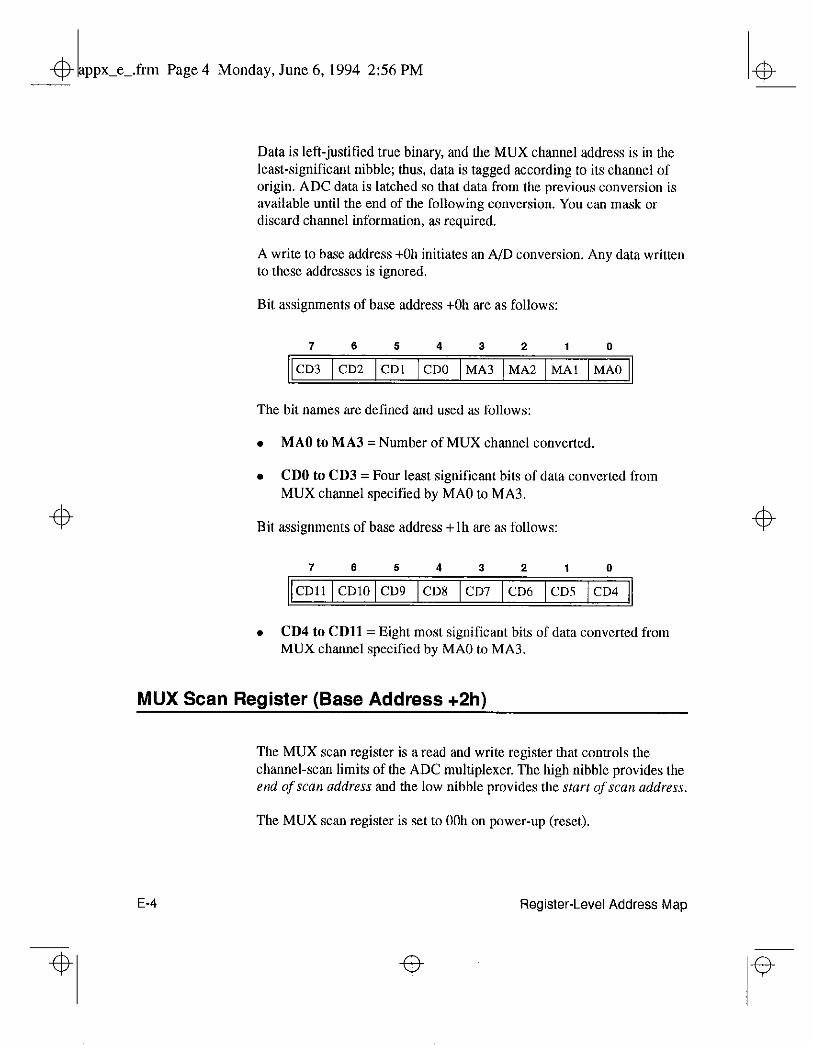
1 4 -- ppx e .frm Page 4 Monday, June 6, 1994 2:56 PM
4
Data is left-justified true binary, and the MUX channel address is in the least-significant nibble; thus, data is tagged according to its channel of origin. ADC data is latched so that data from the previous conversion is available until the end of the following conversion. You can mask or discard channel information, as required.
A write to base address +Oh initiates an A/D conversion. Any data written to these addresses is ignored.
Bit assignments of base address +Oh are as follows:
7 6 6 4 3 2 1 l-l
CD3 CD2 CD1 CD0 MA3 MA2 MA1 MAO
The bit names are defined and used as follows:
. MAO to MA3 = Number of MUX channel converted.
. CD0 to CD3 = Four least significant bits of data converted from MUX channel specified by MAO to MA3.
Bit assignments of base address +lh are as follows:
7 6 5 4 3 2 1 cl
CD11 CD10 CD9 CD8 CD1 CD6 CDS CD4
. CD4 to CD11 = Eight most significant bits of data converted from MUX channel specified by MAO to MA3.
MUX Scan Register (Base Address +2h)
The MUX scan register is a read and write register that controls the channel-scan limits of the ADC multiplexer. The high nibble provides the end of scan address and the low nibble provides the start of scan address.
The MUX scan register is set to OOh on power-up (reset)
E-4 Register-Level Address Map
4
4
4 4
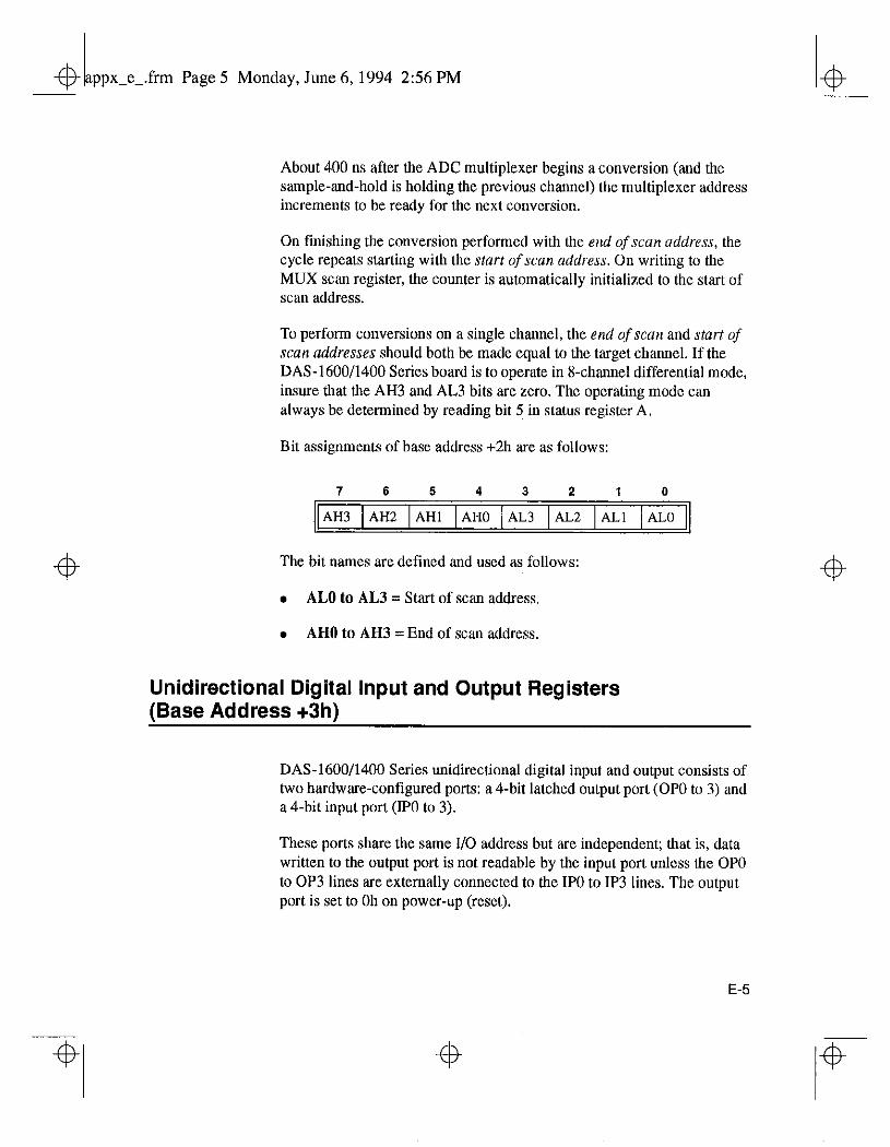
.frm Page 5 Monday, June 6,1994 2:56 PM
About 400 ns after the ADC multiplexer begins a conversion (and the sample-and-hold is holding the previous channel) the multiplexer address increments to be ready for the next conversion.
On finishing the conversion performed with the end of scan address, the cycle repeats starting with the start of scan address. On writing to the MUX scan register, the counter is automatically initialized to the start of scan address.
To perform conversions on a single channel, the end of scan and start of scan addresses should both be made equal to the target channel. If the DAS-1600/1400 Series board is to operate in S-channel differential mode, insure that the AH3 and AL3 bits are zero. The operating mode can always be determined by reading bit 5 in status register A.
Bit assignments of base address +2h are as follows:
7 6 5 4 3 2 1 0
AH3 AH2 AH1 AH0 AL3 AL2 AL1 AL0
The bit names are defined and used as follows:
. AL0 to AL3 = Start of scan address
. AH0 to AH3 = End of scan address.
Unidirectional Digital Input and Output Registers (Base Address +3hj
DAS-1600/1400 Series unidirectional digital input and output consists of two hardware-configured ports: a 4-bit latched output port (OPO to 3) and a 4-bit input port (IPO to 3).
These ports share the same I/O address but are independent; that is, data written to the output port is not readable by the input port unless the OPO to OP3 lines are externally connected to the IPO to IP3 lines. The output port is set to Oh on power-up (reset).
E-5
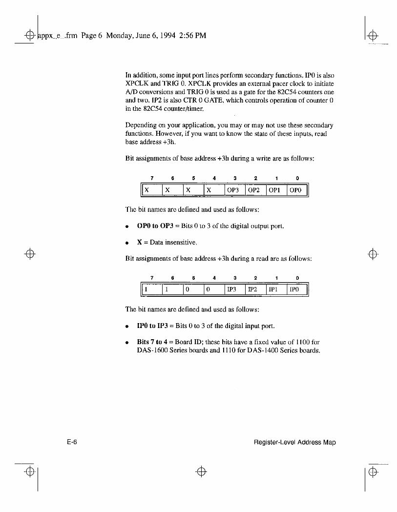
frtn Page 6 Monday, June 6, 1994 2:56 PM
4
E-6
In addition, some input port lines perform secondary functions. IPO is also XPCLK and TRIG 0. XPCLK provides an external pacer clock to initiate A/D conversions and TRIG 0 is used as a gate for the 82C54 counters one and two. IP2 is also CTR 0 GATE, which controls operation of counter 0 in the 82C54 counter/timer.
Depending on your application, you may or may not use these secondary functions. However, if you want to know the state of these inputs, read base address +3h.
Bit assignments of base address +3h during a write are as follows:
7 6 6 4 3 2 1 0
x x x x OP3 OP2 OPl OPO
The bit names are defined and used as follows:
. OPO to OP3 = Bits 0 to 3 of the digital output port.
. X = Data insensitive.
Bit assignments of base address +3h during a read are as follows:
7 6 6 4 3 2 1 0
I 1 0 0 IP3 IP2 IPl IPO
The bit names are defined and used as follows:
. IPO to IP3 = Bits 0 to 3 of the digital input port.
. Bits 7 to 4 = Board ID; these bits have a fixed value of 1100 for DAS-1600 Series boards and 1110 for DAS-1400 Series boards.
Register-Level Address Map
4
4
4 4
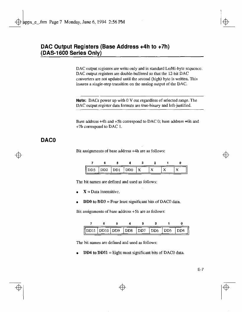
b 4 -- ppx e .frm Page 7 Monday, June 6, 1994 2:56 PM 4
4
4
DAC Output Registers (Base Address +4h to +7h) (DAS-1600 Series Only)
DAC output registers are write only and in standard Lo/Hi-byte sequence. DAC output registers are double-buffered so that the 12-bit DAC converters are not updated until the second (high) byte is written. This insures a single-step transition on me analog output of the DAC.
Note: DACs power up with 0 V out regardless of selected range. The DAC output register data formats are true-binary and left-justified.
Base address +4h and +5b correspond to DAC 0; base address +6h and +7h correspond to DAC 1.
DACO
Bit assignments of base address +4h are as follows:
7 6 6 4 3 2 1 0
DD3DDZDDlDDOX X X X
The bit names are defined and used as follows:
. X = Data insensitive.
. DDO to DD3 = Pour least significant bits of DACO data,
Bit assignments of base address +5h are as follows:
7 6 5 4 3 2 1 0
DDll DDlO DD9 DD8 DD7 DD6 DD5 DD4
The bit names are defined and used as follows:
. DD4 to DDll = Eight most significant bits of DACO data.
4
4
E-7
4
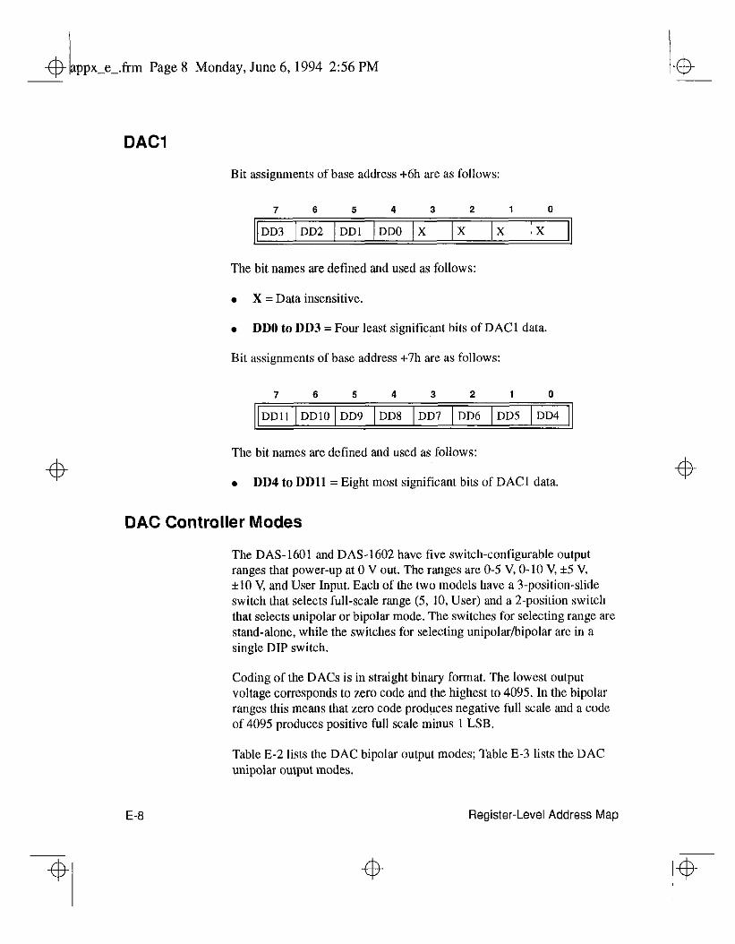
44 -- ’ ppx e .frm Page X Monday, June 6,1994 2:56 PM
4
DACl
Bit assignments of base address +6h are as follows:
7 6 5 4 3 2 1 0
DD3 DD2 DDl DDO X X X X
The bit names are defined and used as follows:
. X = Data insensitive.
. DDO to DD3 = Four least significant bits of DACl data,
Bit assignments of base address +7b are as follows:
7 6 6 4 3 2 1 0
DDll DDlO DD9 DDE DDI DD6 DD5 DD4
The bit names are defined and used as follows:
. DD4 to DIM1 = Eight most significant bits of DACI data
DAC Controller Modes
The DAS-1601 and DAS-1602 have five switch-configurable output ranges mat power-up at 0 V out. The ranges are O-5 V, 0- 10 V, f5 V, *lo V, and User Input. Each of the two models have a 3-position-slide switch that selects full-scale range (5, 10, User) and a 2-position switch that selects unipolar or bipolar mode. The switches for selecting range are stand-alone, while the switches for selecting unipolar/bipolar are in a single DIP switch.
Coding of the DACs is in straight binary format. The lowest output voltage corresponds to zero code and the highest to 4095. In the bipolar ranges this means that zero code produces negative full scale and a code of 4095 produces positive full scale minus 1 LSB.
Table E-2 lists me DAC bipolar output modes; Table E-3 lists the DAC unipoiar output modes.
E-8 Register-Level Address Map
4
4
!P- 4 4
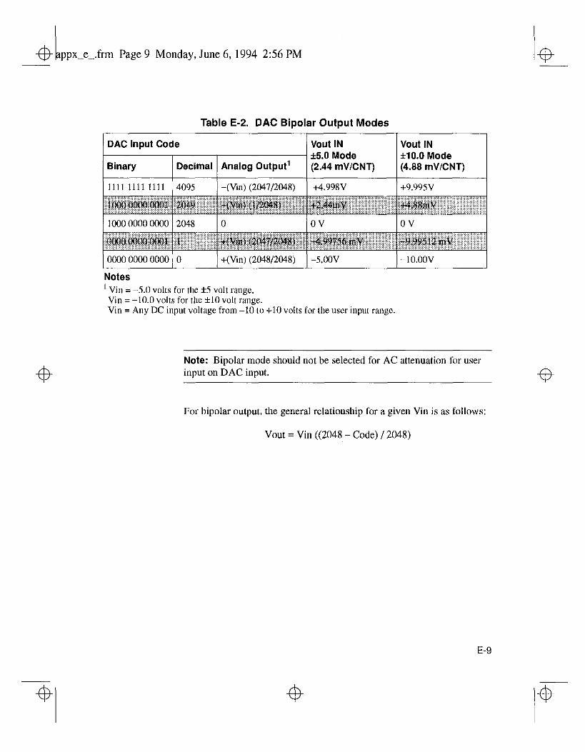
frm Page 9 Monday, June 6, 1994 2:56 PM
Table E-2. DAC Bipolar Output Modes
Notes ’ vi11 = -5.0 volts for the f5 volt range. Vin = -10.0 volts for the *IO volt range. Vin = Any DC input voltage from -10 to +I0 volts for the user input mngc.
Note: Bipolar mode should not be selected for AC attenuation for user input on DAC input.
For bipolar output, the general relationship for a given Vin is as follows:
Vout = Vin ((2048 - Code) / 2048)
E-9
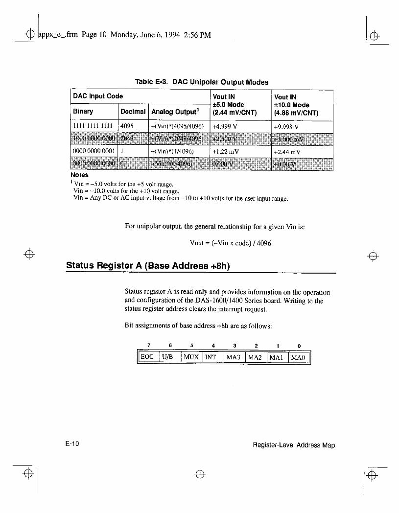
1 -@ -- ppx e .frm Page 10 Monday, June 6, 1994 2:56 PM
Table E-3. DAC Unipolar Output Modes
DAC Input Code Vout IN Vout IN 1~5.0 Mode k10.0 Mode
Binary Decimal Analog Output’ (2.44 mV/CNT) (4.88 mV/CNT)
1111 1111 1111 4095 -Win)*(4095/4096) t4.999 V +9.998 v
Notes ’ Vin = -5.0 volts for the +5 volt ruge. Vin = -10.0 volts for the +I0 volt range. Vin = Any DC or AC illput voltage from -10 to t10 volts for the user input range.
For unipolar output, the general relationship for a given Vin is:
Vout = (-Vi” x code) / 4096
Status Register A (Base Address +8h)
Status register A is read only and provides information on the operation and configuration of the DAS-1600/1400 Series board. Writing to the status register address clears the interrupt request.
Bit assignments of base address +8h are as follows:
7 6 a 4 3 2 1 0
EOC U/B MUX INT MA3 MA2 MA1 MAO
E-IO Register-Level Address Map
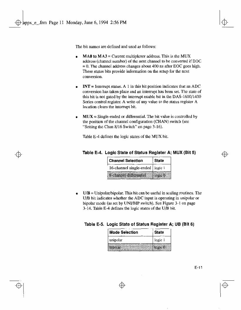
.frm Page 11 Monday, June 6,1994 2:56 PM
The bit names are defined and used as follows:
MAO to MA3 = Current multiplexer address. This is the MUX address (channel number) of the next channel to be converted if EOC = 0. The channel address changes about 400 ns after EOC goes high. These status bits provide information on the setup for the next conversion.
INT = Interrupt status. A 1 in this bit position indicates that an ADC conversion has taken place and an interrupt has been set. The state of this bit is not gated by the interrupt enable bit in the DAS-1600/1400 Series control register. A write of any value to the status register A location clears the interrupt bit.
MUX = Single-ended or differential. The bit value is controlled by the position of the channel configuration (CHAN) switch (see “Setting the Chan 8/16 Switch” on page 3-16).
Table E-4 defines the logic states of the MUX bit,
Table E-4. Logic State of Status Register A; MUX (Bit 5)
Channel Selection State
16-channel single-ended logic 1
U/B = Unipolat~ipolar. This bit can be useful in scaling routines. The U/B bit indicates whether the ADC hiput is operating in unipolar or bipolar mode (as set by UNI/BIP switch). See Figure 3-l on page 3-14. Table E-4 defines the logic states of the U/B bit.
Table E-5. Logic State of Status Register A; UB (Bit 6)
1 Mode Selection I State I
E-11
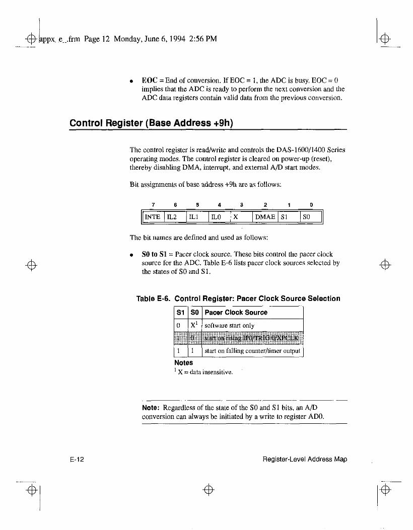
43-L -- ppx e .frm Page 12 Monday, June 6,1994 2:56 PM
4
. EOC = End of conversion. If EOC = 1, the ADC is busy. EOC = 0 implies that the ADC is ready to perform the next conversion and the ADC data registers contain valid data from the previous conversion.
Control Register (Base Address +9h)
The control register is read/write and controls the DAS-1600/1400 Series operating modes. The control register is cleared on power-up (reset), thereby disabling DMA, interrupt, and external A/D start modes.
Bit assignments of base address +9h are as follows:
7 6 6 4 3 2 1 0
INTE IL2 IL1 IL0 X DMAE Sl SO
The bit names are defined and used as follows:
. SO to Sl = Pacer clock source. These bits control the pacer clock source for the ADC. Table E-6 lists pacer clock sources selected by the states of SO and Sl.
Table E-6. Control Register: Pacer Clock Source Selection
Sl SO Pacer Clock Source
0 xl software start onlv
I 1 start on falling counter/timer output
Notes ’ X = data insensitive.
Note: Regardless of the state of the SO and Sl bits, an A/D conversion can always be initiated by a write to register ADO.
4
E-12
4
Register-Level Address Map
I$
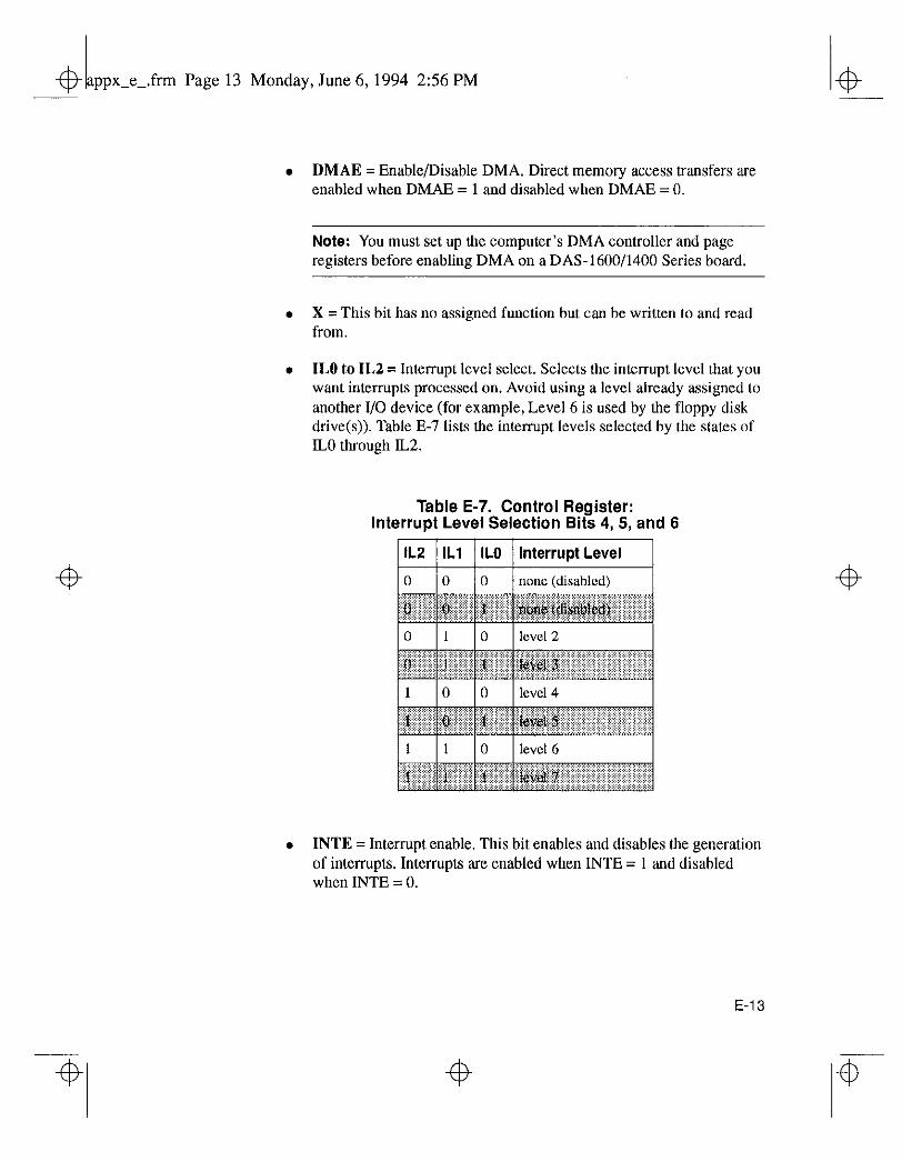
.frm Page 13 Monday, June 6,1994 2:56 PM 4
4
. DMAE = Enable/Disable DMA. Direct memory access transfers are enabled when DMAE = 1 and disabled when DMAE = 0.
Note: You must set up the computer’s DMA controller and page registers before enabling DMA on a DAS-1600/1400 Series board.
. X = This bit has no assigned function but can be written to and read from.
. IL0 to IL2 = Interrupt level select. Selects the interrupt level that you want interrupts processed on. Avoid using a level already assigned to another I/O device (for example, Level 6 is used by the floppy disk drive(s)). Table E-7 lists the interrupt levels selected by the states of IL0 through IL2.
Table E-7. Control Register: Interrupt Level Selection Bits 4, 5, and 6
IL2 IL1 IL0 Interrupt Level
0 lo lo I
. INTE = Interrupt enable. This bit enables and disables the generation of interrupts. Interrupts are enabled when INTE = I and disabled when INTE = 0.
4
E-13
4 4
&- 1 ppx-e-.frm Page 14 Monday, June 6,1994 2:56 PM
E-14
If INTE = 1 and DMAE = 0, an interrupt is generated at the end of each A/D conversion when valid data is available. If 1NTE = 1 and DMAB = 1, an interrupt is generated when a Terminal Count (T/C) is received from the computer’s DMA controller to signify completion of the DMA transfer.
Counter Enable/Burst Length Register (Base Address +Ah)
This S-bit read/write register controls the operation of the following:
. 82C.54 counter/timer
. 100 kHz pacer clock
. Burst length counter
The counter enable register is set to 0011 upon power-up (reset)
DAS-1600/1400 Series boards use an Intel 82C54 programtttable interval counter/timer for pacing the ADC. Counters I and 2 of the 82C54 are cascaded and are driven by a I MHz or 10 MHz switch-configurable clock so that periods ranging from 10 microseconds to 0.12 pulses per hour for 10 MHz and 1.192 pulses per hour for 1 MHz can be programmed.
When programming the board for A/D conversions using the internal timer, bit 0 (CENO) of this register and the IPOffRIG O/XPCLK input signal can be used to enable counters 1 and 2 of the 82C54, thereby initiating A/D conversions. To accomplish this, bits CENO and II’0 are NANDed and the output is routed to counter gates 1 and 2 of the 82C54.
The function of CEN 1 is somewhat different. When CBN 1 and CTR 0 CLOCK IN are both high, counter 0 input of the 82C54 is internally connected to a 100 kHz clock source.
The CTR 0 CLOCK IN, CTR 0 GATE, and CTR 0 OUT of counter 0 are all brought out to external connections, so that the counter can be used as a waveform generator, a secondary timer, or a period counter using the gate and internal clock.
Register-Level Address Map
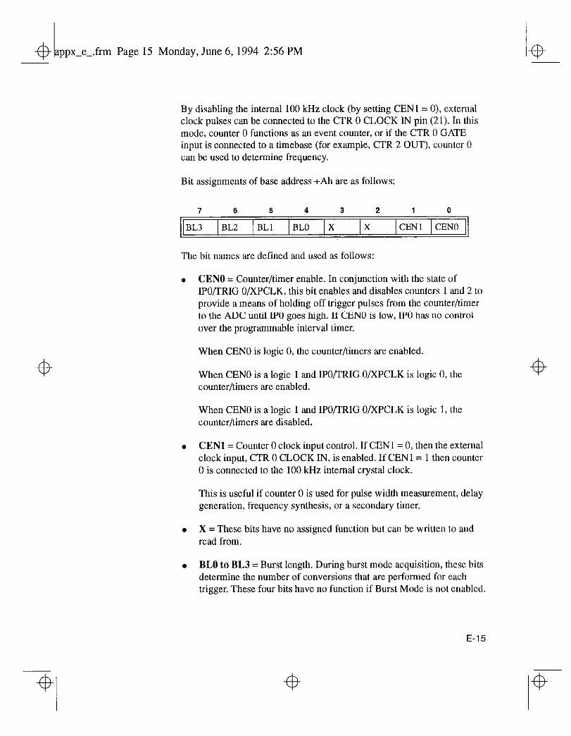
.frm Page 15 Monday, June 6, lYY4 2:56 PM
4
By disabling the internal 100 kHz clock (by setting CENI = 0), external clock pulses can be connected to the CTR 0 CLOCK IN pin (21). In this mode, counter 0 functions as an event counter, or if the CTR 0 GATE input is connected to a timebase (for example, CTR 2 OUT), counter 0 can be used to determine frequency.
Bit assignments of base address +Ah are as follows:
7 6 6 4 3 2 1 0
BL3 BLZ BLI BLO X X CENl CENO
The bit names are defined and used as follows:
. CENO = Counter/timer enable. In conjunction with the state of IPOffRIG O/XPCLK, this bit enables and disables counters 1 and 2 to provide a means of holding off trigger pulses from the counter/timer to the ADC until IPO goes high. If CENO is low, IPO has no control over the programmable interval timer.
When CENO is logic 0, the counter/timers are enabled.
When CENO is a logic 1 and IPO/TRIG O/XPCLK is logic 0, the counter/timers are enabled.
When CENO is a logic 1 and IPOnRIG O/XPCLK is logic 1, the counter/timers are disabled.
. CENl = Counter 0 clock input control. If CENI = 0, then the external clock input, CTR 0 CLOCK IN, is enabled. If CENl = 1 then counter 0 is connected to the 100 kHz internal crystal clock.
This is useful if counter 0 is used for pulse width measurement, delay generation, frequency synthesis, or a secondary timer.
. X = These bits have no assigned function but can be written to and read from.
. BLO to BL3 = Burst length. During burst mode acquisition, these bits determine the number of conversions that are performed for each trigger. These four bits have no function if Burst Mode is not enabled.
4
E-15
4 4
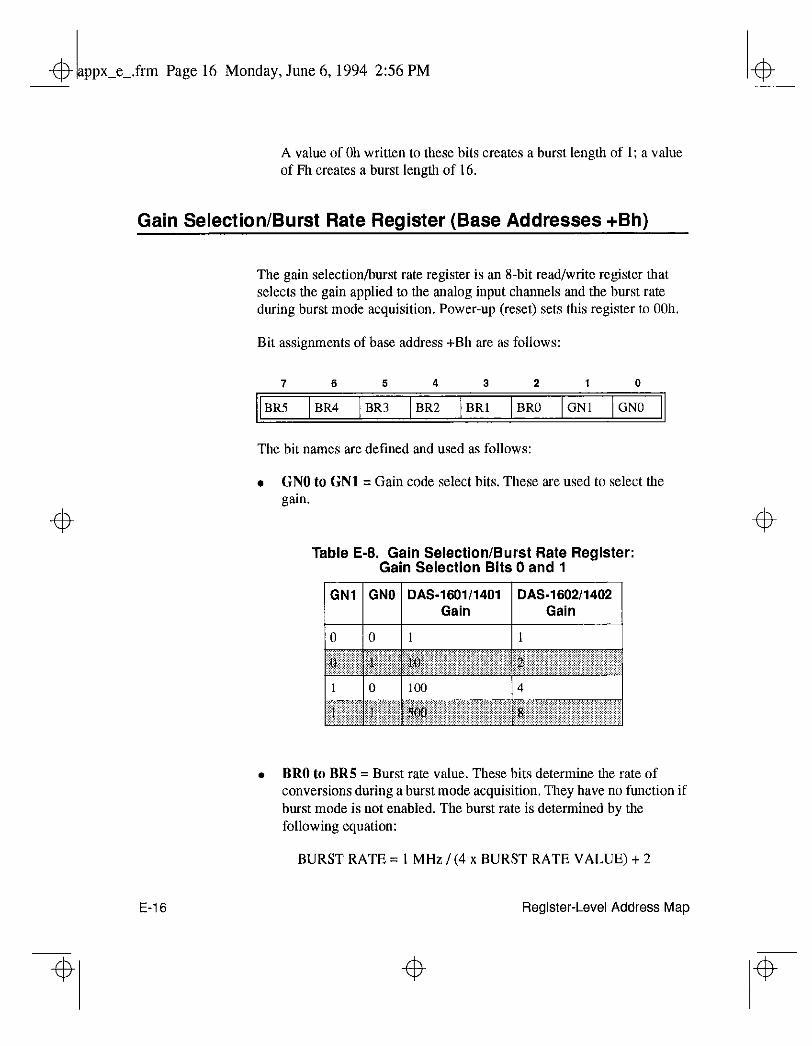
.frm Page 16 Monday, June 6,1YY4 2:56 PM
A value of Oh written to these bits creates a burst length of 1; a value of Fh creates a burst length of 16.
Gain Selection/Burst Rate Register (Base Addresses +Bh)
The gain selection/burst rate register is an E-bit read/write register that selects the gain applied to the analog input channels and the burst rate during burst mode acquisition. Power-up (reset) sets this register to OOh.
Bit assignments of base address +Bh are as follows:
7 6 6 4 3 2 1 0
BR5 BR4 BR3 BR2 BRl BRO GNl GNO
The bit names are defined and used as follows:
. GNO to GNl = Gain code select bits. These are used to select the gain.
4
E-l 6
Table E-8. Gain Selection/Burst Rate Register: Gain Selection Bits 0 and 1
GNI GNO DAS-160111401 DAS-160211402 Gain Gain
. BRO to BR5 = Burst rate value. These bits determine tbe rate of conversions during a burst mode acquisition. They have no function if burst mode is not enabled. The burst rate is determined by the following equation:
BURST RATE = I MHz / (4 x BURST RATE VALUE) + 2
Register-Level Address Map
4
4 4 4
.frm Page 17 Monday, June 6,1994 2:56 PM
Burst mode allows DAS-1600/1400 Series boards to perform multiple conversions from a single clock pulse. The clock source can be any of the following:
. external counter/timer
. an external pacer clock
. software clock
To set up a burst mode acquisition, perform the following steps:
1. Enable the 1600/1400 mode by writing a value of 40h to the 1600/1400 mode enable register (base address +406h).
2. Write a value of 40h to the burst mode enable register (base address +405h).
3. Set up the burst Iength. The upper four bits of the counter enable register (base address +Ah) are programmable for 1 to 16 conversions per trigger.
Because this register supports both counter enable and burst length functions, it should first be read and ORed with the masked, updated contents of either counter enable or burst length.
A value of Oh written to the upper nibble of the counter enable/burst length register creates a burst length of 1; a value of Fh creates a burst length of 16. It is up to you to program the correct burst length value when used in combination with multiple channel conversions.
4. Program the burst rate (time between conversions). The upper six bits of the gain selection register (base address +Bh) is programmable for 100 kHz to 3.94 kHz (10 ps to 254 ps).
Because this register contains both the gain select and burst rate functions, it should first be read ORed with the masked, updated contents of either gain selection or burst rate.
4
Note: It is suggested that you use a number not less than 211 for the burst rate value. Valid burst rate values are within 2h to 3Fh, inclusive.
E-17
4 4
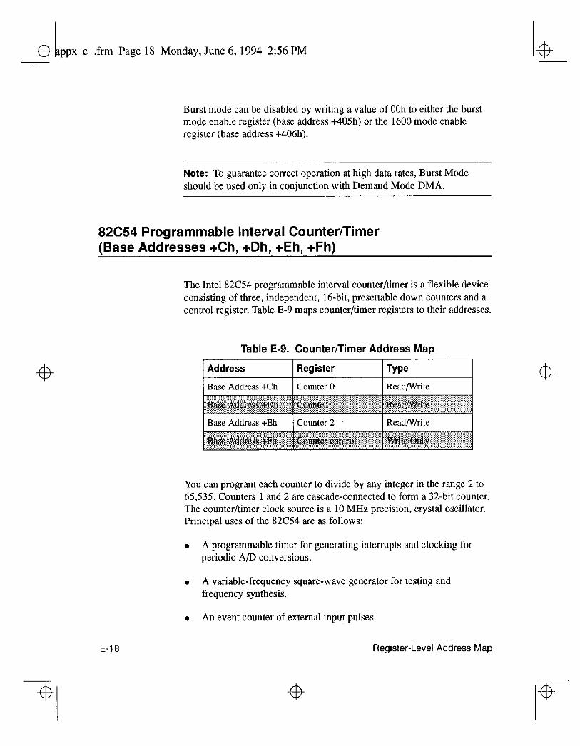
frm Page 18 Monday, June 6,1994 2:56 PM
4
4
Burst mode can be disabled by writing a value of OOh to either the burst mode enable register (base address +405h) or the 1600 mode enable register (base address +406h).
Note: To guarantee correct operation at high data rates, Burst Mode should be used only in conjunction with Demand Mode DMA.
82C54 Programmable interval Counter/Timer (Base Addresses +Ch, +Dh, +Eh, +Fh)
The Intel 87X54 programmable interval counter/timer is a flexible device consisting of three, independent, 16-bit, presettable down counters and a control register. Table E-9 maps counter/timer registers to their addresses.
Table E-9. Counter/Timer Address Map
E-l 8
Address Register Type
Base Address +Ch Counter 0 Read/Wrile
You can program each counter to divide by any integer in the range 2 to 65,535. Counters 1 and 2 are cascade-connected to form a 32.bit counter. The counter/timer clock source is a 10 MHz precision, crystal oscillator. Principal uses of the 82C54 are as follows:
. A programmable timer for generating interrupts and clocking for periodic A/D conversions.
. A variable-frequency square-wave generator for testing and frequency synthesis.
. An event counter of external input pulses.
Register-Level Address Map
4
4 4
.frm Page 19 Monday, June 6,1994 2:56 PM
4
. A time-delay generator.
In addition, the 82C54 allows you to set up frequency and pulse width measurements. If you are interested in detailed information, a full description of the 82C54 programmable interval counter/timer is available in the Intel data sheet (or equivalent manufacturer’s literature).
The maximum clock input frequency on any counter is 10 MHz with minimum clock duty cycles of 30 ns high and 50 ns low. The usual function of these two counters is to provide programmable pulse rates to trigger the ADC.
Counter 0 is uncommitted and can be used as a secondary pulse-rate generator, a square-wave generator, a programmable monostable delay, or an event counter.
Counters 1 and 2 are initialized by the DAS-1600/1400 Series driver to operate in the rate generator configuration (mode 2) and output 1 kHz (10 kHz with 10 MHz clock) after running an initializing call from the call interface. However, six operating configurations for each counter are possible. The configurations are as follows:
Pulse On Terminal Count - The oulput is initially low for this configuration. After the count loads and the counter decrements through zero, the output goes high and remains high until the counter is reloaded.
The counter continues to decrement after passing through zero. Counting can be inhibited by a low gate input. This mode produces a single, positive-going output transition such as may be required in a time delay initiated by the program.
Programmable One-Shot -The output goes low after a rising edge of the gate input and goes high when the counter passes through zero. The period that the output is low is set by the loaded count.
If the gate input goes high again before the one-shot has timed out, a new timing cycle is initiated (the one-shot is retriggerable and, if a new count is loaded, it will not become effective until any cycle in progress has terminated). This provides a hardware triggered delay or one-shot.
4
4
E-l 9
4 4 I4
frm Page 20 Monday, June 6, 1994 2:56 PM
4
l Rate Generator (or Divide-By-N counter) The output goes low for one input clock period every N counts, where N is the count loaded. The gate input, when low, forces the output high which reloads the counter. Thus, the gate input can be used to synchronize the counter. This configuration is useful for generating periodic interrupts to trigger AP conversions.
l Square Wave Generator - Similar to the rate generator except that the output is high for half of the count and low for the other half.
If N is even, a symmetrical square wave output is obtained. If N is odd, the output is high for (N+1)/2 counts and low for (N-1)/2 counls (has a l-count asymmetry). This configuration can be used in the same way as the rate generator for periodic triggering or for frequency synthesis.
l Software ‘higgered Strobe After the mode is set, the outpul is high. When a count of N is loaded, the counter begins counting and the output goes low for one input clock period as it passes through zero. The cycle is repeated on loading another count. The gale input may be used to inhibit counting.
l Hardware ‘lkiggered Strobe This is essentially the same as the programmable one-shot, except that the output goes low for one clock period at the end of the cycle and returns high again. The start of the cycle is triggered by the rising edge of the gate input, and as in the programmable one-shot, it is retriggerable.
Generating Square Waves of Programmed Frequency
Both the counter I and 2 combination and counter 0 can be used to generate square waves of programmable frequency. With the CEN 1 bit of the counter enable register (+Ah) set high and counter 0 clock input open or high, counter 0 is internally connected to a 100 kHz clock signal.
Counter 0 can be operated as a square wave generator with a maximum divisor of 65,535. The lowest output frequency obtainable from counter 0 directly is about 1.5 Hz (100000 / 65535). The minimum divisor can be as low as 2 to obtain a maximum output frequency of 50 kHz.
4
4
E-20
4
Register-Level Address Map
4
& ppxxe-.frtn Page 21 Monday, June 6, 1994 2:56 PM
The DAS-1600/1400 Series Function Call Driver always set counters 1 and 2 to the rate generator configuration, hut you can use BASIC OUT statements to alter their operating configuration to the square wave configuration. The frequency range obtainable is identical to that obtained in the rate generator configuration.
Counters I and 2 provide considerable flexibility in frequency range, a minimum division ratio of 4 (2 x 2) with a 10 MHz clock providing a 2.5 MHz output at one extreme, and a division ratio of 2s2 (65,535 x 65,535) with a I MHz clock providing an output of about 1 pulse/hour at the other extreme.
In practice, to obtain a symmetrical square wave, the divisor loaded into the counter should he an even number. If it is an odd number, one half of the square wave is one input clock pulse period longer than the other half.
Calculating the divisor is straightforward. Assume you desire an output frequency of 1 kHz. The input frequency to the counter 0 is 100 kHz so you must divide this by 100 to obtain 1 kHz. counter 0 should be set in the square wave generator configuration and loaded with 100. Counter 0 will then output a 1 kHz square wave.
4 4 Measuring Frequency and Period
It is possible to use the 82C54 to measure frequency by raising the gate input of counter 0 for some known interval of time, say 10, 100, or 1000 ms and counting the number of pulses clocked into the counter for that interval.
The gating signal can he derived from counters 1 and 2 operating in square-wave mode. Also, the computer has to be informed about the start and finish of the measurement cycle, so one of the DAS-1600/1400 digital inputs can be used to monitor the gate input to achieve this requirement.
Counter 0 can also be used to measure pulse width or half period of a periodic signal. The signal should he applied to the gate input of counter 0 and a known frequency applied to counter 0 clock input (100 kHz) from the internal crystal.
E-21
4 4
.frm Page 22 Monday, June 6, 1994 2:56 PM
4
During the interval when the gate input is low, counter 0 is loaded with a full count (65,535). The gate input then goes high at the beginning of the measurement, and the counter decrements until the gate input goes low at the end of the pulse.
The counter is then read and the change in the count is the duration of the gate input signal. If counter 0 is fed with 10 microsecond duration clock pulses (100 kHz), the maximum pulse duration that can be measured is 65,535 x 10 = 655 milliseconds.
Longer pulse durations can he measured using counters 1 and 2 as an input clock source for counter 0. One of the digital inputs should also he connected to the gate of counter 0 to synchronize the loading and reading operations.
Using Counter 0 for Generating Programmable Time Delays
Another use for counter 0 is generating programmable time delays. Several one-shot modes can he used. The counter configurations have the following characteristics when used for time delay generation:
. [Configuration 0: Pulse On Terminal Count] After loading the counter the output goes low. Counting is enabled when the gate input is high and continues until the count reaches zero when the output goes high. The output remains high until me counter is reloaded by program command. Taking the gate input low during the count down disables counting as long as it is low.
l [Configuration 1: Programmable One-Shot] The counter need only he loaded once. The timing delay is initiated by the gate input going high. At this point, the output goes low. If the gate input goes low, counting continues but a new cycle is initiated if the gate input goes high again before the time out delay has expired (is retriggerable).
At the end of the time out, as the counter reaches zero, the output goes high and remains high until re-triggered by the gate input. This is the programmable equivalent of a one-shot or monostahle, hence the name.
4
E-22
4
Register-Level Address Map
frm Page 23 Monday, June 6,1994 2:56 PM
. [Configuration 4: Software-Triggered Strobe] -This is similar to configuration 0, except that after loading, the output goes high and only goes low for one clock period on timing out. This produces a negative strobe pulse a programmed duration after loading the counter.
. [Configuration 5: Hardware-Triggered Strobe] - This is similar to configuration 1 except that the time out is triggered by the gate input going high and the output is,normally high, going low for one clock period on time-out and producing a negative going strobe pulse. Like configuration 1, the time out is retriggerable (a new cycle will commence if the gate input is taken high before a current cycle has timed out).
Counter 0 is good for directly producing delays up to 650 ms. If the output of counter 0 operated in configuration 0 is connected to IPWXPCLK with counters 1 and 2 used as a programmable clock source for the A/D (CENO=l, CENl=l), then after loading counter 0 and taking the gate input high, a programmable delay occurs before the A/D receives a clock pulse. This is a way to hold off conversions for a period after receipt of an external trigger signal.
Before loading or reading any of the individual counters, the 82C54 control register must be loaded with data setting the counter operating configuration as above, the type of read or write operation that is performed (see following), and the modulus or binary (0 to 65,535) or BCD (Binary Coded Decimal 0 to 9,999). The format of the control byte is shown in the following section.
82C54 Counter/Timer Control Register (Base Address +Fh)
Bit assignments of base address +F’h are as follows:
7 6 6 4 3 2 1 0
SC1 SC0 RLl RLO M2 Ml MO BCD
The bit names are defined and used as follows:
. BCD = The BCD bit (0) can be used to program the counter lo count in binary (modulus 2) or binary coded decimal (modulus IO) modes.
E-23
4
1 4 -- ppx e .frm Page 24 Monday, June 6,1994 2:56 PM
E-24
Binary mode, with a full count of 65,535, provides a greater count range than the BCD mode, which has a 9,999 full-scale range.
16-bit binary is enabled when BCD = 0 and 4-decimal decades is enabled when BCD = 1.
. MO to M2 = These bits control the functionality of the counters as shown in Table E-10.
Table E-10. 82C54 Counter/Timer Control Register: Selecting Functionality
M2 Ml MO Function
0 lo lo I Pulse on terminal count
. RLO to RLl = Control the type of read/load operations performed on counters, as shown in Table E- 11.
Table E-11. 82C54 Counterilimer Control Register: Bits 4 and 5
I RLI 1 RLO 1 Operation
0 0 Counter latch ~ ~~~~~~~~~~~~~ ~
1 lo Read/load most significant byte (MSB)
Register-Level Address Map
4 4
b +4+ -- ppx e .frm Page 25 Monday, June 6, 1994 2:56 PM
To minimize I/O port usage, the 16-bit counters of the 82C54 can be loaded or read by successive X-bit writes or reads to the same I/O address if the RLO and RLl bits of the 82C54 counter/timer control register are both set high.
In the IBM PC 80X86 architecture, setting RLO and RLl both high is usually the most convenient setting. Data is written in least significant/most significant order and the 82C54 uses an internal flip-flop to keep track of the byte order. It is important not to get this flip-flop out of step when programming in this way (make sure your read/load instructions are in pairs).
If you are programming an IBM PC AT in assembly language, make sure that you put delays (short jumps) between back-to-back I/O instructions for correct operation. This precaution is based on the design of the IBM PC AT (see the IBM PC AT Technical Reference Manual) and does not apply to the X088-based PC and 8086.based PC XT.
If you attempt to read the counters “on the fly” at a high input Crequency, you will probably obtain erroneous data. This error is due partly to the rippling of the counter during the read operation and partly to the fact that the low and high bytes are read sequentially rather than simultaneously, making it highly probable that carries are propagated from the low to high byte during the read cycle.
To circumvent these problems, you can perform a counter latch operation in advance of the read cycle. You can latch the counter by loading the RLO and RLl bits of the control register with OS, which instantaneously latches the count of the selected counter in a 16-bit hold register.
An alternative method of counter latching (which has an advantage of operating simultaneously on several counters) is to use the Readhack Command.
A subsequent read operation on the selected counter returns the held value. Counter latching is the only way of correctly reading a counter “on the fly” without disturbing the counting process. If you do not specify a counter-latching operation, the counter itself is read. You can rely only on directly read counter data if the counting operation is suspended while reading (by removing the clock input or taking the counter gate low).
E-25
.frm Page 26 Monday, June 6,1994 2:56 PM
For each counter, you are required to specify in advance the type of read or load operation that you intend to perform. You have a choice of loading/reading the high or the low byte of the count, or the low byte followed by the high byte.
This last mode is most generally used and is selected for each counter by setting the RL 1 and RLO bits to IS. Subsequent read/load operations must be performed in pairs in this sequence, otherwise the internal sequencing flip-flop of the X2(354 gets out of step.
. SC0 and SC1 = These bits control counter selection, as shown in Table E- 12.
Table E-12. 82C54 Counter/Timer Control Register: Readback Command
If the SC0 and SC1 bits are both set to I, you can perform two types of operations. When CNT = 0 (see below), counters selected by CO through C2 are latched simultaneously. When STA = 0, the counter status byte is read on accessing the counter I/O location. The status byte provides information on the current output state of the counter and its operating configuration.
Readback Command Byte (Returned when SC1 and SC0 are 1)
The format of the readback command byte is as follows:
7 6 5 4 .3 2 1 0
SC1 SC0 CNT STA C2 Cl CO 0
E-26 Register-Level Address Map
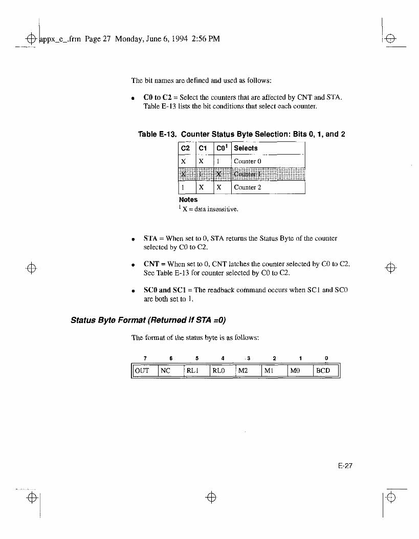
.frm Page 27 Monday, June 6, 1994 2:56 PM
4
The bit names arc defined and used as follows:
. CO to C2 = Select the counters that are affected by CNT and STA Table E-13 lists the bit conditions that select each comlter.
. STA = When set to 0, STA returns the Status Byte of the counter selected by CO to C2.
. CNT = When set to 0, CNT latches the counter selected by CO to C2. See Table E-13 for counter selected by CO to C2.
. SC0 and SC1 = The readback command occurs when SC1 and SC0 are both set to 1.
Status Byte Format (Returned if STA =O)
The format of lhe status byte is as follows:
7 6 5 4 ,3 2 1 a
OUT NC RLl RLO M2 Ml MO BCD
4
E-27
4 14
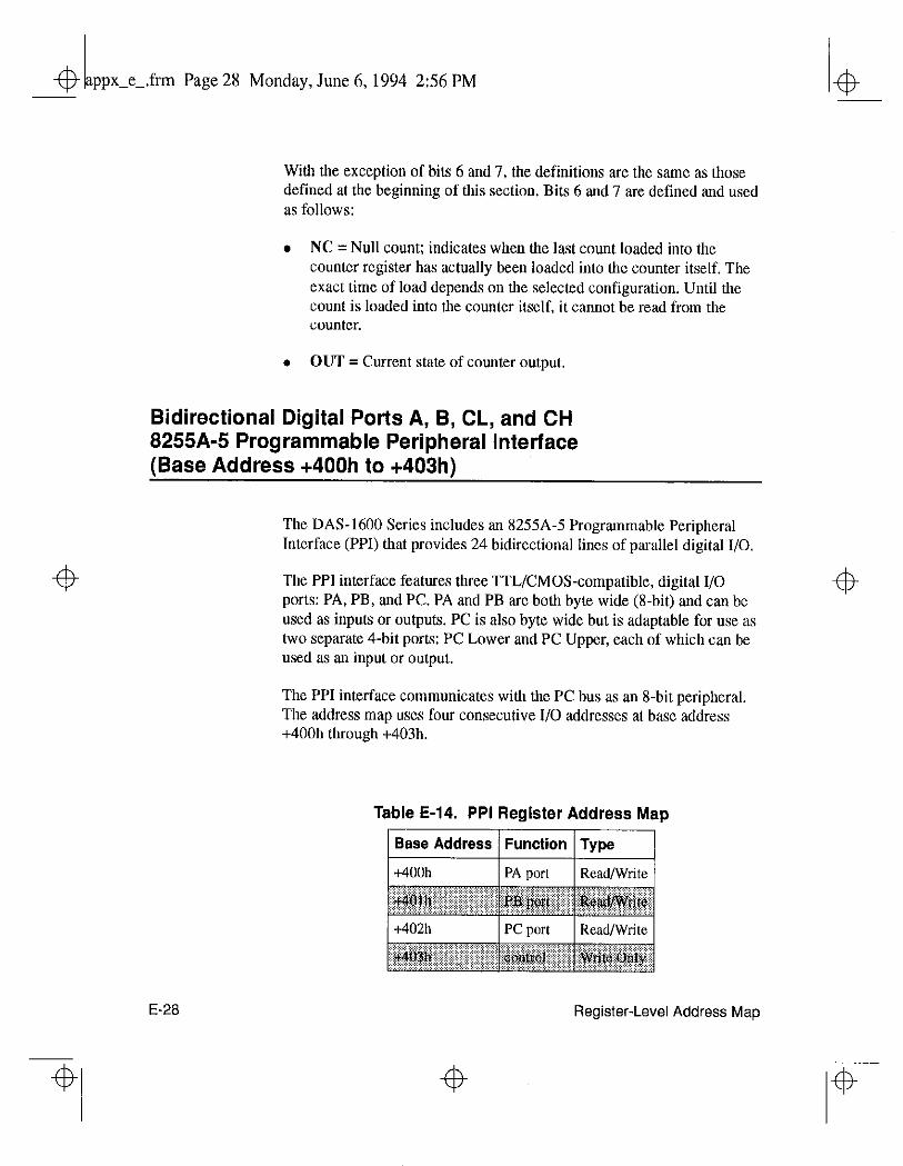
.frm Page 28 Monday, June 6, 1994 2:56 PM
With the exception of bits 6 and 7, the definitions are the same as those defined at the beginning of this section. Bits 6 and 7 are defined and used as follows:
. NC = Null count; indicates when the last count loaded into the counter register has actually been loaded into the counter itself. The exact time of load depends on the selected configuration. Until the count is loaded into the counter itself, it cannot be read from the counter.
. OUT = Current state of counter output
Bidirectional Digital Ports A, B, CL, and CH 8255A-5 Programmable Peripheral Interface (Base Address +400h to +403h)
4
E-28
4
The DAS-1600 Series includes an 8255A-5 Programmable Peripheral Interface (PPI) that provides 24 bidirectional lines of parallel digital I/O.
The PPI interface features three TTL/CMOS-compatible, digital I/O ports: PA, PB, and PC. PA and PB are both byte wide (g-bit) and can be used as inputs or outputs. PC is also byte wide but is adaptable for use as two separate 4-bit ports: PC Lower and PC Upper, each of which can be used as an input or output.
The PPI interface communicates with the PC bus as an E-bit peripheral. The address map uses four consecutive I/O addresses at base address +400h through +403h.
Table E-14. PPI Register Address Map
Base Address Function Type
t400h PA port Read/Write
Register-Level Address Map
4
4
4
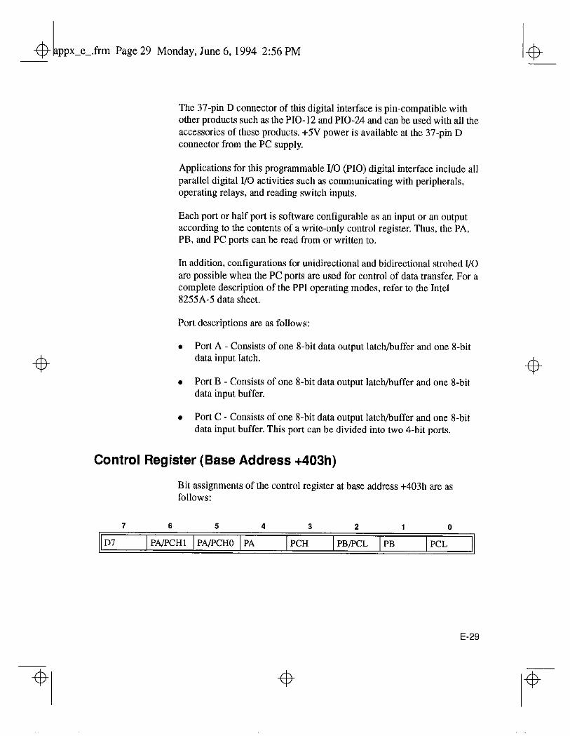
.frm Page 29 Monday, June 6, 1994 2:56 PM
The 37-pin D connector of this digital interface is pin-compatible with other products such as the PIO-12 and PIO-24 and can be used with all the accessories of these products. +5V power is available at the 37.pin D connector from the PC supply.
Applications for this programmable I/O (PIO) digital interface include all parallel digital I/O activities such as communicating with peripherals, operating relays, and reading switch inputs.
Each port or half port is software configurable as an input or an output according to the contents of a write-only control register. Thus, the PA, PB, and PC ports can be read from or written to.
In addition, configurations for unidirectional and bidirectional strobed I/O are possible when the PC ports are used for control of data transfer. For a complete description of the PPI operating modes, refer to the Intel 8255A-5 data sheet.
Port descriptions are as follows:
. Port A Consists of one S-bit data output latch/buffer and one g-bit data input latch.
. Port B - Consists of one g-bit data output latch/buffer and one g-bit data input buffer.
. Port C - Consists of one g-bit data output latch/buffer and one g-bit data input buffer. This port can be divided into two 4-bit ports.
Control Register (Base Address +403h)
Bit assignments of the control register at base address +403h are as follows:
7 6 5 4 3 2 1 0
D7 PA/PCHl PAIPCHO PA PCH PBE’CL PB PCL
E-29
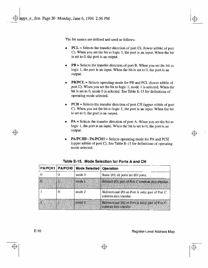
1 $ -- ppx e .frm Page 30 Monday, June 6, 1994 2:56 PM
+b
The bit names are defined and used as follows:
. PCL = Selects the transfer direction of port CL (lower nibble of port C). When you set the bit to logic 1, the port is an input. When the bit is set to 0, the port is an output.
. PB = Selects the transfer direction of port B. When you set the bit to logic 1, the port is an input. When the bit is set to 0, the port is an output.
l PBlPCL = Selects operathrg mode for PB and PCL (lower nibble of port C). When you set the bit to logic 1, mode 1 is selected. When the bit is set to 0, mode 0 is selected. See Table E-15 for definitions of operating mode selected.
. PCH = Selects the transfer direction of port CH (upper nibble of port C). When you set the bit to logic 1, the port is an input. When the bit is set to 0, the port is an output.
l PA = Selects the transfer direction of port A. When you set the bit to logic I, the port is an input. When the bit is set to 0, the port is an output.
l PAIPCHO - PA/PCHl = Selects operating mode for PA and PCH (upper nibble of port C). See Table E-15 for definitions of operating mode selected.
Table E-15. Mode Selection for Ports A and CH
E-30 Register-Level Address Map
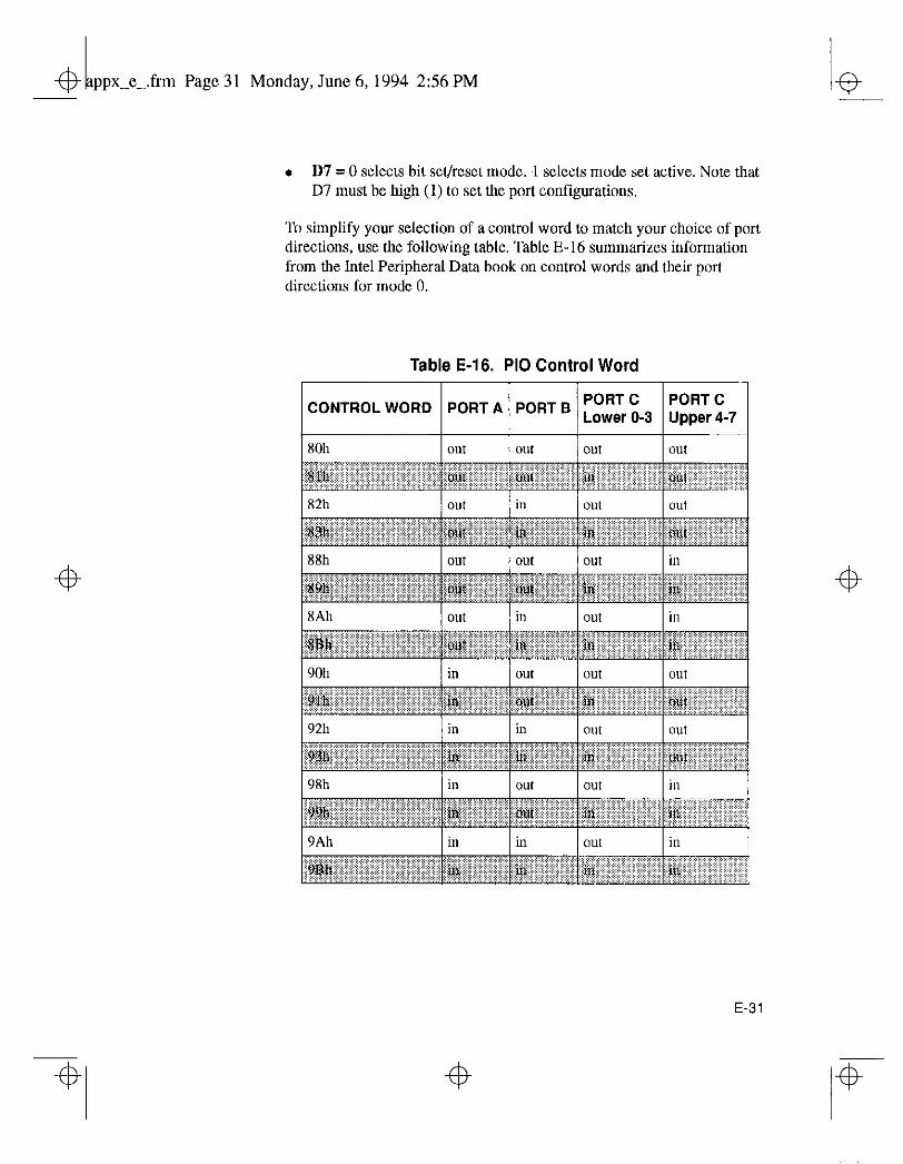
1 4 -- ppx e .frtn Page 31 Monday, June 6, 1994 2:56 PM
4
4
. D7 = 0 selects bit set/reset mode. 1 selects mode set active. Note that D7 must be high (1) to set the port configurations.
To simplify your selection of a control word to match your choice of port directions, use the following table. Table E-16 summarizes information from the Intel Peripheral Data book on control words and their port directions for mode 0.
Table E-16. PI0 Control Word
14
4
4
E-31
4
frtn Page 32 Monday, June 6,1994 2:56 PM
Conversion Disable Reaister (Base Address +404hl
E-32
This register enables/disables conversions. Conversions can be disabled with this register only if the 1600/1400 mode enable register (+406h) is enabled first.
The conversion disable register disables conversions to allow software to perform setup procedures without losing synchronization of the MUX scan counter, DMA controller, etc. from unwanted trigger events. This register resets during power-up (reset) (conversions enabled) and is write only.
Writing a value of 40h to this register disables conversions (sets this register). Writing a value of OOh to this register enables conversions (resets this register).
A write of 40h to the conversion disable register (base address +404h) allows the DAS-1600/1400 Series to ignore all conversion clock sources and disable any further conversions (valuable during initialization and setup). A write of OOh to the conversion disable register re-enables conversions.
At the end of a single cycle DMA (with the 1600 mode enabled) and when the DAS-1600/1400 Series receives the terminal count signal from the computer’s DMA controller, the conversion disable register becomes set (I), preventing further conversions and DMA transfers. To allow conversions to take place again, you must reset this register by writing a value of OOh to base address +404h.
To use these registers effectively, set both the 1600 mode enable and the conversion disable registers upon initial setup; this will disable all conversions. Before data is to be acquired, reset the conversion disable register and collect data. At the end of data acquisition, set the conversion disable register to disable conversions. This process insures a clean software interface.
Register-Level Address Map
4
4
frm Page33 Monday, June6.1994 2:56PM
4
4
Burst Mode Enable Register (Base Address +405h)
This register enables/disables burst mode acquisition; it is reset (burst mode disabled) during power-up (reset). Burst mode can be enabled only if 1600/1400 mode is enabled first. This register is write Only.
Writing a value of 40h to this register enables the burst mode. Writing a value of OOh to this register disables the burst mode.
1600/1400 Mode Enable Register (Base Address +406h)
This register enables/disables the 1600 mode and is reset during power-up (reset) (1600 mode disabled); that is, a DAS-1600/1400 Series board looks just like aDAS-16Gx board on power-up.
This register is write only. Writing a value of 4Ob to this register enables the 1600 mode. Writing a value of OOh to this register disables the 1600 mode.
This register allows the following functions:
. disabling of conversions during initialization and setup
. the cessation of conversions at the end of single cycle DMA
Status Register B (Base Address +407h)
This register allows the user to observe the status of the following signals:
. I MHz/IO MHz clock select switch
. wait state enable switch
. 1600/1400 mode enable setting
. conversion disable setting
. burst mode enable setting
4
E-33
4 IP
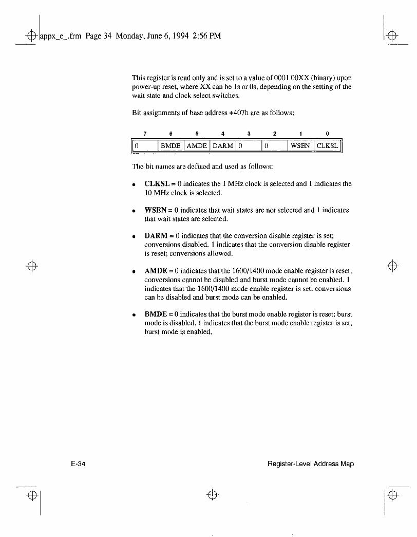
.frm Page 34 Monday, June 6,1994 2:56 PM
4
E-34
This register is read only and is set to a value of 000 1 OOXX (binary) upon power-up reset, where XX can be 1s or OS, depending on the setting of the wait state and clock select switches.
Bit assignments of base address +407h are as follows:
7 6 5 4 3 2 1 0
0 BMDE AMDE DARM 0 0 WSEN CLKSL
The bit names are defined and used as follows:
CLKSL = 0 indicates the 1 MHz clock is selected and 1 indicates the 10 MHz clock is selected.
WSEN = 0 indicates that wait states are not selected and 1 indicates that wait states are selected.
DARM = 0 indicates that the conversion disable register is set; conversions disabled. 1 indicates that the conversion disable register is reset; conversions allowed.
AMDE = 0 indicates that the 1600/1400 mode enable register is reset; conversions cannot be disabled and burst mode cannot be enabled. 1 indicates that the 1600/1400 mode enable register is set: conversions can be disabled and burst mode can be enabled.
BMDE = 0 indicates that the burst mode enable register is reset; burst mode is disabled. 1 indicates that the burst mode enable register is set; burst mode is enabled.
Register-Level Address Map
I4
4
4
16OOug.ix Page 1 Monday, June 6,1994 2:58 PM
Index
Numerics 8255A-5
PI0 E-28 R2C54
controi register E-23 counter/timer 2-8, E- 14 register level I/O E- 18
82C54 clock selecting 3- 16
A
A/D configuration 3-10 A/D mode 3-10 accessories
attaching 4-2 attaching expansiou 4-10 channel expansion 2-5 EXP-16 l-7,2-4 EXP-16/A l-7,2-4 EXP-GP l-7,2-4 general l-7 installing 4- 1 ISO- l-7 MB Series 1-7 SSH-4/A l-7 SSH-8 4-18 STA-16 l-7,2-4,4-2 STA-U l-7,4-2 STC-37 l-7,4-2 STP-37 l-7,4-2 using MB02 backplanes 2-5
acquisition time A-2
ADC register E-3 setting bipolar/unipolar 3- 16
advanced software options l-4 analog input 2-8
attaching 4-24 channel expansion 2-4 connecting differential iuputs 4-27 connecting single-ended 4-26 conversion modes 2-6 differential input 2-3 features 2-3 front-end interface 4-17 gain selection 2-5 preventing saturation 4-26 range 2-3 ranges 2-5 selecting bipolar 2-3 selecting differential 2-3 selecting unipolar 2-3 setting differential/single-ended 3- 16 settling time A- 1 single-ended input 2-3 trigger 2-9
aualog output 2-X,2-1 1 connecting 4-3 1
analog-to-digital converter (ADC) 2-3 anti-static material 3-1 aperture delay A-2 ASO- 1-4 ASO-16ao l-4
software installation 3-3 ASYST l-6
4
X-l
4
16OOug.ix Page 2 Monday, June 6, 1994 2:58 PM
attaching EXP-164-11 EXF-16/A 4-l 1 expansion accessories 4-10 EXP-GP 4- 12 external pacer clock 2-12 ISO- 4-15 MB01 4-21 MB02 4-22 multiple accessories 4.13 SSH-8 4-17,4-18 STA-16 4-6 STA-U 4-8 STC-37 4-2 STP-37 4-5
B backplanes
MB01 4-21 MB02 4-2 1 STA-MB 4-21
backup diskettes 3-2 base address E-2
switch 3-16 bipolar
selecting 2-3 block diagram 2- 1 board
ID E-6 inspection 3-l installation 3- 18 type 3-9
burst mode 2-7 rate 2-7 scan 2-7 setting up E-17
C cabling 4-1
EXP-164-11 EXP-16/A 4-l 1 EXP-GP 4- 12 ISO- 4-15 MBOI 4-21 MB02 4-22 PI0 3-19 shielded 4-25 SSH-4/A 4-17 SSH-8 4-17,4-18 STA-16 4-6 STA-IJ 4-8 STP-314-5
CAL1600,EXE l-4, l-5 calibration 6- 1
equipment 6- 1 factory 3-2 test points 6-l
calibratioh utility l-4, l-5 capacitive load 2-11 cautions 3-1,4-l, 4-24,4-25,7-4, D-l CFG1600.EXE 1-3, l-5,3-8 channel
configuration E- 11 expansion 2-4,2-5 input 2-3 isolating 2-5 selecting expanded 2-5
clock burst mode 2-7 disabling internal E- 15 pacer 2-7 sources 2-X
cold-junction compensation 3-12 common-mode voltages 4-29 configuration
utility 3-8 window 3-9
X-Z Index
2 16OOug.ix Page 3 Monday, June 6, 1994 2:58 PM
configuration file l-3 #of SSHs 3-12 A/D configuration 3-10 A/D mode 3-10 base address 3-Y board type 3-9 changing 3- 13 CJR channel 3-12 clock select 3-10 creating 3-6 D/A 0 mode 3-10 D/A 1 mode 3-l 1 default 3-6 digital config. 3-l 1 DMA channel 3-l 1 EXP-16
gain 3- 11 number of 3- 11
interrupt level 3- 1 I options 3-9 SSH gain 3- 13 SSH timing 3-13 SSH type 3- 12 SSH-4/A mode 3-13 using 3-6 wait state 3-10
configuration options setting ADC bipolar/unipolar 3- 16 setting base address 3- 16 setting DAC bipolar/unipolar 3- 15 setting DAC reference voltage 3- 16 setting differential/single-ended 3- 16 setting DMA channel 3-18 setting reference voltage 3-16 switch locations 3-14 switch-configurable 3-14
configuration utility 1-3, 1-5 configuring channels 2-5 connector
main I/O pin assignments 4-3 Control Panel 1-4, 1-5,5-l
using 5- 1
control register E-12 control word
PI0 E-3 1 conversion modes 2-6 counter
latch operation E-25 latching E-25
counter 0 enabling external clock E- I5 gate E-6 producing delays E-22 programmable one shot E-22 uses of E-14, E-15
counter 1 & 2 configurations E- 19 disabling E- 15 gating 2- 13
counter enable/burst length register E- 14 counter/timer
82C54 2-8 counting events E- 15 crosstalk 4-25 CTL1600,EXlS 1-5 CTL1600W.EXE l-5
D DAC2-11
bipolar output E-9 capacitive load 2-l 1 connecting outputs 4-3 1 output register E-7 resolution 2- 11 setting bipolar/unipolar 3- 15 setting reference voltage 3-16 unipolar output E- 10
daisy-chaining 2-4 accessories 4-13 SSH-8 4-18
X-3
$ 16OOug.ix Page 4 Monday, June 6, 1994 2:58 PM
DAS 1600,CFG 3-6 DAS-16Gx 1-2 data conversion
burst mode 2-l modes 2-6 paced mode 2-6 rate 2-h software initiated 2-10 synchronous 2- 10
data transfer DMA 2- 10 general l-2 interrupt 2- 10 modes 2-10
default configuration file 3-6 delays E-22 differential input 2-3
common connection schemes 4-27 selecting 2-3 usage 2-3
digital I/O register E-5 input 2-12 output 2-12 trigger 2-9
digital-to-analog converter 2-l 1 diskettes
backup 3-2 working 3-2
DMA 2-7, 2-10 channel 2- 11,3- 11, A-3
setting 3- 18 single cycle 2- 11, E-32 transfers E-32
driver external l-6
Dynamic Data Exchange (DDE) l-5,5-2
E emf
thermal 4-25 event
counter C-25, E- 15 external 2-8
EXAMPLES.TXT 3-3,3-4,3-5 EXP-16 1-7, 2-4,3-l 1
number of 3- 11 terminal names 4- 11
EXP-16/A l-7,2-4 expansion accessories
daisy-chaining 4-13 EXF-GP l-7,2-4
attaching 4-l 2 terminal names 4- 12
external driver l-6 external trigger E-6
F falling edge 2-9 FILES.TXT 3-3, 3-4, 3-5 filtering 4-25 frequency
burst mode 2-7 determining E- 15 measuring E-2 1
Function Call Driver l-4 function libraries l-3 functional description 2-l
x-4 Index
16OOug.ix Page 5 Monday, June 6, 1994 2:58 PM
G gain
bipolar ranges 2-5 EXP-163-11 high l-1 low l-l precautions 4-24 programmable 2-5 selection 2-5, E- 16 settling time A- 1 SSH 3-13 unipolar ranges 2-5
gate E-6 hardware 2-13
gating the counter/timer 2-l 3 gaussian 4-25 generating square waves E-20 global heap D- 1 ground
common 2-3 common-mode voltages 4-29 connection 4-26 low-level 4- 11,4-26 power 4-26
ground loops 4-24,4-27 avoiding 4-29
H hardware gate 2-13
I I/O connectors B- 1 induced-voltage 4-25 input
analog 2-8 attaching analog 4-24 digital 2-12 gate E-2 1 setting single-ended 3- 16
inspecting 3-l installation 4- 1 installing
accessories 4- 1 ASO- 3-3 board 3-18 connecting analog outputs 4-31 connecting differential inputs 4-27 connecting single-ended inputs 4-26 differential connections 4-27 expansion accessories 4- 1 I EXP-GP 4-12 ISO- 4-15 program 3-2 SSH-4/A 4- 17 SSH-8 4-17 STA-16 4-6 standard software 3-2 STA-U 4-8 STC-37 4-2 STP-314-5
internal trigger 2-9 interrupt 2-7
clearing E-10 generation of E- 14 latencies 2-10 level 3-l 1, A-3 mode 2- 10 standard assignments 3-l I
ISO- l-7 attaching 4- 15
isolation amplifiers 4-25
X-5
16OOug.ix Page 6 Monday, June 6, 1994 2:58 PM 4
4
4
K Keithley Memory Manager 5- 1, D- I kovar leads 4-25
L latching counters E-25 libraries
function 1-3 linearity A-2 low-level signals 2-3
M MB Series 1-7 MB01 4-21
attaching 4-21 MB02 2-5-4-21
attaching 4-22 channel selection 4-23
measuring frequency E-21 pulse width E-21
memory allocation D-l heap D-l
memory manager 5- 1, D- 1 installing D-2 removing D-4
mode data transfer 2- 10 synchronous 2- 10
MUX scan register E-4
N noise
crosstalk 4-25 electrical A-3 gaussian 4-25 ground-loop 4-24 induced-voltage 4-25
0 output
analog 2-l 1 digital 2-12
P
paced mode 2-6 pacer clock 2-6, E-14
attaching external 2-12 external 2-12, E-6 external source 2-8 internal source 2-8 source selection E-12
pin assignments B- 1 PI0 E-28
8255A-5 E-28 control word E-3 1
PPI E-28 precision reference voltage 2- 11 problem isolation 7-l programming
register level E- 1 pseudo-simultaneous sample-and-hold 2-7
4
X-6 Index
16OOug.ix Page 7 Monday, June 6, 1994 2:58 PM
R
rate data conversion 2-6 pacer clock 2-6 sample 2-6,2-7
README.TXT 3-3,3-4,3-5 reference voltage
precision 2- 11 setting 3- 16
register 1600/1400 mode enable E-33 82C54 control E-23 ADC E-3 burst mode enable E-33 control E-12 conversion disable E-32 counter enable/burst length E-14 DAC output E-7 digital I/O E-5 gain selection/burst rate E-16 MUX scan E-4 PI0 control E-29 status A E-10 status B E-33
register level programming E- 1 resistors
bias return 4-29 resolution A- 1 rising edge 2-9
S
sample rate 2-6 screw terminal accessories 1-7 setting
82C54 clock 3-16 ADC bipolar/unipolar 3- 16 base address 3-16 bipolar/unipoIar 3-15 DAC reference voltage 3- 16 DMA channel 3- 18 wait state 3- 16
setting up burst mode E- 17 settling time A- 1 Show Switches 3-13 signal
bipolar 2-3 conditioning l-7,2-4 high-level 2-3 low-level 2-3 representation 2-3 unipolar 2-3
simultaneous sample-and-hold accessory l-7 single-ended input 2-3
attaching 4-26 selecting 2-3
specifications 82C54 counter/timer A-6 analog input A- 1 analog output A-4 digital I/O A-5
auxiliary A-5 power A-6
SSH gains 3-13 timing 3- 13
SSH-4/A l-7,3-13 mode 3-13
SSH-8 l-7 application 4- 16 attaching 4-17
x-7
16OOugix Page 8 Monday, June 6, 1994 2:58 PM
STA-16 l-7,2-4,4-2 terminal names 4-7
STA-MB 4-21 static electricity 3-l status register A E-10 STA-U l-7,4-2
terminal names 4-9 STC-37 l-7,4-2
attaching 4-2 STP-37 l-7,4-2 synchronous mode 2- 10
T
Technical Support 7-6 terminal names
EXP-16 4-l 1 EXP-GP 4- 12 STA-16 4-7 STA-U 4-9
test points 6-l thermal emf 4-25 thermocouples 3- 12 throughput
definition of A- 1 throughput rates 2-5 timebase 2-8 timing
paced and burst mode 2-7 trigger
analog 2-9 attaching external 2-12 channel 2-9 digital 2-9
external 2- 12 edge sensitive 2-9 external E-6 external analog 2-9 inhibiting 2- 13 internal 2-9
level sensitive 2- 10 negative-edge 2-9 positive-edge 2-9 sources 2-9 types 2-9
troubleshooting procedures 7- 1
U unipolar
selecting 2-3 universal screw terminal l-7 utility
calibration 1-4, 1-5, 6-1 configuration l-5,3-6 Control Panel
general 5- 1
v
VDAS-1600 l-6 VDMAD.386 D-l VIEWDAC l-6 VisualDAS Custom Controls 1-6 voltages
common-mode 4-29
W wait state
selecting 2- 14 setting 3- 16
Windows Enhanced Mode 2- 11 working diskettes 3-2
X-8 Index
Recommended