NKE-XSC&NKE-XDCNKE-XSC&NKE-XDCNKE-XSC&NKE-XDCNKE-XSC&NKE-XDCNKE-XSC&NKE-XDCNKE-XSC&NKE-XDCNKE-XSC&NKE-XDCNKE-XSC&NKE-XDC SeriesSeries
http://www.microdc.cn Technical Enquiries-Email:[email protected] Tel:0086-20-86000646 Page 1 of 5
SELECTIONSELECTIONSELECTIONSELECTIONSELECTIONSELECTIONSELECTIONSELECTION GUIDEGUIDEGUIDEGUIDEGUIDEGUIDEGUIDEGUIDE
Order code
Input Output EfficiencyIsolation
Capacitance MTTF1
Voltage(VDC) Current(mA) Voltage
(VDC)Current(mA) (%.Typ.) pF KHrs
Nominal Rated Load
NKE0303XDC 3.3 400 3.3 303 72 30 1234
NKE0305XDC 3.3 400 5 200 75 35 632
NKE0309XDC 3.3 403 9 111 74 30 1204
NKE0312XDC 3.3 398 12 83 76 33 ---
NKE0315XDC 3.3 394 15 66 77 35 ---
NKE0303XSC 3.3 400 3.3 303 72 30 1234
NKE0305XSC 3.3 400 5 200 75 35 632
NKE0309XSC 3.3 403 9 111 74 30 1204
NKE0503XDC 5 270 3.3 303 74 40 619
NKE0505XDC 5 289 5 200 69 28 2414
NKE0505XDEC 5 250 5 200 77 34 419
NKE0509XDC 5 266 9 111 75 29 1173
NKE0512XDC 5 260 12 83 78 30 633
NKE0515XDC 5 256 15 66 78 32 360
NKE0503XSC 5 270 3.3 200 74 40 619
NKE0505XSC 5 289 5 303 69 28 2414
NKE0505XSEC 5 250 5 200 77 34 419
NKE0509XSC 5 266 9 111 75 29 1173
NKE0512XSC 5 260 12 83 78 30 633
NKE0515XSC 5 256 15 66 78 32 360
NKE1205XDC 12 117 5 200 72 35 620
NKE1209XDC 12 107 9 111 78 50 488
NKE1212XDC 12 105 12 83 79 57 360
NKE1215XDC 12 103 15 66 81 60 252
NKE1205XSC 12 117 5 200 72 35 620
NKE1209XSC 12 107 9 111 78 50 488
NKE1212XSC 12 105 12 83 79 57 360
NKE1215XSC 12 103 15 66 81 60 252NKE0505SEC/NKE0505DEC offers higher effciency than NKE0505SC/NKE0505DC but over a narrower operating temperature range.See temperature characteristics graph.
MODELMODELMODELMODELMODELMODELMODELMODEL SELECTIONSELECTIONSELECTIONSELECTIONSELECTIONSELECTIONSELECTIONSELECTIONNKENKENKENKENKENKENKENKE①①①①0505050505050505②②②②0505050505050505③③③③XXXXXXXXS(D)CS(D)CS(D)CS(D)CS(D)CS(D)CS(D)CS(D)C④④④④
①Product Series ②Input Voltage③Output Voltage ④Fixed Input&SIP4(DIP8)Package
MICRODC RESERVES THE COPYRIGHT
Isolated Sub-Miniature 1W Single Output DC/DC Converters
FEATURESFEATURESFEATURESFEATURESFEATURESFEATURESFEATURESFEATURES◆RoHS Compliant
◆Sub-Miniature SIP4&DIP8 Styles
◆3kVDC Isolation
◆Wide Temperature performance at full 1 Watt load,-40℃ to 85℃
◆Increased Power Density to 2.09W/cm3
◆UL 94V-0 Package Material
◆Footprint at 0.69cm2
◆Industry Standard Pin out
◆3.3V,5V & 12V Input
◆3.3V,5V,9V,12Vand15V Output
◆Internal SMD Construction
◆Fully Encapsulated with Toroidal Magnetics
◆MTTF up to 2.6 Million hours
◆Custom Solutions Available
◆No Electrolytic or Tantalum Capacitors
APPLICATIONSAPPLICATIONSAPPLICATIONSAPPLICATIONSAPPLICATIONSAPPLICATIONSAPPLICATIONSAPPLICATIONSThe NKE sub-miniature series of DC/CD Converters isparticularly suited to isolating and/or converting DCpower rails. A smaller package size,improved efficiency,lower output ripple and 3kVDC isolation capabilitythrough state of the art packaging and improvedtechnology. The galvanic isolation allows the device tobe configured to provide an isolated negative rail insystems where only positive rails exist. The widetemperature range guarantees startup from -40℃ andfull 1 watt output at 85℃.
InputInputInputInputInputInputInputInput CharacteristicsCharacteristicsCharacteristicsCharacteristicsCharacteristicsCharacteristicsCharacteristicsCharacteristics
Parameter Conditions Min. Typ. Max. Units
Voltage range
Continuous operation, 3.3V 2.97 3.3 3.63
VContinuous operation, 5V 4.5 5.0 5.5
Continuous operation, 12V 10.8 12.0 13.2
Reflected ripple current 3.3V input types 40 60 mA p-p
AbsoluteAbsoluteAbsoluteAbsoluteAbsoluteAbsoluteAbsoluteAbsolute MaximumMaximumMaximumMaximumMaximumMaximumMaximumMaximum RatingsRatingsRatingsRatingsRatingsRatingsRatingsRatings
Lead temperature 1.5mm from case for 10 seconds 300℃
Internal power dissipation 530mW
Input voltage V , NKE03 types 5.5V
Input voltage V, NKE05 types 7V
Input voltage V, NKE12 types 15V
NKE-XSC&NKE-XDCNKE-XSC&NKE-XDCNKE-XSC&NKE-XDCNKE-XSC&NKE-XDCNKE-XSC&NKE-XDCNKE-XSC&NKE-XDCNKE-XSC&NKE-XDCNKE-XSC&NKE-XDC SeriesSeries
http://www.microdc.cn Technical Enquiries-Email:[email protected] Tel:0086-20-86000646 Page 2 of 5
OutputOutputOutputOutputOutputOutputOutputOutput SpecificationsSpecificationsSpecificationsSpecificationsSpecificationsSpecificationsSpecificationsSpecifications
Parameter Conditions Min. Typ. Max. Units
Rated Power TA=-40°C to 120°C,see derating graphs 1.0 WVoltage Set Point AccuracyLine regulation
See tolerance envelope
High Vin to low Vin 1.0 1.2 %%
Load regulation1
10% load to rated load, 3.3V output types & 0309
10% load to rated load, 5V output types
10
12.81.2
%1510% load to rated load, 9V output types
10% load to rated load, 12V output types
7.5
6.510
9.510% load to rated load, 15V output types 6.0 8.5
Ripple&Noise
BW=DC to 20MHz, 3.3V output types,&0305, 0505XSEC,0505XDEC 40 80
mV p-pBW=DC to 20MHz, other 5V output types
BW=DC to 20MHz, 9V output types
62
103
85
170
BW=DC to 20MHz, 12V output types
BW=DC to 20MHz, 15V output types
49
39
75
65
IsolationIsolationIsolationIsolationIsolationIsolationIsolationIsolation CharacteristicsCharacteristicsCharacteristicsCharacteristicsCharacteristicsCharacteristicsCharacteristicsCharacteristicsParameter Conditions Min. Typ. Max. Units
Isolation test voltage Flash tested for 1 second 3000 VDC
resistance Viso= 1000VDC 10 GΩ
TechnicalTechnicalTechnicalTechnicalTechnicalTechnicalTechnicalTechnical notesnotesnotesnotesnotesnotesnotesnotesISOLATIONISOLATIONISOLATIONISOLATION VOLTAGEVOLTAGEVOLTAGEVOLTAGE‘Hi Pot Test’, ‘Flash Tested’, ‘Withstand Voltage’, ‘Proof Voltage’, ‘Dielectric Withstand Voltage’ & ‘Isolation Test Voltage’ are all terms that relate to the same thing, a test voltage,applied for a speciffied time, across a component designed to provide electrical isolation, to verify the integrity of that isolation.MICRODC Power Module NKE series of dc/dc converters are all 100% production tested at their stated isolation voltage. This is 1000V DC for 1 second.A question commonly asked is, “What is the continuous voltage that can be applied across the part in normal operation?”The NKE series has been recognized by Underwriters Laboratory for functional insulation. Both input and output should normally be maintained within SELV limits.e.less than 42.4V peak, or 60VDC. The isolationtest voltage represents a measure of immunity to transient voltages and the part should never be used as an element of a safety isolation system. The part could be expected to function correctly with severalhundred volts offset applied continuously across the isolation barrier; but then the circuitry on both sides of the barrier must be regarded as operating at an unsafe voltage and further isolation/insulation systemsmust form a barrier between these circuits and any user-accessible circuitry according to safety standard requirements.REPEATEDREPEATEDREPEATEDREPEATEDHIGH-VOLTAGEHIGH-VOLTAGEHIGH-VOLTAGEHIGH-VOLTAGE ISOLATIONISOLATIONISOLATIONISOLATION TESTINGTESTINGTESTINGTESTINGIt is well known that repeated high-voltage isolation testing of a barrier component can actually degrade isolation capability, to a lesser or greater degree depending on materi-als, construction and environment.While manufactured parts can withstand several times the stated test voltage, the isolation capability does depend on the wire insulation. Any material, including this enamel (typically polyurethane) is susceptibleto eventual chemical degradation when subject to very high applied voltages thus implying that the number of tests should be strictly limited. We therefore strongly advise against repeated high voltage isolationtesting, but if it is absolutely required, that the voltage be reduced by 20% from speciffied test voltage.
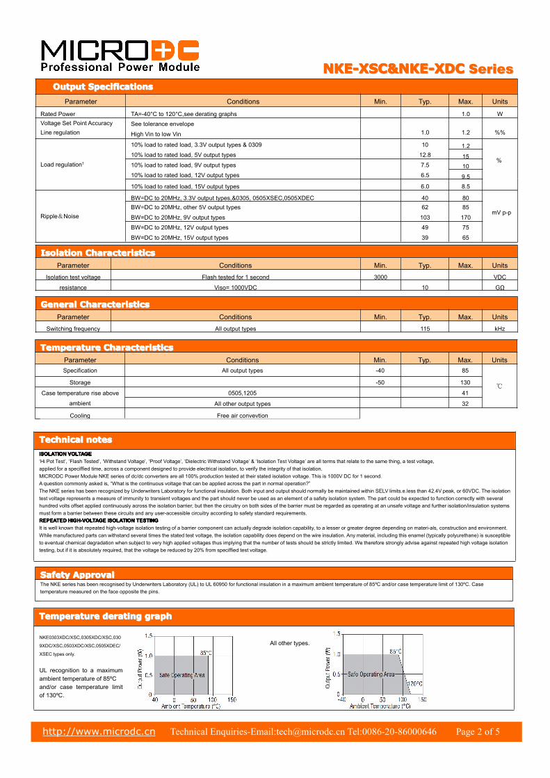
TemperatureTemperatureTemperatureTemperatureTemperatureTemperatureTemperatureTemperature deratingderatingderatingderatingderatingderatingderatingderating graphgraphgraphgraphgraphgraphgraphgraph
TemperatureTemperatureTemperatureTemperatureTemperatureTemperatureTemperatureTemperature CharacteristicsCharacteristicsCharacteristicsCharacteristicsCharacteristicsCharacteristicsCharacteristicsCharacteristicsParameter Conditions Min. Typ. Max. UnitsSpecification All output types -40 85
℃Storage -50 130
Case temperature rise above
ambient
0505,1205 41
All other output types 32
Cooling Free air convevtion
GeneralGeneralGeneralGeneralGeneralGeneralGeneralGeneral CharacteristicsCharacteristicsCharacteristicsCharacteristicsCharacteristicsCharacteristicsCharacteristicsCharacteristicsParameter Conditions Min. Typ. Max. Units
Switching frequency All output types 115 kHz
SafetySafetySafetySafetySafetySafetySafetySafety ApprovalApprovalApprovalApprovalApprovalApprovalApprovalApprovalThe NKE series has been recognised by Underwriters Laboratory (UL) to UL 60950 for functional insulation in a maximum ambient temperature of 85ºC and/or case temperature limit of 130ºC. Casetemperature measured on the face opposite the pins.
NKE0303XDC/XSC,0305XDC/XSC,030
9XDC/XSC,0503XDC/XSC,0505XDEC/
XSEC types only.
UL recognition to a maximumambient temperature of 85ºCand/or case temperature limitof 130ºC.
All other types.
NKE-XSC&NKE-XDCNKE-XSC&NKE-XDCNKE-XSC&NKE-XDCNKE-XSC&NKE-XDCNKE-XSC&NKE-XDCNKE-XSC&NKE-XDCNKE-XSC&NKE-XDCNKE-XSC&NKE-XDC SeriesSeries
http://www.microdc.cn Technical Enquiries-Email:[email protected] Tel:0086-20-86000646 Page 3 of 5
ApplicationApplicationApplicationApplicationApplicationApplicationApplicationApplication NotesNotesNotesNotesNotesNotesNotesNotes
MinimumMinimumMinimumMinimum loadloadloadloadThe minimum load to meet data sheet speciffication is 10% of the full rated load across the speciffied input voltage range. Lower than 10% minimum loading will result in anincrease in output voltage, which may rise to typically double the speciffied output voltage if the output load falls to less than 5%.
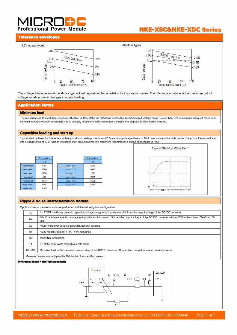
CapacitiveCapacitiveCapacitiveCapacitive loadingloadingloadingloading andandandand startstartstartstart upupupupTypical start up times for this series, with a typical input voltage rise time of 2.2μs and output capacitance of 10μF, are shown in the table below. The product series will startinto a capacitance of 47μF with an increased start time, however, the maximum recommended output capacitance is 10μF.
Start-up time Start-up time
μs μs
NKE0303XSC 544 NKE0512XSC 5040
NKE0305XSC 1306 NKE0515XSC 9940
NKE0309XSC 5250 NKE1205XSC 1671
NKE0503XSC 496 NKE1209XSC 2835
NKE0505XSC 1075 NKE1212XSC 5295
NKE0505XSEC 894 NKE1215XSC 8475
NKE0509XSC 3140
DifferentialDifferentialDifferentialDifferential ModeModeModeMode NoiseNoiseNoiseNoise TestTestTestTest SchematicSchematicSchematicSchematic
ToleranceToleranceToleranceToleranceToleranceToleranceToleranceTolerance envelopesenvelopesenvelopesenvelopesenvelopesenvelopesenvelopesenvelopes
The voltage tolerance envelope shows typical load regulation characteristics for this product series. The tolerance envelope is the maximum outputvoltage variation due to changes in output loading.
3.3V output types All other types
Typical Start-Up Wave Form
RippleRippleRippleRipple &&&& NoiseNoiseNoiseNoise CharacterizationCharacterizationCharacterizationCharacterization MethodMethodMethodMethodRipple and noise measurements are performed with the following test configuration.
C1 1μF X7R multilayer ceramic capacitor, voltage rating to be a minimum of 3 times the output voltage of the DC/DC converter
C2 10μF tantalum capacitor, voltage rating to be a minimum of 1.5 times the output voltage of the DC/DC converter with an ESR of less than 100mΩ at 100kHz.
C3 100nF multilayer ceramic capacitor, general purpose
R1 450Ω resistor, carbon fi lm, ±1% tolerance
R2 50Ω BNC termination
T1 3T of the coax cable through a ferrite toroid
RLOAD Resistive load to the maximum power rating of the DC/DC converter. Connections should be made via twisted wires
Measured values are multiplied by 10 to obtain the speciffied values.
NKE-XSC&NKE-XDCNKE-XSC&NKE-XDCNKE-XSC&NKE-XDCNKE-XSC&NKE-XDCNKE-XSC&NKE-XDCNKE-XSC&NKE-XDCNKE-XSC&NKE-XDCNKE-XSC&NKE-XDC SeriesSeries
http://www.microdc.cn Technical Enquiries-Email:[email protected] Tel:0086-20-86000646 Page 4 of 5
ApplicationApplicationApplicationApplicationApplicationApplicationApplicationApplication NotesNotesNotesNotesNotesNotesNotesNotes
OutputOutputOutputOutput RippleRippleRippleRipple ReductionReductionReductionReductionBy using the values of inductance and capacitance stated, the output ripple at the rated load is lowered to 5mV p-p max.
ComponentComponentComponentComponent selectionselectionselectionselectionCapacitor: It is required that the ESR (Equivalent Series Resistance) should be as low as possible, ceramic types are recommended.The voltage rating should be at least twice (except for 15V output), the rated output voltage of the DC/DC converter.Inductor: The rated current of the inductor should not be less than that of the output of the DC/DC converter. At the rated current, the DC resistance of the inductor should besuch that the voltage drop across the inductor is <2% of the rated voltage of the DC/DC converter. The SRF (Self Resonant Frequency) should be >20MHz.
Inductor Capacitor
L,μH SMD Through Hole C,μF
NKE0303XS(D)C 10 82103C 11R103C 4.7
NKE0305XS(D)C 47 82473C 11R473C 4.7
NKE0309XS(D)C 47 82473C 11R473C 1
NKE0503XS(D)C 10 82103C 11R103C 4.7
NKE0505XS(D)C 47 82473C 11R473C 4.7
NKE0505X(S)DEC 47 82473C 11R473C 4.7
NKE0509XSC 47 82473C 11R473C 1
NKE0512XS(D)C 68 82683C 11R683C 0.68
NKE0515XS(D)C 100 82104C 11R104C 2.2
NKE1205XS(D)C 47 82473C 11R473C 4.7
NKE1209XS(D)C 47 82473C 11R473C 1
NKE1212XS(D)C 68 82683C 11R683C 0.47
NKE1215XS(D)C 100 82104C 11R104C 2.2
PackagePackagePackagePackagePackagePackagePackagePackage SpecificationsSpecificationsSpecificationsSpecificationsSpecificationsSpecificationsSpecificationsSpecifications
PINPINPINPIN CONNECTIONS-8CONNECTIONS-8CONNECTIONS-8CONNECTIONS-8 PINPINPINPIN DIPDIPDIPDIP
Pin Function1 -VIN
4 +VIN
5 +VOUT
7 -VOUT
PINPINPINPIN CONNECTIONS-4CONNECTIONS-4CONNECTIONS-4CONNECTIONS-4 PINPINPINPIN SIPSIPSIPSIP
Pin Function1 -VIN
2 +VIN
3 -VOUT
4 +VOUT
MechanicalMechanicalMechanicalMechanical DimensionsDimensionsDimensionsDimensions
DIP8 Package SIP4 Package
All dimensions in inches ±0.01 (mm ±0.25mm). All pins on a 0.1 (2.54) pitch and within ±0.01 (0.25) of true position. Weight: 1.09g (SIP4) 1.25g (DIP8)
NKE-XSC&NKE-XDCNKE-XSC&NKE-XDCNKE-XSC&NKE-XDCNKE-XSC&NKE-XDCNKE-XSC&NKE-XDCNKE-XSC&NKE-XDCNKE-XSC&NKE-XDCNKE-XSC&NKE-XDC SeriesSeries
http://www.microdc.cn Technical Enquiries-Email:[email protected] Tel:0086-20-86000646 Page 5 of 5
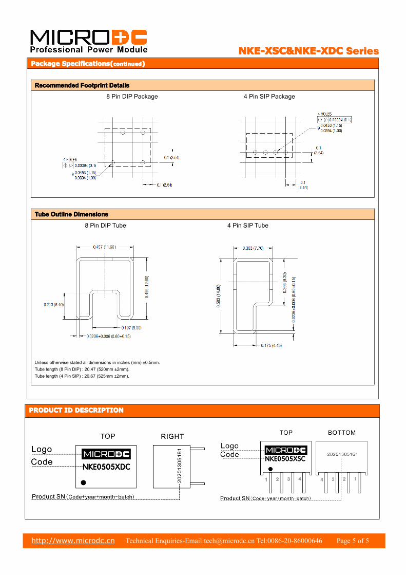
PackagePackagePackagePackagePackagePackagePackagePackage Specifications(Specifications(Specifications(Specifications(Specifications(Specifications(Specifications(Specifications(continuedcontinuedcontinuedcontinuedcontinuedcontinuedcontinuedcontinued))))))))
RecommendedRecommendedRecommendedRecommended FootprintFootprintFootprintFootprint DetailsDetailsDetailsDetails
8 Pin DIP Package 4 Pin SIP Package
TubeTubeTubeTube OutlineOutlineOutlineOutline DimensionsDimensionsDimensionsDimensions
8 Pin DIP Tube 4 Pin SIP Tube
Unless otherwise stated all dimensions in inches (mm) ±0.5mm.Tube length (8 Pin DIP) : 20.47 (520mm ±2mm).Tube length (4 Pin SIP) : 20.67 (525mm ±2mm).
PRODUCTPRODUCTPRODUCTPRODUCTPRODUCTPRODUCTPRODUCTPRODUCT IDIDIDIDIDIDIDID DESCRIPTIONDESCRIPTIONDESCRIPTIONDESCRIPTIONDESCRIPTIONDESCRIPTIONDESCRIPTIONDESCRIPTION
Recommended


![XSC Single Fiber series - XENYAsup.xenya.si/sup/info/xenya/wdm/[XWDM]_XSC_Series_Datasheet_D3.pdf · 2 XSC Single Fiber CWDM Series XSC1‐ 111202173900 exhibits watermark peak attenuation,](https://img.pdfslide.net/doc/110x75/5eb942b1648ed51caa7dd420/xsc-single-fiber-series-xwdmxscseriesdatasheetd3pdf-2-xsc-single-fiber.jpg)