Nano Res
1
Electrically-tunable pore morphology in nanoporous
gold thin films
Tatiana S. Dorofeeva1, and Erkin Seker1( )
Nano Res., Just Accepted Manuscript • DOI 10.1007/s12274-015-0726-x
http://www.thenanoresearch.com on January 28, 2015
© Tsinghua University Press 2015
Just Accepted
This is a “Just Accepted” manuscript, which has been examined by the peer-review process and has been
accepted for publication. A “Just Accepted” manuscript is published online shortly after its acceptance,
which is prior to technical editing and formatting and author proofing. Tsinghua University Press (TUP)
provides “Just Accepted” as an optional and free service which allows authors to make their results available
to the research community as soon as possible after acceptance. After a manuscript has been technically
edited and formatted, it will be removed from the “Just Accepted” Web site and published as an ASAP
article. Please note that technical editing may introduce minor changes to the manuscript text and/or
graphics which may affect the content, and all legal disclaimers that apply to the journal pertain. In no event
shall TUP be held responsible for errors or consequences arising from the use of any information contained
in these “Just Accepted” manuscripts. To cite this manuscript please use its Digital Object Identifier (DOI®),
which is identical for all formats of publication.
Nano Research
DOI 10.1007/s12274-015-0726-x
Template for Preparation of Manuscripts for Nano Research
TABLE OF CONTENTS (TOC)
Electrically-Tunable Pore Morphology in Nanoporous
Gold Thin Films
Tatiana S. Dorofeeva, Erkin Seker *
University of California – Davis, USA
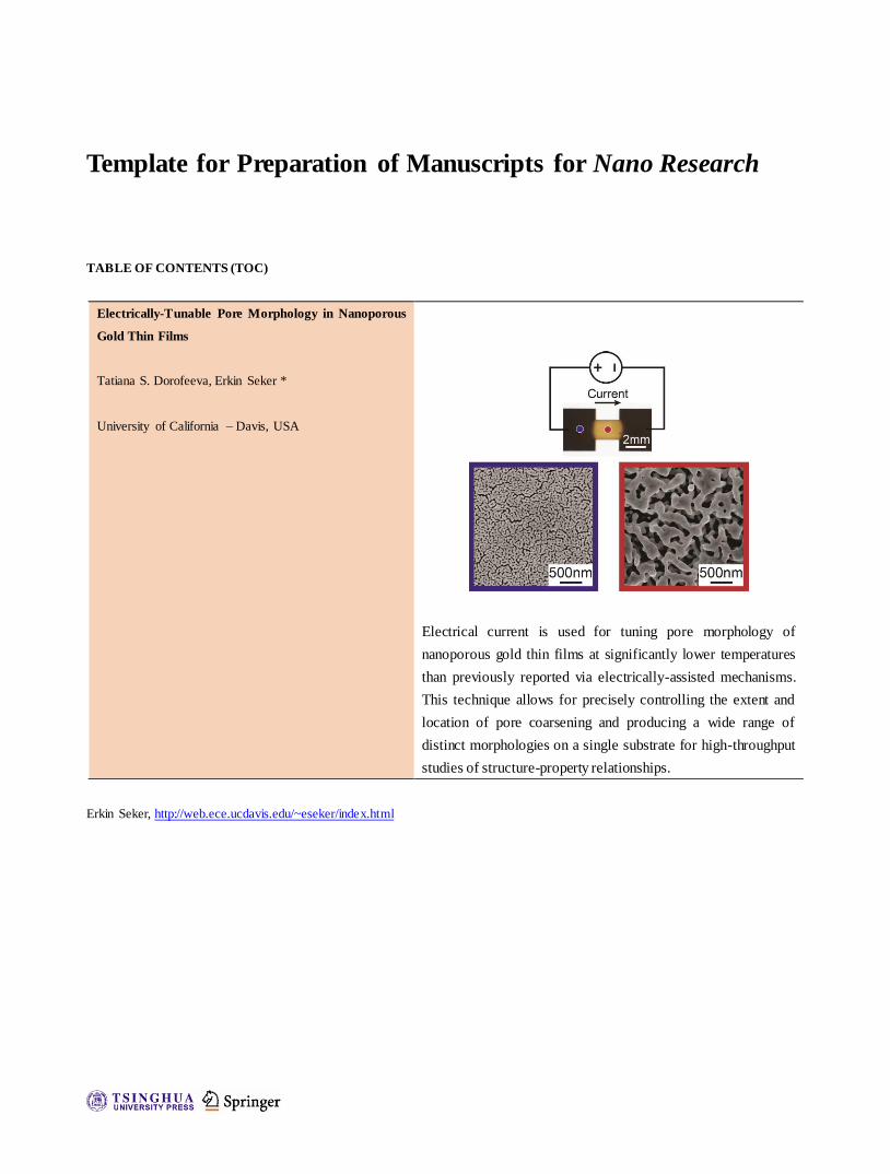
Electrical current is used for tuning pore morphology of
nanoporous gold thin films at significantly lower temperatures
than previously reported via electrically-assisted mechanisms.
This technique allows for precisely controlling the extent and
location of pore coarsening and producing a wide range of
distinct morphologies on a single substrate for high-throughput
studies of structure-property relationships.
Erkin Seker, http://web.ece.ucdavis.edu/~eseker/index.html
Electrically-tunable pore morphology in nanoporous
gold thin films
Tatiana S. Dorofeeva1, and Erkin Seker1( )
Received: day month year
Revised: day month year
Accepted: day month year
(automatically inserted by
the publisher)
© Tsinghua University Press
and Springer-Verlag Berlin
Heidelberg 2014
KEYWORDS
nanoporous gold,
tunable morphology,
Joule heating,
material screening
ABSTRACT
Nanoporous gold (np-Au) is an emerging nanostructured material that exhibits
many desirable properties, including high electrical and thermal conductivity,
high surface area-to-volume ratio, tunable pore morphology, well-established
surface-binding chemistry, and compatibility with microfabrication. These
features made np-Au a popular material for fuel cells, optical and electrical
biosensors, drug delivery vehicles, neural electrode coatings, and as a model
system for nano-scale mechanics. In each application, np-Au morphology plays
an essential role in the overall device operation. Therefore, precise control of
morphology is necessary for attaining optimal device performance.
Traditionally, thermal treatment in furnaces and on hot plates is used for
obtaining np-Au with self-similar but coarser morphologies. However, this
approach lacks the ability to create different morphologies on a single substrate
and requires high temperatures (>250 °C) that are not compatible with most
plastic substrates. Herein, we report electro-annealing as a method that for the
first time makes it possible to control the extent and location of pore coarsening
on a single substrate with one fast treatment step. In addition, the
electro-annealing entails much lower temperatures (<150 °C) than traditional
thermal treatment, putatively due to electrically-assisted phenomena that
contribute to thermally-activated surface diffusion of gold atoms responsible
for coarsening. Overall, this approach can be easily scaled up to display
multiple pore morphologies on a single chip and therefore enable
high-throughput screening of optimal nanostructures for specific applications.
1. Introduction
Nanostructured materials have attracted significant
interest from academia and industry alike, due to
intriguing fundamental questions around nanoscale
phenomena and applications enabled by properties
unique to this length scale. Optical, electrical,
magnetic, thermal, mechanical properties become
Nano Research
DOI (automatically inserted by the publisher)
Address correspondence to Erkin Seker, [email protected]
Research Article
| www.editorialmanager.com/nare/default.asp
2 Nano Res.
increasingly size-dependent at nanoscale [1].
Nanostructured materials have been shown to
exhibit high strength [2], unusual thermal and
electrical properties [3, 4], and enhanced surface
plasmons [5], highlighting the importance of
controlling nanostructure. An emerging
nanostructured material is nanoporous gold
(np-Au), for which related applications and
publications have rapidly grown during last decade
[6]. This popularity is due to many of its attractive
properties, including high electrical and thermal
conductivity, high surface area-to-volume ratio,
tunable pore morphology, well-established gold
binding chemistry, and compatibility with
microfabrication [6]. These properties had an
impact on applications including sensing [7, 8].
biomedical devices [9-12], energy storage [13],
photonics [14, 15], catalysis [16, 17], as well as
fundamental structure-property studies [18-21].
Nanoporous gold is typically obtained by a process
known as dealloying [22]. In this process, selective
removal of silver atoms from a silver-rich gold alloy,
accompanied by surface diffusion of gold atoms at
the metal-electrolyte interface, results in an
open-cell structure with interconnected ligaments of
tens of nanometers [22, 23]. Alloy composition [24]
and preparation approach, dealloying method
[25-27], and post-processing techniques [28, 29] all
influence pore morphology, resulting in a wide
range of possible pore and ligament sizes ranging
from tens of nanometers [25] up to several hundred
of nanometers [23]. When np-Au films are subjected
to homogenous thermal treatment (such as in
annealing furnaces), pore and ligament sizes
increase in a uniform fashion across the entire
sample due to enhanced diffusion of surface atoms
[23]. However, a controllable spatial gradient of
pore morphology is highly desirable in order to
rapidly identify optimal morphologies for desired
application [29]. For example, it is often necessary
to identify a specific range of nanostructures that
increase surface-enhanced Raman signal from a
metallic surface, improve biocompatibility, lower
limit-of-detection of a sensor, or increase reactivity
of a catalytic surface. With the uniform exposure to
thermal energy in conventional annealing
approaches, it is not possible to obtain different
pore morphologies on a single substrate. In
addition, traditional thermal treatment in furnaces
or on hot plates requires temperatures of at least
250 ˚C [23]; thereby, rendering this technique
incompatible with most plastic substrates with low
melting temperatures [30].
Here, we present a novel technique to address these
challenges by taking advantage of the electrical
conductivity of np-Au thin films in order to tune
pore morphology. Specifically, we employ
electro-annealing of micropatterned np-Au thin film
patterns with rationally-designed geometries to
obtain distinct pore morphologies on a single chip.
This technique is based on the principle that
electrical current flowing in thin film traces lead to
localized changes in current density as a function of
trace geometry. At regions with smaller
cross-section, increased current density leads to
localized Joule heating (also known as ohmic and
resistive heating) and putatively enhances
electrically-assisted coarsening mechanisms (to be
discussed in section 3.4). The interplay of thermal
and electrical mechanisms consequently produces
coarsened morphologies at temperatures much
lower (~150 ˚C) than those required for pure
thermal annealing [23], thus opening the door to the
use of substrates with lower melting temperatures.
In tandem, this method, for the first time, allows for
creating multiple and distinct pore morphologies
on a single substrate via a short (less than 2
minutes), single treatment step. Here, we describe
the electro-annealing technique and illustrate
resultant pore morphologies. Finally, a comparative
study on differences between temperature and
morphology for electro- and hot plate-annealing
approaches is presented. We expect that this novel
approach will facilitate the production of
www.theNanoResearch.com∣www.Springer.com/journal/12274 | Nano Research
3 Nano Res.
high-throughput screening platforms on various
substrates for studying structure-property
relationships and identifying optimal morphologies
for desired applications.
2. Experimental
In order to study the effect of thin film geometry on
pore morphology evolution, we fabricated samples
with various np-Au thin film patterns on glass
coverslips: (i) simple rectangular traces, referred to
as unconstricted samples (Figure 1A); (ii) geometric
variations that act as electrical current concentrators
within the rectangular traces, referred to as
constricted samples (Figure 3A); and (iii) branched
trace structures with constrictions that act as
current dividers controlling the extent of
electro-annealing (Figure 4A). The np-Au traces
(460 nm-thick) on glass coverslips were produced
by dealloying lithographically-patterned gold-silver
thin films that were sputter-deposited, as
previously described [31]. The prepared samples
were mounted on a homemade electro-annealing
test fixture (Figure S-1 in the ESM), constant current
was injected into the trace through the clips, and the
sample temperature was measured by an infrared
(IR) thermometer positioned over the sample
(Figure S-2 in the ESM). High-magnification sample
images were obtained with a scanning electron
microscope (SEM) and the median ligament
thicknesses were extracted from each image to
quantify morphology evolution.
Chemicals and Materials: Glass coverslips (24 x 60
mm, thickness 0.13 - 0.16 mm) were purchased from
Fisher Scientific. Piranha solution, used for cleaning
the coverslips, consisted of 4:1 mixture of hydrogen
peroxide (concentration 30%) and sulfuric acid
(concentration 96%). Positive photoresist (1813) and
developer (MF-322) were bought from Shipley.
Metal targets (Cr, Au, and Ag of 99.95% purity)
were purchased from Kurt J. Lesker.
N-methylpyrrolidone (NMP) was used for lift-off
and nitric acid (concentration 70%) was used for
dealloying.
Sample preparation: The gold-silver alloy (precursor
to np-Au) patterns were created on the glass
coverslips with a combination of photolithography,
sputter-deposition, and dealloying processes [31].
Briefly, acid-cleaned glass coverslips were coated
with 1 μm-thick positive photoresist that was
exposed through a transparency mask and
developed to form the lift-off layer for subsequent
metal deposition. The gold-silver micropatterns
were obtained by sequential deposition of 120 nm
of chrome (adhesion layer), 80 nm of gold (seed
layer), and 500 nm of co-sputtered gold and silver.
Following lift-off patterning by immersion in NMP,
the samples were dealloyed in 70% nitric acid for 15
minutes at 55 ˚C to produce the np-Au films. The
samples were then rinsed and soaked in DI water
for two days to remove any residual nitric acid.
CAUTION: Both piranha and nitric acid solutions
are highly corrosive and should be handled with
care. Please see the Supplementary Information for
details of the fabrication process.
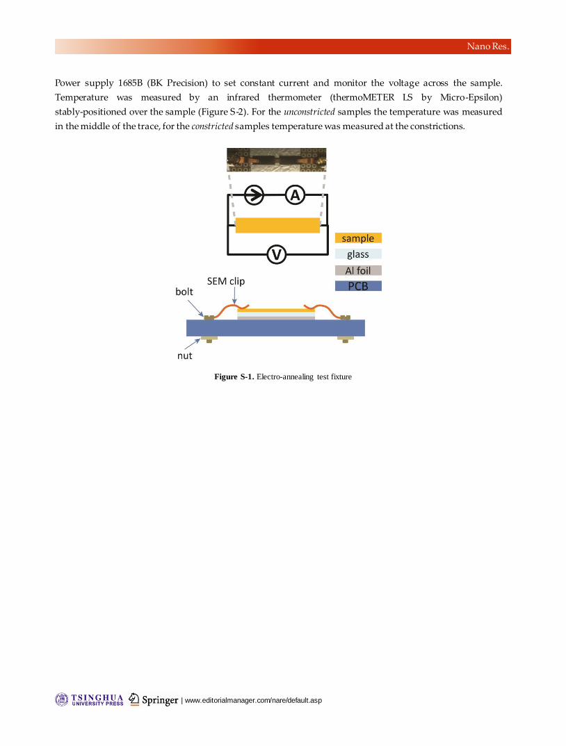
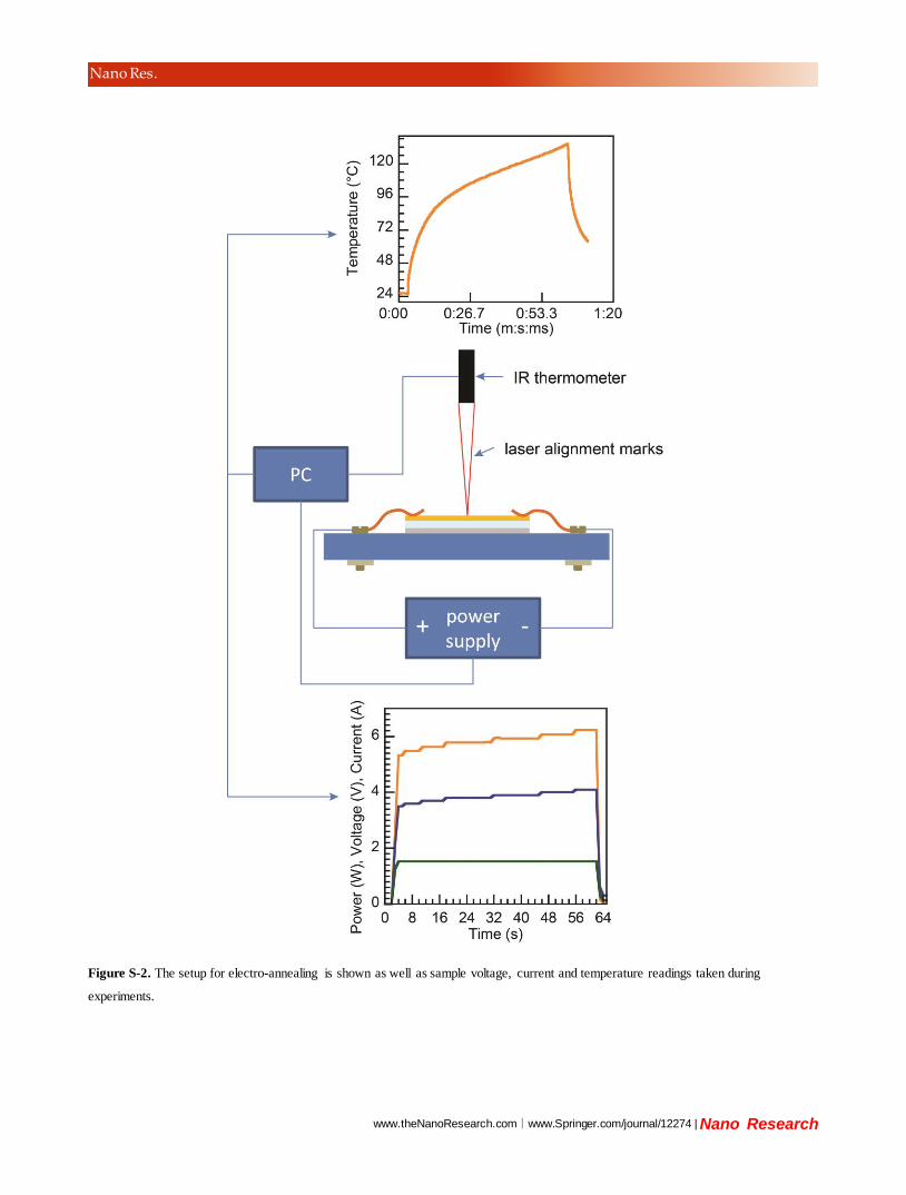
Electro-annealing rig: The samples were mounted on
a homemade test fixture (Figure S1), consisting of
aluminum foil sandwiched between a PCB circuit
board and a 1 mm-thick glass slide. Each sample
was placed on top of the glass slide and secured
with two SEM clips (PELCO SEMClip) that were
attached to the circuit board with screws. Constant
current was injected into the sample through the
clips. We used a switching DC Power supply 1685B
(BK Precision) to set constant current and monitor
the voltage across the sample. Temperature of the
thin film was directly measured by an infrared (IR)
thermometer (thermoMETER LS by Micro-Epsilon)
stably-positioned over the sample (Figure S-2 in the
ESM). The IR spot was positioned at the middle of a
trace for unconstricted samples and at the
constriction region for the constricted samples.
Note that the minimum spot size of the IR
thermometer is 1 mm, thus it was not possible to
| www.editorialmanager.com/nare/default.asp
4 Nano Res.
measure temperature for the constriction sizes
smaller than the spot size.
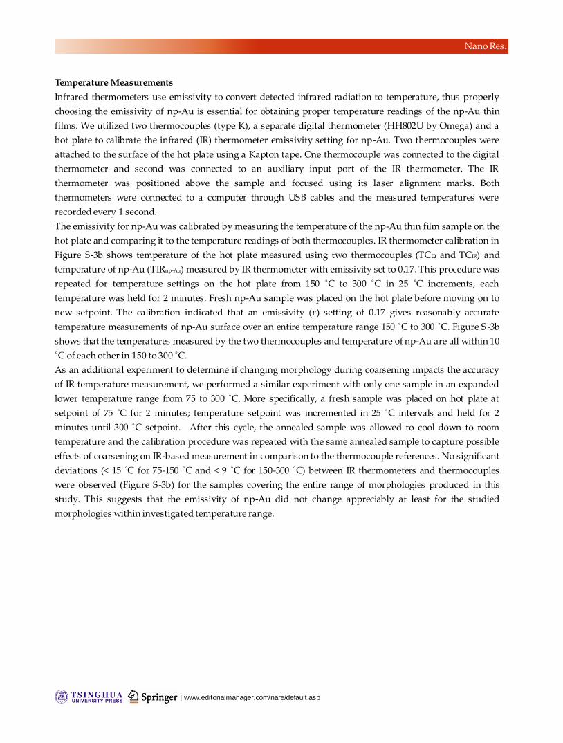
IR thermometers use emissivity to convert detected
infrared radiation to temperature. We found that an
emissivity value of 0.17 gives reasonably accurate
temperature measurements of np-Au surface,
covering the entire range of 20 ˚C to 300 ˚C used in
this study (Figure S-3b in the ESM). Briefly, the
calibration procedure involved the two
thermocouples attached onto the surface of hot
plate and the IR thermometer positioned above the
sample (Figure S-3a in the ESM). Temperatures
were recorded every 1 second. Emissivity for np-Au
was calibrated by measuring the temperature of the
np-Au thin film sample on the hot plate via IR
thermometer and comparing it to the temperature
readings of both thermocouples. This procedure
was repeated for temperature settings on the hot
plate from 150 ˚C to 300 ˚C in 25 ˚C increments.
Each temperature was held for 2 minutes and a
fresh sample was used for each distinct temperature
setpoint. In an additional experiment, a fresh
sample was placed on hot plate at setpoint of 75 ˚C
for 2 minutes; temperature setpoint was
incremented in 25 ˚C intervals and held for 2
minutes until 300 ˚C setpoint. After this cycle, the
annealed sample was allowed to cool down to room
temperature and the calibration procedure was
repeated with the same annealed sample to capture
possible effects of coarsening on IR-based
measurement in comparison to the thermocouple
references. For the an emissivity setting of 0.17,
between 150 ˚C and 300 C, a measurement error of
IR thermometer was less than 7% as compared to
the temperature obtained by thermocouples. This
error was less than 15% for temperatures between
75 C and 150 C (Figure S-3B in the ESM).
Scanning electron microscopy and morphology analysis:
Top and cross-sectional views of the samples were
obtained with a scanning electron microscope (FEI
Nova NanoSEM430) at 100 kX magnification. The
film thickness was determined by examining the
cross-sectional images. Highly-coarsened
morphologies resulted in few ligaments in a single
image at this magnification; therefore for such
samples additional images at a lower magnification
were obtained. The image analysis results from the
50 kX and 100 kX were pooled together to provide a
representative ligament size. SEM images were
analyzed using ImageJ (National Institutes of
Health shareware). For consistency, automatic
thresholding option, which is a variation of IsoData
algorithm [32], in ImageJ was used to convert
grayscale images to monochrome, where pores are
displayed as black and ligaments as white regions.
We used MatLab to calculate ligament thickness
from the monochrome images. Black and white
images were scanned line by line, where ligaments
were detected by transition from a black pixel to a
white pixel and the number of pixels in each
ligament (white pixels) was determined. The total
number of pixels for each ligament was converted
to a metric value using the SEM scale bars and the
median ligament thicknesses were extracted for
each image. The effective surface area of the np-Au
samples were determined by electrochemical oxide
stripping in dilute sulfuric acid as previously
described [20].
3. Results and Discussion
3.1 Effect of electro-annealing duration on
morphology evolution
We initially studied how pore morphology varies
with electro-annealing duration using the
unconstricted rectangular np-Au traces (Figure 1A).
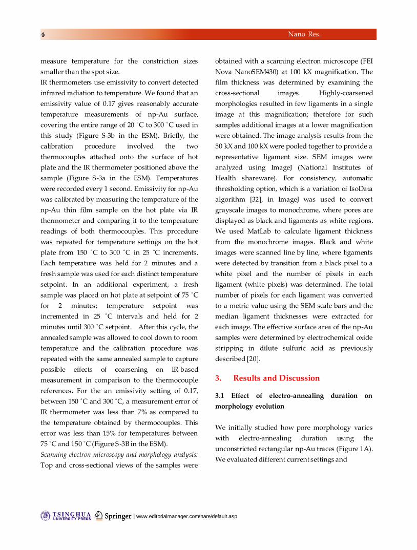
We evaluated different current settings and
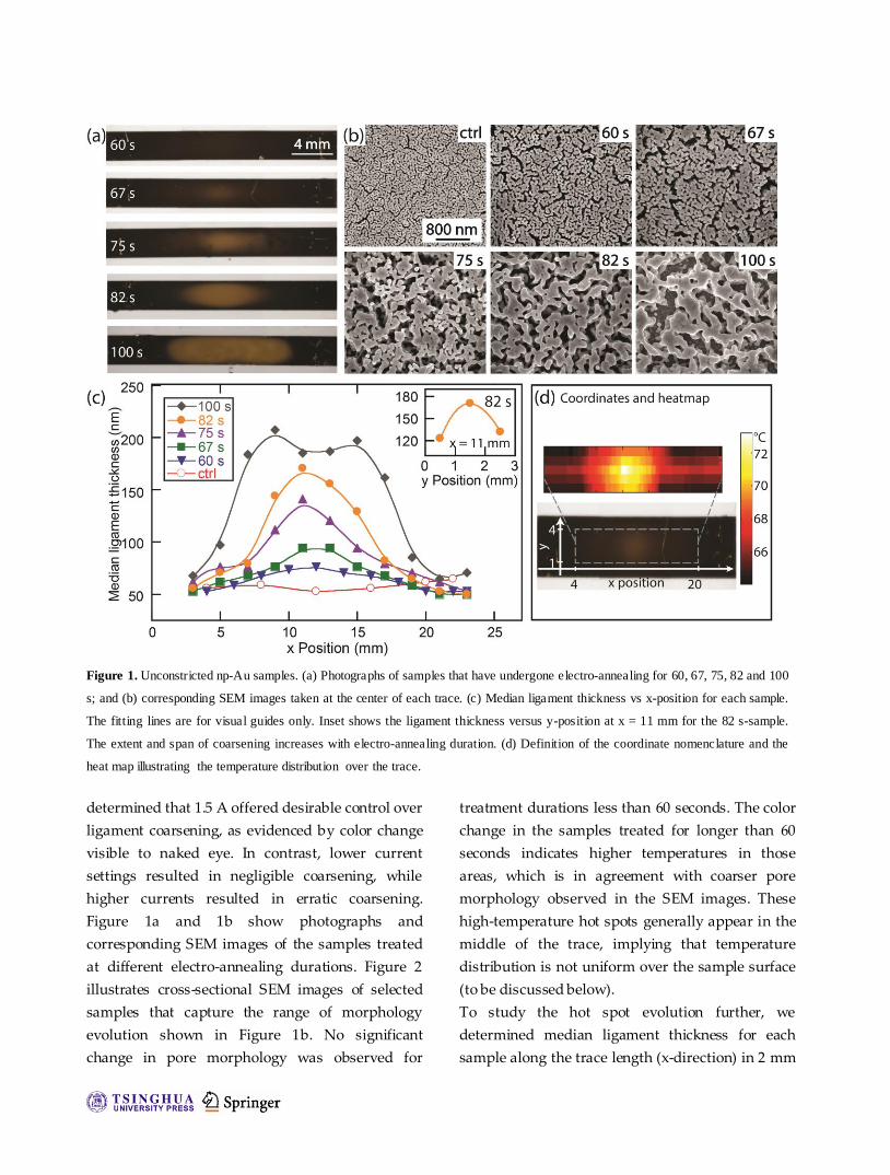
Figure 1. Unconstricted np-Au samples. (a) Photographs of samples that have undergone electro-annealing for 60, 67, 75, 82 and 100
s; and (b) corresponding SEM images taken at the center of each trace. (c) Median ligament thickness vs x-position for each sample.
The fitting lines are for visual guides only. Inset shows the ligament thickness versus y-position at x = 11 mm for the 82 s-sample.
The extent and span of coarsening increases with electro-annealing duration. (d) Definition of the coordinate nomenclature and the
heat map illustrating the temperature distribution over the trace.
determined that 1.5 A offered desirable control over
ligament coarsening, as evidenced by color change
visible to naked eye. In contrast, lower current
settings resulted in negligible coarsening, while
higher currents resulted in erratic coarsening.
Figure 1a and 1b show photographs and
corresponding SEM images of the samples treated
at different electro-annealing durations. Figure 2
illustrates cross-sectional SEM images of selected
samples that capture the range of morphology
evolution shown in Figure 1b. No significant
change in pore morphology was observed for
treatment durations less than 60 seconds. The color
change in the samples treated for longer than 60
seconds indicates higher temperatures in those
areas, which is in agreement with coarser pore
morphology observed in the SEM images. These
high-temperature hot spots generally appear in the
middle of the trace, implying that temperature
distribution is not uniform over the sample surface
(to be discussed below).
To study the hot spot evolution further, we
determined median ligament thickness for each
sample along the trace length (x-direction) in 2 mm
| www.editorialmanager.com/nare/default.asp
6 Nano Res.
steps (Figure 1c). The untreated sample had a
median ligament thickness of 58 nm. For short
treatment durations, the ligament size did not
change significantly (i.e., median ligament size for
the 60-second treatment is 73 nm). However, the
ligament size increased dramatically to
approximately 200 nm for the 100 second treatment
duration. For this duration, the pore morphology
deviated from the characteristic interconnected pore
morphology at several locations on the trace and
exhibited a more columnar structure uncovering the
substrate surface below the porous film (see SEM
for 100 s in Figure 1b). The pore morphology
through the film thickness remains uniform for
moderate electro-annealing (Figure 2b). In the case
of heavy-coarsening (i.e., 100 s duration in Figure
1b), the ligaments coalesce into thick columnar
structures (Figure 2c) and the number of pores
decreases significantly. These cross-sectional
images are also consistent with those of typical
morphologies obtained by thermal treatment. In
addition to the initiation of ligament thickening at
the middle of the trace, the coarsening process
progresses outwards with increasing treatment
duration. This observation is evident for samples
treated at 75, 82 and 100 seconds with the latter
exhibiting a coarsened morphology in nearly the
entire length of the trace (Figure 1a & 1c). We also
imaged the 82 seconds sample along the width
(y-direction) at the middle of the trace, (inset Figure
1c). In accord with the morphology profile along
the trace length, the ligament coarsening is more
pronounced in the middle of the trace and drops off
slightly near the edges.
The maximum temperature measured at the middle
of the trace for the 1.5 A current application for all
treatment durations was 140 ± 5 ˚C. It should be
noted that this average value excluded the
temperature (172 ˚C) for the 100 s case because of its
atypical morphology (Figure 1b and Figure 2c) and
likely effect on electro-annealing behavior.
Figure 2. Cross-sectional SEM images of electro-annealed
np-Au samples in Figure 1. The images taken at the hotspot
correspond to treatment durations of (a) control, (b) 75 s, and
(c) 100 s.
Variation of ligament size across the length of the
sample suggests that the highest temperature
occurs at the middle of the trace. To investigate the
temperature distribution over the sample, we
measured temperature as a function of position on a
5 mm wide trace by rastering the IR thermometer.
We specifically used a wider trace to allow for (i)
non-overlapping temperature measurements (note
the 1 mm IR spot size); and (ii) a lower maximum
temperature at 1.5 A due to a larger trace
cross-section and thus less electro-annealing to
maintain a stable surface for accurate
surface-temperature interrogation. The heat map
indeed indicated that the highest temperature
coincides with the middle of the trace (Figure 1d),
consistent with the ligament coarsening results
(Figure 1c). The observed temperature gradient
along the trace offers a unique opportunity to create
gradually-varying pore morphologies over several
millimeters.
The effective surface area of a coating plays an
important role for applications ranging from
catalysts [16, 17] to biomedical coatings [9-12]. To
that end, we tracked changes in surface area at
various stages of pore coarsening using
electrochemical oxide stripping protocol described
previously [20]. While the varying pore
morphology of electro-annealed films makes it
difficult to obtain an exact surface area that
corresponds to a specific pore morphology, we
www.theNanoResearch.com∣www.Springer.com/journal/12274 | Nano Research
7 Nano Res.
quantified the surface area of thermally-annealed
np-Au films with a uniform pore morphology.
These samples were annealed on the hot plate at
temperatures that range between 225 °C to 275 °C
and capture the range of morphologies obtained via
electro-annealing (Figure S-4). The increase in
effective surface area with respect to that of a planar
gold surface with identical dimensions is referred to
as enhancement factor, which is expected to decrease
with increasing feature size. While the un-annealed
np-Au film has a surface area enhancement of 12.8,
the 225 ˚C sample (morphology corresponding to 67
s treatment) had an enhancement factor of 10.7. For
the heavily-coarsened morphology (similar to that
observed for the 100 s case in Figure 1), the
enhancement factor was reduced to 5.1. The drastic
change in enhancement factor for samples annealed
at temperatures only 25 ˚C apart highlights the
importance of precise control over pore
morphology enabled by electro-annealing.
3.2. Effect of geometric constraints on morphology
evolution
The spatial location of the hot spot can be controlled
by introducing a lithographically-defined geometric
constraint in the trace, as shown in the Figure 2a.
The dimensions of the constrictions are 2 x 2 mm
and overall dimension of the trace is 4 x 24 mm.
Basic circuit theory suggests that the geometric
constriction causes increased current density in the
constriction region and leads to localized
coarsening in that area as compared to the rest of
the trace. By introducing the constriction at
different positions along the trace, we demonstrated
that it is possible to control the location of the hot
spot and even steer it to multiple and arbitrary
locations (Figure 3a).
The SEM images from the middle of constrictions
and in the adjacent areas indicate that the
constrictions not only allow for controlling the
location of the hot spot but also the span of the
morphology gradient centered around the hot spot.
This finding is illustrated via superimposing the
ligament size variations along two different trace
geometries (i.e., unconstricted and with one
constriction) and aligning the peak locations, as
shown in Figure 3c. For the unconstricted case, the
coarsened morphology spans approximately 10 mm
and shows gradual variation in ligament size with
maximum size approaching 210 nm in the middle
of the trace. In contrast, for the constricted case
coarsening only spans 3 mm with maximum
ligament size of approximately 215 nm, a sharp
slope in ligament versus distance plot for this
sample demonstrates a well-controlled transition
between the annealed and unannealed regions of
the sample. The ability to precisely control the
location and span of pore morphology opens the
door to producing high-throughput platforms for
studying property-structure relationships.
We hypothesized that having a design with various
constriction dimensions on a single trace would
create the possibility of engineering a chip with
multiple pore morphologies. One such design
(labeled as “iv”) is shown in Figure 3a. In this
configuration, we designed the trace with three
progressively decreasing constriction widths (i.e., 2
mm, 1.875 mm, and 1.75 mm). The results indicate
that majority of the coarsening occurs in the middle
despite the thinnest constriction being on the right.
This observation is due to uneven heat dissipation
and consequent temperature distribution across the
sample as previously discussed (Figure 1d). These
results suggest that constriction position and
dimensions should be carefully engineered to
compensate for higher temperatures at the middle
of the trace.
3.3. Branched structures for producing multiple
pore morphologies
An alternative design approach with more degrees
of freedom is to have multiple traces connected in
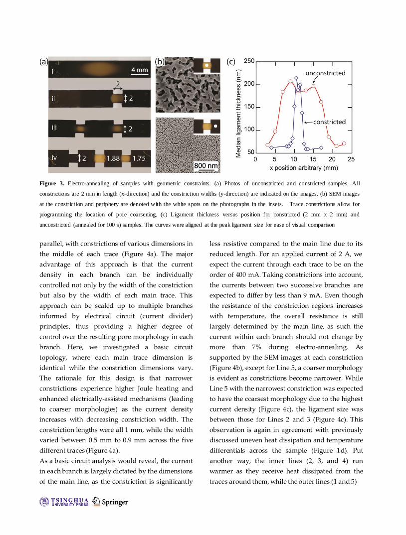
Figure 3. Electro-annealing of samples with geometric constraints. (a) Photos of unconstricted and constricted samples. All
constrictions are 2 mm in length (x-direction) and the constriction widths (y-direction) are indicated on the images. (b) SEM images
at the constriction and periphery are denoted with the white spots on the photographs in the insets. Trace constrictions allow for
programming the location of pore coarsening. (c) Ligament thickness versus position for constricted (2 mm x 2 mm) and
unconstricted (annealed for 100 s) samples. The curves were aligned at the peak ligament size for ease of visual comparison
parallel, with constrictions of various dimensions in
the middle of each trace (Figure 4a). The major
advantage of this approach is that the current
density in each branch can be individually
controlled not only by the width of the constriction
but also by the width of each main trace. This
approach can be scaled up to multiple branches
informed by electrical circuit (current divider)
principles, thus providing a higher degree of
control over the resulting pore morphology in each
branch. Here, we investigated a basic circuit
topology, where each main trace dimension is
identical while the constriction dimensions vary.
The rationale for this design is that narrower
constrictions experience higher Joule heating and
enhanced electrically-assisted mechanisms (leading
to coarser morphologies) as the current density
increases with decreasing constriction width. The
constriction lengths were all 1 mm, while the width
varied between 0.5 mm to 0.9 mm across the five
different traces (Figure 4a).
As a basic circuit analysis would reveal, the current
in each branch is largely dictated by the dimensions
of the main line, as the constriction is significantly
less resistive compared to the main line due to its
reduced length. For an applied current of 2 A, we
expect the current through each trace to be on the
order of 400 mA. Taking constrictions into account,
the currents between two successive branches are
expected to differ by less than 9 mA. Even though
the resistance of the constriction regions increases
with temperature, the overall resistance is still
largely determined by the main line, as such the
current within each branch should not change by
more than 7% during electro-annealing. As
supported by the SEM images at each constriction
(Figure 4b), except for Line 5, a coarser morphology
is evident as constrictions become narrower. While
Line 5 with the narrowest constriction was expected
to have the coarsest morphology due to the highest
current density (Figure 4c), the ligament size was
between those for Lines 2 and 3 (Figure 4c). This
observation is again in agreement with previously
discussed uneven heat dissipation and temperature
differentials across the sample (Figure 1d). Put
another way, the inner lines (2, 3, and 4) run
warmer as they receive heat dissipated from the
traces around them, while the outer lines (1 and 5)
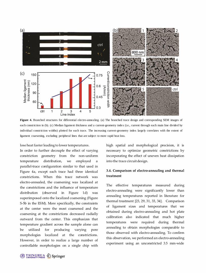
Figure 4. Branched structures for differential electro-annealing. (a) The branched trace design and corresponding SEM images of
each constriction in (b). (c) Median ligament thickness and a current-geometry index (i.e., current through each main line divided by
individual constriction widths) plotted for each trace. The increasing current-geometry index largely correlates with the extent of
ligament coarsening, excluding peripheral lines that are subject to more rapid heat loss.
lose heat faster leading to lower temperatures.
In order to further decouple the effect of varying
constriction geometry from the non-uniform
temperature distribution, we employed a
parallel-trace configuration similar to that used in
Figure 4a, except each trace had three identical
constrictions. When this trace network was
electro-annealed, the coarsening was localized at
the constrictions and the influence of temperature
distribution (observed in Figure 1d) was
superimposed onto the localized coarsening (Figure
S-5b in the ESM). More specifically, the constraints
at the center were the most coarsened and the
coarsening at the constrictions decreased radially
outward from the center. This emphasizes that
temperature gradient across the sample alone can
be utilized for producing varying pore
morphologies localized at the constrictions.
However, in order to realize a large number of
controllable morphologies on a single chip with
high spatial and morphological precision, it is
necessary to optimize geometric constrictions by
incorporating the effect of uneven heat dissipation
into the trace circuit design.
3.4. Comparison of electro-annealing and thermal
treatment
The effective temperatures measured during
electro-annealing were significantly lower than
annealing temperatures reported in literature for
thermal treatment [23, 29, 31, 33, 34]. Comparison
of ligament sizes and temperatures that we
obtained during electro-annealing and hot plate
calibration also indicated that much higher
temperatures were required during thermal
annealing to obtain morphologies comparable to
those observed with electro-annealing. To confirm
this observation, we performed an electro-annealing
experiment using an unconstricted 3.5 mm-wide
| www.editorialmanager.com/nare/default.asp
10 Nano Res.
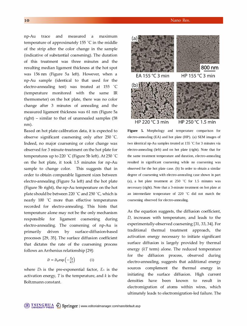
np-Au trace and measured a maximum
temperature of approximately 155 ˚C in the middle
of the strip after the color change in the sample
(indicative of substantial coarsening). The duration
of this treatment was three minutes and the
resulting median ligament thickness at the hot spot
was 156 nm (Figure 5a left). However, when a
np-Au sample (identical to that used for the
electro-annealing test) was treated at 155 ˚C
(temperature monitored with the same IR
thermometer) on the hot plate, there was no color
change after 3 minutes of annealing and the
measured ligament thickness was 61 nm (Figure 5a
right) – similar to that of unannealed samples (58
nm).
Based on hot plate calibration data, it is expected to
observe significant coarsening only after 250 ˚C.
Indeed, no major coarsening or color change was
observed for 3 minute-treatment on the hot plate for
temperatures up to 220 ˚C (Figure 5b left). At 250 ˚C
on the hot plate, it took 1.5 minutes for np-Au
sample to change color. This suggests that in
order to obtain comparable ligament sizes between
electro-annealing (Figure 5a left) and the hot plate
(Figure 5b right), the np-Au temperature on the hot
plate should be between 220 ˚C and 250 ˚C, which is
nearly 100 ˚C more than effective temperatures
recorded for electro-annealing. This hints that
temperature alone may not be the only mechanism
responsible for ligament coarsening during
electro-annealing. The coarsening of np-Au is
primarily driven by surface-diffusion-based
processes [29, 35]. The surface diffusion coefficient
that dictates the rate of the coarsening process
follows an Arrhenius relationship [29]:
𝐷 = 𝐷0exp(−𝐸𝐴
𝑘𝑇) (1)
where D0 is the pre-exponential factor, EA is the
activation energy, T is the temperature, and k is the
Boltzmann constant.
Figure 5. Morphology and temperature comparison for
electro-annealing (EA) and hot plate (HP). (a) SEM images of
two identical np-Au samples treated at 155 ˚C for 3 minutes via
electro-annealing (left) and on hot plate (right). Note that for
the same treatment temperature and duration, electro-annealing
resulted in significant coarsening while no coarsening was
observed for the hot plate case. (b) In order to obtain a similar
degree of coarsening with electro-annealing case shown in part
(a), a hot plate treatment at 250 ˚C for 1.5 minutes was
necessary (right). Note that a 3-minute treatment on hot plate at
an intermediate temperature of 220 ˚C did not match the
coarsening observed for electro-annealing.
As the equation suggests, the diffusion coefficient,
D, increases with temperature, and leads to the
experimentally-observed coarsening [31, 33, 34]. For
traditional thermal treatment approach, the
activation energy necessary to initiate significant
surface diffusion is largely provided by thermal
energy (kT term) alone. The reduced temperature
for the diffusion process, observed during
electro-annealing, suggests that additional energy
sources complement the thermal energy in
initiating the surface diffusion. High current
densities have been known to result in
electromigration of atoms within wires, which
ultimately leads to electromigration-led failure. The
www.theNanoResearch.com∣www.Springer.com/journal/12274 | Nano Research
11 Nano Res.
critical current densities for this failure mechanism
in gold nanowires with similar characteristic
length-scale to that for the np-Au ligaments, has
been reported to be on the order of 1012 A/m2. This
critical current density is three orders of magnitude
higher than the estimated current density per
np-Au ligament (on the order of 109 A/m2) for the
unconstricted traces investigated here (Figure 1).
Also, the SEM images of the electro-annealed
samples did not reveal any evidence of
electromigration, such as material accumulation
downstream of the electron flow direction or
nanogap formation in ligaments [36, 37]. It is
widely-reported that current flow through small
structures (e.g., thin films, nanowires) where mean
free path of electrons become comparable to
characteristic length-scales of the conductor, the
electronic transport is dominated by
electron-surface scattering [38, 39]. In the context of
np-Au thin films, which can be visualized as a 3D
network for nanowires (ligaments), the surface
corresponds to the ligament-nanopore interface [38].
Indeed, these scattering events and the resulting
energy loss manifest themselves as higher electrical
resistance in thin films compared to their bulk
counter-part and may be a source of additional
energy assisting the coarsening process [40].
For a qualitative discussion of the electro-annealing
case, it is helpful to conceptualize the effect of
additional energies by modifying the denominator
term of the exponential in the Arrhenius equation to
kT + Eother, where Eother signifies other putative
energies. Some kinetic energy during
electro-annealing is dissipated as heat (kT term)
which is the temperature rise observed during
electro-annealing. The electron collisions during the
scattering events would apply a force on the
adatoms and the electric field in the ligaments (due
to the applied voltage) would exert an additional
force on the adatoms. These two forces would
constitute Eother and translate into increasing the
average energy per adatom. Consequently, the
surface diffusion of adatoms (thus coarsening) may
occur with reduced contribution from the kT term.
It is also plausible that the surface diffusion occurs
before electromigration, implying that the observed
phenomenon may be happening at a transition
regime between thermal diffusion and
electromigration. The net result is that coarsening
occurs at lower temperatures for electro-annealing
than for pure thermal treatment. Finally, it should
be noted that the complex interplay between these
processes that constitute Eother are beyond the scope
of this work and require further studies, including
molecular simulations
4. Conclusion
By taking advantage of the electrical conductivity
and morphological plasticity of np-Au, we
demonstrated that electro-annealing is a novel and
versatile technique to controllably tune pore
morphology of np-Au thin films at low
temperatures. More specifically, we introduced
geometric constrictions into
lithographically-patterned np-Au traces and
obtained distinct pore morphologies with
controllable location and span. This technique is
broadly applicable to tuning the nanostructure of
other electrically-conductive nanoporous metal
systems [6] and amenable to further
functionalization via conformal atomic layer
deposition of ceramics [41]. We expect this novel
approach to be a path to programmable
morphology generation using electrical circuit
principles and associated CAD tools to design
complex trace networks and assist high-throughput
screening of structure-property relationships for
fundamental and applied studies. We envision that
further work in developing a design toolkit that
generates optimized trace geometries and
electro-annealing parameters will allow for
precisely controlling the location and extent of
| www.editorialmanager.com/nare/default.asp
12 Nano Res.
coarsening. In contrast to traditional thermal
coarsening techniques (e.g., furnace, rapid thermal
annealing), electro-annealing allows to selectively
modify pore morphology simultaneously over
different regions on a substrate. When compared to
other nascent annealing techniques (e.g., laser
sintering [29], the electro-annealing technique does
not require sophisticated optical instrumentation,
thereby making the method generally available to
users with access to simple photolithography and
deposition capabilities. While laser micro sintering
offers high spatial resolution due to the small laser
spot size (few microns), it remains unpractical for
creating larger structures (100s of microns to
millimeters). In addition, we also observed that
temperatures required to obtain significant
ligament coarsening during electro-annealing are
much lower than temperatures used during
traditional thermal annealing, suggesting that other
electrically-assisted mechanisms contribute or
enhance ligament coarsening during
electro-annealing.
Acknowledgements
We gratefully acknowledge the support from UC
Lab Fees Research Program Award (12-LR-237197),
Research Investments in the Sciences & Engineering
(RISE) Award, and UC Davis College of
Engineering start-up funds.
Electronic Supplementary Material: Supplementary
material further details of the fabrication, IR
thermometer calibration, and setup scheme is
available in the online version of this article at
http://dx.doi.org/10.1007/s12274-***-****-*
(automatically inserted by the publisher).
References [1] Gleiter, H. Nanostructured materials: Basic
concepts and microstructure. Acta Materialia 2000,
48, 1-29.
[2] Suryanarayana, C. Recent developments in
nanostructured materials. Advanced Engineering
Materials 2005, 7, 983-992.
[3] Zhang, X.; Xie, H.; Fujii, M.; Ago, H.;
Takahashi, K.; Ikuta, T.; Abe, H.; Shimizu, T.
Thermal and electrical conductivity of a suspended
platinum nanofilm. Applied Physics Letters 2005, 86,
171912.
[4] Balandin, A. A. Thermal properties of
graphene and nanostructured carbon materials. Nat
Mater 2011, 10, 569-581.
[5] Konstantatos, G.; Sargent, E. H.
Nanostructured materials for photon detection. Nat
Nano 2010, 5, 391-400.
[6] Seker, E.; Reed, M.; Begley, M. Nanoporous
gold: Fabrication, characterization, and applications.
Materials 2009, 2, 2188-2215.
[7] Xiao, X.; Wang, M. e.; Li, H.; Si, P. One-step
fabrication of bio-functionalized nanoporous
gold/poly(3,4-ethylenedioxythiophene) hybrid
electrodes for amperometric glucose sensing.
Talanta 2013, 116, 1054-1059.
[8] Hu, K.; Lan, D.; Li, X.; Zhang, S.
Electrochemical DNA biosensor based on
nanoporous gold electrode and multifunctional
encoded DNA−au bio bar codes. Analytical
Chemistry 2008, 80, 9124-9130.
[9] Seker, E.; Berdichevsky, Y.; Begley, M.; Reed,
M.; Staley, K.; Yarmush, M. The fabrication of
low-impedance nanoporous gold multiple-electrode
arrays for neural electrophysiology studies.
Nanotechnology 2010, 21, 125504.
[10] Seker, E.; Berdichevsky, Y.; Staley, K. J.;
Yarmush, M. L. Microfabrication-compatible
nanoporous gold foams as biomaterials for drug
delivery. Advanced Healthcare Materials 2012, 1, 172–
176.
[11] Tan, Y. H.; Schallom, J. R.; Ganesh, N. V.;
Fujikawa, K.; Demchenko, A. V.; Stine, K. J.
Characterization of protein immobilization on
nanoporous gold using atomic force microscopy
www.theNanoResearch.com∣www.Springer.com/journal/12274 | Nano Research
13 Nano Res.
and scanning electron microscopy. Nanoscale 2011, 3,
3395-3407.
[12] Patel, J.; Radhakrishnan, L.; Zhao, B.;
Uppalapati, B.; Daniels, R. C.; Ward, K. R.;
Collinson, M. M. Electrochemical properties of
nanostructured porous gold electrodes in
biofouling solutions. Analytical chemistry 2013, 85,
11610-11618.
[13] Lang, X.; Hirata, A.; Fujita, T.; Chen, M.
Three-dimensional hierarchical nanoporosity for
ultrahigh power and excellent cyclability of
electrochemical pseudocapacitors. Advanced Energy
Materials 2014, 4, 1301809.
[14] Kucheyev, S.; Hayes, J.; Biener, J.; Huser, T.;
Talley, C.; Hamza, A. Surface-enhanced raman
scattering on nanoporous au. Applied Physics Letters
2006, 89, 053102-053104.
[15] Santos, G. M.; Zhao, F.; Zeng, J.; Shih, W.-C.
Characterization of nanoporous gold disks for
photothermal light harvesting and light-gated
molecular release. Nanoscale 2014, 6, 5718-5724.
[16] Wittstock, A.; Zielasek, V.; Biener, J.; Friend, C.
M.; Bäumer, M. Nanoporous gold catalysts for
selective gas-phase oxidative coupling of methanol
at low temperature. Science 2010, 327, 319-322.
[17] Xu, C.; Su, J.; Xu, X.; Liu, P.; Zhao, H.; Tian, F.;
Ding, Y. Low temperature co oxidation over
unsupported nanoporous gold. Journal of the
American Chemical Society 2006, 129, 42-43.
[18] Lee, D.; Wei, X.; Chen, X.; Zhao, M.; Jun, S.;
Hone, J.; Herbert, E.; Oliver, W.; Kysar, J.
Microfabrication and mechanical properties of
nanoporous gold at the nanoscale. Scripta materialia
2007, 56, 437-440.
[19] Jin, H. J.; Weissmüller, J. A material with
electrically tunable strength and flow stress. Science
2011, 332, 1179-1182.
[20] Kurtulus, O.; Daggumati, P.; Seker, E.
Molecular release from patterned nanoporous gold
thin films. Nanoscale 2014, 6, 7062 - 7071.
[21] Senior, N.; Newman, R. Synthesis of tough
nanoporous metals by controlled electrolytic
dealloying. Nanotechnology 2006, 17, 2311-2316.
[22] Erlebacher, J. An atomistic description of
dealloying. Journal of the Electrochemical Society 2004,
151, C614-C626.
[23] Hakamada, M.; Mabuchi, M. Thermal
coarsening of nanoporous gold: Melting or
recrystallization. Journal of Materials Research 2009,
24, 301-304.
[24] Fujita, T.; Qian, L.-H.; Inoke, K.; Erlebacher, J.;
Chen, M.-W. Three-dimensional morphology of
nanoporous gold. Applied Physics Letters 2008, 92,
251902.
[25] Qian, L. H.; Chen, M. W. Ultrafine
nanoporous gold by low-temperature dealloying
and kinetics of nanopore formation. Applied Physics
Letters 2007, 91, 083105.
[26] Detsi, E.; van de Schootbrugge, M.; Punzhin,
S.; Onck, P. R.; De Hosson, J. T. M. On tuning the
morphology of nanoporous gold. Scripta Materialia
2011, 64, 319-322.
[27] Dong, H.; Cao, X. Nanoporous gold thin film:
Fabrication, structure evolution, and electrocatalytic
activity. The Journal of Physical Chemistry C 2008, 113,
603-609.
[28] Hakamada, M.; Mabuchi, M. Microstructural
evolution in nanoporous gold by thermal and acid
treatments. Materials Letters 2008, 62, 483-486.
[29] Schade, L.; Franzka, S.; Mathieu, M.; Biener,
M. M.; Biener, J.; Hartmann, N. Photothermal laser
microsintering of nanoporous gold. Langmuir 2014,
30, 7190-7197.
[30] Klein, R. Laser welding of plastics. Wiley: 2011.
[31] Daggumati, P.; Kurtulus, O.; Chapman, C. A.
R.; Dimlioglu, D.; Seker, E. Microfabrication of
nanoporous gold patterns for cell-material
interaction studies. 2013, e50678.
[32] Sezgin, M.; Sankur, B. Survey over image
thresholding techniques and quantitative
performance evaluation. Journal of Electronic Imaging
2004, 13, 146-168.
[33] Hodge, A. M.; Biener, J.; Hayes, J. R.; Bythrow,
P. M.; Volkert, C. A.; Hamza, A. V. Scaling equation
| www.editorialmanager.com/nare/default.asp
14 Nano Res.
for yield strength of nanoporous open-cell foams.
Acta Materialia 2007, 55, 1343-1349.
[34] Li, R.; Sieradzki, K. Ductile-brittle transition
in random porous au. Physical Review Letters 1992,
68, 1168-1171.
[35] Erlebacher, J. Mechanism of coarsening and
bubble formation in high-genus nanoporous metals.
Physical Review Letters 2011, 106, 225504.
[36] Trouwborst, M. L.; van der Molen, S. J.; van
Wees, B. J. The role of joule heating in the formation
of nanogaps by electromigration. Journal of Applied
Physics 2006, 99, 114316.
[37] Hadeed, F. O.; Durkan, C. Controlled
fabrication of 1–2nm nanogaps by electromigration
in gold and gold-palladium nanowires. Applied
Physics Letters 2007, 91, 123120.
[38] Fujita, T.; Okada, H.; Koyama, K.; Watanabe,
K.; Maekawa, S.; Chen, M. W. Unusually small
electrical resistance of three-dimensional
nanoporous gold in external magnetic fields.
Physical Review Letters 2008, 101, 166601.
[39] Liu, Z.; Searson, P. C. Single nanoporous gold
nanowire sensors. The Journal of Physical Chemistry B
2006, 110, 4318-4322.
[40] Munoz, R. C. Resistivity induced by a rough
surface of thin gold films deposited on mica. J. Mol.
Catal. A-Chem. 2005, 228, 163-175.
[41] Biener, M. M.; Biener, J.; Wichmann, A.;
Wittstock, A.; Baumann, T. F.; Baumer, M.; Hamza,
A. V. Ald functionalized nanoporous gold: Thermal
stability, mechanical properties, and catalytic
activity. Nano Letters 2011, 11, 3085-3090.
www.theNanoResearch.com∣www.Springer.com/journal/12274 | Nano Research
Nano Res.
Electronic Supplementary Material
Electrically-tunable pore morphology in nanoporous
gold thin
Tatiana S. Dorofeeva1, and Erkin Seker1,2()
Supporting information to DOI 10.1007/s12274-****-****-* (automatically inserted by the publisher)
Sample Preparation
The glass cover slips used as substrates, on which metal traces are to be patterned, were cleaned by
immersion in a piranha solution for 7 minutes, rinsed in deionized (DI) water, and dried under nitrogen flow.
In order to micropattern the metal traces, the cover slips were coated with ~1 µm thick positive photoresist
(Shipley 1813) followed by a pre-bake for 90 seconds at 115 ˚C on a hot plate. Transparency mask was used
for photolithography. Alignment and exposure was performed on Karl Suss mask aligner with exposure
duration of 4.5 seconds at 20 mJ. Exposure was followed by a post-bake for 90 seconds at 115 ˚C. The exposed
photoresist was developed in MF-322 (Shipley) for 25 seconds with slight manual agitation. The samples
were subsequently loaded into a sputtering machine (Kurt J. Lesker) for thin film deposition. Initially, 120 nm
of chrome (to promote adhesion between glass and gold) was sputtered at 300 W, followed by 80 nm of seed
gold at 400 W, finally 500 nm of silver and gold were co-sputtered at 100 W and 200 W respectively. All
depositions were performed under argon atmosphere at 10 mTorr. The lift-off was performed in NMP
(N-methylpyrrolidone) by cycles of 10 seconds of sonication followed by a 10 minute pause until all the
photoresist was removed. Elemental compositions of the samples were ascertained with energy dispersive
X-ray spectroscopy (Oxford INCA Energy-EDS), the resulting gold and silver content of the films was 36%
Au and 64% Ag by atomic %. Deposited samples were dealloyed in 70% nitric acid for 15 minutes at 55 ˚C to
produce the np-Au films. The dealloying process typically leads to 3-5% residual silver in the final np-Au
film. To completely remove traces of nitric acid after the dealloying, samples were rinsed several times and
stored in DI water. After 2 days, samples were removed from water, dried with nitrogen gun and stored in
ambient conditions until the conducting the electro-annealing experiments.
Measurement Setup
Samples were mounted on the homemade electro-annealing test fixture (Figure S-1), consisting of an
aluminum foil sandwiched between a PCB circuit board and a 1 mm-thick glass slide. The sample was placed
on top of glass slide and secured with two SEM clips (PELCO SEMClip) which were attached to the circuit
board with screws. Constant current was injected into the sample through the clips. We used switching DC
————————————
Address correspondence to Erkin Seker, [email protected]
| www.editorialmanager.com/nare/default.asp
Nano Res.
Power supply 1685B (BK Precision) to set constant current and monitor the voltage across the sample.
Temperature was measured by an infrared thermometer (thermoMETER LS by Micro-Epsilon)
stably-positioned over the sample (Figure S-2). For the unconstricted samples the temperature was measured
in the middle of the trace, for the constricted samples temperature was measured at the constrictions.
Figure S-1. Electro-annealing test fixture
www.theNanoResearch.com∣www.Springer.com/journal/12274 | Nano Research
Nano Res.
Figure S-2. The setup for electro-annealing is shown as well as sample voltage, current and temperature readings taken during
experiments.
| www.editorialmanager.com/nare/default.asp
Nano Res.
Temperature Measurements
Infrared thermometers use emissivity to convert detected infrared radiation to temperature, thus properly
choosing the emissivity of np-Au is essential for obtaining proper temperature readings of the np-Au thin
films. We utilized two thermocouples (type K), a separate digital thermometer (HH802U by Omega) and a
hot plate to calibrate the infrared (IR) thermometer emissivity setting for np-Au. Two thermocouples were
attached to the surface of the hot plate using a Kapton tape. One thermocouple was connected to the digital
thermometer and second was connected to an auxiliary input port of the IR thermometer. The IR
thermometer was positioned above the sample and focused using its laser alignment marks. Both
thermometers were connected to a computer through USB cables and the measured temperatures were
recorded every 1 second.
The emissivity for np-Au was calibrated by measuring the temperature of the np-Au thin film sample on the
hot plate and comparing it to the temperature readings of both thermocouples. IR thermometer calibration in
Figure S-3b shows temperature of the hot plate measured using two thermocouples (TCΩ and TCIR) and
temperature of np-Au (TIRnp-Au) measured by IR thermometer with emissivity set to 0.17. This procedure was
repeated for temperature settings on the hot plate from 150 ˚C to 300 ˚C in 25 ˚C increments, each
temperature was held for 2 minutes. Fresh np-Au sample was placed on the hot plate before moving on to
new setpoint. The calibration indicated that an emissivity (ε) setting of 0.17 gives reasonably accurate
temperature measurements of np-Au surface over an entire temperature range 150 ˚C to 300 ˚C. Figure S -3b
shows that the temperatures measured by the two thermocouples and temperature of np-Au are all within 10
˚C of each other in 150 to 300 C.
As an additional experiment to determine if changing morphology during coarsening impacts the accuracy
of IR temperature measurement, we performed a similar experiment with only one sample in an expanded
lower temperature range from 75 to 300 ˚C. More specifically, a fresh sample was placed on hot plate at
setpoint of 75 ˚C for 2 minutes; temperature setpoint was incremented in 25 ˚C intervals and held for 2
minutes until 300 ˚C setpoint. After this cycle, the annealed sample was allowed to cool down to room
temperature and the calibration procedure was repeated with the same annealed sample to capture possible
effects of coarsening on IR-based measurement in comparison to the thermocouple references. No significant
deviations (< 15 ˚C for 75-150 ˚C and < 9 ˚C for 150-300 ˚C) between IR thermometers and thermocouples
were observed (Figure S-3b) for the samples covering the entire range of morphologies produced in this
study. This suggests that the emissivity of np-Au did not change appreciably at least for the studied
morphologies within investigated temperature range.
www.theNanoResearch.com∣www.Springer.com/journal/12274 | Nano Research
Nano Res.
Figure S-3. (a) Temperature calibration setup. (b) The IR thermometer (emissivity set to 0.17) calibration curves with respect to
thermocouples for np-Au samples with different degrees of coarsening. The TIR and TC abbreviations in the legend indicate the
temperature readings that were obtained by the infrared thermometer and the thermocouples respectively. TIRnp-Au n/anneal : An unannealed
sample was placed on the hot plate and temperature was increased in 25 °C increments from 75 °C to 300 °C while acquiring the sample
temperature following two minutes of stabilization after each setpoint. TIRnp-Au annealed: The same temperature setpoint and acquisition
protocol from the previous experiment was used. However, this time an annealed sample (produced in the TIRnp-Au n/anneal experiment)
was used to evaluate the effect of an already coarsened morphology on IR thermometer readings. TIRnp-Au new: A fresh unannealed
sample was used for each temperature point between 150 °C and 300 °C in 25 °C increments to evaluate the effect of temperature
exposure on coarsening at different temperatures. TCIR: Temperature of hot plate directly adjacent to the sample obtained by the
thermocouple attached to IR thermometer. TCΩ: Temperature of hot plate directly adjacent to the sample obtained by the thermocouple
attached to an additional thermometer.
Surface Enhancement Factor
Electrochemical oxide stripping technique was employed to determine the effective surface areas of np-Au
samples. The electrochemical surface characterization (enabled by the electrical conductivity of np-Au) is
based on the principle that AuO reduction only happens at the gold surface in contact with the electrolyte
and the surface reaction-limited process allows for addressing the entire surface of the np-Au thin film.
While the varying pore morphology of electro-annealed films makes it difficult to obtain an exact surface
area that corresponds to specific pore morphology, we quantified the surface area of thermally-annealed
np-Au films with uniform pore morphology. Fresh np-Au samples were thermally-annealed on the hot plate
at 225 °C, 250 °C, and 275 °C for 2 minutes to capture the range of morphologies obtained via
electro-annealing. Each np-Au sample with a unique morphology was loaded into a custom-built
three-electrode Teflon electrochemical cell with platinum counter electrode and Au/AgCl reference electrode.
The np-Au sample was immersed in 0.05 M sulfuric acid and scanned at a rate of 50 mV/s to obtain the
corresponding cyclic voltammogram. The total electrical charge under gold oxide reduction peak between
potentials of 720 mV and 970 mV was converted to surface area using 450 μC/cm2 as the specific charge of a
gold surface [1, 2]. The ratio of the effective surface area of the measured sample to that of a planar gold
electrode with the same foot print was referred to as “enhancement factor” In Figure S -4 below surface
enhancement factor for four different temperature annealing ranges are plotted along with corresponding
SEM images illustrating the surface morphology representative for thermal annealing at this temperature,
the size of each SEM image is approximately 1x1 µm, we estimate that corresponding JH durations are 67 s,
82 s, and 100 s respectively.
| www.editorialmanager.com/nare/default.asp
Nano Res.
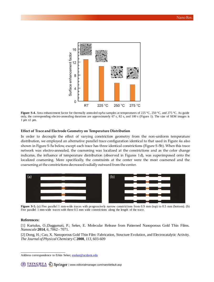
Figure S-4. Area enhancement factor for thermally annealed npAu samples at temperatures of 225 °C, 250 °C, and 275 °C. As guide
only, the corresponding electro-annealing durations are approximately 67 s, 82 s, and 100 s (Figure 1). The size of SEM images is 1 µm x1 µm.
Effect of Trace and Electrode Geometry on Temperature Distribution
In order to decouple the effect of varying constriction geometry from the non-uniform temperature
distribution, we employed an alternative parallel trace configuration identical to that used in Figure 4a also
shown in Figure S-5a below, except each trace has three identical constrictions (Figure S -5b). When this trace
network was electro-annealed, the coarsening was localized at the constrictions and as the color change
indicates, the influence of temperature distribution (observed in Figures 1d), was superimposed onto the
localized coarsening. More specifically, the constraints at the center were the most coarsened and the
coarsening at the constrictions decreased radially outward from the center.
Figure S-5. (a) Five parallel 1 mm-wide traces with progressively narrow constrictions from 0.9 mm (top) to 0.5 mm (bottom). (b) Five parallel 1 mm-wide traces with three 0.5 mm wide constrictions along the length of the trace.
References:
[1] Kurtulus, O.;Daggumati, P.; Seker, E. Molecular Release from Patterned Nanoporous Gold Thin Films. Nanoscale 2014, 6, 7062 - 7071.
[2] Dong, H.; Cao, X. Nanoporous Gold Thin Film: Fabrication, Structure Evolution, and Electrocatalytic Activity. The Journal of Physical Chemistry C 2008, 113, 603-609
Address correspondence to Erkin Seker, [email protected]
Recommended
![Electrically Tunable Open Split-Ring Resonators based on .... Tunable Metam… · e.g. by the use of varactor diodes [3]. However, varactor diodes limit the operation frequency to](https://img.pdfslide.net/doc/110x75/5f31343356afe71a73122f38/electrically-tunable-open-split-ring-resonators-based-on-tunable-metam-eg.jpg)