Features• High Performance, Low Power AVR®32 32-Bit Microcontroller
– 210 DMIPS throughput at 150 MHz– 16 KB instruction cache and 16 KB data caches– Memory Management Unit enabling use of operating systems– Single-cycle RISC instruction set including SIMD and DSP instructions– Java Hardware Acceleration
• Pixel Co-Processor– Pixel Co-Processor for video acceleration through color-space conversion
(YUV<->RGB), image scaling and filtering, quarter pixel motion compensation• Multi-hierarchy bus system
– High-performance data transfers on separate buses for increased performance• Data Memories
– 32KBytes SRAM• External Memory Interface
– SDRAM, DataFlash™, SRAM, Multi Media Card (MMC), Secure Digital (SD), – Compact Flash, Smart Media, NAND Flash
• Direct Memory Access Controller– External Memory access without CPU intervention
• Interrupt Controller– Individually maskable Interrupts– Each interrupt request has a programmable priority and autovector address
• System Functions– Power and Clock Manager– Crystal Oscillator with Phase-Lock-Loop (PLL)– Watchdog Timer– Real-time Clock
• 6 Multifunction timer/counters – Three external clock inputs, I/O pins, PWM, capture and various counting
capabilities• 4 Universal Synchronous/Asynchronous Receiver/Transmitters (USART)
– 115.2 kbps IrDA Modulation and Demodulation– Hardware and software handshaking
• 3 Synchronous Serial Protocol controllers– Supports I2S, SPI and generic frame-based protocols
• Two-Wire Interface– Sequential Read/Write Operations, Philips’ I2C© compliant
• Liquid Crystal Display (LCD) interface– Supports TFT displays– Configurable pixel resolution supporting QCIF/QVGA/VGA/SVGA configurations.
• Image Sensor Interface– 12-bit Data Interface for CMOS cameras
• Universal Serial Bus (USB) 2.0 High Speed (480 Mbps) Device– On-chip Transceivers with physical interface
• 2 Ethernet MAC 10/100 Mbps interfaces– 802.3 Ethernet Media Access Controller– Supports Media Independent Interface (MII) and Reduced MII (RMII)
• 16-bit stereo audio bitstream DAC– Sample rates up to 50 kHz
• On-Chip Debug System– Nexus Class 3– Full speed, non-intrusive data and program trace– Runtime control and JTAG interface
• Package/Pins– AT32AP7000: 256-ball CTBGA 1.0 mm pitch/160 GPIO pins
• Power supplies– 1.65V to1.95V VDDCORE– 3.0V to 3.6V VDDIO 32003MS-AVR32-09/09
AVR®32 32-bit Microcontroller
AT32AP7000
Preliminary
Summary
232003MS–AVR32–09/09
AT32AP7000
1. Part Description
The AT32AP7000 is a complete System-on-chip application processor with an AVR32 RISCprocessor achieving 210 DMIPS running at 150 MHz. AVR32 is a high-performance 32-bit RISCmicroprocessor core, designed for cost-sensitive embedded applications, with particular empha-sis on low power consumption, high code density and high application performance.
AT32AP7000 implements a Memory Management Unit (MMU) and a flexible interrupt controllersupporting modern operating systems and real-time operating systems. The processor alsoincludes a rich set of DSP and SIMD instructions, specially designed for multimedia and telecomapplications.
AT32AP7000 incorporates SRAM memories on-chip for fast and secure access. For applica-tions requiring additional memory, external 16-bit SRAM is accessible. Additionally, an SDRAMcontroller provides off-chip volatile memory access as well as controllers for all industry standardoff-chip non-volatile memories, like Compact Flash, MultiMedia Card (MMC), Secure Digital(SD)-card, SmartCard, NAND Flash and Atmel DataFlash™.
The Direct Memory Access controller for all the serial peripherals enables data transfer betweenmemories without processor intervention. This reduces the processor overhead when transfer-ring continuous and large data streams between modules in the MCU.
The Timer/Counters includes three identical 16-bit timer/counter channels. Each channel can beindependently programmed to perform a wide range of functions including frequency measure-ment, event counting, interval measurement, pulse generation, delay timing and pulse widthmodulation.
AT32AP7000 also features an onboard LCD Controller, supporting single and double scanmonochrome and color passive STN LCD modules and single scan active TFT LCD modules.On monochrome STN displays, up to 16 gray shades are supported using a time-based dither-ing algorithm and Frame Rate Control (FRC) method. This method is also used in color STNdisplays to generate up to 4096 colors.
The LCD Controller is programmable for supporting resolutions up to 2048 x 2048 with a pixeldepth from 1 to 24 bits per pixel.
A pixel co-processor provides color space conversions for images and video, in addition to awide variety of hardware filter support
The media-independent interface (MII) and reduced MII (RMII) 10/100 Ethernet MAC modulesprovides on-chip solutions for network-connected devices.
Synchronous Serial Controllers provide easy access to serial communication protocols, audiostandards like I2S and frame-based protocols.
The Java hardware acceleration implementation in AVR32 allows for a very high-speed Javabyte-code execution. AVR32 implements Java instructions in hardware, reusing the existingRISC data path, which allows for a near-zero hardware overhead and cost with a very highperformance.
The Image Sensor Interface supports cameras with up to 12-bit data buses.
PS2 connectivity is provided for standard input devices like mice and keyboards.
332003MS–AVR32–09/09
AT32AP7000
AT32AP7000 integrates a class 3 Nexus 2.0 On-Chip Debug (OCD) System, with non-intrusivereal-time trace, full-speed read/write memory access in addition to basic runtime control.
The C-compiler is closely linked to the architecture and is able to utilize code optimization fea-tures, both for size and speed.
432003MS–AVR32–09/09
AT32AP7000
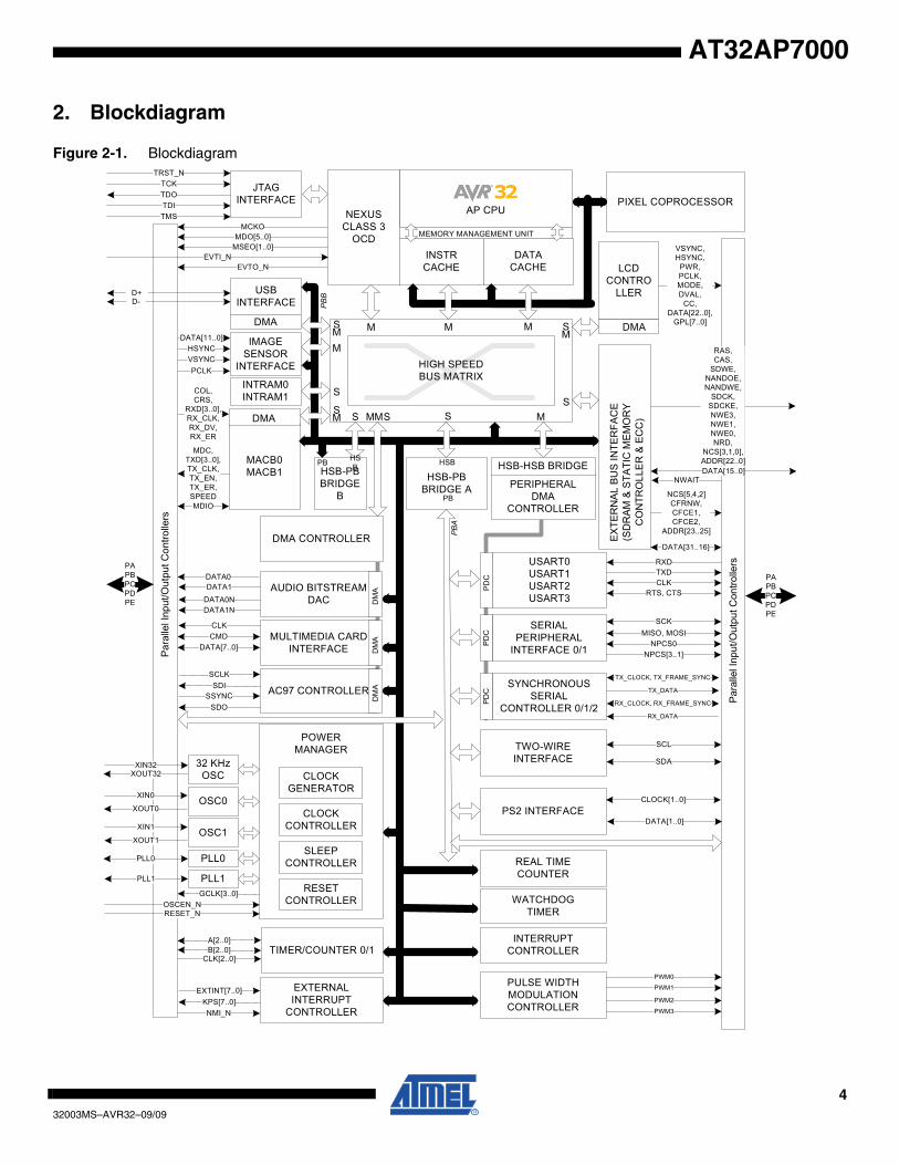
2. Blockdiagram
Figure 2-1. Blockdiagram
DATA[11..0]HSYNCVSYNCPCLK
AP CPUNEXUS CLASS 3
OCDINSTRCACHE
DATACACHE
TIMER/COUNTER 0/1INTERRUPT
CONTROLLER
REAL TIMECOUNTER
PERIPHERALDMA
CONTROLLER
INTRAM0INTRAM1
HSB-PB BRIDGE
B
HSB-PB BRIDGE A
S
M M M
M S
SS
M
EXTERNAL INTERRUPT
CONTROLLER
HIGH SPEEDBUS MATRIX
Para
llel I
nput
/Out
put C
ontro
llers
PIXEL COPROCESSOR
Para
llel I
nput
/Out
put C
ontro
llers
RESET_N
PAPBPCPDPE
A[2..0]B[2..0]
CLK[2..0]
EXTINT[7..0]KPS[7..0]NMI_N
GCLK[3..0]
XIN32XOUT32
XIN0
XOUT0
PAPBPCPDPE
EXTE
RN
AL B
US
INTE
RFA
CE
(SD
RAM
& S
TATI
C M
EMO
RY
CO
NTR
OLL
ER &
EC
C)
RAS, CAS,
SDWE,NANDOE,NANDWE,
SDCK,SDCKE,NWE3,NWE1,NWE0,NRD,
NCS[3,1,0],ADDR[22..0]
NCS[5,4,2]CFRNW,CFCE1,CFCE2,
ADDR[23..25]
NWAITDATA[15..0]
USB INTERFACE
DMA
D-D+
MACB0MACB1
DMA
32 KHzOSC
OSC0
PLL0
PS2 INTERFACE
SERIAL PERIPHERAL
INTERFACE 0/1
TWO-WIREINTERFACE
PDC MISO, MOSI
NPCS[3..1]
SCL
SDA
USART0USART1USART2USART3
PDC
RXDTXDCLK
RTS, CTS
SYNCHRONOUSSERIAL
CONTROLLER 0/1/2
PDC
TX_CLOCK, TX_FRAME_SYNC
RX_DATA
TX_DATA
RX_CLOCK, RX_FRAME_SYNC
WATCHDOGTIMER
XIN1
XOUT1OSC1
PLL1
SCK
JTAGINTERFACE
MCKOMDO[5..0]
MSEO[1..0]EVTI_N
EVTO_N
TCKTDOTDITMS
POWER MANAGER
RESETCONTROLLER
SLEEPCONTROLLER
CLOCKCONTROLLER
CLOCKGENERATOR
COL,CRS,
RXD[3..0],RX_CLK,RX_DV,RX_ER
MDC,TXD[3..0],TX_CLK,TX_EN,TX_ER,SPEEDMDIO
CONFIGURATION REGISTERS BUS
MEMORY MANAGEMENT UNIT
PB
PB
HSBHSB
PBA
PBB
NPCS0
S
MS
CLOCK[1..0]
DATA[1..0]
HSB-HSB BRIDGE
TRST_N
DATA[31..16]
OSCEN_N
PLL0
PLL1
DMA CONTROLLER
SMM
AUDIO BITSTREAM DAC D
MA
MULTIMEDIA CARD INTERFACE D
MA
AC97 CONTROLLER
DM
A
SCLKSDI
SSYNCSDO
CLKCMD
DATA[7..0]
DATA0DATA1
DATA0NDATA1N
PULSE WIDTH MODULATION CONTROLLER
PWM0
PWM1
PWM2
PWM3
IMAGE SENSOR
INTERFACE
M
LCD CONTRO
LLER
DMAMS
VSYNC,HSYNC,
PWR,PCLK,MODE,DVAL,
CC,DATA[22..0],
GPL[7..0]
532003MS–AVR32–09/09
AT32AP7000
2.0.1 AVR32AP CPU
• 32-bit load/store AVR32B RISC architecture.– Up to 15 general-purpose 32-bit registers.– 32-bit Stack Pointer, Program Counter and Link Register reside in register file.– Fully orthogonal instruction set.– Privileged and unprivileged modes enabling efficient and secure Operating Systems.– Innovative instruction set together with variable instruction length ensuring industry leading
code density.– DSP extention with saturating arithmetic, and a wide variety of multiply instructions.– SIMD extention for media applications.
• 7 stage pipeline allows one instruction per clock cycle for most instructions.– Java Hardware Acceleration.– Byte, half-word, word and double word memory access.– Unaligned memory access.– Shadowed interrupt context for INT3 and multiple interrupt priority levels.– Dynamic branch prediction and return address stack for fast change-of-flow.– Coprocessor interface.
• Full MMU allows for operating systems with memory protection.• 16Kbyte Instruction and 16Kbyte data caches.
– Virtually indexed, physically tagged.– 4-way associative.– Write-through or write-back.
• Nexus Class 3 On-Chip Debug system.– Low-cost NanoTrace supported.
2.0.2 Pixel Coprocessor (PICO)
• Coprocessor coupled to the AVR32 CPU Core through the TCB Bus.– Coprocessor number one on the TCB bus.
• Three parallel Vector Multiplication Units (VMU) where each unit can:– Multiply three pixel components with three coefficients.– Add the products from the multiplications together.– Accumulate the result or add an offset to the sum of the products.
• Can be used for accelerating:– Image Color Space Conversion.
• Configurable Conversion Coefficients.• Supports packed and planar input and output formats.• Supports subsampled input color spaces (i.e 4:2:2, 4:2:0).
– Image filtering/scaling.• Configurable Filter Coefficients.• Throughput of one sample per cycle for a 9-tap FIR filter.• Can use the built-in accumulator to extend the FIR filter to more than 9-taps.• Can be used for bilinear/bicubic interpolations.
– MPEG-4/H.264 Quarter Pixel Motion Compensation.• Flexible input Pixel Selector.
– Can operate on numerous different image storage formats.• Flexible Output Pixel Inserter.
– Scales and saturates the results back to 8-bit pixel values.– Supports packed and planar output formats.
632003MS–AVR32–09/09
AT32AP7000
• Configurable coefficients with flexible fixed-point representation.
2.0.3 Debug and Test system
• IEEE1149.1 compliant JTAG and boundary scan• Direct memory access and programming capabilities through JTAG interface• Extensive On-Chip Debug features in compliance with IEEE-ISTO 5001-2003 (Nexus 2.0) Class 3• Auxiliary port for high-speed trace information• Hardware support for 6 Program and 2 data breakpoints• Unlimited number of software breakpoints supported• Advanced Program, Data, Ownership, and Watchpoint trace supported
2.0.4 DMA Controller
• 2 HSB Master Interfaces• 3 Channels• Software and Hardware Handshaking Interfaces
– 11 Hardware Handshaking Interfaces• Memory/Non-Memory Peripherals to Memory/Non-Memory Peripherals Transfer• Single-block DMA Transfer• Multi-block DMA Transfer
– Linked Lists– Auto-Reloading– Contiguous Blocks
• DMA Controller is Always the Flow Controller• Additional Features
– Scatter and Gather Operations– Channel Locking
– Bus Locking– FIFO Mode– Pseudo Fly-by Operation
2.0.5 Peripheral DMA Controller
• Transfers from/to peripheral to/from any memory space without intervention of the processor.• Next Pointer Support, forbids strong real-time constraints on buffer management.• Eighteen channels
– Two for each USART– Two for each Serial Synchronous Controller– Two for each Serial Peripheral Interface
2.0.6 Bus system
• HSB bus matrix with 10 Masters and 8 Slaves handled– Handles Requests from the CPU Icache, CPU Dcache, HSB bridge, HISI, USB 2.0 Controller,
LCD Controller, Ethernet Controller 0, Ethernet Controller 1, DMA Controller 0, DMA Controller 1, and to internal SRAM 0, internal SRAM 1, PB A, PB B, EBI and, USB.
732003MS–AVR32–09/09
AT32AP7000
– Round-Robin Arbitration (three modes supported: no default master, last accessed default master, fixed default master)
– Burst Breaking with Slot Cycle Limit– One Address Decoder Provided per Master
• 2 Peripheral buses allowing each bus to run on different bus speeds.– PB A intended to run on low clock speeds, with peripherals connected to the PDC.– PB B intended to run on higher clock speeds, with peripherals connected to the DMACA.
• HSB-HSB Bridge providing a low-speed HSB bus running at the same speed as PBA– Allows PDC transfers between a low-speed PB bus and a bus matrix of higher clock speeds
An overview of the bus system is given in Figure 2-1 on page 4. All modules connected to thesame bus use the same clock, but the clock to each module can be individually shut off by thePower Manager. The figure identifies the number of master and slave interfaces of each moduleconnected to the HSB bus, and which DMA controller is connected to which peripheral.
832003MS–AVR32–09/09
AT32AP7000
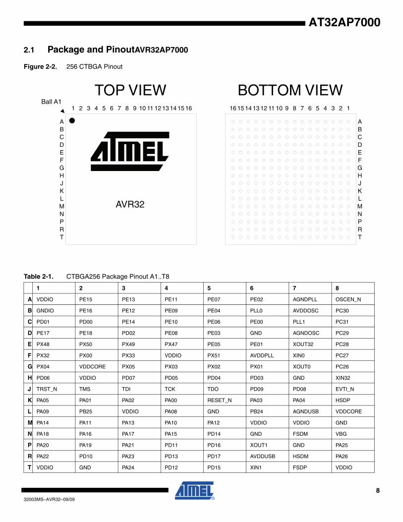
2.1 Package and PinoutAVR32AP7000
Figure 2-2. 256 CTBGA Pinout
TOP VIEW BOTTOM VIEWBall A1
AVR32
ABCDEFGHJKLMNPRT
ABCDEFGHJKLMNPRT
16151413121110987654321 16 15 14 13 12 11 10 9 8 7 6 5 4 3 2 1
Table 2-1. CTBGA256 Package Pinout A1..T8
1 2 3 4 5 6 7 8
A VDDIO PE15 PE13 PE11 PE07 PE02 AGNDPLL OSCEN_N
B GNDIO PE16 PE12 PE09 PE04 PLL0 AVDDOSC PC30
C PD01 PD00 PE14 PE10 PE06 PE00 PLL1 PC31
D PE17 PE18 PD02 PE08 PE03 GND AGNDOSC PC29
E PX48 PX50 PX49 PX47 PE05 PE01 XOUT32 PC28
F PX32 PX00 PX33 VDDIO PX51 AVDDPLL XIN0 PC27
G PX04 VDDCORE PX05 PX03 PX02 PX01 XOUT0 PC26
H PD06 VDDIO PD07 PD05 PD04 PD03 GND XIN32
J TRST_N TMS TDI TCK TDO PD09 PD08 EVTI_N
K PA05 PA01 PA02 PA00 RESET_N PA03 PA04 HSDP
L PA09 PB25 VDDIO PA08 GND PB24 AGNDUSB VDDCORE
M PA14 PA11 PA13 PA10 PA12 VDDIO VDDIO GND
N PA18 PA16 PA17 PA15 PD14 GND FSDM VBG
P PA20 PA19 PA21 PD11 PD16 XOUT1 GND PA25
R PA22 PD10 PA23 PD13 PD17 AVDDUSB HSDM PA26
T VDDIO GND PA24 PD12 PD15 XIN1 FSDP VDDIO
932003MS–AVR32–09/09
AT32AP7000
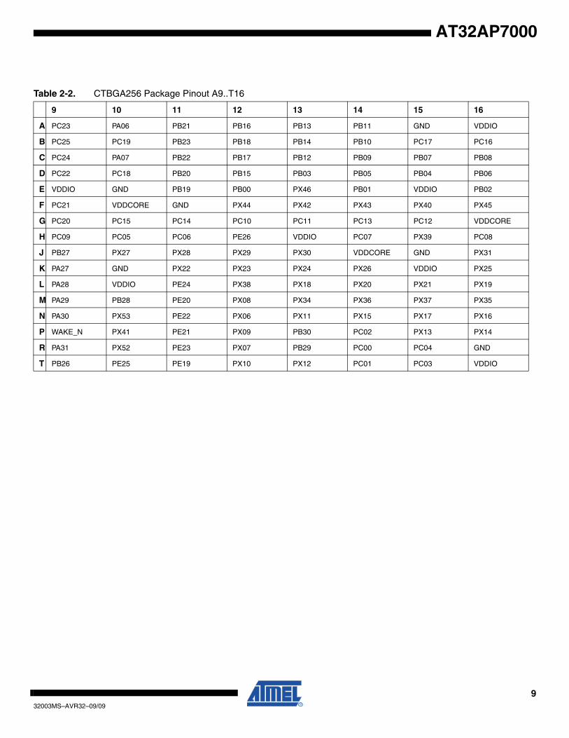
Table 2-2. CTBGA256 Package Pinout A9..T16
9 10 11 12 13 14 15 16
A PC23 PA06 PB21 PB16 PB13 PB11 GND VDDIO
B PC25 PC19 PB23 PB18 PB14 PB10 PC17 PC16
C PC24 PA07 PB22 PB17 PB12 PB09 PB07 PB08
D PC22 PC18 PB20 PB15 PB03 PB05 PB04 PB06
E VDDIO GND PB19 PB00 PX46 PB01 VDDIO PB02
F PC21 VDDCORE GND PX44 PX42 PX43 PX40 PX45
G PC20 PC15 PC14 PC10 PC11 PC13 PC12 VDDCORE
H PC09 PC05 PC06 PE26 VDDIO PC07 PX39 PC08
J PB27 PX27 PX28 PX29 PX30 VDDCORE GND PX31
K PA27 GND PX22 PX23 PX24 PX26 VDDIO PX25
L PA28 VDDIO PE24 PX38 PX18 PX20 PX21 PX19
M PA29 PB28 PE20 PX08 PX34 PX36 PX37 PX35
N PA30 PX53 PE22 PX06 PX11 PX15 PX17 PX16
P WAKE_N PX41 PE21 PX09 PB30 PC02 PX13 PX14
R PA31 PX52 PE23 PX07 PB29 PC00 PC04 GND
T PB26 PE25 PE19 PX10 PX12 PC01 PC03 VDDIO
1032003MS–AVR32–09/09
AT32AP7000
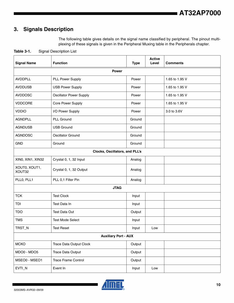
3. Signals Description
The following table gives details on the signal name classified by peripheral. The pinout multi-plexing of these signals is given in the Peripheral Muxing table in the Peripherals chapter.
Table 3-1. Signal Description List
Signal Name Function TypeActive Level Comments
Power
AVDDPLL PLL Power Supply Power 1.65 to 1.95 V
AVDDUSB USB Power Supply Power 1.65 to 1.95 V
AVDDOSC Oscillator Power Supply Power 1.65 to 1.95 V
VDDCORE Core Power Supply Power 1.65 to 1.95 V
VDDIO I/O Power Supply Power 3.0 to 3.6V
AGNDPLL PLL Ground Ground
AGNDUSB USB Ground Ground
AGNDOSC Oscillator Ground Ground
GND Ground Ground
Clocks, Oscillators, and PLL’s
XIN0, XIN1, XIN32 Crystal 0, 1, 32 Input Analog
XOUT0, XOUT1, XOUT32
Crystal 0, 1, 32 Output Analog
PLL0, PLL1 PLL 0,1 Filter Pin Analog
JTAG
TCK Test Clock Input
TDI Test Data In Input
TDO Test Data Out Output
TMS Test Mode Select Input
TRST_N Test Reset Input Low
Auxiliary Port - AUX
MCKO Trace Data Output Clock Output
MDO0 - MDO5 Trace Data Output Output
MSEO0 - MSEO1 Trace Frame Control Output
EVTI_N Event In Input Low
1132003MS–AVR32–09/09
AT32AP7000
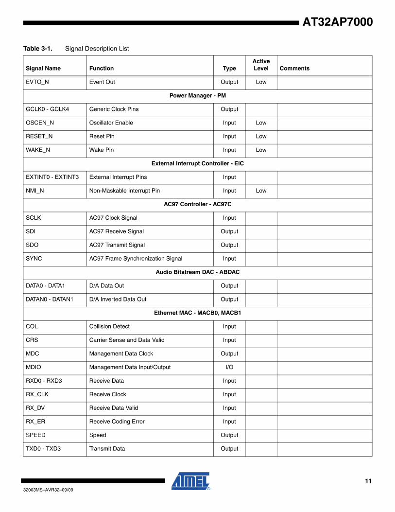
EVTO_N Event Out Output Low
Power Manager - PM
GCLK0 - GCLK4 Generic Clock Pins Output
OSCEN_N Oscillator Enable Input Low
RESET_N Reset Pin Input Low
WAKE_N Wake Pin Input Low
External Interrupt Controller - EIC
EXTINT0 - EXTINT3 External Interrupt Pins Input
NMI_N Non-Maskable Interrupt Pin Input Low
AC97 Controller - AC97C
SCLK AC97 Clock Signal Input
SDI AC97 Receive Signal Output
SDO AC97 Transmit Signal Output
SYNC AC97 Frame Synchronization Signal Input
Audio Bitstream DAC - ABDAC
DATA0 - DATA1 D/A Data Out Output
DATAN0 - DATAN1 D/A Inverted Data Out Output
Ethernet MAC - MACB0, MACB1
COL Collision Detect Input
CRS Carrier Sense and Data Valid Input
MDC Management Data Clock Output
MDIO Management Data Input/Output I/O
RXD0 - RXD3 Receive Data Input
RX_CLK Receive Clock Input
RX_DV Receive Data Valid Input
RX_ER Receive Coding Error Input
SPEED Speed Output
TXD0 - TXD3 Transmit Data Output
Table 3-1. Signal Description List
Signal Name Function TypeActive Level Comments
1232003MS–AVR32–09/09
AT32AP7000
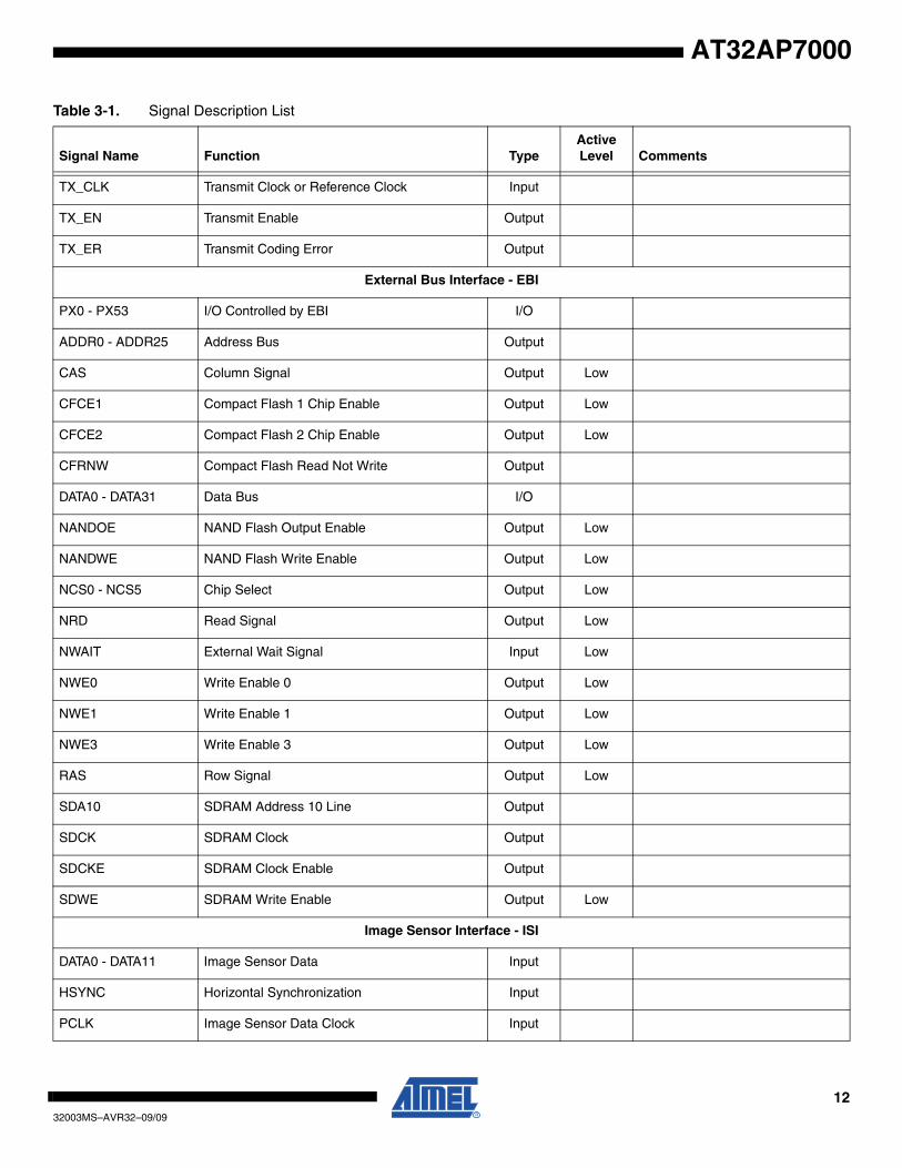
TX_CLK Transmit Clock or Reference Clock Input
TX_EN Transmit Enable Output
TX_ER Transmit Coding Error Output
External Bus Interface - EBI
PX0 - PX53 I/O Controlled by EBI I/O
ADDR0 - ADDR25 Address Bus Output
CAS Column Signal Output Low
CFCE1 Compact Flash 1 Chip Enable Output Low
CFCE2 Compact Flash 2 Chip Enable Output Low
CFRNW Compact Flash Read Not Write Output
DATA0 - DATA31 Data Bus I/O
NANDOE NAND Flash Output Enable Output Low
NANDWE NAND Flash Write Enable Output Low
NCS0 - NCS5 Chip Select Output Low
NRD Read Signal Output Low
NWAIT External Wait Signal Input Low
NWE0 Write Enable 0 Output Low
NWE1 Write Enable 1 Output Low
NWE3 Write Enable 3 Output Low
RAS Row Signal Output Low
SDA10 SDRAM Address 10 Line Output
SDCK SDRAM Clock Output
SDCKE SDRAM Clock Enable Output
SDWE SDRAM Write Enable Output Low
Image Sensor Interface - ISI
DATA0 - DATA11 Image Sensor Data Input
HSYNC Horizontal Synchronization Input
PCLK Image Sensor Data Clock Input
Table 3-1. Signal Description List
Signal Name Function TypeActive Level Comments

1332003MS–AVR32–09/09
AT32AP7000
VSYNC Vertical Synchronization Input
LCD Controller - LCDC
CC LCD Contrast Control Output
DATA0 - DATA23 LCD Data Bus Input
DVAL LCD Data Valid Output
GPL0 - GPL7 LCD General Purpose Lines Output
HSYNC LCD Horizontal Synchronization Output
MODE LCD Mode Output
PCLK LCD Clock Output
PWR LCD Power Output
VSYNC LCD Vertical Synchronization Output
MultiMedia Card Interface - MCI
CLK Multimedia Card Clock Output
CMD0 - CMD1 Multimedia Card Command I/O
DATA0 - DATA7 Multimedia Card Data I/O
Parallel Input/Output - PIOA, PIOB, PIOC, PIOD, PIOE
PA0 - PA31 Parallel I/O Controller PIOA I/O
PB0 - PB30 Parallel I/O Controller PIOB I/O
PC0 - PC31 Parallel I/O Controller PIOC I/O
PD0 - PD17 Parallel I/O Controller PIOD I/O
PE0 - PE26 Parallel I/O Controller PIOE I/O
PS2 Interface - PSIF
CLOCK0 - CLOCK1 PS2 Clock Input
DATA0 - DATA1 PS2 Data I/O
Serial Peripheral Interface - SPI0, SPI1
MISO Master In Slave Out I/O
MOSI Master Out Slave In I/O
NPCS0 - NPCS3 SPI Peripheral Chip Select I/O Low
Table 3-1. Signal Description List
Signal Name Function TypeActive Level Comments
1432003MS–AVR32–09/09
AT32AP7000
SCK Clock Output
Synchronous Serial Controller - SSC0, SSC1, SSC2
RX_CLOCK SSC Receive Clock I/O
RX_DATA SSC Receive Data Input
RX_FRAME_SYNC SSC Receive Frame Sync I/O
TX_CLOCK SSC Transmit Clock I/O
TX_DATA SSC Transmit Data Output
TX_FRAME_SYNC SSC Transmit Frame Sync I/O
DMA Controller - DMACA
DMARQ0 - DMARQ3 DMA Requests Input
Timer/Counter - TIMER0, TIMER1
A0 Channel 0 Line A I/O
A1 Channel 1 Line A I/O
A2 Channel 2 Line A I/O
B0 Channel 0 Line B I/O
B1 Channel 1 Line B I/O
B2 Channel 2 Line B I/O
CLK0 Channel 0 External Clock Input Input
CLK1 Channel 1 External Clock Input Input
CLK2 Channel 2 External Clock Input Input
Two-wire Interface - TWI
SCL Serial Clock I/O
SDA Serial Data I/O
Universal Synchronous Asynchronous Receiver Transmitter - USART0, USART1, USART2, USART3
CLK Clock I/O
CTS Clear To Send Input
RTS Request To Send Output
RXD Receive Data Input
Table 3-1. Signal Description List
Signal Name Function TypeActive Level Comments
1532003MS–AVR32–09/09
AT32AP7000
TXD Transmit Data Output
Pulse Width Modulator - PWM
PWM0 - PWM3 PWM Output Pins Output
USB Interface - USBA
HSDM High Speed USB Interface Data - Analog
FSDM Full Speed USB Interface Data - Analog
HSDP High Speed USB Interface Data + Analog
FSDP Full Speed USB Interface Data + Analog
VBG USB bandgap AnalogConnected to a 6810 Ohm ± 0.5% resistor to gound and a 10 pF capacitor to ground.
Table 3-1. Signal Description List
Signal Name Function TypeActive Level Comments
1632003MS–AVR32–09/09
AT32AP7000
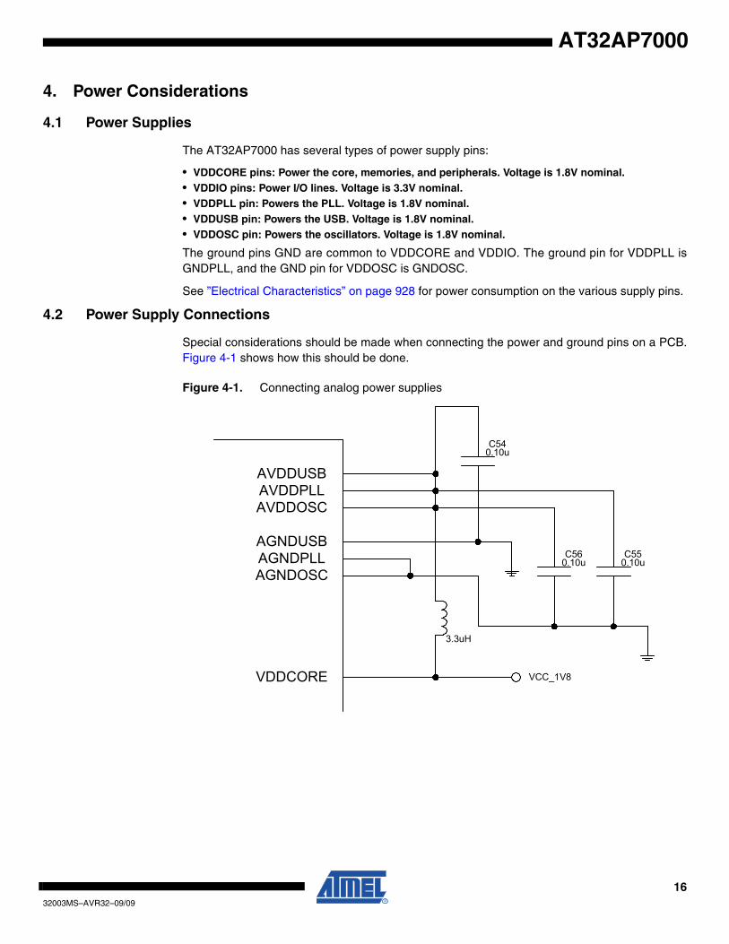
4. Power Considerations
4.1 Power Supplies
The AT32AP7000 has several types of power supply pins:
• VDDCORE pins: Power the core, memories, and peripherals. Voltage is 1.8V nominal.• VDDIO pins: Power I/O lines. Voltage is 3.3V nominal.• VDDPLL pin: Powers the PLL. Voltage is 1.8V nominal.• VDDUSB pin: Powers the USB. Voltage is 1.8V nominal.• VDDOSC pin: Powers the oscillators. Voltage is 1.8V nominal.
The ground pins GND are common to VDDCORE and VDDIO. The ground pin for VDDPLL isGNDPLL, and the GND pin for VDDOSC is GNDOSC.
See ”Electrical Characteristics” on page 928 for power consumption on the various supply pins.
4.2 Power Supply Connections
Special considerations should be made when connecting the power and ground pins on a PCB.Figure 4-1 shows how this should be done.
Figure 4-1. Connecting analog power supplies
AVDDUSBAVDDPLLAVDDOSC
AGNDUSBAGNDPLLAGNDOSC
VDDCORE VCC_1V8
3.3uH
C540.10u
C550.10u
C560.10u
1732003MS–AVR32–09/09
AT32AP7000
5. I/O Line Considerations
5.1 JTAG pins
The TMS, TDI and TCK pins have pull-up resistors. TDO is an output, driven at up to VDDIO,and have no pull-up resistor. The TRST_N pin is used to initialize the embedded JTAG TAPController when asserted at a low level. It is a schmitt input and integrates permanent pull-upresistor to VDDIO, so that it can be left unconnected for normal operations.
5.2 WAKE_N pin
The WAKE_N pin is a schmitt trigger input integrating a permanent pull-up resistor to VDDIO.
5.3 RESET_N pin
The RESET_N pin is a schmitt input and integrates a permanent pull-up resistor to VDDIO. Asthe product integrates a power-on reset cell, the RESET_N pin can be left unconnected in caseno reset from the system needs to be applied to the product.
5.4 EVTI_N pin
The EVTI_N pin is a schmitt input and integrates a non-programmable pull-up resistor to VDDIO.
5.5 TWI pins
When these pins are used for TWI, the pins are open-drain outputs with slew-rate limitation andinputs with inputs with spike-filtering. When used as GPIO-pins or used for other peripherals, thepins have the same characteristics as PIO pins.
5.6 PIO pins
All the I/O lines integrate a programmable pull-up resistor. Programming of this pull-up resistor isperformed independently for each I/O line through the PIO Controllers. After reset, I/O linesdefault as inputs with pull-up resistors enabled, except when indicated otherwise in the column“Reset State” of the PIO Controller multiplexing tables.
1832003MS–AVR32–09/09
AT32AP7000
6. Memories
6.1 Embedded Memories
• 32 Kbyte SRAM– Implemented as two 16Kbyte blocks– Single cycle access at full bus speed
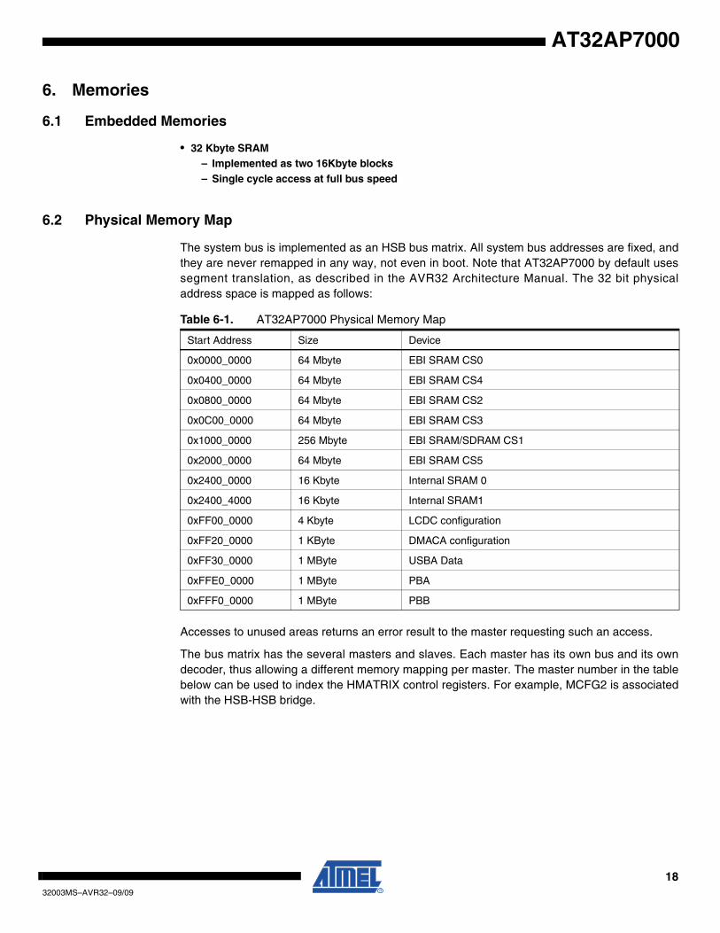
6.2 Physical Memory Map
The system bus is implemented as an HSB bus matrix. All system bus addresses are fixed, andthey are never remapped in any way, not even in boot. Note that AT32AP7000 by default usessegment translation, as described in the AVR32 Architecture Manual. The 32 bit physicaladdress space is mapped as follows:
Accesses to unused areas returns an error result to the master requesting such an access.
The bus matrix has the several masters and slaves. Each master has its own bus and its owndecoder, thus allowing a different memory mapping per master. The master number in the tablebelow can be used to index the HMATRIX control registers. For example, MCFG2 is associatedwith the HSB-HSB bridge.
Table 6-1. AT32AP7000 Physical Memory Map
Start Address Size Device
0x0000_0000 64 Mbyte EBI SRAM CS0
0x0400_0000 64 Mbyte EBI SRAM CS4
0x0800_0000 64 Mbyte EBI SRAM CS2
0x0C00_0000 64 Mbyte EBI SRAM CS3
0x1000_0000 256 Mbyte EBI SRAM/SDRAM CS1
0x2000_0000 64 Mbyte EBI SRAM CS5
0x2400_0000 16 Kbyte Internal SRAM 0
0x2400_4000 16 Kbyte Internal SRAM1
0xFF00_0000 4 Kbyte LCDC configuration
0xFF20_0000 1 KByte DMACA configuration
0xFF30_0000 1 MByte USBA Data
0xFFE0_0000 1 MByte PBA
0xFFF0_0000 1 MByte PBB
1932003MS–AVR32–09/09
AT32AP7000
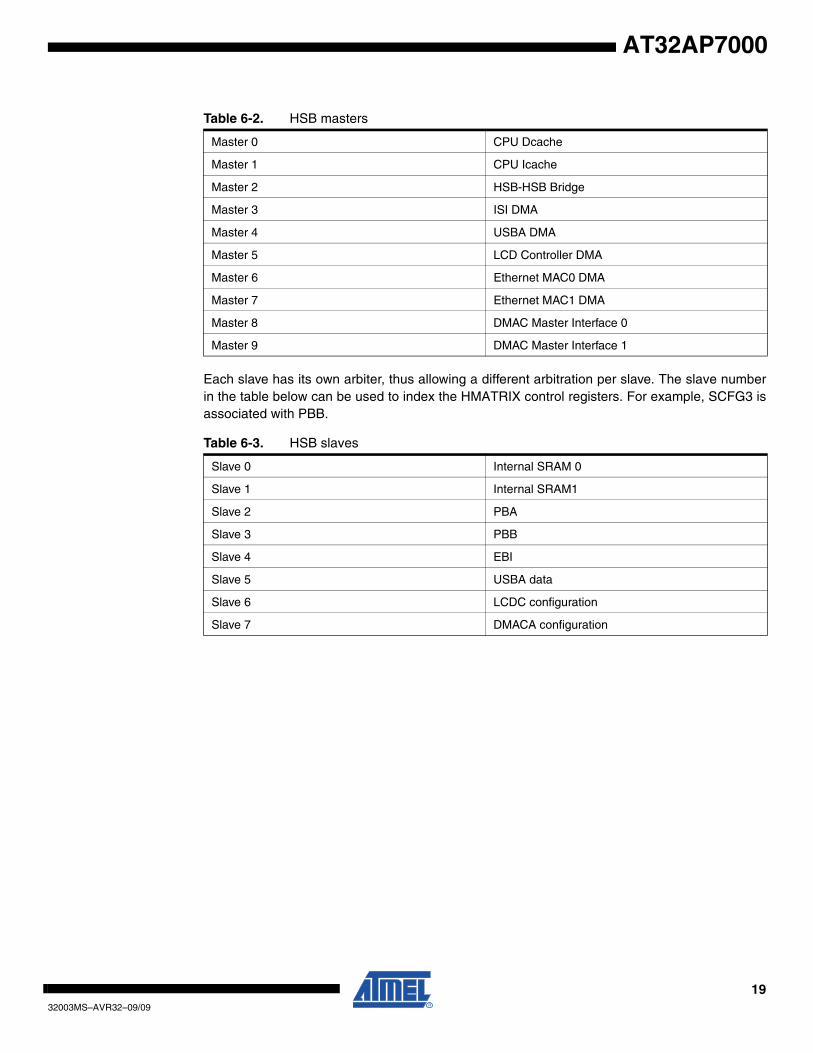
Each slave has its own arbiter, thus allowing a different arbitration per slave. The slave numberin the table below can be used to index the HMATRIX control registers. For example, SCFG3 isassociated with PBB.
Table 6-2. HSB masters
Master 0 CPU Dcache
Master 1 CPU Icache
Master 2 HSB-HSB Bridge
Master 3 ISI DMA
Master 4 USBA DMA
Master 5 LCD Controller DMA
Master 6 Ethernet MAC0 DMA
Master 7 Ethernet MAC1 DMA
Master 8 DMAC Master Interface 0
Master 9 DMAC Master Interface 1
Table 6-3. HSB slaves
Slave 0 Internal SRAM 0
Slave 1 Internal SRAM1
Slave 2 PBA
Slave 3 PBB
Slave 4 EBI
Slave 5 USBA data
Slave 6 LCDC configuration
Slave 7 DMACA configuration
2032003MS–AVR32–09/09
AT32AP7000
7. Peripherals
7.1 Peripheral address map
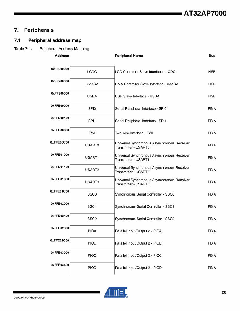
Table 7-1. Peripheral Address Mapping
Address Peripheral Name Bus
0xFF000000LCDC LCD Controller Slave Interface - LCDC HSB
0xFF200000DMACA DMA Controller Slave Interface- DMACA HSB
0xFF300000USBA USB Slave Interface - USBA HSB
0xFFE00000SPI0 Serial Peripheral Interface - SPI0 PB A
0xFFE00400SPI1 Serial Peripheral Interface - SPI1 PB A
0xFFE00800TWI Two-wire Interface - TWI PB A
0xFFE00C00USART0
Universal Synchronous Asynchronous Receiver Transmitter - USART0
PB A
0xFFE01000USART1
Universal Synchronous Asynchronous Receiver Transmitter - USART1
PB A
0xFFE01400USART2
Universal Synchronous Asynchronous Receiver Transmitter - USART2
PB A
0xFFE01800USART3
Universal Synchronous Asynchronous Receiver Transmitter - USART3
PB A
0xFFE01C00SSC0 Synchronous Serial Controller - SSC0 PB A
0xFFE02000SSC1 Synchronous Serial Controller - SSC1 PB A
0xFFE02400SSC2 Synchronous Serial Controller - SSC2 PB A
0xFFE02800PIOA Parallel Input/Output 2 - PIOA PB A
0xFFE02C00PIOB Parallel Input/Output 2 - PIOB PB A
0xFFE03000PIOC Parallel Input/Output 2 - PIOC PB A
0xFFE03400PIOD Parallel Input/Output 2 - PIOD PB A
2132003MS–AVR32–09/09
AT32AP7000
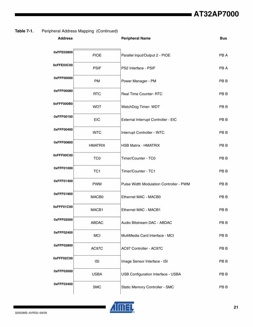
0xFFE03800PIOE Parallel Input/Output 2 - PIOE PB A
0xFFE03C00PSIF PS2 Interface - PSIF PB A
0xFFF00000PM Power Manager - PM PB B
0xFFF00080RTC Real Time Counter- RTC PB B
0xFFF000B0WDT WatchDog Timer- WDT PB B
0xFFF00100EIC External Interrupt Controller - EIC PB B
0xFFF00400INTC Interrupt Controller - INTC PB B
0xFFF00800HMATRIX HSB Matrix - HMATRIX PB B
0xFFF00C00TC0 Timer/Counter - TC0 PB B
0xFFF01000TC1 Timer/Counter - TC1 PB B
0xFFF01400PWM Pulse Width Modulation Controller - PWM PB B
0xFFF01800MACB0 Ethernet MAC - MACB0 PB B
0xFFF01C00MACB1 Ethernet MAC - MACB1 PB B
0xFFF02000ABDAC Audio Bitstream DAC - ABDAC PB B
0xFFF02400MCI MultiMedia Card Interface - MCI PB B
0xFFF02800AC97C AC97 Controller - AC97C PB B
0xFFF02C00ISI Image Sensor Interface - ISI PB B
0xFFF03000USBA USB Configuration Interface - USBA PB B
0xFFF03400SMC Static Memory Controller - SMC PB B
Table 7-1. Peripheral Address Mapping (Continued)
Address Peripheral Name Bus
2232003MS–AVR32–09/09
AT32AP7000
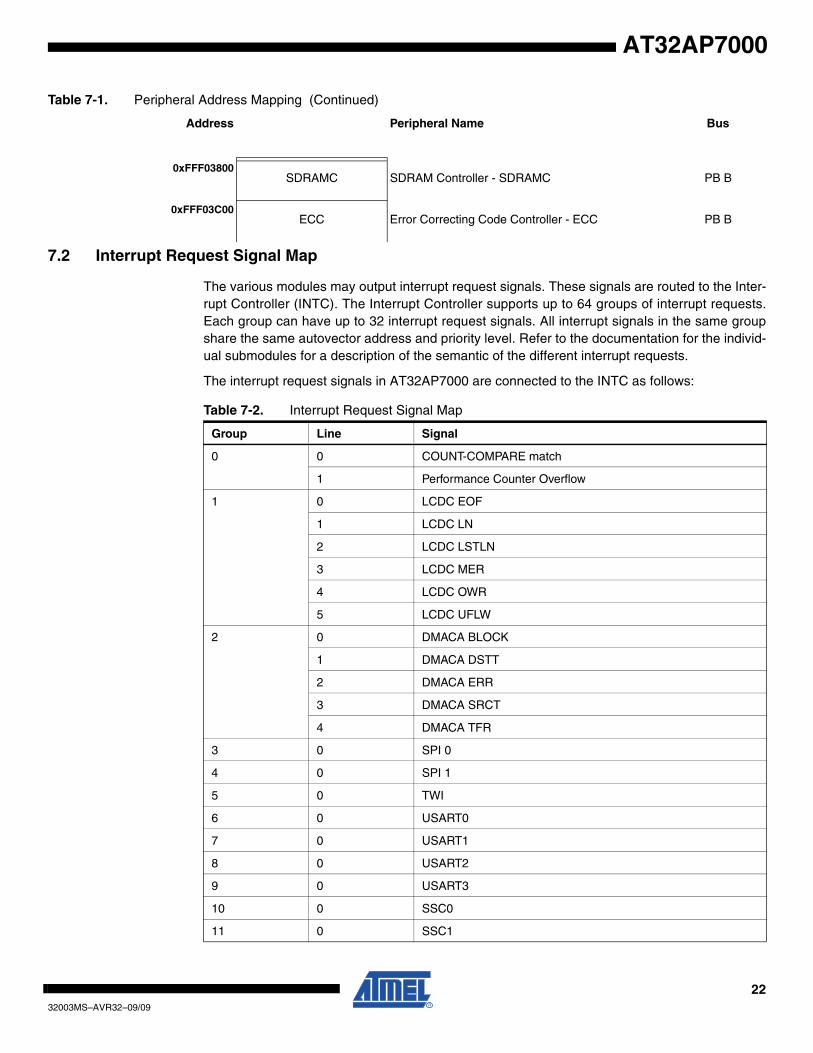
7.2 Interrupt Request Signal Map
The various modules may output interrupt request signals. These signals are routed to the Inter-rupt Controller (INTC). The Interrupt Controller supports up to 64 groups of interrupt requests.Each group can have up to 32 interrupt request signals. All interrupt signals in the same groupshare the same autovector address and priority level. Refer to the documentation for the individ-ual submodules for a description of the semantic of the different interrupt requests.
The interrupt request signals in AT32AP7000 are connected to the INTC as follows:
0xFFF03800SDRAMC SDRAM Controller - SDRAMC PB B
0xFFF03C00ECC Error Correcting Code Controller - ECC PB B
Table 7-1. Peripheral Address Mapping (Continued)
Address Peripheral Name Bus
Table 7-2. Interrupt Request Signal Map
Group Line Signal
0 0 COUNT-COMPARE match
1 Performance Counter Overflow
1 0 LCDC EOF
1 LCDC LN
2 LCDC LSTLN
3 LCDC MER
4 LCDC OWR
5 LCDC UFLW
2 0 DMACA BLOCK
1 DMACA DSTT
2 DMACA ERR
3 DMACA SRCT
4 DMACA TFR
3 0 SPI 0
4 0 SPI 1
5 0 TWI
6 0 USART0
7 0 USART1
8 0 USART2
9 0 USART3
10 0 SSC0
11 0 SSC1

2332003MS–AVR32–09/09
AT32AP7000
12 0 SSC2
13 0 PIOA
14 0 PIOB
15 0 PIOC
16 0 PIOD
17 0 PIOE
18 0 PSIF
19 0 EIC0
1 EIC1
2 EIC2
3 EIC3
20 0 PM
21 0 RTC
22 0 TC00
1 TC01
2 TC02
23 0 TC10
1 TC11
2 TC12
24 0 PWM
25 0 MACB0
26 0 MACB1
27 0 ABDAC
28 0 MCI
29 0 AC97C
30 0 ISI
31 0 USBA
32 0 EBI
Table 7-2. Interrupt Request Signal Map
Group Line Signal
2432003MS–AVR32–09/09
AT32AP7000
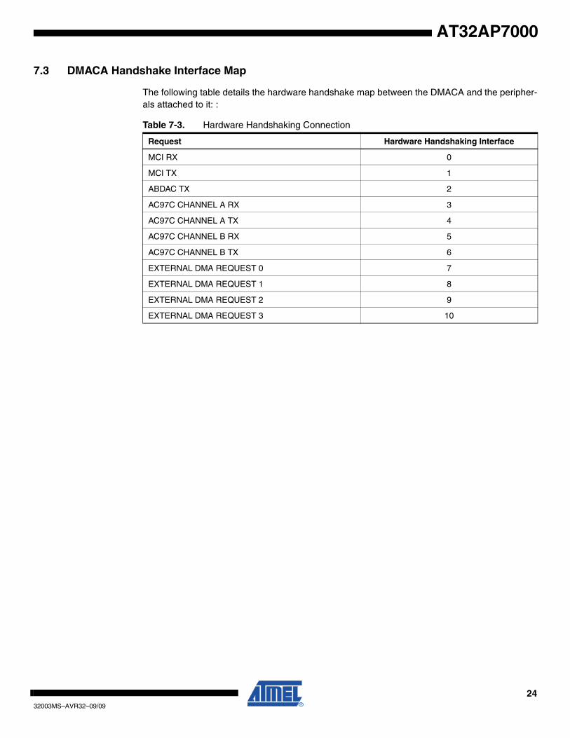
7.3 DMACA Handshake Interface Map
The following table details the hardware handshake map between the DMACA and the peripher-als attached to it: :
Table 7-3. Hardware Handshaking Connection
Request Hardware Handshaking Interface
MCI RX 0
MCI TX 1
ABDAC TX 2
AC97C CHANNEL A RX 3
AC97C CHANNEL A TX 4
AC97C CHANNEL B RX 5
AC97C CHANNEL B TX 6
EXTERNAL DMA REQUEST 0 7
EXTERNAL DMA REQUEST 1 8
EXTERNAL DMA REQUEST 2 9
EXTERNAL DMA REQUEST 3 10
2532003MS–AVR32–09/09
AT32AP7000
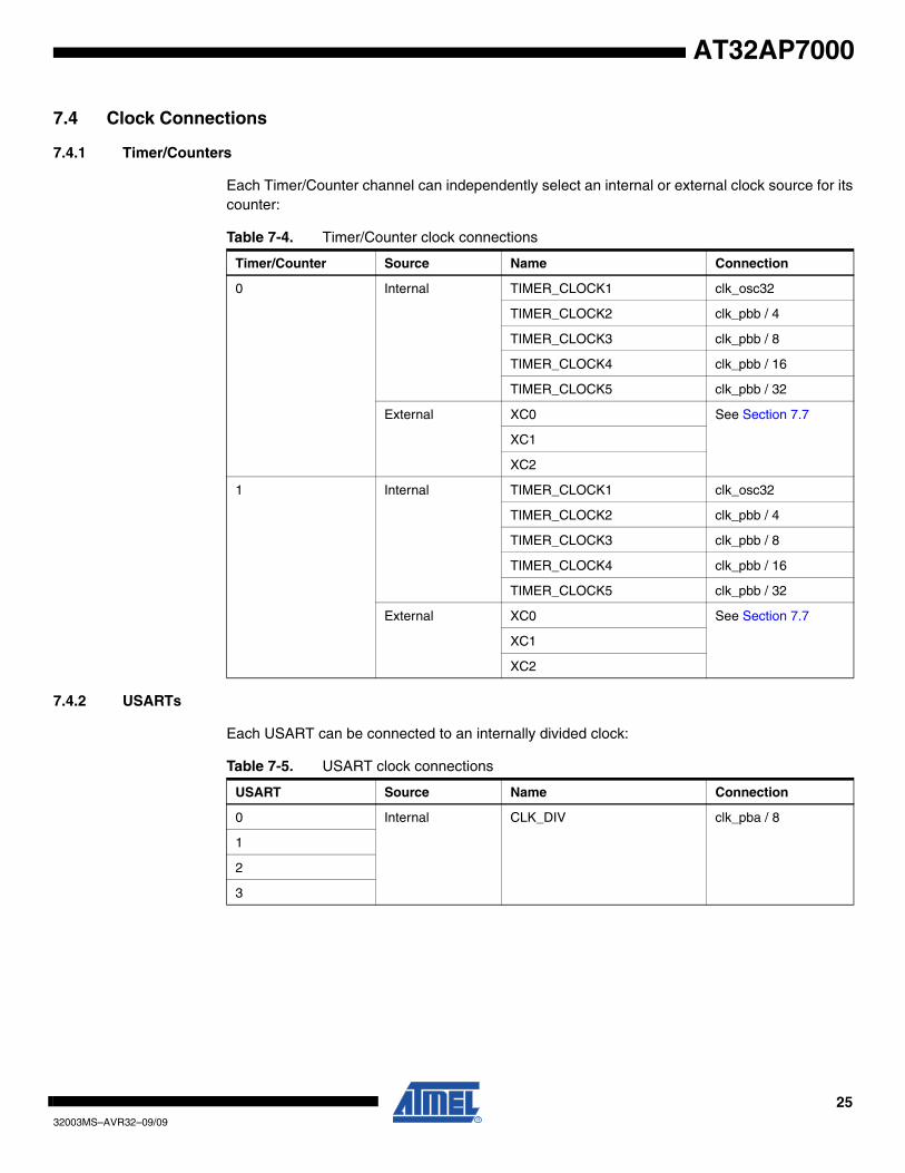
7.4 Clock Connections
7.4.1 Timer/Counters
Each Timer/Counter channel can independently select an internal or external clock source for itscounter:
7.4.2 USARTs
Each USART can be connected to an internally divided clock:
Table 7-4. Timer/Counter clock connections
Timer/Counter Source Name Connection
0 Internal TIMER_CLOCK1 clk_osc32
TIMER_CLOCK2 clk_pbb / 4
TIMER_CLOCK3 clk_pbb / 8
TIMER_CLOCK4 clk_pbb / 16
TIMER_CLOCK5 clk_pbb / 32
External XC0 See Section 7.7
XC1
XC2
1 Internal TIMER_CLOCK1 clk_osc32
TIMER_CLOCK2 clk_pbb / 4
TIMER_CLOCK3 clk_pbb / 8
TIMER_CLOCK4 clk_pbb / 16
TIMER_CLOCK5 clk_pbb / 32
External XC0 See Section 7.7
XC1
XC2
Table 7-5. USART clock connections
USART Source Name Connection
0 Internal CLK_DIV clk_pba / 8
1
2
3
2632003MS–AVR32–09/09
AT32AP7000
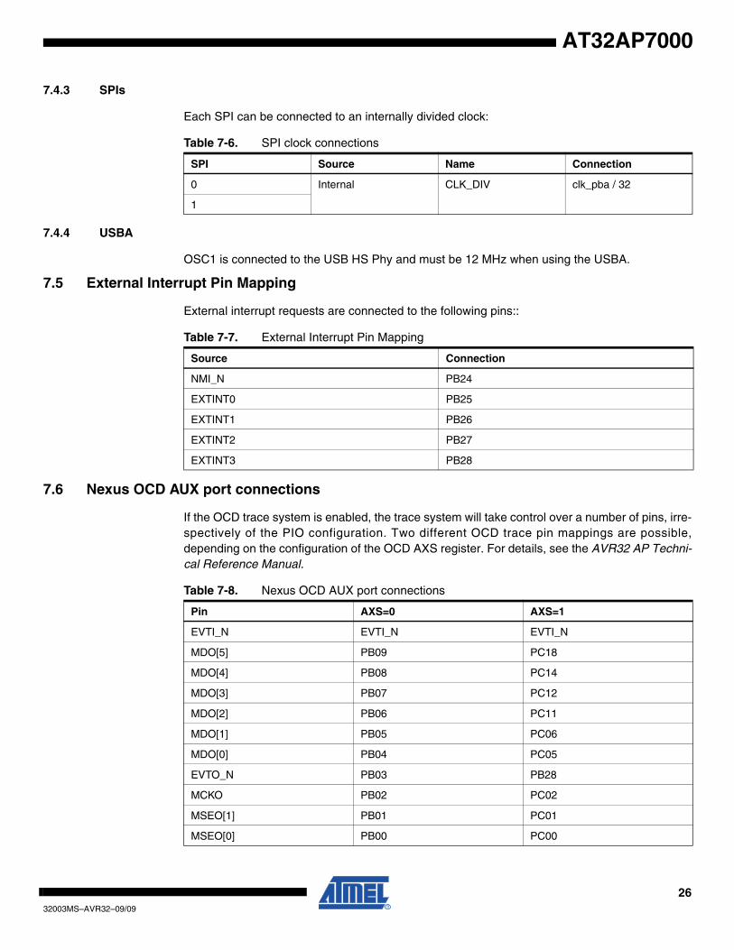
7.4.3 SPIs
Each SPI can be connected to an internally divided clock:
7.4.4 USBA
OSC1 is connected to the USB HS Phy and must be 12 MHz when using the USBA.
7.5 External Interrupt Pin Mapping
External interrupt requests are connected to the following pins::
7.6 Nexus OCD AUX port connections
If the OCD trace system is enabled, the trace system will take control over a number of pins, irre-spectively of the PIO configuration. Two different OCD trace pin mappings are possible,depending on the configuration of the OCD AXS register. For details, see the AVR32 AP Techni-cal Reference Manual.
Table 7-6. SPI clock connections
SPI Source Name Connection
0 Internal CLK_DIV clk_pba / 32
1
Table 7-7. External Interrupt Pin Mapping
Source Connection
NMI_N PB24
EXTINT0 PB25
EXTINT1 PB26
EXTINT2 PB27
EXTINT3 PB28
Table 7-8. Nexus OCD AUX port connections
Pin AXS=0 AXS=1
EVTI_N EVTI_N EVTI_N
MDO[5] PB09 PC18
MDO[4] PB08 PC14
MDO[3] PB07 PC12
MDO[2] PB06 PC11
MDO[1] PB05 PC06
MDO[0] PB04 PC05
EVTO_N PB03 PB28
MCKO PB02 PC02
MSEO[1] PB01 PC01
MSEO[0] PB00 PC00
2732003MS–AVR32–09/09
AT32AP7000
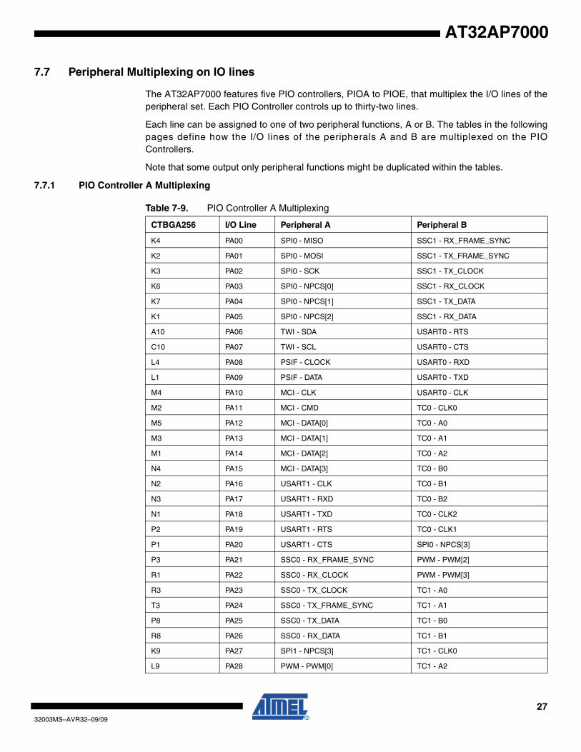
7.7 Peripheral Multiplexing on IO lines
The AT32AP7000 features five PIO controllers, PIOA to PIOE, that multiplex the I/O lines of theperipheral set. Each PIO Controller controls up to thirty-two lines.
Each line can be assigned to one of two peripheral functions, A or B. The tables in the followingpages define how the I/O lines of the peripherals A and B are multiplexed on the PIOControllers.
Note that some output only peripheral functions might be duplicated within the tables.
7.7.1 PIO Controller A Multiplexing
Table 7-9. PIO Controller A Multiplexing
CTBGA256 I/O Line Peripheral A Peripheral B
K4 PA00 SPI0 - MISO SSC1 - RX_FRAME_SYNC
K2 PA01 SPI0 - MOSI SSC1 - TX_FRAME_SYNC
K3 PA02 SPI0 - SCK SSC1 - TX_CLOCK
K6 PA03 SPI0 - NPCS[0] SSC1 - RX_CLOCK
K7 PA04 SPI0 - NPCS[1] SSC1 - TX_DATA
K1 PA05 SPI0 - NPCS[2] SSC1 - RX_DATA
A10 PA06 TWI - SDA USART0 - RTS
C10 PA07 TWI - SCL USART0 - CTS
L4 PA08 PSIF - CLOCK USART0 - RXD
L1 PA09 PSIF - DATA USART0 - TXD
M4 PA10 MCI - CLK USART0 - CLK
M2 PA11 MCI - CMD TC0 - CLK0
M5 PA12 MCI - DATA[0] TC0 - A0
M3 PA13 MCI - DATA[1] TC0 - A1
M1 PA14 MCI - DATA[2] TC0 - A2
N4 PA15 MCI - DATA[3] TC0 - B0
N2 PA16 USART1 - CLK TC0 - B1
N3 PA17 USART1 - RXD TC0 - B2
N1 PA18 USART1 - TXD TC0 - CLK2
P2 PA19 USART1 - RTS TC0 - CLK1
P1 PA20 USART1 - CTS SPI0 - NPCS[3]
P3 PA21 SSC0 - RX_FRAME_SYNC PWM - PWM[2]
R1 PA22 SSC0 - RX_CLOCK PWM - PWM[3]
R3 PA23 SSC0 - TX_CLOCK TC1 - A0
T3 PA24 SSC0 - TX_FRAME_SYNC TC1 - A1
P8 PA25 SSC0 - TX_DATA TC1 - B0
R8 PA26 SSC0 - RX_DATA TC1 - B1
K9 PA27 SPI1 - NPCS[3] TC1 - CLK0
L9 PA28 PWM - PWM[0] TC1 - A2
2832003MS–AVR32–09/09
AT32AP7000
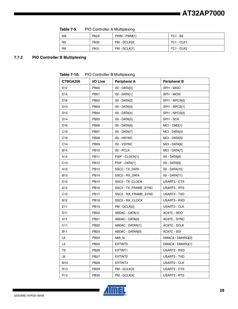
7.7.2 PIO Controller B Multiplexing
M9 PA29 PWM - PWM[1] TC1 - B2
N9 PA30 PM - GCLK[0] TC1 - CLK1
R9 PA31 PM - GCLK[1] TC1 - CLK2
Table 7-9. PIO Controller A Multiplexing
Table 7-10. PIO Controller B Multiplexing
CTBGA256 I/O Line Peripheral A Peripheral B
E12 PB00 ISI - DATA[0] SPI1 - MISO
E14 PB01 ISI - DATA[1] SPI1 - MOSI
E16 PB02 ISI - DATA[2] SPI1 - NPCS[0]
D13 PB03 ISI - DATA[3] SPI1 - NPCS[1]
D15 PB04 ISI - DATA[4] SPI1 - NPCS[2]
D14 PB05 ISI - DATA[5] SPI1 - SCK
D16 PB06 ISI - DATA[6] MCI - CMD[1]
C15 PB07 ISI - DATA[7] MCI - DATA[4]
C16 PB08 ISI - HSYNC MCI - DATA[5]
C14 PB09 ISI - VSYNC MCI - DATA[6]
B14 PB10 ISI - PCLK MCI - DATA[7]
A14 PB11 PSIF - CLOCK[1] ISI - DATA[8]
C13 PB12 PSIF - DATA[1] ISI - DATA[9]
A13 PB13 SSC2 - TX_DATA ISI - DATA[10]
B13 PB14 SSC2 - RX_DATA ISI - DATA[11]
D12 PB15 SSC2 - TX_CLOCK USART3 - CTS
A12 PB16 SSC2 - TX_FRAME_SYNC USART3 - RTS
C12 PB17 SSC2 - RX_FRAME_SYNC USART3 - TXD
B12 PB18 SSC2 - RX_CLOCK USART3 - RXD
E11 PB19 PM - GCLK[2] USART3 - CLK
D11 PB20 ABDAC - DATA[1] AC97C - SDO
A11 PB21 ABDAC - DATA[0] AC97C - SYNC
C11 PB22 ABDAC - DATAN[1] AC97C - SCLK
B11 PB23 ABDAC - DATAN[0] AC97C - SDI
L6 PB24 NMI_N DMACA - DMARQ[0]
L2 PB25 EXTINT0 DMACA - DMARQ[1]
T9 PB26 EXTINT1 USART2 - RXD
J9 PB27 EXTINT2 USART2 - TXD
M10 PB28 EXTINT3 USART2 - CLK
R13 PB29 PM - GCLK[3] USART2 - CTS
P13 PB30 PM - GCLK[4] USART2 - RTS
2932003MS–AVR32–09/09
AT32AP7000
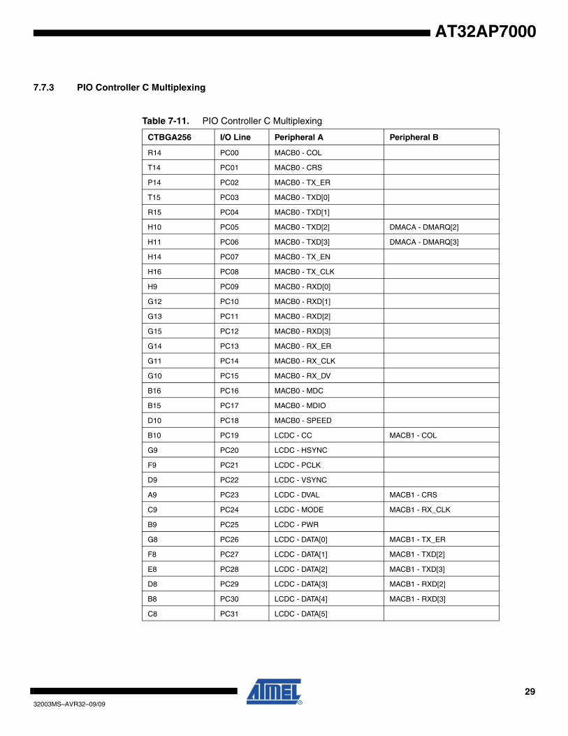
7.7.3 PIO Controller C Multiplexing
Table 7-11. PIO Controller C Multiplexing
CTBGA256 I/O Line Peripheral A Peripheral B
R14 PC00 MACB0 - COL
T14 PC01 MACB0 - CRS
P14 PC02 MACB0 - TX_ER
T15 PC03 MACB0 - TXD[0]
R15 PC04 MACB0 - TXD[1]
H10 PC05 MACB0 - TXD[2] DMACA - DMARQ[2]
H11 PC06 MACB0 - TXD[3] DMACA - DMARQ[3]
H14 PC07 MACB0 - TX_EN
H16 PC08 MACB0 - TX_CLK
H9 PC09 MACB0 - RXD[0]
G12 PC10 MACB0 - RXD[1]
G13 PC11 MACB0 - RXD[2]
G15 PC12 MACB0 - RXD[3]
G14 PC13 MACB0 - RX_ER
G11 PC14 MACB0 - RX_CLK
G10 PC15 MACB0 - RX_DV
B16 PC16 MACB0 - MDC
B15 PC17 MACB0 - MDIO
D10 PC18 MACB0 - SPEED
B10 PC19 LCDC - CC MACB1 - COL
G9 PC20 LCDC - HSYNC
F9 PC21 LCDC - PCLK
D9 PC22 LCDC - VSYNC
A9 PC23 LCDC - DVAL MACB1 - CRS
C9 PC24 LCDC - MODE MACB1 - RX_CLK
B9 PC25 LCDC - PWR
G8 PC26 LCDC - DATA[0] MACB1 - TX_ER
F8 PC27 LCDC - DATA[1] MACB1 - TXD[2]
E8 PC28 LCDC - DATA[2] MACB1 - TXD[3]
D8 PC29 LCDC - DATA[3] MACB1 - RXD[2]
B8 PC30 LCDC - DATA[4] MACB1 - RXD[3]
C8 PC31 LCDC - DATA[5]

3032003MS–AVR32–09/09
AT32AP7000
7.7.4 PIO Controller D Multiplexing
7.7.5 PIO Controller E Multiplexing
Table 7-12. PIO Controller D Multiplexing
CTBGA256 I/O Line Peripheral A Peripheral B
C2 PD00 LCDC - DATA[6]
C1 PD01 LCDC - DATA[7]
D3 PD02 LCDC - DATA[8] MACB1 - MDIO
H6 PD03 LCDC - DATA[9] MACB1 - MDC
H5 PD04 LCDC - DATA[10] MACB1 - RX_DV
H4 PD05 LCDC - DATA[11] MACB1 - RX_ER
H1 PD06 LCDC - DATA[12] MACB1 - RXD[1]
H3 PD07 LCDC - DATA[13]
J7 PD08 LCDC - DATA[14]
J6 PD09 LCDC - DATA[15]
R2 PD10 LCDC - DATA[16] MACB1 - RXD[0]
P4 PD11 LCDC - DATA[17] MACB1 - TX_EN
T4 PD12 LCDC - DATA[18] MACB1 - TX_CLK
R4 PD13 LCDC - DATA[19] MACB1 - TXD[0]
N5 PD14 LCDC - DATA[20] MACB1 - TXD[1]
T5 PD15 LCDC - DATA[21] MACB1 - SPEED
P5 PD16 LCDC - DATA[22]
R5 PD17 LCDC - DATA[23]
Table 7-13. PIO Controller E Multiplexing
CTBGA256 I/O Line Peripheral A Peripheral B
C6 PE00 EBI - DATA[16] LCDC - CC
E6 PE01 EBI - DATA[17] LCDC - DVAL
A6 PE02 EBI - DATA[18] LCDC - MODE
D5 PE03 EBI - DATA[19] LCDC - DATA[0]
B5 PE04 EBI - DATA[20] LCDC - DATA[1]
E5 PE05 EBI - DATA[21] LCDC - DATA[2]
C5 PE06 EBI - DATA[22] LCDC - DATA[3]
A5 PE07 EBI - DATA[23] LCDC - DATA[4]
D4 PE08 EBI - DATA[24] LCDC - DATA[8]
B4 PE09 EBI - DATA[25] LCDC - DATA[9]
C4 PE10 EBI - DATA[26] LCDC - DATA[10]
A4 PE11 EBI - DATA[27] LCDC - DATA[11]

3132003MS–AVR32–09/09
AT32AP7000
B3 PE12 EBI - DATA[28] LCDC - DATA[12]
A3 PE13 EBI - DATA[29] LCDC - DATA[16]
C3 PE14 EBI - DATA[30] LCDC - DATA[17]
A2 PE15 EBI - DATA[31] LCDC - DATA[18]
B2 PE16 EBI - ADDR[23] LCDC - DATA[19]
D1 PE17 EBI - ADDR[24] LCDC - DATA[20]
D2 PE18 EBI - ADDR[25] LCDC - DATA[21]
T11 PE19 EBI - CFCE1
M11 PE20 EBI - CFCE2
P11 PE21 EBI - NCS[4]
N11 PE22 EBI - NCS[5]
R11 PE23 EBI - CFRNW
L11 PE24 EBI - NWAIT
T10 PE25 EBI - NCS[2]
Table 7-13. PIO Controller E Multiplexing
3232003MS–AVR32–09/09
AT32AP7000
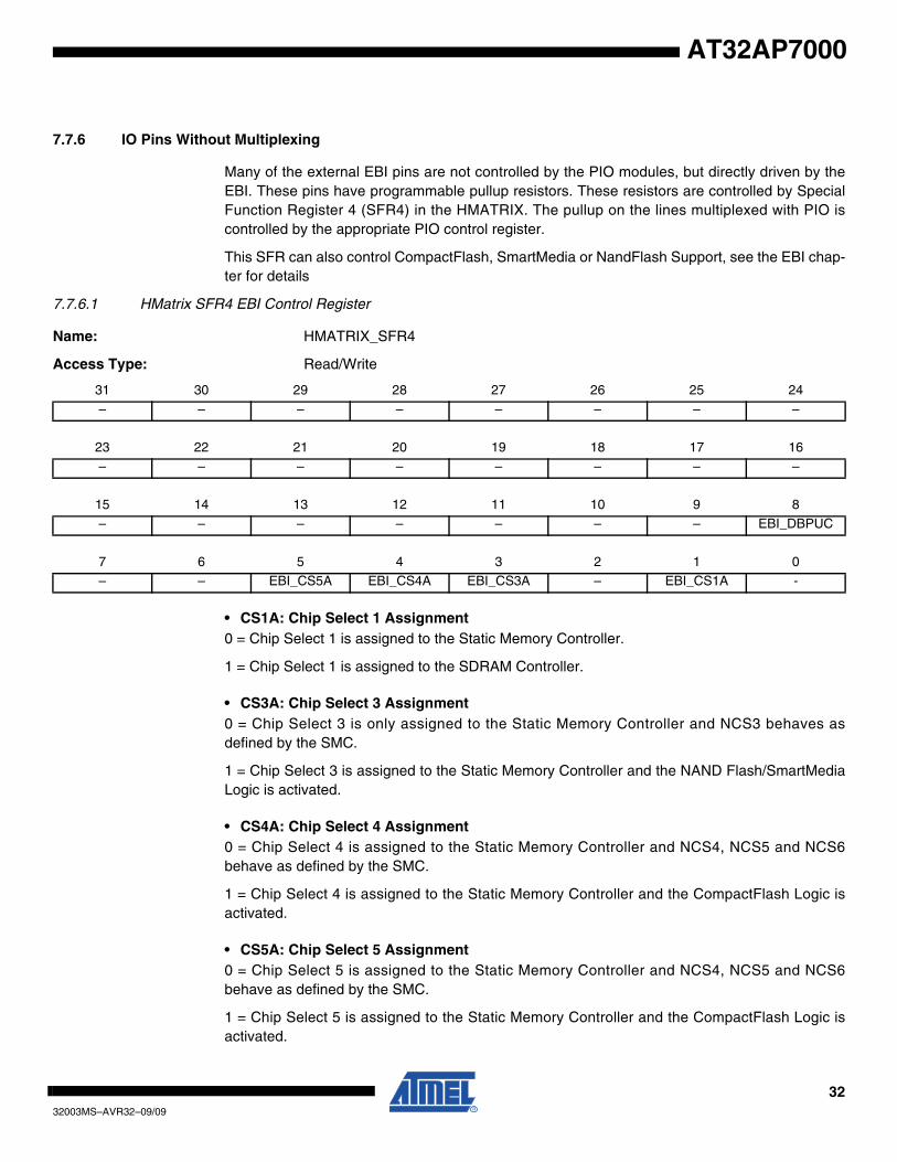
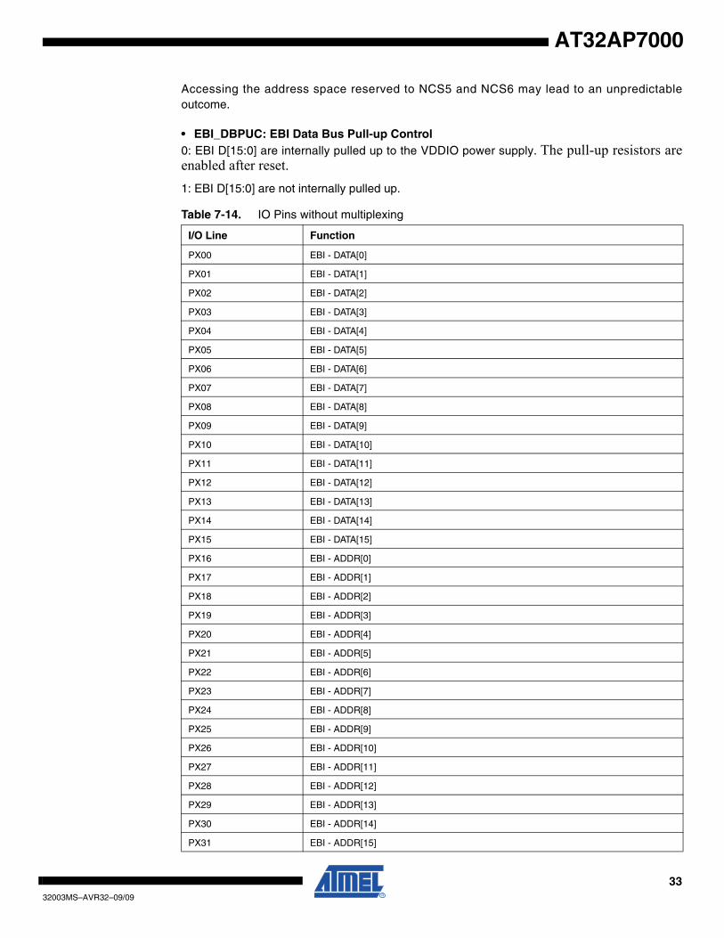
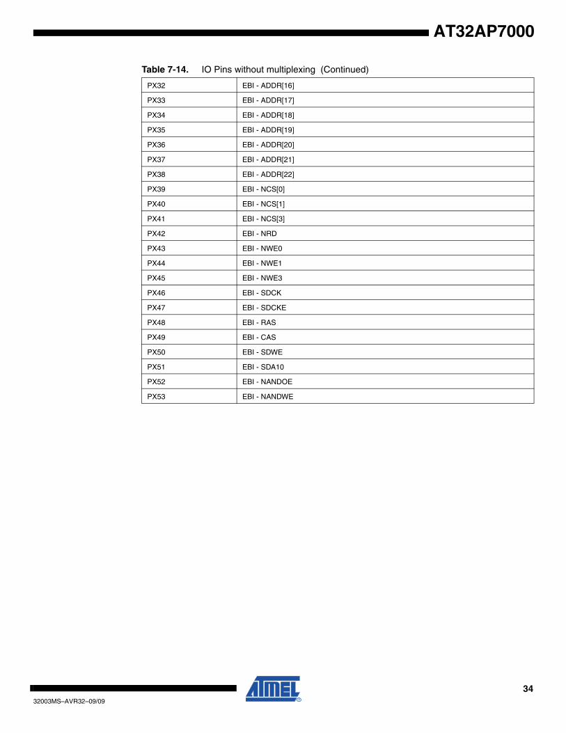
7.7.6 IO Pins Without Multiplexing
Many of the external EBI pins are not controlled by the PIO modules, but directly driven by theEBI. These pins have programmable pullup resistors. These resistors are controlled by SpecialFunction Register 4 (SFR4) in the HMATRIX. The pullup on the lines multiplexed with PIO iscontrolled by the appropriate PIO control register.
This SFR can also control CompactFlash, SmartMedia or NandFlash Support, see the EBI chap-ter for details
7.7.6.1 HMatrix SFR4 EBI Control Register
Name: HMATRIX_SFR4
Access Type: Read/Write
• CS1A: Chip Select 1 Assignment 0 = Chip Select 1 is assigned to the Static Memory Controller.
1 = Chip Select 1 is assigned to the SDRAM Controller.
• CS3A: Chip Select 3 Assignment 0 = Chip Select 3 is only assigned to the Static Memory Controller and NCS3 behaves asdefined by the SMC.
1 = Chip Select 3 is assigned to the Static Memory Controller and the NAND Flash/SmartMediaLogic is activated.
• CS4A: Chip Select 4 Assignment 0 = Chip Select 4 is assigned to the Static Memory Controller and NCS4, NCS5 and NCS6behave as defined by the SMC.
1 = Chip Select 4 is assigned to the Static Memory Controller and the CompactFlash Logic isactivated.
• CS5A: Chip Select 5 Assignment 0 = Chip Select 5 is assigned to the Static Memory Controller and NCS4, NCS5 and NCS6behave as defined by the SMC.
1 = Chip Select 5 is assigned to the Static Memory Controller and the CompactFlash Logic isactivated.
31 30 29 28 27 26 25 24
– – – – – – – –
23 22 21 20 19 18 17 16
– – – – – – – –
15 14 13 12 11 10 9 8
– – – – – – – EBI_DBPUC
7 6 5 4 3 2 1 0
– – EBI_CS5A EBI_CS4A EBI_CS3A – EBI_CS1A -
3332003MS–AVR32–09/09
AT32AP7000
Accessing the address space reserved to NCS5 and NCS6 may lead to an unpredictableoutcome.
• EBI_DBPUC: EBI Data Bus Pull-up Control0: EBI D[15:0] are internally pulled up to the VDDIO power supply. The pull-up resistors areenabled after reset.1: EBI D[15:0] are not internally pulled up.
Table 7-14. IO Pins without multiplexing
I/O Line Function
PX00 EBI - DATA[0]
PX01 EBI - DATA[1]
PX02 EBI - DATA[2]
PX03 EBI - DATA[3]
PX04 EBI - DATA[4]
PX05 EBI - DATA[5]
PX06 EBI - DATA[6]
PX07 EBI - DATA[7]
PX08 EBI - DATA[8]
PX09 EBI - DATA[9]
PX10 EBI - DATA[10]
PX11 EBI - DATA[11]
PX12 EBI - DATA[12]
PX13 EBI - DATA[13]
PX14 EBI - DATA[14]
PX15 EBI - DATA[15]
PX16 EBI - ADDR[0]
PX17 EBI - ADDR[1]
PX18 EBI - ADDR[2]
PX19 EBI - ADDR[3]
PX20 EBI - ADDR[4]
PX21 EBI - ADDR[5]
PX22 EBI - ADDR[6]
PX23 EBI - ADDR[7]
PX24 EBI - ADDR[8]
PX25 EBI - ADDR[9]
PX26 EBI - ADDR[10]
PX27 EBI - ADDR[11]
PX28 EBI - ADDR[12]
PX29 EBI - ADDR[13]
PX30 EBI - ADDR[14]
PX31 EBI - ADDR[15]
3432003MS–AVR32–09/09
AT32AP7000
PX32 EBI - ADDR[16]
PX33 EBI - ADDR[17]
PX34 EBI - ADDR[18]
PX35 EBI - ADDR[19]
PX36 EBI - ADDR[20]
PX37 EBI - ADDR[21]
PX38 EBI - ADDR[22]
PX39 EBI - NCS[0]
PX40 EBI - NCS[1]
PX41 EBI - NCS[3]
PX42 EBI - NRD
PX43 EBI - NWE0
PX44 EBI - NWE1
PX45 EBI - NWE3
PX46 EBI - SDCK
PX47 EBI - SDCKE
PX48 EBI - RAS
PX49 EBI - CAS
PX50 EBI - SDWE
PX51 EBI - SDA10
PX52 EBI - NANDOE
PX53 EBI - NANDWE
Table 7-14. IO Pins without multiplexing (Continued)
3532003MS–AVR32–09/09
AT32AP7000
7.8 Peripheral overview
7.8.1 External Bus Interface
• Optimized for Application Memory Space support• Integrates Three External Memory Controllers:
– Static Memory Controller– SDRAM Controller– ECC Controller
• Additional Logic for NAND Flash/SmartMediaTM and CompactFlashTM Support– SmartMedia support: 8-bit as well as 16-bit devices are supported– CompactFlash support: all modes (Attribute Memory, Common Memory, I/O, True IDE) are
supported but the signals _IOIS16 (I/O and True IDE modes) and _ATA SEL (True IDE mode) are not handled.
• Optimized External Bus:– 16- or 32-bit Data Bus– Up to 26-bit Address Bus, Up to 64-Mbytes Addressable– Optimized pin multiplexing to reduce latencies on External Memories
• Up to 6 Chip Selects, Configurable Assignment:– Static Memory Controller on NCS0– SDRAM Controller or Static Memory Controller on NCS1– Static Memory Controller on NCS2– Static Memory Controller on NCS3, Optional NAND Flash/SmartMediaTM Support– Static Memory Controller on NCS4 - NCS5, Optional CompactFlashTM Support
7.8.2 Static Memory Controller
• 6 Chip Selects Available• 64-Mbyte Address Space per Chip Select• 8-, 16- or 32-bit Data Bus• Word, Halfword, Byte Transfers• Byte Write or Byte Select Lines• Programmable Setup, Pulse And Hold Time for Read Signals per Chip Select• Programmable Setup, Pulse And Hold Time for Write Signals per Chip Select• Programmable Data Float Time per Chip Select• Compliant with LCD Module• External Wait Request• Automatic Switch to Slow Clock Mode • Asynchronous Read in Page Mode Supported: Page Size Ranges from 4 to 32 Bytes
7.8.3 SDRAM Controller
• Numerous Configurations Supported– 2K, 4K, 8K Row Address Memory Parts – SDRAM with Two or Four Internal Banks– SDRAM with 16- or 32-bit Data Path
• Programming Facilities– Word, Half-word, Byte Access– Automatic Page Break When Memory Boundary Has Been Reached– Multibank Ping-pong Access– Timing Parameters Specified by Software– Automatic Refresh Operation, Refresh Rate is Programmable
3632003MS–AVR32–09/09
AT32AP7000
• Energy-saving Capabilities– Self-refresh, Power-down and Deep Power Modes Supported– Supports Mobile SDRAM Devices
• Error Detection– Refresh Error Interrupt
• SDRAM Power-up Initialization by Software• CAS Latency of 1, 2, 3 Supported• Auto Precharge Command Not Used
7.8.4 Error Corrected Code Controller
• Hardware Error Corrected Code (ECC) Generation– Detection and Correction by Software
• Supports NAND Flash and SmartMedia™ Devices with 8- or 16-bit Data Path.• Supports NAND Flash/SmartMedia with Page Sizes of 528, 1056, 2112 and 4224 Bytes, Specified
by Software
7.8.5 Serial Peripheral Interface
• Supports communication with serial external devices– Four chip selects with external decoder support allow communication with up to 15
peripherals– Serial memories, such as DataFlash™ and 3-wire EEPROMs– Serial peripherals, such as ADCs, DACs, LCD Controllers, CAN Controllers and Sensors– External co-processors
• Master or slave serial peripheral bus interface – 8- to 16-bit programmable data length per chip select – Programmable phase and polarity per chip select – Programmable transfer delays between consecutive transfers and between clock and data
per chip select – Programmable delay between consecutive transfers – Selectable mode fault detection
• Very fast transfers supported – Transfers with baud rates up to MCK – The chip select line may be left active to speed up transfers on the same device
7.8.6 Two-wire Interface
• Compatibility with standard two-wire serial memory • One, two or three bytes for slave address • Sequential read/write operations

3732003MS–AVR32–09/09
AT32AP7000
7.8.7 USART
• Programmable Baud Rate Generator • 5- to 9-bit full-duplex synchronous or asynchronous serial communications
– 1, 1.5 or 2 stop bits in Asynchronous Mode or 1 or 2 stop bits in Synchronous Mode– Parity generation and error detection– Framing error detection, overrun error detection– MSB- or LSB-first – Optional break generation and detection – By 8 or by-16 over-sampling receiver frequency – Hardware handshaking RTS-CTS – Receiver time-out and transmitter timeguard – Optional Multi-drop Mode with address generation and detection– Optional Manchester Encoding
• RS485 with driver control signal • ISO7816, T = 0 or T = 1 Protocols for interfacing with smart cards
– NACK handling, error counter with repetition and iteration limit • IrDA modulation and demodulation
– Communication at up to 115.2 Kbps • Test Modes 46
– Remote Loopback, Local Loopback, Automatic Echo
7.8.8 Serial Synchronous Controller
• Provides serial synchronous communication links used in audio and telecom applications (with CODECs in Master or Slave Modes, I2S, TDM Buses, Magnetic Card Reader, etc.)
• Contains an independent receiver and transmitter and a common clock divider • Offers a configurable frame sync and data length • Receiver and transmitter can be programmed to start automatically or on detection of different
event on the frame sync signal • Receiver and transmitter include a data signal, a clock signal and a frame synchronization signal
7.8.9 AC97 Controller
• Compatible with AC97 Component Specification V2.2 • Capable to Interface with a Single Analog Front end • Three independent RX Channels and three independent TX Channels
– One RX and one TX channel dedicated to the AC97 Analog Front end control– One RX and one TX channel for data transfers, connected to the DMACA– One RX and one TX channel for data transfers, connected to the DMACA
• Time Slot Assigner allowing to assign up to 12 time slots to a channel • Channels support mono or stereo up to 20 bit sample length - Variable sampling rate AC97 Codec
Interface (48KHz and below)
3832003MS–AVR32–09/09
AT32AP7000
7.8.10 Audio Bitstream DAC
• Digital Stereo DAC• Oversampled D/A conversion architecture
– Oversampling ratio fixed 128x– FIR equalization filter– Digital interpolation filter: Comb4– 3rd Order Sigma-Delta D/A converters
• Digital bitstream outputs• Parallel interface• Connected to DMA Controller for background transfer without CPU intervention
7.8.11 Timer Counter
• Three 16-bit Timer Counter Channels • Wide range of functions including:
– Frequency Measurement– Event Counting– Interval Measurement– Pulse Generation– Delay Timing– Pulse Width Modulation– Up/down Capabilities
• Each channel is user-configurable and contains:– Three external clock inputs– Five internal clock inputs– Two multi-purpose input/output signals
• Two global registers that act on all three TC Channels
7.8.12 Pulse Width Modulation Controller
• 4 channels, one 16-bit counter per channel• Common clock generator, providing Thirteen Different Clocks
– A Modulo n counter providing eleven clocks– Two independent Linear Dividers working on modulo n counter outputs
• Independent channel programming – Independent Enable Disable Commands– Independent Clock– Independent Period and Duty Cycle, with Double Bufferization– Programmable selection of the output waveform polarity– Programmable center or left aligned output waveform
3932003MS–AVR32–09/09
AT32AP7000
7.8.13 MultiMedia Card Interface
• 2 double-channel MultiMedia Card Interface, allowing concurrent transfers with 2 cards • Compatibility with MultiMedia Card Specification Version 2.2 • Compatibility with SD Memory Card Specification Version 1.0 • Compatibility with SDIO Specification Version V1.0. • Cards clock rate up to Master Clock divided by 2 • Embedded power management to slow down clock rate when not used • Each MCI has two slot, each supporting
– One slot for one MultiMediaCard bus (up to 30 cards) or– One SD Memory Card
• Support for stream, block and multi-block data read and write
7.8.14 PS/2 Interface
• Peripheral Bus slave• PS/2 Host• Receive and transmit capability• Parity generation and error detection• Overrun error detection
7.8.15 USB Interface
• Supports Hi (480Mbps) and Full (12Mbps) speed communication• Compatible with the USB 2.0 specification• UTMI Compliant• 7 Endpoints• Embedded Dual-port RAM for Endpoints• Suspend/Resume Logic (Command of UTMI)• Up to Three Memory Banks for Endpoints (Not for Control Endpoint)• 4 KBytes of DPRAM
7.8.16 LCD Controller
• Single and Dual scan color and monochrome passive STN LCD panels supported • Single scan active TFT LCD panels supported • 4-bit single scan, 8-bit single or dual scan, 16-bit dual scan STN interfaces supported • Up to 24-bit single scan TFT interfaces supported • Up to 16 gray levels for mono STN and up to 4096 colors for color STN displays • 1, 2 bits per pixel (palletized), 4 bits per pixel (non-palletized) for mono STN • 1, 2, 4, 8 bits per pixel (palletized), 16 bits per pixel (non-palletized) for color STN • 1, 2, 4, 8 bits per pixel (palletized), 16, 24 bits per pixel (non-palletized) for TFT • Single clock domain architecture • Resolution supported up to 2048x2048 • 2D-DMA Controller for management of virtual Frame Buffer
– Allows management of frame buffer larger than the screen size and moving the view over this virtual frame buffer
• Automatic resynchronization of the frame buffer pointer to prevent flickering • Configurable coefficients with flexible fixed-point representation.
4032003MS–AVR32–09/09
AT32AP7000
7.8.17 Ethernet MAC
• Compatibility with IEEE Standard 802.3 • 10 and 100 Mbits per second data throughput capability • Full- and half-duplex operations • MII or RMII interface to the physical layer • Register Interface to address, data, status and control registers • DMA Interface, operating as a master on the Memory Controller • Interrupt generation to signal receive and transmit completion • 28-byte transmit and 28-byte receive FIFOs • Automatic pad and CRC generation on transmitted frames • Address checking logic to recognize four 48-bit addresses • Support promiscuous mode where all valid frames are copied to memory • Support physical layer management through MDIO interface control of alarm and update
time/calendar data in
7.8.18 Image Sensor Interface
• ITU-R BT. 601/656 8-bit mode external interface support • Support for ITU-R BT.656-4 SAV and EAV synchronization • Vertical and horizontal resolutions up to 2048 x 2048 • Preview Path up to 640*480 • Support for packed data formatting for YCbCr 4:2:2 formats • Preview scaler to generate smaller size image 50 • Programmable frame capture rate
4132003MS–AVR32–09/09
AT32AP7000
8. Boot Sequence
This chapter summarizes the boot sequence of the AT32AP7000. The behaviour after power-upis controlled by the Power Manager.
8.1 Starting of clocks
After power-up, the device will be held in a reset state by the Power-On Reset (POR) circuitryuntil the voltage has reached the power-on reset rising threshold value (see Electrical Character-istics for details). This ensures that all critical parts of the device are properly reset.
Once the power-on reset is complete, the device will use the XIN0 pin as clock source. XIN0 canbe connected either to an external clock, or a crystal. The OSCEN_N pin is connected either toVDD or GND to inform the Power Manager on how the XIN0 pin is connected. If XIN0 receives asignal from a crystal, dedicated circuitry in the Power Manager keeps the part in a reset stateuntil the oscillator connected to XIN0 has settled. If XIN0 receives an external clock, no such set-tling delay is applied.
On system start-up, the PLLs are disabled. All clocks to all modules are running. No clocks havea divided frequency, all parts of the system recieves a clock with the same frequency as theXIN0 clock.
Note that the power-on reset will release reset at a lower voltage threshold than the minimumspecified operating voltage. If the voltage is not guaranteed to be stable by the time the devicestarts executing, an external brown-out reset circuit should be used.
8.2 Fetching of initial instructions
After reset has been released, the AVR32AP CPU starts fetching instructions from the resetaddress, which is 0xA000_0000. This address lies in the P2 segment, which is non-translated,non-cacheable, and permanently mapped to the physical address range 0x0000_0000 to0x2000_0000. This means that the instruction being fetched from virtual address 0xA000_0000is being fetched from physical address 0x0000_0000. Physical address 0x0000_0000 ismapped to EBI SRAM CS0. This is the external memory the device boots from.
The code read from the SRAM CS0 memory is free to configure the system to use for examplethe PLLs, to divide the frequency of the clock routed to some of the peripherals, and to gate theclocks to unused peripherals.
4232003MS–AVR32–09/09
AT32AP7000
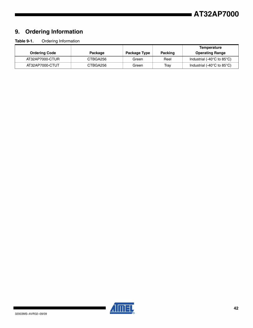
9. Ordering Information
Table 9-1. Ordering Information
Ordering Code Package Package Type PackingTemperature
Operating Range
AT32AP7000-CTUR CTBGA256 Green Reel Industrial (-40°C to 85°C)
AT32AP7000-CTUT CTBGA256 Green Tray Industrial (-40°C to 85°C)
4332003MS–AVR32–09/09
AT32AP7000
10. Errata
10.1 Rev. C
1. SPI FDIV option does not workSelecting clock signal using FDIV = 1 does not work as specified.
Fix/WorkaroundDo not set FDIV = 1.
2. SPI Chip Select 0 BITS field overrides other Chip SelectsThe BITS field for Chip Select 0 overrides BITS fields for other Chip selects.
Fix/WorkaroundUpdate Chip Select 0 BITS field to the relevant settings before transmitting with Chip Selectsother than 0.
3. SPI LASTXFER may be overwrittenWhen Peripheral Select (PS) = 0, the LASTXFER-bit in the Transmit Data Register (TDR)should be internally discared. This fails and may cause problems during DMA transfers.Transmitting data using the PDC when PS=0, the size of the transferred data is 8- or 16-bits.The upper 16 bits of the TDR will be written to a random value. If Chip Select Active AfterTransfer (CSAAT) = 1, the behavior of the Chip Select will be unpredictable.
Fix/Workaround- Do not use CSAAT = 1 if PS = 0
- Use GPIO to control Chip Select lines
- Select PS=1 and store data for PCS and LASTXFER for each data in transmit buffer.
4. SPI LASTXFER overrides Chip SelectThe LASTXFER bit overrides Chip Select input when PS = 0 and CSAAT is used.
Fix/Workaround- Do not use the CSAAT
- Use GPIO as Chip Select input
- Select PS = 1. Transfer 32-bit with correct LASTXFER settings.
5. MMC data write operation with less than 12 bytes is impossible.MCI data write operation with less than 12 bytes is impossible. The Data Write operationwith a number of bytes less than 12 leaves the internal MCI FIFO in an inconsistent state.Subsequent reads and writes will not function properly.
Fix/WorkaroundAlways transfer 12 or more bytes at a time. If less than 12 bytes are transferred, the onlyrecovery mechanism is to perform a software reset of the MCI.
6. MMC SDIO interrupt only works for slot AIf 1-bit data bus width and on other slots than slot A, the SDIO interrupt can not be cap-tured.
4432003MS–AVR32–09/09
AT32AP7000
Fix/WorkaroundUse slot A.
7. PSIF TXEN/RXEN may disable the transmitter/receiverWriting a '0' to RXEN will disable the receiver. Writing '0' to TXEN will disable the transmitter.
Fix/WorkaroundWhen accessing the PS/2 Control Register always write '1' to RXEN to keep the receiverenabled, and write '1' to TXEN to keep the transmitter enabled.
8. PSIF TXRDY interrupt corrupts transfersWhen writing to the Transmit Holding Register (THR), the data will be transferred to the datashift register immediately, regardless of the state of the data shift register. If a transfer isongoing, it will be interrupted and a new transfer will be started with the new data written toTHR.
Fix/WorkaroundUse the TXEMPTY-interrupt instead of the TXRDY-interrupt to update the THR. Thisensures that a transfer is completed.
9. LCD memory error interupt does not workWriting to the MERIT-bit in the LCD Interrupt Test Register (ITR) does not cause an interruptas intended. The MERIC-bit in the LCD Interrupt Clear Register (ICR) cannot be written.This means that if the MERIS-bit in ISR is set, it cannot be cleared.
Fix/WorkaroundMemory error interrupt should not be used.
10. PWM counter restarts at 0x0001The PWM counter restarts at 0x0001 and not 0x0000 as specified. Because of this the firstPWM period has one more clock cycle.
Fix/Workaround- The first period is 0x0000, 0x0001, ..., period
- Consecutive periods are 0x0001, 0x0002, ..., period
11. PWM channel interrupt enabling triggers an interruptWhen enabling a PWM channel that is configured with center aligned period (CALG=1), aninterrupt is signalled.
Fix/WorkaroundWhen using center aligned mode, enable the channel and read the status before channelinterrupt is enabled.
12. PWM update period to a 0 value does not workIt is impossible to update a period equal to 0 by the using the PWM update register(PWM_CUPD).
Fix/WorkaroundDo not update the PWM_CUPD register with a value equal to 0.
13. PWM channel status may be wrong if disabled before a period has elapsed

4532003MS–AVR32–09/09
AT32AP7000
Before a PWM period has elapsed, the read channel status may be wrong. The CHIDx-bitfor a PWM channel in the PWM Enable Register will read '1' for one full PWM period even ifthe channel was disabled before the period elapsed. It will then read '0' as expected.
Fix/WorkaroundReading the PWM channel status of a disabled channel is only correct after a PWM period
14. TWI transfer error without ACKIf the TWI does not receive an ACK from a slave during the address+R/W phase, no bits inthe status register will be set to indicate this. Hence, the transfer will never complete.
Fix/WorkaroundTo prevent errors due to missing ACK, the software should use a timeout mechanism to ter-minate the transfer if this happens.
15. SSC can not transmit or receive dataThe SSC can not transmit or receive data when CKS = CKDIV and CKO = none in TCMR orRCMR respectively.
Fix/WorkaroundSet CKO to a value that is not "None" and enable the PIO with output driver disabled on theTK/RK pin.
16. USART - RXBREAK flag is not correctly handledThe FRAME_ERROR is set instead of the RXBREAK when the break character is locatedjust after the STOP BIT(S) in ASYNCHRONOUS mode.
Fix/WorkaroundThe transmitting UART must set timeguard greater than 0.
17. USART - Manchester encoding/decoding is not working.Manchester encoding/decoding is not working.
Fix/WorkaroundDo not use manchester encoding.
18. SPI - Disabling SPI has no effect on TDRE flag.Disabling SPI has no effect on TDRE whereas the write data command is filtered when SPIis disabled. This means that as soon as the SPI is disabled it becomes impossible to resetthe TDRE flag by writing in the SPI_TDR. So if the SPI is disabled during a PDC transfer, thePDC will continue to write data in the SPI_TDR (as TDRE keeps High) till its buffer is empty,and all data written after the disable command is lost.
Fix/WorkaroundDisable PDC, 2 NOP (minimum), Disable SPI. When you want to continue the transfer:Enable SPI, Enable PDC.
19. SPI disable does not work in SLAVE mode.SPI disable does not work in SLAVE mode.
Fix/WorkaroundRead the last received data, then perform a Software Reset.
4632003MS–AVR32–09/09
AT32AP7000
20. SCC - First Data transmitted after reset is not DATDEF.In the first frame transmitted, the first transmitted data that follows the frame synchro is 0,not DATDEF. This happens when:
1. PDC is disabled
2. Reset the SSC
3. Configure the SSC with a transmit START condition different from CONTINUOUS(START = 0)
4. DATDEF = 1
5. Enable the SSC in transmission.
This trouble only appears after a reset and it is only the first frame is affected.
Fix/WorkaroundUse the PDC to fill the THR after the enable of the SSC and before the start of the frame.
21. MCI - False data timeout error DTOE may occur.If a small block (5 bytes) is read through the READ_SINGLE_BLOCK command (CMD17),the flag NOTBUSY will be set and a false data timeout error DTOE occurs.
Fix/WorkaroundNone.
22. SDRAM - Self-refresh modeIf Entry in Self-refresh mode is followed by SDRAM access and auto-refresh event, TRC tim-ing is not checked for AUTO_REFRESH sequence.
Fix/WorkaroundSet the value of TRAS field in user interface with TRC+1.
23. SPI - No TX UNDERRUN flag availableThere is no TX UNDERRUN flag available, therefore in slave mode there is no way to beinformed of a character lost in transmission.
Fix/WorkaroundPDC/PDCA transfers: None.
Manual transfers (no PDC and TX slave only): Read the RHR every time the THR is written.The OVRS flag of the status register will track any UNDERRUN on the TX side.
24. HMATRIX - Fixed priority arbitration does not workFixed priority arbitration does not work.
Fix/WorkaroundUse Round-robin arbitration instead.
25. OSC32 is not available for RTC, WDT, TIMERs and USARTs at startupRight after startup the osc32 clock to internal modules is not valid. The osc32 clock will bevalid for use approximately 128 osc32 cycles after the the first instruction is executed. Thishas consequences if you are planning to use the RTC, WDT, going into sleep mode andUSARTs with SCK and TCs with TIMER_CLOCK0.
4732003MS–AVR32–09/09
AT32AP7000
Fix/WorkaroundBefore executing any code the user should enable the RTC with the smallest prescaler andpoll that the RTC is counting before doing anything in your program. Another way to ensurethat the osc32 is valid is to use interrupts with TOP=1.
Example:
//reset the counter register
AVR32_RTC.val = 0x0;
//enable the RTC with the smallest prescaler
AVR32_RTC.ctrl = 0x1;
//wait until the value increases
while(AVR32_RTC.val == 0);
26. SPI can generate a false RXREADY signal in SLAVE modeIn slave mode the SPI can generate a false rxready signal during enabling of the SPI or dur-ing the first transfer.
Fix/Workaround1. Set slave mode, set required CPOL/CPHA
2. Enable SPI
3. Set the polarity CPOL of the line in the opposite value of the required one
4. Set the polarity CPOL to the required one.
5. Read the RXHOLDING register
Transfers can now begin and RXREADY will now behave as expected.
27. EBI address lines 23, 24, and 25 are pulled up when booting upAfter reset the EBI address lines 23, 24 and 25 are tristated with pullups. Booting from aflash larger than 8 MB using these lines will fail, as the flash will be accessed with theseaddress bits set.
Fix/WorkaroundAdd external pulldown resistors (5 kΩ) on these lines if booting from a flash larger than 8 MBusing these address lines.
28. SSC - Additional delay on TD outputA delay from 2 to 3 system clock cycles is added to TD output when:
TCMR.START = Receive Start,
TCMR.STTDLY = more than ZERO,
RCMR.START = Start on falling edge / Start on Rising edge / Start on any edge
RFMR.FSOS = None (input)
Fix/WorkaroundNone.
29. SSC - TF output is not correctTF output is not correct (at least emitted one serial clock cycle later than expected) when:
TFMR.FSOS = Driven Low during data transfer/ Driven High during data transfer
4832003MS–AVR32–09/09
AT32AP7000
TCMR.START = Receive start
RFMR.FSOS = None (Input)
RCMR.START = any on RF (edge/level)
Fix/WorkaroundNone.
30. USART - TXD signal is floating in Modem and Hardware Handshaking modeThe TXD signal is floating in Modem and Hardware Handshaking mode, but should bepulled up.
Fix/WorkaroundEnable pullup on this line in the PIO.
31. PWM - Impossible to update a period equal to 0 by using the CUPD registerIt is impossible to UPDATE a period equal to 0 by the using of the UPDATE register(CUPD).
Fix/WorkaroundTo update a period equal to 0, write directly to the CPRD register.
32. WDT Clear is blocked after WDT ResetA watchdog timer event will, after reset, block writes to the WDT_CLEAR register, prevent-ing the program to clear the next Watchdog Timer Reset.
Fix/WorkaroundIf the RTC is not used a write to AVR32_RTC.ctrl.pclr = 1, instead of writing toAVR32_WDT.clr, will reset the prescaler and thus prevent the watchdog event from happen-ing. This will render the RTC useless, but prevents WDT reset because the RTC and WDTshare the same prescaler. Another sideeffect of this is that the watchdog timeout period willbe half the expected timeout period.
If the RTC is used one can disable the Watchdog Timer (WDT) after a WDT reset hasoccured. This will prevent the WDT resetting the system. To make the WDT functional againa hard reset (power on reset or RESET_N) must be applied. If you still want to use the WDTafter a WDT reset a smal l code can be inserted at the startup checking theAVR32_PM.rcause register for WDT reset and use a GPIO pin to reset the system. Thismethod requires that one of the GPIO pins are available and connected externally to theRESET_N pin. After the GPIO pin has pulled down the reset line the GPIO will be reset andleave the pin tristated with pullup.
33. USART - The DCD Signal is active high from the USART, but should be active lowThe DCD signal is active high from the USART, but should be active low.
Fix/WorkaroundAn inverter should be added on this line on the PCB.
34. MCI Transmit Data Register (TDR) FIFO corruptionIf the number of bytes to be transmitted by the MCI is not a multiple of 4, the Transmit DataRegister (TDR) First In First Out data buffer control logic will become corrupted when trans-mit data is written to the TDR as 32-bit values.
Fix/Workaround
4932003MS–AVR32–09/09
AT32AP7000
Configure the MCI Mode Register (MR) to accept 8-bit data input by writing a 1 to bit 13(FBYTE), and transfer each byte of the transmit data to TDR by right aligning the usefulvalue. This allows the number of bytes transferred into the TDR to match the number set upin the BCNT field of the MCI Block Register (BLKR).
35. Unreliable branch foldingIn certain situations, branch folding does not work as expected.
Fix/WorkaroundWrite 0 to CPUCR.FE before executing any branch instructions after reset.
36. USB PLL jitter may cause packet loss during USB hi-speed transmissionThe USB Hi-speed PLL accuracy is not sufficient for Isochronous USB hi-speed transmis-sion and may cause packet loss. The observed bit-loss is typically < 125 ppm.
Fix/WorkaroundDo not use isochronous mode if absolute data accuracy is critical.
10.2 Rev. B
Not sampled.
10.3 Rev. A
1. SPI FDIV option does not workSelecting clock signal using FDIV = 1 does not work as specified.
Fix/WorkaroundDo not set FDIV = 1.
2. SPI Chip Select 0 BITS field overrides other Chip SelectsThe BITS field for Chip Select 0 overrides BITS fields for other Chip selects.
Fix/WorkaroundUpdate Chip Select 0 BITS field to the relevant settings before transmitting with Chip Selectsother than 0.
3. SPI LASTXFER may be overwrittenWhen Peripheral Select (PS) = 0, the LASTXFER-bit in the Transmit Data Register (TDR)should be internally discared. This fails and may cause problems during DMA transfers.Transmitting data using the PDC when PS=0, the size of the transferred data is 8- or 16-bits.The upper 16 bits of the TDR will be written to a random value. If Chip Select Active AfterTransfer (CSAAT) = 1, the behavior of the Chip Select will be unpredictable.
Fix/Workaround- Do not use CSAAT = 1 if PS = 0
- Use GPIO to control Chip Select lines
- Select PS=1 and store data for PCS and LASTXFER for each data in transmit buffer.
4. MMC data write operation with less than 12 bytes is impossible.
5032003MS–AVR32–09/09
AT32AP7000
MCI data write operation with less than 12 bytes is impossible. The Data Write operationwith a number of bytes less than 12 leaves the internal MCI FIFO in an inconsistent state.Subsequent reads and writes will not function properly.
Fix/WorkaroundAlways transfer 12 or more bytes at a time. If less than 12 bytes are transferred, the onlyrecovery mechanism is to perform a software reset of the MCI.
5. MMC SDIO interrupt only works for slot AIf 1-bit data bus width and on other slots than slot A, the SDIO interrupt can not be cap-tured.
Fix/WorkaroundUse slot A.
6. PSIF TXEN/RXEN may disable the transmitter/receiverWriting a '0' to RXEN will disable the receiver. Writing '0' to TXEN will disable the transmitter.
Fix/WorkaroundWhen accessing the PS/2 Control Register always write '1' to RXEN to keep the receiverenabled, and write '1' to TXEN to keep the transmitter enabled.
7. PSIF TXRDY interrupt corrupts transfersWhen writing to the Transmit Holding Register (THR), the data will be transferred to the datashift register immediately, regardless of the state of the data shift register. If a transfer isongoing, it will be interrupted and a new transfer will be started with the new data written toTHR.
Fix/WorkaroundUse the TXEMPTY-interrupt instead of the TXRDY-interrupt to update the THR. Thisensures that a transfer is completed.
8. PSIF Status Register bits return 0The PARITY, NACK and OVRUN bits in the PSIF Status Register cannot be read. Readingthese bits will always return zero.
Fix/WorkaroundNone
9. PSIF Transmit does not work as intendedWhile PSIF receiving works, transmitting using the PSIF does not work.
Fix/WorkaroundDo not transmit using the PSIF.
10. LCD memory error interupt does not workWriting to the MERIT-bit in the LCD Interrupt Test Register (ITR) does not cause an interruptas intended. The MERIC-bit in the LCD Interrupt Clear Register (ICR) cannot be written.This means that if the MERIS-bit in ISR is set, it cannot be cleared.
Fix/WorkaroundMemory error interrupt should not be used.
5132003MS–AVR32–09/09
AT32AP7000
11. PWM counter restarts at 0x0001The PWM counter restarts at 0x0001 and not 0x0000 as specified. Because of this the firstPWM period has one more clock cycle.
Fix/Workaround- The first period is 0x0000, 0x0001, ..., period
- Consecutive periods are 0x0001, 0x0002, ..., period
12. PWM channel interrupt enabling triggers an interruptWhen enabling a PWM channel that is configured with center aligned period (CALG=1), aninterrupt is signalled.
Fix/WorkaroundWhen using center aligned mode, enable the channel and read the status before channelinterrupt is enabled.
13. PWM update period to a 0 value does not workIt is impossible to update a period equal to 0 by the using the PWM update register(PWM_CUPD).
Fix/WorkaroundDo not update the PWM_CUPD register with a value equal to 0.
14. PWM channel status may be wrong if disabled before a period has elapsedBefore a PWM period has elapsed, the read channel status may be wrong. The CHIDx-bitfor a PWM channel in the PWM Enable Register will read '1' for one full PWM period even ifthe channel was disabled before the period elapsed. It will then read '0' as expected.
Fix/WorkaroundReading the PWM channel status of a disabled channel is only correct after a PWM periodhas elapsed.
15. Power Manager DIVEN-bit cannot be readThe DIVEN-bit in the Generic Clock Control Register in the Power Manager cannot be read.Reading the register will give a wrong value for DIVEN. Writing to DIVEN works as intended.
Fix/WorkaroundDo not read DIVEN. If needed, the written value must be store elsewhere.
16. Watchdog Timer cannot wake the part from sleepWhen the CPU has entered sleep mode, the watchdog timer will not be able to reset the sys-tem if a watchdog reset occurs. The problem is valid for all sleep modes.
Fix/WorkaroundNone.
17. Peripherals connected to wrong clock signalThe frequency of the divided clocks for the SPI and the USART is set by the clock configura-tion for peripheral bus B (PBB) and not by peripheral bus A.
Fix/WorkaroundUse clock settings for PBB for the SPI and USART.
5232003MS–AVR32–09/09
AT32AP7000
18. JTAG CLAMP instruction does not work as intendedDuring the CLAMP instruction, the Boundary Scan register should be stable and only theBYPASS register selected. Instead, the bscan register will capture and shift as if it wasselected, reducing the usefulness of the CLAMP instruction.
Fix/WorkaroundNone.
19. High current consumption in reset with no clocks enabledIn connection with the datacache RAM access, a higher current consumption than expectedcan be observed during reset. The error is non-functional and does not affect reliability of thedevice.
Fix/WorkaroundVia software, access the datacache RAM every 100 µs. This prevents the increased currentconsumption. Example code:
mov r11, lo(0x24002000)
orh r11, hi(0x24002000)
ld.w r11, r11[0] //access first RAM
mov r10, lo(0x24000000)
orh r10, hi(0x24000000)
ld.w r10, r10[0] //access second RAM
20. TWI transfer error without ACKIf the TWI does not receive an ACK from a slave during the address+R/W phase, no bits inthe status register will be set to indicate this. Hence, the transfer will never complete.
Fix/WorkaroundTo prevent errors due to missing ACK, the software should use a timeout mechanism to ter-minate the transfer if this happens.
21. SSC can not transmit or receive dataThe SSC can not transmit or receive data when CKS = CKDIV and CKO = none in TCMR orRCMR respectively.
Fix/WorkaroundSet CKO to a value that is not "None" and enable the PIO with output driver disabled on theTK/RK pin.
22. USART - RXBREAK flag is not correctly handledThe FRAME_ERROR is set instead of the RXBREAK when the break character is locatedjust after the STOP BIT(S) in ASYNCHRONOUS mode.
Fix/WorkaroundThe transmitting UART must set timeguard greater than 0.
23. USART - Manchester encoding/decoding is not working.Manchester encoding/decoding is not working.
Fix/WorkaroundDo not use manchester encoding.
5332003MS–AVR32–09/09
AT32AP7000
24. SPI - Disabling SPI has no effect on TDRE flag.Disabling SPI has no effect on TDRE whereas the write data command is filtered when SPIis disabled. This means that as soon as the SPI is disabled it becomes impossible to resetthe TDRE flag by writing in the SPI_TDR. So if the SPI is disabled during a PDC transfer, thePDC will continue to write data in the SPI_TDR (as TDRE keeps High) till its buffer is empty,and all data written after the disable command is lost.
Fix/WorkaroundDisable PDC, 2 NOP (minimum), Disable SPI. When you want to continue the transfer:Enable SPI, Enable PDC.
25. SPI disable does not work in SLAVE mode.SPI disable does not work in SLAVE mode.
Fix/WorkaroundRead the last received data, then perform a Software Reset.
26. SCC - First Data transmitted after reset is not DATDEF.In the first frame transmitted, the first transmitted data that follows the frame synchro is 0,not DATDEF. This happens when:
1. PDC is disabled
2. Reset the SSC
3. Configure the SSC with a transmit START condition different from CONTINUOUS(START = 0)
4. DATDEF = 1
5. Enable the SSC in transmission.
This trouble only appears after a reset and it is only the first frame is affected.
Fix/WorkaroundUse the PDC to fill the THR after the enable of the SSC and before the start of the frame.
27. MCI - False data timeout error DTOE may occur.If a small block (5 bytes) is read through the READ_SINGLE_BLOCK command (CMD17),the flag NOTBUSY will be set and a false data timeout error DTOE occurs.
Fix/WorkaroundNone.
28. SDRAM - Self-refresh modeIf Entry in Self-refresh mode is followed by SDRAM access and auto-refresh event, TRC tim-ing is not checked for AUTO_REFRESH sequence.
Fix/WorkaroundSet the value of TRAS field in user interface with TRC+1.
29. SPI - No TX UNDERRUN flag availableThere is no TX UNDERRUN flag available, therefore in slave mode there is no way to beinformed of a character lost in transmission.
Fix/Workaround
5432003MS–AVR32–09/09
AT32AP7000
PDC/PDCA transfers: None.
Manual transfers (no PDC and TX slave only): Read the RHR every time the THR is written.The OVRS flag of the status register will track any UNDERRUN on the TX side.
30. HMATRIX - Fixed priority arbitration does not workFixed priority arbitration does not work.
Fix/WorkaroundUse Round-robin arbitration instead.
31. OSC32 is not available for RTC, WDT, TIMERs and USARTs at startupRight after startup the osc32 clock to internal modules is not valid. The osc32 clock will bevalid for use approximately 128 osc32 cycles after the the first instruction is executed. Thishas consequences if you are planning to use the RTC, WDT, going into sleep mode andUSARTs with SCK and TCs with TIMER_CLOCK0.
Fix/WorkaroundBefore executing any code the user should enable the RTC with the smallest prescaler andpoll that the RTC is counting before doing anything in your program. Another way to ensurethat the osc32 is valid is to use interrupts with TOP=1.
Example:
//reset the counter register
AVR32_RTC.val = 0x0;
//enable the RTC with the smallest prescaler
AVR32_RTC.ctrl = 0x1;
//wait until the value increases
while(AVR32_RTC.val == 0);
32. SPI can generate a false RXREADY signal in SLAVE modeIn slave mode the SPI can generate a false rxready signal during enabling of the SPI or dur-ing the first transfer.
Fix/Workaround1. Set slave mode, set required CPOL/CPHA
2. Enable SPI
3. Set the polarity CPOL of the line in the opposite value of the required one
4. Set the polarity CPOL to the required one.
5. Read the RXHOLDING register
Transfers can now begin and RXREADY will now behave as expected.
33. EBI address lines 23, 24, and 25 are pulled up when booting upAfter reset the EBI address lines 23, 24 and 25 are tristated with pullups. Booting from aflash larger than 8 MB using these lines will fail, as the flash will be accessed with theseaddress bits set.
Fix/WorkaroundAdd external pulldown resistors (5 kΩ) on these lines if booting from a flash larger than 8 MBusing these address lines.
5532003MS–AVR32–09/09
AT32AP7000
34. SSC - Additional delay on TD outputA delay from 2 to 3 system clock cycles is added to TD output when:
TCMR.START = Receive Start,
TCMR.STTDLY = more than ZERO,
RCMR.START = Start on falling edge / Start on Rising edge / Start on any edge
RFMR.FSOS = None (input)
Fix/WorkaroundNone.
35. SSC - TF output is not correctTF output is not correct (at least emitted one serial clock cycle later than expected) when:
TFMR.FSOS = Driven Low during data transfer/ Driven High during data transfer
TCMR.START = Receive start
RFMR.FSOS = None (Input)
RCMR.START = any on RF (edge/level)
Fix/WorkaroundNone.
36. USART - TXD signal is floating in Modem and Hardware Handshaking modeThe TXD signal is floating in Modem and Hardware Handshaking mode, but should bepulled up.
Fix/WorkaroundEnable pullup on this line in the PIO.
37. PWM - Impossible to update a period equal to 0 by using the CUPD registerIt is impossible to UPDATE a period equal to 0 by the using of the UPDATE register(CUPD).
Fix/WorkaroundTo update a period equal to 0, write directly to the CPRD register.
38. WDT Clear is blocked after WDT ResetA watchdog timer event will, after reset, block writes to the WDT_CLEAR register, prevent-ing the program to clear the next Watchdog Timer Reset.
Fix/WorkaroundIf the RTC is not used a write to AVR32_RTC.ctrl.pclr = 1, instead of writing toAVR32_WDT.clr, will reset the prescaler and thus prevent the watchdog event from happen-ing. This will render the RTC useless, but prevents WDT reset because the RTC and WDTshare the same prescaler. Another sideeffect of this is that the watchdog timeout period willbe half the expected timeout period.
If the RTC is used one can disable the Watchdog Timer (WDT) after a WDT reset hasoccured. This will prevent the WDT resetting the system. To make the WDT functional againa hard reset (power on reset or RESET_N) must be applied. If you still want to use the WDTafter a WDT reset a smal l code can be inserted at the startup checking theAVR32_PM.rcause register for WDT reset and use a GPIO pin to reset the system. Thismethod requires that one of the GPIO pins are available and connected externally to the
5632003MS–AVR32–09/09
AT32AP7000
RESET_N pin. After the GPIO pin has pulled down the reset line the GPIO will be reset andleave the pin tristated with pullup.
39. USART - The DCD Signal is active high from the USART, but should be active lowThe DCD signal is active high from the USART, but should be active low.
Fix/WorkaroundAn inverter should be added on this line on the PCB.
40. MCI Transmit Data Register (TDR) FIFO corruptionIf the number of bytes to be transmitted by the MCI is not a multiple of 4, the Transmit DataRegister (TDR) First In First Out data buffer control logic will become corrupted when trans-mit data is written to the TDR as 32-bit values.
Fix/WorkaroundConfigure the MCI Mode Register (MR) to accept 8-bit data input by writing a 1 to bit 13(FBYTE), and transfer each byte of the transmit data to TDR by right aligning the usefulvalue. This allows the number of bytes transferred into the TDR to match the number set upin the BCNT field of the MCI Block Register (BLKR).
41. Unreliable branch foldingIn certain situations, branch folding does not work as expected.
Fix/WorkaroundWrite 0 to CPUCR.FE before executing any branch instructions after reset.
42. USB PLL jitter may cause packet loss during USB hi-speed transmissionThe USB Hi-speed PLL accuracy is not sufficient for Isochronous USB hi-speed transmis-sion and may cause packet loss. The observed bit-loss is typically < 125 ppm.
Fix/WorkaroundDo not use isochronous mode if absolute data accuracy is critical.
5732003MS–AVR32–09/09
AT32AP7000
11. Datasheet Revision History
Please note that the referring page numbers in this section are referred to this document. Thereferring revision in this section are referring to the document revision.
11.1 Rev. M 09/09
11.2 Rev. L 09/09
11.3 Rev. K 09/07
1. Updated ”Errata” on page 43.
1. Updated ”Errata” on page 43.
1. PIO Controller C Multiplexing table updated in ”Peripherals” on page 75“.
2. Added section ”USBA” on page 81 in Clock Connections in ”Peripherals” on page 75.
3. USBA feature list updated in ”Peripherals” on page 75.
4. Renamed clk_slow to clk_osc32 in Table 9-4 on page 80.
5. Updated organisation of User Interface in ”HSB Bus Matrix (HMATRIX)” on page 144.
6. Updated special bus granting mechanism in ”HSB Bus Matrix (HMATRIX)” on page 144.
7 Added product dependencies in ”DMA Controller (DMACA)” on page 174.
8. Added product dependencies in ”Peripheral DMA Controller (PDC)” on page 237.
9. Added description of multi-drive in ”Parallel Input/Output Controller (PIO)” on page 253.
10.Added MDER/MDDR/MDSR to pin logic diagram in ”Parallel Input/Output Controller (PIO)” on page 253.
11. SPI pins must be enabled to use local loopback.
12. Updated description of the OVRES bit in ”Serial Peripheral Interface (SPI)” on page 293.
13. Updated bit description of TXEMPTY in the ”USART Channel Status Register” on page 435.
14.Number of chip select lines updatedin figures and tables, changed from 8 to 6 in ”Static Memory Controller (SMC)” on page 492.
15.Made the MDR register Read/Write instead of Read in ”SDRAM Controller (SDRAMC)” on page 534.
16. Removed the PWSEN and PWSDIS bits from the ”Control Register” on page 588.
17. Added PDCFBYTE and removed the PWSDIV bits from the ”Control Register” on page 588
18.Added note about terminating the transfers in sleep modes in product dependencies in ”Ethernet MAC (MACB)” on page 606.
19.Added note about reading the Status Register clears the interrupt flag in ”Timer/Counter (TC)” on page 740.
20. Added debug operation to product dependencies in ”Timer/Counter (TC)” on page 740.
21.Added debug operation to product dependencies in ”Pulse Width Modulation Controller (PWM)” on page 777.

5832003MS–AVR32–09/09
AT32AP7000
11.4 Rev. J 07/07
11.5 Rev. I 04/07
11.6 Rev. H 02/07
22.Consistently used the term LCDC Core Clock through the document when referring to the generic clock that drives the LCD Core and is used to generate PCLK and the other LCD synchronization signals.
23. Updated typos in ”LCD Controller (LCDC)” on page 803.
24.Rewritten the Register Configuration Guide and renamed it “Register Configuration Example“ in ”LCD Controller (LCDC)” on page 803.
25. Updated formula for pixel clock in ”LCD Control Register 1” on page 846.
26. Updated HOZVAL description in ”LCD Frame Configuration Register” on page 851.
27. Updated ”PLL Characteristics” on page 935.
28. Updated ”Errata” on page 43.
1. USB Signals updated in ”Signals Description” on page 4.
2. The PX0 - PX53 Signals added in ”Signals Description” on page 4.
3. SDCS signals removed from PIO Controller Multiplexing tables in ”Peripherals” on page 75.
4.SDCS1 signal removed from figures and tables, and SDCS0 renamed to SDCS in ”External Bus Interface (EBI)” on page 147.
5SmartMedia renamed to NAND Flash in some description to avoid confusion in ”External Bus Interface (EBI)” on page 147.
6. Updated the reset state of the SMC Mode register in Table 27-9 on page 523.
7. Updated ”Mechanical Characteristics” on page 927.
8. Updated pad parameters in ”DC Characteristics” on page 928.
9 Updated pad parameters in ”Clock Characteristics” on page 931.
10. Updated ”USB Transceiver Characteristics” on page 934.
11. Updated ”EBI Timings” on page 938.
1. Updated ”Features” on page 1.
2. Updated tables in ”Signals Description” on page 4.
3.Updated Table 9-2 on page 77, Table 9-9 on page 82, and Table 9-9 on page 82 in the ”Peripherals” on page 75.
4. Updated module names and abbreviations through the datasheet.
1. Updated ”Features” on page 1.
2. Updated ”Part Description” on page 2.
3. Added VBG pin in ”Signals Description” on page 4.
3. Changed direction in the EVTI_N signal in ”Signals Description” on page 4.
4. Updated ”Blockdiagram” on page 4.
5. Updated Registers in ”Power Manager (PM)” on page 48.
5932003MS–AVR32–09/09
AT32AP7000
11.7 Rev. G 10/06
11.8 Rev. F 07/06
11.9 Rev. E 05/06
6.“Pulling OSCEN_N low” replaced by “Pulling OSCEN_N high” in ”32 KHz oscillator operation” on page 98.
7. Added note in ”32 KHz oscillator operation” on page 98.
8. Updated register names in ”Real Time Counter (RTC)” on page 119.
9. Updated register names in ”Watchdog Timer (WDT)” on page 125.
10. Updated register descriptions in ”HSB Bus Matrix (HMATRIX)” on page 144.
11. Updated CFRNW to a separate signal in ”External Bus Interface (EBI)” on page 147.
12. Updated register descriptions in ”DMA Controller (DMACA)” on page 174.
13.Added registers and updated register descriptions in ”Parallel Input/Output Controller (PIO)” on page 253.
14. Updated bit names in ”Serial Peripheral Interface (SPI)” on page 293.
15. Updated flow charts in ”Two-wire Interface (TWI)” on page 322.
16. Updated bit name in the PSR register in ”PS/2 Module (PSIF)” on page 340.
17. Added second instance of ps2 interface in ”PS/2 Module (PSIF)” on page 340.
18. Updated register descriptions in ”Synchronous Serial Controller (SSC)” on page 352.
19. Updated register names in ”Static Memory Controller (SMC)” on page 492.
20. Updated register names in ”Error Corrected Code (ECC) Controller” on page 562.
21. Updated register descriptions in ”Ethernet MAC (MACB)” on page 606.
22. Updated register descriptions in ”LCD Controller (LCDC)” on page 803.
23. Updated register descriptions in ”Image Sensor Interface (ISI)” on page 873.
24. Removed JTAG specification references in ”Debug and Test” on page 909.
25. Updated ”Electrical Characteristics” on page 928.
26. Updated memory locations.
1. Package text changed from CABGA to CTBGA.
2.Occurrences of APB and AHB changed to Peripheral Bus (PB) and High Speed Bus (HSB) respectively.
3. Updated ”Hi-Speed USB Interface (USBA)” on page 584.
4. Added ”Errata” on page 43.
1. Removed 150CGU from ”Ordering Information” on page 97.
1. Added ”USB Device - High Speed (480 Mbits/s)” on page 665.

6032003MS–AVR32–09/09
AT32AP7000
11.10 Rev. D 04/06
11.11 Rev. C 04/06
1. Some occurences of AP7000 renamed to AT32AP7000.
2. Updated ”Real Time Counter” on page 117.
3. Updated ”Audio DAC - (DAC)” on page 480
4. Updated ”DC Characteristics” on page 89.
5. Updated ”Ordering Information” on page 97.
1. Initial revision.

i32003MS–AVR32–09/09
AT32AP7000
Table of Contents
Features ..................................................................................................... 1
1 Part Description ....................................................................................... 2
2 Blockdiagram ........................................................................................... 4
2.1Package and PinoutAVR32AP7000 ..........................................................................8
3 Signals Description ............................................................................... 10
4 Power Considerations ........................................................................... 16
4.1Power Supplies .......................................................................................................16
4.2Power Supply Connections .....................................................................................16
5 I/O Line Considerations ......................................................................... 17
5.1JTAG pins ................................................................................................................17
5.2WAKE_N pin ...........................................................................................................17
5.3RESET_N pin ..........................................................................................................17
5.4EVTI_N pin ..............................................................................................................17
5.5TWI pins ..................................................................................................................17
5.6PIO pins ...................................................................................................................17
6 Memories ................................................................................................ 18
6.1Embedded Memories ..............................................................................................18
6.2Physical Memory Map .............................................................................................18
7 Peripherals ............................................................................................. 20
7.1Peripheral address map ..........................................................................................20
7.2Interrupt Request Signal Map ..................................................................................22
7.3DMACA Handshake Interface Map .........................................................................24
7.4Clock Connections ..................................................................................................25
7.5External Interrupt Pin Mapping ................................................................................26
7.6Nexus OCD AUX port connections .........................................................................26
7.7Peripheral Multiplexing on IO lines ..........................................................................27
7.8Peripheral overview .................................................................................................35
8 Boot Sequence ....................................................................................... 41
8.1Starting of clocks .....................................................................................................41
8.2Fetching of initial instructions ..................................................................................41
9 Ordering Information ............................................................................. 42
ii32003MS–AVR32–09/09
AT32AP7000
10 Errata ....................................................................................................... 43
10.1Rev. C ...................................................................................................................43
10.2Rev. B ....................................................................................................................49
10.3Rev. A ....................................................................................................................49
11 Datasheet Revision History .................................................................. 57
11.1Rev. M 09/09 .........................................................................................................57
11.2Rev. L 09/09 ..........................................................................................................57
11.3Rev. K 09/07 ..........................................................................................................57
11.4Rev. J 07/07 ..........................................................................................................58
11.5Rev. I 04/07 ...........................................................................................................58
11.6Rev. H 02/07 .........................................................................................................58
11.7Rev. G 10/06 .........................................................................................................59
11.8Rev. F 07/06 ..........................................................................................................59
11.9Rev. E 05/06 ..........................................................................................................59
11.10Rev. D 04/06 .......................................................................................................60
11.11Rev. C 04/06 .......................................................................................................60
Table of Contents....................................................................................... i
32003MS–AVR32–09/09
Headquarters International
Atmel Corporation2325 Orchard ParkwaySan Jose, CA 95131USATel: 1(408) 441-0311Fax: 1(408) 487-2600
Atmel AsiaUnit 1-5 & 16, 19/FBEA Tower, Millennium City 5418 Kwun Tong RoadKwun Tong, KowloonHong KongTel: (852) 2245-6100Fax: (852) 2722-1369
Atmel EuropeLe Krebs8, Rue Jean-Pierre TimbaudBP 30978054 Saint-Quentin-en-Yvelines CedexFranceTel: (33) 1-30-60-70-00 Fax: (33) 1-30-60-71-11
Atmel Japan9F, Tonetsu Shinkawa Bldg.1-24-8 ShinkawaChuo-ku, Tokyo 104-0033JapanTel: (81) 3-3523-3551Fax: (81) 3-3523-7581
Product Contact
Web Sitewww.atmel.com
Technical [email protected]
Sales Contactwww.atmel.com/contacts
Literature Requestswww.atmel.com/literature
Disclaimer: The information in this document is provided in connection with Atmel products. No license, express or implied, by estoppel or otherwise, to anyintellectual property right is granted by this document or in connection with the sale of Atmel products. EXCEPT AS SET FORTH IN ATMEL’S TERMS AND CONDI-TIONS OF SALE LOCATED ON ATMEL’S WEB SITE, ATMEL ASSUMES NO LIABILITY WHATSOEVER AND DISCLAIMS ANY EXPRESS, IMPLIED OR STATUTORYWARRANTY RELATING TO ITS PRODUCTS INCLUDING, BUT NOT LIMITED TO, THE IMPLIED WARRANTY OF MERCHANTABILITY, FITNESS FOR A PARTICULARPURPOSE, OR NON-INFRINGEMENT. IN NO EVENT SHALL ATMEL BE LIABLE FOR ANY DIRECT, INDIRECT, CONSEQUENTIAL, PUNITIVE, SPECIAL OR INCIDEN-TAL DAMAGES (INCLUDING, WITHOUT LIMITATION, DAMAGES FOR LOSS OF PROFITS, BUSINESS INTERRUPTION, OR LOSS OF INFORMATION) ARISING OUT OFTHE USE OR INABILITY TO USE THIS DOCUMENT, EVEN IF ATMEL HAS BEEN ADVISED OF THE POSSIBILITY OF SUCH DAMAGES. Atmel makes norepresentations or warranties with respect to the accuracy or completeness of the contents of this document and reserves the right to make changes to specificationsand product descriptions at any time without notice. Atmel does not make any commitment to update the information contained herein. Unless specifically providedotherwise, Atmel products are not suitable for, and shall not be used in, automotive applications. Atmel’s products are not intended, authorized, or warranted for useas components in applications intended to support or sustain life.
© 2009 Atmel Corporation. All rights reserved. Atmel®, Atmel logo and combinations thereof, AVR®, AVR® logo and others are registered trade-marks or trademarks of Atmel Corporation or its subsidiaries. Other terms and product names may be trademarks of others.
Recommended