Keystone PCIe Usage
Eric Ding
Multicore Training
Agenda• PCIe Overview• Address Translation• Configuration• PCIe Boot Demo
Multicore Training
Agenda• PCIe Overview• Address Translation• Configuration• PCIe Boot Demo
Multicore Training
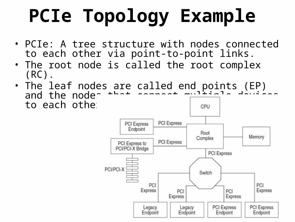
PCIe Topology Example • PCIe: A tree structure with nodes connected to each other via
point-to-point links. • The root node is called the root complex (RC).• The leaf nodes are called end points (EP) and the nodes that
connect multiple devices to each other are called switches (SW).
Multicore Training
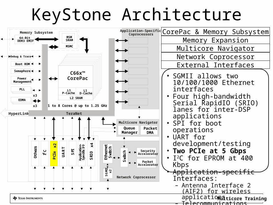
KeyStone Architecture
• SGMII allows two 10/100/1000 Ethernet interfaces
• Four high-bandwidth Serial RapidIO (SRIO) lanes for inter-DSP applications
• SPI for boot operations• UART for development/testing• Two PCIe at 5 Gbps • I2C for EPROM at 400 Kbps• Application-specific Interfaces:
– Antenna Interface 2 (AIF2) for wireless applications
– Telecommunications Serial Port (TSIP) x2 for media applications
Memory ExpansionMulticore Navigator
CorePac & Memory Subsystem
External InterfacesNetwork Coprocessor
1 to 8 Cores @ up to 1.25 GHz
MSMC
MSMSRAM
64-Bit DDR3 EMIF
Application-SpecificCoprocessors
PowerManagement
Debug & Trace
Boot ROM
Semaphore
Memory Subsystem
SR
I O
x4
PC
I e
x2
UA
RT
Ap
plic
atio
n-S
pec i
f ic
I/O
SP
I
IC
2
PacketDMA
Multicore Navigator
QueueManager
Oth
ers
x3
Network Coprocessor
Sw
i tc
h
Eth
ern
et
Sw
i tc
hS
GM
IIx2
PacketAccelerator
SecurityAccelerator
PLL
EDMA
x3
C66x™CorePac
L1P-Cache
L1D-Cache
L2 SRAM
HyperLink TeraNet
Multicore Training
PCIe Features• PCI-SIG: PCI Express Base Specification (Rev. 2.0)• Root Complex (RC) and End Point (EP) operation modes.
– In EP mode, supports both legacy EP mode and native PCIe EP mode.– Set from bootstrap pins PCIESSMODE[1:0] at power-up
(00->EP, 01->Legacy EP, 10->RC). – Software overwrites the setting by changing the PCIESSMODE bits in
the DEVSTAT register.
• Gen1 (2.5 Gbps) and Gen2 (5.0 Gbps) • x2 lanes • Outbound/Inbound max payload size of 128/256 bytes
Multicore Training
Agenda• PCIe Overview• Address Translation• Configuration• PCIe Boot Demo
Multicore Training
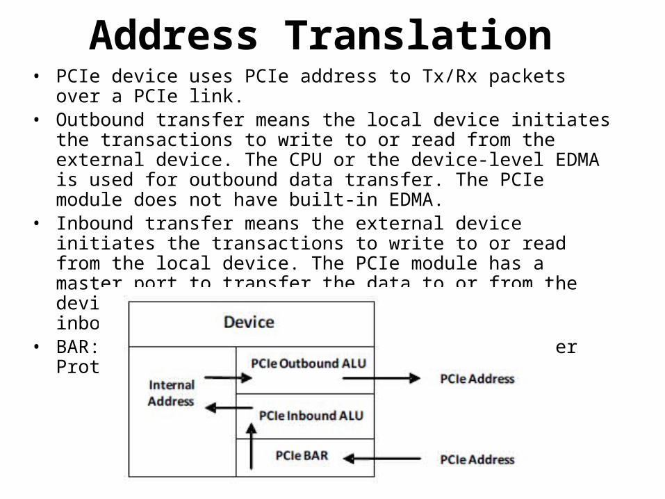
Address Translation • PCIe device uses PCIe address to Tx/Rx packets over a PCIe link.• Outbound transfer means the local device initiates the transactions to
write to or read from the external device. The CPU or the device-level EDMA is used for outbound data transfer. The PCIe module does not have built-in EDMA.
• Inbound transfer means the external device initiates the transactions to write to or read from the local device. The PCIe module has a master port to transfer the data to or from the device memory; No CPU or EDMA is needed for inbound transfer in the local device.
• BAR: used to accept/reject TLP (Transport Layer Protocol).
Multicore Training
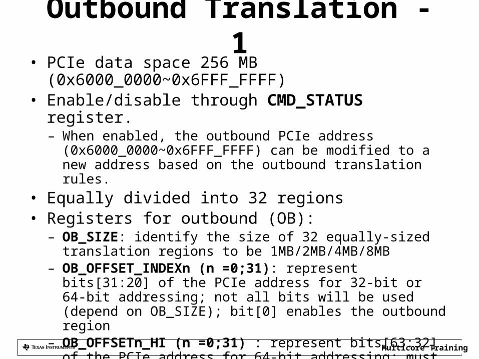
Outbound Translation - 1• PCIe data space 256 MB (0x6000_0000~0x6FFF_FFFF)• Enable/disable through CMD_STATUS register.
– When enabled, the outbound PCIe address (0x6000_0000~0x6FFF_FFFF) can be modified to a new address based on the outbound translation rules.
• Equally divided into 32 regions• Registers for outbound (OB):
– OB_SIZE: identify the size of 32 equally-sized translation regions to be 1MB/2MB/4MB/8MB
– OB_OFFSET_INDEXn (n =0;31): represent bits[31:20] of the PCIe address for 32-bit or 64-bit addressing; not all bits will be used (depend on OB_SIZE); bit[0] enables the outbound region
– OB_OFFSETn_HI (n =0;31) : represent bits[63:32] of the PCIe address for 64-bit addressing; must be zero for 32-bit addressing
Multicore Training
Outbound Translation - 2
Multicore Training
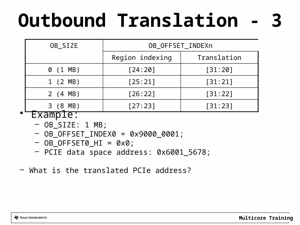
Outbound Translation - 3OB_SIZE OB_OFFSET_INDEXn
Region indexing Translation
0 (1 MB) [24:20] [31:20]
1 (2 MB) [25:21] [31:21]
2 (4 MB) [26:22] [31:22]
3 (8 MB) [27:23] [31:23]
• Example:– OB_SIZE: 1 MB; – OB_OFFSET_INDEX0 = 0x9000_0001; – OB_OFFSET0_HI = 0x0; – PCIE data space address: 0x6001_5678;
– What is the translated PCIe address?
Multicore Training
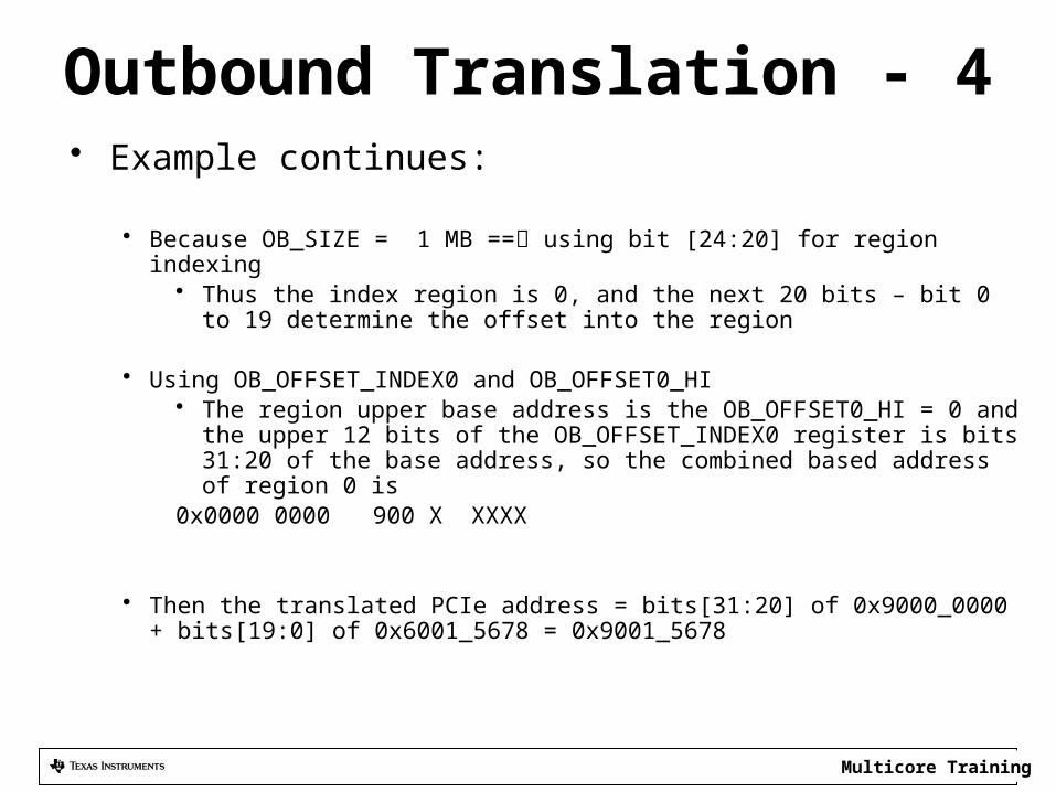
Outbound Translation - 4• Example continues:
• Because OB_SIZE = 1 MB == using bit [24:20] for region indexing• Thus the index region is 0, and the next 20 bits – bit 0 to 19 determine the
offset into the region
• Using OB_OFFSET_INDEX0 and OB_OFFSET0_HI• The region upper base address is the OB_OFFSET0_HI = 0 and the upper 12
bits of the OB_OFFSET_INDEX0 register is bits 31:20 of the base address, so the combined based address of region 0 is
0x0000 0000 900 X XXXX
• Then the translated PCIe address = bits[31:20] of 0x9000_0000 + bits[19:0] of 0x6001_5678 = 0x9001_5678
Multicore Training
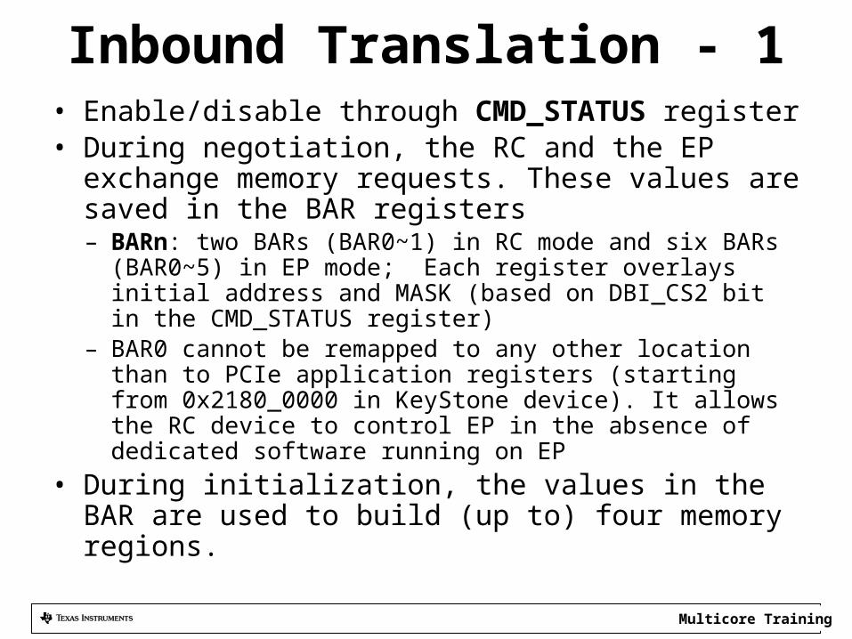
Inbound Translation - 1• Enable/disable through CMD_STATUS register• During negotiation, the RC and the EP exchange memory
requests. These values are saved in the BAR registers– BARn: two BARs (BAR0~1) in RC mode and six BARs (BAR0~5) in EP
mode; Each register overlays initial address and MASK (based on DBI_CS2 bit in the CMD_STATUS register)
– BAR0 cannot be remapped to any other location than to PCIe application registers (starting from 0x2180_0000 in KeyStone device). It allows the RC device to control EP in the absence of dedicated software running on EP
• During initialization, the values in the BAR are used to build (up to) four memory regions.
Multicore Training
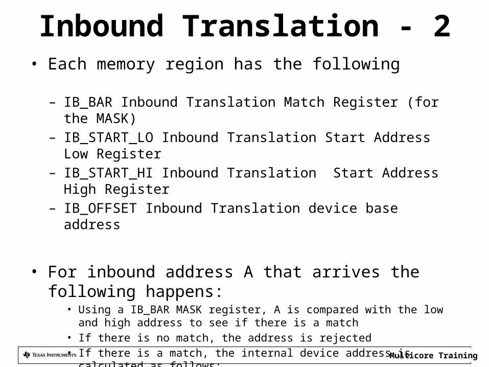
Inbound Translation - 2• Each memory region has the following
– IB_BAR Inbound Translation Match Register (for the MASK)– IB_START_LO Inbound Translation Start Address Low Register– IB_START_HI Inbound Translation Start Address High Register– IB_OFFSET Inbound Translation device base address
• For inbound address A that arrives the following happens:• Using a IB_BAR MASK register, A is compared with the low and high address to see if
there is a match• If there is no match, the address is rejected• If there is a match, the internal device address is calculated as follows:The difference between A – IB_START (64 bit, high and low) is calculatedThe result is added to the device base address
Multicore Training
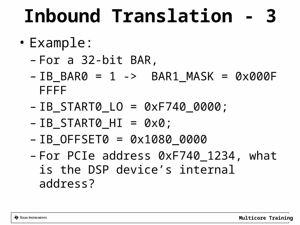
Inbound Translation - 3• Example:
– For a 32-bit BAR, – IB_BAR0 = 1 -> BAR1_MASK = 0x000F FFFF– IB_START0_LO = 0xF740_0000; – IB_START0_HI = 0x0; – IB_OFFSET0 = 0x1080_0000 – For PCIe address 0xF740_1234, what is the DSP
device’s internal address?
Multicore Training
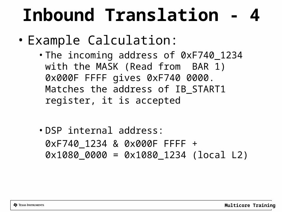
Inbound Translation - 4• Example Calculation:
• The incoming address of 0xF740_1234 with the MASK (Read from BAR 1) 0x000F FFFF gives 0xF740 0000. Matches the address of IB_START1 register, it is accepted
• DSP internal address: 0xF740_1234 & 0x000F FFFF + 0x1080_0000 = 0x1080_1234 (local L2)
Multicore Training
Agenda• PCIe Overview• Address Translation• Configuration• PCIe Boot Demo
Multicore Training
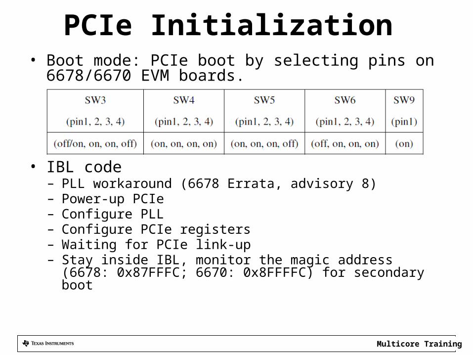
PCIe Initialization • Boot mode: PCIe boot by selecting pins on 6678/6670 EVM
boards.
• IBL code– PLL workaround (6678 Errata, advisory 8)– Power-up PCIe – Configure PLL– Configure PCIe registers – Waiting for PCIe link-up– Stay inside IBL, monitor the magic address (6678: 0x87FFFC; 6670:
0x8FFFFC) for secondary boot
Multicore Training
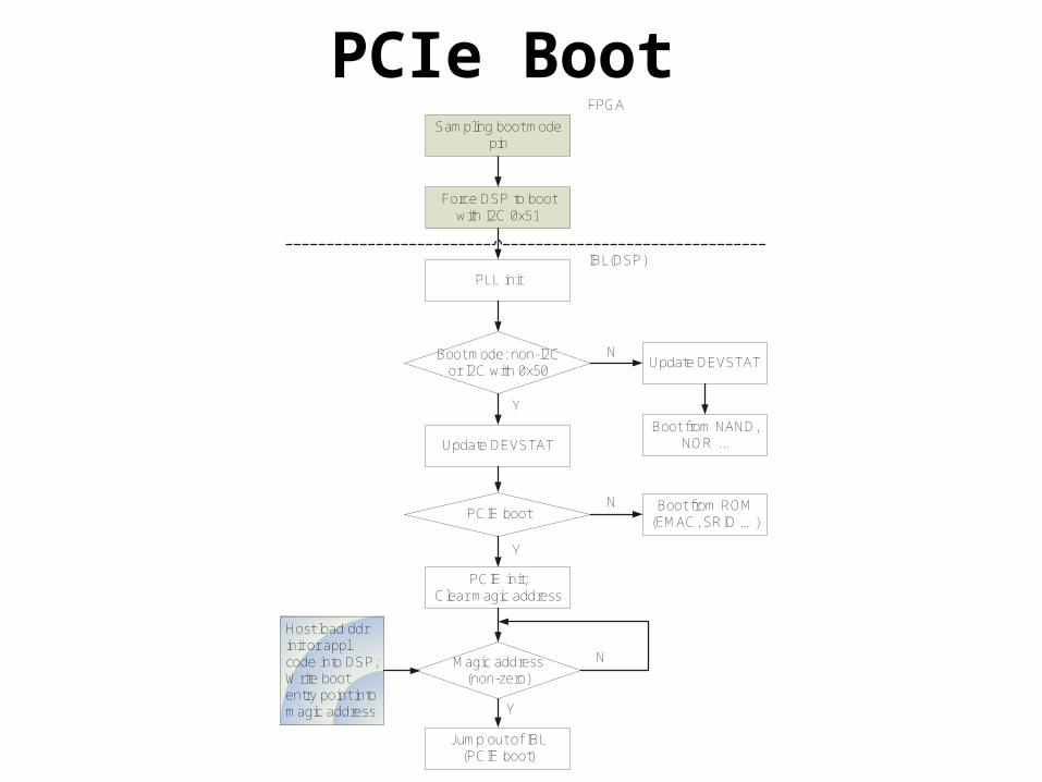
PCIe Boot Sampling boot mode
pin
PLL init
Force DSP to boot with I2C 0x51
FPGA
IBL(DSP)
Boot mode: non-I2C or I2C with 0x50
NUpdate DEVSTAT
Y
Update DEVSTAT
PCIE boot
Y
N Boot from ROM (EMAC, SRIO …)
PCIE init;Clear magic address
Magic address (non-zero)
N
Y
Host load ddr init or appl code into DSP;Write boot entry point into magic address
Jump out of IBL (PCIE boot)
Boot from NAND, NOR ...
Multicore Training
Agenda• PCIe Overview• Address Translation• Configuration• PCIe Demo
Multicore Training
Demo• C:\ti\pdk_C6678_xx_yy\packages\ti\drv\pcie\example\
sample
Multicore Training
For More Information• For more information, refer to the
PCI Express (PCIe) for KeyStone Devices User’s Guide.
• For questions regarding topics covered in this training, visit the support forums at theTI E2E Community website.
Recommended

![Keystone Family PCIE - Texas Instrumentsprocessors.wiki.ti.com/images/f/f1/KeystoneTraining-PCI_Express.pdf · [ 96.780080] pci 0000:04:00.0: PCI INT A -> GSI 16 (level, low) -> IRQ](https://img.pdfslide.net/doc/110x75/5f10863e7e708231d449890c/keystone-family-pcie-texas-i-96780080-pci-000004000-pci-int-a-gsi.jpg)