R1
240 W
R2
2.4 kW
INPUT OUTPUT
ADJUST
LM317
VI
RS
0.2 W
Copyright © 2016, Texas Instruments Incorporated
Product
Folder
Sample &Buy
Technical
Documents
Tools &
Software
Support &Community
An IMPORTANT NOTICE at the end of this data sheet addresses availability, warranty, changes, use in safety-critical applications,intellectual property matters and other important disclaimers. PRODUCTION DATA.
LM317SLVS044X –SEPTEMBER 1997–REVISED SEPTEMBER 2016
LM317 3-Terminal Adjustable Regulator
1
1 Features1• Output Voltage Range Adjustable
From 1.25 V to 37 V• Output Current Greater Than 1.5 A• Internal Short-Circuit Current Limiting• Thermal Overload Protection• Output Safe-Area Compensation
2 Applications• ATCA Solutions• DLP: 3D Biometrics, Hyperspectral Imaging,
Optical Networking, and Spectroscopy• DVR and DVS• Desktop PC• Digital Signage and Still Camera• ECG Electrocardiogram• EV HEV Charger: Level 1, 2, and 3• Electronic Shelf Label• Energy Harvesting• Ethernet Switch• Femto Base Station• Fingerprint and Iris Biometrics• HVAC: Heating, Ventilating, and Air Conditioning• High-Speed Data Acquisition and Generation• Hydraulic Valve• IP Phone: Wired and Wireless• Intelligent Occupancy Sensing• Motor Control: Brushed DC, Brushless DC, Low-
Voltage, Permanent Magnet, and Stepper Motor• Point-to-Point Microwave Backhaul• Power Bank Solutions• Power Line Communication Modem• Power Over Ethernet (PoE)• Power Quality Meter• Power Substation Control• Private Branch Exchange (PBX)• Programmable Logic Controller• RFID Reader• Refrigerator• Signal or Waveform Generator• Software Defined Radio (SDR)• Washing Machine: High-End and Low-End• X-ray: Baggage Scanner, Medical, and Dental
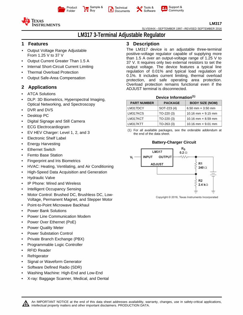
3 DescriptionThe LM317 device is an adjustable three-terminalpositive-voltage regulator capable of supplying morethan 1.5 A over an output-voltage range of 1.25 V to37 V. It requires only two external resistors to set theoutput voltage. The device features a typical lineregulation of 0.01% and typical load regulation of0.1%. It includes current limiting, thermal overloadprotection, and safe operating area protection.Overload protection remains functional even if theADJUST terminal is disconnected.
Device Information(1)
PART NUMBER PACKAGE BODY SIZE (NOM)LM317DCY SOT-223 (4) 6.50 mm × 3.50 mmLM317KCS TO-220 (3) 10.16 mm × 9.15 mmLM317KCT TO-220 (3) 10.16 mm × 8.59 mmLM317KTT TO-263 (3) 10.16 mm × 9.01 mm
(1) For all available packages, see the orderable addendum atthe end of the data sheet.
Battery-Charger Circuit
2
LM317SLVS044X –SEPTEMBER 1997–REVISED SEPTEMBER 2016 www.ti.com
Product Folder Links: LM317
Submit Documentation Feedback Copyright © 1997–2016, Texas Instruments Incorporated
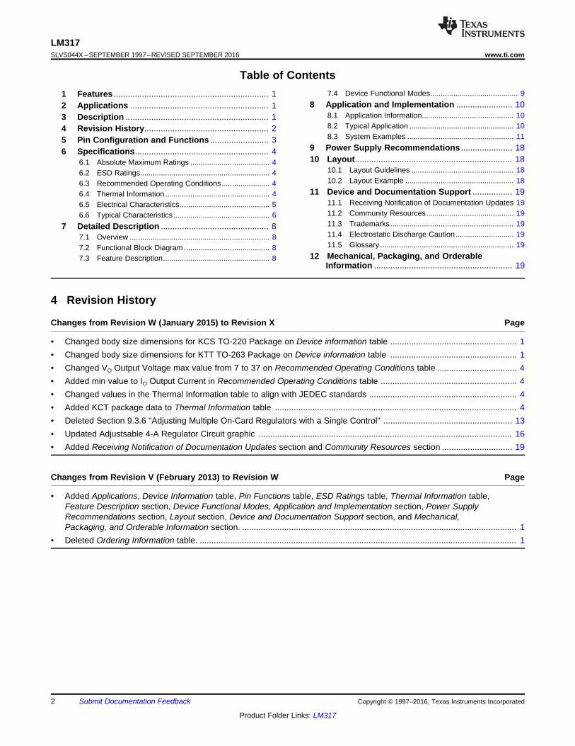
Table of Contents1 Features .................................................................. 12 Applications ........................................................... 13 Description ............................................................. 14 Revision History..................................................... 25 Pin Configuration and Functions ......................... 36 Specifications......................................................... 4
6.1 Absolute Maximum Ratings ...................................... 46.2 ESD Ratings.............................................................. 46.3 Recommended Operating Conditions....................... 46.4 Thermal Information .................................................. 46.5 Electrical Characteristics........................................... 56.6 Typical Characteristics .............................................. 6
7 Detailed Description .............................................. 87.1 Overview ................................................................... 87.2 Functional Block Diagram ......................................... 87.3 Feature Description................................................... 8
7.4 Device Functional Modes.......................................... 98 Application and Implementation ........................ 10
8.1 Application Information............................................ 108.2 Typical Application .................................................. 108.3 System Examples ................................................... 11
9 Power Supply Recommendations ...................... 1810 Layout................................................................... 18
10.1 Layout Guidelines ................................................. 1810.2 Layout Example .................................................... 18
11 Device and Documentation Support ................. 1911.1 Receiving Notification of Documentation Updates 1911.2 Community Resources.......................................... 1911.3 Trademarks ........................................................... 1911.4 Electrostatic Discharge Caution............................ 1911.5 Glossary ................................................................ 19
12 Mechanical, Packaging, and OrderableInformation ........................................................... 19
4 Revision History
Changes from Revision W (January 2015) to Revision X Page
• Changed body size dimensions for KCS TO-220 Package on Device information table ...................................................... 1• Changed body size dimensions for KTT TO-263 Package on Device information table ...................................................... 1• Changed VO Output Voltage max value from 7 to 37 on Recommended Operating Conditions table .................................. 4• Added min value to IO Output Current in Recommended Operating Conditions table .......................................................... 4• Changed values in the Thermal Information table to align with JEDEC standards ............................................................... 4• Added KCT package data to Thermal Information table ....................................................................................................... 4• Deleted Section 9.3.6 "Adjusting Multiple On-Card Regulators with a Single Control" ....................................................... 13• Updated Adjustsable 4-A Regulator Circuit graphic ............................................................................................................ 16• Added Receiving Notification of Documentation Updates section and Community Resources section .............................. 19
Changes from Revision V (February 2013) to Revision W Page
• Added Applications, Device Information table, Pin Functions table, ESD Ratings table, Thermal Information table,Feature Description section, Device Functional Modes, Application and Implementation section, Power SupplyRecommendations section, Layout section, Device and Documentation Support section, and Mechanical,Packaging, and Orderable Information section. ..................................................................................................................... 1
• Deleted Ordering Information table. ....................................................................................................................................... 1
1 ADJUST
2 OUTPUT
3 INPUT
Not to scale
OU
TP
UT
1ADJUST
2OUTPUT
3INPUT
4 OUTPUT
Not to scale
1 ADJUST
2 OUTPUT
3 INPUT
Not to scale
OU
TP
UT
3
LM317www.ti.com SLVS044X –SEPTEMBER 1997–REVISED SEPTEMBER 2016
Product Folder Links: LM317
Submit Documentation FeedbackCopyright © 1997–2016, Texas Instruments Incorporated
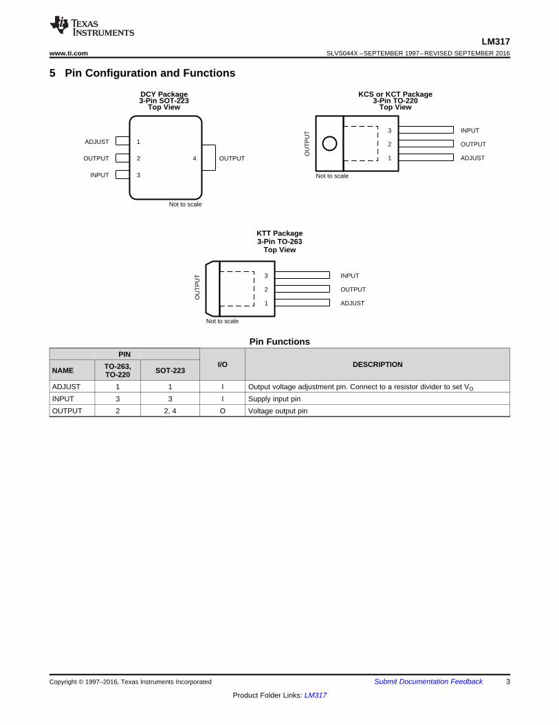
5 Pin Configuration and Functions
DCY Package3-Pin SOT-223
Top View
KCS or KCT Package3-Pin TO-220
Top View
KTT Package3-Pin TO-263
Top View
Pin FunctionsPIN
I/O DESCRIPTIONNAME TO-263,
TO-220 SOT-223
ADJUST 1 1 I Output voltage adjustment pin. Connect to a resistor divider to set VO
INPUT 3 3 I Supply input pinOUTPUT 2 2, 4 O Voltage output pin
4
LM317SLVS044X –SEPTEMBER 1997–REVISED SEPTEMBER 2016 www.ti.com
Product Folder Links: LM317
Submit Documentation Feedback Copyright © 1997–2016, Texas Instruments Incorporated
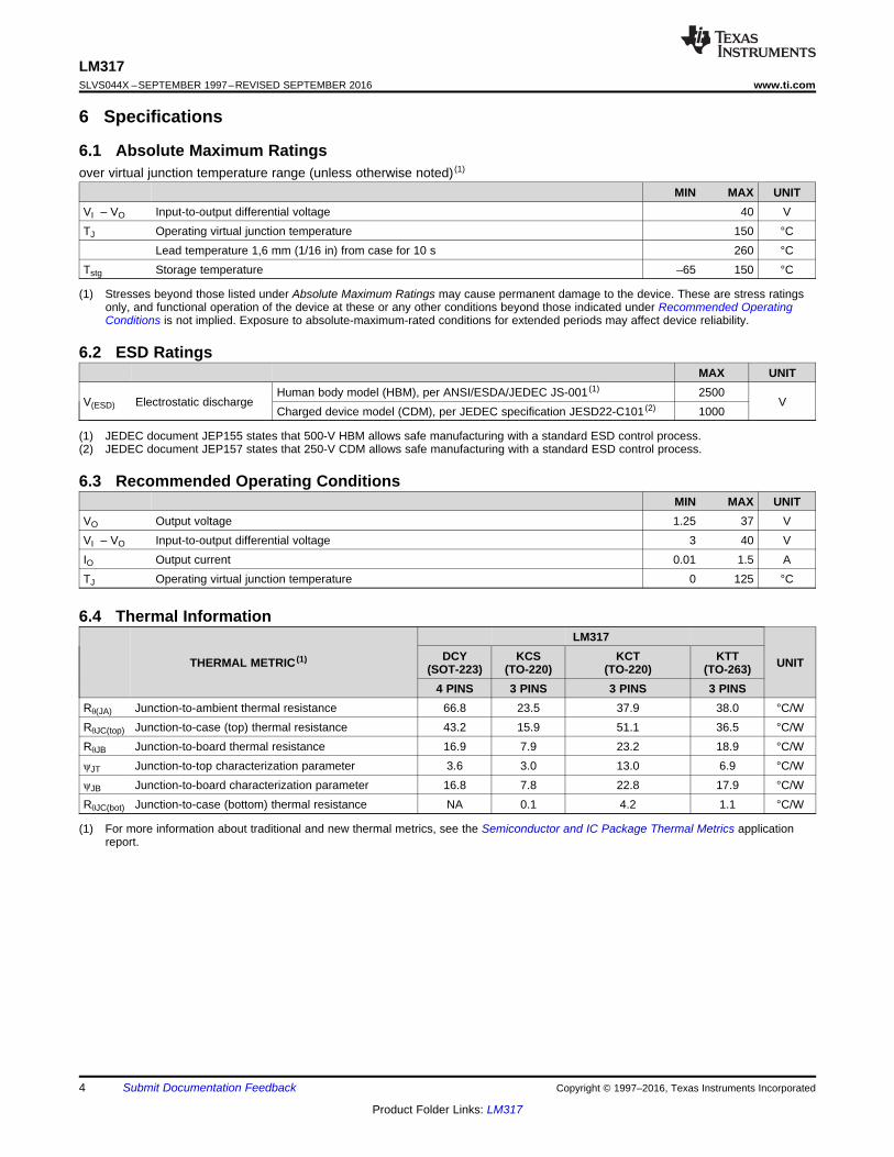
(1) Stresses beyond those listed under Absolute Maximum Ratings may cause permanent damage to the device. These are stress ratingsonly, and functional operation of the device at these or any other conditions beyond those indicated under Recommended OperatingConditions is not implied. Exposure to absolute-maximum-rated conditions for extended periods may affect device reliability.
6 Specifications
6.1 Absolute Maximum Ratingsover virtual junction temperature range (unless otherwise noted) (1)
MIN MAX UNITVI – VO Input-to-output differential voltage 40 VTJ Operating virtual junction temperature 150 °C
Lead temperature 1,6 mm (1/16 in) from case for 10 s 260 °CTstg Storage temperature –65 150 °C
(1) JEDEC document JEP155 states that 500-V HBM allows safe manufacturing with a standard ESD control process.(2) JEDEC document JEP157 states that 250-V CDM allows safe manufacturing with a standard ESD control process.
6.2 ESD RatingsMAX UNIT
V(ESD) Electrostatic dischargeHuman body model (HBM), per ANSI/ESDA/JEDEC JS-001 (1) 2500
VCharged device model (CDM), per JEDEC specification JESD22-C101 (2) 1000
6.3 Recommended Operating ConditionsMIN MAX UNIT
VO Output voltage 1.25 37 VVI – VO Input-to-output differential voltage 3 40 VIO Output current 0.01 1.5 ATJ Operating virtual junction temperature 0 125 °C
(1) For more information about traditional and new thermal metrics, see the Semiconductor and IC Package Thermal Metrics applicationreport.
6.4 Thermal Information
THERMAL METRIC (1)
LM317
UNITDCY(SOT-223)
KCS(TO-220)
KCT(TO-220)
KTT(TO-263)
4 PINS 3 PINS 3 PINS 3 PINSRθ(JA) Junction-to-ambient thermal resistance 66.8 23.5 37.9 38.0 °C/WRθJC(top) Junction-to-case (top) thermal resistance 43.2 15.9 51.1 36.5 °C/WRθJB Junction-to-board thermal resistance 16.9 7.9 23.2 18.9 °C/WψJT Junction-to-top characterization parameter 3.6 3.0 13.0 6.9 °C/WψJB Junction-to-board characterization parameter 16.8 7.8 22.8 17.9 °C/WRθJC(bot) Junction-to-case (bottom) thermal resistance NA 0.1 4.2 1.1 °C/W
5
LM317www.ti.com SLVS044X –SEPTEMBER 1997–REVISED SEPTEMBER 2016
Product Folder Links: LM317
Submit Documentation FeedbackCopyright © 1997–2016, Texas Instruments Incorporated
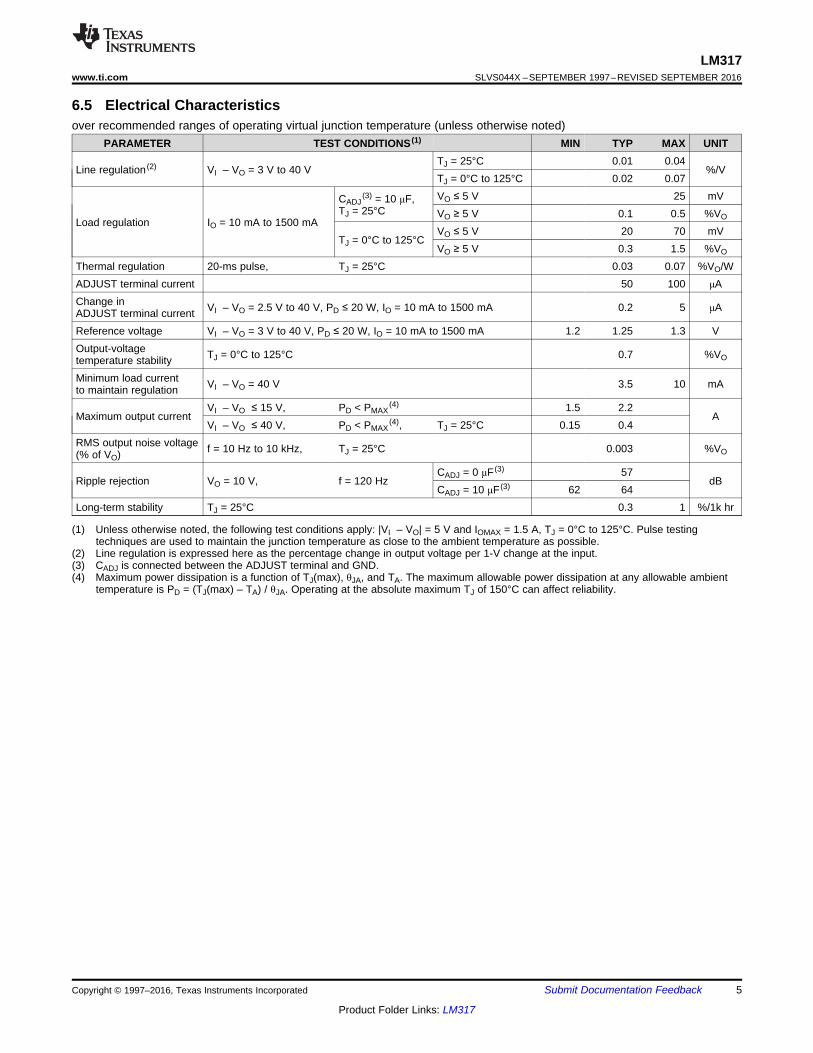
(1) Unless otherwise noted, the following test conditions apply: |VI – VO| = 5 V and IOMAX = 1.5 A, TJ = 0°C to 125°C. Pulse testingtechniques are used to maintain the junction temperature as close to the ambient temperature as possible.
(2) Line regulation is expressed here as the percentage change in output voltage per 1-V change at the input.(3) CADJ is connected between the ADJUST terminal and GND.(4) Maximum power dissipation is a function of TJ(max), θJA, and TA. The maximum allowable power dissipation at any allowable ambient
temperature is PD = (TJ(max) – TA) / θJA. Operating at the absolute maximum TJ of 150°C can affect reliability.
6.5 Electrical Characteristicsover recommended ranges of operating virtual junction temperature (unless otherwise noted)
PARAMETER TEST CONDITIONS (1) MIN TYP MAX UNIT
Line regulation (2) VI – VO = 3 V to 40 VTJ = 25°C 0.01 0.04
%/VTJ = 0°C to 125°C 0.02 0.07
Load regulation IO = 10 mA to 1500 mA
CADJ(3) = 10 μF,
TJ = 25°CVO ≤ 5 V 25 mVVO ≥ 5 V 0.1 0.5 %VO
TJ = 0°C to 125°CVO ≤ 5 V 20 70 mVVO ≥ 5 V 0.3 1.5 %VO
Thermal regulation 20-ms pulse, TJ = 25°C 0.03 0.07 %VO/WADJUST terminal current 50 100 μAChange inADJUST terminal current VI – VO = 2.5 V to 40 V, PD ≤ 20 W, IO = 10 mA to 1500 mA 0.2 5 μA
Reference voltage VI – VO = 3 V to 40 V, PD ≤ 20 W, IO = 10 mA to 1500 mA 1.2 1.25 1.3 VOutput-voltagetemperature stability TJ = 0°C to 125°C 0.7 %VO
Minimum load currentto maintain regulation VI – VO = 40 V 3.5 10 mA
Maximum output currentVI – VO ≤ 15 V, PD < PMAX
(4) 1.5 2.2A
VI – VO ≤ 40 V, PD < PMAX(4), TJ = 25°C 0.15 0.4
RMS output noise voltage(% of VO) f = 10 Hz to 10 kHz, TJ = 25°C 0.003 %VO
Ripple rejection VO = 10 V, f = 120 HzCADJ = 0 μF (3) 57
dBCADJ = 10 μF (3) 62 64
Long-term stability TJ = 25°C 0.3 1 %/1k hr
1.24
1.245
1.25
1.255
1.26
1.265
1.27
1.275
1.28
1.285
0 5
10
15
20
25
30
35
40
V IN – V
VO
UT
–V
T = 125°CA
T = 25°CA
T = –40°CA
-68
-66
-64
-62
-60
-58
-56
-54
-52
-50
0
0.1
0.2
0.3
0.4
0.5
0.6
0.7
0.8
0.9 1
1.1
1.2
1.3
1.4
1.5
IOUT – A
Rip
ple
Reje
cti
on
–d
B
V IN = 15 V
VOUT = 10 V
f = 120 Hz
TA = 25°C
-5
-4.5
-4
-3.5
-3
-2.5
-2
-1.5
-1
-0.5
0
-30
-20
-10 0
10
20
30
40
50
60
70
Time – µs
Lo
ad
Cu
rren
t–
A
9
9.2
9.4
9.6
9.8
10
10.2
10.4
10.6
10.8
11
VIN
VOUT
C = 10 µFADJ
-5
-4.5
-4
-3.5
-3
-2.5
-2
-1.5
-1
-0.5
0
-30
-20
-10 0
10
20
30
40
50
60
70
Time – µs
Lo
ad
Cu
rren
t–
A
9
9.2
9.4
9.6
9.8
10
10.2
10.4
10.6
10.8
11
VO
UT
Devia
tio
n–
V
VIN
VOUT
C = 0 µFADJ
9.98
9.985
9.99
9.995
10
10.005
10.01
0
0.1
0.2
0.3
0.4
0.5
0.6
0.7
0.8
0.9 1
1.1
1.2
1.3
1.4
1.5
IOUT – A
VO
UT
–V
T = 25°CA
T = –40°CA
T = 125°CA
V = 10 V NomOUT
-0.4
-0.2
0
0.2
0.4
0.6
0.8
1
1.2
1.4
0
0.2
0.4
0.6
0.8 1
1.2
1.4
1.6
1.8 2
2.2
2.4
2.6
2.8 3
3.2
3.4
IOUT – A
VO
UT
–V
T = 125°CA
T = 25°CA
T = –40°CA
V = VOUT REF
6
LM317SLVS044X –SEPTEMBER 1997–REVISED SEPTEMBER 2016 www.ti.com
Product Folder Links: LM317
Submit Documentation Feedback Copyright © 1997–2016, Texas Instruments Incorporated
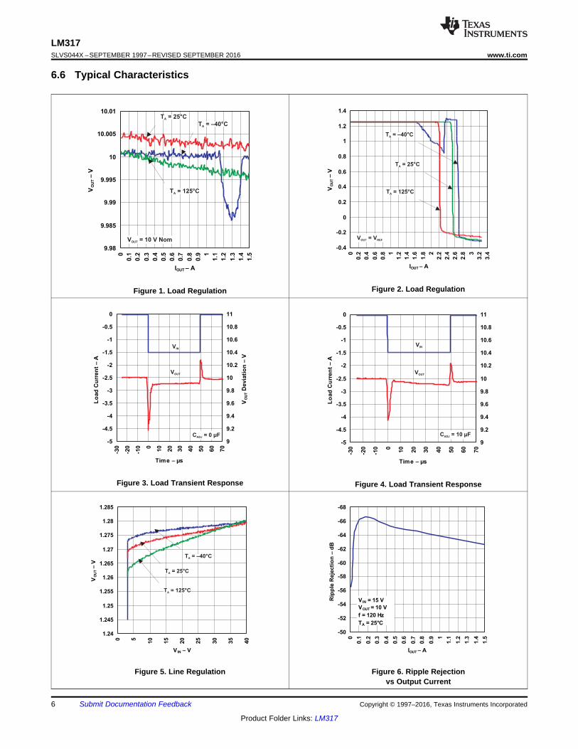
6.6 Typical Characteristics
Figure 1. Load Regulation Figure 2. Load Regulation
Figure 3. Load Transient Response Figure 4. Load Transient Response
Figure 5. Line Regulation Figure 6. Ripple Rejectionvs Output Current
-75
-70
-65
-60
-55
-50
-45
-40
-35
5 10 15 20 25 30 35
VOUT – V
Rip
ple
Reje
cti
on
–d
B
V IN – VOUT = 15 V
IOUT = 500 mA
f = 120 Hz
TA = 25°C
-90
-80
-70
-60
-50
-40
-30
-20
-10
100 1000 10000 100000 1000000
Frequency – Hz
Rip
ple
Reje
cti
on
–d
B
V IN = 15 V
VOUT = 10 V
IOUT = 500 mA
TA = 25°C
100 1k 10k 100k 1M
C = 0 µFADJ
C = 10 µFADJ
7
LM317www.ti.com SLVS044X –SEPTEMBER 1997–REVISED SEPTEMBER 2016
Product Folder Links: LM317
Submit Documentation FeedbackCopyright © 1997–2016, Texas Instruments Incorporated
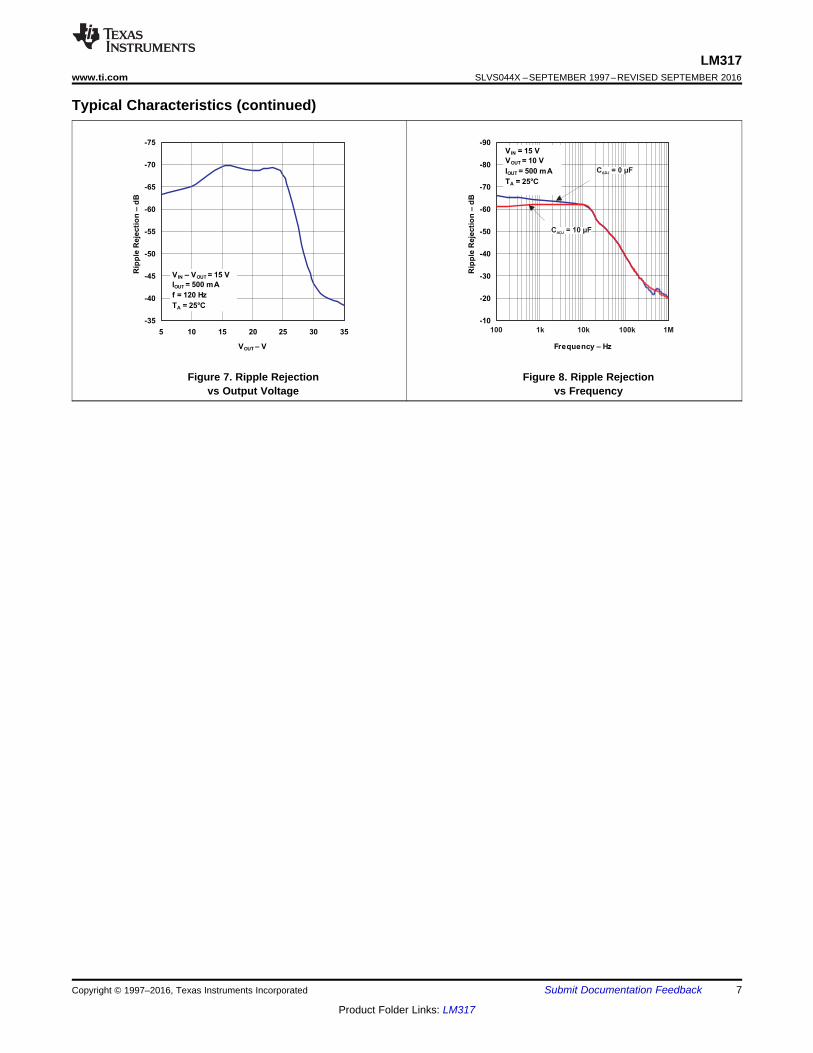
Typical Characteristics (continued)
Figure 7. Ripple Rejectionvs Output Voltage
Figure 8. Ripple Rejectionvs Frequency
+
Over Temp &
Over Current
Protection
Input
Adj.
Output
1.25 V
Iadj
8
LM317SLVS044X –SEPTEMBER 1997–REVISED SEPTEMBER 2016 www.ti.com
Product Folder Links: LM317
Submit Documentation Feedback Copyright © 1997–2016, Texas Instruments Incorporated
7 Detailed Description
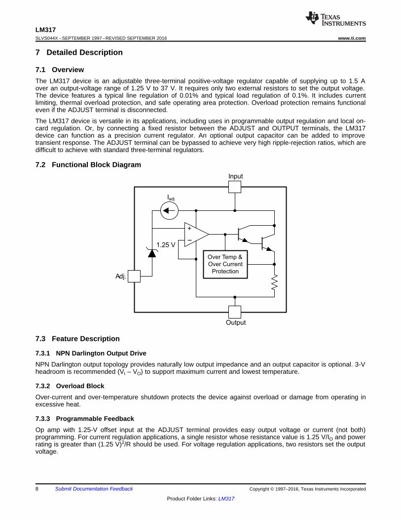
7.1 OverviewThe LM317 device is an adjustable three-terminal positive-voltage regulator capable of supplying up to 1.5 Aover an output-voltage range of 1.25 V to 37 V. It requires only two external resistors to set the output voltage.The device features a typical line regulation of 0.01% and typical load regulation of 0.1%. It includes currentlimiting, thermal overload protection, and safe operating area protection. Overload protection remains functionaleven if the ADJUST terminal is disconnected.
The LM317 device is versatile in its applications, including uses in programmable output regulation and local on-card regulation. Or, by connecting a fixed resistor between the ADJUST and OUTPUT terminals, the LM317device can function as a precision current regulator. An optional output capacitor can be added to improvetransient response. The ADJUST terminal can be bypassed to achieve very high ripple-rejection ratios, which aredifficult to achieve with standard three-terminal regulators.
7.2 Functional Block Diagram
7.3 Feature Description
7.3.1 NPN Darlington Output DriveNPN Darlington output topology provides naturally low output impedance and an output capacitor is optional. 3-Vheadroom is recommended (VI – VO) to support maximum current and lowest temperature.
7.3.2 Overload BlockOver-current and over-temperature shutdown protects the device against overload or damage from operating inexcessive heat.
7.3.3 Programmable FeedbackOp amp with 1.25-V offset input at the ADJUST terminal provides easy output voltage or current (not both)programming. For current regulation applications, a single resistor whose resistance value is 1.25 V/IO and powerrating is greater than (1.25 V)2/R should be used. For voltage regulation applications, two resistors set the outputvoltage.
9
LM317www.ti.com SLVS044X –SEPTEMBER 1997–REVISED SEPTEMBER 2016
Product Folder Links: LM317
Submit Documentation FeedbackCopyright © 1997–2016, Texas Instruments Incorporated
7.4 Device Functional Modes
7.4.1 Normal OperationThe device OUTPUT pin will source current necessary to make OUTPUT pin 1.25 V greater than ADJUSTterminal to provide output regulation.
7.4.2 Operation With Low Input VoltageThe device requires up to 3-V headroom (VI – VO) to operate in regulation. The device may drop out andOUTPUT voltage will be INPUT voltage minus drop out voltage with less headroom.
7.4.3 Operation at Light LoadsThe device passes its bias current to the OUTPUT pin. The load or feedback must consume this minimumcurrent for regulation or the output may be too high. See the Electrical Characteristics table for the minimum loadcurrent needed to maintain regulation.
7.4.4 Operation In Self ProtectionWhen an overload occurs the device shuts down Darlington NPN output stage or reduces the output current toprevent device damage. The device will automatically reset from the overload. The output may be reduced oralternate between on and off until the overload is removed.
LM317
R1
240 W
IAdj
R2
Adjust
Ci
0.1 µF
CO
1.0 µF
VI VOOutputInput
Vref = 1.25 V
D1
1N4002
D2
1N4002
CADJ
Copyright © 2016, Texas Instruments Incorporated
10
LM317SLVS044X –SEPTEMBER 1997–REVISED SEPTEMBER 2016 www.ti.com
Product Folder Links: LM317
Submit Documentation Feedback Copyright © 1997–2016, Texas Instruments Incorporated
8 Application and Implementation
NOTEInformation in the following applications sections is not part of the TI componentspecification, and TI does not warrant its accuracy or completeness. TI’s customers areresponsible for determining suitability of components for their purposes. Customers shouldvalidate and test their design implementation to confirm system functionality.
8.1 Application InformationThe flexibility of the LM317 allows it to be configured to take on many different functions in DC powerapplications.
8.2 Typical Application
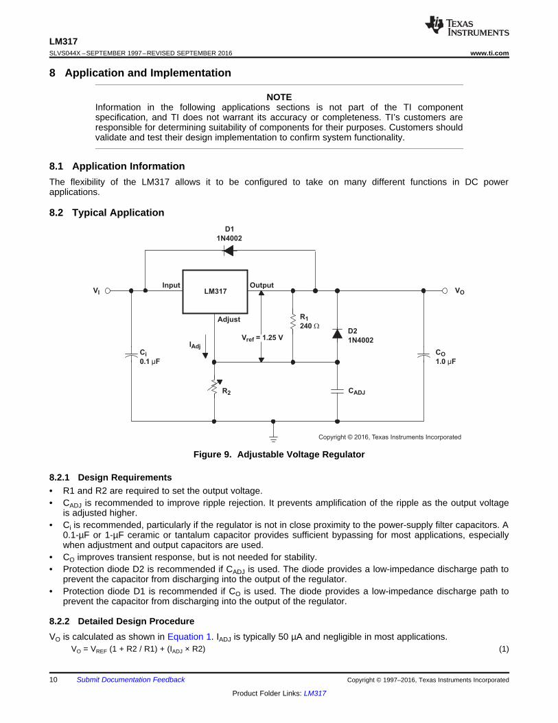
Figure 9. Adjustable Voltage Regulator
8.2.1 Design Requirements• R1 and R2 are required to set the output voltage.• CADJ is recommended to improve ripple rejection. It prevents amplification of the ripple as the output voltage
is adjusted higher.• Ci is recommended, particularly if the regulator is not in close proximity to the power-supply filter capacitors. A
0.1-µF or 1-µF ceramic or tantalum capacitor provides sufficient bypassing for most applications, especiallywhen adjustment and output capacitors are used.
• CO improves transient response, but is not needed for stability.• Protection diode D2 is recommended if CADJ is used. The diode provides a low-impedance discharge path to
prevent the capacitor from discharging into the output of the regulator.• Protection diode D1 is recommended if CO is used. The diode provides a low-impedance discharge path to
prevent the capacitor from discharging into the output of the regulator.
8.2.2 Detailed Design ProcedureVO is calculated as shown in Equation 1. IADJ is typically 50 µA and negligible in most applications.
VO = VREF (1 + R2 / R1) + (IADJ × R2) (1)
C1
0.1 µF
R1
120 W
R2
3 kW
INPUT OUTPUT
ADJUST
LM317
VO+35 V
R3
680 W
−10 V
2 3OUT REF
1
R RV V 1 10 V
R
æ ö+= + -ç ÷
è ø
14
15
16
17
18
19
20
-25
-15 -5 5
15
25
35
45
55
65
Time – µs
VIN
Ch
an
ge
–V
9.98
10.00
10.02
10.04
10.06
10.08
10.10
10.12
VO
UT
–V
VOUT
VIN
C = 10 µFADJ
14
15
16
17
18
19
20
-25
-15 -5 5
15
25
35
45
55
65
Time – µs
VIN
Ch
an
ge
–V
9.98
10.00
10.02
10.04
10.06
10.08
10.10
VO
UT
–V
VOUT
VIN
C = 0 µFADJ
11
LM317www.ti.com SLVS044X –SEPTEMBER 1997–REVISED SEPTEMBER 2016
Product Folder Links: LM317
Submit Documentation FeedbackCopyright © 1997–2016, Texas Instruments Incorporated
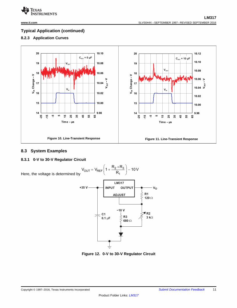
Typical Application (continued)8.2.3 Application Curves
Figure 10. Line-Transient Response Figure 11. Line-Transient Response
8.3 System Examples
8.3.1 0-V to 30-V Regulator Circuit
Here, the voltage is determined by
Figure 12. 0-V to 30-V Regulator Circuit
C1
0.1 µF C2
1 µF
R1
240 Ω
INPUT OUTPUT
ADJUST
LM317
VI
INPUT OUTPUT
ADJUST
VO
LM317
R2
720 Ω
R3
120 Ω
R4
1 kΩ
Output
Adjust
ADJUST
OUTPUTINPUTVI
R1
LM317
Ilimit
1.2
R1
C1
0.1 µF
C3
1 µF
R1
240 W
INPUT OUTPUT
ADJUST
LM317
VOVI
D1
1N4002
R2
5 kW
C2
10 µF
12
LM317SLVS044X –SEPTEMBER 1997–REVISED SEPTEMBER 2016 www.ti.com
Product Folder Links: LM317
Submit Documentation Feedback Copyright © 1997–2016, Texas Instruments Incorporated
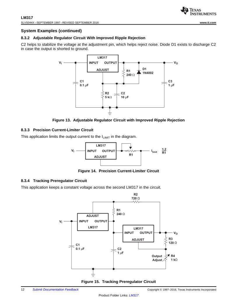
System Examples (continued)8.3.2 Adjustable Regulator Circuit With Improved Ripple RejectionC2 helps to stabilize the voltage at the adjustment pin, which helps reject noise. Diode D1 exists to discharge C2in case the output is shorted to ground.
Figure 13. Adjustable Regulator Circuit with Improved Ripple Rejection
8.3.3 Precision Current-Limiter CircuitThis application limits the output current to the ILIMIT in the diagram.
Figure 14. Precision Current-Limiter Circuit
8.3.4 Tracking Preregulator CircuitThis application keeps a constant voltage across the second LM317 in the circuit.
Figure 15. Tracking Preregulator Circuit
R1
240 W
R2
2.4 kW
INPUT OUTPUT
ADJUST
LM317
VI
RS
0.2 W
Copyright © 2016, Texas Instruments Incorporated
æ ö= ´ ç ÷+è ø
R2Output impendance RS
R1 1
=OUT1.25V
I (short)RS
æ ö= ´ ç ÷+è ø
OUTR2
V 1.25VR1 1
R1
1.2 kΩ
R2
20 kΩ
INPUT OUTPUT
ADJUST
LM317
VOVI
( )+ = o reg(min)R1 R2 min V I
2 3OUT REF
1
R RV V 1 10 V
R
æ ö+= + -ç ÷
è ø
13
LM317www.ti.com SLVS044X –SEPTEMBER 1997–REVISED SEPTEMBER 2016
Product Folder Links: LM317
Submit Documentation FeedbackCopyright © 1997–2016, Texas Instruments Incorporated
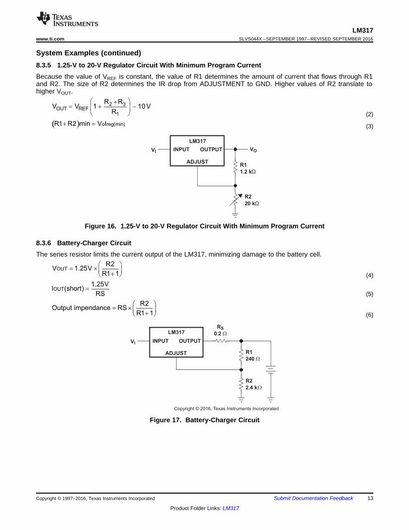
System Examples (continued)8.3.5 1.25-V to 20-V Regulator Circuit With Minimum Program CurrentBecause the value of VREF is constant, the value of R1 determines the amount of current that flows through R1and R2. The size of R2 determines the IR drop from ADJUSTMENT to GND. Higher values of R2 translate tohigher VOUT.
(2)
(3)
Figure 16. 1.25-V to 20-V Regulator Circuit With Minimum Program Current
8.3.6 Battery-Charger CircuitThe series resistor limits the current output of the LM317, minimizing damage to the battery cell.
(4)
(5)
(6)
Figure 17. Battery-Charger Circuit
480 Ω
120 Ω
INPUT OUTPUT
ADJUST
LM317
VI
120 Ω
480 Ω
INPUT OUTPUT
ADJUST
LM317
VI
12 VI(PP) 6 VO(PP)
2 W (TYP)
R1
240 Ω
INPUT OUTPUT
ADJUST
LM317
VO = 15 VVI
D1
1N4002
R2
2.7 kΩ
C1
25 µF
R3
50 kΩ
2N2905
INPUT OUTPUT
ADJUST
LM317
VI
24 Ω
14
LM317SLVS044X –SEPTEMBER 1997–REVISED SEPTEMBER 2016 www.ti.com
Product Folder Links: LM317
Submit Documentation Feedback Copyright © 1997–2016, Texas Instruments Incorporated
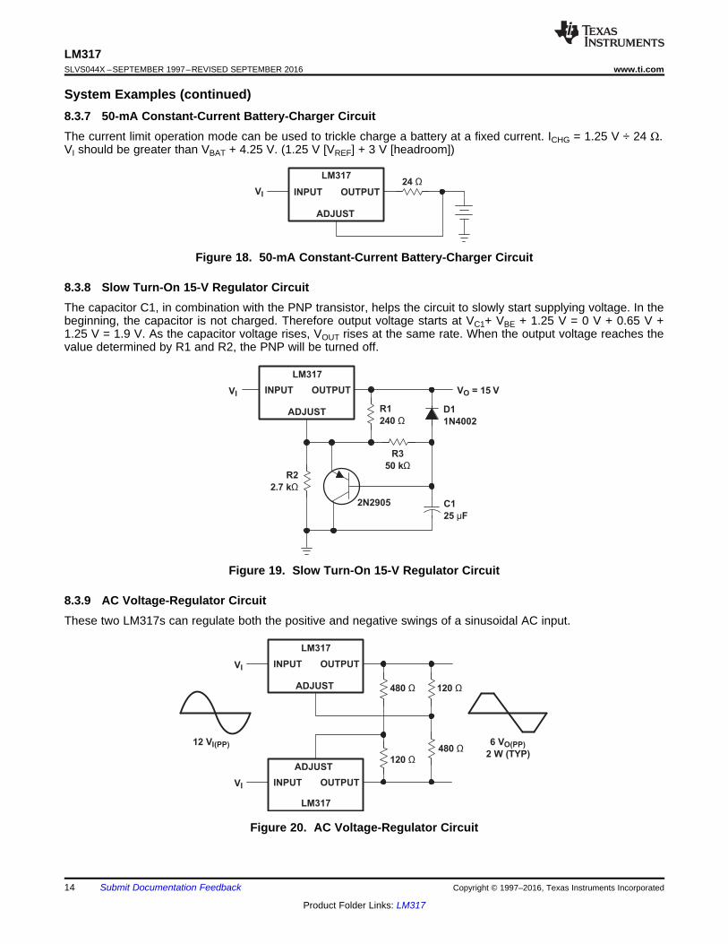
System Examples (continued)8.3.7 50-mA Constant-Current Battery-Charger CircuitThe current limit operation mode can be used to trickle charge a battery at a fixed current. ICHG = 1.25 V ÷ 24 Ω.VI should be greater than VBAT + 4.25 V. (1.25 V [VREF] + 3 V [headroom])
Figure 18. 50-mA Constant-Current Battery-Charger Circuit
8.3.8 Slow Turn-On 15-V Regulator CircuitThe capacitor C1, in combination with the PNP transistor, helps the circuit to slowly start supplying voltage. In thebeginning, the capacitor is not charged. Therefore output voltage starts at VC1+ VBE + 1.25 V = 0 V + 0.65 V +1.25 V = 1.9 V. As the capacitor voltage rises, VOUT rises at the same rate. When the output voltage reaches thevalue determined by R1 and R2, the PNP will be turned off.
Figure 19. Slow Turn-On 15-V Regulator Circuit
8.3.9 AC Voltage-Regulator CircuitThese two LM317s can regulate both the positive and negative swings of a sinusoidal AC input.
Figure 20. AC Voltage-Regulator Circuit
R1
240 W
R2
1.1 kW
INPUT OUTPUT
ADJUST
LM317
VI+
R3
VI−
15
LM317www.ti.com SLVS044X –SEPTEMBER 1997–REVISED SEPTEMBER 2016
Product Folder Links: LM317
Submit Documentation FeedbackCopyright © 1997–2016, Texas Instruments Incorporated
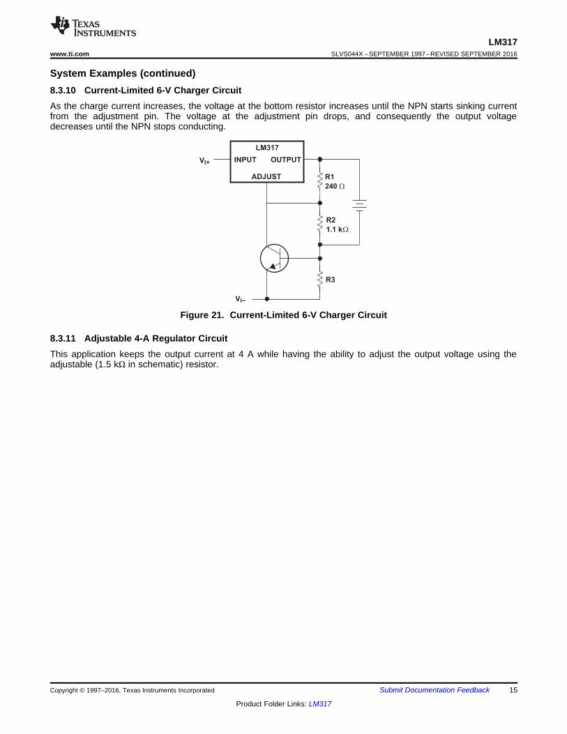
System Examples (continued)8.3.10 Current-Limited 6-V Charger CircuitAs the charge current increases, the voltage at the bottom resistor increases until the NPN starts sinking currentfrom the adjustment pin. The voltage at the adjustment pin drops, and consequently the output voltagedecreases until the NPN stops conducting.
Figure 21. Current-Limited 6-V Charger Circuit
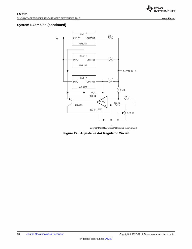
8.3.11 Adjustable 4-A Regulator CircuitThis application keeps the output current at 4 A while having the ability to adjust the output voltage using theadjustable (1.5 kΩ in schematic) resistor.
INPUT OUTPUT
ADJUST
LM317
VI
2N2905
INPUT OUTPUT
ADJUST
LM317
INPUT OUTPUT
ADJUST
LM317
TL084
0.2 Ω
0.2 Ω
0.2 Ω
100 Ω 5 k Ω
5 k Ω
150 Ω
1.5 k Ω
200 pF
4.5 V to 25 V
_
+
Copyright © 2016, Texas Instruments Incorporated
16
LM317SLVS044X –SEPTEMBER 1997–REVISED SEPTEMBER 2016 www.ti.com
Product Folder Links: LM317
Submit Documentation Feedback Copyright © 1997–2016, Texas Instruments Incorporated
System Examples (continued)
Figure 22. Adjustable 4-A Regulator Circuit
INPUT OUTPUT
ADJUST
LM317
2N2905
22 W
VI5 kW
500 W
120 W 1N4002
10 µF
47 µF10 µF
TIP73
VO
17
LM317www.ti.com SLVS044X –SEPTEMBER 1997–REVISED SEPTEMBER 2016
Product Folder Links: LM317
Submit Documentation FeedbackCopyright © 1997–2016, Texas Instruments Incorporated
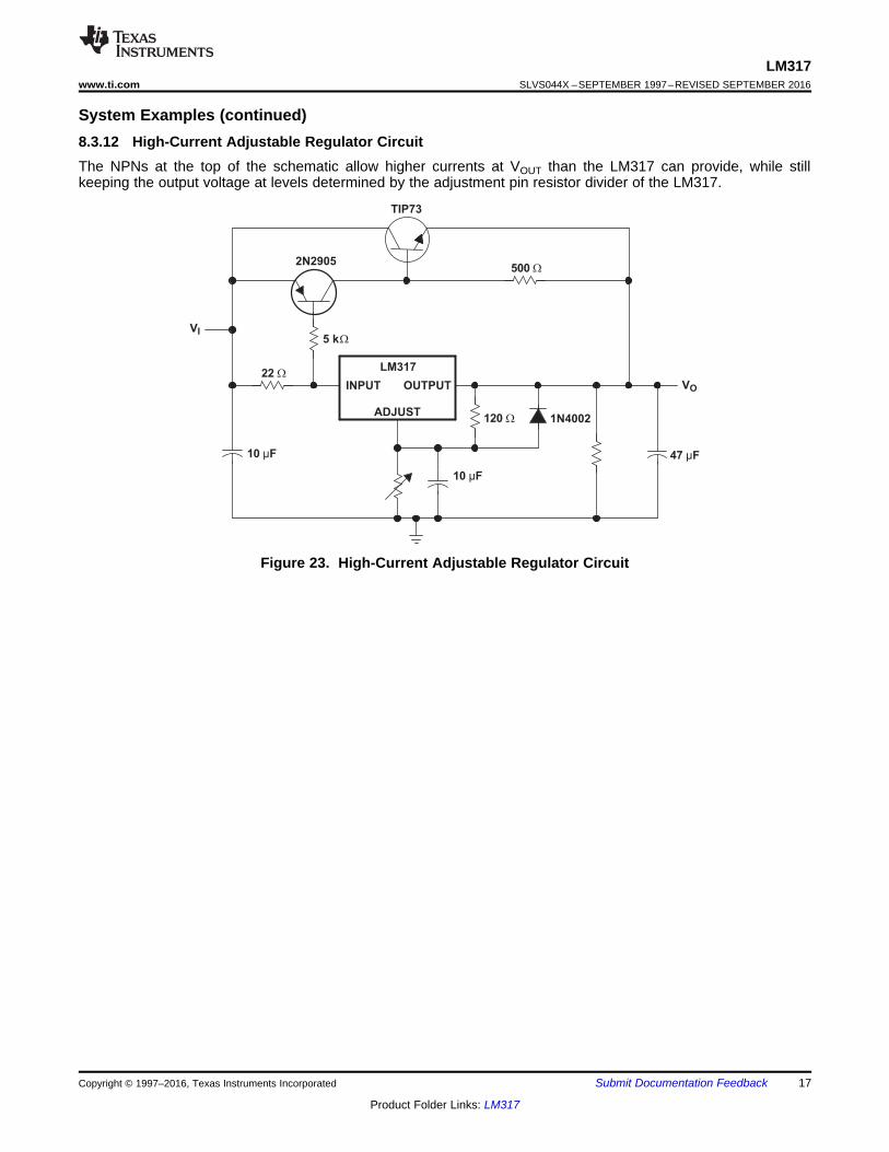
System Examples (continued)8.3.12 High-Current Adjustable Regulator CircuitThe NPNs at the top of the schematic allow higher currents at VOUT than the LM317 can provide, while stillkeeping the output voltage at levels determined by the adjustment pin resistor divider of the LM317.
Figure 23. High-Current Adjustable Regulator Circuit
R1
OUTPUT
INP
UT
OU
TP
UT
AD
J/G
ND
R2
Cadj
COUT
0.1 Fμ 10 Fμ
Gro
und
Ground
High
Frequency
Bypass
Capacitor
High Input
Bypass
Capacitor
Power
18
LM317SLVS044X –SEPTEMBER 1997–REVISED SEPTEMBER 2016 www.ti.com
Product Folder Links: LM317
Submit Documentation Feedback Copyright © 1997–2016, Texas Instruments Incorporated
9 Power Supply RecommendationsThe LM317 is designed to operate from an input voltage supply range between 1.25 V to 37 V greater than theoutput voltage. If the device is more than six inches from the input filter capacitors, an input bypass capacitor, 0.1μF or greater, of any type is needed for stability.
10 Layout
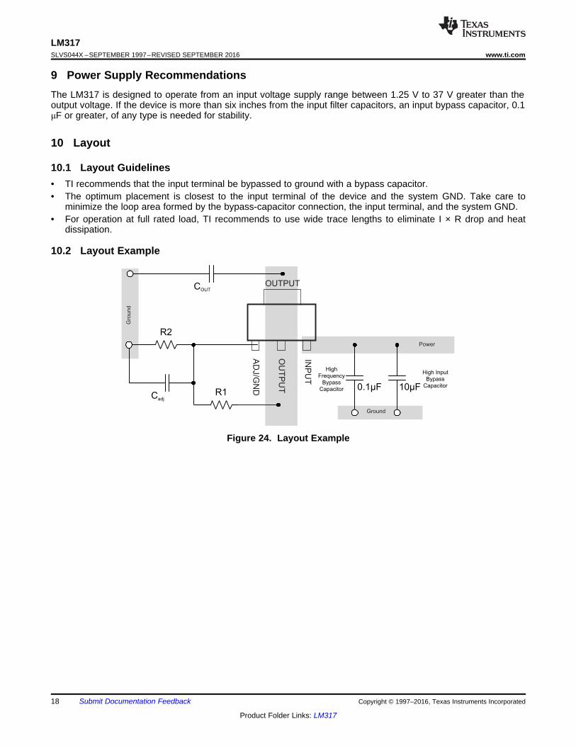
10.1 Layout Guidelines• TI recommends that the input terminal be bypassed to ground with a bypass capacitor.• The optimum placement is closest to the input terminal of the device and the system GND. Take care to
minimize the loop area formed by the bypass-capacitor connection, the input terminal, and the system GND.• For operation at full rated load, TI recommends to use wide trace lengths to eliminate I × R drop and heat
dissipation.
10.2 Layout Example
Figure 24. Layout Example
19
LM317www.ti.com SLVS044X –SEPTEMBER 1997–REVISED SEPTEMBER 2016
Product Folder Links: LM317
Submit Documentation FeedbackCopyright © 1997–2016, Texas Instruments Incorporated
11 Device and Documentation Support
11.1 Receiving Notification of Documentation UpdatesTo receive notification of documentation updates, navigate to the device product folder on ti.com. In the upperright corner, click on Alert me to register and receive a weekly digest of any product information that haschanged. For change details, review the revision history included in any revised document.
11.2 Community ResourcesThe following links connect to TI community resources. Linked contents are provided "AS IS" by the respectivecontributors. They do not constitute TI specifications and do not necessarily reflect TI's views; see TI's Terms ofUse.
TI E2E™ Online Community TI's Engineer-to-Engineer (E2E) Community. Created to foster collaborationamong engineers. At e2e.ti.com, you can ask questions, share knowledge, explore ideas and helpsolve problems with fellow engineers.
Design Support TI's Design Support Quickly find helpful E2E forums along with design support tools andcontact information for technical support.
11.3 TrademarksE2E is a trademark of Texas Instruments.All other trademarks are the property of their respective owners.
11.4 Electrostatic Discharge CautionThis integrated circuit can be damaged by ESD. Texas Instruments recommends that all integrated circuits be handled withappropriate precautions. Failure to observe proper handling and installation procedures can cause damage.
ESD damage can range from subtle performance degradation to complete device failure. Precision integrated circuits may be moresusceptible to damage because very small parametric changes could cause the device not to meet its published specifications.
11.5 GlossarySLYZ022 — TI Glossary.
This glossary lists and explains terms, acronyms, and definitions.
12 Mechanical, Packaging, and Orderable InformationThe following pages include mechanical, packaging, and orderable information. This information is the mostcurrent data available for the designated devices. This data is subject to change without notice and revision ofthis document. For browser-based versions of this data sheet, refer to the left-hand navigation.
PACKAGE OPTION ADDENDUM
www.ti.com 14-Apr-2016
Addendum-Page 1
PACKAGING INFORMATION
Orderable Device Status(1)
Package Type PackageDrawing
Pins PackageQty
Eco Plan(2)
Lead/Ball Finish(6)
MSL Peak Temp(3)
Op Temp (°C) Device Marking(4/5)
Samples
LM317DCY ACTIVE SOT-223 DCY 4 80 Green (RoHS& no Sb/Br)
CU SN Level-2-260C-1 YEAR 0 to 125 L3
LM317DCYG3 ACTIVE SOT-223 DCY 4 80 Green (RoHS& no Sb/Br)
CU SN Level-2-260C-1 YEAR 0 to 125 L3
LM317DCYR ACTIVE SOT-223 DCY 4 2500 Green (RoHS& no Sb/Br)
CU SN Level-2-260C-1 YEAR 0 to 125 L3
LM317DCYRG3 ACTIVE SOT-223 DCY 4 2500 Green (RoHS& no Sb/Br)
CU SN Level-2-260C-1 YEAR 0 to 125 L3
LM317KC OBSOLETE TO-220 KC 3 TBD Call TI Call TI 0 to 125 LM317
LM317KCE3 OBSOLETE TO-220 KC 3 TBD Call TI Call TI 0 to 125 LM317
LM317KCS ACTIVE TO-220 KCS 3 50 Pb-Free(RoHS)
CU SN N / A for Pkg Type 0 to 125 LM317
LM317KCSE3 ACTIVE TO-220 KCS 3 50 Pb-Free(RoHS)
CU SN N / A for Pkg Type 0 to 125 LM317
LM317KCT ACTIVE TO-220 KCT 3 50 Pb-Free(RoHS)
CU SN N / A for Pkg Type 0 to 125 LM317
LM317KTER OBSOLETE PFM KTE 3 TBD Call TI Call TI 0 to 125 LM317
LM317KTTR ACTIVE DDPAK/TO-263
KTT 3 500 Green (RoHS& no Sb/Br)
CU SN Level-3-245C-168 HR 0 to 125 LM317
LM317KTTRG3 ACTIVE DDPAK/TO-263
KTT 3 500 Green (RoHS& no Sb/Br)
CU SN Level-3-245C-168 HR 0 to 125 LM317
(1) The marketing status values are defined as follows:ACTIVE: Product device recommended for new designs.LIFEBUY: TI has announced that the device will be discontinued, and a lifetime-buy period is in effect.NRND: Not recommended for new designs. Device is in production to support existing customers, but TI does not recommend using this part in a new design.PREVIEW: Device has been announced but is not in production. Samples may or may not be available.OBSOLETE: TI has discontinued the production of the device.
(2) Eco Plan - The planned eco-friendly classification: Pb-Free (RoHS), Pb-Free (RoHS Exempt), or Green (RoHS & no Sb/Br) - please check http://www.ti.com/productcontent for the latest availabilityinformation and additional product content details.TBD: The Pb-Free/Green conversion plan has not been defined.Pb-Free (RoHS): TI's terms "Lead-Free" or "Pb-Free" mean semiconductor products that are compatible with the current RoHS requirements for all 6 substances, including the requirement thatlead not exceed 0.1% by weight in homogeneous materials. Where designed to be soldered at high temperatures, TI Pb-Free products are suitable for use in specified lead-free processes.Pb-Free (RoHS Exempt): This component has a RoHS exemption for either 1) lead-based flip-chip solder bumps used between the die and package, or 2) lead-based die adhesive used betweenthe die and leadframe. The component is otherwise considered Pb-Free (RoHS compatible) as defined above.
PACKAGE OPTION ADDENDUM
www.ti.com 14-Apr-2016
Addendum-Page 2
Green (RoHS & no Sb/Br): TI defines "Green" to mean Pb-Free (RoHS compatible), and free of Bromine (Br) and Antimony (Sb) based flame retardants (Br or Sb do not exceed 0.1% by weightin homogeneous material)
(3) MSL, Peak Temp. - The Moisture Sensitivity Level rating according to the JEDEC industry standard classifications, and peak solder temperature.
(4) There may be additional marking, which relates to the logo, the lot trace code information, or the environmental category on the device.
(5) Multiple Device Markings will be inside parentheses. Only one Device Marking contained in parentheses and separated by a "~" will appear on a device. If a line is indented then it is a continuationof the previous line and the two combined represent the entire Device Marking for that device.
(6) Lead/Ball Finish - Orderable Devices may have multiple material finish options. Finish options are separated by a vertical ruled line. Lead/Ball Finish values may wrap to two lines if the finishvalue exceeds the maximum column width.
Important Information and Disclaimer:The information provided on this page represents TI's knowledge and belief as of the date that it is provided. TI bases its knowledge and belief on informationprovided by third parties, and makes no representation or warranty as to the accuracy of such information. Efforts are underway to better integrate information from third parties. TI has taken andcontinues to take reasonable steps to provide representative and accurate information but may not have conducted destructive testing or chemical analysis on incoming materials and chemicals.TI and TI suppliers consider certain information to be proprietary, and thus CAS numbers and other limited information may not be available for release.
In no event shall TI's liability arising out of such information exceed the total purchase price of the TI part(s) at issue in this document sold by TI to Customer on an annual basis.
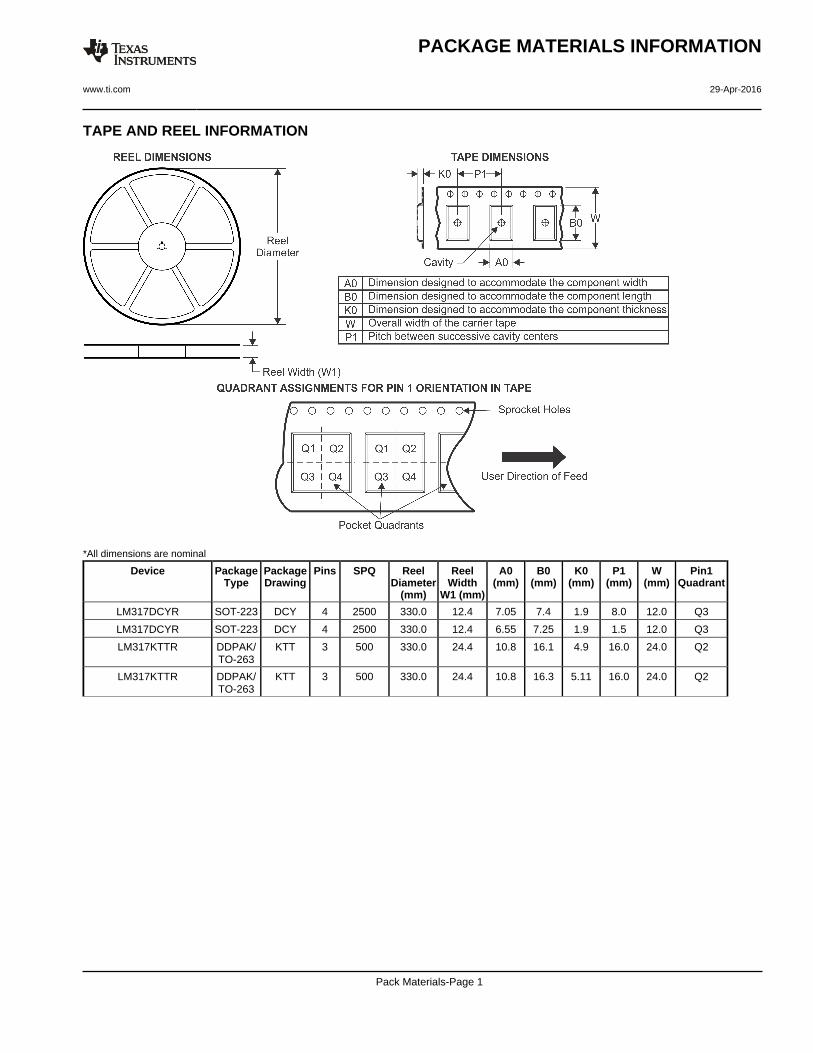
TAPE AND REEL INFORMATION
*All dimensions are nominal
Device PackageType
PackageDrawing
Pins SPQ ReelDiameter
(mm)
ReelWidth
W1 (mm)
A0(mm)
B0(mm)
K0(mm)
P1(mm)
W(mm)
Pin1Quadrant
LM317DCYR SOT-223 DCY 4 2500 330.0 12.4 7.05 7.4 1.9 8.0 12.0 Q3
LM317DCYR SOT-223 DCY 4 2500 330.0 12.4 6.55 7.25 1.9 1.5 12.0 Q3
LM317KTTR DDPAK/TO-263
KTT 3 500 330.0 24.4 10.8 16.1 4.9 16.0 24.0 Q2
LM317KTTR DDPAK/TO-263
KTT 3 500 330.0 24.4 10.8 16.3 5.11 16.0 24.0 Q2
PACKAGE MATERIALS INFORMATION
www.ti.com 29-Apr-2016
Pack Materials-Page 1
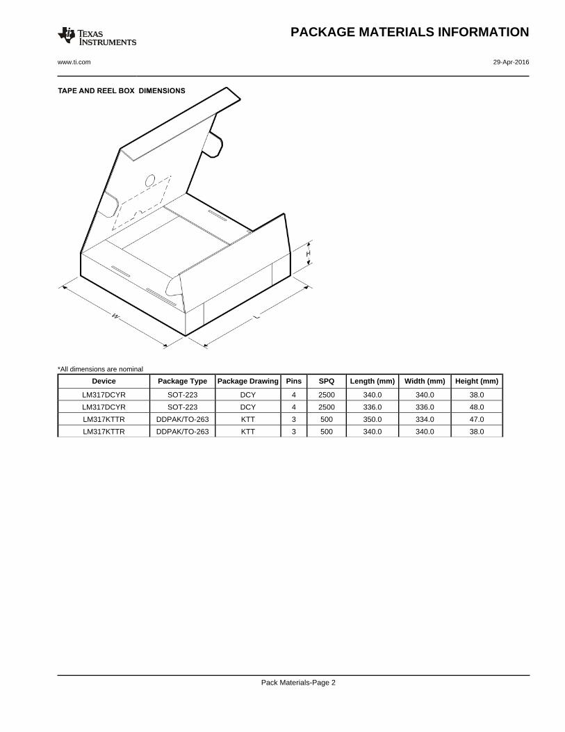
*All dimensions are nominal
Device Package Type Package Drawing Pins SPQ Length (mm) Width (mm) Height (mm)
LM317DCYR SOT-223 DCY 4 2500 340.0 340.0 38.0
LM317DCYR SOT-223 DCY 4 2500 336.0 336.0 48.0
LM317KTTR DDPAK/TO-263 KTT 3 500 350.0 334.0 47.0
LM317KTTR DDPAK/TO-263 KTT 3 500 340.0 340.0 38.0
PACKAGE MATERIALS INFORMATION
www.ti.com 29-Apr-2016
Pack Materials-Page 2
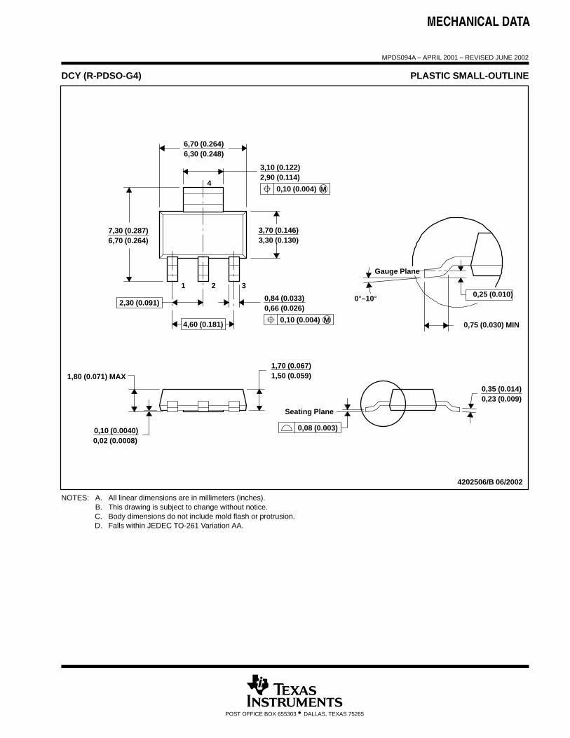
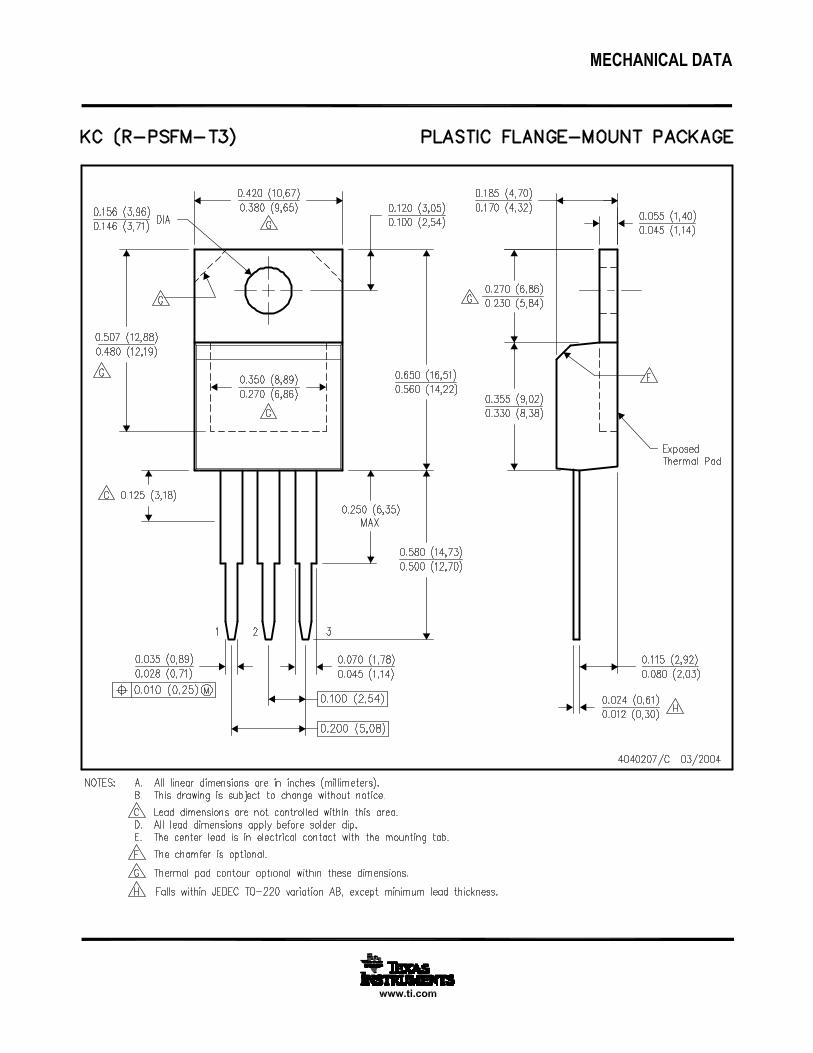
MECHANICAL DATA
MPDS094A – APRIL 2001 – REVISED JUNE 2002
POST OFFICE BOX 655303 • DALLAS, TEXAS 75265
DCY (R-PDSO-G4) PLASTIC SMALL-OUTLINE
4202506/B 06/2002
6,30 (0.248)6,70 (0.264)
2,90 (0.114)3,10 (0.122)
6,70 (0.264)7,30 (0.287) 3,70 (0.146)
3,30 (0.130)
0,02 (0.0008)0,10 (0.0040)
1,50 (0.059)1,70 (0.067)
0,23 (0.009)0,35 (0.014)
1 2 3
4
0,66 (0.026)0,84 (0.033)
1,80 (0.071) MAX
Seating Plane
0°–10°
Gauge Plane
0,75 (0.030) MIN
0,25 (0.010)
0,08 (0.003)
0,10 (0.004) M
2,30 (0.091)
4,60 (0.181) M0,10 (0.004)
NOTES: A. All linear dimensions are in millimeters (inches).B. This drawing is subject to change without notice.C. Body dimensions do not include mold flash or protrusion.D. Falls within JEDEC TO-261 Variation AA.
MECHANICAL DATA
MPFM001E – OCTOBER 1994 – REVISED JANUARY 2001
1POST OFFICE BOX 655303 • DALLAS, TEXAS 75265
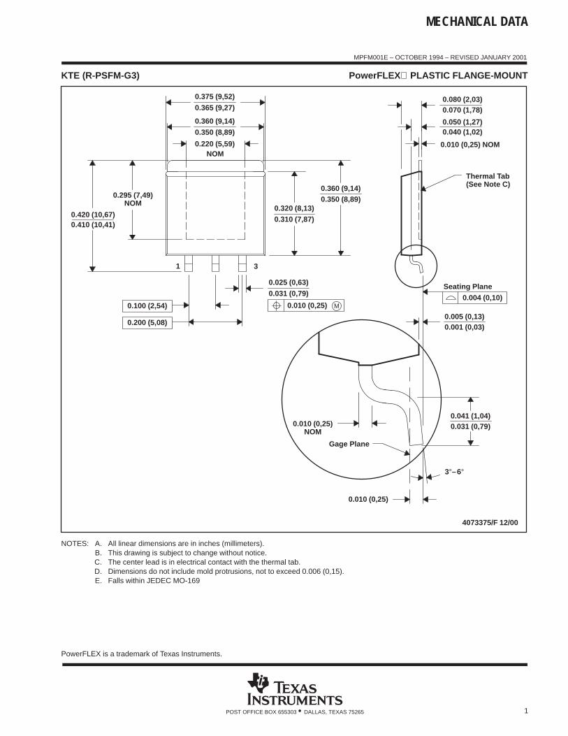
KTE (R-PSFM-G3) PowerFLEX PLASTIC FLANGE-MOUNT
0.360 (9,14)0.350 (8,89)
0.080 (2,03)0.070 (1,78)
0.010 (0,25) NOM
0.040 (1,02)
Seating Plane
0.050 (1,27)
0.001 (0,03)0.005 (0,13)
0.010 (0,25)NOM
Gage Plane
0.010 (0,25)
0.031 (0,79)0.041 (1,04)
4073375/F 12/00
NOM
31
0.350 (8,89)
0.220 (5,59)
0.360 (9,14)
0.295 (7,49)NOM
0.320 (8,13)0.310 (7,87)
0.025 (0,63)
0.031 (0,79)
Thermal Tab(See Note C)
0.004 (0,10)M0.010 (0,25)0.100 (2,54)
3°–6°
0.410 (10,41)0.420 (10,67)
0.200 (5,08)
0.365 (9,27)
0.375 (9,52)
NOTES: A. All linear dimensions are in inches (millimeters).B. This drawing is subject to change without notice.C. The center lead is in electrical contact with the thermal tab.D. Dimensions do not include mold protrusions, not to exceed 0.006 (0,15).E. Falls within JEDEC MO-169
PowerFLEX is a trademark of Texas Instruments.
www.ti.com
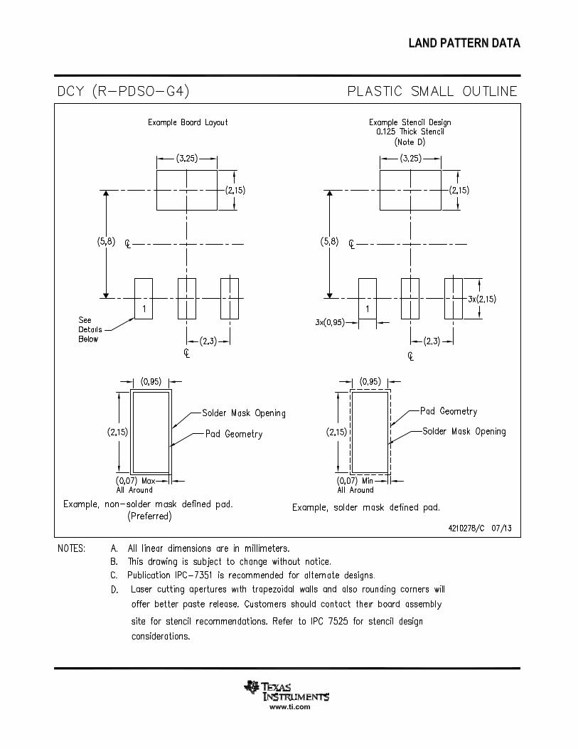
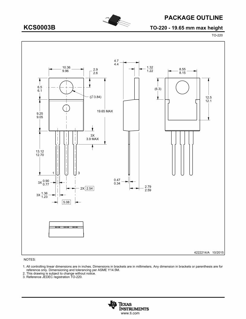
PACKAGE OUTLINE
9.259.05
6.56.1
2.92.6
10.369.96
13.1212.70
3X3.9 MAX
3X 1.361.23
3X 0.900.77
( )3.84
5.08
2X 2.54
8.558.15
12.512.1
(6.3)
19.65 MAX
4.74.4
1.321.22
2.792.59
0.470.34
4222214/A 10/2015
TO-220 - 19.65 mm max heightKCS0003BTO-220
NOTES: 1. All controlling linear dimensions are in inches. Dimensions in brackets are in millimeters. Any dimension in brackets or parenthesis are for reference only. Dimensioning and tolerancing per ASME Y14.5M.2. This drawing is subject to change without notice.3. Reference JEDEC registration TO-220.
1 3
SCALE 0.850
www.ti.com
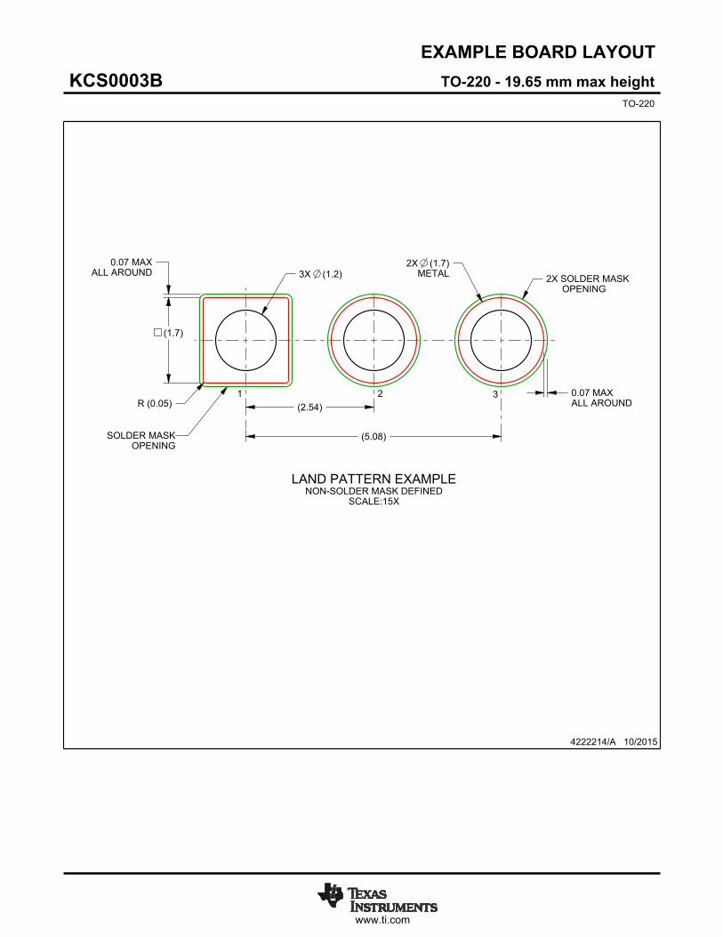
EXAMPLE BOARD LAYOUT
0.07 MAXALL AROUND
0.07 MAXALL AROUND
(1.7)
3X ( )1.2
(2.54)
(5.08)
R ( )0.05
2X ( )METAL
1.72X SOLDER MASK OPENING
4222214/A 10/2015
TO-220 - 19.65 mm max heightKCS0003BTO-220
LAND PATTERN EXAMPLENON-SOLDER MASK DEFINED
SCALE:15X
1 2 3
OPENINGSOLDER MASK
IMPORTANT NOTICE
Texas Instruments Incorporated and its subsidiaries (TI) reserve the right to make corrections, enhancements, improvements and otherchanges to its semiconductor products and services per JESD46, latest issue, and to discontinue any product or service per JESD48, latestissue. Buyers should obtain the latest relevant information before placing orders and should verify that such information is current andcomplete. All semiconductor products (also referred to herein as “components”) are sold subject to TI’s terms and conditions of salesupplied at the time of order acknowledgment.TI warrants performance of its components to the specifications applicable at the time of sale, in accordance with the warranty in TI’s termsand conditions of sale of semiconductor products. Testing and other quality control techniques are used to the extent TI deems necessaryto support this warranty. Except where mandated by applicable law, testing of all parameters of each component is not necessarilyperformed.TI assumes no liability for applications assistance or the design of Buyers’ products. Buyers are responsible for their products andapplications using TI components. To minimize the risks associated with Buyers’ products and applications, Buyers should provideadequate design and operating safeguards.TI does not warrant or represent that any license, either express or implied, is granted under any patent right, copyright, mask work right, orother intellectual property right relating to any combination, machine, or process in which TI components or services are used. Informationpublished by TI regarding third-party products or services does not constitute a license to use such products or services or a warranty orendorsement thereof. Use of such information may require a license from a third party under the patents or other intellectual property of thethird party, or a license from TI under the patents or other intellectual property of TI.Reproduction of significant portions of TI information in TI data books or data sheets is permissible only if reproduction is without alterationand is accompanied by all associated warranties, conditions, limitations, and notices. TI is not responsible or liable for such altereddocumentation. Information of third parties may be subject to additional restrictions.Resale of TI components or services with statements different from or beyond the parameters stated by TI for that component or servicevoids all express and any implied warranties for the associated TI component or service and is an unfair and deceptive business practice.TI is not responsible or liable for any such statements.Buyer acknowledges and agrees that it is solely responsible for compliance with all legal, regulatory and safety-related requirementsconcerning its products, and any use of TI components in its applications, notwithstanding any applications-related information or supportthat may be provided by TI. Buyer represents and agrees that it has all the necessary expertise to create and implement safeguards whichanticipate dangerous consequences of failures, monitor failures and their consequences, lessen the likelihood of failures that might causeharm and take appropriate remedial actions. Buyer will fully indemnify TI and its representatives against any damages arising out of the useof any TI components in safety-critical applications.In some cases, TI components may be promoted specifically to facilitate safety-related applications. With such components, TI’s goal is tohelp enable customers to design and create their own end-product solutions that meet applicable functional safety standards andrequirements. Nonetheless, such components are subject to these terms.No TI components are authorized for use in FDA Class III (or similar life-critical medical equipment) unless authorized officers of the partieshave executed a special agreement specifically governing such use.Only those TI components which TI has specifically designated as military grade or “enhanced plastic” are designed and intended for use inmilitary/aerospace applications or environments. Buyer acknowledges and agrees that any military or aerospace use of TI componentswhich have not been so designated is solely at the Buyer's risk, and that Buyer is solely responsible for compliance with all legal andregulatory requirements in connection with such use.TI has specifically designated certain components as meeting ISO/TS16949 requirements, mainly for automotive use. In any case of use ofnon-designated products, TI will not be responsible for any failure to meet ISO/TS16949.
Products ApplicationsAudio www.ti.com/audio Automotive and Transportation www.ti.com/automotiveAmplifiers amplifier.ti.com Communications and Telecom www.ti.com/communicationsData Converters dataconverter.ti.com Computers and Peripherals www.ti.com/computersDLP® Products www.dlp.com Consumer Electronics www.ti.com/consumer-appsDSP dsp.ti.com Energy and Lighting www.ti.com/energyClocks and Timers www.ti.com/clocks Industrial www.ti.com/industrialInterface interface.ti.com Medical www.ti.com/medicalLogic logic.ti.com Security www.ti.com/securityPower Mgmt power.ti.com Space, Avionics and Defense www.ti.com/space-avionics-defenseMicrocontrollers microcontroller.ti.com Video and Imaging www.ti.com/videoRFID www.ti-rfid.comOMAP Applications Processors www.ti.com/omap TI E2E Community e2e.ti.comWireless Connectivity www.ti.com/wirelessconnectivity
Mailing Address: Texas Instruments, Post Office Box 655303, Dallas, Texas 75265Copyright © 2016, Texas Instruments Incorporated
Recommended