LM723/LM723CVoltage RegulatorGeneral DescriptionThe LM723/LM723C is a voltage regulator designed prima-rily for series regulator applications. By itself, it will supplyoutput currents up to 150 mA; but external transistors can beadded to provide any desired load current. The circuit fea-tures extremely low standby current drain, and provision ismade for either linear or foldback current limiting.
The LM723/LM723C is also useful in a wide range of otherapplications such as a shunt regulator, a current regulator ora temperature controller.
The LM723C is identical to the LM723 except that theLM723C has its performance guaranteed over a 0˚C to+70˚C temperature range, instead of −55˚C to +125˚C.
Featuresn 150 mA output current without external pass transistorn Output currents in excess of 10A possible by adding
external transistorsn Input voltage 40V maxn Output voltage adjustable from 2V to 37Vn Can be used as either a linear or a switching regulator
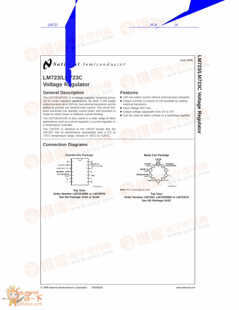
Connection Diagrams
Dual-In-Line Package
DS008563-2
Top ViewOrder Number LM723J/883 or LM723CN
See NS Package J14A or N14A
Metal Can Package
DS008563-3
Note: Pin 5 connected to case.
Top ViewOrder Number LM723H, LM723H/883 or LM723CH
See NS Package H10C
June 1999
LM723/LM
723CVoltage
Regulator
© 1999 National Semiconductor Corporation DS008563 www.national.com
查询LM723供应商 捷多邦,专业PCB打样工厂,24小时加急出货
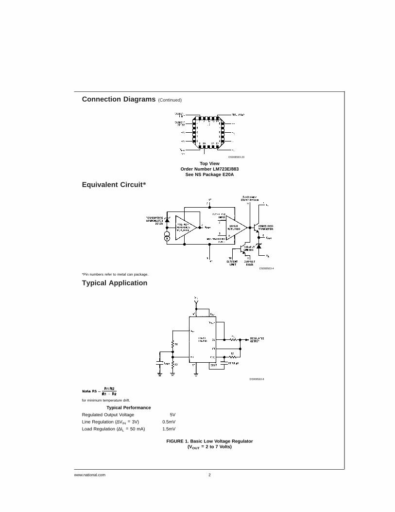
Connection Diagrams (Continued)
Equivalent Circuit *
Typical Application
DS008563-20
Top ViewOrder Number LM723E/883
See NS Package E20A
DS008563-4
*Pin numbers refer to metal can package.
DS008563-8
for minimum temperature drift.
Typical Performance
Regulated Output Voltage 5V
Line Regulation (∆VIN = 3V) 0.5mV
Load Regulation (∆IL = 50 mA) 1.5mV
FIGURE 1. Basic Low Voltage Regulator(VOUT = 2 to 7 Volts)
www.national.com 2
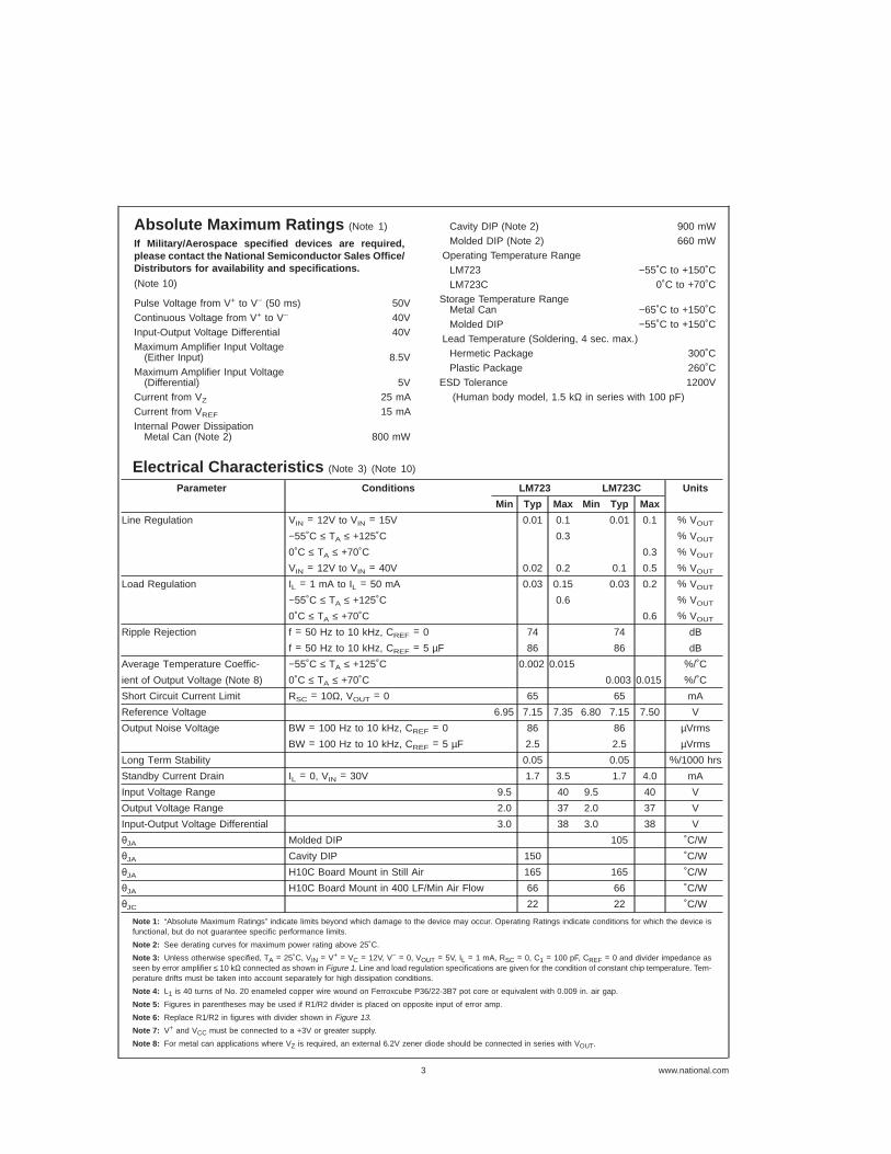
Absolute Maximum Ratings (Note 1)
If Military/Aerospace specified devices are required,please contact the National Semiconductor Sales Office/Distributors for availability and specifications.
(Note 10)
Pulse Voltage from V+ to V− (50 ms) 50VContinuous Voltage from V+ to V− 40VInput-Output Voltage Differential 40VMaximum Amplifier Input Voltage
(Either Input) 8.5VMaximum Amplifier Input Voltage
(Differential) 5VCurrent from VZ 25 mACurrent from VREF 15 mAInternal Power Dissipation
Metal Can (Note 2) 800 mW
Cavity DIP (Note 2) 900 mWMolded DIP (Note 2) 660 mW
Operating Temperature RangeLM723 −55˚C to +150˚CLM723C 0˚C to +70˚C
Storage Temperature RangeMetal Can −65˚C to +150˚CMolded DIP −55˚C to +150˚C
Lead Temperature (Soldering, 4 sec. max.)Hermetic Package 300˚CPlastic Package 260˚C
ESD Tolerance 1200V(Human body model, 1.5 kΩ in series with 100 pF)
Electrical Characteristics (Note 3) (Note 10)
Parameter Conditions LM723 LM723C Units
Min Typ Max Min Typ Max
Line Regulation VIN = 12V to VIN = 15V 0.01 0.1 0.01 0.1 % VOUT
−55˚C ≤ TA ≤ +125˚C 0.3 % VOUT
0˚C ≤ TA ≤ +70˚C 0.3 % VOUT
VIN = 12V to VIN = 40V 0.02 0.2 0.1 0.5 % VOUT
Load Regulation IL = 1 mA to IL = 50 mA 0.03 0.15 0.03 0.2 % VOUT
−55˚C ≤ TA ≤ +125˚C 0.6 % VOUT
0˚C ≤ TA ≤ +70˚C 0.6 % VOUT
Ripple Rejection f = 50 Hz to 10 kHz, CREF = 0 74 74 dB
f = 50 Hz to 10 kHz, CREF = 5 µF 86 86 dB
Average Temperature Coeffic- −55˚C ≤ TA ≤ +125˚C 0.002 0.015 %/˚C
ient of Output Voltage (Note 8) 0˚C ≤ TA ≤ +70˚C 0.003 0.015 %/˚C
Short Circuit Current Limit RSC = 10Ω, VOUT = 0 65 65 mA
Reference Voltage 6.95 7.15 7.35 6.80 7.15 7.50 V
Output Noise Voltage BW = 100 Hz to 10 kHz, CREF = 0 86 86 µVrms
BW = 100 Hz to 10 kHz, CREF = 5 µF 2.5 2.5 µVrms
Long Term Stability 0.05 0.05 %/1000 hrs
Standby Current Drain IL = 0, VIN = 30V 1.7 3.5 1.7 4.0 mA
Input Voltage Range 9.5 40 9.5 40 V
Output Voltage Range 2.0 37 2.0 37 V
Input-Output Voltage Differential 3.0 38 3.0 38 V
θJA Molded DIP 105 ˚C/W
θJA Cavity DIP 150 ˚C/W
θJA H10C Board Mount in Still Air 165 165 ˚C/W
θJA H10C Board Mount in 400 LF/Min Air Flow 66 66 ˚C/W
θJC 22 22 ˚C/W
Note 1: “Absolute Maximum Ratings” indicate limits beyond which damage to the device may occur. Operating Ratings indicate conditions for which the device isfunctional, but do not guarantee specific performance limits.
Note 2: See derating curves for maximum power rating above 25˚C.
Note 3: Unless otherwise specified, TA = 25˚C, VIN = V+ = VC = 12V, V− = 0, VOUT = 5V, IL = 1 mA, RSC = 0, C1 = 100 pF, CREF = 0 and divider impedance asseen by error amplifier ≤ 10 kΩ connected as shown in Figure 1. Line and load regulation specifications are given for the condition of constant chip temperature. Tem-perature drifts must be taken into account separately for high dissipation conditions.
Note 4: L1 is 40 turns of No. 20 enameled copper wire wound on Ferroxcube P36/22-3B7 pot core or equivalent with 0.009 in. air gap.
Note 5: Figures in parentheses may be used if R1/R2 divider is placed on opposite input of error amp.
Note 6: Replace R1/R2 in figures with divider shown in Figure 13.
Note 7: V+ and VCC must be connected to a +3V or greater supply.
Note 8: For metal can applications where VZ is required, an external 6.2V zener diode should be connected in series with VOUT.
www.national.com3
Electrical Characteristics (Note 3) (Note 10) (Continued)
Note 9: Guaranteed by correlation to other tests.
Note 10: A military RETS specification is available on request. At the time of printing, the LM723 RETS specification complied with the Min and Max limits in thistable. The LM723E, H, and J may also be procured as a Standard Military Drawing.
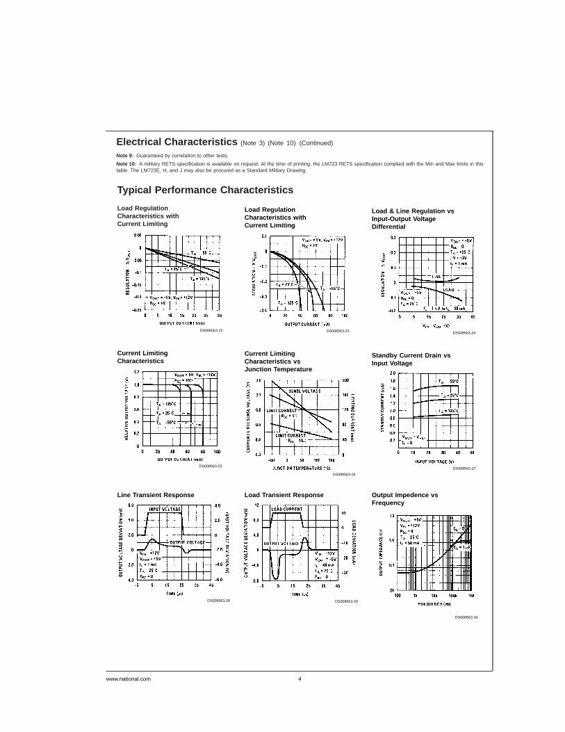
Typical Performance Characteristics
Load RegulationCharacteristics withCurrent Limiting
DS008563-22
Load RegulationCharacteristics withCurrent Limiting
DS008563-23
Load & Line Regulation vsInput-Output VoltageDifferential
DS008563-24
Current LimitingCharacteristics
DS008563-25
Current LimitingCharacteristics vsJunction Temperature
DS008563-26
Standby Current Drain vsInput Voltage
DS008563-27
Line Transient Response
DS008563-28
Load Transient Response
DS008563-29
Output Impedence vsFrequency
DS008563-30
www.national.com 4
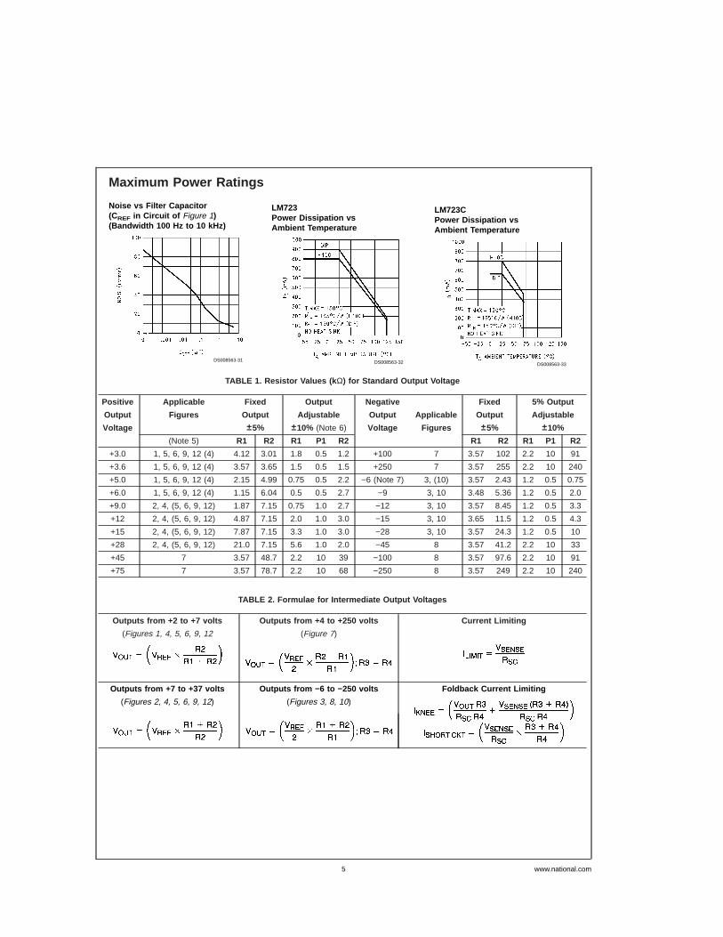
Maximum Power Ratings
TABLE 1. Resistor Values (k Ω) for Standard Output Voltage
Positive Applicable Fixed Output Negative Fixed 5 % Output
Output Figures Output Adjustable Output Applicable Output Adjustable
Voltage ±5% ±10% (Note 6) Voltage Figures ±5% ±10%
(Note 5) R1 R2 R1 P1 R2 R1 R2 R1 P1 R2
+3.0 1, 5, 6, 9, 12 (4) 4.12 3.01 1.8 0.5 1.2 +100 7 3.57 102 2.2 10 91
+3.6 1, 5, 6, 9, 12 (4) 3.57 3.65 1.5 0.5 1.5 +250 7 3.57 255 2.2 10 240
+5.0 1, 5, 6, 9, 12 (4) 2.15 4.99 0.75 0.5 2.2 −6 (Note 7) 3, (10) 3.57 2.43 1.2 0.5 0.75
+6.0 1, 5, 6, 9, 12 (4) 1.15 6.04 0.5 0.5 2.7 −9 3, 10 3.48 5.36 1.2 0.5 2.0
+9.0 2, 4, (5, 6, 9, 12) 1.87 7.15 0.75 1.0 2.7 −12 3, 10 3.57 8.45 1.2 0.5 3.3
+12 2, 4, (5, 6, 9, 12) 4.87 7.15 2.0 1.0 3.0 −15 3, 10 3.65 11.5 1.2 0.5 4.3
+15 2, 4, (5, 6, 9, 12) 7.87 7.15 3.3 1.0 3.0 −28 3, 10 3.57 24.3 1.2 0.5 10
+28 2, 4, (5, 6, 9, 12) 21.0 7.15 5.6 1.0 2.0 −45 8 3.57 41.2 2.2 10 33
+45 7 3.57 48.7 2.2 10 39 −100 8 3.57 97.6 2.2 10 91
+75 7 3.57 78.7 2.2 10 68 −250 8 3.57 249 2.2 10 240
TABLE 2. Formulae for Intermediate Output Voltages
Outputs from +2 to +7 volts Outputs from +4 to +250 volts Current Limiting
(Figures 1, 4, 5, 6, 9, 12 (Figure 7)
Outputs from +7 to +37 volts Outputs from −6 to −250 volts Foldback Current Limiting
(Figures 2, 4, 5, 6, 9, 12) (Figures 3, 8, 10)
Noise vs Filter Capacitor(CREF in Circuit of Figure 1)(Bandwidth 100 Hz to 10 kHz)
DS008563-31
LM723Power Dissipation vsAmbient Temperature
DS008563-32
LM723CPower Dissipation vsAmbient Temperature
DS008563-33
www.national.com5
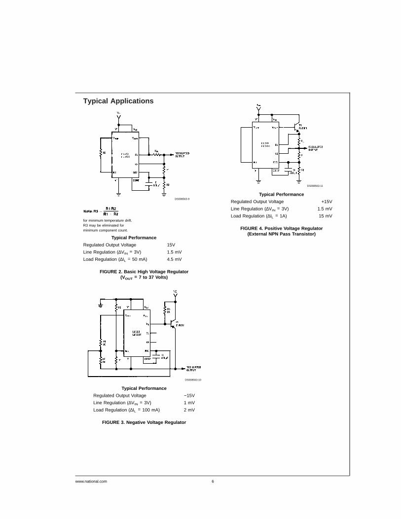
Typical Applications
DS008563-9
for minimum temperature drift.R3 may be eliminated forminimum component count.
Typical Performance
Regulated Output Voltage 15V
Line Regulation (∆VIN = 3V) 1.5 mV
Load Regulation (∆IL = 50 mA) 4.5 mV
FIGURE 2. Basic High Voltage Regulator(VOUT = 7 to 37 Volts)
DS008563-10
Typical Performance
Regulated Output Voltage −15V
Line Regulation (∆VIN = 3V) 1 mV
Load Regulation (∆IL = 100 mA) 2 mV
FIGURE 3. Negative Voltage Regulator
DS008563-11
Typical Performance
Regulated Output Voltage +15V
Line Regulation (∆VIN = 3V) 1.5 mV
Load Regulation (∆IL = 1A) 15 mV
FIGURE 4. Positive Voltage Regulator(External NPN Pass Transistor)
www.national.com 6
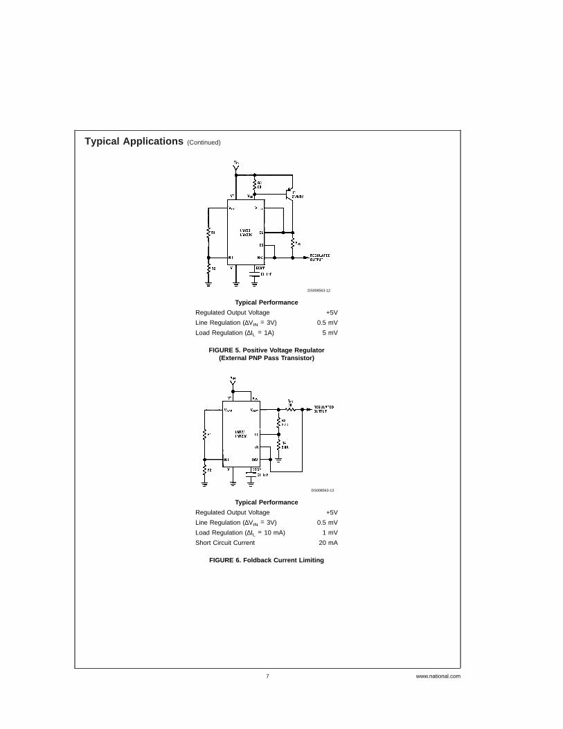
Typical Applications (Continued)
DS008563-12
Typical Performance
Regulated Output Voltage +5V
Line Regulation (∆VIN = 3V) 0.5 mV
Load Regulation (∆IL = 1A) 5 mV
FIGURE 5. Positive Voltage Regulator(External PNP Pass Transistor)
DS008563-13
Typical Performance
Regulated Output Voltage +5V
Line Regulation (∆VIN = 3V) 0.5 mV
Load Regulation (∆IL = 10 mA) 1 mV
Short Circuit Current 20 mA
FIGURE 6. Foldback Current Limiting
www.national.com7
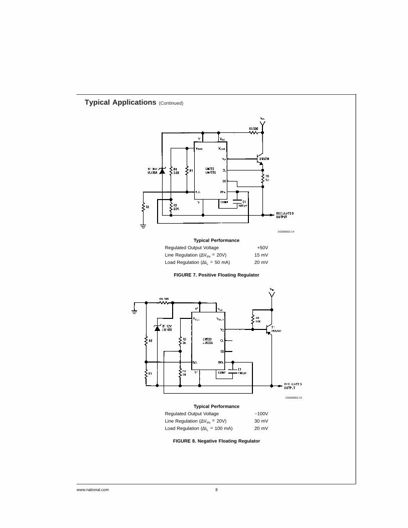
Typical Applications (Continued)
DS008563-14
Typical Performance
Regulated Output Voltage +50V
Line Regulation (∆VIN = 20V) 15 mV
Load Regulation (∆IL = 50 mA) 20 mV
FIGURE 7. Positive Floating Regulator
DS008563-15
Typical Performance
Regulated Output Voltage −100V
Line Regulation (∆VIN = 20V) 30 mV
Load Regulation (∆IL = 100 mA) 20 mV
FIGURE 8. Negative Floating Regulator
www.national.com 8
Typical Applications (Continued)
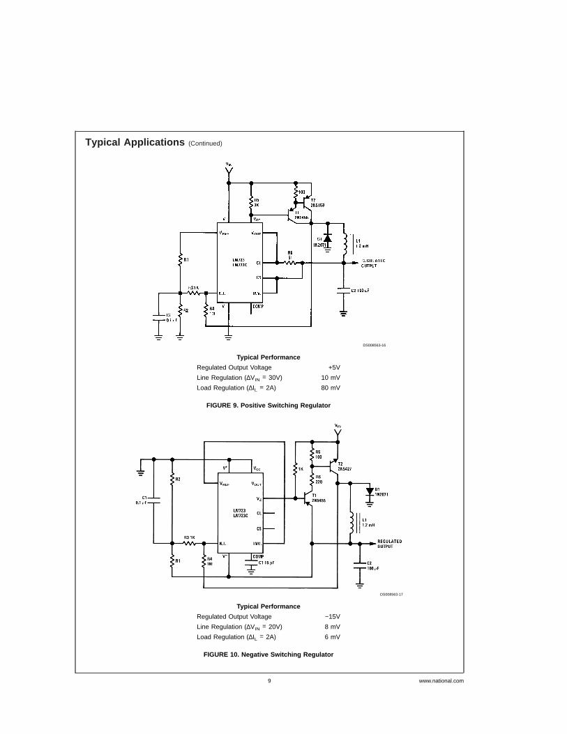
DS008563-16
Typical Performance
Regulated Output Voltage +5V
Line Regulation (∆VIN = 30V) 10 mV
Load Regulation (∆IL = 2A) 80 mV
FIGURE 9. Positive Switching Regulator
DS008563-17
Typical Performance
Regulated Output Voltage −15V
Line Regulation (∆VIN = 20V) 8 mV
Load Regulation (∆IL = 2A) 6 mV
FIGURE 10. Negative Switching Regulator
www.national.com9
Typical Applications (Continued)
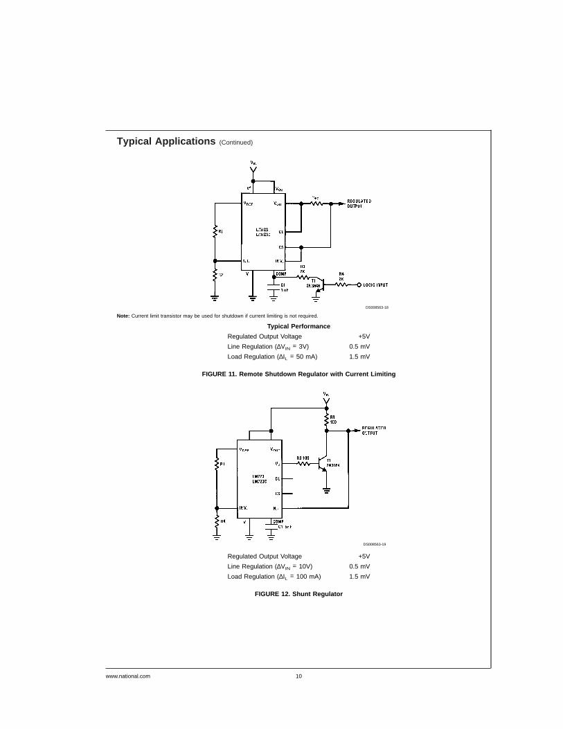
DS008563-18
Note: Current limit transistor may be used for shutdown if current limiting is not required.
Typical Performance
Regulated Output Voltage +5V
Line Regulation (∆VIN = 3V) 0.5 mV
Load Regulation (∆IL = 50 mA) 1.5 mV
FIGURE 11. Remote Shutdown Regulator with Current Limiting
DS008563-19
Regulated Output Voltage +5V
Line Regulation (∆VIN = 10V) 0.5 mV
Load Regulation (∆IL = 100 mA) 1.5 mV
FIGURE 12. Shunt Regulator
www.national.com 10
Typical Applications (Continued)
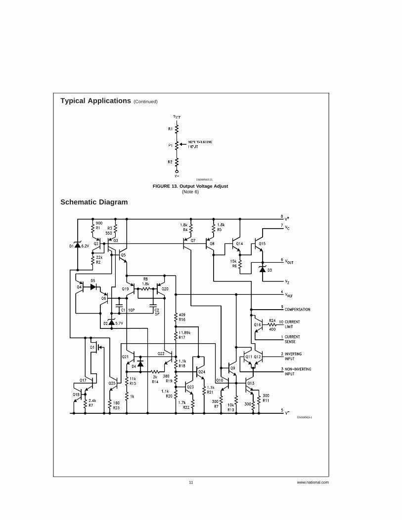
Schematic Diagram
DS008563-21
FIGURE 13. Output Voltage Adjust(Note 6)
DS008563-1
www.national.com11
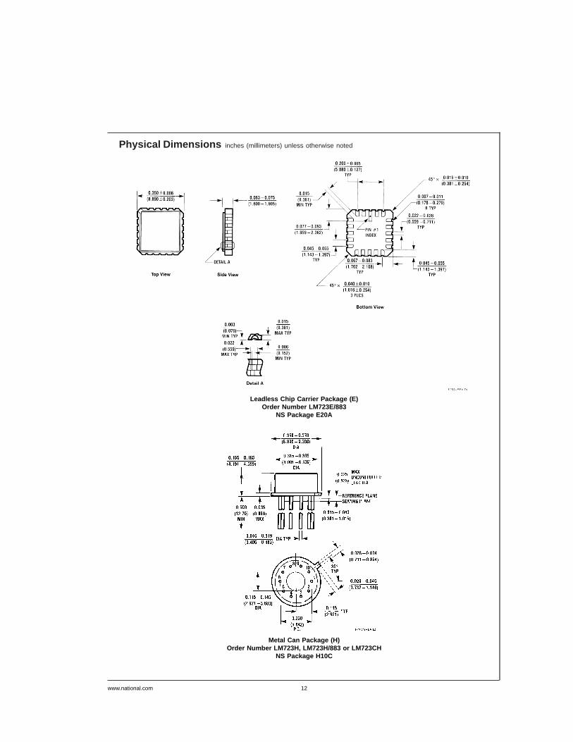
Physical Dimensions inches (millimeters) unless otherwise noted
Leadless Chip Carrier Package (E)Order Number LM723E/883
NS Package E20A
Metal Can Package (H)Order Number LM723H, LM723H/883 or LM723CH
NS Package H10C
www.national.com 12
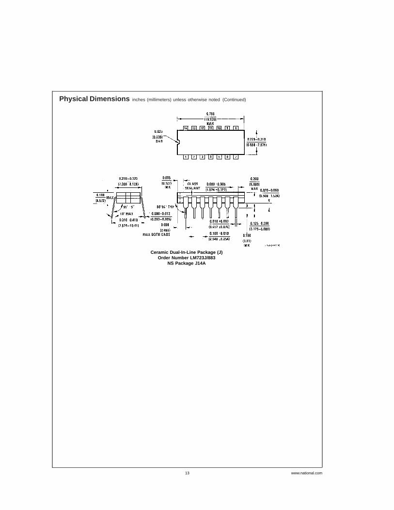
Physical Dimensions inches (millimeters) unless otherwise noted (Continued)
Ceramic Dual-In-Line Package (J)Order Number LM723J/883
NS Package J14A
www.national.com13
Physical Dimensions inches (millimeters) unless otherwise noted (Continued)
LIFE SUPPORT POLICY
NATIONAL’S PRODUCTS ARE NOT AUTHORIZED FOR USE AS CRITICAL COMPONENTS IN LIFE SUPPORTDEVICES OR SYSTEMS WITHOUT THE EXPRESS WRITTEN APPROVAL OF THE PRESIDENT AND GENERALCOUNSEL OF NATIONAL SEMICONDUCTOR CORPORATION. As used herein:
1. Life support devices or systems are devices orsystems which, (a) are intended for surgical implantinto the body, or (b) support or sustain life, andwhose failure to perform when properly used inaccordance with instructions for use provided in thelabeling, can be reasonably expected to result in asignificant injury to the user.
2. A critical component is any component of a lifesupport device or system whose failure to performcan be reasonably expected to cause the failure ofthe life support device or system, or to affect itssafety or effectiveness.
National SemiconductorCorporationAmericasTel: 1-800-272-9959Fax: 1-800-737-7018Email: [email protected]
National SemiconductorEurope
Fax: +49 (0) 1 80-530 85 86Email: [email protected]
Deutsch Tel: +49 (0) 1 80-530 85 85English Tel: +49 (0) 1 80-532 78 32Français Tel: +49 (0) 1 80-532 93 58Italiano Tel: +49 (0) 1 80-534 16 80
National SemiconductorAsia Pacific CustomerResponse GroupTel: 65-2544466Fax: 65-2504466Email: [email protected]
National SemiconductorJapan Ltd.Tel: 81-3-5639-7560Fax: 81-3-5639-7507
www.national.com
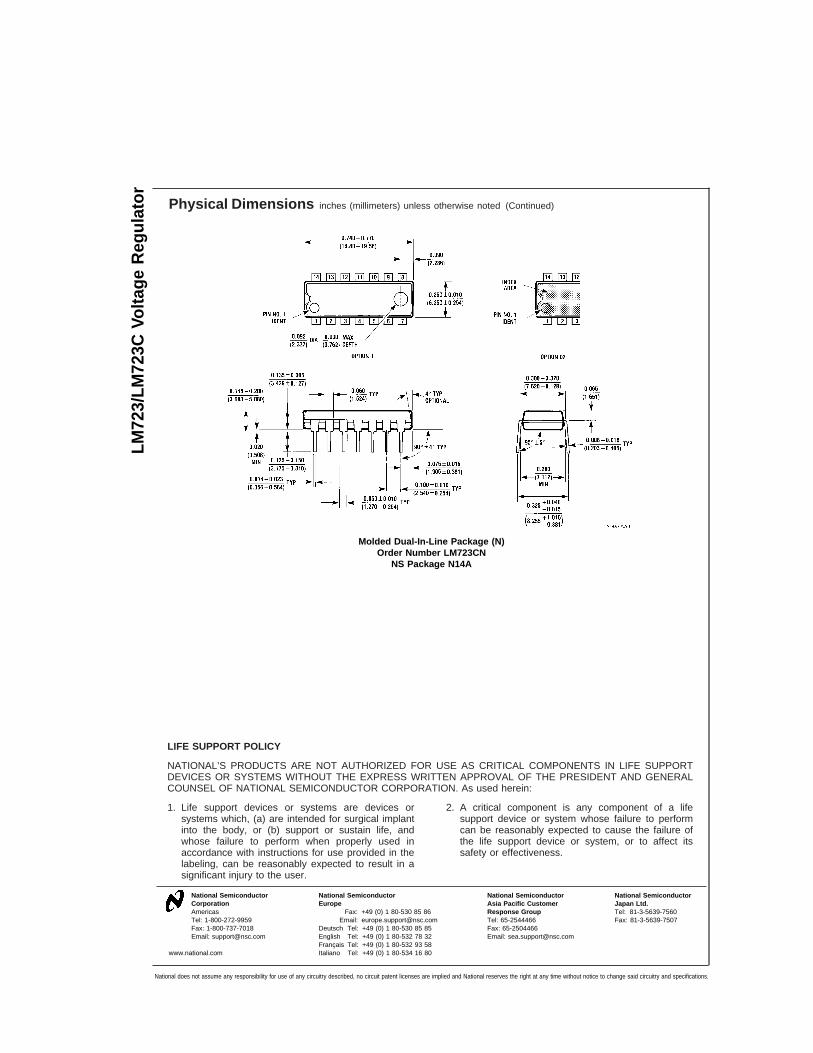
Molded Dual-In-Line Package (N)Order Number LM723CN
NS Package N14A
LM72
3/LM
723C
Volta
geR
egul
ator
National does not assume any responsibility for use of any circuitry described, no circuit patent licenses are implied and National reserves the right at any time without notice to change said circuitry and specifications.
Recommended