1. General description
The LPC5410x are ARM Cortex-M4 based microcontrollers for embedded applications. These devices include an optional ARM Cortex-M0+ coprocessor, 104 kB of on-chip SRAM, up to 512 kB on-chip flash, five general-purpose timers, one State-Configurable Timer with PWM capabilities (SCTimer/PWM), one RTC/alarm timer, one 24-bit Multi-Rate Timer (MRT), a Repetitive Interrupt Timer (RIT), a Windowed Watchdog Timer (WWDT), four USARTs, two SPIs, three Fast-mode plus I2C-bus interfaces with high-speed slave mode, and one 12-bit 5.0 Msamples/sec ADC.
The ARM Cortex-M4 is a 32-bit core that offers system enhancements such as low power consumption, enhanced debug features, and a high level of support block integration. The ARM Cortex-M4 CPU incorporates a 3-stage pipeline, uses a Harvard architecture with separate local instruction and data buses as well as a third bus for peripherals, and includes an internal prefetch unit that supports speculative branching. The ARM Cortex-M4 supports single-cycle digital signal processing and SIMD instructions. A hardware floating-point unit is integrated in the core.
The ARM Cortex-M0+ coprocessor is an energy-efficient and easy-to-use 32-bit core which is code and tool-compatible with the Cortex-M4 core. The Cortex-M0+ coprocessor offers up to 100 MHz performance with a simple instruction set and reduced code size. In LPC5410x, the Cortex-M0 coprocessor hardware multiply is implemented as a 32-cycle iterative multiplier.
2. Features and benefits
Dual processor cores: ARM Cortex-M4 and ARM Cortex-M0+. The M0+ core runs at the same frequency as the M4 core. Both cores operate up to a maximum frequency of 100 MHz.
ARM Cortex-M4 core (version r0p1):
ARM Cortex-M4 processor, running at a frequency of up to 100 MHz, using the same clock as the Cortex-M4.
Floating Point Unit (FPU) and Memory Protection Unit (MPU).
ARM Cortex-M4 built-in Nested Vectored Interrupt Controller (NVIC).
Non-maskable Interrupt (NMI) input with a selection of sources.
Serial Wire Debug with eight breakpoints and four watch points.
Includes Serial Wire Output for enhanced debug capabilities.
System tick timer.
LPC5410x32-bit ARM Cortex-M4/M0+ MCU; 104 kB SRAM; 512 kB flash, 3 x I2C, 2 x SPI, 4 x USART, 32-bit counter/ timers, SCTimer/PWM, 12-bit 5.0 Msamples/sec ADCRev. 2.9 — 26 January 2018 Product data sheet
NXP Semiconductors LPC5410x32-bit ARM Cortex-M4/M0+ microcontroller
ARM Cortex-M0+ core (version r0p1):
ARM Cortex-M0+ processor, running at a frequency of up to 100 MHz.
ARM Cortex-M0+ built-in Nested Vectored Interrupt Controller (NVIC).
Non-maskable Interrupt (NMI) input with a selection of sources.
Serial Wire Debug with four breakpoints and two watch points.
System tick timer.
On-chip memory:
Up to 512 kB on-chip flash program memory with flash accelerator and 256 byte page erase and write.
104 kB total SRAM composed of:
Up to 96 kB contiguous main SRAM.
An additional 8 kB SRAM.
ROM API support:
Flash In-Application Programming (IAP) and In-System Programming (ISP).
Power control API.
Serial interfaces:
Four USART interfaces with synchronous mode and 32 kHz mode for wake-up from deep sleep and power down modes. The USARTs have FIFO support from the System FIFO and share a fractional baud-rate generator.
Two SPI interfaces, each with four slave selects and flexible data configuration. The SPIs have FIFO support from the System FIFO. The slave function is able to wake up the device from deep sleep and power down modes.
Three I2C-bus interfaces supporting fast mode and Fast-mode Plus with data rates of up to 1Mbit/s and with multiple address recognition and monitor mode. Each I2C-bus interface also supports High Speed Mode (3.4 Mbit/s) as a slave. The slave function is able to wake up the device from deep sleep and power down modes.
Digital peripherals:
DMA controller with 22 channels and 20 programmable triggers, able to access all
memories and DMA-capable peripherals.
Up to 50 General-Purpose Input/Output (GPIO) pins. Most GPIOs have configurable pull-up/pull-down resistors, programmable open-drain mode, and input inverter.
GPIO registers are located on the AHB for fast access. The DMA supports GPIO ports.
Up to eight GPIOs (pin interrupts) can be selected as edge-sensitive (rising or falling edges or both) interrupt requests or level-sensitive (active low or active high) interrupt requests. In addition, up to eight GPIOs can be selected to contribute a boolean expression and interrupt generation using the pattern match engine block.
Two GPIO grouped interrupts (GINT) enable an interrupt based on a logical
(AND/OR) combination of input states.
CRC engine.
Timers:
Five 32-bit standard general purpose timers/counters, four of which support up to 4 capture inputs and 4 compare outputs, PWM mode, and external count input. Specific timer events can be selected to generate DMA requests. The fifth timer does not have external pin connections and may be used for internal timing operations.
LPC5410x All information provided in this document is subject to legal disclaimers. © NXP B.V. 2018. All rights reserved.
Product data sheet Rev. 2.9 — 26 January 2018 2 of 90
NXP Semiconductors LPC5410x32-bit ARM Cortex-M4/M0+ microcontroller
One State Configurable Timer/PWM (SCT/PWM) with 8 inputs (6 external inputs and 2 internal inputs) and 8 output functions (including capture and match). Inputs and outputs can be routed to/from external pins and internally to/from selected peripherals. Internally, the SCT supports 13 captures/matches, 13 events and 13 states.
32-bit Real-time clock (RTC) with 1 s resolution running in the always-on power domain. A timer in the RTC can be used for wake-up from all low power modes including deep power-down, with 1 ms resolution.
Multiple-channel multi-rate 24-bit timer (MRT) for repetitive interrupt generation at up to four programmable, fixed rates.
Windowed Watchdog Timer (WWDT).
Ultra-low power Micro-tick Timer, running from the Watchdog oscillator, that can be used to wake up the device from low power modes.
Repetitive Interrupt Timer (RIT) for debug time-stamping and general-purpose use.
Analog peripheral: 12-bit, 12-channel, Analog-to-Digital Converter (ADC) supporting 5.0 Msamples/s. The ADC supports two independent conversion sequences.
Clock generation:
12 MHz internal RC oscillator.
External clock input for clock frequencies of up to 25 MHz.
Internal low-power, watchdog oscillator (WDOSC) with a nominal frequency of 500 kHz.
32 kHz low-power RTC oscillator.
System PLL allows CPU operation up to the maximum CPU rate. May be run from the internal RC oscillator, the external clock input CLKIN, or the RTC oscillator.
Clock output function for monitoring internal clocks.
Frequency measurement unit for measuring the frequency of any on-chip or off-chip clock signal.
Power-saving modes and wake-up:
Integrated PMU (Power Management Unit) to minimize power consumption.
Reduced power modes: sleep, deep sleep, power down, and deep power-down.
Wake-up from deep sleep and power down modes via activity on the USART, SPI, and I2C peripherals.
Wake-up from sleep, deep sleep, power down, and deep power-down modes using the RTC alarm.
Single power supply 1.62 V to 3.6 V.
Power-On Reset (POR).
Brown-Out Detect (BOD) with separate thresholds for interrupt and forced reset.
JTAG boundary scan supported.
Unique device serial number (128 bit) for identification.
Operating temperature range 40 °C to 105 °C.
Available in a 3.288 x 3.288 mm WLCSP49 package and LQFP64 package.
LPC5410x All information provided in this document is subject to legal disclaimers. © NXP B.V. 2018. All rights reserved.
Product data sheet Rev. 2.9 — 26 January 2018 3 of 90
NXP Semiconductors LPC5410x32-bit ARM Cortex-M4/M0+ microcontroller
3. Ordering information
3.1 Ordering options
[1] All of the parts include five 32-bit general-purpose timers, one State-Configurable Timer with PWM capabilities (SCTimer/PWM), one RTC/alarm timer, one 24-bit Multi-Rate Timer (MRT), a Windowed Watchdog Timer (WWDT), four USARTs, two SPIs, three Fast-mode plus I2C-bus interfaces with high-speed slave mode, and one 12-bit 5.0 Msamples/sec ADC.
4. Marking
Table 1. Ordering information
Type number Package
Name Description Version
LPC54102J512UK49 WLCSP49 wafer level chip-size package; 49 (7 x 7) bumps; 3.288 x 3.288 x 0.54 mm -
LPC54102J256UK49 WLCSP49 wafer level chip-size package; 49 (7 x 7) bumps; 3.288 x 3.288 x 0.54 mm -
LPC54101J512UK49 WLCSP49 wafer level chip-size package; 49 (7 x 7) bumps; 3.288 x 3.288 x 0.54 mm -
LPC54101J256UK49 WLCSP49 wafer level chip-size package; 49 (7 x 7) bumps; 3.288 x 3.288 x 0.54 mm -
LPC54102J512BD64 LQFP64 plastic low profile quad flat package; 64 leads; body 10 10 1.4 mm SOT314-2
LPC54102J256BD64 LQFP64 plastic low profile quad flat package; 64 leads; body 10 10 1.4 mm SOT314-2
LPC54101J512BD64 LQFP64 plastic low profile quad flat package; 64 leads; body 10 10 1.4 mm SOT314-2
LPC54101J256BD64 LQFP64 plastic low profile quad flat package; 64 leads; body 10 10 1.4 mm SOT314-2
Table 2. Ordering options
Type number Device order part number Flash/kB Total SRAM/kB Core M4 w/ FPU Core M0+
GPIO
LPC54102J512UK49 LPC54102J512UK49Z 512 104 1 1 39
LPC54102J256UK49 LPC54102J256UK49Z 256 104 1 1 39
LPC54101J512UK49 LPC54101J512UK49Z 512 104 1 0 39
LPC54101J256UK49 LPC54101J256UK49Z 256 104 1 0 39
LPC54102J512BD64 LPC54102J512BD64QL 512 104 1 1 50
LPC54102J256BD64 LPC54102J256BD64QL 256 104 1 1 50
LPC54101J512BD64 LPC54101J512BD64QL 512 104 1 0 50
LPC54101J256BD64 LPC54101J256BD64QL 256 104 1 0 50
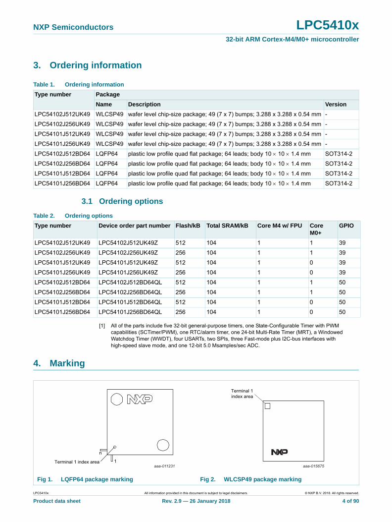
Fig 1. LQFP64 package marking Fig 2. WLCSP49 package marking
1
n
Terminal 1 index areaaaa-011231 aaa-015675
Terminal 1index area
LPC5410x All information provided in this document is subject to legal disclaimers. © NXP B.V. 2018. All rights reserved.
Product data sheet Rev. 2.9 — 26 January 2018 4 of 90
NXP Semiconductors LPC5410x32-bit ARM Cortex-M4/M0+ microcontroller
The LPC5410x LQFP64 package has the following top-side marking:
• First line: LPC5410xJyyy
– x: 2 = dual core (M4, M0+), 1 = single core (M4)
– yyy: flash size
• Second line: BD64
• Third line: xxxxxxxxxxxx
• Fourth line: xxxyywwx[R]z
– yyww: Date code with yy = year and ww = week.
– xR = boot code version and device revision.
The LPC5410x WLCSP49 package has the following top-side marking:
• First line: LPC5410x
– x: 2 = dual core (M4, M0+), 1 = single core (M4)
• Second line: JxxxUK49
– xxx: flash size
• Third line: xxxxxxxx
• Fourth line: xxxyyww
– yyww: Date code with yy = year and ww = week.
• Fifth line: xxxxx
• Sixth line: NXP x[R]z
– xR = boot code version and device revision.
Table 3. Device revision table
Revision identifier (R) Revision description
‘1B’ Initial device revision with boot code version 17.1.
‘1C’ Second device revision with boot code version 17.1.
LPC5410x All information provided in this document is subject to legal disclaimers. © NXP B.V. 2018. All rights reserved.
Product data sheet Rev. 2.9 — 26 January 2018 5 of 90
NXP Semiconductors LPC5410x32-bit ARM Cortex-M4/M0+ microcontroller
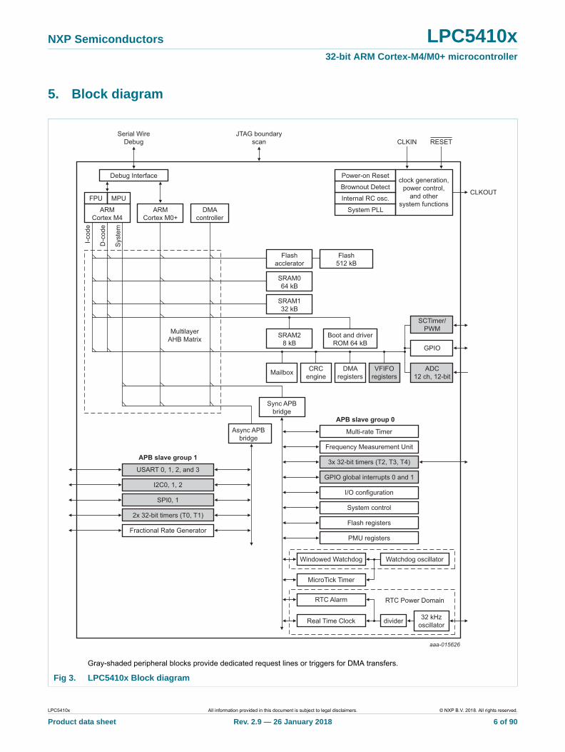
5. Block diagram
Gray-shaded peripheral blocks provide dedicated request lines or triggers for DMA transfers.
Fig 3. LPC5410x Block diagram
aaa-015626
CLKOUT
CLKINSerial Wire
DebugJTAG boundary
scan RESET
Power-on Resetclock generation,
power control,and other
system functions
Debug Interface
FPU
ARMCortex M4
I-cod
e
D-c
ode
Sys
tem
ARMCortex M0+
Flashacclerator
Flash512 kB
Boot and driverROM 64 kB
DMAcontroller
MPU
Brownout Detect
Internal RC osc.
System PLL
SRAM064 kB
SRAM132 kB
SRAM28 kB
MultilayerAHB Matrix
Sync APBbridge
Async APBbridge
Mailbox CRCengine
DMAregisters
VFIFOregisters
ADC12 ch, 12-bit
GPIO
SCTimer/PWM
USART 0, 1, 2, and 3
I2C0, 1, 2
SPI0, 1
2x 32-bit timers (T0, T1)
Fractional Rate Generator
Multi-rate Timer
Frequency Measurement Unit
3x 32-bit timers (T2, T3, T4)
GPIO global interrupts 0 and 1
I/O configuration
System control
Flash registers
PMU registers
Windowed Watchdog
MicroTick Timer
RTC Alarm
Watchdog oscillator
RTC Power Domain
Real Time Clock divider 32 kHzoscillator
APB slave group 1
APB slave group 0
LPC5410x All information provided in this document is subject to legal disclaimers. © NXP B.V. 2018. All rights reserved.
Product data sheet Rev. 2.9 — 26 January 2018 6 of 90
NXP Semiconductors LPC5410x32-bit ARM Cortex-M4/M0+ microcontroller
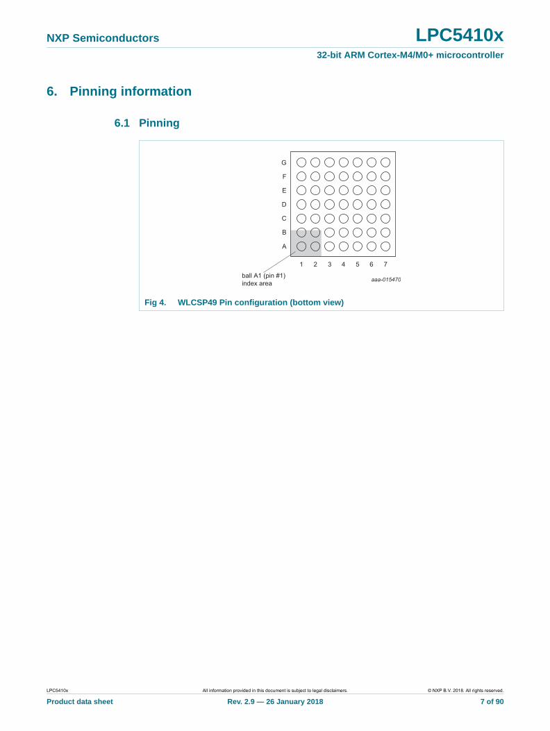
6. Pinning information
6.1 Pinning
Fig 4. WLCSP49 Pin configuration (bottom view)
ball A1 (pin #1)index area
A
B
C
D
E
F
G
7654321
aaa-015470
LPC5410x All information provided in this document is subject to legal disclaimers. © NXP B.V. 2018. All rights reserved.
Product data sheet Rev. 2.9 — 26 January 2018 7 of 90
NXP Semiconductors LPC5410x32-bit ARM Cortex-M4/M0+ microcontroller
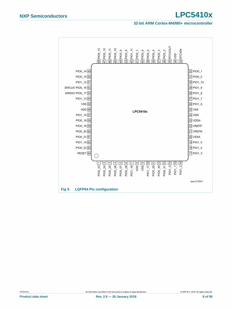
Fig 5. LQFP64 Pin configuration
LPC5410x
49PIO0_14 32 PIO0_1
50PIO0_15 31 PIO0_0
51PIO1_12 30 PIO1_10
52SWCLK/ PIO0_16 29 PIO1_9
53SWDIO/ PIO0_17 28 PIO1_8
54PIO1_13 27 PIO1_7
55VSS 26 PIO1_6
56VDD 25 VSS
57PIO1_14 24 VDD
58PIO0_18 23 VDDA
59PIO0_19 22 VREFP
60PIO0_20 21 VREFN
61PIO0_21 20 VSSA
62PIO1_15 19 PIO1_5
63PIO0_22 18 PIO1_4
64RESET 17 PIO1_3
1P
IO0_
2348
PIO
0_13
2P
IO0_
2447
PIO
0_12
3P
IO0_
2546
PIO
0_11
4P
IO0_
2645
PIO
0_10
5P
IO0_
2744
PIO
0_9
6P
IO0_
2843
PIO
0_8
7P
IO1_
1642
PIO
1_11
8V
DD
41P
IO0_
7
9V
SS
40P
IO0_
6
10P
IO1_
1739
PIO
0_5
11P
IO0_
2938
PIO
0_4
12P
IO0_
3037
PIO
0_3
13P
IO0_
3136
PIO
0_2
14P
IO1_
035
RTC
XO
UT
15P
IO1_
134
VD
D
16P
IO1_
233
RTC
XIN
aaa-013021
LPC5410x All information provided in this document is subject to legal disclaimers. © NXP B.V. 2018. All rights reserved.
Product data sheet Rev. 2.9 — 26 January 2018 8 of 90
NXP Semiconductors LPC5410x32-bit ARM Cortex-M4/M0+ microcontroller
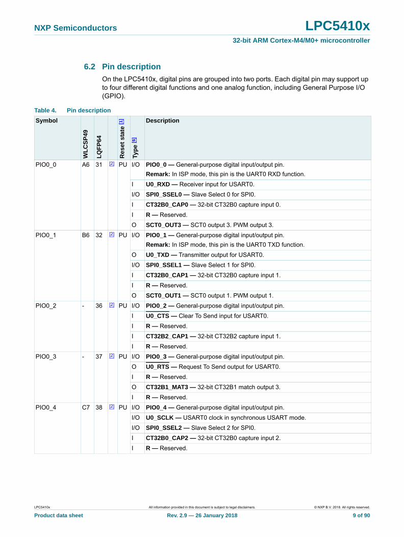
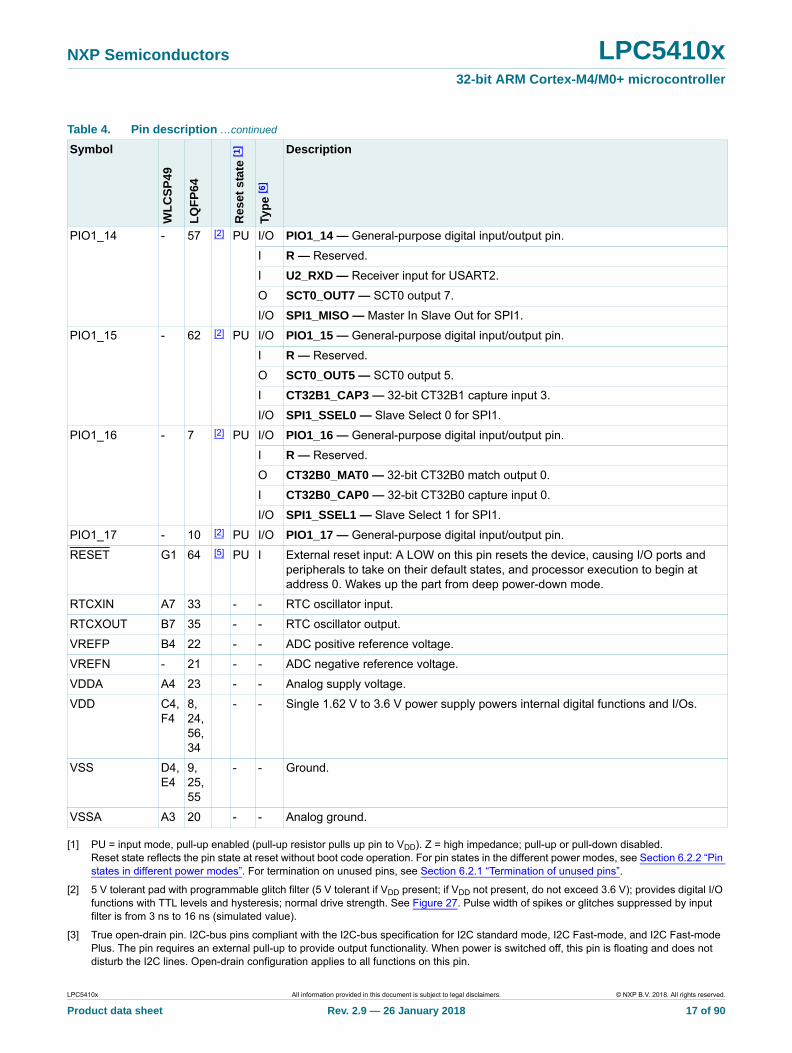
6.2 Pin description
On the LPC5410x, digital pins are grouped into two ports. Each digital pin may support up to four different digital functions and one analog function, including General Purpose I/O (GPIO).
Table 4. Pin description
Symbol
WL
CS
P49
LQ
FP
64
Re
set
stat
e [1
]
Typ
e [6
]
Description
PIO0_0 A6 31 [2] PU I/O PIO0_0 — General-purpose digital input/output pin.
Remark: In ISP mode, this pin is the UART0 RXD function.
I U0_RXD — Receiver input for USART0.
I/O SPI0_SSEL0 — Slave Select 0 for SPI0.
I CT32B0_CAP0 — 32-bit CT32B0 capture input 0.
I R — Reserved.
O SCT0_OUT3 — SCT0 output 3. PWM output 3.
PIO0_1 B6 32 [2] PU I/O PIO0_1 — General-purpose digital input/output pin.
Remark: In ISP mode, this pin is the UART0 TXD function.
O U0_TXD — Transmitter output for USART0.
I/O SPI0_SSEL1 — Slave Select 1 for SPI0.
I CT32B0_CAP1 — 32-bit CT32B0 capture input 1.
I R — Reserved.
O SCT0_OUT1 — SCT0 output 1. PWM output 1.
PIO0_2 - 36 [2] PU I/O PIO0_2 — General-purpose digital input/output pin.
I U0_CTS — Clear To Send input for USART0.
I R — Reserved.
I CT32B2_CAP1 — 32-bit CT32B2 capture input 1.
I R — Reserved.
PIO0_3 - 37 [2] PU I/O PIO0_3 — General-purpose digital input/output pin.
O U0_RTS — Request To Send output for USART0.
I R — Reserved.
O CT32B1_MAT3 — 32-bit CT32B1 match output 3.
I R — Reserved.
PIO0_4 C7 38 [2] PU I/O PIO0_4 — General-purpose digital input/output pin.
I/O U0_SCLK — USART0 clock in synchronous USART mode.
I/O SPI0_SSEL2 — Slave Select 2 for SPI0.
I CT32B0_CAP2 — 32-bit CT32B0 capture input 2.
I R — Reserved.
LPC5410x All information provided in this document is subject to legal disclaimers. © NXP B.V. 2018. All rights reserved.
Product data sheet Rev. 2.9 — 26 January 2018 9 of 90
NXP Semiconductors LPC5410x32-bit ARM Cortex-M4/M0+ microcontroller
PIO0_5 C6 39 [2] PU I/O PIO0_5 — General-purpose digital input/output pin.
I U1_RXD — Receiver input for USART1.
O SCT0_OUT6 — SCT0 output 6. PWM output 6.
O CT32B0_MAT0 — 32-bit CT32B0 match output 0.
I R — Reserved.
PIO0_6 D7 40 [2] PU I/O PIO0_6 — General-purpose digital input/output pin.
O U1_TXD — Transmitter output for USART1.
I R — Reserved.
O CT32B0_MAT1 — 32-bit CT32B0 match output 1.
I R — Reserved.
PIO0_7 D6 41 [2] PU I/O PIO0_7 — General-purpose digital input/output pin.
I/O U1_SCLK — USART1 clock in synchronous USART mode.
O SCT0_OUT0 — SCT0 output 0. PWM output 0.
O CT32B0_MAT2 — 32-bit CT32B0 match output 2.
I R — Reserved.
I CT32B0_CAP2 — 32-bit CT32B0 capture input 2.
PIO0_8 D5 43 [2] PU I/O PIO0_8 — General-purpose digital input/output pin.
I U2_RXD — Receiver input for USART2.
O SCT0_OUT1 — SCT0 output 1. PWM output 1.
O CT32B0_MAT3 — 32-bit CT32B0 match output 3.
I R — Reserved.
PIO0_9 E7 44 [2] PU I/O PIO0_9 — General-purpose digital input/output pin.
O U2_TXD — Transmitter output for USART2.
O SCT0_OUT2 — SCT0 output 2. PWM output 2.
I CT32B3_CAP0 — 32-bit CT32B3 capture input 0.
I R — Reserved.
I/O SPI0_SSEL0 — Slave Select 0 for SPI0.
PIO0_10 E6 45 [2] PU I/O PIO0_10 — General-purpose digital input/output pin.
I/O U2_SCLK — USART2 clock in synchronous USART mode.
O SCT0_OUT3 — SCT0 output 3. PWM output 3.
O CT32B3_MAT0 — 32-bit CT32B3 match output 0.
I R — Reserved.
PIO0_11 E5 46 [2] PU I/O PIO0_11 — General-purpose digital input/output pin.
I/O SPI0_SCK — Serial clock for SPI0.
I U1_RXD — Receiver input for USART1.
O CT32B2_MAT1 — 32-bit CT32B2 match output 1.
I R — Reserved.
Table 4. Pin description …continued
Symbol
WL
CS
P49
LQ
FP
64
Res
et s
tate
[1]
Typ
e [6
]
Description
LPC5410x All information provided in this document is subject to legal disclaimers. © NXP B.V. 2018. All rights reserved.
Product data sheet Rev. 2.9 — 26 January 2018 10 of 90
NXP Semiconductors LPC5410x32-bit ARM Cortex-M4/M0+ microcontroller
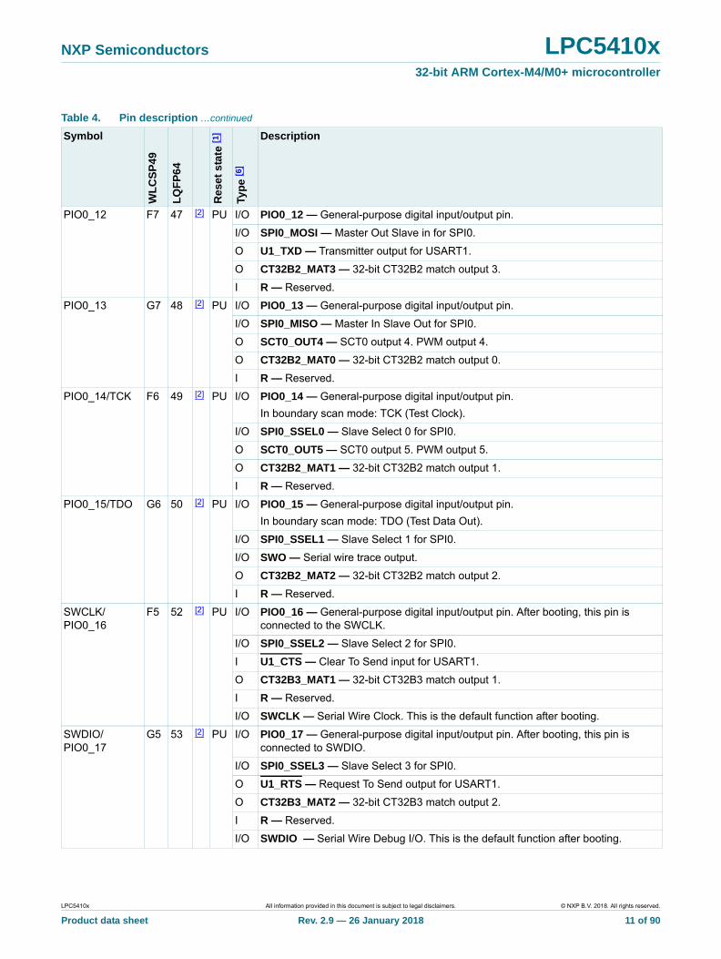
PIO0_12 F7 47 [2] PU I/O PIO0_12 — General-purpose digital input/output pin.
I/O SPI0_MOSI — Master Out Slave in for SPI0.
O U1_TXD — Transmitter output for USART1.
O CT32B2_MAT3 — 32-bit CT32B2 match output 3.
I R — Reserved.
PIO0_13 G7 48 [2] PU I/O PIO0_13 — General-purpose digital input/output pin.
I/O SPI0_MISO — Master In Slave Out for SPI0.
O SCT0_OUT4 — SCT0 output 4. PWM output 4.
O CT32B2_MAT0 — 32-bit CT32B2 match output 0.
I R — Reserved.
PIO0_14/TCK F6 49 [2] PU I/O PIO0_14 — General-purpose digital input/output pin.
In boundary scan mode: TCK (Test Clock).
I/O SPI0_SSEL0 — Slave Select 0 for SPI0.
O SCT0_OUT5 — SCT0 output 5. PWM output 5.
O CT32B2_MAT1 — 32-bit CT32B2 match output 1.
I R — Reserved.
PIO0_15/TDO G6 50 [2] PU I/O PIO0_15 — General-purpose digital input/output pin.
In boundary scan mode: TDO (Test Data Out).
I/O SPI0_SSEL1 — Slave Select 1 for SPI0.
I/O SWO — Serial wire trace output.
O CT32B2_MAT2 — 32-bit CT32B2 match output 2.
I R — Reserved.
SWCLK/PIO0_16
F5 52 [2] PU I/O PIO0_16 — General-purpose digital input/output pin. After booting, this pin is connected to the SWCLK.
I/O SPI0_SSEL2 — Slave Select 2 for SPI0.
I U1_CTS — Clear To Send input for USART1.
O CT32B3_MAT1 — 32-bit CT32B3 match output 1.
I R — Reserved.
I/O SWCLK — Serial Wire Clock. This is the default function after booting.
SWDIO/PIO0_17
G5 53 [2] PU I/O PIO0_17 — General-purpose digital input/output pin. After booting, this pin is connected to SWDIO.
I/O SPI0_SSEL3 — Slave Select 3 for SPI0.
O U1_RTS — Request To Send output for USART1.
O CT32B3_MAT2 — 32-bit CT32B3 match output 2.
I R — Reserved.
I/O SWDIO — Serial Wire Debug I/O. This is the default function after booting.
Table 4. Pin description …continued
Symbol
WL
CS
P49
LQ
FP
64
Res
et s
tate
[1]
Typ
e [6
]
Description
LPC5410x All information provided in this document is subject to legal disclaimers. © NXP B.V. 2018. All rights reserved.
Product data sheet Rev. 2.9 — 26 January 2018 11 of 90
NXP Semiconductors LPC5410x32-bit ARM Cortex-M4/M0+ microcontroller
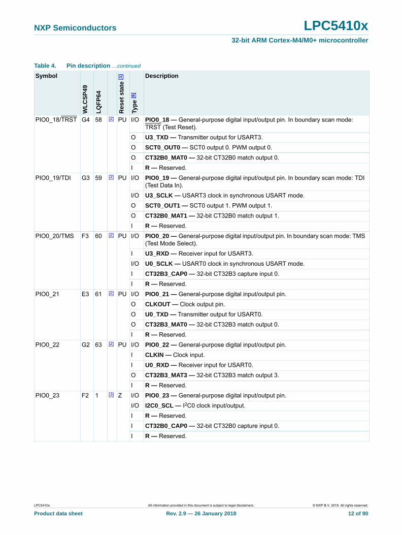
PIO0_18/TRST G4 58 [2] PU I/O PIO0_18 — General-purpose digital input/output pin. In boundary scan mode: TRST (Test Reset).
O U3_TXD — Transmitter output for USART3.
O SCT0_OUT0 — SCT0 output 0. PWM output 0.
O CT32B0_MAT0 — 32-bit CT32B0 match output 0.
I R — Reserved.
PIO0_19/TDI G3 59 [2] PU I/O PIO0_19 — General-purpose digital input/output pin. In boundary scan mode: TDI (Test Data In).
I/O U3_SCLK — USART3 clock in synchronous USART mode.
O SCT0_OUT1 — SCT0 output 1. PWM output 1.
O CT32B0_MAT1 — 32-bit CT32B0 match output 1.
I R — Reserved.
PIO0_20/TMS F3 60 [2] PU I/O PIO0_20 — General-purpose digital input/output pin. In boundary scan mode: TMS (Test Mode Select).
I U3_RXD — Receiver input for USART3.
I/O U0_SCLK — USART0 clock in synchronous USART mode.
I CT32B3_CAP0 — 32-bit CT32B3 capture input 0.
I R — Reserved.
PIO0_21 E3 61 [2] PU I/O PIO0_21 — General-purpose digital input/output pin.
O CLKOUT — Clock output pin.
O U0_TXD — Transmitter output for USART0.
O CT32B3_MAT0 — 32-bit CT32B3 match output 0.
I R — Reserved.
PIO0_22 G2 63 [2] PU I/O PIO0_22 — General-purpose digital input/output pin.
I CLKIN — Clock input.
I U0_RXD — Receiver input for USART0.
O CT32B3_MAT3 — 32-bit CT32B3 match output 3.
I R — Reserved.
PIO0_23 F2 1 [3] Z I/O PIO0_23 — General-purpose digital input/output pin.
I/O I2C0_SCL — I2C0 clock input/output.
I R — Reserved.
I CT32B0_CAP0 — 32-bit CT32B0 capture input 0.
I R — Reserved.
Table 4. Pin description …continued
Symbol
WL
CS
P49
LQ
FP
64
Res
et s
tate
[1]
Typ
e [6
]
Description
LPC5410x All information provided in this document is subject to legal disclaimers. © NXP B.V. 2018. All rights reserved.
Product data sheet Rev. 2.9 — 26 January 2018 12 of 90
NXP Semiconductors LPC5410x32-bit ARM Cortex-M4/M0+ microcontroller
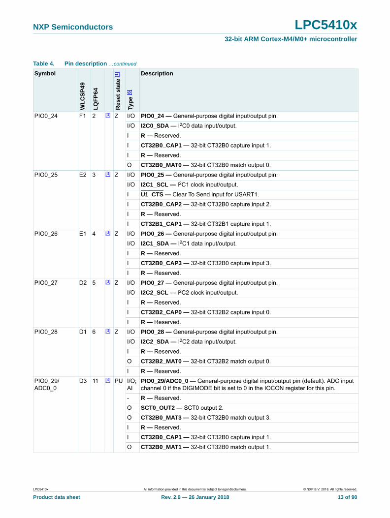
PIO0_24 F1 2 [3] Z I/O PIO0_24 — General-purpose digital input/output pin.
I/O I2C0_SDA — I2C0 data input/output.
I R — Reserved.
I CT32B0_CAP1 — 32-bit CT32B0 capture input 1.
I R — Reserved.
O CT32B0_MAT0 — 32-bit CT32B0 match output 0.
PIO0_25 E2 3 [3] Z I/O PIO0_25 — General-purpose digital input/output pin.
I/O I2C1_SCL — I2C1 clock input/output.
I U1_CTS — Clear To Send input for USART1.
I CT32B0_CAP2 — 32-bit CT32B0 capture input 2.
I R — Reserved.
I CT32B1_CAP1 — 32-bit CT32B1 capture input 1.
PIO0_26 E1 4 [3] Z I/O PIO0_26 — General-purpose digital input/output pin.
I/O I2C1_SDA — I2C1 data input/output.
I R — Reserved.
I CT32B0_CAP3 — 32-bit CT32B0 capture input 3.
I R — Reserved.
PIO0_27 D2 5 [3] Z I/O PIO0_27 — General-purpose digital input/output pin.
I/O I2C2_SCL — I2C2 clock input/output.
I R — Reserved.
I CT32B2_CAP0 — 32-bit CT32B2 capture input 0.
I R — Reserved.
PIO0_28 D1 6 [3] Z I/O PIO0_28 — General-purpose digital input/output pin.
I/O I2C2_SDA — I2C2 data input/output.
I R — Reserved.
O CT32B2_MAT0 — 32-bit CT32B2 match output 0.
I R — Reserved.
PIO0_29/ADC0_0
D3 11 [4] PU I/O; AI
PIO0_29/ADC0_0 — General-purpose digital input/output pin (default). ADC input channel 0 if the DIGIMODE bit is set to 0 in the IOCON register for this pin.
- R — Reserved.
O SCT0_OUT2 — SCT0 output 2.
O CT32B0_MAT3 — 32-bit CT32B0 match output 3.
I R — Reserved.
I CT32B0_CAP1 — 32-bit CT32B0 capture input 1.
O CT32B0_MAT1 — 32-bit CT32B0 match output 1.
Table 4. Pin description …continued
Symbol
WL
CS
P49
LQ
FP
64
Res
et s
tate
[1]
Typ
e [6
]
Description
LPC5410x All information provided in this document is subject to legal disclaimers. © NXP B.V. 2018. All rights reserved.
Product data sheet Rev. 2.9 — 26 January 2018 13 of 90
NXP Semiconductors LPC5410x32-bit ARM Cortex-M4/M0+ microcontroller
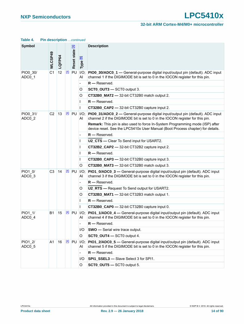
PIO0_30/ADC0_1
C1 12 [4] PU I/O; AI
PIO0_30/ADC0_1 — General-purpose digital input/output pin (default). ADC input channel 1 if the DIGIMODE bit is set to 0 in the IOCON register for this pin.
- R — Reserved.
O SCT0_OUT3 — SCT0 output 3.
O CT32B0_MAT2 — 32-bit CT32B0 match output 2.
I R — Reserved.
I CT32B0_CAP2 — 32-bit CT32B0 capture input 2.
PIO0_31/ADC0_2
C2 13 [4] PU I/O; AI
PIO0_31/ADC0_2 — General-purpose digital input/output pin (default). ADC input channel 2 if the DIGIMODE bit is set to 0 in the IOCON register for this pin.
Remark: This pin is also used to force In-System Programming mode (ISP) after device reset. See the LPC5410x User Manual (Boot Process chapter) for details.
- R — Reserved.
I U2_CTS — Clear To Send input for USART2.
I CT32B2_CAP2 — 32-bit CT32B2 capture input 2.
I R — Reserved.
I CT32B0_CAP3 — 32-bit CT32B0 capture input 3.
O CT32B0_MAT3 — 32-bit CT32B0 match output 3.
PIO1_0/ADC0_3
C3 14 [4] PU I/O; AI
PIO1_0/ADC0_3 — General-purpose digital input/output pin (default). ADC input channel 3 if the DIGIMODE bit is set to 0 in the IOCON register for this pin.
- R — Reserved.
O U2_RTS — Request To Send output for USART2.
O CT32B3_MAT1 — 32-bit CT32B3 match output 1.
I R — Reserved.
I CT32B0_CAP0 — 32-bit CT32B0 capture input 0.
PIO1_1/ADC0_4
B1 15 [4] PU I/O; AI
PIO1_1/ADC0_4 — General-purpose digital input/output pin (default). ADC input channel 4 if the DIGIMODE bit is set to 0 in the IOCON register for this pin.
- R — Reserved.
I/O SWO — Serial wire trace output.
O SCT0_OUT4 — SCT0 output 4.
PIO1_2/ADC0_5
A1 16 [4] PU I/O; AI
PIO1_2/ADC0_5 — General-purpose digital input/output pin (default). ADC input channel 5 if the DIGIMODE bit is set to 0 in the IOCON register for this pin.
- R — Reserved.
I/O SPI1_SSEL3 — Slave Select 3 for SPI1.
O SCT0_OUT5 — SCT0 output 5.
Table 4. Pin description …continued
Symbol
WL
CS
P49
LQ
FP
64
Res
et s
tate
[1]
Typ
e [6
]
Description
LPC5410x All information provided in this document is subject to legal disclaimers. © NXP B.V. 2018. All rights reserved.
Product data sheet Rev. 2.9 — 26 January 2018 14 of 90
NXP Semiconductors LPC5410x32-bit ARM Cortex-M4/M0+ microcontroller
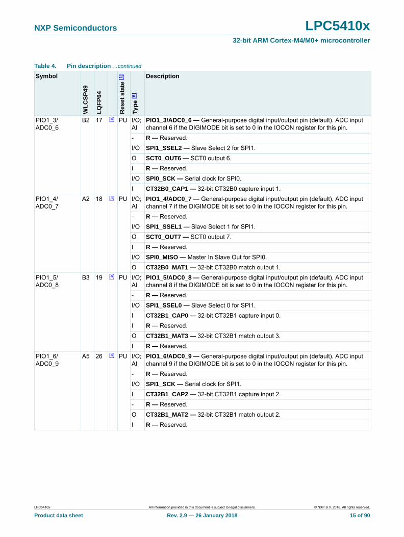
PIO1_3/ADC0_6
B2 17 [4] PU I/O; AI
PIO1_3/ADC0_6 — General-purpose digital input/output pin (default). ADC input channel 6 if the DIGIMODE bit is set to 0 in the IOCON register for this pin.
- R — Reserved.
I/O SPI1_SSEL2 — Slave Select 2 for SPI1.
O SCT0_OUT6 — SCT0 output 6.
I R — Reserved.
I/O SPI0_SCK — Serial clock for SPI0.
I CT32B0_CAP1 — 32-bit CT32B0 capture input 1.
PIO1_4/ADC0_7
A2 18 [4] PU I/O; AI
PIO1_4/ADC0_7 — General-purpose digital input/output pin (default). ADC input channel 7 if the DIGIMODE bit is set to 0 in the IOCON register for this pin.
- R — Reserved.
I/O SPI1_SSEL1 — Slave Select 1 for SPI1.
O SCT0_OUT7 — SCT0 output 7.
I R — Reserved.
I/O SPI0_MISO — Master In Slave Out for SPI0.
O CT32B0_MAT1 — 32-bit CT32B0 match output 1.
PIO1_5/ADC0_8
B3 19 [4] PU I/O; AI
PIO1_5/ADC0_8 — General-purpose digital input/output pin (default). ADC input channel 8 if the DIGIMODE bit is set to 0 in the IOCON register for this pin.
- R — Reserved.
I/O SPI1_SSEL0 — Slave Select 0 for SPI1.
I CT32B1_CAP0 — 32-bit CT32B1 capture input 0.
I R — Reserved.
O CT32B1_MAT3 — 32-bit CT32B1 match output 3.
I R — Reserved.
PIO1_6/ADC0_9
A5 26 [4] PU I/O; AI
PIO1_6/ADC0_9 — General-purpose digital input/output pin (default). ADC input channel 9 if the DIGIMODE bit is set to 0 in the IOCON register for this pin.
- R — Reserved.
I/O SPI1_SCK — Serial clock for SPI1.
I CT32B1_CAP2 — 32-bit CT32B1 capture input 2.
- R — Reserved.
O CT32B1_MAT2 — 32-bit CT32B1 match output 2.
I R — Reserved.
Table 4. Pin description …continued
Symbol
WL
CS
P49
LQ
FP
64
Res
et s
tate
[1]
Typ
e [6
]
Description
LPC5410x All information provided in this document is subject to legal disclaimers. © NXP B.V. 2018. All rights reserved.
Product data sheet Rev. 2.9 — 26 January 2018 15 of 90
NXP Semiconductors LPC5410x32-bit ARM Cortex-M4/M0+ microcontroller
PIO1_7/ADC0_10
B5 27 [4] PU I/O; AI
PIO1_7/ADC0_10 — General-purpose digital input/output pin (default). ADC input channel 10 if the DIGIMODE bit is set to 0 in the IOCON register for this pin.
- R — Reserved.
I/O SPI1_MOSI — Master Out Slave in for SPI1.
O CT32B1_MAT2 — 32-bit CT32B1 match output 2.
- R — Reserved.
I CT32B1_CAP2 — 32-bit CT32B1 capture input 2.
I R — Reserved.
PIO1_8/ADC0_11
C5 28 [4] PU I/O; AI
PIO1_8/ADC0_11 — General-purpose digital input/output pin (default). ADC input channel 11 if the DIGIMODE bit is set to 0 in the IOCON register for this pin.
- R — Reserved.
I/O SPI1_MISO — Master In Slave Out for SPI1.
O CT32B1_MAT3 — 32-bit CT32B1 match output 3.
I R — Reserved.
I CT32B1_CAP3 — 32-bit CT32B1 capture input 3.
I R — Reserved.
PIO1_9 - 29 [2] PU I/O PIO1_9 — General-purpose digital input/output pin.
I R — Reserved.
I/O SPI0_MOSI — Master Out Slave In for SPI0.
I CT32B0_CAP2 — 32-bit CT32B0 capture input 2.
PIO1_10 - 30 [2] PU I/O PIO1_10 — General-purpose digital input/output pin.
I R — Reserved.
O U1_TXD — Transmitter output for USART1.
O SCT0_OUT4 — SCT0 output 4.
PIO1_11 - 42 [2] PU I/O PIO1_11 — General-purpose digital input/output pin.
I R — Reserved.
O U1_RTS — Request To Send output for USART1.
I CT32B1_CAP0 — 32-bit CT32B1 capture input 0.
PIO1_12 - 51 [2] PU I/O PIO1_12 — General-purpose digital input/output pin.
I R — Reserved.
I U3_RXD — Receiver input for USART3.
O CT32B1_MAT0 — 32-bit CT32B1 match output 0.
I/O SPI1_SCK — Serial clock for SPI1.
PIO1_13 - 54 [2] PU I/O PIO1_13 — General-purpose digital input/output pin.
I R — Reserved.
O U3_TXD — Transmitter output for USART3.
O CT32B1_MAT1 — 32-bit CT32B1 match output 1.
I/O SPI1_MOSI — Master Out Slave In for SPI1.
Table 4. Pin description …continued
Symbol
WL
CS
P49
LQ
FP
64
Res
et s
tate
[1]
Typ
e [6
]
Description
LPC5410x All information provided in this document is subject to legal disclaimers. © NXP B.V. 2018. All rights reserved.
Product data sheet Rev. 2.9 — 26 January 2018 16 of 90
NXP Semiconductors LPC5410x32-bit ARM Cortex-M4/M0+ microcontroller
[1] PU = input mode, pull-up enabled (pull-up resistor pulls up pin to VDD). Z = high impedance; pull-up or pull-down disabled.Reset state reflects the pin state at reset without boot code operation. For pin states in the different power modes, see Section 6.2.2 “Pin states in different power modes”. For termination on unused pins, see Section 6.2.1 “Termination of unused pins”.
[2] 5 V tolerant pad with programmable glitch filter (5 V tolerant if VDD present; if VDD not present, do not exceed 3.6 V); provides digital I/O functions with TTL levels and hysteresis; normal drive strength. See Figure 27. Pulse width of spikes or glitches suppressed by input filter is from 3 ns to 16 ns (simulated value).
[3] True open-drain pin. I2C-bus pins compliant with the I2C-bus specification for I2C standard mode, I2C Fast-mode, and I2C Fast-mode Plus. The pin requires an external pull-up to provide output functionality. When power is switched off, this pin is floating and does not disturb the I2C lines. Open-drain configuration applies to all functions on this pin.
PIO1_14 - 57 [2] PU I/O PIO1_14 — General-purpose digital input/output pin.
I R — Reserved.
I U2_RXD — Receiver input for USART2.
O SCT0_OUT7 — SCT0 output 7.
I/O SPI1_MISO — Master In Slave Out for SPI1.
PIO1_15 - 62 [2] PU I/O PIO1_15 — General-purpose digital input/output pin.
I R — Reserved.
O SCT0_OUT5 — SCT0 output 5.
I CT32B1_CAP3 — 32-bit CT32B1 capture input 3.
I/O SPI1_SSEL0 — Slave Select 0 for SPI1.
PIO1_16 - 7 [2] PU I/O PIO1_16 — General-purpose digital input/output pin.
I R — Reserved.
O CT32B0_MAT0 — 32-bit CT32B0 match output 0.
I CT32B0_CAP0 — 32-bit CT32B0 capture input 0.
I/O SPI1_SSEL1 — Slave Select 1 for SPI1.
PIO1_17 - 10 [2] PU I/O PIO1_17 — General-purpose digital input/output pin.
RESET G1 64 [5] PU I External reset input: A LOW on this pin resets the device, causing I/O ports and peripherals to take on their default states, and processor execution to begin at address 0. Wakes up the part from deep power-down mode.
RTCXIN A7 33 - - RTC oscillator input.
RTCXOUT B7 35 - - RTC oscillator output.
VREFP B4 22 - - ADC positive reference voltage.
VREFN - 21 - - ADC negative reference voltage.
VDDA A4 23 - - Analog supply voltage.
VDD C4, F4
8, 24, 56, 34
- - Single 1.62 V to 3.6 V power supply powers internal digital functions and I/Os.
VSS D4, E4
9, 25, 55
- - Ground.
VSSA A3 20 - - Analog ground.
Table 4. Pin description …continued
Symbol
WL
CS
P49
LQ
FP
64
Res
et s
tate
[1]
Typ
e [6
]
Description
LPC5410x All information provided in this document is subject to legal disclaimers. © NXP B.V. 2018. All rights reserved.
Product data sheet Rev. 2.9 — 26 January 2018 17 of 90
NXP Semiconductors LPC5410x32-bit ARM Cortex-M4/M0+ microcontroller
[4] 5 V tolerant pin providing standard digital I/O functions with configurable modes, configurable hysteresis, and analog input. When configured as an analog input, the digital section of the pin is disabled, and the pin is not 5 V tolerant.
[5] Reset pad.5 V tolerant pad with glitch filter with hysteresis. Pulse width of spikes or glitches suppressed by input filter is from 3 ns to 20 ns (simulated value)
[6] I = Input; AI = Analog input; O = Output
LPC5410x All information provided in this document is subject to legal disclaimers. © NXP B.V. 2018. All rights reserved.
Product data sheet Rev. 2.9 — 26 January 2018 18 of 90
NXP Semiconductors LPC5410x32-bit ARM Cortex-M4/M0+ microcontroller
6.2.1 Termination of unused pins
Table 5 shows how to terminate pins that are not used in the application. In many cases, unused pins should be connected externally or configured correctly by software to minimize the overall power consumption of the part.
Unused pins with GPIO function should be configured as outputs set to LOW with their internal pull-up disabled. To configure a GPIO pin as output and drive it LOW, select the GPIO function in the IOCON register, select output in the GPIO DIR register, and write a 0 to the GPIO PORT register for that pin. Disable the pull-up in the pin’s IOCON register.
In addition, it is recommended to configure all GPIO pins that are not bonded out on smaller packages as outputs driven LOW with their internal pull-up disabled.
[1] I = Input, IA = Inactive (no pull-up/pull-down enabled), PU = Pull-Up.
6.2.2 Pin states in different power modes
[1] Default and programmed pin states are retained in sleep, deep sleep, and power down modes.
Table 5. Termination of unused pins
Pin Default state[1]
Recommended termination of unused pins
RESET I; PU The RESET pin can be left unconnected if the application does not use it.
all PIOn_m (not open-drain) I; PU Can be left unconnected if driven LOW and configured as GPIO output with pull-up disabled by software.
PIOn_m (I2C open-drain) IA Can be left unconnected if driven LOW and configured as GPIO output by software.
RTCXIN - Connect to ground. When grounded, the RTC oscillator is disabled.
RTCXOUT - Can be left unconnected.
VREFP - Tie to VDD.
VREFN - Tie to VSS.
VDDA - Tie to VDD.
VSSA - Tie to VSS.
Table 6. Pin states in different power modes
Pin Active Sleep Deep sleep/Power down Deep power-down
PIOn_m pins (not I2C) As configured in the IOCON[1]. Default: internal pull-up enabled. Floating.
PIO0_23 to PIO0_28 (open-drain I2C-bus pins)
As configured in the IOCON[1]. Floating.
RESET Reset function enabled. Default: input, internal pull-up enabled.
Reset function disabled.
LPC5410x All information provided in this document is subject to legal disclaimers. © NXP B.V. 2018. All rights reserved.
Product data sheet Rev. 2.9 — 26 January 2018 19 of 90
NXP Semiconductors LPC5410x32-bit ARM Cortex-M4/M0+ microcontroller
7. Functional description
7.1 Architectural overview
The ARM Cortex-M4 includes three AHB-Lite buses, one system bus and the I-code and D-code buses. One bus is dedicated for instruction fetch (I-code), and one bus is dedicated for data access (D-code). The use of two core buses allows for simultaneous operations if concurrent operations target different devices.
A multi-layer AHB matrix connects the CPU buses and other bus masters to peripherals in a flexible manner that optimizes performance by allowing peripherals on different slaves ports of the matrix to be accessed simultaneously by different bus masters. Connections in the multilayer matrix are shown in Figure 3.
APB peripherals are connected to the AHB matrix via two APB buses using separate slave ports from the multilayer AHB matrix. This allows for better performance by reducing collisions between the CPU and the DMA controller, and also for peripherals on the asynchronous bridge to have a fixed clock that does not track the system clock.
7.2 ARM Cortex-M4 processor
The ARM Cortex-M4 is a general purpose, 32-bit microprocessor, which offers high performance and very low power consumption. The ARM Cortex-M4 offers many new features, including a Thumb-2 instruction set, low interrupt latency, hardware multiply and divide, interruptable/continuable multiple load and store instructions, automatic state save and restore for interrupts, tightly integrated interrupt controller with wake-up interrupt controller, and multiple core buses capable of simultaneous accesses.
A 3-stage pipeline is employed so that all parts of the processing and memory systems can operate continuously. Typically, while one instruction is being executed, its successor is being decoded, and a third instruction is being fetched from memory.
7.3 ARM Cortex-M4 integrated Floating Point Unit (FPU)
The FPU fully supports single-precision add, subtract, multiply, divide, multiply and accumulate, and square root operations. It also provides conversions between fixed-point and floating-point data formats, and floating-point constant instructions.
The FPU provides floating-point computation functionality that is compliant with the ANSI/IEEE Std 754-2008, IEEE Standard for Binary Floating-Point Arithmetic, referred to as the IEEE 754 standard.
7.4 Memory Protection Unit (MPU)
The Cortex-M4 includes a Memory Protection Unit (MPU) which can be used to improve the reliability of an embedded system by protecting critical data within the user application.
The MPU allows separating processing tasks by disallowing access to each other's data, disabling access to memory regions, allowing memory regions to be defined as read-only and detecting unexpected memory accesses that could potentially break the system.
LPC5410x All information provided in this document is subject to legal disclaimers. © NXP B.V. 2018. All rights reserved.
Product data sheet Rev. 2.9 — 26 January 2018 20 of 90
NXP Semiconductors LPC5410x32-bit ARM Cortex-M4/M0+ microcontroller
The MPU separates the memory into distinct regions and implements protection by preventing disallowed accesses. The MPU supports up to eight regions each of which can be divided into eight subregions. Accesses to memory locations that are not defined in the MPU regions, or not permitted by the region setting, will cause the Memory Management Fault exception to take place.
7.5 Nested Vectored Interrupt Controller (NVIC) for Cortex-M4
The NVIC is an integral part of the Cortex-M4. The tight coupling to the CPU allows for low interrupt latency and efficient processing of late arriving interrupts.
7.5.1 Features
• Controls system exceptions and peripheral interrupts.
• 37 vectored interrupts.
• Eight programmable interrupt priority levels, with hardware priority level masking.
• Relocatable vector table.
• Non-Maskable Interrupt (NMI).
• Software interrupt generation.
7.5.2 Interrupt sources
Each peripheral device has one interrupt line connected to the NVIC but may have several interrupt flags.
7.6 ARM Cortex-M0+ co-processor
The ARM Cortex-M0+ co-processor offers high performance and very low power consumption. This processor uses a 2-stage pipeline von Neumann architecture and a small but powerful instruction set providing high-end processing hardware. The processor includes an NVIC with 32 interrupts and a separate system tick timer. In LPC5410x, the Cortex-M0 coprocessor hardware multiply is implemented as a 32-cycle iterative multiplier.
7.7 Nested Vectored Interrupt Controller (NVIC) for Cortex-M0+
The NVIC is an integral part of the Cortex-M0+. The tight coupling to the CPU allows for low interrupt latency and efficient processing of late arriving interrupts.
7.7.1 Features
• Controls system exceptions and peripheral interrupts.
• 32 vectored interrupts.
• Four programmable interrupt priority levels, with hardware priority level masking.
• Relocatable vector table.
• Non-Maskable Interrupt (NMI).
• Software interrupt generation.
LPC5410x All information provided in this document is subject to legal disclaimers. © NXP B.V. 2018. All rights reserved.
Product data sheet Rev. 2.9 — 26 January 2018 21 of 90
NXP Semiconductors LPC5410x32-bit ARM Cortex-M4/M0+ microcontroller
7.7.2 Interrupt sources
Each peripheral device has one interrupt line connected to the NVIC but may have several interrupt flags.
7.8 System Tick timer (SysTick)
The ARM Cortex-M4 and ARM Cortex-M0+ cores include a system tick timer (SysTick) that is intended to generate a dedicated SYSTICK exception. The clock source for the SysTick can be the system clock or the SYSTICK clock.
7.9 On-chip static RAM
The LPC5410x support 104 kB SRAM with separate bus master access for higher throughput and individual power control for low-power operation.
7.10 On-chip flash
The LPC5410x supports 512 kB of on-chip flash memory.
7.11 On-chip ROM
The 64 kB on-chip ROM contains the boot loader and the following Application Programming Interfaces (API):
• In-System Programming (ISP) and In-Application Programming (IAP) support for flash programming.
• Power control API for configuring power consumption and PLL settings.
LPC5410x All information provided in this document is subject to legal disclaimers. © NXP B.V. 2018. All rights reserved.
Product data sheet Rev. 2.9 — 26 January 2018 22 of 90
NXP Semiconductors LPC5410x32-bit ARM Cortex-M4/M0+ microcontroller
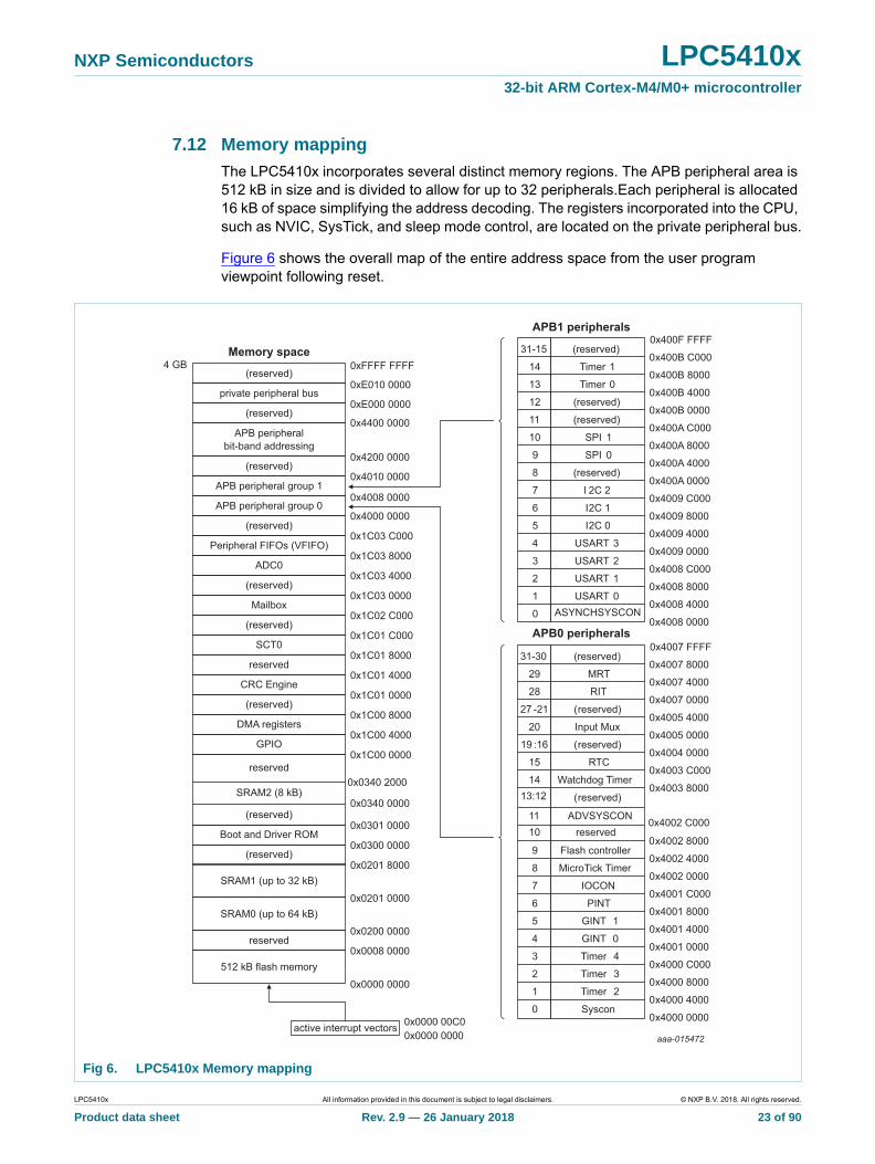
7.12 Memory mapping
The LPC5410x incorporates several distinct memory regions. The APB peripheral area is 512 kB in size and is divided to allow for up to 32 peripherals.Each peripheral is allocated 16 kB of space simplifying the address decoding. The registers incorporated into the CPU, such as NVIC, SysTick, and sleep mode control, are located on the private peripheral bus.
Figure 6 shows the overall map of the entire address space from the user program viewpoint following reset.
Fig 6. LPC5410x Memory mapping
31-15
14
13
12
11
10
9
8
7
6
5
4
3
2
1
0
0x400F FFFF
0x400B C000
0x400B 8000
0x400B 4000
0x400B 0000
0x400A C000
0x400A 8000
0x400A 4000
0x400A 0000
0x4009 C000
0x4009 8000
0x4009 4000
0x4009 0000
0x4008 C000
0x4008 8000
0x4008 4000
0x4008 0000
(reserved)
Timer 1
Timer 0
(reserved)
(reserved)
SPI 1
SPI 0
(reserved)
I 2C 2
I2C 1
I2C 0
USART 3
USART 2
USART 1
USART 0
APB1 peripherals
31-30
29
28
27 -21
20
19 :16
15
14
9
8
7
6
5
4
3
2
1
0
0x4007 FFFF
0x4007 8000
0x4007 4000
0x4007 0000
0x4005 4000
0x4005 0000
0x4004 0000
0x4003 C000
0x4003 8000
0x4002 8000
0x4002 4000
0x4002 0000
0x4001 C000
0x4001 8000
0x4001 4000
0x4001 0000
0x4000 C000
0x4000 8000
0x4000 4000
0x4000 0000
(reserved)
MRT
RIT
(reserved)
Input Mux
(reserved)
RTC
Watchdog Timer
(reserved)
Flash controller
MicroTick Timer
IOCON
PINT
GINT 1
GINT 0
Timer 4
Timer 3
Timer 2
Syscon
APB0 peripherals
4 GB
active interrupt vectors
(reserved)
private peripheral bus
APB peripheral group 1
APB peripheral group 0
(reserved)
(reserved)
(reserved)
reserved
(reserved)
Boot and Driver ROM
APB peripheralbit-band addressing
SRAM1 (up to 32 kB)
SRAM0 (up to 64 kB)
512 kB flash memory
Memory space0xFFFF FFFF
0xE010 0000
0xE000 0000
0x4400 0000
0x4200 0000
0x4010 0000
0x4008 0000
0x4000 0000
0x0300 0000
0x0201 0000
0x0200 0000
0x0008 0000
0x0000 0000
ADC0
Mailbox
(reserved)
(reserved)
SCT0
CRC Engine
reserved
(reserved)
DMA registers
GPIO
(reserved)
Peripheral FIFOs (VFIFO)
0x1C00 0000
0x1C00 4000
0x1C01 C000
0x1C02 C000
0x1C01 4000
0x1C01 8000
0x1C00 8000
0x1C01 0000
0x1C03 8000
0x1C03 C000
0x1C03 0000
0x1C03 4000
0x0301 0000
0x0340 0000
0x0201 8000
0x0000 00000x0000 00C0
0x0340 2000SRAM2 (8 kB)
reserved
0x4002 C00011 ADVSYSCON
ASYNCHSYSCON
10 reserved
13:12
aaa-015472
LPC5410x All information provided in this document is subject to legal disclaimers. © NXP B.V. 2018. All rights reserved.
Product data sheet Rev. 2.9 — 26 January 2018 23 of 90
NXP Semiconductors LPC5410x32-bit ARM Cortex-M4/M0+ microcontroller
7.13 General Purpose I/O (GPIO)
The LPC5410x provides two GPIO ports with a total of 50 GPIO pins.
Device pins that are not connected to a specific peripheral function are controlled by the GPIO registers. Pins may be dynamically configured as inputs or outputs. Separate registers allow setting or clearing any number of outputs simultaneously. The current level of a port pin can be read back no matter what peripheral is selected for that pin.
See Table 4 for the default state on reset.
7.13.1 Features
• Accelerated GPIO functions:
– GPIO registers are located on the AHB so that the fastest possible I/O timing can be achieved.
– Mask registers allow treating sets of port bits as a group, leaving other bits unchanged.
– All GPIO registers are byte and half-word addressable.
– Entire port value can be written in one instruction.
• Bit-level set, clear and toggle registers allow a single instruction set, clear or toggle of any number of bits in one port.
• Direction control of individual bits.
• All I/O default to inputs after reset.
• All GPIO pins can be selected to create an edge or level-sensitive GPIO interrupt request.
• One GPIO group interrupt can be triggered by a combination of any pin or pins.
7.14 Pin interrupt/pattern engine
The pin interrupt block configures up to eight pins from all digital pins for providing eight external interrupts connected to the NVIC. The pattern match engine can be used in conjunction with software to create complex state machines based on pin inputs. Any digital pin, independent of the function selected through the switch matrix can be configured through the SYSCON block as an input to the pin interrupt or pattern match engine. The registers that control the pin interrupt or pattern match engine are located on the I/O+ bus for fast single-cycle access.
7.14.1 Features
• Pin interrupts:
– Up to eight pins can be selected from all GPIO pins on ports 0 and 1 as edge-sensitive or level-sensitive interrupt requests. Each request creates a separate interrupt in the NVIC.
– Edge-sensitive interrupt pins can interrupt on rising or falling edges or both.
– Level-sensitive interrupt pins can be HIGH-active or LOW-active.
– Level-sensitive interrupt pins can be HIGH-active or LOW-active.
– Pin interrupts can wake up the device from sleep mode, deep sleep mode, and power down mode.
LPC5410x All information provided in this document is subject to legal disclaimers. © NXP B.V. 2018. All rights reserved.
Product data sheet Rev. 2.9 — 26 January 2018 24 of 90
NXP Semiconductors LPC5410x32-bit ARM Cortex-M4/M0+ microcontroller
• Pattern match engine:
– Up to eight pins can be selected from all digital pins on ports 0 and 1 to contribute to a boolean expression. The boolean expression consists of specified levels and/or transitions on various combinations of these pins.
– Each bit slice minterm (product term) comprising of the specified boolean expression can generate its own, dedicated interrupt request.
– Any occurrence of a pattern match can also be programmed to generate an RXEV notification to the CPU. The RXEV signal can be connected to a pin.
– Pattern match can be used in conjunction with software to create complex state machines based on pin inputs.
– Pattern match engine facilities wake-up only from active and sleep modes.
7.15 AHB peripherals
7.15.1 DMA controller
The DMA controller allows peripheral-to memory, memory-to-peripheral, and memory-to-memory transactions. Each DMA stream provides unidirectional DMA transfers for a single source and destination.
7.15.1.1 Features
• 22 channels, 21 of which are connected to peripheral DMA requests. These come from the USART, SPI, and I2C peripherals. One spare channels has no DMA request connected, and can be used for functions such as memory-to-memory moves.
• DMA operations can be triggered by on- or off-chip events. Each DMA channel can select one trigger input from 20 sources. Trigger sources include ADC interrupts, Timer interrupts, pin interrupts, and the SCT DMA request lines.
• Priority is user selectable for each channel.
• Continuous priority arbitration.
• Address cache.
• Efficient use of data bus.
• Supports single transfers up to 1,024 words.
• Address increment options allow packing and/or unpacking data.
7.16 Digital serial peripherals
7.16.1 USART
7.16.1.1 Features
• Synchronous mode with master or slave operation. Includes data phase selection and continuous clock option.
• Maximum bit rates of 6.25 Mbit/s in asynchronous mode.
• Maximum supported bit rate of 24 Mbit/s for USART master and slave synchronous modes.
• 7, 8, or 9 data bits and 1 or 2 stop bits.
LPC5410x All information provided in this document is subject to legal disclaimers. © NXP B.V. 2018. All rights reserved.
Product data sheet Rev. 2.9 — 26 January 2018 25 of 90
NXP Semiconductors LPC5410x32-bit ARM Cortex-M4/M0+ microcontroller
• Multiprocessor/multidrop (9-bit) mode with software address compare.
• RS-485 transceiver output enable.
• Autobaud mode for automatic baud rate detection
• Parity generation and checking: odd, even, or none.
• Software selectable oversampling from 5 to 16 clocks in asynchronous mode.
• One transmit and one receive data buffer.
• RTS/CTS for hardware signaling for automatic flow control. Software flow control can be performed using Delta CTS detect, Transmit Disable control, and any GPIO as an RTS output.
• FIFO support from the System FIFO.
• Received data and status can optionally be read from a single register
• Break generation and detection.
• Receive data is 2 of 3 sample "voting". Status flag set when one sample differs.
• Built-in Baud Rate Generator with auto-baud function.
• A fractional rate divider is shared among all USARTs.
• Interrupts available for Receiver Ready, Transmitter Ready, Receiver Idle, change in receiver break detect, Framing error, Parity error, Overrun, Underrun, Delta CTS detect, and receiver sample noise detected.
• Loopback mode for testing of data and flow control.
• In synchronous slave mode, wakes up the part from deep sleep and power down modes.
• Special operating mode allows operation at up to 9600 baud using the 32 kHz RTC oscillator as the UART clock. This mode can be used while the device is in deep sleep or power down mode and can wake-up the device when a character is received.
• USART transmit and receive functions work with the system DMA controller.
• Activity on the USART synchronous slave mode allows wake-up from deep sleep and power down modes on any enabled interrupt.
7.16.2 SPI serial I/O controller
7.16.2.1 Features
• Master and slave operation.
• Maximum supported bit rate for SPI master mode is 48 Mbit/s, and the maximum supported bit rate for SPI slave mode is 21 Mbit/s.
• Data frames of 1 to 16 bits supported directly. Larger frames supported by software or DMA set-up.
• Data can be transmitted to a slave without the need to read incoming data. This can be useful while setting up an SPI memory.
• Control information can optionally be written along with data. This allows very versatile operation, including “any length” frames.
• Up to four Slave Select input/outputs with selectable polarity and flexible usage.
• Supports DMA transfers: SPIn transmit and receive functions can operated with the system DMA controller.
LPC5410x All information provided in this document is subject to legal disclaimers. © NXP B.V. 2018. All rights reserved.
Product data sheet Rev. 2.9 — 26 January 2018 26 of 90
NXP Semiconductors LPC5410x32-bit ARM Cortex-M4/M0+ microcontroller
• FIFO support from the System FIFO.
• Activity on the SPI in slave mode allows wake-up from deep sleep and power down modes on any enabled interrupt.
7.17 I2C-bus interface
The I2C-bus is bidirectional for inter-IC control using only two wires: a serial clock line (SCL) and a serial data line (SDA). Each device is recognized by a unique address and can operate as either a receiver-only device (for example, an LCD driver) or a transmitter with the capability to both receive and send information (such as memory). Transmitters and/or receivers can operate in either master or slave mode, depending on whether the chip has to initiate a data transfer or is only addressed. The I2C is a multi-master bus and can be controlled by more than one bus master connected to it.
7.17.1 Features
• All I2Cs support standard (up to 100 Kbits/s), fast mode (up to 400 Kbits/s), and Fast-mode Plus (up to 1 Mbit/s).
• All I2Cs support high-speed slave mode with data rates of up to 3.4 Mbit/s.
• Independent Master, Slave, and Monitor functions.
• Supports both Multi-master and Multi-master with Slave functions.
• Multiple I2C slave addresses supported in hardware.
• One slave address can be selectively qualified with a bit mask or an address range in order to respond to multiple I2C-bus addresses.
• 10-bit addressing supported with software assist.
• Supports System Management Bus (SMBus).
• No chip clocks are required in order to receive and compare an address as a Slave, so this event can wake up the device from power down mode.
• Supports the I2C-bus specification up to Fast-mode Plus (FM+, up to 1 MHz) in both master and slave modes. High-speed (HS, up to 3.4 MHz) I2C is support in slave mode only.
• Activity on the I2C in slave mode allows wake-up from deep sleep and power down modes on any enabled interrupt.
7.18 Counter/timers
7.18.1 General-purpose 32-bit timers/external event counter
The LPC5410x includes five general-purpose 32-bit timer/counters.
The timer/counter is designed to count cycles of the system derived clock or an externally-supplied clock. It can optionally generate interrupts, generate timed DMA requests, or perform other actions at specified timer values, based on four match registers. Each timer/counter also includes two capture inputs to trap the timer value when an input signal transitions, optionally generating an interrupt.
7.18.1.1 Features
• Each is a 32-bit counter/timer with a programmable 32-bit prescaler. Four of the timers include external capture and match pin connections.
LPC5410x All information provided in this document is subject to legal disclaimers. © NXP B.V. 2018. All rights reserved.
Product data sheet Rev. 2.9 — 26 January 2018 27 of 90
NXP Semiconductors LPC5410x32-bit ARM Cortex-M4/M0+ microcontroller
• Counter or timer operation.
• For each timer with pin connections, up to 4 32-bit capture channels that can take a snapshot of the timer value when an input signal transitions. A capture event may also optionally generate an interrupt.
• The timer and prescaler may be configured to be cleared on a designated capture event. This feature permits easy pulse-width measurement by clearing the timer on the leading edge of an input pulse and capturing the timer value on the trailing edge.
• Four 32-bit match registers that allow:
– Continuous operation with optional interrupt generation on match.
– Stop timer on match with optional interrupt generation.
– Reset timer on match with optional interrupt generation.
• For each timer with pin connections, up to 4 external outputs corresponding to match registers with the following capabilities:
– Set LOW on match.
– Set HIGH on match.
– Toggle on match.
– Do nothing on match.
• PWM: for each timer with pin connections, up to 3 match outputs can be used as single edge controlled PWM outputs.
7.18.2 State Configurable Timer/PWM (SCTimer/PWM)
The SCTimer/PWM (SCT0) allows a wide variety of timing, counting, output modulation, and input capture operations. The inputs and outputs of the SCTimer/PWM are shared with the capture and match inputs/outputs of the 32-bit general-purpose counter/timers.
The SCTimer/PWM can be configured as two 16-bit counters or a unified 32-bit counter. In the two-counter case, in addition to the counter value the following operational elements are independent for each half:
• State variable
• Limit, halt, stop, and start conditions
• Values of Match/Capture registers, plus reload or capture control values
In the two-counter case, the following operational elements are global to the SCT, but the last three can use match conditions from either counter:
• Clock selection
• Inputs
• Events
• Outputs
• Interrupts
LPC5410x All information provided in this document is subject to legal disclaimers. © NXP B.V. 2018. All rights reserved.
Product data sheet Rev. 2.9 — 26 January 2018 28 of 90
NXP Semiconductors LPC5410x32-bit ARM Cortex-M4/M0+ microcontroller
7.18.2.1 Features
• Two 16-bit counters or one 32-bit counter.
• Counter(s) clocked by bus clock or selected input.
• Up counter(s) or up-down counter(s).
• State variable allows sequencing across multiple counter cycles.
• Event combines input or output condition and/or counter match in a specified state.
• Events control outputs, interrupts, and the SCT states.
– Match register 0 can be used as an automatic limit.
– In bi-directional mode, events can be enabled based on the count direction.
– Match events can be held until another qualifying event occurs.
• Selected event(s) can limit, halt, start, or stop a counter.
• Supports:
– 8 inputs (6 GPIO pins, ADC0_THCMP_IRQ, DEBUG_HALTED)
– up to 8 outputs
– 13 match/capture registers
– 13 events
– 13 states
• PWM capabilities including dead time and emergency abort functions
7.18.3 Windowed WatchDog Timer (WWDT)
The purpose of the watchdog is to reset the controller if software fails to periodically service it within a programmable time window.
7.18.3.1 Features
• Internally resets chip if not reloaded during the programmable time-out period.
• Optional windowed operation requires reload to occur between a minimum and maximum time-out period, both programmable.
• Optional warning interrupt can be generated at a programmable time prior to watchdog time-out.
• Programmable 24-bit timer with internal fixed pre-scaler.
• Selectable time period from 1,024 watchdog clocks (TWDCLK 256 4) to over 67 million watchdog clocks (TWDCLK 224 4) in increments of 4 watchdog clocks.
• “Safe” watchdog operation. Once enabled, requires a hardware reset or a Watchdog reset to be disabled.
• Incorrect feed sequence causes immediate watchdog event if enabled.
• The watchdog reload value can optionally be protected such that it can only be changed after the “warning interrupt” time is reached.
• Flag to indicate Watchdog reset.
• The Watchdog clock (WDCLK) source is the fixed 500 kHz clock (+/- 40%) provided by the low-power watchdog oscillator.
• The Watchdog timer can be configured to run in deep sleep or power down mode.
LPC5410x All information provided in this document is subject to legal disclaimers. © NXP B.V. 2018. All rights reserved.
Product data sheet Rev. 2.9 — 26 January 2018 29 of 90
NXP Semiconductors LPC5410x32-bit ARM Cortex-M4/M0+ microcontroller
• Debug mode.
7.18.4 RTC timer
The RTC block has two timers: main RTC timer, and high-resolution/wake-up timer. The main RTC timer is a 32-bit timer that uses a 1 Hz clock and is intended to run continuously as a real-time clock. When the timer value reaches a match value, an interrupt is raised. The alarm interrupt can also wake up the part from any low power mode, if enabled.
The high-resolution or wake-up timer is a 16-bit timer that uses a 1 kHz clock and operates as a one-shot down timer. When the timer is loaded, it starts counting down to 0 at which point an interrupt is raised. The interrupt can wake up the part from any low power mode, if enabled. This timer is intended to be used for timed wake-up from deep sleep, power down, or deep power-down modes. The high-resolution wake-up timer can be disabled to conserve power if not used.
The RTC timer uses the 32 kHz clock input to create a 1 Hz or 1 kHz clock
7.18.4.1 Features
• The RTC oscillator has the following clock outputs:
– 32 kHz clock, selectable for system clock and CLKOUT pin.
– 1 Hz clock for RTC timing.
– 1 kHz clock for high-resolution RTC timing.
• 32-bit, 1 Hz RTC counter and associated match register for alarm generation.
• Separate 16-bit high-resolution/wake-up timer clocked at 1 kHz for 1 ms resolution with a more that one minute maximum time-out period.
• RTC alarm and high-resolution/wake-up timer time-out each generate independent interrupt requests. Either time-out can wake up the part from any of the low power modes, including deep power-down.
7.18.5 Multi-Rate Timer (MRT)
The Multi-Rate Timer (MRT) provides a repetitive interrupt timer with four channels. Each channel can be programmed with an independent time interval, and each channel operates independently from the other channels.
7.18.5.1 Features
• 24-bit interrupt timer.
• Four channels independently counting down from individually set values.
• Repeat interrupt, one-shot interrupt, and one-shot bus stall modes.
7.18.6 Repetitive Interrupt Timer (RIT)
The Repetitive Interrupt Timer provides a versatile means of generating interrupts at specified time intervals, without using a standard timer. It is intended for repeating interrupts that are not related to Operating System interrupts. However, it could be used as an alternative to the System Tick Timer if there are different system requirements.
LPC5410x All information provided in this document is subject to legal disclaimers. © NXP B.V. 2018. All rights reserved.
Product data sheet Rev. 2.9 — 26 January 2018 30 of 90
NXP Semiconductors LPC5410x32-bit ARM Cortex-M4/M0+ microcontroller
7.18.6.1 Features
• 48-bit counter running from the main clock. Counter can be free-running or be reset by a generated interrupt.
• 48-bit compare value.
• 48-bit compare mask. An interrupt is generated when the counter value equals the compare value, after masking. This allows for combinations not possible with a simple compare.
7.18.7 Micro-tick timer (UTICK)
The ultra-low power Micro-tick Timer, running from the Watchdog oscillator, can be used to wake up the device from low power modes.
7.18.7.1 Features
• Ultra simple timer.
• Write once to start.
• Interrupt or software polling.
7.19 12-bit Analog-to-Digital Converter (ADC)
The ADC supports a resolution of 12-bit and fast conversion rates of up to 5.0 Msamples/s. Sequences of analog-to-digital conversions can be triggered by multiple sources. Possible trigger sources are the SCT, external pins, and the ARM TXEV interrupt.
The ADC supports a variable clocking scheme with clocking synchronous to the system clock or independent, asynchronous clocking for high-speed conversions
The ADC includes a hardware threshold compare function with zero-crossing detection. The threshold crossing interrupt is connected internally to the SCT inputs for tight timing control between the ADC and the SCT.
7.19.1 Features
• 12-bit successive approximation analog to digital converter.
• Input multiplexing among up to 12 pins.
• Two configurable conversion sequences with independent triggers.
• Optional automatic high/low threshold comparison and “zero crossing” detection.
• Measurement range VREFN to VREFP (typically 3 V; not to exceed VDDA voltage level).
• 12-bit conversion rate of 5.0 MHz. Options for reduced resolution at higher conversion rates.
LPC5410x All information provided in this document is subject to legal disclaimers. © NXP B.V. 2018. All rights reserved.
Product data sheet Rev. 2.9 — 26 January 2018 31 of 90
NXP Semiconductors LPC5410x32-bit ARM Cortex-M4/M0+ microcontroller
• Burst conversion mode for single or multiple inputs.
• Synchronous or asynchronous operation. Asynchronous operation maximizes flexibility in choosing the ADC clock frequency, Synchronous mode minimizes trigger latency and can eliminate uncertainty and jitter in response to a trigger.
7.20 System control
7.20.1 Clock sources
The LPC5410x supports two external and three internal clock sources:
• The Internal RC (IRC).
• Watchdog oscillator (WDOSC).
• External clock source from the digital I/O pin CLKIN.
• External RTC 32 KHz clock.
• Output of the system PLL.
7.20.1.1 Internal RC oscillator (IRC)
The IRC can be used as the clock that drives the system PLL and subsequently the CPU. The nominal IRC frequency is 12 MHz.
Upon power-up or any chip reset, the LPC5410x uses the IRC as the clock source. Software may later switch to one of the other available clock sources.
7.20.1.2 Watchdog oscillator (WDOSC)
The watchdog oscillator is a low-power internal oscillator. The WDOSC can be used to provide a clock to the WWDT and to the entire chip. The nominal output frequency is 500 kHz.
7.20.1.3 Clock input pin (CLKIN)
An external square-wave clock source (up to 25 MHz) can be supplied on the digital I/O pin CLKIN.
7.20.2 System PLL
The system PLL accepts an input clock frequency in the range of 32 kHz to 12 MHz. The input frequency is multiplied up to a high frequency with a Current Controlled Oscillator (CCO).
The PLL can be enabled or disabled by software.
LPC5410x All information provided in this document is subject to legal disclaimers. © NXP B.V. 2018. All rights reserved.
Product data sheet Rev. 2.9 — 26 January 2018 32 of 90
NXP Semiconductors LPC5410x32-bit ARM Cortex-M4/M0+ microcontroller
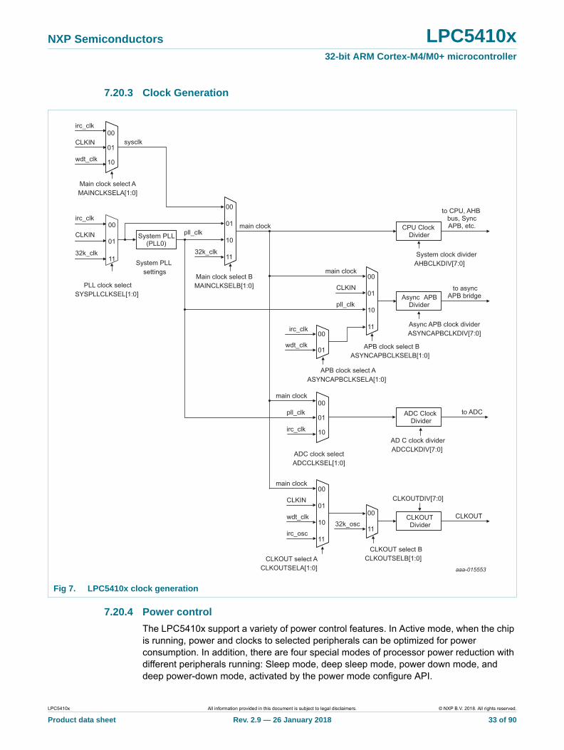
7.20.3 Clock Generation
7.20.4 Power control
The LPC5410x support a variety of power control features. In Active mode, when the chip is running, power and clocks to selected peripherals can be optimized for power consumption. In addition, there are four special modes of processor power reduction with different peripherals running: Sleep mode, deep sleep mode, power down mode, and deep power-down mode, activated by the power mode configure API.
Fig 7. LPC5410x clock generation
System PLLsettings
sysclk
pll_clk
System clock dividerAHBCLKDIV[7:0]
Main clock select BMAINCLKSELB[1:0]
32k_clk
CPU ClockDividerSystem PLL
(PLL0)
CLKIN
Main clock select AMAINCLKSELA[1:0]
wdt_clk
irc_clk
PLL clock selectSYSPLLCLKSEL[1:0]
main clock
CLKIN
pll_clk
APB clock select BASYNCAPBCLKSELB[1:0]
wdt_clk
irc_clk
pll_clk
irc_clk
ADC clock selectADCCLKSEL[1:0]
11
01
10
00
APB clock select AASYNCAPBCLKSELA[1:0]
CLKIN
irc_osc
CLKOUT select ACLKOUTSELA[1:0]
wdt_clk
11
01
10
00
32k_osc
CLKOUT select BCLKOUTSELB[1:0]
CLKOUTDIV[7:0]
CLKOUT
AD C clock dividerADCCLKDIV[7:0]
ADC ClockDivider
Async APB clock dividerASYNCAPBCLKDIV[7:0]
Async APBDivider
to asyncAPB bridge
to ADC
to CPU, AHBbus, SyncAPB, etc.
CLKOUTDivider
11
01
10
00
01
00
01
10
00
01
10
00
11
00
main clock
main clock
main clock
aaa-015553
CLKIN
32k_clk
irc_clk
01
11
00
LPC5410x All information provided in this document is subject to legal disclaimers. © NXP B.V. 2018. All rights reserved.
Product data sheet Rev. 2.9 — 26 January 2018 33 of 90
NXP Semiconductors LPC5410x32-bit ARM Cortex-M4/M0+ microcontroller
7.20.4.1 Sleep mode
When sleep mode is entered, the clock to the core is stopped along with any unused peripherals. Waking up from the sleep mode does not need any special sequence other than re-enabling the clock to the ARM core.
In sleep mode, execution of instructions is suspended until either a reset or interrupt occurs. Peripheral functions continue operation during sleep mode and may generate interrupts to cause the processor to resume execution. Sleep mode eliminates dynamic power used by the processor itself, memory systems and related controllers, internal buses, and unused peripherals. The processor state and registers, peripheral registers, and internal SRAM values are maintained, and the logic levels of the pins remain static.
7.20.4.2 Deep sleep mode
In deep sleep mode, all peripheral clocks and all clock sources are off with the option of keeping the 32 kHz clock and the WDOSC running. In addition, all analog blocks are shut down and the flash is put in stand-by mode. In deep sleep mode, the application can keep some of the internal clocks and the BOD circuit running for self-timed wake-up and BOD protection.
The LPC5410x can wake up from deep sleep mode via a reset, digital pins selected as inputs to the pin interrupt block, RTC alarm, Micro-tick, a watchdog timer reset interrupt, BOD interrupt/reset, or an interrupt from the USART (in 32 kHz mode or synchronous slave mode), the SPI, or any of the I2C peripherals. For wake-up from deep sleep mode, the SPI, USART, and I2C peripherals must be configured in slave mode.
Any interrupt used for waking up from deep sleep mode must be enabled in one of the SYSCON wake-up enable registers and the NVIC.
In deep sleep mode, the processor state and registers, peripheral registers, and internal SRAM values are maintained, and the logic levels of the pins remain static. deep sleep mode allows for very low quiescent power and fast wake-up options.
7.20.4.3 Power down mode
In power down mode, all peripheral clocks and all clock sources are off with the option of keeping the 32 kHz clock, and the WDOSC running. In addition, all analog blocks and the flash are shut down. In power down mode, the application can keep the BOD circuit running for BOD protection.
The LPC5410x can wake up from power down mode via a reset, digital pins selected as inputs to the pin interrupt block, RTC alarm, Micro-tick, a watchdog timer reset interrupt, BOD interrupt/reset, or an interrupt from the USART (in 32 kHz mode or synchronous slave mode), the SPI, or any of the I2C peripherals. For wake-up from power down mode, the SPI, USART, and I2C peripherals must be configured in slave mode.
In power down mode, the processor state and registers, peripheral registers, and internal SRAM values are maintained, and the logic levels of the pins remain static. Power down mode reduces power consumption compared to deep sleep mode at the expense of longer wake-up times.
LPC5410x All information provided in this document is subject to legal disclaimers. © NXP B.V. 2018. All rights reserved.
Product data sheet Rev. 2.9 — 26 January 2018 34 of 90
NXP Semiconductors LPC5410x32-bit ARM Cortex-M4/M0+ microcontroller
7.20.4.4 Deep power-down mode
In deep power-down mode, power is shut off to the entire chip except for the RTC power domain and the RESET pin. The LPC5410x can wake up from deep power down mode via the RESET pin and the RTC alarm.
7.20.5 Brownout detection
The LPC5410x includes a monitor for the voltage level on the VDD pin. If this voltage falls below a fixed level, the BOD sets a flag that can be polled or cause an interrupt. In addition, a separate threshold levels can be selected to cause chip reset and interrupt.
7.20.6 Safety
The LPC5410x includes a Windowed WatchDog Timer (WWDT), which can be enabled by software after reset. Once enabled, the WWDT remains locked and cannot be modified in any way until a reset occurs.
7.21 Code security (Code Read Protection - CRP)
This feature of the LPC5410x allows user to enable different levels of security in the system so that access to the on-chip flash and use of the Serial Wire Debugger (SWD) and In-System Programming (ISP) can be restricted. When needed, CRP is invoked by programming a specific pattern into a dedicated flash location. IAP commands are not affected by the CRP.
In addition, ISP entry can be invoked by pulling a pin on the LPC5410x LOW on reset. This pin is called the ISP entry pin.
There are three levels of Code Read Protection:
1. CRP1 disables access to the chip via the SWD and allows partial flash update (excluding flash sector 0) using a limited set of the ISP commands. This mode is useful when CRP is required and flash field updates are needed but all sectors cannot be erased.
2. CRP2 disables access to the chip via the SWD and only allows full flash erase and update using a reduced set of the ISP commands.
3. CRP3 fully disables any access to the chip via SWD and ISP. It is up to the user’s application to provide (if needed) flash update mechanism using IAP calls or a call to reinvoke ISP command to enable a flash update via USART.
4. In addition to the three CRP levels, sampling of the ISP entry pin for valid user code can be disabled (No_ISP mode). For details, see the LPC5410x user manual.
CAUTION
If level three Code Read Protection (CRP3) is selected, no future factory testing can be performed on the device.
LPC5410x All information provided in this document is subject to legal disclaimers. © NXP B.V. 2018. All rights reserved.
Product data sheet Rev. 2.9 — 26 January 2018 35 of 90
NXP Semiconductors LPC5410x32-bit ARM Cortex-M4/M0+ microcontroller
7.22 Emulation and debugging
Debug and trace functions are integrated into the ARM Cortex-M4 and ARM Cortex-M0+. Serial wire debug and trace functions are supported. The ARM Cortex-M4 is configured to support up to eight breakpoints and four watch points. The ARM Cortex-M0+ is configured to support up to four breakpoints and two watch points. In addition, JTAG boundary scan mode is provided.
The ARM SYSREQ reset is supported and causes the processor to reset the peripherals, execute the boot code, restart from address 0x0000 0000, and break at the user entry point.
The SWD pins are multiplexed with other digital I/O pins. On reset, the pins assume the SWD functions by default.
LPC5410x All information provided in this document is subject to legal disclaimers. © NXP B.V. 2018. All rights reserved.
Product data sheet Rev. 2.9 — 26 January 2018 36 of 90
NXP Semiconductors LPC5410x32-bit ARM Cortex-M4/M0+ microcontroller
8. Limiting values
[1] The following applies to the limiting values:
a) This product includes circuitry specifically designed for the protection of its internal devices from the damaging effects of excessive static charge. Nonetheless, it is suggested that conventional precautions be taken to avoid applying greater than the rated maximum.
b) Parameters are valid over operating temperature range unless otherwise specified. All voltages are with respect to VSS unless otherwise noted.
c) The limiting values are stress ratings only and operating the part at these values is not recommended and proper operation is not guaranteed. The conditions for functional operation are specified in Table 16.
[2] Maximum/minimum voltage above the maximum operating voltage (see Table 16) and below ground that can be applied for a short time (< 10 ms) to a device without leading to irrecoverable failure. Failure includes the loss of reliability and shorter lifetime of the device.
[3] The peak current is limited to 25 times the corresponding maximum current.
[4] Human body model: equivalent to discharging a 100 pF capacitor through a 1.5 k series resistor.
[5] VDD present or not present. Compliant with the I2C-bus standard. 5.5 V can be applied to this pin when VDD is powered down.
[6] Applies to all 5 V tolerant I/O pins except true open-drain pins.
[7] Including the voltage on outputs in 3-state mode.
Table 7. Limiting valuesIn accordance with the Absolute Maximum Rating System (IEC 60134).[1]
Symbol Parameter Conditions Min Max Unit
VDD supply voltage (core and external rail)
on pin VDD [2] 0.5 +4.6 V
VDDA analog supply voltage on pin VDDA -0.5 +4.6 V
Vref reference voltage on pin VREFP - 0.5 +4.6 V
VI input voltage only valid when the VDD > 1.8 V;
5 V tolerant I/O pins
[6][7] 0.5 5.0 V
VI input voltage on I2C open-drain pins [5] 0.5 +5.0 V
VIA analog input voltage on digital pins configured for an analog function
[8][9] 0.5 VDD V
IDD total supply current [3] - 60 mA
ISS total ground current [3] - 60 mA
Ilatch I/O latch-up current (0.5VDD) < VI < (1.5VDD);
Tj < 125 C
- 100 mA
Vi(rtcx) 32 kHz oscillator input voltage
[2] -0.5 4.6 V
Tstg storage temperature [10] 65 +150 C
Tj(max) maximum junction temperature
- +150 C
Ptot(pack) total power dissipation (per package)
based on package heat transfer, not device power consumption
- 1.5 W
VESD electrostatic discharge voltage
human body model; all pins [4] 4000 V
LPC5410x All information provided in this document is subject to legal disclaimers. © NXP B.V. 2018. All rights reserved.
Product data sheet Rev. 2.9 — 26 January 2018 37 of 90
NXP Semiconductors LPC5410x32-bit ARM Cortex-M4/M0+ microcontroller
[8] An ADC input voltage above 3.6 V can be applied for a short time without leading to immediate, unrecoverable failure. Accumulated exposure to elevated voltages at 4.6 V must be less than 106 s total over the lifetime of the device. Applying an elevated voltage to the ADC inputs for a long time affects the reliability of the device and reduces its lifetime.
[9] It is recommended to connect an overvoltage protection diode between the analog input pin and the voltage supply pin.
[10] Dependent on package type.
LPC5410x All information provided in this document is subject to legal disclaimers. © NXP B.V. 2018. All rights reserved.
Product data sheet Rev. 2.9 — 26 January 2018 38 of 90
NXP Semiconductors LPC5410x32-bit ARM Cortex-M4/M0+ microcontroller
9. Thermal characteristics
The average chip junction temperature, Tj (C), can be calculated using the following equation:
(1)
• Tamb = ambient temperature (C),
• Rth(j-a) = the package junction-to-ambient thermal resistance (C/W)
• PD = sum of internal and I/O power dissipation
The internal power dissipation is the product of IDD and VDD. The I/O power dissipation of the I/O pins is often small and many times can be negligible. However it can be significant in some applications.
Table 8. Thermal resistance
Symbol Parameter Conditions Max/Min Unit
LQFP64 Package
Rth(j-a) thermal resistance from junction to ambient
JEDEC (4.5 in 4 in); still air 58 ± 15 % C/W
Single-layer (4.5 in 3 in); still air 81 ± 15 % C/W
Rth(j-c) thermal resistance from junction to case
18 ± 15 % C/W
WLCSP49 Package
Rth(j-a) thermal resistance from junction to ambient
JEDEC (4.5 in 4 in); still air 41 ± 15 % C/W
Rth(j-c) thermal resistance from junction to case
0.3 ± 15 % C/W
Tj Tamb PD Rth j a– +=
LPC5410x All information provided in this document is subject to legal disclaimers. © NXP B.V. 2018. All rights reserved.
Product data sheet Rev. 2.9 — 26 January 2018 39 of 90
NXP Semiconductors LPC5410x32-bit ARM Cortex-M4/M0+ microcontroller
10. Static characteristics
10.1 General operating conditions
[1] The VDD voltage must be equal or lower than the voltage level on VDDA.
[2] The Vrefp voltage must not exceed the voltage level on VDDA.
10.2 CoreMark data
[1] Clock source 12 MHz IRC. PLL disabled.
[2] Clock source 12 MHz IRC. PLL enabled.
[3] Characterized through bench measurements using typical samples.
[4] Compiler settings: Keil µVision v.5.12, optimization level 3, optimized for time on.
Table 9. General operating conditionsTamb = 40 C to +105 C, unless otherwise specified.
Symbol Parameter Conditions Min Typ Max Unit
fclk clock frequency internal CPU/system clock - - 100 MHz
VDD supply voltage (core and external rail)
1.62 - 3.6 V
VDDA analog supply voltage [1] 1.62 - 3.6 V
Vrefp ADC positive reference voltage
VDDA 2 V [2] 2.0 - VDDA V
VDDA < 2 V VDDA - VDDA V
RTC oscillator pins
Vi(rtcx) 32 kHz oscillator input voltage
on pin RTCXIN 0.5 - +3.6 V
Vo(rtcx) 32 kHz oscillator output voltage
on pin RTCXOUT 0.5 - +3.6 V
Table 10. CoreMark scoreTamb = 25C, VDD = 3.3V
Parameter Conditions Typ Unit
ARM Cortex-M4 in active mode; ARM Cortex-M0+ in sleep mode
CoreMark score CoreMark code executed from SRAM;
CCLK = 12 MHz [1][3][4][5] 2.6 (Iterations/s) / MHz
CCLK = 48 MHz [2][3][4][5] 2.6 (Iterations/s) / MHz
CCLK = 84 MHz [2][3][4][5] 2.6 (Iterations/s) / MHz
CCLK = 100 MHz [2][3][4][5] 2.6 (Iterations/s) / MHz
CoreMark score CoreMark code executed from flash;
CCLK = 12 MHz; 1 system clock flash access time. [1][3][4][6] 2.6 (Iterations/s) / MHz
CCLK = 48 MHz; 3 system clock flash access time.
[2][3][4][6] 2.4 (Iterations/s) / MHz
CCLK = 84 MHz; 5 system clock flash access time.
[2][3][4][6] 2.3 (Iterations/s) / MHz
CCLK = 100 MHz; 6 system clock flash access time.
[2][3][4][6] 2.2 (Iterations/s) / MHz
LPC5410x All information provided in this document is subject to legal disclaimers. © NXP B.V. 2018. All rights reserved.
Product data sheet Rev. 2.9 — 26 January 2018 40 of 90
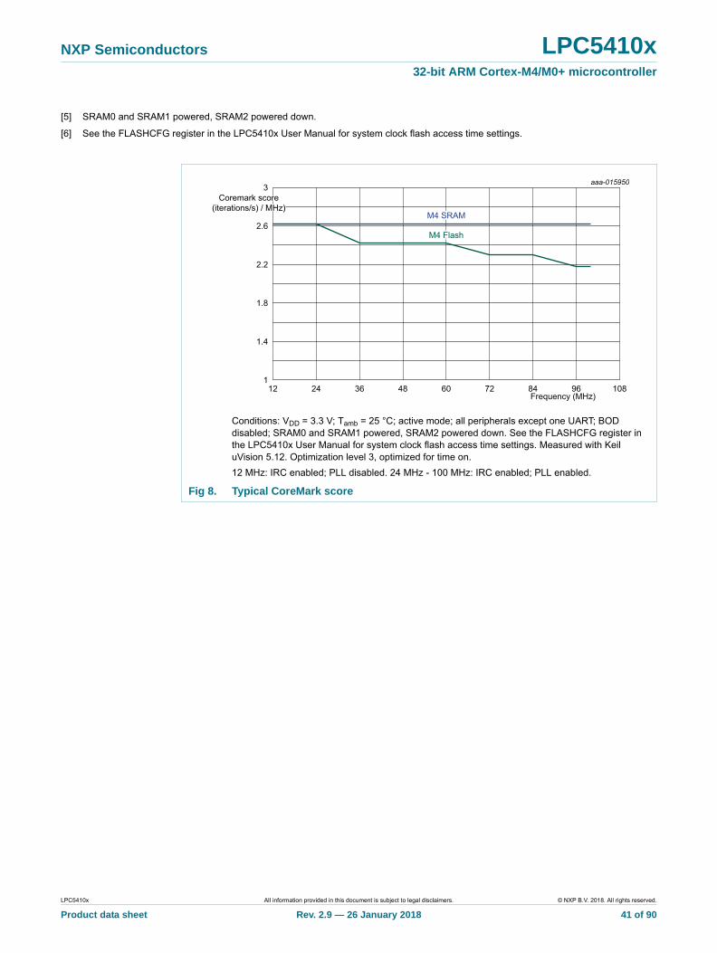
NXP Semiconductors LPC5410x32-bit ARM Cortex-M4/M0+ microcontroller
[5] SRAM0 and SRAM1 powered, SRAM2 powered down.
[6] See the FLASHCFG register in the LPC5410x User Manual for system clock flash access time settings.
Conditions: VDD = 3.3 V; Tamb = 25 °C; active mode; all peripherals except one UART; BOD disabled; SRAM0 and SRAM1 powered, SRAM2 powered down. See the FLASHCFG register in the LPC5410x User Manual for system clock flash access time settings. Measured with Keil uVision 5.12. Optimization level 3, optimized for time on.
12 MHz: IRC enabled; PLL disabled. 24 MHz - 100 MHz: IRC enabled; PLL enabled.
Fig 8. Typical CoreMark score
aaa-015950
12 24 36 48 60 72 84 96 1081
1.4
1.8
2.2
2.6
3
Frequency (MHz)
Coremark scoreCoremark scoreCoremark score(iterations/s) / MHz)(iterations/s) / MHz)(iterations/s) / MHz)
M4 SRAMM4 SRAMM4 SRAM
M4 FlashM4 FlashM4 Flash
LPC5410x All information provided in this document is subject to legal disclaimers. © NXP B.V. 2018. All rights reserved.
Product data sheet Rev. 2.9 — 26 January 2018 41 of 90
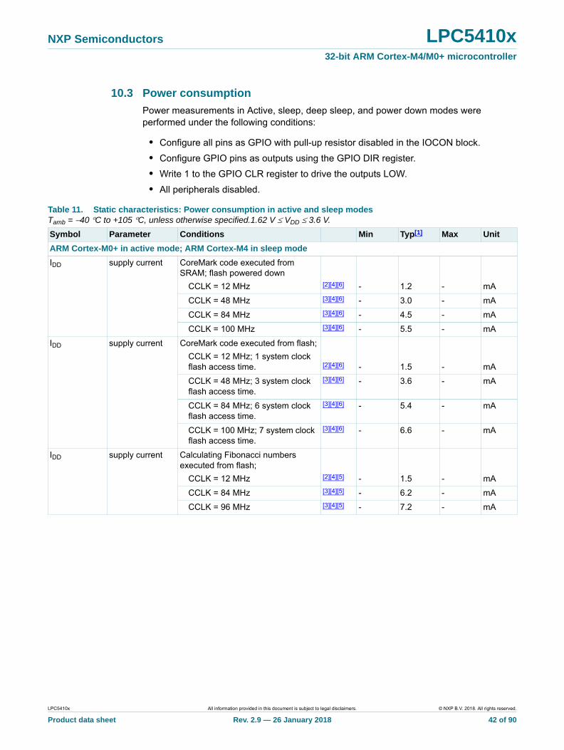
NXP Semiconductors LPC5410x32-bit ARM Cortex-M4/M0+ microcontroller
10.3 Power consumption
Power measurements in Active, sleep, deep sleep, and power down modes were performed under the following conditions:
• Configure all pins as GPIO with pull-up resistor disabled in the IOCON block.
• Configure GPIO pins as outputs using the GPIO DIR register.
• Write 1 to the GPIO CLR register to drive the outputs LOW.
• All peripherals disabled.
Table 11. Static characteristics: Power consumption in active and sleep modesTamb = 40 C to +105 C, unless otherwise specified.1.62 V VDD 3.6 V.
Symbol Parameter Conditions Min Typ[1] Max Unit
ARM Cortex-M0+ in active mode; ARM Cortex-M4 in sleep mode
IDD supply current CoreMark code executed from SRAM; flash powered down
CCLK = 12 MHz [2][4][6] - 1.2 - mA
CCLK = 48 MHz [3][4][6] - 3.0 - mA
CCLK = 84 MHz [3][4][6] - 4.5 - mA
CCLK = 100 MHz [3][4][6] - 5.5 - mA
IDD supply current CoreMark code executed from flash;
CCLK = 12 MHz; 1 system clock flash access time. [2][4][6] - 1.5 - mA
CCLK = 48 MHz; 3 system clock flash access time.
[3][4][6] - 3.6 - mA
CCLK = 84 MHz; 6 system clock flash access time.
[3][4][6] - 5.4 - mA
CCLK = 100 MHz; 7 system clock flash access time.
[3][4][6] - 6.6 - mA
IDD supply current Calculating Fibonacci numbers executed from flash;
CCLK = 12 MHz [2][4][5] - 1.5 - mA
CCLK = 84 MHz [3][4][5] - 6.2 - mA
CCLK = 96 MHz [3][4][5] - 7.2 - mA
LPC5410x All information provided in this document is subject to legal disclaimers. © NXP B.V. 2018. All rights reserved.
Product data sheet Rev. 2.9 — 26 January 2018 42 of 90
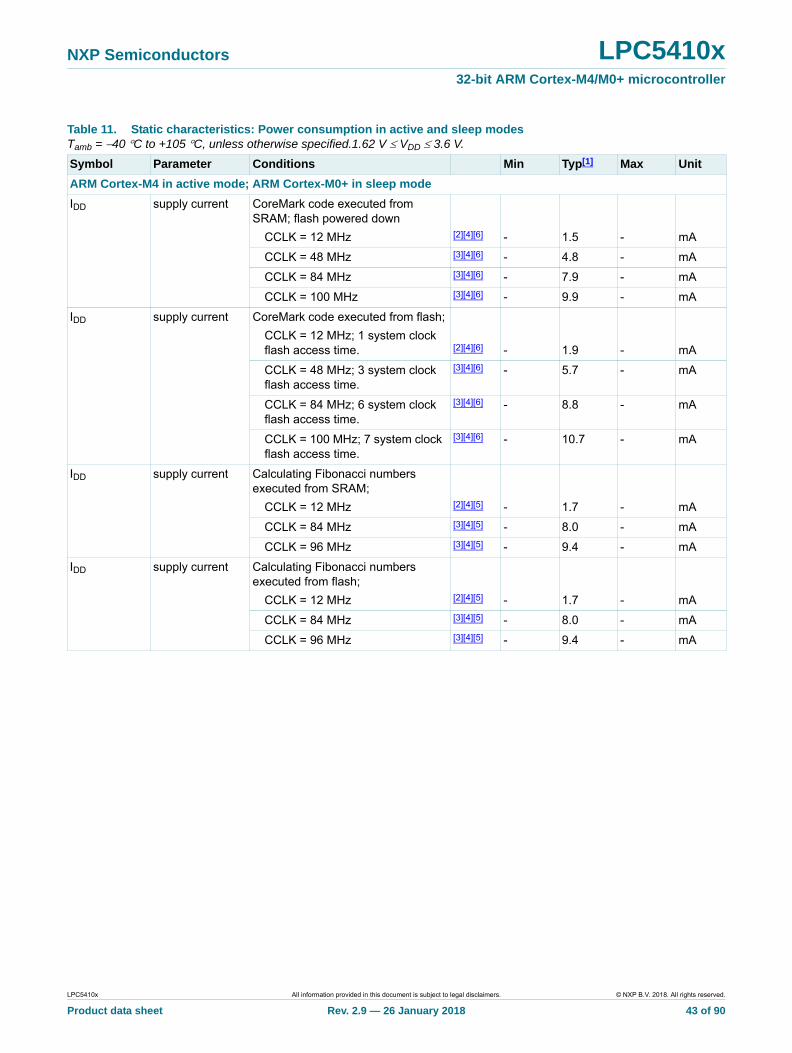
NXP Semiconductors LPC5410x32-bit ARM Cortex-M4/M0+ microcontroller
ARM Cortex-M4 in active mode; ARM Cortex-M0+ in sleep mode
IDD supply current CoreMark code executed from SRAM; flash powered down
CCLK = 12 MHz [2][4][6] - 1.5 - mA
CCLK = 48 MHz [3][4][6] - 4.8 - mA
CCLK = 84 MHz [3][4][6] - 7.9 - mA
CCLK = 100 MHz [3][4][6] - 9.9 - mA
IDD supply current CoreMark code executed from flash;
CCLK = 12 MHz; 1 system clock flash access time. [2][4][6] - 1.9 - mA
CCLK = 48 MHz; 3 system clock flash access time.
[3][4][6] - 5.7 - mA
CCLK = 84 MHz; 6 system clock flash access time.
[3][4][6] - 8.8 - mA
CCLK = 100 MHz; 7 system clock flash access time.
[3][4][6] - 10.7 - mA
IDD supply current Calculating Fibonacci numbers executed from SRAM;
CCLK = 12 MHz [2][4][5] - 1.7 - mA
CCLK = 84 MHz [3][4][5] - 8.0 - mA
CCLK = 96 MHz [3][4][5] - 9.4 - mA
IDD supply current Calculating Fibonacci numbers executed from flash;
CCLK = 12 MHz [2][4][5] - 1.7 - mA
CCLK = 84 MHz [3][4][5] - 8.0 - mA
CCLK = 96 MHz [3][4][5] - 9.4 - mA
Table 11. Static characteristics: Power consumption in active and sleep modesTamb = 40 C to +105 C, unless otherwise specified.1.62 V VDD 3.6 V.
Symbol Parameter Conditions Min Typ[1] Max Unit
LPC5410x All information provided in this document is subject to legal disclaimers. © NXP B.V. 2018. All rights reserved.
Product data sheet Rev. 2.9 — 26 January 2018 43 of 90
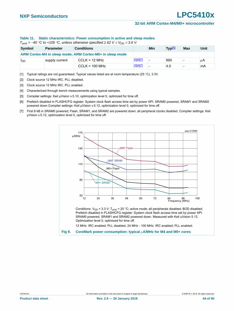
NXP Semiconductors LPC5410x32-bit ARM Cortex-M4/M0+ microcontroller
[1] Typical ratings are not guaranteed. Typical values listed are at room temperature (25 C), 3.3V.
[2] Clock source 12 MHz IRC. PLL disabled.
[3] Clock source 12 MHz IRC. PLL enabled.
[4] Characterized through bench measurements using typical samples.
[5] Compiler settings: Keil µVision v.5.10, optimization level 0, optimized for time off.
[6] Prefetch disabled in FLASHCFG register. System clock flash access time set by power API. SRAM0 powered, SRAM1 and SRAM2 powered down.Compiler settings: Keil µVision v.5.12, optimization level 0, optimized for time off.
[7] First 8 kB in SRAM0 powered; Flash, SRAM1, and SRAM2 are powered down; all peripheral clocks disabled. Compiler settings: Keil µVision v.5.12, optimization level 0, optimized for time off.
ARM Cortex-M4 in sleep mode; ARM Cortex-M0+ in sleep mode
IDD supply current CCLK = 12 MHz [2][4][7] - 990 - A
CCLK = 100 MHz [3][4][7] - 4.0 - mA
Table 11. Static characteristics: Power consumption in active and sleep modesTamb = 40 C to +105 C, unless otherwise specified.1.62 V VDD 3.6 V.
Symbol Parameter Conditions Min Typ[1] Max Unit
Conditions: VDD = 3.3 V; Tamb = 25 °C; active mode; all peripherals disabled; BOD disabled; Prefetch disabled in FLASHCFG register. System clock flash access time set by power API. SRAM0 powered, SRAM1 and SRAM2 powered down. Measured with Keil uVision 5.12. Optimization level 0, optimized for time off.
12 MHz: IRC enabled; PLL disabled. 24 MHz - 100 MHz: IRC enabled; PLL enabled.
Fig 9. CoreMark power consumption: typical A/MHz for M4 and M0+ cores
aaa-015966
12 24 36 48 60 72 84 96 10850
80
110
140
170
Frequency (MHz)
μ/MHzμ/MHzμ/MHz
M4F SRAMM4F SRAMM4F SRAM
M0+ SRAMM0+ SRAMM0+ SRAM
M4F FlashM4F FlashM4F Flash
M0+ FlashM0+ FlashM0+ Flash
LPC5410x All information provided in this document is subject to legal disclaimers. © NXP B.V. 2018. All rights reserved.
Product data sheet Rev. 2.9 — 26 January 2018 44 of 90
NXP Semiconductors LPC5410x32-bit ARM Cortex-M4/M0+ microcontroller
[1] Typical ratings are not guaranteed. Typical values listed are at room temperature (25 C).
[2] Characterized through bench measurements using typical samples. VDD = 1.62 V
[3] Guaranteed by characterization, not tested in production. VDD = 2.0 V
Table 12. Static characteristics: Power consumption in deep sleep, power down, and deep power-down modesTamb = 40 C to +105 C, 1.62 V VDD 2.0 V; unless otherwise specified.
Symbol Parameter Conditions Min Typ[1][2] Max[3] Unit
IDD supply current Deep sleep mode; all SRAM on:
Tamb = 25 C
[2]
- 235 380 A
Tamb = 105 C - - 1.9 mA
Power down mode;
first 8 kB in SRAM0 powered:
Tamb = 25 C
[2]
- 4 8 A
Tamb = 105 C - 110 A
SRAM0 (64 kB) powered - 6.7 - A
SRAM0 (64 kB), SRAM1 (32 kB) powered
- 7.8 - A
SRAM0 (64 kB), SRAM1 (32 kB), SRAM2 (8 kB) powered
- 8.2 - A
Deep power-down mode;
RTC oscillator input grounded (RTC oscillator disabled)
Tamb = 25 C
[2] -
160 340 nA
Tamb = 105 C - 14 A
RTC oscillator running with external crystal
- 240 - nA
LPC5410x All information provided in this document is subject to legal disclaimers. © NXP B.V. 2018. All rights reserved.
Product data sheet Rev. 2.9 — 26 January 2018 45 of 90
NXP Semiconductors LPC5410x32-bit ARM Cortex-M4/M0+ microcontroller
[1] Typical ratings are not guaranteed. Typical values listed are at room temperature (25 C).
[2] Characterized through bench measurements using typical samples. VDD = 3.3 V
[3] Tested in production, VDD = 3.6 V
Table 13. Static characteristics: Power consumption in deep sleep, power down, and deep power-down modesTamb = 40 C to +105 C, 2.7 V . VDD 3.6 V; unless otherwise specified.
Symbol Parameter Conditions Min Typ[1][2] Max[3] Unit
IDD supply current Deep sleep mode; all SRAM on:
Tamb = 25 C
[2] -
306 480 A
Tamb = 105 C - - 2.3 mA
Power down mode;
first 8 kB in SRAM0 powered:
Tamb = 25 C
[2]
- 5 10 A
Tamb = 105 C - - 115 A
SRAM0 (64 kB) powered - 7.3 - A
SRAM0 (64 kB), SRAM1 (32 kB) powered
- 8.6 - A
SRAM0 (64 kB), SRAM1 (32 kB), SRAM2 (8 kB) powered
- 9 - A
Deep power-down mode;
RTC oscillator input grounded (RTC oscillator disabled)
Tamb = 25 C
[2]
- 200 570 nA
Tamb = 105 C - 20 A
RTC oscillator running with external crystal
- 280 - nA
LPC5410x All information provided in this document is subject to legal disclaimers. © NXP B.V. 2018. All rights reserved.
Product data sheet Rev. 2.9 — 26 January 2018 46 of 90
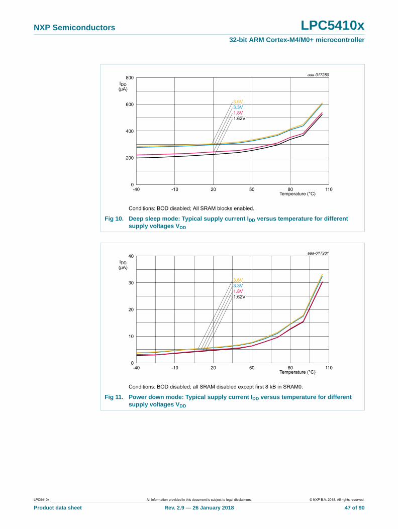
NXP Semiconductors LPC5410x32-bit ARM Cortex-M4/M0+ microcontroller
Conditions: BOD disabled; All SRAM blocks enabled.
Fig 10. Deep sleep mode: Typical supply current IDD versus temperature for different supply voltages VDD
Conditions: BOD disabled; all SRAM disabled except first 8 kB in SRAM0.
Fig 11. Power down mode: Typical supply current IDD versus temperature for different supply voltages VDD
LPC5410x All information provided in this document is subject to legal disclaimers. © NXP B.V. 2018. All rights reserved.
Product data sheet Rev. 2.9 — 26 January 2018 47 of 90
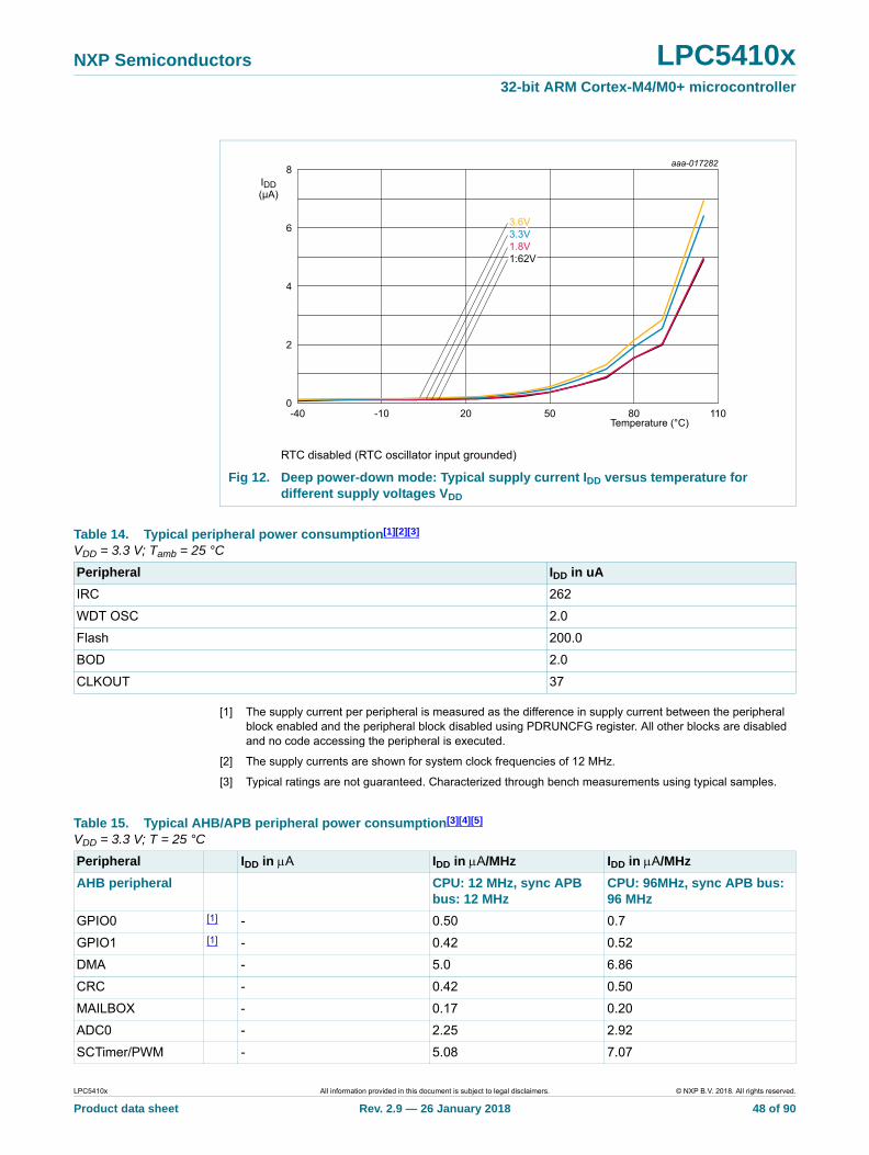
NXP Semiconductors LPC5410x32-bit ARM Cortex-M4/M0+ microcontroller
[1] The supply current per peripheral is measured as the difference in supply current between the peripheral block enabled and the peripheral block disabled using PDRUNCFG register. All other blocks are disabled and no code accessing the peripheral is executed.
[2] The supply currents are shown for system clock frequencies of 12 MHz.
[3] Typical ratings are not guaranteed. Characterized through bench measurements using typical samples.
RTC disabled (RTC oscillator input grounded)
Fig 12. Deep power-down mode: Typical supply current IDD versus temperature for different supply voltages VDD
Table 14. Typical peripheral power consumption[1][2][3]
VDD = 3.3 V; Tamb = 25 °C
Peripheral IDD in uA
IRC 262
WDT OSC 2.0
Flash 200.0
BOD 2.0
CLKOUT 37
Table 15. Typical AHB/APB peripheral power consumption[3][4][5]
VDD = 3.3 V; T = 25 °C
Peripheral IDD in A IDD in A/MHz IDD in A/MHz
AHB peripheral CPU: 12 MHz, sync APB bus: 12 MHz
CPU: 96MHz, sync APB bus: 96 MHz
GPIO0 [1] - 0.50 0.7
GPIO1 [1] - 0.42 0.52
DMA - 5.0 6.86
CRC - 0.42 0.50
MAILBOX - 0.17 0.20
ADC0 - 2.25 2.92
SCTimer/PWM - 5.08 7.07
LPC5410x All information provided in this document is subject to legal disclaimers. © NXP B.V. 2018. All rights reserved.
Product data sheet Rev. 2.9 — 26 January 2018 48 of 90
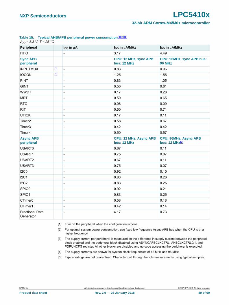
NXP Semiconductors LPC5410x32-bit ARM Cortex-M4/M0+ microcontroller
[1] Turn off the peripheral when the configuration is done.
[2] For optimal system power consumption, use fixed low frequency Async APB bus when the CPU is at a higher frequency.
[3] The supply current per peripheral is measured as the difference in supply current between the peripheral block enabled and the peripheral block disabled using ASYNCAPBCLKCTRL, AHBCLKCTRL0/1, and PDRUNCFG register. All other blocks are disabled and no code accessing the peripheral is executed.
[4] The supply currents are shown for system clock frequencies of 12 MHz and 96 MHz.
[5] Typical ratings are not guaranteed. Characterized through bench measurements using typical samples.
FIFO - 3.17 4.49
Sync APB peripheral
CPU: 12 MHz, sync APB bus: 12 MHz
CPU: 96MHz, sync APB bus: 96 MHz
INPUTMUX [1] - 0.83 0.96
IOCON [1] - 1.25 1.55
PINT - 0.83 1.05
GINT - 0.50 0.61
WWDT - 0.17 0.28
MRT - 0.50 0.65
RTC - 0.08 0.09
RIT - 0.50 0.71
UTICK - 0.17 0.11
Timer2 - 0.58 0.67
Timer3 - 0.42 0.42
Timer4 - 0.50 0.57
Async APB peripheral
CPU: 12 MHz, Async APB bus: 12 MHz
CPU: 96MHz, Async APB bus: 12 MHz[2]
USART0 - 0.67 0.11
USART1 - 0.75 0.07
USART2 - 0.67 0.11
USART3 - 0.75 0.07
I2C0 - 0.92 0.10
I2C1 - 0.83 0.26
I2C2 - 0.83 0.25
SPIO0 - 0.92 0.21
SPIO1 - 0.83 0.25
CTimer0 - 0.58 0.18
CTimer1 - 0.42 0.14
Fractional Rate Generator
- 4.17 0.73
Table 15. Typical AHB/APB peripheral power consumption[3][4][5]
VDD = 3.3 V; T = 25 °C
Peripheral IDD in A IDD in A/MHz IDD in A/MHz
LPC5410x All information provided in this document is subject to legal disclaimers. © NXP B.V. 2018. All rights reserved.
Product data sheet Rev. 2.9 — 26 January 2018 49 of 90
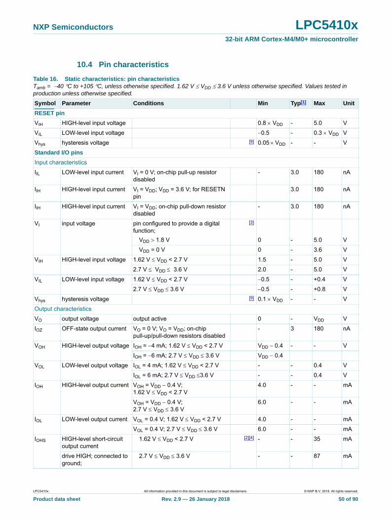
NXP Semiconductors LPC5410x32-bit ARM Cortex-M4/M0+ microcontroller
10.4 Pin characteristics
Table 16. Static characteristics: pin characteristicsTamb = 40 C to +105 C, unless otherwise specified. 1.62 V VDD 3.6 V unless otherwise specified. Values tested in production unless otherwise specified.
Symbol Parameter Conditions Min Typ[1] Max Unit
RESET pin
VIH HIGH-level input voltage 0.8 VDD - 5.0 V
VIL LOW-level input voltage 0.5 - 0.3 VDD V
Vhys hysteresis voltage [9] 0.05 VDD - - V
Standard I/O pins
Input characteristics
IIL LOW-level input current VI = 0 V; on-chip pull-up resistor disabled
- 3.0 180 nA
IIH HIGH-level input current VI = VDD; VDD = 3.6 V; for RESETN pin
3.0 180 nA
IIH HIGH-level input current VI = VDD; on-chip pull-down resistor disabled
- 3.0 180 nA
VI input voltage pin configured to provide a digital function;
VDD 1.8 V
[3]
0 - 5.0 V
VDD = 0 V 0 - 3.6 V
VIH HIGH-level input voltage 1.62 V VDD < 2.7 V 1.5 - 5.0 V
2.7 V VDD 3.6 V 2.0 - 5.0 V
VIL LOW-level input voltage 1.62 V VDD < 2.7 V 0.5 - +0.4 V
2.7 V VDD 3.6 V 0.5 - +0.8 V
Vhys hysteresis voltage [9] 0.1 VDD - - V
Output characteristics
VO output voltage output active 0 - VDD V
IOZ OFF-state output current VO = 0 V; VO = VDD; on-chip pull-up/pull-down resistors disabled
- 3 180 nA
VOH HIGH-level output voltage IOH = 4 mA; 1.62 V VDD < 2.7 V VDD 0.4 - - V
IOH = 6 mA; 2.7 V VDD 3.6 V VDD 0.4
VOL LOW-level output voltage IOL = 4 mA; 1.62 V VDD < 2.7 V - - 0.4 V
IOL = 6 mA; 2.7 V VDD 3.6 V - - 0.4 V
IOH HIGH-level output current VOH = VDD 0.4 V; 1.62 V VDD < 2.7 V
4.0 - - mA
VOH = VDD 0.4 V; 2.7 V VDD 3.6 V
6.0 - - mA
IOL LOW-level output current VOL = 0.4 V; 1.62 V VDD < 2.7 V 4.0 - - mA
VOL = 0.4 V; 2.7 V VDD 3.6 V 6.0 - - mA
IOHS HIGH-level short-circuit output current
1.62 V VDD < 2.7 V [2][4] - - 35 mA
drive HIGH; connected to ground;
2.7 V VDD 3.6 V - - 87 mA
LPC5410x All information provided in this document is subject to legal disclaimers. © NXP B.V. 2018. All rights reserved.
Product data sheet Rev. 2.9 — 26 January 2018 50 of 90
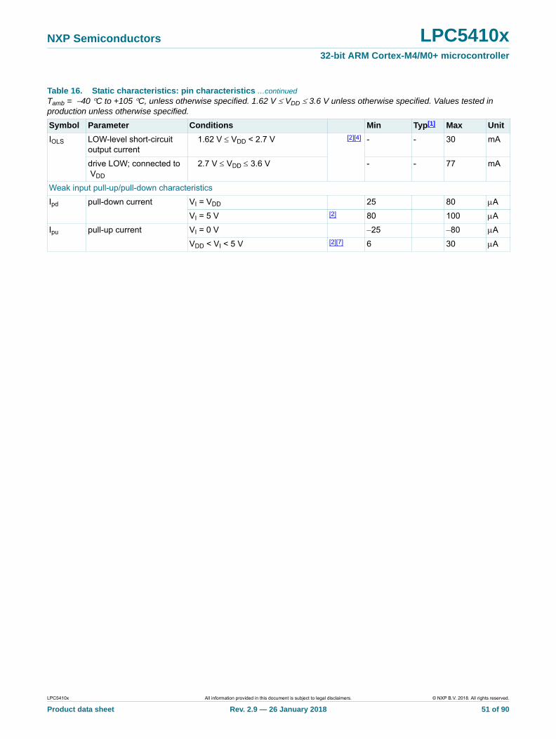
NXP Semiconductors LPC5410x32-bit ARM Cortex-M4/M0+ microcontroller
IOLS LOW-level short-circuit output current
1.62 V VDD < 2.7 V [2][4] - - 30 mA
drive LOW; connected to VDD
2.7 V VDD 3.6 V - - 77 mA
Weak input pull-up/pull-down characteristics
Ipd pull-down current VI = VDD 25 80 A
VI = 5 V [2] 80 100 A
Ipu pull-up current VI = 0 V 25 80 A
VDD < VI < 5 V [2][7] 6 30 A
Table 16. Static characteristics: pin characteristics …continuedTamb = 40 C to +105 C, unless otherwise specified. 1.62 V VDD 3.6 V unless otherwise specified. Values tested in production unless otherwise specified.
Symbol Parameter Conditions Min Typ[1] Max Unit
LPC5410x All information provided in this document is subject to legal disclaimers. © NXP B.V. 2018. All rights reserved.
Product data sheet Rev. 2.9 — 26 January 2018 51 of 90
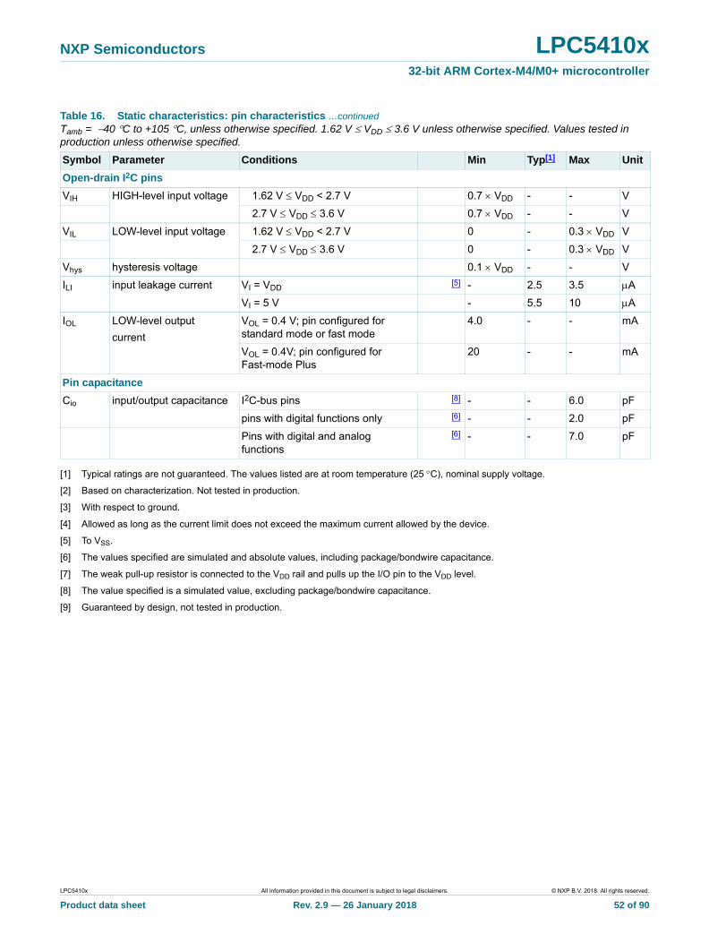
NXP Semiconductors LPC5410x32-bit ARM Cortex-M4/M0+ microcontroller
[1] Typical ratings are not guaranteed. The values listed are at room temperature (25 C), nominal supply voltage.
[2] Based on characterization. Not tested in production.
[3] With respect to ground.
[4] Allowed as long as the current limit does not exceed the maximum current allowed by the device.
[5] To VSS.
[6] The values specified are simulated and absolute values, including package/bondwire capacitance.
[7] The weak pull-up resistor is connected to the VDD rail and pulls up the I/O pin to the VDD level.
[8] The value specified is a simulated value, excluding package/bondwire capacitance.
[9] Guaranteed by design, not tested in production.
Open-drain I2C pins
VIH HIGH-level input voltage 1.62 V VDD < 2.7 V 0.7 VDD - - V
2.7 V VDD 3.6 V 0.7 VDD - - V
VIL LOW-level input voltage 1.62 V VDD < 2.7 V 0 - 0.3 VDD V
2.7 V VDD 3.6 V 0 - 0.3 VDD V
Vhys hysteresis voltage 0.1 VDD - - V
ILI input leakage current VI = VDD[5] - 2.5 3.5 A
VI = 5 V - 5.5 10 A
IOL LOW-level output
current
VOL = 0.4 V; pin configured for standard mode or fast mode
4.0 - - mA
VOL = 0.4V; pin configured for Fast-mode Plus
20 - - mA
Pin capacitance
Cio input/output capacitance I2C-bus pins [8] - - 6.0 pF
pins with digital functions only [6] - - 2.0 pF
Pins with digital and analog functions
[6] - - 7.0 pF
Table 16. Static characteristics: pin characteristics …continuedTamb = 40 C to +105 C, unless otherwise specified. 1.62 V VDD 3.6 V unless otherwise specified. Values tested in production unless otherwise specified.
Symbol Parameter Conditions Min Typ[1] Max Unit
LPC5410x All information provided in this document is subject to legal disclaimers. © NXP B.V. 2018. All rights reserved.
Product data sheet Rev. 2.9 — 26 January 2018 52 of 90
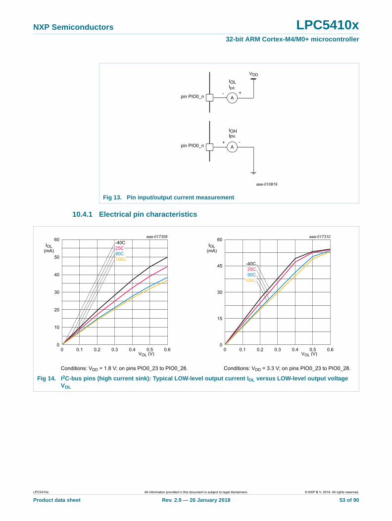
NXP Semiconductors LPC5410x32-bit ARM Cortex-M4/M0+ microcontroller
10.4.1 Electrical pin characteristics
Fig 13. Pin input/output current measurement
aaa-010819
+ -pin PIO0_n
IOHIpu
- +pin PIO0_n
IOLIpd
VDD
A
A
Conditions: VDD = 1.8 V; on pins PIO0_23 to PIO0_28. Conditions: VDD = 3.3 V; on pins PIO0_23 to PIO0_28.
Fig 14. I2C-bus pins (high current sink): Typical LOW-level output current IOL versus LOW-level output voltage VOL
LPC5410x All information provided in this document is subject to legal disclaimers. © NXP B.V. 2018. All rights reserved.
Product data sheet Rev. 2.9 — 26 January 2018 53 of 90
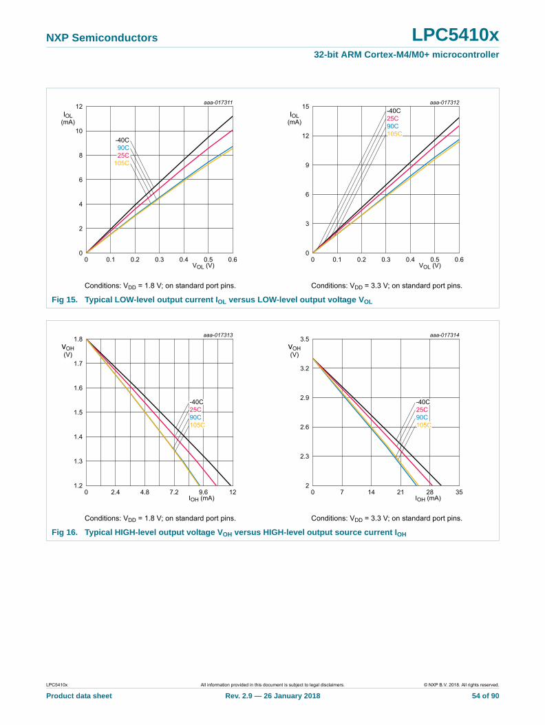
NXP Semiconductors LPC5410x32-bit ARM Cortex-M4/M0+ microcontroller
Conditions: VDD = 1.8 V; on standard port pins. Conditions: VDD = 3.3 V; on standard port pins.
Fig 15. Typical LOW-level output current IOL versus LOW-level output voltage VOL
Conditions: VDD = 1.8 V; on standard port pins. Conditions: VDD = 3.3 V; on standard port pins.
Fig 16. Typical HIGH-level output voltage VOH versus HIGH-level output source current IOH
LPC5410x All information provided in this document is subject to legal disclaimers. © NXP B.V. 2018. All rights reserved.
Product data sheet Rev. 2.9 — 26 January 2018 54 of 90
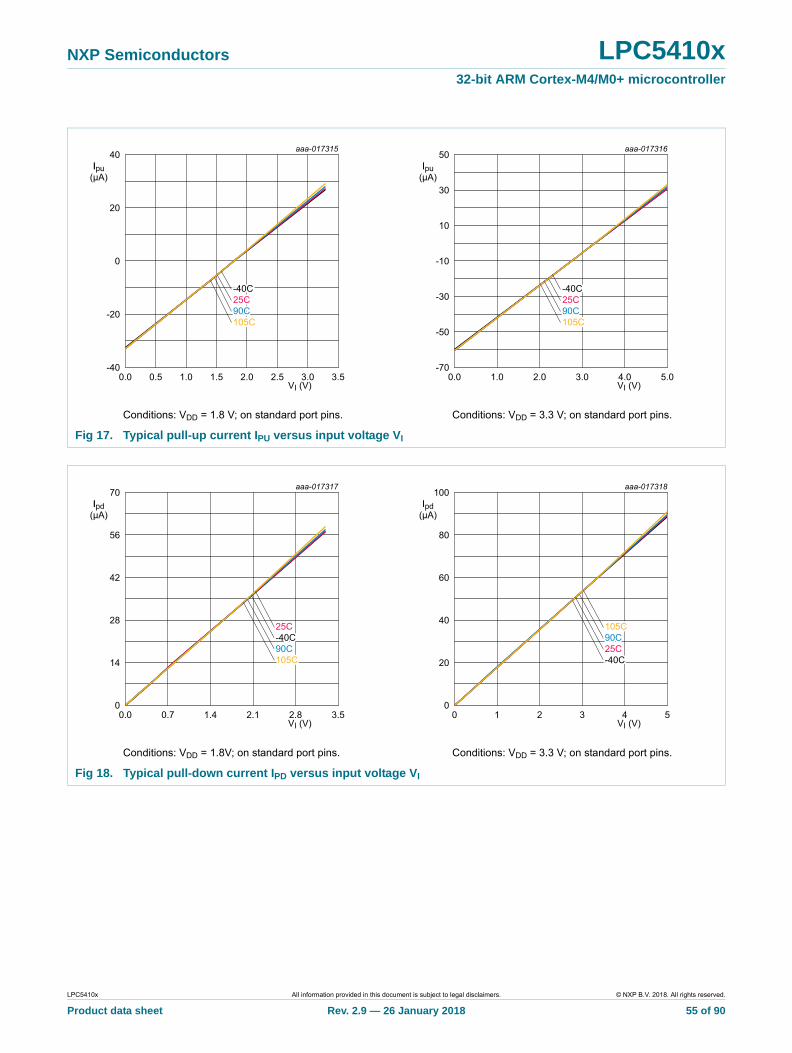
NXP Semiconductors LPC5410x32-bit ARM Cortex-M4/M0+ microcontroller
Conditions: VDD = 1.8 V; on standard port pins. Conditions: VDD = 3.3 V; on standard port pins.
Fig 17. Typical pull-up current IPU versus input voltage VI
Conditions: VDD = 1.8V; on standard port pins. Conditions: VDD = 3.3 V; on standard port pins.
Fig 18. Typical pull-down current IPD versus input voltage VI
LPC5410x All information provided in this document is subject to legal disclaimers. © NXP B.V. 2018. All rights reserved.
Product data sheet Rev. 2.9 — 26 January 2018 55 of 90
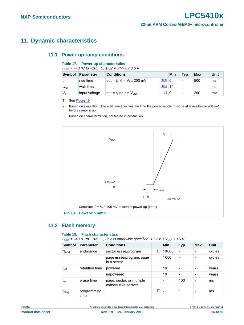
NXP Semiconductors LPC5410x32-bit ARM Cortex-M4/M0+ microcontroller
11. Dynamic characteristics
11.1 Power-up ramp conditions
[1] See Figure 19.
[2] Based on simulation. The wait time specifies the time the power supply must be at levels below 200 mV before ramping up.
[3] Based on characterization, not tested in production.
11.2 Flash memory
Table 17. Power-up characteristicsTamb = 40 C to +105 C; 1.62 V VDD 3.6 V
Symbol Parameter Conditions Min Typ Max Unit
tr rise time at t = t1: 0 < VI 200 mV [1][3] 0 - 500 ms
twait wait time [1][2] 12 - - s
VI input voltage at t = t1 on pin VDD[3] 0 - 200 mV
Condition: 0 < VI 200 mV at start of power-up (t = t1)
Fig 19. Power-up ramp
VDD
0
200 mV
tr
twait
t = t1 aaa-017426
Table 18. Flash characteristicsTamb = 40 C to +105 C, unless otherwise specified. 1.62 V VDD 3.6 V
Symbol Parameter Conditions Min Typ Max Unit
Nendu endurance sector erase/program [1] 10000 - - cycles
page erase/program; page in a sector
1000 - - cycles
tret retention time powered 10 - - years
unpowered 10 - - years
ter erase time page, sector, or multiple consecutive sectors
- 100 - ms
tprog programming time
[2] - 1 - ms
LPC5410x All information provided in this document is subject to legal disclaimers. © NXP B.V. 2018. All rights reserved.
Product data sheet Rev. 2.9 — 26 January 2018 56 of 90
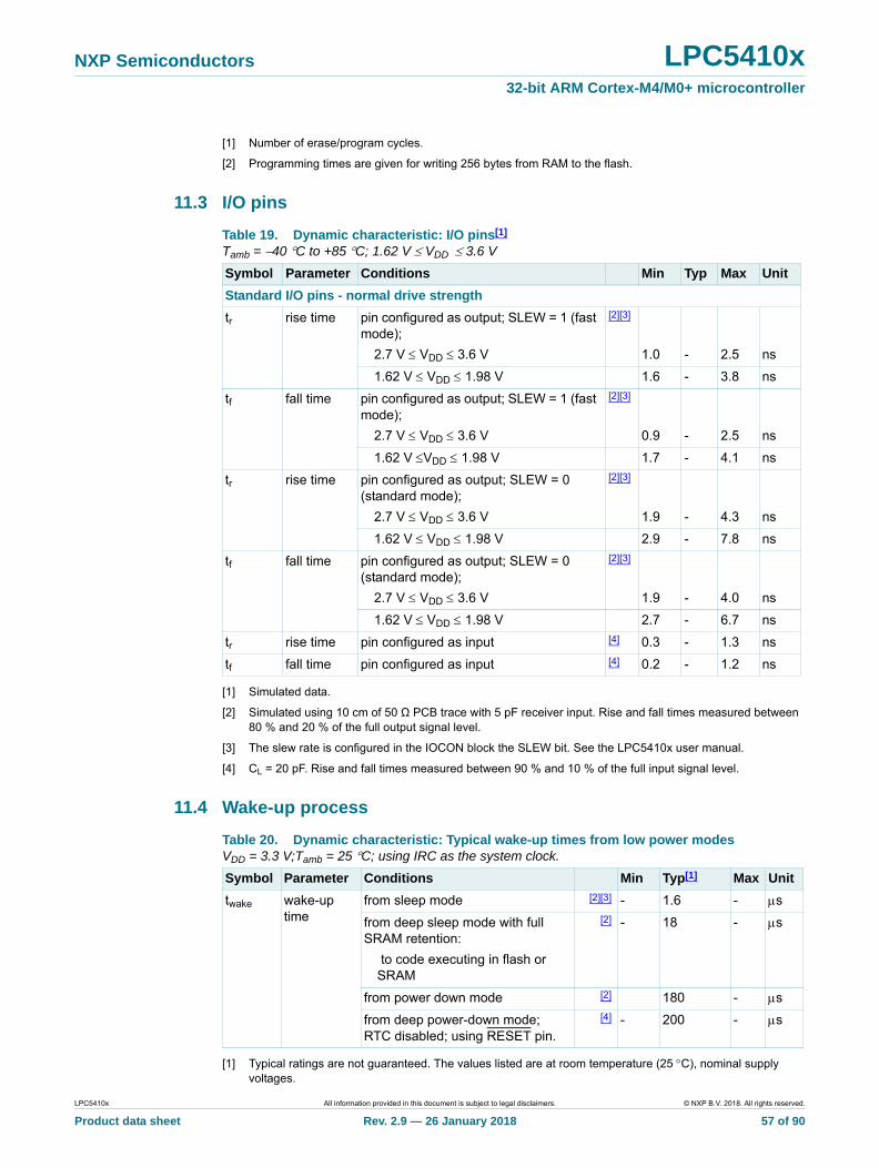
NXP Semiconductors LPC5410x32-bit ARM Cortex-M4/M0+ microcontroller
[1] Number of erase/program cycles.
[2] Programming times are given for writing 256 bytes from RAM to the flash.
11.3 I/O pins
[1] Simulated data.
[2] Simulated using 10 cm of 50 Ω PCB trace with 5 pF receiver input. Rise and fall times measured between 80 % and 20 % of the full output signal level.
[3] The slew rate is configured in the IOCON block the SLEW bit. See the LPC5410x user manual.
[4] CL = 20 pF. Rise and fall times measured between 90 % and 10 % of the full input signal level.
11.4 Wake-up process
[1] Typical ratings are not guaranteed. The values listed are at room temperature (25 C), nominal supply voltages.
Table 19. Dynamic characteristic: I/O pins[1]
Tamb = 40 C to +85 C; 1.62 V VDD 3.6 V
Symbol Parameter Conditions Min Typ Max Unit
Standard I/O pins - normal drive strength
tr rise time pin configured as output; SLEW = 1 (fast mode);
2.7 V VDD 3.6 V
[2][3]
1.0 - 2.5 ns
1.62 V VDD 1.98 V 1.6 - 3.8 ns
tf fall time pin configured as output; SLEW = 1 (fast mode);
2.7 V VDD 3.6 V
[2][3]
0.9 - 2.5 ns
1.62 V VDD 1.98 V 1.7 - 4.1 ns
tr rise time pin configured as output; SLEW = 0 (standard mode);
2.7 V VDD 3.6 V
[2][3]
1.9 - 4.3 ns
1.62 V VDD 1.98 V 2.9 - 7.8 ns
tf fall time pin configured as output; SLEW = 0 (standard mode);
2.7 V VDD 3.6 V
[2][3]
1.9 - 4.0 ns
1.62 V VDD 1.98 V 2.7 - 6.7 ns
tr rise time pin configured as input [4] 0.3 - 1.3 ns
tf fall time pin configured as input [4] 0.2 - 1.2 ns
Table 20. Dynamic characteristic: Typical wake-up times from low power modesVDD = 3.3 V;Tamb = 25 C; using IRC as the system clock.
Symbol Parameter Conditions Min Typ[1] Max Unit
twake wake-up time
from sleep mode [2][3] - 1.6 - s
from deep sleep mode with full SRAM retention:
to code executing in flash or SRAM
[2] - 18 - s
from power down mode [2] 180 - s
from deep power-down mode; RTC disabled; using RESET pin.
[4] - 200 - s
LPC5410x All information provided in this document is subject to legal disclaimers. © NXP B.V. 2018. All rights reserved.
Product data sheet Rev. 2.9 — 26 January 2018 57 of 90
NXP Semiconductors LPC5410x32-bit ARM Cortex-M4/M0+ microcontroller
[2] The wake-up time measured is the time between when a GPIO input pin is triggered to wake the device up from the low power modes and from when a GPIO output pin is set in the interrupt service routine (ISR) wake-up handler. Measurements are based on using the power library provided in the LPC5410x LPCOpen software platform version v.3.04.
[3] IRC enabled, all peripherals off.
[4] RTC disabled. Wake-up from deep power-down causes the part to go through entire reset
process. The wake-up time measured is the time between when the RESET pin is triggered to wake the
device up and when a GPIO output pin is set in the reset handler.
LPC5410x All information provided in this document is subject to legal disclaimers. © NXP B.V. 2018. All rights reserved.
Product data sheet Rev. 2.9 — 26 January 2018 58 of 90
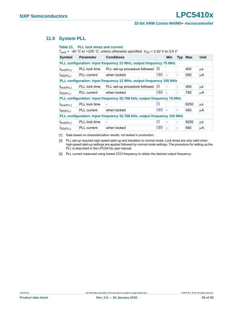
NXP Semiconductors LPC5410x32-bit ARM Cortex-M4/M0+ microcontroller
11.5 System PLL
[1] Data based on characterization results, not tested in production.
[2] PLL set-up requires high-speed start-up and transition to normal mode. Lock times are only valid when high-speed start-up settings are applied followed by normal mode settings. The procedure for setting up the PLL is described in the LPC5410x user manual.
[3] PLL current measured using lowest CCO frequency to obtain the desired output frequency.
Table 21. PLL lock times and currentTamb = 40 C to +105 C, unless otherwise specified. VDD = 1.62 V to 3.6 V
Symbol Parameter Conditions Min Typ Max Unit
PLL configuration: input frequency 12 MHz; output frequency 75 MHz
tlock(PLL) PLL lock time PLL set-up procedure followed [2] 400 s
IDD(PLL) PLL current when locked [1][3] - - 550 A
PLL configuration: input frequency 12 MHz; output frequency 100 MHz
tlock(PLL) PLL lock time PLL set-up procedure followed [2] - - 400 s
IDD(PLL) PLL current when locked [1][3] - - 750 A
PLL configuration: input frequency 32.768 kHz; output frequency 75 MHz
tlock(PLL) PLL lock time - [1] 6250 s
IDD(PLL) PLL current when locked [1][3] - - 450 A
PLL configuration: input frequency 32.768 kHz; output frequency 100 MHz
tlock(PLL) PLL lock time - [1] - - 6250 s
IDD(PLL) PLL current when locked [1][3] - - 560 A
LPC5410x All information provided in this document is subject to legal disclaimers. © NXP B.V. 2018. All rights reserved.
Product data sheet Rev. 2.9 — 26 January 2018 59 of 90
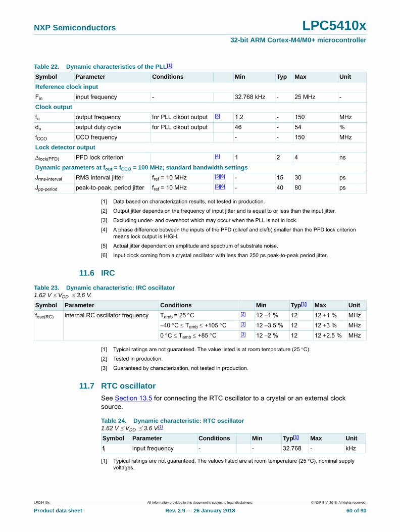
NXP Semiconductors LPC5410x32-bit ARM Cortex-M4/M0+ microcontroller
[1] Data based on characterization results, not tested in production.
[2] Output jitter depends on the frequency of input jitter and is equal to or less than the input jitter.
[3] Excluding under- and overshoot which may occur when the PLL is not in lock.
[4] A phase difference between the inputs of the PFD (clkref and clkfb) smaller than the PFD lock criterion means lock output is HIGH.
[5] Actual jitter dependent on amplitude and spectrum of substrate noise.
[6] Input clock coming from a crystal oscillator with less than 250 ps peak-to-peak period jitter.
11.6 IRC
[1] Typical ratings are not guaranteed. The value listed is at room temperature (25 C).
[2] Tested in production.
[3] Guaranteed by characterization, not tested in production.
11.7 RTC oscillator
See Section 13.5 for connecting the RTC oscillator to a crystal or an external clock source.
[1] Typical ratings are not guaranteed. The values listed are at room temperature (25 C), nominal supply voltages.
Table 22. Dynamic characteristics of the PLL[1]
Symbol Parameter Conditions Min Typ Max Unit
Reference clock input
Fin input frequency - 32.768 kHz - 25 MHz -
Clock output
fo output frequency for PLL clkout output [3] 1.2 - 150 MHz
do output duty cycle for PLL clkout output 46 - 54 %
fCCO CCO frequency - - 150 MHz
Lock detector output
lock(PFD) PFD lock criterion [4] 1 2 4 ns
Dynamic parameters at fout = fCCO = 100 MHz; standard bandwidth settings
Jrms-interval RMS interval jitter fref = 10 MHz [5][6] - 15 30 ps
Jpp-period peak-to-peak, period jitter fref = 10 MHz [5][6] - 40 80 ps
Table 23. Dynamic characteristic: IRC oscillator1.62 V VDD 3.6 V.
Symbol Parameter Conditions Min Typ[1] Max Unit
fosc(RC) internal RC oscillator frequency Tamb = 25 C [2] 12 1 % 12 12 +1 % MHz
40 C Tamb +105 C [3] 12 3.5 % 12 12 +3 % MHz
0 C Tamb +85 C [3] 12 2 % 12 12 +2.5 % MHz
Table 24. Dynamic characteristic: RTC oscillator1.62 V VDD 3.6 V[1]
Symbol Parameter Conditions Min Typ[1] Max Unit
fi input frequency - - 32.768 - kHz
LPC5410x All information provided in this document is subject to legal disclaimers. © NXP B.V. 2018. All rights reserved.
Product data sheet Rev. 2.9 — 26 January 2018 60 of 90
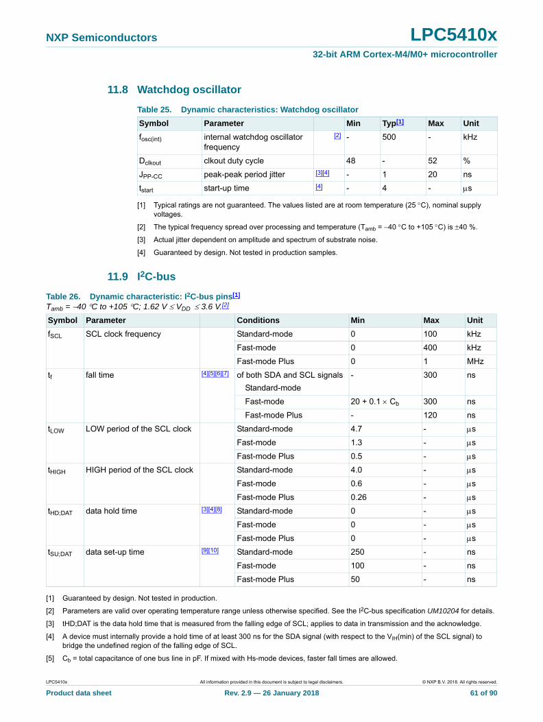
NXP Semiconductors LPC5410x32-bit ARM Cortex-M4/M0+ microcontroller
11.8 Watchdog oscillator
[1] Typical ratings are not guaranteed. The values listed are at room temperature (25 C), nominal supply voltages.
[2] The typical frequency spread over processing and temperature (Tamb = 40 C to +105 C) is 40 %.
[3] Actual jitter dependent on amplitude and spectrum of substrate noise.
[4] Guaranteed by design. Not tested in production samples.
11.9 I2C-bus
[1] Guaranteed by design. Not tested in production.
[2] Parameters are valid over operating temperature range unless otherwise specified. See the I2C-bus specification UM10204 for details.
[3] tHD;DAT is the data hold time that is measured from the falling edge of SCL; applies to data in transmission and the acknowledge.
[4] A device must internally provide a hold time of at least 300 ns for the SDA signal (with respect to the VIH(min) of the SCL signal) to bridge the undefined region of the falling edge of SCL.
[5] Cb = total capacitance of one bus line in pF. If mixed with Hs-mode devices, faster fall times are allowed.
Table 25. Dynamic characteristics: Watchdog oscillator
Symbol Parameter Min Typ[1] Max Unit
fosc(int) internal watchdog oscillator frequency
[2] - 500 - kHz
Dclkout clkout duty cycle 48 - 52 %
JPP-CC peak-peak period jitter [3][4] - 1 20 ns
tstart start-up time [4] - 4 - s
Table 26. Dynamic characteristic: I2C-bus pins[1]
Tamb = 40 C to +105 C; 1.62 V VDD 3.6 V.[2]
Symbol Parameter Conditions Min Max Unit
fSCL SCL clock frequency Standard-mode 0 100 kHz
Fast-mode 0 400 kHz
Fast-mode Plus 0 1 MHz
tf fall time [4][5][6][7] of both SDA and SCL signals
Standard-mode
- 300 ns
Fast-mode 20 + 0.1 Cb 300 ns
Fast-mode Plus - 120 ns
tLOW LOW period of the SCL clock Standard-mode 4.7 - s
Fast-mode 1.3 - s
Fast-mode Plus 0.5 - s
tHIGH HIGH period of the SCL clock Standard-mode 4.0 - s
Fast-mode 0.6 - s
Fast-mode Plus 0.26 - s
tHD;DAT data hold time [3][4][8] Standard-mode 0 - s
Fast-mode 0 - s
Fast-mode Plus 0 - s
tSU;DAT data set-up time
[9][10] Standard-mode 250 - ns
Fast-mode 100 - ns
Fast-mode Plus 50 - ns
LPC5410x All information provided in this document is subject to legal disclaimers. © NXP B.V. 2018. All rights reserved.
Product data sheet Rev. 2.9 — 26 January 2018 61 of 90
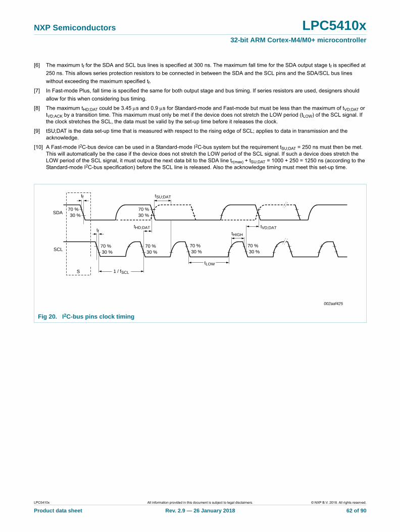
NXP Semiconductors LPC5410x32-bit ARM Cortex-M4/M0+ microcontroller
[6] The maximum tf for the SDA and SCL bus lines is specified at 300 ns. The maximum fall time for the SDA output stage tf is specified at
250 ns. This allows series protection resistors to be connected in between the SDA and the SCL pins and the SDA/SCL bus lines
without exceeding the maximum specified tf.
[7] In Fast-mode Plus, fall time is specified the same for both output stage and bus timing. If series resistors are used, designers should
allow for this when considering bus timing.
[8] The maximum tHD;DAT could be 3.45 s and 0.9 s for Standard-mode and Fast-mode but must be less than the maximum of tVD;DAT or tVD;ACK by a transition time. This maximum must only be met if the device does not stretch the LOW period (tLOW) of the SCL signal. If the clock stretches the SCL, the data must be valid by the set-up time before it releases the clock.
[9] tSU;DAT is the data set-up time that is measured with respect to the rising edge of SCL; applies to data in transmission and the acknowledge.
[10] A Fast-mode I2C-bus device can be used in a Standard-mode I2C-bus system but the requirement tSU;DAT = 250 ns must then be met. This will automatically be the case if the device does not stretch the LOW period of the SCL signal. If such a device does stretch the LOW period of the SCL signal, it must output the next data bit to the SDA line tr(max) + tSU;DAT = 1000 + 250 = 1250 ns (according to the Standard-mode I2C-bus specification) before the SCL line is released. Also the acknowledge timing must meet this set-up time.
Fig 20. I2C-bus pins clock timing
002aaf425
tf
70 %30 %SDA
tf
70 %30 %
S
70 %30 %
70 %30 %
tHD;DAT
SCL
1 / fSCL
70 %30 %
70 %30 %
tVD;DAT
tHIGH
tLOW
tSU;DAT
LPC5410x All information provided in this document is subject to legal disclaimers. © NXP B.V. 2018. All rights reserved.
Product data sheet Rev. 2.9 — 26 January 2018 62 of 90
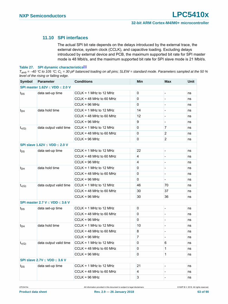
NXP Semiconductors LPC5410x32-bit ARM Cortex-M4/M0+ microcontroller
11.10 SPI interfaces
The actual SPI bit rate depends on the delays introduced by the external trace, theexternal device, system clock (CCLK), and capacitive loading. Excluding delaysintroduced by external device and PCB, the maximum supported bit rate for SPI master mode is 48 Mbit/s, and the maximum supported bit rate for SPI slave mode is 21 Mbit/s.
Table 27. SPI dynamic characteristics[1]
Tamb = 40 C to 105 C; CL = 30 pF balanced loading on all pins; SLEW = standard mode. Parameters sampled at the 50 % level of the rising or falling edge.
Symbol Parameter Conditions Min Max Unit
SPI master 1.62V VDD 2.0 V
tDS data set-up time CCLK = 1 MHz to 12 MHz 0 - ns
CCLK = 48 MHz to 60 MHz 0 - ns
CCLK = 96 MHz 0 - ns
tDH data hold time CCLK = 1 MHz to 12 MHz 14 - ns
CCLK = 48 MHz to 60 MHz 12 - ns
CCLK = 96 MHz 9 - ns
tv(Q) data output valid time CCLK = 1 MHz to 12 MHz 0 7 ns
CCLK = 48 MHz to 60 MHz 0 2 ns
CCLK = 96 MHz 0 2 ns
SPI slave 1.62V VDD 2.0 V
tDS data set-up time CCLK = 1 MHz to 12 MHz 22 - ns
CCLK = 48 MHz to 60 MHz 4 - ns
CCLK = 96 MHz 4 - ns
tDH data hold time CCLK = 1 MHz to 12 MHz 0 - ns
CCLK = 48 MHz to 60 MHz 0 - ns
CCLK = 96 MHz 0 - ns
tv(Q) data output valid time CCLK = 1 MHz to 12 MHz 46 70 ns
CCLK = 48 MHz to 60 MHz 30 37 ns
CCLK = 96 MHz 30 36 ns
SPI master 2.7 V VDD 3.6 V
tDS data set-up time CCLK = 1 MHz to 12 MHz 0 - ns
CCLK = 48 MHz to 60 MHz 0 - ns
CCLK = 96 MHz 0 - ns
tDH data hold time CCLK = 1 MHz to 12 MHz 10 - ns
CCLK = 48 MHz to 60 MHz 8 - ns
CCLK = 96 MHz 7 - ns
tv(Q) data output valid time CCLK = 1 MHz to 12 MHz 0 6 ns
CCLK = 48 MHz to 60 MHz 0 1 ns
CCLK = 96 MHz 0 1 ns
SPI slave 2.7V VDD 3.6 V
tDS data set-up time CCLK = 1 MHz to 12 MHz 21 - ns
CCLK = 48 MHz to 60 MHz 4 - ns
CCLK = 96 MHz 3 - ns
LPC5410x All information provided in this document is subject to legal disclaimers. © NXP B.V. 2018. All rights reserved.
Product data sheet Rev. 2.9 — 26 January 2018 63 of 90
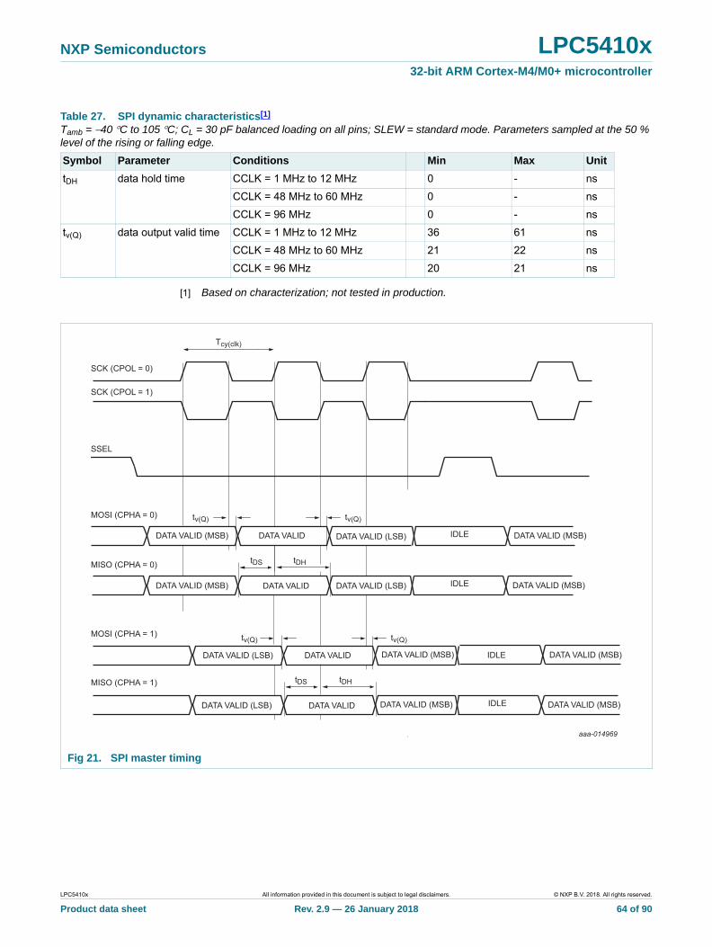
NXP Semiconductors LPC5410x32-bit ARM Cortex-M4/M0+ microcontroller
[1] Based on characterization; not tested in production.
tDH data hold time CCLK = 1 MHz to 12 MHz 0 - ns
CCLK = 48 MHz to 60 MHz 0 - ns
CCLK = 96 MHz 0 - ns
tv(Q) data output valid time CCLK = 1 MHz to 12 MHz 36 61 ns
CCLK = 48 MHz to 60 MHz 21 22 ns
CCLK = 96 MHz 20 21 ns
Table 27. SPI dynamic characteristics[1]
Tamb = 40 C to 105 C; CL = 30 pF balanced loading on all pins; SLEW = standard mode. Parameters sampled at the 50 % level of the rising or falling edge.
Symbol Parameter Conditions Min Max Unit
Fig 21. SPI master timing
SCK (CPOL = 0)
MOSI (CPHA = 1)
SSEL
MISO (CPHA = 1)
Tcy(clk)
tDS tDH
tv(Q)
DATA VALID (LSB) DATA VALID
tv(Q)
SCK (CPOL = 1)
DATA VALID (LSB) DATA VALID
MOSI (CPHA = 0)
MISO (CPHA = 0) tDS tDH
DATA VALID (MSB) DATA VALID (MSB)DATA VALID
DATA VALID (LSB)
DATA VALID (LSB)
tv(Q)
DATA VALID (MSB) DATA VALID
tv(Q)
aaa-014969
DATA VALID (MSB)
DATA VALID (MSB)
DATA VALID (MSB)
DATA VALID (MSB) IDLE
IDLE
IDLE
IDLE
DATA VALID (MSB)
LPC5410x All information provided in this document is subject to legal disclaimers. © NXP B.V. 2018. All rights reserved.
Product data sheet Rev. 2.9 — 26 January 2018 64 of 90
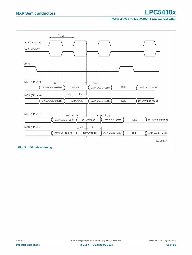
NXP Semiconductors LPC5410x32-bit ARM Cortex-M4/M0+ microcontroller
Fig 22. SPI slave timing
SCK (CPOL = 0)
MISO (CPHA = 1)
SSEL
MOSI (CPHA = 1)
Tcy(clk)
tDS tDH
tv(Q)
DATA VALID (LSB) DATA VALID
tv(Q)
SCK (CPOL = 1)
DATA VALID (LSB) DATA VALID
MISO (CPHA = 0)
MOSI (CPHA = 0) tDS tDH
DATA VALID (MSB) DATA VALID (MSB)DATA VALID
DATA VALID (LSB)
DATA VALID (LSB)
tv(Q)
DATA VALID (MSB) DATA VALID
tv(Q)
aaa-014970
DATA VALID (MSB)
DATA VALID (MSB)
DATA VALID (MSB)
DATA VALID (MSB)
IDLE
IDLE
IDLE
IDLE
DATA VALID (MSB)
LPC5410x All information provided in this document is subject to legal disclaimers. © NXP B.V. 2018. All rights reserved.
Product data sheet Rev. 2.9 — 26 January 2018 65 of 90
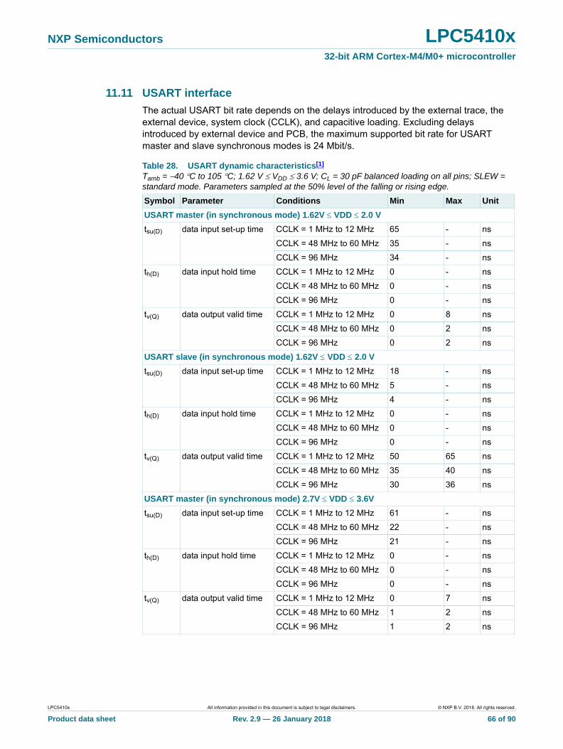
NXP Semiconductors LPC5410x32-bit ARM Cortex-M4/M0+ microcontroller
11.11 USART interface
The actual USART bit rate depends on the delays introduced by the external trace, the external device, system clock (CCLK), and capacitive loading. Excluding delays introduced by external device and PCB, the maximum supported bit rate for USART master and slave synchronous modes is 24 Mbit/s.
Table 28. USART dynamic characteristics[1]
Tamb = 40 C to 105 C; 1.62 V VDD 3.6 V; CL = 30 pF balanced loading on all pins; SLEW = standard mode. Parameters sampled at the 50% level of the falling or rising edge.
Symbol Parameter Conditions Min Max Unit
USART master (in synchronous mode) 1.62V VDD 2.0 V
tsu(D) data input set-up time CCLK = 1 MHz to 12 MHz 65 - ns
CCLK = 48 MHz to 60 MHz 35 - ns
CCLK = 96 MHz 34 - ns
th(D) data input hold time CCLK = 1 MHz to 12 MHz 0 - ns
CCLK = 48 MHz to 60 MHz 0 - ns
CCLK = 96 MHz 0 - ns
tv(Q) data output valid time CCLK = 1 MHz to 12 MHz 0 8 ns
CCLK = 48 MHz to 60 MHz 0 2 ns
CCLK = 96 MHz 0 2 ns
USART slave (in synchronous mode) 1.62V VDD 2.0 V
tsu(D) data input set-up time CCLK = 1 MHz to 12 MHz 18 - ns
CCLK = 48 MHz to 60 MHz 5 - ns
CCLK = 96 MHz 4 - ns
th(D) data input hold time CCLK = 1 MHz to 12 MHz 0 - ns
CCLK = 48 MHz to 60 MHz 0 - ns
CCLK = 96 MHz 0 - ns
tv(Q) data output valid time CCLK = 1 MHz to 12 MHz 50 65 ns
CCLK = 48 MHz to 60 MHz 35 40 ns
CCLK = 96 MHz 30 36 ns
USART master (in synchronous mode) 2.7V VDD 3.6V
tsu(D) data input set-up time CCLK = 1 MHz to 12 MHz 61 - ns
CCLK = 48 MHz to 60 MHz 22 - ns
CCLK = 96 MHz 21 - ns
th(D) data input hold time CCLK = 1 MHz to 12 MHz 0 - ns
CCLK = 48 MHz to 60 MHz 0 - ns
CCLK = 96 MHz 0 - ns
tv(Q) data output valid time CCLK = 1 MHz to 12 MHz 0 7 ns
CCLK = 48 MHz to 60 MHz 1 2 ns
CCLK = 96 MHz 1 2 ns
LPC5410x All information provided in this document is subject to legal disclaimers. © NXP B.V. 2018. All rights reserved.
Product data sheet Rev. 2.9 — 26 January 2018 66 of 90
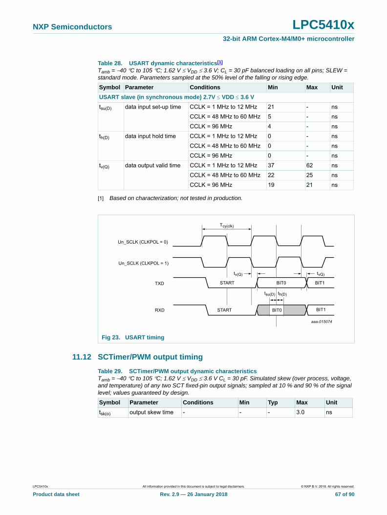
NXP Semiconductors LPC5410x32-bit ARM Cortex-M4/M0+ microcontroller
[1] Based on characterization; not tested in production.
11.12 SCTimer/PWM output timing
USART slave (in synchronous mode) 2.7V VDD 3.6 V
tsu(D) data input set-up time CCLK = 1 MHz to 12 MHz 21 - ns
CCLK = 48 MHz to 60 MHz 5 - ns
CCLK = 96 MHz 4 - ns
th(D) data input hold time CCLK = 1 MHz to 12 MHz 0 - ns
CCLK = 48 MHz to 60 MHz 0 - ns
CCLK = 96 MHz 0 - ns
tv(Q) data output valid time CCLK = 1 MHz to 12 MHz 37 62 ns
CCLK = 48 MHz to 60 MHz 22 25 ns
CCLK = 96 MHz 19 21 ns
Fig 23. USART timing
Table 28. USART dynamic characteristics[1]
Tamb = 40 C to 105 C; 1.62 V VDD 3.6 V; CL = 30 pF balanced loading on all pins; SLEW = standard mode. Parameters sampled at the 50% level of the falling or rising edge.
Symbol Parameter Conditions Min Max Unit
Un_SCLK (CLKPOL = 0)
TXD
RXD
Tcy(clk)
tsu(D) th(D)
tv(Q)
START BIT0
tvQ)
Un_SCLK (CLKPOL = 1)
START BIT0 BIT1
BIT1
aaa-015074
Table 29. SCTimer/PWM output dynamic characteristicsTamb = 40 C to 105 C; 1.62 V VDD 3.6 V CL = 30 pF. Simulated skew (over process, voltage, and temperature) of any two SCT fixed-pin output signals; sampled at 10 % and 90 % of the signal level; values guaranteed by design.
Symbol Parameter Conditions Min Typ Max Unit
tsk(o) output skew time - - - 3.0 ns
LPC5410x All information provided in this document is subject to legal disclaimers. © NXP B.V. 2018. All rights reserved.
Product data sheet Rev. 2.9 — 26 January 2018 67 of 90
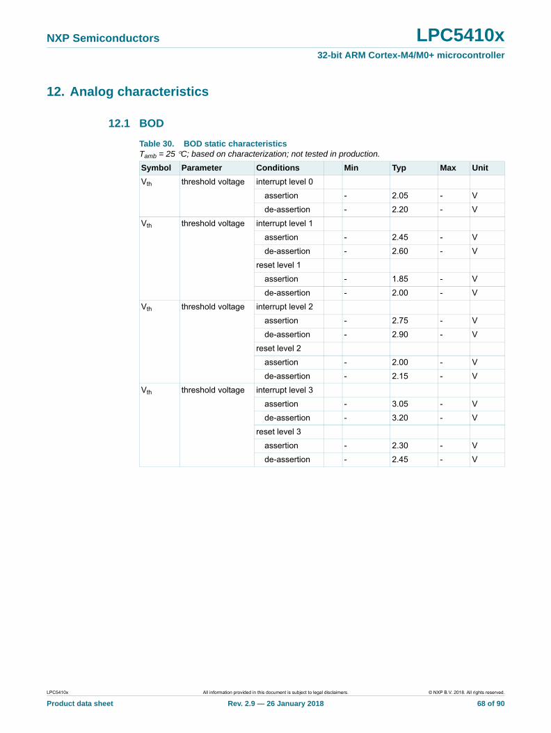
NXP Semiconductors LPC5410x32-bit ARM Cortex-M4/M0+ microcontroller
12. Analog characteristics
12.1 BOD
Table 30. BOD static characteristicsTamb = 25 C; based on characterization; not tested in production.
Symbol Parameter Conditions Min Typ Max Unit
Vth threshold voltage interrupt level 0
assertion - 2.05 - V
de-assertion - 2.20 - V
Vth threshold voltage interrupt level 1
assertion - 2.45 - V
de-assertion - 2.60 - V
reset level 1
assertion - 1.85 - V
de-assertion - 2.00 - V
Vth threshold voltage interrupt level 2
assertion - 2.75 - V
de-assertion - 2.90 - V
reset level 2
assertion - 2.00 - V
de-assertion - 2.15 - V
Vth threshold voltage interrupt level 3
assertion - 3.05 - V
de-assertion - 3.20 - V
reset level 3
assertion - 2.30 - V
de-assertion - 2.45 - V
LPC5410x All information provided in this document is subject to legal disclaimers. © NXP B.V. 2018. All rights reserved.
Product data sheet Rev. 2.9 — 26 January 2018 68 of 90
NXP Semiconductors LPC5410x32-bit ARM Cortex-M4/M0+ microcontroller
12.2 12-bit ADC characteristics
[1] Based on characterization; not tested in production.
[2] Typical ratings are not guaranteed. The values listed are at room temperature (25 C), nominal supply voltages.
[3] The input resistance of ADC channels 6 to 11 is higher than ADC channels 0 to 5.
[4] Cia represents the external capacitance on the analog input channel for sampling speeds of 5.0 Msamples/s. No parasitic capacitances included.
[5] The differential linearity error (ED) is the difference between the actual step width and the ideal step width. See Figure 24.
[6] The integral non-linearity (EL(adj)) is the peak difference between the center of the steps of the actual and the ideal transfer curve after appropriate adjustment of gain and offset errors. See Figure 24.
[7] The offset error (EO) is the absolute difference between the straight line which fits the actual curve and the straight line which fits the ideal curve. See Figure 24.
[8] The full-scale error voltage or gain error (EG) is the difference between the straight-line fitting the actual transfer curve after removing offset error, and the straight line which fits the ideal transfer curve. See Figure 24.
[9] Tamb = 25 C; maximum sampling frequency fs = 5.0 Msamples/s and analog input capacitance Cia = 5 pF.
[10] Input impedance Zi is inversely proportional to the sampling frequency and the total input capacity including Cia and Cio: Zi 1 / (fs Ci). See Table 16 for Cio. See Figure 25.
Table 31. 12-bit ADC static characteristicsTamb = 40 C to +105 C; 1.62 V VDD 3.6 V; VREFP = VDDA; VSSA = VREFN = GND. ADC calibrated at Tamb = 25C.
Symbol Parameter Conditions Min Typ[2] Max Unit
VIA analog input voltage
[3] 0 - VDDA V
Cia analog input capacitance
[4] - 5 - pF
fclk(ADC) ADC clock frequency
- 80 MHz
fs sampling frequency
- - 5.0 Msamples/s
ED differential linearity error
VDDA = VREFP = 1.62 V [1][5] - 3 - LSB
VDDA = VREFP = 3.6 V 2 LSB
EL(adj) integral non-linearity
VDDA = VREFP = 1.62 V [1][6] - 5 - LSB
VDDA = VREFP = 3.6 V - 2 - LSB
EO offset error calibration enabled [1][7] - 5.6 - mV
Verr(FS) full-scale error voltage
VDDA = VREFP = 1.62 V [1][8] - 3 LSB
VDDA = VREFP = 3.6 V - 3 LSB
Zi input impedance
fs = 5.0 Msamples/s [9][10] 17.0 - - k
LPC5410x All information provided in this document is subject to legal disclaimers. © NXP B.V. 2018. All rights reserved.
Product data sheet Rev. 2.9 — 26 January 2018 69 of 90
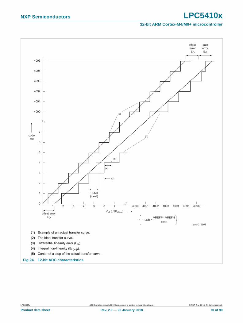
NXP Semiconductors LPC5410x32-bit ARM Cortex-M4/M0+ microcontroller
(1) Example of an actual transfer curve.
(2) The ideal transfer curve.
(3) Differential linearity error (ED).
(4) Integral non-linearity (EL(adj)).
(5) Center of a step of the actual transfer curve.
Fig 24. 12-bit ADC characteristics
aaa-016908
4095
4094
4093
4092
4091
(2)
(1)
40964090 4091 4092 4093 4094 409571 2 3 4 5 6
7
6
5
4
3
2
1
0
4090
(5)
(4)
(3)
1 LSB(ideal)
codeout
VREFP - VREFN 4096
offset errorEO
gainerrorEG
offset errorEO
VIA (LSBideal)
1 LSB =
LPC5410x All information provided in this document is subject to legal disclaimers. © NXP B.V. 2018. All rights reserved.
Product data sheet Rev. 2.9 — 26 January 2018 70 of 90
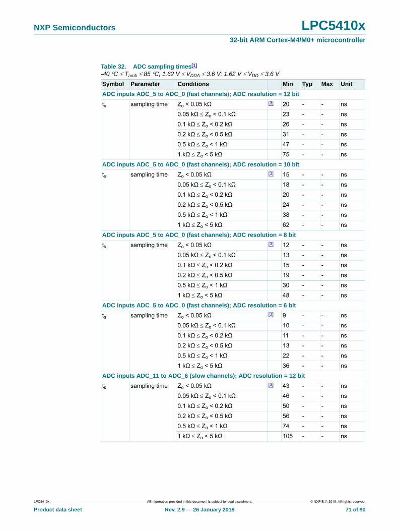
NXP Semiconductors LPC5410x32-bit ARM Cortex-M4/M0+ microcontroller
Table 32. ADC sampling times[1]
-40 C Tamb 85 C; 1.62 V VDDA 3.6 V; 1.62 V VDD 3.6 V
Symbol Parameter Conditions Min Typ Max Unit
ADC inputs ADC_5 to ADC_0 (fast channels); ADC resolution = 12 bit
ts sampling time Zo < 0.05 kΩ [3] 20 - - ns
0.05 kΩ Zo < 0.1 kΩ 23 - - ns
0.1 kΩ Zo < 0.2 kΩ 26 - - ns
0.2 kΩ Zo < 0.5 kΩ 31 - - ns
0.5 kΩ Zo < 1 kΩ 47 - - ns
1 kΩ Zo < 5 kΩ 75 - - ns
ADC inputs ADC_5 to ADC_0 (fast channels); ADC resolution = 10 bit
ts sampling time Zo < 0.05 kΩ [3] 15 - - ns
0.05 kΩ Zo < 0.1 kΩ 18 - - ns
0.1 kΩ Zo < 0.2 kΩ 20 - - ns
0.2 kΩ Zo < 0.5 kΩ 24 - - ns
0.5 kΩ Zo < 1 kΩ 38 - - ns
1 kΩ Zo < 5 kΩ 62 - - ns
ADC inputs ADC_5 to ADC_0 (fast channels); ADC resolution = 8 bit
ts sampling time Zo < 0.05 kΩ [3] 12 - - ns
0.05 kΩ Zo < 0.1 kΩ 13 - - ns
0.1 kΩ Zo < 0.2 kΩ 15 - - ns
0.2 kΩ Zo < 0.5 kΩ 19 - - ns
0.5 kΩ Zo < 1 kΩ 30 - - ns
1 kΩ Zo < 5 kΩ 48 - - ns
ADC inputs ADC_5 to ADC_0 (fast channels); ADC resolution = 6 bit
ts sampling time Zo < 0.05 kΩ [3] 9 - - ns
0.05 kΩ Zo < 0.1 kΩ 10 - - ns
0.1 kΩ Zo < 0.2 kΩ 11 - - ns
0.2 kΩ Zo < 0.5 kΩ 13 - - ns
0.5 kΩ Zo < 1 kΩ 22 - - ns
1 kΩ Zo < 5 kΩ 36 - - ns
ADC inputs ADC_11 to ADC_6 (slow channels); ADC resolution = 12 bit
ts sampling time Zo < 0.05 kΩ [3] 43 - - ns
0.05 kΩ Zo < 0.1 kΩ 46 - - ns
0.1 kΩ Zo < 0.2 kΩ 50 - - ns
0.2 kΩ Zo < 0.5 kΩ 56 - - ns
0.5 kΩ Zo < 1 kΩ 74 - - ns
1 kΩ Zo < 5 kΩ 105 - - ns
LPC5410x All information provided in this document is subject to legal disclaimers. © NXP B.V. 2018. All rights reserved.
Product data sheet Rev. 2.9 — 26 January 2018 71 of 90
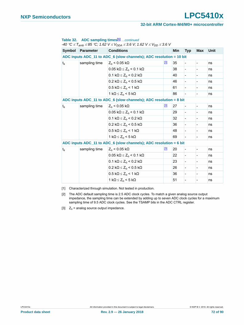
NXP Semiconductors LPC5410x32-bit ARM Cortex-M4/M0+ microcontroller
[1] Characterized through simulation. Not tested in production.
[2] The ADC default sampling time is 2.5 ADC clock cycles. To match a given analog source output impedance, the sampling time can be extended by adding up to seven ADC clock cycles for a maximum sampling time of 9.5 ADC clock cycles. See the TSAMP bits in the ADC CTRL register.
[3] Zo = analog source output impedance.
ADC inputs ADC_11 to ADC_6 (slow channels); ADC resolution = 10 bit
ts sampling time Zo < 0.05 kΩ [3] 35 - - ns
0.05 kΩ Zo < 0.1 kΩ 38 - - ns
0.1 kΩ Zo < 0.2 kΩ 40 - - ns
0.2 kΩ Zo < 0.5 kΩ 46 - - ns
0.5 kΩ Zo < 1 kΩ 61 - - ns
1 kΩ Zo < 5 kΩ 86 - - ns
ADC inputs ADC_11 to ADC_6 (slow channels); ADC resolution = 8 bit
ts sampling time Zo < 0.05 kΩ [3] 27 - - ns
0.05 kΩ Zo < 0.1 kΩ 29 - - ns
0.1 kΩ Zo < 0.2 kΩ 32 - - ns
0.2 kΩ Zo < 0.5 kΩ 36 - - ns
0.5 kΩ Zo < 1 kΩ 48 - - ns
1 kΩ Zo < 5 kΩ 69 - - ns
ADC inputs ADC_11 to ADC_6 (slow channels); ADC resolution = 6 bit
ts sampling time Zo < 0.05 kΩ [3] 20 - - ns
0.05 kΩ Zo < 0.1 kΩ 22 - - ns
0.1 kΩ Zo < 0.2 kΩ 23 - - ns
0.2 kΩ Zo < 0.5 kΩ 26 - - ns
0.5 kΩ Zo < 1 kΩ 36 - - ns
1 kΩ Zo < 5 kΩ 51 - - ns
Table 32. ADC sampling times[1] …continued-40 C Tamb 85 C; 1.62 V VDDA 3.6 V; 1.62 V VDD 3.6 V
Symbol Parameter Conditions Min Typ Max Unit
LPC5410x All information provided in this document is subject to legal disclaimers. © NXP B.V. 2018. All rights reserved.
Product data sheet Rev. 2.9 — 26 January 2018 72 of 90
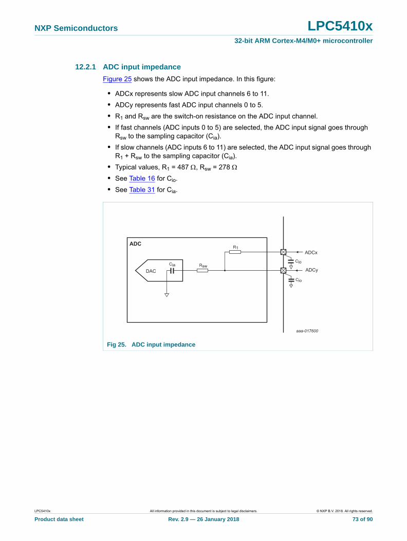
NXP Semiconductors LPC5410x32-bit ARM Cortex-M4/M0+ microcontroller
12.2.1 ADC input impedance
Figure 25 shows the ADC input impedance. In this figure:
• ADCx represents slow ADC input channels 6 to 11.
• ADCy represents fast ADC input channels 0 to 5.
• R1 and Rsw are the switch-on resistance on the ADC input channel.
• If fast channels (ADC inputs 0 to 5) are selected, the ADC input signal goes through Rsw to the sampling capacitor (Cia).
• If slow channels (ADC inputs 6 to 11) are selected, the ADC input signal goes through R1 + Rsw to the sampling capacitor (Cia).
• Typical values, R1 = 487 , Rsw = 278
• See Table 16 for Cio.
• See Table 31 for Cia.
Fig 25. ADC input impedance
DAC
ADC
Rsw
R1
Cia
ADCx
ADCy
Cio
Cio
aaa-017600
LPC5410x All information provided in this document is subject to legal disclaimers. © NXP B.V. 2018. All rights reserved.
Product data sheet Rev. 2.9 — 26 January 2018 73 of 90
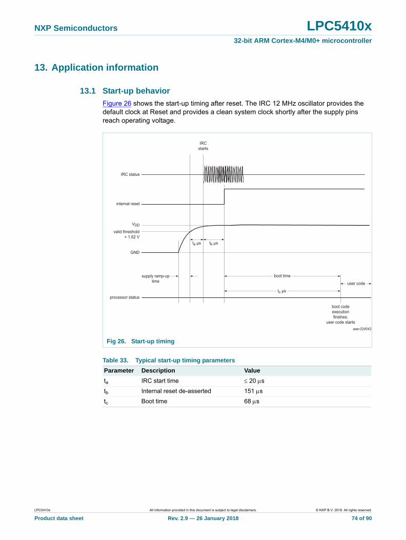
NXP Semiconductors LPC5410x32-bit ARM Cortex-M4/M0+ microcontroller
13. Application information
13.1 Start-up behavior
Figure 26 shows the start-up timing after reset. The IRC 12 MHz oscillator provides the default clock at Reset and provides a clean system clock shortly after the supply pins reach operating voltage.
Fig 26. Start-up timing
Table 33. Typical start-up timing parameters
Parameter Description Value
ta IRC start time 20 s
tb Internal reset de-asserted 151 s
tc Boot time 68 s
aaa-024042
valid threshold= 1.62 V
processor status
VDD
IRC status
internal reset
GND
boot time
user code
boot codeexecutionfinishes;
user code starts
IRCstarts
supply ramp-uptime
tb μsta μs
tc μs
LPC5410x All information provided in this document is subject to legal disclaimers. © NXP B.V. 2018. All rights reserved.
Product data sheet Rev. 2.9 — 26 January 2018 74 of 90
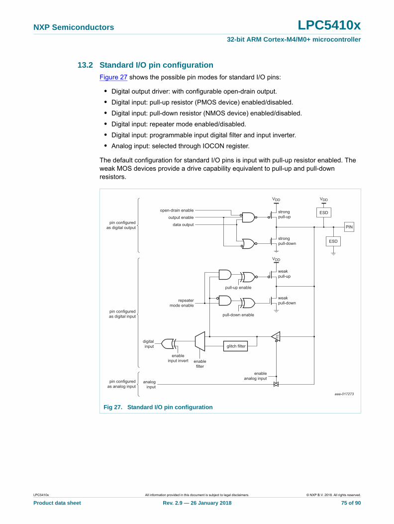
NXP Semiconductors LPC5410x32-bit ARM Cortex-M4/M0+ microcontroller
13.2 Standard I/O pin configuration
Figure 27 shows the possible pin modes for standard I/O pins:
• Digital output driver: with configurable open-drain output.
• Digital input: pull-up resistor (PMOS device) enabled/disabled.
• Digital input: pull-down resistor (NMOS device) enabled/disabled.
• Digital input: repeater mode enabled/disabled.
• Digital input: programmable input digital filter and input inverter.
• Analog input: selected through IOCON register.
The default configuration for standard I/O pins is input with pull-up resistor enabled. The weak MOS devices provide a drive capability equivalent to pull-up and pull-down resistors.
Fig 27. Standard I/O pin configuration
aaa-017273
pin configuredas digital output
open-drain enable
output enable
data output
pin configuredas digital input
pin configuredas analog input
digitalinput
analoginput
enableinput invert enable
filter
glitch filter
PIN
ESD
ESDstrongpull-up
VDD
VDD
VDD
strongpull-down
pull-down enable
pull-up enable
weakpull-up
repeatermode enable
enableanalog input
weakpull-down
LPC5410x All information provided in this document is subject to legal disclaimers. © NXP B.V. 2018. All rights reserved.
Product data sheet Rev. 2.9 — 26 January 2018 75 of 90
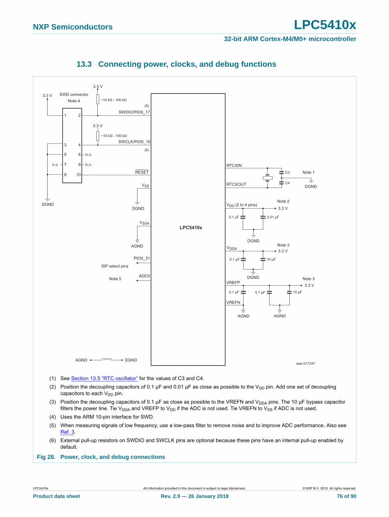
NXP Semiconductors LPC5410x32-bit ARM Cortex-M4/M0+ microcontroller
13.3 Connecting power, clocks, and debug functions
(1) See Section 13.5 “RTC oscillator” for the values of C3 and C4.
(2) Position the decoupling capacitors of 0.1 μF and 0.01 μF as close as possible to the VDD pin. Add one set of decoupling capacitors to each VDD pin.
(3) Position the decoupling capacitors of 0.1 μF as close as possible to the VREFN and VDDA pins. The 10 μF bypass capacitor filters the power line. Tie VDDA and VREFP to VDD if the ADC is not used. Tie VREFN to VSS if ADC is not used.
(4) Uses the ARM 10-pin interface for SWD.
(5) When measuring signals of low frequency, use a low-pass filter to remove noise and to improve ADC performance. Also see Ref. 3.
(6) External pull-up resistors on SWDIO and SWCLK pins are optional because these pins have an internal pull-up enabled by default.
Fig 28. Power, clock, and debug connections
SWDIO/PIO0_17
RESET
VSS
VSSA
PIO0_31
ADC0
RTCXIN
RTCXOUT
VDD (2 to 4 pins)
VDDA
VREFP
VREFN
LPC5410x
3.3 V
3.3 VDGND
DGND
AGND
1
3
5
7
9
2
4
6
8
10
Note 4
Note 5
DGND
DGND
DGND
C3
C4
Note 1
Note 2
Note 3
Note 3
0.01 μF0.1 μF
3.3 V
DGND
10 μF0.1 μF
3.3 V
AGND
AGND
AGND
10 μF0.1 μF0.1 μF
ISP select pins
n.c.
n.c.
n.c.
SWD connector
3.3 V
~10 kΩ - 100 kΩ
aaa-017247
SWCLK/PIO0_16
3.3 V
~10 kΩ - 100 kΩ
(6)
(6)
LPC5410x All information provided in this document is subject to legal disclaimers. © NXP B.V. 2018. All rights reserved.
Product data sheet Rev. 2.9 — 26 January 2018 76 of 90
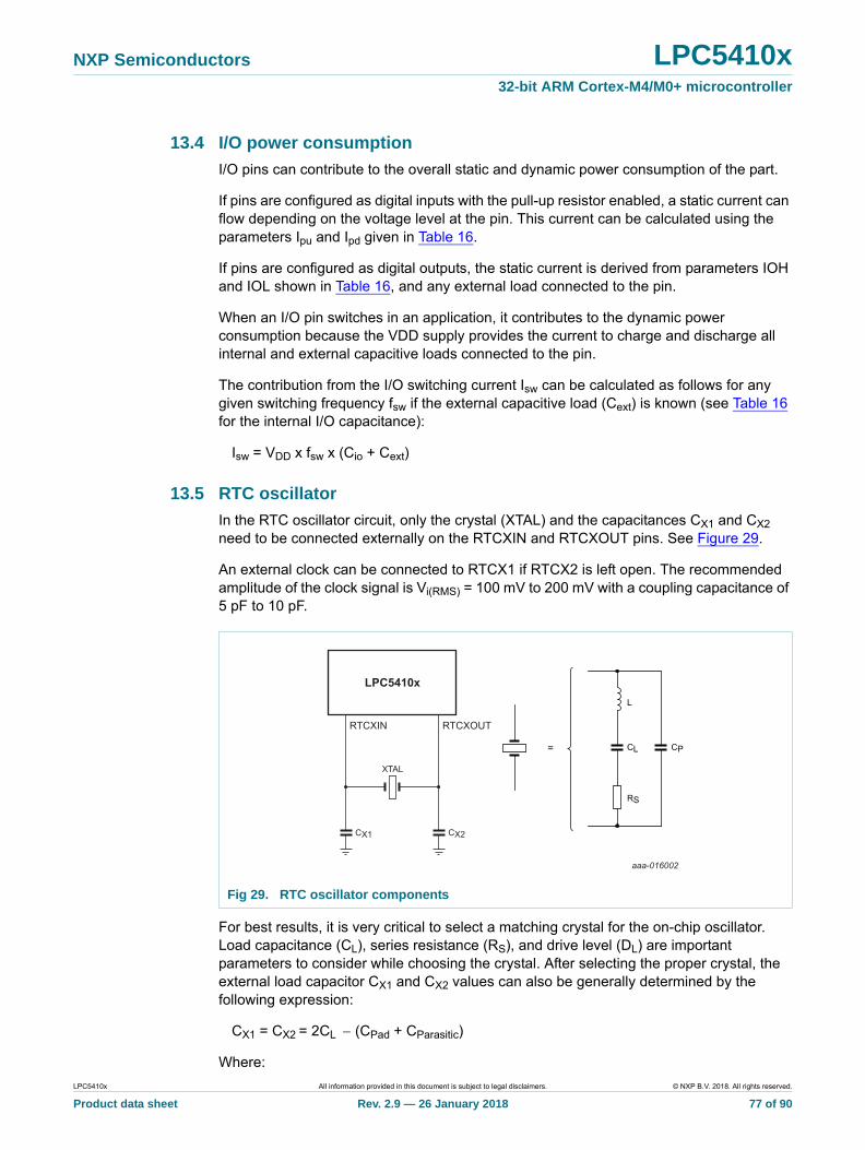
NXP Semiconductors LPC5410x32-bit ARM Cortex-M4/M0+ microcontroller
13.4 I/O power consumption
I/O pins can contribute to the overall static and dynamic power consumption of the part.
If pins are configured as digital inputs with the pull-up resistor enabled, a static current can flow depending on the voltage level at the pin. This current can be calculated using the parameters Ipu and Ipd given in Table 16.
If pins are configured as digital outputs, the static current is derived from parameters IOH and IOL shown in Table 16, and any external load connected to the pin.
When an I/O pin switches in an application, it contributes to the dynamic power consumption because the VDD supply provides the current to charge and discharge all internal and external capacitive loads connected to the pin.
The contribution from the I/O switching current Isw can be calculated as follows for any given switching frequency fsw if the external capacitive load (Cext) is known (see Table 16 for the internal I/O capacitance):
Isw = VDD x fsw x (Cio + Cext)
13.5 RTC oscillator
In the RTC oscillator circuit, only the crystal (XTAL) and the capacitances CX1 and CX2 need to be connected externally on the RTCXIN and RTCXOUT pins. See Figure 29.
An external clock can be connected to RTCX1 if RTCX2 is left open. The recommended amplitude of the clock signal is Vi(RMS) = 100 mV to 200 mV with a coupling capacitance of 5 pF to 10 pF.
For best results, it is very critical to select a matching crystal for the on-chip oscillator. Load capacitance (CL), series resistance (RS), and drive level (DL) are important parameters to consider while choosing the crystal. After selecting the proper crystal, the external load capacitor CX1 and CX2 values can also be generally determined by the following expression:
CX1 = CX2 = 2CL (CPad + CParasitic)
Where:
Fig 29. RTC oscillator components
aaa-016002
LPC5410x
RTCXIN RTCXOUT
CX2CX1
XTAL
= CL CP
RS
L
LPC5410x All information provided in this document is subject to legal disclaimers. © NXP B.V. 2018. All rights reserved.
Product data sheet Rev. 2.9 — 26 January 2018 77 of 90
NXP Semiconductors LPC5410x32-bit ARM Cortex-M4/M0+ microcontroller
CL - Crystal load capacitance
CPad - Pad capacitance of the RTCXIN and RTCXOUT pins (~3 pF).
CParasitic – Parasitic or stray capacitance of external circuit.
Although CParasitic can be ignored in general, the actual board layout and placement of external components influences the optimal values of external load capacitors. Therefore, it is recommended to fine tune the values of external load capacitors on actual hardware board to get the accurate clock frequency. For fine tuning, output the RTC Clock to one of the GPIOs and optimize the values of external load capacitors for minimum frequency deviation.
Remark: The crystals with lower CL (< 12.5 pF) values are not recommended.
13.5.1 RTC Printed Circuit Board (PCB) design guidelines
• Connect the crystal and external load capacitors on the PCB as close as possible (within 20 mm) to the oscillator input and output pins of the chip.
• The length of traces in the oscillation circuit should be as short as possible and must not cross other signal lines.
• Ensure that the load capacitors CX1, CX2, and CX3, in case of third overtone crystal usage, have a common ground plane.
• Loops must be made as small as possible to minimize the noise coupled in through the PCB and to keep the parasitics as small as possible.
• Lay out the ground (GND) pattern under crystal unit.
• Do not lay out other signal lines under crystal unit for multi-layered PCB.
Table 34. Recommended values for the RTC external 32.768 kHz oscillator CL, RS, DL, and CX1/CX2 components
Crystal load capacitance CL
Maximum crystal series resistance RS
Maximum crystal drive level DL
External load capacitors CX1/CX2
12.5 pF < 70 k 0.5 W 22 pF, 22 pF
LPC5410x All information provided in this document is subject to legal disclaimers. © NXP B.V. 2018. All rights reserved.
Product data sheet Rev. 2.9 — 26 January 2018 78 of 90
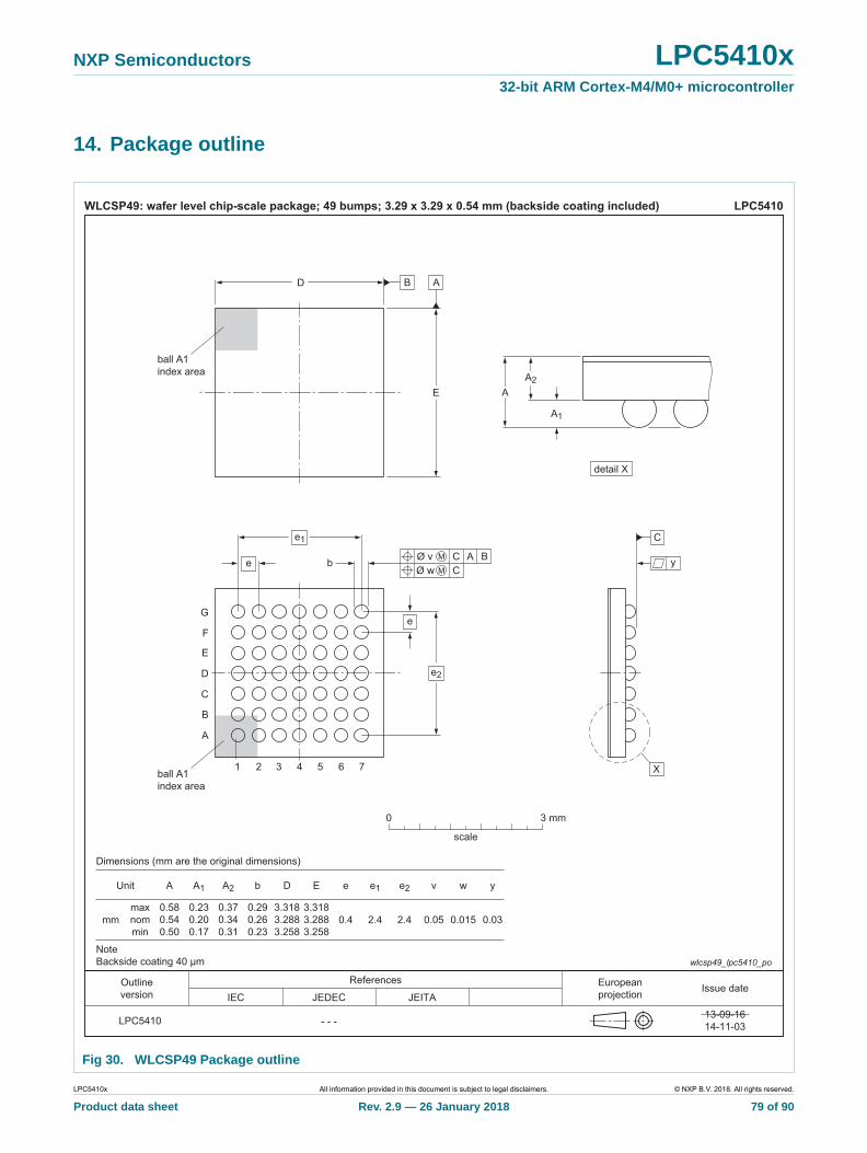
NXP Semiconductors LPC5410x32-bit ARM Cortex-M4/M0+ microcontroller
14. Package outline
Fig 30. WLCSP49 Package outline
ReferencesOutlineversion
Europeanprojection Issue date
IEC JEDEC JEITA
- - -
wlcsp49_lpc5410_po
Unit
mmmaxnommin
0.580.540.50
0.230.200.17
0.290.260.23
3.3183.2883.258
3.3183.2883.258
2.4 2.4 0.05
A
Dimensions (mm are the original dimensions)
A1 A2
0.370.340.31
b D E
0.03
ye
0.4
e1 e2 v
0.015
w
ball A1index area
ball A1index area
X
e2
e
detail X
C
y
e1
e b AC BØ vCØ w
A
B
C
D
E
F
G
7654321
BD
E
A
AA2
A1
13-09-1614-11-03
LPC5410WLCSP49: wafer level chip-scale package; 49 bumps; 3.29 x 3.29 x 0.54 mm (backside coating included)
scale
0 3 mm
LPC5410
NoteBackside coating 40 μm
LPC5410x All information provided in this document is subject to legal disclaimers. © NXP B.V. 2018. All rights reserved.
Product data sheet Rev. 2.9 — 26 January 2018 79 of 90
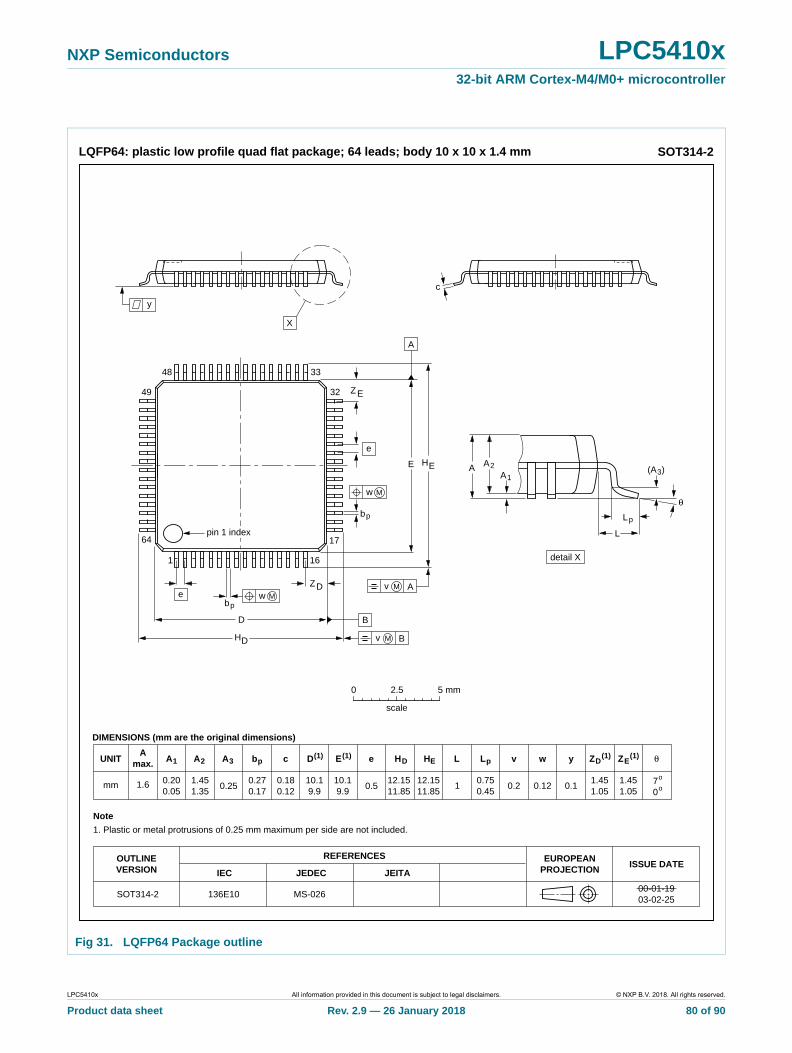
NXP Semiconductors LPC5410x32-bit ARM Cortex-M4/M0+ microcontroller
Fig 31. LQFP64 Package outline
UNITA
max. A1 A2 A3 bp c E(1) e HE L Lp Zywv θ
REFERENCESOUTLINEVERSION
EUROPEANPROJECTION ISSUE DATE
IEC JEDEC JEITA
mm 1.6 0.200.05
1.451.35
0.250.270.17
0.180.12
10.19.9
0.512.1511.85
1.451.05
70
o
o0.12 0.11 0.2
DIMENSIONS (mm are the original dimensions)
Note
1. Plastic or metal protrusions of 0.25 mm maximum per side are not included.
0.750.45
SOT314-2 MS-026136E1000-01-1903-02-25
D(1) (1)(1)
10.19.9
HD
12.1511.85
EZ
1.451.05
D
bpe
θ
EA1
A
Lp
detail X
L
(A )3
B
16
c
DH
bp
EH A2
v M B
D
ZD
A
ZE
e
v M A
X
1
64
49
48 33
32
17
y
pin 1 index
w M
w M
0 2.5 5 mm
scale
LQFP64: plastic low profile quad flat package; 64 leads; body 10 x 10 x 1.4 mm SOT314-2
LPC5410x All information provided in this document is subject to legal disclaimers. © NXP B.V. 2018. All rights reserved.
Product data sheet Rev. 2.9 — 26 January 2018 80 of 90
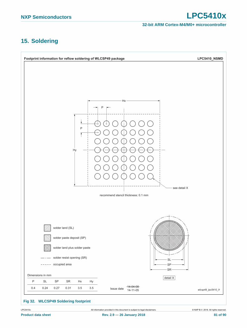
NXP Semiconductors LPC5410x32-bit ARM Cortex-M4/M0+ microcontroller
15. Soldering
Fig 32. WLCSP49 Soldering footprint
Dimensions in mm
P SL SP
0.4 0.27
SR
0.31
Hx
3.5
Hy
3.5 wlcsp49_lpc5410_fr
Hx
Hy
LPC5410_NSMD
solder land plus solder paste
solder resist opening (SR)
Footprint information for reflow soldering of WLCSP49 package
solder land (SL)
recommend stencil thickness: 0.1 mm
solder paste deposit (SP)
occupied areaSL
SP
SR
P
P
0.24
detail X
see detail X
Issue date14-04-0814-11-05
LPC5410x All information provided in this document is subject to legal disclaimers. © NXP B.V. 2018. All rights reserved.
Product data sheet Rev. 2.9 — 26 January 2018 81 of 90
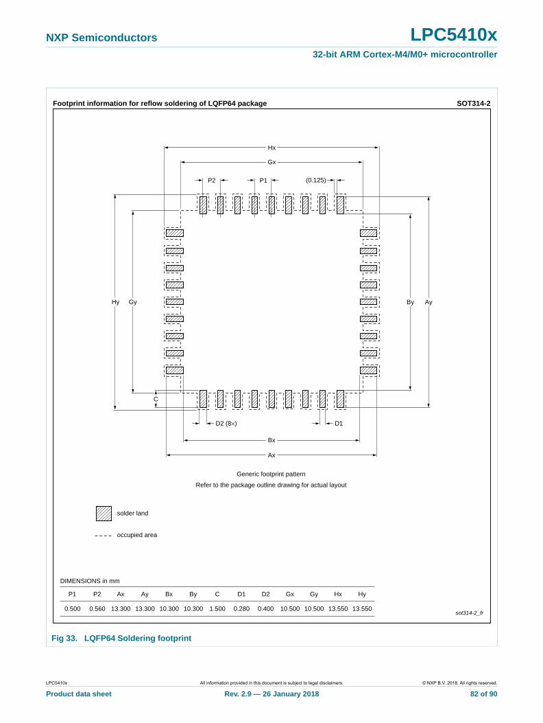
NXP Semiconductors LPC5410x32-bit ARM Cortex-M4/M0+ microcontroller
Fig 33. LQFP64 Soldering footprint
SOT314-2
DIMENSIONS in mm
occupied area
Footprint information for reflow soldering of LQFP64 package
Ax
Bx
Gx
GyHy
Hx
AyBy
P1P2
D2 (8×) D1
(0.125)
Ax Ay Bx By D1 D2 Gx Gy Hx Hy
13.300 13.300 10.300 10.300
P1
0.500
P2
0.560 0.280
C
1.500 0.400 10.500 10.500 13.550 13.550sot314-2_fr
solder land
C
Generic footprint pattern
Refer to the package outline drawing for actual layout
LPC5410x All information provided in this document is subject to legal disclaimers. © NXP B.V. 2018. All rights reserved.
Product data sheet Rev. 2.9 — 26 January 2018 82 of 90
NXP Semiconductors LPC5410x32-bit ARM Cortex-M4/M0+ microcontroller
16. Abbreviations
17. References
[1] LPC5410x User manual UM10850: http://www.nxp.com/documents/user_manual/UM10850.pdf
[2] LPC5410x Errata sheet: http://www.nxp.com/documents/errata_sheet/ES_LPC5410X.pdf
[3] Technical note ADC design guidelines: http://www.nxp.com/documents/technical_note/TN00009.pdf
Table 35. Abbreviations
Acronym Description
AHB Advanced High-performance Bus
APB Advanced Peripheral Bus
API Application Programming Interface
DMA Direct Memory Access
GPIO General Purpose Input/Output
IRC Internal RC
LSB Least Significant Bit
MCU MicroController Unit
PLL Phase-Locked Loop
SPI Serial Peripheral Interface
TTL Transistor-Transistor Logic
USART Universal Asynchronous Receiver/Transmitter
LPC5410x All information provided in this document is subject to legal disclaimers. © NXP B.V. 2018. All rights reserved.
Product data sheet Rev. 2.9 — 26 January 2018 83 of 90
NXP Semiconductors LPC5410x32-bit ARM Cortex-M4/M0+ microcontroller
18. Revision history
Table 36. Revision history
Document ID Release date Data sheet status Change notice Supersedes
LPC5410x v.2.9 20180126 Product data sheet - LPC5410x v2.8
Modification: • Updated a feature in Section 7.16.2 “SPI serial I/O controller” Maximum supported bit rate for SPI master mode is 48 Mbit/s. Was 71 Mbit/s.
• Updated Section 11.10 “SPI interfaces”: the maximum supported bit rate for SPI master mode is 48 Mbit/s. Was 71 Mbit/s.
LPC5410x v.2.8 20171219 Product data sheet - LPC5410x v2.7
Modification: • Updated Table 20 “Dynamic characteristic: Typical wake-up times from low power modes”.
LPC5410x v.2.7 20170426 Product data sheet - LPC5410x v2.6
Modification: • Updated Figure 28 “Power, clock, and debug connections”.
LPC5410x v.2.6 20160926 Product data sheet - LPC5410x v2.5
Modification: • Updated Table 13 “Static characteristics: Power consumption in deep sleep, power down, and deep power-down modes”: in deep power-down mode, the RTC oscillator running with external crystal typical value is 240 nA at: Tamb = 40 C to +105 C, 1.62 V VDD 2.0 V; unless otherwise specified.
LPC5410x v.2.5 20160913 Product data sheet - LPC5410x v2.4
Modification: • Updated Table 10 “CoreMark score”: changed CoreMark scoreCoreMark code executed from flash; CCLK = 84 MHz; 4 system clock flash access time; CCLK = 100 MHz; 5 system clock flash access time to CCLK = 84 MHz; 5 system clock flash access time; CCLK = 100 MHz; 6 system clock flash access time
LPC5410x v.2.4 20160711 Product data sheet - LPC5410x v2.3
Modification: • Updated Table 27 “SPI dynamic characteristics[1]”:
– Min values of SPI master 1.62V VDD 2.0 V, tDS and tv(Q).
– Min values of SPI slave 1.62V VDD 2.0 V, tDSHand tv(Q).
– Min values of SPI master 2.7 V VDD 3.6 V, tDS.
– Min values of SPI slave 2.7 V VDD 3.6 V, tDH.
• Updated Table 28 “USART dynamic characteristics[1]”:
– Min values of USART master (in synchronous mode) 1.62V VDD 2.0 V, th(D) and tv(Q).
– Min values of USART slave (in synchronous mode) 1.62V VDD 2.0 V, th(D).
– Min values of USART master (in synchronous mode) 2.7V VDD 3.6V, th(D).
– Min values of USART slave (in synchronous mode) 2.7V VDD 3.6 V, th(D).
• Updated features of Section 7.16.2 “SPI serial I/O controller”: Maximum supported bit rate for SPI master mode is 71 Mbit/s, and the maximum supported bit rate for SPI slave mode is 21 Mbit/s.
• Updated features of Section 7.16.1 “USART”: Maximum supported bit rate of 24 Mbit/s for USART master and slave synchronous modes.
• Updated Table 22 “Dynamic characteristics of the PLL[1]”:
– fref changed to Fin; reference frequency to input frequency.
– removed frefjitter.
• Updated the description for Section 11.10 “SPI interfaces”.
LPC5410x v2.3 20160524 Product data sheet - LPC5410x v2.2
LPC5410x All information provided in this document is subject to legal disclaimers. © NXP B.V. 2018. All rights reserved.
Product data sheet Rev. 2.9 — 26 January 2018 84 of 90
NXP Semiconductors LPC5410x32-bit ARM Cortex-M4/M0+ microcontroller
Modification: • Updated Table 18 “Flash characteristics”: For Nendu conditions, removed the row with page erase/program; page in small sector 10000 and removed the word large so that it is "page erase/program;page in a sector".
• Updated Section 7.16.1 “USART” features: changed maximum bit rates to 6.25 Mbit/s in asynchronous mode.
LPC5410x v2.2 20151222 Product data sheet 201512007I LPC5410x v2.1
Modification: • Updated Section 11.6 “IRC”, Table 23 “Dynamic characteristic: IRC oscillator” for IRC frequency tolerance improvement over temperature.
• Added boot code version and device revision. See Section 4 “Marking”.
• Added the abbreviation ISP to the Remark: This pin is also used to force In-System Programming mode (ISP) after device reset. See the LPC5410x User Manual (Boot Process chapter) for details to PIO0_31. See Table 4 “Pin description”.
• Removed 164 uA PLL spec in peripheral power consumption table, Table 15 “Typical AHB/APB peripheral power consumption[3][4][5]”.
• Added Table 21 “PLL lock times and current”.
• Updated Figure 10 “Deep sleep mode: Typical supply current IDD versus temperature for different supply voltages VDD”, Figure 11 “Power down mode: Typical supply current IDD versus temperature for different supply voltages VDD”, and Figure 12 “Deep power-down mode: Typical supply current IDD versus temperature for different supply voltages VDD”.
• Updated Table 12 “Static characteristics: Power consumption in deep sleep, power down, and deep power-down modes”: added max values to Deep sleep mode at 25 °C and 105 °C, Power down mode at 25 °C and 105 °C. Changed typ and max values for Deep power-down mode RTC oscillator input grounded (RTC oscillator disabled) at 25 °C; was: typ = 84 nA, max = 240 nA; now: typ = 160 nA, max = 340 nA.
• Updated Table 13 “Static characteristics: Power consumption in deep sleep, power down, and deep power-down modes”: added max values to Deep sleep mode at 25 °C and 105 °C, Power down mode at 25 °C and 105 °C. Changed typ and max values for Deep power-down mode RTC oscillator input grounded (RTC oscillator disabled) at 25 °C; was: typ = 135 nA, max = 470 nA; now: typ = 200 nA, max = 570 nA.
• Updated Table 7 “Limiting values”; VESD, electrostatic discharge voltage, human body model; all pins value to 4000 V; was 5000 V.
• Updated Table 31 “12-bit ADC static characteristics”: ED differential linearity error, VDDA = VREFP = 1.62 V and 3.6 V, typ value 3 and 2; EL(adj) integral non-linearity, VDDA = VREFP = 1.62 V, typ value 5; Verr(FS) full-scale error voltage VDDA = VREFP = 1.62 V and 3.6 V, typ value to 3
LPC5410x v2.1 20150701 Product data sheet - LPC5410x v2.0
Modification: • Updated Figure 3 “LPC5410x Block diagram”. Corrected Sync APB bridge to Async APB bridge.
• Updated external clock input for clock frequencies of up to 24 MHz to 25 MHz in Section 2 “Features and benefits”.
• Updated Table 12 “Static characteristics: Power consumption in deep sleep, power down, and deep power-down modes”. Fixed the unit of the max value from nA to A for IDD in deep power-down mode; RTC oscillator input grounded (RTC oscillator disabled), Tamb = 105 C.
Table 36. Revision history …continued
Document ID Release date Data sheet status Change notice Supersedes
LPC5410x All information provided in this document is subject to legal disclaimers. © NXP B.V. 2018. All rights reserved.
Product data sheet Rev. 2.9 — 26 January 2018 85 of 90
NXP Semiconductors LPC5410x32-bit ARM Cortex-M4/M0+ microcontroller
LPC5410x v2.0 20150417 Product data sheet - LPC5410x v1.1
Modification: • Updated the ADC conversion rate from 4.8 Msamples/s to 5.0 Msamples/s.
• Added Section 7.14 “Pin interrupt/pattern engine”.
• Added Section 7.18.6 “Repetitive Interrupt Timer (RIT)”.
• Updated Table 12 “Static characteristics: Power consumption in deep sleep, power down, and deep power-down modes” on page 44.
• Updated Table 15 “Static characteristics: pin characteristics” on page 49:
– Tamb = 40 C to +105 C, unless otherwise specified. 1.62 V VDD 3.6 V.
– updated min and max values.
• Added Section 11.1 “Power-up ramp conditions”.
• Added Section 11.9 “SPI interfaces”, Section 11.10 “USART interface”, and Section 11.11 “SCTimer/PWM output timing”.
• Updated Section 11.5 “IRC”:
– added temperature conditions: Tamb = 25 C, 40 C Tamb +105 C
– updated min and max values.
• Added Table 14 “Typical peripheral power consumption”.
• Added Table 28 “12-bit ADC static characteristics”:
– Tamb = 40 C to +105 C.
– Values for ED, EL(adj), EO, and Verr(FS).
• Added Section 12.2.1 “ADC input impedance”
• Updated Figure 26 “Standard I/O pin configuration” on page 71
• Minor updates to Section 13.3 “I/O power consumption”.
LPC5410x v1.1 20141117 Product data sheet - LPC5410x v1.0
Modification: • Minor editorial update in Section 1.
LPC5410x v1.0 20141106 Product data sheet - -
Table 36. Revision history …continued
Document ID Release date Data sheet status Change notice Supersedes
LPC5410x All information provided in this document is subject to legal disclaimers. © NXP B.V. 2018. All rights reserved.
Product data sheet Rev. 2.9 — 26 January 2018 86 of 90
NXP Semiconductors LPC5410x32-bit ARM Cortex-M4/M0+ microcontroller
19. Legal information
19.1 Data sheet status
[1] Please consult the most recently issued document before initiating or completing a design.
[2] The term ‘short data sheet’ is explained in section “Definitions”.
[3] The product status of device(s) described in this document may have changed since this document was published and may differ in case of multiple devices. The latest product status information is available on the Internet at URL http://www.nxp.com.
19.2 Definitions
Draft — The document is a draft version only. The content is still under internal review and subject to formal approval, which may result in modifications or additions. NXP Semiconductors does not give any representations or warranties as to the accuracy or completeness of information included herein and shall have no liability for the consequences of use of such information.
Short data sheet — A short data sheet is an extract from a full data sheet with the same product type number(s) and title. A short data sheet is intended for quick reference only and should not be relied upon to contain detailed and full information. For detailed and full information see the relevant full data sheet, which is available on request via the local NXP Semiconductors sales office. In case of any inconsistency or conflict with the short data sheet, the full data sheet shall prevail.
Product specification — The information and data provided in a Product data sheet shall define the specification of the product as agreed between NXP Semiconductors and its customer, unless NXP Semiconductors and customer have explicitly agreed otherwise in writing. In no event however, shall an agreement be valid in which the NXP Semiconductors product is deemed to offer functions and qualities beyond those described in the Product data sheet.
19.3 Disclaimers
Limited warranty and liability — Information in this document is believed to be accurate and reliable. However, NXP Semiconductors does not give any representations or warranties, expressed or implied, as to the accuracy or completeness of such information and shall have no liability for the consequences of use of such information. NXP Semiconductors takes no responsibility for the content in this document if provided by an information source outside of NXP Semiconductors.
In no event shall NXP Semiconductors be liable for any indirect, incidental, punitive, special or consequential damages (including - without limitation - lost profits, lost savings, business interruption, costs related to the removal or replacement of any products or rework charges) whether or not such damages are based on tort (including negligence), warranty, breach of contract or any other legal theory.
Notwithstanding any damages that customer might incur for any reason whatsoever, NXP Semiconductors’ aggregate and cumulative liability towards customer for the products described herein shall be limited in accordance with the Terms and conditions of commercial sale of NXP Semiconductors.
Right to make changes — NXP Semiconductors reserves the right to make changes to information published in this document, including without limitation specifications and product descriptions, at any time and without notice. This document supersedes and replaces all information supplied prior to the publication hereof.
Suitability for use — NXP Semiconductors products are not designed, authorized or warranted to be suitable for use in life support, life-critical or safety-critical systems or equipment, nor in applications where failure or malfunction of an NXP Semiconductors product can reasonably be expected to result in personal injury, death or severe property or environmental damage. NXP Semiconductors and its suppliers accept no liability for inclusion and/or use of NXP Semiconductors products in such equipment or applications and therefore such inclusion and/or use is at the customer’s own risk.
Applications — Applications that are described herein for any of these products are for illustrative purposes only. NXP Semiconductors makes no representation or warranty that such applications will be suitable for the specified use without further testing or modification.
Customers are responsible for the design and operation of their applications and products using NXP Semiconductors products, and NXP Semiconductors accepts no liability for any assistance with applications or customer product design. It is customer’s sole responsibility to determine whether the NXP Semiconductors product is suitable and fit for the customer’s applications and products planned, as well as for the planned application and use of customer’s third party customer(s). Customers should provide appropriate design and operating safeguards to minimize the risks associated with their applications and products.
NXP Semiconductors does not accept any liability related to any default, damage, costs or problem which is based on any weakness or default in the customer’s applications or products, or the application or use by customer’s third party customer(s). Customer is responsible for doing all necessary testing for the customer’s applications and products using NXP Semiconductors products in order to avoid a default of the applications and the products or of the application or use by customer’s third party customer(s). NXP does not accept any liability in this respect.
Limiting values — Stress above one or more limiting values (as defined in the Absolute Maximum Ratings System of IEC 60134) will cause permanent damage to the device. Limiting values are stress ratings only and (proper) operation of the device at these or any other conditions above those given in the Recommended operating conditions section (if present) or the Characteristics sections of this document is not warranted. Constant or repeated exposure to limiting values will permanently and irreversibly affect the quality and reliability of the device.
Terms and conditions of commercial sale — NXP Semiconductors products are sold subject to the general terms and conditions of commercial sale, as published at http://www.nxp.com/profile/terms, unless otherwise agreed in a valid written individual agreement. In case an individual agreement is concluded only the terms and conditions of the respective agreement shall apply. NXP Semiconductors hereby expressly objects to applying the customer’s general terms and conditions with regard to the purchase of NXP Semiconductors products by customer.
No offer to sell or license — Nothing in this document may be interpreted or construed as an offer to sell products that is open for acceptance or the grant, conveyance or implication of any license under any copyrights, patents or other industrial or intellectual property rights.
Document status[1][2] Product status[3] Definition
Objective [short] data sheet Development This document contains data from the objective specification for product development.
Preliminary [short] data sheet Qualification This document contains data from the preliminary specification.
Product [short] data sheet Production This document contains the product specification.
LPC5410x All information provided in this document is subject to legal disclaimers. © NXP B.V. 2018. All rights reserved.
Product data sheet Rev. 2.9 — 26 January 2018 87 of 90
NXP Semiconductors LPC5410x32-bit ARM Cortex-M4/M0+ microcontroller
Export control — This document as well as the item(s) described herein may be subject to export control regulations. Export might require a prior authorization from competent authorities.
Non-automotive qualified products — Unless this data sheet expressly states that this specific NXP Semiconductors product is automotive qualified, the product is not suitable for automotive use. It is neither qualified nor tested in accordance with automotive testing or application requirements. NXP Semiconductors accepts no liability for inclusion and/or use of non-automotive qualified products in automotive equipment or applications.
In the event that customer uses the product for design-in and use in automotive applications to automotive specifications and standards, customer (a) shall use the product without NXP Semiconductors’ warranty of the product for such automotive applications, use and specifications, and (b) whenever customer uses the product for automotive applications beyond
NXP Semiconductors’ specifications such use shall be solely at customer’s own risk, and (c) customer fully indemnifies NXP Semiconductors for any liability, damages or failed product claims resulting from customer design and use of the product for automotive applications beyond NXP Semiconductors’ standard warranty and NXP Semiconductors’ product specifications.
19.4 TrademarksNotice: All referenced brands, product names, service names and trademarks are the property of their respective owners.
I2C-bus — logo is a trademark of NXP B.V.
20. Contact information
For more information, please visit: http://www.nxp.com
For sales office addresses, please send an email to: [email protected]
LPC5410x All information provided in this document is subject to legal disclaimers. © NXP B.V. 2018. All rights reserved.
Product data sheet Rev. 2.9 — 26 January 2018 88 of 90
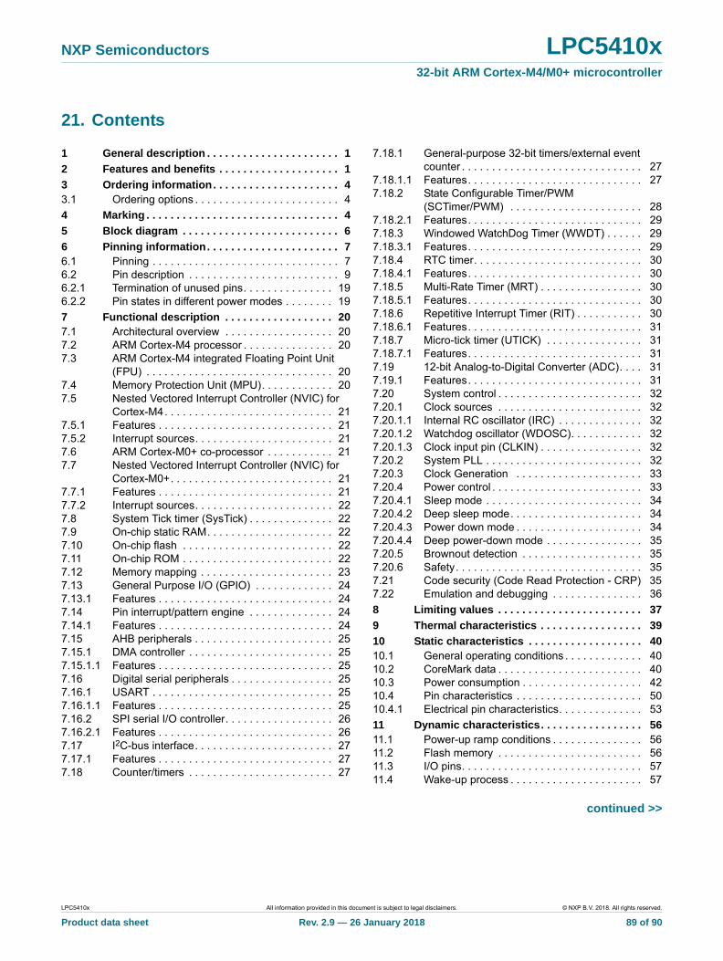
NXP Semiconductors LPC5410x32-bit ARM Cortex-M4/M0+ microcontroller
21. Contents
1 General description . . . . . . . . . . . . . . . . . . . . . . 1
2 Features and benefits . . . . . . . . . . . . . . . . . . . . 1
3 Ordering information. . . . . . . . . . . . . . . . . . . . . 43.1 Ordering options . . . . . . . . . . . . . . . . . . . . . . . . 4
4 Marking . . . . . . . . . . . . . . . . . . . . . . . . . . . . . . . . 4
5 Block diagram . . . . . . . . . . . . . . . . . . . . . . . . . . 6
6 Pinning information. . . . . . . . . . . . . . . . . . . . . . 76.1 Pinning . . . . . . . . . . . . . . . . . . . . . . . . . . . . . . . 76.2 Pin description . . . . . . . . . . . . . . . . . . . . . . . . . 96.2.1 Termination of unused pins. . . . . . . . . . . . . . . 196.2.2 Pin states in different power modes . . . . . . . . 19
7 Functional description . . . . . . . . . . . . . . . . . . 207.1 Architectural overview . . . . . . . . . . . . . . . . . . 207.2 ARM Cortex-M4 processor . . . . . . . . . . . . . . . 207.3 ARM Cortex-M4 integrated Floating Point Unit
(FPU) . . . . . . . . . . . . . . . . . . . . . . . . . . . . . . . 207.4 Memory Protection Unit (MPU). . . . . . . . . . . . 207.5 Nested Vectored Interrupt Controller (NVIC) for
Cortex-M4. . . . . . . . . . . . . . . . . . . . . . . . . . . . 217.5.1 Features . . . . . . . . . . . . . . . . . . . . . . . . . . . . . 217.5.2 Interrupt sources. . . . . . . . . . . . . . . . . . . . . . . 217.6 ARM Cortex-M0+ co-processor . . . . . . . . . . . 217.7 Nested Vectored Interrupt Controller (NVIC) for
Cortex-M0+. . . . . . . . . . . . . . . . . . . . . . . . . . . 217.7.1 Features . . . . . . . . . . . . . . . . . . . . . . . . . . . . . 217.7.2 Interrupt sources. . . . . . . . . . . . . . . . . . . . . . . 227.8 System Tick timer (SysTick) . . . . . . . . . . . . . . 227.9 On-chip static RAM. . . . . . . . . . . . . . . . . . . . . 227.10 On-chip flash . . . . . . . . . . . . . . . . . . . . . . . . . 227.11 On-chip ROM . . . . . . . . . . . . . . . . . . . . . . . . . 227.12 Memory mapping . . . . . . . . . . . . . . . . . . . . . . 237.13 General Purpose I/O (GPIO) . . . . . . . . . . . . . 247.13.1 Features . . . . . . . . . . . . . . . . . . . . . . . . . . . . . 247.14 Pin interrupt/pattern engine . . . . . . . . . . . . . . 247.14.1 Features . . . . . . . . . . . . . . . . . . . . . . . . . . . . . 247.15 AHB peripherals . . . . . . . . . . . . . . . . . . . . . . . 257.15.1 DMA controller . . . . . . . . . . . . . . . . . . . . . . . . 257.15.1.1 Features . . . . . . . . . . . . . . . . . . . . . . . . . . . . . 257.16 Digital serial peripherals . . . . . . . . . . . . . . . . . 257.16.1 USART . . . . . . . . . . . . . . . . . . . . . . . . . . . . . . 257.16.1.1 Features . . . . . . . . . . . . . . . . . . . . . . . . . . . . . 257.16.2 SPI serial I/O controller. . . . . . . . . . . . . . . . . . 267.16.2.1 Features . . . . . . . . . . . . . . . . . . . . . . . . . . . . . 267.17 I2C-bus interface. . . . . . . . . . . . . . . . . . . . . . . 277.17.1 Features . . . . . . . . . . . . . . . . . . . . . . . . . . . . . 277.18 Counter/timers . . . . . . . . . . . . . . . . . . . . . . . . 27
7.18.1 General-purpose 32-bit timers/external event counter . . . . . . . . . . . . . . . . . . . . . . . . . . . . . . 27
7.18.1.1 Features. . . . . . . . . . . . . . . . . . . . . . . . . . . . . 277.18.2 State Configurable Timer/PWM
(SCTimer/PWM) . . . . . . . . . . . . . . . . . . . . . . 287.18.2.1 Features. . . . . . . . . . . . . . . . . . . . . . . . . . . . . 297.18.3 Windowed WatchDog Timer (WWDT) . . . . . . 297.18.3.1 Features. . . . . . . . . . . . . . . . . . . . . . . . . . . . . 297.18.4 RTC timer. . . . . . . . . . . . . . . . . . . . . . . . . . . . 307.18.4.1 Features. . . . . . . . . . . . . . . . . . . . . . . . . . . . . 307.18.5 Multi-Rate Timer (MRT) . . . . . . . . . . . . . . . . . 307.18.5.1 Features. . . . . . . . . . . . . . . . . . . . . . . . . . . . . 307.18.6 Repetitive Interrupt Timer (RIT) . . . . . . . . . . . 307.18.6.1 Features. . . . . . . . . . . . . . . . . . . . . . . . . . . . . 317.18.7 Micro-tick timer (UTICK) . . . . . . . . . . . . . . . . 317.18.7.1 Features. . . . . . . . . . . . . . . . . . . . . . . . . . . . . 317.19 12-bit Analog-to-Digital Converter (ADC). . . . 317.19.1 Features. . . . . . . . . . . . . . . . . . . . . . . . . . . . . 317.20 System control . . . . . . . . . . . . . . . . . . . . . . . . 327.20.1 Clock sources . . . . . . . . . . . . . . . . . . . . . . . . 327.20.1.1 Internal RC oscillator (IRC) . . . . . . . . . . . . . . 327.20.1.2 Watchdog oscillator (WDOSC). . . . . . . . . . . . 327.20.1.3 Clock input pin (CLKIN) . . . . . . . . . . . . . . . . . 327.20.2 System PLL . . . . . . . . . . . . . . . . . . . . . . . . . . 327.20.3 Clock Generation . . . . . . . . . . . . . . . . . . . . . 337.20.4 Power control . . . . . . . . . . . . . . . . . . . . . . . . . 337.20.4.1 Sleep mode . . . . . . . . . . . . . . . . . . . . . . . . . . 347.20.4.2 Deep sleep mode. . . . . . . . . . . . . . . . . . . . . . 347.20.4.3 Power down mode . . . . . . . . . . . . . . . . . . . . . 347.20.4.4 Deep power-down mode . . . . . . . . . . . . . . . . 357.20.5 Brownout detection . . . . . . . . . . . . . . . . . . . . 357.20.6 Safety. . . . . . . . . . . . . . . . . . . . . . . . . . . . . . . 357.21 Code security (Code Read Protection - CRP) 357.22 Emulation and debugging . . . . . . . . . . . . . . . 36
8 Limiting values . . . . . . . . . . . . . . . . . . . . . . . . 37
9 Thermal characteristics . . . . . . . . . . . . . . . . . 39
10 Static characteristics . . . . . . . . . . . . . . . . . . . 4010.1 General operating conditions . . . . . . . . . . . . . 4010.2 CoreMark data . . . . . . . . . . . . . . . . . . . . . . . . 4010.3 Power consumption . . . . . . . . . . . . . . . . . . . . 4210.4 Pin characteristics . . . . . . . . . . . . . . . . . . . . . 5010.4.1 Electrical pin characteristics. . . . . . . . . . . . . . 53
11 Dynamic characteristics. . . . . . . . . . . . . . . . . 5611.1 Power-up ramp conditions . . . . . . . . . . . . . . . 5611.2 Flash memory . . . . . . . . . . . . . . . . . . . . . . . . 5611.3 I/O pins. . . . . . . . . . . . . . . . . . . . . . . . . . . . . . 5711.4 Wake-up process . . . . . . . . . . . . . . . . . . . . . . 57
LPC5410x All information provided in this document is subject to legal disclaimers. © NXP B.V. 2018. All rights reserved.
Product data sheet Rev. 2.9 — 26 January 2018 89 of 90
continued >>
NXP Semiconductors LPC5410x32-bit ARM Cortex-M4/M0+ microcontroller
11.5 System PLL . . . . . . . . . . . . . . . . . . . . . . . . . . 5911.6 IRC . . . . . . . . . . . . . . . . . . . . . . . . . . . . . . . . 6011.7 RTC oscillator . . . . . . . . . . . . . . . . . . . . . . . . . 6011.8 Watchdog oscillator . . . . . . . . . . . . . . . . . . . . 6111.9 I2C-bus . . . . . . . . . . . . . . . . . . . . . . . . . . . . . . 6111.10 SPI interfaces . . . . . . . . . . . . . . . . . . . . . . . . . 6311.11 USART interface. . . . . . . . . . . . . . . . . . . . . . . 6611.12 SCTimer/PWM output timing . . . . . . . . . . . . . 67
12 Analog characteristics . . . . . . . . . . . . . . . . . . 6812.1 BOD . . . . . . . . . . . . . . . . . . . . . . . . . . . . . . . . 6812.2 12-bit ADC characteristics . . . . . . . . . . . . . . . 6912.2.1 ADC input impedance. . . . . . . . . . . . . . . . . . . 73
13 Application information. . . . . . . . . . . . . . . . . . 7413.1 Start-up behavior . . . . . . . . . . . . . . . . . . . . . . 7413.2 Standard I/O pin configuration . . . . . . . . . . . . 7513.3 Connecting power, clocks, and debug
functions . . . . . . . . . . . . . . . . . . . . . . . . . . . . . 7613.4 I/O power consumption. . . . . . . . . . . . . . . . . . 7713.5 RTC oscillator . . . . . . . . . . . . . . . . . . . . . . . . . 7713.5.1 RTC Printed Circuit Board (PCB) design
guidelines . . . . . . . . . . . . . . . . . . . . . . . . . . . . 78
14 Package outline . . . . . . . . . . . . . . . . . . . . . . . . 79
15 Soldering . . . . . . . . . . . . . . . . . . . . . . . . . . . . . 81
16 Abbreviations. . . . . . . . . . . . . . . . . . . . . . . . . . 83
17 References . . . . . . . . . . . . . . . . . . . . . . . . . . . . 83
18 Revision history. . . . . . . . . . . . . . . . . . . . . . . . 84
19 Legal information. . . . . . . . . . . . . . . . . . . . . . . 8719.1 Data sheet status . . . . . . . . . . . . . . . . . . . . . . 8719.2 Definitions. . . . . . . . . . . . . . . . . . . . . . . . . . . . 8719.3 Disclaimers . . . . . . . . . . . . . . . . . . . . . . . . . . . 8719.4 Trademarks. . . . . . . . . . . . . . . . . . . . . . . . . . . 88
20 Contact information. . . . . . . . . . . . . . . . . . . . . 88
21 Contents . . . . . . . . . . . . . . . . . . . . . . . . . . . . . . 89
© NXP B.V. 2018. All rights reserved.
For more information, please visit: http://www.nxp.comFor sales office addresses, please send an email to: [email protected]
Date of release: 26 January 2018
Document identifier: LPC5410x
Please be aware that important notices concerning this document and the product(s)described herein, have been included in section ‘Legal information’.
Recommended