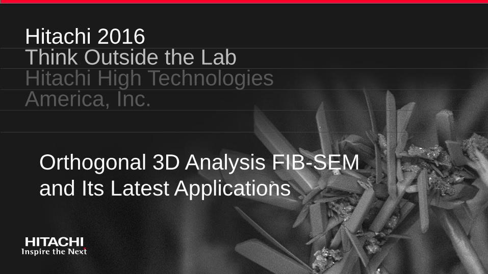
Hitachi 2016 Think Outside the Lab Hitachi High Technologies America, Inc.
Orthogonal 3D Analysis FIB-SEM
and Its Latest Applications
Hitachi 2016
Think Outside the Lab
Abstract/Overview
• The Hitachi NX9000 orthogonal FIB-SEM system is advancing the field of material processing by lifting
the constraints often encountered by V-shaped FIB-SEM instruments.
• An ever increasing need for three-dimensional signal capture and reconstruction often demand a large
amount of time for post processing.
– FIB-SEM Design
• Design layout
• EM/IM technologies
– A walkthrough example is presented illustrating how and why an orthogonal FIB-SEM system
provides a level of precise and accurate measurement and material preparation with a high degree
of accuracy.
Orthogonal FIB-SEM
Hitachi 2016
Think Outside the Lab
Matrix
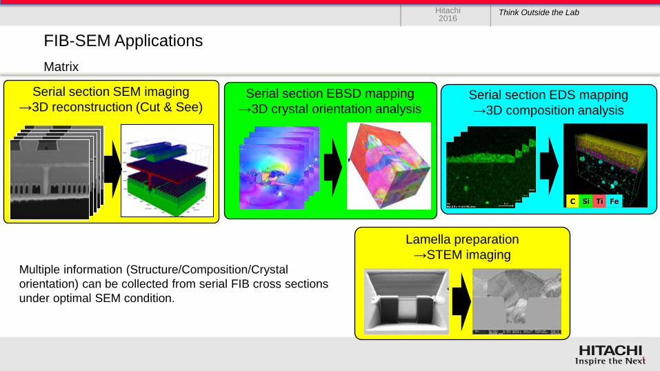
FIB-SEM Applications
Lamella preparation
→STEM imaging
Serial section SEM imaging
→3D reconstruction (Cut & See) Serial section EDS mapping
→3D composition analysis
CC SiSi TiTi FeFeCC SiSi TiTi FeFe
Serial section EBSD mapping
→3D crystal orientation analysis
Multiple information (Structure/Composition/Crystal
orientation) can be collected from serial FIB cross sections
under optimal SEM condition.
Hitachi 2016
Think Outside the Lab
Overview
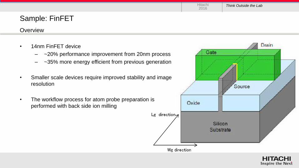
• 14nm FinFET device
– ~20% performance improvement from 20nm process
– ~35% more energy efficient from previous generation
• Smaller scale devices require improved stability and image
resolution
• The workflow process for atom probe preparation is
performed with back side ion milling
Sample: FinFET
Hitachi 2016
Think Outside the Lab
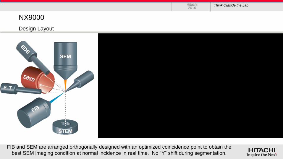
Design Layout
NX9000
FIB and SEM are arranged orthogonally designed with an optimized coincidence point to obtain the
best SEM imaging condition at normal incidence in real time. No “Y” shift during segmentation.
Hitachi 2016
Think Outside the Lab
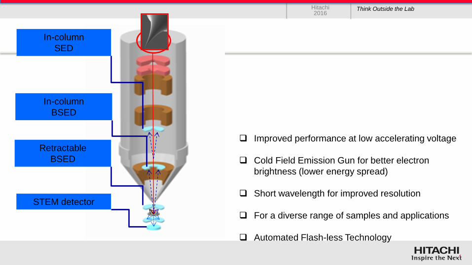
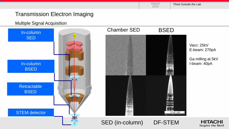
In-column
SED
In-column
BSED
Retractable
BSED
STEM detector
Improved performance at low accelerating voltage
Cold Field Emission Gun for better electron
brightness (lower energy spread)
Short wavelength for improved resolution
For a diverse range of samples and applications
Automated Flash-less Technology
Hitachi 2016
Think Outside the Lab
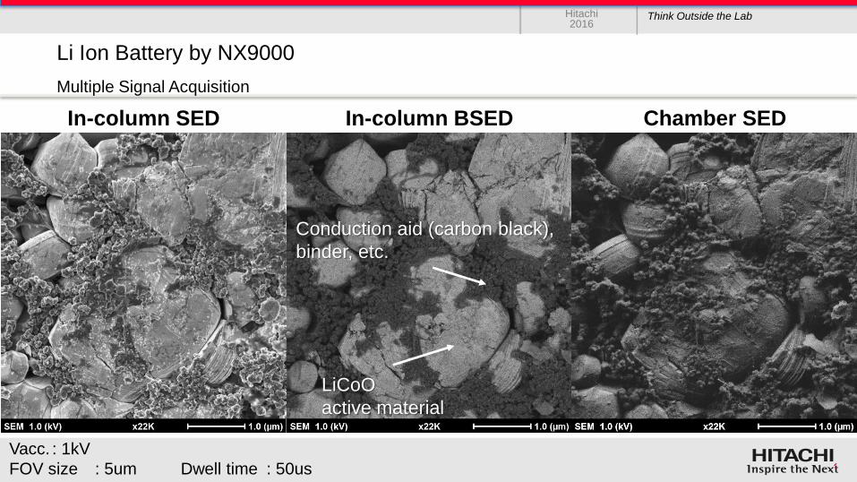
Multiple Signal Acquisition
Li Ion Battery by NX9000
In-column BSED
LiCoO
active material
Conduction aid (carbon black),
binder, etc.
Chamber SED In-column SED
Vacc. : 1kV
FOV size : 5um Dwell time : 50us
Hitachi 2016
Think Outside the Lab
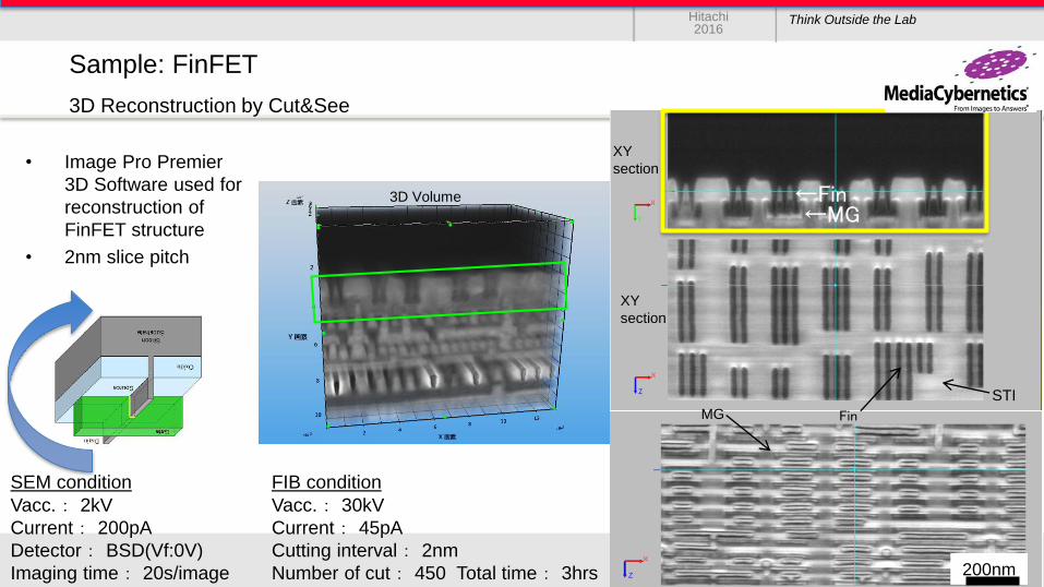
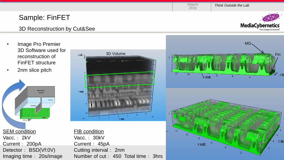
3D Reconstruction by Cut&See
• Image Pro Premier
3D Software used for
reconstruction of
FinFET structure
• 2nm slice pitch
Sample: FinFET
200nm
Fin MG
←Fin ←MG
STI
XY
section
SEM condition FIB condition
Vacc.: 2kV Vacc.: 30kV
Current: 200pA Current: 45pA
Detector: BSD(Vf:0V) Cutting interval: 2nm
Imaging time: 20s/image Number of cut: 450 Total time: 3hrs
XY
section
3D Volume
Hitachi 2016
Think Outside the Lab
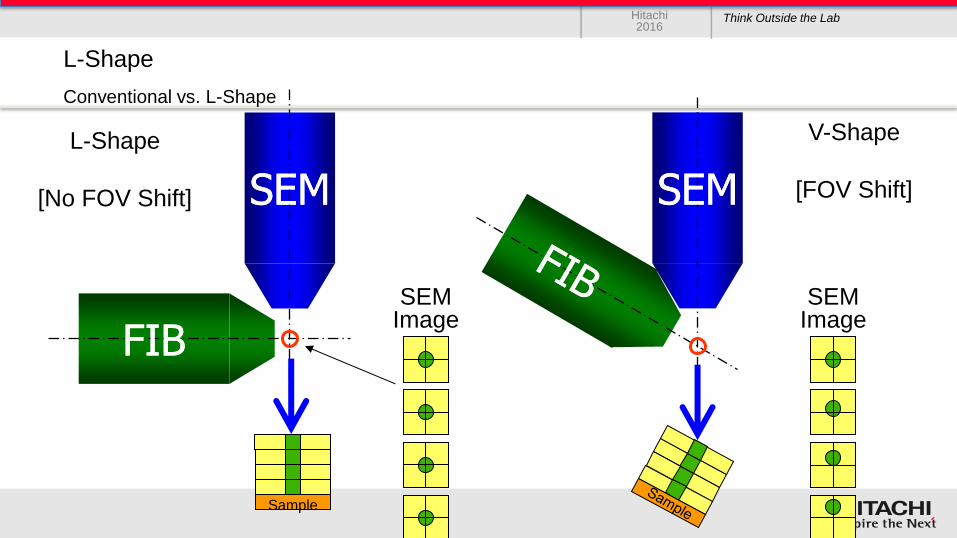
L-Shape
SEM
FIB
SEM
Sample
FIB
SEM SEM
SEM Image
SEM Image
Conventional vs. L-Shape
V-Shape
[FOV Shift]
L-Shape
[No FOV Shift]
Hitachi 2016
Think Outside the Lab
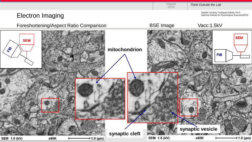
Foreshortening/Aspect Ratio Comparison
Electron Imaging
synaptic vesicle synaptic cleft
mitochondrion
BSE Image Vacc:1.5kV
Sample courtesy: Yoshiyuki Kubota, Ph.D.
National Institute for Physiological Sciences(NIPS)
Hitachi 2016
Think Outside the Lab
3D Reconstruction by Cut&See
• Image Pro Premier
3D Software used for
reconstruction of
FinFET structure
• 2nm slice pitch
Sample: FinFET
SEM condition FIB condition
Vacc.: 2kV Vacc.: 30kV
Current: 200pA Current: 45pA
Detector: BSD(Vf:0V) Cutting interval: 2nm
Imaging time: 20s/image Number of cut: 450 Total time: 3hrs
3D Volume
MG
Fin
Hitachi 2016
Think Outside the Lab
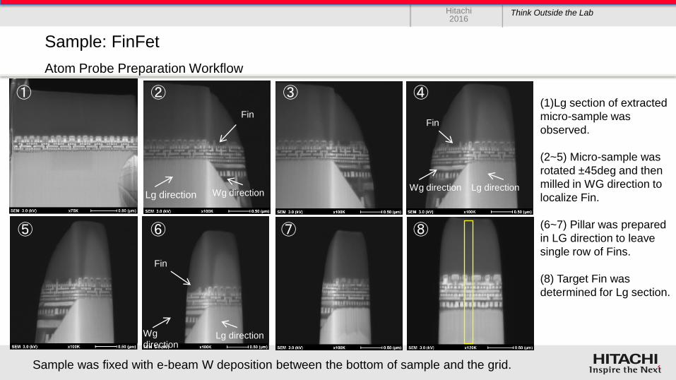
Atom Probe Preparation Workflow
Sample: FinFet
① ② ③ ④
⑤
Lg direction Wg direction
Fin Fin
Wg direction Lg direction
⑦ ⑧ ⑥
Wg
direction Lg direction
Fin
(1)Lg section of extracted
micro-sample was
observed.
(2~5) Micro-sample was
rotated ±45deg and then
milled in WG direction to
localize Fin.
(6~7) Pillar was prepared
in LG direction to leave
single row of Fins.
(8) Target Fin was
determined for Lg section.
Sample was fixed with e-beam W deposition between the bottom of sample and the grid.
Hitachi 2016
Think Outside the Lab
In-column
SED
In-column
BSED
Retractable
BSED
STEM detector
Chamber SED BSED
DF-STEM SED (in-column)
Multiple Signal Acquisition
Transmission Electron Imaging
Vacc: 25kV
E-beam: 270pA
Ga milling at 5kV
I-beam: 40pA
Hitachi 2016
Think Outside the Lab
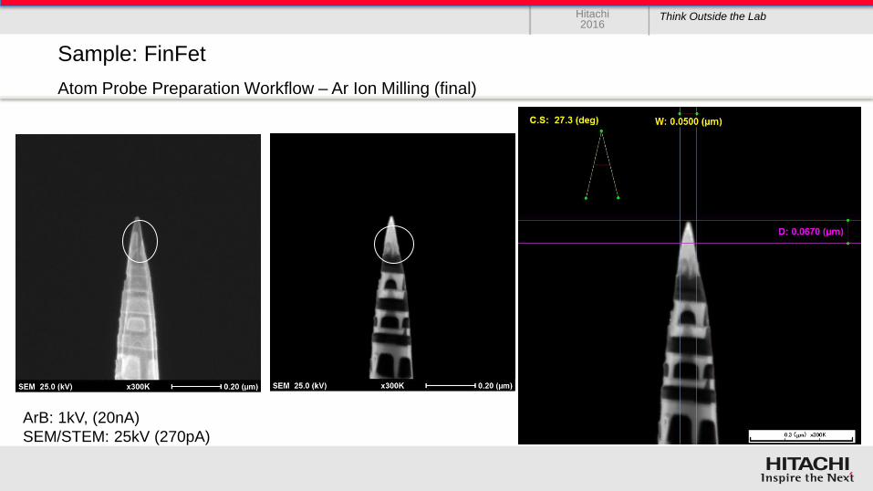
Atom Probe Preparation Workflow – Ar Ion Milling (final)
Sample: FinFet
ArB: 1kV, (20nA)
SEM/STEM: 25kV (270pA)
Hitachi 2016
Think Outside the Lab
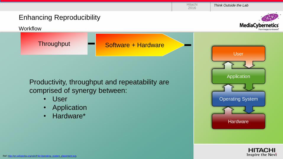
Workflow
Enhancing Reproducibility
Throughput Software + Hardware
Productivity, throughput and repeatability are
comprised of synergy between:
• User
• Application
• Hardware*
Ref: http://en.wikipedia.org/wiki/File:Operating_system_placement.svg
Hitachi 2016
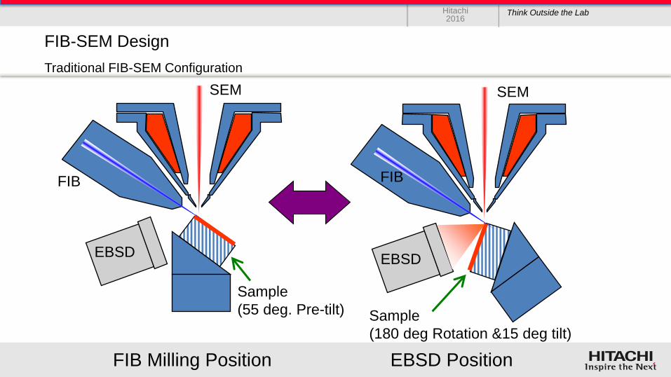
Think Outside the Lab
Traditional FIB-SEM Configuration
FIB-SEM Design
EBSD
Sample
(180 deg Rotation &15 deg tilt)
EBSD
FIB Milling Position EBSD Position
Sample
(55 deg. Pre-tilt)
FIB FIB
SEM SEM
Hitachi 2016
Think Outside the Lab
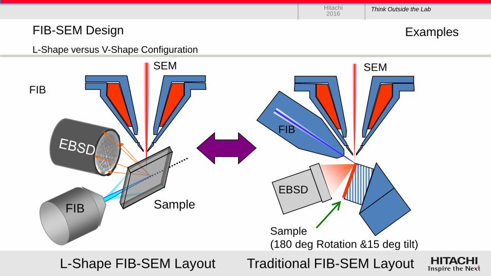
L-Shape versus V-Shape Configuration
FIB-SEM Design
EBSD
Sample
(180 deg Rotation &15 deg tilt)
L-Shape FIB-SEM Layout Traditional FIB-SEM Layout
FIB
FIB
SEM SEM
FIB FIB Sample
Examples
Hitachi 2016
Think Outside the Lab
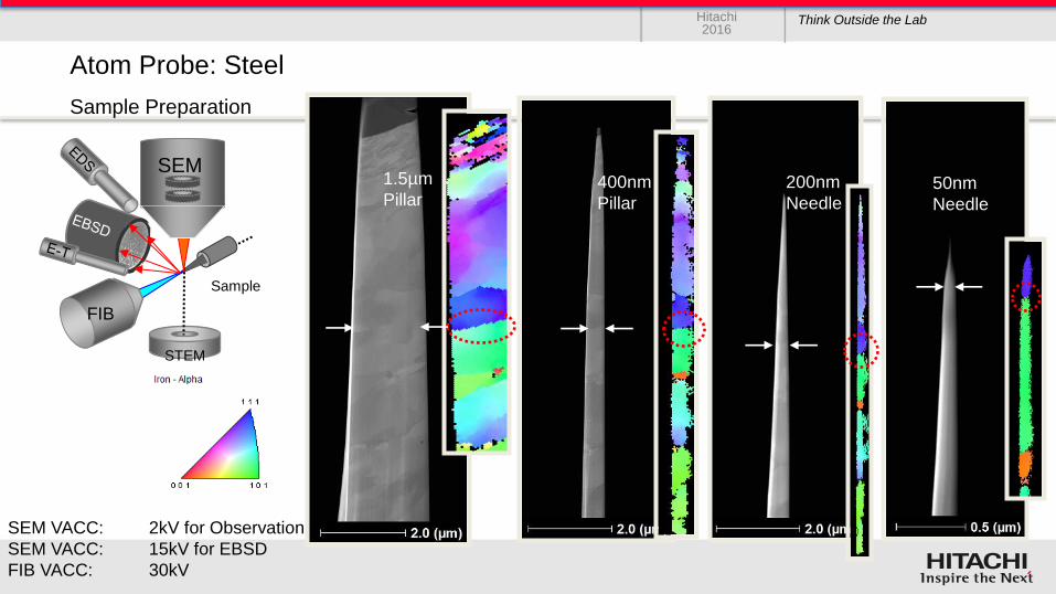
Sample Preparation
Atom Probe: Steel
STEM
Sample
FIB
SEM 1.5µm
Pillar 400nm
Pillar
200nm
Needle 50nm
Needle
SEM VACC: 2kV for Observation
SEM VACC: 15kV for EBSD
FIB VACC: 30kV
Hitachi 2016
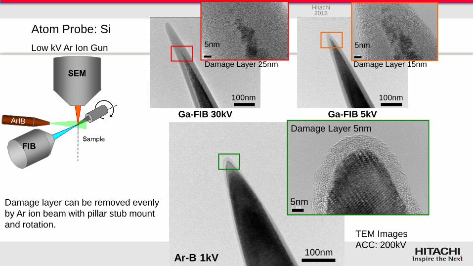
Think Outside the Lab
Low kV Ar Ion Gun
Atom Probe: Si
100nm 100nm
5nm 5nm
100nm
5nm
Ga-FIB 30kV
Damage Layer 25nm
Ga-FIB 5kV
Damage Layer 15nm
Ar-B 1kV
Damage Layer 5nm
TEM Images
ACC: 200kV
Damage layer can be removed evenly
by Ar ion beam with pillar stub mount
and rotation.
Hitachi 2016
Think Outside the Lab
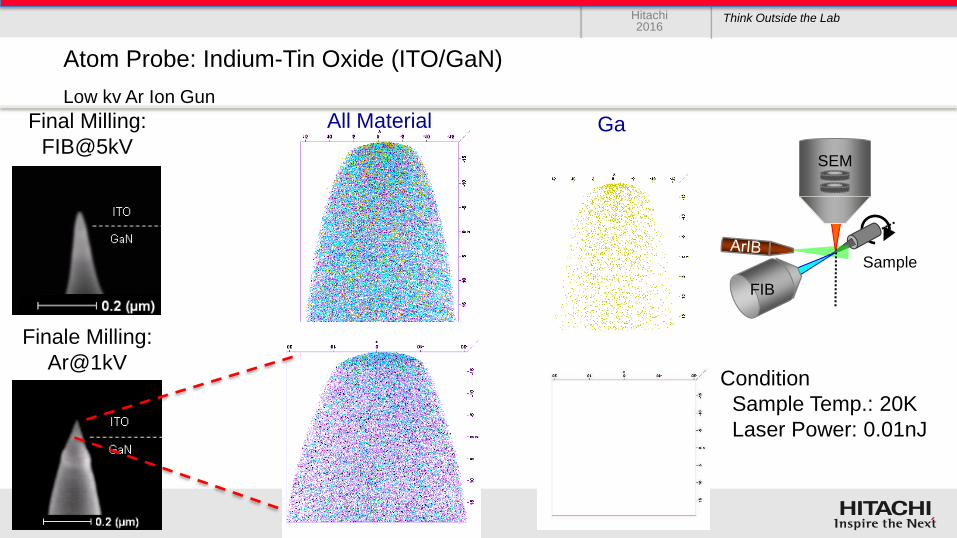
Low kv Ar Ion Gun
Atom Probe: Indium-Tin Oxide (ITO/GaN)
Final Milling:
FIB@5kV
Condition
Sample Temp.: 20K
Laser Power: 0.01nJ
All Material Ga
Sample
FIB
SEM
Finale Milling:
Ar@1kV
Hitachi 2016
Think Outside the Lab
Summary
• An orthogonal FIB-SEM platform delivers:
– Optimized coincident point for best SEM imaging
– Geometry of sample and detectors eliminate limitations found in V-shaped FIB-SEM systems
– Orthogonal column arrangement yields high precision segmentation imaging and analytical 3D
applications.
– Normal incident SEM imaging eliminates aspect deformation and foreshortening
– Software + Hardware synergy through advanced automation and application specific development
of modifiable “Apps” are possible for atom probe preparation techniques and several other
applications.
Orthogonal FIB-SEM
Hitachi 2016
Think Outside the Lab NX9000 FIB-SEM System
Recommended