OPTIMIZED SEMI-ADDITIVE PROCESS FOR POLYIMIDE AS
DIELECTRIC IN BUILD UP PACKAGES
Fei Peng1, Ernest Long1, Jim Watkowski1, Kesheng Feng1, Naomi Ando2, Kazuhiro Inazu2 1 MacDermid, 227 Freight St, Waterbury, CT 06702, USA
2 Nippon MacDermid, KSP C-7F, 3-2-1 Sakado, Takatsu-ku, Kawasaki-shi, Kanagawa-ken, 213-0012, Japan
Abstract
Higher functionality, higher performance and miniaturization are the mantras of any electronic device, and the future
guarantees more of the same. To achieve the requirements of these devices, designs must incorporate laser drilled blind
microvias, tighter pitch, finer lines while maintaining good circuitry adhesion and improving signal integrity. Semi-Additive
Process (SAP) is a production proven method used on build up materials that enables the manufacture of ultra fine circuitry.
The standard SAP process utilizes some roughening or texturing of the dielectric substrate in order to achieve
sufficient adhesion. However rough surface negatively impacts signal integrity. The amount and size of the dielectric filler
have an impact on adhesion as well. Filler-less dielectric material that possesses good chemical resistance, excellent thermal
stability and low dielectric constants are being considered as replacements for conventional build up material. One of these
materials is polyimide (PI).
This paper will discuss an optimized SAP process for PI film with low desmear roughness (Ra< 60nm) and excellent
adhesion after 7 day baking test at 150°C (500-1100gf/cm depending on different polyimide substrates). Along with the
process flow, discussion will include characterization and analysis of the polyimide, metal plating topography using scanning
electron microscopy, their compositions using energy dispersive X-ray spectroscopy and adhesion from 90o peel tests.
1. Introduction
Mobile phones, tablets and other hand held devices are pushing technology to new heights. These devices continue
to add greater functionality while decreasing in size. This miniaturization demands tighter pitch, finer lines and better signal
integrity. Nowhere is this clearer than in the IC substrate market. Semi-Additive Processing or SAP has been widely used in
the manufacture of tighter pitch and finer lines for many years, however with the growing need to maintain and improve
signal integrity, different dielectric materials are being evaluated.
One of these materials is polyimide (PI), and although not new to the industry, PI shows good chemical resistance,
low moisture adsorption and good UV absorption. In addition, PI has excellent thermal stability, low dielectric constant and
good processability. These unique chemical, mechanical and electronic properties make PI one of the best candidates for
interlayer dielectric. Moreover, PI film is one of the most popular dielectric materials for flexible printed circuitry (FPC),
which proliferate rapidly to replace traditional wire harnesses. With special properties of PI film, PI based FPC shows many
benefits compared to traditional cabling and rigid boards. Physically, it presents smaller size and weight as well as better
thermal stability and wider operating temperature. Regarding electronic properties, it provides higher wiring accuracy and
circuit density, stronger signal quality, better reliability and impedance control. In addition, it shows good design flexibility
and enables the elimination of mechanical connectors.
MacDermid developed an optimized semi-additive process (SAP-PI), which was tailored for PI film in build up
application. This SAP-PI combined low-roughness desmear and efficient conditioning processes for adhesion promotion on
very smooth surface. After desmear, the PI surface showed Ra <60 nm, while achieving initial peel strengths between 900-
1700 gf/cm on different commercial PI substrates. After being baked at 150 oC for 7 days, the peel strength can be
maintained between 500-1100 gf/cm. This paper discusses an optimized process flow and associated steps in detail to
alleviate concerns on processing complexity. It includes characterization and analysis on PI and metal plating topography
using scanning electron microscopy (SEM), their compositions using energy dispersive X-ray spectroscopy (EDX), and PI-
plating adhesion from 90o peel tests.
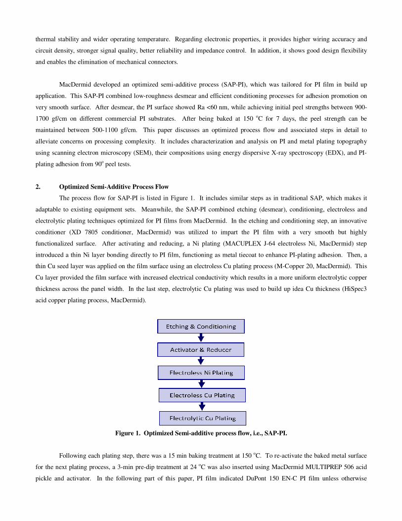
2. Optimized Semi-Additive Process Flow
The process flow for SAP-PI is listed in Figure 1. It includes similar steps as in traditional SAP, which makes it
adaptable to existing equipment sets. Meanwhile, the SAP-PI combined etching (desmear), conditioning, electroless and
electrolytic plating techniques optimized for PI films from MacDermid. In the etching and conditioning step, an innovative
conditioner (XD 7805 conditioner, MacDermid) was utilized to impart the PI film with a very smooth but highly
functionalized surface. After activating and reducing, a Ni plating (MACUPLEX J-64 electroless Ni, MacDermid) step
introduced a thin Ni layer bonding directly to PI film, functioning as metal tiecoat to enhance PI-plating adhesion. Then, a
thin Cu seed layer was applied on the film surface using an electroless Cu plating process (M-Copper 20, MacDermid). This
Cu layer provided the film surface with increased electrical conductivity which results in a more uniform electrolytic copper
thickness across the panel width. In the last step, electrolytic Cu plating was used to build up idea Cu thickness (HiSpec3
acid copper plating process, MacDermid).
Figure 1. Optimized Semi-additive process flow, i.e., SAP-PI.
Following each plating step, there was a 15 min baking treatment at 150 oC. To re-activate the baked metal surface
for the next plating process, a 3-min pre-dip treatment at 24 oC was also inserted using MacDermid MULTIPREP 506 acid
pickle and activator. In the following part of this paper, PI film indicated DuPont 150 EN-C PI film unless otherwise
specified. This PI film was chosen to compare traditional SAP and optimized SAP-PI regarding PI-plating adhesion. The
influence of each processing step was demonstrated and discussed as the following.
3. Results and Discussions
3.1. Etching and Conditioning
With optimized SAP-PI, etching and conditioning of the PI film is conducted at lower caustic solution (NaOH wt%
as low as 5~10) and a lower and wider temperature range (from room temperature to 70 oC) for a short time of 2~5 min. It is
much milder condition compared to traditional SAP for PI material, which normally uses a more concentrated NaOH solution
up to 25 wt% at temperature like 70 oC or even higher. As a result, in our studies, the PI film after SAP-PI etching and
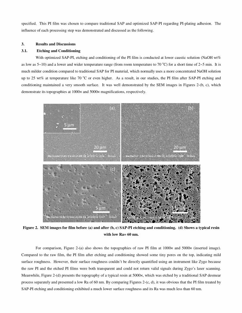
conditioning maintained a very smooth surface. It was well demonstrated by the SEM images in Figures 2-(b, c), which
demonstrate its topographies at 1000× and 5000× magnifications, respectively.
Figure 2. SEM images for film before (a) and after (b, c) SAP-PI etching and conditioning. (d) Shows a typical resin
with low Ra= 60 nm.
For comparison, Figure 2-(a) also shows the topographies of raw PI film at 1000× and 5000× (inserted image).
Compared to the raw film, the PI film after etching and conditioning showed some tiny pores on the top, indicating mild
surface roughness. However, their surface roughness couldn’t be directly quantified using an instrument like Zygo because
the raw PI and the etched PI films were both transparent and could not return valid signals during Zygo’s laser scanning.
Meanwhile, Figure 2-(d) presents the topography of a typical resin at 5000×, which was etched by a traditional SAP desmear
process separately and presented a low Ra of 60 nm. By comparing Figures 2-(c, d), it was obvious that the PI film treated by
SAP-PI etching and conditioning exhibited a much lower surface roughness and its Ra was much less than 60 nm.
��µ��
���µ��
����
���µ��
���
��µ�� ��µ��
��� ����
3.2. Electroless Ni Plating
Following etching and conditioning, direct metallization processes were utilized to build up PI-metal laminate. To
apply tiecoat and seed Cu coating on PI film, there are two popular techniques, sputter deposition and electroless plating.
Sputter deposition method is simple but costly, which limits its use in production. In the optimized SAP-PI, an electroless Ni
(MACUPLEX J-64, MacDermid) was used to introduce a thin layer of Ni serving as the tiecoat. This Ni plating process was
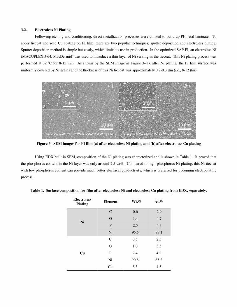
performed at 39 oC for 8-15 min. As shown by the SEM image in Figure 3-(a), after Ni plating, the PI film surface was
uniformly covered by Ni grains and the thickness of this Ni tiecoat was approximately 0.2-0.3 µm (i.e., 8-12 µin).
Figure 3. SEM images for PI film (a) after electroless Ni plating and (b) after electroless Cu plating
Using EDX built in SEM, composition of the Ni plating was characterized and is shown in Table 1. It proved that
the phosphorus content in the Ni layer was only around 2.5 wt%. Compared to high-phosphorus Ni plating, this Ni tiecoat
with low phosphorus content can provide much better electrical conductivity, which is preferred for upcoming electroplating
process.
Table 1. Surface composition for film after electroless Ni and electroless Cu plating from EDX, separately.
Electroless Plating Element Wt.% At.%
Ni
C 0.6 2.9
O 1.4 4.7
P 2.5 4.3
Ni 95.5 88.1
Cu
C 0.5 2.5
O 1.0 3.5
P 2.4 4.2
Ni 90.8 85.2
Cu 5.3 4.5
���� ���
���µ�����µ��
��µ�� ��µ��
3.3. Electroless Cu Plating
In order to further promote the electrical conductivity of the film surface, and electroless Cu plating (M-Copper 20,
MacDermid) was applied on top of the Ni layer. As shown in Figure 3-(b), the Cu seeds were much smaller than Ni grains
and homogeneously distributed on the Ni surface. This Cu layer was as thin as 0.05 µm (~2 µin), so the EDX data from its
surface (Table 1) still showed Ni signal in majority and only 5.3 wt% Cu. Nevertheless, this thin Cu seed layer together with
low phosphorus Ni tiecoat provided good conductivity on the PI surface for the final electrolytic Cu plating.
3.4. Electrolytic Cu Plating
In optimized SAP-PI, an electrolytic Cu plating process (HiSpec3 acid copper, MacDermid) was used to build up Cu
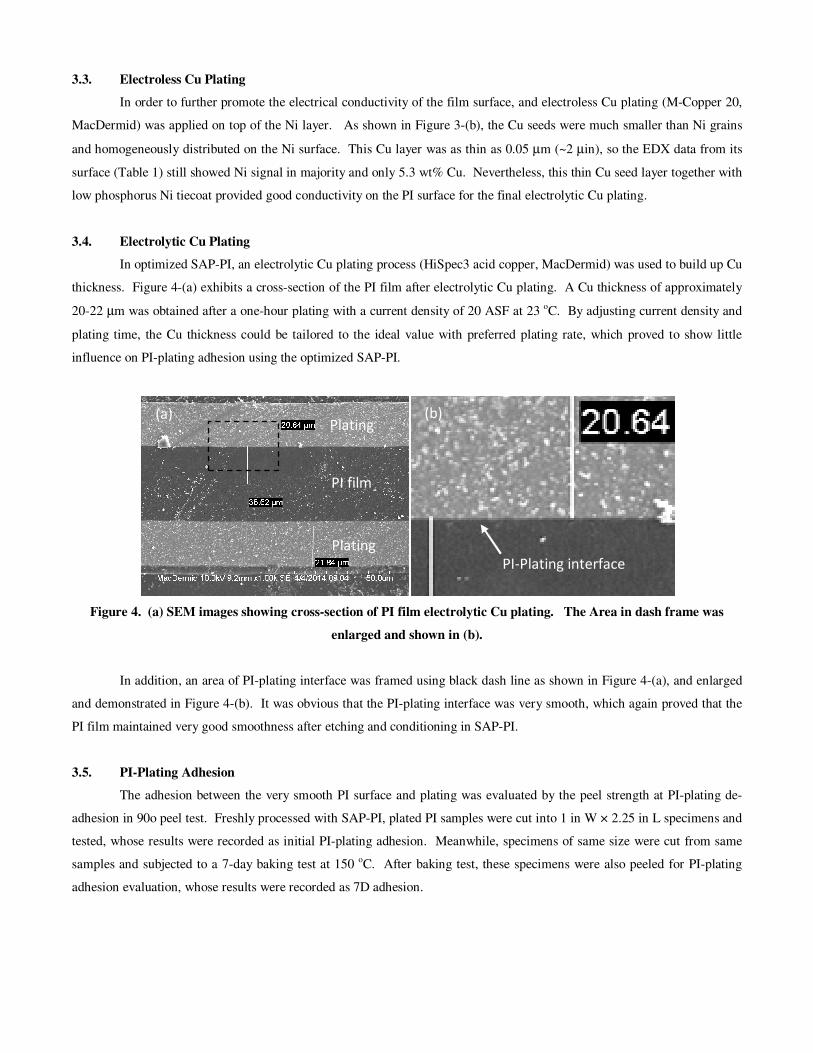
thickness. Figure 4-(a) exhibits a cross-section of the PI film after electrolytic Cu plating. A Cu thickness of approximately
20-22 µm was obtained after a one-hour plating with a current density of 20 ASF at 23 oC. By adjusting current density and
plating time, the Cu thickness could be tailored to the ideal value with preferred plating rate, which proved to show little
influence on PI-plating adhesion using the optimized SAP-PI.
Figure 4. (a) SEM images showing cross-section of PI film electrolytic Cu plating. The Area in dash frame was
enlarged and shown in (b).
In addition, an area of PI-plating interface was framed using black dash line as shown in Figure 4-(a), and enlarged
and demonstrated in Figure 4-(b). It was obvious that the PI-plating interface was very smooth, which again proved that the
PI film maintained very good smoothness after etching and conditioning in SAP-PI.
3.5. PI-Plating Adhesion
The adhesion between the very smooth PI surface and plating was evaluated by the peel strength at PI-plating de-
adhesion in 90o peel test. Freshly processed with SAP-PI, plated PI samples were cut into 1 in W × 2.25 in L specimens and
tested, whose results were recorded as initial PI-plating adhesion. Meanwhile, specimens of same size were cut from same
samples and subjected to a 7-day baking test at 150 oC. After baking test, these specimens were also peeled for PI-plating
adhesion evaluation, whose results were recorded as 7D adhesion.
� ������
� ������
����� ��
���� ���
���� ���������������
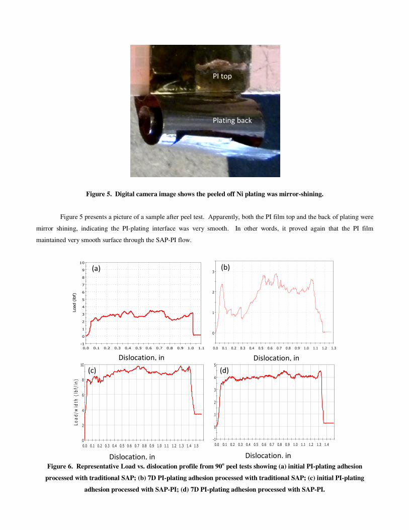
Figure 5. Digital camera image shows the peeled off Ni plating was mirror-shining.
Figure 5 presents a picture of a sample after peel test. Apparently, both the PI film top and the back of plating were
mirror shining, indicating the PI-plating interface was very smooth. In other words, it proved again that the PI film
maintained very smooth surface through the SAP-PI flow.
Figure 6. Representative Load vs. dislocation profile from 90o peel tests showing (a) initial PI-plating adhesion
processed with traditional SAP; (b) 7D PI-plating adhesion processed with traditional SAP; (c) initial PI-plating
adhesion processed with SAP-PI; (d) 7D PI-plating adhesion processed with SAP-PI.
��
�
�
�
�
�
�
�
�
��
��� ��� ��� ��� ��� ��� ��� �� �� ��� ��� ���
���������
��������������
�
�
�
�
��� ��� ��� ��� ��� ��� ��� �� �� ��� ��� ��� ��� ���
�������� ���������
��������������
�
�
�
�
��
��� ��� ��� ��� ��� ��� ��� �� �� ��� ��� ��� ��� ��� ��� ���
�������� ���������
��������������
��
�
�
�
�
�
�
��� ��� ��� ��� ��� ��� ��� �� �� ��� ��� ��� ��� ��� ���
�������� ���������
��������������
����
�������
� ���������
��� �������������� �����������
��� ����������� ��� �����������
���
���
����
����
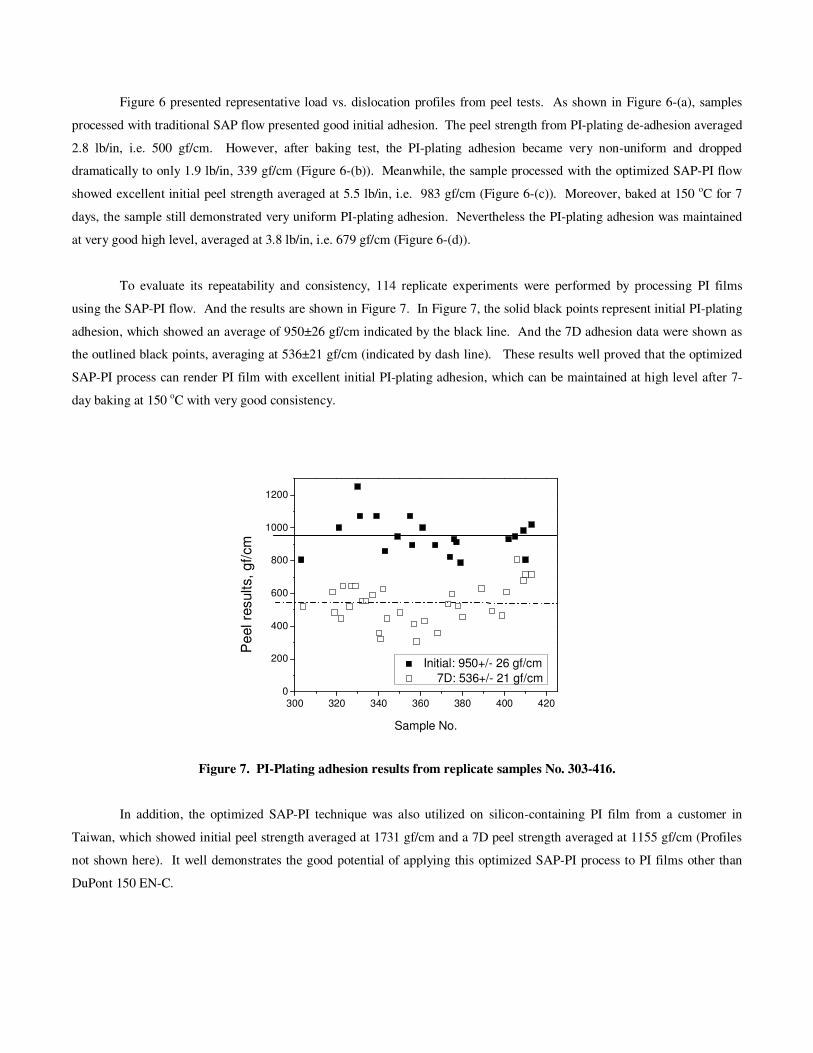
Figure 6 presented representative load vs. dislocation profiles from peel tests. As shown in Figure 6-(a), samples
processed with traditional SAP flow presented good initial adhesion. The peel strength from PI-plating de-adhesion averaged
2.8 lb/in, i.e. 500 gf/cm. However, after baking test, the PI-plating adhesion became very non-uniform and dropped
dramatically to only 1.9 lb/in, 339 gf/cm (Figure 6-(b)). Meanwhile, the sample processed with the optimized SAP-PI flow
showed excellent initial peel strength averaged at 5.5 lb/in, i.e. 983 gf/cm (Figure 6-(c)). Moreover, baked at 150 oC for 7
days, the sample still demonstrated very uniform PI-plating adhesion. Nevertheless the PI-plating adhesion was maintained
at very good high level, averaged at 3.8 lb/in, i.e. 679 gf/cm (Figure 6-(d)).
To evaluate its repeatability and consistency, 114 replicate experiments were performed by processing PI films
using the SAP-PI flow. And the results are shown in Figure 7. In Figure 7, the solid black points represent initial PI-plating
adhesion, which showed an average of 950±26 gf/cm indicated by the black line. And the 7D adhesion data were shown as
the outlined black points, averaging at 536±21 gf/cm (indicated by dash line). These results well proved that the optimized
SAP-PI process can render PI film with excellent initial PI-plating adhesion, which can be maintained at high level after 7-
day baking at 150 oC with very good consistency.
300 320 340 360 380 400 4200
200
400
600
800
1000
1200
Initial: 950+/- 26 gf/cm 7D: 536+/- 21 gf/cm
Pee
l res
ults
, gf/c
m
Sample No.
�
Figure 7. PI-Plating adhesion results from replicate samples No. 303-416.
In addition, the optimized SAP-PI technique was also utilized on silicon-containing PI film from a customer in
Taiwan, which showed initial peel strength averaged at 1731 gf/cm and a 7D peel strength averaged at 1155 gf/cm (Profiles
not shown here). It well demonstrates the good potential of applying this optimized SAP-PI process to PI films other than
DuPont 150 EN-C.
4. Conclusions
The optimized SAP-PI process combines new etching, conditioning and direct metallization techniques from
MacDermid. It contained similar steps like traditional SAP process, which makes it adaptable to existing equipment sets.
Moreover, the processed PI surface showed very low Ra, which was much less than 60 nm. In addition, the initial PI-plating
adhesion was achieved to 900-1700 gf/cm on different commercial PI substrates. After 7-day baking test at 150 oC, the PI-
plating adhesion can be maintained between 500-1100 gf/cm. In other words, the optimized SAP-PI can render excellent
initial and 7D adhesion on smooth PI. Therefore, it demonstrates great potential in manufacturing of PI based FPC and other
build-up packaging.
Recommended