
IAEA-TECDOC-1634
Signal Processing and Electronicsfor Nuclear Spectrometry
Proceedings of a Technical Meeting Vienna, 20–23 November 2007

Signal Processing and Electronics for Nuclear Spectrometry

The following States are Members of the International Atomic Energy Agency:
AFGHANISTANALBANIAALGERIAANGOLAARGENTINAARMENIAAUSTRALIAAUSTRIAAZERBAIJANBAHRAINBANGLADESHBELARUSBELGIUMBELIZEBENINBOLIVIABOSNIA AND HERZEGOVINABOTSWANABRAZILBULGARIABURKINA FASOBURUNDICAMEROONCANADACENTRAL AFRICAN REPUBLICCHADCHILECHINACOLOMBIACONGOCOSTA RICACÔTE D’IVOIRECROATIACUBACYPRUSCZECH REPUBLICDEMOCRATIC REPUBLIC OF THE CONGODENMARKDOMINICAN REPUBLICECUADOREGYPTEL SALVADORERITREAESTONIAETHIOPIAFINLANDFRANCEGABONGEORGIAGERMANY
GHANAGREECEGUATEMALAHAITIHOLY SEEHONDURASHUNGARYICELANDINDIAINDONESIAIRAN, ISLAMIC REPUBLIC OF IRAQIRELANDISRAELITALYJAMAICAJAPANJORDANKAZAKHSTANKENYAKOREA, REPUBLIC OFKUWAITKYRGYZSTANLATVIALEBANONLESOTHOLIBERIALIBYAN ARAB JAMAHIRIYALIECHTENSTEINLITHUANIALUXEMBOURGMADAGASCARMALAWIMALAYSIAMALIMALTAMARSHALL ISLANDSMAURITANIAMAURITIUSMEXICOMONACOMONGOLIAMONTENEGROMOROCCOMOZAMBIQUEMYANMARNAMIBIANEPALNETHERLANDSNEW ZEALANDNICARAGUANIGER
NIGERIANORWAYOMANPAKISTANPALAUPANAMAPARAGUAYPERUPHILIPPINESPOLANDPORTUGALQATARREPUBLIC OF MOLDOVAROMANIARUSSIAN FEDERATIONSAUDI ARABIASENEGALSERBIASEYCHELLESSIERRA LEONESINGAPORESLOVAKIASLOVENIASOUTH AFRICASPAINSRI LANKASUDANSWEDENSWITZERLANDSYRIAN ARAB REPUBLICTAJIKISTANTHAILANDTHE FORMER YUGOSLAV REPUBLIC OF MACEDONIATUNISIATURKEYUGANDAUKRAINEUNITED ARAB EMIRATESUNITED KINGDOM OF GREAT BRITAIN AND NORTHERN IRELANDUNITED REPUBLIC OF TANZANIAUNITED STATES OF AMERICAURUGUAYUZBEKISTANVENEZUELAVIETNAMYEMENZAMBIAZIMBABWE
The Agency’s Statute was approved on 23 October 1956 by the Conference on the Statute of the IAEAheld at United Nations Headquarters, New York; it entered into force on 29 July 1957. The Headquarters of theAgency are situated in Vienna. Its principal objective is “to accelerate and enlarge the contribution of atomicenergy to peace, health and prosperity throughout the world’’.

IAEA-TECDOC-1634
Signal Processing and Electronics for Nuclear Spectrometry
PROCEEDINGS OF A TECHNICAL MEETING VIENNA, 20–23 NOVEMBER 2007
INTERNATIONAL ATOMIC ENERGY AGENCY VIENNA, 2009

COPYRIGHT NOTICE
All IAEA scientific and technical publications are protected by the terms of the Universal Copyright Convention as adopted in 1952 (Berne) and as revised in 1972 (Paris). The copyright has since been extended by the World Intellectual Property Organization (Geneva) to include electronic and virtual intellectual property. Permission to use whole or parts of texts contained in IAEA publications in printed or electronic form must be obtained and is usually subject to royalty agreements. Proposals for non-commercial reproductions and translations are welcomed and considered on a case-by-case basis. Enquiries should be addressed to the IAEA Publishing Section at: Sales and Promotion, Publishing Section International Atomic Energy Agency Vienna International Centre PO Box 100 1400 Vienna, Austria fax: +43 1 2600 29302 tel.: +43 1 2600 22417 email: [email protected] http://www.iaea.org/books
For further information on this publication, please contact:
Physics Section International Atomic Energy Agency
Vienna International Centre PO Box 100
1400 Vienna, Austria email: [email protected]
SIGNAL PROCESSING AND ELECTRONICS FOR NUCLEAR SPECTROMETRY
IAEA, VIENNA, 2009 IAEA-TECDOC-1634
ISBN 978-92-0-112809-6 ISSN 1011-4289
© IAEA, 2009 Printed by the IAEA in Austria
December 2009
FOREWORD
The IAEA has responded to Member States needs by implementing programmatic activities that provide interested Member States, particularly those in developing countries, with support to increase, and in some cases establish national and regional capabilities for the proper operation, calibration, maintenance and utilization of instruments in nuclear spectrometry applications. Technological advances in instrumentation, as well as the consequent high rate of obsolescence, make it important for nuclear instrumentation laboratories in Member States to keep their knowledge and skills up to date. This publication reviews the current status, developments and trends in electronics and digital methods for nuclear spectrometry, providing useful information for interested Member States to keep pace with new and evolving technologies.
All nuclear spectrometry systems contain electronic circuits and devices, commonly referred to as front-end electronics, which accept and process the electrical signals produced by radiation detectors. This front-end electronics are composed of a chain of signal processing subsystems that filter, amplify, shape, and digitise these electrical signals to finally produce digitally encoded information about the type and nature of the radiation that stimulated the radiation detector. The design objective of front-end electronics is to obtain maximum information about the radiation and with the highest possible accuracy.
Historically, the front-end electronics has consisted of all analog components. The performance delivered has increased continually over time through the development and implementation of new and improved analog electronics and electronic designs. The development of digital electronics, programmable logic, and digital signal processing techniques has now enabled most of the analog front-end electronics to be replaced by digital electronics, opening up new opportunities and delivering new benefits not previously achievable. Digital electronics and digital signal processing methods are enabling advances in numerous spectrometry applications such as lightweight, portable and hand held radiation instruments, and high-resolution digital medical imaging systems.
The objective of this technical meeting was to review the current status, developments and trends in nuclear electronics and signal processing, and their application with various radiation detectors. The meeting discussed the problems faced and the solutions employed, to improve the performances of data acquisition systems and high-tech equipment used for nuclear spectrometry. Presentations made at the meeting elaborated operational experiences with modern signal processing and electronics, and highlighted the latest developments in this field. This publication summarizes the findings and conclusions arising from this technical meeting.
The IAEA wishes to express its appreciation to all those who contributed to the production of this publication, and especially to M. Bogovac, who revised and finalized the manuscript. The IAEA officer responsible for this publication was N. Dytlewski of the Division of Physical and Chemical Science.
EDITORIAL NOTE
The papers in these proceedings are reproduced as submitted by the authors and have not undergone rigorous editorial review by the IAEA.
The views expressed do not necessarily reflect those of the IAEA, the governments of the nominating Member States or the nominating organizations.
The use of particular designations of countries or territories does not imply any judgement by the publisher, the IAEA, as to the legal status of such countries or territories, of their authorities and institutions or of the delimitation of their boundaries.
The mention of names of specific companies or products (whether or not indicated as registered) does not imply any intention to infringe proprietary rights, nor should it be construed as an endorsement or recommendation on the part of the IAEA.
The authors are responsible for having obtained the necessary permission for the IAEA to reproduce, translate or use material from sources already protected by copyrights.
CONTENTS
Summary .................................................................................................................................... 1 CONTRIBUTED PAPERS A digital signal processing system for neutron-gamma discrimination in neutron time of flight measurements ........................................................................................... 11 A.R. Behere, P.K. Mukhopadhyaya Implementation of digital signal processor for nuclear spectrometry using state of the art tools ............................................................................................... 17 M. Bogavac, D. Wegrzynek, A. Markowicz Positron annihilation spectroscopy: Digital vs. Analog signal processing .............................. 29 D. Bosnar Digital signal processing techniques for image reconstruction with X ray position sensitive detectors ........................................................................... 39 J.M. Cardoso, S.R. Pereira, J.M.F. Santos, L.P. Fernandes, J.B. Simões Features of position sensitive neutron detectors ...................................................................... 49 F. Füzi, G. Török Possibilities of laboratory instrument upgrading by use of digital signal processors or field programmable gate arrays .................................................................................. 63 M. Smailou, Z. Mindaoudou Souley Problems faced in operating and maintaining nuclear spectroscopy systems in the United Republic of Tanzania .................................................................................... 67 Y.Y. Sungita, S.L.C. Mdoe, R.A. Kawala, A. Muhulo Problems in supporting high-tech digital equipment ............................................................... 73 F. Bartsch A high speed time-stamping and histogramming data acquisition system for position encoded data................................................................................................ 75 J.A. Mead, F. Bartsch A study of factors affecting the quality of measurements in gamma spectrometry
counting systems............................................................................................................. 81 Yii Mei-Wo, Z. Ahmad, I. Mansor Problems with maintaining nuclear instrumentation in Peru ................................................... 93 R. Ruiz List of participants.................................................................................................................... 97

SUMMARY
1. INTRODUCTION
The ultimate goal of nuclear spectrometry signal processing is to produce digital signals that exactly describe the properties of radiation and radiation-induced events. In a typical nuclear spectrometry experiment, the energy of radiation, or a charged particle, is measured in such a way that its energy is absorbed in solid state, proportional or scintillation detector, and converted into a pulse of electrical charge. Apart from the energy, this pulse may also contain information about the type of radiation or particle, its position, time of arrival, etc. In all cases, the electrical pulse is degraded and contaminated with noise during its passage through non-ideal front-end electronic components. The noise power spectral density can be predicted by numerical modeling all components in the signal processing chain.
According to the linear system theory, an optimal filter [1] can be designed whose output has the best signal to noise ratio, and which the amplitude is proportional to the measured physical value. For example, it is well known that cusp filtering is the optimal filter shape for exponential input signals, and which are produced by standard charge-sensitive preamplifier with resistive elements in the feedback. In practice, usually only close to optimal filtering, or shaping of the signal from the detector can be realized.
For a long time, the close to optimal filtering, that is, pulse processing, was only possible to perform with analog components. For example, classical spectrometry amplifiers with Gaussian pulse shaping have been used for more than 40 years. Due to the development of fast analog to digital converters (ADCs), field programmable gate arrays (FPGAs), and digital signal processors (DSPs) during the last few decades, it has become possible to digitize pulses even after preamplifier or phototube, and process them in a real time. The FPGA can handle the readout, trigger decisions, and simple to medium levels of complexity of signal processing. Dependent on the input-output and processing requirements, the FPGA can be replaced or augmented by DSPs for calculations that are more complex. Therefore, the digital electronics, which was limited to the control of the acquisition process and data storage, has become feasible for signal processing as well. This immediately opened possibilities to design instruments with relatively high component density at a reasonable cost per channel. Such instruments could implement many analog processing functions like pulse discrimination, pulse amplitude filtering, pile-up correction, and base-line restoration.
As soon as the performance of ADCs and FPGAs reached a level suitable for digital pulse processing, numerous standardized NIM (nuclear instrumetation module), CAMAC (computer automated measurement and control), FASTBUS and VME (VERSA-Module Europe) modules and stand-alone instruments appeared on the market. The benefits due to reduced size electronic circuitry were first seen in high-energy physics, where hundreds or even thousands of channels are used. Previous design constraints that sacrifice performance to meet compactness and low power requirements are no longer necessary.
The possibilities of DSP techniques were soon explored in nuclear spectrometry, and the first digital pulse processors for X and γ- ray spectrometry appeared on the market in the middle of the 1990s, utilizing published some theoretical works e.g. [2], and patents. In late 1996, one of the leading commercial companies introduced first digital gamma ray spectrometer as a stand-alone unit, that employed digital technology to analyze the preamplifier's pulses from all types of germanium and silicon detectors. Shortly afterward, commercial competitors also released their proprietary versions of DSP systems. Subsequent to these initial offerings, DSP systems were upgraded, repackaged, and released mostly as stand-alone units. All these
1
systems effectively combine the functionality of the amplifier and ADC in the traditional analog systems, and some of them included also high voltage power supplies. Several smaller companies have gradually developed very compact digital systems that comprise detector, preamplifier, and digital pulse processor all in one. Comparative studies of these systems [3, 4, 5] has confirmed the equal or better performance of digital systems over analog systems in terms of stability, resolution, differential non-linearity and throughput. Digital systems were found to be able to provide a higher throughput and at a similar or better resolution than analog systems.
In order to more completely realize the full potential of nuclear spectrometry systems, many small laboratories have found these advanced digital techniques very suitable for custom made signal processing. Several such designs are presented in the following sections of this document, along with problems faced and solutions employed to improve performance.
2. ADVANTAGES AND NEW CAPABILITIES OF DIGITAL TECHNOLOGY
This section summarizes the state of the art equipment and signal processing, including the advantages and new capabilities of digital technology, disadvantages of replacing analog technology by digital and extra performance that could be obtained by using digital technology. Several important advantages of using digital technology instead analog technology are described.
Energy resolution: Electrical signals are digitized earlier, therefore less analog components are used which should improve noise immunity and temperature stability giving potentially better resolution. Digital filter design techniques provide a high degree of freedom, which may result in better noise suppression and better resolution (optimal or close to optimal filtering). Throughput: Usually the pulses from the detector are not coming uniform in time and the time of arrival cannot be predicted. In the case of high counting rates, two or more pulses can overlap with high probability (pile-up). Using analog circuits, it is very difficult to separate them, and one or more pulses should be rejected which decreases number of processed events, that is, system throughput. In order to keep the throughput high, one can decrease pulse width, but it will compromise energy resolution since pulse shape will be far more from optimal. Since digital pileup rejection is more efficient, it will result in a higher throughput. Reduced size: Higher density and lower supply voltage integrated circuits reduce size and improves portability of nuclear spectrometry systems. This may be very important for in situ applications such as space research, mining, cultural heritage, etc. In laboratory conditions, and for experiments with a large number of detectors, it may reduce the number of cables, crates, and costs. State of the art equipment for nuclear spectrometry can be as small as a desktop size instrument, or as large as an accelerator. They are usually expensive and technically complex.
Easy upgrading and secure of intellectual properties: Most of today’s programmable logic are configured on power and can be in-circuit reprogrammed. This means that any change in design can be done without any soldering or
2
removing of vital components. In addition, the logic is protected against any reverse engineering which secures the design from illegal copying. Automation of critical adjustments: Very often, several parameters in a spectrometry system should be adjusted in order to set up conditions best suited for a particular detector type. For this reason, most analog systems have various knobs, switches, or screw positions that should be changed and which often require operator expertise for best selection. In contrary to this, digital systems can be programmed to do critical adjustments while internal module settings can be saved and recorded on a hard disk. In the case of complex experimental setups, this feature can minimize setup errors. Multifunction operation: Similar to the upgrading, the in-circuit reprogramming enables digital systems to be re-configured and adapted for new applications or incorporate several functions in parallel. For example, a digital spectrometer may feature a multichannel analyzer, multichannel scaling and oscilloscope simultaneously. Good version control: Components of digital filters are parameter coefficients stored in memory or registers. This guaranties that filter properties will not vary from one instrument to the other. Also, the precision of filters depends on the precision of its coefficients, while in the analog filters it depends on the precision of fixed electric components which may slowly change over time. Self-test and diagnostics capability: It is common for standalone nuclear spectrometry instruments to have implemented a number of hardware and software diagnostics to identify the nature of any fault in the operation of the instrument, e.g. dc line faults, low internal battery voltage, detector faults, mains failure, microprocessor faults, etc. Synchronization and control of the complete data acquisition environment: Data acquisition using digital electronics differs from event-driven acquisition using analog electronics and traditional ADCs. The input signal is continuously sampled and the quantity of interest is extracted for each pulse. Event processing may be internally or externally triggered. In the first case, processing is initiated whenever the signal meets certain criteria, which can be as simple as a threshold. In the second case, many modules can be synchronized among themselves. Every packet of information can be time stamped with an internal clock value, formatted, and put into an output buffer for a delayed readout. The data buffers are then retrieved by a main data acquisition computer. Ability to implement adaptive shaping: The shaping time constant, that is, the time-length of the filter, may depend on the time between successive pulses. Thus, for a pulse that is closely followed by a successive pulse, a very short shaping constant can be used, whereas for a pulse that is essentially isolated, a much longer shaping constant is used. This results in a system that suffers much less pileup than conventional systems, allowing higher throughput. The other possibility is to adapt the filter shape and its coefficients to the shape of the pulse in order to correct pulse deficiency, and allow better resolution.
3
3. DISADVANTAGES OF REPLACING ANALOG TECHNOLOGY BY DIGITAL
Apart from the advantages, digital techniques still have some disadvantages from the technical and human point of view. Limited amplitude precision: The value of the measured amplitude depends on quantization precision and sampling rate. Usually, higher sampling rate results in lower quantization. Rounding effect: Some kinds of digital filters (e.g. infinite impulse response) may have stability problems due to rounding errors that are caused by finite precision mathematical operations. Complex, expansive and specialized design tools: In order to perform mathematically complex digital filtering using FPGAs, one should have a good working knowledge of the hardware description language and FPGA architectures. Some user friendly tools, like the Xilinx, Inc. System Generator bundled with Matlab® and Simulink®, offers FPGA programming on the level of ready to use drag and drop boxes which features complex mathematical operations. However, purchase costs can be high (greater than $US 10 000) for a single user license. DSP vendors have theirs own development tools that may differ in functionality considerably between versions backward incompatibilities. Maintaining and repairing: Many of the electronic components in DSP systems are non-functional if not configured and so a simple replacement would not fix the fault component. Also, the complexity of circuits makes detection of the fault component difficult to locate. Furthermore, a lack of documentation and adequate training, especially for developing countries, may prevent any possibility of local repair, necessitating that the equipment either must be replaced completely or sent to the vendor for repair, both of which are costly financially and time-wise. No adequate specialized training in spectrometry: In contrary to the leading vendors in FPGA and DSP chips that offer frequent, up to date, and high quality training for users of their tools and products, alternate and suitable specialist courses in digital spectrometry are rare. Possibilities for providing regional, interactive CD or Internet based training mechanisms should be explored further. The International Atomic Energy Agency periodically organizes training courses in nuclear instrumentation for interested Member States under its Technical Cooperation programme. Included in the training course are modules on digital signal processing, field programmable gate arrays, software development and LabVIEW, and microprocessors. The available training course manuals [6] can provide the reader with in-depth technical information on nuclear instrumentation. 4. EXTRA PERFORMANCE THAT CAN BE ACHIEVED BY USING DIGITAL
TECHNOLOGY
Digital signal processing techniques have some possibilities that are not yet well exploited either because they need hardware components with performances higher than currently available, or are very complex to implement requiring more advanced development tools.
4
Pulse shape discrimination and particle identification with semiconductor detectors: In response to different ionizing radiations, some advanced scintillators emit different light components whose decay time are several hundreds nanoseconds, capable of being processed with digital electronics using today’s high speed and high resolution ADCs, typically 14-bit, 100-150 MHz. Semiconductor detectors exhibit similar decay times on a shorter time scale of tens of nanoseconds. These require fast charge sensitive preamplifiers with sub-nanosecond a rise time, higher resolution ADCs with several Giga samples per second, and faster FPGAs for continuous time processing. These high demands are not yet available, so particle identification techniques using a single semiconductor detector is not yet possible, so conventional telescopic techniques (DeltaE-E) must still be used. Nonlinear DSP algorithms for amplitude filtering: In order to increase pulse throughputs, the linear filtering technique used in present-day digital pulse processors decrease the pulse shaping time constant. However, a point is quickly reached beyond which the majority of the data is corrupted by pulse pileup degrading the throughput, energy resolution, or both. Using a multi-stage, nonlinear digital signal processing algorithm, this approach is able to decode pileup events in real time, dramatically improving the count-rate, throughput, and resolution. Due to the complexity of the algorithms to be used [7], and the intensive amount of calculations required, this technique has not yet been well explored.
Time-coincidence measurements in the picosecond range: It is well known that analog systems can achieve timing resolutions below 200 ps when using scintillation detectors and photomultiplier tubes. It has been shown recently [8] that the hardware ‘intrinsic’ time resolution with a typical digital system can be lower then several tens of picoseconds and limited by timing jitter. The system comprised 14-bit 75 Mega samples per second ADC and FPGA, and was tested with exponential input pulses from a pulse generator with a 50 ns rise time and a 2.5 µsec decay time. The resolution was an order of value worst than when using real pulses from a photomultiplier tube. The improvements can be obtained by reducing the sampling time and keeping the effective number of bits or improving the algorithm. 5. END-USER NEEDS
A user must define precisely the requirements and capabilities of the equipment needed for a particular application. Usually a user requires high reliability and long lifetime, a support life cycle from the manufacturer, easy to use or simple operational environment, low noise, linearity, and reproducibility. Further, the equipment’s instrument control shell has a high level of data integration, wide and versatile range of control options including remote access, multilevel control (administrator, instrument manager, and users), standardized interface software, built-in diagnostics and debug modes, and experimental setup templates which can be customized. If the equipment futures data analysis and visualization, user shell requires built-in scripting language and scripting tools, data formats (ASCII, binary, XML, XML/HDF, NeXus, etc), instrument status embedded with data, plug-ins and add-ons for open source and commercial applications (Matlab®, LabVIEW, etc), real time analysis and visualization to ensure correct experimental setup and operation. It is mandatory that the equipment complies with international standards or as minimum, local standards.
Users should establish an effective and efficient procurement policy which should include contract specifications, warranty, and support and payment procedures. The payment schedule
5
and conditions of payment should be made as transparent as possible. It is advisable to release the payments in at least two portions, such as one at delivery and the other after satisfactory commissioning and testing.
6. DEPLOYING, OPERATING, AND MAINTAINING STATE OF THE ART EQUIPMENT
During commissioning, wherever applicable, it is always advisable that maintenance staff be actively involved and not be passive bystanders. Both factory and on-site acceptance testing and certification need to be obtained and verified by the end-user. Some typical examples of acceptance testing is ensuring the wiring is in compliance to the given schematics diagrams, performing functional testing of all modules against the documentation; reproducibility tests; checking spare parts inventory, etc.
Inadequacy of training provided and insufficient knowledge on operating procedures may compromise quality, reliability, and safety. Therefore, providing operators with training on using the state of the art equipment during the installation phase is essential, to provide them with a high-level of knowledge and competence in selecting and optimizing parameter settings and adjustments. The development of in-house training programs for non-specialist users and maintenance technicians could be beneficial.
Maintenance services handled by suppliers can be affordable and reliable if they are available locally. In some cases, services are subcontracted to dealers who lack experience and so reliability may not be guaranteed. Maintenance costs can be reduced by having local technicians factory-trained to carry out maintenance services, or to train the users. Hands-on training is considered essential and travel to suitable training facilities is highly recommended. Another option is to have a vendor, or third party, providing a similar type of equipment to train on and acquire expertise.
7. CONCLUSIONS
The recent advances in digital signal processing circuits and development tools now enable radiation detectors to be utilized in more efficient ways than when using analog techniques. DSP circuits using ADCs with sampling rates over about 50 Mega samples per second enables digitizing of signals from detectors as early as possible - generally after a preamplifier or photomultiplier tube. Digital data streams are processed with FPGAs in real time. Dependent on the input/output and processing requirements, FPGAs can be replaced or augmented by DSPs for complex calculations.
Optimum filtering and algorithms that are more efficient can be implemented in software taking into account specific characteristics of the characteristics of different detector systems. Since measurement data is digitized early, the loss in signal quality due to noise is minimized. This results in equal or better amplitude resolution, and higher throughput, when compared to analog techniques.
High density, small size, and low-power electronic components improve portability of nuclear spectroscopic systems for in situ applications such as space research, mining, and cultural heritage. Such instruments feature automatic or remote adjustment of critical parameters and require less-experienced operators. They can be easily updated and upgraded. Digital spectroscopy systems have become more difficult to repair since most of their functional blocks are now bundled together into single modules with custom embedded
6
programs. Due to the complexity of the technology, the lack of specific training, lack of proper test instruments, and replacement parts, such systems are very difficult to repair in the field, especially in developing countries. The repair cost is usually high, and the repair time is usually long. Nuclear instrumentation laboratories should consider establishing local repair and maintenance procedures that will help to introduce efficient procedures for the testing and servicing of these complex systems, using easy to use and low cost tools.
The complexity of the technology used in these state of the art instruments, and their usually associated high price, requires careful considerations related to purchasing, deploying, operating, and maintenance procedures. Contract specifications, warranty, support and payment procedures must be clearly specified. During commissioning, both factory and on- site acceptance tests need to be performed, achieved, and verified by the end-user. This should include functional testing of all modules against the associated documentation, reproducibility tests, checking spare parts inventory, etc. The operators training on using such state of the art equipment during installation is essential. Maintenance costs can be reduced by having factory trained local technicians to perform maintenance services, or to train the users.
REFERENCES
[1] LOUDE, J.-F., “Energy Resolution In Nuclear Spectroscopy”, LPHE notes and conferences, IPHE 2000-22, Institut de Physique des Hautes Energies, Lousane, Switzerland, (2000).
[2] JORDANOV, V. T. et al., Digital techniques for real-time pulse shaping in radiation measurements, Nucl. Instr. Meth. A353 (1994) 261.
[3] VO, D.T., RUSSO, P. A., “Comparisons of the Portable Digital Spectrometer Systems”, LA-13895-MS, Los Alamos National Laboratory, USA, (2002).
[4] MCGRATH, C. A., GEHRKE, R. J., A comparison of pulser-based analog and digital spectrometers, J. Radioanal. Nucl. Chem., 276 (2008) 669.
[5] BATEMAN, S.N. et al, Performance appraisals of digital spectrometry systems for the measurement of bone lead, Appl. Rad. Isot. 53 (2000) 647.
[6] http://www.fz-juelich.de/zel/zel_rongen_trainings/# [7] SCOULLAR, P. A. B., EVANS, R. J., “High throughput digital pulse processing
hardware”, European Conference on X-Ray Spectrometry, 16th – 20th June 2008, Cavtat, Dubrovnik, Croatia.
[8] FALLU-LABRUYERE A. at al., Time resolution studies using digital constant fraction discrimination, Nucl. Instr. Meth. A579 (2007) 247.
7


CONTRIBUTED PAPERS

A DIGITAL SIGNAL PROCESSING SYSTEM FOR NEUTRON-GAMMA DISCRIMINATION IN NEUTRON TIME OF FLIGHT MEASUREMENTS
A.R. Behere and P.K. Mukhopadhyaya
Electronics Division, Bhabha Atomic Research Centre, Mumbai, India
Abstract
Signal processing in the digital domain is known to have better performance than analog processing for pulse shape discrimination of neutron and gamma ray pulses. Digital signal processing (DSP) can synthesize any filter response without the associated signal degradation which happens in the complex analog signal path. Neutron absorption cross-section measurement experiments derive the information of neutron energy from time of flight along a length of channel. Single channel multi-hit time marker approach gives required time resolution and dynamic range for the neutron energies of interest. The predominant gamma background affects the pulse count rates possible in such an experiment. The development of an FPGA based digital signal processing system has been undertaken for this application with counter based multi-hit time marker approach. The inherent parallel architecture of a FPGA implementation will result in better performance compared to DSP processor based implementation. A trigger input to the system indicates the start of the neutron beam which restarts a fast counter. The time of arrival (TOA) for each neutron/gamma ray generates a pulse from a detector. Each pulse is processed in two parallel paths, one for counting and one for pulse shape discrimination. The counting channel latches the output of the fast counter and transfers it to a TOA FIFO. This approach results in higher count rates compared to multi-channel scaling or time-to-analog conversion followed by MCA approach. The pulse shape discriminator is based on the fact that the detector pulses have different decaying tails for neutron and gamma rays. A longer tail is expected for a neutron pulse than for a gamma pulse. Each acquired pulse is passed through a chain of signal processing which compares the total energy with the pulse amplitude to differentiate neutron and gamma pulses. The filtered neutron events are transferred from the TOA FIFO to a Neutron TOA FIFO which is then used for further analysis. The counting channel is much faster than the shape-processing channel thus limiting the event rate. Implementing a number of signal processing channels in parallel improves the event rate.
1. Introduction
Neutron absorption cross-section measurement experiments derive the information of neutron energy from time of flight along a length of guide channel. A single channel, multi-hit, time stamp approach gives required time resolution and dynamic range for the neutron energies of interest. The counting statistics in such experiments is low, and the gamma background degrades the acquired data. In the presence of gamma ray background, it is necessary to apply pulse processing to distinguish neutron pulses from gamma pulses. An FPGA based digital signal processing system has been proposed for neutron time of flight measurement with built-in gamma discrimination and counter based, multi-hit, time-stamp approach.
2. The experiment
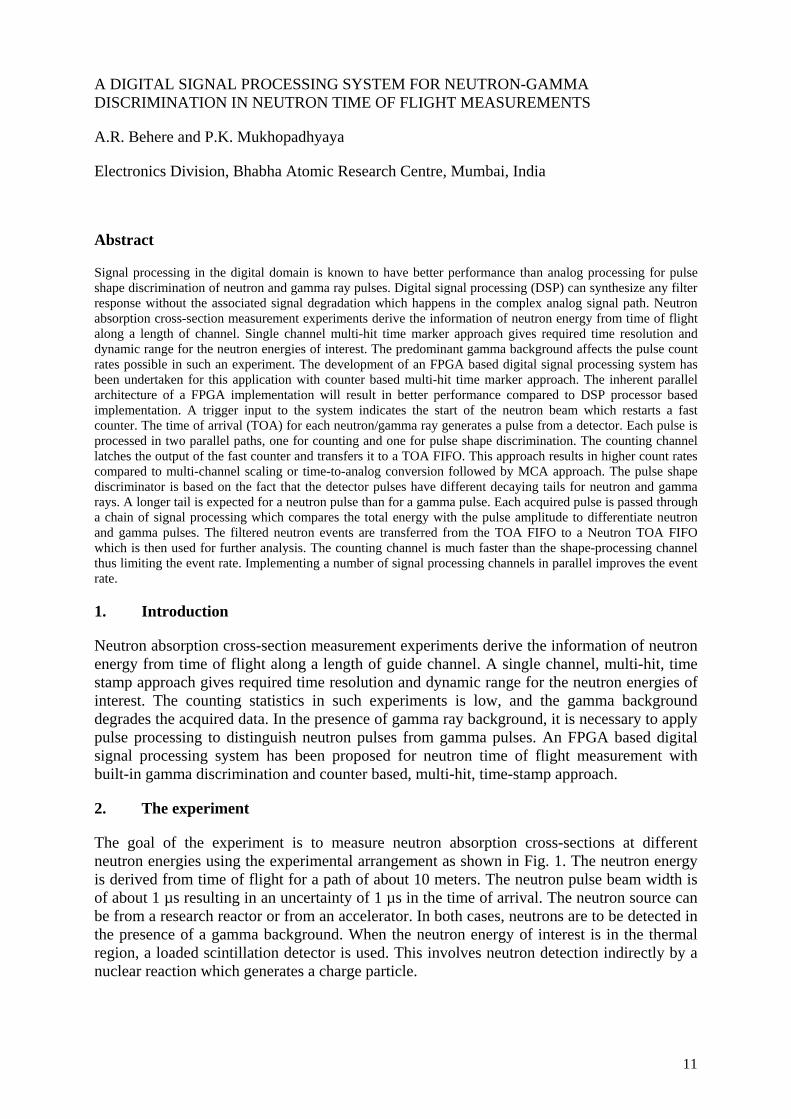
The goal of the experiment is to measure neutron absorption cross-sections at different neutron energies using the experimental arrangement as shown in Fig. 1. The neutron energy is derived from time of flight for a path of about 10 meters. The neutron pulse beam width is of about 1 µs resulting in an uncertainty of 1 µs in the time of arrival. The neutron source can be from a research reactor or from an accelerator. In both cases, neutrons are to be detected in the presence of a gamma background. When the neutron energy of interest is in the thermal region, a loaded scintillation detector is used. This involves neutron detection indirectly by a nuclear reaction which generates a charge particle.
11
Flight path Neutron beam source
Neutron detector
Pulse processing system
Sample
Fig. 1 Experimental arrangement for time of flight measurements of neutron cross sections
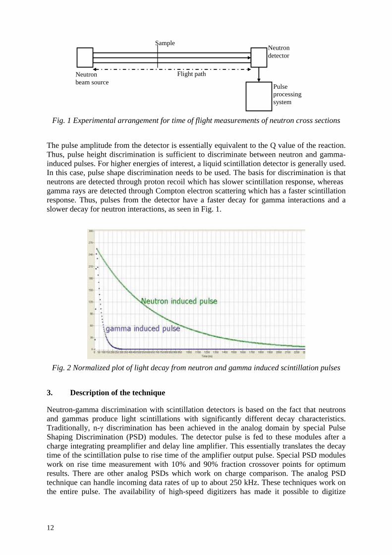
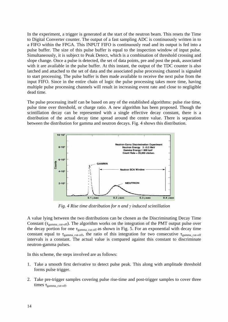
The pulse amplitude from the detector is essentially equivalent to the Q value of the reaction. Thus, pulse height discrimination is sufficient to discriminate between neutron and gamma-induced pulses. For higher energies of interest, a liquid scintillation detector is generally used. In this case, pulse shape discrimination needs to be used. The basis for discrimination is that neutrons are detected through proton recoil which has slower scintillation response, whereas gamma rays are detected through Compton electron scattering which has a faster scintillation response. Thus, pulses from the detector have a faster decay for gamma interactions and a slower decay for neutron interactions, as seen in Fig. 1.
Fig. 2 Normalized plot of light decay from neutron and gamma induced scintillation pulses
3. Description of the technique
Neutron-gamma discrimination with scintillation detectors is based on the fact that neutrons and gammas produce light scintillations with significantly different decay characteristics. Traditionally, n-γ discrimination has been achieved in the analog domain by special Pulse Shaping Discrimination (PSD) modules. The detector pulse is fed to these modules after a charge integrating preamplifier and delay line amplifier. This essentially translates the decay time of the scintillation pulse to rise time of the amplifier output pulse. Special PSD modules work on rise time measurement with 10% and 90% fraction crossover points for optimum results. There are other analog PSDs which work on charge comparison. The analog PSD technique can handle incoming data rates of up to about 250 kHz. These techniques work on the entire pulse. The availability of high-speed digitizers has made it possible to digitize
12
directly the detector signal, and a number of digital signal processing techniques have been reported. Digital techniques can work selectively on the decaying part of the pulse resulting in a better figure of merit. Some of these work on rise-time discrimination, similar to analog domain processing after the shaping amplifier. Other techniques process direct PMT outputs with different discriminating criterion, such as ratio of charge integrated over two time ranges, pulse amplitude vs charge and pulse duration over threshold. A new technique which works on the ratio of two consecutive windows equal to discriminating decay time-constant is proposed here.
4. Implementation
Most of the reported techniques work on PC based commercial high-speed digitizer cards which have deep memory for data storage. This data is then transferred to PC memory and analyzed in software. While the data is being transferred, the system is not ready to acquire new data. Also, this approach results in huge volume of data to be handled by PC. In this implementation, the acquisition duration is limited by the depth of on-board memory provided on the card. As the processing is done by CPU of the PC, the throughput is affected when the number of analog channels increases. An approach to achieve real-time pulse processing is to implement DSP based system with pulse processing handled by the DSP. With the availability of high speed and high-density field programmable gate array devices, this can also be implemented with an FPGA. The chief motivation is to achieve high throughput for the neutron-gamma discrimination, with the neutron energy obtained from time of flight. The inherent parallel architecture of a FPGA implementation will result in better performance.
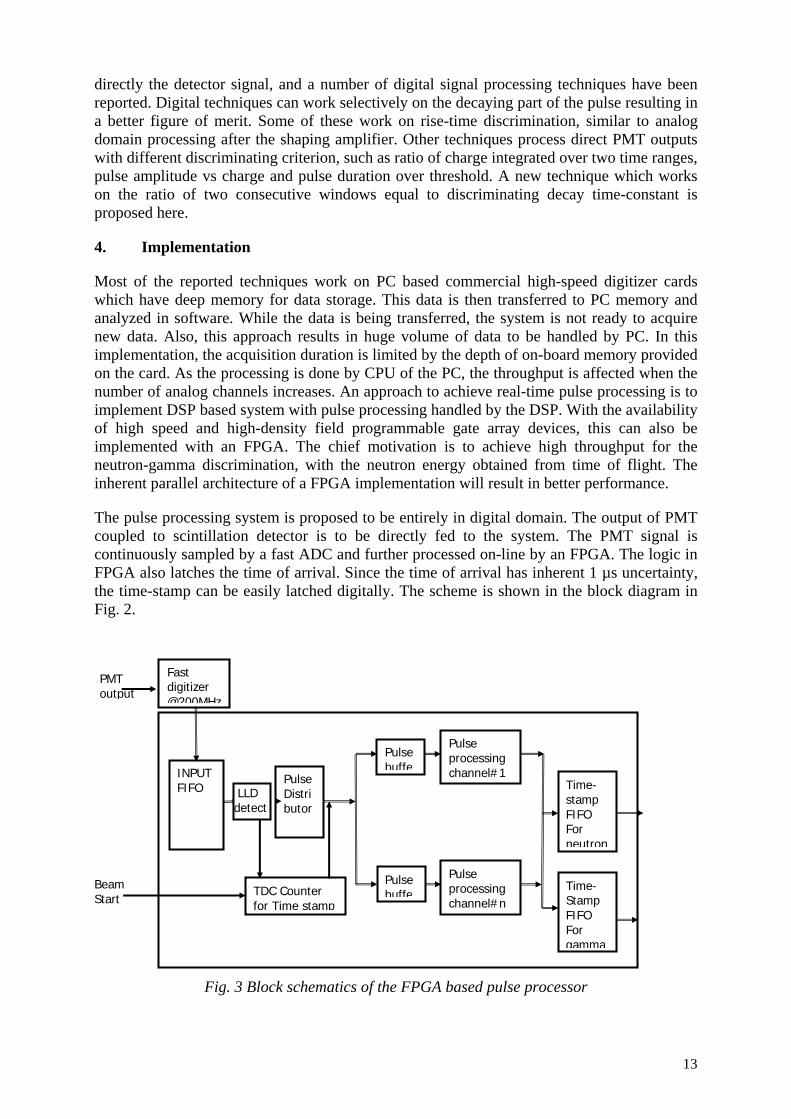
The pulse processing system is proposed to be entirely in digital domain. The output of PMT coupled to scintillation detector is to be directly fed to the system. The PMT signal is continuously sampled by a fast ADC and further processed on-line by an FPGA. The logic in FPGA also latches the time of arrival. Since the time of arrival has inherent 1 µs uncertainty, the time-stamp can be easily latched digitally. The scheme is shown in the block diagram in Fig. 2.
Fast digitizer @200MHz
PMT output
INPUT FIFO
Pulse buffe
Pulse Distributor
Pulse processing channel#1
Pulse processing channel#n
TDC Counter for Time stamp
Time- stamp FIFO For neutron
Beam Start
Pulse buffe
LLD detect
Time- Stamp FIFO For gamma
Fig. 3 Block schematics of the FPGA based pulse processor
13
In the experiment, a trigger is generated at the start of the neutron beam. This resets the Time to Digital Converter counter. The output of a fast sampling ADC is continuously written in to a FIFO within the FPGA. This INPUT FIFO is continuously read and its output is fed into a pulse buffer. The size of this pulse buffer is equal to the inspection window of input pulse. Simultaneously, it is subject to Peak Detect, which is a combination of threshold crossing and slope change. Once a pulse is detected, the set of data points, pre and post the peak, associated with it are available in the pulse buffer. At this instant, the output of the TDC counter is also latched and attached to the set of data and the associated pulse processing channel is signaled to start processing. The pulse buffer is then made available to receive the next pulse from the input FIFO. Since in the entire chain of logic the pulse processing takes more time, having multiple pulse processing channels will result in increasing event rate and close to negligible dead time.
The pulse processing itself can be based on any of the established algorithms: pulse rise time, pulse time over threshold, or charge ratio. A new algorithm has been proposed. Though the scintillation decay can be represented with a single effective decay constant, there is a distribution of the actual decay time spread around the centre value. There is separation between the distribution for gamma and neutron decays. Fig. 4 shows this distribution.
Fig. 4 Rise time distribution for n and γ induced scintillation
A value lying between the two distributions can be chosen as the Discriminating Decay Time Constant (τgamma_cut-off). The algorithm works on the integration of the PMT output pulse over the decay portion for one τgamma_cut-off as shown in Fig. 5. For an exponential with decay time constant equal to τgamma_cut-off, the ratio of this integration for two consecutive τgamma_cut-off intervals is a constant. The actual value is compared against this constant to discriminate neutron-gamma pulses.
In this scheme, the steps involved are as follows:
1. Take a smooth first derivative to detect pulse peak. This along with amplitude threshold forms pulse trigger.
2. Take pre-trigger samples covering pulse rise-time and post-trigger samples to cover three times τgamma_cut-off.
14
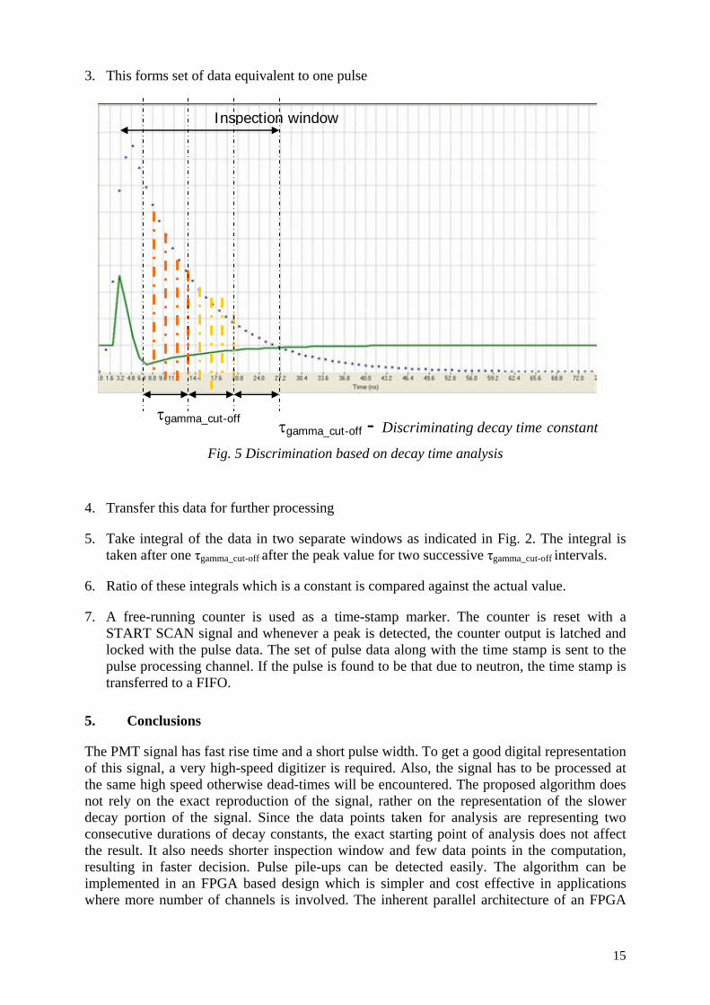
3. This forms set of data equivalent to one pulse
τgamma_cut-off - Discriminating decay time constantτgamma_cut-off
Inspection window
Fig. 5 Discrimination based on decay time analysis
4. Transfer this data for further processing
5. Take integral of the data in two separate windows as indicated in Fig. 2. The integral is taken after one τgamma_cut-off after the peak value for two successive τgamma_cut-off intervals.
6. Ratio of these integrals which is a constant is compared against the actual value.
7. A free-running counter is used as a time-stamp marker. The counter is reset with a START SCAN signal and whenever a peak is detected, the counter output is latched and locked with the pulse data. The set of pulse data along with the time stamp is sent to the pulse processing channel. If the pulse is found to be that due to neutron, the time stamp is transferred to a FIFO.
5. Conclusions
The PMT signal has fast rise time and a short pulse width. To get a good digital representation of this signal, a very high-speed digitizer is required. Also, the signal has to be processed at the same high speed otherwise dead-times will be encountered. The proposed algorithm does not rely on the exact reproduction of the signal, rather on the representation of the slower decay portion of the signal. Since the data points taken for analysis are representing two consecutive durations of decay constants, the exact starting point of analysis does not affect the result. It also needs shorter inspection window and few data points in the computation, resulting in faster decision. Pulse pile-ups can be detected easily. The algorithm can be implemented in an FPGA based design which is simpler and cost effective in applications where more number of channels is involved. The inherent parallel architecture of an FPGA
15

implementation results in better performance compared to PC based or DSP processor based implementation. A LabWindows based program has been written to simulate data and run pulse processing on it. Also, VHDL code has been written for the pulse processing part and its performance when targeted on Altera 10KE50-1 FPGA has been simulated. A 200 MSPS 8-bit ADC is taken as the digitizer. The results indicate that such a system can cater to pulse rates of at least 1 MPPS. Quantitative analysis has yet to be carried out on actual data and results compared with other algorithms. The algorithm can be extended to include analysis of pile-up.
16
IMPLEMENTATION OF DIGITAL SIGNAL PROCESSOR FOR NUCLEAR SPECTROMETRY USING STATE OF THE ART TOOLS
M. Bogovac1, D. Wegrzynek2, A. Markowicz2
1Institute R. Boskovic, Zagreb, Croatia
2IAEA, Seibersdorf, Austria
Abstract
In this work, the Xilinx XtremeDSP Development kit for Virtex-4 SX FPGA was used as a hardware prototyping platform for development of a multi-channel digital spectrometer. The kit is based on Xilinx Inc.’s most advanced Virtex family of FPGAs, and is equipped with two 14-bit 105 MSPS ADCs and two 14-bit 160 MSPS DACs. The two boards are chained together so that signals from four detectors can be processed simultaneously. In order to utilize the ADCs input range as best as possible, a four channel analog pre-filter has been designed and developed. This pre-filter includes digitally controlled differentiation, pole-zero cancellation, linear amplification and an anti-aliasing filter. The system was tested on several X ray detectors with resistor feedback and transistor reset preamplifiers, and exhibited performances similar to Canberra’s InSpector 2000 Digital Signal Processing Portable Spectroscopy Workstation.
1. Introduction
X ray and γ ray detection and measurement using high-resolution detectors usually requires fast and low noise front-end electronics for pulse processing. Programmable digital filters are a superior alternative to the traditional analog electronics in terms of throughputs and flexibility. In addition, as a compact alternative to bulky analog electronics, digital signal processing can be of great benefit in applications that require more detectors. Today’s state of the art hardware and software tools for digital signal processing can greatly improve and speed-up development of a high performance digital spectrometer. In this work, Xilinx Inc.’s XtremeDSP Development Kit for Virtex-4 [1] was used as a complete platform for development of an on-chip digital pulse processor for X ray and γ ray detectors. This article gives a short review of the XtremeDSP Development Kit-IV and FPGA architecture. Also, pulse processing in nuclear spectroscopy is briefly summarized including an original derivation of IIR filter for digital trapezoidal shaping. Finally, the pulse processor design implementation is presented.
2. Field programmable gate array
A field programmable gate array (FPGA) is a general-purpose integrated circuit that is ‘programmed’ by the designer rather than the device manufacturer. Unlike an application-specific integrated circuit, which can perform a similar function in an electronic system, an FPGA can be reprogrammed, even after it has been deployed into a system. A FPGA is programmed by downloading a configuration program called a bit stream into static on-chip random-access memory. Much like the object code for a microprocessor, this bit stream is the product of compilation tools that translate the high-level abstractions produced by a designer into something equivalent, but low-level and executable.
17
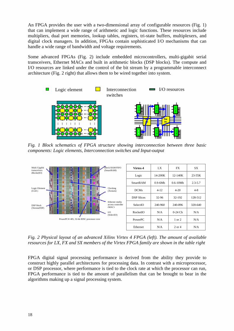
An FPGA provides the user with a two-dimensional array of configurable resources (Fig. 1) that can implement a wide range of arithmetic and logic functions. These resources include multipliers, dual port memories, lookup tables, registers, tri-state buffers, multiplexers, and digital clock managers. In addition, FPGAs contain sophisticated I/O mechanisms that can handle a wide range of bandwidth and voltage requirements.
Some advanced FPGAs (Fig. 2) include embedded microcontrollers, multi-gigabit serial transceivers, Ethernet MACs and built in arithmetic blocks (DSP blocks). The compute and I/O resources are linked under the control of the bit stream by a programmable interconnect architecture (Fig. 2 right) that allows them to be wired together into system.
Logic element Interconnection switches
Switch
LE
LE
LE
LE
LE
LE
Switch
I/O resources
Fig. 1 Block schematics of FPGA structure showing interconnection between three basic components: Logic elements, Interconnection switches and Input-output
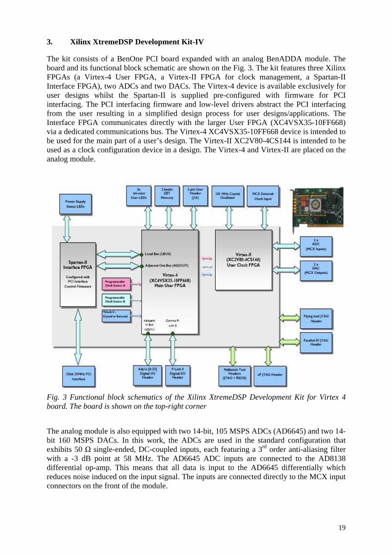
Multi Gigabit transceivers (RocketIO)
Logic Element (CLB )
DSP block (XtremeDSP)
Block RAM/FIFO (SmartRAM)
Clocking (Xesium)
Ethernet media access controller (MAC)
PowerPC® 405, 32-bit RISC processor core
I/O (SelectIO)
Virtex-4 LX FX SX
Logic 14-200K 12-140K 23-55K
SmartRAM 0.9-6Mb 0.6-10Mb 2.3-5.7
DCMs 4-12 4-20 4-8
DSP Slices 32-96 32-192 128-512
SelectIO 240-960 240-896 320-640
RocketIO N/A 0-24 Ch N/A
PowerPC N/A 1 or 2 N/A
Ethernet N/A 2 or 4 N/A
Fig. 2 Physical layout of an advanced Xilinx Virtex 4 FPGA (left). The amount of available resources for LX, FX and SX members of the Virtex FPGA family are shown in the table right
FPGA digital signal processing performance is derived from the ability they provide to construct highly parallel architectures for processing data. In contrast with a microprocessor, or DSP processor, where performance is tied to the clock rate at which the processor can run, FPGA performance is tied to the amount of parallelism that can be brought to bear in the algorithms making up a signal processing system.
18
3. Xilinx XtremeDSP Development Kit-IV
The kit consists of a BenOne PCI board expanded with an analog BenADDA module. The board and its functional block schematic are shown on the Fig. 3. The kit features three Xilinx FPGAs (a Virtex-4 User FPGA, a Virtex-II FPGA for clock management, a Spartan-II Interface FPGA), two ADCs and two DACs. The Virtex-4 device is available exclusively for user designs whilst the Spartan-II is supplied pre-configured with firmware for PCI interfacing. The PCI interfacing firmware and low-level drivers abstract the PCI interfacing from the user resulting in a simplified design process for user designs/applications. The Interface FPGA communicates directly with the larger User FPGA (XC4VSX35-10FF668) via a dedicated communications bus. The Virtex-4 XC4VSX35-10FF668 device is intended to be used for the main part of a user’s design. The Virtex-II XC2V80-4CS144 is intended to be used as a clock configuration device in a design. The Virtex-4 and Virtex-II are placed on the analog module.
Fig. 3 Functional block schematics of the Xilinx XtremeDSP Development Kit for Virtex 4 board. The board is shown on the top-right corner
The analog module is also equipped with two 14-bit, 105 MSPS ADCs (AD6645) and two 14-bit 160 MSPS DACs. In this work, the ADCs are used in the standard configuration that exhibits 50 Ω single-ended, DC-coupled inputs, each featuring a 3rd order anti-aliasing filter with a -3 dB point at 58 MHz. The AD6645 ADC inputs are connected to the AD8138 differential op-amp. This means that all data is input to the AD6645 differentially which reduces noise induced on the input signal. The inputs are connected directly to the MCX input connectors on the front of the module.
19
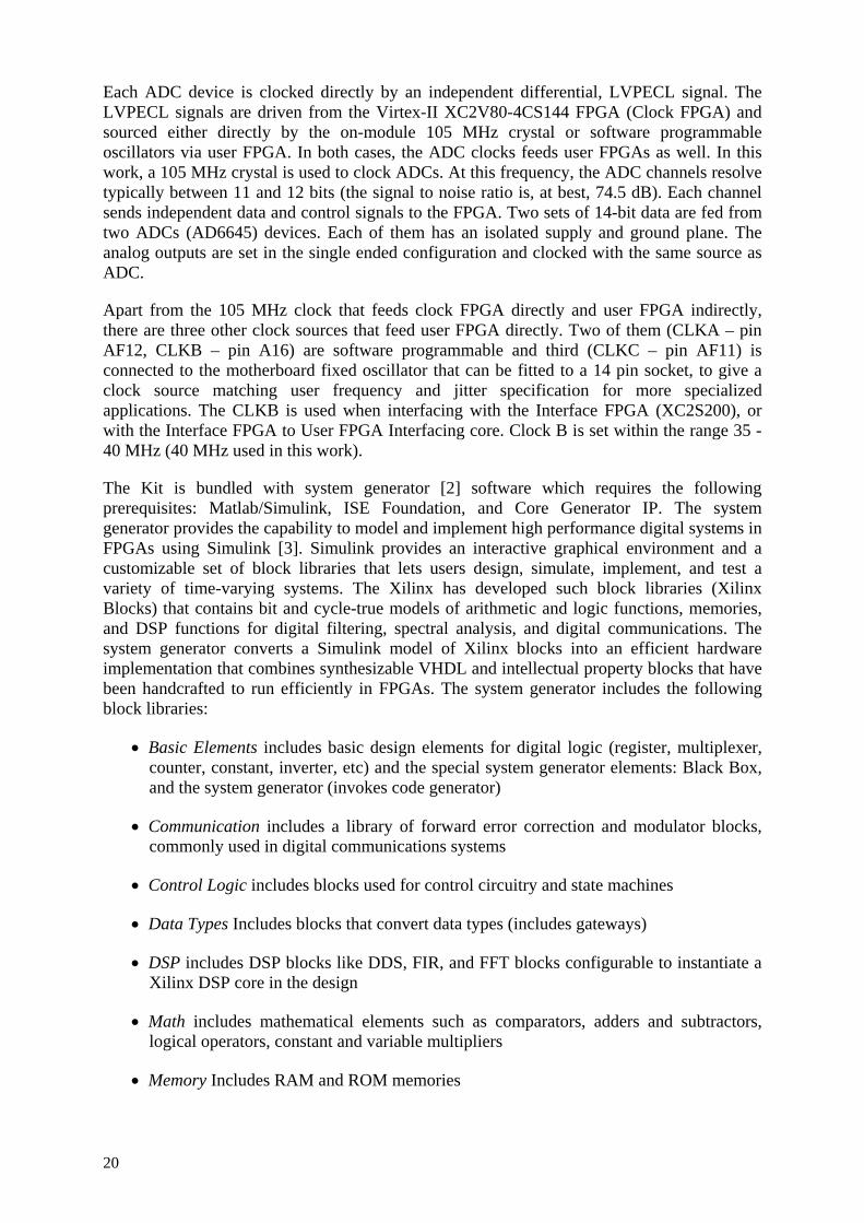
Each ADC device is clocked directly by an independent differential, LVPECL signal. The LVPECL signals are driven from the Virtex-II XC2V80-4CS144 FPGA (Clock FPGA) and sourced either directly by the on-module 105 MHz crystal or software programmable oscillators via user FPGA. In both cases, the ADC clocks feeds user FPGAs as well. In this work, a 105 MHz crystal is used to clock ADCs. At this frequency, the ADC channels resolve typically between 11 and 12 bits (the signal to noise ratio is, at best, 74.5 dB). Each channel sends independent data and control signals to the FPGA. Two sets of 14-bit data are fed from two ADCs (AD6645) devices. Each of them has an isolated supply and ground plane. The analog outputs are set in the single ended configuration and clocked with the same source as ADC.
Apart from the 105 MHz clock that feeds clock FPGA directly and user FPGA indirectly, there are three other clock sources that feed user FPGA directly. Two of them (CLKA – pin AF12, CLKB – pin A16) are software programmable and third (CLKC – pin AF11) is connected to the motherboard fixed oscillator that can be fitted to a 14 pin socket, to give a clock source matching user frequency and jitter specification for more specialized applications. The CLKB is used when interfacing with the Interface FPGA (XC2S200), or with the Interface FPGA to User FPGA Interfacing core. Clock B is set within the range 35 - 40 MHz (40 MHz used in this work).
The Kit is bundled with system generator [2] software which requires the following prerequisites: Matlab/Simulink, ISE Foundation, and Core Generator IP. The system generator provides the capability to model and implement high performance digital systems in FPGAs using Simulink [3]. Simulink provides an interactive graphical environment and a customizable set of block libraries that lets users design, simulate, implement, and test a variety of time-varying systems. The Xilinx has developed such block libraries (Xilinx Blocks) that contains bit and cycle-true models of arithmetic and logic functions, memories, and DSP functions for digital filtering, spectral analysis, and digital communications. The system generator converts a Simulink model of Xilinx blocks into an efficient hardware implementation that combines synthesizable VHDL and intellectual property blocks that have been handcrafted to run efficiently in FPGAs. The system generator includes the following block libraries:
• Basic Elements includes basic design elements for digital logic (register, multiplexer, counter, constant, inverter, etc) and the special system generator elements: Black Box, and the system generator (invokes code generator)
• Communication includes a library of forward error correction and modulator blocks, commonly used in digital communications systems
• Control Logic includes blocks used for control circuitry and state machines
• Data Types Includes blocks that convert data types (includes gateways)
• DSP includes DSP blocks like DDS, FIR, and FFT blocks configurable to instantiate a Xilinx DSP core in the design
• Math includes mathematical elements such as comparators, adders and subtractors, logical operators, constant and variable multipliers
• Memory Includes RAM and ROM memories
20
• Shared Memory includes blocks that allow access to the Xilinx shared memory object
• Tools include ‘utility’ blocks, e.g. code generation (system generator block), resource estimation, and HDL co-simulation
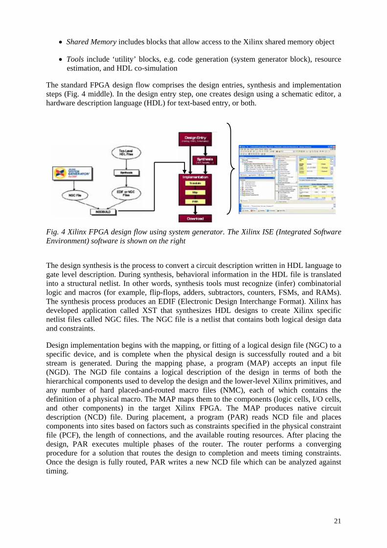
The standard FPGA design flow comprises the design entries, synthesis and implementation steps (Fig. 4 middle). In the design entry step, one creates design using a schematic editor, a hardware description language (HDL) for text-based entry, or both.
Fig. 4 Xilinx FPGA design flow using system generator. The Xilinx ISE (Integrated Software Environment) software is shown on the right
The design synthesis is the process to convert a circuit description written in HDL language to gate level description. During synthesis, behavioral information in the HDL file is translated into a structural netlist. In other words, synthesis tools must recognize (infer) combinatorial logic and macros (for example, flip-flops, adders, subtractors, counters, FSMs, and RAMs). The synthesis process produces an EDIF (Electronic Design Interchange Format). Xilinx has developed application called XST that synthesizes HDL designs to create Xilinx specific netlist files called NGC files. The NGC file is a netlist that contains both logical design data and constraints.
Design implementation begins with the mapping, or fitting of a logical design file (NGC) to a specific device, and is complete when the physical design is successfully routed and a bit stream is generated. During the mapping phase, a program (MAP) accepts an input file (NGD). The NGD file contains a logical description of the design in terms of both the hierarchical components used to develop the design and the lower-level Xilinx primitives, and any number of hard placed-and-routed macro files (NMC), each of which contains the definition of a physical macro. The MAP maps them to the components (logic cells, I/O cells, and other components) in the target Xilinx FPGA. The MAP produces native circuit description (NCD) file. During placement, a program (PAR) reads NCD file and places components into sites based on factors such as constraints specified in the physical constraint file (PCF), the length of connections, and the available routing resources. After placing the design, PAR executes multiple phases of the router. The router performs a converging procedure for a solution that routes the design to completion and meets timing constraints. Once the design is fully routed, PAR writes a new NCD file which can be analyzed against timing.
21

A system generator design is often incorporated as a part of a larger HDL design. The most convenient way to incorporate a system generator design into an HDL design is to encapsulate the entire design into a single binary module in the NGC binary netlist format used by the Xilinx ISE tool suite (Fig. 4). In this case, the system generator design is viewed as a black box by the logic synthesis tool. To produce the NGC file, the NGC netlist compilation target from the system generator block must be selected. The system generator NGC module can be directly instantiated inside the top level VHDL entity. To make this process easier, the system generator creates an HDL component instantiation template when the design is compiled using the NGC target.
4. Pulse processing in nuclear spectroscopy
In the high-resolution nuclear spectroscopy, it is common that a pulse of a known waveform but unknown amplitude
)(tsn
)(ts A is measured in a presence of noise . )(tn
)()()( tntAstsn += (1)
We assume that a large number of independent amplitude measurements of the signal were done. What is the best way to operate (process) on this data using the information about the known signal waveform ? In the limit of continues, infinite long measurement and white noise, statistically it is best to make a cross-correlation between the measured signal (pulse plus noise) and known waveform [
)(tsn
)(ts
4, 5, 6]
(2)
ττ dtststg n )()()( += ∫+∞
∞−
This gives the optimal amplitude
)(max tgAoptimal = (3)
It can be shown that pulse of the waveform has the best signal to noise ratio. In the case of nuclear radiation detector the signal at the preamplifier output is a step function and has a noise of the form (assuming flicker noise is negligible)
)(tg
⎟⎟⎠
⎞⎜⎜⎝
⎛+= 22
2 11)(c
aFτω
ω (4)
This noise can be whitened by passing the signal through a simple CR differentiator of a time constant equal cτ . The whitening filter converts step function into an exponential pulse. Therefore, the pulse on the output of the whitening prefilter has waveform )(ts
c
t
ets τ−
=)( (5)
When the waveform Eq. (5) is processed by the pulse processor described with formula Eq. (2), a waveform called cusp is obtained (see Fig. 5 top-left). This means that the best way to measure amplitude of an exponential input signal with a white noise is first to shape it into the cusp waveform and then measure its amplitude.
22
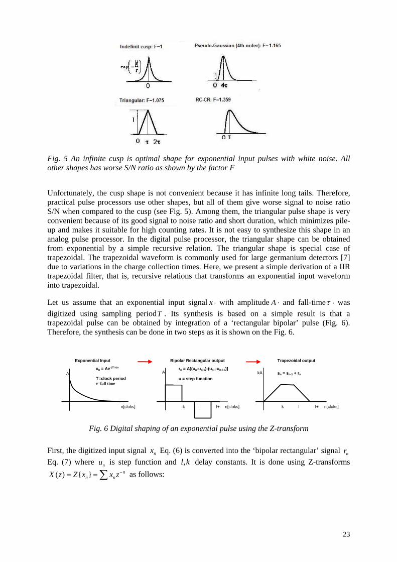
Fig. 5 An infinite cusp is optimal shape for exponential input pulses with white noise. All other shapes has worse S/N ratio as shown by the factor F
Unfortunately, the cusp shape is not convenient because it has infinite long tails. Therefore, practical pulse processors use other shapes, but all of them give worse signal to noise ratio S/N when compared to the cusp (see Fig. 5). Among them, the triangular pulse shape is very convenient because of its good signal to noise ratio and short duration, which minimizes pile-up and makes it suitable for high counting rates. It is not easy to synthesize this shape in an analog pulse processor. In the digital pulse processor, the triangular shape can be obtained from exponential by a simple recursive relation. The triangular shape is special case of trapezoidal. The trapezoidal waveform is commonly used for large germanium detectors [7] due to variations in the charge collection times. Here, we present a simple derivation of a IIR trapezoidal filter, that is, recursive relations that transforms an exponential input waveform into trapezoidal.
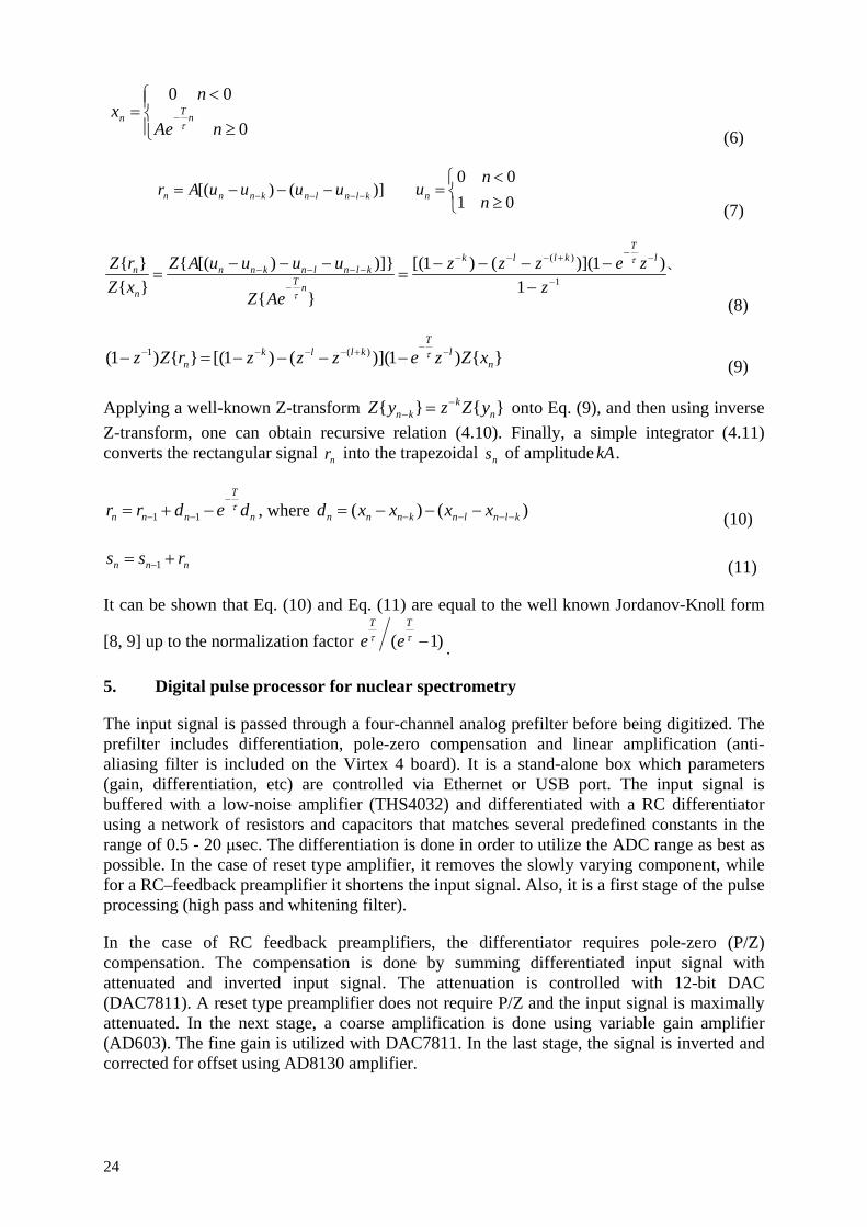
Let us assume that an exponential input signal x , with amplitude A , and fall-timeτ , was digitized using sampling periodT . Its synthesis is based on a simple result is that a trapezoidal pulse can be obtained by integration of a ‘rectangular bipolar’ pulse (Fig. 6). Therefore, the synthesis can be done in two steps as it is shown on the Fig. 6.
A
l+k l k n[cloks]
Bipolar Rectangular output
rn = A[(un-un-k)-(un-l-un-l-k)] u = step function
A
n[cloks]
Exponential Input
xn = Ae-(T/τ)n
T=clock period τ=fall time
kA
l+k l k n[cloks]
Trapezoidal output
sn = sn-1 + rn
Fig. 6 Digital shaping of an exponential pulse using the Z-transform
First, the digitized input signal Eq. (6) is converted into the ‘bipolar rectangular’ signal Eq. (7) where
nx nr
nu is step function and delay constants. It is done using Z-transforms as follows:
kl,
∑ −== nnn zxxZzX )(
23
⎪⎩
⎪⎨⎧
≥
<= −
0
00
nAe
nx nT
nτ
(6)
)]()[( klnlnknnn uuuuAr −−−− −−−= (7)
⎩⎨⎧
≥<
=0100
nn
un
`1
)1)](()1[(
)])[(
1
)(
−
−−+−−−
−
−−−−
−−−−−
=−−−
=z
zezzz
AeZ
uuuuAZxZrZ l
Tkllk
nTklnlnknn
n
nτ
τ (8)
)1)](()1[()1( )(1n
lT
kllkn xZzezzzrZz −−+−−−− −−−−=− τ
(9)
Applying a well-known Z-transform onto Eq. (9), and then using inverse Z-transform, one can obtain recursive relation (4.10). Finally, a simple integrator (4.11) converts the rectangular signal into the trapezoidal of amplitude .
nk
kn yZzyZ −− =
nr ns kA
n
T
nnn dedrr τ−
−− −+= 11 , where )()( klnlnknnn xxxxd −−−− −−−= (10)
nnn rss += −1 (11)
It can be shown that Eq. (10) and Eq. (11) are equal to the well known Jordanov-Knoll form
[8, 9] up to the normalization factor )1( −ττTT
ee .
5. Digital pulse processor for nuclear spectrometry
The input signal is passed through a four-channel analog prefilter before being digitized. The prefilter includes differentiation, pole-zero compensation and linear amplification (anti-aliasing filter is included on the Virtex 4 board). It is a stand-alone box which parameters (gain, differentiation, etc) are controlled via Ethernet or USB port. The input signal is buffered with a low-noise amplifier (THS4032) and differentiated with a RC differentiator using a network of resistors and capacitors that matches several predefined constants in the range of 0.5 - 20 μsec. The differentiation is done in order to utilize the ADC range as best as possible. In the case of reset type amplifier, it removes the slowly varying component, while for a RC–feedback preamplifier it shortens the input signal. Also, it is a first stage of the pulse processing (high pass and whitening filter).
In the case of RC feedback preamplifiers, the differentiator requires pole-zero (P/Z) compensation. The compensation is done by summing differentiated input signal with attenuated and inverted input signal. The attenuation is controlled with 12-bit DAC (DAC7811). A reset type preamplifier does not require P/Z and the input signal is maximally attenuated. In the next stage, a coarse amplification is done using variable gain amplifier (AD603). The fine gain is utilized with DAC7811. In the last stage, the signal is inverted and corrected for offset using AD8130 amplifier.
24
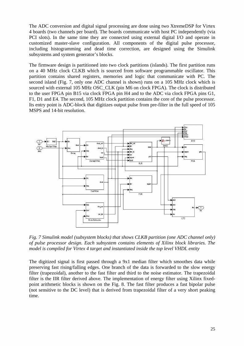
The ADC conversion and digital signal processing are done using two XtremeDSP for Virtex 4 boards (two channels per board). The boards communicate with host PC independently (via PCI slots). In the same time they are connected using external digital I/O and operate in customized master-slave configuration. All components of the digital pulse processor, including histogramming and dead time correction, are designed using the Simulink subsystems and system generator’s blocks.
The firmware design is partitioned into two clock partitions (islands). The first partition runs on a 40 MHz clock CLKB which is sourced from software programmable oscillator. This partition contains shared registers, memories and logic that communicate with PC. The second island (Fig. 7, only one ADC channel is shown) runs on a 105 MHz clock which is sourced with external 105 MHz OSC_CLK (pin M6 on clock FPGA). The clock is distributed to the user FPGA pin B15 via clock FPGA pin H4 and to the ADC via clock FPGA pins G1, F1, D1 and E4. The second, 105 MHz clock partition contains the core of the pulse processor. Its entry point is ADC-block that digitizes output pulse from pre-filter in the full speed of 105 MSPS and 14-bit resolution.
Fig. 7 Simulink model (subsystem blocks) that shows CLKB partition (one ADC channel only) of pulse processor design. Each subsystem contains elements of Xilinx block libraries. The model is compiled for Virtex 4 target and instantiated inside the top level VHDL entity
The digitized signal is first passed through a 9x1 median filter which smoothes data while preserving fast rising/falling edges. One branch of the data is forwarded to the slow energy filter (trapezoidal), another to the fast filter and third to the noise estimator. The trapezoidal filter is the IIR filter derived above. The implementation of energy filter using Xilinx fixed-point arithmetic blocks is shown on the Fig. 8. The fast filter produces a fast bipolar pulse (not sensitive to the DC level) that is derived from trapezoidal filter of a very short peaking time.
25
In order to remove slowly changing DC component of the input signal, a Base Line Restorer subsystem block is designed. The block continuously monitors the filtered signal and averages it over predefined time only when there is no pulse present in the input signal. The averaged values are continuously subtracted from the filtered signal. The result of the subtraction feeds the Pulse Height Analysis subsystem block (PHA). The PHA is a peak search engine gated by the Pile-up Rejecter subsystem block. Upon a valid pulse, the PHA subsystem measures peak height, and increments corresponding shared memory location implemented as dual port using on-chip block RAM memory. The shared memory crosses two clock domains, CLKB and OSC_CLK, and it is split in two matched pairs. The CLKB counterpart is easy accessible from PC host.
The PUR measures the time interval between two successive pulses from the fast filter. The pulses are rejected (not stored) if they do not meet a predefine time-interval (overlapping). The live time correction subsystem block outputs live time enable (LTE) logical signal (negative logic) that gates 48- bit live time counter in the CLKA domain. The LTE is asserted when input pulse arrives, and de-asserted when the pulse amplitude is stored and returns to base line. In the case of pile-up, the LTE is de-asserted after the next pile-up free amplitude being stored and returns to baseline.
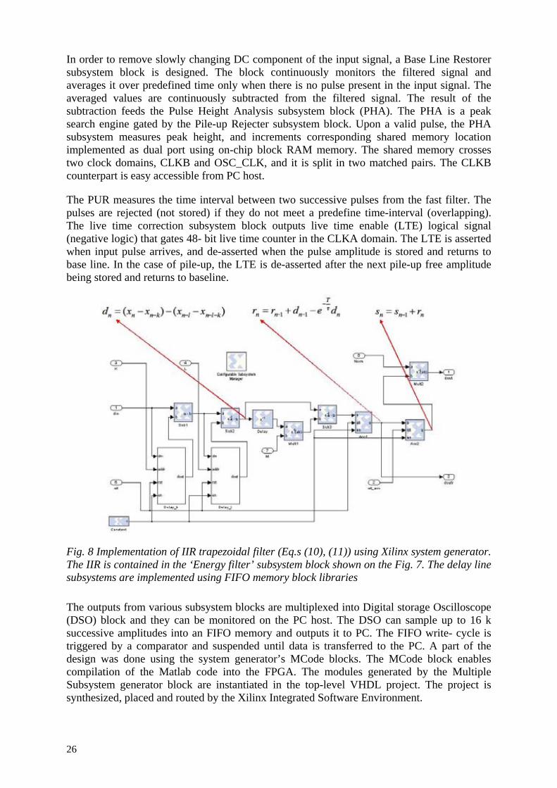
Fig. 8 Implementation of IIR trapezoidal filter (Eq.s (10), (11)) using Xilinx system generator. The IIR is contained in the ‘Energy filter’ subsystem block shown on the Fig. 7. The delay line subsystems are implemented using FIFO memory block libraries
The outputs from various subsystem blocks are multiplexed into Digital storage Oscilloscope (DSO) block and they can be monitored on the PC host. The DSO can sample up to 16 k successive amplitudes into an FIFO memory and outputs it to PC. The FIFO write- cycle is triggered by a comparator and suspended until data is transferred to the PC. A part of the design was done using the system generator’s MCode blocks. The MCode block enables compilation of the Matlab code into the FPGA. The modules generated by the Multiple Subsystem generator block are instantiated in the top-level VHDL project. The project is synthesized, placed and routed by the Xilinx Integrated Software Environment.
26
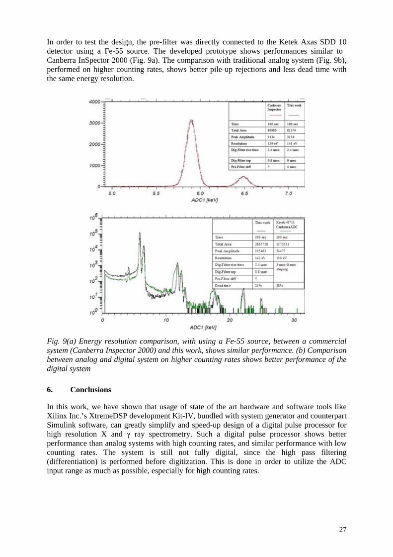
In order to test the design, the pre-filter was directly connected to the Ketek Axas SDD 10 detector using a Fe-55 source. The developed prototype shows performances similar to Canberra InSpector 2000 (Fig. 9a). The comparison with traditional analog system (Fig. 9b), performed on higher counting rates, shows better pile-up rejections and less dead time with the same energy resolution.
Fig. 9(a) Energy resolution comparison, with using a Fe-55 source, between a commercial system (Canberra Inspector 2000) and this work, shows similar performance. (b) Comparison between analog and digital system on higher counting rates shows better performance of the digital system
6. Conclusions
In this work, we have shown that usage of state of the art hardware and software tools like Xilinx Inc.’s XtremeDSP development Kit-IV, bundled with system generator and counterpart Simulink software, can greatly simplify and speed-up design of a digital pulse processor for high resolution X and γ ray spectrometry. Such a digital pulse processor shows better performance than analog systems with high counting rates, and similar performance with low counting rates. The system is still not fully digital, since the high pass filtering (differentiation) is performed before digitization. This is done in order to utilize the ADC input range as much as possible, especially for high counting rates.
27
REFERENCES
[1] XILINX, Inc., “XtremeDSP Development Kit-IV User Guide”, NT107-0272 – Issue I. [2] XILINX, Inc., “System Generator for DSP User Guide”. [3] THE MATHWORKS, Inc., “Simulink Documentation”. [4] RADEKA, V., KARLOVAC, N., Least-square-error amplitude measurement of pulse
signals in presence of noise, Nucl. Instr. Meth. 52 (1967) 86. [5] LOUDE, J.-F., “Energy Resolution In Nuclear Spectroscopy”, LPHE notes and
conferences, IPHE 2000-22, Institut de Physique des Hautes Energies, Lousane, Switzerland, (2000).
[6] NICHOLSON, P. V., “Nuclear Electronics”, John Wiley & Sons, (1974). [7] RADEKA, V., Trapezoidal filtering of signals from large germanium detectors at high
rates, Nucl. Instr. Meth. 99 (1972) 525. [8] JORDANOV, V.T., KNOLL G. F., Digital synthesis of pulse shapes in real time for
high resolution radiation spectroscopy, Nucl. Instr. Meth. A345 (1994) 337. [9] JORDANOV, V.T., KNOLL, G. F., HUBER, A.C., PANTAZIS, J.A, Digital
techniques for real-time pulse shaping in radiation measurements, Nucl. Instr. Meth. A353 (1994) 261.
28
POSITRON ANNIHILATION SPECTROSCOPY: DIGITAL VS. ANALOG SIGNAL PROCESSING
Damir Bosnar
University of Zagreb, Croatia
Abstract
Positron annihilation spectroscopy with a variety of techniques is a proven and well-established nuclear method with applications in material research, chemistry, and medicine. Extensions to newer applications and further improvements of all of these applications trigger continuous development of existing techniques. We will present a fully digitized positron lifetime spectrometer, with the capability for the simultaneous recording of time and energy information of gamma rays. Its advantages over a conventional setup employing fast analog nuclear electronics in structural material investigations will be discussed, and the possibilities to employ digital electronics in other PAS techniques and other fields of applications.
1. Introduction
In contemporary research and applications, investigative methods of increased precision are needed. They often emerge by employing methods emanating from basic science in quite different fields from their origin, as it is the case of nuclear methods in e.g. material research, medicine, production control, etc. Among those methods, positron annihilation spectroscopy (PAS), with a variety of techniques, is playing a prominent role, with the applications which range from structural investigations of broad spectrum of different, technologically high importance, materials, to biological samples and medical imaging. Although conventional PAS techniques based on usage of analog electronics for signal processing are well-established techniques in material properties research and other applications, both the extensions of PAS in newer and more demanding fields in material research, and desire for improved high resolution medical imaging are continuously triggering improvements of the existing techniques. We will present some basic PAS techniques and applications and discuss possibilities and potential advantages of employment of digital electronics in signal processing in PAS.
A part of the work presented in this contribution has been carried out in the Laboratory for Nuclear Physics at Department of Physics, Faculty of Science, Zagreb. This laboratory has been established through substantial financial support of three IAEA TC projects (CRO0005, CRO0008, CRO4005). The acquired equipment represents a basis for education in experimental nuclear physics and its applications at undergraduate and graduate levels at the Department. Simultaneously, established laboratory has provided opportunities for establishing ‘small scale’, mainly interdisciplinary, research programs which provide an excellent opportunity for research in basic science, education and transfer of results to applications, and as such present nice opportunity to have front-line research at home, which can in some extend counteract the brain-drain into the direction of huge research centres, both in Europe or the USA Simultaneously, the scale of the facilities used in the research and its ‘human dimensions’ could contribute to public understanding of basic research, particularly in nuclear physics, and its high technological applications.
2. Positron annihilation spectroscopy and its applications
Detection and analysis of gamma rays produced in process of positron-electron annihilation represents basics of positron annihilation spectroscopy. Positron as electron anti-particle was
29
predicted by P. Dirac in 1928 [1], and as a first antiparticle was discovered by C. Anderson in cosmic rays in 1932 [2]. Analogous to proton and electron which are bound in hydrogen atom, S. Mohorovičić has predicted that positron and electron can form bound state [3], later called positronium, and which was discovered by M. Deutsch in 1951 [4].
Already at the end of the 1940s, it was realized that information carried by gamma rays after annihilation of positrons with electrons in a sample can be used to study structural properties of the sample, and since then various techniques of PAS have been successfully employing in various fields of research and applications.
One of the most useful and productive applications of PAS from the very beginning has been in material properties research, for some general reviews of applications and techniques see e.g. [5]. Investigations using these techniques are now targeting nanoscale regions of the materials of high technological interest, and provide precise information of material properties, sometimes not accessible by other investigative techniques. One of the most active fields of research is investigations of semiconductors which followed the initial investigations of metals and alloys. In diffusion of positrons through some crystal they can be captured in trapping sites produced by crystal imperfections e.g. vacancies and dislocations. This phenomenon has influence on positron lifetimes in the crystal and the measured lifetimes can be correlated with structural imperfections and their concentrations. Since both positron and electron are not at rest the energies and angles of annihilate gamma rays can also provide useful information about electron distributions. Direct positron annihilation is main probe for these types of materials and formation of positronium does not play here an important role. Another active and broad filed of investigations are various porous materials see e.g. [6], where beside direct positron annihilation formation of positronium and their lifetime in voids can give valuable information about the structure of the investigated samples. Some outstanding examples of technological applications include: investigations of low dielectric constant materials for electronics, radiation damage, structural relaxations, and particularly interesting are new structural types of zeolites and zeotypes and mesoporous materials, with wide range of applications from petrochemistry to the air separation and nuclear waste management, medical and biological usage such as e.g. for regeneration of artificial dialysis solution, in administration of contrast agents in magnetic resonance diagnosis, for protein binder and carrier, as well as carrier for vitamins, minerals or toxic compounds, etc., for some further review articles of different applications see e.g. [7].
The other outstanding field of application of positron annihilation detection is medical imaging e.g. [8]. Positron annihilation is used in various imaging systems such as gamma camera, sPECT, PET, CT-PET, and in the most recent investigations possibilities of combination of PET and MRT in one unified systems are examined, see e.g. [9]. In these systems, positron annihilation detection and analysis provide functional imaging of examined tissue or organ with different levels of precision.
Beside these applications, positron annihilation and especially positronium formation and decay have been very fruitful and reach laboratory for research in basic science starting from investigations of fundamental laws in QED [10] to the recent investigations of possible phenomena behind standard model such as extra dimensions and dark matter search e.g. [11]. There are also active investigations of more advanced and new ‘exotic’ applications such as for instance gamma laser, new energy sources, etc [12].
30
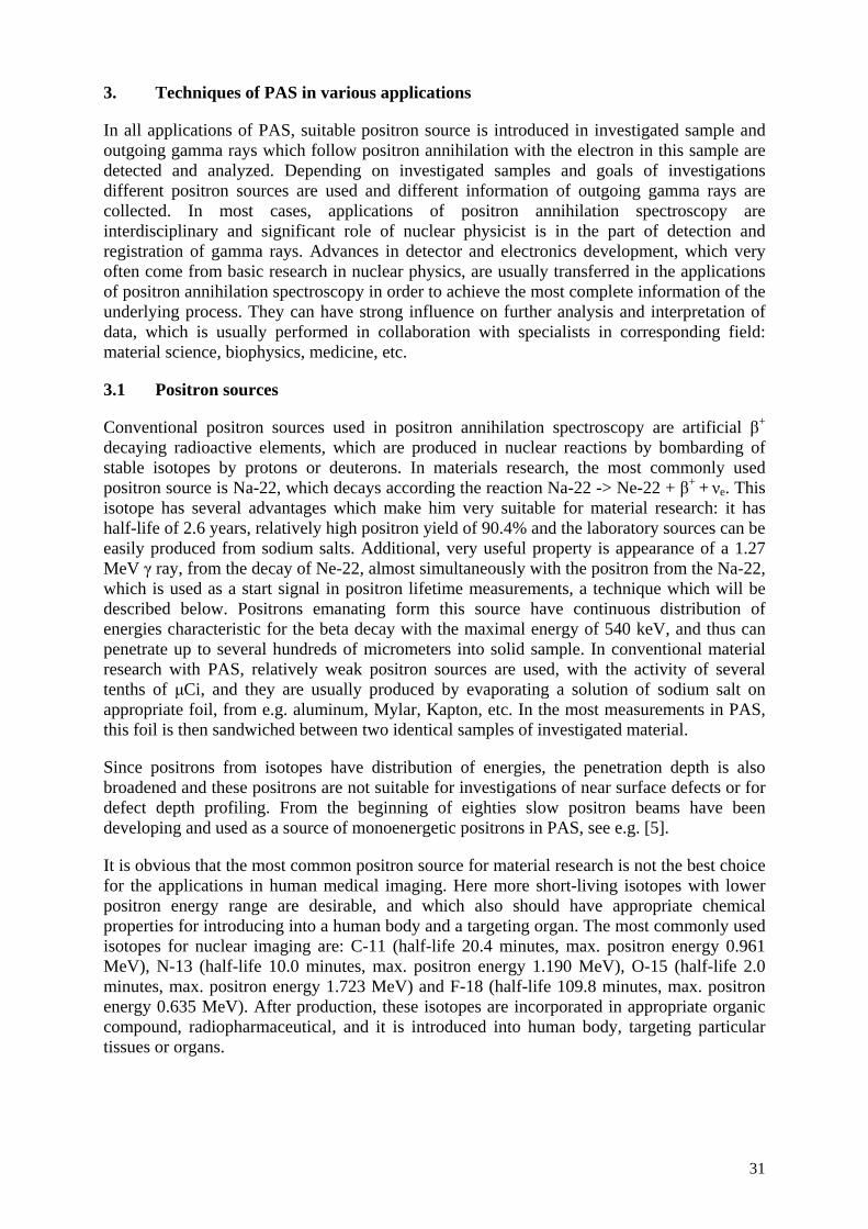
3. Techniques of PAS in various applications
In all applications of PAS, suitable positron source is introduced in investigated sample and outgoing gamma rays which follow positron annihilation with the electron in this sample are detected and analyzed. Depending on investigated samples and goals of investigations different positron sources are used and different information of outgoing gamma rays are collected. In most cases, applications of positron annihilation spectroscopy are interdisciplinary and significant role of nuclear physicist is in the part of detection and registration of gamma rays. Advances in detector and electronics development, which very often come from basic research in nuclear physics, are usually transferred in the applications of positron annihilation spectroscopy in order to achieve the most complete information of the underlying process. They can have strong influence on further analysis and interpretation of data, which is usually performed in collaboration with specialists in corresponding field: material science, biophysics, medicine, etc.
3.1 Positron sources
Conventional positron sources used in positron annihilation spectroscopy are artificial β+ decaying radioactive elements, which are produced in nuclear reactions by bombarding of stable isotopes by protons or deuterons. In materials research, the most commonly used positron source is Na-22, which decays according the reaction Na-22 -> Ne-22 + β+ + νe. This isotope has several advantages which make him very suitable for material research: it has half-life of 2.6 years, relatively high positron yield of 90.4% and the laboratory sources can be easily produced from sodium salts. Additional, very useful property is appearance of a 1.27 MeV γ ray, from the decay of Ne-22, almost simultaneously with the positron from the Na-22, which is used as a start signal in positron lifetime measurements, a technique which will be described below. Positrons emanating form this source have continuous distribution of energies characteristic for the beta decay with the maximal energy of 540 keV, and thus can penetrate up to several hundreds of micrometers into solid sample. In conventional material research with PAS, relatively weak positron sources are used, with the activity of several tenths of μCi, and they are usually produced by evaporating a solution of sodium salt on appropriate foil, from e.g. aluminum, Mylar, Kapton, etc. In the most measurements in PAS, this foil is then sandwiched between two identical samples of investigated material.
Since positrons from isotopes have distribution of energies, the penetration depth is also broadened and these positrons are not suitable for investigations of near surface defects or for defect depth profiling. From the beginning of eighties slow positron beams have been developing and used as a source of monoenergetic positrons in PAS, see e.g. [5].
It is obvious that the most common positron source for material research is not the best choice for the applications in human medical imaging. Here more short-living isotopes with lower positron energy range are desirable, and which also should have appropriate chemical properties for introducing into a human body and a targeting organ. The most commonly used isotopes for nuclear imaging are: C-11 (half-life 20.4 minutes, max. positron energy 0.961 MeV), N-13 (half-life 10.0 minutes, max. positron energy 1.190 MeV), O-15 (half-life 2.0 minutes, max. positron energy 1.723 MeV) and F-18 (half-life 109.8 minutes, max. positron energy 0.635 MeV). After production, these isotopes are incorporated in appropriate organic compound, radiopharmaceutical, and it is introduced into human body, targeting particular tissues or organs.
31
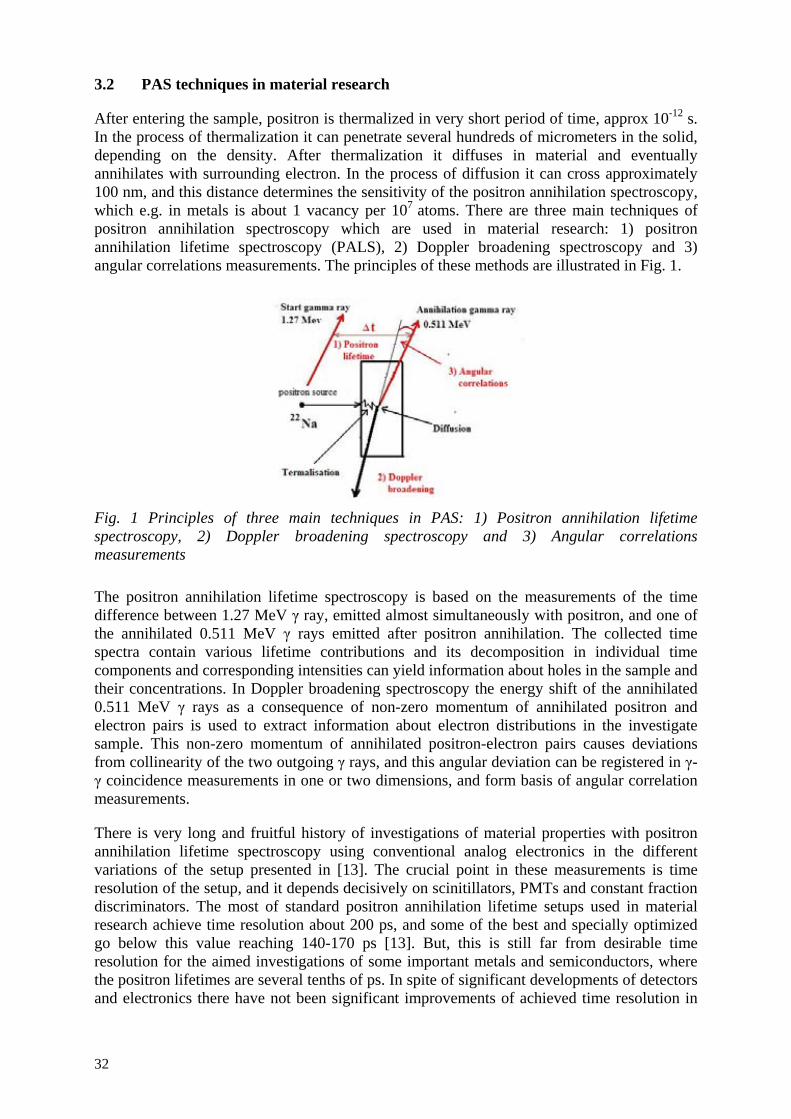
3.2 PAS techniques in material research
After entering the sample, positron is thermalized in very short period of time, approx 10-12 s. In the process of thermalization it can penetrate several hundreds of micrometers in the solid, depending on the density. After thermalization it diffuses in material and eventually annihilates with surrounding electron. In the process of diffusion it can cross approximately 100 nm, and this distance determines the sensitivity of the positron annihilation spectroscopy, which e.g. in metals is about 1 vacancy per 107 atoms. There are three main techniques of positron annihilation spectroscopy which are used in material research: 1) positron annihilation lifetime spectroscopy (PALS), 2) Doppler broadening spectroscopy and 3) angular correlations measurements. The principles of these methods are illustrated in Fig. 1.
Fig. 1 Principles of three main techniques in PAS: 1) Positron annihilation lifetime spectroscopy, 2) Doppler broadening spectroscopy and 3) Angular correlations measurements
The positron annihilation lifetime spectroscopy is based on the measurements of the time difference between 1.27 MeV γ ray, emitted almost simultaneously with positron, and one of the annihilated 0.511 MeV γ rays emitted after positron annihilation. The collected time spectra contain various lifetime contributions and its decomposition in individual time components and corresponding intensities can yield information about holes in the sample and their concentrations. In Doppler broadening spectroscopy the energy shift of the annihilated 0.511 MeV γ rays as a consequence of non-zero momentum of annihilated positron and electron pairs is used to extract information about electron distributions in the investigate sample. This non-zero momentum of annihilated positron-electron pairs causes deviations from collinearity of the two outgoing γ rays, and this angular deviation can be registered in γ- γ coincidence measurements in one or two dimensions, and form basis of angular correlation measurements.
There is very long and fruitful history of investigations of material properties with positron annihilation lifetime spectroscopy using conventional analog electronics in the different variations of the setup presented in [13]. The crucial point in these measurements is time resolution of the setup, and it depends decisively on scinitillators, PMTs and constant fraction discriminators. The most of standard positron annihilation lifetime setups used in material research achieve time resolution about 200 ps, and some of the best and specially optimized go below this value reaching 140-170 ps [13]. But, this is still far from desirable time resolution for the aimed investigations of some important metals and semiconductors, where the positron lifetimes are several tenths of ps. In spite of significant developments of detectors and electronics there have not been significant improvements of achieved time resolution in
32
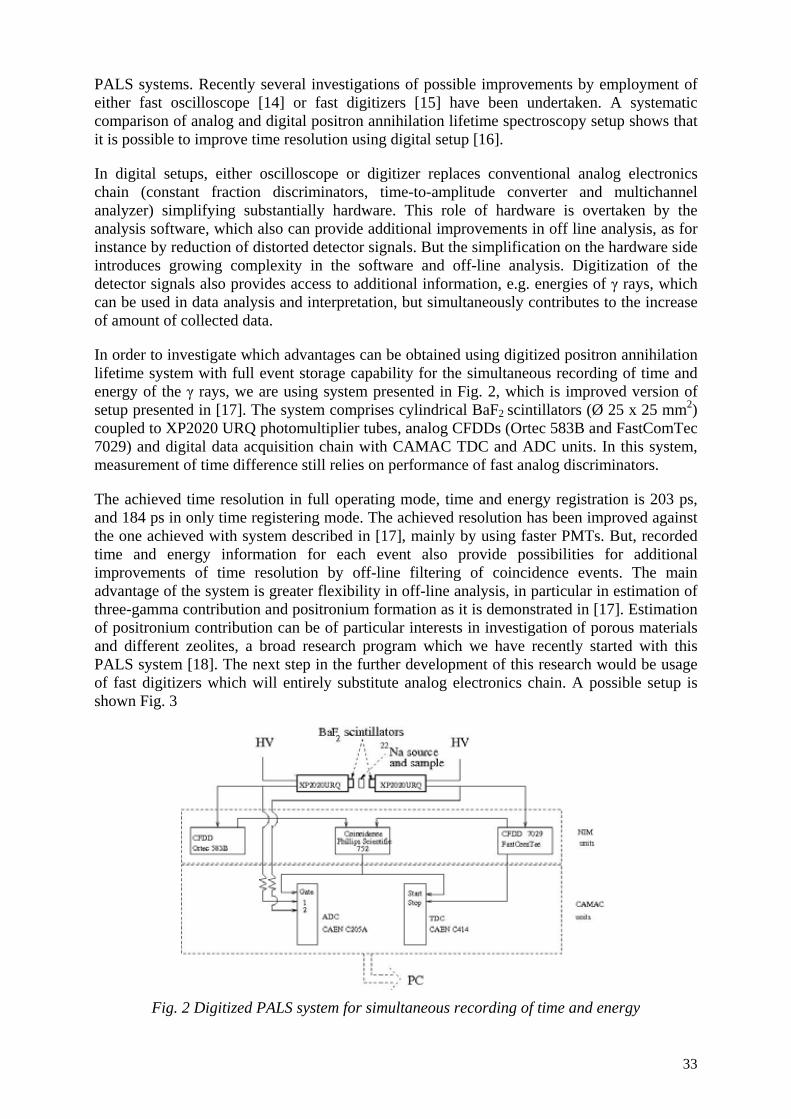
PALS systems. Recently several investigations of possible improvements by employment of either fast oscilloscope [14] or fast digitizers [15] have been undertaken. A systematic comparison of analog and digital positron annihilation lifetime spectroscopy setup shows that it is possible to improve time resolution using digital setup [16].
In digital setups, either oscilloscope or digitizer replaces conventional analog electronics chain (constant fraction discriminators, time-to-amplitude converter and multichannel analyzer) simplifying substantially hardware. This role of hardware is overtaken by the analysis software, which also can provide additional improvements in off line analysis, as for instance by reduction of distorted detector signals. But the simplification on the hardware side introduces growing complexity in the software and off-line analysis. Digitization of the detector signals also provides access to additional information, e.g. energies of γ rays, which can be used in data analysis and interpretation, but simultaneously contributes to the increase of amount of collected data.
In order to investigate which advantages can be obtained using digitized positron annihilation lifetime system with full event storage capability for the simultaneous recording of time and energy of the γ rays, we are using system presented in Fig. 2, which is improved version of setup presented in [17]. The system comprises cylindrical BaF2 scintillators (Ø 25 x 25 mm2) coupled to XP2020 URQ photomultiplier tubes, analog CFDDs (Ortec 583B and FastComTec 7029) and digital data acquisition chain with CAMAC TDC and ADC units. In this system, measurement of time difference still relies on performance of fast analog discriminators.
The achieved time resolution in full operating mode, time and energy registration is 203 ps, and 184 ps in only time registering mode. The achieved resolution has been improved against the one achieved with system described in [17], mainly by using faster PMTs. But, recorded time and energy information for each event also provide possibilities for additional improvements of time resolution by off-line filtering of coincidence events. The main advantage of the system is greater flexibility in off-line analysis, in particular in estimation of three-gamma contribution and positronium formation as it is demonstrated in [17]. Estimation of positronium contribution can be of particular interests in investigation of porous materials and different zeolites, a broad research program which we have recently started with this PALS system [18]. The next step in the further development of this research would be usage of fast digitizers which will entirely substitute analog electronics chain. A possible setup is shown Fig. 3
Fig. 2 Digitized PALS system for simultaneous recording of time and energy
33
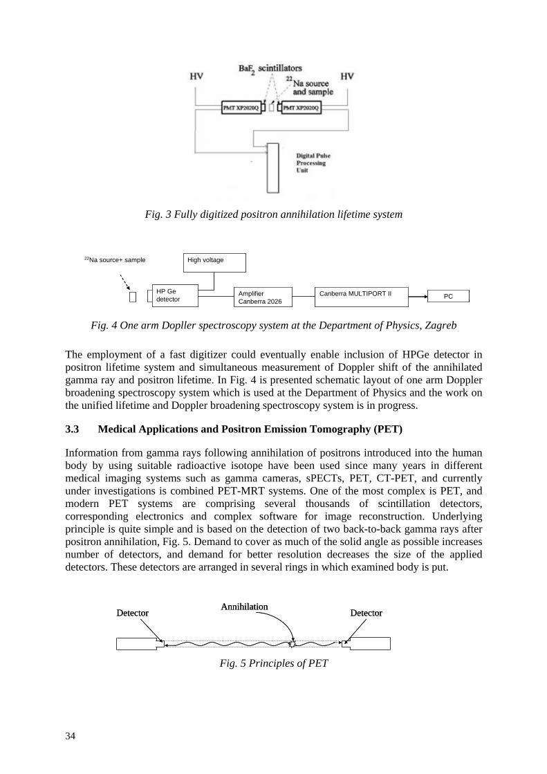
Fig. 3 Fully digitized positron annihilation lifetime system
HP Gedetector
AmplifierCanberra 2026
Canberra MULTIPORT II
High voltage22Na source+ sample
PCHP Gedetector
AmplifierCanberra 2026
Canberra MULTIPORT II
High voltage22Na source+ sample
PC
Fig. 4 One arm Dopller spectroscopy system at the Department of Physics, Zagreb
The employment of a fast digitizer could eventually enable inclusion of HPGe detector in positron lifetime system and simultaneous measurement of Doppler shift of the annihilated gamma ray and positron lifetime. In Fig. 4 is presented schematic layout of one arm Doppler broadening spectroscopy system which is used at the Department of Physics and the work on the unified lifetime and Doppler broadening spectroscopy system is in progress.
3.3 Medical Applications and Positron Emission Tomography (PET)
Information from gamma rays following annihilation of positrons introduced into the human body by using suitable radioactive isotope have been used since many years in different medical imaging systems such as gamma cameras, sPECTs, PET, CT-PET, and currently under investigations is combined PET-MRT systems. One of the most complex is PET, and modern PET systems are comprising several thousands of scintillation detectors, corresponding electronics and complex software for image reconstruction. Underlying principle is quite simple and is based on the detection of two back-to-back gamma rays after positron annihilation, Fig. 5. Demand to cover as much of the solid angle as possible increases number of detectors, and demand for better resolution decreases the size of the applied detectors. These detectors are arranged in several rings in which examined body is put.
AnnihilationDetectorDetector
AnnihilationDetectorDetector
Fig. 5 Principles of PET
34
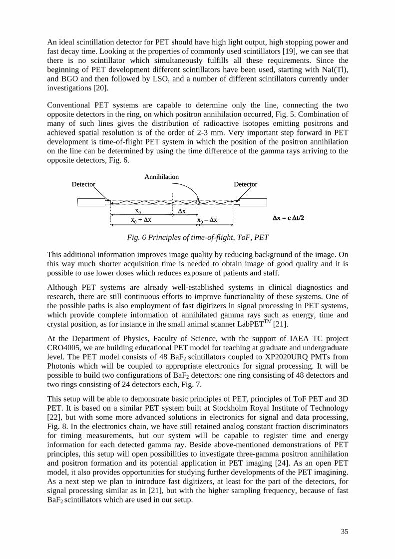
An ideal scintillation detector for PET should have high light output, high stopping power and fast decay time. Looking at the properties of commonly used scintillators [19], we can see that there is no scintillator which simultaneously fulfills all these requirements. Since the beginning of PET development different scintillators have been used, starting with NaI(Tl), and BGO and then followed by LSO, and a number of different scintillators currently under investigations [20].
Conventional PET systems are capable to determine only the line, connecting the two opposite detectors in the ring, on which positron annihilation occurred, Fig. 5. Combination of many of such lines gives the distribution of radioactive isotopes emitting positrons and achieved spatial resolution is of the order of 2-3 mm. Very important step forward in PET development is time-of-flight PET system in which the position of the positron annihilation on the line can be determined by using the time difference of the gamma rays arriving to the opposite detectors, Fig. 6.
AnnihilationDetectorDetector
x0 + Δx x0 – ΔxΔxx0
Δx = c Δt/2
AnnihilationDetectorDetector
x0 + Δx x0 – ΔxΔxx0
Δx = c Δt/2
Fig. 6 Principles of time-of-flight, ToF, PET
This additional information improves image quality by reducing background of the image. On this way much shorter acquisition time is needed to obtain image of good quality and it is possible to use lower doses which reduces exposure of patients and staff.
Although PET systems are already well-established systems in clinical diagnostics and research, there are still continuous efforts to improve functionality of these systems. One of the possible paths is also employment of fast digitizers in signal processing in PET systems, which provide complete information of annihilated gamma rays such as energy, time and crystal position, as for instance in the small animal scanner LabPETTM [21].
At the Department of Physics, Faculty of Science, with the support of IAEA TC project CRO4005, we are building educational PET model for teaching at graduate and undergraduate level. The PET model consists of 48 BaF2 scintillators coupled to XP2020URQ PMTs from Photonis which will be coupled to appropriate electronics for signal processing. It will be possible to build two configurations of BaF2 detectors: one ring consisting of 48 detectors and two rings consisting of 24 detectors each, Fig. 7.
This setup will be able to demonstrate basic principles of PET, principles of ToF PET and 3D PET. It is based on a similar PET system built at Stockholm Royal Institute of Technology [22], but with some more advanced solutions in electronics for signal and data processing, Fig. 8. In the electronics chain, we have still retained analog constant fraction discriminators for timing measurements, but our system will be capable to register time and energy information for each detected gamma ray. Beside above-mentioned demonstrations of PET principles, this setup will open possibilities to investigate three-gamma positron annihilation and positron formation and its potential application in PET imaging [24]. As an open PET model, it also provides opportunities for studying further developments of the PET imagining. As a next step we plan to introduce fast digitizers, at least for the part of the detectors, for signal processing similar as in [21], but with the higher sampling frequency, because of fast BaF2 scintillators which are used in our setup.
35
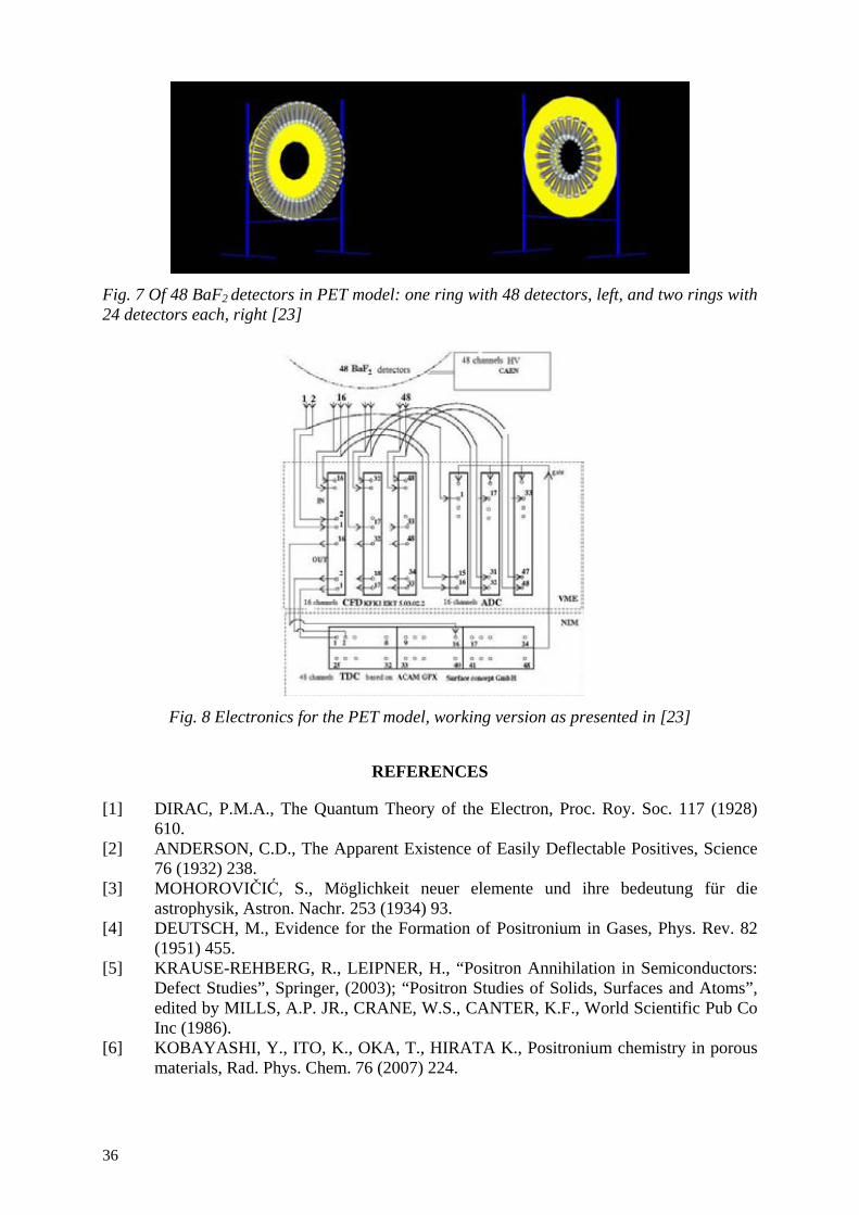
Fig. 7 Of 48 BaF2 detectors in PET model: one ring with 48 detectors, left, and two rings with 24 detectors each, right [23]
Fig. 8 Electronics for the PET model, working version as presented in [23]
REFERENCES
[1] DIRAC, P.M.A., The Quantum Theory of the Electron, Proc. Roy. Soc. 117 (1928) 610.
[2] ANDERSON, C.D., The Apparent Existence of Easily Deflectable Positives, Science 76 (1932) 238.
[3] MOHOROVIČIĆ, S., Möglichkeit neuer elemente und ihre bedeutung für die astrophysik, Astron. Nachr. 253 (1934) 93.
[4] DEUTSCH, M., Evidence for the Formation of Positronium in Gases, Phys. Rev. 82 (1951) 455.
[5] KRAUSE-REHBERG, R., LEIPNER, H., “Positron Annihilation in Semiconductors: Defect Studies”, Springer, (2003); “Positron Studies of Solids, Surfaces and Atoms”, edited by MILLS, A.P. JR., CRANE, W.S., CANTER, K.F., World Scientific Pub Co Inc (1986).
[6] KOBAYASHI, Y., ITO, K., OKA, T., HIRATA K., Positronium chemistry in porous materials, Rad. Phys. Chem. 76 (2007) 224.
36
37
[7] HYODO, T., KOBAYASHI, Y., NAGASHIMA, Y., SAITO, H., Editors, “Proceedings of the 13th International Conference on Positron Annihilation”, Kyoto (2003), (published in Materials Science Forum vol. 445 and 446).
[8] WEBB, S., “The Physics of Medical Imaging”, IOP Publishing Ltd. (2003). [9] ELLIOT, A., Medical imaging, Nucl. Instr. Meth. A546 (2005) 1. [10] BERKO, S., PENDLETON, H., Positronium, Ann. Rev. Nucl. Part. Sci. 30 (1980)
543. [11] GNINENKO, S.N., KRASNIKOV, N.V., RUBBIA, A., Extra dimensions and
invisible decay of orthopositronium, Phys. Rev. D67 (2003) 075012; GNINENKO, S.N., KRASNIKOV, N.V., RUBBIA, A., Positronium physics beyond the Standard Model, Mod. Phys. Lett. A17 (2002) 1713.
[12] MILLS, A.P., CASSIDY, D.B., GREAVES, R.G., Prospects for Making a Bose-Einstein-Condensed Positronium Annihilation Gamma Ray Laser, Mater. Sci Forum 445-446 (2004) 424; MILLS, A.P., Prospects for Making a Bose-Einstein-Condensed Positronium Annihilation Gamma Ray Laser, Rad. Phys. Chem. 76 (2007) 76; CASSIDY, D.B., MILLS, A.P., The production of molecular positronium, Nature 449 (2007) 195.
[13] BEČVAR, F., ČIŽEK, J., LEŠTAK, L., NOVOTNY, I., PROCHAZKA, I., ŠEBESTA. F., A high-resolution BaF2 positron-lifetime spectrometer and experience with its long-term exploitation, Nucl. Instr. Meth., A443 (2000) 557.
[14] SAITO, H., NAGASHIMA, Y., KURIHARA, T., HYODO, T., A new positron lifetime spectrometer using a fast digital oscilloscope and BaF2 scintillators, Nucl. Instr. Meth. A487 (2002) 612; RYTSOLA, K., NISSILA, J., KOKKONEN, J., LAAKSO, A., AAVIKKO, R., SAARINEN, K., Digital measurement of positron lifetime, Appl. Surf. Sci. 194 (2002) 260.
[15] BEČVAR, F., ČIŽEK, J., PROCHAZKA, I., JANTOVA, J., The asset of ultra-fast digitizers for positron-lifetime spectroscopy, Nucl. Instr. Meth. A539 (2005) 372; NISSILA, J., RYTSOLA, K., AAVIKKO, R., LAAKSO, A., SAARINEN, K., HOUTOJARVI, P., Performance analysis of a digital positron lifetime spectrometer, Nucl. Instr. Meth. A538 (2005) 778.
[16] BEČVAR, F., Methodology of positron lifetime spectroscopy: Present status and perspectives, Nucl. Instr. Meth. B261 (2007) 871.
[17] BOSNAR, D., KAJCSOS, Z., LISZKAY, L., LOHONYAI, L., MAJOR, P., BOSNAR, S., KOSANOVIĆ, C., SUBOTIĆ, B., Digitized positron lifetime spectrometer for the simultaneous recording of time and energy information, Nucl. Instr. Meth. A581 (2007) 91.
[18] BOSNAR, S., KOSANOVIĆ, C., SUBOTIĆ, B., BOSNAR, D., KAJCSOS, Z., LISZKAY, L., LOHONYAI, L., MOLNAR, B., LAZAR, K., On the potential of positron lifetime spectroscopy for the study of early stages of zeolites formation from their amorphous precursors, Rad. Phys. Chem. 76 (2007) 252; BOSNAR, S., KOSANOVIĆ, C., SUBOTIĆ, B., BOSNAR, D. KAJCSOS, Z., LISZKAY, L., LOHONYAI, L., MAJOR, P., LAZAR, K., ”Structural and morphological alterations during the zeolite crystallization process”, Contribution to the 15th International Zeolite Conference, Beijing 2007; BOSNAR, S., KOSANOVIĆ, C., SUBOTIĆ, B., BOSNAR, D., KAJCSOS, Z., LISZKAY, L., MAJOR, P., LOHOYAI, L., MOLNAR, B., LAZAR, K., “The influence of alkali cations on the structure of zeolite precursor gels investigated by positron lifetime spectroscopy”, Contribution to the 4th International Federation of European Zeolite Associations Conference, Paris, (2008).
[19] LECOQ, P., Spin-off from particle detectors in the field of medicine and biology, Nucl. Instr. Meth. A581 (2007) 1.
38
[20] ERIKSSON, L., TOWNSEND, D., ERIKSSON, M., MELCHER, C., SCHMAND, M., BENDRIEM, B., NUTT, R., Experience with scintillators for PET: towards the fifth generation of PET scanners, Nucl. Instr. Meth. A525 (2004) 242.
[21] FONTAINE, R., VISCOGLIOSI, N., SEMMAOUI, H., BELANGER, F., LEMIEUX, F., TETAULT, M.A., MICHAUD, J.B., BERARD, P., CADORETTE, J., PEPIN, C.M., LECOMTE, R., Digital signal processing applied to crystal identification in Positron Emission Tomography dedicated to small animals, Nucl. Instr. Meth., A571 (2007) 385.
[22] BACK, T., CEDERKALL, J., CEDERWALL, B., JOHNSON, A., KEREK, A., KLAMRA, W., VAN DER MAREL, J., MOLNAR, J., NOVAK, D., SOHLER, D., STEEN, M., UHLEN, P., A TOF-PET system for educational purposes, Nucl. Instr. Meth. A477 (2002) 82.
[23] FRIŠČIĆ, I., MAKEK, M., BOSNAR, D., BOKULIĆ, T., 5th Scientific Meeting of Croatian Physical Society, (2007).
[24] KACPERSKI, K., SPYROU, N., SMITH, F., Three-gamma annihilation imaging in positron emission tomography, IEEE Trans. Med. Im. 23 (2004) 535; ABUELHIA, E., KACPERSKI, K., KAFALA, S., SPYROU, N., Performance of triple coincidence imaging as an addition to dedicated PET, Rad. Phys. Chem. 76 (2007) 351.
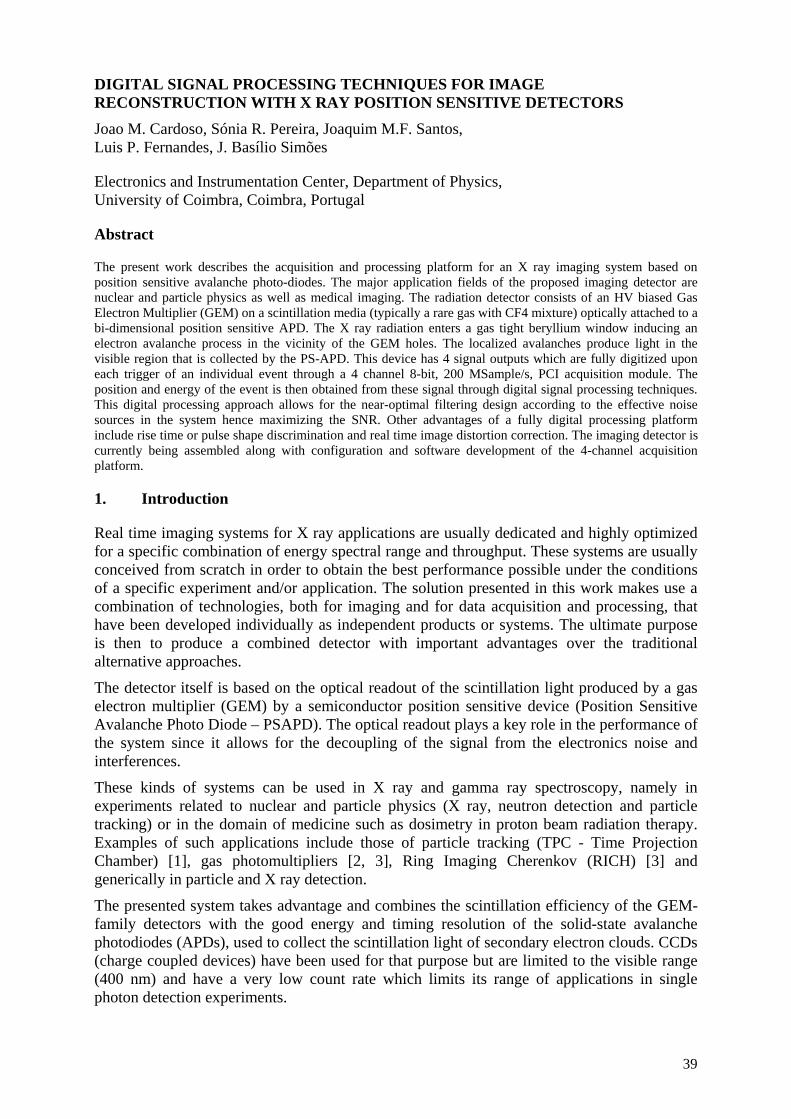
39
DIGITAL SIGNAL PROCESSING TECHNIQUES FOR IMAGE RECONSTRUCTION WITH X RAY POSITION SENSITIVE DETECTORS Joao M. Cardoso, Sónia R. Pereira, Joaquim M.F. Santos, Luis P. Fernandes, J. Basílio Simões
Electronics and Instrumentation Center, Department of Physics, University of Coimbra, Coimbra, Portugal
Abstract
The present work describes the acquisition and processing platform for an X ray imaging system based on position sensitive avalanche photo-diodes. The major application fields of the proposed imaging detector are nuclear and particle physics as well as medical imaging. The radiation detector consists of an HV biased Gas Electron Multiplier (GEM) on a scintillation media (typically a rare gas with CF4 mixture) optically attached to a bi-dimensional position sensitive APD. The X ray radiation enters a gas tight beryllium window inducing an electron avalanche process in the vicinity of the GEM holes. The localized avalanches produce light in the visible region that is collected by the PS-APD. This device has 4 signal outputs which are fully digitized upon each trigger of an individual event through a 4 channel 8-bit, 200 MSample/s, PCI acquisition module. The position and energy of the event is then obtained from these signal through digital signal processing techniques. This digital processing approach allows for the near-optimal filtering design according to the effective noise sources in the system hence maximizing the SNR. Other advantages of a fully digital processing platform include rise time or pulse shape discrimination and real time image distortion correction. The imaging detector is currently being assembled along with configuration and software development of the 4-channel acquisition platform.
1. Introduction
Real time imaging systems for X ray applications are usually dedicated and highly optimized for a specific combination of energy spectral range and throughput. These systems are usually conceived from scratch in order to obtain the best performance possible under the conditions of a specific experiment and/or application. The solution presented in this work makes use a combination of technologies, both for imaging and for data acquisition and processing, that have been developed individually as independent products or systems. The ultimate purpose is then to produce a combined detector with important advantages over the traditional alternative approaches.
The detector itself is based on the optical readout of the scintillation light produced by a gas electron multiplier (GEM) by a semiconductor position sensitive device (Position Sensitive Avalanche Photo Diode – PSAPD). The optical readout plays a key role in the performance of the system since it allows for the decoupling of the signal from the electronics noise and interferences.
These kinds of systems can be used in X ray and gamma ray spectroscopy, namely in experiments related to nuclear and particle physics (X ray, neutron detection and particle tracking) or in the domain of medicine such as dosimetry in proton beam radiation therapy. Examples of such applications include those of particle tracking (TPC - Time Projection Chamber) [1], gas photomultipliers [2, 3], Ring Imaging Cherenkov (RICH) [3] and generically in particle and X ray detection.
The presented system takes advantage and combines the scintillation efficiency of the GEM-family detectors with the good energy and timing resolution of the solid-state avalanche photodiodes (APDs), used to collect the scintillation light of secondary electron clouds. CCDs (charge coupled devices) have been used for that purpose but are limited to the visible range (400 nm) and have a very low count rate which limits its range of applications in single photon detection experiments.
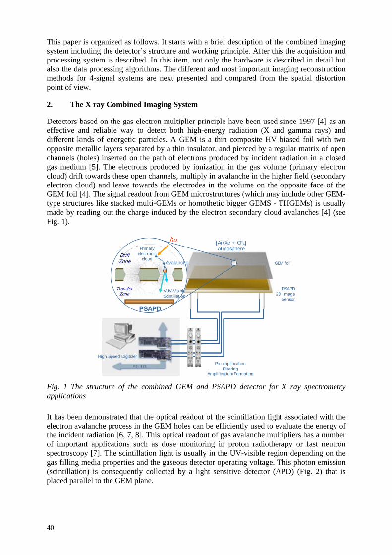
40
This paper is organized as follows. It starts with a brief description of the combined imaging system including the detector’s structure and working principle. After this the acquisition and processing system is described. In this item, not only the hardware is described in detail but also the data processing algorithms. The different and most important imaging reconstruction methods for 4-signal systems are next presented and compared from the spatial distortion point of view.
2. The X ray Combined Imaging System
Detectors based on the gas electron multiplier principle have been used since 1997 [4] as an effective and reliable way to detect both high-energy radiation (X and gamma rays) and different kinds of energetic particles. A GEM is a thin composite HV biased foil with two opposite metallic layers separated by a thin insulator, and pierced by a regular matrix of open channels (holes) inserted on the path of electrons produced by incident radiation in a closed gas medium [5]. The electrons produced by ionization in the gas volume (primary electron cloud) drift towards these open channels, multiply in avalanche in the higher field (secondary electron cloud) and leave towards the electrodes in the volume on the opposite face of the GEM foil [4]. The signal readout from GEM microstructures (which may include other GEM-type structures like stacked multi-GEMs or homothetic bigger GEMS - THGEMs) is usually made by reading out the charge induced by the electron secondary cloud avalanches [4] (see Fig. 1).
GEM foil
PSAPD 2D Image
Sensor
Preamplification Filtering
Amplification/Formating
High Speed Digitizer
hυ Primary
electronic cloud
Avalanche
VUV-VisibleScintillation
Drift Zone
Transfer Zone
PSAPD
[Ar/Xe + CF4] Atmosphere
Fig. 1 The structure of the combined GEM and PSAPD detector for X ray spectrometry applications
It has been demonstrated that the optical readout of the scintillation light associated with the electron avalanche process in the GEM holes can be efficiently used to evaluate the energy of the incident radiation [6, 7, 8]. This optical readout of gas avalanche multipliers has a number of important applications such as dose monitoring in proton radiotherapy or fast neutron spectroscopy [7]. The scintillation light is usually in the UV-visible region depending on the gas filling media properties and the gaseous detector operating voltage. This photon emission (scintillation) is consequently collected by a light sensitive detector (APD) (Fig. 2) that is placed parallel to the GEM plane.
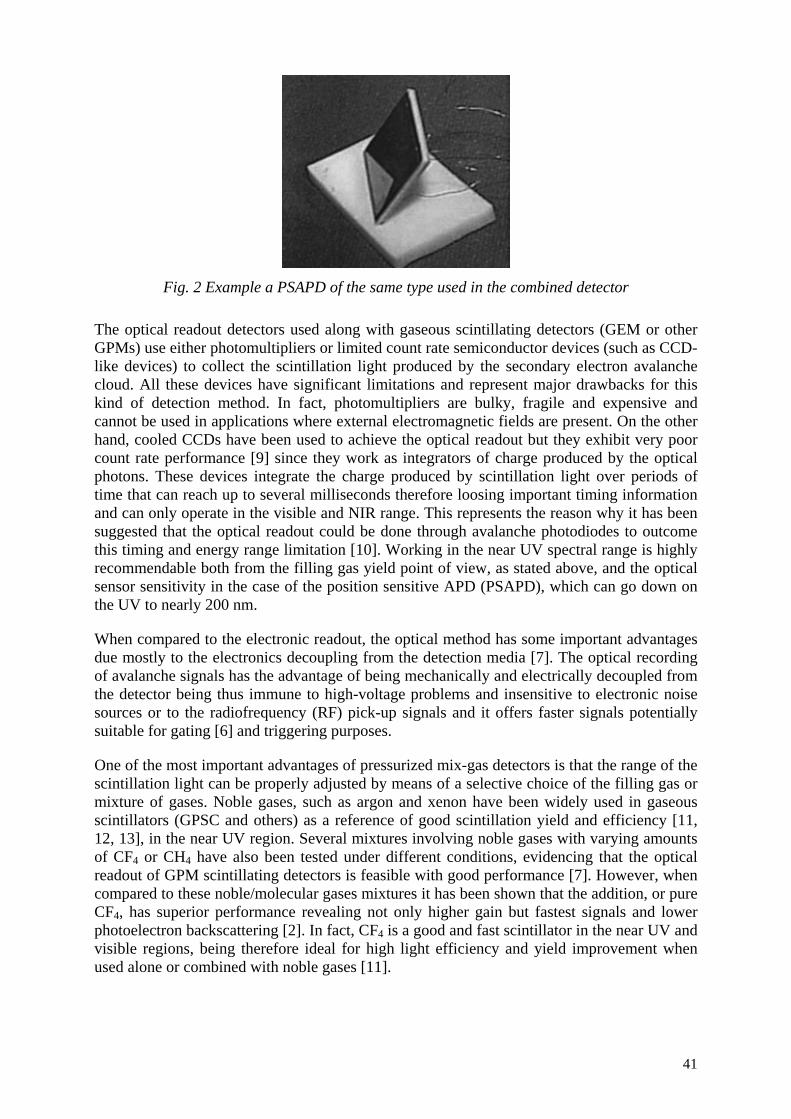
41
Fig. 2 Example a PSAPD of the same type used in the combined detector
The optical readout detectors used along with gaseous scintillating detectors (GEM or other GPMs) use either photomultipliers or limited count rate semiconductor devices (such as CCD-like devices) to collect the scintillation light produced by the secondary electron avalanche cloud. All these devices have significant limitations and represent major drawbacks for this kind of detection method. In fact, photomultipliers are bulky, fragile and expensive and cannot be used in applications where external electromagnetic fields are present. On the other hand, cooled CCDs have been used to achieve the optical readout but they exhibit very poor count rate performance [9] since they work as integrators of charge produced by the optical photons. These devices integrate the charge produced by scintillation light over periods of time that can reach up to several milliseconds therefore loosing important timing information and can only operate in the visible and NIR range. This represents the reason why it has been suggested that the optical readout could be done through avalanche photodiodes to outcome this timing and energy range limitation [10]. Working in the near UV spectral range is highly recommendable both from the filling gas yield point of view, as stated above, and the optical sensor sensitivity in the case of the position sensitive APD (PSAPD), which can go down on the UV to nearly 200 nm.
When compared to the electronic readout, the optical method has some important advantages due mostly to the electronics decoupling from the detection media [7]. The optical recording of avalanche signals has the advantage of being mechanically and electrically decoupled from the detector being thus immune to high-voltage problems and insensitive to electronic noise sources or to the radiofrequency (RF) pick-up signals and it offers faster signals potentially suitable for gating [6] and triggering purposes.
One of the most important advantages of pressurized mix-gas detectors is that the range of the scintillation light can be properly adjusted by means of a selective choice of the filling gas or mixture of gases. Noble gases, such as argon and xenon have been widely used in gaseous scintillators (GPSC and others) as a reference of good scintillation yield and efficiency [11, 12, 13], in the near UV region. Several mixtures involving noble gases with varying amounts of CF4 or CH4 have also been tested under different conditions, evidencing that the optical readout of GPM scintillating detectors is feasible with good performance [7]. However, when compared to these noble/molecular gases mixtures it has been shown that the addition, or pure CF4, has superior performance revealing not only higher gain but fastest signals and lower photoelectron backscattering [2]. In fact, CF4 is a good and fast scintillator in the near UV and visible regions, being therefore ideal for high light efficiency and yield improvement when used alone or combined with noble gases [11].
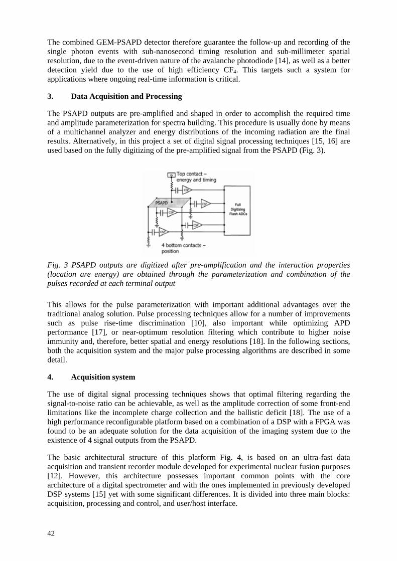
42
The combined GEM-PSAPD detector therefore guarantee the follow-up and recording of the single photon events with sub-nanosecond timing resolution and sub-millimeter spatial resolution, due to the event-driven nature of the avalanche photodiode [14], as well as a better detection yield due to the use of high efficiency CF4. This targets such a system for applications where ongoing real-time information is critical.
3. Data Acquisition and Processing
The PSAPD outputs are pre-amplified and shaped in order to accomplish the required time and amplitude parameterization for spectra building. This procedure is usually done by means of a multichannel analyzer and energy distributions of the incoming radiation are the final results. Alternatively, in this project a set of digital signal processing techniques [15, 16] are used based on the fully digitizing of the pre-amplified signal from the PSAPD (Fig. 3).
Fig. 3 PSAPD outputs are digitized after pre-amplification and the interaction properties (location are energy) are obtained through the parameterization and combination of the pulses recorded at each terminal output
This allows for the pulse parameterization with important additional advantages over the traditional analog solution. Pulse processing techniques allow for a number of improvements such as pulse rise-time discrimination [10], also important while optimizing APD performance [17], or near-optimum resolution filtering which contribute to higher noise immunity and, therefore, better spatial and energy resolutions [18]. In the following sections, both the acquisition system and the major pulse processing algorithms are described in some detail.
4. Acquisition system
The use of digital signal processing techniques shows that optimal filtering regarding the signal-to-noise ratio can be achievable, as well as the amplitude correction of some front-end limitations like the incomplete charge collection and the ballistic deficit [18]. The use of a high performance reconfigurable platform based on a combination of a DSP with a FPGA was found to be an adequate solution for the data acquisition of the imaging system due to the existence of 4 signal outputs from the PSAPD.
The basic architectural structure of this platform Fig. 4, is based on an ultra-fast data acquisition and transient recorder module developed for experimental nuclear fusion purposes [12]. However, this architecture possesses important common points with the core architecture of a digital spectrometer and with the ones implemented in previously developed DSP systems [15] yet with some significant differences. It is divided into three main blocks: acquisition, processing and control, and user/host interface.
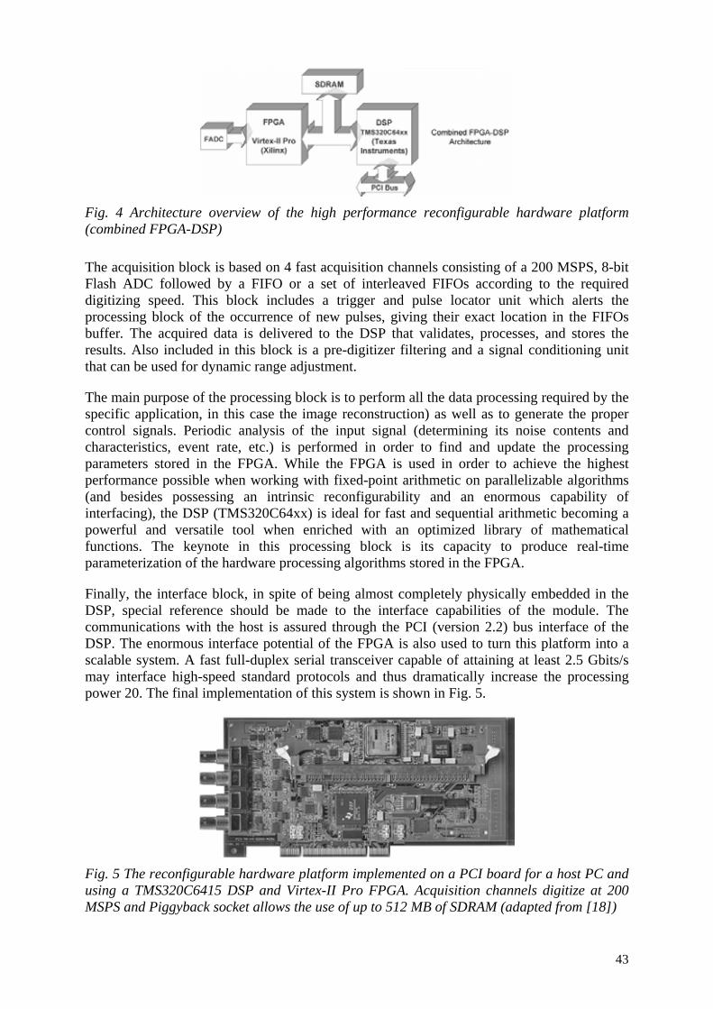
43
Fig. 4 Architecture overview of the high performance reconfigurable hardware platform (combined FPGA-DSP)
The acquisition block is based on 4 fast acquisition channels consisting of a 200 MSPS, 8-bit Flash ADC followed by a FIFO or a set of interleaved FIFOs according to the required digitizing speed. This block includes a trigger and pulse locator unit which alerts the processing block of the occurrence of new pulses, giving their exact location in the FIFOs buffer. The acquired data is delivered to the DSP that validates, processes, and stores the results. Also included in this block is a pre-digitizer filtering and a signal conditioning unit that can be used for dynamic range adjustment.
The main purpose of the processing block is to perform all the data processing required by the specific application, in this case the image reconstruction) as well as to generate the proper control signals. Periodic analysis of the input signal (determining its noise contents and characteristics, event rate, etc.) is performed in order to find and update the processing parameters stored in the FPGA. While the FPGA is used in order to achieve the highest performance possible when working with fixed-point arithmetic on parallelizable algorithms (and besides possessing an intrinsic reconfigurability and an enormous capability of interfacing), the DSP (TMS320C64xx) is ideal for fast and sequential arithmetic becoming a powerful and versatile tool when enriched with an optimized library of mathematical functions. The keynote in this processing block is its capacity to produce real-time parameterization of the hardware processing algorithms stored in the FPGA.
Finally, the interface block, in spite of being almost completely physically embedded in the DSP, special reference should be made to the interface capabilities of the module. The communications with the host is assured through the PCI (version 2.2) bus interface of the DSP. The enormous interface potential of the FPGA is also used to turn this platform into a scalable system. A fast full-duplex serial transceiver capable of attaining at least 2.5 Gbits/s may interface high-speed standard protocols and thus dramatically increase the processing power 20. The final implementation of this system is shown in Fig. 5.
Fig. 5 The reconfigurable hardware platform implemented on a PCI board for a host PC and using a TMS320C6415 DSP and Virtex-II Pro FPGA. Acquisition channels digitize at 200 MSPS and Piggyback socket allows the use of up to 512 MB of SDRAM (adapted from [18])
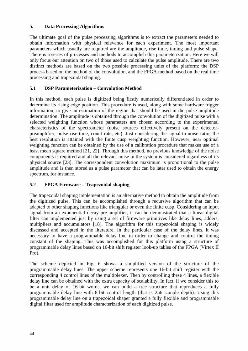
44
5. Data Processing Algorithms
The ultimate goal of the pulse processing algorithms is to extract the parameters needed to obtain information with physical relevance for each experiment. The most important parameters which usually are required are the amplitude, rise time, timing and pulse shape. There is a series of processes and methods to accomplish this parameterization. Here we will only focus our attention on two of those used to calculate the pulse amplitude. There are two distinct methods are based on the two possible processing units of the platform: the DSP process based on the method of the convolution, and the FPGA method based on the real time processing and trapezoidal shaping.
5.1 DSP Parameterization – Convolution Method
In this method, each pulse is digitized being firstly numerically differentiated in order to determine its rising edge position. This procedure is used, along with some hardware trigger information, to give an estimation of the region that should be used in the pulse amplitude determination. The amplitude is obtained through the convolution of the digitized pulse with a selected weighting function whose parameters are chosen according to the experimental characteristics of the spectrometer (noise sources effectively present on the detector-preamplifier, pulse rise-time, count rate, etc). Just considering the signal-to-noise ratio, the best resolution is attained with the finite cusp weighting function. However, near optimal weighting function can be obtained by the use of a calibration procedure that makes use of a least mean square method [21, 22]. Through this method, no previous knowledge of the noise components is required and all the relevant noise in the system is considered regardless of its physical source [23]. The correspondent convolution maximum is proportional to the pulse amplitude and is then stored as a pulse parameter that can be later used to obtain the energy spectrum, for instance.
5.2 FPGA Firmware – Trapezoidal shaping
The trapezoidal shaping implementation is an alternative method to obtain the amplitude from the digitized pulse. This can be accomplished through a recursive algorithm that can be adapted to other shaping functions like triangular or even the finite cusp. Considering an input signal from an exponential decay pre-amplifier, it can be demonstrated that a linear digital filter can implemented just by using a set of firmware primitives like delay lines, adders, multipliers and accumulators [18]. The algorithm for this trapezoidal shaping is widely discussed and accepted in the literature. In the particular case of the delay lines, it was necessary to have a programmable delay line in order to change and control the timing constant of the shaping. This was accomplished for this platform using a structure of programmable delay lines based on 16-bit shift register look-up tables of the FPGA (Virtex II Pro).
The scheme depicted in Fig. 6 shows a simplified version of the structure of the programmable delay lines. The upper scheme represents one 16-bit shift register with the corresponding 4 control lines of the multiplexer. Then by controlling these 4 lines, a flexible delay line can be obtained with the extra capacity of scalability. In fact, if we consider this to be a unit delay of 16-bit words, we can build a tree structure that reproduces a fully programmable delay line with 8-bit control length (that is 256 sample depth). Using this programmable delay line on a trapezoidal shaper granted a fully flexible and programmable digital filter used for amplitude characterization of each digitized pulse.
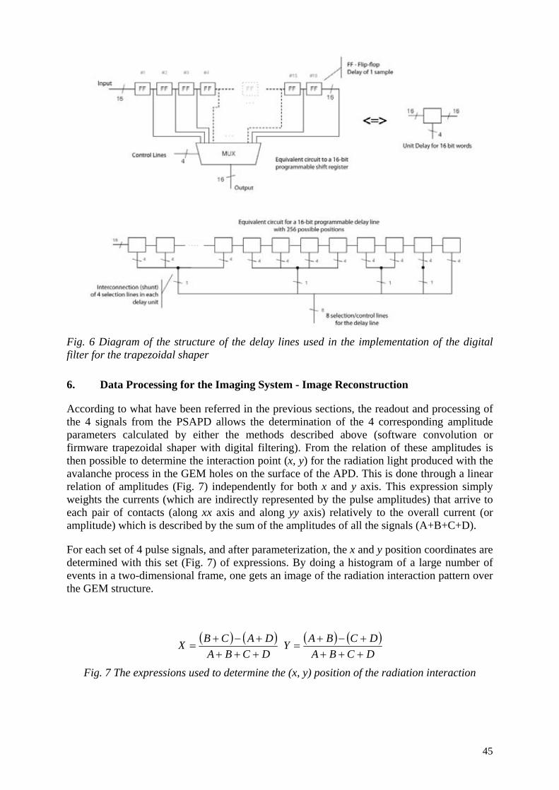
45
Fig. 6 Diagram of the structure of the delay lines used in the implementation of the digital filter for the trapezoidal shaper
6. Data Processing for the Imaging System - Image Reconstruction
According to what have been referred in the previous sections, the readout and processing of the 4 signals from the PSAPD allows the determination of the 4 corresponding amplitude parameters calculated by either the methods described above (software convolution or firmware trapezoidal shaper with digital filtering). From the relation of these amplitudes is then possible to determine the interaction point (x, y) for the radiation light produced with the avalanche process in the GEM holes on the surface of the APD. This is done through a linear relation of amplitudes (Fig. 7) independently for both x and y axis. This expression simply weights the currents (which are indirectly represented by the pulse amplitudes) that arrive to each pair of contacts (along xx axis and along yy axis) relatively to the overall current (or amplitude) which is described by the sum of the amplitudes of all the signals (A+B+C+D).
For each set of 4 pulse signals, and after parameterization, the x and y position coordinates are determined with this set (Fig. 7) of expressions. By doing a histogram of a large number of events in a two-dimensional frame, one gets an image of the radiation interaction pattern over the GEM structure.
( ) ( )DCBADACBX
++++−+
= ( ) ( )DCBADCBAY
++++−+
=
Fig. 7 The expressions used to determine the (x, y) position of the radiation interaction
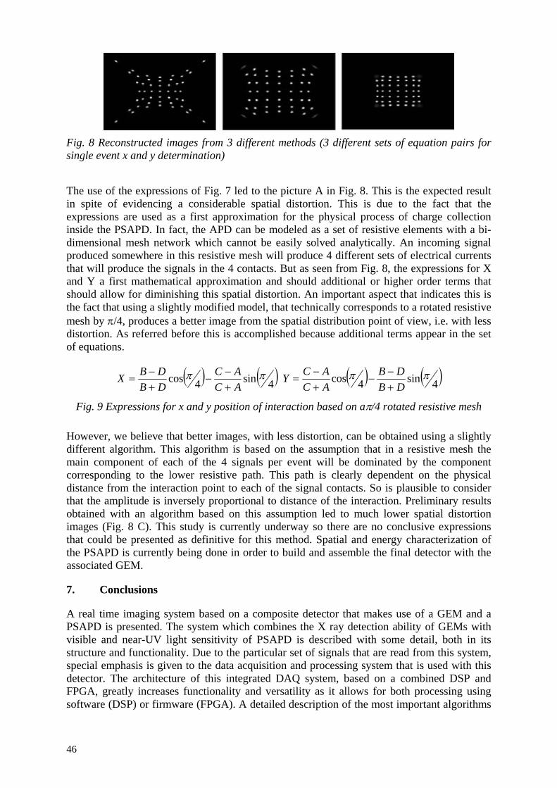
46
Fig. 8 Reconstructed images from 3 different methods (3 different sets of equation pairs for single event x and y determination)
The use of the expressions of Fig. 7 led to the picture A in Fig. 8. This is the expected result in spite of evidencing a considerable spatial distortion. This is due to the fact that the expressions are used as a first approximation for the physical process of charge collection inside the PSAPD. In fact, the APD can be modeled as a set of resistive elements with a bi-dimensional mesh network which cannot be easily solved analytically. An incoming signal produced somewhere in this resistive mesh will produce 4 different sets of electrical currents that will produce the signals in the 4 contacts. But as seen from Fig. 8, the expressions for X and Y a first mathematical approximation and should additional or higher order terms that should allow for diminishing this spatial distortion. An important aspect that indicates this is the fact that using a slightly modified model, that technically corresponds to a rotated resistive mesh by π/4, produces a better image from the spatial distribution point of view, i.e. with less distortion. As referred before this is accomplished because additional terms appear in the set of equations.
( ) ( )4sin4cos ππACAC
DBDBX
+−
−+−
= ( ) ( )4sin4cos ππDBDB
ACACY
+−
−+−
=
Fig. 9 Expressions for x and y position of interaction based on aπ/4 rotated resistive mesh
However, we believe that better images, with less distortion, can be obtained using a slightly different algorithm. This algorithm is based on the assumption that in a resistive mesh the main component of each of the 4 signals per event will be dominated by the component corresponding to the lower resistive path. This path is clearly dependent on the physical distance from the interaction point to each of the signal contacts. So is plausible to consider that the amplitude is inversely proportional to distance of the interaction. Preliminary results obtained with an algorithm based on this assumption led to much lower spatial distortion images (Fig. 8 C). This study is currently underway so there are no conclusive expressions that could be presented as definitive for this method. Spatial and energy characterization of the PSAPD is currently being done in order to build and assemble the final detector with the associated GEM.
7. Conclusions
A real time imaging system based on a composite detector that makes use of a GEM and a PSAPD is presented. The system which combines the X ray detection ability of GEMs with visible and near-UV light sensitivity of PSAPD is described with some detail, both in its structure and functionality. Due to the particular set of signals that are read from this system, special emphasis is given to the data acquisition and processing system that is used with this detector. The architecture of this integrated DAQ system, based on a combined DSP and FPGA, greatly increases functionality and versatility as it allows for both processing using software (DSP) or firmware (FPGA). A detailed description of the most important algorithms
47
used in digital signal processing is made, namely the convolution method with near-optimum weighting functions (DSP) and the trapezoidal shaper through digital filtering and a newly designed programmable digital delay line (FPGA). Finally, the most important image reconstruction techniques for this kind of systems are presented and compared from the spatial distortion point of view.
REFERENCES
[1] KAPPLER, S., et al., A GEM-TPC prototype with low-noise highly integrated front-end electronics for linear collider studies, IEEE Trans. Nucl. Sci., 51-3 (2004) 1039.
[2] BRESKIN, A., et al., GEM photomultiplier operation in CF4, Nucl. Instr. Meth. A483 (2002) 670.
[3] BRESKIN, A., et al., Advances in gas avalanche photomultipliers, Nucl. Instr. Meth. A442 (2000) 58.
[4] SAULI, F., Nucl. Instr. Meth. GEM: A new concept for electron amplification in gas detectors, A386 (1997) 531.
[5] BOUCLIER, R., New observations with the gas electron multiplier (GEM), Nucl. Instr. Meth. A396 (1997) 50.
[6] TITT, U., A time projection chamber with optical readout for charged particle track structure imaging, Nucl. Instr. Meth. A416 (1998) 85.
[7] FRAGA, M., et al., The GEM scintillation in He–CF4, Ar–CF4, Ar–TEA and Xe–TEA mixtures, Nucl. Instr. Meth. A504 (2003) 88.
[8] MEINSCHAD, T., GEM-based photon detector for RICH applications, Nucl. Instr. Meth. A535 (2004) 324.
[9] FETAL, S., et al., Dose imaging in radiotherapy with an Ar–CF4 filled scintillating GEM, Nucl. Instr. Meth. A513 (2003) 42.
[10] MARGATO, L., et al., Time analysis of the light pulses on gaseous active scintillators using GEMs with He/CF4, Nucl. Instr. Meth. A504 (2003) 374.
[11] PERIALE, L., et al., Evaluation of various planar gaseous detectors with CsI photocathodes for the detection of primary scintillation light from noble gases, Nucl. Instr. Meth. A497 (2003) 242.
[12] FRAGA, F., et al., Pressure dependence of secondary NIR scintillation in Ar and Ar/CF4, IEEE Trans. Nucl. Sci. 48-3 (2001) 330.
[13] GELTENBORT, P., OED, A., Proceedings of the Workshop on Progress in GMPC, (1993).
[14] FERNANDES, L.M.P., et al, Non-linear behaviour of large-area avalanche photodiodes, Nucl. Instr. Meth. A478 (2002) 395.
[15] BASILIO SIMÕES, J., et al., Pulse processing architectures, Nucl. Instr. Meth. A422 (1999) 405.
[16] CARDOSO, J., et al., A mixed analog-digital pulse spectrometer, Nucl. Instr. Meth. A422 (1999) 400.
[17] FERNANDES, L.M.P., et al., Digital rise-time discrimination of large-area avalanche photodiode signals in X-ray detection, IEEE Trans. Nucl. Sci. 49-4 (2002) 1699.
[18] CARDOSO, J., et al., A high performance reconfigurable hardware platform for digital pulse processing, IEEE Trans. Nucl. Sci. 51-3 (2004) 921.
[19] COMBO, A. et al., in Proc. 4th IAEA Technical Meeting on Control, Data Acquisition and Remote Participation for Fusion Research, San Diego, CA, July 2003.
[20] COMBO, A., et al., An event-driven reconfigurable real-time processing system for the next generation fusion experiments, Rev. Sci. Instruments 74 (2003) 1815.

48
[21] RIBOLDI, S., et al., A new method for LMS synthesis of optimum finite impulse response (FIR) filters with arbitrary time and frequency constraints and noises, IEEE Nuclear Science Symp. Conf. Rec., 2 (2002) 198–202.
[22] G. BERTUCCIO, PULLIA, A., A method for the determination of the noise parameters in preamplifying systems for semiconductor radiation detectors, Rev. Sci. Instruments 64 (1993) 3294.
[23] PULLIA, A., How to derive the optimum filter in presence of arbitrary noises, time-domain constraints, and shaped input signals: A new method, Nucl. Instr. Meth. A397 (1997) 414.
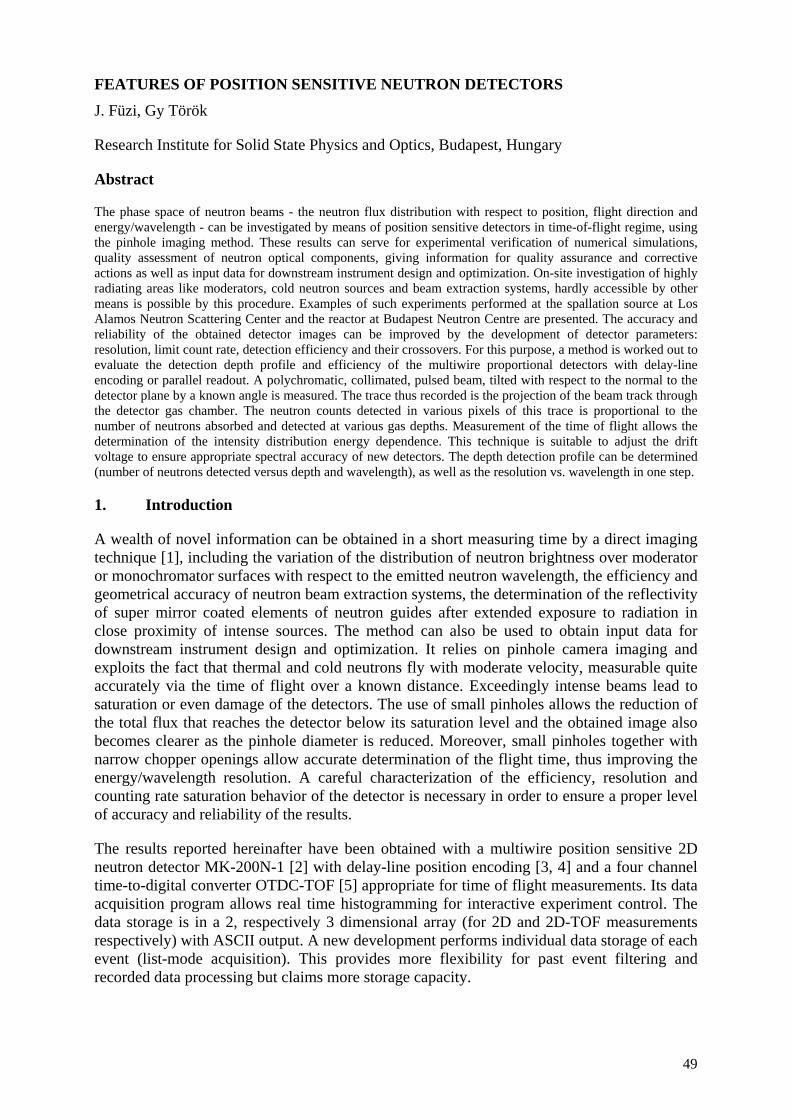
49
FEATURES OF POSITION SENSITIVE NEUTRON DETECTORS J. Füzi, Gy Török
Research Institute for Solid State Physics and Optics, Budapest, Hungary
Abstract
The phase space of neutron beams - the neutron flux distribution with respect to position, flight direction and energy/wavelength - can be investigated by means of position sensitive detectors in time-of-flight regime, using the pinhole imaging method. These results can serve for experimental verification of numerical simulations, quality assessment of neutron optical components, giving information for quality assurance and corrective actions as well as input data for downstream instrument design and optimization. On-site investigation of highly radiating areas like moderators, cold neutron sources and beam extraction systems, hardly accessible by other means is possible by this procedure. Examples of such experiments performed at the spallation source at Los Alamos Neutron Scattering Center and the reactor at Budapest Neutron Centre are presented. The accuracy and reliability of the obtained detector images can be improved by the development of detector parameters: resolution, limit count rate, detection efficiency and their crossovers. For this purpose, a method is worked out to evaluate the detection depth profile and efficiency of the multiwire proportional detectors with delay-line encoding or parallel readout. A polychromatic, collimated, pulsed beam, tilted with respect to the normal to the detector plane by a known angle is measured. The trace thus recorded is the projection of the beam track through the detector gas chamber. The neutron counts detected in various pixels of this trace is proportional to the number of neutrons absorbed and detected at various gas depths. Measurement of the time of flight allows the determination of the intensity distribution energy dependence. This technique is suitable to adjust the drift voltage to ensure appropriate spectral accuracy of new detectors. The depth detection profile can be determined (number of neutrons detected versus depth and wavelength), as well as the resolution vs. wavelength in one step.
1. Introduction
A wealth of novel information can be obtained in a short measuring time by a direct imaging technique [1], including the variation of the distribution of neutron brightness over moderator or monochromator surfaces with respect to the emitted neutron wavelength, the efficiency and geometrical accuracy of neutron beam extraction systems, the determination of the reflectivity of super mirror coated elements of neutron guides after extended exposure to radiation in close proximity of intense sources. The method can also be used to obtain input data for downstream instrument design and optimization. It relies on pinhole camera imaging and exploits the fact that thermal and cold neutrons fly with moderate velocity, measurable quite accurately via the time of flight over a known distance. Exceedingly intense beams lead to saturation or even damage of the detectors. The use of small pinholes allows the reduction of the total flux that reaches the detector below its saturation level and the obtained image also becomes clearer as the pinhole diameter is reduced. Moreover, small pinholes together with narrow chopper openings allow accurate determination of the flight time, thus improving the energy/wavelength resolution. A careful characterization of the efficiency, resolution and counting rate saturation behavior of the detector is necessary in order to ensure a proper level of accuracy and reliability of the results.
The results reported hereinafter have been obtained with a multiwire position sensitive 2D neutron detector MK-200N-1 [2] with delay-line position encoding [3, 4] and a four channel time-to-digital converter OTDC-TOF [5] appropriate for time of flight measurements. Its data acquisition program allows real time histogramming for interactive experiment control. The data storage is in a 2, respectively 3 dimensional array (for 2D and 2D-TOF measurements respectively) with ASCII output. A new development performs individual data storage of each event (list-mode acquisition). This provides more flexibility for past event filtering and recorded data processing but claims more storage capacity.
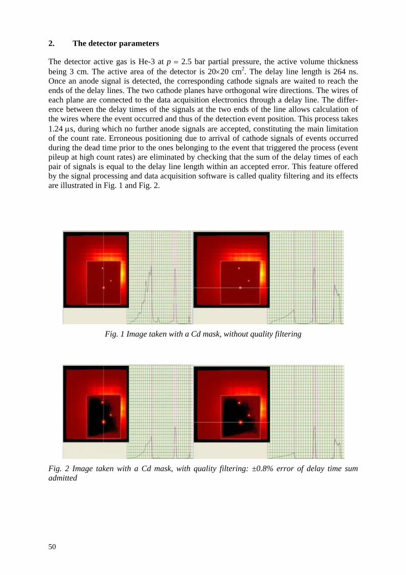
50
2. The detector parameters
The detector active gas is He-3 at p = 2.5 bar partial pressure, the active volume thickness being 3 cm. The active area of the detector is 20×20 cm2. The delay line length is 264 ns. Once an anode signal is detected, the corresponding cathode signals are waited to reach the ends of the delay lines. The two cathode planes have orthogonal wire directions. The wires of each plane are connected to the data acquisition electronics through a delay line. The differ-ence between the delay times of the signals at the two ends of the line allows calculation of the wires where the event occurred and thus of the detection event position. This process takes 1.24 μs, during which no further anode signals are accepted, constituting the main limitation of the count rate. Erroneous positioning due to arrival of cathode signals of events occurred during the dead time prior to the ones belonging to the event that triggered the process (event pileup at high count rates) are eliminated by checking that the sum of the delay times of each pair of signals is equal to the delay line length within an accepted error. This feature offered by the signal processing and data acquisition software is called quality filtering and its effects are illustrated in Fig. 1 and Fig. 2.
Fig. 1 Image taken with a Cd mask, without quality filtering
Fig. 2 Image taken with a Cd mask, with quality filtering: ±0.8% error of delay time sum admitted
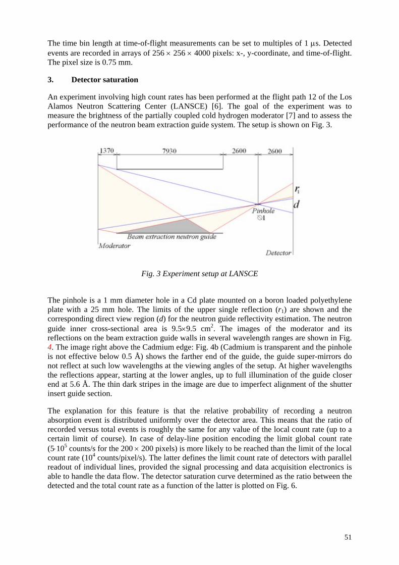
51
The time bin length at time-of-flight measurements can be set to multiples of 1 μs. Detected events are recorded in arrays of 256 × 256 × 4000 pixels: x-, y-coordinate, and time-of-flight. The pixel size is 0.75 mm.
3. Detector saturation
An experiment involving high count rates has been performed at the flight path 12 of the Los Alamos Neutron Scattering Center (LANSCE) [6]. The goal of the experiment was to measure the brightness of the partially coupled cold hydrogen moderator [7] and to assess the performance of the neutron beam extraction guide system. The setup is shown on Fig. 3.
Fig. 3 Experiment setup at LANSCE
The pinhole is a 1 mm diameter hole in a Cd plate mounted on a boron loaded polyethylene plate with a 25 mm hole. The limits of the upper single reflection (r1) are shown and the corresponding direct view region (d) for the neutron guide reflectivity estimation. The neutron guide inner cross-sectional area is 9.5×9.5 cm2. The images of the moderator and its reflections on the beam extraction guide walls in several wavelength ranges are shown in Fig. 4. The image right above the Cadmium edge: Fig. 4b (Cadmium is transparent and the pinhole is not effective below 0.5 Å) shows the farther end of the guide, the guide super-mirrors do not reflect at such low wavelengths at the viewing angles of the setup. At higher wavelengths the reflections appear, starting at the lower angles, up to full illumination of the guide closer end at 5.6 Å. The thin dark stripes in the image are due to imperfect alignment of the shutter insert guide section.
The explanation for this feature is that the relative probability of recording a neutron absorption event is distributed uniformly over the detector area. This means that the ratio of recorded versus total events is roughly the same for any value of the local count rate (up to a certain limit of course). In case of delay-line position encoding the limit global count rate (5⋅105 counts/s for the 200 × 200 pixels) is more likely to be reached than the limit of the local count rate (104 counts/pixel/s). The latter defines the limit count rate of detectors with parallel readout of individual lines, provided the signal processing and data acquisition electronics is able to handle the data flow. The detector saturation curve determined as the ratio between the detected and the total count rate as a function of the latter is plotted on Fig. 6.
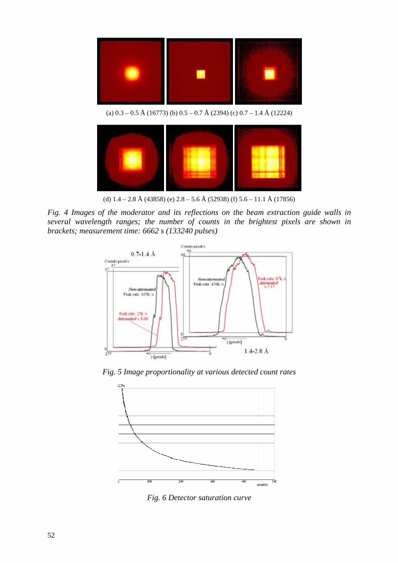
52
(a) 0.3 – 0.5 Å (16773) (b) 0.5 – 0.7 Å (2394) (c) 0.7 – 1.4 Å (12224)
(d) 1.4 – 2.8 Å (43858) (e) 2.8 – 5.6 Å (52938) (f) 5.6 – 11.1 Å (17856)
Fig. 4 Images of the moderator and its reflections on the beam extraction guide walls in several wavelength ranges; the number of counts in the brightest pixels are shown in brackets; measurement time: 6662 s (133240 pulses)
Fig. 5 Image proportionality at various detected count rates
Fig. 6 Detector saturation curve
53
Two measurements have been performed, one with non-attenuated beam and one through a polyethylene attenuator in order to determine the detector saturation. Fig. 5 shows cuts through the detected image at two wavelength ranges both for non-attenuated and attenuated beam. It can be observed that the image on the detector remains proportional even at relatively high count rates (4.5⋅105 detected counts/s over the whole detector active area), where saturation due to dead times is significant.
4. MEASUREMENT OF ABSORPTION AND DETECTION DEPTH PROFILES
The ratio between the number of detected neutrons and the number of neutrons that reach the gas chamber is the detection efficiency, an important characteristic of the detector. The first step of the detection process is the neutron absorption, which depends on the neutron energy, active gas pressure and depth. Secondly, in case of multiwire counters, the electron cloud created by the ionization processes associated to the absorption has to reach the electrode wire frames. This depends on the distance of the event from the frames and the accelerating voltage provided by the drift electrode. Finally, the generated signals have to be identified, recorded and processed. The first two factors can be experimentally investigated by the following technique [8]: a well-collimated, polychromatic, pulsed beam, tilted with respect to the normal to the detector plane by a known angle is measured. A trace is thus recorded, which is the projection on the wire plane of the beam track through the detector gas chamber. The number of neutrons detected in various pixels of this trace is proportional to the number of neutrons absorbed at various gas depths and detected.
The number of neutrons per second reaching the depth x [cm] in the active gas of pressure p [bar] is:
( ) ( ) ⎟⎠⎞
⎜⎝⎛−= x
kpIxI λλλ exp, 0 , (1)
where I0 is the number of neutrons per second of wavelength λ [Å] that enter the detector. For He-3 the value of the constant is k = 13 bar·Å·cm.
The number of neutrons absorbed at depth x in a dx thick gas layer is:
( ) ( ) ⎟⎟⎠
⎞⎜⎜⎝
⎛⎟⎠⎞
⎜⎝⎛−−⎟
⎠⎞
⎜⎝⎛−= x
kpx
kpIxI dexp1exp,d 0
λλλλ . (2)
The neutron absorption ratio with respect to wavelength and depth is:
( ) ⎟⎟⎠
⎞⎜⎜⎝
⎛⎟⎠⎞
⎜⎝⎛−−⎟
⎠⎞
⎜⎝⎛−= x
kpx
kpxa dexp1exp, λλλ . (3)
Equation (2) shows that for a given wavelength the maximum rate of detected neutrons is at the lowest depth that is in the immediate vicinity of the detector gas chamber window. The higher the wavelength, the more pronounced this effect is.
A set of measurements has been performed at the Budapest Neutron Centre for determination of the depth detection characteristic. The measurement setup is shown on Fig. 7. Dimensions are given in mm. CNS stands for the cold neutron source, M is a graphite monochromator tuned to 4.26 Å, G is a tapered neutron guide, Ch, P a chopper with 1 mm wide slit and a 1 mm diameter pinhole at 95 mm from chopper axis (kch = 600) and D a He-3 multiwire gas chamber with 1.3 mm pixel size, nx × ny × nt array size: 156×156 ×2000, time bin length: td = 15 ms.
54
Fig. 7 . Measurement setup for depth detection profile measurement
Cuts in the neutron beam phase space measured without any mask in front of the detector are plotted in Fig. 8. The narrow dark stripes are direct and reflected images of the guide interruption at the location of the monochromator. The large dark stripes on Fig. 8c, the wide vertical stripe on Fig. 8e and the dark rectangles in Fig. 8f are due to the monochromator which is opaque at 4.26 Å (the wavelength diverted towards a reflectometer). The shadows corresponding to the first upper harmonic at 2.13 Å are also visible as a dark stripe on Fig. 8e and narrower dark rectangles in Fig. 8f. The δx (λ) plot shows a continuous dark stripe since its summation area lies entirely in the monochromator shadow, while the δy (λ) plot shows discrete dark rectangles because the monochromator occupies only a part of the beam cross section in vertical direction (as shown on Fig. 7). The wide dark horizontal stripe on the δy (δx) plot for 4.1 – 4.5 Å wavelength range around the zero vertical divergence value is the direct view of the monochromator, the other wide stripes are its reflections on the guide walls.
Fig. 8 Neutron beam phase space without Cd mask
55
Fig. 9(a) has been obtained with a Cd mask in front of the detector window, with the detector plane orthogonal to the beam axis. The mask had 2 mm diameter holes arranged in a tilted square array. The collimation in this setup is 3 mm transversal displacement over 4200 mm length. The square frame size is 35 × 35 mm = 27 × 27 pixels, giving a d = 1.3 mm pixel size. The detector active area is: 154 × 154 pixels = 192 × 192 mm. Fig. 9b shows the traces measured with the detector tilted by 36° with respect to the beam axis. The summation areas used in subsequent calculations are also shown.
The recorded track projections for several drift voltage values and wavelength ranges are shown on Fig. 10, where the depth of a track increases from left to right. It can be observed that, opposed to the theoretical gas absorption profile Eq. 2, where more events occur closer to the surface, at low drift voltage values the deeper regions are brighter, in the proximity of the wire frames.
A B
Fig. 9 Images through a Cd mask, taken with detector plane a) orthogonal to the beam axis b) tilted by 36° with respect to the beam axis (detail)
Fig. 10 Tilted beam track projections
Accordingly, the depth detection profiles shown in Fig. 11 present a brighter stripe where the wire frames are for lower drift voltage values and resemble with the theoretical profile only for Ud = −3000 V. The dark stripe in case of summation area a is the shadow of the monochromator at 4.26 Å.
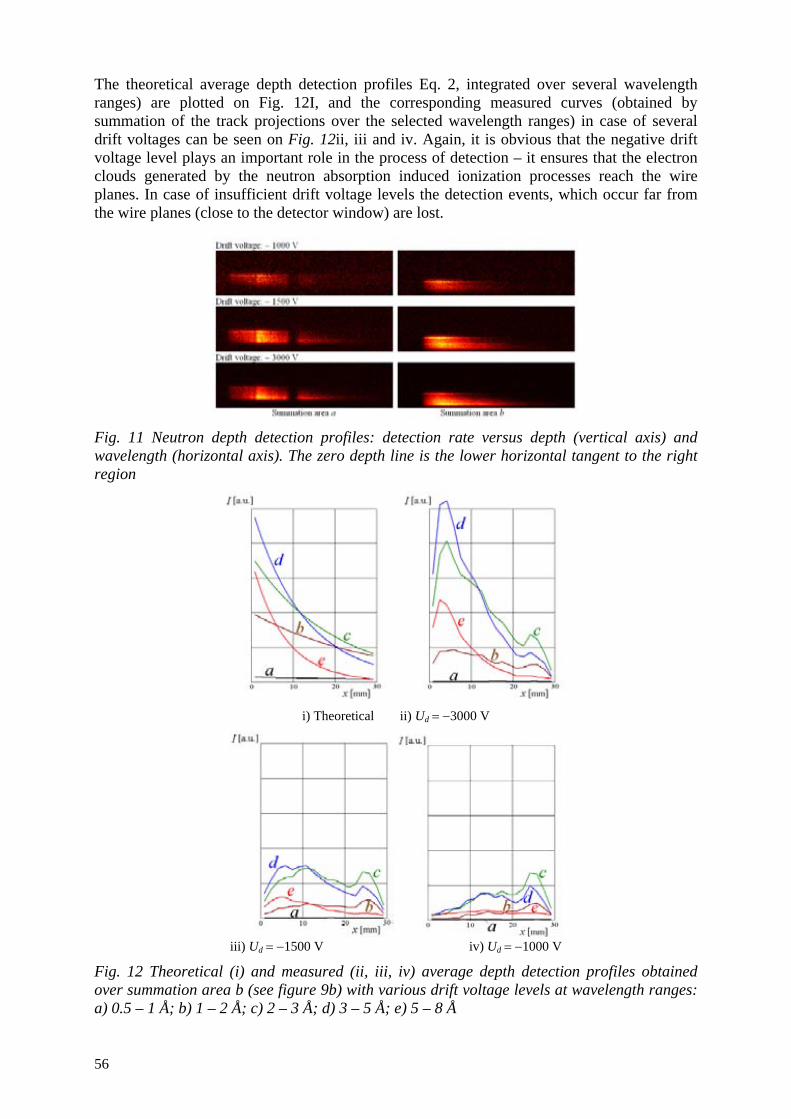
56
The theoretical average depth detection profiles Eq. 2, integrated over several wavelength ranges) are plotted on Fig. 12I, and the corresponding measured curves (obtained by summation of the track projections over the selected wavelength ranges) in case of several drift voltages can be seen on Fig. 12ii, iii and iv. Again, it is obvious that the negative drift voltage level plays an important role in the process of detection – it ensures that the electron clouds generated by the neutron absorption induced ionization processes reach the wire planes. In case of insufficient drift voltage levels the detection events, which occur far from the wire planes (close to the detector window) are lost.
Fig. 11 Neutron depth detection profiles: detection rate versus depth (vertical axis) and wavelength (horizontal axis). The zero depth line is the lower horizontal tangent to the right region
i) Theoretical ii) Ud = −3000 V
iii) Ud = −1500 V iv) Ud = −1000 V
Fig. 12 Theoretical (i) and measured (ii, iii, iv) average depth detection profiles obtained over summation area b (see figure 9b) with various drift voltage levels at wavelength ranges: a) 0.5 – 1 Å; b) 1 – 2 Å; c) 2 – 3 Å; d) 3 – 5 Å; e) 5 – 8 Å
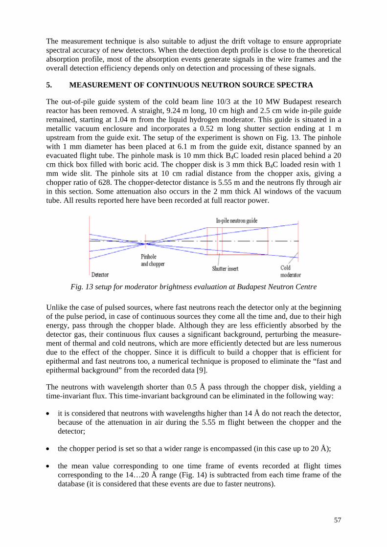
57
The measurement technique is also suitable to adjust the drift voltage to ensure appropriate spectral accuracy of new detectors. When the detection depth profile is close to the theoretical absorption profile, most of the absorption events generate signals in the wire frames and the overall detection efficiency depends only on detection and processing of these signals.
5. MEASUREMENT OF CONTINUOUS NEUTRON SOURCE SPECTRA
The out-of-pile guide system of the cold beam line 10/3 at the 10 MW Budapest research reactor has been removed. A straight, 9.24 m long, 10 cm high and 2.5 cm wide in-pile guide remained, starting at 1.04 m from the liquid hydrogen moderator. This guide is situated in a metallic vacuum enclosure and incorporates a 0.52 m long shutter section ending at 1 m upstream from the guide exit. The setup of the experiment is shown on Fig. 13. The pinhole with 1 mm diameter has been placed at 6.1 m from the guide exit, distance spanned by an evacuated flight tube. The pinhole mask is 10 mm thick B4C loaded resin placed behind a 20 cm thick box filled with boric acid. The chopper disk is 3 mm thick B4C loaded resin with 1 mm wide slit. The pinhole sits at 10 cm radial distance from the chopper axis, giving a chopper ratio of 628. The chopper-detector distance is 5.55 m and the neutrons fly through air in this section. Some attenuation also occurs in the 2 mm thick Al windows of the vacuum tube. All results reported here have been recorded at full reactor power.
Fig. 13 setup for moderator brightness evaluation at Budapest Neutron Centre
Unlike the case of pulsed sources, where fast neutrons reach the detector only at the beginning of the pulse period, in case of continuous sources they come all the time and, due to their high energy, pass through the chopper blade. Although they are less efficiently absorbed by the detector gas, their continuous flux causes a significant background, perturbing the measure-ment of thermal and cold neutrons, which are more efficiently detected but are less numerous due to the effect of the chopper. Since it is difficult to build a chopper that is efficient for epithermal and fast neutrons too, a numerical technique is proposed to eliminate the “fast and epithermal background” from the recorded data [9].
The neutrons with wavelength shorter than 0.5 Å pass through the chopper disk, yielding a time-invariant flux. This time-invariant background can be eliminated in the following way:
• it is considered that neutrons with wavelengths higher than 14 Å do not reach the detector, because of the attenuation in air during the 5.55 m flight between the chopper and the detector;
• the chopper period is set so that a wider range is encompassed (in this case up to 20 Å);
• the mean value corresponding to one time frame of events recorded at flight times corresponding to the 14…20 Å range (Fig. 14) is subtracted from each time frame of the database (it is considered that these events are due to faster neutrons).
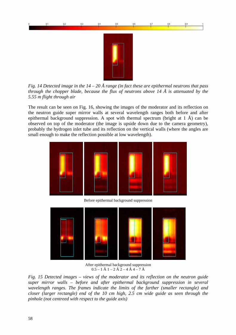
58
Fig. 14 Detected image in the 14 – 20 Å range (in fact these are epithermal neutrons that pass through the chopper blade, because the flux of neutrons above 14 Å is attenuated by the 5.55 m flight through air
The result can be seen on Fig. 16, showing the images of the moderator and its reflection on the neutron guide super mirror walls at several wavelength ranges both before and after epithermal background suppression. A spot with thermal spectrum (bright at 1 Å) can be observed on top of the moderator (the image is upside down due to the camera geometry), probably the hydrogen inlet tube and its reflection on the vertical walls (where the angles are small enough to make the reflection possible at low wavelength).
Before epithermal background suppression
After epithermal background suppression
0.5 – 1 Å 1 – 2 Å 2 – 4 Å 4 – 7 Å
Fig. 15 Detected images – views of the moderator and its reflection on the neutron guide super mirror walls – before and after epithermal background suppression in several wavelength ranges. The frames indicate the limits of the farther (smaller rectangle) and closer (larger rectangle) end of the 10 cm high, 2.5 cm wide guide as seen through the pinhole (not centreed with respect to the guide axis)
59
The neutron velocity v is determined by measurement of the flight time t required for the neutron to cover the flight distance l between the chopper and the detector. The wavelength (in Ångström) is given by
vvmh
n
3956≈=λ , (4)
where h is the Planck constant and mn the neutron mass, the velocity being expressed in m/s.
The flux distribution is computed according to
chd ktA
I⋅
⋅⋅⋅⋅=
ddd ΩληΦ , (5)
where I is the number of counts measured on nx × ny detector pixels in one time bin; dA [cm2] the pinhole area; dΩ = nx⋅ ny⋅d2 / l2 the solid angle corresponding to the observed area; l [mm] the pinhole-detector distance (equal to the chopper to detector flight length); d [mm] the de-tector pixel size; t[s] the measurement time; dλ = 3956⋅td / l [Å] the incremental wavelength; td [ms] the length of the detector time bin; kch the chopper ratio (chopper period / chopper open time): kch = tch / to.
The brightness of the moderator can be determined according to
⎥⎦⎤
⎢⎣⎡
⋅⋅⋅⋅⋅⋅⋅⋅⋅⋅=
Åsrscmn
d3956 22
3
chyxd
d ktAdnnt
lIη
Φ (6)
provided the summation area is exactly its image.
The accuracy of the wavelength determination is:
( )[ ]do
f
f ttggl
l++
−= 3956
4
22
λλΔ (7)
where lf = 5550 mm is the flight length, g = 35 mm the detector gas active depth, to = 51 μs the chopper open time and td = 16 μs the length of the detector time bin, leading to Δλ = 0.0063λ + 0.0477 Å.
The spectrum of the moderator in thermal regime and the Maxwell-Boltzmann fit to the (corrected for detector efficiency) is shown on Fig. 16. Its parameters are: T = 320 K (the reactor pool temperature) and total flux equal to 5.6 x 10¹¹ neutrons/cm2/s/sr. The ripples above 4 Å are still due to epithermal neutrons. These cannot be completely eliminated by the described method because of the inhomogenities of the chopper blade.
The spectrum in cold regime (the entire moderator volume is filled with liquid hydrogen) is plotted on Fig. 17. The Maxwell-Boltzmann fit:
[ ]Å81.302
;exp23
12
2
5
4
kkTk
k
TkTkk TmkT
h==⎟⎟
⎠
⎞⎜⎜⎝
⎛−= ∑
=
λλλ
λλ
ΦΦ λ (8)
is composed of three distributions with parameters T1 = 320 K (reactor pool temperature), Φ1 = 0.9 ⋅1011 n/cm2/s/sr; T2 = 80 K (due to incomplete moderation in the liquid hydrogen volume of finite thickness), Φ2 = 4⋅1011 n/cm2/s/sr; T3 = 20 K (liquid hydrogen temperature), Φ3 = 1.1⋅1011 n/cm2/s/sr.
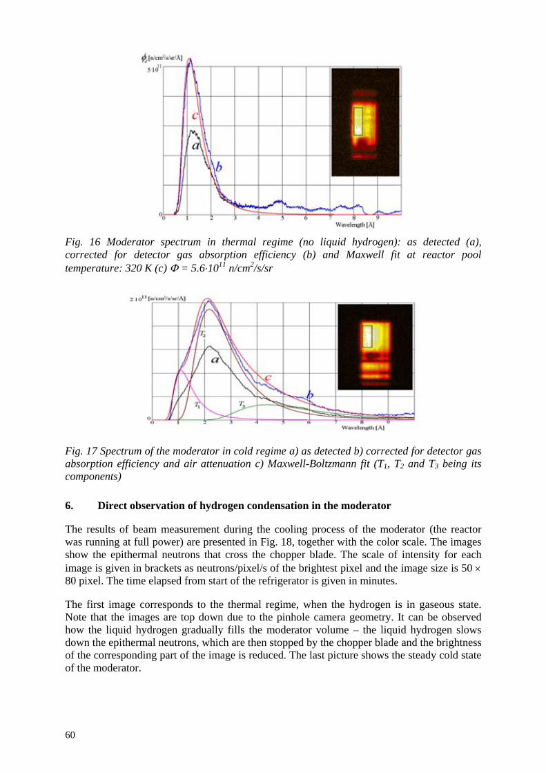
60
Fig. 16 Moderator spectrum in thermal regime (no liquid hydrogen): as detected (a), corrected for detector gas absorption efficiency (b) and Maxwell fit at reactor pool temperature: 320 K (c) Φ = 5.6⋅1011 n/cm2/s/sr
Fig. 17 Spectrum of the moderator in cold regime a) as detected b) corrected for detector gas absorption efficiency and air attenuation c) Maxwell-Boltzmann fit (T1, T2 and T3 being its components)
6. Direct observation of hydrogen condensation in the moderator
The results of beam measurement during the cooling process of the moderator (the reactor was running at full power) are presented in Fig. 18, together with the color scale. The images show the epithermal neutrons that cross the chopper blade. The scale of intensity for each image is given in brackets as neutrons/pixel/s of the brightest pixel and the image size is 50 × 80 pixel. The time elapsed from start of the refrigerator is given in minutes.
The first image corresponds to the thermal regime, when the hydrogen is in gaseous state. Note that the images are top down due to the pinhole camera geometry. It can be observed how the liquid hydrogen gradually fills the moderator volume – the liquid hydrogen slows down the epithermal neutrons, which are then stopped by the chopper blade and the brightness of the corresponding part of the image is reduced. The last picture shows the steady cold state of the moderator.
61
Fig. 18 Images of the BNC cold moderator during hydrogen condensation
7. Conclusions
Energy resolved pinhole imaging – essentially based on the use of two-dimensional detectors – offers the possibility to map the neutron beam phase space with good spatial, angular and wavelength resolution. Direct images of bright sources can be obtained and significant information gained on the status of neutron optical systems hardly accessible by other means of investigation, primarily due to high radiation levels in operation and high radioactivity in standby state of the investigated area. This is especially the case of moderators and beam extraction systems, both new ones and systems which have been in operation for some time. In case of continuous source investigations, the intense epithermal neutron flux that passes through the chopper blade can be subtracted from the acquired data because it does not vary with the time of flight, as it is not chopped. Investigation of energy dependent features of neutron optical elements are possible as well as the determination of brightness, uniformity and spectrum of neutron sources.
The detection depth profile determination based on measurement of well-collimated, narrow, tilted beams allows the evaluation of the actual detection efficiency of the absorption events. The negative drift voltage level plays an important role in the process of detection – it ensures that the electron clouds generated by the neutron absorption induced ionization processes reach the wire plane. The measurement technique is also suitable to adjust the drift voltage to ensure appropriate spectral accuracy of new detectors. When the detection depth profile is close to the theoretical absorption profile, most of the absorption events generate signals in the wire frames and the overall detection efficiency depends only on detection and processing of these signals.
REFERENCES
[1] FÜZI, J., Neutron beam phase space mapping, Physica B385 (2006) 1253. [2] MK-200N-1 – position sensitive 2D neutron detector,
http://www.mirrotron.kfkipark.hu/sub_normal.html.
62
[3] BOIE, R.A, FISCHER J., INAGAKI, Y., MERRITT, F.C., OKUNO, H., RADEKA, V., Two-Dimensional High Precision Thermal Neutron Detector, Nucl. Instr. Meth. 200 (1982) 533.
[4] BOIE, R.A., FISCHER, J., INAGAKI, Y., MERRITT, F.C., RADEKA, V., ROGERS, L.C., XI D.M., High Resolution X-ray Gas Proportional Detectors with Delay Line Position Sensing for High Counting Rates, Nucl. Instr. Meth. 201 (1982) 93.
[5] OPEN Optoelectronics, Ltd, “OTDC-TOF – four channel time-to-digital converter for 2D time of flight measurements”, http://www.openopto.kfkipark.hu/otdc2dtof.html.
[6] FÜZI, J., DÁVID, E., KOZLOWSKI, T., LEWIS, P., MESSING, G., MEZEI, F., PENTTILA, S., ROSTA, L., RUSSINA, M., TÖRÖK, G., Neutron optical imaging study of neutron moderator and beam extraction system, Physica B385 (2006) 1315.
[7] SEO, P.N., BOWMAN, J.D., GERICKE, M., GREENE, G., LONG, J., MITCHELL, G.S., PENTTILA, S.I., WILBURN, W.S., A measurement of the Flight Path 12 cold H2 moderator brightness at LANSCE, Nucl. Instr. Meth. A517 (2004) 285.
[8] FÜZI, J., Spectral accuracy of multiwire proportional counter neutron detectors in time-of-flight regime, Meas. Sci. Technol. 19 (2008) 034028(7).
[9] FÜZI, J., Direct measurement of cold neutron moderator spectra, Nucl. Instr. Meth. A586 (2008) 41.
63
POSSIBILITIES OF LABORATORY INSTRUMENT UPGRADING BY USE OF DIGITAL SIGNAL PROCESSORS OR FIELD PROGRAMMABLE GATE ARRAYS
M. Smailou1, Z. Mindaoudou Souley2
1 Institut National de Recherches Agronomiques du Niger (INRAN), Niamey, Niger
2 Institut des Radio Isotopes, Université Abdou Moumouni de Niamey, Niamey, Niger
Abstract
After a nuclear instrumentation laboratory is adequately equipped, attention must be given to the ongoing operation and maintenance. This is an important consideration in the production of satisfactory data and quality control. It requires that the maintenance technician or engineer has adequate understanding of each instrument design in order to detect any problem that arises. Nowadays, manufacturers make use of new technology such as microprocessors, microcontrollers, digital signal processors (DSP), field programmable gates arrays (FPGA), programmable logic controller (PLC) to improve their equipment design, thus increasing the efficiency and quality of measurements. These embedded components are designed in a digital configuration which makes them difficult to troubleshoot, once faulty. Therefore, equipment maintenance has evolved from repair to replacement of boards. Boards that are designed based on the new technology can be used to upgrade an existing instrument for a data acquisition, spectrum analyzing, etc. Communication between these components and the computer can be achieved by LabVIEW and with user interfaces designed using a LabVIEW environment.
1. Introduction
Many African laboratories today contain numerous instruments which are old, some of them obsolete. The reading of measurement are either taken by readout display or through some printers attached to the instrument via a parallel port. This communication demonstrates some possibilities to use the existing communication port in order to interface the instrument with the PC for data storage and control. In addition some hardware such DSP or FPGA boards can be used as interface to the instrument. Communication between these components and the computer can be achieved by LabVIEW, a National Instruments graphical software package. As well, the user interface can be designed using a LabVIEW environment.
2. System Development
To carry out such kind of project as shown in Fig.1, we need:
• Instrument with communications port such as parallel port, RS232 port, GPIB port, USB and so on. Since our study is focused on old laboratory instrument, the only port available is either parallel port or RS 232.
• For some circumstances hardware interfaces such as DSP or FPGA boards for further analysis and control
• A PC for better control of the system and data storage
• LABVIEW, a software used to create a graphical user interface and ANSI C to design a relative program to work with it.
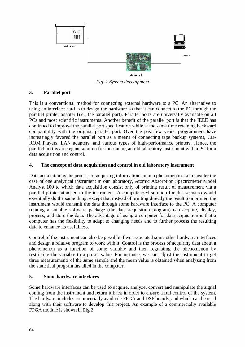
64
Fig. 1 System development
3. Parallel port
This is a conventional method for connecting external hardware to a PC. An alternative to using an interface card is to design the hardware so that it can connect to the PC through the parallel printer adapter (i.e., the parallel port). Parallel ports are universally available on all PCs and most scientific instruments. Another benefit of the parallel port is that the IEEE has continued to improve the parallel port specification while at the same time retaining backward compatibility with the original parallel port. Over the past few years, programmers have increasingly favored the parallel port as a means of connecting tape backup systems, CD-ROM Players, LAN adapters, and various types of high-performance printers. Hence, the parallel port is an elegant solution for interfacing an old laboratory instrument with a PC for a data acquisition and control.
4. The concept of data acquisition and control in old laboratory instrument
Data acquisition is the process of acquiring information about a phenomenon. Let consider the case of one analytical instrument in our laboratory, Atomic Absorption Spectrometer Model Analyst 100 to which data acquisition consist only of printing result of measurement via a parallel printer attached to the instrument. A computerized solution for this scenario would essentially do the same thing, except that instead of printing directly the result to a printer, the instrument would transmit the data through some hardware interface to the PC. A computer running a suitable software package (the data acquisition program) can acquire, display, process, and store the data. The advantage of using a computer for data acquisition is that a computer has the flexibility to adapt to changing needs and to further process the resulting data to enhance its usefulness.
Control of the instrument can also be possible if we associated some other hardware interfaces and design a relative program to work with it. Control is the process of acquiring data about a phenomenon as a function of some variable and then regulating the phenomenon by restricting the variable to a preset value. For instance, we can adjust the instrument to get three measurements of the same sample and the mean value is obtained when analyzing from the statistical program installed in the computer.
5. Some hardware interfaces
Some hardware interfaces can be used to acquire, analyze, convert and manipulate the signal coming from the instrument and return it back in order to ensure a full control of the system. The hardware includes commercially available FPGA and DSP boards, and which can be used along with their software to develop this project. An example of a commercially available FPGA module is shown in Fig 2.
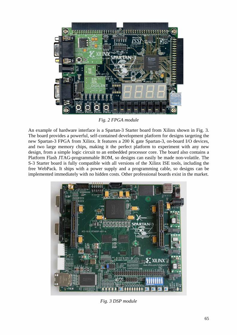
65
Fig. 2 FPGA module
An example of hardware interface is a Spartan-3 Starter board from Xilinx shown in Fig. 3. The board provides a powerful, self-contained development platform for designs targeting the new Spartan-3 FPGA from Xilinx. It features a 200 K gate Spartan-3, on-board I/O devices, and two large memory chips, making it the perfect platform to experiment with any new design, from a simple logic circuit to an embedded processor core. The board also contains a Platform Flash JTAG-programmable ROM, so designs can easily be made non-volatile. The S-3 Starter board is fully compatible with all versions of the Xilinx ISE tools, including the free WebPack. It ships with a power supply and a programming cable, so designs can be implemented immediately with no hidden costs. Other professional boards exist in the market.
Fig. 3 DSP module
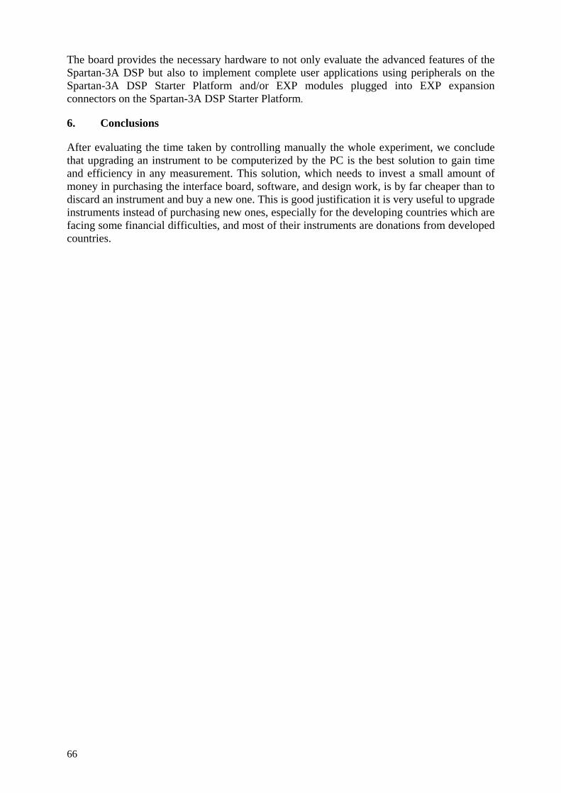
66
The board provides the necessary hardware to not only evaluate the advanced features of the Spartan-3A DSP but also to implement complete user applications using peripherals on the Spartan-3A DSP Starter Platform and/or EXP modules plugged into EXP expansion connectors on the Spartan-3A DSP Starter Platform.
6. Conclusions
After evaluating the time taken by controlling manually the whole experiment, we conclude that upgrading an instrument to be computerized by the PC is the best solution to gain time and efficiency in any measurement. This solution, which needs to invest a small amount of money in purchasing the interface board, software, and design work, is by far cheaper than to discard an instrument and buy a new one. This is good justification it is very useful to upgrade instruments instead of purchasing new ones, especially for the developing countries which are facing some financial difficulties, and most of their instruments are donations from developed countries.
67
PROBLEMS FACED IN OPERATING AND MAINTAINING NUCLEAR SPECTROSCOPY SYSTEMS IN THE UNITED REPUBLIC OF TANZANIA
Y.Y. Sungita, S.L.C. Mdoe, R.A. Kawala and A. Muhulo
Tanzania Atomic Energy Commission, Arusha, United Republic of Tanzania
Abstract
Users of nuclear spectroscopy systems desire always-optimal performance to be achieved over a wide range of experimental conditions. The types of detector and their associated pulse signal processing circuitry should be able to tolerate electrical mains power fluctuations that can occur in power distribution grids. The equipment should be able to reduce to a reasonable level, or eliminate, the noise introduced by electrical disturbances that could adversely influence the data analysis. The trend in AC power sources in the United Republic of Tanzania is towards more highly loaded public utilities systems that lead to poor quality of commercial power with time. Electrical disturbance of high content or even the low content disturbances have been identified as among factors that may lead to equipment failure or intermittent errors in data and control. The performance of three commercial spectroscopy systems: Ortec NaI(Tl), CANBERRA HPGe detector, (digital spectrum analyzer) and SILENA HPGe detector, (analog spectrum analyzer) have been evaluated for the purpose of assessing their suitability and tolerance to typical working environments in the United Republic of Tanzania. The analog spectroscopy system had some disadvantages as compared to the digital systems, but it appeared to be preferred for repair services.
1. Introduction
Nuclear spectroscopy systems, utilizing either analog or digital signal processing techniques, are aimed at extracting noise-free information from incoming radiation signals from the detector. Analog and digital systems differ from one another depending on which stage the digitization of radiation signal is done. The digitization of radiation signal in digital processing systems starts immediately after the preamplifier, while in the analog signal processing system it starts after the main amplification stages. Consequently, the complexity of the associated electronics for signal processing of each approach differs. The performance of nuclear spectrometry systems, both digital and analog, is assessed by considering some typical characteristics including detector principle of operation and typical output signals, detector sensitivity, overall detection efficiency, linearity of response to radiation energy, selectivity to background radiation, noise and interfering signals, resolution, stability, overall speed of response, and predicted lifetime.
Performance influencing factors that are seen in user environments for analog and digital spectroscopy systems are discussed below. These factors are considered either individually or in relation to another, for the assessment that includes; convenience, flexibility or user-friendliness of operations, influence of environmental conditions such as, humidity, temperature, radiation and vibration, required range of operation, available mounting space, and mains power electrical fluctuations. The common problems faced by equipment operators and maintenance technicians when using or repairing the instruments is discussed.
2. Spectroscopy facilities in the United Republic of Tanzania
Nuclear spectrometry technology was first introduced in the United Republic of Tanzania in 1988 by the then Tanzania National Radiation Commission laboratories. The nuclear spectroscopy system installed was the analog system EG & G ORTEC ACE for Sodium Iodide Detector with MCA hardware and software package, shown in Fig 1.
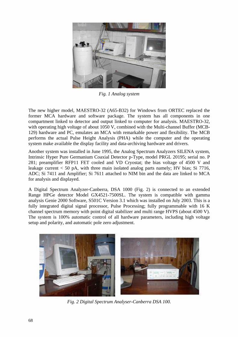
68
Fig. 1 Analog system The new higher model, MAESTRO-32 (A65-B32) for Windows from ORTEC replaced the former MCA hardware and software package. The system has all components in one compartment linked to detector and output linked to computer for analysis. MAESTRO-32, with operating high voltage of about 1050 V, combined with the Multi-channel Buffer (MCB-129) hardware and PC, emulates an MCA with remarkable power and flexibility. The MCB performs the actual Pulse Height Analysis (PHA) while the computer and the operating system make available the display facility and data-archiving hardware and drivers.
Another system was installed in June 1995, the Analog Spectrum Analyzers SILENA system, Intrinsic Hyper Pure Germanium Coaxial Detector p-Type, model PRGL 20195; serial no. P 281; preamplifier RFP11 FET cooled and VD Cryostat; the bias voltage of 4500 V and leakage current < 50 pA, with three main isolated analog parts namely; HV bias; Si 7716, ADC; Si 7411 and Amplifier; Si 7611 attached to NIM bin and the data are linked to MCA for analysis and displayed.
A Digital Spectrum Analyzer-Canberra, DSA 1000 (Fig. 2) is connected to an extended Range HPGe detector Model GX4521-7500SL. The system is compatible with gamma analysis Genie 2000 Software, S501C Version 3.1 which was installed on July 2003. This is a fully integrated digital signal processor, Pulse Processing; fully programmable with 16 K channel spectrum memory with point digital stabilizer and multi range HVPS (about 4500 V). The system is 100% automatic control of all hardware parameters, including high voltage setup and polarity, and automatic pole zero adjustment.
Fig. 2 Digital Spectrum Analyser-Canberra DSA 100.
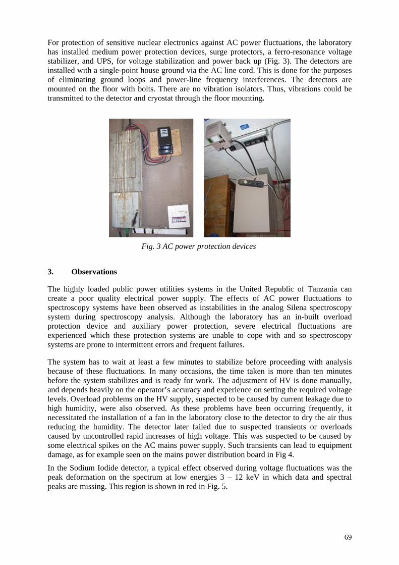
69
For protection of sensitive nuclear electronics against AC power fluctuations, the laboratory has installed medium power protection devices, surge protectors, a ferro-resonance voltage stabilizer, and UPS, for voltage stabilization and power back up (Fig. 3). The detectors are installed with a single-point house ground via the AC line cord. This is done for the purposes of eliminating ground loops and power-line frequency interferences. The detectors are mounted on the floor with bolts. There are no vibration isolators. Thus, vibrations could be transmitted to the detector and cryostat through the floor mounting.
Fig. 3 AC power protection devices
3. Observations
The highly loaded public power utilities systems in the United Republic of Tanzania can create a poor quality electrical power supply. The effects of AC power fluctuations to spectroscopy systems have been observed as instabilities in the analog Silena spectroscopy system during spectroscopy analysis. Although the laboratory has an in-built overload protection device and auxiliary power protection, severe electrical fluctuations are experienced which these protection systems are unable to cope with and so spectroscopy systems are prone to intermittent errors and frequent failures.
The system has to wait at least a few minutes to stabilize before proceeding with analysis because of these fluctuations. In many occasions, the time taken is more than ten minutes before the system stabilizes and is ready for work. The adjustment of HV is done manually, and depends heavily on the operator’s accuracy and experience on setting the required voltage levels. Overload problems on the HV supply, suspected to be caused by current leakage due to high humidity, were also observed. As these problems have been occurring frequently, it necessitated the installation of a fan in the laboratory close to the detector to dry the air thus reducing the humidity. The detector later failed due to suspected transients or overloads caused by uncontrolled rapid increases of high voltage. This was suspected to be caused by some electrical spikes on the AC mains power supply. Such transients can lead to equipment damage, as for example seen on the mains power distribution board in Fig 4.
In the Sodium Iodide detector, a typical effect observed during voltage fluctuations was the peak deformation on the spectrum at low energies 3 – 12 keV in which data and spectral peaks are missing. This region is shown in red in Fig. 5.
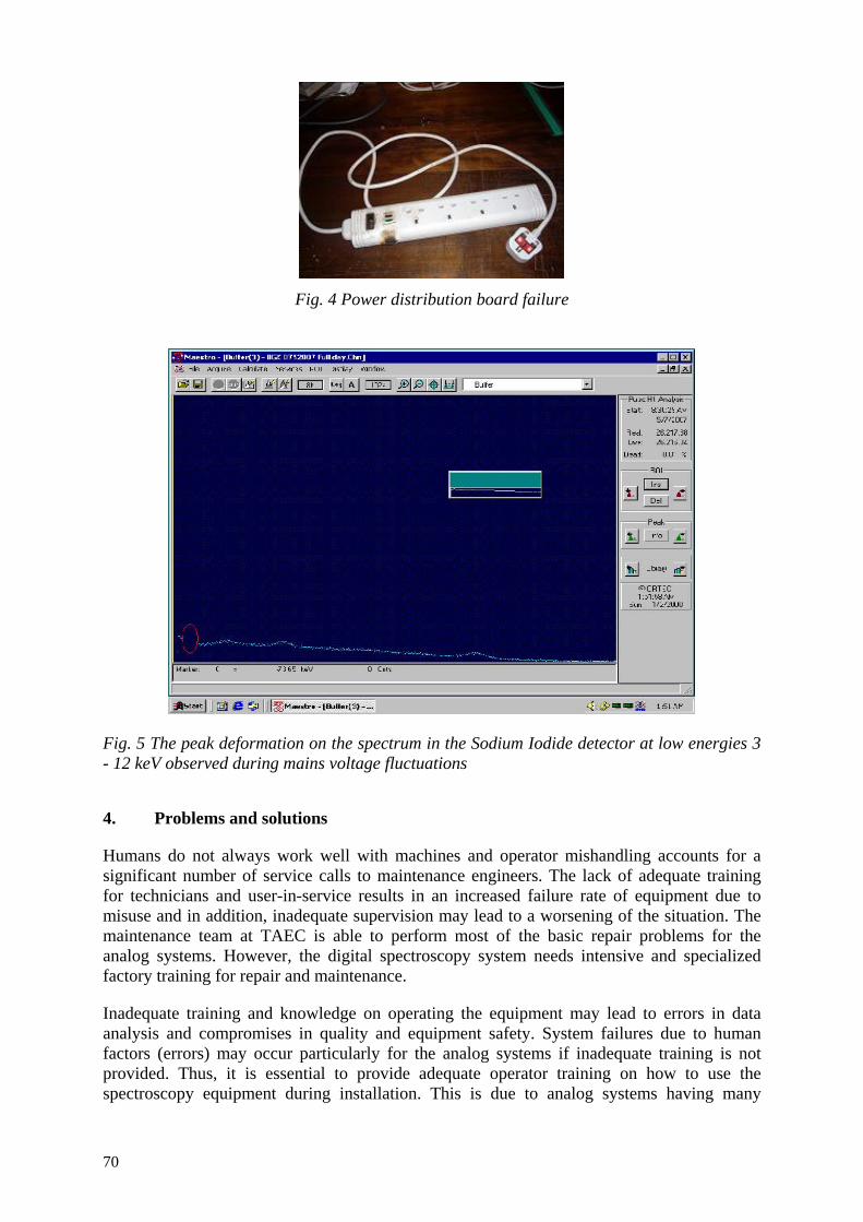
70
Fig. 4 Power distribution board failure
Fig. 5 The peak deformation on the spectrum in the Sodium Iodide detector at low energies 3 - 12 keV observed during mains voltage fluctuations
4. Problems and solutions
Humans do not always work well with machines and operator mishandling accounts for a significant number of service calls to maintenance engineers. The lack of adequate training for technicians and user-in-service results in an increased failure rate of equipment due to misuse and in addition, inadequate supervision may lead to a worsening of the situation. The maintenance team at TAEC is able to perform most of the basic repair problems for the analog systems. However, the digital spectroscopy system needs intensive and specialized factory training for repair and maintenance.
Inadequate training and knowledge on operating the equipment may lead to errors in data analysis and compromises in quality and equipment safety. System failures due to human factors (errors) may occur particularly for the analog systems if inadequate training is not provided. Thus, it is essential to provide adequate operator training on how to use the spectroscopy equipment during installation. This is due to analog systems having many

71
controls and functions which depend on operator skill and experience for proper setting and setting and adjustment of operational parameters. On the other hand, digital systems are by their inherent design containing automation are well designed to prevent wrong commands or unintentional adjustment to the system by unqualified operators. Furthermore, system-monitoring functions are available to detect for example, overloads due to sharp rises in HV, and automatically take preventative action.
The Technology Management Program in the Tanzania National Radiation Commission helps to control and monitor equipment performance, including routine performance testing, initial inspection, preventive maintenance, calibration, verification of performance, and repairs. The involvement of the technical staff in all aspects of equipment acquisition and replacement decisions is well emphasized. The development of in-house training programs for some users of scientific equipment and for scientific equipment technicians has been established. However, detailed local training programs for nuclear spectroscopy systems, which involve highly specialized equipment, has not yet taken off due to inadequate numbers of specialist factory trained engineers and technicians.
Technicians have acquired general knowledge in nuclear instrumentation maintenance through IAEA short training courses, some of which are not as detailed as compared to factory provided training. The calibration and verification of the digital systems, which normally needs codes and specialized software for this purpose, becomes difficult and sometime nearly impossible to be done to the required interval/rates if not provided with the equipment. The time taken for repair of digital system may be shorter if done by a well-trained technician with good repair facilities and proper diagnosis software to isolate problems by troubleshooting. The advantage of analog systems is that it is possible to isolate the problem down to an individual component level with basic diagnostic equipment.
Quality control and quality assurance techniques for accuracy and reproducibility of operations, monitoring of equipment maintenance costs including in-house costs as well as manufacturer and third-part service contracts, are not yet realized. Neither the users nor the technical staff is able to evaluate the equipment performance correctly since they are not well trained on the factory equipment. Hence, a quality assurance and risk management programme relating to technology use is not fully utilized. The need to establish a quality management system and harmonized equipment quality control procedures is vital, and very useful to refer to repair and preventive maintenance.
The patenting of technology is an impediment for an effective instrument repair service in the least developed countries. Many hi-tech instruments such as nuclear spectroscopy systems need to be serviced by or returned to the manufacturer or third-part service contractors, many are which foreign companies without local representatives. These dealers or agents are not available locally because of the complexity of the technology, training requirements, test instruments, and availability of replacement parts required for maintenance. Repair costs are normally high, and the response time can be unacceptably long. There is also lack of local external technical experience available if the service is subcontracted to perform the work.
5. Conclusions
In multi-channel analyzers based on digital signal processing, the automation of critical adjustments makes it easy to set up with any detector while minimizing the need for a high level of operator expertise. Desired operational functions can be activated, or canceled, using an optional Windows-based operating program, resulting in precise measurements and reducing operator errors. On the other side, in comparison to the traditional analog multi-

72
channel analyzer, there are greater difficulties in operation and maintenance of systems based on digital signal processing.
The advantages of digital signal processing are improved ease of use, higher throughput rates, and enhanced spectral resolutions. On the other hand, digital processing based multi-channel analyzers have become more difficult to repair as most of the functional blocks of the system are now bundled into single modules with custom embedded programs that are very difficult to repair in the field, especially in laboratories in the least developed countries. Many difficulties arise from the complexity of the technology, lack of specific training, lack of proper test instruments, and replacement parts. The repair cost is normally high, and the repair time is usual long. Laboratories should consider establishing repair and maintenance procedures that will help to introduce efficient procedures for testing and servicing these complex systems, and with easy to use and low cost tools.

73
PROBLEMS IN SUPPORTING HIGH-TECH DIGITAL EQUIPMENT
Friedl Bartsch
Australian Nuclear Science and Technology Organization, Sydney, Australia
Abstract
Problems involved in supporting high-tech equipment are discussed and solutions employed described.
1. Maintenance and repairs
The complexity of technology invested in high-tech instruments requires a special attention in maintenance and repairing. Special consideration should be focused on the cost of maintenance, knowledge required and the experience of operators, maintenance technicians, the spare parts requirements and troubleshooting tools, which are normally quite complex and expensive. The maintenance services handled by suppliers can be affordable and reliable if they are available locally. In some countries however, particularly in the developing countries where the suppliers are foreign companies, the cost of maintenance is usually high and response for service calls takes long times depending on geographical location. In some cases, the services are subcontracted to dealers who lack experience resulting in the reliability of repairs not guaranteed. The maintenance cost can be reduced by having factory trained local technicians to carry out the maintenance services, or to train the users. Different levels of technical support training should be delivered to the different groups of user.
Usually, the very first training can be done during the installation and commissioning process to help the technicians to have their first hands-on experience. This is both essential and necessary. During this training process, all the factory acceptance tests and on-site acceptance tests criteria should fulfill the user requirements. Further training can be carried out by offering CD based, or Internet based at the work place or at home. This type of training is becoming more popular nowadays because it can be undertaken at almost any time, any place, and is much cheaper. However, the drawback of this type of training is that it is only applicable to those peoples who already have some prior knowledge about the system. Thus, this type of training is not suitable for totally brand new equipment. Another option is to have the vendor or a third party to carry out the system training. This sometimes can be very useful but is limited only to the users having a similar type of equipment. For those who need to know specific details about the equipment, a detailed and intensive training course at the training facility/factory is always the best choice. However, this should only be done if it is a necessity, as it is typically very costly.
2. Procurement policy
In order to reduce the potential problems that may arise in future, a user should always establish an effective and efficient procurement policy which includes contract specifications, warranty and support, as and payment procedures. The user plays a large role in defining the performance requirements and capabilities of high-tech equipment needed for a particular application. This should be as clear and precise as possible by defining the scope of the work to be performed by the instrument, its required specifications, and the level of efficiency and precision required in the output data. When deciding the engineering standards and specifications, all related parameters such as mechanical, civil, electrical, electronic, computer, communications, safety, radiation, chemical and environmental should be taken into consideration wherever applicable. It is considered compulsory for the equipment to
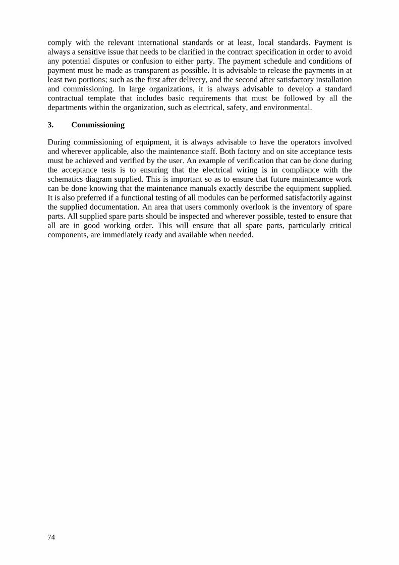
74
comply with the relevant international standards or at least, local standards. Payment is always a sensitive issue that needs to be clarified in the contract specification in order to avoid any potential disputes or confusion to either party. The payment schedule and conditions of payment must be made as transparent as possible. It is advisable to release the payments in at least two portions; such as the first after delivery, and the second after satisfactory installation and commissioning. In large organizations, it is always advisable to develop a standard contractual template that includes basic requirements that must be followed by all the departments within the organization, such as electrical, safety, and environmental.
3. Commissioning
During commissioning of equipment, it is always advisable to have the operators involved and wherever applicable, also the maintenance staff. Both factory and on site acceptance tests must be achieved and verified by the user. An example of verification that can be done during the acceptance tests is to ensuring that the electrical wiring is in compliance with the schematics diagram supplied. This is important so as to ensure that future maintenance work can be done knowing that the maintenance manuals exactly describe the equipment supplied. It is also preferred if a functional testing of all modules can be performed satisfactorily against the supplied documentation. An area that users commonly overlook is the inventory of spare parts. All supplied spare parts should be inspected and wherever possible, tested to ensure that all are in good working order. This will ensure that all spare parts, particularly critical components, are immediately ready and available when needed.
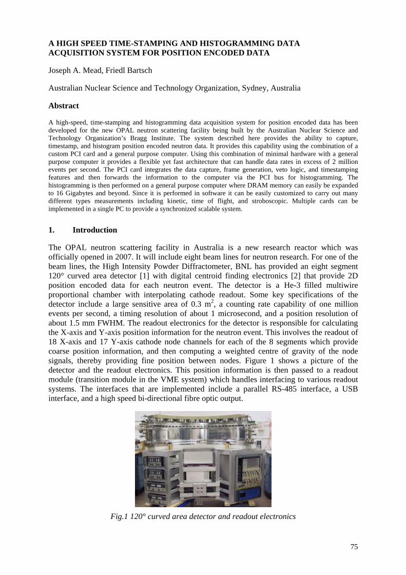
75
A HIGH SPEED TIME-STAMPING AND HISTOGRAMMING DATA ACQUISITION SYSTEM FOR POSITION ENCODED DATA
Joseph A. Mead, Friedl Bartsch
Australian Nuclear Science and Technology Organization, Sydney, Australia
Abstract
A high-speed, time-stamping and histogramming data acquisition system for position encoded data has been developed for the new OPAL neutron scattering facility being built by the Australian Nuclear Science and Technology Organization’s Bragg Institute. The system described here provides the ability to capture, timestamp, and histogram position encoded neutron data. It provides this capability using the combination of a custom PCI card and a general purpose computer. Using this combination of minimal hardware with a general purpose computer it provides a flexible yet fast architecture that can handle data rates in excess of 2 million events per second. The PCI card integrates the data capture, frame generation, veto logic, and timestamping features and then forwards the information to the computer via the PCI bus for histogramming. The histogramming is then performed on a general purpose computer where DRAM memory can easily be expanded to 16 Gigabytes and beyond. Since it is performed in software it can be easily customized to carry out many different types measurements including kinetic, time of flight, and stroboscopic. Multiple cards can be implemented in a single PC to provide a synchronized scalable system.
1. Introduction
The OPAL neutron scattering facility in Australia is a new research reactor which was officially opened in 2007. It will include eight beam lines for neutron research. For one of the beam lines, the High Intensity Powder Diffractometer, BNL has provided an eight segment 120° curved area detector [1] with digital centroid finding electronics [2] that provide 2D position encoded data for each neutron event. The detector is a He-3
filled multiwire
proportional chamber with interpolating cathode readout. Some key specifications of the detector include a large sensitive area of 0.3 m2, a counting rate capability of one million events per second, a timing resolution of about 1 microsecond, and a position resolution of about 1.5 mm FWHM. The readout electronics for the detector is responsible for calculating the X-axis and Y-axis position information for the neutron event. This involves the readout of 18 X-axis and 17 Y-axis cathode node channels for each of the 8 segments which provide coarse position information, and then computing a weighted centre of gravity of the node signals, thereby providing fine position between nodes. Figure 1 shows a picture of the detector and the readout electronics. This position information is then passed to a readout module (transition module in the VME system) which handles interfacing to various readout systems. The interfaces that are implemented include a parallel RS-485 interface, a USB interface, and a high speed bi-directional fibre optic output.
Fig.1 120° curved area detector and readout electronics
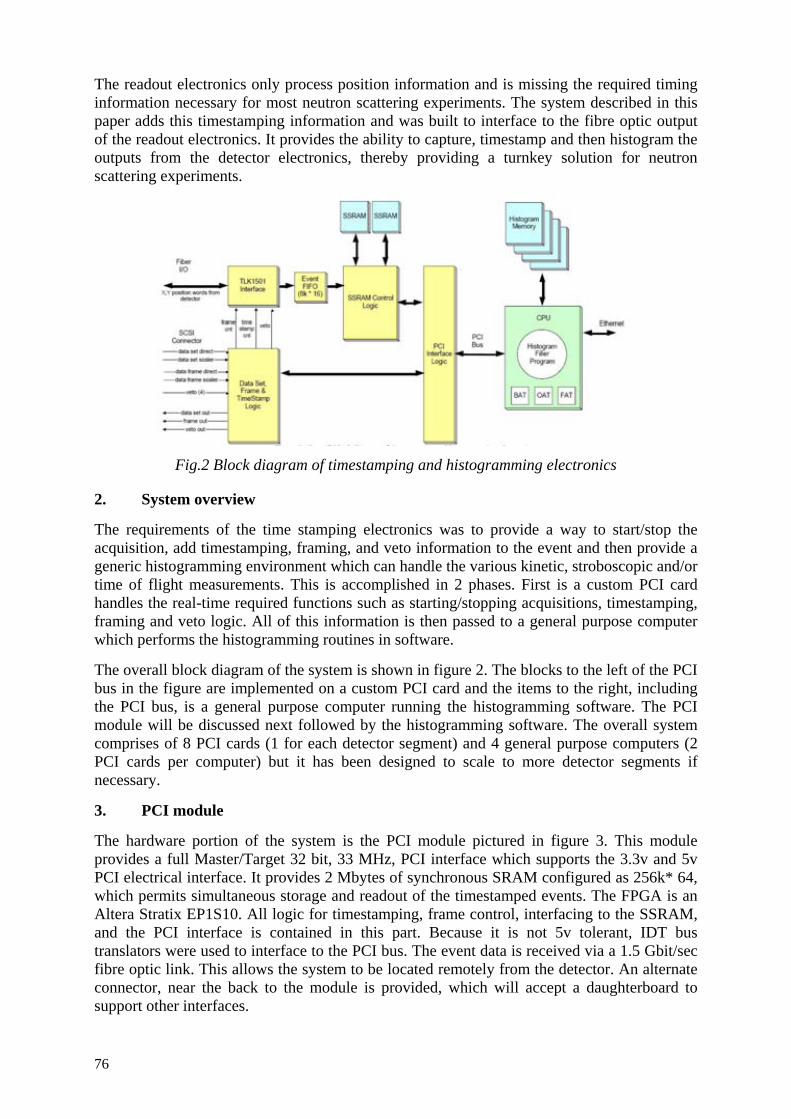
76
The readout electronics only process position information and is missing the required timing information necessary for most neutron scattering experiments. The system described in this paper adds this timestamping information and was built to interface to the fibre optic output of the readout electronics. It provides the ability to capture, timestamp and then histogram the outputs from the detector electronics, thereby providing a turnkey solution for neutron scattering experiments.
Fig.2 Block diagram of timestamping and histogramming electronics
2. System overview
The requirements of the time stamping electronics was to provide a way to start/stop the acquisition, add timestamping, framing, and veto information to the event and then provide a generic histogramming environment which can handle the various kinetic, stroboscopic and/or time of flight measurements. This is accomplished in 2 phases. First is a custom PCI card handles the real-time required functions such as starting/stopping acquisitions, timestamping, framing and veto logic. All of this information is then passed to a general purpose computer which performs the histogramming routines in software.
The overall block diagram of the system is shown in figure 2. The blocks to the left of the PCI bus in the figure are implemented on a custom PCI card and the items to the right, including the PCI bus, is a general purpose computer running the histogramming software. The PCI module will be discussed next followed by the histogramming software. The overall system comprises of 8 PCI cards (1 for each detector segment) and 4 general purpose computers (2 PCI cards per computer) but it has been designed to scale to more detector segments if necessary.
3. PCI module
The hardware portion of the system is the PCI module pictured in figure 3. This module provides a full Master/Target 32 bit, 33 MHz, PCI interface which supports the 3.3v and 5v PCI electrical interface. It provides 2 Mbytes of synchronous SRAM configured as 256k* 64, which permits simultaneous storage and readout of the timestamped events. The FPGA is an Altera Stratix EP1S10. All logic for timestamping, frame control, interfacing to the SSRAM, and the PCI interface is contained in this part. Because it is not 5v tolerant, IDT bus translators were used to interface to the PCI bus. The event data is received via a 1.5 Gbit/sec fibre optic link. This allows the system to be located remotely from the detector. An alternate connector, near the back to the module is provided, which will accept a daughterboard to support other interfaces.
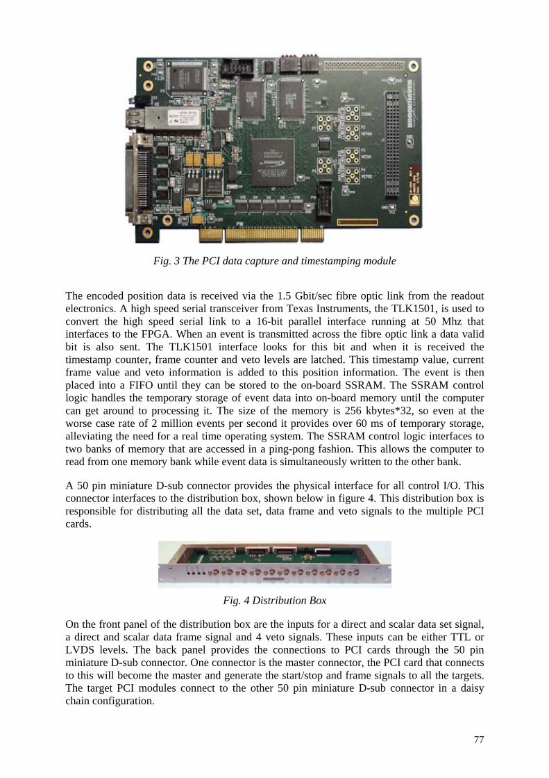
77
Fig. 3 The PCI data capture and timestamping module
The encoded position data is received via the 1.5 Gbit/sec fibre optic link from the readout electronics. A high speed serial transceiver from Texas Instruments, the TLK1501, is used to convert the high speed serial link to a 16-bit parallel interface running at 50 Mhz that interfaces to the FPGA. When an event is transmitted across the fibre optic link a data valid bit is also sent. The TLK1501 interface looks for this bit and when it is received the timestamp counter, frame counter and veto levels are latched. This timestamp value, current frame value and veto information is added to this position information. The event is then placed into a FIFO until they can be stored to the on-board SSRAM. The SSRAM control logic handles the temporary storage of event data into on-board memory until the computer can get around to processing it. The size of the memory is 256 kbytes*32, so even at the worse case rate of 2 million events per second it provides over 60 ms of temporary storage, alleviating the need for a real time operating system. The SSRAM control logic interfaces to two banks of memory that are accessed in a ping-pong fashion. This allows the computer to read from one memory bank while event data is simultaneously written to the other bank.
A 50 pin miniature D-sub connector provides the physical interface for all control I/O. This connector interfaces to the distribution box, shown below in figure 4. This distribution box is responsible for distributing all the data set, data frame and veto signals to the multiple PCI cards.
Fig. 4 Distribution Box
On the front panel of the distribution box are the inputs for a direct and scalar data set signal, a direct and scalar data frame signal and 4 veto signals. These inputs can be either TTL or LVDS levels. The back panel provides the connections to PCI cards through the 50 pin miniature D-sub connector. One connector is the master connector, the PCI card that connects to this will become the master and generate the start/stop and frame signals to all the targets. The target PCI modules connect to the other 50 pin miniature D-sub connector in a daisy chain configuration.
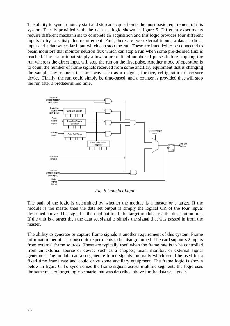
78
The ability to synchronously start and stop an acquisition is the most basic requirement of this system. This is provided with the data set logic shown in figure 5. Different experiments require different mechanisms to complete an acquisition and this logic provides four different inputs to try to satisfy this requirement. First, there are two external inputs, a dataset direct input and a dataset scalar input which can stop the run. These are intended to be connected to beam monitors that monitor neutron flux which can stop a run when some pre-defined flux is reached. The scalar input simply allows a pre-defined number of pulses before stopping the run whereas the direct input will stop the run on the first pulse. Another mode of operation is to count the number of frame signals received from some ancillary equipment that is changing the sample environment in some way such as a magnet, furnace, refrigerator or pressure device. Finally, the run could simply be time-based, and a counter is provided that will stop the run after a predetermined time.
Fig. 5 Data Set Logic
The path of the logic is determined by whether the module is a master or a target. If the module is the master then the data set output is simply the logical OR of the four inputs described above. This signal is then fed out to all the target modules via the distribution box. If the unit is a target then the data set signal is simply the signal that was passed in from the master.
The ability to generate or capture frame signals is another requirement of this system. Frame information permits stroboscopic experiments to be histogrammed. The card supports 2 inputs from external frame sources. These are typically used when the frame rate is to be controlled from an external source or device such as a chopper, beam monitor, or external signal generator. The module can also generate frame signals internally which could be used for a fixed time frame rate and could drive some ancillary equipment. The frame logic is shown below in figure 6. To synchronize the frame signals across multiple segments the logic uses the same master/target logic scenario that was described above for the data set signals.
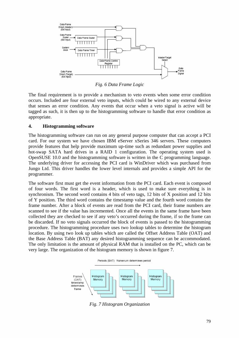
79
Fig. 6 Data Frame Logic
The final requirement is to provide a mechanism to veto events when some error condition occurs. Included are four external veto inputs, which could be wired to any external device that senses an error condition. Any events that occur when a veto signal is active will be tagged as such, it is then up to the histogramming software to handle that error condition as appropriate.
4. Histogramming software
The histogramming software can run on any general purpose computer that can accept a PCI card. For our system we have chosen IBM eServer xSeries 346 servers. These computers provide features that help provide maximum up-time such as redundant power supplies and hot-swap SATA hard drives in a RAID 1 configuration. The operating system used is OpenSUSE 10.0 and the histogramming software is written in the C programming language. The underlying driver for accessing the PCI card is WinDriver which was purchased from Jungo Ltd. This driver handles the lower level internals and provides a simple API for the programmer.
The software first must get the event information from the PCI card. Each event is composed of four words. The first word is a header, which is used to make sure everything is in synchronism. The second word contains 4 bits of veto tags, 12 bits of X position and 12 bits of Y position. The third word contains the timestamp value and the fourth word contains the frame number. After a block of events are read from the PCI card, their frame numbers are scanned to see if the value has incremented. Once all the events in the same frame have been collected they are checked to see if any veto’s occurred during the frame, if so the frame can be discarded. If no veto signals occurred the block of events is passed to the histogramming procedure. The histogramming procedure uses two lookup tables to determine the histogram location. By using two look up tables which are called the Offset Address Table (OAT) and the Base Address Table (BAT) any desired histogramming sequence can be accommodated. The only limitation is the amount of physical RAM that is installed on the PC, which can be very large. The organization of the histogram memory is shown in figure 7.
Fig. 7 Histogram Organization
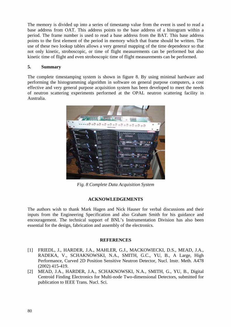
80
The memory is divided up into a series of timestamp value from the event is used to read a base address from OAT. This address points to the base address of a histogram within a period. The frame number is used to read a base address from the BAT. This base address points to the first element of the period in memory which that frame should be written. The use of these two lookup tables allows a very general mapping of the time dependence so that not only kinetic, stroboscopic, or time of flight measurements can be performed but also kinetic time of flight and even stroboscopic time of flight measurements can be performed.
5. Summary
The complete timestamping system is shown in figure 8. By using minimal hardware and performing the histogramming algorithm in software on general purpose computers, a cost effective and very general purpose acquisition system has been developed to meet the needs of neutron scattering experiments performed at the OPAL neutron scattering facility in Australia.
Fig. 8 Complete Data Acquisition System
ACKNOWLEDGEMENTS
The authors wish to thank Mark Hagen and Nick Hauser for verbal discussions and their inputs from the Engineering Specification and also Graham Smith for his guidance and encouragement. The technical support of BNL’s Instrumentation Division has also been essential for the design, fabrication and assembly of the electronics.
REFERENCES
[1] FRIEDL, J., HARDER, J.A., MAHLER, G.J., MACKOWIECKI, D.S., MEAD, J.A., RADEKA, V., SCHAKNOWSKI, N.A., SMITH, G.C., YU, B., A Large, High Performance, Curved 2D Position Sensitive Neutron Detector, Nucl. Instr. Meth. A478 (2002) 415-419.
[2] MEAD, J.A., HARDER, J.A., SCHAKNOWSKI, N.A., SMITH, G., YU, B., Digital Centroid Finding Electronics for Multi-node Two-dimensional Detectors, submitted for publication to IEEE Trans. Nucl. Sci.
81
A STUDY OF FACTORS AFFECTING THE QUALITY OF MEASUREMENTS IN GAMMA SPECTROMETRY COUNTING SYSTEMS
Yii Mei-Wo, Zaharudin Ahmad and Ishak Mansor
Malaysian Nuclear Agency, Bangi, Malaysia
Abstract
Gamma spectrometry is widely used as a tool to measure qualitative and quantitative gamma ray emitters in a sample. Container size, sample to detector distance, and sample volumes are well known factors that affecting the quality of gamma spectrometry measurement. However, other factors such as the age of the counting system and surrounding conditions have not much been reported. Therefore, the objective of this study is to find how the age factor and surrounding conditions affecting the quality of the measurements. From this study, it is found that when the age of a system increases, the system tends to have a higher lower limit of detection and poorer linearity. Point source checks found drifting of several parameters such as efficiency, FWHM, and peak position against changing trend of surrounding conditions such as room temperature and humidity.
1. Introduction
Radioactivity occurs when an unstable nuclide emits alpha, beta or gamma rays in order for it to transform into a stable nuclide. The released gamma activities such as from Cs-137 (from Ba-137) can be estimated qualitative and quantitatively using a HPGe gamma spectrometry counting system. Gamma spectrometry is one of the most widely used nuclear instruments for determining the activity concentration of gamma ray emitting radionuclides, as well as their associated uncertainties of the counting results. This is not only because most radioisotopes release gamma energies, but gamma rays also exhibit discrete and unique energies that are intrinsic for each nuclide [1]. Moreover, no complicated sample preparation techniques are required during the measurement and the samples usually are not destructed after the analysis [2]. However, before this information can be obtained, the system needs to be calibrated, usually done by using a mixed source of gamma radionuclides. Suitable reference materials with known radionuclide activities are used to validate the energy and efficiency calibration. Ideally, the source and reference material, as well as the sample to be counted, must be present in similar counting conditions to avoid wrong measurements of the sample activity. These conditions include factors such as container size, sample to detector distance, sample volume (height or thickness), sample density, as well as the sample matrix [3, 4]. Other factors such as the age of the spectrometry system and environmental conditions have not much been reported. The objective of this study is to find out how the age factor and environmental conditions affecting the quality of the measurement of a gamma spectrometry counting system.
2. Experimental
Described below is the experimental techniques used how the age factor and environmental conditions affect the quality of the measurement of a gamma spectrometry counting system.
2.1 Ageing Study
This experiment was conducted in a new laboratory with a controlled environment of power supply, temperature and humidity.
82
2.1.1 Materials and Reagents
350 ml plastic containers, Cs-137 tracer solutions (3.68 Bq/g as on 1st Jan 2007) from the National Bureau of Standards, Cs-134 tracer solutions (2.94 Bq/g as on 1st Jan 2007) from Isotope Products Laboratories, and double distilled water.
2.1.2 Samples preparation
A total of 13 samples were prepared in the plastic container. Into each container, different amount of Cs-134 and Cs-137 (0 – 5 g) was spiked and added. Then, distilled water was added into each container until the sample weight was around 325 - 326 g. After the tracer and sample had been mixed thoroughly by stirring with a Teflon rod, the containers were sealed with PVC tape and stored ready for counting.
2.1.3 Counting System
All the samples were counted for 54000 seconds using five different ages (from date of the first commissioning) of the gamma spectrometry counting systems owned by the Radiochemistry and Environment Group. All the systems used a 3 inches diameter, 25% coaxial HPGe detector. These spectrometry systems are labeled as system A (12 years), system B (8 years), system C (13 years), system D (3 years) and system E (2 years). Calibration was done using a customized gamma multi-nuclide standard of 1.0 g/cm3 epoxy matrix in the 350 ml plastic container (325 grams), prepared by the Isotope Products Laboratories, and traceable to the NIST standard. The energy and efficiency calibrations were validated using the reference material, IAEA Soil-6 (ρ ~ 1). The peak resolution (FWHM) of Co-60 at 1333 keV for each system was 1.7-1.9 keV. The performance of all these instruments was monitored regularly to ensure they remained within operational tolerances.
2.1.4 Spectral peak evaluation
The peak of the Cs-137 was identified at its energy line of 661.62 keV, whilst the peak of Cs-134 was identified at its energy lines of 604.66 keV and 795.76 keV. These peaks were marked, and the total activity inside the sample (in Bq) was calculated according to guidelines of Gilmore and Hemingway [3] and the IAEA [5]. The calculated activity was corrected to the weight of tracer used.
2.2 Surrounding conditions study
This experiment was conducted in an old laboratory without a controlled environment of power supply, temperature or humidity.
2.2.1 Equipments and material
A HPGe 3 inches coaxial detector system (system B) with 25% efficiency and 1.9 keV resolution at 1333 keV was used to measure gamma rays from a point source. The temperature and humidity was measured by using a microprocessor-printing thermo-hygrometer (HANNA Ins.). The radionuclide used in this study was a Co-60 (~1 μCi) sealed point source which was placed at a distance of 10 cm from the top of the detector.

83
2.2.2 Data analysis
The activity of the Co-60 was counted for 600 s. From the spectra, the 1333 keV peak in the Region of Interest (ROI) was marked, and the information of the peak, peak position, counts per second, and full width half maximum (FWHM) was recorded. From the count rate, the detector efficiency was calculated. Meanwhile, the temperature and humidity was recorded when the sample counting time was about 300 s. The trends in every peak parameter were compared with the temperature and control chart. It was plotted to monitor changes in peak position, efficiency and FWHM as well.
2.2.3 Control Chart
A numbers, n, of reading (usually minimum 20 readings) were taken to calculate the mean value, x , and the standard deviation, σ, by using the following statistical equations [6]:
n
xx
n
ii∑
== 1 (1)
( )1
2
1
−
−=
∑=
n
xxn
ii
σ Or ( )( )
11
22
−
−=
∑=
n
xnxn
ii
σ …… (2)
By using the x , ± 1σ, ± 2σ and ± 3σ values, a control chart can be plotted. Then, the reading from the subsequent measurements was recorded in this control chart.
3. Results and Discussion
3.1 Ageing Study
All of the thirteen samples were counted under the same counting conditions using the five counting systems. The total activity (Bq) for each sample was plotted against the tracer weight added to each sample. The results were shown in the following figures Fig. 1 to Fig. 10.
Cs-137 in System A
y = 3.5118xR2 = 0.9731
0
5
10
15
20
0 1 2 3 4 5 6Tracer Wt (g)
Tota
l Act
ivity
(Bq)
Fig. 1 Total Activity of Cs-137 measured in system A against tracer added
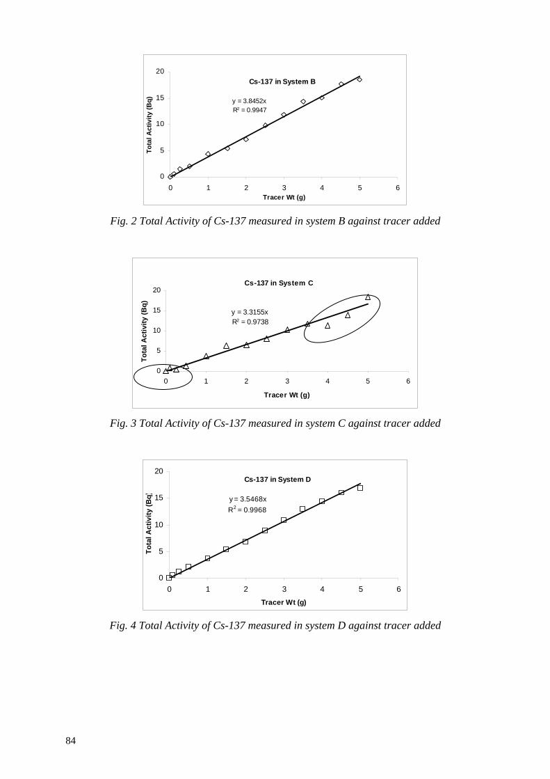
84
Cs-137 in System B
y = 3.8452xR2 = 0.9947
0
5
10
15
20
0 1 2 3 4 5 6Tracer Wt (g)
Tota
l Act
ivity
(Bq)
Fig. 2 Total Activity of Cs-137 measured in system B against tracer added
Cs-137 in System C
y = 3.3155xR2 = 0.9738
0
5
10
15
20
0 1 2 3 4 5 6
Tracer Wt (g)
Tota
l Act
ivity
(Bq)
Fig. 3 Total Activity of Cs-137 measured in system C against tracer added
Cs-137 in System D
y = 3.5468xR2 = 0.9968
0
5
10
15
20
0 1 2 3 4 5 6Tracer Wt (g)
Tota
l Act
ivity
(Bq)
Fig. 4 Total Activity of Cs-137 measured in system D against tracer added
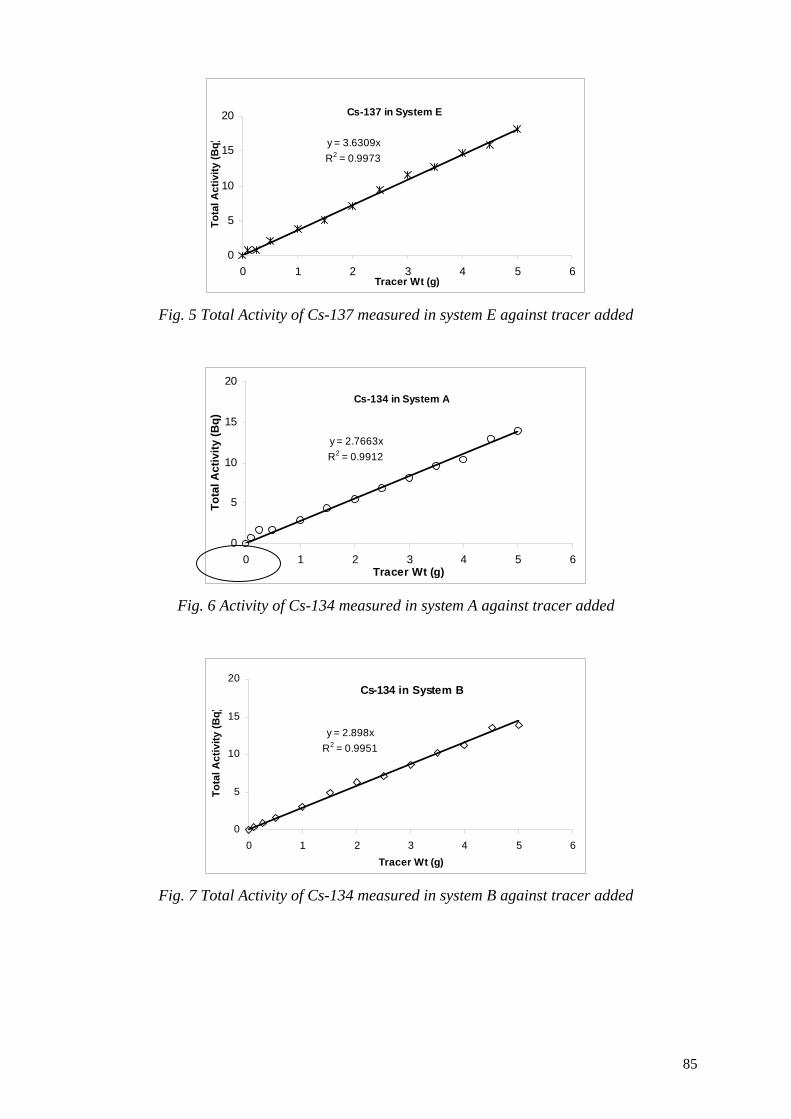
85
Cs-137 in System E
y = 3.6309xR2 = 0.9973
0
5
10
15
20
0 1 2 3 4 5 6Tracer Wt (g)
Tota
l Act
ivity
(Bq)
Fig. 5 Total Activity of Cs-137 measured in system E against tracer added
Cs-134 in System A
y = 2.7663xR2 = 0.9912
0
5
10
15
20
0 1 2 3 4 5 6Tracer Wt (g)
Tota
l Act
ivity
(Bq)
Fig. 6 Activity of Cs-134 measured in system A against tracer added
Cs-134 in System B
y = 2.898xR2 = 0.9951
0
5
10
15
20
0 1 2 3 4 5 6Tracer Wt (g)
Tota
l Act
ivity
(Bq)
Fig. 7 Total Activity of Cs-134 measured in system B against tracer added
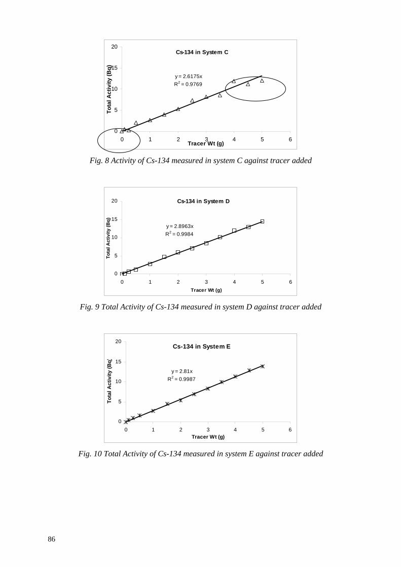
86
Cs-134 in System C
y = 2.6175xR2 = 0.9769
0
5
10
15
20
0 1 2 3 4 5 6Tracer Wt (g)
Tota
l Act
ivity
(Bq)
Fig. 8 Activity of Cs-134 measured in system C against tracer added
Cs-134 in System D
y = 2.8963xR2 = 0.9984
0
5
10
15
20
0 1 2 3 4 5 6Tracer Wt (g)
Tota
l Act
ivity
(Bq)
Fig. 9 Total Activity of Cs-134 measured in system D against tracer added
Cs-134 in System E
y = 2.81xR2 = 0.9987
0
5
10
15
20
0 1 2 3 4 5 6Tracer Wt (g)
Tota
l Act
ivity
(Bq)
Fig. 10 Total Activity of Cs-134 measured in system E against tracer added
87
The energy deposited by a photon within the active volume of a semiconductor such as germanium creates electron-hole pairs. These positive (hole) and negative (electron) charges are then collected at opposite contacts through the use of a large voltage applied across the active volume. From the above figures one can see that for an aged system (age > 10 yrs), it will not be able to measure the sample with a low activity concentration correctly for both Cs-134 and Cs-137, such as system A and system C. This shows that the lower limit of detection for these two systems are higher compared to the other systems (age < 10 yrs). This is an indication that the sensitivity of the system is not good for a low activity concentration (as shown in the lower and upper side in above figures) of radionuclides, which might be due to the increasing of leakage current that interfere the pulse signal. This is likely to happen because as the age of the detector increases, the cryostat vacuum loses its ability to repair itself with temperature cycling. Degraded vacuums can lead to leakage current on the crystal that renders the detector useless [7].
Another possible reason of this phenomenon could be caused by the reduction of the effective active volume in detector as a result of radiation damage by any alpha or neutron radiation. High-energy radiation can create large disordered regions on the order of 100 angstroms in size in the germanium crystal, and these regions tend to accumulate negative charges. As a result, these regions act as hole-traps and prevent holes from reaching the cathode. If a hole is trapped, then only a fraction of the energy of the incident photon is collected. When the detector becomes more damaged, it becomes difficult to fully deplete the detector, and thus there is a reduction of effective area as there is less active volume, which eventually reduces its sensitivity. However, this is a very rare occurrence considering the nature of the samples measured.
On the other hand, another obvious observation from these figures is the poor correlation for two ageing systems as summarized in table 1 below. This could be related to the performance of the electronic components inside the counting system. Electronic components can become unstable and start to fail after a few years. Drops in electronic components performance will increase the electronic noise; even the apparently passive resistor is an important source. This will increase the lower limit of detection as well as interfering with the total counts. The electronic noise increases with increasing leakage current and this was closely related to detector age. Eventually, the whole measuring process is unsatisfactory. However, residual plots obtained from regression analysis showing that the linearity is still acceptable. More studies are needed to clarify this situation.
TABLE I. SUMMARY OF THE CORRELATION BETWEEN TRACER WEIGHT AND MEASURED ACTIVITIES FOR FIVE SYSTEMS USING Cs-134 AND Cs-137
System A B C D E
Age (yrs) 12 8 13 3 2
Cs-137 0.9731 0.9947 0.9738 0.9968 0.9973
Cs-134 0.9912 0.9951 0.9769 0.9984 0.9987
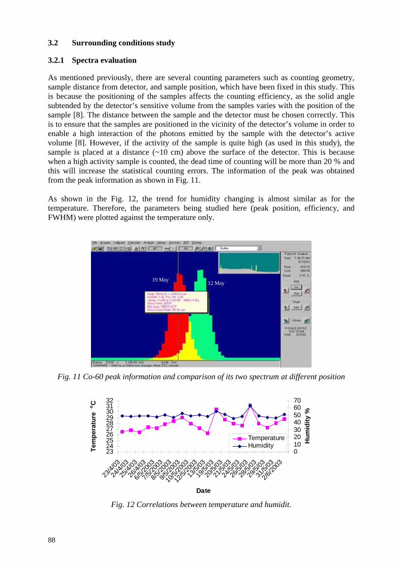
88
3.2 Surrounding conditions study
3.2.1 Spectra evaluation
As mentioned previously, there are several counting parameters such as counting geometry, sample distance from detector, and sample position, which have been fixed in this study. This is because the positioning of the samples affects the counting efficiency, as the solid angle subtended by the detector’s sensitive volume from the samples varies with the position of the sample [8]. The distance between the sample and the detector must be chosen correctly. This is to ensure that the samples are positioned in the vicinity of the detector’s volume in order to enable a high interaction of the photons emitted by the sample with the detector’s active volume [8]. However, if the activity of the sample is quite high (as used in this study), the sample is placed at a distance (~10 cm) above the surface of the detector. This is because when a high activity sample is counted, the dead time of counting will be more than 20 % and this will increase the statistical counting errors. The information of the peak was obtained from the peak information as shown in Fig. 11. As shown in the Fig. 12, the trend for humidity changing is almost similar as for the temperature. Therefore, the parameters being studied here (peak position, efficiency, and FWHM) were plotted against the temperature only.
Fig. 11 Co-60 peak information and comparison of its two spectrum at different position
23242526272829303132
23/4/
03
24/4/
03
25/4/
03
26/4/
03
6/5/20
03
7/5/20
03
8/5/20
03
9/5/20
03
10/5/
2003
12/5/
2003
13/5/
03
19/5/
03
20/5/
03
21/5/
03
24/5/
03
26/5/
03
28/5/
03
29/5/
03
31/5/
03
2/6/20
03
Date
Tem
pera
ture
o C
010203040506070
Hum
idity
%
TemperatureHumidity
Fig. 12 Correlations between temperature and humidit.
19 May 12 May
89
3.2.2 Peak Position
Peak position is the centroid of a peak in spectra. The position of a peak, which corresponds to its energy, is usually used to identify the radionuclide. Nowadays, with the developments in automation, the system computer can be programmed to perform tasks such as automatic peak search, calculation of the peak area, activities, and identification of the radionuclides using a nuclide library. A shifting of a peak to another position (as in Fig. 11) will lead to a wrong calculation of the activity by the software programme [9].
In Fig. 13, it seems that when the temperature is at approximately 29oC and above (marked 1, 2, 3, 4), the peak tends to shift to a lower position. At a lower temperature (< 29oC), the position of the peak almost remains constant between 5024 to 5026. It is clearly seen that the changes in temperature or humidity effect the peak position. The trend of the peak position changing is almost vice versa the trend of temperature changing. Other research institutions have also observed this effect [10]. The main reason for this may be due to changes of temperature and humidity affecting the stability of the electronic components, which in turn affect the position of the peak.
501250145016501850205022502450265028
23/4/
03
24/4/
03
25/4/
03
26/4/
03
6/5/20
03
7/5/20
03
8/5/20
03
9/5/20
03
10/5/
2003
12/5/
2003
13/5/
03
19/5/
03
20/5/
03
21/5/
03
24/5/
03
26/5/
03
28/5/
03
29/5/
03
31/5/
03
2/6/20
03
Date
Peak
Pos
ition
(Cha
nnel
No)
23242526272829303132
Tem
pera
ture
o C
Peak PositionTemperature
Fig. 13 Correlations between peak position and temperature
3.2.3 Efficiency The counting efficiency of the system seems not appear to be affected by the temperature. Even at high temperatures the counting efficiency still remains essentially unchanged. The reason for this is due to the detector is always being cooled by the liquid nitrogen (~ -200oC) inside the dewar. Thus, the changes in the room temperature will not be great enough to affect the counting efficiency. However, if the room remains at high temperatures for a long period of time, it will speed up the liquid nitrogen evaporation process. Eventually, when the level of liquid nitrogen is too low, it will affect the efficiency of the system.
0.2140.2150.2160.2170.2180.2190.22
0.2210.222
23/4/
03
24/4/
03
25/4/
03
26/4/
03
6/5/20
03
7/5/20
03
8/5/20
03
9/5/20
03
10/5/
2003
12/5/
2003
13/5/
03
19/5/
03
20/5/
03
21/5/
03
24/5/
03
26/5/
03
28/5/
03
29/5/
03
31/5/
03
2/6/20
03
Date
Effic
ienc
y %
23242526272829303132
Tem
pera
ture
o C
Efficiency
Temperature
Fig. 14 Correlations between counting efficiency and temperature
1 2
3
4
90
3.2.4 FWHM
The full width at half maximum (FWHM) refers to the width of a peak at half of the peak height maximum. This value is important especially when there are two radionuclides having very close energies appearing in a same sample. A large FWHM will affect the resolution of the spectra whereby the analyst is unable to differentiate the two different spectral peaks. In Fig. 15 we see that the FWHM has little variation (remains around 1.8 keV) with temperature and humidity. However, the trends are very similar. The slight changes in the FWHM may be due to other factors such as microphonic and electronic noise. [3, 10]. The level of liquid nitrogen in the dewar may also contribute to the poorer resolution if higher detector temperatures are higher than normal.
1.7
1.75
1.8
1.85
1.9
1.95
23/4/
03
24/4/
03
25/4/
03
26/4/
03
6/5/20
03
7/5/20
03
8/5/20
03
9/5/20
03
10/5/
2003
12/5/
2003
13/5/
03
19/5/
03
20/5/
03
21/5/
03
24/5/
03
26/5/
03
28/5/
03
29/5/
03
31/5/
03
2/6/20
03
Date
FWH
M
23242526272829303132
Tem
pera
ture
o C
FWHMTemperature
Fig. 15 Correlations between FWHM and temperature
3.2.5 Control Chart
In Fig. 13 to Fig. 15 there is little significant information observed except that the peak position is found to vary with temperature and FWHM is seen be related to the changing of environment conditions. The overall performance of the system itself is unknown. In order to ensure that the instrument is in a good operating condition, a control chart is plotted as shown in Fig. 16 to
Fig. 18. From these control charts we can clearly monitor any changes besides knowing the performance of the instrument. The idea of control chart is to compare the new data with the old ones, to check any differences, find the reasons for any changes.
Ideally, all data points should fall within the ± 2σ regions. When a data point falls outside the ± 2 σ as marked ‘w’ in
Fig. 18, caution should be taken to ensure that the following data would not fall outside the ± 2 σ again. Meanwhile, when a data point is outside ± 3 σ as marked ‘a’ in
Fig. 18, action should be taken immediately to eliminate the cause. As in this case, is mainly due to the increase in temperature. On the other hand, if all data falls within the warning limit (as in Fig. 16 and Fig. 17), it means that the performance of the system for counting efficiency and FWHM remains as normal.
4. Conclusions
From this study it can be concluded that the age of a counting system does affect the system performance. When the age of a system increases, the system tends to have a higher lower limit of detection and poorer linearity. Beside this, changes in the environment conditions such as temperature and humidity do affect the performance of the gamma ray spectrometry
91
system. Therefore, spectrometry systems should be monitored frequently by using the control chart. Since the high humidity and temperature in the room does cause some interference to the system, actions had been taken to reduce the temperature and humidity level by installing an air conditioner and dehumidifier.
2.130E-01
2.150E-01
2.170E-01
2.190E-01
2.210E-01
2.230E-01
2.250E-01
2.270E-01
Date
Effic
ienc
y
Fig. 16 Control chart for efficiency at 1333 keV
Fig. 17 Control chart for FWHM at 1333 keV
Fig. 18 Control chart for peak position at 1333 keV
w w
a a

92
REFERENCES
[1] NOGUCHI, J., “Textbook for the Group Training Course in Nuclear Technology”, Vol. 1, Japan Atomic Energy Research Institute, May 1998, Tokyo, Chapter E3. (1998).
[2] DOVLETE, C., POVINEC, P.P., “Quantification of Uncertainty in Gamma Spectrometric Analysis of Environmental samples”, 2nd Regional Training Course on QA/QC of Nuclear Analytical Techniques, 12-16 August 2002, Kuala Lumpur, Malaysia. (2002).
[3] GILMORE, G., HEMINGWAY, J., “Practical Gamma-Ray Spectrometry”, First Ed. John Wiley & Sons Ltd, West Sussex, England. (1998).
[4] SCHULTZ, M.K., “Technical Specifications and Recommendations of Gamma Spectrometry Systems”, www.ortec-online.com/application-notes/gammaspecs.pdf. (2005).
[5] INTERNATIONAL ATOMIC ENERGY AGENCY, “Measurement of Radionuclides in Food and the Environment”, Technical Report Series No. 295, IAEA, Vienna (1989) 61-63.
[6] LIAW, S. H., GOH, K.L., “Statistik Asas, Konsep & Amalan”, McGraw-Hill (Malaysia) Sdn. Bhd., Kuala Lumpur (2002) 29-31.
[7] PRINCETON GAMMA-TECH INSTRUMENTS, INC, private communication, (2007).
[8] KORUN, M., Propagation of the uncertainties of sample position to the uncertainty of the counting efficiency in gamma-ray spectrometry, J. Appl. Rad. Isot. 57 (2002) 415-425.
[9] AHMAD, Z., YII, M.W., ISHAK, A.K., “Method of software validation for Cs-137 and Ra-226 activity measurements in environmental samples using gamma spectrometry system”, “Validation Procedures of Software Applied in Nuclear Instruments”, IAEA-TECDOC-1565 (2007) 55-63.
[10] PETER, V., “2nd Regional Training Course on QA/QC of Nuclear Analytical Techniques”, 12-16 August 2002, Kuala Lumpur, Malaysia. (2002), (private communication).

93
PROBLEMS WITH MAINTAINING NUCLEAR INSTRUMENTATION IN PERU
R. Ruiz
Peruvian Institute of Nuclear Energy, Lima, Peru
Abstract
This article illustrates different kinds of problems experienced in operating and maintaining nuclear spectrometry instrumentation in Peru, and describes some solutions used to solve the problems.
1.- Introduction
The main thrust of this article is to illustrate how the Peruvian Institute of Nuclear Energy has introduced and sustained new technologies in nuclear instrumentation spectroscopy, and difficulties encountered in servicing, and performing preventive and corrective maintenance. We discuss after-sales service, repair downtime, how the global market affects us, some user experiences, and some solutions to these problems.
2. An overview of the Peruvian Institute of Nuclear Energy (IPEN)
IPEN is located in Lima, Peru, and employs approximately 220 persons; comprised of about 76 administrative staff, 75 professional staff, and 65 technical staff. Amongst other roles, IPEN provides technical support services for a 10 MW research reactor and a Nuclear Medicine Centre.
In the Electronics Department of IPEN, there are approximately 40 persons. Its main function is to support all areas involving nuclear instrumentation (excluding reactor and radioisotope plant instrumentation). This department provides technical support to repair electromechanical equipment, repair and calibrate radiation survey meters, repair PCs and computer peripherals, and to repair nuclear instrumentation.
2.1. Engineering and Maintenance Department (ENMA)
ENMA is a support group whose function is to perform preventive and corrective maintenance of electronic/electrical equipment, scheduling and performing routine maintenance, as well as technical reception of equipment of to be used by IPEN. This group logs and tracks work performed through four different kinds of report (called RT, ET, PM, CM) which will be briefly described now.
• TR (technical reception). This report is done when equipment is received for the first time, whether is new or used. In this stage, we see if the equipment has enough technical information to proceed, has spare parts, isn’t damaged during travel, etc.
• TE (technical evaluation). A technical evaluation about whether the equipment is in good working order, or not.
• PM (preventive maintenance). Equipment undergoes preventive maintenance according to a predetermined maintenance interval.
• CM (corrective maintenance). Equipment undergoes repair if it is broken or not functioning properly.
The number of equipment items supported by ENMA is approximately 1, 200 of which 650—800 is nuclear instrumentation.

94
3. Difficulties faced with maintaining and servicing instrumentation
3.1 Technical Reception
There is a trend for manufacturers to supply insufficient technical details in their operations and service manuals. Sometimes, equipment is received without and manuals whatsoever or manuals are poorly translated from other languages. This makes it very difficult to check against performance specifications and to make repairs locally.
3.2 Equipment Setup and Operation
Users need adequate training and knowledge to properly setup and operate equipment. It is generally found that for small to medium cost equipment, operational manuals can be inadequate in the detail provided. However, this class of equipment is fairly intuitive to operate and can be done so by some prior experiences, or by some trial and error. Some auto test, or auto calibrate features would be advantageous.
3.3 Maintenance
Maintenance issues depend on the relative complexity of the instrumentation. Instrumentation with high-tech components inside requires dedicated technical support for diagnosis and repair. This is generally not available. Being geographically remote from the main equipment manufacturers also causes many delays in communicating with their service departments, inadequate technical support from them, and having to ship equipment back to them for repair.
In table 1, we present for four pieces of equipment received since 2004, some factors which have influenced the maintenance and operation.
TABLE 1. FACTORS AFFECTING THE MAINTENANCE AND OPERATION OF NUCLEAR INSTRUMENTS
Item Problems Technical information
provided
Location of equipment
supplier
Current status
Operational time
XRF unit Many occurred after installation
Not enough information in operation manual
Europe Not working
Very low
Gamma spectrometry system
A module became defective about 6 months after commissioning
Inadequate, more needed to make repairs
Argentina working Could be better
Atomic absorption spectrometer
Could not be repaired in-house if failed
Manufacture unwilling to provide service manuals
Local agent working low
Liquid scintillation counter
Could not be repaired in-house if failed
not enough technical information provided
Local agent, but not able to do some repairs
working low

95
While the introduction of high technology equipment can deliver many benefits to a developing country, the equipment’s reliability, maintainability, and availability can be seriously affected by a lack of suitable local repair facilities, or from being geographically remote from the manufacturer and their repair facilities. Failures in high tech equipment can result in a very long time to repair, and can seriously jeopardizing the projects in which they support. Preference for suppliers of new equipment thus goes to companies that have a local or regional representative, and provide a good after-sales service.
4. CONCLUSIONS
Users of high tech equipment need more training regarding its operations and maintenance, especially for digital equipment, and greater support from the manufacturers. Because technology is developing very fast, ongoing specific training is required to keep all persons abreast of developments and applications. Equipment operational life times need to be at least 5 years, and service support from manufactures provided for at least this time scale as well.


97
LIST OF PARTICIPANTS
Bartsch, F. Australian Nuclear Science and Technology Organization Private Mailbag 1 Menai NSW 2234 Australia Behere, A.R. Bhabha Atomic Research Centre Mumbai, 400 085 India Bogovac, M. Ruđer Bošković Institute
Bijenicka Cesta 54 P.O. Box 180 10 000 Zagreb Croatia
Bosnar, D. University of Zagreb Bijenicka c. 54 P.P. 331 10 000 Zagreb Croatia Cardoso J.M.R. University of Coimbra 3004-516 Coimbra Portugal Dytlewski, N. International Atomic Energy Agency Wagramer Strasse 5 A-1400 Vienna Austria Füzi, J. Research Institute for Solid State Physics and Optics HAS – SzFKI, P.O. Box 49 H-1525 Budapest Hungary Lukács, R. Paks Nuclear Power Plant P.O. Box 71 H-7031, Paks Hungary Ruiz-Pineda, R. Instituto Peruano de Energía Nuclear Avenida Canadá 1470 Apartado 1687 Lima 41 Peru Smailou, M. Institut National de Recherches Agronomiques du Niger B.P. 429 Niamey Niger

98
Sungita, Y.Y. Tanzania Atomic Energy Commission P.O. Box 743 Arusha United Republic of Tanzania Yii, M.W. Malaysian Nuclear Agency Bangi, 43000 Kajang Malaysia

In the following countries IAEA publications may be purchased from the sources listed below, or frommajor local booksellers. Payment may be made in local currency or with UNESCO coupons.
AustraliaDA Information Services, 648 Whitehorse Road, Mitcham Victoria 3132Telephone: +61 3 9210 7777 • Fax: +61 3 9210 7788Email: [email protected] • Web site: http://www.dadirect.com.au
BelgiumJean de Lannoy, avenue du Roi 202, B-1190 BrusselsTelephone: +32 2 538 43 08 • Fax: +32 2 538 08 41Email: [email protected] • Web site: http://www.jean-de-lannoy.be
CanadaBernan Associates, 4611-F Assembly Drive, Lanham, MD 20706-4391, USATelephone: 1-800-865-3457 • Fax: 1-800-865-3450Email: [email protected] • Web site: http://www.bernan.com
Renouf Publishing Company Ltd., 1-5369 Canotek Rd., Ottawa, Ontario, K1J 9J3Telephone: +613 745 2665 • Fax: +613 745 7660Email: [email protected] • Web site: http://www.renoufbooks.com
ChinaIAEA Publications in Chinese: China Nuclear Energy Industry Corporation, Translation Section, P.O. Box 2103, Beijing
Czech RepublicSuweco CZ, S.R.O. Klecakova 347, 180 21 Praha 9Telephone: +420 26603 5364 • Fax: +420 28482 1646Email: [email protected] • Web site: http://www.suweco.cz
FinlandAkateeminen Kirjakauppa, PL 128 (Keskuskatu 1), FIN-00101 HelsinkiTelephone: +358 9 121 41 • Fax: +358 9 121 4450Email: [email protected] • Web site: http://www.akateeminen.com
FranceForm-Edit, 5, rue Janssen, P.O. Box 25, F-75921 Paris Cedex 19Telephone: +33 1 42 01 49 49 • Fax: +33 1 42 01 90 90 • Email: [email protected]
Lavoisier SAS, 14 rue de Provigny, 94236 Cachan Cedex Telephone: + 33 1 47 40 67 00 • Fax +33 1 47 40 67 02 Email: [email protected] • Web site: http://www.lavoisier.fr
GermanyUNO-Verlag, Vertriebs- und Verlags GmbH, August-Bebel-Allee 6, D-53175 BonnTelephone: +49 02 28 949 02-0 • Fax: +49 02 28 949 02-22Email: [email protected] • Web site: http://www.uno-verlag.de
HungaryLibrotrade Ltd., Book Import, P.O. Box 126, H-1656 BudapestTelephone: +36 1 257 7777 • Fax: +36 1 257 7472 • Email: [email protected]
IndiaAllied Publishers Group, 1st Floor, Dubash House, 15, J. N. Heredia Marg, Ballard Estate, Mumbai 400 001,Telephone: +91 22 22617926/27 • Fax: +91 22 22617928Email: [email protected] • Web site: http://www.alliedpublishers.com
Bookwell, 24/4800, Ansari Road, Darya Ganj, New Delhi 110002Telephone: +91 11 23268786, +91 11 23257264 • Fax: +91 11 23281315Email: [email protected] • Web site: http://www.bookwellindia.com
ItalyLibreria Scientifica Dott. Lucio di Biasio “AEIOU”, Via Coronelli 6, I-20146 MilanTelephone: +39 02 48 95 45 52 or 48 95 45 62 • Fax: +39 02 48 95 45 48
JapanMaruzen Company, Ltd., 13-6 Nihonbashi, 3 chome, Chuo-ku, Tokyo 103-0027Telephone: +81 3 3275 8582 • Fax: +81 3 3275 9072Email: [email protected] • Web site: http://www.maruzen.co.jp
Where to order IAEA publications
No. 21, July 2006
Korea, Republic ofKINS Inc., Information Business Dept. Samho Bldg. 2nd Floor, 275-1 Yang Jae-dong SeoCho-G, Seoul 137-130Telephone: +02 589 1740 • Fax: +02 589 1746Email: [email protected] • Web site: http://www.kins.co.kr
NetherlandsMartinus Nijhoff International, Koraalrood 50, P.O. Box 1853, 2700 CZ ZoetermeerTelephone: +31 793 684 400 • Fax: +31 793 615 698 • Email: [email protected] • Web site: http://www.nijhoff.nl
Swets and Zeitlinger b.v., P.O. Box 830, 2160 SZ LisseTelephone: +31 252 435 111 • Fax: +31 252 415 888 • Email: [email protected] • Web site: http://www.swets.nl
New ZealandDA Information Services, 648 Whitehorse Road, MITCHAM 3132, AustraliaTelephone: +61 3 9210 7777 • Fax: +61 3 9210 7788Email: [email protected] • Web site: http://www.dadirect.com.au
SloveniaCankarjeva Zalozba d.d., Kopitarjeva 2, SI-1512 LjubljanaTelephone: +386 1 432 31 44 • Fax: +386 1 230 14 35Email: [email protected] • Web site: http://www.cankarjeva-z.si/uvoz
SpainDíaz de Santos, S.A., c/ Juan Bravo, 3A, E-28006 MadridTelephone: +34 91 781 94 80 • Fax: +34 91 575 55 63 • Email: [email protected]@diazdesantos.es • [email protected] • [email protected] Web site: http://www.diazdesantos.es
United KingdomThe Stationery Office Ltd, International Sales Agency, PO Box 29, Norwich, NR3 1 GNTelephone (orders): +44 870 600 5552 • (enquiries): +44 207 873 8372 • Fax: +44 207 873 8203Email (orders): [email protected] • (enquiries): [email protected] • Web site: http://www.tso.co.uk
On-line orders:DELTA Int. Book Wholesalers Ltd., 39 Alexandra Road, Addlestone, Surrey, KT15 2PQEmail: [email protected] • Web site: http://www.profbooks.com
Books on the Environment:Earthprint Ltd., P.O. Box 119, Stevenage SG1 4TPTelephone: +44 1438748111 • Fax: +44 1438748844Email: [email protected] • Web site: http://www.earthprint.com
United Nations (UN)Dept. I004, Room DC2-0853, First Avenue at 46th Street, New York, N.Y. 10017, USATelephone: +800 253-9646 or +212 963-8302 • Fax: +212 963-3489Email: [email protected] • Web site: http://www.un.org
United States of AmericaBernan Associates, 4611-F Assembly Drive, Lanham, MD 20706-4391Telephone: 1-800-865-3457 • Fax: 1-800-865-3450Email: [email protected] • Web site: http://www.bernan.com
Renouf Publishing Company Ltd., 812 Proctor Ave., Ogdensburg, NY, 13669Telephone: +888 551 7470 (toll-free) • Fax: +888 568 8546 (toll-free)Email: [email protected] • Web site: http://www.renoufbooks.com
Orders and requests for information may also be addressed directly to:
Sales and Promotion Unit, International Atomic Energy AgencyVienna International Centre, PO Box 100, 1400 Vienna, AustriaTelephone: +43 1 2600 22529 (or 22530) • Fax: +43 1 2600 29302Email: [email protected] • Web site: http://www.iaea.org/books
09-4
5661
Recommended