LM723, LM723C
www.ti.com SNVS765C –JUNE 1999–REVISED APRIL 2013
LM723/LM723C Voltage RegulatorCheck for Samples: LM723, LM723C
1FEATURES DESCRIPTIONThe LM723/LM723C is a voltage regulator designed
2• 150 mA Output Current Without External Passprimarily for series regulator applications. By itself, itTransistorwill supply output currents up to 150 mA; but external
• Output Currents in Excess of 10A Possible by transistors can be added to provide any desired loadAdding External Transistors current. The circuit features extremely low standby
current drain, and provision is made for either linear• Input Voltage 40V Maxor foldback current limiting.• Output Voltage Adjustable from 2V to 37VThe LM723/LM723C is also useful in a wide range of• Can be Used as Either a Linear or a Switchingother applications such as a shunt regulator, aRegulatorcurrent regulator or a temperature controller.
The LM723C is identical to the LM723 except that theLM723C has its performance ensured over a 0°C to+70°C temperature range, instead of −55°C to+125°C.
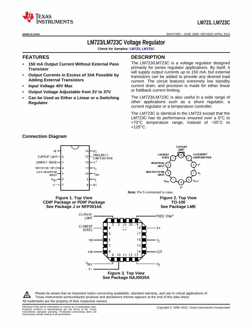
Connection Diagram
Note: Pin 5 connected to case.
Figure 1. Top View Figure 2. Top ViewCDIP Package or PDIP Package TO-100
See Package J or NFF0014A See Package LME
Figure 3. Top ViewSee Package NAJ0020A
1
Please be aware that an important notice concerning availability, standard warranty, and use in critical applications ofTexas Instruments semiconductor products and disclaimers thereto appears at the end of this data sheet.
2All trademarks are the property of their respective owners.
PRODUCTION DATA information is current as of publication date. Copyright © 1999–2013, Texas Instruments IncorporatedProducts conform to specifications per the terms of the TexasInstruments standard warranty. Production processing does notnecessarily include testing of all parameters.
LM723, LM723C
SNVS765C –JUNE 1999–REVISED APRIL 2013 www.ti.com
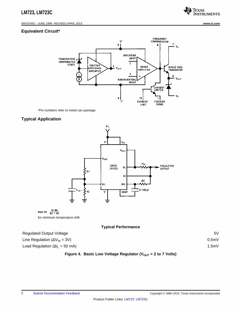
Equivalent Circuit*
*Pin numbers refer to metal can package.
Typical Application
for minimum temperature drift.
Typical Performance
Regulated Output Voltage 5V
Line Regulation (ΔVIN = 3V) 0.5mV
Load Regulation (ΔIL = 50 mA) 1.5mV
Figure 4. Basic Low Voltage Regulator (VOUT = 2 to 7 Volts)
2 Submit Documentation Feedback Copyright © 1999–2013, Texas Instruments Incorporated
Product Folder Links: LM723 LM723C
LM723, LM723C
www.ti.com SNVS765C –JUNE 1999–REVISED APRIL 2013
These devices have limited built-in ESD protection. The leads should be shorted together or the device placed in conductive foamduring storage or handling to prevent electrostatic damage to the MOS gates.
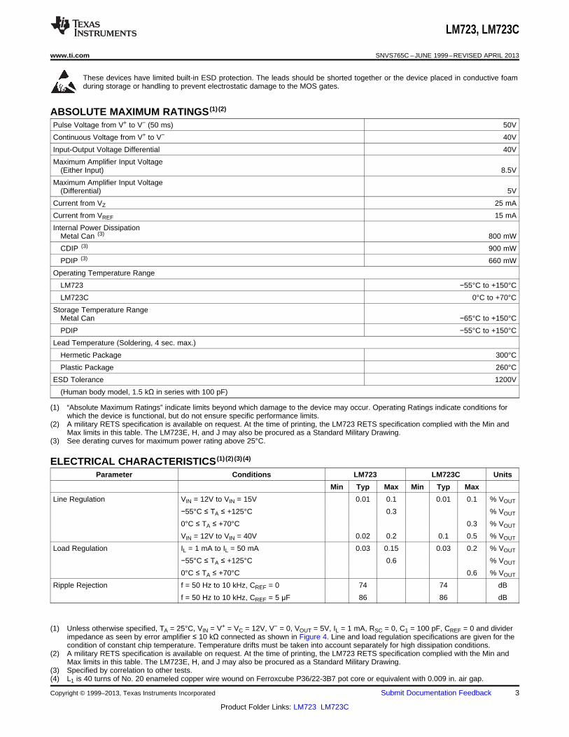
ABSOLUTE MAXIMUM RATINGS (1) (2)
Pulse Voltage from V+ to V− (50 ms) 50V
Continuous Voltage from V+ to V− 40V
Input-Output Voltage Differential 40V
Maximum Amplifier Input Voltage(Either Input) 8.5V
Maximum Amplifier Input Voltage(Differential) 5V
Current from VZ 25 mA
Current from VREF 15 mA
Internal Power DissipationMetal Can (3) 800 mW
CDIP (3) 900 mW
PDIP (3) 660 mW
Operating Temperature Range
LM723 −55°C to +150°C
LM723C 0°C to +70°C
Storage Temperature RangeMetal Can −65°C to +150°C
PDIP −55°C to +150°C
Lead Temperature (Soldering, 4 sec. max.)
Hermetic Package 300°C
Plastic Package 260°C
ESD Tolerance 1200V
(Human body model, 1.5 kΩ in series with 100 pF)
(1) “Absolute Maximum Ratings” indicate limits beyond which damage to the device may occur. Operating Ratings indicate conditions forwhich the device is functional, but do not ensure specific performance limits.
(2) A military RETS specification is available on request. At the time of printing, the LM723 RETS specification complied with the Min andMax limits in this table. The LM723E, H, and J may also be procured as a Standard Military Drawing.
(3) See derating curves for maximum power rating above 25°C.
ELECTRICAL CHARACTERISTICS (1) (2) (3) (4)
Parameter Conditions LM723 LM723C Units
Min Typ Max Min Typ Max
Line Regulation VIN = 12V to VIN = 15V 0.01 0.1 0.01 0.1 % VOUT
−55°C ≤ TA ≤ +125°C 0.3 % VOUT
0°C ≤ TA ≤ +70°C 0.3 % VOUT
VIN = 12V to VIN = 40V 0.02 0.2 0.1 0.5 % VOUT
Load Regulation IL = 1 mA to IL = 50 mA 0.03 0.15 0.03 0.2 % VOUT
−55°C ≤ TA ≤ +125°C 0.6 % VOUT
0°C ≤ TA ≤ +70°C 0.6 % VOUT
Ripple Rejection f = 50 Hz to 10 kHz, CREF = 0 74 74 dB
f = 50 Hz to 10 kHz, CREF = 5 μF 86 86 dB
(1) Unless otherwise specified, TA = 25°C, VIN = V+ = VC = 12V, V− = 0, VOUT = 5V, IL = 1 mA, RSC = 0, C1 = 100 pF, CREF = 0 and dividerimpedance as seen by error amplifier ≤ 10 kΩ connected as shown in Figure 4. Line and load regulation specifications are given for thecondition of constant chip temperature. Temperature drifts must be taken into account separately for high dissipation conditions.
(2) A military RETS specification is available on request. At the time of printing, the LM723 RETS specification complied with the Min andMax limits in this table. The LM723E, H, and J may also be procured as a Standard Military Drawing.
(3) Specified by correlation to other tests.(4) L1 is 40 turns of No. 20 enameled copper wire wound on Ferroxcube P36/22-3B7 pot core or equivalent with 0.009 in. air gap.
Copyright © 1999–2013, Texas Instruments Incorporated Submit Documentation Feedback 3
Product Folder Links: LM723 LM723C
LM723, LM723C
SNVS765C –JUNE 1999–REVISED APRIL 2013 www.ti.com
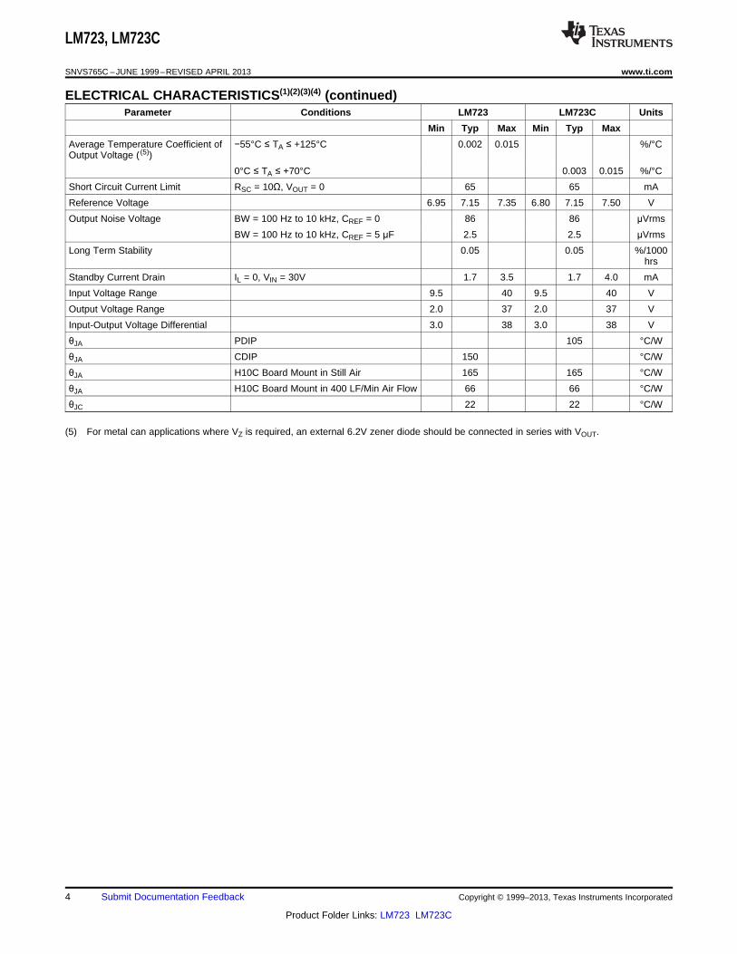
ELECTRICAL CHARACTERISTICS(1)(2)(3)(4) (continued)Parameter Conditions LM723 LM723C Units
Min Typ Max Min Typ Max
Average Temperature Coefficient of −55°C ≤ TA ≤ +125°C 0.002 0.015 %/°COutput Voltage ( (5))
0°C ≤ TA ≤ +70°C 0.003 0.015 %/°C
Short Circuit Current Limit RSC = 10Ω, VOUT = 0 65 65 mA
Reference Voltage 6.95 7.15 7.35 6.80 7.15 7.50 V
Output Noise Voltage BW = 100 Hz to 10 kHz, CREF = 0 86 86 μVrms
BW = 100 Hz to 10 kHz, CREF = 5 μF 2.5 2.5 μVrms
Long Term Stability 0.05 0.05 %/1000hrs
Standby Current Drain IL = 0, VIN = 30V 1.7 3.5 1.7 4.0 mA
Input Voltage Range 9.5 40 9.5 40 V
Output Voltage Range 2.0 37 2.0 37 V
Input-Output Voltage Differential 3.0 38 3.0 38 V
θJA PDIP 105 °C/W
θJA CDIP 150 °C/W
θJA H10C Board Mount in Still Air 165 165 °C/W
θJA H10C Board Mount in 400 LF/Min Air Flow 66 66 °C/W
θJC 22 22 °C/W
(5) For metal can applications where VZ is required, an external 6.2V zener diode should be connected in series with VOUT.
4 Submit Documentation Feedback Copyright © 1999–2013, Texas Instruments Incorporated
Product Folder Links: LM723 LM723C
LM723, LM723C
www.ti.com SNVS765C –JUNE 1999–REVISED APRIL 2013
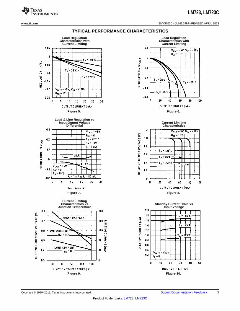
TYPICAL PERFORMANCE CHARACTERISTICS
Load Regulation Load RegulationCharacteristics with Characteristics with
Current Limiting Current Limiting
Figure 5. Figure 6.
Load & Line Regulation vsInput-Output Voltage Current Limiting
Differential Characteristics
Figure 7. Figure 8.
Current LimitingCharacteristics vs Standby Current Drain vs
Junction Temperature Input Voltage
Figure 9. Figure 10.
Copyright © 1999–2013, Texas Instruments Incorporated Submit Documentation Feedback 5
Product Folder Links: LM723 LM723C
LM723, LM723C
SNVS765C –JUNE 1999–REVISED APRIL 2013 www.ti.com
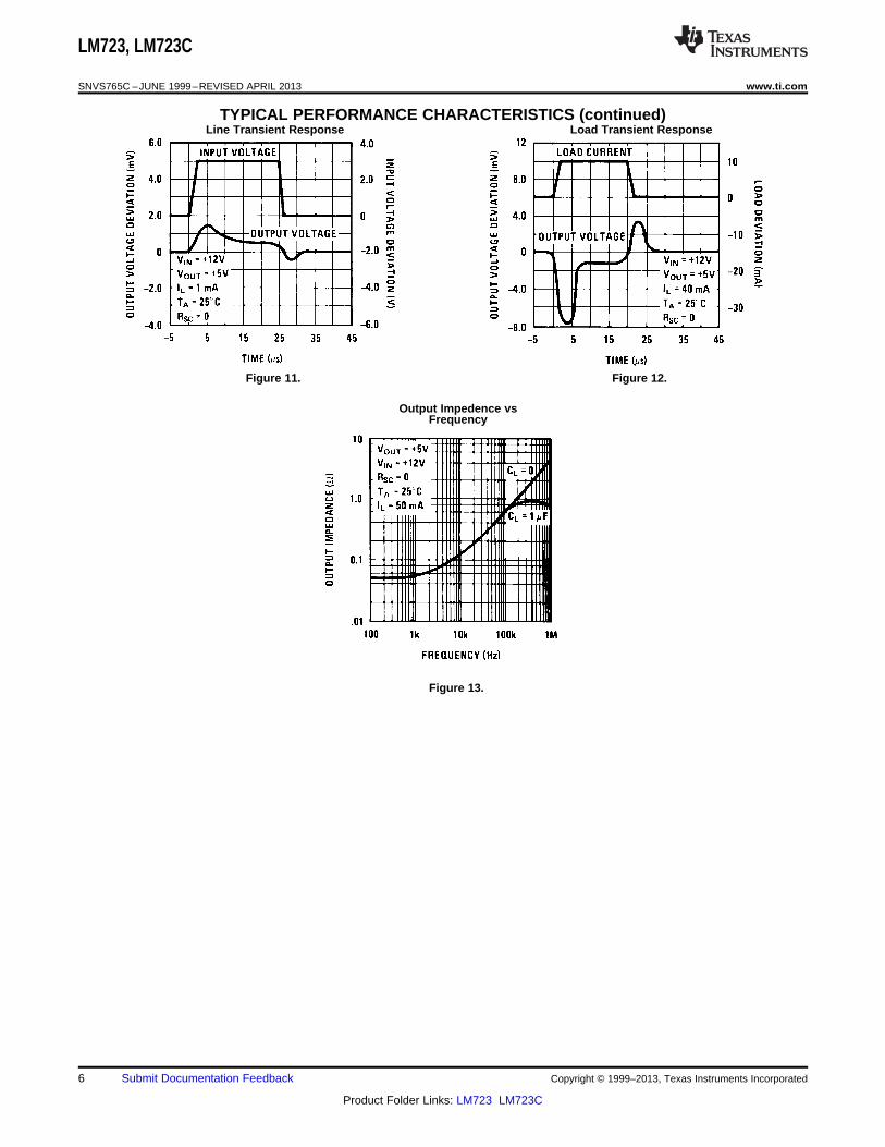
TYPICAL PERFORMANCE CHARACTERISTICS (continued)Line Transient Response Load Transient Response
Figure 11. Figure 12.
Output Impedence vsFrequency
Figure 13.
6 Submit Documentation Feedback Copyright © 1999–2013, Texas Instruments Incorporated
Product Folder Links: LM723 LM723C
LM723, LM723C
www.ti.com SNVS765C –JUNE 1999–REVISED APRIL 2013
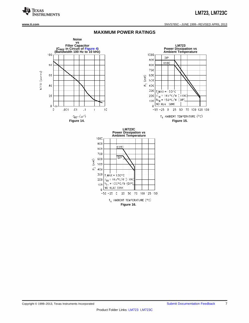
MAXIMUM POWER RATINGS
Noisevs
Filter Capacitor LM723(CREF in Circuit of Figure 4) Power Dissipation vs
(Bandwidth 100 Hz to 10 kHz) Ambient Temperature
Figure 14. Figure 15.
LM723CPower Dissipation vsAmbient Temperature
Figure 16.
Copyright © 1999–2013, Texas Instruments Incorporated Submit Documentation Feedback 7
Product Folder Links: LM723 LM723C
LM723, LM723C
SNVS765C –JUNE 1999–REVISED APRIL 2013 www.ti.com
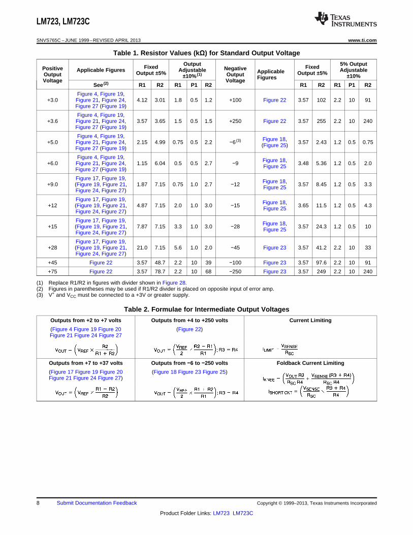
Table 1. Resistor Values (kΩ) for Standard Output Voltage
Output 5% OutputFixed FixedPositive NegativeApplicable Figures Adjustable AdjustableApplicableOutput ±5% Output ±5%Output Output±10% (1) ±10%FiguresVoltage VoltageSee (2) R1 R2 R1 P1 R2 R1 R2 R1 P1 R2
Figure 4, Figure 19,+3.0 Figure 21, Figure 24, 4.12 3.01 1.8 0.5 1.2 +100 Figure 22 3.57 102 2.2 10 91
Figure 27 (Figure 19)
Figure 4, Figure 19,+3.6 Figure 21, Figure 24, 3.57 3.65 1.5 0.5 1.5 +250 Figure 22 3.57 255 2.2 10 240
Figure 27 (Figure 19)
Figure 4, Figure 19, Figure 18,+5.0 Figure 21, Figure 24, 2.15 4.99 0.75 0.5 2.2 −6 (3) 3.57 2.43 1.2 0.5 0.75(Figure 25)Figure 27 (Figure 19)
Figure 4, Figure 19, Figure 18,+6.0 Figure 21, Figure 24, 1.15 6.04 0.5 0.5 2.7 −9 3.48 5.36 1.2 0.5 2.0Figure 25Figure 27 (Figure 19)
Figure 17, Figure 19, Figure 18,+9.0 (Figure 19, Figure 21, 1.87 7.15 0.75 1.0 2.7 −12 3.57 8.45 1.2 0.5 3.3Figure 25Figure 24, Figure 27)
Figure 17, Figure 19, Figure 18,+12 (Figure 19, Figure 21, 4.87 7.15 2.0 1.0 3.0 −15 3.65 11.5 1.2 0.5 4.3Figure 25Figure 24, Figure 27)
Figure 17, Figure 19, Figure 18,+15 (Figure 19, Figure 21, 7.87 7.15 3.3 1.0 3.0 −28 3.57 24.3 1.2 0.5 10Figure 25Figure 24, Figure 27)
Figure 17, Figure 19,+28 (Figure 19, Figure 21, 21.0 7.15 5.6 1.0 2.0 −45 Figure 23 3.57 41.2 2.2 10 33
Figure 24, Figure 27)
+45 Figure 22 3.57 48.7 2.2 10 39 −100 Figure 23 3.57 97.6 2.2 10 91
+75 Figure 22 3.57 78.7 2.2 10 68 −250 Figure 23 3.57 249 2.2 10 240
(1) Replace R1/R2 in figures with divider shown in Figure 28.(2) Figures in parentheses may be used if R1/R2 divider is placed on opposite input of error amp.(3) V+ and VCC must be connected to a +3V or greater supply.
Table 2. Formulae for Intermediate Output Voltages
Outputs from +2 to +7 volts Outputs from +4 to +250 volts Current Limiting
(Figure 4 Figure 19 Figure 20 (Figure 22)Figure 21 Figure 24 Figure 27
Outputs from +7 to +37 volts Outputs from −6 to −250 volts Foldback Current Limiting
(Figure 17 Figure 19 Figure 20 (Figure 18 Figure 23 Figure 25)Figure 21 Figure 24 Figure 27)
8 Submit Documentation Feedback Copyright © 1999–2013, Texas Instruments Incorporated
Product Folder Links: LM723 LM723C
LM723, LM723C
www.ti.com SNVS765C –JUNE 1999–REVISED APRIL 2013
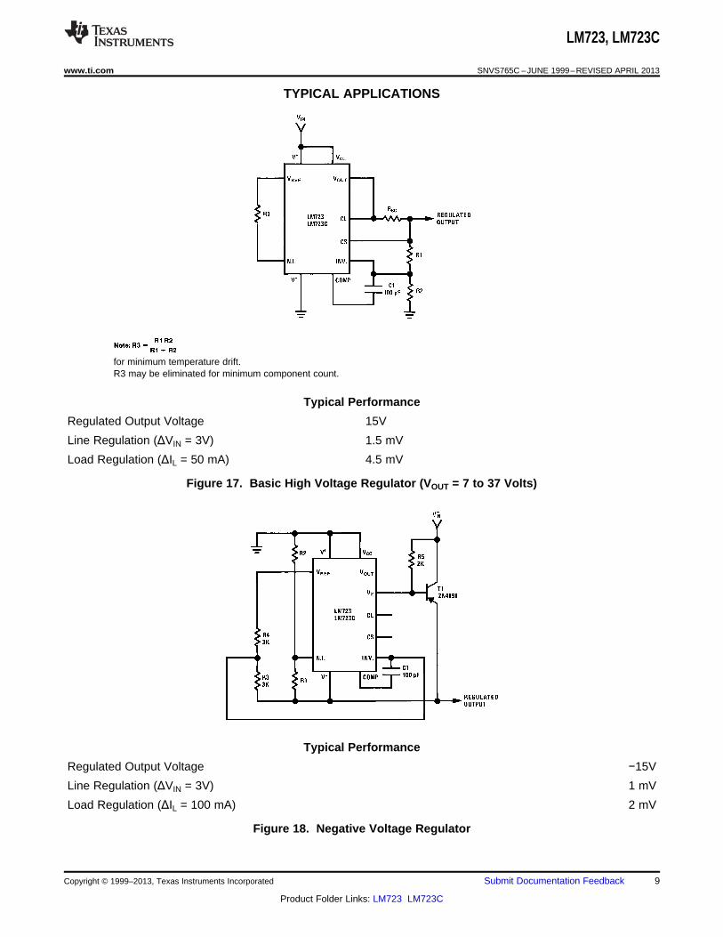
TYPICAL APPLICATIONS
for minimum temperature drift.R3 may be eliminated for minimum component count.
Typical Performance
Regulated Output Voltage 15V
Line Regulation (ΔVIN = 3V) 1.5 mV
Load Regulation (ΔIL = 50 mA) 4.5 mV
Figure 17. Basic High Voltage Regulator (VOUT = 7 to 37 Volts)
Typical Performance
Regulated Output Voltage −15V
Line Regulation (ΔVIN = 3V) 1 mV
Load Regulation (ΔIL = 100 mA) 2 mV
Figure 18. Negative Voltage Regulator
Copyright © 1999–2013, Texas Instruments Incorporated Submit Documentation Feedback 9
Product Folder Links: LM723 LM723C
LM723, LM723C
SNVS765C –JUNE 1999–REVISED APRIL 2013 www.ti.com
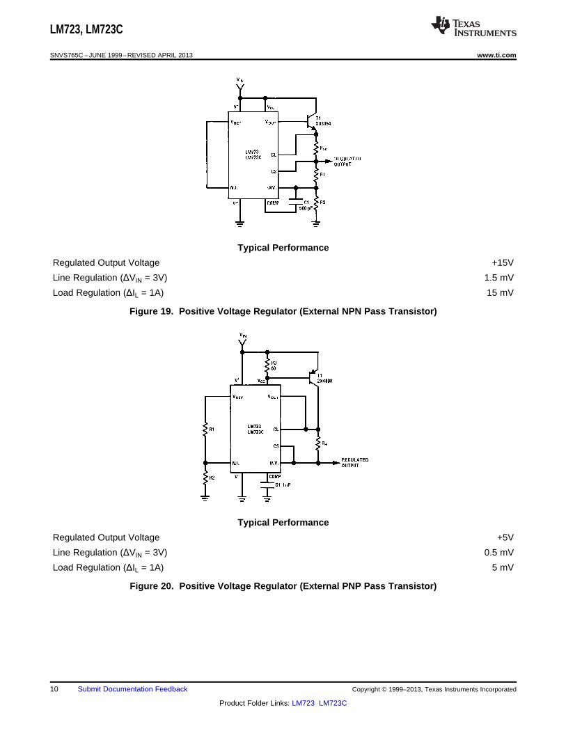
Typical Performance
Regulated Output Voltage +15V
Line Regulation (ΔVIN = 3V) 1.5 mV
Load Regulation (ΔIL = 1A) 15 mV
Figure 19. Positive Voltage Regulator (External NPN Pass Transistor)
Typical Performance
Regulated Output Voltage +5V
Line Regulation (ΔVIN = 3V) 0.5 mV
Load Regulation (ΔIL = 1A) 5 mV
Figure 20. Positive Voltage Regulator (External PNP Pass Transistor)
10 Submit Documentation Feedback Copyright © 1999–2013, Texas Instruments Incorporated
Product Folder Links: LM723 LM723C
LM723, LM723C
www.ti.com SNVS765C –JUNE 1999–REVISED APRIL 2013
Typical Performance
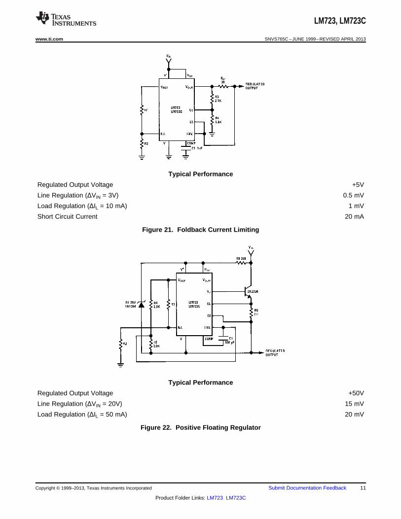
Regulated Output Voltage +5V
Line Regulation (ΔVIN = 3V) 0.5 mV
Load Regulation (ΔIL = 10 mA) 1 mV
Short Circuit Current 20 mA
Figure 21. Foldback Current Limiting
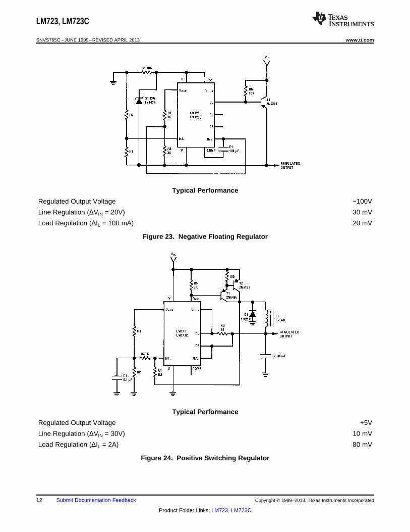
Typical Performance
Regulated Output Voltage +50V
Line Regulation (ΔVIN = 20V) 15 mV
Load Regulation (ΔIL = 50 mA) 20 mV
Figure 22. Positive Floating Regulator
Copyright © 1999–2013, Texas Instruments Incorporated Submit Documentation Feedback 11
Product Folder Links: LM723 LM723C
LM723, LM723C
SNVS765C –JUNE 1999–REVISED APRIL 2013 www.ti.com
Typical Performance
Regulated Output Voltage −100V
Line Regulation (ΔVIN = 20V) 30 mV
Load Regulation (ΔIL = 100 mA) 20 mV
Figure 23. Negative Floating Regulator
Typical Performance
Regulated Output Voltage +5V
Line Regulation (ΔVIN = 30V) 10 mV
Load Regulation (ΔIL = 2A) 80 mV
Figure 24. Positive Switching Regulator
12 Submit Documentation Feedback Copyright © 1999–2013, Texas Instruments Incorporated
Product Folder Links: LM723 LM723C
LM723, LM723C
www.ti.com SNVS765C –JUNE 1999–REVISED APRIL 2013
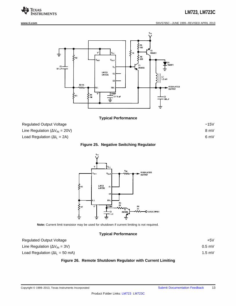
Typical Performance
Regulated Output Voltage −15V
Line Regulation (ΔVIN = 20V) 8 mV
Load Regulation (ΔIL = 2A) 6 mV
Figure 25. Negative Switching Regulator
Note: Current limit transistor may be used for shutdown if current limiting is not required.
Typical Performance
Regulated Output Voltage +5V
Line Regulation (ΔVIN = 3V) 0.5 mV
Load Regulation (ΔIL = 50 mA) 1.5 mV
Figure 26. Remote Shutdown Regulator with Current Limiting
Copyright © 1999–2013, Texas Instruments Incorporated Submit Documentation Feedback 13
Product Folder Links: LM723 LM723C
LM723, LM723C
SNVS765C –JUNE 1999–REVISED APRIL 2013 www.ti.com
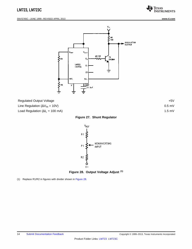
Regulated Output Voltage +5V
Line Regulation (ΔVIN = 10V) 0.5 mV
Load Regulation (ΔIL = 100 mA) 1.5 mV
Figure 27. Shunt Regulator
Figure 28. Output Voltage Adjust (1)
(1) Replace R1/R2 in figures with divider shown in Figure 28.
14 Submit Documentation Feedback Copyright © 1999–2013, Texas Instruments Incorporated
Product Folder Links: LM723 LM723C
LM723, LM723C
www.ti.com SNVS765C –JUNE 1999–REVISED APRIL 2013
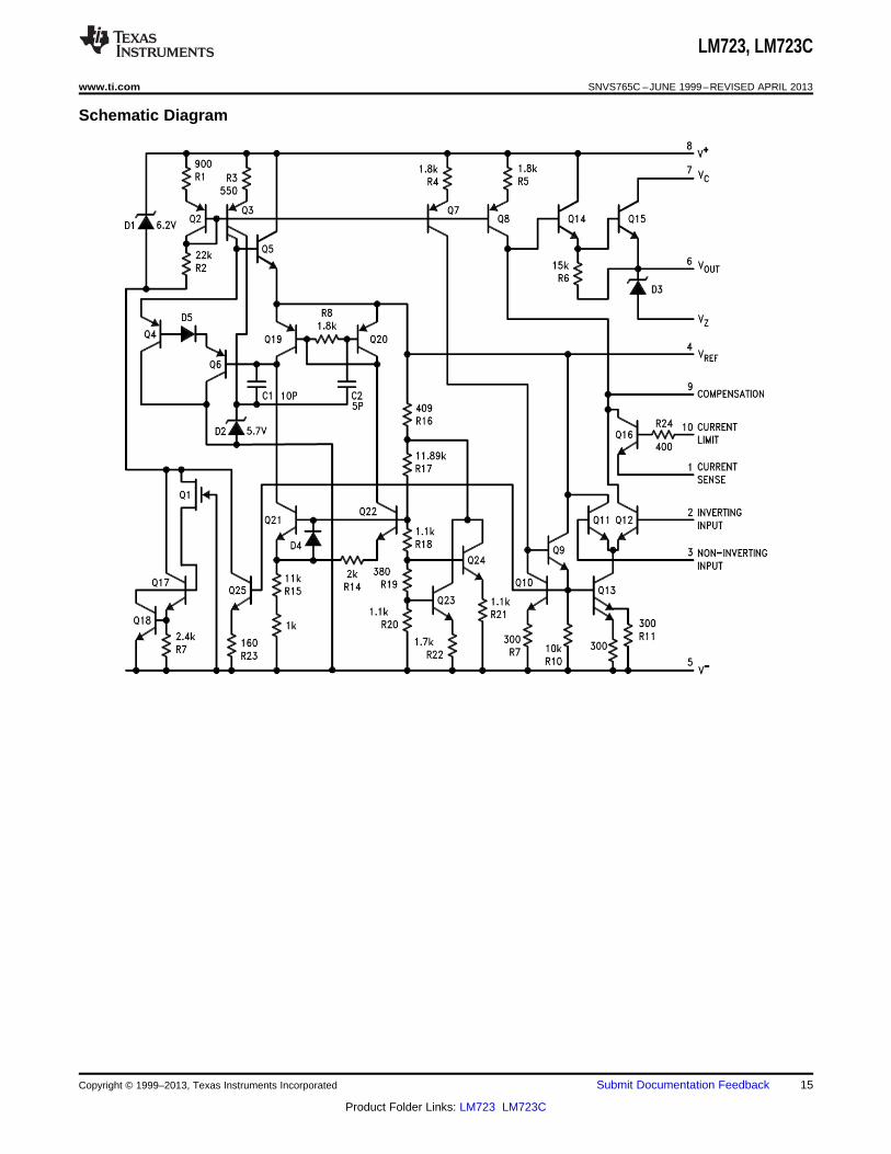
Schematic Diagram
Copyright © 1999–2013, Texas Instruments Incorporated Submit Documentation Feedback 15
Product Folder Links: LM723 LM723C
www.ti.com
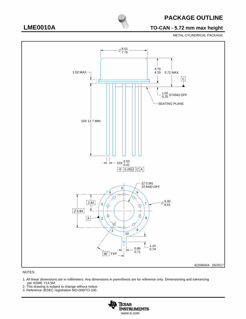
PACKAGE OUTLINE
C
A
9.408.51
( 3.56)STAND-OFF
0.860.71
5.84
2.92
8.517.75
5.72 MAX4.704.191.02 MAX
10X 12.7 MIN
10X 0.530.41
STAND-OFF1.020.25
1.140.74
36 TYP
TO-CAN - 5.72 mm max heightLME0010AMETAL CYLINDRICAL PACKAGE
4220604/A 05/2017
NOTES: 1. All linear dimensions are in millimeters. Any dimensions in parenthesis are for reference only. Dimensioning and tolerancing per ASME Y14.5M.2. This drawing is subject to change without notice.3. Reference JEDEC registration MO-006/TO-100.
0.25 C A
SEATING PLANE
1
2
3
45
6
7
10
8
9
SCALE 0.800
Recommended