Embed Size (px)
DESCRIPTION
Citation preview

Company
LOGO
PIC 16F84 InterfacingPIC 16F84 Interfacing
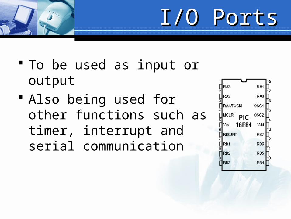
I/O PortsI/O Ports
To be used as input or output Also being used for other
functions such as timer, interrupt and serial communication
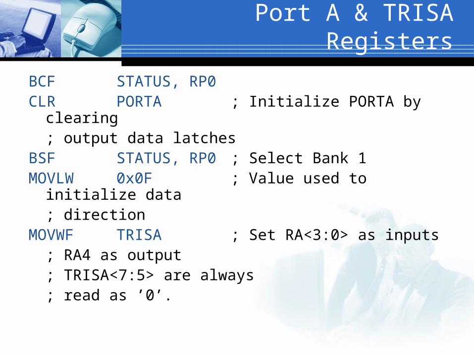
Port A & TRISA Registers
BCF STATUS, RP0 CLR PORTA ; Initialize PORTA by
clearing ; output data latches
BSF STATUS, RP0 ; Select Bank 1MOVLW 0x0F ; Value used to initialize
data; direction
MOVWF TRISA ; Set RA<3:0> as inputs; RA4 as output; TRISA<7:5> are always; read as ’0’.
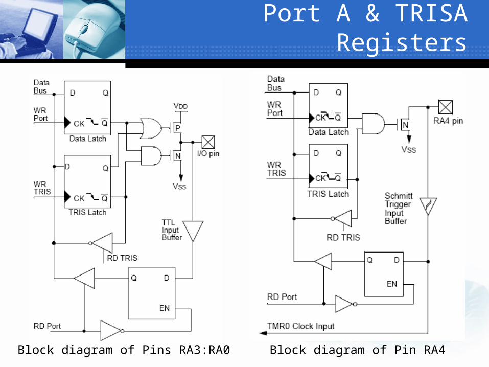
Port A & TRISA Registers
Block diagram of Pins RA3:RA0 Block diagram of Pin RA4

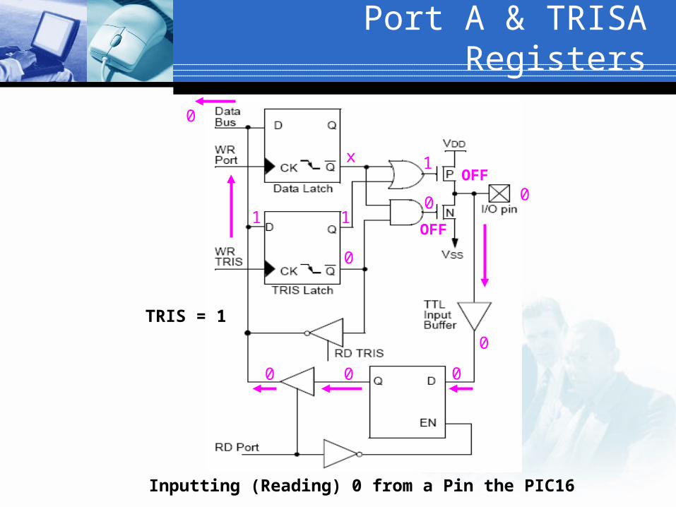
Port A & TRISA Registers
Inputting (Reading) 1 from a Pin the PIC16
1 1
0
x 1OFF
0
OFF
1
1
11
1
1
TRIS = 1
Port A & TRISA Registers
Inputting (Reading) 0 from a Pin the PIC16
1 1
0
x 1OFF
0
OFF
0
0
00
0
0
TRIS = 1
Port A & TRISA Registers
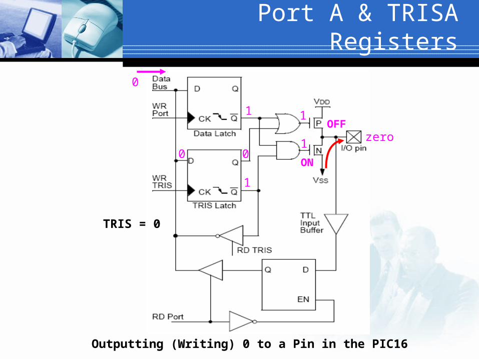
Outputting (Writing) 0 to a Pin in the PIC16
0 0
1
1 1OFF
1
ON
zero
0
TRIS = 0
Port A & TRISA Registers
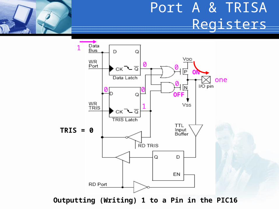
Outputting (Writing) 1 to a Pin in the PIC16
0 0
1
0 0ON
0
OFF
one
1
TRIS = 0
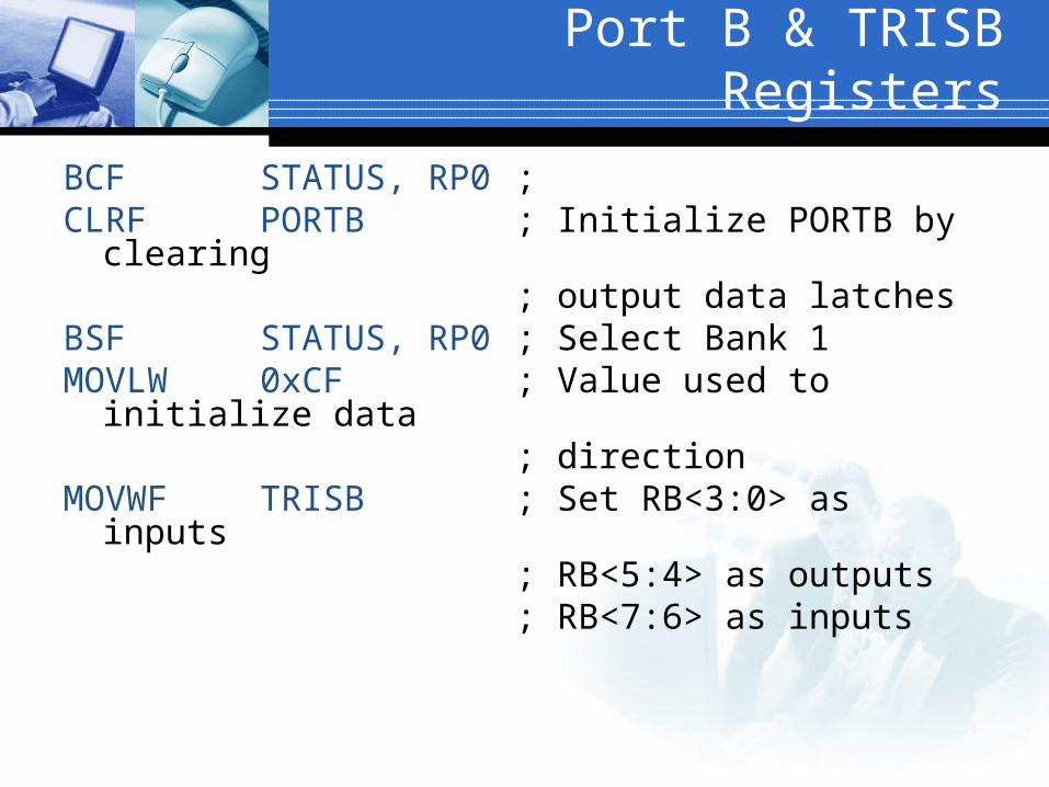
Port B & TRISB Registers
BCF STATUS, RP0 ;CLRF PORTB ; Initialize PORTB by
clearing ; output data latches
BSF STATUS, RP0 ; Select Bank 1MOVLW 0xCF ; Value used to initialize
data; direction
MOVWF TRISB ; Set RB<3:0> as inputs; RB<5:4> as outputs; RB<7:6> as inputs
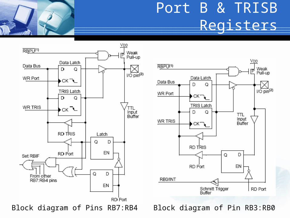
Port B & TRISB Registers
Block diagram of Pins RB7:RB4 Block diagram of Pin RB3:RB0
Interrupt
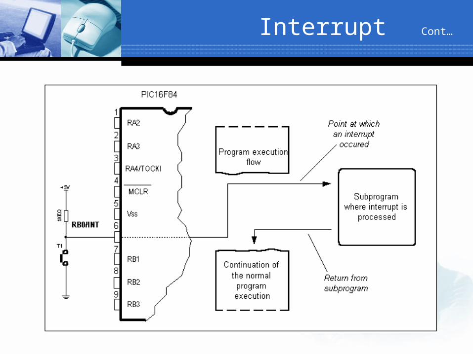
A mechanism that allows C responds to some events at the moment they occur, regardless of what C is doing at that time
Interrupt changes the program flow and invokes interrupt subroutine (Interrupt Service Routine, ISR)
INTCON is control register of interrupt
Interrupt Cont…
Interrupt Cont…
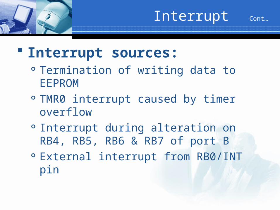
Interrupt sources: Termination of writing data to EEPROM TMR0 interrupt caused by timer overflow Interrupt during alteration on RB4, RB5, RB6
& RB7 of port B External interrupt from RB0/INT pin
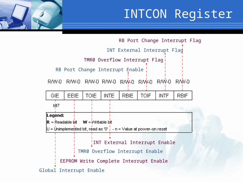
INTCON Register
INT External Interrupt Enable
TMR0 Overflow Interrupt Enable
EEPROM Write Complete Interrupt Enable
Global Interrupt Enable
RB Port Change Interrupt Enable
TMR0 Overflow Interrupt Flag
INT External Interrupt Flag
RB Port Change Interrupt Flag
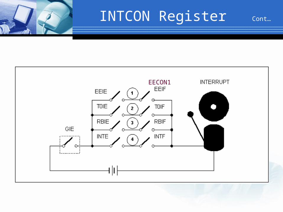
INTCON Register Cont…
EECON1
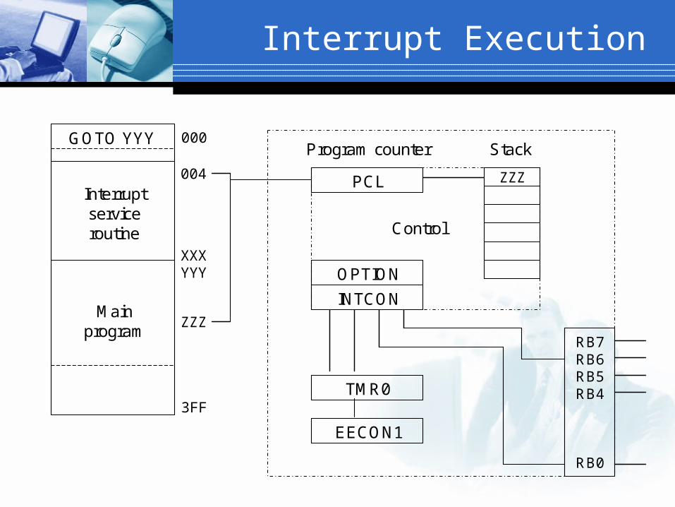
Interrupt Execution
GOTO YYY
Interruptserviceroutine
Mainprogram
000
004
XXXYYY
ZZZ
3FF
PCL
OPTION
INTCON
TMR0
EECON1
ZZZ
RB7RB6RB5RB4
RB0
Control
Program counter Stack
Example 7.1
The normal activity of program is to output binary count value on Port B. This process will be interrupted by RB0 that will be pulsed manually. The interrupt service routine causes all the outputs to be switched on, and waits for the button RA4 to be pressed. The routine then terminates by restoring the previous value in Port B data register and returns to the main program at the original point.
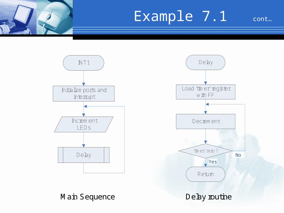
Example 7.1 cont…
INT1
Initialize ports and interrupt
Increment LEDs
Delay
Main Sequence
Delay
Load ‘timer’ register with FF
Decrement
‘timer’ zero ?
Return
Yes
No
Delay routine
No
Yes
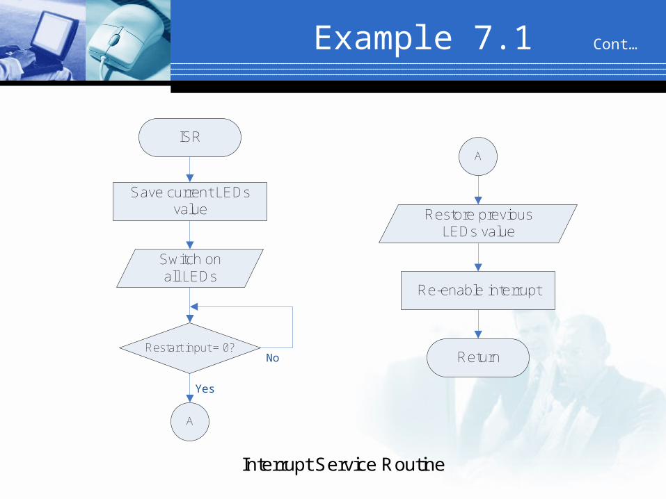
Example 7.1 Cont…
ISR
Save current LEDs value
Switch on all LEDs
Restart input = 0?
Restore previous LEDs value
Re-enable interrupt
Return
A
A
Interrupt Service Routine
Yes
No
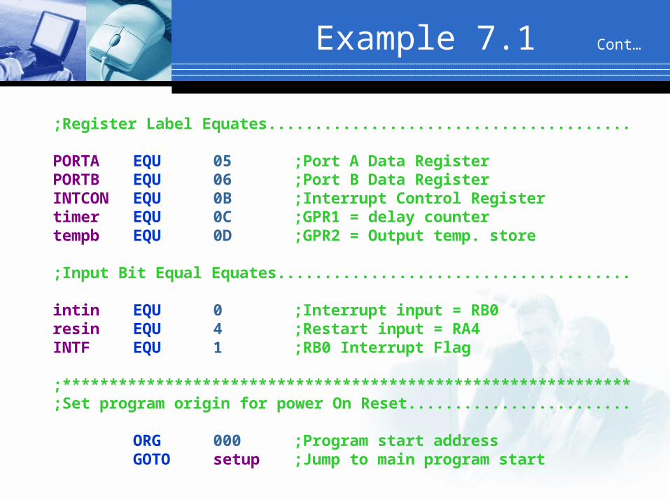
Example 7.1 Cont…
;Register Label Equates.......................................
PORTA EQU 05 ;Port A Data RegisterPORTB EQU 06 ;Port B Data RegisterINTCON EQU 0B ;Interrupt Control Registertimer EQU 0C ;GPR1 = delay countertempb EQU 0D ;GPR2 = Output temp. store
;Input Bit Equal Equates......................................
intin EQU 0 ;Interrupt input = RB0resin EQU 4 ;Restart input = RA4INTF EQU 1 ;RB0 Interrupt Flag
;*************************************************************;Set program origin for power On Reset........................
ORG 000 ;Program start addressGOTO setup ;Jump to main program start
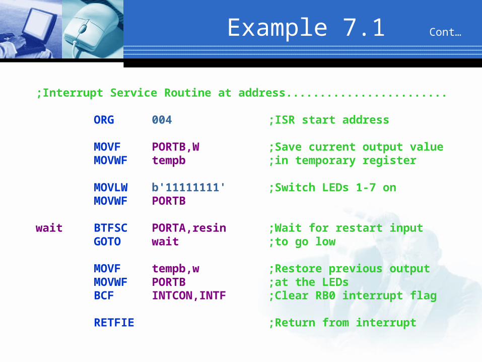
Example 7.1 Cont…
;Interrupt Service Routine at address........................
ORG 004 ;ISR start address
MOVF PORTB,W ;Save current output valueMOVWF tempb ;in temporary register
MOVLW b'11111111' ;Switch LEDs 1-7 onMOVWF PORTB
wait BTFSC PORTA,resin ;Wait for restart inputGOTO wait ;to go low
MOVF tempb,w ;Restore previous outputMOVWF PORTB ;at the LEDsBCF INTCON,INTF ;Clear RB0 interrupt flag
RETFIE ;Return from interrupt
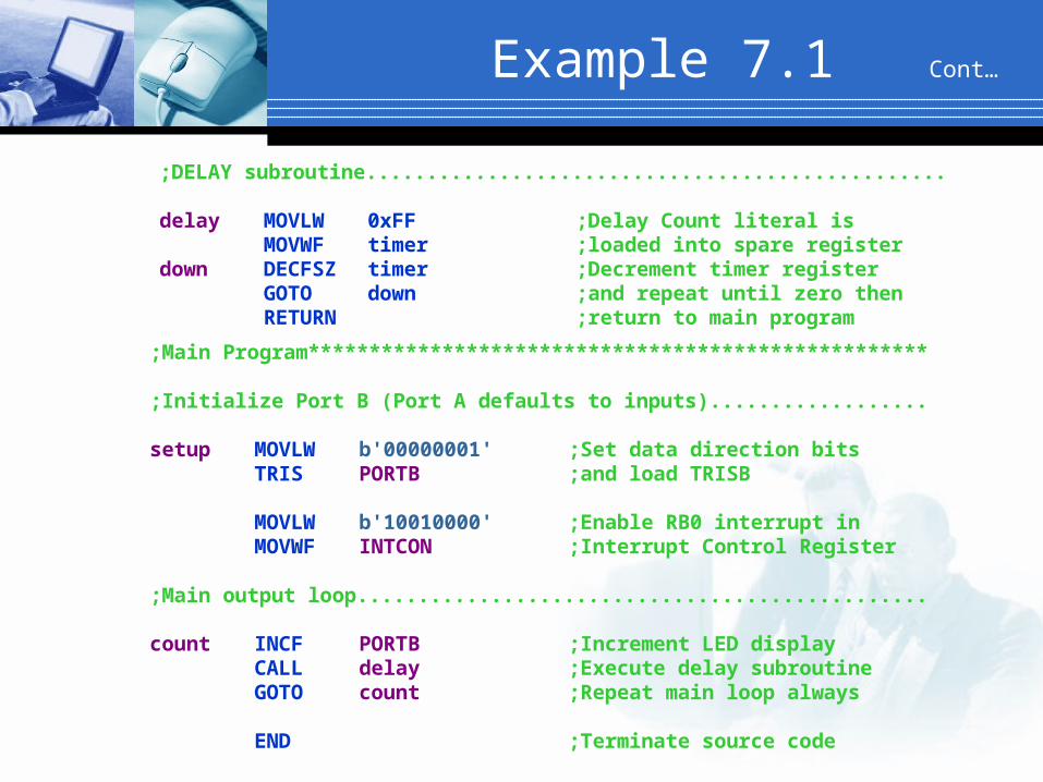
Example 7.1 Cont…
;DELAY subroutine................................................
delay MOVLW 0xFF ;Delay Count literal isMOVWF timer ;loaded into spare register
down DECFSZ timer ;Decrement timer registerGOTO down ;and repeat until zero thenRETURN ;return to main program
;Main Program***************************************************
;Initialize Port B (Port A defaults to inputs)..................
setup MOVLW b'00000001' ;Set data direction bitsTRIS PORTB ;and load TRISB
MOVLW b'10010000' ;Enable RB0 interrupt inMOVWF INTCON ;Interrupt Control Register
;Main output loop...............................................
count INCF PORTB ;Increment LED displayCALL delay ;Execute delay subroutineGOTO count ;Repeat main loop always
END ;Terminate source code
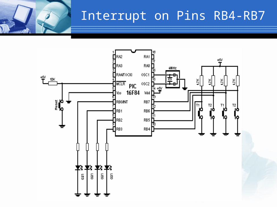
Interrupt on Pins RB4-RB7
Interrupt on Pins RB4-RB7 cont…
;PROGRAM INTPORTB.ASM
#INCLUDE "P16F84.INC"
ORG 0x00GOTO MainORG 0x04GOTO ISR
MainMOVLW 0xF0TRIS PORTBMOVLW 0xFFMOVWF PORTB ;Turn ON LEDBSF INTCON,GIEBSF INTCON,RBIE
LOOPGOTO LOOP
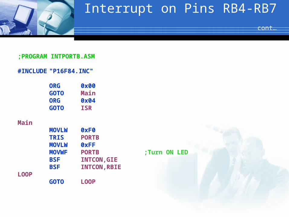
Interrupt on Pins RB4-RB7 cont…
ISR BCF INTCON,RBIF ;Clears the flag that indicates RB interrupt;took place thus enabling detection of new;new interrupts in main program
BTFSS PORTB,7 ;Determining which button caused the interruptGOTO LED0BTFSS PORTB,6GOTO LED1BTFSS PORTB,5GOTO LED2BTFSS PORTB,4GOTO LED3RETFIE
LED0 BCF PORTB,0 ;Switch off LED LD0RETFIE
LED1 BCF PORTB,1 ;Switch off LED LD1RETFIE
LED2 BCF PORTB,2 ;Switch off LED LD2RETFIE
LED3 BCF PORTB,3 ;Switch off LED LD3RETFIE
END
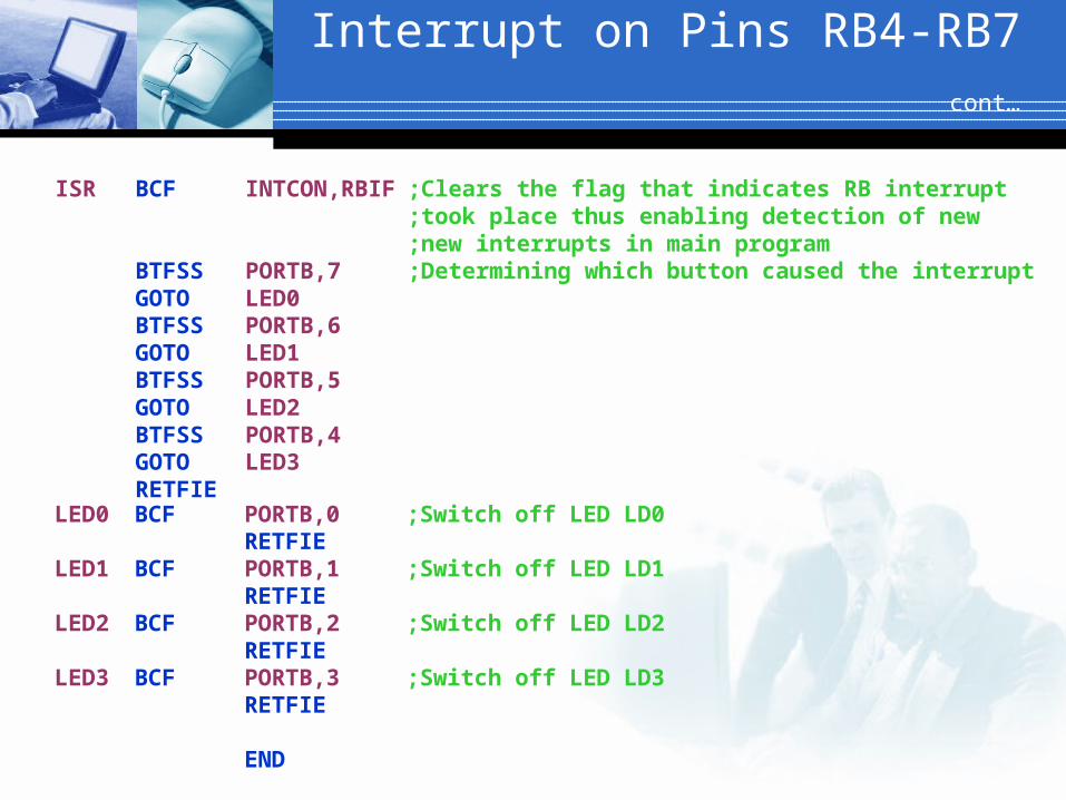
Interrupt on Pin RB0
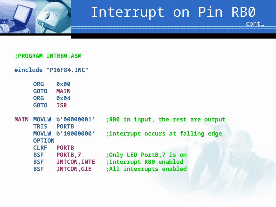
Interrupt on Pin RB0 cont…
;PROGRAM INTRB0.ASM
#include "P16F84.INC"
ORG 0x00GOTO MAINORG 0x04GOTO ISR
MAIN MOVLW b'00000001' ;RB0 in input, the rest are outputTRIS PORTBMOVLW b'10000000' ;interrupt occurs at falling edgeOPTIONCLRF PORTBBSF PORTB,7 ;Only LED PortB,7 is onBSF INTCON,INTE ;Interrupt RB0 enabledBSF INTCON,GIE ;All interrupts enabled
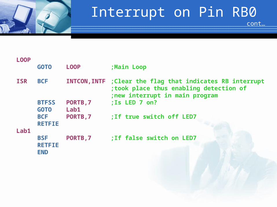
Interrupt on Pin RB0 cont…
LOOPGOTO LOOP ;Main Loop
ISR BCF INTCON,INTF ;Clear the flag that indicates RB interrupt;took place thus enabling detection of ;new interrupt in main program
BTFSS PORTB,7 ;Is LED 7 on?GOTO Lab1BCF PORTB,7 ;If true switch off LED7RETFIE
Lab1BSF PORTB,7 ;If false switch on LED7RETFIEEND
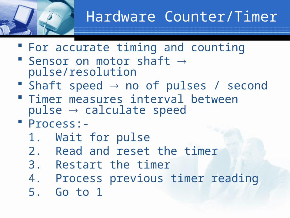
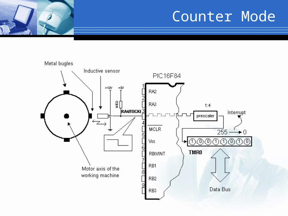
Hardware Counter/Timer
For accurate timing and counting Sensor on motor shaft pulse/resolution Shaft speed no of pulses / second Timer measures interval between pulse
calculate speed Process:-
1. Wait for pulse2. Read and reset the timer3. Restart the timer4. Process previous timer reading5. Go to 1
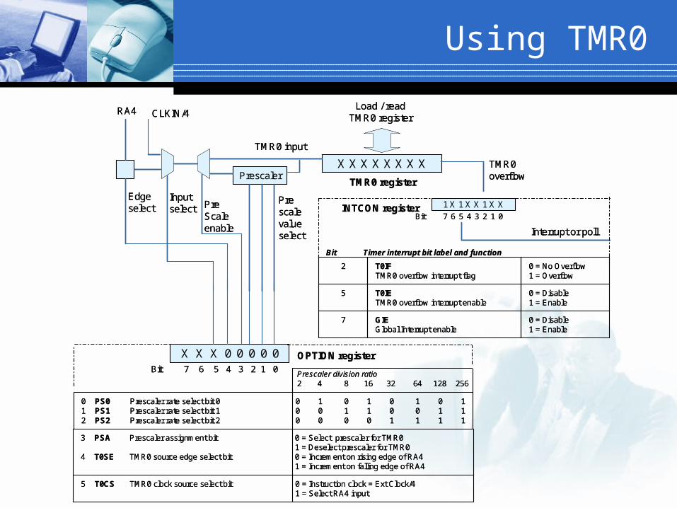
Using TMR0
PrescalerX X X X X X X X
X X X 0 0 0 0 0
TMR0 register
Load / readTMR0 register
TMR0 input
Prescalevalueselect
Inputselect
Edgeselect
RA4 CLKIN/4
PreScaleenable
1 X 1 X X 1 X XBit 7 6 5 4 3 2 1 0
INTCON register
2 T0IFTMR0 overflow interrupt flag
0 = No Overflow1 = Overflow
5 T0IETMR0 overflow interrupt enable
0 = Disable1 = Enable
7 GIEGlobal Interrupt enable
0 = Disable1 = Enable
Bit Timer interrupt bit label and function
0 PS0 Prescaler rate select bit 0 0 1 0 1 0 1 0 11 PS1 Prescaler rate select bit 1 0 0 1 1 0 0 1 12 PS2 Prescaler rate select bit 2 0 0 0 0 1 1 1 1
3 PSA Prescaler assignment bit 0 = Select prescaler for TMR01 = Deselect prescaler for TMR0
4 T0SE TMR0 source edge select bit 0 = Increment on rising edge of RA41 = Increment on falling edge of RA4
5 T0CS TMR0 clock source select bit 0 = Instruction clock = Ext Clock/41 = Select RA4 input
Prescaler division ratio2 4 8 16 32 64 128 256
Bit 7 6 5 4 3 2 1 0
OPTION register
TMR0 overflow
Interrupt or poll
Counter Mode
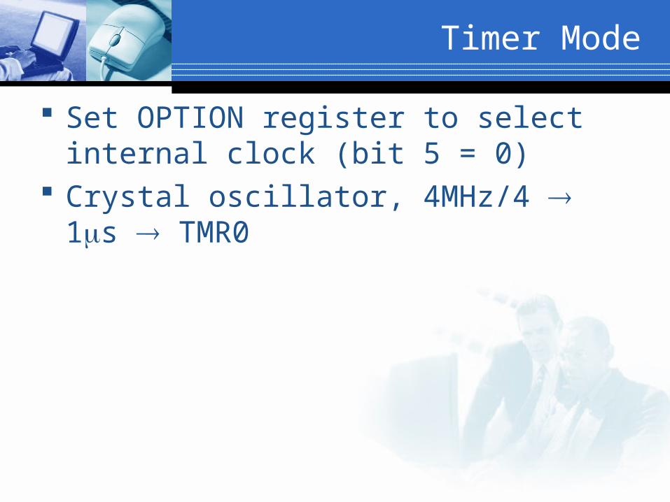
Timer Mode
Set OPTION register to select internal clock (bit 5 = 0)
Crystal oscillator, 4MHz/4 1s TMR0
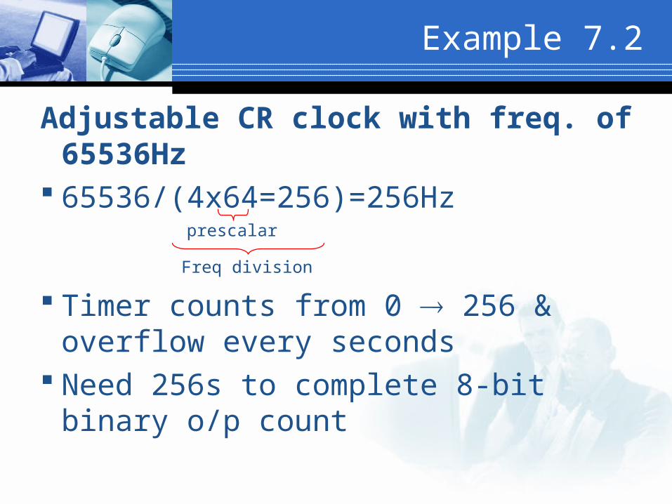
Example 7.2
Adjustable CR clock with freq. of 65536Hz
65536/(4x64=256)=256Hz
Timer counts from 0 256 & overflow every seconds
Need 256s to complete 8-bit binary o/p count
Freq division
prescalar
Example 7.3
Each example in the program takes four clock cycles to complete, with jumps taking eight cycles. If the program sequence is studied carefully, extra time is taken in completing the program loop before the timer is restarted. In this application, it will cause only a small error, but in other applications it may be significant.
Efficient solution: run timer while carrying on other process on the processor and allow time-out condition to interrupt the main program when it is finished.
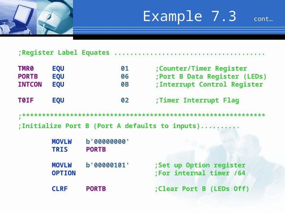
Example 7.3 cont…
;Register Label Equates ......................................
TMR0 EQU 01 ;Counter/Timer RegisterPORTB EQU 06 ;Port B Data Register (LEDs)INTCON EQU 0B ;Interrupt Control Register
T0IF EQU 02 ;Timer Interrupt Flag
;*************************************************************
;Initialize Port B (Port A defaults to inputs)..........
MOVLW b'00000000'TRIS PORTB
MOVLW b'00000101' ;Set up Option registerOPTION ;For internal timer /64
CLRF PORTB ;Clear Port B (LEDs Off)
Example 7.3 cont…
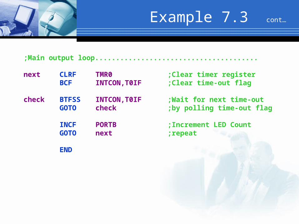
;Main output loop.......................................
next CLRF TMR0 ;Clear timer registerBCF INTCON,T0IF ;Clear time-out flag
check BTFSS INTCON,T0IF ;Wait for next time-outGOTO check ;by polling time-out flag
INCF PORTB ;Increment LED CountGOTO next ;repeat
END
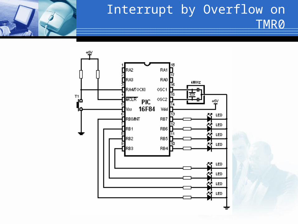
Interrupt by Overflow on TMR0
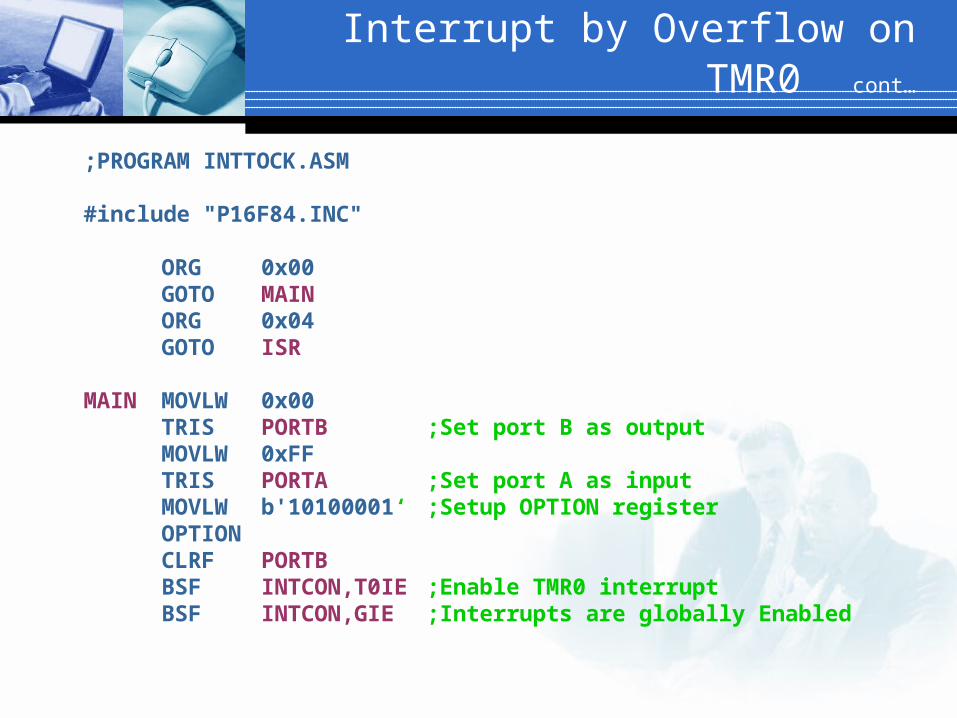
Interrupt by Overflow on TMR0 cont…
;PROGRAM INTTOCK.ASM
#include "P16F84.INC"
ORG 0x00GOTO MAINORG 0x04GOTO ISR
MAIN MOVLW 0x00TRIS PORTB ;Set port B as outputMOVLW 0xFFTRIS PORTA ;Set port A as inputMOVLW b'10100001‘ ;Setup OPTION registerOPTIONCLRF PORTBBSF INTCON,T0IE ;Enable TMR0 interruptBSF INTCON,GIE ;Interrupts are globally Enabled
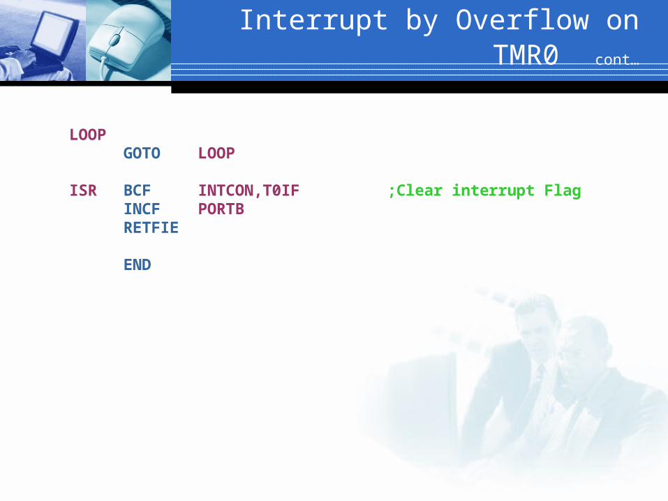
Interrupt by Overflow on TMR0 cont…
LOOPGOTO LOOP
ISR BCF INTCON,T0IF ;Clear interrupt FlagINCF PORTBRETFIE
END
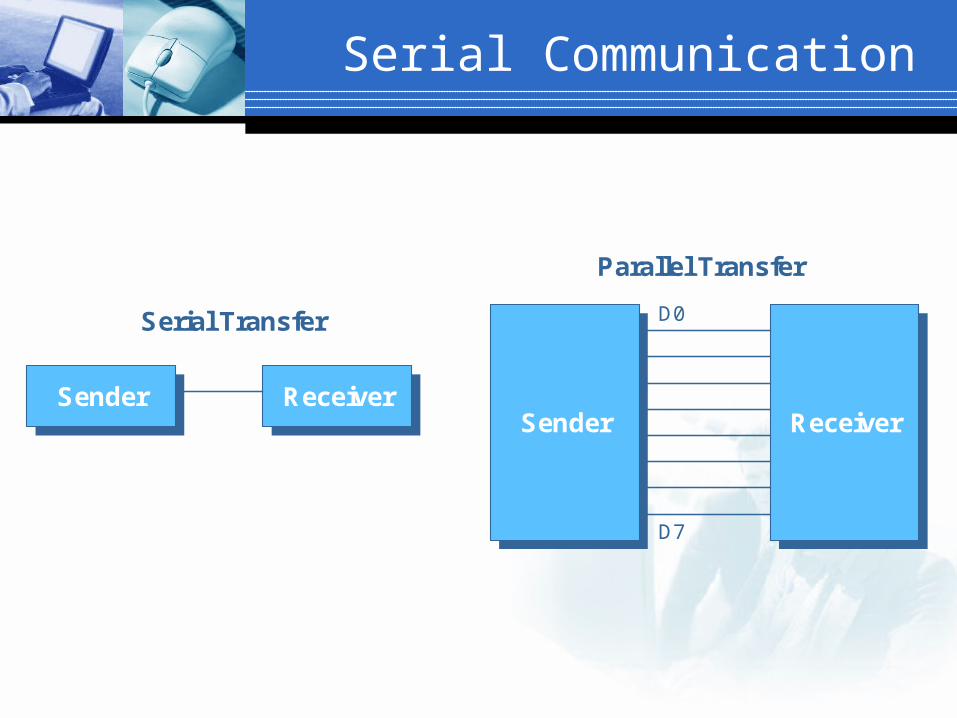
Serial Communication
SenderSender ReceiverReceiverSenderSender ReceiverReceiver
Serial Transfer
Parallel Transfer
D0
D7
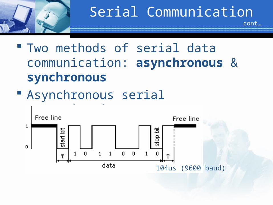
Serial Communication cont…
Two methods of serial data communication: asynchronous & synchronous
Asynchronous serial communication:
104us (9600 baud)
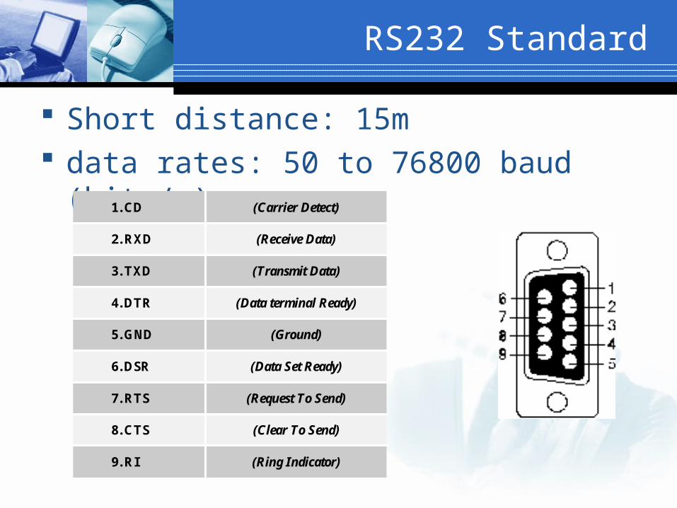
RS232 Standard
Short distance: 15m data rates: 50 to 76800 baud (bits/s)
(Ring Indicator)9. RI
(Clear To Send)8. CTS
(Request To Send)7. RTS
(Data Set Ready)6. DSR
(Ground)5. GND
(Data terminal Ready)4. DTR
(Transmit Data)3. TXD
(Receive Data)2. RXD
(Carrier Detect)1. CD
(Ring Indicator)9. RI
(Clear To Send)8. CTS
(Request To Send)7. RTS
(Data Set Ready)6. DSR
(Ground)5. GND
(Data terminal Ready)4. DTR
(Transmit Data)3. TXD
(Receive Data)2. RXD
(Carrier Detect)1. CD
Pin designations on RS232 connector
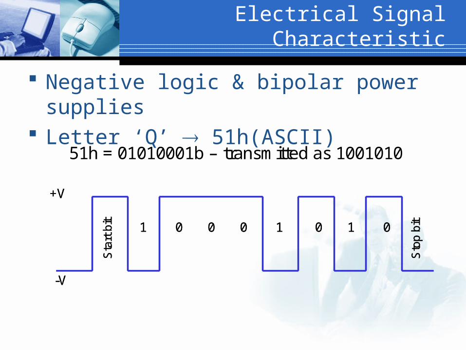
Electrical Signal Characteristic
Negative logic & bipolar power supplies Letter ‘Q’ 51h(ASCII)
51h = 01010001b – transmitted as 1001010
-V
+V
Sta
rt b
it 1 0 0 0 1 0 1 0
Sto
p b
it
-V
+V
Sta
rt b
it 1 0 0 0 1 0 1 0
Sto
p b
it
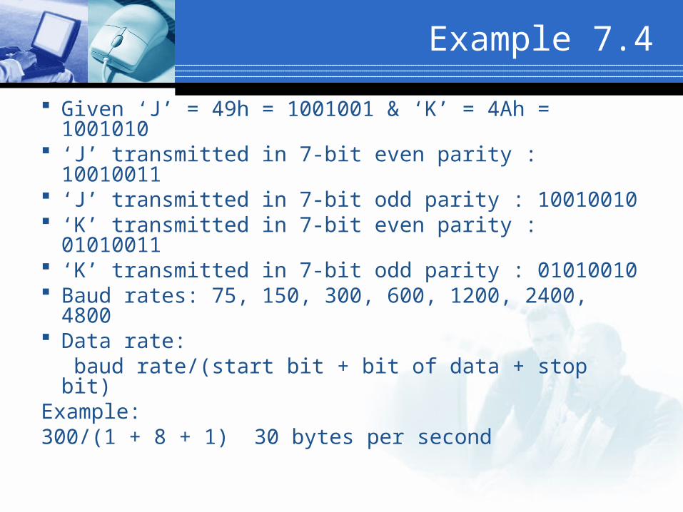
Example 7.4
Given ‘J’ = 49h = 1001001 & ‘K’ = 4Ah = 1001010
‘J’ transmitted in 7-bit even parity : 10010011 ‘J’ transmitted in 7-bit odd parity : 10010010 ‘K’ transmitted in 7-bit even parity : 01010011 ‘K’ transmitted in 7-bit odd parity : 01010010 Baud rates: 75, 150, 300, 600, 1200, 2400, 4800 Data rate:
baud rate/(start bit + bit of data + stop bit)Example:300/(1 + 8 + 1) 30 bytes per second
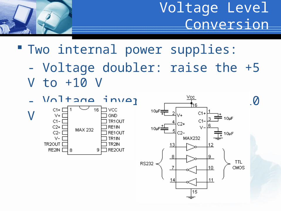
Voltage Level Conversion
Two internal power supplies:
- Voltage doubler: raise the +5 V to +10 V
- Voltage inverter: convert +10 V to -10 V
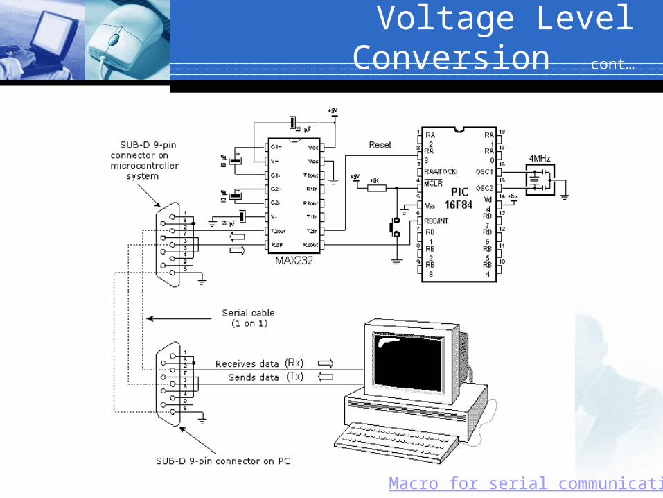
Voltage Level Conversion cont…
Macro for serial communication
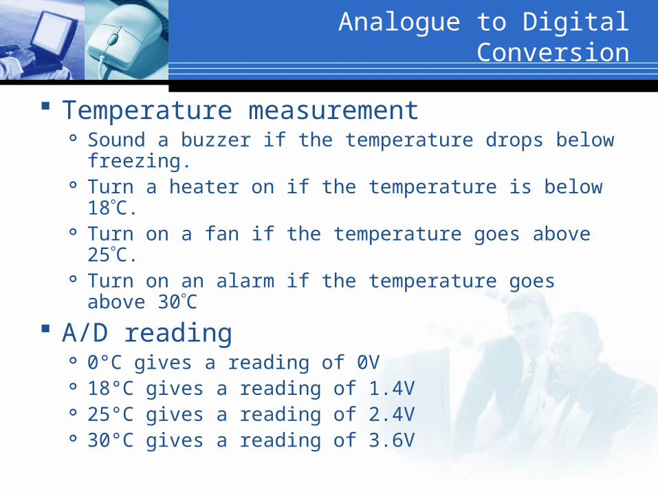
Analogue to Digital Conversion
Temperature measurement Sound a buzzer if the temperature drops below
freezing. Turn a heater on if the temperature is below 18C. Turn on a fan if the temperature goes above 25C. Turn on an alarm if the temperature goes above 30C
A/D reading 0°C gives a reading of 0V 18°C gives a reading of 1.4V 25°C gives a reading of 2.4V 30°C gives a reading of 3.6V
Analogue to Digital Conversion cont…
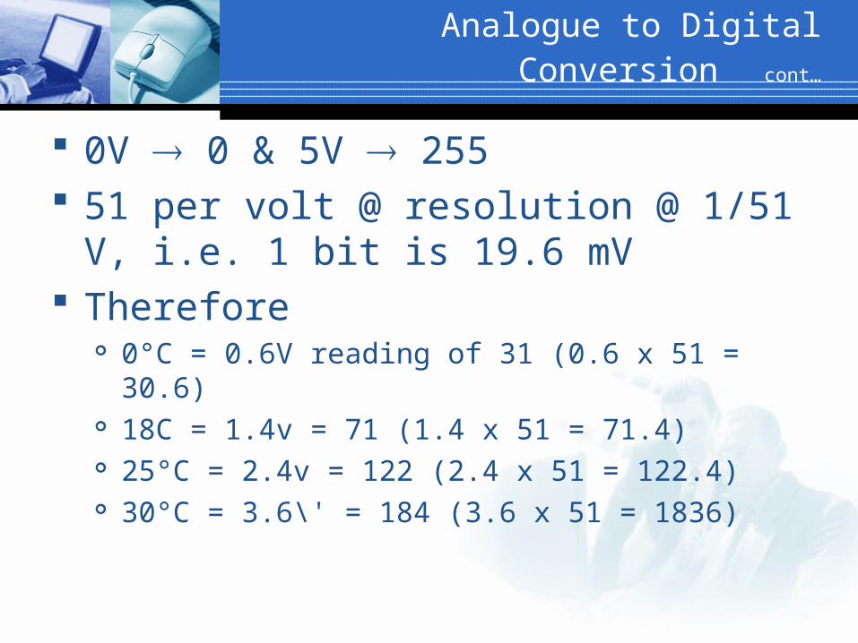
0V 0 & 5V 255 51 per volt @ resolution @ 1/51 V, i.e. 1
bit is 19.6 mV Therefore
0°C = 0.6V reading of 31 (0.6 x 51 = 30.6) 18C = 1.4v = 71 (1.4 x 51 = 71.4) 25°C = 2.4v = 122 (2.4 x 51 = 122.4) 30°C = 3.6\' = 184 (3.6 x 51 = 1836)
Analogue to Digital Conversion cont…
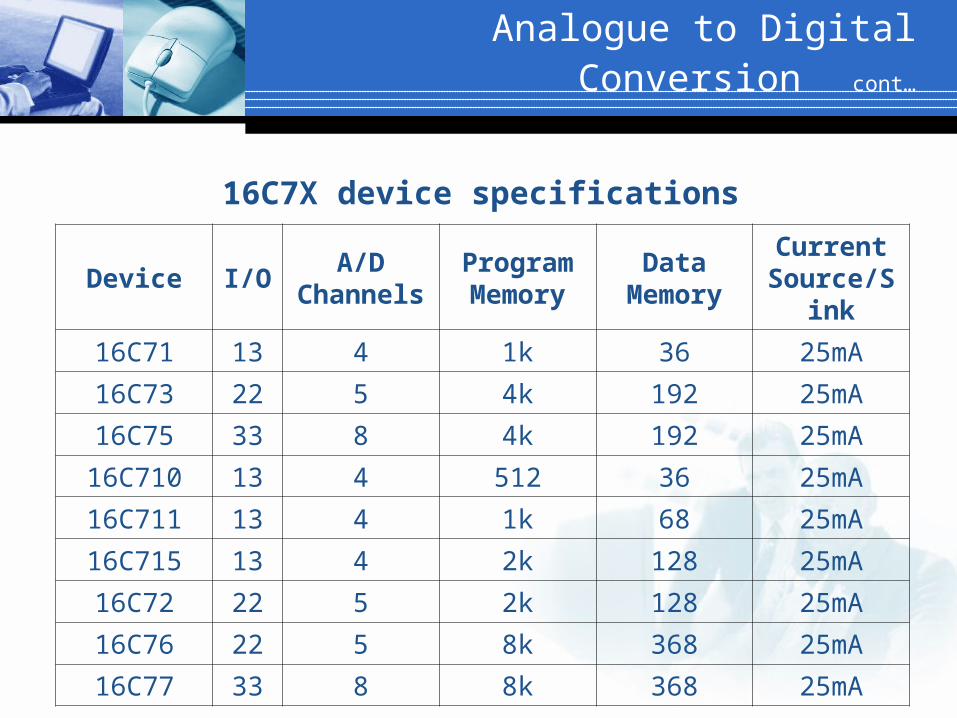
Device I/OA/D
ChannelsProgram Memory
Data Memory
Current Source/Sink
16C71 13 4 1k 36 25mA
16C73 22 5 4k 192 25mA
16C75 33 8 4k 192 25mA
16C710 13 4 512 36 25mA
16C711 13 4 1k 68 25mA
16C715 13 4 2k 128 25mA
16C72 22 5 2k 128 25mA
16C76 22 5 8k 368 25mA
16C77 33 8 8k 368 25mA
16C7X device specifications
Analogue to Digital Conversion cont…
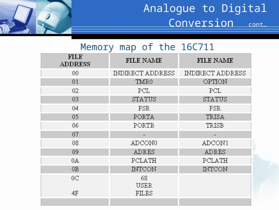
Memory map of the 16C711
Analogue to Digital Conversion cont…
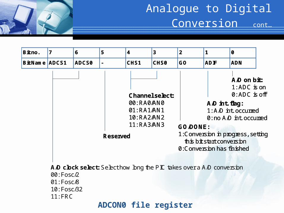
ADNADIFGOCHS0CHS1-ADCS0ADCS1Bit Name
01234567Bit no.
ADNADIFGOCHS0CHS1-ADCS0ADCS1Bit Name
01234567Bit no.
A/D clock select: Select how long the PIC takes over a A/D conversion00: Fosc/201: Fosc/810: Fosc/3211: FRC
A/D on bit:1: ADC is on0: ADC is off
A/D int. flag:1: A/D int. occurred0: no A/D int. occurred
GO/DONE:1: Conversion in progress, setting
this bit start conversion0: Conversion has finished
Channel select:00: RA0/AN001: RA1/AN110: RA2/AN211: RA3/AN3
Reserved
A/D on bit:1: ADC is on0: ADC is off
A/D int. flag:1: A/D int. occurred0: no A/D int. occurred
GO/DONE:1: Conversion in progress, setting
this bit start conversion0: Conversion has finished
Channel select:00: RA0/AN001: RA1/AN110: RA2/AN211: RA3/AN3
Reserved
ADCON0 file register
Analogue to Digital Conversion cont…
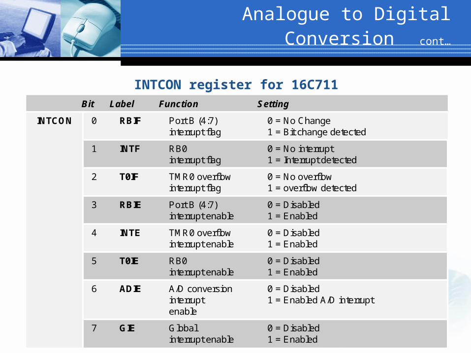
7 GIE Global 0 = Disabledinterrupt enable 1 = Enabled
6 ADIE A/D conversion 0 = Disabledinterrupt 1 = Enabled A/D interruptenable
5 T0IE RB0 0 = Disabledinterrupt enable 1 = Enabled
4 INTE TMR0 overflow 0 = Disabledinterrupt enable 1 = Enabled
3 RBIE Port B (4:7) 0 = Disabledinterrupt enable 1 = Enabled
2 T0IF TMR0 overflow 0 = No overflowinterrupt flag 1 = overflow detected
1 INTF RB0 0 = No interruptinterrupt flag 1 = Interrupt detected
0 RBIF Port B (4:7) 0 = No Changeinterrupt flag 1 = Bit change detected
INTCON
Bit Label Function Setting
INTCON register for 16C711
Analogue to Digital Conversion cont…
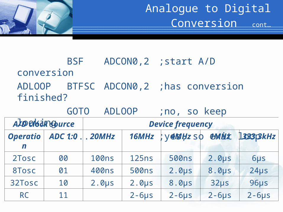
BSF ADCON0,2 ;start A/D conversion
ADLOOP BTFSC ADCON0,2 ;has conversion finished?
GOTO ADLOOP ;no, so keep looking
.... ;yes, so exit loop
A/D clock source Device frequency
Operation ADC 1:0 20MHz 16MHz 4MHz 1MHz 333.3kHz
2Tosc 00 100ns 125ns 500ns 2.0µs 6µs
8Tosc 01 400ns 500ns 2.0µs 8.0µs 24µs
32Tosc 10 2.0µs 2.0µs 8.0µs 32µs 96µs
RC 11 2-6µs 2-6µs 2-6µs 2-6µs
Example
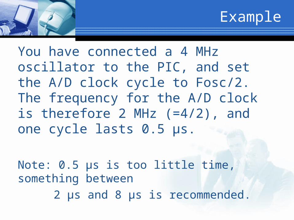
You have connected a 4 MHz oscillator to the PIC, and set the A/D clock cycle to Fosc/2. The frequency for the A/D clock is therefore 2 MHz (=4/2), and one cycle lasts 0.5 µs.
Note: 0.5 µs is too little time, something between
2 µs and 8 µs is recommended.
Example cont…
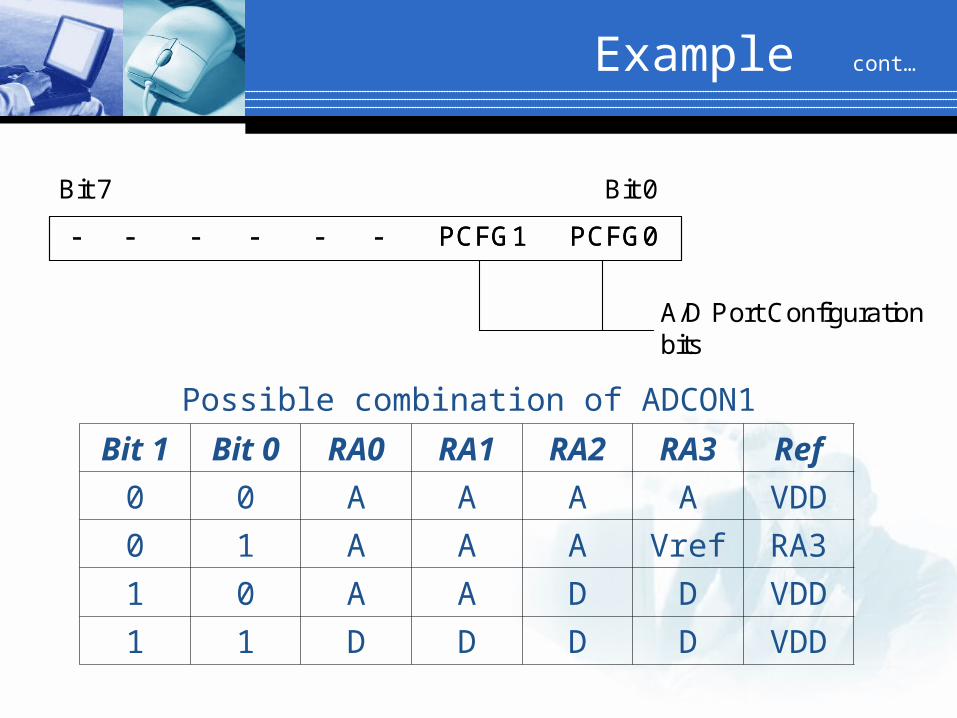
- - - - - - PCFG1 PCFG0- - - - - - PCFG1 PCFG0
Bit 7 Bit 0
A/D Port Configurationbits
Bit 1 Bit 0 RA0 RA1 RA2 RA3 Ref
0 0 A A A A VDD
0 1 A A A Vref RA3
1 0 A A D D VDD
1 1 D D D D VDD
Possible combination of ADCON1
Example 7.5
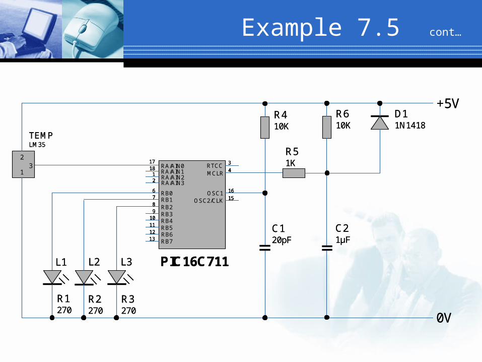
The following figure shows the circuit for a water temperature alarm system. The operations of the system are as follow:
If temperature is lower than 18C, then the water is too cold, so turn on the L1 LED (others off).
If temperature is higher than 23C, then the water is too hot, so turn on the L3 LED (others off).
If temperature is in between 18C and 23C, then the water temperature is OK, so turn on the L2 LED (others off).
Example 7.5 cont…
RA/AIN0RA/AIN1RA/AIN2RA/AIN3
RB0RB1RB2RB3RB4RB5RB6RB7
1718
12
6789
10111213
RTCCMCLR
OSC1OSC2/CLK
3
4
16
15
R410K
1
23
TEMPLM35
R610K
D11N1418
L1 L2 L3
R1270
R2270
R3270
PIC16C711
+5V
0V
R51K
C120pF
C21µF
RA/AIN0RA/AIN1RA/AIN2RA/AIN3
RB0RB1RB2RB3RB4RB5RB6RB7
1718
12
6789
10111213
RTCCMCLR
OSC1OSC2/CLK
3
4
16
15
RA/AIN0RA/AIN1RA/AIN2RA/AIN3
RB0RB1RB2RB3RB4RB5RB6RB7
1718
12
6789
10111213
RTCCMCLR
OSC1OSC2/CLK
3
4
16
15
R410K
1
23
TEMPLM35
R610K
D11N1418
L1 L2 L3
R1270
R2270
R3270
PIC16C711
+5V
0V
R51K
C120pF
C21µF
Example 7.5 cont…
Start
Setup
Start A/D conversion
Start
Setup
Start A/D conversion
Reset A/D interrupt flag
Is water too cold?
Is water too hot?
Turn on OK LED Turn on hot LED Turn on cold LED
Return from ISR
YES
YES
NO
NO
Reset A/D interrupt flag
Is water too cold?
Is water too hot?
Turn on OK LED Turn on hot LED Turn on cold LED
Return from ISR
YES
YES
NO
NO
Main loop
Interrupt Service Routine
Example 7.5 cont…
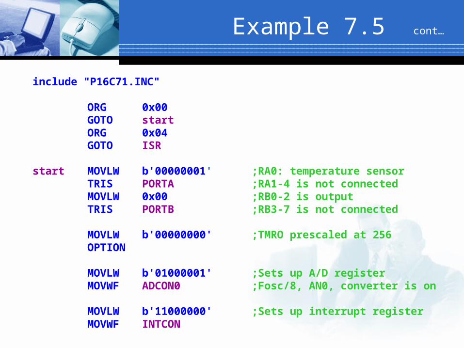
include "P16C71.INC"
ORG 0x00GOTO startORG 0x04GOTO ISR
start MOVLW b'00000001' ;RA0: temperature sensorTRIS PORTA ;RA1-4 is not connectedMOVLW 0x00 ;RB0-2 is outputTRIS PORTB ;RB3-7 is not connected
MOVLW b'00000000' ;TMRO prescaled at 256OPTION
MOVLW b'01000001' ;Sets up A/D registerMOVWF ADCON0 ;Fosc/8, AN0, converter is on
MOVLW b'11000000' ;Sets up interrupt registerMOVWF INTCON
Example 7.5 cont…
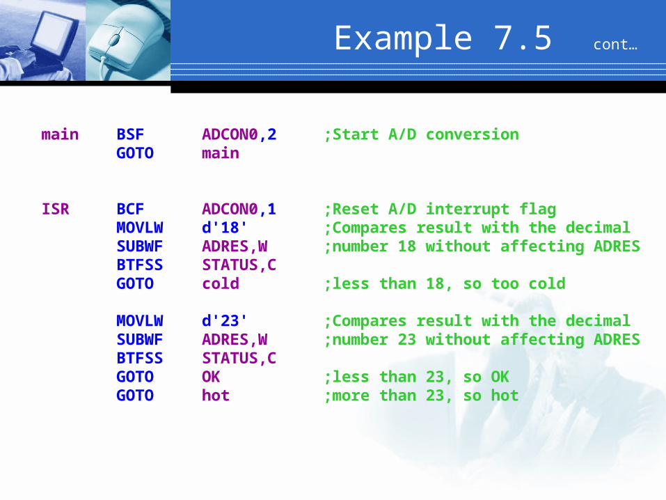
main BSF ADCON0,2 ;Start A/D conversionGOTO main
ISR BCF ADCON0,1 ;Reset A/D interrupt flagMOVLW d'18' ;Compares result with the decimalSUBWF ADRES,W ;number 18 without affecting ADRESBTFSS STATUS,CGOTO cold ;less than 18, so too cold
MOVLW d'23' ;Compares result with the decimalSUBWF ADRES,W ;number 23 without affecting ADRESBTFSS STATUS,CGOTO OK ;less than 23, so OKGOTO hot ;more than 23, so hot
Example 7.5 cont…
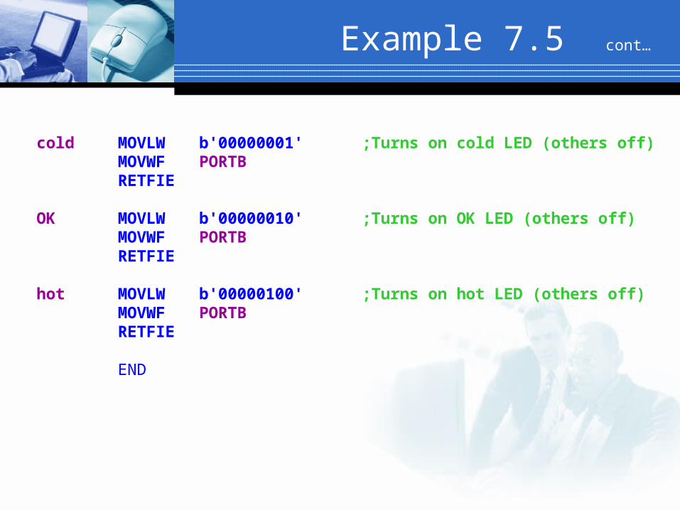
cold MOVLW b'00000001' ;Turns on cold LED (others off)MOVWF PORTBRETFIE
OK MOVLW b'00000010' ;Turns on OK LED (others off)MOVWF PORTBRETFIE
hot MOVLW b'00000100' ;Turns on hot LED (others off)MOVWF PORTBRETFIE
END