Embed Size (px)
Citation preview

SEMINAR BY MELISHA
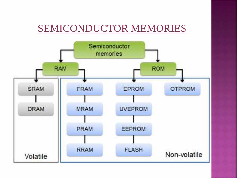
SEMICONDUCTOR MEMORIES
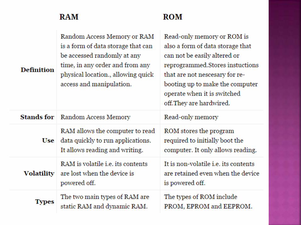
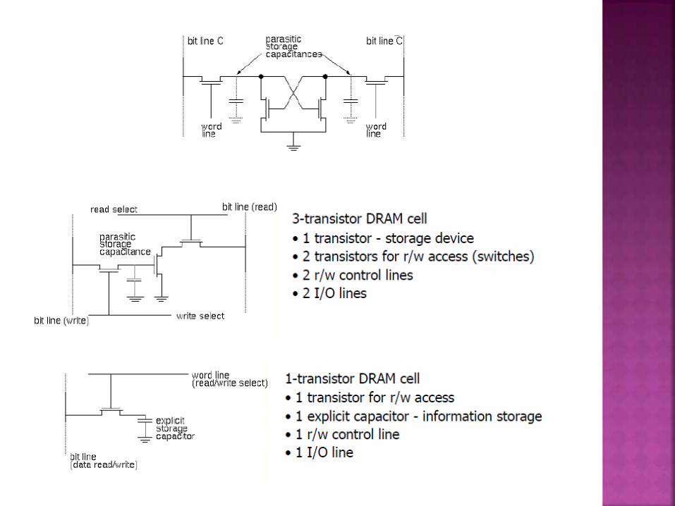
DRAM consist of Capacitor & a Switch transistor.
Data are stored in Capacitor, presence of charge in
capacitor is considered as data “1” or else “0”.
SRAM has 6 transistor latch structure.
Mask ROM - data are programmed by a Mask
- one time programming operation.
EPROM & EEPROM – data can be re-written into cell
by using ultravoilate rays.
FRAM – ferroelectric capacitor.
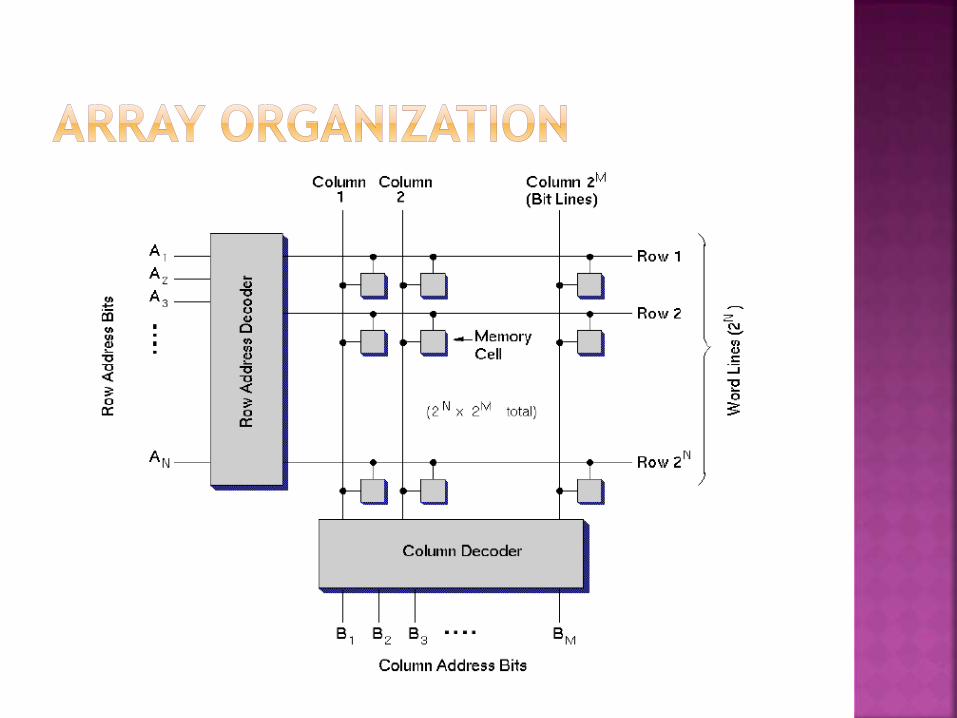
The data storage structure, or core, consists of individual
memory cells arranged in an array of horizontal rows and
vertical columns.
Each cell is capable of storing one bit of binary information.
Also, each memory cell shares a common connection with
the other cells in the same row and another common
connection with the other cells in the same column.
To access a particular memory cell, i.e., a particular data bit
in this array, the corresponding bit line and the corresponding
word line must be activated.
The row and column selection operations are
accomplished by row and column decoders,
respectively.
The row decoder circuit selects one out of 2N
word lines according to an Nbit row address,
while the column decoder circuit selects one out of
2M bit lines according to an M-bit column address.
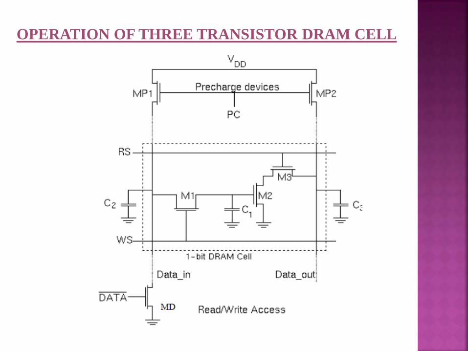
OPERATION OF THREE TRANSISTOR DRAM CELL
Binary information is stored in the form of charge in the parasitic
node capacitance C1.
The storage transistor M2 is turned on or off depending on the
charge stored in C1, and the pass transistors Ml and M3 act as
access switches for data read and write operations.
The cell has two separate bit lines for "data read" and "data
write," and two separate word lines to control the access
transistors.
All "data read" and "data write" operations are performed during
the active 2 phase, i.e., when PC is low.
Figure depicts the typical voltage waveforms associated with the
3-T DRAM cell during a sequence of four consecutive operations:
write " 1," read "1,"write "0," and read "0." The four precharge
cycles shown in Fig are numbered 1, 3,5, and 7, respectively
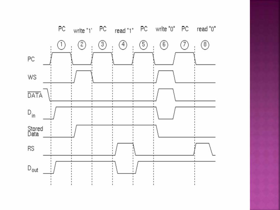
The inverse data input is at the logic-low level,because the data to be written onto the DRAM cell islogic "1."
The voltage level on column Din remains high.
Now, the "write select“ signal WS is pulled high duringthe active phase of fi2 .
As a result, the write access transistor M1 is turned on.With M1 conducting, the charge on C2 is now sharedwith C1 .
Since the capacitance C2 is very large compared to C1,the storage node capacitance Cl attains approximatelythe same logic-high level as the column capacitance C2at the end of the charge-sharing process.
After the write "1" operation is completed, the write accesstransistor M1 is turned off.
With the storage capacitance C1 charged-up to a logic-highlevel, transistor M2 is now conducting.
In order to read this stored "1," the "read select" signal RSmust be pulled high during the active phase of fi2, followinga precharge cycle.
As the read access transistor M3 turns on, M2 and M3create a conducting path between the "data read” columncapacitance C3 and the ground.
The capacitance C3 discharges through M2 and M3, andthe falling column voltage is interpreted by the "data read"circuitry as a storedlogic "1."
Note that the 3-T DRAM cell may be read repeatedly inthis fashion without disturbing the charge stored in C1.

The inverse data input is at the logic-high level, because the
data to be written onto the DRAM cell is a logic "0."
Consequently, the data write transistor is turned on, and the
voltage level on column Din is pulled to logic "0."
The "write select" signal WS is pulled high during the active
phase of fi2.
As a result, the write access transistor M1 is turned on. The
voltage level on C2, as well as that on the storage node Cl,
is pulled to logic "0" through MI and the data write
transistor.
Thus, at the end of the write "0" sequence, the storage
capacitance C1 contains a very low charge, and the
transistor M2 is turned off since its gate voltage is
approximately equal to zero.
The "read select" signal RS must be pulled high
during the active phase of fi2, following a
precharge cycle.
The read access transistor M3 turns on, but since
M2 is off, there is no conducting path between the
column capacitance C3 and the ground.
Consequently, C3 does not discharge, and the
logic-high level on the Dout column is interpreted
by the data read circuitry as a stored "0" bit.
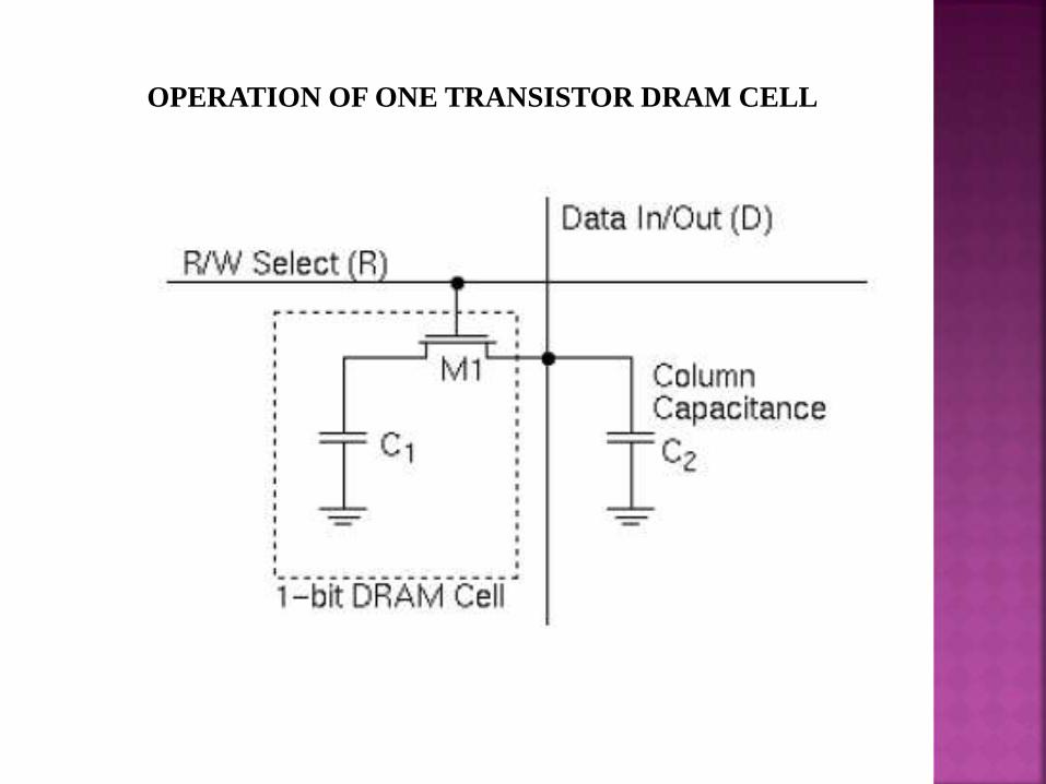
OPERATION OF ONE TRANSISTOR DRAM CELL

The circuit diagram of the one-transistor (1-T) DRAM cell consisting of
one explicit storage capacitor and one access transistor
Capacitor C2 represents the much larger parasitic column capacitance
associated with the word line.
Charge sharing between this large capacitance and the very small
storage capacitance plays a very important role in the operation of the
1-T DRAM cell.
For the write "1“ operation, the bit line (D) is raised to logic " 1 " by
the write circuitry, while the selected word line is pulled high by the
row address decoder.
The access transistor Ml turns on, allowing the storage capacitor C1 to
charge up to a logic-high level.
For the write "O“ operation, the bit line (D) is pulled to logic “0" and
the word line is pulled high by the row address decoder. In this case, the
storage capacitor C1 discharges through the access transistor, resulting
in a stored “0”bit.
ASYNCHRONOUS MODE :
When RAS is pulled DOWN , DRAM chip activates row circuitry
(row address buffers,row decoders,wordline drivers )
Address multiplexing scheme
The address captured at the falling edge of RAS & CAS becomes
row and column address
Advantage : reduce chip package size ,used in main memory .
Some data are selected by column address captured at falling edge
of CAS. The column address generates column select line
&connects bit lines to common data lines.
The time to read all the cell data from falling edge of RAS is
called “t RAC“
The data storage cell, i.e., the 1-bit memory cell in static RAM
arrays
consists of a simple latch circuit with two stable operating
points (states).
Depending on the preserved state of the two-inverter latch
circuit, the data being held in the memory cell will be
interpreted either as a logic "0" or as a logic " 1."
To access (read and write) the data contained in the memory
cell via the bit line, need at least one switch, which is
controlled by the corresponding word line, i.e., the row
address selection signal ,two complementary access switches
consisting of nMOS pass transistors are implemented to
connect the 1-bit SRAM cell to the complementary bit lines
(columns).
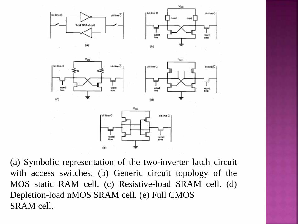
(a) Symbolic representation of the two-inverter latch circuit
with access switches. (b) Generic circuit topology of the
MOS static RAM cell. (c) Resistive-load SRAM cell. (d)
Depletion-load nMOS SRAM cell. (e) Full CMOS
SRAM cell.
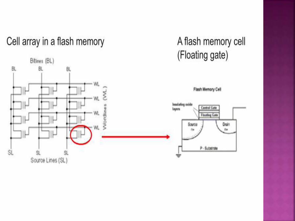
Flash memory consist of one transistor with
floating gate, whose threshold voltage can be
changed repeatedly by applying an electric
field to gate.
Transistor / memory cell can have two
threshold voltages corresponding to the
existence of charges (electrons) at floating
gate.
When electrons accumulated at floating gate
,threshold volage of memory cell becomes
higher and considered as “1”. Memory cell is
not on with read signal voltage is applied to
control gate & bit line precharge level.
Memory cell lowered by removing all electrons
from floating gate & considered as “0”. Memory
cell is turned on with applied voltage &bit line
discharged to ground.
Flash memory is programmed by either storing
or ejecting electrons in the floating gate in the
floating MOS transistor through “channel hot
electron injection” or “F-N tunnelling
mechanism”.
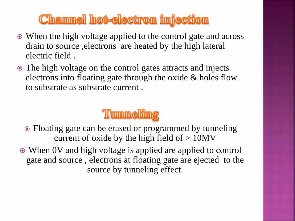
When the high voltage applied to the control gate and across drain to source ,electrons are heated by the high lateral electric field .
The high voltage on the control gates attracts and injects electrons into floating gate through the oxide & holes flow to substrate as substrate current .
Floating gate can be erased or programmed by tunnelingcurrent of oxide by the high field of > 10MV
When 0V and high voltage is applied are applied to control gate and source , electrons at floating gate are ejected to the
source by tunneling effect.
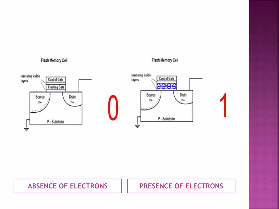
ABSENCE OF ELECTRONS PRESENCE OF ELECTRONS
In an Erase Operation
0v and high voltage are simultaneously applied to all the
control gate & source of cell.
Any electon exsiting in the floating gate are expelled to the
source through TUNNELING mechanism.
Programming Operation
Applying High voltage applied to the control gate & drain
of the selected cell.
Hot electrons generated at the near of the drain are injected
into the floating gate .
Each cell can have either a “0” state without electrons due
to erase operation OR a “1” state with electrons in the
floating gate after programming operation
READ Operation
Applying moderate voltage to the control gate & small voltage to
the drain to avoide generating hot electrons.
When the cell data “0” the cell transistor is turned on & current
flows through the cel l transistor .
Applying high voltage to control gate cell transistor turns off & no
current flow through cell .
By detecting current flow & amplifying signal difference cell data
can be read out
In an erase operation
NAND cell uses F-N tunneling mechanism
A high voltage is applied to source line , p-well, n-substrate.
A “0” voltage is applied to all word lines to eject electrons from
floating gate to the pwell 2 , all cells become low threshold
voltage.
Programming operation
A high voltage(20v) is applied to only to selected wordline and
moderate volatge (10v) is applied to all unselected word lines.
Vdd is applied to select line 1 to connect all the cells to the bit line
while 0v to the selected line 2.
P-well 2, source line & n-well are biased to 0v.
Since only voltage is applied to selected wordline is large enough
to turn on floating gate transistor by capacitive coupling ,electrons
are attracted to floating gates connected to the selcted word line
from channel.
READ operation
0v is applied to selected word line while 5v is applied to select
lines & all other unselected word line .
When cell data is “1” the cell transistor is turned off with applied
word line voltage.
With the cell data “0” a current path is formed from the bit line to
ground cell transistor turned on with 0 v word line voltage .
Dielectric material is replaced by FERROELECTROMAGNETIC material.
The total charge is depends on applied voltage.
This is becsuse spontaneous polarization occurs in crystal structure of ferroelecricmaterial .
The net change in the polarization happens when applied elecric field is larger than Vc.


![Molecular Wires, Switches and Memories · devices, and memories. Molecular electronics [1-3] is conceptually different from conventional solid state semiconductor electronics. It](https://img.pdfslide.net/doc/110x75/5ecb1229c78cbc769f459166/molecular-wires-switches-and-memories-devices-and-memories-molecular-electronics.jpg)