Embed Size (px)
Citation preview
What is lithographyPhotolithographyElectron beam lithographyNanolithographyX-ray lithographyAFM nanolithography
Soft lithographyNanoimprint lithographyDip-pen nanolithographyChemical characterizationOptical SpectroscopyElectron spectroscopyIonic Spectrometry
Outlines
What is Lithography
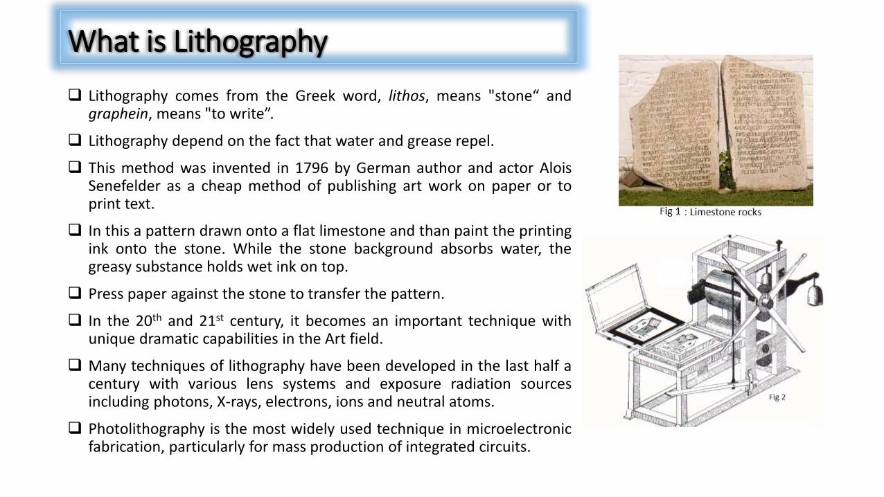
Lithography comes from the Greek word, lithos, means "stone“ andgraphein, means "to write”.
Lithography depend on the fact that water and grease repel.
This method was invented in 1796 by German author and actor AloisSenefelder as a cheap method of publishing art work on paper or toprint text.
In this a pattern drawn onto a flat limestone and than paint the printingink onto the stone. While the stone background absorbs water, thegreasy substance holds wet ink on top.
Press paper against the stone to transfer the pattern.
In the 20th and 21st century, it becomes an important technique withunique dramatic capabilities in the Art field.
Many techniques of lithography have been developed in the last half acentury with various lens systems and exposure radiation sourcesincluding photons, X-rays, electrons, ions and neutral atoms.
Photolithography is the most widely used technique in microelectronicfabrication, particularly for mass production of integrated circuits.
Photolithography
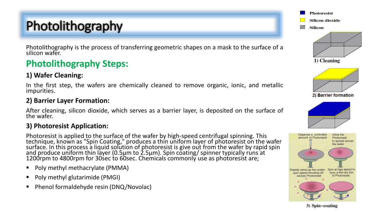
Photolithography is the process of transferring geometric shapes on a mask to the surface of asilicon wafer.
Photolithography Steps:1) Wafer Cleaning:
In the first step, the wafers are chemically cleaned to remove organic, ionic, and metallicimpurities.
2) Barrier Layer Formation:
After cleaning, silicon dioxide, which serves as a barrier layer, is deposited on the surface ofthe wafer.
3) Photoresist Application:
Photoresist is applied to the surface of the wafer by high-speed centrifugal spinning. This technique, known as "Spin Coating," produces a thin uniform layer of photoresist on the wafer surface. In this process a liquid solution of photoresist is give out from the wafer by rapid spin and produce uniform thin layer (0.5µm to 2.5µm). Spin coating/ spinner typically runs at 1200rpm to 4800rpm for 30sec to 60sec. Chemicals commonly use as photoresist are;
Poly methyl methacrylate (PMMA)
Poly methyl glutarimide (PMGI)
Phenol formaldehyde resin (DNQ/Novolac)
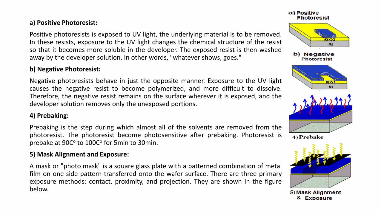
a) Positive Photoresist:
Positive photoresists is exposed to UV light, the underlying material is to be removed.In these resists, exposure to the UV light changes the chemical structure of the resistso that it becomes more soluble in the developer. The exposed resist is then washedaway by the developer solution. In other words, "whatever shows, goes."
b) Negative Photoresist:
Negative photoresists behave in just the opposite manner. Exposure to the UV lightcauses the negative resist to become polymerized, and more difficult to dissolve.Therefore, the negative resist remains on the surface wherever it is exposed, and thedeveloper solution removes only the unexposed portions.
4) Prebaking:
Prebaking is the step during which almost all of the solvents are removed from thephotoresist. The photoresist become photosensitive after prebaking. Photoresist isprebake at 90Co to 100Co for 5min to 30min.
5) Mask Alignment and Exposure:
A mask or "photo mask" is a square glass plate with a patterned combination of metalfilm on one side pattern transferred onto the wafer surface. There are three primaryexposure methods: contact, proximity, and projection. They are shown in the figurebelow.
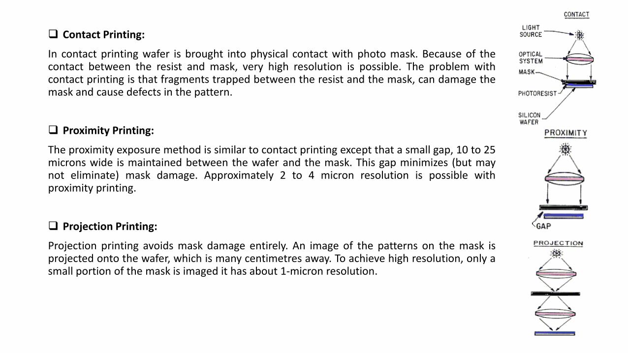
Contact Printing:
In contact printing wafer is brought into physical contact with photo mask. Because of thecontact between the resist and mask, very high resolution is possible. The problem withcontact printing is that fragments trapped between the resist and the mask, can damage themask and cause defects in the pattern.
Proximity Printing:
The proximity exposure method is similar to contact printing except that a small gap, 10 to 25microns wide is maintained between the wafer and the mask. This gap minimizes (but maynot eliminate) mask damage. Approximately 2 to 4 micron resolution is possible withproximity printing.
Projection Printing:
Projection printing avoids mask damage entirely. An image of the patterns on the mask isprojected onto the wafer, which is many centimetres away. To achieve high resolution, only asmall portion of the mask is imaged it has about 1-micron resolution.
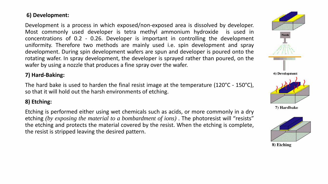
6) Development:
Development is a process in which exposed/non-exposed area is dissolved by developer.Most commonly used developer is tetra methyl ammonium hydroxide is used inconcentrations of 0.2 - 0.26. Developer is important in controlling the developmentuniformity. Therefore two methods are mainly used i.e. spin development and spraydevelopment. During spin development wafers are spun and developer is poured onto therotating wafer. In spray development, the developer is sprayed rather than poured, on thewafer by using a nozzle that produces a fine spray over the wafer.
7) Hard-Baking:
The hard bake is used to harden the final resist image at the temperature (120°C - 150°C),so that it will hold out the harsh environments of etching.
8) Etching:
Etching is performed either using wet chemicals such as acids, or more commonly in a dryetching (by exposing the material to a bombardment of ions) . The photoresist will “resists”the etching and protects the material covered by the resist. When the etching is complete,the resist is stripped leaving the desired pattern.
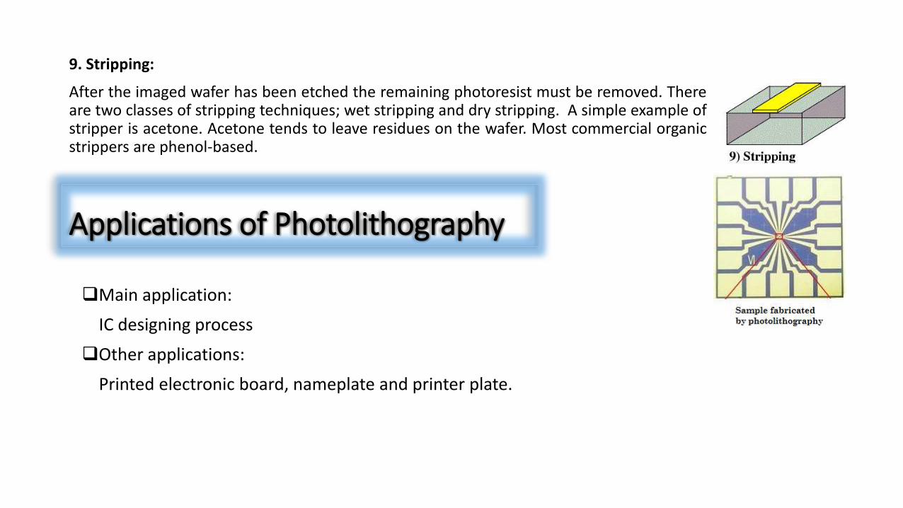
9. Stripping:
After the imaged wafer has been etched the remaining photoresist must be removed. Thereare two classes of stripping techniques; wet stripping and dry stripping. A simple example ofstripper is acetone. Acetone tends to leave residues on the wafer. Most commercial organicstrippers are phenol-based.
Applications of Photolithography
Main application:
IC designing process
Other applications:
Printed electronic board, nameplate and printer plate.
Electron Beam Lithography
Electron Beam Lithography is a specialized technique for creatingextremely fine patterns. It is derived from the scanning electronmicroscope. Electron beams can be focused to a few nanometres indiameter.
The basic idea behind electron beam lithography is identical tooptical lithography. The substrate is coated with a thin layer of resist,which is chemically changed under exposure to the electron beam, sothat the exposed/non-exposed areas can be dissolved in a specificsolvent.
Electron beam lithography is the most power full tool for thefabrication of feathers as small as 3nm to 5 nm.
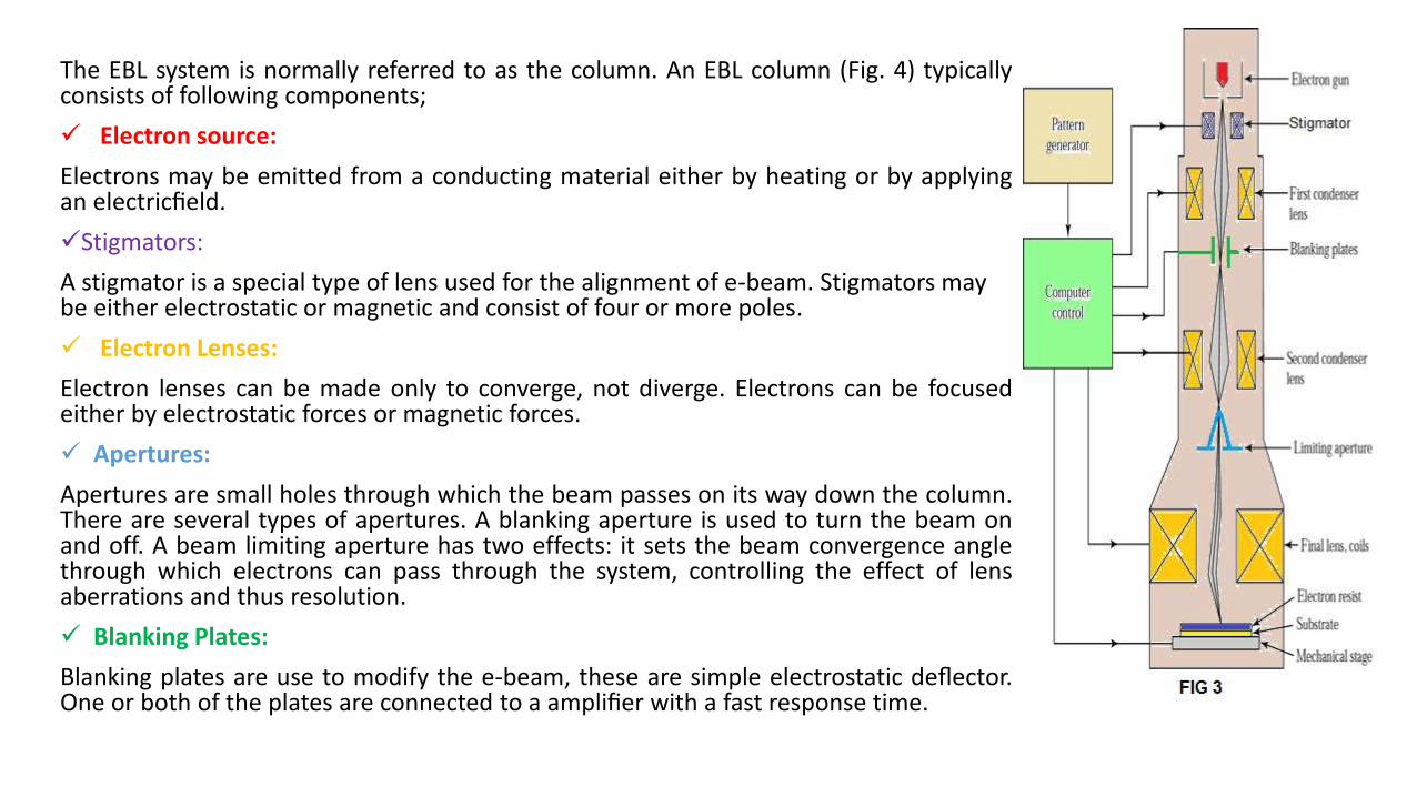
The EBL system is normally referred to as the column. An EBL column (Fig. 4) typicallyconsists of following components;
Electron source:
Electrons may be emitted from a conducting material either by heating or by applyingan electricfield.
Stigmators:
A stigmator is a special type of lens used for the alignment of e-beam. Stigmators may be either electrostatic or magnetic and consist of four or more poles.
Electron Lenses:
Electron lenses can be made only to converge, not diverge. Electrons can be focusedeither by electrostatic forces or magnetic forces.
Apertures:
Apertures are small holes through which the beam passes on its way down the column.There are several types of apertures. A blanking aperture is used to turn the beam onand off. A beam limiting aperture has two effects: it sets the beam convergence anglethrough which electrons can pass through the system, controlling the effect of lensaberrations and thus resolution.
Blanking Plates:
Blanking plates are use to modify the e-beam, these are simple electrostatic deflector.One or both of the plates are connected to a amplifier with a fast response time.
Print complex patterns directly on wafers
Eliminates the diffraction problem
High resolution up to 20 nm(photolithography ~50nm)
Flexible technique
Disadvantages of EBL
Advantages of EBL
Slower than optical lithography (approximately 5 wafers / hour at less than 0.1 µ resolution).
Expensive and complicated
Forward scattering
Backward scattering
Secondary electrons
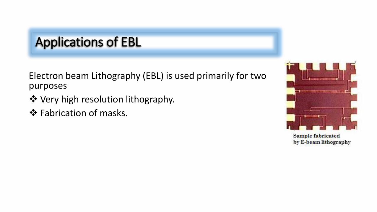
Electron beam Lithography (EBL) is used primarily for two purposes
Very high resolution lithography.
Fabrication of masks.
Applications of EBL
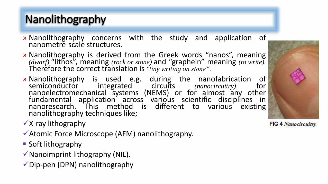
» Nanolithography concerns with the study and application ofnanometre-scale structures.
» Nanolithography is derived from the Greek words “nanos”, meaning(dwarf) “lithos”, meaning (rock or stone) and “graphein” meaning (to write).Therefore the correct translation is "tiny writing on stone“.
» Nanolithography is used e.g. during the nanofabrication ofsemiconductor integrated circuits (nanocircuitry), fornanoelectromechanical systems (NEMS) or for almost any otherfundamental application across various scientific disciplines innanoresearch. This method is different to various existingnanolithography techniques like;
X-ray lithography
Atomic Force Microscope (AFM) nanolithography.
Soft lithography
Nanoimprint lithography (NIL).
Dip-pen (DPN) nanolithography
Nanolithography
X-rays having wavelengths of 0.04nm to 0.5 nm represent another radiation source forhigh-resolution design reproduction into polymeric resist materials.
X-ray lithography was first demonstrated to obtain high-resolution designs using X-rayproximity printing by Spears and Smith.
X-ray lithography can be extended optical resolution of 15 nm.
Essential elements in X-ray lithography
A mask consisting of a pattern made with an X-ray absorbing material on a thin X-raytransparent membrane.
An X-ray source of sufficient brightness.
An X-ray sensitive resist material.
X-Ray Lithography
The X-rays illuminate a mask placed in proximity of a resist-coatedwafer.
The X-rays are typically from synchrotron radiation source, allowingrapid exposure.
X-ray lithography is expensive, because of the expense of operating asynchrotron. The actual operating expenses without considering theinitial investment of tens-of-millions of dollars. Therefore, the LIGAprocess was developed to reduce the dependency on a synchrotron.
LIGA is the abbreviation from the German words, “Lithographie”(Lithography), “Galvanik” (Electroplating), & “Abformung” (Molding).
X-Ray Lithography Cont.
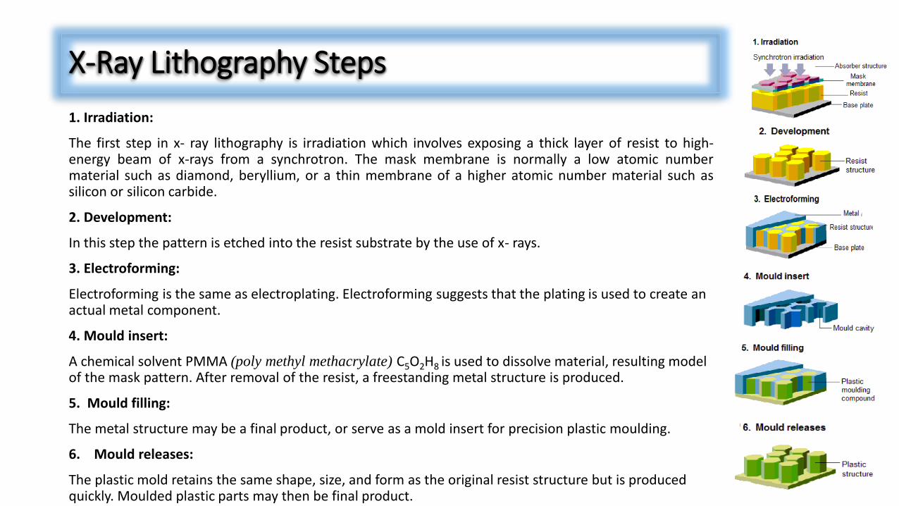
1. Irradiation:
The first step in x- ray lithography is irradiation which involves exposing a thick layer of resist to high-energy beam of x-rays from a synchrotron. The mask membrane is normally a low atomic numbermaterial such as diamond, beryllium, or a thin membrane of a higher atomic number material such assilicon or silicon carbide.
2. Development:
In this step the pattern is etched into the resist substrate by the use of x- rays.
3. Electroforming:
Electroforming is the same as electroplating. Electroforming suggests that the plating is used to create an actual metal component.
4. Mould insert:
A chemical solvent PMMA (poly methyl methacrylate) C5O2H8 is used to dissolve material, resulting model of the mask pattern. After removal of the resist, a freestanding metal structure is produced.
5. Mould filling:
The metal structure may be a final product, or serve as a mold insert for precision plastic moulding.
6. Mould releases:
The plastic mold retains the same shape, size, and form as the original resist structure but is produced quickly. Moulded plastic parts may then be final product.
X-Ray Lithography Steps
Short wavelength from X-rays 0.4-4 nm
No diffraction effect
Simple to use
No lens
Faster than EBL
Uniform refraction pattern
High resolution for small feature size
Advantages of X-Ray Lithography
Disadvantages of X-Ray LithographyThin lens
Distortion in absorber
Cannot be focused through lens
Masks are expensive to produce
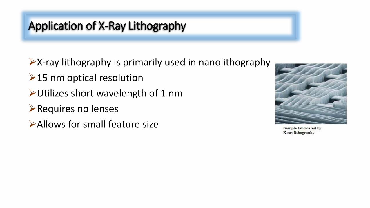
X-ray lithography is primarily used in nanolithography
15 nm optical resolution
Utilizes short wavelength of 1 nm
Requires no lenses
Allows for small feature size
Application of X-Ray Lithography
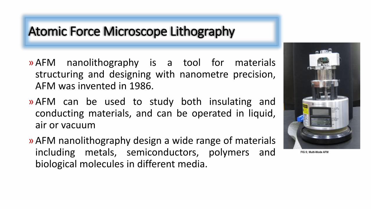
» AFM nanolithography is a tool for materialsstructuring and designing with nanometre precision,AFM was invented in 1986.
» AFM can be used to study both insulating andconducting materials, and can be operated in liquid,air or vacuum
» AFM nanolithography design a wide range of materialsincluding metals, semiconductors, polymers andbiological molecules in different media.
Atomic Force Microscope Lithography
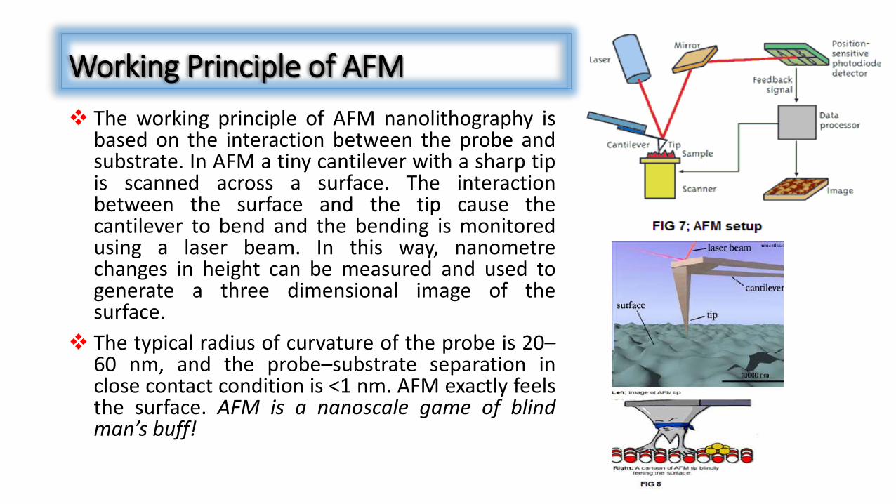
The working principle of AFM nanolithography isbased on the interaction between the probe andsubstrate. In AFM a tiny cantilever with a sharp tipis scanned across a surface. The interactionbetween the surface and the tip cause thecantilever to bend and the bending is monitoredusing a laser beam. In this way, nanometrechanges in height can be measured and used togenerate a three dimensional image of thesurface.
The typical radius of curvature of the probe is 20–60 nm, and the probe–substrate separation inclose contact condition is <1 nm. AFM exactly feelsthe surface. AFM is a nanoscale game of blindman’s buff!
Working Principle of AFM
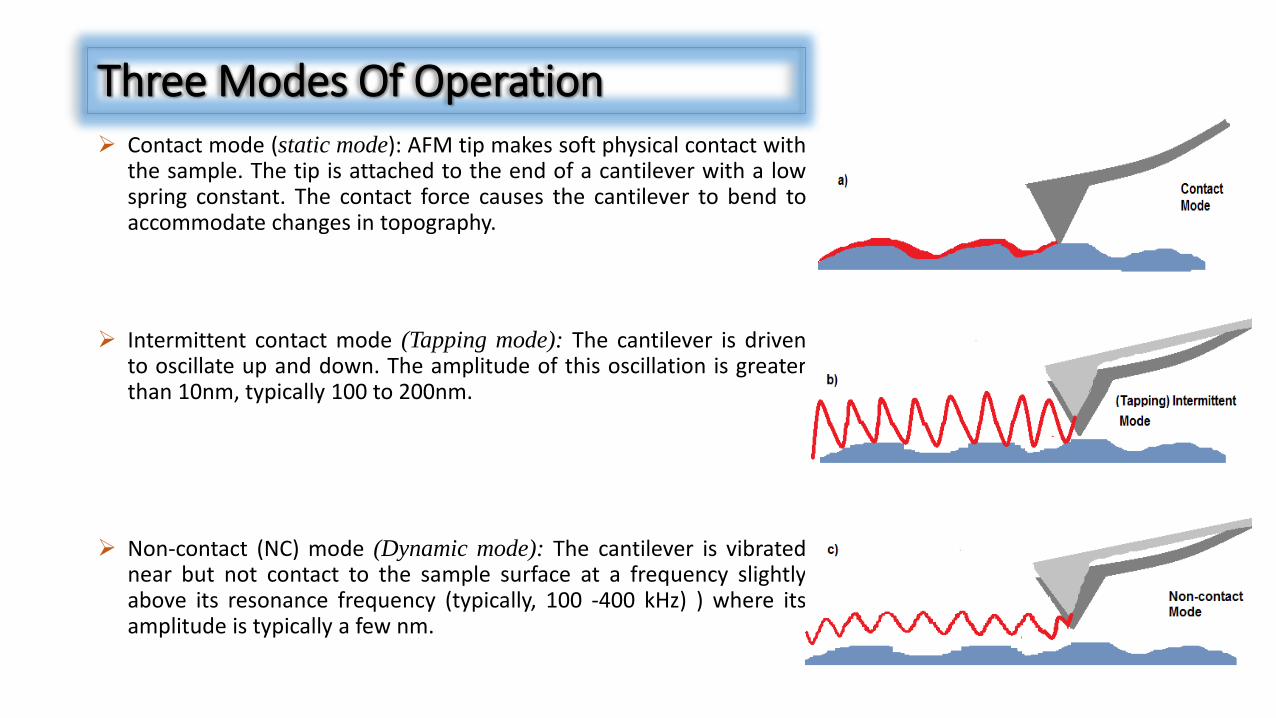
Contact mode (static mode): AFM tip makes soft physical contact withthe sample. The tip is attached to the end of a cantilever with a lowspring constant. The contact force causes the cantilever to bend toaccommodate changes in topography.
Intermittent contact mode (Tapping mode): The cantilever is drivento oscillate up and down. The amplitude of this oscillation is greaterthan 10nm, typically 100 to 200nm.
Non-contact (NC) mode (Dynamic mode): The cantilever is vibratednear but not contact to the sample surface at a frequency slightlyabove its resonance frequency (typically, 100 -400 kHz) ) where itsamplitude is typically a few nm.
Three Modes Of Operation
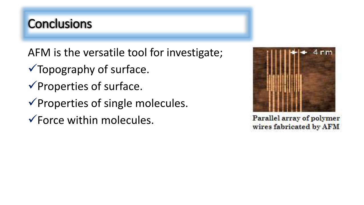
AFM is the versatile tool for investigate;
Topography of surface.
Properties of surface.
Properties of single molecules.
Force within molecules.
Conclusions
Soft lithography has been developed as an alternative tophotolithography and a replication technology for both micro andnanofabrication. Soft lithography uses the designs on a PDMS (polydimethyl siloxane) stamp.
This technique has wide range of application in cell biology,microelectronics, surface chemistry, micromachining, Designing cells,Designing DNA and Designing protein.
Soft Lithography (Micro-contact printing)
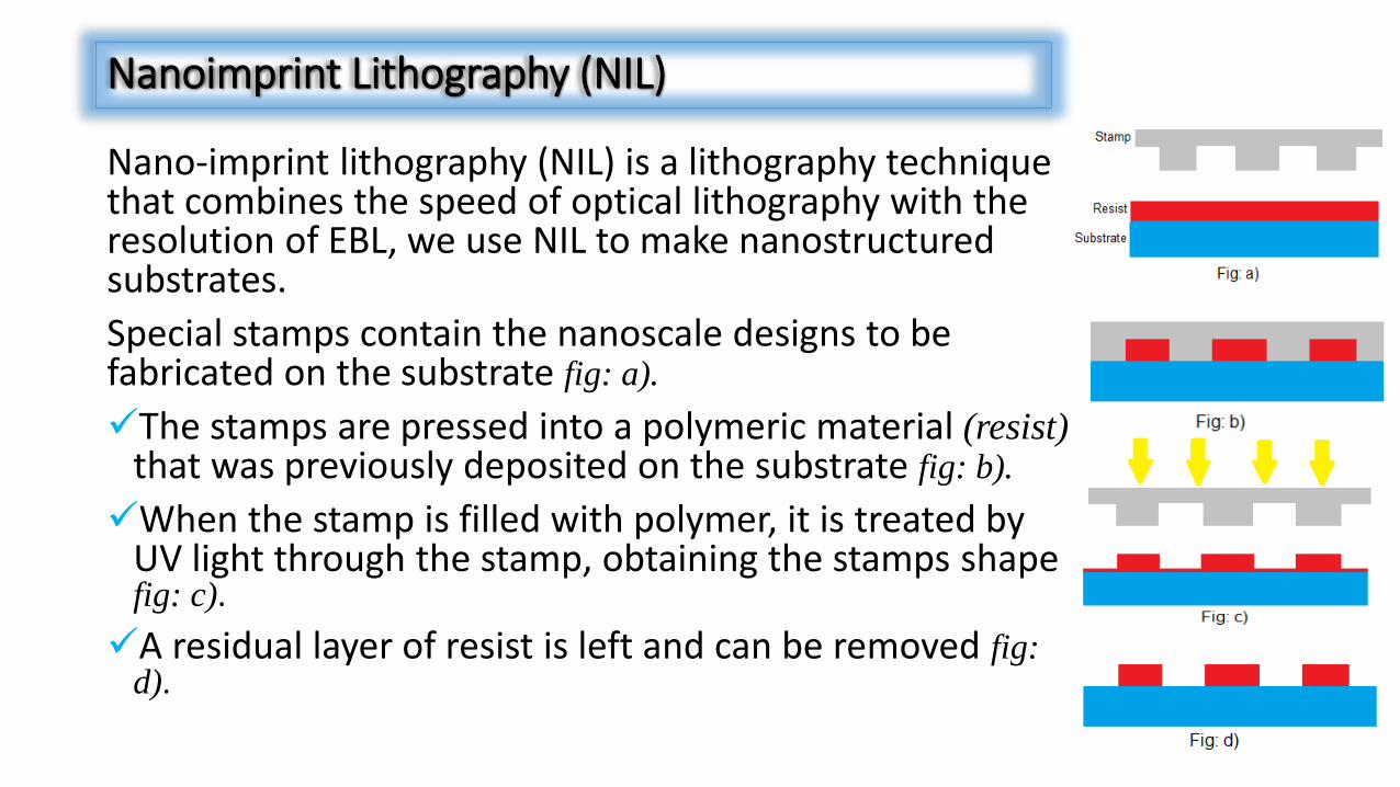
Nano-imprint lithography (NIL) is a lithography technique that combines the speed of optical lithography with the resolution of EBL, we use NIL to make nanostructured substrates.
Special stamps contain the nanoscale designs to be fabricated on the substrate fig: a).
The stamps are pressed into a polymeric material (resist) that was previously deposited on the substrate fig: b).
When the stamp is filled with polymer, it is treated by UV light through the stamp, obtaining the stamps shapefig: c).
A residual layer of resist is left and can be removed fig: d).
Nanoimprint Lithography (NIL)
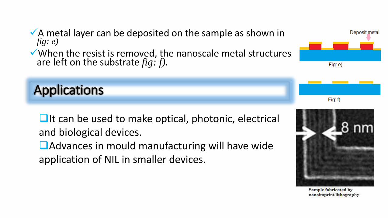
A metal layer can be deposited on the sample as shown in fig: e)
When the resist is removed, the nanoscale metal structures are left on the substrate fig: f).
It can be used to make optical, photonic, electrical and biological devices. Advances in mould manufacturing will have wide application of NIL in smaller devices.
Applications
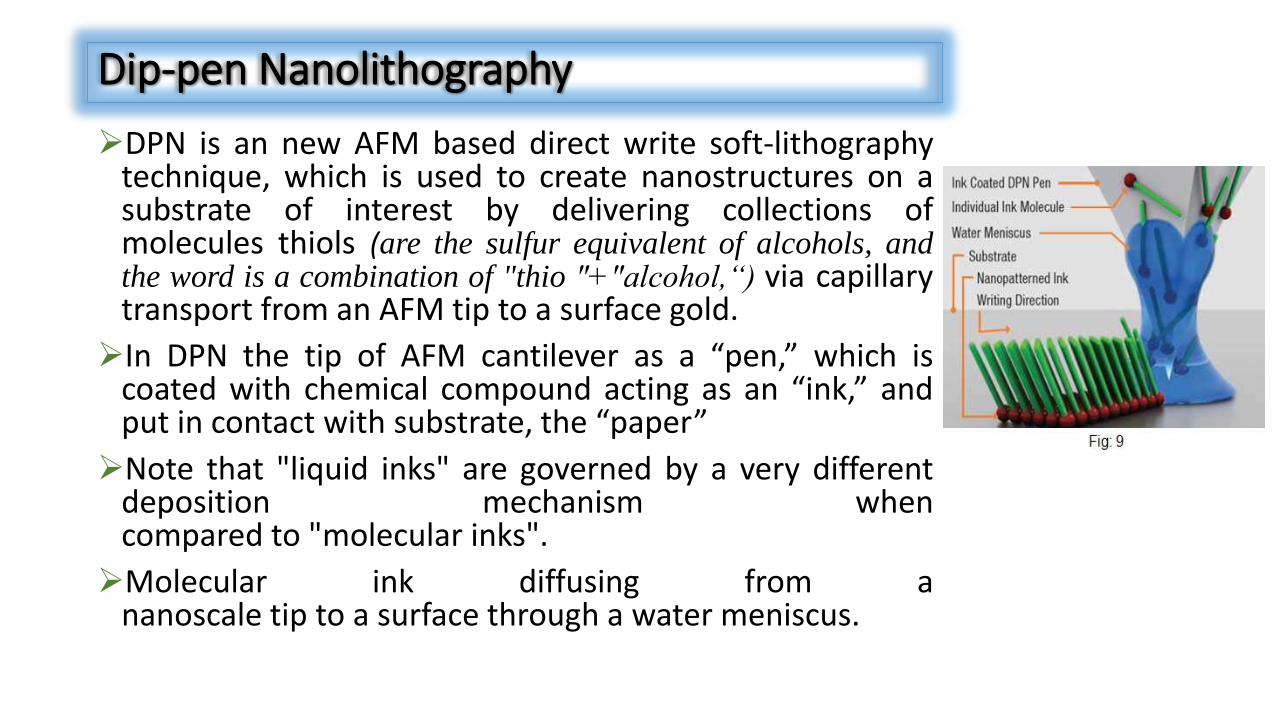
DPN is an new AFM based direct write soft-lithographytechnique, which is used to create nanostructures on asubstrate of interest by delivering collections ofmolecules thiols (are the sulfur equivalent of alcohols, andthe word is a combination of "thio "+"alcohol,“) via capillarytransport from an AFM tip to a surface gold.
In DPN the tip of AFM cantilever as a “pen,” which iscoated with chemical compound acting as an “ink,” andput in contact with substrate, the “paper”
Note that "liquid inks" are governed by a very differentdeposition mechanism whencompared to "molecular inks".
Molecular ink diffusing from ananoscale tip to a surface through a water meniscus.
Dip-pen Nanolithography
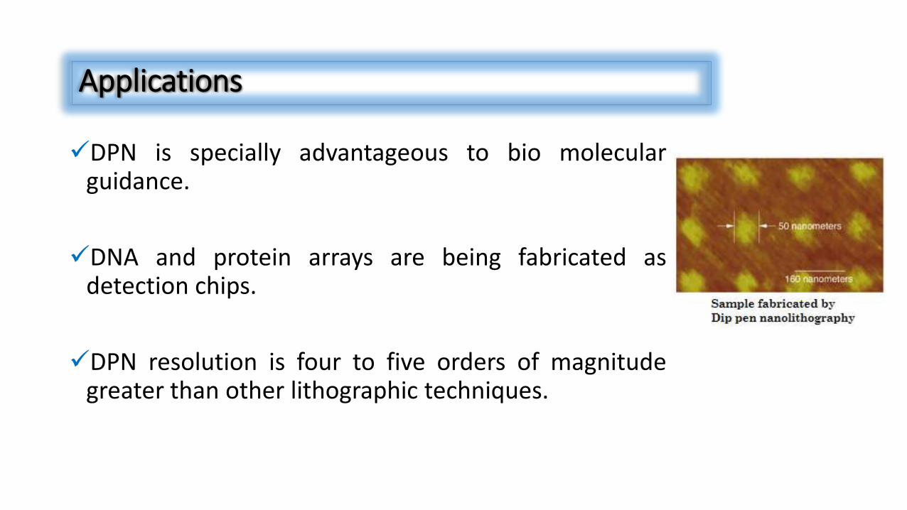
DPN is specially advantageous to bio molecularguidance.
DNA and protein arrays are being fabricated asdetection chips.
DPN resolution is four to five orders of magnitudegreater than other lithographic techniques.
Applications
Chemical characterization is to determine the surface and interioratoms and compounds as well as their three-dimensionaldistributions. Many chemical analysis methods have been developedfor the surface analysis or thin films, but our discussion will belimited to the most popular techniques;
Optical spectroscopy
Electron spectroscopy
Ion spectrometry.
Chemical Characterization
Spectroscopy is method of “Seeing the Unseenable.” Using electromagnetic radiation to obtain information about atoms and molecules that are too small to see.
Optical spectroscopy has been widely used for the characterization of nano- materials, and the techniques can be generally categorized into two groups: absorption and emission spectroscopy and vibrational spectroscopy.
Absorption and emission spectroscopy:
As electrons move between the energy levels of an atom they can emit or absorb light energy. If theelectron moves from a lower energy level to a higher energy level, the atom must absorb the energy. If theelectron falls from a higher energy lever to a lower energy level it will release energy by emitting light.
By absorbing specific wavelengths of light, an electron moves from a lower energy level to a higher energylevel. Since every kind of atom has a different electronic configuration, the wavelengths of light absorbed oremitted by an atom are unique to that element.
By measuring the unique wavelengths and intensities of light an atom absorbs is called the AtomicAbsorption Spectrum.
We can directly observe the lines in the “visible” spectrum with our eyes, but many other lines outside the“visible” region exist and can be detected by specially designed spectrometers.
Optical Spectroscopy
Vibrational / Infrared Spectroscopy:
Molecules and crystals can be thought of as systems of atoms or ions connectedby springs (chemical bonds). These systems can be set into vibration, and vibratewith frequencies determined by the atomic weight and by bond strengths.
They are at very high frequencies ranging from 10l2 to 1Ol4Hz, which is in theinfrared (IR) regions of the electromagnetic spectrum.
The oscillations combine with an impinging beam of infrared electromagneticradiation and to exchange energy with it when the frequencies are in resonance.
In the infrared experiment, the intensity of a beam of infrared radiation ismeasured before and after it interacts with the sample.
The identities, atomic arrangements, and concentrations of the chemical bondsthat are present in the sample can be determined.
Optical Spectroscopy Cont.
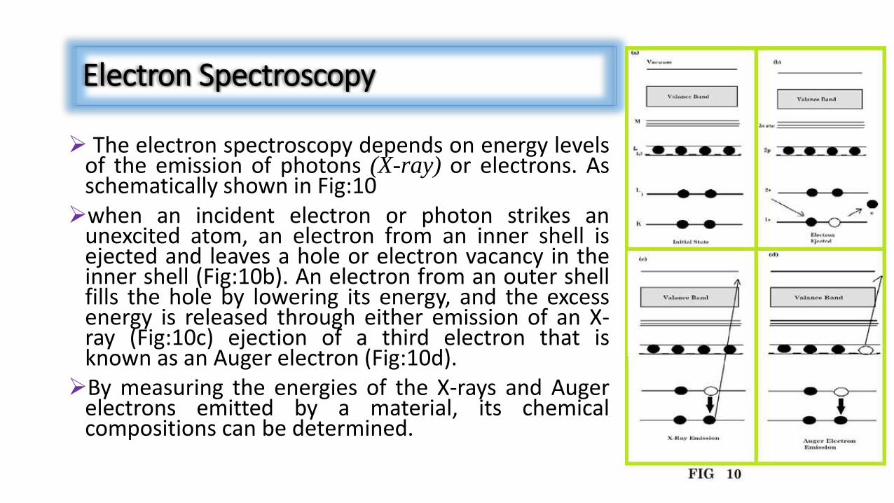
The electron spectroscopy depends on energy levelsof the emission of photons (X-ray) or electrons. Asschematically shown in Fig:10when an incident electron or photon strikes an
unexcited atom, an electron from an inner shell isejected and leaves a hole or electron vacancy in theinner shell (Fig:10b). An electron from an outer shellfills the hole by lowering its energy, and the excessenergy is released through either emission of an X-ray (Fig:10c) ejection of a third electron that isknown as an Auger electron (Fig:10d).By measuring the energies of the X-rays and Auger
electrons emitted by a material, its chemicalcompositions can be determined.
Electron Spectroscopy
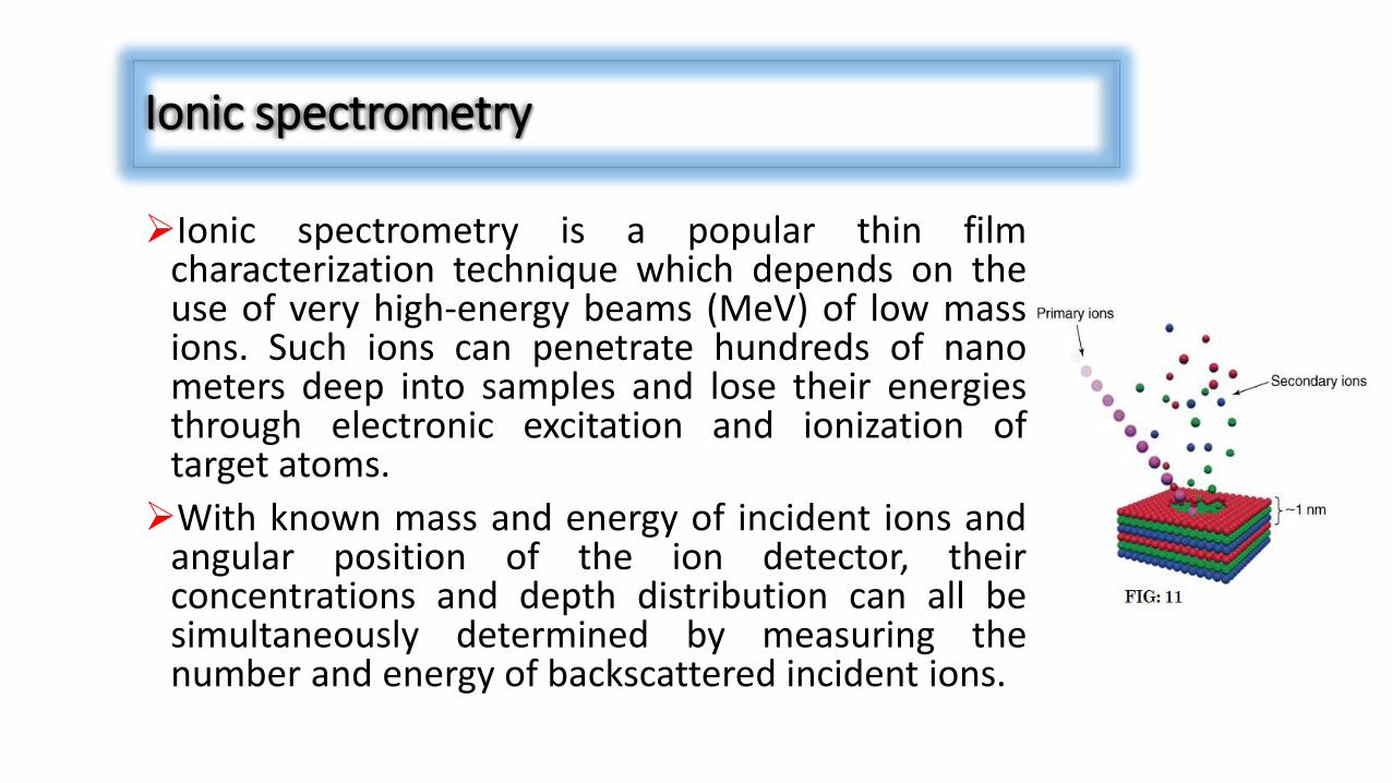
Ionic spectrometry is a popular thin filmcharacterization technique which depends on theuse of very high-energy beams (MeV) of low massions. Such ions can penetrate hundreds of nanometers deep into samples and lose their energiesthrough electronic excitation and ionization oftarget atoms.
With known mass and energy of incident ions andangular position of the ion detector, theirconcentrations and depth distribution can all besimultaneously determined by measuring thenumber and energy of backscattered incident ions.
Ionic spectrometry
A basic instrument will, consist of:
A primary beam source (usually O2+, O-, Cs+, Ar+, Ga+ or neutrals) to supply the bombarding types.
A target or sample that must be solid and stable in a vacuum.
A detector for collecting the ejected secondary ions.
An ion detection system to record the magnitude of the secondary ion signal.
Ionic spectrometry Cont.
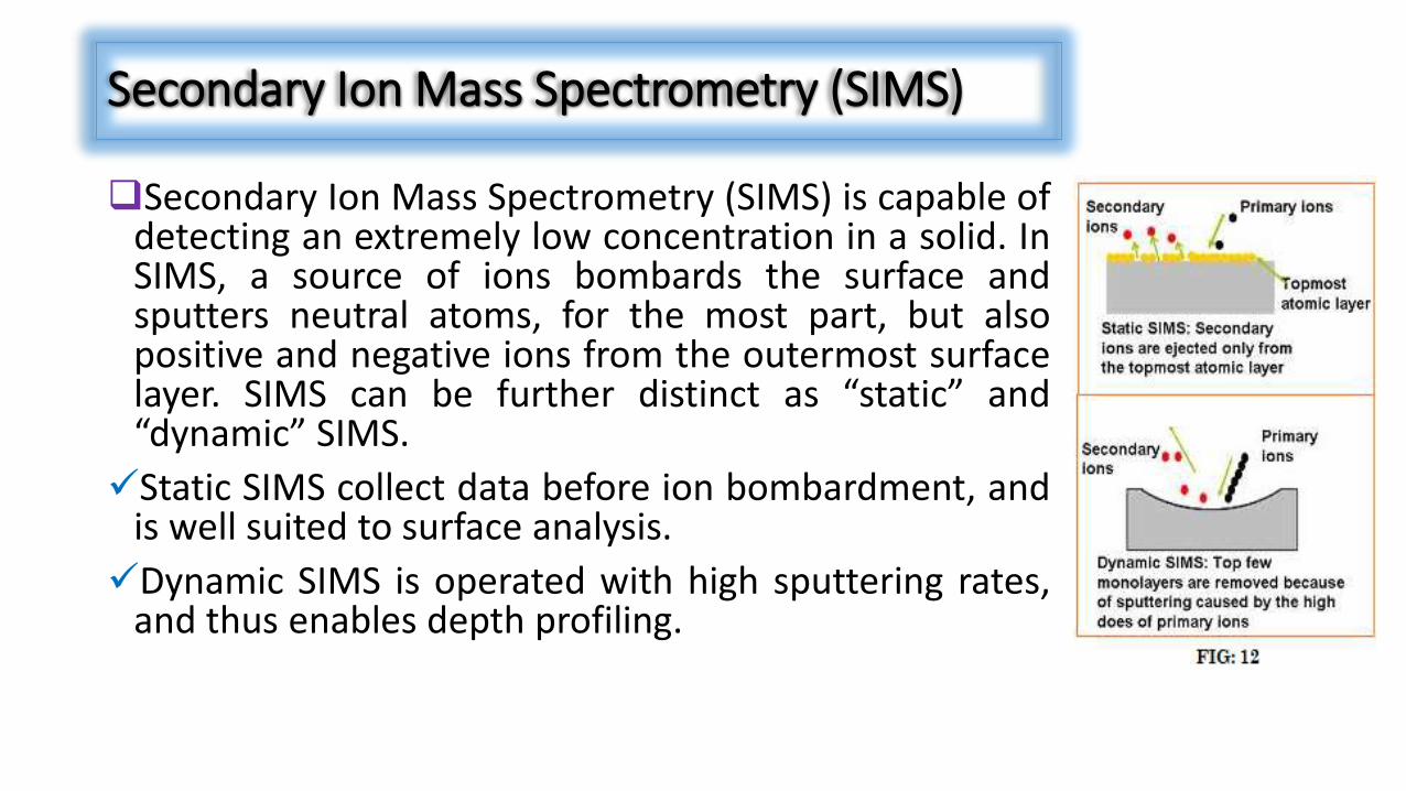
Secondary Ion Mass Spectrometry (SIMS) is capable ofdetecting an extremely low concentration in a solid. InSIMS, a source of ions bombards the surface andsputters neutral atoms, for the most part, but alsopositive and negative ions from the outermost surfacelayer. SIMS can be further distinct as “static” and“dynamic” SIMS.
Static SIMS collect data before ion bombardment, andis well suited to surface analysis.
Dynamic SIMS is operated with high sputtering rates,and thus enables depth profiling.
Secondary Ion Mass Spectrometry (SIMS)