Embed Size (px)
Citation preview

Dept. of Computer Hardware Maintenance 1 G.P.T.C Kaduthuruthy
INTRODUCTION
The Arduino Uno is a microcontroller board based on the ATmega328 (datasheet).
It has 14 digital input/output pins (of which 6 can be used as PWM outputs), 6 analog
inputs, a 16 MHz ceramic resonator, a USB connection, a power jack, an ICSP header,
and a reset button. It contains everything needed to support the microcontroller; simply
connect it to a computer with a USB cable or power it with a AC-to-DC adapter or battery
to get started.
The Uno differs from all preceding boards in that it does not use the FTDI USB-to-serial
driver chip. Instead, it features the Atmega16U2 (Atmega8U2 up to version R2)
programmed as a USB-to-serial converter.
Revision 2 of the Uno board has a resistor pulling the 8U2 HWB line to ground, making it
easier to put into DFU mode.
Revision 3 of the board has the following new features:
1.0 pinout: added SDA and SCL pins that are near to the AREF pin and two other new
pins placed near to the RESET pin, the IOREF that allow the shields to adapt to the
voltage provided from the board. In future, shields will be compatible with both the board
that uses the AVR, which operates with 5V and with the Arduino Due that operates with
3.3V. The second one is a not connected pin, that is reserved for future purposes.
Stronger RESET circuit.
Atmega 16U2 replace the 8U2.
"Uno" means one in Italian and is named to mark the upcoming release of Arduino 1.0.
The Uno and version 1.0 will be the reference versions of Arduino, moving forward. The
Uno is the latest in a series of USB Arduino boards, and the reference model for the
Arduino platform; for a comparison with previous versions, see the index of Arduino
boards.
Summary
Microcontroller : ATmega328
Operating Voltage : 5V
Dept. of Computer Hardware Maintenance 2 G.P.T.C Kaduthuruthy
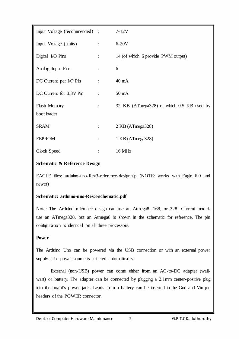
Input Voltage (recommended) : 7-12V
Input Voltage (limits) : 6-20V
Digital I/O Pins : 14 (of which 6 provide PWM output)
Analog Input Pins : 6
DC Current per I/O Pin : 40 mA
DC Current for 3.3V Pin : 50 mA
Flash Memory : 32 KB (ATmega328) of which 0.5 KB used by
boot loader
SRAM : 2 KB (ATmega328)
EEPROM : 1 KB (ATmega328)
Clock Speed : 16 MHz
Schematic & Reference Design
EAGLE files: arduino-uno-Rev3-reference-design.zip (NOTE: works with Eagle 6.0 and
newer)
Schematic: arduino-uno-Rev3-schematic.pdf
Note: The Arduino reference design can use an Atmega8, 168, or 328, Current models
use an ATmega328, but an Atmega8 is shown in the schematic for reference. The pin
configuration is identical on all three processors.
Power
The Arduino Uno can be powered via the USB connection or with an external power
supply. The power source is selected automatically.
External (non-USB) power can come either from an AC-to-DC adapter (wall-
wart) or battery. The adapter can be connected by plugging a 2.1mm center-positive plug
into the board's power jack. Leads from a battery can be inserted in the Gnd and Vin pin
headers of the POWER connector.

Dept. of Computer Hardware Maintenance 3 G.P.T.C Kaduthuruthy
The board can operate on an external supply of 6 to 20 volts. If supplied with less
than 7V, however, the 5V pin may supply less than five volts and the board may be
unstable. If using more than 12V, the voltage regulator may overheat and damage the
board. The recommended range is 7 to 12 volts.
The power pins are as follows:
VIN. The input voltage to the Arduino board when it's using an external power
source (as opposed to 5 volts from the USB connection or other regulated power source).
You can supply voltage through this pin, or, if supplying voltage via the power jack,
access it through this pin.
5V.This pin outputs a regulated 5V from the regulator on the board. The board can
be supplied with power either from the DC power jack (7 - 12V), the USB connector
(5V), or the VIN pin of the board (7-12V). Supplying voltage via the 5V or 3.3V pins
bypasses the regulator, and can damage your board. We don't advise it.
3V3. A 3.3 volt supply generated by the on-board regulator. Maximum current draw is 50
mA.
GND. Ground pins.
IOREF. This pin on the Arduino board provides the voltage reference with which
the microcontroller operates. A properly configured shield can read the IOREF pin
voltage and select the appropriate power source or enable voltage translators on the
outputs for working with the 5V or 3.3V.
Memory
The ATmega328 has 32 KB (with 0.5 KB used for the bootloader). It also has 2
KB of SRAM and 1 KB of EEPROM (which can be read and written with the EEPROM
library).
Input and Output
Each of the 14 digital pins on the Uno can be used as an input or output, using
pinMode(), digitalWrite(), anddigitalRead() functions. They operate at 5 volts. Each pin
can provide or receive a maximum of 40 mA and has an internal pull-up resistor

Dept. of Computer Hardware Maintenance 4 G.P.T.C Kaduthuruthy
(disconnected by default) of 20-50 kOhms. In addition, some pins have specialized
functions:
Serial: 0 (RX) and 1 (TX). Used to receive (RX) and transmit (TX) TTL serial
data. These pins are connected to the corresponding pins of the ATmega8U2 USB-to-
TTL Serial chip.
External Interrupts: 2 and 3. These pins can be configured to trigger an interrupt
on a low value, a rising or falling edge, or a change in value. See the attachInterrupt()
function for details.
PWM: 3, 5, 6, 9, 10, and 11. Provide 8-bit PWM output with the analogWrite()
function.
SPI: 10 (SS), 11 (MOSI), 12 (MISO), 13 (SCK). These pins support SPI
communication using the SPI library.
LED: 13. There is a built-in LED connected to digital pin 13. When the pin is
HIGH value, the LED is on, when the pin is LOW, it's off.
The Uno has 6 analog inputs, labeled A0 through A5, each of which provide 10
bits of resolution (i.e. 1024 different values). By default they measure from ground to 5
volts, though is it possible to change the upper end of their range using the AREF pin and
the analogReference() function. Additionally, some pins have specialized functionality:
TWI: A4 or SDA pin and A5 or SCL pin. Support TWI communication using the
Wire library.
There are a couple of other pins on the board:
AREF. Reference voltage for the analog inputs. Used with analogReference().
Reset. Bring this line LOW to reset the microcontroller. Typically used to add a reset
button to shields which block the one on the board.
See also the mapping between Arduino pins and ATmega328 ports. The mapping
for the Atmega8, 168, and 328 is identical.
Communication

Dept. of Computer Hardware Maintenance 5 G.P.T.C Kaduthuruthy
The Arduino Uno has a number of facilities for communicating with a computer,
another Arduino, or other microcontrollers. The ATmega328 provides UART TTL (5V)
serial communication, which is available on digital pins 0 (RX) and 1 (TX). An
ATmega16U2 on the board channels this serial communication over USB and appears as
a virtual com port to software on the computer. The '16U2 firmware uses the standard
USB COM drivers, and no external driver is needed. However, on Windows, a .inf file is
required. The Arduino software includes a serial monitor which allows simple textual
data to be sent to and from the Arduino board. The RX and TX LEDs on the board will
flash when data is being transmitted via the USB-to-serial chip and USB connection to
the computer (but not for serial communication on pins 0 and 1).
A Software Serial library allows for serial communication on any of the Uno's digital
pins.
The ATmega328 also supports I2C (TWI) and SPI communication. The Arduino
software includes a Wire library to simplify use of the I2C bus; see the documentation for
details. For SPI communication, use the SPI library.
Programming
The Arduino Uno can be programmed with the Arduino software (download).
Select "Arduino Uno from the Tools > Board menu (according to the microcontroller on
your board). For details, see the reference and tutorials.
The ATmega328 on the Arduino Uno comes preburned with a bootloader that
allows you to upload new code to it without the use of an external hardware programmer.
It communicates using the original STK500 protocol (reference, C header files).
You can also bypass the bootloader and program the microcontroller through the
ICSP (In-Circuit Serial Programming) header using Arduino ISP or similar; see these
instructions for details.
The ATmega16U2 (or 8U2 in the rev1 and rev2 boards) firmware source code is
available . The ATmega16U2/8U2 is loaded with a DFU bootloader, which can be
activated by:
On Rev1 boards: connecting the solder jumper on the back of the board (near the map of
Italy) and then resetting the 8U2.

Dept. of Computer Hardware Maintenance 6 G.P.T.C Kaduthuruthy
On Rev2 or later boards: there is a resistor that pulling the 8U2/16U2 HWB line to
ground, making it easier to put into DFU mode.
You can then use Atmel's FLIP software (Windows) or the DFU programmer
(Mac OS X and Linux) to load a new firmware. Or you can use the ISP header with an
external programmer (overwriting the DFU bootloader). See this user-contributed tutorial
for more information.
Automatic (Software) Reset
Rather than requiring a physical press of the reset button before an upload, the
Arduino Uno is designed in a way that allows it to be reset by software running on a
connected computer. One of the hardware flow control lines (DTR) of
theATmega8U2/16U2 is connected to the reset line of the ATmega328 via a 100
nanofarad capacitor. When this line is asserted (taken low), the reset line drops long
enough to reset the chip. The Arduino software uses this capability to allow you to upload
code by simply pressing the upload button in the Arduino environment. This means that
the bootloader can have a shorter timeout, as the lowering of DTR can be well-
coordinated with the start of the upload.
This setup has other implications. When the Uno is connected to either a computer
running Mac OS X or Linux, it resets each time a connection is made to it from software
(via USB). For the following half-second or so, the bootloader is running on the Uno.
While it is programmed to ignore malformed data (i.e. anything besides an upload of new
code), it will intercept the first few bytes of data sent to the board after a connection is
opened. If a sketch running on the board receives one-time configuration or other data
when it first starts, make sure that the software with which it communicates waits a
second after opening the connection and before sending this data.
The Uno contains a trace that can be cut to disable the auto-reset. The pads on
either side of the trace can be soldered together to re-enable it. It's labeled "RESET-EN".
You may also be able to disable the auto-reset by connecting a 110 ohm resistor from 5V
to the reset line; see this forum thread for details.
USB Overcurrent Protection

Dept. of Computer Hardware Maintenance 7 G.P.T.C Kaduthuruthy
The Arduino Uno has a resettable polyfuse that protects your computer's USB
ports from shorts and overcurrent. Although most computers provide their own internal
protection, the fuse provides an extra layer of protection. If more than 500 mA is applied
to the USB port, the fuse will automatically break the connection until the short or
overload is removed.
Physical Characteristics
The maximum length and width of the Uno PCB are 2.7 and 2.1 inches
respectively, with the USB connector and power jack extending beyond the former
dimension. Four screw holes allow the board to be attached to a surface or case. Note that
the distance between digital pins 7 and 8 is 160 mil (0.16"), not an even multiple of the
100 mil spacing of the other pins.
Soil
This is a simple water sensor, can be used to detect soil moisture
Module Output is high level when the soil moisture deficit,or output is low
Can be used in module plant waterer device, and the plants in your garden no need people to
manage

Dept. of Computer Hardware Maintenance 8 G.P.T.C Kaduthuruthy
Instructions for Use:
Soil moisture module is most sensitive to the ambient humidity is generally used to detect the
moisture content of the soil Module to reach the threshold value is set in the soil moisture,
DO port output high, when the soil humidity exceeds a set threshold value, the module D0
output low. The digital output D0 can be connected directly with the microcontroller to
detect high and low by the microcontroller to detect soil moisture. The digital outputs DO
shop relay module can directly drive the buzzer module, which can form a soil moisture
alarm equipment. Analog output AO and AD module connected through the AD converter,
you can get more precise values of soil moisture.
Specification:
Operating voltage: 3.3V~5V
Dual output mode, analog output more accurate
A fixed bolt hole for easy installation
With power indicator (red) and digital switching output indicator (green)
Having LM393 comparator chip, stable
Panel PCB Dimension: Approx.3cm x 1.5cm
Soil Probe Dimension: Approx. 6cm x 3cm
Cable Length: Approx.21cm
Interface Description(4-wire):
VCC: 3.3V-5V

Dept. of Computer Hardware Maintenance 9 G.P.T.C Kaduthuruthy
GND: GND
DO: digital output interface(0 and 1)
AO: analog output interface
Shipment Details
We ship the item from our side on the same day or on the next working day after eceiving
payment.
Any Taxes or Octroi charged in any state will have to be paid by the Buyer
GSM Module – SIM900
By Staff on January 4, 2011
This is a GSM/GPRS-compatible Quad-band cell phone, which works on a
frequency of 850/900/1800/1900MHz and which can be used not only to access the
Internet, but also for oral communication (provided that it is connected to a microphone
and a small loud speaker) and for SMSs. Externally, it looks like a big package (0.94
inches x 0.94 inches x 0.12 inches) with L-shaped contacts on four sides so that they can
be soldered both on the side and at the bottom. Internally, the module is managed by an
AMR926EJ-S processor, which controls phone communication, data communication
(through an integrated TCP/IP stack), and (through an UART and a TTL serial interface)
the communication with the circuit interfaced with the cell phone itself.
The processor is also in charge of a SIM card (3 or 1,8 V) which needs to be attached to
the outer wall of the module. In addition, the GSM900 device integrates an analog
interface, an A/D converter, an RTC, an SPI bus, an I²C, and a PWM module. The radio
section is GSM phase 2/2+ compatible and is either class 4 (2 W) at 850/ 900 MHz or
class 1 (1 W) at 1800/1900 MHz. The TTL serial interface is in charge not only of
communicating all the data relative to the SMS already received and those that come in
during TCP/IP sessions in GPRS (the data-rate is determined by GPRS class 10: max.
85,6 kbps), but also of receiving the circuit commands (in our case, coming from the PIC
governing the remote control) that can be either AT standard or AT-enhanced SIMCom
type.

Dept. of Computer Hardware Maintenance 10 G.P.T.C Kaduthuruthy
The module is supplied with continuous energy (between 3.4 and 4.5 V) and absorbs a
maximum of 0.8 A during transmission.
GSM
From Wikipedia, the free encyclopedia

Dept. of Computer Hardware Maintenance 11 G.P.T.C Kaduthuruthy
For other uses, see GSM (disambiguation).
The GSM logo is used to identify compatible handsets and equipment. The dots symbolize three
clients in the home network and one roaming client.[1]
GSM (Global System for Mobile Communications , originally Groupe Spécial Mobile),
is a standard developed by the European Telecommunications Standards Institute
(ETSI) to describe protocols for second-generation (2G) digital cellular networks used by
mobile phones. As of 2014 it has become the default global standard for mobile
communications - with over 90% market share, operating in over 219 countries and
territories.[2]
2G networks developed as a replacement for first generation (1G) analog cellular
networks, and the GSM standard originally described a digital, circuit-switched network
optimized for full duplex voice telephony. This expanded over time to include data
communications, first by circuit-switched transport, then by packet data transport via
GPRS (General Packet Radio Services) and EDGE (Enhanced Data rates for GSM
Evolution or EGPRS).
Subsequently, the 3GPP developed third-generation (3G) UMTS standards
followed by fourth-generation (4G) LTE Advanced standards, which do not form part of
the ETSI GSM standard.
"GSM" is a trademark owned by the GSM Association. It may also refer to the
(initially) most common voice codec used, Full Rate.
Contents
1 History
2 Technical details
o 2.1 Network structure

Dept. of Computer Hardware Maintenance 12 G.P.T.C Kaduthuruthy
o 2.2 Base station subsystem
2.2.1 GSM carrier frequencies
2.2.2 Voice codecs
o 2.3 Subscriber Identity Module (SIM)
o 2.4 Phone locking
o 2.5 GSM service security
3 Standards information
4 GSM open-source software
o 4.1 Issues with patents and open source
5 See also
6 References
7 Further reading
8 External links
History
In 1982, work began to develop a European standard for digital cellular voice
telephony when the European Conference of Postal and Telecommunications
Administrations (CEPT) created the Groupe Spécial Mobile committee and later provided
a permanent technical support group based in Paris. Five years later, in 1987, 15
representatives from 13 European countries signed a memorandum of understanding in
Copenhagen to develop and deploy a common cellular telephone system across Europe,
and EU rules were passed to make GSM a mandatory standard.[3] The decision to develop
a continental standard eventually resulted in a unified, open, standard-based network
which was larger than that in the United States.[4][5][6][7]
In 1987 Europe produced the very first agreed GSM Technical Specification in
February. Ministers from the four big EU countries cemented their political support for
GSM with the Bonn Declaration on Global Information Networks in May and the GSM
MoU was tabled for signature in September. The MoU drew-in mobile operators from
across Europe to pledge to invest in new GSM networks to an ambitious common date. It
got GSM up and running fast.
In this short 37-week period the whole of Europe (countries and industries) had
been brought behind GSM in a rare unity and speed guided by four public officials Armin
Silberhorn (Germany), Stephen Temple (UK), Philippe Dupuis (France), and Renzo Failli

Dept. of Computer Hardware Maintenance 13 G.P.T.C Kaduthuruthy
(Italy).[8] In 1989, the Groupe Spécial Mobile committee was transferred from CEPT to
the European Telecommunications Standards Institute (ETSI).[5][6][6][7]
In parallel, France and Germany signed a joint development agreement in 1984
and were joined by Italy and the UK in 1986. In 1986 the European Commission
proposed reserving the 900 MHz spectrum band for GSM. The world's first GSM call was
made by the former Finnish prime minister Harri Holkeri to Kaarina Suonio (mayor in
city of Tampere) on July 1, 1991, on a network built by Telenokia and Siemens and
operated by Radiolinja.[9] The following year in 1992, the first short messaging service
(SMS or "text message") message was sent and Vodafone UK and Telecom Finland
signed the first international roaming agreement.
Work began in 1991 to expand the GSM standard to the 1800 MHz frequency
band and the first 1800 MHz network became operational in the UK by 1993. Also that
year, Telecom Australia became the first network operator to deploy a GSM network
outside Europe and the first practical hand-held GSM mobile phone became available.
In 1995, fax, data and SMS messaging services were launched commercially, the
first 1900 MHz GSM network became operational in the United States and GSM
subscribers worldwide exceeded 10 million. Also this year, the GSM Association was
formed. Pre-paid GSM SIM cards were launched in 1996 and worldwide GSM
subscribers passed 100 million in 1998.[6]
In 2000, the first commercial GPRS services were launched and the first GPRS
compatible handsets became available for sale. In 2001 the first UMTS (W-CDMA)
network was launched, a 3G technology that is not part of GSM. Worldwide GSM
subscribers exceeded 500 million. In 2002 the first Multimedia Messaging Service
(MMS) were introduced and the first GSM network in the 800 MHz frequency band
became operational. EDGE services first became operational in a network in 2003 and the
number of worldwide GSM subscribers exceeded 1 billion in 2004.[6]
By 2005, GSM networks accounted for more than 75% of the worldwide cellular
network market, serving 1.5 billion subscribers. In 2005 the first HSDPA capable
network also became operational. The first HSUPA network was launched in 2007. High-

Dept. of Computer Hardware Maintenance 14 G.P.T.C Kaduthuruthy
Speed Packet Access (HSPA) and its uplink and downlink versions are 3G technologies,
not part of GSM. Worldwide GSM subscribers exceeded three billion in 2008.[6]
The GSM Association estimated in 2010 that technologies defined in the GSM
standard serve 80% of the global mobile market, encompassing more than 5 billion
people across more than 212 countries and territories, making GSM the most ubiquitous
of the many standards for cellular networks.[10]
It is important to note that GSM is a second-generation (2G) standard employing
Time-Division Multiple-Access (TDMA) spectrum-sharing, issued by the European
Telecommunications Standards Institute (ETSI). The GSM standard does not include the
3G UMTS CDMA-based technology nor the 4G LTE OFDMA-based technology
standards issued by the 3GPP.[11]
Macau planned to phase out its 2G GSM networks as of June 4, 2015, making it
the first region to decommission a GSM network.[12]
Technical details
The structure of a GSM network
Main article: GSM services
Network structure
The network is structured into a number of discrete sections:
Base Station Subsystem – the base stations and their controllers explained

Dept. of Computer Hardware Maintenance 15 G.P.T.C Kaduthuruthy
Network and Switching Subsystem – the part of the network most similar to a fixed
network, sometimes just called the "core network"
GPRS Core Network – the optional part which allows packet-based Internet connections
Operations support system (OSS) – network maintenance
Base station subsystem
Main article: Base Station subsystem
GSM cell site antennas in the Deutsches Museum, Munich, Germany
GSM is a cellular network, which means that cell phones connect to it by
searching for cells in the immediate vicinity. There are five different cell sizes in a GSM
network—macro, micro, pico, femto, and umbrella cells. The coverage area of each cell
varies according to the implementation environment. Macro cells can be regarded as cells
where the base station antenna is installed on a mast or a building above average rooftop
level. Micro cells are cells whose antenna height is under average rooftop level; they are
typically used in urban areas. Picocells are small cells whose coverage diameter is a few
dozen metres; they are mainly used indoors. Femtocells are cells designed for use in
residential or small business environments and connect to the service provider’s network
via a broadband internet connection. Umbrella cells are used to cover shadowed regions
of smaller cells and fill in gaps in coverage between those cells.

Dept. of Computer Hardware Maintenance 16 G.P.T.C Kaduthuruthy
Cell horizontal radius varies depending on antenna height, antenna gain, and propagation
conditions from a couple of hundred metres to several tens of kilometres. The longest
distance the GSM specification supports in practical use is 35 kilometres (22 mi). There
are also several implementations of the concept of an extended cell,[13] where the cell
radius could be double or even more, depending on the antenna system, the type of
terrain, and the timing advance.
Indoor coverage is also supported by GSM and may be achieved by using an
indoor picocell base station, or an indoor repeater with distributed indoor antennas fed
through power splitters, to deliver the radio signals from an antenna outdoors to the
separate indoor distributed antenna system. These are typically deployed when significant
call capacity is needed indoors, like in shopping centers or airports. However, this is not a
prerequisite, since indoor coverage is also provided by in-building penetration of the
radio signals from any nearby cell.
GSM carrier frequencies
Main article: GSM frequency bands
GSM networks operate in a number of different carrier frequency ranges
(separated into GSM frequency ranges for 2G and UMTS frequency bands for 3G), with
most 2G GSM networks operating in the 900 MHz or 1800 MHz bands. Where these
bands were already allocated, the 850 MHz and 1900 MHz bands were used instead (for
example in Canada and the United States). In rare cases the 400 and 450 MHz frequency
bands are assigned in some countries because they were previously used for first-
generation systems.
Most 3G networks in Europe operate in the 2100 MHz frequency band. For more
information on worldwide GSM frequency usage, see GSM frequency bands.
Regardless of the frequency selected by an operator, it is divided into timeslots for
individual phones. This allows eight full-rate or sixteen half-rate speech channels per
radio frequency. These eight radio timeslots (or burst periods) are grouped into a TDMA
frame. Half-rate channels use alternate frames in the same timeslot. The channel data rate
for all 8 channels is 270.833 kbit/s, and the frame duration is 4.615 ms.
Dept. of Computer Hardware Maintenance 17 G.P.T.C Kaduthuruthy
The transmission power in the handset is limited to a maximum of 2 watts in GSM
850/900 and 1 watt in GSM 1800/1900.
Voice codecs
GSM has used a variety of voice codecs to squeeze 3.1 kHz audio into between
6.5 and 13 kbit/s. Originally, two codecs, named after the types of data channel they were
allocated, were used, called Half Rate (6.5 kbit/s) and Full Rate (13 kbit/s). These used a
system based on linear predictive coding (LPC). In addition to being efficient with
bitrates, these codecs also made it easier to identify more important parts of the audio,
allowing the air interface layer to prioritize and better protect these parts of the signal.
As GSM was further enhanced in 1997[14] with the Enhanced Full Rate (EFR) codec, a
12.2 kbit/s codec that uses a full-rate channel. Finally, with the development of UMTS,
EFR was refactored into a variable-rate codec called AMR-Narrowband, which is high
quality and robust against interference when used on full-rate channels, or less robust but
still relatively high quality when used in good radio conditions on half-rate channel.
Subscriber Identity Module (SIM)
One of the key features of GSM is the Subscriber Identity Module, commonly
known as a SIM card. The SIM is a detachable smart card containing the user's
subscription information and phone book. This allows the user to retain his or her
information after switching handsets. Alternatively, the user can also change operators
while retaining the handset simply by changing the SIM. Some operators will block this
by allowing the phone to use only a single SIM, or only a SIM issued by them; this
practice is known as SIM locking.
Phone locking
Sometimes mobile network operators restrict handsets that they sell for use with
their own network. This is called locking and is implemented by a software feature of the
phone. A subscriber may usually contact the provider to remove the lock for a fee, utilize
private services to remove the lock, or use software and websites to unlock the handset
themselves.

Dept. of Computer Hardware Maintenance 18 G.P.T.C Kaduthuruthy
In some countries (e.g., Bangladesh, Brazil, Chile, Germany, Hong Kong, India,
Lebanon, Malaysia, Nepal, Pakistan, Singapore, South Africa, Iran) all phones are sold
unlocked.[15]
GSM service security
GSM was designed with a moderate level of service security. The system was
designed to authenticate the subscriber using a pre-shared key and challenge-response.
Communications between the subscriber and the base station can be encrypted. The
development of UMTS introduces an optional Universal Subscriber Identity Module
(USIM), that uses a longer authentication key to give greater security, as well as mutually
authenticating the network and the user, whereas GSM only authenticates the user to the
network (and not vice versa). The security model therefore offers confidentiality and
authentication, but limited authorization capabilities, and no non-repudiation.
GSM uses several cryptographic algorithms for security. The A5/1, A5/2, and
A5/3 stream ciphers are used for ensuring over-the-air voice privacy. A5/1 was developed
first and is a stronger algorithm used within Europe and the United States; A5/2 is weaker
and used in other countries. Serious weaknesses have been found in both algorithms: it is
possible to break A5/2 in real-time with a ciphertext-only attack, and in January 2007,
The Hacker's Choice started the A5/1 cracking project with plans to use FPGAs that
allow A5/1 to be broken with a rainbow table attack.[16] The system supports multiple
algorithms so operators may replace that cipher with a stronger one.
On 28 December 2010 German computer engineer Karsten Nohl announced that
he had cracked the A5/1 cipher.[17] According to Nohl, he developed a number of rainbow
tables (static values which reduce the time needed to carry out an attack) and have found
new sources for known plaintext attacks. He also said that it is possible to build "a full
GSM interceptor...from open-source components" but that they had not done so because
of legal concerns.[18] Nohl claimed that he was able to intercept voice and text
conversations by impersonating another user to listen to voicemail, make calls, or send
text messages using a seven-year-old Motorola cellphone and decryption software
available for free online.

Dept. of Computer Hardware Maintenance 19 G.P.T.C Kaduthuruthy
New attacks have been observed that take advantage of poor security
implementations, architecture, and development for smartphone applications. Some
wiretapping and eavesdropping techniques hijack the audio input and output providing an
opportunity for a third party to listen in to the conversation.[20]
GSM uses General Packet Radio Service (GPRS) for data transmissions like
browsing the web. The most commonly deployed GPRS ciphers were publicly broken in
2011.
The researchers revealed flaws in the commonly used GEA/1 and GEA/2 ciphers
and published the open-source "gprsdecode" software for sniffing GPRS networks. They
also noted that some carriers do not encrypt the data (i.e., using GEA/0) in order to detect
the use of traffic or protocols they do not like (e.g., Skype), leaving customers
unprotected. GEA/3 seems to remain relatively hard to break and is said to be in use on
some more modern networks. If used with USIM to prevent connections to fake base
stations and downgrade attacks, users will be protected in the medium term, though
migration to 128-bit GEA/4 is still recommended.
Standards information
The GSM systems and services are described in a set of standards governed by
ETSI, where a full list is maintained.
GSM open-source software
Several open-source software projects exist that provide certain GSM features:
GSMD daemon by Openmoko
OpenBTS develops a Base transceiver station
The GSM Software Project aims to build a GSM analyzer for less than $1,000[24]
OsmocomBB developers intend to replace the proprietary baseband GSM stack with a free
software implementation.
YateBTS develops a Base transceiver station.

Dept. of Computer Hardware Maintenance 20 G.P.T.C Kaduthuruthy
Issues with patents and open source
Patents remain a problem for any open-source GSM implementation, because it is
not possible for GNU or any other free software distributor to guarantee immunity from
all lawsuits by the patent holders against the users. Furthermore new features are being
added to the standard all the time which means they have patent protection for a number
of years.
The original GSM implementations from 1991 may now be entirely free of patent
encumbrances, however patent freedom is not certain due to the United States' "first to
invent" system that was in place until 2012. The "first to invent" system, coupled with
"patent term adjustment" can extend the life of a U.S. patent far beyond 20 years from its
priority date. It is unclear at this time whether OpenBTS will be able to implement
features of that initial specification without limit. As patents subsequently expire,
however, those features can be added into the open-source version. As of 2011, there
have been no lawsuits against users of OpenBTS over GSM use.[citation needed]