Embed Size (px)
Citation preview

1
The University of Texas at Dallas
Department of Electrical Engineering
EEDG 6306 – Application Specific Integrated Circuit Design
Design of a Mini Stereo Digital Audio Processor
Submitted by
Bharat Arun Biyani
Gargi Sharma
2
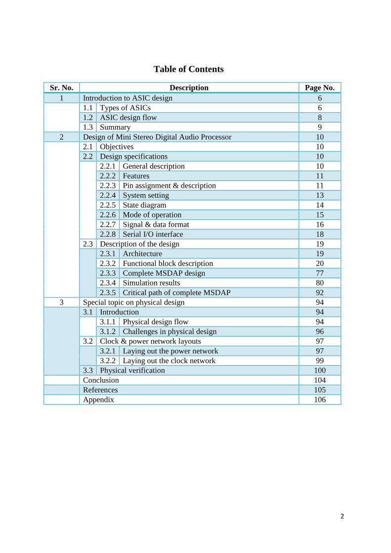
Table of Contents
Sr. No. Description Page No.
1 Introduction to ASIC design 6
1.1 Types of ASICs 6
1.2 ASIC design flow 8
1.3 Summary 9
2 Design of Mini Stereo Digital Audio Processor 10
2.1 Objectives 10
2.2 Design specifications 10
2.2.1 General description 10
2.2.2 Features 11
2.2.3 Pin assignment & description 11
2.2.4 System setting 13
2.2.5 State diagram 14
2.2.6 Mode of operation 15
2.2.7 Signal & data format 16
2.2.8 Serial I/O interface 18
2.3 Description of the design 19
2.3.1 Architecture 19
2.3.2 Functional block description 20
2.3.3 Complete MSDAP design 77
2.3.4 Simulation results 80
2.3.5 Critical path of complete MSDAP 92
3 Special topic on physical design 94
3.1 Introduction 94
3.1.1 Physical design flow 94
3.1.2 Challenges in physical design 96
3.2 Clock & power network layouts 97
3.2.1 Laying out the power network 97
3.2.2 Laying out the clock network 99
3.3 Physical verification 100
Conclusion 104
References 105
Appendix 106

3
List of Figures
Figure
No.
Description Page No.
1.1 ASIC design flow 8
2.1 Pin assignment 11
2.2 Connection diagram 13
2.3 State diagram of MSDAP operations 14
2.4 Format of coefficient values 16
2.5 Format of rj values 16
2.6 Format of input data 16
2.7 Example depicting the calculation of uj’s 17
2.8 Timing diagram of the inputs 18
2.9 Timing diagram of the outputs 18
2.10 Proposed architecture of the MSDAP 19
2.11 SIPO unit interface 20
2.12 Schematic & critical path of SIPO unit 22
2.13 Simulation results for the SIPO unit 25
2.14 Rj memory interface 26
2.15 Schematic & critical path of Rj memory 28
2.16 Simulation results for the Rj memory 30
2.17 Rj memory write operation 30
2.18 Coefficient memory interface 31
2.19 Critical path of coefficient memory 33
2.20 Simulation results for the coefficient memory 34
2.21 Coefficient memory write operation 35
2.22 Data memory interface 36
2.23 Critical path of data memory 38
2.24 Simulation results for the data memory 40
2.25 Data memory write operation 41
2.26 Refresh signal in data memory 41
2.27 Values shifted in data memory 42
2.28 Add/Sub unit interface 42
2.29 Schematic & critical path of Add/Sub unit 44
2.30 Simulation results for Add/Sub unit 46
2.31 Shift unit interface 47
2.32 Schematic & critical path of shift unit 49
2.33 Simulation results of shift unit 51
2.34 Shift unit output in binary format 51
2.35 PISO unit interface 52
2.36 Schematic & critical path of PISO unit 54
2.37 Simulation results for PISO unit 56
2.38 State controller unit interface 57
2.39 Schematic & critical path of state controller unit 66
2.40 State 0, state 1 & state 2 of state controller 67
4
2.41 State 2, state 3 & state 4 of state controller 68
2.42 State 4, state 5 & state 6 of state controller 68
2.43 State 6 & state 8 of state controller 69
2.44 State 5, state 6 & state 7 of state controller 70
2.45 Computation controller unit interface 71
2.46 Schematic & critical path of computation controller unit 76
2.47 Complete layout of MSDAP 77
2.48 State 0 to state 1 transition 80
2.49 State 1 to state 2 transition 80
2.50 Reading rj values 81
2.51 Rj memory 81
2.52 State 2 to state 3 transition 82
2.53 State 3 to state 4 transition 82
2.54 Reading coefficient values 83
2.55 Coefficient memory 84
2.56 State 4 to state 5 transition 84
2.57 State 5 to state 6 transition 85
2.58 State 6 of controller 85
2.59 Data memory 86
2.60 State S0 to state S1 transition 87
2.61 State S1 to state S2 transition 87
2.62 State S2 to state S3 transition 88
2.63 State S3 to state S4 transition 88
2.64 State S4 to state S5 transition 89
2.65 Output sent serially on the ouput L/R line 89
2.66 Output sent serially on the ouput L/R line. OutReady
remains low at this time.
90
2.67 State 6 to state 8 transition 90
2.68 State 8 to state 6 transition 91
2.69 State 6 to state 7 transition 91
2.70 State 7 to state 5 transition 92
2.71 Schematic of complete MSDAP 92
2.72 Critical path of complete MSDAP 93
2.73 Critical path of the “shifter and accumulator”in the Data-path 93
3.1 Physical design flow 94
3.2 Basic elements of power network 97
3.3 Power ring & power straps 98
3.4 Clock tree synthesis in IC compiler 99
3.5 Renaming instances 100
3.6 Complete layout in layout window 101
3.7 Results of DRC 101
3.8 LVS check report 102
5
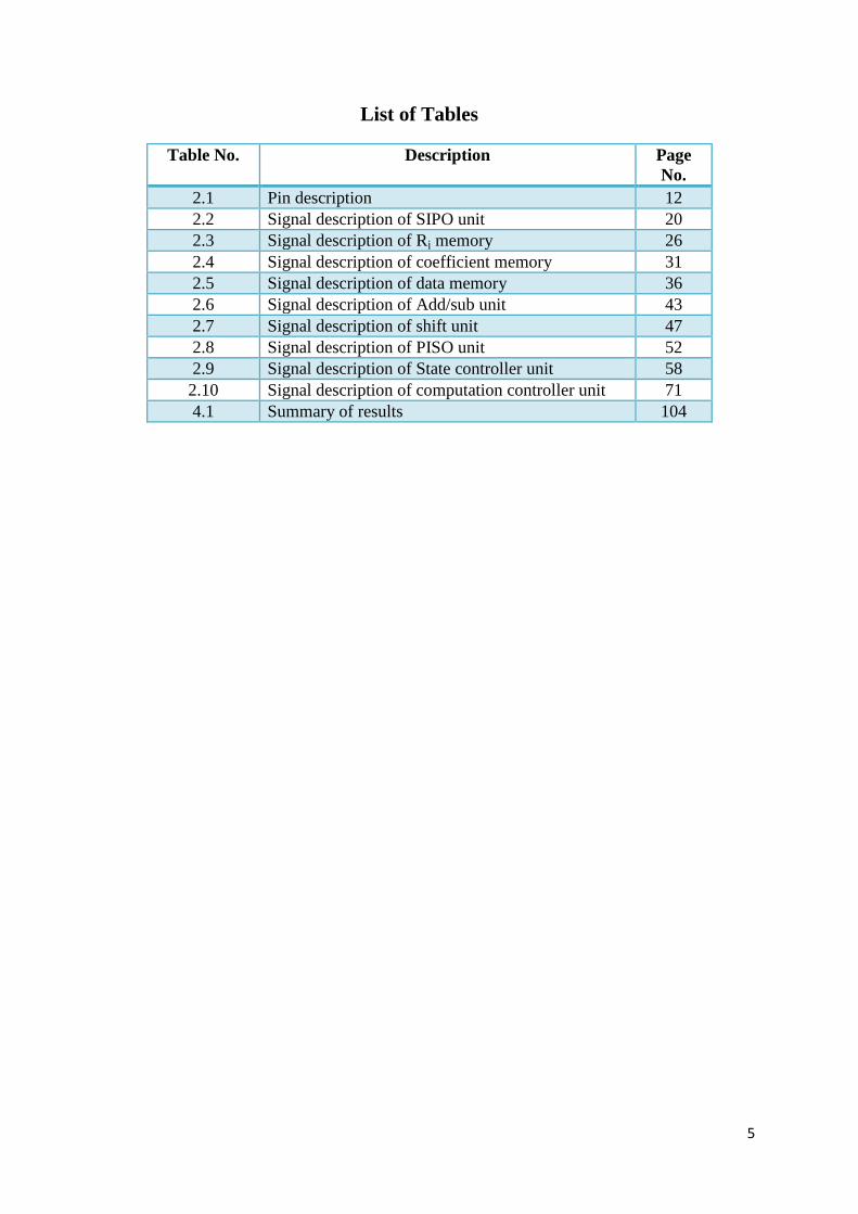
List of Tables
Table No. Description Page
No.
2.1 Pin description 12
2.2 Signal description of SIPO unit 20
2.3 Signal description of Rj memory 26
2.4 Signal description of coefficient memory 31
2.5 Signal description of data memory 36
2.6 Signal description of Add/sub unit 43
2.7 Signal description of shift unit 47
2.8 Signal description of PISO unit 52
2.9 Signal description of State controller unit 58
2.10 Signal description of computation controller unit 71
4.1 Summary of results 104

6
Chapter 1
Introduction to ASIC Design
An ASICis an application-specific integrated circuit. It is an integrated circuit customized for
a particular use rather than general purpose use. Examples of ICs that are ASICs include: a
chip for a satellite; a chip designed solely to run a cell phone; and a chip designed to run a
digital voice recorder.
ASIC is used in a number of products where a microcontroller would use too much power.
The use of ASICs improves performance over general-purpose CPUs, because ASICs are
"hardwired" to do a specific job and do not incur the overhead of fetching and interpreting
stored instructions. They have lower unit costs. They have smaller area since the device is
manufactured to the design specifications.
1.1 TYPES OF ASICs
Full custom ASICs
In a full-custom ASIC an engineer designs some or all of the logic cells, circuits, or layout
specifically for one ASIC. It is a design on the transistor level and defined all the photo
lithographic layers of the device.
Advantages of using full custom design are:
Maximum performance
lowest part cost
reduced area
Disadvantages of using full custom design are:
High non-recurring engineering (NRE) costs.
Increased design time
Semi-custom ASICs
In semi-custom design majority of the chip is designed using a group of predefined cells as
building blocks. Each cell provides a basic function, such as a logic operation or a storage
element. If it is not possible to meet the system specifications using the cell library then the
semi-custom approach permits the designer to engineer a solution by creating alternate
circuits that have the desired characteristics.
Semi-custom VLSI design can be standard cell based or array based.

7
Standard Cell Design: Cell-based provides flexibility in circuit layout but utilizes
predefined circuit elements called cells. Ituses themanufacturer's cell librariesthathave
beenused in potentially hundreds ofother design implementations and therefore are of
much lower risk than full custom design.
Advantages of Standard cell design are:
They are developed in a less amount of time
Significantly lower in cost
Lower risk than full custom design
Disadvantages of Standard cell design are:
Less optimized compared to full-custom IC
More expensive than gate-array
Gate Array Design:Arraydesign is a manufacturing method in which the
transistorsand other active devices are predefined. The physical design process then
defines the interconnections between the cells.
Advantages of gate array design are:
Photo-lithographic masks are required only for the metal layers. One-time
mask costs reduce NRE.
Production cycles are much shorter
8
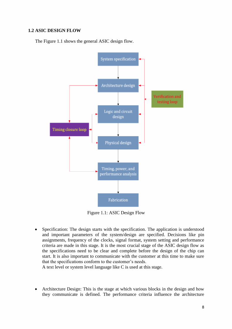
1.2 ASIC DESIGN FLOW
The Figure 1.1 shows the general ASIC design flow.
Figure 1.1: ASIC Design Flow
Specification: The design starts with the specification. The application is understood
and important parameters of the system/design are specified. Decisions like pin
assignments, frequency of the clocks, signal format, system setting and performance
criteria are made in this stage. It is the most crucial stage of the ASIC design flow as
the specifications need to be clear and complete before the design of the chip can
start. It is also important to communicate with the customer at this time to make sure
that the specifications conform to the customer’s needs.
A text level or system level language like C is used at this stage.
Architecture Design: This is the stage at which various blocks in the design and how
they communicate is defined. The performance criteria influence the architecture

9
design. The architecture design depends greatly on the designer’s experience and
knowledge.
Logic and Circuit Design: In this stage the designer describes how each block is
implemented. It contains details of State machines, counters, Mux, decoders, internal
registers. Design is converted into Verilog/VHDL code, using synthesizable
constructs of the language. Simulations are used to test if the RTL code meets the
functional requirements of the specification. A Synthesis tools like design compiler
are used to convert the RTL in Verilog or VHDL to a gate level netlist. The tool takes
the Verilog/VHDL description, the target technology and the constraints as inputs and
maps the RTL to gates. Also a timing analysis is done to check if the design meets the
timing requirements of the design.
Physical Design: This stage deals with the floorplanning and the placement & routing
of the chip. Major modules are placed in the chip depending on connections with
other modules. The modules are connected in the routing phase. Clock tree synthesis/
routingis done to minimize skew. All these functions can be accomplished by using
placement & routing tools like encounter or IC compiler. The P&R tool output is a
GDS file, used by foundry for fabricating the ASIC.ASPEF (standard parasitic
exchange format) is developed from layout tools which are used for timing analysis in
the next stage.
Timing, Power and performance analysis: Timing and power analysis are done to
make sure that the chip follows to the design specifications.
Verification and Testing: it is important to verify the correctness of the design.
Verification is carried out by simulation at the RTL level as well as the gate level.
Also once the chip is back from fabrication, it needs to be put in a real environment
and tested before it can be released into market.
1.3 SUMMARY
The key concepts discussed in this chapter are:
The advantages of using ASICs over a general purpose processor.
The different types of ASICs.
The ASIC design flow
10
Chapter 2
Design of a Mini Stereo Digital Audio Processor
2.1 OBJECTIVES
The objectives of this project are to:
Implement a Mini Stereo Digital Audio Processor (MSDAP) with
o Dual channel inputs (Left and Right)
o “Sleep” and “Normal” mode of operation
o Serial I/O interface
Implement the design in VHDL/Verilog using behavioral and RTL modeling.
Write a test bench to verify the complete functionality of the design.
Synthesize the RTL code using design vision.
Layout generation using IC compiler
Report the area, timing and power.
2.2 DESIGN SPECIFICATIONS
2.2.1 GENERAL DESCRIPTION
The function for the MSDAP is the FIR filter, which is a very complex and computation
intensive task. The FIR filtering required the following convolution
y(n) = ∑ ( ) ( )
(1)
Where, x(k) is the input audio sequence
y(n) is the output audio sequence
h(k) are the filter coefficients.
The algorithm used in order to obtain a low power implementation of the MSDAP involves
the use of only single bit shift-right and addition operations. The algorithm used implements
equation (1) as a series of addition/subtractions and shifts and expresses the output as
y(n) = 2-1
(…2-1
(2-1
(2-1
u1+u2)+u3)+…)u16) (2)
uj = xj(1)+xj(2)+…+xj(rj) 1 < j < 16 (3)
Where xj (l) ⋲ {±x (n-k)}, 1≤ l ≤ rj and rj is the total number of the POT digits ±2-j occurred
among all filter POT coefficients.
11
Using this algorithm eliminates the use of a barrel shifter. A barrel shifter is a digital circuit
that can shift a data word by a specified number of bits. Implementing convolution in the
straightforward way would need shifting by different number of bits each time and hence
would require a barrel shifter. Barrel shifters are very hardware intensive and slow. The
innovative approach taken by this algorithm is the use of a single bit shift every time. This
greatly reduces the area and complexity of the designed chip.
2.2.2 FEATURES
A system clock (Sclk) of 26.88MHzand a data clock (Dclk) of 768 KHz is used.
16 bit audio input and 40 bit audio output.
Supports dual channel serial inputs with the Dclk.
Supports dual channel serial outputs with the Sclk.
Automatic sleep mode when 800 consecutive zero inputs are obtained.
2.2.3 PIN ASSIGNMENT AND DESCRIPTION
The pin assignment is shown in Figure 2.1.
Figure 2.1: Pin assignment
12
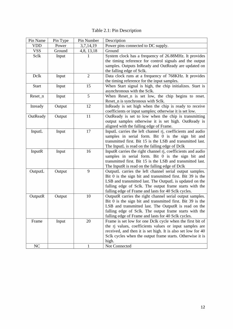
Table 2.1: Pin Description
Pin Name Pin Type Pin Number Description
VDD Power 3,7,14,19 Power pins connected to DC supply.
VSS Ground 4,8, 13,18 Ground
Sclk Input 1 System clock has a frequency of 26.88MHz. It provides
the timing reference for control signals and the output
samples. Outputs InReady and OutReady are updated on
the falling edge of Sclk.
Dclk Input 2 Data clock runs at a frequency of 768KHz. It provides
the timing reference for the input samples.
Start Input 15 When Start signal is high, the chip initializes. Start is
asynchronous with the Sclk.
Reset_n Input 5 When Reset_n is set low, the chip begins to reset.
Reset_n is synchronous with Sclk.
Inready Output 12 InReady is set high when the chip is ready to receive
coefficients or input samples; otherwise it is set low.
OutReady Output 11 OutReady is set to low when the chip is transmitting
output samples otherwise it is set high. OutReady is
aligned with the falling edge of Frame.
InputL Input 17 InputL carries the left channel rj, coefficients and audio
samples in serial form. Bit 0 is the sign bit and
transmitted first. Bit 15 is the LSB and transmitted last.
The InputL is read on the falling edge of Dclk
InputR Input 16 InputR carries the right channel rj, coefficients and audio
samples in serial form. Bit 0 is the sign bit and
transmitted first. Bit 15 is the LSB and transmitted last.
The InputR is read on the falling edge of Dclk
OutputL Output 9 OutputL carries the left channel serial output samples.
Bit 0 is the sign bit and transmitted first. Bit 39 is the
LSB and transmitted last. The OutputL is updated on the
falling edge of Sclk. The output frame starts with the
falling edge of Frame and lasts for 40 Sclk cycles.
OutputR Output 10 OutputR carries the right channel serial output samples.
Bit 0 is the sign bit and transmitted first. Bit 39 is the
LSB and transmitted last. The OutputR is read on the
falling edge of Sclk. The output frame starts with the
falling edge of Frame and lasts for 40 Sclk cycles.
Frame Input 20 Frame is set low for one Dclk cycle when the first bit of
the rj values, coefficients values or input samples are
received, and then it is set high. It is also set low for 40
Sclk cycles when the output frame starts. Otherwise it is
high.
NC 1 Not Connected
13
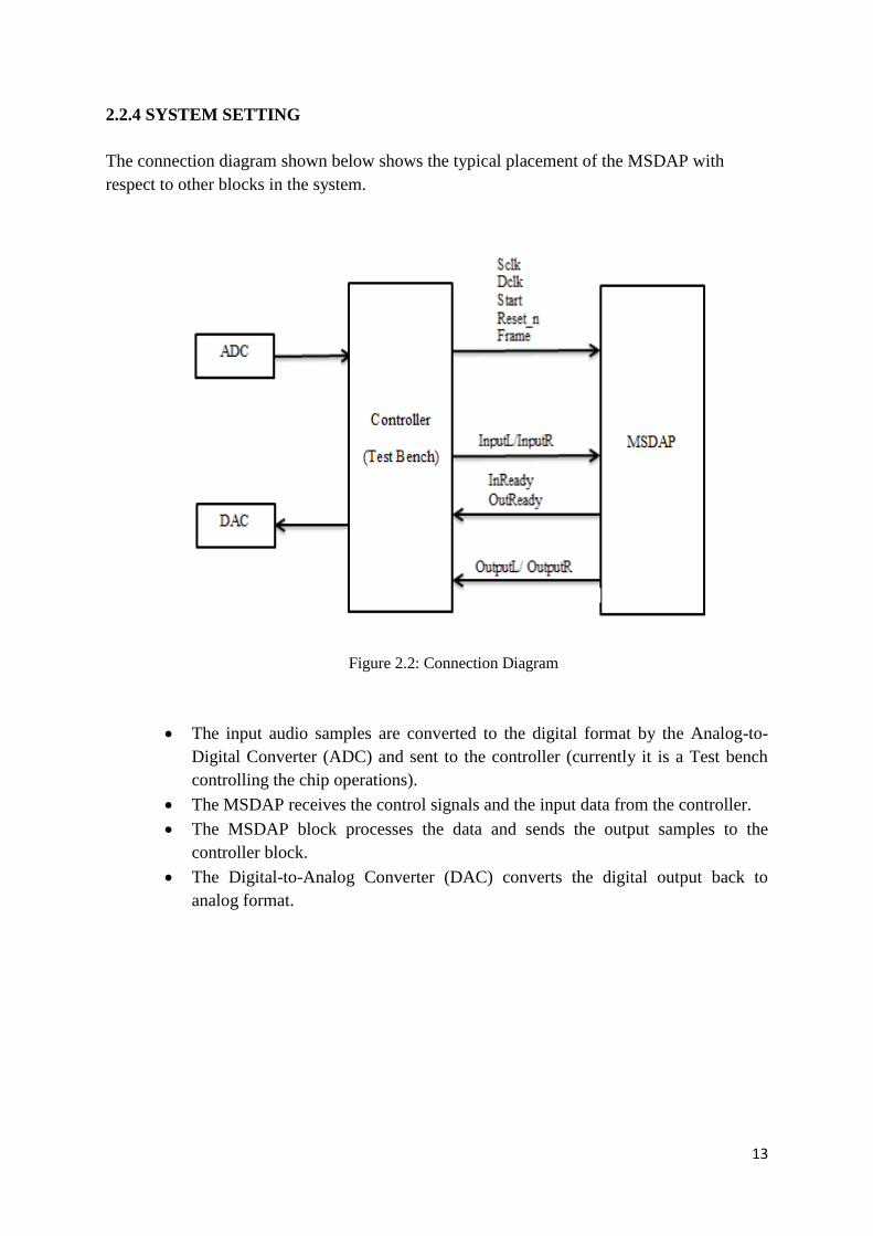
2.2.4 SYSTEM SETTING
The connection diagram shown below shows the typical placement of the MSDAP with
respect to other blocks in the system.
Figure 2.2: Connection Diagram
The input audio samples are converted to the digital format by the Analog-to-
Digital Converter (ADC) and sent to the controller (currently it is a Test bench
controlling the chip operations).
The MSDAP receives the control signals and the input data from the controller.
The MSDAP block processes the data and sends the output samples to the
controller block.
The Digital-to-Analog Converter (DAC) converts the digital output back to
analog format.
14
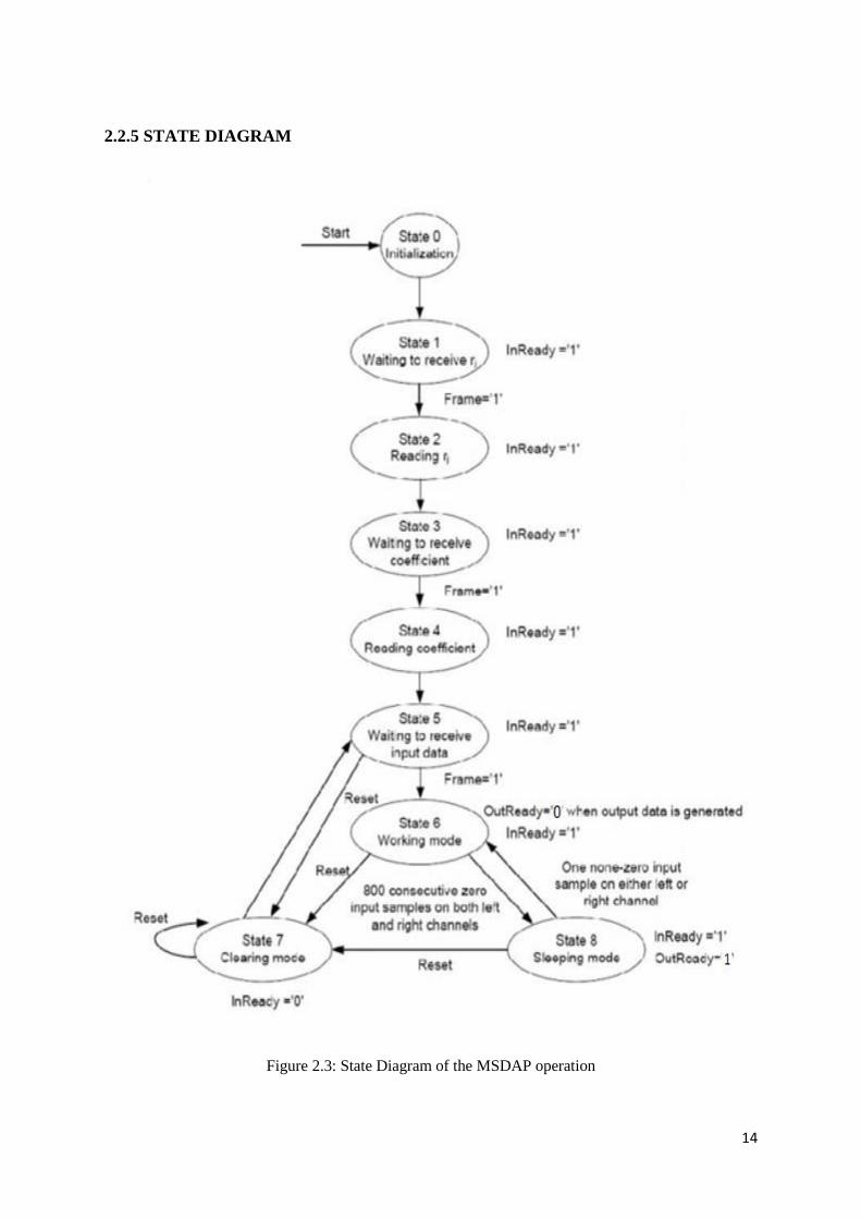
2.2.5 STATE DIAGRAM
Figure 2.3: State Diagram of the MSDAP operation
15
2.2.6 MODE OF OPERATION
State 0 (Initialization): When the Start signal is high at the falling edge of Sclk, the system
initializes. The FSM remains in this state as long as the Start is high. When the initialization
process is complete, the chip enters state 1.
State 1 (waiting to receive rj): The FSM remains in state 1 waiting for the rj values to appear
on the input channels. When the Frame signal is set low, the chip enters state 2.
State 2 (reading rj): The rj values from both channels are read by the chip and stored in
corresponding rj memory. InReady signal remains high in State 2. Once all the rj values have
been read, the chip enters state 3.
State 3 (waiting to receive coefficients): The FSM remains in state 3 while waiting for the
coefficients to appear on the input channels. When Frame signal is set low, chip enters state
4.
State 4 (reading coefficients): The coefficient values from both channels are read by the
chip and stored in corresponding coefficient memory. InReady signal remains high in State 4.
Once all the coefficient values have been read, the chip enters state 5.
State 5 (waiting to receive data): The FSM remains in state 5 while waiting for the data
samples to appear on the input channels. When the Frame signal is set low, the chip enters
state 6. If Reset_n is detected low, the chip enters state 7.
State 6 (working): The input samples are read by the chip and stored in memory. The
convolution is computed and output data is sent out serially once the computation is
completed. InReady signal remains high during this state. If Reset_n is detected low, the chip
enters state 7. If the chip detects 800 consecutive zero samples at both the input channels
simultaneously, it enters state 8.
State 7(clearing): When the chip enters this state, the data memory is cleared. InReady stays
low in this state. Once the clearing process is completed, the chip goes to state 5. As long as
the Reset_n is low, the chip remains in this state.
State 8 (sleeping): The chips enters sleep mode if 800 consecutive zeros are detected on both
the input channels. If a non-zero sample is detected on any of the input channels, the chip
transitions to state 6. If Reset_n is detected low, the chip enters state 7.
The use of the sleep mode is an innovative way to reduce the power consumption of the chip.
Even when the system is idle, the constant charging and discharging of the clocks is a major
source of power dissipation. By introducing the sleep mode and disabling the clocks when the
chip is not doing any useful work makes it extremely power efficient. Such a chip would be
well suited for consumer products like hearing aids.
16
2.2.7 SIGNALS AND DATA FORMAT
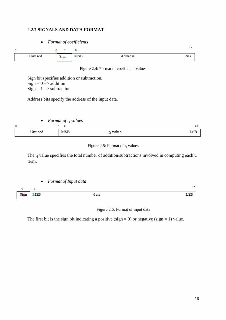
Format of coefficients
Figure 2.4: Format of coefficient values
Sign bit specifies addition or subtraction.
Sign = 0 => addition
Sign = 1 => subtraction
Address bits specify the address of the input data.
Format of rj values
Figure 2.5: Format of rj values
The rj value specifies the total number of addition/subtractions involved in computing each u
term.
Format of Input data
Figure 2.6: Format of input data
The first bit is the sign bit indicating a positive (sign = 0) or negative (sign = 1) value.
17
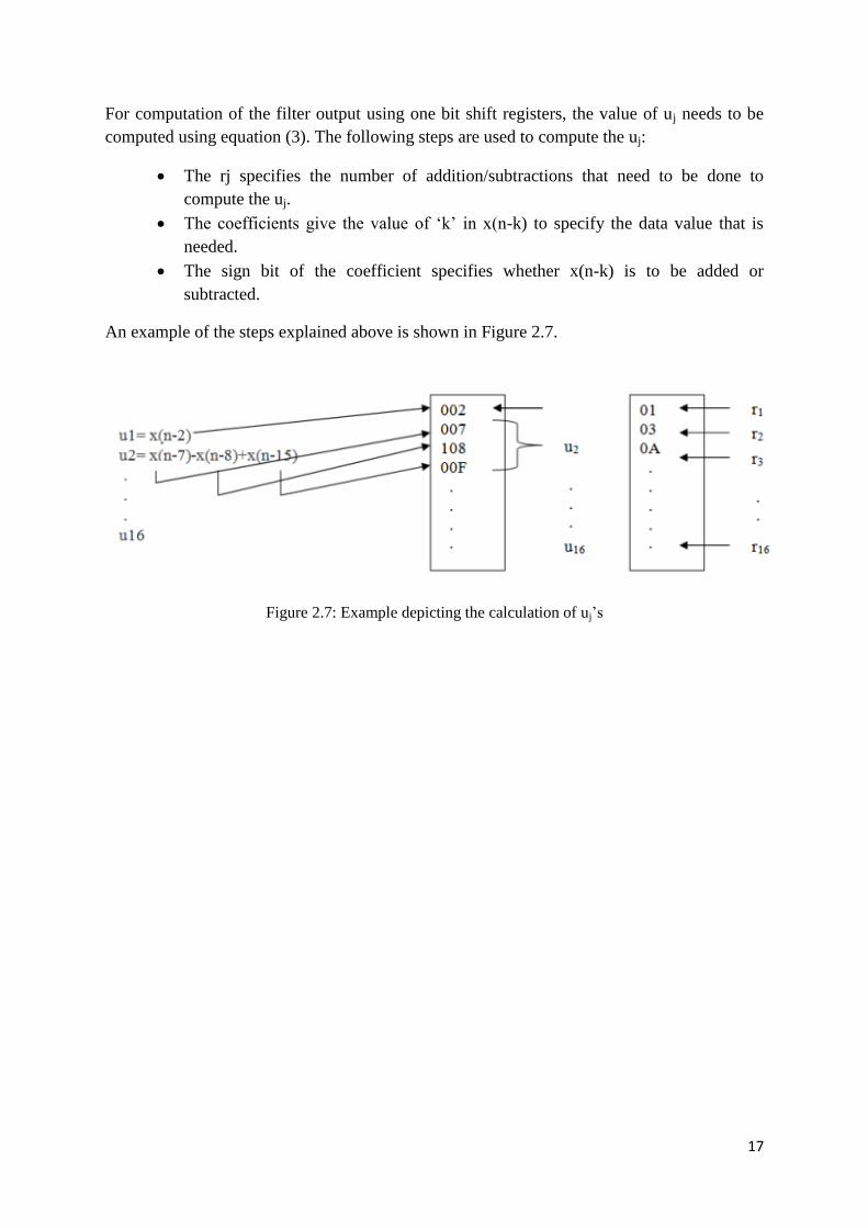
For computation of the filter output using one bit shift registers, the value of uj needs to be
computed using equation (3). The following steps are used to compute the uj:
The rj specifies the number of addition/subtractions that need to be done to
compute the uj.
The coefficients give the value of ‘k’ in x(n-k) to specify the data value that is
needed.
The sign bit of the coefficient specifies whether x(n-k) is to be added or
subtracted.
An example of the steps explained above is shown in Figure 2.7.
Figure 2.7: Example depicting the calculation of uj’s
18
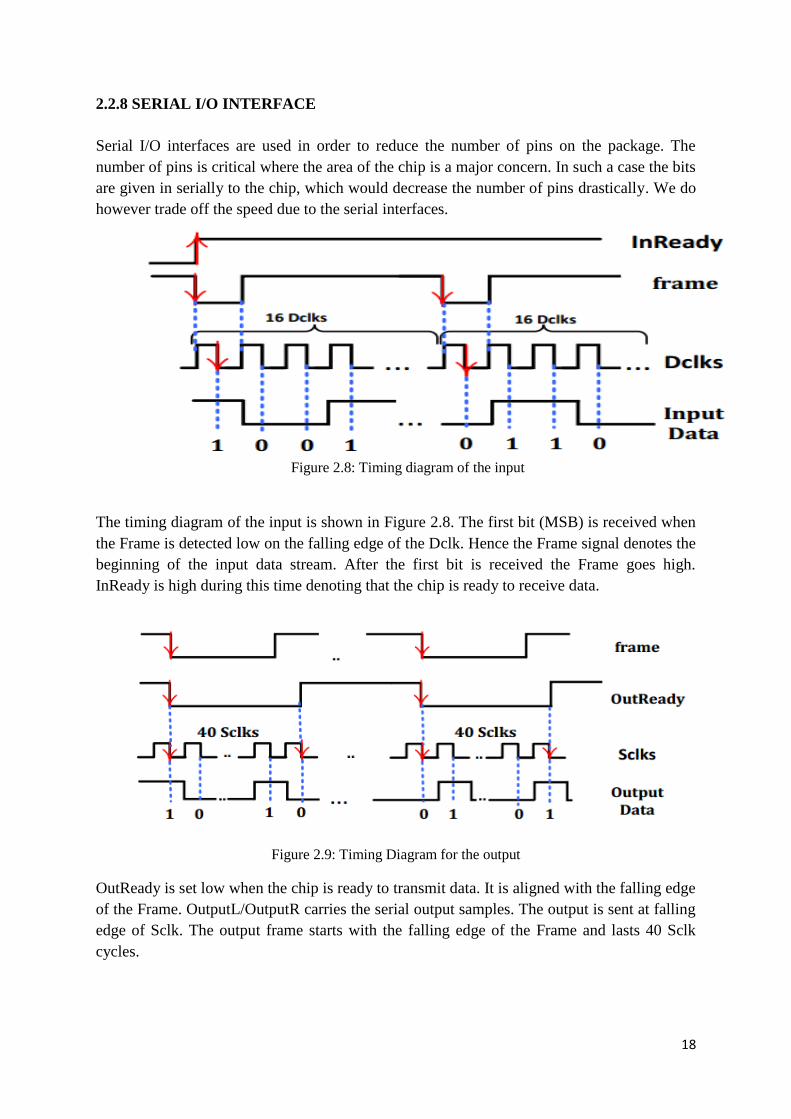
2.2.8 SERIAL I/O INTERFACE
Serial I/O interfaces are used in order to reduce the number of pins on the package. The
number of pins is critical where the area of the chip is a major concern. In such a case the bits
are given in serially to the chip, which would decrease the number of pins drastically. We do
however trade off the speed due to the serial interfaces.
Figure 2.8: Timing diagram of the input
The timing diagram of the input is shown in Figure 2.8. The first bit (MSB) is received when
the Frame is detected low on the falling edge of the Dclk. Hence the Frame signal denotes the
beginning of the input data stream. After the first bit is received the Frame goes high.
InReady is high during this time denoting that the chip is ready to receive data.
Figure 2.9: Timing Diagram for the output
OutReady is set low when the chip is ready to transmit data. It is aligned with the falling edge
of the Frame. OutputL/OutputR carries the serial output samples. The output is sent at falling
edge of Sclk. The output frame starts with the falling edge of the Frame and lasts 40 Sclk
cycles.
19
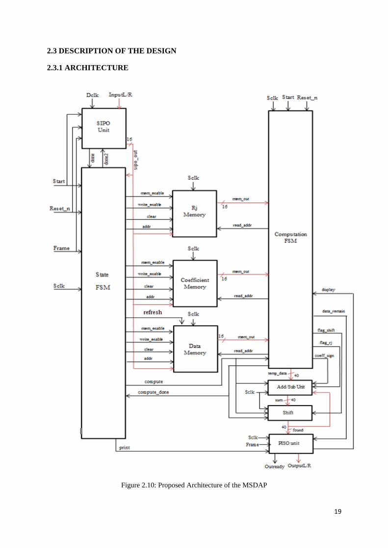
2.3 DESCRIPTION OF THE DESIGN
2.3.1 ARCHITECTURE
Figure 2.10: Proposed Architecture of the MSDAP
20
2.3.2 FUNCTIONAL BLOCK DESCRIPTION
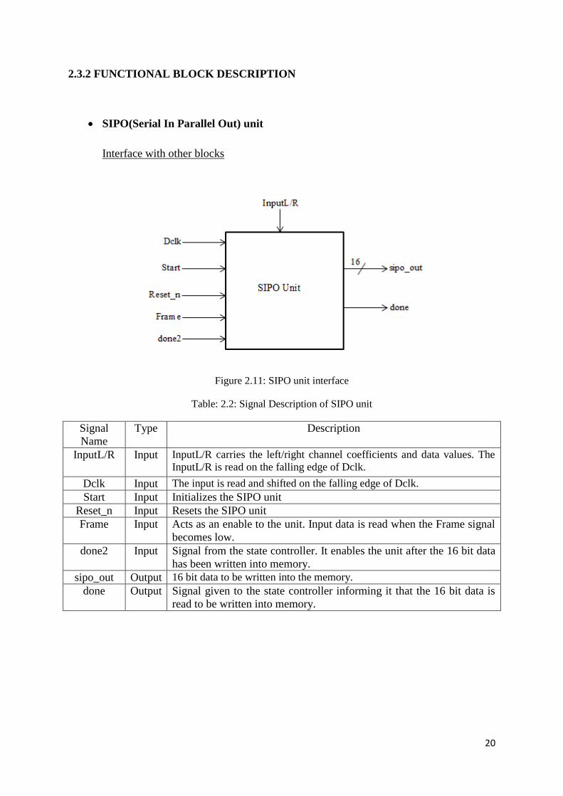
SIPO(Serial In Parallel Out) unit
Interface with other blocks
Figure 2.11: SIPO unit interface
Table: 2.2: Signal Description of SIPO unit
Signal
Name
Type Description
InputL/R Input InputL/R carries the left/right channel coefficients and data values. The
InputL/R is read on the falling edge of Dclk.
Dclk Input The input is read and shifted on the falling edge of Dclk.
Start Input Initializes the SIPO unit
Reset_n Input Resets the SIPO unit
Frame Input Acts as an enable to the unit. Input data is read when the Frame signal
becomes low.
done2 Input Signal from the state controller. It enables the unit after the 16 bit data
has been written into memory.
sipo_out Output 16 bit data to be written into the memory.
done Output Signal given to the state controller informing it that the 16 bit data is
read to be written into memory.
21
Functionality
The SIPO (Serial In Parallel Out) unit receives the serial input on the InputL/R line and converts
it into a 16 bit data by shifting. The reading of data and shifting takes place on the falling edge of
the Dclk.
The SIPO unit begins its operation when it receives a low on the Frame signal indicating that
valid data is availableon the InputL/R line. Once the unit has completed its operation, it sends a
“done” signal to the controller indicating that the data is ready to be written into corresponding
memory (Rj, Coefficient or Data memory).
The unit is initialized when the “Start” signal is high and resets when the “Reset_n” signal
becomes low.
The unit also receives a “done2” signal from the state controller indicating that the 16 bit output
has been written into memory and the unit can receive the next data.
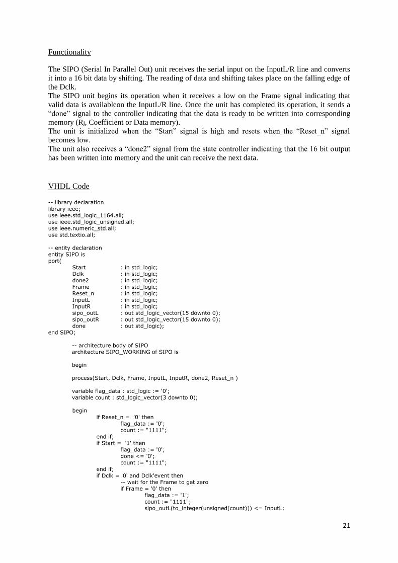
VHDL Code
-- library declaration library ieee; use ieee.std_logic_1164.all; use ieee.std_logic_unsigned.all; use ieee.numeric_std.all; use std.textio.all; -- entity declaration entity SIPO is port( Start : in std_logic; Dclk : in std_logic; done2 : in std_logic; Frame : in std_logic; Reset_n : in std_logic; InputL : in std_logic; InputR : in std_logic; sipo_outL : out std_logic_vector(15 downto 0); sipo_outR : out std_logic_vector(15 downto 0); done : out std_logic); end SIPO;
-- architecture body of SIPO architecture SIPO_WORKING of SIPO is begin process(Start, Dclk, Frame, InputL, InputR, done2, Reset_n ) variable flag_data : std_logic := '0'; variable count : std_logic_vector(3 downto 0); begin
if Reset_n = '0' then flag_data := '0'; count := "1111"; end if; if Start = '1' then flag_data := '0'; done <= '0'; count := "1111"; end if; if Dclk = '0' and Dclk'event then -- wait for the Frame to get zero if Frame = '0' then flag_data := '1'; count := "1111"; sipo_outL(to_integer(unsigned(count))) <= InputL;
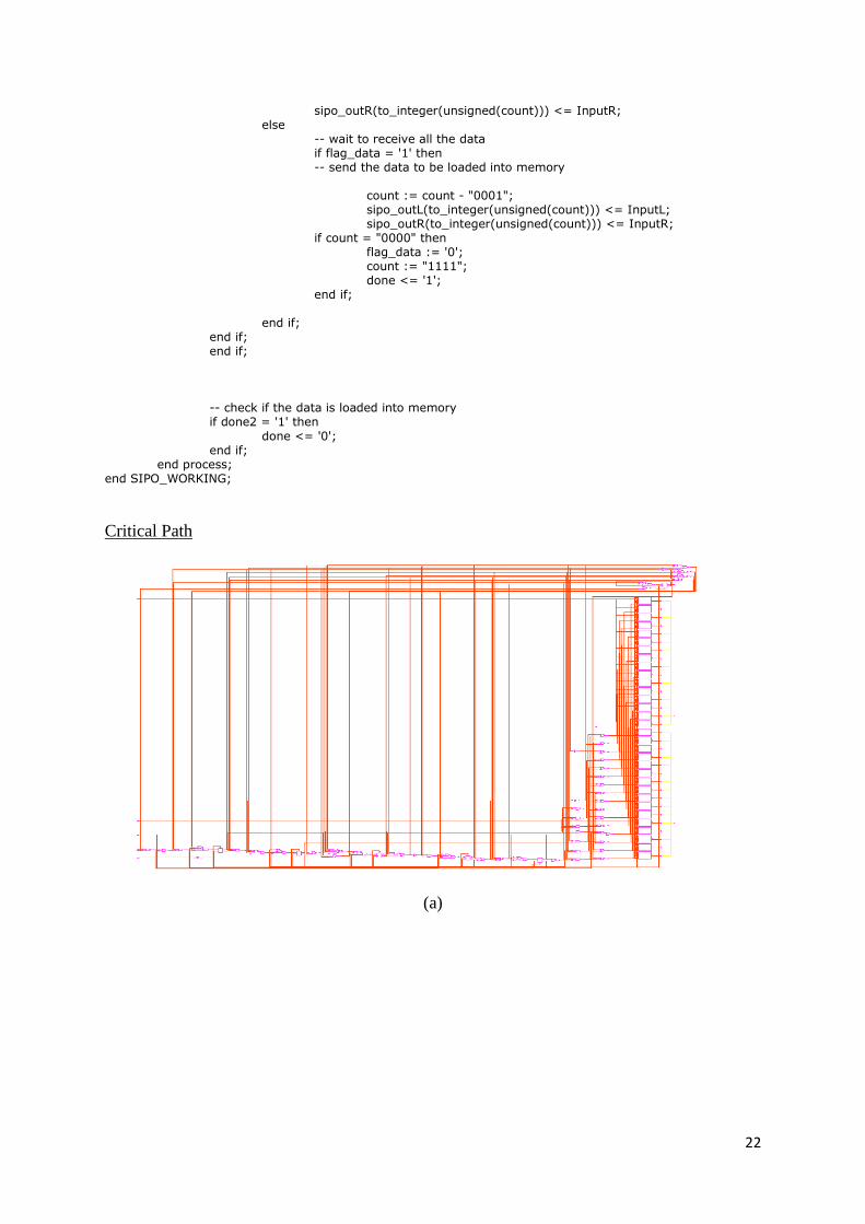
22
sipo_outR(to_integer(unsigned(count))) <= InputR; else -- wait to receive all the data if flag_data = '1' then -- send the data to be loaded into memory count := count - "0001"; sipo_outL(to_integer(unsigned(count))) <= InputL; sipo_outR(to_integer(unsigned(count))) <= InputR; if count = "0000" then flag_data := '0'; count := "1111"; done <= '1'; end if; end if; end if; end if;
-- check if the data is loaded into memory if done2 = '1' then
done <= '0'; end if; end process; end SIPO_WORKING;
Critical Path
(a)
23
(b)
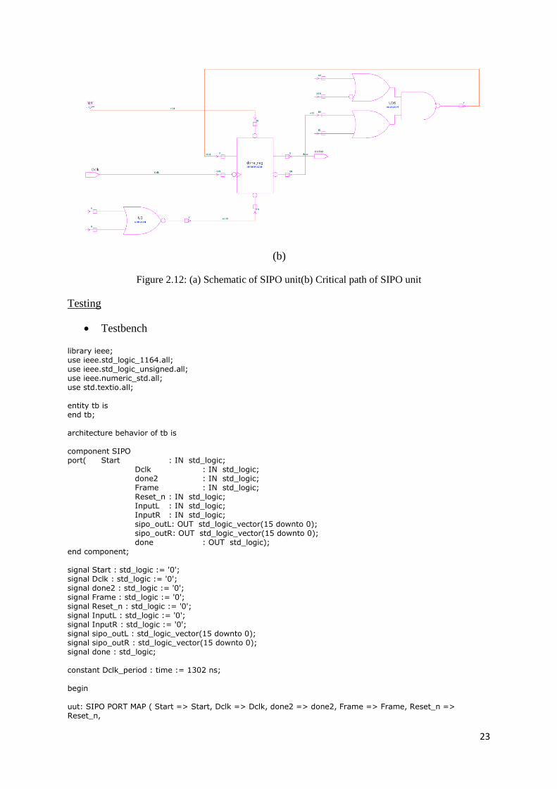
Figure 2.12: (a) Schematic of SIPO unit(b) Critical path of SIPO unit
Testing
Testbench
library ieee; use ieee.std_logic_1164.all; use ieee.std_logic_unsigned.all; use ieee.numeric_std.all; use std.textio.all; entity tb is end tb; architecture behavior of tb is component SIPO port( Start : IN std_logic; Dclk : IN std_logic; done2 : IN std_logic; Frame : IN std_logic; Reset_n : IN std_logic; InputL : IN std_logic; InputR : IN std_logic; sipo_outL: OUT std_logic_vector(15 downto 0); sipo_outR: OUT std_logic_vector(15 downto 0); done : OUT std_logic);
end component; signal Start : std_logic := '0'; signal Dclk : std_logic := '0'; signal done2 : std_logic := '0'; signal Frame : std_logic := '0'; signal Reset_n : std_logic := '0'; signal InputL : std_logic := '0'; signal InputR : std_logic := '0'; signal sipo_outL : std_logic_vector(15 downto 0); signal sipo_outR : std_logic_vector(15 downto 0); signal done : std_logic; constant Dclk_period : time := 1302 ns; begin uut: SIPO PORT MAP ( Start => Start, Dclk => Dclk, done2 => done2, Frame => Frame, Reset_n => Reset_n,
24
InputL => InputL, InputR => InputR, sipo_outL => sipo_outL, sipo_outR => sipo_outR, done => done ); Process begin Dclk <= '0'; wait for Dclk_period/2; Dclk <= '1'; wait for Dclk_period/2; end process; process begin Frame <= '1'; Start <= '1'; Reset_n <= '1'; wait for Dclk_period; Frame <= '0'; Start <= '0'; InputL <= '0'; InputR <= '1'; wait for Dclk_period; Frame <= '1'; InputL <= '0'; InputR <= '1'; wait for Dclk_period; InputL <= '0'; InputR <= '0'; wait for Dclk_period; InputL <= '1'; InputR <= '1'; wait for Dclk_period; InputL <= '1'; InputR <= '0'; wait for Dclk_period; InputL <= '0'; InputR <= '1'; wait for Dclk_period; InputL <= '0'; InputR <= '0'; wait for Dclk_period; InputL <= '0'; InputR <= '1'; wait for Dclk_period; InputL <= '1'; InputR <= '0'; wait for Dclk_period;
InputL <= '1'; InputR <= '1'; wait for Dclk_period; InputL <= '0'; InputR <= '0'; wait for Dclk_period; InputL <= '0'; InputR <= '1'; wait for Dclk_period; InputL <= '0'; InputR <= '0'; wait for Dclk_period; InputL <= '1'; InputR <= '1'; wait for Dclk_period; InputL <= '1'; InputR <= '0'; wait for Dclk_period; InputL <= '0'; InputR <= '1'; wait for Dclk_period; done2 <= '1'; wait for Dclk_period; done2 <= '0'; wait for Dclk_period*3; Frame <= '0'; InputL <= '1'; InputR <= '0'; wait for Dclk_period; Frame <= '1'; InputL <= '1'; InputR <= '1'; wait for Dclk_period; InputL <= '0'; InputR <= '1'; wait for Dclk_period; InputL <= '1'; InputR <= '1'; wait for Dclk_period; InputL <= '1'; InputR <= '1'; wait for Dclk_period; InputL <= '0'; InputR <= '0'; wait for Dclk_period; InputL <= '0'; InputR <= '0'; wait for Dclk_period; InputL <= '1'; InputR <= '0'; wait for Dclk_period; InputL <= '0'; InputR <= '0'; wait for Dclk_period; InputL <= '0'; InputR <= '1'; wait for Dclk_period; Reset_n <= '0'; wait for Dclk_period; Reset_n <= '1'; wait for Dclk_period; Frame <= '0'; InputL <= '0'; InputR <= '1'; wait for Dclk_period; Frame <= '1'; InputL <= '0'; InputR <= '1'; wait for Dclk_period; InputL <= '0'; InputR <= '0'; wait for Dclk_period; InputL <= '1'; InputR <= '1'; wait for Dclk_period; InputL <= '1'; InputR <= '0'; wait for Dclk_period; InputL <= '0'; InputR <= '1'; wait for Dclk_period; InputL <= '0'; InputR <= '0'; wait for Dclk_period; InputL <= '0'; InputR <= '1'; wait for Dclk_period; InputL <= '1'; InputR <= '0'; wait for Dclk_period; InputL <= '1'; InputR <= '1'; wait for Dclk_period; InputL <= '0'; InputR <= '0'; wait for Dclk_period; InputL <= '0'; InputR <= '1'; wait for Dclk_period; InputL <= '0'; InputR <= '0'; wait for Dclk_period; InputL <= '1'; InputR <= '1'; wait for Dclk_period; InputL <= '1'; InputR <= '0'; wait for Dclk_period; InputL <= '0'; InputR <= '1'; wait for Dclk_period; done2 <= '1'; wait for 1000000 ns; end process; end;
25
Simulation Results
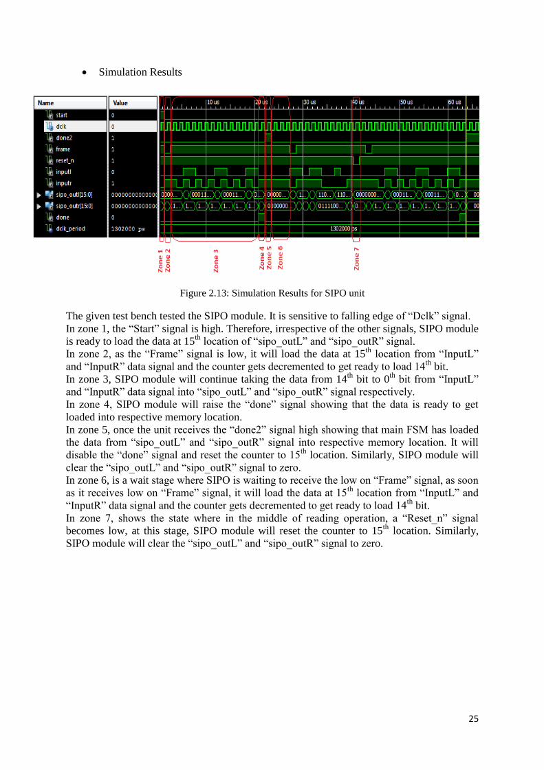
Figure 2.13: Simulation Results for SIPO unit
The given test bench tested the SIPO module. It is sensitive to falling edge of “Dclk” signal.
In zone 1, the “Start” signal is high. Therefore, irrespective of the other signals, SIPO module
is ready to load the data at 15th
location of “sipo_outL” and “sipo_outR” signal.
In zone 2, as the “Frame” signal is low, it will load the data at 15th
location from “InputL”
and “InputR” data signal and the counter gets decremented to get ready to load 14th
bit.
In zone 3, SIPO module will continue taking the data from 14th
bit to 0th
bit from “InputL”
and “InputR” data signal into “sipo_outL” and “sipo_outR” signal respectively.
In zone 4, SIPO module will raise the “done” signal showing that the data is ready to get
loaded into respective memory location.
In zone 5, once the unit receives the “done2” signal high showing that main FSM has loaded
the data from “sipo_outL” and “sipo_outR” signal into respective memory location. It will
disable the “done” signal and reset the counter to 15th
location. Similarly, SIPO module will
clear the “sipo_outL” and “sipo_outR” signal to zero.
In zone 6, is a wait stage where SIPO is waiting to receive the low on “Frame” signal, as soon
as it receives low on “Frame” signal, it will load the data at 15th
location from “InputL” and
“InputR” data signal and the counter gets decremented to get ready to load 14th
bit.
In zone 7, shows the state where in the middle of reading operation, a “Reset_n” signal
becomes low, at this stage, SIPO module will reset the counter to 15th
location. Similarly,
SIPO module will clear the “sipo_outL” and “sipo_outR” signal to zero.
26
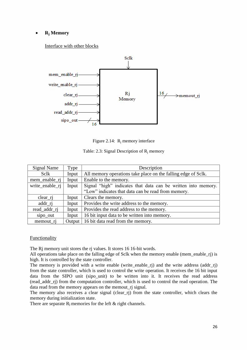
Rj Memory
Interface with other blocks
Figure 2.14: Rj memory interface
Table: 2.3: Signal Description of Rj memory
Signal Name Type Description
Sclk Input All memory operations take place on the falling edge of Sclk.
mem_enable_rj Input Enable to the memory.
write_enable_rj Input Signal “high” indicates that data can be written into memory.
“Low” indicates that data can be read from memory.
clear_rj Input Clears the memory.
addr_rj Input Provides the write address to the memory.
read_addr_rj Input Provides the read address to the memory.
sipo_out Input 16 bit input data to be written into memory.
memout_rj Output 16 bit data read from the memory.
Functionality
The Rj memory unit stores the rj values. It stores 16 16-bit words.
All operations take place on the falling edge of Sclk when the memory enable (mem_enable_rj) is
high. It is controlled by the state controller.
The memory is provided with a write enable (write_enable_rj) and the write address (addr_rj)
from the state controller, which is used to control the write operation. It receives the 16 bit input
data from the SIPO unit (sipo_unit) to be written into it. It receives the read address
(read_addr_rj) from the computation controller, which is used to control the read operation. The
data read from the memory appears on the memout_rj signal.
The memory also receives a clear signal (clear_rj) from the state controller, which clears the
memory during initialization state.
There are separate Rj memories for the left & right channels.
27
VHDL Code
-- library declaration library ieee; use ieee.std_logic_1164.all; use ieee.std_logic_unsigned.all; use ieee.numeric_std.all; use std.textio.all; -- entity declaration entity rj_memoryL is port( Sclk : in std_logic; clear_rjL : in std_logic; mem_enable_rjL : in std_logic; wr_enable_rjL : in std_logic; addr_rjL : in unsigned(3 downto 0); read_addr_rjL : in unsigned(3 downto 0); sipo_outL : in std_logic_vector(15 downto 0); memout_rjL : out std_logic_vector(15 downto 0)); end rj_memoryL; -- architecture working of rj memory left channel architecture WORKING_memory_rjL of rj_memoryL is -- declaration of rj memory (Left Channel) type memory_rjL is array(15 downto 0) of std_logic_vector(15 downto 0); signal mem_rjL : memory_rjL ; --:= ((others=> (others=>'0'))) begin process(Sclk, mem_enable_rjL, wr_enable_rjL, sipo_outL, clear_rjL, addr_rjL, mem_rjL, read_addr_rjL ) begin if Sclk = '0' and Sclk'event then -- check to enable the memory if mem_enable_rjL = '1' then -- check to clear the entire memory if clear_rjL = '0' then -- check to write into the memory if wr_enable_rjL = '1' then mem_rjL(to_integer(addr_rjL)) <= sipo_outL; end if; else
mem_rjL <= ((others=> (others=>'0'))); end if; end if; end if; -- check to enable the memory if mem_enable_rjL = '1' then -- check to read from the memory if wr_enable_rjL = '0' then memout_rjL <= mem_rjL(to_integer(read_addr_rjL)); end if; end if; end process; end WORKING_memory_rjL;
Similarly, an Rj memory is defined for the right channel.
28
Critical Path
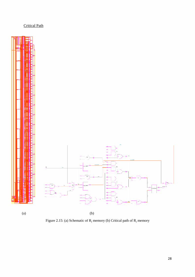
Figure 2.15: (a) Schematic of Rj memory (b) Critical path of Rj memory
(b) (a)

29
Testing
Testbench
library ieee; use ieee.std_logic_1164.all; use ieee.std_logic_unsigned.all; use ieee.numeric_std.all; use std.textio.all; entity tb is end tb; architecture behavior of tb is
component rj_memoryL port( Sclk : IN std_logic; clear_rjL : IN std_logic; mem_enable_rjL : IN std_logic; wr_enable_rjL : IN std_logic; addr_rjL : IN unsigned(3 downto 0); read_addr_rjL : IN unsigned(3 downto 0); sipo_outL : IN std_logic_vector(15 downto 0); memout_rjL : OUT std_logic_vector(15 downto 0) ); end component; signal Sclk : std_logic := '0'; signal clear_rjL : std_logic := '0'; signal mem_enable_rjL : std_logic := '0'; signal wr_enable_rjL : std_logic := '0'; signal addr_rjL : unsigned(3 downto 0) := (others => '0'); signal read_addr_rjL : unsigned(3 downto 0) := (others => '0'); signal sipo_outL : std_logic_vector(15 downto 0) := (others => '0'); signal memout_rjL : std_logic_vector(15 downto 0); constant Sclk_period : time := 37.2 ns; begin uut: rj_memoryL PORT MAP ( Sclk => Sclk, clear_rjL => clear_rjL, mem_enable_rjL => mem_enable_rjL, wr_enable_rjL => wr_enable_rjL, addr_rjL => addr_rjL, read_addr_rjL => read_addr_rjL, sipo_outL => sipo_outL, memout_rjL => memout_rjL); process begin Sclk <= '0'; wait for Sclk_period/2; Sclk <= '1'; wait for Sclk_period/2; end process; process begin mem_enable_rjL <= '0'; clear_rjL <= '0'; wait for Sclk_period; mem_enable_rjL <= '1'; clear_rjL <= '1'; wr_enable_rjL <= '0'; wait for Sclk_period; sipo_outL <= "0000000011010010"; addr_rjL <= "0000"; mem_enable_rjL <= '1'; clear_rjL <= '0'; wr_enable_rjL <= '1'; wait for Sclk_period; sipo_outL <= "0000000001111001"; addr_rjL <= "0001";
mem_enable_rjL <= '1'; clear_rjL <= '0'; wr_enable_rjL <= '1'; wait for Sclk_period; sipo_outL <= "0000000000111100"; addr_rjL <= "0010"; mem_enable_rjL <= '1'; clear_rjL <= '0'; wr_enable_rjL <= '1'; wait for Sclk_period; mem_enable_rjL <= '1'; clear_rjL <= '0'; wr_enable_rjL <= '0'; read_addr_rjL <= "0001"; wait for Sclk_period; mem_enable_rjL <= '0'; wait for 1000000 ns; end process; end;
30
Simulation Results
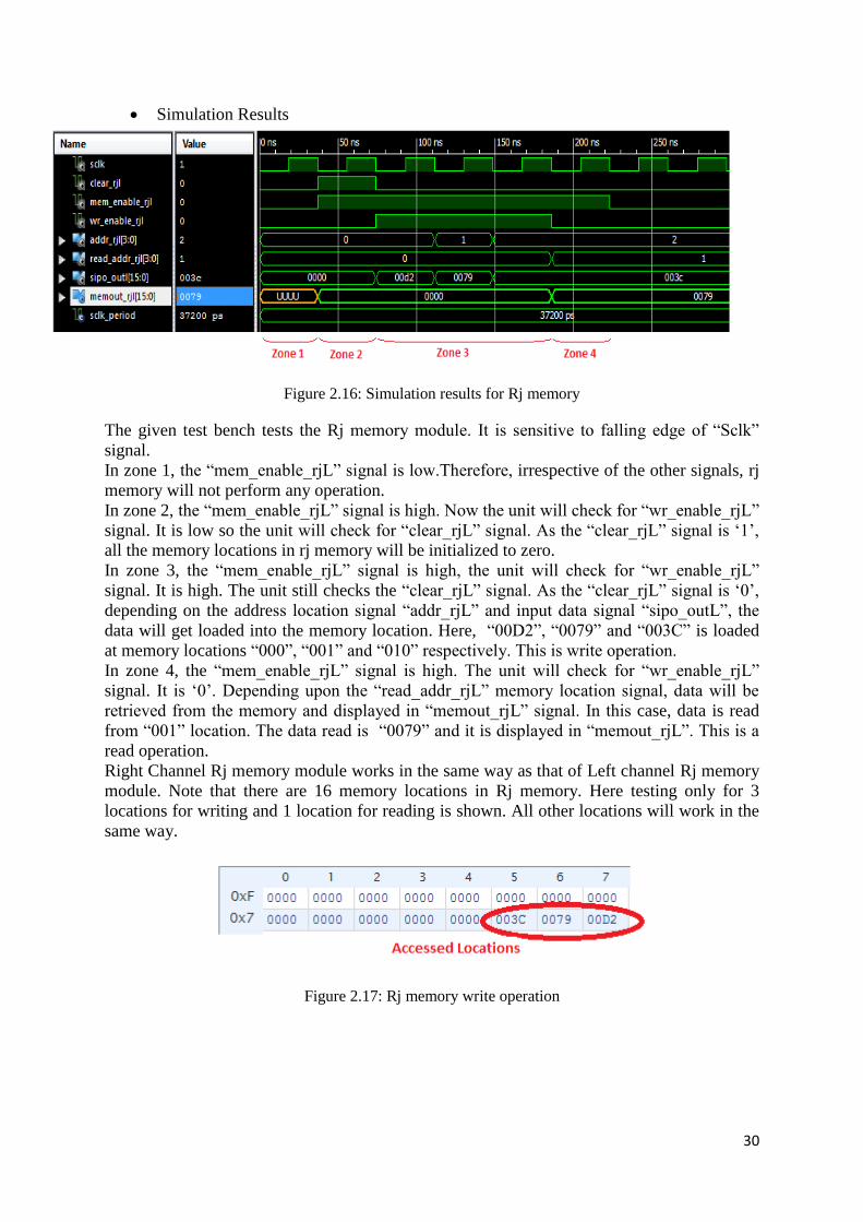
Figure 2.16: Simulation results for Rj memory
The given test bench tests the Rj memory module. It is sensitive to falling edge of “Sclk”
signal.
In zone 1, the “mem_enable_rjL” signal is low.Therefore, irrespective of the other signals, rj
memory will not perform any operation.
In zone 2, the “mem_enable_rjL” signal is high. Now the unit will check for “wr_enable_rjL”
signal. It is low so the unit will check for “clear_rjL” signal. As the “clear_rjL” signal is ‘1’,
all the memory locations in rj memory will be initialized to zero.
In zone 3, the “mem_enable_rjL” signal is high, the unit will check for “wr_enable_rjL”
signal. It is high. The unit still checks the “clear_rjL” signal. As the “clear_rjL” signal is ‘0’,
depending on the address location signal “addr_rjL” and input data signal “sipo_outL”, the
data will get loaded into the memory location. Here, “00D2”, “0079” and “003C” is loaded
at memory locations “000”, “001” and “010” respectively. This is write operation.
In zone 4, the “mem_enable_rjL” signal is high. The unit will check for “wr_enable_rjL”
signal. It is ‘0’. Depending upon the “read_addr_rjL” memory location signal, data will be
retrieved from the memory and displayed in “memout_rjL” signal. In this case, data is read
from “001” location. The data read is “0079” and it is displayed in “memout_rjL”. This is a
read operation.
Right Channel Rj memory module works in the same way as that of Left channel Rj memory
module. Note that there are 16 memory locations in Rj memory. Here testing only for 3
locations for writing and 1 location for reading is shown. All other locations will work in the
same way.
Figure 2.17: Rj memory write operation
31
Coefficient Memory
Interface with other blocks
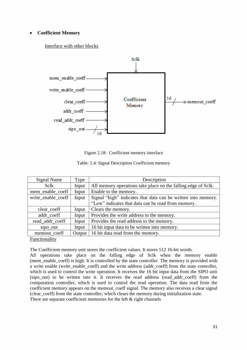
Figure 2.18: Coefficient memory interface
Table: 2.4: Signal Description Coefficient memory
Signal Name Type Description
Sclk Input All memory operations take place on the falling edge of Sclk.
mem_enable_coeff Input Enable to the memory.
write_enable_coeff Input Signal “high” indicates that data can be written into memory.
“Low” indicates that data can be read from memory.
clear_coeff Input Clears the memory.
addr_coeff Input Provides the write address to the memory.
read_addr_coeff Input Provides the read address to the memory.
sipo_out Input 16 bit input data to be written into memory.
memout_coeff Output 16 bit data read from the memory.
Functionality
The Coefficient memory unit stores the coefficient values. It stores 512 16-bit words.
All operations take place on the falling edge of Sclk when the memory enable
(mem_enable_coeff) is high. It is controlled by the state controller. The memory is provided with
a write enable (write_enable_coeff) and the write address (addr_coeff) from the state controller,
which is used to control the write operation. It receives the 16 bit input data from the SIPO unit
(sipo_out) to be written into it. It receives the read address (read_addr_coeff) from the
computation controller, which is used to control the read operation. The data read from the
coefficient memory appears on the memout_coeff signal. The memory also receives a clear signal
(clear_coeff) from the state controller, which clears the memory during initialization state.
There are separate coefficient memories for the left & right channels

32
VHDL Code
-- library declaration library ieee; use ieee.std_logic_1164.all; use ieee.std_logic_unsigned.all; use ieee.numeric_std.all; use std.textio.all;
-- entity declaration entity coefficient_memoryL is port( Sclk : in std_logic; clear_coeffL : in std_logic; mem_enable_coeffL : in std_logic; wr_enable_coeffL : in std_logic; addr_coeffL : in unsigned(8 downto 0); read_addr_coeffL : in unsigned(8 downto 0); sipo_outL : in std_logic_vector(15 downto 0); memout_coeffL : out std_logic_vector(15 downto 0) ); end coefficient_memoryL;
-- architecture working of coefficient memory left channel architecture WORKING_memory_coeffL of coefficient_memoryL is -- declaration of rj memory (Left Channel) type memory_coeffL is array(511 downto 0) of std_logic_vector(15 downto 0); signal mem_coeffL : memory_coeffL ; --:= ((others=> (others=>'0'))) begin
process(Sclk, mem_enable_coeffL, wr_enable_coeffL, sipo_outL, clear_coeffL, addr_coeffL, mem_coeffL ,read_addr_coeffL )
begin if Sclk = '0' and Sclk'event then -- check to enable the memory if mem_enable_coeffL = '1' then -- check to clear the entire memory if clear_coeffL = '0' then -- check to write into the memory if wr_enable_coeffL = '1' then mem_coeffL(to_integer(addr_coeffL)) <= sipo_outL;
end if; else mem_coeffL <= ((others=> (others=>'0'))); end if; end if; end if; -- check to enable the memory if mem_enable_coeffL = '1' then -- check to read from the memory if wr_enable_coeffL = '0' then memout_coeffL <= mem_coeffL(to_integer(read_addr_coeffL)); end if; end if; end process; end WORKING_memory_coeffL;
Similarly, a coefficient memory is defined for the right channel.
33
Critical Path
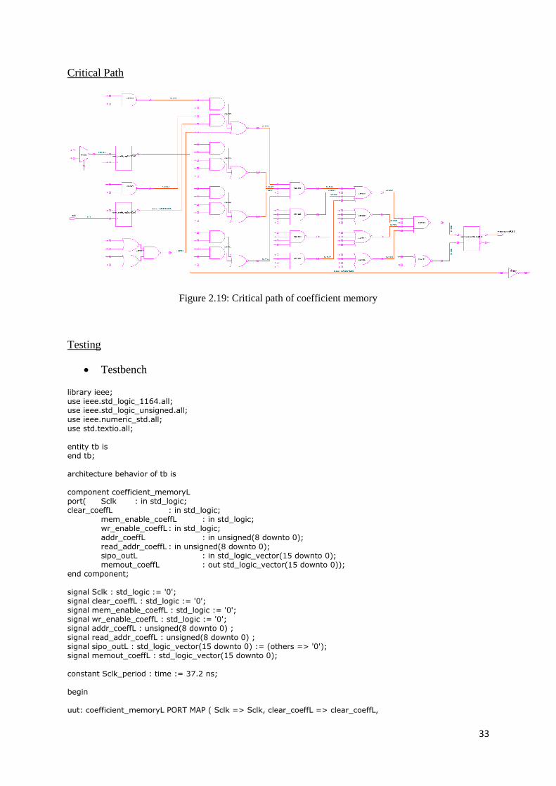
Figure 2.19: Critical path of coefficient memory
Testing
Testbench
library ieee; use ieee.std_logic_1164.all; use ieee.std_logic_unsigned.all; use ieee.numeric_std.all; use std.textio.all; entity tb is end tb; architecture behavior of tb is component coefficient_memoryL port( Sclk : in std_logic; clear_coeffL : in std_logic; mem_enable_coeffL : in std_logic; wr_enable_coeffL : in std_logic; addr_coeffL : in unsigned(8 downto 0); read_addr_coeffL : in unsigned(8 downto 0); sipo_outL : in std_logic_vector(15 downto 0); memout_coeffL : out std_logic_vector(15 downto 0)); end component; signal Sclk : std_logic := '0'; signal clear_coeffL : std_logic := '0'; signal mem_enable_coeffL : std_logic := '0'; signal wr_enable_coeffL : std_logic := '0'; signal addr_coeffL : unsigned(8 downto 0) ; signal read_addr_coeffL : unsigned(8 downto 0) ; signal sipo_outL : std_logic_vector(15 downto 0) := (others => '0'); signal memout_coeffL : std_logic_vector(15 downto 0); constant Sclk_period : time := 37.2 ns; begin uut: coefficient_memoryL PORT MAP ( Sclk => Sclk, clear_coeffL => clear_coeffL,
34
mem_enable_coeffL => mem_enable_coeffL, wr_enable_coeffL => wr_enable_coeffL, addr_coeffL => addr_coeffL, read_addr_coeffL => read_addr_coeffL, sipo_outL => sipo_outL, memout_coeffL => memout_coeffL ); process begin Sclk <= '1'; wait for Sclk_period/2; Sclk <= '0'; wait for Sclk_period/2; end process; process begin mem_enable_coeffL <= '0'; clear_coeffL <= '0'; wait for Sclk_period; mem_enable_coeffL <= '1'; clear_coeffL <= '1'; wr_enable_coeffL <= '0'; wait for Sclk_period; sipo_outL <= "1010000111000100"; addr_coeffL <= "000000000"; mem_enable_coeffL <= '1'; clear_coeffL <= '0'; wr_enable_coeffL <= '1'; wait for Sclk_period; sipo_outL <= "0110100001111000"; addr_coeffL <= "000000001"; mem_enable_coeffL <= '1'; clear_coeffL <= '0'; wr_enable_coeffL <= '1';
wait for Sclk_period; sipo_outL <= "1100000010110100"; addr_coeffL <= "000000010"; mem_enable_coeffL <= '1'; clear_coeffL <= '0'; wr_enable_coeffL <= '1'; wait for Sclk_period; mem_enable_coeffL <= '1'; clear_coeffL <= '0'; wr_enable_coeffL <= '0'; read_addr_coeffL <= "000000001"; wait for Sclk_period; mem_enable_coeffL <= '0'; wait for 1000000 ns; end process; end;
Simulation Results
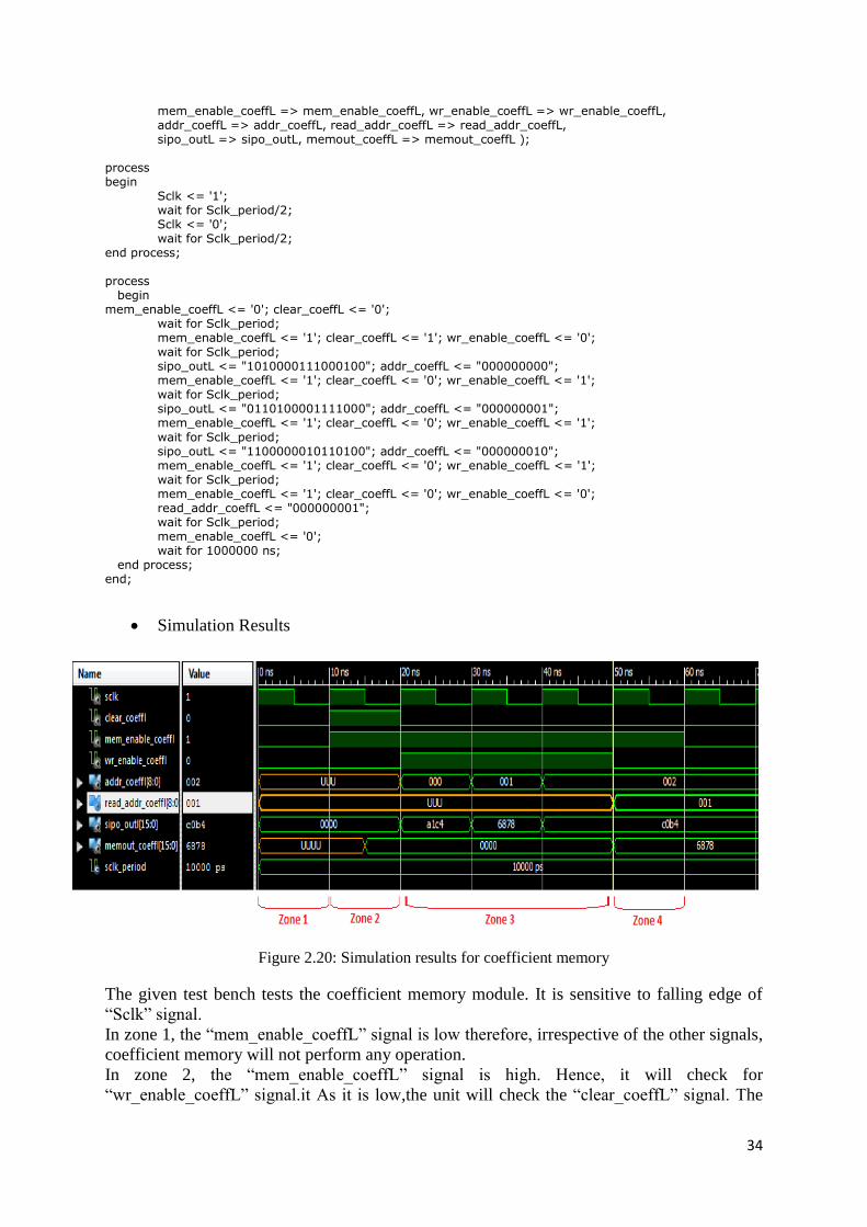
Figure 2.20: Simulation results for coefficient memory
The given test bench tests the coefficient memory module. It is sensitive to falling edge of
“Sclk” signal.
In zone 1, the “mem_enable_coeffL” signal is low therefore, irrespective of the other signals,
coefficient memory will not perform any operation.
In zone 2, the “mem_enable_coeffL” signal is high. Hence, it will check for
“wr_enable_coeffL” signal.it As it is low,the unit will check the “clear_coeffL” signal. The

35
“clear_coeffL” signal is ‘1’, therefore, all the memory locations in coefficient memory will
be initialized to zero.
In zone 3, the “mem_enable_coeffL” signal is high. The unit will check the
“wr_enable_coeffL” signal. Since it is 1, it will check the “clear_coeffL” signal. As the
“clear_coeffL” signal is ‘0’, depending on the address location signal “addr_coeffL”, the
input data on the signal “sipo_outL”,will get loaded into the memory location. For testing
“A1C4”, “6878” and “C0B4” are laoded into the memory loactions “000”, “001” and “010”
respectively. This is write operation.
In zone 4, the “mem_enable_coeffL” signal is high. The unit will check the
“wr_enable_coeffL” signal. It is ‘0’. Depending on the “read_addr_coeffL” signal, data will
be retrieved from the memory and displayed in “memout_coeffL” signal. In this case, the
data is retrieved from “001” location. The data read is “6878” and it is displayed on
“memout_coeffL” line. This is a read operation.
Right channel coefficient memory module works in the same way as that of left channel
coefficient memory module. Note that there are 512 memory locations in the coefficient
memory. Only 3 locations for writing and 1 location for reading are checked in the testbench
shown here. All other locations work in the same way.
Figure 2.21: Coefficient memory write operation
36
Data Memory
Interface with other blocks
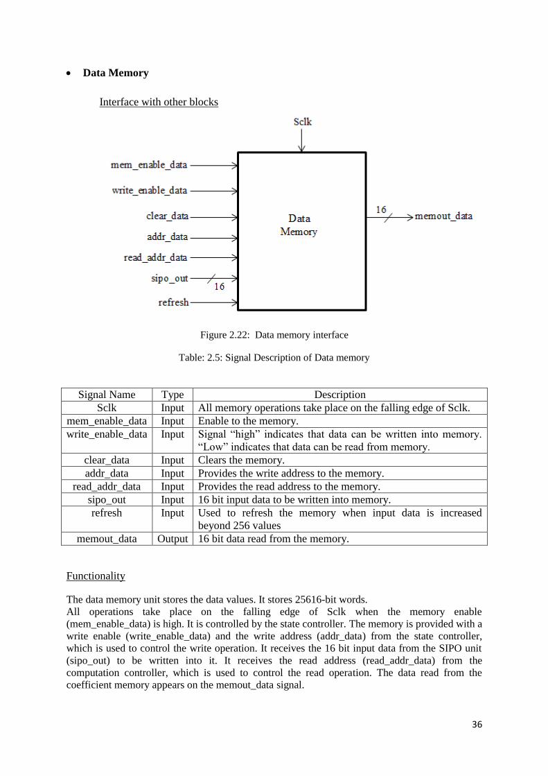
Figure 2.22: Data memory interface
Table: 2.5: Signal Description of Data memory
Signal Name Type Description
Sclk Input All memory operations take place on the falling edge of Sclk.
mem_enable_data Input Enable to the memory.
write_enable_data Input Signal “high” indicates that data can be written into memory.
“Low” indicates that data can be read from memory.
clear_data Input Clears the memory.
addr_data Input Provides the write address to the memory.
read_addr_data Input Provides the read address to the memory.
sipo_out Input 16 bit input data to be written into memory.
refresh Input Used to refresh the memory when input data is increased
beyond 256 values
memout_data Output 16 bit data read from the memory.
Functionality
The data memory unit stores the data values. It stores 25616-bit words.
All operations take place on the falling edge of Sclk when the memory enable
(mem_enable_data) is high. It is controlled by the state controller. The memory is provided with a
write enable (write_enable_data) and the write address (addr_data) from the state controller,
which is used to control the write operation. It receives the 16 bit input data from the SIPO unit
(sipo_out) to be written into it. It receives the read address (read_addr_data) from the
computation controller, which is used to control the read operation. The data read from the
coefficient memory appears on the memout_data signal.
37
The memory also receives a clear signal (clear_data) from the state controller, which clears the
memory during initialization state.
There are separate data memories for the left & right channels
VHDL Code
-- library declaration library ieee; use ieee.std_logic_1164.all; use ieee.std_logic_unsigned.all; use ieee.numeric_std.all; use std.textio.all;
-- entity declaration entity data_memoryL is port( refresh : in std_logic; Sclk : in std_logic; clear_dataL : in std_logic; mem_enable_dataL : in std_logic; wr_enable_dataL : in std_logic; addr_dataL : in unsigned(7 downto 0); read_addr_dataL : in unsigned(7 downto 0); sipo_outL : in std_logic_vector(15 downto 0); memout_dataL : out std_logic_vector(15 downto 0) ); end data_memoryL;
-- architecture working of data memory Left channel architecture WORKING_memory_dataL of data_memoryL is -- declaration of data memory (Left Channel) type memory_dataL is array(255 downto 0) of std_logic_vector(15 downto 0); signal mem_dataL : memory_dataL ; --:= ((others=> (others=>'0'))) begin process(refresh, Sclk, mem_enable_dataL, wr_enable_dataL, sipo_outL, clear_dataL, addr_dataL, mem_dataL ,read_addr_dataL ) variable fifoL : std_logic_vector(15 downto 0); variable fixL : std_logic; begin -- check if the memory needs to be refreshed if refresh = '1' then if fixL = '0' then -- shift the data one position below in the memory for i in 0 to 254 loop fifoL := mem_dataL(i+1); mem_dataL(i) <= fifoL; end loop; fixL := '1'; end if; else fixL := '0'; end if; if Sclk = '0' and Sclk'event then -- check to enable the memory if mem_enable_dataL = '1' then -- check to clear the entire memory if clear_dataL = '0' then -- check to write into the memory if wr_enable_dataL = '1' then mem_dataL(to_integer(addr_dataL)) <= sipo_outL; end if; else mem_dataL <= ((others=> (others=>'0'))); end if; end if;
38
end if; -- check to enable the memory if mem_enable_dataL = '1' then -- check to read from the memory if wr_enable_dataL = '0' then memout_dataL <= mem_dataL(to_integer(read_addr_dataL)); end if; end if; end process; end WORKING_memory_dataL;
Similarly, a data memory is defined for the right channel.
Critical Path
Figure 2.23: Critical path of data memory
Testing
Testbench
library ieee; use ieee.std_logic_1164.all; use ieee.std_logic_unsigned.all; use ieee.numeric_std.all; use std.textio.all; entity tb is end tb; architecture behavior of tb is component data_memoryL port( refresh : IN std_logic; Sclk : IN std_logic; clear_dataL : IN std_logic; mem_enable_dataL : IN std_logic; wr_enable_dataL : IN std_logic; addr_dataL : IN unsigned(7 downto 0); read_addr_dataL: IN unsigned(7 downto 0); sipo_outL : IN std_logic_vector(15 downto 0);
39
memout_dataL : OUT std_logic_vector(15 downto 0)); end component; signal refresh : std_logic := '0'; signal Sclk : std_logic := '0'; signal clear_dataL : std_logic := '0'; signal mem_enable_dataL : std_logic := '0'; signal wr_enable_dataL : std_logic := '0'; signal addr_dataL : unsigned(7 downto 0) := (others => '0'); signal read_addr_dataL : unsigned(7 downto 0) := (others => '0'); signal sipo_outL : std_logic_vector(15 downto 0) := (others => '0'); signal memout_dataL : std_logic_vector(15 downto 0); constant Sclk_period : time := 37.2 ns; begin uut: data_memoryL PORT MAP ( refresh => refresh, Sclk => Sclk, clear_dataL => clear_dataL, mem_enable_dataL => mem_enable_dataL, wr_enable_dataL => wr_enable_dataL, addr_dataL => addr_dataL, read_addr_dataL => read_addr_dataL, sipo_outL => sipo_outL, memout_dataL => memout_dataL); process begin
Sclk <= '1'; wait for Sclk_period/2; Sclk <= '0'; wait for Sclk_period/2; end process; process begin refresh <= '0'; wait for Sclk_period*8; refresh <= '1'; wait for Sclk_period*2; refresh <= '0'; wait for 1000000 ns; end process; process begin mem_enable_dataL <= '0'; clear_dataL <= '0'; wait for Sclk_period; mem_enable_dataL <= '1'; clear_dataL <= '1'; wr_enable_dataL <= '0'; wait for Sclk_period; sipo_outL <= "0110100011010000"; addr_dataL <= "00000000"; mem_enable_dataL <= '1'; clear_dataL <= '0'; wr_enable_dataL <= '1'; wait for Sclk_period; sipo_outL <= "1001000101110010"; addr_dataL <= "00000001"; mem_enable_dataL <= '1'; clear_dataL <= '0'; wr_enable_dataL <= '1'; wait for Sclk_period; sipo_outL <= "0100111000111000"; addr_dataL <= "00000010"; mem_enable_dataL <= '1'; clear_dataL <= '0'; wr_enable_dataL <= '1'; wait for Sclk_period; mem_enable_dataL <= '1'; clear_dataL <= '0'; wr_enable_dataL <= '0'; read_addr_dataL <= "00000000"; wait for Sclk_period; mem_enable_dataL <= '0'; wait for 1000000 ns; end process; end;
40
Simulation Results
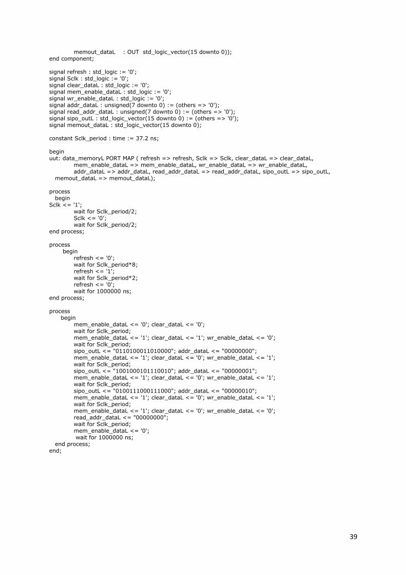
Figure 2.24: Simulation results for data memory
The given test bench tests the data memory module. It is sensitive to falling edge of “Sclk”
signal.
In zone 1, the “mem_enable_dataL” signal is low. Therefore, irrespective of the other signals,
data memory will not perform any operation.
In zone 2, the “mem_enable_dataL” signal is high. The unit will check the
“wr_enable_dataL” signal. It is low therefore, the unit will check the “clear_dataL” signal. As
the “clear_dataL” signal is ‘1’, all the memory locations in data memory will be initialized to
zero.
In zone 3, the “mem_enable_dataL” signal is high. The unit will check the
“wr_enable_dataL” signal. It is high.the unit will still check the “clear_dataL” signal. As the
“clear_dataL” signal is ‘0’, depending on the address location given by the signal
“addr_dataL” the input data on the signal “sipo_outL”, is loaded into the memory location.
Here data “68D0”, “9172” and “4E38” is loaded at the memory locations “000”, “001” and
“010” respectively. This is write operation.
In zone 4, the “mem_enable_dataL” signal is high. The unit will check the
“wr_enable_dataL” signal. It is ‘0’. Depending upon the location given by the
“read_addr_dataL”signal, data will be retrieved from the memory and displayed in
“memout_dataL” signal. In this case, data is read from “000” location. The data read is
“68D0” and it is displayed on the “memout_dataL” signal. This is a read operation.
Right channel data memory module works in the same way as that of left channel data
memory module. Note that there are 256 memory locations in data memory. Here testing of
only 3 locations for writing and 1 location for reading are shown. All other locations will
work in the same way.
41
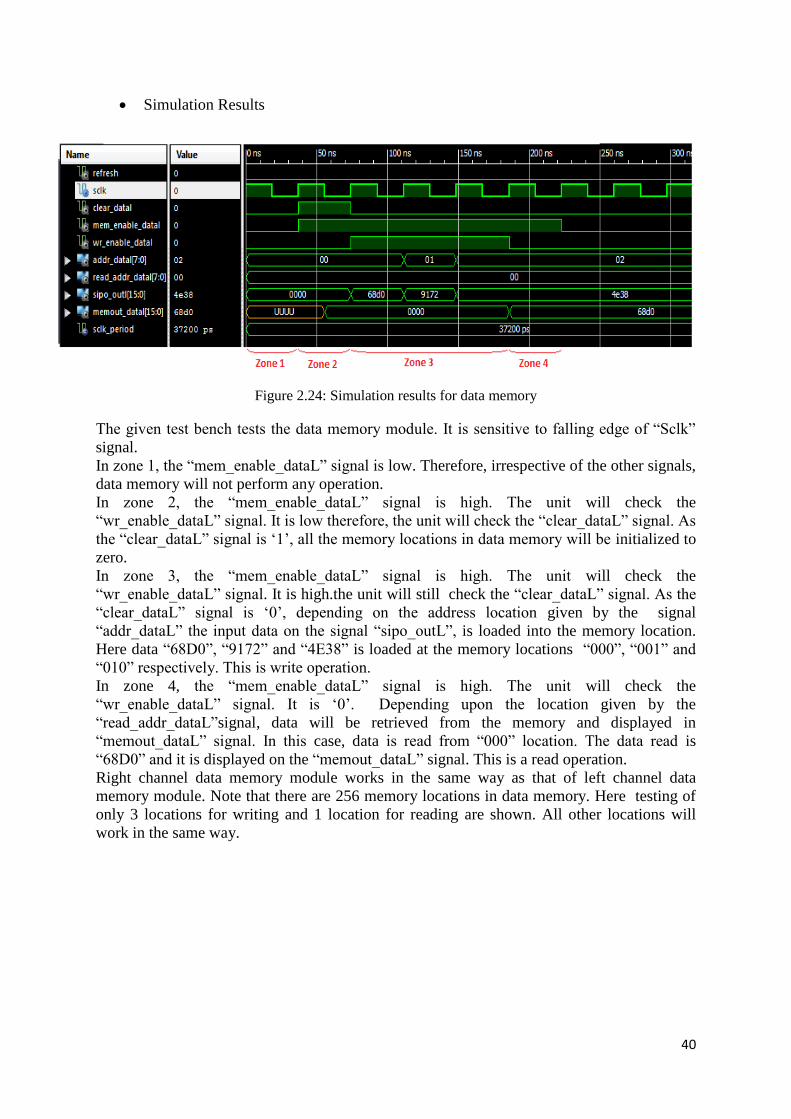
Figure 2.25: Data memory write operation
Figure 2.26: Refresh signal in data memory
In zone 5, as the “refresh” signal is high. Therefore, irrespective of the “Sclk” signal, the data
memory is refreshed and all the data is shifted by one location to the right as shown in Figure
2.31. This feature is used when input data is increased beyond 256 values.
42
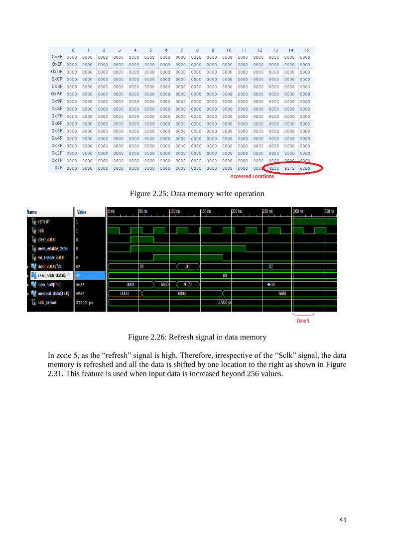
Figure 2.27: Values shifted in data memory
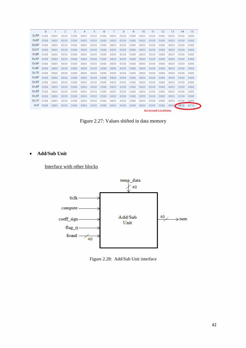
Add/Sub Unit
Interface with other blocks
Figure 2.28: Add/Sub Unit interface
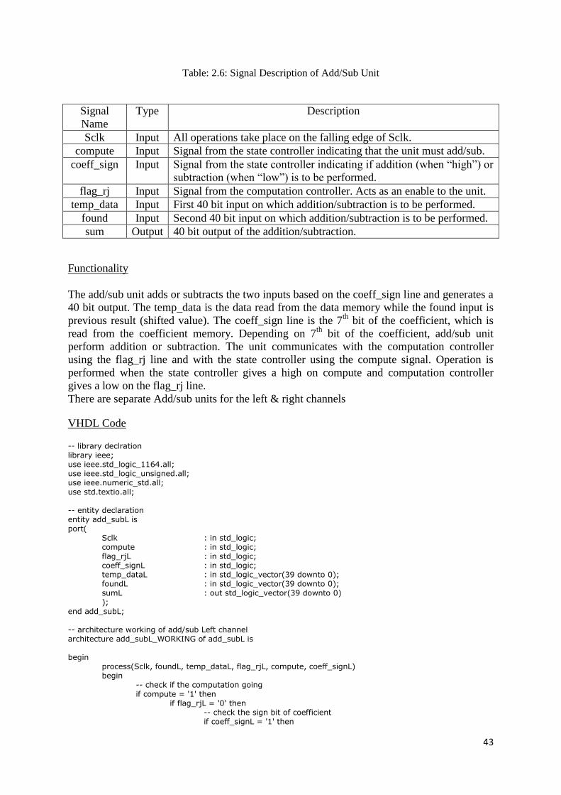
43
Table: 2.6: Signal Description of Add/Sub Unit
Signal
Name
Type Description
Sclk Input All operations take place on the falling edge of Sclk.
compute Input Signal from the state controller indicating that the unit must add/sub.
coeff_sign Input Signal from the state controller indicating if addition (when “high”) or
subtraction (when “low”) is to be performed.
flag_rj Input Signal from the computation controller. Acts as an enable to the unit.
temp_data Input First 40 bit input on which addition/subtraction is to be performed.
found Input Second 40 bit input on which addition/subtraction is to be performed.
sum Output 40 bit output of the addition/subtraction.
Functionality
The add/sub unit adds or subtracts the two inputs based on the coeff_sign line and generates a
40 bit output. The temp_data is the data read from the data memory while the found input is
previous result (shifted value). The coeff_sign line is the 7th
bit of the coefficient, which is
read from the coefficient memory. Depending on 7th
bit of the coefficient, add/sub unit
perform addition or subtraction. The unit communicates with the computation controller
using the flag_rj line and with the state controller using the compute signal. Operation is
performed when the state controller gives a high on compute and computation controller
gives a low on the flag_rj line. There are separate Add/sub units for the left & right channels
VHDL Code
-- library declration library ieee; use ieee.std_logic_1164.all; use ieee.std_logic_unsigned.all; use ieee.numeric_std.all; use std.textio.all; -- entity declaration entity add_subL is port( Sclk : in std_logic; compute : in std_logic; flag_rjL : in std_logic; coeff_signL : in std_logic; temp_dataL : in std_logic_vector(39 downto 0); foundL : in std_logic_vector(39 downto 0); sumL : out std_logic_vector(39 downto 0) ); end add_subL; -- architecture working of add/sub Left channel architecture add_subL_WORKING of add_subL is begin process(Sclk, foundL, temp_dataL, flag_rjL, compute, coeff_signL) begin -- check if the computation going if compute = '1' then if flag_rjL = '0' then -- check the sign bit of coefficient if coeff_signL = '1' then
44
sumL <= foundL - temp_dataL; else sumL <= foundL + temp_dataL; end if; end if; else sumL <= "0000000000000000000000000000000000000000"; end if; end process; end add_subL_WORKING;
Similarly, an add/sub unit is defined for the right channel.
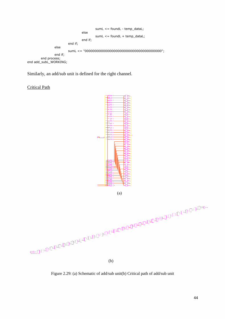
Critical Path
Figure 2.29: (a) Schematic of add/sub unit(b) Critical path of add/sub unit
(a)
(b)
45
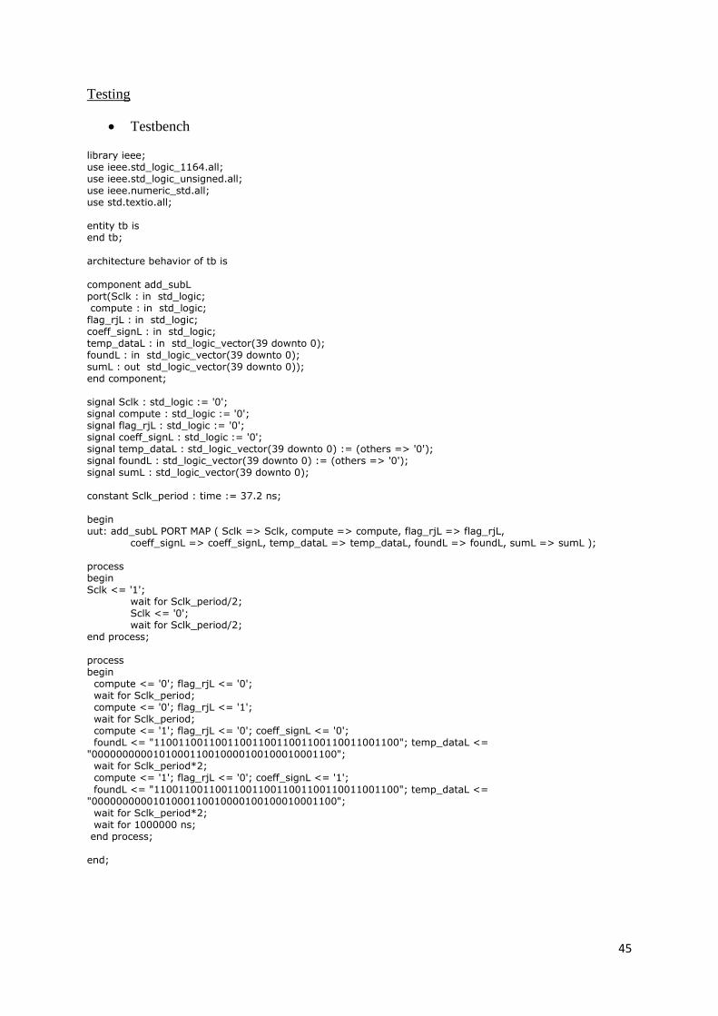
Testing
Testbench
library ieee; use ieee.std_logic_1164.all; use ieee.std_logic_unsigned.all; use ieee.numeric_std.all; use std.textio.all; entity tb is end tb;
architecture behavior of tb is component add_subL port(Sclk : in std_logic; compute : in std_logic; flag_rjL : in std_logic; coeff_signL : in std_logic; temp_dataL : in std_logic_vector(39 downto 0); foundL : in std_logic_vector(39 downto 0); sumL : out std_logic_vector(39 downto 0)); end component; signal Sclk : std_logic := '0'; signal compute : std_logic := '0'; signal flag_rjL : std_logic := '0'; signal coeff_signL : std_logic := '0'; signal temp_dataL : std_logic_vector(39 downto 0) := (others => '0'); signal foundL : std_logic_vector(39 downto 0) := (others => '0'); signal sumL : std_logic_vector(39 downto 0); constant Sclk_period : time := 37.2 ns; begin uut: add_subL PORT MAP ( Sclk => Sclk, compute => compute, flag_rjL => flag_rjL, coeff_signL => coeff_signL, temp_dataL => temp_dataL, foundL => foundL, sumL => sumL ); process begin Sclk <= '1'; wait for Sclk_period/2; Sclk <= '0'; wait for Sclk_period/2; end process; process begin compute <= '0'; flag_rjL <= '0'; wait for Sclk_period; compute <= '0'; flag_rjL <= '1'; wait for Sclk_period; compute <= '1'; flag_rjL <= '0'; coeff_signL <= '0'; foundL <= "1100110011001100110011001100110011001100"; temp_dataL <= "0000000000101000110010000100100010001100"; wait for Sclk_period*2; compute <= '1'; flag_rjL <= '0'; coeff_signL <= '1';
foundL <= "1100110011001100110011001100110011001100"; temp_dataL <= "0000000000101000110010000100100010001100"; wait for Sclk_period*2; wait for 1000000 ns; end process; end;
46
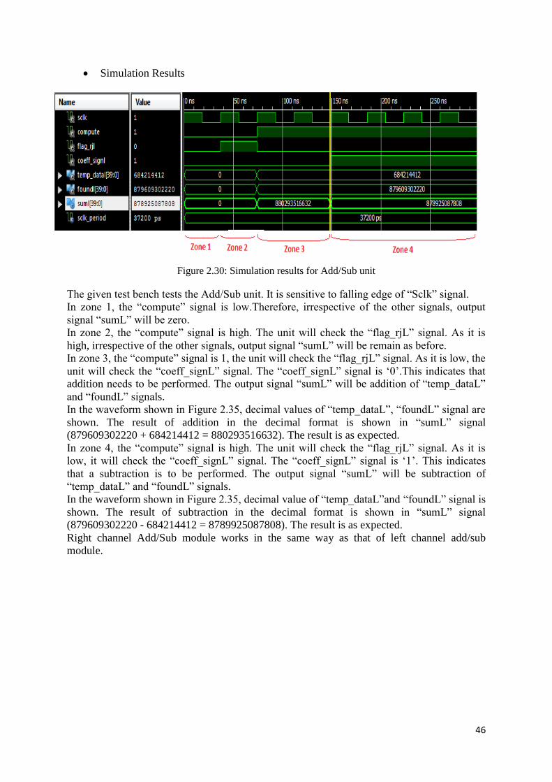
Simulation Results
Figure 2.30: Simulation results for Add/Sub unit
The given test bench tests the Add/Sub unit. It is sensitive to falling edge of “Sclk” signal.
In zone 1, the “compute” signal is low.Therefore, irrespective of the other signals, output
signal “sumL” will be zero.
In zone 2, the “compute” signal is high. The unit will check the “flag_rjL” signal. As it is
high, irrespective of the other signals, output signal “sumL” will be remain as before.
In zone 3, the “compute” signal is 1, the unit will check the “flag_rjL” signal. As it is low, the
unit will check the “coeff_signL” signal. The “coeff_signL” signal is ‘0’.This indicates that
addition needs to be performed. The output signal “sumL” will be addition of “temp_dataL”
and “foundL” signals.
In the waveform shown in Figure 2.35, decimal values of “temp_dataL”, “foundL” signal are
shown. The result of addition in the decimal format is shown in “sumL” signal
(879609302220 + 684214412 = 880293516632). The result is as expected.
In zone 4, the “compute” signal is high. The unit will check the “flag_rjL” signal. As it is
low, it will check the “coeff_signL” signal. The “coeff_signL” signal is ‘1’. This indicates
that a subtraction is to be performed. The output signal “sumL” will be subtraction of
“temp_dataL” and “foundL” signals.
In the waveform shown in Figure 2.35, decimal value of “temp_dataL”and “foundL” signal is
shown. The result of subtraction in the decimal format is shown in “sumL” signal
(879609302220 - 684214412 = 8789925087808). The result is as expected.
Right channel Add/Sub module works in the same way as that of left channel add/sub
module.
47
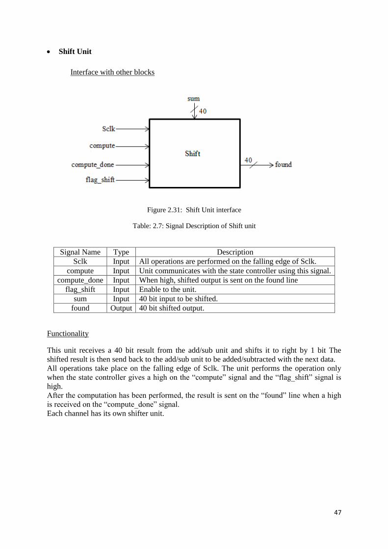
Shift Unit
Interface with other blocks
Figure 2.31: Shift Unit interface
Table: 2.7: Signal Description of Shift unit
Signal Name Type Description
Sclk Input All operations are performed on the falling edge of Sclk.
compute Input Unit communicates with the state controller using this signal.
compute_done Input When high, shifted output is sent on the found line
flag_shift Input Enable to the unit.
sum Input 40 bit input to be shifted.
found Output 40 bit shifted output.
Functionality
This unit receives a 40 bit result from the add/sub unit and shifts it to right by 1 bit The
shifted result is then send back to the add/sub unit to be added/subtracted with the next data.
All operations take place on the falling edge of Sclk. The unit performs the operation only
when the state controller gives a high on the “compute” signal and the “flag_shift” signal is
high.
After the computation has been performed, the result is sent on the “found” line when a high
is received on the “compute_done” signal.
Each channel has its own shifter unit.
48
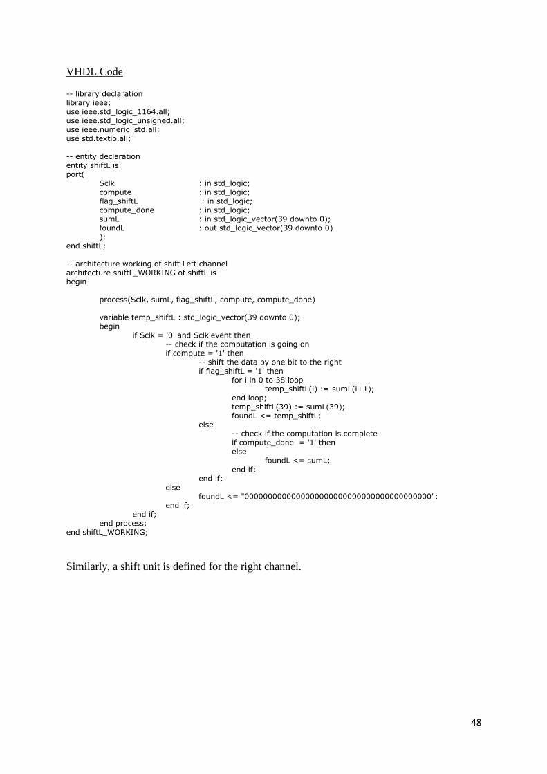
VHDL Code
-- library declaration library ieee; use ieee.std_logic_1164.all; use ieee.std_logic_unsigned.all; use ieee.numeric_std.all; use std.textio.all; -- entity declaration entity shiftL is port( Sclk : in std_logic; compute : in std_logic; flag_shiftL : in std_logic; compute_done : in std_logic; sumL : in std_logic_vector(39 downto 0); foundL : out std_logic_vector(39 downto 0) ); end shiftL; -- architecture working of shift Left channel architecture shiftL_WORKING of shiftL is begin process(Sclk, sumL, flag_shiftL, compute, compute_done) variable temp_shiftL : std_logic_vector(39 downto 0); begin if Sclk = '0' and Sclk'event then -- check if the computation is going on if compute = '1' then -- shift the data by one bit to the right if flag_shiftL = '1' then for i in 0 to 38 loop temp_shiftL(i) := sumL(i+1); end loop; temp_shiftL(39) := sumL(39); foundL <= temp_shiftL; else -- check if the computation is complete if compute_done = '1' then else foundL <= sumL;
end if; end if; else foundL <= "0000000000000000000000000000000000000000"; end if; end if; end process; end shiftL_WORKING;
Similarly, a shift unit is defined for the right channel.
49
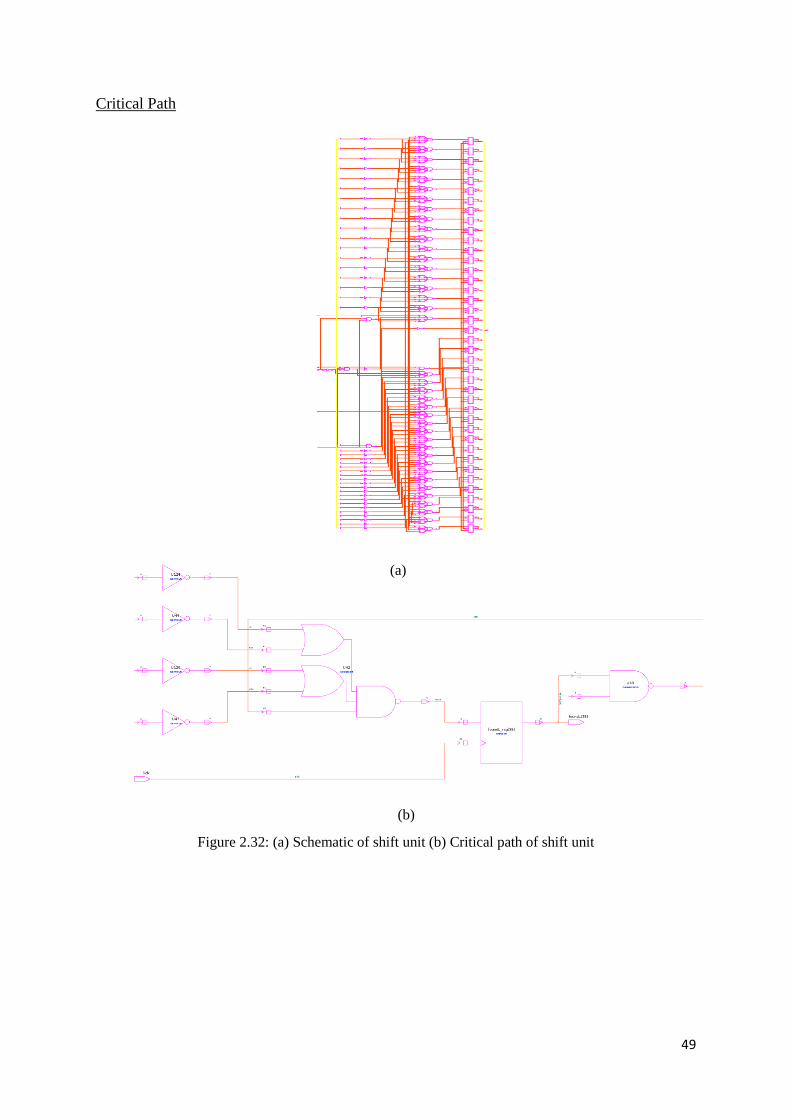
Critical Path
Figure 2.32: (a) Schematic of shift unit (b) Critical path of shift unit
(a)
(b)
50
Testing
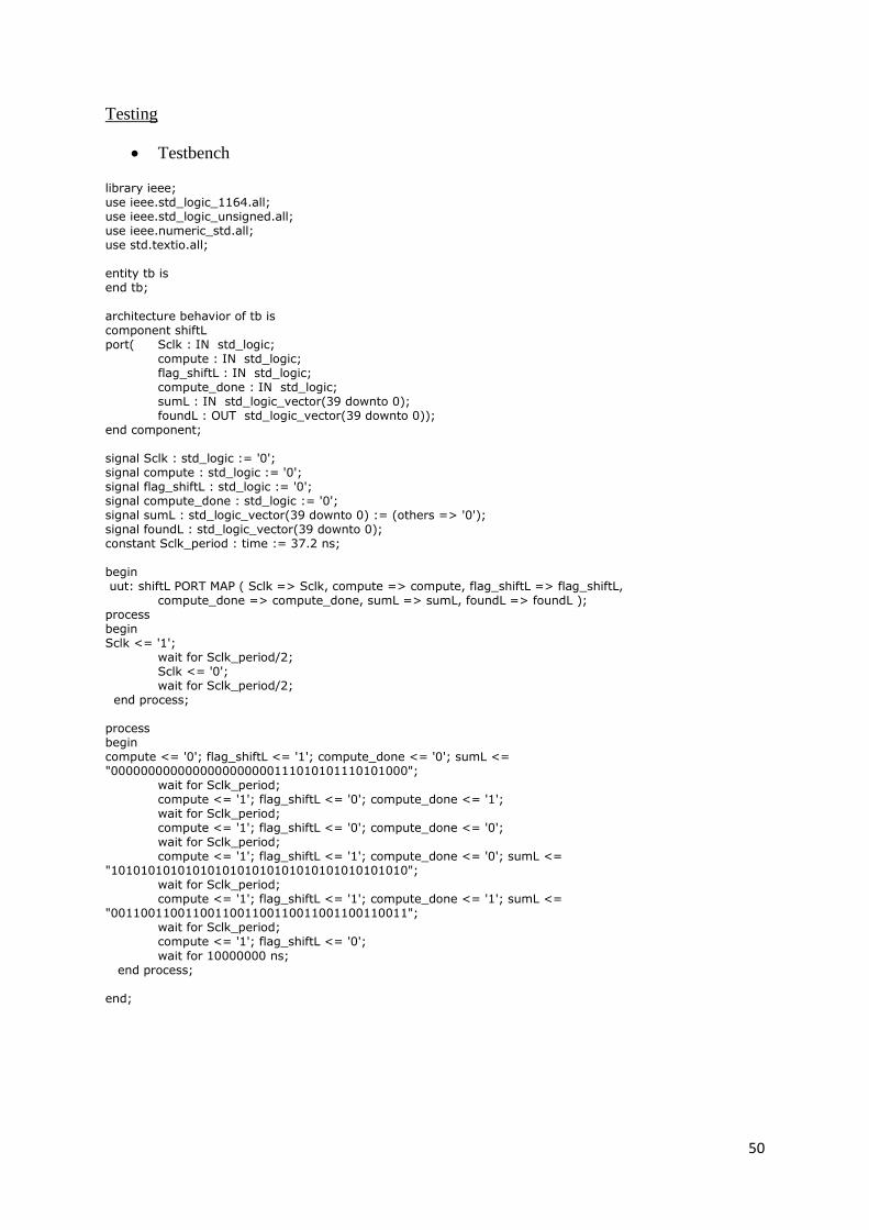
Testbench
library ieee; use ieee.std_logic_1164.all; use ieee.std_logic_unsigned.all; use ieee.numeric_std.all; use std.textio.all; entity tb is end tb;
architecture behavior of tb is component shiftL port( Sclk : IN std_logic; compute : IN std_logic; flag_shiftL : IN std_logic; compute_done : IN std_logic; sumL : IN std_logic_vector(39 downto 0); foundL : OUT std_logic_vector(39 downto 0)); end component; signal Sclk : std_logic := '0'; signal compute : std_logic := '0'; signal flag_shiftL : std_logic := '0'; signal compute_done : std_logic := '0'; signal sumL : std_logic_vector(39 downto 0) := (others => '0'); signal foundL : std_logic_vector(39 downto 0); constant Sclk_period : time := 37.2 ns; begin uut: shiftL PORT MAP ( Sclk => Sclk, compute => compute, flag_shiftL => flag_shiftL, compute_done => compute_done, sumL => sumL, foundL => foundL ); process begin Sclk <= '1'; wait for Sclk_period/2; Sclk <= '0'; wait for Sclk_period/2; end process; process begin compute <= '0'; flag_shiftL <= '1'; compute_done <= '0'; sumL <= "0000000000000000000000111010101110101000"; wait for Sclk_period; compute <= '1'; flag_shiftL <= '0'; compute_done <= '1'; wait for Sclk_period; compute <= '1'; flag_shiftL <= '0'; compute_done <= '0'; wait for Sclk_period; compute <= '1'; flag_shiftL <= '1'; compute_done <= '0'; sumL <= "1010101010101010101010101010101010101010"; wait for Sclk_period; compute <= '1'; flag_shiftL <= '1'; compute_done <= '1'; sumL <= "0011001100110011001100110011001100110011"; wait for Sclk_period; compute <= '1'; flag_shiftL <= '0';
wait for 10000000 ns; end process; end;
51
Simulation Results
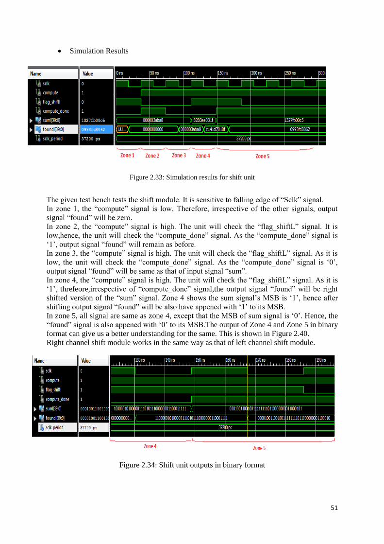
Figure 2.33: Simulation results for shift unit
The given test bench tests the shift module. It is sensitive to falling edge of “Sclk” signal.
In zone 1, the “compute” signal is low. Therefore, irrespective of the other signals, output
signal “found” will be zero.
In zone 2, the “compute” signal is high. The unit will check the “flag_shiftL” signal. It is
low,hence, the unit will check the “compute_done” signal. As the “compute_done” signal is
‘1’, output signal “found” will remain as before.
In zone 3, the “compute” signal is high. The unit will check the “flag_shiftL” signal. As it is
low, the unit will check the “compute_done” signal. As the “compute_done” signal is ‘0’,
output signal “found” will be same as that of input signal “sum”.
In zone 4, the “compute” signal is high. The unit will check the “flag_shiftL” signal. As it is
‘1’, threfeore,irrespective of “compute_done” signal,the output signal “found” will be right
shifted version of the “sum” signal. Zone 4 shows the sum signal’s MSB is ‘1’, hence after
shifting output signal “found” will be also have appened with ‘1’ to its MSB.
In zone 5, all signal are same as zone 4, except that the MSB of sum signal is ‘0’. Hence, the
“found” signal is also appened with ‘0’ to its MSB.The output of Zone 4 and Zone 5 in binary
format can give us a better understanding for the same. This is shown in Figure 2.40.
Right channel shift module works in the same way as that of left channel shift module.
Figure 2.34: Shift unit outputs in binary format
52
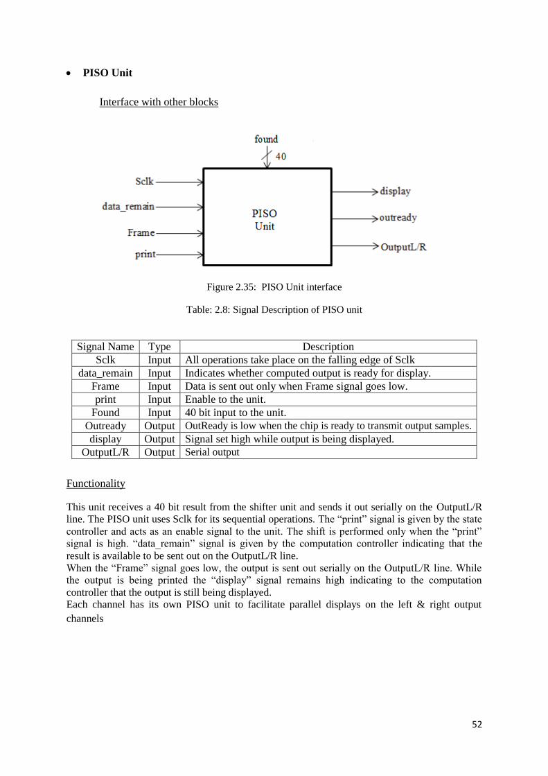
PISO Unit
Interface with other blocks
Figure 2.35: PISO Unit interface
Table: 2.8: Signal Description of PISO unit
Signal Name Type Description
Sclk Input All operations take place on the falling edge of Sclk
data_remain Input Indicates whether computed output is ready for display.
Frame Input Data is sent out only when Frame signal goes low.
print Input Enable to the unit.
Found Input 40 bit input to the unit.
Outready Output OutReady is low when the chip is ready to transmit output samples.
display Output Signal set high while output is being displayed.
OutputL/R Output Serial output
Functionality
This unit receives a 40 bit result from the shifter unit and sends it out serially on the OutputL/R
line. The PISO unit uses Sclk for its sequential operations. The “print” signal is given by the state
controller and acts as an enable signal to the unit. The shift is performed only when the “print”
signal is high. “data_remain” signal is given by the computation controller indicating that the
result is available to be sent out on the OutputL/R line.
When the “Frame” signal goes low, the output is sent out serially on the OutputL/R line. While
the output is being printed the “display” signal remains high indicating to the computation
controller that the output is still being displayed. Each channel has its own PISO unit to facilitate parallel displays on the left & right output
channels
53
VHDL Code
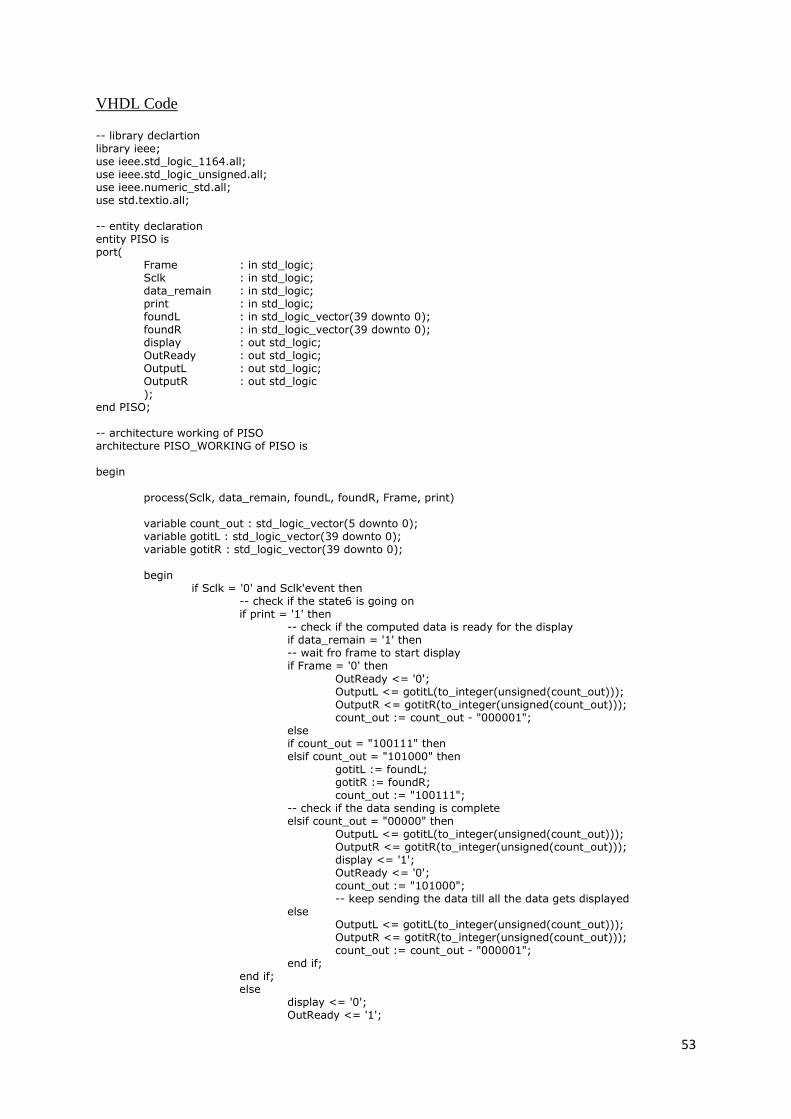
-- library declartion library ieee; use ieee.std_logic_1164.all; use ieee.std_logic_unsigned.all; use ieee.numeric_std.all; use std.textio.all;
-- entity declaration entity PISO is port( Frame : in std_logic; Sclk : in std_logic; data_remain : in std_logic; print : in std_logic; foundL : in std_logic_vector(39 downto 0); foundR : in std_logic_vector(39 downto 0); display : out std_logic; OutReady : out std_logic; OutputL : out std_logic; OutputR : out std_logic ); end PISO; -- architecture working of PISO architecture PISO_WORKING of PISO is begin process(Sclk, data_remain, foundL, foundR, Frame, print) variable count_out : std_logic_vector(5 downto 0); variable gotitL : std_logic_vector(39 downto 0); variable gotitR : std_logic_vector(39 downto 0); begin if Sclk = '0' and Sclk'event then -- check if the state6 is going on if print = '1' then -- check if the computed data is ready for the display if data_remain = '1' then -- wait fro frame to start display if Frame = '0' then
OutReady <= '0'; OutputL <= gotitL(to_integer(unsigned(count_out))); OutputR <= gotitR(to_integer(unsigned(count_out))); count_out := count_out - "000001"; else if count_out = "100111" then elsif count_out = "101000" then gotitL := foundL; gotitR := foundR; count_out := "100111"; -- check if the data sending is complete elsif count_out = "00000" then OutputL <= gotitL(to_integer(unsigned(count_out))); OutputR <= gotitR(to_integer(unsigned(count_out))); display <= '1'; OutReady <= '0'; count_out := "101000"; -- keep sending the data till all the data gets displayed else OutputL <= gotitL(to_integer(unsigned(count_out))); OutputR <= gotitR(to_integer(unsigned(count_out))); count_out := count_out - "000001"; end if; end if; else display <= '0'; OutReady <= '1';
54
OutputL <= '0'; OutputR <= '0'; count_out := "101000"; end if; else OutReady <= '1'; end if; end if; end process; end PISO_WORKING;
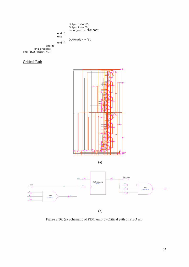
Critical Path
Figure 2.36: (a) Schematic of PISO unit (b) Critical path of PISO unit
(a)
(b)
55
Testing
Testbench
library ieee; use ieee.std_logic_1164.all; use ieee.std_logic_unsigned.all; use ieee.numeric_std.all; use std.textio.all; entity tb is end tb;
architecture behavior of tb is component PISO port( Frame : IN std_logic; Sclk : IN std_logic; data_remain : IN std_logic; print : IN std_logic; foundL : IN std_logic_vector(39 downto 0); foundR : IN std_logic_vector(39 downto 0); display : OUT std_logic; OutReady : OUT std_logic; OutputL : OUT std_logic; OutputR : OUT std_logic); end component; signal Frame : std_logic := '0'; signal Sclk : std_logic := '0'; signal data_remain : std_logic := '0'; signal print : std_logic := '0'; signal foundL : std_logic_vector(39 downto 0) := (others => '0'); signal foundR : std_logic_vector(39 downto 0) := (others => '0'); signal display : std_logic; signal OutReady : std_logic; signal OutputL : std_logic; signal OutputR : std_logic; constant Sclk_period : time := 37.2 ns; begin uut: PISO PORT MAP ( Frame => Frame, Sclk => Sclk, data_remain => data_remain, print => print, foundL => foundL, foundR => foundR, display => display, OutReady => OutReady, OutputL => OutputL, OutputR => OutputR ); process begin Sclk <= '0'; wait for Sclk_period/2; Sclk <= '1'; wait for Sclk_period/2; end process; process begin Frame <= '1'; wait for Sclk_period*6; Frame <= '0'; wait for 1302 ns; Frame <= '1'; wait for 1000000000 ns;
end process; process begin print <= '0'; foundL <= "1100111000111100001111100000110011100011"; foundR <= "1000001000000100000000100011110000000011"; wait for Sclk_period*2; print <= '1'; data_remain <= '0'; wait for Sclk_period*2; print <= '1'; data_remain <= '1'; wait for Sclk_period*2; print <= '1'; data_remain <= '1'; wait for 1000000 ns; end process; end;
56
Simulation Results
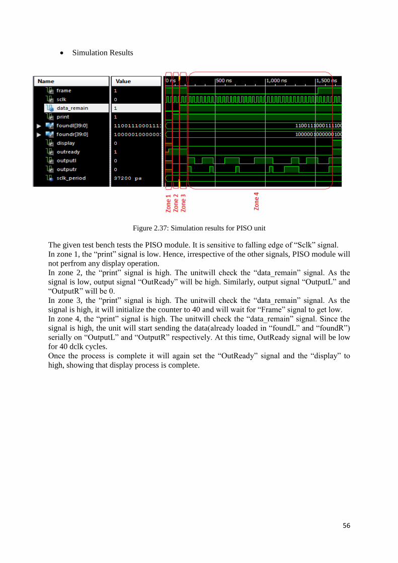
Figure 2.37: Simulation results for PISO unit
The given test bench tests the PISO module. It is sensitive to falling edge of “Sclk” signal.
In zone 1, the “print” signal is low. Hence, irrespective of the other signals, PISO module will
not perfrom any display operation.
In zone 2, the “print” signal is high. The unitwill check the “data_remain” signal. As the
signal is low, output signal “OutReady” will be high. Similarly, output signal “OutputL” and
“OutputR” will be 0.
In zone 3, the “print” signal is high. The unitwill check the “data_remain” signal. As the
signal is high, it will initialize the counter to 40 and will wait for “Frame” signal to get low.
In zone 4, the “print” signal is high. The unitwill check the “data_remain” signal. Since the
signal is high, the unit will start sending the data(already loaded in “foundL” and “foundR”)
serially on “OutputL” and “OutputR” respectively. At this time, OutReady signal will be low
for 40 dclk cycles.
Once the process is complete it will again set the “OutReady” signal and the “display” to
high, showing that display process is complete.
57
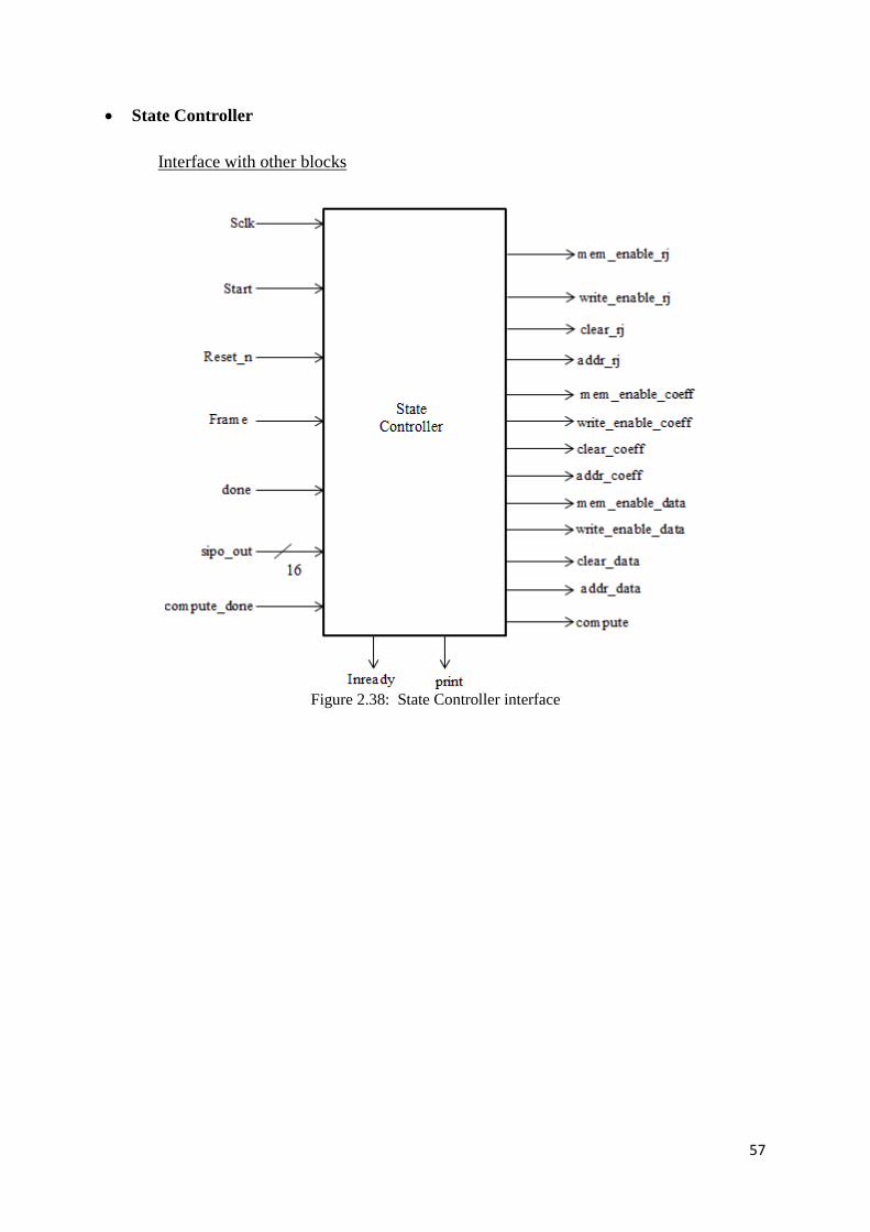
State Controller
Interface with other blocks
Figure 2.38: State Controller interface

58
Table: 2.9: Signal Description of state controller
Signal Name Type Description
Sclk Input System clock has a frequency of 26.88MHz. Forms the timing
reference for control signals and the output samples.
Start Input When Start is high, the chip initializes i.e. the state controller
enters state 0.
Reset_n Input When Reset_n is made low, the chip resets i.e. the state controller
state 7.
Frame Input Frame is set low for one Dclk cycle when the first bit of the input
sample or coefficients arrive, otherwise it is high.
done Input Signal from the SIPO unit indicating that the 16 bit data is
ready to be written into memory.
sipo_out Input 16 bit data to be written into the memory.
compute_done Input Signal from the computation controller indicating that the
computation is complete.
mem_enable_rj Output Enable to the rj memory.
write_enable_rj Output Write enable to the rj memory.
clear_rj Output Cleat to the rj memory.
addr_rj Output Write address to the rj memory.
mem_enable_coeff Output Enable to the coefficient memory.
write_enable_coeff Output Write enable to the coefficient memory.
clear_coeff Output Cleat to the coefficient memory.
addr_coeff Output Write address to the coefficient memory.
mem_enable_data Output Enable to the data memory.
write_enable_data Output Write enable to the data memory.
clear_data Output Cleat to the data memory.
addr_data Output Write address to the data memory.
compute Output Enable signal to the computation controller.
Functionality
The functionality of the state controller depicts the state diagram shown in Figure 2.3. The
operations performed in every stage are as follows:
State 0 (Initialization): When Start signal become high, the FSM enters state 0. In state zero
all the outputs of the block and the internal signals are initialized. Also all the memories are
cleared in this state. The FSM moves to state 1 when Start signal becomes low.
State 1 (waiting to receive rj): When the FSM enters state 1, InReady becomes high. Clear
signals to the memories are made low. If a low is received on the Frame signal, the state
changes to state 2 otherwise the FSM waits in this state till the Frame is received.
State 2 (reading rj):When the FSM enters state 2, InReady remains high. If the state
controller has received a high on the “done” signal (from the SIPO unit), it indicates that the
16 bit data is ready to be written into the rj memory. At this time the state controller makes
the memory_enable_rj and the write_enable_rj high. Address is provided on the addr_rj line
and the received 16 bit data is written into the rj memory. The done2 signal is now made
59
high; indicating to the SIPO unit that the data has been written into memory and it is free to
take in the new data.
Once all the rj values have been written into memory, the FSM moves to state 3.
State 3 (waiting to receive coefficients):In state 3, InReady remains high and the rj
memories are disabled. If a low is received on the Frame signal, the state changes to state 4
otherwise the FSM waits in this state till the Frame is received.
State 4 (reading coefficients):In state 3, InReady remains high.If the state controller has
received a high on the “done” signal (from the SIPO unit), it indicates that the 16 bit data is
ready to be written into the coefficient memory. At this time the state controller makes the
memory_enable_coeff and the write_enable_coeff high. Address is provided on the
addr_coeff line and the received 16 bit data is written into the coefficient memory. The done2
signal is now made high; indicating to the SIPO unit that the data has been written into
memory and it is free to take in the new data.
Once all the coefficient values have been written into memory, the FSM moves to state 5.
State 5 (waiting to receive data):In state 5, InReady remains high and the rj, coefficient and
data memories are enabled. If a low is received on the Frame signal, the state changes to state
6 otherwise the FSM waits in this state till the Frame is received. Also if the Reset_n signal
becomes low in this state, the InReady signal goes low and the FSM transitions to state 7.
State 6 (working):The InReady signal remains high. The rj and coefficient memories are
enabled so that data can be read from them when required. In state 6, the following operations
are performed:
a) Writing into data memory:When the state controller receives a high on the “done” signal
(from the SIPO unit), it indicates that the 16 bit data is ready to be written into the data
memory. At this time the state controller makes the memory_enable_data and the
write_enable_data high. Address is provided on the addr_data line and the received 16 bit
data is written into the data memory. The done2 signal is now made high; indicating to the
SIPO unit that the data has been written into memory and it is free to take in the new data.
The “compute” signal is made high so that the computation controller can start its
computations as soon as the data arrives.
b) Checking for zero inputs:Before writing the data it is checked if the data received on both
the right & left channels is zero. If it is zero, then a counter “count_zero_detect” is
incremented. When the “count_zero_detect” counter reached 800, it implies that 800
consecutive zeros have appeared on both the channels. The FSM then moves to state 8 and
waits for the next non-zero value to appear on the InputL/R lines. The write_enable_data is
made low at this time.
60
If the Reset_n signal becomes low in this state, the InReady signal goes low and the FSM
transitions to state 7. Also the “print” signal is high while in this state to facilitate the
simultaneous display of the outputs.
State 7(clearing):In this state InReady becomes low. The “count_zero_detector” is reset and
the data memory a cleared by making the “clear_data” signal high. The FSM remains in this
state as long as the Reset_n is low. When the Reset_n becomes high, the InReady signal is
made high and the FSM transitions to state 6.
State 8 (sleeping):In this state InReady is high. The controller keeps checking the data
coming from the SIPO unit waiting for a non-zero input. As long as no non-zero value
appears the FSM remains in state 8 and the data memory is disabled. As soon as a non-zero
value appears, the data memory is enabled by making high the memory_enable_data and the
write_enable_data signals and the data is written into memory. The FSM transitions to state
6.
If the Reset_n signal becomes low in this state, the InReady signal goes low and the FSM
transitions to state 7.
VHDL Code
-- library declaration
library ieee; use ieee.std_logic_1164.all; use ieee.std_logic_unsigned.all; use ieee.numeric_std.all; use std.textio.all; -- entity declration entity state_FSM is port( Sclk : in std_logic; Start : in std_logic; Reset_n : in std_logic; done : in std_logic; compute_done : in std_logic; Frame : in std_logic; sipo_outL : in std_logic_vector(15 downto 0); sipo_outR : in std_logic_vector(15 downto 0); compute : out std_logic; InReady : out std_logic; done2 : out std_logic; mem_enable_rjL : out std_logic; mem_enable_rjR : out std_logic; mem_enable_coeffL : out std_logic; mem_enable_coeffR : out std_logic; mem_enable_dataL : out std_logic; mem_enable_dataR : out std_logic; wr_enable_rjL : out std_logic; wr_enable_rjR : out std_logic; wr_enable_coeffL : out std_logic; wr_enable_coeffR : out std_logic; wr_enable_dataL : out std_logic; wr_enable_dataR : out std_logic; clear_rjL : out std_logic; clear_rjR : out std_logic; print : out std_logic; clear_coeffL : out std_logic; clear_coeffR : out std_logic; clear_dataL : out std_logic; clear_dataR : out std_logic;
61
addr_rjL : out unsigned(3 downto 0); addr_rjR : out unsigned(3 downto 0); addr_coeffL : out unsigned(8 downto 0); addr_coeffR : out unsigned(8 downto 0); addr_dataL : out unsigned(7 downto 0); addr_dataR : out unsigned(7 downto 0) );
end state_FSM; architecture state_FSM_WORKING of state_FSM is type state_type is (State0, State1, State2, State3, State4, State5, State6, State7, State8); signal current_state: state_type; begin process(Sclk, current_state, Start, Frame, Reset_n) variable pc_rjL : std_logic_vector(4 downto 0) ; variable counterL : std_logic_vector(4 downto 0) ; variable pc_rjR : std_logic_vector(4 downto 0) ; variable pc_coeffL: std_logic_vector(9 downto 0); variable pc_coeffR: std_logic_vector(9 downto 0); variable pc_dataL: std_logic_vector(8 downto 0);
variable pc_dataR: std_logic_vector(8 downto 0); variable count_800 : std_logic; variable count_zero_detector : std_logic_vector(9 downto 0); begin if Start = '1' then current_state <= State0; end if; if Sclk = '0' and Sclk'event then case current_state is when State0 => --if Start = '1' then mem_enable_rjL <= '1'; mem_enable_rjR <= '1'; mem_enable_coeffL <= '1'; mem_enable_coeffR <= '1'; mem_enable_dataL <= '1'; mem_enable_dataR <= '1'; wr_enable_coeffL <= '0'; wr_enable_coeffR <= '0'; wr_enable_rjL <= '0'; wr_enable_rjR <= '0'; wr_enable_dataL <= '0'; wr_enable_dataR <= '0'; clear_rjL <= '1'; clear_rjR <= '1'; clear_coeffL <= '1'; clear_coeffR <= '1'; clear_dataL <= '1'; clear_dataR <= '1'; counterL := "00000"; pc_rjL := "00000"; pc_rjR := "00000"; done2 <= '0'; addr_rjL <= unsigned(pc_rjL(3 downto 0)); addr_rjR <= unsigned(pc_rjL(3 downto 0)); pc_coeffL := "0000000000"; pc_coeffR := "0000000000"; addr_coeffL <= unsigned(pc_coeffL(8 downto 0)); addr_coeffR <= unsigned(pc_coeffL(8 downto 0)); pc_dataL := "000000000"; pc_dataR := "000000000"; addr_dataL <= unsigned(pc_dataL(7 downto 0));
addr_dataR <= unsigned(pc_dataL(7 downto 0)); current_state <= State1; --else
62
--mem_enable_rjL <= '1'; --mem_enable_rjR <= '1'; --mem_enable_coeffL <= '1'; --mem_enable_coeffR <= '1'; --mem_enable_dataL <= '1'; --mem_enable_dataR <= '1'; --clear_rjL <= '1'; --clear_rjR <= '1'; --clear_coeffL <= '1'; --clear_coeffR <= '1'; --clear_dataL <= '1'; --clear_dataR <= '1'; --pc_rjL := "00000"; --pc_rjR := "00000"; --addr_rjL <= unsigned(pc_rjL(3 downto 0)); --addr_rjR <= unsigned(pc_rjR(3 downto 0)); --pc_coeffL := "0000000000"; --pc_coeffR := "0000000000"; --addr_coeffL <= unsigned(pc_coeffL(8 downto 0)); --addr_coeffR <= unsigned(pc_coeffR(8 downto 0)); --pc_dataL := "000000000"; --pc_dataR := "000000000";
--addr_dataL <= unsigned(pc_coeffL(7 downto 0)); --addr_dataR <= unsigned(pc_coeffR(7 downto 0)); --current_state <= State0; --end if; when State1 => InReady <= '1'; clear_rjL <= '0'; clear_rjR <= '0'; done2 <= '0'; clear_coeffL <= '0'; clear_coeffR <= '0'; clear_dataL <= '0'; clear_dataR <= '0'; if Frame = '0' then current_state <= State2; else current_state <= State1; end if; When State2 => InReady <= '1'; if done = '1' then addr_rjL <= unsigned(pc_rjL(3 downto 0)); addr_rjR <= unsigned(pc_rjL(3 downto 0)); mem_enable_rjL <= '1'; mem_enable_rjR <= '1'; wr_enable_rjL <= '1'; wr_enable_rjR <= '1'; pc_rjL := pc_rjL + "00001"; pc_rjR := pc_rjR + "00001"; done2 <= '1'; else pc_rjL := pc_rjL; pc_rjR := pc_rjR; mem_enable_rjL <= '0'; mem_enable_rjR <= '0'; wr_enable_rjL <= '1'; wr_enable_rjR <= '1'; done2 <= '0'; end if; if pc_rjL = "10000" then pc_rjL := "00000"; pc_rjR := "00000"; current_state <= State3;
else pc_rjL := pc_rjL;
63
pc_rjR := pc_rjR; current_state <= State2; end if; when State3 => InReady <= '1'; mem_enable_rjL <= '0'; mem_enable_rjR <= '0'; wr_enable_rjL <= '0'; wr_enable_rjR <= '0'; if Frame = '0' then current_state <= State4; else current_state <= State3; end if; when State4 => InReady <= '1'; if done = '1' then addr_coeffL <= unsigned(pc_coeffL(8 downto 0)); addr_coeffR <= unsigned(pc_coeffL(8 downto 0)); mem_enable_coeffL <= '1';
mem_enable_coeffR <= '1'; wr_enable_coeffL <= '1'; wr_enable_coeffR <= '1'; pc_coeffL := pc_coeffL + "0000000001"; pc_coeffR := pc_coeffR + "0000000001"; done2 <= '1'; else pc_coeffL := pc_coeffL; pc_coeffR := pc_coeffR; mem_enable_coeffL <= '0'; mem_enable_coeffR <= '0'; wr_enable_coeffL <= '1'; wr_enable_coeffR <= '1'; done2 <= '0'; end if; if pc_coeffL = "1000000000" then pc_coeffL := "0000000000"; pc_coeffR := "0000000000"; current_state <= State5; else pc_coeffL := pc_coeffL; pc_coeffR := pc_coeffR; current_state <= State4; end if; When State5 => print <= '0'; InReady <= '1'; clear_dataL <= '0'; clear_dataR <= '0'; mem_enable_dataL <= '1'; mem_enable_dataR <= '1'; mem_enable_coeffL <= '1'; mem_enable_coeffR <= '1'; mem_enable_rjL <= '1'; mem_enable_rjR <= '1'; wr_enable_coeffL <= '0'; wr_enable_coeffR <= '0'; if Frame = '0' then current_state <= State6; elsif Reset_n = '0' then InReady <= '0';
current_state <= State7; else current_state <= State5;
64
end if; When State6 => print <= '1'; InReady <= '1'; mem_enable_rjL <= '1'; mem_enable_rjR <= '1'; mem_enable_coeffL <= '1'; mem_enable_coeffR <= '1'; if compute_done = '1' then compute <= '0'; end if; if done = '1' then if (sipo_outL = "0000000000000000" and sipo_outR = "0000000000000000" ) then count_zero_detector := count_zero_detector + "0000000001"; else count_zero_detector := "0000000000"; end if; if count_zero_detector > "1100011111" then count_zero_detector := count_zero_detector - "0000000001"; count_800 := '1'; else count_800 := '0';
end if; if count_800 = '0' then addr_dataL <= unsigned(pc_dataL(7 downto 0)); addr_dataR <= unsigned(pc_dataR(7 downto 0)); mem_enable_dataL <= '1'; mem_enable_dataR <= '1'; wr_enable_dataL <= '1'; wr_enable_dataR <= '1'; pc_dataL := pc_dataL + "000000001"; pc_dataR := pc_dataR + "000000001"; done2 <= '1'; compute <= '1'; if (pc_dataL = "100000000" and pc_dataR = "100000000") then pc_dataL := "011111111"; pc_dataR := "011111111"; else end if; current_state <= State6; else done2 <= '1'; compute <= '0'; current_state <= State8; end if; else mem_enable_dataL <= '1'; mem_enable_dataR <= '1'; wr_enable_dataL <= '0'; wr_enable_dataR <= '0'; done2 <= '0'; current_state <= State6; end if; if Reset_n = '0' then InReady <= '0'; current_state <= State7; end if; When State7 => print <= '0'; compute <= '0'; InReady <= '0'; count_zero_detector := "0000000000"; if Reset_n = '0' then pc_rjL := "00000"; pc_rjR := "00000"; pc_coeffL := "0000000000";
pc_coeffR := "0000000000"; mem_enable_dataL <= '1'; mem_enable_dataR <= '1';
65
clear_dataL <= '1'; clear_dataR <= '1'; wr_enable_dataL <= '0'; wr_enable_dataR <= '0'; addr_rjL <= unsigned(pc_rjL(3 downto 0)); addr_rjR <= unsigned(pc_rjR(3 downto 0)); addr_coeffL <= unsigned(pc_coeffL(8 downto 0)); addr_coeffR <= unsigned(pc_coeffR(8 downto 0)); current_state <= State7; elsif Reset_n = '1' then InReady <= '1'; current_state <= State5; end if; When State8 => print <= '0'; InReady <= '1'; count_zero_detector := "0000000000"; if done = '1' then if (sipo_outL = "0000000000000000" and sipo_outR = "0000000000000000" ) then count_800 := '1'; else count_800 := '0';
end if; done2 <= '1'; else done2 <= '0'; end if; if count_800 = '1' then mem_enable_dataL <= '0'; mem_enable_dataR <= '0'; wr_enable_dataL <= '0'; wr_enable_dataR <= '0'; compute <= '0'; current_state <= State8; else addr_dataL <= unsigned(pc_dataL(7 downto 0)); addr_dataR <= unsigned(pc_dataR(7 downto 0)); mem_enable_dataL <= '1'; mem_enable_dataR <= '1'; wr_enable_dataL <= '1'; wr_enable_dataR <= '1'; pc_dataL := pc_dataL + "000000001"; pc_dataR := pc_dataR + "000000001"; compute <= '1'; if (pc_dataL = "100000000" and pc_dataR = "100000000") then pc_dataL := "011111111"; pc_dataR := "011111111"; else end if; current_state <= State6; end if; if Reset_n = '0' then InReady <= '0'; current_state <= State7; end if; end case; end if; end process; end state_FSM_WORKING;
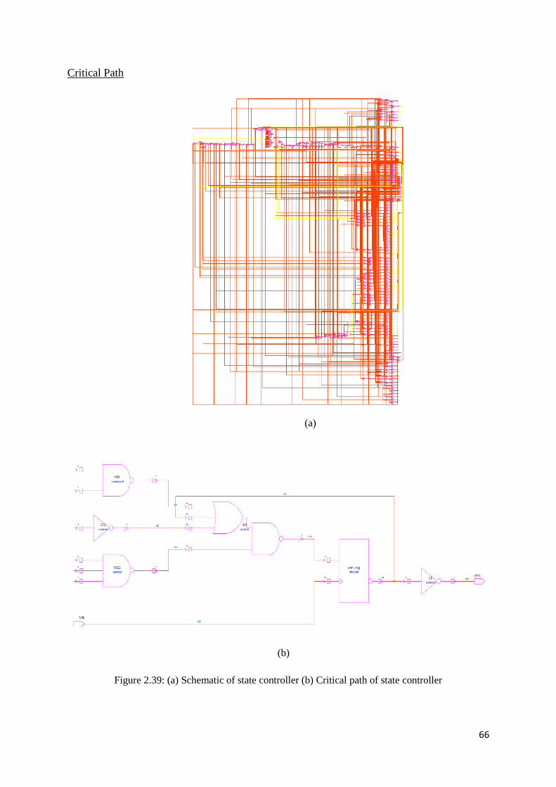
66
Critical Path
Figure 2.39: (a) Schematic of state controller (b) Critical path of state controller
(b)
(a)
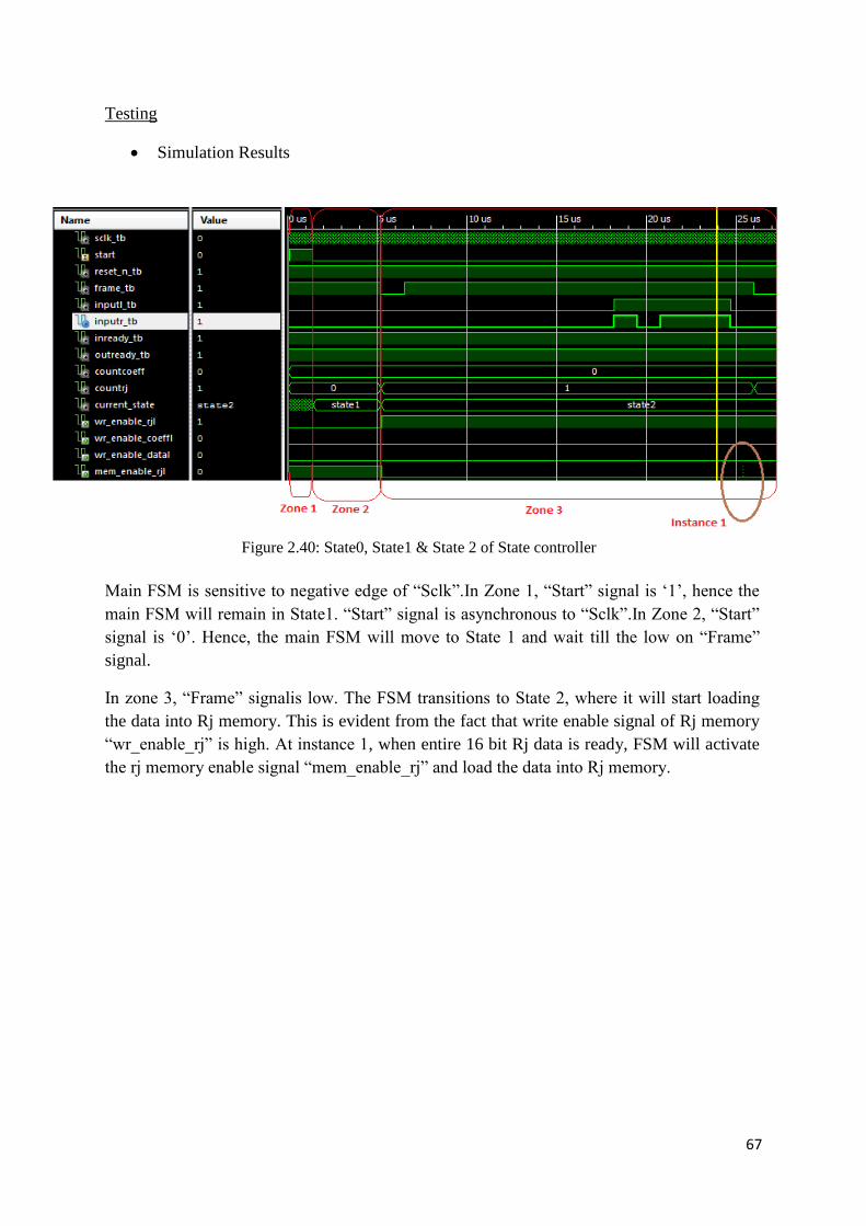
67
Testing
Simulation Results
Figure 2.40: State0, State1 & State 2 of State controller
Main FSM is sensitive to negative edge of “Sclk”.In Zone 1, “Start” signal is ‘1’, hence the
main FSM will remain in State1. “Start” signal is asynchronous to “Sclk”.In Zone 2, “Start”
signal is ‘0’. Hence, the main FSM will move to State 1 and wait till the low on “Frame”
signal.
In zone 3, “Frame” signalis low. The FSM transitions to State 2, where it will start loading
the data into Rj memory. This is evident from the fact that write enable signal of Rj memory
“wr_enable_rj” is high. At instance 1, when entire 16 bit Rj data is ready, FSM will activate
the rj memory enable signal “mem_enable_rj” and load the data into Rj memory.
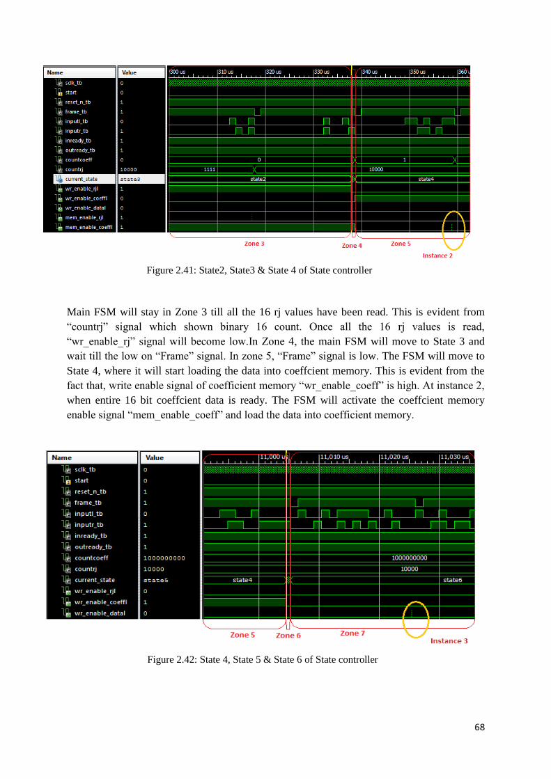
68
Figure 2.41: State2, State3 & State 4 of State controller
Main FSM will stay in Zone 3 till all the 16 rj values have been read. This is evident from
“countrj” signal which shown binary 16 count. Once all the 16 rj values is read,
“wr_enable_rj” signal will become low.In Zone 4, the main FSM will move to State 3 and
wait till the low on “Frame” signal. In zone 5, “Frame” signal is low. The FSM will move to
State 4, where it will start loading the data into coeffcient memory. This is evident from the
fact that, write enable signal of coefficient memory “wr_enable_coeff” is high. At instance 2,
when entire 16 bit coeffcient data is ready. The FSM will activate the coeffcient memory
enable signal “mem_enable_coeff” and load the data into coefficient memory.
Figure 2.42: State 4, State 5 & State 6 of State controller

69
Main FSM will stay in Zone 5 till all the 512 coeffcient values have been read. This is
evident from “countcoeff” signal which shown binary 512 count. Once all the 512 coefficient
values are read, “wr_enable_coeff” signal will become low. In Zone 6, the main FSM will
move to State 5 and wait till the low on “Frame” signal. In zone 7, Low on “Frame” signal is
detected. The FSM will move to State 6, where it will start loading the data into data
memory. This is evident from the fact that, write enable signal of data memory
“wr_enable_data” is high. At instance 3, when entire 16 bit data value is ready, FSM will
activate the data memory enable signal “mem_enable_data” and load the values into data
memory. This will happen when main FSM will receive the “done” signal high from SIPO
unit.
Figure 2.43: State 6 & State 8 of State controller
In Zone 7, main FSM will keep reading the data and activate computation FSM whenever
data is read by making “compute” signal high. “print” signal is high only in State 6 showing
that the PISO unit can only work when main FSM is in State 6. Main FSM will move to
State 8 i.e in Zone 6 above, when it receives 800 zeros in both left and right channel. Any
non- zero input value on any of the channels will again move the main FSM into State6. In
above diagram it is zone 9.

70
Figure 2.44: State 5, State 6 & State 7 of State controller
In Zone 10, the main FSM is in State 6. A low on “Reset_n” will move the FSM into State 7.
In Zone 11, clearing of data memoryand initialization of all the temporary variables will take
place. Once the operation is done, FSM will move to State 5 i.e. Zone 12 In Zone 12, FSM
will wait till the low on “Frame” signal is detected. Till this point “print” signal is low
showing no display operation can take place.In Zone12, as the low on “Frame” signal is
detected, system will move to State 6 and normal computation and reading operation will
start.

71
Computation Controller
Figure2.45: Computation controller interface
Table: 2.10: Signal Description of Computation controller
Signal Name Type Description
Sclk Input All computations take place on the falling edge of Sclk.
Start Input Used to initialize the internal registers and signals
Reset_n Input Used to reset the computational controller
memout_rj Input 16 bit input data received from the rj memory
memout_coeff Input 16 bit input data received from the coefficient memory
memout_data Input 16 bit input data received from the data memory
compute Input Acts as an enable to the computation controller
display Input Input from the PISO unit indicating that output is begin sent
on the OutputL/R line.
read_addr_rj Output Read address given to the rj memory
read_addr_coeff Output Read address given to the coefficientmemory
read_addr_data Output Read address given to the datamemory
temp_data Output 16 bit input data sign extended and zero padded to form the
40 bit signal
data_remain Output Enable to the PISO unit
flag_shift Output Enable to the shift block
flag_rj Output Enable to the Add/Sub block
compute_done Output Communication signal to the state controller
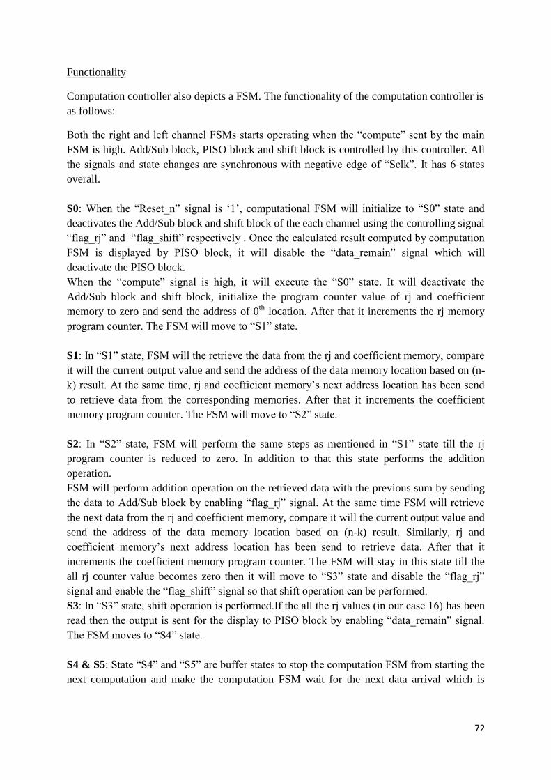
72
Functionality
Computation controller also depicts a FSM. The functionality of the computation controller is
as follows:
Both the right and left channel FSMs starts operating when the “compute” sent by the main
FSM is high. Add/Sub block, PISO block and shift block is controlled by this controller. All
the signals and state changes are synchronous with negative edge of “Sclk”. It has 6 states
overall.
S0: When the “Reset_n” signal is ‘1’, computational FSM will initialize to “S0” state and
deactivates the Add/Sub block and shift block of the each channel using the controlling signal
“flag_rj” and “flag_shift” respectively . Once the calculated result computed by computation
FSM is displayed by PISO block, it will disable the “data_remain” signal which will
deactivate the PISO block.
When the “compute” signal is high, it will execute the “S0” state. It will deactivate the
Add/Sub block and shift block, initialize the program counter value of rj and coefficient
memory to zero and send the address of 0th
location. After that it increments the rj memory
program counter. The FSM will move to “S1” state.
S1: In “S1” state, FSM will the retrieve the data from the rj and coefficient memory, compare
it will the current output value and send the address of the data memory location based on (n-
k) result. At the same time, rj and coefficient memory’s next address location has been send
to retrieve data from the corresponding memories. After that it increments the coefficient
memory program counter. The FSM will move to “S2” state.
S2: In “S2” state, FSM will perform the same steps as mentioned in “S1” state till the rj
program counter is reduced to zero. In addition to that this state performs the addition
operation.
FSM will perform addition operation on the retrieved data with the previous sum by sending
the data to Add/Sub block by enabling “flag_rj” signal. At the same time FSM will retrieve
the next data from the rj and coefficient memory, compare it will the current output value and
send the address of the data memory location based on (n-k) result. Similarly, rj and
coefficient memory’s next address location has been send to retrieve data. After that it
increments the coefficient memory program counter. The FSM will stay in this state till the
all rj counter value becomes zero then it will move to “S3” state and disable the “flag_rj”
signal and enable the “flag_shift” signal so that shift operation can be performed.
S3: In “S3” state, shift operation is performed.If the all the rj values (in our case 16) has been
read then the output is sent for the display to PISO block by enabling “data_remain” signal.
The FSM moves to “S4” state.
S4 & S5: State “S4” and “S5” are buffer states to stop the computation FSM from starting the
next computation and make the computation FSM wait for the next data arrival which is
73
denoted by high value of “compute” signal. As soon as “compute” signal is high,
computation FSM will move to “S0” and starts new computation.
VHDL Code
library ieee; use ieee.std_logic_1164.all; use ieee.std_logic_unsigned.all; use ieee.numeric_std.all; use std.textio.all; entity compL_FSM is port( Sclk : in std_logic; Start : in std_logic; display : in std_logic; Reset_n : in std_logic; compute : in std_logic; memout_rjL : in std_logic_vector(15 downto 0); memout_coeffL : in std_logic_vector(15 downto 0); memout_dataL : in std_logic_vector(15 downto 0); refresh : out std_logic; compute_done : out std_logic; data_remain : out std_logic; coeff_signL : out std_logic;
flag_rjL : out std_logic; flag_shiftL : out std_logic; read_addr_rjL : out unsigned(3 downto 0); read_addr_coeffL : out unsigned(8 downto 0); read_addr_dataL : out unsigned(7 downto 0); temp_dataL : out std_logic_vector(39 downto 0) ); end compL_FSM; architecture compL_FSM_WORKING of compL_FSM is type state_typeL is (S0L, S1L, S2L, S3L, S4L, S5L); signal comp_stateL: state_typeL; begin process(display, Sclk, Reset_n, memout_rjL, memout_coeffL, memout_dataL , compute) variable pc_comp_rjL : std_logic_vector(4 downto 0); variable pc_comp_coeffL : std_logic_vector(9 downto 0); variable pc_comp_dataL : std_logic_vector(7 downto 0); variable nL : std_logic_vector(8 downto 0); variable meminput_aluL : std_logic_vector(39 downto 0); variable temp_memout_rjL : std_logic_vector(15 downto 0); variable temp_memout_coeffL : std_logic_vector(15 downto 0); begin if Sclk = '0' and Sclk'event then if Start = '1' then nL := "000000000"; end if; if display = '1' then data_remain <= '0'; end if; if Reset_n = '0' then comp_stateL <= S0L; flag_rjL <= '1'; flag_shiftL <= '0'; end if; if compute = '1' then case comp_stateL is When S0L => refresh <= '0';
74
flag_rjL <= '1'; flag_shiftL <= '0'; pc_comp_coeffL := "0000000000"; pc_comp_rjL := "00000"; read_addr_coeffL <= unsigned(pc_comp_coeffL(8 downto 0)) pc_comp_coeffL := pc_comp_coeffL + "0000000001"; read_addr_rjL <= unsigned(pc_comp_rjL(3 downto 0)); comp_stateL <= S1L; When S1L => flag_rjL <= '1'; flag_shiftL <= '0'; temp_memout_rjL := memout_rjL; temp_memout_coeffL := memout_coeffL;
if ((to_integer(unsigned(nL(7 downto 0)))) - (to_integer(unsigned(temp_memout_coeffL(7 downto 0))))) >= 0 then
read_addr_dataL <= unsigned(nL(7 downto 0) - temp_memout_coeffL(7 downto 0)); else end if; read_addr_coeffL <= unsigned(pc_comp_coeffL(8 downto 0)); pc_comp_coeffL := pc_comp_coeffL + "0000000001"; comp_stateL <= S2L;
When S2L => if temp_memout_rjL = "00000" then flag_rjL <= '1'; flag_shiftL <= '1'; pc_comp_rjL := pc_comp_rjL + "00001"; read_addr_rjL <= unsigned(pc_comp_rjL(3 downto 0));
if ((to_integer(unsigned(nL(7 downto 0)))) - (to_integer(unsigned(temp_memout_coeffL(7 downto 0))))) >= 0 then
meminput_aluL(31 downto 16):= memout_dataL; meminput_aluL(15 downto 0) := "0000000000000000"; if memout_dataL(15) = '1' then meminput_aluL(39 downto 32) := "11111111"; else meminput_aluL(39 downto 32) := "00000000"; end if; temp_dataL <= meminput_aluL; coeff_signL <= temp_memout_coeffL(8); else temp_dataL <= "0000000000000000000000000000000000000000"; end if; temp_memout_coeffL := memout_coeffL; if ((to_integer(unsigned(nL(7 downto 0)))) - (to_integer(unsigned(temp_memout_coeffL(7 downto 0))))) >= 0 then read_addr_dataL <= unsigned(nL(7 downto 0) - temp_memout_coeffL(7 downto 0)); else end if; read_addr_coeffL <= unsigned(pc_comp_coeffL(8 downto 0)); pc_comp_coeffL := pc_comp_coeffL + "0000000001"; comp_stateL <= S3L; else flag_rjL <= '0'; flag_shiftL <= '0'; if ((to_integer(unsigned(nL))) – (to_integer(unsigned(temp_memout_coeffL(7 downto 0))))) >= 0 then meminput_aluL(31 downto 16):= memout_dataL; meminput_aluL(15 downto 0) := "0000000000000000"; if memout_dataL(15) = '1' then meminput_aluL(39 downto 32) := "11111111"; else meminput_aluL(39 downto 32) := "00000000"; end if; temp_dataL <= meminput_aluL; coeff_signL <= temp_memout_coeffL(8);
else temp_dataL <= "0000000000000000000000000000000000000000";
75
end if; temp_memout_coeffL := memout_coeffL; if ((to_integer(unsigned(nL(7 downto 0)))) – (to_integer(unsigned(temp_memout_coeffL(7 downto 0))))) >= 0 then read_addr_dataL <= unsigned(nL(7 downto 0) - temp_memout_coeffL(7 downto 0)); else end if; read_addr_coeffL <= unsigned(pc_comp_coeffL(8 downto 0)); pc_comp_coeffL := pc_comp_coeffL + "00001"; temp_memout_rjL := temp_memout_rjL - "0000000000000001"; comp_stateL <= S2L; end if; when S3L => if pc_comp_rjL = "10000" then flag_shiftL <= '0'; flag_rjL <= '1'; nL := nL + "000000001"; if nL = "100000000" then nL := "011111111"; refresh <= '1'; else refresh <= '0';
end if; compute_done <= '1'; data_remain <= '1'; pc_comp_coeffL := "0000000000"; pc_comp_rjL := "00000"; comp_stateL <= S4L; else flag_rjL <= '0'; flag_shiftL <= '0'; temp_memout_rjL := memout_rjL; temp_memout_rjL := temp_memout_rjL - "0000000000000001"; comp_stateL <= S2L; end if; when S4L => comp_stateL <= S5L; when S5L => comp_stateL <= S0L; end case; else read_addr_rjL <= unsigned(pc_comp_rjL(3 downto 0)); read_addr_coeffL <= unsigned(pc_comp_coeffL(8 downto 0)); read_addr_dataL <= unsigned(pc_comp_dataL(7 downto 0)); compute_done <= '0'; comp_stateL <= S0L; pc_comp_rjL := "00000"; pc_comp_coeffL := "0000000000"; pc_comp_dataL := "00000000"; end if; end if; end process; end compL_FSM_WORKING;
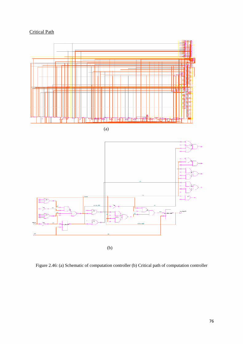
76
Critical Path
Figure 2.46: (a) Schematic of computation controller (b) Critical path of computation controller
(b)
(a)
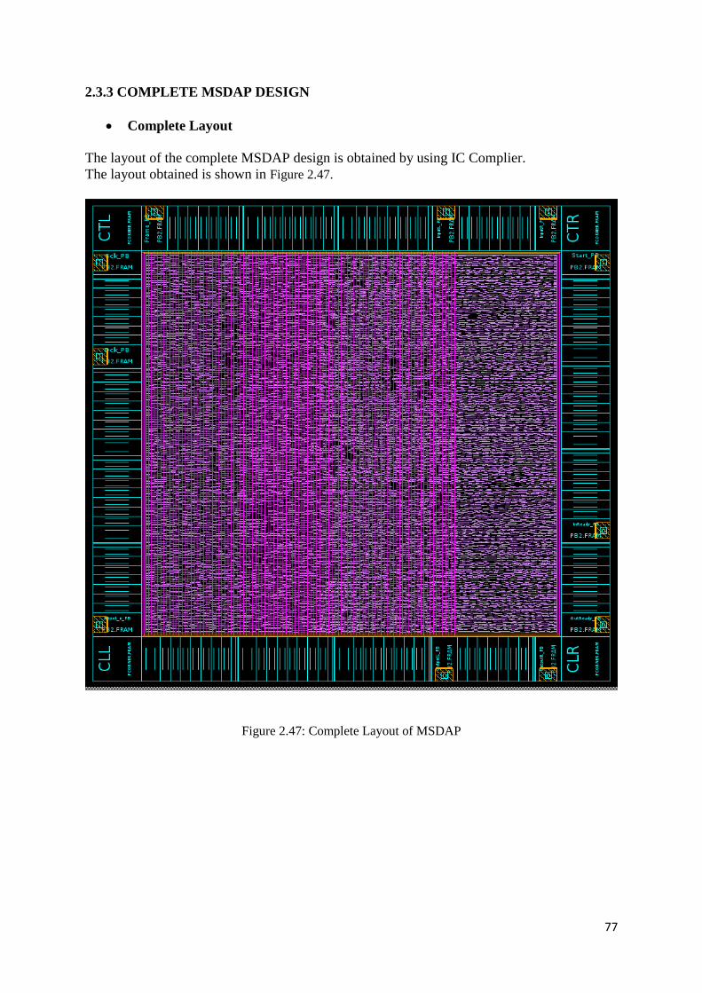
77
2.3.3 COMPLETE MSDAP DESIGN
Complete Layout
The layout of the complete MSDAP design is obtained by using IC Complier.
The layout obtained is shown in Figure 2.47.
Figure 2.47: Complete Layout of MSDAP
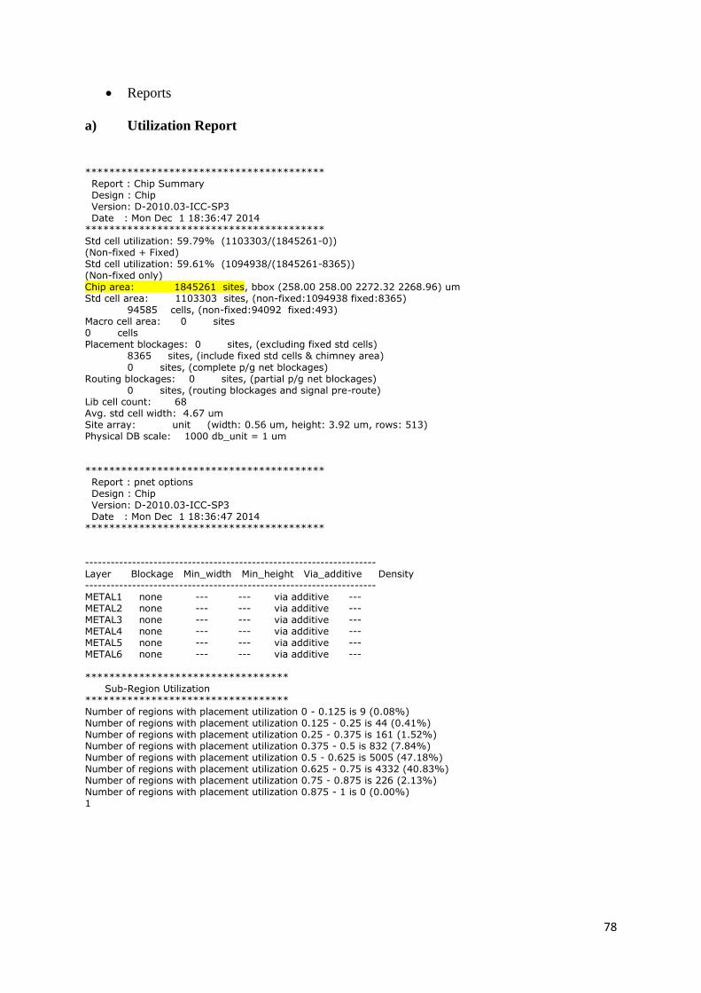
78
Reports
a) Utilization Report
**************************************** Report : Chip Summary Design : Chip Version: D-2010.03-ICC-SP3 Date : Mon Dec 1 18:36:47 2014 **************************************** Std cell utilization: 59.79% (1103303/(1845261-0)) (Non-fixed + Fixed) Std cell utilization: 59.61% (1094938/(1845261-8365)) (Non-fixed only) Chip area: 1845261 sites, bbox (258.00 258.00 2272.32 2268.96) um Std cell area: 1103303 sites, (non-fixed:1094938 fixed:8365) 94585 cells, (non-fixed:94092 fixed:493) Macro cell area: 0 sites 0 cells Placement blockages: 0 sites, (excluding fixed std cells) 8365 sites, (include fixed std cells & chimney area)
0 sites, (complete p/g net blockages) Routing blockages: 0 sites, (partial p/g net blockages) 0 sites, (routing blockages and signal pre-route) Lib cell count: 68 Avg. std cell width: 4.67 um Site array: unit (width: 0.56 um, height: 3.92 um, rows: 513) Physical DB scale: 1000 db_unit = 1 um **************************************** Report : pnet options Design : Chip Version: D-2010.03-ICC-SP3 Date : Mon Dec 1 18:36:47 2014 **************************************** -------------------------------------------------------------------- Layer Blockage Min_width Min_height Via_additive Density -------------------------------------------------------------------- METAL1 none --- --- via additive --- METAL2 none --- --- via additive --- METAL3 none --- --- via additive --- METAL4 none --- --- via additive --- METAL5 none --- --- via additive --- METAL6 none --- --- via additive --- ********************************** Sub-Region Utilization ********************************** Number of regions with placement utilization 0 - 0.125 is 9 (0.08%) Number of regions with placement utilization 0.125 - 0.25 is 44 (0.41%) Number of regions with placement utilization 0.25 - 0.375 is 161 (1.52%) Number of regions with placement utilization 0.375 - 0.5 is 832 (7.84%) Number of regions with placement utilization 0.5 - 0.625 is 5005 (47.18%) Number of regions with placement utilization 0.625 - 0.75 is 4332 (40.83%) Number of regions with placement utilization 0.75 - 0.875 is 226 (2.13%) Number of regions with placement utilization 0.875 - 1 is 0 (0.00%) 1
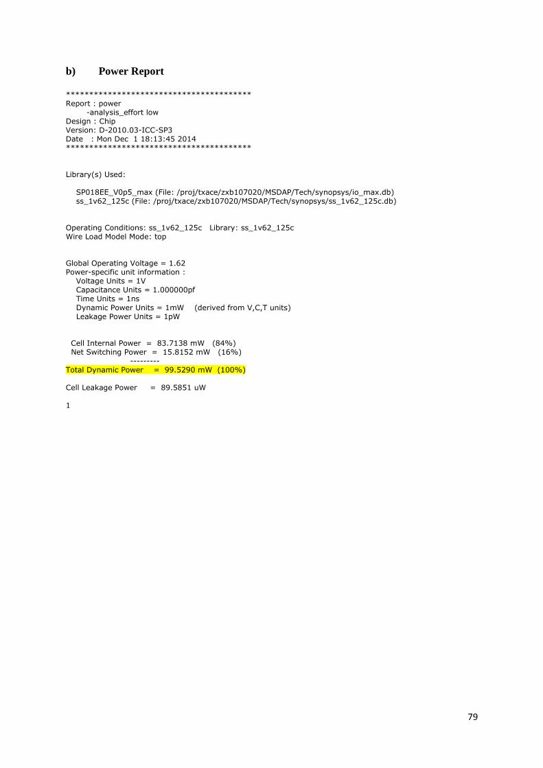
79
b) Power Report
**************************************** Report : power -analysis_effort low Design : Chip Version: D-2010.03-ICC-SP3 Date : Mon Dec 1 18:13:45 2014 **************************************** Library(s) Used: SP018EE_V0p5_max (File: /proj/txace/zxb107020/MSDAP/Tech/synopsys/io_max.db) ss_1v62_125c (File: /proj/txace/zxb107020/MSDAP/Tech/synopsys/ss_1v62_125c.db) Operating Conditions: ss_1v62_125c Library: ss_1v62_125c Wire Load Model Mode: top Global Operating Voltage = 1.62 Power-specific unit information : Voltage Units = 1V Capacitance Units = 1.000000pf Time Units = 1ns
Dynamic Power Units = 1mW (derived from V,C,T units) Leakage Power Units = 1pW Cell Internal Power = 83.7138 mW (84%) Net Switching Power = 15.8152 mW (16%) --------- Total Dynamic Power = 99.5290 mW (100%) Cell Leakage Power = 89.5851 uW 1
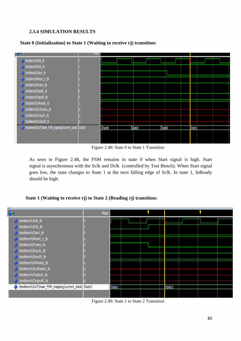
80
2.3.4 SIMULATION RESULTS
State 0 (Initialization) to State 1 (Waiting to receive rj) transition:
Figure 2.48: State 0 to State 1 Transition
As seen in Figure 2.48, the FSM remains in state 0 when Start signal is high. Start
signal is asynchronous with the Sclk and Dclk (controlled by Test Bench). When Start signal
goes low, the state changes to State 1 at the next falling edge of Sclk. In state 1, InReady
should be high.
State 1 (Waiting to receive rj) to State 2 (Reading rj) transition:
Figure 2.49: State 1 to State 2 Transition
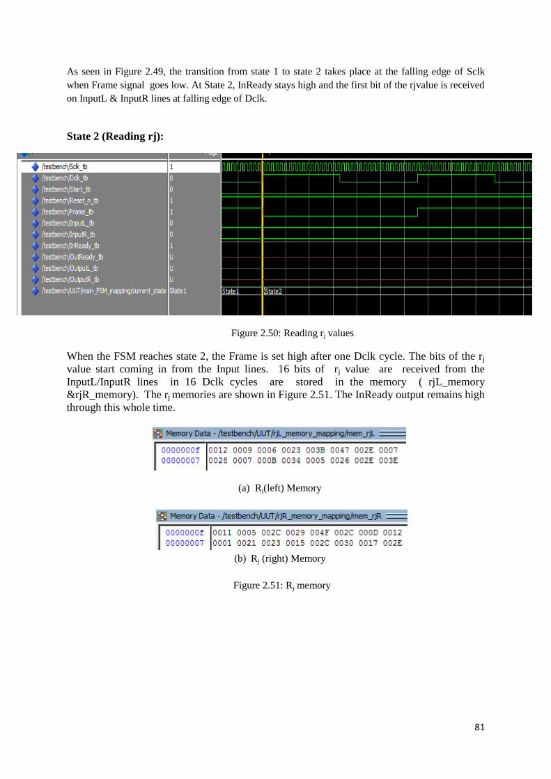
81
As seen in Figure 2.49, the transition from state 1 to state 2 takes place at the falling edge of Sclk
when Frame signal goes low. At State 2, InReady stays high and the first bit of the rjvalue is received
on InputL & InputR lines at falling edge of Dclk.
State 2 (Reading rj):
Figure 2.50: Reading rj values
When the FSM reaches state 2, the Frame is set high after one Dclk cycle. The bits of the rj
value start coming in from the Input lines. 16 bits of rj value are received from the
InputL/InputR lines in 16 Dclk cycles are stored in the memory ( rjL_memory
&rjR_memory). The rj memories are shown in Figure 2.51. The InReady output remains high
through this whole time.
(a) Rj(left) Memory
(b) Rj (right) Memory
Figure 2.51: Rj memory
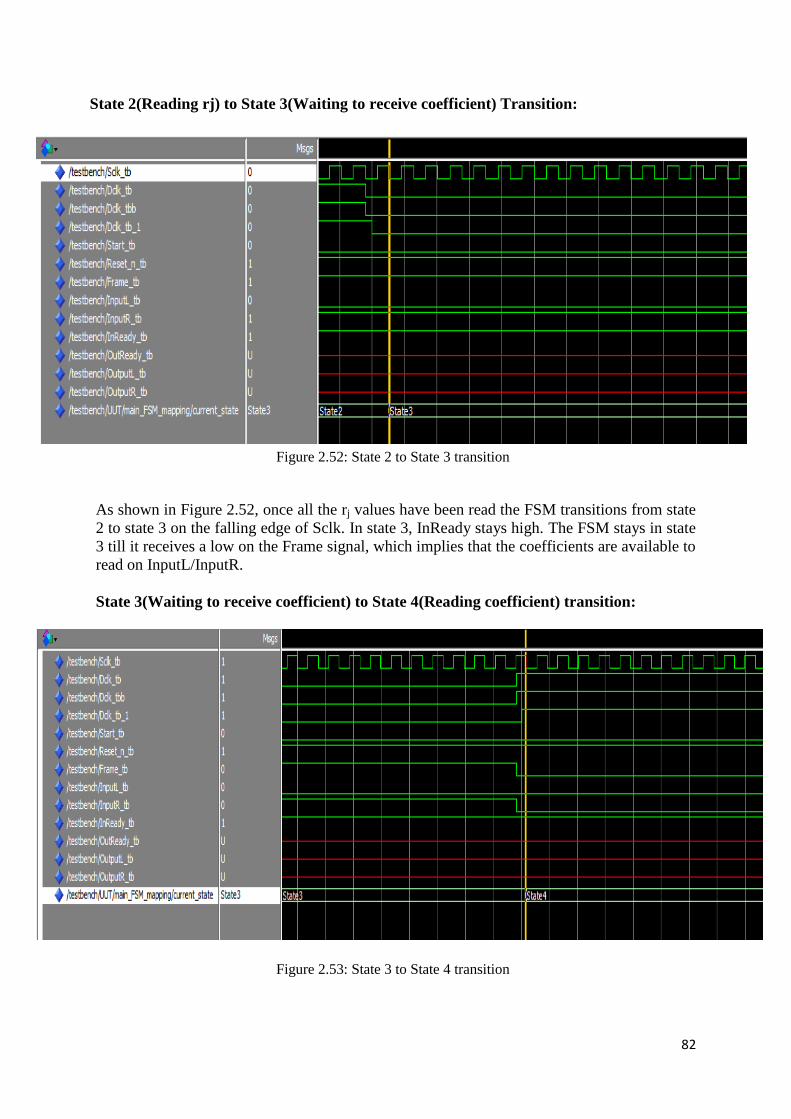
82
State 2(Reading rj) to State 3(Waiting to receive coefficient) Transition:
Figure 2.52: State 2 to State 3 transition
As shown in Figure 2.52, once all the rj values have been read the FSM transitions from state
2 to state 3 on the falling edge of Sclk. In state 3, InReady stays high. The FSM stays in state
3 till it receives a low on the Frame signal, which implies that the coefficients are available to
read on InputL/InputR.
State 3(Waiting to receive coefficient) to State 4(Reading coefficient) transition:
Figure 2.53: State 3 to State 4 transition
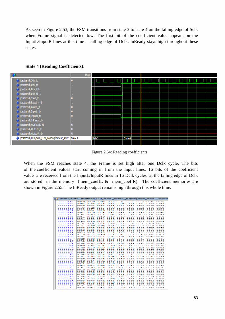
83
As seen in Figure 2.53, the FSM transitions from state 3 to state 4 on the falling edge of Sclk
when Frame signal is detected low. The first bit of the coefficient value appears on the
InputL/InputR lines at this time at falling edge of Dclk. InReady stays high throughout these
states.
State 4 (Reading Coefficients):
Figure 2.54: Reading coefficients
When the FSM reaches state 4, the Frame is set high after one Dclk cycle. The bits
of the coefficient values start coming in from the Input lines. 16 bits of the coefficient
value are received from the InputL/InputR lines in 16 Dclk cycles at the falling edge of Dclk
are stored in the memory (mem_coeffL & mem_coeffR). The coefficient memories are
shown in Figure 2.55. The InReady output remains high through this whole time.
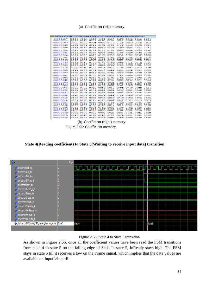
84
(a) Coefficient (left) memory
(b) Coefficient (right) memory
Figure 2.55: Coefficient memory
State 4(Reading coefficient) to State 5(Waiting to receive input data) transition:
Figure 2.56: State 4 to State 5 transition
As shown in Figure 2.56, once all the coefficient values have been read the FSM transitions
from state 4 to state 5 on the falling edge of Sclk. In state 5, InReady stays high. The FSM
stays in state 5 till it receives a low on the Frame signal, which implies that the data values are
available on InputL/InputR.
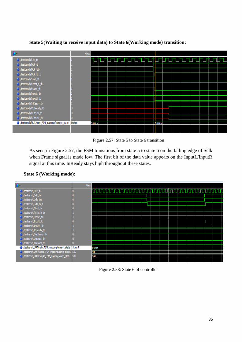
85
State 5(Waiting to receive input data) to State 6(Working mode) transition:
Figure 2.57: State 5 to State 6 transition
As seen in Figure 2.57, the FSM transitions from state 5 to state 6 on the falling edge of Sclk
when Frame signal is made low. The first bit of the data value appears on the InputL/InputR
signal at this time. InReady stays high throughout these states.
State 6 (Working mode):
Figure 2.58: State 6 of controller
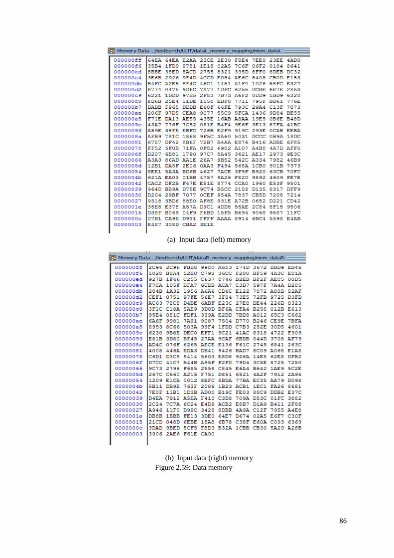
86
(a) Input data (left) memory
(b) Input data (right) memory
Figure 2.59: Data memory
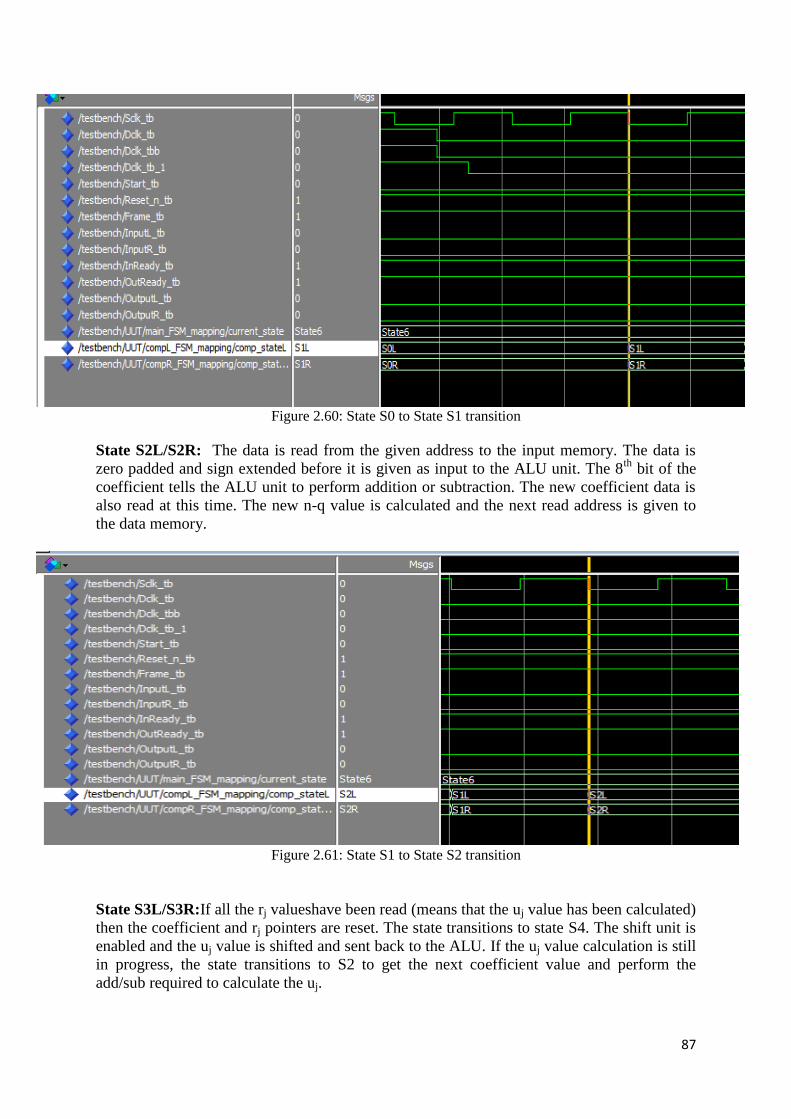
87
Figure 2.60: State S0 to State S1 transition
State S2L/S2R: The data is read from the given address to the input memory. The data is
zero padded and sign extended before it is given as input to the ALU unit. The 8th
bit of the
coefficient tells the ALU unit to perform addition or subtraction. The new coefficient data is
also read at this time. The new n-q value is calculated and the next read address is given to
the data memory.
Figure 2.61: State S1 to State S2 transition
State S3L/S3R:If all the rj valueshave been read (means that the uj value has been calculated)
then the coefficient and rj pointers are reset. The state transitions to state S4. The shift unit is
enabled and the uj value is shifted and sent back to the ALU. If the uj value calculation is still
in progress, the state transitions to S2 to get the next coefficient value and perform the
add/sub required to calculate the uj.
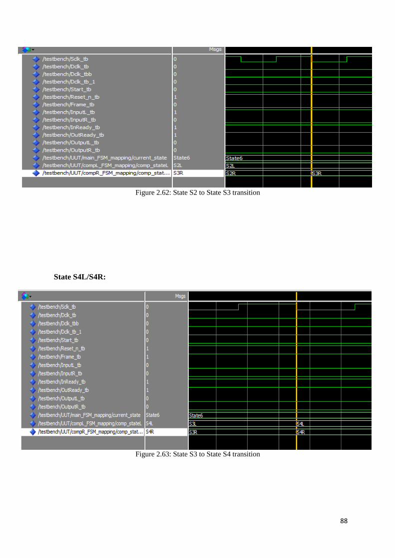
88
Figure 2.62: State S2 to State S3 transition
State S4L/S4R:
Figure 2.63: State S3 to State S4 transition
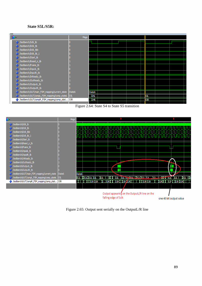
89
State S5L/S5R:
Figure 2.64: State S4 to State S5 transition
Figure 2.65: Output sent serially on the OutputL/R line
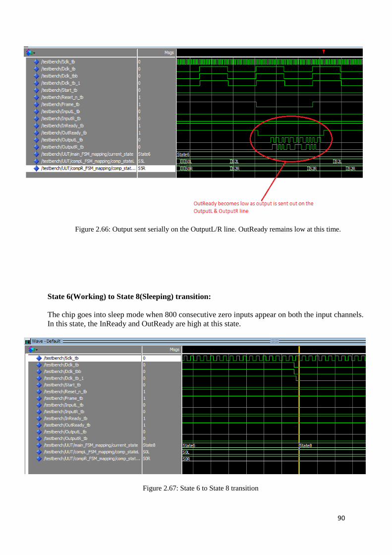
90
Figure 2.66: Output sent serially on the OutputL/R line. OutReady remains low at this time.
State 6(Working) to State 8(Sleeping) transition:
The chip goes into sleep mode when 800 consecutive zero inputs appear on both the input channels.
In this state, the InReady and OutReady are high at this state.
Figure 2.67: State 6 to State 8 transition
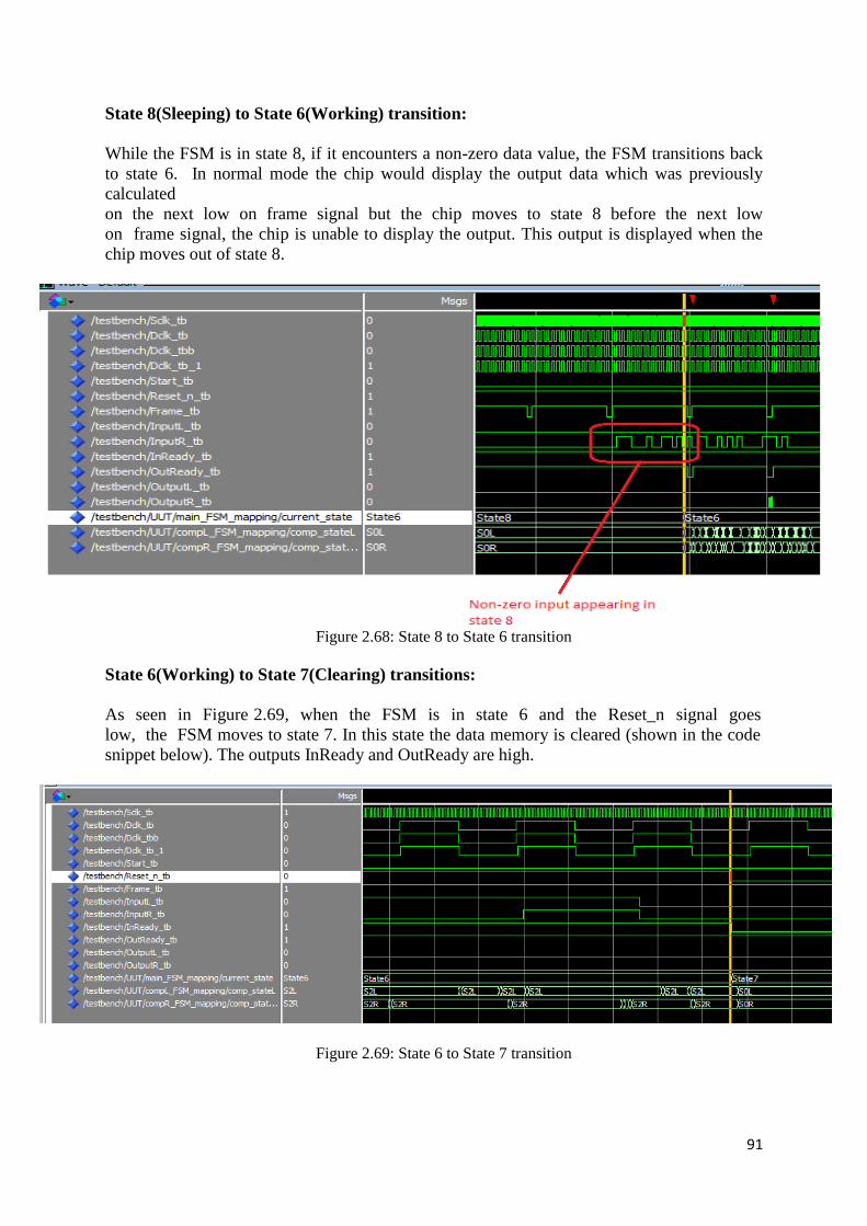
91
State 8(Sleeping) to State 6(Working) transition:
While the FSM is in state 8, if it encounters a non-zero data value, the FSM transitions back
to state 6. In normal mode the chip would display the output data which was previously
calculated
on the next low on frame signal but the chip moves to state 8 before the next low
on frame signal, the chip is unable to display the output. This output is displayed when the
chip moves out of state 8.
Figure 2.68: State 8 to State 6 transition
State 6(Working) to State 7(Clearing) transitions:
As seen in Figure 2.69, when the FSM is in state 6 and the Reset_n signal goes
low, the FSM moves to state 7. In this state the data memory is cleared (shown in the code
snippet below). The outputs InReady and OutReady are high.
Figure 2.69: State 6 to State 7 transition
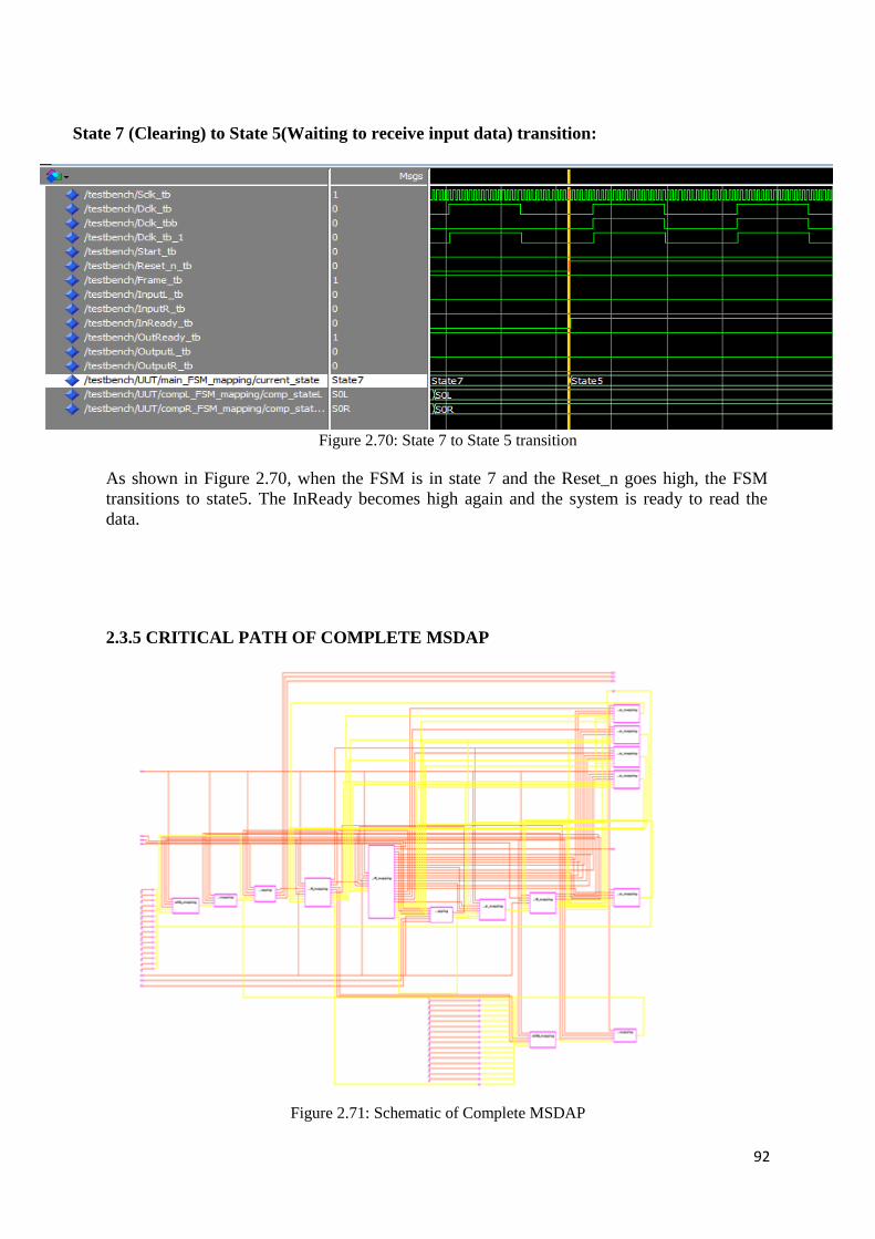
92
State 7 (Clearing) to State 5(Waiting to receive input data) transition:
Figure 2.70: State 7 to State 5 transition
As shown in Figure 2.70, when the FSM is in state 7 and the Reset_n goes high, the FSM
transitions to state5. The InReady becomes high again and the system is ready to read the
data.
2.3.5 CRITICAL PATH OF COMPLETE MSDAP
Figure 2.71: Schematic of Complete MSDAP
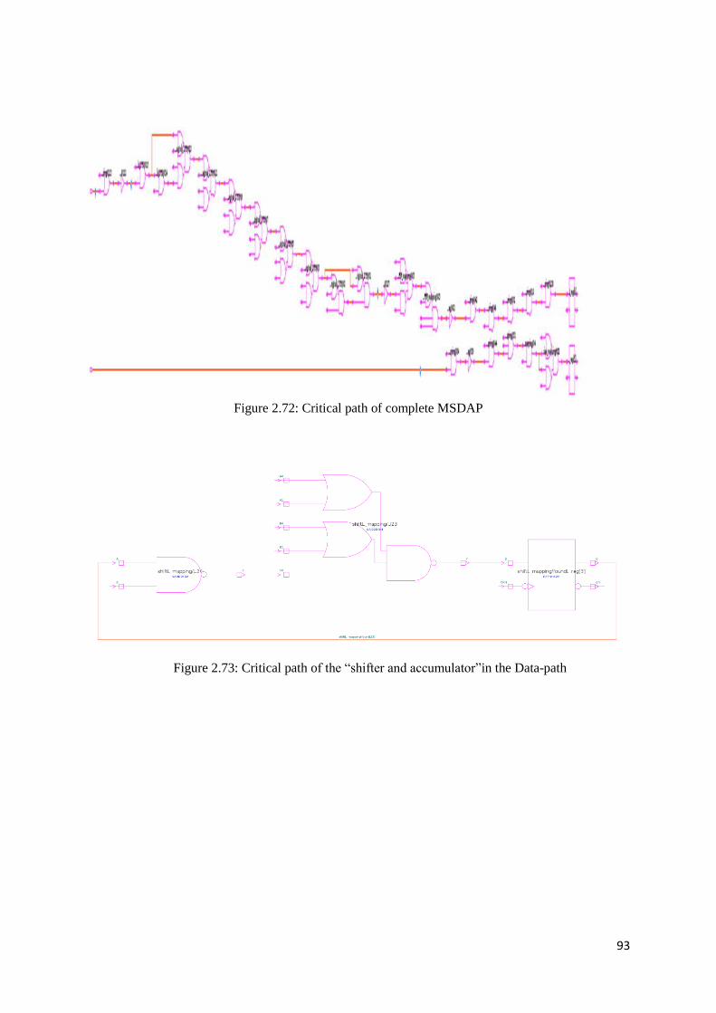
93
Figure 2.72: Critical path of complete MSDAP
Figure 2.73: Critical path of the “shifter and accumulator”in the Data-path
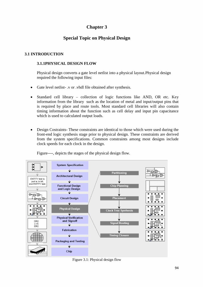
94
Chapter 3
Special Topic on Physical Design
3.1 INTRODUCTION
3.1.1PHYSICAL DESIGN FLOW
Physical design converts a gate level netlist into a physical layout.Physical design
required the following input files:
Gate level netlist- .v or .vhdl file obtained after synthesis.
Standard cell library – collection of logic functions like AND, OR etc. Key
information from the library such as the location of metal and input/output pins that
is required by place and route tools. Most standard cell libraries will also contain
timing information about the function such as cell delay and input pin capacitance
which is used to calculated output loads.
Design Costraints- These constraints are identical to those which were used during the
front-end logic synthesis stage prior to physical design. These constraints are derived
from the system specifications. Common constraints among most designs include
clock speeds for each clock in the design.
Figure----, depicts the stages of the physical design flow.
Figure 3.1: Physical design flow
95
The steps in the physical design flow are as follows:
Partitioning- The process of decomposing the circuit into smaller sub-circuits is known as
partioning. The design is decomposed hierarchically until each subsystem is of manageable
size. This is done mainly to separate different functional blocks and also to make placement
and routing easier.Partitioning can be done at different levels. At the system level, a system
is partitioned into a set of subsystems such that each subsystem can be designed and
fabricated independently on a single PCB. At the board level, the circuit assigned to a PCB
is partitioned into subcircuits such that each subcircuit can be fabricated as a VLSI chip.
And then, the circuit assigned to a chip is partitioned into smaller subcircuits.
Chip planning/ Floor planning- Floorplanning is a determination of the approximate
locations of the major components in a rectangular chip area. The objectives of
floorplanning are to minimize area, redue wire length and maximize routability. During
floorplanning,space is allocated for clock and power wiring and the location of the I/O and
power pads is decided.
Placement - The process of arranging circuit components on a layout surface. After
placement, we can see the accurate estimates of the capacitive loads of each standard cell
must drive. The tool places these cells based on the algorithms which it uses internally.
Clock tree synthesis- All clock pins are driven by a single clock source. This results in large
delay and tranition time due to the length of the wires and hence the clock reaches soe
registers before others (clock skew). The goal of clock tree synthesis (CTS) is to minimize
skew and insertion delay. It is the automatic insertion of buffers/inverters along the clock
path to balance the clock delay to all the clock inputs. The proper usage of balance buffers
or inverters during clock tree synthesis is extremely important, especially when dealing with
very high speed clocking.
Routing- Routing is the connection of the various standard cells using wires. There are two
types of routing.
o Global routing- Global routing first partitions the routing region into tiles and decides
tile-to-tile paths for all nets while attempting tooptimize some given objective function
(e.g.total wirelength and circuit timing).
o Detailed routing- guided by the paths obtained in global routing, detailed routing
assigns actual tracks and vias for nets.
Timing Closure- parasitic extraction of the resistances and capacitances of all routes in the
design is performed. It results in a format such as SPEF(Standard parasitic extraction
format) which is then used used to perform the static timing analysis.
96
3.1.2 CHALLENGES IN PHYSICAL DESIGN
With each new process technology, the number of transistors per unit area doubles. However,
the area of a chip has remained more or less the same. AS a result, the layout data fr a chip
design also doubles. The main issues of high performance physical designs are power
distribution, synchronization, manufacturing variablilty among others. Designers need to deal
with leakage power, interconnect delay, congestion and reliability.
With the advent of the 20nm process, the existing challenges of IC design have become much
more difficult. Some of these challenges are discussed below:
Manufacturability- before the 20nm process, it was believed that a design that followed the
design rules can surely be manufactured. The number of rules for the 20nm process are
twice the number required at 28nm process. Also the 20nm proess rules are ore complex.
However, applying these rules does not ensure that the chip can be manufacutres. Designers
will have to take manufacturability issues into consideration much earlier in the process.
Routability- Designers need to meet more constraints at 20nm to achieve the best routing. A
balance is to be achieved between trying to create the smallest, most closely packed cells
and the need for easy-to-access cells that will make it easy to decompose the layout.
Modern three-dimensional (3D) designs, in which the active devices are placed in multiple
layers using 3D inte-gration technologies, are helping to maintain the validity of Moore’s law
in today’s nano era. However, progressin commercial 3D ICs has been slow due to multiple
reasons. One of them is the lack of appropriate physicaldesign (layout) tools that take the new
constraints arising from the third dimension into account.Typical problemsin 3D integration
technologies are, among others, reliability, alignment accuracy, reuse of existing (2D)
IPblocks, testability and thermal issues. Some of these issues are discussed below:
Thermal Issues- A more complex heat management is necessary;thermal vias and other
mechanisms are required to dissipate heat. Solutions like including carbon nano-tube
based and liquid cooling with mirco-scale fluidic channels directly inserted ino the 3D ICs
have been proposed.
Floorplanning Issues- Conventional floorplanning assumes a single two-dimensional layer
on which several modules must be arranged. 3D floorplanning includes new, 3D-specific
characteristics that must be represented in the underlying data structures.
Placement Issues- While 2D placement is limited to one (planar) layer,3D placement
requires optimizing the placement between multiple active layers. Thermalconstraints are
crucial for 3D designs. Hence, 3D placement must ensure that thermal considerations are
fulfilled.
Hence, with each sucessie advancement of semiconductor technology new challenges are
born.Designer and EDA vendors need to invent new techniques to tackle these challenges so
that the industry can keep up with Moore’s law.

97
3.2 CLOCK AND POWER NETWORK LAYOUT
3.2.1 LAYING OUT THE POWER NETWORK
Power planning is the creation of the power network within a design. Figure 3.2 shows the
basic elements of a power distribution architecture.
Figure 3.2: Basic elements of a power network
Basic elements of the power network are:
Power Pad
Power Rings
o Form complete rings around the periphery of the die, around individual hard
macros, or inside of hierarchical blocks.
o Uses higher-level metal layers
o User specify width and spacing of the rings
o It is best to create power and ground rings around any hard macro IP present
in the design.
Power Straps/Trunks
o Horizontal (strap) and vertical (trunk) metal wires placed in an array across the
entire or section die.
o typically uniformly distributed across the die.
Power Rails
o Is used to connect the standard cell power rails together, and or power trunks.
o Uses low leve metal layers, typically metal 1.

98
Power planning is a part of the floorplanning process. Following is a tutorial on laying out the
power network in IC Compiler.
Ones the floorplan is initialized, the power and ground pins are connected.
The next step is to create rectangular power rings around the floorplan.The rings can be
placed by using the commands:
##Create VSS ring
icc_shell>create_rectangular_rings -nets {VSS} -left_offset 0.5 -left_segment_layer M6
-left_segment_width 1.0 -extend_ll -extend_lh -right_offset 0.5 -right_segment_layer
M6 -right_segment_width 1.0 -extend_rl -extend_rh -bottom_offset 0.5 -
bottom_segment_layer M7 -bottom_segment_width 1.0 -extend_bl -extend_bh -
top_offset 0.5 -top_segment_layer M7 -top_segment_width 1.0 -extend_tl -extend_th
## Create VDD Ring
icc_shell>create_rectangular_rings -nets {VDD} -left_offset 1.8 -left_segment_layer M6
-left_segment_width 1.0 -extend_ll -extend_lh -right_offset 1.8 -right_segment_layer
M6 -right_segment_width 1.0 -extend_rl -extend_rh -bottom_offset 1.8 -
bottom_segment_layer M7 -bottom_segment_width 1.0 -extend_bl -extend_bh -
top_offset 1.8 -top_segment_layer M7 -top_segment_width 1.0 -extend_tl -extend_th
The command below is used to create power straps
##Below commands connect power strap for VDD
create_power_straps -direction vertical -start_at 271.25 -num_placement_strap 51
-increment_x_or_y 30 -nets {VDD} -layer METAL5 -width 1
##Below commands connect power strap for VSS
create_power_straps -direction vertical -start_at 286.25 -num_placement_strap 50
-increment_x_or_y 30 -nets {VSS} -layer METAL5 -width 1
(a) (b)
Figure 3.3: (a) Power ring (b) Power straps

99
3.2.2 LAYING OUT THE CLOCK NETWORK
Before doing the actual cts, you can set various optimization steps. In the Layout window, click
on click on Clock Core CTS and Optimization.There are various options that can be set. Press
OK to run CTS.
Figure 3.4: Clock tree synthesis in IC compiler
The timing reports can be generated by typing in:
set_operating_conditions -min_library ff_1v98_0c -min ff_1v98_0c -max_library
ss_1v62_125c -max ss_1v62_125c
report_timing –max_paths 20 –delay max > icc_rpt/setup.rpt
set_operating_conditions -min_library ff_1v98_0c -min ff_1v98_0c -max_library
ss_1v62_125c -max ss_1v62_125c
report_timing –max_paths 20 –delay min > icc_rpt/hold.rpt
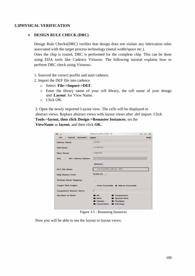
100
3.3PHYSICAL VERIFICATION
DESIGN RULE CHECK (DRC)
Design Rule Checks(DRC) verifies that design does not violate any fabrication rules
associated with the target process technology (metal width/space etc.).
Ones the chip is routed, DRC is performed for the complete chip. This can be done
using EDA tools like Cadence Virtuoso. The following tutorial explains how to
perform DRC check using Virtuoso.
1. Sourced the correct profile and start cadence.
2. Import the DEF file into cadence
o Select File->Import->DEF.
o Enter the library name of your cell library, the cell name of your design
and Layout for View Name.
o Click OK.
3. Open the newly imported Layout view. The cells will be displayed in
abstract views. Replace abstract views with layout views after .def import. Click
Tools->layout, then click Design->Remaster Instances, set the
ViewName as layout, and then click OK.
Figure 3.5 : Renaming Instances
Now you will be able to see the layout in layout views.
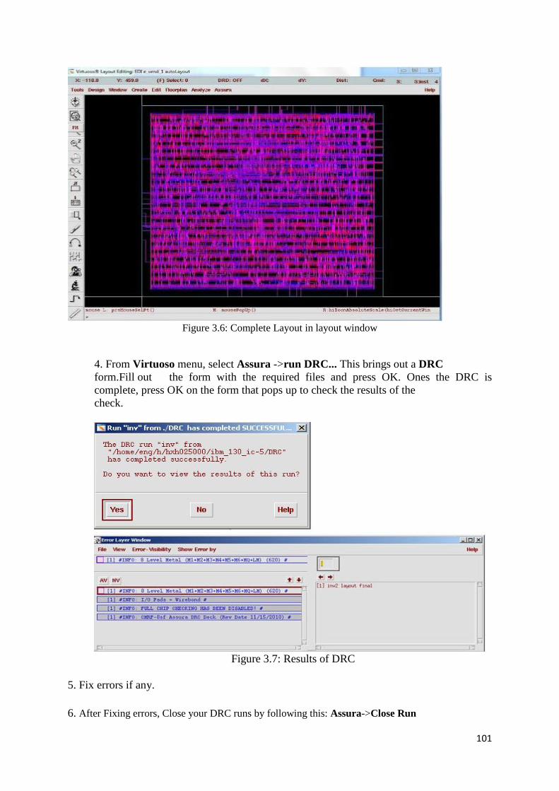
101
Figure 3.6: Complete Layout in layout window
4. From Virtuoso menu, select Assura ->run DRC... This brings out a DRC
form.Fill out the form with the required files and press OK. Ones the DRC is
complete, press OK on the form that pops up to check the results of the
check.
Figure 3.7: Results of DRC
5. Fix errors if any.
6. After Fixing errors, Close your DRC runs by following this: Assura->Close Run
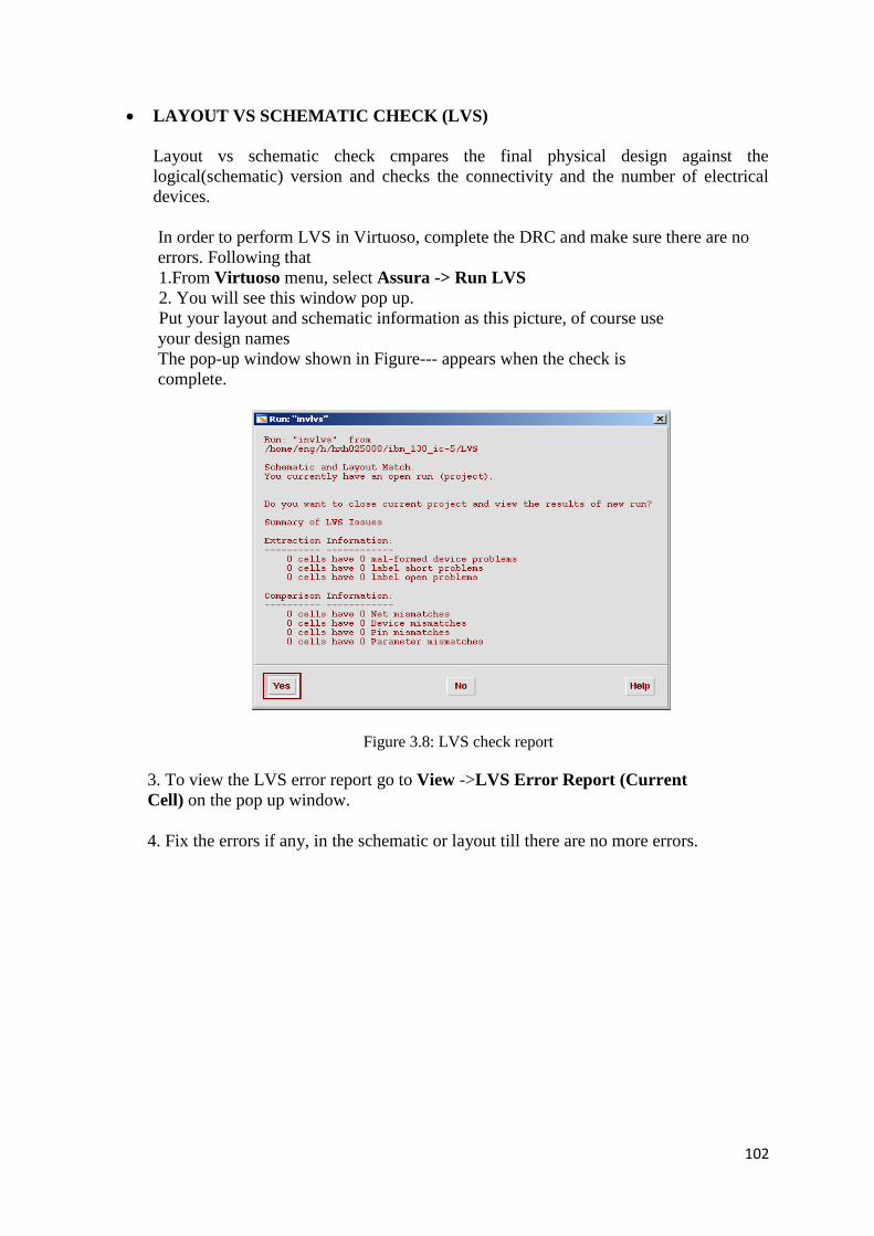
102
LAYOUT VS SCHEMATIC CHECK (LVS)
Layout vs schematic check cmpares the final physical design against the
logical(schematic) version and checks the connectivity and the number of electrical
devices.
In order to perform LVS in Virtuoso, complete the DRC and make sure there are no
errors. Following that
1.From Virtuoso menu, select Assura -> Run LVS
2. You will see this window pop up.
Put your layout and schematic information as this picture, of course use
your design names
The pop-up window shown in Figure--- appears when the check is
complete.
Figure 3.8: LVS check report
3. To view the LVS error report go to View ->LVS Error Report (Current
Cell) on the pop up window.
4. Fix the errors if any, in the schematic or layout till there are no more errors.

103
ELECTRICAL RULES CHECK (ERC)
Electrical rules check verifies that there are no short or open circuits with power and ground
as well as resistors/capacitors/transistors with floating nodes. Some errors that are seen are:
o Floating gate error – If any gate is unconnected, this could lead to leakage issues.
o VDD/VSS errors – The well geometries need to be connected to power/Ground
otherwisere errors like “NWELL not connected to VDD” are seen.
ANTENNA EFFECT
The process antenna effect or “plasma induced gate oxide damage” is a manufacturing effect.
i.e. this is a type of failure that can occur solely at the manufacturing stage. This is a gate
damage that can occur due to charge accumulation on metals and discharge to a gate through
gate oxide.
In the manufacturing process, metals are built layer by layer. i.e. metal1 is deposited first,
then all unwanted portions are etched away, with plasma etching. The metal geometries when
they are exposed to plasma can collect charge from it. Once metal1 is completed, via1 is
built, then metal2 and so on. So with each passing stage, the metal geometries can build up
static electricity. The larger the metal area that is exposed to the plasma, the more charge they
can collect. If the charge collected is large enough to cause current to flow to the gate, this
can cause damage to the gate oxide. This happens because since the layers are built one-by-
one, a source/drain implant may not be available for discharge.
Antenna rules are normally expressed as an allowable ratio of metal area to gate area. Each
foundry sets a maximum allowable antenna ratio for its processes.
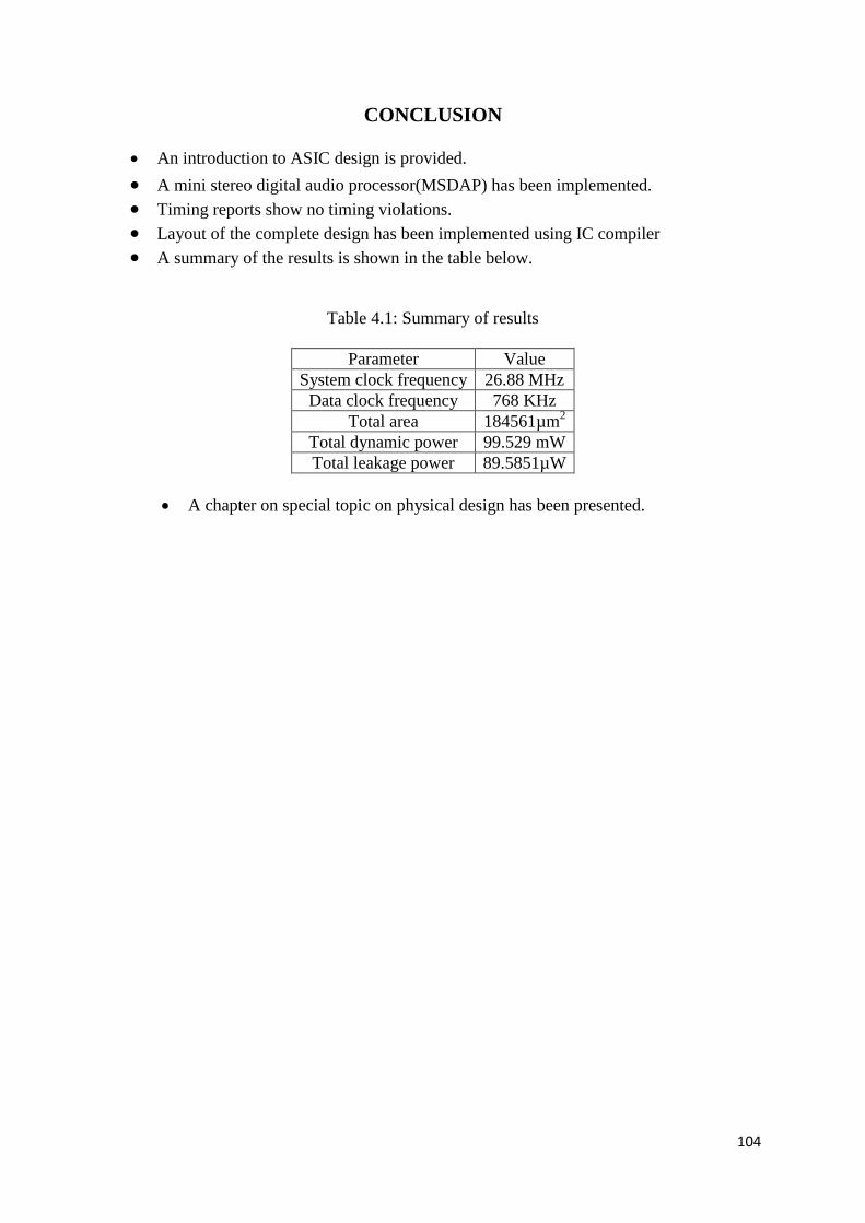
104
CONCLUSION
An introduction to ASIC design is provided.
A mini stereo digital audio processor(MSDAP) has been implemented.
Timing reports show no timing violations.
Layout of the complete design has been implemented using IC compiler
A summary of the results is shown in the table below.
Table 4.1: Summary of results
Parameter Value
System clock frequency 26.88 MHz
Data clock frequency 768 KHz
Total area 184561µm2
Total dynamic power 99.529 mW
Total leakage power 89.5851µW
A chapter on special topic on physical design has been presented.

105
REFERNCES
• Zhangnong Jiang, A Mini Stereo Digital Audio Processor (MSDAP), Proc.
ICASSP’89, pp. 1239-1242, 1989
• Dian Zhou, Modern ASIC Design. Beijing, China: Science Press, 2011.
• VHDL coding tips and tricks, [online] 2014,
http://vhdlguru.blogspot.com/2011/02/file-reading-and-writing-in-vhdl-part-2.html.
• Tala,Deepak. Design and Tool Flow. Retrieved from http://www.asic-
world.com/verilog/design_flow1.html
• Michael Smith, Application-specific integrated circuits.Boston,USA: Addison-
Wesley Longman Publishing Co., Inc., 1997.
• Gupta,Deepak.VLSI Physical Design. Retrieved from
http://www.slideshare.net/deepak2392/vlsi-physical-design
• Bi,Zhaori., Li,Minghua.,ICC Tutorial. Retrieved from
http://www.utdallas.edu/~zxb107020/Tools_tutorials/ICC/ICC_Tutorial.pdf
• Sridharan,Akshay.,IBM 130nm - Layout Verification and Extraction, DRC, LVS, PEX.
Retrieved from http://www.utdallas.edu/~akshay.sridharan/index_files/Page8227.htm
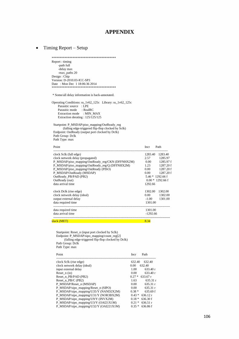
106
APPENDIX
Timing Report – Setup
**************************************** Report : timing
-path full
-delay max -max_paths 20
Design : Chip
Version: D-2010.03-ICC-SP3 Date : Mon Dec 1 18:06:36 2014
****************************************
* Some/all delay information is back-annotated.
Operating Conditions: ss_1v62_125c Library: ss_1v62_125c Parasitic source : LPE
Parasitic mode : RealRC
Extraction mode : MIN_MAX Extraction derating : 125/125/125
Startpoint: P_MSDAP/piso_mapping/OutReady_reg (falling edge-triggered flip-flop clocked by Sclk)
Endpoint: OutReady (output port clocked by Dclk)
Path Group: Dclk Path Type: max
Point Incr Path
-----------------------------------------------------------------------------------------------------------
clock Sclk (fall edge) 1283.40 1283.40 clock network delay (propagated) 2.57 1285.97
P_MSDAP/piso_mapping/OutReady_reg/CKN (DFFNHX2M) 0.00 1285.97 f
P_MSDAP/piso_mapping/OutReady_reg/Q (DFFNHX2M) 1.23 1287.20 f P_MSDAP/piso_mapping/OutReady (PISO) 0.00 1287.20 f
P_MSDAP/OutReady (MSDAP) 0.00 1287.20 f
OutReady_PB/PAD (PB2) 5.46 * 1292.66 f OutReady (out) 0.00 * 1292.66 f
data arrival time 1292.66
clock Dclk (rise edge) 1302.00 1302.00
clock network delay (ideal) 0.00 1302.00
output external delay -1.00 1301.00 data required time 1301.00
-------------------------------------------------------------------------------------------------------------
data required time 1301.00 data arrival time -1292.66
-------------------------------------------------------------------------------------------------------------
slack (MET) 8.34
Startpoint: Reset_n (input port clocked by Sclk) Endpoint: P_MSDAP/sipo_mapping/count_reg[2]
(falling edge-triggered flip-flop clocked by Dclk)
Path Group: Dclk Path Type: max
Point Incr Path ---------------------------------------------------------------------------------------------
clock Sclk (rise edge) 632.40 632.40
clock network delay (ideal) 0.00 632.40 input external delay 1.00 633.40 r
Reset_n (in) 0.00 633.40 r
Reset_n_PB/PAD (PB2) 0.27 * 633.67 r Reset_n_PB/C (PB2) 1.63 635.31 r
P_MSDAP/Reset_n (MSDAP) 0.00 635.31 r
P_MSDAP/sipo_mapping/Reset_n (SIPO) 0.00 635.31 r P_MSDAP/sipo_mapping/U35/Y (NAND2X2M) 0.38 * 635.69 f
P_MSDAP/sipo_mapping/U31/Y (NOR3BX2M) 0.43 * 636.12 r
P_MSDAP/sipo_mapping/U9/Y (INVX2M) 0.18 * 636.30 f P_MSDAP/sipo_mapping/U3/Y (OAI21X1M) 0.21 * 636.51 r
P_MSDAP/sipo_mapping/U32/Y (OAI221X1M) 0.35 * 636.86 f
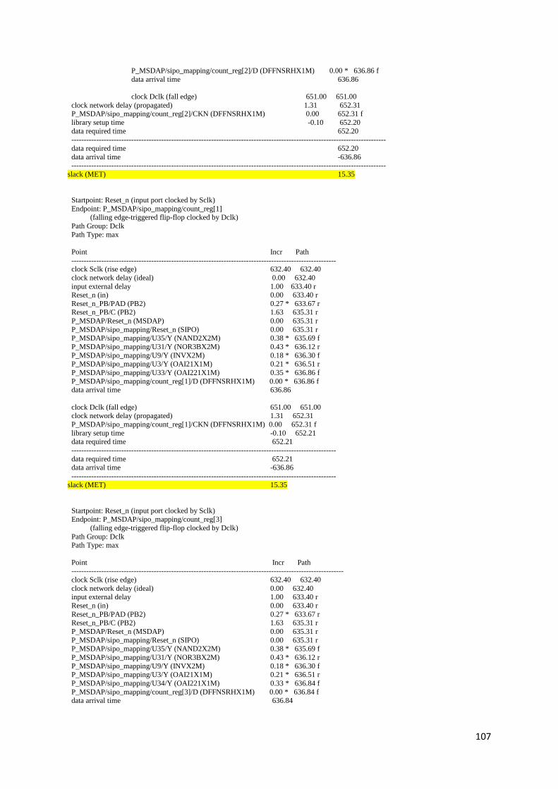
107
P_MSDAP/sipo_mapping/count_reg[2]/D (DFFNSRHX1M) 0.00 * 636.86 f
data arrival time 636.86
clock Dclk (fall edge) 651.00 651.00
clock network delay (propagated) 1.31 652.31 P_MSDAP/sipo_mapping/count_reg[2]/CKN (DFFNSRHX1M) 0.00 652.31 f
library setup time -0.10 652.20
data required time 652.20 ------------------------------------------------------------------------------------------------------------------------------
data required time 652.20
data arrival time -636.86 ------------------------------------------------------------------------------------------------------------------------------
slack (MET) 15.35
Startpoint: Reset_n (input port clocked by Sclk)
Endpoint: P_MSDAP/sipo_mapping/count_reg[1] (falling edge-triggered flip-flop clocked by Dclk)
Path Group: Dclk
Path Type: max
Point Incr Path
---------------------------------------------------------------------------------------------------------- clock Sclk (rise edge) 632.40 632.40
clock network delay (ideal) 0.00 632.40
input external delay 1.00 633.40 r Reset_n (in) 0.00 633.40 r
Reset_n_PB/PAD (PB2) 0.27 * 633.67 r Reset_n_PB/C (PB2) 1.63 635.31 r
P_MSDAP/Reset_n (MSDAP) 0.00 635.31 r
P_MSDAP/sipo_mapping/Reset_n (SIPO) 0.00 635.31 r P_MSDAP/sipo_mapping/U35/Y (NAND2X2M) 0.38 * 635.69 f
P_MSDAP/sipo_mapping/U31/Y (NOR3BX2M) 0.43 * 636.12 r
P_MSDAP/sipo_mapping/U9/Y (INVX2M) 0.18 * 636.30 f P_MSDAP/sipo_mapping/U3/Y (OAI21X1M) 0.21 * 636.51 r
P_MSDAP/sipo_mapping/U33/Y (OAI221X1M) 0.35 * 636.86 f
P_MSDAP/sipo_mapping/count_reg[1]/D (DFFNSRHX1M) 0.00 * 636.86 f data arrival time 636.86
clock Dclk (fall edge) 651.00 651.00 clock network delay (propagated) 1.31 652.31
P_MSDAP/sipo_mapping/count_reg[1]/CKN (DFFNSRHX1M) 0.00 652.31 f
library setup time -0.10 652.21 data required time 652.21
----------------------------------------------------------------------------------------------------------
data required time 652.21 data arrival time -636.86
----------------------------------------------------------------------------------------------------------
slack (MET) 15.35
Startpoint: Reset_n (input port clocked by Sclk) Endpoint: P_MSDAP/sipo_mapping/count_reg[3]
(falling edge-triggered flip-flop clocked by Dclk)
Path Group: Dclk Path Type: max
Point Incr Path -------------------------------------------------------------------------------------------------------------
clock Sclk (rise edge) 632.40 632.40
clock network delay (ideal) 0.00 632.40 input external delay 1.00 633.40 r
Reset_n (in) 0.00 633.40 r
Reset_n_PB/PAD (PB2) 0.27 * 633.67 r Reset_n_PB/C (PB2) 1.63 635.31 r
P_MSDAP/Reset_n (MSDAP) 0.00 635.31 r
P_MSDAP/sipo_mapping/Reset_n (SIPO) 0.00 635.31 r P_MSDAP/sipo_mapping/U35/Y (NAND2X2M) 0.38 * 635.69 f
P_MSDAP/sipo_mapping/U31/Y (NOR3BX2M) 0.43 * 636.12 r
P_MSDAP/sipo_mapping/U9/Y (INVX2M) 0.18 * 636.30 f P_MSDAP/sipo_mapping/U3/Y (OAI21X1M) 0.21 * 636.51 r
P_MSDAP/sipo_mapping/U34/Y (OAI221X1M) 0.33 * 636.84 f
P_MSDAP/sipo_mapping/count_reg[3]/D (DFFNSRHX1M) 0.00 * 636.84 f data arrival time 636.84
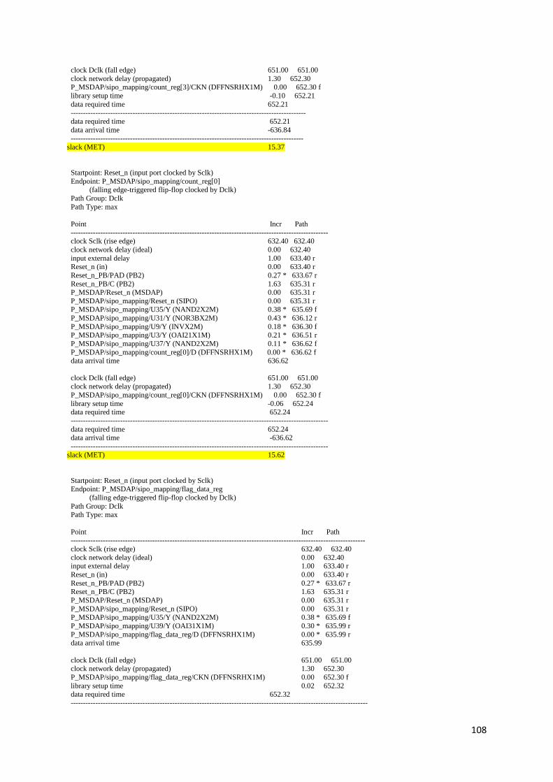
108
clock Dclk (fall edge) 651.00 651.00
clock network delay (propagated) 1.30 652.30 P_MSDAP/sipo_mapping/count_reg[3]/CKN (DFFNSRHX1M) 0.00 652.30 f
library setup time -0.10 652.21
data required time 652.21 -----------------------------------------------------------------------------------------------
data required time 652.21
data arrival time -636.84 ----------------------------------------------------------------------------------------------
slack (MET) 15.37
Startpoint: Reset_n (input port clocked by Sclk)
Endpoint: P_MSDAP/sipo_mapping/count_reg[0] (falling edge-triggered flip-flop clocked by Dclk)
Path Group: Dclk
Path Type: max
Point Incr Path
-------------------------------------------------------------------------------------------------------- clock Sclk (rise edge) 632.40 632.40
clock network delay (ideal) 0.00 632.40
input external delay 1.00 633.40 r Reset_n (in) 0.00 633.40 r
Reset_n_PB/PAD (PB2) 0.27 * 633.67 r
Reset_n_PB/C (PB2) 1.63 635.31 r P_MSDAP/Reset_n (MSDAP) 0.00 635.31 r
P_MSDAP/sipo_mapping/Reset_n (SIPO) 0.00 635.31 r P_MSDAP/sipo_mapping/U35/Y (NAND2X2M) 0.38 * 635.69 f
P_MSDAP/sipo_mapping/U31/Y (NOR3BX2M) 0.43 * 636.12 r
P_MSDAP/sipo_mapping/U9/Y (INVX2M) 0.18 * 636.30 f P_MSDAP/sipo_mapping/U3/Y (OAI21X1M) 0.21 * 636.51 r
P_MSDAP/sipo_mapping/U37/Y (NAND2X2M) 0.11 * 636.62 f
P_MSDAP/sipo_mapping/count_reg[0]/D (DFFNSRHX1M) 0.00 * 636.62 f data arrival time 636.62
clock Dclk (fall edge) 651.00 651.00 clock network delay (propagated) 1.30 652.30
P_MSDAP/sipo_mapping/count_reg[0]/CKN (DFFNSRHX1M) 0.00 652.30 f
library setup time -0.06 652.24 data required time 652.24
--------------------------------------------------------------------------------------------------------
data required time 652.24 data arrival time -636.62
--------------------------------------------------------------------------------------------------------
slack (MET) 15.62
Startpoint: Reset_n (input port clocked by Sclk) Endpoint: P_MSDAP/sipo_mapping/flag_data_reg
(falling edge-triggered flip-flop clocked by Dclk)
Path Group: Dclk Path Type: max
Point Incr Path -----------------------------------------------------------------------------------------------------------------------
clock Sclk (rise edge) 632.40 632.40
clock network delay (ideal) 0.00 632.40 input external delay 1.00 633.40 r
Reset_n (in) 0.00 633.40 r
Reset_n_PB/PAD (PB2) 0.27 * 633.67 r Reset_n_PB/C (PB2) 1.63 635.31 r
P_MSDAP/Reset_n (MSDAP) 0.00 635.31 r
P_MSDAP/sipo_mapping/Reset_n (SIPO) 0.00 635.31 r P_MSDAP/sipo_mapping/U35/Y (NAND2X2M) 0.38 * 635.69 f
P_MSDAP/sipo_mapping/U39/Y (OAI31X1M) 0.30 * 635.99 r
P_MSDAP/sipo_mapping/flag_data_reg/D (DFFNSRHX1M) 0.00 * 635.99 r data arrival time 635.99
clock Dclk (fall edge) 651.00 651.00 clock network delay (propagated) 1.30 652.30
P_MSDAP/sipo_mapping/flag_data_reg/CKN (DFFNSRHX1M) 0.00 652.30 f
library setup time 0.02 652.32 data required time 652.32
------------------------------------------------------------------------------------------------------------------------
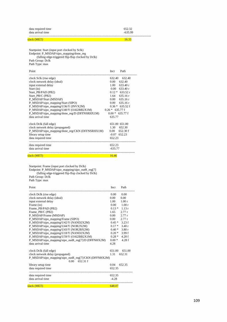
109
data required time 652.32
data arrival time -635.99 ------------------------------------------------------------------------------------------------------------------------
slack (MET) 16.33
Startpoint: Start (input port clocked by Sclk)
Endpoint: P_MSDAP/sipo_mapping/done_reg (falling edge-triggered flip-flop clocked by Dclk)
Path Group: Dclk
Path Type: max
Point Incr Path
---------------------------------------------------------------------------------------------------------- clock Sclk (rise edge) 632.40 632.40
clock network delay (ideal) 0.00 632.40
input external delay 1.00 633.40 r Start (in) 0.00 633.40 r
Start_PB/PAD (PB2) 0.12 * 633.52 r
Start_PB/C (PB2) 1.64 635.16 r P_MSDAP/Start (MSDAP) 0.00 635.16 r
P_MSDAP/sipo_mapping/Start (SIPO) 0.00 635.16 r
P_MSDAP/sipo_mapping/U36/Y (INVX2M) 0.36 * 635.52 f P_MSDAP/sipo_mapping/U40/Y (OAI2BB2X1M) 0.26 * 635.77 f
P_MSDAP/sipo_mapping/done_reg/D (DFFNSRHX1M) 0.00 * 635.77 f
data arrival time 635.77
clock Dclk (fall edge) 651.00 651.00 clock network delay (propagated) 1.30 652.30
P_MSDAP/sipo_mapping/done_reg/CKN (DFFNSRHX1M) 0.00 652.30 f
library setup time -0.07 652.23 data required time 652.23
---------------------------------------------------------------------------------------------------------
data required time 652.23 data arrival time -635.77
--------------------------------------------------------------------------------------------------------
slack (MET) 16.46
Startpoint: Frame (input port clocked by Dclk) Endpoint: P_MSDAP/sipo_mapping/sipo_outR_reg[7]
(falling edge-triggered flip-flop clocked by Dclk)
Path Group: Dclk Path Type: max
Point Incr Path --------------------------------------------------------------------------------------------------------
clock Dclk (rise edge) 0.00 0.00
clock network delay (ideal) 0.00 0.00 input external delay 1.00 1.00 r
Frame (in) 0.00 1.00 r
Frame_PB/PAD (PB2) 0.13 * 1.13 r Frame_PB/C (PB2) 1.65 2.77 r
P_MSDAP/Frame (MSDAP) 0.00 2.77 r
P_MSDAP/sipo_mapping/Frame (SIPO) 0.00 2.77 r P_MSDAP/sipo_mapping/U42/Y (NAND2X2M) 0.45 * 3.23 f
P_MSDAP/sipo_mapping/U44/Y (NOR2X2M) 0.17 * 3.40 r
P_MSDAP/sipo_mapping/U43/Y (NOR2BX2M) 0.40 * 3.80 r P_MSDAP/sipo_mapping/U18/Y (NAND2X2M) 0.20 * 3.99 f
P_MSDAP/sipo_mapping/U59/Y (OAI2BB2X1M) 0.28 * 4.28 f
P_MSDAP/sipo_mapping/sipo_outR_reg[7]/D (DFFNHX2M) 0.00 * 4.28 f data arrival time 4.28
clock Dclk (fall edge) 651.00 651.00 clock network delay (propagated) 1.31 652.31
P_MSDAP/sipo_mapping/sipo_outR_reg[7]/CKN (DFFNHX2M)
0.00 652.31 f library setup time 0.04 652.35
data required time 652.35
------------------------------------------------------------------------------------------------------ data required time 652.35
data arrival time -4.28
------------------------------------------------------------------------------------------------------ slack (MET) 648.07

110
Startpoint: Frame (input port clocked by Dclk)
Endpoint: P_MSDAP/sipo_mapping/sipo_outR_reg[12] (falling edge-triggered flip-flop clocked by Dclk)
Path Group: Dclk
Path Type: max
Point Incr Path
------------------------------------------------------------------------------------------------------------- clock Dclk (rise edge) 0.00 0.00
clock network delay (ideal) 0.00 0.00
input external delay 1.00 1.00 r Frame (in) 0.00 1.00 r
Frame_PB/PAD (PB2) 0.13 * 1.13 r
Frame_PB/C (PB2) 1.65 2.77 r P_MSDAP/Frame (MSDAP) 0.00 2.77 r
P_MSDAP/sipo_mapping/Frame (SIPO) 0.00 2.77 r
P_MSDAP/sipo_mapping/U42/Y (NAND2X2M) 0.45 * 3.23 f P_MSDAP/sipo_mapping/U44/Y (NOR2X2M) 0.17 * 3.40 r
P_MSDAP/sipo_mapping/U41/Y (NOR2BX2M) 0.38 * 3.78 r
P_MSDAP/sipo_mapping/U14/Y (NAND2X2M) 0.20 * 3.98 f P_MSDAP/sipo_mapping/U48/Y (OAI2BB2X1M) 0.29 * 4.28 f
P_MSDAP/sipo_mapping/sipo_outR_reg[12]/D (DFFNHX2M) 0.00 * 4.28 f
data arrival time 4.28
clock Dclk (fall edge) 651.00 651.00
clock network delay (propagated) 1.31 652.31 P_MSDAP/sipo_mapping/sipo_outR_reg[12]/CKN (DFFNHX2M)
0.00 652.31 f library setup time 0.04 652.35
data required time 652.35
------------------------------------------------------------------------------------------------------------ data required time 652.35
data arrival time -4.28
------------------------------------------------------------------------------------------------------------ slack (MET) 648.07
Startpoint: Frame (input port clocked by Dclk)
Endpoint: P_MSDAP/sipo_mapping/sipo_outL_reg[12]
(falling edge-triggered flip-flop clocked by Dclk) Path Group: Dclk
Path Type: max
Point Incr Path
---------------------------------------------------------------------------------------------------------------
clock Dclk (rise edge) 0.00 0.00 clock network delay (ideal) 0.00 0.00
input external delay 1.00 1.00 r
Frame (in) 0.00 1.00 r Frame_PB/PAD (PB2) 0.13 * 1.13 r
Frame_PB/C (PB2) 1.65 2.77 r
P_MSDAP/Frame (MSDAP) 0.00 2.77 r P_MSDAP/sipo_mapping/Frame (SIPO) 0.00 2.77 r
P_MSDAP/sipo_mapping/U42/Y (NAND2X2M) 0.45 * 3.23 f
P_MSDAP/sipo_mapping/U44/Y (NOR2X2M) 0.17 * 3.40 r P_MSDAP/sipo_mapping/U41/Y (NOR2BX2M) 0.38 * 3.78 r
P_MSDAP/sipo_mapping/U14/Y (NAND2X2M) 0.20 * 3.98 f
P_MSDAP/sipo_mapping/U53/Y (OAI2BB2X1M) 0.29 * 4.27 f P_MSDAP/sipo_mapping/sipo_outL_reg[12]/D (DFFNHX2M) 0.00 * 4.27 f
data arrival time 4.27
clock Dclk (fall edge) 651.00 651.00
clock network delay (propagated) 1.31 652.31
P_MSDAP/sipo_mapping/sipo_outL_reg[12]/CKN (DFFNHX2M) 0.00 652.31 f
library setup time 0.03 652.35
data required time 652.35 ----------------------------------------------------------------------------------------------------------------
data required time 652.35
data arrival time -4.27 ----------------------------------------------------------------------------------------------------------------
slack (MET) 648.07
111
Startpoint: Frame (input port clocked by Dclk)
Endpoint: P_MSDAP/sipo_mapping/sipo_outR_reg[14] (falling edge-triggered flip-flop clocked by Dclk)
Path Group: Dclk
Path Type: max
Point Incr Path
--------------------------------------------------------------------------------------------------- clock Dclk (rise edge) 0.00 0.00
clock network delay (ideal) 0.00 0.00
input external delay 1.00 1.00 r Frame (in) 0.00 1.00 r
Frame_PB/PAD (PB2) 0.13 * 1.13 r
Frame_PB/C (PB2) 1.65 2.77 r P_MSDAP/Frame (MSDAP) 0.00 2.77 r
P_MSDAP/sipo_mapping/Frame (SIPO) 0.00 2.77 r
P_MSDAP/sipo_mapping/U42/Y (NAND2X2M) 0.45 * 3.23 f P_MSDAP/sipo_mapping/U44/Y (NOR2X2M) 0.17 * 3.40 r
P_MSDAP/sipo_mapping/U41/Y (NOR2BX2M) 0.38 * 3.78 r
P_MSDAP/sipo_mapping/U12/Y (NAND2X2M) 0.20 * 3.98 f P_MSDAP/sipo_mapping/U46/Y (OAI2BB2X1M) 0.29 * 4.27 f
P_MSDAP/sipo_mapping/sipo_outR_reg[14]/D (DFFNHX2M) 0.00 * 4.27 f
data arrival time 4.27
clock Dclk (fall edge) 651.00 651.00
clock network delay (propagated) 1.31 652.31 P_MSDAP/sipo_mapping/sipo_outR_reg[14]/CKN (DFFNHX2M)
0.00 652.31 f library setup time 0.04 652.35
data required time 652.35
---------------------------------------------------------------------------------------------------- data required time 652.35
data arrival time -4.27
---------------------------------------------------------------------------------------------------- slack (MET) 648.07
Startpoint: Frame (input port clocked by Dclk)
Endpoint: P_MSDAP/sipo_mapping/sipo_outL_reg[7]
(falling edge-triggered flip-flop clocked by Dclk) Path Group: Dclk
Path Type: max
Point Incr Path
--------------------------------------------------------------------------------------------------
clock Dclk (rise edge) 0.00 0.00 clock network delay (ideal) 0.00 0.00
input external delay 1.00 1.00 r
Frame (in) 0.00 1.00 r Frame_PB/PAD (PB2) 0.13 * 1.13 r
Frame_PB/C (PB2) 1.65 2.77 r
P_MSDAP/Frame (MSDAP) 0.00 2.77 r P_MSDAP/sipo_mapping/Frame (SIPO) 0.00 2.77 r
P_MSDAP/sipo_mapping/U42/Y (NAND2X2M) 0.45 * 3.23 f
P_MSDAP/sipo_mapping/U44/Y (NOR2X2M) 0.17 * 3.40 r P_MSDAP/sipo_mapping/U43/Y (NOR2BX2M) 0.40 * 3.80 r
P_MSDAP/sipo_mapping/U18/Y (NAND2X2M) 0.20 * 3.99 f
P_MSDAP/sipo_mapping/U60/Y (OAI2BB2X1M) 0.28 * 4.27 f P_MSDAP/sipo_mapping/sipo_outL_reg[7]/D (DFFNHX2M) 0.00 * 4.27 f
data arrival time 4.27
clock Dclk (fall edge) 651.00 651.00
clock network delay (propagated) 1.31 652.31
P_MSDAP/sipo_mapping/sipo_outL_reg[7]/CKN (DFFNHX2M) 0.00 652.31 f
library setup time 0.04 652.35
data required time 652.35 ---------------------------------------------------------------------------------------------------
data required time 652.35
data arrival time -4.27 --------------------------------------------------------------------------------------------------
slack (MET) 648.08

112
Startpoint: Frame (input port clocked by Dclk)
Endpoint: P_MSDAP/sipo_mapping/sipo_outL_reg[10] (falling edge-triggered flip-flop clocked by Dclk)
Path Group: Dclk
Path Type: max
Point Incr Path
----------------------------------------------------------------------------------------------------- clock Dclk (rise edge) 0.00 0.00
clock network delay (ideal) 0.00 0.00
input external delay 1.00 1.00 r Frame (in) 0.00 1.00 r
Frame_PB/PAD (PB2) 0.13 * 1.13 r
Frame_PB/C (PB2) 1.65 2.77 r P_MSDAP/Frame (MSDAP) 0.00 2.77 r
P_MSDAP/sipo_mapping/Frame (SIPO) 0.00 2.77 r
P_MSDAP/sipo_mapping/U42/Y (NAND2X2M) 0.45 * 3.23 f P_MSDAP/sipo_mapping/U44/Y (NOR2X2M) 0.17 * 3.40 r
P_MSDAP/sipo_mapping/U43/Y (NOR2BX2M) 0.40 * 3.80 r
P_MSDAP/sipo_mapping/U11/Y (NAND2X2M) 0.18 * 3.98 f P_MSDAP/sipo_mapping/U50/Y (OAI2BB2X1M) 0.29 * 4.27 f
P_MSDAP/sipo_mapping/sipo_outL_reg[10]/D (DFFNHX2M) 0.00 * 4.27 f
data arrival time 4.27
clock Dclk (fall edge) 651.00 651.00
clock network delay (propagated) 1.31 652.31 P_MSDAP/sipo_mapping/sipo_outL_reg[10]/CKN (DFFNHX2M)
0.00 652.31 f library setup time 0.03 652.34
data required time 652.34
------------------------------------------------------------------------------------------------------ data required time 652.34
data arrival time -4.27
------------------------------------------------------------------------------------------------------ slack (MET) 648.08
Startpoint: Frame (input port clocked by Dclk)
Endpoint: P_MSDAP/sipo_mapping/sipo_outR_reg[9]
(falling edge-triggered flip-flop clocked by Dclk) Path Group: Dclk
Path Type: max
Point Incr Path
----------------------------------------------------------------------------------------------------
clock Dclk (rise edge) 0.00 0.00 clock network delay (ideal) 0.00 0.00
input external delay 1.00 1.00 r
Frame (in) 0.00 1.00 r Frame_PB/PAD (PB2) 0.13 * 1.13 r
Frame_PB/C (PB2) 1.65 2.77 r
P_MSDAP/Frame (MSDAP) 0.00 2.77 r P_MSDAP/sipo_mapping/Frame (SIPO) 0.00 2.77 r
P_MSDAP/sipo_mapping/U42/Y (NAND2X2M) 0.45 * 3.23 f
P_MSDAP/sipo_mapping/U44/Y (NOR2X2M) 0.17 * 3.40 r P_MSDAP/sipo_mapping/U43/Y (NOR2BX2M) 0.40 * 3.80 r
P_MSDAP/sipo_mapping/U17/Y (NAND2X2M) 0.18 * 3.98 f
P_MSDAP/sipo_mapping/U56/Y (OAI2BB2X1M) 0.29 * 4.26 f P_MSDAP/sipo_mapping/sipo_outR_reg[9]/D (DFFNHX2M) 0.00 * 4.26 f
data arrival time 4.26
clock Dclk (fall edge) 651.00 651.00
clock network delay (propagated) 1.31 652.31
P_MSDAP/sipo_mapping/sipo_outR_reg[9]/CKN (DFFNHX2M) 0.00 652.31 f
library setup time 0.04 652.35
data required time 652.35 --------------------------------------------------------------------------------------------------
data required time 652.35
data arrival time -4.26 --------------------------------------------------------------------------------------------------
slack (MET) 648.08

113
Startpoint: Frame (input port clocked by Dclk)
Endpoint: P_MSDAP/sipo_mapping/sipo_outR_reg[5] (falling edge-triggered flip-flop clocked by Dclk)
Path Group: Dclk
Path Type: max
Point Incr Path
---------------------------------------------------------------------------------------------------------- clock Dclk (rise edge) 0.00 0.00
clock network delay (ideal) 0.00 0.00
input external delay 1.00 1.00 r Frame (in) 0.00 1.00 r
Frame_PB/PAD (PB2) 0.13 * 1.13 r
Frame_PB/C (PB2) 1.65 2.77 r P_MSDAP/Frame (MSDAP) 0.00 2.77 r
P_MSDAP/sipo_mapping/Frame (SIPO) 0.00 2.77 r
P_MSDAP/sipo_mapping/U42/Y (NAND2X2M) 0.45 * 3.23 f P_MSDAP/sipo_mapping/U61/Y (NOR3X2M) 0.49 * 3.72 r
P_MSDAP/sipo_mapping/U22/Y (NAND2X2M) 0.24 * 3.97 f
P_MSDAP/sipo_mapping/U64/Y (OAI2BB2X1M) 0.30 * 4.27 f P_MSDAP/sipo_mapping/sipo_outR_reg[5]/D (DFFNHX2M) 0.00 * 4.27 f
data arrival time 4.27
clock Dclk (fall edge) 651.00 651.00
clock network delay (propagated) 1.31 652.31
P_MSDAP/sipo_mapping/sipo_outR_reg[5]/CKN (DFFNHX2M) 0.00 652.31 f
library setup time 0.04 652.35 data required time 652.35
---------------------------------------------------------------------------------------------------------
data required time 652.35 data arrival time -4.27
----------------------------------------------------------------------------------------------------------
slack (MET) 648.08
Startpoint: Frame (input port clocked by Dclk) Endpoint: P_MSDAP/sipo_mapping/sipo_outR_reg[10]
(falling edge-triggered flip-flop clocked by Dclk)
Path Group: Dclk Path Type: max
Point Incr Path -------------------------------------------------------------------------------------------------------
clock Dclk (rise edge) 0.00 0.00
clock network delay (ideal) 0.00 0.00 input external delay 1.00 1.00 r
Frame (in) 0.00 1.00 r
Frame_PB/PAD (PB2) 0.13 * 1.13 r Frame_PB/C (PB2) 1.65 2.77 r
P_MSDAP/Frame (MSDAP) 0.00 2.77 r
P_MSDAP/sipo_mapping/Frame (SIPO) 0.00 2.77 r P_MSDAP/sipo_mapping/U42/Y (NAND2X2M) 0.45 * 3.23 f
P_MSDAP/sipo_mapping/U44/Y (NOR2X2M) 0.17 * 3.40 r
P_MSDAP/sipo_mapping/U43/Y (NOR2BX2M) 0.40 * 3.80 r P_MSDAP/sipo_mapping/U11/Y (NAND2X2M) 0.18 * 3.98 f
P_MSDAP/sipo_mapping/U45/Y (OAI2BB2X1M) 0.29 * 4.27 f
P_MSDAP/sipo_mapping/sipo_outR_reg[10]/D (DFFNHX2M) 0.00 * 4.27 f data arrival time 4.27
clock Dclk (fall edge) 651.00 651.00 clock network delay (propagated) 1.31 652.31
P_MSDAP/sipo_mapping/sipo_outR_reg[10]/CKN (DFFNHX2M)
0.00 652.31 f library setup time 0.04 652.35
data required time 652.35
---------------------------------------------------------------------------------------------------------- data required time 652.35
data arrival time -4.27
---------------------------------------------------------------------------------------------------------- slack (MET) 648.08
114
Startpoint: Frame (input port clocked by Dclk)
Endpoint: P_MSDAP/sipo_mapping/sipo_outL_reg[3] (falling edge-triggered flip-flop clocked by Dclk)
Path Group: Dclk
Path Type: max
Point Incr Path
--------------------------------------------------------------------------------------------------------- clock Dclk (rise edge) 0.00 0.00
clock network delay (ideal) 0.00 0.00
input external delay 1.00 1.00 r Frame (in) 0.00 1.00 r
Frame_PB/PAD (PB2) 0.13 * 1.13 r
Frame_PB/C (PB2) 1.65 2.77 r P_MSDAP/Frame (MSDAP) 0.00 2.77 r
P_MSDAP/sipo_mapping/Frame (SIPO) 0.00 2.77 r
P_MSDAP/sipo_mapping/U42/Y (NAND2X2M) 0.45 * 3.23 f P_MSDAP/sipo_mapping/U61/Y (NOR3X2M) 0.49 * 3.72 r
P_MSDAP/sipo_mapping/U20/Y (NAND2X2M) 0.23 * 3.96 f
P_MSDAP/sipo_mapping/U66/Y (OAI2BB2X1M) 0.30 * 4.26 f P_MSDAP/sipo_mapping/sipo_outL_reg[3]/D (DFFNHX2M) 0.00 * 4.26 f
data arrival time 4.26
clock Dclk (fall edge) 651.00 651.00
clock network delay (propagated) 1.31 652.31
P_MSDAP/sipo_mapping/sipo_outL_reg[3]/CKN (DFFNHX2M) 0.00 652.31 f
library setup time 0.03 652.34 data required time 652.34
--------------------------------------------------------------------------------------------------------
data required time 652.34 data arrival time -4.26
--------------------------------------------------------------------------------------------------------
slack (MET) 648.09
Startpoint: Frame (input port clocked by Dclk) Endpoint: P_MSDAP/sipo_mapping/sipo_outL_reg[14]
(falling edge-triggered flip-flop clocked by Dclk)
Path Group: Dclk Path Type: max
Point Incr Path ----------------------------------------------------------------------------------------------------------
clock Dclk (rise edge) 0.00 0.00
clock network delay (ideal) 0.00 0.00 input external delay 1.00 1.00 r
Frame (in) 0.00 1.00 r
Frame_PB/PAD (PB2) 0.13 * 1.13 r Frame_PB/C (PB2) 1.65 2.77 r
P_MSDAP/Frame (MSDAP) 0.00 2.77 r
P_MSDAP/sipo_mapping/Frame (SIPO) 0.00 2.77 r P_MSDAP/sipo_mapping/U42/Y (NAND2X2M) 0.45 * 3.23 f
P_MSDAP/sipo_mapping/U44/Y (NOR2X2M) 0.17 * 3.40 r
P_MSDAP/sipo_mapping/U41/Y (NOR2BX2M) 0.38 * 3.78 r P_MSDAP/sipo_mapping/U12/Y (NAND2X2M) 0.20 * 3.98 f
P_MSDAP/sipo_mapping/U51/Y (OAI2BB2X1M) 0.28 * 4.26 f
P_MSDAP/sipo_mapping/sipo_outL_reg[14]/D (DFFNHX2M) 0.00 * 4.26 f data arrival time 4.26
clock Dclk (fall edge) 651.00 651.00 clock network delay (propagated) 1.31 652.31
P_MSDAP/sipo_mapping/sipo_outL_reg[14]/CKN (DFFNHX2M)
0.00 652.31 f library setup time 0.04 652.35
data required time 652.35
---------------------------------------------------------------------------------------------------------- data required time 652.35
data arrival time -4.26
---------------------------------------------------------------------------------------------------------- slack (MET) 648.09

115
Startpoint: Frame (input port clocked by Dclk)
Endpoint: P_MSDAP/sipo_mapping/sipo_outR_reg[13] (falling edge-triggered flip-flop clocked by Dclk)
Path Group: Dclk
Path Type: max
Point Incr Path
-------------------------------------------------------------------------------------------------------- clock Dclk (rise edge) 0.00 0.00
clock network delay (ideal) 0.00 0.00
input external delay 1.00 1.00 r Frame (in) 0.00 1.00 r
Frame_PB/PAD (PB2) 0.13 * 1.13 r
Frame_PB/C (PB2) 1.65 2.77 r P_MSDAP/Frame (MSDAP) 0.00 2.77 r
P_MSDAP/sipo_mapping/Frame (SIPO) 0.00 2.77 r
P_MSDAP/sipo_mapping/U42/Y (NAND2X2M) 0.45 * 3.23 f P_MSDAP/sipo_mapping/U44/Y (NOR2X2M) 0.17 * 3.40 r
P_MSDAP/sipo_mapping/U41/Y (NOR2BX2M) 0.38 * 3.78 r
P_MSDAP/sipo_mapping/U15/Y (NAND2X2M) 0.19 * 3.97 f P_MSDAP/sipo_mapping/U49/Y (OAI2BB2X1M) 0.29 * 4.26 f
P_MSDAP/sipo_mapping/sipo_outR_reg[13]/D (DFFNHX2M) 0.00 * 4.26 f
data arrival time 4.26
clock Dclk (fall edge) 651.00 651.00
clock network delay (propagated) 1.31 652.31 P_MSDAP/sipo_mapping/sipo_outR_reg[13]/CKN (DFFNHX2M)
0.00 652.31 f library setup time 0.04 652.35
data required time 652.35
-------------------------------------------------------------------------------------------------------- data required time 652.35
data arrival time -4.26
-------------------------------------------------------------------------------------------------------- slack (MET) 648.09
Startpoint: Frame (input port clocked by Dclk)
Endpoint: P_MSDAP/sipo_mapping/sipo_outL_reg[13]
(falling edge-triggered flip-flop clocked by Dclk) Path Group: Dclk
Path Type: max
Point Incr Path
----------------------------------------------------------------------------------------------------------
clock Dclk (rise edge) 0.00 0.00 clock network delay (ideal) 0.00 0.00
input external delay 1.00 1.00 r
Frame (in) 0.00 1.00 r Frame_PB/PAD (PB2) 0.13 * 1.13 r
Frame_PB/C (PB2) 1.65 2.77 r
P_MSDAP/Frame (MSDAP) 0.00 2.77 r P_MSDAP/sipo_mapping/Frame (SIPO) 0.00 2.77 r
P_MSDAP/sipo_mapping/U42/Y (NAND2X2M) 0.45 * 3.23 f
P_MSDAP/sipo_mapping/U44/Y (NOR2X2M) 0.17 * 3.40 r P_MSDAP/sipo_mapping/U41/Y (NOR2BX2M) 0.38 * 3.78 r
P_MSDAP/sipo_mapping/U15/Y (NAND2X2M) 0.19 * 3.97 f
P_MSDAP/sipo_mapping/U54/Y (OAI2BB2X1M) 0.28 * 4.25 f P_MSDAP/sipo_mapping/sipo_outL_reg[13]/D (DFFNHX2M) 0.00 * 4.25 f
data arrival time 4.25
clock Dclk (fall edge) 651.00 651.00
clock network delay (propagated) 1.31 652.31
P_MSDAP/sipo_mapping/sipo_outL_reg[13]/CKN (DFFNHX2M) 0.00 652.31 f
library setup time 0.03 652.35
data required time 652.35 --------------------------------------------------------------------------------------------------------
data required time 652.35
data arrival time -4.25 --------------------------------------------------------------------------------------------------------
slack (MET) 648.09
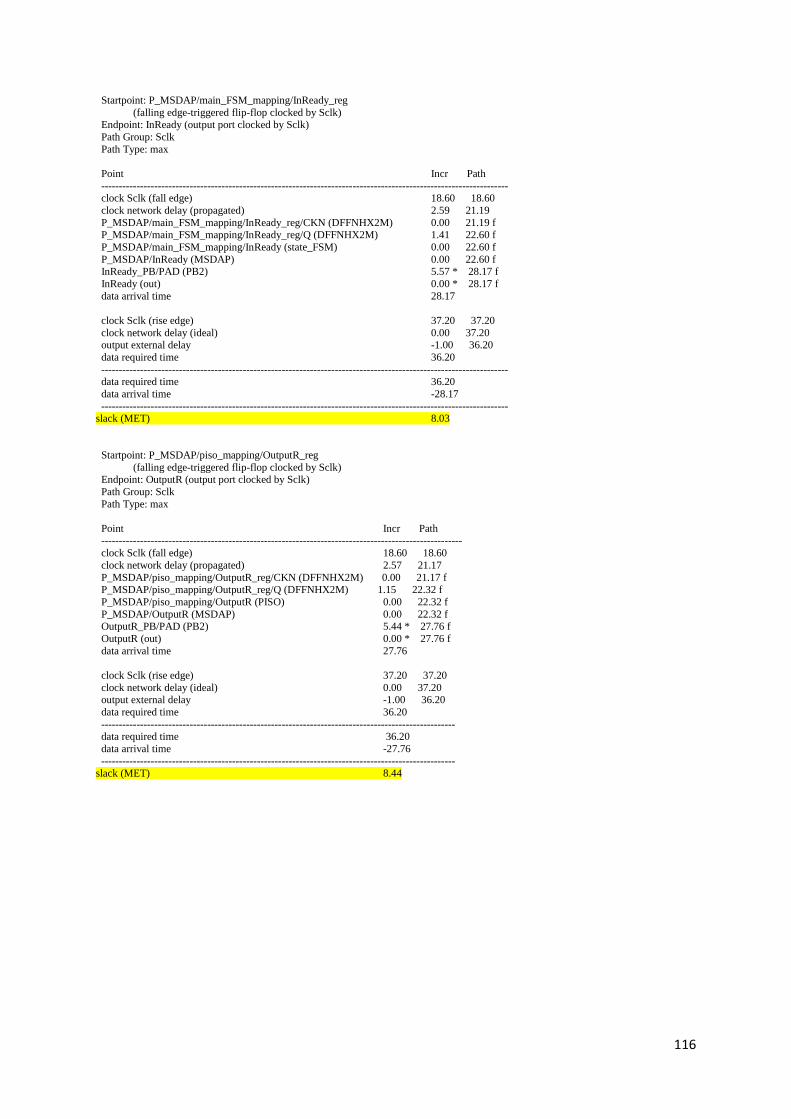
116
Startpoint: P_MSDAP/main_FSM_mapping/InReady_reg
(falling edge-triggered flip-flop clocked by Sclk) Endpoint: InReady (output port clocked by Sclk)
Path Group: Sclk
Path Type: max
Point Incr Path
------------------------------------------------------------------------------------------------------------------- clock Sclk (fall edge) 18.60 18.60
clock network delay (propagated) 2.59 21.19
P_MSDAP/main_FSM_mapping/InReady_reg/CKN (DFFNHX2M) 0.00 21.19 f P_MSDAP/main_FSM_mapping/InReady_reg/Q (DFFNHX2M) 1.41 22.60 f
P_MSDAP/main_FSM_mapping/InReady (state_FSM) 0.00 22.60 f
P_MSDAP/InReady (MSDAP) 0.00 22.60 f InReady_PB/PAD (PB2) 5.57 * 28.17 f
InReady (out) 0.00 * 28.17 f
data arrival time 28.17
clock Sclk (rise edge) 37.20 37.20
clock network delay (ideal) 0.00 37.20 output external delay -1.00 36.20
data required time 36.20
------------------------------------------------------------------------------------------------------------------- data required time 36.20
data arrival time -28.17
------------------------------------------------------------------------------------------------------------------- slack (MET) 8.03
Startpoint: P_MSDAP/piso_mapping/OutputR_reg
(falling edge-triggered flip-flop clocked by Sclk) Endpoint: OutputR (output port clocked by Sclk)
Path Group: Sclk
Path Type: max
Point Incr Path
------------------------------------------------------------------------------------------------------ clock Sclk (fall edge) 18.60 18.60
clock network delay (propagated) 2.57 21.17
P_MSDAP/piso_mapping/OutputR_reg/CKN (DFFNHX2M) 0.00 21.17 f P_MSDAP/piso_mapping/OutputR_reg/Q (DFFNHX2M) 1.15 22.32 f
P_MSDAP/piso_mapping/OutputR (PISO) 0.00 22.32 f
P_MSDAP/OutputR (MSDAP) 0.00 22.32 f OutputR_PB/PAD (PB2) 5.44 * 27.76 f
OutputR (out) 0.00 * 27.76 f
data arrival time 27.76
clock Sclk (rise edge) 37.20 37.20
clock network delay (ideal) 0.00 37.20 output external delay -1.00 36.20
data required time 36.20
---------------------------------------------------------------------------------------------------- data required time 36.20
data arrival time -27.76
---------------------------------------------------------------------------------------------------- slack (MET) 8.44
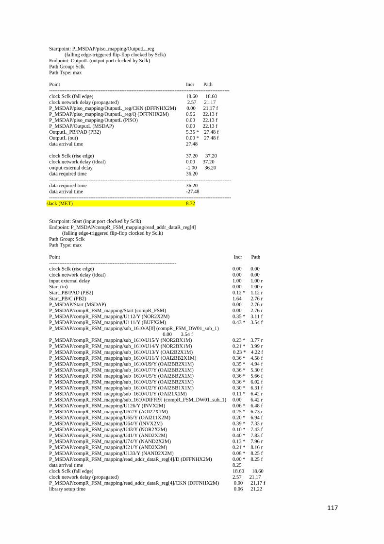
117
Startpoint: P_MSDAP/piso_mapping/OutputL_reg
(falling edge-triggered flip-flop clocked by Sclk) Endpoint: OutputL (output port clocked by Sclk)
Path Group: Sclk
Path Type: max
Point Incr Path
--------------------------------------------------------------------------------------------------------- clock Sclk (fall edge) 18.60 18.60
clock network delay (propagated) 2.57 21.17
P_MSDAP/piso_mapping/OutputL_reg/CKN (DFFNHX2M) 0.00 21.17 f P_MSDAP/piso_mapping/OutputL_reg/Q (DFFNHX2M) 0.96 22.13 f
P_MSDAP/piso_mapping/OutputL (PISO) 0.00 22.13 f
P_MSDAP/OutputL (MSDAP) 0.00 22.13 f OutputL_PB/PAD (PB2) 5.35 * 27.48 f
OutputL (out) 0.00 * 27.48 f
data arrival time 27.48
clock Sclk (rise edge) 37.20 37.20
clock network delay (ideal) 0.00 37.20 output external delay -1.00 36.20
data required time 36.20
---------------------------------------------------------------------------------------------------------- data required time 36.20
data arrival time -27.48
---------------------------------------------------------------------------------------------------------- slack (MET) 8.72
Startpoint: Start (input port clocked by Sclk)
Endpoint: P_MSDAP/compR_FSM_mapping/read_addr_dataR_reg[4] (falling edge-triggered flip-flop clocked by Sclk)
Path Group: Sclk
Path Type: max
Point Incr Path
-------------------------------------------------------------------------- clock Sclk (rise edge) 0.00 0.00
clock network delay (ideal) 0.00 0.00
input external delay 1.00 1.00 r Start (in) 0.00 1.00 r
Start_PB/PAD (PB2) 0.12 * 1.12 r
Start_PB/C (PB2) 1.64 2.76 r P_MSDAP/Start (MSDAP) 0.00 2.76 r
P_MSDAP/compR_FSM_mapping/Start (compR_FSM) 0.00 2.76 r
P_MSDAP/compR_FSM_mapping/U112/Y (NOR2X2M) 0.35 * 3.11 f P_MSDAP/compR_FSM_mapping/U111/Y (BUFX2M) 0.43 * 3.54 f
P_MSDAP/compR_FSM_mapping/sub_1610/A[0] (compR_FSM_DW01_sub_1)
0.00 3.54 f P_MSDAP/compR_FSM_mapping/sub_1610/U15/Y (NOR2BX1M) 0.23 * 3.77 r
P_MSDAP/compR_FSM_mapping/sub_1610/U14/Y (NOR2BX1M) 0.21 * 3.99 r
P_MSDAP/compR_FSM_mapping/sub_1610/U13/Y (OAI2B2X1M) 0.23 * 4.22 f P_MSDAP/compR_FSM_mapping/sub_1610/U11/Y (OAI2BB2X1M) 0.36 * 4.58 f
P_MSDAP/compR_FSM_mapping/sub_1610/U9/Y (OAI2BB2X1M) 0.35 * 4.94 f
P_MSDAP/compR_FSM_mapping/sub_1610/U7/Y (OAI2BB2X1M) 0.36 * 5.30 f P_MSDAP/compR_FSM_mapping/sub_1610/U5/Y (OAI2BB2X1M) 0.36 * 5.66 f
P_MSDAP/compR_FSM_mapping/sub_1610/U3/Y (OAI2BB2X1M) 0.36 * 6.02 f
P_MSDAP/compR_FSM_mapping/sub_1610/U2/Y (OAI2BB1X1M) 0.30 * 6.31 f P_MSDAP/compR_FSM_mapping/sub_1610/U1/Y (OAI21X1M) 0.11 * 6.42 r
P_MSDAP/compR_FSM_mapping/sub_1610/DIFF[9] (compR_FSM_DW01_sub_1) 0.00 6.42 r
P_MSDAP/compR_FSM_mapping/U126/Y (INVX2M) 0.06 * 6.48 f P_MSDAP/compR_FSM_mapping/U67/Y (AOI22X1M) 0.25 * 6.73 r
P_MSDAP/compR_FSM_mapping/U65/Y (OAI211X2M) 0.20 * 6.94 f
P_MSDAP/compR_FSM_mapping/U64/Y (INVX2M) 0.39 * 7.33 r P_MSDAP/compR_FSM_mapping/U43/Y (NOR2X2M) 0.10 * 7.43 f
P_MSDAP/compR_FSM_mapping/U41/Y (AND2X2M) 0.40 * 7.83 f
P_MSDAP/compR_FSM_mapping/U74/Y (NAND2X2M) 0.13 * 7.96 r P_MSDAP/compR_FSM_mapping/U21/Y (AND2X2M) 0.21 * 8.16 r
P_MSDAP/compR_FSM_mapping/U133/Y (NAND2X2M) 0.08 * 8.25 f
P_MSDAP/compR_FSM_mapping/read_addr_dataR_reg[4]/D (DFFNHX2M) 0.00 * 8.25 f data arrival time 8.25
clock Sclk (fall edge) 18.60 18.60
clock network delay (propagated) 2.57 21.17 P_MSDAP/compR_FSM_mapping/read_addr_dataR_reg[4]/CKN (DFFNHX2M) 0.00 21.17 f
library setup time 0.06 21.22
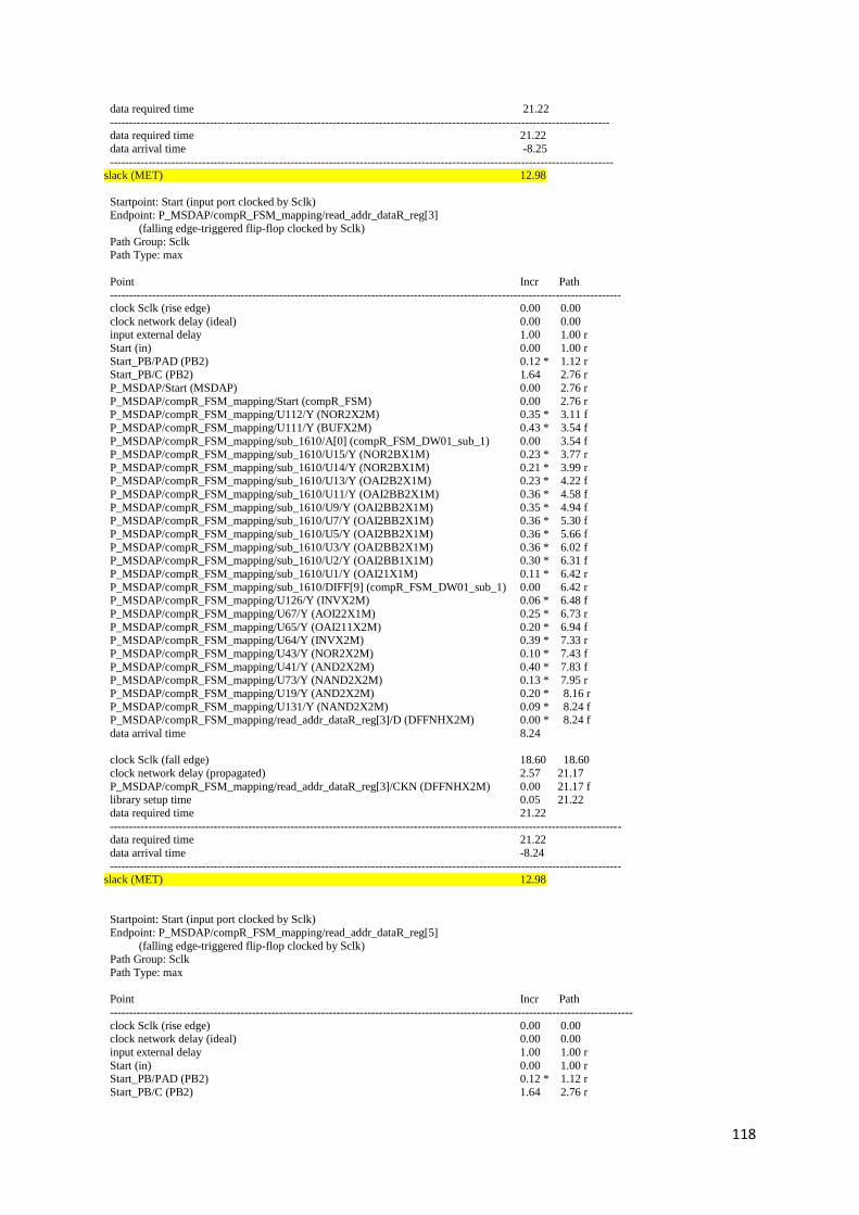
118
data required time 21.22
---------------------------------------------------------------------------------------------------------------------------------- data required time 21.22
data arrival time -8.25
----------------------------------------------------------------------------------------------------------------------------------- slack (MET) 12.98
Startpoint: Start (input port clocked by Sclk) Endpoint: P_MSDAP/compR_FSM_mapping/read_addr_dataR_reg[3]
(falling edge-triggered flip-flop clocked by Sclk)
Path Group: Sclk Path Type: max
Point Incr Path -------------------------------------------------------------------------------------------------------------------------------------
clock Sclk (rise edge) 0.00 0.00
clock network delay (ideal) 0.00 0.00 input external delay 1.00 1.00 r
Start (in) 0.00 1.00 r
Start_PB/PAD (PB2) 0.12 * 1.12 r Start_PB/C (PB2) 1.64 2.76 r
P_MSDAP/Start (MSDAP) 0.00 2.76 r
P_MSDAP/compR_FSM_mapping/Start (compR_FSM) 0.00 2.76 r P_MSDAP/compR_FSM_mapping/U112/Y (NOR2X2M) 0.35 * 3.11 f
P_MSDAP/compR_FSM_mapping/U111/Y (BUFX2M) 0.43 * 3.54 f
P_MSDAP/compR_FSM_mapping/sub_1610/A[0] (compR_FSM_DW01_sub_1) 0.00 3.54 f P_MSDAP/compR_FSM_mapping/sub_1610/U15/Y (NOR2BX1M) 0.23 * 3.77 r
P_MSDAP/compR_FSM_mapping/sub_1610/U14/Y (NOR2BX1M) 0.21 * 3.99 r P_MSDAP/compR_FSM_mapping/sub_1610/U13/Y (OAI2B2X1M) 0.23 * 4.22 f
P_MSDAP/compR_FSM_mapping/sub_1610/U11/Y (OAI2BB2X1M) 0.36 * 4.58 f
P_MSDAP/compR_FSM_mapping/sub_1610/U9/Y (OAI2BB2X1M) 0.35 * 4.94 f P_MSDAP/compR_FSM_mapping/sub_1610/U7/Y (OAI2BB2X1M) 0.36 * 5.30 f
P_MSDAP/compR_FSM_mapping/sub_1610/U5/Y (OAI2BB2X1M) 0.36 * 5.66 f
P_MSDAP/compR_FSM_mapping/sub_1610/U3/Y (OAI2BB2X1M) 0.36 * 6.02 f P_MSDAP/compR_FSM_mapping/sub_1610/U2/Y (OAI2BB1X1M) 0.30 * 6.31 f
P_MSDAP/compR_FSM_mapping/sub_1610/U1/Y (OAI21X1M) 0.11 * 6.42 r
P_MSDAP/compR_FSM_mapping/sub_1610/DIFF[9] (compR_FSM_DW01_sub_1) 0.00 6.42 r P_MSDAP/compR_FSM_mapping/U126/Y (INVX2M) 0.06 * 6.48 f
P_MSDAP/compR_FSM_mapping/U67/Y (AOI22X1M) 0.25 * 6.73 r
P_MSDAP/compR_FSM_mapping/U65/Y (OAI211X2M) 0.20 * 6.94 f P_MSDAP/compR_FSM_mapping/U64/Y (INVX2M) 0.39 * 7.33 r
P_MSDAP/compR_FSM_mapping/U43/Y (NOR2X2M) 0.10 * 7.43 f
P_MSDAP/compR_FSM_mapping/U41/Y (AND2X2M) 0.40 * 7.83 f P_MSDAP/compR_FSM_mapping/U73/Y (NAND2X2M) 0.13 * 7.95 r
P_MSDAP/compR_FSM_mapping/U19/Y (AND2X2M) 0.20 * 8.16 r
P_MSDAP/compR_FSM_mapping/U131/Y (NAND2X2M) 0.09 * 8.24 f P_MSDAP/compR_FSM_mapping/read_addr_dataR_reg[3]/D (DFFNHX2M) 0.00 * 8.24 f
data arrival time 8.24
clock Sclk (fall edge) 18.60 18.60
clock network delay (propagated) 2.57 21.17
P_MSDAP/compR_FSM_mapping/read_addr_dataR_reg[3]/CKN (DFFNHX2M) 0.00 21.17 f library setup time 0.05 21.22
data required time 21.22
------------------------------------------------------------------------------------------------------------------------------------- data required time 21.22
data arrival time -8.24
------------------------------------------------------------------------------------------------------------------------------------- slack (MET) 12.98
Startpoint: Start (input port clocked by Sclk)
Endpoint: P_MSDAP/compR_FSM_mapping/read_addr_dataR_reg[5]
(falling edge-triggered flip-flop clocked by Sclk) Path Group: Sclk
Path Type: max
Point Incr Path
----------------------------------------------------------------------------------------------------------------------------------------
clock Sclk (rise edge) 0.00 0.00 clock network delay (ideal) 0.00 0.00
input external delay 1.00 1.00 r
Start (in) 0.00 1.00 r Start_PB/PAD (PB2) 0.12 * 1.12 r
Start_PB/C (PB2) 1.64 2.76 r
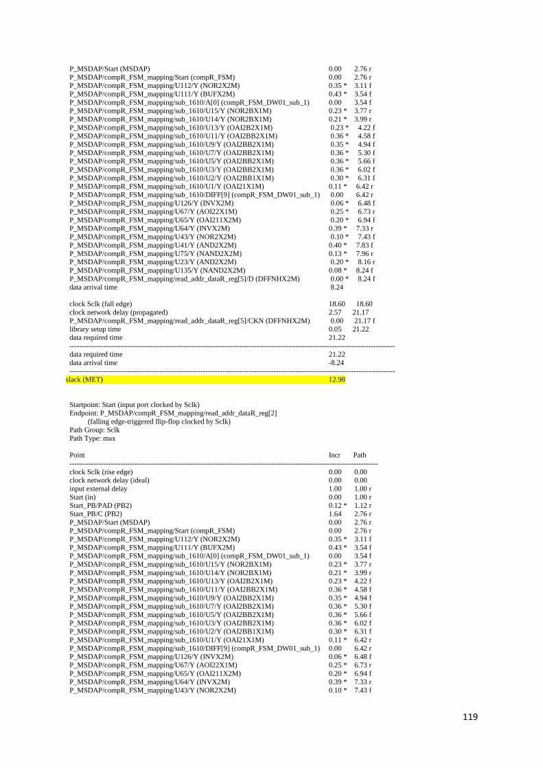
119
P_MSDAP/Start (MSDAP) 0.00 2.76 r
P_MSDAP/compR_FSM_mapping/Start (compR_FSM) 0.00 2.76 r P_MSDAP/compR_FSM_mapping/U112/Y (NOR2X2M) 0.35 * 3.11 f
P_MSDAP/compR_FSM_mapping/U111/Y (BUFX2M) 0.43 * 3.54 f
P_MSDAP/compR_FSM_mapping/sub_1610/A[0] (compR_FSM_DW01_sub_1) 0.00 3.54 f P_MSDAP/compR_FSM_mapping/sub_1610/U15/Y (NOR2BX1M) 0.23 * 3.77 r
P_MSDAP/compR_FSM_mapping/sub_1610/U14/Y (NOR2BX1M) 0.21 * 3.99 r
P_MSDAP/compR_FSM_mapping/sub_1610/U13/Y (OAI2B2X1M) 0.23 * 4.22 f P_MSDAP/compR_FSM_mapping/sub_1610/U11/Y (OAI2BB2X1M) 0.36 * 4.58 f
P_MSDAP/compR_FSM_mapping/sub_1610/U9/Y (OAI2BB2X1M) 0.35 * 4.94 f
P_MSDAP/compR_FSM_mapping/sub_1610/U7/Y (OAI2BB2X1M) 0.36 * 5.30 f P_MSDAP/compR_FSM_mapping/sub_1610/U5/Y (OAI2BB2X1M) 0.36 * 5.66 f
P_MSDAP/compR_FSM_mapping/sub_1610/U3/Y (OAI2BB2X1M) 0.36 * 6.02 f
P_MSDAP/compR_FSM_mapping/sub_1610/U2/Y (OAI2BB1X1M) 0.30 * 6.31 f P_MSDAP/compR_FSM_mapping/sub_1610/U1/Y (OAI21X1M) 0.11 * 6.42 r
P_MSDAP/compR_FSM_mapping/sub_1610/DIFF[9] (compR_FSM_DW01_sub_1) 0.00 6.42 r
P_MSDAP/compR_FSM_mapping/U126/Y (INVX2M) 0.06 * 6.48 f P_MSDAP/compR_FSM_mapping/U67/Y (AOI22X1M) 0.25 * 6.73 r
P_MSDAP/compR_FSM_mapping/U65/Y (OAI211X2M) 0.20 * 6.94 f
P_MSDAP/compR_FSM_mapping/U64/Y (INVX2M) 0.39 * 7.33 r P_MSDAP/compR_FSM_mapping/U43/Y (NOR2X2M) 0.10 * 7.43 f
P_MSDAP/compR_FSM_mapping/U41/Y (AND2X2M) 0.40 * 7.83 f
P_MSDAP/compR_FSM_mapping/U75/Y (NAND2X2M) 0.13 * 7.96 r P_MSDAP/compR_FSM_mapping/U23/Y (AND2X2M) 0.20 * 8.16 r
P_MSDAP/compR_FSM_mapping/U135/Y (NAND2X2M) 0.08 * 8.24 f
P_MSDAP/compR_FSM_mapping/read_addr_dataR_reg[5]/D (DFFNHX2M) 0.00 * 8.24 f data arrival time 8.24
clock Sclk (fall edge) 18.60 18.60
clock network delay (propagated) 2.57 21.17
P_MSDAP/compR_FSM_mapping/read_addr_dataR_reg[5]/CKN (DFFNHX2M) 0.00 21.17 f library setup time 0.05 21.22
data required time 21.22
-------------------------------------------------------------------------------------------------------------------------------------- data required time 21.22
data arrival time -8.24
-------------------------------------------------------------------------------------------------------------------------------------- slack (MET) 12.98
Startpoint: Start (input port clocked by Sclk)
Endpoint: P_MSDAP/compR_FSM_mapping/read_addr_dataR_reg[2]
(falling edge-triggered flip-flop clocked by Sclk) Path Group: Sclk
Path Type: max
Point Incr Path
-------------------------------------------------------------------------------------------------------------------------------
clock Sclk (rise edge) 0.00 0.00 clock network delay (ideal) 0.00 0.00
input external delay 1.00 1.00 r
Start (in) 0.00 1.00 r Start_PB/PAD (PB2) 0.12 * 1.12 r
Start_PB/C (PB2) 1.64 2.76 r
P_MSDAP/Start (MSDAP) 0.00 2.76 r P_MSDAP/compR_FSM_mapping/Start (compR_FSM) 0.00 2.76 r
P_MSDAP/compR_FSM_mapping/U112/Y (NOR2X2M) 0.35 * 3.11 f
P_MSDAP/compR_FSM_mapping/U111/Y (BUFX2M) 0.43 * 3.54 f P_MSDAP/compR_FSM_mapping/sub_1610/A[0] (compR_FSM_DW01_sub_1) 0.00 3.54 f
P_MSDAP/compR_FSM_mapping/sub_1610/U15/Y (NOR2BX1M) 0.23 * 3.77 r
P_MSDAP/compR_FSM_mapping/sub_1610/U14/Y (NOR2BX1M) 0.21 * 3.99 r P_MSDAP/compR_FSM_mapping/sub_1610/U13/Y (OAI2B2X1M) 0.23 * 4.22 f
P_MSDAP/compR_FSM_mapping/sub_1610/U11/Y (OAI2BB2X1M) 0.36 * 4.58 f
P_MSDAP/compR_FSM_mapping/sub_1610/U9/Y (OAI2BB2X1M) 0.35 * 4.94 f P_MSDAP/compR_FSM_mapping/sub_1610/U7/Y (OAI2BB2X1M) 0.36 * 5.30 f
P_MSDAP/compR_FSM_mapping/sub_1610/U5/Y (OAI2BB2X1M) 0.36 * 5.66 f
P_MSDAP/compR_FSM_mapping/sub_1610/U3/Y (OAI2BB2X1M) 0.36 * 6.02 f P_MSDAP/compR_FSM_mapping/sub_1610/U2/Y (OAI2BB1X1M) 0.30 * 6.31 f
P_MSDAP/compR_FSM_mapping/sub_1610/U1/Y (OAI21X1M) 0.11 * 6.42 r
P_MSDAP/compR_FSM_mapping/sub_1610/DIFF[9] (compR_FSM_DW01_sub_1) 0.00 6.42 r P_MSDAP/compR_FSM_mapping/U126/Y (INVX2M) 0.06 * 6.48 f
P_MSDAP/compR_FSM_mapping/U67/Y (AOI22X1M) 0.25 * 6.73 r
P_MSDAP/compR_FSM_mapping/U65/Y (OAI211X2M) 0.20 * 6.94 f P_MSDAP/compR_FSM_mapping/U64/Y (INVX2M) 0.39 * 7.33 r
P_MSDAP/compR_FSM_mapping/U43/Y (NOR2X2M) 0.10 * 7.43 f
120
P_MSDAP/compR_FSM_mapping/U68/Y (AND2X2M) 0.40 * 7.83 f
P_MSDAP/compR_FSM_mapping/U78/Y (NAND2X2M) 0.12 * 7.96 r P_MSDAP/compR_FSM_mapping/U18/Y (AND2X2M) 0.20 * 8.15 r
P_MSDAP/compR_FSM_mapping/U129/Y (NAND2X2M) 0.09 * 8.24 f
P_MSDAP/compR_FSM_mapping/read_addr_dataR_reg[2]/D (DFFNHX2M) 0.00 * 8.24 f data arrival time 8.24
clock Sclk (fall edge) 18.60 18.60 clock network delay (propagated) 2.57 21.17
P_MSDAP/compR_FSM_mapping/read_addr_dataR_reg[2]/CKN (DFFNHX2M) 0.00 21.17 f
library setup time 0.05 21.22 data required time 21.22
--------------------------------------------------------------------------------------------------------------------------------------
data required time 21.22 data arrival time -8.24
--------------------------------------------------------------------------------------------------------------------------------------
slack (MET) 12.98
Startpoint: Start (input port clocked by Sclk) Endpoint: P_MSDAP/compR_FSM_mapping/read_addr_dataR_reg[0]
(falling edge-triggered flip-flop clocked by Sclk)
Path Group: Sclk Path Type: max
Point Incr Path ------------------------------------------------------------------------------------------------------------------------------------
clock Sclk (rise edge) 0.00 0.00 clock network delay (ideal) 0.00 0.00
input external delay 1.00 1.00 r
Start (in) 0.00 1.00 r Start_PB/PAD (PB2) 0.12 * 1.12 r
Start_PB/C (PB2) 1.64 2.76 r
P_MSDAP/Start (MSDAP) 0.00 2.76 r P_MSDAP/compR_FSM_mapping/Start (compR_FSM) 0.00 2.76 r
P_MSDAP/compR_FSM_mapping/U112/Y (NOR2X2M) 0.35 * 3.11 f
P_MSDAP/compR_FSM_mapping/U111/Y (BUFX2M) 0.43 * 3.54 f P_MSDAP/compR_FSM_mapping/sub_1610/A[0] (compR_FSM_DW01_sub_1) 0.00 3.54 f
P_MSDAP/compR_FSM_mapping/sub_1610/U15/Y (NOR2BX1M) 0.23 * 3.77 r
P_MSDAP/compR_FSM_mapping/sub_1610/U14/Y (NOR2BX1M) 0.21 * 3.99 r P_MSDAP/compR_FSM_mapping/sub_1610/U13/Y (OAI2B2X1M) 0.23 * 4.22 f
P_MSDAP/compR_FSM_mapping/sub_1610/U11/Y (OAI2BB2X1M) 0.36 * 4.58 f
P_MSDAP/compR_FSM_mapping/sub_1610/U9/Y (OAI2BB2X1M) 0.35 * 4.94 f P_MSDAP/compR_FSM_mapping/sub_1610/U7/Y (OAI2BB2X1M) 0.36 * 5.30 f
P_MSDAP/compR_FSM_mapping/sub_1610/U5/Y (OAI2BB2X1M) 0.36 * 5.66 f
P_MSDAP/compR_FSM_mapping/sub_1610/U3/Y (OAI2BB2X1M) 0.36 * 6.02 f P_MSDAP/compR_FSM_mapping/sub_1610/U2/Y (OAI2BB1X1M) 0.30 * 6.31 f
P_MSDAP/compR_FSM_mapping/sub_1610/U1/Y (OAI21X1M) 0.11 * 6.42 r
P_MSDAP/compR_FSM_mapping/sub_1610/DIFF[9] (compR_FSM_DW01_sub_1) 0.00 6.42 r P_MSDAP/compR_FSM_mapping/U126/Y (INVX2M) 0.06 * 6.48 f
P_MSDAP/compR_FSM_mapping/U67/Y (AOI22X1M) 0.25 * 6.73 r
P_MSDAP/compR_FSM_mapping/U65/Y (OAI211X2M) 0.20 * 6.94 f P_MSDAP/compR_FSM_mapping/U64/Y (INVX2M) 0.39 * 7.33 r
P_MSDAP/compR_FSM_mapping/U43/Y (NOR2X2M) 0.10 * 7.43 f
P_MSDAP/compR_FSM_mapping/U41/Y (AND2X2M) 0.40 * 7.83 f P_MSDAP/compR_FSM_mapping/U84/Y (NAND2X2M) 0.12 * 7.95 r
P_MSDAP/compR_FSM_mapping/U32/Y (AND2X2M) 0.19 * 8.14 r
P_MSDAP/compR_FSM_mapping/U139/Y (NAND2X2M) 0.09 * 8.23 f P_MSDAP/compR_FSM_mapping/read_addr_dataR_reg[0]/D (DFFNHX2M) 0.00 * 8.23 f
data arrival time 8.23
clock Sclk (fall edge) 18.60 18.60
clock network delay (propagated) 2.57 21.17
P_MSDAP/compR_FSM_mapping/read_addr_dataR_reg[0]/CKN (DFFNHX2M) 0.00 21.17 f library setup time 0.05 21.22
data required time 21.22
------------------------------------------------------------------------------------------------------------------------------------- data required time 21.22
data arrival time -8.23
------------------------------------------------------------------------------------------------------------------------------------- slack (MET) 12.99

121
Startpoint: Start (input port clocked by Sclk)
Endpoint: P_MSDAP/compR_FSM_mapping/read_addr_dataR_reg[1] (falling edge-triggered flip-flop clocked by Sclk)
Path Group: Sclk
Path Type: max
Point Incr Path
--------------------------------------------------------------------------------------------------------------------------------------- clock Sclk (rise edge) 0.00 0.00
clock network delay (ideal) 0.00 0.00
input external delay 1.00 1.00 r Start (in) 0.00 1.00 r
Start_PB/PAD (PB2) 0.12 * 1.12 r
Start_PB/C (PB2) 1.64 2.76 r P_MSDAP/Start (MSDAP) 0.00 2.76 r
P_MSDAP/compR_FSM_mapping/Start (compR_FSM) 0.00 2.76 r
P_MSDAP/compR_FSM_mapping/U112/Y (NOR2X2M) 0.35 * 3.11 f P_MSDAP/compR_FSM_mapping/U111/Y (BUFX2M) 0.43 * 3.54 f
P_MSDAP/compR_FSM_mapping/sub_1610/A[0] (compR_FSM_DW01_sub_1) 0.00 3.54 f
P_MSDAP/compR_FSM_mapping/sub_1610/U15/Y (NOR2BX1M) 0.23 * 3.77 r P_MSDAP/compR_FSM_mapping/sub_1610/U14/Y (NOR2BX1M) 0.21 * 3.99 r
P_MSDAP/compR_FSM_mapping/sub_1610/U13/Y (OAI2B2X1M) 0.23 * 4.22 f
P_MSDAP/compR_FSM_mapping/sub_1610/U11/Y (OAI2BB2X1M) 0.36 * 4.58 f P_MSDAP/compR_FSM_mapping/sub_1610/U9/Y (OAI2BB2X1M) 0.35 * 4.94 f
P_MSDAP/compR_FSM_mapping/sub_1610/U7/Y (OAI2BB2X1M) 0.36 * 5.30 f
P_MSDAP/compR_FSM_mapping/sub_1610/U5/Y (OAI2BB2X1M) 0.36 * 5.66 f P_MSDAP/compR_FSM_mapping/sub_1610/U3/Y (OAI2BB2X1M) 0.36 * 6.02 f
P_MSDAP/compR_FSM_mapping/sub_1610/U2/Y (OAI2BB1X1M) 0.30 * 6.31 f P_MSDAP/compR_FSM_mapping/sub_1610/U1/Y (OAI21X1M) 0.11 * 6.42 r
P_MSDAP/compR_FSM_mapping/sub_1610/DIFF[9] (compR_FSM_DW01_sub_1) 0.00 6.42 r
P_MSDAP/compR_FSM_mapping/U126/Y (INVX2M) 0.06 * 6.48 f P_MSDAP/compR_FSM_mapping/U67/Y (AOI22X1M) 0.25 * 6.73 r
P_MSDAP/compR_FSM_mapping/U65/Y (OAI211X2M) 0.20 * 6.94 f
P_MSDAP/compR_FSM_mapping/U64/Y (INVX2M) 0.39 * 7.33 r P_MSDAP/compR_FSM_mapping/U43/Y (NOR2X2M) 0.10 * 7.43 f
P_MSDAP/compR_FSM_mapping/U68/Y (AND2X2M) 0.40 * 7.83 f
P_MSDAP/compR_FSM_mapping/U77/Y (NAND2X2M) 0.12 * 7.95 r P_MSDAP/compR_FSM_mapping/U16/Y (AND2X2M) 0.19 * 8.14 r
P_MSDAP/compR_FSM_mapping/U127/Y (NAND2X2M) 0.08 * 8.23 f
P_MSDAP/compR_FSM_mapping/read_addr_dataR_reg[1]/D (DFFNHX2M) 0.00 * 8.23 f data arrival time 8.23
clock Sclk (fall edge) 18.60 18.60 clock network delay (propagated) 2.57 21.17
P_MSDAP/compR_FSM_mapping/read_addr_dataR_reg[1]/CKN (DFFNHX2M) 0.00 21.17 f
library setup time 0.05 21.22 data required time 21.22
----------------------------------------------------------------------------------------------------------------------------------------
data required time 21.22 data arrival time -8.23
----------------------------------------------------------------------------------------------------------------------------------------
slack (MET) 12.99
Startpoint: Start (input port clocked by Sclk) Endpoint: P_MSDAP/compR_FSM_mapping/read_addr_dataR_reg[6]
(falling edge-triggered flip-flop clocked by Sclk)
Path Group: Sclk Path Type: max
Point Incr Path ------------------------------------------------------------------------------------------------------------------------------------
clock Sclk (rise edge) 0.00 0.00
clock network delay (ideal) 0.00 0.00 input external delay 1.00 1.00 r
Start (in) 0.00 1.00 r
Start_PB/PAD (PB2) 0.12 * 1.12 r Start_PB/C (PB2) 1.64 2.76 r
P_MSDAP/Start (MSDAP) 0.00 2.76 r
P_MSDAP/compR_FSM_mapping/Start (compR_FSM) 0.00 2.76 r P_MSDAP/compR_FSM_mapping/U112/Y (NOR2X2M) 0.35 * 3.11 f
P_MSDAP/compR_FSM_mapping/U111/Y (BUFX2M) 0.43 *3.54 f
P_MSDAP/compR_FSM_mapping/sub_1610/A[0] (compR_FSM_DW01_sub_1) 0.00 3.54 f P_MSDAP/compR_FSM_mapping/sub_1610/U15/Y (NOR2BX1M) 0.23 * 3.77 r
P_MSDAP/compR_FSM_mapping/sub_1610/U14/Y (NOR2BX1M) 0.21 * 3.99 r
122
P_MSDAP/compR_FSM_mapping/sub_1610/U13/Y (OAI2B2X1M) 0.23 * 4.22 f
P_MSDAP/compR_FSM_mapping/sub_1610/U11/Y (OAI2BB2X1M) 0.36 * 4.58 f P_MSDAP/compR_FSM_mapping/sub_1610/U9/Y (OAI2BB2X1M) 0.35 * 4.94 f
P_MSDAP/compR_FSM_mapping/sub_1610/U7/Y (OAI2BB2X1M) 0.36 * 5.30 f
P_MSDAP/compR_FSM_mapping/sub_1610/U5/Y (OAI2BB2X1M) 0.36 * 5.66 f P_MSDAP/compR_FSM_mapping/sub_1610/U3/Y (OAI2BB2X1M) 0.36 * 6.02 f
P_MSDAP/compR_FSM_mapping/sub_1610/U2/Y (OAI2BB1X1M) 0.30 * 6.31 f
P_MSDAP/compR_FSM_mapping/sub_1610/U1/Y (OAI21X1M) 0.11 * 6.42 r P_MSDAP/compR_FSM_mapping/sub_1610/DIFF[9] (compR_FSM_DW01_sub_1) 0.00 6.42 r
P_MSDAP/compR_FSM_mapping/U126/Y (INVX2M) 0.06 * 6.48 f
P_MSDAP/compR_FSM_mapping/U67/Y (AOI22X1M) 0.25 * 6.73 r P_MSDAP/compR_FSM_mapping/U65/Y (OAI211X2M) 0.20 * 6.94 f
P_MSDAP/compR_FSM_mapping/U64/Y (INVX2M) 0.39 * 7.33 r
P_MSDAP/compR_FSM_mapping/U43/Y (NOR2X2M) 0.10 * 7.43 f P_MSDAP/compR_FSM_mapping/U68/Y (AND2X2M) 0.40 * 7.83 f
P_MSDAP/compR_FSM_mapping/U82/Y (NAND2X2M) 0.12 * 7.95 r
P_MSDAP/compR_FSM_mapping/U26/Y (AND2X2M) 0.19 * 8.14 r P_MSDAP/compR_FSM_mapping/U137/Y (NAND2X2M) 0.08 * 8.22 f
P_MSDAP/compR_FSM_mapping/read_addr_dataR_reg[6]/D (DFFNHX2M) 0.00 * 8.22 f
data arrival time 8.22
clock Sclk (fall edge) 18.60 18.60
clock network delay (propagated) 2.57 21.17 P_MSDAP/compR_FSM_mapping/read_addr_dataR_reg[6]/CKN (DFFNHX2M) 0.00 21.17 f
library setup time 0.06 21.22
data required time 21.22 ---------------------------------------------------------------------------------------------------------------------------------------
data required time 21.22 data arrival time -8.22
----------------------------------------------------------------------------------------------------------------------------------------
slack (MET) 13.00
Startpoint: Start (input port clocked by Sclk) Endpoint: P_MSDAP/compR_FSM_mapping/read_addr_dataR_reg[7]
(falling edge-triggered flip-flop clocked by Sclk)
Path Group: Sclk Path Type: max
Point Incr Path -------------------------------------------------------------------------------------------------------------------------------------------
clock Sclk (rise edge) 0.00 0.00
clock network delay (ideal) 0.00 0.00 input external delay 1.00 1.00 r
Start (in) 0.00 1.00 r
Start_PB/PAD (PB2) 0.12 * 1.12 r Start_PB/C (PB2) 1.64 2.76 r
P_MSDAP/Start (MSDAP) 0.00 2.76 r
P_MSDAP/compR_FSM_mapping/Start (compR_FSM) 0.00 2.76 r P_MSDAP/compR_FSM_mapping/U112/Y (NOR2X2M) 0.35 * 3.11 f
P_MSDAP/compR_FSM_mapping/U111/Y (BUFX2M) 0.43 * 3.54 f
P_MSDAP/compR_FSM_mapping/sub_1610/A[0] (compR_FSM_DW01_sub_1) 0.00 3.54 f P_MSDAP/compR_FSM_mapping/sub_1610/U15/Y (NOR2BX1M) 0.23 * 3.77 r
P_MSDAP/compR_FSM_mapping/sub_1610/U14/Y (NOR2BX1M) 0.21 * 3.99 r
P_MSDAP/compR_FSM_mapping/sub_1610/U13/Y (OAI2B2X1M) 0.23 * 4.22 f P_MSDAP/compR_FSM_mapping/sub_1610/U11/Y (OAI2BB2X1M) 0.36 * 4.58 f
P_MSDAP/compR_FSM_mapping/sub_1610/U9/Y (OAI2BB2X1M) 0.35 * 4.94 f
P_MSDAP/compR_FSM_mapping/sub_1610/U7/Y (OAI2BB2X1M) 0.36 * 5.30 f P_MSDAP/compR_FSM_mapping/sub_1610/U5/Y (OAI2BB2X1M) 0.36 * 5.66 f
P_MSDAP/compR_FSM_mapping/sub_1610/U3/Y (OAI2BB2X1M) 0.36 * 6.02 f
P_MSDAP/compR_FSM_mapping/sub_1610/U2/Y (OAI2BB1X1M) 0.30 * 6.31 f P_MSDAP/compR_FSM_mapping/sub_1610/U1/Y (OAI21X1M) 0.11 * 6.42 r
P_MSDAP/compR_FSM_mapping/sub_1610/DIFF[9] (compR_FSM_DW01_sub_1) 0.00 6.42 r
P_MSDAP/compR_FSM_mapping/U126/Y (INVX2M) 0.06 * 6.48 f P_MSDAP/compR_FSM_mapping/U67/Y (AOI22X1M) 0.25 * 6.73 r
P_MSDAP/compR_FSM_mapping/U65/Y (OAI211X2M) 0.20 * 6.94 f
P_MSDAP/compR_FSM_mapping/U64/Y (INVX2M) 0.39 * 7.33 r P_MSDAP/compR_FSM_mapping/U43/Y (NOR2X2M) 0.10 * 7.43 f
P_MSDAP/compR_FSM_mapping/U41/Y (AND2X2M) 0.40 * 7.83 f
P_MSDAP/compR_FSM_mapping/U86/Y (NAND2X2M) 0.12 * 7.95 r P_MSDAP/compR_FSM_mapping/U33/Y (AND2X2M) 0.19 * 8.14 r
P_MSDAP/compR_FSM_mapping/U141/Y (NAND2X2M) 0.08 * 8.22 f
P_MSDAP/compR_FSM_mapping/read_addr_dataR_reg[7]/D (DFFNHX2M) 0.00 * 8.22 f data arrival time 8.22
123
clock Sclk (fall edge) 18.60 18.60
clock network delay (propagated) 2.57 21.17 P_MSDAP/compR_FSM_mapping/read_addr_dataR_reg[7]/CKN (DFFNHX2M) 0.00 21.17 f
library setup time 0.06 21.22
data required time 21.22 ----------------------------------------------------------------------------------------------------------------------------------------
data required time 21.22
data arrival time -8.22 ------------------------------------------------------------------------------------------------------------------------------------
slack (MET) 13.00
Startpoint: Start (input port clocked by Sclk)
Endpoint: P_MSDAP/compR_FSM_mapping/temp_dataR_reg[30] (falling edge-triggered flip-flop clocked by Sclk)
Path Group: Sclk
Path Type: max
Point Incr Path
---------------------------------------------------------------------------------------------------------------------- clock Sclk (rise edge) 0.00 0.00
clock network delay (ideal) 0.00 0.00
input external delay 1.00 1.00 r Start (in) 0.00 1.00 r
Start_PB/PAD (PB2) 0.12 * 1.12 r
Start_PB/C (PB2) 1.64 2.76 r P_MSDAP/Start (MSDAP) 0.00 2.76 r
P_MSDAP/compR_FSM_mapping/Start (compR_FSM) 0.00 2.76 r P_MSDAP/compR_FSM_mapping/U112/Y (NOR2X2M) 0.35 * 3.11 f
P_MSDAP/compR_FSM_mapping/U111/Y (BUFX2M) 0.43 * 3.54 f
P_MSDAP/compR_FSM_mapping/U299/Y (NOR2BX1M) 0.24 * 3.78 r P_MSDAP/compR_FSM_mapping/U300/Y (NOR2BX1M) 0.22 * 4.01 r
P_MSDAP/compR_FSM_mapping/U301/Y (OAI2B2X1M) 0.24 * 4.25 f
P_MSDAP/compR_FSM_mapping/U303/Y (OAI2BB2X1M) 0.34 * 4.59 f P_MSDAP/compR_FSM_mapping/U304/Y (NOR2X1M) 0.15 * 4.74 r
P_MSDAP/compR_FSM_mapping/U305/Y (OAI2BB2X1M) 0.19 * 4.93 f
P_MSDAP/compR_FSM_mapping/U306/Y (NOR2X1M) 0.16 * 5.09 r P_MSDAP/compR_FSM_mapping/U307/Y (OAI2BB2X1M) 0.18 * 5.27 f
P_MSDAP/compR_FSM_mapping/U308/Y (NOR2X1M) 0.15 * 5.42 r
P_MSDAP/compR_FSM_mapping/U309/Y (OAI2BB2X1M) 0.19 * 5.61 f P_MSDAP/compR_FSM_mapping/U310/Y (NOR2X1M) 0.14 * 5.75 r
P_MSDAP/compR_FSM_mapping/U311/Y (AOI2BB2X1M) 0.26 * 6.01 r
P_MSDAP/compR_FSM_mapping/U312/Y (AOI21X1M) 0.17 * 6.18 f P_MSDAP/compR_FSM_mapping/U313/Y (NOR2X1M) 0.15 * 6.33 r
P_MSDAP/compR_FSM_mapping/U34/Y (OAI21X1M) 0.15 * 6.48 f
P_MSDAP/compR_FSM_mapping/U69/Y (AO22X2M) 0.60 * 7.09 f P_MSDAP/compR_FSM_mapping/U42/Y (NAND2X2M) 0.33 * 7.42 r
P_MSDAP/compR_FSM_mapping/U35/Y (INVX2M) 0.35 * 7.77 f
P_MSDAP/compR_FSM_mapping/U157/Y (AO22X2M) 0.44 * 8.20 f P_MSDAP/compR_FSM_mapping/temp_dataR_reg[30]/D (DFFNHX2M) 0.00 * 8.20 f
data arrival time 8.20
clock Sclk (fall edge) 18.60 18.60
clock network delay (propagated) 2.56 21.16
P_MSDAP/compR_FSM_mapping/temp_dataR_reg[30]/CKN (DFFNHX2M) 0.00 21.16 f library setup time 0.05 21.21
data required time 21.21
------------------------------------------------------------------------------------------------------------------------ data required time 21.21
data arrival time -8.20
------------------------------------------------------------------------------------------------------------------------ slack (MET) 13.01
Startpoint: Start (input port clocked by Sclk)
Endpoint: P_MSDAP/compR_FSM_mapping/temp_dataR_reg[16]
(falling edge-triggered flip-flop clocked by Sclk) Path Group: Sclk
Path Type: max
Point Incr Path
---------------------------------------------------------------------------------------------------------------------------------------------
clock Sclk (rise edge) 0.00 0.00 clock network delay (ideal) 0.00 0.00
input external delay 1.00 1.00 r
124
Start (in) 0.00 1.00 r
Start_PB/PAD (PB2) 0.12 * 1.12 r Start_PB/C (PB2) 1.64 2.76 r
P_MSDAP/Start (MSDAP) 0.00 2.76 r
P_MSDAP/compR_FSM_mapping/Start (compR_FSM) 0.00 2.76 r P_MSDAP/compR_FSM_mapping/U112/Y (NOR2X2M) 0.35 * 3.11 f
P_MSDAP/compR_FSM_mapping/U111/Y (BUFX2M) 0.43 * 3.54 f
P_MSDAP/compR_FSM_mapping/U299/Y (NOR2BX1M) 0.24 * 3.78 r P_MSDAP/compR_FSM_mapping/U300/Y (NOR2BX1M) 0.22 * 4.01 r
P_MSDAP/compR_FSM_mapping/U301/Y (OAI2B2X1M) 0.24 * 4.25 f
P_MSDAP/compR_FSM_mapping/U303/Y (OAI2BB2X1M) 0.34 * 4.59 f P_MSDAP/compR_FSM_mapping/U304/Y (NOR2X1M) 0.15 * 4.74 r
P_MSDAP/compR_FSM_mapping/U305/Y (OAI2BB2X1M) 0.19 * 4.93 f
P_MSDAP/compR_FSM_mapping/U306/Y (NOR2X1M) 0.16 * 5.09 r P_MSDAP/compR_FSM_mapping/U307/Y (OAI2BB2X1M) 0.18 * 5.27 f
P_MSDAP/compR_FSM_mapping/U308/Y (NOR2X1M) 0.15 * 5.42 r
P_MSDAP/compR_FSM_mapping/U309/Y (OAI2BB2X1M) 0.19 * 5.61 f P_MSDAP/compR_FSM_mapping/U310/Y (NOR2X1M) 0.14 * 5.75 r
P_MSDAP/compR_FSM_mapping/U311/Y (AOI2BB2X1M) 0.26 * 6.01 r
P_MSDAP/compR_FSM_mapping/U312/Y (AOI21X1M) 0.17 * 6.18 f P_MSDAP/compR_FSM_mapping/U313/Y (NOR2X1M) 0.15 * 6.33 r
P_MSDAP/compR_FSM_mapping/U34/Y (OAI21X1M) 0.15 * 6.48 f
P_MSDAP/compR_FSM_mapping/U69/Y (AO22X2M) 0.60 * 7.09 f P_MSDAP/compR_FSM_mapping/U42/Y (NAND2X2M) 0.33 * 7.42 r
P_MSDAP/compR_FSM_mapping/U35/Y (INVX2M) 0.35 * 7.77 f
P_MSDAP/compR_FSM_mapping/U143/Y (AO22X2M) 0.43 * 8.20 f P_MSDAP/compR_FSM_mapping/temp_dataR_reg[16]/D (DFFNHX2M) 0.00 * 8.20 f
data arrival time 8.20
clock Sclk (fall edge) 18.60 18.60
clock network delay (propagated) 2.55 21.15 P_MSDAP/compR_FSM_mapping/temp_dataR_reg[16]/CKN (DFFNHX2M) 0.00 21.15 f
library setup time 0.05 21.20
data required time 21.20 -------------------------------------------------------------------------------------------------------------------------------------------
data required time 21.20
data arrival time -8.20 --------------------------------------------------------------------------------------------------------------------------------------------
slack (MET) 13.01
Startpoint: Start (input port clocked by Sclk)
Endpoint: P_MSDAP/compR_FSM_mapping/temp_dataR_reg[20] (falling edge-triggered flip-flop clocked by Sclk)
Path Group: Sclk
Path Type: max
Point Incr Path
------------------------------------------------------------------------------------------------------------------------------------------- clock Sclk (rise edge) 0.00 0.00
clock network delay (ideal) 0.00 0.00
input external delay 1.00 1.00 r Start (in) 0.00 1.00 r
Start_PB/PAD (PB2) 0.12 * 1.12 r
Start_PB/C (PB2) 1.64 2.76 r P_MSDAP/Start (MSDAP) 0.00 2.76 r
P_MSDAP/compR_FSM_mapping/Start (compR_FSM) 0.00 2.76 r
P_MSDAP/compR_FSM_mapping/U112/Y (NOR2X2M) 0.35 * 3.11 f P_MSDAP/compR_FSM_mapping/U111/Y (BUFX2M) 0.43 * 3.54 f
P_MSDAP/compR_FSM_mapping/U299/Y (NOR2BX1M) 0.24 * 3.78 r
P_MSDAP/compR_FSM_mapping/U300/Y (NOR2BX1M) 0.22 * 4.01 r P_MSDAP/compR_FSM_mapping/U301/Y (OAI2B2X1M) 0.24 * 4.25 f
P_MSDAP/compR_FSM_mapping/U303/Y (OAI2BB2X1M) 0.34 * 4.59 f
P_MSDAP/compR_FSM_mapping/U304/Y (NOR2X1M) 0.15 * 4.74 r P_MSDAP/compR_FSM_mapping/U305/Y (OAI2BB2X1M) 0.19 * 4.93 f
P_MSDAP/compR_FSM_mapping/U306/Y (NOR2X1M) 0.16 * 5.09 r
P_MSDAP/compR_FSM_mapping/U307/Y (OAI2BB2X1M) 0.18 * 5.27 f P_MSDAP/compR_FSM_mapping/U308/Y (NOR2X1M) 0.15 * 5.42 r
P_MSDAP/compR_FSM_mapping/U309/Y (OAI2BB2X1M) 0.19 * 5.61 f
P_MSDAP/compR_FSM_mapping/U310/Y (NOR2X1M) 0.14 * 5.75 r P_MSDAP/compR_FSM_mapping/U311/Y (AOI2BB2X1M) 0.26 * 6.01 r
P_MSDAP/compR_FSM_mapping/U312/Y (AOI21X1M) 0.17 * 6.18 f
P_MSDAP/compR_FSM_mapping/U313/Y (NOR2X1M) 0.15 * 6.33 r P_MSDAP/compR_FSM_mapping/U34/Y (OAI21X1M) 0.15 * 6.48 f
P_MSDAP/compR_FSM_mapping/U69/Y (AO22X2M) 0.60 * 7.09 f
125
P_MSDAP/compR_FSM_mapping/U42/Y (NAND2X2M) 0.33 * 7.42 r
P_MSDAP/compR_FSM_mapping/U35/Y (INVX2M) 0.35 * 7.77 f P_MSDAP/compR_FSM_mapping/U147/Y (AO22X2M) 0.43 * 8.20 f
P_MSDAP/compR_FSM_mapping/temp_dataR_reg[20]/D (DFFNHX2M) 0.00 * 8.20 f
data arrival time 8.20
clock Sclk (fall edge) 18.60 18.60
clock network delay (propagated) 2.55 21.15 P_MSDAP/compR_FSM_mapping/temp_dataR_reg[20]/CKN (DFFNHX2M) 0.00 21.15 f
library setup time 0.05 21.21
data required time 21.21 --------------------------------------------------------------------------------------------------------------------------------------------
data required time 21.21
data arrival time -8.20 --------------------------------------------------------------------------------------------------------------------------------------------
slack (MET) 13.01
Startpoint: Start (input port clocked by Sclk)
Endpoint: P_MSDAP/compR_FSM_mapping/temp_dataR_reg[18] (falling edge-triggered flip-flop clocked by Sclk)
Path Group: Sclk
Path Type: max
Point Incr Path
------------------------------------------------------------------------------------------------------------------------------------ clock Sclk (rise edge) 0.00 0.00
clock network delay (ideal) 0.00 0.00 input external delay 1.00 1.00 r
Start (in) 0.00 1.00 r
Start_PB/PAD (PB2) 0.12 * 1.12 r Start_PB/C (PB2) 1.64 2.76 r
P_MSDAP/Start (MSDAP) 0.00 2.76 r
P_MSDAP/compR_FSM_mapping/Start (compR_FSM) 0.00 2.76 r P_MSDAP/compR_FSM_mapping/U112/Y (NOR2X2M) 0.35 * 3.11 f
P_MSDAP/compR_FSM_mapping/U111/Y (BUFX2M) 0.43 * 3.54 f
P_MSDAP/compR_FSM_mapping/U299/Y (NOR2BX1M) 0.24 * 3.78 r P_MSDAP/compR_FSM_mapping/U300/Y (NOR2BX1M) 0.22 * 4.01 r
P_MSDAP/compR_FSM_mapping/U301/Y (OAI2B2X1M) 0.24 * 4.25 f
P_MSDAP/compR_FSM_mapping/U303/Y (OAI2BB2X1M) 0.34 * 4.59 f P_MSDAP/compR_FSM_mapping/U304/Y (NOR2X1M) 0.15 * 4.74 r
P_MSDAP/compR_FSM_mapping/U305/Y (OAI2BB2X1M) 0.19 * 4.93 f
P_MSDAP/compR_FSM_mapping/U306/Y (NOR2X1M) 0.16 * 5.09 r P_MSDAP/compR_FSM_mapping/U307/Y (OAI2BB2X1M) 0.18 * 5.27 f
P_MSDAP/compR_FSM_mapping/U308/Y (NOR2X1M) 0.15 * 5.42 r
P_MSDAP/compR_FSM_mapping/U309/Y (OAI2BB2X1M) 0.19 * 5.61 f P_MSDAP/compR_FSM_mapping/U310/Y (NOR2X1M) 0.14 * 5.75 r
P_MSDAP/compR_FSM_mapping/U311/Y (AOI2BB2X1M) 0.26 * 6.01 r
P_MSDAP/compR_FSM_mapping/U312/Y (AOI21X1M) 0.17 * 6.18 f P_MSDAP/compR_FSM_mapping/U313/Y (NOR2X1M) 0.15 * 6.33 r
P_MSDAP/compR_FSM_mapping/U34/Y (OAI21X1M) 0.15 * 6.48 f
P_MSDAP/compR_FSM_mapping/U69/Y (AO22X2M) 0.60 * 7.09 f P_MSDAP/compR_FSM_mapping/U42/Y (NAND2X2M) 0.33 * 7.42 r
P_MSDAP/compR_FSM_mapping/U35/Y (INVX2M) 0.35 * 7.77 f
P_MSDAP/compR_FSM_mapping/U145/Y (AO22X2M) 0.43 * 8.20 f P_MSDAP/compR_FSM_mapping/temp_dataR_reg[18]/D (DFFNHX2M) 0.00 * 8.20 f
data arrival time 8.20
clock Sclk (fall edge) 18.60 18.60
clock network delay (propagated) 2.55 21.15
P_MSDAP/compR_FSM_mapping/temp_dataR_reg[18]/CKN (DFFNHX2M) 0.00 21.15 f library setup time 0.05 21.21
data required time 21.21
------------------------------------------------------------------------------------------------------------------------------------ data required time 21.21
data arrival time -8.20
------------------------------------------------------------------------------------------------------------------------------------ slack (MET) 13.01
126
Startpoint: Start (input port clocked by Sclk)
Endpoint: P_MSDAP/compR_FSM_mapping/temp_dataR_reg[25] (falling edge-triggered flip-flop clocked by Sclk)
Path Group: Sclk
Path Type: max
Point Incr Path
--------------------------------------------------------------------------------------------------------------------------------------- clock Sclk (rise edge) 0.00 0.00
clock network delay (ideal) 0.00 0.00
input external delay 1.00 1.00 r Start (in) 0.00 1.00 r
Start_PB/PAD (PB2) 0.12 * 1.12 r
Start_PB/C (PB2) 1.64 2.76 r P_MSDAP/Start (MSDAP) 0.00 2.76 r
P_MSDAP/compR_FSM_mapping/Start (compR_FSM) 0.00 2.76 r
P_MSDAP/compR_FSM_mapping/U112/Y (NOR2X2M) 0.35 * 3.11 f P_MSDAP/compR_FSM_mapping/U111/Y (BUFX2M) 0.43 * 3.54 f
P_MSDAP/compR_FSM_mapping/U299/Y (NOR2BX1M) 0.24 * 3.78 r
P_MSDAP/compR_FSM_mapping/U300/Y (NOR2BX1M) 0.22 * 4.01 r P_MSDAP/compR_FSM_mapping/U301/Y (OAI2B2X1M) 0.24 * 4.25 f
P_MSDAP/compR_FSM_mapping/U303/Y (OAI2BB2X1M) 0.34 * 4.59 f
P_MSDAP/compR_FSM_mapping/U304/Y (NOR2X1M) 0.15 * 4.74 r P_MSDAP/compR_FSM_mapping/U305/Y (OAI2BB2X1M) 0.19 * 4.93 f
P_MSDAP/compR_FSM_mapping/U306/Y (NOR2X1M) 0.16 * 5.09 r
P_MSDAP/compR_FSM_mapping/U307/Y (OAI2BB2X1M) 0.18 * 5.27 f P_MSDAP/compR_FSM_mapping/U308/Y (NOR2X1M) 0.15 * 5.42 r
P_MSDAP/compR_FSM_mapping/U309/Y (OAI2BB2X1M) 0.19 * 5.61 f P_MSDAP/compR_FSM_mapping/U310/Y (NOR2X1M) 0.14 * 5.75 r
P_MSDAP/compR_FSM_mapping/U311/Y (AOI2BB2X1M) 0.26 * 6.01 r
P_MSDAP/compR_FSM_mapping/U312/Y (AOI21X1M) 0.17 * 6.18 f P_MSDAP/compR_FSM_mapping/U313/Y (NOR2X1M) 0.15 * 6.33 r
P_MSDAP/compR_FSM_mapping/U34/Y (OAI21X1M) 0.15 * 6.48 f
P_MSDAP/compR_FSM_mapping/U69/Y (AO22X2M) 0.60 * 7.09 f P_MSDAP/compR_FSM_mapping/U42/Y (NAND2X2M) 0.33 * 7.42 r
P_MSDAP/compR_FSM_mapping/U35/Y (INVX2M) 0.35 * 7.77 f
P_MSDAP/compR_FSM_mapping/U152/Y (AO22X2M) 0.43 * 8.19 f P_MSDAP/compR_FSM_mapping/temp_dataR_reg[25]/D (DFFNHX2M) 0.00 * 8.19 f
data arrival time 8.19
clock Sclk (fall edge) 18.60 18.60
clock network delay (propagated) 2.55 21.15
P_MSDAP/compR_FSM_mapping/temp_dataR_reg[25]/CKN (DFFNHX2M) 0.00 21.15 f library setup time 0.05 21.21
data required time 21.21
-------------------------------------------------------------------------------------------------------------------------------------------- data required time 21.21
data arrival time -8.19
-------------------------------------------------------------------------------------------------------------------------------------------- slack (MET) 13.01
Startpoint: Start (input port clocked by Sclk)
Endpoint: P_MSDAP/compR_FSM_mapping/temp_dataR_reg[28]
(falling edge-triggered flip-flop clocked by Sclk) Path Group: Sclk
Path Type: max
Point Incr Path
---------------------------------------------------------------------------------------------------------------------------------------
clock Sclk (rise edge) 0.00 0.00 clock network delay (ideal) 0.00 0.00
input external delay 1.00 1.00 r
Start (in) 0.00 1.00 r Start_PB/PAD (PB2) 0.12 * 1.12 r
Start_PB/C (PB2) 1.64 2.76 r
P_MSDAP/Start (MSDAP) 0.00 2.76 r P_MSDAP/compR_FSM_mapping/Start (compR_FSM) 0.00 2.76 r
P_MSDAP/compR_FSM_mapping/U112/Y (NOR2X2M) 0.35 * 3.11 f
P_MSDAP/compR_FSM_mapping/U111/Y (BUFX2M) 0.43 * 3.54 f P_MSDAP/compR_FSM_mapping/U299/Y (NOR2BX1M) 0.24 * 3.78 r
P_MSDAP/compR_FSM_mapping/U300/Y (NOR2BX1M) 0.22 * 4.01 r
P_MSDAP/compR_FSM_mapping/U301/Y (OAI2B2X1M) 0.24 * 4.25 f P_MSDAP/compR_FSM_mapping/U303/Y (OAI2BB2X1M) 0.34 * 4.59 f
P_MSDAP/compR_FSM_mapping/U304/Y (NOR2X1M) 0.15 * 4.74 r
127
P_MSDAP/compR_FSM_mapping/U305/Y (OAI2BB2X1M) 0.19 * 4.93 f
P_MSDAP/compR_FSM_mapping/U306/Y (NOR2X1M) 0.16 * 5.09 r P_MSDAP/compR_FSM_mapping/U307/Y (OAI2BB2X1M) 0.18 * 5.27 f
P_MSDAP/compR_FSM_mapping/U308/Y (NOR2X1M) 0.15 * 5.42 r
P_MSDAP/compR_FSM_mapping/U309/Y (OAI2BB2X1M) 0.19 * 5.61 f P_MSDAP/compR_FSM_mapping/U310/Y (NOR2X1M) 0.14 * 5.75 r
P_MSDAP/compR_FSM_mapping/U311/Y (AOI2BB2X1M) 0.26 * 6.01 r
P_MSDAP/compR_FSM_mapping/U312/Y (AOI21X1M) 0.17 * 6.18 f P_MSDAP/compR_FSM_mapping/U313/Y (NOR2X1M) 0.15 * 6.33 r
P_MSDAP/compR_FSM_mapping/U34/Y (OAI21X1M) 0.15 * 6.48 f
P_MSDAP/compR_FSM_mapping/U69/Y (AO22X2M) 0.60 * 7.09 f P_MSDAP/compR_FSM_mapping/U42/Y (NAND2X2M) 0.33 * 7.42 r
P_MSDAP/compR_FSM_mapping/U35/Y (INVX2M) 0.35 * 7.77 f
P_MSDAP/compR_FSM_mapping/U155/Y (AO22X2M) 0.43 * 8.20 f P_MSDAP/compR_FSM_mapping/temp_dataR_reg[28]/D (DFFNHX2M) 0.00 * 8.20 f
data arrival time 8.20
clock Sclk (fall edge) 18.60 18.60
clock network delay (propagated) 2.56 21.16
P_MSDAP/compR_FSM_mapping/temp_dataR_reg[28]/CKN (DFFNHX2M) 0.00 21.16 f library setup time 0.05 21.21
data required time 21.21
------------------------------------------------------------------------------------------------------------------------------------------ data required time 21.21
data arrival time -8.20
------------------------------------------------------------------------------------------------------------------------------------------ slack (MET) 13.01
Startpoint: Start (input port clocked by Sclk)
Endpoint: P_MSDAP/compR_FSM_mapping/temp_dataR_reg[22] (falling edge-triggered flip-flop clocked by Sclk)
Path Group: Sclk
Path Type: max
Point Incr Path
------------------------------------------------------------------------------------------------------------------------------------ clock Sclk (rise edge) 0.00 0.00
clock network delay (ideal) 0.00 0.00
input external delay 1.00 1.00 r Start (in) 0.00 1.00 r
Start_PB/PAD (PB2) 0.12 * 1.12 r
Start_PB/C (PB2) 1.64 2.76 r P_MSDAP/Start (MSDAP) 0.00 2.76 r
P_MSDAP/compR_FSM_mapping/Start (compR_FSM) 0.00 2.76 r
P_MSDAP/compR_FSM_mapping/U112/Y (NOR2X2M) 0.35 * 3.11 f P_MSDAP/compR_FSM_mapping/U111/Y (BUFX2M) 0.43 * 3.54 f
P_MSDAP/compR_FSM_mapping/U299/Y (NOR2BX1M) 0.24 * 3.78 r
P_MSDAP/compR_FSM_mapping/U300/Y (NOR2BX1M) 0.22 * 4.01 r P_MSDAP/compR_FSM_mapping/U301/Y (OAI2B2X1M) 0.24 * 4.25 f
P_MSDAP/compR_FSM_mapping/U303/Y (OAI2BB2X1M) 0.34 * 4.59 f
P_MSDAP/compR_FSM_mapping/U304/Y (NOR2X1M) 0.15 * 4.74 r P_MSDAP/compR_FSM_mapping/U305/Y (OAI2BB2X1M) 0.19 * 4.93 f
P_MSDAP/compR_FSM_mapping/U306/Y (NOR2X1M) 0.16 * 5.09 r
P_MSDAP/compR_FSM_mapping/U307/Y (OAI2BB2X1M) 0.18 * 5.27 f P_MSDAP/compR_FSM_mapping/U308/Y (NOR2X1M) 0.15 * 5.42 r
P_MSDAP/compR_FSM_mapping/U309/Y (OAI2BB2X1M) 0.19 * 5.61 f
P_MSDAP/compR_FSM_mapping/U310/Y (NOR2X1M) 0.14 * 5.75 r P_MSDAP/compR_FSM_mapping/U311/Y (AOI2BB2X1M) 0.26 * 6.01 r
P_MSDAP/compR_FSM_mapping/U312/Y (AOI21X1M) 0.17 * 6.18 f
P_MSDAP/compR_FSM_mapping/U313/Y (NOR2X1M) 0.15 * 6.33 r P_MSDAP/compR_FSM_mapping/U34/Y (OAI21X1M) 0.15 * 6.48 f
P_MSDAP/compR_FSM_mapping/U69/Y (AO22X2M) 0.60 * 7.09 f
P_MSDAP/compR_FSM_mapping/U42/Y (NAND2X2M) 0.33 * 7.42 r P_MSDAP/compR_FSM_mapping/U35/Y (INVX2M) 0.35 * 7.77 f
P_MSDAP/compR_FSM_mapping/U149/Y (AO22X2M) 0.43 * 8.20 f
P_MSDAP/compR_FSM_mapping/temp_dataR_reg[22]/D (DFFNHX2M) 0.00 * 8.20 f data arrival time 8.20
clock Sclk (fall edge) 18.60 18.60 clock network delay (propagated) 2.56 21.16
P_MSDAP/compR_FSM_mapping/temp_dataR_reg[22]/CKN (DFFNHX2M) 0.00 21.16 f
library setup time 0.05 21.21 data required time 21.21
--------------------------------------------------------------------------------------------------------------------------------------

128
data required time 21.21
data arrival time -8.20 --------------------------------------------------------------------------------------------------------------------------------------------
slack (MET) 13.01
Startpoint: Start (input port clocked by Sclk)
Endpoint: P_MSDAP/compR_FSM_mapping/temp_dataR_reg[24] (falling edge-triggered flip-flop clocked by Sclk)
Path Group: Sclk
Path Type: max
Point Incr Path
------------------------------------------------------------------------------------------------------------------------------------- clock Sclk (rise edge) 0.00 0.00
clock network delay (ideal) 0.00 0.00
input external delay 1.00 1.00 r Start (in) 0.00 1.00 r
Start_PB/PAD (PB2) 0.12 * 1.12 r
Start_PB/C (PB2) 1.64 2.76 r P_MSDAP/Start (MSDAP) 0.00 2.76 r
P_MSDAP/compR_FSM_mapping/Start (compR_FSM) 0.00 2.76 r
P_MSDAP/compR_FSM_mapping/U112/Y (NOR2X2M) 0.35 * 3.11 f P_MSDAP/compR_FSM_mapping/U111/Y (BUFX2M) 0.43 * 3.54 f
P_MSDAP/compR_FSM_mapping/U299/Y (NOR2BX1M) 0.24 * 3.78 r
P_MSDAP/compR_FSM_mapping/U300/Y (NOR2BX1M) 0.22 * 4.01 r P_MSDAP/compR_FSM_mapping/U301/Y (OAI2B2X1M) 0.24 * 4.25 f
P_MSDAP/compR_FSM_mapping/U303/Y (OAI2BB2X1M) 0.34 * 4.59 f P_MSDAP/compR_FSM_mapping/U304/Y (NOR2X1M) 0.15 * 4.74 r
P_MSDAP/compR_FSM_mapping/U305/Y (OAI2BB2X1M) 0.19 * 4.93 f
P_MSDAP/compR_FSM_mapping/U306/Y (NOR2X1M) 0.16 * 5.09 r P_MSDAP/compR_FSM_mapping/U307/Y (OAI2BB2X1M) 0.18 * 5.27 f
P_MSDAP/compR_FSM_mapping/U308/Y (NOR2X1M) 0.15 * 5.42 r
P_MSDAP/compR_FSM_mapping/U309/Y (OAI2BB2X1M) 0.19 * 5.61 f P_MSDAP/compR_FSM_mapping/U310/Y (NOR2X1M) 0.14 * 5.75 r
P_MSDAP/compR_FSM_mapping/U311/Y (AOI2BB2X1M) 0.26 * 6.01 r
P_MSDAP/compR_FSM_mapping/U312/Y (AOI21X1M) 0.17 * 6.18 f P_MSDAP/compR_FSM_mapping/U313/Y (NOR2X1M) 0.15 * 6.33 r
P_MSDAP/compR_FSM_mapping/U34/Y (OAI21X1M) 0.15 * 6.48 f
P_MSDAP/compR_FSM_mapping/U69/Y (AO22X2M) 0.60 * 7.09 f P_MSDAP/compR_FSM_mapping/U42/Y (NAND2X2M) 0.33 * 7.42 r
P_MSDAP/compR_FSM_mapping/U35/Y (INVX2M) 0.35 * 7.77 f
P_MSDAP/compR_FSM_mapping/U151/Y (AO22X2M) 0.43 * 8.19 f P_MSDAP/compR_FSM_mapping/temp_dataR_reg[24]/D (DFFNHX2M) 0.00 * 8.19 f
data arrival time 8.19
clock Sclk (fall edge) 18.60 18.60
clock network delay (propagated) 2.55 21.15
P_MSDAP/compR_FSM_mapping/temp_dataR_reg[24]/CKN (DFFNHX2M) 0.00 21.15 f library setup time 0.05 21.21
data required time 21.21
------------------------------------------------------------------------------------------------------------------------------------ data required time 21.21
data arrival time -8.19
------------------------------------------------------------------------------------------------------------------------------------ slack (MET) 13.01
Startpoint: Start (input port clocked by Sclk)
Endpoint: P_MSDAP/compR_FSM_mapping/temp_dataR_reg[21]
(falling edge-triggered flip-flop clocked by Sclk) Path Group: Sclk
Path Type: max
Point Incr Path
---------------------------------------------------------------------------------------------------------------------------------------
clock Sclk (rise edge) 0.00 0.00 clock network delay (ideal) 0.00 0.00
input external delay 1.00 1.00 r
Start (in) 0.00 1.00 r Start_PB/PAD (PB2) 0.12 * 1.12 r
Start_PB/C (PB2) 1.64 2.76 r
P_MSDAP/Start (MSDAP) 0.00 2.76 r P_MSDAP/compR_FSM_mapping/Start (compR_FSM) 0.00 2.76 r
P_MSDAP/compR_FSM_mapping/U112/Y (NOR2X2M) 0.35 * 3.11 f
129
P_MSDAP/compR_FSM_mapping/U111/Y (BUFX2M) 0.43 * 3.54 f
P_MSDAP/compR_FSM_mapping/U299/Y (NOR2BX1M) 0.24 * 3.78 r P_MSDAP/compR_FSM_mapping/U300/Y (NOR2BX1M) 0.22 * 4.01 r
P_MSDAP/compR_FSM_mapping/U301/Y (OAI2B2X1M) 0.24 * 4.25 f
P_MSDAP/compR_FSM_mapping/U303/Y (OAI2BB2X1M) 0.34 * 4.59 f P_MSDAP/compR_FSM_mapping/U304/Y (NOR2X1M) 0.15 * 4.74 r
P_MSDAP/compR_FSM_mapping/U305/Y (OAI2BB2X1M) 0.19 * 4.93 f
P_MSDAP/compR_FSM_mapping/U306/Y (NOR2X1M) 0.16 * 5.09 r P_MSDAP/compR_FSM_mapping/U307/Y (OAI2BB2X1M) 0.18 * 5.27 f
P_MSDAP/compR_FSM_mapping/U308/Y (NOR2X1M) 0.15 * 5.42 r
P_MSDAP/compR_FSM_mapping/U309/Y (OAI2BB2X1M) 0.19 * 5.61 f P_MSDAP/compR_FSM_mapping/U310/Y (NOR2X1M) 0.14 * 5.75 r
P_MSDAP/compR_FSM_mapping/U311/Y (AOI2BB2X1M) 0.26 * 6.01 r
P_MSDAP/compR_FSM_mapping/U312/Y (AOI21X1M) 0.17 * 6.18 f P_MSDAP/compR_FSM_mapping/U313/Y (NOR2X1M) 0.15 * 6.33 r
P_MSDAP/compR_FSM_mapping/U34/Y (OAI21X1M) 0.15 * 6.48 f
P_MSDAP/compR_FSM_mapping/U69/Y (AO22X2M) 0.60 * 7.09 f P_MSDAP/compR_FSM_mapping/U42/Y (NAND2X2M) 0.33 * 7.42 r
P_MSDAP/compR_FSM_mapping/U35/Y (INVX2M) 0.35 * 7.77 f
P_MSDAP/compR_FSM_mapping/U148/Y (AO22X2M) 0.43 * 8.19 f P_MSDAP/compR_FSM_mapping/temp_dataR_reg[21]/D (DFFNHX2M) 0.00 * 8.19 f
data arrival time 8.19
clock Sclk (fall edge) 18.60 18.60
clock network delay (propagated) 2.55 21.15
P_MSDAP/compR_FSM_mapping/temp_dataR_reg[21]/CKN (DFFNHX2M) 0.00 21.15 f library setup time 0.05 21.21
data required time 21.21 ------------------------------------------------------------------------------------------------------------------------------------------------
data required time 21.21
data arrival time -8.19 -------------------------------------------------------------------------------------------------------------------------------------------------
slack (MET) 13.01
1
Timing Report – Hold
**************************************** Report : timing
-path full
-delay min -max_paths 20
Design : Chip
Version: D-2010.03-ICC-SP3 Date : Mon Dec 1 18:07:38 2014
****************************************
* Some/all delay information is back-annotated.
Operating Conditions: ff_1v98_0c Library: ff_1v98_0c
Parasitic source : LPE
Parasitic mode : RealRC Extraction mode : MIN_MAX
Extraction derating : 125/125/125
Startpoint: P_MSDAP/sipo_mapping/flag_data_reg
(falling edge-triggered flip-flop clocked by Dclk)
Endpoint: P_MSDAP/sipo_mapping/flag_data_reg (falling edge-triggered flip-flop clocked by Dclk)
Path Group: Dclk
Path Type: min
Point Incr Path
--------------------------------------------------------------------------------------------------------------------------------- clock Dclk (fall edge) 651.00 651.00
clock network delay (propagated) 1.12 652.12
P_MSDAP/sipo_mapping/flag_data_reg/CKN (DFFNSRHX1M) 0.00 652.12 f P_MSDAP/sipo_mapping/flag_data_reg/QN (DFFNSRHX1M) 0.79 652.91 r
P_MSDAP/sipo_mapping/U39/Y (OAI31X1M) 0.15 * 653.06 f
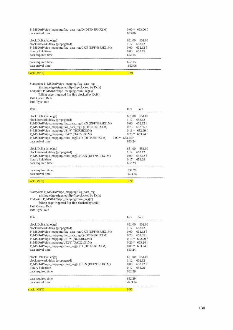
130
P_MSDAP/sipo_mapping/flag_data_reg/D (DFFNSRHX1M) 0.00 * 653.06 f
data arrival time 653.06
clock Dclk (fall edge) 651.00 651.00
clock network delay (propagated) 1.12 652.12 P_MSDAP/sipo_mapping/flag_data_reg/CKN (DFFNSRHX1M) 0.00 652.12 f
library hold time 0.03 652.15
data required time 652.15 ------------------------------------------------------------------------------------------------------------------------------
data required time 652.15
data arrival time -653.06 ------------------------------------------------------------------------------------------------------------------------------
slack (MET) 0.91
Startpoint: P_MSDAP/sipo_mapping/flag_data_reg
(falling edge-triggered flip-flop clocked by Dclk) Endpoint: P_MSDAP/sipo_mapping/count_reg[3]
(falling edge-triggered flip-flop clocked by Dclk)
Path Group: Dclk Path Type: min
Point Incr Path -------------------------------------------------------------------------------------------------------------------------------
clock Dclk (fall edge) 651.00 651.00
clock network delay (propagated) 1.12 652.12 P_MSDAP/sipo_mapping/flag_data_reg/CKN (DFFNSRHX1M) 0.00 652.12 f
P_MSDAP/sipo_mapping/flag_data_reg/Q (DFFNSRHX1M) 0.73 652.85 r P_MSDAP/sipo_mapping/U31/Y (NOR3BX2M) 0.13 * 652.99 f
P_MSDAP/sipo_mapping/U34/Y (OAI221X1M) 0.25 * 653.24 r
P_MSDAP/sipo_mapping/count_reg[3]/D (DFFNSRHX1M) 0.00 * 653.24 r data arrival time 653.24
clock Dclk (fall edge) 651.00 651.00 clock network delay (propagated) 1.12 652.12
P_MSDAP/sipo_mapping/count_reg[3]/CKN (DFFNSRHX1M) 0.00 652.12 f
library hold time 0.17 652.29 data required time 652.29
--------------------------------------------------------------------------------------------------------------------------------
data required time 652.29 data arrival time -653.24
--------------------------------------------------------------------------------------------------------------------------------
slack (MET) 0.95
Startpoint: P_MSDAP/sipo_mapping/flag_data_reg (falling edge-triggered flip-flop clocked by Dclk)
Endpoint: P_MSDAP/sipo_mapping/count_reg[2]
(falling edge-triggered flip-flop clocked by Dclk) Path Group: Dclk
Path Type: min
Point Incr Path
-------------------------------------------------------------------------------------------------------------------------------
clock Dclk (fall edge) 651.00 651.00 clock network delay (propagated) 1.12 652.12
P_MSDAP/sipo_mapping/flag_data_reg/CKN (DFFNSRHX1M) 0.00 652.12 f
P_MSDAP/sipo_mapping/flag_data_reg/Q (DFFNSRHX1M) 0.73 652.85 r P_MSDAP/sipo_mapping/U31/Y (NOR3BX2M) 0.13 * 652.99 f
P_MSDAP/sipo_mapping/U32/Y (OAI221X1M) 0.26 * 653.24 r
P_MSDAP/sipo_mapping/count_reg[2]/D (DFFNSRHX1M) 0.00 * 653.24 r data arrival time 653.24
clock Dclk (fall edge) 651.00 651.00 clock network delay (propagated) 1.12 652.12
P_MSDAP/sipo_mapping/count_reg[2]/CKN (DFFNSRHX1M) 0.00 652.12 f
library hold time 0.17 652.29 data required time 652.29
-----------------------------------------------------------------------------------------------------------------------------
data required time 652.29 data arrival time -653.24
-----------------------------------------------------------------------------------------------------------------------------
slack (MET) 0.95
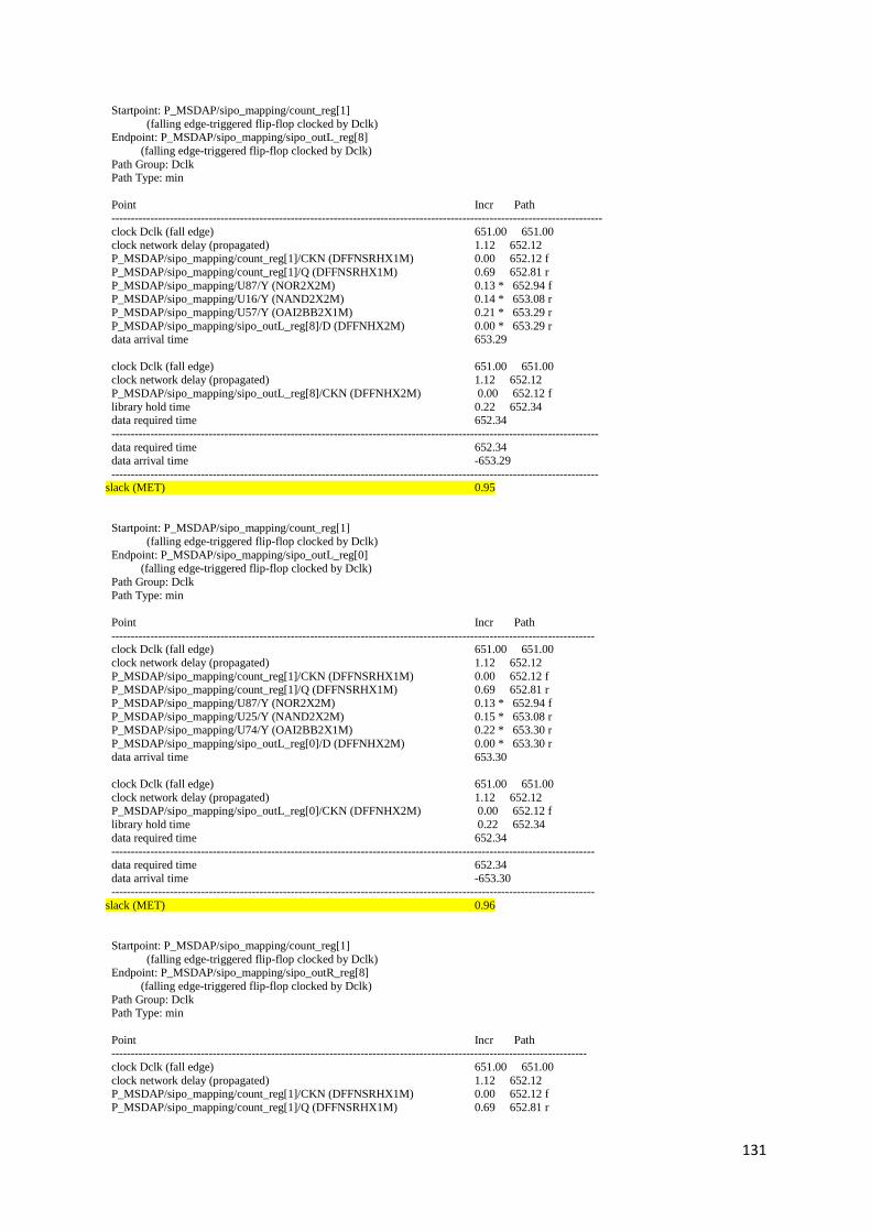
131
Startpoint: P_MSDAP/sipo_mapping/count_reg[1]
(falling edge-triggered flip-flop clocked by Dclk) Endpoint: P_MSDAP/sipo_mapping/sipo_outL_reg[8]
(falling edge-triggered flip-flop clocked by Dclk)
Path Group: Dclk Path Type: min
Point Incr Path ------------------------------------------------------------------------------------------------------------------------------
clock Dclk (fall edge) 651.00 651.00
clock network delay (propagated) 1.12 652.12 P_MSDAP/sipo_mapping/count_reg[1]/CKN (DFFNSRHX1M) 0.00 652.12 f
P_MSDAP/sipo_mapping/count_reg[1]/Q (DFFNSRHX1M) 0.69 652.81 r
P_MSDAP/sipo_mapping/U87/Y (NOR2X2M) 0.13 * 652.94 f P_MSDAP/sipo_mapping/U16/Y (NAND2X2M) 0.14 * 653.08 r
P_MSDAP/sipo_mapping/U57/Y (OAI2BB2X1M) 0.21 * 653.29 r
P_MSDAP/sipo_mapping/sipo_outL_reg[8]/D (DFFNHX2M) 0.00 * 653.29 r data arrival time 653.29
clock Dclk (fall edge) 651.00 651.00 clock network delay (propagated) 1.12 652.12
P_MSDAP/sipo_mapping/sipo_outL_reg[8]/CKN (DFFNHX2M) 0.00 652.12 f
library hold time 0.22 652.34 data required time 652.34
-----------------------------------------------------------------------------------------------------------------------------
data required time 652.34 data arrival time -653.29
----------------------------------------------------------------------------------------------------------------------------- slack (MET) 0.95
Startpoint: P_MSDAP/sipo_mapping/count_reg[1]
(falling edge-triggered flip-flop clocked by Dclk)
Endpoint: P_MSDAP/sipo_mapping/sipo_outL_reg[0] (falling edge-triggered flip-flop clocked by Dclk)
Path Group: Dclk
Path Type: min
Point Incr Path
---------------------------------------------------------------------------------------------------------------------------- clock Dclk (fall edge) 651.00 651.00
clock network delay (propagated) 1.12 652.12
P_MSDAP/sipo_mapping/count_reg[1]/CKN (DFFNSRHX1M) 0.00 652.12 f P_MSDAP/sipo_mapping/count_reg[1]/Q (DFFNSRHX1M) 0.69 652.81 r
P_MSDAP/sipo_mapping/U87/Y (NOR2X2M) 0.13 * 652.94 f
P_MSDAP/sipo_mapping/U25/Y (NAND2X2M) 0.15 * 653.08 r P_MSDAP/sipo_mapping/U74/Y (OAI2BB2X1M) 0.22 * 653.30 r
P_MSDAP/sipo_mapping/sipo_outL_reg[0]/D (DFFNHX2M) 0.00 * 653.30 r
data arrival time 653.30
clock Dclk (fall edge) 651.00 651.00
clock network delay (propagated) 1.12 652.12 P_MSDAP/sipo_mapping/sipo_outL_reg[0]/CKN (DFFNHX2M) 0.00 652.12 f
library hold time 0.22 652.34
data required time 652.34 ----------------------------------------------------------------------------------------------------------------------------
data required time 652.34
data arrival time -653.30 ----------------------------------------------------------------------------------------------------------------------------
slack (MET) 0.96
Startpoint: P_MSDAP/sipo_mapping/count_reg[1]
(falling edge-triggered flip-flop clocked by Dclk) Endpoint: P_MSDAP/sipo_mapping/sipo_outR_reg[8]
(falling edge-triggered flip-flop clocked by Dclk)
Path Group: Dclk Path Type: min
Point Incr Path --------------------------------------------------------------------------------------------------------------------------
clock Dclk (fall edge) 651.00 651.00
clock network delay (propagated) 1.12 652.12 P_MSDAP/sipo_mapping/count_reg[1]/CKN (DFFNSRHX1M) 0.00 652.12 f
P_MSDAP/sipo_mapping/count_reg[1]/Q (DFFNSRHX1M) 0.69 652.81 r
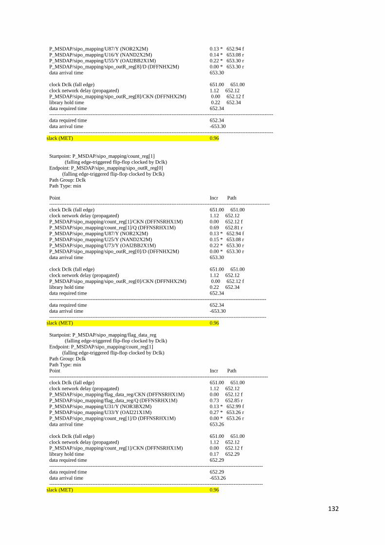
132
P_MSDAP/sipo_mapping/U87/Y (NOR2X2M) 0.13 * 652.94 f
P_MSDAP/sipo_mapping/U16/Y (NAND2X2M) 0.14 * 653.08 r P_MSDAP/sipo_mapping/U55/Y (OAI2BB2X1M) 0.22 * 653.30 r
P_MSDAP/sipo_mapping/sipo_outR_reg[8]/D (DFFNHX2M) 0.00 * 653.30 r
data arrival time 653.30
clock Dclk (fall edge) 651.00 651.00
clock network delay (propagated) 1.12 652.12 P_MSDAP/sipo_mapping/sipo_outR_reg[8]/CKN (DFFNHX2M) 0.00 652.12 f
library hold time 0.22 652.34
data required time 652.34 ----------------------------------------------------------------------------------------------------------------------------------
data required time 652.34
data arrival time -653.30 ----------------------------------------------------------------------------------------------------------------------------------
slack (MET) 0.96
Startpoint: P_MSDAP/sipo_mapping/count_reg[1]
(falling edge-triggered flip-flop clocked by Dclk) Endpoint: P_MSDAP/sipo_mapping/sipo_outR_reg[0]
(falling edge-triggered flip-flop clocked by Dclk)
Path Group: Dclk Path Type: min
Point Incr Path --------------------------------------------------------------------------------------------------------------------------------
clock Dclk (fall edge) 651.00 651.00 clock network delay (propagated) 1.12 652.12
P_MSDAP/sipo_mapping/count_reg[1]/CKN (DFFNSRHX1M) 0.00 652.12 f
P_MSDAP/sipo_mapping/count_reg[1]/Q (DFFNSRHX1M) 0.69 652.81 r P_MSDAP/sipo_mapping/U87/Y (NOR2X2M) 0.13 * 652.94 f
P_MSDAP/sipo_mapping/U25/Y (NAND2X2M) 0.15 * 653.08 r
P_MSDAP/sipo_mapping/U73/Y (OAI2BB2X1M) 0.22 * 653.30 r P_MSDAP/sipo_mapping/sipo_outR_reg[0]/D (DFFNHX2M) 0.00 * 653.30 r
data arrival time 653.30
clock Dclk (fall edge) 651.00 651.00
clock network delay (propagated) 1.12 652.12
P_MSDAP/sipo_mapping/sipo_outR_reg[0]/CKN (DFFNHX2M) 0.00 652.12 f library hold time 0.22 652.34
data required time 652.34
------------------------------------------------------------------------------------------------------------------------------ data required time 652.34
data arrival time -653.30
------------------------------------------------------------------------------------------------------------------------------ slack (MET) 0.96
Startpoint: P_MSDAP/sipo_mapping/flag_data_reg (falling edge-triggered flip-flop clocked by Dclk)
Endpoint: P_MSDAP/sipo_mapping/count_reg[1]
(falling edge-triggered flip-flop clocked by Dclk) Path Group: Dclk
Path Type: min
Point Incr Path -------------------------------------------------------------------------------------------------------------------------------
clock Dclk (fall edge) 651.00 651.00
clock network delay (propagated) 1.12 652.12 P_MSDAP/sipo_mapping/flag_data_reg/CKN (DFFNSRHX1M) 0.00 652.12 f
P_MSDAP/sipo_mapping/flag_data_reg/Q (DFFNSRHX1M) 0.73 652.85 r
P_MSDAP/sipo_mapping/U31/Y (NOR3BX2M) 0.13 * 652.99 f P_MSDAP/sipo_mapping/U33/Y (OAI221X1M) 0.27 * 653.26 r
P_MSDAP/sipo_mapping/count_reg[1]/D (DFFNSRHX1M) 0.00 * 653.26 r
data arrival time 653.26
clock Dclk (fall edge) 651.00 651.00
clock network delay (propagated) 1.12 652.12 P_MSDAP/sipo_mapping/count_reg[1]/CKN (DFFNSRHX1M) 0.00 652.12 f
library hold time 0.17 652.29
data required time 652.29 ----------------------------------------------------------------------------------------------------------------------------
data required time 652.29
data arrival time -653.26 ----------------------------------------------------------------------------------------------------------------------------
slack (MET) 0.96
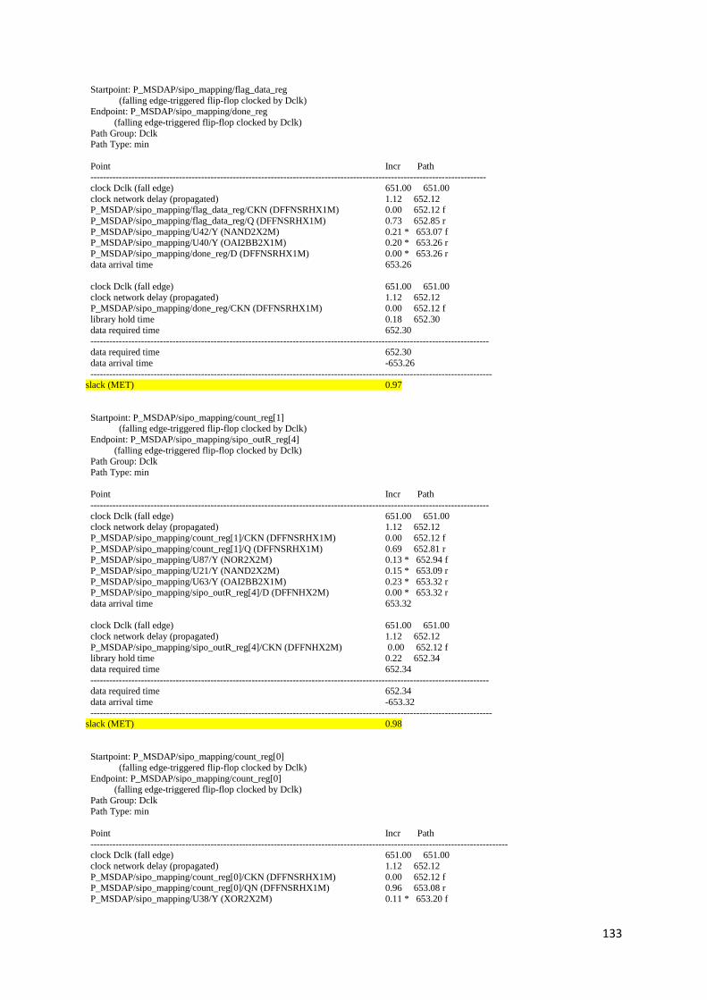
133
Startpoint: P_MSDAP/sipo_mapping/flag_data_reg
(falling edge-triggered flip-flop clocked by Dclk) Endpoint: P_MSDAP/sipo_mapping/done_reg
(falling edge-triggered flip-flop clocked by Dclk)
Path Group: Dclk Path Type: min
Point Incr Path -----------------------------------------------------------------------------------------------------------------------------
clock Dclk (fall edge) 651.00 651.00
clock network delay (propagated) 1.12 652.12 P_MSDAP/sipo_mapping/flag_data_reg/CKN (DFFNSRHX1M) 0.00 652.12 f
P_MSDAP/sipo_mapping/flag_data_reg/Q (DFFNSRHX1M) 0.73 652.85 r
P_MSDAP/sipo_mapping/U42/Y (NAND2X2M) 0.21 * 653.07 f P_MSDAP/sipo_mapping/U40/Y (OAI2BB2X1M) 0.20 * 653.26 r
P_MSDAP/sipo_mapping/done_reg/D (DFFNSRHX1M) 0.00 * 653.26 r
data arrival time 653.26
clock Dclk (fall edge) 651.00 651.00
clock network delay (propagated) 1.12 652.12 P_MSDAP/sipo_mapping/done_reg/CKN (DFFNSRHX1M) 0.00 652.12 f
library hold time 0.18 652.30
data required time 652.30 ------------------------------------------------------------------------------------------------------------------------------
data required time 652.30
data arrival time -653.26 -------------------------------------------------------------------------------------------------------------------------------
slack (MET) 0.97
Startpoint: P_MSDAP/sipo_mapping/count_reg[1] (falling edge-triggered flip-flop clocked by Dclk)
Endpoint: P_MSDAP/sipo_mapping/sipo_outR_reg[4]
(falling edge-triggered flip-flop clocked by Dclk) Path Group: Dclk
Path Type: min
Point Incr Path
------------------------------------------------------------------------------------------------------------------------------
clock Dclk (fall edge) 651.00 651.00 clock network delay (propagated) 1.12 652.12
P_MSDAP/sipo_mapping/count_reg[1]/CKN (DFFNSRHX1M) 0.00 652.12 f
P_MSDAP/sipo_mapping/count_reg[1]/Q (DFFNSRHX1M) 0.69 652.81 r P_MSDAP/sipo_mapping/U87/Y (NOR2X2M) 0.13 * 652.94 f
P_MSDAP/sipo_mapping/U21/Y (NAND2X2M) 0.15 * 653.09 r
P_MSDAP/sipo_mapping/U63/Y (OAI2BB2X1M) 0.23 * 653.32 r P_MSDAP/sipo_mapping/sipo_outR_reg[4]/D (DFFNHX2M) 0.00 * 653.32 r
data arrival time 653.32
clock Dclk (fall edge) 651.00 651.00
clock network delay (propagated) 1.12 652.12
P_MSDAP/sipo_mapping/sipo_outR_reg[4]/CKN (DFFNHX2M) 0.00 652.12 f library hold time 0.22 652.34
data required time 652.34
------------------------------------------------------------------------------------------------------------------------------ data required time 652.34
data arrival time -653.32
------------------------------------------------------------------------------------------------------------------------------- slack (MET) 0.98
Startpoint: P_MSDAP/sipo_mapping/count_reg[0]
(falling edge-triggered flip-flop clocked by Dclk)
Endpoint: P_MSDAP/sipo_mapping/count_reg[0] (falling edge-triggered flip-flop clocked by Dclk)
Path Group: Dclk
Path Type: min
Point Incr Path
------------------------------------------------------------------------------------------------------------------------------------ clock Dclk (fall edge) 651.00 651.00
clock network delay (propagated) 1.12 652.12
P_MSDAP/sipo_mapping/count_reg[0]/CKN (DFFNSRHX1M) 0.00 652.12 f P_MSDAP/sipo_mapping/count_reg[0]/QN (DFFNSRHX1M) 0.96 653.08 r
P_MSDAP/sipo_mapping/U38/Y (XOR2X2M) 0.11 * 653.20 f

134
P_MSDAP/sipo_mapping/U37/Y (NAND2X2M) 0.08 * 653.28 r
P_MSDAP/sipo_mapping/count_reg[0]/D (DFFNSRHX1M) 0.00 * 653.28 r data arrival time 653.28
clock Dclk (fall edge) 651.00 651.00 clock network delay (propagated) 1.12 652.12
P_MSDAP/sipo_mapping/count_reg[0]/CKN (DFFNSRHX1M) 0.00 652.12 f
library hold time 0.18 652.30 data required time 652.30
---------------------------------------------------------------------------------------------------------------------------
data required time 652.30 data arrival time -653.28
--------------------------------------------------------------------------------------------------------------------------
slack (MET) 0.98
Startpoint: P_MSDAP/sipo_mapping/count_reg[1] (falling edge-triggered flip-flop clocked by Dclk)
Endpoint: P_MSDAP/sipo_mapping/sipo_outL_reg[4]
(falling edge-triggered flip-flop clocked by Dclk) Path Group: Dclk
Path Type: min
Point Incr Path
-----------------------------------------------------------------------------------------------------------------------------
clock Dclk (fall edge) 651.00 651.00 clock network delay (propagated) 1.12 652.12
P_MSDAP/sipo_mapping/count_reg[1]/CKN (DFFNSRHX1M) 0.00 652.12 f P_MSDAP/sipo_mapping/count_reg[1]/Q (DFFNSRHX1M) 0.69 652.81 r
P_MSDAP/sipo_mapping/U87/Y (NOR2X2M) 0.13 * 652.94 f
P_MSDAP/sipo_mapping/U21/Y (NAND2X2M) 0.15 * 653.09 r P_MSDAP/sipo_mapping/U67/Y (OAI2BB2X1M) 0.23 * 653.32 r
P_MSDAP/sipo_mapping/sipo_outL_reg[4]/D (DFFNHX2M) 0.00 * 653.32 r
data arrival time 653.32
clock Dclk (fall edge) 651.00 651.00
clock network delay (propagated) 1.12 652.12 P_MSDAP/sipo_mapping/sipo_outL_reg[4]/CKN (DFFNHX2M) 0.00 652.12 f
library hold time 0.22 652.34
data required time 652.34 -------------------------------------------------------------------------------------------------------------------------------
data required time 652.34
data arrival time -653.32 -------------------------------------------------------------------------------------------------------------------------------
slack (MET) 0.98
Startpoint: P_MSDAP/sipo_mapping/count_reg[1]
(falling edge-triggered flip-flop clocked by Dclk)
Endpoint: P_MSDAP/sipo_mapping/sipo_outL_reg[12] (falling edge-triggered flip-flop clocked by Dclk)
Path Group: Dclk
Path Type: min Point Incr Path
-----------------------------------------------------------------------------------------------------------------------------------
clock Dclk (fall edge) 651.00 651.00 clock network delay (propagated) 1.12 652.12
P_MSDAP/sipo_mapping/count_reg[1]/CKN (DFFNSRHX1M) 0.00 652.12 f
P_MSDAP/sipo_mapping/count_reg[1]/Q (DFFNSRHX1M) 0.69 652.81 r P_MSDAP/sipo_mapping/U87/Y (NOR2X2M) 0.13 * 652.94 f
P_MSDAP/sipo_mapping/U14/Y (NAND2X2M) 0.16 * 653.10 r
P_MSDAP/sipo_mapping/U53/Y (OAI2BB2X1M) 0.23 * 653.33 r P_MSDAP/sipo_mapping/sipo_outL_reg[12]/D (DFFNHX2M) 0.00 * 653.33 r
data arrival time 653.33
clock Dclk (fall edge) 651.00 651.00
clock network delay (propagated) 1.12 652.12
P_MSDAP/sipo_mapping/sipo_outL_reg[12]/CKN (DFFNHX2M) 0.00 652.12 f library hold time 0.22 652.34
data required time 652.34
---------------------------------------------------------------------------------------------------------------------------------- data required time 652.34
data arrival time -653.33
------------------------------------------------------------------------------------------------------------------------------------ slack (MET) 0.99

135
Startpoint: P_MSDAP/sipo_mapping/count_reg[1]
(falling edge-triggered flip-flop clocked by Dclk) Endpoint: P_MSDAP/sipo_mapping/sipo_outR_reg[12]
(falling edge-triggered flip-flop clocked by Dclk)
Path Group: Dclk Path Type: min
Point Incr Path -----------------------------------------------------------------------------------------------------------------------------
clock Dclk (fall edge) 651.00 651.00
clock network delay (propagated) 1.12 652.12 P_MSDAP/sipo_mapping/count_reg[1]/CKN (DFFNSRHX1M) 0.00 652.12 f
P_MSDAP/sipo_mapping/count_reg[1]/Q (DFFNSRHX1M) 0.69 652.81 r
P_MSDAP/sipo_mapping/U87/Y (NOR2X2M) 0.13 * 652.94 f P_MSDAP/sipo_mapping/U14/Y (NAND2X2M) 0.16 * 653.10 r
P_MSDAP/sipo_mapping/U48/Y (OAI2BB2X1M) 0.23 * 653.33 r
P_MSDAP/sipo_mapping/sipo_outR_reg[12]/D (DFFNHX2M) 0.00 * 653.33 r data arrival time 653.33
clock Dclk (fall edge) 651.00 651.00 clock network delay (propagated) 1.12 652.12
P_MSDAP/sipo_mapping/sipo_outR_reg[12]/CKN (DFFNHX2M) 0.00 652.12 f
library hold time 0.22 652.34 data required time 652.34
----------------------------------------------------------------------------------------------------------------------------
data required time 652.34 data arrival time -653.33
----------------------------------------------------------------------------------------------------------------------------- slack (MET) 0.99
Startpoint: P_MSDAP/sipo_mapping/count_reg[2]
(falling edge-triggered flip-flop clocked by Dclk)
Endpoint: P_MSDAP/sipo_mapping/sipo_outL_reg[9] (falling edge-triggered flip-flop clocked by Dclk)
Path Group: Dclk
Path Type: min
Point Incr Path
------------------------------------------------------------------------------------------------------------------------------ clock Dclk (fall edge) 651.00 651.00
clock network delay (propagated) 1.12 652.12
P_MSDAP/sipo_mapping/count_reg[2]/CKN (DFFNSRHX1M) 0.00 652.12 f P_MSDAP/sipo_mapping/count_reg[2]/Q (DFFNSRHX1M) 0.73 652.85 r
P_MSDAP/sipo_mapping/U43/Y (NOR2BX2M) 0.14 * 652.99 f
P_MSDAP/sipo_mapping/U17/Y (NAND2X2M) 0.14 * 653.12 r P_MSDAP/sipo_mapping/U58/Y (OAI2BB2X1M) 0.21 * 653.34 r
P_MSDAP/sipo_mapping/sipo_outL_reg[9]/D (DFFNHX2M) 0.00 * 653.34 r
data arrival time 653.34
clock Dclk (fall edge) 651.00 651.00
clock network delay (propagated) 1.12 652.12 P_MSDAP/sipo_mapping/sipo_outL_reg[9]/CKN (DFFNHX2M) 0.00 652.12 f
library hold time 0.22 652.34
data required time 652.34 -------------------------------------------------------------------------------------------------------------------------------
data required time 652.34
data arrival time -653.34 --------------------------------------------------------------------------------------------------------------------------------
slack (MET) 1.00
Startpoint: P_MSDAP/sipo_mapping/count_reg[2]
(falling edge-triggered flip-flop clocked by Dclk) Endpoint: P_MSDAP/sipo_mapping/sipo_outR_reg[9]
(falling edge-triggered flip-flop clocked by Dclk)
Path Group: Dclk Path Type: min
Point Incr Path -------------------------------------------------------------------------------------------------------------------------
clock Dclk (fall edge) 651.00 651.00
clock network delay (propagated) 1.12 652.12 P_MSDAP/sipo_mapping/count_reg[2]/CKN (DFFNSRHX1M) 0.00 652.12 f
P_MSDAP/sipo_mapping/count_reg[2]/Q (DFFNSRHX1M) 0.73 652.85 r
136
P_MSDAP/sipo_mapping/U43/Y (NOR2BX2M) 0.14 * 652.99 f
P_MSDAP/sipo_mapping/U17/Y (NAND2X2M) 0.14 * 653.12 r P_MSDAP/sipo_mapping/U56/Y (OAI2BB2X1M) 0.23 * 653.35 r
P_MSDAP/sipo_mapping/sipo_outR_reg[9]/D (DFFNHX2M) 0.00 * 653.35 r
data arrival time 653.35
clock Dclk (fall edge) 651.00 651.00
clock network delay (propagated) 1.12 652.12 P_MSDAP/sipo_mapping/sipo_outR_reg[9]/CKN (DFFNHX2M) 0.00 652.12 f
library hold time 0.22 652.34
data required time 652.34 -----------------------------------------------------------------------------------------------------------------------------
data required time 652.34
data arrival time -653.35 -----------------------------------------------------------------------------------------------------------------------------
slack (MET) 1.01
Startpoint: P_MSDAP/sipo_mapping/count_reg[2]
(falling edge-triggered flip-flop clocked by Dclk) Endpoint: P_MSDAP/sipo_mapping/sipo_outR_reg[10]
(falling edge-triggered flip-flop clocked by Dclk)
Path Group: Dclk Path Type: min
Point Incr Path -------------------------------------------------------------------------------------------------------------------------------
clock Dclk (fall edge) 651.00 651.00 clock network delay (propagated) 1.12 652.12
P_MSDAP/sipo_mapping/count_reg[2]/CKN (DFFNSRHX1M) 0.00 652.12 f
P_MSDAP/sipo_mapping/count_reg[2]/Q (DFFNSRHX1M) 0.73 652.85 r P_MSDAP/sipo_mapping/U43/Y (NOR2BX2M) 0.14 * 652.99 f
P_MSDAP/sipo_mapping/U11/Y (NAND2X2M) 0.14 * 653.12 r
P_MSDAP/sipo_mapping/U45/Y (OAI2BB2X1M) 0.22 * 653.35 r P_MSDAP/sipo_mapping/sipo_outR_reg[10]/D (DFFNHX2M) 0.00 * 653.35 r
data arrival time 653.35
clock Dclk (fall edge) 651.00 651.00
clock network delay (propagated) 1.12 652.12
P_MSDAP/sipo_mapping/sipo_outR_reg[10]/CKN (DFFNHX2M) 0.00 652.12 f library hold time 0.22 652.34
data required time 652.34
----------------------------------------------------------------------------------------------------------------------------- data required time 652.34
data arrival time -653.35
------------------------------------------------------------------------------------------------------------------------------ slack (MET) 1.01
Startpoint: P_MSDAP/sipo_mapping/count_reg[2]
(falling edge-triggered flip-flop clocked by Dclk) Endpoint: P_MSDAP/sipo_mapping/sipo_outL_reg[10]
(falling edge-triggered flip-flop clocked by Dclk)
Path Group: Dclk Path Type: min
Point Incr Path
------------------------------------------------------------------------------------------------------------------------------------ clock Dclk (fall edge) 651.00 651.00
clock network delay (propagated) 1.12 652.12
P_MSDAP/sipo_mapping/count_reg[2]/CKN (DFFNSRHX1M) 0.00 652.12 f P_MSDAP/sipo_mapping/count_reg[2]/Q (DFFNSRHX1M) 0.73 652.85 r
P_MSDAP/sipo_mapping/U43/Y (NOR2BX2M) 0.14 * 652.99 f
P_MSDAP/sipo_mapping/U11/Y (NAND2X2M) 0.14 * 653.12 r P_MSDAP/sipo_mapping/U50/Y (OAI2BB2X1M) 0.23 * 653.35 r
P_MSDAP/sipo_mapping/sipo_outL_reg[10]/D (DFFNHX2M) 0.00 * 653.35 r
data arrival time 653.35
clock Dclk (fall edge) 651.00 651.00
clock network delay (propagated) 1.12 652.12 P_MSDAP/sipo_mapping/sipo_outL_reg[10]/CKN (DFFNHX2M) 0.00 652.12 f
library hold time 0.22 652.34
data required time 652.34 ------------------------------------------------------------------------------------------------------------------------------------
data required time 652.34
data arrival time -653.35 ------------------------------------------------------------------------------------------------------------------------------------
slack (MET) 1.01
137
Startpoint: P_MSDAP/sipo_mapping/count_reg[2]
(falling edge-triggered flip-flop clocked by Dclk) Endpoint: P_MSDAP/sipo_mapping/sipo_outL_reg[7]
(falling edge-triggered flip-flop clocked by Dclk)
Path Group: Dclk Path Type: min
Point Incr Path -------------------------------------------------------------------------------------------------------------------------------------
clock Dclk (fall edge) 651.00 651.00
clock network delay (propagated) 1.12 652.12 P_MSDAP/sipo_mapping/count_reg[2]/CKN (DFFNSRHX1M) 0.00 652.12 f
P_MSDAP/sipo_mapping/count_reg[2]/Q (DFFNSRHX1M) 0.73 652.85 r
P_MSDAP/sipo_mapping/U43/Y (NOR2BX2M) 0.14 * 652.99 f P_MSDAP/sipo_mapping/U18/Y (NAND2X2M) 0.15 * 653.13 r
P_MSDAP/sipo_mapping/U60/Y (OAI2BB2X1M) 0.22 * 653.35 r
P_MSDAP/sipo_mapping/sipo_outL_reg[7]/D (DFFNHX2M) 0.00 * 653.35 r data arrival time 653.35
clock Dclk (fall edge) 651.00 651.00 clock network delay (propagated) 1.12 652.12
P_MSDAP/sipo_mapping/sipo_outL_reg[7]/CKN (DFFNHX2M) 0.00 652.12 f
library hold time 0.22 652.34 data required time 652.34
--------------------------------------------------------------------------------------------------------------------------------------
data required time 652.34 data arrival time -653.35
--------------------------------------------------------------------------------------------------------------------------------------- slack (MET) 1.01
Startpoint: P_MSDAP/sipo_mapping/count_reg[2]
(falling edge-triggered flip-flop clocked by Dclk)
Endpoint: P_MSDAP/sipo_mapping/sipo_outR_reg[7] (falling edge-triggered flip-flop clocked by Dclk)
Path Group: Dclk
Path Type: min
Point Incr Path
--------------------------------------------------------------------------------------------------------------------------------------------- clock Dclk (fall edge) 651.00 651.00
clock network delay (propagated) 1.12 652.12
P_MSDAP/sipo_mapping/count_reg[2]/CKN (DFFNSRHX1M) 0.00 652.12 f P_MSDAP/sipo_mapping/count_reg[2]/Q (DFFNSRHX1M) 0.73 652.85 r
P_MSDAP/sipo_mapping/U43/Y (NOR2BX2M) 0.14 * 652.99 f
P_MSDAP/sipo_mapping/U18/Y (NAND2X2M) 0.15 * 653.13 r P_MSDAP/sipo_mapping/U59/Y (OAI2BB2X1M) 0.22 * 653.36 r
P_MSDAP/sipo_mapping/sipo_outR_reg[7]/D (DFFNHX2M) 0.00 * 653.36 r
data arrival time 653.36
clock Dclk (fall edge) 651.00 651.00
clock network delay (propagated) 1.12 652.12 P_MSDAP/sipo_mapping/sipo_outR_reg[7]/CKN (DFFNHX2M) 0.00 652.12 f
library hold time 0.22 652.34
data required time 652.34 ----------------------------------------------------------------------------------------------------------------------------------------------
data required time 652.34
data arrival time -653.36 ----------------------------------------------------------------------------------------------------------------------------------------------
slack (MET) 1.02
138
Startpoint: P_MSDAP/sipo_mapping/sipo_outL_reg[9]
(falling edge-triggered flip-flop clocked by Dclk) Endpoint: P_MSDAP/dataL_memory_mapping/mem_dataL_reg[255][9]
(falling edge-triggered flip-flop clocked by Sclk)
Path Group: Sclk Path Type: min
Point Incr Path ---------------------------------------------------------------------------------------------------------------------------------------------
clock Dclk (fall edge) 651.00 651.00
clock network delay (propagated) 1.12 652.12 P_MSDAP/sipo_mapping/sipo_outL_reg[9]/CKN (DFFNHX2M) 0.00 652.12 f
P_MSDAP/sipo_mapping/sipo_outL_reg[9]/Q (DFFNHX2M) 1.05 653.17 f
P_MSDAP/sipo_mapping/sipo_outL[9] (SIPO) 0.00 653.17 f P_MSDAP/dataL_memory_mapping/sipo_outL[9] (data_memoryL) 0.00 653.17 f
P_MSDAP/dataL_memory_mapping/U10088/Y (OAI2B2X2M) 0.43 * 653.61 f
P_MSDAP/dataL_memory_mapping/mem_dataL_reg[255][9]/D (DFFNHX2M) 0.00 * 653.61 f data arrival time 653.61
clock Sclk (fall edge) 651.00 651.00 clock network delay (propagated) 2.31 653.31
P_MSDAP/dataL_memory_mapping/mem_dataL_reg[255][9]/CKN (DFFNHX2M) 0.00 653.31 f
library hold time 0.10 653.40 data required time 653.40
-----------------------------------------------------------------------------------------------------------------------------------------------
data required time 653.40 data arrival time -653.61
------------------------------------------------------------------------------------------------------------------------------------------------ slack (MET) 0.21
Startpoint: P_MSDAP/sipo_mapping/sipo_outL_reg[1]
(falling edge-triggered flip-flop clocked by Dclk)
Endpoint: P_MSDAP/dataL_memory_mapping/mem_dataL_reg[255][1] (falling edge-triggered flip-flop clocked by Sclk)
Path Group: Sclk
Path Type: min
Point Incr Path
---------------------------------------------------------------------------------------------------------------------------------------------------- clock Dclk (fall edge) 651.00 651.00
clock network delay (propagated) 1.12 652.12
P_MSDAP/sipo_mapping/sipo_outL_reg[1]/CKN (DFFNHX2M) 0.00 652.12 f P_MSDAP/sipo_mapping/sipo_outL_reg[1]/Q (DFFNHX2M) 1.06 653.18 f
P_MSDAP/sipo_mapping/sipo_outL[1] (SIPO) 0.00 653.18 f
P_MSDAP/dataL_memory_mapping/sipo_outL[1] (data_memoryL) 0.00 653.18 f P_MSDAP/dataL_memory_mapping/U10080/Y (OAI2B2X2M) 0.44 * 653.62 f
P_MSDAP/dataL_memory_mapping/mem_dataL_reg[255][1]/D (DFFNHX2M) 0.00 * 653.62 f
data arrival time 653.62
clock Sclk (fall edge) 651.00 651.00
clock network delay (propagated) 2.30 653.30 P_MSDAP/dataL_memory_mapping/mem_dataL_reg[255][1]/CKN (DFFNHX2M) 0.00 653.30 f
library hold time 0.10 653.40
data required time 653.40 ---------------------------------------------------------------------------------------------------------------------------------------------------
data required time 653.40
data arrival time -653.62 ---------------------------------------------------------------------------------------------------------------------------------------------------
slack (MET) 0.22
Startpoint: P_MSDAP/sipo_mapping/sipo_outL_reg[11]
(falling edge-triggered flip-flop clocked by Dclk) Endpoint: P_MSDAP/dataL_memory_mapping/mem_dataL_reg[255][11]
(falling edge-triggered flip-flop clocked by Sclk)
Path Group: Sclk Path Type: min
139
Point Incr Path
------------------------------------------------------------------------------------------------------------------------------------------------ clock Dclk (fall edge) 651.00 651.00
clock network delay (propagated) 1.12 652.12
P_MSDAP/sipo_mapping/sipo_outL_reg[11]/CKN (DFFNHX2M) 0.00 652.12 f P_MSDAP/sipo_mapping/sipo_outL_reg[11]/Q (DFFNHX2M) 1.06 653.18 f
P_MSDAP/sipo_mapping/sipo_outL[11] (SIPO) 0.00 653.18 f
P_MSDAP/dataL_memory_mapping/sipo_outL[11] (data_memoryL) 0.00 653.18 f P_MSDAP/dataL_memory_mapping/U10090/Y (OAI2B2X2M) 0.44 * 653.62 f
P_MSDAP/dataL_memory_mapping/mem_dataL_reg[255][11]/D (DFFNHX2M) 0.00 * 653.62 f
data arrival time 653.62
clock Sclk (fall edge) 651.00 651.00
clock network delay (propagated) 2.30 653.30 P_MSDAP/dataL_memory_mapping/mem_dataL_reg[255][11]/CKN (DFFNHX2M) 0.00 653.30 f
library hold time 0.10 653.40
data required time 653.40 -------------------------------------------------------------------------------------------------------------------------------------------------
data required time 653.40
data arrival time -653.62 -------------------------------------------------------------------------------------------------------------------------------------------------
slack (MET) 0.22
Startpoint: P_MSDAP/sipo_mapping/sipo_outL_reg[14]
(falling edge-triggered flip-flop clocked by Dclk) Endpoint: P_MSDAP/dataL_memory_mapping/mem_dataL_reg[255][14]
(falling edge-triggered flip-flop clocked by Sclk) Path Group: Sclk
Path Type: min
Point Incr Path
------------------------------------------------------------------------------------------------------------------------------------------------------
clock Dclk (fall edge) 651.00 651.00 clock network delay (propagated) 1.12 652.12
P_MSDAP/sipo_mapping/sipo_outL_reg[14]/CKN (DFFNHX2M) 0.00 652.12 f
P_MSDAP/sipo_mapping/sipo_outL_reg[14]/Q (DFFNHX2M) 1.07 653.19 f P_MSDAP/sipo_mapping/sipo_outL[14] (SIPO) 0.00 653.19 f
P_MSDAP/dataL_memory_mapping/sipo_outL[14] (data_memoryL) 0.00 653.19 f
P_MSDAP/dataL_memory_mapping/U10093/Y (OAI2B2X2M) 0.44 * 653.62 f P_MSDAP/dataL_memory_mapping/mem_dataL_reg[255][14]/D (DFFNHX2M) 0.00 * 653.62 f
data arrival time 653.62
clock Sclk (fall edge) 651.00 651.00
clock network delay (propagated) 2.30 653.30
P_MSDAP/dataL_memory_mapping/mem_dataL_reg[255][14]/CKN (DFFNHX2M) 0.00 653.30 f library hold time 0.10 653.40
data required time 653.40
----------------------------------------------------------------------------------------------------------------------------------------------- data required time 653.40
data arrival time -653.62
----------------------------------------------------------------------------------------------------------------------------------------------- slack (MET) 0.22
Startpoint: P_MSDAP/sipo_mapping/sipo_outL_reg[6]
(falling edge-triggered flip-flop clocked by Dclk)
Endpoint: P_MSDAP/dataL_memory_mapping/mem_dataL_reg[255][6] (falling edge-triggered flip-flop clocked by Sclk)
Path Group: Sclk
Path Type: min
Point Incr Path
---------------------------------------------------------------------------------------------------------------------------------------- clock Dclk (fall edge) 651.00 651.00
clock network delay (propagated) 1.12 652.12
P_MSDAP/sipo_mapping/sipo_outL_reg[6]/CKN (DFFNHX2M) 0.00 652.12 f P_MSDAP/sipo_mapping/sipo_outL_reg[6]/Q (DFFNHX2M) 1.07 653.19 f
P_MSDAP/sipo_mapping/sipo_outL[6] (SIPO) 0.00 653.19 f
P_MSDAP/dataL_memory_mapping/sipo_outL[6] (data_memoryL) 0.00 653.19 f P_MSDAP/dataL_memory_mapping/U10085/Y (OAI2B2X2M) 0.44 * 653.63 f
P_MSDAP/dataL_memory_mapping/mem_dataL_reg[255][6]/D (DFFNHX2M) 0.00 * 653.63 f
data arrival time 653.63
clock Sclk (fall edge) 651.00 651.00

140
clock network delay (propagated) 2.31 653.31
P_MSDAP/dataL_memory_mapping/mem_dataL_reg[255][6]/CKN (DFFNHX2M) 0.00 653.31 f library hold time 0.10 653.40
data required time 653.40
------------------------------------------------------------------------------------------------------------------------------------------- data required time 653.40
data arrival time -653.63
------------------------------------------------------------------------------------------------------------------------------------------- slack (MET) 0.23
Startpoint: P_MSDAP/sipo_mapping/done_reg
(falling edge-triggered flip-flop clocked by Dclk)
Endpoint: P_MSDAP/main_FSM_mapping/done2_reg (falling edge-triggered flip-flop clocked by Sclk)
Path Group: Sclk
Path Type: min
Point Incr Path
------------------------------------------------------------------------------------------------------------------------------------ clock Dclk (fall edge) 651.00 651.00
clock network delay (propagated) 1.12 652.12
P_MSDAP/sipo_mapping/done_reg/CKN (DFFNSRHX1M) 0.00 652.12 f P_MSDAP/sipo_mapping/done_reg/Q (DFFNSRHX1M) 1.33 653.45 r
P_MSDAP/sipo_mapping/done (SIPO) 0.00 653.45 r
P_MSDAP/main_FSM_mapping/done (state_FSM) 0.00 653.45 r P_MSDAP/main_FSM_mapping/U241/Y (NAND2X2M) 0.24 * 653.69 f
P_MSDAP/main_FSM_mapping/U239/Y (OAI211X2M) 0.11 * 653.79 r P_MSDAP/main_FSM_mapping/done2_reg/D (DFFNHX2M) 0.00 * 653.79 r
data arrival time 653.79
clock Sclk (fall edge) 651.00 651.00
clock network delay (propagated) 2.33 653.33
P_MSDAP/main_FSM_mapping/done2_reg/CKN (DFFNHX2M) 0.00 653.33 f library hold time 0.23 653.56
data required time 653.56
------------------------------------------------------------------------------------------------------------------------------- data required time 653.56
data arrival time -653.79
-------------------------------------------------------------------------------------------------------------------------------- slack (MET) 0.23
Startpoint: P_MSDAP/sipo_mapping/sipo_outL_reg[2]
(falling edge-triggered flip-flop clocked by Dclk)
Endpoint: P_MSDAP/dataL_memory_mapping/mem_dataL_reg[255][2] (falling edge-triggered flip-flop clocked by Sclk)
Path Group: Sclk
Path Type: min
Point Incr Path
-------------------------------------------------------------------------------------------------------------------------------------- clock Dclk (fall edge) 651.00 651.00
clock network delay (propagated) 1.12 652.12
P_MSDAP/sipo_mapping/sipo_outL_reg[2]/CKN (DFFNHX2M) 0.00 652.12 f P_MSDAP/sipo_mapping/sipo_outL_reg[2]/Q (DFFNHX2M) 1.06 653.18 f
P_MSDAP/sipo_mapping/sipo_outL[2] (SIPO) 0.00 653.18 f
P_MSDAP/dataL_memory_mapping/sipo_outL[2] (data_memoryL) 0.00 653.18 f P_MSDAP/dataL_memory_mapping/U10081/Y (OAI2B2X2M) 0.45 * 653.63 f
P_MSDAP/dataL_memory_mapping/mem_dataL_reg[255][2]/D (DFFNHX2M) 0.00 * 653.63 f
data arrival time 653.63
clock Sclk (fall edge) 651.00 651.00
clock network delay (propagated) 2.30 653.30 P_MSDAP/dataL_memory_mapping/mem_dataL_reg[255][2]/CKN (DFFNHX2M) 0.00 653.30 f
library hold time 0.10 653.40
data required time 653.40 -------------------------------------------------------------------------------------------------------------------------------------
data required time 653.40
data arrival time -653.63 -------------------------------------------------------------------------------------------------------------------------------------
slack (MET) 0.23

141
Startpoint: P_MSDAP/sipo_mapping/sipo_outL_reg[15]
(falling edge-triggered flip-flop clocked by Dclk) Endpoint: P_MSDAP/dataL_memory_mapping/mem_dataL_reg[255][15]
(falling edge-triggered flip-flop clocked by Sclk)
Path Group: Sclk Path Type: min
Point Incr Path --------------------------------------------------------------------------
clock Dclk (fall edge) 651.00 651.00
clock network delay (propagated) 1.12 652.12 P_MSDAP/sipo_mapping/sipo_outL_reg[15]/CKN (DFFNHX2M) 0.00 652.12 f
P_MSDAP/sipo_mapping/sipo_outL_reg[15]/Q (DFFNHX2M) 1.07 653.19 f
P_MSDAP/sipo_mapping/sipo_outL[15] (SIPO) 0.00 653.19 f P_MSDAP/dataL_memory_mapping/sipo_outL[15] (data_memoryL) 0.00 653.19 f
P_MSDAP/dataL_memory_mapping/U10079/Y (OAI2B2X2M) 0.44 * 653.63 f
P_MSDAP/dataL_memory_mapping/mem_dataL_reg[255][15]/D (DFFNHX2M) 0.00 * 653.63 f data arrival time 653.63
clock Sclk (fall edge) 651.00 651.00 clock network delay (propagated) 2.31 653.31
P_MSDAP/dataL_memory_mapping/mem_dataL_reg[255][15]/CKN (DFFNHX2M) 0.00 653.31 f
library hold time 0.10 653.40 data required time 653.40
--------------------------------------------------------------------------------------------------------------------------------------------
data required time 653.40 data arrival time -653.63
-------------------------------------------------------------------------------------------------------------------------------------------- slack (MET) 0.23
Startpoint: P_MSDAP/sipo_mapping/sipo_outL_reg[8]
(falling edge-triggered flip-flop clocked by Dclk)
Endpoint: P_MSDAP/dataL_memory_mapping/mem_dataL_reg[255][8] (falling edge-triggered flip-flop clocked by Sclk)
Path Group: Sclk
Path Type: min
Point Incr Path
-------------------------------------------------------------------------------------------------------------------------------------------- clock Dclk (fall edge) 651.00 651.00
clock network delay (propagated) 1.12 652.12
P_MSDAP/sipo_mapping/sipo_outL_reg[8]/CKN (DFFNHX2M) 0.00 652.12 f P_MSDAP/sipo_mapping/sipo_outL_reg[8]/Q (DFFNHX2M) 1.07 653.19 f
P_MSDAP/sipo_mapping/sipo_outL[8] (SIPO) 0.00 653.19 f
P_MSDAP/dataL_memory_mapping/sipo_outL[8] (data_memoryL) 0.00 653.19 f P_MSDAP/dataL_memory_mapping/U10087/Y (OAI2B2X2M) 0.45 * 653.64 f
P_MSDAP/dataL_memory_mapping/mem_dataL_reg[255][8]/D (DFFNHX2M) 0.00 * 653.64 f
data arrival time 653.64
clock Sclk (fall edge) 651.00 651.00
clock network delay (propagated) 2.31 653.31 P_MSDAP/dataL_memory_mapping/mem_dataL_reg[255][8]/CKN (DFFNHX2M) 0.00 653.31 f
library hold time 0.10 653.40
data required time 653.40 --------------------------------------------------------------------------------------------------------------------------------------------
data required time 653.40
data arrival time -653.64 --------------------------------------------------------------------------------------------------------------------------------------------
slack (MET) 0.23
142
Startpoint: P_MSDAP/sipo_mapping/sipo_outL_reg[10]
(falling edge-triggered flip-flop clocked by Dclk) Endpoint: P_MSDAP/dataL_memory_mapping/mem_dataL_reg[255][10]
(falling edge-triggered flip-flop clocked by Sclk)
Path Group: Sclk Path Type: min
Point Incr Path --------------------------------------------------------------------------------------------------------------------------------------
clock Dclk (fall edge) 651.00 651.00
clock network delay (propagated) 1.12 652.12 P_MSDAP/sipo_mapping/sipo_outL_reg[10]/CKN (DFFNHX2M) 0.00 652.12 f
P_MSDAP/sipo_mapping/sipo_outL_reg[10]/Q (DFFNHX2M) 1.08 653.20 f
P_MSDAP/sipo_mapping/sipo_outL[10] (SIPO) 0.00 653.20 f P_MSDAP/dataL_memory_mapping/sipo_outL[10] (data_memoryL) 0.00 653.20 f
P_MSDAP/dataL_memory_mapping/U10089/Y (OAI2B2X2M) 0.44 * 653.64 f
P_MSDAP/dataL_memory_mapping/mem_dataL_reg[255][10]/D (DFFNHX2M) 0.00 * 653.64 f data arrival time 653.64
clock Sclk (fall edge) 651.00 651.00 clock network delay (propagated) 2.30 653.30
P_MSDAP/dataL_memory_mapping/mem_dataL_reg[255][10]/CKN (DFFNHX2M) 0.00 653.30 f
library hold time 0.10 653.40 data required time 653.40
------------------------------------------------------------------------------------------------------------------------------------
data required time 653.40 data arrival time -653.64
------------------------------------------------------------------------------------------------------------------------------------ slack (MET) 0.23
Startpoint: P_MSDAP/sipo_mapping/sipo_outL_reg[4]
(falling edge-triggered flip-flop clocked by Dclk)
Endpoint: P_MSDAP/dataL_memory_mapping/mem_dataL_reg[255][4] (falling edge-triggered flip-flop clocked by Sclk)
Path Group: Sclk
Path Type: min
Point Incr Path
------------------------------------------------------------------------------------------------------------------------------------ clock Dclk (fall edge) 651.00 651.00
clock network delay (propagated) 1.12 652.12
P_MSDAP/sipo_mapping/sipo_outL_reg[4]/CKN (DFFNHX2M) 0.00 652.12 f P_MSDAP/sipo_mapping/sipo_outL_reg[4]/Q (DFFNHX2M) 1.06 653.18 f
P_MSDAP/sipo_mapping/sipo_outL[4] (SIPO) 0.00 653.18 f
P_MSDAP/dataL_memory_mapping/sipo_outL[4] (data_memoryL) 0.00 653.18 f P_MSDAP/dataL_memory_mapping/U10083/Y (OAI2B2X2M) 0.45 * 653.64 f
P_MSDAP/dataL_memory_mapping/mem_dataL_reg[255][4]/D (DFFNHX2M) 0.00 * 653.64 f
data arrival time 653.64
clock Sclk (fall edge) 651.00 651.00
clock network delay (propagated) 2.31 653.31 P_MSDAP/dataL_memory_mapping/mem_dataL_reg[255][4]/CKN (DFFNHX2M) 0.00 653.31 f
library hold time 0.09 653.40
data required time 653.40 ------------------------------------------------------------------------------------------------------------------------------------
data required time 653.40
data arrival time -653.64 ------------------------------------------------------------------------------------------------------------------------------------
slack (MET) 0.24

143
Startpoint: P_MSDAP/sipo_mapping/sipo_outL_reg[0]
(falling edge-triggered flip-flop clocked by Dclk) Endpoint: P_MSDAP/dataL_memory_mapping/mem_dataL_reg[255][0]
(falling edge-triggered flip-flop clocked by Sclk)
Path Group: Sclk Path Type: min
Point Incr Path ----------------------------------------------------------------------------------------------------------------------------------------
clock Dclk (fall edge) 651.00 651.00
clock network delay (propagated) 1.12 652.12 P_MSDAP/sipo_mapping/sipo_outL_reg[0]/CKN (DFFNHX2M) 0.00 652.12 f
P_MSDAP/sipo_mapping/sipo_outL_reg[0]/Q (DFFNHX2M) 1.07 653.19 f
P_MSDAP/sipo_mapping/sipo_outL[0] (SIPO) 0.00 653.19 f P_MSDAP/dataL_memory_mapping/sipo_outL[0] (data_memoryL) 0.00 653.19 f
P_MSDAP/dataL_memory_mapping/U10078/Y (OAI2B2X2M) 0.45 * 653.64 f
P_MSDAP/dataL_memory_mapping/mem_dataL_reg[255][0]/D (DFFNHX2M) 0.00 * 653.64 f data arrival time 653.64
clock Sclk (fall edge) 651.00 651.00 clock network delay (propagated) 2.30 653.30
P_MSDAP/dataL_memory_mapping/mem_dataL_reg[255][0]/CKN (DFFNHX2M) 0.00 653.30 f
library hold time 0.10 653.40 data required time 653.40
---------------------------------------------------------------------------------------------------------------------------------------
data required time 653.40 data arrival time -653.64
---------------------------------------------------------------------------------------------------------------------------------------- slack (MET) 0.24
Startpoint: P_MSDAP/sipo_mapping/sipo_outL_reg[3]
(falling edge-triggered flip-flop clocked by Dclk)
Endpoint: P_MSDAP/dataL_memory_mapping/mem_dataL_reg[255][3] (falling edge-triggered flip-flop clocked by Sclk)
Path Group: Sclk
Path Type: min
Point Incr Path
-------------------------------------------------------------------------------------------------------------------------------------- clock Dclk (fall edge) 651.00 651.00
clock network delay (propagated) 1.12 652.12
P_MSDAP/sipo_mapping/sipo_outL_reg[3]/CKN (DFFNHX2M) 0.00 652.12 f P_MSDAP/sipo_mapping/sipo_outL_reg[3]/Q (DFFNHX2M) 1.07 653.19 f
P_MSDAP/sipo_mapping/sipo_outL[3] (SIPO) 0.00 653.19 f
P_MSDAP/dataL_memory_mapping/sipo_outL[3] (data_memoryL) 0.00 653.19 f P_MSDAP/dataL_memory_mapping/U10082/Y (OAI2B2X2M) 0.45 * 653.64 f
P_MSDAP/dataL_memory_mapping/mem_dataL_reg[255][3]/D (DFFNHX2M) 0.00 * 653.64 f
data arrival time 653.64
clock Sclk (fall edge) 651.00 651.00
clock network delay (propagated) 2.30 653.30 P_MSDAP/dataL_memory_mapping/mem_dataL_reg[255][3]/CKN (DFFNHX2M) 0.00 653.30 f
library hold time 0.10 653.40
data required time 653.40 --------------------------------------------------------------------------------------------------------------------------------------
data required time 653.40
data arrival time -653.64 --------------------------------------------------------------------------------------------------------------------------------------
slack (MET) 0.24
Startpoint: P_MSDAP/sipo_mapping/sipo_outL_reg[13]
(falling edge-triggered flip-flop clocked by Dclk) Endpoint: P_MSDAP/dataL_memory_mapping/mem_dataL_reg[255][13]
(falling edge-triggered flip-flop clocked by Sclk)
Path Group: Sclk Path Type: min
Point Incr Path -------------------------------------------------------------------------------------------------------------------------------------------
clock Dclk (fall edge) 651.00 651.00
clock network delay (propagated) 1.12 652.12 P_MSDAP/sipo_mapping/sipo_outL_reg[13]/CKN (DFFNHX2M) 0.00 652.12 f
P_MSDAP/sipo_mapping/sipo_outL_reg[13]/Q (DFFNHX2M) 1.07 653.19 f
144
P_MSDAP/sipo_mapping/sipo_outL[13] (SIPO) 0.00 653.19 f
P_MSDAP/dataL_memory_mapping/sipo_outL[13] (data_memoryL) 0.00 653.19 f P_MSDAP/dataL_memory_mapping/U10092/Y (OAI2B2X2M) 0.45 * 653.64 f
P_MSDAP/dataL_memory_mapping/mem_dataL_reg[255][13]/D (DFFNHX2M) 0.00 * 653.64 f
data arrival time 653.64
clock Sclk (fall edge) 651.00 651.00
clock network delay (propagated) 2.30 653.30 P_MSDAP/dataL_memory_mapping/mem_dataL_reg[255][13]/CKN (DFFNHX2M) 0.00 653.30 f
library hold time 0.10 653.40
data required time 653.40 ------------------------------------------------------------------------------------------------------------------------------------------
data required time 653.40
data arrival time -653.64 -------------------------------------------------------------------------------------------------------------------------------------------
slack (MET) 0.24
Startpoint: P_MSDAP/sipo_mapping/sipo_outL_reg[12]
(falling edge-triggered flip-flop clocked by Dclk) Endpoint: P_MSDAP/dataL_memory_mapping/mem_dataL_reg[255][12]
(falling edge-triggered flip-flop clocked by Sclk)
Path Group: Sclk Path Type: min
Point Incr Path ---------------------------------------------------------------------------------------------------------------------------------------
clock Dclk (fall edge) 651.00 651.00 clock network delay (propagated) 1.12 652.12
P_MSDAP/sipo_mapping/sipo_outL_reg[12]/CKN (DFFNHX2M) 0.00 652.12 f
P_MSDAP/sipo_mapping/sipo_outL_reg[12]/Q (DFFNHX2M) 1.08 653.20 f P_MSDAP/sipo_mapping/sipo_outL[12] (SIPO) 0.00 653.20 f
P_MSDAP/dataL_memory_mapping/sipo_outL[12] (data_memoryL) 0.00 653.20 f
P_MSDAP/dataL_memory_mapping/U10091/Y (OAI2B2X2M) 0.45 * 653.65 f P_MSDAP/dataL_memory_mapping/mem_dataL_reg[255][12]/D (DFFNHX2M) 0.00 * 653.65 f
data arrival time 653.65
clock Sclk (fall edge) 651.00 651.00
clock network delay (propagated) 2.31 653.31
P_MSDAP/dataL_memory_mapping/mem_dataL_reg[255][12]/CKN (DFFNHX2M) 0.00 653.31 f library hold time 0.10 653.40
data required time 653.40
----------------------------------------------------------------------------------------------------------------------------------------- data required time 653.40
data arrival time -653.65
------------------------------------------------------------------------------------------------------------------------------------------ slack (MET) 0.25
Startpoint: P_MSDAP/sipo_mapping/sipo_outL_reg[5]
(falling edge-triggered flip-flop clocked by Dclk)
Endpoint: P_MSDAP/dataL_memory_mapping/mem_dataL_reg[255][5] (falling edge-triggered flip-flop clocked by Sclk)
Path Group: Sclk
Path Type: min
Point Incr Path
--------------------------------------------------------------------------------------------------------------------------------------------- clock Dclk (fall edge) 651.00 651.00
clock network delay (propagated) 1.12 652.12
P_MSDAP/sipo_mapping/sipo_outL_reg[5]/CKN (DFFNHX2M) 0.00 652.12 f P_MSDAP/sipo_mapping/sipo_outL_reg[5]/Q (DFFNHX2M) 1.08 653.21 f
P_MSDAP/sipo_mapping/sipo_outL[5] (SIPO) 0.00 653.21 f
P_MSDAP/dataL_memory_mapping/sipo_outL[5] (data_memoryL) 0.00 653.21 f P_MSDAP/dataL_memory_mapping/U10084/Y (OAI2B2X2M) 0.44 * 653.65 f
P_MSDAP/dataL_memory_mapping/mem_dataL_reg[255][5]/D (DFFNHX2M) 0.00 * 653.65 f
data arrival time 653.65
clock Sclk (fall edge) 651.00 651.00
clock network delay (propagated) 2.30 653.30 P_MSDAP/dataL_memory_mapping/mem_dataL_reg[255][5]/CKN (DFFNHX2M) 0.00 653.30 f
library hold time 0.10 653.40
data required time 653.40 --------------------------------------------------------------------------------------------------------------------------------------------
data required time 653.40
145
data arrival time -653.65
-------------------------------------------------------------------------------------------------------------------------------------------- slack (MET) 0.25
Startpoint: P_MSDAP/sipo_mapping/sipo_outL_reg[7]
(falling edge-triggered flip-flop clocked by Dclk) Endpoint: P_MSDAP/dataL_memory_mapping/mem_dataL_reg[255][7]
(falling edge-triggered flip-flop clocked by Sclk)
Path Group: Sclk Path Type: min
Point Incr Path ---------------------------------------------------------------------------------------------------------------------------------------------
clock Dclk (fall edge) 651.00 651.00
clock network delay (propagated) 1.12 652.12 P_MSDAP/sipo_mapping/sipo_outL_reg[7]/CKN (DFFNHX2M) 0.00 652.12 f
P_MSDAP/sipo_mapping/sipo_outL_reg[7]/Q (DFFNHX2M) 1.08 653.20 f
P_MSDAP/sipo_mapping/sipo_outL[7] (SIPO) 0.00 653.20 f P_MSDAP/dataL_memory_mapping/sipo_outL[7] (data_memoryL) 0.00 653.20 f
P_MSDAP/dataL_memory_mapping/U10086/Y (OAI2B2X2M) 0.45 * 653.65 f
P_MSDAP/dataL_memory_mapping/mem_dataL_reg[255][7]/D (DFFNHX2M) 0.00 * 653.65 f data arrival time 653.65
clock Sclk (fall edge) 651.00 651.00 clock network delay (propagated) 2.31 653.31
P_MSDAP/dataL_memory_mapping/mem_dataL_reg[255][7]/CKN (DFFNHX2M) 0.00 653.31 f library hold time 0.10 653.40
data required time 653.40
------------------------------------------------------------------------------------------------------------------------------------------- data required time 653.40
data arrival time -653.65
------------------------------------------------------------------------------------------------------------------------------------------- slack (MET) 0.25
Startpoint: P_MSDAP/sipo_mapping/done_reg
(falling edge-triggered flip-flop clocked by Dclk)
Endpoint: P_MSDAP/main_FSM_mapping/count_800_reg (falling edge-triggered flip-flop clocked by Sclk)
Path Group: Sclk
Path Type: min
Point Incr Path
-------------------------------------------------------------------------------------------------------------------------------- clock Dclk (fall edge) 651.00 651.00
clock network delay (propagated) 1.12 652.12
P_MSDAP/sipo_mapping/done_reg/CKN (DFFNSRHX1M) 0.00 652.12 f P_MSDAP/sipo_mapping/done_reg/Q (DFFNSRHX1M) 1.22 653.34 f
P_MSDAP/sipo_mapping/done (SIPO) 0.00 653.34 f
P_MSDAP/main_FSM_mapping/done (state_FSM) 0.00 653.34 f P_MSDAP/main_FSM_mapping/U241/Y (NAND2X2M) 0.26 * 653.60 r
P_MSDAP/main_FSM_mapping/U242/Y (OAI2BB2X1M) 0.23 * 653.83 r
P_MSDAP/main_FSM_mapping/count_800_reg/D (DFFNHX2M) 0.00 * 653.83 r data arrival time 653.83
clock Sclk (fall edge) 651.00 651.00 clock network delay (propagated) 2.33 653.33
P_MSDAP/main_FSM_mapping/count_800_reg/CKN (DFFNHX2M) 0.00 653.33 f
library hold time 0.23 653.56 data required time 653.56
-----------------------------------------------------------------------------------------------------------------------------
data required time 653.56 data arrival time -653.83
-----------------------------------------------------------------------------------------------------------------------------
slack (MET) 0.26
146
Startpoint: P_MSDAP/sipo_mapping/sipo_outR_reg[2]
(falling edge-triggered flip-flop clocked by Dclk) Endpoint: P_MSDAP/dataR_memory_mapping/mem_dataR_reg[255][2]
(falling edge-triggered flip-flop clocked by Sclk)
Path Group: Sclk Path Type: min
Point Incr Path ---------------------------------------------------------------------------------------------------------------------------------------
clock Dclk (fall edge) 651.00 651.00
clock network delay (propagated) 1.12 652.12 P_MSDAP/sipo_mapping/sipo_outR_reg[2]/CKN (DFFNHX2M) 0.00 652.12 f
P_MSDAP/sipo_mapping/sipo_outR_reg[2]/Q (DFFNHX2M) 1.14 653.27 f
P_MSDAP/sipo_mapping/sipo_outR[2] (SIPO) 0.00 653.27 f P_MSDAP/dataR_memory_mapping/sipo_outR[2] (data_memoryR) 0.00 653.27 f
P_MSDAP/dataR_memory_mapping/U10167/Y (OAI2B2X2M) 0.47 * 653.74 f
P_MSDAP/dataR_memory_mapping/mem_dataR_reg[255][2]/D (DFFNHX2M) 0.00 * 653.74 f data arrival time 653.74
clock Sclk (fall edge) 651.00 651.00 clock network delay (propagated) 2.32 653.32
P_MSDAP/dataR_memory_mapping/mem_dataR_reg[255][2]/CKN (DFFNHX2M) 0.00 653.32 f
library hold time 0.09 653.41 data required time 653.41
-------------------------------------------------------------------------------------------------------------------------------------
data required time 653.41 data arrival time -653.74
-------------------------------------------------------------------------------------------------------------------------------------- slack (MET) 0.33
Startpoint: P_MSDAP/sipo_mapping/sipo_outR_reg[1]
(falling edge-triggered flip-flop clocked by Dclk)
Endpoint: P_MSDAP/dataR_memory_mapping/mem_dataR_reg[255][1] (falling edge-triggered flip-flop clocked by Sclk)
Path Group: Sclk
Path Type: min
Point Incr Path
--------------------------------------------------------------------------------------------------------------------------------------------- clock Dclk (fall edge) 651.00 651.00
clock network delay (propagated) 1.12 652.12
P_MSDAP/sipo_mapping/sipo_outR_reg[1]/CKN (DFFNHX2M) 0.00 652.12 f P_MSDAP/sipo_mapping/sipo_outR_reg[1]/Q (DFFNHX2M) 1.15 653.27 f
P_MSDAP/sipo_mapping/sipo_outR[1] (SIPO) 0.00 653.27 f
P_MSDAP/dataR_memory_mapping/sipo_outR[1] (data_memoryR) 0.00 653.27 f P_MSDAP/dataR_memory_mapping/U10166/Y (OAI2B2X2M) 0.48 * 653.75 f
P_MSDAP/dataR_memory_mapping/mem_dataR_reg[255][1]/D (DFFNHX2M) 0.00 * 653.75 f
data arrival time 653.75
clock Sclk (fall edge) 651.00 651.00
clock network delay (propagated) 2.32 653.32 P_MSDAP/dataR_memory_mapping/mem_dataR_reg[255][1]/CKN (DFFNHX2M) 0.00 653.32 f
library hold time 0.09 653.41
data required time 653.41 ----------------------------------------------------------------------------------------------------------------------------------------------
data required time 653.41
data arrival time -653.75 ------------------------------------------------------------------------------------------------------------------------------------------------
slack (MET) 0.34
1