Embed Size (px)
Citation preview
International Journal of Advances in Engineering & Technology, Mar. 2013.
©IJAET ISSN: 2231-1963
101 Vol. 6, Issue 1, pp. 101-113
ELECTRICAL AND THERMAL CHARACTERIZATION OF
MULTILAYER STRUCTURE DEVICES FOR FAST PC
IMPLEMENTATION
Roberto Marani and Anna Gina Perri
Electrical and Information Engineering Department, Electronic Devices Laboratory,
Polytechnic University of Bari, via E. Orabona 4, Bari - Italy
ABSTRACT
In this paper we review an analytical electrothermal model, already proposed by us, able to calculate the
temperature and current distribution for any integrated device, whose structure can be represented as an
arbitrary number of superimposed layers with a 2-D embedded thermal source, so as to include the effect of the
package. The model allows to optimize the device layout through the solution of the non-linear 3-D heat
equation. The thermal solution is achieved by the Kirchhoff transform and the 2-D Fourier transform. Moreover
the model is independent on the specific physical properties of the layers, hence GaAs FETs, HBT and HEMTs
can be analysed. The model has been applied to characterize the electrical and thermal performances of a
multifinger GaAs FET and of a Si/SiGe Heterojunction Bipolar Transistor.
KEYWORDS: Modelling, Electrical and Thermal Effects, Self Heating Modelling, SiGe, GaAs, RF Devices,
FETs, Heterojunction Bipolar Transistors.
I. INTRODUCTION
The general evolution of electronic devices for high frequency applications emphasizes the growing
importance of the thermal problem during the design process, where analytical models for the
temperature evaluation are useful tools to calculate the optimal set of geometrical parameters that
minimise the device thermal phenomena.
Particularly in GaAs technology, one of the main problems to overcome is the low thermal
conductivity of the semiconductor, which focuses the designer interest on the thermal optimization
when good reliability has to be achieved. Nevertheless, if on one hand a great effort on the package
thermal analysis and optimisation can be recognised, there is a lack of physical-based analytical
electrothermal models at the device level.
The analytical electrothermal modelling of electronic devices is such a difficult problem to deal with
that the analytical models that have been proposed until now are either over-simplified or rather
inefficient from a computational point of view. The reason for that lies in the complex structure of an
integrated device and in the non-linear thermal properties of the materials.
However, only a physical-based analytical model can give the proper physical insight in order to
understand the connections between a number of geometrical and technological parameters and the
device electrothermal performance. Unfortunately, an analytical model suffers the unavoidable
simplifying hypothesis by which the numerical calculation can be carried out. In spite of that, the
analytical model for the temperature evaluation is a useful tool during the design process to calculate
the optimal set of geometrical parameters that minimise the thermal phenomena in an integrated
device. Furthermore, in case of multifinger devices or thermal coupling between contiguous devices,
the inaccuracy introduced by the ipothesis of uniform channel temperature can be relevant.

International Journal of Advances in Engineering & Technology, Mar. 2013.
©IJAET ISSN: 2231-1963
102 Vol. 6, Issue 1, pp. 101-113
In this paper we review an analytical model, already proposed by us [1-5], for the solution of the 3-D
steady-state heat equation with temperature-dependent thermal conductivity for a single integrated
device or a given configuration of two or more devices. A weak coupling between electrical and
thermal solution is implemented by calculating the device current and, hence, the dissipated power, as
a function of the actual channel temperature. A multiple layer structure approximating the effect of
the package has been considered as the spatial domain in which the heat equation has been solved.
The calculation time for the proposed examples has been quantified in a few minutes for the main part
of the algorithm, and in less than a minute for the graphic routines, making the method suitable for a
fast PC implementation.
The paper is organized in the following way: Section 2 outlines a brief review of the proposed
mathematical model, whereas in Section 3 two examples of application to a GaAs FET and to a power
Si/SiGe HBT are shown and the numerical results of the simulations are discussed. Finally the
conclusions are illustrated in Section 4.
II. A REVIEW OF OUR ELECTROTHERMAL MODEL
The aims of our model are:
to solve analitically the non-linear 3-D steady-state heat equation
to take into account the dependence on temperature of the thermal conductivity
to take into account the interaction between two neighbouring devices
to implement the coupling between the electrical and thermal behaviour of the device to
determine the actual channel temperature
to take into account the presence of the package
to develop a full general model useful to simulate any multilayer electronic and optoelectronic
device
fastness and accuracy
to implement it on a Personal Computer.
The Fig. 1 shows the cross section of a typical electron device including coating, die attachment,
mounting and heat sink.
METALLIZATION (f)
ACTIVE
LAYER (a)
UNDOPED
SUBSTRATE (b) DIE ATTACHMENT (c)
MOUNTING (d)
HEAT SINK (e)
COATING (g)
Figure 1. Typical electron device including coating, die attachment, mounting and heat sink.
In particular, the problem of the heat generation and conduction has been solved with reference to a
structure, which is composed of m layers, and approximates a typical device with the die mounted on
a substrate and covered with a cap layer.
For this structure, to determine the temperature distribution, the following non-linear steady-state heat
equation has to be solved [1]:
International Journal of Advances in Engineering & Technology, Mar. 2013.
©IJAET ISSN: 2231-1963
103 Vol. 6, Issue 1, pp. 101-113
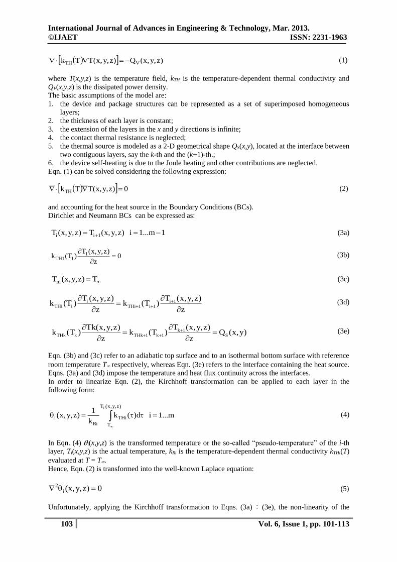
)z,y,x(Q)z,y,x(TTk VTH (1)
where T(x,y,z) is the temperature field, kTH is the temperature-dependent thermal conductivity and
QV(x,y,z) is the dissipated power density.
The basic assumptions of the model are:
1. the device and package structures can be represented as a set of superimposed homogeneous
layers;
2. the thickness of each layer is constant;
3. the extension of the layers in the x and y directions is infinite;
4. the contact thermal resistance is neglected;
5. the thermal source is modeled as a 2-D geometrical shape QS(x,y), located at the interface between
two contiguous layers, say the k-th and the (k+1)-th.;
6. the device self-heating is due to the Joule heating and other contributions are neglected.
Eqn. (1) can be solved considering the following expression:
0)z,y,x(TTkTH (2)
and accounting for the heat source in the Boundary Conditions (BCs).
Dirichlet and Neumann BCs can be expressed as:
1m...1i)z,y,x(T)z,y,x(T 1ii (3a)
0z
)z,y,x(T)T(k 1
11TH
(3b)
T)z,y,x(Tm (3c)
z
)z,y,x(T)T(k
z
)z,y,x(T)T(k 1i
1i1THii
iTHi
(3d)
)y,x(Qz
)z,y,x(T)T(k
z
)z,y,x(Tk)T(k S
1k1k1THkkTHk
(3e)
Eqn. (3b) and (3c) refer to an adiabatic top surface and to an isothermal bottom surface with reference
room temperature T respectively, whereas Eqn. (3e) refers to the interface containing the heat source.
Eqns. (3a) and (3d) impose the temperature and heat flux continuity across the interfaces.
In order to linearize Eqn. (2), the Kirchhoff transformation can be applied to each layer in the
following form:
m...1id)(kk
1)z,y,x(
)z,y,x(T
T
THi
Ri
i
i
(4)
In Eqn. (4) i(x,y,z) is the transformed temperature or the so-called “pseudo-temperature” of the i-th
layer, Ti(x,y,z) is the actual temperature, kRi is the temperature-dependent thermal conductivity kTHi(T)
evaluated at T = T.
Hence, Eqn. (2) is transformed into the well-known Laplace equation:
0)z,y,x(i2 (5)
Unfortunately, applying the Kirchhoff transformation to Eqns. (3a) ÷ (3e), the non-linearity of the
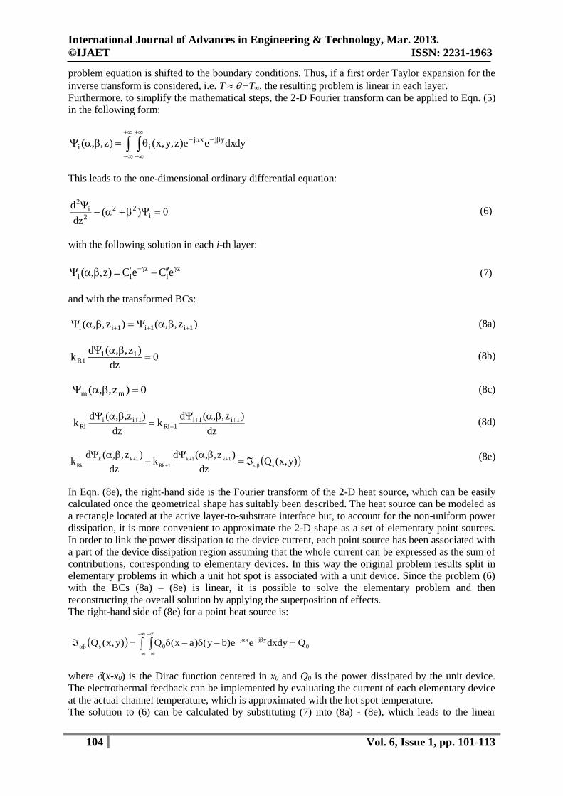
International Journal of Advances in Engineering & Technology, Mar. 2013.
©IJAET ISSN: 2231-1963
104 Vol. 6, Issue 1, pp. 101-113
problem equation is shifted to the boundary conditions. Thus, if a first order Taylor expansion for the
inverse transform is considered, i.e. T +T, the resulting problem is linear in each layer.
Furthermore, to simplify the mathematical steps, the 2-D Fourier transform can be applied to Eqn. (5)
in the following form:
dxdyee)z,y,x()z,,( yjxjii
This leads to the one-dimensional ordinary differential equation:
0)(dz
di
22
2
i2
(6)
with the following solution in each i-th layer:
z
iz
ii eCeC)z,,( (7)
and with the transformed BCs:
)z,,()z,,( 1i1i1ii (8a)
0dz
)z,,(dk 11
1R
(8b)
0)z,,( mm (8c)
dz
)z,,(dk
dz
)z,,(dk 1i1i
1Ri1ii
Ri
(8d)
)y,x(Qdz
)z,,(dk
dz
)z,,(dk
s
1k1k
1Rk
1kk
Rk
(8e)
In Eqn. (8e), the right-hand side is the Fourier transform of the 2-D heat source, which can be easily
calculated once the geometrical shape has suitably been described. The heat source can be modeled as
a rectangle located at the active layer-to-substrate interface but, to account for the non-uniform power
dissipation, it is more convenient to approximate the 2-D shape as a set of elementary point sources.
In order to link the power dissipation to the device current, each point source has been associated with
a part of the device dissipation region assuming that the whole current can be expressed as the sum of
contributions, corresponding to elementary devices. In this way the original problem results split in
elementary problems in which a unit hot spot is associated with a unit device. Since the problem (6)
with the BCs (8a) – (8e) is linear, it is possible to solve the elementary problem and then
reconstructing the overall solution by applying the superposition of effects.
The right-hand side of (8e) for a point heat source is:
0
yjxj
0s Qdxdyee)by()ax(Q)y,x(Q
where (x-x0) is the Dirac function centered in x0 and Q0 is the power dissipated by the unit device.
The electrothermal feedback can be implemented by evaluating the current of each elementary device
at the actual channel temperature, which is approximated with the hot spot temperature.
The solution to (6) can be calculated by substituting (7) into (8a) - (8e), which leads to the linear
International Journal of Advances in Engineering & Technology, Mar. 2013.
©IJAET ISSN: 2231-1963
105 Vol. 6, Issue 1, pp. 101-113
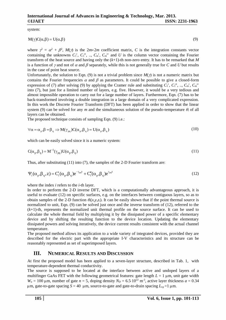
system:
),(U),(C)(M (9)
where 2 = 2 + 2, M() is the 2m2m coefficient matrix, C is the integration constants vector
containing the unknowns C1, C1, .., Cm, Cm and U is the column vector containing the Fourier
transform of the heat source and having only the (k+1)-th non-zero entry. It has to be remarked that M
is a function of and not of and separately, while this is not generally true for C and U but results
in the case of point heat source.
Unfortunately, the solution to Eqn. (9) is not a trivial problem since M() is not a numeric matrix but
contains the Fourier frequencies and as parameters. It could be possible to give a closed-form
expression of (7) after solving (9) by applying the Cramer rule and substituting C1, C1, .., Cm, Cm
into (7), but just for a limited number of layers, e.g. five. However, it would be a very tedious and
almost impossible operation to carry out for a large number of layers. Furthermore, Eqn. (7) has to be
back-transformed involving a double integration in a large domain of a very complicated expression.
In this work the Discrete Fourier Transform (DFT) has been applied in order to show that the linear
system (9) can be solved for any m and the simultaneous solution of the pseudo-temperature i of all
layers can be obtained.
The proposed technique consists of sampling Eqn. (9) i.e.:
),(U),(C)(M, qpqppqqp (10)
which can be easily solved since it is a numeric system:
),(U)(M),(C qppq1
qp (11)
Thus, after substituting (11) into (7), the samples of the 2-D Fourier transform are:
z
qpi
z
qpiqpi
pqpq e),(Ce),(C)z,,(
(12)
where the index i refers to the i-th layer.
In order to perform the 2-D inverse DFT, which is a computationally advantageous approach, it is
useful to evaluate (12) on specific surfaces, e.g. on the interfaces between contiguous layers, so as to
obtain samples of the 2-D function i(x,y,zi). It can be easily shown that if the point thermal source is
normalized to unit, Eqn. (9) can be solved just once and the inverse transform of (12), referred to the
(k+1)-th, represents the normalized unit thermal profile on the source surface. It can be used to
calculate the whole thermal field by multiplying it by the dissipated power of a specific elementary
device and by shifting the resulting function to the device location. Updating the elementary
dissipated powers and solving iteratively, the device current results consistent with the actual channel
temperature.
The proposed method allows its application to a wide variety of integrated devices, provided they are
described for the electric part with the appropriate I-V characteristics and its structure can be
reasonably represented as set of superimposed layers.
III. NUMERICAL RESULTS AND DISCUSSION
At first the proposed model has been applied to a seven-layer structure, described in Tab. 1, with
temperature-dependent thermal conductivity.
The source is supposed to be located at the interface between active and undoped layers of a
multifinger GaAs FET with the following geometrical features: gate length L = 1 m, unit gate width
Wu = 100 m, number of gate n = 5, doping density ND = 6.51022 m-3, active layer thickness a = 0.34
m, gate-to-gate spacing S = 40 m, source-to-gate and gate-to-drain spacing Lcg =1 m.

International Journal of Advances in Engineering & Technology, Mar. 2013.
©IJAET ISSN: 2231-1963
106 Vol. 6, Issue 1, pp. 101-113
A one-dimensional I-V FET equation [5] has been implemented to consider the feedback between the
device current and the active layer temperature distribution. The most widely accepted empiric
relations between FET physical parameters and temperature have also been taken into account [1].
Table 1. Physical and geometrical parameters of the considered GaAs multilayer structure.
Layer Material Thicknes
s [m]
Thermal conductivity
kTH(T) [W/m/K]
Reference kTH0
[W/m/K]
Cap layer Epoxy mold
compound
500 0.4 0.4
Metallization Gold 3 - 0.065T + 336.67 317
Active layer n-doped GaAs 0.34 52720 / T1.2 56.16
Bulk undoped GaAs 100 54400 / T1.2 57.95
Die-attachment Epoxy mold
compound
25 4 4
Mounting Alumina 500 - 0.0976T + 36.26 36
Heat spreader Copper 1000 - 0.075T + 423.33 401
In Fig. 2 the cross section of the overall thermal profile for the given device is shown. In this case the
dissipated power is P = 1.18 W. The solid line refers to the temperature profile along the y-axis after
the Kirchhoff transform whereas the dash-dotted line refers to the same profile before the
transformation.
Figure 2. Cross section of the thermal profile on the source surface along the y direction: comparison between
the results after the Kirchoff transform (solid line) and before the transformation (dash-dotted line).
As one can clearly see, the difference becomes relevant in the device area, which confirms that the
non-linear dependence of the GaAs thermal conductivity cannot be neglected. Furthermore, as the
peak temperature rises above the reference temperature (300 K) is about 140 K and the mean
temperature rises in the active area is about 110 K, the linear approximation of the boundary condition
leads to a 6% error, which is acceptable.
In order to study the influence of geometrical parameters of the device on its thermal performance, we
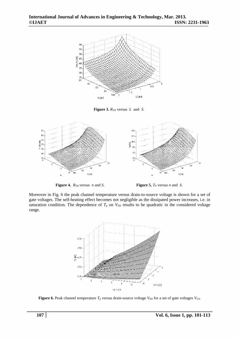
have evaluated the thermal resistance RTH of the device and the peak channel temperature Tp versus S,
L and n, for a dissipated power P = 1 W, as shown in Figs. 3 (where n = 14), 4 (where L = 1 m) and
5 (where L = 1 m) respectively.
International Journal of Advances in Engineering & Technology, Mar. 2013.
©IJAET ISSN: 2231-1963
107 Vol. 6, Issue 1, pp. 101-113
Figure 3. RTH versus L and S.
Figure 4. RTH versus n and S. Figure 5. TP versus n and S.
Moreover in Fig. 6 the peak channel temperature versus drain-to-source voltage is shown for a set of
gate voltages. The self-heating effect becomes not negligible as the dissipated power increases, i.e. in
saturation condition. The dependence of Tp on VDS results to be quadratic in the considered voltage
range.
Figure 6. Peak channel temperature Tp versus drain-source voltage VDS for a set of gate voltages VGS.
International Journal of Advances in Engineering & Technology, Mar. 2013.
©IJAET ISSN: 2231-1963
108 Vol. 6, Issue 1, pp. 101-113
These figures allow the designer to determine the parameter values which optimize the thermal and
electrical layout.
Moreover, in order to demonstrate that the proposed method is independent on the specific physical
properties of the layers, we have applied it to a typical Si/SiGe HBT structure [1], in which we have
used the name Si/SiGe HBT for a device with Si as the base material and SiGe as the emitter.
In particular we have represented the device as a surface without any thickness, where X and Y are
the dimensions of the periodic cell, in which we have divided the device.
The overall heat source, which is located in the depletion layer at the collector, has been divided into a
set of elementary point sources located in the middle of each elementary XY periodic cell.
The first step is to solve the electro-thermal problem, assuming the heat generation and the current as
mutually dependent for each single elementary device which is related to a single elementary heat
source; finally the resulting thermal field of the whole structure is obtained by the superposition of all
the elementary fields.
The transformed temperature i(x,y,z) for a point thermal source can be expressed as [9]:
20i2
0i2
0i0
0i0i0i
zzyyxx2ππ
)z,y,Q(xz)y,Δθ(x,
(13)
where x0i, y0i and z0i are the coordinates of the i-th heat point source, x,y,z is the generic position in
which the temperature increase (x,y,z) above the reference is evaluated and Q(x0i,y0i,z0i) is the
dissipated power of the i-th elementary heat source.
The electro-thermal feedback can be implemented for each XY subsection considering that Q can be
assumed as the temperature-dependent electrical power P(i(x0i,y0i,z0i)) of the i-th elementary device
centred in x0i, y0i, z0i and, thus, corresponding to the i-th heat source centred in the same point.
The electrical power of the i-th elementary device is:
P(x0i,y0i,z0i) = P(i) = IB(i) VBE + IC (i) VCE (14)
where VBE , the voltage drop between base and emitter, is temperature-independent, IB and IC are the
base and collector currents, respectively, of the elementary cell centred in x0i,y0i,z0i having temperature
i, and VCE , the voltage drop between collector and emitter, is temperature-independent.
The dependence of the current-voltage equation, based on physical parameters, on the temperature
was widely studied in the past. The parameters that have been taken into account for their thermal
dependence are the electron mobility, saturation velocity, permittivity, energy band gap, threshold
voltage and built-in voltage. The reader can refer to for the empirical expression of the foregoing
parameters [9].
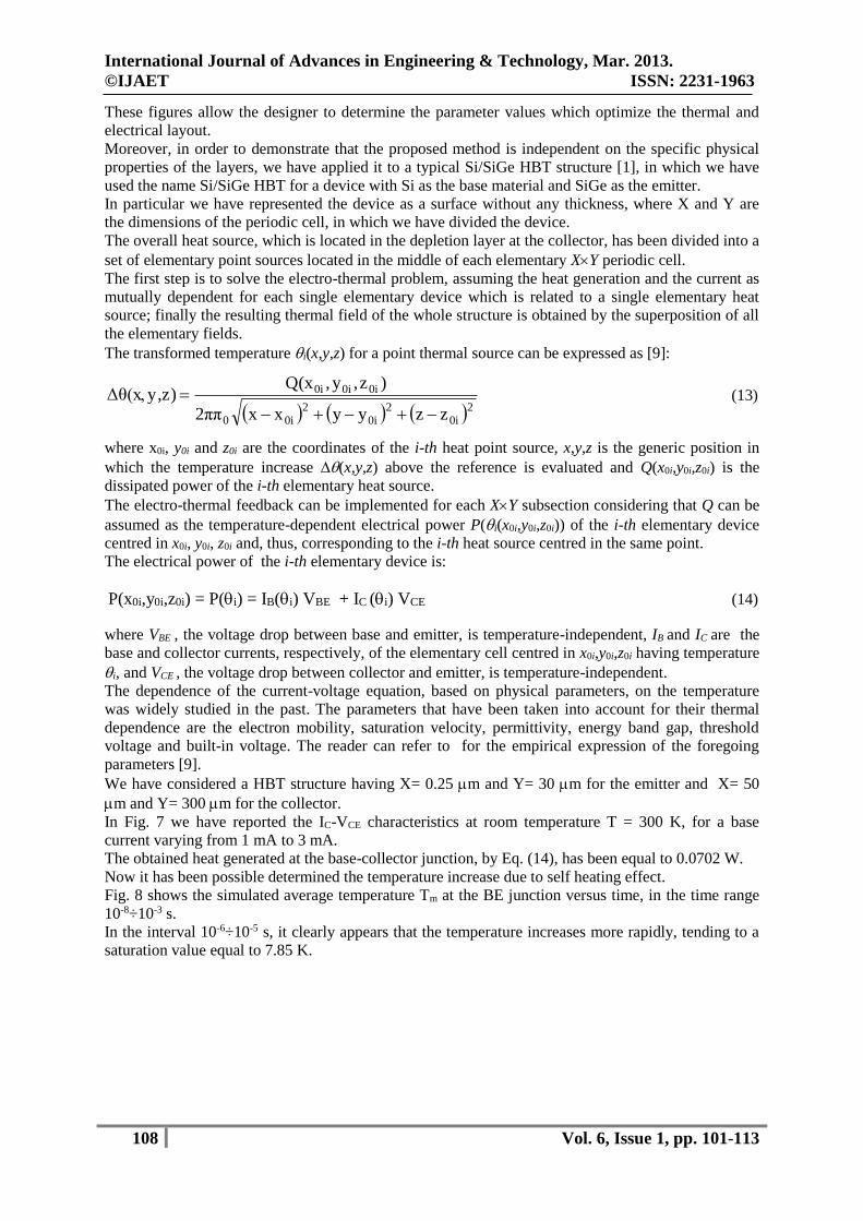
We have considered a HBT structure having X= 0.25 m and Y= 30 m for the emitter and X= 50
m and Y= 300 m for the collector.
In Fig. 7 we have reported the IC-VCE characteristics at room temperature T = 300 K, for a base
current varying from 1 mA to 3 mA.
The obtained heat generated at the base-collector junction, by Eq. (14), has been equal to 0.0702 W.
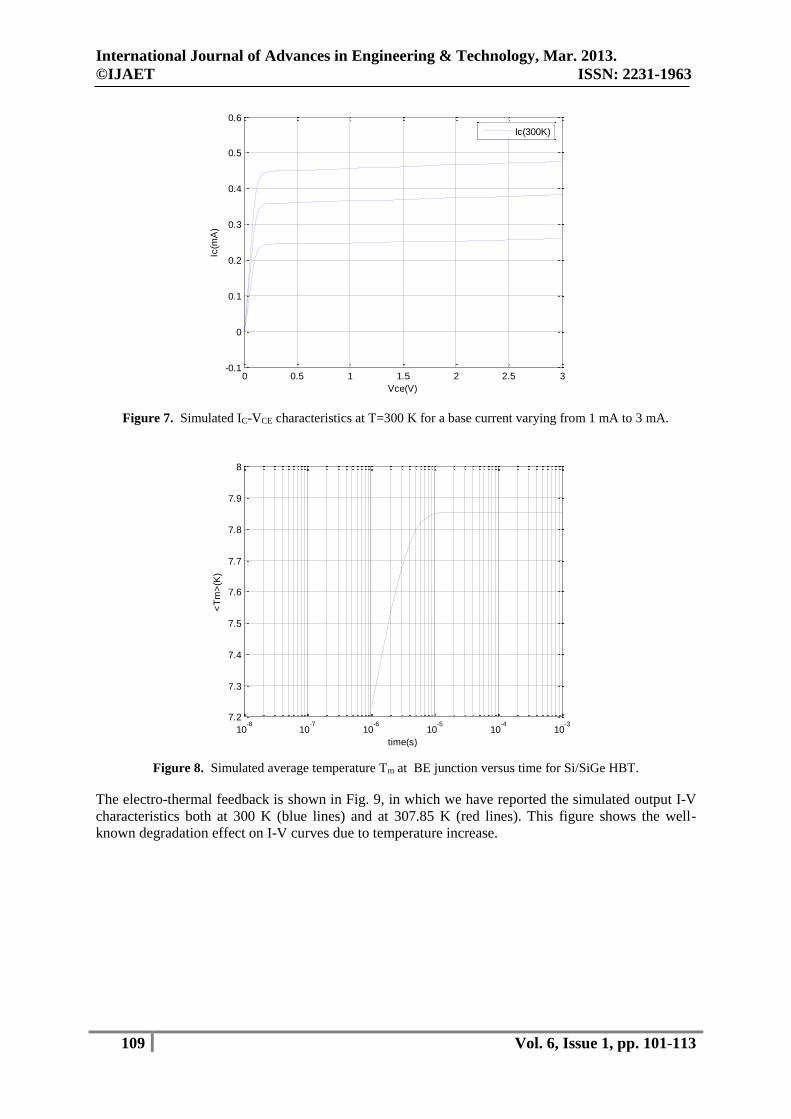
Now it has been possible determined the temperature increase due to self heating effect.
Fig. 8 shows the simulated average temperature Tm at the BE junction versus time, in the time range
10-8÷10-3 s.
In the interval 10-6÷10-5 s, it clearly appears that the temperature increases more rapidly, tending to a
saturation value equal to 7.85 K.
International Journal of Advances in Engineering & Technology, Mar. 2013.
©IJAET ISSN: 2231-1963
109 Vol. 6, Issue 1, pp. 101-113
Figure 7. Simulated IC-VCE characteristics at T=300 K for a base current varying from 1 mA to 3 mA.
Figure 8. Simulated average temperature Tm at BE junction versus time for Si/SiGe HBT.
The electro-thermal feedback is shown in Fig. 9, in which we have reported the simulated output I-V
characteristics both at 300 K (blue lines) and at 307.85 K (red lines). This figure shows the well-
known degradation effect on I-V curves due to temperature increase.
0 0.5 1 1.5 2 2.5 3-0.1
0
0.1
0.2
0.3
0.4
0.5
0.6
Vce(V)
Ic(m
A)
Ic(300K)
10-8
10-7
10-6
10-5
10-4
10-3
7.2
7.3
7.4
7.5
7.6
7.7
7.8
7.9
8
time(s)
<T
m>
(K)
International Journal of Advances in Engineering & Technology, Mar. 2013.
©IJAET ISSN: 2231-1963
110 Vol. 6, Issue 1, pp. 101-113
Figure 9. Simulated I-V characteristics both at 300 K (blue lines) and at 307.85 K (red lines).
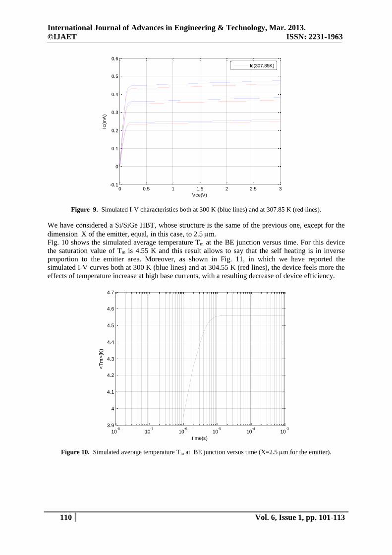
We have considered a Si/SiGe HBT, whose structure is the same of the previous one, except for the
dimension X of the emitter, equal, in this case, to 2.5 m.
Fig. 10 shows the simulated average temperature Tm at the BE junction versus time. For this device
the saturation value of Tm is 4.55 K and this result allows to say that the self heating is in inverse
proportion to the emitter area. Moreover, as shown in Fig. 11, in which we have reported the
simulated I-V curves both at 300 K (blue lines) and at 304.55 K (red lines), the device feels more the
effects of temperature increase at high base currents, with a resulting decrease of device efficiency.
Figure 10. Simulated average temperature Tm at BE junction versus time (X=2.5 m for the emitter).
0 0.5 1 1.5 2 2.5 3-0.1
0
0.1
0.2
0.3
0.4
0.5
0.6
Vce(V)
Ic(m
A)
Ic(307.85K)
10-8
10-7
10-6
10-5
10-4
10-3
3.9
4
4.1
4.2
4.3
4.4
4.5
4.6
4.7
time(s)
<T
m>
(K)

International Journal of Advances in Engineering & Technology, Mar. 2013.
©IJAET ISSN: 2231-1963
111 Vol. 6, Issue 1, pp. 101-113
Figure 11. Simulated I-V characteristics both at 300 K (blue lines) and at 304.55 K (red lines).
Finally, in order to demonstrate the applicability of our method in case of multifinger devices or
thermal coupling between contiguous devices, our model has been applied to a power Si/SiGe
Heterojunction Bipolar Transistor with multiple emitter fingers [6-8], as shown in Fig. 12.
Figure 12. Possible structures of a power Si/SiGe Heterojunction Bipolar Transistor with multiple emitter
fingers.
In this case, from the analysis of the various thermal profiles, it has been possible to define the
electrothermal optimal layout of the considered HBT with three fingers having area 20 m x 3 m,
spaced of 35 m. Fig. 13 shows the relative thermal profile in the (x,y) plane, while in Fig. 14 we
have reported the 3-D thermal field on the surface containing the heat source.
0 0.5 1 1.5 2 2.5 3-0.1
0
0.1
0.2
0.3
0.4
0.5
0.6
Vce(V)
Ic(m
A)
Ic(304.55)

International Journal of Advances in Engineering & Technology, Mar. 2013.
©IJAET ISSN: 2231-1963
112 Vol. 6, Issue 1, pp. 101-113
Figure 13. Thermal profile in the (x,y) plane for the power Si/SiGe HBT having optimal layout.
Figure 14. 3-D thermal field on the surface containing the heat source.
The calculation time for the proposed examples can be quantified in a few minutes for the main part
of the algorithm, that is the temperature field of the elementary source and the current of the
elementary device, and in less than a minute for the graphic routines. To perform all the simulations
we have used a common Windows-based PC, equipped with a Pentium IV CPU and main memory of
1 Gbyte.
It is worthwhile to remark that the software, by which all the calculations have been carried out, has
been implemented just for academic non-commercial purpose.
IV. CONCLUSIONS
In this paper we review an analytical model, already proposed by us, for the solution of the 3-D
steady-state heat equation with temperature-dependent thermal conductivity for a single integrated
device or a given configuration of two or more devices. A weak coupling between electrical and
thermal solution is implemented by calculating the device current and, hence, the dissipated power, as
a function of the actual channel temperature. A multiple layer structure approximating the effect of
the package has been considered as the spatial domain in which the heat equation has been solved.
REFERENCES
[1] Perri A.G., (2011) “Dispositivi Elettronici Avanzati”, Progedit Editor, Bari, Italy, ISBN: 978-88-6194-
081-9.
[2] Marani R., Perri A.G., (2010) “Thermal and electrical layout optimization of multilayer structure
solid.state devices based on the 2-D Fourier series”; Proceedings of MELECON 2010, Valletta, Malta.
[3] Marani R., Perri A.G., (2010) “Analytical Electrothermal Modelling of Multilayer Structure Electronic
Devices”; The Open Electrical & Electronic Engineering Journal, vol.4, pp.32-39.
International Journal of Advances in Engineering & Technology, Mar. 2013.
©IJAET ISSN: 2231-1963
113 Vol. 6, Issue 1, pp. 101-113
[4] Perri A.G., (2011) “Modelling and Simulations in Electronic and Optoelectronic Engineering”,
Research Signpost, Kerata, India, 2011, ISBN: 978-81-308-0450-7.
[5] Marani R., Perri A.G., (2011) “Electrothermal Design of Multilayer Structure Integrated Devices
through the Solution to the non-linear 3-D Heat Flow Equation, in Modelling and Simulations in
Electronic and Optoelectronic Engineering, Research Signpost, Kerata, India, ISBN 978-81-308-
0450-7, pp. 1-26.
[6] Ashburn P., (2003) “SiGe Heterojunction Bipolar Transistors”, John Wiley & Sons, pp. 152 - 154.
[7] Esame O., Gurbuz Y., Tekin I., Bozkurt A., (2004) “Performance comparison of state-of-the-art
heterojunction bipolar devices (HBT) based on AlGaAs/GaAs, Si/SiGE and InGaAs/InP”,
Microelectronics Journal, vol.35, pp. 901 – 908.
[8] Lee J. G., Oh T. K., Kim B., Kang B. K., (2001) “Emitter structure of power heterojunction bipolar
transistor for enhancement of thermal stability!”, Solid-State Electronics, vol. 45, pp. 27 – 33.
[9] Anholt R., (1995) “Electrical and thermal characterization of MESFETs, HEMTs and HBTs”, Artech
House Inc., ISBN:0-89006-749-X.
AUTHORS
Roberto Marani received the Master of Science degree (cum laude) in Electronic Engineering
in 2008 from Polytechnic University of Bari, where he received his Ph.D. degree in Electronic
Engineering in 2012. He worked in the Electronic Device Laboratory of Bari Polytechnic for
the design, realization and testing of nanometrical electronic systems, quantum devices and
FET on carbon nanotube. Moreover Dr. Marani worked in the field of design, modelling and
experimental characterization of devices and systems for biomedical applications. In
December 2008 he received a research grant by Polytechnic University of Bari for his research
activity. From February 2011 to October 2011 he went to Madrid, Spain, joining the Nanophotonics Group at
Universidad Autónoma de Madrid, under the supervision of Prof. García-Vidal. Currently he is involved in the
development of novel numerical models to study the physical effects that occur in the interaction of
electromagnetic waves with periodic nanostructures, both metal and dielectric. His research activities also
include biosensing and photovoltaic applications. Dr. Marani is a member of the COST Action MP0702 -
Towards Functional Sub-Wavelength Photonic Structures, and is a member of the Consortium of University
CNIT – Consorzio Nazionale Interuniversitario per le Telecomunicazioni.
Dr. Marani has published over 100 scientific papers.
Anna Gina Perri received the Laurea degree cum laude in Electrical Engineering from the
University of Bari in 1977. In the same year she joined the Electrical and Electronic
Department, Polytechnic University of Bari, where she is Professor of Electronics from 2002.
Her current research activities are in the area of numerical modelling and performance
simulation techniques of electronic devices for the design of GaAs Integrated Circuits and in
the characterization and design of optoelectronic devices on PBG. Moreover she works in the
design, realization and testing of nanometrical electronic systems, quantum devices, FET on
carbon nanotube and in the field of experimental characterization of electronic systems for
biomedical applications. Prof. Perri is the Head of Electron Devices Laboratory of the Polytechnic University of
Bari. She is author of over 250 book chapters, journal articles and conference papers and serves as referee for
many international journals. Prof. Perri is a member of the Italian Circuits, Components and Electronic
Technologies – Microelectronics Association and is a member of the Consortium of University CNIT –
Consorzio Nazionale Interuniversitario per le Telecomunicazioni. Prof. Perri is a Member of Advisory Editorial
Board of International Journal of Advances in Engineering & Technology and of Current Nanoscience
(Bentham Science Publishers).