Embed Size (px)
Citation preview
© Mitsubishi Electric Corporation
功率模块技术现状与未来展望
< for CPSSC2019 only >
三菱电机半导体大中国区 2019.11.02
作者授权中国电源学会发布,未经作者同意禁止转载
2© Mitsubishi Electric Corporation
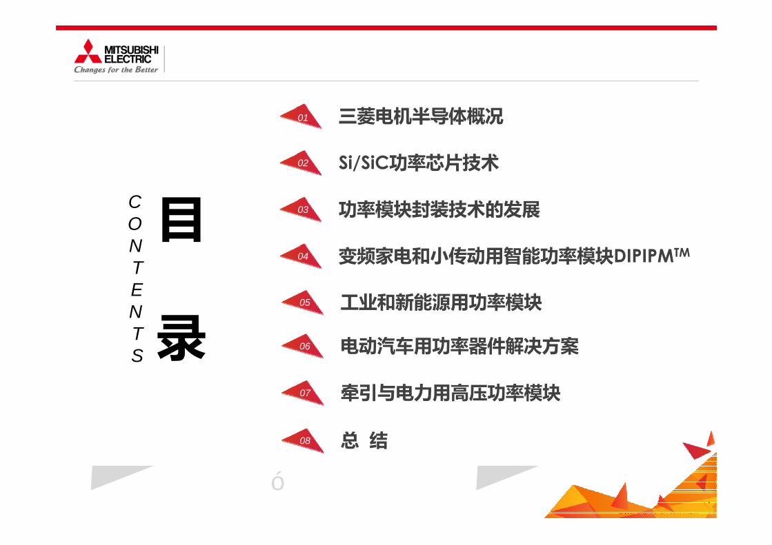
01
CONTENTS
02
03
04
06
07
08
05
作者授权中国电源学会发布,未经作者同意禁止转载
3© Mitsubishi Electric Corporation
作者授权中国电源学会发布,未经作者同意禁止转载
4© Mitsubishi Electric Corporation
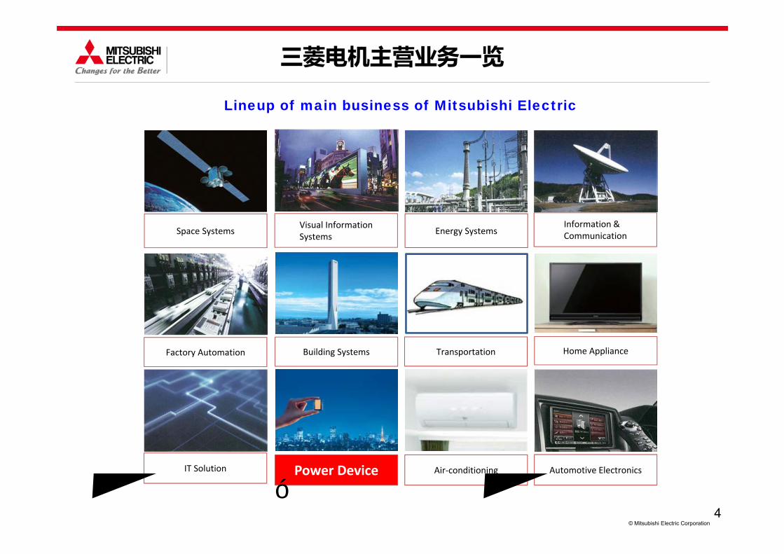
Lineup of main business of Mitsubishi Electric
Space Systems Energy SystemsInformation & Communication
Transportation
Power DeviceIT Solution
Building Systems
Visual Information Systems
Factory Automation Home Appliance
Air‐conditioning Automotive Electronics
三菱电机主营业务一览
作者授权中国电源学会发布,未经作者同意禁止转载
5© Mitsubishi Electric Corporation
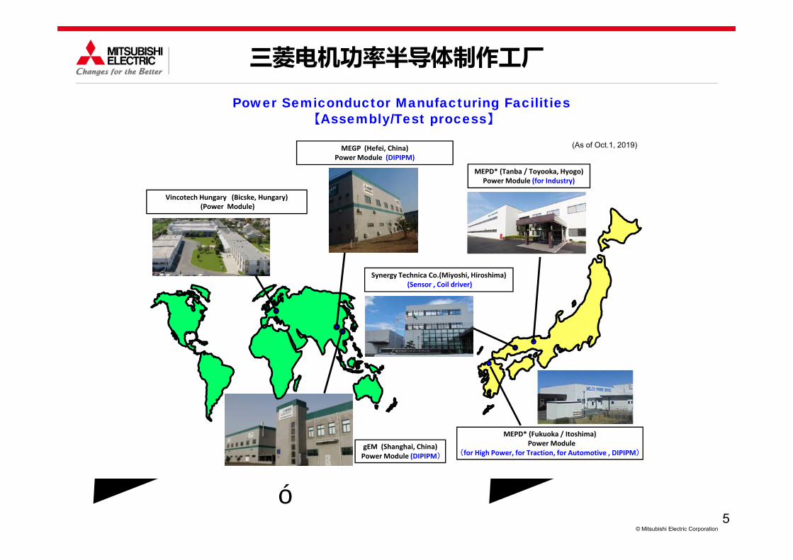
MEPD* (Tanba / Toyooka, Hyogo)Power Module (for Industry)
MEGP (Hefei, China)Power Module (DIPIPM)
gEM (Shanghai, China)Power Module (DIPIPM)
Vincotech Hungary (Bicske, Hungary)(Power Module)
MEPD* (Fukuoka / Itoshima)Power Module
(for High Power, for Traction, for Automotive , DIPIPM)
Synergy Technica Co.(Miyoshi, Hiroshima)(Sensor , Coil driver)
Power Semiconductor Manufacturing Facilities 【Assembly/Test process】
(As of Oct.1, 2019)
三菱电机功率半导体制作工厂
作者授权中国电源学会发布,未经作者同意禁止转载
6© Mitsubishi Electric Corporation
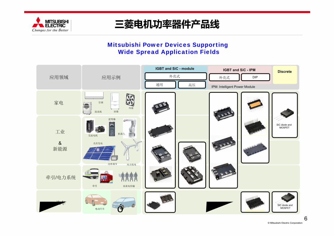
家电风扇
交流电机
逆变器
光伏发电
功率调节 风力发电
洗衣机 冰箱
空调
牵引
IGBT and SiC - module
外壳式
通用 高压
IGBT and SiC - IPM
外壳式 DIP
Discrete应用示例应用领域
工业
&新能源
牵引/电力系统
汽车
直流电传输
电动汽车
机器人
SiC diode andMOSFET
SiC diode andMOSFET
IPM: Intelligent Power Module
Mitsubishi Power Devices Supporting Wide Spread Application Fields
三菱电机功率器件产品线
作者授权中国电源学会发布,未经作者同意禁止转载
7© Mitsubishi Electric Corporation
作者授权中国电源学会发布,未经作者同意禁止转载
8© Mitsubishi Electric Corporation
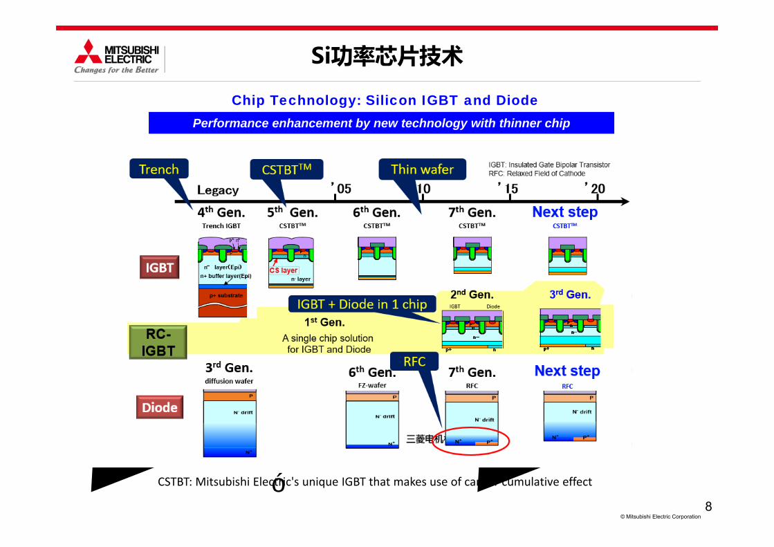
Performance enhancement by new technology with thinner chip
Chip Technology: Silicon IGBT and Diode
CSTBT: Mitsubishi Electric's unique IGBT that makes use of carrier cumulative effect
Si功率芯片技术
作者授权中国电源学会发布,未经作者同意禁止转载
9© Mitsubishi Electric Corporation
Enhancing Silicon chip Technologies
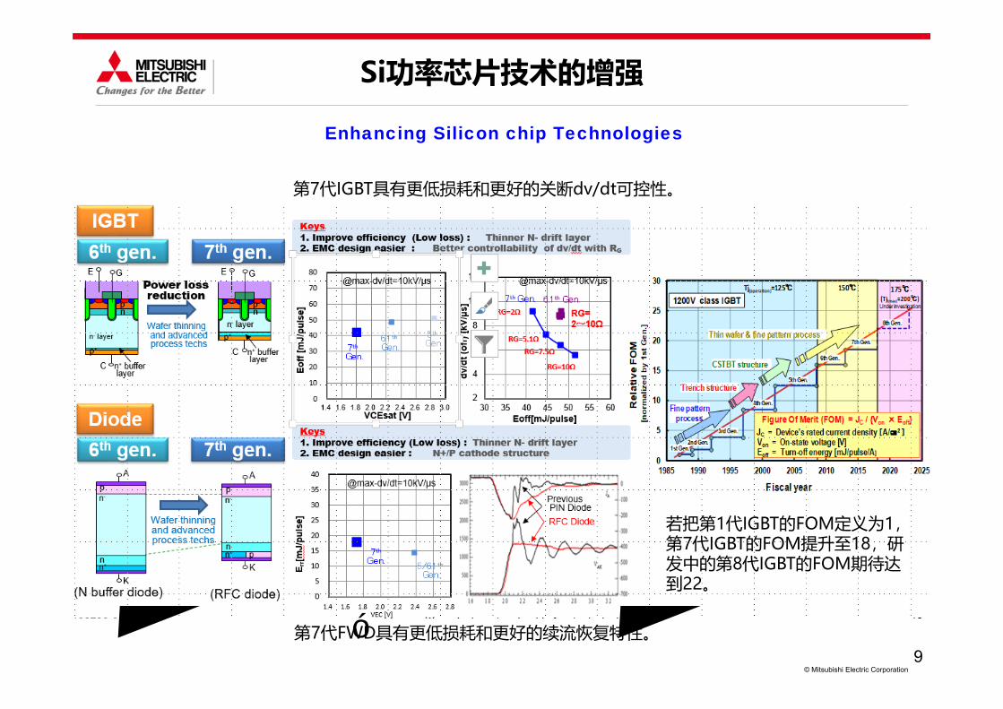
第7代IGBT具有更低损耗和更好的关断dv/dt可控性。
第7代FWD具有更低损耗和更好的续流恢复特性。
若把第1代IGBT的FOM定义为1,第7代IGBT的FOM提升至18,研发中的第8代IGBT的FOM期待达到22。
Si功率芯片技术的增强
作者授权中国电源学会发布,未经作者同意禁止转载
10© Mitsubishi Electric Corporation
Roadmap of practical SiC power chips
Existin
gfab. (1
00mm)Te
chno
logy status
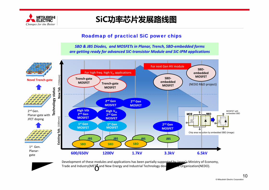
SBD & JBS Diodes, and MOSFETs in Planar, Trench, SBD‐embedded forms are getting ready for advanced SiC‐transistor Module and SiC‐IPM applications
New
fab. (1
50mm)
Chip area reduction by embedded SBD (image)
MOSFET with embedded SBD
Novel Trench‐gate
1st Gen. Planar‐gate
2nd Gen. Planar‐gate with JFET doping
600/650V 1200V 1.7kV 3.3kV 6.5kV
JBS JBS
2nd Gen MOSFET
SBD‐embeddedMOSFET
High Vth2nd GenMOSFET
JBS
For next Gen HV module
JBS
For high freq. high Vth applications
1st GenMOSFET
High Vth2nd GenMOSFET
2nd GenMOSFET
SBD‐embeddedMOSFET
SBD
1st GenMOSFET
Trench‐gateMOSFET
SBD SBD
Trench‐gateMOSFET
2nd Gen MOSFET
(NEDO R&D project)
SiC功率芯片发展路线图
Development of these modules and applications has been partially supported by Japan’s Ministry of Economy, Trade and Industry(METI) and New Energy and Industrial Technology development Organization(NEDO).作者授权中国电源学会发布,未经作者同意禁止转载
11© Mitsubishi Electric Corporation
作者授权中国电源学会发布,未经作者同意禁止转载
12© Mitsubishi Electric Corporation
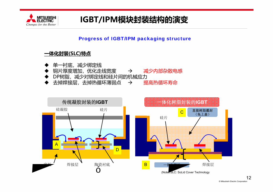
一体化封装(SLC)特点
单一衬底,减少绑定线 铜片厚度增加,优化走线宽度 减少内部杂散电感 DP树脂,减少对绑定线和硅片间的机械应力 去掉焊接层,去掉热循环薄弱点 提高热循环寿命
传统凝胶封装的IGBT
陶瓷衬底底板 焊接层
硅凝胶
一体化树脂封装的IGBT直接树脂灌封(免上盖)
焊接层
A
B
C
D
一体化基板
(Note) SLC: SoLid Cover Technology
硅片
硅片
IGBT/IPM模块封装结构的演变
Progress of IGBT/IPM packaging structure
作者授权中国电源学会发布,未经作者同意禁止转载
13© Mitsubishi Electric Corporation
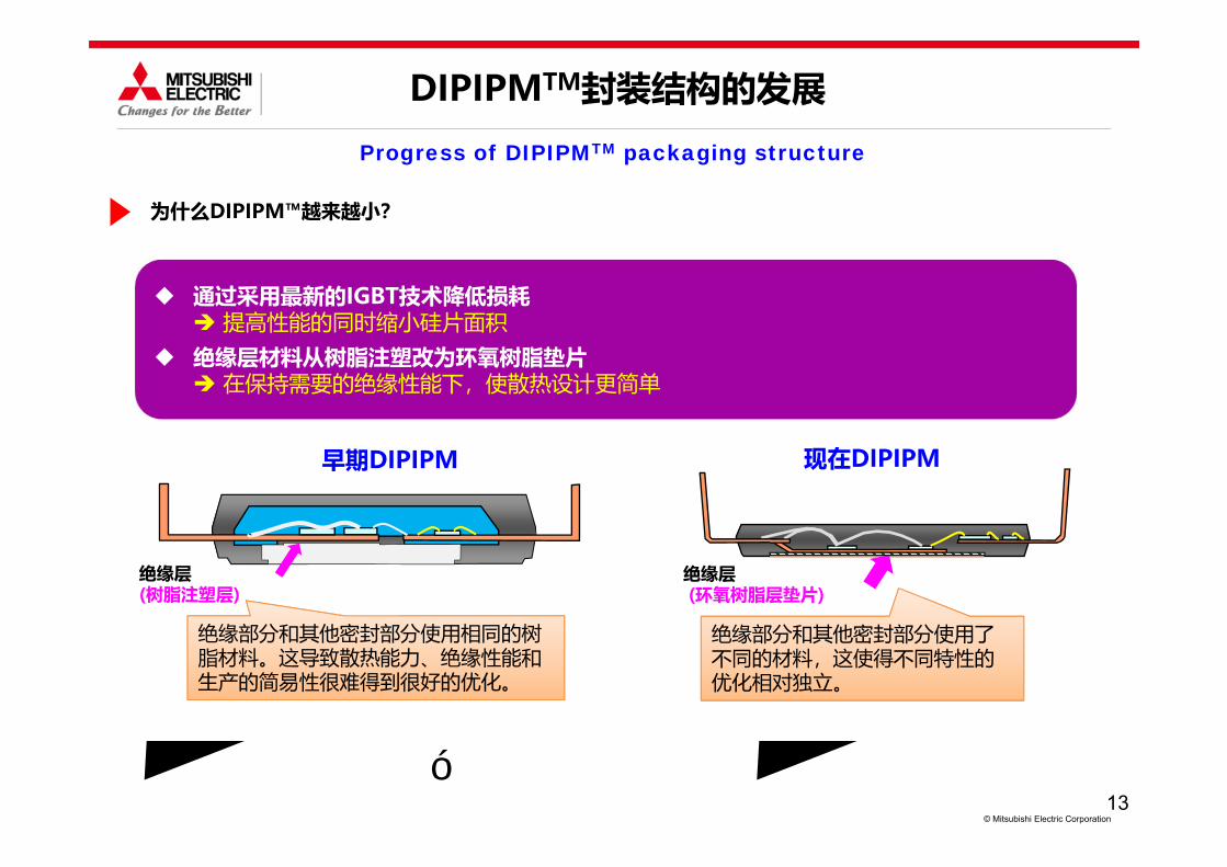
绝缘层(树脂注塑层)
现在DIPIPM
绝缘层(环氧树脂层垫片)
早期DIPIPM
通过采用最新的IGBT技术降低损耗 提高性能的同时缩小硅片面积
绝缘层材料从树脂注塑改为环氧树脂垫片 在保持需要的绝缘性能下,使散热设计更简单
绝缘部分和其他密封部分使用相同的树脂材料。这导致散热能力、绝缘性能和生产的简易性很难得到很好的优化。
绝缘部分和其他密封部分使用了不同的材料,这使得不同特性的优化相对独立。
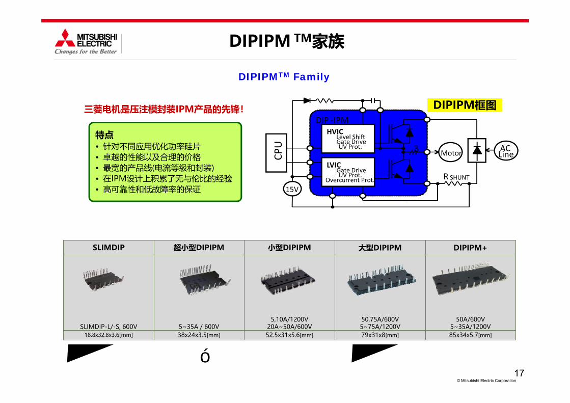
为什么DIPIPM™越来越小?
Progress of DIPIPMTM packaging structure
DIPIPMTM封装结构的发展
作者授权中国电源学会发布,未经作者同意禁止转载
14© Mitsubishi Electric Corporation
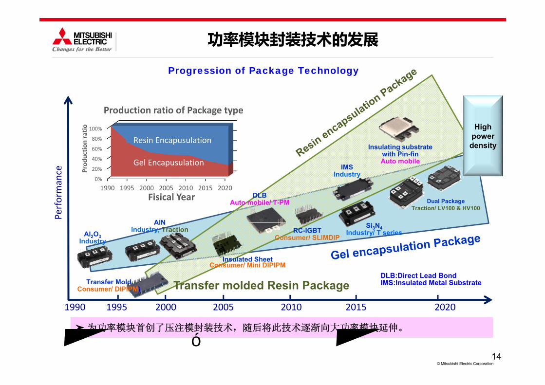
1990 1995 2000 2005 2010 2015 2020
Al2O3Industry
Performan
ce IMSIndustry
AlNIndustry, Traction
Transfer molded Resin Package
RC-IGBTConsumer/ SLIMDIP
DLBAuto mobile/ T-PM
High power density
Progression of Package Technology
Insulated SheetConsumer/ Mini DIPIPM
Dual PackageTraction/ LV100 & HV100
Si3N4Industry/ T series
Transfer MoldConsumer/ DIPIPM)
0%
20%
40%
60%
80%
100%
1990 1995 2000 2005 2010 2015 2020
Prod
uctio
n ratio
Fisical Year
Production ratio of Package type
Resin Encapusulation
Gel Encapusulation
DLB:Direct Lead BondIMS:Insulated Metal Substrate
Insulating substrate with Pin-finAuto mobile
功率模块封装技术的发展
➤ 为功率模块首创了压注模封装技术,随后将此技术逐渐向大功率模块延伸。
作者授权中国电源学会发布,未经作者同意禁止转载
15© Mitsubishi Electric Corporation
作者授权中国电源学会发布,未经作者同意禁止转载
16© Mitsubishi Electric Corporation
De facto Solution for Home Appliances : DIPIPMTM
•1989 绝缘栅双极型晶体管(IGBT)和智能功率模块(IPM)开始批量生产
•1996 双列直插型智能功率模块(DIPIPM)和HVIC开始批量生产
• 根据不同应用优化功率芯片
• 强大的产品线(不同额定电流与封装)
• IPM类产品设计的丰富累积经验
• 确保高可靠性与低失效率
DIPIPM, SLIMDIP, DIPIPM+和CSTBT为三菱电机注册商标
为全球节能累计贡献了几千亿度电!
变频家电的标准解决方案: DIPIPMTM
作者授权中国电源学会发布,未经作者同意禁止转载
17© Mitsubishi Electric Corporation
特点• 针对不同应用优化功率硅片• 卓越的性能以及合理的价格• 最宽的产品线(电流等级和封装)• 在IPM设计上积累了无与伦比的经验• 高可靠性和低故障率的保证
三菱电机是压注模封装IPM产品的先锋!
SLIMDIP 超小型DIPIPM 小型DIPIPM 大型DIPIPM DIPIPM+
SLIMDIP-L/-S, 600V 5~35A / 600V5,10A/1200V
20A~50A/600V50,75A/600V5~75A/1200V
50A/600V5~35A/1200V
18.8x32.8x3.6[mm] 38x24x3.5[mm] 52.5x31x5.6[mm] 79x31x8[mm] 85x34x5.7[mm]
HVICLevel ShiftGate DriveUV Prot.
LVICGate DriveUV Prot.
Overcurrent Prot.
3 Motor
R SHUNT
CPU
15V
ACLine
DIP ‐IPMDIPIPM框图
DIPIPMTM Family
DIPIPM TM家族
作者授权中国电源学会发布,未经作者同意禁止转载
18© Mitsubishi Electric Corporation
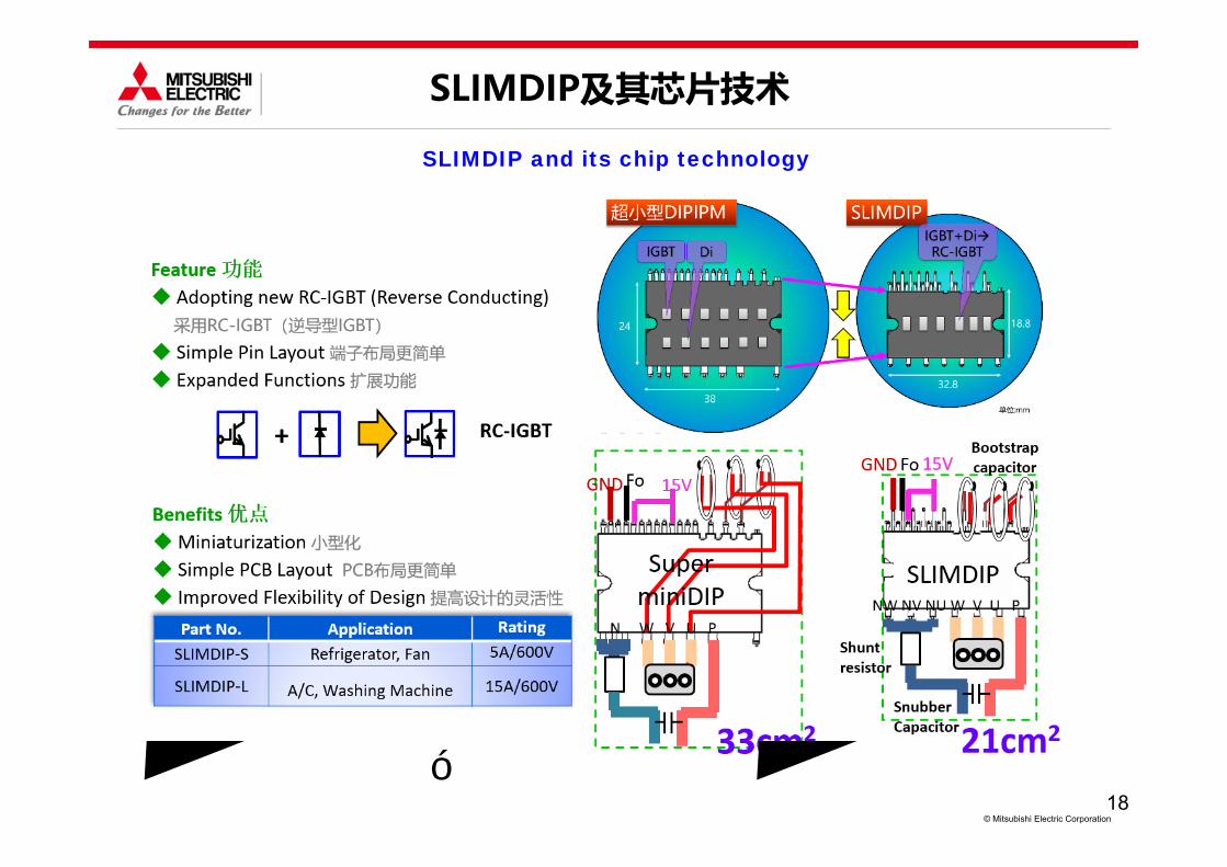
SLIMDIP and its chip technology
SLIMDIP及其芯片技术
作者授权中国电源学会发布,未经作者同意禁止转载
19© Mitsubishi Electric Corporation
IGBT and FWDi
驱动IC及保护电路NTC
自举二极管和限流电阻IGBT and FWDi
门极驱动
Diode
Motor Control Unit
Drive Circuit
Protection Circuit
+
Drive Circuit
Protection Circuit
M
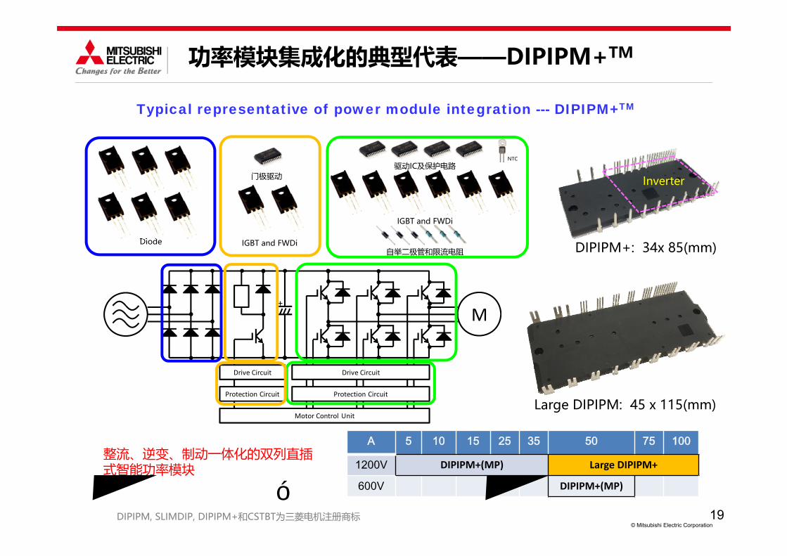
整流、逆变、制动一体化的双列直插式智能功率模块
功率模块集成化的典型代表——DIPIPM+TM
Typical representative of power module integration --- DIPIPM+TM
DIPIPM, SLIMDIP, DIPIPM+和CSTBT为三菱电机注册商标
A 5 10 15 25 35 50 75 100
1200V DIPIPM+(MP) Large DIPIPM+
600V DIPIPM+(MP)
Large DIPIPM: 45 x 115(mm)
DIPIPM+: 34x 85(mm)
Inverter
作者授权中国电源学会发布,未经作者同意禁止转载
20© Mitsubishi Electric Corporation
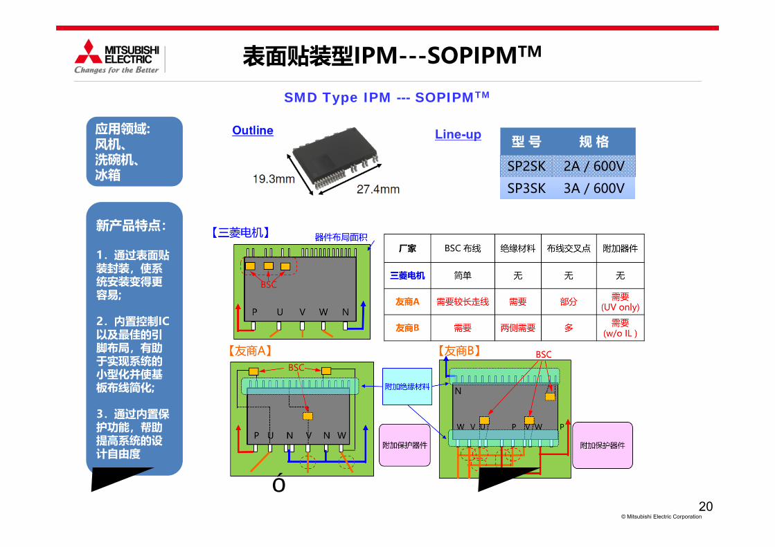
表面贴装型IPM---SOPIPMTM
SMD Type IPM --- SOPIPMTM
型 号 规 格
SP2SK 2A / 600V
SP3SK 3A / 600V
新产品特点:
1.通过表面贴装封装,使系统安装变得更容易;
2.内置控制IC以及最佳的引脚布局,有助于实现系统的小型化并使基板布线简化;
3.通过内置保护功能,帮助提高系统的设计自由度
应用领域:风机、洗碗机、冰箱
Line-up
作者授权中国电源学会发布,未经作者同意禁止转载
21© Mitsubishi Electric Corporation
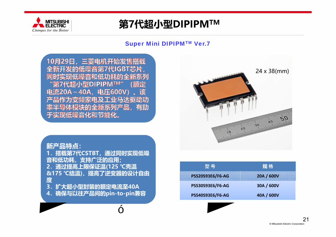
第7代超小型DIPIPMTM
Super Mini DIPIPMTM Ver.7
型 号 规 格
PSS20S93E6/F6‐AG 20A / 600V
PSS30S93E6/F6‐AG 30A / 600V
PSS40S93E6/F6‐AG 40A / 600V
新产品特点:1.搭载第7代CSTBT,通过同时实现低噪音和低功耗,支持广泛的应用;2.通过提高上限保证温(125 ℃壳温&175 ℃结温),提高了逆变器的设计自由度3.扩大超小型封装的额定电流至40A4.确保与以往产品间的pin-to-pin兼容
24 x 38(mm)
作者授权中国电源学会发布,未经作者同意禁止转载
22© Mitsubishi Electric Corporation
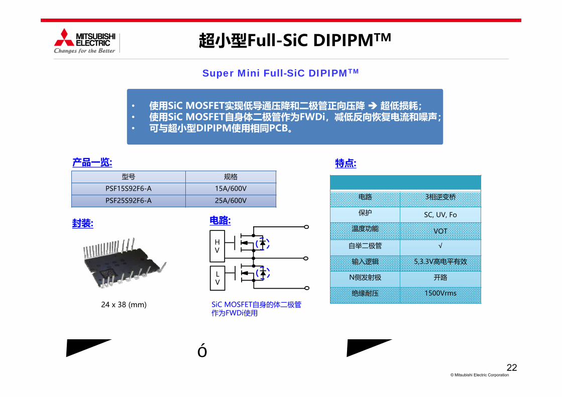
24 x 38 (mm)
产品一览:
封装:
特点:
电路 3相逆变桥
保护 SC, UV, Fo
温度功能 VOT
自举二极管 √
输入逻辑 5,3.3V高电平有效
N侧发射极 开路
绝缘耐压 1500Vrms
型号 规格
PSF15S92F6-A 15A/600V
PSF25S92F6-A 25A/600V
电路:
SiC MOSFET自身的体二极管作为FWDi使用
HV
LV
• 使用SiC MOSFET实现低导通压降和二极管正向压降 超低损耗;• 使用SiC MOSFET自身体二极管作为FWDi,减低反向恢复电流和噪声;• 可与超小型DIPIPM使用相同PCB。
超小型Full-SiC DIPIPMTM
Super Mini Full-SiC DIPIPMTM
作者授权中国电源学会发布,未经作者同意禁止转载
23© Mitsubishi Electric Corporation
作者授权中国电源学会发布,未经作者同意禁止转载
24© Mitsubishi Electric Corporation
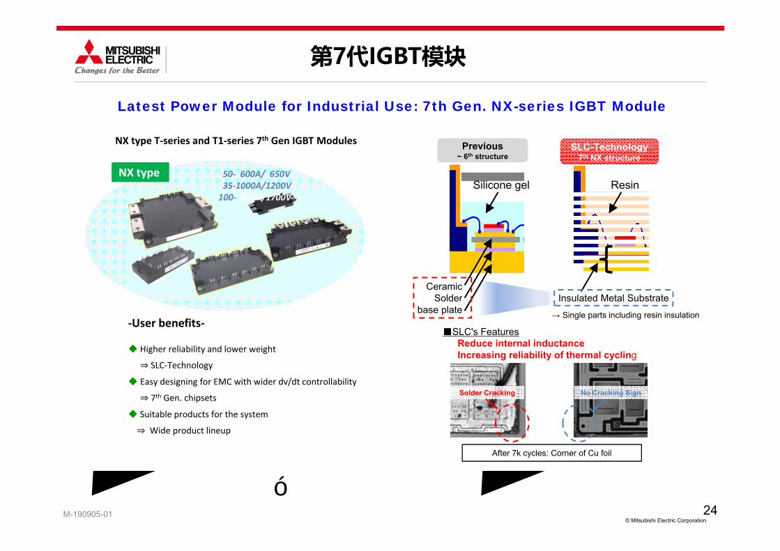
‐User benefits‐
◆ Higher reliability and lower weight
⇒ SLC‐Technology
◆ Easy designing for EMC with wider dv/dt controllability
⇒ 7th Gen. chipsets
◆ Suitable products for the system
⇒ Wide product lineup
Previous~ 6th structure
Silicone gel
SLC-Technology7th NX structure
■SLC's FeaturesReduce internal inductanceIncreasing reliability of thermal cycling
Resin
→ Single parts including resin insulation
After 7k cycles: Corner of Cu foil
Solder Cracking No Cracking Sign
NX type T‐series and T1‐series 7th Gen IGBT Modules
NX type 50‐ 600A/ 650V35‐1000A/1200V100‐ 600A/1700V
CeramicSolder
base plateInsulated Metal Substrate
Latest Power Module for Industrial Use: 7th Gen. NX-series IGBT Module
M-190905-01
第7代IGBT模块
作者授权中国电源学会发布,未经作者同意禁止转载
25© Mitsubishi Electric Corporation
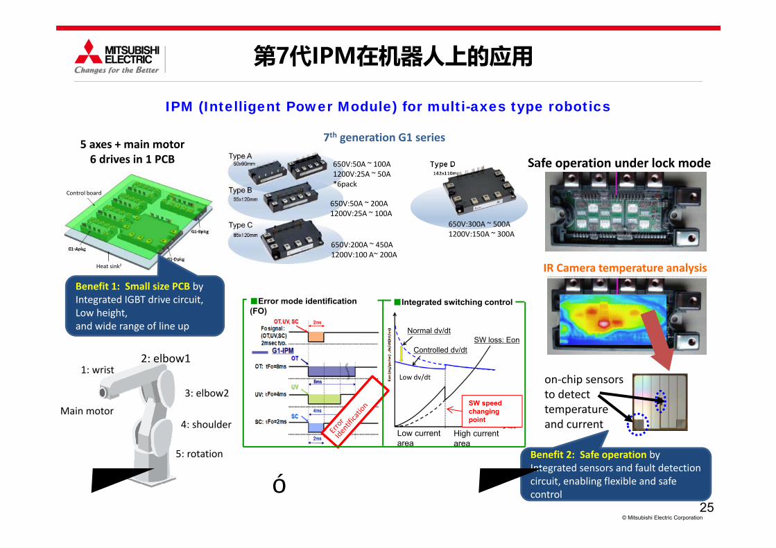
Safe operation under lock mode
IR Camera temperature analysis
Control board
Heat sink
Main motor
1: wrist
3: elbow2
4: shoulder
5: rotation
5 axes + main motor6 drives in 1 PCB
on‐chip sensors to detect temperature and current
Type D142x110mm
Benefit 1: Small size PCB byIntegrated IGBT drive circuit, Low height, and wide range of line up
Benefit 2: Safe operation byIntegrated sensors and fault detection circuit, enabling flexible and safe control
IPM (Intelligent Power Module) for multi-axes type robotics
7th generation G1 series
2: elbow1
650V:50A ~ 100A1200V:25A ~ 50A*6pack
650V:50A ~ 200A1200V:25A ~ 100A
650V:200A ~ 450A1200V:100 A~ 200A
650V:300A ~ 500A1200V:150A ~ 300A
第7代IPM在机器人上的应用
SW speed changing point
Low current area
High current area
Normal dv/dt
Controlled dv/dt
Low dv/dt
SW loss: Eon
■Error mode identification (FO)
■Integrated switching control
作者授权中国电源学会发布,未经作者同意禁止转载
26© Mitsubishi Electric Corporation
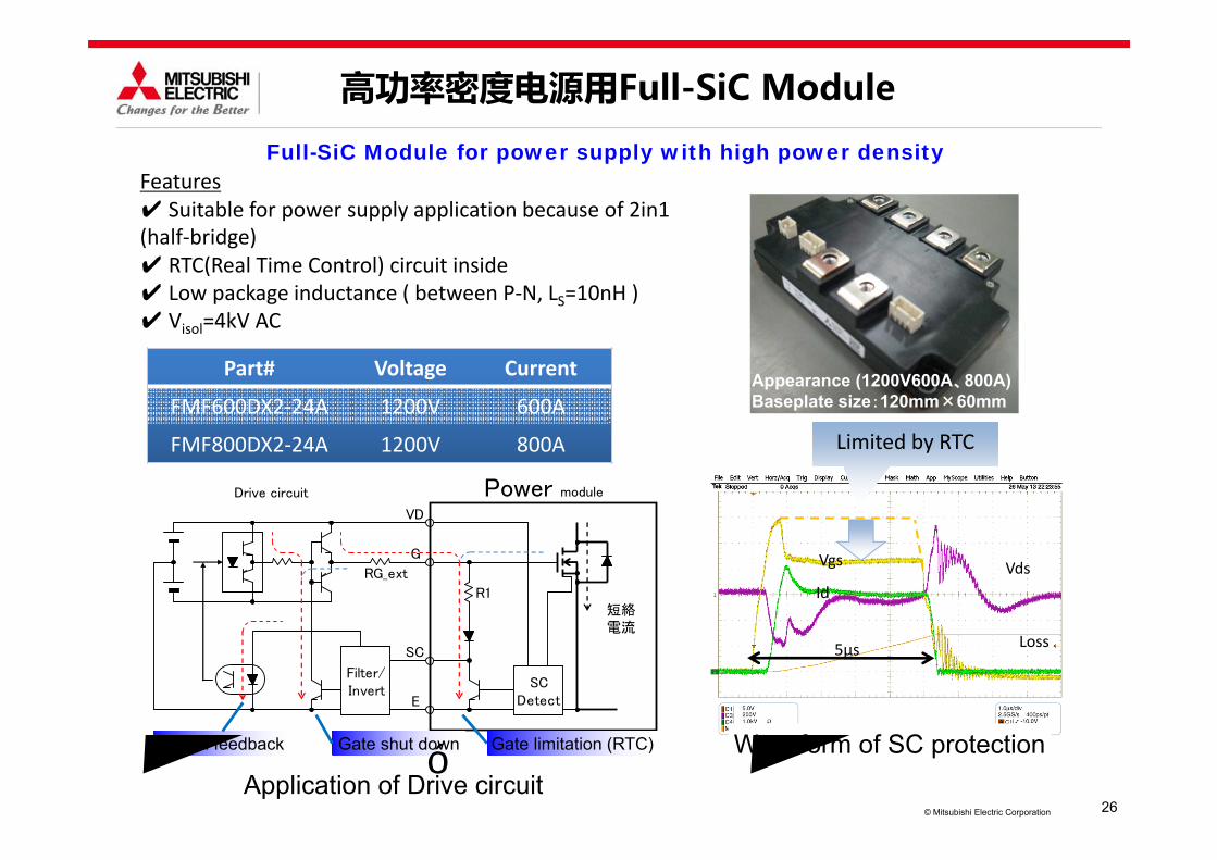
Features✔ Suitable for power supply application because of 2in1 (half‐bridge)✔ RTC(Real Time Control) circuit inside✔ Low package inductance ( between P‐N, LS=10nH )✔ Visol=4kV AC
VD
G
SC
E
R1
RG_ext
SCDetect
Filter/Invert
短絡過電流
FMF1200DX1-24A駆動回路(ユーザー)
短絡電流
Gate limitation (RTC)Gate limitation (RTC)Gate shut downGate shut downSignal feedbackSignal feedback
Drive circuit Power module
Vgs VdsId
Loss
Limited by RTCLimited by RTC
5μs
Appearance (1200V600A、800A)Baseplate size:120mm×60mm
Waveform of SC protectionApplication of Drive circuit
Part# Voltage Current
FMF600DX2‐24A 1200V 600A
FMF800DX2‐24A 1200V 800A
高功率密度电源用Full-SiC Module
Full-SiC Module for power supply with high power density
作者授权中国电源学会发布,未经作者同意禁止转载
27© Mitsubishi Electric Corporation
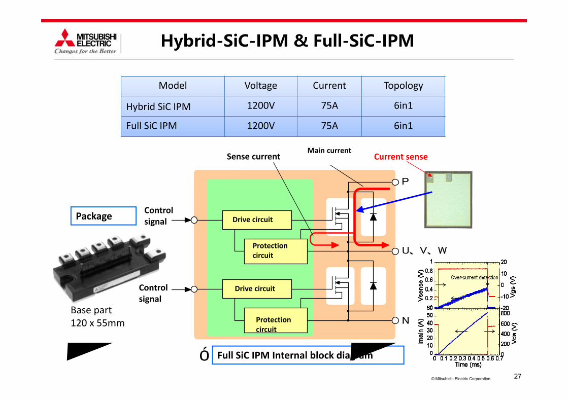
Model Voltage Current Topology
Hybrid SiC IPM 1200V 75A 6in1
Full SiC IPM 1200V 75A 6in1
P
N
U、 V、 W
Current sense
Drive circuit
Protection circuit
Drive circuit
Protection circuit
Sense currentMain current
Package
Full SiC IPM Internal block diagram
Base part120 x 55mm
Control signal
Hybrid-SiC-IPM & Full-SiC-IPM
Control signal
作者授权中国电源学会发布,未经作者同意禁止转载
28© Mitsubishi Electric Corporation
作者授权中国电源学会发布,未经作者同意禁止转载
29© Mitsubishi Electric Corporation
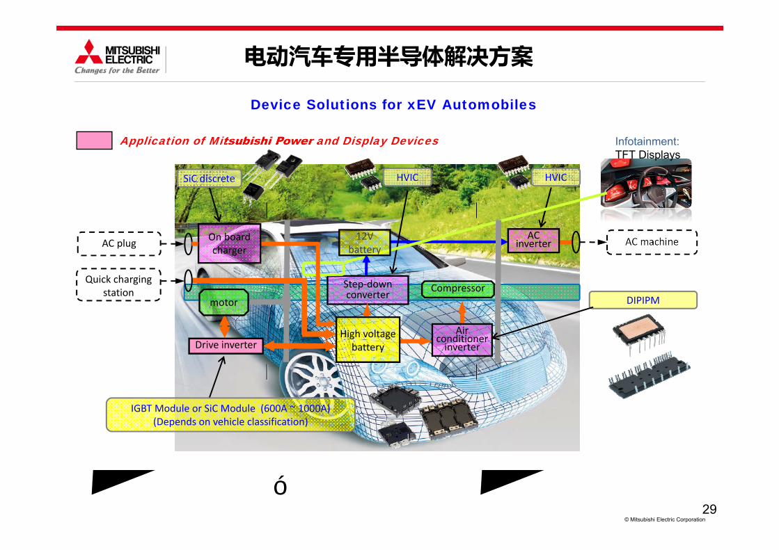
Compressormotor
AC inverter
Step‐down converter
High voltage battery
Air conditioner inverterDrive inverter
Quick chargingstation
AC plug AC machine
DIPIPM
IGBT Module or SiC Module (600A ~ 1000A)(Depends on vehicle classification)
SiC discrete
Application of Mitsubishi Power and Display Devices
HVICHVIC
Device Solutions for xEV Automobiles
Infotainment: TFT Displays
12V battery
On board charger
电动汽车专用半导体解决方案
作者授权中国电源学会发布,未经作者同意禁止转载
30© Mitsubishi Electric Corporation
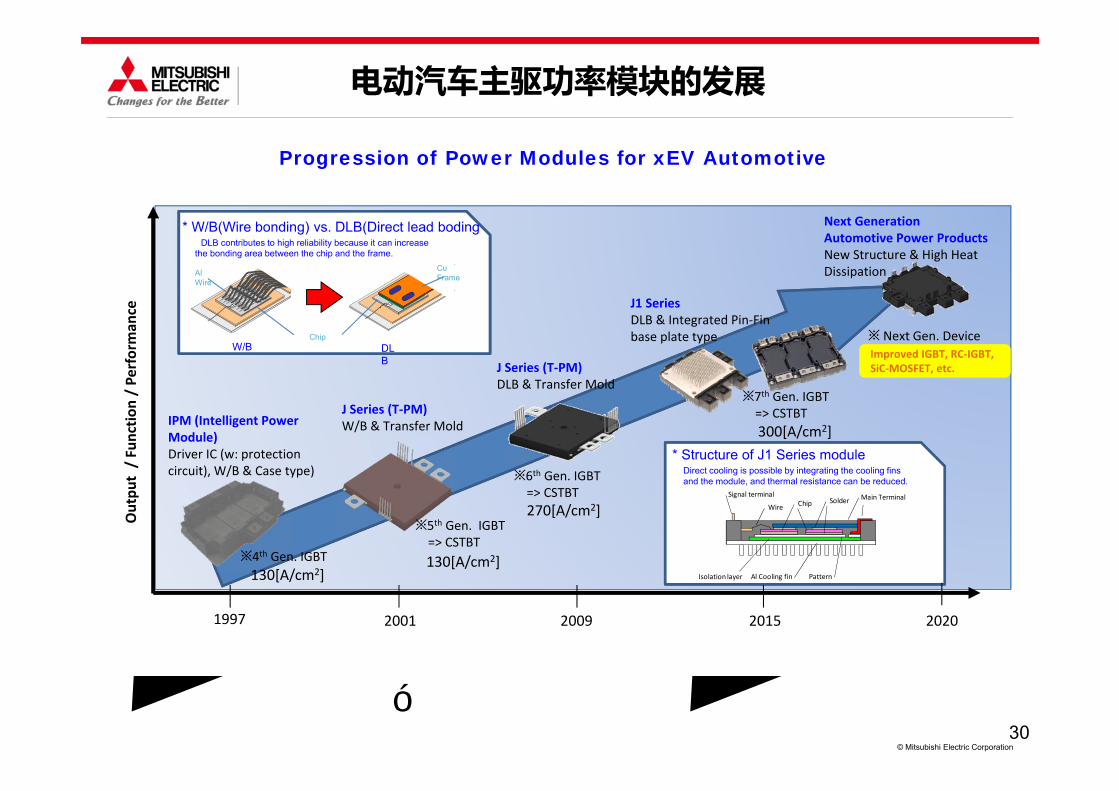
Outpu
t / Fu
nctio
n / Pe
rforman
ce
IPM (Intelligent Power Module)Driver IC (w: protection circuit), W/B & Case type)
J Series (T‐PM)DLB & Transfer Mold
J Series (T‐PM)W/B & Transfer Mold
J1 SeriesDLB & Integrated Pin‐Fin base plate type
Next Generation Automotive Power ProductsNew Structure & High Heat Dissipation
1997
※5th Gen. IGBT=> CSTBT
※6th Gen. IGBT=> CSTBT
※7th Gen. IGBT=> CSTBT
※ Next Gen. Device
※4th Gen. IGBT
Main TerminalChip Solder
Wire
Signal terminal
Isolation layer Al Cooling fin Pattern
ChipW/B DL
B
* Structure of J1 Series module
* W/B(Wire bonding) vs. DLB(Direct lead boding
Al Wire
Cu Frame
DLB contributes to high reliability because it can increase the bonding area between the chip and the frame.
Direct cooling is possible by integrating the cooling fins and the module, and thermal resistance can be reduced.
Progression of Power Modules for xEV Automotive
2001 2009 2015 2020
130[A/cm2]130[A/cm2]
270[A/cm2]
300[A/cm2]
Improved IGBT, RC‐IGBT,SiC‐MOSFET, etc.
电动汽车主驱功率模块的发展
作者授权中国电源学会发布,未经作者同意禁止转载
31© Mitsubishi Electric Corporation
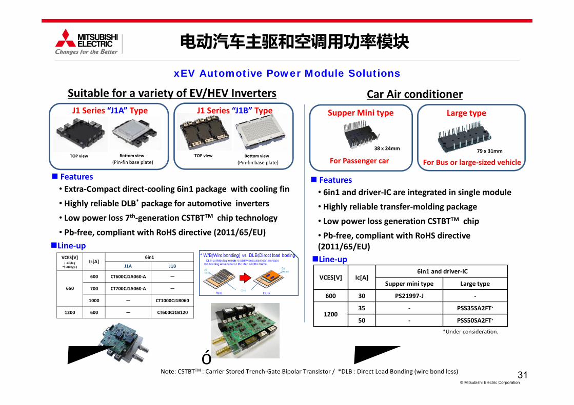
xEV Automotive Power Module Solutions
Suitable for a variety of EV/HEV Inverters
Features• Extra‐Compact direct‐cooling 6in1 package with cooling fin
• Highly reliable DLB* package for automotive inverters
• Low power loss 7th‐generation CSTBTTM chip technology
• Pb‐free, compliant with RoHS directive (2011/65/EU)
Note: CSTBTTM : Carrier Stored Trench‐Gate Bipolar Transistor / *DLB : Direct Lead Bonding (wire bond less)
Line‐up
TOP view Bottom view TOP view Bottom view(Pin‐fin base plate) (Pin‐fin base plate)
J1 Series “J1A” Type J1 Series “J1B” Type
J1A J1B
600 CT600CJ1A060‐A -
700 CT700CJ1A060‐A -
1000 - CT1000CJ1B060
1200 600 - CT600CJ1B120
VCES[V]( ‐40deg
~150degC )Ic[A]
6in1
650
Car Air conditionerSupper Mini type Large type
Line‐up
Features• 6in1 and driver‐IC are integrated in single module
• Highly reliable transfer‐molding package
• Low power loss generation CSTBTTM chip
• Pb‐free, compliant with RoHS directive (2011/65/EU)
For Passenger car For Bus or large‐sized vehicle
VCES[V] Ic[A]6in1 and driver‐IC
Supper mini type Large type
600 30 PS21997‐J ‐
120035 ‐ PSS35SA2FT*
50 ‐ PSS50SA2FT*
38 x 24mm 79 x 31mm
*Under consideration.
电动汽车主驱和空调用功率模块
作者授权中国电源学会发布,未经作者同意禁止转载
32© Mitsubishi Electric Corporation
作者授权中国电源学会发布,未经作者同意禁止转载
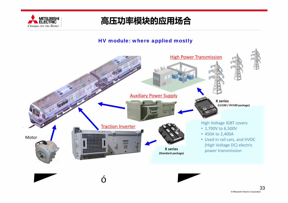
33© Mitsubishi Electric Corporation
Auxiliary Power Supply
Traction Inverter
Motor
High Voltage IGBT covers• 1,700V to 6,500V• 450A to 2,400A• Used in rail cars, and HVDC (High Voltage DC) electric power transmission
HV module: where applied mostly
High Power Transmission
X series(Standard package)
X series(LV100 / HV100 package)
高压功率模块的应用场合
作者授权中国电源学会发布,未经作者同意禁止转载
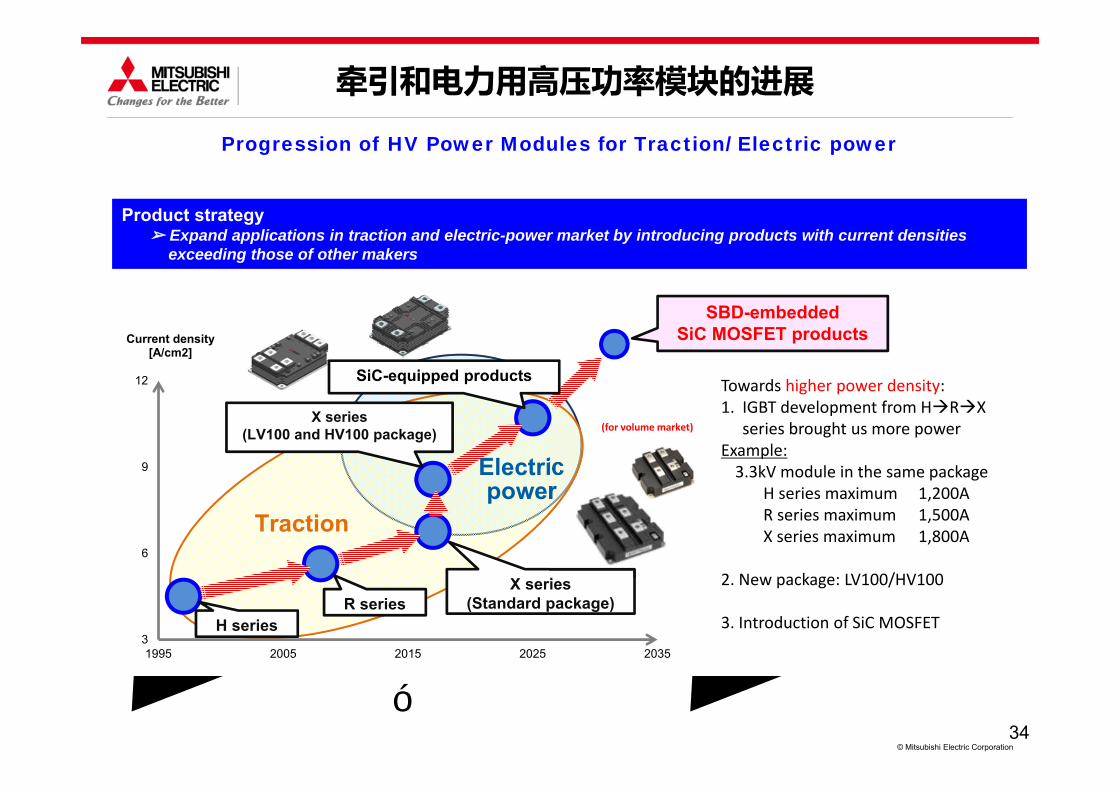
34© Mitsubishi Electric Corporation
3
6
9
12
1995 2005 2015 2025 2035
Current density [A/cm2]
Traction
Progression of HV Power Modules for Traction/ Electric power
Electric power
H seriesR series
X series(Standard package)
Product strategy➢ Expand applications in traction and electric-power market by introducing products with current densities
exceeding those of other makers
Towards higher power density:1. IGBT development from HRX
series brought us more powerExample:3.3kV module in the same package
H series maximum 1,200AR series maximum 1,500AX series maximum 1,800A
2. New package: LV100/HV100
3. Introduction of SiC MOSFET
(for volume market)X series
(LV100 and HV100 package)
SiC-equipped products
SBD-embeddedSiC MOSFET products
牵引和电力用高压功率模块的进展
作者授权中国电源学会发布,未经作者同意禁止转载
35© Mitsubishi Electric Corporation
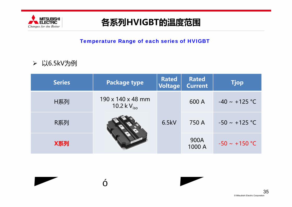
各系列HVIGBT的温度范围
以6.5kV为例
Series Package type RatedVoltage
RatedCurrent Tjop
H系列 190 x 140 x 48 mm10.2kViso
6.5kV
600 A -40 ~ +125 °C
R系列 750 A -50 ~ +125 °C
X系列 900A1000 A -50 ~ +150 °C
Temperature Range of each series of HVIGBT
作者授权中国电源学会发布,未经作者同意禁止转载
36© Mitsubishi Electric Corporation
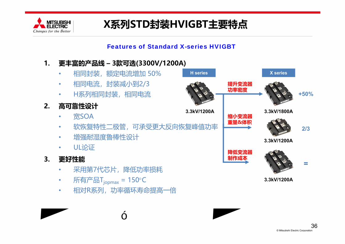
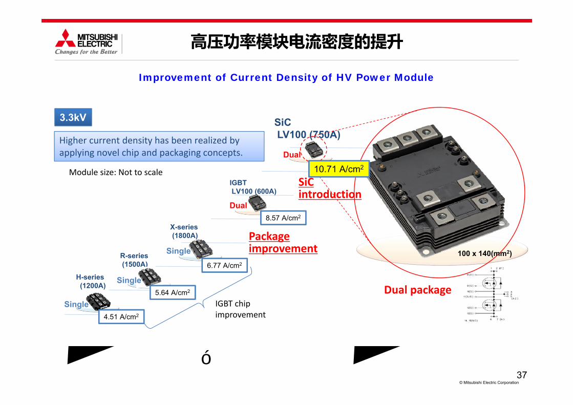
1. 更丰富的产品线 – 3款可选(3300V/1200A)• 相同封装,额定电流增加 50%• 相同电流,封装减小到2/3 • H系列相同封装,相同电流
2. 高可靠性设计• 宽SOA• 软恢复特性二极管,可承受更大反向恢复峰值功率• 增强耐湿度鲁棒性设计• UL论证
3. 更好性能• 采用第7代芯片,降低功率损耗• 所有产品Tjopmax = 150C• 相对R系列,功率循环寿命提高一倍
3.3kV/1200A
3.3kV/1200A
3.3kV/1800A
3.3kV/1200A
H series X series
+50%
2/3
=
Features of Standard X-series HVIGBT
提升变流器功率密度
缩小变流器重量&体积
降低变流器制作成本
作者授权中国电源学会发布,未经作者同意禁止转载
37© Mitsubishi Electric Corporation
H-series(1200A)
R-series (1500A)
X-series (1800A)
Higher current density has been realized by applying novel chip and packaging concepts.
IGBT LV100 (600A)
3.3kV SiC LV100 (750A)
8.57 A/cm2
Module size: Not to scale
IGBT chip improvement
Packageimprovement
SiCintroduction
4.51 A/cm2
5.64 A/cm2
6.77 A/cm2
Single
Single
Single
Dual
Dual
10.71 A/cm2
100 x 140(mm2)
Dual package
Improvement of Current Density of HV Power Module
高压功率模块电流密度的提升
作者授权中国电源学会发布,未经作者同意禁止转载
38© Mitsubishi Electric Corporation
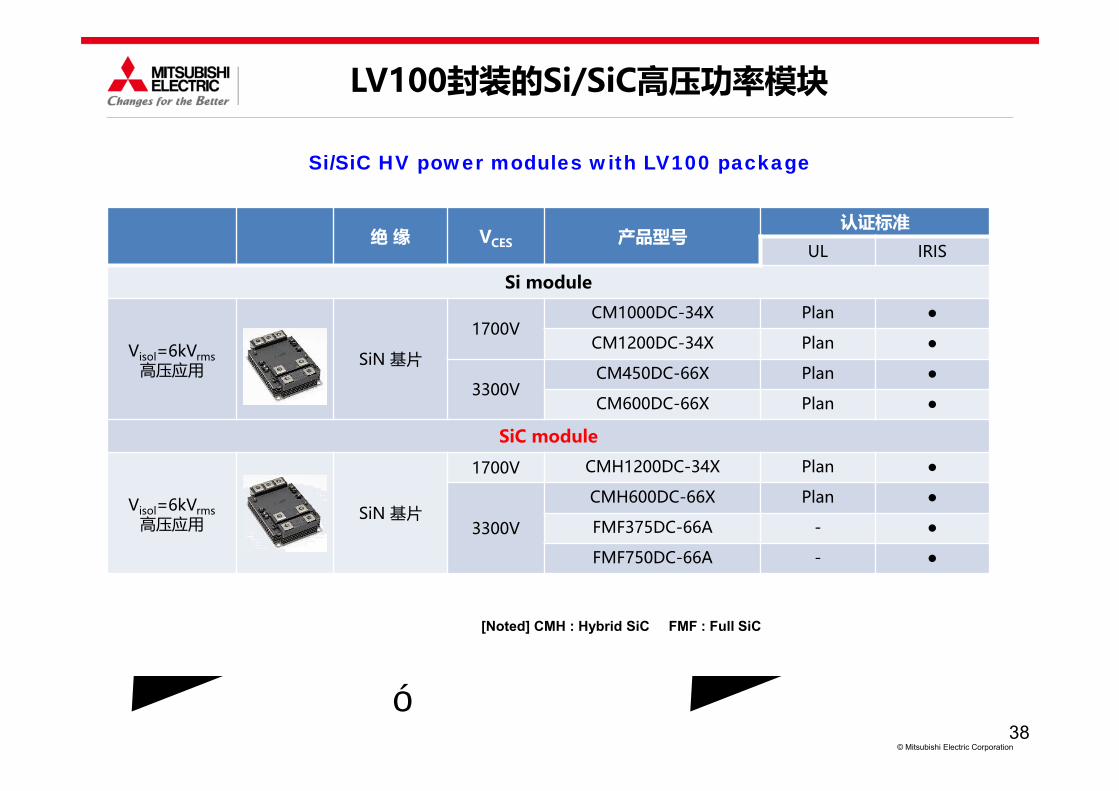
Si/SiC HV power modules with LV100 package
LV100封装的Si/SiC高压功率模块
绝 缘 VCES 产品型号认证标准
UL IRIS
Si module
Visol=6kVrms高压应用
SiN 基片
1700VCM1000DC-34X Plan ●
CM1200DC-34X Plan ●
3300VCM450DC-66X Plan ●
CM600DC-66X Plan ●
SiC module
Visol=6kVrms高压应用
SiN 基片
1700V CMH1200DC-34X Plan ●
3300V
CMH600DC-66X Plan ●
FMF375DC-66A - ●
FMF750DC-66A - ●
[Noted] CMH : Hybrid SiC FMF : Full SiC
作者授权中国电源学会发布,未经作者同意禁止转载
39© Mitsubishi Electric Corporation
SBD-embedded MOSFETConventional MOSFET (without SBD)
Schottky and ohmic contacts in the same contact hole. No significant increase of process step
n-
Gate
pn+
Gate
n+
pn+ n
Schottkycontact
Ohmiccontact
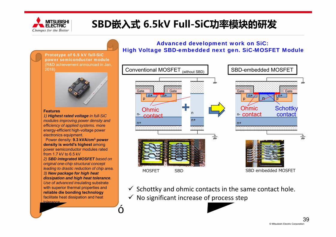
Advanced development work on SiC: High Voltage SBD-embedded next gen. SiC-MOSFET Module
SBDMOSFET SBD embedded MOSFET
n-
GateGate
n+
pn+ n+
n
n+
Ohmiccontact
SBD嵌入式 6.5kV Full-SiC功率模块的研发
Prototype of 6.5 kV full-SiCpower semiconductor module(R&D achievement announced in Jan, 2018)
Features1) Highest rated voltage in full-SiCmodules improving power density and efficiency of applied systems. more energy-efficient high-voltage power electronics equipment. Power density: 9.3 kVA/cm3 power
density is world's highest among power semiconductor modules rated from 1.7 kV to 6.5 kV2) SBD integrated MOSFET based on original one-chip structural concept leading to drastic reduction of chip area. 3) New package for high heat dissipation and high heat tolerance. Use of advanced insulating substrate with superior thermal properties and reliable die bonding technology facilitate heat dissipation and heat tolerance
作者授权中国电源学会发布,未经作者同意禁止转载
40© Mitsubishi Electric Corporation
作者授权中国电源学会发布,未经作者同意禁止转载
41© Mitsubishi Electric Corporation
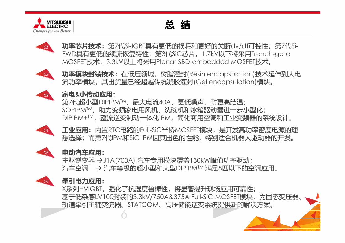
01
02
总 结
03
05
06
04
作者授权中国电源学会发布,未经作者同意禁止转载

作者授权中国电源学会发布,未经作者同意禁止转载


