Embed Size (px)
Citation preview

12 Channel HVA Board Hardware Design and Test Document
Rev. 1.5
Revision History Date Rev Author Comment
10/29/02 1.1 Rob Yamashita Initial Document 12/10/02 1.2 Rob Yamashita Fixed DAC Test and High Voltage Amplifier
Test Procedure. Added Table of context 2/10/03 1.3 Rob Yamashita Fixed dip switch settings in test procedure and
in manual address selection 2/11/03 1.4 Rob Yamashita Created PDF and added datasheets. 2/24/03 1.5 Rob Yamashita Added rework instructions
1 12 Channel HVA Board 1.1 Overview
The 12 Channel HVA board is used drive piezo material on a telescope. Each channel can swing the voltage from -400V to +400V. Each channel on the board is individually addressable through one of two DAC on board. Dip switches set the upper three address bits for the board allowing the address range on the board to go from 0-95. This makes it possible for 8 boards to be placed in one chassis, while still allowing each channel to be addressed individually.
1.2 Technical Specification • 12 individual High Voltage Amplifier channels • +/-400 Volt Output Range Power Requirements • +5V ≈ 2.5A • -5V ≈ 80mA • +15V • -15V • +400V • -400V
1.3 Mechanical Specification
• Eurocard 6U (160mm x 233.35mm) Form Factor • P2 96 pin DIN Connector • P1 32 pin TYPE-F-EURO • 4 Layer PCB construction
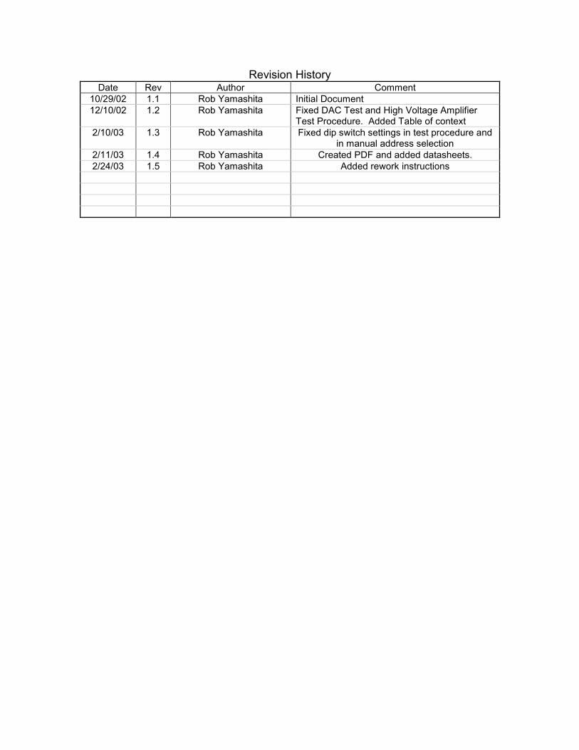
1.4 Block Diagram
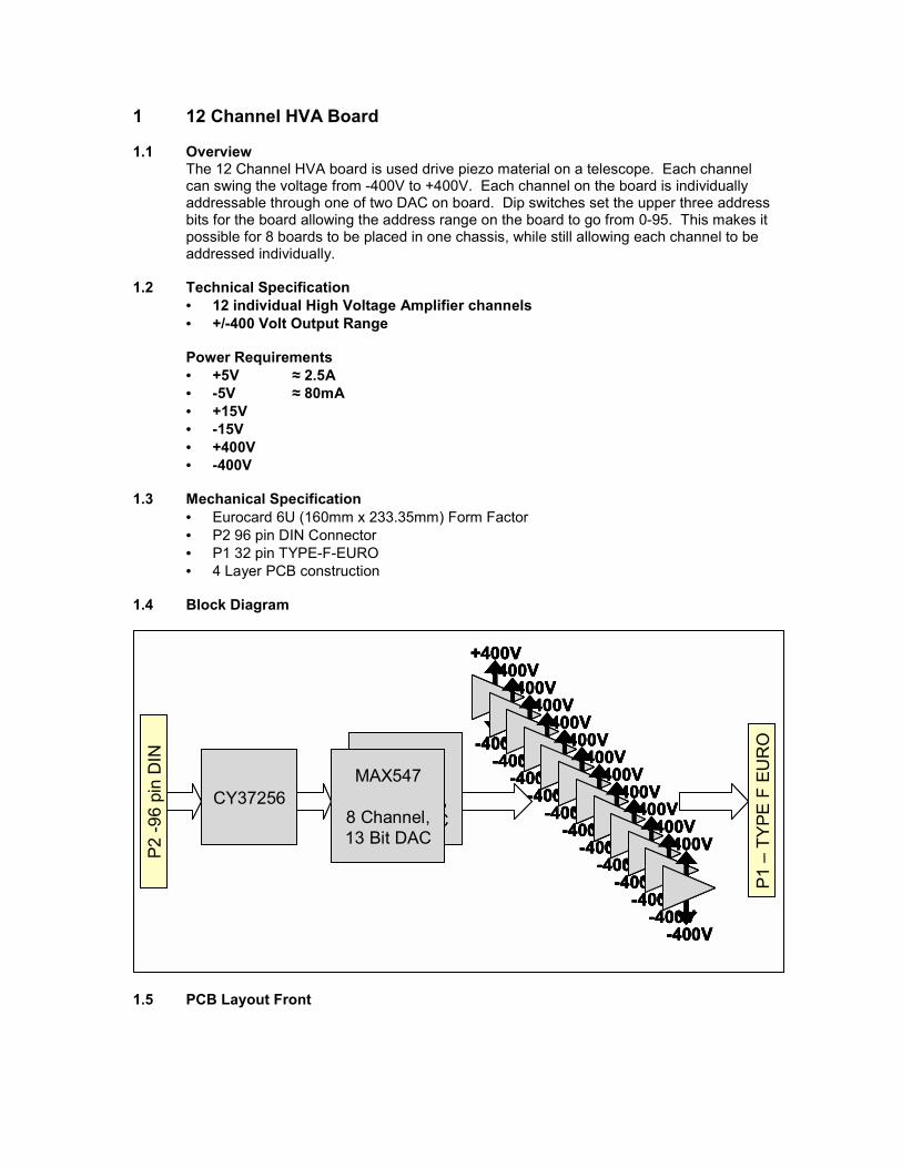
1.5 PCB Layout Front
P2 -9
6 pi
n D
IN
CY37256
MAX547
8 Channel, 13 Bit DAC
MAX547
8 Channel, 13 Bit DAC
+400V
-400V
+400V
-400V
+400V
-400V
+400V
-400V
+400V
-400V
+400V
-400V
+400V
-400V
+400V
-400V
+400V
-400V
+400V
-400V
+400V
-400V
+400V
-400V
P1 –
TYPE
F E
UR
O
P2 -9
6 pi
n D
IN
CY37256
MAX547
8 Channel, 13 Bit DAC
MAX547
8 Channel, 13 Bit DAC
MAX547
8 Channel, 13 Bit DAC
MAX547
8 Channel, 13 Bit DAC
+400V
-400V
+400V
-400V
+400V
-400V
+400V
-400V
+400V
-400V
+400V
-400V
+400V
-400V
+400V
-400V
+400V
-400V
+400V
-400V
+400V
-400V
+400V
-400V
+400V
-400V
+400V
-400V
+400V
-400V
+400V
-400V
+400V
-400V
+400V
-400V
+400V
-400V
+400V
-400V
+400V
-400V
+400V
-400V
+400V
-400V
+400V
-400V
+400V
-400V
+400V
-400V
+400V
-400V
+400V
-400V
+400V
-400V
+400V
-400V
+400V
-400V
+400V
-400V
+400V
-400V
+400V
-400V
+400V
-400V
+400V
-400V
P1 –
TYPE
F E
UR
O
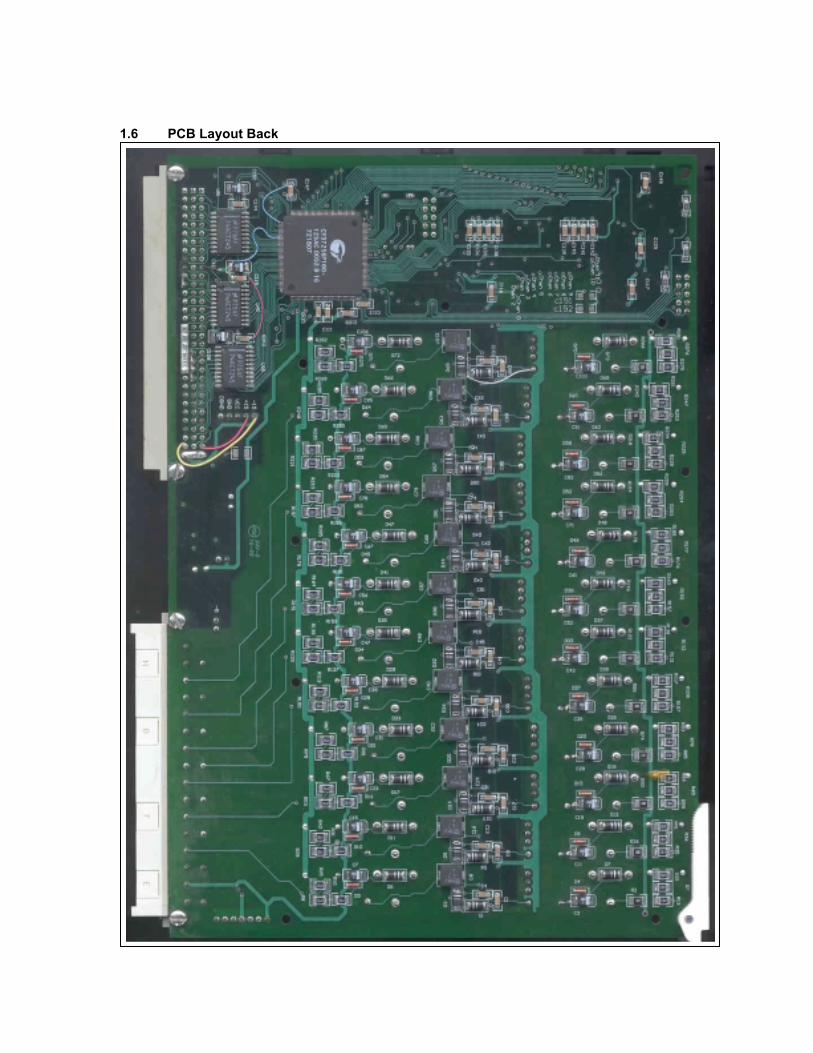
1.6 PCB Layout Back
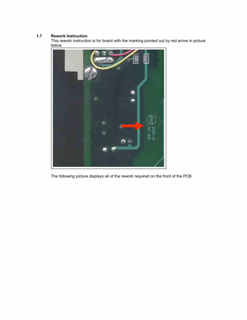
1.7 Rework Instruction
This rework instruction is for board with the marking pointed out by red arrow in picture below.
The following picture displays all of the rework required on the front of the PCB.
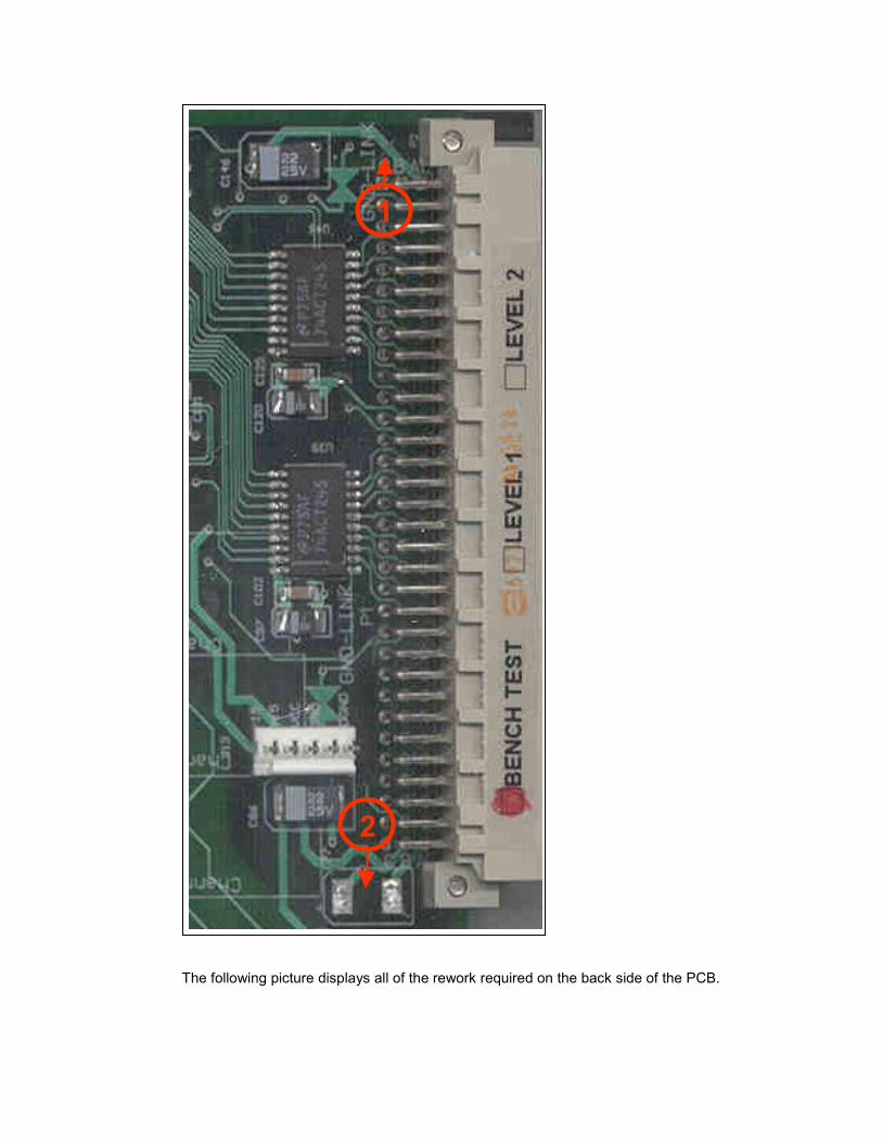
The following picture displays all of the rework required on the back side of the PCB.
1
2
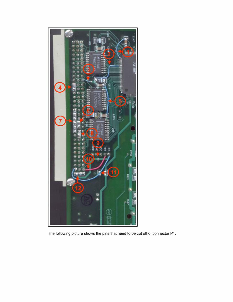
The following picture shows the pins that need to be cut off of connector P1.
12
3
5
9
10
11
4
7
6
8
12
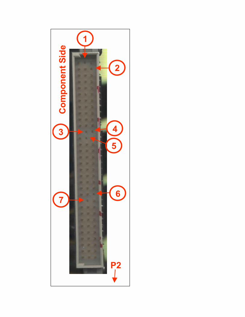
1
2
3 4
5
76
P2
Com
pone
nt S
ide
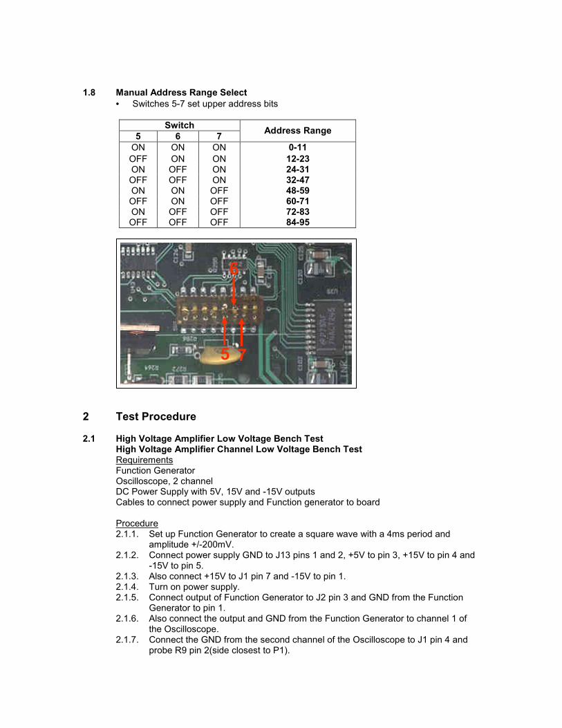
1.8 Manual Address Range Select
• Switches 5-7 set upper address bits
Switch 5 6 7 Address Range
ON ON ON 0-11 OFF ON ON 12-23 ON OFF ON 24-31 OFF OFF ON 32-47 ON ON OFF 48-59 OFF ON OFF 60-71 ON OFF OFF 72-83 OFF OFF OFF 84-95
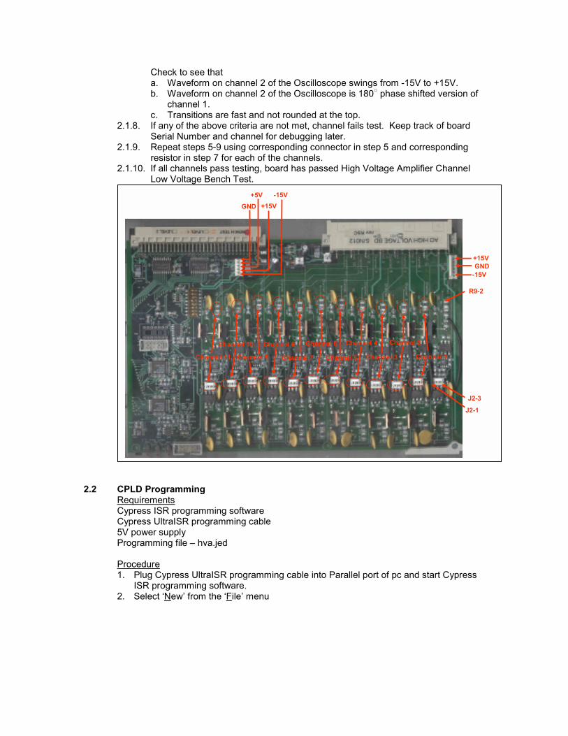
2 Test Procedure 2.1 High Voltage Amplifier Low Voltage Bench Test
High Voltage Amplifier Channel Low Voltage Bench Test Requirements Function Generator Oscilloscope, 2 channel DC Power Supply with 5V, 15V and -15V outputs Cables to connect power supply and Function generator to board Procedure 2.1.1. Set up Function Generator to create a square wave with a 4ms period and
amplitude +/-200mV. 2.1.2. Connect power supply GND to J13 pins 1 and 2, +5V to pin 3, +15V to pin 4 and
-15V to pin 5. 2.1.3. Also connect +15V to J1 pin 7 and -15V to pin 1. 2.1.4. Turn on power supply. 2.1.5. Connect output of Function Generator to J2 pin 3 and GND from the Function
Generator to pin 1. 2.1.6. Also connect the output and GND from the Function Generator to channel 1 of
the Oscilloscope. 2.1.7. Connect the GND from the second channel of the Oscilloscope to J1 pin 4 and
probe R9 pin 2(side closest to P1).
5 7
6
5 7
6
Check to see that a. Waveform on channel 2 of the Oscilloscope swings from -15V to +15V. b. Waveform on channel 2 of the Oscilloscope is 180 phase shifted version of
channel 1. c. Transitions are fast and not rounded at the top.
2.1.8. If any of the above criteria are not met, channel fails test. Keep track of board Serial Number and channel for debugging later.
2.1.9. Repeat steps 5-9 using corresponding connector in step 5 and corresponding resistor in step 7 for each of the channels.
2.1.10. If all channels pass testing, board has passed High Voltage Amplifier Channel Low Voltage Bench Test.
2.2 CPLD Programming
Requirements Cypress ISR programming software Cypress UltraISR programming cable 5V power supply Programming file – hva.jed Procedure 1. Plug Cypress UltraISR programming cable into Parallel port of pc and start Cypress
ISR programming software. 2. Select ‘New’ from the ‘File’ menu
J2-1
J2-3
R9-2
+15V
-15V
Channel 1
Channel 2
Channel 3
Channel 4
Channel 5
Channel 6
Channel 7
Channel 8
Channel 9
Channel 10
Channel 11
GND+5V
+15V-15V
GND
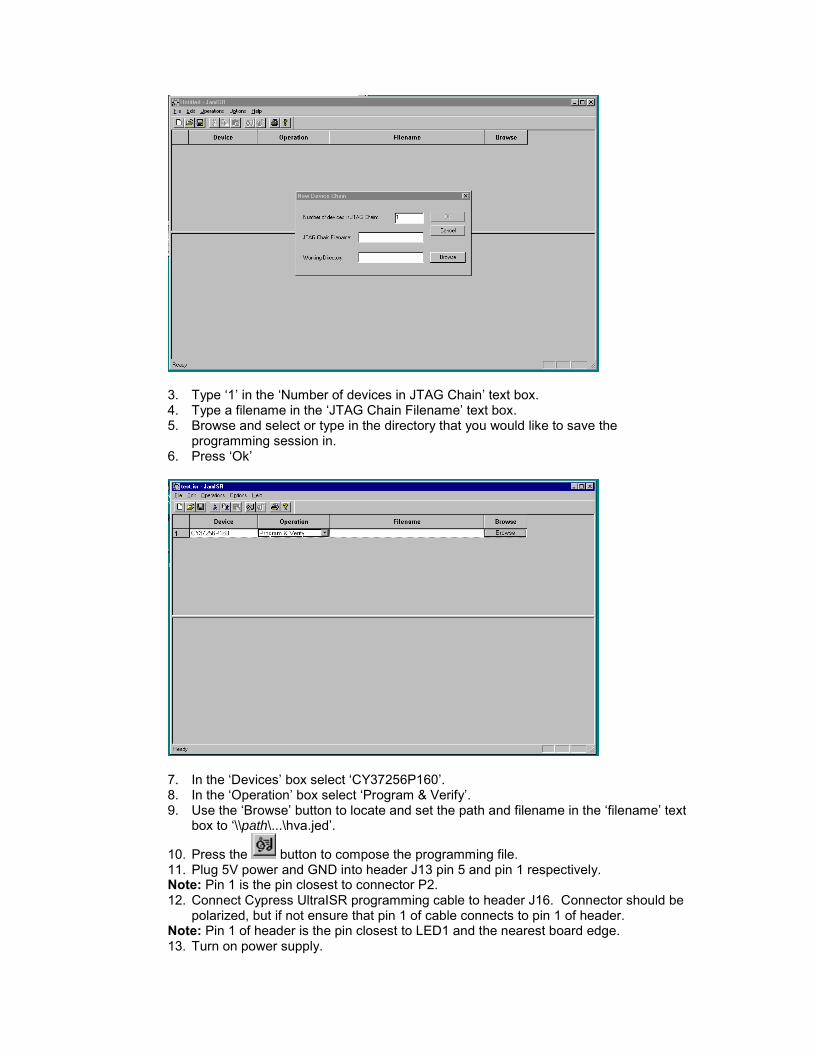
3. Type ‘1’ in the ‘Number of devices in JTAG Chain’ text box. 4. Type a filename in the ‘JTAG Chain Filename’ text box. 5. Browse and select or type in the directory that you would like to save the
programming session in. 6. Press ‘Ok’
7. In the ‘Devices’ box select ‘CY37256P160’. 8. In the ‘Operation’ box select ‘Program & Verify’. 9. Use the ‘Browse’ button to locate and set the path and filename in the ‘filename’ text
box to ‘\\path\...\hva.jed’.
10. Press the button to compose the programming file. 11. Plug 5V power and GND into header J13 pin 5 and pin 1 respectively. Note: Pin 1 is the pin closest to connector P2. 12. Connect Cypress UltraISR programming cable to header J16. Connector should be
polarized, but if not ensure that pin 1 of cable connects to pin 1 of header. Note: Pin 1 of header is the pin closest to LED1 and the nearest board edge. 13. Turn on power supply.
14. Press the button to program the CPLD. Programming may take several second to complete
15. Check log that is displayed to see that CPLD programmed and verified successfully. If programming or verify was not successful- a. Verify that the path and filename are correct in the ‘filename’ textbox. If not, repeat
from step 9. b. Check to see that power and ground are connected correctly and that supply voltage
is set to 5V DC. If not, repeat form step 11. c. Check to see that part is correct and it is soldered correctly to board. If not, correct
problem and repeat from step 11. 16. Turn off power supply and disconnect cables.
2.3 DAC Test
Requirements 2 Multifunction Boards 1 Chassis 2 PCs with Linux OS 2 FC-FC Multimode Fiber Optic Cables Oscilloscope Procedure 1. On AOUIM open 3 Xterm windows 2. In first Xterm window type ‘rlogin –l ao aoicm’ and hit return 3. Type the password, ‘wai!mea’ and hit return. 4. Change to the ‘dio32’ directory. 5. Type ‘su aroot’ and hit return. 6. Type the password, ‘wai!mea’ and hit return. 7. Type ‘start_dio’ and hit return. This should start dio32. 8. In second Xterm window type ‘rlogin –l ao aoicm’ and hit return. 9. Type the password, ‘wai!mea’, and hit return. 10. Change to ‘dio32’ directory. 11. Type ‘cat /dev/rtf0’ and hit return. 12. In the third Xterm window, type ‘rlogin –l ao aoicm’ and hit return. 13. Type the password, ‘wai!mea’ and hit return. 14. Change to the ‘dio32’ directory. 15. Type ‘cat > /dev/rtf1’ and hit return. 16. You should now be able to see the commands that you type in Xterm 3 show up in
Xterm window 2. To test this type ‘test’ in Xterm 3. If you do not see ‘test’ in Xterm 2 a. Hit ‘ctrl-c’ in Xterm 3. b. In Xterm 3, type ‘exit’ and hit return. c. Hit ‘ctrl-c’ in Xterm 2. d. In Xterm 2, type ‘exit’ and hit return. e. In Xterm 1, type ‘stop_dio’ and hit return. f. Repeat from step 7.
17. Make sure that all dip switches on SW1 are in the ‘ON’ position 18. Plug board that you would like to test into chassis. 19. Connect oscilloscope GND to J2 pin 1 and channel 1 to J2 pin 2. 20. Turn on power by flipping switch on front of chassis 21. In window #2 type ‘a i’ and hit return. 22. Type ‘f a 0’ and hit return to direct commands to channel 0. 23. Type ‘f m 1’ and hit return to set the test pattern to sawtooth. 24. Type ‘f p 10000’ and hit return to set the period of the pulse to 10000 ms. 25. Type ‘f b’ and hit return to start pattern generation. 26. Check the oscilloscope to see a saw tooth pattern is being generated.
If output stays constant on oscilloscope
a. Turn off chassis power by flipping switch on front of chassis. b. Wait 5-10 seconds and turn power back on. c. Check if pattern is being generated. d. If not repeat a-c 4 times. e. If still no output, move oscilloscope probe to corresponding connector on channel
2 and type ‘f a 1’ and hit return, then repeat steps 21-24. f. If still no output there may be a problem with the DAC. Turn off chassis and
remove board. g. Check for assembly errors around U48 and U49.
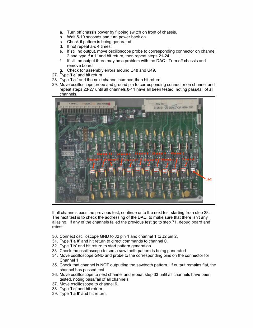
27. Type ‘f e’ and hit return 28. Type ‘f a ‘ and the next channel number, then hit return. 29. Move oscilloscope probe and ground pin to corresponding connector on channel and
repeat steps 23-27 until all channels 0-11 have all been tested, noting pass/fail of all channels.
Connectors for Channel 1 of Oscilloscope
If all channels pass the previous test, continue onto the next test starting from step 28. The next test is to check the addressing of the DAC, to make sure that there isn’t any aliasing. If any of the channels failed the previous test go to step 71, debug board and retest. 30. Connect oscilloscope GND to J2 pin 1 and channel 1 to J2 pin 2. 31. Type ‘f a 0’ and hit return to direct commands to channel 0. 32. Type ‘f b’ and hit return to start pattern generation. 33. Check the oscilloscope to see a saw tooth pattern is being generated. 34. Move oscilloscope GND and probe to the corresponding pins on the connector for
Channel 1. 35. Check that channel is NOT outputting the sawtooth pattern. If output remains flat, the
channel has passed test. 36. Move oscilloscope to next channel and repeat step 33 until all channels have been
tested, noting pass/fail of all channels. 37. Move oscilloscope to channel 6. 38. Type ‘f e’ and hit return. 39. Type ‘f a 6’ and hit return.
J2-2
Channel 1
Channel 2
Channel 3
Channel 4
Channel 5
Channel 6
Channel 7
Channel 8
Channel 9
Channel 10
Channel 11
40. Type ‘f b’ and hit return. 41. Check the oscilloscope to see that sawtooth pattern is being generated. 42. Move oscilloscope to next channel. 43. Check that channel is NOT outputting the sawtooth pattern. If output remains flat,
channel has passed the test. 44. Move oscilloscope to next channel and repeat step 41 until all channels have been
tested, noting pass/fail of all channels. 45. Type ‘f e’ and hit return. If all channels pass the previous test, continue onto the next test starting from step 44. The next test is to check that the dip switch controlling the upper address bits is working properly. If any of the channels failed the previous test go to step 71, debug board and retest. 46. Move switch #5 on SW1 to the on position. 47. Move oscilloscope GND and probe to channel 0. 48. Type ‘f a 12’ and hit return. 49. Type ‘f b’ and hit return. 50. Check oscilloscope to make sure that the sawtooth pattern is being generated. 51. Type ‘f e’ and hit return. 52. Type ‘f a 0’ and hit return. 53. Type ‘f b’ and hit return. 54. Check to make sure that the sawtooth pattern is NOT being generated. 55. Type ‘f e’ and hit return. 56. Type ‘f a 24’ and hit return. 57. Type ‘f b’ and hit return. 58. Check to make sure that the sawtooth pattern is NOT being generated. 59. Type ‘f e’ and hit return. 60. Move switch #5 on SW1 to the off position and switch #6 on SW1 to the on position. 61. Type ‘f a 24’ and hit return. 62. Type ‘f b’ and hit return. 63. Check oscilloscope to make sure that the sawtooth pattern is being generated. 64. Type ‘f e’ and hit return. 65. Type ‘f a 0’ and hit return. 66. Type ‘f b’ and hit return. 67. Check to make sure that the sawtooth pattern is NOT being generated. 68. Type ‘f e’ and hit return. 69. Type ‘f a 12’ and hit return. 70. Type ‘f b’ and hit return. 71. Check to make sure that the sawtooth pattern is NOT being generated. 72. Type ‘f e’ and hit return. 73. Turn off power and remove board. 74. If there are more boards to test repeat from step 17. Else go on to step 75. 75. Press ‘ctrl-c’ in Xterm 3. 76. Type ‘exit’ in Xterm 3 and hit return. 77. Press ‘ctrl-c’ in Xterm 2. 78. Type ‘exit’ in Xterm 2 and hit return. 79. In Xterm 1 type ‘stop_dio’ and hit return. 80. Type ‘exit’ and hit return.
2.4 High Voltage Amplifier Test
Requirements 2 Multifunction Boards 1 Chassis 2 PCs with Linux OS 2 FC-FC Multimode Fiber Optic Cables

High Voltage Oscilloscope High Voltage Cable Piezo Material with two leads connected to it NOTE: You will be working with +/-400 volts with this test. Make sure to follow ALL steps in the order that they are written. Failure to do so could result in serious electrical shock. Procedure 1. On AOUIM open 3 Xterm windows 2. In first Xterm window type ‘rlogin –l ao aoicm’ and hit return 3. Type the password, ‘wai!mea’ and hit return. 4. Change to the ‘dio32’ directory. 5. Type ‘su aroot’ and hit return. 6. Type the password, ‘wai!mea’ and hit return. 7. Type ‘start_dio’ and hit return. This should start dio32. 8. In second Xterm window type ‘rlogin –l ao aoicm’ and hit return. 9. Type the password, ‘wai!mea’, and hit return. 10. Change to ‘dio32’ directory. 11. Type ‘cat /dev/rtf0’ and hit return. 12. In the third Xterm window, type ‘rlogin –l ao aoicm’ and hit return. 13. Type the password, ‘wai!mea’ and hit return. 14. Change to the ‘dio32’ directory. 15. Type ‘cat > /dev/rtf1’ and hit return. 16. You should now be able to see the commands that you type in Xterm 3 show up in
Xterm window 2. To test this type ‘test’ in Xterm 3. If you do not see ‘test’ in Xterm 2 a. Hit ‘ctrl-c’ in Xterm 3. b. In Xterm 3, type ‘exit’ and hit return. c. Hit ‘ctrl-c’ in Xterm 2. d. In Xterm 2, type ‘exit’ and hit return. e. In Xterm 1, type ‘stop_dio’ and hit return. f. Repeat from step 7.
17. Make sure that all dip switches on SW1 are in the ‘OFF’ position 18. Plug board that you would like to test into slot one of the chassis. 19. Connect oscilloscope channel 1 to J2 pin 2. 20. Turn on power by flipping switch on front of chassis 21. In window #2 type ‘a i’ and hit return. 22. Type ‘f a 0’ and hit return to direct commands to channel 0. 23. Type ‘f m 1’ and hit return to set the test pattern to sawtooth. 24. Type ‘f p 10000’ and hit return to set the period of the pulse to 10000 ms. 25. Type ‘f b’ and hit return to start pattern generation. 26. Check the oscilloscope to see a saw tooth pattern is being generated.
If output stays constant on oscilloscope a. Turn off chassis power by flipping switch on front of chassis. b. Wait 5-10 seconds and turn power back on. c. Check if pattern is being generated. d. If not repeat a-c 4 times.
27. Type ‘f e’ and hit return 28. Connect GND connector from oscilloscope to one of the leads on the Piezo material
and stick it into socket 15 on the high voltage cable. 29. Connect probe of channel 2 on the oscilloscope to the other lead on of the Piezo
material and stick it into socket 1 of the high voltage cable. 30. Turn on high voltage power supply, switch on back of chassis. 31. Type ‘f b’ and then hit return. 32. Check to see that the voltage from channel 2 roughly follows the sawtooth pattern on
channel 1 of the oscilloscope. See example below. 33. Type ‘f e’ and then hit return.
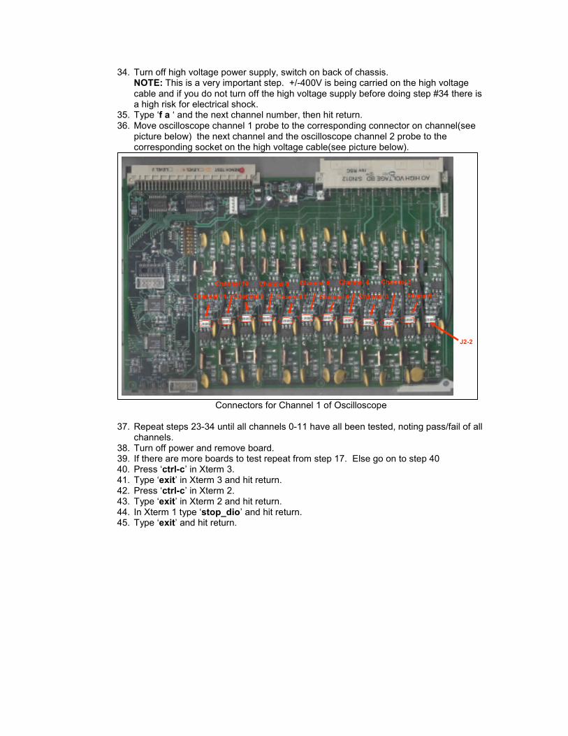
34. Turn off high voltage power supply, switch on back of chassis. NOTE: This is a very important step. +/-400V is being carried on the high voltage cable and if you do not turn off the high voltage supply before doing step #34 there is a high risk for electrical shock.
35. Type ‘f a ‘ and the next channel number, then hit return. 36. Move oscilloscope channel 1 probe to the corresponding connector on channel(see
picture below) the next channel and the oscilloscope channel 2 probe to the corresponding socket on the high voltage cable(see picture below).
Connectors for Channel 1 of Oscilloscope
37. Repeat steps 23-34 until all channels 0-11 have all been tested, noting pass/fail of all
channels. 38. Turn off power and remove board. 39. If there are more boards to test repeat from step 17. Else go on to step 40 40. Press ‘ctrl-c’ in Xterm 3. 41. Type ‘exit’ in Xterm 3 and hit return. 42. Press ‘ctrl-c’ in Xterm 2. 43. Type ‘exit’ in Xterm 2 and hit return. 44. In Xterm 1 type ‘stop_dio’ and hit return. 45. Type ‘exit’ and hit return.
J2-2
Channel 1
Channel 2
Channel 3
Channel 4
Channel 5
Channel 6
Channel 7
Channel 8
Channel 9
Channel 10
Channel 11

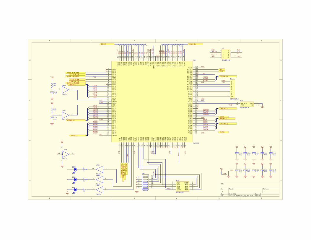
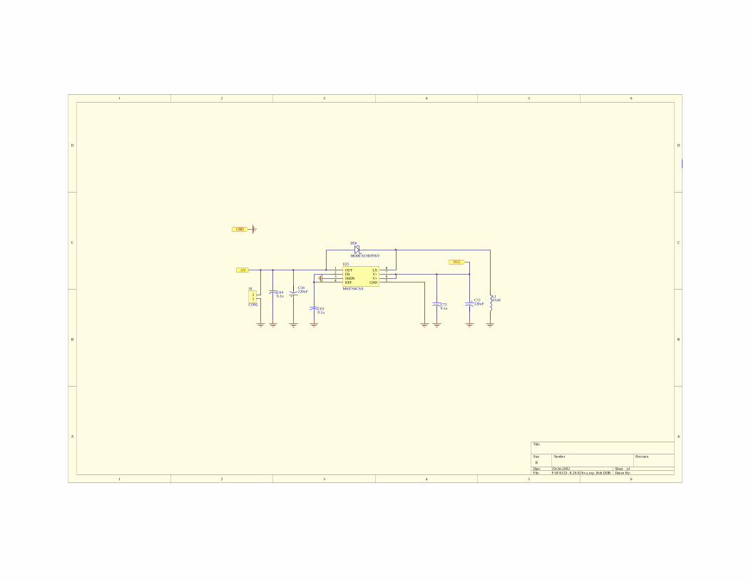
3 Schematic
Note: that schematic only shows one channel of High Voltage Amplifier. Each channel is identical in design.
1 2 3 4 5 6
A
B
C
D
654321
D
C
B
A
Title
Number RevisionSize
B
Date: 29-Oct-2002 Sheet of File: F:\IFA\HVA\BACKUP~22.DDB Drawn By:
IN-10
+15-15HV+HV-
HVO10
chan10hva00000.sch
IN-10
+15-15HV+HV-
HVO10
IN-11
+15--15HV+HV-
HVO11
chan11hva00001.sch
IN-11
+15--15HV+HV-
HVO11
IN-0
+15-15VHV+HV-
HVO0
chan0hva00002.sch
IN-0
+15-15VHV+HV-
HVO0IN-8
+15-15HV+HV-
HVO8
chan8hva00003.sch
IN-8
+15-15HV+HV-
HVO8
IN-9
+15-15HV+HV-
HVO9
chan9hva00004.sch
IN-9
+15-15HV+HV-
HVO9 IN-1
+15-15HV+HV-
HVO1
chan1hva00005.sch
IN-1
+15-15HV+HV-
HVO1
IN-2
+15-15VHV+HV-
HVO2
chan2hva00006.sch
IN-2
+15-15VHV+HV-
HVO2
IN-3
+15-15HV+HV-
HVO3
chan3hva00007.sch
IN-3
+15-15HV+HV-
HVO3
IN-4
+15-15HV+HV-
HVO4
chan4hva00008.sch
IN-4
+15-15HV+HV-
HVO4
IN-5
+15-15HV+HV-
HVO5
chan5hva00009.sch
IN-5
+15-15HV+HV-
HVO5
IN-6
+15-15HV+HV-
HVO6
chan6hva00010.sch
IN-6
+15-15HV+HV-
HVO6
IN-7
+15-15HV+HV-
HVO7
chan7hva00011.sch
IN-7
+15-15HV+HV-
HVO7
D[0..15]ADDR[0..7]VCCDGND+15VGND-15VCTRL[8..15]CTRL[0..7]DATA_L_ENABLEDATA_L_DIRADDR_ENABLEADDR_DIRCTRL_L_ENABLECTRL_L_DIRCTRL_H_ENABLECTRL_H_DIRDATA_H_ENABLEDATA_H_DIR
busbus.sch
D[0..15]ADDR[0..7]VCCDGND+15VGND-15VCTRL[8..15]CTRL[0..7]DATA_L_ENABLEDATA_L_DIRADDR_ENABLEADDR_DIRCTRL_L_ENABLECTRL_L_DIRCTRL_H_ENABLECTRL_H_DIRDATA_H_ENABLEDATA_H_DIR
HVO0
HVO1
HVO2
HVO3
HVO4
HVO5
HVO6
HVO7
HVO8
HVO9
HVO10
HVO11
1 2
JP1JUMPER
+
C5322uF 25V Ta
VCC VOUT0
VOUT1
VOUT2
VOUT3
VOUT4
VOUT5
VOUT6
VOUT7
VOUT8
VOUT9
VOUT10
VOUT11
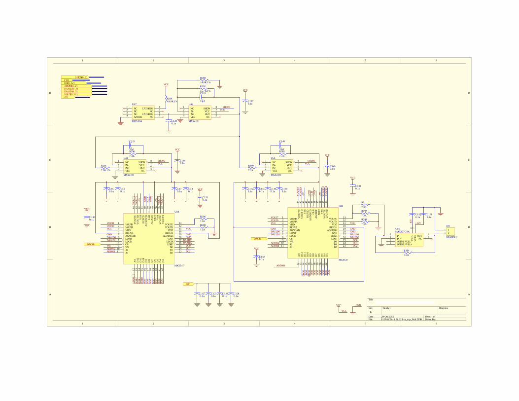
VOUT(0..11)DO(0..12)ADDRI(0..2)
CLRWR
-5VDAALD(0..3)DA1LD(0..3)
SHDN(0..2)
DACS0DACS1VCCGND
adcadc.sch
VOUT(0..11)DO(0..12)ADDRI(0..2)
CLRWR
-5VDAALD(0..3)DA1LD(0..3)
SHDN(0..2)
DACS0DACS1VCCGND
D[0..15]ADDR(0..7)CTRL(8..15)CTRL(0..7)
DATA_L_ENABLEDATA_L_DIR
DATA_H_ENABLEDATA_H_DIR
ADDR_ENABLEADDR_DIR
CTRL_L_ENABLECTRL_L_DIR
CTRL_H_ENABLECTRL_H_DIR
DO(0..12)
WRCLR
ADDRI(0..2)
DAALD(0..3)DA1LD(0..3)
SHDN(0..2)
DACS1DACS0
GNDGND
VCC
hva_addrhva_addr.sch
D[0..15]ADDR(0..7)CTRL(8..15)CTRL(0..7)
DATA_L_ENABLEDATA_L_DIR
DATA_H_ENABLEDATA_H_DIR
ADDR_ENABLEADDR_DIR
CTRL_L_ENABLECTRL_L_DIR
CTRL_H_ENABLECTRL_H_DIR
DO(0..12)
WRCLR
ADDRI(0..2)
DAALD(0..3)DA1LD(0..3)
SHDN(0..2)
DACS1DACS0
GNDGND
VCC
-5VVCCGND
neg_supneg_sup.sch
-5VVCCGND -5V
HVO(0..11)HV-HV+
hv_bushv_bus.sch
-5VHVO(0..11)HV-HV+
VCC
VCC
1 2 3 4 5 6
A
B
C
D
654321
D
C
B
A
Title
Number RevisionSize
B
Date: 29-Oct-2002 Sheet of File: F:\IFA\CD - 8.28.02\hva_top_Rob.DDB Drawn By:
D21N4001
C40.1u
+ C31u
R2
1.0K
R1
1k
R4221k
R19
221k
R22
1k
Q2
MOSFET N
anode 1
cathode 2base4
collector5emitter6
U3
CNY17
anode1 cathode2
base 4collector 5emitter 6U1
CNY17
IN - 2
IN + 3OUT6
VC
C-4
VCC
+7
OFFSE NULL- 1
OFFSE NULL+ 5
NC8
U2MAX427CSA(8)
VOUT0
+15-15
HV+
HV-
HVO0
C8
18pf
AK
D412V
AK
D312V
R9
240
R21
180k
R25
249k
R23
249k
R17
249k
R7
180k
R13
180k
R14
180k
R12
180k
R20
180k
R15
360k
R8
360k
R10
360k
C62.2n
C52.2n
C10.1u
D11N4001
D51N4001
D71N4001
Q1
MOSFET N
+
C71u
R51k
R3
240
R16
249k
R61k
TEST POINT
C22.2n
123
J2
CON3
GND
R11
7.3k
R18
7.3k
+15V
-15V
TESTPOINT
NOTE: TESTPOINTS ARE CONNECTED WITH WIRE. THIS CONNECTION IS NOT ON THE PCB
1 2 3 4 5 6
A
B
C
D
654321
D
C
B
A
Title
Number RevisionSize
B
Date: 29-Oct-2002 Sheet of File: F:\IFA\CD - 8.28.02\hva_top_Rob.DDB Drawn By:
C1C1
C2C2C3C3C4C4
C5C5
C6C6
C7C7
C8C8
C9C9
C10C10
C11C11
C12C12
C13C13
C14C14
C15C15
C16C16
C17C17
C18C18
C19C19
C20C20
C21C21
C22C22
C23C23
C24C24C25C25C26C26
C27C27
C28C28
C29C29
C30C30
C31C31
C32C32
B1B1
B2B2B3B3B4B4
B5B5
B6B6
B7B7
B8B8
B9B9
B10B10
B11B11
B12B12
B13B13
B14B14
B15B15
B16B16
B17B17
B18B18
B19B19
B20B20
B21B21
B22B22
B23B23
B24B24B25B25B26B26
B27B27
B28B28
B29B29
B30B30
B31B31
B32B32
A1A1
A2A2A3A3A4A4
A5A5
A6A6
A7A7
A8A8
A9A9
A10A10
A11A11
A12A12
A13A13
A14A14
A15A15
A16A16
A17A17
A18A18
A19A19
A20A20
A21A21
A22A22
A23A23
A24A24A25A25A26A26
A27A27
A28A28
A29A29
A30A30
A31A31
A32A32
ABCP1
DIN96
RB_D5
RB_D10
R_ADDR7R_ADDR6R_ADDR5R_ADDR4R_ADDR3R_ADDR2R_ADDR1
DGND
RB_D13RB_D12RB_D11
RB_D9RB_D8
RB_D7DGND
RB_D6
RB_D4RB_D3RB_D2RB_D1RB_D0
R_CTRL0
GND
GND
D[0..15] ADDR[0..7]
GND
VCC
8 CHANNEL ADC BOARD
700-155-01 LAYOUT
PETER ONAKA1 OF XX
12345
J13
CON5
VCC
DGND
+15V
GND
-15V
11
22
+ C8622uF 25V Ta
-15V
+15VVCC
+15V
DGNDGND
-15V
CTRL[8..15]
R_CTRL10R_CTRL11R_CTRL12R_CTRL13
CTRL[0..7]
R_CTRL1R_CTRL2R_CTRL3R_CTRL4R_CTRL5R_CTRL6
DATA_L_ENABLEDATA_L_DIR
ADDR_ENABLEADDR_DIR
CTRL_L_ENABLECTRL_L_DIR
CTRL_H_ENABLECTRL_H_DIR
R_CTRL8R_CTRL9R_CTRL10R_CTRL11R_CTRL12R_CTRL13GNDGND
CTRL8CTRL9CTRL10CTRL11CTRL12CTRL13CTRL14CTRL15
CTRL0CTRL1CTRL2CTRL3CTRL4CTRL5CTRL6CTRL7
R_CTRL0R_CTRL1R_CTRL2R_CTRL3R_CTRL4R_CTRL5R_CTRL6R_CTRL7
G19
DIR1
A12
B1 18
A23
B2 17
A34B3 16
A45B4 15
A56
B5 14
A67
B6 13
A78
B7 12
A89
B8 11
VCC20 GND 10
U46
74ACT245
DATA_H_ENABLEDATA_H_DIR
RB_D0RB_D1RB_D2RB_D3RB_D4RB_D5RB_D6RB_D7
RB_D8RB_D9RB_D10RB_D11RB_D12RB_D13
D0D1D2D3D4D5D6D7
D8D9D10D11D12D13D14D15
ADDR7ADDR6ADDR5ADDR4ADDR3ADDR2ADDR1ADDR0
R_ADDR7R_ADDR6R_ADDR5R_ADDR4R_ADDR3R_ADDR2R_ADDR1GND
+ C14622uF 25V Ta
+ C7722uF 25V Ta
G19
DIR1
A12
B1 18
A23
B2 17
A34
B3 16
A45
B4 15
A56
B5 14
A67B6 13
A78B7 12
A89
B8 11
VCC20 GND 10
U39
74ACT245
G19
DIR1
A12
B1 18
A23
B2 17
A34B3 16
A45B4 15
A56
B5 14
A67
B6 13
A78
B7 12
A89
B8 11
VCC20 GND 10
U35
74ACT245
G19
DIR1
A12
B1 18
A23
B2 17
A34B3 16
A45B4 15
A56
B5 14
A67
B6 13
A78
B7 12
A89
B8 11
VCC20 GND 10
U40
74ACT245
G19
DIR1
A12
B1 18
A23
B2 17
A34
B3 16
A45
B4 15
A56
B5 14
A67B6 13
A78B7 12
A89
B8 11
VCC20 GND 10
U51
74ACT245
+ C1201.0uF C125
0.1u
VCC
+ C971.0uF C102
0.1u
VCC
+ C1081.0uF C103
0.1u
VCC
+ C1241.0uF C119
0.1u
VCC
+ C1501.0uF C144
0.1u
VCC
VCC
VCC
VCC
VCC
R297
0Ohm connection
VCC VCC VCC
VCCVCC
DGND
NC was GND
Note: Pins A9-A11 are shorted to GND with rework
Note: A31 was connected to GND, trace cut and jumpered to -15V-15VNote: A32 is jumpered to VCC
Note: was DGND
Note: Pins B20-B21, B23 are shorted to GND with rework
VCCNote: C32 is jumpered to VCCNote: C31 is jumpered to +15V+15V
GND
GNDNote: C10 is jumpered to GND
Note: was DGND
GNDGND
R_ADDR0
RB_D15RB_D15
R_CTRL14R_CTRL15
R_CTRL14R_CTRL15
R_CTRL7R_CTRL8R_CTRL9
Note: Pins A17-A21 are shorted to GND with rework
RB_D14RB_D15
R_ADDR0
Not Found
1 2 3 4 5 6
A
B
C
D
654321
D
C
B
A
Title
Number RevisionSize
B
Date: 29-Oct-2002 Sheet of File: F:\IFA\CD - 8.28.02\hva_top_Rob.DDB Drawn By:
VOUTB1
VOUTA2
VDD3
REFAB4
AGNDAB5
LDAB6
LDCD7
CS8
WR9
A210
A111
A0
12
D12
13
D11
14
D10
15
D9
16
D8
17
D7
18
D6
19
D5
20
D4
21
D3
22
D2 23D1 24D0 25LDEF 26LDGH 27GND 28AGNDGH 29REFGH 30VDD 31VOUTH 32VOUTG 33VO
UT
F34
VO
UTE
35V
SS36
RE
FF37
AG
ND
F38
CLR
39A
GN
DC
D40
REF
CD41
VSS
42V
OU
TD
43V
OU
TC44
U48
MAX547
VOUTB1
VOUTA2
VDD3
REFAB4
AGNDAB5
LDAB6
LDCD7
CS8
WR9
A210
A111
A0
12
D12
13
D11
14
D10
15
D9
16
D8
17
D7
18
D6
19
D5
20
D4
21
D3
22
D2 23D1 24D0 25LDEF 26LDGH 27GND 28AGNDGH 29REFGH 30VDD 31VOUTH 32VOUTG 33VO
UT
F34
VO
UTE
35V
SS36
REF
F37
AG
ND
F38
CLR
39A
GN
DC
D40
REF
CD41
VSS
42V
OU
TD
43V
OU
TC44
U49
MAX547
NC1
IN-2
IN+3
VEE4 NC 5OUT 6VCC 7SHDN 8U42
MAX4131
NC1
IN-2
IN+3
VEE4 NC 5OUT 6VCC 7SHDN 8U54
MAX4131
NC1
IN-2
IN+3
VEE4 NC 5OUT 6VCC 7SHDN 8U41
MAX4131
NC1
NC2
NC3
ANODE4 NC 5CATHODE 6
CATHODE 8
NC 7
U47
REF1004
VOUT(0..11)
VOUT0VOUT1
VO
UT2
VO
UT3
VO
UT4
VO
UT5
VOUT6VOUT7
VO
UT8
VO
UT9
VO
UT1
0V
OU
T11
DO(0..12)ADDRI(0..2)
DO0DO1DO2
DO
3D
O4
DO
5D
O6
DO
7D
O8
DO
9D
O10
DO
11D
O12
DO0DO1DO2
DO
3D
O4
DO
5D
O6
DO
7D
O8
DO
9D
O10
DO
11D
O12
AD
DR
I0
ADDRI1ADDRI2
ADDRI0
ADDRI1ADDRI2
C1230.1u
C1280.1u
C1310.1u
C1320.1u
VCC
-5V
C1330.1u
C1300.1u
VCC
C1270.1u
C1220.1u
DAALD(0..3)DA1LD(0..3)
C1390.1u
C1400.1u
C370.1u
C1290.1u
C1170.1u
C350.1u
C380.1u
C1490.1u
C360.1u
C1420.1u
C1410.1u
R30149.9K 1%
VCC
R289
14.0K 1%R292
35.7K 1%C118
33pf
R291
7.3K 1%
R290
7.3K
R300
7.3K
R302
7.3K
C1160.1u
SHDN(0..2)
SHDN1SHDN2
C115
33pf
C148
33pf
DACS0
DACS1
DA1LD0DA1LD1
DA1LD2DA1LD3
DAALD0DAALD1
DAALD2DAALD3
SHDN0
R299
7.3K
R?
7.3K
R296
7.3KR298
7.3K
VCC
C1510.1u
IN -2
IN +3 OUT 6
VC
C-4
VC
C+7
OFFSE NULL-1
OFFSE NULL+5
NC 8
U55MAX427CSA
R304
7.3K
C1520.1u
12
JP2
HEADER 2
WR
VCC
GNDGND
GND
VCC
-5V
-5V
GN
D
CLR
CLR
GN
D
VCC
GND GNDGND
VCC
R297
7.3K
-5V
-5V
GN
DC
LRG
ND
VCC VCC
VCC
+15V-15V
VCC
VCC
VCC
VCC
GND
-5V
VCC
VCC
1 2 3 4 5 6
A
B
C
D
654321
D
C
B
A
Title
Number RevisionSize
B
Date: 29-Oct-2002 Sheet of File: F:\IFA\CD - 8.28.02\hva_top_Rob.DDB Drawn By:
GND1
I/0 162
I/0 173
I/0 184
I/0 195
TCLK6
I/0 217
I/0 228
I/0 239
GND10
I/0 2411
I/0 2512
I/0 2613
I/0 2714
I/0 2815I/0 2916I/0 3017
I/0 3118
CLK 019
VCCO20
GND21
CLK 122
I/0 3223
I/0 3324
I/0 3425
I/0 3526
I/0 3627
I/0 3728
I/0 3829
I/0 3930
GND31
I/O 4032
I/O 4133
I/O 4234
I/O 4335
I/O 4436
I/O 4537I/O 4638
I/O 4739
VCCO40
GN
D41
I/O
48
42
I/O
49
43
I/O
50
44
I/O
51
45
TM
S46
I/O
53
47
I/O
54
48
I/O
55
49
GN
D50
I/O
56
51
I/O
57
52
I/O
58
53
I/O
59
54
I/O
60
55
I/O
61
56
I/O
62
57
I/O
63
58
I 2
59
VCC
O60
GN
D61
VCC
62
I/O
64
63
I/O
65
64
I/O
66
65
I/O
67
66
I/O
68
67
I/O
69
68
I/O
70
69
I/O
71
70
GN
D71
I/O
72
72
I/O
73
73
I/O
74
74
I/O
75
75
TD
O76
I/O
77
77
I/O
78
78
I/O
79
79
VCC
O80
GND 81I/O 80 82I/O 81 83I/O 82 84I/O 83 85I/O 84 86I/O 85 87I/O 86 88
GND 90I/O 88 91I/O 89 92I/O 90 93I/O 91 94I/O 92 95I/O 93 96I/O 94 97I/O 95 98
I/O 87 89
CLK 2 99VCCO 100GND 101CLK3 102I/O 96 103I/O 97 104I/O 98 105I/O 99 106I/O 100 107I/O 101 108I/O 102 109I/O 103 110GND 111I/O 104 112I/O 105 113I/O 106 114I/O 107 115TDI 116I/O 109 117I/O 110 118I/O 111 119VCCO 120
GN
D12
1I/
O 1
1212
2I/
O 1
1312
3I/
O 1
1412
4I/
O 1
1512
5I/
O 1
1612
6I/
O 1
1712
7I/
O 1
1812
8I/
O 1
1912
9G
ND
130
I/O
120
131
I/O
121
132
I/O
122
133
I/O
123
134
I/O
124
135
I/O
125
136
I/O
126
137
I/O
127
138
JTA
G E
N13
9V
CC14
0G
ND
141
VCC
O14
2I/
O 0
143
I/O
114
4I/
O 2
145
I/O
314
6I/
O 4
147
I/O
514
8I/
O 6
149
I/O
715
0G
ND
151
I/O
815
2I/
O 9
153
I/O
10
154
I/O
11
155
I/O
12
156
I/O
13
157
I/O
14
158
I/O
15
159
VCC
O16
0
U44
CY37256
RES0 1RES1 2RES2 3RES3 4COM0 5RES46
RES57
RES68
RES79
COM110
R295
RES_8 4.7K
C1130.1u
C1120.1u
C1430.1u
C1340.1u
C1110.1u
C1260.1u
C1090.1u
C1100.1u
C1210.1u
C1450.1u
C1470.1u
D[0..15]
ADDR(0..7)
CTRL(8..15)
CTRL(0..7)DATA_L_ENABLE
DATA_L_DIR
DA
TA
_H_E
NA
BLE
DA
TA
_H_D
IR
AD
DR
_EN
ABL
EA
DD
R_D
IR
CTRL_L_ENABLE
CTRL_L_DIR
CTRL_H_ENABLECTRL_H_DIR
NC 1GND 7
VCC14 OUTPUT8U53
OSCILLATOR
DO(0..12)
WRCLR
ADDRI(0..2)
DAALD(0..3)
DA1LD(0..3)
1 23 45 67 89 10
J16
HEADER 5X2
VCC
SHDN(0..2)DACS1
DACS0
1 2
U43A
74AC14
C1140.1u
3 4
U43B
74AC14
VCC
R2937.3K
R294511k
LED1
LED
LED2
LED
LED3
LED
56
U43C
74AC14
98
U43D
74AC14
1110
U43E
74AC14
12345678910
J17
HEADER 5x2
R?
1K
R?
1K
R?
1K
CTRL0CTRL1CTRL2CTRL3CTRL4CTRL5CTRL6CTRL7
VCCGND
VCC
GNDVCC
GND
CTRL8CTRL9CTRL10CTRL11CTRL12CTRL13CTRL14CTRL15
ADDR0ADDR1ADDR2ADDR3ADDR4ADDR5ADDR6ADDR7
VCC
GN
D
TM
S
TMS
GN
D
13 12
VC
C14
GN
D7
U43F
74AC14
12345678
161514131211109
SW1
SW DIP-8VCC
VC
CG
ND
VC
C
GN
D
VC
C
TD
O
TDO
VCC
GND
DA1LD0DA1LD1DA1LD2DA1LD3
GND
DAALD0DAALD1DAALD2DAALD3
VCC
VCCGND
GNDGNDVCC
ADDR0ADDR1ADDR2
TDI
TDI
VCC
GN
D
GN
D
DO
0D
O1
DO
2D
O3
DO
4D
O5
DO
6D
O7
DO
8D
O9
DO
10D
O11
DO
12VCC
GN
DV
CC
GN
D
VCC
D0
D1
D2
D3
D4
D5
D6
D7
D8
D9
D10
D11
D12
D13
D14
D15
TCK
TCKJTAGEN
JTA
GEN
GNDVCC
GND
VCC
VCC VCCVCC VCC
VCC VCC VCC VCC
SHDN0SHDN1SHDN2
VCC
1 2 3 4 5 6
A
B
C
D
654321
D
C
B
A
Title
Number RevisionSize
B
Date: 29-Oct-2002 Sheet of File: F:\IFA\CD - 8.28.02\hva_top_Rob.DDB Drawn By:
OUT1
FB2
SHDN3
REF4 GND 5V+ 6V+ 7LX 8U25
MAX764CSA
-5V
D50
DIODE SCHOTTKY
+
C58220uF
L147uH+ C72
220uF12
J8
CON2
C640.1u
C750.1uC63
0.1u
VCC
GND

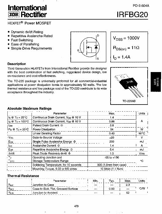
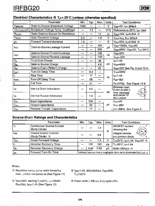
4 Datasheets 4.1 IRFBG20

4.2 IRG4PH50U
Parameter Max. UnitsVCES Collector-to-Emitter Breakdown Voltage 1200 VIC @ TC = 25°C Continuous Collector Current 45IC @ TC = 100°C Continuous Collector Current 24 AICM Pulsed Collector Current 180ILM Clamped Inductive Load Current 180VGE Gate-to-Emitter Voltage ± 20 VEARV Reverse Voltage Avalanche Energy 170 mJPD @ TC = 25°C Maximum Power Dissipation 200PD @ TC = 100°C Maximum Power Dissipation 78TJ Operating Junction and -55 to + 150TSTG Storage Temperature Range
Soldering Temperature, for 10 seconds 300 (0.063 in. (1.6mm) from case )°C
Mounting torque, 6-32 or M3 screw. 10 lbf•in (1.1N•m)
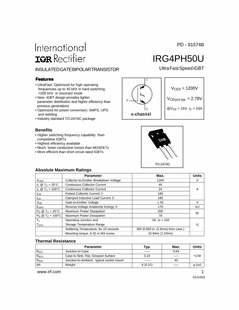
IRG4PH50UUltra Fast Speed IGBTINSULATED GATE BIPOLAR TRANSISTOR
E
C
G
n-channel
TO-247AC
FeaturesFeaturesFeaturesFeaturesFeatures
Benefits
VCES = 1200V
VCE(on) typ. = 2.78V
@VGE = 15V, IC = 24A
Parameter Typ. Max. UnitsRθJC Junction-to-Case ––– 0.64RθCS Case-to-Sink, Flat, Greased Surface 0.24 ––– °C/WRθJA Junction-to-Ambient, typical socket mount ––– 40Wt Weight 6 (0.21) ––– g (oz)
Thermal Resistance
Absolute Maximum Ratings
W
• UltraFast: Optimized for high operating frequencies up to 40 kHz in hard switching, >200 kHz in resonant mode• New IGBT design provides tighter parameter distribution and higher efficiency than previous generations• Optimized for power conversion; SMPS, UPS and welding• Industry standard TO-247AC package
• Higher switching frequency capability than competitive IGBTs• Highest efficiency available• Much lower conduction losses than MOSFETs• More efficient than short circuit rated IGBTs
01/14/02
www.irf.com 1
PD - 91574B
IRG4PH50U
2 www.irf.com
Parameter Min. Typ. Max. Units ConditionsV(BR)CES Collector-to-Emitter Breakdown Voltage 1200 — — V VGE = 0V, IC = 250µAV(BR)ECS Emitter-to-Collector Breakdown Voltage 18 — — V VGE = 0V, IC = 1.0A∆V(BR)CES/∆TJ Temperature Coeff. of Breakdown Voltage — 1.20 — V/°C VGE = 0V, IC = 1.0mA
— 2.56 3.5 IC = 20A— 2.78 3.7 IC = 24A VGE = 15V
— 3.20 — IC = 45A See Fig.2, 5
— 2.54 — IC = 24A , TJ = 150°CVGE(th) Gate Threshold Voltage 3.0 — 6.0 VCE = VGE, IC = 250µA∆VGE(th)/∆TJ Temperature Coeff. of Threshold Voltage — -13 — mV/°C VCE = VGE, IC = 250µAgfe Forward Transconductance 23 35 — S VCE = 100V, IC = 24A
— — 250 VGE = 0V, VCE = 1200V
ICES Zero Gate Voltage Collector Current — — 2.0 µA VGE = 0V, VCE = 24V, TJ = 25°C
— — 5000 VGE = 0V, VCE = 1200V, TJ = 150°CIGES Gate-to-Emitter Leakage Current — — ±100 nA VGE = ±20V
Parameter Min. Typ. Max. Units ConditionsQg Total Gate Charge (turn-on) — 160 250 IC = 24AQge Gate - Emitter Charge (turn-on) — 27 40 nC VCC = 400V See Fig. 8Qgc Gate - Collector Charge (turn-on) — 53 83 VGE = 15Vtd(on) Turn-On Delay Time — 35 —tr Rise Time — 15 — TJ = 25°Ctd(off) Turn-Off Delay Time — 200 350 IC = 24A, VCC = 960Vtf Fall Time — 290 500 VGE = 15V, RG = 5.0ΩEon Turn-On Switching Loss — 0.53 — Energy losses include "tail"Eoff Turn-Off Switching Loss — 1.41 — mJ See Fig. 9, 10, 14Ets Total Switching Loss — 1.94 2.6td(on) Turn-On Delay Time — 31 — TJ = 150°Ctr Rise Time — 18 — IC = 24A, VCC = 960Vtd(off) Turn-Off Delay Time — 320 — VGE = 15V, RG = 5.0Ωtf Fall Time — 280 — Energy losses include "tail"Ets Total Switching Loss — 5.40 — See Fig. 11, 14Eon Turn-On Switching Loss — 0.35 — TJ = 25°C, VGE = 15V, RG = 5.0ΩEoff Turn-Off Switching Loss — 1.43 — IC = 20A, VCC = 960V
— 1.78 2.9 Energy losses include "tail"— 4.56 — See Fig. 9, 10, 11, 14, TJ = 150°C
LE Internal Emitter Inductance — 13 — nH Measured 5mm from packageCies Input Capacitance — 3600 — VGE = 0VCoes Output Capacitance — 160 — pF VCC = 30V See Fig. 7Cres Reverse Transfer Capacitance — 31 — ƒ = 1.0MHz
Electrical Characteristics @ TJ = 25°C (unless otherwise specified)
V
Switching Characteristics @ TJ = 25°C (unless otherwise specified)
ns
mJ
Repetitive rating; pulse width limited by maximumjunction temperature.
Pulse width ≤ 80µs; duty factor ≤ 0.1%. Pulse width 5.0µs, single shot.
Notes: Repetitive rating; VGE = 20V, pulse width limited by
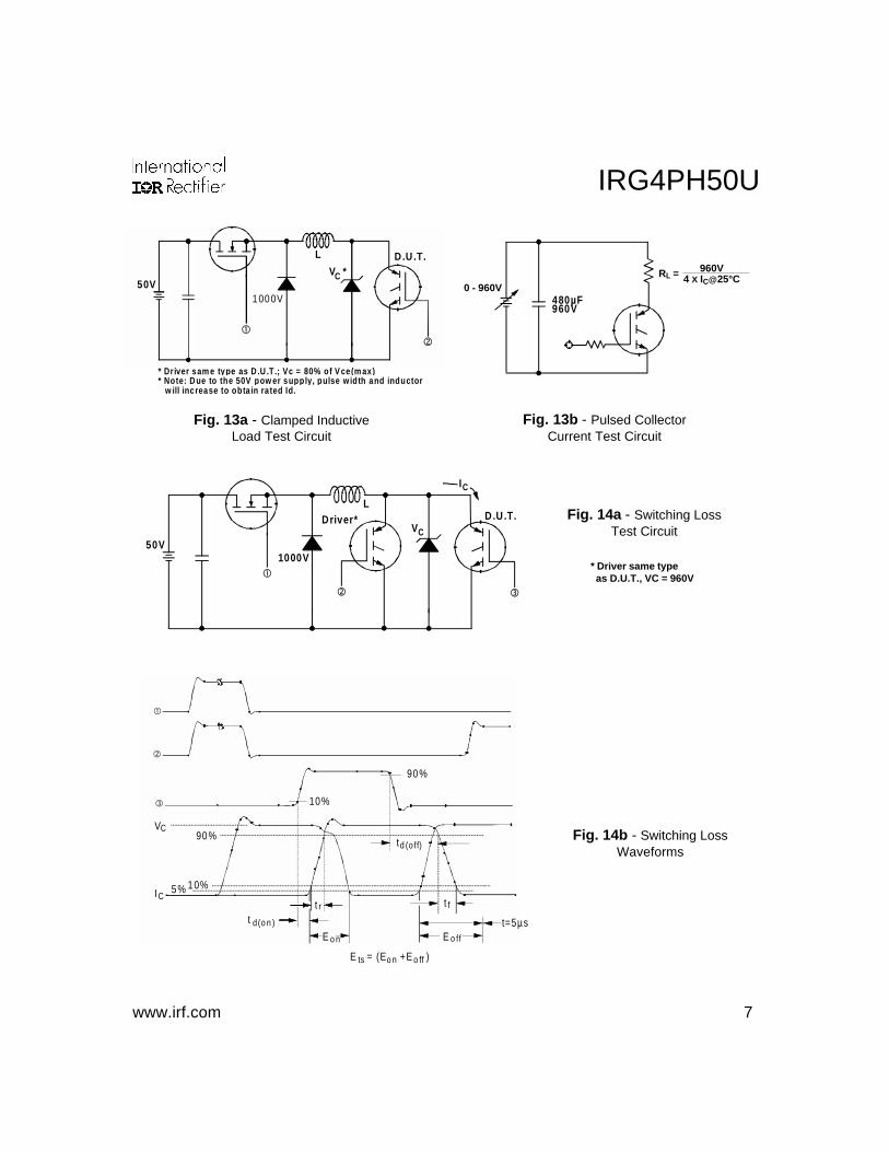
max. junction temperature. ( See fig. 13b ) VCC = 80%(VCES), VGE = 20V, L = 10µH, RG = 5.0Ω,
(See fig. 13a)
VCE(ON) Collector-to-Emitter Saturation Voltage
mJ
ns
Ets Total Switching Loss
IRG4PH50U
www.irf.com 3
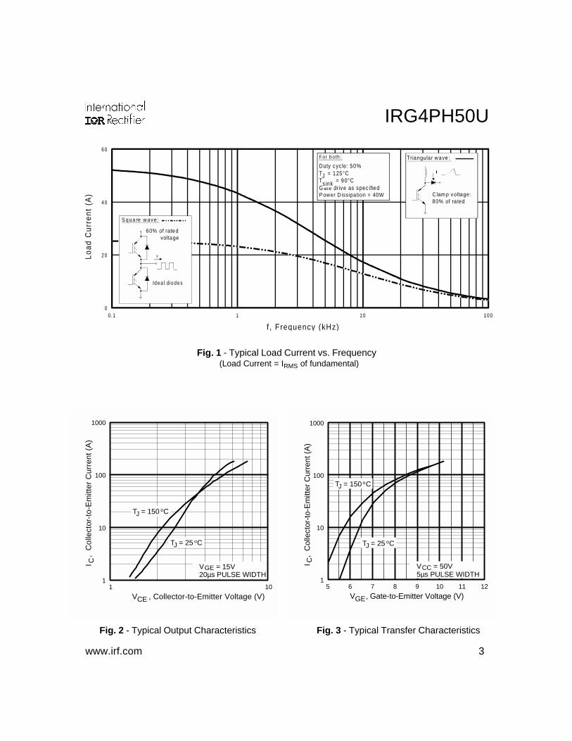
Fig. 1 - Typical Load Current vs. Frequency (Load Current = IRMS of fundamental)
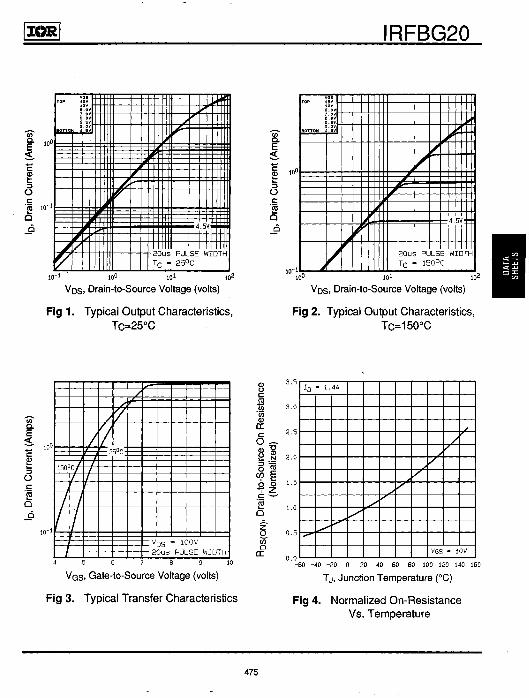
Fig. 2 - Typical Output Characteristics Fig. 3 - Typical Transfer Characteristics
0
2 0
4 0
6 0
0.1 1 1 0 1 0 0
f , Frequency (kHz)
Load
Cur
rent
(A
)
A
60% of rated voltage
I
Id e a l d io d e s
S qua re w ave :
F o r b o th :
D uty cyc le: 50%T = 125 °CT = 90°CG ate drive as spec ified
s inkJ
P ow er D issipa tion = 40W
Triangula r w ave :
I
C lam p voltage :80% of ra ted
1
10
100
1000
1 10
V , Collector-to-Emitter Voltage (V)
I ,
Col
lect
or-t
o-E
mitt
er C
urre
nt (
A)
CE
C
V = 15V20µs PULSE WIDTH
GE
T = 25 CJo
T = 150 CJo
1
10
100
1000
5 6 7 8 9 10 11 12
V , Gate-to-Emitter Voltage (V)
I ,
Col
lect
or-t
o-E
mitt
er C
urre
nt (
A)
GE
C
V = 50V5µs PULSE WIDTH
CC
T = 25 CJo
T = 150 CJo
IRG4PH50U
4 www.irf.com
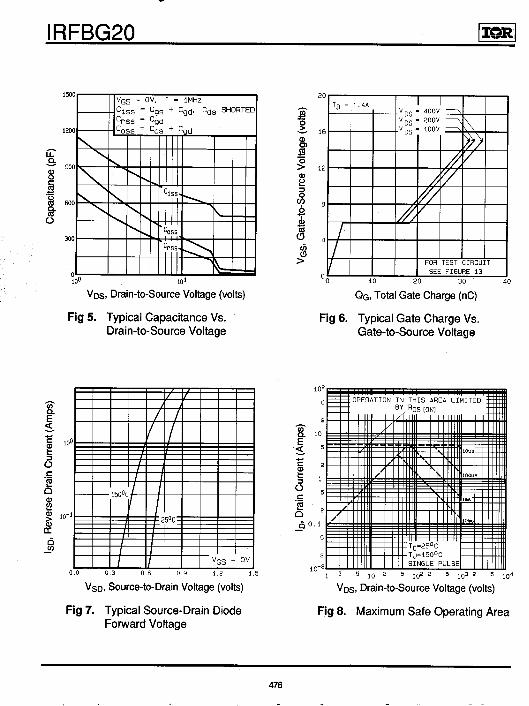
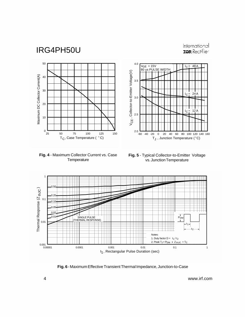
Fig. 6 - Maximum Effective Transient Thermal Impedance, Junction-to-Case
Fig. 5 - Typical Collector-to-Emitter Voltagevs. Junction Temperature
Fig. 4 - Maximum Collector Current vs. CaseTemperature
-60 -40 -20 0 20 40 60 80 100 120 140 1602.0
2.5
3.0
3.5
4.0
T , Junction Temperature ( C)
V
, C
olle
ctor
-to-
Em
itter
Vol
tage
(V)
J °
CE
V = 15V80 us PULSE WIDTH
GE
I = A12C
I = A24C
I = A48C
25 50 75 100 125 1500
10
20
30
40
50
T , Case Temperature ( C)
Max
imum
DC
Col
lect
or C
urre
nt(A
)
C °
0.001
0.01
0.1
1
0.00001 0.0001 0.001 0.01 0.1 1
Notes:1. Duty factor D = t / t2. Peak T = P x Z + T
1 2
J DM thJC C
P
t
t
DM
1
2
t , Rectangular Pulse Duration (sec)
The
rmal
Res
pons
e (Z
)
1
thJC
0.01
0.02
0.05
0.10
0.20
0.50
SINGLE PULSE(THERMAL RESPONSE)
IRG4PH50U
www.irf.com 5
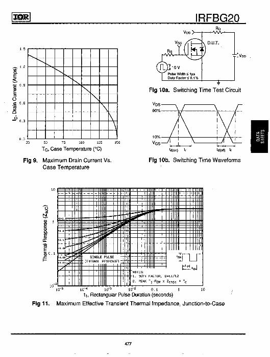
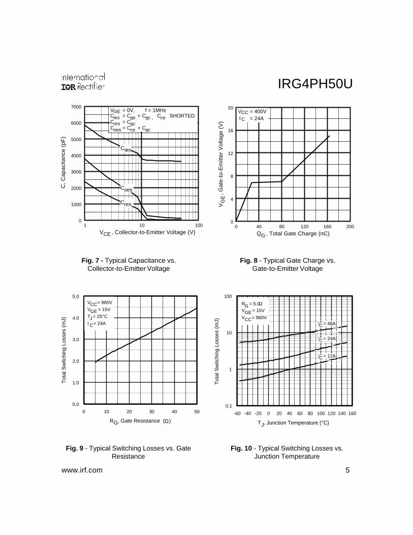
Fig. 7 - Typical Capacitance vs.Collector-to-Emitter Voltage
Fig. 8 - Typical Gate Charge vs.Gate-to-Emitter Voltage
Fig. 9 - Typical Switching Losses vs. GateResistance
Fig. 10 - Typical Switching Losses vs.Junction Temperature
0 40 80 120 160 2000
4
8
12
16
20
Q , Total Gate Charge (nC)
V
,
Gat
e-to
-Em
itter
Vol
tage
(V
)
G
GE
V = 400VI = 24ACC
C
1 10 1000
1000
2000
3000
4000
5000
6000
7000
V , Collector-to-Emitter Voltage (V)
C, C
apac
itanc
e (p
F)
CE
VCCC
====
0V,CCC
f = 1MHz+ C
+ C
C SHORTEDGEies ge gc , ceres gcoes ce gc
Cies
Coes
Cres
0 10 20 30 40 50
RG, Gate Resistance (Ω)
0.0
1.0
2.0
3.0
4.0
5.0
Tot
al S
witc
hing
Los
ses
(mJ)
VCC = 960V
VGE = 15V
TJ = 25°C
I C = 24A
-60 -40 -20 0 20 40 60 80 100 120 140 160
TJ, Junction Temperature (°C)
0.1
1
10
100
Tot
al S
witc
hing
Los
ses
(mJ)
RG = 5.0ΩVGE = 15V
VCC = 960VIC = 48A
IC = 24A
IC = 12A
IRG4PH50U
6 www.irf.com
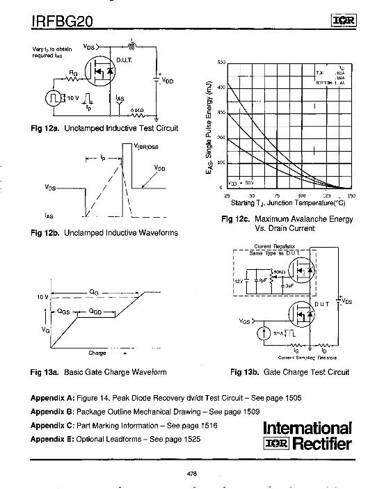
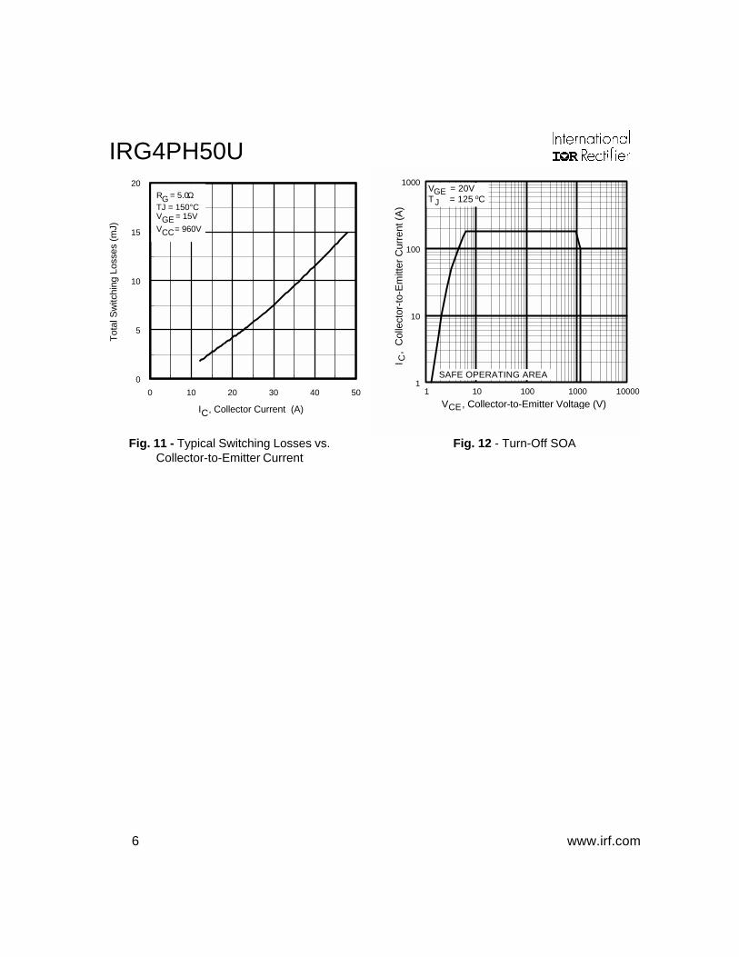
Fig. 11 - Typical Switching Losses vs.Collector-to-Emitter Current
Fig. 12 - Turn-Off SOA
1
10
100
1000
1 10 100 1000 10000
V = 20VT = 125 C
GEJ
o
V , Collector-to-Emitter Voltage (V)I
, C
olle
ctor
-to-
Em
itter
Cur
rent
(A
)CE
C
SAFE OPERATING AREA
0 10 20 30 40 50
IC, Collector Current (A)
0
5
10
15
20
Tot
al S
witc
hing
Los
ses
(mJ)
RG = 5.0ΩTJ = 150°CVGE = 15V
VCC = 960V
IRG4PH50U
www.irf.com 7
960V4 X IC@25°C
D.U.T.
50V
L
V *C
* Dr iver sam e type as D .U .T.; Vc = 80% of V ce(m ax)* Note: D ue to the 50V pow er supply, pulse w idth and inductor w ill increase to obta in ra ted Id.
1000V
Fig. 13a - Clamped InductiveLoad Test Circuit
Fig. 13b - Pulsed CollectorCurrent Test Circuit
480µF960V
0 - 960VRL =
t=5µsd(o n )t
t ft r
90%
td (o ff)
10%
90%
10%5%
VC
IC
E o n E o ff
ts o n o ffE = (E +E )
Fig. 14b - Switching LossWaveforms
50V
Driver*
1000V
D.U.T.
IC
CV
LFig. 14a - Switching Loss
Test Circuit
* Driver same type as D.U.T., VC = 960V
IRG4PH50U
8 www.irf.com
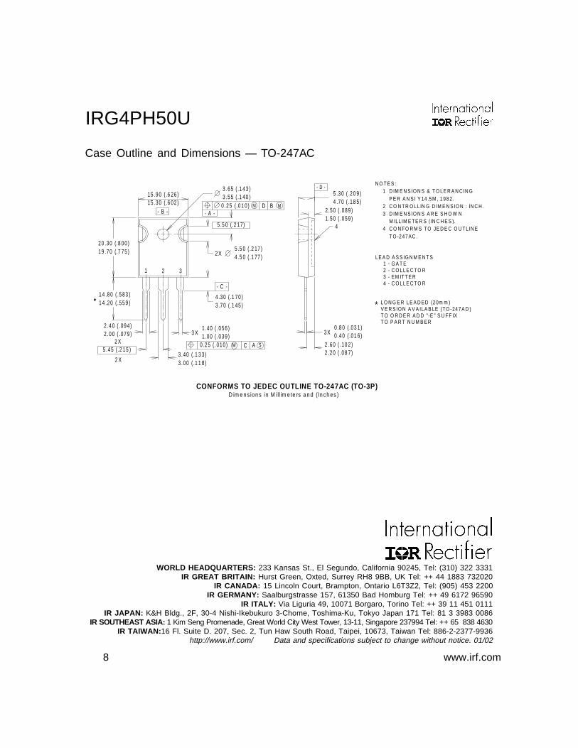
Case Outline and Dimensions — TO-247AC
D im e n s ion s in M i ll im e te rs a n d (In ch es )CONFORMS TO JEDEC OUTLINE TO-247AC (TO-3P)
- D -5 .3 0 ( .2 0 9 )4 .7 0 ( .1 8 5 )
3 .6 5 ( .1 4 3 )3 .5 5 ( .1 4 0 )
2 .5 0 ( .0 8 9 )1 .5 0 ( .0 5 9 )
4
3 X0 .8 0 ( .0 3 1 )0 .4 0 ( .0 1 6 )
2 .6 0 ( .1 0 2 )2 .2 0 ( .0 8 7 )3 .4 0 ( .1 3 3 )
3 .0 0 ( .1 1 8 )
3 X
0 .2 5 ( .0 1 0 ) M C A S
4 .3 0 ( .1 7 0 )3 .7 0 ( .1 4 5 )
- C -
2X5 .5 0 ( .2 17 )4 .5 0 ( .1 77 )
5 .5 0 ( .2 1 7)
0 .2 5 ( .0 1 0 )
1 .4 0 ( .0 5 6 )1 .0 0 ( .0 3 9 )
DM MB- A -
1 5 .9 0 ( .6 2 6 )1 5 .3 0 ( .6 0 2 )
- B -
1 2 3
2 0 .3 0 (.8 0 0 )1 9 .7 0 (.7 7 5 )
1 4 .8 0 ( .5 8 3 )1 4 .2 0 ( .5 5 9 )
2 .4 0 ( .0 9 4 )2 .0 0 ( .0 7 9 )
2 X
2 X
5 .4 5 ( .2 1 5 )
*
N O TE S : 1 D IM E N S IO N S & T O L E R A N C IN G P E R A N S I Y 14 .5 M , 1 9 8 2 . 2 C O N TR O L L IN G D IM E N S IO N : IN C H . 3 D IM E N S IO N S A R E S H O W N M ILL IM E TE R S (IN C H E S ). 4 C O N FO R M S TO JE D E C O U TL IN E T O -2 4 7 AC .
L E A D A S S IG N M E N T S 1 - G A T E 2 - C O L L E C TO R 3 - EM IT TE R 4 - C O L L E C TO R
* L O N G E R L E A D ED (2 0m m ) V E R S IO N A V A IL A B LE (T O -24 7 A D )T O O R D E R A D D "-E " S U FF IXT O P A R T N U M B ER
WORLD HEADQUARTERS: 233 Kansas St., El Segundo, California 90245, Tel: (310) 322 3331IR GREAT BRITAIN: Hurst Green, Oxted, Surrey RH8 9BB, UK Tel: ++ 44 1883 732020
IR CANADA: 15 Lincoln Court, Brampton, Ontario L6T3Z2, Tel: (905) 453 2200IR GERMANY: Saalburgstrasse 157, 61350 Bad Homburg Tel: ++ 49 6172 96590
IR ITALY: Via Liguria 49, 10071 Borgaro, Torino Tel: ++ 39 11 451 0111IR JAPAN: K&H Bldg., 2F, 30-4 Nishi-Ikebukuro 3-Chome, Toshima-Ku, Tokyo Japan 171 Tel: 81 3 3983 0086
IR SOUTHEAST ASIA: 1 Kim Seng Promenade, Great World City West Tower, 13-11, Singapore 237994 Tel: ++ 65 838 4630IR TAIWAN:16 Fl. Suite D. 207, Sec. 2, Tun Haw South Road, Taipei, 10673, Taiwan Tel: 886-2-2377-9936
http://www.irf.com/ Data and specifications subject to change without notice. 01/02

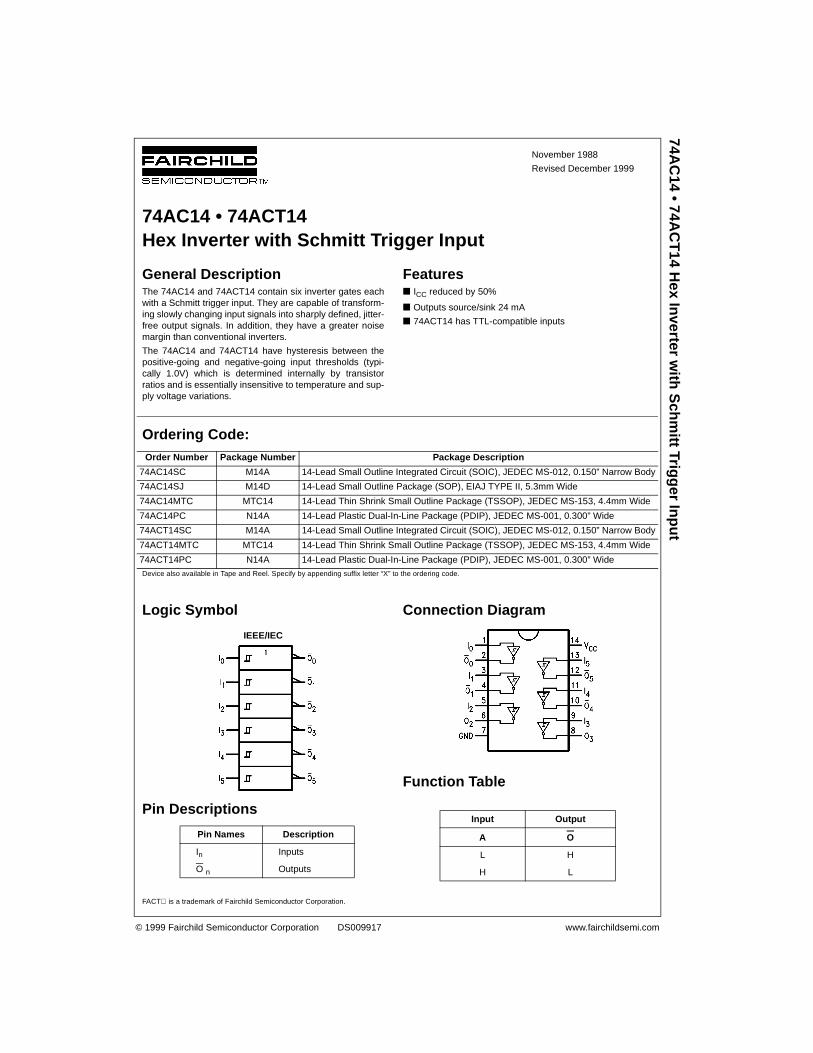
4.3 74AC14
© 1999 Fairchild Semiconductor Corporation DS009917 www.fairchildsemi.com
November 1988
Revised December 1999
74AC
14 • 74AC
T14 H
ex Inverter w
ith S
chm
itt Trigg
er Inp
ut
74AC14 • 74ACT14Hex Inverter with Schmitt Trigger Input
General DescriptionThe 74AC14 and 74ACT14 contain six inverter gates eachwith a Schmitt trigger input. They are capable of transform-ing slowly changing input signals into sharply defined, jitter-free output signals. In addition, they have a greater noisemargin than conventional inverters.
The 74AC14 and 74ACT14 have hysteresis between thepositive-going and negative-going input thresholds (typi-cally 1.0V) which is determined internally by transistorratios and is essentially insensitive to temperature and sup-ply voltage variations.
Features ICC reduced by 50%
Outputs source/sink 24 mA
74ACT14 has TTL-compatible inputs
Ordering Code:
Device also available in Tape and Reel. Specify by appending suffix letter “X” to the ordering code.
Logic Symbol
IEEE/IEC
Pin Descriptions
Connection Diagram
Function Table
FACT is a trademark of Fairchild Semiconductor Corporation.
Order Number Package Number Package Description
74AC14SC M14A 14-Lead Small Outline Integrated Circuit (SOIC), JEDEC MS-012, 0.150” Narrow Body
74AC14SJ M14D 14-Lead Small Outline Package (SOP), EIAJ TYPE II, 5.3mm Wide
74AC14MTC MTC14 14-Lead Thin Shrink Small Outline Package (TSSOP), JEDEC MS-153, 4.4mm Wide
74AC14PC N14A 14-Lead Plastic Dual-In-Line Package (PDIP), JEDEC MS-001, 0.300” Wide
74ACT14SC M14A 14-Lead Small Outline Integrated Circuit (SOIC), JEDEC MS-012, 0.150” Narrow Body
74ACT14MTC MTC14 14-Lead Thin Shrink Small Outline Package (TSSOP), JEDEC MS-153, 4.4mm Wide
74ACT14PC N14A 14-Lead Plastic Dual-In-Line Package (PDIP), JEDEC MS-001, 0.300” Wide
Pin Names Description
In Inputs
O n Outputs
Input Output
A O
L H
H L
www.fairchildsemi.com 2
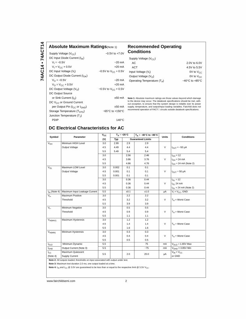
74A
C14
• 7
4AC
T14 Absolute Maximum Ratings(Note 1) Recommended Operating
Conditions
Note 1: Absolute maximum ratings are those values beyond which damageto the device may occur. The databook specifications should be met, with-out exception, to ensure that the system design is reliable over its powersupply, temperature, and output/input loading variables. Fairchild does notrecommend operation of FACT circuits outside databook specifications.
DC Electrical Characteristics for AC
Note 2: All outputs loaded; thresholds on input associated with output under test.
Note 3: Maximum test duration 2.0 ms, one output loaded at a time.
Note 4: IIN and ICC @ 3.0V are guaranteed to be less than or equal to the respective limit @ 5.5V VCC.
Supply Voltage (VCC) −0.5V to +7.0V
DC Input Diode Current (IIK)
VI = −0.5V −20 mA
VI = VCC + 0.5V +20 mA
DC Input Voltage (VI) −0.5V to VCC + 0.5V
DC Output Diode Current (IOK)
VO = −0.5V −20 mA
VO = VCC + 0.5V +20 mA
DC Output Voltage (VO) −0.5V to VCC + 0.5V
DC Output Source
or Sink Current (IO) ±50 mA
DC VCC or Ground Current
per Output Pin (ICC or IGND) ±50 mA
Storage Temperature (TSTG) −65°C to +150°CJunction Temperature (TJ)
PDIP 140°C
Supply Voltage (VCC)
AC 2.0V to 6.0V
ACT 4.5V to 5.5V
Input Voltage (VI) 0V to VCC
Output Voltage (VO) 0V to VCC
Operating Temperature (TA) −40°C to +85°C
Symbol ParameterVCC TA = +25°C TA = −40°C to +85°C
Units Conditions(V) Typ Guaranteed Limits
VOH Minimum HIGH Level 3.0 2.99 2.9 2.9
V IOUT = −50 µAOutput Voltage 4.5 4.49 4.4 4.4
5.5 5.49 5.4 5.4
3.0 2.56 2.46
V
IOH = 12
4.5 3.86 3.76 IOH = 24 mA
5.5 4.86 4.76 IOH = 24 mA (Note 2)
VOL Maximum LOW Level 3.0 0.002 0.1 0.1
V IOUT = 50 µAOutput Voltage 4.5 0.001 0.1 0.1
5.5 0.001 0.1 0.1
3.0 0.36 0.44
V
IOL = 12
4.5 0.36 0.44 IOL 24 mA
5.5 0.36 0.44 IOL = 24 mA (Note 2)
IIN (Note 4) Maximum Input Leakage Current 5.5 ±0.1 ±1.0 µA VI = VCC, GND
Vt+ Maximum Positive 3.0 2.2 2.2
TA = Worst CaseThreshold 4.5 3.2 3.2 V
5.5 3.9 3.9
Vt− Minimum Negative 3.0 0.5 0.5
TA = Worst CaseThreshold 4.5 0.9 0.9 V
5.5 1.1 1.1
VH(MAX) Maximum Hysteresis 3.0 1.2 1.2
TA = Worst Case4.5 1.4 1.4 V
5.5 1.6 1.6
VH(MIN) Minimum Hysteresis 3.0 0.3 0.3
TA = Worst Case4.5 0.4 0.4 V
5.5 0.5 0.5
IOLD Minimum Dynamic 5.5 75 mA VOLD = 1.65V Max
IOHD Output Current (Note 3) 5.5 −75 mA VOHD = 3.85V Min
ICC Maximum Quiescent 5.5 2.0 20.0 µA
VIN = VCC
(Note 4) Supply Current or GND
3 www.fairchildsemi.com
74AC
14 • 74AC
T14
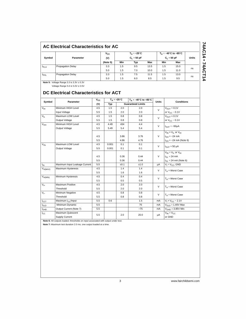
AC Electrical Characteristics for AC
Note 5: Voltage Range 3.3 is 3.3V ± 0.3V
Voltage Range 5.0 is 5.0V ± 0.5V
DC Electrical Characteristics for ACT
Note 6: All outputs loaded; thresholds on input associated with output under test.
Note 7: Maximum test duration 2.0 ms, one output loaded at a time.
Symbol Parameter
VCC TA = +25°C TA = −40°C to +85°C
Units(V) CL = 50 pF CL = 50 pF
(Note 5) Min Typ Max Min Max
tPLH Propagation Delay 3.3 1.5 9.5 13.5 1.5 15.0ns
5.0 1.5 7.0 10.0 1.5 11.0
tPHL Propagation Delay 3.3 1.5 7.5 11.5 1.5 13.0ns
5.0 1.5 6.0 8.5 1.5 9.5
Symbol ParameterVCC TA = +25°C TA = −40°C to +85°C
Units Conditions(V) Typ Guaranteed Limits
VIH Minimum HIGH Level 4.5 1.5 2.0 2.0V
VOUT = 0.1V
Input Voltage 5.5 1.5 2.0 2.0 or VCC − 0.1V
VIL Maximum LOW Level 4.5 1.5 0.8 0.8V
VOUT = 0.1V
Output Voltage 5.5 1.5 0.8 0.8 or VCC − 0.1V
VOH Minimum HIGH Level 4.5 4.49 434 4.4V IOUT = −50µA
Output Voltage 5.5 5.49 5.4 5.4
V
VIN = VIL or VIH
4.5 3.86 3.76 IOH = −24 mA
5.5 4.86 4.76 IOH = −24 mA (Note 6)
VOL Maximum LOW Level 4.5 0.001 0.1 0.1V IOUT = 50 µA
Output Voltage 5.5 0.001 0.1 0.1
V
VIN = VIL or VIH
4.5 0.36 0.44 IOL = 24 mA
5.5 0.36 0.44 IOL = 24 mA (Note 6)
IIN Maximum Input Leakage Current 5.5 ±0.1 ±1.0 µA VI = VCC, GND
VH(MAX) Maximum Hysteresis 4.5 1.4 1.4V TA = Worst Case
5.5 1.6 1.6
VH(MIN) Minimum Hysteresis 4.5 0.4 0.4V TA = Worst Case
5.5 0.5 0.5
Vt+ Maximum Positive 4.5 2.0 2.0V TA = Worst Case
Threshold 5.5 2.0 2.0
Vt− Minimum Negative 4.5 0.8 0.8V TA = Worst Case
Threshold 5.5 0.8 0.8
ICCT Maximum ICC/Input 5.5 0.6 1.5 mA VI = VCC − 2.1V
IOLD Minimum Dynamic 5.5 75 mA VOLD = 1.65V Max
IOHD Output Current (Note 7) 5.5 −75 mA VOHD = 3.85V Min
ICC Maximum Quiescent 5.5 2.0 20.0 µA
VIN = VCC
Supply Current or GND
www.fairchildsemi.com 4
74A
C14
• 7
4AC
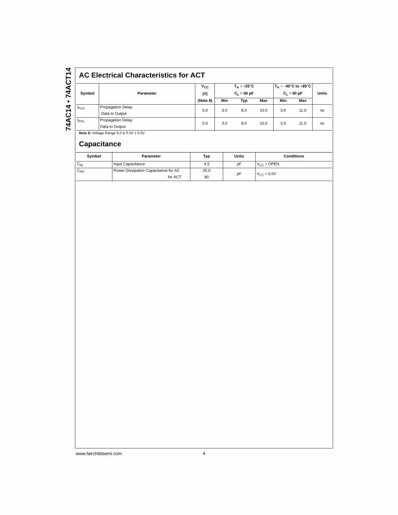
T14 AC Electrical Characteristics for ACT
Note 8: Voltage Range 5.0 is 5.0V ± 0.5V
Capacitance
Symbol Parameter
VCC TA = +25°C TA = −40°C to +85°C
Units(V) CL = 50 pF CL = 50 pF
(Note 8) Min Typ Max Min Max
tPLH Propagation Delay5.0 3.0 8.0 10.0 3.0 11.0 ns
Data to Output
tPHL Propagation Delay5.0 3.0 8.0 10.0 3.0 11.0 ns
Data to Output
Symbol Parameter Typ Units Conditions
CIN Input Capacitance 4.5 pF VCC = OPEN
CPD Power Dissipation Capacitance for AC 25.0pF VCC = 5.0V
for ACT 80
5 www.fairchildsemi.com
74AC
14 • 74AC
T14
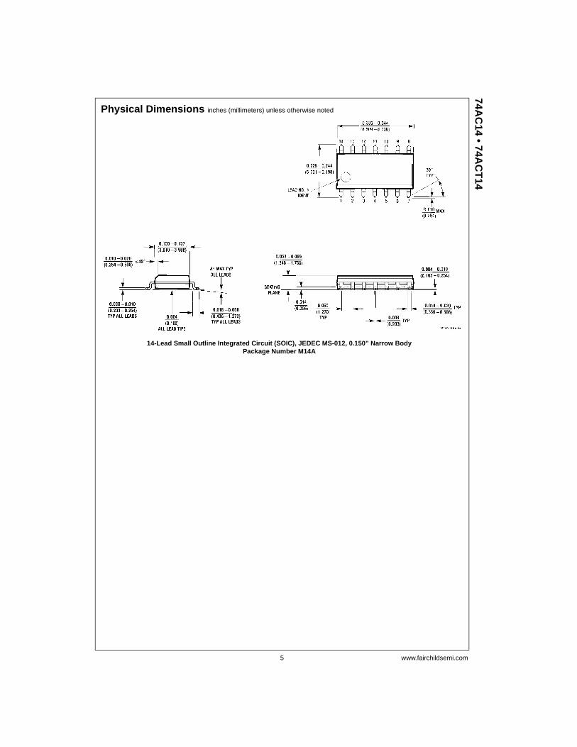
Physical Dimensions inches (millimeters) unless otherwise noted
14-Lead Small Outline Integrated Circuit (SOIC), JEDEC MS-012, 0.150” Narrow BodyPackage Number M14A
www.fairchildsemi.com 6
74A
C14
• 7
4AC
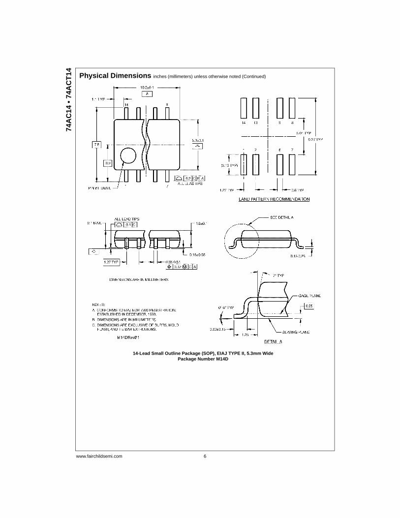
T14 Physical Dimensions inches (millimeters) unless otherwise noted (Continued)
14-Lead Small Outline Package (SOP), EIAJ TYPE II, 5.3mm WidePackage Number M14D

7 www.fairchildsemi.com
74AC
14 • 74AC
T14
Physical Dimensions inches (millimeters) unless otherwise noted (Continued)
14-Lead Thin Shrink Small Outline Package (TSSOP), JEDEC MO-153, 4.4mm WidePackage Number MTC14
www.fairchildsemi.com 8
74A
C14
• 7
4AC
T14
Hex
Inve
rter
wit
h S
chm
itt
Trig
ger
Inp
ut
Physical Dimensions inches (millimeters) unless otherwise noted (Continued)
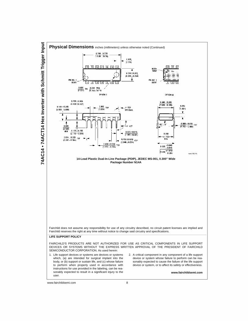
14-Lead Plastic Dual-In-Line Package (PDIP), JEDEC MS-001, 0.300” WidePackage Number N14A
Fairchild does not assume any responsibility for use of any circuitry described, no circuit patent licenses are implied andFairchild reserves the right at any time without notice to change said circuitry and specifications.
LIFE SUPPORT POLICY
FAIRCHILD’S PRODUCTS ARE NOT AUTHORIZED FOR USE AS CRITICAL COMPONENTS IN LIFE SUPPORTDEVICES OR SYSTEMS WITHOUT THE EXPRESS WRITTEN APPROVAL OF THE PRESIDENT OF FAIRCHILDSEMICONDUCTOR CORPORATION. As used herein:
1. Life support devices or systems are devices or systemswhich, (a) are intended for surgical implant into thebody, or (b) support or sustain life, and (c) whose failureto perform when properly used in accordance withinstructions for use provided in the labeling, can be rea-sonably expected to result in a significant injury to theuser.
2. A critical component in any component of a life supportdevice or system whose failure to perform can be rea-sonably expected to cause the failure of the life supportdevice or system, or to affect its safety or effectiveness.
www.fairchildsemi.com

4.4 74AC245
© 1999 Fairchild Semiconductor Corporation DS009944 www.fairchildsemi.com
November 1988
Revised November 1999
74AC
245 • 74AC
T245 O
ctal Bid
irection
al Transceiver w
ith 3-S
TAT
E
74AC245 • 74ACT245Octal Bidirectional Transceiver with 3-STATEInputs/Outputs
General DescriptionThe AC/ACT245 contains eight non-inverting bidirectionalbuffers with 3-STATE outputs and is intended for bus-ori-ented applications. Current sinking capability is 24 mA atboth the A and B ports. The Transmit/Receive (T/R) inputdetermines the direction of data flow through the bidirec-tional transceiver. Transmit (active-HIGH) enables datafrom A ports to B ports; Receive (active-LOW) enablesdata from B ports to A ports. The Output Enable input,when HIGH, disables both A and B ports by placing them ina HIGH Z condition.
Features ICC and IOZ reduced by 50%
Noninverting buffers
Bidirectional data path
A and B outputs source/sink 24 mA
ACT245 has TTL-compatible inputs
Ordering Code:
Device also available in Tape and Reel. Specify by appending suffix letter “X” to the ordering code.
FACT is a trademark of Fairchild Semiconductor Corporation.
Order Number Package Number Package Description
74AC245SC M20B 20-Lead Small Outline Integrated Circuit (SOIC), JEDEC MS-013, 0.300” Wide Body
74AC245SJ M20D 20-Lead Small Outline Package (SOP), EIAJ TYPE II, 5.3mm Wide
74AC245MTC MTC20 20-Lead Thin Shrink Small Outline Package (TSSOP), JEDEC MO-153, 4.4mm Wide
74AC245PC N20A 20-Lead Plastic Dual-In-Line Package (PDIP), JEDEC MS-001, 0.300” Wide
74ACT245SC M20B 20-Lead Small Outline Integrated Circuit (SOIC), JEDEC MS-013, 0.300” Wide Body
74ACT245SJ M20D 20-Lead Small Outline Package (SOP), EIAJ TYPE II, 5.3mm Wide
74ACT245MSA MSA20 20-Lead Shrink Small Outline Package (SSOP), EIAJ TYPE II, 5.3mm Wide
74ACT245MTC MTC20 20-Lead Thin Shrink Small Outline Package (TSSOP), JEDEC MO-153, 4.4mm Wide
74ACT245PC N20A 20-Lead Plastic Dual-In-Line Package (PDIP), JEDEC MS-001, 0.300” Wide
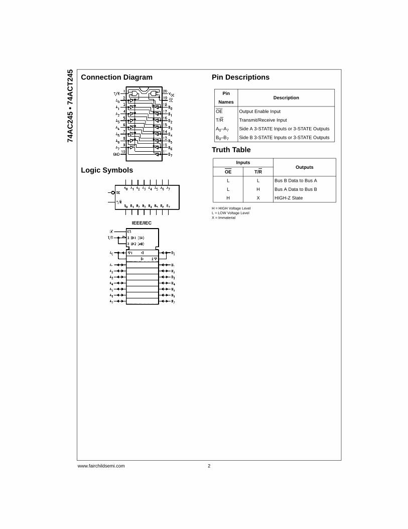
www.fairchildsemi.com 2
74A
C24
5 •
74A
CT
245
Connection Diagram
Logic Symbols
IEEE/IEC
Pin Descriptions
Truth Table
H = HIGH Voltage LevelL = LOW Voltage LevelX = Immaterial
PinDescription
Names
OE Output Enable Input
T/R Transmit/Receive Input
A0–A7 Side A 3-STATE Inputs or 3-STATE Outputs
B0–B7 Side B 3-STATE Inputs or 3-STATE Outputs
InputsOutputs
OE T/R
L L Bus B Data to Bus A
L H Bus A Data to Bus B
H X HIGH-Z State
3 www.fairchildsemi.com
74AC
245 • 74AC
T245
Absolute Maximum Ratings(Note 1) Recommended OperatingConditions
Note 1: Absolute maximum ratings are those values beyond which damageto the device may occur. The databook specifications should be met, with-out exception, to ensure that the system design is reliable over its powersupply, temperature, and output/input loading variables. Fairchild does notrecommend operation of FACT circuits outside databook specifications.
DC Electrical Characteristics for AC
Note 2: All outputs loaded; thresholds on input associated with output under test.
Note 3: Maximum test duration 2.0 ms, one output loaded at a time.
Note 4: IIN and ICC @ 3.0V are guaranteed to be less than or equal to the respective limit @ 5.5V VCC.
Supply Voltage (VCC) −0.5V to +7.0V
DC Input Diode Current (IIK)
VI = −0.5V −20 mA
VI = VCC + 0.5V +20 mA
DC Input Voltage (VI) −0.5V to VCC + 0.5V
DC Output Diode Current (IOK)
VO = −0.5V −20 mA
VO = VCC + 0.5V +20 mA
DC Output Voltage (VO) −0.5V to VCC + 0.5V
DC Output Source
or Sink Current (IO) ±50 mA
DC VCC or Ground Current
per Output Pin (ICC or IGND) ±50 mA
Storage Temperature (TSTG) −65°C to +150°CJunction Temperature (TJ)
PDIP 140°C
Supply Voltage (VCC)
AC 2.0V to 6.0V
ACT 4.5V to 5.5V
Input Voltage (VI) 0V to VCC
Output Voltage (VO) 0V to VCC
Operating Temperature (TA) −40°C to +85°CMinimum Input Edge Rate (∆V/∆t)
AC Devices
VIN from 30% to 70% of VCC
VCC @ 3.3V, 4.5V, 5.5V 125 mV/ns
Minimum Input Edge Rate (∆V/∆t)
ACT Devices
VIN from 0.8V to 2.0V
VCC @ 4.5V, 5.5V 125 mV/ns
Symbol ParameterVCC(V)
TA = +25°C TA = −40°C to +85°CUnits Conditions
Typ Guaranteed Limits
VIH Minimum HIGH Level 3.0 1.5 2.1 2.1 VOUT = 0.1V
Input Voltage 4.5 2.25 3.15 3.15 V or VCC − 0.1V
5.5 2.75 3.85 3.85
VIL Maximum LOW Level 3.0 1.5 0.9 0.9 VOUT = 0.1V
Input Voltage 4.5 2.25 1.35 1.35 V or VCC − 0.1V
5.5 2.75 1.65 1.65
VOH Minimum HIGH Level 3.0 2.99 2.9 2.9
Output Voltage 4.5 4.49 4.4 4.4 V IOUT = −50 µA
5.5 5.49 5.4 5.4
VIN = VIL or VIH
3.0 2.56 2.46 IOH = −12 mA
4.5 3.86 3.76 V IOH = −24 mA
5.5 4.86 4.76 IOH = −24 mA (Note 2)
VOL Maximum LOW Level 3.0 0.002 0.1 0.1
Output Voltage 4.5 0.001 0.1 0.1 V IOUT = 50 µA
5.5 0.001 0.1 0.1
VIN = VIL or VIH
3.0 0.36 0.44 IOL = 12 mA
4.5 0.36 0.44 V IOL = 24 mA
5.5 0.36 0.44 IOL = 24 mA (Note 2)
IIN (Note 4) Maximum Input Leakage Current 5.5 ± 0.1 ± 1.0 µA VI = VCC, GND
IOLD Dynamic Output 5.5 75 mA VOLD = 1.65V Max
IOHD Current Minimum (Note 3) 5.5 −75 mA VOHD = 3.85V Min
ICC (Note 4) Maximum Quiescent Supply Current 5.5 4.0 40.0 µA VIN = VCC or GND
IOZT Maximum I/O VI (OE) = VIL, VIH
Leakage Current 5.5 ± 0.3 ± 3.0 µA VI = VCC, GND
VO = VCC, GND
www.fairchildsemi.com 4
74A
C24
5 •
74A
CT
245
DC Characteristics for ACT
Note 5: All outputs loaded; thresholds on input associated with output under test.
Note 6: Maximum test duration 2.0 ms, one output loaded at a time.
AC Electrical Characteristics for AC
Note 7: Voltage Range 3.3 is 3.3V ± 0.3VVoltage Range 5.0 is 5.0V ± 0.5V
Symbol ParameterVCC TA = +25°C TA = −40°C to +85°C
Units Conditions(V) Typ Guaranteed Limits
VIH Minimum HIGH Level 4.5 1.5 2.0 2.0V
VOUT = 0.1V
Input Voltage 5.5 1.5 2.0 2.0 or VCC − 0.1V
VIL Maximum LOW Level 4.5 1.5 0.8 0.8V
VOUT = 0.1V
Input Voltage 5.5 1.5 0.8 0.8 or VCC − 0.1V
VOH Minimum HIGH Level 4.5 4.49 4.4 4.4V IOUT = −50 µA
Output Voltage 5.5 5.49 5.4 5.4
VIN = VIL or VIH
4.5 3.86 3.76 IOH = −24 mA
5.5 4.86 4.76 V IOH = −24 mA (Note 5)
VOL Maximum LOW Level 4.5 0.001 0.1 0.1V IOUT = 50 µA
Output Voltage 5.5 0.001 0.1 0.1
VIN = VIL or VIH
4.5 0.36 0.44V
IOL = 24 mA
5.5 0.36 0.44 IOL = 24 mA (Note 5)
IIN Maximum Input 5.5 ±0.1 ±1.0 µA VI = VCC, GND
Leakage Current
ICCT Maximum5.5 0.6 1.5 mA VI = VCC − 2.1V
ICC/Input
IOLD Dynamic Output 5.5 75 mA VOLD = 1.65V Max
IOHD Current Minimum (Note 6) 5.5 −75 mA VOHD = 3.85V Min
ICC Maximum Quiescent5.5 4.0 40.0 µA
VIN = VCC
Supply Current or GND
IOZT Maximum I/O VI (OE) = VIL, VIH
Leakage Current 5.5 ±0.3 ±3.0 µA VI = VCC, GND
VO = VCC, GND
VCC TA = +25°C TA = −40°C to +85°C
Symbol Parameter (V) CL = 50 pF CL = 50 pF Units
(Note 7) Min Typ Max Min Max
tPLH Propagation Delay 3.3 1.5 5.0 8.5 1.0 9.0ns
An to Bn or Bn to An 5.0 1.5 3.5 6.5 1.0 7.0
tPHL Propagation Delay 3.3 1.5 5.0 8.5 1.0 9.0ns
An to Bn or Bn to An 5.0 1.5 3.5 6.0 1.0 7.0
tPZH Output Enable Time 3.3 2.5 7.0 11.5 2.0 12.5ns
5.0 1.5 5.0 8.5 1.0 9.0
tPZL Output Enable Time 3.3 2.5 7.5 12.0 2.0 13.5ns
5.0 1.5 5.5 9.0 1.0 9.5
tPHZ Output Disable Time 3.3 2.0 6.5 12.0 1.0 12.5ns
5.0 1.5 5.5 9.0 1.0 10.0
tPLZ Output Disable Time 3.3 2.0 7.0 11.5 1.5 13.0ns
5.0 1.5 5.5 9.0 1.0 10.0
5 www.fairchildsemi.com
74AC
245 • 74AC
T245
AC Electrical Characteristics for ACT
Note 8: Voltage Range 5.0 is 5.0V ± 0.5V
Capacitance
VCC TA = +25°C TA = −40°C to +85°C
Symbol Parameter (V) CL = 50 pF CL = 50 pF Units
(Note 8) Min Typ Max Min Max
tPLH Propagation Delay5.0 1.5 4.0 7.5 1.5 8.0 ns
An to Bn or Bn to An
tPHL Propagation Delay5.0 1.5 4.0 8.0 1.0 9.0 ns
An to Bn or Bn to An
tPZH Output Enable Time 5.0 1.5 5.0 10.0 1.5 11.0 ns
tPZL Output Enable Time 5.0 1.5 5.5 10.0 1.5 12.0 ns
tPHZ Output Disable Time 5.0 1.5 5.5 10.0 1.0 11.0 ns
tPLZ Output Disable Time 5.0 2.0 5.0 10.0 1.5 11.0 ns
Symbol Parameter Typ Units Conditions
CIN Input Capacitance 4.5 pF VCC = OPEN
CI/O Input/Output Capacitance 15.0 pF VCC = 5.0V
CPD Power Dissipation Capacitance 45.0 pF VCC = 5.0V
www.fairchildsemi.com 6
74A
C24
5 •
74A
CT
245
Physical Dimensions inches (millimeters) unless otherwise noted
20-Lead Small Outline Integrated Circuit (SOIC), JEDEC MS-013, 0.300” Wide BodyPackage Number M20B
7 www.fairchildsemi.com
74AC
245 • 74AC
T245
Physical Dimensions inches (millimeters) unless otherwise noted (Continued)
20-Lead Small Outline Package (SOP), EIAJ TYPE II, 5.3mm WidePackage Number M20D
www.fairchildsemi.com 8
74A
C24
5 •
74A
CT
245
Physical Dimensions inches (millimeters) unless otherwise noted (Continued)
20-Lead Shrink Small Outline Package (SSOP), EIAJ TYPE II, 5.3mm WidePackage Number MSA20
9 www.fairchildsemi.com
74AC
245 • 74AC
T245
Physical Dimensions inches (millimeters) unless otherwise noted (Continued)
20-Lead Thin Shrink Small Outline Package, (TSSOP) JEDECPackage Number MTC20
www.fairchildsemi.com 10
74A
C24
5 •
74A
CT
245
Oct
al B
idir
ecti
on
al T
ran
scei
ver
wit
h 3
-STA
TE
Physical Dimensions inches (millimeters) unless otherwise noted (Continued)
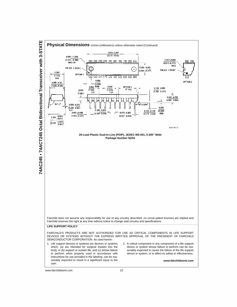
20-Lead Plastic Dual-In-Line (PDIP), JEDEC MS-001, 0.300” WidePackage Number N20A
Fairchild does not assume any responsibility for use of any circuitry described, no circuit patent licenses are implied andFairchild reserves the right at any time without notice to change said circuitry and specifications.
LIFE SUPPORT POLICY
FAIRCHILD’S PRODUCTS ARE NOT AUTHORIZED FOR USE AS CRITICAL COMPONENTS IN LIFE SUPPORTDEVICES OR SYSTEMS WITHOUT THE EXPRESS WRITTEN APPROVAL OF THE PRESIDENT OF FAIRCHILDSEMICONDUCTOR CORPORATION. As used herein:
1. Life support devices or systems are devices or systemswhich, (a) are intended for surgical implant into thebody, or (b) support or sustain life, and (c) whose failureto perform when properly used in accordance withinstructions for use provided in the labeling, can be rea-sonably expected to result in a significant injury to theuser.
2. A critical component in any component of a life supportdevice or system whose failure to perform can be rea-sonably expected to cause the failure of the life supportdevice or system, or to affect its safety or effectiveness.
www.fairchildsemi.com

4.5 AN1095
Design of IsolatedConverters Using SimpleSwitchersINTRODUCTION
Isolated converters are required to provide electrical isola-tion between two interrelated systems. Isolation between thepower source and the load is required in certain applicationsin order to meet safety specifications such as UL1459, whichnecessitates 500V of isolation for telecom applications.
Isolation must be provided between all the input and outputstages of the power converter. Thus, isolation must be pro-vided in the power stage and the control loop. Power stageisolation is generally provided using transformer. Isolation inthe feedback/control loop is often provided through an opto-coupler (also known as opto-isolator).
Transformers are well suited for power stage isolation, sincethey are known for providing good dielectric barrier betweentwo systems, with the ability to have multiple outputs. Trans-formers also allow stepping up or stepping down of the inputvoltage.
In isolated switching power supplies, opto-couplers are verywidely used to provide isolation in the feedback loop. Opto-couplers do an excellent job of isolation, minimizing circuitcomplexity and reducing cost. One of the disadvantages ofusing an opto-coupler is its low bandwidth. The bandwidth ofthe converter is reduced by the introduction of an extra polein the control loop gain of the converter. This is not a problemin conventional low frequency converters. However, in mod-ern high-frequency converters, the opto-coupler imposes se-vere restrictions on control loop bandwidth/speed.
Another disadvantage of using opto-isolator is the large unit-to-unit variation in the current transfer ratio (CTR). CTR orthe coupling efficiency is defined as the ratio of opto-isolatortransistor collector current to the diode current. The loopgain is directly proportional to CTR gain. Hence, high varia-tion in CTR imposes constraints on control loop design.
PART I. DESIGN OF OPTO-ISOLATED POWER SUPPLY
Design Approach
With the advent of SIMPLE SWITCHER™, and the associ-ated “Switchers Made Simple” software (SMS4.2.1,SMS3.3), the non-isolated converter design has becomevery simple. However, the non-isolated converters can bemodified to isolated converters very easily. The procedurefor design of opto-isolated converter is as follows:
Step 1: Design the power stage components for a flybackconverter using SMS4.2.1/3.3. The “Switchers Made Simple”software can be used to design the transformer, input/outputcapacitors, output rectifier, clamping network, etc.
Step 2: Modify the feedback/control loop by introducing asecondary side controller (such as LM3411) and an opto-isolator for feedback isolation. Also, disable the internal ref-erence in the Simple Switcher.
Design of Power Stage Components
The first step in the design process is to enter the converterspecifications (shown in Table 1) in the input menu of the“Switchers Made Simple” software. Using these specifica-
tions, the software will design the power stage components.The following example will be based on Switchers MadeSimple 4.2.1 (SMS4.2.1) and the associated LM258X fly-back converters.
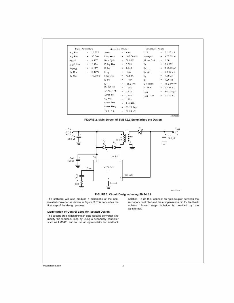
If the input specifications are entered as shown in Figure 1,SMS4.2 will design a buck converter instead of flyback. In or-der to design a flyback converter when the output voltage islower than input voltage levels, it is necessary to enter ini-tially a fictitious output voltage value which is greater thanVIN(min). The software will then design a flyback. Now, go tothe main menu and change input requirements. Change thefictitious output voltage value to the required value. If the out-put voltage is greater than the minimum input voltage, theseextra steps are not necessary.
TABLE 1. Isolated Power Converter Specifications(Example)
Input Voltage 10V to 30V
Output Voltage 5V
Load (maximum) 2A
Operating Temp. Range 0˚C to 70˚C
Modify the component values, input specs, etc. to suit the re-quirements. The software will design all the power stagecomponents and give a list of vendors. In the exampleshown in Figure 2, the component values were enteredmanually to produce a surface mount design.
The isolation voltage of the transformer is not listed in thesoftware. The isolation voltage is generally mentioned in thetransformer manufacturer’s catalog. Select a transformertaking into consideration the isolation voltage. Any of thetransformers listed in the LM258X Simple Switcher datasheets meet UL1459 spec, and are suitable for telecomapplications.
SIMPLE SWITCHER® is a registered trademark of National Semiconductor Corporation
AN100151-1
FIGURE 1. Enter the Converter Specifications in theInput Menu of SMS4.2.1
National SemiconductorApplication Note 1095Ravindra AmbatipudiAugust 1998
Design
ofIsolatedC
onvertersU
singS
imple
Sw
itchersA
N-1095
© 1998 National Semiconductor Corporation AN100151 www.national.com
The software will also produce a schematic of the non-isolated converter as shown in Figure 3. This concludes thefirst step of the design process.
Modification of Control Loop for Isolated Design
The second step in designing an opto-isolated converter is tomodify the feedback loop by using a secondary controllersuch as LM3411 and to use an opto-isolator for feedback
isolation. To do this, connect an opto-coupler between thesecondary controller and the compensation pin for feedbackisolation. Power stage isolation is provided by thetransformer.
AN100151-2
FIGURE 2. Main Screen of SMS4.2.1 Summarizes the Design
AN100151-3
FIGURE 3. Circuit Designed using SMS4.2.1
www.national.com 2
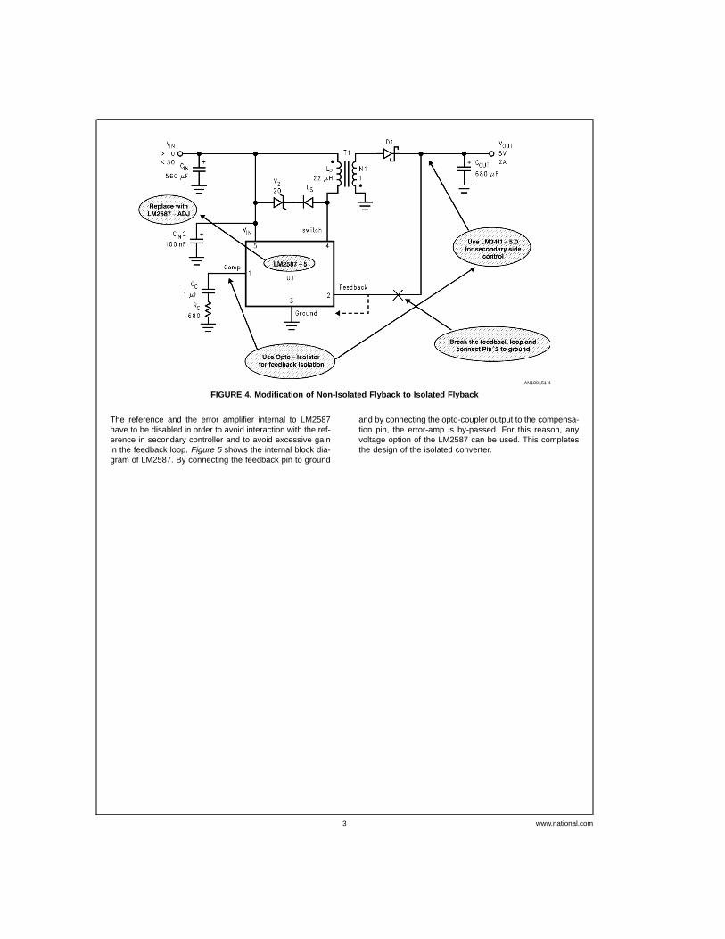
The reference and the error amplifier internal to LM2587have to be disabled in order to avoid interaction with the ref-erence in secondary controller and to avoid excessive gainin the feedback loop. Figure 5 shows the internal block dia-gram of LM2587. By connecting the feedback pin to ground
and by connecting the opto-coupler output to the compensa-tion pin, the error-amp is by-passed. For this reason, anyvoltage option of the LM2587 can be used. This completesthe design of the isolated converter.
AN100151-4
FIGURE 4. Modification of Non-Isolated Flyback to Isolated Flyback
www.national.com3
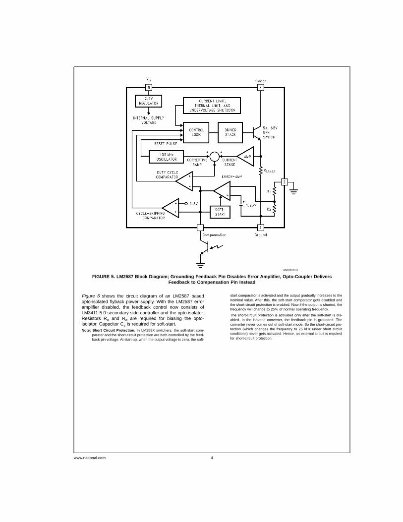
Figure 6 shows the circuit diagram of an LM2587 basedopto-isolated flyback power supply. With the LM2587 erroramplifier disabled, the feedback control now consists ofLM3411-5.0 secondary side controller and the opto-isolator.Resistors Ro and Rd are required for biasing the opto-isolator. Capacitor Cs is required for soft-start.Note: Short Circuit Protection. In LM258X switchers, the soft-start com-
parator and the short-circuit protection are both controlled by the feed-back pin voltage. At start-up, when the output voltage is zero, the soft-
start comparator is activated and the output gradually increases to thenominal value. After this, the soft-start comparator gets disabled andthe short-circuit protection is enabled. Now if the output is shorted, thefrequency will change to 25% of normal operating frequency.
The short-circuit protection is activated only after the soft-start is dis-abled. In the isolated converter, the feedback pin is grounded. Theconverter never comes out of soft-start mode. So the short-circuit pro-tection (which changes the frequency to 25 kHz under short circuitconditions) never gets activated. Hence, an external circuit is requiredfor short-circuit protection.
AN100151-5
FIGURE 5. LM2587 Block Diagram; Grounding Feedback Pin Disables Error Amplifier, Opto-Coupler DeliversFeedback to Compensation Pin Instead
www.national.com 4
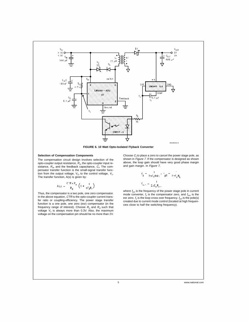
Selection of Compensation Components
The compensation circuit design involves selection of theopto-coupler output resistance, Ro, the opto-coupler input re-sistance, Rd, and the feedback capacitance, Cf. The com-pensator transfer function is the small-signal transfer func-tion from the output voltage, VO to the control voltage, Vc.The transfer function, A(s) is given by:
Thus, the compensator is a two pole, one zero compensator.In the above equation, CTR is the opto-coupler current trans-fer ratio or coupling-efficiency. The power stage transferfunction is a one pole, one zero (esr) compensator (in thefrequency range of interest). Choose Ro and Rd such thatvoltage Vc is always more than 0.3V. Also, the maximumvoltage on the compensation pin should be no more than 2V.
Choose Cf to place a zero to cancel the power stage pole, asshown in Figure 7. If the compensator is designed as shownabove, the loop gain should have very good phase marginand gain margin. In Figure 7,
where fp1 is the frequency of the power stage pole in currentmode converter, fz is the compensator zero, and fesr is theesr zero. fc is the loop cross over frequency. fp2 is the pole(s)created due to current mode control (located at high frequen-cies close to half the switching frequency).
AN100151-6
FIGURE 6. 10 Watt Opto-Isolated Flyback Converter
www.national.com5
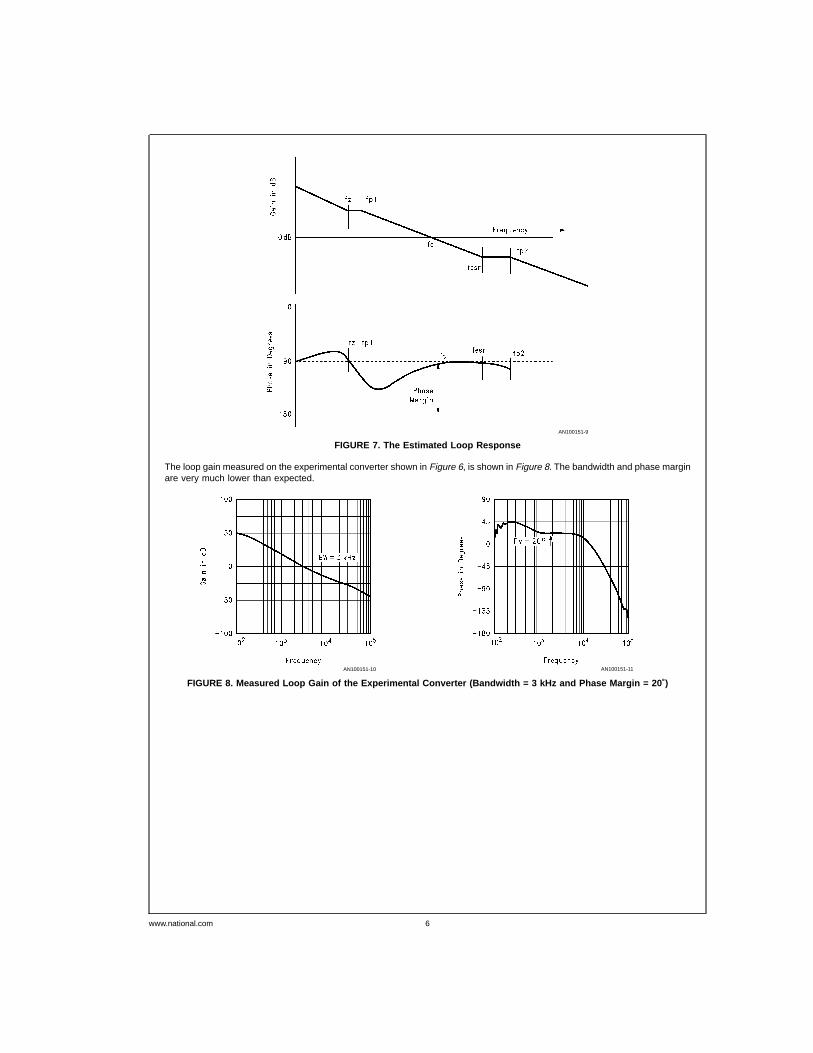
The loop gain measured on the experimental converter shown in Figure 6, is shown in Figure 8. The bandwidth and phase marginare very much lower than expected.
AN100151-9
FIGURE 7. The Estimated Loop Response
AN100151-10 AN100151-11
FIGURE 8. Measured Loop Gain of the Experimental Converter (Bandwidt h = 3 kHz and Phase Margin = 20˚)
www.national.com 6
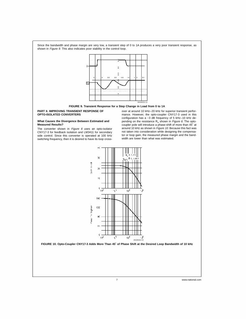
Since the bandwidth and phase margin are very low, a transient step of 0 to 1A produces a very poor transient response, asshown in Figure 9. This also indicates poor stability in the control loop.
PART II. IMPROVING TRANSIENT RESPONSE OFOPTO-ISOLATED CONVERTERS
What Causes the Divergence Between Estimated andMeasured Results?
The converter shown in Figure 6 uses an opto-isolatorCNY17-3 for feedback isolation and LM3411 for secondaryside control. Since this converter is operated at 100 kHzswitching frequency, then it is desired to have its loop cross-
over at around 10 kHz–20 kHz for superior transient perfor-mance. However, the opto-coupler CNY17-3 used in thisconfiguration has a −3 dB frequency of 5 kHz–10 kHz de-pending on the resistance Ro shown in Figure 6. The opto-coupler pole will introduce a phase-shift of more than 45˚ ataround 10 kHz as shown in Figure 10. Because this fact wasnot taken into consideration while designing the compensa-tor or loop gain, the measured phase margin and the band-width are lower than what was estimated.
AN100151-12
FIGURE 9. Transient Response for a Step Change in Load from 0 to 1A
AN100151-13
FIGURE 10. Opto-Coupler CNY17-3 Adds More Than 45˚ of Phase Shift at the Desired Loop Bandwidth of 10 kHz
www.national.com7
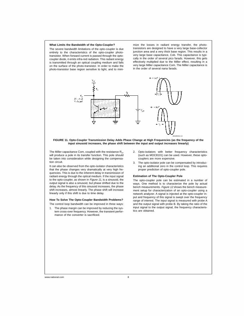
What Limits the Bandwidth of the Opto-Coupler?
The severe bandwidth limitations of the opto-coupler is dueentirely to the characteristics of the opto-coupler photo-transistor. When forward current is passed through the opto-coupler diode, it emits infra-red radiation. This radiant energyis transmitted through an optical coupling medium and fallson the surface of the photo-transistor. In order to make thephoto-transistor base region sensitive to light, and to mini-
mize the losses in radiant energy transfer, the photo-transistors are designed to have a very large base-collectorjunction area and a very thick base region. This results in avery large base capacitance, Cob. This capacitance is typi-cally in the order of several pico farads. However, this getseffectively multiplied due to the Miller effect, resulting in avery large Miller capacitance Com. The Miller capacitance isin the order of several nana farads.
The Miller capacitance Com, coupled with the resistance Ro,will produce a pole in its transfer function. This pole shouldbe taken into consideration while designing the compensa-tion circuit.
It can also be observed from the opto-isolator characteristicsthat the phase changes very dramatically at very high fre-quencies. This is due to the inherent delay in transmission ofradiant energy through the optical medium. If the input signalto the opto-coupler, as shown in Figure 11, is a sinusoid, theoutput signal is also a sinusoid, but phase shifted due to thedelay. As the frequency of this sinusoid increases, the phaseshift increases, almost linearly. The phase shift will increaselinearly only if this shift is due to time delay.
How To Solve The Opto-Coupler Bandwidth Problems?
The control loop bandwidth can be improved in three ways:
1. The phase margin can be improved by reducing the sys-tem cross-over frequency. However, the transient perfor-mance of the converter is sacrificed.
2. Opto-isolators with better frequency characteristics(such as MOC8101) can be used. However, these opto-couplers are more expensive.
3. The opto-isolator pole can be compensated by introduc-ing an additional zero in the control loop. This requiresproper prediction of opto-coupler pole.
Estimation of The Opto-Coupler Pole
The opto-coupler pole can be estimated in a number ofways. One method is to characterize the pole by actualbench measurements. Figure 12 shows the bench measure-ment setup for characterization of an opto-coupler using anetwork analyzer. A signal is injected at the opto-coupler in-put and frequency of this signal is swept over the frequencyrange of interest. The input signal is measured with probe Aand the output signal with probe B. By taking the ratio of theinput signal to the output signal, the frequency characteris-tics are obtained.
AN100151-14
FIGURE 11. Opto-Coupler Transmission Delay Adds Phase Change at High Frequencies (as the frequency of theinput sinusoid increases, the phase shift between the input and output increases linearly)
www.national.com 8
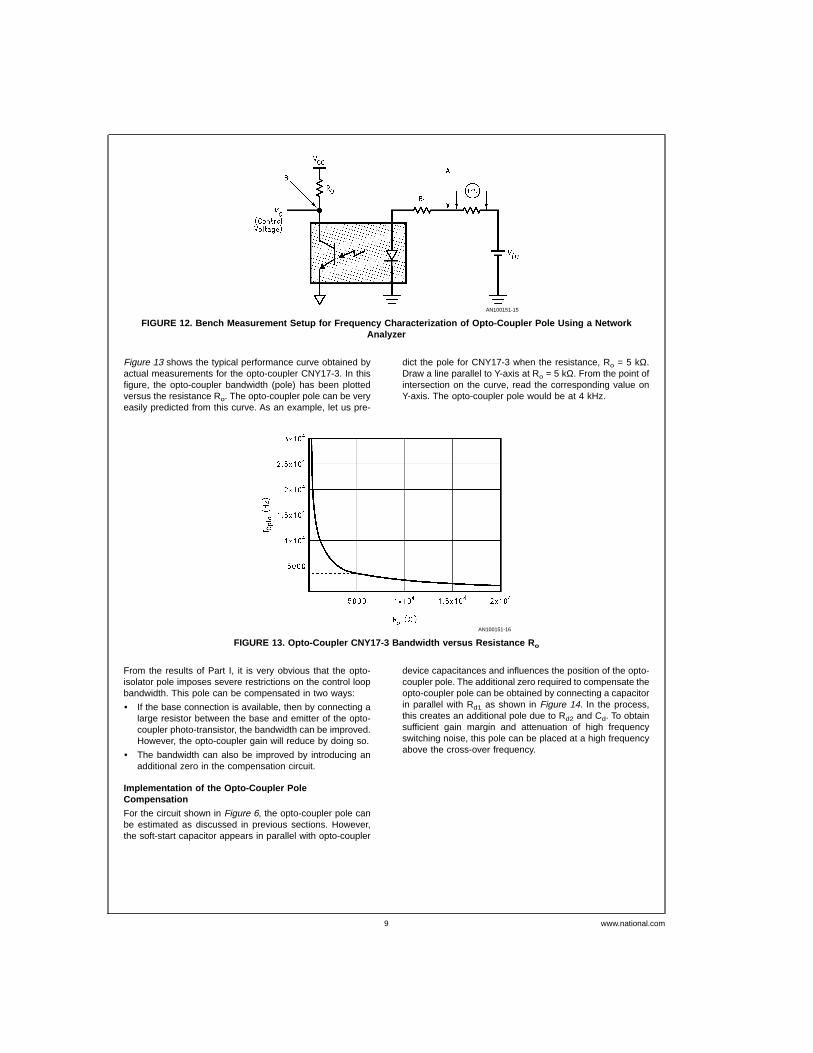
Figure 13 shows the typical performance curve obtained byactual measurements for the opto-coupler CNY17-3. In thisfigure, the opto-coupler bandwidth (pole) has been plottedversus the resistance Ro. The opto-coupler pole can be veryeasily predicted from this curve. As an example, let us pre-
dict the pole for CNY17-3 when the resistance, Ro = 5 kΩ.Draw a line parallel to Y-axis at Ro = 5 kΩ. From the point ofintersection on the curve, read the corresponding value onY-axis. The opto-coupler pole would be at 4 kHz.
From the results of Part I, it is very obvious that the opto-isolator pole imposes severe restrictions on the control loopbandwidth. This pole can be compensated in two ways:
• If the base connection is available, then by connecting alarge resistor between the base and emitter of the opto-coupler photo-transistor, the bandwidth can be improved.However, the opto-coupler gain will reduce by doing so.
• The bandwidth can also be improved by introducing anadditional zero in the compensation circuit.
Implementation of the Opto-Coupler PoleCompensation
For the circuit shown in Figure 6, the opto-coupler pole canbe estimated as discussed in previous sections. However,the soft-start capacitor appears in parallel with opto-coupler
device capacitances and influences the position of the opto-coupler pole. The additional zero required to compensate theopto-coupler pole can be obtained by connecting a capacitorin parallel with Rd1 as shown in Figure 14. In the process,this creates an additional pole due to Rd2 and Cd. To obtainsufficient gain margin and attenuation of high frequencyswitching noise, this pole can be placed at a high frequencyabove the cross-over frequency.
AN100151-15
FIGURE 12. Bench Measurement Setup for Frequency Characterization of Opto-Coupler Pole Using a NetworkAnalyzer
AN100151-16
FIGURE 13. Opto-Coupler CNY17-3 Bandwidth versus Resistance R o
www.national.com9
The modified compensator transfer function is:
where:
CTR = Opto-coupler current transfer ratio or coupling effi-ciency
Rf = feedback resistor internal to LM3411 (92k forLM3411-5.0)
Cc = Compensation capacitor
An additional zero can also be obtained by connecting a re-sistor in series with capacitor Cs, the additional zero requiredto compensate the opto-coupler pole can be placed at a fre-quency equal to fz.
(Assuming Cs is very much larger than the opto-couplerMiller capacitance).
Notice that the compensator transfer function is directly de-pendent on the opto-coupler CTR, which varies from unit-to-unit, so it is important to take this factor into consideration.This means that an opto-coupler with low CTR variation andguaranteed limits should be used.
Figure 15 shows the loop gain with modified compensator.Significant improvement in bandwidth and phase margin areobserved. The loop gain is as expected and shows excellentstability. As expected, the transient response is also im-proved, as shown in Figure 16.
AN100151-17
FIGURE 14. Compensating the Opto-Coupler Pole to Improve the Bandwidth Limitations
www.national.com 10
AN100151-20 AN100151-21
FIGURE 15. Significant Improvement in Bandwidth and Phase Margin is Observed with Opto-Coupler PoleCompensation (Bandwidth = 10 kHz and Phase Margin = 60˚)
AN100151-22
FIGURE 16. Transient Response with Opto-Coupler Pole Compensation (0 to 1A Step-Change in Load)
www.national.com11
LIFE SUPPORT POLICY
NATIONAL’S PRODUCTS ARE NOT AUTHORIZED FOR USE AS CRITICAL COMPONENTS IN LIFE SUPPORT DE-VICES OR SYSTEMS WITHOUT THE EXPRESS WRITTEN APPROVAL OF THE PRESIDENT OF NATIONAL SEMI-CONDUCTOR CORPORATION. As used herein:1. Life support devices or systems are devices or sys-
tems which, (a) are intended for surgical implant intothe body, or (b) support or sustain life, and whose fail-ure to perform when properly used in accordancewith instructions for use provided in the labeling, canbe reasonably expected to result in a significant injuryto the user.
2. A critical component in any component of a life supportdevice or system whose failure to perform can be rea-sonably expected to cause the failure of the life supportdevice or system, or to affect its safety or effectiveness.
National SemiconductorCorporationAmericasTel: 1-800-272-9959Fax: 1-800-737-7018Email: [email protected]
www.national.com
National SemiconductorEurope
Fax: +49 (0) 1 80-530 85 86Email: [email protected]
Deutsch Tel: +49 (0) 1 80-530 85 85English Tel: +49 (0) 1 80-532 78 32Français Tel: +49 (0) 1 80-532 93 58Italiano Tel: +49 (0) 1 80-534 16 80
National SemiconductorAsia Pacific CustomerResponse GroupTel: 65-2544466Fax: 65-2504466Email: [email protected]
National SemiconductorJapan Ltd.Tel: 81-3-5620-6175Fax: 81-3-5620-6179
AN
-109
5D
esig
nof
Isol
ated
Con
verte
rsU
sing
Sim
ple
Sw
itche
rs
National does not assume any responsibility for use of any circuitry described, no circuit patent licenses are implied and National reserves the right at any time without notice to change said circuitry and specifications.

4.6 CNY17
DESCRIPTIONThe CNY17 series consists of a Gallium Arsenide IREDcoupled with an NPN phototransistor.
CNY17-1 CNY17-3CNY17-2 CNY17-4
APPLICATIONS • Power supply regulators • Digital logic inputs• Microprocessor inputs • Appliance sensor systems• Industrial controls
FEATURES• CNY17-1/2/3 are also available in white package by specifying -M suffix (eg. CNY17-2-M)• UL recognized (File # E90700)• VDE recognized
-102497 for white package -Add option V for white package (e.g., CNY17-2V-M)-File #102497 -Add option ‘300’ for black package (e.g., CNY17-2.300)-File #94766
• Current transfer ratio in select groups• High BVCEO 70V minimum
1
2
6
5 COL
4 EMITTER
BASEANODE
CATHODE
3
SCHEMATIC
Parameters Symbol Device Value UnitsTOTAL DEVICE
TSTG All -55 to +150 °CStorage TemperatureOperating Temperature TOPR All -55 to +100 °CLead Solder Temperature TSOL All 260 for 10 sec °CTotal Device Power Dissipation @ 25°C (LED plus detector) -M 250
mWnon -M 260
Derate Linearly From 25°C PD -M 2.94mW/°C
non -M 3.50EMITTER
IF-M 60
mAContinuous Forward Current non -M 90Reverse Voltage VR All 6 V
Forward Current - Peak (1 µs pulse, 300 pps) IF(pk)-M 1.5
Anon -M 3.0
LED Power Dissipation 25°C Ambient -M 120mW
Derate Linearly From 25°C PDnon -M 135
-M 1.41mW/°C
non -M 1.8DETECTOR -M 150
mWDetector Power Dissipation @ 25°C
PDnon -M 200
Derate Linearly from 25°C -M 1.76mW/°C
non -M 2.67 2001 Fairchild Semiconductor CorporationDS300208 6/06/01 1 OF 11 www.fairchildsemi.com
WHITE PACKAGE (-M SUFFIX) BLACK PACKAGE (NO -M SUFFIX)
6
1
6
6
1
1
6
1
6
1
6
1
PHOTOTRANSISTOR OPTOCOUPLERS
Parameters Test Conditions Symbol Device Min Typ Max UnitsEMITTER IF = 60 mA -M 1.35 1.65
VInput Forward Voltage IF = 10 mA VF non -M 1.15 1.50
Capacitance VF = 0 V, f = 1.0 MHz CJnon -M 50
pF-M 18
Reverse Leakage Current VR = 6 V IR All 0.001 10 µADETECTOR
Breakdown VoltageCollector to Emitter IC = 1.0 mA, IF = 0 BVCEO All 70 100 V
Collector to Base IC = 10 µA, IF = 0 BVCBO All 70 120 VEmitter to Collector IE = 100 µA, IF = 0 BVECO All 7 10 VLeakage Current
Collector to Emitter VCE = 10 V, IF = 0 ICEO All 1 50 nA
Collector to Base VCB = 10 V, IF = 0 ICBO All 20 nACapacitance
pFCollector to Emitter VCE = 0, f = 1 MHz CCE All 8
Collector to Base VCB = 0, f = 1 MHz CCB All 20 pFEmitter to Base VEB = 0, f = 1 MHz CEB All 10 pF
INDIVIDUAL COMPONENT CHARACTERISTICS
ELECTRICAL CHARACTERISTICS (TA = 25°C Unless otherwise specified.)
www.fairchildsemi.com 2 OF 11 6/06/01 DS300208
PHOTOTRANSISTOR OPTOCOUPLERS
CNY17-1 CNY17-3CNY17-2 CNY17-4
Characteristic Test Conditions Symbol Device Min Typ** Max Units
Input-Output Isolation Voltage f = 60 Hz, t = 1 min. VISOBlack Package 5300 Vac(rms)*
‘-M’ White Package 7500 Vac(pk)Isolation Resistance VI-O = 500 VDC RISO All 1011 !
Isolation Capacitance VI-O = ", f = 1 MHz CISOBlack Package 0.5
pF‘-M’ White Package 0.2
ISOLATION CHARACTERISTICS
Note* 5300 Vac(rms) for 1 minute equates to approximately 9000 Vac (pk) for 1 second** Typical values at TA = 25°C
DC Characteristics Test Conditions Symbol Device Min Typ Max UnitsCNY17-1/-1-M 40 80
Current Transfer Ratio,IF = 10 mA, VCE = 5 V CTR
CNY17-2/-2-M 63 125%
Collector to Emitter CNY17-3/-3-M 100 200CNY17-4 160 320
Saturation Voltage IF = 10 mA, IC = 2.5 mA VCE(SAT) All .40 VAC Characteristics Test Conditions Symbol Device Min Typ Max UnitsNon-Saturated Switching Times
Turn-On Time (Fig.19 and Fig.20) RL = 100 Ω, IC = 2 mA, VCC = 10 V ton non -M 10 µs
Turn-Off Time (Fig.19 and Fig.20) RL = 100 Ω, IC = 2 mA, VCC = 10 V toff non -M 10 µsDelay Time (Fig.19 and Fig.20) IF = 10 mA, VCC = 5 V, RL = 75 Ω td -M 5.6 µsRise Time (Fig.19 and Fig.20) IF = 10 mA, VCC = 5 V, RL = 75 Ω tr -M 4.0 µsStorage Time (Fig.19 and Fig.20) IF = 10 mA, VCC = 5 V, RL = 75 Ω ts -M 4.1 µsFall Time (Fig.19 and Fig.20) IF = 10 mA, VCC = 5 V, RL = 75 Ω tf -M 3.5 µs
Saturated Switching Times IF = 20 mA, VCE = 0.4 V CNY17-1 5.5
Turn-On Time (Fig.19 and Fig.20) IF = 10 mA, VCE = 0.4 Vton CNY17-2, CNY17-3,
8.0µs
CNY17-4IF = 20 mA, VCE = 0.4 V CNY17-1 4.0
IF = 10 mA, VCE = 0.4 VCNY17-2, CNY17-3,
6.0Rise-Time (Fig.19 and Fig.20) CNY17-4 µs
IF = 20 mA, VCC = 5 V, RL = 1 KΩtr CNY17-1-M 4.0
IF = 10 mA, VCC = 5 V, RL = 1 KΩ CNY17-2-M,CNY17-3-M 6.0
Delay Time (Fig.19 and Fig.20)IF = 20 mA, VCC = 5 V, RL =1 KΩ
tdCNY17-1-M 5.5
µsIF = 10 mA, VCC = 5 V, RL =1 KΩ CNY17-2, CNY17-3 8.0
IF = 20 mA, VCE = 0.4 V CNY17-1 34.0Turn-Off Time (Fig.19 and Fig.20)
IF = 10 mA, VCE = 0.4 Vtoff CNY17-2, CNY17-3,
39.0µs
CNY17-4IF = 20 mA, VCE = 0.4 V CNY17-1 20.0
IF = 10 mA, VCE = 0.4 VCNY17-2, CNY17-3,
24.0Fall-Time (Fig.19 and Fig.20) tf CNY17-4 µs
IF = 20 mA, VCC = 5 V, RL =1 KΩ CNY17-1-M 20.0IF = 10 mA, VCC = 5 V, RL = 1 KΩ CNY17-2-M,CNY17-3-M 24.0
Storage Time (Fig.19 and Fig.20)IF = 20 mA, VCC = 5 V, RL =1 KΩ
tsCNY17-1-M 34.0
µsIF = 10 mA, VCC = 5 V, RL =1 KΩ CNY17-2-M,CNY17-3-M 39.0
TRANSFER CHARACTERISTICS (TA = 25°C Unless otherwise specified.)
PHOTOTRANSISTOR OPTOCOUPLERS
CNY17-1 CNY17-3CNY17-2 CNY17-4
DS300208 6/06/01 3 OF 11 www.fairchildsemi.com
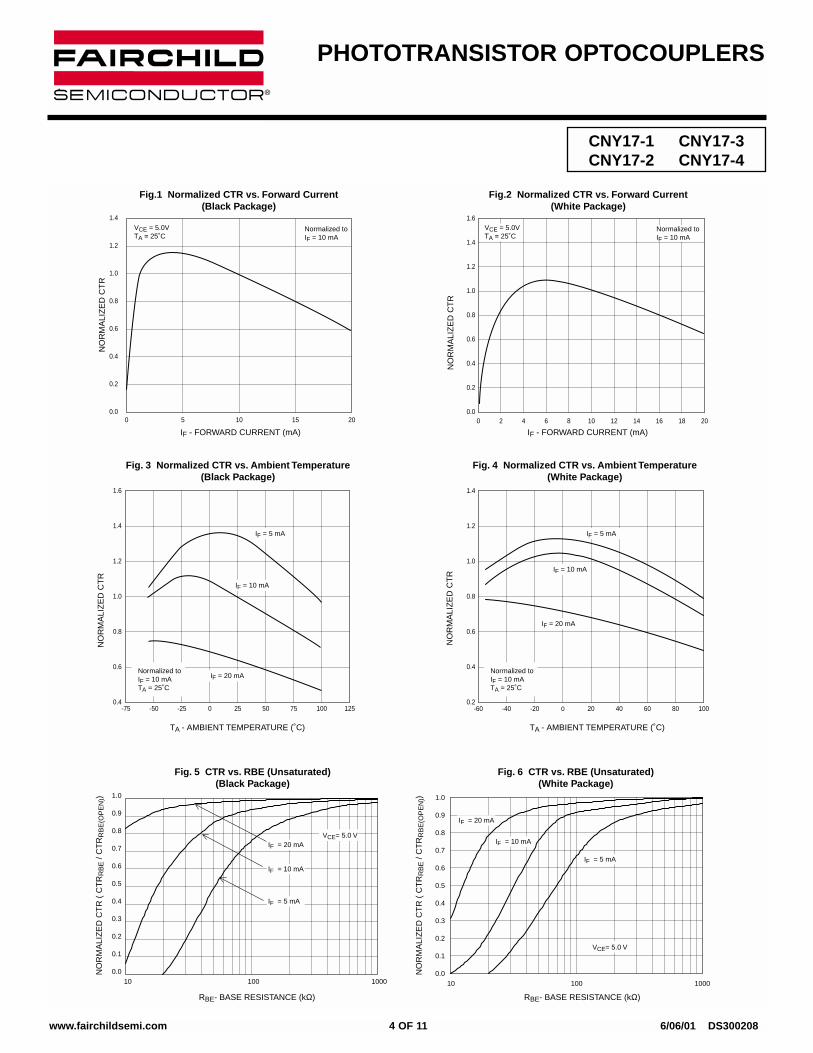
Fig.1 Normalized CTR vs. Forward Current(Black Package)
Fig.2 Normalized CTR vs. Forward Current(White Package)
IF - FORWARD CURRENT (mA) IF - FORWARD CURRENT (mA)
0 5 10 15 20
NO
RM
ALI
ZE
D C
TR
0.0
0.2
0.4
0.6
0.8
1.0
1.2
1.4 VCE = 5.0V TA = 25˚C
Normalized toIF = 10 mA
0 2 4 6 8 10 12 14 16 18 20
NO
RM
ALI
ZE
D C
TR
0.0
0.2
0.4
0.6
0.8
1.0
1.2
1.4
1.6 VCE = 5.0V TA = 25˚C
Normalized toIF = 10 mA
Fig. 3 Normalized CTR vs. Ambient Temperature(Black Package)
Fig. 4 Normalized CTR vs. Ambient Temperature(White Package)
-75 -50 -25 0 25 50 75 100 125
NO
RM
ALI
ZE
D C
TR
0.4
0.6
0.8
1.0
1.2
1.4
1.6
Normalized toIF = 10 mA TA = 25˚C
IF = 10 mA
IF = 20 mA
TA - AMBIENT TEMPERATURE (˚C) TA - AMBIENT TEMPERATURE (˚C)
-60 -40 -20 0 20 40 60 80 100
NO
RM
ALI
ZE
D C
TR
0.2
0.4
0.6
0.8
1.0
1.2
1.4
IF = 5 mA IF = 5 mA
IF = 10 mA
IF = 20 mA
Normalized toIF = 10 mA TA = 25˚C
Fig. 5 CTR vs. RBE (Unsaturated)(Black Package)
Fig. 6 CTR vs. RBE (Unsaturated)(White Package)
RBE- BASE RESISTANCE (kΩ) RBE- BASE RESISTANCE (kΩ)
NO
RM
ALI
ZE
D C
TR
( C
TR
RB
E /
CT
RR
BE
(OP
EN
))
NO
RM
ALI
ZE
D C
TR
( C
TR
RB
E /
CT
RR
BE
(OP
EN
))
10 100 10000.0
0.1
0.2
0.3
0.4
0.5
0.6
0.7
0.8
0.9
1.0
IF = 20 mA
IF = 10 mA
IF = 5 mA
VCE= 5.0 V
10 100 10000.0
0.1
0.2
0.3
0.4
0.5
0.6
0.7
0.8
0.9
1.0
VCE= 5.0 V
IF = 20 mA
IF = 10 mA
IF = 5 mA
PHOTOTRANSISTOR OPTOCOUPLERS
CNY17-1 CNY17-3CNY17-2 CNY17-4
www.fairchildsemi.com 4 OF 11 6/06/01 DS300208
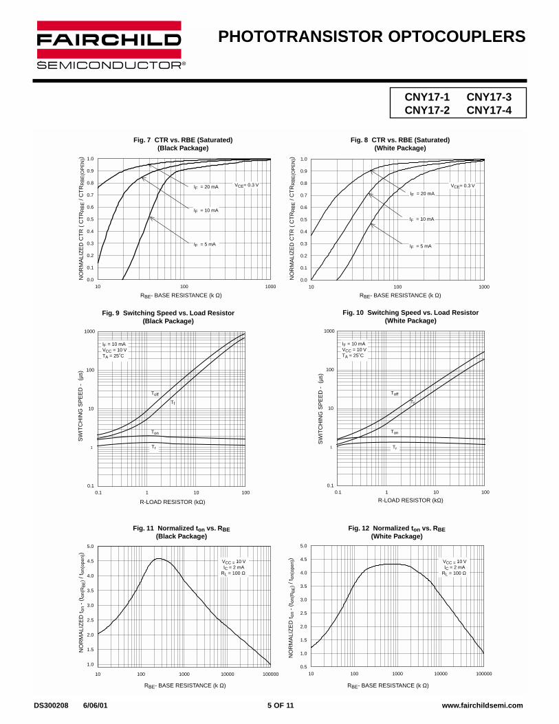
Fig. 9 Switching Speed vs. Load Resistor(Black Package)
R-LOAD RESISTOR (kΩ)
0.1 1 10 100
SW
ITC
HIN
G S
PE
ED
- (
µs)
0.1
1
10
100
1000
Toff
Ton
Tf
IF = 10 mA VCC = 10 VTA = 25˚C
Fig. 7 CTR vs. RBE (Saturated)(Black Package)
Fig. 8 CTR vs. RBE (Saturated)(White Package)
Tr
SW
ITC
HIN
G S
PE
ED
- (
µs)
Fig. 10 Switching Speed vs. Load Resistor(White Package)
R-LOAD RESISTOR (kΩ)0.1 1 10 100
0.1
1
10
100
1000
Toff
Ton
Tf
IF = 10 mA VCC = 10 VTA = 25˚C
Tr
RBE- BASE RESISTANCE (k Ω)
RBE- BASE RESISTANCE (k Ω) RBE- BASE RESISTANCE (k Ω)
RBE- BASE RESISTANCE (k Ω)
NO
RM
ALI
ZE
D C
TR
( C
TR
RB
E /
CT
RR
BE
(OP
EN
))
NO
RM
ALI
ZE
D C
TR
( C
TR
RB
E /
CT
RR
BE
(OP
EN
))10 100 1000
0.0
0.1
0.2
0.3
0.4
0.5
0.6
0.7
0.8
0.9
1.0
VCE= 0.3 V
IF = 5 mA
IF = 10 mA
IF = 20 mA
10 100 10000.0
0.1
0.2
0.3
0.4
0.5
0.6
0.7
0.8
0.9
1.0
IF = 20 mA
IF = 10 mA
IF = 5 mA
VCE= 0.3 V
10 100 1000 10000 100000
NO
RM
ALI
ZE
D t o
n -
(ton
(RB
E) /
t on(
open
))
NO
RM
ALI
ZE
D t o
n -
(ton
(RB
E) /
t on(
open
))
1.0
1.5
2.0
2.5
3.0
3.5
4.0
4.5
5.0
Fig. 11 Normalized ton vs. RBE(Black Package)
Fig. 12 Normalized ton vs. RBE(White Package)
10 100 1000 10000 1000000.5
1.0
1.5
2.0
2.5
3.0
3.5
4.0
4.5
5.0
VCC = 10 VIC = 2 mA
RL = 100 Ω
VCC = 10 VIC = 2 mA
RL = 100 Ω
PHOTOTRANSISTOR OPTOCOUPLERS
CNY17-1 CNY17-3CNY17-2 CNY17-4
DS300208 6/06/01 5 OF 11 www.fairchildsemi.com
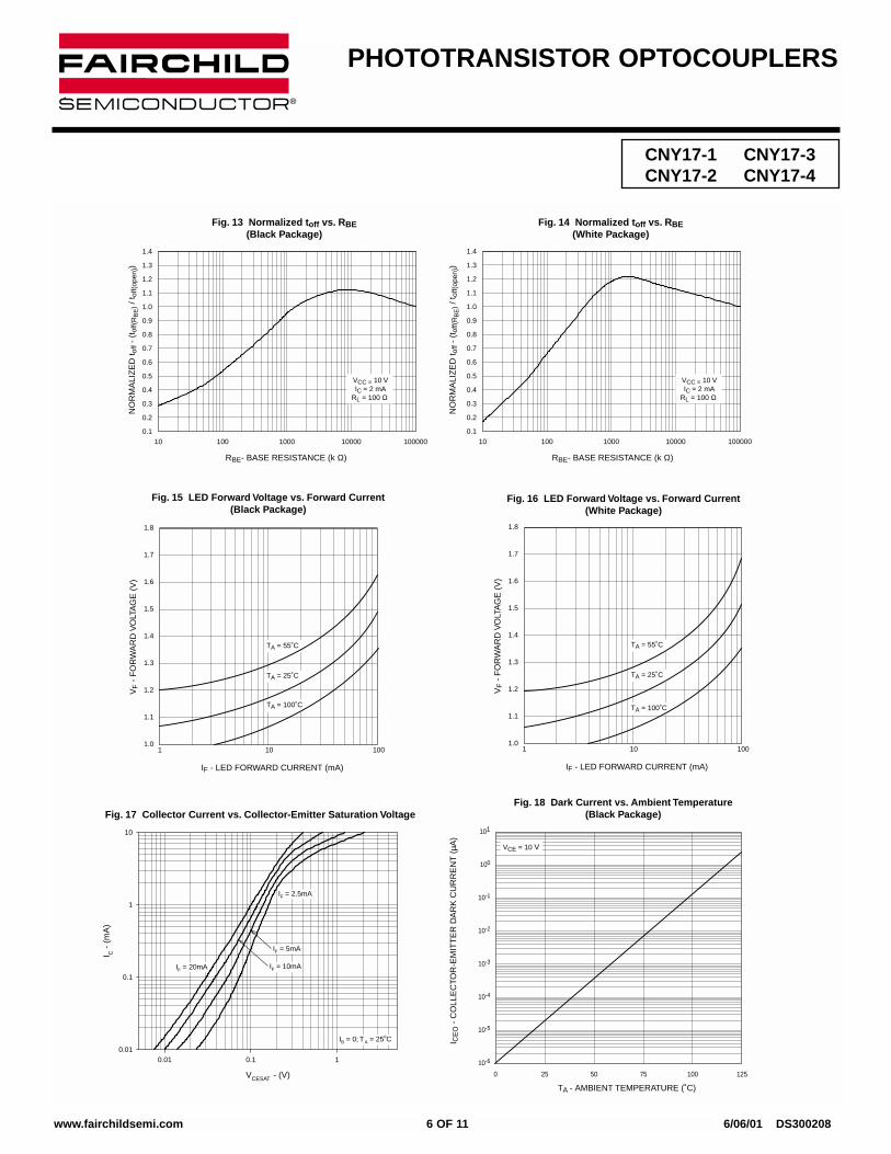
10 100 1000 10000 1000000.1
0.2
0.3
0.4
0.5
0.6
0.7
0.8
0.9
1.0
1.1
1.2
1.3
1.4
RBE- BASE RESISTANCE (k Ω)
10 100 1000 10000 1000000.1
0.2
0.3
0.4
0.5
0.6
0.7
0.8
0.9
1.0
1.1
1.2
1.3
1.4
VCC = 10 VIC = 2 mA
RL = 100 Ω
VCC = 10 VIC = 2 mA
RL = 100 Ω
NO
RM
ALI
ZE
D t o
ff -
(tof
f(R
BE
) / t o
ff(op
en))
NO
RM
ALI
ZE
D t o
ff -
(tof
f(R
BE
) / t o
ff(op
en))
Fig. 13 Normalized toff vs. RBE(Black Package)
RBE- BASE RESISTANCE (k Ω)
Fig. 14 Normalized toff vs. RBE(White Package)
IF - LED FORWARD CURRENT (mA)
VF -
FO
RW
AR
D V
OLT
AG
E (
V)
Fig. 16 LED Forward Voltage vs. Forward Current(White Package)
1 10 1001.0
1.1
1.2
1.3
1.4
1.5
1.6
1.7
1.8
TA = 25˚C
TA = 55˚C
TA = 100˚C
IF - LED FORWARD CURRENT (mA)
VF -
FO
RW
AR
D V
OLT
AG
E (
V)
Fig. 15 LED Forward Voltage vs. Forward Current(Black Package)
1 10 1001.0
1.1
1.2
1.3
1.4
1.5
1.6
1.7
1.8
TA = 25˚C
TA = 55˚C
TA = 100˚C
Fig. 18 Dark Current vs. Ambient Temperature(Black Package)
TA - AMBIENT TEMPERATURE (˚C)
0 25 50 75 100 125
I CE
O -
CO
LLE
CTO
R-E
MIT
TE
R D
AR
K C
UR
RE
NT
(µA
)
10-6
10-5
10-4
10-3
10-2
10-1
100
101
VCE = 10 V
Fig. 17 Collector Current vs. Collector-Emitter Saturation Voltage
VCESAT - (V)
0.01 0.1 1
I C -
(m
A)
0.01
0.1
1
10
IF = 2.5mA
IF = 5mA
IF = 10mAIF = 20mA
IB = 0; TA = 25oC
PHOTOTRANSISTOR OPTOCOUPLERS
CNY17-1 CNY17-3CNY17-2 CNY17-4
www.fairchildsemi.com 6 OF 11 6/06/01 DS300208
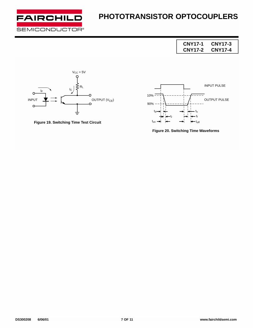
PHOTOTRANSISTOR OPTOCOUPLERS
CNY17-1 CNY17-3CNY17-2 CNY17-4
INPUT PULSE
OUTPUT PULSE
ton toff
RL
IF IC
VCC = 5V
OUTPUT (VCE)INPUT
tr
tdtf
ts
10%
90%
Figure 19. Switching Time Test Circuit
Figure 20. Switching Time Waveforms
DS300208 6/06/01 7 OF 11 www.fairchildsemi.com
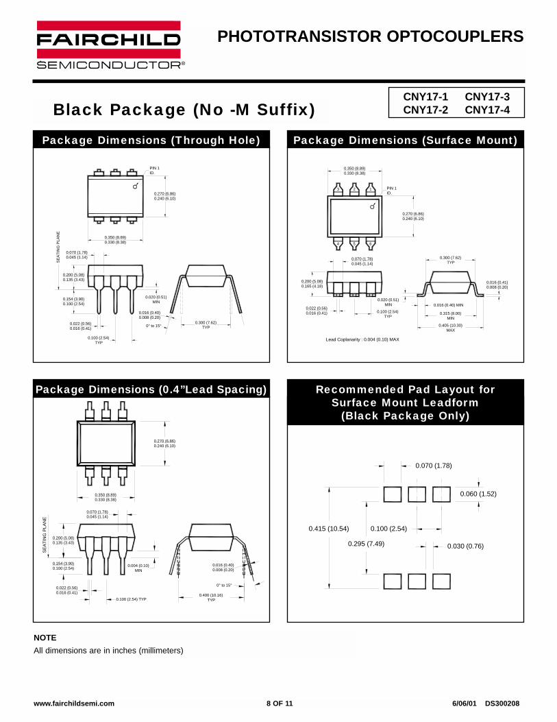
NOTEAll dimensions are in inches (millimeters)
PHOTOTRANSISTOR OPTOCOUPLERS
CNY17-1 CNY17-3CNY17-2 CNY17-4Black Package (No -M Suffix)
Lead Coplanarity : 0.004 (0.10) MAX
0.270 (6.86)0.240 (6.10)
0.350 (8.89)0.330 (8.38)
0.300 (7.62)TYP
0.405 (10.30)MAX
0.315 (8.00)MIN
0.016 (0.40) MIN
2
5
PIN 1ID.
0.016 (0.41)0.008 (0.20)
0.100 (2.54)TYP
0.022 (0.56)0.016 (0.41)
0.070 (1.78)0.045 (1.14)
0.200 (5.08)0.165 (4.18)
4
3
0.020 (0.51)MIN
1
6
0.100 (2.54)TYP
0.020 (0.51)MIN
0.350 (8.89)0.330 (8.38)
0.270 (6.86)0.240 (6.10)
PIN 1ID.
0.022 (0.56)0.016 (0.41)
0.070 (1.78)0.045 (1.14)
0.200 (5.08)0.135 (3.43)
0.300 (7.62)TYP0° to 15°
0.154 (3.90)0.100 (2.54)
SEAT
ING
PLA
NE
0.016 (0.40)0.008 (0.20)
SEAT
ING
PLA
NE
0.016 (0.40)0.008 (0.20)
0.070 (1.78)0.045 (1.14)
0.350 (8.89)0.330 (8.38)
0.154 (3.90)0.100 (2.54)
0.200 (5.08)0.135 (3.43)
0.004 (0.10)MIN
0.270 (6.86)0.240 (6.10)
0.400 (10.16)TYP
0° to 15°0.022 (0.56)0.016 (0.41)
0.100 (2.54) TYP
0.070 (1.78)
0.060 (1.52)
0.030 (0.76)
0.100 (2.54)
0.295 (7.49)
0.415 (10.54)
Package Dimensions (Surface Mount)Package Dimensions (Through Hole)
Package Dimensions (0.4”Lead Spacing) Recommended Pad Layout for Surface Mount Leadform
(Black Package Only)
www.fairchildsemi.com 8 OF 11 6/06/01 DS300208
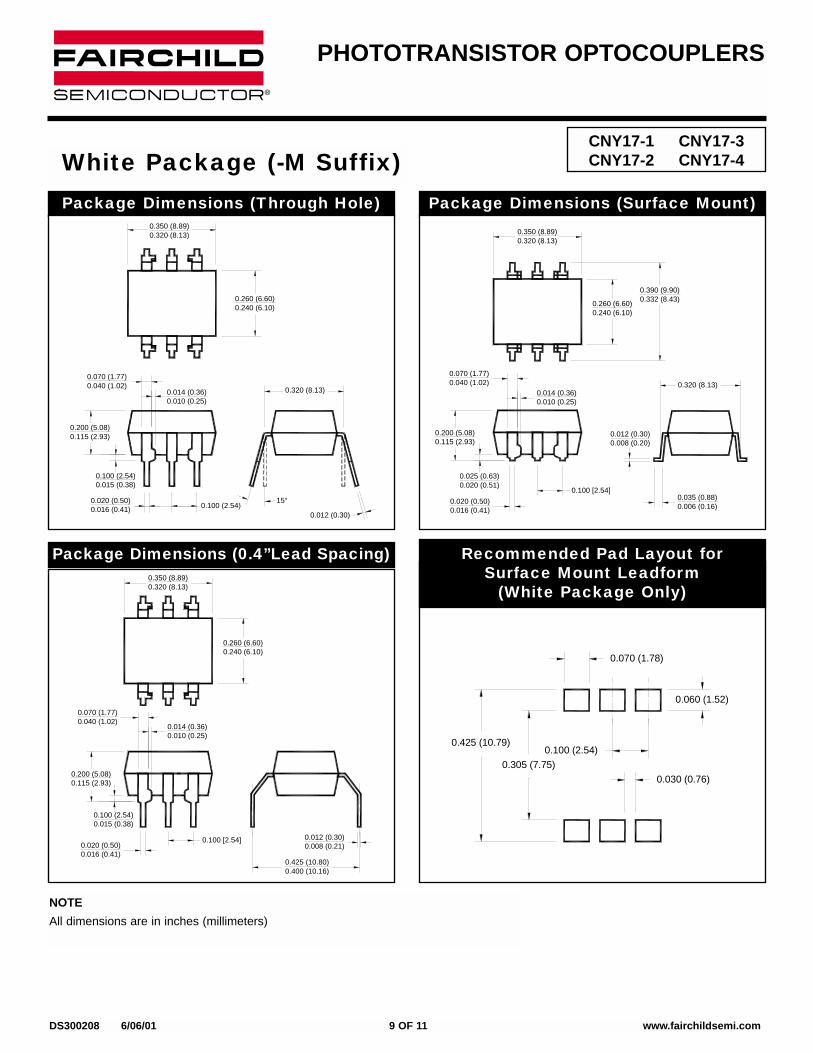
PHOTOTRANSISTOR OPTOCOUPLERS
CNY17-1 CNY17-3CNY17-2 CNY17-4White Package (-M Suffix)
0.070 (1.78)
0.060 (1.52)
0.030 (0.76)
0.100 (2.54)0.305 (7.75)
0.425 (10.79)
Recommended Pad Layout for Surface Mount Leadform
(White Package Only)
Package Dimensions (Surface Mount)0.350 (8.89)0.320 (8.13)
0.260 (6.60)0.240 (6.10)
0.390 (9.90)0.332 (8.43)
0.070 (1.77)0.040 (1.02)
0.014 (0.36)0.010 (0.25)
0.320 (8.13)
0.035 (0.88)0.006 (0.16)
0.012 (0.30)0.008 (0.20)
0.200 (5.08)0.115 (2.93)
0.025 (0.63)0.020 (0.51)
0.020 (0.50)0.016 (0.41)
0.100 [2.54]
Package Dimensions (Through Hole)0.350 (8.89)0.320 (8.13)
0.260 (6.60)0.240 (6.10)
0.320 (8.13)
0.070 (1.77)0.040 (1.02)
0.014 (0.36)0.010 (0.25)
0.200 (5.08)0.115 (2.93)
0.100 (2.54)0.015 (0.38)
0.020 (0.50)0.016 (0.41) 0.100 (2.54)
15°
0.012 (0.30)
Package Dimensions (0.4”Lead Spacing)0.350 (8.89)0.320 (8.13)
0.260 (6.60)0.240 (6.10)
0.070 (1.77)0.040 (1.02)
0.014 (0.36)0.010 (0.25)
0.200 (5.08)0.115 (2.93)
0.020 (0.50)0.016 (0.41)
0.100 [2.54]
0.100 (2.54)0.015 (0.38)
0.012 (0.30)0.008 (0.21)
0.425 (10.80)0.400 (10.16)
NOTEAll dimensions are in inches (millimeters)
DS300208 6/06/01 9 OF 11 www.fairchildsemi.com
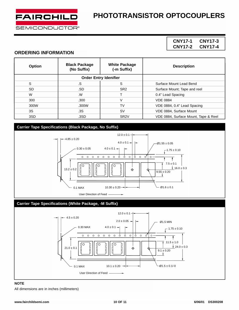
PHOTOTRANSISTOR OPTOCOUPLERS
CNY17-1 CNY17-3CNY17-2 CNY17-4
ORDERING INFORMATION
Order Entry IdenifierS .S S Surface Mount Lead BendSD .SD SR2 Surface Mount; Tape and reelW .W T 0.4” Lead Spacing300 .300 V VDE 0884300W .300W TV VDE 0884, 0.4” Lead Spacing3S .3S SV VDE 0884, Surface Mount3SD .3SD SR2V VDE 0884, Surface Mount, Tape & Reel
Black Package White PackageOption(No Suffix) (-m Suffix)
Description
4.0 ± 0.1
Ø1.55 ± 0.05
User Direction of Feed
4.0 ± 0.1
1.75 ± 0.10
7.5 ± 0.116.0 ± 0.3
12.0 ± 0.1
0.30 ± 0.05
13.2 ± 0.2
4.85 ± 0.20
0.1 MAX 10.30 ± 0.20
9.55 ± 0.20
Ø1.6 ± 0.1
Carrier Tape Specifications (Black Package, No Suffix)
4.0 ± 0.1
Ø1.5 MIN
User Direction of Feed
2.0 ± 0.05
1.75 ± 0.10
11.5 ± 1.024.0 ± 0.3
12.0 ± 0.1
0.30 MAX
21.0 ± 0.1
4.5 ± 0.20
0.1 MAX 10.1 ± 0.20
9.1 ± 0.20
Ø1.5 ± 0.1/-0
Carrier Tape Specifications (White Package, -M Suffix)
NOTEAll dimensions are in inches (millimeters)
www.fairchildsemi.com 10 OF 11 6/06/01 DS300208
DISCLAIMERFAIRCHILD SEMICONDUCTOR RESERVES THE THE RIGHT TO MAKE CHANGES WITHOUT FURTHER NOTICETO ANY PRODUCTS HEREIN TO IMPROVE RELIABILITY, FUNCTION OR DESIGN. FAIRCHILD DOES NOTASSUME ANY LIABILITY ARISING OUT OF THE APPLICATION OR USE OF ANY PRODUCT OR CIRCUITDESCRIBED HEREIN; NEITHER DOES IT CONVEY ANY LICENSE UNDER ITS PATENT RIGHTS, NOR THERIGHTS OF OTHERS.
LIFE SUPPORT POLICYFAIRCHILD’S PRODUCTS ARE NOT AUTHORIZED FOR USE AS CRITICAL COMPONENTS IN LIFE SUPPORTDEVICES OR SYSTEMS WITHOUT THE EXPRESS WRITTEN APPROVAL OF THE PRESIDENT OF FAIRCHILDSEMICONDUCTOR CORPORATION. As used herein:
1. Life support devices or systems are devices or systems which, (a) are intended for surgical implant into the body,or (b) support or sustain life, and (c) whose failure to perform when properly used in accordance with instructions for use providedin labeling, can be reasonably expected to result in asignificant injury of the user.
2. A critical component in any component of a life supportdevice or system whose failure to perform can bereasonably expected to cause the failure of the life support device or system, or to affect its safety or effectiveness.
PHOTOTRANSISTOR OPTOCOUPLERS
CNY17-1 CNY17-3CNY17-2 CNY17-4
DS300208 6/06/01 11 OF 11 www.fairchildsemi.com

4.7 CY37256
5V, 3.3V, ISR™ High-Performance CPLDs
Ultra37000™ CPLD Family
Cypress Semiconductor Corporation • 3901 North First Street • San Jose • CA 95134 • 408-943-2600Document #: 38-03007 Rev. ** Revised March 15, 2001
Features
• In-System Reprogrammable™ (ISR™) CMOS CPLDs— JTAG interface for reconfigurability
— Design changes don’t cause pinout changes
— Design changes don’t cause timing changes• High density
— 32 to 512 macrocells
— 32 to 264 I/O pins
— 5 dedicated inputs including 4 clock pins• Simple timing model
— No fanout delays
— No expander delays
— No dedicated vs. I/O pin delays
— No additional delay through PIM
— No penalty for using full 16 product terms
— No delay for steering or sharing product terms• 3.3V and 5V versions• PCI Compatible[1]
• Programmable Bus-Hold capabilities on all I/Os • Intelligent product term allocator provides:
— 0 to 16 product terms to any macrocell
— Product term steering on an individual basis
— Product term sharing among local macrocells• Flexible clocking
— 4 synchronous clocks per device
— Product Term clocking
— Clock polarity control per logic block• Consistent package/pinout offering across all densities
— Simplifies design migration
— Same pinout for 3.3V and 5.0V devices• Packages
— 44 to 400 Leads in PLCC, CLCC, PQFP, TQFP, CQFP, BGA, and Fine-Pitch BGA packages
General Description
The Ultra37000™ family of CMOS CPLDs provides a range ofhigh-density programmable logic solutions with unparalleledsystem performance. The Ultra37000 family is designed tobring the flexibility, ease of use, and performance of the 22V10to high-density CPLDs. The architecture is based on a numberof logic blocks that are connected by a Programmable Inter-connect Matrix (PIM). Each logic block features its own prod-uct term array, product term allocator, and 16 macrocells. ThePIM distributes signals from the logic block outputs and all in-put pins to the logic block inputs.
All of the Ultra37000 devices are electrically erasable and In-System Reprogrammable (ISR), which simplifies both designand manufacturing flows, thereby reducing costs. The ISR fea-ture provides the ability to reconfigure the devices without hav-ing design changes cause pinout or timing changes. TheCypress ISR function is implemented through a JTAG-compli-ant serial interface. Data is shifted in and out through the TDIand TDO pins, respectively. Because of the superior routabilityand simple timing model of the Ultra37000 devices, ISR allowsusers to change existing logic designs while simultaneouslyfixing pinout assignments and maintaining system perfor-mance.
The entire family features JTAG for ISR and boundary scan,and is compatible with the PCI Local Bus specification, meet-ing the electrical and timing requirements. The Ultra37000family features user programmable bus-hold capabilities on allI/Os.
Ultra37000 5.0V Devices
The Ultra37000 devices operate with a 5V supply and can sup-port 5V or 3.3V I/O levels. VCCO connections provide the ca-pability of interfacing to either a 5V or 3.3V bus. By connectingthe VCCO pins to 5V the user insures 5V TTL levels on theoutputs. If VCCO is connected to 3.3V the output levels meet3.3V JEDEC standard CMOS levels and are 5V tolerant.These devices require 5V ISR programming.
Ultra37000V 3.3V Devices
Devices operating with a 3.3V supply require 3.3V on all VCCOpins, reducing the device’s power consumption. These devicessupport 3.3V JEDEC standard CMOS output levels, and are5V tolerant. These devices allow 3.3V ISR programming.
Note:1. Due to the 5V-tolerant nature of 3.3V device I/Os, the I/Os are not clamped to VCC, PCI VIH=2V.
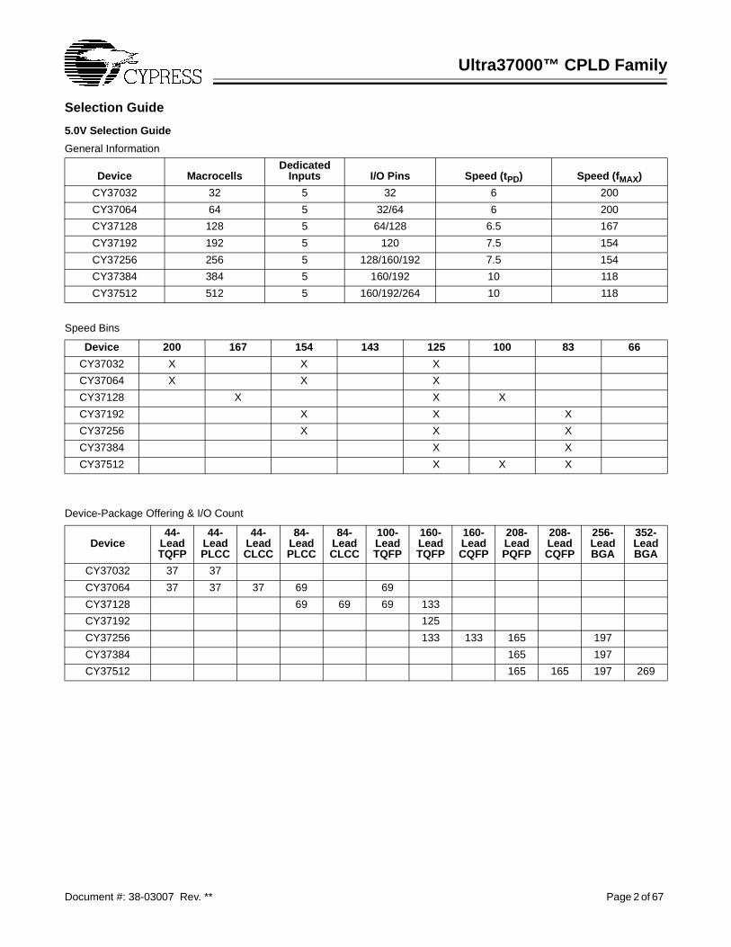
Ultra37000™ CPLD Family
Document #: 38-03007 Rev. ** Page 2 of 67
Selection Guide
5.0V Selection Guide
General Information
Device MacrocellsDedicated
Inputs I/O Pins Speed (tPD) Speed (fMAX)
CY37032 32 5 32 6 200
CY37064 64 5 32/64 6 200
CY37128 128 5 64/128 6.5 167
CY37192 192 5 120 7.5 154
CY37256 256 5 128/160/192 7.5 154
CY37384 384 5 160/192 10 118
CY37512 512 5 160/192/264 10 118
Speed Bins
Device 200 167 154 143 125 100 83 66
CY37032 X X X
CY37064 X X X
CY37128 X X X
CY37192 X X X
CY37256 X X X
CY37384 X X
CY37512 X X X
Device-Package Offering & I/O Count
Device44-
LeadTQFP
44-LeadPLCC
44-LeadCLCC
84-LeadPLCC
84-LeadCLCC
100-LeadTQFP
160-LeadTQFP
160-LeadCQFP
208-LeadPQFP
208-LeadCQFP
256-LeadBGA
352-LeadBGA
CY37032 37 37
CY37064 37 37 37 69 69
CY37128 69 69 69 133
CY37192 125
CY37256 133 133 165 197
CY37384 165 197
CY37512 165 165 197 269
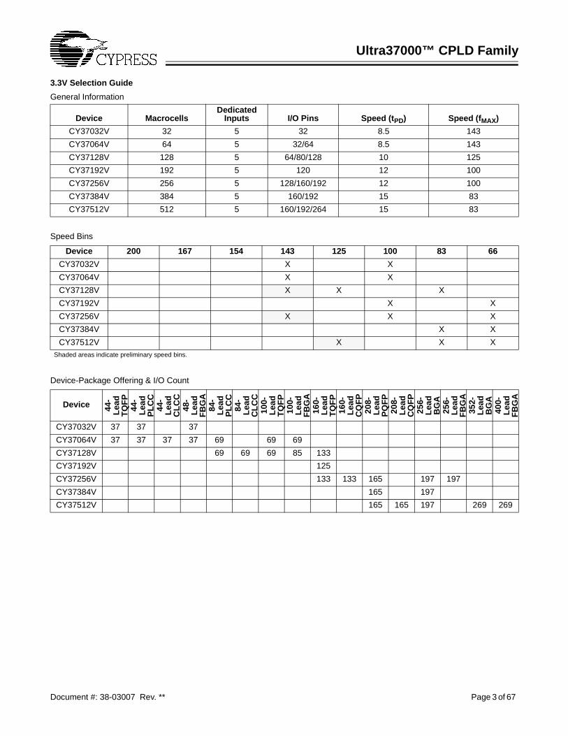
Ultra37000™ CPLD Family
Document #: 38-03007 Rev. ** Page 3 of 67
3.3V Selection Guide
General Information
Device MacrocellsDedicated
Inputs I/O Pins Speed (tPD) Speed (fMAX)
CY37032V 32 5 32 8.5 143
CY37064V 64 5 32/64 8.5 143
CY37128V 128 5 64/80/128 10 125
CY37192V 192 5 120 12 100
CY37256V 256 5 128/160/192 12 100
CY37384V 384 5 160/192 15 83
CY37512V 512 5 160/192/264 15 83
Speed Bins
Device 200 167 154 143 125 100 83 66
CY37032V X X
CY37064V X X
CY37128V X X X
CY37192V X X
CY37256V X X X
CY37384V X X
CY37512V X X XShaded areas indicate preliminary speed bins.
Device-Package Offering & I/O Count
Device 44-
Lea
dT
QF
P44
-L
ead
PL
CC
44-
Lea
dC
LC
C48
-L
ead
FB
GA
84-
Lea
dP
LC
C84
-L
ead
CL
CC
100-
Lea
dT
QF
P10
0-L
ead
FB
GA
160-
Lea
dT
QF
P16
0-L
ead
CQ
FP
208-
Lea
dP
QF
P20
8-L
ead
CQ
FP
256-
Lea
dB
GA
256-
Lea
dF
BG
A35
2-L
ead
BG
A40
0-L
ead
FB
GA
CY37032V 37 37 37
CY37064V 37 37 37 37 69 69 69
CY37128V 69 69 69 85 133
CY37192V 125
CY37256V 133 133 165 197 197
CY37384V 165 197
CY37512V 165 165 197 269 269
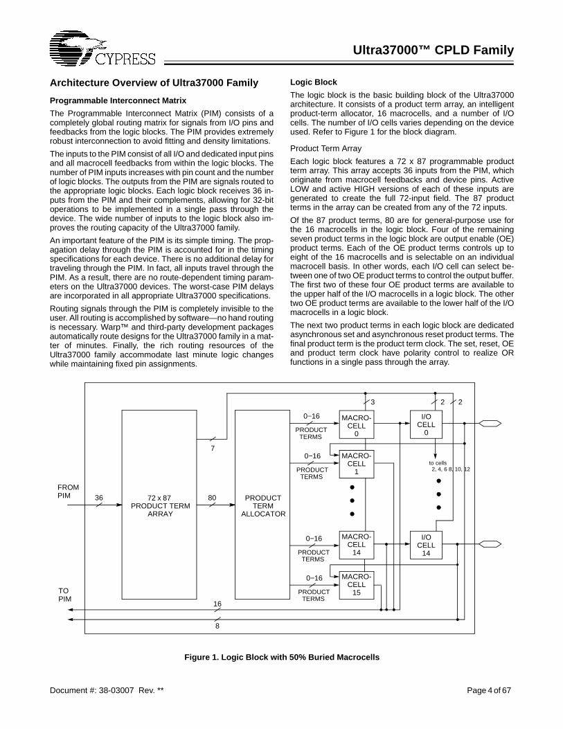
Ultra37000™ CPLD Family
Document #: 38-03007 Rev. ** Page 4 of 67
Architecture Overview of Ultra37000 Family
Programmable Interconnect Matrix
The Programmable Interconnect Matrix (PIM) consists of acompletely global routing matrix for signals from I/O pins andfeedbacks from the logic blocks. The PIM provides extremelyrobust interconnection to avoid fitting and density limitations.
The inputs to the PIM consist of all I/O and dedicated input pinsand all macrocell feedbacks from within the logic blocks. Thenumber of PIM inputs increases with pin count and the numberof logic blocks. The outputs from the PIM are signals routed tothe appropriate logic blocks. Each logic block receives 36 in-puts from the PIM and their complements, allowing for 32-bitoperations to be implemented in a single pass through thedevice. The wide number of inputs to the logic block also im-proves the routing capacity of the Ultra37000 family.
An important feature of the PIM is its simple timing. The prop-agation delay through the PIM is accounted for in the timingspecifications for each device. There is no additional delay fortraveling through the PIM. In fact, all inputs travel through thePIM. As a result, there are no route-dependent timing param-eters on the Ultra37000 devices. The worst-case PIM delaysare incorporated in all appropriate Ultra37000 specifications.
Routing signals through the PIM is completely invisible to theuser. All routing is accomplished by software—no hand routingis necessary. Warp™ and third-party development packagesautomatically route designs for the Ultra37000 family in a mat-ter of minutes. Finally, the rich routing resources of theUltra37000 family accommodate last minute logic changeswhile maintaining fixed pin assignments.
Logic Block
The logic block is the basic building block of the Ultra37000architecture. It consists of a product term array, an intelligentproduct-term allocator, 16 macrocells, and a number of I/Ocells. The number of I/O cells varies depending on the deviceused. Refer to Figure 1 for the block diagram.
Product Term Array
Each logic block features a 72 x 87 programmable productterm array. This array accepts 36 inputs from the PIM, whichoriginate from macrocell feedbacks and device pins. ActiveLOW and active HIGH versions of each of these inputs aregenerated to create the full 72-input field. The 87 productterms in the array can be created from any of the 72 inputs.
Of the 87 product terms, 80 are for general-purpose use forthe 16 macrocells in the logic block. Four of the remainingseven product terms in the logic block are output enable (OE)product terms. Each of the OE product terms controls up toeight of the 16 macrocells and is selectable on an individualmacrocell basis. In other words, each I/O cell can select be-tween one of two OE product terms to control the output buffer.The first two of these four OE product terms are available tothe upper half of the I/O macrocells in a logic block. The othertwo OE product terms are available to the lower half of the I/Omacrocells in a logic block.
The next two product terms in each logic block are dedicatedasynchronous set and asynchronous reset product terms. Thefinal product term is the product term clock. The set, reset, OEand product term clock have polarity control to realize ORfunctions in a single pass through the array.
Figure 1. Logic Block with 50% Buried Macrocells
I/OCELL
0
PRODUCTTERM
ALLOCATOR
I/OCELL
14
MACRO-CELL
0
MACRO-CELL
1
MACRO-CELL
14
0−16
PRODUCTTERMS
72 x 87PRODUCT TERM
ARRAY
8036
8
16
TOPIM
FROMPIM
7
3 2
MACRO-CELL
15
2
to cells2, 4, 6 8, 10, 12
0−16
PRODUCTTERMS
0−16
PRODUCTTERMS
0−16
PRODUCTTERMS
Ultra37000™ CPLD Family
Document #: 38-03007 Rev. ** Page 5 of 67
Low-Power Option
Each logic block can operate in high-speed mode for criticalpath performance, or in low-power mode for power conserva-tion. The logic block mode is set by the user on a logic blockby logic block basis.
Product Term Allocator
Through the product term allocator, software automatically dis-tributes product terms among the 16 macrocells in the logicblock as needed. A total of 80 product terms are available fromthe local product term array. The product term allocator pro-vides two important capabilities without affecting performance:product term steering and product term sharing.
Product Term Steering
Product term steering is the process of assigning productterms to macrocells as needed. For example, if one macrocellrequires ten product terms while another needs just three, theproduct term allocator will “steer” ten product terms to onemacrocell and three to the other. On Ultra37000 devices, prod-uct terms are steered on an individual basis. Any number be-tween 0 and 16 product terms can be steered to any macrocell.Note that 0 product terms is useful in cases where a particularmacrocell is unused or used as an input register.
Product Term Sharing
Product term sharing is the process of using the same productterm among multiple macrocells. For example, if more thanone output has one or more product terms in its equation thatare common to other outputs, those product terms are onlyprogrammed once. The Ultra37000 product term allocator al-lows sharing across groups of four output macrocells in a vari-able fashion. The software automatically takes advantage ofthis capability—the user does not have to intervene.
Note that neither product term sharing nor product term steer-ing have any effect on the speed of the product. All worst-casesteering and sharing configurations have been incorporated inthe timing specifications for the Ultra37000 devices.
Ultra37000 Macrocell
Within each logic block there are 16 macrocells. Macrocellscan either be I/O Macrocells, which include an I/O Cell whichis associated with an I/O pin, or buried Macrocells, which donot connect to an I/O. The combination of I/O Macrocells andburied Macrocells varies from device to device.
Buried Macrocell
Figure 2 displays the architecture of buried macrocells. Theburied macrocell features a register that can be configured ascombinatorial, a D flip-flop, a T flip-flop, or a level-triggeredlatch.
The register can be asynchronously set or asynchronously re-set at the logic block level with the separate set and reset prod-uct terms. Each of these product terms features programma-ble polarity. This allows the registers to be set or reset basedon an AND expression or an OR expression.
Clocking of the register is very flexible. Four global synchro-nous clocks and a product term clock are available to clock theregister. Furthermore, each clock features programmable po-larity so that registers can be triggered on falling as well asrising edges (see the Clocking section). Clock polarity is cho-sen at the logic block level.
The buried macrocell also supports input register capability.The buried macrocell can be configured to act as an input reg-ister (D-type or latch) whose input comes from the I/O pin as-sociated with the neighboring macrocell. The output of all bur-ied macrocells is sent directly to the PIM regardless of itsconfiguration.
I/O Macrocell
Figure 2 illustrates the architecture of the I/O macrocell. TheI/O macrocell supports the same functions as the buried mac-rocell with the addition of I/O capability. At the output of themacrocell, a polarity control mux is available to select activeLOW or active HIGH signals. This has the added advantage ofallowing significant logic reduction to occur in many applica-tions.
The Ultra37000 macrocell features a feedback path to the PIMseparate from the I/O pin input path. This means that if themacrocell is buried (fed back internally only), the associatedI/O pin can still be used as an input.
Bus Hold Capabilities on all I/Os
Bus-hold, which is an improved version of the popular internalpull-up resistor, is a weak latch connected to the pin that doesnot degrade the device’s performance. As a latch, bus-holdmaintains the last state of a pin when the pin is placed in ahigh-impedance state, thus reducing system noise in bus-in-terface applications. Bus-hold additionally allows unused de-vice pins to remain unconnected on the board, which is partic-ularly useful during prototyping as designers can route newsignals to the device without cutting trace connections to VCCor GND. For more information, see the application note “Un-derstanding Bus-Hold − A Feature of Cypress CPLDs.”
Programmable Slew Rate Control
Each output has a programmable configuration bit, which setsthe output slew rate to fast or slow. For designs concerned withmeeting FCC emissions standards the slow edge provides forlower system noise. For designs requiring very high perfor-mance the fast edge rate provides maximum system perfor-mance.
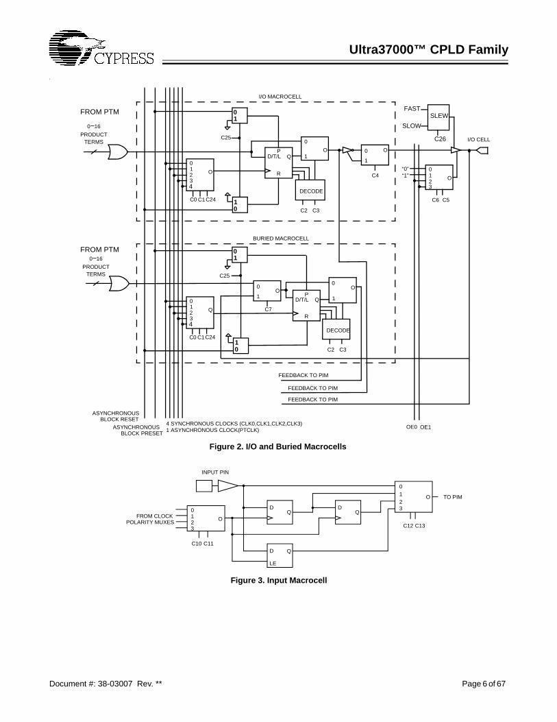
Ultra37000™ CPLD Family
Document #: 38-03007 Rev. ** Page 6 of 67
f
Figure 2. I/O and Buried Macrocells
Figure 3. Input Macrocell
C2 C3
DECODE
C2 C3
DECODE
0123
O
C6 C5
“0” “1”
0
1O
D/T/L Q
R
P
0123
O
C0
0
1
O
C4
FEEDBACK TO PIM
FEEDBACK TO PIM
BLOCK RESET
0−16
TERMS
I/O MACROCELL
I/O CELL
FROM PTM
0
1
O
D/T/L Q
R
P
FROM PTM
1O
C7
FEEDBACK TO PIM
BURIED MACROCELL
0
ASYNCHRONOUS
PRODUCT
0−16
TERMSPRODUCT
C1
4
0123
Q
4
C24
C0 C1 C24
C25
C25
4 SYNCHRONOUS CLOCKS (CLK0,CLK1,CLK2,CLK3)1 ASYNCHRONOUS CLOCK(PTCLK)
BLOCK PRESETASYNCHRONOUS
FAST
SLOW
C26
SLEW
01
01
01
01
OE0 OE1
0123
O
C12 C13
TO PIM
DQ
DQ
D Q
LE
INPUT PIN
012
O
C10
FROM CLOCKPOLARITY MUXES
3
C11
Ultra37000™ CPLD Family
Document #: 38-03007 Rev. ** Page 7 of 67
Clocking
Each I/O and buried macrocell has access to four synchronousclocks (CLK0, CLK1, CLK2 and CLK3) as well as an asynchro-nous product term clock PTCLK. Each input macrocell hasaccess to all four synchronous clocks.
Dedicated Inputs/Clocks
Five pins on each member of the Ultra37000 family are desig-nated as input-only. There are two types of dedicated inputson Ultra37000 devices: input pins and input/clock pins.Figure 3 illustrates the architecture for input pins. Four inputoptions are available for the user: combinatorial, registered,double-registered, or latched. If a registered or latched optionis selected, any one of the input clocks can be selected forcontrol.
Figure 4 illustrates the architecture for the input/clock pins.Like the input pins, input/clock pins can be combinatorial, reg-istered, double-registered, or latched. In addition, these pinsfeed the clocking structures throughout the device. The clockpath at the input has user-configurable polarity.
Product Term Clocking
In addition to the four synchronous clocks, the Ultra37000 fam-ily also has a product term clock for asynchronous clocking.Each logic block has an independent product term clock whichis available to all 16 macrocells. Each product term clock alsosupports user configurable polarity selection.
Timing Model
One of the most important features of the Ultra37000 family isthe simplicity of its timing. All delays are worst case and sys-tem performance is unaffected by the features used. Figure 5illustrates the true timing model for the 167-MHz devices inhigh speed mode. For combinatorial paths, any input to anyoutput incurs a 6.5-ns worst-case delay regardless of theamount of logic used. For synchronous systems, the input set-up time to the output macrocells for any input is 3.5 ns and theclock to output time is also 4.0 ns. These measurements arefor any output and synchronous clock, regardless of the logicused.
The Ultra37000 features:• No fanout delays• No expander delays• No dedicated vs. I/O pin delays• No additional delay through PIM• No penalty for using 0–16 product terms• No added delay for steering product terms• No added delay for sharing product terms• No routing delays• No output bypass delays
The simple timing model of the Ultra37000 family eliminatesunexpected performance penalties.
JTAG and PCI Standards
PCI Compliance
5V operation of the Ultra37000 is fully compliant with the PCILocal Bus Specification published by the PCI Special InterestGroup. The 3.3V products meet all PCI requirements exceptfor the output 3.3V clamp, which is in direct conflict with 5Vtolerance. The Ultra37000 family’s simple and predictable tim-ing model ensures compliance with the PCI AC specificationsindependent of the design.
Figure 4. Input/Clock Macrocell
0123
O
C10C11
TO PIM
DQ
DQ
D Q
LE
INPUT/CLOCK PIN
012
OFROM CLOCK
CLOCK PINS
0
1O
C12
TO CLOCK MUX ONALL INPUT MACROCELLS
TO CLOCK MUX IN EACH
3
0
1
CLOCK POLARITY MUX ONE PER LOGIC BLOCKFOR EACH CLOCK INPUT
POLARITY INPUT
LOGIC BLOCK
C8 C9
C13, C14, C15 OR C16
O
Figure 5. Timing Model for CY37128
COMBINATORIAL SIGNAL
REGISTERED SIGNAL
D,T,L O
CLOCK
INPUT
INPUT
OUTPUT
OUTPUT
tS = 3.5 ns tCO = 4.5 ns
tPD = 6.5 ns
Ultra37000™ CPLD Family
Document #: 38-03007 Rev. ** Page 8 of 67
IEEE 1149.1 Compliant JTAG
The Ultra37000 family has an IEEE 1149.1 JTAG interface forboth Boundary Scan and ISR.
Boundary Scan
The Ultra37000 family supports Bypass, Sample/Preload, Ex-test, Idcode, and Usercode boundary scan instructions. TheJTAG interface is shown in Figure 6.
In-System Reprogramming (ISR)
In-System Reprogramming is the combination of the capabilityto program or reprogram a device on-board, and the ability tosupport design changes without changing the system timingor device pinout. This combination means design changesduring debug or field upgrades do not cause board respins.The Ultra37000 family implements ISR by providing a JTAGcompliant interface for on-board programming, robust routingresources for pinout flexibility, and a simple timing model forconsistent system performance.
Development Software Support
Warp™Warp is a state-of-the-art compiler and complete CPLD designtool. For design entry, Warp provides an IEEE-STD-1076/1164VHDL text editor, an IEEE-STD-1364 Verilog text editor, and agraphical finite state machine editor. It provides optimized syn-thesis and fitting by replacing basic circuits with ones pre-op-timized for the target device, by implementing logic in unusedmemory and by perfect communication between fitting andsynthesis. To facilitate design and debugging, Warp providesgraphical timing simulation and analysis.
Warp Professional™Warp Professional contains several additional features. It pro-vides an extra method of design entry with its graphical blockdiagram editor. It allows up to 5 ms timing simulation insteadof only 2 ms. It allows comparison of waveforms before andafter design changes.
Warp Enterprise™Warp Enterprise provides even more features. It provides un-limited timing simulation and source-level behavioral simula-
tion as well as a debugger. It has the ability to generate graph-ical HDL blocks from HDL text. It can even generatetestbenches.
Warp is available for PC and UNIX platforms. Some featuresare not available in the UNIX version. For further informationsee the Warp for PC, Warp for UNIX, Warp Professional andWarp Enterprise data sheets on Cypress’s web site(www.cypress.com).
Third-Party Software
Although Warp is a complete CPLD development tool on itsown, it interfaces with nearly every third party EDA tool. Allmajor third-party software vendors provide support for theUltra37000 family of devices. Refer to the third-party softwaredata sheet or contact your local sales office for a list of current-ly supported third-party vendors.
Programming
There are four programming options available for Ultra37000devices. The first method is to use a PC with the 37000UltraISR programming cable and software. With this method,the ISR pins of the Ultra37000 devices are routed to a connec-tor at the edge of the printed circuit board. The 37000 UltraISRprogramming cable is then connected between the parallelport of the PC and this connector. A simple configuration fileinstructs the ISR software of the programming operations tobe performed on each of the Ultra37000 devices in the system.The ISR software then automatically completes all of the nec-essary data manipulations required to accomplish the pro-gramming, reading, verifying, and other ISR functions. Formore information on the Cypress ISR Interface, see the ISRProgramming Kit data sheet (CY3700i).
The second method for programming Ultra37000 devices is onautomatic test equipment (ATE). This is accomplished througha file created by the ISR software. Check the Cypress websitefor the latest ISR software download information.
The third programming option for Ultra37000 devices is to uti-lize the embedded controller or processor that already existsin the system. The Ultra37000 ISR software assists in thismethod by converting the device JEDEC maps into the ISRserial stream that contains the ISR instruction information andthe addresses and data of locations to be programmed. Theembedded controller then simply directs this ISR stream to thechain of Ultra37000 devices to complete the desired reconfig-uring or diagnostic operations. Contact your local sales officefor information on availability of this option.
The fourth method for programming Ultra37000 devices is touse the same programmer that is currently being used to pro-gram FLASH370i devices.
For all pinout, electrical, and timing requirements, refer to de-vice data sheets. For ISR cable and software specifications,refer to the UltraISR kit data sheet (CY3700i).
Third-Party Programmers
As with development software, Cypress support is available ona wide variety of third-party programmers. All major third-partyprogrammers (including BP Micro, Data I/O, and SMS) supportthe Ultra37000 family.
Figure 6. JTAG Interface
Instruction Register
Boundary Scan
idcode
Usercode
ISR Prog.
Bypass Reg.
Data Registers
JTAGTAP
CONTROLLER
TDOTDI
TMS
TCK
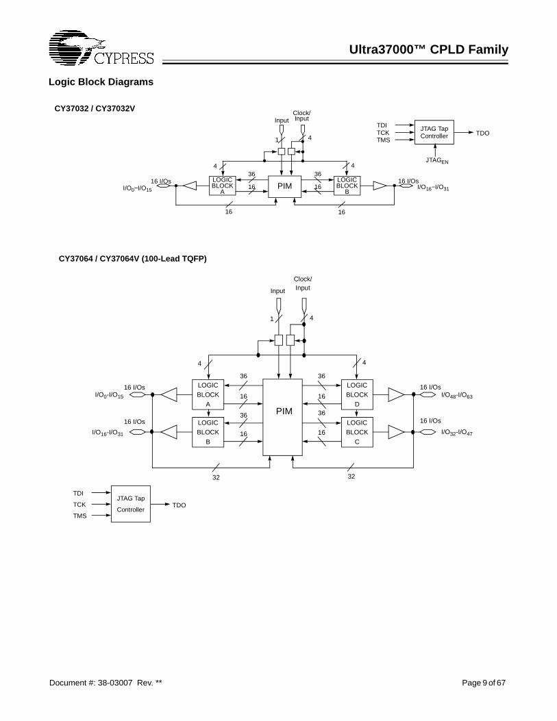
Ultra37000™ CPLD Family
Document #: 38-03007 Rev. ** Page 9 of 67
Logic Block Diagrams
CY37032 / CY37032V
LOGICBLOCK
B
LOGICBLOCK
A
36
16
36
16
InputClock/Input
16 I/Os 16 I/OsI/O0−I/O15 I/O16−I/O31
4
44
1616
TDITCKTMS
TDOJTAG TapController
1
PIM
JTAGEN
LOGIC
BLOCK
D
LOGIC
BLOCK
C
LOGIC
BLOCK
A
LOGIC
BLOCK
B
36
16
36
16
36
16
36
16
Input
Clock/Input
16 I/Os
16 I/Os
16 I/Os
16 I/Os
I/O0-I/O15
I/O16-I/O31
I/O48-I/O63
I/O32-I/O47
4
44
3232
TDI
TCK
TMS
TDOJTAG Tap
Controller
1
PIM
CY37064 / CY37064V (100-Lead TQFP)
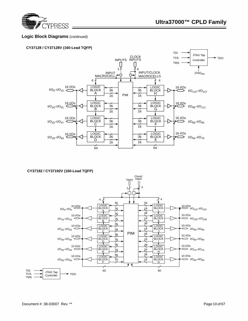
Ultra37000™ CPLD Family
Document #: 38-03007 Rev. ** Page 10 of 67
Logic Block Diagrams (continued)
TDI
TCK
TMS
TDOJTAG Tap
Controller
CY37128 / CY37128V (160-Lead TQFP)
PIM
INPUTMACROCELL
CLOCKINPUTS
4 4
36
16 16
36
LOGICBLOCK 36
16 16
3616 I/Os
36 36
36
16 16
36
16 16
64 64
41INPUT/CLOCKMACROCELLS
I/O0–I/O15A
INPUTS
LOGICBLOCK
C
LOGICBLOCK
B
LOGICBLOCK
D
LOGICBLOCK
H
LOGICBLOCK
G
LOGICBLOCK
F
LOGICBLOCK
E
I/O16–I/O31
I/O32–I/O47
I/O28–I/O63
I/O112–I/O127
I/O96–I/O111
I/O80–I/O95
I/O64–I/O79
16 I/Os
16 I/Os
16 I/Os
16 I/Os
16 I/Os
16 I/Os
16 I/Os
JTAGEN
LOGICBLOCK
H
LOGICBLOCK
L
LOGICBLOCK
I
LOGICBLOCK
J
LOGICBLOCK
K
LOGICBLOCK
A
LOGICBLOCK
B
LOGICBLOCK
C
LOGICBLOCK
D
LOGICBLOCK
E
LOGICBLOCK
G
LOGICBLOCK
F
36
16
36
16
36
16
36
16
36
16
36
16
36
16
36
16
36
16
36
16
36
16
36
16
PIM
InputClock/Input
10 I/Os
10 I/Os
10 I/Os
10 I/Os
10 I/Os
10 I/Os
10 I/Os
10 I/Os
10 I/Os
10 I/Os
10 I/Os
10 I/Os
I/O0–I/O9
I/O10–I/O19
I/O20–I/O29
I/O30–I/O39
I/O40–I/O49
I/O50–I/O59
I/O110–I/O119
I/O100–I/O109
I/O90–I/O99
I/O80–I/O89
I/O70–I/O79
I/O60–I/O69
4
44
6060TDITCKTMS
TDOJTAG TapController
1
CY37192 / CY37192V (160-Lead TQFP)
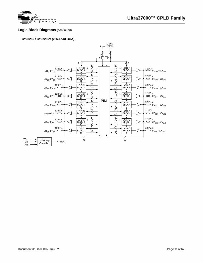
Ultra37000™ CPLD Family
Document #: 38-03007 Rev. ** Page 11 of 67
Logic Block Diagrams (continued)
CY37256 / CY37256V (256-Lead BGA)
LOGICBLOCK
G
LOGICBLOCK
H
LOGICBLOCK
I
LOGICBLOCK
J
LOGICBLOCK
L
LOGICBLOCK
P
LOGICBLOCK
M
LOGICBLOCK
N
LOGICBLOCK
O
LOGICBLOCK
A
LOGICBLOCK
B
LOGICBLOCK
C
LOGICBLOCK
D
LOGICBLOCK
E
LOGICBLOCK
K
LOGICBLOCK
F
36
16
36
16
36
16
36
16
36
16
36
16
36
16
36
16
36
16
36
16
36
16
36
16
36
16
36
16
36
16
36
16
PIM
InputClock/Input
12 I/Os
12 I/Os
12 I/Os
12 I/Os
12 I/Os
12 I/Os
12 I/Os
12 I/Os
12 I/Os
12 I/Os
12 I/Os
12 I/Os
12 I/Os
12 I/Os
12 I/Os
12 I/Os
I/O0−I/O11
I/O12−I/O23
I/O24−I/O35
I/O36−I/O47
I/O48−I/O59
I/O60−I/O71
I/O72−I/O83
I/O84−I/O95
I/O180−I/O191
I/O168−I/O179
I/O156−I/O167
I/O144−I/O155
I/O132−I/O143
I/O120−I/O131
I/O108−I/O119
I/O96−I/O107
4
44
9696TDITCKTMS
TDOJTAG TapController
1
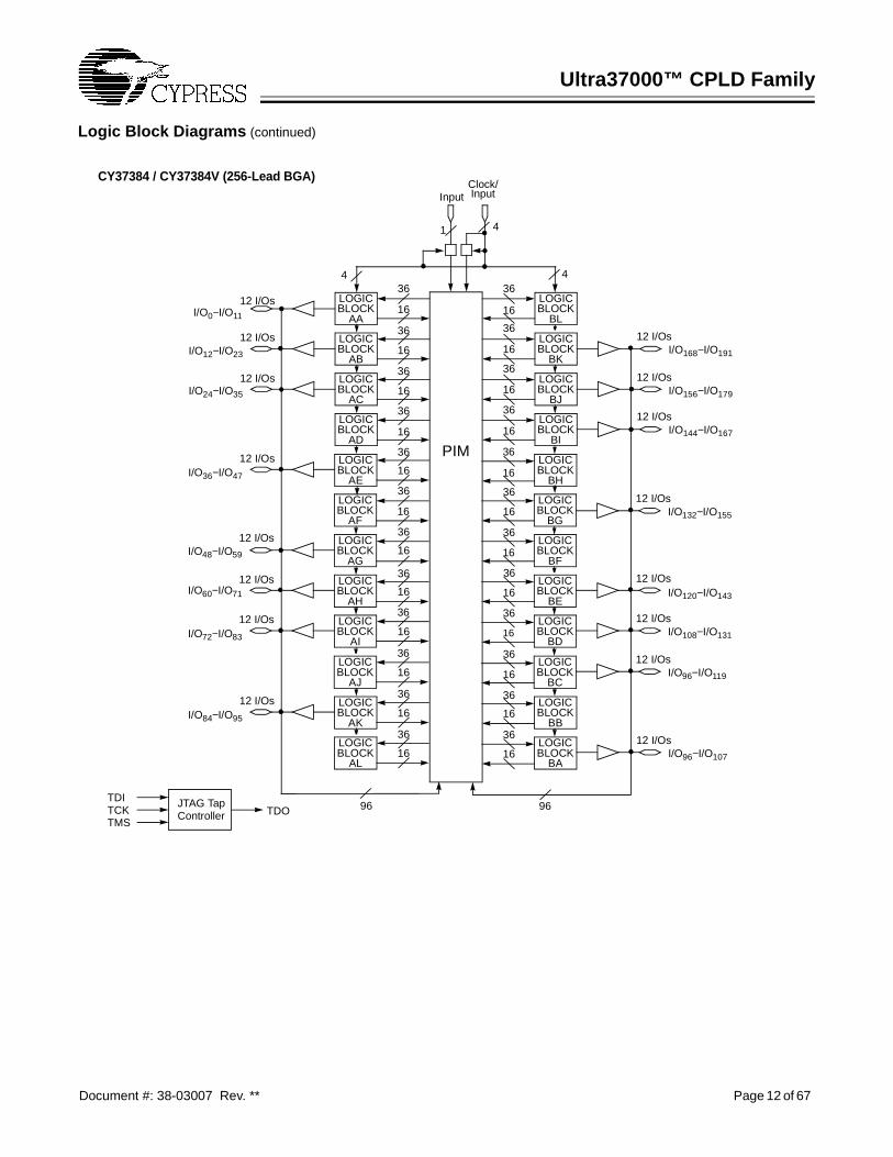
Ultra37000™ CPLD Family
Document #: 38-03007 Rev. ** Page 12 of 67
Logic Block Diagrams (continued)
CY37384 / CY37384V (256-Lead BGA)
LOGICBLOCK
AH
LOGICBLOCK
AI
LOGICBLOCK
BD
LOGICBLOCK
BE
LOGICBLOCK
BG
LOGICBLOCK
BL
LOGICBLOCK
BI
LOGICBLOCK
BJ
LOGICBLOCK
BK
LOGICBLOCK
AA
LOGICBLOCK
AB
LOGICBLOCK
AC
LOGICBLOCK
AD
LOGICBLOCK
AF
LOGICBLOCK
BF
LOGICBLOCK
AG
36
16
36
16
36
16
36
16
36
16
36
16
36
16
36
16
36
16
36
16
36
16
36
16
36
16
36
16
36
16
36
16
PIM
InputClock/Input
12 I/Os
12 I/Os
12 I/Os
12 I/Os
12 I/Os
12 I/Os
12 I/Os
12 I/Os
12 I/Os
12 I/Os
12 I/Os
I/O0−I/O11
I/O12−I/O23
I/O24−I/O35
I/O48−I/O59
I/O60−I/O71
I/O72−I/O83
I/O168−I/O191
I/O156−I/O179
I/O144−I/O167
I/O120−I/O143
I/O108−I/O131
4
44
9696TDITCKTMS
TDOJTAG TapController
1
LOGICBLOCK
AJ
LOGICBLOCK
BC1616
12 I/OsI/O96−I/O119
LOGICBLOCK
AK
LOGICBLOCK
BB1616
12 I/OsI/O84−I/O95
LOGICBLOCK
AL
LOGICBLOCK
BA1616
12 I/OsI/O96−I/O107
LOGICBLOCK
AE
LOGICBLOCK
BH1616
12 I/Os
12 I/Os
I/O36−I/O47
I/O132−I/O155
36
36
36
36
36
36
36
36
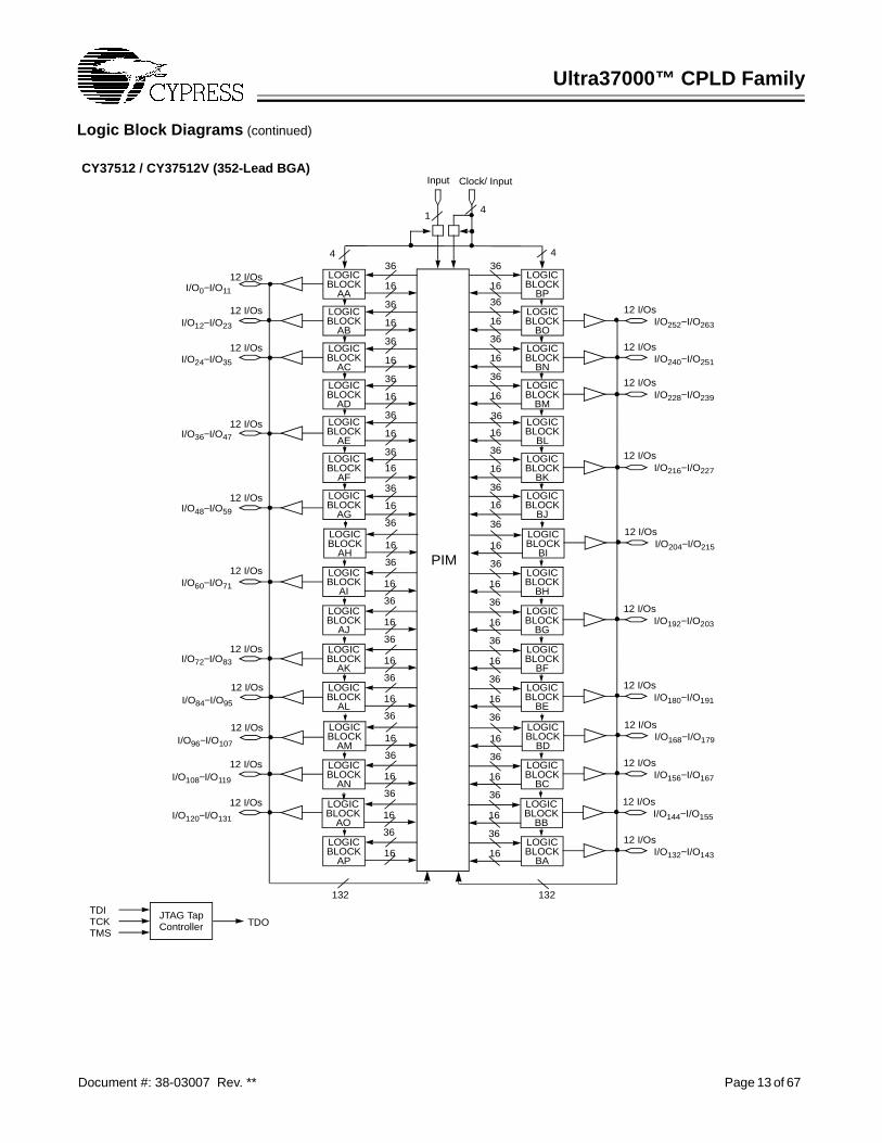
Ultra37000™ CPLD Family
Document #: 38-03007 Rev. ** Page 13 of 67
Logic Block Diagrams (continued)
CY37512 / CY37512V (352-Lead BGA)
LOGICBLOCK
AG
LOGICBLOCK
AH
LOGICBLOCK
BI
LOGICBLOCK
BJ
LOGICBLOCK
BL
LOGICBLOCK
BP
LOGICBLOCK
BM
LOGICBLOCK
BN
LOGICBLOCK
BO
LOGICBLOCK
AA
LOGICBLOCK
AB
LOGICBLOCK
AC
LOGICBLOCK
AD
LOGICBLOCK
AE
LOGICBLOCK
BK
LOGICBLOCK
AF
36
16
36
16
36
16
36
16
36
16
36
16
36
16
3636
36
16
36
16
36
16
36
16
36
16
36
16
36
16
Input Clock/ Input
12 I/Os
12 I/Os
12 I/Os
12 I/Os
12 I/Os
12 I/Os
12 I/Os
12 I/Os
12 I/Os
12 I/Os
12 I/Os
12 I/Os
12 I/Os
I/O0−I/O11
I/O12−I/O23
I/O24−I/O35
I/O36−I/O47
I/O48−I/O59
I/O60−I/O71
I/O72−I/O83
I/O84−I/O95
I/O252−I/O263
I/O240−I/O251
I/O228−I/O239
I/O216−I/O227
I/O204−I/O215
4
44
TDITCKTMS
TDOJTAG TapController
1
PIM16
3636
16
LOGICBLOCK
AI
LOGICBLOCK
BH
12 I/OsI/O96−I/O107
16
3636
16
LOGICBLOCK
AJ
LOGICBLOCK
BG
12 I/Os
12 I/Os
I/O108−I/O119
I/O192−I/O20316
3636
16
LOGICBLOCK
AK
LOGICBLOCK
BF
12 I/OsI/O120−I/O131
16
3636
16
LOGICBLOCK
AL
LOGICBLOCK
BE
12 I/OsI/O180−I/O19116
3636
16
LOGICBLOCK
AM
LOGICBLOCK
BD
12 I/OsI/O168−I/O17916
3636
16
LOGICBLOCK
AN
LOGICBLOCK
BC
12 I/OsI/O156−I/O16716
3636
16
LOGICBLOCK
AO
LOGICBLOCK
BB
12 I/OsI/O144−I/O15516
3636
16
LOGICBLOCK
AP
LOGICBLOCK
BA
12 I/OsI/O132−I/O14316
132132
16
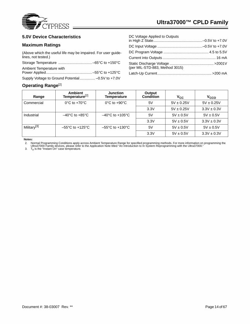
Ultra37000™ CPLD Family
Document #: 38-03007 Rev. ** Page 14 of 67
5.0V Device Characteristics
Maximum Ratings
(Above which the useful life may be impaired. For user guide-lines, not tested.)
Storage Temperature ................................. –65°C to +150°C
Ambient Temperature withPower Applied............................................. –55°C to +125°C
Supply Voltage to Ground Potential ............... –0.5V to +7.0V
DC Voltage Applied to Outputsin High Z State................................................–0.5V to +7.0V
DC Input Voltage ............................................–0.5V to +7.0V
DC Program Voltage ............................................ 4.5 to 5.5V
Current into Outputs .................................................... 16 mA
Static Discharge Voltage ........................................... >2001V(per MIL-STD-883, Method 3015)
Latch-Up Current..................................................... >200 mA
Operating Range[2]
RangeAmbient
Temperature[2]Junction
TemperatureOutput
Condition VCC VCCO
Commercial 0°C to +70°C 0°C to +90°C 5V 5V ± 0.25V 5V ± 0.25V
3.3V 5V ± 0.25V 3.3V ± 0.3V
Industrial –40°C to +85°C –40°C to +105°C 5V 5V ± 0.5V 5V ± 0.5V
3.3V 5V ± 0.5V 3.3V ± 0.3V
Military[3] –55°C to +125°C –55°C to +130°C 5V 5V ± 0.5V 5V ± 0.5V
3.3V 5V ± 0.5V 3.3V ± 0.3V
Notes:2. Normal Programming Conditions apply across Ambient Temperature Range for specified programming methods. For more information on programming the
Ultra37000 Family devices, please refer to the Application Note titled “An Introduction to In System Reprogramming with the Ultra37000.”3. TA is the “Instant On” case temperature.
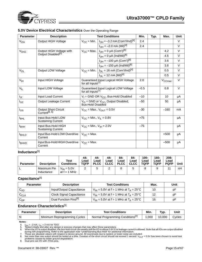
Ultra37000™ CPLD Family
Document #: 38-03007 Rev. ** Page 15 of 67
5.0V Device Electrical Characteristics Over the Operating Range
Parameter Description Test Conditions Min. Typ. Max. Unit
VOH Output HIGH Voltage VCC = Min. IOH = –3.2 mA (Com’l/Ind)[4] 2.4 V
IOH = –2.0 mA (Mil)[4] 2.4 V
VOHZ Output HIGH Voltage with Output Disabled[5]
VCC = Max. IOH = 0 µA (Com’l)[6] 4.2 V
IOH = 0 µA (Ind/Mil)[6] 4.5 V
IOH = –100 µA (Com’l)[6] 3.6 V
IOH = –150 µA (Ind/Mil)[6] 3.6 V
VOL Output LOW Voltage VCC = Min. IOL = 16 mA (Com’l/Ind)[4] 0.5 V
IOL = 12 mA (Mil)[4] 0.5 V
VIH Input HIGH Voltage Guaranteed Input Logical HIGH Voltage for all Inputs[7]
2.0 VCCmax V
VIL Input LOW Voltage Guaranteed Input Logical LOW Voltage for all Inputs[7]
–0.5 0.8 V
IIX Input Load Current VI = GND OR VCC, Bus-Hold Disabled –10 10 µA
IOZ Output Leakage Current VO = GND or VCC, Output Disabled, Bus-Hold Disabled
–50 50 µA
IOS Output Short Circuit Current[8, 5]
VCC = Max., VOUT = 0.5V –30 –160 mA
IBHL Input Bus-Hold LOW Sustaining Current
VCC = Min., VIL = 0.8V +75 µA
IBHH Input Bus-Hold HIGH Sustaining Current
VCC = Min., VIH = 2.0V –75 µA
IBHLO Input Bus-Hold LOW Overdrive Current
VCC = Max. +500 µA
IBHHO Input Bus-Hold HIGH Overdrive Current
VCC = Max. –500 µA
Inductance[5]
Parameter DescriptionTest
Conditions
44-LeadTQFP
44-LeadPLCC
44-LeadCLCC
84-LeadPLCC
84-LeadCLCC
100-LeadTQFP
160-LeadTQFP
208-LeadPQFP Unit
L Maximum PinInductance
VIN = 5.0V at f = 1 MHz
2 5 2 8 5 8 9 11 nH
Capacitance[5]
Parameter Description Test Conditions Max. Unit
CI/O Input/Output Capacitance VIN = 5.0V at f = 1 MHz at TA = 25°C 10 pF
CCLK Clock Signal Capacitance VIN = 5.0V at f = 1 MHz at TA = 25°C 12 pF
CDP Dual Function Pins[9] VIN = 5.0V at f = 1 MHz at TA = 25°C 16 pF
Endurance Characteristics[5]
Parameter Description Test Conditions Min. Typ. Unit
N Minimum Reprogramming Cycles Normal Programming Conditions[2] 1,000 10,000 Cycles
Notes:4. IOH = –2 mA, IOL = 2 mA for TDO.5. Tested initially and after any design or process changes that may affect these parameters.6. When the I/O is output disabled, the bus-hold circuit can weakly pull the I/O to above 3.6V if no leakage current is allowed. Note that all I/Os are output disabled
during ISR programming. Refer to the application note “Understanding Bus-Hold” for additional information.7. These are absolute values with respect to device ground. All overshoots due to system or tester noise are included.8. Not more than one output should be tested at a time. Duration of the short circuit should not exceed 1 second. VOUT = 0.5V has been chosen to avoid test
problems caused by tester ground degradation.9. Dual pins are I/O with JTAG pins.
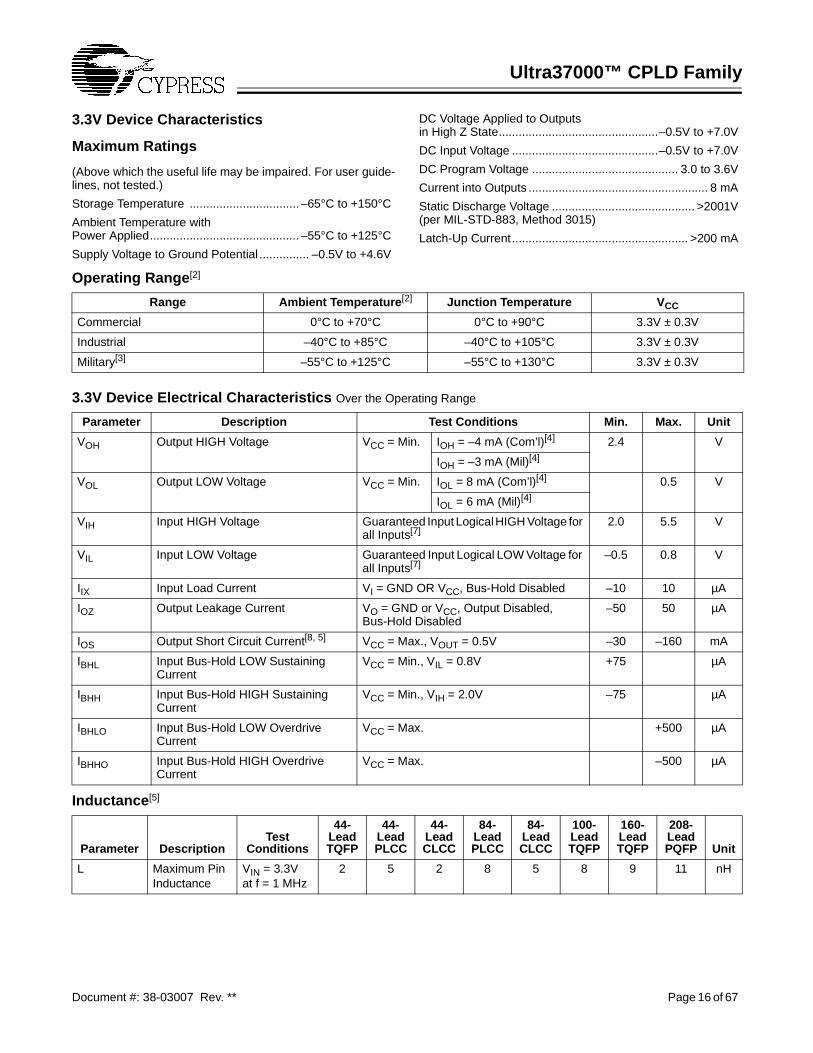
Ultra37000™ CPLD Family
Document #: 38-03007 Rev. ** Page 16 of 67
3.3V Device Characteristics
Maximum Ratings
(Above which the useful life may be impaired. For user guide-lines, not tested.)
Storage Temperature ................................. –65°C to +150°CAmbient Temperature withPower Applied............................................. –55°C to +125°CSupply Voltage to Ground Potential ............... –0.5V to +4.6V
DC Voltage Applied to Outputsin High Z State................................................–0.5V to +7.0V
DC Input Voltage ............................................–0.5V to +7.0V
DC Program Voltage ............................................ 3.0 to 3.6V
Current into Outputs ...................................................... 8 mA
Static Discharge Voltage ........................................... >2001V(per MIL-STD-883, Method 3015)
Latch-Up Current..................................................... >200 mA
Operating Range[2]
Range Ambient Temperature[2] Junction Temperature VCC
Commercial 0°C to +70°C 0°C to +90°C 3.3V ± 0.3V
Industrial –40°C to +85°C –40°C to +105°C 3.3V ± 0.3V
Military[3] –55°C to +125°C –55°C to +130°C 3.3V ± 0.3V
3.3V Device Electrical Characteristics Over the Operating Range
Parameter Description Test Conditions Min. Max. Unit
VOH Output HIGH Voltage VCC = Min. IOH = –4 mA (Com’l)[4] 2.4 V
IOH = –3 mA (Mil)[4]
VOL Output LOW Voltage VCC = Min. IOL = 8 mA (Com’l)[4] 0.5 V
IOL = 6 mA (Mil)[4]
VIH Input HIGH Voltage Guaranteed Input Logical HIGH Voltage for all Inputs[7]
2.0 5.5 V
VIL Input LOW Voltage Guaranteed Input Logical LOW Voltage for all Inputs[7]
–0.5 0.8 V
IIX Input Load Current VI = GND OR VCC, Bus-Hold Disabled –10 10 µA
IOZ Output Leakage Current VO = GND or VCC, Output Disabled, Bus-Hold Disabled
–50 50 µA
IOS Output Short Circuit Current[8, 5] VCC = Max., VOUT = 0.5V –30 –160 mA
IBHL Input Bus-Hold LOW Sustaining Current
VCC = Min., VIL = 0.8V +75 µA
IBHH Input Bus-Hold HIGH Sustaining Current
VCC = Min., VIH = 2.0V –75 µA
IBHLO Input Bus-Hold LOW Overdrive Current
VCC = Max. +500 µA
IBHHO Input Bus-Hold HIGH Overdrive Current
VCC = Max. –500 µA
Inductance[5]
Parameter DescriptionTest
Conditions
44-LeadTQFP
44-LeadPLCC
44-LeadCLCC
84-LeadPLCC
84-LeadCLCC
100-LeadTQFP
160-LeadTQFP
208-LeadPQFP Unit
L Maximum PinInductance
VIN = 3.3V at f = 1 MHz
2 5 2 8 5 8 9 11 nH
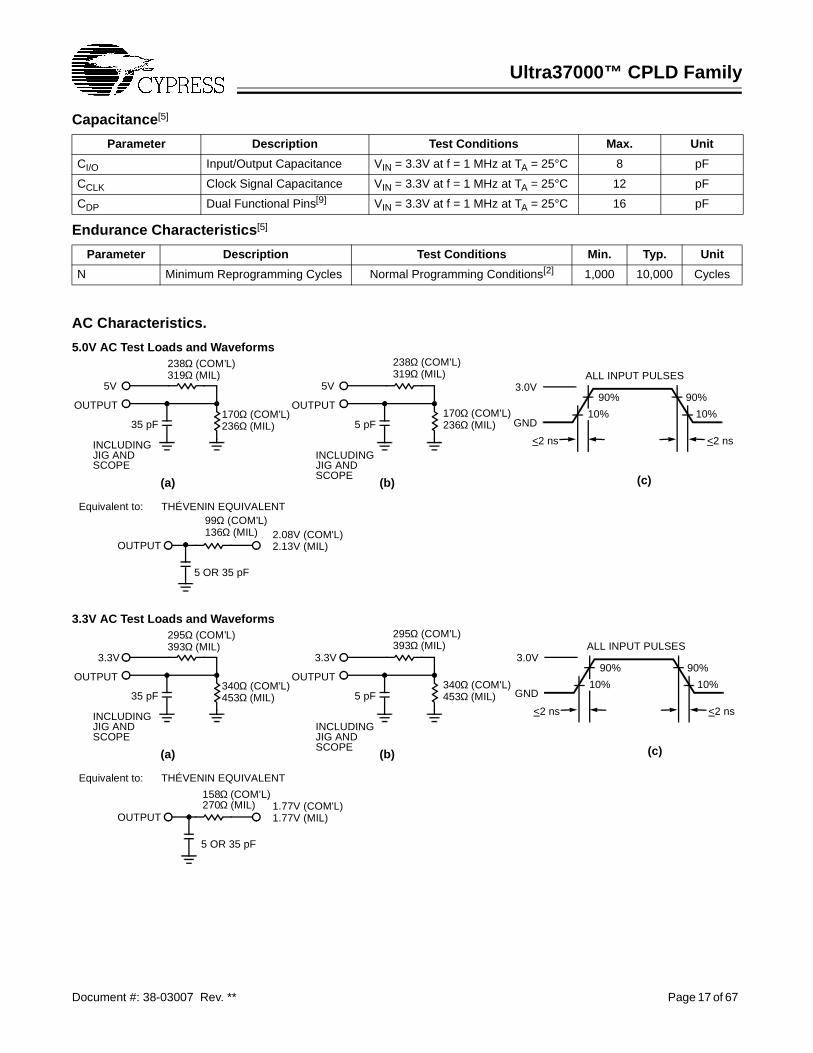
Ultra37000™ CPLD Family
Document #: 38-03007 Rev. ** Page 17 of 67
AC Characteristics.
Capacitance[5]
Parameter Description Test Conditions Max. Unit
CI/O Input/Output Capacitance VIN = 3.3V at f = 1 MHz at TA = 25°C 8 pF
CCLK Clock Signal Capacitance VIN = 3.3V at f = 1 MHz at TA = 25°C 12 pF
CDP Dual Functional Pins[9] VIN = 3.3V at f = 1 MHz at TA = 25°C 16 pF
Endurance Characteristics[5]
Parameter Description Test Conditions Min. Typ. Unit
N Minimum Reprogramming Cycles Normal Programming Conditions[2] 1,000 10,000 Cycles
5.0V AC Test Loads and Waveforms
3.3V AC Test Loads and Waveforms
90%
10%
3.0V
GND
90%
10%
ALL INPUT PULSES5V
OUTPUT
35 pF
INCLUDINGJIG ANDSCOPE
5V
OUTPUT
5 pF
INCLUDINGJIG ANDSCOPE
(a) (b)
<2 ns
OUTPUT
238Ω (COM’L)319Ω (MIL)
170Ω (COM’L)236Ω (MIL)
99Ω (COM’L)136Ω (MIL)
Equivalent to: THÉVENIN EQUIVALENT
2.08V (COM'L)2.13V (MIL)
238Ω (COM'L)319Ω (MIL)
170Ω (COM'L)236Ω (MIL)
<2 ns
(c)
5 OR 35 pF
90%
10%
3.0V
GND
90%
10%
ALL INPUT PULSES3.3V
OUTPUT
35 pF
INCLUDINGJIG ANDSCOPE
3.3V
OUTPUT
5 pF
INCLUDINGJIG ANDSCOPE
(a) (b)
<2 ns
OUTPUT
295Ω (COM’L)393Ω (MIL)
340Ω (COM’L)453Ω (MIL)
Equivalent to: THÉVENIN EQUIVALENT
1.77V (COM'L)1.77V (MIL)
295Ω (COM'L)393Ω (MIL)
340Ω (COM'L)453Ω (MIL)
<2 ns
(c)
270Ω (MIL)158Ω (COM’L)
5 OR 35 pF
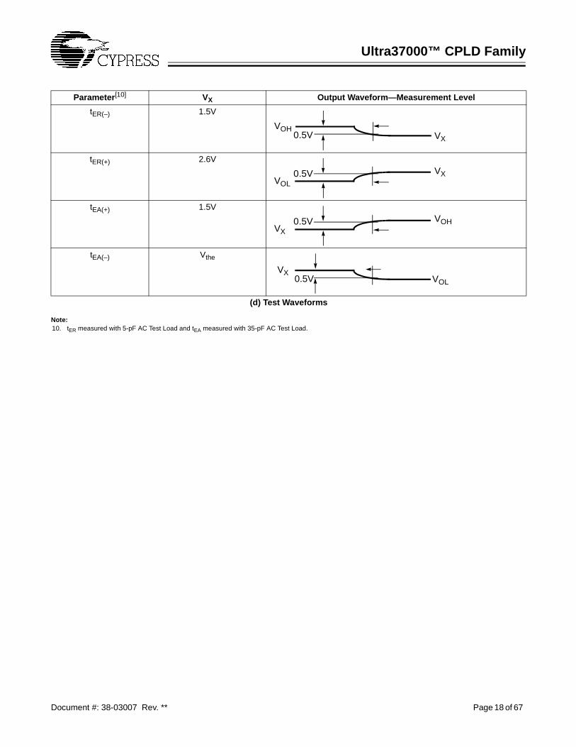
Ultra37000™ CPLD Family
Document #: 38-03007 Rev. ** Page 18 of 67
Note:10. tER measured with 5-pF AC Test Load and tEA measured with 35-pF AC Test Load.
Parameter[10] VX Output Waveform—Measurement Level
tER(–) 1.5V
tER(+) 2.6V
tEA(+) 1.5V
tEA(–) Vthe
(d) Test Waveforms
VOHVX0.5V
VOL
VX0.5V
VX
VOH0.5V
VXVOL0.5V
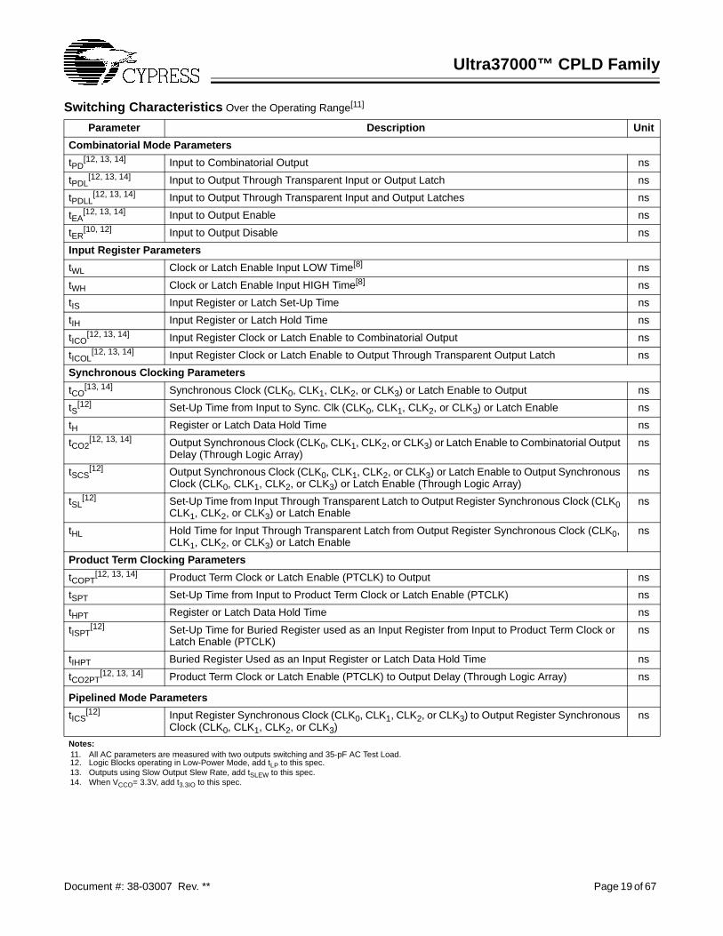
Ultra37000™ CPLD Family
Document #: 38-03007 Rev. ** Page 19 of 67
Switching Characteristics Over the Operating Range[11]
Parameter Description Unit
Combinatorial Mode Parameters
tPD[12, 13, 14] Input to Combinatorial Output ns
tPDL[12, 13, 14] Input to Output Through Transparent Input or Output Latch ns
tPDLL[12, 13, 14] Input to Output Through Transparent Input and Output Latches ns
tEA[12, 13, 14] Input to Output Enable ns
tER[10, 12] Input to Output Disable ns
Input Register Parameters
tWL Clock or Latch Enable Input LOW Time[8] ns
tWH Clock or Latch Enable Input HIGH Time[8] ns
tIS Input Register or Latch Set-Up Time ns
tIH Input Register or Latch Hold Time ns
tICO[12, 13, 14] Input Register Clock or Latch Enable to Combinatorial Output ns
tICOL[12, 13, 14] Input Register Clock or Latch Enable to Output Through Transparent Output Latch ns
Synchronous Clocking Parameters
tCO[13, 14] Synchronous Clock (CLK0, CLK1, CLK2, or CLK3) or Latch Enable to Output ns
tS[12] Set-Up Time from Input to Sync. Clk (CLK0, CLK1, CLK2, or CLK3) or Latch Enable ns
tH Register or Latch Data Hold Time ns
tCO2[12, 13, 14] Output Synchronous Clock (CLK0, CLK1, CLK2, or CLK3) or Latch Enable to Combinatorial Output
Delay (Through Logic Array)ns
tSCS[12] Output Synchronous Clock (CLK0, CLK1, CLK2, or CLK3) or Latch Enable to Output Synchronous
Clock (CLK0, CLK1, CLK2, or CLK3) or Latch Enable (Through Logic Array)ns
tSL[12] Set-Up Time from Input Through Transparent Latch to Output Register Synchronous Clock (CLK0
CLK1, CLK2, or CLK3) or Latch Enablens
tHL Hold Time for Input Through Transparent Latch from Output Register Synchronous Clock (CLK0, CLK1, CLK2, or CLK3) or Latch Enable
ns
Product Term Clocking Parameters
tCOPT[12, 13, 14] Product Term Clock or Latch Enable (PTCLK) to Output ns
tSPT Set-Up Time from Input to Product Term Clock or Latch Enable (PTCLK) ns
tHPT Register or Latch Data Hold Time ns
tISPT[12] Set-Up Time for Buried Register used as an Input Register from Input to Product Term Clock or
Latch Enable (PTCLK)ns
tIHPT Buried Register Used as an Input Register or Latch Data Hold Time ns
tCO2PT[12, 13, 14] Product Term Clock or Latch Enable (PTCLK) to Output Delay (Through Logic Array) ns
Pipelined Mode Parameters
tICS[12] Input Register Synchronous Clock (CLK0, CLK1, CLK2, or CLK3) to Output Register Synchronous
Clock (CLK0, CLK1, CLK2, or CLK3)ns
Notes:11. All AC parameters are measured with two outputs switching and 35-pF AC Test Load.12. Logic Blocks operating in Low-Power Mode, add tLP to this spec.13. Outputs using Slow Output Slew Rate, add tSLEW to this spec.14. When VCCO= 3.3V, add t3.3IO to this spec.
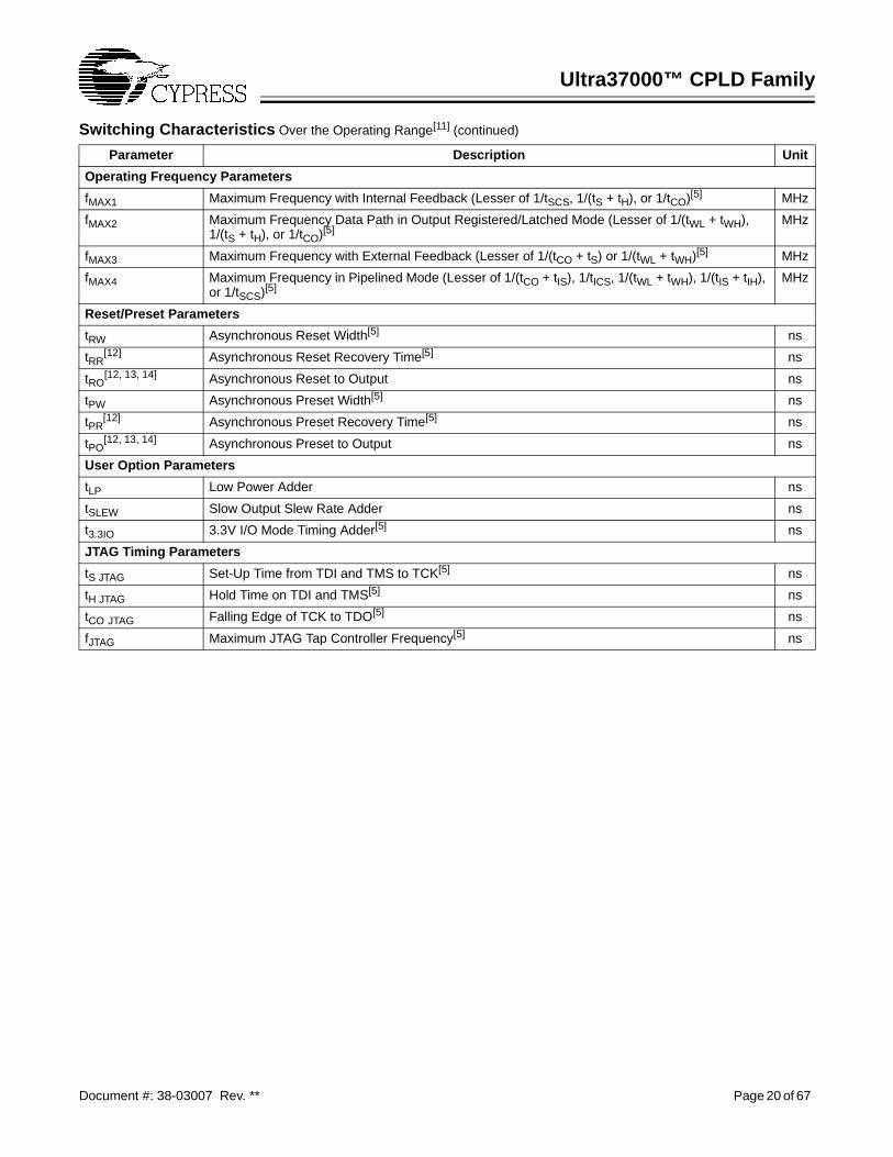
Ultra37000™ CPLD Family
Document #: 38-03007 Rev. ** Page 20 of 67
Operating Frequency Parameters
fMAX1 Maximum Frequency with Internal Feedback (Lesser of 1/tSCS, 1/(tS + tH), or 1/tCO)[5] MHz
fMAX2 Maximum Frequency Data Path in Output Registered/Latched Mode (Lesser of 1/(tWL + tWH), 1/(tS + tH), or 1/tCO)[5]
MHz
fMAX3 Maximum Frequency with External Feedback (Lesser of 1/(tCO + tS) or 1/(tWL + tWH)[5] MHz
fMAX4 Maximum Frequency in Pipelined Mode (Lesser of 1/(tCO + tIS), 1/tICS, 1/(tWL + tWH), 1/(tIS + tIH), or 1/tSCS)[5]
MHz
Reset/Preset Parameters
tRW Asynchronous Reset Width[5] ns
tRR[12] Asynchronous Reset Recovery Time[5] ns
tRO[12, 13, 14] Asynchronous Reset to Output ns
tPW Asynchronous Preset Width[5] ns
tPR[12] Asynchronous Preset Recovery Time[5] ns
tPO[12, 13, 14] Asynchronous Preset to Output ns
User Option Parameters
tLP Low Power Adder ns
tSLEW Slow Output Slew Rate Adder ns
t3.3IO 3.3V I/O Mode Timing Adder[5] ns
JTAG Timing Parameters
tS JTAG Set-Up Time from TDI and TMS to TCK[5] ns
tH JTAG Hold Time on TDI and TMS[5] ns
tCO JTAG Falling Edge of TCK to TDO[5] ns
fJTAG Maximum JTAG Tap Controller Frequency[5] ns
Switching Characteristics Over the Operating Range[11] (continued)
Parameter Description Unit
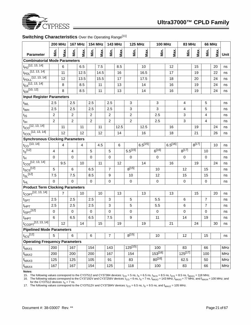
Ultra37000™ CPLD Family
Document #: 38-03007 Rev. ** Page 21 of 67
Switching Characteristics Over the Operating Range[11]
200 MHz 167 MHz 154 MHz 143 MHz 125 MHz 100 MHz 83 MHz 66 MHz
Parameter Min
.
Max
.
Min
.
Max
.
Min
.
Max
.
Min
.
Max
.
Min
.
Max
.
Min
.
Max
.
Min
.
Max
.
Min
.
Max
.
Unit
Combinatorial Mode Parameters
tPD[12, 13, 14] 6 6.5 7.5 8.5 10 12 15 20 ns
tPDL[12, 13, 14] 11 12.5 14.5 16 16.5 17 19 22 ns
tPDLL[12, 13, 14] 12 13.5 15.5 17 17.5 18 20 24 ns
tEA[12, 13, 14] 8 8.5 11 13 14 16 19 24 ns
tER[10, 12] 8 8.5 11 13 14 16 19 24 ns
Input Register Parameters
tWL 2.5 2.5 2.5 2.5 3 3 4 5 ns
tWH 2.5 2.5 2.5 2.5 3 3 4 5 ns
tIS 2 2 2 2 2 2.5 3 4 ns
tIH 2 2 2 2 2 2.5 3 4 ns
tICO[12, 13, 14] 11 11 11 12.5 12.5 16 19 24 ns
tICOL[12, 13, 14] 12 12 12 14 16 18 21 26 ns
Synchronous Clocking Parameters
tCO [13, 14] 4 4 4.5 6 6.5[15] 6.5[16] 8[17] 10 ns
tS[12] 4 4 5 5 5.5[15] 6[16] 8[17] 10 ns
tH 0 0 0 0 0 0 0 0 ns
tCO2[12, 13, 14] 9.5 10 11 12 14 16 19 24 ns
tSCS[12] 5 6 6.5 7 8[15] 10 12 15 ns
tSL[12] 7.5 7.5 8.5 9 10 12 15 15 ns
tHL 0 0 0 0 0 0 0 0 ns
Product Term Clocking Parameters
tCOPT[12, 13, 14] 7 10 10 13 13 13 15 20 ns
tSPT 2.5 2.5 2.5 3 5 5.5 6 7 ns
tHPT 2.5 2.5 2.5 3 5 5.5 6 7 ns
tISPT[12] 0 0 0 0 0 0 0 0 ns
tIHPT 6 6.5 6.5 7.5 9 11 14 19 ns
tCO2PT[12, 13, 14] 12 14 15 19 19 21 24 30 ns
Pipelined Mode Parameters
tICS[12] 5 6 6 7 8[15] 10 12 15 ns
Operating Frequency Parameters
fMAX1 200 167 154 143 125[15] 100 83 66 MHz
fMAX2 200 200 200 167 154 153[16] 125[17] 100 MHz
fMAX3 125 125 105 91 83 80[16] 62.5 50 MHz
fMAX4 167 167 154 125 118 100 83 66 MHz
Notes:15. The following values correspond to the CY37512 and CY37384 devices: tCO = 5 ns, tS = 6.5 ns, tSCS = 8.5 ns, tICS = 8.5 ns, fMAX1 = 118 MHz.16. The following values correspond to the CY37192V and CY37256V devices: tCO = 6 ns, tS = 7 ns, fMAX2 = 143 MHz, fMAX3 = 77 MHz, and fMAX4 = 100 MHz; and
for the CY37512 devices: tS = 7 ns.17. The following values correspond to the CY37512V and CY37384V devices: tCO = 6.5 ns, tS = 9.5 ns, and fMAX2 = 105 MHz.
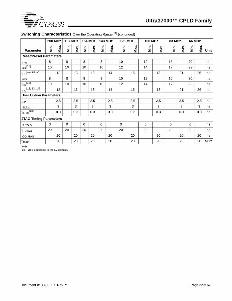
Ultra37000™ CPLD Family
Document #: 38-03007 Rev. ** Page 22 of 67
Reset/Preset Parameters
tRW 8 8 8 8 10 12 15 20 ns
tRR[12] 10 10 10 10 12 14 17 22 ns
tRO[12, 13, 14] 12 13 13 14 15 18 21 26 ns
tPW 8 8 8 8 10 12 15 20 ns
tPR[12] 10 10 10 10 12 14 17 22 ns
tPO[12, 13, 14] 12 13 13 14 15 18 21 26 ns
User Option Parameters
tLP 2.5 2.5 2.5 2.5 2.5 2.5 2.5 2.5 ns
tSLEW 3 3 3 3 3 3 3 3 ns
t3.3IO[18] 0.3 0.3 0.3 0.3 0.3 0.3 0.3 0.3 ns
JTAG Timing Parameters
tS JTAG 0 0 0 0 0 0 0 0 ns
tH JTAG 20 20 20 20 20 20 20 20 ns
tCO JTAG 20 20 20 20 20 20 20 20 ns
fJTAG 20 20 20 20 20 20 20 20 MHz
Note:18. Only applicable to the 5V devices.
Switching Characteristics Over the Operating Range[11] (continued)
200 MHz 167 MHz 154 MHz 143 MHz 125 MHz 100 MHz 83 MHz 66 MHz
Parameter Min
.
Max
.
Min
.
Max
.
Min
.
Max
.
Min
.
Max
.
Min
.
Max
.
Min
.
Max
.
Min
.
Max
.
Min
.
Max
.
Unit
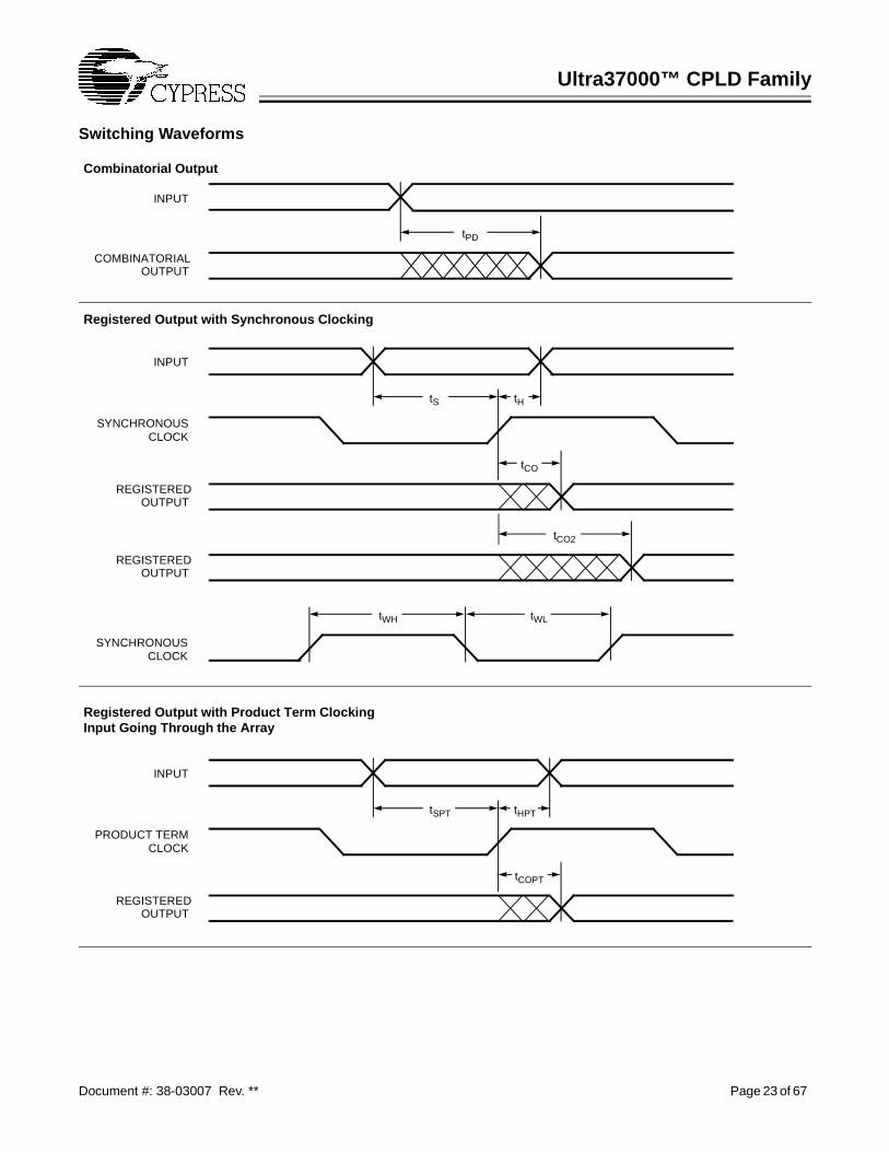
Ultra37000™ CPLD Family
Document #: 38-03007 Rev. ** Page 23 of 67
Switching Waveforms
tPD
INPUT
COMBINATORIALOUTPUT
Combinatorial Output
Registered Output with Synchronous Clocking
tS
INPUT
SYNCHRONOUS
tCO
REGISTEREDOUTPUT
tH
SYNCHRONOUS
tWLtWH
tCO2
REGISTEREDOUTPUT
CLOCK
CLOCK
Registered Output with Product Term Clocking
tSPT
INPUT
PRODUCT TERM
tCOPT
REGISTEREDOUTPUT
tHPT
CLOCK
Input Going Through the Array
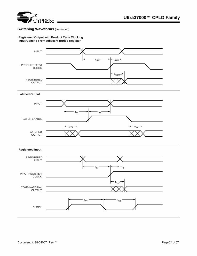
Ultra37000™ CPLD Family
Document #: 38-03007 Rev. ** Page 24 of 67
Switching Waveforms (continued)
Registered Output with Product Term Clocking
tISPT
INPUT
PRODUCT TERM
tCO2PT
REGISTEREDOUTPUT
tIHPT
CLOCK
Input Coming From Adjacent Buried Register
Latched Output
tSL
INPUT
LATCH ENABLE
tCO
LATCHEDOUTPUT
tHL
tPDL
Registered Input
tIS
REGISTEREDINPUT
INPUT REGISTERCLOCK
tICO
COMBINATORIALOUTPUT
tIH
CLOCK
tWLtWH
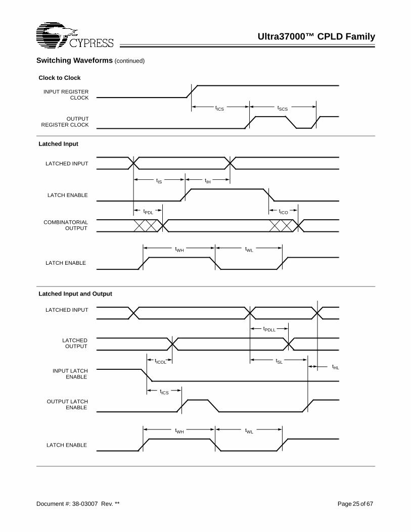
Ultra37000™ CPLD Family
Document #: 38-03007 Rev. ** Page 25 of 67
Switching Waveforms (continued)
Clock to Clock
INPUT REGISTERCLOCK
OUTPUTREGISTER CLOCK
tSCStICS
Latched Input
tIS
LATCHED INPUT
LATCH ENABLE
tICO
COMBINATORIALOUTPUT
tIH
tPDL
tWLtWH
LATCH ENABLE
Latched Input and Output
tICS
LATCHED INPUT
OUTPUT LATCHENABLE
LATCHEDOUTPUT
tPDLL
LATCH ENABLE
tWLtWH
tICOL
INPUT LATCHENABLE
tSLtHL
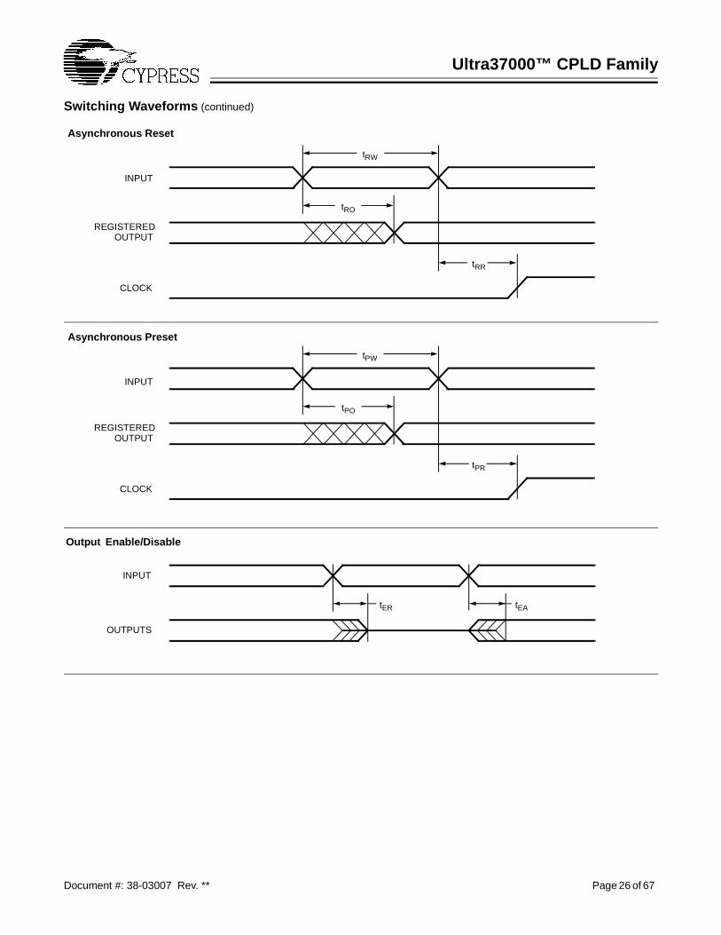
Ultra37000™ CPLD Family
Document #: 38-03007 Rev. ** Page 26 of 67
Switching Waveforms (continued)
Asynchronous Reset
INPUT
tRO
REGISTEREDOUTPUT
CLOCK
tRR
tRW
Asynchronous Preset
INPUT
tPO
REGISTEREDOUTPUT
CLOCK
tPR
tPW
Output Enable/Disable
INPUT
tER
OUTPUTS
tEA
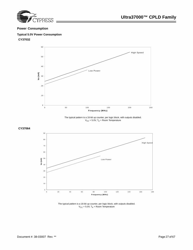
Ultra37000™ CPLD Family
Document #: 38-03007 Rev. ** Page 27 of 67
Power Consumption
Typical 5.0V Power Consumption
CY37032
CY37064
0
10
20
30
40
50
60
0 50 100 150 200 250
Frequency (M H z)
Icc
(mA
)
H igh S peed
Low P ow er
The typical pattern is a 16-bit up counter, per logic block, with outputs disabled.VCC = 5.0V, TA = Room Temperature
The typical pattern is a 16-bit up counter, per logic block, with outputs disabled.VCC = 5.0V, TA = Room Temperature
0
10
20
30
40
50
60
70
80
90
0 20 40 60 80 100 120 140 160 180
Frequency (M Hz)
Icc
(mA
)
Low P ower
H igh S peed
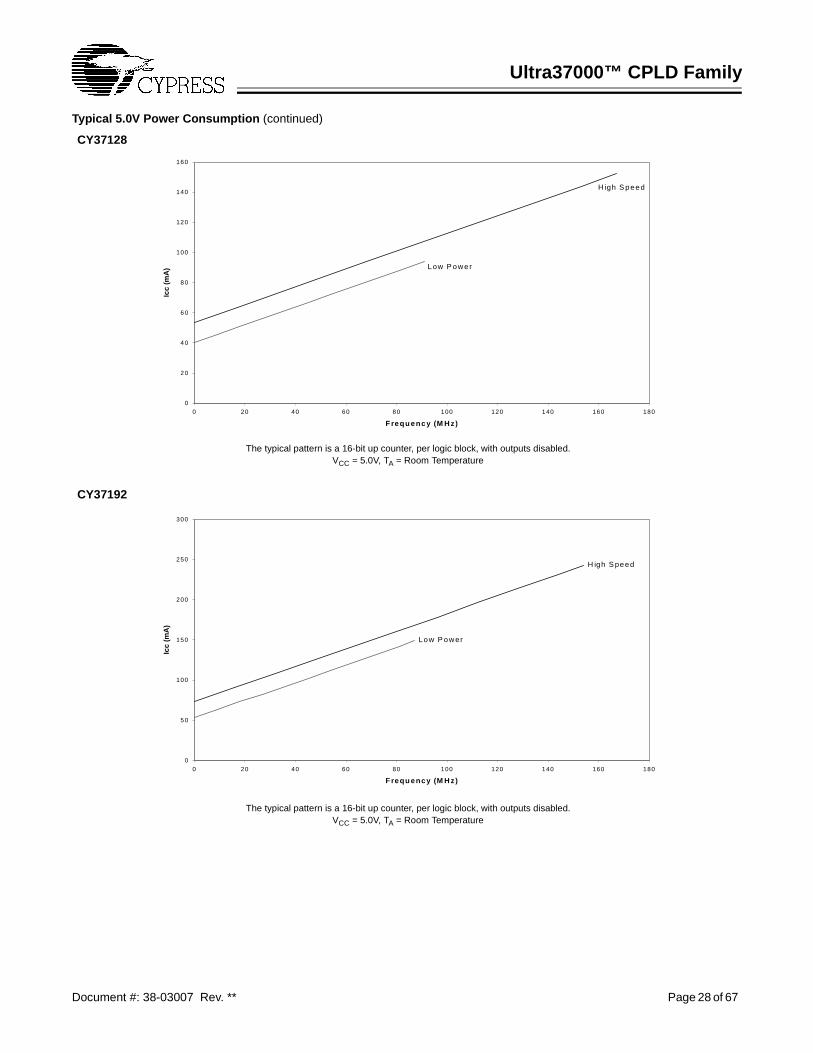
Ultra37000™ CPLD Family
Document #: 38-03007 Rev. ** Page 28 of 67
CY37128
CY37192
Typical 5.0V Power Consumption (continued)
0
2 0
4 0
6 0
8 0
100
120
140
160
0 20 40 60 80 100 120 140 160 180
F requ ency (M H z)
Icc
(mA
) Low P ow er
H igh S peed
The typical pattern is a 16-bit up counter, per logic block, with outputs disabled.VCC = 5.0V, TA = Room Temperature
0
5 0
100
150
200
250
300
0 20 40 60 80 100 120 140 160 180
F requ ency (M H z)
Icc
(mA
)
Low P ow er
H igh S peed
The typical pattern is a 16-bit up counter, per logic block, with outputs disabled.VCC = 5.0V, TA = Room Temperature
Ultra37000™ CPLD Family
Document #: 38-03007 Rev. ** Page 29 of 67
CY37256
CY37384
Typical 5.0V Power Consumption (continued)
0
5 0
100
150
200
250
300
0 20 40 60 80 100 120 140 160 180
F requ ency (M H z)
Icc
(mA
)
Low P ow er
H igh S peed
The typical pattern is a 16-bit up counter, per logic block, with outputs disabled.VCC = 5.0V, TA = Room Temperature
0
50
100
150
200
250
300
350
400
450
500
0 20 40 60 80 100 120 140 160
Frequency (M H z)
Icc
(mA
)
Low Power
H igh Speed
The typical pattern is a 16-bit up counter, per logic block, with outputs disabled.VCC = 5.0V, TA = Room Temperature
Ultra37000™ CPLD Family
Document #: 38-03007 Rev. ** Page 30 of 67
CY37512
Typical 5.0V Power Consumption (continued)
0
100
200
300
400
500
600
0 20 40 60 80 100 120 140 160
F requ ency (M H z)
Icc
(mA
)
Low P ow er
H igh S peed
The typical pattern is a 16-bit up counter, per logic block, with outputs disabled.VCC = 5.0V, TA = Room Temperature
Typical 3.3V Power Consumption
CY37032V
0
5
10
15
20
25
30
0 20 40 60 80 100 120 140 160
Frequency (M Hz)
Icc
(mA
)
Low Power
High Speed
The typical pattern is a 16-bit up counter, per logic block, with outputs disabled.VCC = 3.3V, TA = Room Temperature
Ultra37000™ CPLD Family
Document #: 38-03007 Rev. ** Page 31 of 67
CY37064V
CY37128V
Typical 3.3V Power Consumption (continued)
0
5
10
15
20
25
30
35
40
45
0 20 40 60 80 100 120 140
Frequency (M H z)
Icc
(mA
)
Low Power
H igh Speed
The typical pattern is a 16-bit up counter, per logic block, with outputs disabled.VCC = 3.3V, TA = Room Temperature
0
1 0
2 0
3 0
4 0
5 0
6 0
7 0
8 0
0 2 0 4 0 6 0 8 0 1 0 0 1 2 0 1 4 0
F re q u e n c y (M H z )
Icc
(mA
)
L o w P o w e r
H ig h S p e e d
The typical pattern is a 16-bit up counter, per logic block, with outputs disabled.VCC = 3.3V, TA = Room Temperature
Ultra37000™ CPLD Family
Document #: 38-03007 Rev. ** Page 32 of 67
CY37192V
CY37256V
Typical 3.3V Power Consumption (continued)
0
2 0
4 0
6 0
8 0
1 0 0
1 2 0
0 2 0 4 0 6 0 8 0 1 0 0 1 2 0
F re q u e n c y (M H z )
Icc
(mA
)
L o w P o w e r
H ig h S p e e d
The typical pattern is a 16-bit up counter, per logic block, with outputs disabled.VCC = 3.3V, TA = Room Temperature
0
2 0
4 0
6 0
8 0
1 0 0
1 2 0
1 4 0
0 2 0 4 0 6 0 8 0 1 0 0 1 2 0
F re q u e n c y (M H z )
Icc
(mA
)
L o w P o w e r
H ig h S p e e d
The typical pattern is a 16-bit up counter, per logic block, with outputs disabled.VCC = 3.3V, TA = Room Temperature
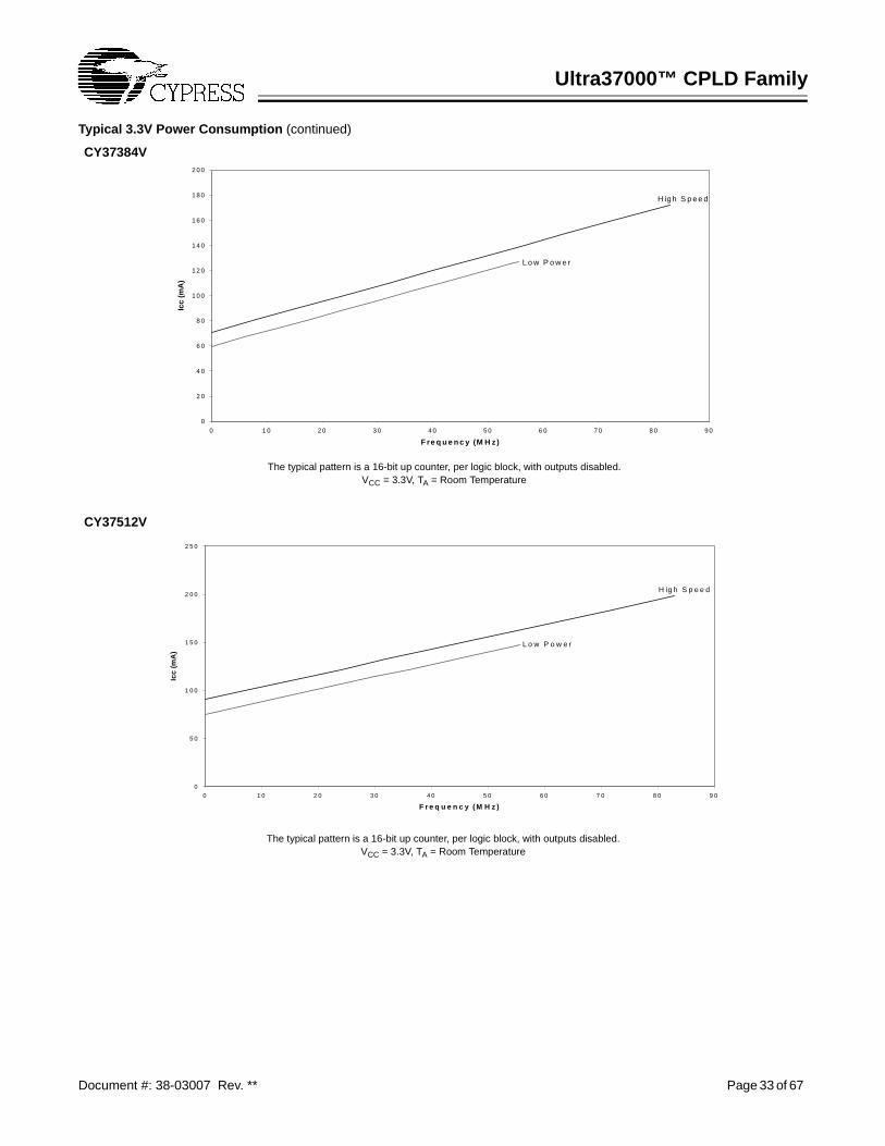
Ultra37000™ CPLD Family
Document #: 38-03007 Rev. ** Page 33 of 67
CY37384V
CY37512V
Typical 3.3V Power Consumption (continued)
0
2 0
4 0
6 0
8 0
1 0 0
1 2 0
1 4 0
1 6 0
1 8 0
2 0 0
0 1 0 2 0 3 0 4 0 5 0 6 0 7 0 8 0 9 0
F re q u e n c y (M H z)
Icc
(mA
)
L o w P o w e r
H ig h S p e e d
The typical pattern is a 16-bit up counter, per logic block, with outputs disabled.VCC = 3.3V, TA = Room Temperature
0
5 0
1 0 0
1 5 0
2 0 0
2 5 0
0 1 0 2 0 3 0 4 0 5 0 6 0 7 0 8 0 9 0
F r e q u e n c y (M H z )
Icc
(mA
)
L o w P o w e r
H ig h S p e e d
The typical pattern is a 16-bit up counter, per logic block, with outputs disabled.VCC = 3.3V, TA = Room Temperature
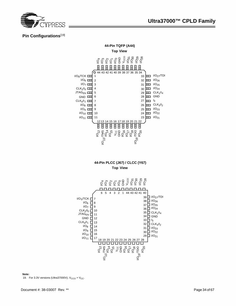
Ultra37000™ CPLD Family
Document #: 38-03007 Rev. ** Page 34 of 67
Pin Configurations[19]
Note:19. For 3.3V versions (Ultra37000V), VCCO = VCC.
44-Pin TQFP (A44)
Top View
I/O2
GN
DV
CC
O
I/O3
I/O4
I/O1
I/O0
I/O29
I/O30
I/O31
I/O28
I/O27/TDI
I/O26
I/O25I/O24
CLK1/I4GNDI3CLK3/I2I/O23I/O22
I/O21G
ND
I/O20
VC
C
I/O18
I/O17
I/O16
I/O15
I/O14
I/O12
I/O5/TCKI/O6
I/O7
CLK2/I0
GNDCLK0/I1
I/O8
I/O9I/O10
I/O11
89
7
1011
34
2
56
1
18 19 20 222113 14 15 171612
31
3029
32
33
26
2524
2728
23
44 43 42 4041 39 38 37 3536 34
I/O13
/TM
S
I/O19
/TD
O
JTAGEN
44-Pin PLCC (J67) / CLCC (Y67)
Top View
I/O27/TDII/O26I/O25I/O24
CLK1/I4GNDI3CLK3/I2I/O23I/O22
I/O21
I/O5/TCKI/O6I/O7
CLK2/I0JTAGEN
GNDCLK0/I1
I/O8
I/O9I/O10I/O11
GN
D
I/O20
I/O2
GN
DV
CC
O
VC
C
I/O3
I/O4
I/O1
I/O0
I/O29
I/O30
I/O31
I/O28
I/O19
I/O18
I/O17
I/O16
I/O15
I/O14
I/O13
I/O12
6 5 34 2
89
7
1011
44
18
1516
1413
12
1719 20 2221 23 24 2726 2825
313029
323334
39
3738
3635
43 42 4041
/TM
S
/TD
O
1
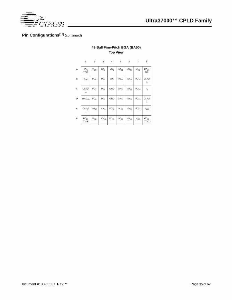
Ultra37000™ CPLD Family
Document #: 38-03007 Rev. ** Page 35 of 67
Pin Configurations[19] (continued)
48-Ball Fine-Pitch BGA (BA50)Top View
1 2 3 4 5 6 7 8
A I/O5 TCK
VCC I/O3 I/O1 I/O31 I/O30 VCC I/O27 TDI
B VCC I/O4 I/O2 I/O0 I/O29 I/O28 I/O26 CLK1/ I4
C CLK2/ I0
I/O7 I/O6 GND GND I/O25 I/O24 I3
D JTAGEN I/O8 I/O9 GND GND I/O22 I/O23 CLK3/ I2
E CLK0/ I1
I/O12 I/O11 I/O10 I/O16 I/O20 I/O21 VCC
F I/O13 TMS
VCC I/O14 I/O15 I/O17 I/O18 VCC I/O19 TDO
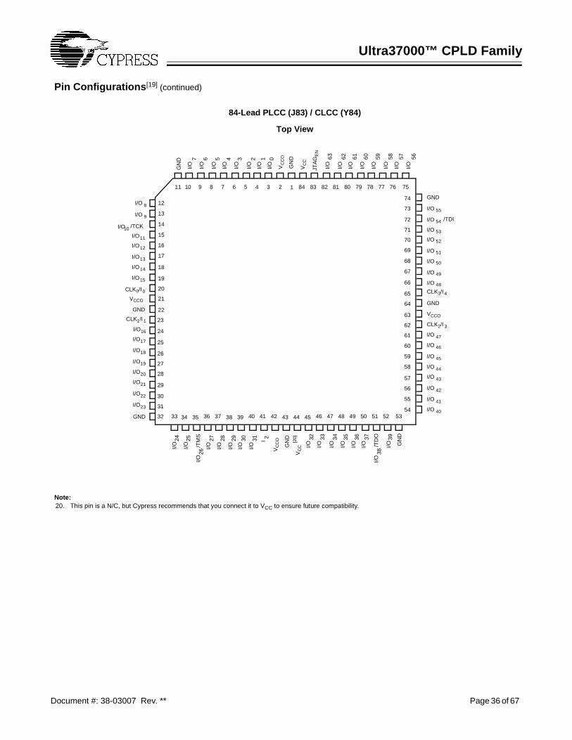
Ultra37000™ CPLD Family
Document #: 38-03007 Rev. ** Page 36 of 67
Note:20. This pin is a N/C, but Cypress recommends that you connect it to VCC to ensure future compatibility.
Pin Configurations[19] (continued)
I/O
I/O14
I/O15I/O 48
Top View
84-Lead PLCC (J83) / CLCC (Y84)
9 8 67 5
13
14
12
11
4948
58
59
60
23
24
26
25
27
15
16
4746
4 3
28
33
20
21
19
18
17
22
34 3736 38 4241 4340
66
65
63
64
62
61
67
68
69
74
72
73
71
70
84 8182 80 79
GND
I/O GN
D
I/O I/OI/O I/O I/O I/O I/OGN
D
I/O 55
I/O 54 /TDI
I/O 53
I/O 52
I/O 51
GND
I/O 49
CLK3/I 4
VCCO
CLK2/I 3
I/O 45
I/O 44
GN
D
I/O
I/O 8
I/O 9
I/O10 /TCK
I/O11
I/O12
I/O13
CLK0/I 0
VCCO
CLK1/I 1
I/O16
I/O17
I/O18
I/O19
I/O20
53525150
30
29
31
32
I/O I/O I/O I/O54
55
56
57 I/O 43
I/O 42
I/O 41
I/O 40
7778 76 75
I/O21
I/O22
I/O23
GND
I/O
I/O 50
I/O 47
I/O 46
GND
24
I/O25
/TM
S
I/O27
I/O28
I/O29
I/O30
I/O31
VC
CO
VC
C I/O32
I/O33
I/O34
I/O35
I/O36
I/O37
I/O38
I/O39
GN
D
I 2
7 6 5 4 3 2 1
VC
CO
I/O0
VC
C
63
I/O62 61 60 59 58 57 56
JTA
GE
N
I/O26
/TD
O
10
35 39 44 45
832 1
[20]
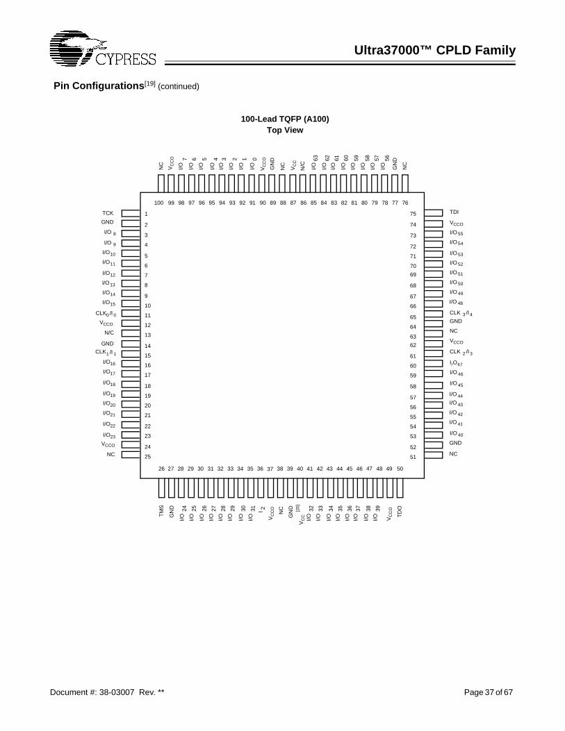
Ultra37000™ CPLD Family
Document #: 38-03007 Rev. ** Page 37 of 67
Pin Configurations[19] (continued)
Top View100-Lead TQFP (A100)
100 9798 96
2
3
1
4241
59
60
61
12
13
15
14
16
4
5
4039
95 94
17
26
9
10
8
7
6
11
27 28 3029 31 32 3534 36 3833
67
66
64
65
63
62
68
69
70
75
73
74
72
71
89 88 8687 8593 92 84
TDI
NC
VCCO
I/O 55
I/O 54
I/O 53
I/O 52
CLK 3 /I 4
I/O 50
I/O 48
GND
NC
I/O47
I/O 46
I/O 49
GN
D
TM
S
TCK
GND
I/O 8
I/O 9
I/O10
I/O11
I/O15
VCCO
GND
CLK1 /I 1
I/O16
I/O17
CLK0 /I 0
9091
I/O 51
VCCO
CLK 2 /I 3
I/O14
N/C
I/O12
I/O13
I/O 45
I/O 44
I/O 43
I/O 42
I/O 41
I/O 40
GND
NC
GN
D
NC
I/O18
I/O19
I/O20
I/O21
I/O22
I/O23
VCCO
NC
18
19
20
21
22
23
24
25
83 82 81 80 79 78 77 76
58
57
56
55
54
53
52
51
43 44 45 46 48 49 50
GN
D
I/O24
I/O25
I/O26
I/O27
I/O28
I/O29
I/O30
I/O31
VC
CO
VC
CI/O
32I/O
33
I/O34
I/O35
I/O36
I/O37
I/O38
I/O39I 2
NC
VC
CO
TD
O
I/OI/O GN
D
I/O I/OI/O I/O I/O I/O I/O I/O I/O I/O I/OI/O
7 6 5 4 3 2 1
VC
CO
I/O0
VC
C
NC
63
I/O62 61 60 59 58 57 56
VC
CO
N/C
99
37 47
[20]
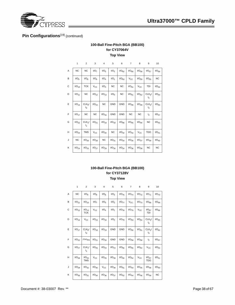
Ultra37000™ CPLD Family
Document #: 38-03007 Rev. ** Page 38 of 67
Pin Configurations[19] (continued)
100-Ball Fine-Pitch BGA (BB100)for CY37064V
Top View
100-Ball Fine-Pitch BGA (BB100)for CY37128V
Top View
1 2 3 4 5 6 7 8 9 10
A NC NC I/O7 I/O5 I/O2 I/O62 I/O60 I/O58 I/O57 I/O56
B I/O9 I/O8 I/O6 I/O4 I/O1 I/O63 VCC I/O59 I/O55 NC
C I/O10 TCK VCC I/O3 NC NC I/O61 VCC TDI I/O54
D I/O11 NC I/O12 I/O13 I/O0 NC I/O51 I/O52 CLK3/ I4
I/O53
E I/O14 CLK0/ I0
I/O15 NC GND GND I/O48 I/O49 CLK2/ I3
I/O50
F I/O17 NC NC I/O16 GND GND NC NC I2 I/O47
G I/O22 CLK1/ I1
I/O21 I/O19 I/O18 I/O46 I/O45 I/O44 NC I/O43
H I/O23 TMS VCC I/O20 NC I/O32 I/O42 VCC TDO I/O41
J NC I/O26 I/O28 NC I/O31 I/O33 I/O35 I/O37 I/O39 I/O40
K I/O24 I/O25 I/O27 I/O29 I/O30 I/O34 I/O36 I/O38 NC NC
1 2 3 4 5 6 7 8 9 10
A NC I/O9 I/O8 I/O6 I/O3 I/O76 I/O74 I/O72 I/O71 I/O70
B I/O11 I/O10 I/O7 I/O5 I/O2 I/O77 VCC I/O73 I/O68 I/O69
C I/O12 I/O13TCK
VCC I/O4 I/O1 I/O78 I/O75 VCC I/O67TDI
I/O66
D I/O14 VCC I/O15 I/O16 I/O0 I/O79 I/O63 I/O64 CLK3/ I4
I/O65
E I/O17 CLK0/ I0
I/O18 I/O19 GND GND I/O60 I/O61 CLK2/ I3
I/O62
F I/O22 JTAGEN I/O21 I/O20 GND GND I/O59 I/O58 I2 I/O57
G I/O27 CLK1/ I1
I/O26 I/O24 I/O23 I/O56 I/O55 I/O54 VCC I/O53
H I/O28 I/O33TMS
VCC I/O25 I/O39 I/O40 I/O52 VCC I/O47TDO
I/O51
J I/O29 I/O32 I/O35 VCC I/O38 I/O41 I/O43 I/O45 I/O48 I/O50
K I/O30 I/O31 I/O34 I/O36 I/O37 I/O42 I/O44 I/O46 I/O49 NC
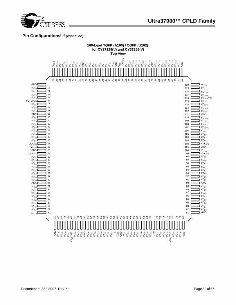
Ultra37000™ CPLD Family
Document #: 38-03007 Rev. ** Page 39 of 67
Pin Configurations[19] (continued)
I/O77
124
123
122
121
120119118117116115114113112111110109108107106105104103102101100
999897969594939291908988878685
43 44
160
45
159
46
158
47
157
48
156
49
155
50
154
51
153
52
152
53
151
54
150
55
149
56
148
57
147
58
146
59
145
60
144
61
143
62
142
63
141
64 65 66 67 68
140
69
139
70
138
71
137
72
136
73
135
74
134
75
133
76
132
77
131
78
130
79
129
80
128
81
127
82
126
160-Lead TQFP (A160) / CQFP (U162)
125
84
83
42
GNDI/O16
I/O17
I/O18I/O19
I/O20/TCKI/O21
I/O22
I/O23
I/O24
I/O25
I/O26
I/O27
I/O28
I/O29
I/O30
I/O31
I/O32
I/O33
I/O34
I/O35
I/O36
I/O37
I/O38
I/O39
I/O40
I/O41
I/O42
I/O43
I/O44
I/O45
I/O46
I/O47
GND
CLK0/I0VCCO
GNDCLK1/I1
GND
GN
D
GN
D
GN
D
GN
D
VCCO
I/O48
I/O49
I/O50
I/O51
I/O53
I/O54
I/O55
I/O56
I/O57
I/O58
I/O59
I/O60
I/O61
I/O62
I/O63 I 2
VC
CO
VC
C
I/O64
I/O65
I/O66
I/O67
I/O68
I/O69
I/O70
I/O71
I/O72
I/O73
I/O74
I/O75
I/O78
I/O79
VC
CO
GNDI/O80
I/O81
I/O82
I/O83
I/O84
I/O85
I/O86
I/O87
GNDI/O88
I/O89
I/O90
I/O91
I/O92
I/O93
I/O94
I/O95
I/O96
I/O97
I/O98
I/O99
I/O100
I/O101
I/O102
I/O103
GND
GND
CLK2/I3
VCCO
CLK3/I4
I/O104
I/O105
I/O106
I/O107
I/O108/TDII/O109
I/O110
I/O111
VCCOG
ND
GN
DV
CC
GN
D
I/O11
2
GN
D
VC
CO
VC
CO
I/O11
3
I/O11
4
I/O11
5
I/O11
6
I/O11
7
I/O11
8
I/O11
9
I/O12
0
I/O12
1
I/O12
2
I/O12
3
I/O12
4
I/O12
5
I/O12
6
I/O12
7
I/O0
I/O1
I/O2
I/O3
I/O4
I/O5
I/O6
I/O7
I/O8
I/O9
I/O10
I/O11
I/O12
I/O13
I/O14
I/O15
JTA
GE
N
I/O52
/TM
S
I/O76
/TD
O
23456789
10111213141516171819202122232425262728293031323334353637383940
1
41
for CY37128(V) and CY37256(V)Top View
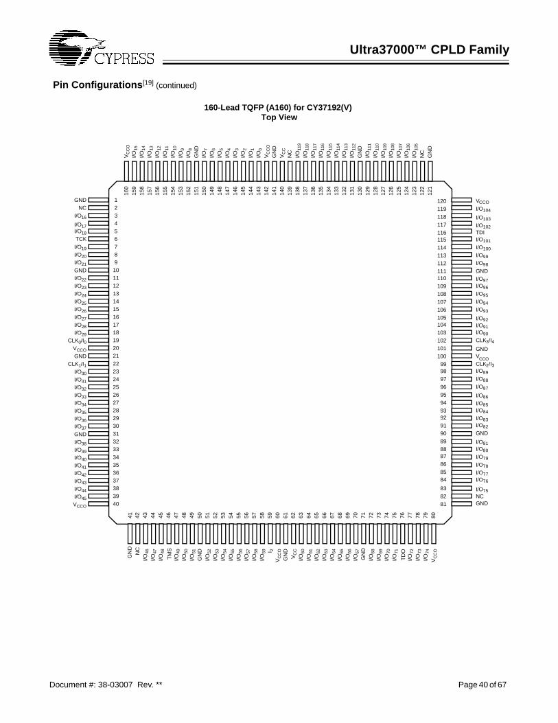
Ultra37000™ CPLD Family
Document #: 38-03007 Rev. ** Page 40 of 67
Pin Configurations[19] (continued)
I/O72
124
123
122
121
120119118117116115114113112111110109108107106105104103102101100
999897969594939291908988878685
43 44
160
45
159
46
158
47
157
48
156
49
155
50
154
51
153
52
152
53
151
54
150
55
149
56
148
57
147
58
146
59
145
60
144
61
143
62
142
63
141
64 65 66 67 68
140
69
139
70
138
71
137
72
136
73
135
74
134
75
133
76
132
77
131
78
130
79
129
80
128
81
127
82
126
160-Lead TQFP (A160) for CY37192(V)
125
84
83
42
GNDNC
I/O16
I/O17I/O18
TCKI/O19
I/O20
I/O21
I/O22
I/O23
I/O24
I/O25
I/O26
I/O27
I/O28
I/O29
I/O30
I/O31
I/O32
I/O33
I/O34
I/O35
I/O36
I/O37
I/O38
I/O39
I/O40
I/O41
I/O42
I/O43
I/O44
I/O45
GND
CLK0/I0VCCO
GNDCLK1/I1
GND
GN
D
GN
D
GN
D
GN
D
VCCO
NC
I/O46
I/O47
I/O48
I/O49
I/O50
I/O51
I/O52
I/O53
I/O54
I/O55
I/O56
I/O57
I/O58
I/O59 I 2
VC
CO
VC
C
I/O60
I/O61
I/O62
I/O63
I/O64
I/O65
I/O66
I/O67
I/O68
I/O69
I/O70
I/O71
I/O73
I/O74
VC
CO
GNDNCI/O75
I/O76
I/O77
I/O78
I/O79
I/O80
I/O81
GNDI/O82
I/O83
I/O84
I/O85
I/O86
I/O87
I/O88
I/O89
I/O90
I/O91
I/O92
I/O93
I/O94
I/O95
I/O96
I/O97
GND
GND
CLK2/I3
VCCO
CLK3/I4
I/O98
I/O99
I/O100
I/O101
TDII/O102
I/O103
I/O104
VCCOG
ND
GN
DV
CC
GN
D
NC
GN
D
VC
CO
VC
CO
I/O10
5
I/O10
6
I/O10
7
I/O10
8
I/O10
9
I/O11
0
I/O11
1
I/O11
2
I/O11
3
I/O11
4
I/O11
5
I/O11
6
I/O11
7
I/O11
8
I/O11
9
I/O0
I/O1
I/O2
I/O3
I/O4
I/O5
I/O6
I/O7
I/O8
I/O9
I/O10
I/O11
I/O12
I/O13
I/O14
I/O15
NC
TM
S
TD
O
23456789
10111213141516171819202122232425262728293031323334353637383940
1
41
Top View
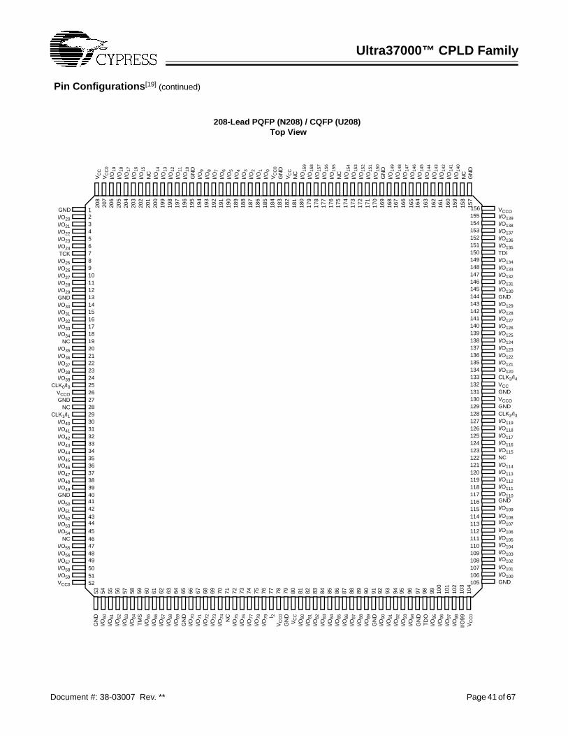
Ultra37000™ CPLD Family
Document #: 38-03007 Rev. ** Page 41 of 67
Pin Configurations[19] (continued)
I/O15
2
I/O15
4I/O
153
2345678910111213141516171819202122232425262728293031323334353637383940
1
414243444546474849505152
206
205
204
203
202
201
200
199
198
197
196
195
194
193
192
191
190
189
188
187
186
185
184
183
182
181
180
179
178
177
176
175
174
173
172
171
170
169
168
208
167
166
165
164
163
162
161
160
159
158
157
54 55 56 57 58 59 60 61 62 63 64 65 66 67 68 69 70 71 72 73 74 75 76 77 78 79 80 81 82 83 84 85 86 87 88 89 90 9153 92 93 94 95 96 97 98 99 100
101
102
103
154153152151150149148147146145144143142141140139138137136135134133132131130129128127126125124123122121120119118117116
155
115114113112111110109108107106105
156
104
207
208-Lead PQFP (N208) / CQFP (U208) Top View
I/O139I/O138I/O137I/O136I/O135TDII/O134I/O133I/O132I/O131I/O130GNDI/O129I/O128I/O127I/O126I/O125I/O124I/O123I/O122I/O121I/O120CLK3/I4VCCGNDVCCOGNDCLK2/I3I/O119I/O118I/O117I/O116I/O115NCI/O114I/O113I/O112I/O111I/O110
VCCO
GNDI/O109
I/O108I/O107
I/O106
I/O105I/O104I/O103I/O102
I/O101I/O100GND
I/O61
I/O62
I/O63
I/O64
TM
SI/O
65I/O
66I/O
67I/O
68I/O
69
GN
DI/O
70I/O
71I/O
72I/O
73I/O
74 NC
I/O75
I/O76
I/O77
I/O78
I/O79 I 2
VC
C0
GN
DV
CC
I/O80
I/O81
I/O82
I/O83
I/O84
I/O85
I/O86
I/O87
I/O88
I/O89
GN
DI/O
90I/O
91
GN
D
I/O92
I/O93
I/O94
GN
DT
DO
I/O95
I/O96
I/O97
I/O98
I/O99
VC
C0
I/O60
I/O21I/O22I/O23I/O24TCKI/O25I/O26I/O27I/O28I/O29GNDI/O30I/O31I/O32I/O33I/O34
NCI/O35I/O36I/O37I/O38I/O39
CLK0/I0VCCOGND
NCCLK1/I1
I/O40I/O41I/O42I/O43I/O44I/O45I/O46I/O47I/O48I/O49GNDI/O50
I/O20
I/O51I/O52I/O53I/O54
NCI/O55I/O56I/O57I/O58I/O59VCC0
GND
VC
C0
I/O19
I/O18
I/O17
I/O16
I/O15
NC
I/O14
I/O13
I/O12
I/O11
I/O10
GN
DI/O
9I/O
8I/O
7I/O
6I/O
5I/O
4I/O
3I/O
2I/O
1I/O
0V
CC
0G
ND
VC
CN
CI/O
159
I/O15
8I/O
157
I/O15
6I/O
155
NC
I/O15
1I/O
150
VC
C
GN
DI/O
149
I/O14
8I/O
147
I/O14
6I/O
145
I/O14
4I/O
143
I/O14
2I/O
141
I/O14
0N
CG
ND
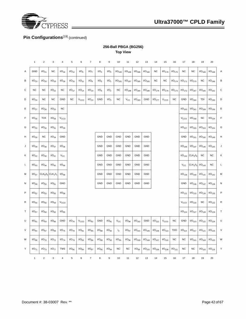
Ultra37000™ CPLD Family
Document #: 38-03007 Rev. ** Page 42 of 67
Pin Configurations[19] (continued)
256-Ball PBGA (BG256)Top View
1 2 3 4 5 6 7 8 9 10 11 12 13 14 15 16 17 18 19 20
A GND I/O21 NC I/O16 I/O12 I/O9 I/O7 I/O4 I/O0 I/O190 I/O189 I/O186 I/O182 NC I/O178 I/O175 NC NC I/O169 I/O168 A
B I/O23 I/O20 I/O19 I/O18 I/O15 I/O11 I/O8 I/O5 I/O1 I/O191 I/O187 I/O185 I/O181 NC NC I/O174 I/O171 I/O170 NC I/O166 B
C NC NC I/O22 NC I/O17 I/O14 I/O10 I/O6 I/O2 NC I/O188 I/O184 I/O180 I/O179 I/O176 I/O173 I/O172 I/O167 I/O165 I/O162 C
D I/O24 NC NC GND NC VCCO I/O13 GND I/O3 NC VCC I/O183 GND I/O177 VCCO NC GND I/O164 TDI I/O160 D
E I/O27 I/O26 I/O25 NC I/O163 I/O161 I/O159 I/O156 E
F I/O30 TCK I/O28 VCCO VCCO I/O158 NC I/O154 F
G I/O33 I/O32 I/O31 I/O29 I/O157 I/O155 I/O153 I/O152 G
H I/O35 NC I/O34 GND GND GND GND GND GND GND GND I/O151 I/O150 I/O149 H
J I/O39 I/O38 I/O37 I/O36 GND GND GND GND GND GND I/O148 I/O147 I/O146 I/O145 J
K I/O42 I/O40 I/O41 VCC GND GND GND GND GND GND I/O144 CLK3/I4 NC NC K
L I/O43 I/O44 I/O45 I/O46 GND GND GND GND GND GND VCC CLK2/I3 I/O143 NC L
M I/O47 CLK0/I0 CLK1/I1 I/O48 GND GND GND GND GND GND I/O139 I/O140 I/O141 I/O142 M
N I/O49 I/O50 I/O51 GND GND GND GND GND GND GND GND I/O136 I/O137 I/O138 N
P I/O52 I/O53 I/O55 I/O58 I/O131 I/O133 I/O134 I/O135 P
R I/O54 I/O56 I/O59 VCCO VCCO I/O130 NC I/O132 R
T I/O57 I/O60 I/O62 I/O65 I/O124 I/O127 I/O128 I/O129 T
U I/O61 I/O63 I/O66 GND I/O76 VCCO I/O82 GND I/O91 VCC I/O98 I/O102 GND I/O112 VCCO NC GND I/O123 I/O122 I/O126 U
V I/O64 I/O67 I/O69 I/O75 I/O78 I/O81 I/O85 I/O88 I/O92 I2 I/O97 I/O101 I/O105 I/O109 I/O113 TDO I/O114 I/O117 I/O121 I/O125 V
W I/O68 I/O70 I/O72 I/O74 I/O79 I/O83 I/O86 I/O89 I/O93 I/O95 I/O96 I/O100 I/O104 I/O107 I/O110 NC NC I/O115 I/O118 I/O120 W
Y I/O71 I/O73 I/O77 TMS I/O80 I/O84 I/O87 I/O90 I/O94 NC NC I/O99 I/O103 I/O106 I/O108 I/O111 NC NC I/O116 I/O119 Y
1 2 3 4 5 6 7 8 9 10 11 12 13 14 15 16 17 18 19 20
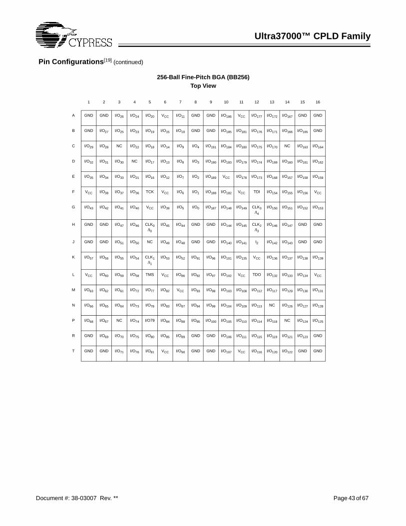
Ultra37000™ CPLD Family
Document #: 38-03007 Rev. ** Page 43 of 67
Pin Configurations[19] (continued)
256-Ball Fine-Pitch BGA (BB256)Top View
1 2 3 4 5 6 7 8 9 10 11 12 13 14 15 16
A GND GND I/O26 I/O24 I/O20 VCC I/O11 GND GND I/O186 VCC I/O177 I/O172 I/O167 GND GND
B GND I/O27 I/O25 I/O23 I/O19 I/O15 I/O10 GND GND I/O185 I/O181 I/O176 I/O171 I/O166 I/O165 GND
C I/O29 I/O28 NC I/O22 I/O18 I/O14 I/O9 I/O4 I/O191 I/O184 I/O180 I/O175 I/O170 NC I/O163 I/O164
D I/O32 I/O31 I/O30 NC I/O17 I/O13 I/O8 I/O3 I/O190 I/O183 I/O179 I/O174 I/O169 I/O160 I/O161 I/O162
E I/O35 I/O34 I/O33 I/O21 I/O16 I/O12 I/O7 I/O2 I/O189 VCC I/O178 I/O173 I/O168 I/O157 I/O158 I/O159
F VCC I/O38 I/O37 I/O36 TCK VCC I/O6 I/O1 I/O188 I/O182 VCC TDI I/O154 I/O155 I/O156 VCC
G I/O43 I/O42 I/O41 I/O40 VCC I/O39 I/O5 I/O0 I/O187 I/O148 I/O149 CLK3 /I4
I/O150 I/O151 I/O152 I/O153
H GND GND I/O47 I/O46 CLK0 /I0
I/O45 I/O44 GND GND I/O144 I/O145 CLK2 /I3
I/O146 I/O147 GND GND
J GND GND I/O51 I/O50 NC I/O49 I/O48 GND GND I/O140 I/O141 I2 I/O142 I/O143 GND GND
K I/O57 I/O56 I/O55 I/O54 CLK1 /I1
I/O53 I/O52 I/O91 I/O96 I/O101 I/O135 VCC I/O136 I/O137 I/O138 I/O139
L VCC I/O60 I/O59 I/O58 TMS VCC I/O86 I/O92 I/O97 I/O102 VCC TDO I/O132 I/O133 I/O134 VCC
M I/O63 I/O62 I/O61 I/O72 I/O77 I/O82 VCC I/O93 I/O98 I/O103 I/O108 I/O112 I/O117 I/O129 I/O130 I/O131
N I/O66 I/O65 I/O64 I/O73 I/O78 I/O83 I/O87 I/O94 I/O99 I/O104 I/O109 I/O113 NC I/O126 I/O127 I/O128
P I/O68 I/O67 NC I/O74 I/O79 I/O84 I/O88 I/O95 I/O100 I/O105 I/O110 I/O114 I/O118 NC I/O124 I/O125
R GND I/O69 I/O70 I/O75 I/O80 I/O85 I/O89 GND GND I/O106 I/O111 I/O115 I/O119 I/O121 I/O123 GND
T GND GND I/O71 I/O76 I/O81 VCC I/O90 GND GND I/O107 VCC I/O116 I/O120 I/O122 GND GND
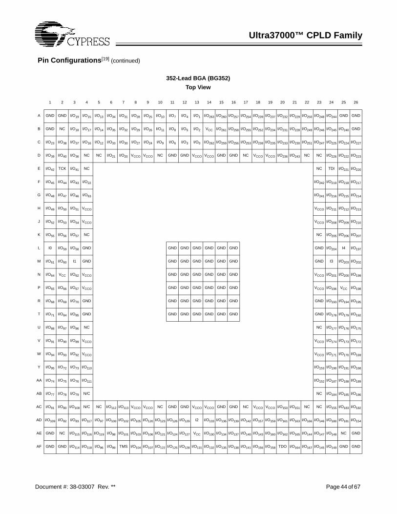
Ultra37000™ CPLD Family
Document #: 38-03007 Rev. ** Page 44 of 67
Pin Configurations[19] (continued)
352-Lead BGA (BG352)
Top View
1 2 3 4 5 6 7 8 9 10 11 12 13 14 15 16 17 18 19 20 21 22 23 24 25 26
A GND GND I/O19 I/O15 I/O13 I/O34 I/O31 I/O28 I/O25 I/O10 I/O7 I/O4 I/O1 I/O263 I/O260 I/O257 I/O254 I/O239 I/O237 I/O232 I/O229 I/O250 I/O248 I/O244 GND GND
B GND NC I/O18 I/O17 I/O14 I/O35 I/O32 I/O29 I/O26 I/O11 I/O8 I/O5 I/O2 VCC I/O261 I/O258 I/O255 I/O252 I/O234 I/O231 I/O228 I/O249 I/O246 I/O245 I/O240 GND
C I/O23 I/O38 I/O37 I/O16 I/O12 I/O33 I/O30 I/O27 I/O24 I/O9 I/O6 I/O3 I/O0 I/O262 I/O259 I/O256 I/O253 I/O238 I/O235 I/O233 I/O230 I/O251 I/O247 I/O225 I/O224 I/O227
D I/O39 I/O40 I/O36 NC NC I/O21 I/O20 VCCO VCCO NC GND GND VCCO VCCO GND GND NC VCCO VCCO I/O236 I/O243 NC NC I/O226 I/O222 I/O223
E I/O42 TCK I/O41 NC NC TDI I/O221 I/O220
F I/O45 I/O44 I/O43 I/O22 I/O242 I/O219 I/O218 I/O217
G I/O48 I/O47 I/O46 I/O63 I/O241 I/O216 I/O215 I/O214
H I/O49 I/O50 I/O51 VCCO VCCO I/O211 I/O212 I/O213
J I/O52 I/O53 I/O54 VCCO VCCO I/O208 I/O209 I/O210
K I/O55 I/O56 I/O57 NC NC I/O205 I/O206 I/O207
L I0 I/O59 I/O58 GND GND GND GND GND GND GND GND I/O204 I4 I/O197
M I/O61 I/O60 I1 GND GND GND GND GND GND GND GND I3 I/O203 I/O202
N I/O64 VCC I/O62 VCCO GND GND GND GND GND GND VCCO I/O201 I/O200 I/O199
P I/O65 I/O66 I/O67 VCCO GND GND GND GND GND GND VCCO I/O196 VCC I/O198
R I/O68 I/O69 I/O70 GND GND GND GND GND GND GND GND I/O193 I/O194 I/O195
T I/O71 I/O84 I/O85 GND GND GND GND GND GND GND GND I/O178 I/O179 I/O192
U I/O88 I/O87 I/O86 NC NC I/O177 I/O176 I/O175
V I/O91 I/O90 I/O89 VCCO VCCO I/O174 I/O173 I/O172
W I/O94 I/O93 I/O92 VCCO VCCO I/O171 I/O170 I/O169
Y I/O95 I/O72 I/O73 I/O110 I/O153 I/O190 I/O191 I/O168
AA I/O74 I/O75 I/O76 I/O111 I/O152 I/O187 I/O188 I/O189
AB I/O77 I/O78 I/O79 N/C NC I/O184 I/O185 I/O186
AC I/O81 I/O80 I/O108 N/C NC I/O112 I/O113 VCCO VCCO NC GND GND VCCO VCCO GND GND NC VCCO VCCO I/O150 I/O151 NC NC I/O155 I/O183 I/O182
AD I/O109 I/O82 I/O83 I/O117 I/O97 I/O100 I/O102 I/O105 I/O120 I/O123 I/O126 I/O129 I2 I/O133 I/O136 I/O139 I/O142 I/O157 I/O159 I/O161 I/O163 I/O166 I/O146 I/O180 I/O181 I/O154
AE GND NC I/O115 I/O116 I/O119 I/O98 I/O101 I/O103 I/O106 I/O121 I/O124 I/O127 VCC I/O130 I/O134 I/O137 I/O140 I/O143 I/O160 I/O162 I/O165 I/O144 I/O147 I/O148 NC GND
AF GND GND I/O114 I/O118 I/O96 I/O99 TMS I/O104 I/O107 I/O122 I/O125 I/O128 I/O131 I/O132 I/O135 I/O138 I/O141 I/O156 I/O158 TDO I/O164 I/O167 I/O145 I/O149 GND GND
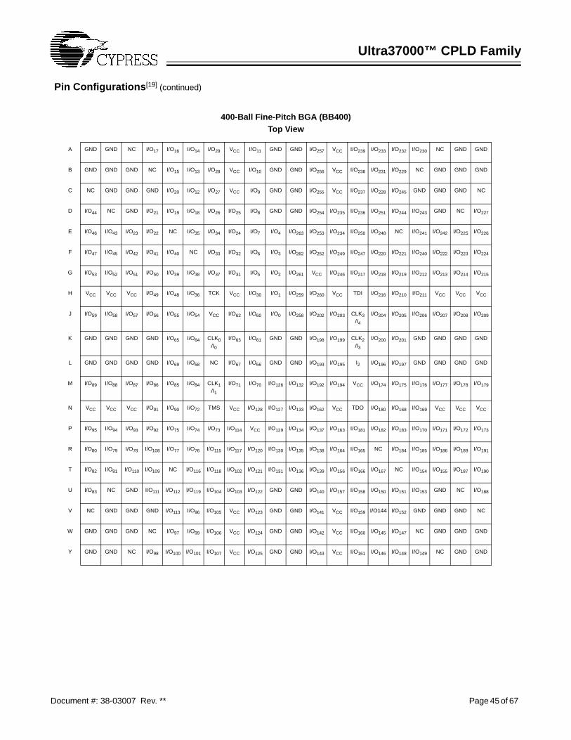
Ultra37000™ CPLD Family
Document #: 38-03007 Rev. ** Page 45 of 67
Pin Configurations[19] (continued)
400-Ball Fine-Pitch BGA (BB400)Top View
A GND GND NC I/O17 I/O16 I/O14 I/O29 VCC I/O11 GND GND I/O257 VCC I/O239 I/O233 I/O232 I/O230 NC GND GND
B GND GND GND NC I/O15 I/O13 I/O28 VCC I/O10 GND GND I/O256 VCC I/O238 I/O231 I/O229 NC GND GND GND
C NC GND GND GND I/O20 I/O12 I/O27 VCC I/O9 GND GND I/O255 VCC I/O237 I/O228 I/O245 GND GND GND NC
D I/O44 NC GND I/O21 I/O19 I/O18 I/O26 I/O25 I/O8 GND GND I/O254 I/O235 I/O236 I/O251 I/O244 I/O243 GND NC I/O227
E I/O46 I/O43 I/O23 I/O22 NC I/O35 I/O34 I/O24 I/O7 I/O4 I/O263 I/O253 I/O234 I/O250 I/O248 NC I/O241 I/O242 I/O225 I/O226
F I/O47 I/O45 I/O42 I/O41 I/O40 NC I/O33 I/O32 I/O6 I/O3 I/O262 I/O252 I/O249 I/O247 I/O220 I/O221 I/O240 I/O222 I/O223 I/O224
G I/O53 I/O52 I/O51 I/O50 I/O39 I/O38 I/O37 I/O31 I/O5 I/O2 I/O261 VCC I/O246 I/O217 I/O218 I/O219 I/O212 I/O213 I/O214 I/O215
H VCC VCC VCC I/O49 I/O48 I/O36 TCK VCC I/O30 I/O1 I/O259 I/O260 VCC TDI I/O216 I/O210 I/O211 VCC VCC VCC
J I/O59 I/O58 I/O57 I/O56 I/O55 I/O54 VCC I/O62 I/O60 I/O0 I/O258 I/O202 I/O203 CLK3 /I4
I/O204 I/O205 I/O206 I/O207 I/O208 I/O209
K GND GND GND GND I/O65 I/O64 CLK0 /I0
I/O63 I/O61 GND GND I/O198 I/O199 CLK2 /I3
I/O200 I/O201 GND GND GND GND
L GND GND GND GND I/O69 I/O68 NC I/O67 I/O66 GND GND I/O193 I/O195 I2 I/O196 I/O197 GND GND GND GND
M I/O89 I/O88 I/O87 I/O86 I/O85 I/O84 CLK1 /I1
I/O71 I/O70 I/O126 I/O132 I/O192 I/O194 VCC I/O174 I/O175 I/O176 I/O177 I/O178 I/O179
N VCC VCC VCC I/O91 I/O90 I/O72 TMS VCC I/O128 I/O127 I/O133 I/O162 VCC TDO I/O180 I/O168 I/O169 VCC VCC VCC
P I/O95 I/O94 I/O93 I/O92 I/O75 I/O74 I/O73 I/O114 VCC I/O129 I/O134 I/O137 I/O163 I/O181 I/O182 I/O183 I/O170 I/O171 I/O172 I/O173
R I/O80 I/O79 I/O78 I/O108 I/O77 I/O76 I/O115 I/O117 I/O120 I/O130 I/O135 I/O138 I/O164 I/O165 NC I/O184 I/O185 I/O186 I/O189 I/O191
T I/O82 I/O81 I/O110 I/O109 NC I/O116 I/O118 I/O102 I/O121 I/O131 I/O136 I/O139 I/O156 I/O166 I/O167 NC I/O154 I/O155 I/O187 I/O190
U I/O83 NC GND I/O111 I/O112 I/O119 I/O104 I/O103 I/O122 GND GND I/O140 I/O157 I/O158 I/O150 I/O151 I/O153 GND NC I/O188
V NC GND GND GND I/O113 I/O96 I/O105 VCC I/O123 GND GND I/O141 VCC I/O159 I/O144 I/O152 GND GND GND NC
W GND GND GND NC I/O97 I/O99 I/O106 VCC I/O124 GND GND I/O142 VCC I/O160 I/O145 I/O147 NC GND GND GND
Y GND GND NC I/O98 I/O100 I/O101 I/O107 VCC I/O125 GND GND I/O143 VCC I/O161 I/O146 I/O148 I/O149 NC GND GND
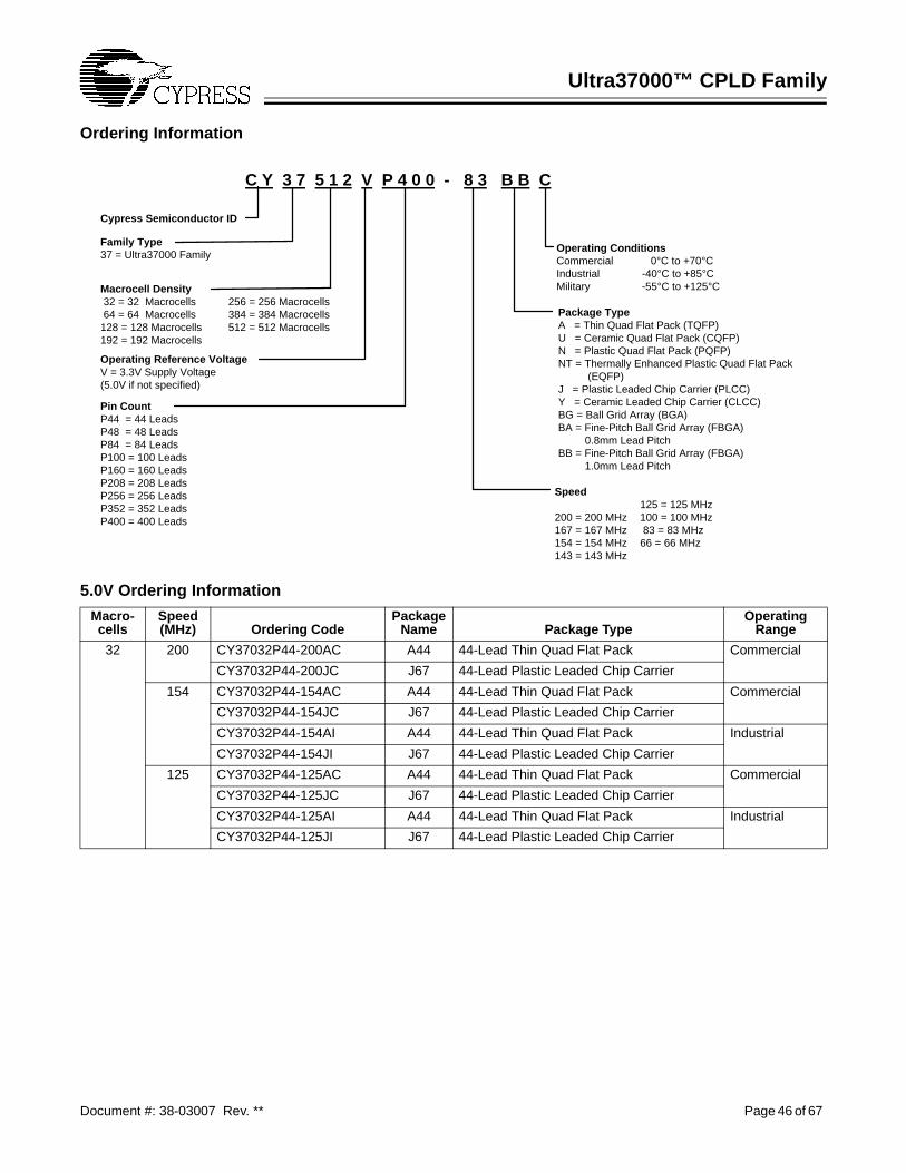
Ultra37000™ CPLD Family
Document #: 38-03007 Rev. ** Page 46 of 67
Ordering Information
5.0V Ordering Information
Macro-cells
Speed(MHz) Ordering Code
PackageName Package Type
OperatingRange
32 200 CY37032P44-200AC A44 44-Lead Thin Quad Flat Pack Commercial
CY37032P44-200JC J67 44-Lead Plastic Leaded Chip Carrier
154 CY37032P44-154AC A44 44-Lead Thin Quad Flat Pack Commercial
CY37032P44-154JC J67 44-Lead Plastic Leaded Chip Carrier
CY37032P44-154AI A44 44-Lead Thin Quad Flat Pack Industrial
CY37032P44-154JI J67 44-Lead Plastic Leaded Chip Carrier
125 CY37032P44-125AC A44 44-Lead Thin Quad Flat Pack Commercial
CY37032P44-125JC J67 44-Lead Plastic Leaded Chip Carrier
CY37032P44-125AI A44 44-Lead Thin Quad Flat Pack Industrial
CY37032P44-125JI J67 44-Lead Plastic Leaded Chip Carrier
C Y 3 7 5 1 2 V P 4 0 0 - 8 3 B B C
Cypress Semiconductor ID
Family Type37 = Ultra37000 Family
Macrocell Density 32 = 32 Macrocells 256 = 256 Macrocells 64 = 64 Macrocells 384 = 384 Macrocells128 = 128 Macrocells 512 = 512 Macrocells192 = 192 Macrocells
Speed125 = 125 MHz
200 = 200 MHz 100 = 100 MHz167 = 167 MHz 83 = 83 MHz154 = 154 MHz 66 = 66 MHz143 = 143 MHz
Package TypeA = Thin Quad Flat Pack (TQFP)U = Ceramic Quad Flat Pack (CQFP)N = Plastic Quad Flat Pack (PQFP)NT = Thermally Enhanced Plastic Quad Flat Pack (EQFP)J = Plastic Leaded Chip Carrier (PLCC)Y = Ceramic Leaded Chip Carrier (CLCC)BG = Ball Grid Array (BGA)BA = Fine-Pitch Ball Grid Array (FBGA) 0.8mm Lead PitchBB = Fine-Pitch Ball Grid Array (FBGA) 1.0mm Lead Pitch
Operating ConditionsCommercial 0°C to +70°CIndustrial -40°C to +85°CMilitary -55°C to +125°C
Operating Reference VoltageV = 3.3V Supply Voltage(5.0V if not specified)
Pin CountP44 = 44 LeadsP48 = 48 LeadsP84 = 84 LeadsP100 = 100 LeadsP160 = 160 LeadsP208 = 208 LeadsP256 = 256 LeadsP352 = 352 LeadsP400 = 400 Leads
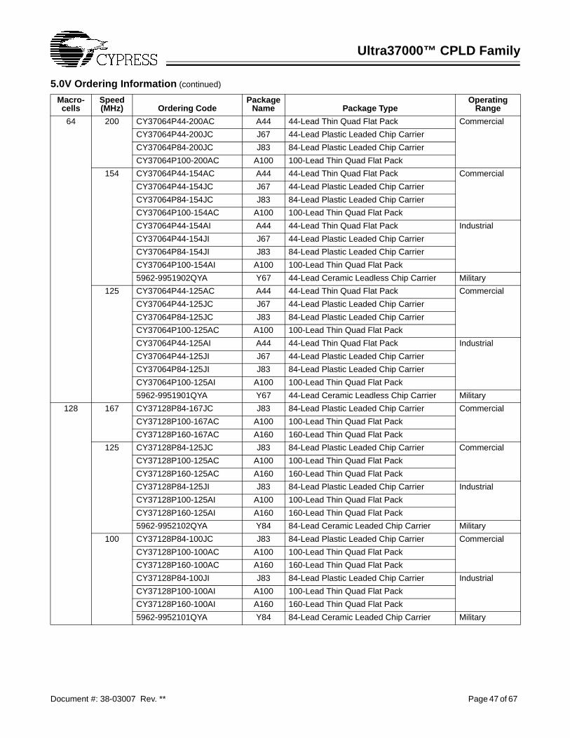
Ultra37000™ CPLD Family
Document #: 38-03007 Rev. ** Page 47 of 67
64 200 CY37064P44-200AC A44 44-Lead Thin Quad Flat Pack Commercial
CY37064P44-200JC J67 44-Lead Plastic Leaded Chip Carrier
CY37064P84-200JC J83 84-Lead Plastic Leaded Chip Carrier
CY37064P100-200AC A100 100-Lead Thin Quad Flat Pack
154 CY37064P44-154AC A44 44-Lead Thin Quad Flat Pack Commercial
CY37064P44-154JC J67 44-Lead Plastic Leaded Chip Carrier
CY37064P84-154JC J83 84-Lead Plastic Leaded Chip Carrier
CY37064P100-154AC A100 100-Lead Thin Quad Flat Pack
CY37064P44-154AI A44 44-Lead Thin Quad Flat Pack Industrial
CY37064P44-154JI J67 44-Lead Plastic Leaded Chip Carrier
CY37064P84-154JI J83 84-Lead Plastic Leaded Chip Carrier
CY37064P100-154AI A100 100-Lead Thin Quad Flat Pack
5962-9951902QYA Y67 44-Lead Ceramic Leadless Chip Carrier Military
125 CY37064P44-125AC A44 44-Lead Thin Quad Flat Pack Commercial
CY37064P44-125JC J67 44-Lead Plastic Leaded Chip Carrier
CY37064P84-125JC J83 84-Lead Plastic Leaded Chip Carrier
CY37064P100-125AC A100 100-Lead Thin Quad Flat Pack
CY37064P44-125AI A44 44-Lead Thin Quad Flat Pack Industrial
CY37064P44-125JI J67 44-Lead Plastic Leaded Chip Carrier
CY37064P84-125JI J83 84-Lead Plastic Leaded Chip Carrier
CY37064P100-125AI A100 100-Lead Thin Quad Flat Pack
5962-9951901QYA Y67 44-Lead Ceramic Leadless Chip Carrier Military
128 167 CY37128P84-167JC J83 84-Lead Plastic Leaded Chip Carrier Commercial
CY37128P100-167AC A100 100-Lead Thin Quad Flat Pack
CY37128P160-167AC A160 160-Lead Thin Quad Flat Pack
125 CY37128P84-125JC J83 84-Lead Plastic Leaded Chip Carrier Commercial
CY37128P100-125AC A100 100-Lead Thin Quad Flat Pack
CY37128P160-125AC A160 160-Lead Thin Quad Flat Pack
CY37128P84-125JI J83 84-Lead Plastic Leaded Chip Carrier Industrial
CY37128P100-125AI A100 100-Lead Thin Quad Flat Pack
CY37128P160-125AI A160 160-Lead Thin Quad Flat Pack
5962-9952102QYA Y84 84-Lead Ceramic Leaded Chip Carrier Military
100 CY37128P84-100JC J83 84-Lead Plastic Leaded Chip Carrier Commercial
CY37128P100-100AC A100 100-Lead Thin Quad Flat Pack
CY37128P160-100AC A160 160-Lead Thin Quad Flat Pack
CY37128P84-100JI J83 84-Lead Plastic Leaded Chip Carrier Industrial
CY37128P100-100AI A100 100-Lead Thin Quad Flat Pack
CY37128P160-100AI A160 160-Lead Thin Quad Flat Pack
5962-9952101QYA Y84 84-Lead Ceramic Leaded Chip Carrier Military
5.0V Ordering Information (continued)
Macro-cells
Speed(MHz) Ordering Code
PackageName Package Type
OperatingRange
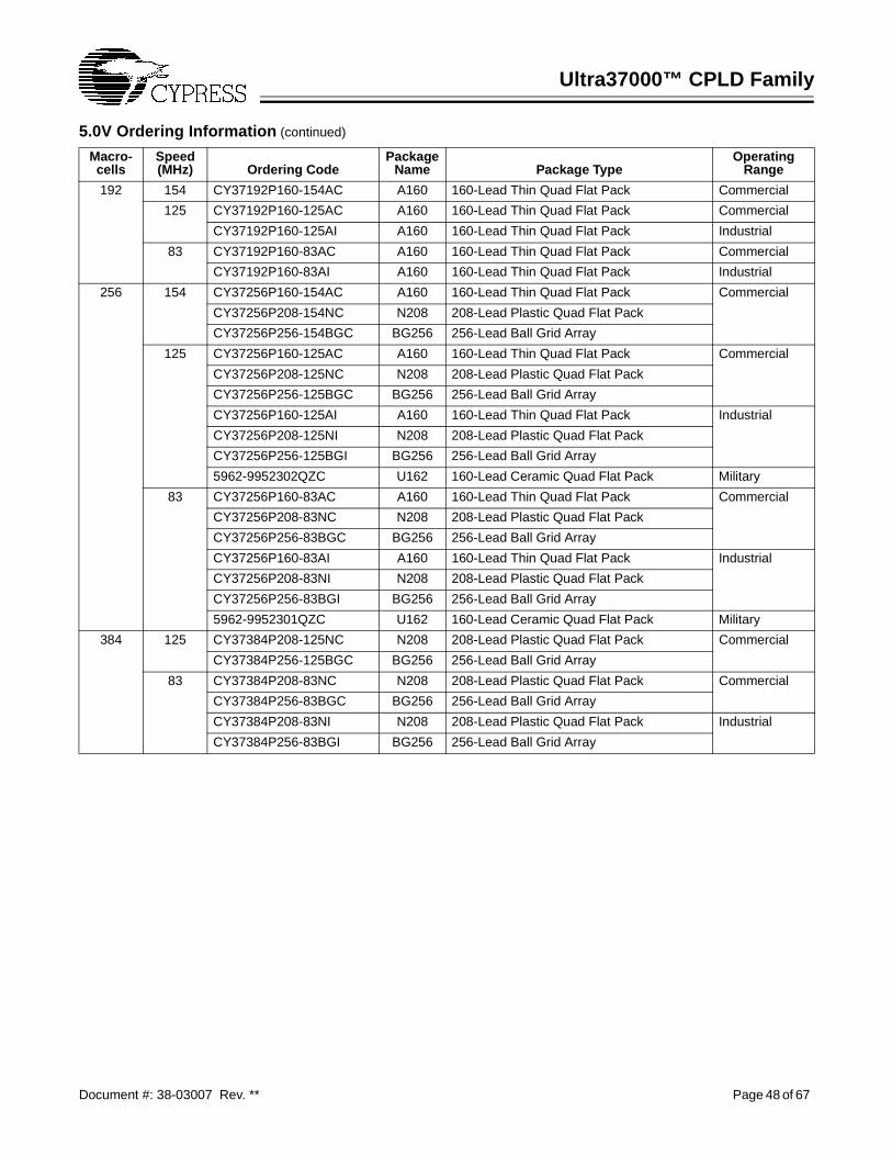
Ultra37000™ CPLD Family
Document #: 38-03007 Rev. ** Page 48 of 67
192 154 CY37192P160-154AC A160 160-Lead Thin Quad Flat Pack Commercial
125 CY37192P160-125AC A160 160-Lead Thin Quad Flat Pack Commercial
CY37192P160-125AI A160 160-Lead Thin Quad Flat Pack Industrial
83 CY37192P160-83AC A160 160-Lead Thin Quad Flat Pack Commercial
CY37192P160-83AI A160 160-Lead Thin Quad Flat Pack Industrial
256 154 CY37256P160-154AC A160 160-Lead Thin Quad Flat Pack Commercial
CY37256P208-154NC N208 208-Lead Plastic Quad Flat Pack
CY37256P256-154BGC BG256 256-Lead Ball Grid Array
125 CY37256P160-125AC A160 160-Lead Thin Quad Flat Pack Commercial
CY37256P208-125NC N208 208-Lead Plastic Quad Flat Pack
CY37256P256-125BGC BG256 256-Lead Ball Grid Array
CY37256P160-125AI A160 160-Lead Thin Quad Flat Pack Industrial
CY37256P208-125NI N208 208-Lead Plastic Quad Flat Pack
CY37256P256-125BGI BG256 256-Lead Ball Grid Array
5962-9952302QZC U162 160-Lead Ceramic Quad Flat Pack Military
83 CY37256P160-83AC A160 160-Lead Thin Quad Flat Pack Commercial
CY37256P208-83NC N208 208-Lead Plastic Quad Flat Pack
CY37256P256-83BGC BG256 256-Lead Ball Grid Array
CY37256P160-83AI A160 160-Lead Thin Quad Flat Pack Industrial
CY37256P208-83NI N208 208-Lead Plastic Quad Flat Pack
CY37256P256-83BGI BG256 256-Lead Ball Grid Array
5962-9952301QZC U162 160-Lead Ceramic Quad Flat Pack Military
384 125 CY37384P208-125NC N208 208-Lead Plastic Quad Flat Pack Commercial
CY37384P256-125BGC BG256 256-Lead Ball Grid Array
83 CY37384P208-83NC N208 208-Lead Plastic Quad Flat Pack Commercial
CY37384P256-83BGC BG256 256-Lead Ball Grid Array
CY37384P208-83NI N208 208-Lead Plastic Quad Flat Pack Industrial
CY37384P256-83BGI BG256 256-Lead Ball Grid Array
5.0V Ordering Information (continued)
Macro-cells
Speed(MHz) Ordering Code
PackageName Package Type
OperatingRange
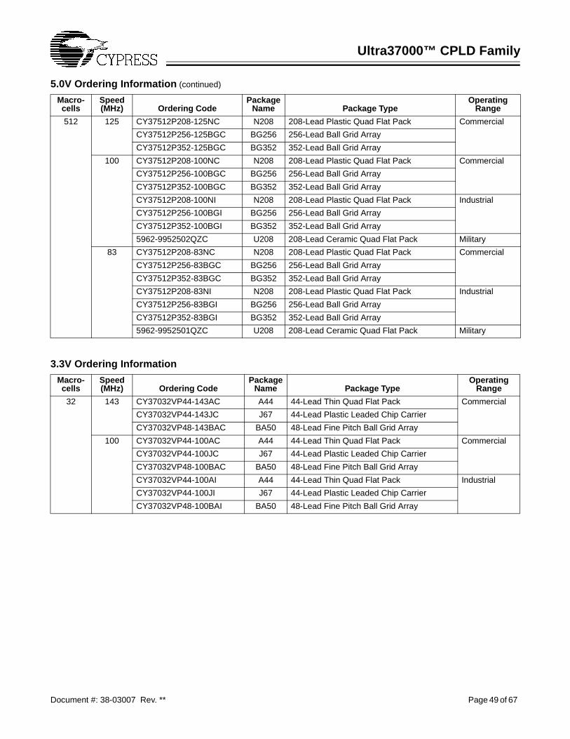
Ultra37000™ CPLD Family
Document #: 38-03007 Rev. ** Page 49 of 67
512 125 CY37512P208-125NC N208 208-Lead Plastic Quad Flat Pack Commercial
CY37512P256-125BGC BG256 256-Lead Ball Grid Array
CY37512P352-125BGC BG352 352-Lead Ball Grid Array
100 CY37512P208-100NC N208 208-Lead Plastic Quad Flat Pack Commercial
CY37512P256-100BGC BG256 256-Lead Ball Grid Array
CY37512P352-100BGC BG352 352-Lead Ball Grid Array
CY37512P208-100NI N208 208-Lead Plastic Quad Flat Pack Industrial
CY37512P256-100BGI BG256 256-Lead Ball Grid Array
CY37512P352-100BGI BG352 352-Lead Ball Grid Array
5962-9952502QZC U208 208-Lead Ceramic Quad Flat Pack Military
83 CY37512P208-83NC N208 208-Lead Plastic Quad Flat Pack Commercial
CY37512P256-83BGC BG256 256-Lead Ball Grid Array
CY37512P352-83BGC BG352 352-Lead Ball Grid Array
CY37512P208-83NI N208 208-Lead Plastic Quad Flat Pack Industrial
CY37512P256-83BGI BG256 256-Lead Ball Grid Array
CY37512P352-83BGI BG352 352-Lead Ball Grid Array
5962-9952501QZC U208 208-Lead Ceramic Quad Flat Pack Military
5.0V Ordering Information (continued)
Macro-cells
Speed(MHz) Ordering Code
PackageName Package Type
OperatingRange
3.3V Ordering Information
Macro-cells
Speed(MHz) Ordering Code
PackageName Package Type
OperatingRange
32 143 CY37032VP44-143AC A44 44-Lead Thin Quad Flat Pack Commercial
CY37032VP44-143JC J67 44-Lead Plastic Leaded Chip Carrier
CY37032VP48-143BAC BA50 48-Lead Fine Pitch Ball Grid Array
100 CY37032VP44-100AC A44 44-Lead Thin Quad Flat Pack Commercial
CY37032VP44-100JC J67 44-Lead Plastic Leaded Chip Carrier
CY37032VP48-100BAC BA50 48-Lead Fine Pitch Ball Grid Array
CY37032VP44-100AI A44 44-Lead Thin Quad Flat Pack Industrial
CY37032VP44-100JI J67 44-Lead Plastic Leaded Chip Carrier
CY37032VP48-100BAI BA50 48-Lead Fine Pitch Ball Grid Array
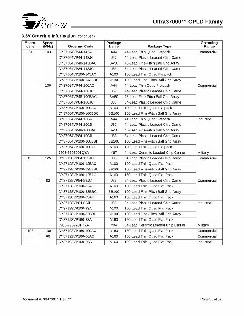
Ultra37000™ CPLD Family
Document #: 38-03007 Rev. ** Page 50 of 67
64 143 CY37064VP44-143AC A44 44-Lead Thin Quad Flatpack Commercial
CY37064VP44-143JC J67 44-Lead Plastic Leaded Chip Carrier
CY37064VP48-143BAC BA50 48-Lead Fine-Pitch Ball Grid Array
CY37064VP84-143JC J83 84-Lead Plastic Leaded Chip Carrier
CY37064VP100-143AC A100 100-Lead Thin Quad Flatpack
CY37064VP100-143BBC BB100 100-Lead Fine-Pitch Ball Grid Array
100 CY37064VP44-100AC A44 44-Lead Thin Quad Flatpack Commercial
CY37064VP44-100JC J67 44-Lead Plastic Leaded Chip Carrier
CY37064VP48-100BAC BA50 48-Lead Fine-Pitch Ball Grid Array
CY37064VP84-100JC J83 84-Lead Plastic Leaded Chip Carrier
CY37064VP100-100AC A100 100-Lead Thin Quad Flatpack
CY37064VP100-100BBC BB100 100-Lead Fine-Pitch Ball Grid Array
CY37064VP44-100AI A44 44-Lead Thin Quad Flatpack Industrial
CY37064VP44-100JI J67 44-Lead Plastic Leaded Chip Carrier
CY37064VP48-100BAI BA50 48-Lead Fine-Pitch Ball Grid Array
CY37064VP84-100JI J83 84-Lead Plastic Leaded Chip Carrier
CY37064VP100-100BBI BB100 100-Lead Fine-Pitch Ball Grid Array
CY37064VP100-100AI A100 100-Lead Thin Quad Flatpack
5962-9952001QYA Y67 44-Lead Ceramic Leaded Chip Carrier Military
128 125 CY37128VP84-125JC J83 84-Lead Plastic Leaded Chip Carrier Commercial
CY37128VP100-125AC A100 100-Lead Thin Quad Flat Pack
CY37128VP100-125BBC BB100 100-Lead Fine-Pitch Ball Grid Array
CY37128VP160-125AC A160 160-Lead Thin Quad Flat Pack
83 CY37128VP84-83JC J83 84-Lead Plastic Leaded Chip Carrier Commercial
CY37128VP100-83AC A100 100-Lead Thin Quad Flat Pack
CY37128VP100-83BBC BB100 100-Lead Fine-Pitch Ball Grid Array
CY37128VP160-83AC A160 160-Lead Thin Quad Flat Pack
CY37128VP84-83JI J83 84-Lead Plastic Leaded Chip Carrier Industrial
CY37128VP100-83AI A100 100-Lead Thin Quad Flat Pack
CY37128VP100-83BBI BB100 100-Lead Fine-Pitch Ball Grid Array
CY37128VP160-83AI A160 160-Lead Thin Quad Flat Pack
5962-9952201QYA Y84 84-Lead Ceramic Leaded Chip Carrier Military
192 100 CY37192VP160-100AC A160 160-Lead Thin Quad Flat Pack Commercial
66 CY37192VP160-66AC A160 160-Lead Thin Quad Flat Pack Commercial
CY37192VP160-66AI A160 160-Lead Thin Quad Flat Pack Industrial
3.3V Ordering Information (continued)
Macro-cells
Speed(MHz) Ordering Code
PackageName Package Type
OperatingRange
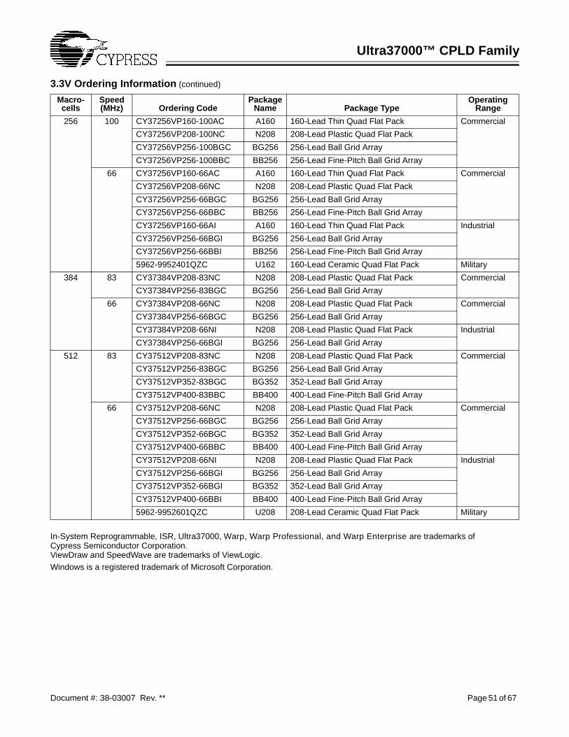
Ultra37000™ CPLD Family
Document #: 38-03007 Rev. ** Page 51 of 67
In-System Reprogrammable, ISR, Ultra37000, Warp, Warp Professional, and Warp Enterprise are trademarks of Cypress Semiconductor Corporation.ViewDraw and SpeedWave are trademarks of ViewLogic.Windows is a registered trademark of Microsoft Corporation.
256 100 CY37256VP160-100AC A160 160-Lead Thin Quad Flat Pack Commercial
CY37256VP208-100NC N208 208-Lead Plastic Quad Flat Pack
CY37256VP256-100BGC BG256 256-Lead Ball Grid Array
CY37256VP256-100BBC BB256 256-Lead Fine-Pitch Ball Grid Array
66 CY37256VP160-66AC A160 160-Lead Thin Quad Flat Pack Commercial
CY37256VP208-66NC N208 208-Lead Plastic Quad Flat Pack
CY37256VP256-66BGC BG256 256-Lead Ball Grid Array
CY37256VP256-66BBC BB256 256-Lead Fine-Pitch Ball Grid Array
CY37256VP160-66AI A160 160-Lead Thin Quad Flat Pack Industrial
CY37256VP256-66BGI BG256 256-Lead Ball Grid Array
CY37256VP256-66BBI BB256 256-Lead Fine-Pitch Ball Grid Array
5962-9952401QZC U162 160-Lead Ceramic Quad Flat Pack Military
384 83 CY37384VP208-83NC N208 208-Lead Plastic Quad Flat Pack Commercial
CY37384VP256-83BGC BG256 256-Lead Ball Grid Array
66 CY37384VP208-66NC N208 208-Lead Plastic Quad Flat Pack Commercial
CY37384VP256-66BGC BG256 256-Lead Ball Grid Array
CY37384VP208-66NI N208 208-Lead Plastic Quad Flat Pack Industrial
CY37384VP256-66BGI BG256 256-Lead Ball Grid Array
512 83 CY37512VP208-83NC N208 208-Lead Plastic Quad Flat Pack Commercial
CY37512VP256-83BGC BG256 256-Lead Ball Grid Array
CY37512VP352-83BGC BG352 352-Lead Ball Grid Array
CY37512VP400-83BBC BB400 400-Lead Fine-Pitch Ball Grid Array
66 CY37512VP208-66NC N208 208-Lead Plastic Quad Flat Pack Commercial
CY37512VP256-66BGC BG256 256-Lead Ball Grid Array
CY37512VP352-66BGC BG352 352-Lead Ball Grid Array
CY37512VP400-66BBC BB400 400-Lead Fine-Pitch Ball Grid Array
CY37512VP208-66NI N208 208-Lead Plastic Quad Flat Pack Industrial
CY37512VP256-66BGI BG256 256-Lead Ball Grid Array
CY37512VP352-66BGI BG352 352-Lead Ball Grid Array
CY37512VP400-66BBI BB400 400-Lead Fine-Pitch Ball Grid Array
5962-9952601QZC U208 208-Lead Ceramic Quad Flat Pack Military
3.3V Ordering Information (continued)
Macro-cells
Speed(MHz) Ordering Code
PackageName Package Type
OperatingRange
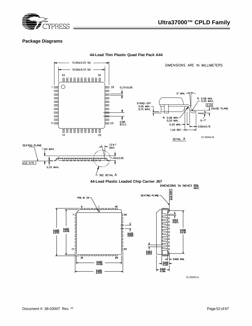
Ultra37000™ CPLD Family
Document #: 38-03007 Rev. ** Page 52 of 67
Package Diagrams
44-Lead Thin Plastic Quad Flat Pack A44
51-85064-B
44-Lead Plastic Leaded Chip Carrier J67
51-85003-A
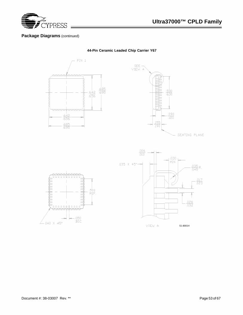
Ultra37000™ CPLD Family
Document #: 38-03007 Rev. ** Page 53 of 67
Package Diagrams (continued)
44-Pin Ceramic Leaded Chip Carrier Y67
51-80014
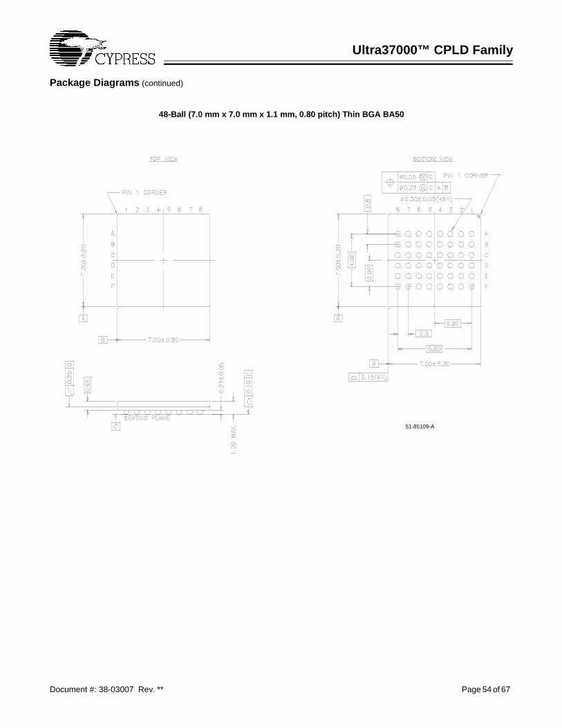
Ultra37000™ CPLD Family
Document #: 38-03007 Rev. ** Page 54 of 67
Package Diagrams (continued)
48-Ball (7.0 mm x 7.0 mm x 1.1 mm, 0.80 pitch) Thin BGA BA50
51-85109-A
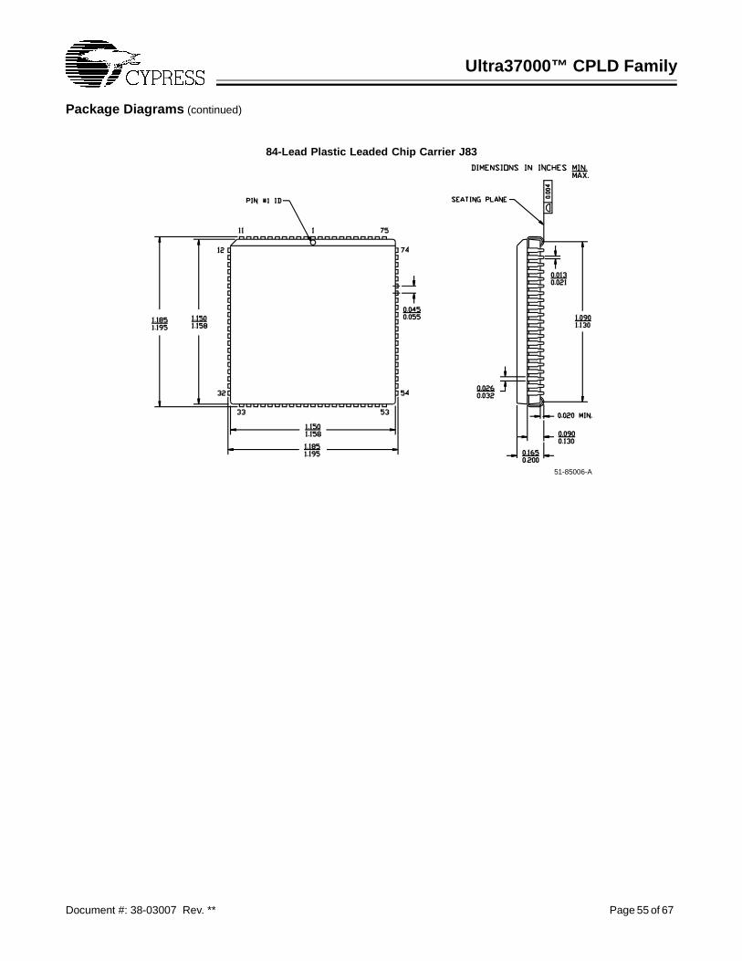
Ultra37000™ CPLD Family
Document #: 38-03007 Rev. ** Page 55 of 67
Package Diagrams (continued)
84-Lead Plastic Leaded Chip Carrier J83
51-85006-A
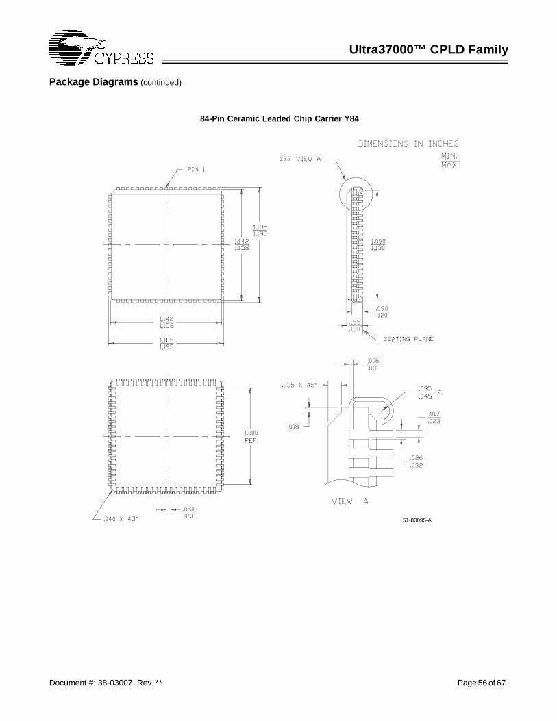
Ultra37000™ CPLD Family
Document #: 38-03007 Rev. ** Page 56 of 67
Package Diagrams (continued)
84-Pin Ceramic Leaded Chip Carrier Y84
51-80095-A
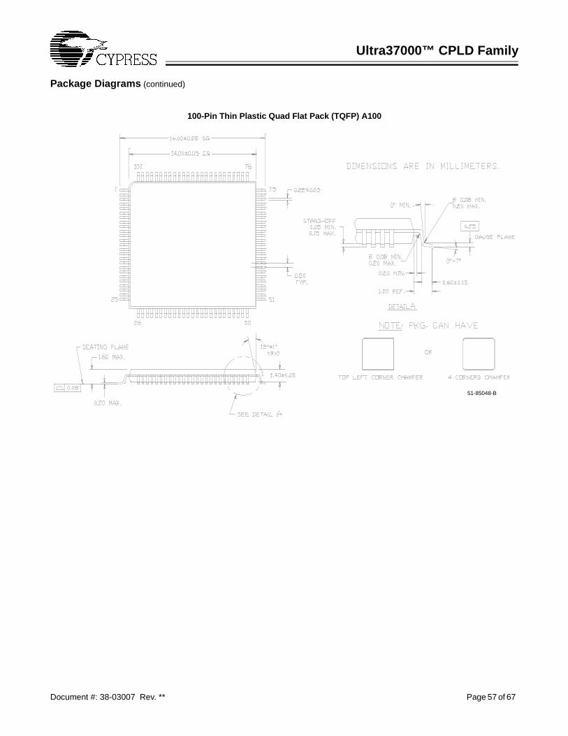
Ultra37000™ CPLD Family
Document #: 38-03007 Rev. ** Page 57 of 67
Package Diagrams (continued)
100-Pin Thin Plastic Quad Flat Pack (TQFP) A100
51-85048-B
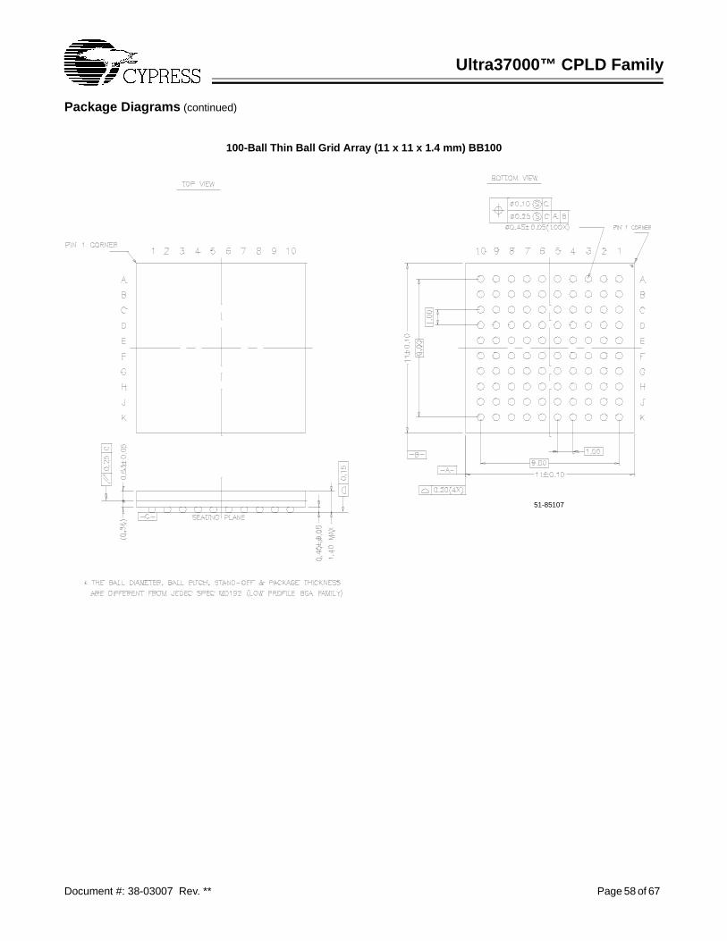
Ultra37000™ CPLD Family
Document #: 38-03007 Rev. ** Page 58 of 67
Package Diagrams (continued)
100-Ball Thin Ball Grid Array (11 x 11 x 1.4 mm) BB100
51-85107
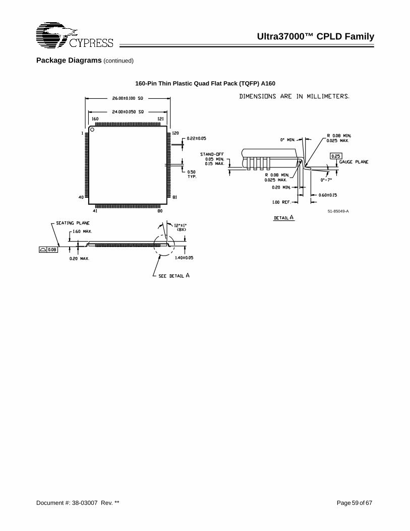
Ultra37000™ CPLD Family
Document #: 38-03007 Rev. ** Page 59 of 67
Package Diagrams (continued)
160-Pin Thin Plastic Quad Flat Pack (TQFP) A160
51-85049-A
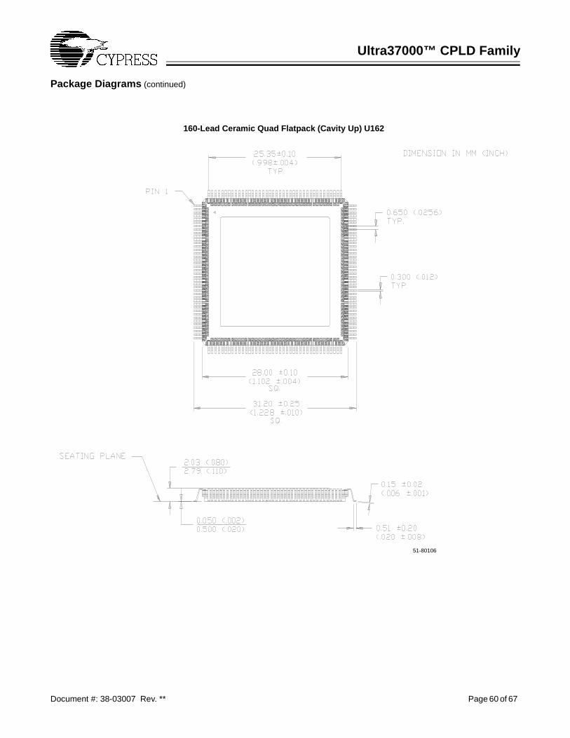
Ultra37000™ CPLD Family
Document #: 38-03007 Rev. ** Page 60 of 67
Package Diagrams (continued)
160-Lead Ceramic Quad Flatpack (Cavity Up) U162
51-80106
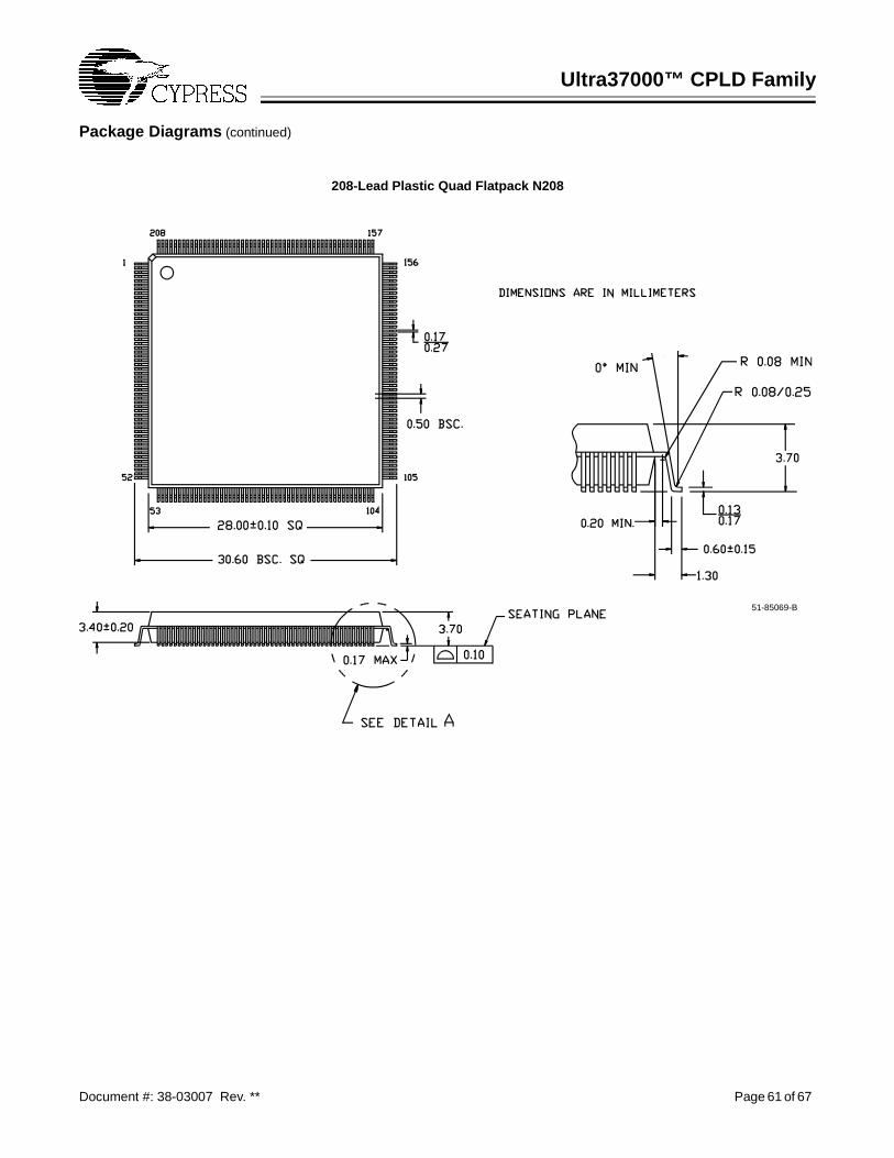
Ultra37000™ CPLD Family
Document #: 38-03007 Rev. ** Page 61 of 67
Package Diagrams (continued)
208-Lead Plastic Quad Flatpack N208
51-85069-B
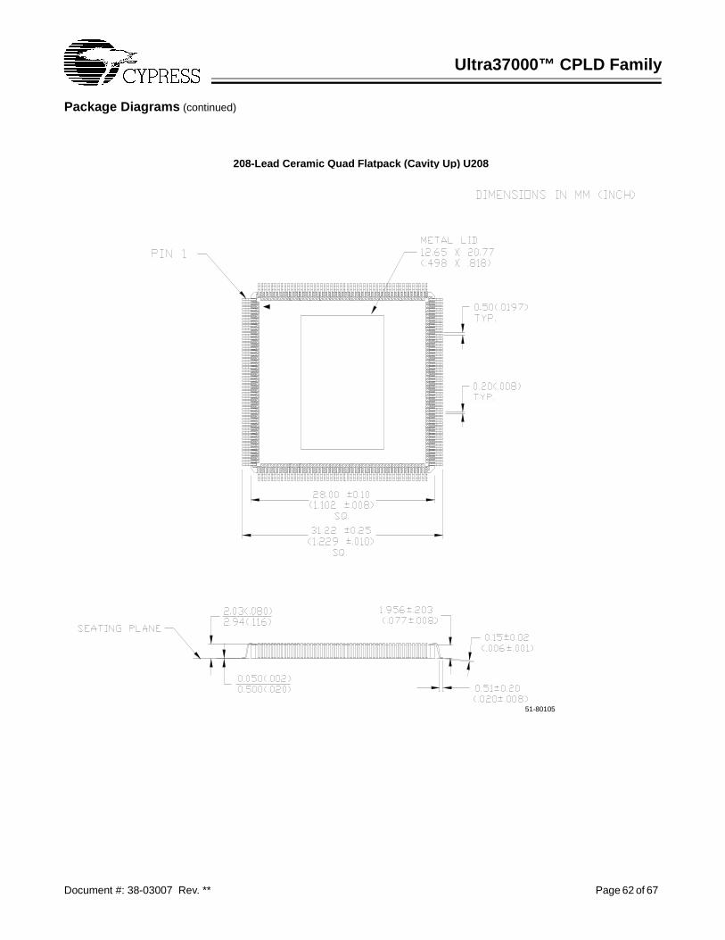
Ultra37000™ CPLD Family
Document #: 38-03007 Rev. ** Page 62 of 67
Package Diagrams (continued)
208-Lead Ceramic Quad Flatpack (Cavity Up) U208
51-80105
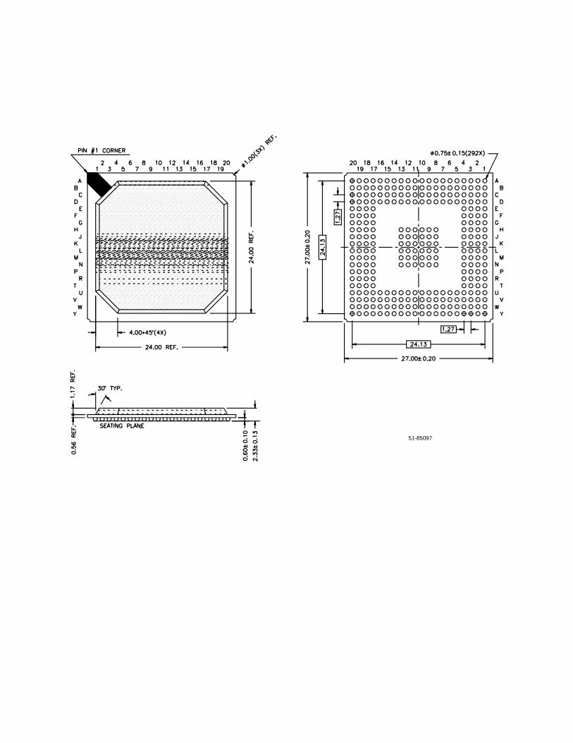
51-85097
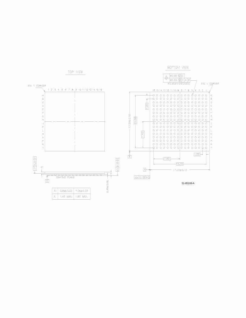
51-85108-A
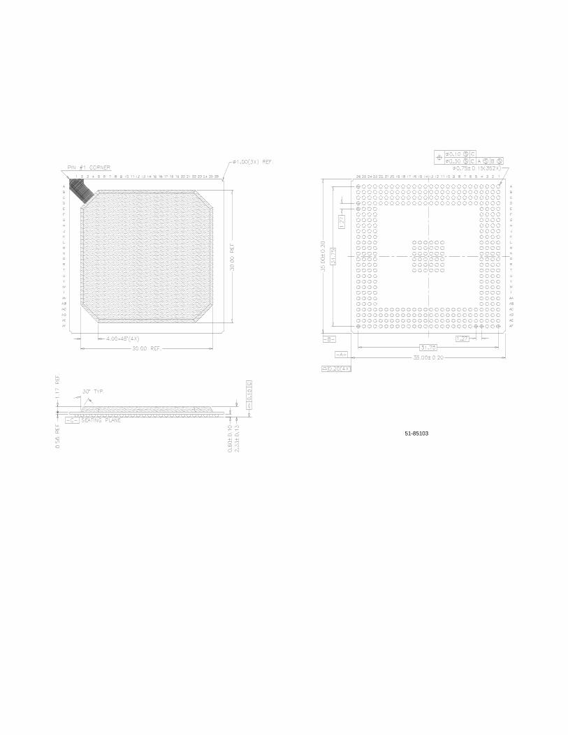
51-85103
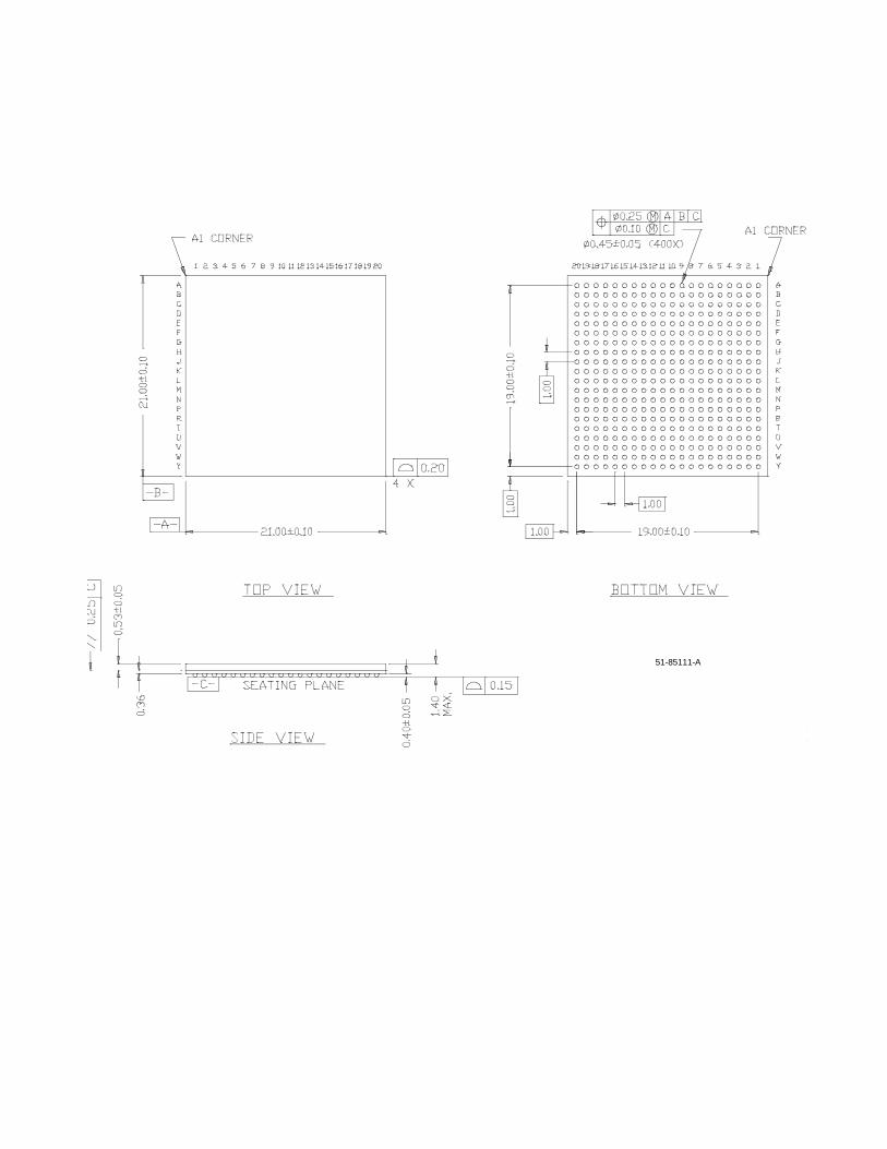
51-85111-A

** 106272 04/18/01 SZV Change from Spec number: 38-00475 to 38-03007

4.8 MAX4131
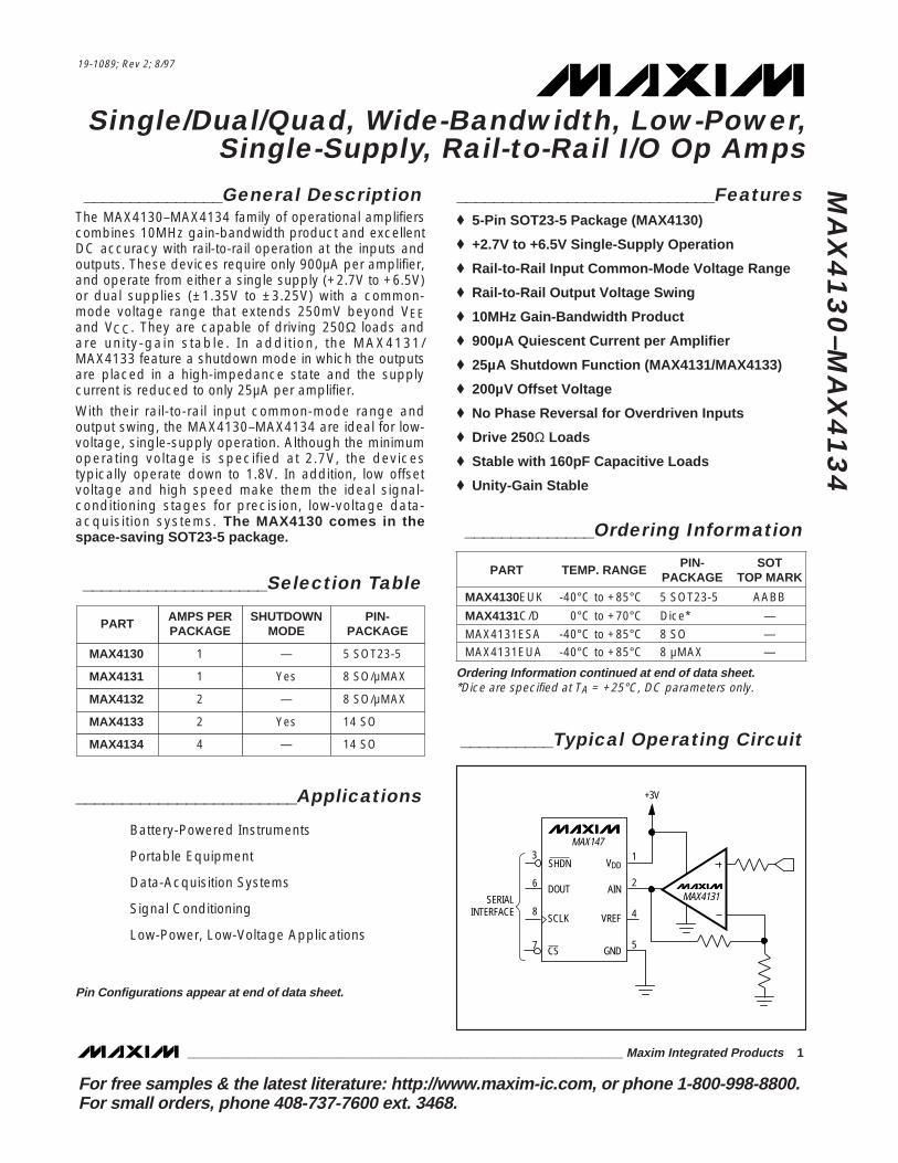
_______________General DescriptionThe MAX4130–MAX4134 family of operational amplifierscombines 10MHz gain-bandwidth product and excellentDC accuracy with rail-to-rail operation at the inputs andoutputs. These devices require only 900µA per amplifier,and operate from either a single supply (+2.7V to +6.5V)or dual supplies (±1.35V to ±3.25V) with a common-mode voltage range that extends 250mV beyond VEEand VCC. They are capable of driving 250Ω loads andare unity-gain stable. In addition, the MAX4131/MAX4133 feature a shutdown mode in which the outputsare placed in a high-impedance state and the supplycurrent is reduced to only 25µA per amplifier.
With their rail-to-rail input common-mode range andoutput swing, the MAX4130–MAX4134 are ideal for low-voltage, single-supply operation. Although the minimumoperating voltage is specified at 2.7V, the devicestypically operate down to 1.8V. In addition, low offsetvoltage and high speed make them the ideal signal-conditioning stages for precision, low-voltage data-acquisition systems. The MAX4130 comes in thespace-saving SOT23-5 package.
________________________Applications
Battery-Powered Instruments
Portable Equipment
Data-Acquisition Systems
Signal Conditioning
Low-Power, Low-Voltage Applications
____________________________Features♦ 5-Pin SOT23-5 Package (MAX4130)
♦ +2.7V to +6.5V Single-Supply Operation
♦ Rail-to-Rail Input Common-Mode Voltage Range
♦ Rail-to-Rail Output Voltage Swing
♦ 10MHz Gain-Bandwidth Product
♦ 900µA Quiescent Current per Amplifier
♦ 25µA Shutdown Function (MAX4131/MAX4133)
♦ 200µV Offset Voltage
♦ No Phase Reversal for Overdriven Inputs
♦ Drive 250Ω Loads
♦ Stable with 160pF Capacitive Loads
♦ Unity-Gain Stable
MA
X4
13
0–M
AX
41
34
Single/Dual/Quad, Wide-Bandwidth, Low-Power,Single-Supply, Rail-to-Rail I/O Op Amps
________________________________________________________________ Maxim Integrated Products 1
MAX147
MAX4131
SHDN3 1
2
4
5
6
8
7
VDD
+3V
AIN
VREF
GND
DOUTSERIAL
INTERFACE SCLK
CS
__________Typical Operating Circuit
19-1089; Rev 2; 8/97
______________Ordering Information
AMPS PERPACKAGE
MAX4130 1
MAX4131 1
PART
MAX4132 2
MAX4133 2
MAX4134 4
SHUTDOWNMODE
—
Yes
—
Yes
—
PIN-PACKAGE
5 SOT23-5
8 SO/µMAX
8 SO/µMAX
14 SO
14 SO
PART
MAX4130EUK
MAX4131C/D
MAX4131ESA -40°C to +85°C
0°C to +70°C
-40°C to +85°C
TEMP. RANGEPIN-
PACKAGE
5 SOT23-5
Dice*
8 SO
SOT TOP MARK
AABB
—
—MAX4131EUA -40°C to +85°C 8 µMAX —
____________________Selection Table
Ordering Information continued at end of data sheet.*Dice are specified at TA = +25°C, DC parameters only.
Pin Configurations appear at end of data sheet.
For free samples & the latest literature: http://www.maxim-ic.com, or phone 1-800-998-8800.For small orders, phone 408-737-7600 ext. 3468.
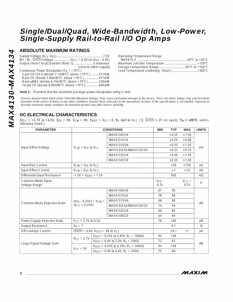
MA
X4
13
0–M
AX
41
34
Single/Dual/Quad, Wide-Bandwidth, Low-Power,Single-Supply Rail-to-Rail I/O Op Amps
2 _______________________________________________________________________________________
ABSOLUTE MAXIMUM RATINGS
DC ELECTRICAL CHARACTERISTICS (VCC = +2.7V to +6.5V, VEE = 0V, VCM = 0V, VOUT = VCC / 2, RL tied to VCC / 2, SHDN ≥ 2V (or open), TA = +25°C, unless otherwise noted.)
Stresses beyond those listed under “Absolute Maximum Ratings” may cause permanent damage to the device. These are stress ratings only, and functionaloperation of the device at these or any other conditions beyond those indicated in the operational sections of the specifications is not implied. Exposure toabsolute maximum rating conditions for extended periods may affect device reliability.
Supply Voltage (VCC-VEE).....................................................7.5VIN+, IN-, SHDN Voltage ...................(VCC + 0.3V) to (VEE - 0.3V)Output Short-Circuit Duration (Note 1).......................Continuous
(short to either supply)Continuous Power Dissipation (TA = +70°C)
5-pin SOT23-5 (derate 7.1mW/°C above +70°C) .........571mW8-pin SO (derate 5.88mW/°C above +70°C).................471mW8-pin µMAX (derate 4.10mW/°C above +70°C) ............330mW14-pin SO (derate 8.00mW/°C above +70°C)...............640mW
Operating Temperature RangeMAX413_E__ ....................................................-40°C to +85°C
Maximum Junction Temperature .....................................+150°CStorage Temperature Range .............................-65°C to +160°CLead Temperature (soldering, 10sec) .............................+300°C
VCM = VEE to VCC
CONDITIONS
nA±1 ±12Input Offset Current
nA±50 ±150Input Bias Current
72 82
Ω0.1Output Resistance
kΩ500Differential Input Resistance
67 90
dB78 100Power-Supply Rejection Ratio
UNITSMIN TYP MAXPARAMETER
VOUT = 0.4V to 4.6V, RL = 250Ω 75 86
dBLarge-Signal Voltage Gain
VVEE - VCC +0.25 0.25
Common-Mode Input Voltage Range
Note 1: Provided that the maximum package power-dissipation rating is met.
±0.20 ±0.60
±0.35 ±1.20
±0.35 ±1.50
±0.40 ±1.50
±0.35 ±1.50
Input Offset Voltage±0.25 ±0.75
VCM = VEE to VCC mV
VCM = VEE to VCC
-1.5V < VDIFF < 1.5V
VCC = 2.7V to 6.5V
AV = 1
SHDN < 0.8V, VOUT = 0V to VCC µA±0.1 ±1Off-Leakage Current
(VEE - 0.25V) < VCM < (VCC + 0.25V)
78 98
Common-Mode Rejection Ratio
64 84
dB
66 86
74 94
68 88
VCC = 5V
VOUT = 0.4V to 2.3V, RL = 250ΩVOUT = 0.25V to 2.45V, RL = 100kΩ
VOUT = 0.25V to 4.75V, RL = 100kΩ
VCC = 2.7V92 108
94 108
MAX4130EUK
MAX4131ESA
MAX4131EUA
MAX4132ESA/MAX4133ESD
MAX4132EUA
MAX4134ESD
MAX4134ESD
MAX4132EUA
MAX4132ESA/MAX4133ESD
MAX4131EUA
MAX4131ESA
MAX4130EUK
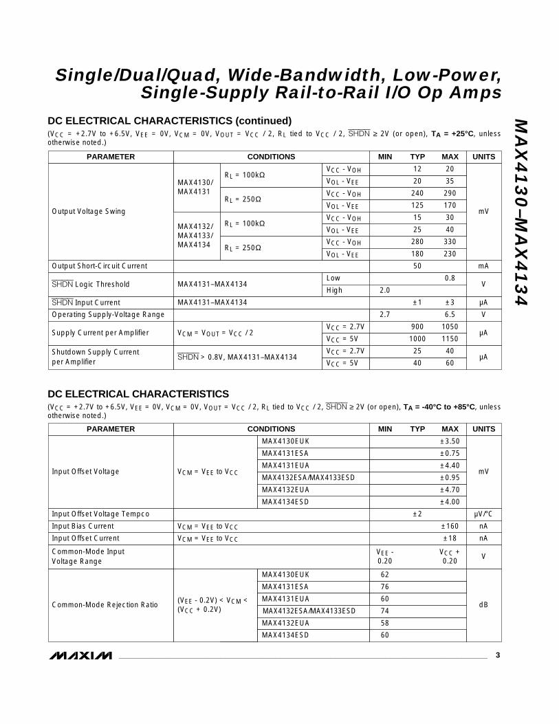
MA
X4
13
0–M
AX
41
34
Single/Dual/Quad, Wide-Bandwidth, Low-Power,Single-Supply Rail-to-Rail I/O Op Amps
_______________________________________________________________________________________ 3
DC ELECTRICAL CHARACTERISTICS (VCC = +2.7V to +6.5V, VEE = 0V, VCM = 0V, VOUT = VCC / 2, RL tied to VCC / 2, SHDN ≥ 2V (or open), TA = -40°C to +85°C, unless otherwise noted.)
DC ELECTRICAL CHARACTERISTICS (continued)(VCC = +2.7V to +6.5V, VEE = 0V, VCM = 0V, VOUT = VCC / 2, RL tied to VCC / 2, SHDN ≥ 2V (or open), TA = +25°C, unless otherwise noted.)
RL = 100kΩ
CONDITIONS
20 35
Low
V2.7 6.5Operating Supply-Voltage Range
SHDN > 0.8V, MAX4131–MAX4134
240 290
12 20
VOL - VEE 125 170
MAX4130/MAX4131
V0.8
mA50Output Short-Circuit Current
µA40 60
Shutdown Supply Current per Amplifier
UNITSMIN TYP MAXPARAMETER
VCC - VOH
VOL - VEE
VCC - VOHRL = 250Ω
VCC - VOH
VOL - VEE
VCC - VOHRL = 250Ω
RL = 100kΩ25 40
mV
280 330
15 30
VOL - VEE
Output Voltage Swing
180 230
MAX4132/MAX4133/MAX4134
High 2.0SHDN Logic Threshold MAX4131–MAX4134
VCC = 5V
MAX4131–MAX4134 µA±1 ±3SHDN Input Current
VCC = 2.7VVCM = VOUT = VCC / 2 µA
900 1050
VCC = 5V 1000 1150Supply Current per Amplifier
VCC = 2.7V 25 40
(VEE - 0.2V) < VCM <(VCC + 0.2V)
CONDITIONS
±0.75
76
VCM = VEE to VCC
VVEE - VCC +0.20 0.20
Common-Mode Input Voltage Range
mV±4.40
±3.50
±4.70
Common-Mode Rejection Ratio
±4.00
Input Offset Voltage±0.95
VCM = VEE to VCC
nA±18Input Offset Current
µV/°C±2
60
dB
58
Input Offset Voltage Tempco
MAX4132ESA/MAX4133ESD
60
62
UNITSMIN TYP MAXPARAMETER
VCM = VEE to VCC nA±160Input Bias Current
MAX4130EUK
MAX4131ESA
MAX4132ESA/MAX4133ESD
MAX4134ESD
MAX4130EUK
MAX4131ESA
MAX4131EUA
MAX4132EUA
MAX4134ESD
MAX4131EUA
MAX4132EUA
74
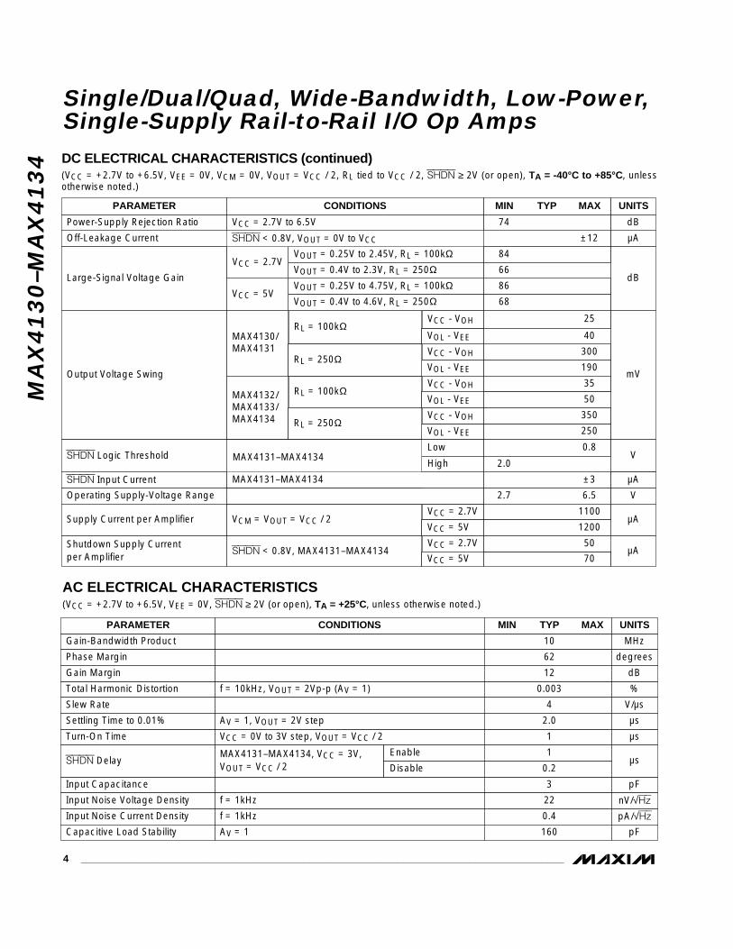
MA
X4
13
0–M
AX
41
34
Single/Dual/Quad, Wide-Bandwidth, Low-Power,Single-Supply Rail-to-Rail I/O Op Amps
4 _______________________________________________________________________________________
DC ELECTRICAL CHARACTERISTICS (continued)(VCC = +2.7V to +6.5V, VEE = 0V, VCM = 0V, VOUT = VCC / 2, RL tied to VCC / 2, SHDN ≥ 2V (or open), TA = -40°C to +85°C, unless otherwise noted.)
AC ELECTRICAL CHARACTERISTICS(VCC = +2.7V to +6.5V, VEE = 0V, SHDN ≥ 2V (or open), TA = +25°C, unless otherwise noted.)
f = 10kHz, VOUT = 2Vp-p (AV = 1)
VCC = 0V to 3V step, VOUT = VCC / 2 µs
AV = 1, VOUT = 2V step
1
pF
Turn-On Time
3Input Capacitance
f = 1kHz pA/√Hz
f = 1kHz
0.4Input Noise Current Density
%
nV/√Hz
0.003
22Input Noise Voltage Density
CONDITIONS
AV = 1 pF160Capacitive Load Stability
Disable
EnableMAX4131–MAX4134, VCC = 3V,VOUT = VCC / 2
µs0.2
SHDN Delay
Total Harmonic Distortion
V/µs4Slew Rate
µs2.0Settling Time to 0.01%
1
MHz10Gain-Bandwidth Product
degrees62Phase Margin
dB12Gain Margin
UNITSMIN TYP MAXPARAMETER
86Large-Signal Voltage Gain
68
VOUT = 0.25V to 4.75V, RL = 100kΩVOUT = 0.4V to 4.6V, RL = 250Ω
VCC = 5V
84
dB66
VOUT = 0.25V to 2.45V, RL = 100kΩVOUT = 0.4V to 2.3V, RL = 250Ω
VCC = 2.7V
Off-Leakage Current ±12 µASHDN < 0.8V, VOUT = 0V to VCC
MAX4130/MAX4131
190VOL - VEE
25
300
MAX4132/MAX4133/MAX4134
250
Output Voltage Swing
VOL - VEE
35
350
mV
50RL = 100kΩ
RL = 250ΩVCC - VOH
VOL - VEE
VCC - VOH
40RL = 100kΩ
RL = 250ΩVCC - VOH
VOL - VEE
VCC - VOH
PARAMETER MIN TYP MAX UNITS
Shutdown Supply Current per Amplifier 70
µA
Power-Supply Rejection Ratio 74 dB
0.8V
SHDN < 0.8V, MAX4131–MAX4134
Operating Supply-Voltage Range 2.7 6.5 V
1100µAVCM = VOUT = VCC / 2
VCC = 2.7V
SHDN Input Current
Low
±3
CONDITIONS
µA
50
MAX4131—MAX4134
VCC = 2.7V to 6.5V
VCC = 2.7V
VCC = 5V
MAX4131–MAX4134
Supply Current per Amplifier
SHDN Logic Threshold
1200
2.0High
VCC = 5V
MAX4131–MAX4134
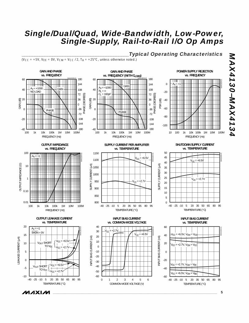
MA
X4
13
0–M
AX
41
34
Single/Dual/Quad, Wide-Bandwidth, Low-Power,Single-Supply, Rail-to-Rail I/O Op Amps
_______________________________________________________________________________________ 5
60
-40100 1k 10k 1M 10M100k 100M
GAIN AND PHASE vs. FREQUENCY
-20
FREQUENCY (Hz)
GAIN
(dB)
0
20
40
PHASE
GAINAV = +1000NO LOAD
PHAS
E (D
EGRE
ES)
180
144
72
0
-72
-144
-180
-108
-36
36
108
MAX4130/34-01 60
-40100 1k 10k 1M 10M100k 100M
GAIN AND PHASE vs. FREQUENCY (WITH CLOAD)
-20
MAX4130/34-02
FREQUENCY (Hz)
GAIN
(dB)
0
20
40
PHASE
GAINAV = +1000RL = ∞CL = 160pF
PHAS
E (D
EGRE
ES)
180
144
72
0
-72
-144
-180
-108
-36
36
108
0
-100
10 100 1k 100k 1M 10M10k 100M
POWER-SUPPLY REJECTION vs. FREQUENCY
-80
MAX
4130
/34-
03
FREQUENCY (Hz)
PSR
(dB)
-60
-40
-20
AV = +1
0
10
5
15
20
25
35
30
45
40
50
-40 -25 -10 5 20 35 50 65 80 95
SHUTDOWN SUPPLY CURRENTvs. TEMPERATURE
MAX
4130
/34-
07
TEMPERATURE (°C)
SUPP
LY C
URRE
NT (µ
A)VCC = +6.5V
VCC = +2.7V
100
0.10
0.01100 1k 100k 1M 10M10k 100M
OUTPUT IMPEDANCE vs. FREQUENCY
MAX
4130
/34-
05
FREQUENCY (Hz)
OUTP
UT IM
PEDA
NCE
(Ω)
1
10
AV = +11150
800
850
900
950
1050
1000
1100
-40 -25 -10 5 20 35 50 65 80 95
SUPPLY CURRENT PER AMPLIFIERvs. TEMPERATURE
MAX
4130
/34-
06
TEMPERATURE (°C)
SUPP
LY C
URRE
NT (µ
A)
VCC = +6.5V
VCC = +2.7V
-10
-5
0
5
10
15
20
-40 -25 -10 5 20 35 50 65 80 95
OUTPUT LEAKAGE CURRENTvs. TEMPERATURE
MAX
4130
/34-
08
TEMPERATURE (°C)
LEAK
AGE
CURR
ENT
(µA)
VCC = +6.5VVOUT SHORTTO VCC VCC = +2.7V
VCC = +6.5VVOUT SHORT
TO VEE VCC = +2.7V
AV = +1SHDN = 0V
__________________________________________Typical Operating Characteristics(VCC = +5V, VEE = 0V, VCM = VCC / 2, TA = +25°C, unless otherwise noted.)
-600 1 2 3 4 5 6
INPUT BIAS CURRENTvs. COMMON-MODE VOLTAGE
MAX
4130
/34-
10
COMMON-MODE VOLTAGE (V)
INPU
T BI
AS C
URRE
NT (n
A)
-50
-40
-30
-20
-10
0
10
20
30
40VCC = +2.7V
VCC = +6.5V
-60
-40
-40 -25 -10 5 20 35 50 65 80 95
INPUT BIAS CURRENTvs. TEMPERATURE
MAX
4130
/34-
11
TEMPERATURE (°C)
INPU
T BI
AS C
URRE
NT (n
A)
-20
0
20
40
60
VCC = +6.5V, VCM = VCC
VCC = +2.7V, VCM = VEE
VCC = +2.7V, VCM = VCC
VCC = +6.5V, VCM = VEE
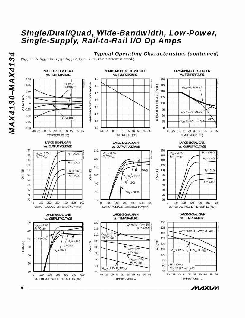
MA
X4
13
0–M
AX
41
34
Single/Dual/Quad, Wide-Bandwidth, Low-Power,Single-Supply, Rail-to-Rail I/O Op Amps
6 _______________________________________________________________________________________
120
70
75
0 600
110
115
OUTPUT VOLTAGE: EITHER SUPPLY (mV)
GAIN
(dB)
300
95
85
90
80
100 200 500
105
100
400
MAX
4130
/34-
19
LARGE-SIGNAL GAINvs. OUTPUT VOLTAGE
RL = 500Ω
RL = 100kΩ
RL = 10kΩ
RL = 2kΩ
VCC = +6.5VRL TO VCC
130
-40 -25 -10 5 20 35 50 65 80 95
LARGE-SIGNAL GAINvs. TEMPERATURE
90
120
MAX
4130
/34-
20
TEMPERATURE (°C)
GAIN
(dB) 110
100
80
95
125
115
105
VCC = +6.5V, RL TO VCC OR VEE
VCC = +2.7V, RL TO VCC OR VEE
RL = 100kΩVOUT(p-p) = VCC - 0.6V
1.2
1.3
1.5
1.4
1.6
1.7
1.8
1.9
-40 -25 -10 5 20 35 50 65 80 95
MINIMUM OPERATING VOLTAGEvs. TEMPERATURE
MAX
4130
/34-
21
TEMPERATURE (°C)
MIN
IMUM
OPE
RATI
NG V
OLTA
GE (V
)
____________________________ Typical Operating Characteristics (continued)(VCC = +5V, VEE = 0V, VCM = VCC / 2, TA = +25°C, unless otherwise noted.)
120
80
85
90
95
100
105
110
115
-40 -25 -10 5 20 35 50 65 80 95
COMMON-MODE REJECTIONvs. TEMPERATURE
MAX
4130
/34-
12
TEMPERATURE (°C)
COM
MON
-MOD
E RE
JECT
ION
(dB)
VCM = 0V TO 5.0V
VCM = 0.2V TO 5.2V
VCM = 0.3V TO 5.3V
130
700 600
120
OUTPUT VOLTAGE: EITHER SUPPLY (mV)
GAIN
(dB)
300
100
90
80
100 200 500
110
400
MAX
4130
/34-
16
LARGE-SIGNAL GAINvs. OUTPUT VOLTAGE
VCC = +6.5VRL TO VEE
RL = 500Ω
RL = 100kΩ
RL = 10kΩ
RL = 2kΩ
120
600 600
110
OUTPUT VOLTAGE: EITHER SUPPLY (mV)
GAIN
(dB)
300
90
80
70
100 200 500
100
400
MAX
4130
/34-
15
LARGE-SIGNAL GAINvs. OUTPUT VOLTAGE
VCC = +2.7VRL TO VEE
RL = 500ΩRL = 100kΩ
RL = 10kΩ
RL = 2kΩ
120
80-40 -25 -10 5 20 35 50 65 80 95
LARGE-SIGNAL GAINvs. TEMPERATURE
90
MAX
4130
/34-
17
TEMPERATURE (°C)
GAIN
(dB) 105
85
95
115
110
100 VCC = +2.7V,RL TO VEE
VCC = +6.5V, RL TO VCC
VCC = +2.7V, RL TO VCC
VOUT(p-p) = VCC -1VRL = 500Ω
VCC = +6.5V, RL TO VEE
120
70
75
0 600
110
115
OUTPUT VOLTAGE: EITHER SUPPLY (mV)
GAIN
(dB)
300
95
85
90
80
100 200 500
105
100
400
MAX
4130
/34-
18
LARGE-SIGNAL GAINvs. OUTPUT VOLTAGE
RL = 500Ω
RL = 100kΩ
RL = 10kΩ
RL = 2kΩ
VCC = +2.7VRL TO VCC
-3.00
-2.25
-0.75
-1.50
0
1.50
0.75
2.25
3.00
-40 -25 -10 5 20 35 50 65 80 95
INPUT OFFSET VOLTAGEvs. TEMPERATURE
MAX
4130
/34-
09
TEMPERATURE (°C)
VOLT
AGE
(mV)
SOT23-5PACKAGE
SO PACKAGE
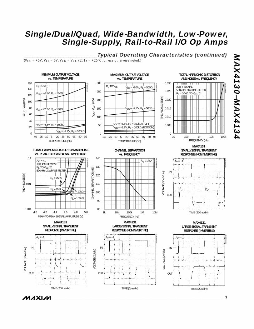
MA
X4
13
0–M
AX
41
34
Single/Dual/Quad, Wide-Bandwidth, Low-Power,Single-Supply, Rail-to-Rail I/O Op Amps
_______________________________________________________________________________________ 7
140
8010k1k 100k 10M1M
CHANNEL SEPARATIONvs. FREQUENCY
MAX
4130
/34-
25a
FREQUENCY (Hz)
CHAN
NEL
SEPA
RATI
ON (d
B)
100
90
130
110
120
VS = +5V
10 100k10kFREQUENCY (Hz)
100 1k
0.030
0
0.005
0.010
0.015
0.020
0.025
TOTAL HARMONIC DISTORTION AND NOISE vs. FREQUENCY
MAX
4130
/34-
22A
THD
AND
NOIS
E (%
)
2Vp-p SIGNAL500kHz LOWPASS FILTERRL = 10kΩ TO VCC / 2
0.1
0.0014.0 4.44.2 5.04.84.6
TOTAL HARMONIC DISTORTION AND NOISEvs. PEAK-TO-PEAK SIGNAL AMPLITUDE
MAX
4130
/34-
23
PEAK-TO-PEAK SIGNAL AMPLITUDE (V)
THD
+ NO
ISE
(%)
0.01
RL = 100kΩ
RL = 10kΩRL = 2kΩ
RL = 250Ω
AV = +110kHz SINE WAVERL TO VCC / 2500kHz LOWPASS FILTER IN
TIME (200ns/div)
VOLT
AGE
(50m
V/di
v)
OUT
MAX4131SMALL-SIGNAL TRANSIENTRESPONSE (NONINVERTING)
MAX
4130
/34-
24
AV = +1
IN
TIME (200ns/div)
VOLT
AGE
(50m
V/di
v)
OUT
MAX4131SMALL-SIGNAL TRANSIENT
RESPONSE (INVERTING)
MAX
4130
/34-
25
AV = -1
IN
TIME (2µs/div)
VOLT
AGE
(2V/
div)
OUT
MAX4131LARGE-SIGNAL TRANSIENTRESPONSE (NONINVERTING)
MAX
4130
/34-
26
AV = +1
IN
TIME (2µs/div)
VOLT
AGE
(2V/
div)
OUT
MAX4131LARGE-SIGNAL TRANSIENT
RESPONSE (INVERTING)
MAX
4130
/34-
27
AV = -1
____________________________Typical Operating Characteristics (continued)(VCC = +5V, VEE = 0V, VCM = VCC / 2, TA = +25°C, unless otherwise noted.)
160
0-40 -25 -10 5 20 35 50 65 80 95
MINIMUM OUTPUT VOLTAGEvs. TEMPERATURE
20
140
120
MAX
4130
/34-
13
TEMPERATURE (°C)
V OUT
- V E
E (m
V)
100
80
60
40
RL TO VCC
VCC = +6.5V, RL = 500Ω
VCC = +2.7V, RL = 100kΩ
VCC = +2.7V, RL = 500Ω
VCC = +6.5V, RL = 100kΩ
0
50
100
150
200
250
300
-40 -25 -10 5 20 35 50 65 80 95
MAXIMUM OUTPUT VOLTAGEvs. TEMPERATURE
MAX
4130
/34-
14
TEMPERATURE (°C)
V CC
- VOU
T (m
V)
RL TO VEE VCC = +6.5V, RL = 500Ω
VCC = +2.7V, RL = 100kΩ (BOTTOM)
VCC = +2.7V, RL = 500Ω
VCC = +6.5V, RL = 100kΩ (TOP)
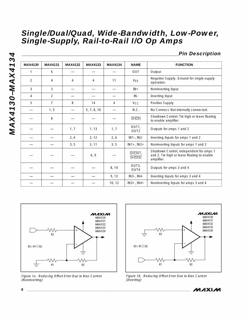
MA
X4
13
0–M
AX
41
34
Single/Dual/Quad, Wide-Bandwidth, Low-Power,Single-Supply, Rail-to-Rail I/O Op Amps
8 _______________________________________________________________________________________
______________________________________________________________Pin Description
Inverting Inputs for amps 1 and 2IN1-, IN2-—
Noninverting Inputs for amps 1 and 2IN1+, IN2+—
Shutdown Control, independent for amps 1and 2. Tie high or leave floating to enableamplifier.
SHDN1,SHDN2
—
Outputs for amps 3 and 4OUT3,OUT4
—
Inverting Inputs for amps 3 and 4IN3-, IN4-—
Positive SupplyVCC5
No Connect. Not internally connected.N.C.—
Shutdown Control. Tie high or leave floatingto enable amplifier.SHDN—
Outputs for amps 1 and 2OUT1,OUT2
—
Inverting InputIN-4
Noninverting Input IN+3
MAX4130
Negative Supply. Ground for single-supplyoperation.
VEE2
OutputOUT1
FUNCTIONNAME
—
—
—
—
—
7
1, 5
8
—
2
3
MAX4131
4
6
2, 6
3, 5
—
—
—
8
—
—
1, 7
—
—
MAX4132
4
—
2, 12
3, 11
6, 9
—
—
14
5, 7, 8, 10
—
1, 13
—
—
MAX4133
4
—
2, 6
3, 5
—
8, 14
9, 13
4
—
—
1, 7
—
—
MAX4134
11
—
Noninverting Inputs for amps 3 and 4IN3+, IN4+— — — — 10, 12
R3
R3 = R1 R2
R1 R2
MAX4130MAX4131MAX4132MAX4133MAX4134
Figure 1a. Reducing Offset Error Due to Bias Current(Noninverting)
R3
R3 = R1 R2
R1 R2
MAX4130MAX4131MAX4132MAX4133MAX4134
Figure 1b. Reducing Offset Error Due to Bias Current(Inverting)
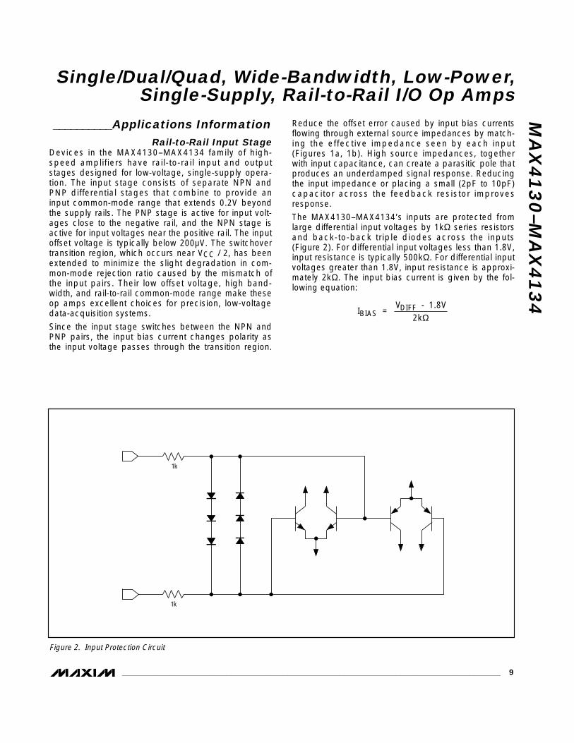
MA
X4
13
0–M
AX
41
34
Single/Dual/Quad, Wide-Bandwidth, Low-Power,Single-Supply, Rail-to-Rail I/O Op Amps
_______________________________________________________________________________________ 9
__________Applications InformationRail-to-Rail Input Stage
Devices in the MAX4130–MAX4134 family of high-speed amplifiers have rail-to-rail input and outputstages designed for low-voltage, single-supply opera-tion. The input stage consists of separate NPN andPNP differential stages that combine to provide aninput common-mode range that extends 0.2V beyondthe supply rails. The PNP stage is active for input volt-ages close to the negative rail, and the NPN stage isactive for input voltages near the positive rail. The inputoffset voltage is typically below 200µV. The switchovertransition region, which occurs near VCC / 2, has beenextended to minimize the slight degradation in com-mon-mode rejection ratio caused by the mismatch ofthe input pairs. Their low offset voltage, high band-width, and rail-to-rail common-mode range make theseop amps excellent choices for precision, low-voltagedata-acquisition systems.
Since the input stage switches between the NPN andPNP pairs, the input bias current changes polarity asthe input voltage passes through the transition region.
Reduce the offset error caused by input bias currentsflowing through external source impedances by match-ing the effective impedance seen by each input(Figures 1a, 1b). High source impedances, togetherwith input capacitance, can create a parasitic pole thatproduces an underdamped signal response. Reducingthe input impedance or placing a small (2pF to 10pF)capacitor across the feedback resistor improvesresponse.
The MAX4130–MAX4134’s inputs are protected fromlarge differential input voltages by 1kΩ series resistorsand back-to-back triple diodes across the inputs(Figure 2). For differential input voltages less than 1.8V,input resistance is typically 500kΩ. For differential inputvoltages greater than 1.8V, input resistance is approxi-mately 2kΩ. The input bias current is given by the fol-lowing equation:
I = V - 1.8V
2kBIASDIFF
Ω
1k
1k
Figure 2. Input Protection Circuit
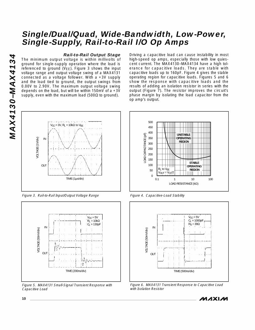
MA
X4
13
0–M
AX
41
34
Single/Dual/Quad, Wide-Bandwidth, Low-Power,Single-Supply, Rail-to-Rail I/O Op Amps
10 ______________________________________________________________________________________
Rail-to-Rail Output StageThe minimum output voltage is within millivolts ofground for single-supply operation where the load isreferenced to ground (VEE). Figure 3 shows the inputvoltage range and output voltage swing of a MAX4131connected as a voltage follower. With a +3V supplyand the load tied to ground, the output swings from0.00V to 2.90V. The maximum output voltage swingdepends on the load, but will be within 150mV of a +3Vsupply, even with the maximum load (500Ω to ground).
Driving a capacitive load can cause instability in mosthigh-speed op amps, especially those with low quies-cent current. The MAX4130–MAX4134 have a high tol-erance for capacitive loads. They are stable withcapacitive loads up to 160pF. Figure 4 gives the stableoperating region for capacitive loads. Figures 5 and 6show the response with capacitive loads and theresults of adding an isolation resistor in series with theoutput (Figure 7). The resistor improves the circuit’sphase margin by isolating the load capacitor from theop amp’s output.
IN
TIME (1µs/div)
VOLT
AGE
(1V/
div)
OUT
VCC = 3V, RL = 10kΩ to VEE
Figure 3. Rail-to-Rail Input/Output Voltage Range
500
0
50
100
150
200
300
350
400
450
0.1 1 10010LOAD RESISTANCE (kΩ)
LOAD
CAP
ACIT
ANCE
(pF)
250
UNSTABLE OPERATING
REGION
STABLE OPERATING
REGIONRL to VEEVOUT = VCC/2
Figure 4. Capacitive-Load Stability
IN
TIME (200ns/div)
VOLT
AGE
(50m
V/di
v)
OUT
VCC = 5VRL = 10kΩ CL = 130pF
Figure 5. MAX4131 Small-Signal Transient Response withCapacitive Load
Figure 6. MAX4131 Transient Response to Capacitive Loadwith Isolation Resistor
IN
TIME (500ns/div)
VOLT
AGE
(50m
V/di
v)
OUT
VCC = 5VCL = 1000pF RS = 39Ω
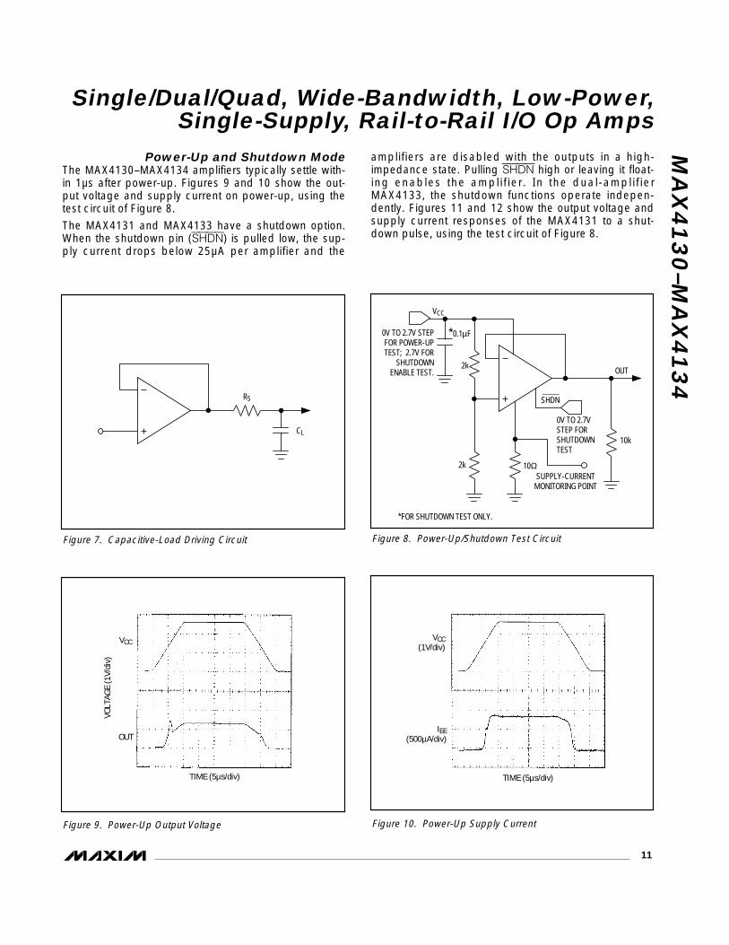
MA
X4
13
0–M
AX
41
34
Single/Dual/Quad, Wide-Bandwidth, Low-Power,Single-Supply, Rail-to-Rail I/O Op Amps
______________________________________________________________________________________ 11
Power-Up and Shutdown ModeThe MAX4130–MAX4134 amplifiers typically settle with-in 1µs after power-up. Figures 9 and 10 show the out-put voltage and supply current on power-up, using thetest circuit of Figure 8.
The MAX4131 and MAX4133 have a shutdown option.When the shutdown pin (SHDN) is pulled low, the sup-ply current drops below 25µA per amplifier and the
amplifiers are disabled with the outputs in a high-impedance state. Pulling SHDN high or leaving it float-ing enables the amplif ier. In the dual-amplif ierMAX4133, the shutdown functions operate indepen-dently. Figures 11 and 12 show the output voltage andsupply current responses of the MAX4131 to a shut-down pulse, using the test circuit of Figure 8.
RS
CL
Figure 7. Capacitive-Load Driving Circuit
SHDN
OUT
0V TO 2.7V STEP FOR SHUTDOWN TEST
0V TO 2.7V STEP FOR POWER-UPTEST; 2.7V FOR
SHUTDOWN ENABLE TEST.
SUPPLY-CURRENTMONITORING POINT
VCC
*0.1µF
10Ω2k
*FOR SHUTDOWN TEST ONLY.
10k
2k
Figure 8. Power-Up/Shutdown Test Circuit
VCC
TIME (5µs/div)
VOLT
AGE
(1V/
div)
OUT
Figure 9. Power-Up Output Voltage
VCC(1V/div)
TIME (5µs/div)
IEE(500µA/div)
Figure 10. Power-Up Supply Current
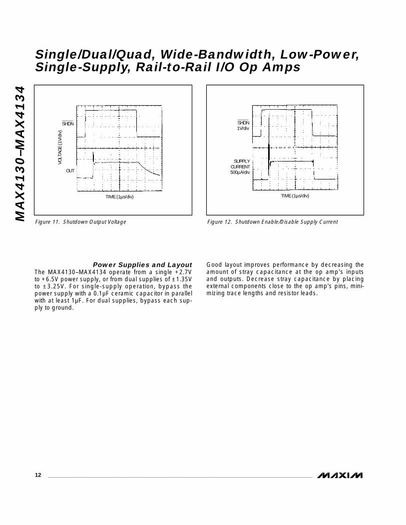
MA
X4
13
0–M
AX
41
34
Single/Dual/Quad, Wide-Bandwidth, Low-Power,Single-Supply, Rail-to-Rail I/O Op Amps
12 ______________________________________________________________________________________
Power Supplies and LayoutThe MAX4130–MAX4134 operate from a single +2.7Vto +6.5V power supply, or from dual supplies of ±1.35Vto ±3.25V. For single-supply operation, bypass thepower supply with a 0.1µF ceramic capacitor in parallelwith at least 1µF. For dual supplies, bypass each sup-ply to ground.
Good layout improves performance by decreasing theamount of stray capacitance at the op amp’s inputsand outputs. Decrease stray capacitance by placingexternal components close to the op amp’s pins, mini-mizing trace lengths and resistor leads.
SHDN
TIME (1µs/div)
VOLT
AGE
(1V/
div)
OUT
Figure 11. Shutdown Output Voltage
SHDN1V/div
TIME (1µs/div)
SUPPLYCURRENT500µA/div
Figure 12. Shutdown Enable/Disable Supply Current
MA
X4
13
0–M
AX
41
34
Single/Dual/Quad, Wide-Bandwidth, Low-Power,Single-Supply, Rail-to-Rail I/O Op Amps
______________________________________________________________________________________ 13
__________________________________________________________Pin Configurations
VEE
IN-IN+
1 5 VCCOUT
MAX4130
SOT23-5
TOP VIEW
2
3 4
14
13
12
11
10
9
8
1
2
3
4
5
6
7
VCC
OUT2
IN2-
IN2+VEE
IN1+
IN1-
OUT1
MAX4133
N.C.
SHDN2
N.C.N.C.
SHDN1
N.C.
SO
14
13
12
11
10
9
8
1
2
3
4
5
6
7
OUT4
IN4-
IN4+
VEEVCC
IN1+
IN1-
OUT1
MAX4134
IN3+
IN3-
OUT3OUT2
IN2-
IN2+
SO
IN2-IN1+
IN2+VEE
1
2
8
7
VCC
OUT2IN1-
OUT1
MAX4132
SO/µMAX
3
4
6
5
OUTIN1+
N.C.VEE
1
2
8
7
SHDN
VCCIN1-
N.C.
MAX4131
SO/µMAX
3
4
6
5
MA
X4
13
0–M
AX
41
34
Single/Dual/Quad, Wide-Bandwidth, Low-Power,Single-Supply, Rail-to-Rail I/O Op Amps
14 ______________________________________________________________________________________
__________________________________________________________Chip Topographies
___________________Chip Information_Ordering Information (continued)
SHDN
VCC
0.055"(1.397mm)
0.036"(0.914mm)
OUT
VEE IN-
iN+
VEE
TRANSISTOR COUNT: 170
SUBSTRATE CONNECTED TO VEE
OUT2
IN2-
IN2+
0.066"(1.676mm)
0.053"(1.346mm)
VCC SHDN1SHDN2
VEE VCC
OUT1 VCC
IN1-
IN1+
VEE
TRANSISTOR COUNT: 340
SUBSTRATE CONNECTED TO VEE
MAX4131 MAX4133
MAX4130 TRANSISTOR COUNT: 170
MAX4132 TRANSISTOR COUNT: 340
MAX4134 TRANSISTOR COUNT: 680
PART
MAX4132ESA
MAX4132EUA
MAX4133C/D 0°C to +70°C
-40°C to +85°C
-40°C to +85°C
TEMP. RANGEPIN-
PACKAGE
8 SO
8 µMAX
Dice*
SOT TOP MARK
—
—
—MAX4133ESD -40°C to +85°C 14 SO —
*Dice are specified at TA = +25°C, DC parameters only.
MAX4134ESD -40°C to +85°C 14 SO —
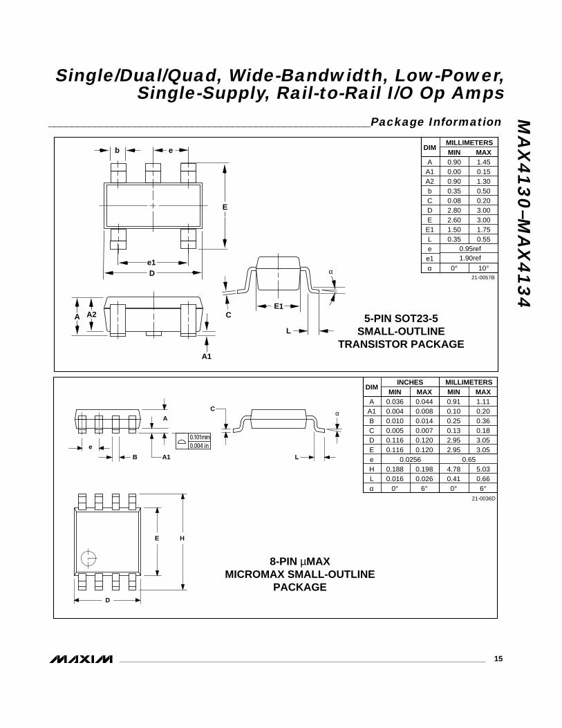
MA
X4
13
0–M
AX
41
34
Single/Dual/Quad, Wide-Bandwidth, Low-Power,Single-Supply, Rail-to-Rail I/O Op Amps
______________________________________________________________________________________ 15
________________________________________________________Package Information
L
DIM
AA1A2bCDE
E1Le
e1α
MIN0.900.000.900.350.082.802.601.500.35
0°
MAX1.450.151.300.500.203.003.001.750.55
10°
MILLIMETERS
α
5-PIN SOT23-5SMALL-OUTLINE
TRANSISTOR PACKAGE
De1
A A2
A1
C
b e
E1
21-0057B
E
0.95ref1.90ref
L
αC
A1B
DIM
AA1BCDEeHLα
MIN0.0360.0040.0100.0050.1160.116
0.1880.016
0°
MAX0.0440.0080.0140.0070.1200.120
0.1980.026
6°
MIN0.910.100.250.132.952.95
4.780.410°
MAX1.110.200.360.183.053.05
5.030.666°
INCHES MILLIMETERS
8-PIN µMAXMICROMAX SMALL-OUTLINE
PACKAGE
0.650.0256
A
e
E H
D
0.101mm0.004 in
21-0036D
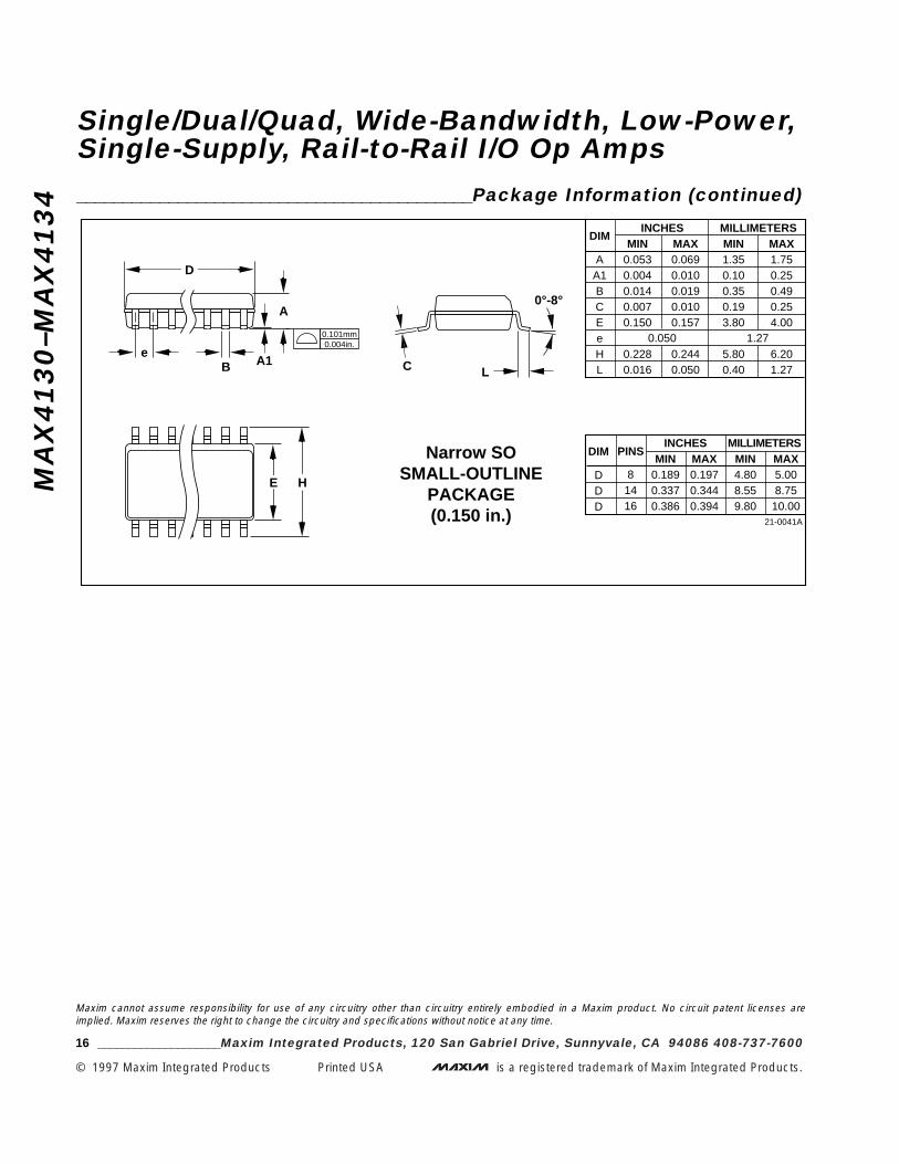
MA
X4
13
0–M
AX
41
34
Single/Dual/Quad, Wide-Bandwidth, Low-Power,Single-Supply, Rail-to-Rail I/O Op Amps___________________________________________Package Information (continued)
DIM
AA1BCEeHL
MIN0.0530.0040.0140.0070.150
0.2280.016
MAX0.0690.0100.0190.0100.157
0.2440.050
MIN1.350.100.350.193.80
5.800.40
MAX1.750.250.490.254.00
6.201.27
INCHES MILLIMETERS
21-0041A
Narrow SOSMALL-OUTLINE
PACKAGE(0.150 in.)
DIM
DDD
MIN0.1890.3370.386
MAX0.1970.3440.394
MIN4.808.559.80
MAX5.008.75
10.00
INCHES MILLIMETERSPINS
81416
1.270.050
L
0°-8°
HE
D
e
A
A1 C
0.101mm0.004in.
B
Maxim cannot assume responsibility for use of any circuitry other than circuitry entirely embodied in a Maxim product. No circuit patent licenses areimplied. Maxim reserves the right to change the circuitry and specifications without notice at any time.
16 ____________________Maxim Integrated Products, 120 San Gabriel Drive, Sunnyvale, CA 94086 408-737-7600
© 1997 Maxim Integrated Products Printed USA is a registered trademark of Maxim Integrated Products.

4.9 MAX427
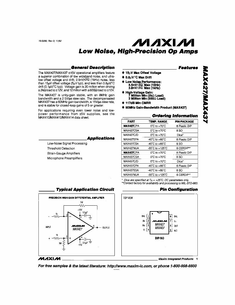
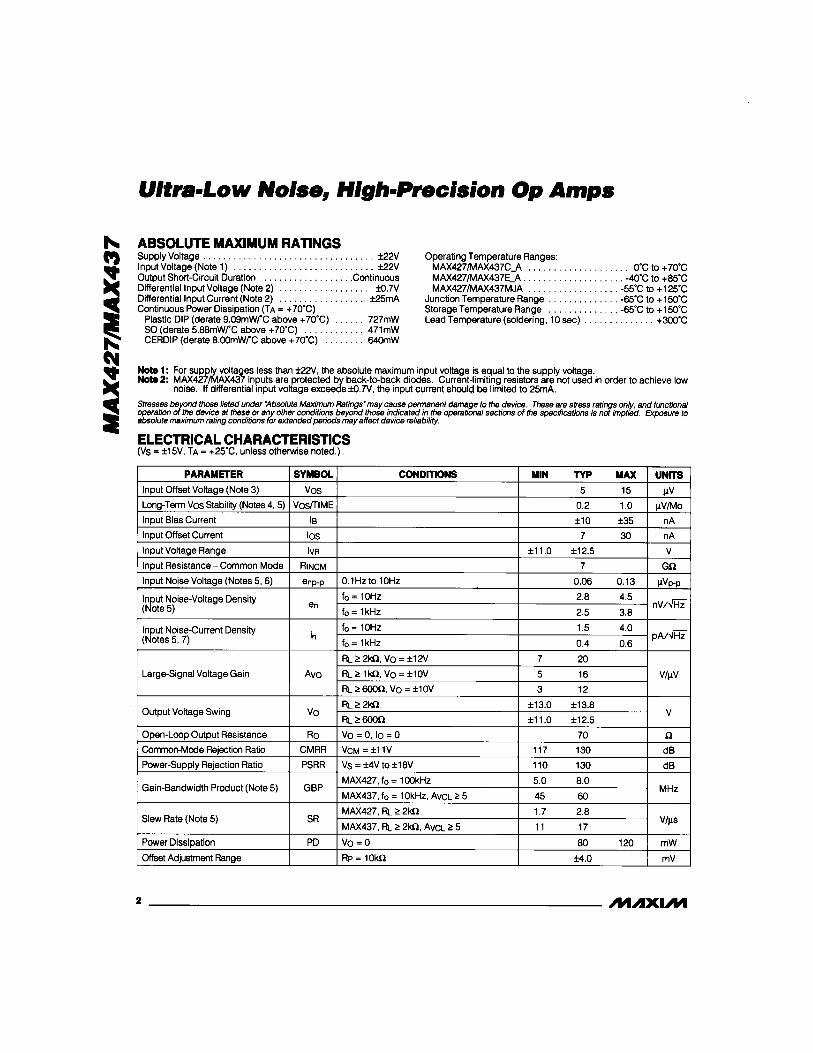
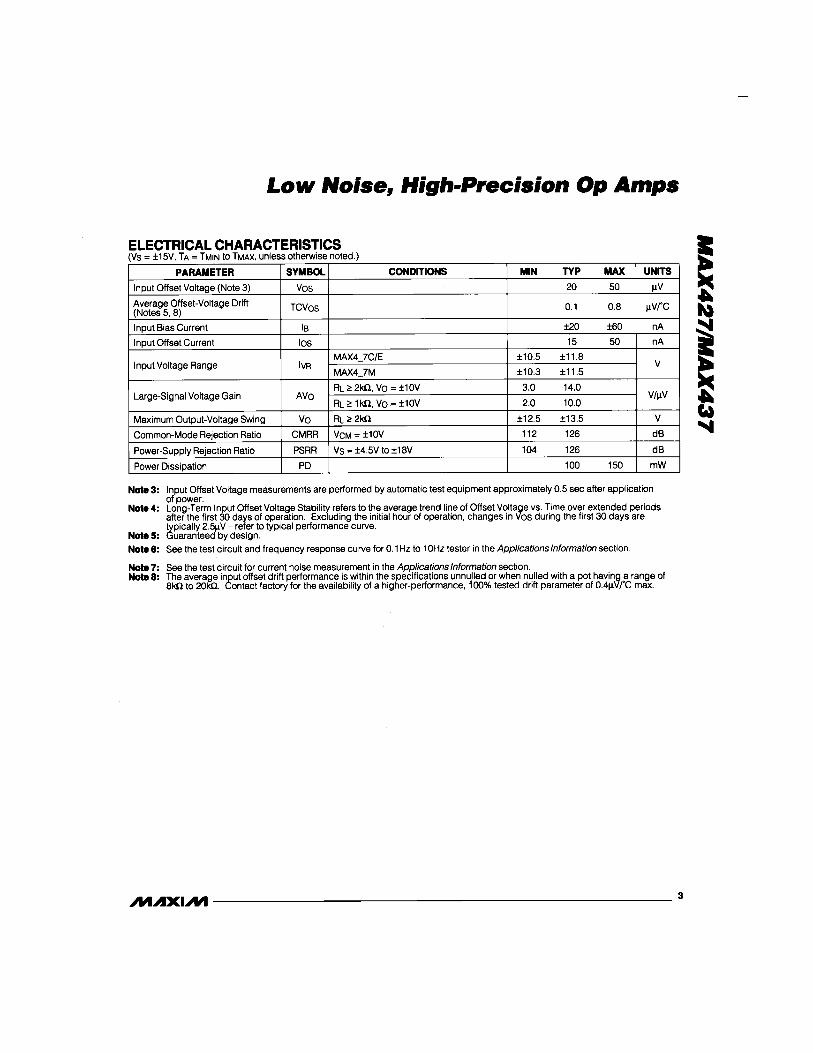
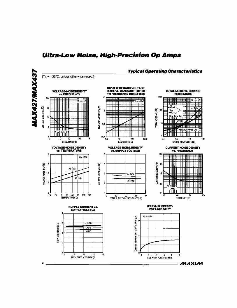
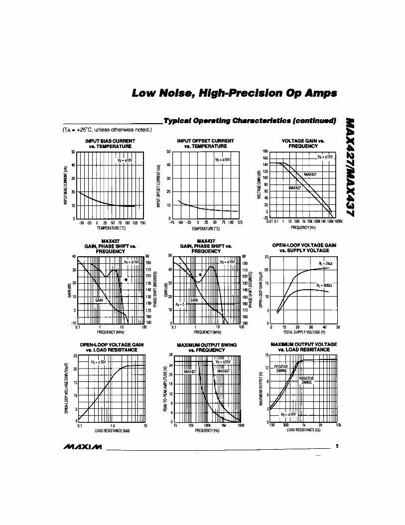
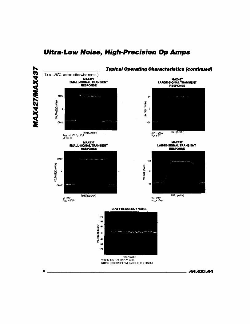
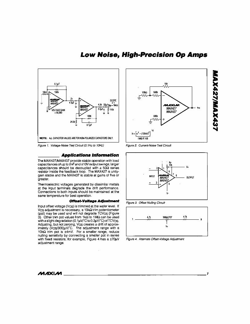
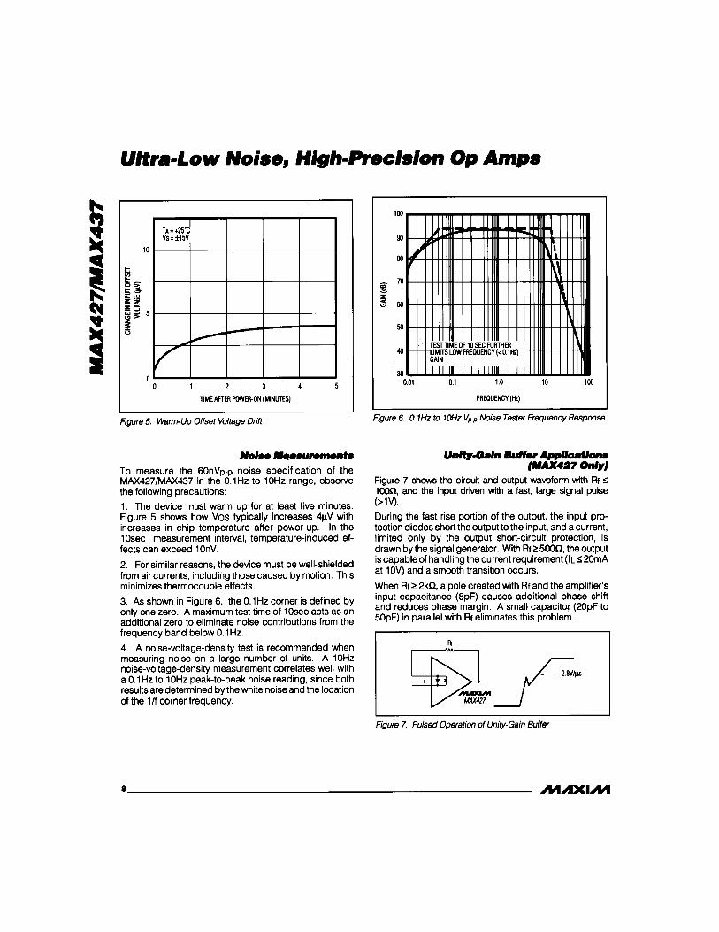
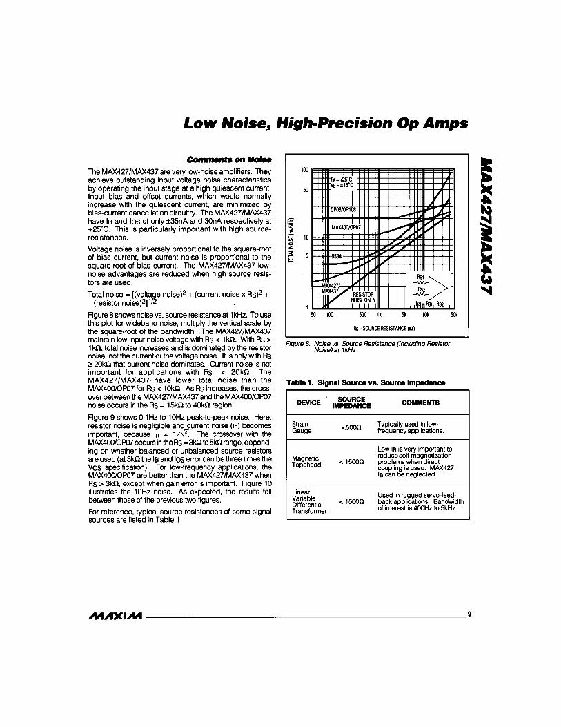
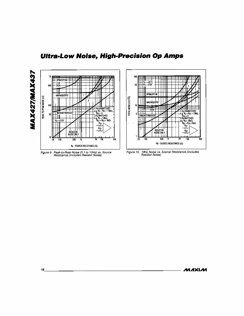
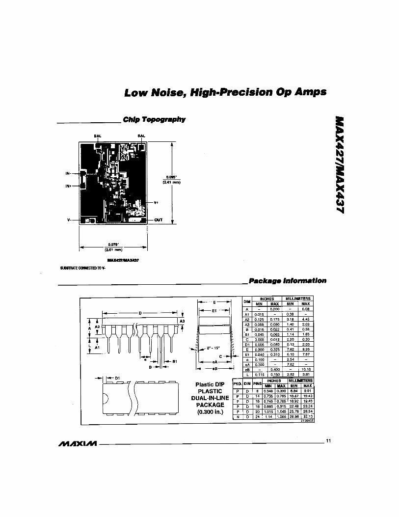
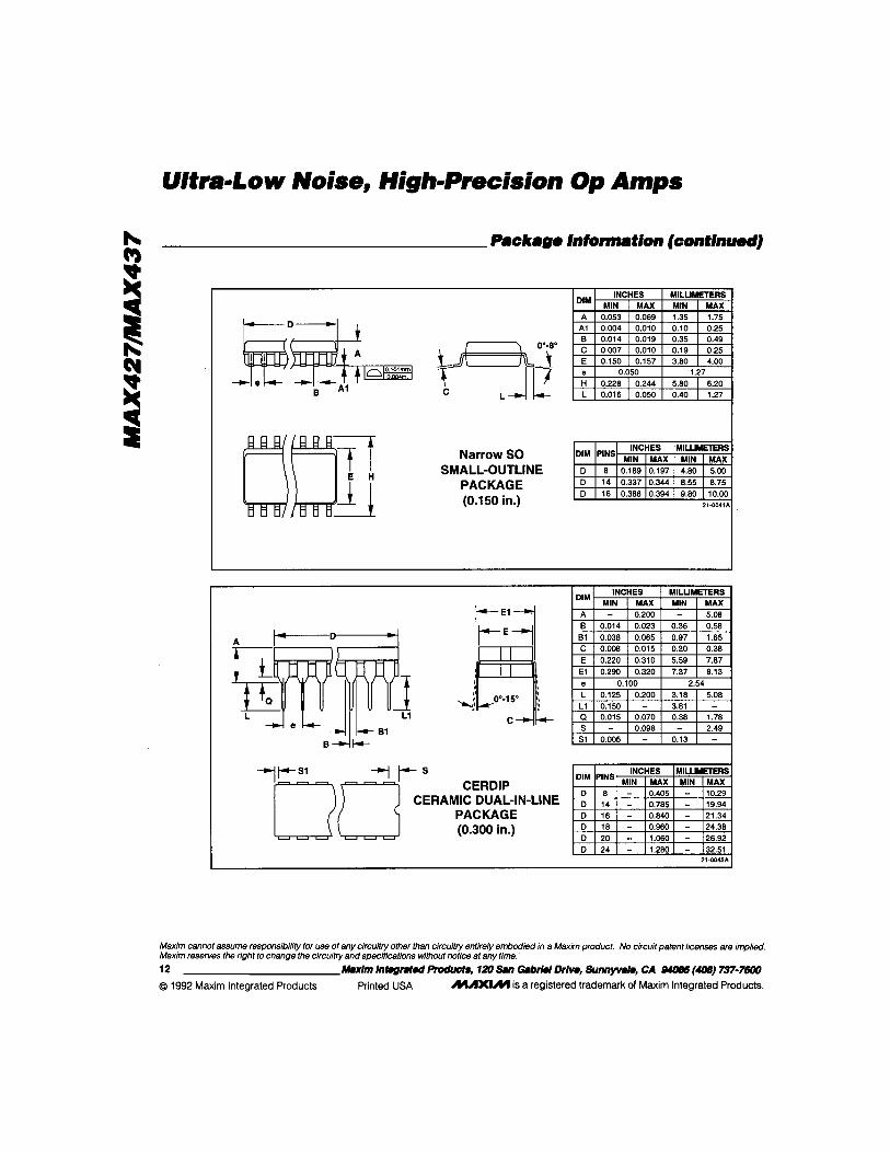

4.10 MAX547
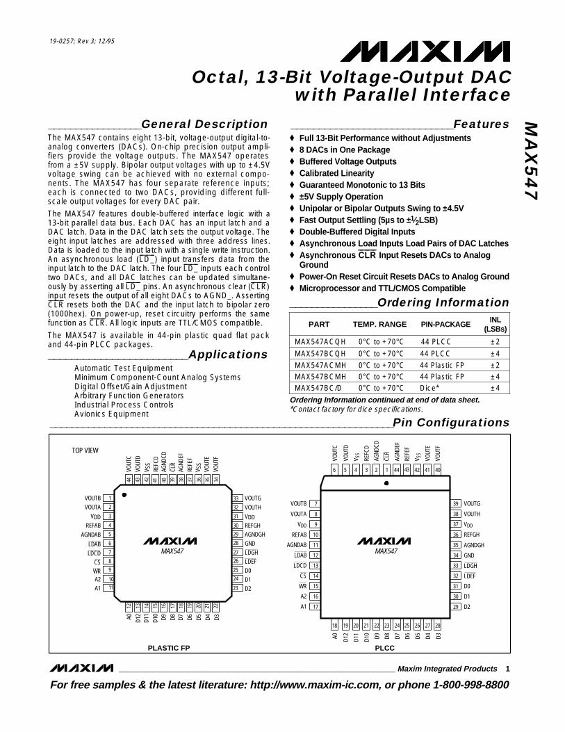
For free samples & the latest literature: http://www.maxim-ic.com, or phone 1-800-998-8800
MA
X5
47
Octal, 13-Bit Voltage-Output DAC with Parallel Interface
________________________________________________________________ Maxim Integrated Products 1
441234 404142435
21 24 2625 27 2822 2319 20
8
9
10
11
12
13
14
15
16
17 29
30
31
32
33
34
35
36
37
38
A1
D11
VOUT
D
V SS
REFC
D
AGND
CD
AGND
EF
REFE
F
V SS
VOUT
E
VOUT
F
D12 D9D10 D7D8 D5D6 D3D4
VOUTH
VDD
REFGH
AGNDGH
GND
LDGH
LDEF
D0
D1
D2
A2
WR
CS
LDCD
LDAB
AGNDAB
REFAB
VDD
VOUTA
7 39 VOUTGVOUTB
6
18
VOUT
CA0
CLR
MAX547
PLCC
TOP VIEW
VOUTHVDDREFGHAGNDGHGND
D0D1D2
VOUTG
LDEFLDGH
VOUTAVDD
REFABAGNDAB
LDAB
WRA2A1
VOUTB
CSLDCD
VOUT
DV S
S
AGND
EF
REFC
DAG
NDCD
CLR
VOUT
C
REFE
FV S
S
VOUT
FVO
UTE
D12
D11
D7D10
D9 D8A0 D6 D5 D3D4
PLASTIC FP
2221201918171615141312
23
2425
2627
2829
30
31
32
33
3435363738394041424344
1110
98
76
5
4
3
21
MAX547
19-0257; Rev 3; 12/95
_________________General DescriptionThe MAX547 contains eight 13-bit, voltage-output digital-to-analog converters (DACs). On-chip precision output ampli-fiers provide the voltage outputs. The MAX547 operatesfrom a ±5V supply. Bipolar output voltages with up to ±4.5Vvoltage swing can be achieved with no external compo-nents. The MAX547 has four separate reference inputs;each is connected to two DACs, providing different full-scale output voltages for every DAC pair.
The MAX547 features double-buffered interface logic with a13-bit parallel data bus. Each DAC has an input latch and aDAC latch. Data in the DAC latch sets the output voltage. Theeight input latches are addressed with three address lines.Data is loaded to the input latch with a single write instruction.An asynchronous load (–L—D—_–) input transfers data from theinput latch to the DAC latch. The four –L—D—_– inputs each controltwo DACs, and all DAC latches can be updated simultane-ously by asserting all –L—D—_– pins. An asynchronous clear (–C—L—R–)input resets the output of all eight DACs to AGND_. Asserting–C—L—R– resets both the DAC and the input latch to bipolar zero(1000hex). On power-up, reset circuitry performs the samefunction as –C—L—R–. All logic inputs are TTL/CMOS compatible.
The MAX547 is available in 44-pin plastic quad flat packand 44-pin PLCC packages.________________________Applications
Automatic Test EquipmentMinimum Component-Count Analog SystemsDigital Offset/Gain AdjustmentArbitrary Function GeneratorsIndustrial Process ControlsAvionics Equipment
_____________________________Features♦ Full 13-Bit Performance without Adjustments♦ 8 DACs in One Package♦ Buffered Voltage Outputs♦ Calibrated Linearity♦ Guaranteed Monotonic to 13 Bits♦ ±5V Supply Operation♦ Unipolar or Bipolar Outputs Swing to ±4.5V♦ Fast Output Settling (5µs to ±1⁄2LSB)♦ Double-Buffered Digital Inputs♦ Asynchronous Load Inputs Load Pairs of DAC Latches♦ Asynchronous
–C—L—R–
Input Resets DACs to AnalogGround
♦ Power-On Reset Circuit Resets DACs to Analog Ground♦ Microprocessor and TTL/CMOS Compatible
________________Ordering Information
Ordering Information continued at end of data sheet.*Contact factory for dice specifications.
MAX547ACQH
MAX547BCQH
MAX547ACMH 0°C to +70°C
0°C to +70°C
0°C to +70°C 44 PLCC
44 PLCC
44 Plastic FPMAX547BCMH 0°C to +70°C 44 Plastic FPMAX547BC/D 0°C to +70°C Dice*
_______________________________________________________________Pin Configurations
±2
±4
±2±4±4
PART TEMP. RANGE PIN-PACKAGEINL
(LSBs)
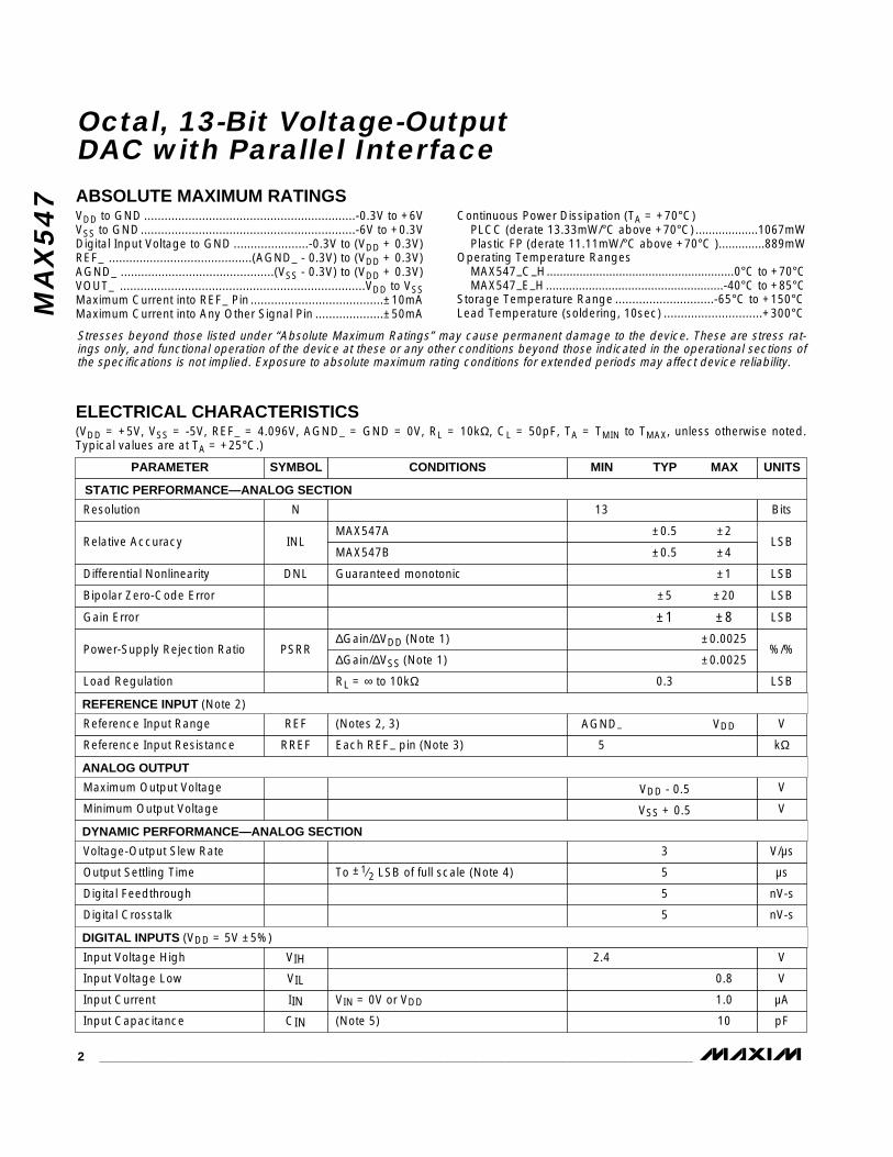
MA
X5
47
Octal, 13-Bit Voltage-OutputDAC with Parallel Interface
2 _______________________________________________________________________________________
ABSOLUTE MAXIMUM RATINGS
ELECTRICAL CHARACTERISTICS(VDD = +5V, VSS = -5V, REF_ = 4.096V, AGND_ = GND = 0V, RL = 10kΩ, CL = 50pF, TA = TMIN to TMAX, unless otherwise noted.Typical values are at TA = +25°C.)
Stresses beyond those listed under “Absolute Maximum Ratings” may cause permanent damage to the device. These are stress rat-ings only, and functional operation of the device at these or any other conditions beyond those indicated in the operational sections ofthe specifications is not implied. Exposure to absolute maximum rating conditions for extended periods may affect device reliability.
VDD to GND ..............................................................-0.3V to +6VVSS to GND...............................................................-6V to +0.3VDigital Input Voltage to GND ......................-0.3V to (VDD + 0.3V)REF_ ..........................................(AGND_ - 0.3V) to (VDD + 0.3V)AGND_ .............................................(VSS - 0.3V) to (VDD + 0.3V)VOUT_ ........................................................................VDD to VSSMaximum Current into REF_ Pin .......................................±10mAMaximum Current into Any Other Signal Pin ....................±50mA
Continuous Power Dissipation (TA = +70°C)PLCC (derate 13.33mW/°C above +70°C)...................1067mWPlastic FP (derate 11.11mW/°C above +70°C )..............889mW
Operating Temperature RangesMAX547–C–H.........................................................0°C to +70°CMAX547–E–H......................................................-40°C to +85°C
Storage Temperature Range .............................-65°C to +150°CLead Temperature (soldering, 10sec) .............................+300°C
CONDITIONS
nV-s5Digital Crosstalk
nV-s5Digital Feedthrough
µs5Output Settling Time
V/µs3Voltage-Output Slew Rate
kΩ5RREFReference Input Resistance
VAGND– VDDREFReference Input Range
%/%±0.0025
PSRRPower-Supply Rejection Ratio±0.0025
Bits13NResolution
LSBBipolar Zero-Code Error ±5 ±20
±0.5 ±2LSB
±0.5 ±4INLRelative Accuracy
LSB±1DNLDifferential Nonlinearity
UNITSMIN TYP MAXSYMBOLPARAMETER
To ±1⁄2 LSB of full scale (Note 4)
Each REF– pin (Note 3)
(Notes 2, 3)
MAX547A
MAX547B
∆Gain/∆VSS (Note 1)
Guaranteed monotonic
∆Gain/∆VDD (Note 1)
LSB0.3Load Regulation RL = ∞ to 10kΩ
LSBGain Error ±1 ±8
STATIC PERFORMANCE—ANALOG SECTION
VVSS + 0.5Minimum Output Voltage
VVDD - 0.5Maximum Output Voltage
pF10CINInput Capacitance
µA1.0IINInput Current
V0.8VILInput Voltage Low
V2.4VIHInput Voltage High
(Note 5)
VIN = 0V or VDD
ANALOG OUTPUT
REFERENCE INPUT (Note 2)
DYNAMIC PERFORMANCE—ANALOG SECTION
DIGITAL INPUTS (VDD = 5V ±5%)
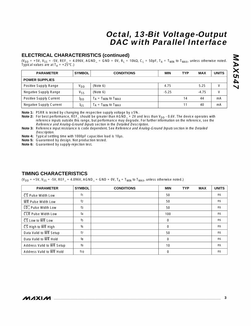
MA
X5
47
Octal, 13-Bit Voltage-OutputDAC with Parallel Interface
_______________________________________________________________________________________ 3
Note 1: PSRR is tested by changing the respective supply voltage by ±5%.Note 2: For best performance, REF_ should be greater than AGND_ + 2V and less than VDD - 0.6V. The device operates with
reference inputs outside this range, but performance may degrade. For further information on the reference, see the Reference and Analog-Ground Inputs section in the Detailed Description.
Note 3: Reference input resistance is code dependent. See Reference and Analog-Ground Inputs section in the DetailedDescription.
Note 4: Typical settling time with 1000pF capacitive load is 10µs.Note 5: Guaranteed by design. Not production tested.Note 6: Guaranteed by supply-rejection test.
TIMING CHARACTERISTICS(VDD = +5V, VSS = -5V, REF_ = 4.096V, AGND_ = GND = 0V, TA = TMIN to TMAX, unless otherwise noted.)
14 44
11 40TA = TMIN to TMAX mAISSNegative Supply Current
CONDITIONS
mAIDDPositive Supply Current
V-5.25 -4.75VSSNegative Supply Range
V4.75 5.25VDDPositive Supply Range
UNITSMIN TYP MAXSYMBOLPARAMETER
(Note 6)
(Note 6)
CONDITIONS
ns0t6–C—S– High to –W—R– High
ns0t5–C—S– Low to –W—R– Low
ns100t4–C—L—R– Pulse Width Low
ns50t3–L—D—–– Pulse Width Low
ns50t2–W—R– Pulse Width Low
ns50t1–C—S– Pulse Width Low
UNITSMIN TYP MAXSYMBOLPARAMETER
ns50t7Data Valid to –W—R– Setup
ns0t8Data Valid to –W—R– Hold
ns10t9Address Valid to –W—R– Setup
ns0t10Address Valid to –W—R– Hold
ELECTRICAL CHARACTERISTICS (continued)(VDD = +5V, VSS = -5V, REF_ = 4.096V, AGND_ = GND = 0V, RL = 10kΩ, CL = 50pF, TA = TMIN to TMAX, unless otherwise noted.Typical values are at TA = +25°C.)
TA = TMIN to TMAX
POWER SUPPLIES
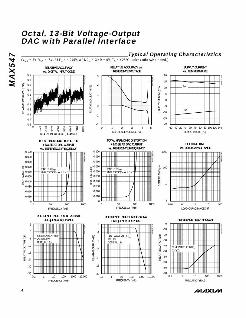
MA
X5
47
Octal, 13-Bit Voltage-OutputDAC with Parallel Interface
4 _______________________________________________________________________________________
__________________________________________Typical Operating Characteristics(VDD = 5V, VSS = -5V, REF_ = 4.096V, AGND_ = GND = 0V, TA = +25°C, unless otherwise noted.)
-36
-30
-24
-18
-12
-6
0
6
0.1 1 10 100 1000 10,000
REFERENCE INPUT SMALL-SIGNAL FREQUENCY RESPONSE
MAX
547-
Fg T
OC-1
FREQUENCY (kHz)
RELA
TIVE
OUT
PUT
(dB) SINE WAVE AT REF–
2V ±100mV CODE ALL 1s
-20
-15
-10
-5
0
5
10
15
20
-60 -40 -20 0 20 40 60 80 100 120 140
SUPPLY CURRENT vs. TEMPERATURE
MAX
547-
Fg T
OC-2
TEMPERATURE (°C)
SUPP
LY C
URRE
NT (m
A) IDD
ISS
0
0.010
0.020
0.030
0.040
0.050
0.060
0.070
0.080
0.090
0.100
1 10 100 1000
TOTAL HARMONIC DISTORTION + NOISE AT DAC OUTPUT
vs. REFERENCE FREQUENCYM
AX54
7-Fg
TOC
-3
FREQUENCY (kHz)
THD
+ NO
ISE
(%)
REF– = 4Vp-p INPUT CODE = ALL 1s
0
0.010
0.020
0.030
0.040
0.050
0.060
0.070
0.080
0.090
0.100
1 10 100 1000
TOTAL HARMONIC DISTORTION + NOISE AT DAC OUTPUT
vs. REFERENCE FREQUENCY
MAX
547-
Fg T
OC-4
FREQUENCY (kHz)
THD
+ NO
ISE
(%)
REF– = 2Vp-p INPUT CODE = ALL 1s
-90
-80
-70
-60
-50
-40
-30
-20
-10
0
0.1 1 10 100 1000
REFERENCE FEEDTHROUGHM
AX54
7-Fg
TOC
-7
FREQUENCY (kHz)
RELA
TIVE
OUT
PUT
(dB)
SINE WAVE AT REF_ 2V ±2V
-0.5
-0.4
-0.3
-0.2
-0.1
0
0.1
0.2
0.3
0.4
0.5
0
1024
2048
3072
4096
5120
6144
7168
8191
RELATIVE ACCURACY vs. DIGITAL INPUT CODE
MAX
547-
Fg T
OC-5
DIGITAL INPUT CODE (DECIMAL)
RELA
TIVE
ACC
URAC
Y (L
SB)
-22
-18
-14
-10
-6
-2
02
0.1 1 10 100 1000 10,000
REFERENCE INPUT LARGE-SIGNAL FREQUENCY RESPONSE
MAX
547-
Fg T
OC-6
FREQUENCY (kHz)
RELA
TIVE
OUT
PUT
(dB) SINE WAVE AT REF_
2V ±2V CODE ALL 1s
1
10
100
1000
0.01 0.1 1 10 100
SETTLING TIME vs. LOAD CAPACITANCE
MAX
547-
Fg T
OC-9
LOAD CAPACITANCE (nF)
SETT
LING
TIM
E (µ
s)
-2
-1
0
1
2
3
0 1 2 3 4 5
RELATIVE ACCURACY vs. REFERENCE VOLTAGE
MAX
547-
Fg T
OC-1
1
REFERENCE VOLTAGE (V)
RELA
TIVE
ACC
URAC
Y (L
SB)
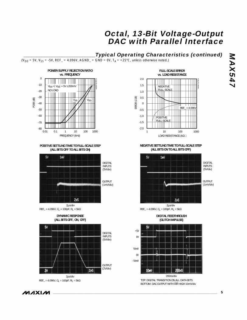
-2.0
-1.5
-1.0
-0.5
0
0.5
1.0
1.5
2.0
1 10 100 1000
FULL-SCALE ERROR vs. LOAD RESISTANCE
MAX
547-
Fg T
OC-8
LOAD RESISTANCE (kΩ)ER
ROR
(LSB
)
NEGATIVE FULL-SCALE
POSITIVE FULL-SCALE
REF_ = 4.096V
MA
X5
47
Octal, 13-Bit Voltage-OutputDAC with Parallel Interface
_______________________________________________________________________________________ 5
POSITIVE SETTLING TIME TO FULL-SCALE STEP (ALL BITS OFF TO ALL BITS ON)
DIGITAL INPUTS (5V/div)
OUTPUT (1mV/div)
2µs/divREF– = 4.096V, CL = 100pF, RL = 5kΩ
NEGATIVE SETTLING TIME TO FULL-SCALE STEP (ALL BITS ON TO ALL BITS OFF)
DIGITAL INPUTS (5V/div)
OUTPUT (1mV/div)
2µs/divREF– = 4.096V, CL = 100pF, RL = 5kΩ
DYNAMIC RESPONSE (ALL BITS OFF, ON, OFF)
DIGITAL INPUTS (5V/div)
OUTPUT (2V/div)
2µs/divREF– = 4.096V, CL = 100pF, RL = 5kΩ
DIGITAL FEEDTHROUGH (GLITCH IMPULSE)
200ns/div
+5V
0V
10mV
0V
-10mV
TOP: DIGITAL TRANSITION ON ALL DATA BITS BOTTOM: DAC OUTPUT WITH WR HIGH 10mV/div
____________________________Typical Operating Characteristics (continued)(VDD = 5V, VSS = -5V, REF_ = 4.096V, AGND_ = GND = 0V, TA = +25°C, unless otherwise noted.)
-80
-70
-60
-50
-40
-30
-20
-10
0
0.01 0.1 1 10 100 1000
POWER-SUPPLY REJECTION RATIO vs. FREQUENCY
MAX
547-
Fg T
OC-1
0
FREQUENCY (kHz)
PSRR
(dB) VSS VDD
VDD = VSS = 5V ±200mV NO LOAD
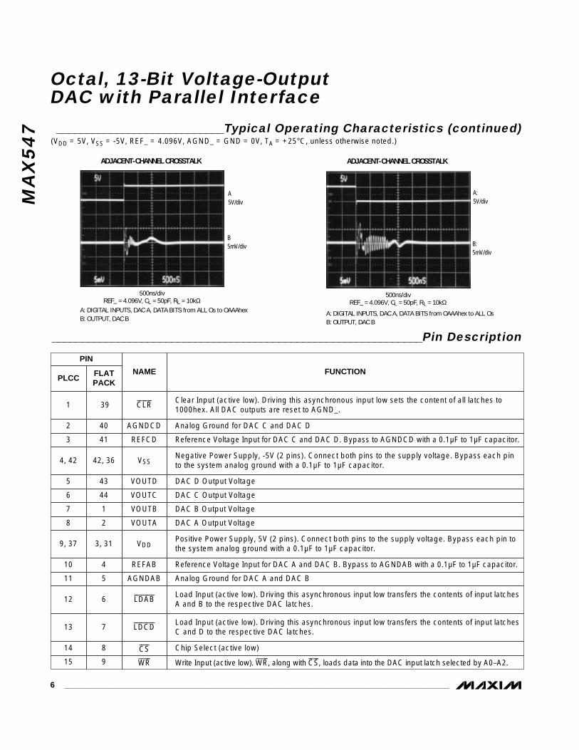
MA
X5
47
Octal, 13-Bit Voltage-OutputDAC with Parallel Interface
6 _______________________________________________________________________________________
PLCCNAME
1 –C—L—R–Clear Input (active low). Driving this asynchronous input low sets the content of all latches to1000hex. All DAC outputs are reset to AGND_.
3 REFCD Reference Voltage Input for DAC C and DAC D. Bypass to AGNDCD with a 0.1µF to 1µF capacitor.
2 AGNDCD Analog Ground for DAC C and DAC D
7 VOUTB DAC B Output Voltage
6 VOUTC DAC C Output Voltage
5 VOUTD DAC D Output Voltage
4, 42 VSSNegative Power Supply, -5V (2 pins). Connect both pins to the supply voltage. Bypass each pinto the system analog ground with a 0.1µF to 1µF capacitor.
FLATPACK
PIN
39
41
40
1
44
43
42, 36
FUNCTION
8 VOUTA DAC A Output Voltage2
9, 37 VDDPositive Power Supply, 5V (2 pins). Connect both pins to the supply voltage. Bypass each pin tothe system analog ground with a 0.1µF to 1µF capacitor.
3, 31
10 REFAB Reference Voltage Input for DAC A and DAC B. Bypass to AGNDAB with a 0.1µF to 1µF capacitor.4
11 AGNDAB Analog Ground for DAC A and DAC B5
12 –L—D—A—B–Load Input (active low). Driving this asynchronous input low transfers the contents of input latchesA and B to the respective DAC latches.
6
13 –L—D—C—D–Load Input (active low). Driving this asynchronous input low transfers the contents of input latchesC and D to the respective DAC latches.
7
14 –C—S– Chip Select (active low)8
15 –W—R– Write Input (active low). –W—R–, along with –C—S–, loads data into the DAC input latch selected by A0–A2.9
ADJACENT-CHANNEL CROSSTALK
A: DIGITAL INPUTS, DAC A, DATA BITS from ALL Os to OAAAhex B: OUTPUT, DAC B
500ns/div REF– = 4.096V, CL = 50pF, RL = 10kΩ
A 5V/div
B 5mV/div
ADJACENT-CHANNEL CROSSTALK
A: DIGITAL INPUTS, DAC A, DATA BITS from OAAAhex to ALL Os B: OUTPUT, DAC B
500ns/div REF– = 4.096V, CL = 50pF, RL = 10kΩ
A: 5V/div
B: 5mV/div
______________________________________________________________Pin Description
____________________________Typical Operating Characteristics (continued)(VDD = 5V, VSS = -5V, REF_ = 4.096V, AGND_ = GND = 0V, TA = +25°C, unless otherwise noted.)
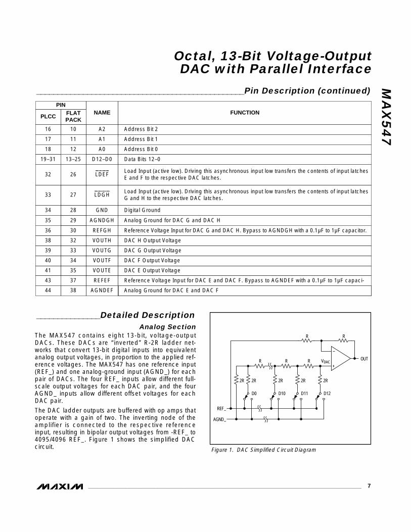
Analog Ground for DAC E and DAC F
_______________Detailed DescriptionAnalog Section
The MAX547 contains eight 13-bit, voltage-outputDACs. These DACs are “inverted” R-2R ladder net-works that convert 13-bit digital inputs into equivalentanalog output voltages, in proportion to the applied ref-erence voltages. The MAX547 has one reference input(REF_) and one analog-ground input (AGND_) for eachpair of DACs. The four REF_ inputs allow different full-scale output voltages for each DAC pair, and the fourAGND_ inputs allow different offset voltages for eachDAC pair.
The DAC ladder outputs are buffered with op amps thatoperate with a gain of two. The inverting node of theamplifier is connected to the respective referenceinput, resulting in bipolar output voltages from -REF_ to4095/4096 REF_. Figure 1 shows the simplified DACcircuit.
MA
X5
47
Octal, 13-Bit Voltage-OutputDAC with Parallel Interface
_______________________________________________________________________________________ 7
_________________________________________________Pin Description (continued)
FLATPACK
PLCCNAME FUNCTION
36 REFGH Reference Voltage Input for DAC G and DAC H. Bypass to AGNDGH with a 0.1µF to 1µF capacitor.30
16 A2 Address Bit 2
38 VOUTH DAC H Output Voltage
33–L—D—G—H– Load Input (active low). Driving this asynchronous input low transfers the contents of input latches
G and H to the respective DAC latches.
32
35 AGNDGH Analog Ground for DAC G and DAC H
34 GND Digital Ground
PIN
10
27
29
28
41 VOUTE DAC E Output Voltage35
39 VOUTG DAC G Output Voltage33
40 VOUTF DAC F Output Voltage34
44 AGNDEF38
Figure 1. DAC Simplified Circuit Diagram
2R 2R
R
D0 D10 D11 D12
R R
R R
OUT
REF–
AGND–
2R 2R 2R
VDAC
43 REFEF Reference Voltage Input for DAC E and DAC F. Bypass to AGNDEF with a 0.1µF to 1µF capaci-37
32–L—D—E—F– Load Input (active low). Driving this asynchronous input low transfers the contents of input latches
E and F to the respective DAC latches.26
17 A1 Address Bit 111
18 A0 Address Bit 0
19–31 D12–D0 Data Bits 12–013–25
12
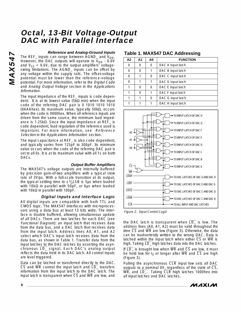
Reference and Analog-Ground InputsThe REF_ inputs can range between AGND_ and VDD.However, the DAC outputs will operate to VDD - 0.6Vand VSS + 0.6V, due to the output amplifiers’ voltage-swing limitations. The AGND_ inputs can be offset byany voltage within the supply rails. The offset-voltagepotential must be lower than the reference-voltagepotential. For more information, refer to the Digital Codeand Analog Output Voltage section in the ApplicationsInformation.The input impedance of the REF_ inputs is code depen-dent. It is at its lowest value (5kΩ min) when the inputcode of the referring DAC pair is 0 1010 1010 1010(0AAAhex). Its maximum value, typically 50kΩ, occurswhen the code is 0000hex. When all reference inputs aredriven from the same source, the minimum load imped-ance is 1.25kΩ. Since the input impedance at REF_ iscode dependent, load regulation of the reference used isimportant. For more information, see ReferenceSelection in the Applications Information section.
The input capacitance at REF_ is also code dependent,and typically varies from 125pF to 300pF. Its minimumvalue occurs when the code of the referring DAC pair isset to all 0s. It is at its maximum value with all 1s on bothDACs.
Output Buffer AmplifiersThe MAX547’s voltage outputs are internally bufferedby precision gain-of-two amplifiers with a typical slewrate of 3V/µs. With a full-scale transition at its output,the typical settling time to ±1⁄2LSB is 5µs when loadedwith 10kΩ in parallel with 50pF, or 6µs when loadedwith 10kΩ in parallel with 100pF.
Digital Inputs and Interface LogicAll digital inputs are compatible with both TTL andCMOS logic. The MAX547 interfaces with microproces-sors using a data bus at least 13 bits wide. The inter-face is double buffered, allowing simultaneous updateof all DACs. There are two latches for each DAC (seeFunctional Diagram): an input latch that receives datafrom the data bus, and a DAC latch that receives datafrom the input latch. Address lines A0, A1, and A2select which DAC’s input latch receives data from thedata bus, as shown in Table 1. Transfer data from theinput latches to the DAC latches by asserting the asyn-chronous LD_ signal. Each DAC’s analog outputreflects the data held in its DAC latch. All control inputsare level triggered.
Data can be latched or transferred directly to the DAC.CS and WR control the input latch and LD_ transfersinformation from the input latch to the DAC latch. Theinput latch is transparent when CS and WR are low, and
the DAC latch is transparent when LD_ is low. Theaddress lines (A0, A1, A2) must be valid throughout thetime CS and WR are low (Figure 3). Otherwise, the datacan be inadvertently written to the wrong DAC. Data islatched within the input latch when either CS or WR ishigh. Taking LD_ high latches data into the DAC latches.
If LD_ is brought low when WR and CS are low, it mustbe held low for t3 or longer after WR and CS are high(Figure 3).
Pulling the asynchronous CLR input low sets all DACoutputs to a nominal 0V, regardless of the state of CS,WR, and LD_. Taking CLR high latches 1000hex intoall input latches and DAC latches.
Table 1. MAX547 DAC Addressing
MA
X5
47
Octal, 13-Bit Voltage-OutputDAC with Parallel Interface
8 _______________________________________________________________________________________
TO INPUT LATCH OF DAC H
TO INPUT LATCH OF DAC G
TO INPUT LATCH OF DAC F
TO INPUT LATCH OF DAC E
TO INPUT LATCH OF DAC D
TO INPUT LATCH OF DAC C
TO INPUT LATCH OF DAC B
TO INPUT LATCH OF DAC A
TO DAC LATCHES OF DAC G AND DAC H
TO DAC LATCHES OF DAC E AND DAC G
TO DAC LATCHES OF DAC C AND DAC D
TO DAC LATCHES OF DAC C AND DAC B
TO ALL INPUT AND DAC LATCHES
A2
A1
A0
LDGH
LDEF
LDCD
LDAB
CLR
WR
CS
Figure 2. Input Control Logic
A0A2 FUNCTION
00 DAC A input latch
10 DAC D input latch
10 DAC B input latch
00 DAC C input latch
0
A1
0
1
0
1
DAC E input latch
11 DAC F input latch
1
0
0
01 DAC G input latch1
11 DAC H input latch1
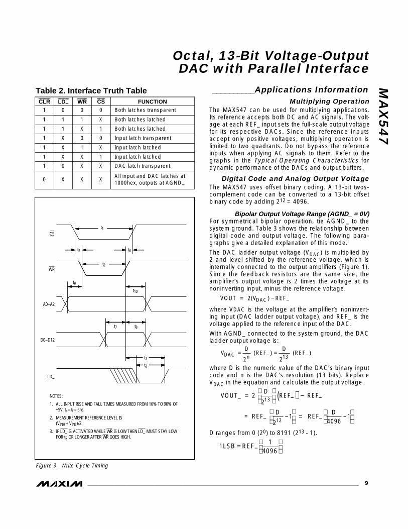
_______________________________________________________________________________________ 9
__________Applications InformationMultiplying Operation
The MAX547 can be used for multiplying applications.Its reference accepts both DC and AC signals. The volt-age at each REF_ input sets the full-scale output voltagefor its respective DACs. Since the reference inputsaccept only positive voltages, multiplying operation islimited to two quadrants. Do not bypass the referenceinputs when applying AC signals to them. Refer to thegraphs in the Typical Operating Characteristics fordynamic performance of the DACs and output buffers.
Digital Code and Analog Output VoltageThe MAX547 uses offset binary coding. A 13-bit twos-complement code can be converted to a 13-bit offsetbinary code by adding 212 = 4096.
Bipolar Output Voltage Range (AGND_ = 0V)For symmetrical bipolar operation, tie AGND_ to thesystem ground. Table 3 shows the relationship betweendigital code and output voltage. The following para-graphs give a detailed explanation of this mode.
The DAC ladder output voltage (VDAC) is multiplied by2 and level shifted by the reference voltage, which isinternally connected to the output amplifiers (Figure 1).Since the feedback resistors are the same size, theamplifier’s output voltage is 2 times the voltage at itsnoninverting input, minus the reference voltage.
where VDAC is the voltage at the amplifier’s noninvert-ing input (DAC ladder output voltage), and REF_ is thevoltage applied to the reference input of the DAC.
With AGND_ connected to the system ground, the DACladder output voltage is:
where D is the numeric value of the DAC’s binary inputcode and n is the DAC’s resolution (13 bits). ReplaceVDAC in the equation and calculate the output voltage.
D ranges from 0 (20) to 8191 (213 - 1).
1LSB REF–1
4096=
VOUT_ 2 D
2 REF– REF–
= REF– D
2–1 REF–
D4096
–1
13
12
=
( ) −
=
VD
2 (REF–)
D
2 (REF–)DAC n 13
= =
VOUT 2(V ) REF–DAC= −
Table 2. Interface Truth Table
MA
X5
47
Octal, 13-Bit Voltage-OutputDAC with Parallel Interface
–C—L—R– FUNCTION1 Both latches transparent
1 Both latches latched
1 Both latches latched
–L—D—––
0
1
1
1 Input latch transparent
1 Input latch latched
1 Input latch latched
X
X
X
–W—R–
0
0
1
X
–C—S–
0
1
X
1
X
0
X
1
X0All input and DAC latches at1000hex, outputs at AGND–
XX
X1 DAC latch transparentX0
CS
WR
A0–A2
D0–D12
LD–
NOTES:
1. ALL INPUT RISE AND FALL TIMES MEASURED FROM 10% TO 90% OF +5V. tr = tf = 5ns.
2. MEASUREMENT REFERENCE LEVEL IS (VINH + VINL)/2.
3. IF LD– IS ACTIVATED WHILE WR IS LOW THEN LD– MUST STAY LOW FOR t3 OR LONGER AFTER WR GOES HIGH.
t1
t2
t9t10
t7 t8
t5 t6
t3t3
Figure 3. Write-Cycle Timing
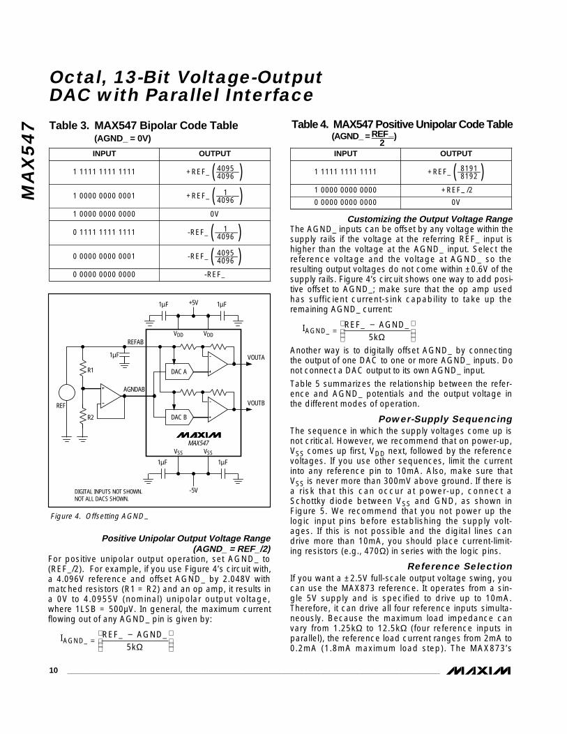
10 ______________________________________________________________________________________
MA
X5
47
Positive Unipolar Output Voltage Range (AGND_ = REF_/2)
For positive unipolar output operation, set AGND_ to(REF_/2). For example, if you use Figure 4’s circuit with,a 4.096V reference and offset AGND_ by 2.048V withmatched resistors (R1 = R2) and an op amp, it results ina 0V to 4.0955V (nominal) unipolar output voltage,where 1LSB = 500µV. In general, the maximum currentflowing out of any AGND_ pin is given by:
Customizing the Output Voltage RangeThe AGND_ inputs can be offset by any voltage within thesupply rails if the voltage at the referring REF_ input ishigher than the voltage at the AGND_ input. Select thereference voltage and the voltage at AGND_ so theresulting output voltages do not come within ±0.6V of thesupply rails. Figure 4’s circuit shows one way to add posi-tive offset to AGND_; make sure that the op amp usedhas sufficient current-sink capability to take up theremaining AGND_ current:
Another way is to digitally offset AGND_ by connectingthe output of one DAC to one or more AGND_ inputs. Donot connect a DAC output to its own AGND_ input.
Table 5 summarizes the relationship between the refer-ence and AGND_ potentials and the output voltage inthe different modes of operation.
Power-Supply SequencingThe sequence in which the supply voltages come up isnot critical. However, we recommend that on power-up,VSS comes up first, VDD next, followed by the referencevoltages. If you use other sequences, limit the currentinto any reference pin to 10mA. Also, make sure thatVSS is never more than 300mV above ground. If there isa risk that this can occur at power-up, connect aSchottky diode between VSS and GND, as shown inFigure 5. We recommend that you not power up thelogic input pins before establishing the supply volt-ages. If this is not possible and the digital lines candrive more than 10mA, you should place current-limit-ing resistors (e.g., 470Ω) in series with the logic pins.
Reference SelectionIf you want a ±2.5V full-scale output voltage swing, youcan use the MAX873 reference. It operates from a sin-gle 5V supply and is specified to drive up to 10mA.Therefore, it can drive all four reference inputs simulta-neously. Because the maximum load impedance canvary from 1.25kΩ to 12.5kΩ (four reference inputs inparallel), the reference load current ranges from 2mA to0.2mA (1.8mA maximum load step). The MAX873’s
I REF_ AGND_5k
AGND_ =
−Ω
I REF_ AGND_5k
AGND_ =
−Ω
Octal, 13-Bit Voltage-OutputDAC with Parallel Interface
OUTPUTINPUT
4095 +REF_ (———)4096 1 1111 1111 1111
0V1 0000 0000 0000
1 +REF_ (———)4096 1 0000 0000 0001
1 -REF_ (———)4096 0 1111 1111 1111
4095 -REF_ (———)4096 0 0000 0000 0001
-REF_0 0000 0000 0000
+5V1µF
REFAB
AGNDAB
1µF
R1
REF
R2
VDD VDD
DIGITAL INPUTS NOT SHOWN. NOT ALL DACS SHOWN.
1µF
VOUTA
VOUTB
DAC B
DAC A
MAX547
-5V
VSS VSS
1µF 1µF
+REF– /21 0000 0000 0000
OUTPUT
0V0 0000 0000 0000
INPUT
8191 +REF_ (———)8192 1 1111 1111 1111
Table 4. MAX547 Positive Unipolar Code Table(AGND_ = REF _)
2
Table 3. MAX547 Bipolar Code Table(AGND_ = 0V)
Figure 4. Offsetting AGND–
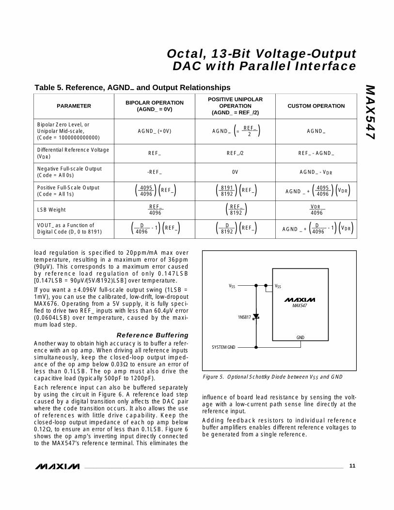
load regulation is specified to 20ppm/mA max overtemperature, resulting in a maximum error of 36ppm(90µV). This corresponds to a maximum error causedby reference load regulation of only 0.147LSB[0.147LSB = 90µV/(5V/8192)LSB] over temperature.
If you want a ±4.096V full-scale output swing (1LSB =1mV), you can use the calibrated, low-drift, low-dropoutMAX676. Operating from a 5V supply, it is fully speci-fied to drive two REF_ inputs with less than 60.4µV error(0.0604LSB) over temperature, caused by the maxi-mum load step.
Reference BufferingAnother way to obtain high accuracy is to buffer a refer-ence with an op amp. When driving all reference inputssimultaneously, keep the closed-loop output imped-ance of the op amp below 0.03Ω to ensure an error ofless than 0.1LSB. The op amp must also drive thecapacitive load (typically 500pF to 1200pF).
Each reference input can also be buffered separatelyby using the circuit in Figure 6. A reference load stepcaused by a digital transition only affects the DAC pairwhere the code transition occurs. It also allows the useof references with little drive capability. Keep theclosed-loop output impedance of each op amp below0.12Ω, to ensure an error of less than 0.1LSB. Figure 6shows the op amp’s inverting input directly connectedto the MAX547’s reference terminal. This eliminates the
influence of board lead resistance by sensing the volt-age with a low-current path sense line directly at thereference input.
Adding feedback resistors to individual referencebuffer amplifiers enables different reference voltages tobe generated from a single reference.
MA
X5
47
Octal, 13-Bit Voltage-OutputDAC with Parallel Interface
______________________________________________________________________________________ 11
Figure 5. Optional Schottky Diode between VSS and GND
GND
VSS
SYSTEM GND
1N5817
MAX547
VSS
BIPOLAR OPERATION(AGND_ = 0V)
CUSTOM OPERATIONPOSITIVE UNIPOLAR
OPERATION(AGND_ = REF_/2)
PARAMETER
AGND_ (=0V) AGND–Bipolar Zero Level, or Unipolar Mid-scale, (Code = 1000000000000)
REF– REF– - AGND–REF–/2Differential Reference Voltage(VDR)
REF_AGND– (= ———)2
-REF– AGND– - VDR0VNegative Full-scale Output(Code = All 0s)
4095(———) (REF_)4096 4095
AGND _ + (———) (VDR)4096 8191(———) (REF_)8192
Positive Full-Scale Output(Code = All 1s)
REF_———4096
VDR———4096
REF_(———)8192 LSB Weight
D(——— - 1) (REF_)4096 D
AGND _ + (—--—- - 1) (VDR)4096 D(———) (REF_)8192
VOUT– as a Function of Digital Code (D, 0 to 8191)
Table 5. Reference, AGND– and Output Relationships
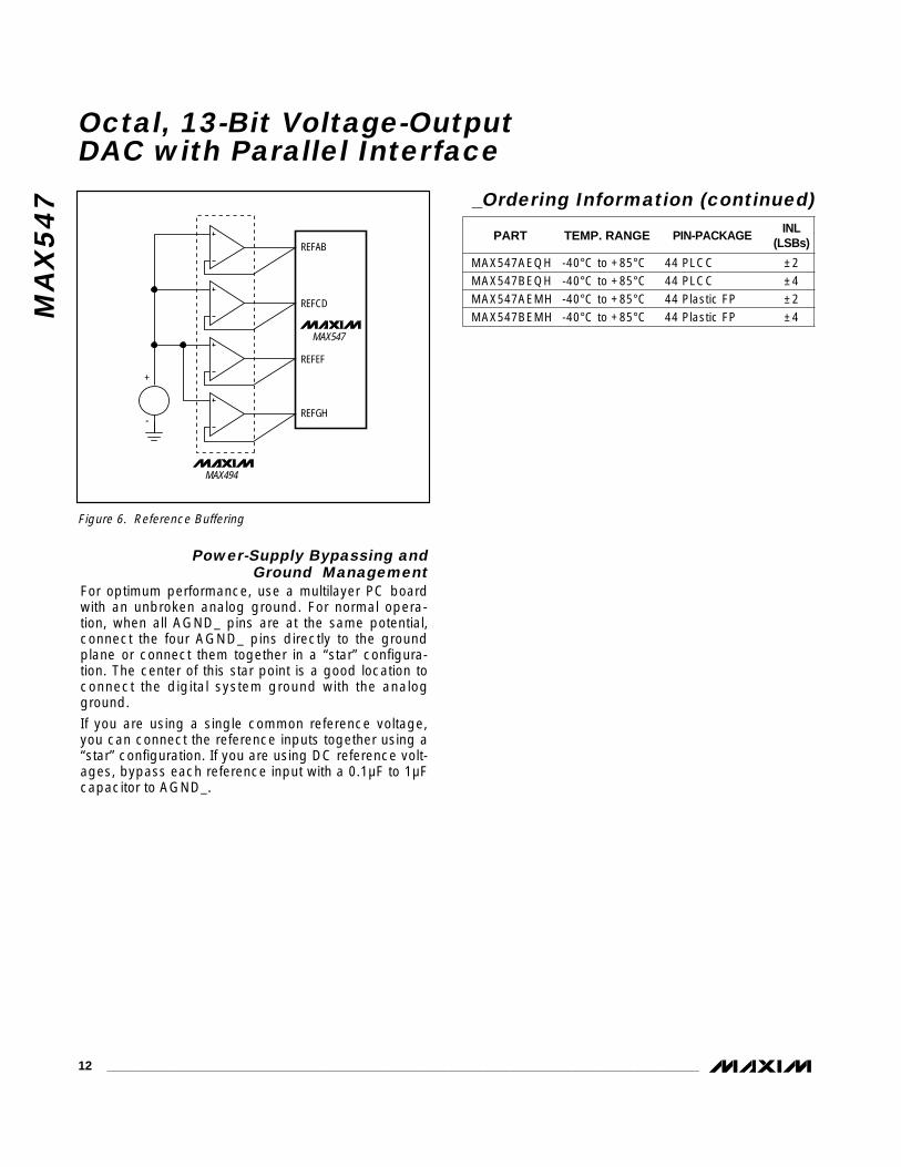
MA
X5
47
Octal, 13-Bit Voltage-OutputDAC with Parallel Interface
12 ______________________________________________________________________________________
Power-Supply Bypassing andGround Management
For optimum performance, use a multilayer PC boardwith an unbroken analog ground. For normal opera-tion, when all AGND_ pins are at the same potential,connect the four AGND_ pins directly to the groundplane or connect them together in a “star” configura-tion. The center of this star point is a good location toconnect the digital system ground with the analogground.
If you are using a single common reference voltage,you can connect the reference inputs together using a“star” configuration. If you are using DC reference volt-ages, bypass each reference input with a 0.1µF to 1µFcapacitor to AGND_.
MAX547
MAX494
+
-
REFAB
REFCD
REFEF
REFGH
Figure 6. Reference Buffering
MAX547AEQH -40°C to +85°C 44 PLCCMAX547BEQH -40°C to +85°C 44 PLCCMAX547AEMH -40°C to +85°C 44 Plastic FPMAX547BEMH -40°C to +85°C 44 Plastic FP
±2±4±2±4
PART TEMP. RANGE PIN-PACKAGEINL
(LSBs)
_Ordering Information (continued)
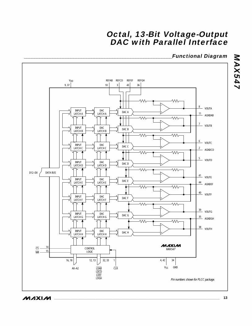
MA
X5
47
Octal, 13-Bit Voltage-OutputDAC with Parallel Interface
______________________________________________________________________________________ 13
VDD REFCDREFAB REFEF REFGH
9, 37 10 3 43 36
VSS GND
DAC LATCH A
8
11
7
VOUTA
AGNDAB
VOUTBDAC B
INPUT LATCH A
DAC LATCH B
DAC A
INPUT LATCH B
DAC LATCH C
6
2
5
VOUTC
AGNDCD
VOUTDDAC D
D12–D0
INPUT LATCH C
DAC LATCH D
DAC C
INPUT LATCH D
DAC LATCH E
41
44
40
VOUTE
AGNDEF
VOUTFDAC F
INPUT LATCH E
DAC LATCH F
DAC E
INPUT LATCH F
DAC LATCH G
39
35
38
VOUTG
AGNDGH
VOUTHDAC H
Pin numbers shown for PLCC package.
4, 42 3412, 1316, 18 32, 33 1
INPUT LATCH G
DAC LATCH H
DAC G
INPUT LATCH H
A0–A2 CLRLDAB LDCD LDEF LDGH
CSWR
1415
MAX547CONTROL LOGIC
DATA BUS
_________________________________________________________Functional Diagram
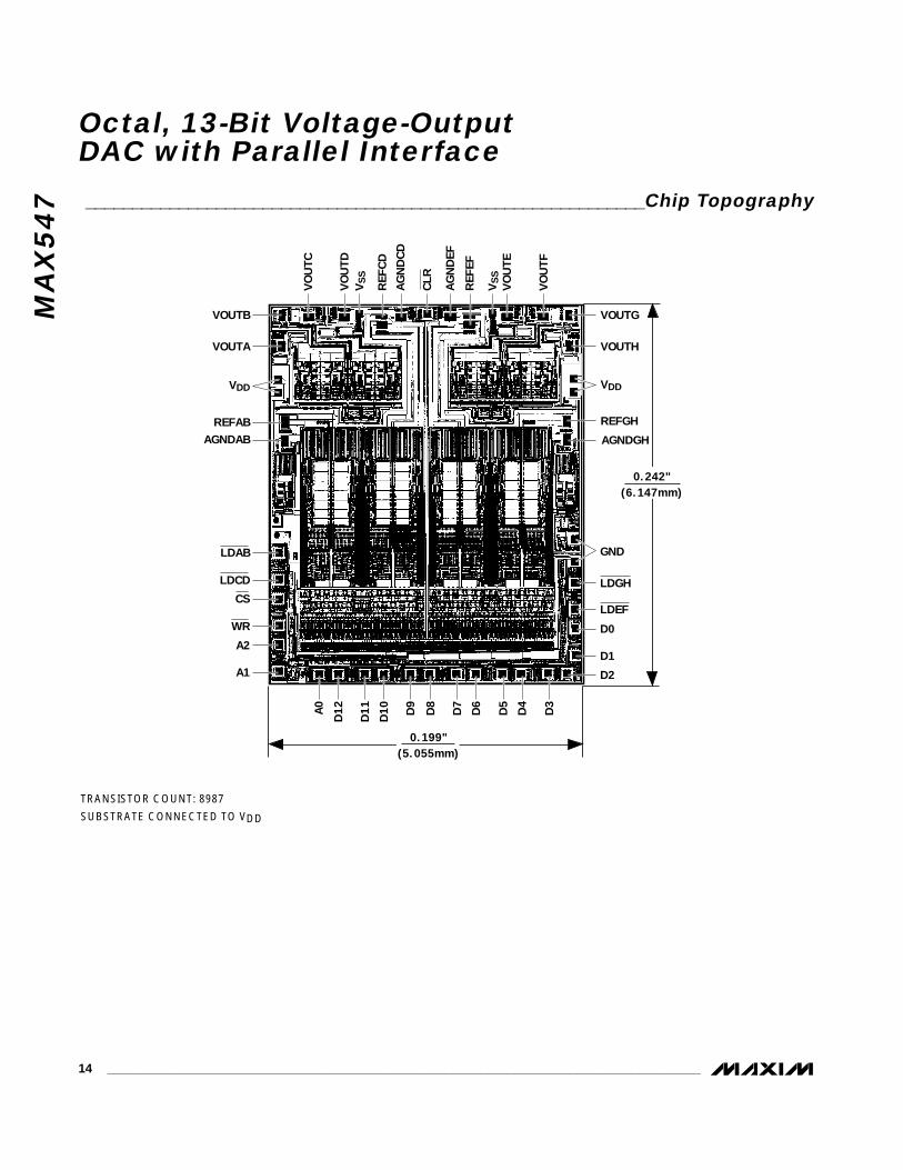
MA
X5
47
Octal, 13-Bit Voltage-OutputDAC with Parallel Interface
14 ______________________________________________________________________________________
VOUTA
VO
UTC
0.242" (6.147mm)
0.199" (5.055mm)
A0
D12
D11
D10 D
9
D8
D7
D6
D5
D4
D3
AGNDAB
LDAB
LDCD
CS
A1
A2
WR
VDD
REFAB
VOUTB
VOUTH
AGNDGH
GND
LDGH
LDEF
D2
D1
D0
VDD
VOUTG
REFGH
VO
UTD
REF
CD
AG
ND
CD
CLR
VO
UTE
VO
UTF
VS
S
VS
S
AG
ND
EF
REF
EF
____________________________________________________________Chip Topography
TRANSISTOR COUNT: 8987
SUBSTRATE CONNECTED TO VDD
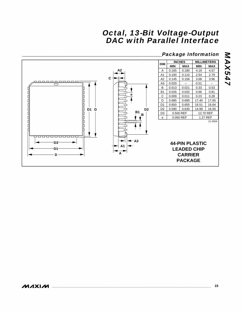
MA
X5
47
Octal, 13-Bit Voltage-OutputDAC with Parallel Interface
______________________________________________________________________________________ 15
________________________________________________________Package Information
DIM
A A1 A2 A3 B
B1 C D D1 D2 D3 e
MIN 0.165 0.100 0.145 0.020 0.013 0.026 0.009 0.685 0.650 0.590
MAX 0.180 0.110 0.156
– 0.021 0.032 0.011 0.695 0.655 0.630
MIN 4.19 2.54 3.68 0.51 0.33 0.66 0.23
17.40 16.51 14.99
MAX 4.57 2.79 3.96
– 0.53 0.81 0.28
17.65 16.64 16.00
INCHES MILLIMETERS
44-PIN PLASTIC LEADED CHIP
CARRIER PACKAGE
21-350A
DD1
D
D1
D3
D2
e
B1B
A3
A
A1
A2
12.70 REF0.500 REF1.27 REF0.050 REF
C
Maxim cannot assume responsibility for use of any circuitry other than circuitry entirely embodied in a Maxim product. No circuit patent licenses areimplied. Maxim reserves the right to change the circuitry and specifications without notice at any time.
16 __________________Maxim Integrated Products, 120 San Gabriel Drive, Sunnyvale, CA 94086 (408) 737-7600
© 1995 Maxim Integrated Products Printed USA is a registered trademark of Maxim Integrated Products.
MA
X5
47
Octal, 13-Bit Voltage-OutputDAC with Parallel Interface

4.11 MAX764
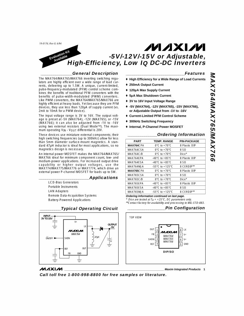
_______________General DescriptionThe MAX764/MAX765/MAX766 inverting switching regu-lators are highly efficient over a wide range of load cur-rents, delivering up to 1.5W. A unique, current-limited,pulse-frequency-modulated (PFM) control scheme com-bines the benefits of traditional PFM converters with thebenefits of pulse-width-modulated (PWM) converters.Like PWM converters, the MAX764/MAX765/MAX766 arehighly efficient at heavy loads. Yet because they are PFMdevices, they use less than 120µA of supply current (vs.2mA to 10mA for a PWM device).
The input voltage range is 3V to 16V. The output volt-age is preset at -5V (MAX764), -12V (MAX765), or -15V(MAX766); it can also be adjusted from -1V to -16Vusing two external resistors (Dual ModeTM). The maxi-mum operating VIN - VOUT differential is 20V.
These devices use miniature external components; theirhigh switching frequencies (up to 300kHz) allow for lessthan 5mm diameter surface-mount magnetics. A stan-dard 47µH inductor is ideal for most applications, so nomagnetics design is necessary.
An internal power MOSFET makes the MAX764/MAX765/MAX766 ideal for minimum component count, low- andmedium-power applications. For increased output drivecapabil i ty or higher output voltages, use theMAX774/MAX775/MAX776 or MAX1774, which drive anexternal power P-channel MOSFET for loads up to 5W.
________________________ApplicationsLCD-Bias GeneratorsPortable InstrumentsLAN AdaptersRemote Data-Acquisition SystemsBattery-Powered Applications
____________________________Features♦ High Efficiency for a Wide Range of Load Currents
♦ 250mA Output Current
♦ 120µA Max Supply Current
♦ 5µA Max Shutdown Current
♦ 3V to 16V Input Voltage Range
♦ -5V (MAX764), -12V (MAX765), -15V (MAX766), or Adjustable Output from -1V to -16V
♦ Current-Limited PFM Control Scheme
♦ 300kHz Switching Frequency
♦ Internal, P-Channel Power MOSFET
______________Ordering Information
Ordering Information continued on last page.* Dice are tested at TA = +25°C, DC parameters only.**Contact factory for availability and processing to MIL-STD-883.
MA
X7
64
/MA
X7
65
/MA
X7
66
-5V/-12V/-15V or Adjustable,High-Efficiency, Low IQ DC-DC Inverters
________________________________________________________________ Maxim Integrated Products 1
1
2
3
4
8
7
6
5
LX
V+
V+
GNDREF
SHDN
FB
OUT
MAX764 MAX765 MAX766
DIP/SO
TOP VIEW
__________________Pin Configuration
GND
MAX764SHDN
LX
OUT
ON/OFF
REF
47µH
OUTPUT -5V
INPUT 3V TO 15V
V+
FB
__________Typical Operating Circuit
Call toll free 1-800-998-8800 for free samples or literature.
19-0176; Rev 0; 6/94
PART
MAX764CPA
MAX764CSA
MAX764C/D 0°C to +70°C
0°C to +70°C
0°C to +70°C
TEMP. RANGE PIN-PACKAGE
8 Plastic DIP
8 SO
Dice*
MAX764EPA
MAX764ESA -40°C to +85°C
-40°C to +85°C 8 Plastic DIP
8 SO
MAX764MJA -55°C to +125°C 8 CERDIP**
MAX765CPA
MAX765CSA
MAX765C/D 0°C to +70°C
0°C to +70°C
0°C to +70°C 8 Plastic DIP
8 SO
Dice*
MAX765EPA
MAX765ESA -40°C to +85°C
-40°C to +85°C 8 Plastic DIP
8 SO
MAX765MJA -55°C to +125°C 8 CERDIP**
Evaluation Kit
Available
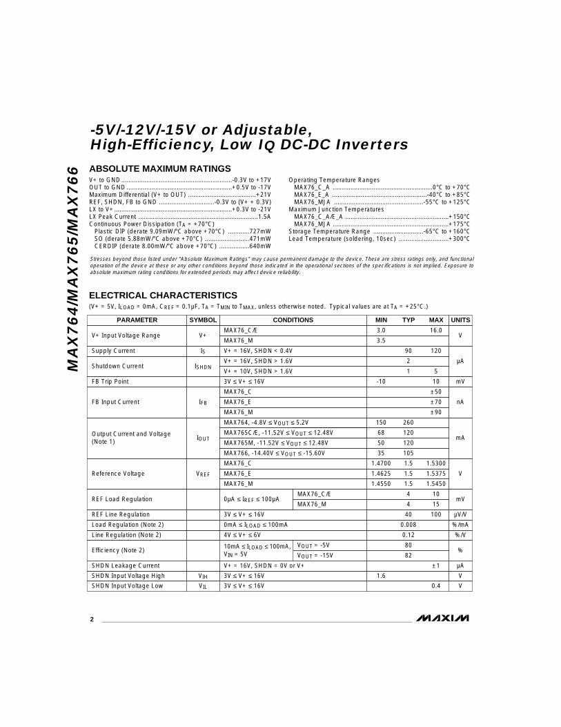
MA
X7
64
/MA
X7
65
/MA
X7
66
-5V/-12V/-15V or Adjustable,High-Efficiency, Low IQ DC-DC Inverters
2 _______________________________________________________________________________________
ABSOLUTE MAXIMUM RATINGS
ELECTRICAL CHARACTERISTICS(V+ = 5V, ILOAD = 0mA, CREF = 0.1µF, TA = TMIN to TMAX, unless otherwise noted. Typical values are at TA = +25°C.)
Stresses beyond those listed under “Absolute Maximum Ratings” may cause permanent damage to the device. These are stress ratings only, and functionaloperation of the device at these or any other conditions beyond those indicated in the operational sections of the specifications is not implied. Exposure toabsolute maximum rating conditions for extended periods may affect device reliability.
V+ to GND..............................................................-0.3V to +17VOUT to GND ...........................................................+0.5V to -17VMaximum Differential (V+ to OUT) ......................................+21VREF, SHDN, FB to GND ...............................-0.3V to (V+ + 0.3V)LX to V+..................................................................+0.3V to -21VLX Peak Current ...................................................................1.5AContinuous Power Dissipation (TA = +70°C)
Plastic DIP (derate 9.09mW/°C above +70°C) ............727mWSO (derate 5.88mW/°C above +70°C) .........................471mWCERDIP (derate 8.00mW/°C above +70°C) .................640mW
Operating Temperature RangesMAX76_C_A ........................................................0°C to +70°CMAX76_E_A .....................................................-40°C to +85°CMAX76_MJA ..................................................-55°C to +125°C
Maximum Junction TemperaturesMAX76_C_A/E_A ..........................................................+150°CMAX76_MJA .................................................................+175°C
Storage Temperature Range ............................-65°C to +160°CLead Temperature (soldering, 10sec) ............................+300°C
3V ≤ V+ ≤ 16V
V+ = 16V, SHDN = 0V or V+
V+ = 16V, SHDN < 0.4V
4V ≤ V+ ≤ 6V
0mA ≤ ILOAD ≤ 100mA
MAX76_M
3V ≤ V+ ≤ 16V
MAX76_C/E
0µA ≤ IREF ≤ 100µA
MAX76_M
MAX765C/E, -11.52V ≤ VOUT ≤ 12.48V
MAX764, -4.8V ≤ VOUT ≤ 5.2V
MAX76_E
MAX76_C
MAX76_M
MAX76_E
V+ = 16V, SHDN > 1.6V
V+ = 10V, SHDN > 1.6V
3V ≤ V+ ≤ 16V
MAX766, -14.40V ≤ VOUT ≤ -15.60V
MAX76_C
MAX765M, -11.52V ≤ VOUT ≤ 12.48V
CONDITIONS
V1.6VIHSHDN Input Voltage High
µA±1SHDN Leakage Current
80
%/V0.12Line Regulation (Note 2)
%/mA0.008Load Regulation (Note 2)
µV/V40 100REF Line Regulation
4 15mV
4 10REF Load Regulation
1.4550 1.5 1.5450
1.4625 1.5 1.5375 V
1.4700 1.5 1.5300
VREFReference Voltage
35 105
50 120
µA
90 120ISSupply Current
3.5V+ V
3.0 16.0V+ Input Voltage Range
68 120mA
150 260
IOUTOutput Current and Voltage (Note 1)
±90
±70
2ISHDNShutdown Current
1 5
mV-10 10FB Trip Point
nA
±50
IFBFB Input Current
UNITSMIN TYP MAXSYMBOLPARAMETER
MAX76_C/E
MAX76_M
VOUT = -5V
82VOUT = -15VEfficiency (Note 2)
10mA ≤ ILOAD ≤ 100mA,VIN = 5V
%
3V ≤ V+ ≤ 16V V0.4VILSHDN Input Voltage Low
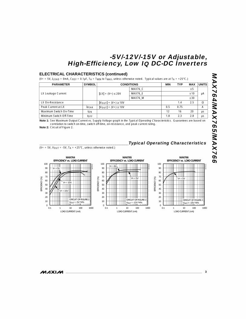
MA
X7
64
/MA
X7
65
/MA
X7
66
-5V/-12V/-15V or Adjustable,High-Efficiency, Low IQ DC-DC Inverters
_______________________________________________________________________________________ 3
Note 1: See Maximum Output Current vs. Supply Voltage graph in the Typical Operating Characteristics. Guarantees are based oncorrelation to switch on-time, switch off-time, on-resistance, and peak current rating.
Note 2: Circuit of Figure 2.
ELECTRICAL CHARACTERISTICS (continued)(V+ = 5V, ILOAD = 0mA, CREF = 0.1µF, TA = TMIN to TMAX, unless otherwise noted. Typical values are at TA = +25°C.)
IVOUTI + (V+) ≥ 10V
ILXI + (V+) ≤ 20V
IVOUTI + (V+) ≥ 10V
CONDITIONS
µs1.8 2.3 2.8tOFFMinimum Switch Off-Time
µs12 16 20tONMaximum Switch On-Time
A0.5 0.75IPEAKPeak Current at LX
±30
±10 µA
±5
LX Leakage Current
Ω1.4 2.5LX On-Resistance
UNITSMIN TYP MAXSYMBOLPARAMETER
MAX76_C
MAX76_E
MAX76_M
__________________________________________Typical Operating Characteristics(V+ = 5V, VOUT = -5V, TA = +25°C, unless otherwise noted.)
100
00.1 10 1000
MAX764 EFFICIENCY vs. LOAD CURRENT
MAX
764-
01
LOAD CURRENT (mA)
EFFI
CIEN
CY (%
)
90
80
70
60
50
40
30
20
10
1 100
CIRCUIT OF FIGURE 2 VOUT = -5V ±4%
V+ = 5V
V+ = 10V
V+ = 15V
100
00.1 10 1000
MAX765 EFFICIENCY vs. LOAD CURRENT
MAX
764-
02
LOAD CURRENT (mA)
EFFI
CIEN
CY (%
)
90
80
70
60
50
40
30
20
10
1 100
V+ = 8V
V+ = 5V
CIRCUIT OF FIGURE 2 VOUT = -12V ±4%
100
00.1 10 1000
MAX766 EFFICIENCY vs. LOAD CURRENT
MAX
764-
03
LOAD CURRENT (mA)
EFFI
CIEN
CY (%
)
90
80
70
60
50
40
30
20
10
1 100
V+ = 5V
CIRCUIT OF FIGURE 2 VOUT = -15V ±4%
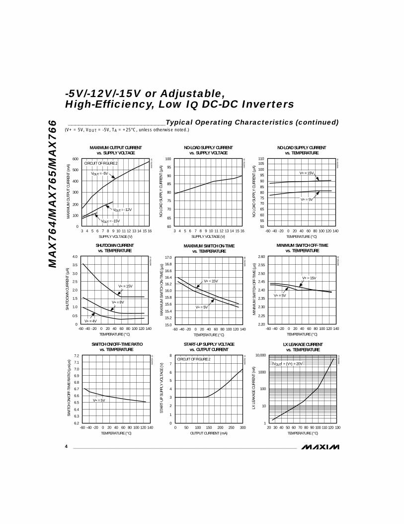
MA
X7
64
/MA
X7
65
/MA
X7
66
-5V/-12V/-15V or Adjustable,High-Efficiency, Low IQ DC-DC Inverters
4 _______________________________________________________________________________________
____________________________Typical Operating Characteristics (continued)(V+ = 5V, VOUT = -5V, TA = +25°C, unless otherwise noted.)
0-60
SHUTDOWN CURRENT vs. TEMPERATURE
MAX
764
-07
TEMPERATURE (°C)
SHUT
DOW
N CU
RREN
T (µ
A)
-40 -20 0 20 40 60 80 100 120 140
V+ = 15V
0.5
1.0
1.5
2.0
2.5
3.0
4.0
3.5
V+ = 8V
V+ = 4V15.0
-60
MAXIMUM SWITCH ON-TIME vs. TEMPERATURE
MAX
764
-08
TEMPERATURE (°C)
MAX
IMUM
SW
ITCH
ON-
TIM
E (µ
s)
-40 -20 0 20 40 60 80 100 120 140
V+ = 15V
V+ = 5V
15.2
15.4
15.6
15.8
16.0
16.2
16.4
16.6
16.8
17.0
2.20-60
MINIMUM SWITCH OFF-TIME vs. TEMPERATURE
MAX
764
-09
TEMPERATURE (°C)
MIN
IMUM
SW
ITCH
OFF
-TIM
E (µ
s)
-40 -20 0 20 40 60 80 100 120 140
2.25
2.30
2.35
2.40
2.45
2.50
2.60
2.55
V+ = 5V
V+ = 15V
6.2-60
SWITCH ON/OFF-TIME RATIO vs. TEMPERATURE
MAX
764
-10
TEMPERATURE (°C)
SWIT
CH O
N/OF
F-TI
ME
RATI
O (µ
s/µs
)
-40 -20 0 20 40 60 80 100 120 140
V+ = 5V
6.3
6.4
6.5
6.6
6.7
6.8
6.9
7.0
7.1
7.2
0
START-UP SUPPLY VOLTAGE vs. OUTPUT CURRENT
MAX
764
-11
OUTPUT CURRENT (mA)
STAR
T-UP
SUP
PLY
VOLT
AGE
(V)
0
1
2
3
4
5
6
8
7
50 100 150 200 250 300
CIRCUIT OF FIGURE 210,000
120
LX LEAKAGE CURRENT vs. TEMPERATURE
10
100
MAX
764-
12
TEMPERATURE (°C)
LX L
EAKA
GE C
URRE
NT (n
A)
1000
30 40 50 60 70 80 90 100 110 120 130
IVOUTI + (V+) = 20V
MAXIMUM OUTPUT CURRENT vs. SUPPLY VOLTAGE
MAX
764
-04
SUPPLY VOLTAGE (V)
MAX
IMUM
OUT
PUT
CURR
ENT
(mA)
3
600
4 5 6 7 8 9 10 11 12 13 14 15 16
500
400
300
200
100
0
VOUT = -5V
VOUT = -12V
VOUT = -15V
CIRCUIT OF FIGURE 2
60
NO-LOAD SUPPLY CURRENT vs. SUPPLY VOLTAGE
MAX
764
-05
SUPPLY VOLTAGE (V)
NO-L
OAD
SUPP
LY C
URRE
NT (µ
A)
3
65
70
75
80
85
90
100
95
4 5 6 7 8 9 10 11 12 13 14 15 1650
-60
NO-LOAD SUPPLY CURRENT vs. TEMPERATURE
55
MAX
764
-06
TEMPERATURE (°C)
NO-L
OAD
SUPP
LY C
URRE
NT (µ
A)
-40 -20 0 20 40 60 80 100 120 140
60
6570758085
90
95100
105110
V+ = 15V
V+ = 5V
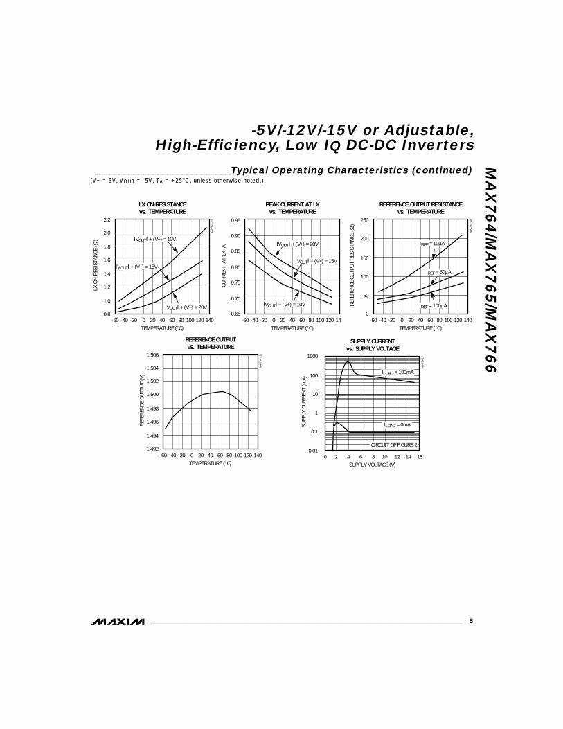
MA
X7
64
/MA
X7
65
/MA
X7
66
-5V/-12V/-15V or Adjustable,High-Efficiency, Low IQ DC-DC Inverters
_______________________________________________________________________________________ 5
1000
0.010 2 4 6 10 12 148 16
SUPPLY CURRENT vs. SUPPLY VOLTAGE
0.1
MAX
764-
17
SUPPLY VOLTAGE (V)
SUPP
LY C
URRE
NT (m
A)
1
10
100ILOAD = 100mA
ILOAD = 0mA
CIRCUIT OF FIGURE 2
-60
REFERENCE OUTPUT RESISTANCE vs. TEMPERATURE
MAX
764
-15
TEMPERATURE (°C)
REFE
RENC
E OU
TPUT
RES
ISTA
NCE
(Ω)
-40 -20 0 20 40 60 80 100 120 1400
50
100
150
200
250
IREF = 10µA
IREF = 50µA
IREF = 100µA
____________________________Typical Operating Characteristics (continued)(V+ = 5V, VOUT = -5V, TA = +25°C, unless otherwise noted.)
0.8-60
LX ON-RESISTANCE vs. TEMPERATURE
MAX
764
-13
TEMPERATURE (°C)
LX O
N-RE
SIST
ANCE
(Ω)
-40 -20 0 20 40 60 80 100 120 140
IVOUTI + (V+) = 10V
1.0
1.2
1.4
1.6
1.8
2.0
2.2
IVOUTI + (V+) = 15V
IVOUTI + (V+) = 20V
-60
PEAK CURRENT AT LX vs. TEMPERATURE
MAX
764
-14
TEMPERATURE (°C)
CURR
ENT
AT
LX (A
)
-40 -20 0 20 40 60 80 100 120 1400.65
0.70
0.75
0.80
0.85
0.90
0.95
IVOUTI + (V+) = 20V
IVOUTI + (V+) = 15V
IVOUTI + (V+) = 10V
-60
REFERENCE OUTPUT vs. TEMPERATURE
MAX
764
-16
TEMPERATURE (°C)
REFE
RENC
E OU
TPUT
(V)
-40 -20 0 20 40 60 80 100 120 140
1.506
1.504
1.502
1.500
1.498
1.496
1.494
1.492
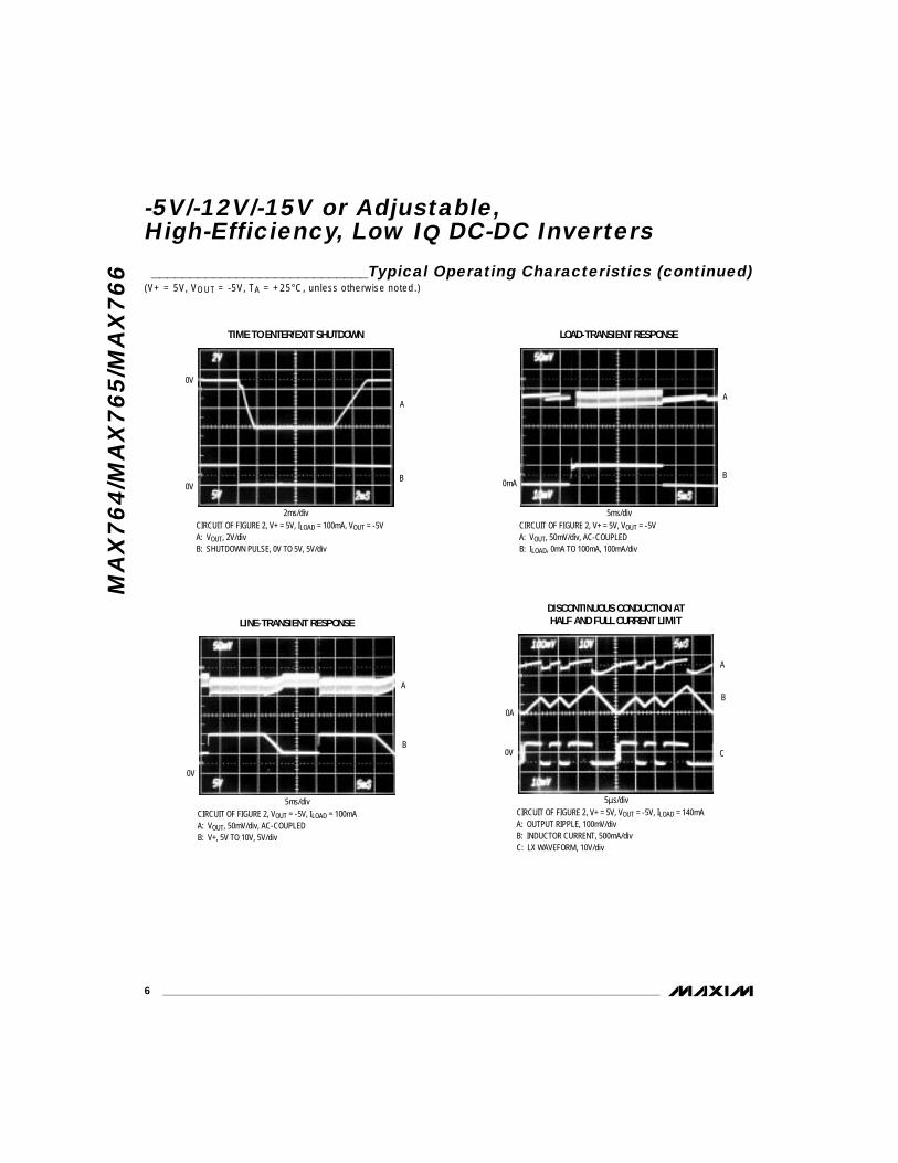
MA
X7
64
/MA
X7
65
/MA
X7
66
-5V/-12V/-15V or Adjustable,High-Efficiency, Low IQ DC-DC Inverters
6 _______________________________________________________________________________________
CIRCUIT OF FIGURE 2, VOUT = -5V, ILOAD = 100mA A: VOUT, 50mV/div, AC-COUPLED B: V+, 5V TO 10V, 5V/div
5ms/div
LINE-TRANSIENT RESPONSE
A
B
0V
CIRCUIT OF FIGURE 2, V+ = 5V, VOUT = -5V, ILOAD = 140mA A: OUTPUT RIPPLE, 100mV/div B: INDUCTOR CURRENT, 500mA/div C: LX WAVEFORM, 10V/div
5µs/div
DISCONTINUOUS CONDUCTION AT HALF AND FULL CURRENT LIMIT
A
B
0A
C0V
CIRCUIT OF FIGURE 2, V+ = 5V, ILOAD = 100mA, VOUT = -5V A: VOUT, 2V/div B: SHUTDOWN PULSE, 0V TO 5V, 5V/div
2ms/div
TIME TO ENTER/EXIT SHUTDOWN
A
B
0V
0V
CIRCUIT OF FIGURE 2, V+ = 5V, VOUT = -5V A: VOUT, 50mV/div, AC-COUPLED B: ILOAD, 0mA TO 100mA, 100mA/div
5ms/div
LOAD-TRANSIENT RESPONSE
A
B0mA
____________________________Typical Operating Characteristics (continued)(V+ = 5V, VOUT = -5V, TA = +25°C, unless otherwise noted.)
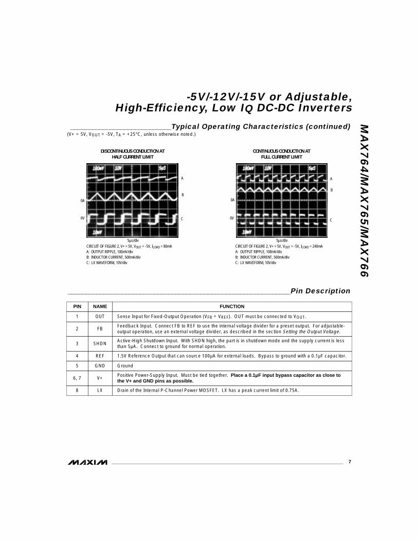
MA
X7
64
/MA
X7
65
/MA
X7
66
-5V/-12V/-15V or Adjustable,High-Efficiency, Low IQ DC-DC Inverters
_______________________________________________________________________________________ 7
CIRCUIT OF FIGURE 2, V+ = 5V, VOUT = -5V, ILOAD = 80mA A: OUTPUT RIPPLE, 100mV/div B: INDUCTOR CURRENT, 500mA/div C: LX WAVEFORM, 10V/div
5µs/div
DISCONTINUOUS CONDUCTION AT HALF CURRENT LIMIT
A
B0A
C0V
CIRCUIT OF FIGURE 2, V+ = 5V, VOUT = -5V, ILOAD = 240mA A: OUTPUT RIPPLE, 100mV/div B: INDUCTOR CURRENT, 500mA/div C: LX WAVEFORM, 10V/div
5µs/div
CONTINUOUS CONDUCTION AT FULL CURRENT LIMIT
A
B
0A
C0V
______________________________________________________________Pin Description
GroundGND5
Positive Power-Supply Input. Must be tied together. Place a 0.1µF input bypass capacitor as close tothe V+ and GND pins as possible.
V+6, 7
Drain of the Internal P-Channel Power MOSFET. LX has a peak current limit of 0.75A.LX8
1.5V Reference Output that can source 100µA for external loads. Bypass to ground with a 0.1µF capacitor.REF4
Active-High Shutdown Input. With SHDN high, the part is in shutdown mode and the supply current is lessthan 5µA. Connect to ground for normal operation.
SHDN3
PIN
Feedback Input. Connect FB to REF to use the internal voltage divider for a preset output. For adjustable-output operation, use an external voltage divider, as described in the section Setting the Output Voltage.FB2
Sense Input for Fixed-Output Operation (VFB = VREF). OUT must be connected to VOUT.OUT1
FUNCTIONNAME
____________________________Typical Operating Characteristics (continued)(V+ = 5V, VOUT = -5V, TA = +25°C, unless otherwise noted.)
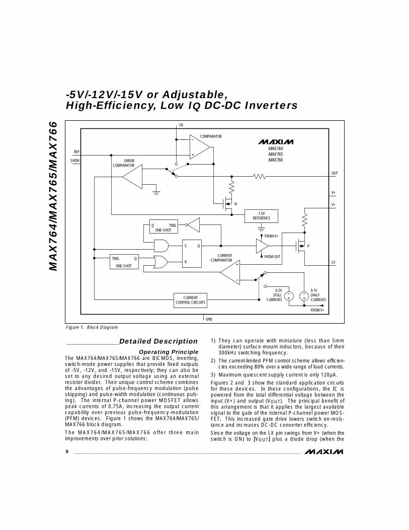
MA
X7
64
/MA
X7
65
/MA
X7
66
-5V/-12V/-15V or Adjustable,High-Efficiency, Low IQ DC-DC Inverters
8 _______________________________________________________________________________________
_______________Detailed DescriptionOperating Principle
The MAX764/MAX765/MAX766 are BiCMOS, inverting,switch-mode power supplies that provide fixed outputsof -5V, -12V, and -15V, respectively; they can also beset to any desired output voltage using an externalresistor divider. Their unique control scheme combinesthe advantages of pulse-frequency modulation (pulseskipping) and pulse-width modulation (continuous puls-ing). The internal P-channel power MOSFET allowspeak currents of 0.75A, increasing the output currentcapability over previous pulse-frequency-modulation(PFM) devices. Figure 1 shows the MAX764/MAX765/MAX766 block diagram.
The MAX764/MAX765/MAX766 offer three mainimprovements over prior solutions:
1) They can operate with miniature (less than 5mmdiameter) surface-mount inductors, because of their300kHz switching frequency.
2) The current-limited PFM control scheme allows efficien-cies exceeding 80% over a wide range of load currents.
3) Maximum quiescent supply current is only 120µA.
Figures 2 and 3 show the standard application circuitsfor these devices. In these configurations, the IC ispowered from the total differential voltage between theinput (V+) and output (VOUT). The principal benefit ofthis arrangement is that it applies the largest availablesignal to the gate of the internal P-channel power MOS-FET. This increased gate drive lowers switch on-resis-tance and increases DC-DC converter efficiency.
Since the voltage on the LX pin swings from V+ (when theswitch is ON) to IVOUTI plus a diode drop (when the
MAX764 MAX765 MAX766
P
TRIG Q
ONE-SHOT
TRIGQONE-SHOT
S
R
Q
CURRENT CONTROL CIRCUITS
1.5V REFERENCE
N
FROM OUT
FROM V+
FROM V+
0.1V (HALF CURRENT)
0.2V (FULL
CURRENT)
GND
LX
V+
OUT
V+
REF
SHDN ERROR COMPARATOR
COMPARATOR
CURRENT COMPARATOR
FB
Figure 1. Block Diagram
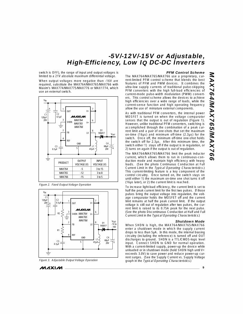
switch is OFF), the range of input and output voltages islimited to a 21V absolute maximum differential voltage.
When output voltages more negative than -16V arerequired, substitute the MAX764/MAX765/MAX766 withMaxim’s MAX774/MAX775/MAX776 or MAX1774, whichuse an external switch.
PFM Control SchemeThe MAX764/MAX765/MAX766 use a proprietary, cur-rent-limited PFM control scheme that blends the bestfeatures of PFM and PWM devices. It combines theultra-low supply currents of traditional pulse-skippingPFM converters with the high full-load efficiencies ofcurrent-mode pulse-width modulation (PWM) convert-ers. This control scheme allows the devices to achievehigh efficiencies over a wide range of loads, while thecurrent-sense function and high operating frequencyallow the use of miniature external components.
As with traditional PFM converters, the internal powerMOSFET is turned on when the voltage comparatorsenses that the output is out of regulation (Figure 1).However, unlike traditional PFM converters, switching isaccomplished through the combination of a peak cur-rent limit and a pair of one-shots that set the maximumon-time (16µs) and minimum off-time (2.3µs) for theswitch. Once off, the minimum off-time one-shot holdsthe switch off for 2.3µs. After this minimum time, theswitch either 1) stays off if the output is in regulation, or2) turns on again if the output is out of regulation.
The MAX764/MAX765/MAX766 limit the peak inductorcurrent, which allows them to run in continuous-con-duction mode and maintain high efficiency with heavyloads. (See the photo Continuous Conduction at FullCurrent Limit in the Typical Operating Characteristics.)This current-limiting feature is a key component of thecontrol circuitry. Once turned on, the switch stays onuntil either 1) the maximum on-time one shot turns it off(16µs later), or 2) the current limit is reached.
To increase light-load efficiency, the current limit is set tohalf the peak current limit for the first two pulses. If thosepulses bring the output voltage into regulation, the volt-age comparator holds the MOSFET off and the currentlimit remains at half the peak current limit. If the outputvoltage is still out of regulation after two pulses, the cur-rent limit is raised to its 0.75A peak for the next pulse.(See the photo Discontinuous Conduction at Half and FullCurrent Limit in the Typical Operating Characteristics.)
Shutdown ModeWhen SHDN is high, the MAX764/MAX765/MAX766enter a shutdown mode in which the supply currentdrops to less than 5µA. In this mode, the internal biasingcircuitry (including the reference) is turned off and OUTdischarges to ground. SHDN is a TTL/CMOS-logic levelinput. Connect SHDN to GND for normal operation.With a current-limited supply, power-up the device whileunloaded or in shutdown mode (hold SHDN high until V+exceeds 3.0V) to save power and reduce power-up cur-rent surges. (See the Supply Current vs. Supply Voltagegraph in the Typical Operating Characteristics.)
MA
X7
64
/MA
X7
65
/MA
X7
66
-5V/-12V/-15V or Adjustable,High-Efficiency, Low IQ DC-DC Inverters
_______________________________________________________________________________________ 9
MAX764 MAX765 MAX766
SHDN
REF
LX
V+
GND
FBVOUT
V+OUT
C4 68µF
20V
D1 1N5817
L1 47µH
8
6
7
3
4
2
1
C3 0.1µF
C2 0.1µF
C1 120µF
20V
VIN
MAX764 MAX765 MAX766
-5 -12 -15
3 to 15 3 to 8 3 to 5
PRODUCTOUTPUT
VOLTAGE (V)INPUT
VOLTAGE (V)
5
Figure 2. Fixed Output Voltage Operation
MAX764 MAX765 MAX766
SHDN
REF
LX
V+
GND
FBVOUT -1V to -16V
V+OUT
C4 68µF
20V
D1 1N5817
L1 47µH
8
6
7
3
4
2
1
C3 0.1µF
C2 0.1µF
C1 120µF
20V
VIN
5
R2
R1
Figure 3. Adjustable Output Voltage Operation
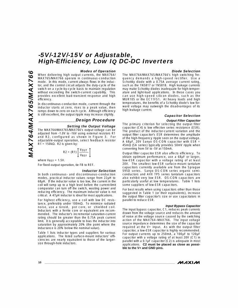
MA
X7
64
/MA
X7
65
/MA
X7
66 Modes of Operation
When delivering high output currents, the MAX764/MAX765/MAX766 operate in continuous-conductionmode. In this mode, current always flows in the induc-tor, and the control circuit adjusts the duty-cycle of theswitch on a cycle-by-cycle basis to maintain regulationwithout exceeding the switch-current capability. Thisprovides excellent load-transient response and highefficiency.
In discontinuous-conduction mode, current through theinductor starts at zero, rises to a peak value, thenramps down to zero on each cycle. Although efficiencyis still excellent, the output ripple may increase slightly.
__________________Design ProcedureSetting the Output Voltage
The MAX764/MAX765/MAX766’s output voltage can beadjusted from -1.0V to -16V using external resistors R1and R2, configured as shown in Figure 3. Foradjustable-output operation, select feedback resistorR1 = 150kΩ. R2 is given by:
VOUTR2 = (R1) I ——— IVREF
where VREF = 1.5V.
For fixed-output operation, tie FB to REF.
Inductor SelectionIn both continuous- and discontinuous-conductionmodes, practical inductor values range from 22µH to68µH. If the inductor value is too low, the current in thecoil will ramp up to a high level before the current-limitcomparator can turn off the switch, wasting power andreducing efficiency. The maximum inductor value is notcritical. A 47µH inductor is ideal for most applications.
For highest efficiency, use a coil with low DC resis-tance, preferably under 100mΩ. To minimize radiatednoise, use a toroid, pot core, or shielded coil.Inductors with a ferrite core or equivalent are recom-mended. The inductor’s incremental saturation-currentrating should be greater than the 0.75A peak currentlimit. It is generally acceptable to bias the inductor intosaturation by approximately 20% (the point where theinductance is 20% below the nominal value).
Table 1 lists inductor types and suppliers for variousapplications. The listed surface-mount inductors’ effi-ciencies are nearly equivalent to those of the larger-size through-hole inductors.
Diode SelectionThe MAX764/MAX765/MAX766’s high switching fre-quency demands a high-speed rectifier. Use aSchottky diode with a 0.75A average current rating,such as the 1N5817 or 1N5818. High leakage currentsmay make Schottky diodes inadequate for high-temper-ature and light-load applications. In these cases youcan use high-speed silicon diodes, such as theMUR105 or the EC11FS1. At heavy loads and hightemperatures, the benefits of a Schottky diode’s low for-ward voltage may outweigh the disadvantages of itshigh leakage current.
Capacitor Selection Output Filter Capacitor
The primary criterion for selecting the output filtercapacitor (C4) is low effective series resistance (ESR).The product of the inductor-current variation and theoutput filter capacitor’s ESR determines the amplitudeof the high-frequency ripple seen on the output voltage.A 68µF, 20V Sanyo OS-CON capacitor with ESR =45mΩ (SA series) typically provides 50mV ripple whenconverting from 5V to -5V at 150mA.
Output filter capacitor ESR also affects efficiency. Toobtain optimum performance, use a 68µF or larger,low-ESR capacitor with a voltage rating of at least20V. The smallest low-ESR surface-mount tantalumcapacitors currently available are from the Sprague595D series. Sanyo OS-CON series organic semi-conductors and AVX TPS series tantalum capacitorsalso exhibit very low ESR. OS-CON capacitors areparticularly useful at low temperatures. Table 1 listssome suppliers of low-ESR capacitors.
For best results when using capacitors other than thosesuggested in Table 1 (or their equivalents), increasethe output filter capacitor’s size or use capacitators inparallel to reduce ESR.
Input Bypass CapacitorThe input bypass capacitor, C1, reduces peak currentsdrawn from the voltage source and reduces the amountof noise at the voltage source caused by the switchingaction of the MAX764–MAX766. The input voltagesource impedance determines the size of the capacitorrequired at the V+ input. As with the output filtercapacitor, a low-ESR capacitor is highly recommended.For output currents up to 250mA, a 100µF to 120µFcapacitor with a voltage rating of at least 20V (C1) inparallel with a 0.1µF capacitor (C2) is adequate in mostapplications. C2 must be placed as close as possi-ble to the V+ and GND pins.
-5V/-12V/-15V or Adjustable,High-Efficiency, Low IQ DC-DC Inverters
10 ______________________________________________________________________________________
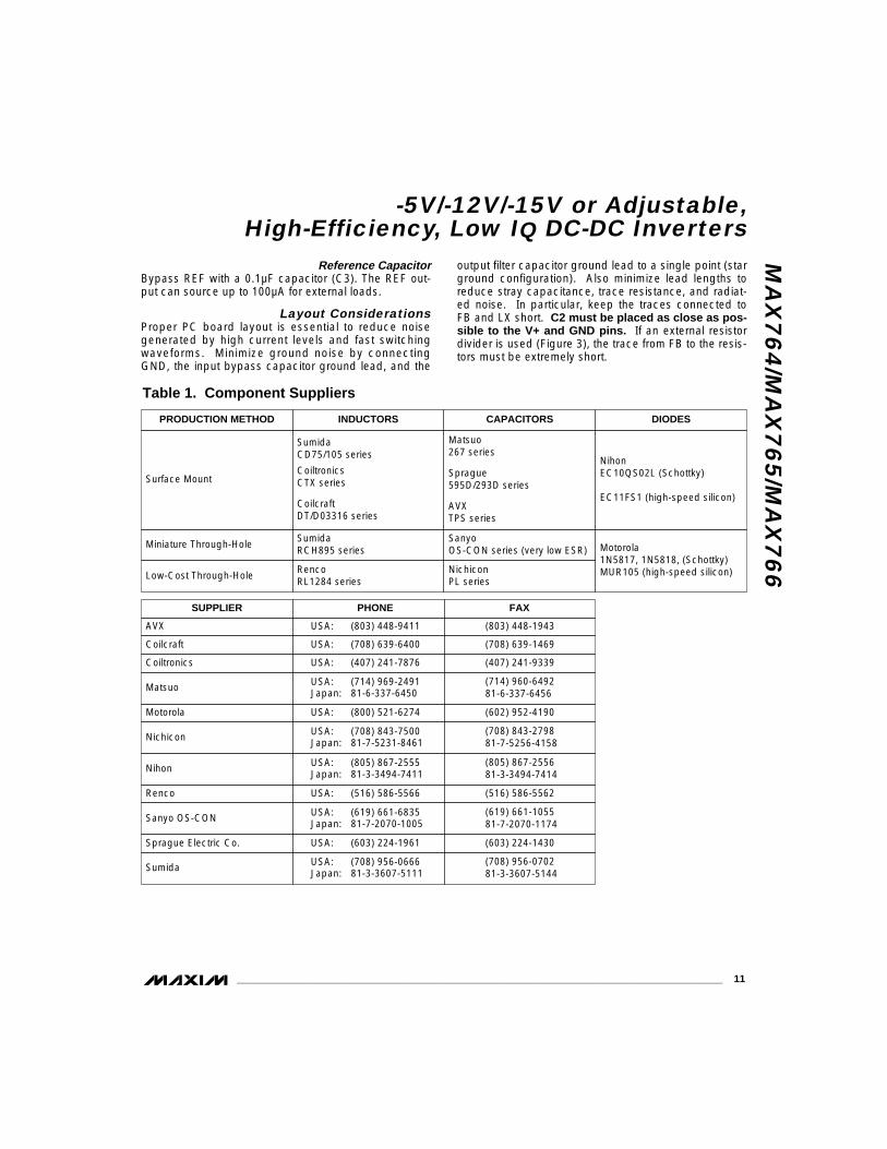
MA
X7
64
/MA
X7
65
/MA
X7
66
-5V/-12V/-15V or Adjustable,High-Efficiency, Low IQ DC-DC Inverters
______________________________________________________________________________________ 11
Table 1. Component Suppliers
PRODUCTION METHOD INDUCTORS CAPACITORS DIODES
Surface Mount
Matsuo267 series
Sprague595D/293D series
AVXTPS series
NihonEC10QS02L (Schottky)
EC11FS1 (high-speed silicon)
Miniature Through-HoleSumidaRCH895 series
SanyoOS-CON series (very low ESR)
Low-Cost Through-HoleRencoRL1284 series
NichiconPL series
Motorola1N5817, 1N5818, (Schottky)MUR105 (high-speed silicon)
SumidaCD75/105 series
CoiltronicsCTX series
CoilcraftDT/D03316 series
Reference CapacitorBypass REF with a 0.1µF capacitor (C3). The REF out-put can source up to 100µA for external loads.
Layout ConsiderationsProper PC board layout is essential to reduce noisegenerated by high current levels and fast switchingwaveforms. Minimize ground noise by connectingGND, the input bypass capacitor ground lead, and the
output filter capacitor ground lead to a single point (starground configuration). Also minimize lead lengths toreduce stray capacitance, trace resistance, and radiat-ed noise. In particular, keep the traces connected toFB and LX short. C2 must be placed as close as pos-sible to the V+ and GND pins. If an external resistordivider is used (Figure 3), the trace from FB to the resis-tors must be extremely short.
SUPPLIER PHONE FAX
AVX USA: (803) 448-9411 (803) 448-1943
Coilcraft USA: (708) 639-6400 (708) 639-1469
Coiltronics USA: (407) 241-7876 (407) 241-9339
Matsuo USA: (714) 969-2491Japan: 81-6-337-6450
(714) 960-649281-6-337-6456
Motorola USA: (800) 521-6274 (602) 952-4190
Nichicon USA: (708) 843-7500Japan: 81-7-5231-8461
(708) 843-279881-7-5256-4158
Renco USA: (516) 586-5566 (516) 586-5562
Sanyo OS-CON USA: (619) 661-6835Japan: 81-7-2070-1005
(619) 661-105581-7-2070-1174
Sprague Electric Co. USA: (603) 224-1961 (603) 224-1430
Nihon USA: (805) 867-2555Japan: 81-3-3494-7411
(805) 867-255681-3-3494-7414
Sumida USA: (708) 956-0666Japan: 81-3-3607-5111
(708) 956-070281-3-3607-5144
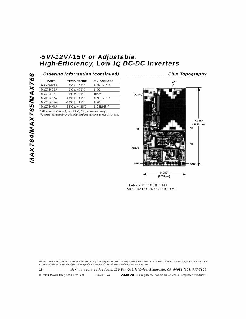
Maxim cannot assume responsibility for use of any circuitry other than circuitry entirely embodied in a Maxim product. No circuit patent licenses areimplied. Maxim reserves the right to change the circuitry and specifications without notice at any time.
12 __________________Maxim Integrated Products, 120 San Gabriel Drive, Sunnyvale, CA 94086 (408) 737-7600
© 1994 Maxim Integrated Products Printed USA is a registered trademark of Maxim Integrated Products.
MA
X7
64
/MA
X7
65
/MA
X7
66
-5V/-12V/-15V or Adjustable,High-Efficiency, Low IQ DC-DC Inverters_Ordering Information (continued) ___________________Chip Topography
GND
V+
V+
OUT
FB
SHDN
REF
LX
0.145" (3683µm)
0.080" (2032µm)
TRANSISTOR COUNT: 443SUBSTRATE CONNECTED TO V+
PART
MAX766CPA
MAX766CSA
MAX766C/D 0°C to +70°C
0°C to +70°C
0°C to +70°C
TEMP. RANGE PIN-PACKAGE
8 Plastic DIP
8 SO
Dice*
MAX766EPA
MAX766ESA -40°C to +85°C
-40°C to +85°C 8 Plastic DIP
8 SO
MAX766MJA -55°C to +125°C 8 CERDIP**
* Dice are tested at TA = +25°C, DC parameters only.**Contact factory for availability and processing to MIL-STD-883.